1
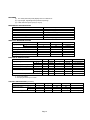
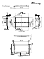
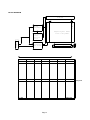
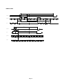
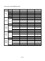
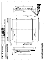
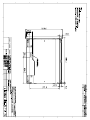
ENRICH YOUR VISUAL WORLD...
Sunlight Readable LCD!
LITEMAX TO1226
Sunlight Readable 12.1” LCD Display
(1st Edition 7/21/06 )
All information is subject to change without notice.
LITEMAX Electronics Inc.
4F, No.131-3, Lane 235, Bau-chiau Rd.,
Shin-dian City, Taipei County, Taiwan R.O.C.
Tel : 886-2-8919-1858
Fax: 886-2-8919-1300
Homepage: http://www.litemax.com.tw
FEATURES
(1) 12.1”XGA(1024x768 pixels) display size for notebook PC
(2) Light weight, High Brightness(1250cd/m2) design
(3) LVDS interface system (H-Sync, V-Sync)
MECHANICAL SPECIFICATIONS
Item
Dimensional Outline (typ.)
Number of Pixels
Active Area
Pixel Pitch
Weight (approximately)
Backlight
Specifications
292.9(W) x 220 (H) x 27.58 max( D) mm
1024(W) x 768(H) pixels
245.76(W) x 184.32(H) mm
0.24(W) x 0.24(H)
(275) g
8 CCFL, Sidelight type
ABSOLUTE MAXIMUM RATINGS
Item
Supply Voltage
Min.
-0.3
0
-0.3
0
-20
10
(VDD)
(VFL)
FL Driving Frequency (fFL)
Input Signal Voltage (VIN)
Operating Temperature
Storage Temperature
Storage Humidity
Max.
4.0
2.0
100
VDD+0.3
50
60
90
Unit
V
kV(rms)
kHz
V
°C
°C
%(RH)
ELECTRICAL SPECIFICATION
Item
Supply Voltage
(VDD)
(VFL)
FL Start Voltage (Ta=0°C)
Differential Input Voltage
Common Mode Input Voltage
Current Consumption
(VID)
(VCM)
*1 (I DD)
*2 (I FL)
*2 *3 Power Consumption
Min.
3.0
--1200
100
1.0
-------
Typ.
3.3
(625)
------(210)
6.0
(4.44)
Max.
3.6
--(1400)
600
2.4-(VID)/2
-------
Unit
V
V(rms)
V(rms)
mV
V
mA
mA(rms)
W
Remarks
I FL=6.0 mA(rms)
I FL=6.0 mA(rms)
*1 : 8 color bars pattern
*2 : Excepting the efficiency FL inverter
OPTICAL SPECIFICATION (Ta=25°C)
Item
Contrast Ratio (CR)
Response Time
Luminance
(L)
(tON)
(tOFF)
Min.
100
-------
Typ.
250
----1250
Page 2
Max.
--25
25
---
Unit
--ms
ms
cd/m 2
Remarks
I FL=6.0 mA(rms)
Page 3
BLOCK DIAGRAM
Y-driver
D C/DC
con verter
Y-driver
X-driver
Liquid C rystal Panel
G ra y s c a l e
M a n i p ul a t i o n
Vo l t a g e
G e n e ra t i o n
Ci r c u i t
10 24 x 768 pixels
P anel
Controller
L V DS i n c l u de
1, 1
1, 2
1, Y
2, 1
C N2
Connector
CN 1
Backlight
X2n-1, 1
X2n, 1
X2n-1, Y
X2n, Y
1, 768
1024, 1
768 pixels
1024,768
Page 4
TIMING CHART
tv
tvw
VSYNC
tvsu
tvhd
th
HSYNC
tvfp
tvbp
tvd
tvds
DE
1023
1
1024
th
thw
HSYNC
thbp
thfp
thds
thd
DE
1024
pixel
1 2 3 4
CLK
Page 5
2
TIMING SPECIFICATION
1) 2) 3) 4) 5) 6) 7)
Item
Horizontal Scanning Term
H-sync Pulse Width
Horizontal Front Porch
Horizontal Back Porch
Horizontal Data Sync Period
Horizontal Display Term
Frame Period
V-sync Pulse Width
V-sync Set Up Time (to H-sync)
V-sync Hold Time
Vertical Front Porch
Vertical Back Porch
Vertical Data Sync Period
Vertical Display Term
Clock Period
Symbol
th
thw
thfp
thbp
thds
thd
tv
tvw
tvsu
tvhd
tvfp
tvbp
tvds
tvd
tc
min.
1334 x tc
4 x tc
4 x tc
24 x tc
32 x tc
1024 x tc
778 x th
2 x th
8 x tc
(thbp+16) x tc
1 x th
2 x th
8 x th
768 x th
15.0
typ.
1344 x tc
136 x tc
24 x tc
160 x tc
296 x tc
1024 x tc
806 x th
6 x th
3 x th
29 x th
35 x th
768 x th
15.38
max.
1024 x tc
860 x th
768 x th
-
unit
clock
clock
clock
clock
clock
clock
line
line
clock
clock
line
line
line
line
ns
Note 1) Refer to “Timing Chart” and LVDS (THC63LVDF84A-85) specifications by THine Electronics, Inc.
corporation.
Note 2) If DE is fixed to "H" or "L" level for certain period while NCLK is supplied, the panel displays black with some flicker.
Note 3) If NCLK is fixed to "H" or "L" level for certain period while DE is supplied, the panel may be damaged.
Note 4) Please adjust LCD operating signal timing and FL driving frequency, to optimize the display quality.
There is a possibility that flicker is observed by the interference of LCD operating signal timing and FL driving
condition (especially driving frequency), even if the condition satisfies above timing specifications and
recommended operating conditions shown in 3.
Note5 ) Do not make tv, tvhd and tvds fluctuate.
If tv, tvhd, and tvds are fluctuate, the panel displays black.
Note6) In case of using the long frame period, the dete rioration of display quality, noise etc. may be occurred.
Note7) NCLK count of each Horizontal Scanning Time should be always the same.
V-Blanking period should be “n” X “Horizontal Scanning Time”. (n: integer)
Frame period should be always the same.
Page 6
CONNECTOR PIN ASSIGNMENT FOR INTERFACE
CN1 INPUT SIGNAL
Connector : DF19L-20P-1H / HIROSE
Mating Connector : DF19G-20S-1F (FPC), DF19G-20S-1C (Cable)
Terminal No.
Symbol
Function
1
VSS
GND
2
VDD
Power Supply : +3.3V
3
VDD
Power Supply : +3.3V
4
VEDID
DDC 3.3V power
5
NC
Non-Connection
6
CLKEDID DDC clock
7
DATAEDIE DDC data
8
RxIN0Negative LVDS differential data input (R0-R5,G0)
9
RxIN0+ Positive LVDS differential data input (R0-R5,G0)
10
VSS
GND
11
RxIN1Negative LVDS differential data input (G1-G5, B0-B1)
12
RxIN1+ Positive LVDS differential data input (G1-G5, B0-B1)
13
VSS
GND
14
RxIN2Negative LVDS differential data input (B2-B5, HS, VS, DE)
15
RxIN2+ Positive LVDS differential data input (B2-B5, HS, VS, DE)
16
VSS
GND
17
CLKClock Signal(-)
18
CLK+
Clock Signal(+)
19
VSS
GND
20
VSS
GND
Note 1) Please connect GND pin to ground. Don't use it as no-connect nor connection with high impedance.
CN2 CCFL POWER SOURCE
Connector : BHSR-02VS-1 / JAPAN SOLDERLESS TERMINAL MFG CO., LTD.
Mating Connector : SM02B-BHS-1 / JAPAN SOLDERLESS TERMINAL MFG CO., LTD.
Terminal No.
Symbol
Function
1
VFLH
CCFL Power Supply ( high voltage)
2
VFLL
CCFL Power Supply (low voltage)
Page 7
RECOMMENDED TRANSMITTER (THC63LVDF63A,THC63LVDM63A,THC63LVDM63A-85)
TO LTD121EC5S INTERFACE ASSIGNMENT
Case1: 6bit Transmitter
THC63LVDF63A,THC63LVDM63A,THC63LVDM63A-85
Input Terminal No.
Symbol
TIN0
TIN1
TIN2
TIN3
TIN4
TIN5
TIN6
TIN7
TIN8
TIN9
TIN10
TIN11
TIN12
TIN13
TIN14
TIN15
TIN16
TIN17
TIN18
TIN19
TIN20
Terminal
44
45
47
48
1
3
4
6
7
9
10
12
13
15
16
18
19
20
22
23
25
CLK IN
26
Input Signal
(Graphics controller output signal)
Symbol
Function
R0
Red Pixels Display Data (LSB)
R1
Red Pixels Display Data
R2
Red Pixels Display Data
R3
Red Pixels Display Data
R4
Red Pixels Display Data
R5
Red Pixels Display Data (MSB)
G0
Green Pixels Display Data (LSB)
G1
Green Pixels Display Data
G2
Green Pixels Display Data
G3
Green Pixels Display Data
G4
Green Pixels Display Data
G5
Green Pixels Display Data (MSB)
B0
Blue Pixels Display Data (LSB)
B1
Blue Pixels Display Data
B2
Blue Pixels Display Data
B3
Blue Pixels Display Data
B4
Blue Pixels Display Data
B5
Blue Pixels Display Data (MSB)
HSYNC H-Sync
VSYNC V-Sync
DE
Compound Synchronization Signal
CLK
Data Sampling Clock
Output
Signal
Symbol
LTD121EC5S
Interface
(CN1)
Terminal
Symbol
TOUT0TOUT0+
No.8
No.9
IN0IN0+
TOUT1TOUT1+
No.11
No.12
IN1IN1+
TOUT2TOUT2+
No.14
No.15
IN2IN2+
TCLK OUTTCLK OUT+
No.17
No.18
CLKCLK+
Note 1) Please connect NC pin to nothing. Don't connect it to ground nor to other signal input.
IN 0
T IN 6
G0
IN 1
T IN 13
B1
IN 2
T IN 20
DE
TI N5
T IN 4
T I N3
TI N2
T IN 1
T IN 0
R5
R4
R3
R2
R1
R0
TI N1 2
T IN 11
TI N1 0
TI N 9
T IN 8
T IN 7
B0
G5
G4
G3
G2
G1
TI N1 9
T IN 18
TI N1 7
T IN 16
TI N1 5
T IN 14
VSYNC
HS YNC
B5
B4
B3
B2
Page 8
RECOMMENDED TRANSMITTER (THC63LVDF63A,THC63LVDM63A,THC63LVDM63A-85)
TO LTD121EC5S INTERFACE ASSIGNMENT
Case2: 8bit Transmitter
THC63LVDF63A,THC63LVDM63A,THC63LVDM63A-85
Input Signal
(Graphics controller output signal)
Symbol
Function
R0
Red Pixels Display Data (LSB)
R1
Red Pixels Display Data
R2
Red Pixels Display Data
R3
Red Pixels Display Data
R4
Red Pixels Display Data
R5
Red Pixels Display Data (MSB)
G0
Green Pixels Display Data(LSB)
G1
Green Pixels Display Data
G2
Green Pixels Display Data
G3
Green Pixels Display Data
G4
Green Pixels Display Data
G5
Green Pixels Display Data(MSB)
B0
Blue Pixels Display Data (LSB)
B1
Blue Pixels Display Data
B2
Blue Pixels Display Data
B3
Blue Pixels Display Data
B4
Blue Pixels Display Data
B5
Blue Pixels Display Data (MSB)
HSYNC H-Sync
VSYNC V-Sync
DE
Compound Synchronization Signal
NC
Non Connection (open)
NC
Non Connection (open)
NC
Non Connection (open)
NC
Non Connection (open)
NC
Non Connection (open)
NC
Non Connection (open)
NC
Non Connection (open)
Input Terminal No.
Symbol
TIN0
TIN1
TIN2
TIN3
TIN4
TIN6
TIN7
TIN8
TIN9
TIN12
TIN13
TIN14
TIN15
TIN18
TIN19
TIN20
TIN21
TIN22
TIN24
TIN25
TIN26
TIN27
TIN5
TIN10
TIN11
TIN16
TIN17
TIN23
Terminal
51
52
54
55
56
3
4
6
7
11
12
14
15
19
20
22
23
24
27
28
30
50
2
8
10
16
18
25
CLK IN
31
CLK
Output
Signal
Symbol
LTD121EC5S
Interface
(CN1)
Terminal
Symbol
TOUT0TOUT0+
No.8
No.9
IN0IN0+
TOUT1TOUT1+
No.11
No.12
IN1IN1+
TOUT2TOUT2+
No.14
No.15
IN2IN2+
No.17
No.18
CLKCLK+
TOUT3TOUT3+
TCLK OUTTCLK OUT+
Data Sampling Clock
Note 1) Please connect NC pin to nothing. Don't connect it to ground nor to other signal input.
IN 0
TIN7
G0
IN 1
IN 2
R5
TIN4
TIN3
TIN2
TIN1
TIN0
R4
R3
R2
R1
R0
TIN12
TIN9
TIN8
G3
G2
G1
T I N 22
TIN21
TI N 2 0
TIN19
B5
B4
B3
B2
TIN10
TIN18
TIN15
TIN14
B1
B0
G5
TIN26
TIN25
TIN24
VS YNC
HS YNC
TIN17
TIN16
T I N 11
NC
NC
NC
DE
IN 3
T IN 6
TIN23
NC
T I N 13
G4
Page 9
NC
TI N 5
NC
TIN27
NC
256k (k=1024) COLORS COMBINATION TABLE
Display
Basic
Color
Gray
Scale of
Red
Black
Blue
Green
Light Blue
Red
Purple
Yellow
White
Black
Dark
↑
↓
Light
Red
Black
Gray
Scale of
Green
Dark
↑
↓
Light
Green
Black
Gray
Scale of
Blue
Dark
↑
↓
Light
Blue
Black
Gray
Scale of
White &
Black
Dark
↑
↓
Light
White
R5 R4 R3 R2 R1 R0
L
L
L
L
H
H
H
H
L
L
L
L
L
L
L
H
H
H
H
L
L
L
L
L
L
L
H
H
H
H
L
L
L
L
L
L
L
H
H
H
H
L
L
L
L
L
L
L
H
H
H
H
L
L
H
L
L
L
L
H
H
H
H
L
H
L
G5 G4 G3 G2 G1 G0
L
L
H
H
L
L
H
H
L
L
L
L
L
H
H
L
L
H
H
L
L
L
L
L
H
H
L
L
H
H
L
L
L
:
:
H
H
H
L
L
L
H
H
H
L
L
L
H
H
H
L
L
L
L
L
L
L
L
L
H
H
H
L
L
L
L
L
L
L
L
L
L
H
H
L
L
L
H
L
H
L
L
L
L
L
L
L
L
L
L
L
L
L
L
L
L
L
L
L
L
L
L
L
L
L
L
L
L
L
L
L
L
L
L
L
L
L
L
L
L
L
L
L
L
L
L
L
L
L
L
L
H
H
H
L
L
L
H
H
H
L
L
L
H
H
H
L
H
L
H
L
H
L
H
L
L
L
L
H
L
H
L
H
L
H
L
L
L
L
H
L
H
L
H
L
H
L
L
L
L
L
L
L
L
H
L
L
L
L
H
L
L
L
L
L
L
L
L
L
L
L
L
L
L
L
L
L
L
L
L
H
H
L
L
L
H
L
H
L
L
L
L
L
L
L
L
L
L
L
L
L
L
L
L
L
L
L
L
L
:
:
L
L
L
L
L
L
L
L
L
L
L
H
L
L
L
L
H
L
L
L
L
L
L
L
L
L
L
L
L
L
L
L
L
L
L
L
H H L H
H H H L
H H H H
H
H
H
H
H
H
L
H
L
H
L
H
L
H
L
L
L
L
L
L
L
L
L
L
L
L
L
L
L
L
L
L
L
L
L
L
L
L
L
L
L
L
L
L
L
L
H
L
L
L
L
H
L
L61
L62
Green L63
L 0
L 1
L 2
L3…
L60
H
H
H
L
L
L
L
H
H
L
L
H
H
L
H
L
H
L
L61
L62
Blue L63
L 0
L 1
L 2
L3…
L60
H
H
H
L
H
H
H
L
H
L61
L62
White L63
:
:
L
L
L
L
L
L
L
L
L
L
L
H
L
L
L
L
H
L
H
H
H
L
L
L
H
H
H
L
L
L
H
H
H
L
L
L
:
:
H
H
H
L
H
L
H
L
H
L
H
L
L
L
:
:
H
H
H
L
L
L
:
:
H
H
H
Page 10
L
H
H
H
L
H
H
H
H
H
H
H
H
H
H
Gray Scale
Level
L 0
L 1
L 2
L3…
L60
L
H
L
H
L
H
L
H
L
L
L
:
:
L
L
L
L
L
L
H
H
H
L
L
L
:
:
H
H
H
L
L
H
H
L
L
H
H
L
L
L
:
:
:
:
L
L
L
L
L
L
L
L
H
H
L
L
H
H
L
L
L
:
:
:
:
L
L
L
L
L
L
L
L
H
H
L
L
H
H
L
L
L
B5 B4 B3 B2 B1 B0
L61
L62
Red
L63
L 0
L 1
L 2
L3…
L60
!
FOR SAFETY
LCD module is generally designed with precise parts to achieve light weighted thin mechanical dimensions.
In using our Modules, make certain that you fully understand and put into practice the warnings and safety precautions
detailed in Engineering Information No.EE- N001,"CAUTIONS AND INSTRUCTIONS FOR TOSHIBA MATSUSHITA
DISPLAY TECHNOLOGY LCD MODULES".
Refer to individual specifications and TECHNICAL DATA sheets (hereinafter called "TD") for more detailed technical
information.
1) SPECIAL PURPOSES
A) Toshiba Matsushita Display technology's Standard LCD Modules have not been customized for operation in extreme
environments or for use in applications where performance failures could be life-threatening or otherwise catastrophic.
B) Since Toshiba Matsushita Display technology's Standard LCD Modules have not been designed for operation in extreme
environments, they must never be used in devices that will be exposed to abnormally high levels of vibration or shock which
exceed Toshiba Matsushita Display technology's published specification limits.
C) In addition, since Toshiba Matsushita Display technology Standard LCD Modules have not been designed for use in
applications where performance failures could be life-threatening or catastrophic, they must never be installed in aircraft
navigation control systems (such as, but not limited to Traffic Collision Avoidance System and Air Traffic Indicator), in military
defense or weapons systems, in critical industrial process-control systems (e.g., those involved in the production of nuclear
energy), or in critical medical device or patient life-support systems.
2) DISASSEMBLING OR MODIFICATION
DO NOT DISASSEMBLE OR MODIFY the module. It may damage sensitive parts inside LCD module, and may cause
scratches or dust on the display.
Toshiba Matsushita Display technology doses not warrant the module, if customer disassembled or modified it.
3) BREAKAGE OF LCD PANEL
DO NOT INGEST liquid crystal material, DO NOT INHALE this material, and DO NOT CONTACT the material with skin, if
LCD panel is broken and liquid crystal material spills out.
If liquid crystal material comes into mouth or eyes, rinse mouth or eyes out with water immediately.
If this material contact with skin or cloths, wash it off immediately with alcohol and rinse thoroughly with water.
4) GLASS OF LCD PANEL
BE CAREFUL WITH CHIPS OF GLASS that may cause injuring fingers or skin, when the glass is broken.
5) ELECTRIC SHOCK
DISCONNECT POWER SUPPLY before handling LCD module.
DO NOT TOUCH the parts inside LCD module and the fluorescent lamp's connector or cables in order to prevent electric
shock, because high voltage is supplied to these parts from the inverter unit while power supply is turned on.
6) ABSOLUTE MAXIMUM RATINGS AND POWER PROTECTION CIRCUIT
DO NOT EXCEED the absolute maximum rating values under the worst probable conditions caused by the supply voltage
variation, input voltage variation, variation in parts' constants, environmental temperature, etc., otherwise LCD module may
be damaged.
Employ protection circuit for power supply, whenever the specification or TD specifies it.
Suitable protection circuit should be applied for each system design.
7) DISPOSAL
When dispose LCD module, obey to the applicable environmental regulations.
Page 11