1
Post Developmental Applications of
Analog-to-Digital Converters
A Major Qualifying Project Report
Submitted to the Faculty
of the
WORCESTER POLYTECHNIC INSTITUTE
in partial fulfillment of the requirements for the
Degree of Bachelor of Science
in
Electrical and Computer Engineering
by
Sean Gray
Gabriel G. McCormick
Dale L. Spencer Jr.
MQP-AW1-IRL9
10/23/2012
Sponsoring Organization:
Analog Devices
Project Advisor:
Professor Alexander Wyglinski
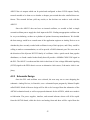
Abstract
The goal of this project is to improve upon the post-development applications for analogto-digital converters (ADC). Specifically, three tasks were pursued throughout the duration of
this project: The first focused on the development of an improved, low jitter evaluation board for
the AD7626 ADC. The second task focused on the generation of a process by which Analog
Devices can create in-house input/output buffer information specification (IBIS) models. Finally,
the third task involved assessing the feasibility of integrating Analog Devices’ products with
third party microcontrollers.
i
Acknowledgements
Without the help from certain individuals and groups, the completion of this project
would not have been possible.
First, we would like to thank Worcester Polytechnic Institute and the Interdisciplinary
and Global Studies Division for making the necessary arrangements for us to go to Limerick,
Ireland.
We would like to thank Analog Devices, for providing us with a place to work and the
necessary equipment needed to complete our project.
We would like to extend a special thanks to Claire Leahy, and Claire Croke for
overseeing our project at Analog Devices.
Most of all we would like to thank Professor Alexander Wyglinski for advising our
project.
Finally, we would like to thank Charlotte Tuohy, our local coordinator for the project
center, for arranging and managing our housing, as well as assisting many times us during our
time in Limerick, Ireland.
ii
Executive Summary
In order to satisfy its customers, Analog Devices needs to provide post development
support for its products. The support required is unique to both the product and the customer and
can range in applications such as developing evaluation boards that showcase a device’s
capabilities, developing software that enhances a product’s functionality, and improving on a
product’s ease of use. Specifically, our group tackled tasks that involved developing an improved
evaluation board for and Analog Devices analog-to-digital converter (ADC), generating a
process by which Analog Devices can create in house input/output buffer information
specification (IBIS) models, and tested the feasibility of integrating Analog Devices products
with third party microcontrollers.
IBIS
I/O Buffer Information Specification (IBIS) is a standard by which the electrical
characteristics of the pins of a digital integrated circuit (IC) are represented. An IBIS model
contains the I/O buffers and other characteristics of the circuit without revealing the circuit’s
structure or process information. Presently, the work of creating the IBIS model for Analog
Devices parts is contracted out to a third part. Analog Devices wants to avoid further contracting,
and would like to move the creation of IBIS models in-house. Therefore, our task in developing
this procedure should outline how to create a model that takes simulated current versus voltage
(I/V) and voltage versus time (V/T) data and converts it into an IBIS model. To develop this
procedure, we will create an IBIS model by converting bench measurement data personally taken
using the AD7091R analog-to-digital converter (ADC), into the IBIS format. The data, along
with the IBIS model itself, will be compared and versified against a model made for the same
device by a third party company.
iii
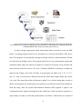
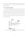
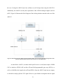
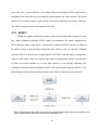
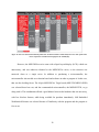
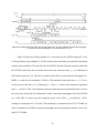
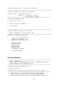
Figure 1: These are the steps required to produce a fully functional IBIS model. The primary goal of this project
was to show that it was possible for Analog Devices to perform the first two steps of this process, gathering the data and
creating the IBIS file, and to develop a procedure of how to do so [1].
In order to begin acquiring the bench measurement data we needed to create our IBIS
model a sweeping program needed to be developed to be used by the Keithley 2420 source
meter. This program was developed by altering an example LabView virtual instrument (VI) that
was offered in the Keithley drivers. The program allowed us to set up measurement options that
controlled voltage range, the number of samples to be taken, how long the sweep will take and
where the data would be saved to. We used a Tektronix DPO4054 oscilloscope to obtain the
ramp rate and Voltage versus Time (VT) data. A measurement was taken at 1.8 V, 2.5 V, 3.3 V,
and 5 V, with a 50 Ω resistor connected between the Serial Data Output (SDO) pin and the
VDRIVE pin. This setup allowed the oscilloscope to gather VDRIVE-relative timing data. In order to
obtain a measurement, the oscilloscope was connected to the SDO pin and Ground (GND) pin.
With this setup, when the System Demonstration Platform (SDP) supplied a signal to the
evaluation board, the signal was displayed on the oscilloscope, which can then be captured as a
single sample. In order to obtain the ground-relative waveforms a 50Ω resistor was connected
iv
between the SDO pin and the GND pin and the process was repeated. To obtain data on the
rising and falling edge, we took advantage of the oscilloscope’s ability to focus onto critical
portions of the waveform. In order to obtain the ramp rate of the rising waveforms, one cursor on
the oscilloscope screen was placed at 20% of the maximum voltage and another was placed at
80% of the maximum voltage, thereby displaying the change in voltage levels between these two
points, as well as the time it took between changes.
The next step was to take all of the data we had acquired and write it in the IBIS format.
We decided to develop a method of accomplishing this task using a LabView Virtual Instrument
(VI). Since Analog Devices wanted the process of translating raw data into the IBIS format to be
as automated as possible, there were two specific goals that this program attempted to
accomplish. The first goal was to be able to use this program with a wide variety of devices,
meaning that it would need to be universal. The second goal was to have the program require as
little user input as possible. These goals contradict each other because by being universal, the
program will most likely need more user inputs. On the other hand, having the program be fully
automated would most likely limit the devices which the program could be used for, so we
would need to find a balance between these two qualities.
The results for the IBIS model project consisted of the numerous measurement files, the
LabView VI, and a step-by-step procedure for creating the IBIS model to be used by Analog
Devices. Once our measurement data was captured, it was saved into a spreadsheet. There were
forty of these spreadsheets in total. Secondly, our LabView VI prompts the user for all of the part
and manufacturer specific headings that exist in the IBIS format, as well as the paths to the many
data files that they must have to create for the model. When the program is run, it will create a
.txt file which can be renamed to an .ibs file to be used in Mentor Graphics’ HyperLynx program
v
for analyzing IBIS models. The final product of this project was the step-by-step tutorial for
creating the IBIS model, which included a careful documentation all of the steps we took that led
to a successful model, as well as how to use the LabView VI that we created.
The IBIS model created in this project only had to contain enough data to show that it
was possible to gather all of the data necessary and output it in the IBIS format. The next steps
would involve additions to our guideline which would outline a procedure for producing a full
IBIS model. This would entail all of the steps necessary for gathering the Voltage versus Time
(VT) and Current versus Voltage (IV) characteristics of the device under its maximum and
minimum performance specifications, while we were only concerned with the data under typical
conditions.
Another simple improvement to the data collection process for the VT data would be to
change the parameters for measuring the rising and falling waveforms. We would have liked to
implement these conditions, but there was no longer time to do so. Additional future work to be
considered is improvements to the “Sweep_Measure_and_output_to_excel” Virtual Interface
(VI). At present the sweep takes a number of data points over set intervals, but it would be more
efficient to take data points at areas of greatest change. This would ensure that a large number of
data points are not wasted over a region where nothing of interest is happening, leaving fewer
data points for the regions that need them. Another possible quality of life improvement would
be to use a LabView VI to control the power supply. This would make taking the measurement
much more efficient as all four sweeps needed for each configuration could be taken at once
instead of needing to run the sweep four times, adjusting the voltage parameters between each
sweep.
vi
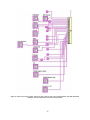
AD7626
Evaluation boards are an important part of the post-development applications at Analog
Devices. They provide the user with a method of testing and using analog-to-digital converters
(ADC), as well as giving the user knowledge of the real performance capabilities of the product.
The speeds of Analog Devices’ ADCs are part of what make them desirable. When building
evaluation boards for any product, one must take special care regarding how all of the different
components will be sensitive to high frequencies. Ideal models will begin to melt away to the
realities of engineering when very high speeds are applied. If an ADC cannot perform to its full
throughput because it is being limited by a different portion of the circuitry, then the ability to
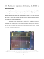
operate at those higher frequencies is wasted. The final objective of the AD7626 Evaluation
Board project is to develop an improved evaluation board for the AD7626, an analog-to-digital
converter that connects to Analog Devices’ new System Demonstration Platform-H (SDP-H)
platform. The new board will allow for high frequency input tones to be applied to the AD7626,
while still maintaining the previous clock source as an alternative. It is also imperative that the
jitter on the Convert Start (CNV) provided to the AD7626 does not impede performance. This
means that a new clocking solution will need to be developed to provide a low jitter input to the
AD7626 as well as the FPGA on the motherboard.
In order to design a low jitter clocking solution, we first needed to research how jitter can
be reduced, and what kinds of devices exist to accomplish this task. Through research and
meetings with our supervisors, we decided to use a PLL centered clocking solution. Next, we
took advantage of video tutorials and applications notes provided on the Analog Devices
website, and decided to use the AD9513, based on three key factors. The first was if the PLL met
the required low jitter specifications. The data sheet for the AD7626 boasts a signal to noise ratio
vii
(SNR) of 91.5dB, while the datasheet of the AD9513 boasts a jitter performance of
approximately 300fs at 10 MHz. The relationship of a device’s SNR (dB) and its jitter is shown
in the equation below in Equation 1:
(
)
(
)
Equation 1
Using this equation, we found that the maximum jitter time that a signal provided by the
PLL could provide without reducing the performance of the ADC is 423.4fs. Therefore, the
AD9513 meets the low jitter recommendations. We also know from our design approach that the
PLL would need at least three LVDS outputs. The AD9513 has six outputs which can be paired
and configured as three LVDS. Finally, we needed to see if a part existed that also satisfied these
two factors, but was a cheaper. We could not find such a product.
Since the AD7626 is very similar to the AD7960, we knew we would be able to leverage
much of the design from that evaluation board schematic. However, while being able to copy
parts from other schematic is very convenient, it does not mean that everything will work
together. In order to gain a greater knowledge in how the AD7960 schematic works, and how it
will need to be changed to function with the AD7626, we will need to seek the advice of one of
the head engineers of the AD7960 project. After the leveraged parts of the previous schematic
are modified to work with the AD7626, the new clocking solution needs to be created. While this
schematic sheet will require more design than the others, we can still take advantage of existing
schematics on the Analog Devices website that use the AD9513. Once we are satisfied with the
viii
design, the schematic will be submitted to the project adviser, along with a bill of materials for
all of the parts existing on the plan. After making the appropriate changes to gain the approval of
Analog Devices, the schematic will go through a final review before being sent to the layout
department for fabrication.
The evaluation board that we designed was completed at such a time during our project
that we would not receive the fabricated board because of the layover between submission and
layout and fabrication. During this time between design submission and receiving the board, we
would have worked on the code that governs the off board field-programmable gate array
(FPGA). Consequently, instead of having the code that governs the FPGA, test results of the
board, and schematics of the circuitry, the only result we have for the AD7626 project is the
schematic that was submitted and approved for layout and fabrication. The process for
submitting a schematic for layout and fabrication involved several meetings with applications
engineers, but it did not involve simulation. However, in these meetings, we went through our
schematic diligently. Since the majority of the schematics we submitted were based on previous
designs, most of the focus was aimed at how the previous circuitry was modified to fit the
differences in the specifications between the AD7626 and the AD7960. When we reviewed the
page that we had created, we were required to explain why every connection was made based
upon product datasheets and evaluation literature from the Analog Devices website.
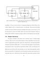
AD7980 Interfacing to Microcontrollers
The advancement of the processing power of microcontrollers has made them more
appealing for interfacing with analog-to-digital converters (ADC). This is especially true
regarding ADCs that have had their performance limited by their controller in the past. This
limitation commonly lies in the maximum clock speed of the controller, as the minimum
ix
conversion time of the ADC relies on the ability of the controller to read the n-bit digital output
within a certain maximum time. If the controller is unable to reach this clock speed, then the
ADC will operate at a reduced throughput. Analog Devices has recognized the consumer’s desire
to interface with microcontrollers by releasing a driver intended to simplify the interfacing of
microcontrollers to one of their ADCs, the AD7980. However, Analog Devices is unsure of the
performance implications on their ADC’s when interfacing to commonly used microcontrollers.
The first goal for the AD7980 Microcontroller project is to collect performance data of
the ADC. The bandwidth of the processor being used while interacting with the ADC is of
interest, as this is likely to impact the other devices the microcontroller is connected to. Ideally,
the microcontrollers would be able to operate the ADC at its maximum throughput. Finally, the
signal to noise ratio (SNR) of the conversion needs to be derived, which can be done over a large
number of conversions, and is expected to decrease as the throughput of the ADC increases, due
to jittery clocks, and the known performance degradation of Serial Peripheral Interface (SPI) at
speeds over 50 kHz. The second project goal for the AD7980 project is to determine the ease of
use of interfacing to these microcontrollers using the generic driver designed by Analog Devices.
The project will test the driver with three microcontrollers, from three different manufacturers, in
order to determine ease of use. If it is found that interfacing to these various devices is not
simple, then methods for improving the driver should be devised.
The project was to use two microcontrollers from different companies. One
microcontroller was required to be from the Texas Instruments MSP430 family, due to its
immense popularity. The other was left to the group’s discretion, but it was recommended that
the other microcontroller be selected from the offerings of STMicroelectronics. When it came to
selecting potential families, and then the individual microcontroller, there were two defining
x
factors. First, the microcontroller needed to be able to utilize the Serial Peripheral Interface (SPI)
when communicating with external components. Second, in order to maintain the AD7980’s
maximum throughput, the microcontrollers needed a clock of at least 55.1725 MHz.
The purpose of the program designed for each microcontroller is exactly the same,
although the code for each microcontroller varies due to differences in how control registers are
accessed for each microcontroller. The objectives of the program were to establish the Serial
Peripheral Interface (SPI) with the AD7980 analog-to-digital converter (ADC), initiate the
conversion, and maintain conversions at the maximum rate provided for by the microcontroller.
A method for exporting the data out of the memory of each microcontroller was needed in order
to get the performance specifications. Once the program for each microcontroller was complete,
tests had to be run in order to derive the performance of the ADC with each microcontroller.
These tests included throughput of the ADC, signal to noise ratio of the conversion, and bit rate
of the microcontroller.
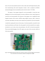
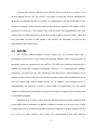
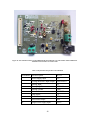
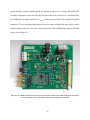
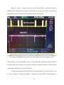
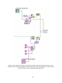
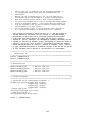
Figure 2: The AD7980 evaluation board that was used. The blue wire connects to the raised OVDD pin on one end, and to
VDRIVE on the other. The red wire allows connections to the SDI pin on the AD7980.
xi
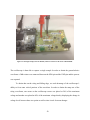
In order to correctly test the AD7980 analog-to-digital converter (ADC) with the
microprocessor, an AD7980 evaluation board was used, in conjunction with a breakout board.
Finally, a signal generator was used to provide the positive and negative terminals of the input
signal. As stated above, the performance specifications that were of interest were the throughput
achieved with the ADC and microcontroller, and the signal to noise ratio (SNR) of the signal
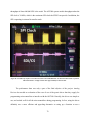
after conversion. In order to derive the throughput of the ADC an oscilloscope was connected to
the 4 wires interfacing the AD7980 to the microcontroller. When a conversion is viewed on the
oscilloscope, the conversion time that has been elapsed can be seen, and can be used to find the
throughput. This is found by the equation in Equation 2.
(
) (
)
Equation 2
This result is the samples that the ADC is able to complete per second when interfacing
with the microprocessors. Computing the SNR requires a large number of conversions for
accuracy purposes. To calculate the SNR, the data from a large number of conversions is input
into a specially designed LabView Virtual Instrument (VI) for creating Fast-Fourier transform
(FFT) plots, and then the VI calculates the overall SNR of the system. Sixteen thousand
conversions are needed in order for the FFT to be accurate. Since the SNR is so heavily
dependent on frequency, the conversions will needed to be tested across a broad range, in order
to get the best possible picture of how the microcontroller and the SPI interface affect the
performance of the AD7980.
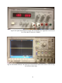
To generate the analog waveform used for testing, an Audio Precision SYS-2722 was
used. Running a single test required changing the SYS-2722 settings to reflect the frequency to
test at, as well as the peak-to-peak voltage. Each microcontroller was to be tested at ten different
xii
frequencies, ranging from 1 kHz to 100 kHz. The peak-to-peak voltage would remain constant.
The voltage level was determined by testing the performance of the AD7980 when interfaced
with Analog Devices’ System Demonstration Platform (SDP), and determining a peak-to-peak
voltage that provided the SNR performance provided on the datasheet of the AD7980. The peakto-peak voltage used was 20 Vpp.
During testing, it was discovered that the MSP430F5528 had 8 kilobytes (kB) of random
access memory (RAM), which was nowhere near the 32 kB needed to hold an array of sixteen
thousand sixteen bit conversions. This caused the MSP430 to require additional code to write the
conversion to flash memory, which had enough space to hold all the conversions. Unfortunately,
this caused additional performance issues, so we made the decision to determine to performance
of a test run at 1 kHz, while writing 2,272 conversions in RAM. The STM32F207ZG was limited
by a 30 MHz SPI clock, but otherwise was able to be interfaced with the AD7980 without any
other modifications. Together, these performance specifications should give an accurate
representation of how well the microcontroller is able to interface with the AD7980 ADC. After
the data was compiled, a report was presented to Analog Devices that highlighted the results and
the ease of use of their generic microprocessor driver.
It was apparent from our results that it would be difficult to recommend interfacing the
AD7980 to these microcontrollers. Limitations on the SPI clocks immediately ruled out any
possibility of reaching the maximum throughput on the AD7980. In addition, data with glitches
from the MSP430 provided an SNR that was significantly less than desired. When the glitches
were removed manually, the SNR increased by a significant margin. Given more time, it is likely
that this SNR could have been improved even further, but it is unlikely that the SNR would get
to within 10 dB of the performance listed on the AD7980 datasheet. Unfortunately, SNR data
xiii
could not be collected for the STM32 due to time restrictions and malfunctioning AD7980
boards. The throughput of the STM32 was not able to reach the maximum throughput of the
AD7980, due to the limitation on the SPI clock. However, the throughput was significantly
improved over the MSP430, despite only a modest SPI clock increase. With more time, a third
microcontroller, the Freescale Kinetis K60, would be tested
xiv
Table of Contents
1 INTRODUCTION ................................................................................................................................... 1
1.1 PROBLEM STATEMENT...............................................................................................................................5
1.2 PROJECT OBJECTIVES AND REPORT CONTRIBUTIONS ........................................................................................7
1.2.1 ADC IBIS Model Generation .........................................................................................................8
1.2.2 AD7626 Evaluation Board ...........................................................................................................8
1.2.3 AD7980 Interfacing to Microcontrollers ......................................................................................8
1.2.4 Report Contributions ...................................................................................................................9
1.3 REPORT ORGANIZATION ..........................................................................................................................10
2 FUNDAMENTALS OF ANALOG-TO-DIGITAL CONVERTERS AND THEIR APPLICATIONS ......................... 12
2.1 ANALOG-TO-DIGITAL CONVERTERS ............................................................................................................12
2.1.1 Successive Approximation ADCs ................................................................................................17
2.2 IBIS ....................................................................................................................................................18
2.2.1 Three-State Output Buffer .........................................................................................................20
2.2.2 Input Buffer ...............................................................................................................................21
2.2.3 Versions of IBIS ..........................................................................................................................22
2.3 SERIAL PERIPHERAL INTERFACE .................................................................................................................23
2.5 CHAPTER SUMMARY ...............................................................................................................................26
3 PROPOSED APPROACH ...................................................................................................................... 28
3.1 PROJECTS PLAN......................................................................................................................................28
3.1.2 GANTT CHART ......................................................................................................................................29
3.2 IBIS .....................................................................................................................................................31
3.3 AD7626 ..............................................................................................................................................31
3.3.1 AD9522-4 ..................................................................................................................................32
3.3.2 AD9515 ......................................................................................................................................32
xv
3.3.3 AD9513 ......................................................................................................................................34
3.4 AD7980 ..............................................................................................................................................35
3.4.1 Project Objectives .....................................................................................................................36
3.4.2 Selecting a Texas Instruments MSP430 Microcontroller ..........................................................37
3.4.3 Selecting a STMicroelectronics Microcontroller ........................................................................39
3.5 CHAPTER SUMMARY ...............................................................................................................................41
4 IMPLEMENTATION ............................................................................................................................. 42
4.1 ANALOG-TO-DIGITAL CONVERTER IBIS MODEL GENERATION .........................................................................42
4.1.1 Writing a Project Plan ...............................................................................................................43
4.1.2 Setting up the Equipment for the AD7091R IBIS Model ............................................................47
4.1.3 Taking the Measurements for the AD7091R IBIS Model ...........................................................48
4.2 DEVELOPING AN AD7626 EVALUATION BOARD METHODOLOGY.....................................................................52
4.2.1 Researching Clocking Solutions .................................................................................................53
4.2.2 Choosing the Best Part ..............................................................................................................54
4.2.3 Schematic Design ......................................................................................................................55
4.3 PERFORMANCE IMPLICATIONS OF INTERFACING THE AD7980 TO MICROCONTROLLERS .......................................58
4.3.1 Selecting the Microcontrollers ..................................................................................................58
4.3.2 Developing the Code for the MSP430 .......................................................................................60
4.3.3 Testing the Performance Specifications ....................................................................................62
4.4 CHAPTER SUMMARY ...............................................................................................................................67
5 RESULTS ............................................................................................................................................. 69
5.1 ANALOG-TO-DIGITAL CONVERTER IBIS MODEL GENERATION .........................................................................69
5.2 DEVELOPING THE AD7626 EVALUATION BOARD RESULTS .............................................................................73
5.3 PERFORMANCE IMPLICATIONS OF INTERFACING THE AD7980 TO MICROCONTROLLERS .......................................76
5.4 CHAPTER SUMMARY ...............................................................................................................................81
xvi
6 DISCUSSION ....................................................................................................................................... 82
6.1 ANALOG-TO-DIGITAL CONVERTER IBIS MODEL GENERATION .........................................................................82
6.2 DEVELOPING AN AD7626 SDP-H EVALUATION BOARD ................................................................................82
6.3 INTERFACING THE AD7980 TO MICROCONTROLLERS AND THE GENERIC DRIVER.................................................83
7 CONCLUSIONS AND FUTURE WORK ................................................................................................... 90
xvii
List of Figures
FIGURE 1: THESE ARE THE STEPS REQUIRED TO PRODUCE A FULLY FUNCTIONAL IBIS MODEL. THE PRIMARY GOAL OF THIS PROJECT WAS TO
SHOW THAT IT WAS POSSIBLE FOR ANALOG DEVICES TO PERFORM THE FIRST TWO STEPS OF THIS PROCESS, GATHERING THE DATA
AND CREATING THE IBIS FILE, AND TO DEVELOP A PROCEDURE OF HOW TO DO SO [1]. ........................................................... IV
FIGURE 2: THE AD7980 EVALUATION BOARD THAT WAS USED. THE BLUE WIRE CONNECTS TO THE RAISED OVDD PIN ON ONE END, AND TO
VDRIVE ON THE OTHER. THE RED WIRE ALLOWS CONNECTIONS TO THE SDI PIN ON THE AD7980. ............................................. XI
FIGURE 3: A GRAPH DEPICTING THE EXPONENTIAL GROWTH OF THE NUMBER OF TRANSISTORS IN MICROPROCESSORS. THE TREND SHOWS
THAT THE NUMBER OF TRANSISTOR USED IN CPUS HAS APPROXIMATELY DOUBLED EVERY TWO YEARS [29]. ................................ 2
FIGURE 4: BLOCK DIAGRAM FOR ANALOG-TO-DIGITAL DATA FLOW. THIS ILLUSTRATION SHOWS THE DATA FLOW FOR HOW INFORMATION
IS RECORDED IN FROM AN ANALOG SIGNAL, CONVERTED INTO DIGITAL DATA FOR USE BY COMPUTING TECHNOLOGY, AND CONVERTED
BACK TO AN ANALOG SIGNAL WHICH WE CAN INTERACT WITH. ............................................................................................ 4
FIGURE 5: TWO AD7980S INTERFACED USING SPI 4-WIRE CS MODE WITHOUT BUSY TO A GENERIC DIGITAL HOST. FOR THIS PROJECT, THE
DIGITAL HOST IS REPRESENTATIVE OF A MICROCONTROLLER, AND ONLY ONE AD7980 WILL BE USED. ......................................... 6
FIGURE 6: DISCREPANCIES FORMED WHEN SAMPLING AN ANALOG WAVEFORM. THIS ILLUSTRATION SHOWS HOW AN ANALOG WAVEFORM
IS DIGITIZED AS WELL AS HOW A LOW SAMPLING RATE CAN HINDER THE CONVERSION [30]. .................................................... 14
FIGURE 7: THIS GRAPH SHOWS TWO IDENTICAL 1 HZ SINE WAVES. THE FIRST SINE WAVE IS SAMPLED EVERY 20 MS AT A 32 BIT
RESOLUTION. THE SECOND SINE WAVE IS SAMPLED EVERY 40 MS AT A 4 BIT RESOLUTION. THE LINES OF THE GRAPH ILLUSTRATE THE
DIGITIZATION OF THE FIRST SINE WAVE WILL BE MORE ACCURATE THAN THE SECOND [30]...................................................... 15
FIGURE 8: A 1 HZ SINE WAVE WITH SAMPLE POINTS TAKEN WITH RESPECT TO THE NYQUIST THEOREM. AS YOU CAN SEE, THIS GRAPH
SHOWS THAT USING THE NYQUIST RATE A MINIMUM AMOUNT OF SAMPLING POINTS, ALLOWS THE SAMPLER TO ACQUIRE EVERY PEAK
AND TROUGH OF THIS SINE WAVE. .............................................................................................................................. 16
FIGURE 9: BLOCK DIAGRAM OF A SUCCESSIVE APPROXIMATION REGISTER ADC. VIN IS THE SAMPLED VOLTAGE. THE CONTROL LOGIC IS
RESPONSIBLE FOR DETERMINING WHETHER THE CONVERSION IS COMPLETE, AND STORING THE CONVERTED BITS. [15] ................ 18
FIGURE 10: A THREE-STATE OUTPUT BUFFER THAT REPRESENTS THE ELECTRICAL CHARACTERISTICS OF THE OUTPUTS OF THE DEVICE BEING
MODELED [1]. ........................................................................................................................................................ 20
FIGURE 11: THE INPUT BUFFER THAT REPRESENTS THE ELECTRICAL CHARACTERISTICS OF THE INPUTS OF THE DEVICE BEING MODELED [1].22
xviii
FIGURE 12: THE TIMING DIAGRAM FOR SPI 4-WIRE CS MODE WITHOUT BUSY [11]. .....................................................................24
FIGURE 13: AD7980 CONNECTED IN 4-WIRE CS MODE, WITHOUT BUSY. THIS INTERFACE ALLOWS FOR MULTIPLE AD7980S TO BE
CONNECTED TO A SINGLE MASTER [11]. ....................................................................................................................... 26
FIGURE 14: GANTT CHART OF THE PROJECT PLAN. THIS CHART SHOWS THE PROGRESS OF OUR PROJECT THROUGHOUT OUR TEN WEEKS AT
ANALOG DEVICES. ...................................................................................................................................................30
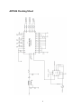
FIGURE 15: BLOCK DIAGRAM OF THE AD9522-4 CENTERED CLOCKING SOLUTION. THIS BLOCK DIAGRAM DISPLAYS THE SIGNAL FLOW OF
THE PROPOSED CLOCKING SOLUTION WHICH WAS CENTERED ON THE USE OF THE AD9522-4 PLL. .......................................... 32
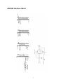
FIGURE 16 : BLOCK DIAGRAM OF THE AD9515 CENTERED CLOCKING SOLUTION. THIS BLOCK DIAGRAM DISPLAYS THE SIGNAL FLOW OF THE
PROPOSED CLOCKING SOLUTION WHICH WAS CENTERED ON THE USE OF THE AD9515 PLL. ................................................... 33
FIGURE 17: BLOCK DIAGRAM OF THE AD9513 CENTERED CLOCKING SOLUTION. THIS BLOCK DIAGRAM DISPLAYS THE SIGNAL FLOW OF THE
PROPOSED CLOCKING SOLUTION WHICH WAS CENTERED ON THE USE OF THE AD9513 PLL. ................................................... 34
FIGURE 18: THE TEXAS INSTRUMENTS MSP430 PRODUCT LINE. ALL MICROCONTROLLERS IN THIS FAMILY HAVE CPU CLOCK SPEEDS BELOW
WHAT IS REQUIRED TO MAXIMIZE THE THROUGHPUT OF THE AD7980 [20]. ....................................................................... 38
FIGURE 19: STMICROELECTRONICS STM32 PRODUCT LINE. THE F1, F2, AND F4 WERE ALL CONSIDERED AS POTENTIAL SERIES TO CHOOSE
FROM [21]. ........................................................................................................................................................... 40
FIGURE 20: THE KEITHLEY SOURCE METER. USING LABVIEW, THIS DEVICE WAS PROGRAMMED TO RUN A SWEEP ON THE EVALAD7091RSDZ BOARD. ...........................................................................................................................................43
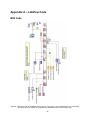
FIGURE 21: PROJECT PLAN- A SUMMARIZATION OF ALL OF THE DATA THAT WILL BE INCLUDED IN THE IBIS MODEL. THIS PLAN PROVIDES A
FRAMEWORK FROM WHICH TO START CREATING THE IBIS MODEL.
...................................................................................45
FIGURE 22: THE EVALUATION BOARD TO TEST THE AD7091R. THIS BOARD ALLOWED US TO CONTROL UNDER WHICH CONDITIONS THE
AD7091R WAS TESTED AND TO RECORD THE RESULTS. ..................................................................................................49
FIGURE 23: THIS FIGURE DISPLAYS HOW THE KEITHLEY 2420 WAS CONNECTED TO THE EVAL-AD7091RSDZ...................................50
FIGURE 24: THE AGILENT TRIPLE OUTPUT POWER SUPPLY. THIS IS AN ADJUSTABLE POWER SUPPLY THAT WAS USED TO TEST THE DEVICE
UNDER DIFFERENT VOLTAGE LEVELS AT VDRIVE. ........................................................................................................... 51
FIGURE 25: THE DPO4054 OSCILLOSCOPE. THIS OSCILLOSCOPE WAS USED TO MEASURE AND RECORD THE VT DATA AS WELL AS THE RAMP
RATE OF THE DEVICE UNDER TESTING. .......................................................................................................................... 51
xix
FIGURE 26: PREVIOUS EVALUATION BOARD FOR THE AD7626 (ADC). IT UTILIZES AN ALTERA FPGA TO SUPPLY THE CNV TO THE ADC,
BUT THIS METHOD RESULTED ON A SIGNAL WHICH WAS TOO NOISY TO ALLOW THE ADC TO FUNCTION PROPERLY. ...................... 53
FIGURE 27: LEVEL TRANSLATOR ON THE AD7960 INTERFACE SHEET. THIS IMAGE EXEMPLIFIES THE SLIGHT MODIFICATIONS THAT WILL
NEED TO BE MADE TO LEVERAGED SCHEMATIC PIECES. SPECIFICALLY, THIS PART WILL NEED A 2.5V INPUT INTO VCCA. ALSO,
BECAUSE THERE ARE TWO UNNECESSARY INPUTS AND OUTPUTS, WE WILL SEARCH FOR A SIMPLER PART WITH 2 INPUTS AND OUTPUTS
INSTEAD OF FOUR. IF THIS SEARCH DOES NOT YIELD SATISFACTORY RESULTS, WE WILL LEAVE THE UNNECESSARY PORTS
DISCONNECTED. ...................................................................................................................................................... 56
FIGURE 28: THE TIMING DIAGRAM FOR SPI 4-WIRE CS MODE WITHOUT BUSY. IN ORDER TO MAINTAIN MAXIMUM ADC THROUGHPUT,
TACQ MUST BE LESS THAN THE MINIMUM TCYC LESS THE MAXIMUM TCONV. [11] ................................................................... 59
FIGURE 29: THE AD7980 EVALUATION BOARD THAT WAS USED. THE BLUE WIRE CONNECTS TO THE RAISED OVDD PIN ON ONE END, AND
TO VDRIVE ON THE OTHER. THE RED WIRE ALLOWS CONNECTIONS TO THE SDI PIN ON THE AD7980......................................... 63
FIGURE 30: OSCILLOSCOPE IMAGE OF AN AD7980 CONVERSION. C2 IS THE CONVERT START, C1 IS THE CHIP SELECT, C4 IS THE SPI CLOCK,
AND C3 IS THE DATA OUT. [25].................................................................................................................................. 64
FIGURE 31: THE SETUP USED IN THE LAB FOR COLLECTING DATA TO TEST THE SNR PERFORMANCE OF THE MICROCONTROLLERS. IN THIS
CASE, THE MSP430 IS BEING TESTED. ......................................................................................................................... 65
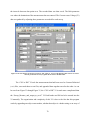
FIGURE 32: THE USER INTERFACE FOR THE SWEEP_MEASURE_AND_OUTPUT_TO_EXCEL VI. THIS INTERFACE ALLOWS THE USER TO
CONTROL ALL OF THE PARAMETERS NECESSARY TO GATHER THE IV DATA FOR THE IBIS MODEL. .............................................. 70
FIGURE 33: THE FIRST PART OF THE CSV TO IBS VI. THIS PART CONTAINS THE DIFFERENT HEADERS NEEDED AT THE BEGINNING OF THE IBIS
MODEL. IT ALSO CONTAINS THE FILE PATHS FOR THE DIFFERENT MEASUREMENTS TAKEN FOR THE INPUT BEING MODELED. ............ 71
FIGURE 34: THE SECOND PART OF THE CSV TO IBS VI. THIS SECTION CONTAINS THE VARIOUS HEADERS AND FILE PATHS NEEDED TO ENTER
THE DATA GATHERED AT THE OUTPUT AT 1.8V AND 2.5V INTO THE IBIS FILE. ..................................................................... 72
FIGURE 35: THE THIRD PART OF THE CSV TO IBS VI. THIS SECTION CONTAINS THE VARIOUS HEADERS AND FILE PATHS NEEDED TO ENTER
THE DATA GATHERED AT THE OUTPUT AT 3.3V AND 5V INTO THE IBIS FILE. ........................................................................ 72
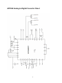
FIGURE 36: CLOCKING SOLUTION PADS SHEET OF THE SCHEMATIC FOR THE AD7626 EVALUATION BOARD. THIS SCHEMATIC PAGE IS THE
ONE PAGE THAT TOOK THE MAJORITY OF THE WORK DESIGNING, AS IT WAS THE ONLY PAGE THAT WAS AN ORIGINAL DESIGN, AND
NOT LEVERAGED FROM PREVIOUS EVALUATION BOARD SCHEMATICS. ................................................................................. 75
xx
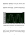
FIGURE 37: PICTURE OF A SINGLE CONVERSION ON THE AD7980 ANALOG-TO-DIGITAL CONVERTER, WHEN INTERFACED WITH THE
MSP430F5528 AND WRITING TO FLASH MEMORY. IN COMPARISON TO FIGURE 39, THERE IS A SIGNIFICANT DELAY BETWEEN A
FINISHED CONVERSION AND THE START OF THE NEXT CONVERSION..................................................................................... 76
FIGURE 38: SNR RESULTS FOR THE MSP430 INTERFACED WITH THE AD7980, WRITING THE RESULTS TO MEMORY. ...........................77
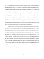
FIGURE 39: PICTURE OF A SINGLE CONVERSION ON THE AD7980 ANALOG-TO-DIGITAL CONVERTER, WHEN INTERFACED WITH THE
MSP430F5528 AND WRITING TO RAM. THE FIRST BURST OF SPI CLOCK IS TO INITIATE THE CONVERSION (SEEN AS A LOW ON THE
SDI/CS LINE), AND THE SECOND AND THIRD BURSTS ARE RESPONSIBLE FOR TRANSFERRING THE CONVERSION DATA, EIGHT BITS AT A
TIME. .................................................................................................................................................................... 78
FIGURE 40: AN OSCILLOSCOPE CAPTURE OF TWO FULL CONVERSIONS OF THE STM32F207ZG. NOTE THAT THE STM32 IS ABLE TO
PERFORM FULL 16-BIT TRANSFERS. A SINGLE TRANSFER TAKES APPROXIMATELY 2.5 MICROSECONDS. ...................................... 79
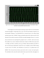
FIGURE 41: THE WAVEFORM PRODUCED BY A 1 KHZ TEST WITH THE MSP430, WRITING TO RAM. THIS WAS THE HIGHEST SNR RESULT OF
THE MSP430 TESTS, FALLING JUST SORT OF 25 DB. THE GLITCHES IN THE WAVEFORM CAN CLEARLY BE SEEN THROUGHOUT THE
WAVEFORM. .......................................................................................................................................................... 85
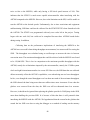
FIGURE 42: THE WAVEFORM THAT RESULTED FROM REMOVING THE GLITCHES PREVIOUSLY FOUND IN THE 1 KHZ MSP430, WRITING TO
RAM. THIS WAVEFORM PRODUCED AN SNR OF ABOUT 54 DB. .......................................................................................87
FIGURE 43: THE LABVIEW CODE FOR THE KEITHLEY SWEEP_MEASURE_AND_OUTPUT_TO_EXCEL VIRTUAL INTERFACE (VI). THE SETTINGS
ENTERED INTO THE VI ARE USED BY THIS PROGRAM TO HAVE THE KEITHLEY RUN THE DESIRED VOLTAGE SWEEP. ......................... 96
FIGURE 44: THE FIRST PART OF THE LABVIEW CODE FOR THE CSV TO IBS VI. THIS CODE CREATED THE HEADER OF THE IBIS MODEL THAT
SUMMARIZES THE BASIC INFORMATION OF THE DEVICE BEING MODELED. ............................................................................ 97
FIGURE 45: THE SECOND PART OF THE LABVIEW CODE FOR THE CSV TO IBS VI. THIS CODE TOOK THE DATA STORED IN A .CSV FILE,
TRANSFERRED IT TO THE .IBS FILE AND APPENDING IT TO THE DATA ALREADY IN THE .IBS FILE. IT ALSO IDENTIFIES THE NEW DATA. THIS
CODE MUST BE REPEATED FOR EACH SWEEP BEING INPUT INTO THE IBIS MODEL. ................................................................. 98
xxi
List of Tables
TABLE 1: THE DIFFERENT VERSIONS OF IBIS. EACH VERSION CONTAINS MORE FEATURES THAN THE PREVIOUS ONE AND ARE DESIGNED TO BE
EXPANDED UPON. .................................................................................................................................................... 23
TABLE 2: COMPARISON OF POSSIBLE TEXAS INSTRUMENTS MSP430 MICROCONTROLLERS FOR SELECTION. THE SELECTED PRODUCT LINE
WAS THE 5 SERIES.................................................................................................................................................... 39
TABLE 3: SELECTING A STMICROELECTRONICS FAMILY. THE STM32 FAMILY WAS SELECTED. ..........................................................40
TABLE 4: SELECTING A MICROCONTROLLER FROM THE STM32 FAMILY. THE F2 PRODUCT LINE WAS SELECTED....................................41
TABLE 5: THE PINS TITLES AND OPERATION OF THE AD7091R...................................................................................................49
xxii
List of Acronyms
ADC: Analog-to-digital-converter
CS: Chip select
CSV: Comma separated value
CNV: Convert Start
ESD: Electrostatic Discharge
FFT: Fast Fourier Transform
FPGA: Field-programmable gate array
GND: Ground
GPIB: General Purpose Interface Bus
IBIS: Input/ Output Buffer Information Specification
IV: Current versus Voltage
LSB: Least significant bit
LVDS: Low-voltage differential signaling
MISO/SOMI: Master in/slave out
MOSI/SIMO: Master out/slave in
MSB: Most significant bit
MSPS: Million samples per second
NI-VISA: National Instrument Virtual Instrument Software Architecture
NMOS: Negative-Channel MOSFET
PMOS: Positive-Channel MOSFET
RAM: Random access memory
SDO: Serial Data Output
xxiii
SDP: System Demonstration Platform
SNR: Signal-to-noise ratio
SPI: Serial peripheral interface
SPS: Samples per second
USB: Universal Serial Bus
VI: Virtual Instrument
VT: Voltage versus Time
xxiv
1 Introduction
Technology is advancing at an exponential rate. Just fifty years ago, the transistor radio
claimed the title of the most popular communication device in history [2]. This device utilized
only five transistors (and electronic on/off switch). Jumping forward to 2012, a top end video
card in a computer has 3.54 billion transistors [3]. Not only has the transistor count in products
increased, but the advancement of technology has led to the incorporation of transistor-based
electronics into almost every aspect of modern society, including work, leisure, travel, and
communication [4]. In fact, Intel has predicted that by 2015, there will be 1,200 quintillion
transistors in the world. If that number is divided by the projected population of 7.2 billion
people in 2015 it results in a relationship of over 165 trillion transistors to every one person on
the Earth [5]. To put it another perspective, the amount of transistors produced each year alone
outnumbers the worldwide ant population by 10 to 100 times [6]. In his 1965 paper, “Cramming
More Components onto Integrated Circuits”, co-founder of Intel, Gordon E. Moore stated that
the number of transistors in a central processing unit (CPU) will double approximately every two
years. This statement has appropriately been deemed, “Moore’s Law”, and it has proved to be
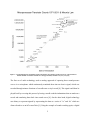
uncannily accurate, as seen in Figure 3.
The exponential growth of technology and its ever-increasing rate of integration into
society can be attributed to the digital revolution, which shifted the operating medium of our
electronics from analog to digital, giving them limitless potential [7]. We live in an analog world.
Everything human beings are able to interact with can be called analog. For example, sound is
transmitted thought the air in sound pressure waves [8].
1
Figure 3: A graph depicting the exponential growth of the number of transistors in microprocessors. The trend shows
that the number of transistor used in CPUs has approximately doubled every two years [29].
The first era of audio technology used an analog approach of capturing these sound pressure
waves via a microphone which continuously translated them into an electric signal, which was
recorded through minute vibrations of a needle onto a vinyl record [8]. This signal could then be
played back by reversing this process by having a needle read the indentations that are made on a
record and translating them back into sound waves [8]. On the other hand, digital technology
uses binary to represent signals by representing the data as a series of “1s” and “0s” which are
often referred to as on/off or true/false [9]. Using the example of sound recording again, a digital
2
system samples the input, converts it to binary, and transfers it to another device which takes the
binary number and reassembles it into an approximation of the original signal. Since the signal is
sampled, and not continually recorded like in an analog approach, the signal is actually a
combination of broken pieces of the source. This means that the resolution of the signal is only
as good as the amount of samples taken in a given amount of time. It would seem that this data
sampling would be detrimental to the signal, but in reality, a digital signal will be clearer than its
analog counterpart. This is because a digital signal knows what it should be when it reaches the
end of the transmission, meaning that it can correct any errors that may have occurred in the data
transfer [9].
The digital revolution is the shift from the analog technologies of old to the digital
technologies of the future. As stated above, a digital signal will be clearer than an analog signal.
Even though the sampling rate is not continuous, it is high enough for humans to perceive it as
such. Also, the nature of digital technology allows it to cram massive amounts of binary data into
a small amount of storage [9]. This allows for more efficient storage. One advantage of a digital
signal is the ability to make an infinite amount of exact copies of the data at the binary level [9].
Purely analog copies will never be exact replicas and will see deterioration as the degrees of
copies increase [9]. However, Digital technology is not without its own disadvantages. Currently,
digital technology is considerably more expensive. In addition, analog is still preferred over
digital in some applications. For example, the argument can be made that analog has the ability
to deliver richer sound quality [9].
The leading argument for using digital technology is that it is compatibility with
computers [10]. Since computers perform digital computations, they can only work with digital
media [10]. Therefore, all analog audio or video media must be converted to digital to work on a
3
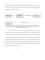
computer. Once the information is digital, computers can be used to edit the data and create
effects that were never possible with analog media. A conceptual block diagram of this
relationship is shown below in Figure 4.
Figure 4: Block Diagram for Analog-to-Digital Data Flow. This illustration shows the data flow for how information is
recorded in from an analog signal, converted into digital data for use by computing technology, and converted back to an
analog signal which we can interact with.
However, as we said before, we do live in an analog world. This means that in order to take
advantage of all the promises of digital technology we must first covert our data from its analog
origins to the binary of digital [7]. Therefore, digital technology is only as good as the ability of
the technologies that faithfully convert our analog world to the digital language of 1s and 0s and
then back into analog signals that can be heard, seen, felt, or perceived by human beings [7].
Improving upon analog to digital converter technologies and their applications will therefore
improve upon all digital data and signal processing, maintaining the exponential growth of
technology and improving our way of life.
4
1.1 Problem Statement
In order to satisfy those users, Analog Devices needs to support the users of their analogto-digital converters (ADCs), post-development, This includes designing evaluation boards that
showcase a product’s capabilities, developing software that enhances a product’s functionality,
and improving how user friendly a product is.
Input/ Output Buffer Information Specification (IBIS) is a standard by which the
electrical characteristics of the pins of a digital integrated circuit are represented. An IBIS model
contains the Input/ Output buffers and other characteristics of the circuit without revealing the
circuit’s structure or process information. Providing IBIS models for Analog Devices’ ADCs
have become oft requested by the customers of Analog Devices. Presently, the work of creating
the IBIS model is contracted out to a third party company. Analog Devices wants to avoid
further contracting, and would like to move the creation of IBIS models in-house.
Evaluation boards are an important part of the post-development applications at Analog
Devices. They provide the user with a method of testing and using ADCs, as well as giving the
user a good idea of the performance capabilities of the product. The speeds of Analog Devices’
ADCs are part of what make them desirable. When building evaluation boards for any product,
one must take special care regarding how all of the different components will be sensitive to high
frequencies. Ideal models will begin to melt away to the realities of engineering when very high
speeds are applied. If an ADC cannot perform to its full throughput because it is being limited by
a different portion of the circuitry, then the ability to operate at those higher frequencies is
meaningless.
This is the case with Analog Devices’ AD7626. Currently, there exists an evaluation
board in which the convert start (CNV) is provided by a field programmable gate array (FPGA)
5
on the daughter board. Providing the CNV from the FPGA has an unfortunate side effect of
producing unmanageable amounts of jitter in the signal at high frequencies, which makes
sampling inaccurate. A new evaluation board needs to be developed in order to resolve this issue.
The advancement of microcontrollers has made them more appealing for interfacing with
analog-to-digital converters (ADC), as there have been significant improvements in raw
processing power, while the cost of these devices has been driven very low. This is especially
true regarding ADCs that have had their performance limited by their controller in the past. This
bottleneck lies in the maximum clock speed of the controller, as the minimum conversion time of
the ADC relies on the ability of the controller to read the n-bit digital output within a certain
maximum time. If the controller is unable to reach this clock speed, then the ADC will have to
operate at a reduced throughput.
Figure 5: Two AD7980s interfaced using SPI 4-wire CS mode without busy to a generic digital host. For this project, the
digital host is representative of a microcontroller, and only one AD7980 will be used.
Analog Devices has recognized the consumer’s desire to interface with microcontrollers
by releasing a driver that was intended to simplify the interfacing of microcontrollers to one of
their ADCs, the AD7980. This driver uses a 4-wire CS mode Serial Peripheral Interface (SPI),
6
one configuration of which is shown in Figure 5, without a busy signal, to communicate between
the devices [11]. Note that in the picture, multiple AD7980s can be4 used in this configuration,
as long as additional chip selects can be provided. However, in this project, there will only be a
single AD7980 connected to the microcontrollers. Previous research has shown that the
performance of ADCs degrades over SPI at speeds above 50 kHz.
Analog Devices is unsure of the performance implications on their ADC’s when
interfacing to commonly used microcontrollers. The project states that their customers are either
already using their ADCs with microcontrollers, or are looking to do so in the future. Therefore,
they need to ensure that the company’s products are easy to use with these microcontrollers or
they risk losing business.
1.2 Project Objectives and Report Contributions
The three tasks that comprise this project all deal with applications of analog-to-digital
converters (ADC) after they have been developed. The Input/ Output Buffer Information
Specification (IBIS) project entailed creating a procedure by which detailed models of existing
devices can be created. These models are used to show the capabilities of the device without
revealing proprietary information about the device. The AD7626 Evaluation Board project
required the development of an evaluation board for testing the AD7626. This board was meant
to connect with Analog Devices’ new System Demonstration Platform-H (SDP-H) without
impeding the performance of the device being tested. Interfacing the two microcontrollers to the
AD7980 required that performance data be recorded and evaluated. The goal of this project was
to determine if the microcontrollers could be used to run the ADC at maximum performance, as
well as to determine the ease of use of Analog Devices’ generic driver.
7
1.2.1 ADC IBIS Model Generation
For the I/O Buffer Information Specification (IBIS) model project, the end goal was to
develop a procedure that Analog Devices can use to create its own IBIS models. This procedure
should outline how to create a model that takes current versus voltage (IV) and voltage versus
time (VT) data and convert it into an IBIS model using the LabView virtual instruments (VI) that
we developed. To develop this procedure, an example IBIS model must be created using the
AD7091R, an Analog Devices ADC. The model created for the AD7091R will then be used to
develop the required procedure.
1.2.2 AD7626 Evaluation Board
The final objective of the AD7626 Evaluation Board project is to develop an evaluation
board for the AD7626, an analog-to-digital converter that connects to Analog Devices’ new
System Demonstration Platform-H (SDP-H) platform. The new board will allow for high
frequency input tones to be applied to the AD7626. It is also imperative that the jitter on the
Convert Start (CNV) provided to the AD7626 does not impede performance. This means that a
solution needs to be designed on the daughter board to replace the previous source for the
clocking signal which was provided by the jittery Xilinx field programmable gate array (FPGA)
on the daughter board. This new clocking solution will provide a low jitter input to the AD7626
as well as the FPGA on the motherboard, which Analog Devices wishes to use to control the
AD7626 from the SDP-H platform.
1.2.3 AD7980 Interfacing to Microcontrollers
The first goal for the AD7980 Microcontroller project is to collect performance data of
the ADC. Data is needed on the performance impact on ADCs when interfacing with
microcontrollers, especially when the ADCs are being operated at higher throughput (the number
8
of samples per second that the ADC is able to achieve). The bandwidth of the processor being
used while interacting with the ADC is of interest, as this is likely to impact the other devices the
microcontroller is also connected to. Ideally, the microcontrollers would be able to operate the
ADC at its maximum throughput. Finally, the signal to noise ratio (SNR) of the conversion needs
to be derived, which can be done over a large number of conversions. The SNR provides
feedback as to how accurate the conversion is. As mentioned above, this is expected to decrease
as the throughput of the ADC increases, due to jittery clocks, and the known performance
degradation of Serial Peripheral Interface (SPI) at speeds over 50 kHz.
The second project goal for the AD7980 project is to determine the ease of use of
interfacing to these microcontrollers using the generic driver designed by Analog Devices. The
project will test the driver with two microcontrollers, from different manufacturers, in order to
determine ease of use. These two microcontrollers should be high performance, as it is desired to
operate the ADC at maximum performance. If it is found that interfacing to these various devices
is not simple, then methods for improving the driver should be devised.
1.2.4 Report Contributions
The IBIS model project served as a starting point for Analog Devices. They will use the
results of our project as the format for generating their own IBIS models. Specifically,
by starting the project, we were able to work out all of the necessary technical
specifications needed for taking the various measurements, such as needing to connect
two nodes with a resistor for one of the measurements, or needing to remove
components from the evaluation board to acquire the correct data. By being the first to
create a model from scratch we were able to allow Analog Devices to pick up our base
9
format and expand as they see fit, without needing to deal with the trials and errors that
were involved in learning the process.
Creating the improved AD7626 evaluation board allows for Analog Devices to be able
to provide an example of how to supply a low-jitter convert signal to the AD7626, or
any analog-to-digital converter (ADC). One frequent issue that customers of Analog
Devices have is driving high frequency ADCs. While the evaluation board will be used
to evaluate the AD7626, it also serves as an example of how to overcome jitter
limitations when driving ADCs.
Interfacing the AD7980 to various high end microcontrollers allows Analog Devices to
provide information to their customers as to how to best interface the AD7980 with a
controller. This would include the performance impact on the ADC and the
microcontroller. In addition, feedback on Analog Devices’ generic driver for
interfacing microcontrollers with the AD7980 is needed to gauge the usefulness and
effectiveness of the driver. With this information Analog Devices can better inform its
customers, and provide them with higher quality support.
1.3 Report Organization
The structure of the report is detailed in this section. Chapter 2 provides a literature
review of necessary background knowledge to build the desired modules for each technical
concept. This chapter gives a description of the analog-to-digital converters and their importance
in our lives. It then then defines the basics of what an input/output buffer information
specification (IBIS). Lastly, Chapter 2 outlines the serial peripheral interface (SDP). Chapter 3
states the specific design approaches we considered and illustrates the process by which we
decided upon the final designs. Chapter 4 provides the methods that we used to accomplish the
10
results that we discuss in Chapter 5. Chapter 6 delivers the conclusions and future
recommendations for improvement. Lastly, appendices are attached at the end of the report. They
document supplementary information that is too large to include in the main text.
11
2
Fundamentals of Analog-to-Digital Converters and
Their Applications
Analog-to-digital converters (ADC) are involved in each project, and thus play a very
important role. In the sections following, the basics of ADC operation is explored, as well as the
type of ADC involved in this MQP, successive approximation register (SAR). Details on the
Input/Output Buffer Information Specification (IBIS) are also provided. The contents of an IBIS
model are explained, as well as what they represent in the buffer. The different versions of IBIS
are briefly explained. Descriptions of the two buffer types used in this project are provided,
detailing what parameters are needed for each buffer and what those parameters refer to. Finally,
the operation of the serial peripheral interface (SPI), which is the interface used between the
microcontrollers and the AD7980, is expounded upon. The focus of this section is to explain the
type of SPI (4-wire CS mode, without busy) used between the microcontrollers and the AD7980.
2.1 Analog-to-Digital Converters
Analog quantities can be defined as continuous and infinitely variable [12]. Many
measurements are of an analog nature, such as the temperature of a furnace, the rate of fluid flow
through a pipe, and the pressure of a fluid. [12]. Importing these analog measurements with
computers allows for a level of data analysis that was unheard of just two decades ago. However,
in order to interface analog signals with the digital world of computers, the data must be
digitized into the binary language that computers work in. This is done using an analog-to-digital
converter.
An analog-to-digital converter (ADC) is an electronic circuit which receives an analog
signal input and generates a multi-bit binary (digital) output [12]. As previously stated, analog
signals are continuous, while digital signals are discrete. An ADC converts the continuous
12
analog signal by sampling the signal at predefined intervals [12]. At each interval, the input
signal gets held at its value at the time of the sample, and remains that value until the next
sample, at which time the input signal is updated and held again [12]. This means that an ADC
that samples a signal one hundred times a second will output a more accurate digital
representation than an ADC that only samples at ten times a second. The amount of samples per
second taken by an ADC is known as the clarity. The higher the number of samples per second
the ADC takes, the higher the sample rate of the outputted signal, and the more accurate the
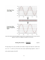
digital representation of the original analog signal will be [12]. Figure 6 shows the digitization of
a 1 Hz sine wave sampled at 8 times per second, or once every 125 ms. As you can see from the
digital representation of the graph, the ADC samples the graph, waits 125 ms and samples again.
When all the samples are taken, the graph can be recreated by connection the data points.
In analog-to-digital conversion, the difference between the original analog signal and the
digitized waveform is known as the quantization error or quantization distortion [13]. This error
is due to rounding or truncation [13]. If you look to the lower graph in Figure 6, you can easily
see the difference between the original analog signal (dotted) and the digitized waveform (solid).
The difference between the two is the quantization error.
When examining a basic twelve bit analog-to-digital converter (ADC), the “twelve bit”
means its digital output ranges from binary 000000000000 to binary 111111111111 (0 to 4096 decimal) [12]. The key to relating any given digital number value to a voltage value is to
understand that the 12-bit resolution of this ADC means it has
or 4096 discrete output states
[12]. Suppose this 12-bit ADC has an analog input voltage range of zero to ten volts.
13
Figure 6: Discrepancies Formed when Sampling an Analog Waveform. This illustration shows how an analog waveform is
digitized as well as how a low sampling rate can hinder the conversion [30].
Equation 3
The input range of ten volts is divided by the number of output states minus one, which in this
case is
or 4095 [12]. This can be more easily explained using Equation 3, where “n”
refers to the bit number of the ADC.
14
For a twelve bit ADC, the result of this equation shows that the analog resolution is 2.442
millivolts per bit [12]. Thus, for any analog signal between 0 mV and 2.442 mV, the ADC’s
output should be zero (binary 000000000000). Similarly, for any analog signal between 2.442
mV and 4.884 mV, the ADC’s output should be one (binary 000000000001), and so on. The
obvious setback of lower resolution ADCs is that any changes that occur in the analog signal that
are too small for the resolution to pick up will be lost [12]. For instance, the ADC that is shown
above will not pick up any input voltage until it reaches 2.442 millivolts [12]. This means that
any voltage higher than zero and lower than 2.442 millivolts will only read as zero. The
detriment of having a sampling rate that is too low as well as a resolution that is too low can be
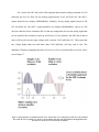
seen in Figure 7.
Figure 7: This graph shows two identical 1 Hz sine waves. The first sine wave is sampled every 20 ms at a 32 bit resolution.
The second sine wave is sampled every 40 ms at a 4 bit resolution. The lines of the graph illustrate the digitization of the
first sine wave will be more accurate than the second [30].
15
It stands to reason that the sampling rate of any ADC must be at least as often as
significant changes are expected to take place in the analog measurement [12]. The Nyquist
Sampling Theorem states that a band limited analog signal can be perfectly reconstructed from
an infinite sequence of samples if the sampling rate exceeds 2B samples per second, where B is
the highest frequency of the original signal [12]. This means that the absolute minimum sample
rate necessary to adequately capture an analog waveform is twice the fundamental frequency of
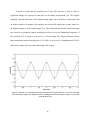
the waveform [12]. In Figure 8, you can see a 1 Hz waveform. The Nyquist Theorem dictates
that the minimum required sampling rate is
(
) As you can see, a sampling rate of 2 Hz is
sufficient to capture all of the peaks and troughs of this signal.
Figure 8: A 1 Hz Sine wave with Sample Points Taken with Respect to the Nyquist Theorem. As you can see, this graph
shows that using the nyquist rate a minimum amount of sampling points, allows the sampler to acquire every peak and
trough of this sine wave.
16
In general, electronics manufacturers find the Nyquist rate to be adequate. However,
circuits will often use ADCs that sample at many times the Nyquist rate, which brings increased
clarity in the converted signal. This is the case in devices such as digital multimeters (DMMs)
and oscilloscopes, the sampling rates are in the billions per second to allow for the successful
digitization of radio-frequency analog signals.
2.1.1 Successive Approximation ADCs
A successive-approximation-register (SAR) analog-to-digital converter (ADC) utilizes a
single comparator to convert the sample into binary [14]. In this way, the SAR addresses the
main faults of the flash ADC, at the expense of the sampling rate. An example of the successiveapproximation architecture can be seen in Figure 9. The single comparator compares the sample
over and over to a varying reference voltage, utilizing a binary search. Initially, the comparator
reference voltage is set to midscale (this would be the voltage represented by the most significant
bit (MSB) set to ‘1’ while all other bits are set to ‘0’). The sample voltage is then compared to
the input voltage. If the input voltage is higher than the reference voltage, then the comparator
outputs a logic ‘1’, and the MSB remains ‘1’ in the register. If this is not the case, then the MSB
is changed to a logic ‘0’. The next bit down is then set to ‘1’, and the process is repeated, until
the binary representation is complete.
SAR ADCs are very commonly used in applications where a sample rate below five
megasamples per second (MSPS) is acceptable, and usually have a resolution ranging from eight
to sixteen bits [14]. The successive approximation architecture allows for low power
consumption and a small form factor. However, the use of only one comparator in combination
with a binary search causes the sampling rate to be compromised.
17
Figure 9: Block diagram of a Successive Approximation Register ADC. Vin is the sampled voltage. The control logic is
responsible for determining whether the conversion is complete, and storing the converted bits. [15]
The final sampling rate is a fraction of the clock rate of the internal circuitry, as there is a certain
maximum time that a full binary search could take [16]. In addition, the settling time of the
digital to analog converter (DAC) has an impact on the maximum sampling rate, as it must
operate within the resolution of the ADC it is a part of. Despite the drawbacks, SAR ADCs
remain a very popular choice for a wide range of applications. The three the ADCs used in this
project use successive-approximation; the AD7980, AD7626, and the AD7091R [11].
2.2
IBIS
Saving time and reducing costs are key factors when designing systems [1]. Modeling
provides system designers the ability to simulate their designs before moving on to the
prototyping phase. Proper modeling is paramount in high speed systems, such as analog to digital
conversion, where simulations need to be performed to analyze the circuit behavior under
different conditions to ensure the integrity of the signal [1]. The modeling serves to detect typical
undesirable situations, such as overshoot, undershoot, and mismatched impedance, thereby
18
ensuring that preventable errors are not passed to the prototyping phase, where they are more
difficult and costly to fix [1].
Unfortunately, the availability of models for digital integrated circuits is very scarce [1].
Therefore, when semiconductor vendors are asked for their SPICE models (a general-purpose,
open source analog electronic circuit simulator) they are reluctant to provide them because these
models may contain sensitive intellectual property. This issue has been resolved with the
adoption of Input/Output Buffer Information Specification (IBIS) [1]. IBIS has become a new
standard for modeling among system designers.
IBIS is a behavioral model that describes the electrical characteristics of the digital inputs
and outputs of a device through voltage versus current (IV) and voltage versus time (VT) data
without disclosing any proprietary information [1]. IBIS models protect intellectual property by
not corresponding to the conventional idea of a model that system designers are accustomed to.
This means that IBIS models do not display information using such tools as a schematic symbol
or polynomial expression [1]. Instead, an IBIS model consists of tabular data made up of current
and voltage values in the output and input pins, as well as the voltage and time relationship at the
output pins under rising or falling switching conditions [1]. An IBIS model maintains accuracy,
as it takes into account nonlinear aspects of the input/output structures, the electrostatic discharge
(ESD) structures (the sudden flow of electricity between two objects caused by contact
structures), and the package parasitics (any other characteristics of the analog to digital to
converter (ADC) package which change its functionality) [1]. The Input portion of an IBIS file
can be referred to as a single stated input buffer, as it only represents the power and ground
clamp measurements. However, the output portion is referred to as a three state output buffer
because it not only measures the power and ground clamps, but it also covers pull up and pull
19
down data, as well as data regarding the switching characteristics which detail how the device
changed from high to low and vice versa. This data is summarized in the different buffers
presented in the IBIS model.
2.2.1 Three-State Output Buffer
At the heart of the Input/Output Buffer Information Specification (IBIS) are buffers,
which are models of the characteristics of the inputs and outputs on a specific package of a
device [17]. One of these buffer models is the three-state output buffer. The three-state output
consists of pull-up and pull-down switching characteristics, power and ground clamp curves, the
die capacitance, any parasitics due to the package, and the switching characteristics of the device
[17]. Each of these parameters represents a different aspect of a buffer. The three-state output
buffer can be seen in Figure 10.
Figure 10: A Three-State Output Buffer that represents the electrical characteristics of the outputs of the device
being modeled [1].
20
Pull-up switching characteristics describes the current versus voltage behavior of the
device when the output state is high
Pull-down switching characteristics describes the current versus voltage behavior of the
device when the output state is low.
Power and ground clamp curves represent the electrical characteristics of the output when
the power and ground clamp diodes are on.
Die capacitance is the capacitance referenced from the PAD back into the buffer.
Package parasitics are any resistance, inductance, or capacitance values that are due to
the packaging of the device and not the device itself.
The switching characteristics detail how the device changes from high to low and from
low to high. This includes the rise time, fall time, and ramp rate of the device.
2.2.2 Input Buffer
An input buffer in an Input/Output Buffer Information Specification (IBIS) model is
much simpler than the three state output buffer [17]. The three state buffer has many
characteristics that must be included in the model, whereas the input buffer only requires the
power and ground clamp curves, the die capacitance, and the package parasitics parameters [17].
These parameters represent the same characteristics for the input buffer as they do for the three
state output buffer. The input buffer can be seen in Figure 11.
21
Figure 11: The Input Buffer that represents the electrical characteristics of the inputs of the device being
modeled [1].
2.2.3 Versions of IBIS
There are several versions of Input/Output Buffer Information Specification (IBIS). Each
new version adds another level of complexity to the model [17]. This includes allowing the
system to hold more data points or adding another level of detail to the graphs of the electrical
characteristics, such as how the device acts under different temperatures [17]. The simplest
version of IBIS is Version 1.1 which can model a buffer with a low and high-state current versus
voltage (IV) table [17]. Version 1.1 also allows for a linear ramp that describes how fast the
buffer can switch from one state to another. Version 2.1 greatly increases the complexity of the
IBIS. For example, Version 2.1 allows for voltage versus time (VT) graphs and support for dualsupply buffers [17]. Similarly, Version 3.2 improved upon previous models by allowing for the
simulation of multi-stage buffers as well as buffers that required multiple IV tables [17]. In
addition, Version 3.2 added support for an electrical board description format [17]. With version
4.0 came an increase in the maximum number of data points allowed in a VT table and the
22
addition of more parameters for expressing data criteria for evaluating buffer performance [17].
These versions can be seen in Table 1. However, it is important to note that an IBIS model
should only be as complex as it needs to be. If a buffer does not call for a VT table or any other
higher-level parameter, then the simplest version of IBIS, Version 1.1, should be used.
Table 1: The different versions of IBIS. Each version contains more features than the previous one and are
designed to be expanded upon.
Version
I-V
Table
Linear
Ramp
V-T
Data
Multiple
Supply
Rails
NonLinear
Output
Switching
Waveform
Ground
Bounce
1.1
2.1
3.2
4
X
X
X
X
X
X
X
X
X
X
X
X
X
X
X
X
X
X
X
X
2.3
Electrical
Board
Description
MultiStage
Buffers
Multiple
I-V
Tables
Independent
Validation
Data Tables
X
X
X
X
X
X
X
Maximum
Number of
V-T Table
Data
Points
100
100
100
1000
Serial Peripheral Interface
The Serial Peripheral Interface (SPI) is being used as the communications interface
between the AD7980 analog-to-digital converter (ADC) and the microcontrollers in the project
in which the performance of these devices is being tested. SPI is a synchronous serial data link
standard that uses a master-slave configuration, in which there can be multiple slaves, selected
by individual chip selects. Serial communication provides a very important advantage over its
faster counterpart, parallel communications; required space. The real estate occupied by serial
communications is significantly less, as it is essentially a bitstream and, if it is synchronous, a
clock.
23
Figure 12: The timing diagram for SPI 4-wire CS mode without busy [11].
Originally named by Motorola, SPI is considered a four-wire serial interface, and
operates in full duplex [18]. Full duplex means that data communicated from the master to the
slave is transferred at the same time as the data communicated from the slave to the master. The
four wires of an SPI interface are the serial clock (SCLK), master output, slave input (MOSI),
master input, slave output (MISO), and slave select (SS) [18]. The SCLK is the clock at which
the data is transmitted, and since SPI is a synchronous interface, it is used in both master output
and slave output [18]. The SS selects the slave that is active, and is usually active low. MOSI is
the data line that is reserved for transfer of bits from the master to the slave, and MISO is the
data line reserved for transfer of bits in the opposite direction.
Before the transfer of data can occur, a number of different SPI settings have to be set up.
First, the clock should be configured. This is often in the low megahertz (MHz) range, although
clock requirements vary based on devices being used, as well as the application being configured
for [18]. Second, the clock polarity needs to be selected, which is the logic level that the clock is
idle at [18]. The clock is idle when there is no data communication. Finally, the clock phase
24
needs to be selected. The clock phase indicates which edge the data is captured on and which
edge the data propagates on (these always occur on opposite edges) [18]. A SPI transfer can be
seen in Figure 12 [11]. The transfer starts with the selection of a chip using the chip select wire,
which is usually active low. Once the clock cycles start, data transfer on the MOSI and the MISO
occurs simultaneously due to the full duplex nature of SPI. This is typically done using two shift
registers; one on the master side and one on the slave side [18]. The most significant bit is shifted
out, and the received bit is transferred into the least significant of the shift register (or the
opposite, if the transfer is least significant bit first). Once the transfer is complete, the master
puts the clock into idle state. Transfer sizes are only limited to the size of the shift registers in
use. It is important to note that data transfers do not have to be meaningful. For instance, sending
data to a device over SPI will trigger a return of data. The received data could be useless, and
just a byproduct of the transfer. On the same note, in order to receive data, data must be sent. If
there is no useful data to be sent, then dummy data is written to the shift register and clocked out,
which clocks the transfer in.
The AD7980 has four different SPI modes in which it can operate [11]. The scope of the
project only focuses on one mode; CS mode 4-wire, without busy. This mode is designed to
allow for multiple AD7980s to be connected to the same host. As can be seen in Figure 13, this
setup uses a conversion signal to initiate conversion [11]. This must be held high through the
conversion, and pulled low before going high for the next conversion.
25
Figure 13: AD7980 connected in 4-wire CS mode, without busy. This interface allows for multiple AD7980s to be
connected to a single master [11].
In addition, a CS pin is used on the host to communicate through the AD7980 SDI pin. This
controls whether the ADC is in acquisition mode, or in read mode. This pin must be held high
when the conversion is initiated, and must be held high until the data is to be read out [11]. The
host must provide a clock to the AD7980, which is the clock for the SPI transfers. Finally, the
SDO pin on the AD7980 is connected to an input on the host, which outputs the conversion data.
2.5 Chapter Summary
The projects contained in this MQP revolve around the usage of analog-to-digital
converters, which are used to convert analog signals to a binary representation. Our project uses
successive approximation register ADCs produced by Analog Devices. The Input/Output Buffer
Information Specification (IBIS) model is a file that provides descriptions of the performance
and reactions of a device’s pins, which are represented as buffers. In the case of this project, the
IBIS model was to be of an ADC, and two buffers were used. These are the input buffer, and the
three-state output buffer. The input buffer is used for input pins, and only requires data for power
and ground clamp curves, while the three-state output buffer requires data for pull-up and pull26
down switching characteristics, and power and ground clamp curves. The Serial Peripheral
Interface (SPI) is the interface used between the microprocessors and the AD7980. This is a bidirectional synchronous interface that uses a master and slave configuration to share a transfer
and receive clock, as well as to select between multiple slaves.
27
3 Proposed Approach
An important aspect of Analog Devices’ Applications Department is ensuring that the
products perform as intended when used in various situations. This support comes in many
forms, including developing new equipment and running tests, in order to provide new
information on their products. For the Input/Output Buffer Information Specification (IBIS)
model project, the end goal was to develop a step-by-step procedure of how to create an IBIS
model. However, much of the approach to this project was already completed by Analog Devices
before we arrived. This was provided to us when we took over the project. The AD7626
evaluation board needed a low-jitter clocking solution that was low jitter, had three low-voltage
differential signaling (LVDS) outputs, and be cost efficient. In order to find a solution, a number
of different PLL parts were evaluated to see which would be the best fit for use in the evaluation
board. When interfacing microcontrollers to the AD7980, two microcontrollers had to be
selected from different manufacturers and product lines, and meet the system clock frequency
requirement, as well as offer serial peripheral interface (SPI) as a transmission option. In
addition, evaluation boards and development software had to be selected, with cost efficiency in
mind.
3.1 Projects Plan
When Analog Devices gave us the three projects, we basically had two choices as to how
to complete them. We could all work on the same project and when it was completed, move on
to the next, or we could split up and have someone work on each project. We decided on the
second choice, because the group decided that the projects would be completed more efficiently
this way. For instance, when we need to write code for the microcontrollers, only one person can
program at one time. By having each person in charge of a different project, it ensures that each
28
of us is always working, and responsible for a part of the project. The projects also play to our
different specialties within electrical and computer engineering. For example, since Gabriel is the
most proficient at coding with microcontrollers, he took charge of the project which assesses the
feasibility of using the Analog Devices driver with third party microcontrollers. Dale would be in
charge of designing the improved, low-jitter clocking solution for the AD7626 evaluation board,
and Sean would be in charge of creating an automated process for generating IBIS models. The
person in charge of each project would do the majority of the work on that project, be
responsible for deadlines and written portions of that project, and speak about the progress of the
project at weekly meetings with Analog Devices. However, each person will help in each
project, and in the end, all three projects are the result of the hard work of all three of the
members of the group. Having each person accountable for a part a project, while having the
help of the other two group members, will ensure that every member remains efficient in their
work. In order to complete our work on time, we followed a Gantt chart that can be seen in the
next section.
3.1.2 Gantt Chart
See Figure 14, on following page.
29
30
Figure 14: Gantt Chart of the Project Plan. This chart shows the progress of our project throughout our ten weeks
at Analog Devices.
3.2 IBIS
There was very little development that needed to be done for the Input/ Output Buffer
Information Specification (IBIS) model project. Analog Devices presented us with the
AD7091R, an analog to digital converter that they wanted modeled. We were also provided with
examples of what the final IBIS model should look like. The equipment necessary to take the
measurements needed for the model was limited to what Analog Devices had available. This was
because Analog Devices’ primary objective with the IBIS model project was to show that they
could produce an IBIS model in-house and to develop a procedure to do so. With Analog
Devices having decided how they wanted the IBIS model project done, all that needed to be
developed was the Virtual Instruments (VI) that were used to create the IBIS model. These
included a program to run the measurements sweeps and one to input all of the measurements
data into the IBIS file. As such, the IBIS model project consisted of creating an IBIS model with
Analog Devices equipment and documenting how it was done.
3.3 AD7626
The previous evaluation board for the AD7626 utilized an Altera field-programmable
gate array (FPGA) to provide the convert start signal (CNV) to the analog-to-digital converter
(ADC). This was not sufficient because the signal that the FPGA was too noisy at the required 10
MHz frequency. Therefore, a new clocking solution needed to be designed to provide a
sufficiently low-jitter, 10 MHz CNV. After meeting with the sponsors at Analog Devices, it was
determined that the new clocking solution would be centered on using a phase locked loop
(PLL). However, the functional block diagram of the clocking solution changed depending on
which PLL was chosen. Each of these solutions had pros and cons, and eventually, one was
chosen to be the best fit for our schematic.
31
3.3.1 AD9522-4
The AD9522-4 is a twelve low-voltage differential signaling (LVDS) output clock
generator with an integrated 1.6 GHz voltage controlled oscillator (VCO). The VCO in the
AD9522-4 would provide its own reference clock. it would output a 100 MHz clock to drive the
off board field-programmable gate array (FPGA), as well as output the 10 MHz convert start
signal (CNV) separately to both the AD7626 and the off board FPGA. A functional block
diagram of this clocking solution is shown below in Figure 15.
Figure 15: Block Diagram of the AD9522-4 Centered Clocking Solution. This block diagram displays the signal flow of
the proposed clocking solution which was centered on the use of the AD9522-4 PLL.
This clocking solution the used the AD9522-4 met all of the hardware requirements set
by Analog Devices. However, the device was unnecessarily complicated for the task at hand, and
this was reflected in the price. Cost is a large factor in the development of this evaluation board,
so we did not choose to use the AD9522-4 as our PLL device.
3.3.2 AD9515
The AD9515 is a 1.6GHz phase locked loop (PLL) clock distribution integrated circuit
with two outputs. The AD9515 is a much simpler chip when compared to the AD9522-4.
Therefore, unlike the AD9522-4, the AD9515 does not have an integrated voltage controlled
oscillator (VCO) that can utilize as its reference. Consequently, an external oscillator needed to
be integrated into the clocking solution. However, even with the need to purchase a second part,
32
the cost of using the AD9515 plus the oscillator was still cheaper than using the AD9522-4.
Additionally, the AD9515 met the jitter requirement of the AD7626 analog-to-digital converter
(ADC). Figure 16 illustrates the block diagram of the clocking solution centered on the use of the
AD9515.
Figure 16 : Block Diagram of the AD9515 Centered Clocking Solution. This block diagram displays the signal flow of the
proposed clocking solution which was centered on the use of the AD9515 PLL.
As stated above, the PLL (no matter which specific device is used) must output a 10MHz
CNV to both the AD7626 ADC and the off board field-programmable gate array (FPGA), as
well as a 100 MHz clock signal to the off board FPGA. Since the AD9515 only has two outputs,
we decided to simply split the CNV signal. However, upon further investigation into the signal
33
type of the CNV, it was found that a low-voltage differential signaling (LVDS) signal must be
terminated at the end of the line by shorting the complementary pair with a resistor. This means
that the CNV could not simply be split, because it cannot be terminated in two places. Therefore,
The AD9515 did not meet the requirements for our PLL.
3.3.3 AD9513
Finding the simplest possible device that would correctly output three separate low jitter
low voltage differential signaling (LVDS) signals was paramount. We found it appropriate to
look in the same family as the AD9515. Our research yielded the AD9513, which is so similar to
the AD9515, that ever the pin setup is exactly the same. However, just as we needed, it differed
from the AD9515 in the key area of output options. The AD9513 has the ability to output three
separate LVDS signals. Since very similar to the AD9515 means that the AD9513 will also need
to utilize an external oscillator as its clock input. However, even with this additional cost,
centering out clocking solution around the AD9513 still costs less than using the AD9522-4. The
block diagram of the clocking solution centered on the AD9513 is shown below in Figure 17.
Figure 17: Block Diagram of the AD9513 Centered Clocking Solution. This block diagram displays the signal flow of the
proposed clocking solution which was centered on the use of the AD9513 PLL.
34
Centering the clocking solution on the AD9513 best fits the three key factors of our
decision making process. First, the AD9513 is as simple of a part that could be found that still
adequately accomplished the task we needed it to. Appropriately, this also means that it is the
cheapest. Second, the AD9513 has the ability to provide three separate LVDS outputs. This is
essential as we need two LVDS signals sent to the off board field programmable gate array
(FPGA) and one LVDS signal sent to the AD7626 analog-to-digital converter (ADC). Third, and
most importantly, the three LVDS outputs of the AD9513 are sufficiently low jitter for the
requirements of the AD7626 ADC.
3.4 AD7980
The AD7980 analog-to-digital converter (ADC) has an evaluation board and a
development board, known as the System Development Platform (SDP), which provides an
interfacing option for consumers for the AD7980. The SDP and evaluation board provide a
method for testing and evaluating performance. However, it is understood that consumer
applications will often have the ADC interfacing with other devices. Microcontrollers are an
attractive option for this, as they provide interfacing options to many different peripherals, and as
such can satisfy many general purpose needs [19]. In addition, the processing power of
microcontrollers has improved, in order to satisfy higher end applications [19]. The current
support of interfacing microcontrollers to the AD7980 consists of a generic driver written in the
C programming language.
Analog Devices is unsure of how well the AD7980 will perform when interfaced with
current high-end microcontrollers. In addition, feedback is needed as to the ease of use of their
existing generic driver. Each microcontroller we used was required to interface with the AD7980
in a 4-wire CS mode, without a busy signal. Two microcontrollers from three different
35
companies were to be selected, and the microcontrollers needed to be high end and selected in
order to get the best performance possible out the AD7980. The first microcontroller had to be
selected from Texas Instruments’ MSP430 line, because its popularity with Analog Devices
customers. In conjunction with this thought process, the other microcontroller should be selected
from STMicroelectronics’ product lines. The goal of this project is to take the existing generic
driver supplied by Analog Devices and interface it with two different microcontrollers,
evaluating the performance of the AD7980 with each one, as well as gauging the ease of use of
the current generic driver.
3.4.1
Project Objectives
In order to accomplish all the goals of this project, there are a number of project
objectives that must be met, and technical challenges that must be overcome.
A microcontroller needs to be selected from the product lineups specified. These
microcontrollers need to be selected to specification so that the performance of the
AD7980 should not be affected. Generally, this requires that the microcontrollers will
need to be selected from higher end product lines. Also required for each microcontroller
are a development board and a development environment for creating and loading
programs onto the microcontrollers. Finally, cost efficiency should be a factor when
selecting products.
Communication between the AD7980 and the microcontrollers is key to the project. The
code responsible for interfacing to the AD7980 needs to be optimized as much as
possible, so as to impact the conversion time as little as possible. Analog Devices has
specified that the microcontroller must communicate with the AD7980 using a 4-wire CS
mode, without busy Serial Peripheral Interface (SPI).
36
In order to produce a Fast Fourier Transform (FFT) for performance analysis, the
microcontroller needs to be able to store the results of sixteen thousand AD7980
conversions. Once the conversions are complete, the data then has to be communicated
over to a computer, where the data can be processed and the FFT can be produced, using
National Instruments LabView.
3.4.2
Selecting a Texas Instruments MSP430 Microcontroller
The Texas Instruments MSP430 family is a series of 16-bit microcontrollers, specializing
in low power applications. The family, seen in Figure 18, consists of over four hundred
microcontrollers offering a broad range of features [20]. The CPU speed of the MSP430 line
ranges from 8 MHz to 25 MHz. This will not be able to reach our target clock speed of just over
55 MHz. As to the other main factor, most of these microcontrollers support SPI. Based on clock
speed alone, all but the MSP430F5xx series and the MSP4306xx series were weeded out, as in
order to maximize the performance of the ADC, the maximum CPU clock speed offered by the
MSP430 line of 25 MHz would need to be used. At this point, most of the 25 MHz
microcontrollers in either family would have satisfied the requirements.
37
Figure 18: The Texas Instruments MSP430 product line. All microcontrollers in this family have CPU clock speeds below
what is required to maximize the throughput of the AD7980 [20].
However, the MSP430F6xx series came with a liquid crystal display (LCD), which was
unnecessary, and was otherwise identical to the MSP430F5xx series, so the selection was
narrowed down to a single series. In addition to purchasing a microcontroller, the
microcontroller also needed an evaluation board and software in order to program it. In this case,
that was the deciding factor. The 64-pin MSP430F5xx Target board (MSP-TS430RGC64USB)
was selected based on cost, and the recommended microcontroller, the MSP420F5528, to go
along with it. This combination offered a good balance between the hardware that was necessary,
with few frivolous features, while being available for purchase immediately. IAR Embedded
Workbench Kickstart was selected because of familiarity with the program and the program is
free to use.
38
Table 2: Comparison of possible Texas Instruments MSP430 microcontrollers for selection. The selected product line was
the 5 series.
MSP430
Product Line
SPI
Maximum
System Clock
Advantages
Disadvantages
Lowest Total
Cost
1 Series
yes 8 MHz
Few extra
features
Low system
clock
$149.00
2 Series
yes 16 MHz
Few extra
features
Low system
clock
$149.00
Value Line
yes 16 MHz
Few extra
features
Low system
clock
$149.00
4 Series
yes 16 MHz
Low system
clock
Includes LCD
$149.00
5 Series
yes 25 MHz
System Clock
Feature-rich
$149.00
6 Series
yes 25 MHz
System Clock
LCD
Feature-rich
$148.00
3.4.3 Selecting a STMicroelectronics Microcontroller
STMicroelectronics makes a couple of different lines of microcontrollers. They have two
main lines; the STM8, which is a line of 8-bit microcontrollers designed for low power use, and
the STM32, which are 32-bit microcontrollers based on ARM Cortex. The STM8 line was
obviously not going to come close to the CPU clock speed requirement set out beforehand, so
that left the STM32 line. Within the STM32 line, seen in Figure 19, there are seven series [21].
Only two of those series were able to meet the CPU clock speed requirement, the STM32 F2 and
the STM32 F4. The STM32 F2 had a maximum CPU clock of 120 MHz, while the STM32 F4
had a CPU clock speed of 168 MHz. However, the STM32 F4 was also a digital signal processor
(DSP), which was an unnecessary feature. Both series offered SPI as an option for interfacing to
external devices. The STM32 F2 series was selected over the STM32 F4 because it offered
everything that was desired, at a lower price, and with fewer frivolous features.
39
Figure 19: STMicroelectronics STM32 product line. The F1, F2, and F4 were all considered as potential series to choose
from [21].
Selecting a microcontroller within this series was a matter of selecting an evaluation
board, as the microcontrollers come soldered onto the boards. The IAR Kickstart for STM32 F2
(STM3220-SK/IAR) was selected not only because it was the least expensive option, but also
because of its compatibility with the IAR Embedded Workbench Kickstart for ARM, a program
that our group was familiar with.
Table 3: Selecting a STMicroelectronics family. The STM32 family was selected.
ST Family SPI Maximum System Clock
Advantages
Disadvantages
STM8
yes 24 MHz
Lower cost
STM32
yes 168 MHz
Adequate System Clocks More Expensive
40
Low system clocks
Table 4: Selecting a microcontroller from the STM32 family. The F2 product line was selected.
STM32
Product Lines
Maximum
System Clock
Advantages
Disadvantages
Low System Clock
Total
Cost
F0
48 MHz
$199.00
F1
72 MHz
Adequate System
Clock
$289.00
F2
120 MHz
Good System
Clock
$299.00
F3
72 MHz
Adequate System
Clock
Includes
unnecessary DSP
$249.00
F4
168 MHz
Good System
Clock
Includes
unnecessary DSP
$299.00
3.5 Chapter Summary
The Input/Output Buffer Information Specification (IBIS) project had a proposed
approach before we were assigned to the project by Analog Devices. This meant that the
company had already outlined a procedure and a methodology that would be used to complete
that project. Instead, the work that had to be done was figuring out how to best follow through
with that procedure. With the three microcontrollers selected and purchased for the
microcontroller project, the project could then move into the programming phase, in which the
program that would run during testing was written. The low-jitter clocking solution selected for
the AD7626 evaluation board fit all the needs specified by Analog Devices. With a phase-locked
loop (PLL) selected, and the oscillator that would work with the PLL, design of the schematic of
the new evaluation board was initiated.
41
4 Implementation
This chapter details the necessary tasks present in this project as well as the steps taken to
complete them. The chapter is split into three sections, the analog-to-digital converter IBIS
model generation, developing an AD7626 evaluation board methodology, and performance
implications of interfacing the AD7980 to microcontrollers. Each section was then further
broken down into what steps were necessary to complete each task.
4.1 Analog-to-Digital Converter IBIS Model Generation
The first task for the analog to digital converter (ADC) I/O Buffer Information
Specification (IBIS) model generation project was to write a project plan that contained all of the
information necessary for generating the IBIS model of the AD7091R, an ADC. The project plan
provided a summary of what we had intended to do. This summary was checked by Analog
Devices to ensure that we covered all of the parameters that we needed to. Once the plan was
established, the sweeping program was developed. The sweeping program communicated
between the Keithley 2420 source meter and the computer via LabView to gather the data
required for the IBIS model. We then developed a Virtual Instrument (VI) that took the measured
data from an excel file and transferred it to a text file. This VI was used to create the IBIS model
for the AD7091R. The model was then tested to ensure that it was valid. By summarizing the
steps taken to create the IBIS model, a guideline to generating IBIS models for a variety of
devices was compiled.
42
Figure 20: The Keithley Source Meter. Using LabView, this device was programmed to run a sweep on the
EVAL-AD7091RSDZ board.
4.1.1 Writing a Project Plan
Our project plan consisted of an outline of all of the data necessary to generate an I/O
Buffer Information Specification (IBIS) model. Writing the project plan provided a starting point
for developing an IBIS model. The plan included all of the pins of interest to the model. This
means that out of the ten pins on the device, only the output and the three inputs were included in
the project plan. Each pin can be represented as a different kind of buffer and each kind of buffer
requires different parameters to be modeled. The parameters summarize the behavior of the
electrical characteristics of the device. These characteristics are the pull-up and pull-down
curves, power and ground clamp curves, ramp rate, rising and falling waveforms, C_Comp, and
package parameters [1]. Either the values of these characteristics or the range over which they
will be sampled should be indicated in the project plan. The model’s name, pin names, and the
conditions under which the device will be operating must also be mentioned. By looking at the
project plan in Figure 21 it can be seen that the three inputs are the same buffer type. This means
43
that only one of the three inputs needed to be modeled. The data gathered from the chosen input
was applicable to all of the inputs.
The drive strength of the device is described in an IBIS model by the pull-up and pulldown curves [1]. The pull-up data describes the current versus voltage (IV) behavior of the
device when the positive-channel MOSFET (PMOS) transistor is on and the output is in the logic
high state [1]. The pull-down data describes the IV behavior when the negative-channel
MOSFET (NMOS) transistor is on and the output is in the logic low state [1]. This data is
acquired by sweeping the output from the maximum negative reflection (-VDRIVE) to the
maximum positive reflection (2*VDRIVE) where VDRIVE is a voltage that exceeds the maximum
output voltage. This ensures that the areas where undershoot, overshoot, and reflection can occur
are covered. The pull-up data is relative to VDRIVE while the pull-down data is relative to ground
[1]. This means that the output current of VDRIVE relative data is dependent on the voltage
between the output and VDRIVE pins. Due to this, the pull-up data needs to be entered into the
model using the following equation.
Equation 4 [1]
The power clamp curve represents the electrical behavior of the output when the power
clamp diode is turned on while the ground clamp curve represents this behavior when the ground
clamp diode is turned on [1]. As the ground clamp diode is only active when the output voltage
is below ground, the ground clamp data must be taken over the range of –VDRIVE to VDRIVE [17].
The power clamp diode, however, is only active when output voltage is above VDRIVE [1].
44
Figure 21: Project Plan- A summarization of all of the data that will be included in the IBIS model. This plan provides a
framework from which to start creating the IBIS Model.
45
As such, the power clamp data must be taken over the range of VDRIVE to 2*VDRIVE and is
relative to VDRIVE.
The ramp rate describes the transition rate when there is a switch in the logic state on the
output [1]. It is measured from 20% to 80% of the maximum voltage level on the Voltage versus
Time (VT) graph, with an assumed resistive load of 50Ω [1]. This can generate four different
waveforms, two describing the rise time and two describing the fall time. For both the rising and
falling graphs, one should have the load connected to VDD and the other with the load connected
to ground.
C_Comp is the value of the silicon die capacitance [1]. It is the capacitance referenced from
the pad back into the buffer and has a different value for the minimum, typical, and maximum
conditions of the device [1]. The package parameters are the electrical characteristics of the
packaging of the device that have an effect on operation [1]. Pin resistance (R_Pin), pin
inductance (L_Pin), and pin capacitance (C_Pin) represent the electrical characteristics for each
pin-to-buffer connection [1]. Package resistance (R_Pkg), package inductance (L_Pkg), and
package capacitance (C_Pkg) represent the electrical characteristics for the overall package [1].
In regards to the AD7091R, there are four pins of interest. These pins are the Serial Data
Output (SDO), the Serial Clock (SCLK), the Chip Select (CS), and Convert Start (CONVST)
[22]. The SDO is an output while the SCLK, CS and CONVST are inputs. The SDO is modeled
by a three-state output buffer while the inputs are modeled by an input buffer. The three-state
output buffer required all of the previously stated parameters to be defined. However, the input
buffers only needed to define the power and ground clamp curves, C_Comp, and package
parameters. Since the SCLK, CS and CONVST were the same buffer under the same conditions,
46
only one needed to be modeled. This model could then be used for all three inputs. The threestate output buffer is shown in Figure 10 and the input buffer is shown in Figure 11.
4.1.2 Setting up the Equipment for the AD7091R IBIS Model
Once the project plan had been completed, work on the I/O Buffer Information
Specification (IBIS) model began. This started with configuring the Keithley 2420, the source
meter selected for use in this project for its data collection capabilities, to communicate with a
computer using the General Purpose Interface Bus (GPIB) connection provided to us. We chose
to use the Keithley 2420 because it was recommended to us by Analog Devices as a readily
available device that met our needs for the project. This was accomplished by going into the
menu, selecting communications, and selecting GPIB. The desired address for the device then
needed to be selected, as multiple devices can be connected through one GPIB connection. The
GPIB cable connected to the USB port of the computer in use. The address identifies the device
to the GPIB controller. The next step was to download the Keithley 24xx drivers in National
Instruments LabView. These drivers allow the computer to recognize that there is a GPIB device
connected and to interface with it. The final step was to install the National Instrument Virtual
Instrument Software Architecture (NI-VISA) version 3.2 or later. This step may be unnecessary
if NI-VISA is already installed on the computer. NI-VISA provides the programming interface
between the hardware and LabView [23].
The second device that needed to be configured was the Digital Phosphor Oscilloscope
(DPO) 4054. The process for configuring the DPO was much simpler than the Keithley 2420.
The DPO comes equipped with a Universal Serial Bus (USB) port. Using a flash drive, all of the
pertinent data can be transferred to a computer.
47
4.1.3 Taking the Measurements for the AD7091R IBIS Model
In order to record the Current versus Voltage (IV) characteristics of the AD7091R, a
virtual instrument (VI) was designed in LabView. By altering one of the example LabView VIs
offered in the Keithley driver, we were able to develop a VI that allowed us to set up
measurement options that controlled voltage range, the number of samples to be taken, how long
the sweep will take and where the data would be saved to. This program was then used to record
the IV characteristics of the AD7091R inputs and output.
The Keithley 2420 was used to measure the voltage characteristics of the device. It was
connected to EVAL-AD7091RSDZ, the evaluation board in Figure 22, as shown below in Figure
23. The configuration shown is set up to measure electrical characteristics of the Serial Data
Output (SDO). Using the LabView VI the Keithley 2420 ran sweeps on the AD7091R to gather
the Current verses Voltage (IV) characteristics of the input and output pins needed to generate
the IBIS model.
A DPO4054 oscilloscope was used to obtain the ramp rate and Voltage versus Time (VT)
data. In order to obtain the VDRIVE-relative waveforms, the evaluation board for the analog-toDigital Converter (ADC) AD7091R was connected to the System Demonstration Platform
(SDP). The evaluation board was powered by an Agilent E3630A Triple Output DC Power
Supply. The DC power supply provided the evaluation board with 1.8V, 2.5V, 3.3V, and 5V. A
measurement was taken at each of these voltage levels with a 50Ω resistor connected between
the Serial Data Output (SDO) pin and the VDRIVE pin. This setup allowed the oscilloscope to
gather VDRIVE-relative timing data. In order to obtain a measurement, the oscilloscope was
connected to the SDO pin and Ground (GND) pin. With this setup, when the SDP supplied a
signal to the evaluation board the signal was displayed on the oscilloscope.
48
Figure 22: The evaluation board to test the AD7091R. This board allowed us to control under which conditions the
AD7091R was tested and to record the results.
Table 5: The pins titles and operation of the AD7091R.
Pin Number
Pin Description
Mnemonic
1
Power Supply Input
VDD
2
Voltage Reference Input Output
REFIN/REFOUT
3
4
5
6
7
8
9
Analog Input
Decoupling Pin
Analog Ground
Convert Start
Chip Select
Serial Clock
Serial Data Output
VIN
REGCAP
GND
CONVST
CS
SCLK
SDO
10
Logic Power Supply Input
VDRIVE
49
Figure 23: This Figure displays how the Keithley 2420 was connected to the EVAL-AD7091RSDZ.
The oscilloscope is then able to capture a single sample. In order to obtain the ground-relative
waveforms a 50Ω resistor was connected between the SDO pin and the GND pin and the process
was repeated.
To obtain data on the rising and falling edge, we took advantage of the oscilloscope’s
ability to focus onto critical portions of the waveform. In order to obtain the ramp rate of the
rising waveforms, one cursor on the oscilloscope screen was placed at 20% of the maximum
voltage and another was placed at 80% of the maximum voltage thereby displaying the change in
voltage levels between these two points as well as time it took between changes.
50
Figure 24: The Agilent Triple Output Power Supply. This is an adjustable power supply that was used to test the
device under different voltage levels at VDRIVE.
Figure 25: The DPO4054 Oscilloscope. This oscilloscope was used to measure and record the VT data as well as the ramp
rate of the device under testing.
51
The individual sweeps and measurements gathered by the Keithley 2420 source meter
and DPO4054 scope were saved as .csv file. This data needed to be transferred to the IBIS file
format. This was accomplished by developing a LabView virtual instrument (VI) that took the
data from a .csv and put it into a .ibs file. The program built the appropriate framework for the
IBIS model and then entered the measurement data where appropriate.
4.2 Developing an AD7626 Evaluation Board Methodology
With projects as large as developing an improved evaluation board for an analog-todigital converter (ADC), there needs to be a well-defined project plan. Each step taken in the
methodology must be planned out and documented. For the AD7626, one of the largest parts of
the project involved leveraging designs from the schematics of evaluation boards of similar
ADCs. Portions of the previous evaluation board for the AD7626 that were not the source for
errors at high speeds were repurposed and used in our new schematic. A new clock source to
supply the convert start signal (CNV) needed to be designed, programmed, and interfaced with
the previous hardware. However, the user still needed to have the ability to choose between
supplying the AD7626’s CNV from the new clocking solution and the off board fieldprogrammable gate array (FPGA).
The AD7626 evaluation board project exists because the previous evaluation board
(shown in Figure 26) was not able to provide a clear enough convert start signal (CNV) to the
AD7626 at the high frequencies that the analog-to-digital converter (ADC) is capable of.
Therefore the first goal was to decide upon a clocking solution that would be able to supply a
high frequency, low jitter CNV signal to the ADC.
52
Figure 26: Previous Evaluation Board for the AD7626 (ADC). It utilizes an Altera FPGA to supply the CNV to the ADC,
but this method resulted on a signal which was too noisy to allow the ADC to function properly.
4.2.1 Researching Clocking Solutions
Further researched was needed before a decision could be reached on how to develop the
clocking solution. A quick search for “Low Jitter Clocking Solutions” yielded many relevant
results. This led to the need to learn of the most popular approaches. These approaches included
phase locked loops (PLLs), delay locked loops (DLLs), and other jitter attenuation circuitry.
Once significant knowledge was gained about the pros and cons of these low jitter clocking
solutions, they were brought to the project advisors at Analog Devices. Through conversing both
through email and personal meetings, it was discovered that using a PLL was the assumed
solution to their clocking problem. We did not want the bias of Analog Devices to get in the way
of choosing the best clocking solution, but we ultimately found that using a PLL was, in fact, the
best choice.
53
4.2.2 Choosing the Best Part
Once the decision to use a phase locked loop PLL centered clocking solution was made,
our research could become more focused. A PLL had to be selected that would fit the needs of
the project. Since we are working for Analog Devices, there are obvious advantages of working
with Analog Devices parts. We searched the Analog Devices website for PLL parts, as well as
notes on their specific applications and uses. Taking advantage of video tutorials and
explanations of Analog Devices products, we decided to contact the lead speaker, an engineer at
the Greensboro, MA office. After explaining our project, he gave excellent insight as to many
PLL options. The final decision was to use the AD9513, based on three key factors. The first
deciding factor was if this PLL met the required low jitter specifications. The data sheet for the
AD7626 boasts a signal to noise ratio (SNR) of 91.5 dB, while the datasheet of the AD9513
boasts a jitter performance of approximately 300 fs at 10 MHz. The relationship of a device’s
SNR (dB) and its jitter is shown in Equation 5:
(
)
(
)
Equation 5
Using this equation, we found that the maximum jitter time that a signal provided by the
PLL could provide without reducing the performance of the ADC is 423.4 fs. As said above, the
jitter performance of the AD9513 is approximately 300 fs at the desired frequency. Therefore,
the AD9513 meets the low jitter recommendations. We also know from out design approach that
the PLL would need at least three low-voltage differential signaling (LVDS) outputs. The
54
AD9513 has six outputs which can be paired and configured as three LVDS outputs. Finally,
research needed to be done as to whether a cheaper part existed that also satisfied these two
factors. This research did not yield any results, so the decision was made to work with the
AD9513.
Since the AD9513 does not have an internal oscillator, we needed to find a simple
external oscillator part to supply the clock input to the PLL. Finding an appropriate oscillator can
be very overwhelming, as there are a plethora of options from many manufacturers. We decided
the best strategy would be to consult some of the application engineers at Analog Devices as to
whether they have recently worked with oscillators in any of their projects, and if they would be
willing to make a recommendation, as well as provide a PADS schematic part. We were sent in
the direction of the Kyocera KC3225 family of oscillators. After a quick search from popular
distributors, we found a model in that family that will provide a 100MHz CMOS CLK signal to
the PLL. The AD9513 can then send this clock in the form of a low-voltage differential signaling
(LVDS) signal to the FPGA that it can use an alternative clock source, if the native clock is too
jittery.
4.2.3 Schematic Design
Once the PLL and oscillator were selected, the next step was to start designing the
schematic. Analog Devices, in Limerick, uses a schematic/layout program by Mentor Graphic
called PADS. Much of the new design will be able to be leveraged from the schematics of the
AD7960 evaluation board, as well as a proposed schematic for the AD7626, which never made it
to fabrication. The power supplies, interface, and external reference sheets will all be copied
from the AD7960 board, while the device and analog front end sheet will be copied from the
55
AD7626 schematic. However, while being able to copy parts from other schematics is very
convenient, it does not mean that everything will work together.
Regarding the AD7960, we will need to make sure the voltage levels and connections
line up to those of the AD7626. The AD7626 and the AD7960 are very similar, but they are not
the same. This can easily be seen in the logic levels of the two devices. The AD7960 runs at a
logic level of 1.8V, while the AD7626 runs at a logic level of 2.5V. One example of the small
modifications that will need to be made is shown in Figure 27. This image is of the level
translator on the interface sheet of the AD7960 schematic, as well as the changes that will need
to be made to make it work with the AD7626.
Figure 27: Level Translator on the AD7960 Interface Sheet. This Image exemplifies the slight modifications that will need
to be made to leveraged schematic pieces. Specifically, this part will need a 2.5V input into VCCA. Also, because there are
two unnecessary inputs and outputs, we will search for a simpler part with 2 inputs and outputs instead of four. If this
search does not yield satisfactory results, we will leave the unnecessary ports disconnected.
56
In order to gain a greater knowledge in how the AD7960 schematic works, and how it
will need to be changed to function with the AD7626, we will need to seek the advice of one of
the head engineers of the AD7960 project. After the leveraged parts of the previous schematic
are modified to work with the AD7626, the PADS sheet for the new clocking solution needs to
be created. One upside to working in PADS is that after someone at Analog Devices creates a
part to be used in the program, it can then be used by everyone else on the network, which saves
a lot of time. By going to Analog Devices applications engineers for an oscillator
recommendation, we not only get reliable part, but we can also expect that the part had already
been built in PADS. Unfortunately, this is not the case for the AD9513. Consequently, we will
need to create a new symbol for the device, as well as for some other integrated circuits that will
be utilized in the design.
The PADS software is very intuitive and user friendly when it comes to the basics, but to
be able to create a part from scratch, we will need to seek out the help of an applications engineer
that regularly works in the program. With his instruction we will be able to build the part into
PADS and the circuitry around it can be developed. While this schematic sheet will require more
design than the others, we can still take advantage of existing schematics on the Analog Devices
website that use the AD9513. Once we are satisfied with the design, the schematic will be
submitted to the project adviser, along with a bill of materials for all of the parts existing on the
plan. After making the appropriate changes to gain the approval of Analog Devices, the
schematic will go through a final review before being sent to the layout department for
fabrication.
57
4.3
Performance Implications of Interfacing the AD7980 to
Microcontrollers
The initial objective of the microcontroller project was to identify microcontroller
families that would make good candidates for interfacing with the AD7980 analog-to-digital
converter (ADC). Once families were selected, individual microcontrollers within those families
could be selected for a final review before purchasing. Analog Devices provides a generic device
driver for use on their website, but this driver needed to be developed further to interact with
each microcontroller. This is because each one has different registers, and different ways of
accessing these registers. In addition to editing the driver, a program for each microcontroller
needed to be developed that would be suitable for testing the performance of the ADC. Finally,
the ADC was tested and the performance was evaluated.
4.3.1 Selecting the Microcontrollers
Analog Devices specified that the project was to use three microcontrollers from three
different companies. One microcontroller was required to be from the Texas Instruments
MSP430 family, due to its immense popularity. The other two were left to the group’s discretion,
but it was recommended that the other two microcontrollers be selected from the offerings of
STMicroelectronics and Freescale. When it came to selecting potential families, and then the
individual microcontroller, there were two defining factors. First, the microcontroller needed to
be able to utilize the Serial Peripheral Interface (SPI) when communicating with external
components. Second, the microcontroller needed to have a high frequency system clock. The
group needed to find the minimum system clock speed in order to maintain the AD7980’s
maximum throughput of 1 mega samples per second (MSPS).
58
Figure 28: The timing diagram for SPI 4-wire CS mode without busy. In order to maintain maximum ADC throughput,
tACQ must be less than the minimum tCYC less the maximum tCONV. [11]
Figure 28 shows the timing diagram for a conversion on the AD7980 using SPI 4-wire
CS mode without a busy indicator [11]. This was the same mode that was used when interfacing
with the microcontrollers. The data sheet for the AD7980 lists the minimum amount of time that
the AD7980 needs from one conversion start to the next conversion start, tCYC, as a minimum of
1000 nanoseconds (ns) [11]. Therefore, in order for the ADC to reach maximum throughput of 1
MSPS, tCYC needs be at its minimum of 1000 ns. The maximum conversion time, tCONV, is 710 ns,
as listed on the data sheet [11]. Subtracting tCONV from tCYC, results in the minimum acquisition
time, tACQ, at 290 ns. This is the minimum amount of time that the microcontroller has to read out
the conversion, and needs to be minimized in order to maximize throughput. Since the AD7980
is a 16-bit ADC, in order to get the minimum period of the SCK, tACQ is divided by 16 bits,
resulting in a minimum of 18.125 ns/bit. This translates to a minimum clock of 55.1725 MHz. In
order to maintain the AD7980’s maximum throughput, the microcontrollers needed a clock of at
least 55.1725 MHz.
59
4.3.2 Developing the Code for the MSP430
The purpose of the program designed for each microcontroller is exactly the same,
although there are variations in the actual code due to differences in how the microcontrollers are
accessed. The objectives of the program were to establish the Serial Peripheral Interface (SPI)
with the AD7980 analog-to-digital converter (ADC), initiate the conversion, and maintain
conversions at the maximum rate provided for by the microcontroller. The program must use the
generic microcontroller driver, provided by Analog Devices, to assist with the interfacing
between the microcontroller and the AD7980. In addition, a method for exporting the data out of
the memory of each microcontroller was needed in order to get the performance specifications.
All of the programming was done in the C programming language. The completed programs for
each microcontroller can be seen in Appendix B.
In order to communicate effectively with the microcontrollers, the serial peripheral
interface (SPI) was used. The generic driver from Analog Devices takes this into account, and
provides an empty function declaration, SPI_Init, in the file communication.c for the user to
complete, as this initialization function will vary from microcontroller to microcontroller. The
function declaration provides for four input variables, representing the SPI clock to be used,
whether the data is transmitted most significant bit (MSB) or least significant bit (LSB) first, the
SPI clock polarity, and the SPI clock phase. The SPI clock just had to be above 55 MHz, in order
to minimize transfer time. In the case of the MSP430, where this was not possible, the maximum
clock of 25 MHz was used. MSB first was used in all microcontrollers, as that was the mode
used by the AD7980. The SPI clock polarity determines whether the data is transmitted on the
rising or falling edge of the clock. In this case, the rising edge of the clock was used. Finally, the
clock phase determines whether the data is sampled on the first or second clock edge (the data
must be made available a half clock cycle before the sample).
60
The next function that had to be developed for each microcontroller within the generic
driver was the SPI_Write function. This is a simple function that accepts an input of one byte of
data, writes the data to the register that holds the data to be shifted out on the Master Out/Slave
In (MOSI) line, and then waits for the transfer to complete before terminating. This function is
responsible for transmitting the signal to initiate a conversion, as the conversion starts when the
MOSI has a rising edge.
Implementing the read function was crucial to the project, as the data had to be recorded
in order to determine the performance of the ADC. SPI_Read is the function responsible for this,
and is very similar to SPI_Write, due to the full-duplex nature of SPI. SPI_Read accepts a pointer
to a variable that can contain a word of data. First, the function writes a dummy byte to the
transfer register. This dummy byte consists of all one is order to keep the MOSI high during the
conversion. Once the transfer is complete, the received register is read out and placed in the
location specified by the pointer passed to the function. If the microcontroller is capable of
sixteen bit transfer, then this is the end of the function and it terminates. However, the MSP430
is not capable of word transfer, and instead needs two eight bit transfers to acquire all of the data.
To do this, another dummy byte is written to the transfer register. When the transfer completes
for the second time, the data in the location determined by the pointer passed to the function is
shifted over a byte and ORed with the data in the received register. The function then terminated.
The functions provided in AD7980.c required only slight editing in order to ensure
compatibility. AD7980_Init simply calls SPI_Init, and returns whether the initialization was
successful. The inputs to SPI_Init simply needed to be altered to set up the SPI correctly for each
device. AD7980_Conversion is a function the controls the entire conversion process for the
AD7980. It has no inputs, and returns the conversion result. Slight changes needed to be made to
61
this function in order to ensure correct operation. The variable txData which contains FFFEh in
the generic driver needed to be changed to 7Fh for the MSP430 (because of single byte transfers)
and to 7FFFh for the other microcontrollers. This change needed to be made in order to reflect
the MSB first transfer of the AD7980, as 7FFFh would send a zero first, while FFFEh would
send a zero last. This just minimizes the time in between conversions by providing a rising edge
on the MOSI as soon as possible. Next, a software delay needed to be implemented after calling
SPI_Write and setting the CS low, as the microcontrollers were all able to transfer the data faster
that the AD7980 could complete a conversion (710 ns maximum). Finally, setting the CS low
and setting the CS high needed to be edited for each microcontroller, as the command and output
pins differed.
Once the program for each microcontroller was complete, tests had to be run in order to
derive the performance of the ADC with each microcontroller. These tests included throughput
of the ADC, signal to noise ratio of the conversion, and bit rate of the microcontroller.
4.3.3 Testing the Performance Specifications
In order to correctly test the AD7980 analog-to-digital converter (ADC) with the
microprocessor, a modified AD7980 evaluation board was used, in conjunction with a breakout
board. This allowed the microcontroller evaluation board to be connected and properly interfaced
to the AD7980. Finally, a signal generator was used to provide the positive and negative
terminals of the input signal. The performance specifications that were of interest were the
throughput achieved with the ADC and microcontroller, and the signal to noise ratio (SNR) of
the signal after conversion.
Before testing could begin, the AD7980 evaluation board needed to be modified, as the
SDP interface uses a three wire SPI, instead of the four wire SPI that will be used by the
62
microcontrollers. On the evaluation board, the SDI pin is tied to VDRIVE, along with OVDD [24].
In order to implement a four wire SPI, the SDI pin needed to be accessed. As a solution to this,
the OVDD pin was raised, and tied to VDRIVE elsewhere on the board. The resistor R26 and the
capacitor C42 were desoldered and removed from the board, and pads left open by the resistor
and the capacitor allowed a wire to be conne3cted to SDI. The modificat6ions made to the board
can be seen in Figure 29.
Figure 29: The AD7980 evaluation board that was used. The blue wire connects to the raised OVDD pin on one end, and
to VDRIVE on the other. The red wire allows connections to the SDI pin on the AD7980.
63
Figure 30: Oscilloscope image of an AD7980 conversion. C2 is the convert start, C1 is the chip select, C4 is the SPI clock,
and C3 is the data out. [25]
The throughput of an ADC is measured in samples per second. Deriving the throughput
of the ADC was a relatively simple task. An oscilloscope was connected to the 4 wires
interfacing the AD7980 to the microcontroller. C2 in Figure 30 is the convert start (CNV), and
signals the start of a conversion by switching high [25]. C1 in Figure 30 is the chip select (CS or
SDI on the AD7980), and allows the converted data to be transferred over the SPI. C4 in Figure
30 is the clock that the converted data is transferred out on (SCK). C3 in Figure 30 is the data
being transmitted out (SDO), least significant bit (LSB) first. When a conversion is viewed on
the oscilloscope, the conversion time that has been elapsed can be seen, and can be used to find
the throughput. This is found by the equation in Equation 6.
(
) (
64
)
Equation 6
This result is the samples that the ADC is able to complete per second when interfacing with the
microprocessors.
Finding the SNR was more complicated. Computing the SNR requires a large number of
conversions for accuracy purposes. To calculate the SNR, the data from a large number of
conversions is input into a specially designed LabView Virtual Instrument (VI) for creating FastFourier transform (FFT) plots, and then the VI calculates the overall SNR of the system. Sixteen
thousand conversions are needed in order for the FFT to be accurate. Because the SNR is so
heavily dependent on frequency, the conversions will needed to be tested across a broad range, in
order to get the best possible picture of how the microcontroller and the SPI interface affect the
performance of the AD7980.
Figure 31: The setup used in the lab for collecting data to test the SNR performance of the microcontrollers. In this case,
the MSP430 is being tested.
65
To generate the analog waveform used for testing, an Audio Precision SYS-2722 was
used. This signal generator is able to produce very accurate waveforms at various frequencies
and voltages. The SYS-2722 was controller via a computer it was connected on, where all the
output settings could be tweaked. The setup used for testing the MSP430 microcontroller can be
seen in Figure 31. Running a single test required changing the SYS-2722 settings to reflect the
frequency to test at, as well as the peak-to-peak voltage. Each microcontroller was to be tested at
ten different frequencies, ranging from 1 kHz to 100 kHz. The peak-to-peak voltage would
remain constant. The voltage level was determined by testing the performance of the AD7980
when interfaced with Analog Devices’ System Demonstration Platform (SDP), and determining
a peak-to-peak voltage that provided the SNR performance provided on the datasheet of the
AD7980. The peak-to-peak voltage used was 20 Vpp.
During testing, it was discovered that the MSP430F5528 had 8 kilobytes (kB) of random
access memory (RAM), which was nowhere near the 32 kB needed to hold an array of sixteen
thousand sixteen bit conversions. This caused the MSP430 to require additional code to write the
conversion to flash memory, which had enough space to hold all the conversions. Unfortunately,
this caused additional performance issues, so the group made the decision to determine to
performance of a test run at 1 kHz, while writing two thousand two hundred and seventy two
conversions in RAM
Once the data was collected from all the tests, the comma separated value (CSV) files
were then imported into the LabView program that was developed for reading the data and
generating an FFT. The development of the virtual instrument (VI) was a matter of adapting
existing Analog Devices’ VI’s to read in a CSV file, and extract the data to compute the FFT.
The VI reads the spreadsheet in as a 2-D array, converting from the hexadecimal values in the
66
spreadsheet to decimal values, which is then indexed into three separate data paths. The first is
the throughput that the AD7980 was operating at when the conversions where taken. This is the
first entry in the single column of data in the spreadsheet, and is of data type double. The second
data path is the resolution of the analog-to-digital converter, which in this case was sixteen. This
is the second entry in column of data. The third path consisted of the conversion results, and was
a 1-D array of doubles. Once the spreadsheet is selected, the results are displayed on the Front
Panel.
Together, these performance specifications should give an accurate representation of how
well the microcontroller is able to interface with the AD7980 ADC. After the data was compiled,
a report was presented to Analog Devices that highlighted the results and the ease of use of their
generic microprocessor driver.
4.4 Chapter Summary
Most of the work involved in the Input/Output Buffer Information Specification (IBIS)
project was in setting up take taking the measurements to acquire the data for the actual model.
In doing this, a LabView program needed to be designed to help take the data sweeps from the
Keithley and transfer them to the computer. Once all of the data was acquired, another LabView
Program needed to be designed which took all the data from the .csv files and put it into the IBIS
format.
Designing the improved low-jitter clocking solution for the AD7626 required that we first
research the best way to reduce jitter. After deciding on using a phase-locked loop (PLL) we
needed to search for the best part based on three factors: meeting jitter requirements, number of
low-voltage differential signaling (LVDS) outputs, and cost. Next, the schematic for the
67
evaluation board was designed in the PADS software. When Analog Devices approved the
schematic it was sent to fabrication.
The first thing that needed to be accomplished for the microcontroller project was to
select the three microcontrollers that we were going to work with. Analog Devices had said that
they would like one of them to be from Texas Instrument’s MSP430 line, and the other two were
left to the group’s discretion, but it was recommended that the other two microcontrollers be
selected from the offerings of STMicroelectronics and Freescale. There were two deciding
factors when it came to selecting potential families, and then the individual microcontroller.
First, the microcontroller needed to be able to utilize the Serial Peripheral Interface (SPI) when
communicating with external components. Second, the microcontroller needed to have a high
frequency system clock. The code for each microcontroller had the same purpose, although there
are variations in the actual code due to differences in how the microcontrollers are accessed. The
objectives of the program were to establish the SPI with the AD7980 analog-to-digital converter
(ADC), initiate the conversion, and maintain conversions at the maximum rate provided for by
the microcontroller. The program had to use the generic microcontroller driver, provided by
Analog Devices and a method for exporting the data out of the memory of each microcontroller
was needed in order to get the performance specifications. All of the programming was done in
the C programming language. In order to test the performance specifications of the ADC when
interfaced with each microcontroller, a signal generator was used to provide the positive and
negative terminals of the input signal.
68
5 Results
This chapter summarizes the results gathered from the development and testing
procedures described in the previous chapter. The chapter was split into the three tasks that
comprised the project.
5.1 Analog-to-Digital Converter IBIS Model Generation
The development of the Input/ Output Buffer Information Specification (IBIS) model
procedure led to the production of several LabView Virtual Interfaces (VI).These VIs were the
“Sweep_Measure_and_output_to_excel”
and
the
“CSV
to
IBS”
programs.
The
“Sweep_Measure_and_output_to_excel” VI was programmed to run voltage sweeps on the
evaluation board and output the data gathered into an excel file. The “CSV to IBIS” VI took the
data gathered from the “Sweep_Measure_and_output_to_excel” VI as well as the Voltage versus
Time (VT) data that was gathered manually and input them into an IBIS file (.ibs) format. The
IBIS model procedure was the result of recording how these VIs were used, how the data was
gathered, and how the data was edited to be readable to the VIs.
The “Sweep_Measure_and_output_to_excel” VI provided a simple interface for setting
up and running voltage sweeps as shown in Figure 32. The address of the device being run, in
this case the Keithley 2420, was entered under the VISA resource name parameter. When the
program was run, the Keithley recorded the performance of the ADC being tested. The data
points that the Keithley gathered were separated by uniform intervals. These intervals were
controlled by the range of the sweep and by the number of data points being taken. The
minimum and maximum ranges of the sweeps were entered under the Minimum Amplitude and
Maximum Amplitude parameters. The number of data points taken during the sweep was
controlled by changing the Number of Points parameter. The larger the sweep range, the greater
69
the intervals between data points was. The recorded data was then saved. The Path parameter
was where the destination of the measurement data was entered. The Current versus Voltage (IV)
data was gathered by adjusting these parameters as needed for each sweep.
Figure 32: The user interface for the Sweep_Measure_and_output_to_excel VI. This interface allows the user to control
all of the parameters necessary to gather the IV data for the IBIS model.
The “CSV to IBS” VI took the measurements that had been saved as Comma Delimited
(.csv) files, converted them to text files, and appended them together one after the other. As can
be seen from Figure 33 through Figure 35, the “CSV to IBS” VI is much more complicated than
the “Sweep_Measure_and_output_to_excel” VI. Each header and file had to be entered into the
VI manually. The organization and complexity of this VI is due to the fact that this program
works by appending one object onto another, whether that object is a header string or an array of
70
data points. If the data were to be entered into the incorrect location, it would be added to the .ibs
file in the wrong order. This would lead to syntax issues in the IBIS model, causing it to fail. In
order for this VI to be able to convert the data file to a text file, all of the measurements needed
to be saved in a (.csv) format. To ensure that the data was saved in the proper format, the stepby-step procedure goes into great detail as to how to save the recorded data. Once the data had
been transferred to the text file, the text file could be changed to an IBIS file by saving it as .ibs
instead of .txt.
Figure 33: The first part of the CSV to IBS VI. This part contains the different headers needed at the beginning of the
IBIS model. It also contains the file paths for the different measurements taken for the input being modeled.
71
Figure 34: The second part of the CSV to IBS VI. This section contains the various headers and file paths
needed to enter the data gathered at the output at 1.8V and 2.5V into the IBIS file.
Figure 35: The third part of the CSV to IBS VI. This section contains the various headers and file paths needed
to enter the data gathered at the output at 3.3V and 5V into the IBIS file.
72
The procedure to generate the IBIS model was a compilation of all of the steps that were
taken to gather, format, and enter the data into an IBIS model. As seen in Appendix E, the
procedure was split into six sections: Gathering the VT Data, Gathering the power and Ground
Clamp Data, Gathering the Pull Up and Pull Down Data, Obtaining the Die Capacitance,
Formatting the Data, and Entering the Data into IBIS. The Gathering the VT Data, Gathering the
power and Ground Clamp Data, and Gathering the Pull Up and Pull Down Data sections describe
how to gather the IV and VT data needed to create the IBIS model. These sections contain
detailed, step-by-step instructions on how to set up the necessary equipment and run the tests.
The Die Capacitance section describes how to obtain the die capacitance of the inputs and output
of the device. This task was its own section because the device had to be removed from the
evaluation board to obtain the die capacitance. Making this section the last section that gathered
performance data ensured that errors with the measurements due to damage to the evaluation
board from removing the device did not occur. The Formatting the Data section ensured that the
measured data was in a format that the “CSV to IBS” VI could read so that the Entering the Data
into the IBIS section could be completed.
5.2 Developing the AD7626 Evaluation Board Results
The evaluation board that we designed was completed at such a time during our project
that we would not receive the fabricated board because of the layover between submission and
layout and fabrication. During this time between design submission and receiving the board, we
would have worked on the code that governs the off board field-programmable gate array
(FPGA). Since we were not going to receive the board during our time in Ireland, the decision
was made to focus our attention on the two remaining projects. Consequently, instead of having
the code that governs the FPGA, test results of the board, and schematics of the circuitry, the
73
only result we have for the AD7626 project is the schematic that was submitted and approved for
layout and fabrication. The process for submitting a schematic for layout and fabrication
involved several meetings with applications engineers, but it did not involve simulation.
However, in these meetings, we went through our schematic diligently. Since the majority of the
schematics we submitted were based on previous designs, most of the focus was aimed at how
the previous circuitry was modified to fit the differences in the specifications between the
AD7626 and the AD7960. When we reviewed the page that we had created, we were required to
explain why every connection was made based upon product datasheets and evaluation literature
from the Analog Devices website.
Figure 36 shows the sheet of the PADS schematic that holds the new clocking
solution that we designed. The three devices on the figure above are the AD9513, the oscillator,
and a signal translator which ensures that the data coming from the FPGA across the interface is
stable when it enters the AD9513. The rest of the schematic, most of which was leveraged from
previous designs, can be found in Appendix D.
74
Figure 36: Clocking Solution PADS sheet of the schematic for the AD7626 evaluation board. This schematic page is the
one page that took the majority of the work designing, as it was the only page that was an original design, and not
leveraged from previous evaluation
board schematics.
75
5.3
Performance Implications of Interfacing the AD7980 to
Microcontrollers
The performance results from the tests are categorized by the throughput of the AD7980
analog-to-digital converter (ADC), as well as the signal-to-noise ratio (SNR) of the sixteen
thousand conversions, per frequency test. The throughput is a measure of how many conversions
the AD7980 is able to make per second. The SNR of a set of conversions represents the ratio
between the signal and the background noise.
In the methods, it was discussed that the MSP430F5528 would have two sets of
performance data; one that records only two thousand two hundred and seventy two conversions,
but stores them in RAM for better access time, and one that records the full sixteen thousand
conversions, storing them in flash memory.
Figure 37: Picture of a single conversion on the AD7980 analog-to-digital converter, when interfaced with the
MSP430F5528 and writing to flash memory. In comparison to Figure 39, there is a significant delay between a finished
conversion and the start of the next conversion.
76
When writing the conversion data to flash memory, the time between conversion starts is
approximately 75 microseconds, as seen in Figure 37. Since this is equivalent to the time that it
takes to complete a single conversion, the inversion of this time will result in the samples per
second of the AD7980. This results in 13,333 samples per second (SPS).
18
16
14
SNR (dB)
12
10
8
6
4
2
0
0
10
20
30
40
50
60
70
80
90
100
Frequency (kHz)
Figure 38: SNR results for the MSP430 interfaced with the AD7980, writing the results to memory.
The SNR results for the ten frequency tests show a maximum SNR of about 16 decibels
(dB), which occurs at 1 kHz. The minimum SNR occurs at 90 kHz, coming in a little below 4
dB. Due to the SNRs becoming varied at higher frequencies, a trend line has been fitted to the
graph of the SNR results. This is likely due to the inaccuracy of a lower throughput at the higher
frequencies, but the trend line shows a linear relationship between frequency and the SNR.
77
Figure 39 shows a single conversion when the AD7980 is interfaced with the
MSP430F5528, when the data is being saved in RAM. As can be seen in Figure 39 the time in
between the start of two conversions is approximately 6.3 microseconds.
Figure 39: Picture of a single conversion on the AD7980 analog-to-digital converter, when interfaced with the
MSP430F5528 and writing to RAM. The first burst of SPI clock is to initiate the conversion (seen as a low on the SDI/CS
line), and the second and third bursts are responsible for transferring the conversion data, eight bits at a time.
This provides us with a throughput of about 158,000 SPS when interfacing with the MSP430
microcontroller and writing the conversions to RAM. The SNR performance of the AD7980
when writing to RAM at 1 kHz was 24.9381 dB.
A single conversion on the STM32F207ZG took approximately 2.5 microseconds, as can
be seen in Figure 40. When the AD7980 is interfaced with the STM32 microcontroller a
78
throughput of about 400,000 SPS is the result. The AD7980 operates at this throughput when the
SPI clock is 30 MHz, which is the maximum SPI clock the STM32 can provide. In addition, the
SPI is operating in sixteen bit transfer mode.
Figure 40: An oscilloscope capture of two full conversions of the STM32F207ZG. Note that the STM32 is able to perform
full 16-bit transfers. A single transfer takes approximately 2.5 microseconds.
The performance data was only a part of the final objective of the project. Analog
Devices also needed an evaluation of the ease of use of the generic driver that they supply for
programming microcontrollers to interface with the AD7980. Generally, the driver was simple to
use, and worked well for all the microcontrollers during programming. In fact, using the driver
definitely was a more efficient and appealing alternative to setting up a function to run a
79
conversion on the AD7980 from scratch. However, there were a couple of changes that could be
made to improve both performance and usability of the driver. First, the generic driver, when
downloaded and opened, passes FFFEh to SPI_Write within the AD7980_conversion function.
This is equal to the binary number 1111 1111 1111 1110. This transfer is to start a conversion on
the AD7980. A conversion will start when the AD7980 encounters a rising edge on the SDI,
which is provided for by sending the single zero. However, the AD7980 operates in most
significant bit (MSB) first mode, which means FFFEh would transmit a zero last. The behavior
of the SPI master out/slave in (MOSI) line is to hold the value of the last bit transferred, which in
this case, would be the voltage value of zero. This means that a rising edge would not be
encountered on the SDI input of the AD7980 until the next transfer of a value of one. This is
unnecessary. Instead, an initial transfer of 7FFFh, which would transfer a zero first, and provide
a rising edge to the AD7980 SDI as soon as possible on the conversion start.
The second issue that was encountered with the generic driver was a slightly wasteful use
of variables within AD7980_Conversion. Namely, the function runs SPI_Read sending it a
pointer to a local variable within AD7980_Conversion. But the function then returns that
variable, forcing the user to save it to another variable in memory. This is wasteful, and can be
solved by either using a global variable within AD7980_Conversion, or by passing a pointer to a
local variable in main. Passing a local variable would be the more elegant solution from a
programming standpoint, but both options are acceptable options in that memory space is not
being wasted. This will also reduce the amount of time in between conversions, because there
will only be a single write to memory, as opposed to two writes.
Lastly, the generic driver fails to reinforce or imply that there needs to be 710
nanoseconds in between the conversion start and the read period. In the generic driver, the code
80
flow calls SPI_Write, and then immediately pulls the chip select (CS) low to initiate the read
from the AD7980. Even when interfacing with the MSP430, which had a maximum clock of 25
MHz and was the slowest operating of the microcontroller we tested, there was a need for a delay
in between calling SPI_Write and pulling the CS low. Obviously, delay functions vary from
microcontroller to microcontroller, as well as compiler to compiler, but a comment here
highlighting the need to respect the timing needs of the AD7980 would go a low way in helping
the user successfully interface to the AD7980.
5.4 Chapter Summary
The result of the Input/Output Buffer Information Specification (IBIS) project was a
completed IBIS file containing all the measurements taken with the AD7091R, in addition to
information taken from the datasheet of the part. This IBIS file represents a complete IBIS model
for the AD7091R in typical conditions (room temperature). A report was also prepared for
analog devices that detailed the exact ste4ps taken to make the IBIS model, so that Analog
Devices could recreate IBIS models for other devices in the future. The AD7626 schematic
submitted to manufacturing represents the final result of the project associated with the ADC.
The re3sults of the microcontroller project showed performance of the interface was not meeting
maximum performance, with the STM32 reaching a maximum of 400,000 SPS, and the MSP430
reaching a maximum of only 158,000 SPS. In addition the SNR seen when the AD7980 is
interfaced with the MSP430 was much lower than expected, to the point where the signal is not
nearly accurate for applications.
81
6 Discussion
6.1 Analog-to-Digital Converter IBIS Model Generation
The main goals of the Input/ Output Buffer Information Specification (IBIS) model
project were to show that it was possible for Analog Devices to produce an IBIS model in-house
and to create a procedure of how to do so. Being able to produce the IBIS model in-house meant
that new equipment could not be ordered, we could only use equipment that Analog Devices
already had. Using the equipment available we gathered data on the Voltage versus Time (VT)
and Current versus Voltage (IV) characteristics of an analog-to-digital converter (ADC) provided
by Analog Devices, the AD7091R. The steps taken to gather these parameters were used to
create the step-by-step procedure of how to create an IBIS model.
As stated previously, one of the main goals of the IBIS model project was to show that it
was possible for Analog Devices to create an IBIS model. This meant that a full IBIS model was
not the end goal of this project: just enough of one to show that it was possible for Analog
Devices to produce one. The data present in the IBIS model created in this project only has data
recorded for the performance of the AD7091R at the typical temperature values. This IBIS
model lacks minimum and maximum data. However, with only the addition of a device that can
simulate the minimum and maximum conditions under which the ADC was designed to operate,
the process for gathering and formatting the necessary data for the IBIS model will remain the
same.
6.2 Developing an AD7626 SDP-H Evaluation Board
The original plan for developing the AD7626 was to design the board in software, have
design sent to fabrication, and test the board to ensure proper functionality. This meant that there
82
was going to be a lull between when the schematic was submitted and when we would have the
actually board to test with. We were originally told that the time of the layout and fabrication
process varies depending on a couple different factors, one of the being how many projects are in
queue before ours. Basically we were told that at best the board would be done within two
weeks, but it could take three. This meant that we had six weeks to create a satisfactory
schematic, thereby giving us one week to test the board. Unfortunately, we were not able to get a
schematic into layout until a point in which the board would not be finished until we were back
in the Unites States. After talking to our supervisors at Analog Devices it was decided that,
instead of coding the FPGA after the board was submitted (which was what we would have been
doing during the layout and fabrication process), we were to use this freedom to focus harder on
the other two projects.
6.3
Interfacing the AD7980 to Microcontrollers and the
Generic Driver
The results of interfacing the MSP430F5528 with the AD7980 analog-to-digital converter
(ADC) show a throughput that is a fraction of the maximum throughput that can be achieved
with the AD7980, as well abysmal signal-to-noise ratio (SNR) performance when compared with
the performance listed in the datasheet. The lower throughput can be attributed to a slow SPI
clock, as well as delays caused by the program. SNR performance issues are due to lower
throughput, as well as other unknown factors encountered when testing the device. No SNR data
was able to be obtained for the STM32F207ZG, due to time constraints and faulty hardware, but
the throughput data showed that the STM32 was a much more capable microcontroller than the
83
MSP430. Maximum throughput was still not reached, due to limitations on the SPI clock, but the
throughput of the STM32 was over twice as high as the MSP430.
The lower throughput seen on the MSP430F5528 when interfacing with the AD7980 was
to be expected. The MSP430 was unable to provide a clock matching the 55 MHz that would be
necessary to run the AD7980 at maximum throughput, 1 million samples per second (MSPS).
The maximum clock the MSP430 was able to provide for the SPI clock was 25 MHz, which will
provide less than half the throughput. Still, the maximum throughput seen with the MSP430 was
158,000 SPS, which is significantly less than half the maximum throughput. Other losses can be
found in the SPI functionality on the MSP430. With the MSP430, there is no option to transfer
sixteen bits of data in a single transfer. Instead, the data had to be transferred in two eight bit
transfers. This introduced a delay, which can be seen in Figure 39, which is roughly half a
microsecond. Finally, the largest delay was caused in writing the data. When the data is being
written to random access memory (RAM), there is about a three microsecond delay while the
data is being written to a variable, and then written to the array that is holding the values in
RAM.
This is one area in which the generic driver could be improved. There is a code delay
imposed on the conversion speed because the generic driver has the data being written to a
variable before that variable is returned through the function AD7980_Conversion, where the
data has to be written to another variable in memory. It would be better to either write to a global
variable, or pass a pointer in to the function. When the MSP430 writes the data to flash, the delay
imposed is significantly larger, about seventy microseconds. This is a testament to the amount of
code and resources that the MSP430 needs to dedicate to writing to flash, as opposed to keeping
the data in RAM. This delay could be optimized very little, and thus was a limitation directly on
84
the performance results of the AD7980, as it does not have enough RAM to hold the 32 kB of
data. In addition, these code-imposed delays were magnified by the slow system clock of the
MSP430, running at only 25 MHz. With a faster system clock, the code would execute faster,
and thus the delays would be less noticeable. The throughput of the AD7980 was much lower
than the maximum throughput of 1 MSPS, instead running at a maximum of 158,000 SPS, and
was unable to operate faster due in majority to limitation imposed by the microcontroller.
Figure 41: The waveform produced by a 1 kHz test with the MSP430, writing to RAM. This was the highest SNR result of
the MSP430 tests, falling just sort of 25 dB. The glitches in the waveform can clearly be seen throughout the waveform.
The extremely low SNRs seen throughout all the tests on the MSP430 were very
surprising. The SNR was expected to be lower than the 91 dB listed on the data sheet, but we
definitely did not expect a 75 dB difference. We had expected to see about a 10 dB drop, as the
throughput had dropped by about a factor of ten. It was soon realized that this was due to the
MSP430 having to write to flash memory after every conversion. The throughput of the AD7980
85
was 13,333 SPS instead of the expected 158,000 SPS. When the data was saved in RAM instead,
the SNR improved to almost 25 dB, but there was not an improvement to the point that we were
comfortable that this was the correct data. The waveform that was resultant of the 1 kHz test can
be seen in Figure 41. Although this waveform was significantly improved from previous tests, it
was apparent that there were glitches throughout the waveform, and that this was the source of
the low SNR. However, time limitations really prevented us from further troubleshooting. We
did come up with a hypothesis for the glitches in the waveform. The procedure of getting the
data off the microcontroller revolved around operating the microcontroller in debug mode. It was
hypothesized that operating in debug mode was causing errors in the data, as the MSP430 would
have to devote some amount of resources towards sending the debugger data.
Although this was never further explored, some data manipulation was done on the 1
kHz data to see if a best case could be found. The data manipulation procedure was to search
through the spreadsheet of data and find all the glitches in the data. When a glitch was found, it
was replaced with the average of the data point before it, and the data point after it. In this way,
the glitches were systematically removed from the data, replaced by an approximation of the
“correct” data point. When the glitches were removed from the data, the SNR improved to 54
dB, which was a drastic improvement, but again, still was significantly off of what was expected.
Figure 42 shows the waveform sans glitches. The AD7980 is known to be working correctly, so
it is likely that the glitches seen in the data are resultant from either a bug in the program for the
MSP430, or the transferring method for the data. However, time restraints required that further
exploration into the issue be suspended.
86
Figure 42: The waveform that resulted from removing the glitches previously found in the 1 kHz MSP430, writing to
RAM. This waveform produced an SNR of about 54 dB.
The throughput on the AD7980 when interfacing with the STM32 was less than half the
maximum throughput at 400,000 SPS. This is due to the SPI clock limitation imposed by the
microcontroller architecture. The STM32F207ZG was selected because of its relatively high
maximum system clock, 120 MHz. The hope was that this system clock, which was well over the
theoretical clock needed to operate the AD7980 at maximum throughput. However, it was later
discovered that the clock controlling SPI1 (peripheral clock 1 or PCLK1), which was the only
SPI available for use on the evaluation board selected, is limited to 30 MHz. If the system clock
is 120 MHz, the PCLK1 is divided by four to get 30 MHz. Unlike the MSP430, the STM32 is
able to do full sixteen bit SPI transfers, which is best case. In addition, with the STM32 running
at system clock of 120 MHz, code inefficiencies are much less of a problem than on the
MSP430. This is because the much faster system clock is able to execute code much quicker.
The combination of the sixteen bit transfers and the faster system clock allow a throughput over
87
twice as fast as the MSP430, while only having a SPI clock speed increase of 20%. This
indicates that the STM32 is much more capable microcontroller when interfacing with the
AD7980 compared to the MSP430. However, due to the limitation on the SPI, it still is unable to
run the AD7980 at the desired speeds. Unfortunately, due to time restrictions and equipment
malfunctioning, SNR data could not be collected for the STM32F207ZG when i9nterfaced with
the AD7980. The STM32 was programmed with only two weeks left in the project. Testing
began with one week left, but could not be completed because three AD7980 boards broke
during testing. In addition,
Collecting data on the performance implications of interfacing the MSP430 to the
AD7980 was successful when taking throughput measurements, but unsuccessful for testing the
SNR. The throughput was calculated using an oscilloscope to measure the time in between
conversion starts. The maximum throughput that could be achieved with the MSP430 was found
to be 150,000 SPS. This is low in comparison to the maximum possible throughput with the
AD7980, mostly due to limitations imposed by the microcontroller, namely the 25 MHz system
clock and eight bit maximum transfer size across SPI. However, the SNR data that was collected
did not accurately reflect the AD7980’s capabilities, even when being run at a lower throughput.
In fact, even though the actual throughput was less than one tenth of the maximum throughput,
the SNR showed the data being more than one million times more inaccurate. Even when the
glitches were removed from the data, the SNR was still ten thousand times less accurate.
However, it should not be ignored that replacing the glitches provided a 29 dB jump in the SNR,
more than doubling the previous SNR. It is because of this that there is still potential when
interfacing the MSP430 with the AD7980. We hypothesized that the reason for the glitches that
caused the low SNR were due to using the debugger as a method of reading out the memory
88
contents on a PC. The idea is if the microcontroller is devoting resources to the debugger, then it
is possible that the diverted resources are causing a “glitch” to be written to memory. If we had
more time, we would have explored other data transfer options.
The Input/Output Buffer Information Specification (IBIS) model project was able to
create an IBIS model for the AD7091R ADC that was representative of the performance of the
AD7091R at typical conditions. A normal IBIS model would also need minimum and maximum
conditions, but this was beyond the proposed plan defined by Analog Devices. The AD7626
project, after some delays in the project, was deemed complete after the schematic designed was
sent to fabrication. This was due to the fabrications time exceeding the amount of time left in the
project. Finally, the microcontroller project was able to draw conclusions that the maximum
throughput would be difficult to achieve, even with high end microprocessors. If a
microprocessor that met all the specifications set out initially, and could provide a non-limited
SPI clock, it is possible that maximum throughput could be achieved. However, even with
maximum throughput, the signal-to-noise ratio seen when using SPI to interface between the
microcontrollers and the AD7980 was extremely low, and would be unacceptable for most
applications, as the signal is not being replicated correctly.
89
7 Conclusions and Future Work
The primary object of the Input/ Output Buffer Information Specification (IBIS) model
project was to develop a step-by-step procedure of how to generate an IBIS model. To that end,
we were given an Analog to Digital Converter (ADC) to model, the AD7091R. The step-by-step
procedure was created by documenting how we developed the model for the AD7091R. The
IBIS model produced served as a proof-of-concept, showing that the procedure that we
developed was valid and that it is possible for Analog Devices to produce an IBIS model inhouse.
The purpose of the Input/ Output Buffer Information Specification (IBIS) model was to
show that Analog Devices had the capability to produce an IBIS model. As such, the IBIS model
created in this project only had to contain enough data to show that it was possible to gather all
of the data necessary and was not a full IBIS model. Future work should endeavor to create a
procedure for producing a full IBIS model. This would entail determining what equipment and
procedures would be needed to find the Voltage versus Time (VT) and Current versus Voltage
(IV) characteristics of the device under its maximum and minimum performance specifications.
A simple change to the data collection process for the VT data that should be considered
during further work on this project would be to change the parameters for measuring the rising
and falling waveforms. This would entail increasing the number of data points that the
oscilloscope takes and focusing the recorded data to only the transition from high to low and
from low to high. Increasing the data points can be accomplished by changing the scale of the
horizontal axis of the oscilloscope. Focusing the recorded data to only the transitions can be
accomplished by setting the gating for saving the data the between cursors. You would then have
to potion the cursors before and after each transition. We would have implanted these conditions
90
if not for the fact that by the time we realized that we could use them there was no longer time to
do so.
Additional future work that should be considered is improvements to the
“Sweep_Measure_and_output_to_excel” Virtual Interface (VI). At present the sweep takes a
number of data points over set intervals. It is suggested that this program be altered to take data
points at areas of greatest change. This would ensure that a large number of data points are not
wasted over a region where nothing of interest is happening, leaving fewer data points for the
regions that need them. Another advancement that should be considered is using the LabView
program to control the power supply. With the power supply being controlled by the LabView
program, code could be written so that the voltage level at VDRIVE and the sweep ranges are
changed between sweeps. This means that all four sweeps needed for each configuration of the
evaluation board could be taken all at once instead of needing to run the sweep four times and
adjusting the voltage parameters between each sweep.
If the group had more time in Limerick, the net step to take would be to program the
field-programmable gate array (FPGA). This would be a simple enough task because we could
again leverage the code from the AD7960 board, changing it to work with the new AD9513
clocking solution. The process for testing the evaluation board involves using the Audio
Precision SYS-2722, which was also used for testing in the AD7980 microcontroller project. As
stated above, the reason we use this signal generator is because it is able to produce very accurate
waveforms at various frequencies and voltages. To test with the SYS-2722, it would be
controlled via a LabView program on a computer in which the input tones could be edited very
particularly. The data sheet for the AD7626 boasts a signal-to-noise-ratio (SNR) of 91B. The
first test that we would perform would be to verify that we receive this SNR performance for all
91
when the CNV signal comes from the new clocking solution centered on the AD9513. We would
then see what kind of SNR performance we would see when the CNV signal is provided from
the off board FPGA. We know that the FPGA will not be able to achieve the desired SNR
performance that the new clocking solution will be able to at the highest speeds that the AD7626
can achieve, but we are interested in the exact speed at which the SNR performance begins to
drop off when we use the FPGA to provide the CNV signal. We imagine that once Analog
Devices see successful results from these tests, the product will be prepared for marketing and
eventually released to the public.
The performance data collected from the two microcontrollers when interfaced with the
AD7980 shows that even high performance microcontrollers have difficulty running the AD7980
analog-to-digital converter at full performance. The MSP430F5528 did not have a clock that was
capable of running over 25 MHz, when at least 55 MHz was needed to achieve full performance.
In addition, the MSP430 could not transfer sixteen bits at a time, instead having to do two eight
bit transfers. These factors, combined with code inefficiencies, meant that the MSP430 was only
capable of running the AD7980 at 158,000 samples per second (SPS), when the maximum
performance would be 1 million SPS. In addition, glitches in the conversion data gathered by the
MSP430 led to very low SNR performance, about 25 dB. Removing these glitches led to a vast
increase in the SNR, bringing it up to 54 dB, and led us to believe that given more time SNR
performance could be brought closer to the target of 91 dB. The MSP430F5528 will never be
able to reach full performance because of its clock frequency and transfer limitations.
The STM32F207ZG had its own limitations as well. It has a system clock able to operate
up to 120 MHz, but the clock that controlled the only SPI that was available, SPI1, was limited
to 30 MHz. This was disappointing to find out while programming the STM32 microcontroller,
92
as it automatically ruled out the possibility of running the AD7980 from the STM32. The
STM3207ZG was able to run the AD7980 at a throughput of 400,000 SPS.
A third microcontroller had been selected from the start, the Freescale Kinetis K60.
Programming and testing it was tabled when time was running out on the project, and it was
clear that we would not get to a third microcontroller. The K60 is an ARM based
microcontroller, and as such, is very similar to the STM32F207ZG. It has a 120 MHz system
clock, but again, the SPI clock is limited to 30 MHz. In addition, given more time, the MSP430
could be revisited, and a data transmission could be implemented so that the program could be
run outside the IAR debugger. We would likely use a UART to USB interface, using
HyperTerminal in LabView to retrieve the data from the virtual communications port. This
would be in an effort to remove the glitches in the data, as we hypothesized that the debugger
was causing these issues. With the glitches removed, hopefully we would see an SNR
representative of the throughput achieved with the MSP430.
93
References
[
1] Mercedes Casamayor. (2004) A First Approach to IBIS Models: What They Are and How They Are Generated.
Online. [Online]. http://www.analog.com/static/importedfiles/application_notes/59359416714120559501529785432450718322963858076014419683496534930565361
26553742AN715_0.pdf
[
2] Geoff Colvin. (2010, August) The staggering pace of technology. [Online].
http:money.cnn.com/2010/08/30/technology/transistors_technology.fortune/index.htm
[
3] James Wang. (2012, March) Introducing The GeForce GTX 680 GPU. [Online].
http://www.geforce.com/whats-new/articles/introducing-the-geforce-gtx-680-gpu/
[
4] Dave James. (2011, September) Intel predicts 1,200 quintillion transistors in the world by 2015. [Online].
http://www.techradar.com/news/computing-components/processors/intel-predicts-1200-quintillion-transistorsin-the-world-by-2015-1025851
[
5] Nation Master. [Online]. http://www.nationmaster.com/graph/peo_pop_in_201-people-population-in-2015
[
6] Michael Kanellos. (2003, February) Moore's Law to roll on for another decade. [Online].
http://news.cnet.com/2100-1001-984051.html
[
7] Analog Devices. It's an Analog World. [Online].
http://www.analog.com/en/content/cu_rr_its_an_analog_world/fca.html
[
8] Susan A. Kitchens. (2006, April) First things first: Analog and Digital. [Online].
http://familyoralhistory.us/articles/view/first_things_first_analog_and_digital/
[
9] Paul Wotel. Analog. Digital. What’s the Difference?. [Online].
http://telecom.hellodirect.com/docs/Tutorials/AnalogVsDigital.1.051501.asp
[
10] PC.net. (2005, January) What is the difference between analog and digital technology?. [Online].
http://pc.net/helpcenter/answers/difference_between_analog_and_digital
[
11] Analog Devices. (2009, June) "AD7980". [Online]. http://www.analog.com/static/importedfiles/data_sheets/AD7980.pdf
[
12] iamechatronics. Digitization of Analog Quantities. [Online]. http://iamechatronics.com/notes/generalengineering/279-digitization-of-analog-quantities
[
13] James J. Colotti. (1990, November) Dynamic Evaluation of High Speed, High Resolution D/A Converters.
[Online]. http://www.ieee.li/pdf/essay/dynamic_evaluation_dac.pdf
[
14] J.W. Bruce, "Nyquist-rate digital-to-analog converter architectures," Potentials, IEEE, vol. 20, no. 3, pp. 24-28,
Aug/Sept 2001.
[
15] Jayantha Katupitiya and Kim Bentley, "Analog-to-Digital Conversion," in Interfacing with C++.: Springer
Berlin Heidelberg, 2006, pp. 331-362.
[
16] Le Bin, T.W. Rondeau, J.H. Reed, and C.W. Bostian, "Analog-to-digital converters," Signal Processing
94
17]
18]
19]
20]
21]
22]
23]
24]
25]
26]
27]
28]
29]
30]
31]
32]
33]
Magazine, IEEE, vol. 22, no. 6, pp. 69-77, November 2005.
[
Stephen Peters. (2005, September) IBIS Modeling Cookbook For IBIS Version 4.0. Online. [Online].
www.eda.org/ibis/cookbook/cookbook-v4.pdf
[
John H. Davies, "Serial Peripheral Interface," in MSP430 Microcontroller Basics.: Newnes, 2008, ch. 10.2, pp.
497-504.
[
Chris Walsh and Saeid Nooshabadi, ""Everyday microcontrollers."," Electronics News, p. 14, September 2008.
[
Texas Instruments. (2012) "MSP430 Ultra-Low-Power Microcontrollers. [Online].
http://www.ti.com/lit/sg/slab034v/slab034v.pdf
[
STMicroelectronics. (2012) "ovprod_l2_stm32_map.jpg". in STM32 - 32-bit ARM Cortex MCUs Overview.
[Online]. http://www.st.com/internet/mcu/class/1734.jsp
[
Analog Devices. (2012, Aug.) 1 MSPS, Ultralow Power, 12-Bit ADC in 10-Lead LFCSP and MSOP. Online.
[Online]. http://www.analog.com/en/analog-to-digital-converters/ad-converters/ad7091r/products/product.html
[
National Instruments Corporation. (2012) National Instruments VISA. Online. [Online].
http://www.ni.com/visa/
[
Analog Devices. (2012, May) Evaluation Board User Guide: UG-340. [Online].
http://www.analog.com/static/imported-files/user_guides/UG-340.pdf
[
Analog Devices. (2012, March) "PMOD_AD4_SIGNALS.png". in AD7980 - MICROCONTORLLER NO-OS
DRIVER. [Online]. http://wiki.analog.com/resources/tools-software/uc-drivers/renesas/ad7980
[
Freescale. (2012) "KINETIS_PORTFOLIO.jpg". in Kinetis K Series Portfolio. [Online].
http://www.freescale.com/webapp/sps/site/overview.jsp?code=KINETIS_K_SERIES
[
Keithley Instruments, Inc. (2002, May) Keithley Model 2400 Series Source Meter User's Manual. Online.
[Online]. mm.ece.ubc.ca/mediawiki/images/2/26/K2400Manual.pdf
[
Alex Doboli and Edward H. Currie, "ΔΣ Analog-to-Digital Converters," in Introduction to Mixed-Signal,
Embedded Design. New York: Springer, 2011, pp. 373 - 411.
[
Gabriel Torres. (2006, April) How Analog-to-Digital Converter (ADC) Works. [Online].
http://www.hardwaresecrets.com/article/How-Analog-to-Digital-Converter-ADC-Works/317/2
[
Dietrich Schlichthärle, "Oversampling and Noise Shaping," in Digital Filters.: Springer Berlin Heidelberg,
2011, pp. 469-491.
[
W. G. Simon. (2011) File:Transistor Count and Moore's Law - 2011.svg.
[
Illinois.edu. Introduction to Digital Audio. [Online].
[
Bruno A. Olshausen. (2000) Aliasing. [Online].
95
Appendix A – LabView Code
IBIS Code
Figure 43: The LabView code for the Keithley Sweep_Measure_and_output_to_excel Virtual Interface (VI). The settings
entered into the VI are used by this program to have the Keithley run the desired voltage sweep.
96
Figure 44: The first part of the LabView code for the CSV to IBS VI. This code created the header of the IBIS model that
summarizes the basic information of the device being modeled.
97
Figure 45: The second part of the LabView code for the CSV to IBS VI. This code took the data stored in a .csv file,
transferred it to the .ibs file and appending it to the data already in the .ibs file. It also identifies the new data. This code
must be repeated for each sweep being input into the IBIS Model.
98
Appendix B – Microprocessor Project Code
Generic ADC Driver
AD7980.h
/***************************************************************************//**
*
@file
AD7980.h
*
@brief Header file of AD7980 Driver.
*
@author Bancisor Mihai
********************************************************************************
* Copyright 2012(c) Analog Devices, Inc.
*
* All rights reserved.
*
* Redistribution and use in source and binary forms, with or without
* modification, are permitted provided that the following conditions are met:
* - Redistributions of source code must retain the above copyright
*
notice, this list of conditions and the following disclaimer.
* - Redistributions in binary form must reproduce the above copyright
*
notice, this list of conditions and the following disclaimer in
*
the documentation and/or other materials provided with the
*
distribution.
* - Neither the name of Analog Devices, Inc. nor the names of its
*
contributors may be used to endorse or promote products derived
*
from this software without specific prior written permission.
* - The use of this software may or may not infringe the patent rights
*
of one or more patent holders. This license does not release you
*
from the requirement that you obtain separate licenses from these
*
patent holders to use this software.
* - Use of the software either in source or binary form, must be run
*
on or directly connected to an Analog Devices Inc. component.
*
* THIS SOFTWARE IS PROVIDED BY ANALOG DEVICES "AS IS" AND ANY EXPRESS OR
* IMPLIED WARRANTIES, INCLUDING, BUT NOT LIMITED TO, NON-INFRINGEMENT,
* MERCHANTABILITY AND FITNESS FOR A PARTICULAR PURPOSE ARE DISCLAIMED.
* IN NO EVENT SHALL ANALOG DEVICES BE LIABLE FOR ANY DIRECT, INDIRECT,
* INCIDENTAL, SPECIAL, EXEMPLARY, OR CONSEQUENTIAL DAMAGES (INCLUDING, BUT NOT
* LIMITED TO, INTELLECTUAL PROPERTY RIGHTS, PROCUREMENT OF SUBSTITUTE GOODS OR
* SERVICES; LOSS OF USE, DATA, OR PROFITS; OR BUSINESS INTERRUPTION) HOWEVER
* CAUSED AND ON ANY THEORY OF LIABILITY, WHETHER IN CONTRACT, STRICT LIABILITY,
* OR TORT (INCLUDING NEGLIGENCE OR OTHERWISE) ARISING IN ANY WAY OUT OF THE USE
* OF THIS SOFTWARE, EVEN IF ADVISED OF THE POSSIBILITY OF SUCH DAMAGE.
*
********************************************************************************
*
SVN Revision: 437
*******************************************************************************/
#ifndef __AD7980_H__
#define __AD7980_H__
/******************************************************************************/
/* Functions Prototypes
*/
/******************************************************************************/
/* Initializes the communication peripheral. */
99
unsigned char AD7980_Init(void);
/* Initiates conversion and reads data. */
unsigned short AD7980_Conversion(void);
#endif // _AD7980_H_
AD7980.c
/***************************************************************************//**
*
@file
AD7980.c
*
@brief Implementation of 7980 Driver.
*
@author Bancisor Mihai
********************************************************************************
* Copyright 2012(c) Analog Devices, Inc.
*
* All rights reserved.
*
* Redistribution and use in source and binary forms, with or without
* modification, are permitted provided that the following conditions are met:
* - Redistributions of source code must retain the above copyright
*
notice, this list of conditions and the following disclaimer.
* - Redistributions in binary form must reproduce the above copyright
*
notice, this list of conditions and the following disclaimer in
*
the documentation and/or other materials provided with the
*
distribution.
* - Neither the name of Analog Devices, Inc. nor the names of its
*
contributors may be used to endorse or promote products derived
*
from this software without specific prior written permission.
* - The use of this software may or may not infringe the patent rights
*
of one or more patent holders. This license does not release you
*
from the requirement that you obtain separate licenses from these
*
patent holders to use this software.
* - Use of the software either in source or binary form, must be run
*
on or directly connected to an Analog Devices Inc. component.
*
* THIS SOFTWARE IS PROVIDED BY ANALOG DEVICES "AS IS" AND ANY EXPRESS OR
* IMPLIED WARRANTIES, INCLUDING, BUT NOT LIMITED TO, NON-INFRINGEMENT,
* MERCHANTABILITY AND FITNESS FOR A PARTICULAR PURPOSE ARE DISCLAIMED.
* IN NO EVENT SHALL ANALOG DEVICES BE LIABLE FOR ANY DIRECT, INDIRECT,
* INCIDENTAL, SPECIAL, EXEMPLARY, OR CONSEQUENTIAL DAMAGES (INCLUDING, BUT NOT
* LIMITED TO, INTELLECTUAL PROPERTY RIGHTS, PROCUREMENT OF SUBSTITUTE GOODS OR
* SERVICES; LOSS OF USE, DATA, OR PROFITS; OR BUSINESS INTERRUPTION) HOWEVER
* CAUSED AND ON ANY THEORY OF LIABILITY, WHETHER IN CONTRACT, STRICT LIABILITY,
* OR TORT (INCLUDING NEGLIGENCE OR OTHERWISE) ARISING IN ANY WAY OUT OF THE USE
* OF THIS SOFTWARE, EVEN IF ADVISED OF THE POSSIBILITY OF SUCH DAMAGE.
*
********************************************************************************
*
SVN Revision: 437
*******************************************************************************/
/******************************************************************************/
/* Include Files
*/
/******************************************************************************/
#include "AD7980.h"
// AD7980 definitions.
100
#include "Communication.h" // Communication definitions.
/***************************************************************************//**
* @brief Initializes the communication peripheral.
*
* @return status - Initialization status.
*
Example: 0 - Initialization failed;
*
1 - Initialization succeeded.
*******************************************************************************/
unsigned char AD7980_Init(void)
{
unsigned char status = 0;
status = SPI_Init(0, 1000000, 1, 1);
return(status);
}
/***************************************************************************//**
* @brief Initiates conversion and reads data.
*
* @return receivedData - Data read from the ADC.
*******************************************************************************/
unsigned short AD7980_Conversion(void)
{
unsigned short receivedData = 0;
unsigned short txData[1] = {0};
unsigned short rxData[1] = {0};
txData[0] = 0xFFFE;
SPI_Write(txData);
AD7980_CS_LOW;
SPI_Read(rxData);
AD7980_CS_HIGH;
receivedData = rxData[0];
return(receivedData);
}
Communications.h
/***************************************************************************//**
*
@file
Communication.h
*
@brief Header file of Communication Driver for RENESAS RX62N Processor.
*
@author DBogdan ([email protected])
********************************************************************************
* Copyright 2012(c) Analog Devices, Inc.
*
* All rights reserved.
*
* Redistribution and use in source and binary forms, with or without
* modification, are permitted provided that the following conditions are met:
* - Redistributions of source code must retain the above copyright
*
notice, this list of conditions and the following disclaimer.
* - Redistributions in binary form must reproduce the above copyright
101
*
notice, this list of conditions and the following disclaimer in
*
the documentation and/or other materials provided with the
*
distribution.
* - Neither the name of Analog Devices, Inc. nor the names of its
*
contributors may be used to endorse or promote products derived
*
from this software without specific prior written permission.
* - The use of this software may or may not infringe the patent rights
*
of one or more patent holders. This license does not release you
*
from the requirement that you obtain separate licenses from these
*
patent holders to use this software.
* - Use of the software either in source or binary form, must be run
*
on or directly connected to an Analog Devices Inc. component.
*
* THIS SOFTWARE IS PROVIDED BY ANALOG DEVICES "AS IS" AND ANY EXPRESS OR
* IMPLIED WARRANTIES, INCLUDING, BUT NOT LIMITED TO, NON-INFRINGEMENT,
* MERCHANTABILITY AND FITNESS FOR A PARTICULAR PURPOSE ARE DISCLAIMED.
* IN NO EVENT SHALL ANALOG DEVICES BE LIABLE FOR ANY DIRECT, INDIRECT,
* INCIDENTAL, SPECIAL, EXEMPLARY, OR CONSEQUENTIAL DAMAGES (INCLUDING, BUT NOT
* LIMITED TO, INTELLECTUAL PROPERTY RIGHTS, PROCUREMENT OF SUBSTITUTE GOODS OR
* SERVICES; LOSS OF USE, DATA, OR PROFITS; OR BUSINESS INTERRUPTION) HOWEVER
* CAUSED AND ON ANY THEORY OF LIABILITY, WHETHER IN CONTRACT, STRICT LIABILITY,
* OR TORT (INCLUDING NEGLIGENCE OR OTHERWISE) ARISING IN ANY WAY OUT OF THE USE
* OF THIS SOFTWARE, EVEN IF ADVISED OF THE POSSIBILITY OF SUCH DAMAGE.
*
********************************************************************************
*
SVN Revision: 437
*******************************************************************************/
#ifndef _COMMUNICATION_H_
#define _COMMUNICATION_H_
/******************************************************************************/
/* GPIO Definitions
*/
/******************************************************************************/
#define AD7980_CS_PIN
// Add your code here.
#define AD7980_CS_PIN_OUT
// Add your code here.
#define AD7980_CS_LOW
// Add your code here.
#define AD7980_CS_HIGH
// Add your code here.
/******************************************************************************/
/* Functions Prototypes
*/
/******************************************************************************/
/* Initializes the SPI communication peripheral. */
unsigned char SPI_Init(unsigned char lsbFirst,
unsigned long clockFreq,
unsigned char clockPol,
unsigned char clockPha);
/* Writes data to SPI. */
void SPI_Write(unsigned short* data);
/* Reads data from SPI. */
void SPI_Read(unsigned short* data);
#endif // _COMMUNICATION_H_
102
Communications.c
/***************************************************************************//**
*
@file
Communication.c
*
@brief Implementation of Communication Driver for RENESAS RX62N
*
Processor.
*
@author DBogdan ([email protected])
********************************************************************************
* Copyright 2012(c) Analog Devices, Inc.
*
* All rights reserved.
*
* Redistribution and use in source and binary forms, with or without
* modification, are permitted provided that the following conditions are met:
* - Redistributions of source code must retain the above copyright
*
notice, this list of conditions and the following disclaimer.
* - Redistributions in binary form must reproduce the above copyright
*
notice, this list of conditions and the following disclaimer in
*
the documentation and/or other materials provided with the
*
distribution.
* - Neither the name of Analog Devices, Inc. nor the names of its
*
contributors may be used to endorse or promote products derived
*
from this software without specific prior written permission.
* - The use of this software may or may not infringe the patent rights
*
of one or more patent holders. This license does not release you
*
from the requirement that you obtain separate licenses from these
*
patent holders to use this software.
* - Use of the software either in source or binary form, must be run
*
on or directly connected to an Analog Devices Inc. component.
*
* THIS SOFTWARE IS PROVIDED BY ANALOG DEVICES "AS IS" AND ANY EXPRESS OR
* IMPLIED WARRANTIES, INCLUDING, BUT NOT LIMITED TO, NON-INFRINGEMENT,
* MERCHANTABILITY AND FITNESS FOR A PARTICULAR PURPOSE ARE DISCLAIMED.
* IN NO EVENT SHALL ANALOG DEVICES BE LIABLE FOR ANY DIRECT, INDIRECT,
* INCIDENTAL, SPECIAL, EXEMPLARY, OR CONSEQUENTIAL DAMAGES (INCLUDING, BUT NOT
* LIMITED TO, INTELLECTUAL PROPERTY RIGHTS, PROCUREMENT OF SUBSTITUTE GOODS OR
* SERVICES; LOSS OF USE, DATA, OR PROFITS; OR BUSINESS INTERRUPTION) HOWEVER
* CAUSED AND ON ANY THEORY OF LIABILITY, WHETHER IN CONTRACT, STRICT LIABILITY,
* OR TORT (INCLUDING NEGLIGENCE OR OTHERWISE) ARISING IN ANY WAY OUT OF THE USE
* OF THIS SOFTWARE, EVEN IF ADVISED OF THE POSSIBILITY OF SUCH DAMAGE.
*
********************************************************************************
*
SVN Revision: 437
*******************************************************************************/
/******************************************************************************/
/* Include Files
*/
/******************************************************************************/
#include "Communication.h"
/***************************************************************************//**
* @brief Initializes the SPI communication peripheral.
*
* @param lsbFirst - Transfer format (0 or 1).
*
Example: 0x0 - MSB first.
*
0x1 - LSB first.
* @param clockFreq - SPI clock frequency (Hz).
*
Example: 1000 - SPI clock frequency is 1 kHz.
103
* @param clockPol - SPI clock polarity (0 or 1).
*
Example: 0x0 - idle state for SPI clock is low.
*
0x1 - idle state for SPI clock is high.
* @param clockPha - SPI clock phase (0 or 1).
*
Example: 0x0 - data is latched on the leading edge of SPI
*
clock and data changes on trailing edge.
*
0x1 - data is latched on the trailing edge of SPI
*
clock and data changes on the leading edge.
*
* @return 0 - Initialization failed, 1 - Initialization succeeded.
*******************************************************************************/
unsigned char SPI_Init(unsigned char lsbFirst,
unsigned long clockFreq,
unsigned char clockPol,
unsigned char clockPha)
{
// Add your code here.
return(1);
}
/***************************************************************************//**
* @brief Writes data to SPI.
*
* @param data - Write data buffer.
*
* @return None.
*******************************************************************************/
void SPI_Write(unsigned short* data)
{
// Add your code here.
}
/***************************************************************************//**
* @brief Reads data from SPI.
*
* @param data - As an output parameter, data represents the read buffer.
*
* @return None.
*******************************************************************************/
void SPI_Read(unsigned short* data)
{
// Add your code here.
}
MSP430 Code
Main
/*
Written by: Gabirel McCormick
Company: Analog Devices
Date: August-September 2012
*/
104
/************* Include Headers ***********************/
#include <string.h>
#include <stdio.h>
#include <stdlib.h>
#include <math.h>
#include "msp430.h"
#include "ad7980.h"
#include "communication.h"
#define FLASH_SIZE 256
#define FLASH_SECTORS 63
// 512 bytes (256 short) per flash sector
// number of flash sectors
/************* FUNCTION DECLARATIONS ****************/
void init_sys(void);
//initializes msp430
void SetVcoreUp (unsigned int level); //set Vcore
void Init_Ports (void);
//initialize all ports to output
void erase_Seg(void);
//erases bank A of flash memory
void Erase_Flash_Segments(void);
void Flash_Erase(short* pStartAddr);
/********** Global variable declarations ************/
unsigned short* data_ptr = (unsigned short*) 0x7000;
unsigned short tempConv[2272] = {0};
/********************* MAIN FUNCTION *********************/
int main( void )
{
unsigned int i = 0;
//unsigned short tempConv;
// Stop watchdog timer to prevent time out reset
WDTCTL = WDTPW + WDTHOLD;
Init_Ports();
init_sys();
// initialize msp430
//erase bank A of flash memory
//Erase_Flash_Segments();
AD7980_Init();
// initialize AD7980
//Aquire data
//while(1)
for( i=0; i < 16000; i++)
//for( i=0; i < 2272; i++)
{
// convert
tempConv[i] = AD7980_Conversion();
/*
// or write conversion to flash
FCTL3 = FWKEY;
FCTL1 = FWKEY+WRT;
*data_ptr = AD7980_Conversion();
FCTL1 = FWKEY;
FCTL3 = FWKEY+LOCK;
data_ptr = data_ptr + 1;
// Clear Lock bit
// Enable word write
// Write word to Flash
// Clear WRT bit
// Set LOCK bit
// increment
105
*/
}
while(1);
}
/********************* END OF MAIN ************************/
/******************** initSys() ***************************/
/** This function initializes the msp430 by stopping the watchdog
*** timer, and then setting the MCLK and SMCLK to 25MHz, set up
*** ports for I/O
***
*** Inputs: None
*** Returns: None
***********************************************************/
void init_sys(void)
{
// set P3.4, 3.3 and P2.7 to use UA0SOMI, UA0SIMO and UCA0CLK, respectively
P3SEL |= (BIT4 + BIT3);
P2SEL |= BIT7;
//set P3.0 for general output
P3SEL &= ~BIT0;
P3DIR |= BIT0;
// Increase Vcore setting to level3 to support fsystem=25MHz
// NOTE: Change core voltage one level at a time..
SetVcoreUp (0x01);
SetVcoreUp (0x02);
SetVcoreUp (0x03);
UCSCTL3 = SELREF_2;
UCSCTL4 |= SELA_2;
// Set DCO FLL reference = REFO
// Set ACLK = REFO
__bis_SR_register(SCG0);
UCSCTL0 = 0x0000;
UCSCTL1 = DCORSEL_7;
UCSCTL2 = FLLD_1 + 762;
//
//
//
//
//
//
//
//
__bic_SR_register(SCG0);
Disable the FLL control loop
Set lowest possible DCOx, MODx
Select DCO range 50MHz operation
Set DCO Multiplier for 25MHz
(N + 1) * FLLRef = Fdco
(762 + 1) * 32768 = 25MHz
Set FLL Div = fDCOCLK/2
Enable the FLL control loop
// Loop until XT1,XT2 & DCO stabilizes - In this case only DCO has to stabilize
do
{
UCSCTL7 &= ~(XT2OFFG + XT1LFOFFG + DCOFFG);
// Clear XT2,XT1,DCO fault flags
SFRIFG1 &= ~OFIFG;
// Clear fault flags
}while (SFRIFG1 & OFIFG);
// Test oscillator fault flag
}
/********* SetVcoreUp(unsigned int level) ********************/
/** This function increases or decreases the Vcore. NOTE: VOCRE
*** LEVEL SHOULD NEVER BE CHANGED IN EITHER DIRECTION BY MORE
106
*** THAN ONE INCREMENT
***
*** Inputs: Level - the vcore level to change to
*** Returns: None
***********************************************************/
void SetVcoreUp (unsigned int level)
{
// Open PMM registers for write
PMMCTL0_H = PMMPW_H;
// Set SVS/SVM high side new level
SVSMHCTL = SVSHE + SVSHRVL0 * level + SVMHE + SVSMHRRL0 * level;
// Set SVM low side to new level
SVSMLCTL = SVSLE + SVMLE + SVSMLRRL0 * level;
// Wait till SVM is settled
while ((PMMIFG & SVSMLDLYIFG) == 0);
// Clear already set flags
PMMIFG &= ~(SVMLVLRIFG + SVMLIFG);
// Set VCore to new level
PMMCTL0_L = PMMCOREV0 * level;
// Wait till new level reached
if ((PMMIFG & SVMLIFG))
while ((PMMIFG & SVMLVLRIFG) == 0);
// Set SVS/SVM low side to new level
SVSMLCTL = SVSLE + SVSLRVL0 * level + SVMLE + SVSMLRRL0 * level;
// Lock PMM registers for write access
PMMCTL0_H = 0x00;
}
/*
* ======== Init_Ports ========
*/
void Init_Ports (void)
{
//Initialization of ports (all unused pins as outputs with low-level
P1OUT = 0x00;
P1DIR = 0xFF;
P2OUT = 0x00;
P2DIR = 0xFF;
P3OUT = 0x00;
P3DIR = 0xFF;
P4OUT = 0x00;
P4DIR = 0xFF;
P5OUT = 0x00;
P5DIR = 0xFF;
P6OUT = 0x00;
P6DIR = 0xFF;
#if defined (__MSP430F563x_F663x)
P9OUT = 0x00;
P9DIR = 0xFF;
#endif
}
/************** Erase_Flash_Segments() *********************/
/** This function erases FLASH_SEECTORS segments with size of
*** FALSH_SIZE
***
*** Inputs: None
*** Returns: None
107
***********************************************************/
void Erase_Flash_Segments(void)
{
int i;
for(i = 0; i < FLASH_SECTORS; i++)
Flash_Erase(data_ptr + (short)(i * FLASH_SIZE));
}
/******************* Flash_Erase() ************************/
/** This function erases a single segment of flash memory, of
*** which pStartAddr is the address of start of the segement
***
*** Inputs: pStartAddr - A pointer to the start of the flash segment
*** Returns: None
***********************************************************/
void Flash_Erase(short* pStartAddr)
{
FCTL3 = FWKEY;
//clear lock bit
FCTL1 = FWKEY + ERASE;
//set erase bit
*pStartAddr = 0;
//dummy write
FCTL1 = FWKEY;
//clear erase bit
FCTL3 = FWKEY + LOCK;
//set lock bit
}
AD7980.c
/***************************************************************************//**
*
@file
AD7980.c
*
@brief Implementation of 7980 Driver.
*
@author Bancisor Mihai
*
Modified for use with the MSP430F5528 by Gabriel McCormick
********************************************************************************
* Copyright 2012(c) Analog Devices, Inc.
*
* All rights reserved.
*
* Redistribution and use in source and binary forms, with or without
* modification, are permitted provided that the following conditions are met:
* - Redistributions of source code must retain the above copyright
*
notice, this list of conditions and the following disclaimer.
* - Redistributions in binary form must reproduce the above copyright
*
notice, this list of conditions and the following disclaimer in
*
the documentation and/or other materials provided with the
*
distribution.
* - Neither the name of Analog Devices, Inc. nor the names of its
*
contributors may be used to endorse or promote products derived
*
from this software without specific prior written permission.
* - The use of this software may or may not infringe the patent rights
*
of one or more patent holders. This license does not release you
*
from the requirement that you obtain separate licenses from these
*
patent holders to use this software.
* - Use of the software either in source or binary form, must be run
*
on or directly connected to an Analog Devices Inc. component.
*
108
* THIS SOFTWARE IS PROVIDED BY ANALOG DEVICES "AS IS" AND ANY EXPRESS OR
* IMPLIED WARRANTIES, INCLUDING, BUT NOT LIMITED TO, NON-INFRINGEMENT,
* MERCHANTABILITY AND FITNESS FOR A PARTICULAR PURPOSE ARE DISCLAIMED.
* IN NO EVENT SHALL ANALOG DEVICES BE LIABLE FOR ANY DIRECT, INDIRECT,
* INCIDENTAL, SPECIAL, EXEMPLARY, OR CONSEQUENTIAL DAMAGES (INCLUDING, BUT NOT
* LIMITED TO, INTELLECTUAL PROPERTY RIGHTS, PROCUREMENT OF SUBSTITUTE GOODS OR
* SERVICES; LOSS OF USE, DATA, OR PROFITS; OR BUSINESS INTERRUPTION) HOWEVER
* CAUSED AND ON ANY THEORY OF LIABILITY, WHETHER IN CONTRACT, STRICT LIABILITY,
* OR TORT (INCLUDING NEGLIGENCE OR OTHERWISE) ARISING IN ANY WAY OUT OF THE USE
* OF THIS SOFTWARE, EVEN IF ADVISED OF THE POSSIBILITY OF SUCH DAMAGE.
*
********************************************************************************
*
SVN Revision: 437
*******************************************************************************/
/******************************************************************************/
/* Include Files
*/
/******************************************************************************/
#include "AD7980.h"
// AD7980 definitions.
#include "Communication.h" // Communication definitions.
#include "msp430f5528.h"
/***************************************************************************//**
* @brief Initializes the communication peripheral.
*
* @return status - Initialization status.
*
Example: 0 - Initialization failed;
*
1 - Initialization succeeded.
*******************************************************************************/
unsigned char AD7980_Init(void)
{
unsigned char status = 0;
status = SPI_Init(0, 0, 1);
return(status);
}
/***************************************************************************//**
* @brief Initiates conversion and reads data.
*
* @return receivedData - Data read from the ADC.
*******************************************************************************/
unsigned short AD7980_Conversion(void)
{
unsigned short receivedData = 0;
unsigned short txData[1] = {0};
unsigned short rxData[1] = {0};
txData[0] = 0x7F;
SPI_Write(txData);
// delay 3 cycles before setting the CS low
// This is based on a 25MHz clock, and should delay for 400 ns
// this should bring the total time from setting the transfer buffer
// to the CS being pulled low to a minimum of 720ns, enough time
// for the conversion to complete.
__delay_cycles(3);
109
P3OUT &= 0xFE;
SPI_Read(rxData);
P3OUT |= 0x01;
receivedData = rxData[0];
// AD7980_CS_LOW
//AD7980_CS_HIGH;
return(receivedData);
}
Communication.c
/***************************************************************************//**
*
@file
Communication.c
*
@brief Implementation of Communication Driver for RENESAS RX62N
*
Processor.
*
@author DBogdan ([email protected])
*
Modified for use with the MSP4305528 by Gabriel McCormick
********************************************************************************
* Copyright 2012(c) Analog Devices, Inc.
*
* All rights reserved.
*
* Redistribution and use in source and binary forms, with or without
* modification, are permitted provided that the following conditions are met:
* - Redistributions of source code must retain the above copyright
*
notice, this list of conditions and the following disclaimer.
* - Redistributions in binary form must reproduce the above copyright
*
notice, this list of conditions and the following disclaimer in
*
the documentation and/or other materials provided with the
*
distribution.
* - Neither the name of Analog Devices, Inc. nor the names of its
*
contributors may be used to endorse or promote products derived
*
from this software without specific prior written permission.
* - The use of this software may or may not infringe the patent rights
*
of one or more patent holders. This license does not release you
*
from the requirement that you obtain separate licenses from these
*
patent holders to use this software.
* - Use of the software either in source or binary form, must be run
*
on or directly connected to an Analog Devices Inc. component.
*
* THIS SOFTWARE IS PROVIDED BY ANALOG DEVICES "AS IS" AND ANY EXPRESS OR
* IMPLIED WARRANTIES, INCLUDING, BUT NOT LIMITED TO, NON-INFRINGEMENT,
* MERCHANTABILITY AND FITNESS FOR A PARTICULAR PURPOSE ARE DISCLAIMED.
* IN NO EVENT SHALL ANALOG DEVICES BE LIABLE FOR ANY DIRECT, INDIRECT,
* INCIDENTAL, SPECIAL, EXEMPLARY, OR CONSEQUENTIAL DAMAGES (INCLUDING, BUT NOT
* LIMITED TO, INTELLECTUAL PROPERTY RIGHTS, PROCUREMENT OF SUBSTITUTE GOODS OR
* SERVICES; LOSS OF USE, DATA, OR PROFITS; OR BUSINESS INTERRUPTION) HOWEVER
* CAUSED AND ON ANY THEORY OF LIABILITY, WHETHER IN CONTRACT, STRICT LIABILITY,
* OR TORT (INCLUDING NEGLIGENCE OR OTHERWISE) ARISING IN ANY WAY OUT OF THE USE
* OF THIS SOFTWARE, EVEN IF ADVISED OF THE POSSIBILITY OF SUCH DAMAGE.
*
********************************************************************************
*
SVN Revision: 437
*******************************************************************************/
110
/******************************************************************************/
/* Include Files
*/
/******************************************************************************/
#include "Communication.h"
#include "msp430f5528.h"
/***************************************************************************//**
* @brief Initializes the SPI communication peripheral.
*
* @param lsbFirst - Transfer format (0 or 1).
*
Example: 0x0 - MSB first.
*
0x1 - LSB first.
* @param clockFreq - SPI clock frequency (Hz).
*
Example: 1000 - SPI clock frequency is 1 kHz.
* @param clockPol - SPI clock polarity (0 or 1).
*
Example: 0x0 - idle state for SPI clock is low.
*
0x1 - idle state for SPI clock is high.
* @param clockPha - SPI clock phase (0 or 1).
*
Example: 0x0 - data is latched on the leading edge of SPI
*
clock and data changes on trailing edge.
*
0x1 - data is latched on the trailing edge of SPI
*
clock and data changes on the leading edge.
*
* @return 0 - Initialization failed, 1 - Initialization succeeded.
*******************************************************************************/
unsigned char SPI_Init(unsigned char lsbFirst,
unsigned char clockPol,
unsigned char clockPha)
{
UCA0CTL1 |= UCSWRST;
// **Put state machine in reset**
UCA0CTL0 |= UCMST+UCSYNC+UCMSB; //
//
//
//
3-pin, 8-bit SPI master
data captured on clock's falling edge
MSB first
Clock polarity low
UCA0CTL1 |= UCSSEL_2;
UCA0BR0 = 0x01;
UCA0BR1 = 0;
UCA0MCTL = 0;
P3OUT |= BIT0;
UCA0CTL1 &= ~UCSWRST;
UCA0IE |= UCRXIE;
select SMCLK for SPI clock
/1
//
//
//
//
//
//
//
No modulation
set AD7980 CS HIGH (inactive)
**Initialize USCI state machine**
Enable USCI_A0 RX interrupt
return(1);
}
/***************************************************************************//**
* @brief Writes data to SPI.
*
* @param data - Write data buffer.
*
* @return None.
*******************************************************************************/
void SPI_Write(unsigned short* data)
{
unsigned short txData[2] = {0,0};
111
txData[0] = data[0];
// initiate byte
// put initiate byte in tranfer buffer
UCA0TXBUF = txData[0];
while (!(UCA0IFG&UCTXIFG));
// wait for transfer to finish
}
/***************************************************************************//**
* @brief Reads data from SPI.
*
* @param data - As an output parameter, data represents the read buffer.
*
* @return None.
*******************************************************************************/
void SPI_Read(unsigned short* data)
{
unsigned short txData[2] = {0,0};
txData[0] = 0xFF;
txData[1] = 0xFF;
// first dummy byte
// second dummy byte
// set the transfer buffer to the first byte
UCA0TXBUF = txData[0];
while (!(UCA0IFG&UCTXIFG));
// wait for transfer
// might be able to reverse the next two lines to speed up
// read out most significant byte
data[0] = UCA0RXBUF;
// set the transfer buffer to the second byte
UCA0TXBUF = txData[1];
while (!(UCA0IFG&UCTXIFG));
// wait for transfer
// shift over first byte and OR with second byte
data[0] = (data[0] << 8) | UCA0RXBUF;
}
STMicroelectronics Code
Main
/*
Written by: Gabirel McCormick
Company: Analog Devices
Date: August-September 2012
*/
/************* Include Headers ***********************/
#include "includes.h"
/************* FUNCTION DECLARATIONS ****************/
void TimingDelay_Decrement(void);
void COM1_Init(void);
void COM1_Transfer(uint16_t data);
112
/********** Global variable declarations ************/
static volatile Int32U TimingDelay;
/*variable for clitical section entry control*/
Int32U CriticalSecCntr;
uint16_t tempConv[16000] = {0};
/**************** MAIN FUNCTION *********************/
int main()
{
unsigned int i = 0;
AD7980_Init();
//while(1)
for(i=0; i < 16000; i++)
{
// convert
tempConv[i] = AD7980_Conversion();
}
COM1_Init();
// initialize COM1 port
COM1_Transfer(0x5547);
// start
for(i=0; i < 16000; i++)
COM1_Transfer(tempConv[i]);
// transfer conversion data
COM1_Transfer(0x4755);
// end
while(1);
}
/********************* END OF MAIN ************************/
/******************** COM1_Init() ***************************/
/** This function initializes the COM1 port to use USART
*** Baud Rate: 9600
*** Word Length: 8-bit
*** 1 Stop Bit
*** No parity
*** Transmit and Receive
*** No Hardware Flow Control
***
*** Inputs: None
*** Returns: None
***********************************************************/
void COM1_Init(void)
{
RCC_AHB1PeriphClockCmd(RCC_AHB1Periph_GPIOG, ENABLE);
RCC_AHB1PeriphClockCmd(RCC_APB1Periph_USART3, ENABLE);
USART_InitTypeDef USART_InitStructure;
USART_InitStructure.USART_BaudRate = 9600;
USART_InitStructure.USART_WordLength = USART_WordLength_8b;
USART_InitStructure.USART_StopBits = USART_StopBits_1;
USART_InitStructure.USART_Parity = USART_Parity_No;
113
USART_InitStructure.USART_Mode = USART_Mode_Tx | USART_Mode_Rx;
USART_InitStructure.USART_HardwareFlowControl = USART_HardwareFlowControl_None;
STM_EVAL_COMInit(COM1, &USART_InitStructure);
}
/************* COM1_Transfer(uint16_t data) ****************/
/** This function transfers 16-bits of data over USART6 using
*** two 8-bit data transfers. The upper byte is transmitted first,
*** followed by the lower byte.
***
*** Inputs: data - the 16 bits of data to be transmitted
*** Returns: None
***********************************************************/
void COM1_Transfer(uint16_t data)
{
uint8_t UpperByte;
uint8_t LowerByte;
UpperByte = (data >> 8);
LowerByte = (data & (0x00FF));
USART_SendData(USART6, UpperByte);
while(USART_GetFlagStatus(USART6, USART_FLAG_TXE) == RESET);
USART_SendData(USART6, LowerByte);
while(USART_GetFlagStatus(USART6, USART_FLAG_TXE) == RESET);
}
/**
* @brief Decrements the TimingDelay variable.
* @param None
* @retval None
*/
void TimingDelay_Decrement(void)
{
if (TimingDelay != 0x00)
{
TimingDelay--;
}
}
AD7980.c
/***************************************************************************//**
*
@file
AD7980.c
*
@brief Implementation of 7980 Driver.
*
@author Bancisor Mihai
*
Modified for use with the STM32F207ZG by Gabriel McCormick
********************************************************************************
* Copyright 2012(c) Analog Devices, Inc.
*
* All rights reserved.
*
* Redistribution and use in source and binary forms, with or without
114
* modification, are permitted provided that the following conditions are met:
* - Redistributions of source code must retain the above copyright
*
notice, this list of conditions and the following disclaimer.
* - Redistributions in binary form must reproduce the above copyright
*
notice, this list of conditions and the following disclaimer in
*
the documentation and/or other materials provided with the
*
distribution.
* - Neither the name of Analog Devices, Inc. nor the names of its
*
contributors may be used to endorse or promote products derived
*
from this software without specific prior written permission.
* - The use of this software may or may not infringe the patent rights
*
of one or more patent holders. This license does not release you
*
from the requirement that you obtain separate licenses from these
*
patent holders to use this software.
* - Use of the software either in source or binary form, must be run
*
on or directly connected to an Analog Devices Inc. component.
*
* THIS SOFTWARE IS PROVIDED BY ANALOG DEVICES "AS IS" AND ANY EXPRESS OR
* IMPLIED WARRANTIES, INCLUDING, BUT NOT LIMITED TO, NON-INFRINGEMENT,
* MERCHANTABILITY AND FITNESS FOR A PARTICULAR PURPOSE ARE DISCLAIMED.
* IN NO EVENT SHALL ANALOG DEVICES BE LIABLE FOR ANY DIRECT, INDIRECT,
* INCIDENTAL, SPECIAL, EXEMPLARY, OR CONSEQUENTIAL DAMAGES (INCLUDING, BUT NOT
* LIMITED TO, INTELLECTUAL PROPERTY RIGHTS, PROCUREMENT OF SUBSTITUTE GOODS OR
* SERVICES; LOSS OF USE, DATA, OR PROFITS; OR BUSINESS INTERRUPTION) HOWEVER
* CAUSED AND ON ANY THEORY OF LIABILITY, WHETHER IN CONTRACT, STRICT LIABILITY,
* OR TORT (INCLUDING NEGLIGENCE OR OTHERWISE) ARISING IN ANY WAY OUT OF THE USE
* OF THIS SOFTWARE, EVEN IF ADVISED OF THE POSSIBILITY OF SUCH DAMAGE.
*
********************************************************************************
*
SVN Revision: 437
*******************************************************************************/
/******************************************************************************/
/* Include Files
*/
/******************************************************************************/
#include "AD7980.h"
// AD7980 definitions.
#include "Communication.h" // Communication definitions.
#include "iar_stm32f207zg_sk.h"
/***************************************************************************//**
* @brief Initializes the communication peripheral.
*
* @return status - Initialization status.
*
Example: 0 - Initialization failed;
*
1 - Initialization succeeded.
*******************************************************************************/
unsigned char AD7980_Init(void)
{
unsigned char status = 0;
RCC_PCLK1Config(RCC_HCLK_Div1);
SPI_Setup(0, 0, 0, 1);
return(status);
}
/***************************************************************************//**
* @brief Initiates conversion and reads data.
*
115
* @return receivedData - Data read from the ADC.
*******************************************************************************/
unsigned short AD7980_Conversion(void)
{
unsigned short receivedData = 0;
unsigned short rxData[1] = {0x0FFF};
unsigned short txData[1] = {0x0FFF};
SPI_Write(txData);
GPIO_ResetBits(GPIOA, GPIO_Pin_4);
SPI_Read(rxData);
GPIO_SetBits(GPIOA, GPIO_Pin_4);
rxData[0] = receivedData;
return(receivedData);
//AD7980_CS_LOW;
// AD7980_CS_HIGH;
}
Communication.c
/***************************************************************************//**
*
@file
Communication.c
*
@brief Implementation of Communication Driver for RENESAS RX62N
*
Processor.
*
@author DBogdan ([email protected])
*
Modified for use with the STM32F207ZG by Gabriel McCormick
********************************************************************************
* Copyright 2012(c) Analog Devices, Inc.
*
* All rights reserved.
*
* Redistribution and use in source and binary forms, with or without
* modification, are permitted provided that the following conditions are met:
* - Redistributions of source code must retain the above copyright
*
notice, this list of conditions and the following disclaimer.
* - Redistributions in binary form must reproduce the above copyright
*
notice, this list of conditions and the following disclaimer in
*
the documentation and/or other materials provided with the
*
distribution.
* - Neither the name of Analog Devices, Inc. nor the names of its
*
contributors may be used to endorse or promote products derived
*
from this software without specific prior written permission.
* - The use of this software may or may not infringe the patent rights
*
of one or more patent holders. This license does not release you
*
from the requirement that you obtain separate licenses from these
*
patent holders to use this software.
* - Use of the software either in source or binary form, must be run
*
on or directly connected to an Analog Devices Inc. component.
*
* THIS SOFTWARE IS PROVIDED BY ANALOG DEVICES "AS IS" AND ANY EXPRESS OR
* IMPLIED WARRANTIES, INCLUDING, BUT NOT LIMITED TO, NON-INFRINGEMENT,
* MERCHANTABILITY AND FITNESS FOR A PARTICULAR PURPOSE ARE DISCLAIMED.
* IN NO EVENT SHALL ANALOG DEVICES BE LIABLE FOR ANY DIRECT, INDIRECT,
* INCIDENTAL, SPECIAL, EXEMPLARY, OR CONSEQUENTIAL DAMAGES (INCLUDING, BUT NOT
* LIMITED TO, INTELLECTUAL PROPERTY RIGHTS, PROCUREMENT OF SUBSTITUTE GOODS OR
* SERVICES; LOSS OF USE, DATA, OR PROFITS; OR BUSINESS INTERRUPTION) HOWEVER
* CAUSED AND ON ANY THEORY OF LIABILITY, WHETHER IN CONTRACT, STRICT LIABILITY,
* OR TORT (INCLUDING NEGLIGENCE OR OTHERWISE) ARISING IN ANY WAY OUT OF THE USE
116
* OF THIS SOFTWARE, EVEN IF ADVISED OF THE POSSIBILITY OF SUCH DAMAGE.
*
********************************************************************************
*
SVN Revision: 437
*******************************************************************************/
/******************************************************************************/
/* Include Files
*/
/******************************************************************************/
#include "Communication.h"
#include "iar_stm32f207zg_sk.h"
/***************************************************************************//**
* @brief Initializes the SPI communication peripheral.
*
* @param lsbFirst - Transfer format (0 or 1).
*
Example: 0x0 - MSB first.
*
0x1 - LSB first.
* @param clockFreq - SPI clock frequency (Hz).
*
Example: 1000 - SPI clock frequency is 1 kHz.
* @param clockPol - SPI clock polarity (0 or 1).
*
Example: 0x0 - idle state for SPI clock is low.
*
0x1 - idle state for SPI clock is high.
* @param clockPha - SPI clock phase (0 or 1).
*
Example: 0x0 - data is latched on the leading edge of SPI
*
clock and data changes on trailing edge.
*
0x1 - data is latched on the trailing edge of SPI
*
clock and data changes on the leading edge.
*
* @return 0 - Initialization failed, 1 - Initialization succeeded.
*******************************************************************************/
unsigned char SPI_Setup (unsigned char lsbFirst,
unsigned long clockFreq,
unsigned char clockPol,
unsigned char clockPha)
{
GPIO_InitTypeDef SPI_GPIOA_config;
GPIO_InitTypeDef SPI_GPIOB_config;
GPIO_InitTypeDef SPI_GPIOA6_config;
GPIO_InitTypeDef IO_config;
SPI_InitTypeDef SPI_InitStructure;
SPI_GPIOA_config.GPIO_Pin = GPIO_Pin_5; // GPIOA Pins 5
SPI_GPIOA_config.GPIO_Mode = GPIO_Mode_AF;
// Seelct fpor alternate
function
SPI_GPIOA_config.GPIO_OType = GPIO_OType_PP;
// pull up/pull down
SPI_GPIOA_config.GPIO_PuPd = GPIO_PuPd_DOWN;
// no pull up/pull down
SPI_GPIOB_config.GPIO_Pin = GPIO_Pin_5;
SPI_GPIOB_config.GPIO_Mode = GPIO_Mode_AF;
function
SPI_GPIOB_config.GPIO_OType = GPIO_OType_OD;
IO_config.GPIO_Pin = GPIO_Pin_4;
IO_config.GPIO_Mode = GPIO_Mode_OUT;
IO_config.GPIO_OType = GPIO_OType_PP;
IO_config.GPIO_PuPd = GPIO_PuPd_DOWN;
// GPIOB Pin 5
// select for alternate
// pull up/pull down
// GPIOA Pin 4
// Select for ouput
// pull up/pull down
// no pull up or pull down
117
SPI_GPIOA6_config.GPIO_Pin = GPIO_Pin_6; // GPIOA Pins 6
SPI_GPIOA6_config.GPIO_Mode = GPIO_Mode_AF;
// Seelct fpor alternate
function
SPI_GPIOA6_config.GPIO_OType = GPIO_OType_PP;
// pull up/pull down
SPI_GPIOA6_config.GPIO_PuPd = GPIO_PuPd_DOWN;
// no pull up/pull down
SPI_InitStructure.SPI_Direction = SPI_Direction_2Lines_FullDuplex;
trnsfer
SPI_InitStructure.SPI_Mode = SPI_Mode_Master;
mode
SPI_InitStructure.SPI_DataSize = SPI_DataSize_16b;
transfer size
SPI_InitStructure.SPI_CPOL = SPI_CPOL_Low;
is low
SPI_InitStructure.SPI_CPHA = SPI_CPHA_2Edge;
the second edge
SPI_InitStructure.SPI_NSS = SPI_NSS_Soft;
(PA4)
SPI_InitStructure.SPI_BaudRatePrescaler = SPI_BaudRatePrescaler_2;
two.... i think?
SPI_InitStructure.SPI_FirstBit = SPI_FirstBit_MSB;
first
SPI_InitStructure.SPI_CRCPolynomial = 7;
not used
// full duplex
// select master
// 16-bit
// clock polarity
// sample data on
// software NSS
//
divide
// transfer MSB
// CRC polynomial
RCC_APB2PeriphClockCmd(RCC_APB2Periph_SPI1, ENABLE);
RCC_AHB1PeriphClockCmd(RCC_AHB1Periph_GPIOA, ENABLE);
RCC_AHB1PeriphClockCmd(RCC_AHB1Periph_GPIOB, ENABLE);
GPIO_PinAFConfig(GPIOA, GPIO_PinSource5, GPIO_AF_SPI1);
GPIO_PinAFConfig(GPIOA, GPIO_PinSource6, GPIO_AF_SPI1);
GPIO_PinAFConfig(GPIOB, GPIO_PinSource5, GPIO_AF_SPI1);
GPIO_Init(GPIOA,
GPIO_Init(GPIOA,
GPIO_Init(GPIOA,
GPIO_Init(GPIOB,
&SPI_GPIOA_config);
&SPI_GPIOA6_config);
&IO_config);
&SPI_GPIOB_config);
SPI_Init(SPI1, &SPI_InitStructure);
SPI_Cmd(SPI1, ENABLE);
return(1);
}
/***************************************************************************//**
* @brief Writes data to SPI.
*
* @param data - Write data buffer.
*
* @return None.
*******************************************************************************/
void SPI_Write(unsigned short* data)
{
unsigned short txData = data[0];
SPI_I2S_SendData(SPI1, txData);
/* Wait for SPI1 TX buffer empty */
while(SPI_I2S_GetFlagStatus(SPI1, SPI_I2S_FLAG_RXNE) == RESET);
118
by
SPI_I2S_ReceiveData(SPI1);
return;
}
/***************************************************************************//**
* @brief Reads data from SPI.
*
* @param data - As an output parameter, data represents the read buffer.
*
* @return None.
*******************************************************************************/
void SPI_Read(unsigned short* data)
{
unsigned short txData = 0xFFFF;
//send dummy write
SPI_I2S_SendData(SPI1, txData);
/* Wait for SPI1 TX buffer empty */
while(SPI_I2S_GetFlagStatus(SPI1, SPI_I2S_FLAG_RXNE) == RESET);
//read data
data[0] = SPI_I2S_ReceiveData(SPI1);
return;
}
Appendix C – IBIS Model
[IBIS Ver] 3.2
[File Name] ad7091rsdz.ibs
[File Rev]
[Source] Measured and Created by Analog Devices
[Date]
[Component] AD7091RSDz
[Manufacturer] Analog Devices
|
[Package]
|
|10 Lead MSOP
|
|Variable Typ
R_pkg 41.75m
L_pkg 0.9957nH
C_pkg 0.1886pF
|
|
[Pin] signal_name model_name R_pin L_pin
C_pin
1
VDD
POWER
2
REFOUT term
3
AIN
term
4
REGCAP
term
5
GND
GND
6
*CONVST input
41.75
7
*CS
input 41.75m
8
SCLK
input 41.75m
9
SDO
sdo
41.75m
10 VDRIVE
POWER
|
[Model Selector] input
in_1.8v digital ctrl input,vdrive=1.8v
in_2.5v digital ctrl input,vdrive=2.5v
in_3.3v digital ctrl input,vdrive=3.3v
in_5.0v digital ctrl input,vdrive=5.0v
|
[Model Selector] sdo
sdo_1.8v digital 3-state output,vdrive=1.8v
sdo_2.5v digital 3-state output,vdrive=2.5v
sdo_3.3v digital 3-state output,vdrive=3.3v
sdo_5.0v digital 3-state output,vdrive=5.0v
|
[Model] in_1.8V
Model_type Input
Vinl = 0.54
Vinh = 1.26
C_comp = 2.4pF
|
| variable typ
[Voltage Range] 1.8v
[Power Clamp Reference] 1.8v
[GND Clamp Reference] 0.00v
[Temperature Range] 25
|
[GND Clamp]
|
-1.800000
-0.412173
119
-1.087309
-0.099999
-1.035578
-0.077339
-0.980950
-0.060525
-0.926672
-0.044462
-0.871713
-0.029360
-0.817102
-0.016842
-0.762703
-0.008326
-0.708350
-0.004291
-0.653711
-0.002233
-0.599501
-0.001018
-0.544992
-0.000341
-0.490517
-0.000080
-0.436116
-0.000014
-0.381550
-0.000002
-0.327252
-0.000000
-0.271996
-0.000000
-0.217752
-0.000000
-0.163182
0.000000
-0.108909
0.000000
-0.054336
0.000000
-0.000044
0.000000
0.054334 0.000000
0.108923 0.000000
0.163218 0.000000
0.217802 0.000000
0.272053 0.000000
0.327017 0.000000
0.381607 0.000000
0.435881 0.000000
0.490469 0.000000
0.544723 0.000000
0.599325 0.000000
0.653513 0.000000
0.708126 0.000000
0.762403 0.000000
0.816981 0.000000
0.871244 0.000000
0.926523 0.000000
0.980786 0.000000
1.035385 0.000000
1.089657 0.000000
1.144239 0.000000
1.198499 0.000000
1.253097 0.000000
1.307382 0.000000
1.362134 0.000000
1.416506 0.000000
1.471238 0.000000
1.526318 0.000000
1.580701 0.000000
1.635408 0.000000
1.689828 0.000000
1.744550 0.000000
1.798940 0.000000
|
[Power Clamp]
|
1.800000 0.000000
-0.053681
0.000000
-0.108404
0.000000
-0.162802
0.000000
-0.217443
0.000000
-0.271847
0.000000
-0.326919
0.000000
-0.381645
0.000002
-0.436029
0.000012
-0.490855
0.000062
-0.545166
0.000204
-0.599957
0.000488
-0.654422
0.000937
-0.708999
0.001599
-0.763406
0.002774
-0.818168
0.005537
-0.872498
0.010885
-0.927798
0.018474
-0.982094
0.024881
-1.800000
0.121385
0.000000 0.000000
0.000000 0.000000
0.000000 0.000000
0.000000 0.000000
0.000000 0.000000
0.000000 0.000000
0.000000 0.000000
0.000000 0.000000
0.000000 0.000000
0.000000 0.000000
0.000000 0.000000
0.000000 0.000000
0.000000 0.000000
0.000000 0.000000
|
[Model] in_2.5V
Model_type Input
Vinl = 0.75
Vinh = 1.75
C_comp = 2.4pF
|
| variable typ
[Voltage Range] 2.5v
[Power Clamp Reference] 2.5v
[GND Clamp Reference] 0.00v
[Temperature Range] 25
||
[GND Clamp]
|
-2.500000
-0.687080
-1.086757
-0.099999
-1.059582
-0.088710
-0.983968
-0.065623
-0.908034
-0.042771
-0.832781
-0.022659
-0.756725
-0.008681
-0.681377
-0.003397
-0.605515
-0.001238
-0.530001
-0.000277
-0.454112
-0.000031
-0.378561
-0.000002
2
-0.302621
-0.000000
-0.227067
-0.000000
-0.151201
0.000000
-0.075985
0.000000
0.000157 0.000000
0.076015 0.000000
0.151269 0.000000
0.227160 0.000000
0.302720 0.000000
0.378636 0.000000
0.453864 0.000000
0.529768 0.000000
0.605347 0.000000
0.681198 0.000000
0.756433 0.000000
0.832333 0.000000
0.907892 0.000000
0.983799 0.000000
1.059377 0.000000
1.135274 0.000000
1.210511 0.000000
1.286407 0.000000
1.362155 0.000000
1.438246 0.000000
1.513655 0.000000
1.589731 0.000000
1.665484 0.000000
1.741568 0.000000
1.817320 0.000000
1.893397 0.000000
1.968812 0.000000
2.044841 0.000000
2.120594 0.000000
2.196666 0.000000
2.272069 0.000000
2.348161 0.000000
2.423910 0.000000
2.499985 0.000000
|
[Power Clamp]
|
2.500000 0.000000 0.000000 0.000000 0.000000
-0.076065
0.000000 0.000000 0.000000 0.000000
-0.151475
0.000000 0.000000 0.000000 0.000000
-0.227794
0.000000 0.000000 0.000000 0.000000
-0.303066
0.000000 0.000000 0.000000 0.000000
-0.379014
0.000002 0.000000 0.000000 0.000000
-0.454594
0.000030 0.000000 0.000000 0.000000
-0.530505
0.000187 0.000000 0.000000 0.000000
-0.605831
0.000600 0.000000 0.000000 0.000000
-0.681640
0.001352 0.000000 0.000000 0.000000
-0.757263
0.002903 0.000000 0.000000 0.000000
-0.833256
0.007731 0.000000 0.000000 0.000000
-0.908347
0.017122 0.000000 0.000000 0.000000
-0.984276
0.025888 0.000000 0.000000 0.000000
-2.500000
0.200873 0.000000 0.000000 0.000000
[Model] in_3.3V
Model_type Input
Vinl = 0.99
Vinh = 2.31
C_comp = 2.4pF
|
| variable typ
[Voltage Range] 3.3v
[Power Clamp Reference] 3.3v
[GND Clamp Reference] 0.00v
[Temperature Range] 25
|
[GND Clamp]
-3.300000
-0.779640
-1.081361
-0.099999
-0.998971
-0.074760
-0.899065
-0.044010
-0.799145
-0.017811
-0.699375
-0.004636
-0.599531
-0.001246
-0.499355
-0.000151
-0.399622
-0.000006
-0.299627
-0.000000
-0.199777
-0.000000
-0.099943
0.000000
-0.000050
0.000000
0.099975 0.000000
0.199848 0.000000
0.299726 0.000000
0.399610 0.000000
0.499489 0.000000
0.599352 0.000000
0.699149 0.000000
0.799034 0.000000
0.898922 0.000000
0.998779 0.000000
1.098687 0.000000
1.198541 0.000000
1.298409 0.000000
1.398537 0.000000
1.498630 0.000000
1.598768 0.000000
1.698881 0.000000
1.798990 0.000000
1.899427 0.000000
1.999458 0.000000
2.099582 0.000000
2.199684 0.000000
2.299795 0.000000
2.399907 0.000000
2.499988 0.000000
2.600113 0.000000
2.700165 0.000000
2.800075 0.000000
2.899949 0.000000
2.999834 0.000000
3.099743 0.000000
3.199629 0.000000
3.299513 0.000000
3
[Power Clamp]
3.300000 0.000000
-0.099348
0.000000
-0.199239
0.000000
-0.299115
0.000000
-0.399422
0.000005
-0.499399
0.000090
-0.599208
0.000524
-0.699050
0.001539
-0.799142
0.004712
-0.899200
0.015355
-0.999362
0.026992
-3.300000
0.294284
2.878995 0.000000
3.030482 0.000000
3.181641 0.000000
3.333145 0.000000
3.484260 0.000000
3.635756 0.000000
3.787268 0.000000
3.938430 0.000000
4.090073 0.000000
4.241573 0.000000
4.393424 0.000000
4.545266 0.000000
4.696763 0.000000
4.848552 0.000000
[Power Clamp]
[Model] in_5.0V
Model_type Input
Vinl = 1.5
Vinh = 3.5
C_comp = 2.4pF
|
| variable typ
[Voltage Range] 5.0v
[Power Clamp Reference] 5.0v
[GND Clamp Reference] 0.00v
[Temperature Range] 25
|
[GND Clamp]
-5.000000
-1.346910
-1.048651
-0.099999
-0.908065
-0.055634
-0.756557
-0.014242
-0.605504
-0.001657
-0.454194
-0.000063
-0.302619
-0.000000
-0.151182
0.000000
0.000170 0.000000
0.151273 0.000000
0.302731 0.000000
0.453871 0.000000
0.605363 0.000000
0.756446 0.000000
0.907905 0.000000
1.059389 0.000000
1.210527 0.000000
1.362162 0.000000
1.513673 0.000000
1.665500 0.000000
1.817327 0.000000
1.968837 0.000000
2.120618 0.000000
2.272084 0.000000
2.423933 0.000000
2.576083 0.000000
2.727820 0.000000
5.000000 0.000000
-0.000044
0.000000
-0.151890
0.000000
-0.303393
0.000000
-0.455163
0.000028
-0.606700
0.000569
-0.757811
0.002790
-0.909282
0.016945
-1.060488
0.031322
-5.000000
0.405902
[Model] sdo_1.8v
Model_type 3-state
Vref=
Rref=
Cref=
Vmeas=
C_comp = 4.5pF
|
[Voltage Range] 1.8v
[Power Clamp Reference] 1.8v
[GND Clamp Reference] 0.00v
[Pullup Reference] 1.8v
[Pulldown Reference] 0.00v
[Temperature Range] 25
|
[GND Clamp]
-1.800000
-1.050005
-1.035376
-0.980760
-0.926477
-0.871518
-0.816909
-0.762334
-0.708190
-0.653568
-0.599364
-0.544864
4
-0.377970
-0.099999
-0.094577
-0.074073
-0.054366
-0.036208
-0.021510
-0.011743
-0.006404
-0.003425
-0.001562
-0.000516
-0.490209
-0.000118
-0.435969
-0.000020
-0.381425
-0.000003
-0.327131
-0.000000
-0.271865
-0.000000
-0.217634
-0.000000
-0.163068
0.000000
-0.108806
0.000000
-0.054242
0.000000
0.000024 0.000000
0.054133 0.000000
0.108715 0.000000
0.162993 0.000000
0.217577 0.000000
0.271823 0.000000
0.326772 0.000000
0.381362 0.000000
0.435621 0.000000
0.490208 0.000000
0.544462 0.000000
0.599046 0.000000
0.653233 0.000000
0.707829 0.000000
0.762095 0.000000
0.816668 0.000000
0.870925 0.000000
0.926205 0.000000
0.980450 0.000000
1.035047 0.000000
1.089318 0.000000
1.143888 0.000000
1.198131 0.000000
1.252720 0.000000
1.307015 0.000000
1.361770 0.000000
1.416160 0.000000
1.470889 0.000000
1.525978 0.000000
1.580370 0.000000
1.635102 0.000000
1.689520 0.000000
1.744252 0.000000
1.798645 0.000000
[Power Clamp]
1.800000 0.000000
-0.053388
0.000000
-0.108119
0.000000
-0.162526
0.000000
-0.217187
0.000000
-0.271593
0.000000
-0.326658
0.000000
-0.381421
0.000002
-0.435811
0.000015
-0.490683
0.000085
-0.544986
0.000314
-0.599816
0.000808
-0.654102
-0.708842
-0.763279
-0.818077
-0.872359
-0.927651
-1.800000
0.001608
0.002824
0.004852
0.009199
0.017125
0.024908
0.147705
[Pullup]
3.600000 -0.016653
2.236052 -0.015705
2.181481 -0.015667
2.127243 -0.015647
2.071970 -0.015627
2.017723 -0.015606
1.963162 -0.015584
1.908873 -0.015560
1.854321 -0.015535
1.800024 -0.015508
1.745648 -0.015479
1.691058 -0.015449
1.636780 -0.015416
1.582192 -0.015382
1.527940 -0.015346
1.472977 -0.015306
1.418386 -0.015265
1.364127 -0.015220
1.309519 -0.015173
1.255262 -0.015121
1.200667 -0.015065
1.146472 -0.015004
1.091861 -0.014935
1.037584 -0.014859
0.983014 -0.014772
0.928741 -0.014671
0.873460 -0.014549
0.819199 -0.014403
0.764592 -0.014218
0.710314 -0.013982
0.655744 -0.013675
0.601473 -0.013280
0.546877 -0.012776
0.492590 -0.012152
0.437843 -0.011390
0.383468 -0.010487
0.328871 -0.009406
0.273773 -0.008182
0.219367 -0.006821
0.164629 -0.005299
0.110175 -0.003635
0.055429 -0.001816
0.000977 0.000136
-0.053762
0.002243
-0.108517
0.004491
-0.162948
0.006854
-0.217639
0.009352
-0.271893
0.011925
5
-0.326973
-0.381685
-0.436085
-1.800000
0.014679
0.017527
0.020399
0.092408
[Pulldown]
-1.800000
-0.221640
-0.849927
-0.099999
-0.817103
-0.095797
-0.762519
-0.088924
-0.708254
-0.082165
-0.653655
-0.075412
-0.599481
-0.068752
-0.544905
-0.062085
-0.490308
-0.055465
-0.436040
-0.048936
-0.381462
-0.042426
-0.327215
-0.036028
-0.271923
-0.029599
-0.217687
-0.023396
-0.163106
-0.017283
-0.108831
-0.011353
-0.054366
-0.005563
-0.000018
0.000000
0.054222 0.005334
0.108891 0.010434
0.163019 0.015155
0.217601 0.019604
0.271863 0.023658
0.326811 0.027358
0.381410 0.030605
0.435673 0.033397
0.490270 0.035768
0.544527 0.037707
0.599113 0.039277
0.653298 0.040508
0.707903 0.041477
0.762177 0.042230
0.816741 0.042828
0.871010 0.043305
0.926291 0.043702
0.980535 0.044027
1.035140 0.044307
1.089393 0.044550
1.143972 0.044767
1.198238 0.044964
1.252827 0.045144
1.307115 0.045307
1.361864 0.045457
1.416251 0.045594
1.470991 0.045723
1.526059 0.045847
1.580460 0.045962
1.635187 0.046071
1.689612 0.046175
1.744341 0.046274
1.798736 0.046366
1.853464 0.046456
1.908193 0.046541
1.962607 0.046624
2.017273 0.046705
2.071672 0.046782
2.126743 0.046855
2.181464 0.046924
2.235867 0.047003
2.290610 0.047141
2.345010 0.047443
3.600000 0.047141
[Rising Waveform]
R_fixture = 50
V_fixture = 0
-0.000000
0.020000
-0.000000
0.000000
-0.000000
0.000000
-0.000000
0.000000
-0.000000
-0.040000
-0.000000
0.040000
-0.000000
0.040000
-0.000000
-0.020000
-0.000000
-0.020000
-0.000000
0.040000
-0.000000
0.020000
-0.000000
0.060000
-0.000000
0.020000
-0.000000
0.000000
-0.000000
0.020000
-0.000000
0.020000
-0.000000
0.000000
-0.000000
-0.020000
-0.000000
0.060000
-0.000000
0.220000
-0.000000
0.380000
-0.000000
0.580000
0.000000 0.720000
0.000000 0.880000
0.000000 0.960000
0.000000 1.020000
0.000000 1.040000
0.000000 1.060000
0.000000 1.040000
0.000000 0.940000
0.000000 0.920000
0.000000 0.880000
0.000000 0.900000
0.000000 0.820000
0.000000 0.760000
0.000000 0.820000
0.000000 0.760000
0.000000 0.780000
0.000000 0.760000
0.000000 0.740000
0.000000 0.740000
0.000000 0.760000
6
0.000000 0.760000
0.000000 0.780000
0.000000 0.760000
0.000000 0.800000
0.000000 0.780000
0.000000 0.800000
0.000000 0.720000
0.000000 0.680000
0.000000 0.700000
-0.000000
-0.000000
-0.000000
-0.000000
-0.000000
-0.000000
-0.000000
[Falling Waveform]
R_fixture = 50
V_fixture = 0
-0.000000
-0.000000
-0.000000
-0.000000
-0.000000
-0.000000
-0.000000
-0.000000
-0.000000
-0.000000
-0.000000
-0.000000
-0.000000
-0.000000
-0.000000
-0.000000
-0.000000
-0.000000
-0.000000
-0.000000
-0.000000
-0.000000
-0.000000
-0.000000
-0.000000
-0.000000
-0.000000
-0.000000
-0.000000
-0.000000
-0.000000
-0.000000
-0.000000
-0.000000
-0.000000
-0.000000
-0.000000
-0.000000
-0.000000
-0.000000
-0.000000
-0.000000
-0.000000
-0.000000
0.740000
0.780000
0.780000
0.800000
0.760000
0.760000
0.760000
0.760000
0.760000
0.760000
0.740000
0.720000
0.740000
0.720000
0.720000
0.760000
0.780000
0.760000
0.620000
0.440000
0.240000
0.160000
0.020000
-0.060000
-0.160000
-0.160000
-0.220000
-0.280000
-0.220000
-0.200000
-0.140000
-0.100000
-0.020000
0.000000
0.060000
0.060000
0.060000
0.020000
0.080000
0.040000
0.040000
-0.020000
0.040000
0.000000
-0.040000
0.000000
-0.020000
-0.020000
0.020000
0.040000
0.020000
[Rising Waveform]
R_fixture = 50
V_fixture = 1.8
-0.000000
0.360000
-0.000000
0.440000
-0.000000
0.480000
-0.000000
0.480000
-0.000000
0.360000
-0.000000
0.360000
-0.000000
0.400000
-0.000000
0.440000
-0.000000
0.400000
-0.000000
0.400000
-0.000000
0.360000
-0.000000
0.400000
-0.000000
0.440000
-0.000000
0.360000
-0.000000
0.400000
-0.000000
0.480000
-0.000000
0.360000
-0.000000
0.320000
-0.000000
0.280000
-0.000000
0.400000
-0.000000
0.320000
-0.000000
0.400000
-0.000000
0.360000
-0.000000
0.360000
-0.000000
0.320000
-0.000000
0.360000
-0.000000
0.720000
0.000000 1.320000
0.000000 1.560000
0.000000 1.800000
0.000000 2.120000
0.000000 2.160000
0.000000 2.240000
0.000000 2.320000
0.000000 2.440000
0.000000 2.440000
0.000000 2.560000
0.000000 2.400000
0.000000 2.160000
0.000000 2.120000
0.000000 2.040000
0.000000 1.840000
0.000000 1.920000
0.000000 1.800000
0.000000 1.880000
0.000000 1.920000
7
0.000000 1.880000
0.000000 1.920000
0.000000 1.920000
0.000000 1.920000
-0.000000
-0.000000
[Falling Waveform]
R_fixture = 50
V_fixture = 1.8
-0.000000
-0.000000
-0.000000
-0.000000
-0.000000
-0.000000
-0.000000
-0.000000
-0.000000
-0.000000
-0.000000
-0.000000
-0.000000
-0.000000
-0.000000
-0.000000
-0.000000
-0.000000
-0.000000
-0.000000
-0.000000
-0.000000
-0.000000
-0.000000
-0.000000
-0.000000
-0.000000
-0.000000
-0.000000
-0.000000
-0.000000
-0.000000
-0.000000
-0.000000
-0.000000
-0.000000
-0.000000
-0.000000
-0.000000
-0.000000
-0.000000
-0.000000
-0.000000
-0.000000
-0.000000
-0.000000
-0.000000
-0.000000
-0.000000
1.800000
1.880000
1.840000
1.760000
1.880000
1.920000
2.040000
1.880000
1.920000
1.800000
1.720000
1.720000
1.760000
1.800000
1.880000
1.840000
1.880000
1.920000
1.880000
1.840000
2.000000
1.960000
1.920000
1.920000
1.520000
1.280000
1.000000
0.640000
0.360000
0.280000
0.280000
0.040000
0.080000
0.000000
-0.080000
-0.080000
0.000000
0.080000
0.280000
0.320000
0.400000
0.560000
0.480000
0.480000
0.480000
0.480000
0.520000
0.440000
0.280000
0.320000
0.280000
[Ramp]
dV/dt_r 360mV/820ps
dV/dt_f 460mV/1.22ns
R_load = 50
|
[Model] sdo_2.5v
Model_type 3-state
Vref=
Rref=
Cref=
Vmeas=
C_comp = 4.5pF
|
[Voltage Range] 2.5v
[Power Clamp Reference] 2.5v
[GND Clamp Reference] 0.00v
[Pullup Reference] 2.5v
[Pulldown Reference] 0.00v
[Temperature Range] 25
|
[GND Clamp]
-2.500000
-0.665320
-1.031177
-0.099999
-0.984009
-0.081845
-0.908062
-0.053585
-0.832797
-0.029228
-0.756546
-0.012687
-0.681415
-0.005241
-0.605528
-0.001957
-0.530032
-0.000440
-0.454151
-0.000049
-0.378593
-0.000003
-0.302618
-0.000000
-0.227065
-0.000000
-0.151196
0.000000
-0.075971
0.000000
0.000151 0.000000
0.076019 0.000000
0.151253 0.000000
0.227142 0.000000
0.302724 0.000000
0.378637 0.000000
0.453861 0.000000
0.529766 0.000000
0.605345 0.000000
0.681186 0.000000
0.756437 0.000000
0.832334 0.000000
0.907893 0.000000
0.983789 0.000000
1.059381 0.000000
1.135260 0.000000
1.210500 0.000000
1.286413 0.000000
8
1.362157 0.000000
1.438237 0.000000
1.513660 0.000000
1.589732 0.000000
1.665483 0.000000
1.741566 0.000000
1.817311 0.000000
1.893398 0.000000
1.968811 0.000000
2.044848 0.000000
2.120593 0.000000
2.196659 0.000000
2.272064 0.000000
2.348157 0.000000
2.423919 0.000000
2.499983 0.000000
[Power Clamp]
2.500000 0.000000
-0.076075
0.000000
-0.151475
0.000000
-0.227794
0.000000
-0.303067
0.000000
-0.379060
0.000005
-0.454649
0.000058
-0.530522
0.000366
-0.605750
0.001171
-0.681668
0.002669
-0.757316
0.005726
-0.833164
0.014045
-0.908369
0.025522
-2.500000
0.268415
1.652710 -0.035628
1.587144 -0.035488
1.521217 -0.035325
1.455615 -0.035138
1.390362 -0.034918
1.324435 -0.034652
1.258865 -0.034331
1.193599 -0.033940
1.127844 -0.033456
1.061759 -0.032862
0.996383 -0.032150
0.930630 -0.031294
0.864564 -0.030273
0.799138 -0.029095
0.733397 -0.027734
0.667346 -0.026180
0.601598 -0.024445
0.536185 -0.022528
0.470179 -0.020401
0.404443 -0.018090
0.339036 -0.015602
0.272953 -0.012900
0.207224 -0.010031
0.141917 -0.006998
0.076116 -0.003770
0.010054 -0.000372
-0.055474
0.003168
-0.121252
0.006885
-0.187212
0.010728
-0.252832
0.014716
-0.318108
0.018813
-0.384051
0.021984
-2.500000
0.123748
[Pulldown]
[Pullup]
5.000000 -0.039285
2.964075 -0.036750
2.898515 -0.036668
2.833304 -0.036649
2.767047 -0.036632
2.701818 -0.036613
2.636247 -0.036589
2.570363 -0.036562
2.505085 -0.036532
2.439704 -0.036498
2.373779 -0.036458
2.308168 -0.036416
2.242912 -0.036369
2.177323 -0.036317
2.111407 -0.036259
2.046167 -0.036195
1.980573 -0.036123
1.914649 -0.036044
1.849470 -0.035958
1.783878 -0.035861
1.717970 -0.035751
-2.500000
-0.358270
-0.708423
-0.099999
-0.660865
-0.093143
-0.595693
-0.083767
-0.530103
-0.074352
-0.464199
-0.064899
-0.398629
-0.055515
-0.333388
-0.046205
-0.267135
-0.036803
-0.201881
-0.027621
-0.136293
-0.018494
-0.070597
-0.009483
-0.005259
-0.000654
0.060174 0.007930
0.125967 0.016301
0.191566 0.024368
0.256839 0.032049
0.322430 0.039379
0.388355 0.046305
0.453590 0.052689
0.519186 0.058594
0.585114 0.063983
9
0.650289 0.068750
0.715885 0.072978
0.781805 0.076653
0.847042 0.079741
0.912624 0.082329
0.978547 0.084455
1.044123 0.086153
1.109386 0.087493
1.175299 0.088556
1.240861 0.089382
1.306127 0.090027
1.371897 0.090542
1.437984 0.090954
1.503381 0.091280
1.569142 0.091543
1.635207 0.091759
1.700648 0.091931
1.766375 0.092072
1.832454 0.092186
1.898205 0.092276
1.963626 0.092344
2.029642 0.092397
2.095370 0.092432
2.160782 0.092454
2.226876 0.092468
2.292626 0.092469
2.358019 0.092459
2.423786 0.092440
2.489856 0.092414
2.555273 0.092380
2.621010 0.092340
2.687065 0.092294
2.752665 0.092242
2.817923 0.092185
2.883842 0.092129
2.949427 0.092098
3.014672 0.092202
3.080606 0.092624
3.146216 0.093506
5.000000 0.092624
[Rising Waveform]
R_fixture = 50
V_fixture = 0
0.000000 0.120000
0.000000 0.080000
0.000000 0.000000
0.000000 0.080000
0.000000 -0.040000
0.000000 -0.040000
0.000000 0.000000
0.000000 0.000000
0.000000 0.000000
0.000000 -0.040000
0.000000 0.000000
0.000000 0.080000
0.000000 0.040000
0.000000 0.000000
0.000000 0.160000
0.000000 0.560000
0.000000 1.080000
0.000000 1.360000
0.000000 1.600000
0.000000 1.800000
0.000000 2.000000
0.000000 2.120000
0.000000 2.000000
0.000000 1.920000
0.000000 2.000000
0.000000 1.920000
0.000000 1.920000
0.000000 1.880000
0.000000 1.760000
0.000000 1.800000
0.000000 1.560000
0.000000 1.520000
0.000000 1.560000
0.000000 1.520000
0.000000 1.480000
0.000000 1.400000
0.000000 1.640000
0.000000 1.640000
0.000000 1.640000
0.000000 1.600000
0.000000 1.560000
0.000000 1.640000
0.000000 1.600000
0.000000 1.520000
0.000000 1.520000
0.000000 1.480000
0.000000 1.600000
0.000000 1.520000
0.000000 1.440000
0.000000 1.400000
[Falling Waveform]
R_fixture = 50
V_fixture = 0
0.000000 1.520000
0.000000 1.680000
0.000000 1.600000
0.000000 1.600000
0.000000 1.640000
0.000000 1.680000
0.000000 1.600000
0.000000 1.640000
0.000000 1.640000
0.000000 1.640000
0.000000 1.560000
0.000000 1.600000
0.000000 1.520000
0.000000 1.520000
0.000000 1.640000
0.000000 1.680000
10
0.000000 1.560000
0.000000 1.560000
0.000000 1.680000
0.000000 1.640000
0.000000 1.480000
0.000000 1.480000
0.000000 1.560000
0.000000 1.560000
0.000000 1.640000
0.000000 1.400000
0.000000 1.120000
0.000000 0.760000
0.000000 0.480000
0.000000 0.120000
0.000000 0.040000
0.000000 -0.040000
0.000000 -0.320000
0.000000 -0.360000
0.000000 -0.440000
0.000000 -0.400000
0.000000 -0.480000
0.000000 -0.240000
0.000000 -0.120000
0.000000 -0.280000
0.000000 -0.240000
0.000000 -0.040000
0.000000 -0.040000
0.000000 0.080000
0.000000 0.160000
0.000000 0.080000
0.000000 0.120000
0.000000 0.000000
0.000000 -0.040000
0.000000 0.000000
[Rising Waveform]
R_fixture = 50
V_fixture = 1.8
-0.000000
-0.000000
-0.000000
-0.000000
-0.000000
-0.000000
-0.000000
-0.000000
-0.000000
-0.000000
-0.000000
-0.000000
-0.000000
-0.000000
-0.000000
-0.000000
-0.000000
-0.000000
-0.000000
0.320000
0.360000
0.400000
0.440000
0.320000
0.360000
0.360000
0.360000
0.440000
0.400000
0.360000
0.320000
0.400000
0.360000
0.320000
0.440000
0.600000
1.120000
1.760000
0.000000 2.360000
0.000000 2.680000
0.000000 2.920000
0.000000 3.040000
0.000000 3.080000
0.000000 3.240000
0.000000 3.320000
0.000000 3.240000
0.000000 3.320000
0.000000 3.200000
0.000000 3.040000
0.000000 2.880000
0.000000 2.520000
0.000000 2.480000
0.000000 2.440000
0.000000 2.440000
0.000000 2.400000
0.000000 2.520000
0.000000 2.520000
0.000000 2.440000
0.000000 2.440000
0.000000 2.520000
0.000000 2.520000
0.000000 2.640000
0.000000 2.600000
0.000000 2.520000
0.000000 2.520000
0.000000 2.400000
0.000000 2.280000
0.000000 2.520000
0.000000 2.560000
0.000000 2.520000
[Falling Waveform]
R_fixture = 50
V_fixture = 1.8
0.000000 2.480000
0.000000 2.560000
0.000000 2.560000
0.000000 2.560000
0.000000 2.520000
0.000000 2.560000
0.000000 2.520000
0.000000 2.480000
0.000000 2.560000
0.000000 2.560000
0.000000 2.520000
0.000000 2.560000
0.000000 2.600000
0.000000 2.640000
0.000000 2.640000
0.000000 2.640000
0.000000 2.600000
0.000000 2.280000
0.000000 1.640000
0.000000 1.160000
0.000000 0.760000
11
0.000000 0.400000
0.000000 0.200000
0.000000 -0.040000
0.000000 -0.240000
0.000000 -0.280000
0.000000 -0.440000
0.000000 -0.400000
0.000000 -0.360000
0.000000 -0.240000
0.000000 -0.040000
0.000000 0.080000
0.000000 0.400000
0.000000 0.520000
0.000000 0.560000
0.000000 0.640000
0.000000 0.600000
0.000000 0.480000
0.000000 0.520000
0.000000 0.440000
0.000000 0.440000
0.000000 0.400000
0.000000 0.320000
0.000000 0.280000
0.000000 0.320000
0.000000 0.480000
0.000000 0.440000
0.000000 0.400000
0.000000 0.520000
0.000000 0.560000
0.000000 0.480000
[Ramp]
dV/dt_r 920mV/740ps
dV/dt_f 920mV/1.24ns
R_load = 50
|
[Model] sdo_3.3v
Model_type 3-state
Vref=
Rref=
Cref=
Vmeas=
C_comp = 4.5pF
|
[Voltage Range] 3.3v
[Power Clamp Reference] 3.3v
[GND Clamp Reference] 0.00v
[Pullup Reference] 3.3v
[Pulldown Reference] 0.00v
[Temperature Range] 25
|
[GND Clamp]
-3.300000
-1.025145
-0.998980
-0.899068
-0.799144
-0.973220
-0.099999
-0.089955
-0.052176
-0.021580
-0.699404
-0.006605
-0.599529
-0.001850
-0.499361
-0.000213
-0.399675
-0.000008
-0.299624
-0.000000
-0.199771
-0.000000
-0.099937
0.000000
-0.000031
0.000000
0.099982 0.000000
0.199857 0.000000
0.299729 0.000000
0.399613 0.000000
0.499496 0.000000
0.599354 0.000000
3.300000 0.000000
[Power Clamp]
3.300000 -0.000000
-0.099236
0.000000
-0.199125
0.000000
-0.299001
0.000000
-0.399328
0.000006
-0.499130
0.000138
-0.599133
0.000916
-0.698929
0.002786
-0.799066
0.007741
-0.899072
0.022770
-3.300000
0.383572
[Pullup]
10.000000
-0.083978
3.794428 -0.064523
3.713550 -0.064269
3.633340 -0.064229
3.552128 -0.064205
3.471246 -0.064180
3.391039 -0.064152
3.310117 -0.064118
3.229705 -0.064081
3.148787 -0.064038
3.067910 -0.063990
2.987353 -0.063936
2.906441 -0.063874
2.826217 -0.063805
2.745307 -0.063726
2.664491 -0.063636
2.583908 -0.063533
2.503017 -0.063414
2.422112 -0.063278
2.341557 -0.063121
2.260642 -0.062937
2.180390 -0.062725
2.099515 -0.062473
2.018619 -0.062175
1.937877 -0.061820
12
1.856796 -0.061390
1.775698 -0.060869
1.695275 -0.060246
1.614185 -0.059492
1.533454 -0.058599
1.452366 -0.057537
1.371274 -0.056293
1.290583 -0.054858
1.209492 -0.053206
1.129083 -0.051346
1.047978 -0.049235
0.966886 -0.046881
0.886127 -0.044290
0.805042 -0.041436
0.723954 -0.038325
0.643532 -0.034987
0.562227 -0.031354
0.481978 -0.027519
0.401046 -0.023404
0.320119 -0.019044
0.239526 -0.014464
0.158750 -0.009644
0.078422 -0.004621
-0.002655
0.000658
-0.083501
0.006138
-0.164001
0.011763
-0.244908
0.017603
-0.325845
0.022328
-5.000000
0.295196
1.270984 0.132283
1.362031 0.135423
1.453139 0.137874
1.544229 0.139732
1.635315 0.141116
1.726432 0.142110
1.817199 0.142808
1.908308 0.143275
1.999331 0.143563
2.090434 0.143717
2.181526 0.143776
2.271962 0.143746
2.363063 0.143649
2.454188 0.143503
2.545270 0.143311
2.636370 0.143084
2.727693 0.142827
2.817946 0.142546
2.908833 0.142248
2.999729 0.141914
3.090647 0.141582
3.181535 0.141233
3.272113 0.140872
3.362948 0.140511
3.453866 0.140134
3.544751 0.139747
3.635660 0.139369
3.726559 0.139014
3.817156 0.138890
6.600000 0.139014
[Pulldown]
-3.300000
-0.503360
-0.998595
-0.146226
-0.907745
-0.132128
-0.816878
-0.119461
-0.726379
-0.106819
-0.635849
-0.095083
-0.545045
-0.081791
-0.454160
-0.068332
-0.363278
-0.054735
-0.272034
-0.040977
-0.181825
-0.027331
-0.090932
-0.013602
-0.000452
-0.000000
0.091017 0.013685
0.181927 0.027000
0.272161 0.039814
0.363104 0.052222
0.453971 0.064022
0.544900 0.075127
0.635715 0.085438
0.726648 0.094907
0.817201 0.103429
0.907764 0.111220
0.998646 0.117891
1.089551 0.123593
1.180448 0.128376
[Rising Waveform]
R_fixture = 50
V_fixture = 0
-0.000000
-0.040000
-0.000000
-0.040000
-0.000000
-0.040000
-0.000000
0.080000
-0.000000
0.080000
-0.000000
-0.040000
-0.000000
0.000000
-0.000000
0.000000
-0.000000
0.000000
-0.000000
0.000000
-0.000000
0.080000
-0.000000
0.040000
-0.000000
0.040000
-0.000000
0.000000
-0.000000
0.000000
-0.000000
0.000000
-0.000000
-0.040000
-0.000000
0.000000
-0.000000
0.000000
-0.000000
0.400000
-0.000000
1.080000
-0.000000
1.600000
0.000000 2.000000
13
0.000000 2.280000
0.000000 2.720000
0.000000 3.000000
0.000000 3.120000
0.000000 3.160000
0.000000 3.120000
0.000000 3.040000
0.000000 2.920000
0.000000 2.800000
0.000000 2.760000
0.000000 2.760000
0.000000 2.560000
0.000000 2.440000
0.000000 2.440000
0.000000 2.400000
0.000000 2.400000
0.000000 2.400000
0.000000 2.400000
0.000000 2.520000
0.000000 2.560000
0.000000 2.360000
0.000000 2.320000
0.000000 2.320000
0.000000 2.360000
0.000000 2.280000
0.000000 2.400000
0.000000 2.440000
0.000000 2.400000
[Falling Waveform]
R_fixture = 50
V_fixture = 0
0.000000 2.400000
0.000000 2.440000
0.000000 2.400000
0.000000 2.440000
0.000000 2.400000
0.000000 2.440000
0.000000 2.280000
0.000000 2.320000
0.000000 2.440000
0.000000 2.400000
0.000000 2.400000
0.000000 2.400000
0.000000 2.360000
0.000000 2.320000
0.000000 2.400000
0.000000 2.520000
0.000000 2.360000
0.000000 2.280000
0.000000 2.360000
0.000000 2.400000
0.000000 2.440000
0.000000 2.400000
0.000000 2.040000
0.000000 1.520000
0.000000 0.680000
0.000000 0.400000
0.000000 0.240000
0.000000 -0.200000
0.000000 -0.520000
0.000000 -0.720000
0.000000 -0.800000
0.000000 -0.720000
0.000000 -0.680000
0.000000 -0.440000
0.000000 -0.360000
0.000000 -0.280000
0.000000 -0.160000
0.000000 -0.040000
0.000000 0.000000
0.000000 0.040000
0.000000 0.120000
0.000000 0.080000
0.000000 0.080000
0.000000 0.080000
0.000000 -0.040000
0.000000 -0.120000
0.000000 -0.120000
0.000000 -0.040000
0.000000 -0.040000
0.000000 -0.120000
0.000000 -0.120000
[Rising Waveform]
R_fixture = 50
V_fixture = 1.8
-0.000000
0.480000
-0.000000
0.480000
-0.000000
0.400000
-0.000000
0.480000
-0.000000
0.720000
-0.000000
0.320000
-0.000000
0.240000
-0.000000
0.480000
-0.000000
0.240000
-0.000000
0.240000
-0.000000
0.640000
-0.000000
0.640000
-0.000000
1.440000
0.000000 2.400000
0.000000 2.800000
0.000000 3.600000
0.000000 3.840000
0.000000 4.000000
0.000000 4.160000
0.000000 4.160000
0.000000 4.400000
0.000000 4.480000
0.000000 4.480000
0.000000 4.080000
0.000000 4.160000
0.000000 3.840000
0.000000 3.520000
14
0.000000 3.360000
0.000000 3.280000
0.000000 3.040000
0.000000 3.120000
0.000000 3.120000
0.000000 3.200000
0.000000 3.200000
0.000000 3.200000
0.000000 3.280000
0.000000 3.440000
0.000000 3.440000
0.000000 3.360000
0.000000 3.280000
0.000000 3.360000
0.000000 3.360000
0.000000 3.280000
0.000000 3.360000
0.000000 3.520000
0.000000 3.280000
0.000000 3.040000
0.000000 3.360000
0.000000 3.200000
0.000000 3.200000
[Falling Waveform]
R_fixture = 50
V_fixture = 1.8
0.000000 3.280000
0.000000 3.360000
0.000000 3.440000
0.000000 3.200000
0.000000 3.280000
0.000000 3.520000
0.000000 3.360000
0.000000 3.200000
0.000000 3.280000
0.000000 3.280000
0.000000 3.200000
0.000000 3.440000
0.000000 3.440000
0.000000 3.360000
0.000000 3.600000
0.000000 3.600000
0.000000 3.360000
0.000000 3.280000
0.000000 3.520000
0.000000 3.200000
0.000000 2.480000
0.000000 2.080000
0.000000 1.120000
0.000000 0.720000
0.000000 0.480000
0.000000 0.000000
0.000000 -0.400000
0.000000 -0.480000
0.000000 -0.480000
0.000000 -0.480000
0.000000 -0.640000
0.000000 -0.480000
0.000000 -0.080000
0.000000 0.080000
0.000000 0.160000
0.000000 0.320000
0.000000 0.480000
0.000000 0.640000
0.000000 0.960000
0.000000 0.960000
0.000000 0.640000
0.000000 0.480000
0.000000 0.560000
0.000000 0.480000
0.000000 0.240000
0.000000 0.480000
0.000000 0.240000
0.000000 0.240000
0.000000 0.480000
0.000000 0.320000
0.000000 0.560000
[Ramp]
dV/dt_r 1.60V/1.16ns
dV/dt_f 1.64V/1.36ns
R_load = 50
|
[Model] sdo_5.0v
Model_type 3-state
Vref=
Rref=
Cref=
Vmeas=
C_comp = 4.5pF
|
[Voltage Range] 5.0v
[Power Clamp Reference] 5.0v
[GND Clamp Reference] 0.00v
[Pullup Reference] 5.0v
[Pulldown Reference] 0.00v
[Temperature Range] 25
|
[GND Clamp]
-5.000000
-1.668720
-0.986377
-0.099998
-0.845157
-0.044803
-0.691805
-0.007749
-0.538137
-0.000854
-0.384200
-0.000011
-0.230731
-0.000000
-0.076994
-0.000000
0.077000 -0.000000
0.230788 -0.000000
0.383940 -0.000000
0.537742 -0.000000
0.691485 -0.000000
0.844961 -0.000000
15
0.998761 -0.000000
1.152570 -0.000000
1.306057 -0.000000
1.460241 -0.000000
1.614412 -0.000000
1.767918 -0.000000
1.922406 -0.000000
2.076511 -0.000000
2.230679 -0.000000
2.384187 -0.000000
2.538339 -0.000000
2.692473 -0.000000
2.845979 -0.000000
2.999805 -0.000000
3.153655 -0.000000
3.307152 -0.000000
3.460912 0.000000
3.614742 0.000000
3.768247 0.000000
3.922078 0.000000
4.076022 0.000000
4.230194 0.000000
4.383696 0.000000
4.537895 0.000000
4.692396 0.000000
4.845857 0.000000
5.000006 0.000000
[Power Clamp]
5.000000 0.000000
-0.000034
0.000000
-0.151886
0.000000
-0.303401
0.000001
-0.455232
0.000067
-0.606607
0.001120
-0.757848
0.005372
-0.909291
0.026691
-5.000000
0.602562
[Pullup]
10.000000
-0.108970
4.455656 -0.120417
4.364865 -0.120605
4.273969 -0.120768
4.183448 -0.120918
4.092561 -0.121032
4.001681 -0.121131
3.910783 -0.121202
3.819902 -0.121248
3.729370 -0.121264
3.638321 -0.121242
3.547197 -0.121177
3.456095 -0.121064
3.364979 -0.120901
3.273867 -0.120684
3.183097 -0.120400
3.091989 -0.120023
3.000937 -0.119546
2.909822 -0.118980
2.818733 -0.118314
2.728287 -0.117531
2.637182 -0.116619
2.546042 -0.115568
2.454948 -0.114388
2.363831 -0.113048
2.272517 -0.111546
2.182267 -0.109880
2.091397 -0.108025
2.000499 -0.105965
1.909601 -0.103647
1.818727 -0.101117
1.728227 -0.099391
1.637393 -0.096377
1.546484 -0.093198
1.455603 -0.089789
1.364693 -0.086133
1.273806 -0.082223
1.183208 -0.078069
1.092318 -0.073633
1.001425 -0.068925
0.910372 -0.063936
0.819244 -0.058667
0.728785 -0.053169
0.637665 -0.047355
0.546526 -0.041273
0.455072 -0.034903
0.363955 -0.028296
0.272902 -0.021448
0.182425 -0.014407
0.091423 -0.007128
0.000101 0.000436
-0.091080
0.008241
-0.182104
0.016218
-5.000000
0.438451
0.000000 0.000000
0.000000 0.000000
0.000000 0.000000
0.000000 0.000000
0.000000 0.000000
0.000000 0.000000
0.000000 0.000000
0.000000 0.000000
[Pulldown]
-5.000000
-0.907728
-0.816871
-0.726369
-0.635499
-0.545078
-0.454168
-0.363302
16
-0.792600
-0.153134
-0.138937
-0.124529
-0.109753
-0.095837
-0.080296
-0.064547
-0.272056
-0.048533
-0.181835
-0.032543
-0.090944
-0.016330
0.000236 -0.000011
0.091033 0.016308
0.181941 0.032522
0.272175 0.048411
0.363115 0.064126
0.454010 0.079454
0.544929 0.094317
0.635433 0.108838
0.726346 0.122560
0.816871 0.135492
0.907771 0.147727
0.998653 0.159166
1.089557 0.169772
1.180446 0.179526
1.270982 0.188374
1.362039 0.196425
1.453140 0.203626
1.544250 0.209995
1.635336 0.215580
1.726447 0.220405
1.817206 0.224497
1.908305 0.227954
1.999341 0.230815
2.090444 0.233127
2.181536 0.234947
2.271958 0.236291
2.363067 0.237269
2.454180 0.237884
2.545273 0.238194
2.636370 0.238244
2.727701 0.238079
2.817945 0.237714
2.908831 0.237214
2.999746 0.236580
3.090653 0.235838
3.181539 0.235005
3.272113 0.234100
3.362926 0.233135
3.453852 0.232142
3.544753 0.231104
3.635661 0.230031
3.726555 0.228926
10.000000
0.230031
[Rising Waveform]
R_fixture = 50
V_fixture = 0
0.000000 -0.160000
0.000000 -0.080000
0.000000 -0.080000
0.000000 0.000000
0.000000 0.240000
0.000000 0.240000
0.000000 0.000000
0.000000 -0.160000
0.000000 -0.080000
0.000000 0.000000
0.000000 0.000000
0.000000 -0.080000
0.000000 0.160000
0.000000 0.080000
0.000000 -0.080000
0.000000 -0.080000
0.000000 -0.080000
0.000000 0.160000
0.000000 1.040000
0.000000 2.160000
0.000000 3.040000
0.000000 3.600000
0.000000 3.840000
0.000000 4.640000
0.000000 5.120000
0.000000 5.360000
0.000000 5.360000
0.000000 5.280000
0.000000 5.120000
0.000000 4.880000
0.000000 4.800000
0.000000 4.560000
0.000000 4.720000
0.000000 4.400000
0.000000 3.840000
0.000000 3.840000
0.000000 3.840000
0.000000 3.840000
0.000000 3.680000
0.000000 3.680000
0.000000 3.920000
0.000000 3.840000
0.000000 3.760000
0.000000 3.920000
0.000000 4.080000
0.000000 4.000000
0.000000 4.080000
0.000000 4.000000
0.000000 4.000000
0.000000 3.840000
[Falling Waveform]
R_fixture = 50
V_fixture = 0
0.000000 4.000000
0.000000 4.000000
0.000000 4.000000
0.000000 3.840000
0.000000 3.840000
0.000000 4.000000
0.000000 3.920000
0.000000 3.920000
0.000000 3.920000
0.000000 3.920000
17
0.000000 4.000000
0.000000 4.000000
0.000000 3.840000
0.000000 4.000000
0.000000 4.080000
0.000000 3.920000
0.000000 3.920000
0.000000 4.000000
0.000000 3.840000
0.000000 3.840000
0.000000 3.040000
0.000000 1.520000
0.000000 0.640000
0.000000 0.480000
0.000000 -0.080000
0.000000 -0.400000
0.000000 -1.040000
0.000000 -1.440000
0.000000 -1.040000
0.000000 -0.720000
0.000000 -0.880000
0.000000 -0.560000
0.000000 -0.480000
0.000000 -0.800000
0.000000 -0.320000
0.000000 -0.160000
0.000000 0.000000
0.000000 0.000000
0.000000 -0.080000
0.000000 0.000000
0.000000 0.000000
0.000000 -0.160000
0.000000 -0.080000
0.000000 0.160000
0.000000 -0.080000
0.000000 0.000000
0.000000 0.160000
0.000000 -0.160000
0.000000 0.000000
0.000000 0.000000
[Rising Waveform]
R_fixture = 50
V_fixture = 1.8
-0.000000
-0.000000
-0.000000
-0.000000
-0.000000
-0.000000
-0.000000
-0.000000
-0.000000
-0.000000
-0.000000
-0.000000
-0.000000
0.640000
0.480000
0.560000
0.480000
0.880000
0.720000
0.480000
0.560000
0.560000
0.480000
0.320000
0.480000
0.720000
-0.000000
0.720000
-0.000000
0.560000
-0.000000
0.560000
-0.000000
0.640000
-0.000000
0.560000
-0.000000
0.400000
-0.000000
0.640000
-0.000000
1.200000
-0.000000
2.560000
-0.000000
4.000000
0.000000 4.880000
0.000000 5.600000
0.000000 6.080000
0.000000 6.240000
0.000000 6.400000
0.000000 6.560000
0.000000 6.640000
0.000000 6.880000
0.000000 6.800000
0.000000 6.240000
0.000000 5.520000
0.000000 5.440000
0.000000 5.280000
0.000000 4.880000
0.000000 4.800000
0.000000 4.720000
0.000000 4.800000
0.000000 4.720000
0.000000 4.960000
0.000000 4.880000
0.000000 5.120000
0.000000 5.120000
0.000000 4.960000
0.000000 5.120000
0.000000 5.120000
0.000000 4.880000
0.000000 5.120000
0.000000 5.120000
[Falling Waveform]
R_fixture = 50
V_fixture = 1.8
0.000000 5.120000
0.000000 5.280000
0.000000 5.120000
0.000000 5.040000
0.000000 4.800000
0.000000 4.880000
0.000000 4.800000
0.000000 4.880000
0.000000 4.880000
0.000000 4.960000
0.000000 5.040000
0.000000 5.040000
0.000000 5.040000
0.000000 5.040000
0.000000 4.880000
18
0.000000 4.880000
0.000000 5.200000
0.000000 5.120000
0.000000 4.880000
0.000000 4.000000
0.000000 2.720000
0.000000 1.680000
0.000000 0.880000
0.000000 0.160000
0.000000 -0.240000
0.000000 -0.560000
0.000000 -0.720000
0.000000 -0.960000
0.000000 -0.960000
0.000000 -1.200000
0.000000 -1.120000
0.000000 -0.560000
0.000000 -0.240000
0.000000 0.240000
0.000000 0.560000
0.000000 0.640000
0.000000 0.720000
0.000000 0.880000
0.000000 0.800000
0.000000 0.800000
0.000000 0.560000
0.000000 0.640000
0.000000 0.560000
0.000000 0.480000
0.000000 0.400000
0.000000 0.400000
0.000000 0.320000
0.000000 0.560000
0.000000 0.960000
0.000000 0.720000
[Ramp]
dV/dt_r 2.8V/1.58ns
dV/dt_f 2.4V/820ps
R_load = 50
|
[Model] term
|
Model_type Terminator
|
C_comp 0pF
|
| variable typ
[Voltage Range] 5V
[Temperature Range] 25
|
[End]
19
Appendix D – AD7626 Schematic
AD7626 Power Supply Sheet
2
AD7626 External Reference Sheet
3
AD7626 Analog Front End Sheet
4
AD7626 Analog-to-Digital Converter Sheet
5
AD7626 Clocking Sheet
6
AD7626 Interface Sheet
7
Appendix E – IBIS Model Procedure
These guidelines are a step-by-step instruction on how to create an IBIS model and are
meant to be used with any device. However, any specifics, such as how the device was set up,
will refer to the EVAL-AD7091RSDZ evaluation board. There are several pieces of equipment
that are necessary in order to generate an Input/ Output Buffer Information Specification (IBIS)
model for any device. These include the following:
Keithley 2400 3A Source Meter
Agilent Triple Output DC Power Supply- an adjustable power supply that allows the
voltage at VDRIVE to be changed as needed
Tektronix DPO 4054 Digital Phosphor Oscilloscope
Tektronix HFS 9003 Stimulus System- a multiple function generator
Boonton 7200 Capacitance Meter
Computer with LabView
System Development Platform (SDP)
While all of this equipment will be used, not all of it is needed for each measurement.
The necessary equipment for each measurement and how to set it up will be noted at the
beginning of each section.
Gathering the VT Data
In order to gather the Voltage versus Time (VT) data the Agilent, oscilloscope, computer,
and System Development Platform (SDP) are needed. Before this equipment can be connected to
the evaluation board, the Serial Data Output (SDO) must be isolated from the SDP because when
the SDO and SDP are connected, the capacitance of the SDP can affect output voltage at the
8
SDO. Isolating the SDO from the SDP removes the capacitance of the SDP as a factor. In order
to run the SDP, the evaluation software is needed and is available on the Analog Devices website
at ftp://ftp.analog.com/pub/evalcd/AD7091RSDZ_v1.3/. Once these prerequisites have been
completed, the setup of the equipment can begin.
The evaluation board, the EVAL-AD7091RSDZ, requires two power supplies, one at
VDD and one at VDRIVE. VDD is provided by a 9V wall-outlet supply. VDRIVE is provided by the
Agilent Power Supply. A flathead screwdriver is needed to connect the Agilent’s power cables to
the evaluation board. The input signals needed to produce an output waveform are provided by a
laptop with the system development software installed via the System Development Platform
(SDP). The results of the tests are recorded by the oscilloscope.
1. The first step to gathering the VT data for the AD7091R is to connect the J4 connector on
the SDP to the J4 connector on the evaluation board. You can bolt the two boards
together for a more secure link, but this is not required. A USB cable must then be
connected between the J1 connector on the SDP and the computer with the evaluation
software installed.
2. Power on the Agilent source meter. Do not connect it to the evaluation board yet. Set the
Agilent to output 1.8V at the +6V supply. Now, power off the Agilent.
3. Connect a flash drive to the USB port on the control panel of the oscilloscope.
4. To configure the evaluation board for measurements relative to ground, connect a 50Ω
resistor between test point 9, SDO, and test point 5, Ground. Simply tying the wires onto
the test points should be sufficient for these measurements. If not, the oscilloscope probe
can be used to clip the wires to the test points.
9
5. The Agilent will be connected to the evaluation board at connector J3. DO NOT POWER
ON THE AGILENT YET. To connect the power, a flathead screwdriver is used to open
the VDRIVE and DGND connectors. Wires are then placed in the DGND and VDRIVE
connectors. Use the flathead screwdriver to close the J3 connector and clamp the wires in
place. The other ends of the wires are then fitted into ban plug connectors and plugged
into the common ground and +6V supply of the Agilent. The Digital Ground (DGND) is
connected to the common ground of the Agilent, labelled COM on the control panel, and
VDRIVE is connected to the +6V supply.
6. Do a quick check of the LK5 Jumper to ensure that it is in position A. It being in position
A means that the board is taking power from the J3 connector, the Agilent, and not the J4
connector, the SDP.
7. To prepare power for VDRIVE, plug the 9V wall outlet into the wall socket. Keep the
other end at hand, but do not plug it in yet.
8. Do a quick check of the LK6 Jumper to ensure that it is in position A. This means that
the evaluation board is being power by the J1 connector, the 9V supply, and not the J2
connector.
9. Connect a low-capacitance probe to channel 1 of the oscilloscope. Connect the ground
clamp of the probe to test point 5 on the evaluation board and connect the probe clip to
test point 9. If you had trouble connecting the 50Ω resistor in step 4, you can use the
probe clip to hold it in place.
10. Open the evaluation software on the computer. Set the sample rate and the number of
samples to be taken.
11. Plug the 9V supply into VDD and power on the Agilent power supply.
10
12. Set the oscilloscope to the default setup. This will return the oscilloscope to its original
settings and will take care of any lingering changes from previous use.
13. Select “Continuous” in the evaluation software. This will cause the SDP to start sending
waveforms to the inputs of the device.
14. Set the oscilloscope to autoset. This will change the scale of the oscilloscope screen to
better fit the waveform being measured.
15. Set the oscilloscope to take a single sample. This will hold a single rendition of the
waveform output that can then be measured and recorded.
16. Stop the SDP evaluation software. The oscilloscope will hold the measured waveform
without a signal from the evaluation board.
17. Turn off the Agilent and disconnect the 9V VDD supply. Disconnect the Agilent form the
evaluation board by unplugging it from common ground and +6V supply.
18. Using the “Pan & Zoom” knob, focus in on a rising edge of the waveform to the highest
zoom that will still encompass the entire transition.
19. Once the waveform is situated as desired, press “Menu” under the Save/ Recall section of
the control panel.
20. Press “Save Waveform”.
21. Press “Destination” and select the flash drive connected to the oscilloscope.
22. Select “Gating” and set gating to the screen.
23. Select “File Details”.
24. Select where the data will be saved.
25. Select “Edit File Name”. Use the controls along the bottom of the screen to name the file.
The file must be saved as a .csv file. It is suggested that you follow the convention of
11
naming your file along the lines of”1.8V Rising GND”. This signifies that the data was
taken at 1.8V, is the rising edge of the waveform, and that the data is ground-relative.
26. Press “OK Accept” to save the data.
27. Turn on the cursors.
28. Use the “Multipurpose A” and “Multipurpose B” knobs to position the cursors at the 20%
level and 80% level of the transition.
29. Record the voltage change and time change between the two cursors displayed on the
screen. This data will be used in the equation
to calculate the ramp rate.
30. Return to step 18 and repeat the procedure for the falling edge.
31. Return to step 4 and repeat the procedure for a 50Ω resistor connected between test point
9, SDO, and test point 10, VDrive.
32. Return to step 2 and repeat the procedure with the Agilent set to a voltage of 2.5V. Then
repeat with the Agilent set to 3.3V and then 5V.
Gathering the Power and Ground Clamp Data
The Agilent, Keithley, and computer are required to gather the power and ground clamp
curves data. The power and ground clamp curves describe the behavior of the clamp diodes when
the Serial Data Output (SDO) is in the high impedance state. In order to ensure that SDO is high,
solder a pull-up resistor between the VDRIVE power supply and Chip Select (CS). Another pull-up
resistor is required between VDRIVE and Convert Start (CONVST). This is necessary because a
problem without the System Development Platform (SDP) in place is that there are not any
signals on the input pins. This means that there is a chance that the Voltage Reference (Vref) will
enter the power down state.
12
Like the setup for gathering the Voltage versus Time (VT) data, the power and ground
clamp data requires two power supplies. Again, these will be provided by the 9V supply and the
Agilent. Unlike the VT measurements, the data will be recorded using the Keithley 2420 Source
Meter. In order to run the Keithley, the device drivers must be installed. Once they are installed
the LabView sweep program can be used to make the Keithley perform a voltage sweep on the
evaluation board
1. Using a General Purpose Interface Bus (GPIB), connect the Keithley to the computer
with the LabView sweep program.
2. Power on the Agilent source meter. Do not connect it to the evaluation board yet. Set the
Agilent to output 1.8V at the +6V supply. Now, power off the Agilent.
3. The Agilent will be connected to the evaluation board at connector J3. DO NOT POWER
ON THE AGILENT YET. To connect the power, a flathead screwdriver is used to open
the VDRIVE and DGND connectors. Wires are then placed in the DGND and VDRIVE
connectors. Use the flathead screwdriver to close the J3 connector and clamp the wires in
place. The other ends of the wires are then fitted into ban plug connectors and plugged
into the common ground and +6V supply of the Agilent. The Digital Ground (DGND) is
connected to the common ground of the Agilent, labelled COM on the control panel, and
VDRIVE is connected to the +6V supply.
4. Do a quick check of the LK5 Jumper to ensure that it is in position A.
5. To prepare power for VDRIVE, plug the 9V wall outlet into the wall socket. Keep the
other end at hand, but do not plug it in yet.
6. Do a quick check of the LK6 Jumper to ensure that it is in position A.
13
7. Connect the ground clip of the Keithley to test point 5, ground, on the evaluation board.
Connect the power clip of the Keithley to test point 9, SDO, on the evaluation board.
8. Open LabView and open the LabView sweep program.
9. In the “VISA Resource Name” drop down list select “GPIB: 24: INSTR”
10. In the “Path” entry enter the file that will be the destination of the data. This file must be
a .csv file. As for the name of the file, it is recommended that you follow the convention
of naming the file along the lines of “1.8V Power-Ground SDO.csv”. This means that the
data was taken from the output at 1.8V and contains the data points for the power and
ground clamp curves.
11. In “Minimum Amplitude” entry enter the lowest value that you wish for the sweep to go
to. In the “Maximum Amplitude” entry enter the highest value you wish for the sweep to
go to. Ideally this range would cover from –VDRIVE to 2*VDRIVE. This means that if the
Agilent is set to 1.8V, then the sweep range will be from -1.8V to 3.6V. However, this
range may not always be possible due to current limiting and other factors. It is possible
that the sweeps at the higher sampling voltages could damage the board. As such, it is
recommended that a smaller sweep range is used. The only limit on how small the sweep
range can get is that the data must include the curves for both the power and ground
clamp diodes.
12. In the “Number of Points” entry, set the number of data points taken to 100.
13. Plug the 9V supply into VDD and power on the Agilent power supply.
14. Click “Run” and wait for the sweep to complete.
15. Unplug the 9V supply from VDD and power off the Agilent power supply.
14
16. Disconnect the power output of the Keithley from test point 9 and reconnect it to one of
the test points 6, 7, or 8. These test points are the inputs of the device and only one of
them needs to be tested. It does not matter which as the measurements from one of the
inputs can be used to describe any of the others.
17. In the “Path” entry enter a new file name.
18. Plug the 9V supply into VDD and power on the Agilent power supply.
19. Click “Run” and wait for the sweep to complete.
20. Unplug the 9V supply from VDD and power off the Agilent power supply.
21. Turn off the Agilent and disconnect the 9V VDD supply. Disconnect the Agilent form the
evaluation board by unplugging it from common ground and +6V supply.
22. Return to step 2 and repeat the procedure with the Agilent set to a voltage of 2.5V. Then
repeat with the Agilent set to 3.3V and then 5V.
23. Remove the Pull-up resistors connected between VDRIVE and CS and VDRIVE and
CONVST
24. Separate the ground clamp data from the power clamp data. To do this, select all the data
points from VDRIVE to 2*VDRIVE. This means that if the data was taken with VDRIVE at
1.8V, select all of the data points between 1.8V and 3.6V. However, if you chose to
restrict the sweep range the data may not go all the way to 2*VDRIVE. If that is the case,
then select all of the data points from VDRIVE to the end of the file. Copy this data into
another .csv file. Delete the data from VDRIVE to 2*VDRIVE in the original file.
25. In the new .csv file, insert a column between columns A and B. In the new B1 enter the
following equation: =(VDRIVE of this sweep)-$A1. Copy and paste this equation into the
rest of column B.
15
26. Save the two resulting excel files. It is recommended that you save the first file along the
lines of “1.8V Ground SDO.csv”. This denotes that the data was taken from the output at
1.8V and contains the data points for the ground clamp curve. Then save the second excel
file along the lines of “1.8V Power SDO.csv”. This denotes that the data was taken from
the output at 1.8V and contains the data points for the power clamp curve. When saving
the data as .csv files a warning message will appear saying that the data may not be
consistent with the file type and asks if you still want to save the data as a .csv file. Select
“Yes”.
Gathering the Pull Up and Pull Down Data
The pull up and pull down data is obtained at the transitions of the device driving from high
to low and from low to high. To obtain these transitions on the output the inputs need to be
supplied signals. These signals will be generated by the Tektronix HFS 9003 Stimulus System, a
multiple function generator. The function generator must be set up to generate the following
waveforms. These waveforms are supplied to the inputs of the device via a breakout board.
Convert Start (CONVST) is connected to pin 73 of the SDP breakout board and is given a binary
signal of 100111111. Chip Select (CS) is connected to pin 89 and 90 of the SDP breakout board
and is given a binary signal of 111000000. Serial Clock (SCLK) is connected to pins 87 and 92
of the breakout board and is given a signal of 111101011.
16
The setup for gathering the pull up and pull down data is more complicated than
for the Voltage versus Time (VT) or power and ground clamp data. The evaluation board still
requires two power supplies, one provided by the 9V supply and another provided by the
Agilent. Like the clamp curves, measurements will be taken using the Keithley. This means that
a computer with the sweep program and Keithley drivers is required as well. As mentioned
above, a function generator is needed to provide signals to the inputs. Finally, an oscilloscope is
needed so that the states of the inputs and output can be verified.
1. Connect J1 on the breakout board to J4 on the evaluation board. You can bolt the two
boards together for a more secure link, but this is not required.
2. Using the oscilloscope, verify that the signals from the function generator are being sent
to the evaluation board. To do this, attach the oscilloscope probe to ground and measure
the signal on the breakout board. Then measure the signal at the corresponding test point.
These measurements should be the same.
3. Connect the ground clip of the Keithley to test point 5, ground, on the evaluation board
and the power clip of the Keithley to test point 9, Serial Digital Output (SDO), on the
evaluation board.
4. Open LabView and open the LabView sweep program.
5. Connect the analog input (VIN), pin 3, to ground, test point 5. Use the oscilloscope to
verify that SDO is in the low state.
6. Power on the Agilent source meter. Do not connect it to the evaluation board yet. Set the
Agilent to output 1.8V at the +6V supply. Now, power off the Agilent.
7. In the “VISA Resource Name” drop down list select “GPIB: 24: INSTR”
17
8. In the “Path” entry enter the file that will be the destination of the data. This file must be
a .csv file. As for the name of the file, it is recommended that you follow the convention
of naming the file along the lines of “1.8V Pull Up.csv”. This means that the data was
taken at 1.8V and contains the data points for the pull up curves.
9. In “Minimum Amplitude” entry enter the lowest value that you wish for the sweep to go
to. In the “Maximum Amplitude” entry enter the highest value you wish for the sweep to
go to. Ideally this range would cover from –VDRIVE to 2*VDRIVE. This means that if the
Agilent is set to 1.8V, then the sweep range will be from -1.8V to 3.6V. However, this
range may not always be possible due to current limiting and other factors. It is possible
that the sweeps at the higher sampling voltages could damage the board. As such, it is
recommended that a smaller sweep range is used. The only limit on how small the sweep
range can get is that the data must include the curves for both the power and ground
clamp diodes.
10. In the “Number of Points” entry, set the number of data points taken to 100.
11. The Agilent will be connected to the evaluation board at connector J3. DO NOT POWER
ON THE AGILENT YET. To connect the power, a flathead screwdriver is used to open
the VDRIVE and DGND connectors. Wires are then placed in the DGND and VDRIVE
connectors. Use the flathead screwdriver to close the J3 connector and clamp the wires in
place. The other ends of the wires are then fitted into ban plug connectors and plugged
into the common ground and +6V supply of the Agilent. The Digital Ground (DGND) is
connected to the common ground of the Agilent, labelled COM on the control panel, and
VDRIVE is connected to the +6V supply.
12. Do a quick check of the LK5 Jumper to ensure that it is in position A.
18
13. To prepare power for VDRIVE, plug the 9V wall outlet into the wall socket. Keep the
other end at hand, but do not plug it in yet.
14. Do a quick check of the LK6 Jumper to ensure that it is in position A.
15. Plug the 9V supply into VDD and power on the Agilent power supply.
16. Click “Run” and wait for the sweep to complete.
17. Unplug the 9V supply from VDD and power off the Agilent power supply and unplug it
from the evaluation board.
18. Return to step 6 and repeat the procedure with the Agilent set to a voltage of 2.5V. Then
repeat with the Agilent set to 3.3V and then 5V.
19. Return to step 5 and repeat the procedure with VIN connected to test point 2, the Voltage
Reference (Vref). Use the oscilloscope to verify that SDO is in the high state.
20. In the pull up files, insert a column between columns A and B. In the new B1 enter the
following equation: =(VDRIVE of this sweep)-$A1. Copy and paste this equation into the
rest of column B.
Obtaining the Die Capacitance
Obtaining the die capacitance is the last measurement to be taken as it requires
removing the device being modelled from the evaluation board. The only equipment required to
take this measurement is the capacitance meter. The board does not need to be powered to obtain
these measurements.
1. Connect the two ground wires of the low and high test connections of the capacitance
meter together.
2. Connect one of the power wires to the ground test point.
3. Turn on the meter and zero the capacitance measurement.
19
4. Connect the second power wire to the output test point. Record the capacitance displayed.
5. Disconnect the power wire on the output test point.
6. Zero the capacitance measurement again.
7. Connect the power wire to one of the input test points. Record the capacitance displayed.
8. Disconnect the capacitance wires from the evaluation board.
9. Remove the device from the evaluation board using a soldering iron or a hot air gun.
Once the chip is removed, return to step 2 and repeat the procedure.
10. Subtract the capacitance measurement taken without the device on the board from the one
with the device on the board to acquire the die capacitance.
Formatting the Data
In order for the measurement data to be entered into an Input/ Output Buffer Information
Specification (IBIS) file format the data must be in a format that is readable to the excel-to-IBIS
conversion program. This means that all pertinent data must be in columns A and B of the excel
file. As part of editing process for the VDRIVE relative data for the power clamp and pull-up
curves a third column was added to the data. This data must be edited so that it contains the
relevant information with only two columns. The data in these files must also cover the full
range that the sweep required. However, seeing as some of the sweeps may not have covered this
range the rest of the graph must be extrapolated from the data that is present.
1. By opening one of the voltage versus time (VT) data files you will see that all relevant
data is already in columns A and B. However, the Oscilloscope also saved information
that described the parameters that the oscilloscope was set to that must be removed.
2. Select the entries in columns A and B and rows 1 through 15. Press “delete”
20
3. Select the entirety of lines 1 through 15 by clicking on the number “1” of row 1. Hold
shift and click on the number “15” of row 15. Right click on the selected rows and select
“Delete” from the menu that appears.
4. Repeat steps 1 through 3 for all of the VT files.
5. Open a VDRIVE-relative measurement file for either the power clamp curves or the pull-up
curves. Open a blank excel file.
6. Copy columns B and C from the original file into columns A and B of the new file.
7. Close the original excel file and save the new file over it.
8. If the sweep contains meaningless data at the ends of the sweep, such as multiple data
points at the same point or a sudden spike after the measurements should have settled to a
particular level, delete these data points from the file. If the deleted data points were at
the beginning of the recorded points, delete the rows that the data was held in.
9. To compensate for the reduced sweeps and deleted data points, use the Formula in
Appendix A to calculate the endpoints. To calculate the left endpoint of a VDRIVE
relative graph copy and paste the last 2 data points into entries A10, B10, A11, and B11.
Change A12 to –VDRIVE of the relevant sweep. Add entries A12 and B12 to the end of the
data points.
10. To calculate the right endpoint of a VDRIVE relative graph copy and paste the first 2 data
points into entries A14, B14, A15, and B15. For a power clamp curve change A16 to
VDRIVE. For a pull-up curve change A16 to 2*VDRIVE. Insert a new row 1. Enter entries
A16 and B16 into the new A1 and B1.
11. Repeat steps 5 through 10 for all power clamp and pull-up curves.
21
12. Open a ground-relative measurement file for either the ground clamp curves or the pulldown curves.
13. If the sweep contains meaningless data at the ends of the sweep, such as multiple data
points at the same point or a sudden spike after the measurements should have settled to a
particular level, delete these data points from the file. If the deleted data points were at
the beginning of the recorded points, delete the rows that data was held.
14. To compensate for the reduced sweeps and deleted data points, use the Formula in
Appendix A to calculate the endpoints. To calculate the left endpoint of a ground relative
graph copy and paste the first 2 data points into entries A2, B2, A3, and B3. Change A4
to –VDRIVE of the relevant sweep. Insert a new row 1. Enter entries A4 and B4 to the new
A1 and B1
15. To calculate the right endpoint of a ground relative graph copy and paste the last 2 data
points into entries A6, B6, A7, and B7. For a ground clamp curve change A8 to VDRIVE.
For a pull-down curve change A8 to 2*VDRIVE. Add entries A8 and B8 to the end of the
data points.
16. Repeat steps 12 through 15 for all ground clamp and pull-down curves.
Entering the Data into IBIS
Before entering the measurement data into the Input/ Output Buffer Information
Specification (IBIS) file format, make sure that you have completed the Formatting the Data
section. With all of the data in the correct format and saved as .csv files you can use the Virtual
Interface (VI) in Appendix A to generate the IBIS model.
1. Create a new file to which the IBIS model will be saved. This file should be saved as
“the_part_being_modeled”.ibs. As an example, if modeling the Analog to Digital
22
Converter (ADC) AD7091RSDZ, then the file should be named ad7091rsdz.ibs. In order
to comply with the IBIS model standard there can be no capitals in the file name.
2. Open the VI “CSV to IBIS.vi”.
3. In the VI are a number of specifications that must be changed to correspond with your
device. These specifications are the headers and keywords that make up the IBIS model
and allow it to be read by another program.
4. Once the headers have been set, the file names of the data must be entered. Below the
header entries the VI is sectioned off into the different voltage levels at which the device
was tested. The file names must be entered into their corresponding path.
5. Once all of the files and headers have been entered, click run.
6. When you are asked what to save the file as, navigate to the file created in step 1 and
double click it.
7. Open the file created in step 1 in order to verify that the IBIS model was created
successfully.
23