1
Finisar
Product Specification
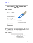
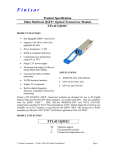
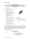
40BASE-SR4/10GBASE-SR 300m QSFP+ Gen2 Optical
Transceiver Module
FTL410QD2C
PRODUCT FEATURES
Four-channel full-duplex
transceiver module
Hot Pluggable QSFP+ form factor
Maximum link length of 300m on
OM3 Multimode Fiber (MMF)
and 400m on OM4 MMF
Multirate capability: 1.06Gb/s to
10.5Gb/s per channel
Unretimed XLPPI electrical
interface
Maximum power dissipation
<1.5W
Reliable VCSEL array technology
Built-in digital diagnostic functions
Commercial operating case
temperature range: 0ºC to 70ºC
Single 1x12 MPO receptacle
RoHS-6 Compliant (lead-free)
APPLICATIONS
40GBASE-SR4 40G Ethernet
Breakout to 10GBASE-SR Ethernet
Proprietary interconnections
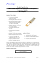
Finisar’s FTL410QD2C QSFP+ transceiver modules are designed for use in 40 Gigabit per
second links over parallel multimode fiber, including breakout to four 10 Gigabit per second
links. They are compliant with the QSFP+ MSA1,2 and IEEE 802.3ba 40GBASE-SR43 and
compatible with IEEE 802.3ae 10GBASE-SR4 The transceiver is RoHS compliant per
Directive 2011/65/EU4 and Finisar Application Note AN-20386.
PRODUCT SELECTION
FTL410QD2C
Finisar Corporation – 24-Jul-13 Rev B5 Finisar Confidential
Page 1
FTL410QD2C Product Specification – July 2013
I.
Finisar
Pin Descriptions
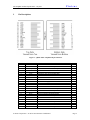
Figure 1 – QSFP+ MSA-compliant 38-pin connector
Pin
1
2
3
4
5
6
7
8
9
10
11
12
13
14
15
16
17
18
19
20
21
22
23
24
Symbol
GND
Tx2n
Tx2p
GND
Tx4n
Tx4p
GND
ModSelL
ResetL
Vcc Rx
SCL
SDA
GND
Rx3p
Rx3n
GND
Rx1p
Rx1n
GND
GND
Rx2n
Rx2p
GND
Rx4n
Name/Description
Ground
Transmitter Inverted Data Input
Transmitter Non-Inverted Data Input
Ground
Transmitter Inverted Data Input
Transmitter Non-Inverted Data Input
Ground
Module Select
Module Reset
+3.3 V Power supply receiver
2-wire serial interface clock
2-wire serial interface data
Ground
Receiver Non-Inverted Data Output
Receiver Inverted Data Output
Ground
Receiver Non-Inverted Data Output
Receiver Inverted Data Output
Ground
Ground
Receiver Inverted Data Output
Receiver Non-Inverted Data Output
Ground
Receiver Inverted Data Output
Finisar Corporation – 24-Jul-13 Rev B5 Finisar Confidential
Notes
1
1
1
1
1
1
1
1
Page 2
Finisar
FTL410QD2C Product Specification – July 2013
25
26
27
28
29
30
31
32
33
34
35
36
37
38
Rx4p
GND
ModPrsL
IntL
Vcc Tx
Vcc1
LPMode
GND
Tx3p
Tx3n
GND
Tx1p
Tx1n
GND
Receiver Non-Inverted Data Output
Ground
Module Present
Interrupt
+3.3 V Power supply transmitter
+3.3 V Power Supply
Low Power Mode
Ground
Transmitter Non-Inverted Data Input
Transmitter Inverted Data Input
Ground
Transmitter Non-Inverted Data Input
Transmitter Inverted Data Input
Ground
1
1
1
1
Notes
1. Circuit ground is internally isolated from chassis ground.
II.
General Product Characteristics
Parameter
Module Form Factor
Number of Lanes
Maximum Aggregate Data Rate
Maximum Data Rate per Lane
Protocols Supported
Electrical Interface and Pin-out
Maximum Power Consumption
per End
Management Interface
Data Rate Specifications
Bit Rate per Lane
Bit Error Ratio
Link distance on OM3 MMF
Link distance on OM4 MMF
Value
QSFP+
4 Tx and 4 Rx
42.0
10.5
Unit
Gb/s
Gb/s
Typical applications include
40G Ethernet, Infiniband,
Fibre Channel,
SATA/SAS3
38-pin edge connector
1.5
Watts
Serial, I2C-based, 400 kHz
maximum frequency
Symbol
BR
BER
d
d
Min
1062
Typ
Notes
Higher bit rates may be supported.
Please contact Finisar.
Pin-out as defined by the
QSFP+ MSA
Varies with output voltage swing
and pre-emphasis settings
(see Figure 2)
As defined by the QSFP+ MSA
Max
10500
10-12
300
400
Units
Mb/sec
meters
meters
Ref.
1
2
3
3
Notes:
1. Compliant with 40G and 10G* Ethernet. Compatible with 1 Gigabit Ethernet and 1/2/4/8/10G Fibre
Channel.
2. Tested with a PRBS 231-1 test pattern.
3. Per 40GBASE-SR4 and 10GBASE-SR IEEE 802.3ba
Finisar Corporation – 24-Jul-13 Rev B5 Finisar Confidential
Page 3
Finisar
FTL410QD2C Product Specification – July 2013
* Max launch power exceeds 10G Ethernet specification by 1 dB, which is well within the guardband of
receiver overload.
III.
Absolute Maximum Ratings
Parameter
Maximum Supply Voltage
Storage Temperature
Case Operating Temperature
Relative Humidity
Damage Threshold, per Lane
Symbol
Vcc1,
VccTx,
VccRx
TS
TOP
RH
DT
Min
-0.5
Typ
Max
3.6
Unit
V
85
70
85
C
C
%
dBm
-40
0
0
3.4
Ref.
1
Notes:
1. Non-condensing.
IV.
Electrical Characteristics (TOP = 0 to 70C, VCC = 3.15 to 3.45 Volts)
Parameter
Supply Voltage
Supply Current
Link turn-on time
Transmit turn-on time
Transmitter (per Lane)
Single ended input voltage tolerance
Differential data input swing
Differential input threshold
AC common mode input voltage tolerance
(RMS)
Differential input return loss
J2 Jitter Tolerance
J9 Jitter Tolerance
Data Dependent Pulse Width Shrinkage
Eye mask colordinates {X1, X2
Y1, Y2}
Receiver (per Lane)
Single-ended output voltage
Differential data output swing
AC common mode output voltage (RMS)
Termination mismatch at 1 MHx
Differential output return loss
Symbol
Vcc1,
VccTx,
VccRx
Icc
Min
Typ
3.15
Max
Unit
3.45
V
350
mA
ms
V
mVpp
mV
2000
VinT
Vin,pp
-0.3
180
4.0
1200
50
15
Jt2
Jt9
DDPWS
Vout,pp
Common mode output return loss
Output transition time, 20% to 80%
Finisar Corporation – 24-Jul-13 Rev B5 Finisar Confidential
Per IEEE P802.3ba,
Section 86A.4.1.1
0.17
0.29
0.07
0.11, 0.31
95, 350
-0.3
0
4.0
800
7.5
5
Per IEEE P802.3ba,
Section 86A.4.2.1
Per IEEE P802.3ba,
Section 86A.4.2.2
28
Ref.
2
3
mV
dB
4
UI
UI
UI
UI
mV
V
mVpp
mV
%
5
7,8
dB
4
dB
4
ps
Page 4
Finisar
FTL410QD2C Product Specification – July 2013
J2 Jitter output
J9 Jitter output
Eye mask coordinates #1 {X1, X2
Y1, Y2}
Eye mask coordinates #2 {X1, X2
Y1, Y2}
Power Supply Ripple Tolerance
Notes:
1.
2.
3.
4.
5.
6.
7.
8.
Jo2
Jo9
0.42
0.65
UI
UI
UI
mV
UI
mV
mVpp
0.29, 0.5
150, 425
0.29, 0.5
125, 500
PSR
50
6
5
Maximum total power value is specified across the full temperature and voltage range.
From power-on and end of any fault conditions.
After internal AC coupling. Self-biasing 100 differential input.
10 MHz to 11.1 GHz range
Hit ratio = 5 x 10E-5. Valid for all settings in Figure 2.
Hit ratio = 5 x 10E-5. Valid only for the shaded settings in Figure 2.
AC coupled with 100 differential output impedance.
Settable in 4 discrete steps via the I2C interface. See Figure 2 for Vout settings.
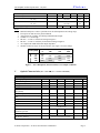
Vout (mV)
Power (mW)
0
317
422
739
Pre-Emphasis into 100ohms (mV)
0
125
175
325
599
751
935
971
1075
787
971
1007
1111
883
1055
1103
1190
Figure 2 – Power Dissipation (mW, maximum) vs. Rx Output Conditions
V.
Optical Characteristics (TOP = 0 to 70C, VCC = 3.15 to 3.45 Volts)
Parameter
Transmitter (per Lane)
Signaling Speed per Lane
Center wavelength
RMS Spectral Width
Average Launch Power per Lane
Transmit OMA per Lane
Difference in Power between any two
lanes [OMA]
Peak Power per Lane
Launch Power [OMA] minus TDP per
Lane
TDP per Lane
Optical Extinction Ratio
Optical Return Loss Tolerance
Encircled Flux
Average launch power of OFF
transmitter, per lane
Relative Intensity Noise
Transmitter eye mask definition {X1,
X2, X3, Y1, Y2, Y3}
Symbol
Min
Typ
Max
10.5
840
SW
TXPx
TxOMA
DPx
PPx
P-TDP
TDP
ER
ORL
FLX
860
0.40
0.5
3.0
4.0
-7.5
-2.5
4.0
dBm
dBm
3.5
dBm
dB
dB
dBm
-6.5
3.0
12
> 86% at 19 um
< 30% at 4.5 um
RIN
Unit
GBd
nm
nm
dBm
dBm
dB
-30
dBm
-128
dB/Hz
Ref.
1
2
3
0.23, 0.34, 0.43, 0.27, 0.35, 0.4
Finisar Corporation – 24-Jul-13 Rev B5 Finisar Confidential
Page 5
Finisar
FTL410QD2C Product Specification – July 2013
Parameter
Symbol
Min
Typ
Max
Unit
Ref.
Receiver (per Lane)
Signaling Speed per Lane
10.5
GBd
4
Center wavelength
840
860
nm
Damage Threshold
DT
3.4
dBm
Average Receive Power per Lane
RXPx
-9.9
2.4
dBm
Receive Power (OMA) per Lane
RxOMA
3.0
dBm
Unstressed Receiver Sensitivity
URS
-11.1
dBm
(OMA) per Lane
Stressed Receiver Sensitivity (OMA)
SRS
-7.5
dBm
per Lane
Peak Power, per lane
PPx
4
dBm
Receiver Reflectance
Rfl
-12
dB
Vertical eye closure penalty, per lane
1.9
dB
Stressed eye J2 jitter, per Lane
0.3
UI
Stressed eye J9 jitter, per Lane
0.47
UI
OMA of each aggressor lane
-0.4
dBm
Rx jitter tolerance: Jitter frequency
(75, 5)
kHz, UI
and p-p amplitude
(375, 1)
kHz, UI
LOS De-Assert
LOSD
-12
dBm
LOS Assert
LOSA
-30
dBm
LOS Hysteresis
0.5
dBm
Notes:
1. Transmitter consists of 4 lasers operating at a maximum rate of 10.5Gb/s each.
2. The maximum launch power of 0.5 dBm is well within the guardband of receiver overload specifications
for commercially available 10GBASE-SR SFP+ transceivers from Finisar and other vendors.
3. Even if TDP is <0.9dB, the OMA min must exceed this value.
4. Receiver consists of 4 photodetectors operating at a maximum rate of 10.5Gb/s each.
VI.
Memory Map and Control Registers
Compatible with SFF-8436 (QSFP+). Please see Finisar Application Note.
VII.
Environmental Specifications
Finisar FTL410QE2C transceivers have an operating temperature range from 0°C to +70°C
case temperature.
Environmental Specifications
Case Operating Temperature
Storage Temperature
Symbol
Min
Top
Tsto
0
-40
Finisar Corporation – 24-Jul-13 Rev B5 Finisar Confidential
Typ
Max
Units
70
85
°C
°C
Ref.
Page 6
FTL410QD2C Product Specification – July 2013
Finisar
VIII. Regulatory Compliance
Finisar FTL410QD2C transceivers are RoHS-6 Compliant. Copies of certificates are
available at Finisar Corporation upon request.
FTL410QD2C transceiver modules are Class 1 laser eye safety compliant per IEC 60825-1.
IX.
Mechanical Specifications
The FTL410QD2C mechanical specifications are compliant to the QSFP+ MSA transceiver
module specifications.
Figure 3 – FTL410QD2C mechanical drawing
Figure 4 – FTL410QD2C product label
Finisar Corporation – 24-Jul-13 Rev B5 Finisar Confidential
Page 7
FTL410QD2C Product Specification – July 2013
Finisar
Figure 5 – FTL410QD2C optical lane assignment
(front view of MPO receptacle)
X.
References
1.
INF-8438i – Specification for QSFP (Quad Small Formfactor Pluggable)
Transceiver, Rev 1.0, November 2006.
2.
SFF-8436 – Specification for QSFP+ Copper and Optical Transceiver, Rev 4.7,
February 2013.
3.
IEEE 802.3ba – PMD Type 40GBASE-SR4.
4.
IEEE 802.3ae – PMD Type 10GBASE-SR.
5.
Directive 2011/65/EU of the European Council Parliament and of the Council, “on
the restriction of the use of certain hazardous substances in electrical and electronic
equipment,” June 8, 2011, which supercedes the previous RoHS Directive
2002/95/EC.
6.
“Application Note AN-2038: Finisar Implementation of RoHS Compliant
Transceivers”, Finisar Corporation, January 21, 2005.
Finisar Corporation – 24-Jul-13 Rev B5 Finisar Confidential
Page 8
FTL410QD2C Product Specification – July 2013
XI.
Finisar
For More Information
Finisar Corporation
1389 Moffett Park Drive
Sunnyvale, CA 94089-1133
Tel. 1-408-548-1000
Fax 1-408-541-6138
[email protected]
www.finisar.com
Finisar Corporation – 24-Jul-13 Rev B5 Finisar Confidential
Page 9