1
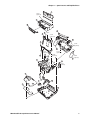
Service Manual
PB42 Portable
Receipt Printer
Service Manual
PB42 Portable
Receipt Printer
Intermec Technologies Corporation
Worldwide Headquarters
6001 36th Ave.W.
Everett, WA 98203
U.S.A.
www.intermec.com
The information contained herein is provided solely for the purpose of allowing customers to operate and
service Intermec-manufactured equipment and is not to be released, reproduced, or used for any other purpose
without written permission of Intermec Technologies Corporation.
Information and specifications contained in this document are subject to change without prior noticed and do
not represent a commitment on the part of Intermec Technologies Corporation.
© 2007 by Intermec Technologies Corporation. All rights reserved.
The word Intermec, the Intermec logo, Norand, ArciTech, Beverage Routebook, CrossBar, dcBrowser,
Duratherm, EasyADC, EasyCoder, EasySet, Fingerprint, INCA (under license), i-gistics, Intellitag, Intellitag
Gen2, JANUS, LabelShop, MobileLAN, Picolink, Ready-to-Work, RoutePower, Sabre, ScanPlus, ShopScan,
Smart Mobile Computing, SmartSystems, TE 2000, Trakker Antares, and Vista Powered are either trademarks
or registered trademarks of Intermec Technologies Corporation.
There are U.S. and foreign patents as well as U.S. and foreign patents pending.
Bluetooth is a trademark of Bluetooth SIG, Inc., U.S.A.
ii
PB42 Portable Receipt Printer Service Manual
Contents
Contents
Before You Begin . . . . . . . . . . . . . . . . . . . . . . . . . . . . . . . . . . . . . . . . . . . . . . . . . . . . . . . . . v
Safety Summary . . . . . . . . . . . . . . . . . . . . . . . . . . . . . . . . . . . . . . . . . . . . . . . . . . . v
Sicherheitsübersicht . . . . . . . . . . . . . . . . . . . . . . . . . . . . . . . . . . . . . . . . . . . . . . . . v
Nicht alleine Reparaturen oder Einstellungen durchführen . . . . . . . . . . . . v
Erste Hilfe . . . . . . . . . . . . . . . . . . . . . . . . . . . . . . . . . . . . . . . . . . . . . . . . . vi
Wiederbelebung . . . . . . . . . . . . . . . . . . . . . . . . . . . . . . . . . . . . . . . . . . . . vi
Stromführende Geräte . . . . . . . . . . . . . . . . . . . . . . . . . . . . . . . . . . . . . . . . vi
Safety Information . . . . . . . . . . . . . . . . . . . . . . . . . . . . . . . . . . . . . . . . . . . . . . . . . vi
Global Services and Support . . . . . . . . . . . . . . . . . . . . . . . . . . . . . . . . . . . . . . . . . . vi
Warranty Information . . . . . . . . . . . . . . . . . . . . . . . . . . . . . . . . . . . . . . . . vi
Web Support. . . . . . . . . . . . . . . . . . . . . . . . . . . . . . . . . . . . . . . . . . . . . . . vi
Telephone Support . . . . . . . . . . . . . . . . . . . . . . . . . . . . . . . . . . . . . . . . . vii
Who Should Read This Manual . . . . . . . . . . . . . . . . . . . . . . . . . . . . . . . . . . . . . . vii
1 Spare Parts List and Exploded Views
....................................... 1
PB42 Exploded Views and Parts Lists . . . . . . . . . . . . . . . . . . . . . . . . . . . . . . . . . . . . . . . . . 2
2 Theory of Operation
........................................................ 5
Microprocessor . . . . . . . . . . . . . . . . . . . . . . . . . . . . . . . . . . . . . . . . . . . . . . . . . . . . . . . . . . 6
Power Supply Sequencing and Bypass Capacitors . . . . . . . . . . . . . . . . . . . . . . . . . . 6
Clock Generation Circuitry . . . . . . . . . . . . . . . . . . . . . . . . . . . . . . . . . . . . . . . . . . 6
Reset Configuration Settings. . . . . . . . . . . . . . . . . . . . . . . . . . . . . . . . . . . . . . . . . . 7
Flash Interface . . . . . . . . . . . . . . . . . . . . . . . . . . . . . . . . . . . . . . . . . . . . . . . . . . . . 8
SDRAM Interface. . . . . . . . . . . . . . . . . . . . . . . . . . . . . . . . . . . . . . . . . . . . . . . . . . 9
Register Settings . . . . . . . . . . . . . . . . . . . . . . . . . . . . . . . . . . . . . . . . . . . . 9
Initialization Procedure . . . . . . . . . . . . . . . . . . . . . . . . . . . . . . . . . . . . . . 11
Self Refresh Mode . . . . . . . . . . . . . . . . . . . . . . . . . . . . . . . . . . . . . . . . . . 12
Serial Peripheral Interface (SPI) . . . . . . . . . . . . . . . . . . . . . . . . . . . . . . . . . . . . . . 13
FRAM . . . . . . . . . . . . . . . . . . . . . . . . . . . . . . . . . . . . . . . . . . . . . . . . . . . 13
Input/Output Shift Registers. . . . . . . . . . . . . . . . . . . . . . . . . . . . . . . . . . 14
Digital to Analog Converter . . . . . . . . . . . . . . . . . . . . . . . . . . . . . . . . . . 15
Analog to Digital Converter . . . . . . . . . . . . . . . . . . . . . . . . . . . . . . . . . . 16
Compact Flash Interface . . . . . . . . . . . . . . . . . . . . . . . . . . . . . . . . . . . . . . . . . . . . 17
Print Controller . . . . . . . . . . . . . . . . . . . . . . . . . . . . . . . . . . . . . . . . . . . . . . . . . . . . . . . . .
GPIO Configuration . . . . . . . . . . . . . . . . . . . . . . . . . . . . . . . . . . . . . . . . . . . . . .
5V Power Enable . . . . . . . . . . . . . . . . . . . . . . . . . . . . . . . . . . . . . . . . . . . . . . . . .
Reset. . . . . . . . . . . . . . . . . . . . . . . . . . . . . . . . . . . . . . . . . . . . . . . . . . . . . . . . . . .
Print Controller Startup . . . . . . . . . . . . . . . . . . . . . . . . . . . . . . . . . . . . . . . . . . . .
Configuration Jumpers . . . . . . . . . . . . . . . . . . . . . . . . . . . . . . . . . . . . . . . . . . . . .
Parallel Interface . . . . . . . . . . . . . . . . . . . . . . . . . . . . . . . . . . . . . . . . . . . . . . . . . .
Serial Interface . . . . . . . . . . . . . . . . . . . . . . . . . . . . . . . . . . . . . . . . . . . . . . . . . . .
Error Detection . . . . . . . . . . . . . . . . . . . . . . . . . . . . . . . . . . . . . . . . . . . . . . . . . .
Thermistors and Paper Sensors . . . . . . . . . . . . . . . . . . . . . . . . . . . . . . . . . . . . . . .
Paper Feed and Backfeed. . . . . . . . . . . . . . . . . . . . . . . . . . . . . . . . . . . . . . . . . . . .
Printhead Resistance Test . . . . . . . . . . . . . . . . . . . . . . . . . . . . . . . . . . . . . . . . . . .
PB42 Portable Receipt Printer Service Manual
17
17
17
18
18
18
18
19
20
20
21
21
iii
Contents
iv
Communication Interfaces. . . . . . . . . . . . . . . . . . . . . . . . . . . . . . . . . . . . . . . . . . . . . . . . .
USB . . . . . . . . . . . . . . . . . . . . . . . . . . . . . . . . . . . . . . . . . . . . . . . . . . . . . . . . . . .
Low Speed Configuration . . . . . . . . . . . . . . . . . . . . . . . . . . . . . . . . . . . .
Full Speed Configuration . . . . . . . . . . . . . . . . . . . . . . . . . . . . . . . . . . . .
Cable Detection . . . . . . . . . . . . . . . . . . . . . . . . . . . . . . . . . . . . . . . . . . .
RS-232 . . . . . . . . . . . . . . . . . . . . . . . . . . . . . . . . . . . . . . . . . . . . . . . . . . . . . . . . .
Cable Detection . . . . . . . . . . . . . . . . . . . . . . . . . . . . . . . . . . . . . . . . . . .
Bluetooth Module . . . . . . . . . . . . . . . . . . . . . . . . . . . . . . . . . . . . . . . . . . . . . . . .
802.11g . . . . . . . . . . . . . . . . . . . . . . . . . . . . . . . . . . . . . . . . . . . . . . . . . . . . . . . .
Secondary Serial Test Port. . . . . . . . . . . . . . . . . . . . . . . . . . . . . . . . . . . . . . . . . . .
22
22
23
23
23
23
24
24
24
24
User Interface . . . . . . . . . . . . . . . . . . . . . . . . . . . . . . . . . . . . . . . . . . . . . . . . . . . . . . . . . .
Speaker Driver . . . . . . . . . . . . . . . . . . . . . . . . . . . . . . . . . . . . . . . . . . . . . . . . . . .
Buttons. . . . . . . . . . . . . . . . . . . . . . . . . . . . . . . . . . . . . . . . . . . . . . . . . . . . . . . . .
LED Control . . . . . . . . . . . . . . . . . . . . . . . . . . . . . . . . . . . . . . . . . . . . . . . . . . . .
25
25
26
26
Power Management . . . . . . . . . . . . . . . . . . . . . . . . . . . . . . . . . . . . . . . . . . . . . . . . . . . . . .
DC Power Input . . . . . . . . . . . . . . . . . . . . . . . . . . . . . . . . . . . . . . . . . . . . . . . . . .
Charging Circuits . . . . . . . . . . . . . . . . . . . . . . . . . . . . . . . . . . . . . . . . . . . . . . . . .
Reading Battery Voltages . . . . . . . . . . . . . . . . . . . . . . . . . . . . . . . . . . . . . . . . . . .
Battery EEPROM. . . . . . . . . . . . . . . . . . . . . . . . . . . . . . . . . . . . . . . . . . . . . . . . .
Sleep Mode. . . . . . . . . . . . . . . . . . . . . . . . . . . . . . . . . . . . . . . . . . . . . . . . . . . . . .
Print Controller Power Down . . . . . . . . . . . . . . . . . . . . . . . . . . . . . . . . .
Power Down Unused Processor Modules . . . . . . . . . . . . . . . . . . . . . . . .
SDRAM Self Refresh. . . . . . . . . . . . . . . . . . . . . . . . . . . . . . . . . . . . . . . .
Normal Low Mode . . . . . . . . . . . . . . . . . . . . . . . . . . . . . . . . . . . . . . . . .
Bluetooth Radio Low Power Mode . . . . . . . . . . . . . . . . . . . . . . . . . . . . .
What To Do In Sleep Mode . . . . . . . . . . . . . . . . . . . . . . . . . . . . . . . . . .
Power Cuts . . . . . . . . . . . . . . . . . . . . . . . . . . . . . . . . . . . . . . . . . . . . . . . . . . . . . .
Watchdog Timer. . . . . . . . . . . . . . . . . . . . . . . . . . . . . . . . . . . . . . . . . . . . . . . . . .
26
26
27
28
29
29
29
29
29
29
30
30
30
31
Immunity and Emissions . . . . . . . . . . . . . . . . . . . . . . . . . . . . . . . . . . . . . . . . . . . . . . . . . .
ESD . . . . . . . . . . . . . . . . . . . . . . . . . . . . . . . . . . . . . . . . . . . . . . . . . . . . . . . . . . .
Power Surge . . . . . . . . . . . . . . . . . . . . . . . . . . . . . . . . . . . . . . . . . . . . . . . . . . . . .
Conducted Emissions . . . . . . . . . . . . . . . . . . . . . . . . . . . . . . . . . . . . . . . . . . . . . .
Radiated Emissions. . . . . . . . . . . . . . . . . . . . . . . . . . . . . . . . . . . . . . . . . . . . . . . .
Clocks . . . . . . . . . . . . . . . . . . . . . . . . . . . . . . . . . . . . . . . . . . . . . . . . . . .
Bus Lines. . . . . . . . . . . . . . . . . . . . . . . . . . . . . . . . . . . . . . . . . . . . . . . . .
Bluetooth Radio . . . . . . . . . . . . . . . . . . . . . . . . . . . . . . . . . . . . . . . . . . .
Switching Power Supplies . . . . . . . . . . . . . . . . . . . . . . . . . . . . . . . . . . . .
32
32
32
33
33
33
33
33
34
PB42 Portable Receipt Printer Service Manual
Before You Begin
Before You Begin
This section provides you with safety information, technical support
information, and sources for additional product information.
Safety Summary
Your safety is extremely important. Read and follow all warnings and
cautions in this document before handling and operating Intermec
equipment. You can be seriously injured, and equipment and data can be
damaged if you do not follow the safety warnings and cautions.
Do Not Repair or Adjust Alone
Do not repair or adjust energized equipment alone under any
circumstances. Someone capable of providing first aid must always be
present for your safety.
First Aid
Always obtain first aid or medical attention immediately after an injury.
Never neglect an injury, no matter how slight it seems.
Resuscitation
Begin resuscitation immediately if someone is injured and stops breathing.
Any delay could result in death. To work on or near high voltage, you
should be familiar with approved industrial first aid methods.
Energized Equipment
Never work on energized equipment unless authorized by a responsible
authority. Energized electrical equipment is dangerous. Electrical shock
from energized equipment can cause death. If you must perform authorized
emergency work on energized equipment, be sure that you comply strictly
with approved safety regulations.
Sicherheitsübersicht
Ihre Sicherheit ist äußerst wichtig. Lesen und befolgen Sie alle Warn- und
Vorsichtshinweise in diesem Dokument, bevor Sie Intermec-Geräte
verwenden und betreiben. Falls die Sicherheitswarnungen und
Vorsichtshinweise nicht befolgt werden, kann es zu ernsthaften
Verletzungen sowie Geräteschäden und Datenverlusten kommen.
Nicht alleine Reparaturen oder Einstellungen durchführen
Reparieren oder justieren Sie niemals alleine stromführende Geräte. Aus
Sicherheitsgründen muss eine zweite Person anwesend sein, die erste Hilfe
leisten kann.
PB42 Portable Receipt Printer Service Manual
v
Before You Begin
Erste Hilfe
Nach einer Verletzung unverzüglich erste Hilfe oder medizinische
Betreuung aufsuchen. Verletzungen dürfen nicht vernachlässigt werden,
auch wenn sie noch so unbedeutend erscheinen.
Wiederbelebung
Wiederbelebungsversuche müssen unverzüglich eingeleitet werden, falls
jemand verletzt wird und die Atmung aussetzt. Verzögerungen können zum
Tod führen. Bei Arbeiten an oder in der Nähe von Hochspannung müssen
Ihnen die zugelassenen Erste-Hilfe-Methoden vertraut sein.
Stromführende Geräte
Niemals an stromführenden Geräten arbeiten, es sei denn Sie wurden von
einer verantwortlichen Stelle dazu berechtigt. Stromführende Geräte sind
gefährlich. Stromschläge durch stromführende Geräte können zu tödlichen
Verletzungen führen. Falls zugelassene Notreparaturen an stromführenden
Geräten vorgenommen werden müssen, ist darauf zu achten, dass die
genehmigten Sicherheitsvorschriften strikt eingehalten werden.
Safety Information
This section explains how to identify and understand notes that are in this
document.
Note: Notes either provide extra information about a topic or contain
special instructions for handling a particular condition or set of
circumstances.
Global Services and Support
Warranty Information
To understand the warranty for your Intermec product, visit the Intermec
web site at www.intermec.com and click Service & Support > Warranty.
Disclaimer of warranties: The sample code included in this document is
presented for reference only. The code does not necessarily represent
complete, tested programs. The code is provided “as is with all faults.” All
warranties are expressly disclaimed, including the implied warranties of
merchantability and fitness for a particular purpose.
Web Support
Visit the Intermec web site at www.intermec.com to download our current
manuals (in PDF). To order printed versions of the Intermec manuals,
contact your local Intermec representative or distributor.
Visit the Intermec technical knowledge base (Knowledge Central) at
intermec.custhelp.com to review technical information or to request
technical support for your Intermec product.
vi
PB42 Portable Receipt Printer Service Manual
Before You Begin
Telephone Support
These services are available from Intermec.
In the USA and Canada
call 1-800-755-5505 and
choose this option
Services
Description
Order Intermec
products
• Place an order.
• Ask about an existing order.
1 and then choose 2
Order Intermec media
Order printer labels and ribbons.
1 and then choose 1
Order spare parts
Order spare parts.
1 or 2 and then choose 4
Technical Support
Talk to technical support about
your Intermec product.
2 and then choose 2
Service
2 and then choose 1
• Get a return authorization
number for authorized service
center repair.
• Request an on-site repair
technician.
Service contracts
• Ask about an existing contract. 1 or 2 and then choose 3
• Renew a contract.
• Inquire about repair billing or
other service invoicing
questions.
Outside the U.S.A. and Canada, contact your local Intermec representative.
To search for your local representative, from the Intermec web site, click
Contact.
Who Should Read This Manual
This manual contains some of the information necessary to repair the PB42
portable receipt printer. It provides an exploded view of the computer, the
spare parts lists, and the theory of operation.
This manual is intended for Intermec service technicians.
PB42 Portable Receipt Printer Service Manual
vii
Before You Begin
viii
PB42 Portable Receipt Printer Service Manual
1
Spare Parts List and Exploded
Views
This chapter provides the exploded views and spare parts list for the PB42
Portable Receipt Printer.
PB42 Portable Receipt Printer Service Manual
1
Chapter 1 — Spare Parts List and Exploded Views
PB42 Exploded Views and Parts Lists
This chapter contains an exploded view and a spare parts list for the PB42.
Locate the part you need to replace in the exploded view and then find the
corresponding part number in the spare parts list.
2
PB42 Portable Receipt Printer Service Manual
Chapter 1 — Spare Parts List and Exploded Views
3
Screw
(2 places)
2
1
6
4
5 Screw
Screw
(2 places)
7
9
Screw
(6 places)
8
Screw
(2 places)
10
11
Screw
(3 places)
Screw
(6 places)
8
12
Screw
(2 places)
11
Screw
(2 places)
13
18
17
16
14
19
15
PB42 Portable Receipt Printer Service Manual
3
Chapter 1 — Spare Parts List and Exploded Views
To identify a part, find the callout in this list and locate the part in the
exploded view.
PB42 Spare Parts List
4
Callout
Description
Part Number
1
PB42 console assembly
075183-001
2
PB42 upper case
075170-001
3
PB42 battery door
074787-001
4
PB42 thermal printer mechanism
592124-001
5
PB42 printhead release wedge
075186-001
6
PB42 platen roller
592123-001
7
PB42 media door assembly
075171-001
8
PB42 media windows, pair
075173-001
9
PB42 linkage arm
075175-001
10
PB42 sub-linkage arm
075187-001
11
PB42 media brackets, pair
075172-001
12
PB42 engine mount assembly
075174-001
13
PB42 print mechanism ground spring
592122-001
14
PB42 battery contact PCB assembly
075182-001
15
PB42 lower case
075184-001
16
PB42 speaker
075180-001
17
PB42 I/O door
075185-001
18
PB42 Bluetooth PCB assembly
074792-001
19
PB42 ESD shield
075179-001
PB42 miscellaneous fastener pack
075178-001
PB42 certification label
074791-001
PB42 control panel overlay label
074790-001
PB42 lubrication
075181-001
PB42 Portable Receipt Printer Service Manual
2
Theory of Operation
This chapter provides a detailed electrical design of the PB42 printer. It is
intended to help software engineering to know how to control the
hardware.
PB42 Portable Receipt Printer Service Manual
5
Chapter 2 — Theory of Operation
Microprocessor
The microprocessor (U1) for the PB42 is the Freescale MPC875. The
following sections describe circuitry connected directly to the
microprocessor.
Power Supply Sequencing and Bypass Capacitors
Power Sequencing and Bypass Capacitors for U1
D101 helps keep VDD (1.8 V) from ever rising faster than the +3.3 V
supply (VCC). D102 is a 1.8 V zener. It keeps VCC and VDD from being
too far from each other.
There are five 0.1 μF ceramic bypass caps on each supply, two 10 μF
capacitors on VCC, and one 10 μF capacitor on VDD.
Clock Generation Circuitry
10MHz Crystal Circuit for the Internal Clock
6
PB42 Portable Receipt Printer Service Manual
Chapter 2 — Theory of Operation
MODCK [1:2] (not shown) are set to 00 on reset. The filter on VDDSYN
provides a clean supply to the internal PLL. CLKOUT is connected to the
SDRAM. EXTCLK is not used. R103 is not placed.
To set the frequency of the system clock to 66 MHz make the following
settings to PLPRCR: PDF = 0, MFI = 13, MFN = 2, MFD = 9, S = 1,
DBRMO = 0.
For SCCR:
• COM = 00 (CLKOUT enabled)
• TBS = 1 (Timebase is GCLK2/16)
• PTDIV = 0 (PIT divider = 4)
• PTSEL = 0 (Crystal oscillator selected)
• CRQEN = 0 (Remain in low frequency when CP is active)
• EBDF = 00 (CLKOUT = GCLK2)
• DFSYNC = 00 (Divide by 1)
• DFBRG = 00 (Divide by 1)
• DFNL = 111 (Divide by 256)
• DFNH = 000 (No division for high frequency mode)
• DFUTP, DFAUTP – Leave at default values. UTOPIA not used.
Reset Configuration Settings
When HRESET* is asserted, U7 drives data bus pin 4. All of the others are
internally pulled low. This process corresponds to these settings:
• Internal bus arbitration
• MSR[IP] = 0
• Boot device bursting disabled
• Memory controller activated
• 16-bit port size
• Internal space base address = 0x00000000
• Debug pin configuration = 00
• Debug port pin configuration = 00
• CLKOUT is GCLK2 divided by 1
• Big endian
PB42 Portable Receipt Printer Service Manual
7
Chapter 2 — Theory of Operation
Flash Interface
Flash Memory Connections
CS0 is the chip select line for the flash. The flash is accessed through one of
the general-purpose chip-select machines (GPCM) of U1.
BR0 and OR0 configure the GPCM control of the flash. Below are the
required settings for those two registers. All other settings can be selected at
the firmware designer’s discretion.
BR0 = 0xXXXXX801:
• BA = Determined by firmware designer (Base address)
• AT = 000 (No address type masking)
• PS = 10 (16-bit port size)
• WP = 0 (Read and write allowed)
• MS = 00 (GPCM selected)
• V = 1 (Valid bank)
OR0 = 0xFFC00940:
• AM = 0xFFC00 (4 MB)
• ATM = 000 (No address type mask)
• CSNT = 1 (Chip-select negation time)
• ACS = 00 (CS* is output at the same time as the address)
• BIH = 1 (Bursting not supported)
• SCY = Number of wait states:
• 0101 for 73.17 MHz < system clock < 85.37 MHz
• 0100 for 60.98 MHz < system clock < 73.17 MHz
8
PB42 Portable Receipt Printer Service Manual
Chapter 2 — Theory of Operation
• 0011 for 48.78 MHz < system clock < 60.98 MHz
• SETA = 0 (Internal or external transfer acknowledge)
• TRLX = 0 (Timing not relaxed)
• EHTR = 0 (No extended hold time on read)
SDRAM Interface
The SDRAM Interface
CS_RAM* is connected to CS1*. The hardware has been designed to allow
the SDRAM to be connected to either UPMA or UPMB depending on the
placement of RP117 or RP118. By default, RP117 is placed, connecting
the SDRAM to UPMB. The RAM clock enable is connected to GPL5.
LDMQ and UDMQ are connected to BS0 and BS1, respectively. The OE*
signal is connected to GPL1 of U1.
The PowerPC UPM is very flexible and complex. The following section
will give the register settings, but for details on the UPM and SDRAM, see
their respective specifications. Micron technical note TN-48-12 gives an
excellent example of how to program the UPM.
Register Settings
Here are the register settings for the SDRAM interface.
BRI = 0x000008C1:
• BA = 0x00000 (Base address = 0)
• AT = 000 (No address type masking)
• PS = 10 (16-bit port size)
PB42 Portable Receipt Printer Service Manual
9
Chapter 2 — Theory of Operation
• WP = 0 (Read and write allowed)
• MS = 11 (UPMB selected)
• V = 1 (Valid bank)
OR1 = 0xFF000A00:
• AM = 0xFF00 (Corresponds to 16MBytes)
• ATM = 000 (No address type mask)
• SAM = 1 (Address multiplexing enabled)
• G5LA = 0 (Output GPL5* on GPL_B5*)
• G5LS = 1 (GPL5* high on memory accesses.)
• BIH = 0 (Bursting is supported)
MAMR = 0x20904331:
• PTA = 32 (Periodic timer period = 15.625us. Assumes 66MHz clock,
SCCR[DFBRG] = 00, MPTPR[PTP] = 0x02)
• PTAE = 1 (Periodic timer enabled)
• AMA = 001 (Address multiplexing size.)
• DSA = 00 (1-cycle disable timer)
• G0CLA = 010 (A10 routed to GPL0*)
• GPLA4DIS = 0 (GPL4* is an output)
• RLFA = 0011 (Burst length is 8)
• WLFA = 0011 (Burst length is 8)
• TLFA = 0011 (1 time execution for each periodic loop)
The memory periodic timer prescaler is set to divide by 32: MPTPR =
0x0200. The UPM RAM array for 75 MHz operation should be programmed
with the following values:
• Read single beat cycle: Addresses 0x00 – 0x04 = 0x0F07FC04,
0x0FFFFC04, 0x00BDFC04, 0x0FF77C00, 0X1FFFFC05
• Read burst cycle: Addresses 0x08 – 0x0F = 0x0F07FC04, 0x0FFFFC04,
0x00BDFC04, 0x00FFFC80, 0x00FFFC80, 0x00FFFC00,
0x0FF77C00, 0x1FFFFC05
• Write single beat cycle: Addresses 0x18 – 0x1D = 0x0F07FC04,
0x0FFFFC00, 0x00BD7C04, 0x0FFFFC04, 0x0FF77C04,
0x1FFFFC05
• Write burst cycle: Addresses 0x20 – 0x28 = 0x0F07FC04,
0x0FFFFC00, 0x00BD7C00, 0x00FFFC80, 0x00FFFC80,
0x00FFFC04, 0x0FFFFC04, 0x0FF77C04, 0x1FFFFC05
• Auto refresh cycle: Addresses 0x30 – 0x39 = 0x0FF77C34,
0x0FFFFC34, 0x0FF5FC34, 0x0FFFFC34, 0x0FFFFC34,
10
PB42 Portable Receipt Printer Service Manual
Chapter 2 — Theory of Operation
0x0FFFFC34, 0x0FFFFC34, 0x0FFFFC34, 0x0FFFFC34,
0x0FFFFC34, 0x1FFFFC35
• Exception: Addresses 0x3C – 0x3D = 0x0FF77C04, 0x1FFFFC05
• Initialization step #1: Addresses 0x2C – 0x2D = 0x0FF77C34,
0x0FFFFC35
• Initialization step #2 and 3: Addresses 0x2E – 0x2F = 0x00F03C34,
0x0FFFFC35
• Enter self refresh mode: Addresses 0x29 – 0x2B = 0x0FF77C34,
0x0FFFFC34, 0x1FF5F035
• Exit self refresh mode: Addresses 0x10 – 0x15 = 0x0FFFFC34,
0x0FFFFC34, 0x0FFFFC34, 0x0FFFFC34, 0x0FFFFC34,
0x1FFFFC35
The SDRAM mode register is programmed as 0x0023. This corresponds to
the following settings:
• Burst length = 8
• Burst type = Sequential
• CAS latency = 2
• Write burst mode = Programmed burst length
The SDRAM extended mode register is programmed as 0x2000. This
corresponds to the following settings:
• Maximum case temperature for temperature compensated self refresh =
70°C
• Self refresh coverage = All four banks
Initialization Procedure
SDRAM initialization should be performed using the following steps:
1 Write patterns to the UPM RAM array.
2 Program MPTPR.
3 Program MBMR.
4 Program BR1.
5 Program OR1, except clear OR1[V].
6 Initialize the SDRAM and its registers.
7 Set OR1[V].
To load each word into the UPM RAM do the following:
1 Write the word contents to MDR.
2 Write 0x008021XX to MCR, where XX corresponds to the array
address.
PB42 Portable Receipt Printer Service Manual
11
Chapter 2 — Theory of Operation
Programming MPTPR, MAMR, BR1, and OR1 is done by simply writing
the proper values to the registers.
To initialize the SDRAM and write to its mode registers do the following:
1 Run initialization step #1 from the UPM RAM array by writing
0x8080212C to MCR.
2 Load MAR with 0x00000046 (SDRAM mode register contents)
3 Run initialization step #2 from the UPM RAM array by writing
0x8080212E to MCR.
4 Load MAR with 0x00800000 (SDRAM mode register contents)
5 Run initialization step #3 from the UPM RAM array by writing
0x8080212E to MCR.
6 Run initialization step #4 from the UPM RAM array by writing
0x80802230 to MCR.
Once this is done, the memory controller will automatically take care of
memory refreshing as well as properly read and write data to the SDRAM.
Self Refresh Mode
Before the processor enters into any power saving modes or slower clock
speeds it must run from the flash memory space and put the SDRAM into
self refresh mode. In self refresh mode, the memory is in its lowest power
state while still preserving its contents. Note that this feature is not
supported in the R1 board due to a missed connection to the CKE pin. For
R1, PE29 must always be output high.
To place the memory into this mode, do the following:
1 Run from flash (CS0).
2 Clear MAMR[PTAE].
3 Run the self refresh sequence from the UPM RAM array by writing
0x80802129 to MCR.
4 Clear BR1[V].
Once this is done, attempts to access the SDRAM will generate an error.
To enable the SDRAM, do the following:
1 Set BR1[V].
2 Run the self refresh exit sequence step #1 from the UPM RAM array by
writing 0x80802110 to MCR.
3 Run step #2 by writing 0x80802130 to MCR.
4 Set MAMR[PTAE].
12
PB42 Portable Receipt Printer Service Manual
Chapter 2 — Theory of Operation
Serial Peripheral Interface (SPI)
The Serial Peripheral Interface (SPI) is used to communicate with five
external chips: the FRAM, input shift register, output shift register, DAC,
and ADC. The following sections describe the SPI settings and data format
for each of these slave devices. For more specific information on operation
of the MPC875 or any of the other SPI devices, see their respective
specifications.
FRAM
The FRAM is a fast, serial, non-volatile memory that can be used to store
critical printer or communications settings. It can store error codes, service
history, and so on. Since it is fast and non-volatile, the processor can use it
to store critical data when it knows that a power cut is imminent. (IRQ0 –
low battery) It is organized as 512 x 8 bits.
The maximum data rate for the SPI interface is 20 MHz. SPMODE bits CI
and CP must be either 0, 0 or 1, 1. The MSB is always first, so
SPMODE[REV] is 1.
The WP* and HOLD* pins of the FRAM are tied high. So the hold and
hardware write protect functions are disabled. Block memory protection
can be used, though, to write protect the upper quarter, half, or all of the
memory array. This is controlled through the status register.
Data transfers with the FRAM can be any 8-bit multiple, depending on the
op-code being used and the amount of data to transfer. The maximum
buffer length for the MPC875 is only 16 bits per transfer. So, the processor
will have to span some transfers over several “chunks” when transferring
more than 16 bits to/from the FRAM. The FRAM_CS* pin (PA0) must
remain asserted over the entire transfer or the operation will be aborted.
Memory Op-Codes
Name
Description
Op-Code
WREN
Set write enable latch
00000110b
WRDI
Write disable
00000100b
RDSR
Read status register
00000101b
WRSR
Write status register
00000001b
READ
Read memory data
0000A011b
WRITE
Write memory data
0000A010b
The “A” bit for the read and write op-codes are the MSB of the 9-bit
address.
The FRAM always powers up with writes disabled. To enable writes to the
status register or the memory array, issue the WREN command once.
PB42 Portable Receipt Printer Service Manual
13
Chapter 2 — Theory of Operation
Memory reads and writes have the following format: Read/write op-code,
lower 8 bits of address, data. For multiple byte transfers, the address is
automatically incremented. If the address reaches 0x1FF, the next address is
0x000.
Memory Write
Memory Read
Input/Output Shift Registers
Due to a shortage of GPIO pins on U1, input and output shift registers are
connected to the SPI.
14
PB42 Portable Receipt Printer Service Manual
Chapter 2 — Theory of Operation
Schematic for the Input/Output Shift Register
Both shift registers reside on the same chip select (PA7). So, for every data
transfer, data is both sent and received simultaneously. The SPI software
must be sure to have valid data in the transmit buffer for every shift register
transfer.
Maximum SPI clock frequency is 5 MHz. Data length is 8 bits
(SPMODE[LEN] = 7). SPMODE[CI] = 1 and SPMODE[CP] = 1. If
SPMODE[REV] = 1, the MSB is sent and received first. For the input shift
register, the first bit transferred is ERR2 (input H). For the output shift
register, the first bit sent is output to QH. BT_RESET corresponds to the
last bit sent.
Digital to Analog Converter
The digital to analog converter (DAC) is used to generate audible alerts. See
“Speaker Driver” on page 25 for more information on the amplifier and
speaker.
The DAC only receives data, so MISO is not used. There is one additional
input that is outside of the standard SPI protocol: FS – Frame sync. (PA10)
The FS signal must behave as follows: FS is normally high. FS goes low at
least 10 ns after CS* (PB26) goes low. FS must go low at least 8 ns before
the SPI clock goes low (first bit transfer). FS must go high at least 10 ns
after the last bit is transferred. FS can go high at the same time as CS*.
PB42 Portable Receipt Printer Service Manual
15
Chapter 2 — Theory of Operation
Digital to Analog Converter Signals
Maximum SPI clock frequency is 20 MHz. SPMODE[CI] = 1,
SPMODE[CP] = 0, SPMODE[REV] = 1, and SPMODE[LEN] = 0xf (16
bit transfers).
The data format is given below:
D15 D14 D13 D12 D11 D10 D9 D8 D7 D6 D5 D4 D3 D2 D1 D0
X
SPD PWR X
X: Do not care
SPD: Speed control bit.
PWR: Power control bit.
New DAC value (8 bits)
1 -> fast mode
1 -> power down
0
0
0
0
0 -> slow mode
0 -> normal operation
The SPD bit should always be set. (fast mode) The PWR bit should be
cleared (normal operation) when sending data, but after the end of an
audible alert, it should be set. (power down) The DAC value is sent MSB
first.
Analog to Digital Converter
The analog to digital converter (ADC) has 8 input channels (CH0 to CH7)
and produces 8-bit data. The input range is 0 to3.3V, corresponding to
output codes from 0x00 to 0xff.
The CS* line is connected to PB27. The maximum SPI clock frequency is
600 kHz. SPMODE bits CI, CP, and REV are, respectively, 0, 0, and 1.
Data transfers are 14 bits long. So, SPMODE[LEN] = 0xd.
To initiate a conversion, the chip must be enabled and a channel selected.
The first 5 bits sent to the ADC accomplish this. The first 2 bits must
always be 1’s. The following chart shows how the next 3 bits select the
channel.
16
PB42 Portable Receipt Printer Service Manual
Chapter 2 — Theory of Operation
Selected Channel
Bit 3
Bit 4
Bit 5
0
0
0
0
1
1
0
0
2
0
0
1
3
1
0
1
4
0
1
0
5
1
1
0
6
0
1
1
7
1
1
1
All data after bit 5 is “don’t care.” Conversion data is received starting from
bit 7. (MSB first) Data received before this is “don’t care.”
For R1, the ADC (U16) should only be used when U32 is enabled.
Compact Flash Interface
The 802.11 module has not yet been selected. If a Compact Flash card is
selected, this section will describe the interface. For now, the interface can
be ignored.
Print Controller
The print controller circuit is based on a reference design from Seiko
Instruments. The document, “IFV001-01B Interface Board Technical
Reference” from Seiko provides many details on how to control the print
engine. This document will highlight the design differences from the Seiko
reference design.
GPIO Configuration
The U1 GPIO pins used for the print controller should be configured as
shown:
• Active outputs – PE14-PE21, PE24, PE26-PE28, PE30
• Inputs – PA3, PB24
All of the above should be configured as GPIO except PB24, which should
be assigned to its dedicated peripheral function, SMC receive.
5V Power Enable
The print controller and print head logic supply is 5 V and is sourced from
linear regulator U32. U32 has an enable pin that allows the microprocessor
to disconnect power to the print controller. To conserve power while not
printing, U1 should disable the 5 V regulator by setting PC_PWR_EN
(PE24) to output low.
PB42 Portable Receipt Printer Service Manual
17
Chapter 2 — Theory of Operation
To prevent forward biasing of the print controller chips’ protection diodes
be sure to set the following GPIO lines to output low when U32 is
disabled:
• PCSTB* - PE30
• PCRESET* - PE28
• PCDATA[1:8] – PE21 – PE14
Reset
After U32 has been enabled (set PC_PWR_EN high) for at least 2μs,
PCRESET* must be de-asserted. PCSTB* should also be de-asserted
(output high).
Print Controller Startup
Upon exiting reset, the print controller requires approximately 670 ms to
initialize, test the print head, and check memory. After that is completed, it
de-asserts ERROR*. PCBSY will still be asserted at that point, but should
go low about 15.7 μs after ERROR* goes high. The print controller is then
ready to accept data.
Configuration Jumpers
The Seiko chip can be configured to accept serial or parallel input. The
specific RS-232 parameters are selected via 16 configuration jumpers
connected to U12 and U13. U1 communicates to the print controller via a
parallel interface, and receives error information via the serial interface.
Also, the LTPV445 print engine must be selected. For these settings, U12.6
and U12.8 are pulled high and the other inputs to U12 and U13 are
grounded.
Parallel Interface
The processor sends data to the print controller via an 8-bit parallel
interface, PCDATA[1:8] (PE21– PE14). The handshaking signals are
PCSTB* (PE30), and PCBSY (IRQ4 and PA3).
With PCBSY connected to both an IRQ and a GPIO pin, software can be
written to control the interface either with either an interrupt service
routine or by polling.
The following illustration shows the timing diagram for the parallel
interface. For more details, see the Seiko print controller chip spec. Note
that the !PACK signal is redundant and is, therefore, not used.
18
PB42 Portable Receipt Printer Service Manual
Chapter 2 — Theory of Operation
Timing Diagram for the Parallel Interface
Serial Interface
Even though the print controller receives data via the parallel interface, it
still sends error codes and response codes back via the serial interface. The
SMC receive line of the processor (PB24) is used to receive that data. There
is no flow control or handshaking. The serial transmission parameters are:
• Baud rate: 2400 bps
• Parity:
None
• Bit length: 8bit
• Stop bit:
1bit
See the Seiko chip spec for information on the format and interpretation of
the data.
PB42 Portable Receipt Printer Service Manual
19
Chapter 2 — Theory of Operation
Error Detection
When the print controller encounters an error condition it asserts the
ERROR* interrupt (IRQ7). The error type is encoded on three signals:
ERR0, ERR1, and ERR2. These are connected, respectively, to bits 2, 1,
and 0 of the input shift register. The error codes are given in the table
below:
Error Codes
Printer Status
!ERROR
ERR0
ERR1
ERR2
Initialize
Low
Low
Low
Low
Hardware error
Low
High
Low
Low
Out-of-paper error
Low
High
High
High
Platen position error
Lor
Low
High
High
Vp voltage error
Low
High
Low
High
Head temperature error
Low
Low
Low
High
Stop mode
High
High
High
High
Return-waiting status
High
High
Low
High
Print-ready status
High
Low
Low
High
Upon receipt of an ERROR* interrupt the error code should be read by the
processor through the input shift register. See section 2.6.2 Input/Output
Shift Registers for details.
Thermistors and Paper Sensors
The print controller monitors the temperature of both the print head and
the ambient air (main PCB). These thermistors are also connected to the
serial ADC. The print head thermistor, SHTH is connected to channel 4
and the ambient thermistor, ENVT, is connected to channel 0.
There are 3 optical paper sensor outputs that can be read by the processor:
• PAPER_SENSOR0
• PAPER_SENSOR1
• PAPER_SENSOR2
The first two are also monitored by the print controller. They are
respectively connected to ADC channels 1, 2, and 3.
The last two (1 and 2) are optional sensors that are connected to Auxiliary
Sensor Connector, J3. These can be used as mark and/or gap sensors. These
sensors are not used in the PB42.
PAPER_SENSOR0 is an out-of-paper sensor. Since this is also monitored
by the print controller, an out of paper condition will generate a print
controller error.
For details on how to read voltages of the thermistors and paper sensors, see
“Analog to Digital Converter” on page 16.
20
PB42 Portable Receipt Printer Service Manual
Chapter 2 — Theory of Operation
The printhead temperature sensor, SHTH, is not available by default. U40
must be installed to enable the ADC to read this voltage.
Paper Feed and Backfeed
Asserting the FEED* and BFEED* signals (PE26 and PE27) causes the
print controller to feed the paper, respectively, forward and backward.
Printhead Resistance Test
Every time the print controller starts up, it conducts a printhead resistance
test to verify that each dot is within tolerance for its resistance. The voltage
that the print controller measures is also connected to channel 7 of the
ADC (signal name is SHR). Using channel 7 enables the microprocessor to
monitor this test and determine which dot is out of tolerance.
SHR Signal After Startup of the Print Controller
The printhead being tested in this example has a large section of failed dots.
The print controller runs the test twice every time it starts up. The next
illustration shows the same signal, but zoomed in significantly to see the
voltage levels of each individual dot.
PB42 Portable Receipt Printer Service Manual
21
Chapter 2 — Theory of Operation
Voltage Levels of an Individual Dot of the Printhead Test
Communication Interfaces
USB
U1 has USB host and function capability, but only the function capability
will be used. (USMOD[HOST] = 0)
The hardware can be configured as either a low speed or a full speed device.
Full speed is default.
The USB transceiver (U14) is connected to the MPC875 USB interface
pins. In addition to those pins, the transceiver also has a SUSPND pin.
This is connected to PB23. A high on this pin puts the transceiver into low
power mode.
This section will describe the hardware-related configuration for the USB
function controller.
22
PB42 Portable Receipt Printer Service Manual
Chapter 2 — Theory of Operation
Low Speed Configuration
To configure the USB controller as low speed, USMOD[LSS] = 1. To
configure the hardware to low speed, place R1404 and R1401, and remove
R1403 and R1402. The low speed configuration is the default hardware
configuration.
To be “seen” by the host when connected, a 1.5 Ω resistor must be
connected between D- and +3.3 V. This resistor, R1401, is enabled by
setting PE31 to output low. To appear disconnected from the host, set
PE31 to output high.
The data rate for low speed is 1.5Mbps, but the internal USB clock must be
4x that rate: 6 MHz. SICR[RUSB, TUSB] select the source of this clock.
One of the BRGx sources must be configured to produce a 6 MHz clock,
and selected.
Full Speed Configuration
To configure the USB controller as full speed, USMOD[LSS] = 0. To
configure the USB transceiver to high speed, place R1403 and R1402, and
remove R1404 and R1401.
To be “seen” by the host when connected, a 1.5 Ω resistor must be
connected between D- and +3.3 V. This resistor, R1402, is enabled by
setting PE31 to output low. To appear disconnected from the host, set
PE31 to output high.
The data rate for full speed is 12 Mbps, but the internal USB clock must be
4x that rate: 48 MHz. Since a 48 MHz clock cannot be internally
generated, Y3 and Q1401 must be placed. Y3 is a 48 MHz oscillator and is
connected to CLK2 (PA6). SICR[RUSB, TUSB] select the USB clock
source, and must both be 101.
Cable Detection
When an active (powered) cable is inserted into or removed from the USB
jack, an interrupt on PC13 occurs. Interrupts on PC13 are handled by the
CPM interrupt controller (CPIC). A cable is inserted when PC13 is high.
When a USB cable is detected, SUSPND (PB23) should be output low,
otherwise it should be output high. This conserves power.
Also, when no cable is detected, the USB baud rate generator, BRGx should
be disabled to conserve power. This is done by clearing BRGCx[EN].
When a cable is detected, set the bit high.
RS-232
The RS-232 interface is a 5-pin implementation that includes RX, TX,
RTS, CTS, and ground. The SCC UART is used for this interface. Also, see
the MPC885 Reference Manual for details on configuring the SCC UART.
PB42 Portable Receipt Printer Service Manual
23
Chapter 2 — Theory of Operation
The SCC UART is shared with the Bluetooth module. Selection between
RS-232 and Bluetooth is accomplished with the SERIAL/BT* output.
(PE22) To enable the RS-232 transceiver and disconnect the Bluetooth
module set SERIAL/BT* to output high.
Cable Detection
When an active (powered) cable is inserted into or removed from the serial
jack, an interrupt on PC15 occurs. Interrupts on PC15 are handled by the
CPM interrupt controller (CPIC). A cable is inserted when PC15 is high.
To conserve power, set SERIAL/BT* high only when a serial cable is
detected.
Bluetooth Module
The Bluetooth module is mounted on the main board. The interface to the
module is the MPC875 SCC UART with hardware flow control. (TX, RX,
CTS, RTS) Two additional GPIO pins (PC12 and PE29) are connected to
the module.
PIO2 (connected to U1 PC12) provides the Bluetooth connection status. A
high level indicates that a connection is established. SPARE_PIO is an extra
signal whose function is programmable within the module.
As described in the previous section, the SCC UART is shared between the
Bluetooth module and the RS-232 interface. The SERIAL/BT* (PE22)
output selects between the two. To communicate with the Bluetooth
module, SERIAL/BT* must be output low.
Holding the Bluetooth module reset line high disables the radio and puts it
into its lowest power mode. (<90 μA) This reset line is connected to bit 7 of
the output shift register. For more information, see “Input/Output Shift
Registers” on page 14. The module must be held in reset when the user
turns the radio off or when a wired connection is detected.
For information on the Bluetooth module itself, see its specification and/or
the PB42 software specification.
802.11g
Not yet implemented. The circuitry on the board is not tested and is only
there as a mechanical placeholder for when it is designed in.
Secondary Serial Test Port
The secondary serial test port is connected to the SMC UART. It can be
used to communicate with the processor when the SCC UART is being
used for either Bluetooth or RS-232 communication.
The test port is shared with the serial data receive line from the print
controller. The following illustration shows how the communication lines
are switched.
24
PB42 Portable Receipt Printer Service Manual
Chapter 2 — Theory of Operation
y
Secondary Serial Test Port Communication Lines
The SMC UART has no flow control. So, it has only RX and TX. The
SMC TX signal is connected directly to the test port. For the SMC RX
signal, a 2:1 mux (U15) is used to switch between the PCTXD and the test
port TX signal. To operate properly, the DETECT pin (pin 4) of the test
cable must be grounded. When DETECT is grounded, the mux selects the
test port. When DETECT is left floating, the mux selects PCTXD.
User Interface
The user interface consists of 2 buttons, 7 LEDs, and a speaker for audible
alerts. The following sections describe how these have been implemented in
hardware and how to control them in software.
Speaker Driver
The speaker driver is a class D amplifier. It receives input from the DAC.
See “Digital to Analog Converter” on page 15 for a description of how to
send data to the DAC.
Before streaming data to the DAC, the amplifier must be enabled. This is
accomplished by setting SPKR_EN (PD8) to output high. To conserve
power, SPKR_EN must be set to output low when not alerting.
PB42 Portable Receipt Printer Service Manual
25
Chapter 2 — Theory of Operation
The speaker driver accepts data that is 8-bit PCM encoded audio samples.
Samples must be sent to the DAC at the same frequency that they were
encoded. A sample rate of 8 kHz is common and should produce adequate
sound quality without consuming large amounts of memory.
If the audio samples are too large, they can be stored in compressed format
in flash, uncompressed during initialization, and stored in RAM, which is
plentiful (16 MB of RAM vs. 4 MB of flash).
Buttons
The two buttons, Feed and Radio Power, are connected to PB31 and PA1
respectively. They are both low asserted, and debouncing must be done in
software.
LED Control
The 7 LEDs are controlled via the output shift register described in “Input/
Output Shift Registers” on page 14. The LEDs and their respective
location in the shift register (MSB is bit 0) are:
0 IRI – Blue
1 Radio – Green
2 Radio – Red
3 Battery B – Green
4 Battery B – Red
5 Battery A – Green
6 Battery A – Red
The control bits are positive logic. If there is a 1 in the shift register turns
the corresponding LED on.
Power Management
The PB42 is designed to operate on 1 or 2 rechargeable battery packs, or 12
VDC power. The following sections describe how the power management
circuitry works and how to maximize battery life.
DC Power Input
The DC jack accepts 10 to 17 V DC power. This can come from an AC
adapter, cigarette lighter adapter, or direct vehicle power. If the input
voltage rises above the cut-off voltage (about 18 V) the protection FET
turns off and disconnects the DC jack from the rest of the power supply.
26
PB42 Portable Receipt Printer Service Manual
Chapter 2 — Theory of Operation
A switching regulator converts the input voltage to 9.0 VDC. If the input
voltage drops below (about) 9.5 V the converter is not able to maintain a
9.0 V output, and will turn off. When this happens, EXT_PWR (IRQ1)
will be pulled down. When external power is within its acceptable voltage
range, EXT_PWR will be high.
Charging Circuits
The Battery Charging Circuits and Battery Connector Pinout
There are two charging integrated circuits (ICs), one for each battery. Each
IC monitors their respective battery temperature. Charging current is
limited to 0.8 A per battery when powered from the DC jack. When the
contact (hinge) charger is used, charging current is limited to 0.4 A per
battery. This doubles the charging time. The signal CONT_CHG is high
when the contact charger is energized.
PB42 Portable Receipt Printer Service Manual
27
Chapter 2 — Theory of Operation
Charging initiation is automatic. When the print controller is disabled and
external power is applied, either from the DC jack or the external charging
contacts, the charging circuit is activated.
Each charging IC has two charging status outputs: CHARGING_[A,B]*
and CHG_DONE_[A,B]*. These outputs behave according to the
following table.
Behavior of IC Outputs
Charge State
CHARGING_[A,B]*
CHG_DONE_[A,B]*
Precharge
Low
High
Fast charge
Low
High
Fault
1 Hz, 50% duty cycle
High
Charging done (>90%)
High
Low
Sleep mode
High
High
Thermistor invalid
High
High
Thermal shutdown
High
High
Battery absent
High
High
Generally, when the charger is charging CHARGING_[A,B]* is asserted,
and when charging is complete CHG_DONE_[A,B]* is asserted. Software
should be written to detect fault conditions based on the charger outputs.
CHARGING_A*, CHG_DONE_A*, CHARGING_B*, and
CHG_DONE_A* can be read on the input shift register bits 7, 6, 5, and 4,
respectively. See “Input/Output Shift Registers” on page 14 for details on
how to read the shift register.
Reading Battery Voltages
Batteries A and B are connected to channels 5 and 6 of the ADC,
respectively. See “Analog to Digital Converter” on page 16 for details on
reading data from the ADC.
The battery voltages are divided down so that a full battery corresponds to
0xff. To convert the ADC output to the actual battery voltage, multiply by
0.0343.
The battery voltages should be periodically monitored to detect the
presence of a battery, and to report low battery capacity. Due to loading
effects, the battery voltage can temporarily droop while printing. Because of
this, software should use the average of several readings when comparing
with the low battery threshold.
The LBO* interrupt generated from the 3.3 V DC-DC converter occurs
when VBB, the diode “or” of the battery voltages, falls below 5.75 V.
28
PB42 Portable Receipt Printer Service Manual
Chapter 2 — Theory of Operation
Battery EEPROM
Each battery pack contains a 1-wire ID, 256 bit, EEPROM from Dallas
Semiconductor (Maxim), DS2430A. The 1-wire interfaces for battery A
and B (ID-A and ID-B) are connected to PE23 and PE25, respectively.
These pins are configured as open drain outputs. (PEODR[OD23,OD25]
= 1)
Sleep Mode
Sleep mode is necessary to provide adequate battery life. When not
printing, the printer should be in sleep mode. This section describes steps
that need to be taken to enter sleep mode.
To enter sleep mode, the steps below should be done in the order presented
in this document. To exit sleep mode, the settings and steps should be
reversed.
Print Controller Power Down
The print controller and engine consume the greatest amount of power in
the printer. Even when not printing, U2 consumes a lot of power.
Therefore, when not printing, it is very important to power down the print
controller.
To power down the print controller PC_PWR_EN (PE24) must be output
low. See “5V Power Enable” on page 17 for details.
Power Down Unused Processor Modules
When in sleep mode, the UART and USB baud rate generators, BRGx,
should be disabled. This is done by clearing BRGCx[EN].
The SCC is powered down by clearing GSMR_L[ENT, ENR].
The SMC is powered down by clearing SMCMR[TEN, REN].
The SPI is powered down by clearing SPMODE[EN].
Note: If a connection with the printer is established (USB, Serial, or
Bluetooth), do not disable the corresponding baud rate generators or SCC.
SDRAM Self Refresh
Put the SDRAM in self refresh mode. See “Self Refresh Mode” on page 12
for details.
While in self refresh mode the CLKOUT buffer should be disabled to
conserve power. This is done by setting SCCR[COM] = 11. SCCR[COM]
must be cleared (00) before exiting self refresh mode.
Normal Low Mode
The last step to take when entering sleep mode is to put the MPC875 into
Normal Low mode.
PB42 Portable Receipt Printer Service Manual
29
Chapter 2 — Theory of Operation
The processor defaults to normal high mode. In this mode, the main
system clock runs at full speed (66 MHz). In normal low mode the clock is
divided down by a division factor set by SCCR[DFNL]. This field should
be set to “Divide by 256” (111). Running the processor at this lower speed
(about 258 kHz) will conserve power.
To enter normal low mode set PLPRCR[CSRC] to 1. Clearing the bit will
return the processor to normal high mode. Switching modes can be done at
any time and will not affect any functions of the chip. Baud rate clocks and
the memory refresh clock are not affected.
Bluetooth Radio Low Power Mode
The Bluetooth module contains firmware that manages its own power
consumption. No action is needed.
What To Do In Sleep Mode
While in sleep mode, the processor should only have to refresh the
watchdog timer. It will have to periodically (every 1-2 seconds) exit sleep
mode to do the following:
• Check the battery voltage.
• Check the charging status.
• Properly activate the LEDs according to the user interface definition.
Cable insertion/removal, power cuts, radio connection status, and button
presses are all monitored via interrupts (or polling) on port c and the IRQ
lines. These interrupts must be enabled.
Power Cuts
When no batteries are installed, (which can be detected by both battery
voltages being below 4 V) IRQ1 should be enabled. It will provide an early
warning when power is about to be cut.
The 3.3 V DC-DC converter has an on-board comparator that generates an
interrupt when VBB falls below 5.75 V. (VBB is the diode “or” of both
batteries.) LBO* is connected to the non-maskable interrupt, IRQ0. When
this interrupt occurs, the interrupt service routine should prepare for a
power cut by turning off the print controller.
If the voltage continues to drop, the PORESET* will be asserted when
VBB falls below 3.5 V. PORESET* will hold the processor in a known state
until the input voltage returns to a valid level.
The illustration below shows the printhead power switch, Q201 and its
control logic. HVPSW is normally the controlling signal for the FET. If the
head temperature is too high HTE will automatically turn off the
printhead. Also, if VBB droops below 5 V the printhead will be turned off.
This will not affect the rest of the print controller.
30
PB42 Portable Receipt Printer Service Manual
Chapter 2 — Theory of Operation
Printhead Power Switch Control Logic
Watchdog Timer
The PowerPC microprocessor has a watchdog timer function. The
watchdog timer automatically resets the processor after a pre-determined
time period if a specific set of instructions are not executed. In case there is
a software lock-up condition caused by some unforeseen event (such as
ESD) this function should be enabled.
Section 10.7 of the MPC885 Reference Manual describes the watchdog
timer in detail.
To configure the watchdog timer set SYPCR[SWF, SWE, SWRI, SWP] to
1111. The timer period is determined by the 16 bit field, SYPCR[SWTC]
and is calculated by the following formula:
SYPCR[SWTC] = clock frequency * timeout period / 2048
The maximum timeout period with a 66MHz clock is 2.034 seconds.
Once enabled, the software must issue the following instructions, in the
given order, within the timeout period:
1 Write 0x556C to the software service register. (SWSR)
2 Write 0xAA39 to the SWSR.
Although the writes must occur in the correct order before a timeout
occurs, any number of instructions may be executed between the writes.
This allows interrupts and exceptions to occur between the two writes when
necessary.
PB42 Portable Receipt Printer Service Manual
31
Chapter 2 — Theory of Operation
Immunity and Emissions
The PB42 circuitry is protected from externally conducted or radiated
noise, power surges, and electrostatic discharge (ESD). The following
sections describe the protection circuitry from these different types of
sources.
ESD
All externally accessible connectors must be protected from ESD at 15kV
air discharge and 8kV contact discharge. Those connectors are P6, J7, P7,
J3, and J2.
P6 and J7 are protected by bidirectional, TVS diodes. Although these are
primarily designed for power surge protection, they also suppress ESD. The
common mode choke, L1, also will suppress any current spikes associated
with the ESD.
P7 is the battery connector. BATT-A and BATT-B are protected by TVS
D11 through D10.
J2 and J3 have TVS diodes on each of their signal lines.
Even though the TVS diodes protect the printer from permanent damage,
power glitches will still occur. These short power glitches can cause the
software to not function properly. Therefore, the software watchdog timer
must be enabled for the printer to recover from an ESD event without user
intervention. For more information, see “Watchdog Timer” on page 31.
Power Surge
Input Circuitry for the DC Jack and the Contact Charger
32
PB42 Portable Receipt Printer Service Manual
Chapter 2 — Theory of Operation
The DC-DC converter circuitry is protected by Q2701 and Q2702. The
comparators of U27 turn on Q2701 and Q2702 when the input voltage is
between 8V and 18V. If a voltage spike occurs on the DC input, the
comparator will immediately turn off the transistors until the voltage
returns to an acceptable level. If the printer does not have batteries
installed, power to the printer will momentarily be interrupted.
L1 suppresses high frequency noise. D8 combines the two DC inputs, and
protects the printer from reverse voltage inputs. D1 and D2 protect Q2701
and Q2702 from transients greater than 100V (and less than -100V).
The zener diode D3 is used to detect when the printer is connected to the
contact (hinge) charger.
Conducted Emissions
Conducted emissions are suppressed by the common mode choke, L1 and
the input capacitors of U29. (C2901, C2917, and C2918)
Radiated Emissions
Potential sources of radiated emissions are clocks, high frequency bus lines,
the Bluetooth radio, and the switching power supplies. This section
describes what was done to suppress noise from each of these sources.
Clocks
There are three high frequency clock sources, 18.4 MHz from the print
controller crystal (Y2), 48 MHz from the USB clock oscillator (Y3), and 66
MHz from the U1 PLL to the SDRAM.
Y2 is not buffered outside the chip, so it is not a concern other than being
sure to place it as close to U2 as possible.
Y3 is buffered and goes into U1. A 20 Ω resistor on the output is used to
filter out any high frequency harmonics.
The 66 MHz CLKOUT signal is also filtered with a 22 Ω resistor along
with the rest of the SDRAM control lines. The signal runs on an internal
plane that is between two ground planes.
Bus Lines
The U1 address and data buses are filtered with 22 W series resistors.
Bluetooth Radio
The Bluetooth radio is mounted as far from the power supply circuitry as
possible. The entire module is shielded.
PB42 Portable Receipt Printer Service Manual
33
Chapter 2 — Theory of Operation
Switching Power Supplies
For the sake of power efficiency, switching DC-DC converters are used for
the 9 V, 3.3 V and 1.8 V supplies. To minimize emissions, magnetically
shielded inductors were used for all three. The 9 V switcher operates at 300
KHz, the other two operate at 850 KHz. Abundant input and output
capacitors were used to filter switching noise. The ceramic filter caps were
placed as close to the chips as possible.
34
PB42 Portable Receipt Printer Service Manual
Worldwide Headquarters
6001 36th Avenue West
Everett, Washington 98203
U.S.A.
tel 425.348.2600
fax 425.355.9551
www.intermec.com
PB42 Portable Receipt Printer Service Manual
*074575-001*
P/N 074575-001