1
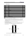
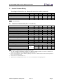
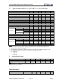
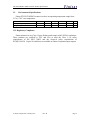
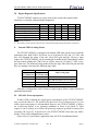
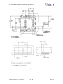
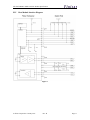
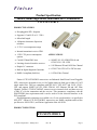
Product Specification 10Gb/s, 80km Single Mode, Multi-Rate SFP+ Transceiver FTLX1871M3BCL PRODUCT FEATURES Hot-pluggable SFP+ footprint Supports 8.5 and 9.95 to 11.3 Gb/s 80km link length 1600ps/nm chromatic dispersion tolerance -5/70°C case temperature range Internal transmitter/receiver CDR 1.5W/1.7W power consumption options Cooled 1550nm EML laser Limiting electrical interface receiver Duplex LC connector Built-in digital diagnostic functions RoHS-6 compliant (lead-free) APPLICATIONS SONET OC-192, SDH STM-64 and OTN G.959.1 P1L1-2D2 10G Ethernet ZR and 10G Fibre Channel OTN G.709 OTU1e/2/2e FEC bit rates 8.5Gb/s Fibre Channel Finisar’s FTLX1871M3BCL transceivers are Enhanced Small Form Factor Pluggable SFP+ transceivers designed for use in 10-Gigabit multi-rate links up to 80km of G.652 single mode fiber. They are compliant with SFF-84311, SFF-84322 and G.959.1 P1L12D2, and support SONET OC-192, SDH STM-64, 10G Ethernet ZR and 10G Fibre Channel. Finisar’s FTLX1871M3BCL transceivers use internal clock and data recovery (CDR) IC’s for the transmitter and the receiver. This guarantees compliance with the SONET/SDH jitter requirements and it can be used to set the electrical interface to be XFI-compliant. Digital diagnostics functions are available via a 2-wire serial interface, as specified in SFF-84723. Finisar’s FTLX1871M3BCL transceivers are RoHS compliant and lead free per Directive 2002/95/EC4, and Finisar Application Note AN-20385. PRODUCT SELECTION FTLX1871M3BCL Finisar Corporation – January 2013 Rev. B Page 1 FTLX1871M3BCL Multi-rate SFP+ Product Specification I. Pin Descriptions Pin 1 2 3 4 5 6 7 8 9 10 11 12 13 14 15 16 17 18 19 20 Symbol VEET TFAULT TDIS SDA SCL MOD_ABS RS0 RX_LOS RS1 VEER VEER RDRD+ VEER VCCR VCCT VEET TD+ TDVEET Name/Description Transmitter Ground Transmitter Fault Transmitter Disable. Laser output disabled on high or open. 2-wire Serial Interface Data Line 2-wire Serial Interface Clock Line Module Absent. Grounded within the module Rate Select 0. Loss of Signal indication. Logic 0 indicates normal operation. Rate Select 1. Receiver Ground Receiver Ground Receiver Inverted DATA out. AC Coupled. Receiver Non-inverted DATA out. AC Coupled. Receiver Ground Receiver Power Supply Transmitter Power Supply Transmitter Ground Transmitter Non-Inverted DATA in. AC Coupled. Transmitter Inverted DATA in. AC Coupled. Transmitter Ground Ref. 1 2 3 2 2 2 4 5 4 1 1 1 6 6 1 1 Notes: 1. Circuit ground is internally isolated from chassis ground. 2. T is an open collector/drain output, which should be pulled up with a 4.7k – 10k Ohms resistor on FAULT 3. 4. 5. 6. the host board if intended for use. Pull up voltage should be between 2.0V to Vcc + 0.3V. A high output indicates a transmitter fault caused by either the TX bias current or the TX output power exceeding the preset alarm thresholds. A low output indicates normal operation. In the low state, the output is pulled to <0.8V. Laser output disabled on TDIS >2.0V or open, enabled on TDIS <0.8V. Internally pulled down per SFF-8431 Rev 4.1. See Sec. X of this datasheet for the logic table to use for the internal CDRs locking modes. LOS is open collector output. Should be pulled up with 4.7k – 10k on host board to a voltage between 2.0V and 3.6V. Logic 0 indicates normal operation; logic 1 indicates loss of signal. Internally connected Towards Bezel 1 VeeT 2 TX_Fault 3 TX_Disable 4 SDA 5 SCL 6 MOD_ABS 7 RS0 8 RX_LOS 9 10 VeeT 20 TD- 19 TD+ 18 VeeT 17 VccT 16 VccR 15 VeeR 14 RD+ 13 RD- 12 VeeR 11 Towards ASIC RS1 VeeR Figure 1. Diagram of Host Board Connector Block Pin Numbers and Names. Finisar Corporation - January 2013 Rev. B Page 2 FTLX1871M3BCL Multi-rate SFP+ Product Specification II. Absolute Maximum Ratings Exceeding the limits below may damage the transceiver module permanently. Parameter Maximum Supply Voltage Storage Temperature Relative Humidity Receiver Optical Damage Threshold Notes: 1. Non-condensing III. Symbol Vcc TS RH RxDamage Min -0.5 -40 0 5 Typ Max 4.0 85 85 Unit V C % dBm Ref. Unit V mV V V mV ps V V mVpp W W W Ref. 1 Electrical Characteristics (TOP = -5 to 70 C) Parameter Supply Voltage Transmitter (Tx) Input differential impedance Differential data input swing Transmit Disable Voltage Transmit Enable Voltage Receiver (Rx) Output differential impedance Differential data output swing Output rise time and fall time LOS asserted LOS de-asserted Power Supply Noise Tolerance Power Consumption Tx and Rx CDR’s ON Tx CDR OFF and Rx CDR ON Tx & Rx CDR’s OFF and Ethernet spec. Symbol Vcc Min 3.14 Typ 3.30 Max 3.46 Rin Vin,pp VD VEN 80 120 Vcc-0.8 0 100 120 850 Vcc 0.8 Rout Vout,pp Tr, Tf VLOS_A VLOS_D VccT/VccR 80 100 120 100 850 28 Vcc-0.8 Vcc 0 0.8 Per SFF-8431 Rev 4.1 Pdiss 1.6 1.5 1.7 1.6 1.5 1 1 2 3 3 4 5 5 5 Notes: 1. Internally AC coupled. Data pins connect directly to the CDR. 2. 20 – 80%. Measured with Module Compliance Test Board and OMA test pattern. Use of four 1’s and four 0’s sequence in the PRBS 9 is an acceptable alternative. SFF-8431 Rev 4.1. 3. LOS is an open collector output. Should be pulled up with 4.7k – 10k on the host board. Normal operation is logic 0; loss of signal is logic 1. 4. See Section 2.8.3 of SFF-8431 Rev 4.1. 5. Typical power consumption values refer to 3.3V, 70C case temperature and beginning of life. Finisar Corporation - January 2013 Rev. B Page 3 FTLX1871M3BCL Multi-rate SFP+ Product Specification IV. Optical Characteristics (TOP = -5 to 70 C, VCC = 3.14 to 3.46 Volts) Parameter Symbol Min Typ Max Unit Ref. Transmitter (Tx) Average Launch Power PAVE 0 4 dBm Optical Wavelength 1530 1565 nm Side-Mode Suppression Ratio SMSR 30 dB Optical Extinction Ratio ER 9 dB Average Launch power when Tx is OFF POFF -30 dBm Jitter Generation 20kHz-80MHz, peak to peak Txjpk2pk1 0.3 UI 1 Jitter Generation 4MHz-80MHz, peak to peak Txjpk2pj2 0.1 UI 1 Relative Intensity Noise RIN -128 dB/Hz Receiver (Rx) Optical Center Wavelength 1260 1600 nm C Receiver Reflectance Rrx -27 dB Bit Rate (Gb/s) BER 8.5, 9.95-10.7 <10-12 RSENS1 -24 dBm 2,3 Sensitivity <10-12 RSENS2 -23 dBm 2 11.1 <10-4 RSENS3 -27 dBm 2 11.3 <10-4 RSENS4 -27 dBm 2 Overload (Average Power) PAVE -7 dBm LOS De-Assert LOSD -28 dBm LOS Assert LOSA -37 -30 dBm LOS Hysteresis LOSH 0.5 dB Bit Rate (Gb/s) BER 8.5, 9.95 <10-12 PP1 2 dB 4.a Path Penalty 10.3-10.7 <10-12 PP2 3 dB 4.a 11.1 <10-4 PP3 3 dB 4.b 11.3 <10-4 PP4 3 dB 4.c Notes: 1. SONET/SDH Tx jitter generation limits are guaranteed with the Tx CDR enabled and locked. 2. Measured with worst ER=9 dB; PRBS 231 – 1. 3. For 10GEthernet application, -24dBm is equivalent to an OMA of -22.09dBm for an ER = 9 dB. 4. Max chromatic dispersion tolerance over 80km of G.652 single mode fiber: a. 1600ps/nm b. 1450ps/nm c. 1300ps/nm V. General Specifications Parameter Bit Rate Max. Supported Link Length Symbol BR LMAX Min 8.5 Typ Max 11.3168 80 Units Gb/s km Ref. 1 2 Typ Max 10 Units s Ref. Notes: 1. Tested with a 231 – 1 PRBS pattern at the BER defined in Table IV. 2. Over G.652 single mode fiber. Timing Parameters Parameter Time to initialize Finisar Corporation - January 2013 Symbol t_start_up Min Rev. B Page 4 FTLX1871M3BCL Multi-rate SFP+ Product Specification VI. Environmental Specifications Finisar FTLX1871M3BCL transceivers have an operating temperature range from 5°C to +70°C case temperature. Parameter Case Operating Temperature Storage Temperature Symbol Top Tsto Min -5 -40 Typ Max 70 85 Units °C °C Ref. VII. Regulatory Compliance Finisar transceivers are Class 1 Laser Products and comply with US FDA regulations. These products are certified by TÜV and CSA to meet the Class 1 eye safety requirements of EN (IEC) 60825 and the electrical safety requirements of EN (IEC) 60950. Copies of certificates are available at Finisar Corporation upon request. Finisar Corporation - January 2013 Rev. B Page 5 FTLX1871M3BCL Multi-rate SFP+ Product Specification VIII. Digital Diagnostic Functions Finisar FTLX1871M3BCL SFP+ transceivers support the 2-wire serial communication protocol as defined in the SFP MSA1. It is very closely related to the E2PROM defined in the GBIC standard, with the same electrical specifications. The standard SFP serial ID provides access to identification information that describes the transceiver’s capabilities, standard interfaces, manufacturer, and other information. Additionally, Finisar SFP+ transceivers provide a enhanced digital diagnostic monitoring interface, which allows real-time access to device operating parameters such as transceiver temperature, laser bias current, transmitted optical power, received optical power and transceiver supply voltage. It also defines a sophisticated system of alarm and warning flags, which alerts end-users when particular operating parameters are outside of a factory set normal range. The SFP MSA defines a 256-byte memory map in E2PROM that is accessible over a 2-wire serial interface at the 8 bit address 1010000X (A0h). The digital diagnostic monitoring interface makes use of the 8 bit address 1010001X (A2h), so the originally defined serial ID memory map remains unchanged. The interface is identical to, and is thus fully backward compatible with both the GBIC Specification and the SFP Multi Source Agreement. The complete interface is described in Finisar Application Note AN2030: “Digital Diagnostics Monitoring Interface for SFP Optical Transceivers”. The operating and diagnostics information is monitored and reported by a Digital Diagnostics Transceiver Controller (DDTC) inside the transceiver, which is accessed through a 2-wire serial interface. When the serial protocol is activated, the serial clock signal (SCL, Mod Def 1) is generated by the host. The positive edge clocks data into the SFP transceiver into those segments of the E2PROM that are not write-protected. The negative edge clocks data from the SFP transceiver. The serial data signal (SDA, Mod Def 2) is bi-directional for serial data transfer. The host uses SDA in conjunction with SCL to mark the start and end of serial protocol activation. The memories are organized as a series of 8-bit data words that can be addressed individually or sequentially. For more information, please see the SFP MSA documentation3 and Finisar Application Note AN-20307. Please note that evaluation board FDB-1027 is available with Finisar ModDEMO software that allows simple to use communication over the 2-wire serial interface. Finisar Corporation - January 2013 Rev. B Page 6 FTLX1871M3BCL Multi-rate SFP+ Product Specification IX. Digital Diagnostic Specifications FTLX1871M3BCL transceivers can be used in host systems that require either internally or externally calibrated digital diagnostics. Parameter Symbol Units Min Max Accuracy Ref. Accuracy Transceiver temperature ºC -10 +75 ±5ºC 1 DDTemp Transceiver supply voltage V 2.8 4.0 ±3% DDVoltage Transmitter bias current mA 0 127 ±10% 2 DDBias Transmitter output power -1 +5 ±2dB DDTx-Power dBm Receiver average optical input power DDRx-Power dBm -28 -5 ±2dB Notes: 1. Internally measured 2. The accuracy of the Tx bias current is 10% of the actual current from the laser driver to the laser X. Internal CDR’s Locking Modes The FTLX1871M3BCL is equipped with internal CDR units on the receiver and the transmitter sides. Both CDR’s are factory set to lock between 9.95 and 11.3 Gb/s, and they will disregard the status of the rate select (R/S) pins and bits. However, upon request, the FTLX1871M3BCL can be customized to enable the R/S functionality and let the host control whether the CDR’s lock at 8.5Gb/s, between 9.95 and 11.3 Gb/s, or bypass either one. The different locking modes follow the logic OR of the R/S pins and soft bits. An example is shown in the following logic table: R/S 0 R/S 1 CDR’s locking Mode Logic OR of: Logic OR of: pin 7 and bit 110.3 pin 9 and bit 118.3 0 (or Low) 0 (or Low) Both CDR’s lock at 8.5Gb/s Tx CDR is in bypass mode 0 (or Low) 1 (or High) Rx CDR locks from 9.95 to 11.3 Gb/s 1 (or High) 0 (or Low) Tx & Rx CDR’s in bypass mode 1 (or High) 1 (or High) Both CDR’s lock from 9.95 to 11.3 Gb/s Alternative configurations can be factory set upon request. Please, contact Finisar for additional information. XI. SFF-8431 Power-up Sequence If either CDR is enabled, the typical power consumption of the FTLX1871M3BCL may exceed the limit of 1.5W specified for the Power Level II transceivers in [1], for which a power-up sequence is recommended. However, the FTLX1871M3BCL is factory set to power-up directly to its operating conditions in Power Level Mode II. Upon request, it can be factory set to follow the power-up sequence specified for transceivers exceeding 1W, as per [1]. In power level I, the FTLX1871M3BCL does not carry traffic, but the 2-wire serial communication is active. Please refer to [1] and Finisar Application Note AN-2076 for additional details. Finisar Corporation - January 2013 Rev. B Page 7 FTLX1871M3BCL Multi-rate SFP+ Product Specification XII. Mechanical Specifications Finisar FTLX1871M3BCL SFP+ transceivers are compatible with the SFF-8432 specification for improved pluggable form factor, and shown here for reference purposes only. Bail color is white. Figure 2. Mechanical Dimensions Finisar Corporation - January 2013 Rev. B Page 8 FTLX1871M3BCL Multi-rate SFP+ Product Specification XIII. Host Board SFP+ Connector Recommendations Figure 3. PCB Layout and Bezel Recommendations, as per [9] Finisar Corporation - January 2013 Rev. B Page 9 FTLX1871M3BCL Multi-rate SFP+ Product Specification Figure 4 Finisar Corporation - January 2013 Rev. B Page 10 FTLX1871M3BCL Multi-rate SFP+ Product Specification XIV. Host-Module Interface Diagram Figure 5 Finisar Corporation - January 2013 Rev. B Page 11 FTLX1871M3BCL Multi-rate SFP+ Product Specification XV. References 1. “Specifications for Enhanced 8.5 and 10 Gigabit Small Form Factor Pluggable Module ‘SFP+ ‘”, SFF Document Number SFF-8431, Revision 4.1. 2. “Improved Pluggable Form factor”, SFF Document Number SFF-8432, Revision 4.2, April 18, 2007. 3. “Digital Diagnostics Monitoring Interface for Optical Transceivers”. SFF Document Number SFF-8472, Revision 10.1, March 1, 2007. 4. Directive 2002/95/EC of the European Council Parliament and of the Council, “on the restriction of the use of certain hazardous substances in electrical and electronic equipment”. January 27, 2003. 5. “Application Note AN-2038: Finisar Implementation of RoHS Compliant Transceivers”, Finisar Corporation, January 21, 2005. 6. Small Form-factor Pluggable (SFP) Transceiver Multi-Source Agreement (MSA) 7. “Application Note AN-2030: Digital Diagnostic Monitoring Interface for SFP Optical Transceivers” XVI. For More Information Finisar Corporation 1389 Moffett Park Drive Sunnyvale, CA 94089-1133 Tel. 1-408-548-1000 Fax 1-408-541-6138 [email protected] www.finisar.com Finisar Corporation - January 2013 Rev. B Page 12