1
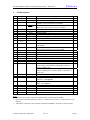
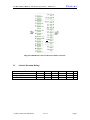
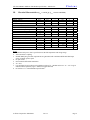
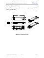
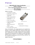
Finisar
Productt Specificaation
10Gb/s, 10km
1
XF
FP Optical Transceiver
FTLX1
1413M3B
BCL
PRO
ODUCT FEA
ATURES
•
Supports 8.5Gb/s to 11.32Gb/s
1
bit rates
•
Power disssipation <1..5W
•
Commerccial temperatture range:
-5°C to 75
5°C
•
RoHS-6 Compliant
C
(llead-free)
•
Hot-plugg
gable XFP fo
ootprint
•
Single Po
ower supply: 3.3V
•
APPL
LICATIONS
S
•
SO
ONET/SDH OC-192 SR
R-1
IT
TU G.693, V
VSR2000-2R
R1
Maximum
m link length
h of 10km
•
•
100GBASE-LR
R /LW 10G E
Ethernet
Uncooled
d 1310nm DF
FB laser
•
•
No Refereence Clock required
r
12200-SM-LL--L 10G Fibree Channel
annd 800-SM-L
LC-L 8G Fibbre Channel
•
Built-in digital
d
diagno
ostic functions
•
IT
TU G.709 OT
TN/FEC OT
TU1e, OTU2,
OT
TU2e
•
100G CPRI
L Small Form
F
Factoor 10Gb/s (XFP) trannsceivers arre
Finisar’s FTLX1413M3BCL
pliant with th
he current XFP
X Multi-So
ource Agreem
ment (MSA)) Specificatiion1. They arre
comp
a truee multi-prottocol transceeiver comply
ying with S ONET OC--192 SR-1, S
SDH STM I64.1, 10-Gigabit Ethernet 10GBASE-LR
R /LW per IEEE 802.3ae, 10G F
Fibre Channeel
1200-SM-LL-L, 8G Fibre Channel 800-SM-LC-L
L, 10G CP
PRI, and ITU-T. G7009
N/FEC proto
ocols OTU1e, OTU2, and
a
OTU2ee. Digital ddiagnostics ffunctions arre
OTN
availaable via a 2-wire serial interface, ass specified iin the XFP M
MSA. The transceiver is
RoHS
S compliant and lead freee per Direcctive 2002/995/EC3, and Finisar Appplication Notte
AN-2
20384.
PRO
ODUCT SEL
LECTION
FTLX14
F
413M3B
BCL
© Finiisar Corporatio
on March 2013
3
Rev C1
Pagee 1
FTLX1413M3BCL Multirate XFP Product Specification – March 2013
I.
Finisar
Pin Descriptions
Pin
1
2
3
Logic
LVTTL-I
4
LVTTL-O
5
6
7
8
9
10
11
LVTTL-I
Symbol
GND
VEE5
Mod-Desel
Interrupt
TX_DIS
VCC5
GND
VCC3
VCC3
SCL
SDA
12
LVTTL-I
LVTTLI/O
LVTTL-O
Mod_Abs
13
LVTTL-O
Mod_NR
14
15
16
17
18
19
20
21
LVTTL-O
LVTTL-I
RX_LOS
GND
GND
RDRD+
GND
VCC2
P_Down/RST
22
23
24
PECL-I
VCC2
GND
RefCLK+
25
PECL-I
RefCLK-
26
27
28
29
30
CML-O
CML-O
CML-I
CML-I
GND
GND
TDTD+
GND
Name/Description
Module Ground
Optional –5.2 Power Supply – Not required
Module De-select; When held low allows the module to
respond to 2-wire serial interface commands
Interrupt (bar); Indicates presence of an important condition
which can be read over the serial 2-wire interface
Transmitter Disable; Transmitter laser source turned off
+5 Power Supply– Not required
Module Ground
+3.3V Power Supply
+3.3V Power Supply
Serial 2-wire interface clock
Serial 2-wire interface data line
Ref.
1
Module Absent; Indicates module is not present. Grounded
in the module.
Module Not Ready; Finisar defines it as a logical OR
between RX_LOS and Loss of Lock in TX/RX.
Receiver Loss of Signal indicator
Module Ground
Module Ground
Receiver inverted data output
Receiver non-inverted data output
Module Ground
+1.8V Power Supply – Not required
Power Down; When high, places the module in the low
power stand-by mode and on the falling edge of P_Down
initiates a module reset
Reset; The falling edge initiates a complete reset of the
module including the 2-wire serial interface, equivalent to a
power cycle.
+1.8V Power Supply – Not required
Module Ground
Reference Clock non-inverted input, AC coupled on the
host board – Not required
Reference Clock inverted input, AC coupled on the host
board – Not required
Module Ground
Module Ground
Transmitter inverted data input
Transmitter non-inverted data input
Module Ground
2
2
1
2
2
2
2
1
1
1
1
3
3
1
1
1
Notes:
1. Module circuit ground is isolated from module chassis ground within the module.
2. Open collector; should be pulled up with 4.7k – 10kohms on host board to a voltage between 3.15V
and 3.6V.
3. A Reference Clock input is not required by the FTLX1413M3BCL. If present, it will be ignored.
© Finisar Corporation March 2013
Rev C1
Page 2
Finisar
FTLX
X1413M3BCL Multirate
M
XFP Product Speciification – Marrch 2013
Diagram
D
of Ho
ost Board Con
nnector Block Pin Numbers and Name
II.
Absolute Maximum Ratings
Parameeter
Maxim
mum Supply Voltage
V
Storag
ge Temperaturee
Case Operating
O
Tem
mperature
© Finiisar Corporatio
on March 2013
3
Symbol
Vcc3
TS
TOP
Min
-0.5
-40
-5
Rev C1
Typ
Max
4.0
85
75
Unit
V
°C
°C
Reff.
Pagee 3
Finisar
FTLX1413M3BCL Multirate XFP Product Specification – March 2013
III.
Electrical Characteristics (TOP = -5 to 75 °C, VCC3 = 3.13 to 3.45 Volts)
Parameter
Supply Voltage
Supply Current
Module total power
Transmitter
Input differential impedance
Differential data input swing
Transmit Disable Voltage
Transmit Enable Voltage
Transmit Disable Assert Time
Receiver
Differential data output swing
Data output rise time
Data output fall time
LOS Fault
LOS Normal
Power Supply Rejection
Symbol
Vcc3
Icc3
P
Rin
Vin,pp
VD
VEN
Vout,pp
tr
tf
VLOS fault
VLOS norm
PSR
Min
3.13
Typ
Max
3.45
600
1.5
Unit
V
mA
W
820
Vcc
GND+ 0.8
10
Ω
mV
V
V
us
2
3
4
mV
ps
ps
V
V
5
6
6
7
7
8
100
120
2.0
GND
340
Vcc – 0.5
GND
650
850
38
38
VccHOST
GND+0.5
See Note 8 below
Ref.
1
Notes:
1. Maximum total power value is specified across the full temperature and voltage range.
2. After internal AC coupling.
3. SONET/SDH jitter generation requirements are guaranteed with a minimum differential data input
swing of 500mV peak-to-peak.
4. Or open circuit.
5. Into 100 ohms differential termination.
6. 20 – 80 %
7. Loss Of Signal is open collector to be pulled up with a 4.7k – 10kohm resistor to 3.15 – 3.6V. Logic 0
indicates normal operation; logic 1 indicates no signal detected.
8. Per Section 2.7.1. in the XFP MSA Specification1.
© Finisar Corporation March 2013
Rev C1
Page 4
Finisar
FTLX1413M3BCL Multirate XFP Product Specification – March 2013
IV.
Optical Characteristics (TOP = -5 to 75°C, VCC3 = 3.13 to 3.45 Volts)
Parameter
Transmitter
Output Opt. Pwr: 9/125 SMF
Optical Wavelength
Optical Extinction Ratio
Sidemode Supression ratio
Tx Jitter (SONET/SDH)
20kHz-80MHz
Tx Jitter (SONET/SDH)
4MHz – 80MHz
Relative Intensity Noise
Receiver
Receiver Sensitivity @ 9.95Gb/s
Receiver Sensitivity @ 10.5Gb/s
Receiver Sensitivity @ 11.3Gb/s
Stressed Receiver Sensitivity
(OMA) @ 10.5Gb/s
Maximum Input Power
Optical Center Wavelength
Receiver Reflectance
LOS De-Assert
LOS Assert
LOS Hysteresis
Symbol
Min
POUT
λ
ER
SSRmin
Txj1
-6
1290
6
30
Max
Unit
Ref.
-1
1330
1
0.3
dBm
nm
dB
dB
UI
Txj2
0.1
UI
RIN
-130
dB/Hz
RSENS1
RSENS2
RSENS3
RSENS4
-14.4
-14.4
-13.4
-10.3
dBm
dBm
dBm
dBm
PMAX
λC
Rrx
LOSD
LOSA
+0.5
1260
-32
0.5
Typ
1600
-14
-18
1
2
2
3
dBm
nm
dB
dBm
dBm
dB
Notes:
1. Having ER = 6 dB guarantees that the –6 dBm minimum output power meets IEEE 802.3ae
requirement of OMA=-5.2dBm.
2. Measured with worst ER; BER<10-12; 231 – 1 PRBS. Complies with –12.6 dBm OMA at ER = 6 dB.
3. Per IEEE 802.3ae. Equivalent to –13.3 dBm average power at Infinite ER, -11.08 dBm at ER = 6 dB.
8.5Gb/s Fibre-Channel:
To operate the FTLX1413D3BCL at 8.5Gb/s Fibre-Channel, the EEPROM-Table 0, Byte
117, Bit 0 must be set as follows; .
• EEPROM Byte 117, Bit 0, value “1” for 8GFC:
• EEPROM Byte 117, Bit 0 value “0” for 10Gb/s rates:
o (It is also possible to bypass the CDRs with, Byte 111, Bit 0.)
By default, a power cycling the transceiver will return the transceiver to normal 10Gb/s
operation with the CDRs active.
© Finisar Corporation March 2013
Rev C1
Page 5
Finisar
FTLX1413M3BCL Multirate XFP Product Specification – March 2013
V.
General Specifications
Parameter
Bit Rate
Bit Error Ratio
Max. Supported Link Length
Symbol
BR
BER
LMAX
Min
8.5
Typ
Max
11.3
10-12
10
Units
Gb/s
km
Ref.
1
2
1
Notes:
1. SONET OC-192 SR-1, SDH STM I-64.1, 10GBASE-LR/LW, 1200-SM-LL-L, 800-SM-LC-L,
SONET OC-192 with FEC, 10GBASE-LR/LW with FEC, 1200-SM-LL-L with FEC.
2. Tested with a 231 – 1 PRBS
VI.
Environmental Specifications
Finisar FTLX1413M3BCL transceivers have a commercial operating case temperature
range of -5°C to +75°C.
Parameter
Case Operating Temperature
Storage Temperature
VII.
Symbol
Top
Tsto
Min
-5
-40
Typ
Max
75
85
Units
°C
°C
Ref.
Regulatory Compliance
Finisar XFP transceivers are Class 1 Laser Products. They are certified per the following
standards:
Feature
Agency
Standard
Laser Eye
Safety
Laser Eye
Safety
FDA/CDRH
CDRH 21 CFR 1040 and Laser Notice 50
TÜV
R72101686
Electrical
Safety
Electrical
Safety
TÜV
EN 60825-1: 2007, EN60825-2:2004+A1
IEC 60825-1: 2007 (2nd Edition)
IEC 60825-2: 2010 (3rd Edition)
EN 60950:2006+A11
CLASS 3862.07
CLASS 3862.87
2283290
UL/CSA
Certificate
Number
9210176-77
R72101686
Copies of the referenced certificates are available at Finisar Corporation upon request.
© Finisar Corporation March 2013
Rev C1
Page 6
FTLX1413M3BCL Multirate XFP Product Specification – March 2013
Finisar
VIII. Digital Diagnostic Functions
As defined by the XFP MSA1, Finisar XFP transceivers provide digital diagnostic
functions via a 2-wire serial interface, which allows real-time access to the following
operating parameters:
•
•
•
•
•
Transceiver temperature
Laser bias current
Transmitted optical power
Received optical power
Transceiver supply voltage
It also provides a sophisticated system of alarm and warning flags, which may be used to
alert end-users when particular operating parameters are outside of a factory-set normal
range.
The operating and diagnostics information is monitored and reported by a Digital
Diagnostics Transceiver Controller (DDTC) inside the transceiver, which is accessed
through the 2-wire serial interface. When the serial protocol is activated, the serial clock
signal (SCL pin) is generated by the host. The positive edge clocks data into the XFP
transceiver into those segments of its memory map that are not write-protected. The
negative edge clocks data from the XFP transceiver. The serial data signal (SDA pin) is
bi-directional for serial data transfer. The host uses SDA in conjunction with SCL to
mark the start and end of serial protocol activation. The memories are organized as a
series of 8-bit data words that can be addressed individually or sequentially. The 2-wire
serial interface provides sequential or random access to the 8 bit parameters, addressed
from 000h to the maximum address of the memory.
For more detailed information including memory map definitions, please see Finisar
Application Note AN-2035 “Digital Diagnostic Monitoring Interface for XFP Optical
Transceivers”, or the XFP MSA Specification1.
© Finisar Corporation March 2013
Rev C1
Page 7
Finisar
FTLX
X1413M3BCL Multirate
M
XFP Product Speciification – Marrch 2013
IX.
Mechaniccal Specifications
Finisar’s XFP traansceivers arre compliantt with the diimensions deefined by the XFP Multtiment (MSA).
Sourccing Agreem
77.95
22.15
5
1
18.35
13.30
0
8.50
LA
ATCHED
16.00
0
UNL
LATCHED
20.85
39.00
R1.00
0
XF
FP Transceiveer (dimensionss are in mm)
© Finiisar Corporatio
on March 2013
3
Rev C1
Pagee 8
FTLX
X1413M3BCL Multirate
M
XFP Product Speciification – Marrch 2013
X.
Finisar
PCB Layou
ut and Bezeel Recommeendations
XFP Host Bo
oard Mechaniical Layout (d
dimensions aree in mm)
© Finiisar Corporatio
on March 2013
3
Rev C1
Pagee 9
FTLX
X1413M3BCL Multirate
M
XFP Product Speciification – Marrch 2013
Finisar
XF
FP Detail Host Board Mech
hanical Layoutt (dimensions are in mm)
XFP Recom
mmended Bezzel Design (dim
mensions are iin mm)
© Finiisar Corporatio
on March 2013
3
Rev C1
Page 110
FTLX1413M3BCL Multirate XFP Product Specification – March 2013
Finisar
XI.
References
1.
10 Gigabit Small Form Factor Pluggable Module (XFP) Multi-Source Agreement
(MSA), Rev 4.5 – August 2005. Documentation is currently available at
http://www.xfpmsa.org/
2.
Application Note AN-2035: “Digital Diagnostic Monitoring Interface for XFP
Optical Transceivers” – Finisar Corporation, December 2003
3.
Directive 2002/95/EC of the European Council Parliament and of the Council,
“on the restriction of the use of certain hazardous substances in electrical and
electronic equipment”. January 27, 2003.
4.
“Application Note AN-2038: Finisar Implementation Of RoHS Compliant
Transceivers”, Finisar Corporation, January 21, 2005.
XII.
For More Information
Finisar Corporation
1389 Moffett Park Drive
Sunnyvale, CA 94089-1133
Tel. 1-408-548-1000
Fax 1-408-541-6138
[email protected]
www.finisar.com
© Finisar Corporation March 2013
Rev C1
Page 11