1
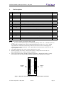
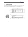
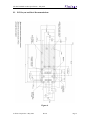
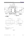
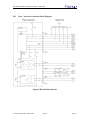
Product Specification
RoHS-6 Compliant
Extended Temperature 10Gb/s 850nm SFP+ Datacom Transceiver
FTLX8571D3BNL
PRODUCT FEATURES
•
Hot-pluggable SFP+ footprint
•
Supports 9.95 to 10.5 Gb/s bit rates
•
Power dissipation < 1W
•
RoHS-6 compliant (lead-free)
•
Extended temperature range
0°C to 85°C
•
Single 3.3Vpower supply
•
Maximum link length of 300m on
2000 MHZ-km MMF
•
Uncooled 850nm VCSEL laser
•
Receiver limiting electrical
interface
•
Duplex LC connector
•
Built-in digital diagnostic functions
APPLICATIONS
•
10GBASE-SR/SW 10G Ethernet
•
1200-Mx-SN-I 10G Fibre Channel
Finisar’s FTLX8571D3BNL Extended Temperature 10Gb/s SFP+ transceivers are
designed for use in 10-Gigabit Ethernet and 10-Gigabit Fibre Channel links over
multimode fiber. They are compliant with SFF-84311, SFF-84322, IEEE 802.3ae
10GBASE-SR/SW3 and 10G Fibre Channel 1200-Mx-SN-I4. Digital diagnostics
functions are available via a 2-wire serial interface, as specified in SFF-84725. The
FTLX8571D3BCL is a “limiting module”, i.e., it employs a limiting receiver. Host board
designers using an EDC PHY IC should follow the IC manufacturer’s recommended
settings for interoperability with an SFP+ limiting module. The transceiver is RoHS
compliant and lead free per Directive 2002/95/EC6, and Finisar Application Note AN20387.
PRODUCT SELECTION
FTLX8571D3BNL
© Finisar Corporation -May 2009
Rev. B
Page 1
FTLX8571D3BNL Product Specification – May 2009
I.
Pin Descriptions
Pin
1
2
3
4
5
6
7
8
9
10
11
12
13
14
15
16
17
18
19
20
Symbol
VEET
TFAULT
TDIS
SDA
SCL
MOD_ABS
RS0
RX_LOS
RS1
VEER
VEER
RDRD+
VEER
VCCR
VCCT
VEET
TD+
TDVEET
Name/Description
Transmitter Ground (Common with Receiver Ground)
Transmitter Fault.
Transmitter Disable. Laser output disabled on high or open.
2-wire Serial Interface Data Line
2-wire Serial Interface Clock Line
Module Absent. Grounded within the module
No connection required
Loss of Signal indication. Logic 0 indicates normal operation.
No connection required
Receiver Ground (Common with Transmitter Ground)
Receiver Ground (Common with Transmitter Ground)
Receiver Inverted DATA out. AC Coupled
Receiver Non-inverted DATA out. AC Coupled
Receiver Ground (Common with Transmitter Ground)
Receiver Power Supply
Transmitter Power Supply
Transmitter Ground (Common with Receiver Ground)
Transmitter Non-Inverted DATA in. AC Coupled.
Transmitter Inverted DATA in. AC Coupled.
Transmitter Ground (Common with Receiver Ground)
Ref.
1
2
3
4
4
4
5
1
1
1
1
1
Notes:
1. Circuit ground is internally isolated from chassis ground.
2. T
is an open collector/drain output, which should be pulled up with a 4.7k – 10k Ohms resistor on
FAULT
3.
4.
5.
the host board if intended for use. Pull up voltage should be between 2.0V to Vcc + 0.3V. A high
output indicates a transmitter fault caused by either the TX bias current or the TX output power
exceeding the preset alarm thresholds. A low output indicates normal operation. In the low state, the
output is pulled to <0.8V.
Laser output disabled on TDIS >2.0V or open, enabled on TDIS <0.8V.
Should be pulled up with 4.7kΩ – 10kΩ on host board to a voltage between 2.0V and 3.6V.
MOD_ABS pulls line low to indicate module is plugged in.
LOS is open collector output. Should be pulled up with 4.7kΩ – 10kΩ on host board to a voltage
between 2.0V and 3.6V. Logic 0 indicates normal operation; logic 1 indicates loss of signal.
1
Towards
Bezel
2
TX_Fault
3
TX_Disable
4
SDA
5
SCL
6
MOD_ABS
7
RS0
8
RX_LOS
9
RS1
10
VeeT
20
TD-
19
TD+
18
VeeT
17
VeeT
VccT
16
VccR
15
VeeR
14
RD+
13
RD-
12
VeeR
11
Towards
ASIC
VeeR
Figure 1. Diagram of Host Board Connector Block Pin Numbers and Names.
© Finisar Corporation - May 2009
Rev B
Page 2
FTLX8571D3BNL Product Specification – May 2009
II.
Absolute Maximum Ratings
Exceeding the limits below may damage the transceiver module permanently.
Parameter
Maximum Supply Voltage
Storage Temperature
Case Operating Temperature
Relative Humidity
Symbol
Vcc
TS
TA
RH
Min
-0.5
-40
0
0
Typ
Max
4.0
85
85
85
Unit
V
°C
°C
%
Ref.
1
Notes:
I. Non-condensing.
III.
Electrical Characteristics (TOP = 0 to 85 °C, VCC = 3.14 to 3.46 Volts)
Parameter
Supply Voltage
Supply Current
Transmitter
Input differential impedance
Differential data input swing
Transmit Disable Voltage
Transmit Enable Voltage
Receiver
Differential data output swing
Data output rise time, fall time
LOS Fault
LOS Normal
Power Supply Noise Tolerance
Symbol
Vcc
Icc
Rin
Vin,pp
VD
VEN
Vout,pp
tr
VLOS fault
VLOS norm
VccT/VccR
Min
3.14
Typ
Max
3.46
250
Unit
V
mA
Ref.
Ω
mV
V
V
1
700
Vcc
Vee+ 0.8
mV
ps
V
V
mVpp
2,6
3
4
4
5
100
180
2
Vee
300
850
28
2
VccHOST
Vee
Vee+0.8
Per SFF-8431 Rev 3.0
Notes:
1. Connected directly to TX data input pins. AC coupling from pins into laser driver IC.
2. Into 100Ω differential termination.
3. 20 – 80 % . Measured with Module Compliance Test Board and OMA test pattern. Use of four 1’s
and four 0’s in sequence in the PRBS^9 is an acceptable alternative. SFF-8431 Rev 3.0
4. LOS is an open collector output. Should be pulled up with 4.7kΩ – 10kΩ on the host board.
Normal operation is logic 0; loss of signal is logic 1. Maximum pull-up voltage is 5.5V.
5. Testing methodology per SFF-8431. Rev 3.0
6. The FTLX8571D3BNL is a “limiting module”, i.e., it employs a limiting receiver. Host board
designers using an EDC PHY IC should follow the IC manufacturer’s recommended settings for
interoperating the host-board EDC PHY with a limiting receiver SFP+ module.
© Finisar Corporation - May 2009
Rev B
Page 3
FTLX8571D3BNL Product Specification – May 2009
IV.
Optical Characteristics (TOP = 0 to 85 °C, VCC = 3.14 to 3.46 Volts)
Parameter
Transmitter
Optical Modulation Amplitude
(OMA)
Average Launch Power
Optical Wavelength
RMS Spectral Width
Optical Extinction Ratio
Transmitter and Dispersion Penalty
Average Launch power of OFF
transmitter
Tx Jitter
Encircled Flux
Relative Intensity Noise
Receiver
Receiver Sensitivity (OMA)
@ 10.5Gb/s
Stressed Receiver Sensitivity
(OMA) @ 10.3Gb/s
Maximum Input Power
Wavelength Range
Receiver Reflectance
LOS De-Assert
LOS Assert
LOS Hysteresis
Symbol
Min
POMA
Typ
Max
-1.5
PAVE
λ
Δλrms
ER
TDP
POFF
-5
840
850
3.0
5.5
-1
860
0.45
3.9
-30
Txj
<4.5μm
<19μm
RIN12OMA
Per IEEE 802.3ae requirements
30
86
Unit
Ref.
dBm
1
dBm
nm
dB
dB
dB
dBm
2
1
1
%
3
-128
dB/Hz
RSENS1
-11.1
dBm
RSENS2
-7.5
dBm
PMAX
λC
Rrx
LOSD
LOSA
+0.5
840
-30
0.5
860
-12
-14
-23
4
5
dBm
nm
dB
dBm
dBm
dB
Notes:
1. Per Tradeoff Table 52.8, IEEE 802.3ae 2005
2. Average Power figures are informative only, per IEEE802.3ae.
3. Measured into Type A1a (50/125 μm multimode) fiber per ANSI/TIA/EIA-455-203-2.
4. Measured with worst ER; BER<10-12; 231 – 1 PRBS.
5. Per IEEE 802.3ae.
© Finisar Corporation - May 2009
Rev B
Page 4
FTLX8571D3BNL Product Specification – May 2009
V.
General Specifications
Parameter
Bit Rate
Bit Error Ratio
Maximum Supported Distances
Fiber Type
850nm OFL
Bandwidth
160 MHz-km
62.5μm
OM1
200 MHz-km
Symbol
BR
BER
Min
9.95
Typ
OM2
500 MHz-km
Units
Gb/s
Ref.
1
2
26
Lmax
33
400 MHz-km
50μm
Max
10.5
10-12
m
66
82
Lmax
OM3
2000 MHz-km
m
300
Notes:
1. 10GBASE-SR/SW, 1200-Mx-SN-I. Contact Finisar for higher data-rate support.
2. 10GBASE-SR/SW, 1200-Mx-SN-I . Tested with a 231 – 1 PRBS @10-12 BER.
VI.
Environmental Specifications
Finisar 850nm SFP+ transceivers have an extended operating case temperature range
from 0°C to +85°C.
Parameter
Case Operating Temperature
Storage Temperature
VII.
Symbol
Top
Tsto
Min
0
-40
Typ
Max
85
85
Units
°C
°C
Ref.
Regulatory Compliance
Finisar transceivers are Class 1 Laser Products and comply with US FDA regulations.
These products are certified by TÜV and CSA to meet the Class 1 eye safety
requirements of EN (IEC) 60825 and the electrical safety requirements of
EN (IEC) 60950. Copies of certificates are available at Finisar Corporation upon request.
© Finisar Corporation - May 2009
Rev B
Page 5
FTLX8571D3BNL Product Specification – May 2009
VIII. Digital Diagnostic Functions
Finisar FTLX8571D3BNL Extended temperature SFP+ transceivers support the 2-wire
serial communication protocol as defined in the SFF-8472. It is very closely related to the
E2PROM defined in the GBIC standard, with the same electrical specifications.
The standard SFP+ serial ID provides access to identification information that describes
the transceiver’s capabilities, standard interfaces, manufacturer, and other information.
Additionally, Finisar SFP+ transceivers provide a enhanced digital diagnostic monitoring
interface, which allows real-time access to device operating parameters such as
transceiver temperature, laser bias current, transmitted optical power, received optical
power and transceiver supply voltage. It also defines a sophisticated system of alarm and
warning flags, which alerts end-users when particular operating parameters are outside of
a factory set normal range.
SFF-8472 defines a 256-byte memory map in E2PROM that is accessible over a
2-wire serial interface at the 8 bit address 1010000X (A0h). The digital diagnostic
monitoring interface makes use of the 8 bit address 1010001X (A2h), so the originally
defined serial ID memory map remains unchanged. The interface is identical to, and is
thus fully backward compatible with both the GBIC Specification and the SFP Multi
Source Agreement. The complete interface is described in Finisar Application Note AN2030: “Digital Diagnostics Monitoring Interface for SFP Optical Transceivers”.
The operating and diagnostics information is monitored and reported by a Digital
Diagnostics Transceiver Controller (DDTC) inside the transceiver, which is accessed
through a 2-wire serial interface. When the serial protocol is activated, the serial clock
signal (SCL, Mod Def 1) is generated by the host. The positive edge clocks data into the
SFP transceiver into those segments of the E2PROM that are not write-protected. The
negative edge clocks data from the SFP transceiver. The serial data signal (SDA, Mod
Def 2) is bi-directional for serial data transfer. The host uses SDA in conjunction with
SCL to mark the start and end of serial protocol activation. The memories are organized
as a series of 8-bit data words that can be addressed individually or sequentially.
For more information, please see the SFF-8472 documentation and Finisar Application
Note AN-2030.
Please note that evaluation board FDB-1027 is available with Finisar ModDEMO
software that allows simple to use communication over the 2-wire serial interface.
© Finisar Corporation - May 2009
Rev B
Page 6
FTLX8571D3BNL Product Specification – May 2009
IX. Digital Diagnostic Specifications
FTLX8571D3BNL Extended temperature transceivers can be used in host systems that
require either internally or externally calibrated digital diagnostics.
Parameter
Accuracy
Internally measured transceiver
temperature
Internally measured transceiver
supply voltage
Measured TX bias current
Measured TX output power
Measured RX received average
optical power
Internally measured transceiver
temperature
Internally measured transceiver
supply voltage
Measured TX bias current
Measured TX output power
Measured RX received average
optical power
Max Reporting Range
Internally measured transceiver
temperature
Internally measured transceiver
supply voltage
Measured TX bias current
Measured TX output power
Measured RX received average
optical power
Symbol
Min
DDTemperature
Typ
Max
Units
-3
3
ºC
DDVoltage
-100
100
mV
DDBias
DDTx-Power
DDRx-Power
-10
-2
-2
10
2
2
%
dB
dB
85
ºC
Dynamic Range for Rated Accuracy
DDTemperature
0
DDVoltage
3.14
3.46
V
DDBias
DDTx-Power
DDRx-Power
0
-9
-20
20
-2.5
0
mA
dBm
dBm
DDTemperature
-40
125
ºC
DDVoltage
2.8
4.0
V
DDBias
DDTx-Power
DDRx-Power
0
-10
-22
20
-3
0
mA
dBm
dBm
Ref.
1
Notes:
1. Accuracy of Measured Tx Bias Current is 10% of the actual Bias Current from the laser driver to the
laser.
© Finisar Corporation - May 2009
Rev B
Page 7
FTLX8571D3BNL Product Specification – May 2009
X.
Mechanical Specifications
Finisar FTLX8571D3BNL Extended temperature SFP+ transceivers are compatible with
the SFF-8432 specification for improved pluggable form factor, and shown here for
reference purposes only. Bail color is beige.
Figure 3. FTLX8571D3BNL Mechanical Dimensions.
© Finisar Corporation - May 2009
Rev B
Page 8
FTLX8571D3BNL Product Specification – May 2009
XI. PCB Layout and Bezel Recommendations
Figure 4.
© Finisar Corporation - May 2009
Rev B
Page 9
FTLX8571D3BNL Product Specification – May 2009
Figure 5.
© Finisar Corporation - May 2009
Rev B
Page 10
FTLX8571D3BNL Product Specification – May 2009
XII.
Host - Transceiver Interface Block Diagram
Figure 6-Host-Module Interface
© Finisar Corporation - May 2009
Rev B
Page 11
FTLX8571D3BNL Product Specification – May 2009
XIII. References
1. “Specifications for Enhanced 8.5 and 10 Gigabit Small Form Factor Pluggable
Module ‘SFP+ ‘”, SFF Document Number SFF-8431, Revision 3.0.
2. “Improved Pluggable Formfactor”, SFF Document Number SFF-8432, Revision 4.2,
April 18, 2007.
3. IEEE Std 802.3ae, Clause 52, PMD Type 10GBASE-SR. IEEE Standards
Department.
4. American National Standard for Information Technology - Fibre Channel - 10
Gigabit Fibre Channel, Rev 3.5, April 9, 2003.
5. “Digital Diagnostics Monitoring Interface for Optical Transceivers”. SFF Document
Number SFF-8472, Revision 10.3, December 1, 2007.
6. Directive 2002/95/EC of the European Council Parliament and of the Council, “on
the restriction of the use of certain hazardous substances in electrical and electronic
equipment”. January 27, 2003.
7. “Application Note AN-2038: Finisar Implementation Of RoHS Compliant
Transceivers”, Finisar Corporation, January 21, 2005.
XIII. For More Information
Finisar Corporation
1389 Moffett Park Drive
Sunnyvale, CA 94089-1133
Tel. 1-408-548-1000
Fax 1-408-541-6138
[email protected]
www.finisar.com
© Finisar Corporation - May 2009
Rev B
Page 12