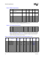
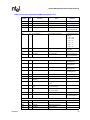
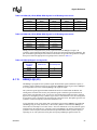
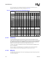
1
Intel® Itanium® 2 Processor
Intel® Itanium® 2 Processor 1.66 GHz with 9 MB L3 Cache
Intel® Itanium® 2 Processor 1.66 GHz with 6 MB L3 Cache
Intel® Itanium® 2 Processor 1.6 GHz with 9 MB L3 Cache
Intel® Itanium® 2 Processor 1.6 GHz with 6 MB L3 Cache
Intel® Itanium® 2 Processor 1.5 GHz with 6 MB L3 Cache
Intel® Itanium® 2 Processor 1.5 GHz with 4 MB L3 Cache
Intel® Itanium® 2 Processor 1.4 GHz with 4 MB L3 Cache
Intel® Itanium® 2 Processor 1.3 GHz with 3 MB L3 Cache
Intel® Itanium® 2 Processor 1.0 GHz with 3 MB L3 Cache
Intel® Itanium® 2 Processor 900 MHz with 1.5 MB L3 Cache
Datasheet
February 2006
Document Number: 250945-005
INFORMATION IN THIS DOCUMENT IS PROVIDED IN CONNECTION WITH INTEL® PRODUCTS. NO LICENSE, EXPRESS OR IMPLIED, BY
ESTOPPEL OR OTHERWISE, TO ANY INTELLECTUAL PROPERTY RIGHTS IS GRANTED BY THIS DOCUMENT. EXCEPT AS PROVIDED IN
INTEL'S TERMS AND CONDITIONS OF SALE FOR SUCH PRODUCTS, INTEL ASSUMES NO LIABILITY WHATSOEVER, AND INTEL DISCLAIMS
ANY EXPRESS OR IMPLIED WARRANTY, RELATING TO SALE AND/OR USE OF INTEL PRODUCTS INCLUDING LIABILITY OR WARRANTIES
RELATING TO FITNESS FOR A PARTICULAR PURPOSE, MERCHANTABILITY, OR INFRINGEMENT OF ANY PATENT, COPYRIGHT OR OTHER
INTELLECTUAL PROPERTY RIGHT. Intel products are not intended for use in medical, life saving, life sustaining applications.
Intel may make changes to specifications and product descriptions at any time, without notice.
Designers must not rely on the absence or characteristics of any features or instructions marked “reserved” or “undefined.” Intel reserves these for
future definition and shall have no responsibility whatsoever for conflicts or incompatibilities arising from future changes to them
The Intel® Itanium® 2 processor may contain design defects or errors known as errata which may cause the product to deviate from published
specifications. Current characterized errata are available on request.
Contact your local Intel sales office or your distributor to obtain the latest specifications and before placing your product order.
Copies of documents which have an order number and are referenced in this document, or other Intel literature, may be obtained by calling1-800-5484725, or by visiting Intel's website at http://www.intel.com.
Intel and Itanium are trademarks or registered trademarks of Intel Corporation or its subsidiaries in the United States and other countries.
Copyright © 2002-2006, Intel Corporation
*Other names and brands may be claimed as the property of others.
I2C is a two-wire communication bus /protocol developed by Phillips. SMBus is a subset of the I2C bus/protocol developed by Intel. Implementation of
the I2C bus/protocol or the SMBus bus/protocol may require licenses from various entities, including Phillips Electronics, N.V. and North American
Phillips Corporation.
2
Datasheet
Contents
1
Introduction....................................................................................................................... 11
1.1
1.2
1.3
1.4
1.5
1.6
2
Overview ............................................................................................................. 11
Processor Abstraction Layer ............................................................................... 11
Mixing Processors of Different Frequencies and Cache Sizes ........................... 12
Terminology......................................................................................................... 12
State of Data ....................................................................................................... 12
Reference Documents......................................................................................... 13
Electrical Specifications.................................................................................................... 15
2.1
2.2
2.3
2.4
2.5
2.6
2.7
2.8
Itanium® 2 Processor System Bus ...................................................................... 15
2.1.1 System Bus Power Pins ......................................................................... 15
2.1.2 System Bus No Connect ........................................................................ 15
System Bus Signals ............................................................................................ 15
2.2.1 Signal Groups......................................................................................... 15
2.2.2 Signal Descriptions................................................................................. 16
Package Specifications ....................................................................................... 17
Signal Specifications ........................................................................................... 18
2.4.1 Maximum Ratings................................................................................... 22
System Bus Signal Quality Specifications and Measurement Guidelines........... 23
2.5.1 Overshoot/Undershoot Magnitude ......................................................... 23
2.5.2 Overshoot/Undershoot Pulse Duration................................................... 24
2.5.3 Activity Factor......................................................................................... 24
2.5.4 Reading Overshoot/Undershoot Specification Tables............................ 25
2.5.5 Determining if a System Meets the Overshoot/Undershoot
Specifications ......................................................................................... 25
2.5.6 Wired-OR Signals................................................................................... 28
Power Pod Connector Signals ............................................................................ 30
Itanium® 2 Processor System Bus Clock and Processor Clocking ..................... 32
Recommended Connections for Unused Pins ....................................................35
3
Pinout Specifications ........................................................................................................ 37
4
Mechanical Specifications ................................................................................................ 69
4.1
4.2
5
Thermal Specifications ..................................................................................................... 75
5.1
5.2
6
Thermal Features ................................................................................................ 75
5.1.1 Thermal Alert.......................................................................................... 75
5.1.2 Enhanced Thermal Management ........................................................... 76
5.1.3 Thermal Trip ........................................................................................... 76
Case Temperature ..............................................................................................76
System Management Feature Specifications................................................................... 79
6.1
Datasheet
Mechanical Dimensions ...................................................................................... 69
Package Marking................................................................................................. 72
4.2.1 Processor Top-Side Marking.................................................................. 72
4.2.2 Processor Bottom-Side Marking............................................................. 72
System Management Bus ................................................................................... 79
6.1.1 System Management Bus Interface ....................................................... 79
6.1.2 System Management Interface Signals.................................................. 79
3
6.2
6.3
6.4
6.5
6.6
6.7
A
Signals Reference............................................................................................................ 91
A.1
4
6.1.3 SMBus Device Addressing..................................................................... 81
Processor Information ROM................................................................................ 82
Scratch EEPROM ............................................................................................... 85
Processor Information ROM and Scratch EEPROM Supported
SMBus Transactions ........................................................................................... 85
Thermal Sensing Device ..................................................................................... 86
Thermal Sensing Device Supported SMBus Transactions ................................. 87
Thermal Sensing Device Registers ..................................................................... 88
6.7.1 Thermal Reference Registers ................................................................ 88
6.7.2 Thermal Limit Registers ......................................................................... 89
6.7.3 Status Register....................................................................................... 89
6.7.4 Configuration Register ........................................................................... 89
6.7.5 Conversion Rate Register ...................................................................... 90
Alphabetical Signals Reference .......................................................................... 91
A.1.1 A[49:3]# (I/O).......................................................................................... 91
A.1.2 A20M# (I) ............................................................................................... 91
A.1.3 ADS# (I/O).............................................................................................. 91
A.1.4 AP[1:0]# (I/O) ......................................................................................... 91
A.1.5 ASZ[1:0]# (I/O) ....................................................................................... 91
A.1.6 ATTR[3:0]# (I/O)..................................................................................... 92
A.1.7 BCLKp/BCLKn (I) ................................................................................... 92
A.1.8 BE[7:0]# (I/O) ......................................................................................... 92
A.1.9 BERR# (I/O) ........................................................................................... 93
A.1.10 BINIT# (I/O) ............................................................................................ 94
A.1.11 BNR# (I/O) ............................................................................................. 94
A.1.12 BPM[5:0]# (I/O) ...................................................................................... 94
A.1.13 BPRI# (I) ................................................................................................ 94
A.1.14 BR[0]# (I/O) and BR[3:1]# (I).................................................................. 94
A.1.15 BREQ[3:0]# (I/O) .................................................................................... 95
A.1.16 CCL# (I/O) .............................................................................................. 96
A.1.17 CPUPRES# (O)...................................................................................... 96
A.1.18 D[127:0]# (I/O) ....................................................................................... 96
A.1.19 D/C# (I/O) ............................................................................................... 96
A.1.20 DBSY# (I/O) ........................................................................................... 96
A.1.21 DBSY_C1# (O)....................................................................................... 96
A.1.22 DBSY_C2# (O)....................................................................................... 97
A.1.23 DEFER# (I)............................................................................................. 97
A.1.24 DEN# (I/O) ............................................................................................. 97
A.1.25 DEP[15:0]# (I/O)..................................................................................... 97
A.1.26 DHIT# (I) ................................................................................................ 97
A.1.27 DPS# (I/O).............................................................................................. 98
A.1.28 DRDY# (I/O) ........................................................................................... 98
A.1.29 DRDY_C1# (O) ...................................................................................... 98
A.1.30 DRDY_C2# (O) ...................................................................................... 98
A.1.31 DSZ[1:0]# (I/O) ....................................................................................... 98
A.1.32 EXF[4:0]# (I/O) ....................................................................................... 98
A.1.33 FCL# (I/O) .............................................................................................. 99
A.1.34 FERR# (O) ............................................................................................. 99
A.1.35 GSEQ# (I) .............................................................................................. 99
A.1.36 HIT# (I/O) and HITM# (I/O) .................................................................... 99
Datasheet
A.2
A.1.37 ID[9:0]# (I) ..............................................................................................99
A.1.38 IDS# (I) ................................................................................................... 99
A.1.39 IGNNE# (I)............................................................................................100
A.1.40 INIT# (I) ................................................................................................100
A.1.41 INT (I) ...................................................................................................100
A.1.42 IP[1:0]# (I).............................................................................................100
A.1.43 LEN[2:0]# (I/O) .....................................................................................100
A.1.44 LINT[1:0] (I) ..........................................................................................101
A.1.45 LOCK# (I/O) .........................................................................................101
A.1.46 NMI (I) ..................................................................................................101
A.1.47 OWN# (I/O) ..........................................................................................101
A.1.48 PMI# (I).................................................................................................101
A.1.49 PWRGOOD (I)......................................................................................101
A.1.50 REQ[5:0]# (I/O) ....................................................................................101
A.1.51 RESET# (I) ...........................................................................................102
A.1.52 RP# (I/O) ..............................................................................................102
A.1.53 RS[2:0]# (I) ...........................................................................................103
A.1.54 RSP# (I)................................................................................................103
A.1.55 SBSY# (I/O)..........................................................................................103
A.1.56 SBSY_C1# (O) .....................................................................................103
A.1.57 SBSY_C2# (O) .....................................................................................103
A.1.58 SPLCK# (I/O) .......................................................................................103
A.1.59 STBn[7:0]# and STBp[7:0]# (I/O) .........................................................104
A.1.60 TCK (I)..................................................................................................104
A.1.61 TDI (I) ...................................................................................................104
A.1.62 TDO (O)................................................................................................104
A.1.63 THRMTRIP# (O)...................................................................................104
A.1.64 THRMALERT# (O) ...............................................................................105
A.1.65 TMS (I) .................................................................................................105
A.1.66 TND# (I/O)............................................................................................105
A.1.67 TRDY# (I) .............................................................................................105
A.1.68 TRST# (I)..............................................................................................105
A.1.69 WSNP# (I/O) ........................................................................................105
Signal Summaries .............................................................................................105
2-1
2-2
2-3
2-4
2-5
2-6
2-7
3-1
4-1
4-2
4-3
4-4
4-5
5-1
Generic Clock Waveform .................................................................................... 22
SMSC Clock Waveform....................................................................................... 22
System Bus Signal Waveform Exhibiting Overshoot/Undershoot .......................24
Itanium® 2 Processor Power Tab Physical Layout.............................................. 30
Processor Full, Normal and Low Power Mode with Timings ............................... 32
System Bus Reset and Configuration Timings for Cold Reset............................ 34
System Bus Reset and Configuration Timings for Warm Reset.......................... 35
Itanium® 2 Processor Pinout ............................................................................... 37
Itanium® 2 Processor Package ........................................................................... 69
Itanium® 2 Processor Package ........................................................................... 70
Itanium® 2 Processor Package Power Tab ......................................................... 71
Processor Top-Side Marking on IHS................................................................... 72
Processor Bottom-Side Marking Placement on Interposer ................................. 73
Itanium® 2 Processor Thermal Features ............................................................. 75
Figures
Datasheet
5
5-2
6-1
Itanium® 2 Processor Package Thermocouple Location..................................... 77
Logical Schematic of SMBus Circuitry ................................................................ 80
2-1
2-2
2-3
2-4
2-5
2-6
2-7
2-8
2-9
2-10
2-11
2-12
2-13
Itanium® 2 Processor System Bus Signal Groups .............................................. 16
Itanium® 2 Processor Package Specifications .................................................... 17
Itanium® 2 Processor Power Supply Specifications............................................ 18
AGTL+ Signals DC Specifications....................................................................... 18
Power Good Signal DC Specifications ................................................................ 19
System Bus Clock Differential HSTL DC Specifications ..................................... 19
TAP Connection DC Specifications..................................................................... 19
SMBus DC Specifications ................................................................................... 20
LVTTL Signal DC Specifications ......................................................................... 20
System Bus Clock Differential HSTL AC Specifications ..................................... 20
SMBus AC Specifications ................................................................................... 21
Itanium® 2 Processor Absolute Maximum Ratings ............................................. 22
Source Synchronous AGTL+ Signal Group and Wired-OR Signal Group
Absolute Overshoot/Undershoot Tolerance ........................................................ 26
Itanium® 2 Processors (900 MHz, 1.0 GHz, 1.3 GHz, 1.4 GHz, 1.5 GHz/6 MB)
Source Synchronous AGTL+ Signal Group Time Dependent
Overshoot/Undershoot Tolerance for 400 MHz System Bus .............................. 26
Itanium® 2 Processors (1.5 GHz/4 MB, 1.6 GHz) Source
Synchronous AGTL+ Signal Group Time-Dependent
Overshoot/Undershoot Tolerance for 400 MHz System Bus .............................. 27
Itanium® 2 (9 MB) Processors Source Synchronous AGTL+
Signal Group Time-Dependent Overshoot/Undershoot Tolerance
for 533 MHz System Bus .................................................................................... 27
Itanium® 2 Processors (1.66 GHz) Source Synchronous AGTL+
Signal Group Time-Dependent Overshoot/Undershoot Tolerance
for 667 MHz System Bus .................................................................................... 28
Itanium® 2 Processors (900 MHz, 1.0 GHz, 1.3 GHz, 1.4 GHz,
1.5 GHz/6 MB) Wired-OR Signal Group
(BINIT#, HIT#, HITM#, BNR#, TND#, BERR#)
Overshoot/Undershoot Tolerance for 400 MHz System Bus .............................. 28
Itanium® 2 Processors (1.5 GHz/4 MB, 1.6 GHz) Wired-OR Signal
Group (BINIT#, HIT#, HITM#, BNR#, TND#, BERR#)
Overshoot/Undershoot Tolerance for 400 MHz System Bus .............................. 29
Itanium® 2 (9 MB) Processors Wired-OR Signal Group
(BINIT#, HIT#, HITM#, BNR#, TND#, BERR#) Overshoot/Undershoot
Tolerance for 533 MHz System Bus ................................................................... 29
Itanium® 2 (1.66 GHz) Processors Wired-OR Signal Group
(BINIT#, HIT#, HITM#, BNR#, TND#, BERR#) Overshoot/Undershoot
Tolerance for 667 MHz System Bus ................................................................... 29
Itanium® 2 Processor Power Pod Connector Signals ......................................... 30
Processor Core Voltage Identification Code ....................................................... 31
Processor Power States...................................................................................... 32
Itanium® 2 Processor System Bus Ratios........................................................... 33
Connection for Unused Pins ............................................................................... 35
Pin/Signal Information Sorted by Pin Name ........................................................ 38
Pin/Signal Information Sorted by Pin Location .................................................... 53
Case Temperature Specification ......................................................................... 76
System Management Interface Signal Descriptions ........................................... 79
Tables
2-14
2-15
2-16
2-17
2-18
2-19
2-20
2-21
2-22
2-23
2-24
2-25
2-26
3-1
3-2
5-1
6-1
6
Datasheet
6-2
6-3
6-4
6-5
6-6
6-7
6-8
6-9
6-10
6-11
6-12
6-13
6-14
6-15
6-16
A-1
A-2
A-3
A-5
A-4
A-6
A-7
A-8
A-9
A-10
A-11
A-12
A-13
A-14
A-15
Datasheet
Thermal Sensing Device SMBus Addressing on the Itanium® 2 Processor ....... 81
EEPROM SMBus Addressing on the Itanium® 2 Processor ............................... 82
Processor Information ROM Format ................................................................... 82
Current Address Read SMBus Packet ................................................................ 86
Random Address Read SMBus Packet .............................................................. 86
Byte Write SMBus Packet ................................................................................... 86
Write Byte SMBus Packet ................................................................................... 87
Read Byte SMBus Packet ................................................................................... 87
Send Byte SMBus Packet ................................................................................... 87
Receive Byte SMBus Packet............................................................................... 87
ARA SMBus Packet ............................................................................................ 87
Command Byte Bit Assignment........................................................................... 88
Thermal Sensing Device Status Register............................................................ 89
Thermal Sensing Device Configuration Register ................................................ 89
Thermal Sensing Device Conversion Rate Register ........................................... 90
Address Space Size ............................................................................................ 92
Effective Memory Type Signal Encoding............................................................. 92
Special Transaction Encoding on Byte Enables.................................................. 93
BR0# (I/O), BR1#, BR2#, BR3# Signals for 2P Rotating Interconnect................ 95
BR0# (I/O), BR1#, BR2#, BR3# Signals for 4P Rotating Interconnect................ 95
BR[3:0]# Signals and Agent IDs.......................................................................... 95
DID[9:0]# Encoding ............................................................................................. 97
Extended Function Signals.................................................................................. 99
Length of Data Transfers...................................................................................100
Transaction Types Defined by REQa#/REQb# Signals ....................................102
STBp[7:0]# and STBn[7:0]# Associations .........................................................104
Output Signals...................................................................................................105
Input Signals......................................................................................................106
Input/Output Signals (Single Driver)..................................................................107
Input/Output Signals (Multiple Driver) ...............................................................107
7
Revision History
Revision No.
8
Description
Date
-001
Initial release of this document.
July 2002
-002
Updated content to include information pertaining to Itanium 2 processor
(1.5 GHz, 6 MB), Itanium 2 processor (1.4 GHz, 4 MB) and Itanium 2
processor (1.3 GHz, 3 MB).
June 2003
-003
Updated content to include information pertaining to Itanium® 2
processor (1.5 GHz, 4 MB) and Itanium 2 processor (1.6 GHz, 6 MB and
9 MB).
November 2004
-004
Updated content to include information pertaining to Itanium® 2
processor (1.66 GHz, 6 MB and 9 MB).
July 2005
-005
Updated content to include information pertaining to Itanium® 2
processor (533 MHz system bus speed).
February 2006
Datasheet
Intel® Itanium® 2 Processor
Intel® Itanium® 2 Processor 1.66 GHz with 9 MB L3 Cache
Intel® Itanium® 2 Processor 1.66 GHz with 6 MB L3 Cache
Intel® Itanium® 2 Processor 1.6 GHz with 9 MB L3 Cache
Intel® Itanium® 2 Processor 1.6 GHz with 6 MB L3 Cache
Intel® Itanium® 2 Processor 1.5 GHz with 6 MB L3 Cache
Intel® Itanium® 2 Processor 1.5 GHz with 4 MB L3 Cache
Intel® Itanium® 2 Processor 1.4 GHz with 4 MB L3 Cache
Intel® Itanium® 2 Processor 1.3 GHz with 3 MB L3 Cache
Intel® Itanium® 2 Processor 1.0 GHz with 3 MB L3 Cache
Intel® Itanium® 2 Processor 900 MHz with 1.5 MB L3 Cache
Product Features
■
■
Wide, parallel hardware based on Intel® Itanium®
architecture for high performance:
— Integrated on-die cache of up to 9 MB; cache
hints for L1, L2, and L3 caches for reduced
memory latency.
— 128 general and 128 floating-point registers
supporting register rotation.
— Register stack engine for effective management
of processor resources.
— Support for predication and speculation.
Extensive RAS features for business-critical
applications:
— Full SMBus compatibility.
— Enhanced machine check architecture with
extensive ECC and parity protection.
— Enhanced thermal management.
— Built-in processor information ROM (PIROM).
— Built-in programmable EEPROM.
■
■
High bandwidth system bus for multiprocessor
scalability:
— Up to 10.6 GB/s bandwidth.
— 128-bit wide data bus.
— 50-bits of physical memory addressing and 64bits of virtual addressing.
— Up to four processors on the same system bus at
400 MHz data bus frequency.
— Up to two processors on the same system bus at
533 MHz or 667 MHz data bus frequency.
— Expandable to systems with multiple system
buses.
Features to support flexible platform environments:
— Support for IA-32 application binaries.
— Bi-endian support.
— Processor abstraction layer eliminates processor
dependencies.
The Intel® Itanium® 2 processor is designed to address the needs of high-performance servers and workstations.
The Itanium architecture goes beyond RISC and CISC approaches by employing Explicitly Parallel Instruction
Computing (EPIC), which pairs extensive processing resources with intelligent compilers that enable parallel
execution explicit to the processor. The processor’s large internal resources combine with predication and
speculation to enable optimization for high performance applications running on multiple operating systems,
including versions of Microsoft Windows*, HP-UX* and Linux*. The Itanium 2 processor is designed to support
very large scale systems, including those employing thousands of processors, to provide the processing power and
performance head room for the most demanding enterprise and technical computing applications. SMBus
compatibility and comprehensive reliability, availability and serviceability (RAS) features make the Itanium 2
processor ideal for applications requiring high up-time. For high performance servers and workstations, the
Itanium 2 processor offers outstanding performance and reliability for today’s applications and the scalability to
address the growing e-business needs of tomorrow.
Datasheet
9
10
Datasheet
1
Introduction
1.1
Overview
The Itanium 2 processor employs Explicitly Parallel Instruction Computing (EPIC) design
concepts for a tighter coupling between hardware and software. In this design style, the interface
between hardware and software is designed to enable the software to exploit all available compiletime information, and efficiently deliver this information to the hardware. It addresses several
fundamental performance bottlenecks in modern computers, such as memory latency, memory
address disambiguation, and control flow dependencies. The EPIC constructs provide powerful
architectural semantics, and enable the software to make global optimizations across a large
scheduling scope, thereby exposing available Instruction Level Parallelism (ILP) to the hardware.
The hardware takes advantage of this enhanced ILP, and provides abundant execution resources.
Additionally, it focuses on dynamic run-time optimizations to enable the compiled code schedule
to flow at high throughput. This strategy increases the synergy between hardware and software, and
leads to greater overall performance.
The Itanium 2 processor provides a 6-wide and 8-stage deep pipeline, running at up to 1.66 GHz.
This provides a combination of abundant resources to exploit ILP as well as increased frequency
for minimizing the latency of each instruction. The resources consist of six integer units, six
multimedia units, two load and two store units, three branch units, two extended-precision floating
point units, and one additional single-precision floating point unit. The hardware employs dynamic
prefetch, branch prediction, a register scoreboard, and non-blocking caches to optimize for
compile-time non-determinism. Three levels of on-die cache minimize overall memory latency.
This includes up to a 9 MB L3 cache, accessed at core speed, providing up to 84.8 Gb/sec of data
bandwidth. The system bus is designed to support up to four processors (on a single system bus),
and can be used as an effective building block for very large systems. The balanced core and
memory subsystem provide high performance for a wide range of applications ranging from
commercial workloads to high performance technical computing.
The Itanium 2 processor supports a range of computing needs and configurations from a 2-way to
large SMP servers. This document provides the electrical, mechanical and thermal specifications
for the Itanium 2 processor for use while using systems with Itanium 2 processors.
1.2
Processor Abstraction Layer
The Itanium 2 processor requires implementation-specific Processor Abstraction Layer (PAL)
firmware. PAL firmware supports processor initialization, error recovery, and other functionality. It
provides a consistent interface to system firmware and operating systems across processor
hardware implementations. The Intel® Itanium® Architecture Software Developer’s Manual,
Volume 2: System Architecture, describes PAL. Platforms must provide access to the firmware
address space and PAL at reset to allow Itanium 2 processors to initialize.
The System Abstraction Layer (SAL) firmware contains platform-specific firmware to initialize
the platform, boot to an operating system, and provide runtime functionality. Further information
about SAL is available in the Intel® Itanium® Processor Family System Abstraction Layer
Specification.
Datasheet
11
Introduction
1.3
Mixing Processors of Different Frequencies and
Cache Sizes
All Itanium 2 processors on the same system bus are required to have the same cache size (9 MB,
6 MB, 4 MB, 3 MB or 1.5 MB) and identical core frequency. Mixing components of different core
frequencies and cache sizes is not supported and has not been validated by Intel. Operating system
support for multiprocessing with mixed components should also be considered.
While Intel has done nothing to specifically prevent processors within a multiprocessor
environment from operating at differing frequencies and differing cache sizes, there may be
uncharacterized errata that exist in such configurations. Customers would be fully responsible for
validation of system configurations with mixed components other than the supported
configurations described above.
1.4
Terminology
In this document, a ‘#’ symbol after a signal name refers to an active low signal. This means that a
signal is in the active state (based on the name of the signal) when driven to a low level. For
example, when RESET# is low, a processor reset has been requested. When NMI is high, a nonmaskable interrupt has occurred. In the case of lines where the name does not imply an active state
but describes part of a binary sequence (such as address or data), the ‘#’ symbol implies that the
signal is inverted. For example, D[3:0] = ‘HLHL’ refers to a hex ‘A’, and D [3:0] # = ‘LHLH’ also
refers to a hex ‘A’ (H = High logic level, L = Low logic level).
The term “system bus” refers to the interface between the processor, system core logic and other
bus agents. The system bus is a multiprocessing interface to processors, memory and I/O.
A signal name has all capitalized letters, for example, VCTERM.
A symbol referring to a voltage level, current level, or a time value carries a plain subscript, e.g.,
VCC,core, or a capitalized abbreviated subscript, for example, TCO.
1.5
State of Data
The data contained in this document is subject to change. It is the best information that Intel is able
to provide at the publication date of this document.
12
Datasheet
Introduction
1.6
Reference Documents
The reader of this specification should also be familiar with material and concepts presented in the
following documents:
Title
Intel® Itanium® 2 Processor Specification Update
®
®
Datasheet
251141
Intel Itanium Architecture Software Developer’s Manual, Volume 1:
Application Architecture
245317
Intel® Itanium® Architecture Software Developer’s Manual, Volume 2: System
Architecture
245318
Intel® Itanium® Architecture Software Developer’s Manual,
Volume 3: Instruction Set Reference
245319
Intel® Itanium® 2 Processor Reference Manual for Software Development and
Optimization
251110
Intel® Itanium® Processor Family System Abstraction Layer Specification
245359
ITP700 Debug Port Design Guide
249679
System Management Bus Specification
Note:
Document Number
http://www.smbus.org/specs
Contact your Intel representative or check http://developer.intel.com for the latest revision of the
reference documents.
13
Introduction
14
Datasheet
2
Electrical Specifications
This chapter describes the electrical specifications of the Itanium 2 processor.
2.1
Itanium® 2 Processor System Bus
Most Itanium 2 processor signals use the Itanium processor’s assisted gunning transceiver logic
(AGTL+) signaling technology. The termination voltage, VCTERM, is generated on the baseboard
and is the system bus high reference voltage. The buffers that drive most of the system bus signals
on the Itanium 2 processor are actively driven to VCTERM during a low-to-high transition to
improve rise times and reduce noise. These signals should still be considered open-drain and
require termination to VCTERM, which provides the high level. The Itanium 2 processor system bus
is terminated to VCTERM at each end of the bus. There is also support of off-die termination in
which case the termination is provided by external resistors connected to VCTERM.
AGTL+ inputs use differential receivers which require a reference signal (VREF). VREF is used by
the receivers to determine if a signal is a logical 0 or a logical 1. The Itanium 2 processor generates
VREF on-die, thereby eliminating the need for an off-chip reference voltage source.
2.1.1
System Bus Power Pins
VCTERM (1.2 V) input pins on the Itanium 2 processor provide power to the driver buffers and
on-die termination. The GND pins, in addition to the GND input at the power tab connector,
provide ground to the processor. Power for the processor core is provided through the power tab
connector by VCC,PS. The 3.3 V pin is included on the processor to provide power to the system
management bus (SMBus). The VCTERM, 3.3 V, and GND pins must remain electrically separated
from each other.
2.1.2
System Bus No Connect
All pins designated as “N/C” or “No Connect” must remain unconnected.
2.2
System Bus Signals
2.2.1
Signal Groups
Table 2-1 contains Itanium 2 processor system bus signals that have been combined into groups by
buffer type and whether they are inputs, outputs or bidirectional with respect to the processor.
Datasheet
15
Electrical Specifications
..
Table 2-1. Itanium® 2 Processor System Bus Signal Groups
Group Name
Signals
AGTL+ Input Signals
BPRI#, BR[3:1]#, DEFER#, GSEQ#, ID[9:0]#, IDS#, RESET#1, RS[2:0]#,
RSP#, TRDY#
AGTL+ I/O Signals
A[49:3]#, ADS#, AP[1:0]#, BERR#, BINIT#, BNR#, BPM[5:0]#1, BR0#,
D[127:0]#, DBSY#, DEP[15:0]#, DRDY#, HIT#, HITM#, LOCK#, REQ[5:0]#,
RP#, SBSY#, STBN[7:0]#, STBP[7:0]#, TND#
AGTL+ Output Signals
FERR#, THRMTRIP#, DBSY[1:0]#, DRDY[1:0]#, SBSY[1:0]#
Special AGTL+ Asynchronous
Interrupt Input Signals
A20M#, IGNNE#, INIT#, LINT[1,0], PMI#
Power Good Signal1
PWRGOOD
HSTL Clock Signals
BCLKn, BCLKp
TAP Input Signals
1
TCK, TDI, TMS, TRST#
1
TDO
TAP Output Signals
System Management Signals
1
3.3V, SMA[2:0], SMSC, SMSD, SMWP, THRMALERT#
Power Signals
GND, VCTERM
LVTTL Power Pod Signals1
CPUPRES#, OUTEN, PPODGD#
Other
TERMA, TERMB, TUNER1, TUNER2, VCCMON, VSSMON
NOTES:
1. Signals will not be terminated on-die even when on-die termination (ODT) is enabled. See Intel® Itanium® 2 Processor
Hardware Developer’s Manual for further details.
All system bus outputs should be treated as open drain signals and require a high level source
provided by the VCTERM supply.
AGTL+ inputs have differential input buffers which use VREF as a reference level. AGTL+ output
signals require termination to VCTERM. In this document, “AGTL+ Input Signals” refers to the
AGTL+ input group as well as the AGTL+ I/O group when receiving. Similarly, “AGTL+ Output
Signals” refers to the AGTL+ output group as well as the AGTL+ I/O group when driving.
The Power Good (PWRGOOD) signal and Test Access Port (TAP) connection input signals use a
non-differential receiver with levels that are similar to AGTL+. No reference voltage is required for
these signals. The TAP Connection Output signals are AGTL+ output signals.
The Itanium 2 processor system bus requires termination on both ends of the bus. The Itanium 2
processor system bus supports both on-die and off-die termination controlled by two pins, TERMA
and TERMB. Please see the TERMA and TERMB pin description in Section 2.2.2.
The HSTL clock signals are the differential clock inputs for the Itanium 2 processor. The SMBus
signals and LVTTL power pod signals are driven using the 3.3 V CMOS logic levels listed in
Table 2-8 and Table 2-9, respectively.
2.2.2
Signal Descriptions
Appendix A, “Signals Reference”contains functional descriptions of all system bus signals and
LVTTL power pod signals. Further descriptions of the system management signals are contained in
Chapter 6. The signals listed under the “Power” and “Other” group are described here:
16
Datasheet
Electrical Specifications
2.3
VCTERM
System bus termination voltage.
GND
System ground.
N/C
No connection can be made to these pins.
TERMA, TERMB
The Itanium 2 processor uses two pins to control the on-die termination
function, TERMA and TERMB. Both of these termination pins must be
pulled to VCTERM in order to terminate the system bus using the on-die
termination resistors. Both of these termination pins must be pulled to
GND in order to use off-die termination.
TUNER1, TUNER2
TUNER1 is used to control the slew rate of the system bus I/O buffers.
The nominal value for the TUNER1 resistor is 150 ohms. A lower
resistance will cause a faster slew rate. TUNER2 is used to control the
termination resistance for the system bus I/O buffers. The nominal value
for the TUNER2 resistor is 150 ohms. A lower resistance will cause a
lower on-die termination resistance. On-die termination mode will only
be selected if the TERMA and TERMB pins are terminated as indicated
above.
VCCMON, VSSMON
These pins provide a remote sense connection from the processor to the
power pod. No connections that constitute a current load can be made to
these pins.
Package Specifications
Table 2-2 through Table 2-9 list the DC voltage, current and power specifications for the Itanium 2
processor. The voltage and current specifications are defined at the Itanium 2 processor pins.
Operational specifications listed in Table 2-2 through Table 2-9 are only valid while meeting
specifications for case temperature, clock frequency, and input voltages.
Table 2-2. Itanium® 2 Processor Package Specifications
Symbol
Datasheet
Parameter
Core
Frequency
Minimum
Typ
Maximum
Unit
Notes
1.2 –1.5%
1.2
1.2 +1.5%
V
1
W
2
VCTERM
Termination Voltage
All
RTERM
Recommended Termination
Resistance
All
VTAP
Test Access Port Voltage
(VCCTAP)
All
ICTERM
Termination Voltage Current
PWRMAX
45
1.2 –1.5%
1.2
1.5
V
All
7.2
A
3
Maximum Processor Power
All
130
W
4
PWRTDE
Thermal Design Envelope
All
130
W
5
PWRTDP
Thermal Design Power
900 MHz
90
W
6
1.0 GHz
100
W
6
1.3 GHz
97
W
6
1.4 GHz
91
W
6
1.5 GHz
107
W
6
1.6 GHz
122
W
6
1.66 GHz
122
W
6
17
Electrical Specifications
NOTES:
1. This is the tolerance requirement, across a 200 MHz bandwidth, at the processor pins. The requirement at the processor pins
accounts for voltage drops (and impedance discontinuities) at the processor pins and to the processor core. In addition to the
±1.5% DC tolerance, there is a ±3.5% AC tolerance for a total of ±5% tolerance.
2. The Itanium® 2 processor system bus is terminated at each end of the system bus. The Itanium 2 processor supports both ondie and off-die termination which is selected by the TERMA and TERMB pins. Termination tolerance is ±15% for on-die
termination measured at VOL and ±1% for off-die termination.
3. Maximum termination voltage current on one terminating agent.
4. For all core frequencies and cache sizes.
5. Maximum thermal design envelope is provided for the design of thermal/chassis solutions.
6. Maximum thermal design power is an estimate of the power dissipation for the Itanium 2 processor offering while executing a
worst-case application mix under nominal VCC,PS and worst-case temperature.
Table 2-3. Itanium® 2 Processor Power Supply Specifications
Symbol
Parameter
Minimum
Typ
Maximum
Unit
Notes
VID –1.5%
VID
VID +1.5%
V
1, 2
3
VCC,PS
VCC from the Power Supply
ICC,PS
Current Required from Power Supply
100
A
PSslew_rate
Power Supply Slew Rate at the
Processor Power Pod Connector
100
A/µs
PSTT
Power Supply Slew Rate for the
Termination Voltage at the Processor
Pins
0.05
A/ns
NOTES:
1. The power pod DC set point accuracy is ±1.5%. Included for reference only, under worst case switching activity, the power pod
tolerance is ±7%.
2. The VCC,PS for the processor is defined by the VID bits specified in Table 2-23.
3. The maximum current (ICC,PS) specification is intended for system power supply design. The maximum current values are
defined to be based on worst-case VCC,PS, temperature and application mix.
2.4
Signal Specifications
This section describes the DC specifications of the system bus signals. The processor signal’s DC
specifications are defined at the Itanium 2 processor pins. Table 2-4 through Table 2-9 describe the
DC specifications for the AGTL+, PWRGOOD, HSTL clock, TAP port, system management, and
LVTTL signals. Please refer to the ITP700 Debug Port Design Guide for the TAP connection
signals DC specifications at the debug port.
Table 2-4. AGTL+ Signals DC Specifications (Sheet 1 of 2)
Symbol
18
Parameter
Core
Frequency
Minimum
Typ
Maximum
Unit
Notes
0.625
V
1
V
1
V
1
V
1
2
VIL
Input Low Voltage
All
VIH
Input High Voltage
All
VIL
Input Low Voltage
(1.6x GHz, I.5 GHz/4 MB
Itanium® 2 Processors)
All
VIH
Input High Voltage
(1.6x GHz, I.5 GHz/4 MB
Itanium 2 Processors)
All
VOL
Output Low Voltage
All
VOH
Output High Voltage
All
VCTERM,
minimum
IOL
Output Low Current @ 0.3V
All
34
mA
3
IOL
Output Low Current @ 0.3V
All
17
mA
4
0.875
0.65
0.85
0.3
0.4
V
VCTERM
VCTERM,
maximum
V
Datasheet
Electrical Specifications
Table 2-4. AGTL+ Signals DC Specifications (Sheet 2 of 2)
Symbol
Parameter
IL
Leakage Current
CAGTL+
AGTL+ Pad Capacitance
Core
Frequency
Minimum
Typ
Maximum
Unit
Notes
All
±100
µA
5
900 MHz
3
pF
6
1.0 GHz
3
pF
6
1.3 GHz
1.5
pF
6
1.4 GHz
1.5
pF
6
1.5 GHz
1.5
pF
6
1.6 GHz
1.5
pF
6
1.66 GHz
1.5
pF
6
NOTES:
1. The typical transition point between VIL and VIH assuming 125 mV VREF uncertainty for ODT. VREF_high and VREF_low levels are
VREF ±100 mV respectively, for a system bus agent using on-board termination. VREF_high and VREF_low levels are VREF ±125
mV respectively, for a system bus agent using on-die termination.
2. Parameter measured into a 22.5 ohm resistor to 1.2V. Minimum VOL and IOL are guaranteed by design/characterization.
3. Calculated using off-die termination through two 45 ohm ±1% resistors in parallel.
4. Calculated using on-die termination to a 45 ±15% resistor measured at VOL.
5. At 1.2V ±1.5%. VCTERM, minimum ≤Vpin ≤VCTERM, maximum.
6. Total of I/O buffer with ESD structure and processor parasitics if applicable. Capacitance values guaranteed by design for all
AGTL+ buffers.
Table 2-5. Power Good Signal DC Specifications
Symbol
Parameter
VIL
Input Low Voltage
VIH
Input High Voltage
Minimum
Maximum
0.440
0.875
Unit
Notes
V
V
Table 2-6. System Bus Clock Differential HSTL DC Specifications
Symbol
Parameter
Minimum
Maximum
Unit
Notes
VIH
Input High Voltage
0.78
1.3
V
VIL
Input Low Voltage
–0.3
0.5
V
VX
Input Crossover Voltage
0.55
0.85
V
CCLK
Input (Pad) Capacitance
1.75
pF
Minimum
Maximum
Unit
Notes
Table 2-7. TAP Connection DC Specifications
Symbol
Parameter
VIL
Input Low Voltage
–0.3
0.5
V
1
VIH
Input High Voltage
1.1
1.57
V
1, 2
0.3
V
VOL
Output Low Voltage
VOH
Output High Voltage
1.2
IOL
Output Low Current
20
IIC
Input Current
V
2, 3
mA
690
uA
4
NOTES:
1.
2.
3.
4.
Datasheet
There is a 100 mV hysteresis on TCK.
VIH, MAX = 1.5V + 5%, VOH, MAX = 1.2V +5%.
There is no internal pull-up. An external pull-up is always assumed. Max voltage tolerated at TDO is 1.5V.
Per input pin.
19
Electrical Specifications
Table 2-8. SMBus DC Specifications
Symbol
Parameter
Minimum
Typ
Maximum
Unit
Notes
3.3V
VCC for the System Management
Components
3.14
3.3
3.47
V
3.3V ±5%
VIL
Input Low Voltage
–0.3
0.3*3.3V
V
VIH
Input High Voltage
2.31
3.47
V
VOL
Output Low Voltage
I3.3V
3.3V Supply Current
IOL
Output Low Current
IOL2
Output Low Current
ILI
Input Leakage Current
10
µA
ILO
Output Leakage Current
10
µA
5.0
Max =
3.3 +5%
Min +
0.7*3.3V
0.4
V
30.0
mA
3
mA
1
mA
2
6
NOTES:
1. The value specified for IOL applies to all signals except for THRMALERT#.
2. The value specified for IOL2 applies only to THRMALERT# which is an open drain signal.
Table 2-9. LVTTL Signal DC Specifications
Symbol
Parameter
VIL
Input Low Voltage
VIH
Input High Voltage
VOL
Output Low Voltage
VOH
Output High Voltage
Minimum
Maximum
Unit
0.8
V
3.63
V
0.4
V
2.0
2.4
Notes
V
Table 2-10 through Table 2-11 list the AC specifications for the Itanium 2 processor’s clock and
SMBus (timing diagrams begin with Figure 2-1). The Itanium 2 processor uses a differential HSTL
clocking scheme with a frequency of 200, 266 or 333 MHz. The SMBus is a subset of the I2C*
interface which supports operation of up to 100 kHz.
Table 2-10. System Bus Clock Differential HSTL AC Specifications (Sheet 1 of 2)
Symbol
Parameter
System
Bus
Clock
(MHz)
Minimum
Typ
Maximum
Unit
Figure
Figure 2-1
Tperiod
BCLKp Period
200
5.0
ns
Tskew
System Clock Skew
200
100
ps
fBCLK
BCLKp Frequency
200
Tjitter
BCLKp Input Jitter
200
Thigh
BCLKp High Time
200
2.25
Tlow
BCLKp Low Time
200
2.25
Tperiod
BCLKp Period
266
Tskew
System Clock Skew
266
fBCLK
BCLKp Frequency
266
Tjitter
BCLKp Input Jitter
266
Thigh
BCLKp High Time
266
20
1
200
MHz
Figure 2-1
2
100
ps
Figure 2-1
3
2.5
2.75
ns
Figure 2-1
4
2.5
2.75
ns
Figure 2-1
4
ns
Figure 2-1
200
3.75
266
1.69
Notes
1.88
5
60
ps
266
MHz
Figure 2-1
2
50
ps
Figure 2-1
3
2.06
ns
Figure 2-1
4
Datasheet
Electrical Specifications
Table 2-10. System Bus Clock Differential HSTL AC Specifications (Sheet 2 of 2)
System
Bus
Clock
(MHz)
Minimum
Typ
Maximum
Unit
Figure
Notes
BCLKp Low Time
266
1.69
1.88
2.06
ns
Figure 2-1
4
ns
Figure 2-1
Symbol
Tlow
Parameter
Tperiod
BCLKp Period
333
Tskew
System Clock Skew
333
3.0
60
ps
333
MHz
Figure 2-1
50
ps
Figure 2-1
3
fBCLK
BCLKp Frequency
333
Tjitter
BCLKp Input Jitter
333
Thigh
BCLKp High Time
333
1.35
1.5
1.65
ns
Figure 2-1
4
Tlow
BCLKp Low Time
333
1.35
1.5
1.65
ns
Figure 2-1
4
Trise
BCLKp Rise Time
All
333
500
667
ps
Figure 2-1
20–80%
Tfall
BCLKp Fall Time
All
333
500
667
ps
Figure 2-1
20–80%
VPP
Minimum Input Swing
All
mV
Figure 2-1
6
333
600
NOTES:
1. The system clock skew is ±100 ps.
2. Measured on cross point of rising edge of BCLKp and falling edge of BCLKn. Long term jitter is defined as peak-to-peak variation measured by
accumulating a large number of clock cycles and recording peak-to-peak jitter.
3. Cycle-to-cycle jitter is defined as peak-to-peak variation measured over 10000 cycles peak-to-peak jitter.
4. Measured on cross point of rising edge of BCLKp and falling edge of BCLKn.
5. The system clock skew is ±60 ps.
6. VPPmin is defined as the minimum input differential voltage which will cause no increase in the clock receiver timing.
Table 2-11. SMBus AC Specifications
Symbol
Parameter
Minimum
Maximum
Unit
100
kHz
Notes
fSMSC
SMSC Clock Frequency
TSMSC
SMSC Clock Period
10
µs
thigh
SMSC Clock High Time
4.0
µs
1
tlow
SMSC Clock Low Time
4.7
µs
1
trise
SMSC Clock Rise Time
1.0
µs
1
tfall
SMSC Clock Fall Time
0.3
µs
1
tVALID
SMBus Output Valid Delay
1.0
µs
tSU
SMBus Input Setup Time
tHLD
SMBus Input Hold Time
tFREE
Bus Free Time
250
ns
0
ns
4.7
µs
2
NOTES:
1. Please refer to Figure 2-2 for the Standard Microsystems Corporation (SMSC)* clock waveform.
2. Bus Free Time is the minimum time allowed between request cycles.
Datasheet
21
Electrical Specifications
Figure 2-1. Generic Clock Waveform
Thigh
Tlow
Trise
Vpp
Tjitter
Tfall
BCLKN
80%
20%
Tperiod
BCLKP
Trise = Rise Time
Tperiod = Period
Tfall = Fall Time
Tjitter
= Long Term Peak-to-Peak Jitter
Thigh = High Time
Vpp
= Peak-to-Peak Swing
Tlow = Low Time
000615
Figure 2-2. SMSC Clock Waveform
Thigh
Trise
SMSC
Vcc (3.3V)
90% Vcc
75% Vcc
25% Vcc
Tfall
Trise = Rise Time
Thigh = High Time
Tfall = Fall Time
Tlow = Low Time
Tlow
000618
2.4.1
Maximum Ratings
Table 2-12 contains the Itanium 2 processor stress ratings. Functional operation at the absolute
maximum and minimum is neither implied nor guaranteed. The processor should not receive a
clock while subjected to these conditions. Functional operating conditions are given in the DC
tables. Extended exposure to the maximum ratings may affect device reliability. Furthermore,
although the processor contains protective circuitry to resist damage from static electric discharge,
one should always take precautions to avoid static voltages or electric fields.
Table 2-12. Itanium® 2 Processor Absolute Maximum Ratings (Sheet 1 of 2)
Symbol
22
Parameter
Minimum
Maximum
Unit
Notes
Tstorage
Processor Storage Temperature
–10
45
°C
1
Tshipping
Processor Shipping Temperature
–45
75
°C
2
VCC,Processor
Any VCC,Processor Voltage with Respect
to GND
–0.1
2.1
V
3
3.3V
Any 3.3V Supply Voltage with Respect to
GND
–0.3
5.5
V
4
Datasheet
Electrical Specifications
Table 2-12. Itanium® 2 Processor Absolute Maximum Ratings (Sheet 2 of 2)
Symbol
Parameter
Minimum
Maximum
Unit
Notes
Vin, SMBus
SMBus Buffer DC Input Voltage with
Respect to GND
–0.1
6.0
V
4
Vin, AGTL+
AGTL+ Buffer DC Input Voltage with
Respect to GND
–0.1
1.9
V
5, 6
VCTERM
Any VCTERM Voltage with Respect to
GND
–0.1
1.9
V
3
Vin,TAP
TAP Buffer DC Input Voltage with
Respect to GND.
–0.1
2.1
V
5
NOTES:
1.
2.
3.
4.
5.
6.
2.5
Storage temperature is temperature in which the processor can be stored for up to one year.
Shipping temperature is temperature in which the processor can be shipped for up to 24 hours.
See Table 2-4 through Table 2-9 inclusive for operating voltages.
Parameters are from third party vendor specifications.
Maximum instantaneous voltage at receiver buffer input.
Specification includes Vin,AGTL+ and Vin,AGTL+ ASYNCHRONOUS (AGTL+ asynchronous buffer DC input voltage with
respect to GND.
System Bus Signal Quality Specifications and
Measurement Guidelines
Overshoot (or undershoot) is the absolute value of the maximum voltage above the nominal
VCTERM voltage (or below GND), as shown in Table 2-3. The overshoot/undershoot specifications
limit transitions beyond VCTERM or GND due to the fast signal edge rates. The processor can be
permanently damaged by repeated overshoot or undershoot events on any input, output, or I/O
buffer if the charge is large enough (that is, if the overshoot/undershoot is great enough).
Determining the impact of an overshoot/undershoot condition requires knowledge of the
magnitude, the pulse duration, and the activity factor (AF).
2.5.1
Overshoot/Undershoot Magnitude
Magnitude describes the maximum potential difference between a signal and its voltage reference
level. For the Itanium 2 processor, both are referenced to GND as shown in Figure 2-3. It is
important to note that overshoot and undershoot conditions are separate and their impact must be
determined independently. Overshoot/undershoot magnitude levels must observe the absolute
maximum specifications listed in Table 2-13 through Table 2-21. These specifications must not be
violated at any time regardless of bus activity or system state. Within these specifications are
threshold levels that define different allowed pulse duration. Provided that the magnitude of the
overshoot/undershoot is within the absolute maximum specifications (1.8 V for overshoot and
–0.60 V for undershoot), the pulse magnitude, duration and activity factor must all be used to
determine if the overshoot/undershoot pulse is within specifications.
Datasheet
23
Electrical Specifications
Figure 2-3. System Bus Signal Waveform Exhibiting Overshoot/Undershoot
Maximum
Absolute
Overshoot
Time-dependent
Overshoot
V MAX
V CTERM
V REF
V OL
GND
V MIN
Maximum
Absolute
Undershoot
Time-dependent
Undershoot
000588
2.5.2
Overshoot/Undershoot Pulse Duration
Pulse duration describes the total time an overshoot/undershoot event exceeds the
overshoot/undershoot reference voltage (VCTERM/GND). The total time could encompass several
oscillations above the reference voltage. Multiple overshoot/undershoot pulses within a single
overshoot/undershoot event may need to be measured to determine the total pulse duration.
Note:
2.5.3
Oscillations below the reference voltage cannot be subtracted from the total overshoot/undershoot
pulse duration.
Activity Factor
Activity factor (AF) describes the frequency of overshoot (or undershoot) occurrence relative to a
clock. Since the highest frequency of assertion of any common clock signal is every other clock, an
AF = 1 indicates that the specific overshoot (or undershoot) waveform occurs every other clock
cycle. Thus, an AF = 0.01 indicates that the specific overshoot (or undershoot) waveform occurs
one time in every 200 clock cycles. For source synchronous signals (data, and associated strobes),
the activity factor is in reference to the strobe edge. The highest frequency of assertion of any
source synchronous signal is every active edge of its associated strobe. So, an AF = 1 indicates that
the specific overshoot (or undershoot) waveform occurs every other strobe cycle. The
specifications provided in Table 2-14 through Table 2-21 show the maximum pulse duration
allowed for a given overshoot/undershoot magnitude at a specific activity factor. Each table entry is
independent of all others, meaning that the pulse duration reflects the existence of
overshoot/undershoot events of that magnitude ONLY. A platform with an overshoot/undershoot
that just meets the pulse duration for a specific magnitude where the AF <1, means that there can
be no other overshoot/undershoot events, even of lesser magnitude (if AF = 1, then the event
occurs at all times and no other events can occur).
24
Datasheet
Electrical Specifications
Note:
AF for the common clock AGTL+ signals is referenced to BCLKn, and BCLKp frequency.
The wired-OR Signals (BINIT#, HIT#, HITM#, BNR#, TND#, BERR#) are common clock
AGTL+ signals.
Note:
AF for source synchronous (2x) signals is referenced to STBP#[7:0], and STBN#[7:0].
2.5.4
Reading Overshoot/Undershoot Specification Tables
The overshoot/undershoot specification for the processor is not a simple single value. Instead,
many factors are needed in order to correctly interpret the overshoot/undershoot specification. In
addition to the magnitude of the overshoot, the following parameters must also be known: the
width of the overshoot and the AF. To determine the allowed overshoot for a particular overshoot
event, the following must be done:
1. Determine the signal group that the particular signal falls into. For AGTL+ signals operating
in the 2x source synchronous domain, use Table 2-14 through Table 2-17. If the signal is a
wired-OR AGTL+ signal operating in the common clock domain, use Table 2-18 through
Table 2-21.
2. Determine the magnitude of the overshoot, or the undershoot (relative to GND).
3. Determine the activity factor (how often does this overshoot occur?).
4. Next, from the appropriate specification table, determine the maximum pulse duration (in
nanoseconds) allowed. The pulse duration shown in the table are referring to the period where
either the maximum overshoot (for high phase) and undershoot (for low phase) occurred.
5. Compare the specified maximum pulse duration to the signal being measured. If the pulse
duration measured is less than the pulse duration shown in the table, then the signal meets the
specifications.
6. Undershoot events must be analyzed separately from overshoot events as they are
mutually exclusive.
NOTES: The following notes also apply when reading the Overshoot/Undershoot tables.
1. Absolute Maximum Overshoot magnitude must never be exceeded.
2. Absolute Maximum Overshoot magnitude is measured referenced to GND. Pulse Duration of overshoot is
measured relative to VCTERM.
3. Absolute Maximum Undershoot magnitude and Pulse Duration of undershoot is measured relative to
VCTERM.
4. Ringback below VCTERM cannot be subtracted from overshoots/undershoots.
5. Lesser undershoot does not allocate overshoot with longer duration or greater magnitude.
6. OEM’s are strongly encouraged to follow Intel layout guidelines.
7. All values specified by design characterization.
2.5.5
Determining if a System Meets the Overshoot/Undershoot
Specifications
The overshoot/undershoot specifications listed in Table 2-13 through Table 2-21 specify the
allowable overshoot/undershoot for a single overshoot/undershoot event. However, most systems
will have multiple overshoot and/or undershoot events that each have their own set of parameters
(duration, AF and magnitude). While each overshoot on its own may meet the overshoot
specification, the total impact of all overshoot events may cause the system to fail. A guideline to
ensure a system passes the overshoot and undershoot specifications is shown below:
1. Ensure no signal ever exceeds VCTERM or GND.
2. If only one overshoot/undershoot event magnitude occurs, ensure it meets the specifications
listed in Table 2-13 through Table 2-21.
Datasheet
25
Electrical Specifications
3. If multiple overshoots and/or multiple undershoots occur, measure the worst-case pulse
duration for each magnitude and compare the results against the AF = 1 specifications. If all of
these worst-case overshoot or undershoot events meet the specifications (measured time <
specifications) in the table (where AF = 1), then the system passes.
Table 2-13. Source Synchronous AGTL+ Signal Group and Wired-OR Signal Group Absolute
Overshoot/Undershoot Tolerance
Parameter
Description
Specification
Units
VCTERM
I/O power supply voltage (nominal).
1.20
V
VMAX
Maximum absolute voltage for system bus signals at the input
of the receiver buffers.
1.80
V
VMIN
Minimum absolute voltage for system bus signals at the input of
the receiver buffers.
–0.60
V
Overshoot
Time dependent overshoot amount above VCTERM .
1
Undershoot
Time dependent undershoot amount below GND.
1
NOTES:
1. These parameters cannot be specified in absolute terms.
NOTES: The following notes apply to Table 2-14 through Table 2-21:
1. Absolute Maximum Overshoot magnitude of 1.8V must never be exceeded.
2. Absolute Maximum Overshoot is measured referenced to GND. Pulse duration of overshoot is measured
relative to VCTERM.
3. Absolute Maximum Undershoot and Pulse Duration of undershoot is measured relative to VCTERM.
4. Ringback below VCTERM cannot be subtracted from overshoots/undershoots.
5. Lesser undershoot does not allocate overshoot with longer duration or greater magnitude.
6. All values specified by design characterization.
Table 2-14. Itanium® 2 Processors (900 MHz, 1.0 GHz, 1.3 GHz, 1.4 GHz, 1.5 GHz/6 MB) Source
Synchronous AGTL+ Signal Group Time Dependent Overshoot/Undershoot
Tolerance for 400 MHz System Bus
Absolute
Maximum (V)
Overshoot
Undershoot
Pulse Duration (ns)
AF = 11
AF = 0.75
AF = 0.5
AF = 0.25
AF = 0.1
AF = 0.05
AF = 0.01
1.8
–0.6
0.0083
0.0089
0.0137
0.02750
0.0688
0.1376
0.6863
1.75
–0.55
0.0206
0.0276
0.0413
0.0827
0.2067
0.4139
2.0680
1.7
–0.5
0.0621
0.0828
0.1239
0.2480
0.6207
1.2420
2.5
1.65
–0.45
0.1851
0.2470
0.3702
0.7392
1.8500
2.5
2.5
1.6
–0.4
0.5477
0.7296
1.0972
2.1915
2.5
2.5
2.5
1.55
–0.35
1.6100
2.1451
2.5
2.5
2.5
2.5
2.5
1.5
–0.3
2.5
2.5
2.5
2.5
2.5
2.5
2.5
1.45
–0.25
2.5
2.5
2.5
2.5
2.5
2.5
2.5
NOTES:
1. Activity factor = 1 means signal toggles every 5 ns.
26
Datasheet
Electrical Specifications
Table 2-15. Itanium® 2 Processors (1.5 GHz/4 MB, 1.6 GHz) Source Synchronous AGTL+
Signal Group Time-Dependent Overshoot/Undershoot Tolerance for 400 MHz
System Bus
Absolute
Maximum (V)
Pulse Duration (ns)
Overshoot
Undershoot
AF = 11
AF = 0.75
AF = 0.5
AF = 0.25
AF = 0.1
AF = 0.05
AF = 0.01
1.8
–0.6
0.0083
0.0090
0.0143
0.0287
0.0717
0.1431
0.7169
1.75
–0.55
0.0216
0.0287
0.0430
0.0861
0.2157
0.4313
2.1552
1.7
–0.5
0.0646
0.0861
0.1291
0.2584
0.6457
1.2914
2.5
1.65
–0.45
0.1925
0.2572
0.3858
0.7700
1.9264
2.5
2.5
1.6
–0.4
0.5713
0.7625
1.1408
2.2831
2.5
2.5
2.5
1.55
–0.35
1.1.676
2.2351
2.5
2.5
2.5
2.5
2.5
1.5
–0.3
2.5
2.5
2.5
2.5
2.5
2.5
2.5
1.45
–0.25
2.5
2.5
2.5
2.5
2.5
2.5
2.5
NOTES:
1. Activity Factor = 1 means signal toggles every 5 ns.
Table 2-16. Itanium® 2 (9 MB) Processors Source Synchronous AGTL+ Signal Group TimeDependent Overshoot/Undershoot Tolerance for 533 MHz System Bus
Absolute
Maximum (V)
Overshoot
Undershoot
Pulse Duration (ns)
AF = 11
AF = 0.75
AF = 0.5
AF = 0.25
AF = 0.1
AF = 0.05
AF = 0.01
1.8
–0.6
0.0032
0.0035
0.0107
0.0214
0.0538
0.1074
0.5371
1.75
–0.55
0.0161
0.0215
0.0323
0.0647
0.1619
0.3230
1.6161
1.7
–0.5
0.0494
0.0646
0.0969
0.1937
0.4853
0.9692
1.875
1.65
–0.45
0.1444
0.1924
0.2894
0.5776
1.4465
1.875
1.875
1.6
–0.4
0.4279
0.5705
0.8561
1.7130
1.875
1.875
1.875
1.55
–0.35
1.2573
1.6763
1.875
1.875
1.875
1.875
1.875
1.5
–0.3
1.875
1.875
1.875
1.875
1.875
1.875
1.875
1.45
–0.25
1.875
1.875
1.875
1.875
1.875
1.875
1.875
NOTES:
1. Activity Factor = 1 means signal toggles every 3.75 ns.
Datasheet
27
Electrical Specifications
Table 2-17. Itanium® 2 Processors (1.66 GHz) Source Synchronous AGTL+ Signal Group
Time-Dependent Overshoot/Undershoot Tolerance for 667 MHz System Bus
Absolute
Maximum (V)
Overshoot
Undershoot
Pulse Duration (ns)
AF = 11
AF = 0.75
AF = 0.5
AF = 0.25
AF = 0.1
AF = 0.05
AF = 0.01
1.8
–0.6
0.0050
0.0054
0.0086
0.0172
0.0423
0.0858
0.4297
1.75
–0.55
0.0129
0.0172
0.0258
0.0517
0.1292
0.2585
1.2953
1.7
–0.5
0.0387
0.0516
0.0775
0.1553
0.3882
0.7748
1.5
1.65
–0.45
0.1158
0.1544
0.2311
0.4629
1.1564
1.5
1.5
1.6
–0.4
0.3429
0.4562
0.6845
1.3728
1.5
1.5
1.5
1.55
–0.35
1.0065
1.3411
1.5
1.5
1.5
1.5
1.5
1.5
–0.3
1.5
1.5
1.5
1.5
1.5
1.5
1.5
1.45
–0.25
1.5
1.5
1.5
1.5
1.5
1.5
1.5
NOTES:
1. Activity Factor = 1 means signal toggles every 3 ns.
2.5.6
Wired-OR Signals
System bus signals must meet certain overshoot and undershoot requirements. The maximum
absolute overshoot voltage is 1.8V and the minimum absolute undershoot voltage is
–0.6V. The system bus wired-OR signals (BINIT#, HIT#, HITM#, BNR#, TND#, BERR#) have
the same absolute overshoot and undershoot specification as the Source Synchronous AGTL+
Signals, but they have different time dependent overshoot/undershoot requirements. Please refer to
Table 2-18 through Table 2-21 for the wired-OR time dependant overshoot/undershoot limits.
Table 2-18. Itanium® 2 Processors (900 MHz, 1.0 GHz, 1.3 GHz, 1.4 GHz, 1.5 GHz/6 MB) WiredOR Signal Group (BINIT#, HIT#, HITM#, BNR#, TND#, BERR#)1
Overshoot/Undershoot Tolerance for 400 MHz System Bus
Absolute
Maximum (V)
Pulse Duration (ns)
Overshoot
Undershoot
AF = 12
AF = 0.75
AF = 0.5
AF = 0.25
AF = 0.1
AF = 0.05
AF = 0.01
1.8
–0.6
0.0493
0.06576
0.0985
0.1968
0.4923
0.9852
4.9228
1.75
–0.55
0.1485
0.1977
0.2966
0.5933
1.4834
2.9659
5
1.7
–0.5
0.4444
0.5932
0.8898
1.7798
4.4448
5
5
1.65
–0.45
1.3290
1.7670
2.6529
5
5
5
5
1.6
–0.4
3.9270
5
5
5
5
5
5
1.55
–0.35
5
5
5
5
5
5
5
1.5
–0.3
5
5
5
5
5
5
5
NOTES:
1. Wired-OR signals operate at 200 MHz.
2. Activity factor = 1 means signal toggles every 10ns.
28
Datasheet
Electrical Specifications
Table 2-19. Itanium® 2 Processors (1.5 GHz/4 MB, 1.6 GHz) Wired-OR Signal Group (BINIT#,
HIT#, HITM#, BNR#, TND#, BERR#) Overshoot/Undershoot Tolerance for 400 MHz
System Bus
Absolute
Maximum (V)
Pulse Duration (ns)
Overshoot
Undershoot
AF = 11
AF = 0.75
AF = 0.5
AF = 0.25
AF = 0.1
AF = 0.05
AF = 0.01
1.8
–0.6
0.0513
0.0685
0.1026
0.2054
0.5129
1.0258
5
1.75
–0.55
0.1547
0.2059
0.3088
0.6192
1.5458
3.0902
5
1.7
–0.5
0.4640
0.6191
0.9265
1.8536
4.6313
5
5
1.65
–0.45
1.3836
1.8410
2.7641
5
5
5
5
1.6
–0.4
4.0947
5
5
5
5
5
5
1.55
–0.35
5
5
5
5
5
5
5
1.5
–0.3
5
5
5
5
5
5
5
NOTES:
1. Activity Factor = 1 means signal toggles every 10 ns.
Table 2-20. Itanium® 2 (9 MB) Processors Wired-OR Signal Group (BINIT#, HIT#, HITM#, BNR#,
TND#, BERR#) Overshoot/Undershoot Tolerance for 533 MHz System Bus
Absolute
Maximum (V)
Pulse Duration (ns)
Overshoot
Undershoot
AF = 11
AF = 0.75
AF = 0.5
AF = 0.25
AF = 0.1
AF = 0.05
AF = 0.01
1.8
–0.6
0.0385
0.0513
0.0770
0.1541
0.3853
0.7690
3.75
1.75
–0.55
0.1161
0.1548
0.2317
0.4641
1.1593
2.3177
3.75
1.7
–0.5
0.3473
0.4643
0.6945
1.3895
3.4738
3.75
3.75
1.65
–0.45
1.0365
1.3801
2.0731
3.75
3.75
3.75
3.75
1.6
–0.4
3.0710
3.75
3.75
3.75
3.75
3.75
3.75
1.55
-0.35
3.75
3.75
3.75
3.75
3.75
3.75
3.75
1.5
–0.3
3.75
3.75
3.75
3.75
3.75
3.75
3.75
NOTES:
1. Activity Factor = 1 means signal toggles every 7.5 ns.
Table 2-21. Itanium® 2 (1.66 GHz) Processors Wired-OR Signal Group (BINIT#, HIT#, HITM#,
BNR#, TND#, BERR#) Overshoot/Undershoot Tolerance for 667 MHz System Bus
(Sheet 1 of 2)
Absolute
Maximum (V)
Datasheet
Pulse Duration (ns)
Overshoot
Undershoot
AF = 11
AF = 0.75
AF = 0.5
AF = 0.25
AF = 0.1
AF = 0.05
AF = 0.01
1.8
–0.6
0.0308
0.0411
0.0615
0.1231
0.3079
0.6167
3
1.75
–0.55
0.0928
0.1237
0.1855
0.3706
0.9291
1.8546
3
1.7
–0.5
0.2780
0.3714
0.5568
1.1136
2.7783
3
3
1.65
–0.45
0.8288
1.1056
1.6585
3
3
3
3
29
Electrical Specifications
Table 2-21. Itanium® 2 (1.66 GHz) Processors Wired-OR Signal Group (BINIT#, HIT#, HITM#,
BNR#, TND#, BERR#) Overshoot/Undershoot Tolerance for 667 MHz System Bus
(Sheet 2 of 2)
Absolute
Maximum (V)
Pulse Duration (ns)
1.6
–0.4
2.4567
3
3
3
3
3
3
1.55
–0.35
3
3
3
3
3
3
3
1.5
–0.3
3
3
3
3
3
3
3
NOTES:
1. Activity Factor = 1 means signal toggles every 6 ns.
2.6
Power Pod Connector Signals
Power delivery for the Itanium 2 processor is from a DC-DC converter called the “power pod”. The
power pod consists of a DC-DC converter and a semi-flexible connector which delivers the voltage
to the processor.
Table 2-22 lists all of the signals which are part of the Itanium 2 processor power pod connector.
Table 2-22. Itanium® 2 Processor Power Pod Connector Signals
Group Name
Signals
Power Pod Connector
Warning:
OUTEN, CPUPRES#, PPODGD#, VCC, VCCMON, GND, VSSMON, VID[4:0]
If the power supply cannot supply the voltages requested by the components in the Itanium 2
processor, then it must disable itself.
Figure 2-4 shows the top and bottom views of the power tab connector. The processor ground,
VSS,Processor, connection is provided on the power tab connector as well.
Reserved
OUTEN
VSSMON
VCCMON
PPODGD#
CPUPRES#
Processor
To Power Pod
VCC
To Power Pod
GND / VSS
Figure 2-4. Itanium® 2 Processor Power Tab Physical Layout
Processor
Pins
Reserved
VID[4]
VID[3]
VID[2]
VID[1]
VID[0]
Top View of Processor
Bottom View of Processor
000983a
30
Datasheet
Electrical Specifications
The power pod provides a selectable output voltage controlled via multiple binary weighted
Voltage Identification (VID) inputs. The VID value (high = 1; low = 0) is defined in Table 2-23.
VID pads shall be considered as LVTTL inputs to the power pod, having resistive pull-ups (5 kΩ)
included inside the power pod to the internal 3.3 V power supply. The VID pads on the power
connector tab will be pulled low with 10 Ω resistors that are internal to the processor. The 10 Ω
resistive pulldowns are controlled by Intel and will not be externally adjustable.
Table 2-23. Processor Core Voltage Identification Code1
Processor Pins: 0 = Connected to GND; 1 = Open
VCC (VDC)
VID4
VID3
VID2
VID1
VID0
1
1
1
1
1
1
1
1
1
0
0.95
1
1
1
0
1
0.975
1
1
1
0
0
1.0
1
1
0
1
1
1.025
1
1
0
1
0
1.05
1
1
0
0
1
1.075
1
1
0
0
0
1.1
1
0
1
1
1
1.125
1
0
1
1
0
1.15
1
0
1
0
1
1.175
1
0
1
0
0
1.2
1
0
0
1
1
1.225
1
0
0
1
0
1.250
1
0
0
0
1
1.275
1
0
0
0
0
1.3
0
1
1
1
1
1.325
0
1
1
1
0
1.35
0
1
1
0
1
1.375
0
1
1
0
0
1.4
0
1
0
1
1
1.425
0
1
0
1
0
1.45
0
1
0
0
1
1.475
0
1
0
0
0
1.5
0
0
1
1
1
1.525
0
0
1
1
0
1.55
0
0
1
0
1
1.575
0
0
1
0
0
1.6
0
0
0
1
1
1.625
0
0
0
1
0
1.65
0
0
0
0
1
1.675
0
0
0
0
0
1.7
Output Off
NOTES:
1. Nominal settings require regulation to ±7% at VCC,PS pins at the power tab under all conditions.
The processor has several power levels as shown in Table 2-24 and in Figure 2-5. Full power to the
processor is defined in Table 2-2.
Datasheet
31
Electrical Specifications
Table 2-24. Processor Power States
State Transition
Ramp Rate
Comment
Zero to 1st Power State (A)
10 μs
Off state to initial power on.
1st Power State to 2nd Power State (B)
10 μs
1st power state is defined as the system
minimum operating load. Fastest power up
sequence.
2nd Power State to 3rd Power State (C)
10 μs
2nd power state is defined as 75% of full
power.
3rd Power State to 2nd Power State (D)
10 μs
3rd power state is defined as 40% of full
power.
2nd Power State to 1st Power State (E)
10 μs
Typical fast power down to initial power on.
Normal Operating Range (F)
100 A/μs max
Defined as 75% to 100% of full power.
Thermal Trip (G)
1ns ±250 ps or one
processor core cycle.
Processor over temperature condition
emergency shutdown.
Figure 2-5. Processor Full, Normal and Low Power Mode with Timings
Current Level
100A
Current Level
B
D
100A
75A
75A
F
F
40A
40A
5A
5A
C
0A
A
0A
E
G
000672b
2.7
Itanium® 2 Processor System Bus Clock and
Processor Clocking
The BCLKn and BCLKp inputs control the operating frequency of the Itanium 2 processor system
bus interface. All Itanium 2 processor system bus timing parameters are specified with respect to
the falling edge of BCLKn and rising edge of BCLKp. The Itanium 2 processor core to bus ratio
must be configured during system reset by using the A[21:17]# pins (see Table 2-25). The value on
these pins during the system reset sequence determines the multiplier that the PLL will use for the
internal core clock. Because the A[21:17]# signals pins have different uses after a system reset is
complete, these signals must be multiplexed for configuration during reset and for normal use after
reset. See the Intel® Itanium® 2 Processor Hardware Developer’s Manual for complete
information on Itanium 2 processor system bus clock and processor clocking.
32
Datasheet
Electrical Specifications
Listed in Table 2-25 are the system bus ratios defined for the Itanium 2 processor. The Itanium 2
processor supports bus ratios of 2/9, 2/10, 2/13, 2/14, 2/15 and 2/16. Table 2-25 lists the system bus
ratios defined for the Itanium 2 processor. Each particular implementation of the Itanium 2
processor only supports a small subset of the ratios listed in Table 2-25. The supported ratios are
defined below:
•
•
•
•
•
•
The Itanium 2 processor 900 MHz with 1.5 MB L3 cache supports a bus ratio of 2/9.
The Itanium 2 processor 1.0 GHz with 3 MB L3 cache supports a bus ratio of 2/10.
The Itanium 2 processor 1.30 GHz with 3 MB L3 cache supports a bus ratio of 2/13.
The Itanium 2 processor 1.40 GHz with 4 MB L3 cache supports a bus ratio of 2/14.
The Itanium 2 processor 1.50 GHz with 6 MB L3 cache supports a bus ratio of 2/15.
All other Itanium 2 processors will be locked at the correct supported ratios.
Table 2-25. Itanium® 2 Processor System Bus Ratios
Core Frequency
Ratio of Bus Frequency
to Processor Frequency
A21#
A20#
A19#
A18#
A17#
900 MHz
2/9
1(L)
0(H)
1(L)
1(L)
0(H)
1.0 GHz
2/10
1(L)
0(H)
1(L)
0(H)
1(L)
1.3 GHz
2/13
1(L)
0(H)
0(H)
1(L)
0(H)
1.4 GHz
2/14
1(L)
0(H)
0(H)
0(H)
1(L)
2/15
1(L)
0(H)
0(H)
0(H)
0(H)
1.5 GHz
Reserved
1
All other possible encodings
NOTES:
1. Reserved bus ratio encodings should never be driven on the bus during reset, otherwise it may cause damage to the
processor.
The Itanium 2 processor bus to core ratio is configured during system reset by using the A[21:17]#
signal pins. These bus ratio configuration pins are required to be stable and valid during the
duration of the reset sequence as defined below.
Cold Reset Sequence:
• The bus ratio configuration pins (A[21:17]#) must be asserted the entire time RESET# is
asserted.
• RESET# must be asserted before PWRGOOD is asserted.
• The duration from the assertion of PWRGOOD to the deassertion of RESET# must be 1
millisecond minimum.
• After RESET# is deasserted, all the configuration, including the bus ratio configuration pins
A[21:17]#, must remain valid for 2 BCLKs (minimum) to 3 BCLKs (maximum).
• BCLK is shown as a time reference to the BCLK period. It is not a requirement that this is
BCLKn or BCLKp signal.
• Configuration signals other than A[21:17]# must be asserted 4 BCLKs prior to the deasserted
edge of RESET# and must remain valid for 2 BCLKs (minimum) to 3 BCLKs (maximum)
after the deasserted edge of RESET#.
Figure 2-6 outlines the timing relationship between the bus ratio configuration pins, RESET# and
PWRGOOD for cold reset.
Datasheet
33
Electrical Specifications
Figure 2-6. System Bus Reset and Configuration Timings for Cold Reset
t-4
t-3
t-2
t-1
t0
t1
t2
t3
BCLK
PWRGOOD
TA
RESET#
TC
TB
TD
Bus Ratio
(A[21:17]#)
TE
Additional
Configuration
Signals
TF
TA = 1.15 ns minimum; (set up time to BCLK for deassertion edge of RESET#)
TB = 1 ms minimum for cold reset
TC = Bus ratio signals must be asserted no later than RESET#
TD = 2 BCLKs minimum, 3 BCLKs maximum
TE = 4 BCLKs minimum
TF = 2 BCLKs minimum, 3 BCLKs maximum
000859b
Warm Reset Sequence:
• PWRGOOD remains high throughout the entire sequence as power is already available and
stable to the processor.
• The bus ratio configuration pins (A[21:17]#) must be asserted the entire time RESET# is
asserted.
• The duration from the assertion of RESET# to the deassertion of RESET# must be 1
millisecond minimum.
• After RESET# is deasserted, the configuration pins must remain valid for two BCLKs
(minimum) to three BCLKs (maximum).
• BCLK is shown as a time reference to the BCLK period. It is not a requirement that this is
BCLKn or BCLKp signal.
• Configuration signals other than A[21:17]# must be asserted four BCLKs prior to the
deasserted edge of RESET# and must remain valid for two BCLKs (minimum) to three
BCLKs (maximum) after the deasserted edge of RESET#.
Figure 2-7 outlines the timing relationship between the bus ratio configuration pins, RESET# and
PWRGOOD for warm reset.
34
Datasheet
Electrical Specifications
Figure 2-7. System Bus Reset and Configuration Timings for Warm Reset
t-4
t-3
t-2
t-1
t0
t1
t2
t3
BCLK
PWRGOOD
TA
RESET#
TC
TB
TD
Bus Ratio
(A[21:17]#)
TE
Additional
Configuration
Signals
TF
TA = 1.15 ns minimum; (set up time to BCLK for deassertion edge of RESET#)
TB = 1 ms minimum for warm reset
TC = Bus ratio signals must be asserted no later than RESET#
TD = 2 BCLKs minimum, 3 BCLKs maximum
TE = 4 BCLKs minimum
TF = 2 BCLKs minimum, 3 BCLKs maximum
000777b
2.8
Recommended Connections for Unused Pins
Pins that are unused in an application environment (as opposed to testing environment) should be
connected to the states listed in Table 2-26. Pins that must be used in an application are stated as
such and do not have a recommended state for unused connection.
Table 2-26. Connection for Unused Pins (Sheet 1 of 2)
Pins/Pin Groups
AGTL+ pins
HSTL Clock Signals
Recommended
Connections
Notes
H
1, 2
Must be used
All Power Signals
Must be used
PWRGOOD
Must be used
TUNER[2:1]
Must be used
TAP Signals
Datasheet
TCK
L
1, 3
TRST#
L
1, 3
TDI
H
1, 3
TDO
H
1, 3
TMS
H
1, 3
35
Electrical Specifications
Table 2-26. Connection for Unused Pins (Sheet 2 of 2)
Pins/Pin Groups
Recommended
Connections
Notes
System Management Signals
3.3V
GND
SMA[2:0]
N/C
SMSC
N/C
SMSD
N/C
SMWP
N/C
THRMALERT#
H
1, 4
LVTTL Power Pod Signals
OUTEN
Must be used
PPODGD#
Must be used
CPUPRES#
Must be used
Reserved Pins
N/C
N/C
NOTES:
1.
2.
3.
4.
36
L = GND, H = VCTERM.
AGTL+ output signals SBSY[0:1]#, DBSY[0:1]#, and DRDY[0,1]# may be left as N/C if not used on platform.
Should be properly terminated through a resistor.
THRMALERT# should be pulled up to 3.3V through a resistor.
Datasheet
3
Pinout Specifications
This chapter describes the Itanium 2 processor signals and pinout.
Note:
The pins labeled “N/C” must remain unconnected. The Itanium 2 processor uses a JEDEC standard
pin naming convention.
In this chapter, pin names are the actual names given to each physical pin of the processor.
System bus signal names are the names associated with the functions of those pins. For those pins
associated with multiple functions, their pin names and system bus signal names are not
necessarily identical.
Figure 3-1 shows the Itanium 2 processor pin location diagram from the top view.
Figure 3-1. Itanium® 2 Processor Pinout
AH
AG
AF
AE
AD
AC
AB
AA
Y
W
V
U
T
R
P
N
M
L
GND
VC
TERM
K
J
H
G
F
E
D
C
GND
VC
TERM
B
A
1
1
GND
GND
GND
GND
GND
GND
GND TERMA GND
ID0#
GND
ID1#
GND A07# GND A04#
TERMB GND
ID2#
GND
ID3#
GND
VC GND
TERM
GND
VC GND
TERM
GND
2
2
VC D30# GND D27# VC D20# GND
TERM
TERM
NC
VC D11# GND D07# VC D04# GND
TERM
TERM
3.3V
VC
TERM
3
3
TUNER[1] TUNER[2]
GND A06# GND A05# GND D25# GND D23# GND D17# GND D13# GND D14# GND D01# GND
NC
GND GND
4
4
GND OUTEN
ID4#
ID5#
A13#
A10# GND DEP3# VC D24# GND STBP1# VC D16# GND D12# VC STBN0# GND D03# VC
TERM
TERM
TERM
TERM
NC
NC
5
5
NC
NC
ID6#
GND
GND
ID7#
GND A11# GND A12# GND
NC
GND D29# GND STBN1# GND D19# GND DEP1# GND D08# GND STBP0# GND D02# GND GND
6
6
GND RSP#
ID8#
ID9#
A08#
A03#
VC DEP2#
TERM
D26#
VC D28#
TERM
D18#
VC D09#
TERM
D06#
VC D05# GND
TERM
NC
VC
TERM
7
7
TDO
TDI
GND
RS0# GND
GND INIT#
RS1#
IDS#
GND DRDY0# GND A14# GND A09# GND D31# GND D22# GND D21# GND DEP0# GND D15# GND D10# GND D00# GND THRM
ALERT#
8
8
9
TMS
RS2#
A17#
A15#
DEP6# VC D54#
TERM
D48#
VC D49# GND D42# VC D45# GND D37# VC
TERM
TERM
TERM
NC
GND
TCK GND REQ0# GND DBSY# GND DSBY0# GND A21# GND A18# GND D63# GND D58# GND D53# GND DEP4# GND D38# GND D40# GND D35# GND VSSMON
9
10
10
GND REQ1#
REQ2#
HIT#
A24#
A20#
VC DEP7#
TERM
D61#
VC STBP3#
TERM
D50#
VC D32#
TERM
STBN2# VC D34# GND GND VCTERM
TERM
11
11
NC
NC
GND REQ3# GND DRDY# GND A23# GND A26# GND
NC
GND D60# GND STBN3# GND D56# GND DEP5# GND D41# GND STBP2# GND D33# GNDVCCMON
12
12
GND REQ4#
REQ5#
HITM#
A25#
A19#
D62#
VC D57#
TERM
D51#
VC
TERM
NC
GND D46#
VC D44# GND D36# VC
TERM
TERM
13
13
BCLKN BCLKP GND SBSY# GND
RP#
GND SBSY0# GND A22# GND A16# GND D59# GND D55# GND D52# GND D47# GND D43# GND D39# GND
NC
GND GND
14
14
GND TRDY#
GSEQ#
DEFER#
A34#
A31#
VC D94#
TERM
D87#
VC D84#
TERM
NC
VC D75#
TERM
D68#
VC D65# GND
TERM
NC
VC
TERM
15
15
PWR PROC GND LOCK# GND TND# GND BINIT# GND A37# GND A28# GND D92# GND D91# GND D81# GND D78# GND D71# GND D67# GND
GOOD PRES#
NC
GND SMA2
16
16
GND BREQ0#
BREQ1#
NC
A36#
A38#
DEP11# VC D93#
TERM
STBP5# VC D83# GND D76# VC STBN4# GND D66# VC
TERM
TERM
TERM
NC
GND
17
17
NC
NC
GND
NC
GND
NC
GND A33# GND A32# GND BNR# GND D89# GND STBN5# GND D88# GND DEP9# GND D72# GND STBP4# GND D73# GND SMA1
18
18
GNDBREQ3#
NC
BREQ2#
A35#
A29#
VC DEP10#
TERM
D95#
VC D86#
TERM
D80#
VC D77#
TERM
D69#
VC D64# GND SMA0 VC
TERM
TERM
19
19
NC
NC
GND BPRI# GND SBSY1# GND DBSY1# GND A30# GND A27# GND D90# GND D85# GND D82# GND DEP8# GND D79# GND D74# GND D70# GND GND
20
20
GND PPOD
GD#
RESET#
ADS# GND A39#
A45# GND DEP14# VC D122# GND D118# VC D117# GND D111# VC D106# GND D102# VC
TERM
TERM
TERM
TERM
NC
GND
21
21
NC
NC
GND TRST# GND
NC
GND DRDY1# GND A44# GND A48# GND D124# GND D127# GND D112# GND DEP12# GND D101# GND D96# GND D99# GND SMWP
22
22
GND LINT0
BPM0#
BERR#
A49#
A47#
VC DEP15#
TERM
D125#
VC STBP7#
TERM
D114#
VC D105#
TERM
STBN6# VC D98# GND SMSD VC
TERM
TERM
23
23
A20M# IGNNE#
BPM2# GND BPM3# GND AP1# GND A46# GND A42# GND D126# GND STBN7# GND D116# GND DEP13# GND D108# GND STBP6# GND D97# GND GND
24
24
GND LINT1 GND BPM4# GND BPM5# GND A43#
A40# GND D123#
VC D120# GND D115# VC
TERM
TERM
NC
GND D109#
VC D103# GND D104# VC SMSC GND
TERM
TERM
25
25
FERR# TH_TRIP#
AH
AG
AF
PMI# GND BPM1# GND AP0# GND A41# GND
AE
AD
AC
AB
AA
Y
W
V
VC GND D121# GND D119# GND D113# GND D110# GND D107# GND D100# GND
TERM
U
T
R
P
N
M
L
K
J
H
G
F
E
D
NC
GND
VC
TERM
C
B
A
Power Pod
000638b
Datasheet
37
Pinout Specifications
Table 3-1 provides the Itanium 2 processor pin list in alphabetical order.
Table 3-2 provides the Itanium 2 processor pin list by pin location.
Table 3-1. Pin/Signal Information Sorted by Pin Name (Sheet 1 of 15)
Pin Name
System Bus
Signal Name
3.3V
38
Pin
Location
Input/Output
Notes
B02
IN
SMBus supply voltage
A003#
AA03#/EXF0#
V06
IN/OUT
A004#
AA04#/EXF1#
V02
IN/OUT
A005#
AA05#/EXF2#
U03
IN/OUT
A006#
AA06#/EXF3#
W03
IN/OUT
A007#
AA07#/EXF4#
Y02
IN/OUT
A008#
AA08#/BE0#
Y06
IN/OUT
A009#
AA09#/BE1#
U07
IN/OUT
A010#
AA10#/BE2#
V04
IN/OUT
A011#
AA11#/BE3#
AA05
IN/OUT
A012#
AA12#/BE4#
W05
IN/OUT
A013#
AA13#/BE5#
Y04
IN/OUT
A014#
AA14#/BE6#
W07
IN/OUT
A015#
AA15#/BE7#
V08
IN/OUT
A016#
AA16#/DID0#
U13
IN/OUT
A017#
AA17#/DID1#
Y08
IN/OUT
A018#
AA18#/DID2#
U09
IN/OUT
A019#
AA19#/DID3#
V12
IN/OUT
A020#
AA20#/DID4#
V10
IN/OUT
A021#
AA21#/DID5#
W09
IN/OUT
A022#
AA22#/DID6#
W13
IN/OUT
A023#
AA23#/DID7#
AA11
IN/OUT
A024#
AA24#/DID8#
Y10
IN/OUT
A025#
AA25#/DID9#
Y12
IN/OUT
A026#
AA26#/AB26#
W11
IN/OUT
A027#
AA27#/xTPRValue0#
U19
IN/OUT
A028#
AA28#/xTPRValue1#
U15
IN/OUT
A029#
AA29#/xTPRValue2#
V18
IN/OUT
A030#
AA30#/xTPRValue3#
W19
IN/OUT
A031#
AA31#/xTPRDisable#
V14
IN/OUT
A032#
AA32#/ATTR0#
W17
IN/OUT
A033#
AA33#/ATTR1#
AA17
IN/OUT
A034#
AA34#/ATTR2#
Y14
IN/OUT
A035#
AA35#/ATTR3#
Y18
IN/OUT
A036#
AA36#/AB36#
Y16
IN/OUT
A037#
AA37#/AB37#
W15
IN/OUT
A038#
AA38#/AB38#
V16
IN/OUT
A039#
AA39#/AB39#
Y20
IN/OUT
Datasheet
Pinout Specifications
Table 3-1. Pin/Signal Information Sorted by Pin Name (Sheet 2 of 15)
Datasheet
Pin Name
System Bus
Signal Name
Pin
Location
Input/Output
A040#
AA40#/AB40#
V24
IN/OUT
A041#
AA41#/AB41#
W25
IN/OUT
A042#
AA42#/AB42#
U23
IN/OUT
A043#
AA43#/AB43#
Y24
IN/OUT
A044#
AA44#/AB44#
W21
IN/OUT
A045#
AA45#/AB45#
V20
IN/OUT
A046#
AA46#/AB46#
W23
IN/OUT
A047#
AA47#/AB47#
V22
IN/OUT
A048#
AA48#/AB48#
U21
IN/OUT
A049#
AA49#/AB49#
Y22
IN/OUT
A20M#
A20M#
AH23
IN
ADS#
ADS#
AB20
IN/OUT
AP0#
AP0#
AA25
IN/OUT
AP1#
AP1#
AA23
IN/OUT
BCLKn
BCLKN
AH13
IN
BCLKp
BCLK
AG13
IN
BERR#
BERR#
AB22
IN/OUT
BINIT#
BINIT#
AA15
IN/OUT
BNR#
BNR#
U17
IN/OUT
BPM0#
BPM0#
AD22
IN/OUT
BPM1#
BPM1#
AC25
IN/OUT
BPM2#
BPM2#
AE23
IN/OUT
BPM3#
BPM3#
AC23
IN/OUT
BPM4#
BPM4#
AD24
IN/OUT
BPM5#
BPM5#
AB24
IN/OUT
BPRI#
BPRI#
AE19
IN
BR0#
BREQ0#
AF16
IN/OUT
BR1#
BREQ1#
AD16
IN
BR2#
BREQ2#
AB18
IN
BR3#
BREQ3#
AF18
IN
CPUPRES#
CPUPRES#
AG15
OUT
D000#
D00#
C07
IN/OUT
D001#
D01#
E03
IN/OUT
D002#
D02#
C05
IN/OUT
D003#
D03#
D04
IN/OUT
D004#
D04#
D02
IN/OUT
D005#
D05#
D06
IN/OUT
D006#
D06#
F06
IN/OUT
D007#
D07#
F02
IN/OUT
D008#
D08#
G05
IN/OUT
D009#
D09#
H06
IN/OUT
Notes
Power pod signal
39
Pinout Specifications
Table 3-1. Pin/Signal Information Sorted by Pin Name (Sheet 3 of 15)
40
Pin Name
System Bus
Signal Name
Pin
Location
Input/Output
D010#
D10#
E07
IN/OUT
D011#
D11#
H02
IN/OUT
D012#
D12#
H04
IN/OUT
D013#
D13#
J03
IN/OUT
D014#
D14#
G03
IN/OUT
D015#
D15#
G07
IN/OUT
D016#
D16#
K04
IN/OUT
D017#
D17#
L03
IN/OUT
D018#
D18#
K06
IN/OUT
D019#
D19#
L05
IN/OUT
D020#
D20#
M02
IN/OUT
D021#
D21#
L07
IN/OUT
D022#
D22#
N07
IN/OUT
D023#
D23#
N03
IN/OUT
D024#
D24#
P04
IN/OUT
D025#
D25#
R03
IN/OUT
D026#
D26#
P06
IN/OUT
D027#
D27#
P02
IN/OUT
D028#
D28#
M06
IN/OUT
D029#
D29#
R05
IN/OUT
D030#
D30#
T02
IN/OUT
D031#
D31#
R07
IN/OUT
D032#
D32#
H10
IN/OUT
D033#
D33#
C11
IN/OUT
D034#
D34#
D10
IN/OUT
D035#
D35#
C09
IN/OUT
D036#
D36#
D12
IN/OUT
D037#
D37#
D08
IN/OUT
D038#
D38#
G09
IN/OUT
D039#
D39#
E13
IN/OUT
D040#
D40#
E09
IN/OUT
D041#
D41#
G11
IN/OUT
D042#
D42#
H08
IN/OUT
D043#
D43#
G13
IN/OUT
D044#
D44#
F12
IN/OUT
D045#
D45#
F08
IN/OUT
D046#
D46#
H12
IN/OUT
D047#
D47#
J13
IN/OUT
D048#
D48#
M08
IN/OUT
D049#
D49#
K08
IN/OUT
D050#
D50#
K10
IN/OUT
Notes
Datasheet
Pinout Specifications
Table 3-1. Pin/Signal Information Sorted by Pin Name (Sheet 4 of 15)
Datasheet
Pin Name
System Bus
Signal Name
Pin
Location
Input/Output
D051#
D51#
M12
IN/OUT
D052#
D52#
L13
IN/OUT
D053#
D53#
L09
IN/OUT
D054#
D54#
P08
IN/OUT
D055#
D55#
N13
IN/OUT
D056#
D56#
L11
IN/OUT
D057#
D57#
P12
IN/OUT
D058#
D58#
N09
IN/OUT
D059#
D59#
R13
IN/OUT
D060#
D60#
R11
IN/OUT
D061#
D61#
P10
IN/OUT
D062#
D62#
T12
IN/OUT
D063#
D63#
R09
IN/OUT
D064#
D64#
D18
IN/OUT
D065#
D65#
D14
IN/OUT
D066#
D66#
D16
IN/OUT
D067#
D67#
E15
IN/OUT
D068#
D68#
F14
IN/OUT
D069#
D69#
F18
IN/OUT
D070#
D70#
C19
IN/OUT
D071#
D71#
G15
IN/OUT
D072#
D72#
G17
IN/OUT
D073#
D73#
C17
IN/OUT
D074#
D74#
E19
IN/OUT
D075#
D75#
H14
IN/OUT
D076#
D76#
H16
IN/OUT
D077#
D77#
H18
IN/OUT
D078#
D78#
J15
IN/OUT
D079#
D79#
G19
IN/OUT
D080#
D80#
K18
IN/OUT
D081#
D81#
L15
IN/OUT
D082#
D82#
L19
IN/OUT
D083#
D83#
K16
IN/OUT
D084#
D84#
M14
IN/OUT
D085#
D85#
N19
IN/OUT
D086#
D86#
M18
IN/OUT
D087#
D87#
P14
IN/OUT
D088#
D88#
L17
IN/OUT
D089#
D89#
R17
IN/OUT
D090#
D90#
R19
IN/OUT
D091#
D91#
N15
IN/OUT
Notes
41
Pinout Specifications
Table 3-1. Pin/Signal Information Sorted by Pin Name (Sheet 5 of 15)
42
Pin Name
System Bus
Signal Name
Pin
Location
Input/Output
D092#
D92#
R15
IN/OUT
D093#
D93#
P16
IN/OUT
D094#
D94#
T14
IN/OUT
D095#
D95#
P18
IN/OUT
D096#
D96#
E21
IN/OUT
D097#
D97#
C23
IN/OUT
D098#
D98#
D22
IN/OUT
D099#
D99#
C21
IN/OUT
D100#
D100#
E25
IN/OUT
D101#
D101#
G21
IN/OUT
D102#
D102#
D20
IN/OUT
D103#
D103#
F24
IN/OUT
D104#
D104#
D24
IN/OUT
D105#
D105#
H22
IN/OUT
D106#
D106#
F20
IN/OUT
D107#
D107#
G25
IN/OUT
D108#
D108#
G23
IN/OUT
D109#
D109#
H24
IN/OUT
D110#
D110#
J25
IN/OUT
D111#
D111#
H20
IN/OUT
D112#
D112#
L21
IN/OUT
D113#
D113#
L25
IN/OUT
D114#
D114#
K22
IN/OUT
D115#
D115#
M24
IN/OUT
D116#
D116#
L23
IN/OUT
D117#
D117#
K20
IN/OUT
D118#
D118#
M20
IN/OUT
D119#
D119#
N25
IN/OUT
D120#
D120#
P24
IN/OUT
D121#
D121#
R25
IN/OUT
D122#
D122#
P20
IN/OUT
D123#
D123#
T24
IN/OUT
D124#
D124#
R21
IN/OUT
D125#
D125#
P22
IN/OUT
D126#
D126#
R23
IN/OUT
D127#
D127#
N21
IN/OUT
DBSY#
DBSY#
AC09
IN/OUT
DBSY0#
DBSY_C1#
AA09
OUT
DBSY1#
DBSY_C2#
AA19
OUT
DEFER#
DEFER#
AB14
IN
DEP00#
DEP0#
J07
IN/OUT
Notes
Datasheet
Pinout Specifications
Table 3-1. Pin/Signal Information Sorted by Pin Name (Sheet 6 of 15)
Datasheet
Pin Name
System Bus
Signal Name
Pin
Location
Input/Output
DEP01#
DEP1#
J05
IN/OUT
DEP02#
DEP2#
T06
IN/OUT
DEP03#
DEP3#
T04
IN/OUT
DEP04#
DEP4#
J09
IN/OUT
DEP05#
DEP5#
J11
IN/OUT
DEP06#
DEP6#
T08
IN/OUT
DEP07#
DEP7#
T10
IN/OUT
DEP08#
DEP8#
J19
IN/OUT
DEP09#
DEP9#
J17
IN/OUT
DEP10#
DEP10#
T18
IN/OUT
DEP11#
DEP11#
T16
IN/OUT
DEP12#
DEP12#
J21
IN/OUT
DEP13#
DEP13#
J23
IN/OUT
DEP14#
DEP14#
T20
IN/OUT
DEP15#
DEP15#
T22
IN/OUT
DRDY#
DRDY#
AC11
IN/OUT
DRDY0#
DRDY_C1#
AA07
OUT
DRDY1#
DRDY_C2#
AA21
OUT
FERR#
FERR#
AH25
OUT
GND
GND
A01
IN
GND
GND
A03
IN
GND
GND
A05
IN
GND
GND
A08
IN
GND
GND
A13
IN
GND
GND
A16
IN
GND
GND
A19
IN
GND
GND
A20
IN
GND
GND
A23
IN
GND
GND
A24
IN
GND
GND
AA02
IN
GND
GND
AA20
IN
GND
GND
AA24
IN
GND
GND
AB01
IN
GND
GND
AB03
IN
GND
GND
AB05
IN
GND
GND
AB07
IN
GND
GND
AB09
IN
GND
GND
AB11
IN
GND
GND
AB13
IN
GND
GND
AB15
IN
GND
GND
AB17
IN
Notes
43
Pinout Specifications
Table 3-1. Pin/Signal Information Sorted by Pin Name (Sheet 7 of 15)
44
Pin Name
System Bus
Signal Name
Pin
Location
Input/Output
GND
GND
AB19
IN
GND
GND
AB21
IN
GND
GND
AB23
IN
GND
GND
AB25
IN
GND
GND
AC02
IN
GND
GND
AC24
IN
GND
GND
AD01
IN
GND
GND
AD03
IN
GND
GND
AD05
IN
GND
GND
AD07
IN
GND
GND
AD09
IN
GND
GND
AD11
IN
GND
GND
AD13
IN
GND
GND
AD15
IN
GND
GND
AD17
IN
GND
GND
AD19
IN
GND
GND
AD21
IN
GND
GND
AD23
IN
GND
GND
AD25
IN
GND
GND
AE02
IN
GND
GND
AE24
IN
GND
GND
AF01
IN
GND
GND
AF05
IN
GND
GND
AF07
IN
GND
GND
AF09
IN
GND
GND
AF11
IN
GND
GND
AF13
IN
GND
GND
AF15
IN
GND
GND
AF17
IN
GND
GND
AF19
IN
GND
GND
AF21
IN
GND
GND
AG02
IN
GND
GND
AG04
IN
GND
GND
AG06
IN
GND
GND
AG08
IN
GND
GND
AG10
IN
GND
GND
AG12
IN
GND
GND
AG14
IN
GND
GND
AG16
IN
GND
GND
AG18
IN
GND
GND
AG20
IN
Notes
Datasheet
Pinout Specifications
Table 3-1. Pin/Signal Information Sorted by Pin Name (Sheet 8 of 15)
Datasheet
Pin Name
System Bus
Signal Name
Pin
Location
Input/Output
GND
GND
AG22
IN
GND
GND
AG24
IN
GND
GND
AH01
IN
GND
GND
B03
IN
GND
GND
B05
IN
GND
GND
B07
IN
GND
GND
B09
IN
GND
GND
B10
IN
GND
GND
B11
IN
GND
GND
B13
IN
GND
GND
B15
IN
GND
GND
B17
IN
GND
GND
B19
IN
GND
GND
B21
IN
GND
GND
B23
IN
GND
GND
B25
IN
GND
GND
C02
IN
GND
GND
C06
IN
GND
GND
C10
IN
GND
GND
C14
IN
GND
GND
C18
IN
GND
GND
C22
IN
GND
GND
D01
IN
GND
GND
D03
IN
GND
GND
D05
IN
GND
GND
D07
IN
GND
GND
D09
IN
GND
GND
D11
IN
GND
GND
D13
IN
GND
GND
D15
IN
GND
GND
D17
IN
GND
GND
D19
IN
GND
GND
D21
IN
GND
GND
D23
IN
GND
GND
D25
IN
GND
GND
E04
IN
GND
GND
E08
IN
GND
GND
E12
IN
GND
GND
E16
IN
GND
GND
E20
IN
GND
GND
E24
IN
Notes
45
Pinout Specifications
Table 3-1. Pin/Signal Information Sorted by Pin Name (Sheet 9 of 15)
46
Pin Name
System Bus
Signal Name
Pin
Location
Input/Output
GND
GND
F01
IN
GND
GND
F03
IN
GND
GND
F05
IN
GND
GND
F07
IN
GND
GND
F09
IN
GND
GND
F11
IN
GND
GND
F13
IN
GND
GND
F15
IN
GND
GND
F17
IN
GND
GND
F19
IN
GND
GND
F21
IN
GND
GND
F23
IN
GND
GND
F25
IN
GND
GND
G02
IN
GND
GND
H03
IN
GND
GND
H05
IN
GND
GND
H07
IN
GND
GND
H09
IN
GND
GND
H11
IN
GND
GND
H13
IN
GND
GND
H15
IN
GND
GND
H17
IN
GND
GND
H19
IN
GND
GND
H21
IN
GND
GND
H23
IN
GND
GND
H25
IN
GND
GND
J01
IN
GND
GND
J04
IN
GND
GND
J08
IN
GND
GND
J12
IN
GND
GND
J16
IN
GND
GND
J20
IN
GND
GND
J24
IN
GND
GND
K03
IN
GND
GND
K05
IN
GND
GND
K07
IN
GND
GND
K09
IN
GND
GND
K11
IN
GND
GND
K13
IN
GND
GND
K15
IN
GND
GND
K17
IN
Notes
Datasheet
Pinout Specifications
Table 3-1. Pin/Signal Information Sorted by Pin Name (Sheet 10 of 15)
Datasheet
Pin Name
System Bus
Signal Name
Pin
Location
Input/Output
GND
GND
K19
IN
GND
GND
K21
IN
GND
GND
K23
IN
GND
GND
K25
IN
GND
GND
L02
IN
GND
GND
M01
IN
GND
GND
M03
IN
GND
GND
M05
IN
GND
GND
M07
IN
GND
GND
M09
IN
GND
GND
M11
IN
GND
GND
M13
IN
GND
GND
M15
IN
GND
GND
M17
IN
GND
GND
M19
IN
GND
GND
M21
IN
GND
GND
M23
IN
GND
GND
M25
IN
GND
GND
N04
IN
GND
GND
N20
IN
GND
GND
N24
IN
GND
GND
P01
IN
GND
GND
P03
IN
GND
GND
P05
IN
GND
GND
P07
IN
GND
GND
P09
IN
GND
GND
P11
IN
GND
GND
P13
IN
GND
GND
P15
IN
GND
GND
P17
IN
GND
GND
P19
IN
GND
GND
P21
IN
GND
GND
P23
IN
GND
GND
P25
IN
GND
GND
R02
IN
GND
GND
T01
IN
GND
GND
T03
IN
GND
GND
T05
IN
GND
GND
T07
IN
GND
GND
T09
IN
GND
GND
T11
IN
Notes
47
Pinout Specifications
Table 3-1. Pin/Signal Information Sorted by Pin Name (Sheet 11 of 15)
48
Pin Name
System Bus
Signal Name
Pin
Location
Input/Output
GND
GND
T13
IN
GND
GND
T15
IN
GND
GND
T17
IN
GND
GND
T19
IN
GND
GND
T21
IN
GND
GND
T23
IN
GND
GND
T25
IN
GND
GND
U04
IN
GND
GND
U20
IN
GND
GND
U24
IN
GND
GND
V01
IN
GND
GND
V03
IN
GND
GND
V05
IN
GND
GND
V07
IN
GND
GND
V09
IN
GND
GND
V11
IN
GND
GND
V13
IN
GND
GND
V15
IN
GND
GND
V17
IN
GND
GND
V19
IN
GND
GND
V21
IN
GND
GND
V23
IN
GND
GND
V25
IN
GND
GND
W02
IN
GND
GND
Y01
IN
GND
GND
Y03
IN
GND
GND
Y05
IN
GND
GND
Y07
IN
GND
GND
Y09
IN
GND
GND
Y11
IN
GND
GND
Y13
IN
GND
GND
Y15
IN
GND
GND
Y17
IN
GND
GND
Y19
IN
GND
GND
Y21
IN
GND
GND
Y23
IN
GND
GND
Y25
IN
GSEQ#
GSEQ#
AD14
IN
HIT#
HIT#
AB10
IN/OUT
HITM#
HITM#
AB12
IN/OUT
ID0#
IDA0#/IP0#
AD02
IN
Notes
Datasheet
Pinout Specifications
Table 3-1. Pin/Signal Information Sorted by Pin Name (Sheet 12 of 15)
Datasheet
Pin Name
System Bus
Signal Name
Pin
Location
Input/Output
ID1#
IDA1#/IP1#
AB02
IN
ID2#
IDA2#/DHIT#
AC03
IN
ID3#
IDA3#/IDB3#
AA03
IN
ID4#
IDA4#/IDB4#
AD04
IN
ID5#
IDA5#/IDB5#
AB04
IN
ID6#
IDA6#/IDB6#
AE05
IN
ID7#
IDA7#/IDB7#
AC05
IN
ID8#
IDA8#/IDB8#
AD06
IN
ID9#
IDA9#/IDB9#
AB06
IN
IDS#
IDS#
AC07
IN
IGNNE#
IGNNE#
AG23
IN
INIT#
INIT#
AF08
IN
LINT0
INT
AF22
IN
LINT1
NMI
AF24
IN
LOCK#
LOCK#
AE15
IN/OUT
N/C
A04
N/C
AB16
N/C
AC17
N/C
AC21
N/C
AD18
N/C
AE17
N/C
AG05
N/C
AG11
N/C
AG17
N/C
AG19
N/C
AG21
N/C
AH05
N/C
AH11
N/C
AH17
N/C
AH19
N/C
AH21
N/C
B04
N/C
B06
N/C
B08
N/C
B14
N/C
B16
N/C
B20
N/C
C03
N/C
C13
N/C
C15
N/C
C25
Notes
49
Pinout Specifications
Table 3-1. Pin/Signal Information Sorted by Pin Name (Sheet 13 of 15)
Pin Name
System Bus
Signal Name
N/C
K02
N/C
K12
N/C
K14
N/C
K24
N/C
U05
N/C
OUTEN
50
Pin
Location
Input/Output
Notes
IN
Power pod signal
U11
OUTEN
AF04
PMI#
PMI#
AE25
IN
PPODGD#
PPODGD#
AF20
OUT
PWRGOOD
PWRGOOD
AH15
IN
REQ0#
REQA0#/LEN0#
AE09
IN/OUT
REQ1#
WSNP#, D/C#/LEN1#
AF10
IN/OUT
REQ2#
REQA2#/ REQB2#
AD10
IN/OUT
REQ3#
ASZ0#/DSZ0#
AE11
IN/OUT
REQ4#
ASZ1#/DSZ1#
AF12
IN/OUT
REQ5#
REQ5#
AD12
IN/OUT
RESET#
RESET#
AD20
IN
RP#
RP#
AC13
IN/OUT
RS0#
RS0#
AE07
IN
RS1#
RS1#
AD08
IN
RS2#
RS2#
AB08
IN
RSP#
RSP#
AF06
IN
SBSY#
SBSY#
AE13
IN/OUT
Power pod signal
SBSY0#
SBSY_C1#
AA13
OUT
SBSY1#
SBSY_C2#
AC19
OUT
SMA0
SMA0
B18
IN
SMBus signal
SMA1
SMA1
A17
IN
SMBus signal
SMA2
SMA2
A15
IN
SMBus signal
SMSC
SMSC
B24
IN
SMBus signal
SMSD
SMSD
B22
IN/OUT
SMBus signal
SMWP
SMWP
A21
IN
SMBus signal
STBN0#
STBN0#
F04
IN/OUT
STBN1#
STBN1#
N05
IN/OUT
STBN2#
STBN2#
F10
IN/OUT
STBN3#
STBN3#
N11
IN/OUT
STBN4#
STBN4#
F16
IN/OUT
STBN5#
STBN5#
N17
IN/OUT
STBN6#
STBN6#
F22
IN/OUT
STBN7#
STBN7#
N23
IN/OuT
STBP0#
STBP0#
E05
IN/OUT
STBP1#
STBP1#
M04
IN/OUT
Datasheet
Pinout Specifications
Table 3-1. Pin/Signal Information Sorted by Pin Name (Sheet 14 of 15)
Datasheet
Pin Name
System Bus
Signal Name
Pin
Location
Input/Output
STBP2#
STBP2#
E11
IN/OUT
STBP3#
STBP3#
M10
IN/OUT
STBP4#
STBP4#
E17
IN/OUT
STBP5#
STBP5#
M16
IN/OUT
STBP6#
STBP6#
E23
IN/OUT
STBP7#
STBP7#
M22
IN/OUT
TCK
TCK
AG09
IN
Notes
JTAG
TDI
TDI
AG07
IN
JTAG
TDO
TDO
AH07
OUT
JTAG
TERMA
FSBT1
AF02
IN
TERMB
FSBT2
AE03
IN
THRMTRIP#
THRMTRIP#
AG25
OUT
THRMALERT#
THRMALERT#
A07
OUT
TMS
TMS
AH09
IN
TND#
TND#
AC15
IN/OUT
JTAG
TRDY#
TRDY#
AF14
IN
TRST#
TRST#
AE21
IN
JTAG
TUNER[1]
TUNER[1]
AH03
TUNER[2]
TUNER[2]
AG03
VCCMON
VCCMON
A11
OUT
Power pod signal
VCTERM
VCTERM
A02
IN
VCTERM
VCTERM
A06
IN
VCTERM
VCTERM
A10
IN
VCTERM
VCTERM
A14
IN
VCTERM
VCTERM
A18
IN
VCTERM
VCTERM
A22
IN
VCTERM
VCTERM
A25
IN
VCTERM
VCTERM
C01
IN
VCTERM
VCTERM
C04
IN
VCTERM
VCTERM
C08
IN
VCTERM
VCTERM
C12
IN
VCTERM
VCTERM
C16
IN
VCTERM
VCTERM
C20
IN
VCTERM
VCTERM
C24
IN
VCTERM
VCTERM
E02
IN
VCTERM
VCTERM
E06
IN
VCTERM
VCTERM
E10
IN
VCTERM
VCTERM
E14
IN
VCTERM
VCTERM
E18
IN
VCTERM
VCTERM
E22
IN
VCTERM
VCTERM
G01
IN
51
Pinout Specifications
Table 3-1. Pin/Signal Information Sorted by Pin Name (Sheet 15 of 15)
52
Pin Name
System Bus
Signal Name
Pin
Location
Input/Output
VCTERM
VCTERM
G04
IN
VCTERM
VCTERM
G08
IN
VCTERM
VCTERM
G12
IN
VCTERM
VCTERM
G16
IN
VCTERM
VCTERM
G20
IN
VCTERM
VCTERM
G24
IN
VCTERM
VCTERM
J02
IN
VCTERM
VCTERM
J06
IN
VCTERM
VCTERM
J10
IN
VCTERM
VCTERM
J14
IN
VCTERM
VCTERM
J18
IN
VCTERM
VCTERM
J22
IN
VCTERM
VCTERM
L01
IN
VCTERM
VCTERM
L04
IN
VCTERM
VCTERM
L08
IN
VCTERM
VCTERM
L12
IN
VCTERM
VCTERM
L16
IN
VCTERM
VCTERM
L20
IN
VCTERM
VCTERM
L24
IN
VCTERM
VCTERM
N02
IN
VCTERM
VCTERM
N06
IN
VCTERM
VCTERM
N10
IN
VCTERM
VCTERM
N14
IN
VCTERM
VCTERM
N18
IN
VCTERM
VCTERM
N22
IN
VCTERM
VCTERM
R01
IN
VCTERM
VCTERM
R04
IN
VCTERM
VCTERM
R08
IN
VCTERM
VCTERM
R12
IN
VCTERM
VCTERM
R16
IN
VCTERM
VCTERM
R20
IN
VCTERM
VCTERM
R24
IN
VCTERM
VCTERM
U02
IN
VCTERM
VCTERM
U06
IN
VCTERM
VCTERM
U10
IN
VCTERM
VCTERM
U14
IN
VCTERM
VCTERM
U18
IN
VCTERM
VCTERM
U22
IN
VCTERM
VCTERM
U25
IN
VSSMON
VSSMON
A09
OUT
Notes
Power pod signal
Datasheet
Pinout Specifications
Table 3-2. Pin/Signal Information Sorted by Pin Location (Sheet 1 of 15)
Pin Name
System Bus
Signal Name
Pin
Location
Input/Output
GND
GND
A01
IN
VCTERM
VCTERM
A02
IN
GND
GND
A03
IN
GND
A05
N/C
GND
A04
VCTERM
VCTERM
A06
IN
THRMALERT#
A07
OUT
GND
GND
A08
IN
VSSMON
VSSMON
A09
OUT
VCTERM
VCTERM
A10
IN
VCCMON
VCCMON
A11
OUT
GND
GND
A13
IN
VCTERM
VCTERM
A14
IN
SMA2
SMA2
A15
IN
GND
GND
A16
IN
SMA1
SMA1
A17
IN
VCTERM
VCTERM
A18
IN
GND
GND
A19
IN
GND
GND
A20
IN
SMWP
SMWP
A21
IN
VCTERM
VCTERM
A22
IN
GND
GND
A23
IN
GND
GND
A24
IN
VCTERM
VCTERM
3.3V
GND
N/C
GND
A25
IN
B02
IN
B03
IN
GND
B05
Power pod signal
SMBus signal
SMBus signal
SMBus signal
SMBus supply voltage
IN
B06
GND
GND
B07
RSVD
RSVD
B08
GND
GND
B09
IN
GND
GND
B10
IN
IN
GND
GND
B11
IN
GND
GND
B13
IN
GND
B15
GND
GND
B17
SMA0
SMA0
B18
IN
GND
GND
B19
IN
N/C
GND
Power pod signal
B04
N/C
B14
N/C
Datasheet
IN
THRMALERT#
GND
Notes
IN
B16
IN
SMBus signal
53
Pinout Specifications
Table 3-2. Pin/Signal Information Sorted by Pin Location (Sheet 2 of 15)
Pin Name
System Bus
Signal Name
N/C
Input/Output
GND
GND
B21
IN
SMSD
SMSD
B22
IN/OUT
GND
GND
B23
IN
SMSC
SMSC
B24
IN
GND
GND
B25
IN
VCTERM
VCTERM
C01
IN
GND
GND
C02
IN
SMBus signal
SMBus signal
C03
VCTERM
VCTERM
C04
IN
D002#
D02#
C05
IN/OUT
GND
GND
C06
IN
D000#
D00#
C07
IN/OUT
VCTERM
VCTERM
C08
IN
D035#
D35#
C09
IN/OUT
GND
GND
C10
IN
D033#
D33#
C11
IN/OUT
VCTERM
VCTERM
C12
IN
N/C
GND
Notes
B20
N/C
C13
GND
N/C
C14
IN
C15
VCTERM
VCTERM
C16
IN
D073#
D73#
C17
IN/OUT
GND
GND
C18
IN
D070#
D70#
C19
IN/OUT
VCTERM
VCTERM
C20
IN
D099#
D99#
C21
IN/OUT
GND
GND
C22
IN
D097#
D97#
C23
IN/OUT
VCTERM
VCTERM
C24
IN
N/C
54
Pin
Location
C25
GND
GND
D01
IN
D004#
D04#
D02
IN/OUT
GND
GND
D03
IN
D003#
D03#
D04
IN/OUT
GND
GND
D05
IN
D005#
D05#
D06
IN/OUT
GND
GND
D07
IN
D037#
D37#
D08
IN/OUT
GND
GND
D09
IN
D034#
D34#
D10
IN/OUT
Datasheet
Pinout Specifications
Table 3-2. Pin/Signal Information Sorted by Pin Location (Sheet 3 of 15)
Datasheet
Pin Name
System Bus
Signal Name
Pin
Location
Input/Output
GND
GND
D11
IN
D036#
D36#
D12
IN/OUT
GND
GND
D13
IN
D065#
D65#
D14
IN/OUT
GND
GND
D15
IN
D066#
D66#
D16
IN/OUT
GND
GND
D17
IN
D064#
D64#
D18
IN/OUT
GND
GND
D19
IN
D102#
D102#
D20
IN/OUT
GND
GND
D21
IN
D098#
D98#
D22
IN/OUT
GND
GND
D23
IN
D104#
D104#
D24
IN/OUT
GND
GND
D25
IN
VCTERM
VCTERM
E02
IN
D001#
D01#
E03
IN/OUT
GND
GND
E04
IN
STBP0#
STBP0#
E05
IN/OUT
VCTERM
VCTERM
E06
IN
D010#
D10#
E07
IN/OUT
GND
GND
E08
IN
D040#
D40#
E09
IN/OUT
VCTERM
VCTERM
E10
IN
STBP2#
STBP2#
E11
IN/OUT
GND
GND
E12
IN
D039#
D39#
E13
IN/OUT
VCTERM
VCTERM
E14
IN
D067#
D67#
E15
IN/OUT
GND
GND
E16
IN
STBP4#
STBP4#
E17
IN/OUT
VCTERM
VCTERM
E18
IN
D074#
D74#
E19
IN/OUT
GND
GND
E20
IN
D096#
D96#
E21
IN/OUT
VCTERM
VCTERM
E22
IN
STBP6#
STBP6#
E23
IN/OUT
GND
GND
E24
IN
D100#
D100#
E25
IN/OUT
GND
GND
F01
IN
D007#
D07#
F02
IN/OUT
Notes
55
Pinout Specifications
Table 3-2. Pin/Signal Information Sorted by Pin Location (Sheet 4 of 15)
56
Pin Name
System Bus
Signal Name
Pin
Location
Input/Output
GND
GND
F03
IN
STBN0#
STBN0#
F04
IN/OUT
GND
GND
F05
IN
D006#
D06#
F06
IN/OUT
GND
GND
F07
IN
D045#
D45#
F08
IN/OUT
GND
GND
F09
IN
STBN2#
STBN2#
F10
IN/OUT
GND
GND
F11
IN
D044#
D44#
F12
IN/OUT
GND
GND
F13
IN
D068#
D68#
F14
IN/OUT
GND
GND
F15
IN
STBN4#
STBN4#
F16
IN/OUT
GND
GND
F17
IN
D069#
D69#
F18
IN/OUT
GND
GND
F19
IN
D106#
D106#
F20
IN/OUT
GND
GND
F21
IN
STBN6#
STBN6#
F22
IN/OUT
GND
GND
F23
IN
D103#
D103#
F24
IN/OUT
GND
GND
F25
IN
VCTERM
VCTERM
G01
IN
GND
GND
G02
IN
D014#
D14#
G03
IN/OUT
VCTERM
VCTERM
G04
IN
D008#
D08#
G05
IN/OUT
D015#
D15#
G07
IN/OUT
VCTERM
VCTERM
G08
IN
D038#
D38#
G09
IN/OUT
D041#
D41#
G11
IN/OUT
VCTERM
VCTERM
G12
IN
D043#
D43#
G13
IN/OUT
D071#
D71#
G15
IN/OUT
VCTERM
VCTERM
G16
IN
D072#
D72#
G17
IN/OUT
D079#
D79#
G19
IN/OUT
VCTERM
VCTERM
G20
IN
D101#
D101#
G21
IN/OUT
D108#
D108#
G23
IN/OUT
Notes
Datasheet
Pinout Specifications
Table 3-2. Pin/Signal Information Sorted by Pin Location (Sheet 5 of 15)
Datasheet
Pin Name
System Bus
Signal Name
Pin
Location
Input/Output
VCTERM
VCTERM
G24
IN
D107#
D107#
G25
IN/OUT
D011#
D11#
H02
IN/OUT
GND
GND
H03
IN
D012#
D12#
H04
IN/OUT
GND
GND
H05
IN
D009#
D09#
H06
IN/OUT
GND
GND
H07
IN
D042#
D42#
H08
IN/OUT
GND
GND
H09
IN
D032#
D32#
H10
IN/OUT
GND
GND
H11
IN
D046#
D46#
H12
IN/OUT
GND
GND
H13
IN
D075#
D75#
H14
IN/OUT
GND
GND
H15
IN
D076#
D76#
H16
IN/OUT
GND
GND
H17
IN
D077#
D77#
H18
IN/OUT
GND
GND
H19
IN
D111#
D111#
H20
IN/OUT
GND
GND
H21
IN
D105#
D105#
H22
IN/OUT
GND
GND
H23
IN
D109#
D109#
H24
IN/OUT
GND
GND
H25
IN
GND
GND
J01
IN
VCTERM
VCTERM
J02
IN
D013#
D13#
J03
IN/OUT
GND
GND
J04
IN
DEP01#
DEP1#
J05
IN/OUT
VCTERM
VCTERM
J06
IN
DEP00#
DEP0#
J07
IN/OUT
GND
GND
J08
IN
DEP04#
DEP4#
J09
IN/OUT
VCTERM
VCTERM
J10
IN
DEP05#
DEP5#
J11
IN/OUT
GND
GND
J12
IN
D047#
D47#
J13
IN/OUT
VCTERM
VCTERM
J14
IN
D078#
D78#
J15
IN/OUT
Notes
57
Pinout Specifications
Table 3-2. Pin/Signal Information Sorted by Pin Location (Sheet 6 of 15)
Pin Name
System Bus
Signal Name
Pin
Location
Input/Output
GND
GND
J16
IN
DEP09#
DEP9#
J17
IN/OUT
VCTERM
VCTERM
J18
IN
DEP08#
DEP8#
J19
IN/OUT
GND
GND
J20
IN
DEP12#
DEP12#
J21
IN/OUT
VCTERM
VCTERM
J22
IN
DEP13#
DEP13#
J23
IN/OUT
GND
GND
J24
IN
D110#
D110#
J25
IN/OUT
N/C
K02
GND
GND
K03
IN
D016#
D16#
K04
IN/OUT
GND
GND
K05
IN
D018#
D18#
K06
IN/OUT
GND
GND
K07
IN
D049#
D49#
K08
IN/OUT
GND
GND
K09
IN
D050#
D50#
K10
IN/OUT
GND
GND
K11
IN
N/C
GND
K12
GND
N/C
K13
IN
K14
GND
GND
K15
IN
D083#
D83#
K16
IN/OUT
GND
GND
K17
IN
D080#
D80#
K18
IN/OUT
GND
GND
K19
IN
D117#
D117#
K20
IN/OUT
GND
GND
K21
IN
D114#
D114#
K22
IN/OUT
GND
GND
K23
IN
N/C
58
Notes
K24
GND
GND
K25
IN
VCTERM
VCTERM
L01
IN
GND
GND
L02
IN
D017#
D17#
L03
IN/OUT
VCTERM
VCTERM
L04
IN
D019#
D19#
L05
IN/OUT
D021#
D21#
L07
IN/OUT
VCTERM
VCTERM
L08
IN
Datasheet
Pinout Specifications
Table 3-2. Pin/Signal Information Sorted by Pin Location (Sheet 7 of 15)
Datasheet
Pin Name
System Bus
Signal Name
Pin
Location
Input/Output
D053#
D53#
L09
IN/OUT
D056#
D56#
L11
IN/OUT
VCTERM
VCTERM
L12
IN
D052#
D52#
L13
IN/OUT
D081#
D81#
L15
IN/OUT
VCTERM
VCTERM
L16
IN
D088#
D88#
L17
IN/OUT
D082#
D82#
L19
IN/OUT
VCTERM
VCTERM
L20
IN
D112#
D112#
L21
IN/OUT
D116#
D116#
L23
IN/OUT
VCTERM
VCTERM
L24
IN
D113#
D113#
L25
IN/OUT
GND
GND
M01
IN
D020#
D20#
M02
IN/OUT
GND
GND
M03
IN
STBP1#
STBP1#
M04
IN/OUT
GND
GND
M05
IN
D028#
D28#
M06
IN/OUT
GND
GND
M07
IN
D048#
D48#
M08
IN/OUT
GND
GND
M09
IN
STBP3#
STBP3#
M10
IN/OUT
GND
GND
M11
IN
D051#
D51#
M12
IN/OUT
GND
GND
M13
IN
D084#
D84#
M14
IN/OUT
GND
GND
M15
IN
STBP5#
STBP5#
M16
IN/OUT
GND
GND
M17
IN
D086#
D86#
M18
IN/OUT
GND
GND
M19
IN
D118#
D118#
M20
IN/OUT
GND
GND
M21
IN
STBP7#
STBP7#
M22
IN/OUT
GND
GND
M23
IN
D115#
D115#
M24
IN/OUT
GND
GND
M25
IN
VCTERM
VCTERM
N02
IN
D023#
D23#
N03
IN/OUT
GND
GND
N04
IN
Notes
59
Pinout Specifications
Table 3-2. Pin/Signal Information Sorted by Pin Location (Sheet 8 of 15)
60
Pin Name
System Bus
Signal Name
Pin
Location
Input/Output
STBN1#
STBN1#
N05
IN/OUT
VCTERM
VCTERM
N06
IN
D022#
D22#
N07
IN/OUT
D058#
D58#
N09
IN/OUT
VCTERM
VCTERM
N10
IN
STBN3#
STBN3#
N11
IN/OUT
D055#
D55#
N13
IN/OUT
VCTERM
VCTERM
N14
IN
D091#
D91#
N15
IN/OUT
STBN5#
STBN5#
N17
IN/OUT
VCTERM
VCTERM
N18
IN
D085#
D85#
N19
IN/OUT
GND
GND
N20
IN
D127#
D127#
N21
IN/OUT
VCTERM
VCTERM
N22
IN
STBN7#
STBN7#
N23
IN/OuT
GND
GND
N24
IN
D119#
D119#
N25
IN/OUT
GND
GND
P01
IN
D027#
D27#
P02
IN/OUT
GND
GND
P03
IN
D024#
D24#
P04
IN/OUT
GND
GND
P05
IN
D026#
D26#
P06
IN/OUT
GND
GND
P07
IN
D054#
D54#
P08
IN/OUT
GND
GND
P09
IN
D061#
D61#
P10
IN/OUT
GND
GND
P11
IN
D057#
D57#
P12
IN/OUT
GND
GND
P13
IN
D087#
D87#
P14
IN/OUT
GND
GND
P15
IN
D093#
D93#
P16
IN/OUT
GND
GND
P17
IN
D095#
D95#
P18
IN/OUT
GND
GND
P19
IN
D122#
D122#
P20
IN/OUT
GND
GND
P21
IN
D125#
D125#
P22
IN/OUT
GND
GND
P23
IN
Notes
Datasheet
Pinout Specifications
Table 3-2. Pin/Signal Information Sorted by Pin Location (Sheet 9 of 15)
Datasheet
Pin Name
System Bus
Signal Name
Pin
Location
Input/Output
D120#
D120#
P24
IN/OUT
GND
GND
P25
IN
VCTERM
VCTERM
R01
IN
GND
GND
R02
IN
D025#
D25#
R03
IN/OUT
VCTERM
VCTERM
R04
IN
D029#
D29#
R05
IN/OUT
D031#
D31#
R07
IN/OUT
VCTERM
VCTERM
R08
IN
D063#
D63#
R09
IN/OUT
D060#
D60#
R11
IN/OUT
VCTERM
VCTERM
R12
IN
D059#
D59#
R13
IN/OUT
D092#
D92#
R15
IN/OUT
VCTERM
VCTERM
R16
IN
D089#
D89#
R17
IN/OUT
D090#
D90#
R19
IN/OUT
VCTERM
VCTERM
R20
IN
D124#
D124#
R21
IN/OUT
D126#
D126#
R23
IN/OUT
VCTERM
VCTERM
R24
IN
D121#
D121#
R25
IN/OUT
GND
GND
T01
IN
D030#
D30#
T02
IN/OUT
GND
GND
T03
IN
DEP03#
DEP3#
T04
IN/OUT
GND
GND
T05
IN
DEP02#
DEP2#
T06
IN/OUT
GND
GND
T07
IN
DEP06#
DEP6#
T08
IN/OUT
GND
GND
T09
IN
DEP07#
DEP7#
T10
IN/OUT
GND
GND
T11
IN
D062#
D62#
T12
IN/OUT
GND
GND
T13
IN
D094#
D94#
T14
IN/OUT
GND
GND
T15
IN
DEP11#
DEP11#
T16
IN/OUT
GND
GND
T17
IN
DEP10#
DEP10#
T18
IN/OUT
GND
GND
T19
IN
Notes
61
Pinout Specifications
Table 3-2. Pin/Signal Information Sorted by Pin Location (Sheet 10 of 15)
Pin Name
System Bus
Signal Name
Pin
Location
Input/Output
DEP14#
DEP14#
T20
IN/OUT
GND
GND
T21
IN
DEP15#
DEP15#
T22
IN/OUT
GND
GND
T23
IN
D123#
D123#
T24
IN/OUT
GND
GND
T25
IN
VCTERM
VCTERM
U02
IN
A005#
AA05#/EXF2#
U03
IN/OUT
GND
GND
U04
IN
VCTERM
U06
IN
A009#
AA09#/BE1#
U07
IN/OUT
A018#
AA18#/DID2#
U09
IN/OUT
VCTERM
VCTERM
U10
IN
N/C
VCTERM
U05
N/C
62
Notes
U11
A016#
AA16#/DID0#
U13
IN/OUT
VCTERM
VCTERM
U14
IN
A028#
AA28#/xTPRValue1#
U15
IN/OUT
BNR#
BNR#
U17
IN/OUT
VCTERM
VCTERM
U18
IN
A027#
AA27#/xTPRValue0#
U19
IN/OUT
GND
GND
U20
IN
A048#
AA48#/AB48#
U21
IN/OUT
VCTERM
VCTERM
U22
IN
A042#
AA42#/AB42#
U23
IN/OUT
GND
GND
U24
IN
VCTERM
VCTERM
U25
IN
GND
GND
V01
IN
A004#
AA04#/EXF1#
V02
IN/OUT
GND
GND
V03
IN
A010#
AA10#/BE2#
V04
IN/OUT
GND
GND
V05
IN
A003#
AA03#/EXF0#
V06
IN/OUT
GND
GND
V07
IN
A015#
AA15#/BE7#
V08
IN/OUT
GND
GND
V09
IN
A020#
AA20#/DID4#
V10
IN/OUT
GND
GND
V11
IN
A019#
AA19#/DID3#
V12
IN/OUT
GND
GND
V13
IN
A031#
AA31#/xTPRDisable#
V14
IN/OUT
Datasheet
Pinout Specifications
Table 3-2. Pin/Signal Information Sorted by Pin Location (Sheet 11 of 15)
Datasheet
Pin Name
System Bus
Signal Name
Pin
Location
Input/Output
GND
GND
V15
IN
A038#
AA38#/AB38#
V16
IN/OUT
GND
GND
V17
IN
A029#
AA29#/xTPRValue2#
V18
IN/OUT
GND
GND
V19
IN
A045#
AA45#/AB45#
V20
IN/OUT
GND
GND
V21
IN
A047#
AA47#/AB47#
V22
IN/OUT
GND
GND
V23
IN
A040#
AA40#/AB40#
V24
IN/OUT
GND
GND
V25
IN
GND
GND
W02
IN
A006#
AA06#/EXF3#
W03
IN/OUT
A012#
AA12#/BE4#
W05
IN/OUT
A014#
AA14#/BE6#
W07
IN/OUT
A021#
AA21#/DID5#
W09
IN/OUT
A026#
AA26#/AB26#
W11
IN/OUT
A022#
AA22#/DID6#
W13
IN/OUT
A037#
AA37#/AB37#
W15
IN/OUT
A032#
AA32#/ATTR0#
W17
IN/OUT
A030#
AA30#/xTPRValue3#
W19
IN/OUT
A044#
AA44#/AB44#
W21
IN/OUT
A046#
AA46#/AB46#
W23
IN/OUT
A041#
AA41#/AB41#
W25
IN/OUT
GND
GND
Y01
IN
A007#
AA07#/EXF4#
Y02
IN/OUT
GND
GND
Y03
IN
A013#
AA13#/BE5#
Y04
IN/OUT
GND
GND
Y05
IN
A008#
AA08#/BE0#
Y06
IN/OUT
GND
GND
Y07
IN
A017#
AA17#/DID1#
Y08
IN/OUT
GND
GND
Y09
IN
A024#
AA24#/DID8#
Y10
IN/OUT
GND
GND
Y11
IN
A025#
AA25#/DID9#
Y12
IN/OUT
GND
GND
Y13
IN
A034#
AA34#/ATTR2#
Y14
IN/OUT
GND
GND
Y15
IN
A036#
AA36#/AB36#
Y16
IN/OUT
GND
GND
Y17
IN
Notes
63
Pinout Specifications
Table 3-2. Pin/Signal Information Sorted by Pin Location (Sheet 12 of 15)
Pin Name
System Bus
Signal Name
Pin
Location
Input/Output
A035#
AA35#/ATTR3#
Y18
IN/OUT
GND
GND
Y19
IN
A039#
AA39#/AB39#
Y20
IN/OUT
GND
GND
Y21
IN
A049#
AA49#/AB49#
Y22
IN/OUT
GND
GND
Y23
IN
A043#
AA43#/AB43#
Y24
IN/OUT
GND
GND
Y25
IN
GND
GND
AA02
IN
ID3#
IDA3#/IDB3#
AA03
IN
A011#
AA11#/BE3#
AA05
IN/OUT
DRDY0#
DRDY_C1#
AA07
OUT
DBSY0#
DBSY_C1#
AA09
OUT
A023#
AA23#/DID7#
AA11
IN/OUT
SBSY0#
SBSY_C1#
AA13
OUT
BINIT#
BINIT#
AA15
IN/OUT
A033#
AA33#/ATTR1#
AA17
IN/OUT
DBSY1#
DBSY_C2#
AA19
OUT
GND
GND
AA20
IN
DRDY1#
DRDY_C2#
AA21
OUT
AP1#
AP1#
AA23
IN/OUT
GND
GND
AA24
IN
AP0#
AP0#
AA25
IN/OUT
GND
GND
AB01
IN
ID1#
IDA1#/IP1#
AB02
IN
GND
GND
AB03
IN
ID5#
IDA5#/IDB5#
AB04
IN
GND
GND
AB05
IN
ID9#
IDA9#/IDB9#
AB06
IN
GND
GND
AB07
IN
RS2#
RS2#
AB08
IN
GND
GND
AB09
IN
HIT#
HIT#
AB10
IN/OUT
GND
GND
AB11
IN
HITM#
HITM#
AB12
IN/OUT
GND
GND
AB13
IN
DEFER#
DEFER#
AB14
IN
GND
GND
AB15
IN
N/C
64
Notes
AB16
GND
GND
AB17
IN
BR2#
BREQ2#
AB18
IN
Datasheet
Pinout Specifications
Table 3-2. Pin/Signal Information Sorted by Pin Location (Sheet 13 of 15)
Pin Name
System Bus
Signal Name
Pin
Location
Input/Output
GND
GND
AB19
IN
ADS#
ADS#
AB20
IN/OUT
GND
GND
AB21
IN
BERR#
BERR#
AB22
IN/OUT
GND
GND
AB23
IN
BPM5#
BPM5#
AB24
IN/OUT
GND
GND
AB25
IN
GND
GND
AC02
IN
ID2#
IDA2#/DHIT#
AC03
IN
ID7#
IDA7#/IDB7#
AC05
IN
IDS#
IDS#
AC07
IN
DBSY#
DBSY#
AC09
IN/OUT
DRDY#
DRDY#
AC11
IN/OUT
RP#
RP#
AC13
IN/OUT
TND#
TND#
AC15
IN/OUT
SBSY_C2#
AC19
BPM3#
AC23
N/C
SBSY1#
AC17
N/C#
BPM3#
OUT
AC21
IN/OUT
GND
GND
AC24
IN
BPM1#
BPM1#
AC25
IN/OUT
GND
GND
AD01
IN
ID0#
IDA0#/IP0#
AD02
IN
GND
GND
AD03
IN
ID4#
IDA4#/IDB4#
AD04
IN
GND
GND
AD05
IN
ID8#
IDA8#/IDB8#
AD06
IN
GND
GND
AD07
IN
RS1#
RS1#
AD08
IN
GND
GND
AD09
IN
REQ2#
REQA2#/ REQB2#
AD10
IN/OUT
GND
GND
AD11
IN
REQ5#
REQ5#
AD12
IN/OUT
GND
GND
AD13
IN
GSEQ#
GSEQ#
AD14
IN
GND
GND
AD15
IN
BR1#
BREQ1#
AD16
IN
GND
GND
AD17
IN
N/C
Datasheet
Notes
AD18
GND
GND
AD19
IN
RESET#
RESET#
AD20
IN
65
Pinout Specifications
Table 3-2. Pin/Signal Information Sorted by Pin Location (Sheet 14 of 15)
Pin Name
System Bus
Signal Name
Pin
Location
Input/Output
GND
GND
AD21
IN
BPM0#
BPM0#
AD22
IN/OUT
GND
GND
AD23
IN
BPM4#
BPM4#
AD24
IN/OUT
GND
GND
AD25
IN
IN
GND
GND
AE02
TERMB
FSBT2
AE03
ID6#
IDA6#/IDB6#
AE05
IN
RS0#
RS0#
AE07
IN
REQ0#
REQA0#/LEN0#
AE09
IN/OUT
REQ3#
ASZ0#/DSZ0#
AE11
IN/OUT
SBSY#
SBSY#
AE13
IN/OUT
LOCK#
LOCK#
AE15
IN/OUT
N/C
BPRI#
66
Notes
AE17
BPRI#
AE19
IN
TRST#
TRST#
AE21
IN
BPM2#
BPM2#
AE23
IN/OUT
GND
GND
AE24
IN
PMI#
PMI#
AE25
IN
GND
GND
AF01
IN
TERM
FSBT
AF02
IN
OUTEN
OUTEN
AF04
IN
GND
GND
AF05
IN
RSP#
RSP#
AF06
IN
GND
GND
AF07
IN
INIT#
INIT#
AF08
IN
GND
GND
AF09
IN
REQ1#
WSNP#, D/C#/LEN1#
AF10
IN/OUT
GND
GND
AF11
IN
REQ4#
ASZ1#/DSZ1#
AF12
IN/OUT
GND
GND
AF13
IN
TRDY#
TRDY#
AF14
IN
GND
GND
AF15
IN
BR0#
BREQ0#
AF16
IN/OUT
GND
GND
AF17
IN
BR3#
BREQ3#
AF18
IN
GND
GND
AF19
IN
PPODGD#
PPODGD#
AF20
OUT
GND
GND
AF21
IN
LINT0
INT
AF22
IN
LINT1
NMI
AF24
IN
Power pod signal
Power pod signal
Datasheet
Pinout Specifications
Table 3-2. Pin/Signal Information Sorted by Pin Location (Sheet 15 of 15)
Pin Name
System Bus
Signal Name
Pin
Location
Input/Output
GND
GND
AG02
IN
GND
AG04
GND
AG06
TDI
TDI
AG07
IN
GND
GND
AG08
IN
TCK
TCK
AG09
IN
GND
GND
AG10
IN
GND
AG12
BCLKp
CLK
AG13
IN
GND
GND
AG14
IN
CPUPRES#
CPUPRES#
AG15
OUT
GND
GND
AG16
IN
GND
AG18
GND
AG20
GND
GND
AG22
IGNNE#
IGNNE#
AG23
IN
GND
GND
AG24
IN
THRMTRIP#
THRMTRIP#
AG25
OUT
GND
GND
AH01
IN
TUNER[2]
GND
AG03
N/C
GND
JTAG
IN
Power pod signal
IN
AG19
N/C
IN
AG21
TUNER[1]
AH03
N/C
AH05
IN
Thermal trip
TDO
TDO
AH07
OUT
JTAG
TMS
TMS
AH09
IN
JTAG
BCLKn
BCLKN
AH13
IN
PWRGOOD
PWRGOOD
AH15
IN
N/C
Datasheet
JTAG
AG17
N/C
GND
IN
AG11
N/C
GND
IN
AG05
N/C
GND
Notes
AH11
N/C
AH17
N/C
AH19
N/C
AH21
A20M#
A20M#
AH23
IN
FERR#
FERR#
AH25
OUT
67
Pinout Specifications
68
Datasheet
4
Mechanical Specifications
This chapter provides the mechanical specifications of the Itanium 2 processor.
4.1
Mechanical Dimensions
The Itanium 2 processor package is comprised of an interposer, a processor package substrate, and
an integrated heat spreader (IHS), as illustrated in Figure 4-1. The interposer interfaces with the
socket and the power pod and contains 611 pins which are positioned in a 25 x 28 grid. The IHS,
which is mounted on the top surface of the processor package substrate, efficiently transfers the
heat generated by the die to its surface.
Figure 4-1. Itanium® 2 Processor Package
IHS
Processor
Package
Substrate
(OLGA)
Interposer
001160e
Figure 4-2 contains mechanical drawings and dimensions for the Itanium 2 processor package.
Figure 4-3 contains mechanical drawing for the power tab. All dimensions are measured in mm
and are not to scale.
Datasheet
69
Mechanical Specifications
Figure 4-2. Itanium® 2 Processor Package
90.00
42.50
38.50
48.26
42.50
38.50
Top View
Integrated Heat Spreader
IHS Height (See Note)
Processor Package Substrate
Substrate Height (See Note)
Interposer
1.43
0.00
2.03
Pins
Side View
34.29
28 x 1.27 Pitch
25 x 1.27 Pitch
611 x Ø 0.305 Pins
30.48
Bottom View
All dimensions are measured in mm. Not to scale.
000655g
NOTE:
Processor
70
IHS
Height
Substrate
Height
Units
900 MHz (1.5 MB)
5.575
3.397
mm
1.0 GHz (3 MB)
5.575
3.397
mm
1.3 GHz (3 MB)
5.825
3.447
mm
1.4 GHz (4 MB)
5.825
3.447
mm
1.5 GHz (4 MB/6 MB)
5.825
3.447
mm
1.6 GHz (6 MB/9 MB)
5.825
3.447
mm
1.66 GHz (6 MB/9 MB)
5.825
3.447
mm
Datasheet
Mechanical Specifications
Figure 4-3. Itanium® 2 Processor Package Power Tab
CL
2.48
2x R1.20
12x 2.92
2x 25.85
24.13
12x 0.86
10x 1.15
46.96
CL
46.74
2x 16.10
12x 38.76
42.46
48.26
45.00
90.00
Top View
CL
2.98
2x 9.10
2x 12.91
46.96
46.00
42.21
4x R1.00
Bottom View
All dimensions are measured in mm. Not to scale.
001159a
Datasheet
71
Mechanical Specifications
4.2
Package Marking
The following section details the processor top-side and bottom-side markings for the Itanium 2
processor and is provided as an identification aid. The processor top-side mark for the product is a
laser marking on the IHS.
4.2.1
Processor Top-Side Marking
Figure 4-4 shows an example of the laser marking on the IHS. The processor top-side mark
provides the following information:
•
•
•
•
INTEL CONFIDENTIAL
Legal Mark
Assembly Process Order (APO) number
Serial Number
Figure 4-4. Processor Top-Side Marking on IHS
INTEL CONFIDENTIAL
i M C 'YY
APO NUMBER
SERIAL NUMBER
001088b
4.2.2
Processor Bottom-Side Marking
The processor bottom-side mark for the product is a laser marking on the pin side of the interposer.
Figure 4-5 shows the placement of the laser marking on the pin side of interposer. The processor
bottom-side mark provides the following information:
•
•
•
•
•
•
72
Product ID
Finish Process Order (FPO)
Serial Number
S-Spec
Country of origin
2D Matrix Mark (on Itanium 2 processor [1.30 GHz, 1.40 GHz, 1.50 GHz, 1.60 GHz],
Itanium 2 (9 MB) class of processors and Montecito class of processors only. Not included on
the Itanium 2 [900 MHz, 1.0 GHz] processor).
Datasheet
Mechanical Specifications
Figure 4-5. Processor Bottom-Side Marking Placement on Interposer
Laser Mark including
2D Matrix Mark
AH25
A25
AH1
A1
Pin 1
Indicator
001267b
NOTE: 2D Matrix Mark only present on Itanium 2 processor (6 MB), Itanium 2 processor (4 MB) and Itanium 2
processor (1.3 GHz, 3 MB).
Datasheet
73
Mechanical Specifications
74
Datasheet
5
Thermal Specifications
This chapter provides a description of the thermal features relating to the Itanium 2 processor.
5.1
Thermal Features
The Itanium 2 processor has an internal thermal circuit which senses when a certain temperature is
reached on the processor core. This circuit is used for controlling various thermal states. In
addition, an on-chip thermal diode is available for use by the thermal sensing device on the
Itanium 2 processor. Figure 5-1 shows the relationship between temperature, time, and the thermal
alert, enhanced thermal management (ETM), and thermal trip points.
Note:
Figure 5-1 is not intended to show a linear relationship in time or temperature as a processor's
thermal state advances from one state to the next state when the cooling solution fails to control the
processor temperature, as this is affected by many factors such as cooling solution performance
degradation and processor workload variations.
Figure 5-1. Itanium® 2 Processor Thermal Features
Temperature
ETM
Thermal Trip
Thermal Alert
Time
000653b
5.1.1
Thermal Alert
THRMALERT# is a programmable thermal alert signal which is part of the Itanium 2 processor
system management feature. THRMALERT# is asserted when the measured temperature from the
processor thermal diode equals or exceeds the temperature threshold data programmed in the high
temp (THIGH) or low temp (TLOW) registers on the sensor. Intel recommends using the upper
temperature reference byte listed in the Processor Information ROM when programming the
THIGH register (see Chapter 6 for more details). This signal can be used by the platform to
implement thermal regulation features such as generating an external interrupt to tell the operating
system that the processor core die temperature is increasing.
Datasheet
75
Thermal Specifications
5.1.2
Enhanced Thermal Management
ETM is a new feature that has been added to the Itanium 2 processor. ETM uses a thermal sensing
device on the die to monitor a thermal entry point, indicating dangerous operation exceeding the
thermal specification. Once the thermal sensing device observes the temperature rise above the
thermal entry point, the processor will enter a low power mode of execution and notify the system
by sending a Correctable Machine Check Interrupt (CMCI). The Itanium 2 processor will remain in
this low power mode until the temperature decreases below the thermal entry point and remains for
approximately one second, at which point the it will send an another CMCI and resume normal
operation. If the temperature cannot be reduced and continues to rise to critical levels, the
processor will assert the THRMTRIP# signal. The ETM feature may be disabled through the PAL.
5.1.3
Thermal Trip
The Itanium 2 processor protects itself from catastrophic overheating by use of an internal thermal
sensor. The sensor trip point is set well above the normal operating temperature to ensure that there
are no false trips. The Itanium 2 processor will stop all execution when the junction temperature
exceeds a safe operating level.
Warning:
Data will be lost if the Itanium 2 processor goes into thermal trip (signaled to the system by the
THRMTRIP# pin).
Once thermal trip is activated, the Itanium 2 processor remains stopped until RESET# is asserted.
The processor case temperature must drop below the specified maximum before issuing a reset to
the processor. Please see Section 5.2 for details on case temperature.
5.2
Case Temperature
See Table 5-1 for the case temperature specifications for the Itanium 2 processor. The case
temperature is defined as the temperature measured at the center of the top surface of the IHS.
Warning:
Data may be lost if the case temperature exceeds the specified maximum.
Table 5-1. Case Temperature Specification
Symbol
Tcase
Parameter
Case Temperature
Core
Frequency
Minimum
Maximum
Unit
900 MHz
5
85
°C
1.0 GHz
5
85
°C
1.3 GHz
5
83
°C
1.4 GHz
5
83
°C
1.5 GHz
5
83
°C
1.6 GHz
5
83
°C
1.66 GHz
5
83
°C
Notes
Figure 5-2 contains dimensions for the thermocouple location on the Itanium 2 processor package.
This is the recommended location for placement of a thermocouple for case temperature
measurement.
76
Datasheet
Thermal Specifications
Figure 5-2. Itanium® 2 Processor Package Thermocouple Location
24.13
45.00
Thermocouple Location
All dimensions are measured in mm. Not to scale.
001103a
Datasheet
77
Thermal Specifications
78
Datasheet
6
System Management Feature
Specifications
The Itanium 2 processor includes a system management bus (SMBus) interface. This chapter
describes the features of the SMBus and SMBus components.
6.1
System Management Bus
6.1.1
System Management Bus Interface
The Itanium 2 processor includes an Itanium processor family SMBus interface which allows
access to several processor features. The system management components on the processor include
two memory components (EEPROMs) and a thermal sensing device (digital thermometer). The
processor information EEPROM (PIROM) is programmed by Intel with manufacturing and feature
information specific to the Itanium 2 processor. This information is permanently write-protected.
Section 6.2 provides detail on the PIROM. The other EEPROM is a scratch EEPROM that is
available for other data at the system vendor’s discretion. The thermal sensor can be used in
conjunction with the information in the PIROM and/or the Scratch EEPROM for system thermal
monitoring and management. The thermal sensing device on the processor provides an accurate
means of acquiring an indicator of the junction temperature of the processor core die. The thermal
sensing device is connected to the anode and cathode of the Itanium 2 processor on-die thermal
diode. SMBus implementation on the Itanium 2 processor uses the clock and data signals as
defined by SMBus specifications.
6.1.2
System Management Interface Signals
Table 6-1 lists the system management interface signals and their descriptions. These signals are
used by the system to access the system management components via the SMBus.
Table 6-1. System Management Interface Signal Descriptions
Signal Name
Pin Count
Description
3.3V
1
Voltage supply for EEPROMs and thermal sensor.
SMA[2:0]
3
Address select passed through from socket.
SMSC
1
System management bus clock.
SMSD
1
System management serial address/data bus.
SMWP
1
Scratch EEPROM write protect.
THRMALERT#
1
Temperature alert from the thermal sensor.
Figure 6-1 shows the logical schematics of SMBus circuitry on the Itanium 2 processor and shows
how the various system management components are connected to the SMBus. The reference to
the System Board at the lower left corner of Figure 6-1 shows how SMBus address configuration
for multiple Itanium 2 processors can be realized with resistor stuffing options.
Datasheet
79
System Management Feature Specifications
Figure 6-1. Logical Schematic of SMBus Circuitry
Intel® Itanium ® 2 Processor
3.3V
Core
10K
10K
THERMDA
10K
VCC
THERMDC
A0
A1
A2
Processor SC
Information
SD
ROM
VCC
A0
A1
STBY
Thermal
Sensing
Device
SC
SD
10K
ALERT
VCC
A0
A1
10K
A2
SC
Scratch
EEPROM
SD
WP
10K
SMA0
3.3V
SMWP
SMA1
SMA2
SMSD
SMSC
THRMALERT#
3.3V
3.3V
10K
Stuffing
Options
System Board
System Board
NOTE:
1. Actual implementation may vary.
2. For use in general understanding of the architecture.
000668b
80
Datasheet
System Management Feature Specifications
6.1.3
SMBus Device Addressing
Of the addresses broadcast across the SMBus, the memory components claim those of the form
“1010XXYZb”. The “XX” and “Y” bits are used to enable the devices on the processor at adjacent
addresses. The Y bit is hard-wired on the processor to GND (‘0’) for the Scratch EEPROM and
pulled to 3.3V (‘1’) for the processor information ROM. The “XX” bits are defined by the
processor socket via the SMA0 and SMA1 pins on the Itanium 2 processor connector. These
address pins have a weak pull-down (10 kΩ) to ensure that the memory components are in a known
state in systems which do not support the SMBus, or only support a partial implementation. The
“Z” bit is the read/write bit for the serial bus transaction.
The thermal sensing device internally decodes 1 of 3 upper address patterns from the bus of the
form “0011XXXZb”, “1001XXXZb” or “0101XXXZb”. The device’s addressing, as implemented,
uses SMA2 and SMA1 and includes a Hi-Z state for the SMA2 address pin. Therefore, the thermal
sensing device supports six unique resulting addresses. To set the Hi-Z state for SMA2, the pin
must be left floating. The system should drive SMA1 and SMA0, and will be pulled low (if not
driven) by the 10 kΩ pull-down resistor on the processor substrate. Attempting to drive either of
these signals to a Hi-Z state would cause ambiguity in the memory device address decode, possibly
resulting in the devices not responding, thus timing out or hanging the SMBus. As before, the “Z”
bit is the read/write bit for the serial bus transaction.
Figure 6-1 shows a logical diagram of the pin connections. Table 6-2 and Table 6-3 describe the
address pin connections and how they affect the addressing of the devices.
Note:
Addresses of the form “0000XXXXb” are Reserved and should not be generated by an SMBus
master. Also, system management software must be aware of the processor select in the address for
the thermal sensing device.
Table 6-2. Thermal Sensing Device SMBus Addressing on the Itanium® 2 Processor
Processor Select
Address (Hex)
3Xh
5Xh
9Xh
8-Bit Address Word on Serial Bus
Upper Address1
SMA2
SMA1
b[7:0]
0011
0
0
0011000Xb
0011
0
1
0011010Xb
0101
Z2
0
0101001Xb
0101
Zb
1
0101011Xb
1001
1
0
1001100Xb
1001
1
1
1001110Xb
NOTES:
1. Upper address bits are decoded in conjunction with the select pins.
2. A tri-state or “Z” state on this pin is achieved by leaving this pin unconnected.
Datasheet
81
System Management Feature Specifications
Table 6-3. EEPROM SMBus Addressing on the Itanium® 2 Processor
Address
(Hex)
Upper
Address1
Processor Select
Memory
Device
Select
Read/
Write
Device Addressed
Bits 7–4
(SMA1)
Bit 3
(SMA0)
Bit 2
Bit 1
Bit 0
A0h/A1h
1010
0
0
0
X
Scratch EEPROM 1
A2h/A3h
1010
0
0
1
X
Processor Information ROM 1
A4h/A5h
1010
0
1
0
X
Scratch EEPROM 2
A6h/A7h
1010
0
1
1
X
Processor Information ROM 2
A8h/A9h
1010
1
0
0
X
Scratch EEPROM 3
AAh/ABh
1010
1
0
1
X
Processor Information ROM 3
ACh/ADh
1010
1
1
0
X
Scratch EEPROM 4
AEh/AFh
1010
1
1
1
X
Processor Information ROM 4
NOTES:
1. Though this addressing scheme is targeted for up to four-way MP systems, more processors can be supported by using a
multiplexed (or separate) SMBus implementation.
6.2
Processor Information ROM
An electrically programmed read-only memory (ROM) provides information about the Itanium 2
processor. The checksum bits for each category provide error correction and serve as a mechanism
to check whether data is corrupted or not. This information is permanently write-protected.
Table 6-4 shows the data fields and formats provided in the memory.
Note:
The data, in byte format, is written and read serially with the most significant bit first.
Table 6-4. Processor Information ROM Format (Sheet 1 of 4)
Offset/
Section
# of
Bits
Function
Notes
Examples
Header
00h
8
Data Format Revision
Two 4-bit hex digits
Start with 00h
01h
16
EEPROM Size
Size in bytes (MSB first)
Use a decimal to hex
transfer; 128 bytes =
0080h:
• 02h[7:4] = 0000
• 02h[3:0] = 0000
• 01h[7:4] = 1000
• 01h[3:0] = 0000
82
03h
8
Processor Data Address
Byte pointer, 00h if not present
0Eh
04h
8
Processor Core Address
Byte pointer, 00h if not present
17h
05h
8
Processor Cache Address
Byte pointer, 00h if not present
28h
06h
8
Processor Data Address
Byte pointer, 00h if not present
37h
07h
8
Part Number Data Address
Byte pointer, 00h if not present
3Eh
08h
8
Thermal Reference Data
Address
Byte pointer, 00h if not present
63h
Datasheet
System Management Feature Specifications
Table 6-4. Processor Information ROM Format (Sheet 2 of 4)
Offset/
Section
09h
# of
Bits
Function
Notes
Byte pointer, 00h if not present
Examples
8
Feature Data Address
67h
0Ah
8
Other Data Address
Byte pointer, 00h if not present
7Ah
0Bh
16
Reserved
Reserved for future use
0000h
0Dh
8
Checksum
1 byte checksum
Add up by byte and
take 2’s complement.
48
S-spec Number
Six 8-bit ASCII characters
S-spec number of S123
would be:
Processor
0Eh
• 13h = 00h
• 12h = 00h
• 11h = “3”
• 10h = “2”
• 0Fh = “1”
• 0Eh = “S”
14h
2
Sample/Production
00b = Sample only (MSB First)
00000001b =
Production
15h
8
Reserved
Reserved for future use
00h
16h
8
Checksum
1 byte checksum
Add up by byte and
take 2’s complement.
17h
8
Architecture Revision
From CPUID1
Taken from
CPUID[3].archrev.
18h
8
Processor Core Family
From CPUID
Taken from
CPUID[3].family.
19h
8
Processor Core Model
From CPUID
Taken from
CPUID[3].model.
1Ah
8
Processor Core Stepping
From CPUID
Taken from
CPUID[3].revision.
1Bh
24
Reserved
Reserved for future use
000000h
1Eh
16
Maximum Core Frequency
Four 4-bit hex digits (in MHz)
1 GHz = 1000h 2
20h
12
Maximum System Bus
Frequency
Three 4-bit hex digits (in MHz)
200 MHz = 200h 1
22h
16
Core Voltage ID
Voltage in four 4-bit hex digits
(in mV)
1500 mV = 1500h 1
24h
8
Core Voltage Tolerance,
High
Edge finger tolerance in mV, +
two 4-bit hex digits
1.5% = 22 mV = 22h 1
25h
8
Core Voltage Tolerance,
Low
Edge finger tolerance in mV, –
two 4-bit hex digits
1.5% = 22 mV = 22h 1
26h
8
Reserved
Reserved for future use
00h
27h
8
Checksum
1 byte checksum
Add up by byte and
take 2’s complement.
28h
32
Reserved
Reserved for future use
00000000h
2Ch
16
Cache Size
Four 4-bit hex digits (in Kbytes)
3072 Kbytes = 3072h 1
2Eh
64
Reserved
Reserved for future use
x0h
36h
8
Checksum
1 byte checksum
Core
Cache
Datasheet
83
System Management Feature Specifications
Table 6-4. Processor Information ROM Format (Sheet 3 of 4)
Offset/
Section
# of
Bits
Function
Notes
Examples
Package
37h
32
Package Revision
Four 8-bit ASCII characters
Itanium® 2 Package =
INT2b, (1.50 GHz 4MB
and above) = INT3b:
• 37h = I
• 38h = N
• 39h = T
• 3Ah = 2 or 3
3Bh
2
Substrate Revision
Software ID
2-bit revision number
00
3Ch
8
Reserved
Reserved for future use
00h
3Dh
8
Checksum
1 byte checksum
Add up by byte and
take 2’s complement
Processor Part Number
Seven 8-bit ASCII characters
Itanium 2 (900 MHz,
1.0 GHz) = 80542KC.
Part Numbers
3Eh
56
Itanium 2 processor
(1.30 GHz -1.66 GHz) =
80543KC:
• 3Eh = “8”
• 3Fh = “0”
• 40h = “5”
• 41h = “4”
• 42h = “2” or “3”
• 43h = “K”
• 44h = “C”
45h
64
Processor Electronic
Signature
64-bit identification number
May have padded
zeros
4Dh
168
Reserved
Reserved for future use
x0h
62h
8
Checksum
1 byte checksum
Add up by byte and
take 2’s complement
Thermal Reference
63h
8
Upper Temp Reference
Byte
Hex value of thermal upper temp
limit
Default = 113 for 1.66
GHz through 1.5
GHz/4MB. Default =
105 for all others.
64h
8
Thermal Calibration Offset
Byte Present
Number of degrees in error (±)
Default = 0
65h
8
Reserved
Reserved for future use
00h
66h
8
Checksum
1 byte checksum
Add up by byte and
take 2’s complement.
67h
32
IA-32 Processor Core
Feature Flags
From 32 bit CPUID
4387FBFFh
6Bh
64
Reserved
Reserved (Processor core
feature flags implemented in the
Itanium® processor family)
0000 0000 6380 811Bh
Features
84
Datasheet
System Management Feature Specifications
Table 6-4. Processor Information ROM Format (Sheet 4 of 4)
Offset/
Section
# of
Bits
Function
Notes
Examples
1 indicates EEPROM
data for specified field
is valid.
73h
32
Processor Feature Flags
All other are reserved:
[4] =Upper temp reference byte
[3] =Thermal calibration offset
byte present
[2] =SCRATCH EEPROM
present
[1] =Core VID present
77h
4
Number of Devices in TAP
Chain
One 4-bit hex digit
78h
4
Reserved
Reserved for future use
0h
79h
8
Checksum
1 byte checksum
Add up by byte and
take 2’s complement.
16
Reserved
Reserved for future use
0000h
Other
7Ah
NOTES:
1. Refer to the Intel® Itanium® Architecture Software Developer’s Manual for details on CPUID registers.
2. The translation is using BCD.
6.3
Scratch EEPROM
Also available on the SMBus interface on the processor is an EEPROM which may be used for
other data at the system vendor’s discretion (Intel will not be using the scratch EEPROM). The data
in this EEPROM, once programmed, can be write-protected by asserting the active-high SMWP
signal. This signal has a weak pull-down (10 kΩ) to allow the EEPROM to be programmed in
systems with no implementation of this signal.
6.4
Processor Information ROM and Scratch EEPROM
Supported SMBus Transactions
The processor information ROM and scratch EEPROM responds to three of the SMBus packet
types: current address read, random address read, and sequential read.
Table 6-5 shows the format of the current address read SMBus packet. The internal address counter
keeps track of the address accessed during the last read or write operation, incremented by one.
Address “roll over” during reads is from the last byte of the last eight byte page to the first byte of
the first page. “Roll over” during writes is from the last byte of the current eight byte page to the
first byte of the same page.
Table 6-6 shows the format of the random read SMBus packet. The write with no data loads the
address desired to be read. Sequential reads may begin with a current address read or a random
address read. After the SMBus host controller receives the data word, it responds with an
acknowledge. This will continue until the SMBus host controller responds with a negative
acknowledge and a stop.
Table 6-7 shows the format of the byte write SMBus packet. The page write operates the same way
as the byte write except that the SMBus host controller does not send a stop after the first data byte
and acknowledge. The Scratch EEPROM internally increments its address. The SMBus host
Datasheet
85
System Management Feature Specifications
controller continues to transmit data bytes until it terminates the sequence with a stop. All data
bytes will result in an acknowledge from the Scratch EEPROM. If more than eight bytes are
written, the internal address will “roll over” and the previous data will be overwritten.
In Table 6-5 through Table 6-7, ‘S’ represents the SMBus start bit, ‘P’ represents a stop bit, ‘R’
represents a read, ‘W’ represents a write bit, ‘A’ represents an acknowledge, and ‘///’ represents a
negative acknowledge. The shaded bits are transmitted by the processor information ROM or
Scratch EEPROM and the bits that are not shaded are transmitted by the SMBus host controller. In
the tables the data addresses indicate eight bits. The SMBus host controller should transmit eight
bits, but as there are only 128 addresses, the most significant bit is a don’t care.
Table 6-5. Current Address Read SMBus Packet
S
Device
Address
R
A
Data
///
P
1
7 bits
1
1
8 bits
1
1
Table 6-6. Random Address Read SMBus Packet
S
Device
Address
W
A
Data
Address
A
S
Device
Address
R
A
Data
///
P
1
7 bits
1
1
8 bits
1
1
7 bits
1
1
8 bits
1
1
Table 6-7. Byte Write SMBus Packet
6.5
S
Device
Address
W
A
Data
Address
A
Data
A
P
1
7 bits
0
1
8 bits
1
8 bits
1
1
Thermal Sensing Device
The Itanium 2 processor’s thermal sensing device provides a means of acquiring thermal data from
the processor. The accuracy of the thermal reading is expected to be better than ±3 °C. The thermal
sensing device is composed of control logic, SMBus interface logic, a precision analog to digital
converter, and a precision current source. The thermal sensing device drives a small current
through a thermal diode located on the processor core and measures the voltage generated across
the thermal diode by the current. With this information, the thermal sensing device computes a byte
of temperature data. Software running on the processor or on a micro-controller can use the
temperature data from the thermal sensing device to thermally manage the system.
The thermal sensing device provides a register with a data byte (seven bits plus sign) which
contains a value corresponding to the sampled output of the thermal diode in the Itanium 2
processor core. The value of the byte read from the thermal sensor gives an accurate reading of
processor core temperature at the time of the reading. This data can be used in conjunction with the
upper temperature reference byte (provided in the processor information ROM) for thermal
management purposes. The temperature data from the thermal sensor can be read out digitally
using an SMBus read command (see Section 6.6). The thermal sensor detects when SMBus power
is applied to the processor, and resets itself at power up.
The thermal sensing device also contains alarm registers to store thermal reference threshold data.
These values can be individually programmed on the thermal sensor. If the measured temperature
equals or exceeds the alarm threshold value, the appropriate bit is set in the thermal sensing device
status register, which is also brought out to the Itanium 2 processor system bus via the
86
Datasheet
System Management Feature Specifications
THRMALERT# signal (see Section 6.1.1 for more details). At power up, the appropriate alarm
register values need to be programmed into the thermal sensing device via the SMBus. It is
recommended that the upper thermal reference threshold byte (provided in the processor
information ROM) be used for setting the upper threshold value in the alarm register.
When polling the thermal sensing device on the processor to read the processor temperatures, it is
recommended that the polling frequency be every 0.5 to 1 second.
6.6
Thermal Sensing Device Supported SMBus
Transactions
The thermal sensing device responds to five of the SMBus packet types: write byte, read byte, send
byte, receive byte, and alert response address (ARA). The send byte packet is used for sending oneshot commands only. The receive byte packet accesses the register commanded by the last read
byte packet. If a receive byte packet was preceded by a write byte or send byte packet more
recently than a read byte packet, then the behavior is undefined. Table 6-8 through Table 6-12
diagram the five packet types. In these tables, ‘S’ represents the SMBus start bit, ‘P’ represents a
stop bit, ‘Ack’ represents an acknowledge, and ‘///’ represents a negative acknowledge. The shaded
bits are transmitted by the thermal sensor and the unshaded bits are transmitted by the SMBus host
controller. Table 6-13 shows the encoding of the command byte.
Table 6-8. Write Byte SMBus Packet
S
Address
Write
Ack
Command
Ack
Data
Ack
P
1
7 bits
1
1
8 bits
1
8 bits
1
1
Table 6-9. Read Byte SMBus Packet
S
Address
Write
Ack
Command
Ack
S
Address
Read
Ack
Data
///
P
1
7 bits
1
1
8 bits
1
1
7 bits
1
1
8 bits
1
1
Table 6-10. Send Byte SMBus Packet
S
Address
Write
Ack
Command
Ack
1
7 bits
1
1
8 bits
1
P
Table 6-11. Receive Byte SMBus Packet
S
Address
Read
Ack
Data
///
P
1
7 bits
1
1
8 bits
1
1
Table 6-12. ARA SMBus Packet
Datasheet
S
ARA
Read
Ack
1
0001 100
1
1
Address
///
P
1001 1011
1
1
87
System Management Feature Specifications
Table 6-13. Command Byte Bit Assignment
Register
Command
Reset State
Function
RESERVED
00h
N/A
RRT
01h
N/A
Read processor core thermal data.
RS
02h
N/A
Read status byte (flags, busy signal).
RC
03h
0000 0000
Read configuration byte.
RCR
04h
0000 0010
Read conversion rate byte.
RESERVED
05h
0111 1111
Reserved for future use.
RESERVED
06h
1100 1001
Reserved for future use.
Read processor core thermal diode THIGH limit.
Reserved for future use.
RRHL
07h
0111 1111
RRLL
08h
1100 1001
WC
09h
N/A
Write configuration byte.
WCR
0Ah
N/A
Write conversion rate byte.
RESERVED
0Bh
N/A
Reserved for future use.
RESERVED
0Ch
N/A
Reserved for future use.
WRHL
0Dh
N/A
Write processor core thermal diode THIGH limit.
WRLL
0Eh
N/A
Write processor core thermal diode TLOW limit.
OSHT
RESERVED
Read processor core thermal diode TLOW limit.
0Fh
N/A
One shot command (use send byte packet).
10h – FFh
N/A
Reserved for future use.
All of the commands are for reading or writing registers in the thermal sensor except the one-shot
command (OSHT). The one-shot command forces the immediate start of a new voltage-totemperature conversion cycle. If a conversion is in progress when the one-shot command is
received, then the command is ignored. If the thermal sensing device is in standby mode when the
one-shot command is received, a conversion is performed and the sensor returns to standby mode.
If the thermal sensor is in auto-convert mode and is between conversions, then the conversion rate
timer resets, and the next automatic conversion takes place after a full delay elapses. Please refer to
Section 6.7.4 for further detail on standby and auto-convert modes.
The default command after reset is the reserved value (00h). After reset, receive byte packets will
return invalid data until another command is sent to the thermal sensing device.
6.7
Thermal Sensing Device Registers
The system management software can configure and control the thermal sensor by writing to and
interacting with different registers in the thermal sensor. These registers include a thermal
reference register, two thermal limit registers, a status register, a configuration register, a
conversion rate register, and other reserved registers. The following subsections describe the
registers in detail.
6.7.1
Thermal Reference Registers
The processor core and thermal sensing device internal thermal reference registers contain the
thermal reference value of the thermal sensing device and the processor core thermal diodes. This
value ranges from +127 to –128 decimal and is expressed as a two’s complement, eight-bit number.
These registers are saturating, that is, values above 127 are represented at 127 decimal, and values
below –128 are represented as –128 decimal.
88
Datasheet
System Management Feature Specifications
6.7.2
Thermal Limit Registers
The thermal sensing device has two thermal limit registers; they define high and low limits for the
processor core thermal diode. The encoding for these registers is the same as for the thermal
reference registers. If the diode thermal value equals or exceeds one of its limits, then its alarm bit
in the status register is triggered. This indication is also brought out to the Itanium 2 processor
system bus via the THRMALERT# signal.
6.7.3
Status Register
The status register shown in Table 6-14 indicates which (if any) of the thermal value thresholds
have been exceeded. It also indicates if a conversion is in progress or if an open circuit has been
detected in the processor core thermal diode connection. Once set, alarm bits stay set until they are
cleared by a status register read. A successful read to the status register will clear any alarm bits
that may have been set, unless the alarm condition persists. Note that the THRMALERT# interrupt
signal is latched and is not automatically cleared when the status flag bit is cleared. The latch is
cleared by sending the Alert Response Address (0001100) on the SMBus.
Table 6-14. Thermal Sensing Device Status Register
Bit
6.7.4
Name
Function
7 (MSB)
BUSY
A one indicates that the device’s analog to digital converter is busy converting.
6
RESERVED
Reserved for future use.
5
RESERVED
Reserved for future use.
4
RHIGH
A one indicates that the processor core thermal diode high temperature alarm has
been activated.
3
RLOW
A one indicates that the processor core thermal diode low temperature alarm has
been activated.
2
OPEN
A one indicates an open fault in the connection to the processor core diode.
1
RESERVED
Reserved for future use.
0 (LSB)
RESERVED
Reserved for future use.
Configuration Register
The configuration register controls the operating mode (standby vs. auto-convert) of the thermal
sensing device. Table 6-15 shows the format of the configuration register. If the RUN/STOP bit is
set (high) then the thermal sensing device immediately stops converting and enters standby mode.
The thermal sensing device will still perform analog-to-digital conversions in standby mode when
it receives a one-shot command. If the RUN/STOP bit is clear (low) then the thermal sensor enters
auto-conversion mode. The thermal sensing device starts operating in free running mode, autoconverting at 0.25 Hz after power-up.
Table 6-15. Thermal Sensing Device Configuration Register
Datasheet
Bit
Name
Reset
State
7 (MSB)
RESERVED
0
Reserved for future use.
6
RUN/STOP
0
Standby mode control bit. If high, the device immediately stops
converting, and enters standby mode. If low, the device converts in either
one-shot or timer mode.
5–0
RESERVED
0
Reserved for future use.
Function
89
System Management Feature Specifications
6.7.5
Conversion Rate Register
The contents of the conversion rate register determine the nominal rate at which analog-to-digital
conversions happen when the thermal sensing device is in auto-convert mode. Table 6-16 shows
the mapping between conversion rate register values and the conversion rate. As indicated in
Table 6-16, the conversion rate register is set to its default state of 02h (0.25 Hz nominally) when
the thermal sensing device is powered-up. There is a ±25% error tolerance between the conversion
rate indicated in the conversion rate register and the actual conversion rate.
Table 6-16. Thermal Sensing Device Conversion Rate Register
90
Register Contents
Conversion Rate (Hz)
00h
0.0625
01h
0.125
02h
0.25
03h
0.5
04h
1
05h
2
06h
4
07h
8
08h to FFh
Reserved for future use
Datasheet
A
Signals Reference
This appendix provides an alphabetical listing of all Itanium 2 processor system bus signals. The
tables at the end of this appendix summarize the signals by direction: output, input, and I/O.
For a complete pinout listing including processor specific pins, please refer to Chapter 3, “Pinout
Specifications.”
A.1
Alphabetical Signals Reference
A.1.1
A[49:3]# (I/O)
The Address (A[49:3]#) signals, with byte enables, define a 250 Byte physical memory address
space. When ADS# is active, these pins transmit the address of a transaction. These pins are also
used to transmit other transaction related information such as transaction identifiers and external
functions in the cycle following ADS# assertion. These signals must connect the appropriate pins
of all agents on the Itanium 2 processor system bus. The A[49:27]# signals are parity-protected by
the AP1# parity signal, and the A[26:3]# signals are parity-protected by the AP0# parity signal.
On the active-to-inactive transition of RESET#, the processors sample the A[49:3]# pins to
determine their power-on configuration.
A.1.2
A20M# (I)
A20M# is ignored in the Itanium 2 processor system environment.
A.1.3
ADS# (I/O)
The Address Strobe (ADS#) signal is asserted to indicate the validity of the transaction address on
the A[49:3]#, REQ[5:0]#, AP[1:0]# and RP#pins. All bus agents observe the ADS# activation to
begin parity checking, protocol checking, address decode, internal snoop, or deferred reply ID
match operations associated with the new transaction.
A.1.4
AP[1:0]# (I/O)
The Address Parity (AP[1:0]#) signals can be driven by the request initiator along with ADS# and
A[49:3]#. AP[1]# covers A[49:27]#, and AP[0]# covers A[26:3]#. A correct parity signal is high if
an even number of covered signals are low and low if an odd number of covered signals are low.
This allows parity to be high when all the covered signals are high.
A.1.5
ASZ[1:0]# (I/O)
The ASZ[1:0]# signals are the memory address-space size signals. They are driven by the request
initiator during the first Request Phase clock on the REQa[4:3]# pins. The ASZ[1:0]# signals are
valid only when REQa[2:1]# signals equal 01B, 10B, or 11B, indicating a memory access
transaction. The ASZ[1:0]# decode is defined in Table A-1.
Datasheet
91
Signals Reference
Table A-1. Address Space Size
ASZ[1:0]#
Memory Address
Space
Memory Access
Range
0
0
Reserved
Reserved
0
1
36-bit
0 to (64 GByte - 1)
1
0
50-bit
64 GByte to
(1 Pbyte –1)
1
1
Reserved
Reserved
Any memory access transaction addressing a memory region that is less than 64 GB (that is,
Aa[49:36]# are all zeroes) must set ASZ[1:0]# to 01. Any memory access transaction addressing a
memory region that is equal to or greater than 64 GB (that is, Aa[49:36]# are not all zeroes) must
set ASZ[1:0]# to 10. All observing bus agents that support the 64 GByte (36-bit) address space
must respond to the transaction when ASZ[1:0]# equals 01. All observing bus agents that support
larger than the 64 GByte (36-bit) address space must respond to the transaction when ASZ[1:0]#
equals 01 or 10.
A.1.6
ATTR[3:0]# (I/O)
The ATTR[3:0]# signals are the attribute signals. They are driven by the request initiator during the
second clock of the Request Phase on the Ab[35:32]# pins. The ATTR[3:0]# signals are valid for
all transactions. The ATTR[3]# signal is reserved. The ATTR[2:0]# are driven based on the
memory type. Please refer to Table A-2.
Table A-2. Effective Memory Type Signal Encoding
A.1.7
ATTR[2:0]#
Description
000
Uncacheable
100
Write Coalescing
101
Write-Through
110
Write-Protect
111
Writeback
BCLKp/BCLKn (I)
The BCLKp and BCLKn differential clock signals determine the bus frequency. All agents drive
their outputs and latch their inputs on the differential crossing of BCLKp and BCLKn on the
signals that are using the common clock latched protocol.
BCLKp and BCLKn indirectly determine the internal clock frequency of the Itanium 2 processor.
Each Itanium 2 processor derives its internal clock by multiplying the BCLKp and BCLKn
frequency by a ratio that is defined and allowed by the power-on configuration.
A.1.8
BE[7:0]# (I/O)
The BE[7:0]# signals are the byte-enable signals for partial transactions. They are driven by the
request initiator during the second Request Phase clock on the Ab[15:8]# pins.
92
Datasheet
Signals Reference
For memory or I/O transactions, the byte-enable signals indicate that valid data is requested or
being transferred on the corresponding byte on the 128-bit data bus. BE[0]# indicates that the least
significant byte is valid, and BE[7]# indicates that the most significant byte is valid. Since
BE[7:0]# specifies the validity of only 8 bytes on the 16 byte wide bus, A[3]# is used to determine
which half of the data bus is validated by BE[7:0]#.
For special transactions ((REQa[5:0]# = 001000B) and (REQb[1:0]# = 01B)), the BE[7:0]# signals
carry special cycle encodings as defined in Table A-3. All other encodings are reserved.
Table A-3. Special Transaction Encoding on Byte Enables
Special Transaction
Byte Enables[7:0]#
NOP
0000 0000
Shutdown
0000 0001
Flush (INVD)
0000 0010
Halt
0000 0011
Sync (WBINVD)
0000 0100
Reserved
0000 0101
StopGrant Acknowledge
0000 0110
Reserved
0000 0111
xTPR Update
0000 1000
For Deferred Reply transactions, BE[7:0]# signals are reserved. The Defer Phase transfer length is
always the same length as that specified in the Request Phase except the Bus Invalidate Line (BIL)
transaction.
A BIL transaction may return one cache line (128 bytes).
A.1.9
BERR# (I/O)
The Bus Error (BERR#) signal can be asserted to indicate a recoverable error with global MCA.
BERR# assertion conditions are configurable at the system level. Configuration options enable
BERR# to be driven as follows:
• Asserted by the requesting agent of a bus transaction after it observes an internal error.
• Asserted by any bus agent when it observes an error in a bus transaction.
When the bus agent samples an asserted BERR# signal and BERR# sampling is enabled, the
processor enters a Machine Check Handler.
BERR# is a wired-OR signal to allow multiple bus agents to drive it at the same time.
Datasheet
93
Signals Reference
A.1.10
BINIT# (I/O)
If enabled by configuration, the Bus Initialization (BINIT#) signal is asserted to signal any bus
condition that prevents reliable future operation.
If BINIT# observation is enabled during power-on configuration, and BINIT# is sampled asserted,
all bus state machines are reset. All agents reset their rotating IDs for bus arbitration to the same
state as that after reset, and internal count information is lost. The L2 and L3 caches are not
affected.
If BINIT# observation is disabled during power-on configuration, BINIT# is ignored by all bus
agents with the exception of the priority agent. The priority agent must handle the error in a manner
that is appropriate to the system architecture.
BINIT# is a wired-OR signal.
A.1.11
BNR# (I/O)
The Block Next Request (BNR#) signal is used to assert a bus stall by any bus agent that is unable
to accept new bus transactions to avoid an internal transaction queue overflow. During a bus stall,
the current bus owner cannot issue any new transactions.
Since multiple agents might need to request a bus stall at the same time, BNR# is a wired-OR
signal. In order to avoid wired-OR glitches associated with simultaneous edge transitions driven by
multiple drivers, BNR# is asserted and sampled on specific clock edges.
A.1.12
BPM[5:0]# (I/O)
The BPM[5:0]# signals are system support signals used for inserting breakpoints and for
performance monitoring. They can be configured as outputs from the processor that indicate
programmable counters used for monitoring performance, or inputs from the processor to indicate
the status of breakpoints.
A.1.13
BPRI# (I)
The Bus Priority-agent Request (BPRI#) signal is used by the priority agent to arbitrate for
ownership of the system bus. Observing BPRI# asserted causes all other agents to stop issuing new
requests, unless such requests are part of an ongoing locked operation.The priority agent keeps
BPRI# asserted until all of its requests are completed, then releases the bus by deasserting BPRI#.
A.1.14
BR[0]# (I/O) and BR[3:1]# (I)
BR[3:0]# are the physical bus request pins that drive the BREQ[3:0]# signals in the system. The
BREQ[3:0]# signals are interconnected in a rotating manner to individual processor pins.
Table A-4 and Table A-4 give the rotating interconnection between the processor and bus signals
for both the 4P and 2P system bus topologies.
94
Datasheet
Signals Reference
Table A-4. BR0# (I/O), BR1#, BR2#, BR3# Signals for 4P Rotating Interconnect
Bus Signal
Agent 0 Pins
Agent 1 Pins
Agent 2 Pins
Agent 3 Pins
BREQ[0]#
BR[0]#
BR[3]#
BR[2]#
BR[1]#
BREQ[1]#
BR[1]#
BR[0]#
BR[3]#
BR[2]#
BREQ[2]#
BR[2]#
BR[1]#
BR[0]#
BR[3]#
BREQ[3]#
BR[3]#
BR[2]#
BR[1]#
BR[0]#
Table A-5. BR0# (I/O), BR1#, BR2#, BR3# Signals for 2P Rotating Interconnect
Bus Signal
Agent 0 Pins
Agent 3 Pins
BREQ[0]#
BR[0]#
BR[1]#
BREQ[1]#
BR[1]#
BR[0]#
BREQ[2]#
Not Used
Not Used
BREQ[3]#
Not Used
Not Used
During power-on configuration, the priority agent must assert the BR[0]# bus signal. All
symmetric agents sample their BR[3:0]# pins on asserted-to-deasserted transition of RESET#. The
pin on which the agent samples an asserted level determines its agent ID. All agents then configure
their pins to match the appropriate bus signal protocol as shown in Table A-6.
Table A-6. BR[3:0]# Signals and Agent IDs
A.1.15
Pin Sampled
Asserted on
RESET#
Arbitration ID
Agent ID Reported
BR[0]#
0
0
BR[3]#
1
2
BR[2]#
2
4
BR[1]#
3
6
BREQ[3:0]# (I/O)
The BREQ[3:0]# signals are the symmetric agent arbitration bus signals (called bus request). A
symmetric agent n arbitrates for the bus by asserting its BREQn# signal. Agent n drives BREQn#
as an output and receives the remaining BREQ[3:0]# signals as inputs.
The symmetric agents support distributed arbitration based on a round-robin mechanism. The
rotating ID is an internal state used by all symmetric agents to track the agent with the lowest
priority at the next arbitration event. At power-on, the rotating ID is initialized to three, allowing
agent 0 to be the highest priority symmetric agent. After a new arbitration event, the rotating ID of
all symmetric agents is updated to the agent ID of the symmetric owner. This update gives the new
symmetric owner lowest priority in the next arbitration event.
A new arbitration event occurs either when a symmetric agent asserts its BREQn# on an Idle bus
(all BREQ[3:0]# previously deasserted), or the current symmetric owner deasserts BREQn# to
release the bus ownership to a new bus owner n. On a new arbitration event, all symmetric agents
simultaneously determine the new symmetric owner using BREQ[3:0]# and the rotating ID. The
symmetric owner can park on the bus (hold the bus) provided that no other symmetric agent is
requesting its use. The symmetric owner parks by keeping its BREQn# signal asserted. On
Datasheet
95
Signals Reference
sampling BREQn# asserted by another symmetric agent, the symmetric owner deasserts BREQn#
as soon as possible to release the bus. A symmetric owner stops issuing new requests that are not
part of an existing locked operation on observing BPRI# asserted.
A symmetric agent can deassert BREQn# before it becomes a symmetric owner. A symmetric
agent can reassert BREQn# after keeping it deasserted for one clock.
A.1.16
CCL# (I/O)
CCL# is the Cache Cleanse signal. It is driven on the second clock of the Request Phase on the
EXF[2]#/Ab[5]# pin. CCL# is asserted for Memory Write transaction to indicate that a modified
line in a processor may be written to memory without being invalidated in its caches.
A.1.17
CPUPRES# (O)
CPUPRES# can be used to detect the presence of a Itanium 2 processor in a socket. A ground
indicates that a Itanium 2 processor is installed, while an open indicates that a Itanium 2 processor
is not installed.
A.1.18
D[127:0]# (I/O)
The Data (D[127:0]#) signals provide a 128-bit data path between various system bus agents.
Partial transfers require one data transfer clock with valid data on the byte(s) indicated by asserted
byte enables BE[7:0]# and A[3]#. Data signals that are not valid for a particular transfer must still
have correct ECC (if data bus error checking is enabled). The data driver asserts DRDY# to
indicate a valid data transfer.
A.1.19
D/C# (I/O)
The Data/Code (D/C#) signal is used to indicate data (1) or code (0) on REQa[1]#, only during
Memory Read transactions.
A.1.20
DBSY# (I/O)
The Data Bus Busy (DBSY#) signal is asserted by the agent that is responsible for driving data on
the system bus to indicate that the data bus is in use. The data bus is released after DBSY# is
deasserted.
DBSY# is replicated three times to enable partitioning of the data paths in the system agents. This
copy of the Data Bus Busy signal (DBSY#) is an input as well as an output.
A.1.21
DBSY_C1# (O)
DBSY# is a copy of the Data Bus Busy signal. This copy of the Data Bus Busy signal
(DBSY_C1#) is an output only.
96
Datasheet
Signals Reference
A.1.22
DBSY_C2# (O)
DBSY# is a copy of the Data Bus Busy signal. This copy of the Data Bus Busy signal
(DBSY_C2#) is an output only.
A.1.23
DEFER# (I)
The DEFER# signal is asserted by an agent to indicate that the transaction cannot be guaranteed inorder completion. Assertion of DEFER# is normally the responsibility of the priority agent.
A.1.24
DEN# (I/O)
The Defer Enable (DEN#) signal is driven on the bus on the second clock of the Request Phase on
the Ab[4]# pin. DEN# is asserted to indicate that the transaction can be deferred by the responding
agent.
A.1.25
DEP[15:0]# (I/O)
The Data Bus ECC Protection (DEP[15:0]#) signals provide optional ECC protection for Data Bus
(D[127:0]#). They are driven by the agent responsible for driving D[127:0]#. During power-on
configuration, bus agents can be enabled for either ECC checking or no checking.
The ECC error correcting code can detect and correct single-bit errors and detect double-bit or
nibble errors.
A.1.26
DHIT# (I)
The Deferred Hit (DHIT#) signal is driven during the Deferred Phase by the deferring agent. For
read transactions on the bus DHIT# returns the final cache status that would have been indicated on
HIT# for a transaction which was not deferred. DID[9:0]# (I/O)
DID[9:0]# are Deferred Identifier signals. The requesting agent transfers these signals by using
A[25:16]#. They are transferred on Ab[25:16]# during the second clock of the Request Phase on all
transactions, but Ab[20:16]# is only defined for deferrable transactions (DEN# asserted).
DID[9:0]# is also transferred on Aa[25:16]# during the first clock of the Request Phase for
Deferred Reply transactions.
The Deferred Identifier defines the token supplied by the requesting agent. DID[9]# and DID[8:5]#
carry the agent identifiers of the requesting agents (always valid) and DID[4:0]# carry a transaction
identifier associated with the request (valid only with DEN# asserted). This configuration limits the
bus specification to 32 logical bus agents with each one of the bus agents capable of making up to
32 requests. Table A-7 shows the DID encodings.
Table A-7. DID[9:0]# Encoding
DID[9]#
DID[8:5]#
DID[4:0]#
Agent Type
Agent ID[3:0]
Transaction ID[4:0]
DID[9]# indicates the agent type. Symmetric agents use 0. Priority agents use 1. DID[8:5]#
indicates the agent ID. Symmetric agents use their arbitration ID. DID[4:0]# indicates the
transaction ID for an agent. The transaction ID must be unique for all deferrable transactions issued
by an agent which have not reported their snoop results.
Datasheet
97
Signals Reference
The Deferred Reply agent transmits the DID[9:0]# (Ab[25:16]#) signals received during the
original transaction on the Aa[25:16]# signals during the Deferred Reply transaction. This process
enables the original requesting agent to make an identifier match with the original request that is
awaiting completion.
A.1.27
DPS# (I/O)
The Deferred Phase Enable (DPS#) signal is driven to the bus on the second clock of the Request
Phase on the Ab[3]# pin. DPS# is asserted if a requesting agent supports transaction completion
using the Deferred Phase. A requesting agent that supports the Deferred Phase will always assert
DPS#. A requesting agent that does not support the Deferred Phase will always deassert DPS#.
A.1.28
DRDY# (I/O)
The Data Ready (DRDY#) signal is asserted by the data driver on each data transfer, indicating
valid data on the data bus. In a multi-cycle data transfer, DRDY# can be deasserted to insert
idle clocks.
DRDY# is replicated three times to enable partitioning of data paths in the system agents. This
copy of the Data Ready signal (DRDY#) is an input as well as an output.
A.1.29
DRDY_C1# (O)
DRDY# is a copy of the Data Ready signal. This copy of the Data Phase data-ready signal
(DRDY_C1#) is an output only.
A.1.30
DRDY_C2# (O)
DRDY# is a copy of the Data Ready signal. This copy of the Data Phase data-ready signal
(DRDY_C2#) is an output only.
A.1.31
DSZ[1:0]# (I/O)
The Data Size (DSZ[1:0]#) signals are transferred on REQb[4:3]# signals in the second clock of
the Request Phase by the requesting agent. The DSZ[1:0]# signals define the data transfer
capability of the requesting agent. For the Itanium 2 processor, DSZ# = 01, always.
A.1.32
EXF[4:0]# (I/O)
The Extended Function (EXF[4:0]#) signals are transferred on the A[7:3]# pins by the requesting
agent during the second clock of the Request Phase. The signals specify any special functional
requirement associated with the transaction based on the requestor mode or capability. The signals
are defined in Table A-8.
98
Datasheet
Signals Reference
Table A-8. Extended Function Signals
Extended Function
Signal
A.1.33
Signal Name Alias
Function
EXF[4]#
Reserved
Reserved
EXF[3]#
SPLCK#/FCL#
Split Lock / Flush Cache Line
EXF[2]#
OWN#/CCL#
Memory Update Not Needed / Cache Cleanse
EXF[1]#
DEN#
Defer Enable
EXF[0]#
DPS#
Deferred Phase Supported
FCL# (I/O)
The Flush Cache Line (FCL#) signal is driven to the bus on the second clock of the Request Phase
on the A[6]# pin. FCL# is asserted to indicate that the memory transaction is initiated by the global
Flush Cache (FC) instruction.
A.1.34
FERR# (O)
The FERR# signal may be asserted to indicate a processor detected error when IERR mode is
enabled. If IERR mode is disabled, the FERR# signal will not be asserted in the Itanium 2
processor system environment.
A.1.35
GSEQ# (I)
Assertion of the Guaranteed Sequentiality (GSEQ#) signal indicates that the platform guarantees
completion of the transaction without a retry while maintaining sequentiality.
A.1.36
HIT# (I/O) and HITM# (I/O)
The Snoop Hit (HIT#) and Hit Modified (HITM#) signals convey transaction snoop operation
results. Any bus agent can assert both HIT# and HITM# together to indicate that it requires a snoop
stall. The stall can be continued by reasserting HIT# and HITM# together.
A.1.37
ID[9:0]# (I)
The Transaction ID (ID[9:0]#) signals are driven by the deferring agent. The signals in the two
clocks are referenced IDa[9:0]# and IDb[9:0]#. During both clocks, ID[9:0]# signals are protected
by the IP0# parity signal for the first clock, and by the IP[1]# parity signal on the second clock.
IDa[9:0]# returns the ID of the deferred transaction which was sent on Ab[25:16]# (DID[9:0]#).
A.1.38
IDS# (I)
The ID Strobe (IDS#) signal is asserted to indicate the validity of ID[9:0]# in that clock and the
validity of DHIT# and IP[1:0]# in the next clock.
Datasheet
99
Signals Reference
A.1.39
IGNNE# (I)
IGNNE# is ignored in the Itanium 2 processor system environment.
A.1.40
INIT# (I)
The Initialization (INIT#) signal triggers an unmasked interrupt to the processor. INIT# is usually
used to break into hanging or idle processor states. Semantics required for platform compatibility
are supplied in the PAL firmware interrupt service routine.
A.1.41
INT (I)
INT is the 8259-compatible Interrupt Request signal which indicates that an external interrupt has
been generated. The interrupt is maskable. The processor vectors to the interrupt handler after the
current instruction execution has been completed. An interrupt acknowledge transaction is
generated by the processor to obtain the interrupt vector from the interrupt controller.
The LINT[0] pin can be software configured to be used either as the INT signal or another local
interrupt.
A.1.42
IP[1:0]# (I)
The ID Parity (IP[1:0]#) signals are driven on the second clock of the Deferred Phase by the
deferring agent. IP0# protects the IDa[9:0]# and IDS# signals for the first clock, and IP[1]#
protects the IDb[9:2, 0]# and IDS# signals on the second clock.
A.1.43
LEN[2:0]# (I/O)
The Data Length (LEN[2:0]#) signals are transmitted using REQb[2:0]# signals by the requesting
agent in the second clock of Request Phase. LEN[2:0]# defines the length of the data transfer
requested by the requesting agent as shown in Table A-9. The LEN[2:0]#, HITM#, and RS[2:0]#
signals together define the length of the actual data transfer.
Table A-9. Length of Data Transfers
100
LEN[2:0]#
Length
000
0 – 8 bytes
001
16 bytes
010
32 bytes
011
64 bytes
100
128 bytes
101
Reserved
110
Reserved
111
Reserved
Datasheet
Signals Reference
A.1.44
LINT[1:0] (I)
LINT[1:0] are local interrupt signals. These pins are disabled after RESET#. LINT[0] is typically
software configured as INT, an 8259-compatible maskable interrupt request signal. LINT[1] is
typically software configured as NMI, a non-maskable interrupt.Both signals are asynchronous
inputs.
A.1.45
LOCK# (I/O)
LOCK# is never asserted or sampled in the Itanium 2 processor system environment.
A.1.46
NMI (I)
The NMI signal is the Non-maskable Interrupt signal. Asserting NMI causes an interrupt with an
internally supplied vector value of 2. An external interrupt-acknowledge transaction is not
generated. If NMI is asserted during the execution of an NMI service routine, it remains pending
and is recognized after the EOI is executed by the NMI service routine. At most, one assertion of
NMI is held pending.
NMI is rising-edge sensitive. Recognition of NMI is guaranteed in a specific clock if it is asserted
synchronously and meets the setup and hold times. If asserted asynchronously, asserted and
deasserted pulse widths of NMI must be a minimum of two clocks.This signal must be software
configured to be used either as NMI or as another local interrupt (LINT1 pin).
A.1.47
OWN# (I/O)
The Guaranteed Cache Line Ownership (OWN#) signal is driven to the bus on the second clock of
the Request Phase on the Ab[5]# pin. OWN# is asserted if cache line ownership is guaranteed. This
allows a memory controller to ignore memory updates due to implicit writebacks.
A.1.48
PMI# (I)
The Platform Management Interrupt (PMI#) signal triggers the highest priority interrupt to the
processor. PMI# is usually used by the system to trigger system events that will be handled by
platform specific firmware.
A.1.49
PWRGOOD (I)
The Power Good (PWRGOOD) signal must be deasserted (L) during power-on, and must be
asserted (H) after RESET# is first asserted by the system.
A.1.50
REQ[5:0]# (I/O)
The REQ[5:0]# are the Request Command signals. They are asserted by the current bus owner in
both clocks of the Request Phase. In the first clock, the REQa[5:0]# signals define the transaction
type to a level of detail that is sufficient to begin a snoop request. In the second clock, REQb[5:0]#
signals carry additional information to define the complete transaction type. REQb[4:3]# signals
transmit DSZ[1:0]# or the data transfer information of the requestor for transactions that involve
data transfer. REQb[2:0]# signals transmit LEN[2:0]# (the data transfer length information). In
both clocks, REQ[5:0]# and ADS# are protected by parity RP#.
Datasheet
101
Signals Reference
All receiving agents observe the REQ[5:0]# signals to determine the transaction type and
participate in the transaction as necessary, as shown in Table A-10.
Table A-10. Transaction Types Defined by REQa#/REQb# Signals
REQa[5:0]#
REQb[5:0]#
Transaction
A.1.51
5
4
3
2
1
0
5
4
3
2
1
0
Deferred Reply
0
0
0
0
0
0
0
x
x
x
x
x
x
x
Reserved
0
0
0
0
0
1
0
x
x
x
Interrupt
Acknowledge
0
0
1
0
0
0
0
DSZ[1:0]#
0
0
0
Special
Transactions
0
0
1
0
0
0
0
DSZ[1:0]#
0
0
1
Reserved
0
0
1
0
0
0
0
DSZ[1:0]#
0
1
x
Reserved
0
0
1
0
0
1
0
DSZ[1:0]#
0
x
x
Interrupt
0
0
1
0
0
1
0
DSZ[1:0]#
1
0
0
Purge TC
0
0
1
0
0
1
0
DSZ[1:0]#
1
0
1
Reserved
0
0
1
0
0
1
0
DSZ[1:0]#
1
1
x
I/O Read
0
1
0
0
0
0
0
DSZ[1:0]#
x
x
x
I/O Write
0
1
0
0
0
1
0
DSZ[1:0]#
x
x
x
Reserved
0
1
1
0
0
x
0
DSZ[1:0]#
x
x
x
Memory Read &
Invalidate
0
ASZ[1:0]#
0
1
0
0
DSZ[1:0]#
LEN[2:0]#
Reserved
0
ASZ[1:0]#
0
1
1
0
DSZ[1:0]#
LEN[2:0]#
Memory Read
0
ASZ[1:0]#
1
D/C#
0
0
DSZ[1:0]#
LEN[2:0]#
Memory Read
Current
1
ASZ[1:0]#
1
0
0
0
DSZ[1:0]#
LEN[2:0]#
Reserved
1
ASZ[1:0]#
1
1
0
0
DSZ[1:0]#
LEN[2:0]#
Memory Write
0
ASZ[1:0]#
1
WSNP#
1
0
DSZ[1:0]#
Cache Line
Replacement
1
ASZ[1:0]#
1
WSNP#
1
0
DSZ[1:0]#
LEN[2:0]#
0
0
0
RESET# (I)
Asserting the RESET# signal resets all processors to known states and invalidates all caches
without writing back Modified (M state) lines. RESET# must remain asserted for one millisecond
for a “warm” reset; for a power-on reset, RESET# must stay asserted for at least one millisecond
after PWRGOOD and BCLKp have reached their proper specifications. On observing asserted
RESET#, all system bus agents must deassert their outputs within two clocks.
A number of bus signals are sampled at the asserted-to-deasserted transition of RESET# for the
power-on configuration.
Unless its outputs are tristated during power-on configuration, after asserted-to-deasserted
transition of RESET#, the processor begins program execution at the reset-vector
A.1.52
RP# (I/O)
The Request Parity (RP#) signal is driven by the requesting agent, and provides parity protection
for ADS# and REQ[5:0]#.
102
Datasheet
Signals Reference
A correct parity signal is high if an even number of covered signals are low and low if an odd
number of covered signals are low. This definition allows parity to be high when all covered
signals are high.
A.1.53
RS[2:0]# (I)
The Response Status (RS[2:0]#) signals are driven by the responding agent (the agent responsible
for completion of the transaction).
A.1.54
RSP# (I)
The Response Parity (RSP#) signal is driven by the responding agent (the agent responsible for
completion of the current transaction) during assertion of RS[2:0]#, the signals for which RSP#
provides parity protection.
A correct parity signal is high if an even number of covered signals are low and low if an odd
number of covered signals are low. During the Idle state of RS[2:0]# (RS[2:0]#=000), RSP# is also
high since it is not driven by any agent guaranteeing correct parity.
A.1.55
SBSY# (I/O)
The Strobe Bus Busy (SBSY#) signal is driven by the agent transferring data when it owns the
strobe bus. SBSY# holds the strobe bus before the first DRDY# and between DRDY# assertions
for a multiple clock data transfer. SBSY# is deasserted before DBSY# to allow the next data
transfer agent to predrive the strobes before the data bus is released.
SBSY# is replicated three times to enable partitioning of data paths in the system agents. This copy
of the Strobe Bus Busy signal (SBSY#) is an input as well as an output.
A.1.56
SBSY_C1# (O)
SBSY# is a copy of the Strobe Bus Busy signal. This copy of the Strobe Bus Busy signal
(SBSY_C1#) is an output only.
A.1.57
SBSY_C2# (O)
SBSY# is a copy of the Strobe Bus Busy signal. This copy of the Strobe Bus Busy signal
(SBSY_C2#) is an output only.
A.1.58
SPLCK# (I/O)
The Split Lock (SPLCK#) signal is driven in the second clock of the Request Phase on the Ab[6]#
pin of the first transaction of a locked operation. It is driven to indicate that the locked operation
will consist of four locked transactions.
Datasheet
103
Signals Reference
A.1.59
STBn[7:0]# and STBp[7:0]# (I/O)
STBp[7:0]# and STBn[7:0]# (and DRDY#) are used to transfer data at the 2x transfer rate in lieu of
BCLKp. They are driven by the data transfer agent with a tight skew relationship with respect to its
corresponding bus signals, and are used by the receiving agent to capture valid data in its latches.
This functions like an independent double frequency clock constructed from a falling edge of either
STBp[7:0]# or STBn[7:0]#. The data is synchronized by DRDY#. Each strobe pair is associated
with 16 data bus signals and two ECC signals as shown in Table A-11.
Table A-11. STBp[7:0]# and STBn[7:0]# Associations
A.1.60
Strobe Bits
Data Bits
ECC Bits
STBp[7]#, STBn[7]#
D[127:112]#
DEP[15:14]#
STBp[6]#, STBn[6]#
D[111:96]#
DEP[13:12]#
STBp[5]#, STBn[5]#
D[95:80]#
DEP[11:10]#
STBp[4]#, STBn[4]#
D[79:64]#
DEP[9:8]#
STBp[3]#, STBn[3]#
D[63:48]#
DEP[7:6]#
STBp[2]#, STBn[2]#
D[47:32]#
DEP[5:4]#
STBp[1]#, STBn[1]#
D[31:16]#
DEP[3:2]#
STBp[0]#, STBn[0]#
D[15:0]#
DEP[1:0]#
TCK (I)
The Test Clock (TCK) signal provides the clock input for the IEEE 1149.1 compliant TAP.
A.1.61
TDI (I)
The Test Data In (TDI) signal transfers serial test data into the Itanium 2 processor. TDI provides
the serial input needed for IEEE 1149.1 compliant TAP.
A.1.62
TDO (O)
The Test Data Out (TDO) signal transfers serial test data out from the Itanium 2 processor. TDO
provides the serial output needed for IEEE 1149.1 compliant TAP.
A.1.63
THRMTRIP# (O)
The Thermal Trip (THRMTRIP#) signal protects the Itanium 2 processor from catastrophic
overheating by use of an internal thermal sensor. This sensor is set well above the normal operating
temperature to ensure that there are no false trips. Data will be lost if the processor goes into
thermal trip (signaled to the system by the assertion of the THRMTRIP# signal). Once
THRMTRIP# is asserted, the platform must assert RESET# to protect the physical integrity of the
processor.
104
Datasheet
Signals Reference
A.1.64
THRMALERT# (O)
THRMALERT# is asserted when the measured temperature from the processor thermal diode
equals or exceeds the temperature threshold data programmed in the high-temp (THIGH) or lowtemp (TLOW) registers on the sensor. This signal can be used by the platform to implement
thermal regulation features.
A.1.65
TMS (I)
The Test Mode Select (TMS) signal is an IEEE 1149.1 compliant TAP specification support signal
used by debug tools.
A.1.66
TND# (I/O)
The TLB Purge Not Done (TND#) signal is asserted to delay completion of a TLB Purge
instruction, even after the TLB Purge transaction completes on the system bus.
A.1.67
TRDY# (I)
The Target Ready (TRDY#) signal is asserted by the target to indicate that it is ready to receive a
write or implicit writeback data transfer.
A.1.68
TRST# (I)
The TAP Reset (TRST#) signal is an IEEE 1149.1 compliant TAP support signal used by debug
tools.
A.1.69
WSNP# (I/O)
The Write Snoop (WSNP#) signal indicates that snooping agents will snoop the memory write
transaction
A.2
Signal Summaries
Table A-12 through Table A-15 list attributes of the Itanium 2 processor output, input, and I/O
signals.
Table A-12. Output Signals (Sheet 1 of 2)
Datasheet
Name
Active Level
Clock
Signal Group
CPUPRES#
Low
—
Platform
DBSY_C1#
Low
BCLKp
Data
DBSY_C2#
Low
BCLKp
Data
DRDY_C1#
Low
BCLKp
Data
DRDY_C2#
Low
BCLKp
Data
FERR#
Low
Asynchronous
PC Compatibility,
IERR Mode
105
Signals Reference
Table A-12. Output Signals (Sheet 2 of 2)
Name
Active Level
Clock
Signal Group
SBSY_C1#
Low
BCLKp
Data
SBSY_C2#
Low
BCLKp
Data
TDO
High
TCK
TAP
THRMTRIP#
Low
Asynchronous
Error
THRMALERT#
Low
Asynchronous
Error
Name
Active Level
Clock
Signal Group
Qualified
BPRI#
Low
BCLKp
Arbitration
Always
BR1#
Low
BCLKp
Arbitration
Always
BR2#
Low
BCLKp
Arbitration
Always
BR3#
Low
BCLKp
Arbitration
Always
BCLKp
High
—
Control
Always
BCLKn
High
—
Control
Always
Table A-13. Input Signals
D/C#
Low
BCLKp
System Bus
Request Phase (Mem Rd)
DEFER#
Low
BCLKp
Snoop
Snoop Phase
DHIT#
Low
BCLKp
System Bus
IDS#+1
GSEQ#
Low
BCLKp
Snoop
Snoop Phase
ID[9:0]#
Low
BCLKp
Defer
IDS#, IDS#+1
IDS#
Low
BCLKp
Defer
Always
INIT#
Low
Asynch
Exec Control
Always1
INT (LINT0)
High
Asynch
Exec Control
IP[1:0]#
Low
BCLKp
System Bus
NMI (LINT1)
High
Asynch
Exec Control
IDS#+1
RESET#
Low
BCLKp
Control
Always
RS[2:0]#
Low
BCLKp
Response
Always
Always
RSP#
Low
BCLKp
Response
PMI#
Low
Asynch
Exec Control
PWRGOOD
High
Asynch
Control
—
TCK
High
—
Diagnostic
Always
TDI
High
TCK
Diagnostic
Always
TMS
High
TCK
Diagnostic
Always
TRST#
Low
Asynch
Diagnostic
Always
TRDY#
Low
BCLKp
Response
Response Phase
NOTES:
1. Synchronous assertion with asserted RS[2:0]# guarantees synchronization.
106
Datasheet
Signals Reference
Table A-14. Input/Output Signals (Single Driver)
Name
Active Level
Clock
Signal Group
Qualified
A[49:3]#
Low
BCLKp
Request
ADS#, ADS#+1
ADS#
Low
BCLKp
Request
Always
AP[1:0]#
Low
BCLKp
Request
ADS#, ADS#+1
ASZ[1:0]#
Low
BCLKp
System Bus
ADS#
ATTR[3:0]#
Low
BCLKp
System Bus
ADS#+1
BE[7:0]#
Low
BCLKp
System Bus
ADS#+1
BR0#
Low
BCLKp
System Bus
Always
BPM[5:0]#
Low
BCLKp
Diagnostic
Always
CCL#
Low
BCLKp
System Bus
ADS#+1
D[127:0]#
Low
BCLKp
Data
DRDY#
DBSY#
Low
BCLKp
Data
Always
D/C#
Low
BCLKp
System Bus
ADS#
DEN#
Low
BCLKp
System Bus
ADS#+1
DEP[15:0]#
Low
BCLKp
System Bus
DRDY#
DID[9:0]#
Low
BCLKp
System Bus
ADS#+1
DRDY#
Low
BCLKp
Data
Always
DPS#
Low
BCLKp
System Bus
ADS#+1
DSZ[1:0]#
Low
BCLKp
System Bus
ADS#+1
EXF[4:0]#
Low
BCLKp
System Bus
ADS#+1
FCL#
Low
BCLKp
System Bus
ADS#+1
LEN[2:0]#
Low
BCLKp
System Bus
ADS#+1
LOCK#
Low
BCLKp
Arbitration
Always
OWN#
Low
BCLKp
System Bus
ADS#+1
REQ[5:0]#
Low
BCLKp
Request
ADS#, ADS#+1
RP#
Low
BCLKp
Request
ADS#, ADS#+1
SBSY#
Low
BCLKp
Data
Always
SPLCK#
Low
BCLKp
System Bus
ADS#+1
STBn[7:0]#
Low
—
Data
Always
STBp[7:0]#
Low
—
Data
Always
WSNP#
Low
BCLKp
System Bus
ADS#
Table A-15. Input/Output Signals (Multiple Driver)
Datasheet
Name
Active Level
Clock
Signal Group
Qualified
BNR#
Low
BCLKp
System Bus
Always
BERR#
Low
BCLKp
Error
Always
BINIT#
Low
BCLKp
Error
Always
HIT#
Low
BCLKp
Snoop
Snoop Phase
HITM#
Low
BCLKp
Snoop
Snoop Phase
TND#
Low
BCLKp
Snoop
Always
107
Signals Reference
108
Datasheet