1
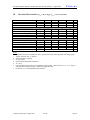
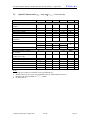
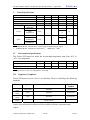
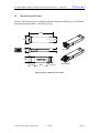
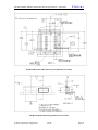
Finisar
Product Specification
Industrial Temperature Range
10Gb/s 850nm Multimode Datacom XFP Optical Transceiver
FTLX8511D3BTL
PRODUCT FEATURES
•
Hot-pluggable XFP footprint
•
Supports 9.95Gb/s to 10.5Gb/s
bit rates*
•
Power dissipation <1.5W
•
RoHS-6 compliant (lead-free)
•
Temperature range -40°C to +85°C
•
Single power supply: 3.3V
•
Maximum link length of 300m
•
850nm heated VCSEL laser.
•
Duplex LC connector
•
No Reference Clock required
•
Built-in digital diagnostic functions
•
Standard bail release mechanism
APPLICATIONS
•
10GBASE-SR/SW 10G Ethernet
•
1200-Mx-SN-I 10G Fibre Channel
Finisar’s FTLX8511D3BTL Small Form Factor 10Gb/s (XFP) transceivers are compliant
with the current XFP Multi-Source Agreement (MSA) Specification1 now available with
Industrial Temperature Range of Operation (-40°C to +85°C). They comply with 10Gigabit Ethernet 10GBASE-SR/SW per IEEE 802.3ae and 10G Fibre Channel 1200-MxSN-I. Digital diagnostics functions are available via a 2-wire serial interface, as specified
in the XFP MSA. The transceiver is RoHS compliant and lead free per Directive
2002/95/EC3, and Finisar Application Note AN-20384.
PRODUCT SELECTION
FTLX8511D3BTL
*Contact Finisar for higher data-rate support
© Finisar Corporation August 2010
Rev B
Page 1
FTLX8511D3BTL Industrial Temperature XFP SR Specification – August 2010
I.
Finisar
Pin Descriptions
Pin
1
2
3
Logic
LVTTL-I
4
LVTTL-O
5
6
7
8
9
10
11
LVTTL-I
Symbol
GND
VEE5
Mod-Desel
Interrupt
TX_DIS
VCC5
GND
VCC3
VCC3
SCL
SDA
12
LVTTL-I
LVTTLI/O
LVTTL-O
Mod_Abs
13
LVTTL-O
Mod_NR
14
15
16
17
18
19
20
21
LVTTL-O
LVTTL-I
RX_LOS
GND
GND
RDRD+
GND
VCC2
P_Down/RST
22
23
24
PECL-I
VCC2
GND
RefCLK+
25
PECL-I
RefCLK-
26
27
28
29
30
CML-O
CML-O
CML-I
CML-I
GND
GND
TDTD+
GND
Name/Description
Module Ground
Optional –5.2 Power Supply – Not required
Module De-select; When held low allows the module to
respond to 2-wire serial interface commands
Interrupt (bar); Indicates presence of an important condition
which can be read over the serial 2-wire interface
Transmitter Disable; Transmitter laser source turned off
+5 Power Supply – Not required
Module Ground
+3.3V Power Supply
+3.3V Power Supply
Serial 2-wire interface clock
Serial 2-wire interface data line
Ref.
1
Module Absent; Indicates module is not present. Grounded
in the module.
Module Not Ready; Finisar defines it as a logical OR
between RX_LOS and Loss of Lock in TX/RX.
Receiver Loss of Signal indicator
Module Ground
Module Ground
Receiver inverted data output
Receiver non-inverted data output
Module Ground
+1.8V Power Supply – Not required
Power Down; When high, places the module in the low
power stand-by mode and on the falling edge of P_Down
initiates a module reset
Reset; The falling edge initiates a complete reset of the
module including the 2-wire serial interface, equivalent to a
power cycle.
+1.8V Power Supply – Not required
Module Ground
Reference Clock non-inverted input, AC coupled on the
host board – Not required
Reference Clock inverted input, AC coupled on the host
board – Not required
Module Ground
Module Ground
Transmitter inverted data input
Transmitter non-inverted data input
Module Ground
2
2
1
2
2
2
2
1
1
1
1
3
3
1
1
1
Notes:
1. Module circuit ground is isolated from module chassis ground within the module.
2. Open collector; should be pulled up with 4.7kΩ – 10kΩ on host board to a voltage between 3.15V and
3.6V.
3. A Reference Clock input is not required by the FTLX8511D3BTL. If present, it will be ignored.
© Finisar Corporation August 2010
Rev B
Page 2
FTLX8511D3BTL Industrial Temperature XFP SR Specification – August 2010
Finisar
Diagram of Host Board Connector Block Pin Numbers and Name
II.
Absolute Maximum Ratings
Parameter
Maximum Supply Voltage
Case Operating Temperature
© Finisar Corporation August 2010
Symbol
Vcc3
TOP
Min
-0.5
-40
Rev B
Typ
Max
4.0
+85
Unit
V
°C
Ref.
Page 3
FTLX8511D3BTL Industrial Temperature XFP SR Specification – August 2010
III.
Finisar
Electrical Characteristics (TOP = -40 to +85°C, VCC3 = 3.13 to 3.45 Volts)
Parameter
Supply Voltage
Supply Current
Module total power consumption
Transmitter
Input differential impedance
Differential data input swing
Transmit Disable Voltage
Transmit Enable Voltage
Transmit Disable Assert Time
Receiver
Differential data output swing
Data output rise time
Data output fall time
LOS Fault
LOS Normal
Power Supply Rejection
Symbol
Vcc3
Icc3
P
Rin
Vin,pp
VD
VEN
Vout,pp
tr
tf
VLOS fault
VLOS norm
PSR
Min
3.13
Typ
360
1.2
Max
3.45
435
1.5
Unit
V
mA
W
Ref.
Ω
mV
V
V
us
2
1000
Vcc
GND+ 0.8
10
mV
ps
ps
V
V
4
5
5
6
6
7
100
120
2.0
GND
600
Vcc – 0.5
GND
650
800
40
40
VccHOST
GND+0.5
See Note 7 below
1
1
3
Notes:
1. Maximum total power consumption value is specified across the full temperature and voltage range.
Typical current at -40C is ~400mA.
2. After internal AC coupling.
3. Or open circuit.
4. Into 100 ohms differential termination.
5. 20 – 80 %.
6. Loss Of Signal is open collector to be pulled up with a 4.7kΩ – 10kΩ resistor to 3.15 – 3.6V. Logic 0
indicates normal operation; logic 1 indicates no signal detected.
7. Per Section 2.7.1. in the XFP MSA Specification1.
© Finisar Corporation August 2010
Rev B
Page 4
Finisar
FTLX8511D3BTL Industrial Temperature XFP SR Specification – August 2010
IV.
Optical Characteristics (TOP = -40 to +85°C, VCC3 = 3.13 to 3.45 Volts)
Parameter
Transmitter
Optical Modulation Amplitude
(OMA)
Average Optical Power
Optical Wavelength
RMS Spectral Width
Optical Extinction Ratio
Transmitter and Dispersion Penalty
Average Launch power of OFF
transmitter
Tx Jitter
Encircled Flux
Relative Intensity Noise
Receiver
Receiver Sensitivity (OMA)
@ 10.5Gb/s
Stressed Receiver Sensitivity
(OMA) @ 10.3Gb/s
Maximum Input Power
Wavelength Range
Receiver Reflectance
LOS De-Assert
LOS Assert
LOS Hysteresis
Symbol
Min
Typ
POMA
-2.8
-1.5
PAVE
λ
Δλrms
ER
TDP
POFF
-5.0
840
3.0
850
0.4
5.5
Max
-1.0
860
0.45
Per 802.3ae requirements
30
<4.5μm
<19μm
RIN12OMA
86
1
nm
dB
dB
dB
dBm
%
-128
dB/Hz
RSENS1
-11.1
dBm
RSENS2
-7.5
dBm
PMAX
λC
Rrx
LOSD
LOSA
+0.5
840
Ref.
dBm
3.9
-30
Txj
Unit
860
-12
-14
-30
0.5
2
3
4
dBm
nm
dB
dBm
dBm
dB
Notes:
1. Average power figures are informative only, per IEEE 802.3ae.
2. Measured into Type A1a (50/125 μm multimode) fiber per ANSI/TIA/EIA-455-203-2.
3. Measured with worst ER; BER<10-12; 231 – 1 PRBS.
4. Per IEEE 802.3ae.
© Finisar Corporation August 2010
Rev B
Page 5
Finisar
FTLX8511D3BTL Industrial Temperature XFP SR Specification – August 2010
V.
General Specifications
Parameter
Bit Rate
Bit Error Ratio
Maximum Supported Distances
Fiber Type
850nm OFL
Bandwidth
160MHz-km
OM1
62.5μm
200MHz-km
50μm
400MHz-km
OM2
500MHz-km
OM3
2000MHz-km
Symbol
BR
BER
Min
9.95
Typ
Max
10.5
See Note 2
Units
Gb/s
Ref.
1
2
26
Lmax
33
m
66
82
Lmax
m
300
Notes:
1. 10GBASE-SR/SW, 1200-Mx-SN-I. Contact Finisar for higher data-rate support.
2. 10GBASE-SR/SW, 1200-Mx-SN-I tested with 231 – 1 PRBS @ 10-12 BER.
VI.
Environmental Specifications
This Finisar XFP transceiver model has an operating temperature range from -40°C to
+85°C case temperature.
Parameter
Case Operating Temperature
Storage Temperature
Symbol
Top
Tsto
Min
-40
-40
Typ
Max
85
85
Units
°C
°C
Ref.
1
Notes:
1. Warm-up time at -40°C case temperature is 10 seconds.
VII.
Regulatory Compliance
Finisar XFP transceivers are Class 1 Laser Products. They are certified per the following
standards:
Feature
Laser Eye
Safety
Laser Eye
Safety
Electrical
Safety
Electrical
Safety
Agency
Standard
Certificate
Number
FDA/CDRH
IEC60825
9210176-77
TÜV
EN60825
R72101686
TÜV
EN 60950
R72101686
UL/CSA
CLASS 3862.07
CLASS 3862.87
2283290
Copies of the referenced certificates will be available at Finisar Corporation upon
request.
© Finisar Corporation August 2010
Rev B
Page 6
FTLX8511D3BTL Industrial Temperature XFP SR Specification – August 2010
Finisar
VIII. Digital Diagnostic Functions
As defined by the XFP MSA1, Finisar XFP transceivers provide digital diagnostic
functions via a 2-wire serial interface, which allows real-time access to the following
operating parameters:
•
•
•
•
•
Transceiver temperature
Laser bias current
Transmitted optical power
Received optical power
Transceiver supply voltage
It also provides a sophisticated system of alarm and warning flags, which may be used to
alert end-users when particular operating parameters are outside of a factory-set normal
range.
The operating and diagnostics information is monitored and reported by a Digital
Diagnostics Transceiver Controller (DDTC) inside the transceiver, which is accessed
through the 2-wire serial interface. When the serial protocol is activated, the serial clock
signal (SCL pin) is generated by the host. The positive edge clocks data into the XFP
transceiver into those segments of its memory map that are not write-protected. The
negative edge clocks data from the XFP transceiver. The serial data signal (SDA pin) is
bi-directional for serial data transfer. The host uses SDA in conjunction with SCL to
mark the start and end of serial protocol activation. The memories are organized as a
series of 8-bit data words that can be addressed individually or sequentially. The 2-wire
serial interface provides sequential or random access to the 8 bit parameters, addressed
from 000h to the maximum address of the memory.
For more detailed information including memory map definitions, please see Finisar
Application Note AN-2035 “Digital Diagnostic Monitoring Interface for XFP Optical
Transceivers”, or the XFP MSA Specification1.
© Finisar Corporation August 2010
Rev B
Page 7
FTLX8511D3BTL Industrial Temperature XFP SR Specification – August 2010
IX.
Finisar
Mechanical Specifications
Finisar’s XFP transceivers are compliant with the dimensions defined by the XFP MultiSourcing Agreement (MSA). Bail color is beige.
77.95
22.15
18.35
13.30
8.50
LATCHED
16.00
UNLATCHED
20.85
39.00
R1.00
XFP Transceiver (dimensions are in mm)
© Finisar Corporation August 2010
Rev B
Page 8
FTLX8511D3BTL Industrial Temperature XFP SR Specification – August 2010
X.
Finisar
PCB Layout and Bezel Recommendations
XFP Host Board Mechanical Layout (dimensions are in mm)
© Finisar Corporation August 2010
Rev B
Page 9
FTLX8511D3BTL Industrial Temperature XFP SR Specification – August 2010
Finisar
XFP Detail Host Board Mechanical Layout (dimensions are in mm)
XFP Recommended Bezel Design (dimensions are in mm)
© Finisar Corporation August 2010
Rev B
Page 10
FTLX8511D3BTL Industrial Temperature XFP SR Specification – August 2010
Finisar
XI.
References
1.
10 Gigabit Small Form Factor Pluggable Module (XFP) Multi-Source Agreement
(MSA), Rev 4.5 - August 2005. Documentation is currently available at
http://www.xfpmsa.org/
2.
Application Note AN-2035: “Digital Diagnostic Monitoring Interface for XFP
Optical Transceivers” – Finisar Corporation, December 2003
3.
Directive 2002/95/EC of the European Council Parliament and of the Council,
“on the restriction of the use of certain hazardous substances in electrical and
electronic equipment”. January 27, 2003.
4.
“Application Note AN-2038: Finisar Implementation Of RoHS Compliant
Transceivers”, Finisar Corporation, January 21, 2005.
XII.
For More Information
Finisar Corporation
1389 Moffett Park Drive
Sunnyvale, CA 94089-1133
Tel. 1-408-548-1000
Fax 1-408-541-6138
[email protected]
www.finisar.com
© Finisar Corporation August 2010
Rev B
Page 11