1
Intel® Core™ i7-800 and i5-700
Desktop Processor Series
Datasheet – Volume 2
September 2009
Document Number: 322165-001
INFORMATION IN THIS DOCUMENT IS PROVIDED IN CONNECTION WITH INTEL® PRODUCTS. NO LICENSE, EXPRESS OR IMPLIED,
BY ESTOPPEL OR OTHERWISE, TO ANY INTELLECTUAL PROPERTY RIGHTS IS GRANTED BY THIS DOCUMENT. EXCEPT AS
PROVIDED IN INTEL'S TERMS AND CONDITIONS OF SALE FOR SUCH PRODUCTS, INTEL ASSUMES NO LIABILITY WHATSOEVER,
AND INTEL DISCLAIMS ANY EXPRESS OR IMPLIED WARRANTY, RELATING TO SALE AND/OR USE OF INTEL PRODUCTS INCLUDING
LIABILITY OR WARRANTIES RELATING TO FITNESS FOR A PARTICULAR PURPOSE, MERCHANTABILITY, OR INFRINGEMENT OF ANY
PATENT, COPYRIGHT OR OTHER INTELLECTUAL PROPERTY RIGHT. Intel products are not intended for use in medical, life saving,
life sustaining, critical control or safety systems, or in nuclear facility applications.
Legal Lines and Disclaimers
Intel may make changes to specifications and product descriptions at any time, without notice.
Designers must not rely on the absence or characteristics of any features or instructions marked “reserved” or “undefined.” Intel
reserves these for future definition and shall have no responsibility whatsoever for conflicts or incompatibilities arising from future
changes to them.
The Intel Core™ i7-800 and i5-700 desktop processor series may contain design defects or errors known as errata which may
cause the product to deviate from published specifications. Current characterized errata are available on request.
Δ
Intel processor numbers are not a measure of performance. Processor numbers differentiate features within each processor
family, not across different processor families. See http://www.intel.com/products/processor_number for details. Over time
processor numbers will increment based on changes in clock, speed, cache, FSB, or other features, and increments are not
intended to represent proportional or quantitative increases in any particular feature. Current roadmap processor number
progression is not necessarily representative of future roadmaps. See www.intel.com/products/processor_number for details.
No computer system can provide absolute security under all conditions. Intel® Trusted Execution Technology (Intel® TXT) requires
a computer system with Intel® Virtualization Technology, an Intel TXT-enabled processor, chipset, BIOS, Authenticated Code
Modules and an Intel TXT-compatible measured launched environment (MLE). The MLE could consist of a virtual machine monitor,
an OS or an application. In addition, Intel TXT requires the system to contain a TPM v1.2, as defined by the Trusted Computing
Group and specific software for some uses. For more information, see http://www.intel.com/technology/security/.
Intel® Virtualization Technology requires a computer system with an enabled Intel® processor, BIOS, virtual machine monitor
(VMM) and, for some uses, certain platform software enabled for it. Functionality, performance or other benefits will vary
depending on hardware and software configurations and may require a BIOS update. Software applications may not be compatible
with all operating systems. Please check with your application vendor.
Intel® Active Management Technology requires the computer system to have an Intel(R) AMT-enabled chipset, network hardware
and software, as well as connection with a power source and a corporate network connection. Setup requires configuration by the
purchaser and may require scripting with the management console or further integration into existing security frameworks to
enable certain functionality. It may also require modifications of implementation of new business processes. With regard to
notebooks, Intel AMT may not be available or certain capabilities may be limited over a host OS-based VPN or when connecting
wirelessly, on battery power, sleeping, hibernating or powered off. For more information, see www.intel.com/technology/platformtechnology/intel-amt/
Enabling Execute Disable Bit functionality requires a PC with a processor with Execute Disable Bit capability and a supporting
operating system. Check with your PC manufacturer on whether your system delivers Execute Disable Bit functionality.
Contact your local Intel sales office or your distributor to obtain the latest specifications and before placing your product order.
Copies of documents which have an order number and are referenced in this document, or other Intel literature may be obtained
by calling 1-800-548-4725 or by visiting Intel's website at http://www.intel.com.
Intel, Intel Core, Intel Scalable Memory Interconnect (Intel SMI), Intel Virtualization Technology for Directed I/O, Intel Trusted
Execution Technology (Intel TXT), Intel Management Engine (Intel ME), Intel Interconnect BIST (Intel IBIST), and the Intel logo
are trademarks of Intel Corporation in the U. S. and other countries.
*Other names and brands may be claimed as the property of others.
Copyright © 2009, Intel Corporation. All Rights Reserved.
2
Datasheet, Volume 2
Contents
1
Introduction ............................................................................................................ 17
1.1
Register Terminology ......................................................................................... 17
2
Configuration Process and Registers ....................................................................... 19
2.1
Platform Configuration Structure ......................................................................... 19
2.1.1 Processor Integrated I/O (IIO) Devices (PCI Bus 0) .................................... 19
2.1.2 Processor Uncore Devices (PCI Bus — FFh) ................................................ 20
2.2
Configuration Mechanisms .................................................................................. 21
2.2.1 Standard PCI Express* Configuration Mechanism........................................ 21
2.2.2 PCI Express* Configuration Mechanism ..................................................... 21
2.3
Routing Configuration Accesses ........................................................................... 23
2.3.1 Internal Device Configuration Accesses ..................................................... 24
2.3.2 Bridge-Related Configuration Accesses ...................................................... 24
2.3.2.1 PCI Express* Configuration Accesses ........................................... 24
2.3.2.2 DMI Configuration Accesses ....................................................... 25
2.4
Processor Register Introduction ........................................................................... 25
2.5
I/O Mapped Registers ........................................................................................ 26
3
Processor Integrated I/O (IIO) Configuration Registers ......................................... 27
3.1
Processor IIO Devices (PCI Bus 0) ....................................................................... 27
3.2
Device Mapping................................................................................................. 28
3.2.1 Unimplemented Devices/Functions and Registers........................................ 28
3.3
PCI Express*/DMI Configuration Registers ............................................................ 28
3.3.1 Other Register Notes .............................................................................. 28
3.3.2 Configuration Register Map ...................................................................... 29
3.3.3 Standard PCI Configuration Space (0h to 3Fh) —
Type 0/1 Common Configuration Space ..................................................... 35
3.3.3.1 VID—Vendor Identification Register............................................. 35
3.3.3.2 DID—Device Identification Register ............................................. 35
3.3.3.3 PCICMD—PCI Command Register ................................................ 36
3.3.3.4 PCISTS—PCI Status Register ...................................................... 38
3.3.3.5 RID—Revision Identification Register ........................................... 40
3.3.3.6 CCR—Class Code Register .......................................................... 40
3.3.3.7 CLSR—Cacheline Size Register.................................................... 41
3.3.3.8 PLAT—Primary Latency Timer ..................................................... 41
3.3.3.9 HDR—Header Type Register ....................................................... 41
3.3.3.10 SVID—Subsystem Vendor ID ...................................................... 42
3.3.3.11 SID—Subsystem Identity ........................................................... 42
3.3.3.12 CAPPTR—Capability Pointer ........................................................ 42
3.3.3.13 INTLIN—Interrupt Line Register .................................................. 42
3.3.3.14 INTPIN—Interrupt Pin Register ................................................... 43
3.3.3.15 PBUS—Primary Bus Number Register........................................... 43
3.3.3.16 SECBUS—Secondary Bus Number ............................................... 43
3.3.3.17 SUBBUS—Subordinate Bus Number Register................................. 44
3.3.3.18 IOBAS—I/O Base Register.......................................................... 44
3.3.3.19 IOLIM—I/O Limit Register .......................................................... 45
3.3.3.20 SECSTS—Secondary Status Register ........................................... 46
3.3.3.21 MBAS—Memory Base ................................................................ 47
3.3.3.22 MLIM—Memory Limit ................................................................. 47
3.3.3.23 PMBASE—Prefetchable Memory Base Register............................... 48
3.3.3.24 PMLIMIT—Prefetchable Memory Limit .......................................... 48
3.3.3.25 PMBASEU—Prefetchable Memory Base (Upper 32 bits) ................... 49
3.3.3.26 PMLIMITU—Prefetchable Memory Limit (Upper 32 bits) .................. 49
3.3.3.27 BCTRL—Bridge Control Register .................................................. 50
3.3.4 Device-Specific PCI Configuration Space — 40h to FFh ................................ 51
3.3.4.1 SCAPID—Subsystem Capability Identity ....................................... 51
Datasheet, Volume 2
3
3.3.4.2
3.3.4.3
3.3.4.4
3.3.4.5
3.4
4
SNXTPTR—Subsystem ID Next Pointer .........................................51
SVID—Subsystem Vendor ID ......................................................52
SID—Subsystem Identity ...........................................................52
DMIRCBAR—DMI Root Complex Register Block Base Address
Register ...................................................................................52
3.3.4.6 MSICAPID—MSI Capability ID .....................................................53
3.3.4.7 MSINXTPTR—MSI Next Pointer ....................................................53
3.3.4.8 MSICTRL—MSI Control Register...................................................53
3.3.4.9 MSIAR—MSI Address Register .....................................................54
3.3.4.10 MSIDR—MSI Data Register .........................................................55
3.3.4.11 MSIMSK—MSI Mask Bit Register ..................................................55
3.3.4.12 MSIPENDING—MSI Pending Bit Register .......................................56
3.3.4.13 PEGCAPID—PCI Express* Capability Identity Register ....................56
3.3.4.14 PEGNXTPTR—PCI Express* Next Pointer Register...........................56
3.3.4.15 PEGCAP—PCI Express* Capabilities Register .................................57
3.3.4.16 DEVCAP—PCI Express* Device Capabilities Register .......................58
3.3.4.17 DEVCTRL—PCI Express* Device Control Register ...........................59
3.3.4.18 DEVSTS—PCI Express* Device Status Register ..............................61
3.3.4.19 LNKCAP—PCI Express* Link Capabilities Register...........................62
3.3.4.20 LNKCON—PCI Express* Link Control Register (Device 0) ................64
3.3.4.21 LNKCON—PCI Express* Link Control Register ................................65
3.3.4.22 LNKSTS—PCI Express* Link Status Register..................................66
3.3.4.23 SLTCAP—PCI Express* Slot Capabilities Register ...........................68
3.3.4.24 SLTCON—PCI Express* Slot Control Register.................................69
3.3.4.25 ROOTCON—PCI Express* Root Control Register.............................70
3.3.4.26 ROOTCAP—PCI Express* Root Capabilities Register........................71
3.3.4.27 ROOTSTS—PCI Express* Root Status Register...............................72
3.3.4.28 DEVCAP2—PCI Express* Device Capabilities Register 2 ..................73
3.3.4.29 DEVCTRL2—PCI Express* Device Control Register 2.......................74
3.3.4.30 LNKCON2—PCI Express* Link Control Register 2 ...........................75
3.3.4.31 LNKSTS2—PCI Express* Link Control Register 2 ............................76
3.3.4.32 PMCAP—Power Management Capabilities Register ..........................76
3.3.4.33 PMCSR—Power Management Control and Status
Register (Device 0 DMI) .............................................................77
3.3.4.34 PMCSR—Power Management Control and Status Register................78
3.3.5 PCIe/DMI Extended Configuration Space ....................................................79
3.3.5.1 APICBASE—APIC Base Register ...................................................79
3.3.5.2 APICLIMIT—APIC Limit Register ..................................................79
3.3.5.3 PERFCTRLSTS—Performance Control and Status Register................79
3.3.5.4 MISCCTRLSTS—Miscellaneous Control and Status Register..............81
3.3.5.5 CTOCTRL—Completion Time-out Control Register ..........................83
3.3.6 DMI Root Complex Register Block .............................................................84
3.3.6.1 DMIVCH—DMI Virtual Channel Capability Header ...........................85
3.3.6.2 DMIVCCAP1—DMI Port VC Capability Register 1 ............................85
3.3.6.3 DMIVCCAP2—DMI Port VC Capability Register 2 ............................86
3.3.6.4 DMIVCCTL—DMI Port VC Control .................................................86
3.3.6.5 DMIVC0RCAP—DMI VC0 Resource Capability .................................87
3.3.6.6 DMIVC0RCTL—DMI VC0 Resource Control.....................................87
3.3.6.7 DMIVC0RSTS—DMI VC0 Resource Status......................................88
3.3.6.8 DMIVC1RCAP—DMI VC1 Resource Capability .................................88
3.3.6.9 DMIVC1RCTL—DMI VC1 Resource Control.....................................89
3.3.6.10 DMIVC1RSTS—DMI VC1 Resource Status......................................90
3.3.6.11 DMILCAP—DMI Link Capabilities ..................................................90
3.3.6.12 DMILCTRL—DMI Link Control ......................................................91
3.3.6.13 DMILSTS—DMI Link Status .........................................................91
Integrated I/O Core Registers (Device 8, Function 0-3)...........................................92
3.4.1 Configuration Register Map (Device 8, Function 0-3) ...................................92
3.4.2 Standard PCI Configuration Registers ........................................................98
3.4.2.1 VID—Vendor Identification Register .............................................98
3.4.2.2 DID—Device Identification Register..............................................98
3.4.2.3 PCICMD—PCI Command Register ................................................98
Datasheet, Volume 2
3.4.3
3.4.4
3.4.5
Datasheet, Volume 2
3.4.2.4 PCISTS—PCI Status Register .................................................... 101
3.4.2.5 RID—Revision Identification Register ......................................... 103
3.4.2.6 CCR—Class Code Register ........................................................ 103
3.4.2.7 CLSR—Cacheline Size Register.................................................. 103
3.4.2.8 HDR—Header Type Register ..................................................... 104
3.4.2.9 SVID—Subsystem Vendor ID .................................................... 104
3.4.2.10 SID—Subsystem Device ID ...................................................... 104
3.4.2.11 CAPPTR—Capability Pointer ...................................................... 104
3.4.2.12 INTLIN—Interrupt Line Register ................................................ 105
3.4.2.13 INTPIN—Interrupt Pin Register ................................................. 105
Common Extended Configuration Space Registers..................................... 105
3.4.3.1 CAPID—PCI Express® Capability List Register ............................. 105
3.4.3.2 NXTPTR—PCI Express® Next Capability List Register.................... 106
3.4.3.3 EXPCAP—PCI Express® Capabilities Register............................... 106
3.4.3.4 DEVCAP—PCI Express® Device Capabilities Register .................... 107
3.4.3.5 DEVCTRL—PCI Express® Device Control Register ........................ 108
3.4.3.6 DEVSTS—PCI Express® Device Status Register ........................... 110
Intel® VT-d, Address Mapping, System Management Registers (Device 8,
Function 0).......................................................................................... 111
3.4.4.1 IIOMISCCTRL—Integrated I/O Misc Control Register .................... 111
3.4.4.2 IIOMISCSS—Integrated I/O MISC Status ................................... 112
3.4.4.3 TSEGCTRL—TSEG Control Register ............................................ 112
3.4.4.4 TOLM—Top of Low Memory ...................................................... 113
3.4.4.5 TOHM—Top of High Memory ..................................................... 113
3.4.4.6 NCMEM.BASE—NCMEM Base .................................................... 113
3.4.4.7 NCMEM.LIMIT—NCMEM Limit .................................................... 114
3.4.4.8 DEVHIDE1—Device Hide 1 Register ........................................... 114
3.4.4.9 DEVHIDE2—Device Hide 2 Register ........................................... 117
3.4.4.10 IIOBUSNO—IIO Internal Bus Number ........................................ 118
3.4.4.11 LMMIOL.BASE—Local MMIOL Base............................................. 118
3.4.4.12 LMMIOL.LIMIT—Local MMIOL Limit ............................................ 119
3.4.4.13 LMMIOH.BASE—Local MMIOH Base............................................ 119
3.4.4.14 LMMIOH.LIMIT—Local MMIOH Limit ........................................... 119
3.4.4.15 LMMIOH.BASEU—Local MMIOH Base Upper ................................ 120
3.4.4.16 LMMIOH.LIMITU—Local MMIOH Limit Upper................................ 120
3.4.4.17 LCFGBUS.BASE—Local Configuration Bus Number Base Register ... 120
3.4.4.18 LCFGBUS.LIMIT—Local Configuration Bus Number Limit Register... 121
3.4.4.19 GMMIOL.BASE—Global MMIOL Base .......................................... 121
3.4.4.20 GMMIOL.LIMIT—Global MMIOL Limit.......................................... 121
3.4.4.21 GMMIOH.BASE—Global MMIOH Base ......................................... 122
3.4.4.22 GMMIOH.LIMIT—Global MMIOH Limit......................................... 122
3.4.4.23 GMMIOH.BASEU—Global MMIOH Base Upper .............................. 123
3.4.4.24 GMMIOH.LIMITU—Global MMIOH Limit Upper ............................. 123
3.4.4.25 GCFGBUS.BASE—Global Configuration Bus Number Base Register . 123
3.4.4.26 GCFGBUS.LIMIT—Global Configuration Bus Number Limit Register. 124
3.4.4.27 MESEGBASE—Intel® Management Engine (Intel® ME)
Memory Region Base ............................................................... 124
3.4.4.28 MESEGMASK—Intel® ME Memory Region Mask ........................... 124
3.4.4.29 VTBAR—Base Address Register for Intel® VT-d Chipset Registers .. 125
3.4.4.30 VTGENCTRL—Intel® VT-d General Control Register...................... 126
3.4.4.31 VTISOCHCTRL—Intel VT-d Isoch Related Control Register ............ 127
3.4.4.32 VTGENCTRL2—Intel VT-d General Control 2 Register ................... 127
3.4.4.33 VTSTS—Intel® VT-d Status Register .......................................... 128
Semaphore and ScratchPad Registers (Dev:8, F:1) ................................... 128
3.4.5.1 SR[0:3]—Scratch Pad Register 0-3 (Sticky) ................................ 128
3.4.5.2 SR[4:7]—Scratch Pad Register 4-7 (Sticky) ................................ 128
3.4.5.3 SR[8:11]—Scratch Pad Register 8-11 (Non-Sticky)...................... 128
3.4.5.4 SR[12:15]—Scratch Pad Register 12-15 (Non-Sticky) .................. 129
3.4.5.5 SR[16:17]—Scratch Pad Register 16-17 (Non-Sticky) .................. 129
3.4.5.6 SR[18:23]—Scratch Pad Register 18-23 (Non-Sticky) .................. 129
3.4.5.7 CWR[0:3]—Conditional Write Registers 0-3 ................................ 129
5
3.4.6
3.4.7
3.5
6
Intel®
3.5.1
3.5.2
3.4.5.8 CWR[4:7]—Conditional Write Registers 4-7................................. 130
3.4.5.9 CWR[8:11]—Conditional Write Registers 8-11 ............................. 130
3.4.5.10 CWR[12:15]—Conditional Write Registers 12-15.......................... 130
3.4.5.11 CWR[16:17]—Conditional Write Registers 16-17.......................... 131
3.4.5.12 CWR[18:23]—Conditional Write Registers 18-23.......................... 131
3.4.5.13 IR[0:3]—Increment Registers 0-3.............................................. 131
3.4.5.14 IR[4:7]—Increment Registers 4-7.............................................. 132
3.4.5.15 IR[8:11]—Increment Registers 8-11 .......................................... 132
3.4.5.16 IR[12:15]—Increment Registers 12-15....................................... 132
3.4.5.17 IR[16:17]—Increment Registers 16-17....................................... 133
3.4.5.18 IR[18:23]—Increment Registers 18-23....................................... 133
System Control/Status Registers (Device 8, Function 2) ............................. 134
3.4.6.1 SYSMAP—System Error Event Map Register ................................ 134
3.4.6.2 GENMCA—Generate MCA.......................................................... 134
3.4.6.3 SYRE—System Reset ............................................................... 135
Miscellaneous Registers (Dev:8, F:3)....................................................... 135
3.4.7.1 IIOSLPSTS_L—IIO Sleep Status Low Register.............................. 135
3.4.7.2 IIOSLPSTS_H—IIO Sleep Status High Register ............................ 136
3.4.7.3 PMUSTATE—Power Management State Register ........................... 136
3.4.7.4 CTSTS—Throttling Status Register ............................................. 137
3.4.7.5 CTCTRL—Throttling Control Register .......................................... 137
VT-d Memory Mapped Registers ............................................................... 137
Intel® VT-d Configuration Register Space (MMIO) ..................................... 138
Register Description .............................................................................. 141
3.5.2.1 VTD_VERSION[0:1]—Version Number Register............................ 141
3.5.2.2 VTD_CAP[0:1]—Intel® VT-d Chipset Capabilities Register ............. 142
3.5.2.3 EXT_VTD_CAP[0:1]—Extended Intel® VT-d Capability Register...... 143
3.5.2.4 GLBCMD[0:1]—Global Command Register .................................. 144
3.5.2.5 GLBSTS[0:1]—Global Status Register......................................... 145
3.5.2.6 ROOTENTRYADD[0:1]—Root Entry Table Address Register ............ 145
3.5.2.7 CTXCMD[0:1]—Context Command Register ................................ 146
3.5.2.8 FLTSTS[0:1]—Fault Status Register ........................................... 147
3.5.2.9 FLTEVTCTRL[0:1]—Fault Event Control Register .......................... 148
3.5.2.10 FLTEVTDATA[0:1]—Fault Event Data Register ............................. 149
3.5.2.11 FLTEVTADDR[0:1]—Fault Event Address Register ........................ 149
3.5.2.12 FLTEVTUPRADDR[0:1]—Fault Event Upper Address Register.......... 149
3.5.2.13 PMEN[0:1]—Protected Memory Enable Register ........................... 149
3.5.2.14 PROT_LOW_MEM_BASE[0:1]—Protected Memory Low
Base Register ......................................................................... 150
3.5.2.15 PROT_LOW_MEM_LIMIT[0:1]—Protected Memory Low
Limit Register ......................................................................... 150
3.5.2.16 PROT_HIGH_MEM_BASE[0:1]—Protected Memory High
Base Register ......................................................................... 150
3.5.2.17 PROT_HIGH_MEM_LIMIT[0:1]—Protected Memory Limit
Base Register ......................................................................... 151
3.5.2.18 INV_QUEUE_HEAD[0:1]—Invalidation Queue Header
Pointer Register ...................................................................... 151
3.5.2.19 INV_QUEUE_TAIL[0:1]—Invalidation Queue Tail Pointer
Register ................................................................................. 151
3.5.2.20 INV_QUEUE_ADD[0:1]—Invalidation Queue Address
Register ................................................................................. 152
3.5.2.21 INV_COMP_STATUS[0:1]—Invalidation Completion Status
Register ................................................................................. 152
3.5.2.22 INV_COMP_EVT_CTL[0:1]—Invalidation Completion
Event Control Register ............................................................. 153
3.5.2.23 INV_COMP_EVT_DATA[0:1]—Invalidation Completion
Event Data Register................................................................. 153
3.5.2.24 INV_COMP_EVT_ADDR[0:1]—Invalidation Completion
Event Address Register ............................................................ 153
3.5.2.25 INV_COMP_EVT_UPRADDR[0:1]—Invalidation Completion
Event Upper Address Register ................................................... 154
Datasheet, Volume 2
3.6
Intel®
3.6.1
3.7
Intel®
3.7.1
3.7.2
4
3.5.2.26 INTR_REMAP_TABLE_BASE[0:1]—Interrupt Remapping
Table Base Address Register..................................................... 154
3.5.2.27 FLTREC[10,7:0]—Fault Record Register ..................................... 155
3.5.2.28 INVADDRREG[0:1]—Invalidate Address Register ......................... 155
3.5.2.29 IOTLBINV[0:1]—IOTLB Invalidate Register ................................. 156
Trusted Execution Technology (Intel® TXT) Register Map ............................ 157
Intel® TXT Space Registers.................................................................... 162
3.6.1.1 TXT.STS—Intel® TXT Status Register ........................................ 162
3.6.1.2 TXT.ESTS—Intel® TXT Error Status Register ............................... 164
3.6.1.3 TXT.THREADS.EXISTS—Intel® TXT Thread Exists Register............ 165
3.6.1.4 TXT.THREADS.JOIN—Intel® TXT Threads Join Register ................ 165
3.6.1.5 TXT.ERRORCODE—Intel® TXT Error Code Register ...................... 166
3.6.1.6 TXT.CMD.RESET—Intel® TXT System Reset Command Register .... 166
3.6.1.7 TXT.CMD.CLOSE_PRIVATE—Intel® TXT Close Private Command
Register................................................................................. 167
3.6.1.8 TXT.VER.QPIIF ....................................................................... 167
3.6.1.9 TXT.ID—Intel® TXT Identifier Register ....................................... 168
3.6.1.10 TXT.CMD.LOCK.BASE—Intel® TXT Lock Base Command Register... 168
3.6.1.11 TXT.CMD.UNLOCK.BASE—Intel® TXT Unlock Base Command
Register................................................................................. 169
3.6.1.12 TXT.SINIT.MEMORY.BASE—Intel® TXT SINIT Code Base Register .. 169
3.6.1.13 TXT.SINIT.MEMORY.SIZE—Intel® TXT SINIT Memory
Size Register .......................................................................... 170
3.6.1.14 TXT.MLE.JOIN—Intel® TXT MLE Join Base Register ...................... 170
3.6.1.15 TXT.HEAP.BASE—Intel® TXT HEAP Code Base Register ................ 171
3.6.1.16 TXT.HEAP.SIZE—Intel® TXT HEAP Size Register.......................... 171
3.6.1.17 TXT.MSEG.BASE—Intel® TXT MSEG Base Register....................... 172
3.6.1.18 TXT.MSEG.SIZE—Intel® TXT MSEG Size Register ........................ 172
3.6.1.19 TXT.SCRATCHPAD0—Intel® TXT Scratch Pad Register 0 ............... 173
3.6.1.20 TXT.SCRATCHPAD1—Intel® TXT Scratch Pad Register 1 ............... 173
3.6.1.21 TXT.CMD.OPEN.LOCALITY1—Intel® TXT Open Locality 1
Command .............................................................................. 174
3.6.1.22 TXT.CMD.CLOSE.LOCALITY1—Intel® TXT Close Locality 1
Command .............................................................................. 174
3.6.1.23 TXT.CMD.OPEN.LOCALITY2—Intel® TXT Open Locality 2
Command .............................................................................. 174
3.6.1.24 TXT.CMD.CLOSE.LOCALITY2—Intel® TXT Close Locality 2
Command .............................................................................. 175
3.6.1.25 TXT.PUBLIC.KEY—Intel® TXT Public Key Hash Register ................ 175
QuickPath Interconnect Device/Functions .................................................. 176
Intel® QuickPath Interconnect Link Layer Registers................................... 177
3.7.1.1 SVID—Subsystem Vendor ID .................................................... 177
3.7.1.2 SID—Subsystem Device ID ...................................................... 177
3.7.1.3 CAPPTR—Capability Pointer ...................................................... 177
3.7.1.4 QPI[0]LCL—Intel® QuickPath Interconnect Link Control ............... 178
3.7.1.5 QPI[0]LCRDC—Intel® QuickPath Interconnect Link Credit Control .. 179
Intel® QuickPath Interconnect Routing & Protocol Layer Registers............... 180
3.7.2.1 QPIPCTRL0—Intel® QuickPath Interconnect Protocol Control 0 ...... 181
3.7.2.2 QPIPISOCRES—Intel® QuickPath Interconnect Protocol
Isochronous Reservation.......................................................... 181
3.7.2.3 CAPHDRH—PCI Express® Capability Header High Register ............ 182
Processor Uncore Configuration Registers ............................................................. 183
4.1
Processor Uncore Configuration Structure (PCI Bus — FFh) ................................... 183
4.2
Device Mapping............................................................................................... 184
4.3
Detailed Configuration Space Maps .................................................................... 185
4.4
PCI Standard Registers .................................................................................... 201
4.4.1 VID—Vendor Identification Register ........................................................ 201
4.4.2 DID—Device Identification Register......................................................... 201
4.4.3 RID—Revision Identification Register ...................................................... 202
4.4.3.1 Stepping Revision ID (SRID) .................................................... 203
Datasheet, Volume 2
7
4.5
4.6
4.7
4.8
4.9
8
4.4.3.2 Compatible Revision ID (CRID) ................................................. 203
4.4.4 CCR—Class Code Register ...................................................................... 204
4.4.5 HDR—Header Type Register ................................................................... 205
4.4.6 SVID—Subsystem Vendor Identification Register....................................... 205
4.4.7 SID—Subsystem Identity ....................................................................... 206
4.4.8 PCICMD—Command Register.................................................................. 207
4.4.9 PCISTS—PCI Status Register .................................................................. 208
SAD—System Address Decoder Registers ............................................................ 209
4.5.1 SAD_PAM0123 ..................................................................................... 209
4.5.2 SAD_PAM456 ....................................................................................... 211
4.5.3 SAD_HEN ............................................................................................ 212
4.5.4 SAD_SMRAM ........................................................................................ 212
4.5.5 SAD_PCIEXBAR .................................................................................... 213
4.5.6 SAD_TPCIEXBAR .................................................................................. 213
4.5.7 SAD_MCSEG_BASE ............................................................................... 214
4.5.8 SAD_MCSEG_MASK .............................................................................. 214
4.5.9 SAD_MESEG_BASE ............................................................................... 215
4.5.10 SAD_MESEG_MASK............................................................................... 215
4.5.11 SAD_DRAM_RULE_0; SAD_DRAM_RULE_1
SAD_DRAM_RULE_2; SAD_DRAM_RULE_3
SAD_DRAM_RULE_4; SAD_DRAM_RULE_5
SAD_DRAM_RULE_6; SAD_DRAM_RULE_7 ............................................... 216
4.5.12 SAD_INTERLEAVE_LIST_0; SAD_INTERLEAVE_LIST_1
SAD_INTERLEAVE_LIST_2; SAD_INTERLEAVE_LIST_3
SAD_INTERLEAVE_LIST_4; SAD_INTERLEAVE_LIST_5
SAD_INTERLEAVE_LIST_6; SAD_INTERLEAVE_LIST_7............................... 217
Intel® QuickPath Interconnect Link Registers....................................................... 218
4.6.1 QPI_QPILCL_L0 .................................................................................... 218
Integrated Memory Controller Control Registers ................................................... 220
4.7.1 MC_CONTROL ...................................................................................... 220
4.7.2 MC_SMI_DIMM_ERROR_STATUS............................................................. 221
4.7.3 MC_SMI_CNTRL.................................................................................... 221
4.7.4 MC_STATUS......................................................................................... 222
4.7.5 MC_RESET_CONTROL............................................................................ 222
4.7.6 MC_CHANNEL_MAPPER.......................................................................... 223
4.7.7 MC_MAX_DOD...................................................................................... 223
4.7.8 MC_CFG_LOCK ..................................................................................... 224
4.7.9 MC_RD_CRDT_INIT............................................................................... 225
4.7.10 MC_CRDT_WR_THLD............................................................................. 226
TAD—Target Address Decoder Registers ............................................................. 227
4.8.1 TAD_DRAM_RULE_0; TAD_DRAM_RULE_1
TAD_DRAM_RULE_2; TAD_DRAM_RULE_3
TAD_DRAM_RULE_4; TAD_DRAM_RULE_5
TAD_DRAM_RULE_6; TAD_DRAM_RULE_7 ............................................... 227
4.8.2 TAD_INTERLEAVE_LIST_0; TAD_INTERLEAVE_LIST_1
TAD_INTERLEAVE_LIST_2; TAD_INTERLEAVE_LIST_3
TAD_INTERLEAVE_LIST_4; TAD_INTERLEAVE_LIST_5
TAD_INTERLEAVE_LIST_6; TAD_INTERLEAVE_LIST_7 ............................... 228
Integrated Memory Controller Test Registers ....................................................... 229
4.9.1 Integrated Memory Controller Padscan .................................................... 229
4.9.2 MC_DIMM_CLK_RATIO_STATUS ............................................................. 231
4.9.3 MC_DIMM_CLK_RATIO .......................................................................... 232
4.9.4 MC_TEST_LTRCON................................................................................ 232
4.9.5 MC_TEST_PH_CTR ................................................................................ 233
4.9.6 MC_TEST_PH_PIS ................................................................................. 233
4.9.7 MC_TEST_PAT_GCTR ............................................................................ 234
4.9.8 MC_TEST_PAT_BA ................................................................................ 235
Datasheet, Volume 2
4.10
4.9.9 MC_TEST_PAT_IS................................................................................. 235
4.9.10 MC_TEST_PAT_DCD ............................................................................. 235
4.9.11 MC_TEST_EP_SCCTL............................................................................. 236
4.9.12 MC_TEST_EP_SCD................................................................................ 236
Integrated Memory Controller Channel Control Registers ...................................... 237
4.10.1 MC_CHANNEL_0_DIMM_RESET_CMD
MC_CHANNEL_1_DIMM_RESET_CMD ...................................................... 237
4.10.2 MC_CHANNEL_0_DIMM_INIT_CMD
MC_CHANNEL_1_DIMM_INIT_CMD ......................................................... 238
4.10.3 MC_CHANNEL_0_DIMM_INIT_PARAMS
MC_CHANNEL_1_DIMM_INIT_PARAMS .................................................... 239
4.10.4 MC_CHANNEL_0_DIMM_INIT_STATUS
MC_CHANNEL_1_DIMM_INIT_STATUS .................................................... 240
4.10.5 MC_CHANNEL_0_DDR3CMD
MC_CHANNEL_1_DDR3CMD................................................................... 241
4.10.6 MC_CHANNEL_0_REFRESH_THROTTLE_SUPPORT
MC_CHANNEL_1_REFRESH_THROTTLE_SUPPORT ..................................... 242
4.10.7 MC_CHANNEL_0_MRS_VALUE_0_1
MC_CHANNEL_1_MRS_VALUE_0_1 ......................................................... 242
4.10.8 MC_CHANNEL_0_MRS_VALUE_2
MC_CHANNEL_1_MRS_VALUE_2 ............................................................ 243
4.10.9 MC_CHANNEL_0_RANK_PRESENT
MC_CHANNEL_1_RANK_PRESENT........................................................... 244
4.10.10MC_CHANNEL_0_RANK_TIMING_A
MC_CHANNEL_1_RANK_TIMING_A ......................................................... 245
4.10.11MC_CHANNEL_0_RANK_TIMING_B
MC_CHANNEL_1_RANK_TIMING_B ......................................................... 247
4.10.12MC_CHANNEL_0_BANK_TIMING
MC_CHANNEL_1_BANK_TIMING ............................................................. 248
4.10.13MC_CHANNEL_0_REFRESH_TIMING
MC_CHANNEL_1_REFRESH_TIMING ........................................................ 248
4.10.14MC_CHANNEL_0_CKE_TIMING
MC_CHANNEL_1_CKE_TIMING ............................................................... 249
4.10.15MC_CHANNEL_0_ZQ_TIMING
MC_CHANNEL_1_ZQ_TIMING................................................................. 250
4.10.16MC_CHANNEL_0_RCOMP_PARAMS
MC_CHANNEL_1_RCOMP_PARAMS.......................................................... 250
4.10.17MC_CHANNEL_0_ODT_PARAMS1
MC_CHANNEL_1_ODT_PARAMS1 ............................................................ 251
4.10.18MC_CHANNEL_0_ODT_PARAMS2
MC_CHANNEL_1_ODT_PARAMS2 ............................................................ 252
4.10.19MC_CHANNEL_0_ODT_MATRIX_RANK_0_3_RD
MC_CHANNEL_1_ODT_MATRIX_RANK_0_3_RD ........................................ 252
4.10.20MC_CHANNEL_0_ODT_MATRIX_RANK_4_7_RD
MC_CHANNEL_1_ODT_MATRIX_RANK_4_7_RD ........................................ 253
4.10.21MC_CHANNEL_0_ODT_MATRIX_RANK_0_3_WR
MC_CHANNEL_1_ODT_MATRIX_RANK_0_3_WR ....................................... 253
4.10.22MC_CHANNEL_0_ODT_MATRIX_RANK_4_7_WR
MC_CHANNEL_1_ODT_MATRIX_RANK_4_7_WR ....................................... 253
4.10.23MC_CHANNEL_0_WAQ_PARAMS
MC_CHANNEL_1_WAQ_PARAMS ............................................................. 254
4.10.24MC_CHANNEL_0_SCHEDULER_PARAMS
MC_CHANNEL_1_SCHEDULER_PARAMS................................................... 255
4.10.25MC_CHANNEL_0_MAINTENANCE_OPS
MC_CHANNEL_1_MAINTENANCE_OPS ..................................................... 255
4.10.26MC_CHANNEL_0_TX_BG_SETTINGS
MC_CHANNEL_1_TX_BG_SETTINGS........................................................ 256
4.10.27MC_CHANNEL_0_RX_BGF_SETTINGS
MC_CHANNEL_1_RX_BGF_SETTINGS...................................................... 257
Datasheet, Volume 2
9
4.11
4.12
10
4.10.28MC_CHANNEL_0_EW_BGF_SETTINGS
MC_CHANNEL_1_EW_BGF_SETTINGS...................................................... 257
4.10.29MC_CHANNEL_0_EW_BGF_OFFSET_SETTINGS
MC_CHANNEL_1_EW_BGF_OFFSET_SETTINGS ......................................... 258
4.10.30MC_CHANNEL_0_ROUND_TRIP_LATENCY
MC_CHANNEL_1_ROUND_TRIP_LATENCY................................................. 258
4.10.31MC_CHANNEL_0_PAGETABLE_PARAMS1
MC_CHANNEL_1_PAGETABLE_PARAMS1 .................................................. 259
4.10.32MC_CHANNEL_0_PAGETABLE_PARAMS2
MC_CHANNEL_1_PAGETABLE_PARAMS2 .................................................. 259
4.10.33MC_TX_BG_CMD_DATA_RATIO_SETTINGS_CH0
MC_TX_BG_CMD_DATA_RATIO_SETTINGS_CH1 ....................................... 260
4.10.34MC_TX_BG_CMD_OFFSET_SETTINGS_CH0
MC_TX_BG_CMD_OFFSET_SETTINGS_CH1............................................... 260
4.10.35MC_TX_BG_DATA_OFFSET_SETTINGS_CH0
MC_TX_BG_DATA_OFFSET_SETTINGS_CH1 ............................................. 260
Integrated Memory Controller Channel Address Registers...................................... 261
4.11.1 MC_DOD_CH0_0
MC_DOD_CH0_1 .................................................................................. 261
4.11.2 MC_DOD_CH1_0
MC_DOD_CH1_1 .................................................................................. 262
4.11.3 MC_SAG_CH0_0; MC_SAG_CH0_1; MC_SAG_CH0_2; MC_SAG_CH0_3;
MC_SAG_CH0_4; MC_SAG_CH0_5; MC_SAG_CH0_6; MC_SAG_CH0_7........ 263
4.11.4 MC_SAG_CH1_0; MC_SAG_CH1_1; MC_SAG_CH1_2; MC_SAG_CH1_3;
MC_SAG_CH1_4; MC_SAG_CH1_5; MC_SAG_CH1_6; MC_SAG_CH1_7........ 264
Integrated Memory Controller Channel Rank Registers .......................................... 265
4.12.1 MC_RIR_LIMIT_CH0_0; MC_RIR_LIMIT_CH0_1; MC_RIR_LIMIT_CH0_2;
MC_RIR_LIMIT_CH0_3; MC_RIR_LIMIT_CH0_4; MC_RIR_LIMIT_CH0_5;
MC_RIR_LIMIT_CH0_6; MC_RIR_LIMIT_CH0_7 ........................................ 265
4.12.2 MC_RIR_LIMIT_CH1_0; MC_RIR_LIMIT_CH1_1; MC_RIR_LIMIT_CH1_2;
MC_RIR_LIMIT_CH1_3; MC_RIR_LIMIT_CH1_4; MC_RIR_LIMIT_CH1_5;
MC_RIR_LIMIT_CH1_6; MC_RIR_LIMIT_CH1_7 ........................................ 265
4.12.3 MC_RIR_WAY_CH0_0; MC_RIR_WAY_CH0_1; MC_RIR_WAY_CH0_2;
MC_RIR_WAY_CH0_3; MC_RIR_WAY_CH0_4; MC_RIR_WAY_CH0_5
MC_RIR_WAY_CH0_6; MC_RIR_WAY_CH0_7
MC_RIR_WAY_CH0_8; MC_RIR_WAY_CH0_9
MC_RIR_WAY_CH0_10; MC_RIR_WAY_CH0_11
MC_RIR_WAY_CH0_12; MC_RIR_WAY_CH0_13
MC_RIR_WAY_CH0_14; MC_RIR_WAY_CH0_15
MC_RIR_WAY_CH0_16; MC_RIR_WAY_CH0_17
MC_RIR_WAY_CH0_18; MC_RIR_WAY_CH0_19
MC_RIR_WAY_CH0_20; MC_RIR_WAY_CH0_21
MC_RIR_WAY_CH0_22; MC_RIR_WAY_CH0_23
MC_RIR_WAY_CH0_24; MC_RIR_WAY_CH0_25
MC_RIR_WAY_CH0_26; MC_RIR_WAY_CH0_27
MC_RIR_WAY_CH0_28; MC_RIR_WAY_CH0_29
MC_RIR_WAY_CH0_30; MC_RIR_WAY_CH0_31 ........................................ 266
4.12.4 MC_RIR_WAY_CH1_0; MC_RIR_WAY_CH1_1
MC_RIR_WAY_CH1_2; MC_RIR_WAY_CH1_3
MC_RIR_WAY_CH1_4; MC_RIR_WAY_CH1_5
MC_RIR_WAY_CH1_6; MC_RIR_WAY_CH1_7
MC_RIR_WAY_CH1_8; MC_RIR_WAY_CH1_9
MC_RIR_WAY_CH1_10; MC_RIR_WAY_CH1_11
MC_RIR_WAY_CH1_12; MC_RIR_WAY_CH1_13
MC_RIR_WAY_CH1_14; MC_RIR_WAY_CH1_15
MC_RIR_WAY_CH1_16; MC_RIR_WAY_CH1_17
MC_RIR_WAY_CH1_18; MC_RIR_WAY_CH1_19
MC_RIR_WAY_CH1_20; MC_RIR_WAY_CH1_21
MC_RIR_WAY_CH1_22; MC_RIR_WAY_CH1_23
MC_RIR_WAY_CH1_24; MC_RIR_WAY_CH1_25
Datasheet, Volume 2
4.13
5
MC_RIR_WAY_CH1_26; MC_RIR_WAY_CH1_27
MC_RIR_WAY_CH1_28; MC_RIR_WAY_CH1_29
MC_RIR_WAY_CH1_30; MC_RIR_WAY_CH1_31........................................ 267
Memory Thermal Control .................................................................................. 268
4.13.1 MC_THERMAL_CONTROL0
MC_THERMAL_CONTROL1 ..................................................................... 268
4.13.2 MC_THERMAL_STATUS0
MC_THERMAL_STATUS1........................................................................ 268
4.13.3 MC_THERMAL_DEFEATURE0
MC_THERMAL_DEFEATURE1 .................................................................. 269
4.13.4 MC_THERMAL_PARAMS_A0
MC_THERMAL_PARAMS_A1.................................................................... 269
4.13.5 MC_THERMAL_PARAMS_B0
MC_THERMAL_PARAMS_B1.................................................................... 270
4.13.6 MC_COOLING_COEF0
MC_COOLING_COEF1 ........................................................................... 270
4.13.7 MC_CLOSED_LOOP0
MC_CLOSED_LOOP1 ............................................................................. 271
4.13.8 MC_THROTTLE_OFFSET0
MC_THROTTLE_OFFSET1....................................................................... 271
4.13.9 MC_RANK_VIRTUAL_TEMP0
MC_RANK_VIRTUAL_TEMP1 ................................................................... 272
4.13.10MC_DDR_THERM_COMMAND0
MC_DDR_THERM_COMMAND1 ............................................................... 272
4.13.11MC_DDR_THERM_STATUS0
MC_DDR_THERM_STATUS1 ................................................................... 273
System Address Map ............................................................................................. 275
5.1
Introduction ................................................................................................... 275
5.2
Memory Address Space .................................................................................... 276
5.2.1 System Address Map ............................................................................ 277
5.2.2 System DRAM Memory Regions .............................................................. 278
5.2.3 VGA/SMM and Legacy C/D/E/F Regions ................................................... 279
5.2.3.1 VGA/SMM Memory Space ......................................................... 279
5.2.3.2 C/D/E/F Segments .................................................................. 280
5.2.4 Address Region between 1 MB and TOLM................................................. 280
5.2.4.1 Relocatable TSEG.................................................................... 281
5.2.5 Address Region from TOLM to 4 GB ........................................................ 281
5.2.5.1 PCI Express® Memory Mapped Configuration Space..................... 281
5.2.5.2 MMIOL .................................................................................. 282
5.2.5.3 Miscellaneous ......................................................................... 282
5.2.5.4 Processor Local CSR, On-die ROM, and Processor PSeg ................ 282
5.2.5.5 Legacy/HPET/TXT/TPM/Others .................................................. 282
5.2.5.6 Local XAPIC ........................................................................... 283
5.2.5.7 High BIOS Area ...................................................................... 283
5.2.5.8 INTA/Rsvd ............................................................................. 283
5.2.5.9 Firmware ............................................................................... 283
5.2.6 Address Regions above 4 GB.................................................................. 284
5.2.6.1 High System Memory .............................................................. 284
5.2.6.2 Memory Mapped IO High.......................................................... 284
5.2.6.3 BIOS Notes on Address Allocation above 4 GB ............................ 285
5.2.7 Protected System DRAM Regions ............................................................ 285
5.3
IO Address Space............................................................................................ 285
5.3.1 VGA I/O Addresses ............................................................................... 285
5.3.2 ISA Addresses ..................................................................................... 286
5.3.3 CFC/CF8 Addresses .............................................................................. 286
5.3.4 PCIe Device I/O Addresses .................................................................... 286
5.4
Configuration/CSR Space.................................................................................. 286
5.4.1 PCIe Configuration Space ...................................................................... 286
Datasheet, Volume 2
11
5.5
5.6
5.7
5.8
12
System Management Mode (SMM) ..................................................................... 287
5.5.1 SMM Space Definition ............................................................................ 287
5.5.2 SMM Space Restrictions ......................................................................... 288
5.5.3 SMM Space Combinations ...................................................................... 288
5.5.4 SMM Control Combinations..................................................................... 289
5.5.5 SMM Space Decode and Transaction Handling........................................... 289
5.5.6 Processor WB Transaction to an Enabled SMM Address Space ..................... 289
5.5.7 SMM Access Through GTT TLB ................................................................ 289
Memory Shadowing.......................................................................................... 290
IIO Address Map Notes ..................................................................................... 290
5.7.1 Memory Recovery ................................................................................. 290
5.7.2 Non-Coherent Address Space ................................................................. 290
IIO Address Decoding....................................................................................... 291
5.8.1 Outbound Address Decoding................................................................... 291
5.8.1.1 General Overview.................................................................... 291
5.8.1.2 FWH Decoding ........................................................................ 292
5.8.1.3 Other Outbound Target Decoding .............................................. 292
5.8.1.4 Summary of Outbound Target Decoder Entries ............................ 293
5.8.1.5 Summary of Outbound Memory/IO/Configuration Decoding........... 293
5.8.2 Inbound Address Decoding..................................................................... 295
5.8.2.1 Overview ............................................................................... 295
5.8.2.2 Summary of Inbound Address Decoding ..................................... 296
5.8.3 Intel® VT-d Address Map Implications ..................................................... 300
Datasheet, Volume 2
Figures
2-1
2-2
3-1
3-2
4-1
5-1
5-2
5-3
Memory Map to PCI Express* Device Configuration Space....................................... 22
Processor Configuration Cycle Flowchart ............................................................... 23
DMI Port (Device 0) and PCI Express* Root Ports Type 1 Configuration Space ........... 29
Base Address of Intel® VT-d Remap Engines ....................................................... 137
Padscan Accessibility Mechanism ....................................................................... 230
System address Map........................................................................................ 277
VGA/SMM and Legacy C/D/E/F Regions .............................................................. 279
Pre-allocated Memory Example for 64 MB DRAM, 1 MB VGA, 1 MB GTT Stolen
and 1 MB TSEG ............................................................................................... 281
Tables
3-1
3-2
3-3
3-4
3-5
3-6
3-7
3-8
3-9
3-10
3-11
3-12
3-13
3-14
3-15
3-16
3-17
3-18
3-19
3-20
3-21
4-1
4-2
4-3
4-4
4-5
4-6
4-7
4-8
4-9
4-10
4-11
4-12
Functions Handled by the Processor Integrated I/O (IIO) ........................................ 28
Device 0 (DMI) Configuration Map ....................................................................... 31
Device 0 (DMI) Extended Configuration Map ......................................................... 32
Device 3,5 PCI Express* Registers Legacy Configuration Map .................................. 33
Device 3,5 PCI Express* Registers Extended Configuration Map............................... 34
DMI RCRB Registers .......................................................................................... 84
Core Registers (Device 8, Function 0) — Offset 000h–0FFh ..................................... 92
Core Registers (Device 8, Function 0) — Offset 100h–1FFh ..................................... 93
Core Registers (Device 8, Function 1) — Semaphore and ScratchPad
Registers (Sheet 1 of 2) ..................................................................................... 94
Core Registers (Device 8, Function 1) — Semaphore and ScratchPad
Registers (Sheet 2 of 2) ..................................................................................... 95
Core Registers (Device 8, Function 2) — System Control/Status Registers................. 96
Core Registers (Device 8, Function 3) — Miscellaneous Registers ............................. 97
Intel® VT-d Memory Mapped Registers — 00h–FFh, 1000h–10FFh ......................... 138
Intel® VT-d Memory Mapped Registers — 100h–1FFh, 1100h–11FFh ...................... 139
Intel® Trusted Execution Technology Registers.................................................... 157
Intel® Trusted Execution Technology Registers, cont’d ......................................... 158
Intel® Trusted Execution Technology Registers, cont’d ......................................... 159
Intel® Trusted Execution Technology Registers, cont’d ......................................... 160
Intel® Trusted Execution Technology Registers, cont’d ......................................... 161
Intel® QuickPath Interconnect Physical/Link Map Port 0 (Device 16)....................... 176
CSR Intel® QuickPath Interconnect Routing Layer, Protocol (Device 16, Function 1) . 180
Functions Specifically Handled by the Processor................................................... 184
Device 0, Function 0 — Generic Non-core Registers ............................................. 185
Device 0, Function 1 — System Address Decoder Registers ................................... 186
Device 2, Function 0 — Intel® QuickPath Interconnect Link 0 Registers .................. 187
Device 2, Function 1 — Intel® QuickPath Interconnect Physical 0 Registers ............. 188
Device 3, Function 0 — Integrated Memory Controller Registers ............................ 189
Device 3, Function 1 — Target Address Decoder Registers .................................... 190
Device 3, Function 2 — Memory Controller Test Registers ..................................... 191
Device 3, Function 4 — Integrated Memory Controller Test Registers...................... 192
Device 4, Function 0 — Integrated Memory Controller Channel 0
Control Registers............................................................................................. 193
Device 4, Function 1 — Integrated Memory Controller Channel 0
Address Registers............................................................................................ 194
Device 4, Function 2 — Integrated Memory Controller Channel 0
Rank Registers................................................................................................ 195
Datasheet, Volume 2
13
4-13 Device 4, Function 3 — Integrated Memory Controller Channel 0
Thermal Control Registers................................................................................. 196
4-14 Device 5, Function 0 — Integrated Memory Controller Channel 1
Control Registers ............................................................................................. 197
4-15 Device 5, Function 1 — Integrated Memory Controller Channel 1
Address Registers ............................................................................................ 198
4-16 Device 5, Function 2 — Integrated Memory Controller Channel 1
Rank Registers ................................................................................................ 199
4-17 Device 5, Function 3 — Integrated Memory Controller Channel 1
Thermal Control Registers................................................................................. 200
4-18 Padscan Accessible Parameters.......................................................................... 229
4-19 Scan Chains .................................................................................................... 229
4-20 Halt and Mask Bit Usage ................................................................................... 230
4-21 Padscan Registers............................................................................................ 230
5-1
Transaction Address Ranges – Compatible, High, and TSEG ................................... 287
5-2
SMM Space Table............................................................................................. 288
5-3
SMM Control Table ........................................................................................... 289
5-4
Outbound Target Decoder Entries ...................................................................... 293
5-5
Decoding of Outbound Memory Requests from Intel® QuickPath Interconnect
(from processor or remote Peer-to-Peer) ............................................................ 293
5-6
Decoding of Outbound Configuration Requests (from Processor or Peer-toPeer) from Intel® QuickPath Interconnect and Decoding of Outbound
Peer-to-Peer Completions from Intel QuickPath Interconnect ................................. 294
5-7
Subtractive Decoding of Outbound I/O Requests from Intel® QuickPath Interconnect 294
5-8
Inbound Memory Address Decoding.................................................................... 296
5-9
Inbound I/O Address Decoding .......................................................................... 298
5-10 Inbound Configuration Request Decoding ............................................................ 299
14
Datasheet, Volume 2
Revision History
Revision
Number
-001
Description
Revision
Date
September
2009
Initial release
§
Datasheet, Volume 2
15
16
Datasheet, Volume 2
Introduction
1
Introduction
This is Volume 2 of the Datasheet for the Intel® Core™ i7-800 and i5-700 desktop
processor series.
The processor contains one or more PCI devices within a single physical component.
The configuration registers for these devices are mapped as devices residing on the PCI
Bus assigned for the processor socket. This document describes these configuration
space registers or device-specific control and status registers (CSRs) only. This
document does NOT include Model Specific Registers (MSRs).
Note:
Throughout this document, the Intel® Core™ i7-800 and i5-700 desktop processor
series may be referred to as “processor”.
Note:
Througout this document, the Intel® 5 series Chipset Platform Controller Hub Platform
Controller Hub is also referred to as “PCH”.
Note:
The term “DT” refers to desktop platforms.
1.1
Register Terminology
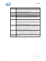
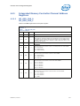
Registers and register bits are assigned one or more of the following attributes. These
attributes define the behavior of register and the bit(s) that are contained with in. All
bits are set to default values by hard reset. Sticky bits retain their states between hard
resets.
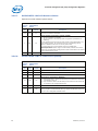
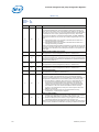
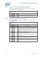
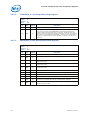
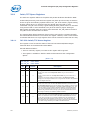
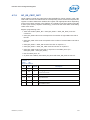
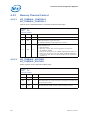
i
Term
Description
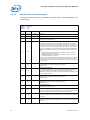
RO
Read Only. If a register bit is read only, the hardware sets its state. The bit may be read
by software. Writes to this bit have no effect.
WO
Write Only. The register bit is not implemented as a bit. The write causes some hardware
event to take place.
RWO
Datasheet, Volume 2
Read/Write Once. These bits can be read by software. After reset, these bits can only
be written by software once, after which the bits becomes ‘Read Only’.
RW
Read/Write. A register bit with this attribute can be read and written by software.
RC
Read Clear. The bit or bits can be read by software, but the act of reading causes the
value to be cleared.
RCW
Read Clear/Write. A register bit with this attribute will get cleared after the read. The
register bit can be written.
RW1C
Read/Write 1 Clear. A register bit with this attribute can be read or cleared by software.
In order to clear this bit, a one must be written to it. Writing a zero will have no effect.
RW0C
Read/Write 0 Clear. A register bit with this attribute can be read or cleared by software.
In order to clear this bit, a zero must be written to it. Writing a one will have no effect.
ROS
RO Sticky. These bits can only be read by software, writes have no effect. The value of
the bits is determined by the hardware only. These bits are only re-initialized to their
default value by a PWRGOOD reset.
RWS
R/W Sticky.These bits can be read and written by software. These bits are only reinitialized to their default value by a PWRGOOD reset.
RW1S
Read/Write 1 Set. A register bit can be either read or set by software. In order to set
this bit, a one must be written to it. Writing a zero to this bit has no effect. Hardware will
clear this bit.
RW0S
Read/Write 0 Set. A register bit can be either read or set by software. In order to set
this bit, a zero must be written to it. Writing a one to this bit has no effect. Hardware will
clear this bit.
RWL
Read/Write/Lock. A register bit with this attribute can be read or written by software.
Hardware or a configuration bit can lock the bit and prevent it from being updated.
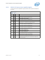
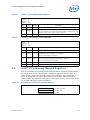
17
Introduction
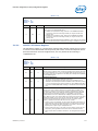
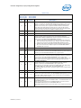
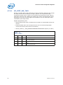
Term
Description
RWO
Read/Write Once. A register bit with this attribute can be written to only once after
power up. After the first write, the bit becomes read only. This attribute is applied on a bit
by bit basis. For example, if the RWO attribute is applied to a 2-bit field, and only one bit
is written, then the written bit cannot be rewritten (unless reset). The unwritten bit, of the
field, may still be written once. This is special case of RWL.
RWDS
RRW
L
RSVD/RV
RW and Sticky. Re-initialized to default value only with POWERGOOD reset. Value
written will take effect on the next Link layer init.
Read/Restricted Write. This bit can be read and written by software. However, only
supported values will be written. Writes of non supported values will have no effect.
Lock. A register bit with this attribute becomes Read Only after a lock bit is set.
Reserved Bit. This bit is reserved for future expansion and must not be written. The
latest version of the PCI Local Bus Specification, requires that reserved bits must be
preserved. Any software that modifies a register that contains a reserved bit is
responsible for reading the register, modifying the desired bits, and writing back the
result.
Reserved Bits
Some of the processor registers described in this section contain reserved bits. These bits
are labeled “Reserved”. Software must deal correctly with fields that are reserved. On
reads, software must use appropriate masks to extract the defined bits and not rely on
reserved bits being any particular value. On writes, software must ensure that the values
of reserved bit positions are preserved. That is, the values of reserved bit positions must
first be read, merged with the new values for other bit positions and then written back.
Note that software does not need to perform a read-merge-write operation for the
Configuration Address (CONFIG_ADDRESS) register.
Reserved
Registers
In addition to reserved bits within a register, the processor contains address locations in
the configuration space that are marked either “Reserved” or “Intel Reserved”. The
processor responds to accesses to “Reserved” address locations by completing the host
cycle. When a “Reserved” register location is read, a zero value is returned. (“Reserved”
registers can be 8, 16, or 32 bits in size). Writes to “Reserved” registers have no effect on
the processor. Registers that are ®marked as “Intel Reserved” must not be modified by
system software. Writes to “Intel Reserved” registers may cause system failure. Reads to
“Intel Reserved” registers may return a non-zero value.
Default Value
upon a Reset
Upon a reset, the processor sets all of its internal configuration registers to predetermined
default states. Some register values at reset are determined by external strapping
options. The default state represents the minimum functionality feature set required to
successfully bring up the system. Hence, it does not represent the optimal system
configuration. It is the responsibility of the system initialization software (usually BIOS) to
properly determine the DRAM configurations, operating parameters and optional system
features that are applicable, and to program the processor registers accordingly.
“ST” appended to
the end of a bit
name
The bit is “sticky” or unchanged by a hard reset. These bits can only be cleared by a
PWRGOOD reset.
§
18
Datasheet, Volume 2
Configuration Process and Registers
2
Configuration Process and
Registers
2.1
Platform Configuration Structure
The DMI physically connects the processor and the Intel Platform Controller Hub (PCH).
From a configuration standpoint, the DMI is logically PCI Bus 0. A physical PCI Bus 0
does not exist. DMI and the internal devices in the processor Integrated I/O (IIO) and
Intel PCH logically constitute PCI Bus 0 to configuration software. As a result, all
devices internal to the processor and the Intel PCH appear to be on PCI Bus 0.
The system primary PCI expansion bus is physically attached to the Intel PCH and,
from a configuration perspective, appears to be a hierarchical PCI bus behind a PCI-toPCI bridge and, therefore, has a programmable PCI Bus number. The PCI Express*
Graphics Attach appears to system software to be a real PCI bus behind a PCI-to-PCI
bridge that is a device resident on PCI Bus 0.
Devices residing in the Processor Uncore appear on PCI Bus FFh. There is a
programmable base bus number that determines the top bus number to start top down
processor socket to PCI bus mapping. The processors default to 255 as the top bus
number. However, this top bus number can be redefined by the SAD_PCIEXBAR CSR
(Bus: FFh, Device 0, Function 1, Register offset 50h).
2.1.1
Processor Integrated I/O (IIO) Devices (PCI Bus 0)
The processor IIO contains the following PCI devices within a single, physical
component. The configuration registers for the devices are mapped as devices residing
on PCI Bus 0.
• Device 0 — DMI Root Port. Logically this appears as a PCI device residing on PCI
Bus 0. Device 0 contains the standard PCI header registers, extended PCI
configuration registers and DMI device specific configuration registers.
• Device 3 — PCI Express Root Port 1. Logically this appears as a “virtual” PCI-toPCI bridge residing on PCI Bus 0 and is compliant with the PCI Express Local Bus
Specification Revision 1.0. Device 3 contains the standard PCI Express/PCI
configuration registers including PCI Express Memory Address Mapping registers. It
also contains the extended PCI Express configuration space that includes PCI
Express error status/control registers and Isochronous and Virtual Channel
controls.
• Device 5 — PCI Express Root Port 3. Logically this appears as a “virtual” PCI-toPCI bridge residing on PCI Bus 0 and is compliant with PCI Express Local Bus
Specification Revision 1.0. Device 5 contains the standard PCI Express/PCI
configuration registers including PCI Express Memory Address Mapping registers. It
also contains the extended PCI Express configuration space that include PCI
Express error status/control registers and Isochronous and Virtual Channel
controls.
• Device 8 — Integrated I/O Core. This device contains the Standard PCI registers
for each of its functions. This device implements four functions; Function 0 contains
Address Mapping, Intel® Virtualization Technology (Intel® VT) for Directed I/O
(Intel VT-d) related registers and other system management registers. Function 1
contains Semaphore and Scratchpad registers, Function 3 contains System
Datasheet, Volume 2
19
Configuration Process and Registers
Control/Status registers and Function 4 contains miscellaneous control/status
registers on power management and throttling.
• Device 16 — Intel® QuickPath Interconnect. Device 16, Function 0 contains the
Intel® QuickPath Interconnect configuration registers for Intel QuickPath
Interconnect Link. Device 16, Function 1 contains the routing and protocol.
2.1.2
Processor Uncore Devices (PCI Bus — FFh)
The processor Uncore contains the following devices within a single, physical
component. The configuration registers for these devices are mapped as devices
residing on the PCI bus assigned for the processor socket. Bus number is derived by
the maximum bus range setting and processor socket number.
• Device 0 — Generic processor non-core. Device 0, Function 0 contains the generic
non-core configuration registers for the processor and resides at DID (Device ID) of
2C50-7h. Device 0, Function 1 contains the System Address Decode registers and
resides at DID of 2C81h.
• Device 2 — Intel QuickPath Interconnect. Device 2, Function 0 contains the Intel
QuickPath Interconnect configuration registers for Intel QuickPath Interconnect
Link 0 and resides at DID of 2C90h. Device 2, Function 1 contains the physical layer
registers for Intel QuickPath Interconnect Link 0 and resides at DID of 2C91h.
• Device 3 — Integrated Memory Controller. Device 3, Function 0 contains the
general registers for the Integrated Memory Controller and resides at DID of
2C98h. Device 3, Function 1 contains the Target Address Decode registers for the
Integrated Memory Controller and resides at DID of 2C99h. Device 3, Function 4
contains the test registers for the Integrated Memory Controller and resides at DID
of 2C9C.
• Device 4 — Integrated Memory Controller Channel 0. Device 4, Function 0
contains the control registers for Integrated Memory Controller Channel 0 and
resides at DID of 2CA0h. Device 4, Function 1 contains the address registers for
Integrated Memory Controller Channel 0 and resides at DID of 2CA1h. Device 4,
Function 2 contains the rank registers for Integrated Memory Controller Channel 0
and resides at DID of 2CA2h. Device 4, Function 3 contains the thermal control
registers for Integrated Memory Controller Channel 0 and resides at DID of 2CA3h.
• Device 5 — Integrated Memory Controller Channel 1. Device 5, Function 0
contains the control registers for Integrated Memory Controller Channel 1 and
resides at DID of 2CA8h. Device 5, Function 1 contains the address registers for
Integrated Memory Controller Channel 1 and resides at DID of 2CA9h. Device 5,
Function 2 contains the rank registers for Integrated Memory Controller Channel 1
and resides at DID of 2CAAh. Device 5, Function 3 contains the thermal control
registers for Integrated Memory Controller Channel 1 and resides at DID of 2CABh.
20
Datasheet, Volume 2
Configuration Process and Registers
2.2
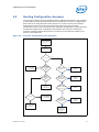
Configuration Mechanisms
The processor is the originator of configuration cycles. Internal to the processor
transactions received through both of the below configuration mechanisms are
translated to the same format.
2.2.1
Standard PCI Express* Configuration Mechanism
The following is the mechanism for translating processor I/O bus cycles to configuration
cycles.
The PCI specification defines a slot based "configuration space" that allows each device
to contain up to eight functions, with each function containing up to 256, 8-bit
configuration registers. The PCI specification defines two bus cycles to access the PCI
configuration space: Configuration Read and Configuration Write. Memory and I/O
spaces are supported directly by the processor. Configuration space is supported by a
mapping mechanism implemented within the processor.
The configuration access mechanism makes use of the CONFIG_ADDRESS Register (at
I/O address 0CF8h though 0CFBh) and CONFIG_DATA Register (at I/O address 0CFCh
though 0CFFh). To reference a configuration register, a DW I/O write cycle is used to
place a value into CONFIG_ADDRESS that specifies the PCI bus, the device on that bus,
the function within the device and a specific configuration register of the device
function being accessed. CONFIG_ADDRESS[31] must be 1 to enable a configuration
cycle. CONFIG_DATA then becomes a window into the four bytes of configuration space
specified by the contents of CONFIG_ADDRESS. Any read or write to CONFIG_DATA will
result in the processor translating the CONFIG_ADDRESS into the appropriate
configuration cycle.
The processor is responsible for translating and routing the processor’s I/O accesses to
the CONFIG_ADDRESS and CONFIG_DATA registers to internal processor configuration
registers, DMI, or PCI Express.
2.2.2
PCI Express* Configuration Mechanism
PCI Express extends the configuration space to 4096 bytes per device/function as
compared to 256 bytes allowed by PCI Specification Revision 2.3. PCI Express
configuration space is divided into a PCI 2.3 compatible region, which consists of the
first 256 bytes of a logical device’s configuration space and a PCI Express extended
region that consists of the remaining configuration space.
The PCI-compatible region can be accessed using either the Standard PCI Configuration
Mechanism or using the PCI Express Enhanced Configuration Mechanism described in
this section. The extended configuration registers may only be accessed using the PCI
Express Enhanced Configuration Mechanism. To maintain compatibility with PCI
configuration addressing mechanisms, system software must access the extended
configuration space using 32-bit operations (32-bit aligned) only. These 32-bit
operations include byte enables allowing only appropriate bytes within the DWord to be
accessed. Locked transactions to the PCI Express memory mapped configuration
address space are not supported. All changes made using either access mechanism are
equivalent.
The PCI Express Enhanced Configuration Mechanism utilizes a flat memory-mapped
address space to access device configuration registers. This address space is reported
by the system firmware to the operating system. The register, SAD_PCIEXBAR defines
Datasheet, Volume 2
21
Configuration Process and Registers
the base address for the block of addresses below 4 GB for the configuration space
associated with busses, devices and functions that are potentially a part of the PCI
Express root complex hierarchy. In the SAD_PCIEXBAR register there exists controls to
limit the size of this reserved memory mapped space. 256 MB is the amount of address
space required to reserve space for every bus, device, and function that could possibly
exist. Options for 128 MB and 64 MB exist in order to free up those addresses for other
uses. In these cases the number of busses and all of their associated devices and
functions are limited to 128 or 64 busses, respectively.
The PCI Express Configuration Transaction Header includes an additional four bits
(ExtendedRegisterAddress[3:0]) between the Function Number and Register Address
fields to provide indexing into the 4 KB of configuration space allocated to each
potential device. For PCI Compatible Configuration Requests, the Extended Register
Address field must be all zeros.
Figure 2-1.
Memory Map to PCI Express* Device Configuration Space
0xFFFFFFF
0xFFF
0x7FFF
0xFFFFF
Bus 255
Device 31
Function 7
PCI Express
Extended
Configuration
Space
0xFF
0xFFFF
0x1FFFFF
0x1FFF
Device 1
Bus 1
0x3F
0x7FFF
0xFFFFF
Bus 0
Function 1
0xFFF
Device 0
Function 0
PCI Compatible
Configuration
Space
PCI Compatible
Configuration
Space Header
0
Located by
PCI Express* Base Address
As with PCI devices, each device is selected based on decoded address information that
is provided as a part of the address portion of Configuration Request packets. A PCI
Express device will decode all address information fields (bus, device, function and
extended address numbers) to provide access to the correct register.
To access this space (step 1 is done only once by BIOS),
1. Write to CSR address 01050h to enable the PCI Express enhanced configuration
mechanism by writing 1 to Bit 0 of the SAD_PCIEXBAR register. Allocate either 256,
128, or 64 busses to PCI Express by writing “000”, “111”, or “110,” respectively, to
Bits 3:1. Pick a naturally aligned base address for mapping the configuration space
onto memory space using 1 MB per bus number and write that base address into
Bits 39:20.
2. Calculate the host address of the register you wish to set using (PCI Express base
+ (bus number * 1 MB) + (device number * 32 KB) + (function number * 4 KB) +
(1 B * offset within the function) = host address).
3. Use a memory write or memory read cycle to the calculated host address to write
or read that register.
22
Datasheet, Volume 2
Configuration Process and Registers
2.3
Routing Configuration Accesses
The processor supports two PCI related interfaces: DMI and PCI Express. The processor
is responsible for routing PCI and PCI Express configuration cycles to the appropriate
device that is an integrated part of the processor or to one of these two interfaces.
Configuration cycles to the PCH internal devices and Primary PCI (including
downstream devices) are routed to the PCH using DMI. Configuration cycles to both the
PCI Express Graphics PCI compatibility configuration space and the PCI Express
Graphics extended configuration space are routed to the PCI Express Graphics port
device or associated link.
Figure 2-2.
Processor Configuration Cycle Flowchart
DW I/O Write to
CONFIG_ADDRESS
with bit 31 = 1
I/O Read/Write to
CONFIG_DATA
Bus # = 0
Yes
No
Processor Generates
Type 1 Access
to PCI Express
Yes
Dev # 1
Enabled &
Bus # > SEC BUS
Bus# ≤ SUB BUS
in Bus 0
Dev 1
No
Device# = 0 &
Function#==00&
Device#
Function# = 0
Yes
Processor
Yes
Claims
Processor
Claims
Yes
Yes
Processor
Processor
Claims
Claims
Yes
Yes
Processor
Processor
Claims
Claims
Yes
Processor
Claims
No
No
Yes
Dev # 1
Enabled &
Bus# =
SECONDARY BUS
in Bus 0
Dev 1
No
Processor Generates
DMI Type 1
Configuration Cycle
Device # ==11&&
Device#
Dev # 1Enabled
Enabled &
Dev#1
& Function# = 0
Function# = 0
No
No
Device# =2 &
Device # = 2 &
Dev#2
Dev # 2Enabled
Enabled &
Function#
& Function# == 00
No
No
Device# = 0
No
MCH allows cycle to
go to DMI resulting
in Master Abort
Yes
Processor Generates
Type 0 Access
to PCI Express
Device # = 4 &
Dev # 4 Enabled
&
Function#
Device#
= =n 0&
Dev#n Enabled &
Function#
=0
No
Yes
Processor
Claims
No
MCH Generates
DMI Type 0
MCH
Generates
Configuration
Cycle
DMI Type 0
Configuration
Cycle
Datasheet, Volume 2
23
Configuration Process and Registers
2.3.1
Internal Device Configuration Accesses
The processor decodes the Bus Number (Bits 23:16) and the Device Number fields of
the CONFIG_ADDRESS register. If the Bus Number field of CONFIG_ADDRESS is 0, the
configuration cycle is targeting a PCI Bus 0 device.
If the targeted PCI Bus 0 device exists in the processor and is not disabled, the
configuration cycle is claimed by the appropriate device.
2.3.2
Bridge-Related Configuration Accesses
Configuration accesses on PCI Express or DMI are PCI Express Configuration
Transaction Layer Packets (TLPs).
• Bus Number [7:0] is Header Byte 8 [7:0]
• Device Number [4:0] is Header Byte 9 [7:3]
• Function Number [2:0] is Header Byte 9 [2:0]
And special fields for this type of TLP:
• Extended Register Number [3:0] is Header Byte 10 [3:0]
• Register Number [5:0] is Header Byte 11 [7:2]
See the PCI Express Specification for more information on both the PCI 2.3 compatible
and PCI Express Enhanced Configuration Mechanism and transaction rules.
2.3.2.1
PCI Express* Configuration Accesses
When the Bus Number of a Type 1 Standard PCI Configuration cycle or PCI Express
Enhanced Configuration access matches the Device 1 Secondary Bus Number a PCI
Express Type 0 Configuration TLP is generated on the PCI Express link targeting the
device directly on the opposite side of the link. This should be Device 0 on the bus
number assigned to the PCI Express link (likely Bus 1).
The device on other side of link must be Device 0. The processor will Master Abort any
Type 0 Configuration access to a non-zero Device number. If there is to be more than
one device on that side of the link there must be a bridge implemented in the
downstream device.
When the Bus Number of a Type 1 Standard PCI Configuration cycle or PCI Express
Enhanced Configuration access is within the claimed range (between the upper bound
of the bridge device’s Subordinate Bus Number register and the lower bound of the
bridge device’s Secondary Bus Number register) but doesn't match the Device 1
Secondary Bus Number, a PCI Express Type 1 Configuration TLP is generated on the
secondary side of the PCI Express link.
PCI Express Configuration Writes:
• The processor will translate writes to PCI Express extended configuration space to
configuration writes on the backbone internally.
• Posted writes to extended space are non-posted on the PCI Express or DMI (that is,
translated to configuration writes).
24
Datasheet, Volume 2
Configuration Process and Registers
2.3.2.2
DMI Configuration Accesses
Accesses to disabled processor internal devices, bus numbers not claimed by the HostPCI Express bridge, or PCI Bus 0 devices not part of the processor will subtractively
decode to the PCH and consequently be forwarded over the DMI using a PCI Express
configuration TLP. In Figure 2-2, the subtractive decode is completed by testing Devices
0 through n, where Devices 0 through n, if enabled and Function 0 is present in the
processor are claimed by the processor.
If the Bus Number is zero, the processor will generate a Type 0 Configuration Cycle TLP
on DMI. If the Bus Number is non-zero, and falls outside the range claimed by the
Host-PCI Express bridge, the processor will generate a Type 1 Configuration Cycle TLP
on DMI.
The PCH routes configurations accesses in a manner similar to the processor. The PCH
decodes the configuration TLP and generates a corresponding configuration access.
Accesses targeting a device on PCI Bus 0 may be claimed by an internal device. The
PCH compares the non-zero Bus Number with the Secondary Bus Number and
Subordinate Bus Number registers of its PCI-to-PCI bridges to determine if the
configuration access is meant for Primary PCI, or some other downstream PCI bus or
PCI Express link.
Configuration accesses that are forwarded to the PCH, but remain unclaimed by any
device or bridge will result in a master abort.
2.4
Processor Register Introduction
The processor contains two sets of software accessible registers – control registers and
internal configuration registers:
• Control registers are I/O mapped into the processor I/O space. These registers
control access to PCI and PCI Express configuration space (see Section 2.5, I/O
Mapped Registers).
• Internal configuration registers residing within the processor are partitioned into
the device register sets as indicated in Section 2.1.1 and Section 2.1.2.
The processor internal registers (I/O Mapped, Configuration and PCI Express Extended
Configuration registers) are accessible by the Host processor. The registers that reside
within the lower 256 bytes of each device can be accessed as byte, word (16 bit), or
DWord (32 bit) quantities, with the exception of CONFIG_ADDRESS, which can only be
accessed as a DWord. All multi-byte numeric fields use "little-endian" ordering (that is,
lower addresses contain the least significant parts of the field). Registers that reside in
bytes 256 through 4095 of each device may only be accessed using memory mapped
transactions in DWord (32 bit) quantities.
Some of the processor registers described in this section contain reserved bits; these
bits are labeled "Reserved”. Software must not modify reserved fields. On reads,
software must use appropriate masks to extract the defined bits and not rely on
reserved bits being any particular value. On writes, software must ensure that the
values of reserved bit positions are preserved. That is, the values of reserved bit
positions must first be read, merged with the new values for other bit positions and
then written back. Note that the software does not need to perform read, merge, and
write operation for the Configuration Address Register.
Datasheet, Volume 2
25
Configuration Process and Registers
In addition to reserved bits within a register, the processor contains address locations
in the configuration space of the Host Bridge entity that are marked either "Reserved"
or “Intel Reserved”. The processor responds to accesses to “Reserved” address
locations by completing the host cycle. When a “Reserved” register location is read, a
zero value is returned. (“Reserved” registers can be 8, 16, or 32 bits in size). Registers
that are marked as “Intel Reserved” must not be modified by system software. Writes
to “Intel Reserved” registers may cause system failure. Reads from “Intel Reserved”
registers may return a non-zero value.
Upon a Full Reset, the processor sets its entire set of internal configuration registers to
predetermined default states. Some register values at reset are determined by external
strapping options. The default state represents the minimum functionality feature set
required to successfully bring up the system. Hence, it does not represent the optimal
system configuration. It is the responsibility of the system initialization software
(usually BIOS) to properly determine the DRAM configurations, operating parameters,
and optional system features that are applicable, and to program the processor
registers accordingly.
2.5
I/O Mapped Registers
The processor contains two registers that reside in the processor I/O address space −
the Configuration Address (CONFIG_ADDRESS) Register and the Configuration Data
(CONFIG_DATA) Register. The Configuration Address Register enables/disables the
configuration space and determines what portion of configuration space is visible
through the Configuration Data window.
§
26
Datasheet, Volume 2
Processor Integrated I/O (IIO) Configuration Registers
3
Processor Integrated I/O (IIO)
Configuration Registers
3.1
Processor IIO Devices (PCI Bus 0)
The processor Integrated I/O (IIO) contains the following PCI devices within a single,
physical component. The configuration registers for the devices are mapped as devices
residing on PCI Bus 0.
• Device 0 — DMI Root Port. Logically this appears as a PCI device residing on PCI
Bus 0. Device 0 contains the standard PCI header registers, extended PCI
configuration registers and DMI device specific configuration registers.
• Device 3 — PCI Express Root Port 1. Logically this appears as a “virtual” PCI-toPCI bridge residing on PCI Bus 0 and is compliant with the PCI Express Local Bus
Specification Revision 1.0. Device 3 contains the standard PCI Express/PCI
configuration registers including PCI Express Memory Address Mapping registers. It
also contains the extended PCI Express configuration space that include PCI
Express error status/control registers and Isochronous and Virtual Channel
controls.
• Device 5 — PCI Express Root Port 3. Logically this appears as a “virtual” PCI-toPCI bridge residing on PCI Bus 0 and is compliant with PCI Express Local Bus
Specification Revision 1.0. Device 5 contains the standard PCI Express/PCI
configuration registers including PCI Express Memory Address Mapping registers. It
also contains the extended PCI Express configuration space that include PCI
Express error status/control registers and Isochronous and Virtual Channel
controls.
• Device 8 — Integrated I/O Core. This device contains the Standard PCI registers
for each of its functions. This device implements four functions; Function 0 contains
Address Mapping, Intel VT-d related registers and other system management
registers. Function 1 contains Semaphore and Scratchpad registers. Function 3
contains System Control/Status registers. Function 4 contains miscellaneous
control/status registers on power management and throttling.
• Device 16 — Intel QuickPath Interconnect. Device 16, Function 0 contains the
Intel QuickPath Interconnect configuration registers for Intel QuickPath
Interconnect Link. Device 16, Function 1 contains the routing and protocol.
Datasheet, Volume 2
27
Processor Integrated I/O (IIO) Configuration Registers
3.2
Device Mapping
All devices on the Integrated I/O Module reside on PCI Bus 0. Table 3-1 describes the
devices and functions that the integrated I/O (IIO) module implements or routes
specifically.
Table 3-1.
Functions Handled by the Processor Integrated I/O (IIO)
Register Group
DMI
3.2.1
DID
Device
Function
D131h = DT
0
0
Comment
PCI Express Root Port 1
D138h
3
0
x16 or x8 max link width
PCI Express Root Port 3
D13Ah
5
0
x8 max link width
Core
D155h
8
0
Address mapping, Intel VT-d,
System Management
Core
D156h
8
1
Semaphore and Scratchpad
registers
Core
D157h
8
2
System control/status registers
Core
D158h
8
3
Miscellaneous registers
Intel QuickPath Interconnect Port
D150h
16
0
Intel QuickPath Interconnect Link
Intel QuickPath Interconnect Port
D151h
16
1
Intel QuickPath Interconnect
Routing and Protocol
Unimplemented Devices/Functions and Registers
Configuration reads to unimplemented functions and devices will return all ones
emulating a master abort response. There is no asynchronous error reporting when a
configuration read master aborts. Configuration writes to unimplemented functions and
devices will return a normal response to Intel QuickPath Interconnect.
Software should not attempt or rely on reads or writes to unimplemented registers or
register bits. Software should also not attempt to modify Reserved bits or any unused
bits called out specifically. Unimplemented registers return all zeroes when read. Writes
to unimplemented registers are ignored. For configuration writes to these registers, the
completion is returned with a normal completion status (not master-aborted).
3.3
PCI Express*/DMI Configuration Registers
This section covers the configuration space registers for PCI Express and DMI. The first
part of this section describes the standard PCI header space from 0h to 3Fh. The
second part describes the device specific region from 40h to FFh. The third part
describes the PCI Express enhanced configuration region.
3.3.1
Other Register Notes
Note that in general, all register bits in the standard PCI header space (offset 0h–3Fh)
or in any OS-visible capability registers, that control the address decode like MSE,
IOSE, VGAEN or otherwise control transaction forwarding must be treated as dynamic
bits in the sense that these register bits could be changed by the OS when there is
traffic flowing through the IIO. Note that the address register themselves can be
28
Datasheet, Volume 2
Processor Integrated I/O (IIO) Configuration Registers
treated as static in the sense that they will not be changed without the decode control
bits being clear. Registers outside of this standard space will be noted as dynamic when
appropriate.
3.3.2
Configuration Register Map
Figure 3-1.
DMI Port (Device 0) and PCI Express* Root Ports Type 1 Configuration Space
Extended
Configuration Space
PCI Device
Dependent
FFFh
100h
P C I E C a p a b ilit y
M S I C a p a b ili t y
S V I D / S D I D C a p a b ilit y
40h
CAP_PTR
P2P'
00h
Datasheet, Volume 2
PCI Header
P M C a p a b ilit y
29
Processor Integrated I/O (IIO) Configuration Registers
Figure 3-1 illustrates how each PCI Express port’s configuration space appears to
software. Each PCI Express configuration space has three regions:
• Standard PCI Header — This region is the standard PCI-to-PCI bridge header
providing legacy OS compatibility and resource management.
• PCI Device Dependent Region — This region is also part of standard PCI
configuration space and contains the PCI capability structures and other port
specific registers. For the IIO, the supported capabilities are:
— SVID/SDID Capability
— Message Signalled Interrupts
— Power Management
— PCI Express Capability
• PCI Express Extended Configuration Space — This space is an enhancement
beyond standard PCI and only accessible with PCI Express aware software.
Note that all the capabilities listed above for a PCI Express port are required for a DMI
port. Through the rest of the chapter, as each register is elaborated, it will be noted
which registers are applicable to the PCI Express port and which are applicable to the
DMI port.
30
Datasheet, Volume 2
Processor Integrated I/O (IIO) Configuration Registers
Table 3-2.
Device 0 (DMI) Configuration Map
DID
VID
00h
80h
PCISTS
PCICMD
04h
84h
CCR
HDR
PLAT
RID
08h
88h
CLSR
0Ch
8Ch
10h
PEGCAP
14h
18h
DEVSTS
1Ch
20h
PEGNXTPTR
PEGCAPID
DEVCAP
94h
DEVCTRL
LNKCAP
LNKSTS
LNKCON
2Ch
A8h
ROOTCAP
ROOTCON
30h
ROOTSTS
B0h
34h
DEVCAP2
B4h
INTLIN
3Ch
38h
DEVCTRL2
LNKCON2
44h
DMIRCBAR
MSICAPID
MSIAR
MSIDR
Datasheet, Volume 2
B8h
BCh
40h
MSINXTPTR
ACh
CAPPTR
INTPIN
MSICTL
A0h
A4h
28h
SVID
98h
9Ch
24h
SID
90h
C0h
C4h
48h
C8h
4Ch
CCh
50h
D0h
54h
D4h
58h
D8h
5Ch
DCh
60h
PMCAP
E0h
64h
PMCSR
E4h
68h
E8h
MSIMSK
6Ch
ECh
MSIPENDING
70h
F0h
74h
F4h
78h
F8h
7Ch
FCh
31
Processor Integrated I/O (IIO) Configuration Registers
Table 3-3.
Device 0 (DMI) Extended Configuration Map
100h
104h
108h
10Ch
APICLIMIT
APICBASE
MISCCTRLSTS
180h
184h
188h
18Ch
110h
190h
114h
194h
118h
198h
11Ch
19Ch
120h
1A0h
124h
1A4h
128h
1A8h
12Ch
1ACh
130h
1B0h
134h
1B4h
138h
1B8h
13Ch
1BCh
140h
1C0h
144h
1C4h
148h
1C8h
14Ch
1CCh
150h
1D0h
154h
1D4h
158h
1D8h
15Ch
1DCh
160h
164h
32
PERFCTRLSTS
CTOCTRL
1E0h
1E4h
168h
1E8h
16Ch
1ECh
170h
1F0h
174h
1F4h
178h
1F8h
17Ch
1FCh
Datasheet, Volume 2
Processor Integrated I/O (IIO) Configuration Registers
Table 3-4.
Device 3,5 PCI Express* Registers Legacy Configuration Map
DID
VID
00h
80h
PCISTS
PCICMD
04h
84h
CCR
HDR
PLAT
RID
08h
88h
CLSR
0Ch
8Ch
10h
PEGCAP
14h
SUBBUS
SECBUS
PBUS
18h
IOLIM
IOBAS
1Ch
SECSTS
MLIM
MBAS
20h
PMLIMIT
PMBASE
24h
PEGNXTPTR
DEVSTS
DEVCTRL
98h
9Ch
LNKCON
SLTCAP
A0h
A4h
PMBASEU
28h
SLTSTS
SLTCON
A8h
2Ch
ROOTCAP
ROOTCON
ACh
30h
ROOTSTS
B0h
34h
DEVCAP2
B4h
38h
INTPIN
SNXTPTR
SID
INTLIN
3Ch
SCAPID
40h
SVID
MSINXTPTR
MSICAPID
MSIAR
MSIDR
Datasheet, Volume 2
94h
LNKCAP
LNKSTS
90h
PMLIMITU
BCTRL
MSICTRL
PEGCAPID
DEVCAP
DEVCTRL2
B8h
BCh
LNKSTS2
LNKCON2
C0h
C4h
44h
48h
C8h
4Ch
CCh
50h
D0h
54h
D4h
58h
D8h
5Ch
DCh
60h
PMCAP
E0h
64h
PMCSR
E4h
68h
E8h
MSIMSK
6Ch
ECh
MSIPENDING
70h
F0h
74h
F4h
78h
F8h
7Ch
FCh
33
Processor Integrated I/O (IIO) Configuration Registers
Table 3-5.
Device 3,5 PCI Express* Registers Extended Configuration Map
100h
104h
108h
10Ch
APICLIMIT
APICBASE
MISCCTRLSTS
180h
184h
188h
18Ch
110h
190h
114h
194h
118h
198h
11Ch
19Ch
120h
1A0h
124h
1A4h
128h
1A8h
12Ch
1ACh
130h
1B0h
134h
1B4h
138h
1B8h
13Ch
1BCh
140h
1C0h
144h
1C4h
148h
1C8h
14Ch
1CCh
150h
1D0h
154h
1D4h
158h
1D8h
15Ch
1DCh
160h
164h
34
PERFCTRLSTS
CTOCTRL
1E0h
1E4h
168h
1E8h
16Ch
1ECh
170h
1F0h
174h
1F4h
178h
1F8h
17Ch
1FCh
Datasheet, Volume 2
Processor Integrated I/O (IIO) Configuration Registers
3.3.3
Standard PCI Configuration Space (0h to 3Fh) —
Type 0/1 Common Configuration Space
This section covers registers in the 0h to 3Fh region that are common to devices 0, 3,5.
Comments at the top of the table indicate what devices/functions the description
applies to. Exceptions that apply to specific functions are noted in the individual bit
descriptions.
3.3.3.1
VID—Vendor Identification Register
Register:
Device:
Function:
Offset:
3.3.3.2
VID
0, 3,5
0
00h
Bit
Attr
Default
15:0
RO
8086h
Description
Vendor Identification Number (VID)
PCI Standard Identification for Intel.
DID—Device Identification Register
Register:
Device:
Function:
Offset:
Datasheet, Volume 2
DID
0, 3,5
0
02h
Bit
Attr
Default
15:0
RO
See Table 3-1
Description
Device Identification Number
Identifier assigned to the product.
35
Processor Integrated I/O (IIO) Configuration Registers
3.3.3.3
PCICMD—PCI Command Register
This register defines the PCI 3.0 compatible command register values applicable to PCI
Express space.
Register:
Device:
Function:
Offset:
36
PCICMD
0 (DMI)
0
04h
Bit
Attr
Default
Description
15:11
RV
00h
10
RW
0
Legacy Interrupt Mode Enable/Disable
9
RO
0
Fast Back-to-Back Enable
Not applicable. Hardwired to 0.
Reserved
8
RW
0
SERR Enable
For PCI Express/DMI ports, this field enables notifying the internal core
error logic of occurrence of an uncorrectable error (fatal or non-fatal) at
the port. The internal core error logic of Integrated I/O then decides if/how
to escalate the error further (pins/message, and so forth). This bit also
controls the propagation of PCI Express ERR_FATAL and ERR_NONFATAL
messages received from the port to the internal Integrated I/O core error
logic.
0 = Fatal and Non-fatal error generation and Fatal and Non-fatal error
message forwarding is disabled
1 = Fatal and Non-fatal error generation and Fatal and Non-fatal error
message forwarding is enabled
Refer to the latest PCI Express Base Specification for details of how this bit
is used in conjunction with other control bits in the Root Control register
for forwarding errors detected on the PCI Express interface to the system
core error logic.
7
RO
0
IDSEL Stepping/Wait Cycle Control
Not applicable to Processor Integrated I/O devices.
Hardwired to 0.
6
RW
0
Parity Error Response
For PCI Express/DMI ports, Processor Integrated I/O ignores this bit and
always does ECC/parity checking and signaling for data/address of
transactions both to and from IIO. This bit though affects the setting of Bit
8 in the PCISTS register.
5
RO
0
VGA Palette Snoop Enable
Not applicable to Processor Integrated I/O devices.
Hardwired to 0.
4
RO
0
Memory Write and Invalidate Enable
Not applicable to Processor Integrated I/O devices.
Hardwired to 0.
3
RO
0
Special Cycle Enable
Not applicable. Hardwired to 0.
2
RO
0
Bus Master Enable (BME)
For Device 0 (DMI), this bit is hardwired to 0 since the DMI is not a PCI-toPCI bridge. Hardware should ignore the functionality of this bit.
1
RO
0
Memory Space Enable (MSE)
For Device 0 (DMI), this bit is hardwired to 0 since the DMI is not a PCI-toPCI bridge.
0
RO
0
IO Space Enable (IOSE)
For Device 0 (DMI), this bit is hardwired to 0 since the DMI is not a PCI-toPCI bridge.
Datasheet, Volume 2
Processor Integrated I/O (IIO) Configuration Registers
(Sheet 1 of 2)
Register:
Device:
Function:
Offset:
Bit
Attr
Default
15:11
RV
00h
10
RW
0
Legacy Interrupt Mode Enable/Disable
9
RO
0
Fast Back-to-Back Enable
Not applicable to PCI Express and is hardwired to 0.
Description
Reserved (by PCI SIG)
8
RW
0
SERR Enable
For PCI Express/DMI ports, this field enables notifying the internal core
error logic of occurrence of an uncorrectable error (fatal or non-fatal) at
the port. The internal core error logic of IIO then decides if/how to
escalate the error further (pins/message, and so forth). This bit also
controls the propagation of PCI Express ERR_FATAL and ERR_NONFATAL
messages received from the port to the internal IIO core error logic.
0 = Fatal and Non-fatal error generation and Fatal and Non-fatal error
message forwarding is disabled.
1 = Fatal and Non-fatal error generation and Fatal and Non-fatal error
message forwarding is enabled.
Refer to the latest PCI Express Base Specification for details of how this
bit is used in conjunction with other control bits in the Root Control
register for forwarding errors detected on the PCI Express interface to
the system core error logic.
7
RO
0
IDSEL Stepping/Wait Cycle Control
Not applicable to Processor Integrated I/O devices.
Hardwired to 0.
6
RW
0
Parity Error Response
For PCI Express/DMI ports, Processor Integrated I/O ignores this bit and
always does ECC/parity checking and signaling for data/address of
transactions both to and from Integrated I/O.
5
RO
0
VGA Palette Snoop Enable
Not applicable to Processor Integrated I/O devices.
Hardwired to 0.
4
RO
0
Memory Write and Invalidate Enable
Not applicable to Processor Integrated I/O devices.
Hardwired to 0.
3
RO
0
Special Cycle Enable
Not applicable to PCI Express. Hardwired to 0.
0
Bus Master Enable (BME)
This bit controls the ability of the PCI Express port in
generating/forwarding memory (including MSI writes) or I/O
transactions (and not messages) or configuration transactions from the
secondary side to the primary side.
0 = The Bus Master is disabled. When this bit is 0, Integrated I/O root
ports will treat upstream PCI Express memory writes/reads, I/O
writes/reads, and configuration reads and writes as unsupported
requests (and follow the rules for handling unsupported requests).
This behavior is also true towards transactions that are already
pending in the Integrated I/O root port’s internal queues when the
BME bit is turned off.
1 = Enables the PCI Express ports to generate/forward memory,
configuration, or I/O read/write requests.
2
Datasheet, Volume 2
PCICMD
3,5 (PCIe*)
0
04h
RW
37
Processor Integrated I/O (IIO) Configuration Registers
(Sheet 2 of 2)
Register:
Device:
Function:
Offset:
Bit
1
0
3.3.3.4
PCICMD
3,5 (PCIe*)
0
04h
Attr
RW
RW
Default
Description
0
Memory Space Enable (MSE)
0 = Disables a PCI Express port’s memory range registers (including the
CSR range registers) to be decoded as valid target addresses for
transactions from primary side.
1 = Enables a PCI Express port’s memory range registers to be decoded
as valid target addresses for transactions from primary side.
Note that if a PCI Express port’s MSE bit is clear, that port can still be
target of any memory transaction if subtractive decoding is enabled on
that port.
0
IO Space Enable (IOSE)
Applies to PCI Express ports
0 = Disables the I/O address range, defined in the IOBASE and IOLIM
registers of the PCI-to-PCI bridge header, for target decode from
primary side.
1 = Enables the I/O address range, defined in the IOBASE and IOLIM
registers of the PCI-to-PCI bridge header, for target decode from
primary side.
Note that if a PCI Express port’s IOSE bit is clear, that port can still be
target of an I/O transaction if subtractive decoding is enabled on that
port.
PCISTS—PCI Status Register
The PCI Status register is a 16-bit status register that reports the occurrence of various
events associated with the primary side of the “virtual” PCI-to-PCI bridge embedded in
PCI Express ports and also primary side of the other devices on the internal Processor
Integrated I/O bus.
(Sheet 1 of 2)
Register:
Device:
Function:
Offset:
Bit
15
14
38
PCISTS
0 (DMI), 3,5 (PCIe)
0
06h
Attr
RW1C
RW1C
Default
Description
0
Detected Parity Error
This bit is set by a device when it receives a packet on the primary side
with an uncorrectable data error or an uncorrectable address/control
parity error. The setting of this bit is regardless of the Parity Error
Response bit (PERRE) in the PCICMD register.
0
Signaled System Error
0 = The device did not report a fatal/non-fatal error.
1 = The device reported fatal/non-fatal (and not correctable) errors it
detected on its PCI Express* interface through a message to the
PCH, with SERRE bit enabled. Software clears this bit by writing a 1
to it. For PCI Express ports, this bit is also set (when SERR enable
bit is set) when a FATAL/NON-FATAL message is forwarded from the
Express link to the PCH using a message.
Datasheet, Volume 2
Processor Integrated I/O (IIO) Configuration Registers
(Sheet 2 of 2)
Register:
Device:
Function:
Offset:
Bit
13
12
Datasheet, Volume 2
PCISTS
0 (DMI), 3,5 (PCIe)
0
06h
Attr
RW1C
RW1C
Default
Description
0
Received Master Abort Status
This bit is set when a device experiences a master abort condition on a
transaction it mastered on the primary interface (Integrated I/O internal
bus). Note that certain errors might be detected right at the PCI Express
interface and those transactions might not “propagate” to the primary
interface before the error is detected (for example, accesses to memory
above TOCM in cases where the PCI Express* interface logic itself might
have visibility into TOCM). Such errors do not cause this bit to be set,
and are reported using the PCI Express interface error bits (secondary
status register). Conditions that cause Bit 13 to be set, include:
• Device receives a completion on the primary interface (internal bus
of Integrated I/O) with Unsupported Request or master abort
completion Status. This includes UR status received on the primary
side of a PCI Express port on peer-to-peer completions also.
• Device accesses to holes in the main memory address region that
are detected by Intel QuickPath Interconnect Source Address
Decoder.
• Other master abort conditions detected on the Integrated I/O
internal bus.
0
Received Target Abort
This bit is set when a device experiences a completor abort condition on
a transaction it mastered on the primary interface (Integrated I/O
internal bus). Note that certain errors might be detected right at the PCI
Express interface and those transactions might not propagate to the
primary interface before the error is detected (for example, accesses to
memory above VTCSRBASE). Such errors do not cause this bit to be set,
and are reported using the PCI Express interface error bits (secondary
status register). Conditions that cause Bit 12 to be set, include:
• Device receives a completion on the primary interface (internal bus
of Integrated I/O) with completor abort completion Status. This
includes CA status received on the primary side of a PCI Express port
on peer-to-peer completions also.
• Accesses to Intel QuickPath Interconnect that return a failed
completion status.
• Other completer abort conditions detected on the Integrated
I/O internal bus.
Signaled Target Abort
This bit is set when a device signals a completer abort completion status
on the primary side (internal bus of Integrated I/O). This condition
includes a PCI Express port forwarding a completer abort status received
on a completion from the secondary side and passed to the primary side
on a peer-to-peer completion.
11
RW1C
0
10:9
RO
0h
DEVSEL# Timing
Not applicable to PCI Express. Hardwired to 0.
8
RW1C
0
Master Data Parity Error
This bit is set by a device if the Parity Error Response bit in the PCI
Command register is set and it receives a completion with poisoned data
from the primary side or if it forwards a packet with data (including MSI
writes) to the primary side with poison.
7
RO
0
Fast Back-to-Back
Not applicable to PCI Express. Hardwired to 0.
6
RO
0
Reserved
5
RO
0
66-MHz Capable
Not applicable to PCI Express. Hardwired to 0.
4
RO
1
Capabilities List
This bit indicates the presence of a capabilities list structure.
3
RO
0
Reserved
2:0
RO
0h
Reserved
39
Processor Integrated I/O (IIO) Configuration Registers
3.3.3.5
RID—Revision Identification Register
This register contains the revision number of the Integrated I/O.
Register:
Device:
Function:
Offset:
RID
0 (DMI), 3,5 (PCIe)
0
08h
Bit
Attr
7:4
RWO
Default
Description
Minor Revision
See
Steppings that required all masks be regenerated. Refer to the Intel®
Description Core™ i7-800 and i5-700 Desktop Processor Series Specification Update
for the value of the Revision ID Register.
3:0
RWO
Minor Revision Identification Number
Increment for each steppings that do not require masks to be
See
®
Description regenerated. Refer to the Intel Core™ i7-800 and i5-700 Desktop
Processor Series Specification Update for the value of the Revision
ID Register.
3.3.3.6
CCR—Class Code Register
This register contains the Class Code for the device.
Register:
Device:
Function:
Offset:
Bit
Attr
Default
Description
23:16
RO
06h
Base Class
For DMI port, this field is hardwired to 06h, indicating it is a “Bridge Device.”
15:8
RO
00h
Sub-Class
For Device 0 (DMI), this field defaults to 00h to indicate a “Host Bridge.”
7:0
RO
00h
Register-Level Programming Interface
This field is hardwired to 00h for DMI port.
Register:
Device:
Function:
Offset:
40
CCR
0
0
09h
CCR
3,5 (PCIe)
0
09h
Bit
Attr
Default
23:16
RO
06h
15:8
RO
See
Description
7:0
RO
00h
Description
Base Class
For PCI Express ports this field is hardwired to 06h, indicating it is a
“Bridge Device.”
Sub-Class
For PCI Express ports, this field defaults to 04h indicating “PCI-to-PCI
bridge”. This register changes to the sub class of 00h to indicate “Host
Bridge,” when bit 0 in “MISCCTRLSTS—Misc Control and Status Register”
is set.
Register-Level Programming Interface
This field is hardwired to 00h for PCI Express ports.
Datasheet, Volume 2
Processor Integrated I/O (IIO) Configuration Registers
3.3.3.7
CLSR—Cacheline Size Register
Register:
Device:
Function:
Offset:
3.3.3.8
CLSR
0 (DMI), 3,5 (PCIe)
0
0Ch
Bit
Attr
Default
7:0
RW
0h
Description
Cacheline Size
This register is set as RW for compatibility reasons only. Cacheline size
for Integrated I/O is always 64B. Hardware ignores this setting.
PLAT—Primary Latency Timer
Register: PLAT
Device: 0 (DMI), 3,5 (PCIe)
Function:
0
Offset:
0Dh
Bit
Attr
Default
7:0
RO
00h
Description
Prim_Lat_timer: Primary Latency Timer
Not applicable to PCI Express*. Hardwired to 00h.
The above register denotes the maximum time slice for a burst transaction in legacy
PCI 2.3 on the primary interface. It does not affect/influence PCI Express functionality.
3.3.3.9
HDR—Header Type Register
This register identifies the header layout of the configuration space.
Register:
Device:
Function:
Offset:
HDR
0 (DMI)
0
0Eh
Bit
Attr
Default
7
RO
0
6:0
RO
Description
Multi-Function Device
This bit defaults to 0 for PCI Express*/DMI ports.
00h
Configuration Layout
This field identifies the format of the configuration header layout.
For Device 0 (DMI), default is 00h indicating a conventional type 00h PCI
header.
Register: HDR
Device: 3,5 (PCIe)
Function:
0
Offset:
0Eh
Bit
Attr
Default
7
RO
0
6:0
Datasheet, Volume 2
RO
01h
Description
Multi-Function Device
This bit defaults to 0 for PCI Express*/DMI ports.
Configuration Layout
This field identifies the format of the configuration header layout. It is Type 1
for all PCI Express ports.
The default is 01h, indicating a PCI-to-PCI bridge.
41
Processor Integrated I/O (IIO) Configuration Registers
3.3.3.10
SVID—Subsystem Vendor ID
This register identifies the vendor of the subsystem. This 16-bit register combined with
the Device Identification Register uniquely identify any PCI device.
Register:
Device:
Function:
Offset:
3.3.3.11
SVID
0 (DMI)
0
2Ch
Bit
Attr
Default
15:0
RWO
8086h
Description
Subsystem Vendor Identification
This field is programmed during boot-up to indicate the vendor of the
system board. After it has been written once, it becomes read only.
SID—Subsystem Identity
This register identifies the particular subsystem.
Register:
Device:
Function:
Offset:
3.3.3.12
SID
0 (DMI)
0
2Eh
Bit
Attr
Default
15:0
RWO
00h
Description
Subsystem Identification Number
Assigned by the subsystem vendor to uniquely identify the subsystem.
CAPPTR—Capability Pointer
The CAPPTR provides the offset to the location of the first device capability in the
capability list.
Register:
Device:
Function:
Offset:
3.3.3.13
CAPPTR
0 (DMI), 3,5 (PCIe)
0
34h
Bit
Attr
Default
7:0
RWO
40h
Description
Capability Pointer
Points to the first capability structure for the device.
INTLIN—Interrupt Line Register
The Interrupt Line register is used to communicate interrupt line routing information
between initialization code and the device driver. The device itself does not use this
value. OS and device drivers use this to determine priority and vector information.
Register:
Device:
Function:
Offset:
42
INTLIN
0 (DMI), 3,5 (PCIe)
0
3Ch
Bit
Attr
Default
7:0
RW
00h
Description
Interrupt Line
This bit is RW for devices that can generate a legacy INTx message and
is needed only for compatibility purposes.
Datasheet, Volume 2
Processor Integrated I/O (IIO) Configuration Registers
3.3.3.14
INTPIN—Interrupt Pin Register
The INTP register identifies legacy interrupts for INTA, INTB, INTC, and INTD as
determined by BIOS/firmware.
Register:
Device:
Function:
Offset:
Bit
7:0
3.3.3.15
INTPIN
0 (DMI), 3,5 (PCIe)
0
3Dh
Attr
RWO
Default
Description
01h
INTP: Interrupt Pin
This field defines the type of interrupt to generate for the PCI Express
port.
001 = Generate INTA
010 = Generate INTB
011 = Generate INTC
100 = Generate INTD
Others = Reserved
BIOS/configuration Software has the ability to program this register once
during boot to set up the correct interrupt for the port.
PBUS—Primary Bus Number Register
This register identifies the bus number on the on the primary side of the PCI Express
port.
Register:
Device:
Function:
Offset:
Bit
7:0
3.3.3.16
PBUS
3,5 (PCIe)
0
18h
Attr
RW
Default
Description
00h
Primary Bus Number
Configuration software programs this field with the number of the bus on
the primary side of the bridge. BIOS must program this register to the
correct value since Integrated I/O hardware would depend on this
register for inbound decode purposes.
SECBUS—Secondary Bus Number
This register identifies the bus number assigned to the secondary side (PCI Express) of
the “virtual” PCI-to-PCI bridge. This number is programmed by the PCI configuration
software to allow mapping of configuration cycles to devices connected to PCI Express.
Register:
Device:
Function:
Offset:
Datasheet, Volume 2
SECBUS
3,5 (PCIe)
0
19h
Bit
Attr
Default
7:0
RW
00h
Description
Secondary Bus Number
This field is programmed by configuration software to assign a bus
number to the secondary bus of the virtual PCI-to-PCI bridge.
43
Processor Integrated I/O (IIO) Configuration Registers
3.3.3.17
SUBBUS—Subordinate Bus Number Register
This register identifies the subordinate bus (if any) that resides at the level below the
secondary bus of the PCI Express interface. This number is programmed by the PCI
configuration software to allow mapping of configuration cycles to devices subordinate
to the secondary PCI Express port.
Register: SUBBUS
Device: 3,5 (PCIe)
Function: 0
Offset:
1Ah
Bit
7:0
3.3.3.18
Attr
RW
Default
Description
00h
Subordinate Bus Number
This register is programmed by configuration software with the number
of the highest subordinate bus that is behind the PCI Express* port. Any
transaction that falls between the secondary and subordinate bus
number (both inclusive) of an Express port is forwarded to the express
port.
IOBAS—I/O Base Register
The I/O Base register defines an address range that is used by the PCI Express port to
determine when to forward I/O transactions from one interface to the other using the
following formula:
IO_BASE ≤ A[15:12] ≤ IO_LIMIT
The bottom of the defined I/O address range will be aligned to a 4-KB (1-KB if EN1K bit
is set. Refer to the IIOMISCCTRL register for the definition of EN1K bit) boundary while
the top of the region specified by IO_LIMIT will be one less than a 4-KB (1-KB if EN1K
bit is set) multiple. Setting the I/O limit less than I/O base disables the I/O range
altogether.
Register: IOBAS
Device: 3,5 (PCIe)
Function: 0
Offset:
1Ch
Note:
44
Bit
Attr
Default
Description
7:4
RW
0h
I/O Base Address
Corresponds to A[15:12] of the I/O addresses at the PCI Express* port.
3:2
RWL
0h
When EN1K is set (Refer to IIOMISCCTRL register for definition of EN1K
bit), these bits become RW and allow for 1-K granularity of I/O
addressing; otherwise, these are RO.
1:0
RO
0h
I/O Address Capability
Integrated I/O supports only 16-bit addressing
In general, the I/O base register will not be programmed by software without clearing
the IOSE bit first.
Datasheet, Volume 2
Processor Integrated I/O (IIO) Configuration Registers
3.3.3.19
IOLIM—I/O Limit Register
The I/O Base register defines an address range that is used by the PCI Express port to
determine when to forward I/O transactions from one interface to the other using the
following formula:
IO_BASE ≤ A[15:12] ≤ IO_LIMIT
The bottom of the defined I/O address range will be aligned to a 4-KB (1-KB if EN1K bit
is set. Refer to IIOMISCCTRL register for definition of EN1K bit) boundary while the top
of the region specified by IO_LIMIT will be one less than a 4-KB (1-KB if EN1K bit is
set) multiple. Setting the I/O limit less than I/O base disables the I/O range altogether.
Register:
Device:
Function:
Offset:
Note:
IOLIM
3,5 (PCIe)
0
1Dh
Bit
Attr
Default
Description
7:4
RW
0h
I/O Address Limit
Corresponds to A[15:12] of the I/O addresses at the PCI Express* port.
3:2
RWL
0h
When EN1K is set, these bits become RW and allow for 1-K granularity of
I/O addressing, otherwise these bits are RO.
1:0
RO
0h
I/O Address Limit Capability
IIO only supports 16-bit addressing.
In general, the I/O limit register will not be programmed by software without clearing
the IOSE bit first.
Datasheet, Volume 2
45
Processor Integrated I/O (IIO) Configuration Registers
3.3.3.20
SECSTS—Secondary Status Register
Secondary Status register is a 16-bit status register that reports the occurrence of
various events associated with secondary side (that is, PCI Express/DMI side) of the
“virtual” PCI-to-PCI bridge.
Register:
Device:
Function:
Offset:
Bit
46
SECSTS
3,5 (PCIe)
0
1Eh
Attr
Default
Description
15
RW1C
0
Detected Parity Error
This bit is set by the Integrated I/O whenever it receives a poisoned TLP
in the PCI Express* port. This bit is set regardless of the state the Parity
Error Response Enable bit in the Bridge Control register.
14
RW1C
0
Received System Error
This bit is set by the Integrated I/O when it receives a ERR_FATAL or
ERR_NONFATAL message.
13
RW1C
0
Received Master Abort Status
This bit is set when the PCI Express port receives a Completion with
“Unsupported Request Completion” Status or when IIO master aborts a
Type 0 configuration packet that has a non-zero device number.
12
RW1C
0
Received Target Abort Status
This bit is set when the PCI Express port receives a Completion with
“Completer Abort” Status.
Signaled Target Abort
This bit is set when the PCI Express port sends a completion packet with
a “Completer Abort” Status (including peer-to-peer completions that are
forwarded from one port to another).
11
RW1C
0
10:9
RO
00
DEVSEL# Timing
Not applicable to PCI Express. Hardwired to 0.
8
RW1C
0
Master Data Parity Error
This bit is set by the PCI Express port on the secondary side (PCI Express
link) if the Parity Error Response Enable bit (PERRE) is set in Bridge
Control register and either of the following two conditions occurs:
• The PCI Express port receives a Completion from PCI Express
marked poisoned.
• The PCI Express port poisons a packet with data.
If the Parity Error Response Enable bit in Bridge Control Register is
cleared, this bit is never set.
7
RO
0
Fast Back-to-Back Transactions Capable
Not applicable to PCI Express. Hardwired to 0.
6
RO
0
Reserved
5
RO
0
66-MHz Capability
Not applicable to PCI Express. Hardwired to 0.
4:0
RO
0h
Reserved
Datasheet, Volume 2
Processor Integrated I/O (IIO) Configuration Registers
3.3.3.21
MBAS—Memory Base
The Memory Base and Memory Limit registers define a memory-mapped I/O nonprefetchable address range (32-bit addresses) and the Integrated I/O directs accesses
in this range to the PCI Express port based on the following formula:
MEMORY_BASE ≤ A[31:20] ≤ MEMORY_LIMIT
The upper 12 bits of both the Memory Base and Memory Limit registers are read/write
and corresponds to the upper 12 address bits, A[31:20] of 32-bit addresses. Thus, the
bottom of the defined memory address range will be aligned to a 1-MB boundary and
the top of the defined memory address range will be one less than a 1-MB boundary.
Register:
Device:
Function:
Offset:
MBAS
3,5 (PCIe)
0
20h
Bit
Attr
Default
Description
15:4
RW
0h
Memory Base Address
This field corresponds to A[31:20] of the memory address on the PCI Express*
port.
3:0
RO
0h
Reserved
Setting the memory limit less than memory base disables the 32-bit memory range
altogether.
Note:
In general, the memory base and limit registers will not be programmed by software
without clearing the MSE bit first.
3.3.3.22
MLIM—Memory Limit
Register:
Device:
Function:
Offset:
Datasheet, Volume 2
MLIM
3,5 (PCIe)
0
22h
Bit
Attr
Default
Description
15:4
RW
0h
Memory Limit Address
This field corresponds to A[31:20] of the memory address that corresponds to
the upper limit of the range of memory accesses that will be passed by the PCI
Express* bridge
3:0
RO
0h
Reserved (by PCI-SIG)
47
Processor Integrated I/O (IIO) Configuration Registers
3.3.3.23
PMBASE—Prefetchable Memory Base Register
The Prefetchable Memory Base and Memory Limit registers define a memory mapped
I/O prefetchable address range (64-bit addresses) which is used by the PCI Express
bridge to determine when to forward memory transactions based on the following
formula:
PREFETCH_MEMORY_BASE_UPPER::PREFETCH_MEMORY_BASE ≤ A[63:20] ≤
PREFETCH_MEMORY_LIMIT_UPPER::PREFETCH_MEMORY_LIMIT
The upper 12 bits of both the Prefetchable Memory Base and Memory Limit registers
are read/write and correspond to the upper 12 address bits, A[31:20] of the 32-bit
addresses. The bottom of the defined memory address range will be aligned to a 1-MB
boundary and the top of the defined memory address range will be one less than a
1-MB boundary.
Register:
Device:
Function:
Offset:
PMBASE
3,5 (PCIe)
0
24h
Bit
Attr
Default
Description
15:4
RW
000h
Prefetchable Memory Base Address
This field corresponds to A[31:20] of the prefetchable memory address on the
PCI Express* port.
3:0
RO
1h
Prefetchable Memory Base Address Capability
Integrated I/O sets this bit to 01h to indicate 64-bit capability.
The bottom 4 bits of both the Prefetchable Memory Base and Prefetchable Memory
Limit registers are read-only, contain the same value, and encode whether or not the
bridge supports 64-bit addresses. If these four bits have the value 0h, then the bridge
supports only 32-bit addresses. If these four bits have the value 01h, then the bridge
supports 64-bit addresses and the Prefetchable Base Upper-32 bits and Prefetchable
Limit Upper 32-bits registers hold the rest of the 64-bit prefetchable base and limit
addresses respectively.
Setting the prefetchable memory limit less than prefetchable memory base disables the
64-bit prefetchable memory range altogether.
Note:
In general, the memory base and limit registers won’t be programmed by software
without clearing the MSE bit first.
3.3.3.24
PMLIMIT—Prefetchable Memory Limit
Register:
Device:
Function:
Offset:
48
PMLIMIT
3,5 (PCIe)
0
26h
Bit
Attr
Default
Description
15:4
RW
000h
Prefetchable Memory Limit Address
This field corresponds to A[31:20] of the memory address on the PCI Express
bridge.
3:0
RO
1h
Prefetchable Memory Limit Address Capability
Integrated I/O sets this field to 01h to indicate 64-bit capability.
Datasheet, Volume 2
Processor Integrated I/O (IIO) Configuration Registers
3.3.3.25
PMBASEU—Prefetchable Memory Base (Upper 32 bits)
The Prefetchable Base Upper 32-bits and Prefetchable Limit Upper 32-bits registers are
extensions to the Prefetchable Memory Base and Prefetchable Memory Limit registers
to support a 64-bit prefetchable memory address range.
Register:
Device:
Function:
Offset:
Bit
31:0
3.3.3.26
PMBASEU
3,5 (PCIe)
0
28h
Attr
RW
Default
Description
00000000h
Prefetchable Upper 32-bit Memory Base Address
This field corresponds to A[63:32] of the memory address that maps to the
upper base of the prefetchable range of memory accesses that will be passed
by the PCI Express bridge. The OS should program these bits based on the
available physical limits of the system.
PMLIMITU—Prefetchable Memory Limit (Upper 32 bits)
Register:
Device:
Function:
Offset:
Bit
31:0
Datasheet, Volume 2
PMLIMITU
3,5 (PCIe)
0
2Ch
Attr
RW
Default
00000000h
Description
Prefetchable Upper 32-bit Memory Limit Address
This field corresponds to A[63:32] of the memory address that maps to the
upper limit of the prefetchable range of memory accesses that will be passed
by the PCI Express bridge. OS should program these bits based on the
available physical limits of the system.
49
Processor Integrated I/O (IIO) Configuration Registers
3.3.3.27
BCTRL—Bridge Control Register
The Bridge Control register provides additional control for the secondary interface (that
is, PCI Express) as well as some bits that affect the overall behavior of the “virtual”
PCI-to-PCI bridge embedded within the Integrated I/O, for example, VGA-compatible
address range mapping.
(Sheet 1 of 2)
Register:
Device:
Function:
Offset:
50
BCTRL
3,5 (PCIe)
0
3Eh
Bit
Attr
Default
Description
15:12
RO
0h
11
RO
0
Discard Timer SERR Status
Not applicable to PCI Express*. This bit is hardwired to 0.
10
RO
0
Discard Timer Status
Not applicable to PCI Express. This bit is hardwired to 0.
9
RO
0
Secondary Discard Timer
Not applicable to PCI Express. This bit is hardwired to 0.
8
RO
0
Primary Discard Timer
Not applicable to PCI Express. This bit is hardwired to 0.
7
RO
0
Fast Back-to-Back Enable
Not applicable to PCI Express. This bit is hardwired to 0.
Reserved
6
RW
0
Secondary Bus Reset
0 = No reset happens on the PCI Express port.
1 = Setting this bit triggers a hot reset on the link for the corresponding PCI
Express port and the PCI Express hierarchy domain subordinate to the
port. This sends the LTSSM into the Training (or Link) Control Reset state,
which necessarily implies a reset to the downstream device and all
subordinate devices. The transaction layer corresponding to port will be
emptied by Integrated I/O when this bit is set. This means that in the
outbound direction, all posted transactions are dropped and non-posted
transactions are sent a UR response. In the inbound direction,
completions for inbound NP requests are dropped when they arrive.
Inbound posted writes are required to be flushed as well either by
dropping the packets are by retiring them normally.
Note also that a secondary bus reset will not reset the virtual PCI-to-PCI
bridge configuration registers of the targeted PCI Express port.
5
RO
0
Master Abort Mode
Not applicable to PCI Express. This bit is hardwired to 0.
4
RW
0
VGA 16-bit Decode
This bit enables the virtual PCI-to-PCI bridge to provide 16-bit decoding of
VGA I/O address precluding the decoding of alias addresses every 1 KB.
0 = Execute 10-bit address decodes on VGA I/O accesses.
1 = Execute 16-bit address decodes on VGA I/O accesses.
This bit only has meaning if bit 3 of this register is also set to 1, enabling VGA
I/O decoding and forwarding by the bridge.
Refer to the PCI-to-PCI Bridge Specification for further details of this bit
behavior.
3
RW
0
VGA Enable
This bit controls the routing of processor initiated transactions targeting VGA
compatible I/O and memory address ranges. This bit must only be set for one
PCI Express port.
Datasheet, Volume 2
Processor Integrated I/O (IIO) Configuration Registers
(Sheet 2 of 2)
Register:
Device:
Function:
Offset:
Bit
2
BCTRL
3,5 (PCIe)
0
3Eh
Attr
RW
Default
Description
0
ISA Enable
This bit modifies the response by the Integrated I/O to an I/O access issued by
the processor that target ISA I/O addresses. This applies only to I/O
addresses that are enabled by the IOBASE and IOLIM registers.
0 = All addresses defined by the IOBASE and IOLIM for processor I/O
transactions will be mapped to PCI Express.
1 = The Integrated I/O will not forward to PCI Express any I/O transactions
addressing the last 768 bytes in each 1-KB block even if the addresses
are within the range defined by the IOBASE and IOLIM registers.
1
RW
0
SERR Enable
This bit controls forwarding of ERR_COR, ERR_NONFATAL and ERR_FATAL
messages from the PCI Express* port to the primary side.
0 = Disables forwarding of ERR_COR, ERR_NONFATAL and ERR_FATAL.
1 = Enables forwarding of ERR_COR, ERR_NONFATAL and ERR_FATAL
messages.
0
RW
0
Parity Error Response Enable
The Integrated I/O ignores this bit. This bit though affects the setting of Bit 8
in the SECSTS register.
3.3.4
Device-Specific PCI Configuration Space — 40h to FFh
3.3.4.1
SCAPID—Subsystem Capability Identity
Register:
Device:
Function:
Offset:
3.3.4.2
SCAPID
3,5 (PCIe)
0
40h
Bit
Attr
Default
7:0
RO
0Dh
Description
Capability ID
Assigned by PCI-SIG for subsystem capability ID.
SNXTPTR—Subsystem ID Next Pointer
Register:S
Device:
Function:
Offset:
Datasheet, Volume 2
NXTPTR
3,5 (PCIe)
0
41h
Bit
Attr
Default
7:0
RWO
60h
Description
Next Ptr
This field is set to 80h for the next capability list (MSI capability structure) in
the chain.
51
Processor Integrated I/O (IIO) Configuration Registers
3.3.4.3
SVID—Subsystem Vendor ID
Register:
Device:
Function:
Offset:
3.3.4.4
Bit
Attr
Default
Description
15:0
RWO
8086h
Subsystem Vendor Identification
This field is programmed during boot-up to indicate the vendor of the system
board. After it has been written once, it becomes read only.
SID—Subsystem Identity
Register:
Device:
Function:
Offset:
3.3.4.5
SVID
3,5 (PCIe)
0
44h
SID
3,5 (PCIe)
0
46h
Bit
Attr
Default
15:0
RWO
00h
Description
Subsystem Identification Number
Assigned by the subsystem vendor to uniquely identify the subsystem.
DMIRCBAR—DMI Root Complex Register Block Base Address
Register
This is the base address for the root complex configuration space. This window of
addresses contains the Root complex Register set for the PCI Express hierarchy
associated with the processor. On Reset, the Root complex configuration space is
disabled and must be enabled by writing a 1 to DMIRCBAREN [Device 0, offset 50h,
bit 0]. All the bits in this register are locked in Intel TXT enabled mode.
Register:
Device:
Function:
Offset:
Bit
52
DMIRCBAR
0 (DMI)
0
50h
Attr
Default
Description
DMI Base Address (DMIRCBAR)
This field corresponds to Bits 32:12 of the base address DMI Root Complex
register space. BIOS will program this register resulting in a base address for a
4-KB block of contiguous memory address space. This register ensures that a
naturally aligned 4-KB space is allocated within the first 64 GB of addressable
memory space. System Software uses this base address to program the DMI
Root Complex register set. All the Bits in this register are locked in Intel
Trusted Execution Technology (Intel TXT) enabled mode.
31:12
RWO
00000h
11:1
RV
00h
0
RW
0
Reserved
DMIRCBAR Enable (DMIRCBAREN)
0 = DMIRCBAR is disabled and does not claim any memory.
1 = DMIRCBAR memory mapped accesses are claimed and decoded.
Datasheet, Volume 2
Processor Integrated I/O (IIO) Configuration Registers
3.3.4.6
MSICAPID—MSI Capability ID
Register:
Device:
Function:
Offset:
3.3.4.7
Bit
Attr
Default
7:0
RO
05h
Description
Capability Identifier
Assigned by PCI-SIG for MSI (root ports).
MSINXTPTR—MSI Next Pointer
Register:
Device:
Function:
Offset:
3.3.4.8
MSICAPID
0 (DMI), 3,5 (PCIe)
0
60h
MSINXTPTR
0 (DMI), 3,5 (PCIe)
0
61h
Bit
Attr
Default
7:0
RWO
90h
Description
Next Ptr
This field is set to 90h for the next capability list (PCI Express capability
structure) in the chain.
MSICTRL—MSI Control Register
Register:
Device:
Function:
Offset:
Bit
Attr
Default
15:9
RV
00h
Reserved
8
RO
1
Reserved
7
RO
0
64-bit Address Capable
This field is hardwired to 0h since the message addresses are only 32-bit
addresses (for example, FEEx_xxxxh).
Description
6:4
RW
000
Multiple Message Enable
Applicable only to PCI Express* ports. Software writes to this field to indicate
the number of allocated messages which is aligned to a power of two. When
MSI is enabled, the software will allocate at least one message to the device. A
value of 000 indicates 1 message. Any value greater than or equal to 001
indicates a message of 2.
3:1
RO
001
Multiple Message Capable
Integrated I/O Express ports support two messages for all their internal
events.
0
Datasheet, Volume 2
MSICTRL
0 (DMI), 3,5 (PCIe)
0
62h
RW
0
MSI Enable
The software sets this bit to select platform-specific interrupts or transmit MSI
messages.
0 = Disables MSI from being generated.
1 = MSI will be generated when appropriate conditions occur.
53
Processor Integrated I/O (IIO) Configuration Registers
3.3.4.9
MSIAR—MSI Address Register
The MSI Address Register (MSIAR) contains the system specific address information to
route MSI interrupts from the root ports and is broken into its constituent fields.
Register:
Device:
Function:
Offset:
54
MSIAR
0 (DMI), 3,5 (PCIe)
0
64h
Bit
Attr
Default
Description
31:20
RW
0h
Address MSB
This field specifies the 12 most significant bits of the 32-bit MSI address. This
field is R/W for compatibility reasons only.
19:12
RW
00h
Address Destination ID
This field is initialized by software for routing the interrupts to the appropriate
destination.
11:4
RW
00h
Address Extended Destination ID
This field is not used by IA32 processor and is used in IPF as an address
extension.
3
RW
0h
Address Redirection Hint
0 = directed
1 = redirectable
2
RW
0h
Address Destination Mode
0 = physical
1 = logical
1:0
RO
0h
Reserved
Datasheet, Volume 2
Processor Integrated I/O (IIO) Configuration Registers
3.3.4.10
MSIDR—MSI Data Register
The MSI Data Register contains all the data (interrupt vector) related to MSI interrupts
from the root ports.
Register:
Device:
Function:
Offset:
Bit
Attr
Default
31:16
RO
0000h
Reserved
15:14
RW
0h
Reserved
13:12
RW
0h
Reserved
0h
Delivery Mode
0000 = Fixed: Trigger Mode can be edge or level.
0001 = Lowest Priority: Trigger Mode can be edge or level.
0010 = Intel SMI/PMI/MCA - Not supported using MSI of root port
0011 = Reserved - Not supported using MSI of root port
0100 = NMI - Not supported using MSI of root port
0101 = INIT - Not supported using MSI of root port
0110 = Reserved
0111 = ExtINT - Not supported using MSI of root port
1000–1111 - Reserved
0h
Interrupt Vector
The interrupt vector (LSB) will be modified by the Integrated I/O to provide
context sensitive interrupt information for different events that require
attention from the processor, for example, Power Management and error
events.
11:8
7:0
3.3.4.11
MSIDR
0 (DMI), 3,5 (PCIe)
0
68h
RW
RW
Description
MSIMSK—MSI Mask Bit Register
The Mask Bit register enables software to disable message sending on a per-vector
basis.
Register:
Device:
Function:
Offset:
Datasheet, Volume 2
MSIMSK
0 (DMI), 3,5 (PCIe)
0
6Ch
Bit
Attr
Default
Description
31:2
RV
0h
Reserved
1:0
RW
0h
Mask Bit
For each Mask bit that is set, the PCI Express* port is prohibited from sending
the associated message.
55
Processor Integrated I/O (IIO) Configuration Registers
3.3.4.12
MSIPENDING—MSI Pending Bit Register
The Mask Pending register enables software to defer message sending on a per-vector
basis.
Register:
Device:
Function:
Offset:
3.3.4.13
MSIPENDING
0 (DMI), 3,5 (PCIe)
0
70h
Bit
Attr
Default
Description
31:2
RV
0h
Reserved
1:0
RO
0h
Pending Bit
For each Pending bit that is set, the PCI Express port has a pending associated
message.
PEGCAPID—PCI Express* Capability Identity Register
The PCI Express Capability List register enumerates the PCI Express Capability
structure in the PCI 3.0 configuration space.
Register:
Device:
Function:
Offset:
3.3.4.14
PEGCAPID
0 (DMI), 3,5 (PCIe)
0
90h
Bit
Attr
Default
7:0
RO
10h
Description
Capability ID
Provides the PCI Express capability ID assigned by PCI-SIG.
PEGNXTPTR—PCI Express* Next Pointer Register
The PCI Express Capability List register enumerates the PCI Express Capability
structure in the PCI 3.0 configuration space.
Register:
Device:
Function:
Offset:
56
PEGNXTPTR
0 (DMI), 3,5 (PCIe)
0
91h
Bit
Attr
Default
7:0
RWO
E0h
Description
Next Ptr
This field is set to the PCI PM capability.
Datasheet, Volume 2
Processor Integrated I/O (IIO) Configuration Registers
3.3.4.15
PEGCAP—PCI Express* Capabilities Register
The PCI Express Capabilities register identifies the PCI Express device type and
associated capabilities.
Register:
Device:
Function:
Offset:
PEGCAP
0 (DMI), 3,5 (PCIe)
0
92h
Bit
Attr
Default
15:14
RV
0h
13:9
Datasheet, Volume 2
RO
Description
Reserved
00h
Interrupt Message Number
Applies only to the root ports.
This field indicates the interrupt message number that is generated for
PM/HP events. When there are more than one MSI interrupt Number, this
register field is required to contain the offset between the base Message
Data and the MSI Message that is generated when the status bits in the slot
status register or root port status registers are set. IIO assigns the first
vector for PM/HP events and so this field is set to 0.
Slot Implemented
Applies only to the root ports.
0 = Indicates no slot is connected to this port.
1 = Indicates that the PCI Express link associated with the port is connected
to a slot.
This register bit is of type “write once” and is controlled by BIOS/special
initialization firmware.
8
RWO
0
7:4
RO
0100
3:0
RWO
Dev 3,5: 2h
Dev 3,5: 2h
Dev 0: 1h
Device/Port Type
This field identifies the type of device. It is set to 0100 for all the Express
ports.
Capability Version
This field identifies the version of the PCI Express capability structure. Set to
2h for PCI Express devices for compliance with the extended base registers.
Note: BIOS should set this to 1h for Device 0 (DMI).
57
Processor Integrated I/O (IIO) Configuration Registers
3.3.4.16
DEVCAP—PCI Express* Device Capabilities Register
The PCI Express Device Capabilities register identifies device specific information for
the device.
Register:
Device:
Function:
Offset:
Bit
Attr
Default
31:28
RV
0h
Reserved
27:26
RO
0h
Captured Slot Power Limit Scale
Does not apply to root ports or integrated devices.
25:18
RO
00h
Captured Slot Power Limit Value
Does not apply to root ports or integrated devices.
17:16
RV
0h
15
RO
1
Role Based Error Reporting
Integrated I/O is PCI Express Base Specification compliant and supports
this feature.
14
RO
0
Power Indicator Present on Device
Does not apply to root ports or integrated devices.
13
RO
0
Attention Indicator Present
Does not apply to root ports or integrated devices.
12
RO
0
Attention Button Present
Does not apply to root ports or integrated devices.
Description
Reserved
11:9
RO
000
Reserved
8:6
RO
000
Reserved
5
RO
1
4:3
RO
0h
RO
Dev 0: 000b
Dev 3,5: 001b
Dev 3,5: 001b
2:0
58
DEVCAP
0 (DMI), 3,5 (PCIe)
0
94h
Extended Tag Field Supported
Integrated I/O devices support 8-bit tag.
Reserved
Max Payload Size Supported
IIO supports 256B payloads on PCI Express ports and 128B on the DMI port
(Device 0).
Datasheet, Volume 2
Processor Integrated I/O (IIO) Configuration Registers
3.3.4.17
DEVCTRL—PCI Express* Device Control Register
The PCI Express Device Control register controls PCI Express specific capabilities
parameters associated with the device.
(Sheet 1 of 2)
Register:
Device:
Function:
Offset:
DEVCTRL
0 (DMI), 3,5 (PCIe)
0
98h
Bit
Attr
Default
15
RV
0h
14:12
RO
000
11
RO
0
Enable No Snoop
Not applicable to root ports since they never set the ‘No Snoop’ bit for
transactions they originate (not forwarded from peer) to PCI Express.
This bit has no impact on forwarding of NoSnoop attribute on peer requests.
10
RO
0
Reserved
9
RO
0
Reserved
8
RW
0h
7:5
4
3
2
Datasheet, Volume 2
RW
RO
RW
RW
000
Description
Reserved
Max_Read_Request_Size
Express/DMI ports in Integrated I/O do not generate requests greater than
128B and this field is ignored.
Extended Tag Field Enable
This bit enables the PCI Express/DMI ports to use an 8-bit Tag field as a
requester.
Max Payload Size
This field is set by configuration software for the maximum TLP payload size
for the PCI Express port. As a receiver, the IIO must handle TLPs as large as
the set value. As a requester (that is, for requests where Integrated IO’s own
RequesterID is used), it must not generate TLPs exceeding the set value.
Permissible values that can be programmed are indicated by the
Max_Payload_Size_Supported in the Device Capabilities register:
000 = 128B max payload size
001 = 256B max payload size (applies only to standard PCI Express ports
and DMI port aliases to 128B)
others = alias to 128B
0
Enable Relaxed Ordering
Not applicable to root ports since they never set relaxed ordering bit as a
requester (this does not include Tx forwarded from peer devices).
This bit has no impact on forwarding of relaxed ordering attribute on peer
requests.
0
Unsupported Request Reporting Enable
Applies only to the PCI Express/DMI ports. This bit controls the reporting of
unsupported requests that Integrated I/O itself detects on requests its
receives from a PCI Express/DMI port.
0 = Reporting of unsupported requests is disabled.
1 = Reporting of unsupported requests is enabled.
Refer to the latest PCI Express Base Specification for complete details of how
this bit is used in conjunction with other bits to UR errors.
0
Fatal Error Reporting Enable
Applies only to the PCI Express/DMI ports. Controls the reporting of fatal
errors that Integrated I/O detects on the PCI Express/DMI interface.
0 = Reporting of Fatal error detected by device is disabled.
1 = Reporting of Fatal error detected by device is enabled.
Refer to the latest PCI Express Base Specification for complete details of how
this bit is used in conjunction with other bits to report errors.
For the PCI Express/DMI ports, this bit is not used to control the reporting of
other internal component uncorrectable fatal errors (at the port unit) in any
way.
59
Processor Integrated I/O (IIO) Configuration Registers
(Sheet 2 of 2)
Register:
Device:
Function:
Offset:
Bit
1
0
60
DEVCTRL
0 (DMI), 3,5 (PCIe)
0
98h
Attr
RW
RW
Default
Description
0
Non Fatal Error Reporting Enable
Applies only to the PCI Express/DMI ports. Controls the reporting of non-fatal
errors that Integrated I/O detects on the PCI Express/DMI interface.
0 = Reporting of Non Fatal error detected by device is disabled.
1 = Reporting of Non Fatal error detected by device is enabled.
Refer to the latest PCI Express Base Specification for complete details of how
this bit is used in conjunction with other bits to report errors.
For the PCI Express/DMI ports, this bit is not used to control the reporting of
other internal component uncorrectable non-fatal errors (at the port unit) in
any way.
0
Correctable Error Reporting Enable
Applies only to the PCI Express/DMI ports. Controls the reporting of
correctable errors that Integrated I/O detects on the PCI Express/DMI
interface.
0 = Reporting of link Correctable error detected by the port is disabled.
1 = Reporting of link Correctable error detected by port is enabled.
Refer to the latest PCI Express Base Specification for complete details of how
this bit is used in conjunction with other bits to report errors.
For the PCI Express/DMI ports, this bit is not used to control the reporting of
other internal component correctable errors (at the port unit) in any way.
Datasheet, Volume 2
Processor Integrated I/O (IIO) Configuration Registers
3.3.4.18
DEVSTS—PCI Express* Device Status Register
The PCI Express Device Status register provides information about PCI Express device
specific parameters associated with the device.
Register:
Device:
Function:
Offset:
Bit
Attr
Default
15:6
RV
000h
5
RO
0h
4
RO
0
Reserved
0
Unsupported Request Detected
This bit applies only to the root/DMI ports.This bit indicates that the root
port detected an Unsupported Request. Errors are logged in this register
regardless of whether error reporting is enabled or not in the Device Control
Register.
0 = No unsupported request detected by the root port.
1 = Unsupported Request detected at the device/port. These unsupported
requests are NP requests inbound that the root port received and it
detected them as unsupported requests (for example, address decoding
failures that the root port detected on a packet, receiving inbound lock
reads, BME bit is clear, and so forth). Note that this bit is not set on
peer-to-peer completions with UR status that are forwarded by the root
port to the PCI Express link.
0
Fatal Error Detected
This bit indicates that a fatal (uncorrectable) error is detected by the device.
Errors are logged in this register regardless of whether error reporting is
enabled or not in the Device Control register.
0 = No Fatal errors detected.
1 = Fatal errors detected.
0
Non Fatal Error Detected
This bit gets set if a non-fatal uncorrectable error is detected by the device.
Errors are logged in this register regardless of whether error reporting is
enabled or not in the Device Control register.
0 = No Fatal errors detected.
1 = Fatal errors detected.
0
Correctable Error Detected
This bit gets set if a correctable error is detected by the device. Errors are
logged in this register regardless of whether error reporting is enabled or not
in the PCI Express Device Control register.
0 = No Fatal errors detected.
1 = Fatal errors detected.
3
2
1
0
Datasheet, Volume 2
DEVSTS
0 (DMI), 3,5 (PCIe)
0
9Ah
RW1C
RW1C
RW1C
RW1C
Description
Reserved
Transactions Pending
Does not apply to root/DMI ports, that is, bit hardwired to 0 for these
devices.
61
Processor Integrated I/O (IIO) Configuration Registers
3.3.4.19
LNKCAP—PCI Express* Link Capabilities Register
The Link Capabilities register identifies the PCI Express specific link capabilities.
(Sheet 1 of 2)
Register:
Device:
Function:
Offset:
Bit
Attr
Default
31:24
RWO
0
23:22
RV
0h
21
RO
1
Link Bandwidth Notification Capability
A value of 1b indicates support for the Link Bandwidth Notification status
and interrupt mechanisms.
20
RO
1
Data Link Layer Link Active Reporting Capable
IIO supports reporting status of the data link layer so software knows
when it can enumerate a device on the link or otherwise know the status
of the link.
19
RO
1
Surprise Down Error Reporting Capable
IIO supports reporting a surprise down error condition
18
RO
0
Clock Power Management
Does not apply to IIO.
17:15
14:12
11:10
62
LNKCAP
0 (DMI), 3,5 (PCIe)
0
9Ch
RWO
RWO
RWO
Description
Port Number
This field indicates the PCI Express port number for the link and is
initialized by software/BIOS.
Reserved
010
L1 Exit Latency
This field indicates the L1 exit latency for the given PCI Express port. It
indicates the length of time this port requires to complete transition from
L1 to L0.
000 = Less than 1 µs
001 = 1 is to less than 2 µs
010 = 2 is to less than 4 µs
011 = 4 is to less than 8 µs
100 = 8 is to less than 16 µs
101 = 16 is to less than 32 µs
110 = 32 is to 64 µs
111 = More than 64 µs
011
L0s Exit Latency
This field indicates the L0s exit latency (that is, L0s to L0) for the PCI
Express port.
000 = Less than 64 ns
001 = 64 ns to less than 128 ns
010 = 128 ns to less than 256 ns
011 = 256 ns to less than 512 ns
100 = 512 ns to less than 1 ns
101 = 1 is to less than 2 ns
110 = 2 is to 4 ns
111 = More than 4 ns
11
Active State Link PM Support
This field indicates the level of active state power management supported
on the given PCI Express port.
00 = Disabled
01 = L0s Entry Supported
10 = Reserved
11 = L0s and L1 Supported
Datasheet, Volume 2
Processor Integrated I/O (IIO) Configuration Registers
(Sheet 2 of 2)
Register:
Device:
Function:
Offset:
Bit
9:4
3:0
Datasheet, Volume 2
LNKCAP
0 (DMI), 3,5 (PCIe)
0
9Ch
Attr
Default
RWO
010000b
RWO
Dev 3,5: See
description
Dev 3,5: See
description
Dev 0: 0001b
Description
Maximum Link Width
This field indicates the maximum width of the given PCI Express Link
attached to the port.
001000 = x8
010000 = x16
000100 = Reserved
Others = Reserved
This is left as a RWO register for BIOS to update based on the platform
usage of the links.
Maximum Link Speeds Supported
Integrated I/O supports both 2.5 Gbps and 5 Gbps speeds
0001b = 2.5 GT/s support only
0010b = 2.5 GT/s and 5.0GT/s support
63
Processor Integrated I/O (IIO) Configuration Registers
3.3.4.20
LNKCON—PCI Express* Link Control Register (Device 0)
The PCI Express Link Control register controls the PCI Express Link specific
parameters.
Register:
Device:
Function:
Offset:
Bit
Attr
Default
15:12
RV
0
Reserved
11
RO
0
Link Autonomous Bandwidth Interrupt Enable
When set to 1, this bit enables the generation of an interrupt to indicate that
the Link Autonomous Bandwidth Status bit has been set.
10
RO
0
Link Bandwidth Management Interrupt Enable
When set to 1, this bit enables the generation of an interrupt to indicate that
the Link Bandwidth Management Status bit has been set.
9
RO
0
Hardware Autonomous Width Disable
When set, this bit disables hardware from changing the link width for
reasons other than attempting to correct unreliable link operation
8
RO
0
Enable Clock Power Management
N/A to Integrated I/O
7
RO
0
Extended Sync
When set to 1, this bit forces the transmission of additional ordered sets
when exiting L0s and when in recovery. See the latest PCI Express Base
Specification for details.
6
RO
0
Common Clock Configuration
Integrated I/O does nothing with this bit
0
Retrain Link
A write of 1 to this bit initiates link retraining in the given PCI Express port
by directing the LTSSM to the recovery state if the current state is [L0, L0s or
L1]. If the current state is anything other than L0, L0s, L1 then a write to
this bit does nothing. This bit always returns 0 when read.
If the Target Link Speed field has been set to a non-zero value different than
the current operating speed, then the LTSSM will attempt to negotiate to the
target link speed.
It is permitted to write 1b to this bit while simultaneously writing modified
values to other fields in this register. When this is done, all modified values
that affect link retraining must be applied in the subsequent retraining.
5
64
LNKCON
0 (DMI)
0
A0h
RO
Description
4
RO
0
Link Disable
This field controls whether the link associated with the PCI Express port is
enabled or disabled. When this bit is a 1, a previously configured link (a link
that has gone past the polling state) would return to the “disabled” state as
defined in the PCI Express Base Specification. When this bit is clear, an
LTSSM in the “disabled” state goes back to the detect state.
0 = Enables the link associated with the PCI Express port.
1 = Disables the link associated with the PCI Express port.
3
RO
0
Read Completion Boundary
Set to zero to indicate Integrated I/O could return read completions at 64B
boundaries.
2
RV
0
Reserved
1:0
RO
00
Active State Link PM Control
When 01b or 11b, L0s on transmitter is enabled, otherwise it is disabled.
Datasheet, Volume 2
Processor Integrated I/O (IIO) Configuration Registers
3.3.4.21
LNKCON—PCI Express* Link Control Register
The PCI Express Link Control register controls the PCI Express Link specific
parameters.
Register:
Device:
Function:
Offset:
LNKCON
3, 5 (PCIe)
0
A0h
Bit
Attr
Default
15:12
RV
0
Reserved
11
RW
0
Link Autonomous Bandwidth Interrupt Enable
When set to 1, this bit enables the generation of an interrupt to indicate that
the Link Autonomous Bandwidth Status bit has been set.
10
RW
0
Link Bandwidth Management Interrupt Enable
When set to 1, this bit enables the generation of an interrupt to indicate that
the Link Bandwidth Management Status bit has been set.
9
RW
0
Hardware Autonomous Width Disable
When set to 1, this bit disables hardware from changing the Link width for
reasons other than attempting to correct unreliable Link operation by
reducing Link width.
8
RO
0
Enable Clock Power Management
N/A to IIO
7
RW
0
Extended Sync
When set to 1, this bit forces the transmission of additional ordered sets
when exiting L0s and when in recovery. Refer to the latest PCI Express Base
Specification for details.
6
RW
0
Common Clock Configuration
Integrated I/O does nothing with this bit.
0
Retrain Link
A write of 1 to this bit initiates link retraining in the given PCI Express port
by directing the LTSSM to the recovery state if the current state is [L0, L0s,
or L1]. If the current state is anything other than L0, L0s, L1, then a write to
this bit does nothing. This bit always returns 0 when read.
If the Target Link Speed field has been set to a non-zero value different than
the current operating speed, the LTSSM will attempt to negotiate to the
target link speed.
It is permitted to write 1 to this bit while simultaneously writing modified
values to other fields in this register. When this is done, all modified values
that affect link retraining must be applied in the subsequent retraining.
5
Datasheet, Volume 2
WO
Description
4
RW
0
Link Disable
This field controls whether the link associated with the PCI Express port is
enabled or disabled. When this bit is a 1, a previously configured link (a link
that has gone past the polling state) would return to the “disabled” state as
defined in the latest PCI Express Base Specification When this bit is clear, an
LTSSM in the “disabled” state goes back to the detect state.
0 = Enables the link associated with the PCI Express port.
1 = Disables the link associated with the PCI Express port.
3
RO
0
Read Completion Boundary
Set to zero to indicate IIO could return read completions at 64B boundaries.
2
RV
0
Reserved
1:0
RW
00
Active State Link PM Control
When 01b or 11b, L0s on transmitter is enabled; otherwise, it is disabled.
65
Processor Integrated I/O (IIO) Configuration Registers
3.3.4.22
LNKSTS—PCI Express* Link Status Register
The PCI Express Link Status register provides information on the status of the PCI
Express Link such as negotiated width, training, and so forth.
(Sheet 1 of 2)
Register:
Device:
Function:
Offset:
Bit
15
14
13
12
66
LNKSTS
0 (DMI), 3, 5 (PCIe)
0
A2h
Attr
RW1C
RW1C
RO
RWO
Default
Description
0
Link Autonomous Bandwidth Status
This bit is set to 1 by hardware to indicate that hardware has
autonomously changed link speed or width, without the port transitioning
through DL_Down status, for reasons other than to attempt to correct
unreliable link operation.
Integrated I/O sets this bit when it receives eight consecutive TS1 or TS2
ordered sets with the Autonomous Change bit set.
Note that if the status bit is set by hardware in the same clock software
clears the status bit, the status bit should remain set and if MSI is
enabled, the hardware should trigger a new MSI.
0
Link Bandwidth Management Status
This bit is set to 1 by hardware to indicate that either of the following has
occurred without the port transitioning through DL_Down status:
a) A link retraining initiated by a write of 1b to the Retrain Link bit has
completed
b) Hardware has autonomously changed link speed or width to attempt
to correct unreliable link operation
Note that if the status bit is set by hardware in the same clock software
clears the status bit, the status bit should remain set and if MSI is
enabled, the hardware should trigger a new MSI.
0
Data Link Layer Link Active
This bit is set to 1 when the Data Link Control and Management State
Machine is in the DL_Active state, 0b otherwise.
On a downstream port or upstream port, when this bit is 0b, the
transaction layer associated with the link will abort all transactions that
would otherwise be routed to that link.
1
Slot Clock Configuration
This bit indicates whether Integrated I/O receives clock from the same
XTAL that also provides clock to the device on the other end of the link.
0 = Indicates that the device uses an independent clock irrespective of
the presence of a reference on the connector.
1 = Indicates the same physical reference clock to devices on both ends
of the link.
11
RO
0
Link Training
This field indicates the status of an ongoing link training session in the
PCI Express port
0 = LTSSM has exited the recovery/configuration state
1 = LTSSM is in recovery/configuration state or the Retrain Link was set
but training has not yet begun.
The Integrated I/O hardware clears this bit once LTSSM has exited the
recovery/configuration state. Refer to the latest PCI Express Base
Specification for details of which states within the LTSSM would set this
bit and which states would clear this bit.
10
RO
0
Reserved
Datasheet, Volume 2
Processor Integrated I/O (IIO) Configuration Registers
(Sheet 2 of 2)
Register:
Device:
Function:
Offset:
Bit
9:4
3:0
Datasheet, Volume 2
LNKSTS
0 (DMI), 3, 5 (PCIe)
0
A2h
Attr
RO
RO
Default
Description
0h
Negotiated Link Width
This field indicates the negotiated width of the given PCI Express link
after training is completed. Only x8 and x16 link width negotiations are
supported in Integrated I/O.
0x08 = x8 max link width
0x10 = x16 max link width
The value in this field is not defined and could show any value when the
link is not up. Software determines if the link is up or not by reading Bit
13 of this register.
1h
Current Link Speed
This field indicates the negotiated Link speed of the given PCI Express
Link.
0001b = 2.5 Gbps
0010b = 5 Gbps
Others = Reserved
The value in this field is not defined and could show any value, when the
link is not up. Software determines if the link is up or not by reading Bit
13 of this register.
67
Processor Integrated I/O (IIO) Configuration Registers
3.3.4.23
SLTCAP—PCI Express* Slot Capabilities Register
The Slot Capabilities register identifies the PCI Express specific slot capabilities. These
registers must be ignored by software on the DMI links.
Note:
Hot-plug for PCIe is not supported on Desktop, Platforms.
Register:
Device:
Function:
Offset:
Bit
Attr
Default
31:19
RWO
0h
Physical Slot Number
This field indicates the physical slot number of the slot connected to the PCI
Express* port and is initialized by BIOS.
18
RO
0h
Command Complete Not Capable
Integrated I/O is capable of command complete interrupt.
0h
Electromechanical Interlock Present
When set to 1, this bit indicates that an Electromechanical Interlock is
implemented on the chassis for this slot and that lock is controlled by Bit 11 in
Slot Control register.
BIOS Note: This capability is not set if the Electromechanical Interlock control
is connected to main slot power control.
0h
Slot Power Limit Scale
This field specifies the scale used for the Slot Power Limit Value and is
initialized by BIOS. IIO uses this field when it sends a Set_Slot_Power_Limit
message on PCI Express.
Range of Values:
00 = 1.0x
01 = 0.1x
10 = 0.01x
11 = 0.001x
17
16:15
68
SLTCAP
0 (DMI), 3, 5 (PCIe)
0
A4h
RWO
RWO
Description
Slot Power Limit Value
This field specifies the upper limit on power supplied by slot in conjunction
with the Slot Power Limit Scale value defined previously
Power limit (in Watts) = SPLS x SPLV.
This field is initialized by BIOS. IIO uses this field when it sends a
Set_Slot_Power_Limit message on PCI Express.
Design Note: Integrated I/O can choose to send the Set_Slot_Power_Limit
message on the link at first link up condition without regards to whether this
register and the Slot Power Limit Scale register are programmed yet by BIOS.
Integrated I/O must then be designed to discard a received
Set_Slot_Power_Limit message without an error.
14:7
RWO
00h
6:5
RV
0h
Reserved - Hot-Plug is not supported.
4
RWO
0h
Power Indicator Present
When set to 1, this bit indicates that a Power Indicator is implemented for this
slot and is electrically controlled by the chassis.
3
RWO
0h
Attention Indicator Present
When set to 1, this bit indicates that an Attention Indicator is implemented for
this slot and is electrically controlled by the chassis
2
RWO
0h
MRL Sensor Present
When set to 1, this bit indicates that an MRL Sensor is implemented on the
chassis for this slot.
1
RWO
0h
Power Controller Present
When set to 1, this bit indicates that a software controllable power controller is
implemented on the chassis for this slot.
0
RV
0h
Reserved - Hot-Plug is not supported.
Datasheet, Volume 2
Processor Integrated I/O (IIO) Configuration Registers
3.3.4.24
SLTCON—PCI Express* Slot Control Register
The Slot Control register identifies the PCI Express specific slot control parameters for
operations such as Power Management.
Register:
Device:
Function:
Offset:
SLTCON
0 (DMI), 3, 5 (PCIe)
0
A8h
Bit
Attr
Default
15:13
RV
0h
12
RWS
0
Data Link Layer State Changed Enable
When set to 1, this field enables software notification when Data Link Layer
Link Active field is changed
0
Electromechanical Interlock Control
If an electromechanical lock is implemented, a write of 1b to this field causes
the state of the interlock to toggle. Write of 0b has no effect. This bit always
returns a 0 when read. If electromechanical lock is not implemented, then
either a write of 1 or 0 to this register has no effect.
1
Power Controller Control
If a power controller is implemented, when written, this bit sets the power
state of the slot per the defined encodings. Reads of this field must reflect
the value from the latest write.
0 = Power On
1 = Power Off
11
10
9:8
Datasheet, Volume 2
RW
RWS
RW
Description
Reserved
3h
Power Indicator Control
If a Power Indicator is implemented, writes to this register set the Power
Indicator to the written state. Reads of this field must reflect the value from
the latest write.
00 = Reserved
01 = On
10 = Blink (Integrated I/O drives 1.5-Hz square wave for Chassis mounted
LEDs)
11 = Off
When this register is written, the event is signaled using the virtual pins of
the Integrated I/O over a dedicated SMBus port.
Integrated I/O does not generate the Power_Indicator_On/Off/Blink
messages on PCI Express when this field is written to by software.
Attention Indicator Control
If an Attention Indicator is implemented, writes to this register set the
Attention Indicator to the written state.
Reads of this field reflect the value from the latest write.
00 = Reserved
01 = On
10 = Blink (The Integrated I/O drives 1.5 Hz square wave)
11 = Off
When this register is written, the event is signaled using the virtual pins of
the Integrated I/O over a dedicated SMBus port.
Integrated I/O does not generated the Attention_Indicator_On/Off/Blink
messages on PCI Express* when this field is written to by software.
7:6
RW
3h
5:0
RV
00h
Reserved
69
Processor Integrated I/O (IIO) Configuration Registers
3.3.4.25
ROOTCON—PCI Express* Root Control Register
The PCI Express Root Control register specifies parameters specific to the root complex
port.
(Sheet 1 of 2)
Register:
Device:
Function:
Offset:
Bit
Attr
Default
15:5
RV
0h
Reserved
0h
CRS Software Visibility Enable
When set to 1, this bit enables the Root Port to return Configuration Request
Retry Status (CRS) Completion Status to software. If 0, retry status cannot be
returned to software. Root ports that do not implement this capability must
hardwire this bit to 0b.
0h
PME Interrupt Enable
This field controls the generation of MSI interrupts and Intx messages for PME
messages.
0 = Disables interrupt generation for PME messages.
1 = Enables interrupt generation upon receipt of a PME message as reflected
in the PME status bit of the Root Status Register.
0h
System Error on Fatal Error Enable
This field enables notifying the internal core error logic of occurrence of an
uncorrectable fatal error at the port or below its hierarchy. The internal core
error logic of Integrated I/O then decides if/how to escalate the error further
(pins/message, an so forth).
0 = No internal core error logic notification should be generated on a fatal
error reported by any of the devices in the hierarchy associated with and
including this port.
1 = Indicates that a internal core error logic notification should be generated
if a fatal error is reported by any of the devices in the hierarchy
associated with and including this port.
Note that generation of system notification on a PCI Express/DMI fatal error is
orthogonal to generation of an MSI interrupt for the same error. Both a system
error and MSI can be generated on a fatal error or software can choose one of
the two.
Refer to the latest PCI Express Base Specification for details of how this bit is
used in conjunction with other error control bits to generate core logic
notification of error events in a PCI Express/DMI port.
0h
System Error on Non-Fatal Error Enable
This field enables notifying the internal core error logic of occurrence of an
uncorrectable non-fatal error at the port or below its hierarchy. The internal
core error logic of Integrated I/O then decides if/how to escalate the error
further (pins/message and so forth).
0 = No internal core error logic notification should be generated on a nonfatal error reported by any of the devices in the hierarchy associated with
and including this port
1 = Indicates that a internal core error logic notification should be generated
if a non-fatal error is reported by any of the devices in the hierarchy
associated with and including this port.
Note that generation of system notification on a PCI Express/DMI non-fatal
error is orthogonal to generation of an MSI interrupt for the same error. Both a
system error and MSI can be generated on a non-fatal error or software can
choose one of the two.
Refer to the latest PCI Express Base Specification for details of how this bit is
used in conjunction with other error control bits to generate core logic
notification of error events in a PCI Express/DMI port.
4
3
2
1
70
ROOTCON
0 (DMI), 3, 5 (PCIe)
0
ACh
RW
RW
RW
RW
Description
Datasheet, Volume 2
Processor Integrated I/O (IIO) Configuration Registers
(Sheet 2 of 2)
Register:
Device:
Function:
Offset:
Bit
0
3.3.4.26
ROOTCON
0 (DMI), 3, 5 (PCIe)
0
ACh
Attr
RW
Default
Description
0h
System Error on Correctable Error Enable
This field controls notifying the internal core error logic of the occurrence of a
correctable error in the device or below its hierarchy. The internal core error
logic of Integrated I/O then decides if/how to escalate the error further
(pins/message, and so forth).
0 = No internal core error logic notification should be generated on a
correctable error reported by any of the devices in the hierarchy
associated with and including this port.
1 = Indicates that an internal core error logic notification should be generated
if a correctable error is reported by any of the devices in the hierarchy
associated with and including this port.
Note that generation of system notification on a PCI Express correctable error
is orthogonal to generation of an MSI interrupt for the same error. Both a
system error and MSI can be generated on a correctable error or software can
choose one of the two.
Refer to the latest PCI Express Base Specification for details of how this bit is
used in conjunction with other error control bits to generate core logic
notification of error events in a PCI Express/DMI port.
ROOTCAP—PCI Express* Root Capabilities Register
The PCI Express Root Status register specifies parameters specific to the root complex
port.
Register:
Device:
Function:
Offset:
Datasheet, Volume 2
ROOTCAP
0 (DMI), 3, 5 (PCIe)
0
AEh
Bit
Attr
Default
15:1
RV
0h
0
RO
1
Description
Reserved
CRS Software Visibility
When set to 1, this bit indicates that the Root Port is capable of returning
Configuration Request Retry Status (CRS) Completion Status to software.
Integrated I/O supports this capability.
71
Processor Integrated I/O (IIO) Configuration Registers
3.3.4.27
ROOTSTS—PCI Express* Root Status Register
The PCI Express Root Status register specifies parameters specific to the root complex
port.
Register:
Device:
Function:
Offset:
Bit
Attr
Default
31:18
RV
0h
Reserved
0h
PME Pending
This field indicates that another PME is pending when the PME Status bit is set.
When the PME Status bit is cleared by software; the pending PME is delivered
by hardware by setting the PME Status bit again and updating the Requestor
ID appropriately. The PME pending bit is cleared by hardware if no more PMEs
are pending.
17
72
ROOTSTS
0 (DMI), 3, 5 (PCIe)
0
B0h
RO
Description
16
RW1C
0h
PME Status
This field indicates a PM_PME message (either from the link or internally from
within that root port) was received at the port.
1 = PME was asserted by a requester as indicated by the PMEREQID field
This bit is cleared by software by writing a 1.
15:0
RO
0000h
PME Requester ID
This field indicates the PCI requester ID of the last PME requestor. If the root
port itself was the source of the (virtual) PME message, then a RequesterID of
IIOBUSNO:DevNo:0 is logged in this field.
Datasheet, Volume 2
Processor Integrated I/O (IIO) Configuration Registers
3.3.4.28
DEVCAP2—PCI Express* Device Capabilities Register 2
Register:
Device:
Function:
Offset:
Bit
Attr
Default
31:6
RO
0h
5
RO
1
Alternative RID Interpretation (ARI) Capable
This bit is set to 1b indicating Root Port supports this capability.
4
RO
1
Completion Time-out Disable Supported
IIO supports disabling completion time-out.
3:0
Datasheet, Volume 2
DEVCAP2
0 (DMI), 3, 5 (PCIe)
0
B4h
RO
1110b
Description
Reserved
Completion Time-out Values Supported
This field indicates device support for the optional Completion Time-out
programmability mechanism. This mechanism allows system software to
modify the Completion Time-out range. Bits are one-hot encoded and set
according to the table below to show time-out value ranges supported. A
device that supports the optional capability of Completion Time-out
Programmability must set at least two bits.
Four time values ranges are defined:
A: 50 µs to 10 ms
B: 10 ms to 250 ms
C: 250 ms to 4 s
D: 4 s to 64 s
Bits are set according to table below to show time-out value ranges supported.
0000b = Completions Time-out programming not supported -- values is fixed
by implementation in the range 50 µs to 50 ms.
0001b = Range A
0010b = Range B
0011b = Range A & B
0110b = Range B & C
0111b = Range A, B, & C
1110b = Range B, C, & D
1111b = Range A, B, C & D
All other values are reserved.
Integrated I/O supports time-out values up to 10 ms-64 s.
73
Processor Integrated I/O (IIO) Configuration Registers
3.3.4.29
DEVCTRL2—PCI Express* Device Control Register 2
Register:
Device:
Function:
Offset:
Bit
Attr
Default
15:6
RO
0h
5
RW
0
Alternative RID Interpretation (ARI) Enable
When set to 1b, ARI is enabled for the Root Port.
0
Completion Time-out Disable
1 = Disables the Completion Time-out mechanism for all NP tx that IIO issues
on the PCI Express/DMI link.
0 = Completion time-out is enabled.
Software can change this field while there is active traffic in the root port.
0000b
Completion Time-out Value on NP Tx that Integrated I/O Issues on
PCI Express/DMI – In Devices that support Completion Time-out
programmability, this field allows system software to modify the Completion
Time-out range. The following encodings and corresponding time-out ranges
are defined:
0000b = 10 ms to 50 ms
0001b = Reserved (Integrated I/O aliases to 0000b)
0010b = Reserved (Integrated I/O aliases to 0000b)
0101b = 16 ms to 55 ms
0110b = 65 ms to 210 ms
1001b = 260 ms to 900 ms
1010b = 1 s to 3.5 s
1101b = 4 s to 13 s
1110b = 17 s to 64 s
When the OS selects 17 s to 64 s range, the CTOCTRL register further controls
the time-out value within that range. For all other ranges selected by OS, the
time-out value within that range is fixed in Integrated I/O hardware.
Software can change this field while there is active traffic in the root port.
4
3:0
74
DEVCTRL2
0 (DMI), 3, 5 (PCIe)
0
B8h
RW
RW
Description
Reserved
Datasheet, Volume 2
Processor Integrated I/O (IIO) Configuration Registers
3.3.4.30
LNKCON2—PCI Express* Link Control Register 2
Register:
Device:
Function:
Offset:
LNKCON2
0 (DMI), 3, 5 (PCIe)
0
C0h
Bit
Attr
Default
15:13
RO
0
Reserved
12
RWS
0
Compliance De-Emphasis
This bit sets the de-emphasis level in Polling Compliance state if the entry
occurred due to the Enter Compliance bit being 1b.
1b = 3.5 dB
0b = 6 dB
11
RWS
0
Compliance SOS
When set to 1, the LTSSM is required to send SKP Ordered Sets periodically in
between the (modified) compliance patterns.
10
RWS
0
Enter Modified Compliance
When this bit is set to 1, the device transmits Modified Compliance Pattern if
the LTSSM enters Polling.Compliance substate.
9:7
RWS
0
Transmit Margin
This field controls the value of the non de-emphasized voltage level at the
Transmitter pins.
0
Selectable De-Emphasis
When the Link is operating at 5.0 GT/s speed, this bit selects the level of deemphasis for an Upstream component.
Encodings:
1b = 3.5 dB
0b = 6 dB
When the Link is operating at 2.5 GT/s speed, the setting of this bit has no
effect.
0
Hardware Autonomous Speed Disable
When set to 1, this bit disables hardware from changing the Link speed for
device specific reasons other than attempting to correct unreliable Link
operation by reducing Link speed.
0
Enter Compliance
Software is permitted to force a link to enter Compliance mode at the speed
indicated in the Target Link Speed field by setting this bit to 1b in both
components on a link and then initiating a hot reset on the link.
6
5
4
3:0
Datasheet, Volume 2
Description
RWO
RW
RWS
RWS
Dev0: 0001b
Dev 3, 5:
0010b
Dev 3,5:
0010b
Target Link Speed
This field sets an upper limit on link operational speed by restricting the values
advertised by the upstream component in its training sequences.
Defined encodings are:
0001b = 2.5-Gb/s Target Link Speed
0010b = 5-Gb/s Target Link Speed
All other encodings are reserved.
If a value is written to this field that does not correspond to a speed included
in the Supported Link Speeds field, Integrated I/O will default to Gen1 speed.
This field is also used to set the target compliance mode speed when software
is using the Enter Compliance bit to force a link into compliance mode.
75
Processor Integrated I/O (IIO) Configuration Registers
3.3.4.31
LNKSTS2—PCI Express* Link Control Register 2
Register:
Device:
Function:
Offset:
Bit
Attr
Default
15:1
RO
0
Reserved
0
Compliance De-Emphasis
Current de-emphasis level - when operating at Gen2 speed. This is unused in
Gen1 speed.
1b = 3.5 dB
0b = 6 dB
0
3.3.4.32
LNKSTS2
0 (DMI), 3, 5 (PCIe)
0
C2h
RO
Description
PMCAP—Power Management Capabilities Register
The PM Capabilities Register defines the capability ID, next pointer and other power
management related support. The following PM registers/capabilities are added for
software compliance. For Device 0 DMI, this register should be RO and zero.
Register:
Device:
Function:
Offset:
76
PMCAP
0 (DMI), 3, 5 (PCIe)
0
E0h
Bit
Attr
Default
Description
31:27
RO
11001
26
RO
0
D2 Support
Integrated I/O does not support power management state D2.
25
RO
0
D1 Support
Integrated I/O does not support power management state D1.
24:22
RO
0h
21
RO
0
Device Specific Initialization
20
RV
0
Reserved
19
RO
0
PME Clock
This field is hardwired to 0h as it does not apply to PCI Express.
18:16
RO
011
Version
This field is set to 3h (PM 1.2 compliant) as version number for all PCI Express
ports.
15:8
RO
00h
Next Capability Pointer
This is the last capability in the chain and hence set to 0.
7:0
RO
01h
Capability ID
Provides the PM capability ID assigned by PCI-SIG.
Power Management Event (PME) Support
Bits 31, 30, and 27 must be set to 1 for PCI-to-PCI bridge structures
representing ports on root complexes.
Reserved
Datasheet, Volume 2
Processor Integrated I/O (IIO) Configuration Registers
3.3.4.33
PMCSR—Power Management Control and Status
Register (Device 0 DMI)
This register provides status and control information for PM events on the DMI port..
.
Register:
Device:
Function:
Offset:
PMCSR
0 (DMI)
0
E4h
Bit
Attr
Default
Description
31:24
RO
00h
23
RO
0h
Bus Power/Clock Control Enable
This field is hardwired to 0h as it does not apply to PCI Express.
22
RO
0h
B2/B3 Support
This field is hardwired to 0h as it does not apply to PCI Express.
21:16
RV
0h
Reserved
Reserved
15
RO
0h
Reserved
14:13
RO
0h
Reserved
12:9
RO
0h
Reserved
8
RO
0h
Reserved
7:4
RV
0h
Reserved
3
RV
0h
Reserved
2
RV
0h
Reserved
0h
Power State
This 2-bit field is used to determine the current power state of the function
and to set a new power state.
00 = D0 (default)
01 = D1 (not supported by Integrated I/O)
10 = D2 (not supported by Integrated I/O)
11 = D3hot
If Software tries to write 01 or 10 to this field, the power state does not
change from the existing power state (which is either D0 or D3hot) and nor
do these bits change value.
1:0
Datasheet, Volume 2
RO
77
Processor Integrated I/O (IIO) Configuration Registers
3.3.4.34
PMCSR—Power Management Control and Status Register
This register provides status and control information for PM events in the PCI Express
ports of the Integrated I/O.
Register:
Device:
Function:
Offset:
Bit
Attr
Default
31:24
RO
00h
23
RO
0h
Bus Power/Clock Control Enable
This field is hardwired to 0h as it does not apply to PCI Express.
22
RO
0h
Reserved
21:16
RV
0h
Reserved
15
RV
0h
Reserved
14:13
RO
0h
Reserved
12:9
RO
0h
Reserved
Description
Reserved
8
RWS
0h
Reserved
7:4
RV
0h
Reserved
3
RWO
1
Reserved
2
RV
0h
Reserved
0h
Power State
This 2-bit field is used to determine the current power state of the
function and to set a new power state.
00 = D0 (default)
01 = D1 (not supported by Integrated I/O)
10 = D2 (not supported by Integrated I/O)
11 = D3hot
If Software tries to write 01 or 10 to this field, the power state does not
change from the existing power state (which is either D0 or D3hot) and
nor do these bits change value.
1:0
78
PMCSR
3, 5 (PCIe)
0
E4h
RW
Datasheet, Volume 2
Processor Integrated I/O (IIO) Configuration Registers
3.3.5
PCIe/DMI Extended Configuration Space
This section describes the extended configuration space (100h to 1FCh) for PCI Express
and DMI ports.
3.3.5.1
APICBASE—APIC Base Register
Register:
Device:
Function:
Offset:
3.3.5.2
Bit
Attr
Default
15:12
RO
0h
Reserved
Description
11:1
RW
0h
Bits 19:9 of the APIC Base
Bits 31:20 are assumed to be FECh. Bits 8:0 are don’t care for address
decode. Address decoding to the APIC range is done as APIC_BASE[31:8] ≤
A[31:8] ≤ APIC_LIMIT[31:8].
0
RW
0h
APIC Range Enable
Enables the decode of the APIC window.
APICLIMIT—APIC Limit Register
Register:
Device:
Function:
Offset:
3.3.5.3
APICBASE
0 (DMI), 3, 5 (PCIe)
0
140h
APICLIMIT
0 (DMI), 3, 5 (PCIe)
0
142h
Bit
Attr
Default
Description
15:12
RO
0h
Reserved
11:1
RW
0h
Bits 19:9 of the APIC Limit
Bits 31:20 are assumed to be FECh. Bits 8:0 are a don’t care for address
decode. Address decoding to the APIC range is done as APIC_BASE[31:8] ≤
A[31:8] ≤ APIC_LIMIT[31:8].
0
RO
0h
Reserved
PERFCTRLSTS—Performance Control and Status Register
(Sheet 1 of 2)
Register:
Device:
Function:
Offset:
PERFCTRLSTS
0 (DMI), 3, 5 (PCIe)
0
180h
Bit
Attr
Default
63:42
RO
0
41
RO
0
Reserved
40
RV
0
Reserved
39:36
RO
0
Reserved
35
RV
0
Reserved
34:21
RV
0
Reserved
Datasheet, Volume 2
Description
Reserved
79
Processor Integrated I/O (IIO) Configuration Registers
(Sheet 2 of 2)
Register:
Device:
Function:
Offset:
Bit
PERFCTRLSTS
0 (DMI), 3, 5 (PCIe)
0
180h
Attr
Default
Description
Number of Outstanding RFOs/Pre-Allocated Non-Posted Requests for PCI
Express Gen1
This register controls the number of outstanding inbound non-posted
requests - I/O, config, memory - that a Gen1 PCI Express downstream port
can have, for all non-posted requests (peer-to-peer or to main-memory) it
pre-allocates buffer space for. The value of this parameter for the port when
operating in Gen1 x8 width is obtained by multiplying this register by 2 and
4, respectively. Software programs this register based on the read/RFO
latency to main memory.
A value of 1 indicates one outstanding pre-allocated request, 2 indicates 2
outstanding pre-allocated requests and so on. If software programs a value
greater than the buffer size the DMA engine supports, then the maximum
hardware supported value is used.
20:16
RW
18h
15:14
RO
0
Reserved
Number of Outstanding Pre-Allocated Non-Posted Requests for PCI Express
Gen2
This register controls the number of outstanding inbound non-posted
requests - I/O, config, memory - (maximum length of these requests is a
CL) that a Gen1 PCI Express downstream port can have, for all non-posted
requests (peer-to-peer or to main-memory) it pre-allocates buffer space for.
The value of this parameter for the port when operating in Gen2 width is
obtained by multiplying this register by 2 and 4, respectively. Software
programs this register based on the read/RFO latency to main memory.
A value of 1 indicates one outstanding pre-allocated request, 2 indicates 2
outstanding pre-allocated requests and so on. If software programs a value
greater than the buffer size the DMA engine supports, then the maximum
hardware supported value is used.
13:8
RW
30h
7
RO
0
Reserved
6
RO
0
Reserved
5
RO
0
Reserved
4
RO
0
Reserved
Enable No-Snoop Write Optimization on Writes
When set, inbound writes to memory with NS=1 will be treated as noncoherent (no snoops) writes on Intel QuickPath Interconnect and pipelined
to the processor node.
3
RW
0
Notes:
1.
This bit should be set to the same value as Bit 2 (Enable No-Snoop
Optimization on reads) of this register.
2.
This must be set for DMI port to support Isoch traffic. For PCI Express
ports the NS optimization must not be used and this bit should be zero.
Enable No-Snoop Optimization on Reads
When set, memory reads with NS=1 will not be snooped on Intel QuickPath
Interconnect.
80
2
RW
0
Notes:
1.
This bit should be set to the same value as Bit 3 (Enable No-Snoop
Optimization on writes) of this register.
2.
This must be set for DMI port to support Isoch traffic. For PCI Express
ports the NS optimization must not be used and this bit should be zero.
1
RO
0
Reserved
0
RO
0
Reserved
Datasheet, Volume 2
Processor Integrated I/O (IIO) Configuration Registers
3.3.5.4
MISCCTRLSTS—Miscellaneous Control and Status Register
(Sheet 1 of 3)
Register:
Device:
Function:
Offset:
MISCCTRLSTS
0 (DMI), 3, 5 (PCIe)
0
188h
Bit
Attr
Default
Description
63:50
RO
0
49
RW1CS
0
Reserved
Reserved
48
RW1C
0
Received PME_TO_ACK
Indicates that Integrated I/O received a PME turn off ACK packet or it
timed out waiting for the packet.
47:38
RO
0
Reserved
37
RV
0
Reserved
0
Form-Factor
Indicates what form-factor a particular root port controls
0 = CEM/Cable
1 = SIOM
This bit is used to interpret bit 6 in the VPP serial stream for the port as
either MRL# (CEM/Cable) input or EMLSTS# (SIOM) input.
0
Override System Error on PCI Express Fatal Error Enable
When set, fatal errors on PCI Express (that have been successfully
propagated to the primary interface of the port) are sent to the Integrated
I/O core error logic (for further escalation) regardless of the setting of the
equivalent bit in the ROOTCON register. When clear, the fatal errors are
only propagated to the Integrated I/O core error logic if the equivalent bit
in ROOTCTRL register is set.
0
Override System Error on PCI Express Non-Fatal Error Enable
When set, non-fatal errors on PCI Express (that have been successfully
propagated to the primary interface of the port) are sent to the Integrated
I/O core error logic (for further escalation) regardless of the setting of the
equivalent bit in the ROOTCON register. When clear, the non-fatal errors
are only propagated to the Integrated I/O core error logic if the equivalent
bit in ROOTCON register is set.
0
Override System Error on PCI Express Correctable Error Enable
When set, correctable errors on PCI Express (that have been successfully
propagated to the primary interface of the port) are sent to the Integrated
I/O core error logic (for further escalation) regardless of the setting of the
equivalent bit in the ROOTCON register. When clear, the correctable errors
are only propagated to the Integrated I/O core error logic if the equivalent
bit in ROOTCON register is set.
36
35
34
33
Datasheet, Volume 2
RWS
RW
RW
RW
32
RW
0
ACPI PME Interrupt Enable
When set, Assert/Deassert_PMEGPE messages are enabled to be
generated when ACPI mode is enabled for handling PME messages from
PCI Express. When this bit is cleared (from a 1), a Deassert_PMEGPE
message is scheduled on behalf of the root port if an Assert_PMEGPE
message was sent earlier from the root port.
31
RW
0
Disable L0s on Transmitter
When set, Integrated I/O never puts its tx in L0s state, even if OS enables
it using the Link Control register.
30
RV
0
Reserved
29
RW
1
cfg_to_en
Disables/enables configuration timeouts, independently of other timeouts.
28
RO
0
Reserved
81
Processor Integrated I/O (IIO) Configuration Registers
(Sheet 2 of 3)
Register:
Device:
Function:
Offset:
Bit
Attr
Default
Description
27
RWS
0
System Interrupt Only on Link BW/Management Status
This bit, when set, will disable generating MSI interrupt on link bandwidth
(speed and/or width) and management changes, even if MSI is enabled
that is, will disable generating MSI when LNKSTS Bits 15 and 14 are set.
26
RW
0
Disable EOI Broadcast to this PCI Express link
When set, EOI message will not be broadcast down this PCI Express link.
When clear, the port is a valid target for EOI broadcast.
25
RW
0
Peer-to-Peer Memory Write Disable
When set, peer-to-peer memory writes are master aborted otherwise they
are allowed to progress per the peer-to-peer decoding rules.
24
RV
1
Reserved
23
RW
0
Phold Disable
When set, the IIO responds with unsupported request on receiving
assert_phold message from PCH and results in generating a fatal error.
22:10
RV
--
Reserved
9
RV
0
Reserved
8:7
RW
0
PME_TO_ACK Time-out Control
This field sets the time-out value for receiving a PME_TO_ACK message
after a PME_TURN_OFF message has been transmitted. This field has
meaning only if bit 6 is set to a 0b.
00 = 1 ms
01 = 10 ms
10 = 50 ms
11 = test mode
6
RW
0
Disable Time-out for Receiving PME_TO_ACK
When set, IIO disables the time-out to receiving the PME_TO_ACK.
5
RW
0
Send PME_TURN_OFF Message
When this bit is written with a 1, IIO sends a PME_TURN_OFF message to
the PCI Express link. Hardware clears this bit when the message has been
sent on the link.
4
RW
0
When set, the PCI Express errors do not trigger an MSI interrupt,
regardless of the whether MSI is enabled or not.
When this bit is cleared, PCI Express errors are reported using MSI and/or
NMI/SMI/MCA. When this bit is clear and if MSI enable bit in the MSICTRL
register is set, then an MSI interrupt is generated for PCI Express errors.
When this bit is clear, and ‘System Error on Fatal Error Enable’ bit in
Section 3.3.4.25, “ROOTCON—PCI Express* Root Control Register” is set,
then NMI/SMI/MCA is (also) generated for a PCI Express fatal error.
Similar behavior for non-fatal and corrected errors.
3
RW
0
Reserved
0
Enable ACPI Mode for PM
When set, all PM events at the PCI Express port are handled using
_PMEGPE messages to the PCH, and no MSI interrupts are ever generated
for PM events at the root port (regardless of whether MSI is enabled at the
root port or not). When clear, _PMEGPE message generation for PM events
is disabled and OS can choose to generate MSI interrupts for delivering PM
events by setting the MSI enable bit in root ports. This bit does not apply
to the DMI ports.
Clearing this bit (from being 1) schedules a Deassert_PMEGPE event on
behalf of the root port, provided there was any previous Assert_PMEGPE
message that was sent without an associated Deassert message.
2
82
MISCCTRLSTS
0 (DMI), 3, 5 (PCIe)
0
188h
RW
Datasheet, Volume 2
Processor Integrated I/O (IIO) Configuration Registers
(Sheet 3 of 3)
Register:
Device:
Function:
Offset:
3.3.5.5
MISCCTRLSTS
0 (DMI), 3, 5 (PCIe)
0
188h
Bit
Attr
Default
Description
1
RWO
0h
Inbound Configuration Enable
When clear, all inbound configuration transactions are sent a UR response
by the receiving PCI Express port. When set, inbound configs are allowed.
Note: Enabling is only for debug purposes.
0
Dev:attr
0:RO
else:RW
Dev:val
0:1
else: 0
Set Host Bridge Class Code
When this bit is set, the class code register indicates “Host Bridge”.
CTOCTRL—Completion Time-out Control Register
Register:
Device:
Function:
Offset:
CTOCTRL
0 (DMI), 3, 5 (PCIe)
0
1E0h
Bit
Attr
Default
31:10
RV
00
Reserved
Datasheet, Volume 2
Description
9:8
RW
00
XP-to-PCIe Time-out Select within 17 s to 64 s Range
When OS selects a time-out range of 17 s to 64 s for Windows* XP (that
affect NP tx issued to the PCI Express/DMI) using the root port’s DEVCTRL2
register, this field selects the sub-range within that larger range, for
additional controllability.
00 = 17 s-30 s
01 = 31 s-45 s
10 = 46 s-64 s
11 = Reserved
Note: This field is subject to redefinition based on design feedback.
7:0
RV
00
Reserved
83
Processor Integrated I/O (IIO) Configuration Registers
3.3.6
DMI Root Complex Register Block
This block is mapped into memory space, using register DMIRCBAR [Dev0:F0, offset
50h].
Table 3-6.
DMI RCRB Registers
DMIVCH
00h
DMIVCCAP1
04h
DMIVCCAP2
08h
DMIVCCTL
0Ch
8Ch
DMIVC0RCAP
10h
90h
84
DMILCAP
DMILSTS
84h
DMILCTRL
88h
14h
94h
18h
98h
DMIVC1RCAP
1Ch
9Ch
DMIVC1RCTL
20h
A0h
24h
A4h
28h
A8h
2Ch
ACh
30h
B0h
34h
B4h
38h
B8h
3Ch
BCh
40h
C0h
44h
C4h
48h
C8h
4Ch
CCh
50h
D0h
54h
D4h
58h
D8h
5Ch
DCh
60h
E0h
64h
E4h
68h
E8h
6Ch
ECh
70h
F0h
74h
F4h
78h
F8h
7Ch
FCh
DMIVC0RCTL
DMIVC0RSTS
DMIVC1RSTS
80h
Datasheet, Volume 2
Processor Integrated I/O (IIO) Configuration Registers
3.3.6.1
DMIVCH—DMI Virtual Channel Capability Header
This register Indicates DMI Virtual Channel capabilities.
BAR:
Register:
Offset:
3.3.6.2
DMIRCBAR
DMIVCH
0000h
Bit
Attr
Default
Description
31:20
RO
040h
Pointer to Next Capability (PNC)
This field contains the offset to the next PCI Express capability structure in the
linked list of capabilities (Link Declaration Capability).
19:16
RO
1h
PCI Express Virtual Channel Capability Version (PCIEVCCV)
Hardwired to 1 to indicate compliances with the 1.1 version of the PCI Express
specification.
15:0
RO
0002h
Extended Capability ID (ECID)
Value of 0002 h identifies this linked list item (capability structure) as being
for PCI Express Virtual Channel registers.
DMIVCCAP1—DMI Port VC Capability Register 1
This register describes the configuration of PCI Express Virtual Channels associated
with the DMI port.
BAR:
Register:
Offset:
Bit
Attr
Default
31:7
RV
0
Reserved
Description
6:4
RO
0
Low Priority Extended VC Count (LPEVCC)
Indicates the number of (extended) Virtual Channels in addition to the
default VC belonging to the low-priority VC (LPVC) group that has the lowest
priority with respect to other VC resources in a strict-priority VC Arbitration.
The value of 0 in this field implies strict VC arbitration.
3
RO
0
Reserved
2:0
Datasheet, Volume 2
DMIRCBAR
DMIVCCAP1
0004h
RWO
001b
Extended VC Count (EVCC)
Indicates the number of (extended) Virtual Channels in addition to the
default VC supported by the device.
The Private Virtual Channel is not included in this count.
85
Processor Integrated I/O (IIO) Configuration Registers
3.3.6.3
DMIVCCAP2—DMI Port VC Capability Register 2
This register Describes the configuration of PCI Express Virtual Channels associated
with this port.
BAR:
Register:
Offset:
Bit
3.3.6.4
DMIRCBAR
DMIVCCAP2
0008h
Attr
Default
Description
31:24
RO
0h
Reserved for VC Arbitration Table Offset
23:8
RO
0h
Reserved
7:0
RO
0h
Reserved for VC Arbitration Capability (VCAC)
DMIVCCTL—DMI Port VC Control
BAR: DMIRCBAR
Register: DMIVCCTL
Offset: 000Ch
86
Bit
Attr
Default
Description
15:4
RO
0h
Reserved
3:1
RW
0h
VC Arbitration Select (VCAS)
This field will be programmed by software to the only possible value as
indicated in the VC Arbitration Capability field.
The value 000b when written to this field will indicate the VC arbitration
scheme is hardware fixed (in the root complex). This field cannot be modified
when more than one VC in the LPVC group is enabled.
000 = Hardware fixed arbitration scheme, for example, Round Robin
Others = Reserved
Refer to the latest PCI Express Base Specification for more details.
0
RO
0h
Reserved for Load VC Arbitration Table
Datasheet, Volume 2
Processor Integrated I/O (IIO) Configuration Registers
3.3.6.5
DMIVC0RCAP—DMI VC0 Resource Capability
BAR:
Register:
Offset:
Bit
3.3.6.6
DMIRCBAR
DMIVC0RCAP
0010h
Attr
Default
Description
31:24
RO
0h
23
RO
0
22:16
RO
0h
Reserved for Maximum Time Slots
Reserved for Port Arbitration Table Offset
Reserved
15
RO
0h
Reject Snoop Transactions (REJSNPT)
0 = Transactions with or without the No Snoop bit set within the TLP header
are allowed on this VC.
1 = Any transaction without the No Snoop bit set within the TLP header will
be rejected as an Unsupported Request.
14:8
RO
0h
Reserved
7:0
RO
01h
Port Arbitration Capability (PAC)
Having only Bit 0 set indicates that the only supported arbitration scheme
for this VC is non-configurable hardware-fixed.
DMIVC0RCTL—DMI VC0 Resource Control
Controls the resources associated with PCI Express Virtual Channel 0.
BAR:
Register:
Offset:
DMIRCBAR
DMIVC0RCTL
0014h
Bit
Attr
Default
Description
31
RO
1
30:27
RO
0h
Reserved
26:24
RO
0h
Virtual Channel 0 ID (VC0ID)
Assigns a VC ID to the VC resource. For VC0 this is hardwired to 0 and read
only.
23:20
RO
0h
Reserved
Virtual Channel 0 Enable (VC0E)
For VC0, this is hardwired to 1 and read only as VC0 can never be disabled.
19:17
RW
0h
Port Arbitration Select (PAS)
Configures the VC resource to provide a particular Port Arbitration service.
Valid value for this field is a number corresponding to one of the asserted bits
in the Port Arbitration Capability field of the VC resource. Because only bit 0 of
that field is asserted.
This field will always be programmed to 1.
16:8
RO
0h
Reserved
Traffic Class/Virtual Channel 0 Map (TCVC0M)
Indicates the TCs (Traffic Classes) that are mapped to the VC resource. Bit
locations within this field correspond to TC values.
For example, when Bit 7 is set in this field, TC7 is mapped to this VC resource.
When more than one bit in this field is set, it indicates that multiple TCs are
mapped to the VC resource. In order to remove one or more TCs from the
TC/VC Map of an enabled VC, software must ensure that no new or
outstanding transactions with the TC labels are targeted at the given Link.
Datasheet, Volume 2
7:1
RW
7Fh
0
RO
1
Traffic Class 0/Virtual Channel 0 Map (TC0VC0M)
Traffic Class 0 is always routed to VC0.
87
Processor Integrated I/O (IIO) Configuration Registers
3.3.6.7
DMIVC0RSTS—DMI VC0 Resource Status
Reports the Virtual Channel specific status.
BAR:
Register:
Offset:
3.3.6.8
Bit
Attr
Default
15:2
RO
0h
Reserved. Reserved and Zero for future R/WC/S implementations. Software
must use 0 for writes to these bits.
Description
1
RO
1b
Virtual Channel 0 Negotiation Pending (VC0NP)
0 = The VC negotiation is complete.
1 = The VC resource is still in the process of negotiation (initialization or
disabling).
This bit indicates the status of the process of Flow Control initialization. It is
set by default on Reset, as well as whenever the corresponding Virtual
Channel is Disabled or the Link is in the DL_Down state.
It is cleared when the link successfully exits the FC_INIT2 state.
BIOS Requirement: Before using a Virtual Channel, software must check
whether the VC Negotiation Pending fields for that Virtual Channel are cleared
in both Components on a Link.
0
RO
0b
Reserved
DMIVC1RCAP—DMI VC1 Resource Capability
BAR:
Register:
Offset:
Bit
88
DMIRCBAR
DMIVC0RSTS
001Ah
DMIRCBAR
DMIVC1RCAP
001Ch
Attr
Default
Description
31:24
RO
0h
23
RO
0
22:16
RO
0h
Reserved for Maximum Time Slots
Reserved for Port Arbitration Table Offset
Reserved
15
RO
0h
Reject Snoop Transactions (REJSNPT)
0 = Transactions with or without the No Snoop bit set within the TLP header
are allowed on this VC.
1 = Any transaction without the No Snoop bit set within the TLP header will
be rejected as an Unsupported Request.
14:8
RO
0h
Reserved
7:0
RO
01h
Port Arbitration Capability (PAC)
Having only Bit 0 set indicates that the only supported arbitration scheme for
this VC is non-configurable hardware-fixed.
Datasheet, Volume 2
Processor Integrated I/O (IIO) Configuration Registers
3.3.6.9
DMIVC1RCTL—DMI VC1 Resource Control
Controls the resources associated with PCI Express Virtual Channel 1.
BAR:
Register:
Offset:
DMIRCBAR
DMIVC1RCTL
0020h
Bit
Attr
Default
Description
31
RW
0
Virtual Channel 1 Enable (VC1E)
0 = Virtual Channel is disabled.
1 = Virtual Channel is enabled. See exceptions below.
Software must use the VC Negotiation Pending bit to check whether the VC
negotiation is complete. When VC Negotiation Pending bit is cleared, a 1 read
from this VC Enable bit indicates that the VC is enabled (Flow Control
Initialization is completed for the PCI Express port). A 0 read from this bit
indicates that the Virtual Channel is currently disabled.
BIOS Requirement:
1.
To enable a Virtual Channel, the VC Enable bits for that Virtual Channel
must be set in both Components on a Link.
2.
To disable a Virtual Channel, the VC Enable bits for that Virtual Channel
must be cleared in both Components on a Link.
3.
Software must ensure that no traffic is using a Virtual Channel at the
time it is disabled.
4.
Software must fully disable a Virtual Channel in both Components on a
Link before re-enabling the Virtual Channel.
30:27
RO
0h
26:24
RW
001b
Reserved
Virtual Channel 1 ID (VC1ID)
Assigns a VC ID to the VC resource. Assigned value must be non-zero. This
field can not be modified when the VC is already enabled.
23:20
RO
0h
Reserved
19:17
RW
0h
Port Arbitration Select (PAS)
Configures the VC resource to provide a particular Port Arbitration service.
Valid value for this field is a number corresponding to one of the asserted bits
in the Port Arbitration Capability field of the VC resource.
16:8
RO
0h
Reserved
Datasheet, Volume 2
7:1
RW
00h
0
RO
0
Traffic Class / Virtual Channel 1 Map (TCVC1M)
Indicates the TCs (Traffic Classes) that are mapped to the VC resource. Bit
locations within this field correspond to TC values.
For example, when Bit 7 is set in this field, TC7 is mapped to this VC resource.
When more than one bit in this field is set, it indicates that multiple TCs are
mapped to the VC resource. In order to remove one or more TCs from the
TC/VC Map of an enabled VC, software must ensure that no new or
outstanding transactions with the TC labels are targeted at the given Link.
Traffic Class 0/Virtual Channel 0 Map (TC0VC1M)
Traffic Class 0 is always routed to VC0.
89
Processor Integrated I/O (IIO) Configuration Registers
3.3.6.10
DMIVC1RSTS—DMI VC1 Resource Status
Reports the Virtual Channel specific status.
BAR:
Register:
Offset:
3.3.6.11
DMIRCBAR
DMIVC1RSTS
0026h
Bit
Attr
Default
15:2
RO
0h
Description
Reserved. Reserved and Zero for future R/WC/S implementations. Software
must use 0 for writes to these bits.
1
RO
1
Virtual Channel 1 Negotiation Pending (VC1NP):
0 = The VC negotiation is complete.
1 = The VC resource is still in the process of negotiation (initialization or
disabling).
This bit indicates the status of the process of Flow Control initialization. It is
set by default on Reset, as well as whenever the corresponding Virtual
Channel is Disabled or the Link is in the DL_Down state.
It is cleared when the link successfully exits the FC_INIT2 state.
BIOS Requirement: Before using a Virtual Channel, software must check
whether the VC Negotiation Pending fields for that Virtual Channel are cleared
in both Components on a Link.
0
RO
0
Reserved
DMILCAP—DMI Link Capabilities
Indicates DMI specific capabilities.
BAR:
Register:
Offset:
90
DMIRCBAR
DMILCAP
0084h
Bit
Attr
Default
Description
31:18
RO
0h
17:15
RWO
010
14:12
RWO
7h
11:10
RO
11b
Active State Link PM Support (ASLPMS)
L0s and L1 entry supported.
9:4
RO
04h
Max Link Width (MLW)
Indicates the maximum number of lanes supported for this link.
3:0
RO
1h
Reserved
L1 Exit Latency (EL1)
Default value of 010b indicates that the exit latency is 2 µs to 4 µs.
L0s Exit Latency
Max Link Speed (MLS)
Hardwired to indicate 2.5 Gb/s.
Datasheet, Volume 2
Processor Integrated I/O (IIO) Configuration Registers
3.3.6.12
DMILCTRL—DMI Link Control
This register allows control of DMI.
BAR:
Register:
Offset:
Bit
Attr
Default
15:8
RO
0h
7
RW
0
6:2
RO
0h
1:0
3.3.6.13
DMIRCBAR
DMILCTRL
0088h
RW
00b
Description
Reserved
Extended Synch (EXTSYNC)
0 = Standard Fast Training Sequence (FTS).
1 = Forces the transmission of additional ordered sets when exiting the L0s
state and when in the Recovery state.
This mode provides external devices (for example, logic analyzers) monitoring
the Link time to achieve bit and symbol lock before the link enters L0 and
resumes communication.
This is a test mode only and may cause other undesired side effects such as
buffer overflows or underruns.
Reserved
Active State Power Management Support (ASPMS)
This field controls the level of active state power management supported on
the given link.
00 = Disabled
01 = L0s Entry Supported
10 = Reserved
11 = L0s and L1 Entry Supported
DMILSTS—DMI Link Status
This register indicates DMI status.
BAR:
Register:
Offset:
DMIRCBAR
DMILSTS
008Ah
Bit
Attr
Default
15:10
RO
0h
9:4
3:0
Datasheet, Volume 2
RO
RO
00h
1h
Description
Reserved
Negotiated Width (NWID)
Indicates negotiated link width. This field is valid only when the link is in the
L0, L0s, or L1 states (after link width negotiation is successfully completed).
00h = Reserved
01h = X1
02h = X2
04h = X4
All other encodings are reserved.
Negotiated Speed (NSPD)
Indicates negotiated link speed.
1h = 2.5 Gb/s
All other encodings are reserved.
91
Processor Integrated I/O (IIO) Configuration Registers
3.4
Integrated I/O Core Registers (Device 8, Function
0-3)
This section describes the standard PCI configuration registers and device specific
Configuration Registers related to below:
•
•
•
•
Intel VT-d, address mapping, system management — Device 8, Function 0
Semaphore and Scratchpad — Device 8, Function 1
System control/status — Device 8, Function 2
Miscellaneous Registers — Device 8, Function 3
3.4.1
Configuration Register Map (Device 8, Function 0-3)
Table 3-7.
Core Registers (Device 8, Function 0) — Offset 000h–0FFh
DID
VID
00h
80h
PCISTS
PCICMD
04h
84h
CCR
RID
08h
88h
HDR
CLSR
0Ch
8Ch
10h
90h
14h
94h
18h
IIOMISCCTRL
98h
1Ch
IIOMISCSS
9Ch
20h
A0h
24h
28h
SID
EXPCAP
A8h
SVID
2Ch
ACh
30h
B0h
CAPPTR1
34h
B4h
38h
B8h
INTPIN
INTLIN
3Ch
BCh
NXTPTR
CAPID
40h
C0h
44h
C4h
DEVCAP
DEVSTS
A4h
TSEGCTRL
DEVCTRL
48h
C8h
4Ch
CCh
50h
54h
58h
5Ch
RESERVEDPCI Express Header space
60h
64h
68h
TOLM
TOHM
NCMEM.BASE
NCMEM.LIMIT
6Ch
70h
78h
D4h
D8h
DCh
E0h
E4h
E8h
ECh
DEVHIDE 1
74h
7Ch
D0h
F0h
F4h
DEVHIDE 2
F8h
FCh
Notes:
1. CAPPTR points to the first capability block.
92
Datasheet, Volume 2
Processor Integrated I/O (IIO) Configuration Registers
Table 3-8.
Core Registers (Device 8, Function 0) — Offset 100h–1FFh
Reserved for PCI Express header space
100h
VTBAR
104h
IIOBUSNO
180h
VTGENCTRL
184h
108h
VTISOCHCTRL
188h
LMMIOL.LIMIT
LMMIOL.BASE
10Ch
VTGENCTRL2
18Ch
LMMIOH.LIMIT
LMMIOH.BASE
110h
VTSTS
190h
LMMIOH.BASEU
114h
194h
LMMIOH.LIMITU
118h
198h
11Ch
19Ch
120h
1A0h
LCFGBUS.L
IMIT
LCFGBUS.B
ASE
GMMIOL.LIMIT
GMMIOL.BASE
124h
1A4h
GMMIOH.LIMIT
GMMIOH.BASE
128h
1A8h
GMMIOH.BASEU
12Ch
1ACh
GMMIOH.LIMITU
130h
1B0h
134h
1B4h
GCFGBUS.L
IMIT
MESEGBASE
MESEGMASK
Datasheet, Volume 2
GCFGBUS.
BASE
138h
1B8h
13Ch
1BCh
140h
1C0h
144h
1C4h
148h
1C8h
14Ch
1CCh
150h
1D0h
154h
1D4h
158h
1D8h
15Ch
1DCh
160h
1E0h
164h
1E4h
168h
1E8h
16Ch
1ECh
170h
1F0h
174h
1F4h
178h
1F8h
17Ch
1FCh
93
Processor Integrated I/O (IIO) Configuration Registers
Table 3-9.
Core Registers (Device 8, Function 1) — Semaphore and ScratchPad
Registers (Sheet 1 of 2)
DID
VID
000h
SR[1]
080h
PCISTS
PCICMD
004h
SR[2]
084h
CCR
RID
008h
SR[3]
088h
HDR
CLSR
00Ch
SR[4]
08Ch
010h
SR[5]
090h
014h
SR[6]
094h
018h
SR[7]
098h
01Ch
SR[8]
09Ch
020h
SR[9]
0A0h
024h
SR[10]
0A4h
028h
SR[11]
0A8h
02Ch
SR[12]
0ACh
SID
EXPCAP
SVID
030h
SR[13]
0B0h
CAPPTR1
034h
SR[14]
0B4h
038h
SR[15]
0B8h
INTPIN
INTLIN
03Ch
SR[16]
0BCh
NXTPTR
CAPID
DEVCAP
DEVSTS
DEVCTRL
RESERVEDPCI Express Header space
SR[0]
040h
SR[17]
0C0h
044h
SR[18]
0C4h
048h
SR[19]
0C8h
04Ch
SR[20]
0CCh
050h
SR[21]
0D0h
054h
SR[22]
0D4h
058h
SR[23]
0D8h
05Ch
CWR[0]
0DCh
060h
CWR[1]
0E0h
064h
CWR[2]
0E4h
068h
CWR[3]
0E8h
06Ch
CWR[4]
0ECh
070h
CWR[5]
0F0h
074h
CWR[6]
0F4h
078h
CWR[7]
0F8h
07Ch
CWR[8]
0FCh
Notes:
1. CAPPTR points to the first capability block.
94
Datasheet, Volume 2
Processor Integrated I/O (IIO) Configuration Registers
Table 3-10. Core Registers (Device 8, Function 1) — Semaphore and ScratchPad
Registers (Sheet 2 of 2)
Datasheet, Volume 2
RESERVEDPCI Express Header space
100h
IR[16]
180h
CWR[9]
104h
IR[17]
184h
CWR[10]
108h
IR[18]
188h
CWR[11]
10Ch
IR[19]
18Ch
CWR[12]
110h
IR[20]
190h
CWR[13]
114h
IR[21]
194h
CWR[14]
118h
IR[22]
198h
CWR[15]
11Ch
IR[23]
19Ch
CWR[16]
120h
1A0h
CWR[17]
124h
1A4h
CWR[18]
128h
1A8h
CWR[19]
12Ch
1ACh
CWR[20]
130h
1B0h
CWR[21]
134h
1B4h
CWR[22]
138h
1B8h
CWR[23]
13Ch
1BCh
IR[0]
140h
1C0h
IR[1]
144h
1C4h
IR[2]
148h
1C8h
IR[3]
14Ch
1CCh
IR[4]
150h
1D0h
IR[5]
154h
1D4h
IR[6]
158h
1D8h
IR[7]
15Ch
1DCh
IR[8]
160h
1E0h
IR[9]
164h
1E4h
IR[10]
168h
1E8h
IR[11]
16Ch
1ECh
IR[12]
170h
1F0h
IR[13]
174h
1F4h
IR[14]
178h
1F8h
IR[15]
17Ch
1FCh
95
Processor Integrated I/O (IIO) Configuration Registers
Table 3-11. Core Registers (Device 8, Function 2) — System Control/Status Registers
DID
VID
PCISTS
PCICMD
000h
080h
004h
084h
CCR
RID
008h
088h
HDR
CLSR
00Ch
08Ch
010h
090h
014h
094h
018h
098h
01Ch
SID
SVID
CAPPTR
EXPCAP
09Ch
0A0h
024h
0A4h
028h
0A8h
02Ch
0ACh
030h
0B0h
034h
0B4h
038h
0B8h
INTPIN
INTLIN
03Ch
0BCh
NXTPTR
CAPID
040h
0C0h
DEVCAP
DEVSTS
1
SYSMAP
020h
044h
DEVCTRL
04Ch
RESERVEDPCI Express Header space
GENMCA
0C4h
0C8h
048h
SYRE
0CCh
050h
0D0h
054h
0D4h
058h
0D8h
05Ch
0DCh
060h
0E0h
064h
0E4h
068h
0E8h
06Ch
0ECh
070h
0F0h
074h
0F4h
078h
0F8h
07Ch
0FCh
Notes:
1. CAPPTR points to the first capability block.
96
Datasheet, Volume 2
Processor Integrated I/O (IIO) Configuration Registers
Table 3-12. Core Registers (Device 8, Function 3) — Miscellaneous Registers
DID
VID
PCISTS
PCICMD
CCR
RID
HDR
SID
SVID
00h
80h
04h
84h
08h
88h
0Ch
8Ch
10h
90h
14h
94h
18h
98h
1Ch
9Ch
20h
A0h
24h
A4h
28h
A8h
2Ch
ACh
30h
B0h
34h
B4h
38h
B8h
3Ch
BCh
40h
C0h
44h
C4h
48h
C8h
4Ch
CCh
50h
D0h
54h
D4h
58h
D8h
5Ch
DCh
60h
E0h
IIOSLPSTS_L
64h
E4h
IIOSLPSTS_H
68h
E8h
6Ch
ECh
70h
F0h
74h
Datasheet, Volume 2
PMUSTATE
CTCTRL
CTSTS
F4h
78h
F8h
7Ch
FCh
97
Processor Integrated I/O (IIO) Configuration Registers
3.4.2
Standard PCI Configuration Registers
3.4.2.1
VID—Vendor Identification Register
Read only Vendor ID (Intel) value.
Register:
Device:
Function:
Offset:
3.4.2.2
Bit
Attr
Default
15:0
RO
8086h
Description
Vendor Identification Number (VID)
PCI Standard Identification for Intel.
DID—Device Identification Register
Register:
Device:
Function:
Offset:
Bit
15:0
3.4.2.3
VID
8
0-3
00h
DID
8
0-3
02h
Attr
RO
Default
D155h
D156h
D157h
D158h
Description
(F:0)
(F:1)
(F:2)
(F:3)
Device Identification Number
Identifier assigned to the product. Integrated I/O will have a unique
device id for each device.
The value is assigned by Intel to each product. Integrated
I/O will have a unique device ID for each of its single function devices
and a unique device ID for each function in the multi-function devices.
PCICMD—PCI Command Register
This register defines the PCI 3.0 compatible command register values applicable to PCI
Express space.
(Sheet 1 of 3)
Register:
Device:
Function:
Offset:
98
PCICMD
8
0-3
04h
Bit
Attr
Default
15:11
RV
00h
Description
Reserved
10
RO
0
INTDIS: Interrupt Disable
This bit does not affect the ability of the Express port to route interrupt
messages received at the PCI Express* port.
0 = Legacy Interrupt message generation is enabled.
1 = Legacy Interrupt message generation is disabled.
9
RO
0
Fast Back-to-Back Enable
Not applicable to PCI Express and is hardwired to 0.
Datasheet, Volume 2
Processor Integrated I/O (IIO) Configuration Registers
(Sheet 2 of 3)
Register:
Device:
Function:
Offset:
Bit
Attr
Default
Description
8
RO
0
SERR Enable
For PCI Express/DMI ports, this field enables notifying the internal core
error logic of occurrence of an uncorrectable error (fatal or non-fatal) at
the port. The internal core error logic of Integrated I/O then decides if/how
to escalate the error further (pins/message and so forth). This bit also
controls the propagation of PCI Express ERR_FATAL and ERR_NONFATAL
messages received from the port to the internal Integrated I/O core error
logic.
0 = Fatal and Non-fatal error generation and Fatal and Non-fatal error
message forwarding is disabled.
1 = Fatal and Non-fatal error generation and Fatal and Non-fatal error
message forwarding is enabled.
Refer to the latest PCI Express Base Specification for details of how this bit
is used in conjunction with other control bits in the Root Control register for
forwarding errors detected on the PCI Express interface to the system core
error logic.
7
RO
0
IDSEL Stepping/Wait Cycle Control
Not applicable to internal Integrated I/O devices. Hardwired to 0.
6
RO
0
Parity Error Response
For PCI Express/DMI ports, Integrated I/O ignores this bit and always does
ECC/parity checking and signaling for data/address of transactions both to
and from Integrated I/O.
5
RO
0
VGA Palette Snoop Enable
Not applicable to internal Integrated I/O devices. Hardwired to 0.
4
RO
0
Memory Write and Invalidate Enable
Not applicable to internal Integrated I/O devices. Hardwired to 0.
3
RO
0
Special Cycle Enable
Not applicable to PCI Express. Hardwired to 0.
0
Bus Master Enable
Controls the ability of the PCI Express port in generating/forwarding
memory (including MSI writes) or I/O transactions (and not messages) or
configuration transactions from the secondary side to the primary side.
0 = The Bus Master is disabled. When this bit is 0, Integrated I/O root
ports will treat upstream PCI Express memory writes/reads, IO
writes/reads, and configuration reads and writes as unsupported
requests (and follow the rules for handling unsupported requests).
This behavior is also true towards transactions that are already
pending in the Integrated I/O root port’s internal queues when the
BME bit is turned off.
1 = Enables the PCI Express ports to generate/forward memory,
configuration, or I/O read/write requests.
0
Memory Space Enable
0 = Disables a PCI Express port’s memory range registers to be decoded
as valid target addresses for transactions from primary side.
1 = Enables a PCI Express port’s memory range registers to be decoded as
valid target addresses for transactions from primary side.
Note that if a PCI Express port’s MSE bit is clear, that port can still be target
of any memory transaction if subtractive decoding is enabled on that port.
2
1
Datasheet, Volume 2
PCICMD
8
0-3
04h
RO
RO
99
Processor Integrated I/O (IIO) Configuration Registers
(Sheet 2 of 3)
Register:
Device:
Function:
Offset:
Bit
Attr
Default
Description
8
RO
0
SERR Enable
For PCI Express/DMI ports, this field enables notifying the internal core
error logic of occurrence of an uncorrectable error (fatal or non-fatal) at
the port. The internal core error logic of Integrated I/O then decides if/how
to escalate the error further (pins/message and so forth). This bit also
controls the propagation of PCI Express ERR_FATAL and ERR_NONFATAL
messages received from the port to the internal Integrated I/O core error
logic.
0 = Fatal and Non-fatal error generation and Fatal and Non-fatal error
message forwarding is disabled.
1 = Fatal and Non-fatal error generation and Fatal and Non-fatal error
message forwarding is enabled.
Refer to the latest PCI Express Base Specification for details of how this bit
is used in conjunction with other control bits in the Root Control register for
forwarding errors detected on the PCI Express interface to the system core
error logic.
7
RO
0
IDSEL Stepping/Wait Cycle Control
Not applicable to internal Integrated I/O devices. Hardwired to 0.
6
RO
0
Parity Error Response
For PCI Express/DMI ports, Integrated I/O ignores this bit and always does
ECC/parity checking and signaling for data/address of transactions both to
and from Integrated I/O.
5
RO
0
VGA Palette Snoop Enable
Not applicable to internal Integrated I/O devices. Hardwired to 0.
4
RO
0
Memory Write and Invalidate Enable
Not applicable to internal Integrated I/O devices. Hardwired to 0.
3
RO
0
Special Cycle Enable
Not applicable to PCI Express. Hardwired to 0.
0
Bus Master Enable
Controls the ability of the PCI Express port in generating/forwarding
memory (including MSI writes) or I/O transactions (and not messages) or
configuration transactions from the secondary side to the primary side.
0 = The Bus Master is disabled. When this bit is 0, Integrated I/O root
ports will treat upstream PCI Express memory writes/reads, IO
writes/reads, and configuration reads and writes as unsupported
requests (and follow the rules for handling unsupported requests).
This behavior is also true towards transactions that are already
pending in the Integrated I/O root port’s internal queues when the
BME bit is turned off.
1 = Enables the PCI Express ports to generate/forward memory,
configuration, or I/O read/write requests.
0
Memory Space Enable
0 = Disables a PCI Express port’s memory range registers to be decoded
as valid target addresses for transactions from primary side.
1 = Enables a PCI Express port’s memory range registers to be decoded as
valid target addresses for transactions from primary side.
Note that if a PCI Express port’s MSE bit is clear, that port can still be target
of any memory transaction if subtractive decoding is enabled on that port.
2
1
100
PCICMD
8
0-3
04h
RO
RO
Datasheet, Volume 2
Processor Integrated I/O (IIO) Configuration Registers
(Sheet 3 of 3)
Register:
Device:
Function:
Offset:
Bit
0
3.4.2.4
PCICMD
8
0-3
04h
Attr
Default
Description
0
IO Space Enable
Applies only to PCI Express/DMI ports
0 = Disables the I/O address range, defined in the IOBASE and IOLIM
registers of the PCI-to-PCI bridge header, for target decode from
primary side.
1 = Enables the I/O address range, defined in the IOBASE and IOLIM
registers of the PCI-to-PCI bridge header, for target decode from
primary side.
Note that if a PCI Express/DMI port’s IOSE bit is clear, that port can still be
target of an I/O transaction if subtractive decoding is enabled on that port.
RO
PCISTS—PCI Status Register
The PCI Status register is a 16-bit status register that typically reports the occurrence
of various events associated with the primary side of the “virtual” PCI Express device.
Since these devices are host bridge devices, the only field that has meaning is
“Capabilities List.”
(Sheet 1 of 2)
Register:
Device:
Function:
Offset:
Bit
15
14
13
Datasheet, Volume 2
PCISTS
8
0-3
06h
Attr
RO
RO
RO
Default
Description
0
Detected Parity Error
This bit is set by a device when it receives a packet on the primary side with
an uncorrectable data error or an uncorrectable address/control parity error.
The setting of this bit is regardless of the Parity Error Response bit (PERRE)
in the PCICMD register.
0
Signaled System Error
0 = The device did not report a fatal/non-fatal error
1 = The device reported fatal/non-fatal (and not correctable) errors it
detected on its PCI Express interface. Software clears this bit by writing
a 1 to it. For Express ports, this bit is also set (when SERR enable bit is
set) when a FATAL/NON-FATAL message is forwarded from the Express
link
0
Received Master Abort
This bit is set when a device experiences a master abort condition on a
transaction it mastered on the primary interface (Integrated I/O internal
bus). Note that certain errors might be detected right at the PCI Express
interface and those transactions might not ‘propagate’ to the primary
interface before the error is detected (for example, accesses to memory
above TOCM in cases where the PCI Express interface logic itself might have
visibility into TOCM). Such errors do not cause this bit to be set, and are
reported using the PCI Express interface error bits (secondary status
register). Conditions that cause Bit 13 to be set, include:
• Device receives a completion on the primary interface (internal bus of
Integrated I/O) with Unsupported Request or master abort completion
Status. This includes UR status received on the primary side of a PCI
Express port on peer-to-peer completions also.
• Device accesses to holes in the main memory address region that are
detected by Intel QuickPath Interconnect Source Address Decoder.
• Other master abort conditions detected on the Integrated I/O internal
bus.
101
Processor Integrated I/O (IIO) Configuration Registers
(Sheet 2 of 2)
Register:
Device:
Function:
Offset:
Bit
12
102
PCISTS
8
0-3
06h
Attr
RO
Default
Description
0
Received Target Abort
This bit is set when a device experiences a completor abort condition on a
transaction it mastered on the primary interface (Integrated I/O internal
bus). Note that certain errors might be detected right at the PCI Express
interface and those transactions might not ‘propagate’ to the primary
interface before the error is detected (for example, accesses to memory
above VTCSRBASE). Such errors do not cause this bit to be set, and are
reported using the PCI Express interface error bits (secondary status
register). Conditions that cause Bit 12 to be set, include:
• Device receives a completion on the primary interface (internal bus of
Integrated I/O) with completor abort completion Status. This includes
CA status received on the primary side of a PCI Express port on peerto-peer completions also.
• Accesses to Intel QuickPath InterConnect that return a failed completion
status
• Other completer abort conditions detected on the Integrated
I/O internal bus
Signaled Target Abort
This bit is set when a device signals a completer abort completion status on
the primary side (internal bus of Integrated I/O). This condition includes a
PCI Express port forwarding a completer abort status received on a
completion from the secondary side and passed to the primary side on a
peer-to-peer completion.
11
RO
0
10:9
RO
0h
DEVSEL# Timing
Not applicable to PCI Express. Hardwired to 0.
8
RO
0
Master Data Parity Error
This bit is set by a device if the Parity Error Response bit in the PCI
Command register is set and it receives a completion with poisoned data
from the primary side or if it forwards a packet with data (including MSI
writes) to the primary side with poison.
7
RO
0
Fast Back-to-Back
Not applicable to PCI Express. Hardwired to 0.
6
RO
0
Reserved
5
RO
0
66-MHz Capable
Not applicable to PCI Express. Hardwired to 0.
4
RO
1b(F:0/1/2)
0b (F3)
3
RO
0
2:0
RV
0h
Capabilities List
This bit indicates the presence of a capabilities list structure.
INTx Status
This bit indicates that a legacy INTx interrupt condition is pending internally.
This bit has meaning only in the legacy interrupt mode. This bit is always 0
when MSI-X has been selected for DMA interrupts.
Note that the setting of the INTx status bit is independent of the INTx
enable bit in the PCI command register that is, this bit is set anytime the
DMA engine is setup by its driver to generate any interrupt and the
condition that triggers the interrupt has occurred, regardless of whether a
legacy interrupt message was signaled to the PCH or not. Note that the INTx
enable bit has to be set in the PCICMD register for DMA to generate a INTx
message to the PCH.
This bit is not applicable to PCI Express and DMI ports.
Reserved
Datasheet, Volume 2
Processor Integrated I/O (IIO) Configuration Registers
3.4.2.5
RID—Revision Identification Register
This register contains the revision number of the Integrated I/O.
Register:
Device:
Function:
Offset:
RID
8
0-3
08h
Bit
Attr
Default
7:4
RO
See
description
Description
Minor Revision
Steppings which required all masks be regenerated. Refer to the Intel®
Core™ i7-800 and i5-700 Desktop Processor Series Specification Update
for the value of the Revision ID Register.
3:0
3.4.2.6
RO
See
description
Minor Revision Identification Number (RID)
Increment for each steppings which do not require masks to be regenerated.
Refer to the Intel® Core™ i7-800 and i5-700 Desktop Processor Series
Specification Update for the value of the Revision ID Register.
CCR—Class Code Register
This register contains the Class Code for the device.
Register:
Device:
Function:
Offset:
3.4.2.7
CCR
8
0-3
09h
Bit
Attr
Default
Description
23:16
RO
08h
BaseClass
Provides the PCI Express base class type. Most common registers will default
to 08h. (Base system peripherals.)
15:8
RO
80h
SubClass
This field defaults to 80h indicating other system peripherals in PCI v3.0 class
code mnemonic).
7:0
RO
00h
Register-Level Programming Interface
This field is hardwired to 00h.
CLSR—Cacheline Size Register
Register:
Device:
Function:
Offset:
Datasheet, Volume 2
CLSR
8
0-2
0Ch
Bit
Attr
Default
7:0
RW
0
Description
Cacheline Size
This register is set as RW for compatibility reasons only. Cacheline size for
Integrated I/O is always 64B. IIO hardware ignore this setting.
103
Processor Integrated I/O (IIO) Configuration Registers
3.4.2.8
HDR—Header Type Register
This register identifies the header layout of the configuration space.
Register:
Device:
Function:
Offset:
3.4.2.9
Bit
Attr
Default
7
RO
1b
6:0
RO
00h
Multi-function Device
This bit is set to 0 for Single Function Devices and 1 for multi- function
devices.
Configuration Layout
This field identifies the format of the configuration header layout. Type1 for all
PCI Express* ports and Type 0 for DMI devices.
SVID
8
0-3
2Ch
Bit
Attr
Default
Description
7:0
RWO
0h
Subsystem Vendor Identification
This field is programmed during boot-up to indicate the vendor of the system
board. After it has been written once, it becomes read only.
SID—Subsystem Device ID
Register:
Device:
Function:
Offset:
3.4.2.11
Description
SVID—Subsystem Vendor ID
Register:
Device:
Function:
Offset:
3.4.2.10
HDR
8
0-3
0Eh
SID
8
0-3
2Eh
Bit
Attr
Default
7:0
RWO
00h
Description
Subsystem Identification Number
Assigned by the subsystem vendor to uniquely identify the subsystem.
CAPPTR—Capability Pointer
The CAPPTR provides the offset to the location of the first device capability in the
capability list.
Register:
Device:
Function:
Offset:
104
CAPPTR
8
0-3
34h
Bit
Attr
Default
7:0
RO
40h: F 0/1/2
00h: F 3
Description
Capability Pointer Points to the first capability structure for the device.
Datasheet, Volume 2
Processor Integrated I/O (IIO) Configuration Registers
3.4.2.12
INTLIN—Interrupt Line Register
The Interrupt Line register is used to communicate interrupt line routing information
between initialization code and the device driver.
Register:
Device:
Function:
Offset:
3.4.2.13
INTLIN
8
0-2
3Ch
Bit
Attr
Default
7:0
RO
00h
Description
Interrupt Line
This bit is RW for devices that can generate a legacy INTx message and is
needed only for compatibility purposes.
INTPIN—Interrupt Pin Register
Indicates what INTx message a device generates. This register has no meaning for
Device 8.
Register:
Device:
Function:
Offset:
INTPIN
8
0-2
3Dh
Bit
Attr
Default
7:0
RO
00h
Description
Interrupt Pin
These bits have no meaning for the device called out in this section and are
hard coded to 0.
3.4.3
Common Extended Configuration Space Registers
3.4.3.1
CAPID—PCI Express® Capability List Register
The PCI Express Capability List register enumerates the PCI Express Capability
structure in the PCI 3.0 configuration space.
Device:
Function:
Offset:
Datasheet, Volume 2
8
0, 1, 2
40h
Bit
Attr
Default
7:0
RO
10h
Description
Capability ID
Defines the PCI Express capability ID. 10h is defined as a “PCI Express”
capability.
105
Processor Integrated I/O (IIO) Configuration Registers
3.4.3.2
NXTPTR—PCI Express® Next Capability List Register
The PCI Express Capability List register enumerates the PCI Express Capability
structure in the PCI 3.0 configuration space.
Device:
Function:
Offset:
3.4.3.3
8
0, 1, 2
41h
Bit
Attr
Default
7:0
RO
0
Description
Next Ptr
This field contains the offset to the next PCI Capability structure.
EXPCAP—PCI Express® Capabilities Register
The PCI Express Capabilities register identifies the PCI Express device type and
associated capabilities.
Device:
Function:
Offset:
Bit
Attr
Default
15:14
RV
0h
13:9
106
8
0, 1, 2
42h
RO
Description
Reserved
00h
Interrupt Message Number
This field indicates the interrupt message number that is generated for
PM/HP/BW-change events. When there are more than one MSI interrupt
Number, this register field is required to contain the offset between the base
Message Data and the MSI Message that is generated when the associated
status bits in this capability register are set. IIO assigns the first vector for
PM/HP/BW-change events and so this field is set to 0.
8
RO
0
Slot Implemented
0 = indicates no slot is connected to this port.
1 = indicates that the PCI Express link associated with the port is connected
to a slot.
This register bit is of type “write once” and is controlled by BIOS/special
initialization firmware.
7:4
RO
1001b
Device/Port Type
This field identifies the type of device. It is set to 0100 for all the Express ports
and 1001 for the DMA, Perfmon and PCI Express DF* register devices.
3:0
RO
2h
Capability Version
This field identifies the version of the PCI Express capability structure. Set to
2h for PCI Express and DMA devices for compliance with the extended base
registers.
Datasheet, Volume 2
Processor Integrated I/O (IIO) Configuration Registers
3.4.3.4
DEVCAP—PCI Express® Device Capabilities Register
The PCI Express Device Capabilities register identifies device specific information for
the device.
Device:
Function:
Offset:
8
0, 1, 2
44h
Bit
Attr
Default
Description
31:28
RO
0h
Reserved
27:26
RO
0h
Captured Slot Power Limit Scale
Does not apply to root ports or integrated devices.
25:18
RO
00h
Captured Slot Power Limit Value
Does not apply to root ports or integrated devices.
17:16
RO
0h
15
RO
1
Role Based Error Reporting
Integrated I/O is 1.1 compliant and so supports this feature.
14
RO
0
Power Indicator Present on Device
Does not apply to root ports or integrated devices.
13
RO
0
Attention Indicator Present
Does not apply to root ports or integrated devices.
12
RO
0
Attention Button Present
Does not apply to root ports or integrated devices.
11:9
RO
000
Endpoint L1 Acceptable Latency
Does not apply to Integrated I/O.
8:6
RO
000
Endpoint L0s Acceptable Latency
Does not apply to Integrated I/O.
5
RO
0
4:3
RO
0h
2:0
RO
000
Datasheet, Volume 2
Reserved
Extended Tag Field Supported
Integrated I/O devices support only 5-bit tag field.
Phantom Functions Supported
Integrated I/O does not support phantom functions.
Max Payload Size Supported
Integrated I/O supports 256B payloads on Express port and 128B on the
reminder of the devices.
107
Processor Integrated I/O (IIO) Configuration Registers
3.4.3.5
DEVCTRL—PCI Express® Device Control Register
The PCI Express Device Control register controls PCI Express specific capabilities
parameters associated with the device.
(Sheet 1 of 2)
Device:
Function:
Offset:
Bit
Attr
Default
15
RO
0h
14:12
RO
000
11
RO
0
Enable No Snoop
Not applicable to root ports since they never set the ‘No Snoop’ bit for
transactions they originate (not forwarded from peer) to PCI Express.
This bit has no impact on forwarding of NoSnoop attribute on peer requests.
10
RO
0
Reserved
9
RO
0
Reserved
8
RO
0h
7:5
4
3
2
108
8
0, 1, 2
48h
RO
RO
RO
RO
000
Description
Reserved
Max_Read_Request_Size
The PCI Express/DMI ports in Integrated I/O do not generate requests
greater than 128B and this field is ignored.
Extended Tag Field Enable
This bit enables the PCI Express port/DMI to use an 8-bit Tag field as a
requester.
Max Payload Size
This field is set by configuration software for the maximum TLP payload size
for the PCI Express port. As a receiver, the Integrated I/O must handle TLPs
as large as the set value. As a requester (that is, for requests where
Integrated I/O’s own RequesterID is used), it must not generate TLPs
exceeding the set value. Permissible values that can be programmed are
indicated by the Max_Payload_Size_Supported in the Device Capabilities
register:
000 = 128B max payload size
001 = 256B max payload size (applies only to standard PCI Express ports
and other devices alias to 128B)
others = alias to 128B
0
Enable Relaxed Ordering
Not applicable to root ports since they never set relaxed ordering bit as a
requester (this does not include Tx forwarded from peer devices).
This bit has no impact on forwarding of relaxed ordering attribute on peer
requests.
0
Unsupported Request Reporting Enable
This bit applies only to the PCI Express/DMI ports. This bit controls the
reporting of unsupported requests that Integrated I/O itself detects on
requests its receives from a PCI Express/DMI port.
0 = Reporting of unsupported requests is disabled.
1 = Reporting of unsupported requests is enabled.
Refer to the latest PCI Express Base Specification for complete details of how
this bit is used in conjunction with other bits to UR errors.
0
Fatal Error Reporting Enable
This bit applies only to the PCI Express/DMI ports. The bit controls the
reporting of fatal errors that Integrated I/O detects on the PCI Express/DMI
interface.
0 = Reporting of Fatal error detected by device is disabled.
1 = Reporting of Fatal error detected by device is enabled.
Refer to the latest PCI Express Base Specification for complete details of how
this bit is used in conjunction with other bits to report errors.
For the PCI Express/DMI ports, this bit is not used to control the reporting of
other internal component uncorrectable fatal errors (at the port unit) in any
way.
Datasheet, Volume 2
Processor Integrated I/O (IIO) Configuration Registers
(Sheet 2 of 2)
Device:
Function:
Offset:
Bit
1
0
Datasheet, Volume 2
8
0, 1, 2
48h
Attr
RO
RO
Default
Description
0
Non Fatal Error Reporting Enable
This bit applies only to the PCI Express/DMI ports. The bit controls the
reporting of non-fatal errors that IIO detects on the PCI Express/DMI
interface or any non-fatal errors that PerfMon detect.
0 = Reporting of Non Fatal error detected by device is disabled.
1 = Reporting of Non Fatal error detected by device is enabled.
Refer to the latest PCI Express Base Specification for complete details of how
this bit is used in conjunction with other bits to report errors.
For the PCI Express/DMI ports, this bit is not used to control the reporting of
other internal component uncorrectable non-fatal errors (at the port unit) in
any way.
0
Correctable Error Reporting Enable
This bit applies only to the PCI Express/DMI ports. The bit controls the
reporting of correctable errors that IIO detects on the PCI Express/DMI
interface
0 = Reporting of link Correctable error detected by the port is disabled.
1 = Reporting of link Correctable error detected by port is enabled.
Refer to the latest PCI Express Base Specification for complete details of how
this bit is used in conjunction with other bits to report errors.
For the PCI Express/DMI ports, this bit is not used to control the reporting of
other internal component correctable errors (at the port unit) in any way.
109
Processor Integrated I/O (IIO) Configuration Registers
3.4.3.6
DEVSTS—PCI Express® Device Status Register
The PCI Express Device Status register provides information about PCI Express device
specific parameters associated with the device.
Device:
Function:
Offset:
Bit
Attr
Default
15:6
RO
000h
Description
Reserved
Transactions Pending
0 = This bit cleared only when all Completions for any outstanding NonPosted Requests it owns have been received.
1 = Indicates that the DMA device has outstanding Non-Posted Request
which it has issued either towards main memory or a peer PCI Express
port, which have not been completed.
5
RO
0h
4
RO
0
Reserved
0
Unsupported Request Detected
This bit applies only to the root/DMI ports.This bit indicates that the root
port detected an Unsupported Request. Errors are logged in this register
regardless of whether error reporting is enabled or not in the Device Control
Register.
0 = No unsupported request detected by the root port.
1 = Unsupported Request detected at the device/port. These unsupported
requests are NP requests inbound that the root port received and it
detected them as unsupported requests (for example, address decoding
failures that the root port detected on a packet, receiving inbound lock
reads, BME bit is clear and so forth). Note that this bit is not set on
peer-to-peer completions with UR status that are forwarded by the root
port to the PCI Express link.
0
Fatal Error Detected
This bit applies only to the root/DMI ports. This bit indicates that a fatal
(uncorrectable) error is detected by the device. Errors are logged in this
register regardless of whether error reporting is enabled or not in the Device
Control register.
0 = No Fatal errors detected
1 = Fatal errors detected
0
Non Fatal Error Detected
This bit applies only to the root/DMI ports. This bit gets set if a non-fatal
uncorrectable error is detected by the device. Errors are logged in this
register regardless of whether error reporting is enabled or not in the Device
Control register.
0 = No non-Fatal Errors detected
1 = Non Fatal errors detected
0
Correctable Error Detected
This bit applies only to the root/DMI ports. This bit gets set if a correctable
error is detected by the device. Errors are logged in this register regardless
of whether error reporting is enabled or not in the PCI Express Device
Control register.
0 = No correctable errors detected
1 = Correctable errors detected
3
2
1
0
110
8
0, 1, 2
4Ah
RO
RO
RO
RO
Datasheet, Volume 2
Processor Integrated I/O (IIO) Configuration Registers
3.4.4
Intel® VT-d, Address Mapping, System Management
Registers (Device 8, Function 0)
3.4.4.1
IIOMISCCTRL—Integrated I/O Misc Control Register
Register:
Device:
Function:
Offset:
IIOMISCCTRL
8
0
98h
Bit
Attr
Default
31:14
RV
0
Reserved
13
RW
0
CPUCSR_IB_Abort
This bit controls if inbound access to CPUCSR range is enabled.
0 = IB access to CPUCSR range is disabled, that is, allowed.
1 = IB access to CPUCSR range is enabled, that is, disallowed.
0
Lock Thawing Mode
Mode controls how inbound queues in the south agents (PCIe, DMI) thaw
when they are target of a locked read.
0 = Thaw only posted requests
1 = Thaw posted and non-posted requests.
12
RW
Description
SUBDECEN
Indicates the port that provides the subtractive decode path for inbound and
outbound decode.
00 = DMI
01 = Reserved
10 = Reserved
11 = Intel QuickPath Interconnect
When this points to DMI, all address ranges in the PCI-to-PCI configuration
space of the port are ignored for address decode purposes.
11:10
RW
00
9
RV
0
Reserved
8
RW
0
TOCMVALID
This bit is set by software after it has initialized the TOCM register with the
right value. IIO decoder uses this bit to determine if bits from 32 to TOCM are
to be decoded towards privileged CSR space.
Datasheet, Volume 2
7:3
RO
00100
TOCM
Indicates the top of Intel QuickPath Interconnect physical addressability limit.
00100 = 2^36 (default)
IIO uses this to abort all inbound transactions that cross this limit.
2
RW
0
EN1K
This bit when set, enables 1-K granularity for I/O space decode in each of the
virtual PCI-to-PCI bridges corresponding to root ports and DMI ports.
1:0
RV
0
Reserved
111
Processor Integrated I/O (IIO) Configuration Registers
3.4.4.2
IIOMISCSS—Integrated I/O MISC Status
This register can be used to read the status of Integrated I/O strapping pins.
Register:
Device:
Function:
Offset:
Bit
Attr
Default
Description
31:5
RO
0
Reserved
4
RO
1b
Reserved
3
RO
1b
Reserved
2:0
3.4.4.3
IIOMISCSS
8
0
9Ch
RO
Strap
CFG[2:0] Strap (Port Bifurcation)
111 = x16 (default)
110 = x8x8
101 = Reserved
Others = Reserved
TSEGCTRL—TSEG Control Register
The location of the TSEG region, size, and enable/disable control.
Register:
Device:
Function:
Offset:
112
TSEGCTRL
8
0
A8h
Bit
Attr
Default
31:20
RWO
FE0h
19:4
RV
0
3:1
RWO
100
0
RWO
1
Description
TBA: TSEG Base Address
Indicates the base address which is aligned to a 1-MB boundary. Bits
[31:20] corresponds to A[31:20] address bits.
Reserved
TSEG_SIZE: Size of TSEG
000 = 512 KB
001 = 1 MB
010 = 2 MB
011 = 4 MB
100 = 8 MB
Others = Reserved
TSEG_EN: TSEG Enabling Control
0 = Disabling the TSEG in IIO.
1 = Enabling the TSEG in IIO for IB access check.
Datasheet, Volume 2
Processor Integrated I/O (IIO) Configuration Registers
3.4.4.4
TOLM—Top of Low Memory
Top of low memory. Note that bottom of low memory is assumed to be 0.
Register:
Device:
Function:
Offset:
3.4.4.5
TOLM
8
0
D0h
Bit
Attr
Default
Description
31:26
RWLB
0
TOLM Address
Indicates the top of low DRAM memory which is aligned to a 64-MB boundary.
A 32-bit transaction that satisfies ‘0 ≤ A[31:26] ≤ TOLM[31:26]” is a
transaction towards main memory.
25:0
RV
0
Reserved
TOHM—Top of High Memory
Top of high memory. Note that bottom of high memory is fixed at 4 GB.
Register:
Device:
Function:
Offset:
Bit
3.4.4.6
TOHM
8
0
D4h
Attr
Default
Description
63:26
RWLB
0
TOHM Address
Indicates the limit of an aligned 64-MB granular region that decodes > 4-GB
addresses towards system memory. A 64-bit transaction that satisfies ‘4G ≤
A[63:26] ≤ TOHM[63:26]” is a transaction towards main memory.
This register is programmed once at boot time and does not change after
that, including any quiescent flows.
25:0
RV
0
Reserved
NCMEM.BASE—NCMEM Base
Base address of Intel QuickPath Interconnect non-coherent memory.
Register:
Device:
Function:
Offset:
Bit
NCMEM.BASE
8
0
DCh
Attr
Default
Description
Non-Coherent Memory Base Address
Describes the base address of a 64-MB aligned DRAM memory region on
Intel QuickPath Interconnect that is non-coherent. Address bits [63:26] of
an inbound address if it satisfies ‘NcMem.Base[63:26] <= A[63:26] <=
NcMem.Limit[63:26]’ is considered to be towards the Intel QuickPath
Interconnect non-coherent memory region. It is expected that the range
indicated by the Non-coherent memory base and limit registers is a subset
of either the low DRAM or high DRAM memory regions as described using
the corresponding base and limit registers.
This register is programmed once at boot time and does not change after
that.
63:26
RW
3F_FFFF_
FFFFh
25:0
RV
0
Datasheet, Volume 2
Reserved
113
Processor Integrated I/O (IIO) Configuration Registers
3.4.4.7
NCMEM.LIMIT—NCMEM Limit
Limit address of Intel QuickPath Interconnect non-coherent memory.
Register:
Device:
Function:
Offset:
Bit
3.4.4.8
NCMEM.LIMIT
8
0
E4h
Attr
Default
Description
63:26
RW
0
Non-Coherent Memory Limit Address
Describes the limit address of a 64-MB aligned DRAM memory region on
Intel QuickPath Interconnect that is non-coherent. Address bits [63:26] of
an inbound address if it satisfies ‘NcMem.Base[63:26] <= A[63:26] <=
NcMem.Limit[63:26]’ is considered to be towards the non-coherent Intel
QuickPath Interconnect memory region. It is expected that the range
indicated by the non-coherent memory base and limit registers is a subset
of either the low DRAM or high DRAM memory regions as described using
the corresponding base and limit registers.
This register is programmed once at boot time and does not change after
that.
25:0
RV
0
Reserved
DEVHIDE1—Device Hide 1 Register
This register provides a method to hide the PCI configuration space of devices inside
the Integrated I/O, from the host initiated configuration accesses. This register does
not impact JTAG initiated accesses to the corresponding device’s configuration space.
When set (for each device), all PCI configuration accesses from Intel QuickPath
Interconnect targeting the corresponding device’s configuration space inside the
Integrated I/O (IIO) are master aborted. When clear, configuration accesses targeting
the device’s configuration space are allowed.
(Sheet 1 of 3)
Register:
Device:
Function:
Offset:
Bit
Attr
Default
31:28
RV
0
Reserved
0
Hide_Dev16_Fun1
When set, hide Device #16/Function #1
When set, all PCI configuration accesses from Intel QuickPath
Interconnect targeting the corresponding device’s configuration space
inside IIO are master aborted. When clear, configuration accesses
targeting the device’s configuration space are allowed.
This bit has no effect on smbus and jtag initiated accesses to
corresponding device’s configuration space.
The lock bit is lock1 (“TXTLOCK: TXT Lock Register”)
27
114
DEVHIDE1
8
0
F0h
RWL
Description
Datasheet, Volume 2
Processor Integrated I/O (IIO) Configuration Registers
(Sheet 2 of 3)
Register:
Device:
Function:
Offset:
Bit
DEVHIDE1
8
0
F0h
Attr
Default
Description
Hide_Dev16_Fun0
When set, hide Device #16/Function #0
When set, all PCI configuration accesses from Intel QuickPath
Interconnect targeting the corresponding device’s configuration space
inside IIO are master aborted. When clear, configuration accesses
targeting the device’s configuration space are allowed.
This bit has no effect on smbus and jtag initiated accesses to
corresponding device’s configuration space.
The lock bit is lock1 (“TXTLOCK: TXT Lock Register”)
26
RWL
0
25:20
RV
00h
Reserved
19:12
RV
0
Reserved
12
RWLB
0
Hide_Dev8_Fun3
When set, hide Device 8/Function 3
11:8
RV
0
Reserved
7
RV
0
Reserved
0
Hide_Dev6
When set, hide Device #6
1.
This bit has no impact on any configuration transactions that
target the secondary side of a device that is a PCI-to-PCI bridge.
2.
This bit has no effect on JTAG initiated accesses to corresponding
device’s configuration space.
3.
This bit has no impact on memory transactions targeting the
device or memory transactions forwarded through the device.
4.
This bit has no impact on IO transactions forwarded through the
device to the PCI Express/DMI link.
5.
This bit has no impact on messages forwarded to/through the
device (for example, messages forwarded through a PCI-to-PCI
bridge to PCI Express link)
0
Hide_Dev5
When set, hide Device 5
1.
This bit has no impact on any configuration transactions that
target the secondary side of a device that is a PCI-to-PCI bridge.
2.
This bit has no effect on JTAG initiated accesses to corresponding
device’s configuration space.
3.
This bit has no impact on memory transactions targeting the
device or memory transactions forwarded through the device.
4.
This bit has no impact on IO transactions forwarded through the
device to the PCI Express/DMI link.
5.
This bit has no impact on messages forwarded to/through the
device (for example, messages forwarded through a PCI-to-PCI
bridge to PCI Express link)
0
Hide_Dev4
When set, hide Device 4
1.
This bit has no impact on any configuration transactions that
target the secondary side of the PCI-to-PCI bridge.
2.
This bit has no effect on JTAG initiated accesses to corresponding
device’s configuration space.
3.
This bit has no impact on memory transactions forwarded
through the device (for example, memory transactions forwarded
through the Device#0 p2p bridge, to the PCI Express link)
4.
This bit has no impact on IO transactions forwarded through the
device to the PCI Express/DMI link.
5.
This bit has no impact on messages forwarded to/through the
device (for example, messages forwarded through a PCI-to-PCI
bridge to PCI Express link)
6
5
4
Datasheet, Volume 2
RWLB
RWLB
RWL
115
Processor Integrated I/O (IIO) Configuration Registers
(Sheet 3 of 3)
Register:
Device:
Function:
Offset:
Bit
Attr
Default
Description
3
RWL
0
Hide_Dev3
When set, hide Device 3
1.
This bit has no impact on any configuration transactions that
target the secondary side of a device that is a PCI-to-PCI bridge.
2.
This bit has no effect on JTAG initiated accesses to corresponding
device’s configuration space.
3.
This bit has no impact on memory transactions targeting the
device or memory transactions forwarded through the device.
4.
This bit has no impact on IO transactions forwarded through the
device to the PCI Express/DMI link.
5.
This bit has no impact on messages forwarded to/through the
device (for example, messages forwarded through a PCI-to-PCI
bridge to PCI Express link)
2:1
RV
0
Reserved
0
Hide_Dev0
When set, hide Device 0
1.
This bit has no impact on any configuration transactions that
target the secondary side of the PCI-to-PCI bridge
2.
This bit has no effect on JTAG initiated accesses to corresponding
device configuration space
3.
This bit has no impact on memory transactions forwarded
through the device (for example, memory transactions forwarded
through the Device 0 PCI-to-PCI bridge, to the PCI Express link)
4.
This bit has no impact on IO transactions forwarded through the
device to the PCI Express/DMI link.
5.
This bit has no impact on messages forwarded to/through the
device (for example, messages forwarded through a PCI-to-PCI
bridge to PCI Express link)
0
116
DEVHIDE1
8
0
F0h
RWL
Datasheet, Volume 2
Processor Integrated I/O (IIO) Configuration Registers
3.4.4.9
DEVHIDE2—Device Hide 2 Register
This register provides a method to hide the PCI configuration space of devices inside
IIO, from the host initiated configuration accesses. This register does not impact JTAG
initiated accesses to the corresponding device’s configuration space.
When set (for each device), all PCI configuration accesses from Intel QuickPath
Interconnect targeting the corresponding device’s configuration space inside the
Integrated I/O (IIO) are master aborted. When clear, configuration accesses targeting
the device’s configuration space are allowed.
Note:
If software hides Function 0 in Device 8, it needs to hide all functions within that device
to comply with PCI rules.
Register:
Device:
Function:
Offset:
Bit
Attr
Default
31:7
RV
0000000h
Reserved
6
RV
0b
Reserved
0b
Hide_Dev8_Fun2
When set, hide Device 8/Function 2.
1.
This bit has no effect on JTAG initiated accesses to corresponding
device’s configuration space.
2.
This bit has no impact on memory transactions targeting the device.
0b
Hide_Dev8_Fun1
When set, hide Device 8/Function 1.
1.
This bit has no effect on JTAG initiated accesses to corresponding
device’s configuration space.
2.
This bit has no impact on memory transactions targeting the device.
5
4
Datasheet, Volume 2
DEVHIDE2
8
0
F8h
RWLB
RWLB
Description
3
RWLB
0b
Hide_Dev8_Fun0
When set, hide Device 8/Function 0.
1.
This bit has no effect on JTAG initiated accesses to corresponding
device’s configuration space.
2.
This bit has no impact on memory transactions targeting the device.
Note: If Dev8_Fun0 is hidden, then other functions within this device should
also be hidden to comply with PCI rules.
2:0
RV
0h
Reserved
117
Processor Integrated I/O (IIO) Configuration Registers
3.4.4.10
IIOBUSNO—IIO Internal Bus Number
Register:
Device:
Function:
Offset:
Bit
Attr
Default
15:9
RV
00h
8
7:0
3.4.4.11
RW
RW
Description
Reserved
0b
Valid
0 = The IIO claims PCI configuration access to its internal devices
(device/function) defined in Table 3-1, “Functions Handled by the
Processor Integrated I/O (IIO)” with ANY Bus number, regardless of
bits[7:0] of this register.
1 = The IIO (Integrated I/O) claims PCI configuration access to its internal
devices (device/function) defined in Table 3-1, “Functions Handled by the
Processor Integrated I/O (IIO)” with the Bus number defined in bits[7:0]
of this register only.
Since the processor does not support values other than 00 for the bus number,
BIOS should set this bit to 1 to prevent the bus number from changing.
00h
Internal bus number of IIO (Integrated I/O)
This field is used to compare against the bus # in the Intel QuickPath
Interconnect configuration tx and decide if the access is to the IIO internal
devices or if it goes out to a bus hierarchy below the IIO’s internal bus.
This register is programmed once at boot time and does not change after that.
For the processor, the default value of 00h is the only valid setting.
LMMIOL.BASE—Local MMIOL Base
Register:
Device:
Function:
Offset:
Bit
118
IIOBUSNO
8
0
10Ah
LMMIOL.BASE
8
0
10Ch
Attr
Default
Description
Local MMIOL Base Address
This field corresponds to A[31:24] of MMIOL base address. An inbound or
outbound memory address that satisfies ‘local MMIOL base[15:8] ≤ A[31:24] ≤
local MMIOL limit[15:8]’ is treated as a local peer-to-peer transaction that
does not cross an Intel QuickPath Interconnect link.
Setting LMMIOL.BASE greater than LMMIOL.LIMIT disables local MMIOL peerto-peer.
This register is programmed once at boot time and does not change after that.
15:8
RW
00h
7:0
RO
0h
Reserved
Datasheet, Volume 2
Processor Integrated I/O (IIO) Configuration Registers
3.4.4.12
LMMIOL.LIMIT—Local MMIOL Limit
Register:
Device:
Function:
Offset:
Bit
3.4.4.13
Attr
Default
Description
Local MMIOL Limit Address
This field corresponds to A[31:24] of MMIOL limit. An inbound or outbound
memory address that satisfies ‘local MMIOL base[15:8] ≤ A[31:24] ≤ local
MMIOL limit[15:8]’ is treated as a local peer-to-peer transaction that does not
cross an Intel QuickPath Interconnect link.
Setting LMMIOL.BASE greater than LMMIOL.LIMIT disables local MMIOL peerto-peer.
This register is programmed once at boot time and does not change after that.
15:8
RW
00h
7:0
RO
0h
Reserved
LMMIOH.BASE—Local MMIOH Base
Register:
Device:
Function:
Offset:
Bit
3.4.4.14
LMMIOL.LIMIT
8
0
10Eh
LMMIOH.BASE
8
0
110h
Attr
Default
Description
Local MMIOH Base Address
This field corresponds to A[31:26] of MMIOH base. An inbound or outbound
memory address that satisfies ‘local MMIOH base upper[31:0]::local MMIOH
base[15:10] ≤ A[63:26] ≤ local MMIOH limit upper[31:0]::local MMIOH
limit[15:10]’ is treated as a local peer-to-peer transaction that does not cross
an Intel QuickPath Interconnect link.
Setting LMMIOH.BASEU::LMMIOH.BASE greater than
LMMIOH.LIMITU::LMMIOH.LIMIT disables local MMIOH peer-to-peer.
This register is programmed once at boot time and does not change after that.
15:10
RW
00h
9:0
RO
0h
Reserved
LMMIOH.LIMIT—Local MMIOH Limit
Register:
Device:
Function:
Offset:
Bit
LMMIOH.LIMIT
8
0
112h
Attr
Default
Description
Local MMIOH Limit Address
This field corresponds to A[31:26] of MMIOH limit. An inbound or outbound
memory address that satisfies ‘local MMIOH base upper[31:0]::local MMIOH
base[15:10] ≤ A[63:26] ≤ local MMIOH limit upper[31:0]::local MMIOH
limit[15:10]’ is treated as local a peer-to-peer transactions that does not cross
an Intel QuickPath Interconnect link.
Setting LMMIOH.BASEU::LMMIOH.BASE greater than
LMMIOH.LIMITU::LMMIOH.LIMIT disables local MMIOH peer-to-peer.
This register is programmed once at boot time and does not change after that.
15:10
RW
00h
9:0
RO
000h
Datasheet, Volume 2
Reserved
119
Processor Integrated I/O (IIO) Configuration Registers
3.4.4.15
LMMIOH.BASEU—Local MMIOH Base Upper
Register:
Device:
Function:
Offset:
Bit
Attr
Default
31:19
RO
0000h
18:0
3.4.4.16
00000h
This field corresponds to address A[63:51] of the local MMIOH range and is
always 0.
Local MMIOH Base Upper Address
This field corresponds to A[50:32] of MMIOH base. An inbound or outbound
memory address that satisfies ‘local MMIOH base upper[31:0]::local MMIOH
base[15:10] ≤ A[63:26] ≤ local MMIOH limit upper[31:0]::local MMIOH
limit[15:10]’ is treated as a local peer-to-peer transaction that does not cross
an Intel QuickPath Interconnect link.
Setting LMMIOH.BASEU::LMMIOH.BASE greater than
LMMIOH.LIMITU::LMMIOH.LIMIT disables local MMIOH peer-to-peer.
This register is programmed once at boot time and does not change after that.
LMMIOH.LIMITU
8
0
118h
Bit
Attr
Default
31:19
RO
0000h
18:0
RW
00000h
Description
This field corresponds to address A[63:51] of the local MMIOH range and is
always 0.
Local MMIOH Limit Upper Address
This field corresponds to A[50:32] of MMIOH limit. An inbound or outbound
memory address that satisfies ‘local MMIOH base upper[31:0]::local MMIOH
base[15:10] ≤ A[63:26] ≤ local MMIOH limit upper[31:0]::local MMIOH
limit[15:10]’ is treated as local a peer-to-peer transactions that does not cross
an Intel QuickPath Interconnect link.
Setting LMMIOH.BASEU::LMMIOH.BASE greater than
LMMIOH.LIMITU::LMMIOH.LIMIT disables local MMIOH peer-to-peer.
This register is programmed once at boot time and does not change after that.
LCFGBUS.BASE—Local Configuration Bus Number Base Register
Register:
Device:
Function:
Offset:
Bit
7:0
120
RW
Description
LMMIOH.LIMITU—Local MMIOH Limit Upper
Register:
Device:
Function:
Offset:
3.4.4.17
LMMIOH.BASEU
8
0
114h
LCFGBUS.BASE
8
0
11Ch
Attr
RW
Default
Description
00h
Local Configuration Bus Number Base
This field corresponds to base bus number of bus number range allocated to
the hierarchy below the Intel QuickPath Interconnect link. An inbound or
outbound configuration tx falls within the local bus number range if ‘Local Bus
Number Base [7:0] ≤ Bus Number[7:0] ≤ Local Bus Number Limit [7:0]’ and
such transactions are treated as local peer-to-peer transactions that do not
cross an Intel QuickPath Interconnect link.
Setting LCFGBUS.BASE greater than LCFGBUS.LIMIT disables local peer-topeer configuration cycles.
This register is programmed once at boot time and does not change after that.
Datasheet, Volume 2
Processor Integrated I/O (IIO) Configuration Registers
3.4.4.18
LCFGBUS.LIMIT—Local Configuration Bus Number Limit Register
Register:
Device:
Function:
Offset:
Bit
7:0
3.4.4.19
Attr
RW
Default
Description
00h
Local Configuration Bus Number Limit
This field corresponds to Limit bus number of bus number range allocated to
the hierarchy below the Intel QuickPath Interconnect link. An inbound or
outbound configuration falls within the local bus number range if ‘Local Bus
Number Base [7:0] ≤ Bus Number[7:0] ≤ Local Bus Number Limit [7:0]’ and
such transactions are treated as local peer-to-peer transactions that do not
cross an Intel QuickPath Interconnect link.
Setting LCFGBUS.BASE greater than LCFGBUS.LIMIT disables local peer-topeer configuration cycles.
This register is programmed once at boot time and does not change after that.
GMMIOL.BASE—Global MMIOL Base
Register:
Device:
Function:
Offset:
Bit
3.4.4.20
LCFGBUS.LIMIT
8
0
11Dh
GMMIOL.BASE
8
0
124h
Attr
Default
Description
15:8
RW
00h
Global MMIOL Base Address
This field corresponds to A[31:24] of global MMIOL base. An inbound or
outbound memory address that satisfies ‘global MMIOL base[15:8] ≤ A[31:24]
≤ global MMIOL limit[15:8]’ but is outside of the local MMIOL range is treated
as a remote peer memory transaction over Intel QuickPath Interconnect.
Setting GMMIOL.BASE greater than GMMIOL.LIMIT disables global MMIOL
peer-to-peer.
This register is programmed once at boot time and does not change after that.
7:0
RO
00h
Reserved
GMMIOL.LIMIT—Global MMIOL Limit
Register:
Device:
Function:
Offset:
Bit
Datasheet, Volume 2
GMMIOL.LIMIT
8
0
126h
Attr
Default
Description
15:8
RW
00h
Global MMIOL Limit Address
This field corresponds to A[31:24] of global MMIOL limit. An inbound or
outbound memory address that satisfies ‘global MMIOL base[15:8] ≤ A[31:24]
≤ global MMIOL limit[15:8]’ but is outside of the local MMIOL range is treated
as a remote peer-to-peer transaction over Intel QuickPath Interconnect link.
Setting GMMIOL.BASE greater than GMMIOL.LIMIT disables global MMIOL
peer-to-peer.
This register is programmed once at boot time and does not change after that.
7:0
RO
00h
Reserved
121
Processor Integrated I/O (IIO) Configuration Registers
3.4.4.21
GMMIOH.BASE—Global MMIOH Base
Register:
Device:
Function:
Offset:
Bit
3.4.4.22
Attr
Default
Description
Global MMIOH Base Address
This field corresponds to A[31:26] of global MMIOH base. An inbound or
outbound memory address that satisfies ‘global MMIOH base
upper[31:0]::global MMIOH base[15:10] ≤ A[63:26] ≤ global MMIOH limit
upper[31:0]::global MMIOH limit[15:10]’ but is outside of the local MMIOH
range is treated as a remote peer-to-peer transaction over Intel QuickPath
Interconnect link.
Setting GMMIOH.BASEU::GMMIOH.BASE greater than
GMMIOH.LIMITU::GMMIOH.LIMIT disables global MMIOH peer-to-peer.
This register is programmed once at boot time and does not change after that.
15:10
RW
00h
9:0
RO
000h
Reserved
GMMIOH.LIMIT—Global MMIOH Limit
Register:
Device:
Function:
Offset:
Bit
122
GMMIOH.BASE
8
0
128h
GMMIOH.LIMIT
8
0
12Ah
Attr
Default
Description
Global MMIOH Limit Address
This field corresponds to A[31:26] of global MMIOH limit. An inbound or
outbound memory address that satisfies ‘global MMIOH base
upper[31:0]::global MMIOH base[15:10] ≤ A[63:26] ≤ global MMIOH limit
upper[31:0]::global MMIOH limit[15:10]’ but is outside of the local MMIOH
range is treated as a remote peer-to-peer transaction over Intel QuickPath
Interconnect link.
Setting GMMIOH.BASEU::GMMIOH.BASE greater than
GMMIOH.LIMITU::GMMIOH.LIMIT disables global MMIOH peer-to-peer.
This register is programmed once at boot time and does not change after that.
15:10
RW
00h
9:0
RO
000h
Reserved
Datasheet, Volume 2
Processor Integrated I/O (IIO) Configuration Registers
3.4.4.23
GMMIOH.BASEU—Global MMIOH Base Upper
Register:
Device:
Function:
Offset:
Bit
Attr
Default
31:19
RO
0h
This field corresponds to address A[63:51] of the global MMIOH range and is
always 0.
0h
Global MMIOH Base Upper Address
This field corresponds to A[50:32] of global MMIOH base. An inbound or
outbound memory address that satisfies ‘global MMIOH base
upper[31:0]::global MMIOH base[15:10] ≤ A[63:26] ≤ global MMIOH limit
upper[31:0]::global MMIOH limit[15:10]’ but is outside of the local MMIOH
range is treated as a remote peer-to-peer transaction over Intel QuickPath
Interconnect link.
Setting GMMIOH.BASEU::GMMIOH.BASE greater than
GMMIOH.LIMITU::GMMIOH.LIMIT disables global MMIOH peer-to-peer.
This register is programmed once at boot time and does not change after that.
18:0
3.4.4.24
RW
Description
GMMIOH.LIMITU—Global MMIOH Limit Upper
Register:
Device:
Function:
Offset:
GMMIOH.LIMITU
8
0
130h
Bit
Attr
Default
31:19
RO
0h
This field corresponds to address A[63:51] of the global MMIOH range and is
always 0.
0h
Global MMIOH Limit Upper Address
This field corresponds to A[51:32] of global MMIOH limit. An inbound or
outbound memory address that satisfies ‘global MMIOH base
upper[31:0]::global MMIOH base[15:10] ≤ A[63:26] ≤ global MMIOH limit
upper[31:0]::global MMIOH limit[15:10]’ but is outside of the local MMIOH
range is treated as a remote peer-to-peer transaction over Intel QuickPath
Interconnect link.
Setting GMMIOH.BASEU::GMMIOH.BASE greater than
GMMIOH.LIMITU::GMMIOH.LIMIT disables global MMIOH peer-to-peer.
This register is programmed once at boot time and does not change after that.
18:0
3.4.4.25
GMMIOH.BASEU
8
0
12Ch
RW
Description
GCFGBUS.BASE—Global Configuration Bus Number Base Register
Register:
Device:
Function:
Offset:
Bit
7:0
Datasheet, Volume 2
GCFGBUS.BASE
8
0
134h
Attr
RW
Default
Description
0h
Global Configuration Bus Number Base
This field corresponds to base bus number of bus number range that spans all
IIOs in a partition. An inbound or outbound configuration tx that satisfies
‘Global Bus Number Base [7:0] ≤ Bus Number[7:0] ≤ Global Bus Number Limit
[7:0]’ but is outside of the local bus number range is treated as a remote
peer-to-peer transaction over Intel QuickPath Interconnect link.
123
Processor Integrated I/O (IIO) Configuration Registers
3.4.4.26
GCFGBUS.LIMIT—Global Configuration Bus Number Limit Register
Register:
Device:
Function:
Offset:
Bit
7:0
3.4.4.27
GCFGBUS.LIMIT
8
0
135h
Attr
RW
Default
Description
FFh
Global Configuration Bus Number Limit
This field corresponds to limit bus number of bus number range allocated
across all IIOs in the partition. An inbound or outbound configuration that
satisfies ‘Global Bus Number Base [7:0] ≤ Bus Number[7:0] ≤ Global Bus
Number Limit [7:0]’ but is outside of the low bus number range is treated as a
remote peer-to-peer transaction over Intel QuickPath Interconnect link.
This register is programmed once at boot time and does not change after that.
MESEGBASE—Intel® Management Engine (Intel® ME)
Memory Region Base
The MESEGBASE and MESEGMASK registers are used for protecting Intel®
Management Engine (Intel ME) stolen memory from processor accesses.
Register:
Device:
Function:
Offset:
3.4.4.28
Bit
Attr
Default
63:36
RV
0
35:19
RWL
1FFFFh
18:0
RV
0
Description
Reserved
Base address of ME SEG
Must be 4-MB aligned. This field is controlled by Bit 10 of MESEGMASK
register.
Reserved
MESEGMASK—Intel® ME Memory Region Mask
Register:
Device:
Function:
Offset:
124
MESEGBASE
8
0
138h
MESEGMASK
8
0
140H
Bit
Attr
Default
Description
63:36
RV
0
Reserved
35:19
RWL
0
Which bits must match the MESEGBASE in order to be inside the Intel ME
memory region
18:12
RV
0
Reserved
11
RWO
0
Enable for Intel ME memory region
10
RWO
0
Lock for Intel ME memory region base/mask. This bit is only cleared upon a
reset. MESEGMASK and MESEGBASE cannot be changed once this bit is set.
9:0
RV
0
Reserved
Datasheet, Volume 2
Processor Integrated I/O (IIO) Configuration Registers
3.4.4.29
VTBAR—Base Address Register for Intel® VT-d Chipset Registers
Register:
Device:
Function:
Offset:
Bit
VTBAR
8
0
180h
Attr
Default
Description
Intel VT-d Chipset Base Address
This field provides an aligned 8-K base address for IIO registers relating to
Intel VT-d. All inbound accesses to this region are completer aborted by the
IIO.
This is programmed once at boot time and does not change after that.
This field may be locked as RO in Intel TXT mode.
31:13
RWL
00000h
12:1
RV
000h
0
Datasheet, Volume 2
RWL
0
Reserved
Intel VT-d Chipset Base Address Enable
Enables the VTBAR register.
This bit is RO when VTGENCTRL[15]=1 OR may be locked as RO in Intel TXT
mode, else this bit is RW.
125
Processor Integrated I/O (IIO) Configuration Registers
3.4.4.30
VTGENCTRL—Intel® VT-d General Control Register
Register:
Device:
Function:
Offset:
VTGENCTRL
8
0
184h
Bit
Attr
Default
15
RWO
0b
Lock Intel VT-d
When this bit is 0, the VTBAR[0] is RWL (where the lock functionality is
described in VTBAR register). When this bit is 0, VTBAR[0] is RO.
14:11
RV
0h
Reserved
10:8
7:4
RWL
RWL
Description
111b
Isoch GPA_LIMIT
Represents the guest virtual addressing limit for the Isoch Intel VT-d
engine.
000–011 = Reserved
100 = 2^36 (that is, Bits 35:0)
101 = 2^37
110 = 2^38
111 = 2^39
When Intel VT-d translation is enabled on the isoch Intel VT-d engine, all
incoming guest addresses from isochronous device, that go beyond the
limit specified in this register will be aborted by the IIO and a UR response
returned. This register is not used when translation is not enabled. Note
that ‘translated’ and ‘pass-through’ addresses are in the ‘host-addressing’
domain and NOT ‘guest-addressing’ domain and hence GPA_LIMIT checking
on those accesses are bypassed and instead HPA_LIMIT checking applies.
This field may be locked as RO in Intel TXT mode
0h
Isoch/Non-Isoch HPA_LIMIT
Represents the host processor addressing limit
0000 = 2^36 (that is, Bits 35:0)
0001 = 2^37 (that is, Bits 36:0)
...
1111 = 2^51 (that is, Bits 50:0)
When Intel VT-d translation is enabled on an Intel VT-d engine (isoch or
non-isoch), all host addresses (during page walks) that go beyond the limit
specified in this register will be aborted by IIO. Note that pass-through
accesses carry the host-address directly in the access and are subject to
this check as well.
This field may be locked as RO in Intel TXT mode
Non-Isoch GPA_LIMIT
Represents the guest virtual addressing limit for the non-Isoch Intel VT-d
engine.
0000 = 2^40 (that is, Bits 39:0)
0001 = 2^41 (that is, Bits 40:0)
3:0
126
RWL
8h
0111 = 2^47
1000 = 2^48
1001–1111 = Reserved
When Intel VT-d translation is enabled, all incoming guest addresses from
PCI Express, associated with the non-isoch Intel VT-d engine, that go
beyond the limit specified in this register will be aborted by IIO and a UR
response returned. This register is not used when translation is not
enabled. Note that ‘translated’ and ‘pass-through’ addresses are in the
‘host-addressing’ domain and NOT ‘guest-addressing’ domain and hence
GPA_LIMIT checking on those accesses are bypassed and instead
HPA_LIMIT checking applies.
This field may be locked as RO in Intel TXT mode
Datasheet, Volume 2
Processor Integrated I/O (IIO) Configuration Registers
3.4.4.31
VTISOCHCTRL—Intel VT-d Isoch Related Control Register
Register:
Device:
Function:
Offset:
3.4.4.32
VTISOCHCTRL
8
0
188h
Bit
Attr
Default
Description
31:5
RV
0
Reserved
4:2
RWL
0
Number of Isoch cache entries when Isoch Intel VT-d engine is enabled:
000 = 0 entries
001 = 1 entry
010 = 2 entries
Others = Reserved
1
RWL
0
2 entries for isochronous Desc
This field may be locked as RO in Intel TXT mode
0
RWL
1
Steer isochronous to non-isochronous Intel VT-d engine
This field may be locked as RO in Intel TXT mode
VTGENCTRL2—Intel VT-d General Control 2 Register
Register:
Device:
Function:
Offset:
VTGENCTRL2
8
0
18Ch
Bit
Attr
Default
31:11
RV
0
Reserved
10:7
RWL
Fh
LRU Timer
Prefetch Control
This field controls which Intel VT-d reads are to be considered for
prefetch/snarf/reuse in the Intel QuickPath Interconnect buffers.
00 = Prefetch/snarf/reuse is disabled.
01 = Prefetch/snarf/reuse is enabled for all leaf/non-leaf Intel VT-d page
walk reads.
Others = Reserved
Datasheet, Volume 2
Description
6:5
RWL
01
4
RV
0
Reserved
3
RV
0
Reserved
2
RV
0
Reserved
1
RV
0
Reserved
0
RV
0
Reserved
127
Processor Integrated I/O (IIO) Configuration Registers
3.4.4.33
VTSTS—Intel® VT-d Status Register
Register:
Device:
Function:
Offset:
Bit
VTSTS
8
0
190h
Attr
Default
Description
31:2
RV
00000000h
1
RW1CS
0
Interrupt Transaction Seen on VC1/VCp
0
RW1CS
0
Reserved
Reserved
3.4.5
Semaphore and ScratchPad Registers (Dev:8, F:1)
3.4.5.1
SR[0:3]—Scratch Pad Register 0-3 (Sticky)
Register:
Device:
Function:
Offset:
3.4.5.2
Bit
Attr
Default
31:0
RWSLB
0h
Scratch Pad — Sticky
Sticky scratch pad registers for firmware utilization.
SR[4:7]
8
1
08Ch-098h by 4
Bit
Attr
Default
31:0
RWSLB
0h
Description
Scratch Pad — Sticky
Sticky scratch pad registers for firmware utilization.
SR[8:11]—Scratch Pad Register 8-11 (Non-Sticky)
Register:
Device:
Function:
Offset:
128
Description
SR[4:7]—Scratch Pad Register 4-7 (Sticky)
Register:
Device:
Function:
Offset:
3.4.5.3
SR[0:3]
8
1
07Ch-088h by 4
SR[8:11]
8
1
09Ch-0A8h by 4
Bit
Attr
Default
31:0
RWLB
0h
Description
Scratch Pad — Non-Sticky
Non-sticky scratch pad registers for firmware utilization.
Datasheet, Volume 2
Processor Integrated I/O (IIO) Configuration Registers
3.4.5.4
SR[12:15]—Scratch Pad Register 12-15 (Non-Sticky)
Register:
Device:
Function:
Offset:
3.4.5.5
Bit
Attr
Default
31:0
RWLB
0h
Scratch Pad — Non-Sticky
Non-sticky scratch pad registers for firmware utilization.
SR[16:17]
8
1
0BCh-0C0h by 4
Bit
Attr
Default
31:0
RWLB
0h
Description
Scratch Pad — Non-Sticky
Non-sticky scratch pad registers for firmware utilization.
SR[18:23]—Scratch Pad Register 18-23 (Non-Sticky)
Register:
Device:
Function:
Offset:
3.4.5.7
Description
SR[16:17]—Scratch Pad Register 16-17 (Non-Sticky)
Register:
Device:
Function:
Offset:
3.4.5.6
SR[12:15]
8
1
0ACh-0B8h by 4
SR[18:23]
8
1
0C4h-0D8h by 4
Bit
Attr
Default
31:0
RW
0h
Description
Scratch Pad — Non-Sticky
Non-sticky scratch pad registers for firmware utilization.
CWR[0:3]—Conditional Write Registers 0-3
Register:
Device:
Function:
Offset:
Bit
31:0
Datasheet, Volume 2
CWR[0:3]
8
1
0DCh-0E8h by 4
Attr
RWSLB
Default
Description
0h
Conditional Write
These registers are physically mapped to scratch pad registers. A read from
CWR[n] reads SR[n]. A write to CWR[n] writes SR[n] if SR[n][0] = 0 before the
write, and has no effect otherwise. The registers provide firmware with
synchronization variables (semaphores) that are overloaded onto the same
physical registers as SR.
129
Processor Integrated I/O (IIO) Configuration Registers
3.4.5.8
CWR[4:7]—Conditional Write Registers 4-7
Register:
Device:
Function:
Offset:
Bit
31:0
3.4.5.9
Attr
RWSLB
Bit
31:0
0h
Description
Conditional Write
These registers are physically mapped to scratch pad registers. A read from
CWR[n] reads SR[n]. A write to CWR[n] writes SR[n] if SR[n][0] = 0 before the
write, and has no effect otherwise. The registers provide firmware with
synchronization variables (semaphores) that are overloaded onto the same
physical registers as SR.
CWR[8:11]
8
1
0FCh, 104h -10Ch by 4
Attr
RWLB
Default
0h
Description
Conditional Write
These registers are physically mapped to scratch pad registers. A read from
CWR[n] reads SR[n]. A write to CWR[n] writes SR[n] if SR[n][0] = 0 before the
write, and has no effect otherwise. The registers provide firmware with
synchronization variables (semaphores) that are overloaded onto the same
physical registers as SR.
CWR[12:15]—Conditional Write Registers 12-15
Register:
Device:
Function:
Offset:
Bit
31:0
130
Default
CWR[8:11]—Conditional Write Registers 8-11
Register:
Device:
Function:
Offset:
3.4.5.10
CWR[4:7]
8
1
0ECh-0F8h by 4
CWR[12:15]
8
1
110h-11Ch by 4
Attr
RWLB
Default
0h
Description
Conditional Write
These registers are physically mapped to scratch pad registers. A read from
CWR[n] reads SR[n]. A write to CWR[n] writes SR[n] if SR[n][0] = 0 before the
write, and has no effect otherwise. The registers provide firmware with
synchronization variables (semaphores) that are overloaded onto the same
physical registers as SR.
Datasheet, Volume 2
Processor Integrated I/O (IIO) Configuration Registers
3.4.5.11
CWR[16:17]—Conditional Write Registers 16-17
Register:
Device:
Function:
Offset:
Bit
31:0
3.4.5.12
Attr
RWLB
Default
Description
0h
Conditional Write
These registers are physically mapped to scratch pad registers. A read from
CWR[n] reads SR[n]. A write to CWR[n] writes SR[n] if SR[n][0] = 0 before the
write, and has no effect otherwise. The registers provide firmware with
synchronization variables (semaphores) that are overloaded onto the same
physical registers as SR.
CWR[18:23]—Conditional Write Registers 18-23
Register:
Device:
Function:
Offset:
Bit
CWR[18:23]
8
1
128h-13Ch by 4
Attr
31:0
3.4.5.13
CWR[16:17]
8
1
18h-124h by 4
RW
Default
Description
0h
Conditional Write
These registers are physically mapped to scratch pad registers. A read from
CWR[n] reads SR[n]. A write to CWR[n] writes SR[n] if SR[n][0] = 0 before the
write, and has no effect otherwise. The registers provide firmware with
synchronization variables (semaphores) that are overloaded onto the same
physical registers as SR.
IR[0:3]—Increment Registers 0-3
Register:
Device:
Function:
Offset:
Bit
31:0
Datasheet, Volume 2
IR[0:3]
8
1
140h-14Ch by 4
Attr
RWSLB
Default
Description
0h
Increment
These registers are physically mapped to scratch pad registers. A read from IR[n]
reads SR[n] and then increments SR[n]. A write to IR[n] increments SR[n] while
the write data is unused. Increments within SR[n] for reads and writes roll over to
zero. The read or write and the increment side effect are atomic with respect to
other accesses. The registers provide firmware with synchronization variables
(semaphores) that are overloaded onto the same physical registers as SR.
131
Processor Integrated I/O (IIO) Configuration Registers
3.4.5.14
IR[4:7]—Increment Registers 4-7
Register:
Device:
Function:
Offset:
Bit
31:0
3.4.5.15
Attr
RWSLB
Bit
31:0
Description
0h
Increment
These registers are physically mapped to scratch pad registers. A read from IR[n]
reads SR[n] and then increments SR[n]. A write to IR[n] increments SR[n] while
the write data is unused. Increments within SR[n] for reads and writes roll over to
zero. The read or write and the increment side effect are atomic with respect to
other accesses. The registers provide firmware with synchronization variables
(semaphores) that are overloaded onto the same physical registers as SR.
IR[8:11]
8
1
160h-16Ch by 4
Attr
RWLB
Default
Description
0h
Increment
These registers are physically mapped to scratch pad registers. A read from IR[n]
reads SR[n] and then increments SR[n]. A write to IR[n] increments SR[n] while
the write data is unused. Increments within SR[n] for reads and writes roll over to
zero. The read or write and the increment side effect are atomic with respect to
other accesses. The registers provide firmware with synchronization variables
(semaphores) that are overloaded onto the same physical registers as SR.
IR[12:15]—Increment Registers 12-15
Register:
Device:
Function:
Offset:
Bit
31:0
132
Default
IR[8:11]—Increment Registers 8-11
Register:
Device:
Function:
Offset:
3.4.5.16
IR[4:7]
8
1
150h-15Ch by 4
IR[12:15]
8
1
170h-17Ch by 4
Attr
RWLB
Default
Description
0h
Increment
These registers are physically mapped to scratch pad registers. A read from IR[n]
reads SR[n] and then increments SR[n]. A write to IR[n] increments SR[n] while
the write data is unused. Increments within SR[n] for reads and writes roll over to
zero. The read or write and the increment side effect are atomic with respect to
other accesses. The registers provide firmware with synchronization variables
(semaphores) that are overloaded onto the same physical registers as SR.
Datasheet, Volume 2
Processor Integrated I/O (IIO) Configuration Registers
3.4.5.17
IR[16:17]—Increment Registers 16-17
Register:
Device:
Function:
Offset:
Bit
31:0
3.4.5.18
IR[16:17]
8
1
180h-184h by 4
Attr
RWLB
Default
Description
0h
Increment
These registers are physically mapped to scratch pad registers. A read from IR[n]
reads SR[n] and then increments SR[n]. A write to IR[n] increments SR[n] while
the write data is unused. Increments within SR[n] for reads and writes roll over to
zero. The read or write and the increment side effect are atomic with respect to
other accesses. The registers provide firmware with synchronization variables
(semaphores) that are overloaded onto the same physical registers as SR.
IR[18:23]—Increment Registers 18-23
Register:
Device:
Function:
Offset:
Bit
31:0
Datasheet, Volume 2
IR[18:23]
8
1
188h-19Ch by 4
Attr
RW
Default
Description
0h
Increment
These registers are physically mapped to scratch pad registers. A read from IR[n]
reads SR[n] and then increments SR[n]. A write to IR[n] increments SR[n] while
the write data is unused. Increments within SR[n] for reads and writes roll over to
zero. The read or write and the increment side effect are atomic with respect to
other accesses. The registers provide firmware with synchronization variables
(semaphores) that are overloaded onto the same physical registers as SR.
133
Processor Integrated I/O (IIO) Configuration Registers
3.4.6
System Control/Status Registers (Device 8, Function 2)
3.4.6.1
SYSMAP—System Error Event Map Register
This register maps the error severity detected by the IIO to one of the system events.
Register:
Device:
Function:
Offset:
Bit
Attr
Default
31:7
RV
0
6:4
RWS
010
3
RV
0
2:0
3.4.6.2
SYSMAP
8
2
09Ch
RWS
010
Description
Reserved
Severity 1 Error Map
010 = Generate NMI
001 = Generate SMI
000 = No Inband Message
Reserved
Severity 0 Error Map
010 = Generate NMI
001 = Generate SMI
000 = No Inband Message
GENMCA—Generate MCA
This register is used to generate an Intel® Scalable Memory Interconnect (Intel SMI)
interrupt to the processor by firmware.
Register:
Device:
Function:
Offset:
Bit
Attr
Default
31:1
RO
0
Reserved
0
Generate Intel SMI
When this bit is set and transition from 0 to 1, Integrated I/O dispatches a
MCA interrupt defined in the error MCA configuration register to the
processor. This bit is cleared by hardware when Integrated I/O has
dispatched MCA to the Intel QuickPath Interconnect link.
This bit should never be set since the processor does not support MCA
0
134
GENMCA
8
2
0C4h
RWS
Description
Datasheet, Volume 2
Processor Integrated I/O (IIO) Configuration Registers
3.4.6.3
SYRE—System Reset
This register controls IIO (Integrated I/O) Reset behavior. Any resets produced by a
write to this register must be delayed until the configuration write is completed on the
initiating interface (PCI Express, DMI, JTAG).
There is no “SOFT RESET” bit in this register. That function is invoked through the DMI
interface. There are no Intel QuickPath Interconnect PCI Express gear ratio definitions
in this register. The Intel QuickPath Interconnect frequencies are specified in the FREQ
register. The PCI Express frequencies are automatically negotiated in-band.
Register:
Device:
Function:
Offset:
Bit
SYRE
8
2
0CCh
Attr
Default
Description
31:17
RV
0
Reserved
16
RV
0
Reserved
15
RV
0
Reserved
14
RV
0
Reserved
13:12
RV
0
Reserved
11
RW
0
RSTMSK
0 = The Integrated I/O will perform the appropriate internal handshakes on
RSTIN# signal transitions to progress through the hard reset.
1 = Integrated I/O ignores RST_N, unaffected by the RST_N assertion.
10
RW
0
CPURESET
1 = IIO (Integrated I/O) asserts internal reset.
The IIO clears this bit when the CPURESET timer elapses.
9:1
RV
0
Reserved
0
RV
0
Reserved
3.4.7
Miscellaneous Registers (Dev:8, F:3)
3.4.7.1
IIOSLPSTS_L—IIO Sleep Status Low Register
Register:
Device:
Function:
Offset:
Bit
31:0
Datasheet, Volume 2
IIOSLPSTS_L
8
3
64h
Attr
ROS
Default
Description
0h
SLPDUR_L: Sleep Duration Low
This is the lower 32 bits of the IIOSLPSTS register field that indicates the
number of clocks that the Integrated I/O (IIO) has been put to sleep. The IIO
will clear this register on entry into sleep state and will increment it for every
clock that the IIO is asleep. This combined with IIOSLPSTS_H provides 2^44
clocks worth of monitoring, or approximately 2^44*(1/133 MHz) = 131941s =
36.65 hours (maximum).
135
Processor Integrated I/O (IIO) Configuration Registers
3.4.7.2
IIOSLPSTS_H—IIO Sleep Status High Register
Register:
Device:
Function:
Offset:
Bit
Attr
Default
31:12
RV
000h
11:0
3.4.7.3
ROS
0h
Description
Reserved
SLPDUR_H: Sleep Duration High
This is the upper 12 bits of the IIOSLPSTS register field that indicates the
number of clocks that the IIO has been put to sleep. The IIO will clear this
register on entry into sleep state and will increments it for every clock that the
IIO is asleep. This combined with IIOSLPSTS_L provides 2^44 clocks worth of
monitoring, or approximately 2^44*(1/133 MHz) = 131941s = 36.65 hours
(maximum).
PMUSTATE—Power Management State Register
Register:
Device:
Function:
Offset:
136
IIOSLPSTS_H
8
3
68h
PMUSTATE
8
3
D8h
Bit
Attr
Default
Description
15
RV
00h
14
ROS
0h
When set, this bit indicates that Intel QuickPath Interconnect has transitioned to
L1.
13
ROS
0h
When set, this bit indicates that the IIO has sent the DMI translated Req->C7
message to the PCH.
12
ROS
0h
When set, this bit indicates that the IIO has sent the DMI translated Req>C6
message to the PCH.
11
ROS
0h
When set, this bit indicates that the IIO has sent the DMI translated Req->C3
message to the PCH.
Reserved
10
ROS
0h
When set, this bit indicates that the PCH has acknowledged that it is in C7
9
ROS
0h
When set, this bit indicates that the PCH has acknowledged that it is in C6
8
ROS
0h
7:2
RV
00h
Indicates that the PCH has acknowledged that it is in C3
1
ROS
0h
Set when the IIO (Integrated I/O) detects a Req C0 message on Intel QuickPath
Interconnect. Can remain set until the next Req(C3/6/7) message
0
ROS
0h
Indicates that the PCH has acknowledged the ReqC0 message by returning the
InC0.Ack message on DMI
Reserved
Datasheet, Volume 2
Processor Integrated I/O (IIO) Configuration Registers
3.4.7.4
CTSTS—Throttling Status Register
Register:
Device:
Function:
Offset:
3.4.7.5
Bit
Attr
Default
7:2
RV
00h
1
RW1CS
0
Integrated I/O Throttling Event
This bit is asserted when a high temperature situation is signalled from the
processor uncore logic, and reset when de-asserted.
0
RV
0
Reserved
Description
Reserved
CTCTRL—Throttling Control Register
Register:
Device:
Function:
Offset:
3.5
CTSTS
8
3
F4h
CTCTRL
8
3
F7h
Bit
Attr
Default
Description
7:4
RV
00h
3
RW
1h
When set, this bit enables Force L0s on Tx links on PCI Express when an
Integrated I/O (IIO) throttling event is signalled.
If not set, this feature is de-featured.
2
RW
1h
When set, throttling of Integrated I/O Intel QuickPath Interconnect occurs,
when an Integrated I/O (IIO) throttling event is signalled.
If not set, this feature is de-featured.
1
RV
0h
Reserved
0
RV
0
Reserved
Reserved
Intel® VT-d Memory Mapped Registers
Intel VT-d registers are all addressed using aligned DWord or aligned QWord accesses.
Any combination of bits is allowed within a DWord or QWord access. The Intel VT-d
remap engine registers corresponding to the non-Isochronous port represented by
Device 0, occupy the first 4 K of offset starting from the base address defined by
VTBAR register. The Intel VT-d Isochronous remap engine registers occupies the second
4 K of offset starting from the base address.
Figure 3-2.
Base Address of Intel® VT-d Remap Engines
Isoch VT-d
Non-Isoch VT-d
VT_BAR + 8KB Total
VT_BAR + 4KB
VT_BAR
Datasheet, Volume 2
137
Processor Integrated I/O (IIO) Configuration Registers
3.5.1
Intel® VT-d Configuration Register Space (MMIO)
Table 3-13. Intel® VT-d Memory Mapped Registers — 00h–FFh, 1000h–10FFh
VER_REG
00h
04h
CAP_REG
EXTCAP_REG
10h
14h
GLBCMD_REG
18h
GLBSTS_REG
1Ch
ROOTENTRYADDR_REG
CTXCMD_REG
FLTSTS_REG
84h
88h
INV_QUEUE_TAIL_REG
8Ch
90h
INV_QUEUE_ADD_REG
94h
98h
INV_COMP_STATUS_REG
9Ch
20h
INV_COMP_EVT_CTL_REG
A0h
24h
INV_COMP_EVT_DATA_REG
A4h
28h
INV_COMP_EVT_ADDR_REG
A8h
2Ch
INV_COMP_EVT_UPRADDR_REG
ACh
30h
B0h
34h
B4h
FLTEVTCTRL_REG
38h
FLTEVTDATA_REG
3Ch
FLTEVTADDR_REG
40h
C0h
FLTEVTUPRADDR_REG
44h
C4h
PMEN_REG
INTR_REMAP_TABLE_BASE_REG
B8h
BCh
48h
C8h
4Ch
CCh
50h
D0h
54h
D4h
58h
D8h
5Ch
DCh
60h
E0h
64h
E4h
PROT_LOW_BASE_REG
68h
E8h
PROT_LOW_MEM_LIMIT_REG
6Ch
ECh
70h
F0h
74h
F4h
PROT_HIGH_MEM_BASE_REG
PROT_HIGH_MEM_LIMIT_REG
138
08h
0Ch
80h
INV_QUEUE_HEAD_REG
78h
F8h
7Ch
FCh
Datasheet, Volume 2
Processor Integrated I/O (IIO) Configuration Registers
Table 3-14. Intel® VT-d Memory Mapped Registers — 100h–1FFh, 1100h–11FFh
FLTREC0
FLTREC1
FLTREC2
FLTREC3
FLTREC4
FLTREC5
FLTREC6
FLTREC7
Datasheet, Volume 2
100h
180h
104h
184h
108h
188h
10Ch
18Ch
110h
190h
114h
194h
118h
198h
11Ch
19Ch
120h
1A0h
124h
1A4h
128h
1A8h
12Ch
1ACh
130h
1B0h
134h
1B4h
138h
1B8h
13Ch
1BCh
140h
1C0h
144h
1C4h
148h
1C8h
14Ch
1CCh
150h
1D0h
154h
1D4h
158h
1D8h
15Ch
1DCh
160h
1E0h
164h
1E4h
168h
1E8h
16Ch
1ECh
170h
1F0h
174h
1F4h
178h
1F8h
17Ch
1FCh
139
Processor Integrated I/O (IIO) Configuration Registers
INVADDRREG
IOTLBINV
140
200h
280h
204h
284h
208h
288h
20Ch
28Ch
210h
290h
214h
294h
218h
298h
21Ch
29Ch
220h
2A0h
224h
2A4h
228h
2A8h
22Ch
2ACh
230h
2B0h
234h
2B4h
238h
2B8h
23Ch
2BCh
240h
2C0h
244h
2C4h
248h
2C8h
24Ch
2CCh
250h
2D0h
254h
2D4h
258h
2D8h
25Ch
2DCh
260h
2E0h
264h
2E4h
268h
2E8h
26Ch
2ECh
270h
2F0h
274h
2F4h
278h
2F8h
27Ch
2FCh
Datasheet, Volume 2
Processor Integrated I/O (IIO) Configuration Registers
3.5.2
Register Description
In the following sections, Intel VT-d registers [0] correspond to the non-isochronous
Intel VT-d remap engine and registers [1] correspond to the Isochronous Intel VT-d
remap engine.
3.5.2.1
VTD_VERSION[0:1]—Version Number Register
Register:
Addr:
BAR:
Offset:
Bit
Datasheet, Volume 2
VTD_VERSION[0:1]
MMIO
VTBAR
00h, 1000h
Attr
Default
Description
31:8
RV
0h
Reserved
7:4
RO
1h
Major Revision
3:0
RO
0h
Minor Revision
141
Processor Integrated I/O (IIO) Configuration Registers
3.5.2.2
VTD_CAP[0:1]—Intel® VT-d Chipset Capabilities Register
(Sheet 1 of 2)
Register:
Addr:
BAR:
Offset:
Bit
Attr
Default
63:56
RV
0
Reserved
55:54
RO
11b
Reserved
53:48
RO
09h
Max Address Mask Value (MAMV)
IIO supports MAMV value of 9h.
47:40
RO
Off:def
7h (nonIsoch)
0h (Isoch)
39
RO
1
Page Selective Invalidation
Supported in IIO (Integrated I/O)
38
RV
0
Reserved
37:34
RO
0h
Reserved
33:24
RO
10h
23
RWO
Off:def
08h: 0
else: 1
22
RV
1
RO
Off:def
08h: 2Fh
else: 26h
21:16
142
VTD_CAP[0:1]
MMIO
VTBAR
08h, 1008h
Description
Number of Fault Recording Registers
IIO supports 8 fault recording registers for non-isochronous Intel VT-d engine,
and 1 fault recording register for isochronous Intel VT-d engine.
Fault Recording Register Offset
Fault registers are at offset 100h
Isoch
This bit is set to 1 for isochronous Intel VT-d engine and 0 for the nonisochronous engine.
Reserved
MGAW
For non-isochronous Intel VT-d engine, this field is set based on the setting of
the Non-Isoch GPA_LIMIT field in the VTGENCTRL register. Similarly for isoch
Intel VT-d engine, this field is set by the Isoch GPA_LIMIT field of the
VTGENCTRL register.
15
RV
0h
Reserved
14:13
RO
0h
Reserved
12:8
RO
Off:def
08h: 4h
else: 2h
7
RO
0
TCM
IIO does not cache invalid pages.
6
RO
1
PHMR Support
IIO supports protected high memory range.
5
RO
1
PLMR Support
IIO supports protected low memory range.
4
RO
0
Reserved
3
RO
0
Advanced Fault Logging
IIO does not support advanced fault logging.
2:0
RO
010b
SAGAW
IIO supports 3 level walks on the Isochronous Intel VT-d engine and 4 level
walks on the non-Isochronous Intel VT-d engine.
Number of Domains Supported
IIO supports 256 domains with 8-bit domain ID
Datasheet, Volume 2
Processor Integrated I/O (IIO) Configuration Registers
3.5.2.3
EXT_VTD_CAP[0:1]—Extended Intel® VT-d Capability Register
Register:
Addr:
BAR:
Offset:
EXT_VTD_CAP[0:1]
MMIO
VTBAR
10h, 1010h
Bit
Attr
Default
Description
63:24
RV
0
Reserved
23:20
RO
Fh
Max Handle Mask Value
IIO supports all 16 bits of handle being masked.
Note: IIO always performs global interrupt entry invalidation on any interrupt
cache invalidation command and h/w never really looks at the mask value.
19:18
RV
0
Reserved
17:8
RO
20h
7
RWO
0 (offset
1010h)
1 (offset
10h)
6
RV
1
Reserved
5
RO
1
Caching hints
IIO supports caching hints
4
RO
0
Reserved
3
RWO
1
Interrupt Remapping Support
IIO supports this
2
RV
0 (offset
1010h)
1 (offset
10h)
1
RWO
1
Queued Invalidation Support
IIO supports this.
0
Coherency Support
BIOS can write to this bit to indicate to hardware to either snoop or not-snoop
the DMA/Interrupt table structures in memory (root/context/pd/pt/irt). Note
that this bit is expected to be always set to 0 for the Isochronous Intel VT-d
engine.
0
Datasheet, Volume 2
RWO
Invalidation Unit Offset
IIO has the invalidation registers at offset 200h
0 = Hardware does not support 1-setting of the SNP field in the page-table
entries.
1 = Hardware supports the 1-setting of the SNP field in the page-table entries.
IIO supports snoop override only for the non-isochronous Intel VT-d engine.
Reserved
143
Processor Integrated I/O (IIO) Configuration Registers
3.5.2.4
GLBCMD[0:1]—Global Command Register
Register:
Addr:
BAR:
Offset:
Bit
Attr
Default
31
RV
0
Reserved
Description
30
RW
0
Set Root Table Pointer
Software sets this field to set/update the root-entry table pointer used by
hardware. The root-entry table pointer is specified through the Root-entry Table
Address register.
Hardware reports the status of the root table pointer set operation through the
RTPS field in the Global Status register.
Clearing this bit has no effect.
29
RO
0
Reserved (N/A to IIO)
28
RO
0
Reserved (N/A to IIO)
27
RO
0
Reserved (N/A to IIO)
0
Queued Invalidation Enable
Software writes to this field to enable queued invalidations.
0 = Disable queued invalidations. In this case, invalidations must be performed
through the Context Command and IOTLB Invalidation registers.
1 = Enable use of queued invalidations. Once enabled, all invalidations must be
submitted through the invalidation queue and the invalidation registers
cannot be used without going through an IIO Reset. The invalidation queue
address register must be initialized before enabling queued invalidations. Also
software must make sure that all invalidations submitted prior using the
register interface are all completed before enabling the queued invalidation
interface.
26
144
GLBCMD[0:1]
MMIO
VTBAR
18h, 1018h
RW
25
RW
0
Interrupt Remapping Enable:
0 = Disable Interrupt Remapping Hardware
1 = Enable Interrupt Remapping Hardware
Hardware reports the status of the interrupt-remap enable operation through the
IRES field in the Global Status register.
Before enabling (or re-enabling) Interrupt-remapping hardware through this field,
software must:
• Setup the interrupt-remapping structures in memory
• Set the Interrupt Remap table pointer in hardware (through SIRTP field).
• Perform global invalidation of IOTLB
24
RV
0
Reserved
23
RV
0
Reserved
22:0
RV
0
Reserved
Datasheet, Volume 2
Processor Integrated I/O (IIO) Configuration Registers
3.5.2.5
GLBSTS[0:1]—Global Status Register
(Sheet 1 of 2)
Register:
Addr:
BAR:
Offset:
3.5.2.6
GLBSTS[0:1]
MMIO
VTBAR
1Ch, 101Ch
Bit
Attr
Default
31
RO
0
Translation Enable Status
When set, this bit indicates that translation hardware is enabled and when
clear indicates the translation hardware is not enabled.
30
RO
0
Set Root Table Pointer Status
This field indicates the status of the root- table pointer in hardware.
29
RO
0
Reserved (N/A to IIO)
28
RO
0
Reserved (N/A to IIO)
27
RO
0
Reserved (N/A to IIO)
26
RO
0
Queued Invalidation Interface Status
IIO sets this bit once it has completed the software command to enable the
queued invalidation interface. Till then this bit is 0.
25
RO
0
Interrupt Remapping Enable Status
IIO sets this bit once it has completed the software command to enable the
interrupt remapping interface. Till then this bit is 0.
Interrupt Remapping Table Pointer Status
This field indicates the status of the interrupt remapping table pointer in
hardware. This field is cleared by hardware when software sets the SIRTP field
in the Global Command register. This field is set by hardware when hardware
completes the set interrupt remap table pointer operation using the value
provided in the Interrupt Remapping Table Address register.
24
RO
0
23:0
RV
000000h
Description
Reserved
ROOTENTRYADD[0:1]—Root Entry Table Address Register
RegisteR:
Addr:
BAR:
Offset:
Bit
ROOTENTRYADD[0:1]
MMIO
VTBAR
20h, 1020h
Attr
Default
Description
63:12
RW
0
Root Entry Table Base Address
4-K aligned base address for the root entry table. Processor does not utilize
bits 63:36 and checks for them to be 0. Software specifies the base address
of the root-entry table through this register, and enables it in hardware
through the SIRTP field in the Global Command register. Reads of this register
returns value that was last programmed to it.
11:0
RV
0
Reserved
Datasheet, Volume 2
145
Processor Integrated I/O (IIO) Configuration Registers
3.5.2.7
CTXCMD[0:1]—Context Command Register
Register:
Addr:
BAR:
Offset:
Bit
63
62:61
Attr
RW
RW
Default
Description
0
Invalidate Context Entry Cache (ICC)
Software requests invalidation of context-cache by setting this field.
Software must also set the requested invalidation granularity by
programming the CIRG field. Software must read back and check the ICC
field to be clear to confirm the invalidation is complete. Software must not
update this register when this field is set. Hardware clears the ICC field to
indicate the invalidation request is complete. Hardware also indicates the
granularity at which the invalidation operation was performed through the
CAIG field. Software must not submit another invalidation request through
this register while the ICC field is set.
Since information from the context-cache may be used by hardware to tag
IOTLB entries, software must perform domain-selective (or global)
invalidation of IOTLB after the context cache invalidation has completed.
0
Context Invalidation Request Granularity (CIRG)
When requesting hardware to invalidate the context-entry cache (by setting
the ICC field), software writes the requested invalidation granularity
through this field.
Following are the encoding for the 2-bit CIRG field.
00 = Reserved
01 = Global Invalidation request. IIO supports this.
10 = Domain-selective invalidation request. The target domain-ID must be
specified in the DID field. IIO supports this.
11 = Device-selective invalidation request. The target SID must be
specified in the SID field, and the domain-ID (programmed in the
context-entry for this device) must be provided in the DID field. IIO
aliases the h/w behavior for this command to the ‘Domain-selective
invalidation request’.
Hardware indicates completion of the invalidation request by clearing the
ICC field. At this time, hardware also indicates the granularity at which the
actual invalidation was performed through the CAIG field.
Context Actual Invalidation Granularity (CAIG)
Hardware reports the granularity at which an invalidation request was
processed through the CAIG field at the time of reporting invalidation
completion (by clearing the ICC field). The following are the encoding for
the 2-bit CAIG field.
00 = Reserved. This is the value on reset.
01 = Global Invalidation performed. IIO sets this in response to a global
invalidation request.
10 = Domain-selective invalidation performed using the domain-ID that
was specified by software in the DID field. IIO set this in response to a
domain-selective or device-selective invalidation request.
11 = Device-selective invalidation. IIO never sets this encoding.
60:59
RO
0
58:34
RV
0000000h
33:32
RW
00b
31:16
RW
0000h
Source ID
IIO ignores this field. (Used when performing device selective context
cache invalidation)
0000h
Domain ID
Indicates the ID of the domain whose context-entries needs to be
selectively invalidated. S/W needs to program this for both domain and
device selective invalidates. IIO ignores Bits 15:8 since it supports only a 8bit Domain ID.
15:0
146
CTXCMD[0:1]
MMIO
VTBAR
28h, 1028h
RW
Reserved
Function Mask
Since IIO does not perform any device selective invalidation, this field is a
don’t care.
Datasheet, Volume 2
Processor Integrated I/O (IIO) Configuration Registers
3.5.2.8
FLTSTS[0:1]—Fault Status Register
Register:
Addr:
BAR:
Offset:
FLTSTS[0:1]
MMIO
VTBAR
34h, 1034h
Bit
Attr
Default
31:16
RV
0
Reserved
Datasheet, Volume 2
Description
15:8
ROS
0
Fault Record Index
This field is valid only when the Primary Fault Pending field is set. This
field indicates the index (from base) of the fault recording register to
which the first pending fault was recorded when the Primary Fault
pending field was set by hardware.
7
RV
0
Reserved
6
RW1CS
0
Invalidation Time-out Error (ITE)
Hardware detected a Device-IOTLB invalidation completion time-out. At
this time, a fault event may be generated based on the programming of
the Fault Event Control register.
5
RW1CS
0
Invalidation Completion Error
Hardware received an unexpected or invalid Device-IOTLB invalidation
completion. At this time, a fault event is generated based on the
programming of the Fault Event Control register.
4
RW1CS
0
Invalidation Queue Error (IQE)
Hardware detected an error associated with the invalidation queue. For
example, hardware detected an erroneous or un-supported Invalidation
Descriptor in the Invalidation Queue. At this time, a fault event is
generated based on the programming of the Fault Event Control register.
3:2
RV
0
Reserved
1
ROS
0
Primary Pending Fault (PPF)
This field indicates if there are one or more pending faults logged in the
fault recording registers.
0 = No pending faults in any of the fault recording registers
1 = One or more fault recording registers has pending faults. The fault
recording index field is updated by hardware whenever this field is
set by hardware. Also, depending on the programming of fault
event control register, a fault event is generated when hardware
sets this field.
0
RW1CS
0
Primary Fault Overflow
Hardware sets this bit to indicate overflow of fault recording registers
147
Processor Integrated I/O (IIO) Configuration Registers
3.5.2.9
FLTEVTCTRL[0:1]—Fault Event Control Register
Register:
Addr:
BAR:
Offset:
Bit
31
148
FLTEVTCTRL[0:1]
MMIO
VTBAR
38h, 1038h
Attr
RW
Default
Description
1
Interrupt Message Mask (IMM)
0 = Software has cleared this bit to indicate interrupt service is available. When
a faulting condition is detected, hardware may issue a interrupt request
(using the fault event data and fault event address register values)
depending on the state of the interrupt mask and interrupt pending bits.
1 = Hardware is prohibited from issuing interrupt message requests.
30
RO
0
Interrupt Pending (IP)
Hardware sets the IP field whenever it detects an interrupt condition. Interrupt
condition is defined as when an interrupt condition occurs when hardware
records a fault through one of the Fault Recording registers and sets the PPF
field in Fault Status register.
• Hardware detected error associated with the Invalidation Queue, setting the
IQE field in the Fault Status register.
• Hardware detected invalidation completion time-out error, setting the ITE
field in the Fault Status register.
• If any of the above status fields in the Fault Status register was already set
at the time of setting any of these fields, it is not treated as a new interrupt
condition.
The IP field is kept set by hardware while the interrupt message is held pending.
The interrupt message could be held pending due to interrupt mask (IM field)
being set, or due to other transient hardware conditions.
The IP field is cleared by hardware as soon as the interrupt message pending
condition is serviced. This could be due to either:
1.
Hardware issuing the interrupt message due to either change in the
transient hardware condition that caused interrupt message to be held
pending or due to software clearing the IM (Interrupt Mask) field in
Section 3.5.2.22.
2.
Software servicing all the pending interrupt status fields in the Fault Status
register.
— PPF field is cleared by hardware when it detects all the Fault
Recording registers have Fault (F) field clear.
— Other status fields in the Fault Status register is cleared by software
writing back the value read from the respective fields.
29:0
RO
0
Reserved
Datasheet, Volume 2
Processor Integrated I/O (IIO) Configuration Registers
3.5.2.10
FLTEVTDATA[0:1]—Fault Event Data Register
Register:
Addr:
BAR:
Offset:
Bit
3.5.2.11
Default
Description
RO
0
Reserved
15:0
RW
0
Interrupt Data
FLTEVTADDR[0:1]—Fault Event Address Register
FLTEVTADDR[0:1]
MMIO
VTBAR
40h, 1040h
Bit
Attr
Default
Description
31:2
RW
0
Interrupt Address
The interrupt address is interpreted as the address of any other interrupt from a
PCI Express port.
1:0
RO
0
Reserved
FLTEVTUPRADDR[0:1]—Fault Event Upper Address Register
Register:
Addr:
BAR:
Offset:
3.5.2.13
Attr
31:16
Register:
Addr:
BAR:
Offset:
3.5.2.12
FLTEVTDATA[0:1]
MMIO
VTBAR
3Ch, 103Ch
FLTEVTUPADDR[0:1]
MMIO
VTBAR
44h, 1044h
Bit
Attr
Default
31:0
RW
0
Description
Address
Integrated I/O supports extended interrupt mode and hence implements this
register.
PMEN[0:1]—Protected Memory Enable Register
Register:
Addr:
BAR:
Offset:
Datasheet, Volume 2
PMEN[0:1]
MMIO
VTBAR
64h, 1064h
Bit
Attr
Default
Description
31
RWL
0
Enable Protected Memory, as defined by the PROT_LOW(HIGH)_BASE and
PROT_LOW(HIGH)_LIMIT registers.
This bit may be locked as RO in Intel TXT mode.
30:1
RV
0
Reserved
0
RO
0
Protected Region Status
This bit is set by IIO whenever it has completed enabling the protected memory
region per the rules stated in the Intel VT-d spec.
149
Processor Integrated I/O (IIO) Configuration Registers
3.5.2.14
PROT_LOW_MEM_BASE[0:1]—Protected Memory Low
Base Register
Register:
Addr:
BAR:
Offset:
Bit
3.5.2.15
Default
Description
31:21
RWL
0
20:0
RV
0
Reserved
PROT_LOW_MEM_LIMIT[0:1]—Protected Memory Low
Limit Register
Bit
PROT_LOW_MEM_LIMIT[0:1]
MMIO
VTBAR
6Ch, 106Ch
Attr
Default
Description
31:21
RWL
0
LPD Limit
2-MB aligned limit address of the low protected DRAM (LPD) region
Note that Intel VT-d engine generated reads/writes (page walk, interrupt queue,
invalidation queue read, invalidation status) themselves are allowed toward this
region, but no DMA accesses of any kind from any device is allowed toward this
region, when enabled.
This bit may be locked as RO in Intel TXT mode.
20:0
RV
0
Reserved
PROT_HIGH_MEM_BASE[0:1]—Protected Memory High
Base Register
Register:
Addr:
BAR:
Offset:
Bit
150
Attr
LPD Base
2-MB aligned base address of the low protected DRAM (LPD) region.
Note that Intel VT-d engine generated reads/writes (page walk, interrupt queue,
invalidation queue read, invalidation status) themselves are allowed toward this
region, but no DMA accesses of any kind from any device is allowed toward this
region, when enabled.
This bit may be locked as RO in Intel TXT mode.
Register:
Addr:
BAR:
Offset:
3.5.2.16
PROT_LOW_MEM_BASE[0:1]
MMIO
VTBAR
68h, 1068h
PROT_HIGH_MEM_BASE[0:1]
MMIO
VTBAR
70h, 1070h
Attr
Default
Description
63:21
RWL
0
HPD Base
2-MB aligned base address of the high protected DRAM (LPD) region.
Note that Intel VT-d engine generated reads/writes (page walk, interrupt queue,
invalidation queue read, invalidation status) themselves are allowed toward this
region, but no DMA accesses of any kind from any device is allowed toward this
region, when enabled.
This bit may be locked as RO in Intel TXT mode.
20:0
RV
0
Reserved
Datasheet, Volume 2
Processor Integrated I/O (IIO) Configuration Registers
3.5.2.17
PROT_HIGH_MEM_LIMIT[0:1]—Protected Memory Limit
Base Register
Register:
Addr:
BAR:
Offset:
Bit
3.5.2.18
Attr
Default
Description
63:21
RWL
0
HPD Limit
2-MB aligned limit address of the high protected DRAM (LPD) region
Note that Intel VT-d engine generated reads/writes (page walk, interrupt queue,
invalidation queue read, invalidation status) themselves are allowed toward this
region, but no DMA accesses of any kind from any device is allowed toward this
region, when enabled.
This bit may be locked as RO in Intel Trusted Execution Technology (Intel TXT)
mode.
20:0
RV
0
Reserved
INV_QUEUE_HEAD[0:1]—Invalidation Queue Header
Pointer Register
Register:
Addr:
BAR:
Offset:
3.5.2.19
PROT_HIGH_MEM_LIMIT[0:1]
MMIO
VTBAR
78h, 1078h
INV_QUEUE_HEAD[0:1]
MMIO
VTBAR
80h, 1080h
Bit
Attr
Default
Description
63:19
RV
0
Reserved
18:4
RO
0
Queue Head
Specifies the offset (128-bit aligned) to the invalidation queue for the command
that will be fetched next by hardware. This field is incremented after the
command has been fetched successfully and has been verified to be a
valid/supported command.
3:0
RV
0
Reserved
INV_QUEUE_TAIL[0:1]—Invalidation Queue Tail Pointer
Register
Register:
Addr:
BAR:
Offset:
INV_QUEUE_TAIL[0:1]
MMIO
VTBAR
88h, 1088h
Bit
Attr
Default
63:19
RV
0
Reserved
18:4
RW
0
Queue Tail
Specifies the offset (128-bit aligned) to the invalidation queue for the command
that will be written next by software.
3:0
RV
0
Reserved
Datasheet, Volume 2
Description
151
Processor Integrated I/O (IIO) Configuration Registers
3.5.2.20
INV_QUEUE_ADD[0:1]—Invalidation Queue Address
Register
Register:
Addr:
BAR:
Offset:
3.5.2.21
Bit
Attr
Default
63:12
RW
0
IRQ Base
This field points to the base of size-aligned invalidation request queue.
11:3
RV
0
Reserved
2:0
RW
0
Queue Size
This field specifies the length of the invalidation request queue. The number of
entries in the invalidation queue is defined as 2^(X + 8), where X is the value
programmed in this field.
Description
INV_COMP_STATUS[0:1]—Invalidation Completion Status
Register
Register;
Addr:
BAR:
Offset:
152
INV_QUEUE_ADD[0:1]
MMIO
VTBAR
90h, 1090h
INV_COMP_STATUS[0:1]
MMIO
VTBAR
9Ch, 109Ch
Bit
Attr
Default
Description
31:1
RV
0
Reserved
0
RW1CS
0
Invalidation Wait Descriptor Complete
Indicates completion of Invalidation Wait Descriptor with Interrupt Flag (IF)
field set. Once set this field remains set till software clears it.
Datasheet, Volume 2
Processor Integrated I/O (IIO) Configuration Registers
3.5.2.22
INV_COMP_EVT_CTL[0:1]—Invalidation Completion
Event Control Register
Register:
Addr:
BAR:
Offset:
Bit
31
3.5.2.23
Attr
RW
Default
Description
1
Interrupt Mask (IM)
0 = No masking of interrupt. When a invalidation event condition is detected,
hardware issues an interrupt message (using the Invalidation Event Data &
Invalidation Event Address register values).
1 = This is the value on reset. Software may mask interrupt message
generation by setting this field. Hardware is prohibited from sending the
interrupt message when this field is set.
30
RO
0
Interrupt Pending (IP)
Hardware sets the IP field whenever it detects an interrupt condition. Interrupt
condition is defined as:
• An Invalidation Wait Descriptor with Interrupt Flag (IF) field set completed,
setting the IWC field in the Fault Status register.
• If the IWC field in the Invalidation Event Status register was already set at
the time of setting this field, it is not treated as a new interrupt condition.
The IP field is kept set by hardware while the interrupt message is held
pending. The interrupt message could be held pending due to interrupt
mask (IM field) being set, or due to other transient hardware conditions.
The IP field is cleared by hardware as soon as the interrupt message pending
condition is serviced. This could be due to either:
1.
Hardware issuing the interrupt message due to either change in the
transient hardware condition that caused interrupt message to be held
pending or due to software clearing the IM field.
2.
Software servicing the IWC field in the Fault Status register.
29:0
RO
0
Reserved
INV_COMP_EVT_DATA[0:1]—Invalidation Completion
Event Data Register
Register:
Addr:
BAR:
Offset:
Bit
3.5.2.24
INV_COMP_EVT_CTL[0:1]
MMIO
VTBAR
A0h, 10A0h
INV_COMP_EVT_DATA[0:1]
MMIO
VTBAR
A4h, 10A4h
Attr
Default
Description
31:16
RO
0
Reserved
15:0
RW
0
Interrupt Data
INV_COMP_EVT_ADDR[0:1]—Invalidation Completion
Event Address Register
Register:
Addr:
BAR:
Offset:
Datasheet, Volume 2
INV_COMP_EVT_ADDR[0:1]
MMIO
VTBAR
A8h, 10A8h
Bit
Attr
Default
Description
31:2
RW
0
Interrupt Address
1:0
RO
0
Reserved
153
Processor Integrated I/O (IIO) Configuration Registers
3.5.2.25
INV_COMP_EVT_UPRADDR[0:1]—Invalidation Completion
Event Upper Address Register
Register:
Addr:
BAR:
Offset:
3.5.2.26
Bit
Attr
Default
31:0
RW
0
Description
Address
Integrated I/O (IIO) supports extended interrupt mode and implements this
register.
INTR_REMAP_TABLE_BASE[0:1]—Interrupt Remapping
Table Base Address Register
RegisteR:
Addr:
BAR:
Offset:
154
INV_COMP_EVT_UPRADDR[0:1]
MMIO
VTBAR
ACh, 10ACh
INTR_REMAP_TABLE_BASE[0:1]
MMIO
VTBAR
B8h, 10B8h
Bit
Attr
Default
Description
63:12
RW
0
Intr Remap Base
This field points to the base of the page-aligned interrupt remapping table. If the
Interrupt Remapping Table is larger than 4-KB in size, it must be size-aligned.
Reads of this field returns value that was last programmed to it.
11
RO
0
IA32 Extended Interrupt Enable mode is not supported. IA-32 system is
operating in legacy IA-32 interrupt mode. Hardware interprets only 8-bit APICID
in the Interrupt Remapping Table entries.
10:4
RV
0
Reserved
3:0
RW
0
Size
This field specifies the size of the interrupt remapping table. The number of
entries in the interrupt remapping table is 2^(X+1), where X is the value
programmed in this field.
Datasheet, Volume 2
Processor Integrated I/O (IIO) Configuration Registers
3.5.2.27
FLTREC[10,7:0]—Fault Record Register
FLTREC[10] register is for the Isochronous Intel VT-d engine and [7:0] registers are for
non-isochronous Intel VT-d engine.
Register:
Addr:
BAR:
Offset:
Bit
3.5.2.28
FLTREC[10,7:0]
MMIO
VTBAR
1100h, 170h,160h,150h,140h,130h,120h,110h,100h
Attr
Default
Description
127
RW1CS
0
Fault (F)
Hardware sets this field to indicate a fault is logged in this fault recording
register. When this field is set, hardware may collapse additional faults from
the same requestor (SID).
Software writes the value read from this field to clear it.
126
RO
0
Reserved
125:124
RO
0
Reserved
123:104
RV
0
Reserved
103:96
ROS
0
Fault Reason
Reason for the first translation fault. See Intel VT-d specification for details.
This field is only valid when Fault bit is set.
95:80
RV
0
Reserved
79:64
ROS
0
Source Identifier
Requester ID that faulted. Valid only when F bit is set.
63:12
ROS
0
GPA
4-K aligned GPA for the faulting transaction. Valid only when F field is set.
11:0
RV
0
Reserved
INVADDRREG[0:1]—Invalidate Address Register
Register:
Addr:
BAR:
Offset:
INVADDRREG[0:1]
MMIO
VTBAR
200h, 1200h
Bit
Attr
Default
Description
63:12
RW
0
Address (ADDR)
To request a page-specific invalidation request to hardware, software must first
write the corresponding guest physical address to this register, and then issue a
page-specific invalidate command through the IOTLBINV register.
11:7
RV
0
Reserved
Datasheet, Volume 2
6
RW
0
Invalidation Hint
The field provides hint to hardware to preserve or flush the respective non-leaf
page-table entries that may be cached in hardware.
0 = Software may have modified both leaf and non-leaf page-table entries
corresponding to mappings specified in the ADDR and AM fields. On a pageselective invalidation request, IIO must flush both the cached leaf and
nonleaf page-table entries corresponding to mappings specified by ADDR
and AM fields. IIO performs a domain-level invalidation on non-leaf entries
and page-selective-domain-level invalidation at the leaf level
1 = Software has not modified any non-leaf page-table entries corresponding to
mappings specified in the ADDR and AM fields. On a page-selective
invalidation request, IIO preserves the cached non-leaf page-table entries
corresponding to mappings specified by ADDR and AM fields and performs
only a page-selective invalidation at the leaf level.
5:0
RW
0
Address Mask (AM)
IIO supports values of 0-9. All other values result in undefined results.
155
Processor Integrated I/O (IIO) Configuration Registers
3.5.2.29
IOTLBINV[0:1]—IOTLB Invalidate Register
Register:
Addr:
BAR:
Offset:
Bit
63
62:60
156
IOTLBINV[0:1]
MMIO
VTBAR
208h, 1208h
Attr
RW
RW
Default
Description
0
Invalidate IOTLB cache (IVT)
Software requests IOTLB invalidation by setting this field. Software must also
set the requested invalidation granularity by programming the IIRG field.
Hardware clears the IVT field to indicate the invalidation request is complete.
Hardware also indicates the granularity at which the invalidation operation was
performed through the IAIG field. Software must read back and check the IVT
field to be clear to confirm the invalidation is complete.
When IVT field is set, software must not update the contents of this register
(and Invalidate Address register, i if it is being used), nor submit new IOTLB
invalidation requests.
0
IOTLB Invalidation Request Granularity (IIRG)
When requesting hardware to invalidate the IOTLB (by setting the IVT field),
software writes the requested invalidation granularity through this IIRG field.
Following are the encoding for the 3-bit IIRG field.
000 = Reserved. IIO ignores the invalidation request and reports invalidation
complete by clearing the IVT field and reporting 00 in the AIG field.
001 = Global Invalidation request.
010 = Domain-selective invalidation request. The target domain-ID must be
specified in the DID field.
011 = Page-selective invalidation request. The target address, mask and
invalidation hint must be specified in the Invalidate Address register, the
domain-ID must be provided in the DID field.
101–111 = Reserved. IIO ignores the invalidation request and completes the
invalidation by clearing the IVT field and reporting 000 in the IAIG
field.
IOTLB Actual Invalidation Granularity (IAIG)
Hardware reports the granularity at which an invalidation request was proceed
through the AIG field at the time of reporting invalidation completion (by
clearing the IVT field).
The following are the encoding for the 3-bit IAIG field.
000 = Reserved. This indicates hardware detected an incorrect invalidation
request and ignored the request.
001 = Global Invalidation performed. IIO sets this in response to a global
IOTLB invalidation request.
010 = Domain-selective invalidation performed using the domain-ID that was
specified by software in the DID field. IIO sets this in response to a
domain selective IOTLB invalidation request.
011 = IIO sets this in response to a page selective invalidation request.
100–111 = Reserved
59:57
RO
0
56:50
RV
00h
49
RW
0
Drain Reads
IIO uses this to drain or not drain reads on an invalidation request.
48
RW
0
Drain Writes
IIO uses this to drain or not drain writes on an invalidation request.
47:32
RW
0
Domain ID
Domain to be invalidated and is programmed by software for both page and
domain selective invalidation requests. IIO ignores the bits 47:40 since it
supports only an 8 bit Domain ID.
31:0
RV
00000000h
Reserved
Reserved
Datasheet, Volume 2
Processor Integrated I/O (IIO) Configuration Registers
3.6
Intel® Trusted Execution Technology (Intel® TXT)
Register Map
Table 3-15. Intel® Trusted Execution Technology Registers
TXT.STS
TXT.ESTS
TXT.THREADS.EXISTS
TXT.THREADS.JOINS
TXT.ERRORCODE
TXT.Cmd.Res
et
TXT.Cmd.Clos
e-Private
Datasheet, Volume 2
00h
80h
04h
84h
08h
88h
0Ch
8Ch
10h
90h
14h
94h
18h
98h
1Ch
9Ch
20h
A0h
24h
A4h
28h
A8h
2Ch
ACh
30h
B0h
34h
B4h
38h
B8h
3Ch
BCh
40h
C0h
44h
C4h
48h
C8h
4Ch
CCh
50h
D0h
54h
D4h
58h
D8h
5Ch
DCh
60h
E0h
64h
E4h
68h
E8h
6Ch
ECh
70h
F0h
74h
F4h
78h
F8h
7Ch
FCh
157
Processor Integrated I/O (IIO) Configuration Registers
Table 3-16. Intel® Trusted Execution Technology Registers, cont’d
TXT.VER.QPIIF
TXT.ID
158
100h
180h
104h
184h
108h
188h
10Ch
18Ch
110h
190h
114h
194h
118h
198h
11Ch
19Ch
120h
1A0h
124h
1A4h
128h
1A8h
12Ch
1ACh
130h
1B0h
134h
1B4h
138h
1B8h
13Ch
1BCh
140h
1C0h
144h
1C4h
148h
1C8h
14Ch
1CCh
150h
1D0h
154h
1D4h
158h
1D8h
15Ch
1DCh
160h
1E0h
164h
1E4h
168h
1E8h
16Ch
1ECh
170h
1F0h
174h
1F4h
178h
1F8h
17Ch
1FCh
Datasheet, Volume 2
Processor Integrated I/O (IIO) Configuration Registers
Table 3-17. Intel® Trusted Execution Technology Registers, cont’d
200h
280h
204h
284h
208h
288h
20Ch
28Ch
210h
214h
TXT.Cmd.Lock.
Base
TXT.Cmd.Unlo
ck.Base
TXT.SINIT.MEMORY.BASE
TXT.SINIT.MEMORY.SIZE
Datasheet, Volume 2
TXT.MLE.JOIN
290h
294h
218h
298h
21Ch
29Ch
220h
2A0h
224h
2A4h
228h
2A8h
22Ch
2ACh
230h
2B0h
234h
2B4h
238h
2B8h
23Ch
2BCh
240h
2C0h
244h
2C4h
248h
2C8h
24Ch
2CCh
250h
2D0h
254h
2D4h
258h
2D8h
25Ch
2DCh
260h
2E0h
264h
2E4h
268h
2E8h
26Ch
2ECh
270h
2F0h
274h
2F4h
278h
2F8h
27Ch
2FCh
159
Processor Integrated I/O (IIO) Configuration Registers
Table 3-18. Intel® Trusted Execution Technology Registers, cont’d
TXT.Heap.Base
300h
TXT.Cmd.Ope
n.
Locality1
304h
TXT.Heap.Size
308h
384h
TXT.Cmd.Clos
e.
Locality1
30Ch
TXT.MSEG.Base
310h
TXT.Scratchpad0
TXT.Scratchpad1
160
318h
388h
38Ch
TXT.Cmd.Ope
n.
Locality2
390h
394h
314h
TXT.MSEG.Size
380h
TXT.Cmd.Clos
e.
Locality2
398h
31Ch
39Ch
320h
3A0h
324h
3A4h
328h
3A8h
32Ch
3ACh
330h
3B0h
334h
3B4h
338h
3B8h
33Ch
3BCh
340h
3C0h
344h
3C4h
348h
3C8h
34Ch
3CCh
350h
3D0h
354h
3D4h
358h
3D8h
35Ch
3DCh
360h
3E0h
364h
3E4h
368h
3E8h
36Ch
3ECh
370h
3F0h
374h
3F4h
378h
3F8h
37Ch
3FCh
Datasheet, Volume 2
Processor Integrated I/O (IIO) Configuration Registers
Table 3-19. Intel® Trusted Execution Technology Registers, cont’d
TXT.Public.Key
Datasheet, Volume 2
400h
480h
404h
484h
408h
488h
40Ch
48Ch
410h
490h
414h
494h
418h
498h
41Ch
49Ch
420h
4A0h
424h
4A4h
428h
4A8h
42Ch
4ACh
430h
4B0h
434h
4B4h
438h
4B8h
43Ch
4BCh
440h
4C0h
444h
4C4h
448h
4C8h
44Ch
4CCh
450h
4D0h
454h
4D4h
458h
4D8h
45Ch
4DCh
460h
4E0h
464h
4E4h
468h
4E8h
46Ch
4ECh
470h
4F0h
474h
4F4h
478h
4F8h
47Ch
4FCh
161
Processor Integrated I/O (IIO) Configuration Registers
3.6.1
Intel® TXT Space Registers
The Intel TXT registers adhere to the public and private attributes described in XREF.
As described previously, each Intel TXT register may have up to three ways to access it.
These are given the following symbolic names. TXT_TXT is the memory region starting
at FED2_0000h when it is accessed using the special Intel TXT read or write
commands. TXT_PR is the memory region starting at FED2_0000h when it is accessed
using normal read or write commands. TXT_PB is the memory region starting at
FED3_0000h accessed using any read or write command. TXT_PB_noWR is similar to
TXT_PB but write accesses have no affect.
The register tables below sometimes list more than one base for a register. Normally
this would indicate that there is more than one register. However, in the current section
it indicates that there is a single register which can be accessed in more than one way.
3.6.1.1
TXT.STS—Intel® TXT Status Register
This register is used to read the status of the Intel TXT Command/Status Engine
functional block in the Shortened Product Name.
General Behavioral Rules:
• This is a read-only register, so writes to this register will be ignored.
• This register is available in both the Public and Private Intel TXT configuration
spaces.
(Sheet 1 of 2)
Base: TXT_TXT
Base: TXT_PR
Base: TXT_PB
Bit
Attr
Default
31:18
RV
0h
17
16
15
162
Offset: 0000h
Offset: 0000h
Offset: 0000h
RO
RO
RO
Description
Reserved
0
TXT.SEQ.IN.PROGRESS
This bit is set when the TXT.SEQUENCE.START msg is received from a
processor.
This bit is cleared when the TXT.SEQUENCE.DONE msg is received from a
processor.
If this bit is set and the chipset receives another TXT.SEQUENCE.START
message, then the chipset treats this as a rogue attack and does TXT_RESET#
and sets Rogue status bit.
0
TXT.LOCALITY2.OPEN.STS
This bit is set when either the TXT.CMD.OPEN.LOCALITY2 command or the
TXT.CMD.OPEN.PRIVATE is seen by the chipset. It is cleared on reset or when
either TXT.CMD.CLOSE.LOCALITY2 or TXT.CMD.CLOSE.PRIVATE is seen. This
bit can be used by sw as a positive indication that the command has taken
effect. Note that hardware should not set or clear this bit until the internal
hardware will guarantee that incoming cycles will be decoded based on the
state change caused by the OPEN or CLOSE command.
0
TXT.LOCALITY1.OPEN.STS
This bit is set when the TXT.CMD.OPEN.LOCALITY1 command is seen by the
chipset. It is cleared on reset or when TXT.CMD.CLOSE.LOCALITY1 is seen.
This bit can be used by sw as a positive indication that the command has
taken effect. Note that hardware should not set or clear this bit until the
internal hardware will guarantee that incoming cycles will be decoded based
on the state change caused by the OPEN or CLOSE command.
Datasheet, Volume 2
Processor Integrated I/O (IIO) Configuration Registers
(Sheet 2 of 2)
Base: TXT_TXT
Base: TXT_PR
Base: TXT_PB
Bit
14
RO
Default
Description
0
TXT.LOCALITY3.OPEN.STS
This bit is set when the TXT.CMD.OPEN.LOCALITY3 command is seen by the
chipset. It is cleared on reset or when TXT.CMD.CLOSE.LOCALITY3 is seen.
This bit can be used by sw as a positive indication that the command has
taken effect. Note that hardware should not set or clear this bit until the
internal hardware will guarantee that incoming cycles will be decoded based
on the state change caused by the OPEN or CLOSE command.
13
RV
0
Reserved
12
RV
0
Reserved
11
RO
0
TXT.MEM-CONFIG-OK.STS (TXTMCONFOKSTS)
This bit indicates whether the chipset has received and accepted the
TXT.CMD.MEM-CONFIG-CHECKED TXT command. This bit is cleared by PCI
reset or by the TXT.CMD.UNLOCK-MEMCONFIG command.
0 = Indicates that memory configuration checking has not been performed.
This is the default state after PCI reset. This bit is also set to 0 after the
chipset has accepted the TXT.CMD.UNLOCK-MEM-CONFIG command.
0 = Indicates that memory configuration checking has been performed. This
bit is set to one when the chipset accepts the TXT.CMD.MEM-CONFIGCHECKED TXT command.
10:8
RV
0
Reserved
7
RO
0
TXT.PRIVATE-OPEN.STS
This bit will be set to 1 when the TXT.CMD.OPEN-PRIVATE is performed.This bit
cleared by the TXT.CMD.CLOSE-PRIVATE or by a system reset.
0
TXT.MEM-CONFIG-LOCK.STS
This bit will be set to 1 when the memory configuration has been locked.This
bit is cleared by TXT.CMD.UNLOCK.MEMCONFIG or by a system reset.
When this bit is set registers VTCTRL (D20:F0:7Ch) and VTBAR (D20:F0:78h)
will be locked. And these registers will be unlocked when this bit is clear.
TXT.BASE.LOCKED.STS
This bit will be set to 1 when the TXT.LOCK.BASE command is issued.
This bit is cleared by TXT.UNLOCK.BASE or by a system reset.
When this bit is set, TXT space registers TXT_HEAP_BASE, TXT_HEAP_SIZE,
TXT_MSEG_BASE, TXT_MSEG_SIZE, TXT_SCRATCHPAD0 and
TXT_SCRATCHPAD1 will be locked. And these registers will be unlocked when
this bit is clear.
6
RO
5
RO
0
4:2
RV
0h
1
RO
1
SEXIT.DONE.STS
This bit is set when all of the bits in the TXT.THREADS.JOIN register are clear 0
(using TXT_JOINS_CLEAR command). Thus, this bit will be set immediately
after reset (since the bits are all 0).
0
SENTER.DONE.STS
The chipset sets this bit when TXT.THREADS.JOIN = TXT.THREAD.EXISTS and
TXT.THREADS.JOIN != 0.
When any of the threads does the TXT.JOINS.CLEAR to clear the set bit in
TXT.THREADS.JOIN register, the TXT.THREADS.JOIN and
TXT.THREADS.EXISTS registers will not be equal, so the chipset will clear this
bit.
0
Datasheet, Volume 2
Attr
Offset: 0000h
Offset: 0000h
Offset: 0000h
RO
Reserved
163
Processor Integrated I/O (IIO) Configuration Registers
3.6.1.2
TXT.ESTS—Intel® TXT Error Status Register
This register is used to read the status associated with various errors that might be
detected.
General Behavioral Rules:
• This register is available for read-only access from the Public configuration space.
• This register is available for read and write access from the Private configuration
space. Each status bit is cleared by writing to this register with a 1 in the
corresponding bit position.
• The bits in this register are cleared by writing a 1 to the corresponding bit
positions. These bits are not cleared by a standard system reset.
Base: TXT_TXT
Offset: 0008h
Base: TXT_PR
Offset: 0008h
Base: TXT_PB_noWROffset: 0008h
Bit
Attr
Default
7
RV
0
Reserved
6
RW1C
0
TXT.WAKE-ERROR.STS
The chipset sets this bit when it detects that there might have been secrets
in memory and a reset or power failure occurred.If this bit is set after a
system reset, the chipset will prevent memory accesses until specifically
enabled. The software that is authorized to enable the memory accesses
will also be responsible for clearing the secrets from memory.Software can
read chipset-specific registers to determine the specific cause of the error.
The location of those bits is beyond the scope of this specification. On a
reset, if NOP_ACK_WITH_SECRETS is received, then this bit is set to 1. On
a reset, if NOP_ACK_WITHOUT_SECRETS is received, then this bit is
cleared to 0.
This bit must be cleared if a read to FED4_0000h returns a 1 in Bit 0.
5
RWC
0
TXT.ALIAS.FAULT
Set when the platform determines there is an address alias error that could
be a security violation. Software can clear this bit by writing a 1 to it.
4
RWC
0
Reserved.
This bit is set when the processor issues a write to TXT.ESTS.SET register
with bit [4] = 1.
3
RWC
0
Reserved.
This bit is set when the processor issues a write to TXT.ESTS.SET register
with bit [3] = 1.
2
RWC
0
TXT.MEMORY.ATTACK
This bit is set when there is some illegal read of DRAM. This bit is set when
the processor issues a write to TXT.ESTS.SET register with bit [2]=1.
Software can clear this bit by writing a 1 to it.
1
RW1C
0
TXT.ROGUE.STS
The chipset sets this bit to indicate that some thread has left the secure
environment improperly.
0
TXT.POISON Cycle Received
The chipset sets this bit to indicate that the TXT.POISON cycle has been
received. Note that this bit is sticky and is only cleared by a power cycle.
The effect of TXT.POISON is also held active through reset and so the
chipset is poisoned even after the reset. The only way to clear the poison
effect is to do a power cycle.
0
164
Description
ROS
Datasheet, Volume 2
Processor Integrated I/O (IIO) Configuration Registers
3.6.1.3
TXT.THREADS.EXISTS—Intel® TXT Thread Exists Register
This register is used to read which threads are registered as Intel TXT capable.
General Behavioral Rules:
• This is a read-only register, so writes to this register will be ignored.
• This register is available in both the Public and Private Intel TXT configuration
spaces.
Base: TXT_TXT Offset: 0010h
Base: TXT_PR Offset: 0010h
Base: TXT_PB Offset: 0010h
Bit
63:0
3.6.1.4
Attr
RO
Default
Description
0h
TXT.THREADS.EXISTS[63:0]
This bit field indicates the threads that exit in the platform. Each thread sets
its bit in this register by writing a 1 to the corresponding TXT.EXISTS.SET
register. How each thread determines which bit to write is platform
dependent.
These bits can be cleared by writing a 1 to the corresponding bit in the
TXT.EXISTS.CLEAR register.
TXT.THREADS.JOIN—Intel® TXT Threads Join Register
This register is used to count the threads that have joined the Intel TXT environment.
General Behavioral Rules:
• This is a read-only register, so writes to this register will be ignored.
• This register is available in both the Public and Private Intel TXT configuration
spaces.
Base: TXT_TXT Offset: 0020h
Base: TXT_PR Offset: 0020h
Base: TXT_PB Offset: 0020h
Bit
63:0
Datasheet, Volume 2
Attr
RO
Default
0h
Description
TXT.THREADS.JOIN[63:0]
This bit field indicates the threads that exist in the platform. Each thread
sets its bit in this register by writing a 1 to the corresponding
TXT.JOINS.SET register. How each thread determines which bit to write is
platform dependent.
These bits can be cleared by writing a 1 to the corresponding bit in the
TXT.JOINS.CLEAR register.
165
Processor Integrated I/O (IIO) Configuration Registers
3.6.1.5
TXT.ERRORCODE—Intel® TXT Error Code Register
When software discovers an error, it can write this scratch-pad register. However, the
register is sticky and reset only by a power-good reset, and so allows diagnostic
software (after the hard reset) to determine why the SENTER sequence failed (by
examining various status bits).
General Behavioral Rules:
• This is a read-only register in the public Intel TXT configuration space.
• This register is for read and write in the private Intel TXT configuration space.
• Accesses to this register are done with 1-, 2-, or 4-byte writes and reads.
• The default value of this register is 00000000h.
• Access to this register has no other effect on the chipset other than reading or
writing the contents of this register.
Base: TXT_TXT
Offset: 0030h
Base: TXT_PR
Offset: 0030h
Base: TXT_PB_noWROffset: 0030h
3.6.1.6
Bit
Attr
Default
Description
31:0
RWS
0h
TXT_ERRORCODE[31:0]
This register is a scratch pad register and is defined by the software usage
model.
TXT.CMD.RESET—Intel® TXT System Reset Command Register
When this command is invoked, the chipset resets the entire platform.
General Behavioral Rules:
• This is a write-only register.
• This register is only available in the private Intel TXT configuration space.
• Accesses to this register are done with 1-byte writes.
• The data bits associated with this command are undefined and have no specific
meaning.
Base: TXT_TXT
Base: TXT_PR
166
Offset: 0038h
Offset: 0038h
Bit
Attr
Default
7:0
WO
0h
Description
N/A
Datasheet, Volume 2
Processor Integrated I/O (IIO) Configuration Registers
3.6.1.7
TXT.CMD.CLOSE_PRIVATE—Intel® TXT Close Private Command
Register
The processor that authenticates the SEXIT code does this to prevent the Intel TXT
Private configuration space from being accessed using standard memory read/write
cycles.
General Behavioral Rules:
• This is a write-only register.
• This register is only available in the Private Intel TXT configuration space.
• Accesses to this register are done with 1-byte writes.
• The data bits associated with this command are undefined and have no specific
meaning.
Base: TXT_TXT Offset: 0048h
Base: TXT_PR Offset: 0048h
3.6.1.8
Bit
Attr
Default
7:0
WO
0h
Description
N/A
TXT.VER.QPIIF
This register provides chipset version information. Important to MLE to detect/debug
chipsets.
Base: TXT_TXT Offset: 0100h
Base: TXT_PR Offset: 0100h
Datasheet, Volume 2
Bit
Attr
7:0
WO
Default
Description
chipset revision ID
167
Processor Integrated I/O (IIO) Configuration Registers
3.6.1.9
TXT.ID—Intel® TXT Identifier Register
This register holds TXT ID for IIO.
General Behavioral Rules:
• This register is available in both the Public and Private Intel TXT configuration
spaces.
Base: TXT_TXT
Base: TXT_PR
Base: TXT_PB
Bit
63:48
Attr
RWLBS
Offset: 0110h
Offset: 0110h
Offset: 0110h
Default
Description
0h
TXT.ID.EXT
This is an Extension onto the other ID fields.
This register will be locked for access using Intel TXT public space when
the TXT.CMD.LOCK.BASE is issued. When locked this register is updated
by private or Intel TXT writes, but not public writes.
TXT.RID
Revision ID
This field is revision dependent.
Refer to the Intel® Core™ i7-800 and i5-700 Desktop Processor Series
Specification Update for the value of the Revision ID Register.
47:32
RO
0h
31:16
RO
C002h
TXT.DID - Device ID C002h
15:0
RO
8086h
TXT.VID
Vendor ID = 8086 for Intel corporation.
Note:
Intel Chipset Implementation Notes: For IIO, the TXT.MIF.LARGE.CAP bit will be 1. IIO
will support having any pointers point to addresses above 4G.
3.6.1.10
TXT.CMD.LOCK.BASE—Intel® TXT Lock Base Command Register
When this command is invoked, the chipset will lock the registers listed in the table of
registers and commands. The command may be used by SCHECK or by SINIT to lock
down the location of code or any other information that needs to be passed between
SCHECK and the VMM and its loader.
General Behavioral Rules:
• This is a write-only register.
• This register is only available in the Private Intel TXT configuration space.
• Accesses to this register are done with 1-byte writes.
• The data bits associated with this command are undefined and have no specific
meaning.
Base: TXT_TXT
Base: TXT_PR
168
Offset: 0230h
Offset: 0230h
Bit
Attr
Default
7:0
WO
0h
Description
N/A
Datasheet, Volume 2
Processor Integrated I/O (IIO) Configuration Registers
3.6.1.11
TXT.CMD.UNLOCK.BASE—Intel® TXT Unlock Base Command
Register
When this command is invoked, the chipset unlocks the registers listed in the table of
registers and commands. When unlocked, the registers affected by this command may
be written with public cycles, as well as private or Intel TXT cycles.
General Behavioral Rules:
• This is a write-only register.
• This register is only available in the Private Intel TXT configuration space.
• Accesses to this register are done with 1-byte writes.
• The data bits associated with this command are undefined and have no specific
meaning.
Base: TXT_TXT Offset: 0238h
Base: TXT_PR Offset: 0238h
3.6.1.12
Bit
Attr
Default
7:0
WO
0h
Description
N/A
TXT.SINIT.MEMORY.BASE—Intel® TXT SINIT Code Base Register
This register holds a pointer to the base address of the SINIT code.
General Behavioral Rules:
• This is a read/write register.
• This register is available for reads or writes in the Public Intel TXT configuration
space.
• This register is available for read or write in the Private Intel TXT configuration
space.
Base: TXT_TXT Offset: 0270h
Base: TXT_PR Offset: 0270h
Base: TXT_PB Offset: 0270h
Bit
Attr
Default
Description
63:40
RO
0h
Reserved
39:12
RW
0h
TXT.SINIT.BASE[39:12]
Base address of the SINIT code.
Note: Only Bits 39:12 are implemented because the SINIT code must be
aligned to a 4-KB page boundary.
11:0
RO
0h
Reserved
Datasheet, Volume 2
169
Processor Integrated I/O (IIO) Configuration Registers
3.6.1.13
TXT.SINIT.MEMORY.SIZE—Intel® TXT SINIT Memory
Size Register
This register indicates the size of the SINIT memory space.
General Behavioral Rules:
• This is a read/write register.
• This register is available for read or write in the Private Intel TXT configuration
space.
Base: TXT_TXT
Base: TXT_PR
Base: TXT_PB
3.6.1.14
Offset: 0278h
Offset: 0278h
Offset: 0278h
Bit
Attr
Default
Description
63:0
RW
0h
TXT.SINIT.SIZE[63:0]
Hardware does not use the information contained in this register. It is used
as a mailbox between two pieces of software.
TXT.MLE.JOIN—Intel® TXT MLE Join Base Register
Holds a pointer to the base address of the SVMM join code used by the RLPs.
General Behavioral Rules:
• This is a read/write register.
• This register is available for read or write in the Public Intel TXT configuration
space.
• This register is available for read or write in the Private Intel TXT configuration
space.
Base: TXT_TXT
Base: TXT_PR
Base: TXT_PB
170
Offset: 0290h
Offset: 0290h
Offset: 0290h
Bit
Attr
Default
63:40
RO
0h
39:0
RW
0h
Description
Reserved
TXT.MLE.JOIN[39:0]
Base address of the MLE join code.
Datasheet, Volume 2
Processor Integrated I/O (IIO) Configuration Registers
3.6.1.15
TXT.HEAP.BASE—Intel® TXT HEAP Code Base Register
This register holds a pointer to the base address for the Intel TXT Heap.
General Behavioral Rules:
• This is a read/write register.
• This register is locked by TXT.CMD.LOCK.BASE. When locked this register is
updated by private or Intel TXT writes, but not public writes
• This register is available for read or write in the Public Intel TXT configuration
space.
• This register is available for read or write in the Private Intel TXT configuration
space.
Base: TXT_TXT
Base: TXT_PR
Base: TXT_PB
Bit
63:0
3.6.1.16
Attr
RWLB
Offset: 0300h
Offset: 0300h
Offset: 0300h
Default
Description
0h
TXT.HEAP.BASE[63:0]
Base address of the heap.
This register will be locked for access using Intel TXT public space when the
TXT.CMD.LOCK.BASE is issued. When locked this register is updated by
private or Intel TXT writes, but not public writes.
TXT.HEAP.SIZE—Intel® TXT HEAP Size Register
This register indicates the size of the Intel TXT Heap.
General Behavioral Rules:
• This is a read/write register.
• This register is locked by TXT.CMD.LOCK.BASE. When locked this register is
updated by private or Intel TXT writes, but not public writes
• This register is available for read or write in the Public Intel TXT configuration
space.
• This register is available for read or write in the Private Intel TXT configuration
space.
Base: TXT_TXT Offset: 0308h
Base: TXT_PR Offset: 0308h
Base: TXT_PB Offset: 0308h
Bit
63:0
Datasheet, Volume 2
Attr
RWLB
Default
Description
0h
TXT.HEAP.SIZE[63:0]
Size of the total device space in bytes.
This register will be locked for access using Intel TXT public space when the
TXT.CMD.LOCK.BASE is issued. When locked this register is updated by
private or Intel TXT writes, but not public writes.
171
Processor Integrated I/O (IIO) Configuration Registers
3.6.1.17
TXT.MSEG.BASE—Intel® TXT MSEG Base Register
This register holds a pointer to the base address for the TXT MSEG.
General Behavioral Rules:
• This is a read/write register.
• This register is locked by TXT.CMD.LOCK.BASE. When locked it may not be changed
by any writes, whether they are Intel TXT private or public writes.
• This register is available for read or write in the Public Intel TXT configuration
space.
• This register is available for read or write in the Private Intel TXT configuration
space.
Base: TXT_TXT
Base: TXT_PR
Base: TXT_PB
Bit
63:0
3.6.1.18
Attr
RWL
Offset: 0310h
Offset: 0310h
Offset: 0310h
Default
Description
0h
TXT.MSEG.BASE[63:0]
This register will be locked for access using Intel TXT public space when the
TXT.CMD.LOCK.BASE is issued. When locked this register is updated by
private or Intel TXT writes, but not public writes.
TXT.MSEG.SIZE—Intel® TXT MSEG Size Register
This register holds the size (in bytes) of the Intel TXT MSEG region.
General Behavioral Rules:
• This is a read/write register.
• This register is locked by TXT.CMD.LOCK.BASE. When locked it may not be changed
by any writes, whether they are Intel TXT private or public writes.
• This register is available for read or write in the Public Intel TXT configuration
space.
• This register is available for read or write in the Private Intel TXT configuration
space.
Base: TXT_TXT
Base: TXT_PR
Base: TXT_PB
172
Offset: 0318h
Offset: 0318h
Offset: 0318h
Bit
Attr
Default
Description
63:0
RWL
0h
TXT.MSEG.SIZE[63:0]
This register will be locked for access using Intel TXT public space when the
TXT.CMD.LOCK.BASE is issued. When locked this register is updated by
private or Intel TXT writes, but not public writes.
Datasheet, Volume 2
Processor Integrated I/O (IIO) Configuration Registers
3.6.1.19
TXT.SCRATCHPAD0—Intel® TXT Scratch Pad Register 0
Intel TXT Scratch Pad Register.
General Behavioral Rules:
• This is a read/write register.
• This register is locked by TXT.CMD.LOCK.BASE. When locked this register is
updated by private or Intel TXT writes, but not public writes.
• This register is available for read or write in the Public and Private Intel TXT
configuration space.
Base: TXT_TXT Offset: 0320h
Base: TXT_PR Offset: 0320h
Base: TXT_PB Offset: 0320h
3.6.1.20
Bit
Attr
Default
Description
63:0
RWLB
0h
TXT.SCRATCHPAD0[63:0]
This register will be locked for access using Intel TXT public space when the
TXT.CMD.LOCK.BASE is issued. When locked this register is updated by
private or Intel TXT writes, but not public writes.
TXT.SCRATCHPAD1—Intel® TXT Scratch Pad Register 1
Intel TXT Scratch Pad Register.
General Behavioral Rules:
• This is a read/write register.
• This register is available for read or write in the Public and Private Intel TXT
configuration space.
Base: TXT_TXT Offset: 0328h
Base: TXT_PR
Offset: 0328h
Base: TXT_PB
Offset: 0328h
Datasheet, Volume 2
Bit
Attr
Default
63:0
RW
0h
Description
TXT.SCRATCHPAD1[63:0]
173
Processor Integrated I/O (IIO) Configuration Registers
3.6.1.21
TXT.CMD.OPEN.LOCALITY1—Intel® TXT Open Locality 1
Command
Enables Locality 1 decoding in chipset.
General Behavioral Rules:
• This is a write-only register.
• This register is only available in the private Intel TXT configuration space.
• Accesses to this register are done with 1-byte writes.
• The data bits associated with this command are undefined and have no specific
meaning.
Base: TXT_TXT
3.6.1.22
Offset: 0380h
Bit
Attr
Default
7:0
WO
0h
Description
N/A
TXT.CMD.CLOSE.LOCALITY1—Intel® TXT Close Locality 1
Command
Disables Locality 1 decoding in chipset.
General Behavioral Rules:
• This is a write-only register.
• This register is only available in the private Intel TXT configuration space.
• Accesses to this register are done with 1-byte writes.
• The data bits associated with this command are undefined and have no specific
meaning.
Base: TXT_TXT
Base: TXT_PR
3.6.1.23
Offset: 0388h
Offset: 0388h
Bit
Attr
Default
7:0
WO
0h
Description
N/A
TXT.CMD.OPEN.LOCALITY2—Intel® TXT Open Locality 2
Command
Enables Locality 2 decoding in chipset. This command will open Locality2 for decode as
an Intel TXT space by the chipset. This command is either an TXTMW or a private write
when private is open.
Note:
OPEN.PRIVATE will open Locality 2 and CLOSE.PRIVATE will close Locality 2 without
requiring an explicit OPEN/CLOSE.CMD.LOCALITY3 cycle.
The OPEN/CLOSE Locality 2 commands are to be used in the window while PRIVATE is
open, but the VMM wants to close or re-open the Locality 2 space while still leaving
PRIVATE open.
If the locality is closed, then cycles to the Locality 2 address range are not decoded as
Intel TXT cycles.
174
Datasheet, Volume 2
Processor Integrated I/O (IIO) Configuration Registers
Note:
PRIVATE space must also be Open for Locality 2 to be decoded as Intel TXT space.
General Behavioral Rules:
• This is a write-only register.
• This register is only available in the private Intel TXT configuration space.
• Accesses to this register are done with 1-byte writes.
• The data bits associated with this command are undefined and have no specific
meaning.
Base: TXT_TXT Offset: 0390h
Base: TXT_PR Offset: 0390h
3.6.1.24
Bit
Attr
Default
7:0
WO
0h
Description
N/A
TXT.CMD.CLOSE.LOCALITY2—Intel® TXT Close Locality 2
Command
Disables Locality 2 decoding in chipset. When closed, the chipset may decode this
range as normal memory space, or it may abort cycles to this range. This command is
either an TXTMW or a private write when private is open.
General Behavioral Rules:
• This is a write-only register.
• Accesses to this register are done with 1-byte writes.
• The data bits associated with this command are undefined and have no specific
meaning.
Base: TXT_TXT Offset: 0398h
Base: TXT_PR Offset: 0398h
3.6.1.25
Bit
Attr
Default
7:0
WO
0h
Description
N/A
TXT.PUBLIC.KEY—Intel® TXT Public Key Hash Register
Chipset public key hash.
Base: TXT_TXT Offset: 0400h
Base: TXT_PR Offset: 0400h
Base: TXT_PB Offset: 0400h
Bit
Attr
256:0
RO
Datasheet, Volume 2
Default
Description
N/A
175
Processor Integrated I/O (IIO) Configuration Registers
Intel® QuickPath Interconnect Device/Functions
3.7
The following device/functions control the Intel QuickPath Interconnect coherent link.
Register Group
Device
Function
Comment
Intel QuickPath Interconnect Port
16
0
Link and PPR
Intel QuickPath Interconnect Port
16
1
Routing and protocol
Table 3-20. Intel® QuickPath Interconnect Physical/Link Map Port 0 (Device 16)
DID
VID
00h
80h
04h
84h
CCR
RID
08h
88h
HDR
CLS
0Ch
8Ch
10h
90h
14h
94h
18h
98h
1Ch
9Ch
20h
A0h
24h
A4h
28h
A8h
2Ch
ACh
30h
B0h
PCISTS
PCICMD
SID
SVID
CAPPTR
34h
B4h
38h
B8h
40h
BCh
40h
C0h
44h
QPI[0]LCL
C8h
4Ch
CCh
50h
D0h
54h
D4h
58h
D8h
5Ch
DCh
60h
E0h
64h
E4h
68h
E8h
6Ch
ECh
70h
F0h
74h
78h
7Ch
176
C4h
48h
F4h
QPI[0]LCRDC
F8h
FCh
Datasheet, Volume 2
Processor Integrated I/O (IIO) Configuration Registers
3.7.1
Intel® QuickPath Interconnect Link Layer Registers
The link layer register are defined for the coherent link. There is a special attribute on
some link layer registers to handle the link layer specific reset. The link layer only has
hard and soft resets. ‘N’ attribute indicates that the register is reset on a link layer hard
reset. ‘NN’ indicates that the register is reset on any link layer reset (hard or soft).
3.7.1.1
SVID—Subsystem Vendor ID
Register:
Device:
Function:
Offset:
3.7.1.2
Bit
Attr
Default
Description
7:0
RWO
00h
Subsystem Vendor Identification
This field is programmed during boot-up to indicate the vendor of the system
board. After it has been written once, it becomes read only.
SID—Subsystem Device ID
Register:
Device:
Function:
Offset:
3.7.1.3
SVID
16
0,1
2Ch
SID
16
0,1
2Eh
Bit
Attr
Default
7:0
RWO
00h
Description
Subsystem Identification Number
Assigned by the subsystem vendor to uniquely identify the subsystem.
CAPPTR—Capability Pointer
The CAPPTR provides the offset to the location of the first device capability in the
capability list.
Register:
Device:
Function:
Offset:
Datasheet, Volume 2
CAPPTR
16
0,1
34h
Bit
Attr
Default
7:0
RO
00h: F 0/1
Description
Capability Pointer Points to the first capability structure for the device.
177
Processor Integrated I/O (IIO) Configuration Registers
3.7.1.4
QPI[0]LCL—Intel® QuickPath Interconnect Link Control
Register per Intel QuickPath Interconnect port. This register is used for Control of Link
Layer.
Register:
Device:
Function:
Offset:
178
QPI[0]LCL
16
0
C4h
Bit
Attr
Default
Description
31:21
RO
0
Reserved
20
RWDS
0
L1 enable
Bit is ANDed with the parameter exchanged value for L1 to determine if the
link may enter L1.
0 = Disable
1 = Enable
19:0
RO
0
Reserved
Datasheet, Volume 2
Processor Integrated I/O (IIO) Configuration Registers
3.7.1.5
QPI[0]LCRDC—Intel® QuickPath Interconnect Link Credit Control
Registers controls what credits are defined for each message class on VN0 and VNA.
These credits are made visible on Intel QuickPath Interconnect during the initialization
phase of the link layer. Incorrect programming can result in overflow of the receive
queue. When returning credits on Intel QuickPath Interconnect this register is used in
conjunction with the Intel QuickPath Interconnect standard register QPI[0]LCL—Intel
QuickPath Interconnect Link Control to determine how many credits are returned.
This value is captured and used by the Link Layer when exiting the parameter
exchange. This state is referred to as “Begin Normal Operation.”
Register:
Device:
Function:
Offset:
QPI[0]LCRDC
16
0
F8h
Bit
Attr
Default
31
RV
0
Reserved
30:28
RV
0h
Reserved
27
RV
0
Reserved
26:24
RWDS
1/2h
23
RV
0
22:20
RWDS
19
RV
0
18:16
RWDS
1/2h
15
RV
0
14:12
RWDS
1/2h
11
RV
0
10:8
RWDS
0/2h
7
RV
0
6:0
Datasheet, Volume 2
RWDS
1/2h
66/4Ah
Description
VN0 - NCB credits
Allowed values = 0–7 credits
Reserved
VN0 - NCS credits
Allowed values = 0–7 credits
Reserved
VN0 - NDR credits
With Isoc enabled this value is expected to be set at 3 to ensure QoS with
processor.
Allowed values = 0–7 credits
Reserved
VN0 - DRS credits
With Isoc enabled this value is expected to be set at 4 to ensure QoS with
processor.
Allowed values = 0–7 credits
Reserved
VN0 - Snp credits
Allowed values = 0–7 credits
Snp credits are only needed for debug mode only. This should be set to 0 for
normal operation. It can be changed to 1 for debug mode.
Reserved
VNA credits
Default is set to 102 (66h), which allows for 1 VN0 credit per message class
to be assigned with standard headers.
0 –127 credits
Additional modifiers on VNA credits.
If VN0 Snp Credits is set to 1, this must be set to one less credit.
If VN0 DRS credits are set to the recommended isoc value (4), this should be
set to 33 less credits.
179
Processor Integrated I/O (IIO) Configuration Registers
Intel® QuickPath Interconnect Routing & Protocol Layer
Registers
3.7.2
Table 3-21. CSR Intel® QuickPath Interconnect Routing Layer, Protocol (Device 16,
Function 1)
DID
VID
00h
80h
PCISTS
PCICMD
04h
84h
CCR
RID
08h
88h
HDR
CLS
0Ch
8Ch
10h
90h
14h
94h
SID
SVID
CAPPTR1
18h
98h
1Ch
9Ch
20h
A0h
24h
A4h
28h
A8h
2Ch
ACh
30h
B0h
34h
B4h
QPIPRDLTO
38h
INTL
3Ch
BCh
40h
C0h
44h
C4h
INTP
QPIPCTRL0
QPIPISOCRES
B8h
48h
C8h
4Ch
CCh
50h
D0h
54h
D4h
58h
D8h
5Ch
DCh
60h
E0h
64h
E4h
68h
E8h
6Ch
ECh
70h
F0h
74h
F4h
78h
F8h
7Ch
FCh
Notes:
1. CAPPTR points to the first capability block
180
Datasheet, Volume 2
Processor Integrated I/O (IIO) Configuration Registers
3.7.2.1
QPIPCTRL0—Intel® QuickPath Interconnect Protocol Control 0
Register can only be modified under system quiescence. All RWL bits are locked with
the lock1 bit.
Register:
Device:
Function:
Offset:
Bit
31:30
3.7.2.2
QPIPCTRL0
16
1
4Ch
Attr
Default
RWL
Description
0
VC1 Priority
When Isoc is enabled this value should is expected to be set as Critical.
00 = Standard
01 = Reserved
10 = High
11 = Critical (recommended when isoc enabled)
29:28
RWL
0
VCp Priority
When Isoc is enabled this value should is expected to be set as High (‘10).
00 = Standard
01 = Reserved
10 = High (recommended when isoc enabled)
11 = Critical
27:0
RWL
0
Reserved
QPIPISOCRES—Intel® QuickPath Interconnect Protocol
Isochronous Reservation
Controls how TID are allocated to for Isochronous requests. Values applies across all
TID allocation pools for a given Intel QuickPath Interconnect port.
Register modified only under system quiescence.
Register:
Device:
Function:
Offset:
QPIPISOCRES
16
1
B8h
Bit
Attr
Default
31:17
RV
0
Reserved
1
Isoc Enabled
When set the VCp and VC1 Isoc flows are enabled on Intel QuickPath
Interconnect. It is required when this is enabled that the “VC1 Maximum” and
the “VCp Maximum” values be non-zero.
0
VC1 Reserved
Number of TIDs that are reserved for VC1 (Azalia) Traffic. The value must be
less then “MaxRequest minus the Reserved for High priority”. Should be set no
greater than the “VC1 Maximum” value.
0–7 = Invalid values
>7 = Reserved
Recommend setting (VC1) = 3
16
15:12
Datasheet, Volume 2
RW
RW
Description
181
Processor Integrated I/O (IIO) Configuration Registers
Register:
Device:
Function:
Offset:
Bit
11:8
7:4
3:0
3.7.2.3
QPIPISOCRES
16
1
B8h
Attr
RW
RW
RW
Default
Description
0
VC1 Maximum
Maximum tags that can be used for VC1 (Azalia) Traffic. Value should not be
set greater then MaxRequests. It is required that “Pool Index” in
QPI[0]PORB— QPI[0] Protocol Outgoing Request Buffer be disabled when Isoc
traffic is enabled.
When Isoc is enabled, this value must be set to >0.
0–7 = Maximum TIDs pending on Intel QuickPath Interconnect with critical
priority set.
>7 = Reserved
Recommend setting (VC1 max) = 4
0
VCp Reserved
Number of TIDs that are reserved for VCp (legacy Isoc) Traffic. The value must
be less then “MaxRequest minus the Reserved for Critical priority”. Should be
set no greater than the “VCp Maximum” value.
0–7 = Invalid values
>7 = reserved
Recommend setting (VCp) = 2
0
VCp Maximum
Maximum tags that can be used for VCp (legacy Isoc) Traffic. Value should not
be set greater then MaxRequests. It is required that “Pool Index” in
QPI[0]PORB—QPI[0] Protocol Outgoing Request Buffer be disabled when Isoc
traffic is enabled. When Isoc is enabled this value must be set to >0.
0–7 = Maximum TIDs pending on Intel QuickPath Interconnect with critical
priority set.
>7 = Reserved
Recommend setting (VCp max) = 4
CAPHDRH—PCI Express® Capability Header High Register
Capability header (capability ID) for this extended function.
Device:
Function:
Offset:
16
1
100h
Bit
Attr
Default
31:0
RO
000Bh
Description
CAPIDH
000Bh is the Capability ID for vendor specific
§
182
Datasheet, Volume 2
Processor Uncore Configuration Registers
4
Processor Uncore Configuration
Registers
The processor supports PCI configuration space accesses using the mechanism denoted
as Configuration Mechanism in the PCI specification as defined in the latest revision of
the PCI Local Bus Specification, as well as the PCI Express* enhanced configuration
mechanism as specified in the latest revision of the PCI Express Base Specification. All
the registers are organized by bus, device, function, and so forth, as defined in the PCI
Express Base Specification. All processor registers appear on the PCI bus assigned for
the processor socket. Bus number is derived by the max bus range setting and
processor socket number. All multi-byte numeric fields use “little-endian” ordering (that
is, lower addresses contain the least significant parts of the field).
4.1
Processor Uncore Configuration Structure (PCI
Bus — FFh)
The processor Uncore contains the following PCI devices within a single, physical
component. The configuration registers for these devices are mapped as devices
residing on the PCI bus assigned for the processor socket. Bus number is derived by
the max bus range setting and processor socket number.
• Device 0 — Generic processor non-core. Device 0, Function 0 contains the generic
non-core configuration registers for the processor and resides at DID (Device ID) of
2C50-7h. Device 0, Function 1 contains the System Address Decode registers and
resides at DID of 2C81h.
• Device 2 — Intel QuickPath Interconnect. Device 2, Function 0 contains the
Intel QuickPath Interconnect configuration registers for Intel QuickPath
Interconnect Link 0 and resides at DID of 2C90h. Device 2, Function 1 contains the
frequency control layer registers for Intel QuickPath Interconnect Link 0 and
resides at DID of 2C91h.
• Device 3 — Integrated Memory Controller. Device 3, Function 0 contains the
general registers for the Integrated Memory Controller and resides at DID of
2C98h. Device 3, Function 1 contains the Target Address Decode registers for the
Integrated Memory Controller and resides at DID of 2C99h. Device 3, Function 4
contains the test registers for the Integrated Memory Controller and resides at DID
of 2C9Ch.
• Device 4 — Integrated Memory Controller Channel 0. Device 4, Function 0
contains the control registers for Integrated Memory Controller Channel 0 and
resides at DID of 2CA0h. Device 4, Function 1 contains the address registers for
Integrated Memory Controller Channel 0 and resides at DID of 2CA1h. Device 4,
Function 2 contains the rank registers for Integrated Memory Controller Channel 0
and resides at DID of 2CA2h. Device 4, Function 3 contains the thermal control
registers for Integrated Memory Controller Channel 0 and resides at DID of 2CA3h.
• Device 5 — Integrated Memory Controller Channel 1. Device 5, Function 0
contains the control registers for Integrated Memory Controller Channel 1 and
resides at DID of 2CA8h. Device 5, Function 1 contains the address registers for
Integrated Memory Controller Channel 1 and resides at DID of 2CA9h. Device 5,
Function 2 contains the rank registers for Integrated Memory Controller Channel 1
and resides at DID of 2CAAh. Device 5, Function 3 contains the thermal control
registers for Integrated Memory Controller Channel 1 and resides at DID of 2CABh.
Datasheet, Volume 2
183
Processor Uncore Configuration Registers
4.2
Device Mapping
Each component in the processor is uniquely identified by a PCI bus address consisting
of Bus Number, Device Number and Function Number. Device configuration is based on
the PCI Type 0 configuration conventions. All processor registers appear on the PCI bus
assigned for the processor socket. Bus number is derived by the max bus range setting
and processor socket number.
Table 4-1.
Functions Specifically Handled by the Processor
Component
Register Group
Intel QuickPath Architecture Generic Non-core
Registers
Processor
184
DID
2C51h
Device
Function
0
0
Intel QuickPath Architecture System Address Decoder 2C81h
1
Intel QuickPath Interconnect Link 0
2C90h
0
Intel QuickPath Interconnect Physical 0
2C91h
Integrated Memory Controller Registers
2C98h
2
3
1
0
Integrated Memory Controller Target Address Decoder 2C99h
1
Integrated Memory Controller Test Registers
2C9Ch
4
Integrated Memory Controller Channel 0 Control
2CA0h
Integrated Memory Controller Channel 0 Address
2CA1h
4
0
1
Integrated Memory Controller Channel 0 Rank
2CA2h
2
Integrated Memory Controller Channel 0 Thermal
Control
2CA3h
3
Integrated Memory Controller Channel 1 Control
2CA8h
Integrated Memory Controller Channel 1 Address
2CA9h
5
0
1
Integrated Memory Controller Channel 1 Rank
2CAAh
2
Integrated Memory Controller Channel 1 Thermal
Control
2CABh
3
Datasheet, Volume 2
Processor Uncore Configuration Registers
4.3
Detailed Configuration Space Maps
Table 4-2.
Device 0, Function 0 — Generic Non-core Registers
DID
VID
00h
80h
PCISTS
PCICMD
04h
84h
CCR
RID
HDR
SID
Datasheet, Volume 2
SVID
08h
88h
0Ch
8Ch
10h
90h
14h
94h
18h
98h
1Ch
9Ch
20h
A0h
24h
A4h
28h
A8h
2Ch
ACh
30h
B0h
34h
B4h
38h
B8h
3Ch
BCh
40h
C0h
44h
C4h
48h
C8h
4Ch
CCh
50h
D0h
54h
D4h
58h
D8h
5Ch
DCh
60h
E0h
64h
E4h
68h
E8h
6Ch
ECh
70h
F0h
74h
F4h
78h
F8h
7Ch
FCh
185
Processor Uncore Configuration Registers
Table 4-3.
Device 0, Function 1 — System Address Decoder Registers
DID
VID
PCISTS
PCICMD
CCR
RID
HDR
SID
SVID
00h
SAD_DRAM_RULE_0
80h
04h
SAD_DRAM_RULE_1
84h
08h
SAD_DRAM_RULE_2
88h
0Ch
SAD_DRAM_RULE_3
8Ch
10h
SAD_DRAM_RULE_4
90h
14h
SAD_DRAM_RULE_5
94h
18h
SAD_DRAM_RULE_6
98h
1Ch
SAD_DRAM_RULE_7
9Ch
20h
A0h
24h
A4h
28h
A8h
2Ch
ACh
30h
B0h
34h
B4h
38h
B8h
3Ch
SAD_PAM0123
BCh
SAD_INTERLEAVE_LIST_0
C0h
SAD_PAM456
44h
SAD_INTERLEAVE_LIST_1
C4h
SAD_HEN
48h
SAD_INTERLEAVE_LIST_2
C8h
SAD_SMRAM
4Ch
SAD_INTERLEAVE_LIST_3
CCh
50h
SAD_INTERLEAVE_LIST_4
D0h
54h
SAD_INTERLEAVE_LIST_5
D4h
58h
SAD_INTERLEAVE_LIST_6
D8h
5Ch
SAD_INTERLEAVE_LIST_7
DCh
SAD_PCIEXBAR
SAD_TPCIEXBAR
SAD_MCSEG_BASE
SAD_MCSEG_MASK
SAD_MESEG_BASE
SAD_MESEG_MASK
186
40h
60h
E0h
64h
E4h
68h
E8h
6Ch
ECh
70h
F0h
74h
F4h
78h
F8h
7Ch
FCh
Datasheet, Volume 2
Processor Uncore Configuration Registers
Table 4-4.
Device 2, Function 0 — Intel® QuickPath Interconnect Link 0 Registers
DID
VID
PCISTS
PCICMD
CCR
RID
HDR
SID
SVID
QPI_QPILCL_L0
Datasheet, Volume 2
00h
80h
04h
84h
08h
88h
0Ch
8Ch
10h
90h
14h
94h
18h
98h
1Ch
9Ch
20h
A0h
24h
A4h
28h
A8h
2Ch
ACh
30h
B0h
34h
B4h
38h
B8h
3Ch
BCh
40h
C0h
44h
C4h
48h
C8h
4Ch
CCh
50h
D0h
54h
D4h
58h
D8h
5Ch
DCh
60h
E0h
64h
E4h
68h
E8h
6Ch
ECh
70h
F0h
74h
F4h
78h
F8h
7Ch
FCh
187
Processor Uncore Configuration Registers
Table 4-5.
Device 2, Function 1 — Intel® QuickPath Interconnect Physical 0 Registers
DID
VID
PCISTS
PCICMD
CCR
RID
HDR
SID
188
SVID
00h
80h
04h
84h
08h
88h
0Ch
8Ch
10h
90h
14h
94h
18h
98h
1Ch
9Ch
20h
A0h
24h
A4h
28h
A8h
2Ch
ACh
30h
B0h
34h
B4h
38h
B8h
3Ch
BCh
40h
C0h
44h
C4h
48h
C8h
4Ch
CCh
50h
D0h
54h
D4h
58h
D8h
5Ch
DCh
60h
E0h
64h
E4h
68h
E8h
6Ch
ECh
70h
F0h
74h
F4h
78h
F8h
7Ch
FCh
Datasheet, Volume 2
Processor Uncore Configuration Registers
Table 4-6.
Device 3, Function 0 — Integrated Memory Controller Registers
DID
VID
00h
80h
PCISTS
PCICMD
04h
84h
CCR
RID
HDR
SID
SVID
08h
88h
0Ch
8Ch
10h
90h
14h
94h
18h
98h
1Ch
9Ch
20h
A0h
24h
A4h
28h
A8h
2Ch
ACh
30h
B0h
34h
B4h
38h
B8h
3Ch
BCh
40h
C0h
44h
C4h
MC_CONTROL
48h
C8h
MC_STATUS
4Ch
CCh
MC_SMI_DIMM_ERROR_STATUS
50h
D0h
MC_SMI_CNTRL
54h
D4h
58h
D8h
MC_RESET_CONTROL
5Ch
DCh
MC_CHANNEL_MAPPER
60h
E0h
MC_MAX_DOD
64h
E4h
68h
E8h
6Ch
ECh
MC_RD_CRDT_INIT
70h
F0h
MC_CRDT_WR_THLD
74h
F4h
MC_CFG_LOCK
Datasheet, Volume 2
78h
F8h
7Ch
FCh
189
Processor Uncore Configuration Registers
Table 4-7.
Device 3, Function 1 — Target Address Decoder Registers
DID
VID
PCISTS
PCICMD
CCR
RID
HDR
SID
00h
SVID
TAD_DRAM_RULE_0
04h
TAD_DRAM_RULE_1
84h
08h
TAD_DRAM_RULE_2
88h
0Ch
TAD_DRAM_RULE_3
8Ch
10h
TAD_DRAM_RULE_4
90h
14h
TAD_DRAM_RULE_5
94h
18h
TAD_DRAM_RULE_6
98h
1Ch
TAD_DRAM_RULE_7
9Ch
20h
A0h
24h
A4h
28h
A8h
2Ch
ACh
30h
B0h
34h
B4h
38h
B8h
3Ch
190
80h
BCh
40h
TAD_INTERLEAVE_LIST_0
C0h
44h
TAD_INTERLEAVE_LIST_1
C4h
48h
TAD_INTERLEAVE_LIST_2
C8h
4Ch
TAD_INTERLEAVE_LIST_3
CCh
50h
TAD_INTERLEAVE_LIST_4
D0h
54h
TAD_INTERLEAVE_LIST_5
D4h
58h
TAD_INTERLEAVE_LIST_6
D8h
5Ch
TAD_INTERLEAVE_LIST_7
DCh
60h
E0h
64h
E4h
68h
E8h
6Ch
ECh
70h
F0h
74h
F4h
78h
F8h
7Ch
FCh
Datasheet, Volume 2
Processor Uncore Configuration Registers
Table 4-8.
Device 3, Function 2 — Memory Controller Test Registers
DID
VID
PCISTS
00h
PCICMD
CCR
RID
HDR
SID
Datasheet, Volume 2
SVID
80h
04h
84h
08h
88h
0Ch
8Ch
10h
90h
14h
94h
18h
98h
1Ch
9Ch
20h
A0h
24h
A4h
28h
A8h
2Ch
ACh
30h
B0h
34h
B4h
38h
B8h
3Ch
BCh
40h
C0h
44h
C4h
48h
C8h
4Ch
CCh
50h
D0h
54h
D4h
58h
D8h
5Ch
DCh
60h
E0h
64h
E4h
68h
E8h
6Ch
ECh
70h
F0h
74h
F4h
78h
F8h
7Ch
FCh
191
Processor Uncore Configuration Registers
Table 4-9.
Device 3, Function 4 — Integrated Memory Controller Test Registers
DID
VID
PCISTS
00h
PCICMD
CCR
RID
HDR
MC_TEST_PH_PIS
04h
84h
08h
88h
0Ch
8Ch
10h
90h
14h
94h
18h
98h
1Ch
9Ch
20h
A0h
24h
28h
SID
SVID
MC_DIMM_CLK_RATIO
MC_TEST_LTRCON
MC_TEST_PH_CTR
A4h
MC_TEST_PAT_GCTR
MC_TEST_PAT_BA
B0h
34h
B4h
38h
B8h
3Ch
MC_TEST_PAT_IS
BCh
40h
MC_TEST_PAT_DCD
C0h
44h
C4h
48h
C8h
4Ch
CCh
50h
D0h
54h
D4h
58h
D8h
5Ch
DCh
60h
E0h
64h
E4h
68h
E8h
6Ch
ECh
70h
F0h
74h
192
A8h
ACh
2Ch
30h
MC_DIMM_CLK_RATIO_STATUS
80h
F4h
78h
MC_TEST_EP_SCCTL
F8h
7Ch
MC_TEST_EP_SCD
FCh
Datasheet, Volume 2
Processor Uncore Configuration Registers
Table 4-10. Device 4, Function 0 — Integrated Memory Controller Channel 0
Control Registers
DID
VID
00h
MC_CHANNEL_0_RANK_TIMING_A
80h
PCISTS
PCICMD
04h
MC_CHANNEL_0_RANK_TIMING_B
84h
CCR
RID
HDR
SID
SVID
08h
MC_CHANNEL_0_BANK_TIMING
88h
0Ch
MC_CHANNEL_0_REFRESH_TIMING
8Ch
10h
MC_CHANNEL_0_CKE_TIMING
90h
14h
MC_CHANNEL_0_ZQ_TIMING
94h
18h
MC_CHANNEL_0_RCOMP_PARAMS
98h
1Ch
MC_CHANNEL_0_ODT_PARAMS1
9Ch
20h
MC_CHANNEL_0_ODT_PARAMS2
A0h
24h
MC_CHANNEL_0_ODT_MATRIX_RANK_0_3_RD
A4h
28h
MC_CHANNEL_0_ODT_MATRIX_RANK_4_7_RD
A8h
2Ch
MC_CHANNEL_0_ODT_MATRIX_RANK_0_3_WR
ACh
30h
MC_CHANNEL_0_ODT_MATRIX_RANK_4_7_WR
B0h
34h
MC_CHANNEL_0_WAQ_PARAMS
B4h
38h
MC_CHANNEL_0_SCHEDULER_PARAMS
B8h
3Ch
MC_CHANNEL_0_MAINTENANCE_OPS
BCh
40h
MC_CHANNEL_0_TX_BG_SETTINGS
44h
C0h
C4h
48h
MC_CHANNEL_0_RX_BGF_SETTINGS
C8h
4Ch
MC_CHANNEL_0_EW_BGF_SETTINGS
CCh
MC_CHANNEL_0_DIMM_RESET_CMD
50h
MC_CHANNEL_0_EW_BGF_OFFSET_SETTINGS
D0h
MC_CHANNEL_0_DIMM_INIT_CMD
54h
MC_CHANNEL_0_ROUND_TRIP_LATENCY
D4h
MC_CHANNEL_0_DIMM_INIT_PARAMS
58h
MC_CHANNEL_0_PAGETABLE_PARAMS1
D8h
MC_CHANNEL_0_DIMM_INIT_STATUS
5Ch
MC_CHANNEL_0_PAGETABLE_PARAMS2
DCh
MC_CHANNEL_0_DDR3CMD
MC_CHANNEL_0_REFRESH_THROTTLE_SUPPORT
60h
MC_TX_BG_CMD_DATA_RATIO_SETTINGS_CH0
E0h
64h
MC_TX_BG_CMD_OFFSET_SETTINGS_CH0
E4h
68h
MC_TX_BG_DATA_OFFSET_SETTINGS_CH0
6Ch
E8h
ECh
MC_CHANNEL_0_MRS_VALUE_0_1
70h
MC_CHANNEL_0_MRS_VALUE_2
74h
78h
F8h
MC_CHANNEL_0_RANK_PRESENT
7Ch
FCh
Datasheet, Volume 2
MC_CHANNEL_0_ADDR_MATCH
F0h
F4h
193
Processor Uncore Configuration Registers
Table 4-11. Device 4, Function 1 — Integrated Memory Controller Channel 0
Address Registers
DID
VID
00h
MC_SAG_CH0_0
80h
PCISTS
PCICMD
04h
MC_SAG_CH0_1
84h
CCR
RID
HDR
SID
194
SVID
08h
MC_SAG_CH0_2
88h
0Ch
MC_SAG_CH0_3
8Ch
10h
MC_SAG_CH0_4
90h
14h
MC_SAG_CH0_5
94h
18h
MC_SAG_CH0_6
98h
1Ch
MC_SAG_CH0_7
9Ch
20h
A0h
24h
A4h
28h
A8h
2Ch
ACh
30h
B0h
34h
B4h
38h
B8h
3Ch
BCh
40h
C0h
44h
C4h
MC_DOD_CH0_0
48h
C8h
MC_DOD_CH0_1
4Ch
CCh
50h
D0h
54h
D4h
58h
D8h
5Ch
DCh
60h
E0h
64h
E4h
68h
E8h
6Ch
ECh
70h
F0h
74h
F4h
78h
F8h
7Ch
FCh
Datasheet, Volume 2
Processor Uncore Configuration Registers
Table 4-12. Device 4, Function 2 — Integrated Memory Controller Channel 0
Rank Registers
DID
VID
00h
MC_RIR_WAY_CH0_0
80h
PCISTS
PCICMD
04h
MC_RIR_WAY_CH0_1
84h
CCR
RID
HDR
SID
SVID
08h
MC_RIR_WAY_CH0_2
88h
0Ch
MC_RIR_WAY_CH0_3
8Ch
10h
MC_RIR_WAY_CH0_4
90h
14h
MC_RIR_WAY_CH0_5
94h
18h
MC_RIR_WAY_CH0_6
98h
1Ch
MC_RIR_WAY_CH0_7
9Ch
20h
MC_RIR_WAY_CH0_8
A0h
24h
MC_RIR_WAY_CH0_9
A4h
28h
MC_RIR_WAY_CH0_10
A8h
2Ch
MC_RIR_WAY_CH0_11
ACh
30h
MC_RIR_WAY_CH0_12
B0h
34h
MC_RIR_WAY_CH0_13
B4h
38h
MC_RIR_WAY_CH0_14
B8h
3Ch
MC_RIR_WAY_CH0_15
BCh
MC_RIR_LIMIT_CH0_0
40h
MC_RIR_WAY_CH0_16
C0h
MC_RIR_LIMIT_CH0_1
44h
MC_RIR_WAY_CH0_17
C4h
MC_RIR_LIMIT_CH0_2
48h
MC_RIR_WAY_CH0_18
C8h
MC_RIR_LIMIT_CH0_3
4Ch
MC_RIR_WAY_CH0_19
CCh
MC_RIR_LIMIT_CH0_4
50h
MC_RIR_WAY_CH0_20
D0h
MC_RIR_LIMIT_CH0_5
54h
MC_RIR_WAY_CH0_21
D4h
MC_RIR_LIMIT_CH0_6
58h
MC_RIR_WAY_CH0_22
D8h
MC_RIR_LIMIT_CH0_7
5Ch
MC_RIR_WAY_CH0_23
DCh
60h
MC_RIR_WAY_CH0_24
E0h
64h
MC_RIR_WAY_CH0_25
E4h
Datasheet, Volume 2
68h
MC_RIR_WAY_CH0_26
E8h
6Ch
MC_RIR_WAY_CH0_27
ECh
70h
MC_RIR_WAY_CH0_28
F0h
74h
MC_RIR_WAY_CH0_29
F4h
78h
MC_RIR_WAY_CH0_30
F8h
7Ch
MC_RIR_WAY_CH0_31
FCh
195
Processor Uncore Configuration Registers
Table 4-13. Device 4, Function 3 — Integrated Memory Controller Channel 0
Thermal Control Registers
DID
VID
00h
MC_COOLING_COEF0
80h
PCISTS
PCICMD
04h
MC_CLOSED_LOOP0
84h
08h
MC_THROTTLE_OFFSET0
CCR
RID
HDR
8Ch
10h
90h
14h
94h
18h
MC_RANK_VIRTUAL_TEMP0
98h
1Ch
MC_DDR_THERM_COMMAND0
9Ch
20h
24h
SID
SVID
A0h
MC_DDR_THERM_STATUS0
A4h
28h
A8h
2Ch
ACh
30h
B0h
34h
B4h
38h
B8h
3Ch
BCh
40h
C0h
44h
C4h
MC_THERMAL_CONTROL0
48h
C8h
MC_THERMAL_STATUS0
4Ch
CCh
50h
D0h
54h
D4h
MC_THERMAL_DEFEATURE0
196
88h
0Ch
58h
D8h
5Ch
DCh
MC_THERMAL_PARAMS_A0
60h
E0h
MC_THERMAL_PARAMS_B0
64h
E4h
68h
E8h
6Ch
ECh
70h
F0h
74h
F4h
78h
F8h
7Ch
FCh
Datasheet, Volume 2
Processor Uncore Configuration Registers
Table 4-14. Device 5, Function 0 — Integrated Memory Controller Channel 1
Control Registers
DID
VID
00h
MC_CHANNEL_1_RANK_TIMING_A
80h
PCISTS
PCICMD
04h
MC_CHANNEL_1_RANK_TIMING_B
84h
CCR
RID
HDR
SID
SVID
08h
MC_CHANNEL_1_BANK_TIMING
88h
0Ch
MC_CHANNEL_1_REFRESH_TIMING
8Ch
10h
MC_CHANNEL_1_CKE_TIMING
90h
14h
MC_CHANNEL_1_ZQ_TIMING
94h
18h
MC_CHANNEL_1_RCOMP_PARAMS
98h
1Ch
MC_CHANNEL_1_ODT_PARAMS1
9Ch
20h
MC_CHANNEL_1_ODT_PARAMS2
A0h
24h
MC_CHANNEL_1_ODT_MATRIX_RANK_0_3_RD
A4h
28h
MC_CHANNEL_1_ODT_MATRIX_RANK_4_7_RD
A8h
2Ch
MC_CHANNEL_1_ODT_MATRIX_RANK_0_3_WR
ACh
30h
MC_CHANNEL_1_ODT_MATRIX_RANK_4_7_WR
B0h
34h
MC_CHANNEL_1_WAQ_PARAMS
B4h
38h
MC_CHANNEL_1_SCHEDULER_PARAMS
B8h
3Ch
MC_CHANNEL_1_MAINTENANCE_OPS
BCh
40h
MC_CHANNEL_1_TX_BG_SETTINGS
44h
C0h
C4h
48h
MC_CHANNEL_1_RX_BGF_SETTINGS
C8h
4Ch
MC_CHANNEL_1_EW_BGF_SETTINGS
CCh
MC_CHANNEL_1_DIMM_RESET_CMD
50h
MC_CHANNEL_1_EW_BGF_OFFSET_SETTINGS
D0h
MC_CHANNEL_1_DIMM_INIT_CMD
54h
MC_CHANNEL_1_ROUND_TRIP_LATENCY
D4h
MC_CHANNEL_1_DIMM_INIT_PARAMS
58h
MC_CHANNEL_1_PAGETABLE_PARAMS1
D8h
MC_CHANNEL_1_DIMM_INIT_STATUS
5Ch
MC_CHANNEL_1_PAGETABLE_PARAMS2
DCh
MC_CHANNEL_1_DDR3CMD
MC_CHANNEL_1_REFRESH_THROTTLE_SUPPORT
60h
MC_TX_BG_CMD_DATA_RATIO_SETTINGS_CH1
E0h
64h
MC_TX_BG_CMD_OFFSET_SETTINGS_CH1
E4h
68h
MC_TX_BG_DATA_OFFSET_SETTINGS_CH1
E8h
6Ch
ECh
MC_CHANNEL_1_MRS_VALUE_0_1
70h
F0h
MC_CHANNEL_1_MRS_VALUE_2
74h
F4h
78h
F8h
MC_CHANNEL_1_RANK_PRESENT
7Ch
FCh
Datasheet, Volume 2
197
Processor Uncore Configuration Registers
Table 4-15. Device 5, Function 1 — Integrated Memory Controller Channel 1
Address Registers
DID
VID
00h
MC_SAG_CH1_0
80h
PCISTS
PCICMD
04h
MC_SAG_CH1_1
84h
CCR
RID
HDR
SID
198
SVID
08h
MC_SAG_CH1_2
88h
0Ch
MC_SAG_CH1_3
8Ch
10h
MC_SAG_CH1_4
90h
14h
MC_SAG_CH1_5
94h
18h
MC_SAG_CH1_6
98h
1Ch
MC_SAG_CH1_7
9Ch
20h
A0h
24h
A4h
28h
A8h
2Ch
ACh
30h
B0h
34h
B4h
38h
B8h
3Ch
BCh
40h
C0h
44h
C4h
MC_DOD_CH1_0
48h
C8h
MC_DOD_CH1_1
4Ch
CCh
50h
D0h
54h
D4h
58h
D8h
5Ch
DCh
60h
E0h
64h
E4h
68h
E8h
6Ch
ECh
70h
F0h
74h
F4h
78h
F8h
7Ch
FCh
Datasheet, Volume 2
Processor Uncore Configuration Registers
Table 4-16. Device 5, Function 2 — Integrated Memory Controller Channel 1
Rank Registers
DID
VID
00h
MC_RIR_WAY_CH1_0
80h
PCISTS
PCICMD
04h
MC_RIR_WAY_CH1_1
84h
CCR
RID
HDR
SID
SVID
08h
MC_RIR_WAY_CH1_2
88h
0Ch
MC_RIR_WAY_CH1_3
8Ch
10h
MC_RIR_WAY_CH1_4
90h
14h
MC_RIR_WAY_CH1_5
94h
18h
MC_RIR_WAY_CH1_6
98h
1Ch
MC_RIR_WAY_CH1_7
9Ch
20h
MC_RIR_WAY_CH1_8
A0h
24h
MC_RIR_WAY_CH1_9
A4h
28h
MC_RIR_WAY_CH1_10
A8h
2Ch
MC_RIR_WAY_CH1_11
ACh
30h
MC_RIR_WAY_CH1_12
B0h
34h
MC_RIR_WAY_CH1_13
B4h
38h
MC_RIR_WAY_CH1_14
B8h
3Ch
MC_RIR_WAY_CH1_15
BCh
MC_RIR_LIMIT_CH1_0
40h
MC_RIR_WAY_CH1_16
C0h
MC_RIR_LIMIT_CH1_1
44h
MC_RIR_WAY_CH1_17
C4h
MC_RIR_LIMIT_CH1_2
48h
MC_RIR_WAY_CH1_18
C8h
MC_RIR_LIMIT_CH1_3
4Ch
MC_RIR_WAY_CH1_19
CCh
MC_RIR_LIMIT_CH1_4
50h
MC_RIR_WAY_CH1_20
D0h
MC_RIR_LIMIT_CH1_5
54h
MC_RIR_WAY_CH1_21
D4h
MC_RIR_LIMIT_CH1_6
58h
MC_RIR_WAY_CH1_22
D8h
MC_RIR_LIMIT_CH1_7
5Ch
MC_RIR_WAY_CH1_23
DCh
60h
MC_RIR_WAY_CH1_24
E0h
64h
MC_RIR_WAY_CH1_25
E4h
Datasheet, Volume 2
68h
MC_RIR_WAY_CH1_26
E8h
6Ch
MC_RIR_WAY_CH1_27
ECh
70h
MC_RIR_WAY_CH1_28
F0h
74h
MC_RIR_WAY_CH1_29
F4h
78h
MC_RIR_WAY_CH1_30
F8h
7Ch
MC_RIR_WAY_CH1_31
FCh
199
Processor Uncore Configuration Registers
Table 4-17. Device 5, Function 3 — Integrated Memory Controller Channel 1
Thermal Control Registers
DID
VID
00h
MC_COOLING_COEF1
80h
PCISTS
PCICMD
04h
MC_CLOSED_LOOP1
84h
08h
MC_THROTTLE_OFFSET1
CCR
RID
HDR
88h
0Ch
8Ch
10h
90h
14h
94h
18h
MC_RANK_VIRTUAL_TEMP1
98h
1Ch
SID
SVID
20h
MC_DDR_THERM_COMMAND1
A0h
24h
MC_DDR_THERM_STATUS1
A4h
28h
A8h
2Ch
ACh
30h
B0h
34h
B4h
38h
B8h
3Ch
BCh
40h
C0h
44h
C4h
MC_THERMAL_CONTROL1
48h
C8h
MC_THERMAL_STATUS1
4Ch
CCh
50h
D0h
54h
D4h
MC_THERMAL_DEFEATURE1
200
9Ch
58h
D8h
5Ch
DCh
MC_THERMAL_PARAMS_A1
60h
E0h
MC_THERMAL_PARAMS_B1
64h
E4h
68h
E8h
6Ch
ECh
70h
F0h
74h
F4h
78h
F8h
7Ch
FCh
Datasheet, Volume 2
Processor Uncore Configuration Registers
4.4
PCI Standard Registers
These registers appear in every function for every device.
4.4.1
VID—Vendor Identification Register
The VID Register contains the vendor identification number. This 16-bit register,
combined with the Device Identification Register uniquely identifies the manufacturer
of the function within the processor. Writes to this register have no effect.
Device:
0
Function: 0, 1
Offset:
00h
Device:
2
Function: 0, 1
Offset:
00h
Device:
3
Function: 0, 1, 4
Offset:
00h
Device:
4, 5
Function: 0–3
Offset:
00h
Bit
15:0
4.4.2
Attr
Default
RO
8086h
Description
Vendor Identification Number
The value assigned to Intel.
DID—Device Identification Register
This 16-bit register combined with the Vendor Identification register uniquely identifies
the Function within the processor. Writes to this register have no effect. See Table 4-1
for the DID of each processor function.
Device:
0
Function: 0, 1
Offset:
02h
Device:
2
Function: 0, 1
Offset:
02h
Device:
3
Function: 0, 1, 4
Offset:
02h
Device:
4, 5
Function: 0–3
Offset:
02h
Bit
15:0
Datasheet, Volume 2
Attr
RO
Default
*See
Table 4-1
Description
Device Identification Number
Identifies each function of the processor.
201
Processor Uncore Configuration Registers
4.4.3
RID—Revision Identification Register
This register contains the revision number of the processor. The Revision ID (RID) is a
traditional 8-bit Read Only (RO) register located at offset 08h in the standard PCI
header of every PCI/PCI Express compatible device and function.
Previously, a new value for RID was assigned for Intel chipsets for every stepping.
There is a a need to provide an alternative value for software compatibility when a
particular driver or patch unique to that stepping or an earlier stepping is required, for
instance, to prevent Windows software from flagging differences in RID during device
enumeration. The solution is to implement a mechanism to read one of two possible
values from the RID register:
1. Stepping Revision ID (SRID): This is the default power on value for mask/metal
steppings
2. Compatible Revision ID (CRID): The CRID functionality gives BIOS the flexibility
to load OS drivers optimized for a previous revision of the silicon instead of the
current revision of the silicon in order to reduce drivers updates and minimize
changes to the OS image for minor optimizations to the silicon for yield
improvement, or feature enhancement reasons that do not negatively impact the
OS driver functionality.
Reading the RID in the processor returns either the SRID or CRID depending on the
state of a register select flip-flop. Following reset, the register select flip flop is reset
and the SRID is returned when the RID is read at offset 08h. The SRID value reflects
the actual product stepping. To select the CRID value, BIOS/configuration software
writes a key value of 69h to Bus 0, Device 0, Function 0 (DMI device) of the processor’s
RID register at offset 08h. This sets the SRID/CRID register select flip-flop and causes
the CRID to be returned when the RID is read at offset 08h.
The RID register in the DMI device (Bus 0 device 0 Function 0) is a “write-once” sticky
register and gets locked after the first write. This causes the CRID to be returned on all
subsequent RID register reads. Software should read and save all device SRID values
by reading processor device RID registers before setting the SRID/CRID register select
flip flop. The RID values for all devices and functions in the processor are controlled by
the SRID/CRID register select flip flop, thus writing the key value (69h) to the RID
register in Bus 0, Device 0, Function 0 sets all processor device RID registers to return
the CRID. Writing to the RID register of other devices has no effect on the SRID/CRID
register select flip-flop. Only a power good reset can change the RID selection back to
SRID.
202
Datasheet, Volume 2
Processor Uncore Configuration Registers
Device:
0
Function: 0, 1
Offset:
08h
Device:
2
Function: 0, 1
Offset:
08h
Device:
3
Function: 0, 1, 4
Offset:
08h
Device:
4, 5
Function: 0–3
Offset:
08h
Bit
7:4
3:0
Attr
RO
RO
Default
Description
Minor Revision
Steppings which required all masks be regenerated.
See
description Refer to the Intel® Core™ i7-800 and i5-700 Desktop Processor Series
Specification Update for the value of the Revision ID Register.
Minor Revision Identification Number
Increment for each steppings which do not require masks to be
See
description regenerated.
Refer to the Intel® Core™ i7-800 and i5-700 Processor Specification
Update for the value of the Revision ID Register.
4.4.3.1
Stepping Revision ID (SRID)
This register contains the revision number of the processor.
The SRID is a 4-bit hardwired value assigned by Intel, based on product’s stepping. The
SRID is not a directly addressable PCI register. The SRID value is reflected through the
RID register when appropriately addressed. The 4 bits of the SRID are reflected as the
two least significant bits of the major and minor revision field respectively. See
Table 4-1.
4.4.3.2
Compatible Revision ID (CRID)
The CRID is an 4-bit hardwired value assigned by Intel during manufacturing process.
Normally, the value assigned as the CRID will be identical to the SRID value of a
previous stepping of the product with which the new product is deemed “compatible”.
The CRID is not a directly addressable PCI register. The CRID value is reflected through
the RID register when appropriately addressed.The 4 bits of the CRID are reflected as
the two least significant bits of the major and minor revision field respectively. See
Table 4-1.
Datasheet, Volume 2
203
Processor Uncore Configuration Registers
4.4.4
CCR—Class Code Register
This register contains the Class Code for the device. Writes to this register have
no effect.
Device:
0
Function: 0, 1
Offset:
0Eh
Device:
2
Function: 0, 1
Offset:
0Eh
Device:
3
Function: 0, 1, 4
Offset:
0Eh
Device:
4, 5
Function: 0–3
Offset:
0Eh
Bit
Default
Description
23:16
RO
06h
Base Class
This field indicates the general device category. For the processor, this field
is hardwired to 06h, indicating it is a “Bridge Device”.
15:8
RO
0
Sub-Class
This field qualifies the Base Class, providing a more detailed specification of
the device function.
For all devices, the default is 00h, indicating “Host Bridge”.
0
Register-Level Programming Interface
This field identifies a specific programming interface (if any), that device
independent software can use to interact with the device. There are no
such interfaces defined for “Host Bridge” types, and this field is hardwired
to 00h.
7:0
204
Attr
RO
Datasheet, Volume 2
Processor Uncore Configuration Registers
4.4.5
HDR—Header Type Register
This register identifies the header layout of the configuration space.
Device:
0
Function: 0, 1
Offset:
08h
Device:
2
Function: 0, 1
Offset:
08h
Device:
3
Function: 0, 1, 4
Offset:
08h
Device:
4, 5
Function: 0–3
Offset:
08h
Bit
7
6:0
4.4.6
Attr
Default
RO
RO
Description
1
Multi-Function Device
This bit selects whether this is a multi-function device, that may have
alternative configuration layouts. This bit is hardwired to 1 for devices in the
processor.
0
Configuration Layout
This field identifies the format of the configuration header layout for a PCI-toPCI bridge from bytes 10h through 3Fh.
For all devices, the default is 00h, indicating a conventional type 00h PCI
header.
SVID—Subsystem Vendor Identification Register
This register identifies the manufacturer of the system. This 16-bit register combined
with the Device Identification Register uniquely identify any PCI device.
Device:
0
Function: 0, 1
Offset:
2Ch
Device:
2
Function: 0, 1
Offset:
2Ch
Device:
3
Function: 0, 1, 4
Offset:
2Ch
Device:
4, 5
Function: 0–3
Offset:
2Ch
Bit
Attr
Default
15:0
RWO
8086h
Description
Vendor Identification Number
The default value specifies Intel.
A write to any of the above registers on the processor will write to all of them.
Datasheet, Volume 2
205
Processor Uncore Configuration Registers
4.4.7
SID—Subsystem Identity
This register identifies the system. It appears in every function.
Device:
0
Function: 0, 1
Offset:
2Eh
Device:
2
Function: 0, 1
Offset:
2Eh
Device:
3
Function: 0, 1, 4
Offset:
2Eh
Device:
4, 5
Function: 0–3
Offset:
2Eh
206
Bit
Attr
Default
15:0
RWO
8086h
Description
Subsystem Identification Number
The default value specifies Intel.
Datasheet, Volume 2
Processor Uncore Configuration Registers
4.4.8
PCICMD—Command Register
This register defines the PCI 3.0 compatible command register values applicable to PCI
Express space.
Device:
0
Function: 0, 1
Offset:
04h
Device:
2
Function: 0, 1
Offset:
04h
Device:
3
Function: 0, 1, 4
Offset:
04h
Device:
4, 5
Function: 0–3
Offset:
04h
Bit
Attr
Default
15:11
RV
0
Reserved. (by PCI-SIG)
Datasheet, Volume 2
Description
10
RO
0
INTxDisable: Interrupt Disable
Controls the ability of the PCI Express port to generate INTx messages.
If this device does not generate interrupts, this bit is not implemented and is RO.
If this device generates interrupts, this bit is RW and this bit disables the
device/function from asserting INTx#. A value of 0 enables the assertion of its INTx#
signal. A value of 1 disables the assertion of its INTx# signal.
Legacy Interrupt mode is enabled
1 = Legacy Interrupt mode is disabled
9
RO
0
FB2B: Fast Back-to-Back Enable
This bit controls whether or not the master can do fast back-to-back writes. Since
this device is strictly a target this bit is not implemented. This bit is hardwired to 0.
Writes to this bit position have no effect.
8
RO
0
SERRE: SERR Message Enable
This bit is a global enable bit for this devices SERR messaging. This host bridge will
not implement SERR messaging. This bit is hardwired to 0. Writes to this bit position
have no effect.If SERR is used for error generation, then this bit must be RW and
enable/disable SERR signaling.
7
RO
0
IDSELWCC: IDSEL Stepping/Wait Cycle Control
Per the PCI 2.3 specification, this bit is hardwired to 0. Writes to this bit position have
no effect.
6
RO
0
PERRE: Parity Error Response Enable
Parity error is not implemented in this host bridge. This bit is hardwired to 0. Writes
to this bit position have no effect.
5
RO
0
VGAPSE: VGA palette snoop Enable
This host bridge does not implement this bit. This bit is hardwired to a 0. Writes to
this bit position have no effect.
4
RO
0
MWIEN: Memory Write and Invalidate Enable
This host bridge will never issue memory write and invalidate commands. This bit is
therefore hardwired to 0. Writers to this bit position will have no effect.
3
RO
0
SCE: Special Cycle Enable
This host bridge does not implement this bit. This bit is hardwired to a 0. Writers to
this bit position will have no effect.
2
RO
1
BME: Bus Master Enable
This host bridge is always enabled as a master. This bit is hardwired to a 1. Writes to
this bit position have no effect.
1
RO
1
MSE: Memory Space Enable
This host bridge always allows access to main memory. This bit is not implemented
and is hardwired to 1. Writes to this bit position have no effect.
0
RO
0
IOAE: Access Enable
This bit is not implemented in this host bridge and is hardwired to 0. Writes to this bit
position have no effect.
207
Processor Uncore Configuration Registers
4.4.9
PCISTS—PCI Status Register
The PCI Status register is a 16-bit status register that reports the occurrence of various
error events on this device's PCI interface.
Device:
0
Function: 0, 1
Offset:
06h
Device:
2
Function: 0, 1
Offset:
06h
Device:
3
Function: 0, 1, 4
Offset:
06h
Device:
4, 5
Function: 0–3
Offset:
06h
Bit
Attr
Default
Description
15
RO
0
Detect Parity Error (DPE)
The host bridge does not implement this bit and it is hardwired to a 0. Writes
to this bit position have no effect.
0
Signaled System Error (SSE)
This bit is set to 1 when this device generates an SERR message over the bus
for any enabled error condition. If the host bridge does not signal errors using
this bit, this bit is hardwired to a 0 and is read-only. Writes to this bit position
have no effect.
0
Received Master Abort Status (RMAS)
This bit is set when this device generates request that receives an
Unsupported Request completion packet. Software clears the bit by writing 1
to it.
If this device does not receive Unsupported Request completion packets, this
bit is hardwired to 0 and is read-only. Writes to this bit position have no effect.
0
Received Target Abort Status (RTAS)
This bit is set when this device generates a request that receives a Completer
Abort completion packet. Software clears this bit by writing a 1 to it.
If this device does not receive Completer Abort completion packets, this bit is
hardwired to 0 and read-only. Writes to this bit position have no effect.
0
Signaled Target Abort Status (STAS)
This device will not generate a Target Abort completion or Special Cycle. This
bit is not implemented in this device and is hardwired to a 0. Writes to this bit
position have no effect.
14
13
12
11
208
RO
RO
RO
RO
10:9
RO
0
DEVSEL Timing (DEVT)
These bits are hardwired to “00”. Writes to these bit positions have no effect.
This device does not physically connect to PCI bus X. These bits are set to
“00” (fast decode) so that optimum DEVSEL timing for PCI bus X is not limited
by this device.
8
RO
0
Master Data Parity Error Detected (DPD)
PERR signaling and messaging are not implemented by this bridge, therefore
this bit is hardwired to 0. Writes to this bit position have no effect.
7
RO
1
Fast Back-to-Back (FB2B)
This bit is hardwired to 1. Writes to this bit position have no effect. This device
is not physically connected to a PCI bus. This bit is set to 1 (indicating backto-back capabilities) so that the optimum setting for this PCI bus is not limited
by this device.
6
RO
0
Reserved
Datasheet, Volume 2
Processor Uncore Configuration Registers
Device:
0
Function: 0, 1
Offset:
06h
Device:
2
Function: 0, 1
Offset:
06h
Device:
3
Function: 0, 1, 4
Offset:
06h
Device:
4, 5
Function: 0–3
Offset:
06h
Bit
Attr
Default
5
RO
0
66-MHz Capable
Does not apply to PCI Express. Must be hardwired to 0.
1
Capability List (CLIST)
This bit is hardwired to 1 to indicate to the configuration software that this
device/function implements a list of new capabilities. A list of new capabilities
is accessed using registers CAPPTR at the configuration address offset 34h
from the start of the PCI configuration space header of this function. Register
CAPPTR contains the offset pointing to the start address with configuration
space of this device where the capability register resides. This bit must be set
for a PCI Express device or the VSEC capability.
If no capability structures are implemented, this bit is hardwired to 0.
4
RO
Description
3
RO
0
Interrupt Status
If this device generates an interrupt, then this read-only bit reflects the state
of the interrupt in the device/function. Only when the Interrupt Disable bit in
the command register is a 0 and this Interrupt Status bit is a 1, will the
device’s/function’s INTx# signal be asserted. Setting the Interrupt Disable bit
to a 1 has no effect on the state of this bit.
If this device does not generate interrupts, this bit is not implemented (RO
and reads returns 0).
2:0
RO
0
Reserved
4.5
SAD—System Address Decoder Registers
4.5.1
SAD_PAM0123
Register for legacy device 0, function 0, 90h–93h address space.
Device:
0
Function: 1
Offset:
40h
Access as a DWord
Bit
Attr
Default
31:29
RO
0
Reserved
0
PAM3_HIENABLE. 0D4000–0D7FFFh Attribute (HIENABLE)
This field controls the steering of read and write cycles that address the BIOS
area from 0D4000h to 0D7FFFh.
00 = DRAM Disabled — All accesses are directed to DMI.
01 = Read Only — All reads are sent to DRAM. All writes are forwarded to DMI.
10 = Write Only — All writes are send to DRAM. Reads are serviced by DMI.
11 = Normal DRAM Operation — All reads and writes are serviced by DRAM.
29:28
Datasheet, Volume 2
RW
Description
209
Processor Uncore Configuration Registers
Device:
0
Function: 1
Offset:
40h
Access as a DWord
210
Bit
Attr
Default
Description
27:26
RO
0
Reserved
25:24
RW
0
PAM3_LOENABLE. 0D0000h–0D3FFFh Attribute (LOENABLE)
This field controls the steering of read and write cycles that address the BIOS
area from 0D0000h to 0D3FFFh
00 = DRAM Disabled — All accesses are directed to DMI.
01 = Read Only — All reads are sent to DRAM. All writes are forwarded to DMI.
10 = Write Only — All writes are send to DRAM. Reads are serviced by DMI.
11 = Normal DRAM Operation — All reads and writes are serviced by DRAM.
23:22
RO
0
Reserved
21:20
RW
0
PAM2_HIENABLE. 0CC000h–0CFFFFh Attribute (HIENABLE)
This field controls the steering of read and write cycles that address the BIOS
area from 0CC000h to 0CFFFFh.
00 = DRAM Disabled — All accesses are directed to DMI.
01 = Read Only — All reads are sent to DRAM. All writes are forwarded to DMI.
10 = Write Only — All writes are send to DRAM. Reads are serviced by DMI.
11 = Normal DRAM Operation — All reads and writes are serviced by DRAM.
19:18
RO
0
Reserved
17:16
RW
0
PAM2_LOENABLE. 0C8000h–0CBFFFhAttribute (LOENABLE)
This field controls the steering of read and write cycles that address the BIOS
area from 0C8000h to 0CBFFFh.
00 = DRAM Disabled — All accesses are directed to DMI.
01 = Read Only — All reads are sent to DRAM. All writes are forwarded to DMI.
10 = Write Only — All writes are send to DRAM. Reads are serviced by DMI.
11 = Normal DRAM Operation — All reads and writes are serviced by DRAM.
35:14
RO
0
Reserved
13:12
RW
0
PAM1_HIENABLE. 0C4000h–0C7FFFh Attribute (HIENABLE)
This field controls the steering of read and write cycles that address the BIOS
area from 0C4000h to 0C7FFFh.
00 = DRAM Disabled — All accesses are directed to DMI.
01 = Read Only — All reads are sent to DRAM. All writes are forwarded to DMI.
10 = Write Only — All writes are send to DRAM. Reads are serviced by DMI.
11 = Normal DRAM Operation — All reads and writes are serviced by DRAM.
11:10
RO
0
Reserved
9:8
RW
0
PAM1_LOENABLE. 0C0000h–0C3FFFh Attribute (LOENABLE)
This field controls the steering of read and write cycles that address the BIOS
area from 0C0000h to 0C3FFFh.
00 = DRAM Disabled — All accesses are directed to DMI.
01 = Read Only — All reads are sent to DRAM. All writes are forwarded to DMI.
10 = Write Only — All writes are send to DRAM. Reads are serviced by DMI.
11 = Normal DRAM Operation — All reads and writes are serviced by DRAM.
7:6
RO
0
Reserved
5:4
RW
0
PAM0_HIENABLE. 0F0000h–0FFFFFh Attribute (HIENABLE)
This field controls the steering of read and write cycles that address the BIOS
area from 0F0000h to 0FFFFFh.
00 = DRAM Disabled — All accesses are directed to DMI.
01 = Read Only — All reads are sent to DRAM. All writes are forwarded to DMI.
10 = Write Only — All writes are send to DRAM. Reads are serviced by DMI.
11 = Normal DRAM Operation — All reads and writes are serviced by DRAM.
3:0
RO
0
Reserved
Datasheet, Volume 2
Processor Uncore Configuration Registers
4.5.2
SAD_PAM456
Register for legacy device 0, function 0, 94h-97h address space.
Device:
0
Function: 1
Offset:
44h
Access as a DWord
Bit
Attr
Default
31:22
RO
0
Reserved
0
PAM6_HIENABLE. 0EC000h–0EFFFFh Attribute (HIENABLE)
This field controls the steering of read and write cycles that address the BIOS
area from 0EC000h to 0EFFFFh.
00 = DRAM Disabled — All accesses are directed to DMI.
01 = Read Only — All reads are sent to DRAM. All writes are forwarded to DMI.
10 = Write Only — All writes are send to DRAM. Reads are serviced by DMI.
11 = Normal DRAM Operation — All reads and writes are serviced by DRAM.
21:20
RW
Description
17:16
RW
0
PAM6_LOENABLE. 0E8000h–0EBFFFh Attribute (LOENABLE)
This field controls the steering of read and write cycles that address the BIOS
area from 0E8000h to 0EBFFFh.
00 = DRAM Disabled — All accesses are directed to DMI.
01 = Read Only — All reads are sent to DRAM. All writes are forwarded to DMI.
10 = Write Only — All writes are send to DRAM. Reads are serviced by DMI.
11 = Normal DRAM Operation — All reads and writes are serviced by DRAM.
15:14
RO
0
Reserved
13:12
RW
0
PAM5_HIENABLE. 0E4000h–0E7FFFh Attribute (HIENABLE)
This field controls the steering of read and write cycles that address the BIOS
area from 0E4000h to 0E7FFFh.
00 = DRAM Disabled — All accesses are directed to DMI.
01 = Read Only — All reads are sent to DRAM. All writes are forwarded to DMI.
10 = Write Only — All writes are send to DRAM. Reads are serviced by DMI.
11 = Normal DRAM Operation — All reads and writes are serviced by DRAM.
11:10
RO
0
Reserved
9:8
RW
0
PAM5_LOENABLE. 0E0000h–0E3FFFh Attribute (LOENABLE)
This field controls the steering of read and write cycles that address the BIOS
area from 0E0000h to 0E3FFFh.
00 = DRAM Disabled — All accesses are directed to DMI.
01 = Read Only — All reads are sent to DRAM. All writes are forwarded to DMI.
10 = Write Only — All writes are send to DRAM. Reads are serviced by DMI.
11 = Normal DRAM Operation — All reads and writes are serviced by DRAM.
7:6
RO
0
Reserved
5:4
RW
0
PAM4_HIENABLE. 0DC000h–0DFFFFh Attribute (HIENABLE)
This field controls the steering of read and write cycles that address the BIOS
area from 0DC000h to 0DFFFFh.
00 = DRAM Disabled — All accesses are directed to DMI.
01 = Read Only — All reads are sent to DRAM. All writes are forwarded to DMI.
10 = Write Only — All writes are send to DRAM. Reads are serviced by DMI.
11 = Normal DRAM Operation — All reads and writes are serviced by DRAM.
3:2
RO
0
Reserved
0
PAM4_LOENABLE. 0D8000h–0DBFFFh Attribute (LOENABLE)
This field controls the steering of read and write cycles that address the BIOS
area from 0D8000h to 0DBFFFh.
00 = DRAM Disabled — All accesses are directed to DMI.
01 = Read Only — All reads are sent to DRAM. All writes are forwarded to DMI.
10 = Write Only — All writes are send to DRAM. Reads are serviced by DMI.
11 = Normal DRAM Operation — All reads and writes are serviced by DRAM.
1:0
Datasheet, Volume 2
RW
211
Processor Uncore Configuration Registers
4.5.3
SAD_HEN
Register for legacy Hole Enable.
Device:
0
Function: 1
Offset:
48h
Access as a DWord
4.5.4
Bit
Attr
Default
Description
31:8
RO
0
Reserved
7
RW
0
HEN
This field enables a memory hole in DRAM space. The DRAM that lies
"behind" this space is not remapped.
0 = No Memory hole.
1 = Memory hole from 15 MB to 16 MB.
6:0
RO
0
Reserved
SAD_SMRAM
Register for legacy 9Dh address space.
Device:
0
Function: 1
Offset:
4Ch
Access as a DWord
Bit
Attr
Default
31:15
RO
0
Reserved
0
SMM Space Open (D_OPEN)
When D_OPEN=1 and D_LCK=0, the SMM space DRAM is made visible even
when SMM decode is not active. This is intended to help BIOS initialize SMM
space. Software should ensure that D_OPEN=1 and D_CLS=1 are not set at
the same time.
0
SMM Space Closed (D_CLS)
When D_CLS = 1, SMM space DRAM is not accessible to data references,
even if SMM decode is active. Code references may still access SMM space
DRAM. This will allow SMM software to reference through SMM space to
update the display even when SMM is mapped over the VGA range. Software
should ensure that D_OPEN=1 and D_CLS=1 are not set at the same time.
0
SMM Space Locked (D_LCK)
When D_LCK is set to 1, D_OPEN is reset to 0 and D_LCK, D_OPEN,
C_BASE_SEG, G_SMRAME,PCI ExpressXBAR, (DRAM_RULEs and
INTERLEAVE_LISTs), become read only. D_LCK can be set to 1 using a
normal configuration space write but can only be cleared by a Reset. The
combination of D_LCK and D_OPEN provide convenience with security. The
BIOS can use the D_OPEN function to initialize SMM space and then use
D_LCK to "lock down" SMM space in the future so that no application
software (or BIOS itself) can violate the integrity of SMM space, even if the
program has knowledge of the D_OPEN function. Note that TAD does not
implement this lock.
0
Global SMRAM Enable (G_SMRAME)
If set to a 1, Compatible SMRAM functions are enabled, providing 128 KB of
DRAM, accessible at the A0000h address while in SMM (ADSB with SMM
decode). To enable Extended SMRAM function this bit has to be set to 1. Once
D_LCK is set, this bit becomes read only.
14
13
12
11
212
RW
RW
RW1S
RW
Description
10:8
RO
-
Compatible SMM Space Base Segment (C_BASE_SEG)
This field indicates the location of SMM space. SMM DRAM is not remapped. It
is simply made visible if the conditions are right to access SMM space,
otherwise the access is forwarded to HI. Only SMM space between A0000 and
BFFFF is supported so this field is hardwired to 010.
7:0
RO
0
Reserved
Datasheet, Volume 2
Processor Uncore Configuration Registers
4.5.5
SAD_PCIEXBAR
Global register for PCI ExpressXBAR address space.
Device:
0
Function: 1
Offset:
50h
Access as a QWord
4.5.6
Bit
Attr
Default
Description
63:40
RV
0
Reserved
39:20
RW
0
ADDRESS
Base address of PCI ExpressXBAR. Must be naturally aligned to size; low
order bits are ignored.
19:4
RO
0
Reserved
3:1
RW
0
SIZE
Size of the PCI ExpressXBAR address space. (MAX bus number).
000 = 256 MB
001 = Reserved
010 = Reserved
011 = Reserved
100 = Reserved
101 = Reserved
110 = 64 MB
111 = 128 MB
0
RW
0
ENABLE
Enable for PCI ExpressXBAR address space. Editing size should not be done
without also enabling range.
SAD_TPCIEXBAR
Global register for trusted PCIEXBAR address space. Bus number comes from
PCIEXBAR.
Device:
0
Function: 1
Offset:
58h
Access as a QWord
Bit
Type
Default
63:40
RV
0
Reserved
39:20
RW
0
ADDRESS
Base address of PCIEXBAR.Must be naturally aligned to size; low order bits are
ignored.
19:1
RO
0
Reserved
0
RW
0
ENABLE
Enable for PCIEXBAR address space.
Datasheet, Volume 2
Description
213
Processor Uncore Configuration Registers
4.5.7
SAD_MCSEG_BASE
Global register for McSEG address space. These are designed to look just like the cores
SMRR type registers.
Device:
0
Function: 1
Offset:
60h
Access as a QWord
4.5.8
Bit
Type
Default
Description
63:40
RV
0
Reserved
39:19
RW
0
BASE_ADDRESS
Base address of McSEG. Must be 4K aligned (space must be power of 2
aligned).
18:0
RO
0
Reserved
SAD_MCSEG_MASK
Global register for McSEG address space. These are designed to look just like the cores
SMRR type registers.
Device:
0
Function: 1
Offset:
68h
Access as a QWord
214
Bit
Type
Default
Description
63:40
RV
0
Reserved
39:19
RW
0
MASK
Mask of McSEG. Space must be power of 2 aligned.
18:12
RO
0
Reserved
11
RW
0
ENABLE
Is McSeg Enabled.
10
RW
0
LOCK
Is McSeg/Mask register locked.
9:0
RO
0
Reserved
Datasheet, Volume 2
Processor Uncore Configuration Registers
4.5.9
SAD_MESEG_BASE
Register for Intel Management Engine (Intel ME) range base address.
Device:
0
Function: 1
Offset:
70h
Access as a QWord
4.5.10
Bit
Attr
Default
Description
63:40
RV
0
Reserved
39:19
RW
0
BASE ADDRESS
Base address of Intel ME SEG. Must be 4-K aligned (space must be power of
2 aligned).
18:0
RO
0
Reserved
SAD_MESEG_MASK
Register for Intel ME mask.
Device:
0
Function: 1
Offset:
78h
Access as a QWord
Bit
Attr
Default
63:40
RV
0
Reserved
39:19
RW
0
MASK
Mask of Intel ME SEG. Space must be power of 2 aligned. Field indicates
which bits must match the BASE in order to be inside the Intel ME range.
11
RW
0
ENABLE
Enable for Intel ME SEG. When enabled, all core access to Intel ME SEG
space is aborted.
10
RWL
0
LOCK
Lock for Intel ME SEG base and mask.
9:0
RO
0
Reserved
Datasheet, Volume 2
Description
215
Processor Uncore Configuration Registers
4.5.11
SAD_DRAM_RULE_0;
SAD_DRAM_RULE_2;
SAD_DRAM_RULE_4;
SAD_DRAM_RULE_6;
SAD_DRAM_RULE_1
SAD_DRAM_RULE_3
SAD_DRAM_RULE_5
SAD_DRAM_RULE_7
SAD DRAM rules. Address Map for package determination.
Device:
0
Function: 1
Offset:
80h, 84h, 88h, 8Ch, 90h, 94h, 98h, 9Ch
Access as a DWord
216
Bit
Attr
Default
Description
31:20
RV
0
Reserved
19:6
RW
-
LIMIT. DRAM rule top limit address
This bit must be strictly greater than previous rule, even if this rule is
disabled, unless this rule and all following rules are disabled. Lower limit is
the previous rule (or 0 if it is first rule). This field is compared against
MA[39:26] in the memory address map.
5:3
RO
0
Reserved
2:1
RW
-
MODE. DRAM rule interleave mode
If a DRAM_RULE hits, a 3-bit number is used to index into the
corresponding interleave_list to determine which package the DRAM
belongs to. This mode selects how that number is computed.
00 = Address bits {8,7,6}.
01 = Address bits {8,7,6} XORed with {18,17,16}.
10 = Address bit {6}, MOD3(Address[39..6]). (Note 6 is the high order bit)
11 = Reserved.
0
RW
0
ENABLE. Enable for DRAM rule
If Enabled Range between this rule and previous rule is Directed to HOME
channel (unless overridden by other dedicated address range registers). If
disabled, all accesses in this range are directed in MMIO to the IIH.
Datasheet, Volume 2
Processor Uncore Configuration Registers
4.5.12
SAD_INTERLEAVE_LIST_0;
SAD_INTERLEAVE_LIST_2;
SAD_INTERLEAVE_LIST_4;
SAD_INTERLEAVE_LIST_6;
SAD_INTERLEAVE_LIST_1
SAD_INTERLEAVE_LIST_3
SAD_INTERLEAVE_LIST_5
SAD_INTERLEAVE_LIST_7
This register contains SAD DRAM package assignments. When the corresponding
DRAM_RULE hits, a 3-bit number (determined by mode) is used to index into the
interleave_list to determine which package is the HOME for this address.
00
01
10
11
=
=
=
=
IIH
Socket 0
Reserved
Reserved
Device:
0
Function: 1
Offset:
C0h, C4h, C8h, CCh, D0h, D4h, D8h, DCh
Access as a DWord
Bit
Attr
Default
Description
31:30
RO
0
Reserved
29:28
RW
0
PACKAGE7. Package for group 7 of interleaves.
27:26
RO
0
Reserved
25:24
RW
0
PACKAGE6. Package for group 6 of interleaves.
23:22
RO
0
Reserved
21:20
RW
0
PACKAGE5. Package for group 5 of interleaves.
19:18
RO
0
Reserved
17:16
RW
0
PACKAGE4. Package for group 4 of interleaves.
15:14
RO
0
Reserved
13:12
RW
0
PACKAGE3. Package for group 3 of interleaves.
11:10
RO
0
Reserved
9:8
RW
0
PACKAGE2. Package for group 2 of interleaves.
7:6
RO
0
Reserved
5:4
RW
0
PACKAGE1. Package for group 1 of interleaves.
3:2
RO
0
Reserved
1:0
RW
0
PACKAGE0. Package for group 0 of interleaves.
Datasheet, Volume 2
217
Processor Uncore Configuration Registers
4.6
Intel® QuickPath Interconnect Link Registers
4.6.1
QPI_QPILCL_L0
Intel QuickPath Interconnect Link Control.
Device:
2
Function: 0
Offset:
48h
Access as a DWord
Bit
Type
Default
31:22
RO
0
Reserved
0
L1_MASTER
Indicates that this end of the link is the L1 master. This link transmitter bit is an
L1 power state master and can initiate an L1 power state transition. If this bit is
not set, then the link transmitter is an L1 power state slave and should respond
to L1 transitions with an ACK or NACK.
If the link power state of L1 is enabled, then there is one master and one slave
per link. The master may only issue single L1 requests, while the slave can only
issue single L1_Ack or L1_NAck responses for the corresponding request. This
link transmitter bit is an L1 power state master and can initiate an L1 power
state transition. If this bit is not set, then the link transmitter is an L1 power
state slave and should respond to L1 transitions with an ACK or NACK.
If the link power state of L1 is enabled, there is one master and one slave per
link. The master may only issue single L1 requests, while the slave can only
issue single L1_Ack or L1_NAck responses for the corresponding request.
21
20
RW
0
L1_ENABLE
Enables L1 mode at the transmitter. This bit should be ANDed with the receive
L1 capability bit received during parameter exchange to determine if a
transmitter is allowed to enter into L1. This is NOT a bit that determines the
capability of a device. at the transmitter. This bit should be ANDed with the
receive L1 capability bit received during parameter exchange to determine if a
transmitter is allowed to enter into L1. This is NOT a bit that determines the
capability of a device.
19
RO
0
Reserved
0
L0S_ENABLE
Enables L0s mode at the transmitter. This bit should be ANDed with the receive
L0s capability bit received during parameter exchange to determine if a
transmitter is allowed to enter into L0s. This is NOT a bit that determines the
capability of a device. at the transmitter. This bit should be ANDed with the
receive L0s capability bit received during parameter exchange to determine if a
transmitter is allowed to enter into L0s. This is NOT a bit that determines the
capability of a device.
0
STALL_RDY_FOR_NORMAL
Link Layer Initialization stall (on next initialization) — Sticky.
0 = Disable
1 = Enable, stall initialization until this bit is cleared.
18
17
RW
RWST
16
RWST
0
STALL_RDY_FOR_INIT
Link Layer Initialization stall (on next initialization) — Sticky.
0 = Disable
1 = Enable, stall initialization until this bit is cleared.
15:8
RO
0
Reserved
0
LLR_TIMEOUT
Link Level Retry (LLR) timeout value in flit cycles — Sticky, Late action.
00 = 4095
01 = 1023
10 = 255
11 = 63.
7:6
218
RW
Description
RWST
Datasheet, Volume 2
Processor Uncore Configuration Registers
Device:
2
Function: 0
Offset:
48h
Access as a DWord
Bit
5:4
Datasheet, Volume 2
Type
RWST
Default
Description
0
LLR_TO_LINK_RESET
Consecutive LLRs to Link Reset — Sticky, Late action.
00 = up to 16
01 = up to 8
10 = up to 4
11 = 0, disable LLR (if CRC error, immediate error condition).
3:2
RWST
0
LINK_RESET_FROM_LLR
Consecutive Link Reset from LLR till error condition (only applies if LLR enabled)
— Sticky, Late action.
00 = up to 2
01 = up to 1
10 = up to 0
11 = Reserved.
1
RW
0
LINK_HARD_RESET. Link Hard Reset
Re-initialize resetting values in sticky registers. Write 1 to reset this link. This is
a destructive reset. When reset asserts, register clears to 0h.
0
RW
0
LINK_SOFT_RESET. Link Soft Reset
Re-initialize without resetting sticky registers. Write 1 to reset this link. This is a
destructive reset. When reset asserts, register clears to 0h.
219
Processor Uncore Configuration Registers
4.7
Integrated Memory Controller Control Registers
4.7.1
MC_CONTROL
Primary control register.
Device:
3
Function: 0
Offset:
48h
Access as a DWord
Bit
Attr
Default
31:8
RO
0
Reserved
9
RW
0
CHANNEL1_ACTIVE
When set, this bit indicates MC channel 1 is active. This bit is controlled
(set/reset) by software only. This bit is required to be set for any active
channel when INIT_DONE is set by software.
8
RW
0
CHANNEL0_ACTIVE
When set, this bit indicate MC channel 0 is active. This bit is controlled
(set/reset) by software only. This bit is required to be set for any active
channel when INIT_DONE is set by software.
7
WO
0
INIT_DONE
MC initialize complete signal. Setting this bit will exit the training mode of
the Integrated Memory Controller and begin normal operation including all
enabled maintenance operations. Any CHANNNEL_ACTIVE bits not set
when writing a 1 to INIT_DONE will cause the corresponding channel to be
disabled.
6
RW
0
DIVBY3EN. Divide By 3 Enable
When set, MAD would use the longer pipeline for transactions that are 3or 6-way interleaved and shorter pipeline for all other transactions. The
SAG registers must be appropriately programmed as well.
5
RO
0
Reserved
4
RW
0
CHANNELRESET1
Reset only the state within the channel. Equivalent to pulling warm reset
for that channel.
3
RW
0
CHANNELRESET0
Reset only the state within the channel. Equivalent to pulling warm reset
for that channel.
2
RW
0
AUTOPRECHARGE. Autoprecharge Enable
This bit should be set with the closed page bit. If it is not set with closed
page, address decode will be done without setting the autoprecharge bit.
1
0
220
Description
Reserved
RW
0
CLOSED_PAGE
When set, the MC supports a Closed Page policy. The default is Open Page
but BIOS should always configure this bit.
Datasheet, Volume 2
Processor Uncore Configuration Registers
4.7.2
MC_SMI_DIMM_ERROR_STATUS
SMI DIMM error threshold overflow status register. This bit is set when the per-DIMM
error counter exceeds the specified threshold. The bit is reset by BIOS.
Device:
3
Function: 0
Offset:
50h
Access as a DWord
Bit
Type
Default
31:14
RO
0
Reserved
13:12
RW0C
0
REDUNDANCY_LOSS_FAILING_DIMM
The ID for the failing DIMM when redundancy is lost.
11:8
7:0
4.7.3
Description
Reserved
RW0C
0
DIMM_ERROR_OVERFLOW_STATUS
This 8-bit field is the per DIMM error overflow status bits. The organization is as
follows:
If there are one or two DIMMS on the channel:
Bit 0 = DIMM 0, Ranks 0 and 1, Channel 0
Bit 1 = DIMM 0, Ranks 2 and 3, Channel 0
Bit 2 = DIMM 1, Ranks 0 and 1, Channel 0
Bit 3 = DIMM 1, Ranks 2 and 3, Channel 0
Bit 4 = DIMM 0, Ranks 0 and 1, Channel 1
Bit 5 = DIMM 0, Ranks 2 and 3, Channel 1
Bit 6 = DIMM 1, Ranks 0 and 1, Channel 1
Bit 7 = DIMM 1, Ranks 2 and 3, Channel 1
MC_SMI_CNTRL
System Management Interrupt control register.
Device:
3
Function: 0
Offset:
54h
Access as a DWord
Bit
Type
Default
31:17
RO
0
Reserved
16
RW
0
INTERRUPT_SELECT_NMI. NMI Enable
This bit is set to enable NMI signaling. Clear to disable NMI signaling. If both
NMI and SMI enable bits are set, then only SMI is sent.
15
RW
0
INTERRUPT_SELECT_SMI. SMI Enable.
This bit is set to enable SMI signaling. Clear to disable SMI signaling. If both
NMI and SMI enable bits are set, then only SMI is sent.
14:0
RW
0
Reserved
Datasheet, Volume 2
Description
221
Processor Uncore Configuration Registers
4.7.4
MC_STATUS
MC Primary Status register.
Device:
3
Function: 0
Offset:
4Ch
Access as a DWord
Bit
Attr
Default
31:17
RO
0
Reserved
4
RO
1
Reserved
3
RO
0
Reserved
2
RO
0
Reserved
0
CHANNEL1_DISABLED. Channel 1 is disabled.
This can be factory configured or if Init done is written without the
channel_active being set. Clocks in the channel will be disabled when this bit
is set.
0
CHANNEL0_DISABLED. Channel 0 is disabled.
This can be factory configured or if Init done is written without the
channel_active being set. Clocks in the channel will be disabled when this bit
is set.
1
0
4.7.5
RO
RO
Description
MC_RESET_CONTROL
DIMM Reset enabling controls.
Device:
3
Function: 0
Offset:
5Ch
Access as a DWord
222
Bit
Attr
Default
Description
31:1
RO
0
Reserved
0
WO
0
BIOS_RESET_ENABLE
When set, MC takes over control of driving RESET to the DIMMs. This bit is
set on S3 exit and cold boot to take over RESET driving responsibility from
the physical layer.
Datasheet, Volume 2
Processor Uncore Configuration Registers
4.7.6
MC_CHANNEL_MAPPER
Channel mapping register. The sequence of operations to update this register is:
Read MC_Channel_Mapper register
Compare data read to data to be written. If different then write.
Poll MC_Channel_Mapper register until the data read matches data written.
Device:
3
Function: 0
Offset:
60h
Access as a DWord
4.7.7
Bit
Attr
Default
Description
31:12
RO
0
Reserved
11:9
RW
0
RDLCH1
Mapping of Logical channel 1 to physical channel for Reads.
8:6
RW
0
WRLCH1
Mapping of Logical channel 1 to physical channel for Writes.
5:3
RW
0
RDLCH0
Mapping of Logical channel 0 to physical channel for Read.
2:0
RW
0
WRLCH0
Mapping of Logical channel 0 to physical channel for Writes.
MC_MAX_DOD
This register defines the MAX number of DIMMS, RANKS, BANKS, ROWS, COLS among
all DIMMS populating the two channels. The Memory Init logic uses this register to
cycle through all the memory addresses writing all 0s to initialize all locations.
Device:
3
Function: 0
Offset:
64h
Access as a DWord
Bit
Attr
Default
31:11
RO
0
Reserved
0
MAXNUMCOL. Maximum Number of Columns
00 = 2^10 columns
01 = 2^11 columns
10 = 2^12 columns
11 = Reserved
10:9
Datasheet, Volume 2
RW
Description
8:6
RW
0
MAXNUMROW. Maximum Number of Rows
000 = 2^12 Rows
001 = 2^13 Rows
010 = 2^14 Rows
011 = 2^15 Rows
100 = 2^16 Rows
Others = Reserved.
5:4
RW
0
MAXNUMBANK. Maximum Number of Banks
00 = Four-banked
01 = Eight-banked
10 = Sixteen-banked
223
Processor Uncore Configuration Registers
Device:
3
Function: 0
Offset:
64h
Access as a DWord
Bit
3:2
1:0
4.7.8
Attr
RW
RW
Default
Description
0
MAXNUMRANK. Maximum Number of Ranks
00 = Single Ranked
01 = Double Ranked
10 = Reserved
0
MAXNUMDIMMS. Maximum Number of DIMMs
00 = 1 DIMM
01 = 2 DIMMs
10 = Reserved
11 = Reserved
MC_CFG_LOCK
BIOS must write the MC_CFG_LOCK bit after configuration is complete to allow the
Integrated Memory Controller to start accepting requests.
Device:
3
Function: 0
Offset:
68h
Access as a DWord
224
Bit
Attr
Default
Description
31:2
RO
0
Reserved
1
WO
0
MC_CFG_UNLOCK
This bit unlocks the Integrated Memory Controller configuration registers
without processor reset. This bit does NOT unlock any other lock type
without a processor reset.
0
WO
0
MC_CFG_LOCK
This bit locks the Integrated Memory Controller configuration registers.
Writes are no longer allowed to the configuration registers.
Datasheet, Volume 2
Processor Uncore Configuration Registers
4.7.9
MC_RD_CRDT_INIT
These registers contain the initial read credits available for issuing memory reads. TAD
read credit counters are loaded with the corresponding values at reset and anytime this
register is written. BIOS must initialize this register with appropriate values depending
on the level of Isoch support in the platform. It is illegal to write this register while TAD
is active (has memory requests outstanding), as the write will break TAD's outstanding
credit count values.
Register programming rules:
• Total read credits (CRDT_RD + CRDT_RD_HIGH + CRDT_RD_CRIT) must not
exceed 31.
• CRDT_RD_HIGH value must correspond to the number of high RTIDs reserved at
the IIH.
• CRDT_RD_CRIT value must correspond to the number of critical RTIDs reserved at
the IIH.
• CRDT_RD_HIGH + CRDT_RD must be less than or equal to 13.
• CRDT_RD_HIGH + CRDT_RD_CRIT must be less than or equal to 8.
• CRDT_RD_CRIT must be less than or equal to 6. Set CRDT_RD to (16 CRDT_RD_CRIT - CRDT_RD_HIGH).
• Max for CRDT_RD is 15.
• If (Isoch not enabled) then CRDT_RD_HIGH and CRDT_RD_CRIT are set to 0.
Device:
3
Function: 0
Offset:
70h
Access as a DWord
Bit
Attr
Default
31:21
RO
0
Reserved
20:16
RW
3
CRDT_RD_CRIT
Critical Read Credits.
15:13
RO
0
Reserved
12:8
RW
1
CRDT_RD_HIGH
High Read Credits.
7:5
RO
0
Reserved
4:0
RW
13
Datasheet, Volume 2
Description
CRDT_RD
Normal Read Credits.
225
Processor Uncore Configuration Registers
4.7.10
MC_CRDT_WR_THLD
Memory Controller Write Credit Thresholds. A Write threshold is defined as the number
of credits reserved for this priority (or higher) request. It is required that High
threshold be greater than or equal to Crit threshold, and that both be lower than the
total Write Credit init value. BIOS must initialize this register with appropriate values
depending on the level of Isoch support in the platform. The new values take effect
immediately upon being written.
Register programming rules:
• CRIT threshold value must correspond to the number of critical RTIDs reserved at
the IIH.
• HIGH threshold value must correspond to the sum of critical and high RTIDs
reserved at the IIH (which must not exceed 30).
• Set MC_Channel_*_WAQ_PARAMS.ISOCENTRYTHRESHHOLD equal to (31-CRIT.)
Device:
3
Function: 0
Offset:
74h
Access as a DWord
226
Bit
Attr
Default
Description
31:13
RO
0
Reserved
12:8
RW
4
HIGH
High Credit Threshold.
7:5
RO
0
Reserved
4:0
RW
3
CRIT
Critical Credit Threshold.
Datasheet, Volume 2
Processor Uncore Configuration Registers
4.8
TAD—Target Address Decoder Registers
4.8.1
TAD_DRAM_RULE_0;
TAD_DRAM_RULE_2;
TAD_DRAM_RULE_4;
TAD_DRAM_RULE_6;
TAD_DRAM_RULE_1
TAD_DRAM_RULE_3
TAD_DRAM_RULE_5
TAD_DRAM_RULE_7
TAD DRAM rules. Address map for channel determination within a package. All
addresses sent to this HOME agent must hit a valid enabled DRAM_RULE. No error will
be generated if they do not and memory aliasing will happen.
Device:
3
Function: 1
Offset:
80h, 84h, 88h, 8Ch, 90h, 94h, 98h, 9Ch
Access as a DWord
Datasheet, Volume 2
Bit
Attr
Default
Description
31:20
RO
0
Reserved
19:6
RW
-
LIMIT. DRAM rule top limit address
This field must be strictly greater than previous rule, even if this rule is
disabled, unless this rule and all following rules are disabled. Lower limit is
the previous rule (or 0 if it is the first rule).
5:3
RO
0
Reserved
2:1
RW
-
MODE. DRAM rule interleave mode
If a DRAM_RULE hits, a 3-bit number is used to index into the corresponding
interleave_list to determine which channel the DRAM belongs to. This mode
selects how that number is computed.
00 = Address bits {8,7,6}.
01 = Address bits {8,7,6} XORed with {18,17,16}.
10 = Address bit {6}, MOD3(Address[39..6]). (Note 6 is the high order bit)
11 = reserved.
0
RW
0
ENABLE. Enable for DRAM rule
227
Processor Uncore Configuration Registers
4.8.2
TAD_INTERLEAVE_LIST_0;
TAD_INTERLEAVE_LIST_2;
TAD_INTERLEAVE_LIST_4;
TAD_INTERLEAVE_LIST_6;
TAD_INTERLEAVE_LIST_1
TAD_INTERLEAVE_LIST_3
TAD_INTERLEAVE_LIST_5
TAD_INTERLEAVE_LIST_7
TAD DRAM package assignments. When the corresponding DRAM_RULE hits, a 3-bit
number (determined by mode) is used to index into the Interleave_List Branches to
determine which channel the DRAM request belongs to.
Device:
3
Function: 1
Offset:
C0h, C4h, C8h, CCh, D0h, D4h, D8h, DCh
Access as a DWord
228
Bit
Attr
Default
Description
31:30
RO
0
Reserved
29:28
RW
-
Branch7. Branch (or index) 111 of the Interleave List.
Bits determined from the matching TAD_DRAM_RULE mode.
27:26
RO
-
Reserved
25:24
RW
-
Branch6. Branch (or index) 110 of the Interleave List.
Bits determined from the matching TAD_DRAM_RULE mode.
23:22
RO
-
Reserved
21:20
RW
-
Branch5. Branch (or index) 101 of the Interleave List.
Bits determined from the matching TAD_DRAM_RULE mode.
19:18
RO
-
Reserved
17:16
RW
-
Branch4. Branch (or index) 100 of the Interleave List.
Bits determined from the matching TAD_DRAM_RULE mode.
15:14
RO
-
Reserved
13:12
RW
-
Branch3. Branch (or index) 011 of the Interleave List.
Bits determined from the matching TAD_DRAM_RULE mode.
11:10
RO
-
Reserved
9:8
RW
-
Branch2. Branch (or index) 010 of the Interleave List.
Bits determined from the matching TAD_DRAM_RULE mode.
7:6
RO
-
Reserved
5:4
RW
-
Branch1. Branch (or index) 001 of the Interleave List.
Bits determined from the matching TAD_DRAM_RULE mode.
3:2
RO
-
Reserved
1:0
RW
-
Branch0. Branch (or index) 000 of the Interleave List.
Bits determined from the matching TAD_DRAM_RULE mode.
Datasheet, Volume 2
Processor Uncore Configuration Registers
4.9
Integrated Memory Controller Test Registers
4.9.1
Integrated Memory Controller Padscan
Table 4-18. Padscan Accessible Parameters
Parameters Accessible
Per channel
Per Rank
Per Strobe (4 pin) Group
Receive Enable Training
Yes
Yes
Yes
RD DQ-DQS Training
Yes
Yes
Yes
WR DQ-DQS Training
Yes
Yes
Yes
Write Leveling Training
Yes
Yes
Yes
CS-ODT Timing & Control
Yes
No
No
Timing Delays for CMD Pins
Yes
No
No
Rank Clock Disable
Yes
Yes
No
Clock Delay
Yes
Yes
No
Transmitter Equalization Control
Yes
No
No
CKE Delay
Yes
Yes
No
Clock Slew Rate Control
No
No
No
Data Buffer Pull-up Impedance
No
No
No
IO Training Max Jitter Control
No
No
No
IO Training Number of Samples
No
No
No
Scramble Control
No
No
No
OTD compensation Control
No
No
No
DQ Driver Compensation Control
No
No
No
There are four scan chains (1 for each channel and 1 global).
Table 4-19. Scan Chains
Scan Chain
Channel 0
Chain Length
(Subject to Change)
5261 bits
Channel 1
5261 bits
Global chain
539 bits
Each chain is broken into smaller “sections”. Each section is composed of N bits where
N ≤ 32. Each section is used to read/write a particular parameter. Each section contains
N – 2 data bits (that is, the parameter to be read/written). Each section has two
additional bits: a Mask bit, and a Halt bit.
Datasheet, Volume 2
229
Processor Uncore Configuration Registers
The mask and halt bits are defined as shown in Table 4-20.
Table 4-20. Halt and Mask Bit Usage
Mask
Halt
Function
0
X
Serial data is not loaded into the shadow register
1
0
Serial data is loaded into shadow register but will be overwritten
1
1
Serial data is loaded into shadow register and held until halt is cleared. This is
the most commonly used setting.
There are 3 registers defined for Padscan usage.
Table 4-21. Padscan Registers
Register Name
Figure 4-1.
Description
MC_TEST_EP_SCCTL
Scan chain control register
MC_TEST_EP_SCD
Scan chain data register
MC_TEST_LTRCON
Scan chain select register
Padscan Accessibility Mechanism
Data Register
32 bit Payload
Control Register
Rd Wr
Index[29:0]
FSM
Shadow
Register
L
S
B
Tdo
Shift, Capture, Update, Reset
L
S
B
M
S
B
M
S
B
Tdi
Index
Index n
Index 0
Pad Scan Chain
A read operation is performed by writing the index (Chain length — Offset +38 —
length of section +1) of the section to be read and read bit into the control register. The
appropriate scan chain is selected in the scan chain select register. The read is
complete when the read bit in the control register is cleared by the Integrated Memory
Controller. The control register must be read after the read (write) command is issued
to guarantee the read (write) command completes.
When the read data is complete the contents of the data register will be valid. Note that
reads will provide a total of 32 bits which may include adjacent sections of the scan
chain. For example if section 18 which has 11 bits is read out, the data register will
return section 18 in the lower portion of the 32-bit data register along with data from
adjacent sections 9 and 1 in the scan chain. The index in this case would be 5271
(5261 – 18 +38 – 11 +1). Refer to Figure 4-1.
230
Datasheet, Volume 2
Processor Uncore Configuration Registers
A write operation is performed by writing the payload in the data register including
mask and halt bits. The appropriate scan chain is selected in the scan chain select
register. The index (offset +length of section –1) is written into the control register
along with the write bit. The write is complete when the write bit is cleared. The write is
complete when the write bit in the control register is cleared by the Integrated Memory
Controller. For optimization adjacent sections that fit within 32 bits may be written
together. For example a write to adjacent sections 40 (length 11 bits), 51 (length
11 bits) and 62 (length 8 bits) can be written in one write operation because they are a
total of 30 bits which fits in the data register without overlap into other sections.
Section 40 would be shifted eft by 30 bits into the data register. Section 51 would be
shifted left 20 bits into the data register. Section 62 would be shifted left by 8 bits into
the data register. Bit positions 31 and 30 would be left over as zeros in the data
register. When the write operation begins Section 62 will be shifted in first followed by
sections 51 and 40. The index that is programmed into the control register in this case
would be 69 (62 + 8 – 1). Refer to Figure 4-1.
4.9.2
MC_DIMM_CLK_RATIO_STATUS
This register contains status information about DIMM clock ratio.
Device:
3
Function: 4
Offset:
50h
Access as a DWord
Bit
Attr
Default
31:29
RO
0
Reserved
28:24
RO
0
MAX_RATIO.
Maximum ratio allowed by the part.
Value – Qclk
00000 = RSVD
00010 = 266 MHz
00100 = 533 MHz
00110 = 800 MHz
01000 = 1066 MHz
01010 = 1333 MHz
23:5
RO
0
Reserved
0
QCLK_RATIO
Current ratio of Qclk.
Value – Qclk.
00000 = RSVD
00010 = 266 MHz
00100 = 533 MHz
00110 = 800 MHz
01000 = 1066 MHz
01010 = 1333 MHz
4:0
Datasheet, Volume 2
Description
RO
231
Processor Uncore Configuration Registers
4.9.3
MC_DIMM_CLK_RATIO
Requested DIMM clock ratio (Qclk). This is the data rate going to the DIMM. The clock
sent to the DIMM is 1/2 of QCLK rate.
Device:
3
Function: 4
Offset:
54h
Access as a DWord
Bit
Attr
Default
31:5
RO
0
Reserved
6
QCLK_RATIO
Requested ratio of Qclk/Bclk.
00000 = RSVD
00010 = 266 MHz
00100 = 533 MHz
00110 = 800 MHz
01000 = 1066 MHz
01010 = 1333 MHz
4:0
4.9.4
RW
Description
MC_TEST_LTRCON
Memory test configuration register.
Device:
3
Function: 4
Offset:
5Ch
Access as a DWord
232
Bit
Attr
Default
Description
31:27
RO
0
Reserved
26:25
RW
0
Link_Select
Selects DDR channel.
00 = Channel 0
01 = Channel 1
10 = Reserved
11 = Global Scan Chain
24:5
RO
0
Reserved
4:0
RW
0
Link_Control
Datasheet, Volume 2
Processor Uncore Configuration Registers
4.9.5
MC_TEST_PH_CTR
Memory test Control Register
Device:
3
Function: 4
Offset:
6Ch
Access as a DWord
4.9.6
Bit
Attr
Default
Description
31:11
RO
0
Reserved
10:8
RW
0
INIT_MODE
Initialization Mode
7:0
RO
0
Reserved
MC_TEST_PH_PIS
Memory test physical layer initialization status
Device:
3
Function: 4
Offset:
80h
Access as a DWord
Bit
Attr
Default
31:30
RO
0
Reserved
29
RO
0
GLOBAL_ERROR
Indication that an error was detected during a memory test.
28:0
RO
0
Reserved
Datasheet, Volume 2
Description
233
Processor Uncore Configuration Registers
4.9.7
MC_TEST_PAT_GCTR
Pattern Generator Control.
Device:
3
Function: 4
Offset:
A8h
Access as a DWord
234
Bit
Attr
Default
Description
31:29
RO
0
Reserved
28:24
RW
6
EXP_LOOP_CNT
Sets the length of the test, defined as 2^(EXP_LOOP_CNT).
23:22
RO
0
Reserved
21
RW
0
ERROR_COUNT_STALL
Masks all detected errors until cleared.
20
RW1S
0
STOP_TEST
Force exit from Loopback.Pattern.
19
RW
0
DRIVE_DC_ZERO
Drive 0 on lanes with PAT_DCD asserted.
18:14
RO
0
Reserved
13:12
RW
0
PATBUF_WD_SEL
Select word within pattern buffer to be written.
11
RO
0
Reserved
10:9
RW
0
PATBUF_SEL
Select which pattern buffer will be written when MC_TEST_PAT_BA is written.
8:6
RO
0
Reserved
5
RW
0
IGN_REM_PARAM
Slave will ignore remote parameters transmitted in Loopback.Marker.
4
RW
0
ENABLE_LFSR2
Use scrambled output of Pattern Buffer 2.
3
RW
0
ENABLE_LFSR1
Use scrambled output of Pattern Buffer 1.
2
RW
1
ENABLE_AUTOINV
Inversion pattern register will rotate automatically once per loop.
1
RW
0
STOP_ON_ERROR
Exit Loopback.Pattern upon first detected error.
0
RW1S
0
START_TEST
Initiate transition to Loopback.Pattern.
Datasheet, Volume 2
Processor Uncore Configuration Registers
4.9.8
MC_TEST_PAT_BA
Memory Test Pattern Generator Buffer.
Device:
3
Function: 4
Offset:
B0h
Access as a DWord
4.9.9
Bit
Attr
Default
31:0
RW
0
Description
DATA
32-bit window into the indirectly-addressed pattern buffer register space.
MC_TEST_PAT_IS
Memory test pattern inversion selection register.
Device:
3
Function: 4
Offset:
BCh
Access as a DWord
4.9.10
Bit
Attr
Default
Description
31:8
RO
0
Reserved
7:0
RW
1
LANE_INVERT
Per-lane selection of normal or inverted pattern
MC_TEST_PAT_DCD
Memory test DC drive register.
Device:
3
Function: 4
Offset:
C0h
Access as a DWord
Datasheet, Volume 2
Bit
Attr
Default
Description
31:8
RO
0
Reserved
7:0
RW
0
LANE_DRIVE_DC
Per-lane selection of DC pattern
235
Processor Uncore Configuration Registers
4.9.11
MC_TEST_EP_SCCTL
Memory test electrical parameter scan chain control register.
Device:
3
Function: 4
Offset:
F8h
Access as a DWord
4.9.12
Bit
Attr
Default
Description
31
RW1S
0
SCAN_READ
Perform a scan chain read.
30
RW1S
0
SCAN_WRITE
Perform a san chain write.
29:16
RO
0
Reserved
15:0
RW
0
SCAN_OFFSET
Shift count to perform upon next shift command.
MC_TEST_EP_SCD
Memory test electrical parameter scan chain data register.
Device:
3
Function: 4
Offset:
FCh
Access as a DWord
236
Bit
Attr
Default
31:0
RW
0
Description
DATA
Contains the data written to or read from the scan chain.
Datasheet, Volume 2
Processor Uncore Configuration Registers
4.10
Integrated Memory Controller Channel Control
Registers
4.10.1
MC_CHANNEL_0_DIMM_RESET_CMD
MC_CHANNEL_1_DIMM_RESET_CMD
Integrated Memory Controller DIMM reset command register. This register is used to
sequence the reset signals to the DIMMs.
Device:
4, 5
Function: 0
Offset:
50h
Access as a DWord
Bit
Attr
Default
31:3
RO
0
Reserved
2
RW
0
BLOCK_CKE
When set, CKE will be forced to be deasserted.
1
RW
0
ASSERT_RESET
When set, Reset will be driven to the DIMMs.
0
RESET
Reset the DIMMs. Setting this bit will cause the Integrated Memory
Controller DIMM Reset state machine to sequence through the reset
sequence using the parameters in MC_DIMM_INIT_PARAMS.
0
Datasheet, Volume 2
WO
Description
237
Processor Uncore Configuration Registers
4.10.2
MC_CHANNEL_0_DIMM_INIT_CMD
MC_CHANNEL_1_DIMM_INIT_CMD
Integrated Memory Controller DIMM initialization command register. This register is
used to sequence the channel through the physical layer training required for DDR.
Device:
4, 5
Function: 0
Offset:
54h
Access as a DWord
Bit
Attr
Default
31:18
RO
0
Reserved
17
WO
0
ASSERT_CKE
When set, all CKE will be asserted. Write a 0 to this bit to stop the init
block from driving CKE. This bit has no effect once INIT_DONE is set. This
bit must not be asserted during initialization for S3 resume.
16
RW
0
DO_RCOMP
When set, an RCOMP will be issued to the rank specified in the RANK field.
15
RW
0
DO_ZQCL
When set, a ZQCL will be issued to the rank specified in the RANK field.
14
RW
0
WRDQDQS_MASK
When set, the Write DQ-DQS training will be skipped.
13
RW
0
WRLEVEL_MASK
When set, the Write Levelization step will be skipped.
12
RW
0
RDDQDQS_MASK
When set, the Read DQ-DQS step will be skipped.
11
RW
0
RCVEN_MASK
When set, the RCVEN step will be skipped.
10
WO
0
RESET_FIFOS
When set, the TX and RX FIFO pointers will be reset at the next BCLK
edge. The Bubble Generators will also be reset.
9
RW
0
IGNORE_RX
When set, the read return datapath will ignore all data coming from the RX
FIFOS. This is done by gating the early valid bit.
8
RW
0
STOP_ON_FAIL
When set along with the AUTORESETDIS not being set, the phyinit FSM will
stop if a step has not completed after timing out.
7:5
RW
0
RANK
The rank currently being tested. The PhyInit FSM must be sequenced for
every rank present in the channel. The rank value is set to the rank being
trained.
0
NXT_PHYINIT_STATE
Set to sequence the physical layer state machine.
000 = IDLE
001 = RD DQ-DQS
010 = RcvEn Bitlock
011 = Write Level
100 = WR DQ-DQS.
4:2
238
RW
Description
1
RW
0
AUTODIS
Disables the automatic training where each step is automatically
incremented. When set, the physical layer state machine must be
sequenced with software. The training FSM must be sequenced using the
NXT_PHYINIT_STATE field.
0
WO
0
TRAIN
Cycle through the training sequence for the rank specified in the RANK
field.
Datasheet, Volume 2
Processor Uncore Configuration Registers
4.10.3
MC_CHANNEL_0_DIMM_INIT_PARAMS
MC_CHANNEL_1_DIMM_INIT_PARAMS
Initialization sequence parameters are stored in this register. Each field is 2^n count.
Device:
4, 5
Function: 0
Offset:
58h
Access as a DWord
Datasheet, Volume 2
Bit
Attr
Default
Description
31:27
RO
0
Reserved
26
RV
0
Reserved
25
RV
0
Reserved
24
RV
0
Reserved
23
RV
0
Reserved
22
RV
0
Reserved
21:17
RW
15
WRDQDQS_DELAY
Specifies the delay in DCLKs between reads and writes for WRDQDQS
training.
16
RW
0
WRLEVEL_DELAY
Specifies the delay used between write CAS indications for write leveling
training.
0 = 16 DCLKs
1 = 32 DCLKs
15
RV
0
Reserved
14:10
RW
0
PHY_FSM_DELAY
Global timer used for bounding the physical layer training. If the timer
expires, the FSM will go to the next step and the counter will be reloaded
with PHY_FSM_DELAY value. Units are 2^n dclk.
9:5
RW
0
BLOCK_CKE_DELAY
Delay in ns from when clocks and command are valid to the point CKE is
allowed to be asserted. Units are in 2^n uclk.
4:0
RW
0
RESET_ON_TIME
Reset will be asserted for the time specified. Units are 2^n Uclk.
239
Processor Uncore Configuration Registers
4.10.4
MC_CHANNEL_0_DIMM_INIT_STATUS
MC_CHANNEL_1_DIMM_INIT_STATUS
The initialization state is stored in this register. This register is cleared on a new
training command.
Device:
4, 5
Function: 0
Offset:
5Ch
Access as a DWord
Bit
Attr
Default
31:10
RO
0
Reserved
9
RO
0
RCOMP_CMPLT
When set, indicates that RCOMP command has complete. This bit is cleared
by hardware on command issuance and set once the command is complete.
8
RO
0
INIT_CMPLT
This bit is cleared when a new training command is issued. It is set once the
sequence is complete regardless of whether all steps passed or not.
7
RO
0
ZQCL_CMPLT
When set, indicates that ZQCL command has completed. This bit is cleared
by hardware on command issuance and set once the command is complete.
6
RO
0
WR_DQ_DQS_PASS
Set after a training command when the Write DQ-DQS training step passes.
The bit is cleared by hardware when a new training command is sent.
5
RO
0
WR_LEVEL_PASS
Set after a training command when the write leveling training step passes.
The bit is cleared by hardware when a new training command is sent.
4
RO
0
RD_RCVEN_PASS
Set after a training command when the Read Receive Enable training step
passes. The bit is cleared by hardware when a new training command is sent.
3
RO
0
RD_DQ_DQS_PASS
Set after a training command when the Read DQ-DQS training step passes.
The bit is cleared by hardware when a new training command is sent.
0
PHYFSMSTATE
The current state of the top level training FSM.
000 = IDLE
001 = RD DQ-DQS
010 = RcvEn Bitlock
011 = Write Level
100 = WR DQ-DQS
2:0
240
RO
Description
Datasheet, Volume 2
Processor Uncore Configuration Registers
4.10.5
MC_CHANNEL_0_DDR3CMD
MC_CHANNEL_1_DDR3CMD
DDR3 Configuration Command. This register is used to issue commands to the DIMMs
such as MRS commands. The register is used by setting one of the *_VALID bits along
with the appropriate address and destination RANK. The command is then issued
directly to the DIMM. Care must be taken in using this register as there is no
enforcement of timing parameters related to the action taken by a DDR3CMD write.This
register has no effect after MC_CONROL>INIT_DONE is set.
Device:
4, 5
Function: 0
Offset:
60h
Access as a DWord
Datasheet, Volume 2
Bit
Attr
Default
Description
31:29
RO
0
Reserved
28
RW
0
PRECHARGE_VALID
Indicates current command is for a precharge command.
27
RW
0
ACTIVATE_VALID
Indicates current command is for an activate command.
26
RW
0
Reserved
25
RW
0
WR_VALID
Indicates current command is for a write CAS. Bit is cleared by hardware
on issuance.
24
RW
0
RD_VALID
Indicates current command is for a read CAS. Bit is cleared by hardware
on issuance.
23
RW
0
MRS_VALID
Indicates current command is an MRS command. Bit is cleared by
hardware on issuance.
22:20
RW
0
RANK
Destination rank for command.
19:16
RW
0
MRS_BA
Bank address portion of the MRS command. The MRS_BA field corresponds
to BA[3:0].
15:0
RW
0
MRS_ADDR
Address used by the MRS command.
241
Processor Uncore Configuration Registers
4.10.6
MC_CHANNEL_0_REFRESH_THROTTLE_SUPPORT
MC_CHANNEL_1_REFRESH_THROTTLE_SUPPORT
This register supports Self Refresh and Thermal Throttle functions.
Device:
4, 5
Function: 0
Offset:
68h
Access as a DWord
Bit
Attr
Default
31:4
RO
0
Reserved
0
INC_ENTERPWRDWN_RATE
Powerdown rate will be increased during thermal throttling based on the
following configurations.
00 = tRANKIDLE (Default)
01 = 16
10 = 24
11 = 32
0
DIS_OP_REFRESH
When set the refresh engine will not issue opportunistic refresh. Setting this
bit when either the MC_DIMM_INIT_PARAMS.QUAD_RANK_PRESENT bit or
the MC_DIMM_INIT_PARAMS.THREE_DIMMS_PRESENT bit is set will prevent
entry into self refresh
0
ASR_PRESENT
When set, this bit indicates DRAMs on this channel can support Automatic
Self Refresh. If the DRAM is not supporting ASR (Auto Self Refresh), then
Self Refresh entry will be delayed until the temperature is below the 2x
refresh temperature.
3:2
1
0
4.10.7
RW
RW
RW
Description
MC_CHANNEL_0_MRS_VALUE_0_1
MC_CHANNEL_1_MRS_VALUE_0_1
The initial MRS register values for MR0, and MR1 can be specified in this register. These
values are used for the automated MRS writes used as a part of the training FSM. The
remaining values of the MRS register must be specified here.
Device:
4, 5
Function: 0
Offset:
70h
Access as a DWord
242
Bit
Attr
Default
Description
31:16
RW
0
MR1
The values to write to MR1 for A15:A0.
15:0
RW
0
MR0
The values to write to MR0 for A15:A0.
Datasheet, Volume 2
Processor Uncore Configuration Registers
4.10.8
MC_CHANNEL_0_MRS_VALUE_2
MC_CHANNEL_1_MRS_VALUE_2
The initial MRS register values for MR2. The RC fields do not need to be programmed if
the address inversion and 3T/1T transitions are disabled.
Device:
4, 5
Function: 0
Offset:
74h
Access as a DWord
Datasheet, Volume 2
Bit
Attr
Default
Description
31:24
RO
0
Reserved
23:20
RW
0
Reserved
19:16
RW
0
Reserved
15:0
RW
0
MR2
The values to write to MR2 for A15:A0.
243
Processor Uncore Configuration Registers
4.10.9
MC_CHANNEL_0_RANK_PRESENT
MC_CHANNEL_1_RANK_PRESENT
This register provides the rank present vector.
Device:
4, 5
Function: 0
Offset:
7Ch
Access as a DWord
Bit
Attr
Default
31:8
RO
0
Reserved
0
RANK_PRESENT
Vector that represents the ranks that are present. Each bit represents a
logical rank. When two or fewer DIMMs are present, [3:0] represents the
four possible ranks in DIMM0 and [7:4] represents the ranks that are
possible in DIMM1. When three DIMMs are present, then the following
applies:
[1:0] represents ranks 1:0 in Slot 0
[3:2] represents ranks 3:2 in Slot 1
[5:4] represents ranks 5:4 in Slot 2
[7:6] represents ranks 7:6 in Slot 3
7:0
244
RW
Description
Datasheet, Volume 2
Processor Uncore Configuration Registers
4.10.10
MC_CHANNEL_0_RANK_TIMING_A
MC_CHANNEL_1_RANK_TIMING_A
This register contains parameters that specify the rank timing used. All parameters are
in DCLK.
Device:
4, 5
Function:
0
Offset:
80h
Access as a DWord
Bit
Attr
Default
31:27
RO
0
Reserved
0
tddWrTRd
Minimum delay between a write followed by a read to different DIMMs.
000 = 1
001 = 2
010 = 3
011 = 4
100 = 5
101 = 6
110 = 7
111 = 8
0
tdrWrTRd
Minimum delay between a write followed by a read to different ranks on the
same DIMM.
000 = 1
001 = 2
010 = 3
011 = 4
100 = 5
101 = 6
110 = 7
111 = 8
0
tsrWrTRd
Minimum delay between a write followed by a read to the same rank.
0000 = 10
0001 = 11
0010 = 12
0011 = 13
0100 = 14
0101 = 15
0110 = 16
0111 = 17
1000 = 18
1001 = 19
1010 = 20
1011 = 21
1100 = 22
0
tddRdTWr
Minimum delay between Read followed by a write to different DIMMs.
000 = 2
001 = 3
010 = 4
011 = 5
100 = 6
101 = 7
110 = 8
111 = 9
28:26
25:23
22:19
18:15
Datasheet, Volume 2
RW
RW
RW
RW
Description
245
Processor Uncore Configuration Registers
Device:
4, 5
Function:
0
Offset:
80h
Access as a DWord
Bit
14:11
10:7
6:4
246
Attr
RW
RW
RW
Default
Description
0
tdrRdTWr
Minimum delay between Read followed by a write to different ranks on the
same DIMM.
000 = 2
001 = 3
010 = 4
011 = 5
100 = 6
101 = 7
110 = 8
111 = 9
0
tsrRdTWr
Minimum delay between Read followed by a write to the same rank.
000 = RSVD
001 = RSVD
010 = RSVD
011 = 5
100 = 6
101 = 7
110 = 8
111 = 9
0
tddRdTRd
Minimum delay between reads to different DIMMs.
000 = 2
001 = 3
010 = 4
011 = 5
100 = 6
101 = 7
110 = 8
111 = 9
3:1
RW
0
tdrRdTRd
Minimum delay between reads to different ranks on the same DIMM.
000 = 2
001 = 3
010 = 4
011 = 5
100 = 6
101 = 7
110 = 8
111 = 9
0
RW
0
tsrRdTRd Minimum delay between reads to the same rank.
0=4
1=6
Datasheet, Volume 2
Processor Uncore Configuration Registers
4.10.11
MC_CHANNEL_0_RANK_TIMING_B
MC_CHANNEL_1_RANK_TIMING_B
This register contains parameters that specify the rank timing used. All parameters are
in DCLK.
Device:
4, 5
Function: 0
Offset:
84h
Access as a DWord
Bit
Attr
Default
31:21
RO
0
Reserved
0
B2B_CAS_DELAY
This field controls the delay between CAS commands in DCLKS. The
minimum spacing is 4 DCLKS. Values below 3 have no effect. A value of 0
disables the logic. Setting the value between 3-31 also spaces the read
data by 0-29 DCLKS. The value entered is one less than the spacing
required, that is, a spacing of 5 DCLKS between CAS commands (or 1
DCLK on the read data) requires a setting of 4.
0
tddWrTWr
Minimum delay between writes to different DIMMs.
000 = 2
001 = 3
010 = 4
011 = 5
100 = 6
101 = 7
110 = 8
111 = 9
20:16
15:13
Datasheet, Volume 2
RW
RW
Description
12:10
RW
0
tdrWrTWr
Minimum delay between writes to different ranks on the same DIMM.
000 = 2
001 = 3
010 = 4
011 = 5
100 = 6
101 = 7
110 = 8
111 = 9
9
RW
0
tsrWrTWr
Minimum delay between writes to the same rank.
0= 4
1= 6
8:6
RW
0
tRRD
Specifies the minimum time between activate commands to the same
rank.
5:0
RW
0
tFAW
Four Activate Window. Specifies the time window in which four activates
are allowed the same rank.
247
Processor Uncore Configuration Registers
4.10.12
MC_CHANNEL_0_BANK_TIMING
MC_CHANNEL_1_BANK_TIMING
This register contains parameters that specify the bank timing parameters. These
values are in DCLK. The values in these registers are encoded where noted. All of these
values apply to commands to the same rank only.
Device:
4, 5
Function: 0
Offset:
88h
Access as a DWord
4.10.13
Bit
Attr
Default
Description
31:22
RO
0
Reserved
21:17
RW
0
tWTPr: Minimum Write CAS to Precharge command delay.
16:13
RW
0
tRTPr: Minimum Read CAS to Precharge command delay.
12:9
RW
0
tRCD: Minimum delay between Activate and CAS commands.
8:4
RW
0
tRAS: Minimum delay between Activate and Precharge commands.
3:0
RW
0
tRP: Minimum delay between Precharge command and Activate command.
MC_CHANNEL_0_REFRESH_TIMING
MC_CHANNEL_1_REFRESH_TIMING
This register contains parameters that specify the refresh timings. Units are in DCLK.
Device:
4, 5
Function: 0
Offset:
8Ch
Access as a DWord
248
Bit
Attr
Default
Description
31:30
RO
0
Reserved
29:19
RW
0
tTHROT_OPPREF
The minimum time between two opportunistic refreshes. The ranges should
be within tRFC/3 to 4*tRFC. Zero is an invalid encoding. A value of 1 should
be programmed to disable the throttling of opportunistic refreshes. By setting
this field to tRFC, current to a single DIMM can be limited to that required to
support this scenario without significant performance impact:
• 8 panic refreshes in tREFI to one rank
• 1 opportunistic refresh every tRFC to another rank
• full bandwidth delivered by the third and fourth ranks
Platforms that can supply peak currents to the DIMMs should disable
opportunistic refresh throttling for max performance.
18:9
RW
0
tREFI_8
Average periodic refresh interval divided by 8.
8:0
RW
0
tRFC
Delay between the refresh command and an activate or refresh command.
Datasheet, Volume 2
Processor Uncore Configuration Registers
4.10.14
MC_CHANNEL_0_CKE_TIMING
MC_CHANNEL_1_CKE_TIMING
This register contains parameters that specify the CKE timings. All units are in DCLK.
Device:
4, 5
Function: 0
Offset:
90h
Access as a DWord
Bit
Datasheet, Volume 2
Attr
Default
Description
31:24
RW
0
tRANKIDLE
Rank will go into powerdown after it has been idle for the specified number
of DCLKs. tRANKIDLE covers max(txxxPDEN). Minimum value is
tWRAPDEN. If CKE is being shared between ranks then both ranks must be
idle for this amount of time. A Power Down Entry command will be
requested for a rank after this number of DCLKs if no request to the rank is
in the MC.
23:21
RW
0
tXP
Minimum delay from exit power down with DLL and any valid command.
Exit Precharge Power Down with DLL frozen to commands not requiring a
locked DLL. Slow exit precharge powerdown is not supported.
20:11
RW
0
tXSDLL
Minimum delay between the exit of self refresh and commands that
require a locked DLL.
10:3
RW
0
tXS
Minimum delay between the exit of self refresh and commands not
requiring a DLL.
2:0
RW
0
tCKE
CKE minimum pulse width.
249
Processor Uncore Configuration Registers
4.10.15
MC_CHANNEL_0_ZQ_TIMING
MC_CHANNEL_1_ZQ_TIMING
This register contains parameters that specify ZQ timing. All units are DCLK unless
otherwise specified. The register encodings are specified where applicable.
Device:
4, 5
Function: 0
Offset:
94h
Access as a DWord
Bit
Attr
Default
31
RO
0
Reserved
30
RW
1
Parallel_ZQ
Enable ZQ calibration to different ranks in parallel.
29
RW
1
tZQenable
Enable the issuing of periodic ZQCS calibration commands.
28:8
RW
16410
7:5
4:0
4.10.16
RW
RW
Description
ZQ_Interval
Nominal interval between periodic ZQ calibration in increments of tREFI.
4
tZQCS
Specifies ZQCS cycles in increments of 16. This is the minimum delay
between ZQCS and any other command. This register should be
programmed to at least 64/16=4='100' to conform to the DDR3
specification.
0
tZQInit
Specifies ZQInit cycles in increments of 32. This is the minimum delay
between ZQCL and any other command. This register should be
programmed to at least 512/32=16='10000' to conform to the DDR3
specification.
MC_CHANNEL_0_RCOMP_PARAMS
MC_CHANNEL_1_RCOMP_PARAMS
This register contains parameters that specify Rcomp timings.
Device:
4, 5
Function: 0
Offset:
98h
Access as a DWord
250
Bit
Attr
Default
Description
31:17
RO
0
Reserved
16
RW
0
RCOMP_EN. Enable Rcomp
When set, the Integrated Memory Controller will do the programmed blocking
of requests and send indications.
15:10
RW
2
RCOMP_CMD_DCLK
Delay from the start of an RCOMP command blocking period in which the
command rcomp update is done. Program this field to 15 for all
configurations.
9:4
RW
9
RCOMP_LENGTH
Number of Dclks during which all commands are blocked for an RCOMP
update. Data RCOMP update is done on the last DCLK of this period. Program
this field to 31 for all configurations.
3:0
RW
0
RCOMP_INTERVAL
Duration of interval between Rcomp in increments of tRefI. Register value is
tRefI–1. For example a setting of 0 will produce an interval of tRefI.
Datasheet, Volume 2
Processor Uncore Configuration Registers
4.10.17
MC_CHANNEL_0_ODT_PARAMS1
MC_CHANNEL_1_ODT_PARAMS1
This register contains parameters that specify ODT timings. All values are in DCLK.
Device:
4, 5
Function: 0
Offset:
9Ch
Access as a DWord
Bit
Attr
Default
31:27
RO
0
Reserved
26:24
RW
0
TAOFD
ODT turn off delay.
23:20
RW
6
MCODT_DURATION
Controls the duration of MC ODT activation. BL/2 + 2.
19:16
RW
4
MCODT_DELAY
Controls the delay from Rd CAS to MC ODT activation. This value is tCAS–1.
15:12
RW
5
ODT_RD_DURATION
Controls the duration of Rd ODT activation. This value is BL/2 + 2.
11:8
RW
0
ODT_RD_DELAY
Controls the delay from Rd CAS to ODT activation. This value is tCAS–tWL.
7:4
RW
5
ODT_WR_DURATION
Controls the duration of Wr ODT activation. value is BL/2 + 2.
3:0
RW
0
ODT_WR_DELAY
Controls the delay from Wr CAS to ODT activation. This value is always 0.
Datasheet, Volume 2
Description
251
Processor Uncore Configuration Registers
4.10.18
MC_CHANNEL_0_ODT_PARAMS2
MC_CHANNEL_1_ODT_PARAMS2
This register contains parameters that specify Forcing ODT on Specific ranks.
Device:
4, 5
Function: 0
Offset:
A0h
Access as a DWord
Bit
4.10.19
Attr
Default
Description
31:10
RO
0
Reserved
9
RW
0
MCODT_Writes. Drive MC ODT on reads and writes.
8
RW
0
FORCE_MCODT. Force MC ODT to always be asserted.
7
RW
0
FORCE_ODT7. Force ODT for Rank 7 to always be asserted.
6
RW
0
FORCE_ODT6. Force ODT for Rank 6 to always be asserted.
5
RW
0
FORCE_ODT5. Force ODT for Rank 5 to always be asserted.
4
RW
0
FORCE_ODT4. Force ODT for Rank 4 to always be asserted.
3
RW
0
FORCE_ODT3. Force ODT for Rank 3 to always be asserted.
2
RW
0
FORCE_ODT2. Force ODT for Rank 2 to always be asserted.
1
RW
0
FORCE_ODT1. Force ODT for Rank 1 to always be asserted.
0
RW
0
FORCE_ODT0. Force ODT for Rank 0 to always be asserted.
MC_CHANNEL_0_ODT_MATRIX_RANK_0_3_RD
MC_CHANNEL_1_ODT_MATRIX_RANK_0_3_RD
This register contains the ODT activation matrix for RANKS 0 to 3 for Reads.
Device:
4, 5
Function: 0
Offset:
A4h
Access as a DWord
252
Bit
Attr
Default
Description
31:24
RW
1
ODT_RD3. ODT values for all 8 Ranks when reading Rank 3.
23:16
RW
1
ODT_RD2. ODT values for all 8 Ranks when reading Rank 2.
15:8
RW
4
ODT_RD1. ODT values for all 8 Ranks when reading Rank 1.
7:0
RW
4
ODT_RD0. ODT values for all 8 Ranks when reading Rank 0.
Datasheet, Volume 2
Processor Uncore Configuration Registers
4.10.20
MC_CHANNEL_0_ODT_MATRIX_RANK_4_7_RD
MC_CHANNEL_1_ODT_MATRIX_RANK_4_7_RD
This register contains the ODT activation matrix for RANKS 4 to 7 for Reads.
Device:
4, 5
Function:)0
Offset:
A8h
Access as a DWord
4.10.21
Bit
Attr
Default
Description
31:24
RW
1
ODT_RD3. ODT values for all 8 Ranks when reading Rank 7.
23:16
RW
1
ODT_RD2. ODT values for all 8 Ranks when reading Rank 6.
15:8
RW
4
ODT_RD1. ODT values for all 8 Ranks when reading Rank 5.
7:0
RW
4
ODT_RD0. ODT values for all 8 Ranks when reading Rank 4.
MC_CHANNEL_0_ODT_MATRIX_RANK_0_3_WR
MC_CHANNEL_1_ODT_MATRIX_RANK_0_3_WR
This register contains the ODT activation matrix for RANKS 0 to 3 for Writes.
Device:
4, 5
Function: 0
Offset:
ACh
Access as a DWord
4.10.22
Bit
Attr
Default
Description
31:24
RW
9
ODT_WR3. ODT values for all 4 Ranks when writing to Rank 3.
23:16
RW
5
ODT_WR2. ODT values for all 4 Ranks when writing to Rank 2.
15:8
RW
6
ODT_WR1. ODT values for all 4 Ranks when writing to Rank 1.
7:0
RW
5
ODT_WR0. ODT values for all 4 Ranks when writing to Rank 0.
MC_CHANNEL_0_ODT_MATRIX_RANK_4_7_WR
MC_CHANNEL_1_ODT_MATRIX_RANK_4_7_WR
This register contains the ODT activation matrix for RANKS 4 to 7 for Writes.
Device:
4, 5
Function: 0
Offset:
B0h
Access as a DWord
Bit
Attr
Default
31:24
RW
9
ODT_WR7. ODT values for all 4 ranks when writing to Rank7.
23:16
RW
5
ODT_WR6. ODT values for all 4 ranks when writing to Rank6.
15:8
RW
6
ODT_WR5. ODT values for all 4 ranks when writing to Rank5.
7:0
RW
5
ODT_WR4. ODT values for all 4 ranks when writing to Rank4.
Datasheet, Volume 2
Description
253
Processor Uncore Configuration Registers
4.10.23
MC_CHANNEL_0_WAQ_PARAMS
MC_CHANNEL_1_WAQ_PARAMS
This register contains parameters that specify settings for the Write Address Queue.
Device:
4, 5
Function: 0
Offset:
B4h
Access as a DWord
254
Bit
Attr
Default
Description
31:30
RO
0
Reserved
29:25
RW
6
PRECASWRTHRESHOLD
Threshold above which Medium-Low Priority reads cannot PRE-CAS write
requests.
24:20
RW
31
PARTWRTHRESHOLD
Threshold used to raise the priority of underfill requests in the scheduler.
Set to 31 to disable.
19:15
RW
31
ISOCEXITTHRESHOLD
Write Major Mode ISOC Exit Threshold. When the number of writes in the
WAQ drops below this threshold, the MC will exit write major mode in the
presence of a read.
14:10
RW
31
ISOCENTRYTHRESHOLD
Write Major Mode ISOC Entry Threshold. When the number of writes in the
WAQ exceeds this threshold, the MC will enter write major mode in the
presence of a read.
9:5
RW
22
WMENTRYTHRESHOLD
Write Major Mode Entry Threshold. When the number of writes in the WAQ
exceeds this threshold, the MC will enter write major mode.
4:0
RW
22
WMEXITTHRESHOLD
Write Major Mode Exit Threshold. When the number of writes in the WAQ
drop below this threshold, the MC will exit write major mode.
Datasheet, Volume 2
Processor Uncore Configuration Registers
4.10.24
MC_CHANNEL_0_SCHEDULER_PARAMS
MC_CHANNEL_1_SCHEDULER_PARAMS
These are the parameters used to control parameters within the scheduler.
Device:
4, 5
Function: 0
Offset:
B8h
Access as a DWord
4.10.25
Bit
Attr
Default
Description
31:14
RO
0
Reserved
13
RW
0
DDR_CLK_TRISTATE_DISABLE. When set to 0, DDR clock drivers will
always be enabled.
12
RW
0
CS_ODT_TRISTATE_DISABLE. When set to 0, CS and ODT drivers will
always be enabled.
11
RW
0
FLOAT_EN
When set to 1, the address and command lines will float to save power
when commands are not being sent out.
10:6
RW
7
PRECASRDTHRESHOLD
Threshold above which Medium-Low Priority reads can PRE-CAS write
requests.
5
RW
0
DISABLE_ISOC_RBC_RESERVE
When set to 1, this bit will prevent any RBC's from being reserved for
ISOC.
4
RW
0
ENABLE3N. Enable 3n Timing
3
RW
0
ENABLE2N. Enable 2n Timing
2:0
RW
0
PRIORITYCOUNTER
Upper 3 MSB of 8-bit priority time out counter.
MC_CHANNEL_0_MAINTENANCE_OPS
MC_CHANNEL_1_MAINTENANCE_OPS
This register enables various maintenance operations such as Refreshes, ZQ, RCOMP,
and so forth.
Device:
4, 5
Function: 0
Offset:
BCh
Access as a DWord
Bit
Attr
Default
31:13
RO
0
Reserved
12:0
RW
0
MAINT_CNTR
Value to be loaded in the maintenance counter. This counter sequences the
rate to Refreshes, ZQ, RCOMP. It should be set to 7800/DCLKperiodInNS. The
value of 0 is invalid.
Datasheet, Volume 2
Description
255
Processor Uncore Configuration Registers
4.10.26
MC_CHANNEL_0_TX_BG_SETTINGS
MC_CHANNEL_1_TX_BG_SETTINGS
These are the parameters used to set the Start Scheduler for TX clock crossing. This is
used to send commands to the DIMMs.
The NATIVE RATIO is UCLK multiplier of BCLK = U
ALIEN RATIO is DCLK multiplier of BCLK = D
PIPE DEPTH = 8 UCLK (design dependent variable)
MIN SEP DELAY = 670 ps (design dependent variable, Internally this is logic delay of
FIFO + clock skew between U and D)
TOTAL EFFECTIVE DELAY = PIPE DEPTH * UCLK PERIOD in ps + MIN SEP DELAY
DELAY FRACTION = (TOTAL EFFECTIVE DELAY * D) / (UCLK PERIOD in ps * G.C.D(U,D)
Determine OFFSET MULTIPLE using the equation
FLOOR ((OFFSET MULTIPLE +1) / G.C.D (U,D)) > DELAY FRACTION
OFFSET VALUE = MOD (OFFSET MULTIPLE, U) ≤ Final answer for OFFSET MULTIPLE
Device:
4, 5
Function: 0
Offset:
C0h
Access as a DWord
256
Bit
Attr
Default
Description
31:17
RO
0
Reserved
23:16
RW
2
OFFSET
TX offset setting.
15:8
RW
1
ALIENRATIO
Dclk ratio to BCLK. TX Alien Ratio setting.
7:0
RW
4
NATIVERATIO
Uclk ratio to BCLK. TX Native Ratio setting.
Datasheet, Volume 2
Processor Uncore Configuration Registers
4.10.27
MC_CHANNEL_0_RX_BGF_SETTINGS
MC_CHANNEL_1_RX_BGF_SETTINGS
These are the parameters used to set the Rx clock crossing BGF.
Device:
4, 5
Function: 0
Offset:
C8h
Access as a DWord
4.10.28
Bit
Attr
Default
Description
31:27
RO
0
Reserved
26:24
RW
2
PTRSEP
RX FIFO pointer separation settings. THIS FIELD IS NOT USED BY
HARDWARE. RX Pointer separation can be modified using the round trip
setting (larger value causes a larger pointer separation).
23:16
RW
0
OFFSET
RX offset setting.
15:8
RW
1
ALIENRATIO
Qclk to BCLK ratio. RX Alien Ratio setting.
7:0
RW
2
NATIVERATIO
Uclk to BCLK ratio. RX Native Ratio setting.
MC_CHANNEL_0_EW_BGF_SETTINGS
MC_CHANNEL_1_EW_BGF_SETTINGS
These are the parameters used to set the early warning RX clock crossing BGF.
Device:
4, 5
Function: 0
Offset:
CCh
Access as a DWord
Datasheet, Volume 2
Bit
Attr
Default
Description
31:16
RO
0
Reserved
15:8
RW
1
ALIENRATIO
Dclk to Bclk ratio. Early warning Alien Ratio setting.
7:0
RO
0
Reserved
257
Processor Uncore Configuration Registers
4.10.29
MC_CHANNEL_0_EW_BGF_OFFSET_SETTINGS
MC_CHANNEL_1_EW_BGF_OFFSET_SETTINGS
These are the parameters to set the early warning RX clock crossing BGF.
Device:
4, 5
Function: 0
Offset:
D0h
Access as a DWord
4.10.30
Bit
Attr
Default
Description
31:16
RO
0
Reserved
15:8
RW
2
EVENOFFSET
Early warning even offset setting.
7:0
RW
0
ODDOFFSET
Early warning odd offset setting.
MC_CHANNEL_0_ROUND_TRIP_LATENCY
MC_CHANNEL_1_ROUND_TRIP_LATENCY
These are the parameters to set the early warning RX clock crossing the Bubble
Generator FIFO (BGF) used to go between different clocking domains. These settings
provide the gearing necessary to make that clock crossing.
Device:
4, 5
Function: 0
Offset:
D4h
Access as a DWord
258
Bit
Attr
Default
Description
31:8
RO
0
Reserved
7:0
RW
0
ROUND_TRIP_LATENCY
Round trip latency for reads. Units are in UCLK. This register must be
programmed with the appropriate time for read data to be retuned from the
pads after a READ CAS is sent to the DIMMs.
Datasheet, Volume 2
Processor Uncore Configuration Registers
4.10.31
MC_CHANNEL_0_PAGETABLE_PARAMS1
MC_CHANNEL_1_PAGETABLE_PARAMS1
These are the parameters used to control parameters for page closing policies.
Device:
4, 5
Function: 0
Offset:
D8h
Access as a DWord
Bit
Attr
Default
31:16
RO
0
Reserved
15:8
RW
0
REQUESTCOUNTER
Upper 8 MSBs of a 12-bit counter. This counter determines the window over
which the page close policy is evaluated.
0
ADAPTIVETIMEOUTCOUNTER
Upper 8 MSBs of a 12-bit counter. This counter adapts the interval between
assertions of the page close flag. For a less aggressive page close, the length
of the count interval is increased and vice versa for a more aggressive page
close policy.
7:0
4.10.32
RW
Description
MC_CHANNEL_0_PAGETABLE_PARAMS2
MC_CHANNEL_1_PAGETABLE_PARAMS2
These are the parameters used to control parameters for page closing policies.
Device:
4, 5
Function: 0
Offset:
DCh
Access as a DWord
Bit
Attr
Default
31:28
RO
0
Reserved
27
RW
0
ENABLEADAPTIVEPAGECLOSE
When set, enables Adaptive Page Closing.
26:18
RW
0
MINPAGECLOSELIMIT
Upper 9 MSBs of a 13-bit threshold limit. When the mistake counter falls
below this threshold, a less aggressive page close interval (larger) is
selected.
17:9
RW
0
MAXPAGECLOSELIMIT
Upper 9 bits of a 13-bit threshold limit. When the mistake counter exceeds
this threshold, a more aggressive page close interval (smaller) is selected.
0
MISTAKECOUNTER
Upper 9 MSBs of a 12-bit counter. This counter adapts the interval
between assertions of the page close flag. For a less aggressive page
close, the length of the count interval is increased and vice versa for a
more aggressive page close policy.
8:0
Datasheet, Volume 2
RW
Description
259
Processor Uncore Configuration Registers
4.10.33
MC_TX_BG_CMD_DATA_RATIO_SETTINGS_CH0
MC_TX_BG_CMD_DATA_RATIO_SETTINGS_CH1
Channel Bubble Generator ratios for CMD and DATA.
Device:
4, 5
Function: 0
Offset:
E0h
Access as a DWord
Bit
4.10.34
Attr
Default
Description
31:16
RO
0
Reserved
15:8
RW
0
ALIENRATIO. DCLK to BCLK ratio.
7:0
RW
0
NATIVERATIO. UCLK to BCLK ratio.
MC_TX_BG_CMD_OFFSET_SETTINGS_CH0
MC_TX_BG_CMD_OFFSET_SETTINGS_CH1
Integrated Memory Controller Channel Bubble Generator Offsets for CMD FIFO. The
Data command FIFOs share the settings for channel 0 across all three channels. The
register in Channel 0 must be programmed for all configurations.
Device:
4, 5
Function: 0
Offset:
E4h
Access as a DWord
4.10.35
Bit
Attr
Default
Description
31:10
RO
0
Reserved
9:8
RW
0
PTROFFSET. IFO pointer offset.
7:0
RW
0
BGOFFSET BG offset.
MC_TX_BG_DATA_OFFSET_SETTINGS_CH0
MC_TX_BG_DATA_OFFSET_SETTINGS_CH1
Integrated Memory Controller Channel Bubble Generator Offsets for DATA FIFO.
Device:
4, 5
Function: 0
Offset:
E8h
Access as a DWord
Bit
260
Attr
Default
Description
31:17
RO
0
Reserved
16:14
RW
0
RDPTROFFSET. Read FIFO pointer offset.
13:10
RW
0
WRTPTROFFSET. Write FIFO pointer offset.
9:8
RW
0
PTROFFSET. FIFO pointer offset.
7:0
RW
0
BGOFFSET. BG offset.
Datasheet, Volume 2
Processor Uncore Configuration Registers
4.11
Integrated Memory Controller Channel Address
Registers
4.11.1
MC_DOD_CH0_0
MC_DOD_CH0_1
Channel 0 DIMM Organization Descriptor Register.
Device:
4
Function: 1
Offset:
48h, 4Ch, 50h, 54h
Access as a DWord
Bit
Attr
Default
Description
31:13
RO
0
Reserved
12:10
RW
0
RANKOFFSET
Rank Offset for calculating RANK. This corresponds to the first logical rank on
the DIMM. The rank offset is always programmed to 0 for the DIMM 0 DOD
registers. (DIMM 0 rank offset is always 0.) DIMM 1 DOD rank offset is 4 for
two DIMMs per channel.
9
RW
0
DIMMPRESENT. DIMM slot is populated.
0
NUMBANK
This field defines the number of (real, not shadow) banks on these DIMMs.
00 = Four-banked
01 = Eight-banked
10 = Sixteen-banked
0
NUMRANK. Number of Ranks
This field defines the number of ranks on these DIMMs.
00 = Single Ranked
01 = Double Ranked
10 = Reserved
0
NUMROW. Number of Rows
This field defines the number of rows within these DIMMs.
000 = 2^12 Rows
001 = 2^13 Rows
010 = 2^14 Rows
011 = 2^15 Rows
100 = 2^16 Rows
0
NUMCOL. Number of Columns
This field defines the number of columns within on these DIMMs.
00 = 2^10 columns
01 = 2^11 columns
10 = 2^12 columns
11 = RSVD
8:7
6:5
4:2
1:0
Datasheet, Volume 2
RW
RW
RW
RW
261
Processor Uncore Configuration Registers
4.11.2
MC_DOD_CH1_0
MC_DOD_CH1_1
Channel 1 DIMM Organization Descriptor Register.
Device:
5
Function: 1
Offset:
48h, 4Ch, 50h, 54h
Access as a DWord
Bit
Attr
Default
31:13
RO
0
Reserved
12:10
RW
0
RANKOFFSET
Rank Offset for calculating RANK. This corresponds to the first logical rank on
the DIMM. The rank offset is always programmed to 0 for the DIMM 0 DOD
registers. (DIMM 0 rank offset is always 0.) DIMM 1 DOD rank offset is 4 for
two DIMMs per channel.
9
RW
0
DIMMPRESENT. DIMM slot is populated.
0
NUMBANK
This field defines the number of (real, not shadow) banks on these DIMMs.
00 = Four-banked
01 = Eight-banked
10 = Sixteen-banked
0
NUMRANK. Number of Ranks
This field defines the number of ranks on these DIMMs.
00 = Single Ranked
01 = Double Ranked
10 = Reserved
0
NUMROW. Number of Rows
This field defines the number of rows within these DIMMs.
000 = 2^12 Rows
001 = 2^13 Rows
010 = 2^14 Rows
011 = 2^15 Rows
100 = 2^16 Rows
0
NUMCOL. Number of Columns
This field defines the number of columns within on these DIMMs.
00 = 2^10 columns
01 = 2^11 columns
10 = 2^12 columns
11 = RSVD
8:7
6:5
4:2
1:0
262
Description
RW
RW
RW
RW
Datasheet, Volume 2
Processor Uncore Configuration Registers
4.11.3
MC_SAG_CH0_0; MC_SAG_CH0_1; MC_SAG_CH0_2;
MC_SAG_CH0_3; MC_SAG_CH0_4; MC_SAG_CH0_5;
MC_SAG_CH0_6; MC_SAG_CH0_7
Channel Segment Address Registers. For each of the 8 interleave ranges, they specify
the offset between the System Address and the Memory Address and the System
Address bits used for level 1 interleave, which should not be translated to Memory
Address bits. Memory Address is calculated from System Address and the contents of
these registers by the following algorithm:
m[39:16] = SystemAddress[39:16] - (2’s complement {Offset[23:0]});
m[15:6] = SystemAddress[15:6];
If (Removed[2]) {Bit 8 removed};
If (Removed[1]) {Bit 7 removed};
If (Removed[0]) {Bit 6 removed};
MemoryAddress[36:6] = m[36:6];
Removed Div3 Interleave
000
001
011
000
001
0
0
0
1
1
None
2-way
4-way
3-way
6-way
All other combinations are not supported.
Device:
4
Function: 1
Offset:
80h, 84h, 88h, 8Ch, 90h, 94h, 98h, 9Ch
Access as a DWord
Bit
Attr
Default
31:28
RO
0
Reserved
27
RW
0
DIVBY3
This bit indicates the rule is a 3 or 6 way interleave.
26:24
RW
0
REMOVED
These are the bits to be removed after offset subtraction. These bits
correspond to System Address [8,7,6].
23:0
RW
0
OFFSET
This value should be subtracted from the current system address to create a
contiguous address space within a channel. BITS 9:0 ARE RESERVED AND
MUST ALWAYS BE SET TO 0.
Datasheet, Volume 2
Description
263
Processor Uncore Configuration Registers
4.11.4
MC_SAG_CH1_0; MC_SAG_CH1_1; MC_SAG_CH1_2;
MC_SAG_CH1_3; MC_SAG_CH1_4; MC_SAG_CH1_5;
MC_SAG_CH1_6; MC_SAG_CH1_7
Channel Segment Address Registers. For each of the 8 interleave ranges, they specify
the offset between the System Address and the Memory Address and the System
Address bits used for level 1 interleave, which should not be translated to Memory
Address bits. The first stage of Memory Address calculation using System Address and
the contents of these registers is done by the following algorithm:
m[39:16] = SystemAddress[39:16] – (2’s complement {Offset[23:0]});
m[15:6] = SystemAddress[15:6];
If (Removed[2]) {Bit 8 removed};
If (Removed[1]) {Bit 7 removed};
If (Removed[0]) {Bit 6 removed};
MemoryAddress[36:6] = m[36:6];
Removed Div3 Interleave
000
001
011
000
001
0
0
0
1
1
None
2-way
4-way
3-way
6-way
All other combinations are not supported.
Device:
5
Function: 1
Offset:
80h, 84h, 88h, 8Ch, 90h, 94h, 98h, 9Ch
Access as a DWord
264
Bit
Attr
Default
Description
31:28
RO
0
Reserved
27
RW
0
DIVBY3
This bit tells us that the rule is a 3- or 6-way interleave.
26:24
RW
0
REMOVED
These are the bits to be removed after offset subtraction. These bits
correspond to System Address [8,7,6].
23:0
RW
0
OFFSET
This value should be subtracted from the current system address to create
a contiguous address space within a channel. BITS 9:0 ARE RESERVED
AND MUST ALWAYS BE SET TO 0.
Datasheet, Volume 2
Processor Uncore Configuration Registers
4.12
Integrated Memory Controller Channel Rank
Registers
4.12.1
MC_RIR_LIMIT_CH0_0;
MC_RIR_LIMIT_CH0_2;
MC_RIR_LIMIT_CH0_4;
MC_RIR_LIMIT_CH0_6;
MC_RIR_LIMIT_CH0_1;
MC_RIR_LIMIT_CH0_3;
MC_RIR_LIMIT_CH0_5;
MC_RIR_LIMIT_CH0_7
Channel 0 Rank Limit Range Registers.
Device:
4
Function: 2
Offset:
40h, 44h, 48h, 4Ch, 50h, 54h, 58h, 5Ch
Access as a DWord
Bit
Attr
Default
31:10
RO
0
Reserved
0
LIMIT
This field specifies the top of the range being mapped to the ranks
specified in the MC_RIR_WAY_CH registers. The most significant bits of
the lowest address in this range is one greater than the limit field in the
RIR register with the next lower index. This field is compared against
MA[37:28].
9:0
4.12.2
RW
Description
MC_RIR_LIMIT_CH1_0;
MC_RIR_LIMIT_CH1_2;
MC_RIR_LIMIT_CH1_4;
MC_RIR_LIMIT_CH1_6;
MC_RIR_LIMIT_CH1_1;
MC_RIR_LIMIT_CH1_3;
MC_RIR_LIMIT_CH1_5;
MC_RIR_LIMIT_CH1_7
Channel 1 Rank Limit Range Registers.
Device:
5
Function: 2
Offset:
40h, 44h, 48h, 4Ch, 50h, 54h, 58h, 5Ch
Access as a DWord
Bit
Attr
Default
31:10
RO
0
Reserved
0
LIMIT
This field specifies the top of the range being mapped to the ranks specified in
the MC_RIR_WAY_CH registers. The most significant bits of the lowest address
in this range is one greater than the limit field in the RIR register with the next
lower index. This field is compared against MA[37:28].
9:0
Datasheet, Volume 2
RW
Description
265
Processor Uncore Configuration Registers
4.12.3
MC_RIR_WAY_CH0_0; MC_RIR_WAY_CH0_1;
MC_RIR_WAY_CH0_2; MC_RIR_WAY_CH0_3;
MC_RIR_WAY_CH0_4; MC_RIR_WAY_CH0_5
MC_RIR_WAY_CH0_6; MC_RIR_WAY_CH0_7
MC_RIR_WAY_CH0_8; MC_RIR_WAY_CH0_9
MC_RIR_WAY_CH0_10; MC_RIR_WAY_CH0_11
MC_RIR_WAY_CH0_12; MC_RIR_WAY_CH0_13
MC_RIR_WAY_CH0_14; MC_RIR_WAY_CH0_15
MC_RIR_WAY_CH0_16; MC_RIR_WAY_CH0_17
MC_RIR_WAY_CH0_18; MC_RIR_WAY_CH0_19
MC_RIR_WAY_CH0_20; MC_RIR_WAY_CH0_21
MC_RIR_WAY_CH0_22; MC_RIR_WAY_CH0_23
MC_RIR_WAY_CH0_24; MC_RIR_WAY_CH0_25
MC_RIR_WAY_CH0_26; MC_RIR_WAY_CH0_27
MC_RIR_WAY_CH0_28; MC_RIR_WAY_CH0_29
MC_RIR_WAY_CH0_30; MC_RIR_WAY_CH0_31
Channel Rank Interleave Way Range Registers. These registers allow the user to define
the ranks and offsets that apply to the ranges defined by the LIMIT in the
MC_RIR_LIMIT_CH registers. The mappings are as follows:
RIR_LIMIT_CH{chan}[0]
RIR_LIMIT_CH{chan}[1]
RIR_LIMIT_CH{chan}[2]
RIR_LIMIT_CH{chan}[3]
RIR_LIMIT_CH{chan}[4]
RIR_LIMIT_CH{chan}[5]
RIR_LIMIT_CH{chan}[6]
RIR_LIMIT_CH{chan}[7]
->
->
->
->
->
->
->
->
RIR_WAY_CH{chan}[3:0]
RIR_WAY_CH{chan}[7:6]
RIR_WAY_CH{chan}[11:10]
RIR_WAY_CH{chan}[15:14]
RIR_WAY_CH{chan}[19:18]
RIR_WAY_CH{chan}[23:22]
RIR_WAY_CH{chan}[27:26]
RIR_WAY_CH{chan}[31:28]
Device:
Function:
Offset:
4
2
80h, 84h, 88h, 8Ch, 90h, 94h, 98h, 9Ch, A0h, A4h, A8h, ACh, B0h, B4h, B8h, BCh, C0h,
C4h, C8h, CCh, D0h, D4h, D8h, DCh, E0h, E4h, E8h, ECh, F0h, F4h, F8h, FCh
Access as a DWord
Bit
Attr
Default
31:14
RO
0
Reserved
13:4
RW
0
OFFSET
This field defines the offset used in the rank interleave. This is a 2's
complement value.
0
RANK
This field defines which rank participates in WAY(n). If MC.CLOSEDPAGE=1,
this field defines the DRAM rank selected when MemoryAddress[7:6]=(n). If
MC.CLOSEDPAGE=0, this field defines which rank is selected when
MemoryAddress[13:12]=(n). (n) is the instantiation of the register. This field
is organized by physical rank. Bits [3:2] are the encoded DIMM ID (slot). Bits
[1:0] are the rank within that DIMM.
3:0
266
RW
Description
Datasheet, Volume 2
Processor Uncore Configuration Registers
4.12.4
MC_RIR_WAY_CH1_0; MC_RIR_WAY_CH1_1
MC_RIR_WAY_CH1_2; MC_RIR_WAY_CH1_3
MC_RIR_WAY_CH1_4; MC_RIR_WAY_CH1_5
MC_RIR_WAY_CH1_6; MC_RIR_WAY_CH1_7
MC_RIR_WAY_CH1_8; MC_RIR_WAY_CH1_9
MC_RIR_WAY_CH1_10; MC_RIR_WAY_CH1_11
MC_RIR_WAY_CH1_12; MC_RIR_WAY_CH1_13
MC_RIR_WAY_CH1_14; MC_RIR_WAY_CH1_15
MC_RIR_WAY_CH1_16; MC_RIR_WAY_CH1_17
MC_RIR_WAY_CH1_18; MC_RIR_WAY_CH1_19
MC_RIR_WAY_CH1_20; MC_RIR_WAY_CH1_21
MC_RIR_WAY_CH1_22; MC_RIR_WAY_CH1_23
MC_RIR_WAY_CH1_24; MC_RIR_WAY_CH1_25
MC_RIR_WAY_CH1_26; MC_RIR_WAY_CH1_27
MC_RIR_WAY_CH1_28; MC_RIR_WAY_CH1_29
MC_RIR_WAY_CH1_30; MC_RIR_WAY_CH1_31
Channel Rank Interleave Way Range Registers. These registers allow the user to define
the ranks and offsets that apply to the ranges defined by the LIMIT in the
MC_RIR_LIMIT_CH registers. The mappings are as follows:
RIR_LIMIT_CH{chan}[0]
RIR_LIMIT_CH{chan}[1]
RIR_LIMIT_CH{chan}[2]
RIR_LIMIT_CH{chan}[3]
RIR_LIMIT_CH{chan}[4]
RIR_LIMIT_CH{chan}[5]
RIR_LIMIT_CH{chan}[6]
RIR_LIMIT_CH{chan}[7]
->
->
->
->
->
->
->
->
RIR_WAY_CH{chan}[3:0]
RIR_WAY_CH{chan}[7:6]
RIR_WAY_CH{chan}[11:10]
RIR_WAY_CH{chan}[15:14]
RIR_WAY_CH{chan}[19:18]
RIR_WAY_CH{chan}[23:22]
RIR_WAY_CH{chan}[27:26]
RIR_WAY_CH{chan}[31:28]
Device:
Function:
Offset:
5
2
80h, 84h, 88h, 8Ch, 90h, 94h, 98h, 9Ch, A0h, A4h, A8h, ACh, B0h, B4h, B8h, BCh, C0h,
C4h, C8h, CCh, D0h, D4h, D8h, DCh, E0h, E4h, E8h, ECh, F0h, F4h, F8h, FCh
Access as a DWord
Bit
Attr
Default
31:5
RO
0
Reserved
13:4
RW
0
OFFSET
This field defines the offset used in the rank interleave. This is a 2's
complement value.
0
RANK
This field defines which rank participates in WAY(n). If MC.CLOSEDPAGE=1,
this field defines the DRAM rank selected when MemoryAddress[7:6]=(n). If
MC.CLOSEDPAGE=0, this field defines which rank is selected when
MemoryAddress[13:12]=(n). (n) is the instantiation of the register. This field
is organized by physical rank. Bits [3:2] are the encoded DIMM ID (slot). Bits
[1:0] are the rank within that DIMM.
3:0
Datasheet, Volume 2
RW
Description
267
Processor Uncore Configuration Registers
4.13
Memory Thermal Control
4.13.1
MC_THERMAL_CONTROL0
MC_THERMAL_CONTROL1
Controls for the Integrated Memory Controller thermal throttle logic.
Device:
4, 5
Function: 3
Offset:
48h
Access as a DWord
Bit
Attr
Default
31:3
RO
0
Reserved
2
RW
1
APPLY_SAFE
Enable the application of safe values while
MC_THERMAL_PARAMS_B.SAFE_INTERVAL is exceeded.
0
THROTTLE_MODE
Selects throttling mode.
0 = Throttle disabled
1 = Open Loop: Throttle when Virtual Temperature is greater than
MC_THROTTLE_OFFSET.
2 = Closed Loop: Throttle when MC_CLOSED_LOOP.THROTTLE_NOW is set.
3 = Closed Loop: Throttle when MC_DDR_THERM_COMMAND.THROTTLE is
set and the PM_EXT_TS# pin is asserted OR OLTT will be implemented
(Condition 1).
1:0
4.13.2
RW
Description
MC_THERMAL_STATUS0
MC_THERMAL_STATUS1
Status registers for the thermal throttling logic.
Device:
4, 5
Function: 3
Offset:
4Ch
Access as a DWord
268
Bit
Attr
Default
Description
31:30
RO
0
Reserved
29:4
RO
0
CYCLES_THROTTLED
This field indicates the number of throttle cycles triggered in all ranks since
last temperature sample.
3:0
RO
0
RANK_TEMP
The field specifies whether the rank is above throttling threshold.
Datasheet, Volume 2
Processor Uncore Configuration Registers
4.13.3
MC_THERMAL_DEFEATURE0
MC_THERMAL_DEFEATURE1
Thermal Throttle defeature register.
Device:
4, 5
Function: 3
Offset:
50h
Access as a DWord
4.13.4
Bit
Attr
Default
Description
31:1
RO
0
Reserved
0
RW1S
0
THERM_REG_LOCK
When set to 1, no further modification of all thermal throttle registers are
allowed. This bit must be set to the same value for all channels.
MC_THERMAL_PARAMS_A0
MC_THERMAL_PARAMS_A1
Parameters used by Open Loop Throughput Throttling (OLTT) and Closed Loop Thermal
Throttling (CLTT).
Device:
4, 5
Function: 3
Offset:
60h
Access as a DWord
Datasheet, Volume 2
Bit
Attr
Default
Description
31:24
RW
0
CKE_ASSERT_ENERGY
Energy of having CKE asserted when no command is issued.
23:16
RW
0
CKE_DEASSERT_ENERGY
Energy of having CKE deasserted when no command is issued.
15:8
RW
0
WRCMD_ENERGY
Energy of a write including data transfer.
7:0
RW
0
RDCMD_ENERGY
Energy of a read including data transfer.
269
Processor Uncore Configuration Registers
4.13.5
MC_THERMAL_PARAMS_B0
MC_THERMAL_PARAMS_B1
Parameters used by the thermal throttling logic.
Device:
4, 5
Function: 3
Offset:
64h
Access as a DWord
Bit
4.13.6
Attr
Default
Description
31:26
RW
1
SAFE_INTERVAL
Safe values for cooling coefficient and duty cycle will be applied while the
SAFE_INTERVAL is exceeded. This interval is the number of ZQ intervals
since the last time the MC_COOLING_COEF or MC_CLOSED_LOOP registers
have been written. A register to write to MC_COOLING_COEF or
MC_CLOSED_LOOP will re-apply the normal MC_COOLING_COEF and
MC_CLOSED_LOOP.MIN_THROTTLE_DUTY_CYC values. The register value
written need not be different; writing the current value will suffice. The
MC_THERMAL_STATUS.CYCLES_THROTTLED field is reloaded when the
number of ZQ intervals exceeds this value. This field must not be
programmed to 0; this value is invalid.
25:16
RW
255
SAFE_DUTY_CYC
This value replaces MC_CLOSED_LOOP.MIN_THROTTLE_DUTY_CYC while the
MC_THERMAL_PARAMS_B.SAFE_INTERVAL is exceeded.
15:8
RW
1
SAFE_COOL_COEF
This value replaces MC_COOLING_COEF while the
THERMAL_PARAMS_B.SAFE_INTERVAL is exceeded.
7:0
RW
0
ACTCMD_ENERGY
Energy of an Activate/Precharge Cycle.
MC_COOLING_COEF0
MC_COOLING_COEF1
Heat removed from DRAM 8 DCLKs. This should be scaled relative to the per command
weights and the initial value of the throttling threshold. This includes idle command and
refresh energies. If 2X refresh is supported, the worst case of 2X refresh must be
assumed.
When there are more than 4 ranks attached to the channel, the thermal throttle logic is
shared.
Device:
4, 5
Function: 3
Offset:
80h
Access as a DWord
270
Bit
Attr
Default
Description
31:24
RW
255
RANK3. Rank 3 Cooling Coefficient.
23:16
RW
255
RANK2. Rank 2 Cooling Coefficient.
15:8
RW
255
RANK1. Rank 1 Cooling Coefficient.
7:0
RW
255
RANK0. Rank 0 Cooling Coefficient.
Datasheet, Volume 2
Processor Uncore Configuration Registers
4.13.7
MC_CLOSED_LOOP0
MC_CLOSED_LOOP1
This register controls the closed loop thermal response of the DRAM thermal throttle
logic. It supports immediate thermal throttle and 2X refresh. In addition, the register is
used to configure the throttling duty cycle.
Device:
4, 5
Function: 3
Offset:
84h
Access as a DWord
4.13.8
Bit
Attr
Default
31:18
RO
0
Description
Reserved
MIN_THROTTLE_DUTY_CYC
This parameter represents the minimum number of DCLKs of operation
allowed after throttling. In order to provide actual command opportunities,
the number of clocks between CKE deassertion and first command should
be considered.
17:8
RW
64
7:5
RO
0
Reserved
4
RW
0
REF_2X_NOW
Direct control of dynamic 2X refresh if direct throttling is enabled.
3:0
RW
0
THROTTLE_NOW
Throttler Vector to directly control throttling if
MC_THERMAL_CONTROL.THROTTLE_MODE == 2.
MC_THROTTLE_OFFSET0
MC_THROTTLE_OFFSET1
Compared against bits [36:29] of virtual temperature of each rank stored in
RANK_VIRTUAL_TEMP to determine the throttle point. Recommended value for each
rank is 255.
When there are more than 4 ranks attached to the channel, the thermal throttle logic is
shared.
Device:
4, 5
Function: 3
Offset:
88h
Access as a DWord
Datasheet, Volume 2
Bit
Attr
Default
Description
31:24
RW
0
RANK3. Rank 3 throttle offset.
23:16
RW
0
RANK2. Rank 2 throttle offset.
15:8
RW
0
RANK1. Rank 1 throttle offset.
7:0
RW
0
RANK0. Rank 0 throttle offset.
271
Processor Uncore Configuration Registers
4.13.9
MC_RANK_VIRTUAL_TEMP0
MC_RANK_VIRTUAL_TEMP1
This register contains the 8 most significant bits [37:30] of the virtual temperature of
each rank. The difference between the virtual temperature and the sensor temperature
can be used to determine how fast fan speed should be increased. The value stored is
right shifted one bit to the right with respect to the corresponding MC_Throttle_Offset
register value. For example when When a rank throttle offset is set to 40h, the value
read from the corresponding in MC_RANK_VIRTUAL_TEMP register is 20h.
When there are more than 4 ranks attached to the channel, the thermal throttle logic is
shared.
Device:
4, 5
Function: 3
Offset:
98h
Access as a DWord
4.13.10
Bit
Attr
Default
Description
31:24
RO
0
RANK3. Rank 3 virtual temperature.
23:16
RO
0
RANK2. Rank 2 virtual temperature.
15:8
RO
0
RANK1. Rank 1 virtual temperature.
7:0
RO
0
RANK0. Rank 0 virtual temperature.
MC_DDR_THERM_COMMAND0
MC_DDR_THERM_COMMAND1
This register contains the command portion of the functionality of the
PM_EXT_TS#[1:0] signals.
Device:
4, 5
Function: 3
Offset:
9Ch
Access as a DWord
272
Bit
Attr
Default
Description
31:4
RO
0
Reserved
3
RW
0
THROTTLE
Force throttling when DDR_THERM# pin is asserted.
2
RW
0
REF_2X
Force 2x refresh as long as DDR_THERM# is asserted.
1
RW
0
DISABLE_EXTTS
DDR_THERM# pin disable, forces signal to look deasserted; thus, a 1.
0
RW
0
LOCK
When set, all bits in this register are RO and cannot be written.
Datasheet, Volume 2
Processor Uncore Configuration Registers
4.13.11
MC_DDR_THERM_STATUS0
MC_DDR_THERM_STATUS1
This register contains the status portion of the DDR_THERM# functionality as described
in the processor datasheet (that is, what is happening or has happened with respect to
the pin).
Device:
4, 5
Function: 3
Offset:
A4h
Access as a DWord
Bit
Attr
Default
31:3
RO
0
Reserved
2
RO
0
ASSERTION
An assertion edge was seen on DDR_THERM#. Write-1-to-clear.
1
RO
0
DEASSERTION
A deassertion edge was seen on DDR_THERM#. Write-1-to-clear.
0
STATE
Present logical state of DDR_THERM# bit. This is a static indication of the
pin, and may be several clocks out of date due to the delay between the pin
and the signal.
STATE = 0 means DDR_THERM# is deasserted
STATE = 1 means DDR_THERM# is asserted
0
RO
Description
§
Datasheet, Volume 2
273
Processor Uncore Configuration Registers
274
Datasheet, Volume 2
System Address Map
5
System Address Map
5.1
Introduction
This chapter provides a basic overview of the system address map and describes how
the processor IIO comprehends and decodes the various regions in the system address
map. The term “IIO” in this chapter refers to processor IIO (in both End Point and Dual
IIO Proxy modes). This chapter does not provide the full details of the platform system
address space as viewed by software and also it does not provide the details of
processor address decoding.
The IIO supports 64 GB (36 bit) of host address space and 64 KB+3 of addressable
I/O space. There is a programmable memory address space under the 1-MB region
which is divided into regions which can be individually controlled with programmable
attributes such as Disable, Read/Write, Write Only, or Read Only. Attribute
programming is described in Section 3.5.2. This section focuses on how the memory
space is partitioned and what the separate memory regions are used for. I/O address
space has simpler mapping, and is explained near the end of this section.
The processor IIO supports 36 bits (35:0) of memory addressing on its Intel QuickPath
Interconnect interface. IIO also supports receiving and decoding 64 bits of address
from PCI Express. Memory transactions received from PCI Express that go above the
top of physical address space supported on Intel QuickPath Interconnect (which is
dependent on the Intel QuickPath Interconnect profile but is always less than or equal
to 2^40 for IIO) are reported as errors by IIO. The IIO as a requester would never
generate requests on PCI Express with any of Address Bits 63 to 40 set. For packets
that IIO receives from Intel QuickPath Interconnect and for packets that IIO receives
from PCIe, the IIO always performs a full 64-bit target address decoding. This means
that for the processor, Bits 36 to 63 of the address must be set to all zeros in order for
the IIO’s target address decoder to positively decode and acknowledge the packet.
The IIO supports 16 bits of I/O addressing on its Intel QuickPath Interconnect
interface. IIO also supports receiving and decoding the full 32 bits of I/O address from
PCI Express. I/O transactions initiated by the processor on Intel QuickPath
Interconnect can have non-zero value for address bits 16 and above. This is an artifact
of the uncore logic in the processor. IIO’s outbound I/O address decoder must ignore
them when decoding the I/O address space. I/O requests received from PCI Express
that are beyond 64 KB are reported as errors by IIO. IIO as a requester would never
generate I/O requests on PCI Express with any of address bits 31 to 16 set.
The IIO supports PCI configuration addressing up to 256 buses, 32 devices per bus and
8 functions per device. A single grouping of 256 buses, 32 devices per bus and
8 functions per device is referred to as a PCI segment. All configuration addressing
within an IIO and hierarchies below an IIO must be within one segment. IIO does not
support being in multiple PCI segments.
Refer to Section 5.8.3 for address map details when Intel VT-d is enabled.
Note:
In debug mode, some address bits in the Intel QuickPath Interconnect header are used
for passing source information and hence are not decoded for forwarding transactions.
For the processor, the IIO is always the legacy IIO and DMI is always the subtractive
decode port.
Datasheet, Volume 2
275
System Address Map
The processor supports PCI Express* upper pre-fetchable base/limit registers. This
allows the PCI Express unit to claim IO accesses above 36 bits, complying with the PCI
Express Spec. Addressing of greater than 8 GB is allowed on either the DMI Interface or
PCI Express interface. The memory controller supports a maximum of 8 GB of DRAM.
No DRAM memory will be accessible above 8 GB.
When running in internal graphics mode, writes to GMADR range linear range are
supported. Write accesses to linear regions are supported from DMI only. Write
accesses to tileX and tileY regions (defined using fence registers) are not supported
from DMI or the PEG port. GMADR read accesses are not supported from either DMI or
PEG.
In the following sections, it is assumed that all of the compatibility memory ranges
reside on the DMI Interface. The exception to this rule is VGA ranges, which may be
mapped to PCI Express, DMI, or to the internal graphics device (IGD). In the absence
of more specific references, cycle descriptions referencing PCI should be interpreted as
the DMI Interface/PCI, while cycle descriptions referencing PCI Express or IGD are
related to the PCI Express bus or the internal graphics device respectively. The
Processor does not remap APIC or any other memory spaces above TOLM. The TOLM
register is set to the appropriate value by BIOS. The reclaim base/reclaim limit
registers remap logical accesses bound for addresses above 4 GB onto physical
addresses that fall within DRAM.
5.2
Memory Address Space
Figure 5-1 shows the IIO system memory address space. There are three basic regions
of memory address space in the system: address below 1 MB, address between 1 MB
and 4 GB, and address above 4 GB. These regions are described in the following
sections.
Throughout this section, there will be references to subtractive decode port. It refers to
the port of IIO that is attached to a legacy PCH (DMI). This port is also the recipient of
all addresses that are not positively decoded towards any PCIE device or towards
memory. Refer to Section 5.8.1 and Section 5.8.2.
276
Datasheet, Volume 2
System Address Map
5.2.1
System Address Map
Figure 5-1.
System address Map
Privileged
CSR
(Not Used)
TOCM
2^51
2^46
2^40
variable
Reserved
MMIOH
variable
(relocatable)
TOHM
TOCM
DRAM
High
2^40
N X 64 MB
Memory
1_0000_0000
High
Memory
FF00_0000
FEF0_0000
4 GB
FEE0_0000
FED0_0000
FEC0_0000
FEB0_0000
Low
Memory
FWH
16MB
IntA/Rsvd
1MB
LocalxAPIC
1MB
LegacyLT/TPM
1MB
I/OxAPIC
1MB
LocalCSR/CPUOndirROM/Pseg
1MB
Misc (CPEI, etc.)
2MB
MMIOL
(relocatable)
variable
CPUCSR
16MB
PCI Express
MMCFG
(relocatable)
64 MB –
256 MB
DRAM
Low
Memory
NX
64 MB
TSeg
(programmable)
512 KB –
8 MB
FEA0_0000
FE80_0000
1 MB
Compatibility
Area
F_FFFF
E_0000
Areas are
not
drawn to scale.
E and F
segments
128 K
C and D
Segments 128 K
C_0000
FD00_0000
FC00_0000
TOLM
VGA/SMM
Memory
128 K
A_0000
DOS
Range
0
Datasheet, Volume 2
640 K
10_0000
DRAM
Low
Memory
8MB
277
System Address Map
5.2.2
System DRAM Memory Regions
Address Region
From
To
640-KB MS-DOS* Memory
000_0000_0000h
000_0009_FFFFh
1 MB to Top-of-Low-Memory
000_0010_0000h
TOLM
Bottom-of-High-Memory to Top-ofHigh-Memory
4 GB
TOHM
These address ranges are always mapped to system DRAM memory, regardless of the
system configuration. The top of main memory below 4 GB is defined by the Top of Low
Memory (TOLM). Memory between 4 GB and TOHM is extended system memory. Since
the platform may contain multiple processors, the memory space is divided amongst
the processors. There may be memory holes between each processor’s memory
regions. These system memory regions are either coherent or non-coherent. A set of
range registers in the IIO define a non-coherent memory region
(NcMem.Base/NcMem.Limit) within the system DRAM memory region shown above.
System DRAM memory region outside of this range but within the DRAM region shown
in table above is considered coherent.
For inbound transactions, IIO positively decodes these ranges using a couple of
software programmable range registers. Refer to Table 5-8 for details of inbound
decoding towards system memory. For outbound transactions, it would be an error for
IIO to receive non-coherent accesses to these addresses from Intel QuickPath
Interconnect, but IIO does not explicitly check for this error condition but would rather
forward such accesses to the subtractive decode port, if one exists downstream, by
virtue of subtractive decoding, else it is master aborted. Refer to Section 5.8.1 for
further details.
278
Datasheet, Volume 2
System Address Map
5.2.3
VGA/SMM and Legacy C/D/E/F Regions
Figure 5-2 shows the memory address regions below 1 MB. These regions are legacy
access ranges.
Figure 5-2.
VGA/SMM and Legacy C/D/E/F Regions
1MB
VGA/SMM
Regions
0C0000h
768 KB
0B8000h
736 KB
0B0000h
704 KB
0A0000h
640 KB
BIOS, Shadow
RAM accesses Controlled at 16K
granularity in C P U
Source decoder
Controlled by
VGA Enable
and SMM Enable
in CPU
Key
= VGA/SMM
= Low BIOS
= System Memory (DOS)
5.2.3.1
VGA/SMM Memory Space
Address Region
From
To
VGA
000_000A_0000h
000_000B_FFFFh
This legacy address range is used by video cards to map a frame buffer or a characterbased video buffer. By default, accesses to this region are forwarded to main memory
by the processor. However, once firmware figures out where the VGA device is in the
system, it sets up the processor’s source address decoders to forward these accesses
to the IIO. Within IIO, if the VGAEN bit is set in the PCI bridge control register (BCTRL)
of a PCIe port, then transactions within the VGA space (defined above) are forwarded
to the associated port, regardless of the settings of the peer-to-peer memory address
ranges of that port. If none of the PCIe ports have the VGAEN bit set (note that per the
IIO address map constraints the VGA memory addresses cannot be included as part of
the normal peer-to-peer bridge memory apertures in the root ports), then these
accesses are forwarded to the subtractive decode port. Also refer to the PCI-PCI Bridge
1.2 Specification for further details on the VGA decoding. Note that only one VGA
device may be enabled per system partition. The VGAEN bit in the PCIe bridge control
register must be set only in one PCIe port in a system partition. IIO does not support
the MDA (monochrome display adapter) space independent of the VGA space.
Datasheet, Volume 2
279
System Address Map
The VGA memory address range can also be mapped to system memory in SMM. IIO is
totally transparent to the workings of this region in the SMM mode. All outbound and
inbound accesses to this address range are always forwarded to the VGA device by the
IIO. Refer to Table 5-7 and Table 5-8 for further details of inbound and outbound VGA
decoding.
5.2.3.2
C/D/E/F Segments
The E/F region is used for BIOS flash in the early stages of the boot flow and could be
mapped to any firmware hub port in IA32 system. E/F could also be used to address
DRAM from an I/O device (processors have registers to select between addressing
BIOS flash and DRAM). IIO does not explicitly decode the E/F region in the outbound
direction and relies on subtractive decoding to forward accesses to this region to the
legacy PCH through DMI. IIO does not explicitly decode inbound accesses to the E/F
address region. It is expected that the DRAM low range that IIO decodes will be setup
to cover the E/F address range. By virtue of that, IIO will forward inbound accesses to
the E/F segment to system DRAM. If it is necessary to block inbound access to these
ranges, a Generic Memory Protection Ranges could be used.
C/D region is used in system DRAM memory for BIOS and option ROM shadowing. IIO
does not explicitly decode these regions for inbound accesses. Software must program
one of the system DRAM memory decode ranges that IIO uses (for inbound system
memory decoding) to include these ranges. If it is necessary to block inbound access to
these ranges, the Generic Memory Protection Ranges could be used.
All outbound accesses to the C-F regions are first positively decoded against all valid
targets’ address ranges and if none match, these address are forwarded to the
subtractive decode port of the IIO.
IIO will complete locks to this range, but cannot guarantee atomicity when writes and
reads are mapped to separate destinations.
5.2.4
Address Region between 1 MB and TOLM
Note:
The ME stolen memory space must be located below Top Of Low Memory
(TOLM) (or TOHM ifit needs to be above 4 GB).
This region is always allocated to system DRAM memory. Software must set up one of
the coarse memory decode ranges that IIO uses (for inbound system memory
decoding) to include this address range. By virtue of that, IIO will forward inbound
accesses to this region to system memory (unless any of these access addresses fall
within a protected DRAM range as described in Section 5.2.7). It would be an error for
IIO to receive outbound accesses to an address in this region, other than snoop
requests, from Intel QuickPath Interconnect, but IIO does not explicitly check for this
error condition but would rather forward such accesses to the subtractive decode port
by virtue of subtractive decoding.
Any inbound access that decodes to be within one of the two coarse memory decode
windows but has no real DRAM populated for that address, will result in a master abort
response on PCI Express.
280
Datasheet, Volume 2
System Address Map
5.2.4.1
Relocatable TSEG
Address Region
From
To
TSEG
FE00_0000h (default)
FE7F_FFFFh (default)
These are system DRAM memory regions that are used for SMM/CMM mode operation.
IIO would completer abort all inbound transactions that target these address ranges.
IIO should not receive transactions that target these addresses in the outbound
direction, but IIO does not explicitly check for this error condition but rather
subtractively forwards such transactions to the subtractive decode port of the IIO, if
one exists downstream else it is master aborted.
The location (1-MB aligned) and size (from 512 KB to 8 MB) in IIO can be programmed
by software.
Figure 5-3.
Pre-allocated Memory Example for 64 MB DRAM, 1 MB VGA, 1 MB GTT Stolen
and 1 MB TSEG
Memory Segments
Attributes
Comments
0000_0000h – 03CF_FFFFh
R/W
03D0_0000h – 03DF_FFFFh
SMM Mode Only processor Reads
Available System Memory 61 MB
03E0_0000h – 03EF_FFFFh
R/W
Pre-allocated Graphics VGA memory.
1 MB (or 4/8/16/32/64/128/256 MB) when IGD is
enabled.
03F0_0000h – 03FF_FFFFh
R/W
Pre-allocated Graphics GTT stolen memory.
1 MB (or 2 MB) when IGD is enabled.
TSEG Address Range & Pre-allocated Memory
5.2.5
Address Region from TOLM to 4 GB
5.2.5.1
PCI Express® Memory Mapped Configuration Space
This is the system address region that is allocated for software to access the PCI
Express Configuration Space. This region is relocatable below 4 GB by BIOS/firmware
and IIO has no explicit knowledge of this address range. It is the responsibility of
software to make sure that this system address range is not included in any of the
system DRAM memory ranges that IIO decodes inbound. If software were to misprogram IIO in this way, accesses to this space could potentially be sent to the
processor by the IIO.
Datasheet, Volume 2
281
System Address Map
5.2.5.2
MMIOL
Address Region
From
To
MMIOL
GMMIOL.Base
GMMIOL.Limit
This region is used for PCIe device memory addressing below 4 GB. Each IIO in the
system is allocated a portion of this address range and individual PCIe ports and other
integrated devices within an IIO (for example, VTBAR) use sub-portions within that
range. There are IIO-specific requirements on how software allocates this system
region amongst IIOs to support of peer-to-peer between IIOs. Refer to Section 5.8.3
for details of these restrictions. Each IIO has a couple of MMIOL address range registers
(LMMIOL and GMMIOL) to support local peer-to-peer in the MMIOL address range.
Refer to Section 5.8 for details of how these registers are used in the inbound and
outbound MMIOL range decoding.
5.2.5.3
Miscellaneous
This region is used by the processor for miscellaneous functionality including an
address range that software can write to generate CPEI message on Intel QuickPath
Interconnect, and so forth. IIO aborts all inbound accesses to this region. Outbound
accesses to this region is not explicitly decoded by IIO and are forwarded to
downstream subtractive decode port, if one exists, by virtue of subtractive decoding
else it is master aborted.
5.2.5.4
Address Region
From
To
Misc
FE80_0000h
FE9F_FFFFh
Processor Local CSR, On-die ROM, and Processor PSeg
Address Region
From
To
processor Local CSR and PSeg
FEB0_0000h
FEBF_FFFFh
This region accommodates processor’s local CSRs, on-die ROM, and PSeg. IIO will block
all inbound accesses from PCIe to this address region and return a completer abort
response. Outbound accesses to this address range are not part of the normal
programming model and IIO subtractively sends such accesses to the subtractive
decode port of the IIO, if one exists downstream (else Master Abort).
5.2.5.5
Legacy/HPET/TXT/TPM/Others
Address Region
From
To
Legacy/HPET/TXT/TPM/Others
FED0_0000h
FEDF_FFFFh
This region covers the High performance event timers, TXT registers, TPM region, and
so forth, in the PCH. All inbound/peer-to-peer accesses to this region are completer
aborted by IIO.
282
Datasheet, Volume 2
System Address Map
5.2.5.6
Local XAPIC
Address Region
From
To
Local XAPIC
FEE0_0000h
FEEF_FFFFh
The processor Interrupt space is the address used to deliver interrupts to the
processor(s). Message Signaled Interrupts (MSI) from PCIe devices that target this
address are forwarded as SpcInt messages to the processor.
The processors may also use this region to send inter-processor interrupts (IPI) from
one processor to another. But, IIO is never a recipient of such an interrupt. Inbound
reads to this address are considered errors and are completer aborted by IIO.
Outbound accesses to this address are considered as errors, but IIO does not explicitly
check for this error condition but simply forwards the transaction subtractively to its
subtractive decode port, if one exists downstream.
5.2.5.7
High BIOS Area
The top 2 MB (FFE0_0000h–FFFF_FFFFh) of the PCI Memory Address Range is reserved
for System BIOS (High BIOS), extended BIOS for PCI devices, and the A20 alias of the
system BIOS. The processor begins execution from the High BIOS after reset. This
region is mapped to DMI Interface so that the upper subset of this region aliases to 16MB to 256-KB range. The actual address space required for the BIOS is less than 2 MB,
but the minimum processor MTRR range for this region is 2 MB — so that full 2 MB
must be considered.
5.2.5.8
INTA/Rsvd
Address Region
From
To
IntA/Others
FEF0_0000h
FEFF_FFFFh
This region accommodates IPF architecture-specific address regions. All inbound
accesses to this address region are completer aborted by the IIO. All outbound
accesses to this address region are subtractively sent to the subtractive decode port of
the IIO, if one exists downstream.
5.2.5.9
Firmware
Address Region
From
To
HIGHBIO
FF00_0000h
FFFF_FFFFh
This ranges starts at FF00_0000h and ends at FFFF_FFFFh. It is used for
BIOS/Firmware. Outbound accesses within this range are forwarded to firmware hubs.
Refer to Section 5.8.1.2 for firmware decoding details in IIO. During boot initialization,
IIO with firmware connected south of it will communicate this on all Intel QuickPath
Interconnect ports so that processor hardware can configure the path to firmware. IIO
does not support accesses to this address range inbound, that is, those inbound
transactions are aborted and a completer abort response is sent back.
Datasheet, Volume 2
283
System Address Map
5.2.6
Address Regions above 4 GB
5.2.6.1
High System Memory
Address Region
From
To
High System Memory
4 GB
TOHM
This region is used to describe the address range of system memory above the 4-GB
boundary. IIO forwards all inbound accesses to this region to the system memory port
(unless any of these access addresses are also marked protected.). A portion of the
address range within this high system DRAM region could be marked non-coherent
(using NcMem.Base/NcMem.Limit register) and IIO treats them as non-coherent. All
other addresses are treated as coherent (unless modified using the NS attributes on
PCI Express). IIO should not receive outbound accesses to this region, but IIO does not
explicitly check for this error condition but rather subtractively forwards these accesses
to the subtractive decode port, if one exists downstream (else it is a programming
error).
Software must setup this address range such that any recovered DRAM hole from
below the 4-GB boundary and that might encompass a protected sub-region is not
included in the range.
5.2.6.2
Memory Mapped IO High
The high memory mapped I/O range is located above main memory. This region is used
to map I/O address requirements above 4-GB range. Each IIO in the system is
allocated a portion of this system address region and within that portion each PCIe port
use up a sub-range. Refer to Section 5.8.3 for details of these restrictions.
Each IIO has a couple of MMIOH address range registers (LMMIOH and GMMIOH) to
support local and remote peer-to-peer in the MMIOH address range. Refer to
Section 5.8.1 and Section 5.8.2 for details of inbound and outbound decoding for
accesses to this region.
For the processor, LMMIOH range registers define the IIO high memory mapped range.
GMMIOH.BAS/LIM must be set to the same value as LMMIOH.BASE/LIM.
284
Datasheet, Volume 2
System Address Map
5.2.6.3
BIOS Notes on Address Allocation above 4 GB
The processor does not support hot added memory. Hence, no special BIOS actions are
required for address allocation above 4 GB to maintain a hole.
Since IIO supports only a single contiguous address range for accesses to system
DRAM above 4 GB, BIOS must make sure that there is enough reserved space gap left
between the top of high memory and the bottom of the MMIOH region, if the system
cares about memory hot add. This gap can be used to address hot added memory in
the system and would fit the constraints imposed by IIO decode mechanism.
5.2.7
Protected System DRAM Regions
IIO supports three address ranges for protecting various system DRAM regions that
carry protected OS code or other proprietary platform information. The ranges are:
• Intel VT-d protected high range
• Intel VT-d protected low range
5.3
IO Address Space
There are four classes of I/O addresses that are specifically decoded by the platform:
1. I/O addresses used for VGA controllers.
2. I/O addresses used for ISA aliasing
3. I/O addresses used for the PCI Configuration protocol - CFC/CF8
4. I/O addresses used by downstream PCI/PCIe IO devices, typically legacy devices.
The range can be further divided by various downstream ports in the IIO. Each
downstream port in IIO contains a BAR to decode its I/O range. Address that falls
within this range is forwarded to its respective IIO, then subsequently to the
downstream port.
5.3.1
VGA I/O Addresses
Legacy VGA device uses up the addresses 3B0h–3BBh, 3C0h–3DFh. Any PCIe, DMI port
in IIO can be a valid target of these address ranges if the VGAEN bit in the peer-to-peer
bridge control register corresponding to that port is set (besides the condition where
these regions are positively decoded within the peer-to-peer I/O address range). In the
outbound direction at the PCI-to-PCI bridge (part of PCIe port) direction, by default,
IIO only decodes the bottom 10 bits of the 16 bit I/O address when decoding this VGA
address range with the VGAEN bit set in the peer-to-peer bridge control register. But
when the VGA16DECEN bit is set in addition to VGAEN being set, IIO performs a full 16
bit decode for that port when decoding the VGA address range outbound. In general,
on outbound accesses to this space, IIO positively decodes the address ranges of all
PCIe ports per the peer-to-peer bridge decoding rules (refer to the PCI-PCI Bridge 1.2
Specification for details). When no target is positively identified, IIO sends it down its
subtractive decode port (if one exists, else, Master Abort).
Datasheet, Volume 2
285
System Address Map
5.3.2
ISA Addresses
IIO supports ISA addressing per the PCI-PCI Bridge 1.2 Specification. ISA addressing is
enabled in a PCIe port using the ISAEN bit in the bridge configuration space. Note that
when VGAEN bit is set in a PCIe port without the VGA16DECEN bit being set, the ISAEN
bit must be set in all the peer PCIe ports in the system.
5.3.3
CFC/CF8 Addresses
These addresses are used by legacy operating systems to generate PCI configuration
cycles. These have been replaced with a memory-mapped configuration access
mechanism in PCI Express (which only PCI Express aware operating systems utilize).
That said, IIO does not explicitly decode these I/O addresses and take any specific
action. These accesses are decoded as part of the normal inbound and outbound I/O
transaction flow and follow the same routing rules. Refer also to Table 5-8 and
Table 5-10 for further details of I/O address decoding in IIO.
5.3.4
PCIe Device I/O Addresses
These addresses could be anywhere in the 64KB I/O space and are used to allocate I/O
addresses to PCIe devices. Each IIO is allocated a chunk of I/O address space and
there are IIO-specific requirements on how these chunks are distributed amongst IIOs
to support peer-to-peer. Refer to Section 5.8.3 for details of these restrictions. Each IIO
has a couple of IO address range registers (LIO and GIO) to support local and remote
peer-to-peer in the IO address range (debug mode only). Refer to section Section 5.8.1
and Section 5.8.2 for details of how these registers are used in the inbound and
outbound IO address decoding.
5.4
Configuration/CSR Space
There are two types of configuration/CSR space in IIO - PCIe configuration space and
Intel QuickPath Interconnect CPUCSR space. PCIe configuration space is the standard
PCIe configuration space defined in the PCIe specification. CSR space is memory
mapped space used exclusively for special processor registers.
5.4.1
PCIe Configuration Space
PCIe configuration space allows for upto 256 buses, 32 devices per bus and 8 functions
per device. There could be multiple groups of these configuration spaces and each is
called a segment. IIO can support multiple segments in a system. But each IIO can
span one segment and no peer-to-peer accesses are allowed between segments.
Within each IIO there are multiple devices that are in the PCIe configuration space. All
these devices are accessed using NcCfgWr/Rd transactions on Intel QuickPath
Interconnect. Within each segment, bus 0 is always assigned to the internal bus
number of IIO which has the legacy PCH attached to it. Refer to Section 5.8.1 and
Section 5.8.2 for details of IIO configuration transaction decoding.
Each IIO is allocated a chunk of PCIe bus numbers and there are IIO-specific
requirements on how these chunks are distributed amongst IIOs to support peer-topeer. Refer to Section 5.8.3 for details of these restrictions. Each IIO has a couple of
configuration bus range registers (LCFGBUS and GCFGBUS) to support local and
286
Datasheet, Volume 2
System Address Map
remote peer-to-peer. Refer to section Section 5.8.1 and Section 5.8.2 for details of how
these registers are used in the inbound and outbound memory/configuration/message
decoding.
Configuration transactions initiated by the processor on Intel QuickPath Interconnect
can have non-zero value for address bits 28 and above. This is an artifact of the uncore
logic in the processor. IIO’s outbound configuration address decoder must ignore these
bits when decoding the PCIe configuration space.
5.5
System Management Mode (SMM)
System Management Mode uses main memory for System Management RAM (SMM
RAM). The Processor supports: Compatible SMRAM (C_SMRAM), High Segment
(HSEG), and Top of Memory Segment (TSEG). System Management RAM space
provides a memory area that is available for the Intel SMI handlers and code and data
storage. This memory resource is normally hidden from the system OS so that the
processor has immediate access to this memory space upon entry to SMM. Processor
provides three SMRAM options:
• Below 1 MB option that supports compatible Intel SMI handlers.
• Above 1 MB option that allows new Intel SMI handlers to execute with write-back
cacheable SMRAM.
• Optional TSEG area of 1 MB, 2 MB, or 8 MB in size. The TSEG area lies below IGD
stolen memory.
The above 1 MB solutions require changes to compatible SMRAM handlers code to
properly execute above 1 MB.
Note:
DMI Interface and PCI Express masters are not allowed to access the SMM space.
5.5.1
SMM Space Definition
SMM space is defined by its addressed SMM space and its DRAM SMM space. The
addressed SMM space is defined as the range of bus addresses used by the processor
to access SMM space. DRAM SMM space is defined as the range of physical DRAM
memory locations containing the SMM code. SMM space can be accessed at one of
three transaction address ranges: Compatible, High, and TSEG. The Compatible and
TSEG SMM space is not remapped and therefore the addressed and DRAM SMM space
is the same address range. Since the High SMM space is remapped the addressed and
DRAM SMM space is a different address range. Note that the High DRAM space is the
same as the Compatible Transaction Address space. Table 5-1 describes three unique
address ranges:
• Compatible Transaction Address
• High Transaction Address
• TSEG Transaction Address
Table 5-1.
Transaction Address Ranges – Compatible, High, and TSEG
SMM Space Enabled
Datasheet, Volume 2
Transaction Address Space
DRAM Space (DRAM)
Compatible
000A_0000h to 000B_FFFFh
000A_0000h to 000B_FFFFh
High
FEDA_0000h to FEDB_FFFFh
000A_0000h to 000B_FFFFh
TSEG
(TOLM–STOLEN–TSEG) to TOLM–STOLEN
(TOLM–STOLEN–TSEG) to TOLM–STOLEN
287
System Address Map
5.5.2
SMM Space Restrictions
If any of the following conditions are violated the results of SMM accesses are
unpredictable and may cause the system to hang:
1. The Compatible SMM space must not be set-up as cacheable.
2. High or TSEG SMM transaction address space must not overlap address space
assigned to system DRAM, or to any “PCI” devices (including DMI Interface, and
PCI Express, and graphics devices). This is a BIOS responsibility.
3. Both D_OPEN and D_CLOSE must not be set to 1 at the same time.
4. When TSEG SMM space is enabled, the TSEG space must not be reported to the
OS as available DRAM. This is a BIOS responsibility.
5. Any address translated through the GMADR TLB must not target DRAM from
A_0000h–F_FFFFh.
5.5.3
SMM Space Combinations
When High SMM is enabled (G_SMRAME=1 and H_SMRAM_EN=1) the Compatible SMM
space is effectively disabled. Processor originated accesses to the Compatible SMM
space are forwarded to PCI Express if VGAEN=1 (also depends on MDAP), otherwise
they are forwarded to the DMI Interface. PCI Express and DMI Interface originated
accesses are never allowed to access SMM space.
Table 5-2.
288
SMM Space Table
Global Enable
G_SMRAME
High Enable
H_SMRAM_EN
TSEG Enable
TSEG_EN
Compatible (C)
Range
High (H)
Range
TSEG (T)
Range
0
X
X
Disable
Disable
Disable
1
0
0
Enable
Disable
Disable
1
0
1
Enable
Disable
Enable
1
1
0
Disabled
Enable
Disable
1
1
1
Disabled
Enable
Enable
Datasheet, Volume 2
System Address Map
5.5.4
SMM Control Combinations
The G_SMRAME bit provides a global enable for all SMM memory. The D_OPEN bit
allows software to write to the SMM ranges without being in SMM mode. BIOS software
can use this bit to initialize SMM code at powerup. The D_LCK bit limits the SMM range
access to only SMM mode accesses. The D_CLS bit causes SMM (both CSEG and TSEG)
data accesses to be forwarded to the DMI Interface or PCI Express. The SMM software
can use this bit to write to video memory while running SMM code out of DRAM.
Table 5-3.
5.5.5
SMM Control Table
G_SMRAME
D_LCK
D_CLS
D_OPEN
Processor in
SMM Mode
SMM Code
Access
SMM Data
Access
0
x
X
x
x
Disable
Disable
1
0
X
0
0
Disable
Disable
1
0
0
0
1
Enable
Enable
1
0
0
1
x
Enable
Enable
1
0
1
0
1
Enable
Disable
1
0
1
1
x
Invalid
Invalid
1
1
X
x
0
Disable
Disable
1
1
0
x
1
Enable
Enable
1
1
1
x
1
Enable
Disable
SMM Space Decode and Transaction Handling
Only the processor is allowed to access SMM space. PCI Express and DMI Interface
originated transactions are not allowed to SMM space.
5.5.6
Processor WB Transaction to an Enabled SMM Address Space
Processor Writeback transactions (REQa[1]# = 0) to enabled SMM Address Space must
be written to the associated SMM DRAM even though D_OPEN=0 and the transaction is
not performed in SMM mode. This ensures SMM space cache coherency when cacheable
extended SMM space is used.
5.5.7
SMM Access Through GTT TLB
Accesses through GTT TLB address translation to enabled SMM DRAM space are not
allowed. Writes will be routed to Memory address 000C_0000h with byte enables deasserted and reads will be routed to Memory address 000C_0000h. If a GTT TLB
translated address hits enabled SMM DRAM space, an error is recorded in the
PGTBL_ER register.
PCI Express and DMI Interface originated accesses are never allowed to access SMM
space directly or through the GTT TLB address translation. If a GTT TLB translated
address hits enabled SMM DRAM space, an error is recorded in the PGTBL_ER register.
PCI Express and DMI Interface write accesses through GMADR range will be snooped.
Assesses to GMADR linear range (defined using fence registers) are supported. PCI
Express and DMI Interface tileY and tileX writes to GMADR are not supported. If, when
translated, the resulting physical address is to enabled SMM DRAM space, the request
will be remapped to address 000C_0000h with de-asserted byte enables.
Datasheet, Volume 2
289
System Address Map
PCI Express and DMI Interface read accesses to the GMADR range are not supported
therefore will have no address translation concerns. PCI Express and DMI Interface
reads to GMADR will be remapped to address 000C_0000h. The read will complete with
UR (unsupported request) completion status.
GTT Fetches are always decoded (at fetch time) to ensure not in SMM (actually,
anything above base of TSEG or 640 KB – 1 MB). Thus, they will be invalid and go to
address 000C_0000h, but that isn’t specific to PCI Express or DMI; it applies to
processor or internal graphics engines. Also, since the GMADR snoop would not be
directly to the SMM space, there wouldn’t be a writeback to SMM. In fact, the writeback
would also be invalid (because it uses the same translation) and go to address
000C_0000h.
5.6
Memory Shadowing
Any block of memory that can be designated as read-only or write-only can be
“shadowed” into Processor DRAM memory. Typically this is done to allow ROM code to
execute more rapidly out of main DRAM. ROM is used as a read-only during the copy
process while DRAM at the same time is designated write-only. After copying, the
DRAM is designated read-only so that ROM is shadowed. Processor bus transactions are
routed accordingly.
5.7
IIO Address Map Notes
5.7.1
Memory Recovery
When software recovers an underlying DRAM memory region that resides below the
4-GB address line that is used for system resources like firmware, local APIC, and so
forth, (the gap below 4-GB address line), it needs to make sure that it does not create
system memory holes whereby all the system memory cannot be decoded with two
contiguous ranges. It is OK to have unpopulated addresses within these contiguous
ranges that are not claimed by any system resource. IIO decodes all inbound accesses
to system memory using two contiguous address ranges (0–TOLM, 4 GB–TOHM) and
there cannot be holes created inside of those ranges that are allocated to other system
resources in the gap below 4-GB address line. The only exception to this is the hole
created in the low system DRAM memory range using the VGA memory address. IIO
comprehends this and does not forward these VGA memory regions to system memory.
5.7.2
Non-Coherent Address Space
IIO supports one coarse main memory range which can be treated as non-coherent by
IIO, that is, inbound accesses to this region are treated as non-coherent. This address
range has to be a subset of one of the coarse memory ranges that IIO decodes towards
system memory. Inbound accesses to the NC range are not snooped on Intel QuickPath
Interconnect.
290
Datasheet, Volume 2
System Address Map
5.8
IIO Address Decoding
In general, software needs to guarantee that for a given address there can only be a
single target in the system. Otherwise, it is a programming error and results are
undefined. The one exception is that VGA addresses would fall within the inbound
coarse decode memory range. The IIO inbound address decoder handles this conflict
and forwards the VGA addresses to only the VGA port in the system (and not system
memory).
5.8.1
Outbound Address Decoding
This section covers address decoding that IIO performs on a transaction from Intel
QuickPath Interconnect/JTAG that targets one of the downstream devices/ports of the
IIO. In the description in the rest of the section, PCIe refers to all of a standard PCI
Express port and DMI, unless noted otherwise.
5.8.1.1
General Overview
• Before any transaction from Intel QuickPath Interconnect is validly decoded by IIO,
the NodeID in the incoming transaction must match the NodeIDs assigned to the
IIO (any exceptions are noted when required). Else it is an error.
• All target decoding toward PCIe, firmware and internal IIO devices follow address
based routing. Address based routing follows the standard PCI tree hierarchy
routing
• No NodeID based routing is supported south of the Intel QuickPath Interconnect
port in IIO
• Subtractive decode port in IIO is the port that is a) the recipient of all addresses
that are not positively decoded towards any of the valid targets in the IIO and b)
the recipient of all message/special cycles that are targeted at the legacy PCH.
— In the processor, the DMI is always the subtractive port. Virtual peer-to-peer
bridge decoding related registers with their associated control bits (for
example, VGAEN bit) and other misc address ranges (I/OxAPIC) of a DMI port
are NOT valid (and ignored by the IIO decoder) when it is set as the subtractive
decoding port. Subtractive decode transactions are forwarded to the legacy
DMI port, irrespective of the setting of the MSE/IOSE bits in that port.
• Unless specified otherwise, all addresses (no distinction made) are first positively
decoded against all target address ranges. Valid targets are PCIe, DMI, CSR and
Perf Mon device. Software has the responsibility to make sure that only one target
can ultimately be the target of a given address and IIO will forward the transaction
towards that target.
— For outbound transactions, when no target is positively decoded, the
transactions are sent to the downstream DMI port if it is indicated as the
subtractive decode port. In the processor, the DMI is always the subtractive
decode port.
— For inbound transactions on the processor, when no target is positively
decoded, the transactions are sent to the subtractive decode port which is DMI.
• For positive decoding, the memory decode to each PCIe target is governed by
Memory Space Enable (MSE) bit in the device PCI configuration space and I/O
decode is covered by the I/O Space Enable bit in the device PCI configuration
space. The only exceptions to this rule are the per port (external) I/OxAPIC address
range which are decoded irrespective of the setting of the memory space enable
Datasheet, Volume 2
291
System Address Map
bit. There is no decode enable bit for configuration cycle decoding towards either a
PCIe port or the internal CSR configuration space of IIO.
• The target decoding for internal VTdCSR space is based on whether the incoming
CSR address is within the VTdCSR range (limit is 8K plus the base, VTBAR).
• Each PCIe/DMI port in IIO has one special address range - I/OxAPIC
• No loopback supported, that is, a transaction originating from a port is never sent
back to the same port and the decode ranges of originating port are ignored in
address decode calculations
5.8.1.2
FWH Decoding
This section talks about how IIO allows for access to flash memory that is resident
below the IIO.
• FWH accesses using an IIO are allowed only from Intel QuickPath Interconnect. No
accesses from JTAG/PCIe
• IIO indicates presence of bootable FWH to processor if it is with a FWH that
contains the boot code below the legacy PCH connected to it
• All FWH addresses (4 GB:4 GB–16 MB) and (1 MB:1 MB – 128 K) that do not
positively decode to IIO’s PCIe ports, are subtractively forwarded to its legacy
decode port.
• When IIO receives a transaction from Intel QuickPath Interconnect within 4 GB:4
GB–16 MB or 1 MB:1 MB–128 K and there is no positive decode hit against any of
the other valid targets (if there is a positive decode hit to any of the other valid
targets, the transaction is sent to that target), then the transaction is forwarded to
DMI.
5.8.1.3
Other Outbound Target Decoding
• Other address ranges (besides CSR, FWH, I/OxAPIC) that need to be decoded per
PCIe/DMI port include the standard peer-to-peer bridge decode ranges (MMIOL,
MMIOH, I/O, VGA, CONFIG). Refer to PCI-PCI Bridge 1.2 Specification and PCI
Express Base Specification for details. These ranges are also summarized in
Table 5-4.
• VTCSR
— Remote peer-to-peer accesses from Intel QuickPath Interconnect that target
VTCSR region are not completer aborted by IIO. If inbound protection is
needed, VTd translation table should be used to protect at the source IIO. If
the VTd table is not enabled, a Generic Protected Memory Range could be used
to protect. A last defense is to turn off IB peer-to-peer MMIO The remote peerto-peer support is an issue not yet closed completely yet.
— Remote peer-to-peer PCI configuration transactions from Intel QuickPath
Interconnect that target the internal bus number of IIO (regardless of device
number) are aborted by IIO.
292
Datasheet, Volume 2
System Address Map
5.8.1.4
Summary of Outbound Target Decoder Entries
Table 5-4 provides a list of all the target decoder entries in IIO, such as PCIe port,
required by the outbound target decoder to positively decode towards a target.
Table 5-4.
Outbound Target Decoder Entries
Address Region
Target
Decoder Entry
Comments
VGA (Memory space A_0000h–
B_FFFFh and I/O space 3B0h–
3BBh and 3C0h–3DFh)
4+11
Fixed.
TPM/TXT/FW ranges (E/F segs
and 4 G–16 M to 4 G)
1
Fixed.
MMIOL
4
Variable. From peer-to-peer Bridge Configuration
Register Space
MMIOH
4
Variable. From peer-to-peer Bridge Configuration
Register Space (upper 32 bits PM BASE/LIMIT)
1
Legacy IIO internal bus number should be set to bus 0.
4
Variable. From peer-to-peer Bridge Configuration
Register Space for PCIe bus number decode.
VTBAR
1
Variable. Decodes the Intel VT-d chipset registers.
IO
4
Variable. From four local peer-to-peer Bridge
Configuration Register Space of the PCIe port.
CFGBUS
Notes:
1.
This is listed as 4+1 entries because each of the 4 local peer-to-peer bridges have their own VGA decode
enable bit and local IIO has to comprehend this bit individually for each port, and local IIO’s
QPIPVGASAD.Valid bit is used to indicate the dual IIO has VGA port or not.
5.8.1.5
Summary of Outbound Memory/IO/Configuration Decoding
Throughout the tables in this section, a reference to a PCIe port generically refers to a
standard PCIe port or a DMI port.
Note:
Integrated I/O Module will support configurations cycles that originate only from the
processor. It may support inbound CFG for debug only.
Table 5-5.
Decoding of Outbound Memory Requests from Intel® QuickPath Interconnect
(from processor or remote Peer-to-Peer)
Address Range
CB DMA BAR,
I/OxAPIC BAR,
ABAR, VTBAR
TPM, FED4_0xxx FED4_7xxx
All other memory
accesses
Datasheet, Volume 2
Conditions
IIO Behavior
CB_BAR, ABAR, MBAR, VTBAR and remote
peer-to-peer access
Completer Abort
CB_BAR, ABAR, MBAR, VTBAR and not
remote peer-to-peer access
Forward to that target
Processor has no Intel TPM.
Forward to DMI as TXT_* cycle assuming
Intel TPM is not supported.
! (CB_BAR, ABAR, MBAR, VTBAR, TPM)
and one of the downstream ports
positively claimed the address
Forward to that port
! (CB_BAR, ABAR, MBAR, VTBAR, TPM)
and none of the downstream ports
positively claimed the address and DMI is
the subtractive decode port
Forward to DMI
! (CB_BAR, ABAR, MBAR, VTBAR, TPM)
and none of the downstream ports
positively claimed the address and DMI is
not the subtractive decode port
Master Abort
293
System Address Map
Table 5-6 details IIO behavior for configuration requests from Intel QuickPath
Interconnect and peer-to-peer completions from Intel QuickPath Interconnect.
Table 5-6.
Decoding of Outbound Configuration Requests (from Processor or Peer-toPeer) from Intel® QuickPath Interconnect and Decoding of Outbound
Peer-to-Peer Completions from Intel QuickPath Interconnect
Address
Range
Bus 0
Bus 1–255
Conditions
IIO Behavior
Bus 0 and legacy IIO and device number
matches one of internal device numbers
Forward to that internal device.
Bus 0 and legacy IIO and device number does
NOT match one of IIO’s internal device
numbers
Forward to the downstream subtractive
decode port, that is, the legacy DMI port
If the transaction is a configuration request,
the request is forwarded as a Type 01
configuration transaction to the subtractive
decode port
Bus 0 and NOT legacy IIO
Master Abort
Bus 1–255 and it matches the IIOBUSNO and
device number matches one of IIO’s internal
device numbers
Forward to that internal device.
Bus 1–255 and it matches the IIOBUSNO and
device number does NOT match any of IIO’s
internal device numbers
Master Abort
Bus 1–255 and it does not match the
IIOBUSNO but positively decodes to one of
the downstream PCIe ports
Forward to that port.
Configuration requests are forwarded as a
Type 02 (if bus number matches secondary
bus number of port) or a Type 1.
Bus 1–255 and it does not match the
IIOBUSNO and does not positively decode to
one of the downstream PCIe ports and DMI is
the subtractive decode port
Forward to DMI3.
Forward configuration request as Type 0/1,
depending on secondary bus number register
of the port.
Bus 1–255 and it does not match the
IIOBUSNO and does not positively decode to
one of the downstream PCIe ports and DMI is
not the subtractive decode port
Master Abort
Notes:
1.
Note that when forwarding to DMI, Type 0 transaction with any device number is required to be forwarded
by IIO (unlike the standard PCI Express root ports)
2.
If a downstream port is a standard PCI Express root port, then PCI Express specification requires that all
non-zero-device numbered Type0 transactions are master aborted by the root port. If the downstream port
is non-legacy DMI, then Type 0 transaction with any device number is allowed/forwarded.
3.
Note that when forwarding to DMI, Type 0 transaction with any device number is required to be forwarded
by IIO (unlike the standard PCI Express root ports).
Table 5-7 details IIO behavior when no target has been positively decoded for an
outgoing I/O transaction from Intel QuickPath Interconnect Inbound Address Decoding.
Table 5-7.
Subtractive Decoding of Outbound I/O Requests from Intel® QuickPath
Interconnect
Address
Range
Any I/O
address not
positively
decoded
294
Conditions
IIO Behavior
No valid target decoded and one of the
downstream ports is the subtractive decode port
Forward to downstream subtractive
decode port
No valid target decoded and none of the
downstream ports is the subtractive decode port
Master Abort
Datasheet, Volume 2
System Address Map
5.8.2
Inbound Address Decoding
This section covers the decoding that is done on any transaction that is received on a
PCIe or DMI.
5.8.2.1
Overview
• All inbound addresses that fall above the top of Intel QuickPath Interconnect
physical address limit are flagged as errors by IIO. Top of Intel QuickPath
Interconnect physical address limit is dependent on the Intel QuickPath
Interconnect profile.
• Inbound decoding towards main memory in IIO happens in two steps. The first step
involves a ‘coarse decode’ towards main memory using two separate system
memory window ranges (0–TOLM, 4 GB–TOHM) that can be setup by software.
These ranges are non-overlapping. The second step is the fine source decode
towards an individual socket using the Intel QuickPath Interconnect memory source
address decoders.
— A sub-region within one of the two coarse regions can be marked as noncoherent
— VGA memory address would overlap one of the two main memory ranges and
IIO decoder is cognizant of that and steers these addresses towards the VGA
device of the system
• Inbound peer-to-peer decoding also happens in two steps. The first step involves
decoding peer-to-peer not crossing Intel QuickPath Interconnect (local peer-topeer). The second step involves actual target decoding for local peer-to-peer (if
transaction targets another device south of the IIO).
— A pair of base/limit registers are provided for IIO to positively decode local
peer-to-peer transactions.
— On the processor, the global pair must be set to be the same as local, so the
second pair of base/limit registers do not add any functionality.
Note:
The processor IIO supports peer-2-peer writes, interrupt messages for legacy interrupt
and GPE (Please see section on Platform Interrupts in the Interrupt Chapter for more
details). The processor IIO does not support peer-2-peer reads.
— Fixed VGA memory addresses (A0000h–BFFFFh) are always peer-to-peer
addresses and would reside outside of the global peer-to-peer memory address
ranges mentioned above. The VGA memory addresses also overlap one of the
system memory address regions, but IIO always treats the VGA addresses as
peer-to-peer addresses. VGA I/O addresses (3B0h–3BBh, 3C0h–3DFh) always
are forwarded to the VGA I/O agent of the system. IIO performs only 16-bit
VGA I/O address decode inbound.
— Subtractively decoded inbound addresses are forwarded to the subtractive
decode port of the IIO.
• Inbound accesses to ME host visible devices (HECI, HECI2, IDEr, and KT; Dev18,
Fun0-3) are allowed and will not be blocked by IIO.
• Inbound accesses to FWH, TPM, VTCSR, CPUCSR and CPULocalCSR are blocked by
IIO (completer aborted).
Datasheet, Volume 2
295
System Address Map
5.8.2.2
Summary of Inbound Address Decoding
Table 5-8 summarizes IIO behavior on inbound memory transactions from any PCIe
port. Note that this table is only intended to show the routing of transactions based on
the address and is not intended to show the details of several control bits that govern
forwarding of memory requests from a given PCI Express port. Refer to the PCI Express
Base Specification 2.0 and the registers chapter for details of these control bits.
Table 5-8.
Inbound Memory Address Decoding (Sheet 1 of 2)
Address Range
DRAM
Interrupts
TPM/HPET, I/OxAPIC,
CPUCSR when enabled,
CPULocalCSR,
privileged
CSR,INTA/Rsvd, TSEG,
Relocated CSeg, On-die
ROM, FWH, VTBAR1
(when enabled),
Protected VT-d range
Low and High, Generic
Protected dram range,
CB DMA and I/OxAPIC
BARs2
VGA3
296
Conditions
IIO Behavior
Address in Intel ME range in DRAM, class TCm
over DMI
Forward to Intel QuickPath
Interconnect
Address in Intel ME range in DRAM, not class
TCm over DMI
Master Abort
Address outside Intel ME range in DRAM,
class TCm over DMI
Master Abort
Address in Intel ME range in DRAM and any
class over PCIE
Master Abort
Address within 0:TOLM or 4 GB:TOHM and
SAD hit
Forward to Intel QuickPath
Interconnect
Address within FEE00000h–FEEFFFFFh and
write
Forward to Intel QuickPath
Interconnect
Address within FEE00000h–FEEFFFFFh and
read
UR Response
•
•
•
•
•
•
•
FC00000h–FEDFFFFFh or FEF00000h–
FFFFFFFFh
VTBAR
VT-d_Prot_High
VT-d_Prot_Low
Generic_Prot_DRAM
CB DMA BAR
I/OxAPIC ABAR and MBAR
Completer Abort
Address within 0A0000h–0BFFFFh and main
switch SAD is programmed to forward VGA
Forward to Intel QuickPath
Interconnect
Address within 0A0000h–0BFFFFh and main
switch SAD is NOT programmed to forward
VGA and one of the PCIe has VGAEN bit set
Forward to the PCIe port
Address within 0A0000h–0BFFFFh and main
switch SAD is NOT programmed to forward
VGA and none of the PCIe has VGAEN bit set
and DMI port is the subtractive decoding port
Forward to DMI
Address within 0A0000h–0BFFFFh and main
switch SAD is NOT programmed to forward
VGA and none of the PCIe ports have VGAEN
bit set and DMI is not the subtractive decode
port
Master abort
Datasheet, Volume 2
System Address Map
Table 5-8.
Inbound Memory Address Decoding (Sheet 2 of 2)
Address Range
Other
Peer-to-Peer4
Conditions
Address within LMMIOL.BASE/LMMIOL.LIMIT
or LMMIOH.BASE/LMMIOH.LIMIT and a PCIe
port positively decoded as target
Forward to the PCI Express port
Address within LMMIOL.BASE/LMMIOL.LIMIT
or LMMIOH.BASE/LMMIOH.LIMIT and no PCIe
port positively decoded as target
Forward to DMI
Address NOT within
LMMIOL.BASE/LMMIOL.LIMIT or
LMMIOH.BASE/LIOH.LIMIT, but is within
GMMIOL.BASE/GMMIOL.LIMIT or
GMMIOH.BASE/GMMIOH.LIMIT
Forward to Intel QuickPath
Interconnect
For the processor, this is not
applicable as GMMIOH and LMMIOH
must be programmed to the same
values.
•
DRAM Memory holes
and other non-existent
regions
All Else
IIO Behavior
•
•
{4G ≤ Address ≤ TOHM (OR) 0 ≤ Address
≤ TOLM} AND address does not decode to
any socket in Intel QuickPath
Interconnect source decoder
Address > TOCM
When Intel VT-d translation enabled, and
guest address greater than 2^GPA_LIMIT
Master Abort
Forward to subtractive decode port.
Notes:
1.
Note that VTBAR range would be within the MMIOL range of that IIO. And by that token, VTBAR range can
never overlap with any DRAM ranges.
2.
The CB DMA BAR and I/OxAPIC MBAR regions of an IIO overlap with MMIOL/MMIOH ranges of that IIO.
3.
CB DMA does not support generating memory accesses to the VGA memory range and it will abort all
transactions to that address range. Also, if peer-to-peer memory read disable bit is set, VGA memory reads
are aborted.
4.
If peer-to-peer memory read disable bit is set, then peer-to-peer memory reads are aborted.
Datasheet, Volume 2
297
System Address Map
Table 5-9 summarizes IIO behavior on inbound I/O transactions from any PCIe port.
Table 5-9.
Inbound I/O Address Decoding
Address
Range
Any
VGA
Other Peerto-Peer
Nonexistent
Addresses
Conditions
IIO Behavior
Inbound I/O is disabled
Master Abort
Address within 3B0h–3BBh, 3C0h–3DFh and
inbound I/O is enabled1 and (main switch SAD
is programmed to forward VGA OR address
not within local peer-to-peer I/O base/limit
range but within global peer-to-peer I/O
base/limit range)
Forward to Intel QuickPath Interconnect
Address within 3B0h–3BBh, 3C0h–3DFh and
inbound I/O is enabled and main switch SAD
is NOT programmed to forward VGA and one
of the PCIe ports has VGAEN bit set
Forward to that PCIe port
Address within 3B0h–3BBh, 3C0h–3DFh and
inbound I/O is enabled and main switch SAD
is NOT programmed to forward VGA and none
of the PCIe has VGAEN bit set but is within the
I/O base/limit range of one of the PCIe port
Forward to that PCIe port
Address within 3B0h–3BBh, 3C0h–3DFh and
inbound I/O is enabled and main switch SAD
is NOT programmed to forward VGA and none
of the PCIe has VGAEN bit set and is not
within the I/O base/limit range of any of the
PCIe ports and DMI is the subtractive decode
port
Forward to DMI
Address within 03B0h–3BBh, 3C0h–3DFh and
inbound I/O is enabled and main switch SAD
is NOT programmed to forward VGA and none
of the PCIe has VGAEN bit set and is not
within the base/limit range of any PCIE port
and DMI port is not the subtractive decode
port
Master abort
Address within LIO.BASE/LIO.LIMIT and
inbound I/O is enabled and a PCIe port
positively decoded as target
Forward to the PCI Express port
Address within LIO.BASE/LIO.LIMIT and
inbound I/O is enabled and no PCIe port
positively decoded as target and DMI is the
subtractive decode port
Forward to DMI
Address within LIO.BASE/LIO.LIMIT and
inbound I/O is enabled and no PCIe port
decoded as target and DMI is not the
subtractive decode port
Master Abort
Inbound I/O is enabled and address NOT
within LIO.BASE/LIO.LIMIT but is within
GIO.BASE/GIO.LIMIT
Forward to Intel QuickPath Interconnect
Address ≥ 64 KB
Master Abort
All Else
Forward to subtractive decode port.
Notes:
1.
Inbound I/O is enabled using CSRMISCCTRLSTS[30].
298
Datasheet, Volume 2
System Address Map
Table 5-10 summarizes IIO behavior on inbound configuration transactions from any
PCIe port.
Table 5-10. Inbound Configuration Request Decoding
Transaction
Type
Type 0
Type 1
Conditions
IIO Behavior
N/A
Master Abort
Inbound Configuration disabled
Master Abort
Inbound Configuration enabled (by
MISCCTRLSTS[1]) and bus 0
Master Abort
Inbound Configuration enabled and bus is
between 1–255 and Bus number matches the
internal bus number of IIO (IIOBUSNO or
PBN register)
Master Abort
Inbound Configuration enabled and bus is
between 1–255 and Bus number does not
match the internal bus number of IIO
(IIOBUSNO or PBN register) and bus number
is outside of LCFGBUS.BASE/LCFGBUS.LIMIT
and inside of
GCFGBUS.BASE/GCFGBUS.LIMIT
Forward to Intel QuickPath Interconnect
Inbound Configuration enabled and bus is
between 1–255 and Bus number does not
match the internal bus number of IIO
(IIOBUSNO or PBN register) and bus number
is outside of
GCFGBUS.BASE/GCFGBUS.LIMIT
Forward to subtractive decode port (DMI or
Intel QuickPath Interconnect), if enabled
using MISCCTRLSTS[1]
Inbound Configuration enabled and bus is
between 1–255 and Bus number does not
match the internal bus number of IIO
(IIOBUSNO or PBN register) and is within
LCFGBUS.BASE/LCFGBUS.LIMIT and one of
the PCIe ports is positively decoded
Forward to that PCIe port.
Forward as Type 0/1 depending on secondary
bus number of the port.
Inbound Configuration enabled and bus is
between 1–255 and Bus number does not
match the internal bus number of IIO
(IIOBUSNO or PBN register) and is within
LCFGBUS.BASE/LCFGBUS.LIMIT and none of
the PCIe ports is positively decoded and DMI
is the subtractive decode port
Forward to DMI
Forward as Type 01/1 depending on
secondary bus number of the port.
Inbound Configuration enabled and bus is
between 1–255 and Bus number does not
match the internal bus number of IIO
(IIOBUSNO or PBN register) and is within
LCFGBUS.BASE/LCFGBUS.LIMIT and none of
the PCIe ports is positively decoded and DMI
is not the subtractive decode port
Master Abort
Notes:
1.
When forwarding Type 0 accesses to DMI, any device number in the configuration transaction is
allowed/forwarded.
Datasheet, Volume 2
299
System Address Map
5.8.3
Intel® VT-d Address Map Implications
Intel VT-d applies only to inbound memory transactions. Inbound I/O and configuration
transactions are not affected by Intel VT-d. Inbound I/O, configuration and message
decode and forwarding happens the same whether Intel VT-d is enabled or not. For
memory transaction decode, the host address map in Intel VT-d corresponds to the
address map discussed earlier in the chapter and all addresses after translation are
subject to the same address map rule checking (and error reporting) as in the non-Intel
VT-d mode. There is not a fixed guest address map that IIO Intel VT-d hardware can
rely upon (except that the guest domain addresses cannot go beyond the guest
address width specified using the GPA_LIMIT register); that is, it is OS dependent. IIO
converts all incoming memory guest addresses to host addresses and then applies the
same set of memory address decoding rules as described earlier. In addition to the
address map and decoding rules previously discussed, IIO also supports an additional
memory range called the VTBAR range and this range is used to handle accesses to
Intel VT-d related chipset registers. Only aligned DWord/QWord accesses are allowed to
this region. Only outbound and SMBus/JTAG accesses are allowed to this range and
also these can only be accesses outbound from Intel QuickPath Interconnect. Inbound
accesses to this address range are completer aborted by the IIO.
§
300
Datasheet, Volume 2