1
Intel® Core™ i7 Processor Family for
the LGA-2011 Socket
Datasheet, Volume 2
Supporting Desktop Intel® Core™ i7-3960X Extreme Edition Processor for
the LGA-2011 Socket
Supporting Desktop Intel® Core™ i7-3000K and i7-3000 Processor Series
for the LGA-2011 Socket
This is volume 2 of 2.
November 2011
Document Number: 326197-001
INFORMATION IN THIS DOCUMENT IS PROVIDED IN CONNECTION WITH INTEL® PRODUCTS. NO LICENSE, EXPRESS OR IMPLIED,
BY ESTOPPEL OR OTHERWISE, TO ANY INTELLECTUAL PROPERTY RIGHTS IS GRANTED BY THIS DOCUMENT. EXCEPT AS
PROVIDED IN INTEL'S TERMS AND CONDITIONS OF SALE FOR SUCH PRODUCTS, INTEL ASSUMES NO LIABILITY WHATSOEVER,
AND INTEL DISCLAIMS ANY EXPRESS OR IMPLIED WARRANTY, RELATING TO SALE AND/OR USE OF INTEL PRODUCTS INCLUDING
LIABILITY OR WARRANTIES RELATING TO FITNESS FOR A PARTICULAR PURPOSE, MERCHANTABILITY, OR INFRINGEMENT OF ANY
PATENT, COPYRIGHT OR OTHER INTELLECTUAL PROPERTY RIGHT. Intel products are not intended for use in medical, life saving,
life sustaining, critical control or safety systems, or in nuclear facility applications.
Legal
al
Lines
Lines
andand
Disclaimers
Disclaimers
Intel may make changes to specifications and product descriptions at any time, without notice.
Designers must not rely on the absence or characteristics of any features or instructions marked “reserved” or “undefined.” Intel
reserves these for future definition and shall have no responsibility whatsoever for conflicts or incompatibilities arising from future
changes to them. The information here is subject to change without notice. Do not finalize a design with this information.
The products described in this document may contain design defects or errors known as errata which may cause the product to
deviate from published specifications. Current characterized errata are available on request.
This document contains information on products in the design phase of development. The information here is subject to change
without notice. Do not finalize a design with this information.
Contact your local Intel sales office or your distributor to obtain the latest specifications and before placing your product order.
Hyper-Threading Technology requires a computer system with a processor supporting HT Technology and an HT Technology
enabled chipset, BIOS and operating system. Performance will vary depending on the specific hardware and software you use. For
more information including details on which processors support HT Technology, see
http://www.intel.com/products/ht/hyperthreading_more.htm.
Enhanced Intel SpeedStep® Technology - See the Processor Spec Finder or contact your Intel representative for more information.
Enabling Execute Disable Bit functionality requires a PC with a processor with Execute Disable Bit capability and a supporting
operating system. Check with your PC manufacturer on whether your system delivers Execute Disable Bit functionality.
Intel® Virtualization Technology requires a computer system with an enabled Intel® processor, BIOS, virtual machine monitor
(VMM) and, for some uses, certain computer system software enabled for it. Functionality, performance or other benefits will vary
depending on hardware and software configurations and may require a BIOS update. Software applications may not be compatible
with all operating systems. Please check with your application vendor.
Intel® Turbo Boost Technology requires a PC with a processor with Intel Turbo Boost Technology capability. Intel Turbo Boost
Technology performance varies depending on hardware, software and overall system configuration. Check with your PC
manufacturer on whether your system delivers Intel Turbo Boost Technology. For more information, see
http://www.intel.com/technology/turboboost/.
Intel® Active Management Technology requires the platform to have an Intel® AMT-enabled chipset, network hardware and
software, connection with a power source and a network connection.
64-bit computing on Intel architecture requires a computer system with a processor, chipset, BIOS, operating system, device
drivers and applications enabled for Intel® 64 architecture. Performance will vary depending on your hardware and software
configurations. Consult with your system vendor for more information.
Intel processor numbers are not a measure of performance. Processor numbers differentiate features within each processor family,
not across different processor families. See http://www.intel.com/products/processor_number for details.
I2C is a two-wire communications bus/protocol developed by Philips. SMBus is a subset of the I2C bus/protocol and was developed
by Intel. Implementations of the I2C bus/protocol may require licenses from various entities, including Philips Electronics N.V. and
North American Philips Corporation.
Intel, Enhanced Intel SpeedStep Technology, Intel Core, and the Intel logo are trademarks of Intel Corporation in the U.S. and
other countries.
*Other names and brands may be claimed as the property of others.
Copyright © 2011, Intel Corporation. All rights reserved.
2
Datasheet, Volume 2
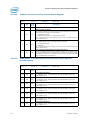
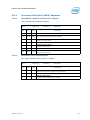
Contents
1
Introduction ............................................................................................................ 25
1.1
Document Terminology ...................................................................................... 25
1.2
Related Documents ........................................................................................... 27
1.3
Register Terminology ......................................................................................... 28
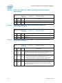
2
Configuration Process and Registers ....................................................................... 31
2.1
Platform Configuration Structure ......................................................................... 31
2.1.1 Processor IIO Devices (CPUBUSNO (0))..................................................... 31
2.1.2 Processor Uncore Devices (CPUBUSN0 (1)) ................................................ 33
2.2
Configuration Register Rules ............................................................................... 34
2.2.1 CSR Access ........................................................................................... 34
2.2.2 PCI Bus Number..................................................................................... 34
2.2.3 Uncore Bus Number................................................................................ 34
2.3
Configuration Mechanisms .................................................................................. 35
2.3.1 Standard PCI Express* Configuration Mechanism........................................ 35
2.4
Device Mapping................................................................................................. 35
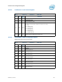
3
Processor Integrated I/O (IIO) Configuration Registers ......................................... 37
3.1
Processor IIO Devices (PCI Bus CPUBUSNO (0)) .................................................... 37
3.2
PCI Configuration Space Registers (CSRs)...................................................... 37
3.2.1 Unimplemented Devices/Functions and Registers........................................ 37
3.2.2 PCI Bus Number..................................................................................... 37
3.2.3 IIO PCI Express* Configuration Space Registers ......................................... 40
3.2.4 Standard PCI Configuration Space (Type 0/1
Common Configuration Space) ................................................................. 47
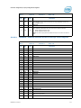
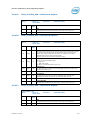
3.2.4.1 VID—Vendor Identification Register............................................. 47
3.2.4.2 DID—Device Identification Register ............................................. 47
3.2.4.3 PCICMD—PCI Command Register ................................................ 48
3.2.4.4 PCISTS—PCI Status Register ...................................................... 49
3.2.4.5 RID—Revision Identification Register ........................................... 51
3.2.4.6 CCR—Class Code Register .......................................................... 51
3.2.4.7 CLSR—Cacheline Size Register.................................................... 51
3.2.4.8 PLAT—Primary Latency Timer Register ......................................... 52
3.2.4.9 HDR—Header Type Register ....................................................... 52
3.2.4.10 HDR—Header Type Register ....................................................... 52
3.2.4.11 BIST—Built-In Self Test Register ................................................. 53
3.2.4.12 PBUS—Primary Bus Number Register........................................... 53
3.2.4.13 SECBUS—Secondary Bus Number Register ................................... 53
3.2.4.14 SUBBUS—Subordinate Bus Number Register................................. 53
3.2.4.15 IOBAS—I/O Base Register.......................................................... 54
3.2.4.16 IOLIM—I/O Limit Register .......................................................... 54
3.2.4.17 SECSTS—Secondary Status Register ........................................... 55
3.2.4.18 MBAS—Memory Base Register .................................................... 56
3.2.4.19 MLIM—Memory Limit Register..................................................... 56
3.2.4.20 PBAS—Prefetchable Memory Base Register ................................... 57
3.2.4.21 PLIM—Prefetchable Memory Limit Register ................................... 57
3.2.4.22 PBASU—Prefetchable Memory Base (Upper 32 bits) Register........... 57
3.2.4.23 PLIMU—Prefetchable Memory Limit (Upper 32 bits) Register ........... 58
3.2.4.24 SVID—Subsystem Vendor ID Register.......................................... 58
3.2.4.25 SDID—Subsystem Identity ......................................................... 59
3.2.4.26 CAPPTR—Capability Pointer ........................................................ 59
3.2.4.27 CAPPTR—Capability Pointer ........................................................ 59
3.2.4.28 INTL—Interrupt Line Register ..................................................... 59
3.2.4.29 INTPIN—Interrupt Pin Register ................................................... 60
3.2.4.30 BCTRL—Bridge Control Register .................................................. 60
3.2.4.31 SCAPID—Subsystem Capability Identity Register........................... 61
Datasheet, Volume 2
3
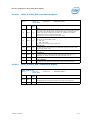
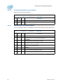
3.2.4.32 SNXTPTR—Subsystem ID Next Pointer Register .............................62
3.2.4.33 DMIRCBAR—DMI Root Complex Register Block Base
Address Register .......................................................................62
3.2.4.34 MSICAPID—MSI Capability ID Register .........................................62
3.2.4.35 MSINXTPTR—MSI Next Pointer Register........................................63
3.2.4.36 MSIMSGCTL—MSI Control Register ..............................................63
3.2.4.37 MSIMSGCTL—MSI Control Register ..............................................64
3.2.4.38 MSGADR—MSI Address Register..................................................65
3.2.4.39 MSGDAT—MSI Data Register ......................................................65
3.2.4.40 MSIMSK—MSI Mask Bit Register..................................................65
3.2.4.41 MSIPENDING—MSI Pending Bit Register .......................................66
3.2.4.42 PXPCAPID—PCI Express* Capability Identity Register .....................66
3.2.4.43 PXPNXTPTR—PCI Express* Next Pointer Register ...........................66
3.2.4.44 PXPCAP—PCI Express* Capabilities Register..................................67
3.2.4.45 DEVCAP—PCI Express* Device Capabilities Register .......................68
3.2.4.46 DEVCTRL—PCI Express* Device Control Register ...........................69
3.2.4.47 DEVSTS—PCI Express* Device Status Register ..............................71
3.2.4.48 LNKCAP—PCI Express* Link Capabilities Register...........................72
3.2.4.49 LNKCON—PCI Express* Link Control Register ................................73
3.2.4.50 LNKSTS—PCI Express* Link Status Register..................................75
3.2.4.51 SLTCAP—PCI Express* Slot Capabilities Register ...........................76
3.2.4.52 SLTCON—PCI Express* Slot Control Register.................................78
3.2.4.53 SLTSTS—PCI Express* Slot Status Register ..................................80
3.2.4.54 ROOTCON—PCI Express* Root Control Register.............................81
3.2.4.55 ROOTCAP—PCI Express* Root Capabilities Register........................83
3.2.4.56 ROOTSTS—PCI Express* Root Status Register...............................84
3.2.4.57 DEVCAP2—PCI Express* Device Capabilities 2 Register ..................84
3.2.4.58 DEVCTRL2—PCI Express* Device Control Register 2.......................85
3.2.4.59 LNKCAP2—PCI Express* Link Capabilities 2 Register ......................86
3.2.4.60 LNKCON2—PCI Express* Link Control 2 Register ...........................87
3.2.4.61 LNKSTS2—PCI Express* Link Status Register 2 .............................88
3.2.4.62 PMCAP—Power Management Capabilities Register ..........................89
3.2.4.63 PMCSR—Power Management Control and Status Register................90
3.2.4.64 XPREUT_HDR_EXT—REUT PCIe* Header Extended Register ............91
3.2.4.65 XPREUT_HDR_CAP—REUT Header Capability Register.....................91
3.2.4.66 XPREUT_HDR_LEF—REUT Header Leaf Capability Register ..............92
3.2.4.67 ACSCAPHDR—Access Control Services Extended Capability
Header Register ........................................................................92
3.2.4.68 ACSCAP—Access Control Services Capability Register .....................93
3.2.4.69 ACSCTRL—Access Control Services Control Register .......................94
3.2.4.70 APICBASE—APIC Base Register ...................................................94
3.2.4.71 APICLIMIT—APIC Limit Register ..................................................95
3.2.4.72 VSECHDR—PCI Express* Enhanced Capability Header
Register – DMI2 Mode................................................................95
3.2.4.73 VSHDR—Vendor Specific Header Register – DMI2 Mode ..................95
3.2.4.74 ERRCAPHDR—PCI Express* Enhanced Capability Header
Register – Root Ports .................................................................96
3.2.4.75 UNCERRSTS—Uncorrectable Error Status Register .........................96
3.2.4.76 UNCERRMSK—Uncorrectable Error Mask Register...........................97
3.2.4.77 UNCERRSEV—Uncorrectable Error Severity Register .......................97
3.2.4.78 CORERRSTS—Correctable Error Status Register.............................98
3.2.4.79 CORERRMSK—Correctable Error Mask Register ..............................98
3.2.4.80 ERRCAP—Advanced Error Capabilities and Control Register .............99
3.2.4.81 HDRLOG[0:3]—Header Log 0–3 Register ......................................99
3.2.4.82 RPERRCMD—Root Port Error Command Register .......................... 100
3.2.4.83 RPERRSTS—Root Port Error Status Register ................................ 100
3.2.4.84 ERRSID—Error Source Identification Register .............................. 101
3.2.4.85 PERFCTRLSTS—Performance Control and Status Register.............. 102
3.2.4.86 MISCCTRLSTS—Miscellaneous Control and Status Register............ 103
3.2.4.87 PCIE_IOU_BIF_CTRL—PCIe* Port Bifurcation Control
Register – DMI2 Port/PCIe* ...................................................... 107
3.2.4.88 DMICTRL—DMI Control Register ................................................ 107
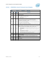
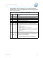
4
Datasheet, Volume 2
3.2.5
3.2.6
3.2.7
3.2.8
Datasheet, Volume 2
3.2.4.89 PCIE_IOU_BIF_CTRL—PCIe* Port Bifurcation Control Register....... 108
3.2.4.90 PXP2CAP—Secondary PCI Express* Extended Capability
Header Register...................................................................... 109
3.2.4.91 LNKCON3—Link Control 3 Register ............................................ 109
PCI Express* and DMI2 Error Registers ................................................... 110
3.2.5.1 ERRINJCAP—PCI Express* Error Injection Capability Register........ 110
3.2.5.2 ERRINJHDR—PCI Express* Error Injection Capability
Header Register...................................................................... 110
3.2.5.3 ERRINJCON—PCI Express* Error Injection Control Register .......... 111
3.2.5.4 CTOCTRL—Completion Timeout Control Register ......................... 111
3.2.5.5 XPCORERRSTS—XP Correctable Error Status Register .................. 112
3.2.5.6 XPCORERRMSK—XP Correctable Error Mask Register ................... 112
3.2.5.7 XPUNCERRSTS—XP Uncorrectable Error Status Register ............... 113
3.2.5.8 XPUNCERRMSK—XP Uncorrectable Error Mask Register ................ 113
3.2.5.9 XPUNCERRSEV—XP Uncorrectable Error Severity Register ............ 114
3.2.5.10 XPUNCERRPTR—XP Uncorrectable Error Pointer Register .............. 114
3.2.5.11 UNCEDMASK—Uncorrectable Error Detect Status Mask Register .... 115
3.2.5.12 COREDMASK—Correctable Error Detect Status Mask Register ....... 115
3.2.5.13 RPEDMASK—Root Port Error Detect Status Mask Register ............. 116
3.2.5.14 XPUNCEDMASK—XP Uncorrectable Error Detect Mask Register ...... 116
3.2.5.15 XPCOREDMASK—XP Correctable Error Detect Mask Register ......... 117
3.2.5.16 XPGLBERRSTS—XP Global Error Status Register .......................... 117
3.2.5.17 XPGLBERRPTR—XP Global Error Pointer Register ......................... 118
3.2.5.18 LNERRSTS—Lane Error Status Register ...................................... 118
3.2.5.19 LER_CAP—Live Error Recovery Capability Register....................... 119
3.2.5.20 LER_HDR—Live Error Recovery Capability Header Register ........... 119
3.2.5.21 LER_CTRLSTS—Live Error Recovery Control and Status Register ... 119
3.2.5.22 LER_UNCERRMSK—Live Error Recovery Uncorrectable
Error Mask Register................................................................. 120
3.2.5.23 LER_XPUNCERRMSK—Live Error Recovery XP Uncorrectable
Error Mask Register................................................................. 120
3.2.5.24 LER_RPERRMSK—Live Error Recovery Root Port Error
Mask Register......................................................................... 121
PCI Express* Lane Equalization Registers ................................................ 121
3.2.6.1 LN[0:3]EQ—Lane 0 through Lane 3 Equalization
Control Register...................................................................... 121
3.2.6.2 LN[4:7]EQ—Lane 4 through Lane 7 Equalization Control Register .. 122
3.2.6.3 LN[8:15]EQ—Lane 8 though Lane 15 Equalization Control Register 124
PCI Express* and DMI2 Perfmon ............................................................ 125
3.2.7.1 XPPMDL[0:1]—XP PM Data Low Bits Register .............................. 125
3.2.7.2 XPPMCL[0:1]—XP PM Compare Low Bits Register ........................ 125
3.2.7.3 XPPMDH—XP PM Data High Bits Register .................................... 126
3.2.7.4 XPPMCH—XP PM Compare High Bits Register .............................. 126
3.2.7.5 XPPMR[0:1]—XP PM Response Control Register........................... 127
3.2.7.6 XPPMEVL[0:1]—XP PM Events Low Register ................................ 130
3.2.7.7 XPPMEVH[0:1]—XP PM Events High Register .............................. 132
3.2.7.8 XPPMER[0:1]—XP PM Resource Events Register .......................... 133
DMI Root Complex Register Block (RCRB)................................................ 134
3.2.8.1 DMIVC0RCAP—DMI VC0 Resource Capability Register .................. 135
3.2.8.2 DMIVC0RCTL—DMI VC0 Resource Control Register ...................... 135
3.2.8.3 DMIVC0RSTS—DMI VC0 Resource Status Register ....................... 136
3.2.8.4 DMIVC1RCAP—DMI VC1 Resource Capability Register .................. 136
3.2.8.5 DMIVC1RCTL—DMI VC1 Resource Control Register ...................... 137
3.2.8.6 DMIVC1RSTS—DMI VC1 Resource Status Register ....................... 138
3.2.8.7 DMIVCPRCAP—DMI VCP Resource Capability Register .................. 138
3.2.8.8 DMIVCPRCTL—DMI VCP Resource Control Register ...................... 139
3.2.8.9 DMIVCPRSTS—DMI VCP Resource Status Register ....................... 140
3.2.8.10 DMIVCMRCAP—DMI VCM Resource Capability Register ................. 140
3.2.8.11 DMIVCMRCTL—DMI VCM Resource Control Register ..................... 141
3.2.8.12 DMIVCMRSTS—DMI VCM Resource Status Register...................... 141
3.2.8.13 DMIRCLDECH—DMI Root Complex Link Declaration Register ......... 142
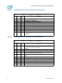
5
3.3
6
3.2.8.14 DMIESD—DMI Element self Description Register .......................... 142
3.2.8.15 DMILED—DMI Link Entry Description Register ............................. 142
3.2.8.16 DMILBA0—DMI Link Address Register ........................................ 143
3.2.8.17 DMIVC1CdtThrottle—DMI VC1 Credit Throttle Register ................. 143
3.2.8.18 DMIVCpCdtThrottle—DMI VCp Credit Throttle Register.................. 143
3.2.8.19 DMIVCmCdtThrottle—DMI VCm Credit Throttle Register................ 144
Integrated I/O Core Registers............................................................................ 145
3.3.1 Configuration Register Maps (Device 5, Function: 0, 2 and 4) ..................... 145
3.3.2 PCI Configuration Space Registers Common to Device 5............................. 155
3.3.2.1 VID—Vendor Identification Register ........................................... 155
3.3.2.2 DID—Device Identification Register............................................ 155
3.3.2.3 PCICMD—PCI Command Register .............................................. 155
3.3.2.4 PCISTS—PCI Status Register..................................................... 156
3.3.2.5 RID—Revision Identification Register ......................................... 157
3.3.2.6 CCR—Class Code Register ........................................................ 157
3.3.2.7 CLSR—Cacheline Size Register .................................................. 157
3.3.2.8 HDR—Header Type Register...................................................... 158
3.3.2.9 SVID—Subsystem Vendor ID Register ........................................ 158
3.3.2.10 SID—Subsystem Device ID Register .......................................... 158
3.3.2.11 CAPPTR—Capability Pointer Register .......................................... 159
3.3.2.12 INTL—Interrupt Line Register.................................................... 159
3.3.2.13 INTPIN—Interrupt Pin Register .................................................. 159
3.3.2.14 PXPCAPID—PCI Express* Capability Identity Register ................... 159
3.3.2.15 PXPNXTPTR—PCI Express* Next Pointer Register ......................... 160
3.3.2.16 PXPCAP—PCI Express* Capabilities Register................................ 160
3.3.3 Intel® VT-d, Address Mapping, System Management,
Coherent Interface, Misc Registers .......................................................... 160
3.3.3.1 HDRTYPECTRL—PCI Header Type Control Register ....................... 160
3.3.3.2 MMCFG—MMCFG Address Range Register ................................... 161
3.3.3.3 TSEG—TSeg Address Range Register ......................................... 161
3.3.3.4 GENPROTRANGE1_BASE—Generic Protected Memory Range 1
Base Address Register ............................................................. 161
3.3.3.5 GENPROTRANGE1_LIMIT—Generic Protected Memory Range 1
Limit Address Register ............................................................. 162
3.3.3.6 GENPROTRANGE2_BASE—Generic Protected Memory Range 2
Base Address Register ............................................................. 162
3.3.3.7 GENPROTRANGE2_LIMIT—Generic Protected Memory Range 2
Limit Address Register ............................................................. 163
3.3.3.8 TOLM—Top of Low Memory Register .......................................... 163
3.3.3.9 TOHM—Top of High Memory Register ......................................... 163
3.3.3.10 NCMEM_BASE—NCMEM Base Register ........................................ 164
3.3.3.11 NCMEM_LIMIT—NCMEM Limit Register ....................................... 164
3.3.3.12 MENCMEM_BASE—Intel® Management Engine (Intel® ME)
Non-coherent Memory Base Address Register.............................. 164
3.3.3.13 MENCMEM_LIMIT—Intel® ME Non-coherent Memory Limit
Address Register ..................................................................... 165
3.3.3.14 CPUBUSNO—CPU Internal Bus Numbers Register ......................... 165
3.3.3.15 LMMIOL—Local MMIO Low Base Register .................................... 166
3.3.3.16 LMMIOH_BASE—Local MMIO High Base Register .......................... 166
3.3.3.17 LMMIOH_LIMIT—Local MMIO High Base Register ......................... 167
3.3.3.18 GENPROTRANGE0_BASE—Generic Protected Memory Range 0
Base Address Register ............................................................. 167
3.3.3.19 GENPROTRANGE0_LIMIT—Generic Protected Memory Range 0
Limit Address Register ............................................................. 168
3.3.3.20 CIPCTRL—Coherent Interface Protocol Control Register ................ 168
3.3.3.21 CIPSTS—Coherent Interface Protocol Status Register ................... 170
3.3.3.22 CIPDCASAD—Coherent Interface Protocol DCA Source Address
Decode Register ...................................................................... 170
3.3.3.23 CIPINTRC—Coherent Interface Protocol Interrupt Control Register . 171
3.3.3.24 CIPINTRS—Coherent interface Protocol Interrupt Status Register ... 172
3.3.3.25 VTBAR—Base Address Register for Intel® VT-d Registers .............. 173
Datasheet, Volume 2
VTGENCTRL—Intel® VT-d General Control Register...................... 173
VTISOCHCTRL—Intel® VT-d Isoch Related Control Register .......... 174
VTGENCTRL2—Intel® VT-d General Control 2 Register ................. 175
IOTLBPARTITION—IOTLB Partitioning Control Register ................. 176
VTUNCERRSTS—Uncorrectable Error Status Register ................... 176
VTUNCERRMSK—Intel® VT Uncorrectable Error Mask Register....... 177
VTUNCERRSEV—Intel® VT Uncorrectable Error Severity Register... 177
VTUNCERRPTR—Intel® VT Uncorrectable Error Pointer Register..... 178
IIOMISCCTRL—IIO MISC Control Register .................................. 178
IRP_MISC_DFX0—Coherent Interface Miscellaneous
DFx 0 Register........................................................................ 182
3.3.3.36 IRP_MISC_DFX1—Coherent Interface Miscellaneous
DFx 1 Register........................................................................ 183
3.3.3.37 IRP0DELS—Coherent Interface 0 Debug Event Lane
Select Register ....................................................................... 184
3.3.3.38 IRP1DELS—Coherent Interface 1 Debug Event Lane
Select Register ....................................................................... 184
3.3.3.39 IRP0DBGRING[0:1]—Coherent Interface 0 Debug Ring 0 Register . 185
3.3.3.40 IRP1DBGRING[0:1]—Coherent Interface 1 Debug Ring 0 Register . 185
3.3.3.41 IRP0DBGRING1—Coherent Interface 0 Debug Ring 1 Register ....... 185
3.3.3.42 IRP1DBGRING1—Coherent Interface 1 Debug Ring 1 Register ....... 185
3.3.3.43 IRP0RNG—Coherent Interface 0 Cluster Debug Ring
Control Register...................................................................... 186
3.3.3.44 IRP1RNG—Coherent Interface 1 Cluster Debug Ring
Control Register...................................................................... 188
3.3.3.45 IRPEGCREDITS—R2PCIe Egress Credits Register ......................... 190
Global System Control and Error Registers............................................... 191
3.3.4.1 IRPPERRSV—IRP Protocol Error Severity Register ........................ 191
3.3.4.2 IIOERRSV—IIO Core Error Severity Register ............................... 192
3.3.4.3 MIERRSV—Miscellaneous Error Severity Register ......................... 192
3.3.4.4 PCIERRSV—PCIe* Error Severity Map Register............................ 193
3.3.4.5 SYSMAP—System Error Event Map Register ................................ 193
3.3.4.6 VIRAL—Viral Alert Register....................................................... 194
3.3.4.7 ERRPINCTL—Error Pin Control Register ...................................... 194
3.3.4.8 ERRPINST—Error Pin Status Register ......................................... 195
3.3.4.9 ERRPINDAT—Error Pin Data Register ......................................... 195
3.3.4.10 VPPCTL—VPP Control Register .................................................. 196
3.3.4.11 VPPSTS—VPP Status Register ................................................... 196
3.3.4.12 GNERRST—Global Non-Fatal Error Status Register....................... 197
3.3.4.13 GFERRST—Global Fatal Error Status Register .............................. 198
3.3.4.14 GERRCTL—Global Error Control Register .................................... 199
3.3.4.15 GSYSST—Global System Event Status Register ........................... 200
3.3.4.16 GSYSCTL—Global System Event Control Register ........................ 200
3.3.4.17 GFFERRST—Global Fatal FERR Status Register ............................ 200
3.3.4.18 GFNERRST—Global Fatal NERR Status Register ........................... 201
3.3.4.19 GNFERRST—Global Non-Fatal FERR Status Register ..................... 201
3.3.4.20 GNNERRST—Global Non-Fatal NERR Status Register .................... 201
Local Error Registers............................................................................. 202
3.3.5.1 IRPP0ERRST—IRP Protocol Error Status Register ......................... 202
3.3.5.2 IRPP0ERRCTL—IRP Protocol Error Control Register ...................... 202
3.3.5.3 IRPP0FFERRST—IRP Protocol Fatal FERR Status Register .............. 203
3.3.5.4 IRPP0FNERRST—IRP Protocol Fatal NERR Status Register ............. 204
3.3.5.5 IRPP0FFERRHD[0:3]—IRP Protocol Fatal FERR Header
Log 0 Register ........................................................................ 204
3.3.5.6 IRPP0NFERRST—IRP Protocol Non-Fatal FERR Status Register ....... 205
3.3.5.7 IRPP0NNERRST—IRP Protocol Non-Fatal NERR Status Register ...... 205
3.3.5.8 IRPP0NFERRHD[0:3]—IRP Protocol Non-Fatal FERR Header
Log 0 Register ........................................................................ 206
3.3.5.9 IRPP0ERRCNTSEL—IRP Protocol Error Counter Select Register ...... 206
3.3.5.10 IRPP0ERRCNT—IRP Protocol Error Counter Register ..................... 206
3.3.5.11 IRPP1ERRST—IRP Protocol Error Status Register ......................... 207
3.3.3.26
3.3.3.27
3.3.3.28
3.3.3.29
3.3.3.30
3.3.3.31
3.3.3.32
3.3.3.33
3.3.3.34
3.3.3.35
3.3.4
3.3.5
Datasheet, Volume 2
7
3.3.5.12
3.3.5.13
3.3.5.14
3.3.5.15
3.3.6
3.3.7
8
IRPP1ERRCTL—IRP Protocol Error Control Register ....................... 208
IRPP1FFERRST—IRP Protocol Fatal FERR Status Register .............. 209
IRPP1FNERRST—IRP Protocol Fatal NERR Status Register ............. 209
IRPP1FFERRHD[0:3]—IRP Protocol Fatal FERR Header
Log 0 Register ........................................................................ 210
3.3.5.16 IRPP1NFERRST—IRP Protocol Non-Fatal FERR Status Register ....... 210
3.3.5.17 IRPP1NNERRST—IRP Protocol Non-Fatal NERR Status Register ...... 211
3.3.5.18 IRPP1NFERRHD[0:3]—IRP Protocol Non-Fatal FERR Header
Log 0 Register ........................................................................ 211
3.3.5.19 IRPP1ERRCNTSEL—IRP Protocol Error Counter Select Register....... 211
3.3.5.20 IRPP1ERRCNT—IRP Protocol Error Counter Register ..................... 212
3.3.5.21 IIOERRST—IIO Core Error Status Register .................................. 212
3.3.5.22 IIOERRCTL—IIO Core Error Control Register ............................... 212
3.3.5.23 IIOFFERRST—IIO Core Fatal FERR Status Register ....................... 213
3.3.5.24 IIOFFERRHD[0:3]—IIO Core Fatal FERR Header Register .............. 213
3.3.5.25 IIOFNERRST—IIO Core Fatal NERR Status Register ...................... 213
3.3.5.26 IIONFERRST—IIO Core Non-Fatal FERR Status Register ................ 213
3.3.5.27 IIONFERRHD[0:3]—IIO Core Non-Fatal FERR Header Register ....... 214
3.3.5.28 IIONNERRST—IIO Core Non-Fatal NERR Status Register ............... 214
3.3.5.29 IIOERRCNTSEL—IIO Core Error Counter Selection Register ........... 214
3.3.5.30 IIOERRCNT—IIO Core Error Counter Register .............................. 215
3.3.5.31 MIERRST—Miscellaneous Error Status Register ............................ 215
3.3.5.32 MIERRCTL—Miscellaneous Error Control Register ......................... 215
3.3.5.33 MIFFERRST—Miscellaneous Fatal First Error Status Register .......... 216
3.3.5.34 MIFFERRHDR_[0:3]—Miscellaneous Fatal First Error Header 0
Log Register ........................................................................... 216
3.3.5.35 MIFNERRST—Miscellaneous Fatal Next Error Status Register ......... 216
3.3.5.36 MINFERRST—Miscellaneous Non-Fatal First Error Status Register ... 216
3.3.5.37 MINFERRHDR_[0:3]—Miscellaneous Non-Fatal First Error
Header 0 Log Register.............................................................. 217
3.3.5.38 MINNERRST—Miscellaneous Non-Fatal Next Error Status Register .. 217
3.3.5.39 MIERRCNTSEL—Miscellaneous Error Count Select Register ............ 217
3.3.5.40 MIERRCNT—Miscellaneous Error Counter Register ........................ 217
IOxAPIC PCI Configuration Space............................................................ 218
3.3.6.1 MBAR—IOxAPIC Base Address Register ...................................... 218
3.3.6.2 SVID—Subsystem Vendor ID Register ........................................ 218
3.3.6.3 SDID—Subsystem Device ID Register ........................................ 218
3.3.6.4 INTL—Interrupt Line Register.................................................... 219
3.3.6.5 INTPIN—Interrupt Pin Register - Others ..................................... 219
3.3.6.6 ABAR—I/OxAPIC Alternate BAR Register..................................... 219
3.3.6.7 PMCAP—Power Management Capabilities Register ........................ 220
3.3.6.8 PMCSR—Power Management Control and Status Register.............. 220
3.3.6.9 RDINDEX—Alternate Index to read Indirect I/OxAPIC Register....... 221
3.3.6.10 RDWINDOW—Alternate Window to read Indirect
I/OxAPIC Register ................................................................... 221
3.3.6.11 IOAPICTETPC—IOxAPIC Table Entry Target Programmable
Control Register ...................................................................... 222
3.3.6.12 IOADSELS0—IOxAPIC DSELS Register 0 ..................................... 222
3.3.6.13 IOADSELS1—IOxAPIC DSELS Register 1 ..................................... 223
3.3.6.14 IOINTSRC0—IO Interrupt Source Register 0................................ 223
3.3.6.15 IOINTSRC1—IO Interrupt Source Register 1................................ 224
3.3.6.16 IOREMINTCNT—Remote IO Interrupt Count Register .................... 224
3.3.6.17 IOREMGPECNT—Remote IO GPE Count Register .......................... 225
3.3.6.18 IOXAPICPARERRINJCTL—IOxAPIC Parity Error Injection
Control Register ...................................................................... 225
3.3.6.19 FAUXGV—FauxGV Register ....................................................... 225
I/OxAPIC Memory Mapped Registers ....................................................... 226
3.3.7.1 INDX—Index Register .............................................................. 228
3.3.7.2 WNDW—Window Register ......................................................... 228
3.3.7.3 PAR—Pin Assertion Register ...................................................... 228
3.3.7.4 EOI Register ........................................................................... 229
Datasheet, Volume 2
3.3.8
Datasheet, Volume 2
3.3.7.5 APICID Register...................................................................... 229
3.3.7.6 VER—Version Register ............................................................. 229
3.3.7.7 ARBID—Arbitration ID Register ................................................. 230
3.3.7.8 BCFG—Boot Configuration Register ........................................... 230
3.3.7.9 RTL[0:23]—Redirection Table Low DWord Register ...................... 231
3.3.7.10 RTH[0:23]—Redirection Table High DWord Register..................... 232
Intel® VT-d Memory Mapped Register ..................................................... 233
3.3.8.1 VTD0_VERSION—Version Number Register................................. 239
3.3.8.2 VTD0_CAP—Intel® VT-d Capabilities Register ............................. 239
3.3.8.3 VTD0_EXT_CAP—Extended Intel® VT-d Capability Register........... 240
3.3.8.4 VTD0_GLBCMD—Global Command Register ................................ 241
3.3.8.5 VTD0_GLBSTS—Global Status Register ...................................... 243
3.3.8.6 VTD0_ROOTENTRYADD—Root Entry Table Address Register ......... 244
3.3.8.7 VTD0_CTXCMD—Context Command Register .............................. 244
3.3.8.8 VTD0_FLTSTS—Fault Status Register......................................... 246
3.3.8.9 VTD0_FLTEVTCTRL—Fault Event Control Register ........................ 247
3.3.8.10 VTD0_FLTEVTDATA—Fault Event Data Register ........................... 247
3.3.8.11 VTD0_FLTEVTADDR—Fault Event Address Register ...................... 248
3.3.8.12 VTD0_PMEN—Protected Memory Enable Register......................... 248
3.3.8.13 VTD0_PROT_LOW_MEM_BASE—Protected Memory Low
Base Register ......................................................................... 248
3.3.8.14 VTD0_PROT_LOW_MEM_LIMIT—Protected Memory Low
Limit Register......................................................................... 249
3.3.8.15 VTD0_PROT_HIGH_MEM_BASE—Protected Memory High
Base Register ......................................................................... 249
3.3.8.16 VTD0_PROT_HIGH_MEM_LIMIT—Protected Memory High
Limit Register......................................................................... 249
3.3.8.17 VTD0_INV_QUEUE_HEAD—Invalidation Queue Header
Pointer Register ...................................................................... 250
3.3.8.18 VTD0_INV_QUEUE_TAIL—Invalidation Queue Tail
Pointer Register ...................................................................... 250
3.3.8.19 VTD0_INV_QUEUE_ADD—Invalidation Queue Address Register ..... 250
3.3.8.20 VTD0_INV_COMP_STATUS—Invalidation Completion
Status Register....................................................................... 251
3.3.8.21 VTD0_INV_COMP_EVT_CTL—Invalidation Completion Event
Control Register...................................................................... 251
3.3.8.22 VTD0_INV_COMP_EVT_DATA—Invalidation Completion Event
Data Register ......................................................................... 252
3.3.8.23 VTD0_INV_COMP_EVT_ADDR—Invalidation Completion
Event Address Register ............................................................ 252
3.3.8.24 VTD0_INTR_REMAP_TABLE_BASE—Interrupt Remapping Table
Base Address Register ............................................................. 252
3.3.8.25 VTD0_FLTREC0_GPA—Fault Record Register ............................... 253
3.3.8.26 VTD0_FLTREC0_SRC—Fault Record Register............................... 253
3.3.8.27 VTD0_FLTREC1_GPA—Fault Record Register ............................... 253
3.3.8.28 VTD0_FLTREC1_SRC—Fault Record Register............................... 254
3.3.8.29 VTD0_FLTREC2_GPA—Fault Record Register ............................... 254
3.3.8.30 VTD0_FLTREC2_SRC—Fault Record Register............................... 255
3.3.8.31 VTD0_FLTREC3_GPA—Fault Record Register ............................... 255
3.3.8.32 VTD0_FLTREC3_SRC—Fault Record Register............................... 256
3.3.8.33 VTD0_FLTREC4_GPA—Fault Record Register ............................... 256
3.3.8.34 VTD0_FLTREC4_SRC—Fault Record Register............................... 257
3.3.8.35 VTD0_FLTREC5_GPA—Fault Record Register ............................... 257
3.3.8.36 VTD0_FLTREC5_SRC—Fault Record Register............................... 258
3.3.8.37 VTD0_FLTREC6_GPA—Fault Record Register ............................... 258
3.3.8.38 VTD0_FLTREC6_SRC—Fault Record Register............................... 259
3.3.8.39 VTD0_FLTREC7_GPA—Fault Record Register ............................... 259
3.3.8.40 VTD0_FLTREC7_SRC—Fault Record Register............................... 260
3.3.8.41 VTD0_INVADDRREG—Invalidate Address Register ....................... 260
3.3.8.42 VTD0_IOTLBINV—IOTLB Invalidate Register ............................... 261
3.3.8.43 VTD1_VERSION—Version Number Register................................. 262
3.3.8.44 VTD1_CAP—Intel® VT-d Capabilities Register ............................. 262
9
3.3.8.45
3.3.8.46
3.3.8.47
3.3.8.48
3.3.8.49
3.3.8.50
3.3.8.51
3.3.8.52
3.3.8.53
3.3.8.54
3.3.8.55
3.3.8.56
3.3.8.57
3.3.8.58
3.3.8.59
3.3.8.60
3.3.8.61
3.3.8.62
3.3.8.63
3.3.8.64
3.3.8.65
3.3.8.66
3.3.8.67
3.3.8.68
3.3.8.69
3.3.8.70
4
10
VTD1_EXT_CAP—Extended Intel® VT-d Capability Register ........... 263
VTD1_GLBCMD—Global Command Register................................. 264
VTD1_GLBSTS—Global Status Register....................................... 266
VTD1_ROOTENTRYADD—Root Entry Table Address Register .......... 266
VTD1_CTXCMD—Context Command Register .............................. 267
VTD1_FLTSTS—Fault Status Register ......................................... 268
VTD1_FLTEVTCTRL—Fault Event Control Register ........................ 269
VTD1_FLTEVTDATA—Fault Event Data Register ........................... 269
VTD1_FLTEVTADDR—Fault Event Address Register ...................... 270
VTD1_PMEN—Protected Memory Enable Register ......................... 270
VTD1_PROT_LOW_MEM_BASE—Protected Memory Low
Base Register ......................................................................... 270
VTD1_PROT_LOW_MEM_LIMIT—Protected Memory Low
Limit Register ......................................................................... 271
VTD1_PROT_HIGH_MEM_BASE—Protected Memory High
Base Register ......................................................................... 271
VTD1_PROT_HIGH_MEM_LIMIT—Protected Memory High
Limit Register ......................................................................... 271
VTD1_INV_QUEUE_HEAD—Invalidation Queue Header
Pointer Register ...................................................................... 272
VTD1_INV_QUEUE_TAIL—Invalidation Queue Tail
Pointer Register ...................................................................... 272
VTD1_INV_QUEUE_ADD—Invalidation Queue
Address Register ..................................................................... 272
VTD1_INV_COMP_STATUS—Invalidation Completion
Status Register ....................................................................... 273
VTD1_INV_COMP_EVT_CTL—Invalidation Completion Event
Control Register ...................................................................... 273
VTD1_INV_COMP_EVT_DATA—Invalidation Completion Event
Data Register.......................................................................... 273
VTD1_INV_COMP_EVT_ADDR—Invalidation Completion
Event Address Register ............................................................ 274
VTD1_INTR_REMAP_TABLE_BASE—Interrupt Remapping Table
Base Address Register ............................................................. 274
VTD1_FLTREC0_GPA—Fault Record Register ............................... 274
VTD1_FLTREC0_SRC—Fault Record Register ............................... 275
VTD1_INVADDRREG—Invalidate Address Register ....................... 275
VTD1_IOTLBINV—IOTLB Invalidate Register ............................... 276
Processor Uncore Configuration Registers ............................................................. 277
4.1
PCI Standard Registers..................................................................................... 277
4.1.1 VID—Vendor Identification Register......................................................... 277
4.1.2 DID—Device Identification Register ......................................................... 277
4.1.3 PCICMD—PCI Command Register ............................................................ 278
4.1.4 PCISTS—PCI Status Register .................................................................. 279
4.1.5 RID—Revision Identification Register ....................................................... 280
4.1.6 CCR—Class Code Register ...................................................................... 280
4.1.7 CLSR—Cacheline Size Register................................................................ 280
4.1.8 PLAT—Primary Latency Timer Register..................................................... 280
4.1.9 HDR—Header Type Register ................................................................... 281
4.1.10 BIST—Built-In Self Test Register............................................................. 281
4.1.11 SVID—Subsystem Vendor ID Register ..................................................... 281
4.1.12 SDID—Subsystem Device ID Register ...................................................... 281
4.1.13 CAPPTR—Capability Pointer Register........................................................ 282
4.1.14 INTL—Interrupt Line Register ................................................................. 282
4.1.15 INTPIN—Interrupt Pin Register ............................................................... 282
4.1.16 MINGNT—Minimum Grant Register .......................................................... 282
4.1.17 MAXLAT—Maximum Latency Register ...................................................... 282
4.2
Integrated Memory Controller Configuration Registers .......................................... 283
4.2.1 Processor Registers............................................................................... 283
Datasheet, Volume 2
4.2.2
4.2.3
4.2.4
4.2.5
Datasheet, Volume 2
CSR Register Maps ............................................................................... 283
CBO unicast CSRs ................................................................................ 301
4.2.3.1 RTID_Config_Pool01_Size—Ring Global Configuration Register...... 301
4.2.3.2 RTID_Config_Pool23_Size—Ring Global Configuration Register...... 301
4.2.3.3 RTID_Config_Pool45_Size—Ring Global Configuration Register...... 302
4.2.3.4 RTID_Config_Pool67_Size—Ring Global Configuration Register...... 302
4.2.3.5 VNA_Credit_Config—VNA Credit Configuration Register ................ 303
4.2.3.6 PipeRspFunc—Pipe Response Function Register ........................... 303
4.2.3.7 PipeDbgBusSel—Pipe Debug Bus Select Register ......................... 304
4.2.3.8 SadDbgMm2 Register .............................................................. 304
4.2.3.9 Cbsads_Unicast_Cfg_Spare Register.......................................... 304
4.2.3.10 CBO_GDXC_PKT_CNTRL—CBO GDXC Packet Control Register ....... 305
4.2.3.11 RTID_Config_Pool01_Base—Ring Global Configuration Register ..... 306
4.2.3.12 RTID_Config_Pool23_Base—Ring Global Configuration Register ..... 307
4.2.3.13 RTID_Config_Pool45_Base—Ring Global Configuration Register ..... 308
4.2.3.14 RTID_Config_Pool67_Base—Ring Global Configuration Register ..... 309
4.2.3.15 RTID_Pool_Config—Ring Global Configuration Register................. 310
4.2.3.16 RTID_Config_Pool01_Base_Shadow—Ring Global
Configuration Shadow Register ................................................. 311
4.2.3.17 RTID_Config_Pool23_Base_Shadow—Ring Global
Configuration Shadow Register ................................................. 312
4.2.3.18 RTID_Config_Pool45_Base_Shadow—Ring Global
Configuration Shadow Register ................................................. 313
4.2.3.19 RTID_Config_Pool67_Base_Shadow—Ring Global
Configuration Shadow Register ................................................. 314
4.2.3.20 RTID_Pool_Config_Shadow— Ring Global
Configuration Shadow Register ................................................. 315
System Address Decoder Registers (CBO)................................................ 316
4.2.4.1 PAM0123—CBO SAD PAM Register ............................................ 316
4.2.4.2 PAM456—CBO SAD PAM Register .............................................. 317
4.2.4.3 SMRAMC—System Management RAM Control Register ................. 319
4.2.4.4 MESEG_BASE—Manageability Engine Base Address Register ......... 320
4.2.4.5 MESEG_LIMIT—Manageability Engine Limit Address Register ........ 320
4.2.4.6 DRAM_RULE[0:9]—DRAM Rule 0 Register .................................. 321
4.2.4.7 INTERLEAVE_LIST[0:9]—DRAM Interleave List 0 Register ............ 321
4.2.4.8 DRAM_RULE_1—DRAM Rule 1 Register ...................................... 322
4.2.4.9 INTERLEAVE_LIST_1—DRAM Interleave List 1 Register ................ 322
4.2.4.10 DRAM_RULE_2—DRAM Rule 2 Register ...................................... 323
4.2.4.11 INTERLEAVE_LIST_2—DRAM Interleave List 2 Register ................ 323
4.2.4.12 DRAM_RULE_3—DRAM Rule 3 Register ...................................... 324
4.2.4.13 INTERLEAVE_LIST_3—DRAM Interleave List 3 Register ................ 324
4.2.4.14 DRAM_RULE_4—DRAM Rule 4 Register ...................................... 325
4.2.4.15 INTERLEAVE_LIST_4—DRAM Interleave List 4 Register ................ 325
4.2.4.16 DRAM_RULE_5—DRAM Rule 5 Register ...................................... 326
4.2.4.17 INTERLEAVE_LIST_5—DRAM Interleave List 5 Register ................ 326
4.2.4.18 DRAM_RULE_6—DRAM Rule 6 Register ...................................... 327
4.2.4.19 INTERLEAVE_LIST_6—DRAM Interleave List 6 Register ................ 327
4.2.4.20 DRAM_RULE_7—DRAM Rule 7 Register ...................................... 328
4.2.4.21 INTERLEAVE_LIST_7—DRAM Interleave List 7 Register ................ 328
4.2.4.22 DRAM_RULE_8—DRAM Rule 8 Register ...................................... 329
4.2.4.23 INTERLEAVE_LIST_8—DRAM Interleave List 8 Register ................ 329
4.2.4.24 DRAM_RULE_9—DRAM Rule 9 Register ...................................... 330
4.2.4.25 INTERLEAVE_LIST_9—DRAM Interleave List 9 Register ................ 330
Caching Agent Broadcast Registers (CBo) ................................................ 331
4.2.5.1 Cbo_ISOC_Config—Cbo Isochrony Configuration Register............. 331
4.2.5.2 Cbo_Coh_Config—Cbo Coherency Configuration Register.............. 331
4.2.5.3 TOLM—Top of Low Memory Register .......................................... 332
4.2.5.4 TOHM—Top of High Memory Register......................................... 332
4.2.5.5 MMIO_RULE[0:7]—MMIO Rule 0 Register ................................... 332
4.2.5.6 MMCFG_Rule—MMCFG Rule for Interleave Decoder Register ......... 334
4.2.5.7 IOPORT_Target_LIST—IO Target List Register ............................ 334
11
4.2.5.8 MMCFG_Target_LIST—MMCFG Target List Register ...................... 335
4.2.5.9 MMIO_Target_LIST—MMIO Target List Register ........................... 335
4.2.5.10 IOAPIC_Target_LIST—IOAPIC Target List Register ....................... 336
4.2.5.11 SAD_Target—SAD Target List ................................................... 336
4.2.5.12 SAD_Control—SAD Control Register ........................................... 337
4.2.6 Integrated Memory Controller Target Address Registers ............................. 337
4.2.6.1 PXPCAP—PCI Express* Capability Register .................................. 337
4.2.6.2 MCMTR—MC Memory Technology Register .................................. 338
4.2.6.3 TADWAYNESS_[0:11]—TAD Range Wayness, Limit and
Target Register ....................................................................... 339
4.2.6.4 MCMTR2—MC Memory Technology Register 2.............................. 339
4.2.6.5 MC_INIT_STATE_G—Initialization State for Boot, Training
and IOSAV Register ................................................................. 340
4.2.6.6 RCOMP_TIMER—RCOMP Wait Timer Register............................... 341
4.2.7 Integrated Memory Controller MemHot Registers ...................................... 342
4.2.7.1 MH_MAINCNTL—MEMHOT Main Control Register .......................... 342
4.2.7.2 MH_SENSE_500NS_CFG—MEMHOT Sense and 500 ns
Config Register ....................................................................... 343
4.2.7.3 MH_DTYCYC_MIN_ASRT_CNTR_[0:1]—MEMHOT Duty Cycle
Period and Min Assertion Counter Register .................................. 343
4.2.7.4 MH_IO_500NS_CNTR—MEMHOT Input Output and 500ns
Counter Register ..................................................................... 344
4.2.7.5 MH_CHN_ASTN—MEMHOT Domain Channel Association Register ... 345
4.2.7.6 MH_TEMP_STAT—MEMHOT Temperature Status Register .............. 346
4.2.7.7 MH_EXT_STAT Register............................................................ 347
4.2.8 Integrated Memory Controller SMBus Registers......................................... 347
4.2.8.1 SMB_STAT_[0:1]—SMBus Status Register .................................. 347
4.2.8.2 SMBCMD_[0:1]—SMBus Command Register................................ 349
4.2.8.3 SMBCntl_[0:1]—SMBus Control Register .................................... 350
4.2.8.4 SMB_TSOD_POLL_RATE_CNTR_[0:1]—SMBus Clock Period
Counter Register ..................................................................... 351
4.2.8.5 SMB_STAT_1—SMBus Status Register........................................ 352
4.2.8.6 SMBCMD_1—SMBus Command Register ..................................... 353
4.2.8.7 SMBCntl_1—SMBus Control Register .......................................... 354
4.2.8.8 SMB_TSOD_POLL_RATE_CNTR_1—SMBus Clock Period
Counter Register ..................................................................... 355
4.2.8.9 SMB_PERIOD_CFG—SMBus Clock Period Config Register .............. 356
4.2.8.10 SMB_PERIOD_CNTR—SMBus Clock Period Counter Register .......... 356
4.2.8.11 SMB_TSOD_POLL_RATE—SMBus TSOD POLL RATE Register .......... 356
4.2.9 Integrated Memory Controller DIMM Memory Technology Type Registers...... 357
4.2.9.1 PXPCAP—PCI Express* Capability Register .................................. 357
4.2.9.2 DIMMMTR_[0:2]—DIMM Memory Technology Register .................. 358
4.2.10 Integrated Memory Controller Memory Target Address Decoder Registers..... 359
4.2.10.1 TADCHNILVOFFSET_[0:11]—TAD Range Channel Interleave i
OFFSET Register ..................................................................... 359
4.2.11 Integrated Memory Controller Channel Rank Registers ............................... 360
4.2.11.1 RIRWAYNESSLIMIT_[0:4]—RIR Range Wayness and
Limit Register ......................................................................... 360
4.2.11.2 RIRILV0OFFSET_[0:4]—RIR Range Rank Interleave 0
OFFSET Register ..................................................................... 360
4.2.11.3 RIRILV1OFFSET_[0:4]—RIR Range Rank Interleave 1
OFFSET Register ..................................................................... 361
4.2.11.4 RIRILV2OFFSET_[0:4]—RIR Range Rank Interleave 2
OFFSET Register ..................................................................... 361
4.2.11.5 RIRILV3OFFSET_[0:4]—RIR Range Rank Interleave 3
OFFSET Register ..................................................................... 362
4.2.11.6 RIRILV4OFFSET_[0:4]—RIR Range Rank Interleave 4
OFFSET Register ..................................................................... 362
4.2.11.7 RIRILV5OFFSET_[0:4]—RIR Range Rank Interleave 5
OFFSET Register ..................................................................... 362
12
Datasheet, Volume 2
4.2.11.8 RIRILV6OFFSET_[0:4]—RIR Range Rank Interleave 6
OFFSET Register ..................................................................... 363
4.2.11.9 RIRILV7OFFSET_[0:4]—RIR Range Rank Interleave 7
OFFSET Register ..................................................................... 363
4.2.11.10RIRILV0OFFSET_1—RIR Range Rank Interleave 0
OFFSET Register ..................................................................... 364
4.2.11.11RIRILV1OFFSET_1—RIR Range Rank Interleave 1
OFFSET Register ..................................................................... 364
4.2.11.12RIRILV2OFFSET_1—RIR Range Rank Interleave 2
OFFSET Register ..................................................................... 365
4.2.11.13RIRILV3OFFSET_1—RIR Range Rank Interleave 3
OFFSET Register ..................................................................... 365
4.2.11.14RIRILV4OFFSET_1—RIR Range Rank Interleave 4
OFFSET Register ..................................................................... 366
4.2.11.15RIRILV5OFFSET_1—RIR Range Rank Interleave 5
OFFSET Register ..................................................................... 366
4.2.11.16RIRILV6OFFSET_1—RIR Range Rank Interleave 6
OFFSET Register ..................................................................... 367
4.2.11.17RIRILV7OFFSET_1—RIR Range Rank Interleave 7
OFFSET Register ..................................................................... 367
4.2.11.18RIRILV0OFFSET_2—RIR Range Rank Interleave 0
OFFSET Register ..................................................................... 368
4.2.11.19RIRILV1OFFSET_2—RIR Range Rank Interleave 1
OFFSET Register ..................................................................... 368
4.2.11.20RIRILV2OFFSET_2—RIR Range Rank Interleave 2
OFFSET Register ..................................................................... 369
4.2.11.21RIRILV3OFFSET_2—RIR Range Rank Interleave 3
OFFSET Register ..................................................................... 369
4.2.11.22RIRILV4OFFSET_2—RIR Range Rank Interleave 4
OFFSET Register ..................................................................... 370
4.2.11.23RIRILV5OFFSET_2—RIR Range Rank Interleave 5
OFFSET Register ..................................................................... 370
4.2.11.24RIRILV6OFFSET_2—RIR Range Rank Interleave 6
OFFSET Register ..................................................................... 371
4.2.11.25RIRILV7OFFSET_2—RIR Range Rank Interleave 7
OFFSET Register ..................................................................... 371
4.2.11.26RIRILV0OFFSET_3—RIR Range Rank Interleave 0
OFFSET Register ..................................................................... 372
4.2.11.27RIRILV1OFFSET_3—RIR Range Rank Interleave 1
OFFSET Register ..................................................................... 372
4.2.11.28RIRILV2OFFSET_3—RIR Range Rank Interleave 2
OFFSET Register ..................................................................... 373
4.2.11.29RIRILV3OFFSET_3—RIR Range Rank Interleave 3
OFFSET Register ..................................................................... 373
4.2.11.30RIRILV4OFFSET_3—RIR Range Rank Interleave 4
OFFSET Register ..................................................................... 374
4.2.11.31RIRILV5OFFSET_3—RIR Range Rank Interleave 5
OFFSET Register ..................................................................... 374
4.2.11.32RIRILV6OFFSET_3—RIR Range Rank Interleave 6
OFFSET Register ..................................................................... 375
4.2.11.33RIRILV7OFFSET_3—RIR Range Rank Interleave 7
OFFSET Register ..................................................................... 375
4.2.11.34RIRILV0OFFSET_4—RIR Range Rank Interleave 0
OFFSET Register ..................................................................... 376
4.2.11.35RIRILV1OFFSET_4—RIR Range Rank Interleave 1
OFFSET Register ..................................................................... 376
4.2.11.36RIRILV2OFFSET_4—RIR Range Rank Interleave 2
OFFSET Register ..................................................................... 377
4.2.11.37RIRILV3OFFSET_4—RIR Range Rank Interleave 3
OFFSET Register ..................................................................... 377
4.2.11.38RIRILV4OFFSET_4—RIR Range Rank Interleave 4
OFFSET Register ..................................................................... 378
Datasheet, Volume 2
13
4.2.11.39RIRILV5OFFSET_4—RIR Range Rank Interleave 5
OFFSET Register ..................................................................... 378
4.2.11.40RIRILV6OFFSET_4—RIR Range Rank Interleave 6
OFFSET Register ..................................................................... 379
4.2.11.41RIRILV7OFFSET_4—RIR Range Rank Interleave 7
OFFSET Register ..................................................................... 379
4.2.12 Integrated Memory Controller Error Injection Registers .............................. 380
4.2.12.1 PXPENHCAP—PCI Express* Capability Register ............................ 380
4.2.12.2 RIRWAYNESSLIMIT_[0:4]—RIR Range Wayness and
Limit Register ......................................................................... 380
4.2.12.3 RIRILV0OFFSET_[0:4]—RIR Range Rank Interleave 0
OFFSET Register ..................................................................... 381
4.2.12.4 RIRILV1OFFSET_[0:4]—RIR Range Rank Interleave 1
OFFSET Register ..................................................................... 381
4.2.12.5 RIRILV2OFFSET_[0:4]—RIR Range Rank Interleave 2
OFFSET Register ..................................................................... 382
4.2.12.6 RIRILV3OFFSET_[0:4]—RIR Range Rank Interleave 3
OFFSET Register ..................................................................... 382
4.2.12.7 RIRILV4OFFSET_[0:4]—RIR Range Rank Interleave 4
OFFSET Register ..................................................................... 383
4.2.12.8 RIRILV5OFFSET_[0:4]—RIR Range Rank Interleave 5
OFFSET Register ..................................................................... 383
4.2.12.9 RIRILV6OFFSET_[0:4]—RIR Range Rank Interleave 6
OFFSET Register ..................................................................... 384
4.2.12.10RIRILV7OFFSET_[0:4]—RIR Range Rank Interleave 7
OFFSET Register ..................................................................... 384
4.2.12.11RIRILV0OFFSET_1—RIR Range Rank Interleave 0
OFFSET Register ..................................................................... 385
4.2.12.12RIRILV1OFFSET_1—RIR Range Rank Interleave 1
OFFSET Register ..................................................................... 385
4.2.12.13RIRILV2OFFSET_1—RIR Range Rank Interleave 2
OFFSET Register ..................................................................... 386
4.2.12.14RIRILV3OFFSET_1—RIR Range Rank Interleave 3
OFFSET Register ..................................................................... 386
4.2.12.15RIRILV4OFFSET_1—RIR Range Rank Interleave 4
OFFSET Register ..................................................................... 387
4.2.12.16RIRILV5OFFSET_1—RIR Range Rank Interleave 5
OFFSET Register ..................................................................... 387
4.2.12.17RIRILV6OFFSET_1—RIR Range Rank Interleave 6
OFFSET Register ..................................................................... 388
4.2.12.18RIRILV7OFFSET_1—RIR Range Rank Interleave 7
OFFSET Register ..................................................................... 388
4.2.12.19RIRILV0OFFSET_2—RIR Range Rank Interleave 0
OFFSET Register ..................................................................... 389
4.2.12.20RIRILV1OFFSET_2—RIR Range Rank Interleave 1
OFFSET Register ..................................................................... 389
4.2.12.21RIRILV2OFFSET_2—RIR Range Rank Interleave 2
OFFSET Register ..................................................................... 390
4.2.12.22RIRILV3OFFSET_2—RIR Range Rank Interleave 3
OFFSET Register ..................................................................... 390
4.2.12.23RIRILV4OFFSET_2—RIR Range Rank Interleave 4
OFFSET Register ..................................................................... 391
4.2.12.24RIRILV5OFFSET_2—RIR Range Rank Interleave 5
OFFSET Register ..................................................................... 391
4.2.12.25RIRILV6OFFSET_2—RIR Range Rank Interleave 6
OFFSET Register ..................................................................... 392
4.2.12.26RIRILV7OFFSET_2—RIR Range Rank Interleave 7
OFFSET Register ..................................................................... 393
4.2.12.27RIRILV0OFFSET_3—RIR Range Rank Interleave 0
OFFSET Register ..................................................................... 393
4.2.12.28RIRILV1OFFSET_3—RIR Range Rank Interleave 1
OFFSET Register ..................................................................... 394
14
Datasheet, Volume 2
4.2.12.29RIRILV2OFFSET_3—RIR Range Rank Interleave 2
OFFSET Register ..................................................................... 394
4.2.12.30RIRILV3OFFSET_3—RIR Range Rank Interleave 3
OFFSET Register ..................................................................... 395
4.2.12.31RIRILV4OFFSET_3—RIR Range Rank Interleave 4
OFFSET Register ..................................................................... 395
4.2.12.32RIRILV5OFFSET_3—RIR Range Rank Interleave 5
OFFSET Register ..................................................................... 396
4.2.12.33RIRILV6OFFSET_3—RIR Range Rank Interleave 6
OFFSET Register ..................................................................... 396
4.2.12.34RIRILV7OFFSET_3—RIR Range Rank Interleave 7
OFFSET Register ..................................................................... 397
4.2.12.35RIRILV0OFFSET_4—RIR Range Rank Interleave 0
OFFSET Register ..................................................................... 397
4.2.12.36RIRILV1OFFSET_4—RIR Range Rank Interleave 1
OFFSET Register ..................................................................... 398
4.2.12.37RIRILV2OFFSET_4—RIR Range Rank Interleave 2
OFFSET Register ..................................................................... 398
4.2.12.38RIRILV3OFFSET_4—RIR Range Rank Interleave 3
OFFSET Register ..................................................................... 399
4.2.12.39RIRILV4OFFSET_4—RIR Range Rank Interleave 4
OFFSET Register ..................................................................... 399
4.2.12.40RIRILV5OFFSET_4—RIR Range Rank Interleave 5
OFFSET Register ..................................................................... 400
4.2.12.41RIRILV6OFFSET_4—RIR Range Rank Interleave 6
OFFSET Register ..................................................................... 400
4.2.12.42RIRILV7OFFSET_4—RIR Range Rank Interleave 7
OFFSET Register ..................................................................... 401
4.2.12.43RSP_FUNC_ADDR_MATCH_LO Register ...................................... 401
4.2.12.44RSP_FUNC_ADDR_MATCH_HI Register ...................................... 402
4.2.12.45RSP_FUNC_ADDR_MASK_LO Register ........................................ 402
4.2.12.46RSP_FUNC_ADDR_MASK_HI Register ........................................ 403
4.2.13 Integrated Memory Controller Thermal Control Registers ........................... 403
4.2.13.1 PXPCAP—PCI Express* Capability Register ................................. 403
4.2.13.2 ET_CFG—Electrical Throttling Configuration Register.................... 404
4.2.13.3 CHN_TEMP_CFG—Channel TEMP Configuration Register ............... 405
4.2.13.4 CHN_TEMP_STAT—Channel TEMP Status Register ....................... 405
4.2.13.5 DIMM_TEMP_OEM_[0:2]—DIMM TEMP Configuration Register ....... 406
4.2.13.6 DIMM_TEMP_TH_[0:2]—DIMM TEMP Configuration Register ......... 407
4.2.13.7 DIMM_TEMP_THRT_LMT_[0:2]—DIMM TEMP
Configuration Register ............................................................. 408
4.2.13.8 DIMM_TEMP_EV_OFST_[0:2]—DIMM TEMP
Configuration Register ............................................................. 409
4.2.13.9 DIMMTEMPSTAT_[0:2]—DIMM TEMP Status Register ................... 410
4.2.13.10PM_CMD_PWR_[0:2]—Electrical Power and Thermal
Throttling Command Power Register .......................................... 411
4.2.13.11ET_DIMM_AVG_SUM_[0:2]—Electrical Throttling Energy
Accumulator Register .............................................................. 412
4.2.13.12ET_DIMM_TH_[0:2]—Electrical Throttling Energy
Threshold Register .................................................................. 412
4.2.13.13THRT_PWR_DIMM_[0:2]—THRT_PWR_DIMM_0 Register .............. 413
4.2.13.14PM_PDWN—PM CKE OFF Control Register................................... 413
4.2.13.15MC_TERM_RNK_MSK—MC Termination Rank Mask Register .......... 415
4.2.13.16PM_SREF—PM Self-Refresh Control Register ............................... 415
4.2.13.17PM_DLL—PM DLL Config Register .............................................. 416
4.2.13.18ET_CH_AVG—Electrical Throttling Energy Averager Register ......... 417
4.2.13.19ET_CH_SUM—Electrical Throttling Energy Accumulator Register .... 417
4.2.13.20ET_CH_TH—Electrical Throttling Energy Threshold....................... 417
4.2.14 Integrated Memory Controller DIMM Channels
Timing Registers .................................................................................. 418
4.2.14.1 TCDBP—Timing Constraints DDR3 Bin Parameter Register ............ 418
Datasheet, Volume 2
15
4.2.14.2 TCRAP—Timing Constraints DDR3 Regular Access
Parameter Register.................................................................. 419
4.2.14.3 TCRWP—Timing Constraints DDR3 Read Write Parameter
Register ................................................................................. 420
4.2.14.4 TCOTHP—Timing Constraints DDR3 Other Timing
Parameter Register.................................................................. 422
4.2.14.5 TCRFP—Timing Constraints DDR3 Refresh Parameter Register ....... 423
4.2.14.6 TCRFTP—Timing Constraints Refresh Timing Parameter Register .... 423
4.2.14.7 TCSRFTP—Timing Constraints Self-Refresh Timing
Parameter Register.................................................................. 424
4.2.14.8 TCMR2SHADOW—Timing Constraints MR2 Shadow Timing
Parameter Register.................................................................. 424
4.2.14.9 TCZQCAL—Timing Constraints ZQ Calibration Timing
Parameter Register.................................................................. 425
4.2.14.10TCSTAGGER_REF Register ........................................................ 426
4.2.14.11TCMR0SHADOW—MR0 Shadow Register ..................................... 426
4.2.14.12RPQAGE Register .................................................................... 427
4.2.14.13IDLETIME—Page Policy and Timing Parameter Register................. 427
4.2.14.14RDIMMTIMINGCNTL—RDIMM Timing Parameter Register .............. 428
4.2.14.15RDIMMTIMINGCNTL2 Register................................................... 429
4.2.14.16TCMRS—DDR3 MRS Timing Register .......................................... 429
4.2.14.17RD_ODT_TBL0—Read ODT Lookup Table 0 Register ..................... 429
4.2.14.18RD_ODT_TBL1—Read ODT Lookup Table 1 Register ..................... 430
4.2.14.19RD_ODT_TBL2—Read ODT Lookup Table 2 Register ..................... 431
4.2.14.20WR_ODT_TBL0—Write ODT Lookup Table 0 Register .................... 432
4.2.14.21WR_ODT_TBL1—Write ODT Lookup Table 1 Register .................... 433
4.2.14.22WR_ODT_TBL2—Write ODT Lookup Table 2 Register .................... 434
4.2.14.23MC_INIT_STAT_C Register ....................................................... 434
4.2.14.24RSP_FUNC_MCCTRL_ERR_INJ Register....................................... 435
4.2.14.25PWMM_STARV_CNTR_PRESCALER Register................................. 435
4.2.14.26WDBWM—WDB Watermarks Register ......................................... 436
4.2.14.27WDAR_MODE Register ............................................................. 436
4.2.14.28SPARING Register ................................................................... 437
4.2.15 Integrated Memory Controller DDR3 Training Registers .............................. 437
4.2.15.1 IOSAV_SPEC_CMD_ADDR_[0:3]—IOSAV Special Command
ADDR Seq 0 Register ............................................................... 437
4.2.15.2 IOSAV_CH_ADDR_UPDT_[0:3]—IOSAV Channel Address
Update Seq 0 Register ............................................................. 438
4.2.15.3 IOSAV_CH_ADDR_LFSR_[0:3]— IOSAV Channel Address
LFSR Seq 0 Register ................................................................ 439
4.2.15.4 IOSAV_CH_SPCL_CMD_CTRL_[0:3]—IOSAV Channel Special
Command Control Seq 0 Register .............................................. 439
4.2.15.5 IOSAV_CH_SUBSEQ_CTRL_[0:3]—IOSAV Channel Sub-Sequence
Control Seq 0 Register ............................................................. 440
4.2.15.6 IOSAV_CH_SEQ_CTRL—IOSAV Channel Sequence
Control Register ...................................................................... 441
4.2.15.7 IOSAV_CH_STAT—IOSAV Channel Status Register....................... 442
4.2.15.8 IOSAV_CH_DATA_CNTL—IOSAV Channel Data
Control Register ...................................................................... 443
4.2.15.9 IOSAV_CH_DATA_CYC_MSK—IOSAV Channel Data Cycle
Mask Register ......................................................................... 443
4.2.16 Integrated Memory Controller Error Registers ........................................... 444
4.2.16.1 ROUNDTRIP0—Round-Trip Latency Register ................................ 444
4.2.16.2 ROUNDTRIP1—Round-Trip Latency 1 Register ............................. 444
4.2.16.3 IOLATENCY0—IO Latency Register............................................. 445
4.2.16.4 IOLATENCY1—IO Latency 1 Register .......................................... 445
4.2.16.5 WDBPRELOADREG0—WDB Data Load Register 0.......................... 446
4.2.16.6 WDBPRELOADREG1—WDB Data Load Register 1.......................... 446
4.2.16.7 WDBPRELOADCTRL—WDB Preload Control Register...................... 447
4.2.16.8 CORRERRCNT_0—Corrected Error Count Register ........................ 448
4.2.16.9 CORRERRCNT_1—Corrected Error Count Register ........................ 449
16
Datasheet, Volume 2
4.3
4.4
4.2.16.10CORRERRCNT_2—Corrected Error Count Register........................ 449
4.2.16.11CORRERRCNT_3—Corrected Error Count Register........................ 450
4.2.16.12CORRERRTHRSHLD_0—Corrected Error Threshold Register........... 450
4.2.16.13CORRERRTHRSHLD_1—Corrected Error Threshold Register........... 451
4.2.16.14CORRERRTHRSHLD_2—Corrected Error Threshold Register........... 451
4.2.16.15CORRERRTHRSHLD_3—Corrected Error Threshold Register........... 451
4.2.16.16CORRERRORSTATUS—Corrected Error Status Register ................. 452
4.2.16.17LEAKY_BKT_2ND_CNTR_REG Register ....................................... 453
4.2.16.18DEVTAG_CNTRL[0:7]—Device Tagging Control for Logical
Rank 0 Register ...................................................................... 454
4.2.16.19IOSAV_CH_B0_B3_BW_SERR Register....................................... 455
4.2.16.20IOSAV_CH_B4_B7_BW_SERR Register....................................... 455
4.2.16.21IOSAV_CH_B8_BW_SERR Register ............................................ 456
4.2.16.22IOSAV_CH_B0_B3_BW_MASK Register ...................................... 456
4.2.16.23IOSAV_CH_B4_B7_BW_MASK Register ...................................... 457
4.2.16.24IOSAV_CH_B8_BW_MASK Register ........................................... 457
4.2.16.25IOSAV_DQ_LFSR[0:2] Register................................................. 458
4.2.16.26IOSAV_DQ_LFSRSEED[0:2] Register ......................................... 458
4.2.16.27IOSAV_DQ_LFSR1 Register ...................................................... 459
4.2.16.28IOSAV_DQ_LFSRSEED1 Register............................................... 459
4.2.16.29IOSAV_DQ_LFSR2 Register ...................................................... 460
4.2.16.30IOSAV_DQ_LFSRSEED2 Register............................................... 460
4.2.16.31MCSCRAMBLECONFIG—Data Scrambler Configuration Register ..... 461
4.2.16.32MCSCRAMBLE_SEED_SEL Register ............................................ 461
4.2.16.33RSP_FUNC_CRC_ERR_INJ_DEV0_XOR_MSK Register ................... 462
4.2.16.34RSP_FUNC_CRC_ERR_INJ_DEV1_XOR_MSK Register ................... 462
4.2.16.35RSP_FUNC_CRC_ERR_INJ_EXTRA Register ................................. 463
4.2.16.36x4modesel—MDCP X4 Mode Select Register................................ 464
Processor Home Agent Registers ....................................................................... 465
4.3.1 CSR Register Maps ............................................................................... 465
4.3.2 Processor Home Agent Register.............................................................. 466
4.3.2.1 TMBAR—Thermal Memory Mapped Register Range Base ............... 466
4.3.2.2 TAD[0:11]—Target Address Decode DRAM Rule Register .............. 466
4.3.2.3 HaCrdtCnt—Home Agent Credit Counter Register ........................ 467
4.3.2.4 HtBase—Home Track Base Selection Register ............................. 470
4.3.2.5 HABGFTune—HA BGF Tuning Register........................................ 471
Power Control Unit (PCU) Registers.................................................................... 472
4.4.1 CSR Register Maps ............................................................................... 472
4.4.2 PCU0 Registers .................................................................................... 476
4.4.2.1 MEM_TRML_ESTIMATION_CONFIG—Memory Thermal
Estimation Configuration Register ............................................. 476
4.4.2.2 MEM_TRML_ESTIMATION_CONFIG2—Memory Thermal
Estimation Configuration 2 Register........................................... 477
4.4.2.3 MEM_TRML_TEMPERATURE_REPORT Register ............................. 477
4.4.2.4 MEM_ACCUMULATED_BW_CH_[0:3]—
MEM_ACCUMULATED_BW_CH_0 Register ................................... 478
4.4.2.5 PRIP_NRG_STTS—Primary Plane Energy Status Register .............. 478
4.4.2.6 PACKAGE_POWER_SKU—Package Power SKU Register................. 478
4.4.2.7 PACKAGE_POWER_SKU_UNIT—Package Power SKU Unit Register.. 479
4.4.2.8 PACKAGE_ENERGY_STATUS—Package Energy Status Register ...... 479
4.4.2.9 PLATFORM_ID—Platform ID Register ......................................... 480
4.4.2.10 PLATFORM_INFO—Platform Information Register......................... 480
4.4.2.11 PP0_Any_Thread_Activity—PP0_Any_Thread_Activity Register ...... 481
4.4.2.12 PP0_Efficient_Cycles—Power Plane 0 Efficient Cycles Register ....... 481
4.4.2.13 PP0_Thread_Activity—Power Plane 0 Thread Activity Register ....... 481
4.4.2.14 Package_Temperature Register................................................. 482
4.4.2.15 PP0_temperature Register........................................................ 482
4.4.2.16 PCU_REFERENCE_CLOCK—PCU Reference Clock Register ............. 482
4.4.2.17 P_STATE_LIMITS—P-State Limits Register.................................. 483
4.4.2.18 TEMPERATURE_TARGET—Temperature Target Register ................ 484
4.4.2.19 TURBO_POWER_LIMIT—Turbo Power Limit Register..................... 484
Datasheet, Volume 2
17
4.5
18
4.4.2.20 PRIP_TURBO_PWR_LIM—Primary Plane Turbo Power
Limitation Register .................................................................. 486
4.4.2.21 PRIMARY_PLANE_CURRENT_CONFIG_CONTROL—Primary
Plane Current Configuration Control Register............................... 487
4.4.3 PCU1 Registers..................................................................................... 488
4.4.3.1 SSKPD—Sticky Scratchpad Data Register.................................... 488
4.4.3.2 C2C3TT—C2 to C3 Transition Timer Register ............................... 488
4.4.3.3 PCIE_ILTR_OVRD—PCI Express* Latency Tolerance
Requirement (LTR) Override Register ......................................... 489
4.4.3.4 BIOS_MAILBOX_DATA—BIOS Mailbox Data Register .................... 490
4.4.3.5 BIOS_MAILBOX_INTERFACE—BIOS Mailbox Interface Register ...... 490
4.4.3.6 BIOS_RESET_CPL—BIOS Reset Complete Register ....................... 491
4.4.3.7 MC_BIOS_REQ—MC_BIOS_REQ Register .................................... 493
4.4.3.8 CSR_DESIRED_CORES—Desired Cores Register........................... 493
4.4.3.9 SAPMCTL—System Agent Power Management Control Register ...... 494
4.4.3.10 M_COMP—Memory COMP Control Register .................................. 496
4.4.3.11 SAPMTIMERS—System Agent Power Management Timers Register . 496
4.4.3.12 RINGTIMERS—RING Timers Register.......................................... 497
4.4.3.13 BANDTIMERS—PLL Self Banding Timers Register ......................... 497
4.4.4 PCU2 Registers..................................................................................... 498
4.4.4.1 CPU_BUS_NUMBER—CPU Bus Number Register ........................... 498
4.4.4.2 SA_TEMPERATURE—SA Temperature Register ............................. 498
4.4.4.3 DYNAMIC_PERF_POWER_CTL Register ....................................... 498
4.4.4.4 GLOBAL_PKG_C_S_CONTROL Register ....................................... 499
4.4.4.5 GLOBAL_NID_MAP_REGISTER_0 Register ................................... 500
4.4.4.6 PKG_CST_ENTRY_CRITERIA_MASK Register ............................... 501
4.4.4.7 PRIMARY_PLANE_RAPL_PERF_STATUS Register........................... 501
4.4.4.8 PACKAGE_RAPL_PERF_STATUS Register..................................... 502
4.4.4.9 DRAM_POWER_INFO Register ................................................... 502
4.4.4.10 DRAM_ENERGY_STATUS Register .............................................. 503
4.4.4.11 DRAM_ENERGY_STATUS_CH[0:3]—DRAM Energy Status
CH0 Register .......................................................................... 503
4.4.4.12 DRAM_PLANE_POWER_LIMIT—DRAM Plane Power Limit Register ... 504
4.4.4.13 DRAM_RAPL_PERF_STATUS—DRAM RAPL Perf Status Register....... 504
4.4.4.14 PERF_P_LIMIT_CONTROL Register ............................................. 505
4.4.4.15 IO_BANDWIDTH_P_LIMIT_CONTROL Register ............................. 506
4.4.4.16 MCA_ERR_SRC_LOG—MCA Error Source Log Register .................. 507
4.4.4.17 SAPMTIMERS3—System Agent Power Management Timers3
Register ................................................................................. 507
4.4.4.18 THERMTRIP_CONFIG—ThermTrip Configuration Register............... 508
4.4.4.19 PERFMON_PCODE_FILTER—Perfmon Pcode Filter Register............. 508
4.4.5 PCU3 Registers..................................................................................... 509
4.4.5.1 DEVHIDE[0:7]—Function 0 Device Hide Register ......................... 509
4.4.5.2 CAP_HDR Register................................................................... 509
4.4.5.3 CAPID0 Register...................................................................... 510
4.4.5.4 CAPID1 Register...................................................................... 511
4.4.5.5 CAPID2 Register...................................................................... 513
4.4.5.6 CAPID3 Register...................................................................... 514
4.4.5.7 CAPID4 Register...................................................................... 515
4.4.5.8 FLEX_RATIO—Flexible Ratio Register.......................................... 516
4.4.5.9 RESOLVED_CORES_MASK—Resolved Cores Mask Register ............ 516
4.4.5.10 PWR_LIMIT_MISC_INFO Register .............................................. 516
Processor Utility Box (UBOX) Registers ............................................................... 517
4.5.1 CSR Group........................................................................................... 517
4.5.2 Processor Utility Box (UBOX) Registers .................................................... 519
4.5.2.1 CPUNODEID—Node ID Configuration Register ............................. 519
4.5.2.2 CPUEnable—CPU Enable Register............................................... 519
4.5.2.3 IntControl—Interrupt Control Register ........................................ 520
4.5.2.4 LockControl—Lock Control Register............................................ 521
4.5.2.5 GIDNIDMAP—Node ID Mapping Register ..................................... 521
4.5.2.6 CoreCount—Number of Cores Register ....................................... 522
Datasheet, Volume 2
4.6
4.7
4.8
4.5.2.7 UBOXErrSts—Error Status Register............................................ 522
4.5.2.8 EVENTS_DEBUG Register ......................................................... 523
4.5.3 ScratchPad and Semaphore Registers ..................................................... 523
4.5.3.1 BIOSScratchpad[0:7]—BIOS Scratchpad 0 Register ..................... 523
4.5.3.2 BIOSNonStickyScratchpad[0:15]—BIOS NonSticky
Scratchpad 0 Register ............................................................. 523
4.5.3.3 LocalSemaphore[0:1]—Local Semaphore 0 Register .................... 524
4.5.3.4 SystemSemaphore[0:1]—System Semaphore 0 Register.............. 525
4.5.3.5 DEVHIDE[0:7]—Device Hide 0 Register...................................... 526
4.5.3.6 CPUBUSNO—CPU Bus Number Register...................................... 526
4.5.3.7 SMICtrl—SMI Control Register .................................................. 526
4.5.3.8 ABORTDEBUG1—Abort Debug Register ...................................... 527
4.5.3.9 ABORTDEBUG2—Abort Debug Register ...................................... 527
Performance Monitoring (PMON) Registers .......................................................... 528
4.6.1 CSR Register Maps ............................................................................... 528
4.6.2 Processor Performance Monitor Registers................................................. 529
4.6.2.1 PmonCtr[0:4]—PMON Counter .................................................. 529
4.6.2.2 PmonDbgCntResetVal—Perfmon Counter 4 Reset Value
Register................................................................................. 529
4.6.2.3 PmonCntr_Fixed—Fixed Counter Register ................................... 529
4.6.2.4 PmonCntrCfg_[0:4]—Performance Counter Control Register ......... 530
4.6.2.5 PmonUnitCtrl—Performance Unit Control Register........................ 531
4.6.2.6 PmonUnitStatus—Performance Unit Status Register ..................... 532
4.6.2.7 HaPerfmonAddrMatch0—
Home Agent Perfmon Address Match Register 0 .......................... 533
4.6.2.8 HaPerfmonAddrMatch1—
Home Agent Perfmon Address Match Register 1 .......................... 533
4.6.2.9 HaPerfmonOpcodeMatch—HA Performance Opcode Match Register 533
4.6.2.10 HAPmonDbgCtrl—HA Perfmon Debug Control Register ................. 534
4.6.2.11 HAPmonDbgCntResetVal—Perfmon Counter 4 Reset
Value Register ........................................................................ 534
R2PCIe Routing Table and Ring Credits .............................................................. 535
4.7.1 R2PCIe Routing Register Map................................................................. 535
4.7.1.1 IIO_BW_COUNTER—IIO Bandwidth Counter Register ................... 536
4.7.1.2 R2PGNCTRL—R2PCIe General Control Register............................ 536
4.7.1.3 R2PINGERRLOG0 Register........................................................ 536
4.7.1.4 R2PINGERRMSK0 Register........................................................ 537
4.7.1.5 R2PINGDBG Register............................................................... 537
4.7.1.6 R2PEGRDBG Register .............................................................. 538
4.7.1.7 R2PDEBUG—R2PCIe Debug Register.......................................... 538
4.7.1.8 R2EGRERRLOG Register........................................................... 539
4.7.1.9 R2EGRERRMSK Register .......................................................... 540
4.7.1.10 R2PCIE_DBG_BUS_CONTROL Register ....................................... 541
4.7.1.11 R2PCIE_DBG_BUS_MATCH Register .......................................... 541
4.7.1.12 R2PCIE_DBG_BUS_MASK Register ............................................ 541
4.7.1.13 R2PCIE_ASC_CNTR Register..................................................... 541
4.7.1.14 R2PCIE_ASC_LDVAL Register ................................................... 542
4.7.1.15 R2PCIE_ASC_CONTROL Register ............................................... 542
4.7.1.16 R2PCIE_GLB_RSP_CNTRL Register ............................................ 542
4.7.1.17 R2PCIE_LCL_RESP_CNTRL Register ........................................... 542
MISC Registers ............................................................................................... 543
4.8.1 DDRIOTrainingModeA[0:1]—DDRIOTrainingMode Register ......................... 543
4.8.2 DDRIOTrainingResult1A[0:1]—
DDRIOTrainingResult1 Register .............................................................. 544
4.8.3 DDRIOTrainingResult2A[0:1]—
DDRIOTrainingResult2 Register .............................................................. 544
4.8.4 DDRIOBuffCfgA[0:1]—DDRIOBuffCfg Register .......................................... 545
4.8.5 DDRIOTXRXBotRank0A[0:1]—
DDRIOTXRXBotRank0 Register ............................................................... 546
4.8.6 DDRIORXTopRank0A[0:1]—DDRIORXTopRank0 Register ........................... 547
Datasheet, Volume 2
19
4.8.7
4.8.8
4.8.9
4.8.10
4.8.11
4.8.12
4.8.13
4.8.14
4.8.15
4.8.16
4.8.17
4.8.18
4.8.19
4.8.20
4.8.21
4.8.22
4.8.23
4.8.24
4.8.25
4.8.26
4.8.27
4.8.28
4.8.29
DDRIOTXTopRank0A[0:1]—DDRIOTXTopRank0 Register ............................ 547
DDRIOCtlPICode0A[0:1]—DDRIOCtlPICode0 Register ................................ 548
DDRIOCtlPICode1A[0:1]—DDRIOCtlPICode1 Register ................................ 549
DDRIOLogicDelayA[0:1]—DDRIOLogicDelay Register ................................. 550
DDRIOCtlRankCnfgA[0:1]—DDRIOCtlRankCnfg Register............................. 550
DDRIOCmdPICodeA[0:1]—DDRIOCmdPICode Register............................... 551
DDRIOCkRankUsedA[0:1]—DDRIOCkRankUsed Register ............................ 552
DDRIOCkPiCode0A[0:1]—DDRIOCkPiCode0 Register ................................. 553
DDRIOCkPiCode1A[0:1]—DDRIOCkPiCode1 Register ................................. 554
DDRIOCkLogicDelayA[0:1]—DDRIOCkLogicDelay Register .......................... 555
DDRIOCompOvrOfst2A[0:1]—
DDRIOCompOvrOfst2 Register................................................................ 555
DDRIOCompOVR5A[0:1] Register ........................................................... 556
DDRIOCompCfgSPDA[0:1] Register......................................................... 557
QPIREUT_PM_R0—REUT Power Management Register 0 ............................. 558
TXALIGN_EN Register............................................................................ 560
TXEQ_LVL0_0 Register .......................................................................... 561
TXEQ_LVL0_1 Register .......................................................................... 561
TXEQ_LVL1_0 Register .......................................................................... 561
TXEQ_LVL1_1 Register .......................................................................... 562
TXEQ_LVL2_0 Register .......................................................................... 562
TXEQ_LVL2_1 Register .......................................................................... 562
TXEQ_LVL3_0 Register .......................................................................... 563
FWDC_LCPKAMP_CFG Register ............................................................... 563
Figures
2-1
2-2
3-1
3-2
3-3
Processor Integrated I/O Device Map....................................................................31
Processor Uncore Devices Map.............................................................................33
DMI2 Port (Device 0) and PCI Express* Root Ports Type 1 Configuration Space ..........38
Device 1/Functions 0–1 (Root Ports) – Device 2/Function 0–3 (Root Port
Mode) and Devices 3/Functions 0–3 (Root Ports) Type 1 Configuration Space ............39
Base Address of Intel VT-d Remap Engines233
Tables
1-1
1-2
1-3
2-1
3-1
3-2
3-3
3-4
3-5
3-6
20
Processor Terminology .......................................................................................25
Processor Documents .........................................................................................27
Register Attributes Definitions .............................................................................28
Functions Specifically Handled by the Processor .....................................................35
(DMI2 Mode) Legacy Configuration Map – Device 0 Function 0 –
Offset 00h–0FCh................................................................................................40
(DMI2) Extended Configuration Map – Device 0/Function 0 –
Offset 100h–1FCh ..............................................................................................41
(DMI2) Mode Extended Configuration Map – Device 0/Function 0 –
Offset 200h–2FCh ..............................................................................................42
Device 1/Functions 0-1 (PCIe* Root Ports), Devices 2/Functions 0–3
(PCIe* Root Ports), and Device 3/Function 0–3 (PCIe* Root Ports)
Legacy Configuration Map ...................................................................................43
Device 1/Functions 0–1 (PCIe* Root Ports), Devices 2/Functions 0–3
(PCIe* Root Ports), Device 3/Function 0-3 (PCIe* Root Ports) Extended
Configuration Map – Offset 100h–1FFh .................................................................44
Device 1/Functions 0-1 (PCIe* Root Ports), Devices 2/Functions 0–3
(PCIe* Root Ports), and Device 3/Function 0–3 (PCIe* Root Ports)
Extended Configuration Map – Offset 200h–2FCh ...................................................45
Datasheet, Volume 2
3-7
3-8
3-9
3-10
3-11
3-12
3-13
3-14
3-15
3-16
3-17
3-18
3-19
3-20
3-21
3-22
3-23
3-24
3-25
4-1
4-2
4-3
4-4
4-5
4-6
4-7
4-8
4-9
4-10
4-11
Device 0/Function 0 DMI2 mode), Devices 2/Functions 0 (PCIe* Root Port),
and Device 3/Function 0 (PCIe* Root Port) Extended Configuration Map –
Offset 400h–4FCh ............................................................................................. 46
DMI2 RCRB Registers....................................................................................... 134
Intel® VT, Address Map, System Management, Miscellaneous Registers
(Device 5, Function 0) – Offset 000h–0FFh ......................................................... 145
Intel® VT-d, Address Map, System Management, Miscellaneous Registers
(Device 5, Function 0) – Offset 100h–1FFh ......................................................... 146
Intel® VT-d, Address Map, System Management, Miscellaneous Registers
(Device 5, Function 0) - Offset 200h-2FFh .......................................................... 147
Intel® VT-d, Address Map, System Management, Miscellaneous Registers
(Device 5, Function 0) – Offset 800h–8FFh ......................................................... 148
IIO Control/Status and Global Error Register Map – Device 5, Function 2 –
Offset 0h–FFh ................................................................................................. 149
IIO Control/Status and Global Error Register Map – Device 5, Function 2 –
Offset 100h–1FFh............................................................................................ 150
IIO Local Error Map – Device 5, Function 2 – Offset 200h–2FFh ............................. 151
IIO Local Error Map – Device 5, Function 2 – Offset 300h–3FFh ............................. 152
I/OxAPIC PCI Configuration Space Map – Device 5/Function 4 –
Offset 00h–FFh ............................................................................................... 153
I/OxAPIC PCI Configuration Space Map – Device 5/Function 4 –
Offset 200h–2FFh............................................................................................ 154
I/OxAPIC Direct Memory Mapped Registers ......................................................... 226
I/OxAPIC Indexed Registers (Redirection Table Entries) – WINDOW 0 –
Register Map Table .......................................................................................... 227
Intel® VT-d Memory Mapped Registers – 00h–FFh (VTD0) .................................... 234
Intel® VT-d Memory Mapped Registers – 100h–1FCh (VTD0) ................................ 235
Intel® VT-d Memory Mapped Registers – 200h–2FCh (VTD0), 1200h–12FCh (VTD1) 236
Intel® VT-d Memory Mapped Registers – 1000h–11FCh (VTD1) ............................. 237
Intel® VT-d Memory Mapped Registers – 1100h–11FCh (VTD1) ............................. 238
Unicast CSR’s(CBo) : Device 12–13, Function 0–3, Offset 00h–FCh ........................ 283
System Address Decoder (CBo) : Device 12, Function 6, Offset 00h–FCh ................ 284
Caching agent broadcast registers(CBo) : Device 12, Function 7,
Offset 00h–FCh ............................................................................................... 285
Caching agent broadcast registers(CBo): Device 13, Function 6,
Offset 00h–FCh ............................................................................................... 286
Memory Controller Target Address Decoder Registers: Device 15,
Function 0, Offset 00h–FCh .............................................................................. 287
Memory Controller MemHot and SMBus Registers: Bus N, Device 15,
Function 0, Offset 100h–1FCh ........................................................................... 288
Memory Controller RAS Registers: Bus N, Device 15, Function 1,
Offset 00h–FCh ............................................................................................... 289
Memory Controller RAS Registers: Bus N, Device 15, Function 1,
Offset 100h–1FCh ........................................................................................... 290
Memory Controller DIMM Timing and Interleave Registers: Bus N,
Device 15, Function 2–5 Offset 00h–FCh ............................................................ 291
Memory Controller Channel Rank Registers: Bus N, Device 15,
Function 2–5 Offset 100h–1FCh ........................................................................ 292
Memory Controller Channel 2 Thermal Control Registers: Bus N, Device 16,
Function 0, Offset 00h–FCh
Memory Controller Channel 3 Thermal Control Registers: Bus N, Device 16,
Function 1, Offset 00h–FCh
Memory Controller Channel 0 Thermal Control Registers: Bus N, Device 16,
Datasheet, Volume 2
21
4-12
4-13
4-14
4-15
4-16
4-17
4-18
22
Function 4, Offset 00h–FCh
Memory Controller Channel 1 Thermal Control Registers: Bus N, Device 16,
Function 5, Offset 00h–FCh ............................................................................... 293
Memory Controller Channel 2 Thermal Control Registers: Bus N, Device 16,
Function 0, Offset 100h–1FCh
Memory Controller Channel 3 Thermal Control Registers: Bus N, Device 16,
Function 1, Offset 100h–1FCh
Memory Controller Channel 0 Thermal Control Registers: Bus N, Device 16,
Function 4, Offset 100h–1FCh
Memory Controller Channel 1 Thermal Control Registers: Bus N, Device 16,
Function 5, Offset 100h–1FCh ........................................................................... 294
Memory Controller Channel 2 DIMM Timing Registers: Bus N, Device 16,
Function 0, Offset 200h–2FCh
Memory Controller Channel 3 DIMM Timing Registers: Bus N, Device 16,
Function 1, Offset 200h–2FCh
Memory Controller Channel 0 DIMM Timing Registers: Bus N, Device 16,
Function 4, Offset 200h–2FCh
Memory Controller Channel 1 DIMM Timing Registers: Bus N, Device 16,
Function 5, Offset 200h–2FCh ........................................................................... 295
Memory Controller Channel 2 DIMM Timing Registers: Bus N, Device 16,
Function 0, Offset 300h–3FCh
Memory Controller Channel 3 DIMM Timing Registers: Bus N, Device 16,
Function 1, Offset 300h–3FCh
Memory Controller Channel 0 DIMM Timing Registers: Bus N, Device 16,
Function 4, Offset 300h–3FCh
Memory Controller Channel 1 DIMM Timing Registers: Bus N, Device 16,
Function 5, Offset 300h–3FCh ........................................................................... 296
Memory Controller Channel 2 DIMM Training Registers: Bus N, Device 16,
Function 0, Offset 400h–4FCh
Memory Controller Channel 3 DIMM Training Registers: Bus N, Device 16,
Function 1, Offset 400h–4FCh
Memory Controller Channel 0 DIMM Training Registers: Bus N, Device 16,
Function 4, Offset 400h–4FCh
Memory Controller Channel 1 DIMM Training Registers: Bus N, Device 16,
Function 5, Offset 400h–4FCh ........................................................................... 297
Memory Controller Channel 2 Error Registers: Bus N, Device 16, Function 2,
Offset 00h–FCh
Memory Controller Channel 3 Error Registers: Bus N, Device 16, Function 3,
Offset 00h–FCh
Memory Controller Channel 0 Error Registers: Bus N, Device 16, Function 6,
Offset 00h–FCh
Memory Controller Channel 1 Error Registers: Bus N, Device 16, Function 7,
Offset 00h–FC ................................................................................................. 298
Memory Controller Channel 2 Error Registers: Bus N, Device 16, Function 2,
Offset 100h–1FCh
Memory Controller Channel 3 Error Registers: Bus N, Device 16, Function 3,
Offset 100h–1FCh
Memory Controller Channel 0 Error Registers: Bus N, Device 16, Function 6,
Offset 100h–1FCh
Memory Controller Channel 1 Error Registers: Bus N, Device 16, Function 7,
Offset 100h–1FCh ............................................................................................ 299
Memory Controller Channel 2 Error Registers: Bus N, Device 16, Function 2,
Offset 200h–2FCh
Memory Controller Channel 3 Error Registers: Bus N, Device 16, Function 3,
Offset 200h–2FCh
Memory Controller Channel 0 Error Registers: Bus N, Device 16, Function 6,
Datasheet, Volume 2
4-19
4-20
4-21
4-22
4-23
4-24
4-25
4-26
4-27
Offset 200h–2FCh
Memory Controller Channel 1 Error Registers: Bus N, Device 16, Function 7,
Offset 200h–2FCh ........................................................................................... 300
Processor Home Agent Registers Device: 14, Function: 0)..................................... 465
PCU0 Register Map: Device: 10 Function: 000h–104h .......................................... 472
PCU1 Register Map: Device: 10 Function: 1 ........................................................ 473
PCU2 Register Map Table: Device: 10 Function: 2 ................................................ 474
PCU2 Register Map Table: Device: 10 Function: 3 ................................................ 475
Processor Utility BOX Registers Device 11, Function 0 .......................................... 517
Scratchpad and Semaphore Registers (Device 11, Function 3)............................... 518
Ring2PCIe Perfmon Registers (Device 19, Function 1- Home Agent Perfmon
Registers Device 14, Function 1 - Memory Controller Perfmon Registers
Device 16, Function 0,1,4,5 .............................................................................. 528
R2PCIe Register Map (Device 19, Function 0) ...................................................... 535
Datasheet, Volume 2
23
Revision History
Revision
Number
Description
Date
001
•
Initial release
November 2011
002
•
Updated to clarify references to PCI Express*
November 2011
§
24
Datasheet, Volume 2
Introduction
1
Introduction
This document is Volume 2 of the datasheet for the Intel® Core™ i7 processor family
for the LGA-2011 socket. The complete datasheet consists of two volumes. This
document provides register information. Volume 1 provides DC electrical specifications,
land and signal definitions, interface functional descriptions, power management
descriptions, and additional feature information pertinent to the implemtation and
operation of the processor on its platform.
The Intel® Core™ i7 processor family for the LGA-2011 socket are multi-core
processors, based on 32-nm process technology. The processor is optimized for
performance with the power efficiencies of a low-power microarchitecture. Processor
features vary by SKU and include up to 20 MB of shared cache, and an integrated
memory controller. The processors support all the existing Streaming SIMD Extensions
2 (SSE2), Streaming SIMD Extensions 3 (SSE3), and Streaming SIMD Extensions 4
(SSE4). The processor supports several Advanced Technologies – Execute Disable Bit,
Intel® 64 Technology, Enhanced Intel SpeedStep® Technology, Intel® Virtualization
Technology (Intel® VT), and Intel® Hyper-Threading Technology (Intel® HT
Technology).
The processor contains one or more PCI devices within a single physical component.
The configuration registers for these devices are mapped as devices residing on the PCI
Bus assigned for the processor socket. This document describes these configuration
space registers or device-specific control and status registers (CSRs) only. This
document does NOT include Model Specific Registers (MSRs).
The processor implements several key technologies:
• Four channel Integrated Memory Controller supporting DDR3
• Integrated I/O with up to 40 lanes for PCI Express* capable of up to 8.0 GT/s
speeds.
Note:
Throughout this document, Intel® Core™ i7 processor family for the LGA-2011 socket
may be referred to as “processor”.
1.1
Document Terminology
A ‘#’ symbol after a signal name refers to an active low signal, indicating a signal is in
the active state when driven to a low level. For example, when RESET# is low, a reset
has been requested.
Table 1-1.
Processor Terminology (Sheet 1 of 3)
Term
Description
DDR3
Third generation Double Data Rate SDRAM memory technology that is the
successor to DDR2 SDRAM
DMA
Direct Memory Access
DMI2
Direct Media Interface 2
DTS
Digital Thermal Sensor
Enhanced Intel
SpeedStep® Technology
Allows the operating system to reduce power consumption when performance is
not needed.
Datasheet, Volume 2
25
Introduction
Table 1-1.
Processor Terminology (Sheet 2 of 3)
Term
26
Description
Execute Disable Bit
The Execute Disable bit allows memory to be marked as executable or nonexecutable, when combined with a supporting operating system. If code
attempts to run in non-executable memory the processor raises an error to the
operating system. This feature can prevent some classes of viruses or worms
that exploit buffer overrun vulnerabilities and can thus help improve the overall
security of the system. See the Intel® 64 and IA-32 Architectures Software
Developer's Manuals for more detailed information.
Functional Operation
Refers to the normal operating conditions in which all processor specifications,
including DC, AC, system bus, signal quality, mechanical, and thermal, are
satisfied.
Home Agent (HA)
Responsible for memory transaction through the Ring and handles incoming/
outgoing memory transactions
Integrated Heat Spreader
(IHS)
A component of the processor package used to enhance the thermal
performance of the package. Component thermal solutions interface with the
processor at the IHS surface.
Integrated Memory
Controller (IMC)
The Memory Controller is integrated on the processor die.
Intel® 64 Technology
64-bit memory extensions to the IA-32 architecture.
Intel® Turbo Boost
Technology
Intel® Turbo Boost Technology is a way to automatically run the processor core
faster than the marked frequency if the part is operating under power, temperature, and current specifications limits of the Thermal Design Power (TDP). This
results in increased performance of both single and multi-threaded applications.
Intel® Virtualization
Technology (Intel® VT)
Processor virtualization which when used in conjunction with Virtual Machine
Monitor software enables multiple, robust independent software environments
inside a single platform.
Intel® VT-d
Intel® Virtualization Technology (Intel® VT) for Directed I/O. Intel VT-d is a
hardware assist, under system software (Virtual Machine Manager or OS)
control, for enabling I/O device virtualization. Intel VT-d also brings robust
security by providing protection from errant DMAs by using DMA remapping, a
key feature of Intel VT-d.
IOV
I/O Virtualization
Jitter
Any timing variation of a transition edge or edges from the defined Unit Interval
(UI).
LGA2011 Socket
The 2011-land FC-LGA package mates with the system board through this
surface mount, 2011-contact socket.
NCTF
Non-Critical to Function: NCTF locations are typically redundant ground or noncritical reserved, so the loss of the solder joint continuity at end of life conditions
will not affect the overall product functionality.
NTB
Non-Transparent Bridge
PCH
Platform Controller Hub. The next generation chipset with centralized platform
capabilities including the main I/O interfaces along with display connectivity,
audio features, power management, manageability, security and storage
features.
PCU
Power Control Unit.
PECI
Platform Environment Control Interface
Processor
The 64-bit, single-core or multi-core component (package)
Processor Core
The term “processor core” refers to Si die itself which can contain multiple
execution cores. Each execution core has an instruction cache, data cache, and
256-KB L2 cache. All execution cores share the L3 cache.
Rank
A unit of DRAM corresponding four to eight devices in parallel. These devices are
usually, but not always, mounted on a single side of a DDR3 DIMM.
Ring
Processor interconnect between the different Uncore modules
RP
Indicate Root Port for PCI Express
SCI
System Control Interrupt. Used in ACPI protocol.
Datasheet, Volume 2
Introduction
Table 1-1.
Processor Terminology (Sheet 3 of 3)
Term
Description
SMBus
System Management Bus. A two-wire interface through which simple system and
power management related devices can communicate with the rest of the
system. It is based on the principals of the operation of the I2C* two-wire serial
bus from Philips Semiconductor.
SSE
Intel® Streaming SIMD Extensions (Intel® SSE)
Storage Conditions
A non-operational state. The processor may be installed in a platform, in a tray,
or loose. Processors may be sealed in packaging or exposed to free air. Under
these conditions, processor landings should not be connected to any supply
voltages, have any I/Os biased or receive any clocks. Upon exposure to “free air”
(that is, unsealed packaging or a device removed from packaging material) the
processor must be handled in accordance with moisture sensitivity labeling
(MSL) as indicated on the packaging material.
TAC
Thermal Averaging Constant
TDP
Thermal Design Power
Uncore
The portion of the processor comprising the shared cache, IMC, and IIO.
Unit Interval
Signaling convention that is binary and unidirectional. In this binary signaling,
one bit is sent for every edge of the forwarded clock, whether it be a rising edge
or a falling edge. If a number of edges are collected at instances t1, t2, tn,...., tk
then the UI at instance “n” is defined as:
UI
1.2
n
= t n- t
n
-1
UR
Unsupported Requests
VCC
Processor core power supply
VSS
Processor ground
x1
Refers to a Link or Port with one Physical Lane
x16
Refers to a Link or Port with sixteen Physical Lanes
x4
Refers to a Link or Port with four Physical Lanes
x8
Refers to a Link or Port with eight Physical Lanes
Related Documents
Refer to the following documents for additional information.
Table 1-2.
Processor Documents (Sheet 1 of 2)
Document
Document Number/
Location
Intel® Core™ i7 Processor Family for the LGA-2011 Socket Datasheet, Volume
1
326196
Desktop Intel® Core™ i7 Processor Family for the LGA-2011 Thermal
Mechanical Specification and Design Guide
326199
Intel® Core™ i7 Processor Family for the LGA-2011 Socket Specification Update
326198
Intel® X79 Express Chipset Datasheet
326200
Intel® X79 Express Chipset Thermal Mechanical Specifications and Design
Guide
326202
Advanced Configuration and Power Interface Specification 3.0
http://www.acpi.info
PCI Local Bus Specification
http://www.pcisig.com/
specifications
PCI Express® Base Specification
http://www.pcisig.com
DDR3 SDRAM Specification
Datasheet, Volume 2
http://www.jedec.org
27
Introduction
Table 1-2.
Processor Documents (Sheet 2 of 2)
Document Number/
Location
Document
Intel® 64 and IA-32 Architectures Software Developer's Manuals
• Volume 1: Basic Architecture
• Volume 2A: Instruction Set Reference, A-M
• Volume 2B: Instruction Set Reference, N-Z
• Volume 3A: System Programming Guide
• Volume 3B: System Programming Guide
http://www.intel.com/
products/processor/
manuals/index.htm
Intel® 64 and IA-32 Architectures Optimization Reference Manual
Intel® Virtualization Technology Specification for Directed I/O Architecture
Specification
1.3
http://download.intel.com/
technology/computing/
vptech/
Intel(r)_VT_for_Direct_IO.p
df
Register Terminology
The bits in configuration register descriptions will have an assigned attribute from
Table 1-3. Bits without a Sticky attribute are set to their default value by a hard reset.
Note:
Table 1-3 is a comprehensive list of all possible attributes and included for
completeness.
Table 1-3.
Register Attributes Definitions (Sheet 1 of 2)
28
Attr
Description
RO
Read Only: These bits can only be read by software, writes have no effect. The value of the bits
is determined by the hardware only.
RW
Read / Write: These bits can be read and written by software.
RC
Read Clear Variant :These bits can be read by software, and the act of reading them
automatically clears them. HW is responsible for writing these bits, and therefore the -V modifier
is implied.
W1S
Write 1 to Set :Writing a 1 to these bits will set them to 1. Writing 0 will have no effect. Reading
will return indeterminate values and read ports are not requited on the register. These are not
supported by critter, and today is only allowed in the Cbo.
WO
Write Only: These bits can only be written by microcode, reads return indeterminate values.
Microcode that wants to ensure this bit was written must read wherever the side-effect takes
place.
RW-O
Read / Write Once: These bits can be read by software. After reset, these bits can only be
written by software once, after which the bits becomes ‘Read Only’.
RW-L
Read / Write Lock: These bits can be read and written by software. Hardware can make these
bits ‘Read Only’ using a separate configuration bit or other logic.
RW1C
Read / Write 1 to Clear: These bits can be read and cleared by software. Writing a ‘1’ to a bit
clears it, while writing a ‘0’ to a bit has no effect.
ROS
RO Sticky: These bits can only be read by software, writes have no effect. The value of the bits
is determined by the hardware only. These bits are only re-initialized to their default value by a
PWRGOOD reset.
RW1S
Read, Write 1 to Set: These bits can be read. Writing a 1 to a given bit will set it to 1. Writing
a 0 to a given bit will have no effect. It is not possible for software to set a bit to "0". The 1->0
transition can only be performed by hardware. These registers are implicitly -V.
RWS
R / W Sticky: These bits can be read and written by software. These bits are only re-initialized
to their default value by a PWRGOOD reset.
RW1CS
R / W1C Sticky: These bits can be read and cleared by software. Writing a ‘1’ to a bit clears it,
while writing a ‘0’ to a bit has no effect. These bits are only re-initialized to their default value by
a PWRGOOD reset.
Datasheet, Volume 2
Introduction
Table 1-3.
Register Attributes Definitions (Sheet 2 of 2)
Attr
Description
RW-LB
Read/Write Lock Bypass : Similar to RWL, these bits can be read and written by software. HW
can make these bits "Read Only" using a separate configuration bit or other logic. However, RWLB is a special case where the locking is controlled by the lock-bypass capability that is
controlled by the lock-bypass enable bits. Each lock-bypass enable bit enables a set of config
request sources that can bypass the lock. The requests sourced from the corresponding bypass
enable bits will be lock-bypassed (that is, RW) while requests sourced from other sources are
under lock control (RO). The lock bit and bypass enable bit are generally defined with RWO
attributes. Sticky can be used with this attribute (RW-SWB). These bits are only reinitialized to
their default values after PWRGOOD. Note that the lock bits may not be sticky, and it is
important that they are written to after reset to ensure that software will not be able to change
their values after a reset.
RO-FW
Read Only Forced Write :These bits are read only from the perspective of the cores. However,
Pcode is able to write to these registers.
RWS-O
If a register is both sticky and "once" then the sticky value applies to both the register value and
the "once" characteristic. Only a PWRGOOD reset will reset both the value and the "once" so that
the register can be written to again.
RW-V
These bits may be modified by hardware. Software cannot expect the values to stay unchanged.
This is similar to "volatile" in software land.
RWS-L
If a register is both sticky and locked, then the sticky behavior only applies to the value. The
sticky behavior of the lock is determined by the register that controls the lock.
RV
Reserved: These bits are reserved for future expansion and their value must not be modified by
software. When writing these bits, software must preserve the value read. The bits are read-only
must return 0 when read.
§
Datasheet, Volume 2
29
Introduction
30
Datasheet, Volume 2
Configuration Process and Registers
2
Configuration Process and
Registers
2.1
Platform Configuration Structure
The DMI2 physically connects the processor and the PCH. From a configuration
standpoint, the DMI2 is a logical extension of PCI Bus 0. DMI2 and the internal devices
in the processor IIO and PCH logically constitute PCI Bus 0 to configuration software.
As a result, all devices internal to the processor and the PCH appear to be on PCI Bus 0.
2.1.1
Processor IIO Devices (CPUBUSNO (0))
The processor IIO contains 10 PCI devices within a single, physical component. The
configuration registers for the devices are mapped as devices residing on PCI Bus
“CPUBUSNO(0) ” where CPUBUSNO(0) is programmable by BIOS.
Figure 2-1.
Processor Integrated I/O Device Map
Processor
Integrated I /O Core
(Device 5)
Memory Map/VTd
(Function 0)
IOAPIC (Function 4)
DMI2 Host
Bridge or PCIe
Root Port
(Device 0)
PCH
IOU Port1
IOU Port2
PCIe Port 3d
(Dev#3, F#3)
PCIe Port 3c
(Dev#3, F#2)
PCIe Port 3b
(Dev#3, F#1)
PCIe Port 3a
(Dev#3, F#0)
PCIe Port 2d
(Dev#2, F#3)
PCIe Port 2c
(Dev#2, F#2)
PCIe Port 2b
(Dev#2, F#1)
PCIe Port 2a
(Dev#2, F#0)
PCIe Port 1b
(Dev#1, F#1)
PCIe Port 1a
(Dev#1, F#0)
Bus = CPUBUSNO(0)*
IOU Port3
• Device 0: DMI2 Root Port. Logically this appears as a PCI device residing on PCI
Bus 0. Device 0 contains the standard PCI header registers, extended PCI
configuration registers and DMI2 device specific configuration registers.
• Device 1: PCI Express Root Port 1a and 1b. Logically this appears as a “virtual”
PCI-to-PCI bridge residing on PCI Bus 0 and is compliant with the PCI Express Local
Bus Specification Revision 3.0. Device 1 contains the standard PCI Express/PCI
configuration registers including PCI Express Memory Address Mapping registers. It
Datasheet, Volume 2
31
Configuration Process and Registers
also contains the extended PCI Express configuration space that include PCI
Express error status/control registers and Isochronous and Virtual Channel
controls.
• Device 2: PCI Express Root Port 2a, 2b, 2c and 2d. Logically this appears as a
“virtual” PCI-to-PCI bridge residing on PCI bus 0 and is compliant with PCI Express
Specification Revision 3.0. Device 2 contains the standard PCI Express/PCI
configuration registers including PCI Express Memory Address Mapping registers. It
also contains the extended PCI Express configuration space that include PCI
Express Link status/control registers and Isochronous and Virtual Channel controls.
• Device 3: PCI Express Root Port 3a, 3b, 3c and 3d. Logically this appears as a
“virtual” PCI-to-PCI bridge residing on PCI Bus 0 and is compliant with PCI Express
Local Bus Specification Revision 3.0. Device 3 contains the standard PCI Express/
PCI configuration registers including PCI Express Memory Address Mapping
registers. It also contains the extended PCI Express configuration space that
include PCI Express error status/control registers and Isochronous and Virtual
Channel controls.
• Device 5: Integrated I/O Core. This device contains the Standard PCI registers for
each of its functions. This device implements three functions; Function 0 contains
Address Mapping, Intel® Virtualization Technology (Intel® VT) for Directed I/O
(Intel® VT-d) related registers and other system management registers. Function 4
contains System Control/Status registers and miscellaneous control/status
registers on power management and throttling.
2
32
Datasheet, Volume 2
Configuration Process and Registers
2.1.2
Processor Uncore Devices (CPUBUSN0 (1))
The configuration registers for these devices are mapped as devices residing on the PCI
bus assigned for the processor socket.
Figure 2-2.
Processor Uncore Devices Map
Processor
Processor
Interrupt
Handling
(Device 11,
Function 3 and 6)
Core Broadcast
(Device 12,
Function 6 and
7, Device 13
Function 6)
Processor Home
Agent
(Device 14, Function 0-1)
Bus = CPUBUSNO(1)*
Integrated Memory Controller
(Device 15)
Integrated Memory Controller
(Device 16)
General Registers (Function 0)
Channel TAD, Rank and
Timings (Function 2-5)
Thermal Control (Function 0, 1,
4, and 5)
Test (Function 2, 3, 6 and 7)
Performance
Monitoring
(Device 19,
Function 1)
• Device 10: Processor Power Control Unit. Device 10, Function 0-3 contains the
configurable PCU registers and resides at DID of 3CC0h-3CD0h.
• Device 11: Processor Interrupt Event Handling. Device 11, Function 3 contains the
Semaphore and Scratchpad configuration registers. Device 11, Function 0 contains
the processor Interrupt control registers.
• Device 12: Processor Core Broadcast. Device 12, Function 0-3 contains the
Unicast configuration registers, Function 6 contains the Caching agent broadcast
configuration registers for the Memory Controller. Function 7 contains the System
Address Decode registers.
• Device 13: Processor Core Broadcast. Device 13, Function 0-3 contain the Unicast
registers, Function 6 contains the Caching agent broadcast configuration registers
for the Memory Controller.
• Device 14: Processor Home Agent. Device 14, Function 0 contains the processor
Home Agent Target Address configuration registers for the Memory Controller.
Device 14, Function 1 contains processor Home Agent performance monitoring
registers.
• Device 15: Integrated Memory Controller. Device 15, Function 0 contains the
general and MemHot registers for the Integrated Memory Controller and resides at
DID of 3CA8h. Device 15, Function 2-5 contains the Target Address Decode,
Channels Rank and Memory Timing Registers which resides at DID of 3CAAh to
3CADh.
Datasheet, Volume 2
33
Configuration Process and Registers
• Device 16: Integrated Memory Controller Channel 0, 1, 2 and 3. Device 16,
Function 0, 1, 4 and 5 contains the Thermal control registers for Integrated
Memory Controller. Channel 0 resides at DID of 3CB4h. Channel 1 resides at DID of
3CB5h. Channel 2 resides at DID of 3CB0h. Channel 3 resides at DID of 3CB1h.
Device 16, Function 2, 3, 6 and 7 contains the test registers for the Integrated
Memory Controller.
• Device 19: Processor performance monitoring and Ring. Device 19, Function 1
contains the processor Ring to PCI Express performance monitoring registers and
resides a DID of 3C43h.
2.2
Configuration Register Rules
Types of registers:
• PCI Configuration Space Registers (CSRs)
• CSRs are chipset specific registers that are located at PCI defined address space.
2.2.1
CSR Access
Configuration space registers are accessed using the configuration transaction
mechanism defined in the PCI specification and this uses the bus:device:function
number concept to address a specific device’s configuration space. Accesses to PCI
configuration registers is achieved using NcCfgRd/Wr transactions on the Ring.
All configuration register accesses are accessed over Message Channel through the
UBox but might come from a variety of different sources:
• Local cores
• PECI or JTAG
This unit supports PCI configuration space access as defined in the PCI Express Base
Specification, Revision 3.0. Configuration registers can be read or written in Byte,
WORD (16-bit), or DWord (32-bit) quantities. Accesses larger than a DWord to PCI
Express configuration space will result in unexpected behavior. All multi-byte numeric
fields use “little-endian” ordering (that is, lower addresses contain the least significant
parts of the field).
2.2.2
PCI Bus Number
In the tables shown for IIO devices ( 0–7), the PCI Bus numbers are all marked as “Bus
0”.The specific bus number for all PCIe* devices in the processor is specified in the
CPUBUSNO register “CPUBUSNO—CPU Internal Bus Numbers Register” on page 165
which exists in the I/O module’s configuration space.
2.2.3
Uncore Bus Number
In the tables shown for Uncore devices (8 - 19), the PCI Bus numbers are all marked as
“bus 1”. The specific bus number for all PCIe devices in the processor is specified in the
CPUBUSNO register found at “CPUBUSNO—CPU Internal Bus Numbers Register” on
page 165.
34
Datasheet, Volume 2
Configuration Process and Registers
2.3
Configuration Mechanisms
The processor is the originator of configuration cycles. Internal to the processor,
transactions received through both of the below configuration mechanisms are
translated to the same format.
2.3.1
Standard PCI Express* Configuration Mechanism
The following is the mechanism for translating processor I/O bus cycles to configuration
cycles.
The PCI specification defines a slot based "configuration space" that allows each device
to contain up to eight functions, with each function containing up to 256, 8-bit
configuration registers. The PCI specification defines two bus cycles to access the PCI
configuration space—Configuration Read and Configuration Write. Memory and I/O
spaces are supported directly by the processor. Configuration space is supported by a
mapping mechanism implemented within the processor.
2.4
Device Mapping
Each component in the processor is uniquely identified by a PCI bus address consisting
of Bus Number, Device Number and Function Number. Device configuration is based on
the PCI Type 0 configuration conventions. All processor registers appear on the PCI bus
assigned for the processor socket.
Table 2-1.
Functions Specifically Handled by the Processor (Sheet 1 of 2)
Register Group
DID
Device
Function
Comment
DMI2
3C00h
0
0
PCI Express Root Port 1
3C02h,
3C03h
1
0–1
x8 or x4 max link width
PCI Express Root Port 2
3C04h,
3C05h,
3C06h,
3C07h
2
0–3
x16, x8 or x4 max link width
PCI Express Root Port 3
3C08h,
3C09h,
3COAh,
3C0Bh
3
0–3
x16, x8 or x4 max link width
Core
3C28h
5
0
x4 Link from Processor to PCH
Address Map, VTd_Misc, System
Management
Core
3C2Ah
5
2
RAS, Control Status and Global Errors
Core
3C2Ch
5
4
I/O APIC
Core
3C40h
5
6
IIO Switch and IRP Perfmon
PCU
3CC0h,
3CC1h,
3CC2h
3CD0h
10
0–3
UBOX
3CE0h
11
0
Scratchpad and Semaphores
UBOX
3CE3h
11
3
Scratchpad and Semaphores
Caching Agent (CBo)
3CE8h,
3CEAh,
3CECh,
3CEEh
12
0–3
Datasheet, Volume 2
Power Control Unit
Unicast Registers
35
Configuration Process and Registers
Table 2-1.
Functions Specifically Handled by the Processor (Sheet 2 of 2)
Register Group
DID
Device
Function
Caching Agent (CBo)
3CE9h,
3CEBh,
3CEDh,
3CEFh
Comment
13
0–3
Caching Agent (CBo)
3CF4h
12
6
Caching Agent (CBo)
3CF6h
12
7
System Address Decoder
Caching Agent (CBo)
3CF5h
13
6
Broadcast Registers
Home Agent (HA)
3CA0h,
3C46h
14
0–1
Integrated Memory Controller
3CA8h
15
0
Integrated Memory Controller
3CAAh,
3CABh,
3CACh,
3CADh,
3CAEh
15
2–6
Integrated Memory Controller
3CB2h,
3CB3h,
3CB6h,
3CB7h
16
2, 3 ,6, 7
Channel 0 -3 ERROR Registers
Integrated Memory Controller
3CB0h,
3CB1h,
3CB4h,
3CB5h
16
0, 1, 4, 5
Channel 0 -3 Thermal Control
Integrated Memory Controller
3CB8h
17
0
DDRIO
R2PCIe
3CE4h
19
0
R2PCIE
R2PCIe
3C43h
19
1
PCI Express Ring performance monitoring
Unicast Registers
System Address Decoder
Processor Home Agent
Target Address / Thermal Registers
Channel Target Address Decoder Registers
§
36
Datasheet, Volume 2
Processor Integrated I/O (IIO) Configuration Registers
3
Processor Integrated I/O (IIO)
Configuration Registers
3.1
Processor IIO Devices (PCI Bus CPUBUSNO (0))
The processor IIO contains 10 PCI devices within a single, physical component. The
configuration registers for the devices are mapped as devices residing on PCI Bus
“CPUBUSNO(0)” where CPUBUSNO(0) is programmable by BIOS.
3.2
PCI Configuration Space Registers (CSRs)
This section covers registers which reside in legacy PCIe configuration space.
Comments at the top of the table indicate what devices/functions the description
applies to. Exceptions that apply to specific functions are noted in the individual bit
descriptions.
3.2.1
Unimplemented Devices/Functions and Registers
Configuration reads to unimplemented functions and devices will return all ones
emulating a master abort response. Note that there is no asynchronous error reporting
that happens when a configuration read master aborts. Configuration writes to
unimplemented functions and devices will return a normal response.
Software should not attempt or rely on reads or writes to unimplemented registers or
register bits. Unimplemented registers should return 00h bytes. Writes to
unimplemented registers are ignored. For configuration writes to these register (require
a completion), the completion is returned with a normal completion status (not masteraborted).
3.2.2
PCI Bus Number
In the following tables, the PCI Bus numbers are all marked as “bus 0”. The specific bus
number for all PCIe devices in the processor is specified in the CPUBUSNO register
found at Section 3.3.3.14, “CPUBUSNO—CPU Internal Bus Numbers Register” on
page 165.
Datasheet, Volume 2
37
Processor Integrated I/O (IIO) Configuration Registers
Figure 3-1.
DMI2 Port (Device 0) and PCI Express* Root Ports Type 1 Configuration Space
Extended
Configuration Space
0 xFFF
VSEC- AER
Capability
VSEC- REUT
Capability
0x 100
PCI Device
Dependent
PCIe Capability
0x40
CAP_ PTR
Type0 Header
0x00
Note:
38
PCI Header
Legacy
Configuration Space
PM Capability
VSEC stands for Vendor Specific Extended Capability. In DMI2 mode, AER appears as a vendor specific
extended capability.
Datasheet, Volume 2
Processor Integrated I/O (IIO) Configuration Registers
Figure 3-2.
Device 1/Functions 0–1 (Root Ports) – Device 2/Function 0–3 (Root Port
Mode) and Devices 3/Functions 0–3 (Root Ports) Type 1 Configuration Space
Extended
Configuration Space
0 xFFF
AER Capability
ACS
Capability
VSEC - REUT
Capability
0 x100
PCI Device
Dependent
PCIe Capability
MSI Capability
SVID / SDID Capability
0x 40
CAP_ PTR
P2 P Header
0x 00
PCI Header
Legacy
Configuration Space
PM Capability
Figure 3-2 illustrates how each PCI Express/DMI2 port’s configuration space appears to
software. Each PCI Express configuration space has three regions:
• Standard PCI Header: This region is the standard PCI-to-PCI bridge header
providing legacy OS compatibility and resource management.
• PCI Device Dependent Region: This region is also part of standard PCI
configuration space and contains basic PCI capability structures and other port
specific registers. For the processor, the supported capabilities are:
— SVID/SDID Capability
— Message Signalled Interrupts
— Power Management
— PCI Express Capability
• PCI Express Extended Configuration Space: This space is an enhancement
beyond standard PCI and only accessible with PCI Express aware software.
Datasheet, Volume 2
39
Processor Integrated I/O (IIO) Configuration Registers
3.2.3
IIO PCI Express* Configuration Space Registers
Table 3-1.
(DMI2 Mode) Legacy Configuration Map – Device 0 Function 0 –
Offset 00h–0FCh
DID
VID
PCISTS
PCICMD
CCR
BIST
HDR
RID
PLAT
CLSR
0h
80h
4h
84h
8h
88h
Ch
10h
8Ch
PXPCAP
14h
SDID
SVID
PXPNXTPTR
PXPCAPID
DEVCAP
94h
18h
98h
1Ch
9Ch
20h
A0h
24h
A4h
28h
A8h
2Ch
ROOTCON
30h
CAPPTR
DMIRCBAR
INTL
ACh
B0h
34h
DEVCAP2
B4h
38h
INTPIN
90h
B8h
3Ch
LNKCAP2
BCh
40h
C0h
44h
C4h
48h
C8h
4Ch
CCh
50h
D0h
54h
D4h
58h
D8h
5Ch
DCh
60h
PMCAP
64h
PMCSR
E0h
E4h
68h
E8h
6Ch
ECh
70h
DEV
STS
DEVSTS
DEVCTRL
74h
78h
DEVCTRL2
7Ch
40
Datasheet, Volume 2
Processor Integrated I/O (IIO) Configuration Registers
Table 3-2.
(DMI2) Extended Configuration Map – Device 0/Function 0 –
Offset 100h–1FCh
XPREUT_HDR_EXT
100h
XPREUT_HDR_CAP
104h
XPREUT_HDR_LEF
108h
180h
PERFCTRLSTS
184h
188h
MISCCTRLSTS
10Ch
110h
18Ch
PCIE_IOU_BIF_CTRL
114h
194h
118h
198h
11Ch
19Ch
120h
1A0h
DMICTRL
124h
128h
1A4h
DMISTS
1A8h
12Ch
130h
1ACh
LNKSTS
LNKCON
Datasheet, Volume 2
APICBASE
1B0h
134h
1B4h
138h
1B8h
13Ch
APICLIMIT
190h
140h
1BCh
LNKSTS2
LNKCON2
1C0h
VSECHDR
144h
1C4h
VSHDR
148h
1C8h
UNCERRSTS
14Ch
UNCERRMSK
150h
ERRINJCAP
UNCERRSEV
154h
ERRINJHDR
CORERRSTS
158h
CORERRMSK
15Ch
ERRCAP
160h
HDRLOG0
164h
1E4h
HDRLOG1
168h
1E8h
1CCh
1D0h
1D4h
ERRINJCON
1D8h
1DCh
CTOCTRL
1E0h
HDRLOG2
16Ch
1ECh
HDRLOG3
170h
1F0h
RPERRCMD
174h
1F4h
RPERRSTS
178h
1F8h
ERRSID
17Ch
1FCh
41
Processor Integrated I/O (IIO) Configuration Registers
Table 3-3.
(DMI2) Mode Extended Configuration Map – Device 0/Function 0 –
Offset 200h–2FCh
XPCORERRSTS
200h
LER_CAP
XPCORERRMSK
204h
LER_HDR
284h
XPUNCERRSTS
208h
LER_CTRLSTS
288h
XPUNCERRMSK
20Ch
LER_UNCERRMSK
28Ch
XPUNCERRSEV
210h
LER_XPUNCERRMSK
290h
214h
LER_RPERRMSK
294h
XPUNCERR
PTR
UNCEDMASK
218h
298h
COREDMASK
21Ch
29Ch
RPEDMASK
220h
2A0h
XPUNCEDMASK
224h
2A4h
XPCOREDMASK
228h
2A8h
22Ch
2ACh
230h
2B0h
234h
2B4h
238h
2B8h
23Ch
2BCh
240h
2C0h
244h
2C4h
248h
2C8h
XPGLBERRPTR
XPGLBERRSTS
24Ch
2CCh
250h
2D0h
254h
2D4h
258h
2D8h
25Ch
2DCh
260h
2E0h
264h
2E4h
268h
2E8h
26Ch
270h
42
280h
2ECh
XPPMDFXMAT0
2F0h
274h
2F4h
278h
2F8h
27Ch
2FCh
Datasheet, Volume 2
Processor Integrated I/O (IIO) Configuration Registers
Table 3-4.
Device 1/Functions 0-1 (PCIe* Root Ports), Devices 2/Functions 0–3
(PCIe* Root Ports), and Device 3/Function 0–3 (PCIe* Root Ports)
Legacy Configuration Map
DID
VID
PCISTS
0h
PCICMD
CCR
BIST
RID
HDR
PLAT
CLSR
80h
4h
84h
8h
88h
Ch
10h
8Ch
PXPCAP
14h
SUBBUS
SECBUS
SECSTS
IOLIM
MLIM
PBUS
18h
IOBAS
1Ch
MBAS
PLIM
20h
PBAS
LNKCAP
24h
PLIMU
2Ch
ROOTCAP
30h
ROOTSTS
34h
DEVCAP2
38h
INTPIN
INTL
3Ch
SNXTPTR
SCAPID
40h
SDID
SVID
DMIRCBAR1
MSINXTPTR
MSICAPID
A0h
SLTCON
A8h
ROOTCON
ACh
A4h
B0h
B4h
LNKCAP2
B8h
BCh
LNKCON2
C0h
44h
C4h
48h
C8h
4Ch
CCh
50h
D0h
54h
D4h
58h
D8h
5Ch
MSIMSGCTL
9Ch
DEVCTRL2
LNKSTS2
98h
LNKCON
SLTCAP
SLTSTS
90h
94h
DEVCTRL
LNKSTS
28h
BCTRL
PXPCAPID
DEVCAP
DEVSTS
PBASU
CAPPTR
PXPNXTPTR
DCh
60h
PMCAP
E0h
MSGADR
64h
PMCSR
MSGDAT
68h
E8h
MSIMSK
6Ch
ECh
MSIPENDING
70h
F0h
74h
F4h
78h
F8h
7Ch
FCh
E4h
Notes:
1. DMIRCBAR - Device 0 Only
Datasheet, Volume 2
43
Processor Integrated I/O (IIO) Configuration Registers
Table 3-5.
Device 1/Functions 0–1 (PCIe* Root Ports), Devices 2/Functions 0–3
(PCIe* Root Ports), Device 3/Function 0-3 (PCIe* Root Ports) Extended
Configuration Map – Offset 100h–1FFh
XPREUT_HDR_EXT
100h
XPREUT_HDR_CAP
104h
XPREUT_HDR_LEF
108h
PERFCTRLSTS
180h
184h
MISCCTRLSTS
188h
10Ch
ACSCAPHDR
ACSCTRL
APICLIMIT
44
110h
ACSCAP
APICBASE
18Ch
PCIE_IOU_BIF_CTRL
114h
190h
194h
118h
198h
11Ch
19Ch
120h
1A0h
124h
1A4h
128h
1A8h
12Ch
1ACh
130h
1B0h
134h
1B4h
138h
1B8h
13Ch
1BCh
140h
1C0h
144h
1C4h
ERRCAPHDR
148h
1C8h
UNCERRSTS
14Ch
1CCh
UNCERRMSK
150h
ERRINJCAP
1D0h
UNCERRSEV
154h
ERRINJHDR
1D4h
CORERRSTS
158h
CORERRMSK
15Ch
ERRCAP
160h
HDRLOG0
164h
ERRINJCON
1D8h
1DCh
CTOCTRL
1E0h
1E4h
HDRLOG1
168h
1E8h
HDRLOG2
16Ch
1ECh
HDRLOG3
170h
1F0h
RPERRCMD
174h
1F4h
RPERRSTS
178h
1F8h
ERRSID
17Ch
1FCh
Datasheet, Volume 2
Processor Integrated I/O (IIO) Configuration Registers
Table 3-6.
Device 1/Functions 0-1 (PCIe* Root Ports), Devices 2/Functions 0–3
(PCIe* Root Ports), and Device 3/Function 0–3 (PCIe* Root Ports)
Extended Configuration Map – Offset 200h–2FCh
XPCORERRSTS
200h
LER_CAP
280h
XPCORERRMSK
204h
LER_HDR
284h
XPUNCERRSTS
208h
LER_CTRLSTS
288h
XPUNCERRMSK
20Ch
LER_UNCERRMSK
28Ch
210h
LER_XPUNCERRMSK
XPUNCERRSEV
XPUNCERR
PTR
214h
LER_RPERRMSK
290h
294h
UNCEDMASK
218h
298h
COREDMASK
21Ch
29Ch
RPEDMASK
220h
2A0h
XPUNCEDMASK
224h
2A4h
XPCOREDMASK
XPGLBERRPTR
XPGLBERRSTS
228h
2A8h
22Ch
2ACh
230h
2B0h
234h
2B4h
238h
2B8h
23Ch
2BCh
240h
2C0h
244h
2C4h
248h
2C8h
24Ch
2CCh
PXP2CAP4
250h
2D0h
LNKCON34
254h
2D4h
LNERRSTS
4
258h
2D8h
LN1EQ4
LN0EQ4
25Ch
2DCh
LN3EQ4
LN2EQ4
260h
2E0h
LN5EQ5
LN4EQ5
264h
2E4h
LN7EQ5
LN6EQ5
268h
2E8h
LN9EQ3
LN8EQ3
26Ch
2ECh
LN11EQ3
LN10EQ3
270h
XPPMDFXMAT01
2F0h
LN13EQ3
LN12EQ3
274h
XPPMDFXMAT12
2F4h
3
3
278h
3
XPPMDFXMSK0
2F8h
27Ch
XPPMDFXMSK13
2FCh
LN15EQ
Note:
1.
Applicable
2.
Applicable
3.
Applicable
4.
Applicable
5.
Applicable
to
to
to
to
to
Device
Device
Device
Device
Device
Datasheet, Volume 2
LN14EQ
0,2,3/Function 0.
2/Function 0.
2,3/Function 0.
1-3.
1/Function 0 and Device 2,3/Function 0,2.
45
Processor Integrated I/O (IIO) Configuration Registers
Table 3-7.
Device 0/Function 0 DMI2 mode), Devices 2/Functions 0 (PCIe* Root Port),
and Device 3/Function 0 (PCIe* Root Port) Extended Configuration Map –
Offset 400h–4FCh
400h
XPPMDL0
480h
404h
XPPMDL1
484h
408h
XPPMCL0
488h
40Ch
XPPMCL1
48Ch
410h
414h
XPPMDH
XPPMR0
490h
494h
418h
XPPMR1
498h
41Ch
XPPMEVL0
49Ch
420h
XPPMEVL1
4A0h
424h
XPPMEVH0
4A4h
428h
XPPMEVH1
4A8h
42Ch
XPPMER0
4ACh
430h
XPPMER1
434h
46
XPPMCH
4B0h
4B4h
438h
4B8h
43Ch
4BCh
440h
4C0h
444h
4C4h
448h
4C8h
44Ch
4CCh
450h
4D0h
454h
4D4h
458h
4D8h
45Ch
4DCh
460h
4E0h
464h
4E4h
468h
4E8h
46Ch
4ECh
470h
4F0h
474h
4F4h
478h
4F8h
47Ch
4FCh
Datasheet, Volume 2
Processor Integrated I/O (IIO) Configuration Registers
3.2.4
Standard PCI Configuration Space (Type 0/1
Common Configuration Space)
This section covers registers in the 0h to 3Fh region that are common to all the devices
0–3. Comments at the top of the table indicate what devices/functions the description
applies to. Exceptions that apply to specific functions are noted in the individual bit
descriptions.
3.2.4.1
VID—Vendor Identification Register
Register: VID
Bus: 0
Bus: 0
Bus: 0
Bus: 0
3.2.4.2
Device:
Device:
Device:
Device:
Bit
Attr
Reset
Value
15:0
RO
8086h
0
1
2
3
Function:
Function:
Function:
Function:
0
0–1
0–3
0–3
Offset:
Offset:
Offset:
Offset:
00h
00h
00h
00h
Description
Vendor Identification Number
The value is assigned by PCI-SIG to Intel.
DID—Device Identification Register
DID
Bus:
Bus:
Bus:
Bus:
Bit
15:0
Datasheet, Volume 2
0
0
0
0
Device:
Device:
Device:
Device:
Attr
RO
Reset
Value
0
1
2
3
Function:
Function:
Function:
Function:
0
0–1
0–3
0–3
Offset:
Offset:
Offset:
Offset:
00h
00h
00h
00h
Description
Device Identification Number
Device IDs for PCI Express root ports are as follows:
3C00h = Device 0 in DMI mode
3C02h = Port 1a
3C03h = Port 1b
3C04h = Port 2a
3C05h = Port 2b
3C06h = Port 2c
3C07h = Port 2d
3C08h = Port 3a in PCIe mode
3C09h = Port 3b
3C0Ah = Port 3c
3C0Bh = Port 3d
The value is assigned by Intel to each product.
47
Processor Integrated I/O (IIO) Configuration Registers
3.2.4.3
PCICMD—PCI Command Register
PCICMD
Bus: 0
Bus: 0
Bus: 0
Bus: 0
0
1
2
3
Bit
Attr
Reset
Value
15:11
RV
0h
Reserved
Function:
Function:
Function:
Function:
0
0–1
0–3
0–3
Offset:
Offset:
Offset:
Offset:
04h
04h
04h
04h
Description
10
RW
0b
INTxDisable: Interrupt Disable
This bit controls the ability of the PCI Express port to generate INTx messages.
This bit does not affect the ability of the processor to route interrupt messages
received at the PCI Express port. However, this bit controls the generation of
legacy interrupts to the DMI for PCI Express errors detected internally in this port
(for example, Malformed TLP, CRC error, completion time out, and so forth) or
when receiving RP error messages or interrupts due to HP/PM events generated in
legacy mode within the processor.
1 = Legacy Interrupt mode is disabled
0 = Legacy Interrupt mode is enabled
9
RO
0b
Fast Back-to-Back Enable
Not applicable to PCI Express must be hardwired to 0.
8
RO
0b
SERR Enable
For PCI Express/DMI ports, this field enables notifying the internal core error logic
of occurrence of an uncorrectable error (fatal or non-fatal) at the port. The
internal core error logic of IIO then decides if/how to escalate the error further
(pins/message, and so forth). This bit also controls the propagation of PCI Express
ERR_FATAL and ERR_NONFATAL messages received from the port to the internal
IIO core error logic.
1 = Fatal and Non-fatal error generation and Fatal and Non-fatal error message
forwarding is enabled
0 = Fatal and Non-fatal error generation and Fatal and Non-fatal error message
forwarding is disabled
Refer to PCI Express Base Specification, Revision 3.0 for details of how this bit is
used in conjunction with other control bits in the Root Control register for
forwarding errors detected on the PCI Express interface to the system core error
logic.
7
RO
0b
IDSEL Stepping/Wait Cycle Control
Not applicable to PCI Express must be hardwired to 0.
6
RW
0b
Parity Error Response
For PCI Express/DMI ports, IIO ignores this bit and always does ECC/parity
checking and signaling for data/address of transactions both to and from IIO. This
bit though affects the setting of bit 8 in the PCISTS register (see bit 8 in
Section 3.2.4.4, “PCISTS—PCI Status Register” ).
5
RO
0b
VGA palette snoop Enable
Not applicable to PCI Express; must be hardwired to 0.
4
RO
0b
Memory Write and Invalidate Enable
Not applicable to PCI Express; must be hardwired to 0.
3
RO
0b
Special Cycle Enable
Not applicable to PCI Express; must be hardwired to 0.
0b
Bus Master Enable
1 = PCIe NTB will forward Memory Requests that it receives on its primary
internal interface to its secondary external link interface.
0 = PCIe NTB will not forward Memory Requests that it receives on its primary
internal interface. Memory requests received on the primary internal
interface will be returned to requester as an Unsupported Requests UR.
Requests other than Memory Requests are not controlled by this bit.
Reset Value value of this bit is 0b.
2
48
Device:
Device:
Device:
Device:
RW
Datasheet, Volume 2
Processor Integrated I/O (IIO) Configuration Registers
PCICMD
Bus: 0
Bus: 0
Bus: 0
Bus: 0
Bit
1
0
3.2.4.4
Device:
Device:
Device:
Device:
Attr
RW
RO
0
1
2
3
Function:
Function:
Function:
Function:
0
0–1
0–3
0–3
Offset:
Offset:
Offset:
Offset:
04h
04h
04h
04h
Reset
Value
Description
0b
Memory Space Enable
1 = Enables a PCI Express port’s memory range registers to be decoded as valid
target addresses for transactions from secondary side.
0 = Disables a PCI Express port’s memory range registers (including the
Configuration Registers range registers) to be decoded as valid target
addresses for transactions from secondary side. All memory accesses
received from secondary side are UR’ed.
0b
IO Space Enable
This bit controls a device's response to I/O Space accesses. When this bit is 0, it
disables the device response. When this bit is 1, it allows the device to respond to
I/O space accesses.
The state after RST# is 0. NTB does not support I/O space accesses. Hardwired to
0.
PCISTS—PCI Status Register
PCISTS
Bus: 0
Bus: 0
Bus: 0
Bus: 0
Bit
15
14
13
Datasheet, Volume 2
Device:
Device:
Device:
Device:
Attr
RW1C
RW1C
RW1C
0
1
2
3
Function:
Function:
Function:
Function:
0
0–1
0–3
0–3
Offset:
Offset:
Offset:
Offset:
06h
06h
06h
06h
Reset
Value
Description
0b
Detected Parity Error
This bit is set by a root port when it receives a packet on the primary side with an
uncorrectable data error (including a packet with poison bit set) or an
uncorrectable address/control parity error. The setting of this bit is regardless of
the Parity Error Response bit (PERRE) in the PCICMD register.
0b
Signaled System Error
1 = The root port reported fatal/non-fatal (and not correctable) errors it detected
on its PCI Express interface to the IIO core error logic (which might
eventually escalate the error through the ERR[2:0] pins or message to
processor core or message to PCH). The SERRE bit in the PCICMD register
must be set for a device to report the error in the IIO core error logic.
Software clears this bit by writing a 1 to it. This bit is also set (when SERR
enable bit is set) when a FATAL/NON-FATAL message is forwarded to the IIO
core error logic. IIO internal core errors (like parity error in the internal
queues) are not reported using this bit.
0 = The root port did not report a fatal/non-fatal error.
0b
Received Master Abort
This bit is set when a root port experiences a master abort condition on a
transaction it mastered on the primary interface (uncore internal bus).
Note that certain errors might be detected right at the PCI Express interface and
those transactions might not propagate to the primary interface before the error is
detected (for example, accesses to memory above TOCM in cases where the PCIe
interface logic itself might have visibility into TOCM). Such errors do not cause this
bit to be set, and are reported using the PCI Express interface error bits
(secondary status register).
Conditions that cause bit 13 to be set, include:
• Device receives a completion on the primary interface (internal bus of uncore)
with Unsupported Request or master abort completion Status. This includes
UR status received on the primary side of a PCI Express port on peer-to-peer
completions also.
49
Processor Integrated I/O (IIO) Configuration Registers
PCISTS
Bus: 0
Bus: 0
Bus: 0
Bus: 0
Bit
50
Device:
Device:
Device:
Device:
Attr
0
1
2
3
Function:
Function:
Function:
Function:
0
0–1
0–3
0–3
Offset:
Offset:
Offset:
Offset:
06h
06h
06h
06h
Reset
Value
Description
12
RW1C
0b
Received Target Abort
This bit is set when a device experiences a completer abort condition on a
transaction it mastered on the primary interface (uncore internal bus). Certain
errors might be detected right at the PCI Express interface and those transactions
might not propagate to the primary interface before the error is detected (for
example, accesses to memory above VTBAR). Such errors do not cause this bit to
be set, and are reported using the PCI Express interface error bits (secondary
status register).
Conditions that cause bit 12 to be set, include:
• Device receives a completion on the primary interface (internal bus of uncore)
with completer abort completion Status. This includes CA status received on
the primary side of a PCI Express port on peer-to-peer completions also.
11
RW1C
0b
Signaled Target Abort
This bit is set when a root port signals a completer abort completion status on the
primary side (internal bus of uncore). This condition includes a PCI Express port
forwarding a completer abort status received on a completion from the secondary.
10:9
RO
0h
DEVSEL# Timing
Not applicable to PCI Express. Hardwired to 0.
8
RW1C
0b
Master Data Parity Error
This bit is set by a root port if the Parity Error Response bit in the PCI Command
register is set and it either receives a completion with poisoned data from the
primary side or it forwards a packet with data (including MSI writes) to the
primary side with poison.
7
RO
0b
Fast Back-to-Back
Not applicable to PCI Express. Hardwired to 0.
6
RO
0b
Reserved
5
RO
0b
PCI Bus 66 MHz Capable
Not applicable to PCI Express. Hardwired to 0.
4
RO
1b
Capabilities List
This bit indicates the presence of a capabilities list structure.
3
RO-V
0b
INTx Status
This read-only bit reflects the state of the interrupt in the PCI Express Root Port.
Only when the Interrupt Disable bit in the command register is a 0 and this
Interrupt Status bit is a 1, will this device generate INTx interrupt. Setting the
Interrupt Disable bit to a 1 has no effect on the state of this bit. This bit does not
get set for interrupts forwarded to the root port from downstream devices in the
hierarchy. When MSI are enabled, Interrupt status should not be set.
The intx status bit should be de-asserted when all the relevant events (RAS
errors/HP/link change status/PM) internal to the port using legacy interrupts are
cleared by software.
2:0
RV
0h
Reserved
Datasheet, Volume 2
Processor Integrated I/O (IIO) Configuration Registers
3.2.4.5
RID—Revision Identification Register
RID
Bus:
Bus:
Bus:
Bus:
0
0
0
0
Bit
Attr
7:0
3.2.4.6
RO
0
1
2
3
Function:
Function:
Function:
Function:
0
0–1
0–3
0–3
Offset:
Offset:
Offset:
Offset:
08h
08h
08h
08h
Reset
Value
Description
00h
Revision Identification
Reflects the Uncore Revision ID after reset.
Reflects the Compatibility Revision ID after BIOS writes 69h to any RID register in
any processor function.
Implementation Note: Read and write requests from the host to any RID
register in any processor function are re-directed to the IIO cluster. Accesses to
the CCR field are also redirected due to DWord alignment. It is possible that JTAG
accesses are direct; thus, will not always be redirected.
CCR—Class Code Register
CCR
Bus:
Bus:
Bus:
Bus:
3.2.4.7
Device:
Device:
Device:
Device:
0
0
0
0
Device:
Device:
Device:
Device:
0
1
2
3
Function:
Function:
Function:
Function:
0
0–1
0–3
0–3
Offset:
Offset:
Offset:
Offset:
09h
09h
09h
09h
Bit
Attr
Reset
Value
Description
23:16
RO
06h
Base Class
For Root ports (including the root port mode operation of DMI and NTB ports), this
field is hardwired to 06h indicating it is a Bridge Device.
15:8
RO
04h
Sub-Class
For Root ports, this field defaults to 04h indicating PCI-PCI bridge. This register
changes to the sub-class of 00h to indicate Host Bridge, when bit 0 in the
MISCCTRLSTS register is set.
7:0
RO
00h
Register-Level Programming Interface
This field is hardwired to 00h for PCI Express ports.
CLSR—Cacheline Size Register
CLSR
Bus: 0
Bus: 0
Bus: 0
Bus: 0
Device:
Device:
Device:
Device:
Bit
Attr
Reset
Value
7:0
RW
0h
Datasheet, Volume 2
0
1
2
3
Function:
Function:
Function:
Function:
0
0–1
0–3
0–3
Offset:
Offset:
Offset:
Offset:
0Ch
0Ch
0Ch
0Ch
Description
Cacheline Size
This register is set as RW for compatibility reasons only. Cacheline size for the
processor is always 64B. IIO hardware ignores this setting.
51
Processor Integrated I/O (IIO) Configuration Registers
3.2.4.8
PLAT—Primary Latency Timer Register
PLAT
Bus: 0
Bus: 0
Bus: 0
Bus: 0
3.2.4.9
Device:
Device:
Device:
Device:
Bit
Attr
Reset
Value
7:0
RO
0h
0
0–1
0–3
0–3
Offset:
Offset:
Offset:
Offset:
0Dh
0Dh
0Dh
0Dh
Description
Primary Latency Timer
Not applicable to PCI Express. Hardwired to 00h.
Device: 0
Bit
Attr
Reset
Value
7
RO
0b
6:0
RO-V
00h
Function: 0
Offset: 0Eh
Description
Multi-function Device
This bit defaults to 0 for Device 0.
Configuration Layout
This field identifies the format of the configuration header layout.
In DMI mode, default is 00h indicating a conventional type 00h PCI header.
HDR—Header Type Register
HDR
Bus: 0
Bus: 0
Bus: 0
Bit
52
Function:
Function:
Function:
Function:
HDR—Header Type Register
HDR
Bus: 0
3.2.4.10
0
1
2
3
Device: 1
Device: 2
Device: 3
Attr
Function: 0–1
Function: 0–3
Function: 0–3
Offset: 0Eh
Offset: 0Eh
Offset: 0Eh
Reset
Value
Description
7
RO-V
1b
Multi-function Device
This bit defaults to 1 for Devices 1–3 since these are multi-function devices.
BIOS can individually control the value of this bit in Function 0 of these devices,
based on the HDRTYPCTRL register. BIOS will write to that register to change this
field to 0 in Function 0 of these devices if it exposes only Function 0 in the device
to OS.
Note: In product SKUs where only Function 0 of the device is exposed to any
software (BIOS/OS), BIOS would still have to set the control bits mentioned above
to set the bit in this register to be compliant per PCI rules.
6:0
RO
01h
Configuration Layout
This field identifies the format of the configuration header layout. It is Type1 for all
PCI Express root ports. The default is 01h indicating a PCI to PCI Bridge.
Datasheet, Volume 2
Processor Integrated I/O (IIO) Configuration Registers
3.2.4.11
BIST—Built-In Self Test Register
BIST
Bus: 0
Bus: 0
Bus: 0
Bus: 0
3.2.4.12
Device:
Device:
Device:
Device:
Bit
Attr
Reset
Value
7:0
RO
0h
Bit
7:0
0
0–1
0–3
0–3
Offset:
Offset:
Offset:
Offset:
0Fh
0Fh
0Fh
0Fh
Description
BIST Tests
Not supported. Hardwired to 00h.
Device: 1
Device: 2
Device: 3
Attr
RW
Function: 0–1
Function: 0–3
Function: 0–3
Offset: 18h
Offset: 18h
Offset: 18h
Reset
Value
Description
00h
Primary Bus Number
Configuration software programs this field with the number of the bus on the
primary side of the bridge. This register has to be kept consistent with the Internal
Bus Number 0 in the CPUBUSNO01 register. BIOS (and OS if internal bus number
gets moved) must program this register to the correct value since IIO hardware
would depend on this register for inbound configuration cycle decode purposes.
SECBUS—Secondary Bus Number Register
SECBUS
Bus: 0
Bus: 0
Bus: 0
Bit
7:0
3.2.4.14
Function:
Function:
Function:
Function:
PBUS—Primary Bus Number Register
PBUS
Bus: 0
Bus: 0
Bus: 0
3.2.4.13
0
1
2
3
Device: 1
Device: 2
Device: 3
Attr
RW
Function: 0–1
Function: 0–3
Function: 0–3
Offset: 19h
Offset: 19h
Offset: 19h
Reset
Value
Description
00h
Secondary Bus Number
This field is programmed by configuration software to assign a bus number to the
secondary bus of the virtual PCI-to-PCI bridge. IIO uses this register to either
forward a configuration transaction as a Type 1 or Type 0 to PCI Express.
SUBBUS—Subordinate Bus Number Register
SUBBUS
Bus: 0
Bus: 0
Bus: 0
Bus: 0
Bit
7:0
Datasheet, Volume 2
Device:
Device:
Device:
Device:
Attr
RW
0
1
2
3
Function:
Function:
Function:
Function:
0
0–1
0–3
0–3
Offset:
Offset:
Offset:
Offset:
1Ah (PCIe MODE)
1Ah
1Ah
1Ah
Reset
Value
Description
00h
Subordinate Bus Number
This register is programmed by configuration software with the number of the
highest subordinate bus that is behind the PCI Express port. Any transaction that
falls between the secondary and subordinate bus number (both inclusive) of an
Express port is forwarded to the express port.
53
Processor Integrated I/O (IIO) Configuration Registers
3.2.4.15
IOBAS—I/O Base Register
IOBAS
Bus: 0
Bus: 0
Bus: 0
Bus: 0
3.2.4.16
Device:
Device:
Device:
Device:
Function:
Function:
Function:
Function:
0
0–1
0–3
0–3
Offset:
Offset:
Offset:
Offset:
1Ch (PCIe MODE)
1Ch
1Ch
1Ch
Bit
Attr
Reset
Value
7:4
RW
Fh
I/O Base Address
This field corresponds to A[15:12] of the I/O base address of the PCI Express
port. See also the IOLIM register description.
3:2
RW-L
3h
More I/O Base Address
When EN1K is set in the Section 3.3.4, “Global System Control and Error
Registers” on page 191 register, these bits become RW and allow for 1K
granularity of I/O addressing; otherwise, these are RO.
1:0
RO
0h
I/O Address capability
IIO supports only 16 bit addressing.
Description
IOLIM—I/O Limit Register
IOLIM
Bus: 0
Bus: 0
Bus: 0
Bus: 0
Bit
54
0
1
2
3
Device:
Device:
Device:
Device:
Attr
0
1
2
3
Function:
Function:
Function:
Function:
0
0–1
0–3
0–3
Offset:
Offset:
Offset:
Offset:
1Dh (PCIe MODE)
1Dh
1Dh
1Dh
Reset
Value
Description
7:4
RW
0h
I/O Address Limit
This field corresponds to A[15:12] of the I/O limit address of the PCI Express port.
The I/O Base and I/O Limit registers define an address range that is used by the
PCI Express port to determine when to forward I/O transactions from one
interface to the other using the following formula:
IO_BASE A[15:12] IO_LIMIT
The bottom of the defined I/O address range will be aligned to a 4 KB boundary
(1 KB if EN1K bit is set. Refer to Section 3.3.4, “Global System Control and Error
Registers” on page 191 for definition of EN1K bit) while the top of the region
specified by IO_LIMIT will be one less than a 4 KB (1 KB if EN1K bit is set)
multiple.
Notes:
1.
Setting the I/O limit less than I/O base disables the I/O range altogether.
2.
In general the I/O base and limit registers will not be programmed by
software without clearing the IOSE bit first.
3:2
RW-L
0h
More I/O Address Limit
When EN1K is set in Section 3.3.4, “Global System Control and Error Registers”
register, these bits become RW and allow for 1K granularity of I/O addressing,
otherwise these are RO.
1:0
RO
0h
I/O Address Limit Capability
IIO only supports 16 bit addressing.
Datasheet, Volume 2
Processor Integrated I/O (IIO) Configuration Registers
3.2.4.17
SECSTS—Secondary Status Register
SECSTS
Bus: 0
Bus: 0
Bus: 0
Bus: 0
Device:
Device:
Device:
Device:
0
1
2
3
Function:
Function:
Function:
Function:
0
0–1
0–3
0–3
Offset:
Offset:
Offset:
Offset:
1Eh (PCIe MODE)
1Eh
1Eh
1Eh
Bit
Attr
Reset
Value
Description
15
RW1C
0b
Detected Parity Error
This bit is set by the root port when it receives a poisoned TLP in the PCI Express
port. This bit is set regardless of the state the Parity Error Response Enable bit in
the Bridge Control register.
14
RW1C
0b
Received System Error
This bit is set by the root port when it receives a ERR_FATAL or ERR_NONFATAL
message from PCI Express. This does not include the virtual ERR* messages that
are internally generated from the root port when it detects an error on its own.
13
RW1C
0b
Received Master Abort Status
This bit is set when the root port receives a Completion with Unsupported Request
Completion Status or when the root port master aborts a Type 0 configuration
packet that has a non-zero device number.
12
RW1C
0b
Received Target Abort Status
This bit is set when the root port receives a Completion with Completer Abort
Status.
11
RW1C
0b
Signaled Target Abort
This bit is set when the root port sends a completion packet with a Completer
Abort Status (including peer-to-peer completions that are forwarded from one
port to another).
10:9
RO
00b
DEVSEL# Timing
Not applicable to PCI Express. Hardwired to 0.
8
RW1C
0b
Master Data Parity Error
This bit is set by the root port on the secondary side (PCI Express link) if the Parity
Error Response Enable bit (PERRE) is set in Bridge Control register and either of
the following two conditions occurs:
• The PCI Express port receives a Completion from PCI Express marked
poisoned.
• The PCI Express port poisons an outgoing packet with data.
If the Parity Error Response Enable bit in Bridge Control Register is cleared, this
bit is never set.
7
RO
0b
Fast Back-to-Back Transactions Capable
Not applicable to PCI Express. Hardwired to 0.
6
RV
0h
Reserved
5
RO
0b
PCI bus 66 MHz capability
Not applicable to PCI Express. Hardwired to 0.
4:0
RV
0h
Reserved
Datasheet, Volume 2
55
Processor Integrated I/O (IIO) Configuration Registers
3.2.4.18
MBAS—Memory Base Register
MBAS
Bus: 0
Bus: 0
Bus: 0
Bus: 0
3.2.4.19
Device:
Device:
Device:
Device:
Bit
Attr
Reset
Value
15:4
RW
FFFh
3:0
RV
0h
Function:
Function:
Function:
Function:
0
0–1
0–3
0–3
Offset:
Offset:
Offset:
Offset:
20h (PCIe* MODE)
20h
20h
20h
Description
Memory Base Address
This bit corresponds to A[31:20] of the 32-bit memory window’s base address of
the PCI Express port. See also the MLIM register description.
Reserved
MLIM—Memory Limit Register
MLIM
Bus: 0
Bus: 0
Bus: 0
Bus: 0
Bit
56
0
1
2
3
Device:
Device:
Device:
Device:
Attr
0
1
2
3
Function:
Function:
Function:
Function:
0
0–1
0–3
0–3
Offset:
Offset:
Offset:
Offset:
22h (PCIe* MODE)
22h
22h
22h
Reset
Value
Description
Memory Limit Address
This field corresponds to A[31:20] of the 32-bit memory window’s limit address
that corresponds to the upper limit of the range of memory accesses that will be
passed by the PCI Express bridge.The Memory Base and Memory Limit registers
define a memory mapped I/O non-prefetchable address range (32-bit addresses)
and the IIO directs accesses in this range to the PCI Express port based on the
following formula:
MEMORY_BASE A[31:20] MEMORY_LIMIT
The upper 12 bits of both the Memory Base and Memory Limit registers are read/
write and correspond to the upper 12 address bits – A[31:20] of 32-bit addresses.
Thus, the bottom of the defined memory address range will be aligned to a 1 MB
boundary and the top of the defined memory address range will be one less than a
1 MB boundary. Refer to the Address Map (PCH Platform Architecture
Specification) for further details on decoding.
Notes:
1.
Setting the memory limit less than memory base disables the 32-bit memory
range altogether.
2.
In general the memory base and limit registers will not be programmed by
software without clearing the MSE bit first.
15:4
RW
000h
3:0
RV
0h
Reserved
Datasheet, Volume 2
Processor Integrated I/O (IIO) Configuration Registers
3.2.4.20
PBAS—Prefetchable Memory Base Register
PBAS
Bus: 0
Bus: 0
Bus: 0
Bus: 0
3.2.4.21
Device:
Device:
Device:
Device:
Bit
Attr
Reset
Value
15:4
RW
FFFh
3:0
RO
1h
Function:
Function:
Function:
Function:
0
0–1
0–3
0–3
Offset:
Offset:
Offset:
Offset:
24h (PCIe* MODE)
24h
24h
24h
Description
Prefetchable Memory Base Address
This field corresponds to A[31:20] of the prefetchable memory address range’s
base address of the PCI Express port. See also the PLIMU register description.
Prefetchable Memory Base Address Capability
IIO sets this bit to 01h to indicate 64-bit capability.
PLIM—Prefetchable Memory Limit Register
PLIM
Bus: 0
Bus: 0
Bus: 0
Bus: 0
3.2.4.22
0
1
2
3
Device:
Device:
Device:
Device:
Bit
Attr
Reset
Value
15:4
RW
000h
3:0
RO
1h
0
1
2
3
Function:
Function:
Function:
Function:
0
0–1
0–3
0–3
Offset:
Offset:
Offset:
Offset:
26h (PCIe* MODE)
26h
26h
26h
Description
Prefetchable Memory Limit Address
This field corresponds to A[31:20] of the prefetchable memory address range’s
limit address of the PCI Express port. See also the PLIMU register description.
Prefetchable Memory Limit Address Capability
IIO sets this field to 01h to indicate 64-bit capability.
PBASU—Prefetchable Memory Base (Upper 32 bits) Register
PBASU
Bus: 0
Bus: 0
Bus: 0
Bus: 0
Device:
Device:
Device:
Device:
Bit
Attr
31:0
RW
Datasheet, Volume 2
Reset
Value
0
1
2
3
Function:
Function:
Function:
Function:
0
0–1
0–3
0–3
Offset:
Offset:
Offset:
Offset:
28h (PCIe* MODE)
28h
28h
28h
Description
Prefetchable Upper 32-bit Memory Base Address
FFFFFFFFh This field corresponds to A[63:32] of the prefetchable memory address range’s
base address of the PCI Express port. See the PLIMU register description.
57
Processor Integrated I/O (IIO) Configuration Registers
3.2.4.23
PLIMU—Prefetchable Memory Limit (Upper 32 bits) Register
PLIMU
Bus: 0
Bus: 0
Bus: 0
Bus: 0
Bit
31:0
3.2.4.24
Device:
Device:
Device:
Device:
Attr
RW
Function:
Function:
Function:
Function:
0
0–1
0–3
0–3
Offset:
Offset:
Offset:
Offset:
2Ch (PCIe* MODE)
2Ch
2Ch
2Ch
Reset
Value
Description
000000
00h
Prefetchable Upper 32-bit Memory Limit Address
This field corresponds to A[63:32] of the prefetchable memory address range’s
limit address of the PCI Express port. The Prefetchable Memory Base and Memory
Limit registers define a memory mapped I/O prefetchable address range (64-bit
addresses) that is used by the PCI Express bridge to determine when to forward
memory transactions based on the following formula:
PREFETCH_MEMORY_BASE_UPPER:: PREFETCH_MEMORY_BASE A[63:20]
PREFETCH_MEMORY_LIMIT_UPPER::PREFETCH_MEMORY_LIMIT
The upper 12 bits of both the Prefetchable Memory Base and Memory Limit
registers are read/write and correspond to the upper 12 address bits, A[31:20] of
32-bit addresses. The bottom of the defined memory address range will be aligned
to a 1 MB boundary and the top of the defined memory address range will be one
less than a 1 MB boundary.
The bottom 4 bits of both the Prefetchable Memory Base and Prefetchable Memory
Limit registers are read-only, contain the same value, and encode whether or not
the bridge supports 64-bit addresses.
If these four bits have the value 0h, the bridge supports only 32 bit addresses.
If these four bits have the value 1h, the bridge supports 64-bit addresses and the
Prefetchable Base Upper 32 Bits and Prefetchable Limit Upper 32 Bits registers
hold the rest of the 64-bit prefetchable base and limit addresses respectively.
Notes:
1.
Setting the prefetchable memory limit less than prefetchable memory base
disables the 64-bit prefetchable memory range altogether.
2.
In general the memory base and limit registers will not be programmed by
software without clearing the MSE bit first.
SVID—Subsystem Vendor ID Register
SVID
Bus: 0
Bus: 0
Bus: 0
Bus: 0
Bus: 0
58
0
1
2
3
Device:
Device:
Device:
Device:
Device:
Bit
Attr
Reset
Value
15:0
RW-O
8086h
0
0
1
2
3
Function:
Function:
Function:
Function:
Function:
0
0
0–1
0–3
0–3
Offset:
Offset:
Offset:
Offset:
Offset:
2Ch ( DMI2 MODE)
44h ( PCIe* MODE)
44h
44h
44h
Description
Subsystem Vendor ID
Assigned by PCI-SIG for the subsystem vendor. This defaults to 8086 but can be
changed by BIOS.
Datasheet, Volume 2
Processor Integrated I/O (IIO) Configuration Registers
3.2.4.25
SDID—Subsystem Identity
SDID
Bus: 0
Bus: 0
Bus: 0
Bus: 0
Bus: 0
3.2.4.26
Device:
Device:
Device:
Device:
Device:
Bit
Attr
Reset
Value
15:0
RW-O
00h
Bit
7:0
0
0
0–1
0–3
0–3
Offset:
Offset:
Offset:
Offset:
Offset:
2Eh( DMI2 MODE)
46h( PCIe* MODE)
46h
46h
46h
Description
Subsystem Device ID
Assigned by the subsystem vendor to uniquely identify the subsystem
Device: 0
Attr
RO
Function: 0
Reset
Value
90h
Offset: 34h
Description
Capability Pointer
This field points to the first capability structure for the device.
In DMI mode it points to the PCIe capability.
In PCIe mode it points to the SVID/SDID capability.
CAPPTR—Capability Pointer
CAPPTR
Bus: 0
Bus: 0
Bus: 0
3.2.4.28
Function:
Function:
Function:
Function:
Function:
CAPPTR—Capability Pointer
CAPPTR
Bus: 0
3.2.4.27
0
0
1
2
3
Device: 1
Device: 2
Device: 3
Bit
Attr
Reset
Value
7:0
RO
40h
Function: 0–1
Function: 0–3
Function: 0–3
Offset: 34h
Offset: 34h
Offset: 34h
Description
Capability Pointer
This field points to the first capability structure for the device which is the SVID/
SDID capability.
INTL—Interrupt Line Register
INTL
Bus: 0
Bus: 0
Bus: 0
Bus: 0
Device:
Device:
Device:
Device:
Bit
Attr
Reset
Value
7:0
RW
00h
Datasheet, Volume 2
0
1
2
3
Function:
Function:
Function:
Function:
0
0–1
0–3
0–3
Offset:
Offset:
Offset:
Offset:
3Ch
3Ch
3Ch
3Ch
Description
Interrupt Line
This is RW only for compatibility reasons. IIO hardware does not use it for any
reason.
59
Processor Integrated I/O (IIO) Configuration Registers
3.2.4.29
INTPIN—Interrupt Pin Register
INTPIN
Bus: 0
Bus: 0
Bus: 0
Bus: 0
Bit
7:0
3.2.4.30
Device:
Device:
Device:
Device:
Attr
RW-O
Function:
Function:
Function:
Function:
0
0–1
0–3
0–3
Offset:
Offset:
Offset:
Offset:
3Dh
3Dh
3Dh
3Dh
Reset
Value
Description
01h
Interrupt Pin
The only allowed values in this register are 00h and 01h.
BIOS will leave the register at its default value unless it chooses to fully defeature
INTx generation from a root port. For the latter scenario, BIOS will write a value of
00h before the OS takes control. The OS, when it reads this register to be 00h,
understands that the root port does not generate any INTx interrupt. This helps
simplify some of the BIOS ACPI tables relating to interrupts when INTx interrupt
generation from a root port is not enabled in the platform.
When BIOS writes a value of 00h in this register, that in itself does not disable
INTx generation in hardware. Disabling INTx generation in hardware has to be
achieved through the INTx Disable bit in the “PCICMD—PCI Command Register”
register.
IIO hardware does not use this bit for anything.
For DMI mode operation, it is not applicable, since Device 0 does not generate any
INTx interrupts on its own while in DMI mode.
BCTRL—Bridge Control Register
BCTRL
Bus: 0
Bus: 0
Bus: 0
Bus: 0
Device:
Device:
Device:
Device:
0
1
2
3
Function:
Function:
Function:
Function:
0
0–1
0–3
0–3
Offset:
Offset:
Offset:
Offset:
3Eh(PCIe* MODE)
3Eh
3Eh
3Eh
Bit
Attr
Reset
Value
15:12
RV
0h
Reserved
11
RO
0b
Discard Timer SERR Status
Not applicable to PCI Express. This bit is hardwired to 0.
10
RO
0b
Discard Timer Status
Not applicable to PCI Express. This bit is hardwired to 0.
9
RO
0b
Secondary Discard Timer
Not applicable to PCI Express. This bit is hardwired to 0.
8
RO
0b
Primary Discard Timer
Not applicable to PCI Express. This bit is hardwired to 0.
7
RO
0b
Fast Back-to-Back Enable
Not applicable to PCI Express. This bit is hardwired to 0.
0b
Secondary Bus Reset
1 = Setting this bit triggers a hot reset on the link for the corresponding PCI
Express port and the PCI Express hierarchy domain subordinate to the port.
This sends the LTSSM into the Training (or Link) Control Reset state, which
necessarily implies a reset to the downstream device and all subordinate
devices. The transaction layer corresponding to the port will be emptied by
virtue of the link going down when this bit is set. This means that in the
outbound direction, all posted transactions are dropped and non-posted
transactions are sent a UR response. In the inbound direction, completions
for inbound NP requests are dropped when they arrive. Inbound posted
writes are retired normally.Note also that a secondary bus reset will not reset
the virtual PCI-to-PCI bridge configuration registers of the targeted PCI
Express port.
0 = No reset happens on the PCI Express port.
6
60
0
1
2
3
RW
Description
Datasheet, Volume 2
Processor Integrated I/O (IIO) Configuration Registers
BCTRL
Bus: 0
Bus: 0
Bus: 0
Bus: 0
0
1
2
3
Function:
Function:
Function:
Function:
0
0–1
0–3
0–3
Offset:
Offset:
Offset:
Offset:
3Eh(PCIe* MODE)
3Eh
3Eh
3Eh
Bit
Attr
Reset
Value
5
RO
0b
Master Abort Mode
Not applicable to PCI Express. This bit is hardwired to 0.
0b
VGA 16-bit Decode
This bit enables the virtual PCI-to-PCI bridge to provide 16-bit decoding of VGA
I/O address precluding the decoding of alias addresses every 1 KB.
0 = Execute 10-bit address decodes on VGA I/O accesses.
1 = Execute 16-bit address decodes on VGA I/O accesses.
Notes:
1.
This bit only has meaning if bit 3 of this register is also set to 1, enabling
VGA I/O decoding and forwarding by the bridge.
2.
Refer to PCI-PCI Bridge Specification Revision 1.2 for further details of this
bit behavior.
0b
VGA Enable
This bit controls the routing of processor-initiated transactions targeting VGA
compatible I/O and memory address ranges. This bit must only be set for one
peer-to-peer port in the entire system.
Note: When Device 3 Function 0 is in NTB mode, then the Device 3 Function 0
version of this bit must be left at default value. VGA compatible devices are not
supported on the secondary side of the NTB.
0b
ISA Enable
This bit modifies the response by the root port to an I/O access issued by the core
that targets ISA I/O addresses. This applies only to I/O addresses that are
enabled by the IOBASE and IOLIM registers.
1 = The root port will not forward to PCI Express any I/O transactions addressing
the last 768 bytes in each 1 KB block even if the addresses are within the
range defined by the IOBASE and IOLIM registers.
0 = All addresses defined by the IOBASE and IOLIM for core issued I/O
transactions will be mapped to PCI Express.
4
3
2
3.2.4.31
Device:
Device:
Device:
Device:
RW
RW
RW
Description
1
RW
0b
SERR Response Enable
This bit controls forwarding of ERR_COR, ERR_NONFATAL and ERR_FATAL
messages from the PCI Express port to the primary side.
1 = Enables forwarding of ERR_COR, ERR_NONFATAL and ERR_FATAL messages.
0 = Disables forwarding of ERR_COR, ERR_NONFATAL and ERR_FATAL
Refer to PCI Express Base Specification, Revision 3.0 for details of the myriad
control bits that control error reporting in IIO.
0
RW
0b
Parity Error Response Enable
This only effect this bit has is on the setting of bit 8 in the SECSTS register.
SCAPID—Subsystem Capability Identity Register
SCAPID
Bus: 0
Bus: 0
Bus: 0
Bus: 0
Device:
Device:
Device:
Device:
Bit
Attr
Reset
Value
7:0
RO
0Dh
Datasheet, Volume 2
0
1
2
3
Function:
Function:
Function:
Function:
0
0–1
0–3
0–3
Offset:
Offset:
Offset:
Offset:
40h (PCIe* MODE)
40h
40h
40h
Description
Capability ID
Assigned by PCI-SIG for subsystem capability ID
61
Processor Integrated I/O (IIO) Configuration Registers
3.2.4.32
SNXTPTR—Subsystem ID Next Pointer Register
SNXTPTR
Bus: 0
Bus: 0
Bus: 0
Bus: 0
3.2.4.33
Device:
Device:
Device:
Device:
0
0–1
0–3
0–3
Offset:
Offset:
Offset:
Offset:
41h (PCIe* MODE)
41h
41h
41h
Attr
Reset
Value
Description
7:0
RO
60h
Next Ptr
This field is set to 60h for the next capability list (MSI capability structure) in the
chain.
DMIRCBAR—DMI Root Complex Register Block Base
Address Register
Bit
Attr
Device: 0
Function: 0
Offset: 50h
Reset
Value
Description
DMI Base Address
This field corresponds to bits 32:12 of the base address DMI Root Complex
register space. BIOS will program this register resulting in a base address for a
4 KB block of contiguous memory address space. This register ensures that a
naturally aligned 4KB space is allocated within the first 64 GB of addressable
memory space. System Software uses this base address to program the DMI Root
Complex register set.
This register is kept around on Device 0 even if that port is operating as PCIe port,
to provide flexibility of using the VCs in PCIe mode as well.
31:12
RW-LB
00000h
11:1
RV
0h
Reserved
0b
DMIRCBAR Enable
0 = DMIRCBAR is disabled and does not claim any memory
1 = DMIRCBAR memory mapped accesses are claimed and decoded
Notes:
1.
Accesses to registers pointed to by the DMIRCBAR using the message
channel or JTAG mini-port are not gated by this enable bit; that is, accesses
to these registers are honored regardless of the setting of this bit.
2.
BIOS sets this bit only when it wishes to update the registers in the
DMIRCBAR. It must clear this bit when it has finished changing values.
0
RW-LB
MSICAPID—MSI Capability ID Register
MSICAPID
Bus: 0
Bus: 0
Bus: 0
Bus: 0
62
Function:
Function:
Function:
Function:
Bit
DMIRCBAR
Bus: 0
3.2.4.34
0
1
2
3
Device:
Device:
Device:
Device:
Bit
Attr
Reset
Value
7:0
RO
05h
0
1
2
3
Function:
Function:
Function:
Function:
0
0–1
0–3
0–3
Offset:
Offset:
Offset:
Offset:
60h (PCIe* MODE)
60h
60h
60h
Description
Capability ID
Assigned by PCI-SIG for MSI (root ports).
Datasheet, Volume 2
Processor Integrated I/O (IIO) Configuration Registers
3.2.4.35
MSINXTPTR—MSI Next Pointer Register
MSINXTPTR
Bus: 0
Bus: 0
Bus: 0
Bus: 0
3.2.4.36
Device:
Device:
Device:
Device:
0
1
2
3
Function:
Function:
Function:
Function:
0
0–1
0–3
0–3
Offset:
Offset:
Offset:
Offset:
61h (PCIe* MODE)
61h
61h
61h
Bit
Attr
Reset
Value
Description
7:0
RW-O
90h
Next Ptr
This field is set to 90h for the next capability list (PCI Express capability structure)
in the chain.
0_3_0_Port3_NTB: Attr: RW-O; Reset Value: 80h
MSIMSGCTL—MSI Control Register
MSIMSGCTL
Bus: 0
Bus: 0
Bus: 0
Bus: 0
Device:
Device:
Device:
Device:
0
1
2
3
Function:
Function:
Function:
Function:
0
0–1
0–3
1–3
Offset:
Offset:
Offset:
Offset:
62h (PCIe* MODE)
62h
62h
62h
Bit
Attr
Reset
Value
15:9
RV
0h
Reserved
8
RO
1b
Per-vector masking capable
This bit indicates that PCI Express ports support MSI per-vector masking.
7
RO
0b
Bus 64-bit Address Capable
This field is hardwired to 0h since the message addresses are only 32-bit
addresses (fore example, FEEx_xxxxh).
Description
6:4
RW
000b
Multiple Message Enable
Applicable only to PCI Express ports. Software writes to this field to indicate the
number of allocated messages, which is aligned to a power of two. When MSI is
enabled, the software will allocate at least one message to the device. A value of
000 indicates 1 message. Any value greater than or equal to 001 indicates a
message of 2.
See MSIDR for discussion on how the interrupts are distributed among the various
sources of interrupts based on the number of messages allocated by software for
the PCI Express ports.
3:1
RO
001b
Multiple Message Capable
The processor Express ports support two messages for all their internal events.
0
Datasheet, Volume 2
RW
0b
MSI Enable
Software sets this bit to select INTx style interrupt or MSI interrupt for root port
generated interrupts.
0 = INTx interrupt mechanism is used for root port interrupts, provided the
override bits in Section 3.2.4.86, “MISCCTRLSTS—Miscellaneous Control and
Status Register” on page 103) allow it.
1 = MSI interrupt mechanism is used for root port interrupts, provided the
override bits in MISCCTRLSTS allow it.
Bits 4:2 and bit 2 MISCCTRLSTS can disable both MSI and INTx interrupt from
being generated on root port interrupt events.
63
Processor Integrated I/O (IIO) Configuration Registers
3.2.4.37
MSIMSGCTL—MSI Control Register
MSIMSGCTL
Bus: 0
Function: 0
Offset: 62h
Bit
Attr
Reset
Value
15:9
RV
0h
Reserved
8
RO
1b
Per-vector Masking Capable
This bit indicates that PCI Express ports support MSI per-vector masking.
0b
Bus 64-bit Address Capable
A PCI Express Endpoint must support the 64-bit Message Address version of the
MSI Capability structure
1 = Function is capable of sending 64-bit message address
0 = Function is not capable of sending 64-bit message address.
000b
Multiple Message Enable
Applicable only to PCI Express ports. Software writes to this field to indicate the
number of allocated messages, which are aligned to a power of two. When MSI is
enabled, the software will allocate at least one message to the device. A value of
000 indicates 1 message.
000 = 1
001 = 2
010 = 4
011 = 8
100 = 16
101 = 32
110 = Reserved
111 = Reserved
001b
Multiple Message Capable
IOH’s PCI Express port supports 16 messages for all internal events.
000 = 1
001 = 2
010 = 4
011 = 8
100 = 16
101 = 32
110 = Reserved
111 = Reserved
7
6:4
3:1
0
64
Device: 3
RO
RW
RO
RW
0b
Description
MSI Enable
The software sets this bit to select platform-specific interrupts or transmit MSI
messages.
0 = Disables MSI from being generated.
1 = Enables the PCI Express port to use MSI messages for RAS, provided bit 4 in
MISCCTRLSTS is clear and also enables the Express port to use MSI
messages for PM and HP events at the root port provided these individual
events are not enabled for ACPI handling.
Note: Software must disable INTx and MSI-X for this device when using MSI.
Datasheet, Volume 2
Processor Integrated I/O (IIO) Configuration Registers
3.2.4.38
MSGADR—MSI Address Register
The MSI Address Register (MSIAR) contains the system specific address information to
route MSI interrupts from the root ports and is broken into its constituent fields.
MSGADR
Bus: 0
Bus: 0
Bus: 0
Bus: 0
3.2.4.39
Device:
Device:
Device:
Device:
Function:
Function:
Function:
Function:
0
0–1
0–3
0–3
Offset:
Offset:
Offset:
Offset:
64h (PCIe* MODE)
64h
64h
64h
Bit
Attr
Reset
Value
Description
31:20
RW
000h
Address MSB
This field specifies the 12 most significant bits of the 32-bit MSI address. This field
is RW for compatibility reasons only.
19:2
RW
00000h
Address ID
The definition of this field depends on whether interrupt remapping is enabled or
disabled.
1:0
RV
0h
Reserved
MSGDAT—MSI Data Register
MSGDAT
Bus: 0
Bus: 0
Bus: 0
Bus: 0
3.2.4.40
0
1
2
3
Device:
Device:
Device:
Device:
0
1
2
3
Function:
Function:
Function:
Function:
0
0–1
0–3
0–3
Offset:
Offset:
Offset:
Offset:
68h (PCIe* MODE)
68h
68h
68h
Bit
Attr
Reset
Value
31:16
RV
0000h
Reserved
15:0
RW
0000h
Data
The definition of this field depends on whether interrupt remapping is enabled or
disabled.
Description
MSIMSK—MSI Mask Bit Register
MSIMSK
Bus: 0
Bus: 0
Bus: 0
Bus: 0
Device:
Device:
Device:
Device:
0
1
2
3
Function:
Function:
Function:
Function:
0
0–1
0–3
0–3
Offset:
Offset:
Offset:
Offset:
6Ch (PCIe* MODE)
6Ch
6Ch
6Ch
Bit
Attr
Reset
Value
31:2
RV
0h
Reserved
0h
Mask Bits
Relevant only when MSI is enabled and used for interrupts generated by the root
port. For each Mask bit that is set, the PCI Express port is prohibited from sending
the associated message. When only one message is allocated to the root port by
software, only mask bit 0 is relevant and used by hardware.
1:0
Datasheet, Volume 2
RW
Description
65
Processor Integrated I/O (IIO) Configuration Registers
3.2.4.41
MSIPENDING—MSI Pending Bit Register
MSIPENDING
Bus: 0
Bus: 0
Bus: 0
Bus: 0
0
0–1
0–3
0–3
Offset:
Offset:
Offset:
Offset:
70h (PCIe* MODE)
70h
70h
70h
Reset
Value
31:2
RV
0h
Reserved
0h
Pending Bits
This field is relevant only when MSI is enabled and used for interrupts generated
by the root port. When MSI is not enabled or used by the root port, this register
always reads a value 0. For each Pending bit that is set, the PCI Express port has
a pending associated message. When only one message is allocated to the root
port by software, only pending bit 0 is set/cleared by hardware and pending bit 1
always reads 0.
Hardware sets this bit when it has an interrupt pending to be sent. This bit
remains set till either the interrupt is sent by hardware or the status bits
associated with the interrupt condition are cleared by software.
RO-V
Description
PXPCAPID—PCI Express* Capability Identity Register
Device:
Device:
Device:
Device:
Bit
Attr
Reset
Value
7:0
RO
10h
0
1
2
3
Function:
Function:
Function:
Function:
0
0–1
0–3
0–3
Offset:
Offset:
Offset:
Offset:
90h
90h
90h
90h
Description
Capability ID
This field provides the PCI Express capability ID assigned by PCI-SIG.
PXPNXTPTR—PCI Express* Next Pointer Register
PXPNXTPTR
Bus: 0
Bus: 0
Bus: 0
Bus: 0
66
Function:
Function:
Function:
Function:
Attr
PXPCAPID
Bus: 0
Bus: 0
Bus: 0
Bus: 0
3.2.4.43
0
1
2
3
Bit
1:0
3.2.4.42
Device:
Device:
Device:
Device:
Device:
Device:
Device:
Device:
Bit
Attr
Reset
Value
7:0
RO
E0h
0
1
2
3
Function:
Function:
Function:
Function:
0
0–1
0–3
0–3
Offset:
Offset:
Offset:
Offset:
91h
91h
91h
91h
Description
Next Ptr
This field is set to the PCI PM capability.
Datasheet, Volume 2
Processor Integrated I/O (IIO) Configuration Registers
3.2.4.44
PXPCAP—PCI Express* Capabilities Register
PXPCAP
Bus: 0
Bus: 0
Bus: 0
Bus: 0
Device:
Device:
Device:
Device:
Bit
Attr
Reset
Value
15:14
RV
0h
13:9
RO
0
1
2
3
Function:
Function:
Function:
Function:
0
0–1
0–3
0–3
Offset:
Offset:
Offset:
Offset:
92h
92h
92h
92h 2
Description
Reserved
00h
Interrupt Message Number
This field applies to root ports. This field indicates the interrupt message number
that is generated for PM/HP/BW-change events. When there are more than one
MSI interrupt Number allocated for the root port MSI interrupts, this register field
is required to contain the offset between the base Message Data and the MSI
Message that is generated when there are PM/HP/BW-change interrupts. IIO
assigns the first vector for PM/HP/BW-change events and so this field is set to 0.
8
RW-O
0b
Slot Implemented
This bit applies only to the root ports.
1 = Indicates that the PCI Express link associated with the port is connected to a
slot.
0 = Indicates no slot is connected to this port.
Notes:This register bit is of type “write once” and is set by BIOS.
7:4
RO
4h
Device/Port Type
This field identifies the type of device. It is set to 0100 for all the Express ports.
3:0
RW-O
2h
Capability Version
This field identifies the version of the PCI Express capability structure, which is 2h
as of now. This register field is left as RW-O to cover any unknowns with PCIe 3.0.
Datasheet, Volume 2
67
Processor Integrated I/O (IIO) Configuration Registers
3.2.4.45
DEVCAP—PCI Express* Device Capabilities Register
DEVCAP
Bus: 0
Bus: 0
Bus: 0
Bus: 0
68
Device:
Device:
Device:
Device:
0
1
2
3
Function:
Function:
Function:
Function:
0
0–1
0–3
0–3
Offset:
Offset:
Offset:
Offset:
94h
94h
94h
94h
Bit
Attr
Reset
Value
31:28
RV
0h
Reserved
27:26
RO
0h
Captured Slot Power Limit Scale
Does not apply to root ports or integrated devices.
25:18
RO
00h
Captured Slot Power Limit Value
Does not apply to root ports or integrated devices.
17:16
RV
0h
Reserved
15
RO
1b
Role Based Error Reporting
Processor is 1.1 compliant and so supports this feature.
14
RO
0b
Power Indicator Present on Device
Does not apply to root ports or integrated devices.
13
RO
0b
Attention Indicator Present
Does not apply to root ports or integrated devices.
12
RO
0b
Attention Button Present
Does not apply to root ports or integrated devices.
11:9
RO
000b
Endpoint L1 Acceptable Latency
Does not apply to RC.
8:6
RO
000b
Endpoint L0s Acceptable Latency
Does not apply to RC.
5
RO
0b
Extended Tag Field Supported
Not supported.
4:3
RO
0h
Phantom Functions Supported
IIO does not support phantom functions.
2:0
RO
0h
Max Payload Size Supported
Max payload is 128B on the DMI/PCIe port corresponding to Port 0.
Description
Datasheet, Volume 2
Processor Integrated I/O (IIO) Configuration Registers
3.2.4.46
DEVCTRL—PCI Express* Device Control Register
DEVCTRL
Bus: 0
Bus: 0
Bus: 0
Bus: 0
Bus: 0
Device:
Device:
Device:
Device:
Device:
Bit
Attr
Reset
Value
15
RV
0h
14:12
RO
000b
Function:
Function:
Function:
Function:
Function:
0
0
0–1
0–3
0–3
Offset:
Offset:
Offset:
Offset:
Offset:
F0h (DMI2 MODE)
98h (PCIe* MODE)
98h
98h
98h
Description
Reserved
Max_Read_Request_Size
PCI Express/DMI ports in the processor do not generate requests greater than
64B and this field is RO.
11
RO
0b
Enable No Snoop
Not applicable to DMI or PCIe root ports since they never set the ‘No Snoop’ bit for
transactions they originate (not forwarded from peer) to PCI Express/DMI. This bit
has no impact on forwarding of NoSnoop attribute on peer requests.
10
RO
0b
Auxiliary Power Management Enable
Not applicable to Processor
9
RO
0b
Phantom Functions Enable
Not applicable to IIO since it never uses phantom functions as a requester.
0h
Extended Tag Field Enable
Not applicable since IIO it never generates any requests on its own that uses tags
7:5. Note though that on peer to peer writes, IIO forwards the tag field along
without modification and tag fields 7:5 could be set and that is not impacted by
this bit.
000b
Max Payload Size
This field is set by configuration software for the maximum TLP payload size for
the PCI Express port. As a receiver, the IIO must handle TLPs as large as the set
value. As a requester (That is, for requests where IIO’s own RequesterID is used),
it must not generate TLPs exceeding the set value. Permissible values that can be
programmed are indicated by the Max_Payload_Size_Supported in the Device
Capabilities register.
000 = =128B max payload size
001 = 256B max payload size
others = alias to 128B
IIO can receive packets equal to the size set by this field.
IIO generate read completions as large as the value set by this field.
IIO generates memory writes of max 64B.
0b
Enable Relaxed Ordering
Not applicable to root/DMI ports since they never set relaxed ordering bit as a
requester (this does not include tx forwarded from peer devices). This bit has no
impact on forwarding of relaxed ordering attribute on peer requests.
0b
Unsupported Request Reporting Enable
This bit controls the reporting of unsupported requests that IIO itself detects on
requests its receives from a PCI Express/DMI port.
0 = Reporting of unsupported requests is disabled
1 = Reporting of unsupported requests is enabled.
Refer to PCI Express Base Specification, Revision 3.0 for complete details of how
this bit is used in conjunction with other bits to UR errors.
0b
Fatal Error Reporting Enable
This bit controls the reporting of fatal errors that IIO detects on the PCI Express/
DMI interface.
0 = Reporting of Fatal error detected by device is disabled
1 = Reporting of Fatal error detected by device is enabled
Refer to PCI Express Base Specification, Revision 3.0 for complete details of how
this bit is used in conjunction with other bits to report errors.
This bit is not used to control the reporting of other internal component
uncorrectable fatal errors (at the port unit) in any way.
8
7:5
4
3
2
Datasheet, Volume 2
0
0
1
2
3
RO
RW
RO
RW
RW
69
Processor Integrated I/O (IIO) Configuration Registers
DEVCTRL
Bus: 0
Bus: 0
Bus: 0
Bus: 0
Bus: 0
Bit
1
0
70
Device:
Device:
Device:
Device:
Device:
Attr
RW
RW
Reset
Value
0
0
1
2
3
Function:
Function:
Function:
Function:
Function:
0
0
0–1
0–3
0–3
Offset:
Offset:
Offset:
Offset:
Offset:
F0h (DMI2 MODE)
98h (PCIe* MODE)
98h
98h
98h
Description
0b
Non Fatal Error Reporting Enable
This bit controls the reporting of non-fatal errors that IIO detects on the PCI
Express/DMI interface.
0 = Reporting of Non Fatal error detected by device is disabled
1 = Reporting of Non Fatal error detected by device is enabled
Refer to PCI Express Base Specification, Revision 3.0 for complete details of how
this bit is used in conjunction with other bits to report errors.
This bit is not used to control the reporting of other internal component
uncorrectable non-fatal errors (at the port unit) in any way.
0b
Correctable Error Reporting Enable
This bit controls the reporting of correctable errors that IIO detects on the PCI
Express/DMI interface.
0 = Reporting of link Correctable error detected by the port is disabled
1 = Reporting of link Correctable error detected by port is enabled
Refer to PCI Express Base Specification, Revision 3.0 for complete details of how
this bit is used in conjunction with other bits to report errors.
This bit is not used to control the reporting of other internal component
correctable errors (at the port unit) in any way.
Datasheet, Volume 2
Processor Integrated I/O (IIO) Configuration Registers
3.2.4.47
DEVSTS—PCI Express* Device Status Register
DEVSTS
Bus: 0
Bus: 0
Bus: 0
Bus: 0
Bus: 0
Device:
Device:
Device:
Device:
Device:
0
0
1
2
3
Function:
Function:
Function:
Function:
Function:
0
0
0–1
0–3
0–3
Offset:
Offset:
Offset:
Offset:
Offset:
F2h (DMI2 MODE)
9Ah (PCIe* MODE)
9Ah
9Ah
9Ah
Bit
Attr
Reset
Value
15:6
RV
0h
Reserved
5
RO
0h
Transactions Pending
Does not apply to Root/DMI ports, that is, bit hardwired to 0 for these devices.
4
RO
0b
AUX Power Detected
Does not apply to the processor
3
RW1C
0b
Description
Unsupported Request Detected
This bit indicates that the root port or DMI port detected an Unsupported Request.
Errors are logged in this register regardless of whether error reporting is enabled
or not in the Device Control Register.
1 = Unsupported Request detected at the device/port. These unsupported
requests are NP requests inbound that the root port or DMI port received and
it detected them as unsupported requests (for example, address decoding
failures that the root port detected on a packet, receiving inbound lock reads,
BME bit is clear and so forth).
0 = No unsupported request detected by the root or DMI port
Note:
2
1
0
Datasheet, Volume 2
RW1C
RW1C
RW1C
This bit is not set on peer-to-peer completions with UR status that are
forwarded by the root port or DMI port to the PCIe/DMI link.
0b
Fatal Error Detected
This bit indicates that a fatal (uncorrectable) error is detected by the root or DMI
port. Errors are logged in this register regardless of whether error reporting is
enabled or not in the Device Control register.
1 = Fatal errors detected
0 = No Fatal errors detected
0b
Non Fatal Error Detected
This bit gets set if a non-fatal uncorrectable error is detected by the root or DMI
port. Errors are logged in this register regardless of whether error reporting is
enabled or not in the Device Control register.
1 = Non Fatal errors detected
0 = No non-Fatal Errors detected
0b
Correctable Error Detected
This bit gets set if a correctable error is detected by the root or DMI port. Errors
are logged in this register regardless of whether error reporting is enabled or not
in the PCI Express Device Control register.
1 = Correctable errors detected
0 = No correctable errors detected
71
Processor Integrated I/O (IIO) Configuration Registers
3.2.4.48
LNKCAP—PCI Express* Link Capabilities Register
The Link Capabilities register identifies the PCI Express specific link capabilities. The
link capabilities register needs some default values setup by the local host.
LNKCAP
Bus: 0
Bus: 0
Bus: 0
Bus: 0
0
1
2
3
Function:
Function:
Function:
Function:
0
0–1
0–3
0–3
Offset:
Offset:
Offset:
Offset:
9Ch (PCIe* MODE)
9Ch
9Ch
9Ch
Bit
Attr
Reset
Value
31:24
RW-O
0h
Port Number
This field indicates the PCI Express port number for the link and is initialized by
software/BIOS. IIO hardware does nothing with this bit.
23:22
RV
0h
Reserved
21
RO
1b
Link Bandwidth Notification Capability
A value of 1b indicates support for the Link Bandwidth Notification status and
interrupt mechanisms.
20
RO
1b
Data Link Layer Link Active Reporting Capable
IIO supports reporting status of the data link layer so software knows when it can
enumerate a device on the link or otherwise know the status of the link.
19
RO
1b
Surprise Down Error Reporting Capable
IIO supports reporting a surprise down error condition.
18
RO
0b
Clock Power Management
Does not apply to the processor
17:15
14:12
11:10
72
Device:
Device:
Device:
Device:
RW-O
RW-O
RW-O
Description
010b
L1 Exit Latency
This field indicates the L1 exit latency for the given PCI Express port. It indicates
the length of time this port requires to complete transition from L1 to L0.
000 = Less than 1 us
001 = 1 us to less than 2 us
010 = 2 us to less than 4 us
011 = 4 us to less than 8 us
100 = 8 us to less than 16 us
101 = 16 us to less than 32 us
110 = 32 us to 64 us
111 = More than 64 us
This register is made writable once by BIOS so that the value is settable based on
experiments post-si.
011b
L0s Exit Latency
This field indicates the L0s exit latency (that is, L0s to L0) for the PCI Express
port.
000 = Less than 64 ns
001 = 64 ns to less than 128 ns
010 = 128 ns to less than 256 ns
011 = 256 ns to less than 512 ns
100 = 512 ns to less than 1 us
101 = 1 to less than 2 us
110 = 2 to 4 us
111 = More than 4 us
This register is made writable once by BIOS so that the value is settable based on
experiments post-si.
11b
Active State Link PM Support
This field indicates the level of active state power management supported on the
given PCI Express port.
00 = Disabled
01 = L0s Entry Supported
10 = Reserved
11 = L0s and L1 Supported
Datasheet, Volume 2
Processor Integrated I/O (IIO) Configuration Registers
LNKCAP
Bus: 0
Bus: 0
Bus: 0
Bus: 0
Device:
Device:
Device:
Device:
Bit
9:4
3:0
3.2.4.49
Attr
RW-O
RW-O
0
1
2
3
Function:
Function:
Function:
Function:
0
0–1
0–3
0–3
Offset:
Offset:
Offset:
Offset:
9Ch (PCIe* MODE)
9Ch
9Ch
9Ch
Reset
Value
Description
4h
Maximum Link Width
This field indicates the maximum width of the given PCI Express Link attached to
the port.
000001 = x1
000010 = x2
000100 = x4
001000 = x8
010000 = x16
Others = Reserved
This is left as a RW-O register for BIOS to update based on the platform usage of
the links.
0010b
Maximum Link Speed
This field indicates the maximum link speed of this Port.
0001 = 2.5 Gbps
0010 = 5 Gbps
0011 = 8 Gbps (Port 0 does not support this speed)
Others = Reserved
Processor supports a maximum of 5 Gbps for the DMI port.
LNKCON—PCI Express* Link Control Register
The PCI Express Link Control register controls the PCI Express Link specific parameters.
The link control register needs some default values setup by the local host.
LNKCON
Bus: 0
Bus: 0
Bus: 0
Bus: 0
Bus: 0
Device:
Device:
Device:
Device:
Device:
0
0
1
2
3
Function:
Function:
Function:
Function:
Function:
0
0
0–1
0–3
0–3
Offset:
Offset:
Offset:
Offset:
Offset:
1B0h (DMI2 MODE)
A0h (PCIe* MODE)
A0h
A0h
A0h
Bit
Attr
Reset
Value
15:12
RV
0h
Reserved
0b
Link Autonomous Bandwidth Interrupt Enable
For root ports, when set to 1b, this bit enables the generation of an interrupt to
indicate that the Link Autonomous Bandwidth Status bit has been set. For DMI
mode on Device 0, interrupt is not supported and hence this bit is not useful.
Expectation is that BIOS will set bit 27 in Section 3.2.4.86,
“MISCCTRLSTS—Miscellaneous Control and Status Register” on page 103 to notify
the system of autonomous bandwidth change event on that port.
0b
Link Bandwidth Management Interrupt Enable
For root ports, when set to 1b, this bit enables the generation of an interrupt to
indicate that the Link Bandwidth Management Status bit has been set. For DMI
mode on Device 0, interrupt is not supported and hence this bit is not useful.
Expectation is that BIOS will set bit 27 inSection 3.2.4.86,
“MISCCTRLSTS—Miscellaneous Control and Status Register” on page 103 to notify
the system of autonomous bandwidth change event on that port.
0b
Hardware Autonomous Width Disable
When Set, this bit disables hardware from changing the Link width for reasons
other than attempting to correct unreliable Link operation by reducing Link width.
IIO does not, by itself, change width for any reason other than reliability. So this
bit only disables such a width change as initiated by the device on the other end of
the link.
11
10
9
Datasheet, Volume 2
RW
RW
RW
Description
73
Processor Integrated I/O (IIO) Configuration Registers
LNKCON
Bus: 0
Bus: 0
Bus: 0
Bus: 0
Bus: 0
0
0
1
2
3
Function:
Function:
Function:
Function:
Function:
0
0
0–1
0–3
0–3
Offset:
Offset:
Offset:
Offset:
Offset:
1B0h (DMI2 MODE)
A0h (PCIe* MODE)
A0h
A0h
A0h
Bit
Attr
Reset
Value
8
RO
0b
Enable Clock Power Management
Not Applicable to processor
7
RW
0b
Extended Synch
This bit when set, forces the transmission of additional ordered sets when exiting
L0s and when in recovery. See PCI Express Base Specification, Revision 3.0 for
details.
0b
Common Clock Configuration
Software sets this bit to indicate that this component and the component at the
opposite end of the Link are operating with a common clock source. A value of 0b
indicates that this component and the component at the opposite end of the Link
are operating with separate reference clock sources. Reset Value of this bit is 0b.
Components use this common clock configuration information to report the correct
L0s and L1 Exit Latencies in the NFTS.
The values used come from these registers depending on the value of this bit:
0 = Use NFTS values from CLSPHYCTL3
1 = Use NFTS values from CLSPHYCTL4
0b
Retrain Link
A write of 1 to this bit initiates link retraining in the given PCI Express/DMI port by
directing the LTSSM to the recovery state if the current state is [L0, L0s or L1]. If
the current state is anything other than L0, L0s, L1, then a write to this bit does
nothing. This bit always returns 0 when read. It is permitted to write 1b to this bit
while simultaneously writing modified values to other fields in this register. If the
LTSSM is not already in Recovery or Configuration, the resulting Link training must
use the modified values. If the LTSSM is already in Recovery or Configuration, the
modified values are not required to affect the Link training that is already in
progress.
6
5
74
Device:
Device:
Device:
Device:
Device:
RW-V
WO
Description
4
RW
0b
Link Disable
This field controls whether the link associated with the PCI Express/DMI port is
enabled or disabled. When this bit is a 1, a previously configured link would return
to the ’disabled’ state as defined in the PCI Express Base Specification, Revision
3.0. When this bit is clear, an LTSSM in the ’disabled’ state goes back to the detect
state.
0 = Enables the link associated with the PCI Express port
1 = Disables the link associated with the PCI Express port
3
RO
0b
Read Completion Boundary
Set to zero to indicate IIO could return read completions at 64B boundaries
2
RV
0h
Reserved
1:0
RW-V
00b
Active State Link PM Control
When 01b or 11b, L0s on transmitter is enabled; otherwise, it is disabled. 10 and
11 enables L1 ASPM.
Datasheet, Volume 2
Processor Integrated I/O (IIO) Configuration Registers
3.2.4.50
LNKSTS—PCI Express* Link Status Register
The PCI Express Link Status register provides information on the status of the PCI
Express Link such as negotiated width, training, and so forth. The link status register
needs some default values setup by the local host.
LNKSTS
Bus: 0
Bus: 0
Bus: 0
Bus: 0
Bus: 0
Bit
15
14
13
12
Attr
RW1C
RW1C
RO-V
RW-O
0
0
1
2
3
Function:
Function:
Function:
Function:
Function:
0
0
0–1
0–3
0–3
Offset:
Offset:
Offset:
Offset:
Offset:
1B2h (DMI2 MODE)
A2h (PCIe* MODE)
A2h
A2h
A2h
Reset
Value
Description
0b
Link Autonomous Bandwidth Status
This bit is set to 1b by hardware to indicate that hardware has autonomously
changed link speed or width, without the port transitioning through DL_Down
status for reasons other than to attempt to correct unreliable link operation. IIO
does not, on its own, change speed or width autonomously for non-reliability
reasons. IIO only sets this bit when it receives a width or speed change indication
from downstream component that is not for link reliability reasons.
0b
Link Bandwidth Management Status
This bit is set to 1b by hardware to indicate that either of the following has
occurred without the port transitioning through DL_Down status:
• A link retraining initiated by a write of 1b to the Retrain Link bit has completed
• Hardware has autonomously changed link speed or width to attempt to
correct unreliable link operation
Note: IIO also sets this bit when it receives a width or speed change indication
from downstream component that is for link reliability reasons.
0b
Data Link Layer Link Active
Set to 1b when the Data Link Control and Management State Machine is in the
DL_Active state; 0b otherwise. When this bit is 0b, the transaction layer
associated with the link will abort all transactions that would otherwise be routed
to that link.
1b
Slot Clock Configuration
This bit indicates whether the processor receives clock from the same xtal that
also provides clock to the device on the other end of the link.
1 = Indicates that same xtal provides clocks to the processor and the slot or
device on other end of the link
0 = Indicates that different xtals provide clocks to the processor and the slot or
device on other end of the link
In general, this field is expected to be set to 1b by BIOS based on board clock
routing, except probably in some NTB usage models. This bit has to be set to 1b
on DMI mode operation on Device 0.
11
RO-V
0b
Link Training
This field indicates the status of an ongoing link training session in the PCI Express
port
0 = LTSSM has exited the recovery/configuration state.
1 = LTSSM is in recovery/configuration state or the Retrain Link was set but
training has not yet begun.
The IIO hardware clears this bit once LTSSM has exited the recovery/configuration
state. Refer to PCI Express Base Specification, Revision 3.0 for details of which
states within the LTSSM would set this bit and which states would clear this bit.
10
RO
0b
Reserved
9:4
Datasheet, Volume 2
Device:
Device:
Device:
Device:
Device:
RO-V
00h
Negotiated Link Width
This field indicates the negotiated width of the given PCI Express link after training
is completed. Only x1, x2, x4, x8, and x16 link width negotiations are possible in
the processor for Device 1-2 and only x1, x2 and x4 on Device 0. A value of 01h in
this field corresponds to a link width of x1, 02h indicates a link width of x2, and so
on, with a value of 10h for a link width of x16.The value in this field is reserved
and could show any value when the link is not up. Software determines if the link
is up or not by reading bit 13 of this register.
75
Processor Integrated I/O (IIO) Configuration Registers
LNKSTS
Bus: 0
Bus: 0
Bus: 0
Bus: 0
Bus: 0
Bit
3:0
3.2.4.51
Device:
Device:
Device:
Device:
Device:
Attr
RO-V
0
0
1
2
3
Function:
Function:
Function:
Function:
Function:
0
0
0–1
0–3
0–3
Offset:
Offset:
Offset:
Offset:
Offset:
1B2h (DMI2 MODE)
A2h (PCIe* MODE)
A2h
A2h
A2h
Reset
Value
Description
1h
Current Link Speed
This field indicates the negotiated Link speed of the given PCI Express Link.
0001 = 2.5 Gbps
0010 = 5 Gbps
0011 = 8 Gbps (Port 0 does not support this speed)
Others = Reserved
The value in this field is not defined when the link is not up. Software determines
if the link is up or not by reading bit 13 of this register.
SLTCAP—PCI Express* Slot Capabilities Register
The Slot Capabilities register identifies the PCI Express specific slot capabilities.
SLTCAP
Bus: 0
Bus: 0
Bus: 0
Bus: 0
0
1
2
3
Function:
Function:
Function:
Function:
0
0–1
0–3
0–3
Offset:
Offset:
Offset:
Offset:
A4h (PCIe* MODE)
A4h
A4h
A4h
Bit
Attr
Reset
Value
31:19
RW-O
0h
Physical Slot Number
This field indicates the physical slot number of the slot connected to the PCI
Express port and is initialized by BIOS.
18
RO
0b
Command Complete Not Capable
Processor is capable of command complete interrupt.
0b
Electromechanical Interlock Present
This bit, when set, indicates that an Electromechanical Interlock is implemented
on the chassis for this slot and that lock is controlled by bit 11 in Slot Control
register. This field is initialized by BIOS based on the system architecture.
BIOS Note: This capability is not set if the Electromechanical Interlock control is
connected to main slot power control.
This is expected to be used only for Express Module hot-pluggable slots.
0b
Slot Power Limit Scale
This field specifies the scale used for the Slot Power Limit Value and is initialized
by BIOS. IIO uses this field when it sends a Set_Slot_Power_Limit message on PCI
Express. Range of Values:
00 = 1.0x
01 = 0.1x
10 = 0.01x
11 = 0.001x
Writes to this register trigger a Set_Slot_Power_Limit message to be sent.
00h
Slot Power Limit Value
This field specifies the upper limit on power supplied by slot in conjunction with
the Slot Power Limit Scale value defined previously Power limit (in Watts) = SPLS
x SPLV.
This field is initialized by BIOS. IIO uses this field when it sends a
Set_Slot_Power_Limit message on PCI Express.
Writes to this register trigger a Set_Slot_Power_Limit message to be sent.
Design Note: IIO sends the Set_Slot_Power_Limit message on the link at first
link up condition (except on the DMI link operating in DMI mode) without regards
to whether this register and the Slot Power Limit Scale register are programmed
yet by BIOS.
17
16:15
14:7
76
Device:
Device:
Device:
Device:
RW-O
RW-O
RW-O
Description
Datasheet, Volume 2
Processor Integrated I/O (IIO) Configuration Registers
SLTCAP
Bus: 0
Bus: 0
Bus: 0
Bus: 0
Bit
6
5
4
3
2
1
Datasheet, Volume 2
Device:
Device:
Device:
Device:
Attr
RW-O
RW-O
RW-O
RW-O
RW-O
RW-O
Reset
Value
0
1
2
3
Function:
Function:
Function:
Function:
0
0–1
0–3
0–3
Offset:
Offset:
Offset:
Offset:
A4h (PCIe* MODE)
A4h
A4h
A4h
Description
0b
Hot-plug Capable
This field defines hot-plug support capabilities for the PCI Express port.
1 = indicates that this slot is not capable of supporting hot-plug operations.
0 = indicates that this slot is capable of supporting hot-plug operations
This bit is programed by BIOS based on the system design. This bit must be
programmed by BIOS to be consistent with the VPP enable bit for the port.
0b
Hot-plug Surprise
This field indicates that a device in this slot may be removed from the system
without prior notification. This field is initialized by BIOS.
0 = indicates that hot-plug surprise is not supported
1 = indicates that hot-plug surprise is supported
Generally this bit is not expected to be set because the only know usage case for
this is the ExpressCard FF. But that is not really expected usage in Processor
context. But this bit is present regardless to allow a usage if it arises.
This bit is used by IIO hardware to determine if a transition from DL_active to
DL_Inactive is to be treated as a surprise down error or not. If a port is associated
with a hot-pluggable slot and the hot-plug surprise bit is set, then any transition
to DL_Inactive is not considered an error. Refer to PCI Express Base Specification,
Revision 3.0 for further details.
0b
Power Indicator Present
This bit indicates that a Power Indicator is implemented for this slot and is
electrically controlled by the chassis.
0 = indicates that a Power Indicator that is electrically controlled by the chassis is
not present
1 = indicates that Power Indicator that is electrically controlled by the chassis is
present
BIOS programs this field with a 1 for CEM/Express Module FFs, if the slot is hotplug capable.
0b
Attention Indicator Present
This bit indicates that an Attention Indicator is implemented for this slot and is
electrically controlled by the chassis
0 = indicates that an Attention Indicator that is electrically controlled by the
chassis is not present
1 = indicates that an Attention Indicator that is electrically controlled by the
chassis is present
BIOS programs this field with a 1 for CEM/Express Module FFs, if the slot is hotplug capable.
0b
MRL Sensor Present
This bit indicates that an MRL Sensor is implemented on the chassis for this slot.
0 = indicates that an MRL Sensor is not present
1 = indicates that an MRL Sensor is present
BIOS programs this field with a 0 for Express Module FF always. If CEM slot is hotplug capable, BIOS programs this field with either 0 or 1 depending on system
design.
0b
Power Controller Present
This bit indicates that a software controllable power controller is implemented on
the chassis for this slot.
0 = indicates that a software controllable power controller is not present
1 = indicates that a software controllable power controller is present
BIOS programs this field with a 1 for CEM/Express Module FFs, if the slot is hotplug capable.
77
Processor Integrated I/O (IIO) Configuration Registers
SLTCAP
Bus: 0
Bus: 0
Bus: 0
Bus: 0
Bit
0
3.2.4.52
Device:
Device:
Device:
Device:
Attr
RW-O
0
1
2
3
Function:
Function:
Function:
Function:
0
0–1
0–3
0–3
Offset:
Offset:
Offset:
Offset:
A4h (PCIe* MODE)
A4h
A4h
A4h
Reset
Value
Description
0b
Attention Button Present
This bit indicates that the Attention Button event signal is routed (from slot or onboard in the chassis) to the IIO’s hot-plug controller.
0 = indicates that an Attention Button signal is routed to IIO
1 = indicates that an Attention Button is not routed to IIO
BIOS programs this field with a 1 for CEM/Express Module FFs, if the slot is hotplug capable.
SLTCON—PCI Express* Slot Control Register
Any write to this register will set the Command Completed bit in the SLTSTS register,
ONLY if the VPP enable bit for the port is set. If the port’s VPP enable bit is set (that is,
hot-plug for that slot is enabled), then the required actions on VPP are completed
before the Command Completed bit is set in the SLTSTS register. If the VPP enable bit
for the port is clear, then the write simply updates this register (see individual bit
definitions for details) but the Command Completed bit in the SLTSTS register is not
set.
SLTCON
Bus: 0
Bus: 0
Bus: 0
Bus: 0
0
1
2
3
Function:
Function:
Function:
Function:
0
0–1
0–3
0–3
Offset:
Offset:
Offset:
Offset:
A8h (PCIe* MODE)
A8h
A8h
A8h
Bit
Attr
Reset
Value
15:13
RV
0h
Reserved
0b
Data Link Layer State Changed Enable
When set to 1, this field enables software notification when Data Link Layer Link
Active bit in the “LNKSTS—PCI Express* Link Status Register” on page 75 register
changes state
0b
Electromechanical Interlock Control
When software writes either a 1 to this bit, IIO pulses the EMIL pin. Write of 0 has
no effect. This bit always returns a 0 when read. If electromechanical lock is not
implemented, then either a write of 1 or 0 to this register has no effect.
1b
Power Controller Control
If a power controller is implemented, when writes to this field will set the power
state of the slot per the defined encodings. Reads of this field must reflect the
value from the latest write, even if the bcorresponding hot-plug command is not
executed yet at the VPP, unless software issues a write without waiting for the
previous command to complete in which case the read value is undefined.
0 = Power On
1 = Power Off
Note: If the link experiences an unexpected DL_Down condition that is not the
result of a Hot Plug removal, the Processor follows the PCI Express specification
for logging Surprise Link Down. Software is required to set SLTCON[10] to 0
(Power On) in all devices that do not connect to a slot that supports Hot-Plug to
enable logging of this error in that device.
For devices connected to slots supporting Hot-Plug operations, SLTCON[10] usage
to control PWREN# assertion is as described elsewhere.
12
11
10
78
Device:
Device:
Device:
Device:
RWS
RW
RWS
Description
Datasheet, Volume 2
Processor Integrated I/O (IIO) Configuration Registers
SLTCON
Bus: 0
Bus: 0
Bus: 0
Bus: 0
Bit
9:8
7:6
5
4
3
2
Datasheet, Volume 2
Device:
Device:
Device:
Device:
Attr
RW
RW
RW
RW
RW
RW
0
1
2
3
Function:
Function:
Function:
Function:
0
0–1
0–3
0–3
Offset:
Offset:
Offset:
Offset:
A8h (PCIe* MODE)
A8h
A8h
A8h
Reset
Value
Description
3h
Power Indicator Control
If a Power Indicator is implemented, writes to this field will set the Power Indicator
to the written state. Reads of this field must reflect the value from the latest write,
even if the corresponding hot-plug command is not executed yet at the VPP,
unless software issues a write without waiting for the previous command to
complete in which case the read value is undefined.
00 = Reserved.
01 = On
10 = Blink (IIO drives 1 Hz square wave for Chassis mounted LEDs)
11 = Off
IIO does not generated the Power_Indicator_On/Off/Blink messages on PCI
Express when this field is written to by software.
3h
Attention Indicator Control
If an Attention Indicator is implemented, writes to this field will set the Attention
Indicator to the written state. Reads of this field reflect the value from the latest
write, even if the corresponding hot-plug command is not executed yet at the VPP,
unless software issues a write without waiting for the previous command to
complete in which case the read value is undefined.
00 = Reserved.
01 = On
10 = Blink (Processor drives 1 Hz square wave)
11 = Off
IIO does not generated the Attention_Indicator_On/Off/Blink messages on PCI
Express when this field is written to by software.
0b
Hot-plug Interrupt Enable
When set to 1b, this bit enables generation of Hot-Plug interrupt.
0 = Disables interrupt generation on Hot-plug events
1 = Enables interrupt generation on Hot-plug events
0b
Command Completed Interrupt Enable
This field enables software notification (Interrupt - MSI/INTx or WAKE) when a
command is completed by the hot-plug controller connected to the PCI Express
port
0 = Disables hot-plug interrupts on a command completion by a hot-plug
Controller
1 = Enables hot-plug interrupts on a command completion by a hot-plug
Controller
0h
Presence Detect Changed Enable
This bit enables the generation of hot-plug interrupts or wake messages using a
presence detect changed event.
0 = Disables generation of hot-plug interrupts or wake messages when a
presence detect changed event happens.
1 = Enables generation of hot-plug interrupts or wake messages when a presence
detect changed event happens.
0h
MRL Sensor Changed Enable
This bit enables the generation of hot-plug interrupts or wake messages using a
MRL Sensor changed event.
0 = Disables generation of hot-plug interrupts or wake messages when an MRL
Sensor changed event happens.
1 = Enables generation of hot-plug interrupts or wake messages when an MRL
Sensor changed event happens.
79
Processor Integrated I/O (IIO) Configuration Registers
SLTCON
Bus: 0
Bus: 0
Bus: 0
Bus: 0
Bit
1
0
3.2.4.53
Device:
Device:
Device:
Device:
Attr
RW
RW
0
1
2
3
Function:
Function:
Function:
Function:
0
0–1
0–3
0–3
Reset
Value
Offset:
Offset:
Offset:
Offset:
A8h (PCIe* MODE)
A8h
A8h
A8h
Description
0h
Power Fault Detected Enable
This bit enables the generation of hot-plug interrupts or wake messages using a
power fault event.
0 = Disables generation of hot-plug interrupts or wake messages when a power
fault event happens.
1 = Enables generation of hot-plug interrupts or wake messages when a power
fault event happens.
0h
Attention Button Pressed Enable
This bit enables the generation of hot-plug interrupts or wake messages using an
attention button pressed event.
0 = Disables generation of hot-plug interrupts or wake messages when the
attention button is pressed.
1 = Enables generation of hot-plug interrupts or wake messages when the
attention button is pressed.
SLTSTS—PCI Express* Slot Status Register
The PCI Express Slot Status register defines important status information for
operations such as hot-plug and Power Management.
SLTSTS
Bus: 0
Bus: 0
Bus: 0
Bus: 0
0
1
2
3
Function:
Function:
Function:
Function:
0
0–1
0–3
0–3
Offset:
Offset:
Offset:
Offset:
AAh (PCIe* MODE)
AAh
AAh
AAh
Bit
Attr
Reset
Value
15:9
RV
0h
Reserved
0b
Data Link Layer State Changed
This bit is set (if it is not already set) when the state of the Data Link Layer Link
Active bit in the Link Status register changes. Software must read Data Link Layer
Active field to determine the link state before initiating configuration cycles to the
hot-plugged device.
0b
Electromechanical Latch Status
When read, this register returns the current state of the Electromechanical
Interlock (the EMILS pin), which has the defined encodings as:
0 = Electromechanical Interlock Disengaged
1 = Electromechanical Interlock Engaged
0b
Presence Detect State
For ports with slots (where the Slot Implemented bit of the PCI Express Capabilities Registers is 1b), this field is the logical OR of the Presence Detect status
determined using an in-band mechanism and sideband Present Detect pins. Refer
to how PCI Express Base Specification, Revision 3.0 for how the inband presence
detect mechanism works (certain states in the LTSSM constitute ‘card present’ and
others do not).
0 = Card/Module slot empty
1 = Card/module Present in slot (powered or unpowered)
For ports with no slots, IIO hardwires this bit to 1b.
Note: The operating system could get confused when it sees an empty PCI
Express root port, that is, ‘no slots + no presence’, since this is now disallowed in
the specification. Thus, BIOS must hide all unused root ports devices in IIO
configuration space, using the DEVHIDE register.
8
7
6
80
Device:
Device:
Device:
Device:
RW1C
RO
RO
Description
Datasheet, Volume 2
Processor Integrated I/O (IIO) Configuration Registers
SLTSTS
Bus: 0
Bus: 0
Bus: 0
Bus: 0
Bit
5
Attr
RO
0
1
2
3
Function:
Function:
Function:
Function:
0
0–1
0–3
0–3
Reset
Value
Offset:
Offset:
Offset:
Offset:
AAh (PCIe* MODE)
AAh
AAh
AAh
Description
0b
MRL Sensor State
This bit reports the status of an MRL sensor if it is implemented.
0 = MRL Closed
1 = MRL Open.
4
RW1C
0b
Command Completed
This bit is set by IIO when the hot-plug command has completed and the hot-plug
controller is ready to accept a subsequent command. It is subsequently cleared by
software after the field has been read and processed. This bit provides no
assurance that the action corresponding to the command is complete. Any write to
‘PCI Express Slot Control Register (SLTCON)’ (regardless of the port is capable or
enabled for hot-plug) is considered a ‘hot-plug’ command.
If the port is not hot-plug capable or hot-plug enabled, then the hot-plug
command does not trigger any action on the VPP port but the command is still
completed using this bit.
3
RW1C
0b
Presence Detect Changed
This bit is set by IIO when the value reported in bit 6 is changes. It is
subsequently cleared by software after the field has been read and processed.
2
RW1C
0b
MRL Sensor Changed
This bit is set if the value reported in bit 5 changes. It is subsequently cleared by
software after the field has been read and processed.
1
RW1C
0b
Power Fault Detected
This bit is set by IIO when a power fault event is detected by the power controller
(which is reported using the VPP bit stream). It is subsequently cleared by
software after the field has been read and processed.
0b
Attention Button Pressed
This bit is set by IIO when the attention button is pressed. It is subsequently
cleared by software after the field has been read and processed.
IIO silently discards the Attention_Button_Pressed message if received from PCI
Express link without updating this bit.
0
3.2.4.54
Device:
Device:
Device:
Device:
RW1C
ROOTCON—PCI Express* Root Control Register
ROOTCON
Bus: 0
Bus: 0
Bus: 0
Bus: 0
Device:
Device:
Device:
Device:
0
1
2
3
Function:
Function:
Function:
Function:
0
0–1
0–3
0–3
Offset:
Offset:
Offset:
Offset:
ACh
ACh
ACh
ACh
Bit
Attr
Reset
Value
15:5
RV
0h
Reserved
0b
CRS software visibility Enable
This bit, when set, enables the Root Port to return Configuration Request Retry
Status (CRS) Completion Status to software. If this bit is 0, retry status cannot be
returned to software.
0b
PME Interrupt Enable
This field controls the generation of MSI interrupts/INTx interrupts for PME
messages.
1 = Enables interrupt generation upon receipt of a PME message
0 = Disables interrupt generation for PME messages
4
3
Datasheet, Volume 2
RW
RW
Description
81
Processor Integrated I/O (IIO) Configuration Registers
ROOTCON
Bus: 0
Bus: 0
Bus: 0
Bus: 0
Bit
2
1
82
Attr
RW
RW
Device:
Device:
Device:
Device:
0
1
2
3
Function:
Function:
Function:
Function:
0
0–1
0–3
0–3
Offset:
Offset:
Offset:
Offset:
ACh
ACh
ACh
ACh
Reset
Value
Description
0b
System Error on Fatal Error Enable
This field enables notifying the internal IIO core error logic of occurrence of an
uncorrectable fatal error at the port or below its hierarchy. The internal core error
logic of IIO then decides if/how to escalate the error further (pins/message etc).
1 = Indicates that an internal IIO core error logic notification should be generated
if a fatal error (ERR_FATAL) is reported by any of the devices in the hierarchy
associated with and including this port.
0 = No internal IIO core error logic notification should be generated on a fatal
error (ERR_FATAL) reported by any of the devices in the hierarchy associated
with and including this port.
Generation of system notification on a PCI Express fatal error is orthogonal to
generation of an MSI/INTx interrupt for the same error. Both a system error and
MSI/INTx can be generated on a fatal error or software can chose one of the two.
Refer to PCI Express Base Specification, Revision 3.0 for details of how this bit is
used in conjunction with other error control bits to generate core logic notification
of error events in a PCI Express port.
Since this register is defined only in PCIe mode for Device 0, this bit will read a 0
in DMI mode. Thus, to enable core error logic notification on DMI mode fatal
errors, BIOS must set bit 35 of “MISCCTRLSTS—Miscellaneous Control and Status
Register” on page 103 to a 1 (to override this bit) on Device 0 in DMI mode.
0b
System Error on Non-Fatal Error Enable
This field enables notifying the internal IIO core error logic of occurrence of an
uncorrectable non-fatal error at the port or below its hierarchy. The internal IIO
core error logic then decides if/how to escalate the error further (pins/message
etc).
1 = Indicates that a internal IIO core error logic notification should be generated
if a non-fatal error (ERR_NONFATAL) is reported by any of the devices in the
hierarchy associated with and including this port.
0 = No internal core error logic notification should be generated on a non-fatal
error (ERR_NONFATAL) reported by any of the devices in the hierarchy
associated with and including this port.
Generation of system notification on a PCI Express non-fatal error is orthogonal to
generation of an MSI/INTx interrupt for the same error. Both a system error and
MSI/INTx can be generated on a non-fatal error or software can chose one of the
two.
Refer to PCI Express Base Specification, Revision 3.0 for details of how this bit is
used in conjunction with other error control bits to generate core logic notification
of error events in a PCI Express port.
Since this register is defined only in PCIe mode for Device#0, this bit will read a 0
in DMI mode. So, to enable core error logic notification on DMI mode non-fatal
errors, BIOS must set bit 34 of “MISCCTRLSTS—Miscellaneous Control and Status
Register” on page 103 to a 1 (to override this bit) on Device#0 in DMI mode.
Datasheet, Volume 2
Processor Integrated I/O (IIO) Configuration Registers
ROOTCON
Bus: 0
Bus: 0
Bus: 0
Bus: 0
Bit
0
3.2.4.55
Attr
RW
Device:
Device:
Device:
Device:
0
1
2
3
Function:
Function:
Function:
Function:
0
0–1
0–3
0–3
Offset:
Offset:
Offset:
Offset:
ACh
ACh
ACh
ACh
Reset
Value
Description
0b
System Error on Correctable Error Enable
This field controls notifying the internal IIO core error logic of the occurrence of a
correctable error in the device or below its hierarchy. The internal core error logic
of IIO then decides if/how to escalate the error further (pins/message, and so on).
1 = Indicates that an internal core error logic notification should be generated if a
correctable error (ERR_COR) is reported by any of the devices in the
hierarchy associated with and including this port.
0 = No internal core error logic notification should be generated on a correctable
error (ERR_COR) reported by any of the devices in the hierarchy associated
with and including this port.
Generation of system notification on a PCI Express correctable error is orthogonal
to generation of an MSI/INTx interrupt for the same error. Both a system error
and MSI/INTx can be generated on a correctable error or software can chose one
of the two.
Refer to PCI Express Base Specification, Revision 3.0 for details of how this bit is
used in conjunction with other error control bits to generate core logic notification
of error events in a PCI Express port.
Since this register is defined only in PCIe mode for Device#0, this bit will read a 0
in DMI mode. So, to enable core error logic notification on DMI mode correctable
errors, BIOS must set bit 33 of “MISCCTRLSTS—Miscellaneous Control and Status
Register” on page 103 to a 1 (to override this bit) on Device#0 in DMI mode.
ROOTCAP—PCI Express* Root Capabilities Register
ROOTCAP
Bus: 0
Bus: 0
Bus: 0
Bus: 0
Device:
Device:
Device:
Device:
0
1
2
3
Function:
Function:
Function:
Function:
0
0–1
0–3
0–3
Offset:
Offset:
Offset:
Offset:
AEh (PCIe* MODE)
AEh
AEh
AEh
Bit
Attr
Reset
Value
15:1
RV
0h
Reserved
0
RO
1b
CRS Software Visibility
This bit, when set, indicates that the Root Port is capable of returning
Configuration Request Retry Status (CRS) Completion Status to software.
Processor supports this capability.
Datasheet, Volume 2
Description
83
Processor Integrated I/O (IIO) Configuration Registers
3.2.4.56
ROOTSTS—PCI Express* Root Status Register
ROOTSTS
Bus: 0
Bus: 0
Bus: 0
Bus: 0
Function:
Function:
Function:
Function:
0
0–1
0–3
0–3
Offset:
Offset:
Offset:
Offset:
B0h (PCIe* MODE)
B0h
B0h
B0h
Attr
Reset
Value
31:18
RV
0h
Reserved
0b
PME Pending
This field indicates that another PME is pending when the PME Status bit is set.
When the PME Status bit is cleared by software, the pending PME is delivered by
hardware by setting the PME Status bit again and updating the Requestor ID
appropriately. The PME pending bit is cleared by hardware if no more PMEs are
pending.
0b
PME Status
This field indicates a PM_PME message (either from the link or internally from
within that root port) was received at the port.
1 = PME was asserted by a requester as indicated by the PME Requester ID field
This bit is cleared by software by writing a 1. The root port itself could be the
source of a PME event when a hot-plug event is observed when the port is in
D3hot state.
0000h
PME Requester ID
This field indicates the PCI requester ID of the last PME requestor. If the root port
itself was the source of the (virtual) PME message, then a RequesterID of
CPUBUSNO0 :DevNo:FunctionNo is logged in this field.
16
15:0
RO-V
RW1C
RO-V
Description
DEVCAP2—PCI Express* Device Capabilities 2 Register
DEVCAP2
Bus: 0
Bus: 0
Bus: 0
Bus: 0
Device:
Device:
Device:
Device:
Bit
Attr
Reset
Value
31:14
RV
0h
0
1
2
3
Function:
Function:
Function:
Function:
0
0–1
0–3
0–3
Offset:
Offset:
Offset:
Offset:
B4h
B4h
B4h
B4h
Description
Reserved
TPH Completer Supported
This field indicates the support for TLP Processing Hints. Processor does not
support the extended TPH header.
00 = TPH and Extended TPH Completer not supported.
01 = TPH Completer supported; Extended TPH Completer not supported.
10 = Reserved.
11 = Both TPH and Extended TPH Completer supported.
13:12
RW-O
01b
11
RW-O
0b
LTR Mechanism Supported
A value of 1b indicates support for the optional Latency Tolerance Reporting (LTR)
mechanism capability.
0b
No RO-enabled PR-PR Passing
If this bit is Set, the routing element never carries out the passing permitted by
PCIe ordering rule entry A2b that is associated with the Relaxed Ordering
Attribute field being Set.
This bit applies only for Switches and RCs that support peer to peer traffic
between Root Ports. This bit applies only to Posted Requests being forwarded
through the Switch or RC and does not apply to traffic originating or terminating
within the Switch or RC itself. All Ports on a Switch or RC must report the same
value for this bit. For all other functions, this bit must be 0b.
10
84
0
1
2
3
Bit
17
3.2.4.57
Device:
Device:
Device:
Device:
RO
Datasheet, Volume 2
Processor Integrated I/O (IIO) Configuration Registers
DEVCAP2
Bus: 0
Bus: 0
Bus: 0
Bus: 0
0
1
2
3
Function:
Function:
Function:
Function:
0
0–1
0–3
0–3
Offset:
Offset:
Offset:
Offset:
B4h
B4h
B4h
B4h
Bit
Attr
Reset
Value
9
RW-O
0b
AtomicOp CAS Completer 128-bit Operand Supported
Unsupported
8
RW-O
0b
AtomicOp Completer 64-bit Operand Supported
Unsupported
7
RW-O
0b
AtomicOp Completer 32-bit Operand Supported
Unsupported
6
RO
0b
AtomicOp Routing Supported
peer-to-peer routing of AtomicOp is not supported
5
RW-O
1b
Alternative RID InterpretationCapable
This bit is set to 1b indicating Root Port supports this capability.
4
RO
1b
Completion Timeout Disable Supported
IIO supports disabling completion timeout
Eh
Completion Timeout Values Supported
This field indicates device support for the optional Completion Timeout programmability mechanism. This mechanism allows system software to modify the
Completion Timeout range. Bits are one-hot encoded and set according to the
table below to show timeout value ranges supported. A device that supports the
optional capability of Completion Timeout Programmability must set at least two
bits.Four time values ranges are defined:
Range A = 50 us to 10 ms
Range B = 10 ms to 250 ms
Range C = 250 ms to 4 s
Range D = 4 s to 64 s
Bits are set according to table below to show timeout value ranges supported.
0000b = Completions Timeout programming not supported – values is fixed by
implementation in the range 50 us to 50 ms.
0001b = Range A
0010b = Range B
0011b = Range A & B
0110b = Range B & C
0111b = Range A, B, & C
1110b = Range B, C D
1111b = Range A, B, C & D
All other values are reserved.
IIO supports timeout values up to 10 ms–64 s.
3:0
3.2.4.58
Device:
Device:
Device:
Device:
RO
Description
DEVCTRL2—PCI Express* Device Control Register 2
DEVCTRL2
Bus: 0
Bus: 0
Bus: 0
Bus: 0
Bus: 0
Device:
Device:
Device:
Device:
Device:
0
0
1
2
3
Function:
Function:
Function:
Function:
Function:
0
0
0–1
0–3
0–3
Offset:
Offset:
Offset:
Offset:
Offset:
F8h (DMI2 MODE)
B8h (PCIe* MODE)
B8h
B8h
B8h
Bit
Attr
Reset
Value
15:6
RV
0h
Reserved
5
RO
0b
Alternative RID InterpretationEnable
This bit applies only to root ports. When set to 1b, ARI is enabled for the Root
Port. For Device 0 in DMI mode, this bit is ignored.
Datasheet, Volume 2
Description
85
Processor Integrated I/O (IIO) Configuration Registers
DEVCTRL2
Bus: 0
Bus: 0
Bus: 0
Bus: 0
Bus: 0
Bit
4
3:0
3.2.4.59
Attr
RW
RW
0
0
1
2
3
Function:
Function:
Function:
Function:
Function:
0
0
0–1
0–3
0–3
Reset
Value
Offset:
Offset:
Offset:
Offset:
Offset:
F8h (DMI2 MODE)
B8h (PCIe* MODE)
B8h
B8h
B8h
Description
1b
Completion Timeout Disable
1 = Disables the Completion Timeout mechanism for all NP tx that IIO issues on
the PCIe/DMI link.
0 = Completion timeout is enabled.
Software can change this field while there is active traffic in the root/DMI port.
0h
Completion Timeout Value on NP Tx that IIO issues on PCIe/DMI
In Devices that support Completion Timeout programmability, this field allows
system software to modify the Completion Timeout range. The following
encodings and corresponding timeout ranges are defined:
0000b = 10 ms to 50 ms
0001b = Reserved (IIO aliases to 0000b)
0010b = Reserved (IIO aliases to 0000b)
0101b = 16 ms to 55 ms
0110b = 65 ms to 210 ms
1001b = 260 ms to 900 ms
1010b = 1 s to 3.5 s
1101b = 4 s to 13 s
1110b = 17 s to 64 s
When software selects 17 s to 64 s range, “CTOCTRL—Completion Timeout Control
Register” on page 111 further controls the timeout value within that range. For all
other ranges selected by the operating system, the timeout value within that
range is fixed in IIO hardware.
Software can change this field while there is active traffic in the root port.
This value will also be used to control PME_TO_ACK Timeout. That is, this field
sets the timeout value for receiving a PME_TO_ACK message after a
PME_TURN_OFF message has been transmitted. The PME_TO_ACK Timeout has
meaning only if bit 6 of “MISCCTRLSTS—Miscellaneous Control and Status
Register” on page 103 register is set to a 1b.
LNKCAP2—PCI Express* Link Capabilities 2 Register
LNKCAP2
Bus: 0
Bus: 0
Bus: 0
Bus: 0
86
Device:
Device:
Device:
Device:
Device:
Device:
Device:
Device:
Device:
0
1
2
3
Bit
Attr
Reset
Value
31:8
RV
0h
Reserved
Function:
Function:
Function:
Function:
0
0–1
0–3
0–3
Offset:
Offset:
Offset:
Offset:
BCh
BCh
BCh
BCh
Description
7:1
RO-V
3h
Supported Link Speeds Vector
This field indicates the supported Link speed(s) of the associated Port. For each
bit, a value of 1b indicates that the corresponding Link speed is supported;
otherwise, the Link speed is not supported.
Bit definitions are:
Bit 1 = 2.5 GT/s set in processor
Bit 2 = 5.0 GT/s set in processor
Bit 3 = 8.0 GT/s set in processor unless PCIe 3.0 is disabled in that part
Bits 7:4 = Reserved
The processor supports all speeds, unless PCIe 3.0 is disabled in that part, then
only Gen1 and Gen2 are supported.
0
RV
0h
Reserved
Datasheet, Volume 2
Processor Integrated I/O (IIO) Configuration Registers
3.2.4.60
LNKCON2—PCI Express* Link Control 2 Register
LNKCON2
Bus: 0
Bus: 0
Bus: 0
Bus: 0
Bus: 0
Device:
Device:
Device:
Device:
Device:
0
0
1
2
3
Bit
Attr
Reset
Value
15:13
RO
0b
Reserved
Function:
Function:
Function:
Function:
Function:
0
0
0–1
0–3
0–3
Offset:
Offset:
Offset:
Offset:
Offset:
1C0h (DMI2 MODE)
C0h (PCIe* MODE)
C0h
C0h
C0h
Description
12
RWS
0b
Compliance De-emphasis
This bit sets the de-emphasis level in Polling.Compliance state if the entry
occurred due to the Enter Compliance bit being 1b.
1 = -3.5 dB
0 = -6 dB
11
RWS
0b
Compliance SOS
When set to 1b, the LTSSM is required to send SKP Ordered Sets periodically in
between the (modified) compliance patterns.
10
RWS
0b
Enter Modified Compliance
When this bit is set to 1b, the device transmits Modified Compliance Pattern if the
LTSSM enters Polling.Compliance substate.
9:7
RWS-V
000b
6
RW-O
0b
Selectable De-emphasis
When the Link is operating at 5.0 GT/s speed, this bit selects the level of deemphasis for an Upstream component.Encodings:
1 = -3.5 dB
0 = -6 dB
When the Link is operating at 2.5 GT/s speed, the setting of this bit has no effect.
5
RWS
0b
Hardware Autonomous Speed Disable
When set, this bit disables hardware from changing the Link speed for device
specific reasons other than attempting to correct unreliable Link operation by
reducing Link speed.
4
RWS-V
0b
Enter Compliance
Software is permitted to force a link to enter Compliance mode at the speed
indicated in the Target Link Speed field by setting this bit to 1b in both
components on a link and then initiating a hot reset on the link.
2h
Target Link Speed
This field sets an upper limit on link operational speed by restricting the values
advertised by the upstream component in its training sequences. Defined
encodings are:
0001b = 2.5 Gb/s Target Link Speed
0010b = 5 Gb/s Target Link Speed
All other encodings are reserved.
If a value is written to this field that does not correspond to a speed included in
the Supported Link Speeds field, IIO will default to Gen1 speed.
This field is also used to set the target compliance mode speed when software is
using the Enter Compliance bit to force a link into compliance mode.
3:0
Datasheet, Volume 2
Transmit Margin
This field controls the value of the nondeemphasized voltage level at the
Transmitter pins.
RWS-V
87
Processor Integrated I/O (IIO) Configuration Registers
3.2.4.61
LNKSTS2—PCI Express* Link Status Register 2
LNKSTS2
Bus: 0
Bus: 0
Bus: 0
Bus: 0
Bus: 0
0
0
1
2
3
Function:
Function:
Function:
Function:
Function:
0
0
0–1
0–3
0–3
Offset:
Offset:
Offset:
Offset:
Offset:
1C2h (DMI2 MODE)
C2h (PCIe* MODE)
C2h
C2h
C2h
Bit
Attr
Reset
Value
15:6
RV
0h
Reserved
5
RW1C
0b
Link Equalization Request
This bit is set by hardware to request Link equalization process to be performed
on the link.
4
RO-V
0b
Equalization Phase 3 Successful
When set to 1b, this indicates that Phase 3 of the Transmitter Equalization
procedure has successfully completed.
3
RO-V
0b
Equalization Phase 2 Successful
When set to 1b, this indicates that Phase 2 of the Transmitter Equalization
procedure has successfully completed.
2
RO-V
0b
Equalization Phase 1 Successful
When set to 1b, this indicates that Phase 1 of the Transmitter Equalization
procedure has successfully completed.
1
RO-V
0b
Equalization Complete
When set to 1b, this indicates that the Transmitter Equalization procedure has
completed.
0b
Current De-emphasis Level
When operating at Gen2 speed, this reports the current de-emphasis level. This
field is Unused for Gen1 speeds
1b = -3.5 dB
0b = -6 dB
0
88
Device:
Device:
Device:
Device:
Device:
RO-V
Description
Datasheet, Volume 2
Processor Integrated I/O (IIO) Configuration Registers
3.2.4.62
PMCAP—Power Management Capabilities Register
The PM Capabilities Register defines the capability ID, next pointer, and other power
management related support. The following PM registers/capabilities are added for
software compliance.
PMCAP
Bus: 0
Bus: 0
Bus: 0
Bus: 0
Bit
Device:
Device:
Device:
Device:
Attr
0
1
2
3
Function:
Function:
Function:
Function:
0
0–1
0–3
0–3
Offset:
Offset:
Offset:
Offset:
Reset
Value
E0h
E0h
E0h
E0h (RP_ONLY)
Description
31:27
RO
0h
PME Support
Indicates the PM states within which the function is capable of sending a PME
message. NTB secondary side does not forward PME messages.
Bit 31 = D3cold
Bit 30 = D3hot
Bit 29 = D2
Bit 28 = D1
Bit 27 = D0
26
RO
0b
D2 Support
IIO does not support power management state D2.
25
RO
0b
D1 Support
IIO does not support power management state D1.
24:22
RO
000b
21
RO
0b
Device Specific Initialization
Device initialization is not required
20
RV
0h
Reserved
19
RO
0b
PME Clock
This field is hardwired to 0h as it does not apply to PCI Express.
18:16
RO
011b
15:8
RO
00h
Next Capability Pointer
This is the last capability in the chain and hence set to 0.
7:0
RO
01h
Capability ID
Provides the PM capability ID assigned by PCI-SIG.
Datasheet, Volume 2
AUX Current
Device does not support auxiliary current
Version
This field is set to 3h (PM 1.2 compliant) as version number for all PCI Express
ports.
89
Processor Integrated I/O (IIO) Configuration Registers
3.2.4.63
PMCSR—Power Management Control and Status Register
This register provides status and control information for PM events in the PCI Express
port of the IIO.
PMCSR
Bus: 0
Bus: 0
Bus: 0
Bus: 0
0
1
2
3
Function:
Function:
Function:
Function:
0
0–1
0–3
0–3
Offset:
Offset:
Offset:
Offset:
E4h
E4h
E4h
E4h
Bit
Attr
Reset
Value
31:24
RO
00h
23
RO
0h
Bus Power/Clock Control Enable
This field is hardwired to 0h as it does not apply to PCI Express.
22
RO
0h
B2/B3 Support
This field is hardwired to 0h as it does not apply to PCI Express.
21:16
RV
0h
Reserved
Description
Data
Not relevant for IIO
15
RO
0h
PME Status
Applies only to RPs. This bit is hard-wired to read-only 0, since this function does
not support PME# generation from any power state.
This PME Status is a sticky bit. This bit is set, independent of the PMEEN bit
defined below, on an enabled PCI Express hotplug event provided the RP was in
D3hot state. Software clears this bit by writing a 1 when it has been completed.
Refer to PCI Express Base Specification, Revision 3.0 for further details on wake
event generation at a RP
14:13
RO
0h
Data Scale
Not relevant for IIO
12:9
RO
0h
Data Select
Not relevant for IIO
8
RO
0h
PME Enable
Applies only to RPs.
0 = Disable ability to send PME messages when an event occurs
1 = Enables ability to send PME messages when an event occurs
7:4
RV
0h
Reserved
3
RW-O
1b
Indicates IIO does not reset its registers when it transitions from D3hot
to D0
2
RV
0h
Reserved
0h
Power State
This 2-bit field is used to determine the current power state of the function and to
set a new power state as well.
00 = D0
01 = D1 (not supported by IIO)
10 = D2 (not supported by IIO)
11 = D3_hot
If Software tries to write 01 or 10 to this field, the power state does not change
from the existing power state (which is either D0 or D3hot) and nor do these bits
1:0 change value.
All devices will respond to only Type 0 configuration transactions when in D3hot
state (RP will not forward Type 1 accesses to the downstream link) and will not
respond to memory/IO transactions (that is, D3hot state is equivalent to MSE/
IOSE bits being clear) as target and will not generate any memory/IO/
configuration transactions as initiator on the primary bus (messages are still
allowed to pass through).
1:0
90
Device:
Device:
Device:
Device:
RW
Datasheet, Volume 2
Processor Integrated I/O (IIO) Configuration Registers
3.2.4.64
XPREUT_HDR_EXT—REUT PCIe* Header Extended Register
XPREUT_HDR_EXT
Bus: 0
Device:
Bus: 0
Device:
Bus: 0
Device:
Bus: 0
Device:
Bit
3.2.4.65
Attr
0
1
2
3
Function:
Function:
Function:
Function:
0
0–1
0–3
0–3
Reset
Value
Offset:
Offset:
Offset:
Offset:
100h
100
100
100
Description
PcieNextPtr
Next Capability Pointer This field contains the offset to the next PCI capability
structure or 00h if no other items exist in the linked list of capabilities.
In DMI Mode, it points to the Vendor Specific Error Capability.
In PCIe Mode, it points to the ACS Capability.
31:20
RO
110h
19:16
RO
1h
PcieCapVersion: Capability Version
This field is a PCI-SIG defined version number that indicates the nature and
format of the extended capability. This indicates the version of the REUT
Capability.
15:0
RO
Bh
PcieCapID: PCIe Extended CapID
This field has the value 0Bh to identify the CAP_ID assigned by the PCI SIG
indicating a vendor specific capability.
XPREUT_HDR_CAP—REUT Header Capability Register
XPREUT_HDR_CAP
Bus: 0
Device:
Bus: 0
Device:
Bus: 0
Device:
Bus: 0
Device:
0
1
2
3
Function:
Function:
Function:
Function:
0
0–1
0–3
0–3
Offset:
Offset:
Offset:
Offset:
104h
104h
104h
104h
Bit
Attr
Reset
Value
Description
31:20
RO
Ch
VSECLength: VSEC Length
This field defines the length of the REUT ‘capability body’. The size of the leaf body
is 12 bytes including the _EXT, _CAP and _LEF registers.
19:16
RO
0h
VSECIDRev: REUT VSECID Rev
This field is defined as the version number that indicates the nature and format of
the VSEC structure. Software must quality the Vendor ID before interpreting this
field.
0002h
VSECID: REUT Engine VSECID
This field is a Intel-defined ID number that indicates the nature and format of the
VSEC structure. Software must qualify the Vendor ID before interpreting this field.
Notes:
A value of ‘00h’ is reserved
A value of ‘01h’ is the ID Council defined for REUT engines.
A value of ‘02h’ is specified for the REUT ‘leaf’ capability structure which resides in
each link which in supported by a REUT engine.
15:0
Datasheet, Volume 2
RO
91
Processor Integrated I/O (IIO) Configuration Registers
3.2.4.66
XPREUT_HDR_LEF—REUT Header Leaf Capability Register
XPREUT_HDR_LEF
Bus: 0
Device:
Bus: 0
Device:
Bus: 0
Device:
Bus: 0
Device:
3.2.4.67
Bit
Attr
Reset
Value
31:16
RV
0h
Function:
Function:
Function:
Function:
0
0–1
0–3
0–3
Offset:
Offset:
Offset:
Offset:
108h
108h
108h
108h
Description
Reserved
15:8
RO
30h
LeafReutDevNum
This field identifies the PCI Device/Function # where the REUT engine associated
with this link resides.
Device6 = 00110b & function0 = 000b = 30h
7:0
RO
2h
LeafReutEngID
This field identifies the REUT engine associated with the link (same as the REUT
ID).
ACSCAPHDR—Access Control Services Extended Capability
Header Register
ACSCAPHDR
Bus: 0
Bus: 0
Bus: 0
Bus: 0
92
0
1
2
3
Device:
Device:
Device:
Device:
Bit
Attr
Reset
Value
31:20
RO
148h
19:16
RO
1h
15:0
RO
000Dh
0
1
2
3
Function:
Function:
Function:
Function:
0
0–1
0–3
0–3
Offset:
Offset:
Offset:
Offset:
110h(PCIe* MODE)
110h
110h
110h
Description
Next Capability Offset
This field points to the next Capability in extended configuration space.
In PCIe Mode, it points to the Advanced Error Capability.
Capability Version
Set to 1h for this version of the PCI Express logic
PCI Express Extended CAP ID
Assigned for Access Control Services capability by PCISIG.
Datasheet, Volume 2
Processor Integrated I/O (IIO) Configuration Registers
3.2.4.68
ACSCAP—Access Control Services Capability Register
ACSCAP
Bus: 0
Bus: 0
Bus: 0
Bus: 0
Device:
Device:
Device:
Device:
0
1
2
3
Function:
Function:
Function:
Function:
0
0–1
0–3
0–3
Offset:
Offset:
Offset:
Offset:
114h(PCIe* MODE)
114h
114h
114h
Bit
Attr
Reset
Value
15:8
RO
0h
Egress Control Vector Size
Not Applicable for IIO
7
RV
0h
Reserved
6
RO
5
RO
0b
ACS P2P Egress Control
Applies only to root ports Indicates that the component does not implement ACS
peer-to-peer Egress Control.
4
RO
1b
ACS Upstream Forwarding
Applies only to root ports Indicates that the component implements ACS
Upstream Forwarding.
3
RO
1b
ACS P2P Completion Redirect
Applies only to root ports Indicates that the component implements ACS peer-topeer Completion Redirect.
2
RO
1b
ACS P2P Request Redirect
Applies only to root ports Indicates that the component implements ACS peer-topeer Request Redirect.
1
RO
1b
ACS Translation Blocking
Applies only to root ports Indicates that the component implements ACS
Translation Blocking.
0
RO
1b
ACS Source Validation
Applies only to root ports Indicates that the component implements ACS Source
Validation.
Datasheet, Volume 2
Description
ACS Direct Translated P2P
Applies only to root ports Indicates that the component does not implement ACS
Direct Translated peer-to-peer.
93
Processor Integrated I/O (IIO) Configuration Registers
3.2.4.69
ACSCTRL—Access Control Services Control Register
ACSCTRL
Bus: 0
Bus: 0
Bus: 0
Bus: 0
Function:
Function:
Function:
Function:
0
0–1
0–3
0–3
Offset:
Offset:
Offset:
Offset:
116h(PCIe* MODE)
116h
116h
116h
Attr
Reset
Value
15:7
RV
0h
Reserved
6
RO
0b
ACS Direct Translated P2P Enable
Applies only to root ports This is hardwired to 0b as the component does not
implement ACS Direct Translated peer-to-peer.
5
RO
0b
ACS P2P Egress Control Enable
Applies only to root ports. The component does not implement ACS peer-to-peer
Egress Control and hence this bit should not be used by software.
Description
4
RW
0b
ACS Upstream Forwarding Enable
Applies only to root ports. When this bit is set, transactions arriving from a root
port that target the same port back down, will be forwarded. Normally such traffic
would be aborted.
Other than this, the bit has no other impact on IIO hardware.
3
RW
0b
ACS P2P Completion Redirect Enable
Applies only to root ports. Determines when the component redirects peer-to-peer
Completions upstream; applicable only to Read Completions whose Relaxed
Ordering Attribute is clear.
2
RW
0b
ACS P2P Request Redirect Enable
Applies only to root ports. When this bit is set, transactions arriving from a root
port that target the same port back down, will be forwarded. Normally such traffic
would be aborted.
Other than this, the bit has no other impact on IIO hardware.
1
RW
0b
ACS Translation Blocking Enable
Applies only to root ports. When set, the component blocks all upstream Memory
Requests whose Address Translation (AT) field is not set to the default value.
0b
ACS Source Validation Enable
Applies only to root ports. When set, the component validates the Bus Number
from the Requester ID of upstream Requests against the secondary / subordinate
Bus Numbers.
RW
APICBASE—APIC Base Register
APICBASE
Bus: 0
Bus: 0
Bus: 0
Bus: 0
94
0
1
2
3
Bit
0
3.2.4.70
Device:
Device:
Device:
Device:
Device:
Device:
Device:
Device:
Bit
Attr
Reset
Value
15:12
RV
0h
11:1
RW
000h
0
RW
0h
0
1
2
3
Function:
Function:
Function:
Function:
0
0–1
0–3
0–3
Offset:
Offset:
Offset:
Offset:
140h
140h
140h
140h
Description
Reserved
Bits 19:9 of the APIC base Applies only to root ports.
Bits 31:20 are assumed to be FECh. Bits 8:0 are a don’t care for address decode.
Address decoding to the APIC range is done as:
APICBASE.ADDR[31:8] A[31:8] APICLIMIT.ADDR[31:8].
Outbound accesses to the APIC range are claimed by the root port and forwarded
to PCIe, if bit 0 is set, even if the MSE bit of the root port is clear or the root port
itself is in D3hot state.
APIC Range Enable
Enables the decode of the APIC window
Datasheet, Volume 2
Processor Integrated I/O (IIO) Configuration Registers
3.2.4.71
APICLIMIT—APIC Limit Register
APICLIMIT
Bus: 0
Bus: 0
Bus: 0
Bus: 0
3.2.4.72
Bit
Attr
Reset
Value
15:12
RV
0h
11:1
RW
000h
0
RV
0h
0
1
2
3
Function:
Function:
Function:
Function:
0
0–1
0–3
0–3
Offset:
Offset:
Offset:
Offset:
142h
142h
142h
142h
Description
Reserved
Bits 19:9 of the APIC limit
Applies only to root ports.
Bits 31:20 are assumed to be FECh. Bits 8:0 are a don’t care for address decode.
Address decoding to the APIC range is done as:
APICBASE.ADDR[31:8] A[31:8] APICLIMIT.ADDR[31:8].
Outbound accesses to the APIC range are claimed by the root port and forwarded
to PCIe, if the range is enabled, even if the MSE bit of the root port is clear or the
root port itself is in D3hot state.
Reserved
VSECHDR—PCI Express* Enhanced Capability Header
Register – DMI2 Mode
VSECHDR
Bus: 0
3.2.4.73
Device:
Device:
Device:
Device:
Device: 0
Function: 0
Offset: 144h
Bit
Attr
Reset
Value
Description
31:20
RO
1D0h
Next Capability Offset
This field points to the next Capability in extended configuration space or is 0 if it
is that last capability.
19:16
RO
1h
15:0
RO
000Bh
Capability Version
Set to 1h for this version of the PCI Express logic
PCI Express Extended CAP ID
Assigned for Vendor Specific Capability
VSHDR—Vendor Specific Header Register – DMI2 Mode
VSHDR
Bus: 0
Device: 0
Function: 0
Offset: 148h
Bit
Attr
Reset
Value
31:20
RO
3Ch
19:16
RO
1h
VSEC Version
Set to 1h for this version of the PCI Express logic
15:0
RO
4h
VSEC ID
Identifies Intel Vendor Specific Capability for AER on DMI
Datasheet, Volume 2
Description
VSEC Length
This field points to the next Capability in extended configuration space which is
the ACS capability at 150h.
95
Processor Integrated I/O (IIO) Configuration Registers
3.2.4.74
ERRCAPHDR—PCI Express* Enhanced Capability Header
Register – Root Ports
ERRCAPHDR
Bus: 0
Bus: 0
Bus: 0
Bus: 0
3.2.4.75
Device:
Device:
Device:
Device:
0
1
2
3
Function:
Function:
Function:
Function:
0
0–1
0–3
0–3
Offset:
Offset:
Offset:
Offset:
148h (PCIe* MODE)
148h
148h
148h
Bit
Attr
Reset
Value
Description
31:20
RO
1D0h
Next Capability Offset
This field points to the next Capability in extended configuration space or is 0 if it
is that last capability.
19:16
RO
1h
15:0
RO
0001h
Capability Version
Set to 1h for this version of the PCI Express logic
PCI Express Extended CAP ID
Assigned for advanced error reporting
UNCERRSTS—Uncorrectable Error Status Register
This register identifies uncorrectable errors detected for PCI Express/DMI port
UNCERRSTS
Bus: 0
Bus: 0
Bus: 0
Bus: 0
0
1
2
3
Function:
Function:
Function:
Function:
0
0–1
0–3
0–3
Offset:
Offset:
Offset:
Offset:
Attr
Reset
Value
31:22
RV
0h
Reserved
21
RW1CS
0b
ACS Violation Status
20
RW1CS
0b
Received an Unsupported Request
19
RV
0h
Reserved
18
RW1CS
0b
Malformed TLP Status
17
RW1CS
0b
Receiver Buffer Overflow Status
16
RW1CS
0b
Unexpected Completion Status
15
RW1CS
0b
Completer Abort Status
14
RW1CS
0b
Completion Time-out Status
13
RW1CS
0b
Flow Control Protocol Error Status
Bit
96
Device:
Device:
Device:
Device:
14Ch
14Ch
14Ch
14Ch
Description
12
RW1CS
0b
Poisoned TLP Status
11:6
RV
0h
Reserved
5
RW1CS
0b
Surprise Down Error Status
Note: For non hot-plug removals, this will be logged only when SLTCON[10] is set
to 0.
4
RW1CS
0b
Data Link Protocol Error Status
3:0
RV
0h
Reserved
Datasheet, Volume 2
Processor Integrated I/O (IIO) Configuration Registers
3.2.4.76
UNCERRMSK—Uncorrectable Error Mask Register
This register masks uncorrectable errors from being signaled.
UNCERRMSK
Bus: 0
Bus: 0
Bus: 0
Bus: 0
0
1
2
3
Function:
Function:
Function:
Function:
0
0–1
0–3
0–3
Offset:
Offset:
Offset:
Offset:
Attr
Reset
Value
31:22
RV
0h
Reserved
21
RWS
0b
ACS Violation Mask
20
RWS
0b
Unsupported Request Error Mask
19
RV
0h
Reserved
18
RWS
0b
Malformed TLP Mask
17
RWS
0b
Receiver Buffer Overflow Mask
16
RWS
0b
Unexpected Completion Mask
15
RWS
0b
Completer Abort Mask
14
RWS
0b
Completion Time-out Mask
13
RWS
0b
Flow Control Protocol Error Mask
12
RWS
0b
Poisoned TLP Mask
11:6
RV
0h
Reserved
5
RWS
0b
Surprise Down Error Mask
4
RWS
0b
Data Link Layer Protocol Error Mask
3:0
RV
0h
Reserved
Bit
3.2.4.77
Device:
Device:
Device:
Device:
150h
150h
150h
150h
Description
UNCERRSEV—Uncorrectable Error Severity Register
This register indicates the severity of the uncorrectable errors
UNCERRSEV
Bus: 0
Bus: 0
Bus: 0
Bus: 0
Device:
Device:
Device:
Device:
0
1
2
3
Function:
Function:
Function:
Function:
0
0–1
0–3
0–3
Offset:
Offset:
Offset:
Offset:
Bit
Attr
Reset
Value
31:22
RV
0h
Reserved
21
RWS
0b
ACS Violation Severity
20
RWS
0b
Unsupported Request Error Severity
19
RV
0h
Reserved
18
RWS
1b
Malformed TLP Severity
17
RWS
1b
Receiver Buffer Overflow Severity
16
RWS
0b
Unexpected Completion Severity
15
RWS
0b
Completer Abort Severity
14
RWS
0b
Completion Time-out Severity
13
RWS
1b
Flow Control Protocol Error Severity
12
RWS
0b
Poisoned TLP Severity
11:6
RV
0h
Reserved
5
RWS
1b
Surprise Down Error Severity
4
RWS
1b
Data Link Protocol Error Severity
3:0
RV
0h
Reserved
Datasheet, Volume 2
154h
154h
154h
154h
Description
97
Processor Integrated I/O (IIO) Configuration Registers
3.2.4.78
CORERRSTS—Correctable Error Status Register
This register identifies the status of the correctable errors that have been detected by
the PCI Express port
CORERRSTS
Bus: 0
Bus: 0
Bus: 0
Bus: 0
0
1
2
3
Function:
Function:
Function:
Function:
0
0–1
0–3
0–3
Offset:
Offset:
Offset:
Offset:
Attr
Reset
Value
31:14
RV
0h
Reserved
13
RW1CS
0b
Advisory Non-fatal Error Status
Bit
3.2.4.79
Device:
Device:
Device:
Device:
158h
158h
158h
158h
Description
12
RW1CS
0b
Replay Timer Time-out Status
11:9
RV
0h
Reserved
8
RW1CS
0b
Replay_Num Rollover Status
7
RW1CS
0b
Bad DLLP Status
6
RW1CS
0b
Bad TLP Status
5:1
RV
0h
Reserved
0
RW1CS
0b
Receiver Error Status
CORERRMSK—Correctable Error Mask Register
This register masks correctable errors from being signaled.
CORERRMSK
Bus: 0
Bus: 0
Bus: 0
Bus: 0
98
Device:
Device:
Device:
Device:
0
1
2
3
Function:
Function:
Function:
Function:
0
0–1
0–3
0–3
Offset:
Offset:
Offset:
Offset:
Bit
Attr
Reset
Value
31:14
RV
0h
Reserved
13
RWS
1b
Advisory Non-fatal Error Mask
12
RWS
0b
Replay Timer Time-out Mask
11:9
RV
0h
Reserved
8
RWS
0b
Replay_Num Rollover Mask
7
RWS
0b
Bad DLLP Mask
6
RWS
0b
Bad TLP Mask
5:1
RV
0h
Reserved
0
RWS
0b
Receiver Error Mask
15Ch
15Ch
15Ch
15Ch
Description
Datasheet, Volume 2
Processor Integrated I/O (IIO) Configuration Registers
3.2.4.80
ERRCAP—Advanced Error Capabilities and Control Register
ERRCAP
Bus: 0
Bus: 0
Bus: 0
Bus: 0
0
1
2
3
Function:
Function:
Function:
Function:
0
0–1
0–3
0–3
Offset:
Offset:
Offset:
Offset:
160h
160h
160h
160h
Bit
Attr
Reset
Value
31:9
RV
0h
Reserved
8
RO
0b
ECRC Check Enable
Not Applicable to IIO
7
RO
0b
ECRC Check Capable
Not Applicable to IIO
6
RO
0b
ECRC Generation Enable
Not Applicable to IIO
5
RO
0b
ECRC Generation Capable
Not Applicable to IIO
0h
First error pointer
The First Error Pointer is a read-only register that identifies the bit position of the
first unmasked error reported in the Uncorrectable Error register. In case of two
errors happening at the same time, fatal error gets precedence over non-fatal, in
terms of being reported as first error. This field is rearmed to capture new errors
when the status bit indicated by this field is cleared by software.
4:0
3.2.4.81
Device:
Device:
Device:
Device:
ROS-V
Description
HDRLOG[0:3]—Header Log 0–3 Register
This register contains the header log when the first error occurs. Headers of the
subsequent errors are not logged.
HDRLOG[0:3]
Bus: 0
Bus: 0
Bus: 0
Bus: 0
Device:
Device:
Device:
Device:
Bit
Attr
Reset
Value
31:0
ROS-V
000000
00h
Datasheet, Volume 2
0
1
2
3
Function:
Function:
Function:
Function:
0
0–1
0–3
0–3
Offset:
Offset:
Offset:
Offset:
164h,
164h,
164h,
164h,
168h,
168h,
168h,
168h,
16Ch,
16Ch,
16Ch,
16Ch,
170h
170h
170h
170h
Description
Log of Header DWord 0
Logs the first DWord of the header on an error condition
99
Processor Integrated I/O (IIO) Configuration Registers
3.2.4.82
RPERRCMD—Root Port Error Command Register
This register controls behavior upon detection of errors.
RPERRCMD
Bus: 0
Bus: 0
Bus: 0
Bus: 0
3.2.4.83
Device:
Device:
Device:
Device:
0
1
2
3
Function:
Function:
Function:
Function:
0
0–1
0–3
0–3
Offset:
Offset:
Offset:
Offset:
174h
174h
174h
174h
Bit
Attr
Reset
Value
31:3
RV
0h
Reserved
2
RW
0b
FATAL Error Reporting Enable
Applies to root ports only Enable MSI/INTx interrupt on fatal errors when set.
1
RW
0b
Non-FATAL Error Reporting Enable
Applies to root ports only Enable interrupt on a non-fatal error when set.
0
RW
0b
Correctable Error Reporting Enable
Applies to root ports only Enable interrupt on correctable errors when set.
Description
RPERRSTS—Root Port Error Status Register
The Root Error Status register reports status of error Messages (ERR_COR),
ERR_NONFATAL, and ERR_FATAL) received by the Root Complex in IIO, and
errors detected by the Root Port itself (which are treated conceptually as if the
Root Port had sent an error Message to itself). The ERR_NONFATAL and
ERR_FATAL Messages are grouped together as uncorrectable. Each correctable
and uncorrectable (Non-fatal and Fatal) error source has a first error bit and a
next error bit associated with it respectively. When an error is received by a
Root Complex, the respective first error bit is set and the Requestor ID is
logged in the Error Source Identification register. A set individual error status
bit indicates that a particular error category occurred; software may clear an
error status by writing a 1 to the respective bit. If software does not clear the
first reported error before another error Message is received of the same
category (correctable or uncorrectable), the corresponding next error status
bit will be set but the Requestor ID of the subsequent error Message is
discarded. The next error status bits may be cleared by software by writing a 1
to the respective bit as well.
RPERRSTS
Bus: 0
Bus: 0
Bus: 0
Bus: 0
Bit
100
Attr
Device:
Device:
Device:
Device:
0
1
2
3
Function:
Function:
Function:
Function:
0
0–1
0–3
0–3
Offset:
Offset:
Offset:
Offset:
178h
178h
178h
178h
Reset
Value
Description
31:27
RO
0h
Advanced Error Interrupt Message Number
Advanced Error Interrupt Message Number offset between base message data an
the MSI message if assigned more than one message number. IIO hardware
automatically updates this register to 1h if the number of messages allocated to
the root port is 2.
26:7
RO
0h
Reserved
6
RW1CS
0b
Fatal Error Messages Received
Set when one or more Fatal Uncorrectable error Messages have been received.
5
RW1CS
0b
Non-Fatal Error Messages Received
Set when one or more Non-Fatal Uncorrectable error Messages have been
received.
Datasheet, Volume 2
Processor Integrated I/O (IIO) Configuration Registers
RPERRSTS
Bus: 0
Bus: 0
Bus: 0
Bus: 0
3.2.4.84
Device:
Device:
Device:
Device:
0
1
2
3
Function:
Function:
Function:
Function:
0
0–1
0–3
0–3
Offset:
Offset:
Offset:
Offset:
178h
178h
178h
178h
Bit
Attr
Reset
Value
Description
4
RW1CS
0b
First Uncorrectable Fatal
Set when bit 2 is set (from being clear) and the message causing bit 2 to be set is
an ERR_FATAL message.
3
RW1CS
0b
Multiple Error Fatal/Nonfatal Received
Set when either a fatal or a non-fatal error message is received and Error Fatal/
Nonfatal Received is already set, that is, log from the 2nd Fatal or No fatal error
message onwards
2
RW1CS
0b
Error Fatal/Nonfatal Received
Set when either a fatal or a non-fatal error message is received and this bit is
already not set; that is, log the first error message. When this bit is set, bit 3
could be either set or clear.
1
RW1CS
0b
Multiple Correctable Error Received
Set when either a correctable error message is received and Correctable Error
Received bit is already set; that is, log from the 2nd Correctable error message
onwards.
0
RW1CS
0b
Correctable Error Received
Set when a correctable error message is received and this bit is already not set;
that is, log the first error message.
ERRSID—Error Source Identification Register
ERRSID
Bus: 0
Bus: 0
Bus: 0
Bus: 0
Bit
31:16
15:0
Datasheet, Volume 2
Device:
Device:
Device:
Device:
Attr
ROS-V
ROS-V
0
1
2
3
Function:
Function:
Function:
Function:
0
0–1
0–3
0–3
Offset:
Offset:
Offset:
Offset:
17Ch
17Ch
17Ch
17Ch
Reset
Value
Description
0h
Fatal Non Fatal Error Source ID
Requestor ID of the source when an Fatal or Non Fatal error message is received
and the Error Fatal/Nonfatal Received bit is not already set; that is, log ID of the
first Fatal or Non Fatal error message. When the root port itself is the cause of the
received message (virtual message), then a Source ID of CPUBUSNO0:DevNo:0 is
logged into this register.
0h
Correctable Error Source ID
Requestor ID of the source when a correctable error message is received and the
Correctable Error Received bit is not already set; that is, log ID of the first
correctable error message. When the root port itself is the cause of the received
message (virtual message), then a Source ID of CPUBUSNO0:DevNo:0 is logged
into this register.
101
Processor Integrated I/O (IIO) Configuration Registers
3.2.4.85
PERFCTRLSTS—Performance Control and Status Register
PERFCTRLSTS
Bus: 0
Bus: 0
Bus: 0
Bus: 0
Device:
Device:
Device:
Device:
0
1
2
3
Function:
Function:
Function:
Function:
0
0–1
0–3
0–3
Offset:
Offset:
Offset:
Offset:
180h
180h
180h
180h
Bit
Attr
Reset
Value
63:42
RV
0h
Reserved
41
RW
0b
TLP Processing Hint Disable
When set, writes or reads with TPH=1, will be treated as if TPH=0.
Description
40
RW
0b
DCA Requester ID Override
When this bit is set, Requester ID match for DCA writes is bypassed. All writes
from the port are treated as DCA writes and the tag field will convey if DCA is
enabled or not and the target information.
39:36
RV
0h
Reserved
35
RW
0b
Max read request completion combining size
34:21
RV
0h
Reserved
20:16
RW
18h
15:14
RV
0h
13:8
RW
30h
Outstanding Requests for Gen1
Reserved
Outstanding Requests for Gen2
Use Allocating Flows for ‘Normal Writes’ on VC0 and VCp
1 = Use allocating flows for the writes that meet the following criteria.
0 = Use non-allocating flows for writes that meet the following criteria.
(TPH=0 OR TPHDIS=1 OR (TPH=1 AND Tag=0 AND CIPCTRL[28]=1)) AND
(NS=0 OR NoSnoopOpWrEn=0) AND
Non-DCA Write
RW
0b
4
RW
1b
Read Stream Interleave Size
0b
Enable No-Snoop Optimization on VC0 writes and VCp writes
This applies to writes with the following conditions:
NS=1 AND (TPH=0 OR TPHDIS=1)
1 = Inbound writes to memory with above conditions will be treated as noncoherent (no snoops) writes on Intel QPI
0 = Inbound writes to memory with above conditions will be treated as allocating
or non-allocating writes, depending on bit 4 in this register.
Notes:
1.
If TPH=1 and TPHDIS=0, then NS is ignored and this bit is ignored
2.
VC1/VCm writes are not controlled by this bit since they are always nonsnoop and can be no other way.
3.
Current recommendation for BIOS is to just leave this bit at default of 0b.
3
102
Notes:
1.
VC1/VCm traffic is not impacted by this bit in Device 0
2.
When allocating flows are used for the above write types, IIO does not send
a Prefetch Hint message.
3.
Current recommendation for BIOS is to just leave this bit at default of 1b for
all but DMI port. For DMI port when operating in DMI mode, this bit must be
left at default value and when operating in PCIe mode, this bit should be set
by BIOS.
4.
There is a coupling between the usage of this bit and bits 2 and 3.
5.
TPHDIS is bit 0 of this register
6.
NoSnoopOpWrEn is bit 3 of this register
7
RW
Datasheet, Volume 2
Processor Integrated I/O (IIO) Configuration Registers
PERFCTRLSTS
Bus: 0
Bus: 0
Bus: 0
Bus: 0
Bit
3.2.4.86
Attr
Device:
Device:
Device:
Device:
0
1
2
3
Function:
Function:
Function:
Function:
0
0–1
0–3
0–3
Offset:
Offset:
Offset:
Offset:
180h
180h
180h
180h
Reset
Value
Description
2
RW
0b
Enable No-Snoop Optimization on VC0 reads and VCp reads
This applies to reads with the following conditions:
NS=1 AND (TPH=0 OR TPHDIS=1)
1 = When the condition is true for a given inbound read request to memory, it will
be treated as non-coherent (no snoops) reads on Intel QPI.
0 = When the condition is true for a given inbound read request to memory, it will
be treated as normal snooped reads from PCIe (which trigger a PCIRdCurrent
or DRd.UC on IDI).
Notes:
1.
If TPH=1 and TPHDIS=0 then NS is ignored and this bit is ignored
2.
VC1 and VCm reads are not controlled by this bit and those reads are always
non-snoop.
3.
Current recommendation for BIOS is to just leave this bit at default of 0b.
1
RW
0b
Disable reads bypassing other reads
0
RW
1b
Read Stream Policy
MISCCTRLSTS—Miscellaneous Control and Status Register
MISCCTRLSTS
Bus: 0
Bus: 0
Bus: 0
Bus: 0
Bit
Attr
Device:
Device:
Device:
Device:
0
1
2
3
Function:
Function:
Function:
Function:
0
0–1
0–3
0–3
Reset
Value
Offset:
Offset:
Offset:
Offset:
188h
188h
188h
188h
Description
63:52
RV
0h
Reserved
51
RW
1b
VCM Arbitrated in VC1
50
RW
0b
No VCM Throttle in Quiesce
49
RW1CS
0b
Locked read timed out
Indicates that a locked read request incurred a completion time-out on PCI
Express/DMI
48
RW1C
0b
Received PME_TO_ACK
Indicates that IIO received a PME turn off ack packet or it timed out waiting for
the packet
47:42
RV
0h
Reserved
41
RW
0b
Override SocketID in Completion ID
For TPH/DCA requests, the Completer ID can be returned with SocketID when this
bit is set.
40:39
RV
0h
Reserved
0b
’Problematic Port’ for Lock Flows
This bit is set by BIOS when it knows that this port is connected to a device that
creates Posted-Posted dependency on its In-Out queues.
Briefly, this bit is set on a link if:
• This link is connected to a processor RP or processor NTB port on the other
side of the link
IIO lock flows depend on the setting of this bit to treat this port in a special way
during the flows. If BIOS is setting up the lock flow to be in the ’ Intel QPI
compatible’ mode, then this bit must be set to 0.
Note: An inbound MSI request can block the posted channel until EOI’s are posted
to all outbound queues enabled to receive EOI. Because of this, this bit cannot be
set unless EOIFD is also set.
38
Datasheet, Volume 2
RW
103
Processor Integrated I/O (IIO) Configuration Registers
MISCCTRLSTS
Bus: 0
Bus: 0
Bus: 0
Bus: 0
Bit
37
36
35
34
33
104
Attr
RW
RWS
RW
RW
RW
Device:
Device:
Device:
Device:
0
1
2
3
Function:
Function:
Function:
Function:
0
0–1
0–3
0–3
Offset:
Offset:
Offset:
Offset:
188h
188h
188h
188h
Reset
Value
Description
0b
Disable MCTP Broadcast to this link
When set, this bit will prevent a broadcast MCTP message (w/ Routing Type of
’Broadcast from RC’) from being sent to this link. This bit is provided as a general
chicken bit in case there are devices that barf when they receive this message or
for the case where peer-to-peer posted traffic is to be specifically prohibited to
this port to avoid deadlocks, like can happen if this port is the ’problematic’ port.
0b
Form-Factor
Indicates what form-factor a particular root port controls
0 = CEM
1 = Express Module
This bit is used to interpret bit 6 in the VPP serial stream for the port as either
MRL# (CEM) input or EMLSTS# (Express Module) input.
0b
Override System Error on PCIe Fatal Error Enable
When set, fatal errors on PCI Express (that have been successfully propagated to
the primary interface of the port) are sent to the IIO core error logic (for further
escalation) regardless of the setting of the equivalent bit in the ROOTCTRL
register. When clear, the fatal errors are only propagated to the IIO core error
logic if the equivalent bit in ROOTCTRL register is set.
For Device 0 in DMI mode and Device 3/Function 0, unless this bit is set, DMI/NTB
link related fatal errors will never be notified to system software.
0b
Override System Error on PCIe Non-fatal Error Enable
When set, non-fatal errors on PCI Express (that have been successfully
propagated to the primary interface of the port) are sent to the IIO core error
logic (for further escalation) regardless of the setting of the equivalent bit in the
ROOTCTRL register. When clear, the non-fatal errors are only propagated to the
IIO core error logic if the equivalent bit in ROOTCTRL register is set.
For Device 0 in DMI mode and Device 3/Function 0, unless this bit is set, DMI/NTB
link related non-fatal errors will never be notified to system software.
0b
Override System Error on PCIe Correctable Error Enable
When set, correctable errors on PCI Express (that have been successfully
propagated to the primary interface of the port) are sent to the IIO core error
logic (for further escalation) regardless of the setting of the equivalent bit in the
ROOTCTRL register. When clear, the correctable errors are only propagated to the
IIO core error logic if the equivalent bit in ROOTCTRL register is set.
For Device 0 in DMI mode and Device 3/Function 0, unless this bit is set, DMI/NTB
link related correctable errors will never be notified to system software.
32
RW
0b
ACPI PME Interrupt Enable
When set, Assert/Deassert_PMEGPE messages are enabled to be generated when
ACPI mode is enabled for handling PME messages from PCI Express. See Power
Management Chapter for more details of this bit’s usage.When this bit is cleared
(from a 1), a Deassert_PMEGPE message is scheduled on behalf of the root port if
an Assert_PMEGPE message was sent last from the root port.
When NTB is enabled on Device 3/Function 0, this bit is meaningless because PME
messages are not expected to be received on the NTB link.
31
RW
0b
Disable L0s on transmitter
When set, IIO never puts its tx in L0s state, even if OS enables it using the Link
Control register.
29
RW
1b
cfg_to_en
Disables/enables config timeouts, independently of other timeouts.
28
RW
0b
to_dis
Disables timeouts completely.
Datasheet, Volume 2
Processor Integrated I/O (IIO) Configuration Registers
MISCCTRLSTS
Bus: 0
Bus: 0
Bus: 0
Bus: 0
Bit
27
RWS
0
1
2
3
Function:
Function:
Function:
Function:
0
0–1
0–3
0–3
Offset:
Offset:
Offset:
Offset:
188h
188h
188h
188h
Reset
Value
Description
0b
System Interrupt Only on Link BW/Management Status
This bit, when set, will disable generating MSI and Intx interrupts on link
bandwidth (speed and/or width) and management changes, even if MSI or INTx is
enabled (that is, will disable generating MSI or INTx when LNKSTS bits 15 and 14
are set). Whether or not this condition results in a system event like SMI/PMI/
CPEI is dependent on whether this event masked or not in the XPCORERRMSK
register.
When Device 3 is operation in NTB mode, this bit still applies and BIOS needs to
do the needful if it wants to enable/disable these events from generating MSI/
INTx interrupts from the NTB device.
26
RW
0b
EOI Forwarding Disable – Disable EOI broadcast to this PCIe link
1 = EOI message will not be broadcast down this PCIe link.
0 = The port is a valid target for EOI broadcast.
BIOS must set this bit on a port if it is connected to another processor NTB or root
port on other end of the link.
25
RO
0b
Peer-to-peer Memory Write Disable
When set, peer-to-peer memory writes are master aborted; otherwise, they are
allowed to progress per the peer-to-peer decoding rules.
This has not be implemented and so is read-only.
24
RW
0b
Peer-to-peer Memory Read Disable
When set, peer-to-peer memory reads are master aborted; otherwise, they are
allowed to progress per the peer-to-peer decoding rules.
23
RW
0b
Phold Disable
Applies only to Device 0. When set, the IIO responds with Unsupported request on
receiving assert_phold message from PCH and results in generating a fatal error.
22
RWS
0b
check_cpl_tc
0b
Force Outbound TC to Zero
Forces the TC field to zero for outbound requests.
1 = TC is forced to zero on all outbound transactions regardless of the source TC
value
0 = TC is not altered
Note:
In DMI mode, TC is always forced to zero and this bit has no effect.
21
Datasheet, Volume 2
Attr
Device:
Device:
Device:
Device:
RW-O
20
RW
1b
Malformed TLP 32b address in 64b header Enable
When set, this bit enables reporting a Malformed packet when the TLP is a 32 bit
address in a 4DW header. PCI Express forbids using 4DW header sizes when the
address is less than 4 GB, but some cards may use the 4DW header anyway. In
these cases, the upper 32 bits of address are all 0.
19
RV
0h
Reserved
18
RWS
0b
Disable Read Completion Combining
When set, all completions are returned without combining. Completions are
naturally broken on cacheline boundaries, so all completions will be 64B or less.
17
RO
0b
Force Data Parity Error
16
RO
0b
Force EP Bit Error
15
RWS
0b
dis_hdr_storage
14
RWS
0b
allow_one_np_os
13
RWS
0b
tlp_on_any_lane
12
RWS
1b
disable_ob_parity_check
105
Processor Integrated I/O (IIO) Configuration Registers
MISCCTRLSTS
Bus: 0
Bus: 0
Bus: 0
Bus: 0
Bit
0
1
2
3
Function:
Function:
Function:
Function:
0
0–1
0–3
0–3
Offset:
Offset:
Offset:
Offset:
188h
188h
188h
188h
Reset
Value
Description
11
RWS
1b
allow_1nonvc1_after_10vc1s
Allow a non-VC1 request from DMI to go after every ten VC1 request (to prevent
starvation of non-VC1).
Notes:
This bit has no effect if the port is in PCI Express mode.
10
RV
0h
Reserved
9
RWS
0b
dispdspolling
Disables gen2 if timeout happens in polling.cfg.
8:7
RW
0b
PME2ACKTOCTRL
6
RW
0b
Enable timeout for receiving PME_TO_ACK
When set, IIO enables the timeout to receiving the PME_TO_ACK
5
RW-V
0b
Send PME_TURN_OFF message
When this bit is set to 1, IIO sends a PME_TURN_OFF message to the PCIe link.
Hardware clears this bit when the message has been sent on the link.
0b
Enable System Error only for AER
Applies only to root ports. For Device 0 in DMI mode, this bit is to be left at default
value always. When this bit is set, the PCI Express errors do not trigger an MSI or
Intx interrupt, regardless of the whether MSI or INTx is enabled or not. Whether
or not PCI Express errors result in a system event like NMI/SMI/PMI/CPEI is
dependent on whether the appropriate system error or override system error
enable bits are set or not.
When this bit is clear, PCI Express errors are reported using MSI or INTx and/or
NMI/SMI/MCA/CPEI. .
0b
Enable_ACPI_mode_for_Hotplug
This bit applies only to root ports. For Device 0 in DMI mode, this bit is to be left
at the Reset Value always. When this bit is set, all Hot Plug events from the PCI
Express port are handled using _HPGPE messages to the PCH and no MSI/INTx
messages are ever generated for Hot Plug events (regardless of whether MSI or
INTx is enabled at the root port or not) at the root port.
When this bit is clear, _HPGPE message generation on behalf of root port Hot Plug
events is disabled and OS can chose to generate MSI or INTx interrupt for Hot
Plug events, by setting the MSI enable bit in the Section 3.3.5.22, “MSICTRL: MSI
Control” on page 188 in root ports. This bit does not apply to the DMI ports. Refer
to PCI Express Base Specification, Revision 2.0 and Chapter 10, 'PCI Express Hot
Plug Interrupts,' for details of MSI and GPE message generation for hot plug
events. Clearing this bit (from being 1) schedules a Deassert_HPGPE event on
behalf of the root port, provided there was any previous Assert_HPGPE message
that was sent without an associated Deassert message. Note that this bit applies
to Device 3/Fn#0 in NTB mode as well and BIOS needs to set it up appropriately
in that mode.
4
3
106
Attr
Device:
Device:
Device:
Device:
RW
RW
2
RW
0b
Enable_ACPI_mode_for_PM
This bit applies only to root ports. For Dev#0 in DMI mode, this bit is to be left at
default value always.When this bit is set, all PM events at the PCI Express port are
handled via _PMEGPE messages to the ICH, and no MSI interrupts are ever
generated for PM events at the root port (regardless of whether MSI in the Section
3.3.5.22, “ : MSI Control” on page 188 is enabled at the root port or not). When
clear, _PMEGPE message generation for PM events is disabled and OS can chose
to generate MSI interrupts for delivering PM events by setting the MSI enable bit
in root ports. This bit does not apply to the DMI ports. Refer to PCI Express Base
Specification, Revision 2.0 and Chapter 19, 'Power Management,' for details of
MSI and GPE Clearing this bit (from being 1) schedules a Deassert_PMEGPE event
on behalf of the root port, provided there was any previous Assert_PMEGPE
message that was sent without an associated Deassert message. Note that this bit
applies to Dev#3/Fn#0 in NTB mode as well and BIOS needs to set it up
appropriately in that mode.
1
RW-O
ob
Enable Inbound Configuration Requests
Datasheet, Volume 2
Processor Integrated I/O (IIO) Configuration Registers
3.2.4.87
PCIE_IOU_BIF_CTRL—PCIe* Port Bifurcation Control
Register – DMI2 Port/PCIe*
PCIE_IOU_BIF_CTRL
Bus: 0
Device: 0
Function: 0
Offset: 190h
Bit
Attr
Reset
Value
15:4
RV
0h
Reserved
0b
IOU Start Bifurcation
When software writes a 1 to this bit, IIO starts the port 0 bifurcation process.
After writing to this bit, software can poll the Data Link Layer link active bit in the
LNKSTS register to determine if a port is up and running. Once a port bifurcation
has been initiated by writing a 1 to this bit, software cannot initiate any more
write-1 to this bit (write of 0 is ok).
3
WO
Description
Note: This bit can be written to a 1 in the same write that changes values for bits
2:0 in this register and in that case, the new value from the write to bits 2:0 take
effect.
This bit always reads a 0b.
2:0
3.2.4.88
RO
000b
IOU Bifurcation Control
To select a IOU bifurcation, software sets this field and then either
1.
sets bit 3 in this register to initiate training OR
2.
resets the entire processor and on exit from that reset,
The processor will bifurcate the ports per the setting in this field. In Port 0, it is
hardwired to never bifurcate.
000 = x4
others = Reserved
DMICTRL—DMI Control Register
DMICTR
Bus: N
Device: 0
Offset: 1A0
Bit
Attr
Reset
Value
63:2
RO
000000
000000
0000h
1
0
Datasheet, Volume 2
RW
RW
Function: 0
CFG Mode: Parent
Description
Reserved
1b
Auto Complete PM Message Handshake
This bit, if set, enables the DMI port to automatically complete PM message
handshakes by generating an Ack_Sx or Rst_Warn_Ack message down DMI for
the following DMI messages received:
Go_S0
Go_S1_RW
Go_S1_Temp
Go_S1_Final
Go_S3
Go_S4
Go_S5
Rst_Warn
1b
Abort Inbound Requests
Setting this bit causes IIO to abort all inbound requests on the DMI port. This will
be used during specific power state and reset transitions to prevent requests from
PCH. This bit does not apply in PCI Express mode.
Inbound posted requests will be dropped and inbound non-posted requests will be
completed with Unsupported Request completion. Completions flowing inbound
(from outbound requests) will not be dropped, but will be forwarded normally.
This bit will not affect S-state auto-completion, if it is enabled.
107
Processor Integrated I/O (IIO) Configuration Registers
3.2.4.89
PCIE_IOU_BIF_CTRL—PCIe* Port Bifurcation Control Register
PCIE_IOU_BIF_CTRL
Bus: 0
Device: 1
Bus: 0
Device: 2
Bus: 0
Device: 3
Offset: 190h
Offset: 190h
Offset: 190h
Bit
Attr
Reset
Value
15:4
RV
0h
Reserved
0b
Port Start Bifurcation
When software writes a 1 to this bit, IIO starts the port 0 bifurcation process.
After writing to this bit, software can poll the Data Link Layer link active bit in the
LNKSTS register to determine if a port is up and running. Once a port bifurcation
has been initiated by writing a 1 to this bit, software cannot initiate any more
write-1 to this bit (write of 0 is ok).
Note: That this bit can be written to a 1 in the same write that changes values for
bits 2:0 in this register and in that case, the new value from the write to bits 2:0
take effect.
This bit always reads a 0b.
3
2:0
108
Function: 0
Function: 0
Function: 0
WO
RWS
Description
Port Bifurcation Control
To select a Port bifurcation, software sets this field and then either
1.
sets bit 3 in this register to initiate training OR
2.
resets the entire Processor and on exit from that reset,
Processor will bifurcate the ports per the setting in this field.
For Device 1 Function 0:
000 = x4x4 (operate lanes 7:4 as x4, 3:0 as x4)
001 = x8
others = Reserved
For Device 2 Function 0:
000 = x4x4x4x4 (operate lanes 15:12 as x4, 11:8 as x4, 7:4 as x4 and 3:0 as x4)
001 = x4x4x8 (operate lanes 15:12 as x4, 11:8 as x4 and 7:0 as x8)
010 = x8x4x4 (operate lanes 15:8 as x8, 7:4 as x4 and 3:0 as x4)
011 = x8x8 (operate lanes 15:8 as x8, 7:0 as x8)
100 = x16
others: Reserved
Device :1 Function :0 CFG: Attr: RWS Reset Value: 001b
Device :2 Function :0 CFG: Attr: RWS Reset Value: 100b
Device :3 Function :0 CFG: Attr: RWS Reset Value: 100b
Datasheet, Volume 2
Processor Integrated I/O (IIO) Configuration Registers
3.2.4.90
PXP2CAP—Secondary PCI Express* Extended Capability
Header Register
PXP2CAP
Bus: 0
Bus: 0
Bus: 0
Device: 1
Device: 2
Device: 3
Function: 0–1
Function: 0–3
Function: 0–3
Offset: 250h
Offset: 250h
Offset: 250h
Bit
Attr
Reset
Value
Description
31:20
RO
280h
Next Capability Offset
This field contains the offset to the next PCI Express Extended Capability structure
or 000h if no other items exist in the linked list of capabilities.
19:16
RO
2h
15:0
RWO
0000h
Capability Version
This field is a PCI-SIG defined version number that indicates the version of the
Capability structure present. Must be 1h for this version of the specification.
PCI Express Extended Capability ID
This field is a PCI SIG defined ID number that indicates the nature and format of
the Extended Capability. PCI Express Extended Capability ID for the Secondary
PCI Express Extended Capability is 0019h.
Note: BIOS is required to write 0019h.
3.2.4.91
LNKCON3—Link Control 3 Register
LNKCON3
Bus: 0
Bus: 0
Bus: 0
Device: 1
Device: 2
Device: 3
Function: 0–1
Function: 0–3
Function: 0–3
Offset: 254h
Offset: 254h
Offset: 254h
Bit
Attr
Reset
Value
31:2
RV
0h
Reserved
1
RW
0b
Link Equalization Request Interrupt Enable
When Set, this bit enables the generation of interrupt to indicate that the Link
Equalization Request bit has been set.
0
RW
0b
Perform Equalization
When this register is 1b and a 1b is written to the `Link Retrain’ register with
`Target Link Speed’ set to 8 GT/s, the Upstream component must perform
Transmitter Equalization.
Datasheet, Volume 2
Description
109
Processor Integrated I/O (IIO) Configuration Registers
3.2.5
PCI Express* and DMI2 Error Registers
The architecture model for error logging and escalation of internal errors is similar to
that of PCI Express AER, except that these internal errors never trigger an MSI and are
always reported to the system software. Mask bits mask the reporting of an error and
severity bit controls escalation to either fatal or non-fatal error to the internal core
error logic. Internal errors detected in the PCI Express cluster are not dependent on
any other control bits for error escalation other than the mask bit defined in these
registers. All these registers are sticky.
3.2.5.1
ERRINJCAP—PCI Express* Error Injection Capability Register
Defines a vendor specific capability for WHEA error injection.
ERRINJCAP
Bus: 0
Bus: 0
Bus: 0
Bus: 0
3.2.5.2
Bit
Attr
Reset
Value
31:20
RO
280h
19:16
RO
1h
15:0
RO
000Bh
0
1
2
3
Function:
Function:
Function:
Function:
0
0 -1
0 -3
0-3
Offset:
Offset:
Offset:
Offset:
1D0h
1D0h
1D0h
1D0h
Description
Next Capability Offset
This field points to the next capability or 0 if there isn’t a next capability.
Capability Version
Set to 2h for this version of the PCI Express specification
PCI Express Extended Capability ID
Vendor Defined Capability
ERRINJHDR—PCI Express* Error Injection Capability
Header Register
ERRINJHDR
Bus: 0
Bus: 0
Bus: 0
Bus: 0
110
Device:
Device:
Device:
Device:
Device:
Device:
Device:
Device:
Bit
Attr
Reset
Value
31:20
RO
00Ah
19:16
RO
1h
15:0
RO
0003h
0
1
2
3
Function:
Function:
Function:
Function:
0
0 -1
0 -3
0–3
Offset:
Offset:
Offset:
Offset:
1D4h
1D4h
1D4h
1D4h
Description
Vendor Specific Capability Length
Indicates the length of the capability structure, including header bytes.
Vendor Specific Capability Revision
Set to 1h for this version of the WHEA Error Injection logic.
Vendor Specific ID
Assigned for WHEA Error Injection
Datasheet, Volume 2
Processor Integrated I/O (IIO) Configuration Registers
3.2.5.3
ERRINJCON—PCI Express* Error Injection Control Register
ERRINJCON
Bus: 0
Bus: 0
Bus: 0
Bus: 0
Device:
Device:
Device:
Device:
Bit
Attr
Reset
Value
15:3
RV
0h
2
RW
0b
0
1
2
3
Function:
Function:
Function:
Function:
0
0 -1
0 -3
0–3
Offset:
Offset:
Offset:
Offset:
1D8h
1D8h
1D8h
1D8h
Description
Reserved
Cause a Completion Timeout Error
When this bit is written to transition from 0 to 1, one and only one error assertion
pulse is produced on the error source signal for the given port. This error will
appear equivalent to an actual error assertion because this event is OR’d into the
existing error reporting structure. To log another error, this bit must be cleared
first, before setting again. Leaving this bit in a 1 state does not produce a
persistent error condition.
Notes:
This bit is used for an uncorrectable error test
This bit must be cleared by software before creating another event.
This bit is disabled by bit 0 of this register
1
RW
0b
Cause a Receiver Error
When this bit is written to transition from 0 to 1, one and only one error assertion
pulse is produced on the error source signal for the given port. This error will
appear equivalent to an actual error assertion because this event is OR’d into the
existing error reporting structure. To log another error, this bit must be cleared
first, before setting again. Leaving this bit in a 1 state does not produce a
persistent error condition.
Notes:
This bit is used for an correctable error test
This bit must be cleared by software before creating another event.
This bit is disabled by bit 0 of this register
0
3.2.5.4
RW-O
0b
Error Injection Disable
This bit disables the use of the PCIe error injection bits.
Notes:
This is a write once bit.
CTOCTRL—Completion Timeout Control Register
CTOCTRL
Bus: 0
Bus: 0
Bus: 0
Bus: 0
Device:
Device:
Device:
Device:
Bit
Attr
Reset
Value
31:10
RV
0h
9:8
RW
00b
7:0
RV
0h
Datasheet, Volume 2
0
1
2
3
Function:
Function:
Function:
Function:
0
0–1
0–3
0–3
Offset:
Offset:
Offset:
Offset:
1E0h
1E0h
1E0h
1E0h
Description
Reserved
XP-to-PCIe timeout select within 17 s to 64 s range
When OS selects a timeout range of 17s to 64s for XP (that affect NP tx issued to
the PCIe/DMI) using the root port’s DEVCTRL2 register, this field selects the subrange within that larger range, for additional controllability.
00 = 17s-30s
01 = 31s-45s
10 = 46s-64s
11 = Reserved
Reserved
111
Processor Integrated I/O (IIO) Configuration Registers
3.2.5.5
XPCORERRSTS—XP Correctable Error Status Register
The contents of the next set of registers – XPCORERRSTS, XPCORERRMSK,
XPUNCERRSTS, XPUNCERRMSK, XPUNCERRSEV, XPUNCERRPTR – to be defined by the
design team based on microarchitecture. The architecture model for error logging and
escalation of internal errors is similar to that of PCI Express AER, except that these
internal errors never trigger an MSI and are always reported to the system software.
Mask bits mask the reporting of an error and severity bit controls escalation to either
fatal or non-fatal error to the internal core error logic. Internal errors detected in the
PCI Express cluster are not dependent on any other control bits for error escalation
other than the mask bit defined in these registers. All these registers are sticky.
XPCORERRSTS
Bus: 0
Bus: 0
Bus: 0
Bus: 0
3.2.5.6
0
1
2
3
Function:
Function:
Function:
Function:
0
0 -1
0 -3
0–3
Offset:
Offset:
Offset:
Offset:
200h
200h
200h
200h
Bit
Attr
Reset
Value
31:1
RV
0h
Reserved
0
RW1CS
0b
PCI link bandwidth changed status
This bit is set when the logical OR of LNKSTS[15] and LNKSTS[14] goes from 0 to
1.
Description
XPCORERRMSK—XP Correctable Error Mask Register
XPCORERRMSK
Bus: 0
Bus: 0
Bus: 0
Bus: 0
112
Device:
Device:
Device:
Device:
Device:
Device:
Device:
Device:
0
1
2
3
Function:
Function:
Function:
Function:
0
0 -1
0 -3
0–3
Offset:
Offset:
Offset:
Offset:
204h
204h
204h
204h
Bit
Attr
Reset
Value
31:1
RV
0h
Reserved
0
RWS
0b
PCI link bandwidth Changed mask
Masks the BW change event from being propagated to the IIO core error logic as a
correctable error
Description
Datasheet, Volume 2
Processor Integrated I/O (IIO) Configuration Registers
3.2.5.7
XPUNCERRSTS—XP Uncorrectable Error Status Register
XPUNCERRSTS
Bus: 0
Bus: 0
Bus: 0
Bus: 0
3.2.5.8
Device:
Device:
Device:
Device:
0
1
2
3
Function:
Function:
Function:
Function:
0
0 -1
0 -3
0–3
Offset:
Offset:
Offset:
Offset:
208h
208h
208h
208h
Bit
Attr
Reset
Value
31:10
RV
0h
Reserved
9
RW1CS
0b
Outbound Poisoned Data
Set when outbound poisoned data (from Intel QPI or peer, write or read
completion) is received by this port
8
RW1CS
0b
Received MSI writes greater than a DWord data
7
RW1CS
0b
Unused7
6
RW1CS
0b
Received PCIe completion with UR status
5
RW1CS
0b
Received PCIe completion with CA status
4
RW1CS
0b
Sent completion with Unsupported Request
3
RW1CS
0b
Sent completion with Completer Abort
2
RW1CS
0b
Unused2
1
RW1CS
0b
Outbound Switch FIFO data parity error detected
0
RW1CS
0b
Unused0
Description
XPUNCERRMSK—XP Uncorrectable Error Mask Register
XPUNCERRMSK
Bus: 0
Bus: 0
Bus: 0
Bus: 0
Device:
Device:
Device:
Device:
0
1
2
3
Function:
Function:
Function:
Function:
0
0 -1
0 -3
0–3
Offset:
Offset:
Offset:
Offset:
20Ch
20Ch
20Ch
20Ch
Bit
Attr
Reset
Value
31:10
RV
0h
Reserved
9
RWS
0b
Outbound Poisoned Data Mask
Masks signaling of stop and scream condition to the core error logic.
8
RWS
0b
Received MSI writes greater than a DWord data mask
7
RWS
0b
Unused7
6
RWS
0b
Received PCIe completion with UR status mask
5
RWS
0b
Received PCIe completion with CA status mask
4
RWS
0b
Sent completion with Unsupported Request mask
3
RWS
0b
Sent completion with Completer Abort mask
2
RWS
0b
Unused2
1
RWS
0b
Outbound Switch FIFO data parity error detected mask
0
RWS
0b
Unused0
Datasheet, Volume 2
Description
113
Processor Integrated I/O (IIO) Configuration Registers
3.2.5.9
XPUNCERRSEV—XP Uncorrectable Error Severity Register
XPUNCERRSEV
Bus: 0
Bus: 0
Bus: 0
Bus: 0
Function:
Function:
Function:
Function:
0
0 -1
0 -3
0–3
Offset:
Offset:
Offset:
Offset:
210h
210h
210h
210h
Reset
Value
31:10
RV
0h
Reserved
9
RWS
0b
Outbound Poisoned Data Severity
8
RWS
0b
Received MSI writes greater than a DWord data severity
7
RWS
0b
Unused7
6
RWS
0b
Received PCIe completion with UR status severity
5
RWS
0b
Received PCIe completion with CA status severity
4
RWS
0b
Sent completion with Unsupported Request severity
3
RWS
0b
Sent completion with Completer Abort severity
2
RWS
0b
Unused2
1
RWS
1b
Outbound Switch FIFO data parity error detected severity
0
RWS
0b
Unused0
Description
XPUNCERRPTR—XP Uncorrectable Error Pointer Register
XPUNCERRPTR
Bus: 0
Bus: 0
Bus: 0
Bus: 0
Device:
Device:
Device:
Device:
0
1
2
3
Function:
Function:
Function:
Function:
0
0 -1
0–3
0–3
Offset:
Offset:
Offset:
Offset:
214h
214h
214h
214h
Bit
Attr
Reset
Value
7:5
RV
0h
Reserved
0h
XP Uncorrectable First Error Pointer
This field points to which of the unmasked uncorrectable errors happened first.
This field is only valid when the corresponding error is unmasked and the status
bit is set and this field is rearmed to load again when the status bit indicated to by
this pointer is cleared by software from 1 to 0.Value of 0h corresponds to bit 0 in
XPUNCERRSTS register, value of 1h corresponds to bit 1 etc.
4:0
114
0
1
2
3
Attr
Bit
3.2.5.10
Device:
Device:
Device:
Device:
ROS-V
Description
Datasheet, Volume 2
Processor Integrated I/O (IIO) Configuration Registers
3.2.5.11
UNCEDMASK—Uncorrectable Error Detect Status Mask Register
This register masks PCIe link related uncorrectable errors from causing the associated
AER status bit to be set.
UNCEDMASK
Bus: 0
Bus: 0
Bus: 0
Bus: 0
0
1
2
3
Function:
Function:
Function:
Function:
0
0 -1
0 -3
0–3
Offset:
Offset:
Offset:
Offset:
218h
218h
218h
218h
Attr
Reset
Value
31:22
RV
0h
Reserved
21
RWS
0b
ACS Violation Detect Mask
20
RWS
0b
Received an Unsupported Request Detect Mask
19
RV
0h
Reserved
18
RWS
0b
Malformed TLP Detect Mask
17
RWS
0b
Receiver Buffer Overflow Detect Mask
16
RWS
0b
Unexpected Completion Detect Mask
15
RWS
0b
Completer Abort Detect Mask
14
RWS
0b
Completion Time-out Detect Mask
13
RWS
0b
Flow Control Protocol Error Detect Mask
Bit
3.2.5.12
Device:
Device:
Device:
Device:
Description
12
RWS
0b
Poisoned TLP Detect Mask
11:6
RV
0h
Reserved
5
RWS
0b
Surprise Down Error Detect Mask
4
RWS
0b
Data Link Layer Protocol Error Detect Mask
3:0
RV
0h
Reserved
COREDMASK—Correctable Error Detect Status Mask Register
This register masks PCIe link related correctable errors from causing the associated
status bit in AER status register to be set.
COREDMASK
Bus: 0
Bus: 0
Bus: 0
Bus: 0
Device:
Device:
Device:
Device:
0
1
2
3
Function:
Function:
Function:
Function:
0
0 -1
0–3
0–3
Offset:
Offset:
Offset:
Offset:
1D0h
21Ch
21Ch
21Ch
Bit
Attr
Reset
Value
31:14
RV
0h
Reserved
13
RWS
0b
Advisory Non-fatal Error Detect Mask
12
RWS
0b
Replay Timer Time-out Detect Mask
Description
11:9
RV
0h
Reserved
8
RWS
0b
Replay_Num Rollover Detect Mask
7
RWS
0b
Bad DLLP Detect Mask
6
RWS
0b
Bad TLP Detect Mask
5:1
RV
0h
Reserved
0
RWS
0b
Receiver Error Detect Mask
Datasheet, Volume 2
115
Processor Integrated I/O (IIO) Configuration Registers
3.2.5.13
RPEDMASK—Root Port Error Detect Status Mask Register
This register masks the associated error messages (received from PCIe link and NOT
the virtual ones generated internally), from causing the associated status bits in AER to
be set
RPEDMASK
Bus: 0
Bus: 0
Bus: 0
Bus: 0
3.2.5.14
Device:
Device:
Device:
Device:
0
1
2
3
Function:
Function:
Function:
Function:
0
0 -1
0 -3
0–3
Offset:
Offset:
Offset:
Offset:
220h
220h
220h
220h
Bit
Attr
Reset
Value
31:3
RV
0h
Reserved
2
RWS
0b
Fatal error Detected Status mask
1
RWS
0b
Non-fatal error detected Status mask
0
RWS
0b
Correctable error detected status mask
Description
XPUNCEDMASK—XP Uncorrectable Error Detect Mask Register
This register masks other uncorrectable errors from causing the associated
XPUNCERRSTS status bit to be set.
XPUNCEDMASK
Bus: 0
Bus: 0
Bus: 0
Bus: 0
116
Device:
Device:
Device:
Device:
0
1
2
3
Function:
Function:
Function:
Function:
0
0 -1
0 -3
0–3
Offset:
Offset:
Offset:
Offset:
224h
224h
224h
224h
Bit
Attr
Reset
Value
31:10
RV
0h
Reserved
9
RWS
0b
Outbound Poisoned Data Detect Mask
8
RWS
0b
Received MSI writes greater than a DWord data Detect Mask
7
RWS
0b
Unused7
6
RWS
0b
Received PCIe completion with UR Detect Mask
5
RWS
0b
Received PCIe completion with CA Detect Mask
4
RWS
0b
Sent completion with Unsupported Request Detect Mask
3
RWS
0b
Sent completion with Completer Abort Detect Mask
2
RWS
0b
Unused2
1
RWS
0b
Outbound Switch FIFO data parity error Detect Mask
0
RWS
0b
Unused0
Description
Datasheet, Volume 2
Processor Integrated I/O (IIO) Configuration Registers
3.2.5.15
XPCOREDMASK—XP Correctable Error Detect Mask Register
This register masks other correctable errors from causing the associated
XPCORERRSTS status bit to be set.
XPCOREDMASK
Bus: 0
Bus: 0
Bus: 0
Bus: 0
Bit
3.2.5.16
Attr
Device:
Device:
Device:
Device:
0
1
2
3
Function:
Function:
Function:
Function:
0
0 -1
0 -3
0–3
Reset
Value
Offset:
Offset:
Offset:
Offset:
228h
228h
228h
228h
Description
31:1
RV
0h
Reserved
0
RWS
0b
PCI link bandwidth changed Detect Mask
XPGLBERRSTS—XP Global Error Status Register
This register captures a concise summary of the error logging in AER registers so that
sideband system management software can view the errors independent of the main
OS that might be controlling the AER errors.
XPGLBERRSTS
Bus: 0
Bus: 0
Bus: 0
Bus: 0
Device:
Device:
Device:
Device:
0
1
2
3
Function:
Function:
Function:
Function:
0
0 -1
0 -3
0–3
Offset:
Offset:
Offset:
Offset:
230h
230h
230h
230h
Bit
Attr
Reset
Value
15:3
RV
0h
Reserved
0b
PCIe AER Correctable Error
A PCIe correctable error (ERR_COR message received from externally or through
a virtual ERR_COR message generated internally) was detected anew. Note that if
that error was masked in the PCIe AER, it is not reported in this field. Software
clears this bit by writing a 1 and at that stage, only ‘subsequent’ PCIe unmasked
correctable errors will set this bit.Conceptually, per the flow of PCI Express Base
Specification 2.0 defined Error message control, this bit is set by the ERR_COR
message that is enabled to cause a System Error notification.
0b
PCIe AER Non-fatal Error
A PCIe non-fatal error (ERR_NONFATAL message received from externally or
through a virtual ERR_NONFATAL message generated internally) was detected
anew. Note that if that error was masked in the PCIe AER, it is not reported in this
field. Software clears this bit by writing a 1 and at that stage only ‘subsequent’
PCIe unmasked non-fatal errors will set this bit again.
0b
PCIe AER Fatal Error
A PCIe fatal error (ERR_FATAL message received from externally or through a
virtual ERR_FATAL message generated internally) was detected anew. Note that if
that error was masked in the PCIe AER, it is not reported in this field. Software
clears this bit by writing a 1 and at that stage, only ‘subsequent’ PCIe unmasked
fatal errors will set this bit.
2
1
0
Datasheet, Volume 2
RW1CS
RW1CS
RW1CS
Description
117
Processor Integrated I/O (IIO) Configuration Registers
3.2.5.17
XPGLBERRPTR—XP Global Error Pointer Register
Check that the perfmon registers are per “cluster”
XPGLBERRPTR
Bus: 0
Bus: 0
Bus: 0
Bus: 0
Function:
Function:
Function:
Function:
0
0 -1
0 -3
0–3
Offset:
Offset:
Offset:
Offset:
232h
232h
232h
232h
Attr
Reset
Value
15:3
RV
0h
Reserved
0b
XP Cluster Global First Error Pointer
This field points to which of the 3 errors indicated in the XPGLBERRSTS register
happened first. This field is only valid when the corresponding status bit is set and
this field is rearmed to load again when the status bit indicated to by this pointer
is cleared by software from 1 to 0.Value of 0h corresponds to bit 0 in
XPGLBERRSTS register, value of 1h corresponds to bit 1, and so forth.
ROS-V
Description
LNERRSTS—Lane Error Status Register
LNERRSTS
Bus: 0
Bus: 0
Bus: 0
Device: 1
Device: 2
Device: 3
Bit
Attr
Reset
Value
31:16
RV
0h
15:0
118
0
1
2
3
Bit
2:0
3.2.5.18
Device:
Device:
Device:
Device:
RW1CS
0000h
Function: 0 -1
Function: 0 -3
Function: 0–3
Offset: 258h
Offset: 258h
Offset: 258h
Description
Reserved
Lane Error Status
A value of 1b in any bit indicates if the corresponding PCIe Express Lane detected
lane based error.
bit 0 Lane 0 Error Detected
bit 1 Lane 1 Error Detected
bit 2 Lane 2 Error Detected
bit 3 Lane 3 Error Detected
bit 4 Lane 4 Error Detected (not used when the link is bifurcated as x4)
bit 5 Lane 5 Error Detected (not used when the link is bifurcated as x4)
bit 6 Lane 6 Error Detected (not used when the link is bifurcated as x4)
bit 7 Lane 7 Error Detected (not used when the link is bifurcated as x4)
bit 8 Lane 8 Error Detected (not used when the link is bifurcated as x4 or x8)
bit 9 Lane 9 Error Detected (not used when the link is bifurcated as x4 or x8)
bit 10 Lane 10 Error Detected (not used when the link is bifurcated as x4 or x8)
bit 11 Lane 11 Error Detected (not used when the link is bifurcated as x4 or x8)
bit 12 Lane 12 Error Detected (not used when the link is bifurcated as x4 or x8)
bit 13 Lane 13 Error Detected (not used when the link is bifurcated as x4 or x8)
bit 14 Lane 14 Error Detected (not used when the link is bifurcated as x4 or x8)
bit 15 Lane 15 Error Detected (not used when the link is bifurcated as x4 or x8)
Datasheet, Volume 2
Processor Integrated I/O (IIO) Configuration Registers
3.2.5.19
LER_CAP—Live Error Recovery Capability Register
Live error recovery is not supported in the processor.
LER_CAP
Bus: 0
Bus: 0
Bus: 0
Bus: 0
3.2.5.20
Device:
Device:
Device:
Device:
Bit
Attr
Reset
Value
31:20
RO
000h
19:16
RO
1h
15:0
RO
000Bh
Function:
Function:
Function:
Function:
0
0–1
0–3
0–3
Offset:
Offset:
Offset:
Offset:
280h
280
280
280
Description
Next Capability Offset
Capability Version
PCI Express Extended Capability ID
Vendor Specific Capability
LER_HDR—Live Error Recovery Capability Header Register
LER_HDR
Bus: 0
Bus: 0
Bus: 0
Bus: 0
3.2.5.21
0
1
2
3
Device:
Device:
Device:
Device:
Bit
Attr
Reset
Value
31:20
RO
018h
19:16
RO
2h
15:0
RO
0004h
0
1
2
3
Function:
Function:
Function:
Function:
0
0–1
0–3
0–3
Offset:
Offset:
Offset:
Offset:
284h
284
284
284
Description
VSEC Length
VSEC Revision ID
Vendor Specific ID
Represents the Live Error Recovery capability
LER_CTRLSTS—Live Error Recovery Control and Status Register
LER_CTRLSTS
Bus: 0
Bus: 0
Bus: 0
Bus: 0
Bit
Attr
Device:
Device:
Device:
Device:
0
1
2
3
Function:
Function:
Function:
Function:
0
0–1
0–3
0–3
Offset:
Offset:
Offset:
Offset:
288h
288
288
288
Reset
Value
Description
31
RW1CS
0b
Live Error Recovery Status
Indicates that an error was detected that caused the PCIe port to go into a live
error recovery (LER) mode. While in LER mode, the link goes into a LinkDown
state and all outbound transactions are aborted (including packets that may have
caused the error).
This bit remains set until all the associated unmasked status bits are cleared.
Once this status becomes cleared by clearing the error condition, the link will
retrain into LinkUp state and outbound transactions will no longer be aborted.
A link that is forced into a LinkDown state due to LER does not trigger a "surprise
LinkDown" error in the UNCERRSTS register.
30:1
RV
0h
Reserved
0
RWS
0b
Live Error Recovery Enable
When set, as long as the LER_SS Status bit in this register is set, the associated
root port will go into LER mode. When clear, the root port can never go into LER
mode.
Datasheet, Volume 2
119
Processor Integrated I/O (IIO) Configuration Registers
3.2.5.22
LER_UNCERRMSK—Live Error Recovery Uncorrectable
Error Mask Register
This register masks uncorrectable errors from being signaled as LER events.
LER_UNCERRMSK
Bus: 0
Bus: 0
Bus: 0
Bus: 0
Function:
Function:
Function:
Function:
0
0–1
0–3
0–3
Offset:
Offset:
Offset:
Offset:
Reset
Value
31:22
RV
0h
Reserved
21
RWS
0b
ACS Violation Mask
20
RWS
0b
Unsupported Request Error Mask
19
RV
0h
Reserved
18
RWS
0b
Malformed TLP Mask
17
RWS
0b
Receiver Buffer Overflow Mask
16
RWS
0b
Unexpected Completion Mask
15
RWS
0b
Completer Abort Mask
14
RWS
0b
Completion Time-out Mask
13
RWS
0b
Flow Control Protocol Error Mask
28Ch
28C
28C
28C
Description
12
RWS
0b
Poisoned TLP Mask
11:6
RV
0h
Reserved
5
RWS
0b
Surprise Down Error Mask
4
RWS
0b
Data Link Layer Protocol Error Mask
3:0
RV
0h
Reserved
LER_XPUNCERRMSK—Live Error Recovery XP Uncorrectable
Error Mask Register
LER_XPUNCERRMSK
Bus: 0
Device:
Bus: 0
Device:
Bus: 0
Device:
Bus: 0
Device:
120
0
1
2
3
Attr
Bit
3.2.5.23
Device:
Device:
Device:
Device:
0
1
2
3
Function:
Function:
Function:
Function:
0
0–1
0–3
0–3
Offset:
Offset:
Offset:
Offset:
290
290
290
290
Bit
Attr
Reset
Value
31:10
RV
0h
Reserved
9
RWS
0b
Outbound Poisoned Data Mask
Masks signaling of stop and scream condition to the core error logic
8:7
RV
0h
Reserved
6
RWS
0b
Received PCIe completion with Unsupported Request status mask
5
RWS
0b
Received PCIe completion with Completer Abort status mask
4
RWS
0b
Sent completion with Unsupported Request mask
3
RWS
0b
Sent completion with Completer Abort mask
2:0
RV
0h
Reserved
Description
Datasheet, Volume 2
Processor Integrated I/O (IIO) Configuration Registers
3.2.5.24
LER_RPERRMSK—Live Error Recovery Root Port Error
Mask Register
LER_RPERRMSK
Bus: 0
Bus: 0
Bus: 0
Bus: 0
Device:
Device:
Device:
Device:
0
1
2
3
Function:
Function:
Function:
Function:
0
0–1
0–3
0–3
Offset:
Offset:
Offset:
Offset:
294
294
294
294
Bit
Attr
Reset
Value
31:7
RV
0h
Reserved
6
RWS
0b
Fatal Error Messages Received Mask
Masks LER response to Fatal Error Messages received
5
RWS
0b
Non-Fatal Error Messages Received Mask
Masks LER response to Non-Fatal Error Messages received.
4:0
RV
0h
Reserved
Description
3.2.6
PCI Express* Lane Equalization Registers
3.2.6.1
LN[0:3]EQ—Lane 0 through Lane 3 Equalization
Control Register
LN[0:3]EQ
Bus: 0
Bus: 0
Bus: 0
Device: 1
Device: 2
Device: 3
Bit
Attr
Reset
Value
15
RV
0h
Function: 0–1
Function: 0–3
Function: 0–3
Offset: 25Ch, 25Eh, 260h, 262h
Offset: 25Ch, 25Eh, 260h, 262h
Offset: 25Ch, 25Eh, 260h, 262h
Description
Reserved
Downstream Component Receiver Preset Hint
Receiver Preset Hint for Downstream Component with the following encoding. The
Upstream component must pass on this value in the EQ TS2’es.
000b = -6 dB
001b = -7 dB
010b = -8 dB
011b = -9 dB
100b = -10 dB
101b = -11 dB
110b = -12 dB
111b = Reserved
For a Downstream Component, this field reflects the latest Receiver Preset value
requested from the Upstream Component on Lane 0. The default value is 111b.
14:12
RW1C
0000h
11
RV
0h
Reserved
2h
Downstream Component Transmitter Preset
Transmitter Preset for Downstream Component with the following encoding. The
Upstream component must pass on this value in the EQ TS2’es.
000b = -6 dB for de-emphasis, 0 dB for preshoot
001b = -3.5 dB for de-emphasis, 0 dB for preshoot
010b = -6 dB for de-emphasis, -3.5 dB for preshoot
011b = -3.5 dB for de-emphasis, -3.5 dB for preshoot
100b = -0 dB for de-emphasis, 0 dB for preshoot
101b = -0 dB for de-emphasis, -3.5 dB for preshoot
others = reserved
For a Downstream Component, this field reflects the latest Transmitter Preset
requested from the Upstream Component on Lane 0. The default value is 111b.
10:8
Datasheet, Volume 2
RW-O
121
Processor Integrated I/O (IIO) Configuration Registers
LN[0:3]EQ
Bus: 0
Bus: 0
Bus: 0
3.2.6.2
Device: 1
Device: 2
Device: 3
Function: 0–1
Function: 0–3
Function: 0–3
Offset: 25Ch, 25Eh, 260h, 262h
Offset: 25Ch, 25Eh, 260h, 262h
Offset: 25Ch, 25Eh, 260h, 262h
Bit
Attr
Reset
Value
7
RV
0h
Reserved
6:4
RO
7h
Upstream Component Receiver Preset Hint
Receiver Preset Hint for Upstream Component. The upstream component uses this
hint for receiver equalization. The Root Ports are upstream components. The
encodings are defined below.
000b = -6 dB
001b = -7 dB
010b = -8 dB
011b = -9 dB
100b = -10 dB
101b = -11 dB
110b = -12 dB
111b = reserved
Description
3
RV
0h
Reserved
2:0
RW-O
2h
Upstream Component Transmitter Preset
Transmitter Preset for an Upstream Component. The Root Ports are upstream
components. The encodings are defined below.
000b = -6 dB for de-emphasis, 0 dB for preshoot
001b = -3.5 dB for de-emphasis, 0 dB for preshoot
010b = -6 dB for de-emphasis, -3.5 dB for preshoot
011b = -3.5 dB for de-emphasis, -3.5 dB for preshoot
100b = -0 dB for de-emphasis, 0 dB for preshoot
101b = -0 dB for de-emphasis, -3.5 dB for preshoot
others = reserved
LN[4:7]EQ—Lane 4 through Lane 7 Equalization Control Register
This register is unused when the link is configured at x4 in the bifurcation register.
LN[4:7]EQ
Bus: 0
Bus: 0
Bus: 0
122
Device: 1
Device: 2
Device: 3
Bit
Attr
Reset
Value
15
RV
0h
Reserved
Function: 0
Function: 0, 2
Function: 0, 2
Offset: 264h, 266h, 268h, 26Ah
Offset: 264h, 266h, 268h, 26Ah
Offset: 264h, 266h, 268h, 26Ah
Description
14:12
RW-O
2h
Downstream Component Receiver Preset Hint
Receiver Preset Hint for Downstream Component with the following encoding. The
Upstream component must pass on this value in the EQ TS2’es.
000b = -6 dB
001b = -7 dB
010b = -8 dB
011b = -9 dB
100b = -10 dB
101b = -11 dB
110b = -12 dB
111b = Reserved
For a Downstream Component, this field reflects the latest Receiver Preset value
requested from the Upstream Component on Lane 0. The default value is 111b.
11
RV
0h
Reserved
Datasheet, Volume 2
Processor Integrated I/O (IIO) Configuration Registers
LN[4:7]EQ
Bus: 0
Bus: 0
Bus: 0
Bit
Attr
Device: 1
Device: 2
Device: 3
Reset
Value
Function: 0
Function: 0, 2
Function: 0, 2
Offset: 264h, 266h, 268h, 26Ah
Offset: 264h, 266h, 268h, 26Ah
Offset: 264h, 266h, 268h, 26Ah
Description
10:8
RW-O
2h
Downstream Component Transmitter Preset
Transmitter Preset for Downstream Component with the following encoding. The
Upstream component must pass on this value in the EQ TS2’es.
000b = -6 dB for de-emphasis, 0 dB for preshoot
001b = -3.5 dB for de-emphasis, 0 dB for preshoot
010b = -6 dB for de-emphasis, -3.5 dB for preshoot
011b = -3.5 dB for de-emphasis, -3.5 dB for preshoot
100b = -0 dB for de-emphasis, 0 dB for preshoot
101b = -0 dB for de-emphasis, -3.5 dB for preshoot
others = reserved
For a Downstream Component, this field reflects the latest Transmitter Preset
requested from the Upstream Component on Lane 0. The default value is 111b.
7
RV
0h
Reserved
6:4
RO
7h
Upstream Component Receiver Preset Hint
Receiver Preset Hint for Upstream Component. The upstream component uses this
hint for receiver equalization. The Root Ports are upstream components. The
encodings are defined below.
000b = -6 dB
001b = -7 dB
010b = -8 dB
011b = -9 dB
100b = -10 dB
101b = -11 dB
110b = -12 dB
111b = reserved
3
RV
0h
Reserved
2h
Upstream Component Transmitter Preset
Transmitter Preset for an Upstream Component. The Root Ports are upstream
components. The encodings are defined below.
000b = -6 dB for de-emphasis, 0 dB for preshoot
001b = -3.5 dB for de-emphasis, 0 dB for preshoot
010b = -6 dB for de-emphasis, -3.5 dB for preshoot
011b = -3.5 dB for de-emphasis, -3.5 dB for preshoot
100b = -0 dB for de-emphasis, 0 dB for preshoot
101b = -0 dB for de-emphasis, -3.5 dB for preshoot
others = reserved
2:0
Datasheet, Volume 2
RW-O
123
Processor Integrated I/O (IIO) Configuration Registers
3.2.6.3
LN[8:15]EQ—Lane 8 though Lane 15 Equalization Control Register
This register is unused when the link is configured at x4 or x8 in the bifurcation
register.
LN[8:15]EQ
Bus: 0
Device: 2
Bus: 0
Device: 3
124
Function: 0
Function: 0
Bit
Attr
Reset
Value
15
RV
0h
Reserved
Offset: 26Ch, 26Eh, 270h, 272h, 274h, 276h, 278h, 278h
Offset: 26Ch, 26Eh, 270h, 272h, 274h, 276h, 278h, 278h
Description
14:12
RW-O
2h
Downstream Component Receiver Preset Hint
Receiver Preset Hint for Downstream Component with the following encoding. The
Upstream component must pass on this value in the EQ TS2’es.
000b = -6 dB
001b = -7 dB
010b = -8 dB
011b = -9 dB
100b = -10 dB
101b = -11 dB
110b = -12 dB
111b = Reserved
For a Downstream Component, this field reflects the latest Receiver Preset value
requested from the Upstream Component on Lane 0. The default value is 111b.
11
RV
0h
Reserved
10:8
RW-O
2h
Downstream Component Transmitter Preset
Transmitter Preset for Downstream Component with the following encoding. The
Upstream component must pass on this value in the EQ TS2’es.
000b = -6 dB for de-emphasis, 0 dB for preshoot
001b = -3.5 dB for de-emphasis, 0 dB for preshoot
010b = -6 dB for de-emphasis, -3.5 dB for preshoot
011b = -3.5 dB for de-emphasis, -3.5 dB for preshoot
100b = -0 dB for de-emphasis, 0 dB for preshoot
101b = -0 dB for de-emphasis, -3.5 dB for preshoot
others = reserved
For a Downstream Component, this field reflects the latest Transmitter Preset
requested from the Upstream Component on Lane 0. The default value is 111b.
7
RV
0h
Reserved
6:4
RO
7h
Upstream Component Receiver Preset Hint
Receiver Preset Hint for Upstream Component. The upstream component uses this
hint for receiver equalization. The Root Ports are upstream components. The
encodings are defined below.
000b = -6 dB
001b = -7 dB
010b = -8 dB
011b = -9 dB
100b = -10 dB
101b = -11 dB
110b = -12 dB
111b = reserved
3
RV
0h
Reserved
Datasheet, Volume 2
Processor Integrated I/O (IIO) Configuration Registers
LN[8:15]EQ
Bus: 0
Device: 2
Bus: 0
Device: 3
Bit
2:0
Attr
RW-O
Function: 0
Function: 0
Offset: 26Ch, 26Eh, 270h, 272h, 274h, 276h, 278h, 278h
Offset: 26Ch, 26Eh, 270h, 272h, 274h, 276h, 278h, 278h
Reset
Value
2h
Description
Upstream Component Transmitter Preset
Transmitter Preset for an Upstream Component. The Root Ports are upstream
components. The encodings are defined below.
000b = -6 dB for de-emphasis, 0 dB for preshoot
001b = -3.5 dB for de-emphasis, 0 dB for preshoot
010b = -6 dB for de-emphasis, -3.5 dB for preshoot
011b = -3.5 dB for de-emphasis, -3.5 dB for preshoot
100b = -0 dB for de-emphasis, 0 dB for preshoot
101b = -0 dB for de-emphasis, -3.5 dB for preshoot
others = reserved
3.2.7
PCI Express* and DMI2 Perfmon
3.2.7.1
XPPMDL[0:1]—XP PM Data Low Bits Register
This is the performance monitor counter. This counter is reset at the beginning of a
sample period unless pre-loaded with a sample value. Therefore, the counter can cause
an early overflow condition with values loaded into the register.
XPPMDL[0:1]
Bus: 0
Bus: 0
Bus: 0
3.2.7.2
Device: 0
Device: 2
Device: 3
Bit
Attr
Reset
Value
31:0
RW-V
0h
Function: 0
Function: 0
Function: 0
Offset: 480, 484
Offset: 480, 484
Offset: 480, 484
Description
PM data counter low value
Low order bits [31:0] for PM data counter[1:0].
XPPMCL[0:1]—XP PM Compare Low Bits Register
The value of PMD is compared to the value of PMC. If PMD is greater than PMC, this
status is reflected in the PERFCON register and/or on the GE[3:0] (TBD) as selected in
the Event Status Output field of the PMR register.
XPPMCL[0:1]
Bus: 0
Bus: 0
Bus: 0
Device: 0
Device: 2
Device: 3
Bit
Attr
Reset
Value
31:0
RW
FFFFFFF
Fh
Datasheet, Volume 2
Function: 0
Function: 0
Function: 0
Offset: 488, 48C
Offset: 488, 48C
Offset: 488, 48C
Description
PM compare low value
Low order bits [31:0] for PM compare register [1:0].
125
Processor Integrated I/O (IIO) Configuration Registers
3.2.7.3
XPPMDH—XP PM Data High Bits Register
This register contains the high nibbles from each of the PMD 36-bit counter register.
XPPMDH
Bus: 0
Bus: 0
Bus: 0
3.2.7.4
Device: 0
Device: 2
Device: 3
Function: 0
Function: 0
Function: 0
Offset: 490
Offset: 490
Offset: 490
Bit
Attr
Reset
Value
15:12
RV
0h
Reserved
11:8
RW-V
0h
High Nibble PEX Counter1 value
High order bits [35:32] of the 36-bit PM Data1 register.
7:4
RV
0h
Reserved
3:0
RW-V
0h
High Nibble PEX Counter0 value
High order bits [35:32] of the 36-bit PM Data0 register.
Description
XPPMCH—XP PM Compare High Bits Register
This register contains the high nibbles from each of the PMC 36-bit compare registers.
XPPMCH
Bus: 0
Bus: 0
Bus: 0
126
Device: 0
Device: 2
Device: 3
Function: 0
Function: 0
Function: 0
Offset: 492
Offset: 492
Offset: 492
Bit
Attr
Reset
Value
15:12
RV
0h
Reserved
11:8
RW
Fh
High Nibble PEX Compare1 value
High order bits [35:32] of the 36-bit PM Compare1 register.
7:4
RV
0h
Reserved
3:0
RW
Fh
High Nibble PEX Compare0 value
High order bits [35:32] of the 36-bit PM Compare0 register.
Description
Datasheet, Volume 2
Processor Integrated I/O (IIO) Configuration Registers
3.2.7.5
XPPMR[0:1]—XP PM Response Control Register
The PMR register controls operation of its associated counter, and provides overflow or
max compare status information.
XPPMR[0:1]
Bus: 0
Bus: 0
Bus: 0
Device: 0
Device: 2
Device: 3
Function: 0
Function: 0
Function: 0
Offset: 494, 498
Offset: 494, 498
Offset: 494, 498
Bit
Attr
Reset
Value
31
RV
0h
Reserved
0b
Not greater than comparison
0 = PMC will compare a greater than function. When clear the perfmon status
will assert when the PMD is greater than the PMC.
1 = PMC will compare with NOT (greater than) function. When set the perfmon
status will assert when the PMD is less than or equal to the PMC.
30
RW
Description
29
RW
0b
Force PMD counter to add zero to input
This feature is used with the queue measurement bus. When this bit is set the
value on the queue measurement bus is added to zero so the result in PMD will
always reflect the value from the queue measurement bus.
0 = Do not add zero. Normal PerfMon operation.
1 = Add zero with input queue bus.
28
RW
0b
Latched Count Enable Select
0 = Normal PM operation. Use CENS as count enable.
1 = Use Latched count enable from queue empty events
27
RW
0b
Reset Pulse Enable
Setting this bit will select a pulsed version of the reset signal source in the reset
block.
0 = Normal reset signaling
1 = Select a pulsed reset from the reset signal sources.
26:24
RV
0h
Reserved
0h
Event Group Selection
Selects which event register to use for performance monitoring.
00 = Bus events (XPMEVL,H register) and also Resource Utilizations (XP_PMER
Registers) when all XP_PMEH and XP_PMEL Registers are set to ’0’. That is,
when monitoring PMER events, all PMEV events are to be deselected; when
monitoring PMEV events, all PMER events are to be deselected.
01 = Reserved
10 = Queue measurement (in the XPPMER register).
Note: To enable FIFO queue histogramming write bit field CNTMD =’11’
and select queues in the XPPMER register.
11 = Reserved
20:19
RW
18:17
RW
00b
16
RW
0b
Datasheet, Volume 2
Count Event Select
Selects the condition for incrementing the performance monitor counter.
00 = Event source selected by PMEV{L,H}
01 = Partner event status (max compare or overflow)
10 = All clocks when enabled
11 = Reserved
Event Polarity Invert
This bit inverts the polarity of the conditioned event signal.
0 = No inversion
1 = Invert the polarity of the conditioned event signal
127
Processor Integrated I/O (IIO) Configuration Registers
XPPMR[0:1]
Bus: 0
Bus: 0
Bus: 0
Bit
15:14
13:11
10:8
128
Attr
RW
RW
RW
Device: 0
Device: 2
Device: 3
Function: 0
Function: 0
Function: 0
Offset: 494, 498
Offset: 494, 498
Offset: 494, 498
Reset
Value
Description
00b
Count Mode
This field sets how the events will be counted.
00 = Count clocks when event is logic high. Counting is level sensitive,
whenever the event is logic 1 the counter is enabled to count.
01 = Count rising edge events. Active low signals should be inverted with
EVPOLINV for correct measurements.
10 = Latch event and count clocks continuously. After the event is asserted,
latch this state and count clocks continuously. The latched state of this
condition is cleared by xxxPMRx.CNTRST bit, or PERFCON.GBRST, or
GE[3:0].
11 = Enable FIFO (push/pop) queue histogram measurement.
This mode will enable histogram measurements on PM0. This mode enable logic
to perform the function listed in the table below. The measurement cycle will not
begin until the Qempty signal is asserted. Refer to xref.
FIFO queue histogram table
FIFOn_Push
FIFOn_POP
PMD Adder control
0
0
Add zero
1
0
Add queue bus value*
0
1
Sub queue bus value*
1
1
Add zero
The latched condition of the Qempty signal cannot be cleared by PMR.CLREVLAT.
A new measurement cycle requires clearing all counters and the latched value by
asserting either PMRx.CNTRST or PERFCON.GBRST.
000b
Counter enable source
These bits identify which input enables the counter. Reset Value disables
counting.
000 = Disabled
001 = Local Count Enabled (LCEN). This bit is always a logic 1.
010 = Partner counter’s event status (max compare or overflow)
011 = Reserved
100 = GE[0], from the Global Debug Event Block
101 = GE[1], from the Global Debug Event Block
110 = GE[2], from the Global Debug Event Block
111 = GE[3], from the Global Debug Event Block
Note: Address/Header MatchOut signal must align with PMEVL,H events for this
to be effective.
000b
Reset Event Select
Counter and event status will reset and counting will continue.
000 = No reset condition
001 = Partner’s event status: When the partner counter causes an event status
condition to be activated, either by a counter overflow or max
comparison, then this counter will reset and continue counting.
010 = Partners PME register event: When the partner counter detects a match
condition which meets its selected PME register qualifications, then this
counter will reset and continue counting.
011 = This PM counter’s status output.
100 = GE[0], from the Global Debug Event Block.
101 = GE[1], from the Global Debug Event Block.
110 = GE[2], from the Global Debug Event Block.
111 = GE[3], from the Global Debug Event Block.
Datasheet, Volume 2
Processor Integrated I/O (IIO) Configuration Registers
XPPMR[0:1]
Bus: 0
Bus: 0
Bus: 0
Bit
Offset: 494, 498
Offset: 494, 498
Offset: 494, 498
Description
Compare Mode
This field defines how the PMC (compare) register is to be used.
00 = compare mode disabled (PMC register not used)
01 = max compare only: The PMC register value is compared with the counter
value. If the counter value is greater then the Compare Status (CMPSTAT)
will be set.
10 = max compare with update of PMC at end of sample: The PMC register value
is compared with the counter value, and if the counter value is greater, the
PMC register is updated with the counter value. Note, the Compare Status
field is not affected in this mode.
11 = Reserved
RW
00b
5
RW
0b
RW
Function: 0
Function: 0
Function: 0
Reset
Value
7:6
4:3
00b
PM Status Signal Output
0 = Level output from status/overflow signals.
1 = Pulsed output from status/overflow signals.
PerfMon Trigger Output
This field selects what the signal is communicated to the chip’s event logic
structure.
00 = No cluster trigger output from PerfMons or header match.
01 = PM Status.
10 = PM Event Detection.
11 = Reserved
2
RW1C
0b
Compare Status
This status bit captures a count compare event. The Compare Status field can be
programmed to allow this bit to be driven to Global Event (GE[3:0]) signals
which will then distribute the event to the debug logic.
0 = no event
1 = count compare – PMD counter greater than PMC register when in compare
mode.
This bit remains set once an event is reported even though the original condition
is no longer valid. Writing a logic 1 clears the bit.
1
RW1C
0b
Overflow Status Bit
This status bit captures the overflow event from the PMD counter. This bit
remains set once an event is reported even though the original condition is no
longer valid. Writing a logic 1 clears the bit.
0b
Counter Reset
Setting this bit resets the PMD counter, the associated adder storage register and
the count mode state latch (see bits CNTMD) to the default state. It does not
change the state of this PMR register, the event selections, or the value in the
compare register.
Note: This bit must be cleared by software, otherwise the counters remain in
reset. There is also a reset bit in the PERFCON register which clears all PM
registers including the PMR.
0
Datasheet, Volume 2
Attr
Device: 0
Device: 2
Device: 3
RW
129
Processor Integrated I/O (IIO) Configuration Registers
3.2.7.6
XPPMEVL[0:1]—XP PM Events Low Register
Selections in this register correspond to fields within the PCIe header. Each field
selection is logically combined according to the match equation. The qualifications for
fields in this register are listed below. It should be noted that the bit selections are
generic for packet and for either inbound or outbound direction. Because of this, there
will be bit fields that do not make sense. For these packet matching situations the user
should select “Either” which acts as a don’t care for the match equation.
PCIe PerfMon Match Equation
PMEV Match = ((IO_Cfg_Write_event + IO_Cfg_Read_event _+ Mem_Write_event +
Mem_Read_event + Trusted_write_event + Trusted_read_event + General_event)
& INOUTBND) + GESEL
IO_Cfg_Write_event = (REQCMP[0] & CMPR[1] & RDWR[1] &
DATALEN & (TTYP[2] + (TTYP[1] & CFGTYP)))
IO_Cfg_Read_event = (REQCMP[0] & CMPR[1] & RDWR[0] &
DATALEN & (TTYP[2] + (FMTTYP[1] & CFGTYP)))
Mem_Write_event = (REQCMP[0] & CMPR[0] & RDWR[1] & DATALEN
& TTYP[3] & LOCK & EXTADDR & SNATTR)
Note:
An outbound memory write does not have a snoop attribute as an inbound memory
write has. So the user should set SNATTR=”11” for outbound memory write transaction
event counting.
Mem_Read_event = (REQCMP[0] & CMPR[1] & RDWR[0] & DATALEN
& (( TTYP[3] & LOCK & EXTADDR & SNATTR) + TTYP[2] +
(TTYP[1] & CFGTYP)))
Note:
For outbound memory reads, there is no concept of issuing a snoop cycle. The user
should select SNATTR=“11” for either snoop attribute.
Msg_event = (TTYP[0] & DND)
(INOUTBND[0] & (MatchEq) + (IOBND[1] & (MatchEq)
Setting both bits in INOUTBND is acceptable however the performance data
gathered will not be accurate since once one header can be counted at a time.
XPPMEVL[0:1]
Bus: 0
Bus: 0
Bus: 0
Function: 0
Function: 0
Function: 0
Offset: 49C, 4A0
Offset: 49C, 4A0
Offset: 49C, 4A0
Bit
Attr
Reset
Value
31:30
RW
0b
Data or no data attribute
x1 = Request/completion/message with data
1x = Request/completion/message packet without data
0b
Snoop Attribute
x1 = No snoop required
1x = Snoop required
11 = Either
29:28
130
Device: 0
Device: 2
Device: 3
RW
Description
Datasheet, Volume 2
Processor Integrated I/O (IIO) Configuration Registers
XPPMEVL[0:1]
Bus: 0
Bus: 0
Bus: 0
Bit
27:26
25:24
23:22
21:20
19:18
17:16
15:11
10:4
3:0
Datasheet, Volume 2
Attr
RW
RW
RW
RW
RW
RW
RW
RW
RW
Device: 0
Device: 2
Device: 3
Function: 0
Function: 0
Function: 0
Reset
Value
Offset: 49C, 4A0
Offset: 49C, 4A0
Offset: 49C, 4A0
Description
0b
Request or Completion Packet Selection
x1 = Request packet
1x = Completion packet
11 = Either
0b
Read or Write Selection
x1 = Read
1x = Write
11 = Either
0b
Completion Required
x1 = No completion required
1x = Completion required
11 = Either
0b
Lock Attribute Selection
x1 = No lock
1x = Lock
11 = Either
0b
Extended Addressing Header
x1 = 32b addressing
1x = 64b addressing
11 = Either
0b
Configuration Type
x1 = Type
01x = Type 1
11 = Either
0h
Transaction Type Encoding
1_xxxx = Trusted
x_1xxx: Memory
x_x1xx: IO
x_xx1x: Configuration
x_xxx1: Messages
1_1111: Any transaction type
0h
Data Length
1xx_xxxx = (129 to 256 bytes)
x1x_xxxx = (65 to 128 bytes)
xx1_xxxx = (33 to 64 bytes)
xxx_1xxx = (17 to 32 bytes)
xxx_x1xx = (9 to 16 bytes)
xxx_xx1x = (0 to 8 bytes)
xxx_xxx1 = 0 bytes, used for a special zero length encoded packets
111_1111 = Any Data length
0b
Completion Status.
1xxx = Completer abortx
1xx = Configuration request retry status (only used for inbound completions)
xx1x = Unsupported request
xxx1 = Successful completion
1111 = Any status
The completion feature is not supported. This field should not be used by software
(reserved): write 0 always, read return random.
131
Processor Integrated I/O (IIO) Configuration Registers
3.2.7.7
XPPMEVH[0:1]—XP PM Events High Register
Selections in this register correspond to fields within the PEX packet header. Each field
selection is ANDed with all other fields in this register including the XPPMEVL except for
the Global Event signals. These signals are OR’ed with any event in the XPPMEVL and
enables for debug operations requiring the accumulation of specific debug signals.The
qualifications for fields in this register are as follows.
XPPMEVH[0:1]
Bus: 0
Bus: 0
Bus: 0
Function: 0
Function: 0
Function: 0
Offset: 4A4, 4A8
Offset: 4A4, 4A8
Offset: 4A4, 4A8
Bit
Attr
Reset
Value
31:8
RV
0h
Reserved
0h
Global Event Selection
Selects which GE[3:0] is used for event counting. This field is OR’d with other
fields in this register. The GEs cannot be qualified with other PerfMon signals.If
more than 1 GE is selected then the resultant event is the OR between each GE.
However, properly counting Global Event based on design, XP PM Response
Control Register bit 13:11 CENS must be set to choose GE[3:0] and also bit 18:17
CNTEVSEL must be set to 2’b10.
1x_xxxx = GE[5]
x1_xxxx = GE[4]
xx_1xxx = GE[3]
xx_x1xx = GE[2]
xx_xx1x = GE[1]
xx_xxx1 = GE[0]
7:2
1:0
132
Device: 0
Device: 2
Device: 3
RW
RW
00b
Description
Inbound or Outbound Selection
Selects which path to count transactions.
1x = Outbound
x1 = Inbound (from PCI bus)
11 = Either
Datasheet, Volume 2
Processor Integrated I/O (IIO) Configuration Registers
3.2.7.8
XPPMER[0:1]—XP PM Resource Events Register
This register is used to select queuing structures for measurement. Use of this event
register is mutually exclusive with the XPPMEV{L,H} registers. The Event Register
Select field in the PMR register must select this register for to enable monitoring
operations of the queues.
XPPMER[0:1]
Bus: 0
Bus: 0
Bus: 0
Device: 0
Device: 2
Device: 3
Function: 0
Function: 0
Function: 0
Offset: 4AC, 4B0
Offset: 4AC, 4B0
Offset: 4AC, 4B0
Bit
Attr
Reset
Value
31:21
RV
0h
Reserved
0b
XP Resource Assignment
This selects which PCI Express links are being monitored.A logic 1 selects that
PCIe link for monitoring.
1000 = Select NA / PXP6 / PXP10 (depending on device number) for monitoring.
0100 = Select PXP2 / PXP5 / PXP9 (depending on device number) for monitoring.
0010 = Select PXP1 / PXP4 / PXP8 (depending on device number) for monitoring.
0001 = Select PXP / PXP3 / PXP7 (depending on device number) for monitoring.
20:17
RW
Description
16:13
RW
0b
Link Send Utilization
This level signal that is active when the link could send a packet or an idle. The
choices are a logic idle flit, a link layer packet, or a transaction layer packet. The
user can count the number of clocks that the link is not active by inverting this
signal in the event conditioning logic (PMR.EVPOLINV = 1). The selection listed
combines all the links for clarity. If the user is operating on XP3 then the bit field
selects Links[6:3] only.
0000 = No event selected
1000 = Link 6 (xp3), link 10 (xp7), reserved, reserved
0100 = Link 5 (xp3), link 9 (xp7), reserved, reserved
0010 = Link 4 (xp3), link 8 (xp7), port 2 (xp0), reserved
0001 = Link 3 (xp3), link 7 (xp7), link 1 (xp0), link 0 (xp0 -DMI)
12:11
RV
0h
Reserved
10:8
RO
0b
Reserved
Bits 10:8 is defined as PSHPOPQSEL[2:0] :PSHPOPQSEL: Push/Pop Queue Select
(TBD)
0000 = No queue selected
0001 = TBD
0010–1111 = Reserved
7:6
RW
0h
flowcntrclass
0h
QBUSSEL: Queue Measurement Bus Select:
This field selects a queue to monitor. These queues are connected the
QueueMeasBus that is derived from the difference in the write and read pointers.
000000 = No queues selected
--010001 = xp0, xp3, xp7 - Inbound data payload
010010 = xp1, xp4, xp8 - Inbound data payload
010100 = xp2, xp5, xp9 - Inbound data payload
011000 = NA, xp6, xp10 - Inbound data payload
100001 = xp0, xp3, xp7 - Outbound data payload
100010 = xp1, xp4, xp8 - Outbound data payload
100100 = xp2, xp5, xp9 - Outbound data payload
101000 = NA, xp6, xp10 - Outbound data payload
others = reserved
NA = not applicable.
5:0
Datasheet, Volume 2
RW
133
Processor Integrated I/O (IIO) Configuration Registers
3.2.8
DMI Root Complex Register Block (RCRB)
This block is mapped into memory space, using register DMIRCBAR [Device 0:Function
0, offset 50h].
Table 3-8.
DMI2 RCRB Registers
DMIVC0RCAP
10h
90h
DMIVC0RCTL
14h
94h
18h
98h
DMIVC1RCAP
1Ch
9Ch
DMIVC1RCTL
20h
A0h
DMIVC0RSTS
DMIVC1RSTS
24h
A4h
DMIVCPRCAP
28h
A8h
DMIVCPRCTL
2Ch
ACh
30h
B0h
DMIVCMRCAP
34h
B4h
DMIVCMRCTL
38h
B8h
3Ch
BCh
40h
C0h
44h
C4h
48h
C8h
DMIVCPRSTS
DMIVCMRSTS
DMIRCLDECH
DMIESD
4Ch
CCh
50h
D0h
54h
D4h
58h
D8h
5Ch
DCh
60h
E0h
DMIVCpCdtThrottle
64h
E4h
DMIVCmCdtThrottle
68h
E8h
6Ch
ECh
70h
F0h
74h
F4h
78h
F8h
DMILED
DMILBA0
DMIVC1CdtThrottle
134
7Ch
FCh
80h
100h
84h
104h
88h
108h
8Ch
10Ch
Datasheet, Volume 2
Processor Integrated I/O (IIO) Configuration Registers
3.2.8.1
DMIVC0RCAP—DMI VC0 Resource Capability Register
DMIVC0RCAP
Bus: 0
3.2.8.2
Device: 0
Offset: 10
Bit
Attr
Reset
Value
31:16
RO
0000h
Function: 0
MMIO BAR: DMIRCBAR
Description
Max Time Slots
15
RO
0h
Reject Snoop Transactions
0 = Transactions with or without the No Snoop bit set within the TLP header
are allowed on this VC.
1 = Any transaction without the No Snoop bit set within the TLP header will
be rejected as an Unsupported Request.
14:0
RV
0h
Reserved
DMIVC0RCTL—DMI VC0 Resource Control Register
Controls the resources associated with PCI Express Virtual Channel 0.
DMIVC0RCTL
Bus: 0
Device: 0
Offset: 14
Function: 0
MMIO BAR: DMIRCBAR
Bit
Attr
Reset
Value
Description
31
RO
1b
Virtual Channel 0 Enable
For VC0, this is hardwired to 1 and read only as VC0 can never be disabled.
30:27
RV
0h
Reserved
26:24
RO
0h
Virtual Channel 0 ID
Assigns a VC ID to the VC resource. For VC0, this is hardwired to 0 and read
only.
23:8
RV
0h
Reserved
7
RO
0b
Traffic Class 7/ Virtual Channel 0 Map
Traffic Class 7 is always routed to VCm.
Datasheet, Volume 2
6:1
RW-LB
3Fh
Traffic Class / Virtual Channel 0 Map
Indicates the TCs (Traffic Classes) that are mapped to the VC resource. Bit
locations within this field correspond to TC values.For example, when bit 6 is
set in this field, TC6 is mapped to this VC resource. When more than one bit
in this field is set, it indicates that multiple TCs are mapped to the VC
resource. In order to remove one or more TCs from the TC/VC Map of an
enabled VC, software must ensure that no new or outstanding transactions
with the TC labels are targeted at the given Link.
0
RO
1b
Traffic Class 0 / Virtual Channel 0 Map
Traffic Class 0 is always routed to VC0.
135
Processor Integrated I/O (IIO) Configuration Registers
3.2.8.3
DMIVC0RSTS—DMI VC0 Resource Status Register
Reports the Virtual Channel specific status.
DMIVC0RSTS
Bus: 0
3.2.8.4
Bit
Attr
Reset
Value
15:2
RV
0h
Reserved
Function: 0
MMIO BAR: DMIRCBAR
Description
1
RO-V
1b
Virtual Channel 0 Negotiation Pending
0 = The VC negotiation is complete.
1 = The VC resource is still in the process of negotiation (initialization or
disabling).
This bit indicates the status of the process of Flow Control initialization. It is set by
default on Reset, as well as whenever the corresponding Virtual Channel is
Disabled or the Link is in the DL_Down state.
It is cleared when the link successfully exits the FC_INIT2 state.
BIOS Requirement: Before using a Virtual Channel, software must check
whether the VC Negotiation Pending fields for that Virtual Channel are cleared in
both Components on a Link.
0
RV
0h
Reserved
DMIVC1RCAP—DMI VC1 Resource Capability Register
DMIVC1RCAP
Bus: 0
136
Device: 0
Offset: 1A
Device: 0
Offset: 1C
Bit
Attr
Reset
Value
31:16
RV
0h
Reserved
Function: 0
MMIO BAR: DMIRCBAR
Description
15
RO
1b
Reject Snoop Transactions
0 = Transactions with or without the No Snoop bit set within the TLP header are
allowed on this VC.
1 = Any transaction without the No Snoop bit set within the TLP header will be
rejected as an Unsupported Request.
14:0
RV
0h
Reserved
Datasheet, Volume 2
Processor Integrated I/O (IIO) Configuration Registers
3.2.8.5
DMIVC1RCTL—DMI VC1 Resource Control Register
Controls the resources associated with PCI Express* Virtual Channel 1.
DMIVC1RCTL
Bus: 0
Bit
Attr
Device: 0
Offset: 20
Function: 0
MMIO BAR: DMIRCBAR
Reset
Value
Description
31
RW-LB
0b
Virtual Channel 1 Enable
0 = Virtual Channel is disabled.
1 = Virtual Channel is enabled. See exceptions below.
Software must use the VC Negotiation Pending bit to check whether the VC
negotiation is complete. When VC Negotiation Pending bit is cleared, a 1 read from
this VC Enable bit indicates that the VC is enabled (Flow Control Initialization is
completed for the PCI Express port). A 0 read from this bit indicates that the
Virtual Channel is currently disabled.
BIOS Requirement:
1.
To enable a Virtual Channel, the VC Enable bits for that Virtual Channel must
be set in both Components on a Link.
2.
To disable a Virtual Channel, the VC Enable bits for that Virtual Channel must
be cleared in both Components on a Link.
3.
Software must ensure that no traffic is using a Virtual Channel at the time it
is disabled.
4.
Software must fully disable a Virtual Channel in both Components on a Link
before re-enabling the Virtual Channel.
30:27
RV
0h
Reserved
26:24
RW-LB
001b
23:8
RV
0h
Reserved
7
RO
0b
Traffic Class 7/ Virtual Channel 1 Map
Traffic Class 7 is always routed to VCm.
6:1
RW-LB
00h
0
RO
0b
Datasheet, Volume 2
Virtual Channel 1 ID
Assigns a VC ID to the VC resource. Assigned value must be non-zero. This field
can not be modified when the VC is already enabled.
Traffic Class / Virtual Channel 1 Map
Indicates the TCs (Traffic Classes) that are mapped to the VC resource. Bit
locations within this field correspond to TC values. For example, when bit 6 is set
in this field, TC6 is mapped to this VC resource. When more than one bit in this
field is set, it indicates that multiple TCs are mapped to the VC resource. To
remove one or more TCs from the TC/VC Map of an enabled VC, software must
ensure that no new or outstanding transactions with the TC labels are targeted at
the given Link.
Traffic Class 0 / Virtual Channel 0 Map
Traffic Class 0 is always routed to VC0.
137
Processor Integrated I/O (IIO) Configuration Registers
3.2.8.6
DMIVC1RSTS—DMI VC1 Resource Status Register
Reports the Virtual Channel specific status.
DMIVC1RSTS
Bus: N
3.2.8.7
Bit
Attr
Reset
Value
15:2
RV
0h
Reserved
Function: 0
MMIO BAR: DMIRCBAR
Description
1
RO-V
1b
Virtual Channel 1 Negotiation Pending
0 = The VC negotiation is complete.
1 = The VC resource is still in the process of negotiation (initialization or
disabling).
This bit indicates the status of the process of Flow Control initialization. It is set by
default on Reset, as well as whenever the corresponding Virtual Channel is
Disabled or the Link is in the DL_Down state.
It is cleared when the link successfully exits the FC_INIT2 state.
BIOS Requirement: Before using a Virtual Channel, software must check
whether the VC Negotiation Pending fields for that Virtual Channel are cleared in
both Components on a Link.
0
RV
0h
Reserved
DMIVCPRCAP—DMI VCP Resource Capability Register
DMIVCPRCAP
Bus: 0
138
Device: 0
Offset: 26
Device: 0
Offset: 28
Bit
Attr
Reset
Value
31:16
RV
0h
Reserved
Function: 0
MMIO BAR: DMIRCBAR
Description
15
RO
0b
Reject Snoop Transactions
0 = Transactions with or without the No Snoop bit set within the TLP header are
allowed on this VC.
1 = Any transaction without the No Snoop bit set within the TLP header will be
rejected as an Unsupported Request.
14:0
RV
0h
Reserved
Datasheet, Volume 2
Processor Integrated I/O (IIO) Configuration Registers
3.2.8.8
DMIVCPRCTL—DMI VCP Resource Control Register
Controls the resources associated with the DMI Private Channel (VCp).
DMIVCPRCTL
Bus: 0
Bit
Attr
Device: 0
Offset: 2C
Function: 0
MMIO BAR: DMIRCBAR
Reset
Value
Description
31
RW-LB
0b
Virtual Channel Private Enable
0 = Virtual Channel is disabled.
1 = Virtual Channel is enabled. See exceptions below.
Software must use the VC Negotiation Pending bit to check whether the VC
negotiation is complete. When VC Negotiation Pending bit is cleared, a 1 read from
this VC Enable bit indicates that the VC is enabled (Flow Control Initialization is
completed for the PCI Express port). A 0 read from this bit indicates that the
Virtual Channel is currently disabled.
BIOS Requirement:
1.
To enable a Virtual Channel, the VC Enable bits for that Virtual Channel must
be set in both Components on a Link.
2.
To disable a Virtual Channel, the VC Enable bits for that Virtual Channel must
be cleared in both Components on a Link.
3.
Software must ensure that no traffic is using a Virtual Channel at the time it
is disabled.
4.
Software must fully disable a Virtual Channel in both Components on a Link
before re-enabling the Virtual Channel.
30:27
RV
0h
Reserved
26:24
RW-LB
010b
23:8
RV
0h
Reserved
7
RO
0b
Traffic Class 7/ Virtual Channel 0 Map
Traffic Class 7 is always routed to VCm.
6:1
RW-LB
00h
0
RO
0b
Datasheet, Volume 2
Virtual Channel Private ID
Assigns a VC ID to the VC resource. This field can not be modified when the VC is
already enabled. No private VCs are precluded by hardware and private VC
handling is implemented the same way as non-private VC handling.
Traffic Class / Virtual Channel private Map
Indicates the TCs (Traffic Classes) that are mapped to the VC resource. Bit
locations within this field correspond to TC values. For example, when bit 6 is set
in this field, TC6 is mapped to this VC resource. When more than one bit in this
field is set, it indicates that multiple TCs are mapped to the VC resource. To
remove one or more TCs from the TC/VC Map of an enabled VC, software must
ensure that no new or outstanding transactions with the TC labels are targeted at
the given Link.
Traffic Class 0 / Virtual Channel Private Map
Traffic Class 0 is always routed to VC0.
139
Processor Integrated I/O (IIO) Configuration Registers
3.2.8.9
DMIVCPRSTS—DMI VCP Resource Status Register
Reports the Virtual Channel specific status.
DMIVCPRSTS
Bus: N
3.2.8.10
Bit
Attr
Reset
Value
15:2
RV
0h
Reserved
Function: 0
MMIO BAR: DMIRCBAR
Description
1
RO-V
1b
Virtual Channel Private Negotiation Pending
0 = The VC negotiation is complete.
1 = The VC resource is still in the process of negotiation (initialization or
disabling).
This bit indicates the status of the process of Flow Control initialization. It is set by
default on Reset, as well as whenever the corresponding Virtual Channel is
Disabled or the Link is in the DL_Down state.
It is cleared when the link successfully exits the FC_INIT2 state.
BIOS Requirement: Before using a Virtual Channel, software must check whether
the VC Negotiation Pending fields for that Virtual Channel are cleared in both
Components on a Link.
0
RV
0h
Reserved
DMIVCMRCAP—DMI VCM Resource Capability Register
DMIVCMRCAP
Bus: 0
140
Device: 0
Offset: 32
Device: 0
Offset: 34
Bit
Attr
Reset
Value
31:16
RV
0h
Reserved
Function: 0
MMIO BAR: DMIRCBAR
Description
15
RO
1b
Reject Snoop Transactions
0 = Transactions with or without the No Snoop bit set within the TLP header are
allowed on this VC.
1 = Any transaction without the No Snoop bit set within the TLP header will be
rejected as an Unsupported Request.
14:0
RV
0h
Reserved
Datasheet, Volume 2
Processor Integrated I/O (IIO) Configuration Registers
3.2.8.11
DMIVCMRCTL—DMI VCM Resource Control Register
Controls the resources associated with PCI Express Virtual Channel 0.
DMIVCMRCTL
Bus: 0
Bit
3.2.8.12
Attr
Device: 0
Offset: 38
Function: 0
MMIO BAR: DMIRCBAR
Reset
Value
Description
31
RW-LB
0b
Virtual Channel M Enable
0 = Virtual Channel is disabled.
1 = Virtual Channel is enabled. See exceptions below.
Software must use the VC Negotiation Pending bit to check whether the VC
negotiation is complete. When VC Negotiation Pending bit is cleared, a 1 read from
this VC Enable bit indicates that the VC is enabled (Flow Control Initialization is
completed for the PCI Express port). A 0 read from this bit indicates that the
Virtual Channel is currently disabled.
BIOS Requirement:
1.
To enable a Virtual Channel, the VC Enable bits for that Virtual Channel must
be set in both Components on a Link.
2.
To disable a Virtual Channel, the VC Enable bits for that Virtual Channel must
be cleared in both Components on a Link.
3.
Software must ensure that no traffic is using a Virtual Channel at the time it
is disabled.
4.
Software must fully disable a Virtual Channel in both Components on a Link
before re-enabling the Virtual Channel.
30:27
RV
0h
Reserved
26:24
RW-LB
000b
23:8
RV
0h
Reserved
7
RO
1b
Traffic Class 7/ Virtual Channel 0 Map
Traffic Class 7 is always routed to VCm.
6:1
RO
0h
Traffic Class / Virtual Channel M Map
No other traffic class is mapped to VCM
0
RO
0b
Traffic Class 0 Virtual Channel Map
VCm ID
DMIVCMRSTS—DMI VCM Resource Status Register
Reports the Virtual Channel specific status.
DMIVCMRSTS
Bus: N
Device: 0
Offset: 3E
Bit
Attr
Reset
Value
15:2
RV
0h
Reserved
Datasheet, Volume 2
Function: 0
MMIO BAR: DMIRCBAR
Description
1
RO-V
1b
Virtual Channel 0 Negotiation Pending
0 = The VC negotiation is complete.
1 = The VC resource is still in the process of negotiation (initialization or
disabling).
This bit indicates the status of the process of Flow Control initialization. It is set by
default on Reset, as well as whenever the corresponding Virtual Channel is
Disabled or the Link is in the DL_Down state.
It is cleared when the link successfully exits the FC_INIT2 state.
BIOS Requirement: Before using a Virtual Channel, software must check
whether the VC Negotiation Pending fields for that Virtual Channel are cleared in
both Components on a Link.
0
RV
0h
Reserved
141
Processor Integrated I/O (IIO) Configuration Registers
3.2.8.13
DMIRCLDECH—DMI Root Complex Link Declaration Register
This register only has meaning if placed in the configuration space.
DMIRCLDECH
Bus: 0
3.2.8.14
Bit
Attr
Reset
Value
31:20
RO
080h
19:16
RO
1h
15:0
RO
0005h
MMIO BAR: DMIRCBAR
Description
Pointer to Next Capability
Capability Version
Indicates capability structure version
Extended Capability ID
Indicates Root Complex Link Declaration capability structure.
Device: 0
Offset: 44
Function: 0
MMIO BAR: DMIRCBAR
Attr
Reset
Value
31:24
RO
01h
Port Number
23:16
RW-O
00h
Component ID
15:8
RO
01h
Number of Link Entries
7:4
RV
0h
Reserved
3:0
RO
2h
Element Type
Indicates Internal Root Complex Link for DMI port
Bit
Description
DMILED—DMI Link Entry Description Register
DMILED
Bus: 0
142
Function: 0
DMIESD—DMI Element self Description Register
DMIESD
Bus: 0
3.2.8.15
Device: 0
Offset: 40
Device: 0
Offset: 50
Function: 0
MMIO BAR: DMIRCBAR
Bit
Attr
Reset
Value
31:24
RW-O
00h
Target Port Number
23:16
RW-O
00h
Target Component ID
15:2
RV
0h
Reserved
1
RO
0b
Link Type
0 = Link Points to Memory Mapped Space
1 = Link Points to Configuration Space
0
RW-O
0b
Link Valid
Description
Datasheet, Volume 2
Processor Integrated I/O (IIO) Configuration Registers
3.2.8.16
DMILBA0—DMI Link Address Register
DMILBA0
Bus: 0
3.2.8.17
Device: 0
Offset: 58
Bit
Attr
Reset
Value
31:12
RW-O
00000h
11:0
RV
0h
MMIO BAR: DMIRCBAR
Description
Link Address
Reserved
DMIVC1CdtThrottle—DMI VC1 Credit Throttle Register
DMIVC1CdtThrottle
Bus: 0
Device: 0
Offset: 60
3.2.8.18
Function: 0
Function: 0
MMIO BAR: DMIRCBAR
Bit
Attr
Reset
Value
31:24
RWS
00h
23:22
RV
0h
21:16
RWS
00h
Posted Request Header VC1 Credit Withhold
Number of VC1 Posted Request credits to withhold from being reported or used.
15:8
RWS
00h
Non-Posted Request Data VC1 Credit Withhold
Number of VC1 Non-Posted Data credits to withhold from being reported or used.
7:6
RV
0h
5:0
RWS
00h
Description
Posted Request Data VC1 Credit Withhold
Number of VC1 Posted Data credits to withhold from being reported or used.
Reserved
Reserved
Non-Posted Request Header VC1 Credit Withhold
Number of VC1 Non-Posted Request credits to withhold from being reported or
used.
DMIVCpCdtThrottle—DMI VCp Credit Throttle Register
DMIVCpCdtThrottle
Bus: 0
Device: 0
Offset: 64
Function: 0
MMIO BAR: DMIRCBAR
Bit
Attr
Reset
Value
31:24
RWS
00h
23:22
RV
0h
21:16
RWS
00h
Posted Request Header VCp Credit Withhold
Number of VCp Posted Request credits to withhold from being reported or used.
15:8
RWS
00h
Non-Posted Request Data VCp Credit Withhold
Number of VCp Non-Posted Data credits to withhold from being reported or used.
7:6
RV
0h
5:0
RWS
00h
Datasheet, Volume 2
Description
Posted Request Data VCp Credit Withhold
Number of VCp Posted Data credits to withhold from being reported or used.
Reserved
Reserved
Non-Posted Request Header VCp Credit Withhold
Number of VCp Non-Posted Request credits to withhold from being reported or
used.
143
Processor Integrated I/O (IIO) Configuration Registers
3.2.8.19
DMIVCmCdtThrottle—DMI VCm Credit Throttle Register
DMIVCmCdtThrottle
Bus: 0
Device: 0
Offset: 68
144
Function: 0
MMIO BAR: DMIRCBAR
Bit
Attr
Reset
Value
31:24
RWS
00h
23:22
RV
0h
21:16
RWS
00h
Posted Request Header VCm Credit Withhold
Number of VCm Posted Request credits to withhold from being reported or used.
15:8
RWS
00h
Non-Posted Request Data VCm Credit Withhold
Number of VCm Non-Posted Data credits to withhold from being reported or used.
7:6
RV
0h
5:0
RWS
00h
Description
Posted Request Data VCm Credit Withhold
Number of VCm Posted Data credits to withhold from being reported or used.
Reserved
Reserved
Non-Posted Request Header VCm Credit Withhold
Number of VCm Non-Posted Request credits to withhold from being reported or
used.
Datasheet, Volume 2
Processor Integrated I/O (IIO) Configuration Registers
3.3
Integrated I/O Core Registers
This section describes the standard PCI configuration registers and device specific
Configuration Registers related to below:
• Intel VT-d, address mapping, system management and Miscellaneous Registers –
Device 5, Function 0
• IIO control/status and Global Error Registers- Device 5, Function 2
• IOxAPIC Registers- Device 5, Function 4
3.3.1
Configuration Register Maps (Device 5, Function: 0, 2 and
4)
Table 3-9.
Intel® VT, Address Map, System Management, Miscellaneous Registers
(Device 5, Function 0) – Offset 000h–0FFh
DID
VID
00h
HDRTYPECTRL
PCISTS
PCICMD
04h
MMCFG
80h
84h
CCR
RID
08h
88h
HDR
CLSR
0Ch
8Ch
10h
90h
14h
94h
18h
98h
1Ch
9Ch
20h
A0h
24h
28h
SDID
SVID
2Ch
30h
CAPPTR1
INTPIN
INTL
3Ch
PXPNXTPTR
PXPCAPID
40h
PCIe-Reserved
GENPROTRANGE1_BASE
B0h
GENPROTRANGE1_LIMIT
B8h
B4h
BCh
GENPROTRANGE2_BASE
C0h
GENPROTRANGE2_LIMIT
C8h
44h
48h
A8h
ACh
34h
38h
PXPCAP
A4h
TSEG
C4h
4Ch
CCh
50h
TOLM
D0h
54h
TOHM
D4h
58h
D8h
5Ch
DCh
60h
NCMEM_BASE
64h
68h
NCMEM_LIMIT
6Ch
70h
78h
E8h
ECh
MENCMEM_BASE
74h
7Ch
E0h
E4h
F0h
F4h
MENCMEM_LIMIT
F8h
FCh
Notes:
1. CAPPTR points to the first capability block
Datasheet, Volume 2
145
Processor Integrated I/O (IIO) Configuration Registers
Table 3-10. Intel® VT-d, Address Map, System Management, Miscellaneous Registers
(Device 5, Function 0) – Offset 100h–1FFh
100h
VTBAR
104h
184h
CPUBUSNO
108h
VTISOCHCTRL
188h
LMMIOL
10Ch
VTGENCTRL2
18Ch
LMMIOH_BASE
LMMIOH_LIMIT
GENPROTRANGE0_BASE
GENPROTRANGE0_LIMIT
110h
114h
190h
IOTLBPARTITION
118h
198h
19Ch
120h
1A0h
124h
1A4h
128h
VTUNCERRSTS
1A8h
12Ch
VTUNCERRMSK
1ACh
130h
VTUNCERRSEV
1B8h
1BCh
140h
144h
CIPINTRS
1B4h
138h
CIPSTS
CIPINTRC
1B0h
VTUNCERRPTR
13Ch
CIPCTRL
CIPDCASAD
194h
11Ch
134h
146
180h
VTGENCTRL
IIOMISCCTRL
1C0h
1C4h
148h
1C8h
14Ch
1CCh
150h
1D0h
154h
1D4h
158h
1D8h
15Ch
1DCh
160h
1E0h
164h
1E4h
168h
1E8h
16Ch
1ECh
170h
1F0h
174h
1F4h
178h
1F8h
17Ch
1FCh
Datasheet, Volume 2
Processor Integrated I/O (IIO) Configuration Registers
Table 3-11. Intel® VT-d, Address Map, System Management, Miscellaneous Registers
(Device 5, Function 0) - Offset 200h-2FFh
200h
280h
204h
284h
208h
288h
20Ch
28Ch
210h
214h
Datasheet, Volume 2
LTDPR
290h
294h
218h
298h
21Ch
29Ch
220h
2A0h
224h
2A4h
228h
2A8h
22Ch
2ACh
230h
2B0h
234h
2B4h
238h
2B8h
23Ch
2BCh
240h
2C0h
244h
2C4h
248h
2C8h
24Ch
2CCh
250h
2D0h
254h
2D4h
258h
2D8h
25Ch
2DCh
260h
2E0h
264h
2E4h
268h
2E8h
26Ch
2ECh
270h
2F0h
274h
2F4h
278h
2F8h
27Ch
2FCh
147
Processor Integrated I/O (IIO) Configuration Registers
Table 3-12. Intel® VT-d, Address Map, System Management, Miscellaneous Registers
(Device 5, Function 0) – Offset 800h–8FFh
IRP_MISC_DFX0
800h
880h
IRP_MISC_DFX1
804h
884h
IRP0DELS
IRP1DELS
IRP0DBGRING0
888h
88Ch
810h
890h
814h
894h
818h
898h
81Ch
89Ch
820h
8A0h
824h
8A4h
828h
8A8h
82Ch
8ACh
IRP0RNG
830h
8B0h
IRP1RNG
834h
8B4h
IRP1DBGRING0
IRPSPARER
EGS
IRP1DBGRI
NG1
IRPEGCREDITS
148
808h
80Ch
IRP0DBGRI
NG1
838h
8B8h
83Ch
8BCh
840h
8C0h
844h
8C4h
848h
8C8h
84Ch
8CCh
850h
8D0h
854h
8D4h
858h
8D8h
85Ch
8DCh
860h
8E0h
864h
8E4h
868h
8E8h
86Ch
8ECh
870h
8F0h
874h
8F4h
878h
8F8h
87Ch
8FCh
Datasheet, Volume 2
Processor Integrated I/O (IIO) Configuration Registers
Table 3-13. IIO Control/Status and Global Error Register Map – Device 5, Function 2 –
Offset 0h–FFh
DID
VID
0h
PCISTS
PCICMD
04h
CCR
RID
08h
HDR
CLSR
0Ch
IRPPERRSV
IIOERRSV
10h
MIERRSV
14h
PCIERRSV
18h
1Ch
SDID
SVID
20h
VIRAL
24h
ERRPINCTL
28h
ERRPINST
2Ch
ERRPINDAT
30h
VPPCTL
CAPPTR1
34h
INTPIN
INTL
3Ch
BCh
PXPNXTPTR
PXPCAPID
40h
C0h
44h
C4h
38h
PXPCAP
SYSMAP
PCIe RESERVED
VPPSTS
48h
C8h
4Ch
CCh
50h
D0h
54h
D4h
58h
D8h
5Ch
DCh
60h
E0h
64h
E4h
68h
E8h
6Ch
ECh
70h
F0h
74h
F4h
78h
F8h
7Ch
FCh
Notes:
1. CAPPTR points to the first capability block.
Datasheet, Volume 2
149
Processor Integrated I/O (IIO) Configuration Registers
Table 3-14. IIO Control/Status and Global Error Register Map – Device 5, Function 2 –
Offset 100h–1FFh
RESERVED PCIe Header space
100h
180h
104h
184h
108h
188h
10Ch
18Ch
110h
190h
114h
194h
118h
198h
11Ch
19Ch
120h
1A0h
124h
1A4h
128h
1A8h
12Ch
1ACh
130h
1B0h
134h
1B4h
138h
1B8h
13Ch
1BCh
140h
GNERRST
144h
GFERRST
148h
GERRCTL
14Ch
GSYSST
150h
GSYSCTL
154h
158h
15Ch
GFFERRST
160h
164h
168h
GFNERRST
16Ch
GNFERRST
170h
174h
178h
GNNERRST
17Ch
150
Datasheet, Volume 2
Processor Integrated I/O (IIO) Configuration Registers
Table 3-15. IIO Local Error Map – Device 5, Function 2 – Offset 200h–2FFh
200h
280h
204h
284h
208h
288h
20Ch
28Ch
210h
290h
214h
294h
218h
298h
21Ch
29Ch
220h
2A0h
224h
2A4h
228h
2A8h
22Ch
IRPP0ERRST
230h
2ACh
IRPP1ERRST
2B0h
IRPP0ERRCTL
234h
IRPP1ERRCTL
2B4h
IRPP0FFERRST
238h
IRPP1FFERRST
2B8h
IRPP0FNERRST
23Ch
IRPP1FNERRST
2BCh
IRPP0FFERRHD0
240h
IRPP1FFERRHD0
2C0h
IRPP0FFERRHD1
244h
IRPP1FFERRHD1
2C4h
IRPP0FFERRHD2
248h
IRPP1FFERRHD2
2C8h
IRPP0FFERRHD3
24Ch
IRPP1FFERRHD3
2CCh
IRPP0NFERRST
250h
IRPP1NFERRST
2D0h
IRPP0NNERRST
254h
IRPP1NNERRST
2D4h
IRPP0NFERRHD0
258h
IRPP1NFERRHD0
2D8h
IRPP0NFERRHD1
25Ch
IRPP1NFERRHD1
2DCh
IRPP0NFERRHD2
260h
IRPP1NFERRHD2
2E0h
IRPP0NFERRHD3
264h
IRPP1NFERRHD3
2E4h
IRPP0ERRCNTSEL
268h
IRPP1ERRCNTSEL
2E8h
IRPP0ERRCNT
26Ch
IRPP1ERRCNT
2ECh
Datasheet, Volume 2
270h
2F0h
274h
2F4h
278h
2F8h
27Ch
2FCh
151
Processor Integrated I/O (IIO) Configuration Registers
Table 3-16. IIO Local Error Map – Device 5, Function 2 – Offset 300h–3FFh
IIOERRST
300h
MIERRST
IIOERRCTL
304h
MIERRCTL
384h
IIOFFERRST
308h
MIFFERRST
388h
IIOFFERRHD0
30Ch
MIFFERRHDR_0
38Ch
IIOFFERRHD1
310h
MIFFERRHDR_1
390h
IIOFFERRHD2
314h
MIFFERRHDR_2
394h
IIOFFERRHD3
318h
MIFFERRHDR_3
398h
IIOFNERRST
31Ch
MIFNERRST
39Ch
IIONFERRST
320h
MINFERRST
3A0h
IIONFERRHD0
324h
MINFERRHDR_0
3A4h
IIONFERRHD1
328h
MINFERRHDR_1
3A8h
IIONFERRHD2
32Ch
MINFERRHDR_2
3ACh
IIONFERRHD3
330h
MINFERRHDR_3
3B0h
IIONNERRST
334h
MINNERRST
338h
152
380h
3B4h
3B8h
IIOERRCNTSEL
33Ch
MIERRCNTSEL
3BCh
IIOERRCNT
340h
MIERRCNT
3C0h
344h
3C4h
348h
3C8h
34Ch
3CCh
350h
3D0h
354h
3D4h
358h
3D8h
35Ch
3DCh
360h
3E0h
364h
3E4h
368h
3E8h
36Ch
3ECh
370h
3F0h
374h
3F4h
378h
3F8h
37Ch
3FCh
Datasheet, Volume 2
Processor Integrated I/O (IIO) Configuration Registers
Table 3-17. I/OxAPIC PCI Configuration Space Map – Device 5/Function 4 –
Offset 00h–FFh
DID
VID
0h
PCISTS
PCICMD
4h
RDINDEX
80h
84h
CCR
RID
8h
88h
HDR
CLSR
Ch
8Ch
MBAR
10h
RDWINDOW
14h
18h
98h
1Ch
9Ch
20h
24h
SDID
SVID
INTPIN
ABAR
PXPCAP
PMCAP
PMCSR
Datasheet, Volume 2
90h
94h
IOAPICTETPC
A0h
A4h
28h
A8h
2Ch
ACh
30h
B0h
CAPPTR
34h
B4h
38h
B8h
INTL
3Ch
BCh
40h
C0h
44h
C4h
48h
C8h
4Ch
CCh
50h
D0h
54h
D4h
58h
D8h
5Ch
DCh
60h
E0h
64h
E4h
68h
E8h
6Ch
ECh
70h
F0h
74h
F4h
78h
F8h
7Ch
FCh
153
Processor Integrated I/O (IIO) Configuration Registers
Table 3-18. I/OxAPIC PCI Configuration Space Map – Device 5/Function 4 –
Offset 200h–2FFh
154
200h
280h
204h
284h
208h
IOADSELS0
288h
20Ch
IOADSELS1
28Ch
210h
290h
214h
294h
218h
298h
21Ch
29Ch
220h
IOINTSRC0
2A0h
224h
IOINTSRC1
2A4h
228h
IOREMINTCNT
2A8h
22Ch
IOREMGPECNT
2ACh
230h
2B0h
234h
2B4h
238h
2B8h
23Ch
2BCh
240h
IOXAPICPARERRINJCTL
2C0h
244h
FAUXGV
2C4h
248h
2C8h
24Ch
2CCh
250h
2D0h
254h
2D4h
258h
2D8h
25Ch
2DCh
260h
2E0h
264h
2E4h
268h
2E8h
26Ch
2ECh
270h
2F0h
274h
2F4h
278h
2F8h
27Ch
2FCh
Datasheet, Volume 2
Processor Integrated I/O (IIO) Configuration Registers
3.3.2
PCI Configuration Space Registers Common to Device 5
3.3.2.1
VID—Vendor Identification Register
VID
Bus: 0
3.3.2.2
Device: 5
Bit
Attr
Reset
Value
15:0
RO
8086h
Offset: 00h
Description
Vendor Identification Number
The value is assigned by PCI-SIG to Intel.
DID—Device Identification Register
DID
Bus: 0
Bit
15:0
3.3.2.3
Function: 0,2,4,
Device: 5
Attr
RO
Function: 0,2,4
Offset: 02h
Reset
Value
Description
3C28h
Device Identification Number
Device ID values vary from function to function. Bits 15:8 are equal to 3Ch for the
processor. The following list is a breakdown of the function groups.
3C00h–3C1Fh : PCI Express and DMI ports
3C20h–3C3Fh : IO Features (APIC, VT)
3CA0h–3CBFh : Home Agent/Memory Controller
3CC0h–3CDFh : Power Management
3CE0h–3CFFh : Cbo/Ring
PCICMD—PCI Command Register
This register defines the PCI 3.0 compatible command register values applicable to PCI
Express space.
PCICMD
Bus: 0
Device: 5
Function: 0,2,4
Offset: 04h
Bit
Attr
Reset
Value
15:11
RV
0h
Reserved
10
RO
0b
INTx Disable
Not applicable for these devices
9
RO
0b
Fast Back-to-Back Enable
Not applicable to PCI Express and is hardwired to 0
8
RO
0b
SERR Enable
This bit has no impact on error reporting from these devices
7
RO
0b
IDSEL Stepping/Wait Cycle Control
Not applicable to internal devices. Hardwired to 0.
6
RO
0b
Parity Error Response
This bit has no impact on error reporting from these devices
5
RO
0b
VGA palette snoop Enable
Not applicable to internal devices. Hardwired to 0.
4
RO
0b
Memory Write and Invalidate Enable
Not applicable to internal devices. Hardwired to 0.
Datasheet, Volume 2
Description
155
Processor Integrated I/O (IIO) Configuration Registers
PCICMD
Bus: 0
3.3.2.4
Device: 5
Function: 0,2,4
Offset: 04h
Bit
Attr
Reset
Value
3
RO
0b
Special Cycle Enable
Not applicable. Hardwired to 0.
2
RO
0b
Bus Master Enable
Hardwired to 0 since these devices don’t generate any transactions
1
RO
0b
Memory Space Enable
Hardwired to 0 since these devices don’t decode any memory BARs
0
RO
0b
IO Space Enable
Hardwired to 0 since these devices don’t decode any IO BARs
Description
PCISTS—PCI Status Register
The PCI Status register is a 16-bit status register that typically reports the occurrence
of various events associated with the primary side of the “virtual” PCI Express device.
Since these devices are host bridge devices, the only field that has meaning is
“Capabilities List.”
PCISTS
Bus: 0
Bit
156
Device: 5
Attr
Function: 0,2,4
Reset
Value
Offset: 06h
Description
15
RO
0b
Detected Parity Error
This bit is set when the device receives a packet on the primary side with an
uncorrectable data error (including a packet with poison bit set) or an
uncorrectable address/control parity error. The setting of this bit is regardless of
the Parity Error Response bit (PERRE) in the PCICMD register. R2PCIe will never
set this bit.
14
RO
0b
Signaled System Error
Hardwired to 0
13
RO
0b
Received Master Abort
Hardwired to 0
12
RO
0b
Received Target Abort
Hardwired to 0
11
RO
0b
Signaled Target Abort
Hardwired to 0
10:9
RO
0h
DEVSEL# Timing
Not applicable to PCI Express. Hardwired to 0.
8
RO
0b
Master Data Parity Error
Hardwired to 0
7
RO
0b
Fast Back-to-Back
Not applicable to PCI Express. Hardwired to 0.
6
RV
0h
Reserved
5
RO
0b
pci bus 66 MHz capable
Not applicable to PCI Express. Hardwired to 0.
4
RO
1b
Capabilities List
This bit indicates the presence of a capabilities list structure
3
RO
0b
INTx Status
Hardwired to 0
2:0
RV
0h
Reserved
Datasheet, Volume 2
Processor Integrated I/O (IIO) Configuration Registers
3.3.2.5
RID—Revision Identification Register
This register contains the revision number of the Integrated I/O.
RID
Bus: 0
Bit
7:0
3.3.2.6
Device: 5
Attr
RO
Function: 0,2,4
Offset: 08h
Reset
Value
Description
00h
Revision_ID
Reflects the Uncore Revision ID after reset.
Reflects the Compatibility Revision ID after BIOS writes 69h to any RID register in any
processor function.
Implementation Note: Read and write requests from the host to any RID register in
any processor Intel QPI function are re-directed to the IIO cluster. Accesses to the
CCR field are also redirected due to DWord alignment. It is possible that JTAG
accesses are direct, so will not always be redirected.
CCR—Class Code Register
This register contains the Class Code for the device.
CCR
Bus: 0
3.3.2.7
Device: 5
Function: 0,2,4
Offset: 09h
Bit
Attr
Reset
Value
23:16
RO
08h
Base Class
For almost all IIO device/functions this field is hardwired to 06h, indicating it is a
’Bridge Device’. Non-bridge generic devices use a value of 08h, indicating it is a
’Generic System Peripheral’.
15:8
RO
80h
Sub-Class
For almost all IIO device/functions, this field defaults to 00h indicating host bridge.
Non-bridge devices use a value of 80h.
7:0
RO
00h
Register-Level Programming Interface
Set to 00h for all non-APIC devices.
Description
CLSR—Cacheline Size Register
CLSR
Bus: 0
Device: 5
Bit
Attr
Reset
Value
7:0
RW
0h
Datasheet, Volume 2
Function: 0,2,4
Offset: 0Ch
Description
Cacheline Size
This register is set as RW for compatibility reasons only. Cacheline size for the
processor is always 64B.
157
Processor Integrated I/O (IIO) Configuration Registers
3.3.2.8
HDR—Header Type Register
This register identifies the header layout of the configuration space.
HDR
Bus: 0
Bit
Attr
Reset
Value
Description
RO
1b
6:0
RO
00h
Configuration Layout
This field identifies the format of the configuration header layout. It is Type 0 for
all these devices. The default is 00h, indicating a ’endpoint device’.
1b
Multi-function Device
This bit defaults to 1b since all these devices are multi-function. For Device 4, 6,
7, BIOS can individually control the value of this bit in function#0 of these
devices, based on HDRTYPECTRL register. BIOS will set these control bits to
change this field to 0 in function 0 of these devices, if it exposes only function 0 in
the device to OS.
RO
SVID—Subsystem Vendor ID Register
Device: 5
Bit
Attr
Reset
Value
15:0
RW-O
8086h
Function: 0, 2,4
Offset: 2Ch
Description
Subsystem Vendor Identification Number
The default value specifies Intel but can be set to any value once after reset.
SID—Subsystem Device ID Register
SCID
Bus: 0
158
Offset: 0Eh
7
SVID
Bus: 0
3.3.2.10
Function: 0,2,4
Multi-function Device
This bit defaults to 1b since all these devices are multi-function For Devive 4, 6,
7, BIOS can individually control the value of this bit in function 0 of these devices,
based on HDRTYPECTRL register. BIOS will set these control bits to change this
field to 0 in function#0 of these devices, if it exposes only function 0 in the device
to OS.
7
3.3.2.9
Device: 5
Device: 5
Bit
Attr
Reset
Value
15:0
RW-O
00h
Function: 0,2,4
Offset: 2Eh
Description
Subsystem Device Identification Number
Assigned by the subsystem vendor to uniquely identify the subsystem
Datasheet, Volume 2
Processor Integrated I/O (IIO) Configuration Registers
3.3.2.11
CAPPTR—Capability Pointer Register
The CAPPTR provides the offset to the location of the first device capability in the
capability list.
CAPPTR
Bus: 0
3.3.2.12
Device: 5
Bit
Attr
Reset Value
7:0
RO
Dev 5, F 0,2
= 40h
Dev 5, F4
= 44h
Function: 0,2,4
Offset: 34h
Description
Capability Pointer
Points to the first capability structure for the device which is the PCIe
capability.
INTL—Interrupt Line Register
The Interrupt Line register is used to communicate interrupt line routing information
between initialization code and the device driver.
INTL
Bus: 0
3.3.2.13
Device: 5
Bit
Attr
Reset
Value
7:0
RO
00h
Offset: 3Ch
Description
Interrupt Line
Not applicable for these devices
INTPIN—Interrupt Pin Register
INTPIN
Bus: 0
3.3.2.14
Function: 0,2
Device: 5
Bit
Attr
Reset
Value
7:0
RO
00h
Function: 0,2
Offset: 3Dh
Description
Interrupt Pin
Not applicable since these devices do not generate any interrupt on their own
PXPCAPID—PCI Express* Capability Identity Register
The PCI Express Capability List register enumerates the PCI Express Capability
structure in the PCI 3.0 configuration space.
PXPCAPID
Bus: 0
Device: 5
Bit
Attr
Reset
Value
7:0
RO
10h
Datasheet, Volume 2
Function: 0, 2
Offset: 40h
Description
Capability ID
This field provides the PCI Express capability ID assigned by PCI-SIG..
159
Processor Integrated I/O (IIO) Configuration Registers
3.3.2.15
PXPNXTPTR—PCI Express* Next Pointer Register
The PCI Express Capability List register enumerates the PCI Express Capability
structure in the PCI 3.0 configuration space.
PXPNXTPTR
Bus: 0
3.3.2.16
Device: 5
Bit
Attr
Reset
Value
7:0
RO
E0h
Function: 0,2
Offset: 41h
Description
Next Ptr
This field is set to the PCI PM capability.
PXPCAP—PCI Express* Capabilities Register
The PCI Express Capability List register enumerates the PCI Express Capability
structure in the PCI 3.0 configuration space.
PXPCAP
Bus: 0
Bit
Device: 5
Attr
Function: 0, 2,4
Reset
Value
15:14
RV
0h
13:9
RO
00h
8
RO
0b
7:4
RO
1001b
3:0
RO
2h
Offset: 42h
Description
Reserved
Interrupt Message Number. Not applicable
Slot Implemented. Not applicable
Device/Port Type
This field identifies the type of device. It is set to for the DMA to indicate root
complex integrated endpoint device.
Capability Version
This field identifies the version of the PCI Express capability structure. Set to 2h
for PCI Express and DMA devices for compliance with the extended base registers.
3.3.3
Intel® VT-d, Address Mapping, System Management,
Coherent Interface, Misc Registers
3.3.3.1
HDRTYPECTRL—PCI Header Type Control Register
HDRTYPECTRL
Bus: 0
Bit
Attr
Reset
Value
31:3
RV
0h
2:0
160
Device: 5
RW
000b
Function: 0
Offset: 80
Description
Reserved
Set Header Type to Single Function (clear MFD bit)
When set, function#0 with in the indicated device shows a value of 0 for bit 7 of
the HDR register, indicating a single function device. BIOS sets this bit, when only
function#0 is visible within the device, either because SKU reasons or BIOS has
hidden all functions but function#0 within the device using the DEVHIDE register.
Bit 0 is for Device 1
Bit 1 is for Device 2
Bit 3 is for Device 3
Currently this is defined only for devices 1, 2 and 3 because in other devices it is
expected that at least 2 functions are visible to the operating system or the entire
device is hidden.
Datasheet, Volume 2
Processor Integrated I/O (IIO) Configuration Registers
3.3.3.2
MMCFG—MMCFG Address Range Register
MMCFG
Bus: 0
Bit
3.3.3.3
Device: 5
Attr
Reset
Value
Offset: 84
Description
MMCFG Limit Address
This field indicates the limit address which is aligned to a 64 MB boundary. Any
access that decodes to be between MMCFG.BASE Addr MMCFG.LIMIT targets
the MMCFG region and is aborted by IIO. Setting the MMCFG.BASE greater than
MMCFG.LIMIT disables this region.
63:58
RW-LB
00h
57:32
RV
0h
Reserved
31:26
RW-LB
3Fh
MMCFG Base Address
Indicates the base address which is aligned to a 64 MB boundary.
25:0
RV
0h
Reserved
TSEG—TSeg Address Range Register
TSEG
Bus: 0
Bit
3.3.3.4
Function: 0
Device: 5
Attr
Function: 0
Offset: A8
Reset
Value
Description
TSeg Limit Address
This field indicates the limit address which is aligned to a 1 MB boundary. Bits 31:20
corresponds to A[31:20] address bits.Any access to falls within TSEG.BASE Addr
TSEG.LIMIT is considered to target the TSEG region and IIO aborts it. Setting the
TSEG.BASE greater than the limit disables this region.
63:52
RW-LB
000h
51:32
RV
0h
31:20
RW-LB
FE0h
19:0
RV
0h
Reserved
TSeg Base Address
Indicates the base address which is aligned to a 1MB boundary. Bits 31:20
corresponds to A[31:20] address bits.
Reserved
GENPROTRANGE1_BASE—Generic Protected Memory Range 1
Base Address Register
GENPROTRANGE1_BASE
Bus: 0
Device: 5
Bit
Attr
Reset
Value
63:51
RV
0h
50:16
RW-LB
15:0
RV
Datasheet, Volume 2
Function: 0
Offset: B0
Description
Reserved
Base address
This field indicates bits 50:16 of the generic memory address range that needs to
be protected from inbound DMA accesses. The protected memory range can be
anywhere in the memory space addressable by the processor. Addresses that fall
in this range; that is, GenProtRange.Base[63:16] Address [63:16]
7FFFFFF GenProtRange.Limit [63:16]) are completer aborted by IIO.
FFh
Setting the Protected range base address greater than the limit address disables
the protected memory region. Note that this range is orthogonal to Intel VT-d
specification defined protected address range.
Since this register provides for a generic range, it can be used to protect any
system DRAM region or MMIO region from DMA accesses. But the expected usage
for this range is to abort all PCIe accesses to the PCI-Segments region.
0h
Reserved
161
Processor Integrated I/O (IIO) Configuration Registers
3.3.3.5
GENPROTRANGE1_LIMIT—Generic Protected Memory Range 1
Limit Address Register
GENPROTRANGE1_LIMIT
Bus: 0
Device: 5
3.3.3.6
Bit
Attr
Reset
Value
63:51
RV
0h
50:16
RW-LB
000000
000h
15:0
RV
0h
Offset: B8
Description
Reserved
Limit address
This field indicates bits 50:16 of the generic memory address range that needs to
be protected from inbound DMA accesses. The protected memory range can be
anywhere in the memory space addressable by the processor. Addresses that fall
in this range; that is, GenProtRange.Base[63:16] Address [63:16]
GenProtRange.Limit [63:16]) are completer aborted by IIO.
Setting the Protected range base address greater than the limit address disables
the protected memory region.
This range is orthogonal to Intel VT-d specification defined protected address
range. This register is programmed once at boot time and does not change after
that, including any quiesce flows. Since this register provides for a generic range,
it can be used to protect any system DRAM region from DMA accesses. The
expected usage for this range is to abort all PCIe accesses to the PCI-Segments
region.
Reserved
GENPROTRANGE2_BASE—Generic Protected Memory Range 2
Base Address Register
GENPROTRANGE2_BASE
Bus: 0
Device: 5
162
Function: 0
Bit
Attr
Reset
Value
63:51
RV
0h
50:16
RW-LB
15:0
RV
Function: 0
Offset: C0
Description
Reserved
Base address
This field indicates bits 50:16 of the generic memory address range that needs to
be protected from inbound DMA accesses. The protected memory range can be
anywhere in the memory space addressable by the processor. Addresses that fall
in this range; that is, GenProtRange.Base[63:16] Address [63:16]
GenProtRange.Limit [63:16]) are completer aborted by IIO.
7FFFFFF
Setting the Protected range base address greater than the limit address disables
FFh
the protected memory region.
This range is orthogonal to Intel VT-d Specification defined protected address
range. This register is programmed once at boot time and does not change after
that, including any quiesce flows.
This region is expected to be used to protect against PAM region accesses
inbound, but could also be used for other purposes, if needed.
0h
Reserved
Datasheet, Volume 2
Processor Integrated I/O (IIO) Configuration Registers
3.3.3.7
GENPROTRANGE2_LIMIT—Generic Protected Memory Range 2
Limit Address Register
GENPROTRANGE2_LIMIT
Bus: 0
Device: 5
3.3.3.8
Bit
Attr
Reset
Value
63:51
RV
0h
50:16
RW-LB
000000
000h
15:0
RV
0h
Offset: C8
Description
Reserved
Limit address
This field indicates bits 50:16 of the generic memory address range that needs to
be protected from inbound DMA accesses. The protected memory range can be
anywhere in the memory space addressable by the processor. Addresses that fall
in this range; that is, GenProtRange.Base[63:16] Address [63:16]
GenProtRange.
Limit [63:16] are completer aborted by IIO.Setting the Protected range base
address greater than the limit address disables the protected memory region.
This range is orthogonal to Intel VT-d specification defined protected address
range. This register is programmed once at boot time and does not change after
that, including any quiesce flows.
This region is expected to be used to protect against PAM region accesses
inbound, but could also be used for other purposes, if needed.
Reserved
TOLM—Top of Low Memory Register
TOLM
Bus: 0
Bit
3.3.3.9
Function: 0
Device: 5
Attr
Function: 0
Reset
Value
31:26
RW-LB
00h
25:0
RV
0h
Offset: D0
Description
TOLM address
This field indicates the top of low DRAM memory which is aligned to a 64 MB
boundary. A 32-bit transaction that satisfies ’0 Address[31:26] TOLM[31:26]’
is a transaction towards main memory.
Reserved
TOHM—Top of High Memory Register
TOHM
Bus: 0
Bit
Device: 5
Attr
Reset
Value
63:26
RW-LB
000000
0000h
25:0
RV
0h
Datasheet, Volume 2
Function: 0
Offset: D4
Description
TOHM address
This field indicates the limit of an aligned 64 MB granular region that decodes
>4 GB addresses towards system DRAM memory. A 64-bit transaction that
satisfies ’4G A[63:26] TOHM[63:26]’ is a transaction towards main memory.
This register is programmed once at boot time and does not change after that,
including during quiesce flows.
Reserved
163
Processor Integrated I/O (IIO) Configuration Registers
3.3.3.10
NCMEM_BASE—NCMEM Base Register
NCMEM_BASE
Bus: 0
Bit
3.3.3.11
Attr
63:26
RW-LB
25:0
RV
Bit
Reset
Value
Offset: E0
Description
Non Coherent memory base address
This field describes the base address of a 64 MB aligned DRAM memory region on
Intel QPI that is non-coherent. Address bits 63:26 of an inbound address if it
satisfies ’NcMem.Base[63:26] A[63:26] NcMem.Limit[63:26]’ is considered to
be towards the non-coherent Intel QPI memory region. This means that IIO
cannot ever use ’allocating’ write commands for accesses to this region, over IDI.
This, in effect, means that DCA/TH writes cannot ever target this address region.
3FFFFFF
The range indicated by the Non-coherent memory base and limit registers does
FFFh
not necessarily fall within the low DRAM or high DRAM memory regions as
described using the corresponding base and limit registers.
Usage Model for this range is ROL. Accesses to this range default to NSWr and
NSRd accesses on Intel QPI. But accesses to this range will use non-allocating
reads and writes, when enabled.
This register is programmed once at boot time and does not change after that,
including any quiesce flows.
0h
Reserved
Attr
Device: 5
Function: 0
Offset: E8
Reset
Value
Description
Non Coherent memory limit address
Describes the limit address of a 64 MB aligned DRAM memory region on Intel QPI
that is non-coherent. Address bits 63:26 of an inbound address if it satisfies
’NcMem.Base[63:26] A[63:26] NcMem.Limit[63:26]’ is considered to be
towards the non-coherent Intel QPI memory region. This means that IIO cannot
ever use ’allocating’ write commands for accesses to this region, over IDI. This in
effect means that DCA/TH writes cannot ever target this address region.
The range indicated by the Non-coherent memory base and limit registers does
not necessarily fall within the low DRAM or high DRAM memory regions as
described using the corresponding base and limit registers.
This register is programmed once at boot time and does not change after that,
including any quiesce flows.
63:26
RW-LB
000000
0000h
25:0
RV
0h
Reserved
MENCMEM_BASE—Intel® Management Engine (Intel® ME)
Non-coherent Memory Base Address Register
MENCMEM_BASE
Bus: 0
Device: 5
164
Function: 0
NCMEM_LIMIT—NCMEM Limit Register
NCMEM_LIMIT
Bus: 0
3.3.3.12
Device: 5
Bit
Attr
63:19
RW-LB
18:0
RV
Reset
Value
Function: 0
Offset: F0
Description
Intel Management Engine (Intel ME) UMA Base Address
1FFFFFF
FFFFFh Indicates the base address which is aligned to a 1MB boundary. Bits 63:19
corresponds to A[63:19] address bits.
0h
Reserved
Datasheet, Volume 2
Processor Integrated I/O (IIO) Configuration Registers
3.3.3.13
MENCMEM_LIMIT—Intel® ME Non-coherent Memory Limit
Address Register
MENCMEM_LIMIT
Bus: 0
Device: 5
Bit
3.3.3.14
Attr
Function: 0
Offset: F8
Reset
Value
Description
Intel ME UMA Limit Address
This field indicates the limit address which is aligned to a 1 MB boundary. Bits
[63:19] corresponds to A[63:19] address bits. Any address that falls within
MENCMEMBASE Addr MENCMEMLIMIT range is considered to target the UMA
range. Setting the MCNCMEMBASE greater than the MCNCMEMLIMIT disables this
range.
The range indicated by this register must fall within the low DRAM or high DRAM
memory regions as described using the corresponding base and limit registers.
63:19
RW-LB
0000000
00000h
18:0
RV
0h
Reserved
CPUBUSNO—CPU Internal Bus Numbers Register
CPUBUSNO
Bus: 0
Device: 5
Function: 0
Offset: 108
Bit
Attr
Reset
Value
31:17
RV
0h
Reserved
0h
Valid
1 = IIO claims PCI config accesses from ring if:
— Bus # matches the value in bits 7:0 of this register and Device # 16
OR
— Bus # does not match either the value in bits 7:0 or 15:8 of this register
0 = IIO does not claim PCI config accesses from ring
00h
Internal bus number 1 of CPU Uncore
This field indicates the internal bus # of the rest of uncore. All devices are claimed
by UBOX on behalf of this component. Devices that do not exist within this
component on this bus number are master aborted by the UBOX.
00h
Internal bus number 0 of CPU Uncore
This field indicates the internal bus # of IIO and also PCH. Configuration requests
that target Devices 16-31 on this bus number must be forwarded to the PCH by
the IIO. Devices 0–15 on this bus number are claimed by the UBOX to send to IIO
internal registers. UBOX master aborts devices 8-15 automatically, since these
devices do not exist.
16
15:8
7:0
Datasheet, Volume 2
RW-LB
RW-LB
RW-LB
Description
165
Processor Integrated I/O (IIO) Configuration Registers
3.3.3.15
LMMIOL—Local MMIO Low Base Register
LMMIOL
Bus: 0
Bit
3.3.3.16
Device: 5
Attr
Reset
Value
31:24
RW-LB
00h
23:16
RV
0h
15:8
RW-LB
00h
7:0
RV
0h
Offset: 10C
Description
Local MMIO Low Limit Address
This field corresponds to A[31:24] of MMIOL limit. An inbound memory address
that satisfies ’local MMIOL base[15:8] A[31:24] local MMIOL limit[15:8]’ is
treated as a local peer-to-peer transaction that does not cross the coherent
interface.
Notes:
1.
Setting LMMIOL.BASE greater than LMMIOL.LIMIT disables local MMIOL peerto-peer.
2.
This register is programmed once at boot time and does not change after
that, including any quiesce flows.
Reserved
Local MMIO Low Base Address
This field corresponds to A[31:24] of MMIOL base address. An inbound memory
address that satisfies ’local MMIOL base[15:8] A[31:24] local MMIOL
limit[15:8]’ is treated as a local peer-to-peer transaction that do not cross
coherent interface.
Notes:
1.
Setting LMMIOL.BASE greater than LMMIOL.LIMIT disables local MMIOL peerto-peer.
2.
This register is programmed once at boot time and does not change after
that, including any quiesce flows.
Reserved
LMMIOH_BASE—Local MMIO High Base Register
LMMIOH_BASE
Bus: N
166
Function: 0
Device: 5
Bit
Attr
Reset
Value
63:51
RV
0h
50:26
RW-LB
000000
0h
25:0
RV
0h
Function: 0
Offset: 110
Description
Reserved
Local MMIOH Base Address
This field corresponds to A[50:26] of MMIOH base. An inbound memory address
that satisfies local MMIOH base [50:26] A[63:26] local MMIOH limit [50:26] is
treated as a local peer-to-peer transaction that does not cross the coherent
interface.
Notes:
1.
Setting LMMIOH.BASE greater than LMMIOH.LIMIT disables local MMIOH
peer-to-peer.
2.
This register is programmed once at boot time and does not change after
that, including any quiesce flows.
Reserved
Datasheet, Volume 2
Processor Integrated I/O (IIO) Configuration Registers
3.3.3.17
LMMIOH_LIMIT—Local MMIO High Base Register
LMMIOH_LIMIT
Bus: N
3.3.3.18
Device: 5
Bit
Attr
Reset
Value
63:51
RV
0h
50:26
RW-LB
000000
0h
25:0
RV
0h
Function: 0
Offset: 118
Description
Reserved
Local MMIOH Limit Address
This field corresponds to A[50:26] of MMIOH limit. An inbound memory address
that satisfies local MMIOH base [50:26] A[63:26] local MMIOH limit [50:26] is
treated as local a peer-to-peer transactions that does not cross the coherent
interface.
Notes:
1.
Setting LMMIOH.BASE greater than LMMIOH.LIMIT disables local MMIOH
peer-to-peer.
2.
This register is programmed once at boot time and does not change after
that, including any quiesce flows.
Reserved
GENPROTRANGE0_BASE—Generic Protected Memory Range 0
Base Address Register
GENPROTRANGE0_BASE
Bus: 0
Device: 5
Bit
Attr
Reset
Value
63:51
RV
0h
50:16
RW-LB
15:0
RV
Datasheet, Volume 2
Function: 0
Offset: 120
Description
Reserved
Base address
This field indicates bits 50:16 of generic memory address range that needs to be
protected from inbound DMA accesses. The protected memory range can be
anywhere in the memory space addressable by the processor. Addresses that fall
in this range; that is, GenProtRange.Base[63:16] Address [63:16]
7FFFFFF GenProtRange.Limit [63:16]) are completer aborted by IIO.
FFh
Setting the Protected range base address greater than the limit address disables
the protected memory region. Note that this range is orthogonal to Intel VT-d
specification defined protected address range.
Since this register provides for a generic range, it can be used to protect any
system DRAM region or MMIO region from DMA accesses. But the expected usage
for this range is to abort all PCIe accesses to the PCI-Segments region.
0h
Reserved
167
Processor Integrated I/O (IIO) Configuration Registers
3.3.3.19
GENPROTRANGE0_LIMIT—Generic Protected Memory Range 0
Limit Address Register
GENPROTRANGE0_LIMIT
Bus: 0
Device: 5
3.3.3.20
Bit
Attr
Reset
Value
63:51
RV
0h
50:16
RW-LB
000000
000h
15:0
RV
0h
Offset: 128
Description
Reserved
Limit Address
This field indicates bits 50:16 of generic memory address range that needs to be
protected from inbound DMA accesses. The protected memory range can be
anywhere in the memory space addressable by the processor. Addresses that fall
in this range; that is, GenProtRange.Base[63:16] Address [63:16]
GenProtRange.Limit [63:16]) are completer aborted by IIO.
Setting the Protected range base address greater than the limit address disables
the protected memory region.
This range is orthogonal to Intel VT-d specification defined protected address
range. This register is programmed once at boot time and does not change after
that, including any quiesce flows. Since this register provides for a generic range,
it can be used to protect any system DRAM region from DMA accesses. The
expected usage for this range is to abort all PCIe accesses to the PCI-Segments
region.
Reserved
CIPCTRL—Coherent Interface Protocol Control Register
CIPCTRL
Bus: 0
Bit
Device: 5
Attr
Function: 0
Offset: 140
Reset
Value
Description
31
RW
0b
Flush Currently Pending Writes to DRAM from Write Cache
Whenever this bit is written to 1 (regardless what the current value of this bit is),
IRP block first clears bit 0 in CIPSTS register and takes a snapshot of the currently
pending write transactions to DRAM in Write Cache, wait for them to complete
fully (that is, deallocate the corresponding Write Cache/RRB entry) and then set
bit 0 in CIPSTS register.
30:29
RV
0h
Reserved
28
RW
0b
Disable WriteUpdate Flow
When set, the PCIWriteUpdate command is never issued on IDI and the writes
that triggered this flow would be treated as ’normal’ writes and the rules
corresponding to the ’normal writes’ apply.
27:16
RV
0h
Reserved
15
RW
1b
Read Merge Enable
0h
Socket ID
This is the BIOS programmed field that indicates the ’SocketID’ of this particular
socket. ’SocketID’ is the unique value that each socket in the system gets for
DCA/DIO target determination. Normally this value is the same as the
APICID[7:5] of the cores in the socket, but it can be other values as well, if
system topology were to not allow that straight mapping.
IIO uses strapped NodeID to compare against the target NodeID determined by
using the target SocketID value as a lookup into the CIPDCASAD register. If there
is a match, then a PCIDCAHint is not sent (since the data is already located in the
same LLC).
This register is not used for this comparison. It is not used by hardware at all.
14:12
168
Function: 0
RW
Datasheet, Volume 2
Processor Integrated I/O (IIO) Configuration Registers
CIPCTRL
Bus: 0
Bit
11:9
8:6
Device: 5
Attr
RW
RW
Function: 0
Offset: 140
Reset
Value
Description
0h
RRB Size (Write Cache Size)
Specifies the number of entries used in each half of the write cache. The default is
to use all entries.
000 = 64 each side (128 total)
001 = 56 each side (112 total)
010 = 48 each side (96 total)
011 = 40 each side (80 total)
100 = 32 each side (64 total)
101 = 24 each side (48 total)
110 = 16 each side (32 total)
111 = 8 each side (16 total)
Used to limit performance for tuning purposes.
This size includes both isoch and non-isoch traffic.
001b
Number of RTIDs for VCp
000 = 0
001 = 1
010 = 2
011 = 3
100 = 4
Others = Reserved
Limits the number of RTIDs used for VCp isoch. An equal number of RRB entries
are also reserved for VCp isoch. BIOS programs a value into this register based on
SKU.
Number of RTIDs for VC1
000 = 0
001 = 1
010 = 2
011 = 3
100 = 4
Others = Reserved
Limits the number of RTIDs used for VC1 isoch. An equal number of RRB entries
are also reserved for VC1 isoch. BIOS programs a value into this register based on
SKU.
5:3
RW
000b
2
RW
0b
Extended RTID Mode Enable
When this bit is set, NDR responses that IIO sends back on AK ring to Ubox or
Cbox and DRS responses it sends back on BL ring to Ubox or Cbox (and not to
Intel QPI), IIO copies DNID[2] on to the RHNID[2] field.
0b
Disable write combining
Causes all writes to send a WB request as soon as M-state is acquired.
0 = Enable b2b Write Combining for writes from same port
1 = Disable b2b Write Combining for writes from same port
0b
PCIRdCurrent/DRd.UC mode select
On Inbound Coherent Reads selection of RdCur or DRd is done based on this
configuration bit.
0 = PCIRdCurrent
1 = DRd.UC
1
0
Datasheet, Volume 2
RW
RW
169
Processor Integrated I/O (IIO) Configuration Registers
3.3.3.21
CIPSTS—Coherent Interface Protocol Status Register
CIPSTS
Bus: 0
Offset: 144
Attr
Reset
Value
31:3
RV
0h
Reserved
1b
RRB non-phold_arb Empty
This indicates that there are no pending requests in the RRB with the exception of
ProcLock/Unlock* messages to the lock arbiter.
0 = Pending RRB requests
1 = RRB Empty except for any pending Proclock*/Unlock
This is a live bit and hence can toggle clock by clock. This is provided mostly as a
debug visibility feature.
1b
RRB Empty
This indicates that there are no pending requests in the RRB.
0 = Pending RRB requests
1 = RRB Empty
This is a live bit and hence can toggle clock by clock. This is provided mostly as a
debug visibility feature.
0b
Flush Currently Pending Writes from Write Cache Status
This bit gets cleared whenever bit 31 in CPICTRL is written to 1 by software and
gets set by hardware when the pending writes in the Write Cache (at the time bit
31 in CIPCTRL is written to 1 by software) complete; that is, the Write Cache/RRB
entry is deallocated for all those writes.
1
0
RO
RO
RO
Description
CIPDCASAD—Coherent Interface Protocol DCA Source Address
Decode Register
CIPDCASAD
Bus: 0
170
Function: 0
Bit
2
3.3.3.22
Device: 5
Device: 5
Function: 0
Offset: 148
Bit
Attr
Reset
Value
31:29
RW
000b
DCA Lookup Table Entry 7
For a TPH/DCA request, this field specifies the target NodeID[2:0] when the
inverted Tag[2:0] is 7.
28:26
RW
000b
DCA Lookup Table Entry 6
For a TPH/DCA request, this field specifies the target NodeID[2:0] when the
inverted Tag[2:0] is 6.
25:23
RW
000b
DCA Lookup Table Entry 5
For a TPH/DCA request, this field specifies the target NodeID[2:0] when the
inverted Tag[2:0] is 5.
22:20
RW
000b
DCA Lookup Table Entry 4
For a TPH/DCA request, this field specifies the target NodeID[2:0] when the
inverted Tag[2:0] is 4.
19:17
RW
000b
DCA Lookup Table Entry 3
For a TPH/DCA request, this field specifies the target NodeID[2:0] when the
inverted Tag[2:0] is 3.
16:14
RW
000b
DCA Lookup Table Entry 2
For a TPH/DCA request, this field specifies the target NodeID[2:0] when the
inverted Tag[2:0] is 2.
13:11
RW
000b
DCA Lookup Table Entry 1
For a TPH/DCA request, this field specifies the target NodeID[2:0] when the
inverted Tag[2:0] is 1.
Description
Datasheet, Volume 2
Processor Integrated I/O (IIO) Configuration Registers
CIPDCASAD
Bus: 0
Device: 5
Bit
Attr
Reset
Value
10:8
RW
000b
7:1
RV
0h
0
RW
0b
Function: 0
Offset: 148
Description
DCA Lookup Table Entry 0
For a TPH/DCA request, this field specifies the target NodeID[2:0] when the
inverted Tag[2:0] is 0.
Reserved
Enable TPH/DCA
When disabled, PrefetchHint will not be sent on the coherent interface.
0 = Disable TPH/DCA Prefetch Hints
1 = Enable TPH/DCA Prefetch Hints
Notes: This table is programmed by BIOS and this bit is set when the table is
valid
3.3.3.23
CIPINTRC—Coherent Interface Protocol Interrupt Control Register
CIPINTRC
Bus: 0
Bit
Attr
Device: 5
Function: 0
Reset
Value
Description
63:45
RV
0h
Reserved
44
RW
1b
A20M Detect
43
RW
1b
INTR Detect
42
RW
0b
SMI Detect
41
RW
0b
INIT Detect
40
RW
0b
NMI Detect
39:38
RV
0h
Reserved
37
RW
0b
FERR Invert
36
RW
1b
A20M Invert
35
RW
0b
INTR Invert
34
RW
0b
SMI Invert
33
RW
0b
Init Invert
32
RW
0b
NMI Invert
31:26
RV
0h
Reserved
25
RW
0b
Disable INTx Route to PCH
24
RW
0b
Route NMI to MCA
23:21
RV
0h
Reserved
20
RW
0b
A20M Mask
19
RV
0h
Reserved
18
RW
0b
SMI / MSI Enable
17
RW
0b
Init MSI Enable
16
RW
0b
NMI MSI Enable
15:14
RV
0h
Reserved
13
RW-L
1b
FERR Mask
Note: Locked by RSPLCK
12
RW
1b
A20M Mask
Datasheet, Volume 2
Offset: 14C
171
Processor Integrated I/O (IIO) Configuration Registers
CIPINTRC
Bus: 0
3.3.3.24
Device: 5
Function: 0
Bit
Attr
Reset
Value
11
RW
1b
INTR Mask
10
RW
1b
SMI Mask
9
RW
1b
Init Mask
8
RW
1b
NMI Mask
7
RW-L
0b
IA32 or IPF
Note: Locked by RSPLCK
6:2
RV
0h
Reserved
1
RW
0b
Interrupt Logical Mode
0
RW-L
0b
Cluster Check Sampling Mode
Note: Locked by RSPLCK
Offset: 14C
Description
CIPINTRS—Coherent interface Protocol Interrupt Status Register
This register is to be polled by BIOS to determine if internal pending system interrupts
are drained out of IIO.
CIPINTRS
Bus: 0
172
Device: 5
Function: 0
Offset: 154
Bit
Attr
Reset
Value
31
RW1CS
0b
Externally generated VLWSignaled
This is set when IIO forwards a VLW from PCH that had the SMI bit asserted.
30
RW1CS
0b
Externally generated VLWSignaled
This is set when IIO forwards a VLW from PCH that had the NMI bit asserted.
29:8
RV
0h
Reserved
7
RO-V
0b
MCA RAS Event Pending
6
RO-V
0b
NMI RAS Event Pending
5
RO-V
0b
SMI RAS Event Pending
4
RO-V
0b
INTR Event Pending
3
RO-V
0b
A20M Event Pending
2
RO-V
0b
INIT Event Pending
1
RO-V
0b
NMI Event Pending
0
RO-V
0b
VLW message pending
(either generated internally or externally)
Description
Datasheet, Volume 2
Processor Integrated I/O (IIO) Configuration Registers
3.3.3.25
VTBAR—Base Address Register for Intel® VT-d Registers
VTBAR
Bus: 0
Function: 0
Offset: 180
Bit
Attr
Reset
Value
31:13
RW-LB
00000h
12:1
RV
0h
Reserved
0b
Intel VT-d Base Address Enable
Accesses to registers pointed to by VTBAR are accessible using message channel
or JTAG mini-port, irrespective of the setting of this enable bit. That is, even if this
bit is clear, read/write to Intel VT-d registers are completed normally (writes
update registers and reads return the value of the register) for accesses from
message channel or JTAG mini-port.
This bit is RW-LB (that is, lock is determined based on the ’trusted’ bit in message
channel) when VTGENCTRL[15] is set, else it is RO.
0
3.3.3.26
Device: 5
RW-LB
Description
Intel VT-d Base Address
This field provides an aligned 8K base address for IIO registers relating to Intel
VT-d. All inbound accesses to this region are completer aborted by the IIO.
VTGENCTRL—Intel® VT-d General Control Register
VTGENCTRL
Bus: 0
Device: 5
Function: 0
Offset: 184
Bit
Attr
Reset
Value
15
RW-O
0b
Lock Intel VT-d
When this bit is 0, the VTBAR[0]is RW-LB else it is RO.
14:8
RV
0h
Reserved
7:4
3:0
Datasheet, Volume 2
RW-LB
RW-LB
Description
0011b
Isoch/Non-Isoch HPA_LIMIT
Represents the host processor addressing limit
0000 = 2^36 (that is, bits 35:0)
0001 = 2^37 (that is, bits 36:0)
...
1010 = 2^46 (that is, bits 45:0)
When Intel VT-d translation is enabled on an Intel VT-d engine (isoch or nonisoch), all host addresses (during page walks) that go beyond the limit specified in
this register will be aborted by IIO. Pass-through and ’translated’ ATS accesses
carry the host-address directly in the access and are subject to this check as well.
8h
Isoch/Non-Isoch GPA_LIMIT
Represents the guest virtual addressing limit for the non-Isoch Intel VT-d engine.
0000 = 2^40 (That is, bits 39:0)
0001 = 2^41 (That is, bits 40:0)
..
0111 = 2^47
1000 = 2^48
Others = Reserved
When Intel VT-d translation is enabled, all incoming guest addresses from PCI
Express, associated with the non-isoch Intel VT-d engine, that go beyond the limit
specified in this register will be aborted by IIO and a UR response returned. This
register is not used when translation is not enabled. Note that ’translated’ and
’pass-through’ addresses are in the ’host-addressing’ domain and NOT ’guestaddressing’ domain and hence GPA_LIMIT checking on those accesses are
bypassed and instead HPA_LIMIT checking applies.
173
Processor Integrated I/O (IIO) Configuration Registers
3.3.3.27
VTISOCHCTRL—Intel® VT-d Isoch Related Control Register
VTISOCHCTRL
Bus: 0
Function: 0
Offset: 188
Bit
Attr
Reset
Value
31:9
RV
0h
Reserved
0b
Intel High Definition Audio traffic to use VCp channel
1 = all VCp traffic uses the Intel High Definition Audio optimizations in Intel VT-d
pagewalk request.
0 = non-Intel High Definition Audio VCp traffic uses VC0 channel for Intel VT-d
pagewalk request.
This bit should be set whenever Intel High Definition Audio traffic is sharing VCp
with non-Intel High Definition Audio rather than running on VC1 to avoid and nonIntel High Definition Audio to Intel High Definition Audio dependencies that can
crop up when Intel High Definition Audio traffic is also on VCp.
When this bit is cleared, VC0 can block non-Intel High Definition Audio VCp traffic.
If Intel High Definition Audio traffic is running on VCp, then VCp traffic can block
Intel High Definition Audio. Therefore, VC0 can block Intel High Definition Audio
traffic.
Intel High Definition Audio traffic will always use the optimizations regardless of
the value of this bit. This bit makes it is possible to allow non-Intel High Definition
Audio VCp to also use the Intel High Definition Audio optimizations.
0h
L3 Dedicated Resource for ISOCH
Number of Isoch L3 entries reserved for Intel High Definition Audio and non-Intel
High Definition Audio VCp.
USB VCp would use these reserved entries only when Isoch engine is enabled and
USB VCP is set to take High priority switch path.
000 = 16 entries when Isoch engine is enabled.
001 = 1 entry
010 = 2 entries
011 = 4 entries
100 = 8 entries
101 = 16 entries
Others = Reserved
8
7:5
174
Device: 5
RW-LB
RW-LB
Description
4:2
RW-LB
0h
Number of Isoch L1 entries for Intel High Definition Audio when Isoch
Intel VT-d Engine is Enabled
000 = 16 entries (when ISOCH is enabled only)
001 = 1 entry
010 = 2 entries
011 = 4 entries
100 = 8 entries
101 = 16 entries
Others = Reserved
1
RV
0h
Reserved
0
RW-LB
1b
Steer Intel High Definition Audio to non-Intel High Definition Audio Intel
VT-d Engine
When this bit is set, it causes Intel High Definition Audio traffic to use the NonIsoch Intel VT-d engine
Datasheet, Volume 2
Processor Integrated I/O (IIO) Configuration Registers
3.3.3.28
VTGENCTRL2—Intel® VT-d General Control 2 Register
VTGENCTRL2
Bus: 0
Device: 5
Function: 0
Offset: 18C
Bit
Attr
Reset
Value
31:12
RV
0h
Reserved
0b
LRU Count Control
This bit controls what increments the LRU counter that is used to degrade the LRU
bits in the IOTLB, L1/L2, and L3 caches.
1 = Count Cycles (same as TB)
0 = Count Requests
7h
LRU Timer
This bit controls the rate at which the LRU buckets should degrade.
If in "Request" mode (LRUCTRL = 0), then LRU will be degraded after 16 * N
requests where N is the value of this field.
If we are in "Cycles" mode (CRUCTRL = 1), then LRU will be degraded after 256 *
N cycles where N is the value of this field.
The default value of 7h (along with LRUCTRL=0) will provide a default behavior of
decreasing the LRU buckets every 112 requests.
Prefetch Control
Queued invalidation, interrupt table read, context table reads and root table reads
NEVER have prefetch/snarf/reuse capability. This is a general rule. Beyond that
the Prefetch Control bits control additional behavior as shown below.
00 = Prefetch/snarf/reuse is turned off, that is, IRP cluster never reuses the Intel
VT-d read data
01 = Prefetch/snarf/reuse is enabled for all leaf/non-leaf Intel VT-d page walk
reads.
10 = Prefetch/snarf/reuse is enabled only on leaf (not non-leaf) Intel VT-d page
walks reads with CC.ALH bit set
11 = Prefetch/snarf/reuse is enabled on ALL leaf (not non-leaf) Intel VT-d page
walks reads regardless of the setting of the CC.ALH bit
11
10:7
RW-L
RW-LB
Description
6:5
RW-LB
01b
4
RV
0h
Reserved
3
RW-LB
0b
Do Not use U bit in leaf entry for leaf eviction policy on untranslated DMA
requests (AT=00b)
2
RW-LB
0b
Mark non-leaf entries on translation requests with AT=01 for early
eviction
1
RW-LB
0b
Do Not mark leaf entries with U=0 on translation requests with AT=01 for
early eviction
0
RV
0h
Reserved
Datasheet, Volume 2
175
Processor Integrated I/O (IIO) Configuration Registers
3.3.3.29
IOTLBPARTITION—IOTLB Partitioning Control Register
IOTLBPARTITION
Bus: 0
Device: 5
Bit
3.3.3.30
Attr
Reset
Value
Offset: 194
Description
31:29
RV
0h
28:27
RW
00b
Range Selection for DMI[20:22]
26:25
RW
00b
Range Selection for IOU24 upper X2 link
24:23
RW
00b
Range Selection for IOU23 upper X2 link
Reserved
22:15
RV
0h
14:13
RW
00b
Range Selection for Intel ME
Reserved
12:11
RW
00b
Range Selection for CB
10:9
RW
00b
Range Selection for INTR
8:1
RV
0h
Reserved
0
RW-LB
0b
IOTLB Partitioning Enable
0 = Disabled
1 = Enabled
VTUNCERRSTS—Uncorrectable Error Status Register
VTUNCERRSTS
Bus: 0
176
Function: 0
Device: 5
Function: 0
Offset: 1A8
Bit
Attr
Reset
Value
31
RW1CS
0b
Intel VT-d Specification Defined Errors
This bit is set when an Intel VT-d specification defined error has been detected
(and logged in the Intel VT-d fault registers)
30:9
RV
0h
Reserved
8
RW1CS
0b
Protected memory region space violated status
7
RW1CS
0b
Illegal request to FEEh
Illegal request to FEEh; GPA/HPA limit error status
6
RW1CS
0b
Unsuccessful status received in the coherent interface read completion
status
5
RW1CS
0b
TLB1 parity error status
4
RW1CS
0b
TLB0 parity error status
3
RW1CS
0b
Data parity error while doing a L3 lookup status
2
RW1CS
0b
Data parity error while doing a L2 lookup status
1
RW1CS
0b
Data parity error while doing a L1 lookup status
0
RW1CS
0b
Data parity error while doing a context cache look up status
Description
Datasheet, Volume 2
Processor Integrated I/O (IIO) Configuration Registers
3.3.3.31
VTUNCERRMSK—Intel® VT Uncorrectable Error Mask Register
VTUNCERRMSK
Bus: 0
3.3.3.32
Device: 5
Bit
Attr
Reset
Value
Function: 0
Offset: 1AC
Description
31
RWS
0b
Mask reporting Intel VT-d defined errors to IIO core logic
30:9
RV
0h
Reserved
8
RWS
0b
Protected memory region space violated mask
7
RWS
0b
Illegal request to FEEh Mask
Illegal request to FEEh, GPA/HPA limit error mask
6
RWS
0b
Unsuccessful status received in the coherent interface read completion
mask
5
RWS
0b
TLB1 Parity Error Mask
4
RWS
0b
TLB0 Parity Error Mask
3
RWS
0b
Data Parity Error while doing a L3 lookup mask
2
RWS
0b
Data Parity Error while doing a L2 lookup mask
1
RWS
0b
Data Parity Error while doing a L1 lookup mask
0
RWS
0b
Data Parity Error while doing a context cache look up mask
VTUNCERRSEV—Intel® VT Uncorrectable Error Severity Register
VTUNCERRSEV
Bus: 0
Device: 5
Function: 0
Offset: 1B0
Bit
Attr
Reset
Value
Description
31
RWS
0b
VT-d Specification Defined Error Severity
When set, this bit escalates reporting of Intel VT-d specification defined errors, as
FATAL errors. When clear, those errors are escalated as Nonfatal errors.
30:9
RV
0h
Reserved
8
RWS
1b
Protected memory region space violated severity
7
RWS
1b
Illegal Request to FEEh Severity
Illegal request to FEEh, GPA/HPA limit error severity
6
RWS
0b
Unsuccessful status received in the coherent interface read completion
severity
5
RWS
1b
TLB1 Parity Error Severity
4
RWS
1b
TLB0 Parity Error Severity
3
RWS
1b
Data Parity Error while doing a L3 lookup severity
2
RWS
1b
Data Parity Error while doing a L2 lookup severity
1
RWS
1b
Data Parity Error while doing a L1 lookup severity
0
RWS
1b
Data Parity Error while doing a context cache look up severity
Datasheet, Volume 2
177
Processor Integrated I/O (IIO) Configuration Registers
3.3.3.33
VTUNCERRPTR—Intel® VT Uncorrectable Error Pointer Register
VTUNCERRPTR
Bus: 0
Bit
Attr
Reset
Value
7:5
RV
0h
4:0
3.3.3.34
ROS-V
00h
Function: 0
Offset: 1B4
Description
Reserved
Intel VT Uncorrectable First Error Pointer
This field points to which of the unmasked uncorrectable errors happened first.
This field is only valid when the corresponding error is unmasked and the status
bit is set and this field is rearmed to load again when the status bit indicated to by
this pointer is cleared by software from 1 to 0.
A value of 0h corresponds to bit 0 in VTUNCERRSTS register, a value of 1h
corresponds to bit 1, and so forth.
IIOMISCCTRL—IIO MISC Control Register
IIOMISCCTRL
Bus: 0
Device: 5
Bit
Attr
Reset
Value
63:42
RV
0h
Reserved
Function: 0
Offset: 1C0
Description
41
RW
0b
Enable Poison Message Specification Behavior
In the processor, a received poison packet is treated as a Fatal error if its severity
bit is set, but treated as correctable if the severity bit is cleared (and logged in
both the UNCERRSTS register and the Advisory Non-Fatal Error bit in the
CORERRSTS register).
In the processor, a POISFEN bit forces the poison error to be logged as an
Advisory Non-Fatal error. When this bit is set, the poison severity bit can force
Fatal behavior regardless of POISFEN. Generally however, MCA needs to have
priority over AER drivers, so this bit default is 0. The PCIe specification requires
this bit to be 0.
When this bit is clear:
sev pfen Error
0
0
non-fatal
0
1
correctable
1
0
fatal
1
1
correctable
When this bit is set:
sev pfen Error
0
0
non-fatal
0
1
correctable
1
0
fatal
1
1
fatal
40
RV
0h
Reserved
39
RW
0b
Disable New APIC Ordering
When this bit is set, behavior returns to the original behavior.
38
RWS-O
0b
UNIPHY Enable Power Down
0b
Poison Forwarding Enable
This bit enables poisoned data received inbound (either inbound posted data or
completions for outbound reads that have poisoned data) to be forwarded to the
destination (DRAM or Cache or PCIe Peer).
0 = Poison indication is not forwarded with the data
(this may result in silent corruption if AER poison reporting is disabled).
1 = Poison indication is forwarded with the data
(this may result in a conflict with MCA poison reporting if AER poison
reporting is enabled)
37
178
Device: 5
RW
Datasheet, Volume 2
Processor Integrated I/O (IIO) Configuration Registers
IIOMISCCTRL
Bus: 0
Device: 5
Bit
Attr
Reset
Value
36:35
RV
0h
Function: 0
Offset: 1C0
Description
Reserved
Show the PCI Express Port identifier in Intel QPI packets
A Port Identifier that identifies which PCI Express port a transaction comes from
will be placed in the AD Ring TNID[2:0] field of the request packet, when enabled.
This field is normally used for DCAHint and is not used for normal demand read.
Since there are up to 11 specific ports, then Port ID is encoded in 4 bits. Only
three bits can be selected to be sent in TNID as follows:
100 = TNID[2:0] = PortID[3:1]
011 = TNID[2:0] = PortID[3:2, 0]
010 = TNID[2:0] = PortID[3, 1:0]
001 = TNID[2:0] = PortID[2:0]
000 = IIO will not send Port ID information in the TNID[2:0] field
The PortIDs are mapped as follows:
0 = Device 0 Function 0
DMI/PCIe port 0
(IOU2)
1 = Device 1 Function 0
Port 1a (x4 or x8)
(IOU2)
2 = Device 1 Function 1
Port 1b (x4)
(IOU2)
3 = Device 2 Function 0
Port 2a (x4, x8, or x16) (IOU0)
4 = Device 2 Function 1
Port 2b (x4)
(IOU0)
5 = Device 2 Function 2
Port 2c (x4 or x8)
(IOU0)
6 = Device 2 Function 3
Port 2d (x4)
(IOU0)
7 = Device 3 Function 0
Port 3a (x4, x8, or x16)
8 = Device 3 Function 1
Port 3b (x4)
(IOU1)
9 = Device 3 Function 2
Port 3c (x4 or x8)
(IOU1)
10 = Device 3 Function 3
Port 3d (x4)
(IOU1)
11 = CB
12 = VT
Note: The TNID[2:0] value will be copied to the TORID[4:0] by CBo, if the packet
is to be sent to the Intel QPI port.
34:32
RWS
000b
31
RV
0h
Reserved
30
RW
1b
Treat last write in descriptor Specially
Treat CB DMA writes with NS=RO=1 & NS is enabled in CB DMA & ’last write in
descriptor’, as-if NS=1 and RO=0 write.
29
RW
0b
Disable local P2P memory writes
When set, local peer-to-peer memory writes are aborted by IIO .
28
RW
0b
Disable local P2P Reads
When set, local peer-to-peer memory reads are aborted by IIO and a UR response
returned
27
RW
0b
Disable Remote P2P memory writes
When set, remote peer-to-peer memory writes are aborted by IIO.
26
RW
0b
Disable Remote P2P Reads
When set, remote peer-to-peer memory reads are aborted by IIO and a UR
response returned.
1b
Use Allocating Flows for CB DMA
When set, use Allocating Flows for non-DCA writes from CB DMA. This bit does not
affect DCA requests when DCA requests are enabled (bit 21 of this register). A
DCA request is identified as matching the DCA requestor ID and having a Tag of
non-zero. All DCA requests are always allocating, unless they are disabled, or
unless all allocating flows are disabled (bit 24). If all allocating flows are disabled,
then DCA requests are also disabled.
BIOS is to leave this bit at default of 1b for all but DMI port.
25
Datasheet, Volume 2
RWS
179
Processor Integrated I/O (IIO) Configuration Registers
IIOMISCCTRL
Bus: 0
Bit
Reset
Value
Function: 0
Offset: 1C0
Description
24
RW
0b
Disable all allocating flows
When this bit is set, IIO will no more issue any new inbound IDI command that
can allocate into LLC. Instead, all the writes will use one of the non-allocating
commands – PCIWiL/PCIWiLF/PCINSWr/PCINSWrF. This is provided primarily for
PSMI where a mode is needed to not allocate into the LLC. Software should set
this bit only when no requests are being actively issued on IDI. So either a lock/
quiesce flow should be employed before this bit is set/cleared or it should be set
up before DMA is enabled in system.
23
RV
0h
Reserved
22
RW
0b
Disable RO on writes from CB DMA
21
RW
0b
Disable DCA from CB DMA
1 = DCA is disabled from CB DMA engine and the write are treated as normal
non-DCA writes
20
RW
0b
Switch Arbitration Weight for CB DMA
1 = CB DMA arbitration weight is treated equivalent to a x16 PCIe port.
0 = It is equivalent to a x8 PCie port.
0b
RVGAEN
Remote VGA Enable Enables VGA accesses to be sent to remote node.
1 = Accesses to the VGA region (A_0000h to B_FFFFh) will be forwarded to the
CBo where it will determine the node ID where the VGA region resides. It will
then be forwarded to the given remote node.
0 = VGA accesses will be forwarded to the local PCIe port that has its VGAEN set.
If none have their VGAEN set, then the request will be forwarded to the local
DMI port, if operating in DMI mode. If it is not operating in DMI mode, then
the request will be aborted.
1b
Disable inbound RO for VC0/VCp writes
When enabled, this mode will treat all inbound write traffic as RO=0 for VC0. This
affects all PCI Express ports and the DMI port.
0 = Ordering of inbound transactions is based on RO bit for VC0
1 = RO bit is treated as ’0’ for all inbound VC0 traffic
This impacts only the NS write traffic because for snooped traffic RO bit is ignored
by hardware. When this bit is set, the NS write (if enabled) BW is going to be
generally bad.
This bit does not impact VC1 and VCm writes.
01b
VC1 Write Ordering
This mode is used to control VC1 write traffic from DMI (Intel High Definition
Audio).
00 = Reserved
01 = Serialize writes on CSI issuing one at a time
10 = Pipeline writes on CSI except for writes with Tag value of 21h which are
issued only after prior writes have all completed and reached global
observability
11 = Pipeline writes on CSI based on RO bit. That is, if RO=1, pipeline a write on
Intel QPI without waiting for prior write to have reached global observability.
If RO=0, then it needs to wait till prior writes have all reached global
observability.
0b
DMI VC1 Intel VT-d fetch Ordering
This mode is to allow VC1 Intel VT-d conflicts with outstanding VC0 Intel VT-d
reads on IDI to be pipelined. This can occur when Intel VT-d tables are shared
between Intel High Definition Audio (VC1) and other devices. To ensure QoS the
Intel VT-d reads from VC1 need to be issued in parallel with non-Isoc accesses to
the same cacheline.
0 = Serialize all IDI address conflicts to DRAM
1 = Pipeline Intel VT-d reads from VC1 with address conflict on IDI
Note: A maximum of 1 VC1 Intel VT-d read and 1 non-VC1 Intel VT-d read to the
same address can be outstanding on IDI.
19
18
17:16
15
180
Attr
Device: 5
RW
RW
RW
RW
Datasheet, Volume 2
Processor Integrated I/O (IIO) Configuration Registers
IIOMISCCTRL
Bus: 0
Function: 0
Offset: 1C0
Bit
Attr
Reset
Value
Description
14
RW
0b
Pipeline Non-Snooped Writes on the Coherent Interface
When this bit is set, it allows inbound non-snooped writes to pipeline at the
coherent interface; issuing the writes before previous writes are completed in the
coherent domain.
13
RW
0b
VC1 Reads Bypass VC1 Writes
0 = VC1 Reads push VC1 writes
1 = VC1 Reads are allowed to bypass VC1 writes
12
RW
0b
Lock Thawing Mode
This mode controls how inbound queues in the south agents (PCIe, DMI) thaw
when they are target of a locked read. See xref for details on when this should be
used and on the restrictions in its use.
0 = Thaw only posted requests
1 = Thaw posted and non-posted requests.
If the lock target is also a ’problematic’ port (as indicated by bit TBD in
MISCCTRLSTS register), then this becomes meaningless because both posted and
non-posted requests are thawed.
11
RV
0h
Reserved
0b
Legacy Port
Sockets where the NodeID=0 are generally identified as having the legacy DMI
port. But there is still a possibility that another socket also has a NodeID=0. The
system is configured by software to route legacy transactions to the correct
socket. However, inbound legacy messages received on a PCIe port of a socket
with NodeID=0 that is not the true legacy port need to be routed to a remote
socket that is the true legacy port.
For a local NodeID is zero, this bit is used to determine if inbound messages
should be routed to a DMI port on a remote socket with NodeID=0, or if the
messages should be sent to the local DMI port, since the local NodeID is also 0. If
the local NodeID is not zero, then this bit is ignored.
0 = indicates this socket has the true DMI legacy port, send legacy transactions
to local DMI port
1 = indicates this is a non-legacy socket, send legacy transactions to the
Coherent Interface
Notes:
1.
This bit does not affect routing for non-message transactions. It only affects
inbound messages that need to be routed to the true legacy port.
2.
This bit is NOT used for any outbound address decode/routing purposes.
Outbound traffic that is subtractively decoded will always be forwarded to
local DMI port, if one exists, or it will be aborted.
3.
The default value of this field is based on the NodeID and
FWAGENT_DMIMODE straps.
4.
Software can only change this bit after reset during early boot phase, but
must guarantee there is no traffic flowing through the system, except for the
write that changes this bit.
Intel High Definition Audio traffic to use VCp channel
This bit indicates whether Isoch Intel High Definition Audio traffic from PCH will
use the VCp channel or the VC1 channel. It is used to optimized isoch traffic flow.
0 = Isoch Intel High Definition Audio traffic optimized for VC1 - only VC1 traffic
will use the low latency paths
1 = Isoch Intel High Definition Audio traffic optimized for VCp - VC1 and VCp will
use the low latency paths
10
Datasheet, Volume 2
Device: 5
RW
9
RW
1b
8
RW
0b
TOCM field is valid
Enables the TOCM field.
181
Processor Integrated I/O (IIO) Configuration Registers
3.3.3.35
IRP_MISC_DFX0—Coherent Interface Miscellaneous
DFx 0 Register
IRP_MISC_DFX0
Bus: 0
Device: 5
Offset: 800
Bit
Attr
Reset
Value
31
RW-L
0b
Disable Prefetch Ack Bypass Path
A bypass path for the pf_ack reduces latency by 3 cycles. This bit disables the
bypass.
Note: Locked by DBGBUSLCK
30
RW-L
0b
Enable Parity Error Checking
Enables Parity Error Checking in the IRP on the data received from the IIO switch
Note: Locked by DBGBUSLCK
0b
Force No-Snoop on VC1 and VCm
This bit forces no snp on vc1 vcm transactions. This bit needs to be used in
conjunction with fast path disable for vc1 vcm transactions. otherwise switch will
receive an additional prh_done
Note: Locked by DBGBUSLCK
1b
Dump Prefetch with Conflicts
This bit is a performance optimization. If there is a wr pf that is followed by a
conflicting transaction, this just sends a fake pf_ack without sending it to CBO
Note: Locked by DBGBUSLCK
29
28
RW-L
RW-L
Description
27
RW-L
1b
Use Latest Read Prefetch
This bit is a performance optimization. if a rd pf 1, rd pf 2, rd f 1, rd f 2 is sent,
then the data from rd pf 2 is used for rd f 1. This is ok since the data being sent is
an even later version than what is ok.
Note: Locked by DBGBUSLCK
26
RW-L
0b
Disregard SNUM while merging
This bit merges non back to back writes. This might cause deadlock. It needs to
be used with flush transactions on timeout knob.
Note: Locked by DBGBUSLCK
25
RW-L
0b
Disregard Posted Ordering
Writes are sent in any random order. This might cause deadlock. It needs to be
used with aging timer rollover.
Note: Locked by DBGBUSLCK
24
RW-L
1b
Disregard Intel VT-d Reuse Hint
This bit disregards the reuse hint from Intel VT-d. Results are in a fetch to CBO
every time.
Note: Locked by DBGBUSLCK
23:22
RW-L
00b
Ageing Timer Rollover
0h = Disabled
1h = 32 us
2h = 128 us
3h = 512 us
There is an error of abt +100%. The numbers maybe moved around a little to
facilitate pre-si validation
Note: Locked by DBGBUSLCK
21:15
RW-L
03h
Threshold to flush reusable lines
The number of free lines left before some of the older Intel VT-d reuse lines are
flushed
Note: Locked by DBGBUSLCK
14
182
Function: 0
RW-L
0b
Repeat Dumped Prefetch
This bit is a performance optimization. if ownership is lost due to a tickle, it is
reissued independent of the switch coming back without a fetch from switch.
Note: Locked by DBGBUSLCK
Datasheet, Volume 2
Processor Integrated I/O (IIO) Configuration Registers
IRP_MISC_DFX0
Bus: 0
Device: 5
Bit
3.3.3.36
Attr
Function: 0
Offset: 800
Reset
Value
Description
Minimum Free Conflict Queue Entries
The number of free conflict entries at which the non-isoc transactions are
throttled. There are a total of 32 entries to begin with.
Note: Locked by DBGBUSLCK
13:9
RW-L
09h
8
RW-L
1b
Check IO Config Format
Does some format checking (address alignment) for io and cfg transactions.
Note: Locked by DBGBUSLCK
7
RW-L
1b
Check LT Read Format
Does some format checking for lt transactions.
Note: Locked by DBGBUSLCK
6
RW-L
1b
Use Isoch Overflow Queue
Use a different queue between switch and IRP for isoc transaction.
Note: Locked by DBGBUSLCK
5
RW-L
1b
Enable spl Isoch Intel VT Requests
Issue an isoc Intel VT transaction irrespective of whether another trans to the
same address is pending or not.
Note: Locked by DBGBUSLCK
4:1
RW-L
4h
Minimum Free Isoch HQ Entry
Note: Locked by DBGBUSLCK
0
RV
0h
Reserved
IRP_MISC_DFX1—Coherent Interface Miscellaneous
DFx 1 Register
IRP_MISC_DFX1
Bus: 0
Device: 5
Bit
Attr
Function: 0
Reset
Value
Offset: 804
Description
31:14
RV
0h
Reserved
13
RW-L
0b
Use BGF Credit for BGF Empty
12
RV
0h
Reserved
11:10
RW-L
00b
Config Retry Timeout
0h = 32 us
1h = 256 ms
2h = 4 sec
3h = 64 sec
Has a +100% timeout error
Note: Locked by DBGBUSLCK
9:8
RW-L
00b
Debug Field Select
Note: Locked by DBGBUSLCK
7:2
RW-L
0h
Debug Entry Number Select
Note: Locked by DBGBUSLCK
1
RW-L
1b
Auto Debug Signal Enable
puts out cache entry related info on a round robin basis
Note: Locked by DBGBUSLCK
0
RW-L
0b
Debug Signal Enable
Enables reading address CAM in unused cycles.
Note: Locked by DBGBUSLCK
Datasheet, Volume 2
183
Processor Integrated I/O (IIO) Configuration Registers
3.3.3.37
IRP0DELS—Coherent Interface 0 Debug Event Lane
Select Register
IRP0DELS
Bus: 0
3.3.3.38
Function: 0
Offset: 808
Bit
Attr
Reset
Value
63:36
RV
0h
Reserved
35:32
RW-L
0h
Debug Event Set Lane Select 8
Note: Locked by DBGBUSLCK
31:28
RW-L
0h
Debug Event Set Lane Select 7
Note: Locked by DBGBUSLCK
27:24
RW-L
0h
Debug Event Set Lane Select 6
Note: Locked by DBGBUSLCK
23:20
RW-L
0h
Debug Event Set Lane Select 5
Note: Locked by DBGBUSLCK
19:16
RW-L
0h
Debug Event Set Lane Select 4
Note: Locked by DBGBUSLCK
15:12
RW-L
0h
Debug Event Set Lane Select 3
Note: Locked by DBGBUSLCK
11:8
RW-L
0h
Debug Event Set Lane Select 2
Note: Locked by DBGBUSLCK
7:4
RW-L
0h
Debug Event Set Lane Select 1
Note: Locked by DBGBUSLCK
3:0
RW-L
0h
Debug Event Set Lane Select 0
Note: Locked by DBGBUSLCK
Description
IRP1DELS—Coherent Interface 1 Debug Event Lane
Select Register
IRP1DELS
Bus: 0
184
Device: 5
Device: 5
Function: 0
Offset: 810
Bit
Attr
Reset
Value
63:36
RV
0h
Reserved
35:32
RW-L
0h
Debug Event Set Lane Select 8
Note: Locked by DBGBUSLCK
31:28
RW-L
0h
Debug Event Set Lane Select 7
Note: Locked by DBGBUSLCK
27:24
RW-L
0h
Debug Event Set Lane Select 6
Note: Locked by DBGBUSLCK
23:20
RW-L
0h
Debug Event Set Lane Select 5
Note: Locked by DBGBUSLCK
19:16
RW-L
0h
Debug Event Set Lane Select 4
Note: Locked by DBGBUSLCK
15:12
RW-L
0h
Debug Event Set Lane Select 3
Note: Locked by DBGBUSLCK
11:8
RW-L
0h
Debug Event Set Lane Select 2
Note: Locked by DBGBUSLCK
7:4
RW-L
0h
Debug Event Set Lane Select 1
Note: Locked by DBGBUSLCK
3:0
RW-L
0h
Debug Event Set Lane Select 0
Note: Locked by DBGBUSLCK
Description
Datasheet, Volume 2
Processor Integrated I/O (IIO) Configuration Registers
3.3.3.39
IRP0DBGRING[0:1]—Coherent Interface 0 Debug Ring 0 Register
IRP0DBGRING[0:1]
Bus: 0
Device: 5
3.3.3.40
Bit
Attr
Reset
Value
63:0
RO
000000
000000
0000h
Debug Ring Signal
IRP1DBGRING[0:1]—Coherent Interface 1 Debug Ring 0 Register
Bit
Attr
Reset
Value
63:0
RO
000000
000000
0000h
Function: 0
Offset: 820
Description
Debug Ring Signal
IRP0DBGRING1—Coherent Interface 0 Debug Ring 1 Register
IRP0DBGRING1
Bus: 0
3.3.3.42
Offset: 818
Description
IRP1DBGRING[0:1]
Bus: 0
Device: 5
3.3.3.41
Function: 0
Device: 5
Bit
Attr
Reset
Value
7:0
RO
00h
Function: 0
Offset: 828
Description
Debug Ring Signal [71:64]
IRP1DBGRING1—Coherent Interface 1 Debug Ring 1 Register
IRP1DBGRING1
Bus: 0
Device: 5
Bit
Attr
Reset
Value
7:0
RO
00h
Datasheet, Volume 2
Function: 0
Offset: 829
Description
Debug Ring Signal [71:64]
185
Processor Integrated I/O (IIO) Configuration Registers
3.3.3.43
IRP0RNG—Coherent Interface 0 Cluster Debug Ring
Control Register
IRP0RNG
Bus: 0
Bit
31
30:27
26:24
23:21
20:18
17:15
186
Attr
RWS-L
RWS-L
RWS-L
RWS-L
RWS-L
RWS-L
Device: 5
Reset
Value
0b
0000b
Function: 0
Offset: 830
Description
Select Trigger
This bit selects the cluster trigger output signals (ClusterTrigOut[1:0]) from this
cluster and places them onto the two LSBs of the lane selected by primary lane
(bits 30:27).
Note: Locked by DBGBUSLCK
Primary Lane Selection for placement of a trigger
This field selects the lane this cluster will use to place the designated trigger
enabled by bit 31. When cluster trigger out is enabled by bit 31, the lane selected
with bits 30:27 will display the CTO triggers on its two LSB bits – Only if this
cluster supports CTO outputs.
Note: Locked by DBGBUSLCK
000b
Debug ring source lane 8 select
This field selects the source of data to be driven to the next cluster on lane 8.
000 = Select ring contents from previous cluster onto debug ring
001 = Select cluster outgoing data onto debug ring
010 = Select cluster incoming data onto debug ring
011 = Select debug bus lane 8 onto debug ring
111 = Select debug bus lane 3 onto debug ring
Others = Reserved
Note: Locked by DBGBUSLCK
000b
Debug ring source lane 7 select
This field selects the source of data to be driven to the next cluster on lane 7.
000 = Select ring contents from previous cluster onto debug ring
001 = Select cluster outgoing data onto debug ring
010 = Select cluster incoming data onto debug ring
011 = Select debug bus lane 7 onto debug ring
111 = Select debug bus lane 2 onto debug ring
Others = Reserved
Note: Locked by DBGBUSLCK
000b
Debug ring source lane 6 select
This field selects the source of data to be driven to the next cluster on lane 6.
000 = Select ring contents from previous cluster onto debug ring
001 = Select cluster outgoing data onto debug ring
010 = Select cluster incoming data onto debug ring
011 = Select debug bus lane 6 onto debug ring
111 = Select debug bus lane 1 onto debug ring
Others = Reserved
Note: Locked by DBGBUSLCK
000b
Debug ring source lane 5 select
This field selects the source of data to be driven to the next cluster on lane 5.
000 = Select ring contents from previous cluster onto debug ring
001 = Select cluster outgoing data onto debug ring
010 = Select cluster incoming data onto debug ring
011 = Select debug bus lane 5 onto debug ring
111 = Select debug bus lane 0 onto debug ring
Others = Reserved
Note: Locked by DBGBUSLCK
Datasheet, Volume 2
Processor Integrated I/O (IIO) Configuration Registers
IRP0RNG
Bus: 0
Bit
14:12
11:9
8:6
5:3
2:0
Datasheet, Volume 2
Attr
RWS-L
RWS-L
RWS-L
RWS-L
RWS-L
Device: 5
Reset
Value
Function: 0
Offset: 830
Description
000b
Debug ring source lane 4 select
This field selects the source of data to be driven to the next cluster on lane 4.
000 = Select ring contents from previous cluster onto debug ring
001 = Select cluster outgoing data onto debug ring
010 = Select cluster incoming data onto debug ring
011 = Select debug bus lane 4 onto debug ring
111 = Select debug bus lane 8 onto debug ring
Others = Reserved
Note: Locked by DBGBUSLCK
000b
Debug ring source lane 3 select
This field selects the source of data to be driven to the next cluster on lane 3.
000 = Select ring contents from previous cluster onto debug ring
001 = Select cluster outgoing data onto debug ring
010 = Select cluster incoming data onto debug ring
011 = Select debug bus lane 3 onto debug ring
111 = Select debug bus lane 7 onto debug ring
Others = Reserved
Note: Locked by DBGBUSLCK
000b
Debug ring source lane 2 select
This field selects the source of data to be driven to the next cluster on lane 2.
000 = Select ring contents from previous cluster onto debug ring
001 = Select cluster outgoing data onto debug ring
010 = Select cluster incoming data onto debug ring
011 = Select debug bus lane 2 onto debug ring
111 = Select debug bus lane 6 onto debug ring
Others = Reserved
Note: Locked by DBGBUSLCK
000b
Debug ring source lane 1 select
This field selects the source of data to be driven to the next cluster on lane 1.
000 = Select ring contents from previous cluster onto debug ring
001 = Select cluster outgoing data onto debug ring
010 = Select cluster incoming data onto debug ring
011 = Select debug bus lane 1 onto debug ring
111 = Select debug bus lane 5 onto debug ring
Others = Reserved
Note: Locked by DBGBUSLCK
000b
Debug ring source lane 0 select
This field selects the source of data to be driven to the next cluster on lane 0.
000 = Select ring contents from previous cluster onto debug ring
001 = Select cluster outgoing data onto debug ring
010 = Select cluster incoming data onto debug ring
011 = Select debug bus lane 0 onto debug ring
111 = Select debug bus lane 4 onto debug ring
Others = Reserved
Note: Locked by DBGBUSLCK
187
Processor Integrated I/O (IIO) Configuration Registers
3.3.3.44
IRP1RNG—Coherent Interface 1 Cluster Debug Ring
Control Register
IRP1RNG
Bus: 0
Bit
31
30:27
26:24
23:21
20:18
17:15
188
Attr
RWS-L
RWS-L
RWS-L
RWS-L
RWS-L
RWS-L
Device: 5
Reset
Value
0b
0000b
Function: 0
Offset: 834
Description
Select Trigger
This bit selects the cluster trigger output signals (ClusterTrigOut[1:0]) from this
cluster and places them onto the two LSBs of the lane selected by primary lane
(bits 30:27).
Note: Locked by DBGBUSLCK
Primary Lane Selection for Placement of a Trigger
This field selects the lane this cluster will use to place the designated trigger
enabled by bit 31. When cluster trigger out is enabled by bit 31, then the lane
selected with bits 30:27 will display the CTO triggers on it’s two LSB bits – Only if
this cluster supports CTO outputs.
Note: Locked by DBGBUSLCK
000b
DebugRring Source lane 8 Select
This field selects the source of data to be driven to the next cluster on lane 8.
000 = Select ring contents from previous cluster onto debug ring
001 = Select cluster outgoing data onto debug ring
010 = Select cluster incoming data onto debug ring
011 = Select debug bus lane 8 onto debug ring
111 = Select debug bus lane 3 onto debug ring
Others = Reserved
Note: Locked by DBGBUSLCK
000b
Debug ring source lane 7 select
This field selects the source of data to be driven to the next cluster on lane 7.
000 = Select ring contents from previous cluster onto debug ring
001 = Select cluster outgoing data onto debug ring
010 = Select cluster incoming data onto debug ring
011 = Select debug bus lane 7 onto debug ring
111 = Select debug bus lane 2 onto debug ring
Others = Reserved
Note: Locked by DBGBUSLCK
000b
Debug ring source lane 6 select
This field selects the source of data to be driven to the next cluster on lane 6.
000 = Select ring contents from previous cluster onto debug ring
001 = Select cluster outgoing data onto debug ring
010 = Select cluster incoming data onto debug ring
011 = Select debug bus lane 6 onto debug ring
111 = Select debug bus lane 1 onto debug ring
Others = Reserved
Note: Locked by DBGBUSLCK
000b
Debug ring source lane 5 select
This field selects the source of data to be driven to the next cluster on lane 5.
000 = Select ring contents from previous cluster onto debug ring
001 = Select cluster outgoing data onto debug ring
010 = Select cluster incoming data onto debug ring
011 = Select debug bus lane 5 onto debug ring
111 = Select debug bus lane 0 onto debug ring
Others = Reserved
Note: Locked by DBGBUSLCK
Datasheet, Volume 2
Processor Integrated I/O (IIO) Configuration Registers
IRP1RNG
Bus: 0
Bit
14:12
11:9
8:6
5:3
2:0
Datasheet, Volume 2
Attr
RWS-L
RWS-L
RWS-L
RWS-L
RWS-L
Device: 5
Reset
Value
Function: 0
Offset: 834
Description
000b
Debug ring source lane 4 select
This field selects the source of data to be driven to the next cluster on lane 4.
000 = Select ring contents from previous cluster onto debug ring
001 = Select cluster outgoing data onto debug ring
010 = Select cluster incoming data onto debug ring
011 = Select debug bus lane 4 onto debug ring
111 = Select debug bus lane 8 onto debug ring
Others = Reserved
Note: Locked by DBGBUSLCK
000b
Debug ring source lane 3 select
This field selects the source of data to be driven to the next cluster on lane 3.
000 = Select ring contents from previous cluster onto debug ring
001 = Select cluster outgoing data onto debug ring
010 = Select cluster incoming data onto debug ring
011 = Select debug bus lane 3 onto debug ring
111 = Select debug bus lane 7 onto debug ring
Others = Reserved
Note: Locked by DBGBUSLCK
000b
Debug ring source lane 2 select
This field selects the source of data to be driven to the next cluster on lane 2.
000 = Select ring contents from previous cluster onto debug ring
001 = Select cluster outgoing data onto debug ring
010 = Select cluster incoming data onto debug ring
011 = Select debug bus lane 2 onto debug ring
111 = Select debug bus lane 6 onto debug ring
Others = Reserved
Note: Locked by DBGBUSLCK
000b
Debug ring source lane 1 select
This field selects the source of data to be driven to the next cluster on lane 1.
000 = Select ring contents from previous cluster onto debug ring
001 = Select cluster outgoing data onto debug ring
010 = Select cluster incoming data onto debug ring
011 = Select debug bus lane 1 onto debug ring
111 = Select debug bus lane 5 onto debug ring
Others = Reserved
Note: Locked by DBGBUSLCK
000b
Debug ring source lane 0 select
This field selects the source of data to be driven to the next cluster on lane 0.
000 = Select ring contents from previous cluster onto debug ring
001 = Select cluster outgoing data onto debug ring
010 = Select cluster incoming data onto debug ring
011 = Select debug bus lane 0 onto debug ring
111 = Select debug bus lane 4 onto debug ring
Others = Reserved
Note: Locked by DBGBUSLCK
189
Processor Integrated I/O (IIO) Configuration Registers
3.3.3.45
IRPEGCREDITS—R2PCIe Egress Credits Register
This register specifies the Credits used by IRP when transmitting messages to various
destinations on various rings. BIOS should leave this register at default unless noted
otherwise in the individual bit descriptions. These registers are made CSR only for the
scenario that this might be needed for testing purposes.
IRPEGCREDITS
Bus: 0
Bit
Attr
Reset
Value
63:34
RV
0h
Reserved
Function: 0
Offset: 840
Description
33:30
RW-L
8h
FIFO Credits
The IRP has a FIFO on the inbound path feeding the R2PCIe. This is only a staging
FIFO to assist in the flow of inbound traffic. This field specifies the number of FIFO
entries to use in this IRP staging FIFO.
29:28
RW-L
1h
IIO to UBox NCB/NCS Credits
This field specifies the number of credits allocated for IIO to UBox NCB and NCS
combined. Uses entries in R2PCIe BL Pool B.
27:24
RW-L
8h
IIO IDI Credits
Specifies the credits used for:
• I2U data for VC0
• I2U data VC1/VCm
• I2U data VCp
• DRS to CBox
These use R2PCIe BL Pool A entries.
23:22
RW-L
1h
BL Egress - DRS to Intel QPI Credits
21:20
RW-L
1h
AD Egress - IIO VC1 Credits
This field specifies the credits used for VC1 and VCm combined. Uses R2PCIe AD
Pool A credits.
19:18
RW-L
1h
AD Egress - IIO VCp Credits
17:14
RW-L
9h
AD Egress - IIO VC0 Write Credits
Bh
AD Egress - IIO VC0 Read Credits
These are the total credits allocated for read requests for VC0. There are three
transaction types that can use this pool:
• Non-posted read requests (used for remote peer-to-peer)
A credit from this pool will be used to send these.
• Posted read requests (used for read requests to HA, either local or remote)
A credit from this pool will be used to send these.
A credit from the vc0_rd_p0_cdt_threshold pool will be used.
• NDR to Intel QPI requests
A credit from the qpi_ndr_cdt_threshold will be used.
If more than one credit is used, then a credit will be used from this pool too.
The total number of credits reserved for all three types is 12, regardless of how
these registers are programmed.
13:10
RW-L
9:6
RW-L
7h
AD Egress – IIO VC0 Non-Posted Read Credits
This field represents how many of the vc0_rd_cdt_threshold credits may be used
for non-posted reads (remote peer-to-peer).
Posted read requests (used for read requests to HA, either local or remote)
A credit from this pool will be used to send these.
A credit from the vc0_rd_cdt_threshold pool will be used.
5:3
RW-L
7h
IIO to CBox NDR Credits
4h
AD Egress - IIO NDR to Intel QPI Credits
These are the total credits allocated for NDR packets.
NDR to Intel QPI requests
• If more than one credit is used, a credit from the vc0_rd_cdt_threshold pool
will be used.
• A credit from this pool will be used.
The first credit out of this pool is not shared with vc0_rd_cdt_threshold, but all
additional credits are shared from that pool.
2:0
190
Device: 5
RW-L
Datasheet, Volume 2
Processor Integrated I/O (IIO) Configuration Registers
3.3.4
Global System Control and Error Registers
3.3.4.1
IRPPERRSV—IRP Protocol Error Severity Register
IRPPERRSV
Bus: 0
Device: 5
Bit
Attr
Reset
Value
63:30
RV
0h
29:28
RWS
25:22
RV
0h
21:20
RWS
10b
19:10
RV
0h
RWS
Reserved
Protocol Layer Received Unexpected Response/Completion (D7)
00 = Error Severity Level 0 (Correctable)
01 = Error Severity Level 1 (Recoverable)
10 = Error Severity Level 2 (Fatal)
11 = Reserved
Reserved
01b
CSR access crossing 32-bit boundary (C3)
00 = Error Severity Level 0 (Correctable)
01 = Error Severity Level 1 (Recoverable)
10 = Error Severity Level 2 (Fatal)
11 = Reserved
01b
Write Cache Un-correctable ECC (C2)
00 = Error Severity Level 0 (Correctable)
01 = Error Severity Level 1 (Recoverable)
10 = Error Severity Level 2 (Fatal)
11 = Reserved
Protocol Layer Received Poisoned Packet (C1)
00 = Error Severity Level 0 (Correctable)
01 = Error Severity Level 1 (Recoverable)
10 = Error Severity Level 2 (Fatal)
11 = Reserved
5:4
RWS
01b
3:2
RWS
00b
1:0
RV
0h
Datasheet, Volume 2
Reserved
Protocol Queue/Table Overflow or Underflow (DA)
00 = Error Severity Level 0 (Correctable)
01 = Error Severity Level 1 (Recoverable)
10 = Error Severity Level 2 (Fatal)
11 = Reserved
10b
7:6
Description
10b
RWS
RWS
Offset: 80
Protocol Parity Error (DB)
00 = Error Severity Level 0 (Correctable)
01 = Error Severity Level 1 (Recoverable)
10 = Error Severity Level 2 (Fatal)
11 = Reserved
27:26
9:8
Function: 2
Write Cache Correctable ECC (B4)
00 = Error Severity Level 0 (Correctable)
01 = Error Severity Level 1 (Recoverable)
10 = Error Severity Level 2 (Fatal)
11 = Reserved
Reserved
191
Processor Integrated I/O (IIO) Configuration Registers
3.3.4.2
IIOERRSV—IIO Core Error Severity Register
This register associates the detected IIO internal core errors to an error severity level.
An individual error is reported with the corresponding severity in this register. Software
can program the error severity to one of the three severities supported by IIO. This
register is sticky and can only be reset by PWRGOOD.
IIOERRSV
Bus: 0
Bit
Attr
Reset
Value
31:14
RV
0h
13:12
11:10
3.3.4.3
RWS
RWS
Function: 2
Offset: 8C
Description
Reserved
01b
Overflow/Underflow Error Severity
00 = Error Severity Level 0 (Correctable)
01 = Error Severity Level 1 (Recoverable)
10 = Error Severity Level 2 (Fatal)
11 = Reserved
01b
Completer Abort Error Severity
00 = Error Severity Level 0 (Correctable)
01 = Error Severity Level 1 (Recoverable)
10 = Error Severity Level 2 (Fatal)
11 = Reserved
Master Abort Error Severity
00 = Error Severity Level 0 (Correctable)
01 = Error Severity Level 1 (Recoverable)
10 = Error Severity Level 2 (Fatal)
11 = Reserved
9:8
RWS
01b
7:0
RV
0h
Reserved
MIERRSV—Miscellaneous Error Severity Register
MIERRSV
Bus: 0
Bit
192
Device: 5
Device: 5
Attr
Function: 2
Offset: 90
Reset
Value
Description
31:10
RV
0h
9:8
RWS
00b
Reserved
DFx Injection Error
7:6
RWS
00b
VPP port Error Status Severity
5:4
RWS
00b
JTAG TAP Status Severity
3:2
RWS
00b
SMBus Port Status Severity
There is no SMBus; thus, this field is unused.
1:0
RWS
00b
Config Register par Severity
Datasheet, Volume 2
Processor Integrated I/O (IIO) Configuration Registers
3.3.4.4
PCIERRSV—PCIe* Error Severity Map Register
This register allows remapping of the PCIe errors to the IIO error severity.
PCIERRSV
Bus: 0
Bit
Attr
Reset
Value
31:6
RV
0h
5:4
3:2
1:0
3.3.4.5
Device: 5
RWS
RWS
RWS
Function: 2
Offset: 94
Description
Reserved
10b
PCIe Fatal Error Severity Map
10 = Map this PCIe error type to Error Severity 2
01 = Map this PCIe error type to Error Severity 1
00 = Map this PCIe error type to Error Severity 0
01b
PCIe Non-Fatal Error Severity Map
10 = Map this PCIe error type to Error Severity 2
01 = Map this PCIe error type to Error Severity 1
00 = Map this PCIe error type to Error Severity 0
00b
PCIe Correctable Error Severity Map
10 = Map this PCIe error type to Error Severity 2
01 = Map this PCIe error type to Error Severity 1
00 = Map this PCIe error type to Error Severity 0
SYSMAP—System Error Event Map Register
This register maps the error severity detected by the IIO to on of the system events.
When an error is detected by the IIO, its corresponding error severity determines which
system event to generate according to this register.
SYSMAP
Bus: 0
Device: 5
Bit
Attr
Reset
Value
31:11
RV
0h
10:8
RWS
101b
7
RV
0h
6:4
RWS
010b
3
RV
0h
2:0
Datasheet, Volume 2
RWS
010b
Function: 2
Offset: 9C
Description
Reserved
Severity 2 Error Map
101 = Generate CPEI
010 = Generate NMI
001 = Generate SMI/PMI
000 = No inband message
Others = Reserved
Reserved
Severity 1 Error Map
101 = Generate CPEI
010 = Generate NMI
001 = Generate SMI/PMI
000 = No inband message
Others = Reserved
Reserved
Severity 0 Error Map
101 = Generate CPEI
010 = Generate NMI
001 = Generate SMI/PMI
000 = No inband message
Others = Reserved
193
Processor Integrated I/O (IIO) Configuration Registers
3.3.4.6
VIRAL—Viral Alert Register
This register provides the option to generate viral alert upon the detection of fatal error.
Viral is not officially supported in the processor but am still leaving it in here because
IVB might need it.
VIRAL
Bus: 0
3.3.4.7
Device: 5
Bit
Attr
Reset
Value
31:3
RV
0h
Reserved
Function: 2
Offset: A0
Description
2
RWS
0b
Fatal Viral Alert Enable
This bit enables viral alert for Fatal Error.
0 = Disable Viral Alert for error severity 2.
1 = IIO goes viral when error severity 2 is set in the system event status register.
Notes:
1.
Recommendation is for BIOS to leave this bit at 0 always.
2.
This is unsupported in the processor
1:0
RV
0h
Reserved
ERRPINCTL—Error Pin Control Register
This register provides the option to configure an error pin to either as a special purpose
error pin that is asserted based on the detected error severity, or as a general purpose
output that is asserted based on the value in the ERRPINDAT. The assertion of the error
pins can also be completely disabled by this register.
ERRPINCTL
Bus: 0
Bit
Attr
Reset
Value
31:6
RV
0h
5:4
3:2
1:0
194
Device: 5
RW
RW
RW
Function: 2
Offset: A4
Description
Reserved
00b
Error[2] Pin Assertion Control
11 = Reserved
10 = Assert Error Pin when error severity 2 is set in the system event status reg.
01 = Assert and Deassert Error pin according to error pin data register.
00 = Disable Error pin assertion
00b
Error[1] Pin Assertion Control
11 = Reserved
10 = Assert Error Pin when error severity 1 is set in the system event status reg.
01 = Assert and Deassert Error pin according to error pin data register.
00 = Disable Error pin assertion
00b
Error[0] Pin Assertion Control
11 = Reserved
10 = Assert Error Pin when error severity 0 is set in the system event status reg.
01 = Assert and Deassert Error pin according to error pin data register.
00 = Disable Error pin assertion
Datasheet, Volume 2
Processor Integrated I/O (IIO) Configuration Registers
3.3.4.8
ERRPINST—Error Pin Status Register
This register reflects the state of the error pin assertion. The status bit of the
corresponding error pin is set upon the deassertion to assertion transition of the error
pin. This bit is cleared by the software with writing 1 to the corresponding bit.
ERRPINST
Bus: 0
3.3.4.9
Device: 5
Function: 2
Offset: A8
Bit
Attr
Reset
Value
31:3
RV
0h
Reserved
2
RW1CS
0b
Error[2] Pin Status
This bit is set upon the transition of deassertion to assertion of the Error pin.
Software write 1 to clear the status.
1
RW1CS
0b
Error[1] Pin Status
This bit is set upon the transition of deassertion to assertion of the Error pin.
Software write 1 to clear the status.
0
RW1CS
0b
Error[0] Pin Status
This bit is set upon the transition of deassertion to assertion of the Error pin.
Software write 1 to clear the status.
Description
ERRPINDAT—Error Pin Data Register
This register provides the data value when the error pin is configured as a general
purpose output.
ERRPINDAT
Bus: 0
Device: 5
Function: 2
Offset: AC
Bit
Attr
Reset
Value
31:3
RV
0h
Reserved
0b
Error[2] Pin Data
This bit acts as the general purpose output for the Error[2] pin. Software sets/
clears this bit to assert/deassert Error[2] pin. This bit applies only when
ERRPINCTL[5:4]=01; otherwise it is reserved.
0 = Deassert Error[2] pin
1 = Assert Error[2] pin
0b
Error[1] Pin Data
This bit acts as the general purpose output for the Error[1] pin. Software sets/
clears this bit to assert/deassert Error[1] pin. This bit applies only when
ERRPINCTL[3:2]=01; otherwise it is reserved.
0 = Deassert Error[1] pin
1 = Assert Error[1] pin
0b
Error[0] Pin Data
This bit acts as the general purpose output for the Error[0] pin. Software sets/
clears this bit to assert/deassert Error[0] pin. This bit applies only when
ERRPINCTL[1:0]=01; otherwise it is reserved.
0 = Deassert Error[0] pin
1 = Assert Error[0] pin
2
1
0
Datasheet, Volume 2
RW-LB
RW-LB
RW-LB
Description
195
Processor Integrated I/O (IIO) Configuration Registers
3.3.4.10
VPPCTL—VPP Control Register
This register defines the control/command for PCA9555.
VPPCTL
Bus: 0
Function: 2
Offset: B0
Bit
Attr
Reset
Value
63:56
RV
0h
Reserved
0b
VPP Reset Mode
0 = Power good reset will reset the VPP state machines and hard reset will cause
the VPP state machine to terminate at the next ’logical’ VPP stream boundary
and then reset the VPP state machines
1 = Both power good and hard reset will reset the VPP state machines
55
RWS
54:44
RWS
43:0
3.3.4.11
Device: 5
RWS
000h
000000
00000h
Description
VPP Enable
When set, the VPP function for the corresponding root port is enabled.
Enable
Root Port
[54]
Port 3d
[53]
Port 3c
[52]
Port 3b
[51]
Port 3a
[50]
Port 2d
[49]
Port 2c
[48]
Port 2b
[47]
Port 2a
[46]
Port 1b
[45]
Port 1a
[44]
Port 0 (PCIe mode only)
VPP Address
This field assigns the VPP address of the device on the VPP interface and assigns
the port address for the ports within the VPP device. There are more address bits
than root ports so assignment must be spread across VPP ports.
Port
Addr
Root Port
[43]
[42:40]
Port 3d
[39]
[38:36]
Port 3c
[35]
[34:32]
Port 3b
[31]
[30:28]
Port 3a
[27]
[27:24]
Port 2d
[23]
[22:20]
Port 2c
[19]
[18:16]
Port 2b
[15]
[14:12]
Port 2a
[11]
[10:8]
Port 1b
[7]
[6:4]
Port 1a
[3]
[2:0]
Port 0 (PCIe mode only)
VPPSTS—VPP Status Register
This register defines the status from PCA9555.
VPPSTS
Bus: 0
196
Device: 5
Bit
Attr
Reset
Value
31:1
RV
0h
0
RW1CS
00b
Function: 2
Offset: B8
Description
Reserved
VPP Error
VPP Port error happened; that is, an unexpected STOP of NACK was seen on the
VPP port.
Datasheet, Volume 2
Processor Integrated I/O (IIO) Configuration Registers
3.3.4.12
GNERRST—Global Non-Fatal Error Status Register
This register indicates the non-fatal error reported to the IIO global error logic. An
individual error status bit that is set indicates that a particular local interface has
detected an error.
GNERRST
Bus: 0
Device: 5
Function: 2
Offset: 1C0
Bit
Attr
Reset
Value
31:26
RV
0h
Reserved
25
RW1CS
0b
VTd Error Status
24
RW1CS
0b
Miscellaneous Error Status
23
RW1CS
0b
IIO Core Error Status
This bit indicates that IIO core has detected an error.
22
RW1CS
0b
DMA Error Status
This bit indicates that IIO has detected an error in its DMA engine.
21
RV
0h
Reserved
20
RW1CS
0b
DMI Error Status
This bit indicates that IIO DMI port 0 has detected an error.
19:16
RV
0h
Reserved
Description
PCIe Error Status
Associated PCIe logical port has detected an error.
Bit 5 = Port 0
Bit 6 = Port 1a
Bit 7 = Port 1b
Bit 8 = Port 2a
Bit 9 = Port 2b
Bit 10 = Port 2c
Bit 11 = Port 2d
Bit 12 = Port 3a
Bit 13 = Port 3b
Bit 14 = Port 3c
Bit 15 = Port 3d
15:5
RW1CS
000h
4:2
RV
0h
Reserved
1
RW1CS
0b
IRP1 Coherent Interface Error
0
RW1CS
0b
IRP0 Coherent Interface Error
Datasheet, Volume 2
197
Processor Integrated I/O (IIO) Configuration Registers
3.3.4.13
GFERRST—Global Fatal Error Status Register
This register indicates the fatal error reported to the IIO global error logic. An individual
error status bit that is set indicates that a particular local interface has detected an
error.
GFERRST
Bus: 0
Function: 2
Offset: 1C4
Bit
Attr
Reset
Value
31:26
RV
0h
Reserved
25
RW1CS
0b
Intel VT-d Error Status
This register indicates the fatal error reported to the Intel VT-d error logic. An
individual error status bit that is set indicates that a particular local interface has
detected an error.
24
RV
0h
Reserved
23
RW1CS
0b
IIO Core Error Status
This bit indicates that IIO core has detected an error.
22
RW1CS
0b
DMA Error Status
This bit indicates that IIO has detected an error in its DMA engine.
21
RV
0h
Reserved
20
RW1CS
0b
DMI Error Status
This bit indicates that IIO DMI port 0 has detected an error.
19:16
RV
0h
Reserved
15:5
198
Device: 5
Description
PCIe Error Status
Associated PCIe logical port has detected an error.
Bit 5 = Port 0
Bit 6 = Port 1a
Bit 7 = Port 1b
Bit 8 = Port 2a
Bit 9 = Port 2b
Bit 10 = Port 2c
Bit 11 = Port 2d
Bit 12 = Port 3a
Bit 13 = Port 3b
Bit 14 = Port 3c
Bit 15 = Port 3d
RW1CS
000h
4:2
RV
0h
Reserved
1
RW1CS
0b
IRP1 Coherent Interface Error
0
RW1CS
0b
IRP0 Coherent Interface Error
Datasheet, Volume 2
Processor Integrated I/O (IIO) Configuration Registers
3.3.4.14
GERRCTL—Global Error Control Register
This register controls/masks the reporting of errors detected by the IIO local interfaces.
An individual error control bit that is set masks error reporting of the particular local
interface; software may set or clear the control bit. This register is sticky and can only
be reset by PWRGOOD. Note that bit fields in this register can become reserved
depending on the port configuration. For example, if the PCIe port is configured as 2X8
ports, then only the corresponding PCIe X8 bit fields are valid; other bits are unused
and reserved. Global error control register masks errors reported from the local
interface to the global register. If the an error reporting is disabled in this register, all
errors from the corresponding local interface will not set any of the global error status
bits.
GERRCTL
Bus: 0
Bit
Device: 5
Attr
Function: 2
Reset
Value
Offset: 1C8
Description
31:26
RV
0h
Reserved
25
RW
0b
VTd Error Mask
24
RW
0b
Miscellaneous Error Mask
23
RW
0b
IIO Core Error Enable
This bit enables/masks the error detected in the IIO Core.
22
RW
0b
DMA Error Enable
This bit enables/masks the error detected in the DMA .
21
RV
0h
Reserved
20
RW
0b
DMI Error Enable
This bit enables/masks the error detected in the DMI[0] Port.
19:16
RV
0h
Reserved
15:5
RW
000h
PCIe Error Mask
Masks the error detected with the associated PCIe port.
Bit 5 = Port 0
Bit 6 = Port 1a
Bit 7 = Port 1b
Bit 8 = Port 2a
Bit 9 = Port 2b
Bit 10 = Port 2c
Bit 11 = Port 2d
Bit 12 = Port 3a
Bit 13 = Port 3b
Bit 14 = Port 3c
Bit 15 = Port 3d
4:2
RV
0h
Reserved
1
RW
0b
IRP1 Error Mask
0
RW
0b
IRP0 Error Mask
When set, disables logging of this error
Datasheet, Volume 2
199
Processor Integrated I/O (IIO) Configuration Registers
3.3.4.15
GSYSST—Global System Event Status Register
This register indicates the error severity signaled by the IIO global error logic. Setting
of an individual error status bit indicates that the corresponding error severity has been
detected by the IIO.
GSYSST
Bus: 0
3.3.4.16
Device: 5
Function: 2
Offset: 1CC
Bit
Attr
Reset
Value
31:5
RV
0h
Reserved
4
ROS-V
0b
Severity Error 4 Thermal Trip
Thermal Trip Error (not used in the processor)
3
ROS-V
0b
Severity 3 Thermal Alert
Thermal Alert Error (not used in the processor)
2
ROS-V
0b
Severity 2 Error Status
When set, IIO has detected an error of error severity 2
1
ROS-V
0b
Severity 1 Error Status
When set, IIO has detected an error of error severity 1
0
ROS-V
0b
Severity 0 Error Status
When set, IIO has detected an error of error severity 0
Description
GSYSCTL—Global System Event Control Register
The system event control register controls/masks the reporting the errors indicated by
the system event status register. When cleared, the error severity does not cause the
generation of the system event. When set, detection of the error severity generates
system event(s) according to system event map register (SYSMAP).
GSYSCTL
Bus: 0
3.3.4.17
Device: 5
Offset: 1D0
Bit
Attr
Reset
Value
31:5
RV
0h
Reserved
4
RW
0b
Severity 4 Enable Thermal Trip
Thermal Trip Enable (not used in the processor)
3
RW
0b
Severity 3 Enable Thermal Alert
Thermal Alert Enable (not used in the processor)
2
RW
0b
Severity 2 Error Enable
1
RW
0b
Severity 1 Error Enable
0
RW
0b
Severity 0 Error Enable
Description
GFFERRST—Global Fatal FERR Status Register
GFFERRST
Bus: 0
200
Function: 2
Device: 5
Bit
Attr
Reset
Value
31:27
RV
0h
26:0
ROS-V
000000
0h
Function: 2
Offset: 1DC
Description
Reserved
Global Error Status Log
This field logs the global error status register content when the first fatal error is
reported. This has the same format as the global error status register (GFERRST).
Datasheet, Volume 2
Processor Integrated I/O (IIO) Configuration Registers
3.3.4.18
GFNERRST—Global Fatal NERR Status Register
GFNERRST
Bus: 0
3.3.4.19
Bit
Attr
Reset
Value
31:27
RV
0h
26:0
ROS-V
000000
0h
Function: 2
Offset: 1E8
Description
Reserved
Global Error Status Log
This filed logs the global error status register content when the next fatal error is
reported. This has the same format as the global error status register (GFERRST).
GNFERRST—Global Non-Fatal FERR Status Register
GNFERRST
Bus: 0
Device: 5
Bit
Attr
Reset
Value
31:27
RV
0h
26:0
3.3.4.20
Device: 5
ROS-V
000000
0h
Function: 2
Offset: 1EC
Description
Reserved
Global Error Status Log
This filed logs the global error status register content when the first non-fatal
error is reported. This has the same format as the global error status register
(GNERRST).
GNNERRST—Global Non-Fatal NERR Status Register
GNNERRST
Bus: 0
Device: 5
Bit
Attr
Reset
Value
31:27
RV
0h
26:0
ROS-V
000000
0h
Datasheet, Volume 2
Function: 2
Offset: 1F8
Description
Reserved
Global Error Status Log
This filed logs the global error status register content when the subsequent nonfatal error is reported. This has the same format as the global error status register
(GNERRST).
201
Processor Integrated I/O (IIO) Configuration Registers
3.3.5
Local Error Registers
3.3.5.1
IRPP0ERRST—IRP Protocol Error Status Register
This register indicates the error detected by the Coherent Interface.
IRPP0ERRST
Bus: 0
3.3.5.2
Device: 5
Function: 2
Offset: 230
Bit
Attr
Reset
Value
31:15
RV
0h
Reserved
14
RW1CS
0b
Protocol Parity Error (DB)
This bit was originally used for detecting parity error on coherent interface;
however, no parity checks exist. Thus, this bit logs parity errors on data from the
IIO switch on the inbound path.
Description
13
RW1CS
0b
Protocol Queue/Table Overflow or Underflow (DA)
12:11
RV
0h
Reserved
10
RW1CS
0b
Protocol Layer Received Unexpected Response/Completion (D7)
A completion has been received from the Coherent Interface that was unexpected.
9:5
RV
0h
Reserved
4
RW1CS
0b
CSR access crossing 32-bit boundary (C3)
3
RW1CS
0b
Write Cache Un-correctable ECC (C2)
A double bit ECC error was detected within the Write Cache.
2
RW1CS
0b
Protocol Layer Received Poisoned Packet (C1)
A poisoned packet has been received from the Coherent Interface.
1
RW1CS
0b
Write Cache Correctable ECC (B4)
A single bit ECC error was detected and corrected within the Write Cache.
0
RV
0h
Reserved
IRPP0ERRCTL—IRP Protocol Error Control Register
This register enables the error status bit setting for a Coherent Interface detected error.
Setting of the bit enables the setting of the corresponding error status bit in IRPPERRST
register. If the bit is cleared, the corresponding error status will not be set.
IRPP0ERRCTL
Bus: 0
202
Device: 5
Function: 2
Offset: 234
Bit
Attr
Reset
Value
31:15
RV
0h
Reserved
14
RWS
0b
Protocol Parity Error (DB)
0 = Disable error status logging for this error
1 = Enable Error status logging for this error
13
RWS
0b
Protocol Queue/Table Overflow or Underflow (DA)
0 = Disable error status logging for this error
1 = Enable Error status logging for this error
12:11
RV
0h
Reserved
10
RWS
0b
Protocol Layer Received Unexpected Response/Completion (D7)
0 = Disable error status logging for this error
1 = Enable Error status logging for this error
9:5
RV
0h
Reserved
Description
Datasheet, Volume 2
Processor Integrated I/O (IIO) Configuration Registers
IRPP0ERRCTL
Bus: 0
3.3.5.3
Device: 5
Function: 2
Offset: 234
Bit
Attr
Reset
Value
4
RWS
0b
CSR Access Crossing 32-bit Boundary (C3)
0 = Disable error status logging for this error
1 = Enable Error status logging for this error
3
RWS
0b
Write Cache Un-correctable ECC (C2)
0 = Disable error status logging for this error
1 = Enable Error status logging for this error
2
RWS
0b
Protocol Layer Received Poisoned Packet (C1)
0 = Disable error status logging for this error
1 = Enable Error status logging for this error
1
RWS
0b
Write Cache Correctable ECC (B4)
0 = Disable error status logging for this error
1 = Enable Error status logging for this error
0
RV
0h
Reserved
Description
IRPP0FFERRST—IRP Protocol Fatal FERR Status Register
The error status log indicates which error is causing the report of the first fatal error
event.
IRPP0FFERRST
Bus: 0
Device: 5
Function: 2
Offset: 238
Bit
Attr
Reset
Value
31:15
RV
0h
Reserved
14
ROS-V
0b
Protocol Parity Error (DB)
This bit was originally used for detecting parity error on coherent interface;
however, no parity checks exist. Thus, this bit logs parity errors on data from the
IIO switch on the inbound path.
Description
13
ROS-V
0b
Protocol Queue/Table Overflow or Underflow (DA)
12:11
RV
0h
Reserved
10
ROS-V
0b
Protocol Layer Received Unexpected Response/Completion (D7)
A completion has been received from the Coherent Interface that was unexpected.
9:5
RV
0h
Reserved
4
ROS-V
0b
CSR Access Crossing 32-bit Boundary (C3)
3
ROS-V
0b
Write Cache Un-correctable ECC (C2)
A double bit ECC error was detected within the Write Cache.
2
ROS-V
0b
Protocol Layer Received Poisoned Packet (C1)
A poisoned packet has been received from the Coherent Interface.
1
ROS-V
0b
Write Cache Correctable ECC (B4)
A single bit ECC error was detected and corrected within the Write Cache.
0
RV
0h
Reserved
Datasheet, Volume 2
203
Processor Integrated I/O (IIO) Configuration Registers
3.3.5.4
IRPP0FNERRST—IRP Protocol Fatal NERR Status Register
The error status log indicates which error is causing the report of the next fatal error
event (any event that is not the first).
IRPP0FNERRST
Bus: 0
3.3.5.5
Device: 5
Offset: 23C
Bit
Attr
Reset
Value
31:15
RV
0h
Reserved
14
ROS-V
0b
Protocol Parity Error (DB)
This bit was originally used for detecting parity error on coherent interface;
however, no parity checks exist. Thus, this logs parity errors on data from the IIO
switch on the inbound path.
13
ROS-V
0b
Protocol Queue/Table Overflow or Underflow (DA)
12:11
RV
0h
Reserved
10
ROS-V
0b
Protocol Layer Received Unexpected Response/Completion (D7)
A completion has been received from the Coherent Interface that was unexpected.
9:5
RV
0h
Reserved
4
ROS-V
0b
CSR Access Crossing 32-bit Boundary (C3)
3
ROS-V
0b
Write Cache Un-correctable ECC (C2)
A double bit ECC error was detected within the Write Cache.
2
ROS-V
0b
Protocol Layer Received Poisoned Packet (C1)
A poisoned packet has been received from the Coherent Interface.
1
ROS-V
0b
Write Cache Correctable ECC (B4)
A single bit ECC error was detected and corrected within the Write Cache.
0
RV
0h
Reserved
Description
IRPP0FFERRHD[0:3]—IRP Protocol Fatal FERR Header
Log 0 Register
IRPP0FFERRHD[0:3]
Bus: 0
Device: 5
204
Function: 2
Bit
Attr
Reset
Value
31:0
ROS-V
000000
00h
Function: 2
Offset: 240, 244, 248, 24C
Description
Log of Header DWord 0
Logs the first DWord of the header on an error condition
Datasheet, Volume 2
Processor Integrated I/O (IIO) Configuration Registers
3.3.5.6
IRPP0NFERRST—IRP Protocol Non-Fatal FERR Status Register
The error status log indicates which error is causing the report of the first non-fatal
error event.
IRPP0NFERRST
Bus: 0
3.3.5.7
Device: 5
Function: 2
Offset: 250
Bit
Attr
Reset
Value
31:15
RV
0h
Reserved
14
ROS-V
0b
Protocol Parity Error (DB)
This bit was originally used for detecting parity error on coherent interface;
however, no parity checks exist. Thus, this bit logs parity errors on data from the
IIO switch on the inbound path.
Description
13
ROS-V
0b
Protocol Queue/Table Overflow or Underflow (DA)
12:11
RV
0h
Reserved
10
ROS-V
0b
Protocol Layer Received Unexpected Response/Completion (D7)
A completion has been received from the Coherent Interface that was unexpected.
9:5
RV
0h
Reserved
4
ROS-V
0b
CSR access crossing 32-bit boundary (C3)
3
ROS-V
0b
Write Cache Un-correctable ECC (C2)
A double bit ECC error was detected within the Write Cache.
2
ROS-V
0b
Protocol Layer Received Poisoned Packet (C1)
A poisoned packet has been received from the Coherent Interface.
1
ROS-V
0b
Write Cache Correctable ECC (B4)
A single bit ECC error was detected and corrected within the Write Cache.
0
RV
0h
Reserved
IRPP0NNERRST—IRP Protocol Non-Fatal NERR Status Register
The error status log indicates which error is causing the report of the next non-fatal
error event (any event that is not the first).
IRPP0NNERRST
Bus: 0
Device: 5
Function: 2
Offset: 254
Bit
Attr
Reset
Value
31:15
RV
0h
Reserved
14
ROS-V
0b
Protocol Parity Error (DB)
This bit was originally used for detecting parity error on coherent interface;
however, no parity checks exist. Thus, this bit logs parity errors on data from the
IIO switch on the inbound path.
Description
13
ROS-V
0b
Protocol Queue/Table Overflow or Underflow (DA)
12:11
RV
0h
Reserved
10
ROS-V
0b
Protocol Layer Received Unexpected Response/Completion (D7)
A completion has been received from the Coherent Interface that was unexpected.
9:5
RV
0h
Reserved
4
ROS-V
0b
CSR Access Crossing 32-bit Boundary (C3)
3
ROS-V
0b
Write Cache Un-correctable ECC (C2)
A double bit ECC error was detected within the Write Cache.
2
ROS-V
0b
Protocol Layer Received Poisoned Packet (C1)
A poisoned packet has been received from the Coherent Interface.
Datasheet, Volume 2
205
Processor Integrated I/O (IIO) Configuration Registers
IRPP0NNERRST
Bus: 0
3.3.5.8
Device: 5
Attr
Reset
Value
1
ROS-V
0b
Write Cache Correctable ECC (B4)
A single bit ECC error was detected and corrected within the Write Cache.
0
RV
0h
Reserved
Description
IRPP0NFERRHD[0:3]—IRP Protocol Non-Fatal FERR Header
Log 0 Register
Bit
Attr
Reset
Value
31:0
ROS-V
000000
00h
Offset: 258, 25C, 260, 264
Log of Header DWord 0
Logs the first DWord of the header on an error condition
IRPP0ERRCNTSEL—IRP Protocol Error Counter Select Register
Bit
Attr
Reset
Value
31:19
RV
0h
18:0
RW
00000h
Function: 2
Offset: 268
Description
Reserved
Select Error Events for Counting
See IRPP0ERRST for per bit description of each error. Each bit in this field has the
following behavior:
0 = Do not select this error type for error counting
1 = Select this error type for error counting
IRPP0ERRCNT—IRP Protocol Error Counter Register
IRPP0ERRCNT
Bus: 0
Device: 5
Function: 2
Offset: 26C
Bit
Attr
Reset
Value
31:8
RV
0h
Reserved
7
RW1CS
0b
ERROVF: Error Accumulator Overflow
0 = No overflow occurred
1 = Error overflow. The error count may not be valid.
6:0
206
Function: 2
Description
IRPP0ERRCNTSEL
Bus: 0
Device: 5
3.3.5.10
Offset: 254
Bit
IRPP0NFERRHD[0:3]
Bus: 0
Device: 5
3.3.5.9
Function: 2
RW1CS
00h
Description
Error Accumulator (Counter)
This counter accumulates errors that occur when the associated error type is
selected in the ERRCNTSEL register.
Notes:
1.
This register is cleared by writing 7Fh.
2.
Maximum counter available is 127d (7Fh)
Datasheet, Volume 2
Processor Integrated I/O (IIO) Configuration Registers
3.3.5.11
IRPP1ERRST—IRP Protocol Error Status Register
This register indicates the error detected by the Coherent Interface.
IRPP1ERRST
Bus: 0
Device: 5
Bit
Attr
Reset
Value
31:15
RV
0h
Reserved
Function: 2
Offset: 2B0
Description
14
RW1CS
0b
Protocol Parity Error (DB)
This bit was originally used for detecting parity error on coherent interface;
however, no parity checks exist. Thus, this bit logs parity errors on data from the
IIO switch on the inbound path.
13
RW1CS
0b
Protocol Queue/Table Overflow or Underflow (DA)
12:11
RV
0h
Reserved
10
RW1CS
0b
Protocol Layer Received Unexpected Response/Completion (D7)
A completion has been received from the Coherent Interface that was unexpected.
9:5
RV
0h
Reserved
4
RW1CS
0b
CSR Access Crossing 32-bit Boundary (C3)
3
RW1CS
0b
Write Cache Un-correctable ECC (C2)
A double bit ECC error was detected within the Write Cache.
2
RW1CS
0b
Protocol Layer Received Poisoned Packet (C1)
A poisoned packet has been received from the Coherent Interface.
1
RW1CS
0b
Write Cache Correctable ECC (B4)
A single bit ECC error was detected and corrected within the Write Cache.
0
RV
0h
Reserved
Datasheet, Volume 2
207
Processor Integrated I/O (IIO) Configuration Registers
3.3.5.12
IRPP1ERRCTL—IRP Protocol Error Control Register
This register enables the error status bit setting for a Coherent Interface detected error.
Setting of the bit enables the setting of the corresponding error status bit in IRPPERRST
register. If the bit is cleared, the corresponding error status will not be set.
IRPP1ERRCTL
Bus: 0
208
Device: 5
Function: 2
Offset: 2B4
Bit
Attr
Reset
Value
31:15
RV
0h
Reserved
14
RWS
0b
Protocol Parity Error (DB)
0 = Disable error status logging for this error
1 = Enable Error status logging for this error
13
RWS
0b
Protocol Queue/Table Overflow or Underflow (DA)
0 = Disable error status logging for this error
1 = Enable Error status logging for this error
12:11
RV
0h
Reserved
10
RWS
0b
Protocol Layer Received Unexpected Response/Completion (D7)
0 = Disable error status logging for this error
1 = Enable Error status logging for this error
9:5
RV
0h
Reserved
4
RWS
0b
CSR Access Crossing 32-bit Boundary (C3)
0 = Disable error status logging for this error
1 = Enable Error status logging for this error
3
RWS
0b
Write Cache Un-correctable ECC (C2)
0 = Disable error status logging for this error
1 = Enable Error status logging for this error
2
RWS
0b
Protocol Layer Received Poisoned Packet (C1)
0 = Disable error status logging for this error
1 = Enable Error status logging for this error
1
RWS
0b
Write Cache Correctable ECC (B4)
0 = Disable error status logging for this error
1 = Enable Error status logging for this error
0
RV
0h
Reserved
Description
Datasheet, Volume 2
Processor Integrated I/O (IIO) Configuration Registers
3.3.5.13
IRPP1FFERRST—IRP Protocol Fatal FERR Status Register
The error status log indicates which error is causing the report of the first fatal error
event.
IRPP1FFERRST
Bus: 0
3.3.5.14
Device: 5
Function: 2
Offset: 2B8
Bit
Attr
Reset
Value
31:15
RV
0h
Reserved
14
ROS-V
0b
Protocol Parity Error (DB)
This bit was Originally used for detecting parity error on coherent interface;
however, no parity checks exist. Thus, this bit logs parity errors on data from the
IIO switch on the inbound path.
Description
13
ROS-V
0b
Protocol Queue/Table Overflow or Underflow (DA)
12:11
RV
0h
Reserved
10
ROS-V
0b
Protocol Layer Received Unexpected Response/Completion (D7)
A completion has been received from the Coherent Interface that was unexpected.
9:5
RV
0h
Reserved
4
ROS-V
0b
CSR Access Crossing 32-bit Boundary (C3)
3
ROS-V
0b
Write Cache Un-correctable ECC (C2)
A double bit ECC error was detected within the Write Cache.
2
ROS-V
0b
Protocol Layer Received Poisoned Packet (C1)
A poisoned packet has been received from the Coherent Interface.
1
ROS-V
0b
Write Cache Correctable ECC (B4)
A single bit ECC error was detected and corrected within the Write Cache.
0
RV
0h
Reserved
IRPP1FNERRST—IRP Protocol Fatal NERR Status Register
The error status log indicates which error is causing the report of the next fatal error
event (any event that is not the first).
IRPP1FNERRST
Bus: 0
Device: 5
Function: 2
Offset: 2BC
Bit
Attr
Reset
Value
31:15
RV
0h
Reserved
14
ROS-V
0b
Protocol Parity Error (DB)
This bit was originally used for detecting parity error on coherent interface;
however, no parity checks exist. Thus, this bit logs parity errors on data from the
IIO switch on the inbound path.
Description
13
ROS-V
0b
Protocol Queue/Table Overflow or Underflow (DA)
12:11
RV
0h
Reserved
10
ROS-V
0b
Protocol Layer Received Unexpected Response/Completion (D7)
A completion has been received from the Coherent Interface that was unexpected.
9:5
RV
0h
Reserved
4
ROS-V
0b
CSR Access Crossing 32-bit Boundary (C3)
3
ROS-V
0b
Write Cache Un-correctable ECC (C2)
A double bit ECC error was detected within the Write Cache.
2
ROS-V
0b
Protocol Layer Received Poisoned Packet (C1)
A poisoned packet has been received from the Coherent Interface.
Datasheet, Volume 2
209
Processor Integrated I/O (IIO) Configuration Registers
IRPP1FNERRST
Bus: 0
3.3.5.15
Device: 5
Offset: 2BC
Bit
Attr
Reset
Value
1
ROS-V
0b
Write Cache Correctable ECC (B4)
A single bit ECC error was detected and corrected within the Write Cache.
0
RV
0h
Reserved
Description
IRPP1FFERRHD[0:3]—IRP Protocol Fatal FERR Header
Log 0 Register
IRPP1FFERRHD[0:3]
Bus: 0
Device: 5
3.3.5.16
Function: 2
Bit
Attr
Reset
Value
31:0
ROS-V
000000
00h
Function: 2
Offset: 2C0, 2C4, 2C8, 2CC
Description
Log of Header DWord 0
Logs the first DWord of the header on an error condition
IRPP1NFERRST—IRP Protocol Non-Fatal FERR Status Register
The error status log indicates which error is causing the report of the first non-fatal
error event.
IRPP1NFERRST
Bus: 0
210
Device: 5
Function: 2
Offset: 2D0
Bit
Attr
Reset
Value
31:15
RV
0h
Reserved
14
ROS-V
0b
Protocol Parity Error (DB)
This bit was originally used for detecting parity error on coherent interface:
however, no parity checks exist. Thus, this bit logs parity errors on data from the
IIO switch on the inbound path.
Description
13
ROS-V
0b
Protocol Queue/Table Overflow or Underflow (DA)
12:11
RV
0h
Reserved
10
ROS-V
0b
Protocol Layer Received Unexpected Response/Completion (D7)
A completion has been received from the Coherent Interface that was unexpected.
9:5
RV
0h
Reserved
4
ROS-V
0b
CSR Access Crossing 32-bit Boundary (C3)
3
ROS-V
0b
Write Cache Un-correctable ECC (C2)
A double bit ECC error was detected within the Write Cache.
2
ROS-V
0b
Protocol Layer Received Poisoned Packet (C1)
A poisoned packet has been received from the Coherent Interface.
1
ROS-V
0b
Write Cache Correctable ECC (B4)
A single bit ECC error was detected and corrected within the Write Cache.
0
RV
0h
Reserved
Datasheet, Volume 2
Processor Integrated I/O (IIO) Configuration Registers
3.3.5.17
IRPP1NNERRST—IRP Protocol Non-Fatal NERR Status Register
The error status log indicates which error is causing the report of the next non-fatal
error event (any event that is not the first).
IRPP1NNERRST
Bus: 0
3.3.5.18
Device: 5
Offset: 2D4
Bit
Attr
Reset
Value
31:15
RV
0h
Reserved
14
ROS-V
0b
Protocol Parity Error (DB)
This bit was originally used for detecting parity error on coherent interface:
however, no parity checks exist. Thus, this bit logs parity errors on data from the
IIO switch on the inbound path.
13
ROS-V
0b
Protocol Queue/Table Overflow or Underflow (DA)
12:11
RV
0h
Reserved
10
ROS-V
0b
Protocol Layer Received Unexpected Response/Completion (D7)
A completion has been received from the Coherent Interface that was unexpected.
9:5
RV
0h
Reserved
4
ROS-V
0b
CSR Access Crossing 32-bit Boundary (C3)
3
ROS-V
0b
Write Cache Un-correctable ECC (C2)
A double bit ECC error was detected within the Write Cache.
2
ROS-V
0b
Protocol Layer Received Poisoned Packet (C1)
A poisoned packet has been received from the Coherent Interface.
1
ROS-V
0b
Write Cache Correctable ECC (B4)
A single bit ECC error was detected and corrected within the Write Cache.
0
RV
0h
Reserved
Description
IRPP1NFERRHD[0:3]—IRP Protocol Non-Fatal FERR Header
Log 0 Register
IRPP1NFERRHD[0:3]
Bus: 0
Device: 5
3.3.5.19
Function: 2
Bit
Attr
Reset
Value
31:0
ROS-V
000000
00h
Function: 2
Offset: 2D8, 2DC, 2E0, 2E4
Description
Log of Header DWord 0
Logs the first DWord of the header on an error condition
IRPP1ERRCNTSEL—IRP Protocol Error Counter Select Register
IRPP1ERRCNTSEL
Bus: 0
Device: 5
Bit
Attr
Reset
Value
31:19
RV
0h
18:0
Datasheet, Volume 2
RW
00000h
Function: 2
Offset: 2E8
Description
Reserved
Select Error Events for Counting
See IRPP0ERRST for per bit description of each error. Each bit in this field has the
following behavior:
0 = Do not select this error type for error counting
1 = Select this error type for error counting
211
Processor Integrated I/O (IIO) Configuration Registers
3.3.5.20
IRPP1ERRCNT—IRP Protocol Error Counter Register
IRPP1ERRCNT
Bus: 0
Function: 2
Offset: 2EC
Bit
Attr
Reset
Value
31:8
RV
0h
Reserved
7
RW1CS
0b
Error Accumulator Overflow
0 = No overflow occurred
1 = Error overflow. The error count may not be valid.
6:0
3.3.5.21
Device: 5
RW1CS
00h
Description
Error Accumulator (Counter)
This counter accumulates errors that occur when the associated error type is
selected in the ERRCNTSEL register.
Notes:
1.
This register is cleared by writing 7Fh.
2.
Maximum counter available is 127d (7Fh)
IIOERRST—IIO Core Error Status Register
This register indicates the IIO internal core errors detected by the IIO error logic. An
individual error status bit that is set indicates that a particular error occurred; software
may clear an error status by writing a 1 to the respective bit. This register is sticky and
can only be reset by PWRGOOD. Clearing of the IIO**ERRST is done by clearing the
corresponding IIOERRST bits.
IIOERRST
Bus: 0
Function: 2
Offset: 300
Attr
Reset
Value
31:7
RV
0h
Reserved
6
RW1CS
0b
Overflow/Underflow Error Status (C6)
5
RW1CS
0b
Completer Abort Error Status (C5)
4
RW1CS
0b
Master Abort Error Status (C4)
3:0
RV
0h
Reserved
Bit
3.3.5.22
Device: 5
Description
IIOERRCTL—IIO Core Error Control Register
This register controls the reporting of IIO internal core errors detected by the IIO error
logic. An individual error control bit that is cleared masks reporting of that a particular
error; software may set or clear the respective bit. This register is sticky and can only
be reset by PWRGOOD.
IIOERRCTL
Bus: 0
Function: 2
Offset: 304
Attr
Reset
Value
31:7
RV
0h
Reserved
6
RWS
0b
Overflow/Underflow Error Enable (C6)
5
RWS
0b
Completer Abort Error Enable (C5)
4
RWS
0b
Master Abort Error Enable (C4)
3:0
RV
0h
Reserved
Bit
212
Device: 5
Description
Datasheet, Volume 2
Processor Integrated I/O (IIO) Configuration Registers
3.3.5.23
IIOFFERRST—IIO Core Fatal FERR Status Register
IIOFFERRST
Bus: 0
Bit
Attr
Reset
Value
31:7
RV
0h
6:0
3.3.5.24
Device: 5
ROS-V
00h
Function: 2
Offset: 308
Description
Reserved
IIO Core Error Status Log
The error status log indicates which error is causing the report of the first error
event. The encoding indicates the corresponding bit position of the error in the
error status register.
IIOFFERRHD[0:3]—IIO Core Fatal FERR Header Register
Header log stores the IIO data path header information of the associated IIO core error.
The header indicates where the error is originating from and the address of the cycle.
IIOFFERRHD[0:3]
Bus: 0
Device: 5
3.3.5.25
Bit
Attr
Reset
Value
31:0
ROS-V
000000
00h
Offset: 30C, 310, 314, 318
Description
Log of Header DWord 0
Logs the first DWord of the header on an error condition
IIOFNERRST—IIO Core Fatal NERR Status Register
IIOFNERRST
Bus: 0
3.3.5.26
Function: 2
Device: 5
Bit
Attr
Reset
Value
31:7
RV
0h
6:0
ROS-V
00h
Function: 2
Offset: 31C
Description
Reserved
IIO Core Error Status Log
The error status log indicates which error is causing the report of the first error
event. The encoding indicates the corresponding bit position of the error in the
error status register.
IIONFERRST—IIO Core Non-Fatal FERR Status Register
IIONFERRST
Bus: 0
Device: 5
Bit
Attr
Reset
Value
31:7
RV
0h
6:0
ROS-V
00h
Datasheet, Volume 2
Function: 2
Offset: 320
Description
Reserved
IIO Core Error Status Log
The error status log indicates which error is causing the report of the first error
event. The encoding indicates the corresponding bit position of the error in the
error status register.
213
Processor Integrated I/O (IIO) Configuration Registers
3.3.5.27
IIONFERRHD[0:3]—IIO Core Non-Fatal FERR Header Register
Header log stores the IIO data path header information of the associated IIO core error.
The header indicates where the error is originating from and the address of the cycle.
IIONFERRHD[0:3]
Bus: 0
Device: 5
3.3.5.28
Bit
Attr
Reset
Value
31:0
ROS-V
000000
00h
Description
Log of Header DWord 0
Logs the first DWord of the header on an error condition
Device: 5
Bit
Attr
Reset
Value
31:7
RV
0h
6:0
ROS-V
00h
Function: 2
Offset: 334
Description
Reserved
IIO Core Error Status Log
The error status log indicates which error is causing the report of the next error
event. The encoding indicates the corresponding bit position of the error in the
error status register.
IIOERRCNTSEL—IIO Core Error Counter Selection Register
IIOERRCNTSEL
Bus: 0
Device: 5
Function: 2
Offset: 33C
Attr
Reset
Value
31:7
RV
0h
Reserved
6
RW
0b
Overflow/Underflow Error Count Select
5
RW
0b
Completer Abort Error Select
4
RW
0b
Master Abort Error Select
3:0
RV
0h
Reserved
Bit
214
Offset: 324, 328, 32C, 330
IIONNERRST—IIO Core Non-Fatal NERR Status Register
IIONNERRST
Bus: 0
3.3.5.29
Function: 2
Description
Datasheet, Volume 2
Processor Integrated I/O (IIO) Configuration Registers
3.3.5.30
IIOERRCNT—IIO Core Error Counter Register
IIOERRCNT
Bus: 0
Offset: 340
Attr
Reset
Value
31:8
RV
0h
Reserved
7
RW1CS
0b
Error Accumulator Overflow
0 = No overflow occurred
1 = Error overflow. The error count may not be valid.
RW1CS
00h
Description
Error Accumulator
This counter accumulates errors that occur when the associated error type is
selected in the ERRCNTSEL register.
Notes:
1.
This register is cleared by writing 7Fh.
2.
Maximum counter available is 127d (7Fh).
MIERRST—Miscellaneous Error Status Register
MIERRST
Bus: 0
Bit
3.3.5.32
Function: 2
Bit
6:0
3.3.5.31
Device: 5
Device: 5
Attr
Function: 2
Reset
Value
Offset: 380
Description
31:5
RV
0h
Reserved
4
RW1CS
0b
DFx Injected Error
3
RW1CS
0b
VPP Error Status
2
RW1CS
0b
JTAG Tap Port Status
1
RW1CS
0b
SMBus Port Status (not used)
This bit will never be set since there is no longer an SMBus slave device.
0
RW1CS
0b
Config Register Parity Error
MIERRCTL—Miscellaneous Error Control Register
MIERRCTL
Bus: 0
Device: 5
Function: 2
Offset: 384
Bit
Attr
Reset
Value
31:5
RV
0h
Reserved
4
RWS
0b
DFx Injected Error Enable
3
RWS
0b
VPP Error Status Enable
2
RWS
0b
JTAG Tap Port Status Enable
1
RWS
0b
SMBus Port Status Enable
This bit has no effect.
0
RWS
0b
Config Register Parity Error Enable
Datasheet, Volume 2
Description
215
Processor Integrated I/O (IIO) Configuration Registers
3.3.5.33
MIFFERRST—Miscellaneous Fatal First Error Status Register
MIFFERRST
Bus: 0
Bit
3.3.5.34
Attr
Device: 5
31:11
RV
0h
10:0
ROS-V
000h
Description
Reserved
Miscellaneous Error Status Log
MIFFERRHDR_[0:3]—Miscellaneous Fatal First Error Header 0
Log Register
Bit
Attr
Reset
Value
31:0
ROS-V
000000
00h
Offset: 38C, 390, 394, 398
Description
Header
Device: 5
Bit
Attr
Reset
Value
31:11
RV
0h
10:0
ROS-V
000h
Function: 2
Offset: 39C
Description
Reserved
Miscellaneous Error Status Log
MINFERRST—Miscellaneous Non-Fatal First Error Status Register
MINFERRST
Bus: 0
Bit
216
Function: 2
MIFNERRST—Miscellaneous Fatal Next Error Status Register
MIFNERRST
Bus: 0
3.3.5.36
Offset: 388
Reset
Value
MIFFERRHDR_[0:3]
Bus: 0
Device: 5
3.3.5.35
Function: 2
Attr
Device: 5
Function: 2
Offset: 3A0
Reset
Value
31:11
RV
0h
10:0
ROS-V
000h
Description
Reserved
Miscellaneous Error Status Log
Datasheet, Volume 2
Processor Integrated I/O (IIO) Configuration Registers
3.3.5.37
MINFERRHDR_[0:3]—Miscellaneous Non-Fatal First Error
Header 0 Log Register
MINFERRHDR_[0:3]
Bus: 0
Device: 5
3.3.5.38
Bit
Attr
Reset
Value
31:0
ROS-V
000000
00h
Description
Header
Device: 5
Bit
Attr
Reset
Value
31:11
RV
0h
10:0
ROS-V
000h
Function: 2
Offset: 3B4
Description
Reserved
Miscellaneous Error Status Log
MIERRCNTSEL—Miscellaneous Error Count Select Register
MIERRCNTSEL
Bus: 0
Bit
3.3.5.40
Offset: 3A4, 3A8, 3AC, 3B0
MINNERRST—Miscellaneous Non-Fatal Next Error Status Register
MINNERRST
Bus: 0
3.3.5.39
Function: 2
Attr
Device: 5
Function: 2
Offset: 3BC
Reset
Value
Description
31:5
RV
0h
Reserved
4
RW
0b
DFx Injected Error Count Select
3
RW
0b
VPP Error Status Count Select
2
RW
0b
JTAG Tap Port Status Count Select
1
RW
0b
SMBus Port Status Count Select
This bit has no effect.
0
RW
0b
Config Register Parity Error Count Select
MIERRCNT—Miscellaneous Error Counter Register
MIERRCNT
Bus: 0
Device: 5
Function: 2
Offset: 3C0
Bit
Attr
Reset
Value
31:8
RV
0h
Reserved
7
RW1CS
0b
Error Accumulator Overflow
0 = No overflow occurred
1 = Error overflow.
The error count may not be valid.
6:0
Datasheet, Volume 2
RW1CS
00h
Description
Error Accumulator
This counter accumulates errors that occur when the associated error type is
selected in the ERRCNTSEL register.
Notes:
1.
This register is cleared by writing 7Fh.
2.
Maximum counter available is 127d (7Fh).
217
Processor Integrated I/O (IIO) Configuration Registers
3.3.6
IOxAPIC PCI Configuration Space
This section covers the I/OxAPIC related registers
3.3.6.1
MBAR—IOxAPIC Base Address Register
MBAR
Bus: 0
Bit
3.3.6.2
Device: 5
Attr
Reset
Value
Description
31:12
RW
0h
11:4
RO
0h
Reserved
3
RO
0b
Prefetchable
The IOxAPIC registers are not prefetchable.
2:1
RO
00b
0
RO
0b
Type
The IOAPIC registers can only be placed below 4G system address space.
Memory Space
This Base Address Register indicates memory space.
SVID—Subsystem Vendor ID Register
Device: 5
Bit
Attr
Reset
Value
15:0
RW-O
8086h
Function: 4
Offset: 2C
Description
Subsystem Vendor Identification Number.
The default value specifies Intel but can be set to any value once after reset.
SDID—Subsystem Device ID Register
SDID
Bus: 0
218
Offset: 10
BAR
This marks the 4 KB aligned 32-bit base address for memory-mapped registers of
I/OxAPIC
Note: Any accesses using message channel or JTAG mini port to registers pointed
to by the MBAR address, are not gated by MSE bit (in PCICMD register) being set;
that is, even if MSE bit is a 0, message channel accesses to the registers pointed
to by MBAR address are allowed/completed normally.
SVID
Bus: 0
3.3.6.3
Function: 4
Device: 5
Bit
Attr
Reset
Value
15:0
RW-O
0000h
Function: 4
Offset: 2E
Description
Subsystem Device Identification Number
Assigned by the subsystem vendor to uniquely identify the subsystem
Datasheet, Volume 2
Processor Integrated I/O (IIO) Configuration Registers
3.3.6.4
INTL—Interrupt Line Register
INTL
Bus: 0
3.3.6.5
Device: 5
Bit
Attr
Reset
Value
7:0
RO
00h
Offset: 3C
Description
Interrupt Line
Not applicable for these devices
INTPIN—Interrupt Pin Register - Others
INTPIN
Bus: 0
3.3.6.6
Function: 4
Device: 5
Bit
Attr
Reset
Value
7:0
RO
00h
Function: 4
Offset: 3D
Description
Interrupt Pin
Not applicable since these devices do not generate any interrupt on their own
ABAR—I/OxAPIC Alternate BAR Register
ABAR
Bus: 0
Bit
Device: 5
Attr
Function: 4
Offset: 40
Reset
Value
Description
15
RW
0b
ABAR Enable
When set, the range FECX_YZ00 to FECX_YZFF is enabled as an alternate access
method to the IOxAPIC registers and these addresses are claimed by the IIO’s
internal I/OxAPIC, regardless of the setting the MSE bit in the I/OxAPIC
configuration space. Bits ’XYZ’ are defined below.
Note: Any accesses using message channel or JTAG mini port to registers pointed
to by the ABAR address, are not gated by this bit being set. That is, even if this bit
is a 0, message channel accesses to the registers pointed to by ABAR address are
allowed/completed normally.
14:12
RO
0h
Reserved
0h
Base Address [19:16] (XBAD)
These bits determine the high order bits of the I/O APIC address map. When a
memory address is recognized by the IIO which matches FECX_YZ00-toFECX_YZFF, the IIO will respond to the cycle and access the internal I/O APIC.
0h
Base Address [15:12] (YBAD)
These bits determine the low order bits of the I/O APIC address map. When a
memory address is recognized by the IIO which matches FECX_YZ00-toFECX_YZFF, the IIO will respond to the cycle and access the internal I/O APIC.
0h
Base Address [11:8] (ZBAD)
These bits determine the low order bits of the I/O APIC address map. When a
memory address is recognized by the IIO which matches FECX_YZ00-toFECX_YZFF, the IIO will respond to the cycle and access the internal I/O APIC.
11:8
7:4
3:0
Datasheet, Volume 2
RW
RW
RW
219
Processor Integrated I/O (IIO) Configuration Registers
3.3.6.7
PMCAP—Power Management Capabilities Register
PMCAP
Bus: 0
3.3.6.8
Device: 5
Offset: 6C
Bit
Attr
Reset
Value
31:27
RO
0h
PME Support
Bits 31, 30, and 27 must be set to 1 for PCI-PCI bridge structures representing
ports on root complexes.
26
RO
0b
D2 Support
I/OxAPIC does not support power management state D2.
25
RO
0b
D1 Support
I/OxAPIC does not support power management state D1.
24:22
RO
0h
AUX Current
21
RO
0b
Device Specific Initialization
20
RV
0h
Reserved
19
RO
0b
PME Clock
This field is hardwired to 0h as it does not apply to PCI Express.
18:16
RW-O
011b
15:8
RO
00h
Next Capability Pointer
This is the last capability in the chain and hence set to 0.
7:0
RO
01h
Capability ID
This field provides the PM capability ID assigned by PCI-SIG.
Description
Version
This field is set to 3h (PM 1.2 compliant) as version number. The bits are RW-O to
make the version 2h incase legacy operating systems have any issues.
PMCSR—Power Management Control and Status Register
PMCSR
Bus: 0
220
Function: 4
Device: 5
Function: 4
Offset: 70
Bit
Attr
Reset
Value
31:24
RO
00h
23
RO
0h
Bus Power/Clock Control Enable
Not relevant for I/OxAPIC
22
RO
0h
B2/B3 Support
Not relevant for I/OxAPIC
21:16
RV
0h
Reserved
15
RO
0h
PME Status
Not relevant for I/OxAPIC
14:13
RO
0h
Data Scale
Not relevant for I/OxAPIC
12:9
RO
0h
Data Select
Not relevant for I/OxAPIC
8
RO
0h
PME Enable
Not relevant for I/OxAPIC
7:4
RV
0h
Reserved
Description
Data
Not relevant for I/OxAPIC
Datasheet, Volume 2
Processor Integrated I/O (IIO) Configuration Registers
PMCSR
Bus: 0
Offset: 70
Attr
Reset
Value
3
RO
1b
No Soft Reset
This bit indicates I/OxAPIC does not reset its registers when transitioning from
D3hot to D0.
2
RV
0h
Reserved
0h
Power State
This 2-bit field is used to determine the current power state of the function and to
set a new power state as well.
00 = D0
01 = D1 (not supported by IOAPIC)
10 = D2 (not supported by IOAPIC)
11 = D3_hot
If Software tries to write 01 or 10 to this field, the power state does not change
from the existing power state (which is either D0 or D3hot), nor do these bits 1:0
change value.
When in D3hot state, I/OxAPIC will
• respond to only Type 0 configuration transactions targeted at the device’s
configuration space, when in D3hot state
• will not respond to memory (That is, D3hot state is equivalent to MSE )
accesses to MBAR region.
Note: ABAR region access still go through in D3hot state, if it enabled.
• will not generate any MSI writes
RW-V
Description
RDINDEX—Alternate Index to read Indirect I/OxAPIC Register
RDINDEX
Bus: 0
Bit
7:0
3.3.6.10
Function: 4
Bit
1:0
3.3.6.9
Device: 5
Attr
RW
Device: 5
Function: 4
Offset: 80
Reset
Value
Description
0h
Index
When PECI/JTAG wants to read the indirect RTE registers of I/OxAPIC, this
register is used to point to the index of the indirect register, as defined in the
I/OxAPIC indirect memory space. Software writes to this register and then does a
read of the RDWINDOW register to read the contents at that index.
Note: Hardware does not preclude software from accessing this register over the
coherent interface, but that is not what this register is defined for.
RDWINDOW—Alternate Window to read Indirect
I/OxAPIC Register
RDWINDOW
Bus: 0
Device: 5
Function: 4
Offset: 90
Bit
Attr
Reset
Value
Description
31:0
RO
0h
Window
When SMBUS/JTAG reads this register, the data contained in the indirect register
pointed to by the RDINDEX register is returned on the read.
Datasheet, Volume 2
221
Processor Integrated I/O (IIO) Configuration Registers
3.3.6.11
IOAPICTETPC—IOxAPIC Table Entry Target Programmable
Control Register
IOAPICTETPC
Bus: 0
3.3.6.12
Function: 4
Offset: A0
Bit
Attr
Reset
Value
31:17
RV
0h
Reserved
16
RW
0b
CB DMA Channel 0 IntA Interrupt Assignment
0 = src/int is connected to IOAPIC table entry 7
1 = src/int is connected to IOAPIC table entry 23
15:13
RV
0h
Reserved
12
RW
0b
NTB Interrupt Assignment
0 = src/int is connected to IOAPIC table entry 16
1 = src/int is connected to IOAPIC table entry 23
11
RV
0h
Reserved
10
RW
0b
Port 3c IntB Interrupt Assignment
0 = src/int is connected to IOAPIC table entry 21
1 = src/int is connected to IOAPIC table entry 19
9
RV
0h
Reserved
8
RW
0b
Port 3a IntB Interrupt Assignment
0 = src/int is connected to IOAPIC table entry 20
1 = src/int is connected to IOAPIC table entry 17
7
RV
0h
Reserved
6
RW
0b
Port 2c IntB Interrupt Assignment
0 = src/int is connected to IOAPIC table entry 13
1 = src/int is connected to IOAPIC table entry 11
5
RV
0h
Reserved
4
RW
0b
Port 2a IntB Interrupt Assignment
0 = src/int is connected to IOAPIC table entry 12
1 = src/int is connected to IOAPIC table entry 9
3:1
RV
0h
Reserved
0
RW
0b
Port 0 IntB Interrupt Assignment
0 = src/int is connected to IOAPIC table entry 1
1 = src/int is connected to IOAPIC table entry 3
Description
IOADSELS0—IOxAPIC DSELS Register 0
IOADSELS0
Bus: 0
Device: 5
Function: 4
Offset: 288
Attr
Reset
Value
31:29
RV
0h
Reserved
28
RWS
0b
SW2IPC AER Negative Edge Mask
Bit
222
Device: 5
Description
27
RWS
0b
SW2IPC AER Event Select
26:0
RWS
0h
gttcfg2SIpcIOADels0[26:0]
Datasheet, Volume 2
Processor Integrated I/O (IIO) Configuration Registers
3.3.6.13
IOADSELS1—IOxAPIC DSELS Register 1
IOADSELS1
Bus: 0
Function: 4
Attr
Reset
Value
31:18
RV
0h
Reserved
17:0
RWS
0h
gttcfg2SIpcIOADels1[17:0]
Bit
3.3.6.14
Device: 5
Offset: 28C
Description
IOINTSRC0—IO Interrupt Source Register 0
IOINTSRC0
Bus: 0
Bit
31:0
Datasheet, Volume 2
Attr
RW-V
Device: 5
Function: 4
Reset
Value
000000
00h
Offset: 2A0
Description
Interrupt Source
Bit
Interrupt
31
INTD
30
INTC
29
INTB
28
INTA
27
INTD
26
INTC
25
INTB
24
INTA
23
INTD
22
INTC
21
INTB
20
INTA
19
INTD
18
INTC
17
INTB
16
INTA
15
INTD
14
INTC
13
INTB
12
INTA
11
INTD
10
INTC
9
INTB
8
INTA
7
INTD
6
INTC
5
INTB
4
INTA
3
INTD
2
INTC
1
INTB
0
INTA
0
Source
Port 3b
Port 3b
Port 3b
Port 3b
Port 3a
Port 3a
Port 3a
Port 3a
Port 1b
Port 1b
Port 1b
Port 1b
Port 1a
Port 1a
Port 1a
Port 1a
Port 2d
Port 2d
Port 2d
Port 2d
Port 2c
Port 2c
Port 2c
Port 2c
Port 2b
Port 2b
Port 2b
Port 2b
Port 2a
Port 2a
Port 2a
Port 2a
223
Processor Integrated I/O (IIO) Configuration Registers
3.3.6.15
IOINTSRC1—IO Interrupt Source Register 1
IOINTSRC1
Bus: 0
Device: 5
Bit
Attr
Reset
Value
31:21
RV
0h
Function: 4
Offset: 2A4
Description
Reserved
Interrupt Source 1
20:0
3.3.6.16
RW-V
Interrupt
INTA
INTB
INTC
INTD
INTA
INTD
INTC
INTB
INTA
INTD
INTC
INTB
INTA
INTD
INTC
INTB
INTA
INTD
INTC
INTB
INTA
Source
Root Port Core
ME KT
ME IDE-R
ME HECI
ME HECI
CB DMA
CB DMA
CB DMA
CB DMA
Port 0/DMI
Port 0/DMI
Port 0/DMI
Port 0/DMI
Port 3d
Port 3d
Port 3d
Port 3d
Port 3c
Port 3c
Port 3c
Port 3c
IOREMINTCNT—Remote IO Interrupt Count Register
IOREMINTCNT
Bus: 0
224
Bit
20
19
18
17
16
15
14
13
12
000000h
11
10
9
8
7
6
5
4
3
2
1
0
Device: 5
Function: 4
Offset: 2A8
Bit
Attr
Reset
Value
31:24
RW
0h
REM_INT_D_CNT
Number of remote interrupts D received
23:16
RW
0h
REM_INT_C_CNT
Number of remote interrupts C received
15:8
RW
0h
REM_INT_B_CNT
Number of remote interrupts B received
7:0
RW
0h
REM_INT_A_CNT
Number of remote interrupts A received
Description
Datasheet, Volume 2
Processor Integrated I/O (IIO) Configuration Registers
3.3.6.17
IOREMGPECNT—Remote IO GPE Count Register
IOREMGPECNT
Bus: 0
3.3.6.18
Device: 5
Offset: 2AC
Bit
Attr
Reset
Value
31:24
RV
0h
Reserved
23:16
RW
0h
REM_HPGPE_CNT
Number of remote HPGPEs received
15:8
RW
0h
REM_PMGPE_CNT
Number of remote PMGPEs received
7:0
RW
0h
REM_GPE_CNT
Number of remote GPEs received
Description
IOXAPICPARERRINJCTL—IOxAPIC Parity Error Injection
Control Register
IOXAPICPARERRINJCTL
Bus: 0
Device: 5
3.3.6.19
Function: 4
Bit
Attr
Reset
Value
31
RWS
0b
EIE
Function: 4
Offset: 2C0
Description
30
RWS
0b
EIRFS
29:26
RV
0h
Reserved
25:24
RWS
0b
BFS[1:0]
23:22
RV
0h
Reserved
21:18
RWS
0b
Unused [3:0]
17:4
RV
0h
Reserved
3:0
RWS
0b
PF[3:0]
FAUXGV—FauxGV Register
FAUXGV
Bus: 0
Device: 5
Function: 4
Attr
Reset
Value
31:1
RV
0h
Reserved
0
RWS-L
0b
Faux GV Enable
Bit
Datasheet, Volume 2
Offset: 2C4
Description
225
Processor Integrated I/O (IIO) Configuration Registers
3.3.7
I/OxAPIC Memory Mapped Registers
I/OxAPIC has a direct memory mapped space. An index/data register pair is located
within the directed memory mapped region and is used to access the redirection table
entries. provides the direct memory mapped registers of the I/OxAPIC. The offsets
shown in the table are from the base address in either ABAR or MBAR or both. Accesses
to addresses beyond 40h return all 0s.
Only addresses up to offset FFh can be accessed using the ABAR register; whereas
offsets up to FFFh can be accessed using MBAR. Only aligned DWord reads and write
are allowed towards the I/OxAPIC memory space. Any other accesses will result in an
error.
Table 3-19. I/OxAPIC Direct Memory Mapped Registers
INDX
0h
4h
8h
Ch
WNDW
10h
14h
18h
1Ch
PAR
20h
24h
28h
2Ch
30h
34h
38h
3Ch
EOI
40h
44h
48h
4Ch
50h
54h
58h
5Ch
60h
64h
226
Datasheet, Volume 2
Processor Integrated I/O (IIO) Configuration Registers
Table 3-20. I/OxAPIC Indexed Registers (Redirection Table Entries) – WINDOW 0 –
Register Map Table
BCFG
ARBID
VER
APICID
0h
80h
4h
84h
8h
88h
Ch
8Ch
RTH1
RTL1
RTH0
RTL0
10h
90h
RTH3
RTL3
RTH2
RTL2
14h
94h
RTH5
RTL5
RTH4
RTL4
18h
98h
RTH7
RTL7
RTH6
RTL6
1Ch
9Ch
RTH9
RTL9
RTH8
RTL8
20h
A0h
RTH11
RTL11
RTH10
RTL10
24h
A4h
RTH13
RTL13
RTH12
RTL12
28h
A8h
RTH15
RTL15
RTH14
RTL14
2Ch
ACh
RTH17
RTL17
RTH16
RTL16
30h
B0h
RTH19
RTL19
RTH18
RTL18
34h
B4h
RTH21
RTL21
RTH20
RTL20
38h
B8h
RTH23
RTL23
RTH22
RTL22
3Ch
BCh
40h
C0h
44h
C4h
Datasheet, Volume 2
48h
C8h
4Ch
CCh
50h
D0h
54h
D4h
58h
D8h
5Ch
DCh
60h
E0h
64h
E4h
68h
E8h
6Ch
ECh
70h
F0h
74h
F4h
78h
F8h
7Ch
FCh
227
Processor Integrated I/O (IIO) Configuration Registers
3.3.7.1
INDX—Index Register
The Index Register will select which indirect register appears in the window register to
be manipulated by software. Software will program this register to select the desired
APIC internal register.
INDX
Bus: 0
3.3.7.2
Device: 5
Offset: 0
Bit
Attr
Reset
Value
7:0
RW-L
00h
Bit
31:0
Description
Index
Indirect register to access.
Note: Locked in D3hot state.
Device: 5
Offset: 10
Function: 4
MMIO BAR: MBAR
Attr
Reset
Value
Description
RW-LV
000000
00h
Data
Data to be written to the indirect register on writes, and location of read data from
the indirect register on reads.
Note: Locked in D3hot state.
PAR—Pin Assertion Register
PAR
Bus: 0
228
MMIO BAR: MBAR
WNDW—Window Register
WNDW
Bus: 0
3.3.7.3
Function: 4
Device: 5
Offset: 20
Bit
Attr
Reset
Value
7:0
RO
0h
Function: 4
MMIO BAR: MBAR
Description
Pin Assertion
IIO does not allow writes to the PAR to cause MSI interrupts.
Datasheet, Volume 2
Processor Integrated I/O (IIO) Configuration Registers
3.3.7.4
EOI Register
EOI
Bus: 0
Bit
7:0
3.3.7.5
Device: 5
Offset: 40
Attr
RW-L
Function: 4
MMIO BAR: MBAR
Reset
Value
Description
00h
EOI
The EOI register is present to provide a mechanism to efficiently convert level
interrupts to edge triggered MSI interrupts. When a write is issued to this register,
the I/O(x)APIC will check the lower 8 bits written to this register, and compare it
with the vector field for each entry in the I/O Redirection Table. When a match is
found, the Remote_IRR bit for that I/O Redirection Entry will be cleared. If
multiple I/O Redirection entries, for any reason, assign the same vector, each of
those entries will have the Remote_IRR bit reset to 0. This will cause the
corresponding I/OxAPIC entries to resample their level interrupt inputs and if they
are still asserted, cause more MSI interrupt(s) (if unmasked) which will again set
the Remote_IRR bit.
Note: Locked in D3hot state
APICID Register
This register uniquely identifies an APIC in the system. This register is not used by
operating systems anymore and is still implemented in hardware because of FUD.
APICID
Bus: 0
3.3.7.6
Device: 5
Offset: 0
Function: 4
MMIO BAR: WINDOW_0
Bit
Attr
Reset
Value
27:24
RW
0b
APICID
Allows for up to 16 unique APIC IDs in the system.
23:0
RV
0h
Reserved
7:28
RV
0h
Reserved
Description
VER—Version Register
This register uniquely identifies an APIC in the system. This register is not used by
operating systems anymore and is still implemented in hardware because of FUD.
VER
Bus: 0
Bit
Device: 5
Offset: 1
Attr
Function: 4
MMIO BAR: WINDOW_0
Reset
Value
Description
23:16
RO
17h
Maximum Redirection Entries
This is the entry number of the highest entry in the redirection table. It is equal to
the number of interrupt inputs minus one. This field is hardwired to 17h to
indicate 24 interrupts.
15
RO
0b
IRQ Assertion Register Supported
This bit is set to 0 to indicate that this version of the I/OxAPIC does not implement
the IRQ Assertion register and does not allow PCI devices to write to it to cause
interrupts.
14:8
RV
0h
Reserved
7:0
RO
20h
7:24
RV
0h
Datasheet, Volume 2
Version
This identifies the implementation version. This field is hardwired to 20h indicate
this is an I/OxAPIC.
Reserved
229
Processor Integrated I/O (IIO) Configuration Registers
3.3.7.7
ARBID—Arbitration ID Register
This is a legacy register carried over from days of serial bus interrupt delivery. This
register has no meaning in IIO. It just tracks the APICID register for compatibility
reasons.
ARBID
Bus: 0
3.3.7.8
Device: 5
Offset: 2
Bit
Attr
Reset
Value
27:24
RO
0b
Arbitration ID
Just tracks the APICID register.
23:0
RV
0h
Reserved
7:28
RV
0h
Reserved
MMIO BAR: WINDOW_0
Description
BCFG—Boot Configuration Register
BCFG
Bus: 0
230
Function: 4
Device: 5
Offset: 3
Function: 4
MMIO BAR: WINDOW_0
Bit
Attr
Reset
Value
7:1
RV
0h
Reserved
0
RW
1b
Boot Configuration
This bit is default = 1 to indicate FSB delivery mode. A value of 0 has no effect. Its
left as RW for software compatibility reasons.
Description
Datasheet, Volume 2
Processor Integrated I/O (IIO) Configuration Registers
3.3.7.9
RTL[0:23]—Redirection Table Low DWord Register
The information in this register along with Redirection Table High DWord register is
used to construct the MSI interrupt. There is one of these pairs of registers for every
interrupt. The first interrupt has the redirection registers at offset 10h. The second
interrupt at 12h, third at 14h, etc. until the final interrupt (interrupt 23) at 3Eh.
RTL[0:23]
Bus: 0
Function: 4
MMIO BAR: WINDOW_0
Bit
Attr
Reset
Value
17
RW
0b
Disable Flushing
This bit has no meaning in IIO. This bit is RW for software compatibility reasons
only
1b
Mask
When cleared, an edge assertion or level (depending on bit 15 in this register) on
the corresponding interrupt input results in delivery of an MSI interrupt using the
contents of the corresponding redirection table high/low entry. When set, an edge
or level on the corresponding interrupt input does not cause MSI Interrupts and no
MSI interrupts are held pending as well (that is, if an edge interrupt asserted
when the mask bit is set, no MSI interrupt is sent and the hardware does not
remember the event to cause an MSI later when the mask is cleared). When set,
assertion/deassertion of the corresponding interrupt input causes Assert/
Deassert_INTx messages to be sent to the legacy ICH, provided the ’Disable PCI
INTx Routing to ICH’ bit is clear. If the latter is set, Assert/Deassert_INTx
messages are not sent to the legacy ICH.
When mask bit goes from 1 to 0 for an entry and the entry is programmed for
level input, the input is sampled and if asserted, an MSI is sent. Also, if an
Assert_INTx message was previously sent to the legacy ICH/internal-coalescing
logic on behalf of the entry, when the mask bit is clear, then a Deassert_INTx
event is scheduled on behalf of the entry (whether this event results in a
Deassert_INTx message to the legacy ICH depends on whether there were other
outstanding Deassert_INTx messages from other sources). When the mask bit
goes from 0 to 1, and the corresponding interrupt input is already asserted, an
Assert_INTx event is scheduled on behalf of the entry. Note though that if the
interrupt is deasserted when the bit transitions from 0 to 1, a Deassert_INTx is
not scheduled on behalf of the entry.
0b
Trigger Mode
This field indicates the type of signal on the interrupt input that triggers an
interrupt.
0 = Indicates edge sensitive
1 = Indicates level sensitive.
0b
Remote IRR
This bit is used for level triggered interrupts; its meaning is undefined for edge
triggered interrupts. For level triggered interrupts, this bit is set when an MSI
interrupt has been issued by the I/OxAPIC into the system fabric (noting that if
BME bit is clear or when the mask bit is set, no new MSI interrupts cannot be
generated and this bit cannot transition from 0 to 1 in those conditions). It is reset
(if set) when an EOI message is received from a local APIC with the appropriate
vector number, at which time the level interrupt input corresponding to the entry
is resampled causing one more MSI interrupt (if other enable bits are set) and
causing this bit to be set again.
0b
Interrupt Input Pin Polarity
0 = Active high
1 = Active low
Strictly, speaking this bit has no meaning in IIO since the Assert/Deassert_INTx
messages are level in-sensitive. But the core I/OxAPIC logic that is reused from
PXH might be built to use this bit to determine the correct polarity. Most operating
systems today support only active low interrupt inputs for PCI devices. Given that,
the OS is expected to program a 1 into this register and so the ’internal’ virtual
wire signals in the IIO need to be active low (that is, 0=asserted and
1=deasserted).
16
15
14
13
Datasheet, Volume 2
Device: 5
Offset: 10
RW
RW
RO
RW
Description
231
Processor Integrated I/O (IIO) Configuration Registers
RTL[0:23]
Bus: 0
Bit
3.3.7.10
Attr
Function: 4
MMIO BAR: WINDOW_0
Reset
Value
Description
12
RO
0b
Delivery Status
When trigger mode is set to level and the entry is unmasked, this bit indicates the
state of the level interrupt. That is, 1b if interrupt is asserted; else 0b. When the
trigger mode is set to level but the entry is masked, this bit is always 0b. This bit
is always 0b when trigger mode is set to edge.
11
RW
0b
Destination Mode
0 - Physical1 - Logical
10:8
RW
0b
Delivery Mode
This field specifies how the APICs listed in the destination field should act upon
reception of the interrupt. Certain Delivery modes will only operate as intended
when used in conjunction with a specific trigger mode. The encodings are:
000 = Fixed: Trigger mode can be edge or level. Examine TM bit to determine.
001 = Lowest Priority: Trigger mode can be edge or level. Examine TM bit to
determine.
010 = SMI/PMI: Trigger mode is always edge and TM bit is ignored.
011 = Reserved
100 = NMI. Trigger mode is always edge and TM bit is ignored.
101 = INIT. Trigger mode is always edge and TM bit is ignored.
110 = Reserved
111 = ExtINT. Trigger mode is always edge and TM bit is ignored.
7:0
RW
0h
Vector
This field contains the interrupt vector for this interrupt
7:18
RV
0h
Reserved
RTH[0:23]—Redirection Table High DWord Register
RTH[0:23]
Bus: 0
232
Device: 5
Offset: 10
Device: 5
Offset: 11
Function: 4
MMIO BAR: WINDOW_0
Bit
Attr
Reset
Value
31:24
RW
00h
Destination ID
They are bits [19:12] of the MSI address.
23:16
RW
00h
Extended Destination ID
These bits become bits [11:4] of the MSI address.
15:0
RV
0h
Reserved
7:32
RV
0h
Reserved
Description
Datasheet, Volume 2
Processor Integrated I/O (IIO) Configuration Registers
3.3.8
Intel® VT-d Memory Mapped Register
Intel VT-d registers are all addressed using aligned DWord or aligned QWord accesses.
Any combination of bits is allowed within a DWord or QWord access. The Intel VT-d
remap engine registers corresponding to the non-Isochronous port represented by
Device 0, occupy the first 4 K of offset starting from the base address defined by
VTBAR register. The Intel VT-d Isochronous remap engine registers occupies the second
4 K of offset starting from the base address.
Figure 3-3.
Base Address of Intel VT-d Remap Engines
Isoch Intel VT-d
Non-Isoch Intel VT-d
VT_ BAR+8 KB Total
VT_ BAR+4KB
VT_BAR
Datasheet, Volume 2
233
Processor Integrated I/O (IIO) Configuration Registers
Table 3-21. Intel® VT-d Memory Mapped Registers – 00h–FFh (VTD0)
VTD0_VERSION
0h
4h
VTD0_CAP
VTD0_EXT_CAP
Ch
10h
14h
84h
88h
VTD0_INV_QUEUE_TAIL
8Ch
90h
VTD0_INV_QUEUE_ADD
94h
VTD0_GLBCMD
18h
VTD0_GLBSTS
1Ch
VTD0_INV_COMP_STATUS
9Ch
20h
VTD0_INV_COMP_EVT_CTL
A0h
24h
VTD0_INV_COMP_EVT_DATA
VTD0_ROOTENTRYADD
VTD0_CTXCMD
28h
2Ch
98h
A4h
A8h
VTD0_INV_COMP_EVT_ADDR
ACh
30h
B0h
B4h
VTD0_FLTSTS
34h
VTD0_FLTEVTCTRL
38h
VTD0_FLTEVTDATA
3Ch
VTD0_FLTEVTADDR
VTD0_INTR_REMAP_TABLE_BASE
B8h
BCh
40h
C0h
44h
C4h
48h
C8h
4Ch
CCh
50h
D0h
54h
D4h
58h
D8h
5Ch
DCh
60h
E0h
VTD0_PMEN
64h
E4h
VTD0_PROT_LOW_MEM_BASE
68h
E8h
VTD0_PROT_LOW_MEM_LIMIT
6Ch
ECh
70h
F0h
74h
F4h
78h
F8h
7Ch
FCh
VTD0_PROT_HIGH_MEM_BASE
VTD0_PROT_HIGH_MEM_LIMIT
234
8h
80h
VTD0_INV_QUEUE_HEAD
Datasheet, Volume 2
Processor Integrated I/O (IIO) Configuration Registers
Table 3-22. Intel® VT-d Memory Mapped Registers – 100h–1FCh (VTD0)
VTD0_FLTREC0_GPA
VTD0_FLTREC0_SRC
VTD0_FLTREC1_GPA
VTD0_FLTREC1_SRC
VTD0_FLTREC2_GPA
VTD0_FLTREC2_SRC
VTD0_FLTREC3_GPA
VTD0_FLTREC3_SRC
VTD0_FLTREC4_GPA
VTD0_FLTREC4_SRC
VTD0_FLTREC5_GPA
VTD0_FLTREC5_SRC
VTD0_FLTREC6_GPA
VTD0_FLTREC6_SRC
VTD0_FLTREC7_GPA
VTD0_FLTREC7_SRC
Datasheet, Volume 2
100h
180h
104h
184h
108h
188h
10Ch
18Ch
110h
190h
114h
194h
118h
198h
11Ch
19Ch
120h
1A0h
124h
1A4h
128h
1A8h
12Ch
1ACh
130h
1B0h
134h
1B4h
138h
1B8h
13Ch
1BCh
140h
1C0h
144h
1C4h
148h
1C8h
14Ch
1CCh
150h
1D0h
154h
1D4h
158h
1D8h
15Ch
1DCh
160h
1E0h
164h
1E4h
168h
1E8h
16Ch
1ECh
170h
1F0h
174h
1F4h
178h
1F8h
17Ch
1FCh
235
Processor Integrated I/O (IIO) Configuration Registers
Table 3-23. Intel® VT-d Memory Mapped Registers – 200h–2FCh (VTD0), 1200h–12FCh
(VTD1)
VTD0_INVADDRREG
VTD0_IOTLBINV
236
200h
280h
204h
284h
208h
288h
20Ch
28Ch
210h
290h
214h
294h
218h
298h
21Ch
29Ch
220h
2A0h
224h
2A4h
228h
2A8h
22Ch
2ACh
230h
2B0h
234h
2B4h
238h
2B8h
23Ch
2BCh
240h
2C0h
244h
2C4h
248h
2C8h
24Ch
2CCh
250h
2D0h
254h
2D4h
258h
2D8h
25Ch
2DCh
260h
2E0h
264h
2E4h
268h
2E8h
26Ch
2ECh
270h
2F0h
274h
2F4h
278h
2F8h
27Ch
2FCh
Datasheet, Volume 2
Processor Integrated I/O (IIO) Configuration Registers
Table 3-24. Intel® VT-d Memory Mapped Registers – 1000h–11FCh (VTD1)
VTD1_VERSION
1000h
1004h
VTD1_CAP
VTD1_EXT_CAP
1008h
100Ch
1010h
1014h
VTD1_INV_QUEUE_HEAD
VTD1_INV_QUEUE_TAIL
VTD1_INV_QUEUE_ADD
1080h
1084h
1088h
108Ch
1090h
1094h
VTD1_GLBCMD
1018h
VTD1_GLBSTS
101Ch
VTD1_INV_COMP_STATUS
109Ch
1020h
VTD1_INV_COMP_EVT_CTL
10A0h
1024h
VTD1_INV_COMP_EVT_DATA
VTD1_ROOTENTRYADD
VTD1_CTXCMD
1028h
102Ch
VTD1_INV_COMP_EVT_ADDR
10A4h
10A8h
10ACh
1030h
10B0h
10B4h
VTD1_FLTSTS
1034h
VTD1_FLTEVTCTRL
1038h
VTD1_FLTEVTDATA
103Ch
VTD1_FLTEVTADDR
1098h
VTD1_INTR_REMAP_TABLE_BASE
10B8h
10BCh
1040h
10C0h
1044h
10C4h
1048h
10C8h
104Ch
10CCh
1050h
10D0h
1054h
10D4h
1058h
10D8h
105Ch
10DCh
1060h
10E0h
VTD1_PMEN
1064h
10E4h
VTD1_PROT_LOW_MEM_BASE
1068h
10E8h
VTD1_PROT_LOW_MEM_LIMIT
106Ch
10ECh
1070h
10F0h
1074h
10F4h
1078h
10F8h
107Ch
10FCh
VTD1_PROT_HIGH_MEM_BASE
VTD1_PROT_HIGH_MEM_LIMIT
Datasheet, Volume 2
237
Processor Integrated I/O (IIO) Configuration Registers
Table 3-25. Intel® VT-d Memory Mapped Registers – 1100h–11FCh (VTD1)
VTD1_FLTREC0_GPA
VTD1_FLTREC0_SRC
238
1100h
1180h
1104h
1184h
1108h
1188h
110Ch
118Ch
1110h
1190h
1114h
1194h
1118h
1198h
111Ch
119Ch
1120h
11A0h
1124h
11A4h
1128h
11A8h
112Ch
11ACh
1130h
11B0h
1134h
11B4h
1138h
11B8h
113Ch
11BCh
1140h
11C0h
1144h
11C4h
1148h
11C8h
114Ch
11CCh
1150h
11D0h
1154h
11D4h
1158h
11D8h
115Ch
11DCh
1160h
11E0h
1164h
11E4h
1168h
11E8h
116Ch
11ECh
1170h
11F0h
1174h
11F4h
1178h
11F8h
117Ch
11FCh
Datasheet, Volume 2
Processor Integrated I/O (IIO) Configuration Registers
3.3.8.1
VTD0_VERSION—Version Number Register
VTD0_VERSION
Bus: 0
Bit
3.3.8.2
Attr
Device: 5
Offset: 0h
Function: 0
Reset
Value
MMIO BAR: VTBAR
Description
31:8
RV
0h
Reserved
7:4
RO
1h
Major Revision
3:0
RO
0h
Minor Revision
VTD0_CAP—Intel® VT-d Capabilities Register
VTD0_CAP
Bus: 0
Device: 5
Offset: 8h
Function: 0
MMIO BAR: VTBAR
Bit
Attr
Reset
Value
63:56
RV
0h
Reserved
55
RO
1b
DMA Read Draining
The processor supports hardware based draining
54
RO
1b
DMA Write Draining
The processor supports hardware based write draining
53:48
RO
12h
MAMV
The processor support MAMV value of 12h (up to 1G super pages).
47:40
RO
07h
Number of Fault Recording Registers
The processor supports 8 fault recording registers
39
RO
1b
Page Selective Invalidation
Supported in IIO
38
RV
0h
Reserved
37:34
RWO
3h
Super Page Support
2 MB, 1G supported.
33:24
RO
10h
23
RW-O
0b
ISOCH
Remapping Engine has ISOCH Support.
Note: This bit used to be for "Spatial Separation". This is no longer the case.
22
RWO
1b
ZLR
ZLR: Zero-length DMA requests to write-only pages supported.
Description
Fault Recording Register Offset
Fault registers are at offset 100h
21:16
RO
2Fh
MGAW
This register is set by the processor-based on the setting of the GPA_LIMIT
register. The value is the same for both the Intel High Definition Audio and nonIntel High Definition Audio engines. This is because the translation for Intel High
Definition Audio has been extended to be 4-level (instead of 3).
15:13
RV
0h
Reserved
12:8
RO
04h
Datasheet, Volume 2
SAGAW
Supports 4-level walk on both Intel High Definition Audio and non-Intel High
Definition Audio engines.
239
Processor Integrated I/O (IIO) Configuration Registers
VTD0_CAP
Bus: 0
Bit
3.3.8.3
Attr
Function: 0
Reset
Value
MMIO BAR: VTBAR
Description
7
RO
0b
CM
The processor does not cache invalid pages.
This bit should always be set to 0 on hardware. It can be set to 1 when doing
software virtualization of Intel VT-d.
6
RO
1b
PHMR Support
The processor supports protected high memory range.
5
RO
1b
PLMR Support
The processor supports protected low memory range.
4
RO
0b
RWBF
Not applicable for the processor.
3
RO
0b
Advanced Fault Logging
The processor does not support advanced fault logging.
2:0
RO
010b
Number of Domains Supported
The processor supports 256 domains with 8 bit domain ID.
VTD0_EXT_CAP—Extended Intel® VT-d Capability Register
VTD0_EXT_CAP
Bus: 0
240
Device: 5
Offset: 8h
Device: 5
Offset: 10h
Function: 0
MMIO BAR: VTBAR
Bit
Attr
Reset
Value
63:24
RV
0h
Reserved
23:20
RO
Fh
Maximum Handle Mask Value
IIO supports all 16 bits of handle being masked.
Note: IIO always performs global interrupt entry invalidation on any interrupt
cache invalidation command and hardware never really looks at the mask value.
19:18
RV
0h
Reserved
17:8
RO
20h
Description
Invalidation Unit Offset
IIO has the invalidation registers at offset 200h.
7
RWO
1b
Snoop Control
0 = Hardware does not support 1-setting of the SNP field in the page-table
entries.
1 = Hardware supports the 1-setting of the SNP field in the page-table entries.
IIO supports snoop override only for the non-isoch Intel VT-d engine.
6
RW-O
1b
Pass through
IIO supports pass through. This bit is RW-O for defeaturing in case of post-si
bugs.
5
RO
1b
Caching Hints
IIO supports caching hints
4
RO
1b
IA32 Extended Interrupt Mode
IIO supports the extended interrupt mode
3
RWO
1b
Interrupt Remapping Support
IIO supports this
2
RW-O
1b
Device TLB Support
IIO supports ATS for the non-isoch Intel VT-d engine. This bit is RW-O for nonisoch engine in case we might have to defeature ATS post-si.
Datasheet, Volume 2
Processor Integrated I/O (IIO) Configuration Registers
VTD0_EXT_CAP
Bus: 0
Function: 0
MMIO BAR: VTBAR
Bit
Attr
Reset
Value
1
RWO
1b
Queued Invalidation Support
IIO supports this
0b
Coherency Support
BIOS can write to this bit to indicate to hardware to either snoop or not-snoop the
DMA/Interrupt table structures in memory (root/context/pd/pt/irt). Note that this
bit is expected to be always set to 0 for the Intel High Definition Audio Intel VT-d
engine and programmability is only provided for that engine for debug reasons.
0
3.3.8.4
Device: 5
Offset: 10h
RW-O
Description
VTD0_GLBCMD—Global Command Register
VTD0_GLBCMD
Bus: 0
Bit
31
Datasheet, Volume 2
Attr
RW
Device: 5
Offset: 18h
Function: 0
MMIO BAR: VTBAR
Reset
Value
Description
0b
Translation Enable
Software writes to this field to request hardware to enable/disable DMAremapping hardware.
0 = Disable DMA-remapping hardware
1 = Enable DMA-remapping hardware
Hardware reports the status of the translation enable operation through the TES
field in the Global Status register. Before enabling (or re-enabling) DMAremapping hardware through this field, software must:
• Setup the DMA-remapping structures in memory
• Flush the write buffers (through WBF field), if write buffer flushing is reported
as required.
• Set the root-entry table pointer in hardware (through SRTP field).
• Perform global invalidation of the context-cache and global invalidation of
IOTLB
• If advanced fault logging supported, setup fault log pointer (through SFL field)
and enable advanced fault logging (through EAFL field).
There may be active DMA requests in the platform when software updates this
field. Hardware must enable or disable remapping logic only at deterministic
transaction boundaries, so that any in-flight transaction is either subject to
remapping or not at all.
30
RW
0b
Set Root Table Pointer
Software sets this field to set/update the root-entry table pointer used by
hardware. The root-entry table pointer is specified through the Root-entry Table
Address register. Hardware reports the status of the root table pointer set
operation through the RTPS field in the Global Status register. The root table
pointer set operation must be performed before enabling or re-enabling (after
disabling) DMA remapping hardware.
After a root table pointer set operation, software must globally invalidate the
context cache followed by global invalidate of IOTLB. This is required to ensure
hardware uses only the remapping structures referenced by the new root table
pointer, and not any stale cached entries. While DMA-remapping hardware is
active, software may update the root table pointer through this field. However, to
ensure valid in-flight DMA requests are deterministically remapped, software must
ensure that the structures referenced by the new root table pointer are
programmed to provide the same remapping results as the structures referenced
by the previous root table pointer.
Clearing this bit has no effect.
29
RO
0b
Set Fault Log Pointer
Not Applicable to the processor
28
RO
0b
Enable Advanced Fault Logging
Not Applicable to the processor
241
Processor Integrated I/O (IIO) Configuration Registers
VTD0_GLBCMD
Bus: 0
Function: 0
MMIO BAR: VTBAR
Bit
Attr
Reset
Value
27
RO
0b
Write Buffer Flush
Not Applicable to the processor
0b
Queued Invalidation Enable
Software writes to this field to enable queued invalidations.
0 = Disable queued invalidations. In this case, invalidations must be performed
through the Context Command and IOTLB Invalidation Unit registers.
1 = Enable use of queued invalidations. Once enabled, all invalidations must be
submitted through the invalidation queue and the invalidation registers
cannot be used till the translation has been disabled. The invalidation queue
address register must be initialized before enabling queued invalidations.
Also software must make sure that all invalidations submitted prior using the
register interface are all completed before enabling the queued invalidation
interface.
Hardware reports the status of queued invalidation enable operation through QIES
field in the Global Status register. Value returned on read of this field is undefined.
0b
Interrupt Remapping Enable
0 = Disable Interrupt Remapping Hardware
1 = Enable Interrupt Remapping Hardware
Hardware reports the status of the interrupt-remap enable operation through the
IRES field in the Global Status register.
Before enabling (or re-enabling) Interrupt-remapping hardware through this field,
software must:
• Setup the interrupt-remapping structures in memory
• Set the Interrupt Remap table pointer in hardware (through IRTP field).
• Perform global invalidation of IOTLB
There may be active interrupt requests in the platform when software updates this
field. Hardware must enable or disable remapping logic only at deterministic
transaction boundaries, so that any in-flight interrupts are either subject to
remapping or not at all. IIO must drain any in-flight translated DMA read/write,
MSI interrupt requests queued within the root complex before completing the
translation enable command and reflecting the status of the command through
the IRES field in the GSTS_REG. Value returned on read of this field is undefined.
0b
Set Interrupt Remap Table Pointer
Software sets this field to set/update the interrupt remapping table pointer used
by hardware. The interrupt remapping table pointer is specified through the
Interrupt Remapping Table Address register.Hardware reports the status of the
interrupt remapping table pointer set operation through the IRTPS field in the
Global Status register.
The interrupt remap table pointer set operation must be performed before
enabling or re-enabling (after disabling) interrupt remapping hardware through
the IRE field.
After an interrupt remap table pointer set operation, software must globally
invalidate the interrupt entry cache. This is required to ensure hardware uses only
the interrupt remapping entries referenced by the new interrupt remap table
pointer, and not any stale cached entries.
While interrupt remapping is active, software may update the interrupt remapping
table pointer through this field. However, to ensure valid in-flight interrupt
requests are deterministically remapped, software must ensure that the
structures referenced by the new interrupt remap table pointer are programmed
to provide the same remapping results as the structures referenced by the
previous interrupt remap table pointer. Clearing this bit has no effect. IIO
hardware internally clears this field before the ’set’ operation requested by
software has take effect.
26
25
24
242
Device: 5
Offset: 18h
RW
RW
RW
Description
Datasheet, Volume 2
Processor Integrated I/O (IIO) Configuration Registers
VTD0_GLBCMD
Bus: 0
Bit
3.3.8.5
Attr
Device: 5
Offset: 18h
Function: 0
MMIO BAR: VTBAR
Reset
Value
Description
23
RW
0b
Compatibility Format Interrupt
Software writes to this field to enable or disable Compatibility Format interrupts
on Intel 64 platforms. The value in this field is effective only when interruptremapping is enabled and Legacy Interrupt Mode is active.
0 = Block Compatibility format interrupts.
1 = Process Compatibility format interrupts as pass-through (bypass interrupt
remapping).
Hardware reports the status of updating this field through the CFIS field in the
Global Status register.
This field is not implemented on Itanium® platforms.
22:0
RV
0h
Reserved
VTD0_GLBSTS—Global Status Register
VTD0_GLBSTS
Bus: 0
Function: 0
MMIO BAR: VTBAR
Bit
Attr
Reset
Value
31
RO
0b
Translation Enable Status
When set, this bit indicates that translation hardware is enabled and when clear
indicates the translation hardware is not enabled.
Description
30
RO
0b
Set Root Table Pointer Status
This field indicates the status of the root- table pointer in hardware.This field is
cleared by hardware when software sets the SRTP field in the Global Command
register. This field is set by hardware when hardware finishes the set root-table
pointer operation (by performing an implicit global invalidation of the contextcache and IOTLB, and setting/updating the root-table pointer in hardware with the
value provided in the Root-Entry Table Address register).
29
RO
0b
Set Fault Log Pointer Status
Not applicable to the processor
28
RO
0b
Advanced Fault Logging Status
Not applicable to the processor
27
RO
0b
Write Buffer Flush Status
Not applicable to the processor
26
RO
0b
Queued Invalidation Interface Status
IIO sets this bit once it has completed the software command to enable the
queued invalidation interface. Until then, this bit is 0.
25
RO
0b
Interrupt Remapping Enable Status
OH sets this bit once it has completed the software command to enable the
interrupt remapping interface. Until then, this bit is 0.
0b
Interrupt Remapping Table Pointer Status
This field indicates the status of the interrupt remapping table pointer in
hardware. This field is cleared by hardware when software sets the SIRTP field in
the Global Command register. This field is set by hardware when hardware
completes the set interrupt remap table pointer operation using the value
provided in the Interrupt Remapping Table Address register.
0b
Compatibility Format Interrupt Status
The value reported in this field is applicable only when interrupt-remapping is
enabled and Legacy interrupt mode is active.
0 = Compatibility format interrupts are blocked.
1 = Compatibility format interrupts are processed as pass-through (bypassing
interrupt remapping).
24
23
Datasheet, Volume 2
Device: 5
Offset: 1Ch
RO
RO
243
Processor Integrated I/O (IIO) Configuration Registers
VTD0_GLBSTS
Bus: 0
3.3.8.6
Device: 5
Offset: 1Ch
Bit
Attr
Reset
Value
22:0
RV
0h
Reserved
VTD0_ROOTENTRYADD—Root Entry Table Address Register
Bit
Attr
Function: 0
MMIO BAR: VTBAR
Reset
Value
Description
63:12
RW
0h
Root Entry Table Base Address
4K aligned base address for the root entry table. The processor does not use bits
63:43 and checks for them to be 0. Software specifies the base address of the
root-entry table through this register, and enables it in hardware through the
SRTP field in the Global Command register. Reads of this register returns a value
that was last programmed to it.
11:0
RV
0h
Reserved
VTD0_CTXCMD—Context Command Register
VTD0_CTXCMD
Bus: 0
Bit
63
244
MMIO BAR: VTBAR
Description
VTD0_ROOTENTRYADD
Bus: 0
Device: 5
Offset: 20h
3.3.8.7
Function: 0
Attr
RW
Device: 5
Offset: 28h
Function: 0
MMIO BAR: VTBAR
Reset
Value
Description
0b
Invalidate Context Entry Cache
Software requests invalidation of context-cache by setting this field. Software
must also set the requested invalidation granularity by programming the CIRG
field. Software must read back and check the ICC field to be clear to confirm the
invalidation is complete. Software must not update this register when this field is
set. Hardware clears the ICC field to indicate the invalidation request is complete.
Hardware also indicates the granularity at which the invalidation operation was
performed through the CAIG field. Software must not submit another invalidation
request through this register while the ICC field is set.Software must submit a
context cache invalidation request through this field only when there are no
invalidation requests pending at this DMA-remapping hardware unit. Since
information from the context-cache may be used by hardware to tag IOTLB
entries, software must perform domain-selective (or global) invalidation of IOTLB
after the context cache invalidation has completed.
Datasheet, Volume 2
Processor Integrated I/O (IIO) Configuration Registers
VTD0_CTXCMD
Bus: 0
Bit
62:61
Attr
RW
Device: 5
Offset: 28h
Function: 0
MMIO BAR: VTBAR
Reset
Value
Description
0b
Context Invalidation Request Granularity
When requesting hardware to invalidate the context-entry cache (by setting the
ICC field), software writes the requested invalidation granularity through this field.
Following are the encodings for the 2-bit IRG field.
00 = Reserved. Hardware ignores the invalidation request and reports
invalidation complete by clearing the ICC field and reporting 00 in the CAIG
field.
01 = Global Invalidation request. The processor supports this.
10 = Domain-selective invalidation request. The target domain-id must be
specified in the DID field. The processor supports this.
11 = Device-selective invalidation request. The target SID must be specified in
the SID field, and the domain-id (programmed in the context-entry for this
device) must be provided in the DID field. The processor aliases the
hardware behavior for this command to the ’Domain-selective invalidation
request’.
Hardware indicates completion of the invalidation request by clearing the ICC
field. At this time, hardware also indicates the granularity at which the actual
invalidation was performed through the CAIG field.
60:59
RO
0b
Context Actual Invalidation Granularity
Hardware reports the granularity at which an invalidation request was processed
through the CAIG field at the time of reporting invalidation completion (by clearing
the ICC field). The following are the encoding for the 2-bit CAIG field.
00 = Reserved. This is the value on reset.
01 = Global Invalidation performed. The processor sets this in response to a
global invalidation request.
10 = Domain-selective invalidation performed using the domain-id that was
specified by software in the DID field. The processor set this in response to
a domain-selective or device-selective invalidation request.
11 = Device-selective invalidation. The processor never sets this encoding.
58:34
RV
0h
Reserved
33:32
RW
00b
31:16
RW
0h
Source ID
Used by the processor when performing device selective context cache
invalidation.
0h
Domain ID
Indicates the id of the domain whose context-entries needs to be selectively
invalidated. Software needs to program this for both domain and device selective
invalidates. The processor ignores bits 15:8 since it supports only a 8 bit Domain
ID.
15:0
Datasheet, Volume 2
RW
Function Mask
Used by the processor when performing device selective invalidation.
245
Processor Integrated I/O (IIO) Configuration Registers
3.3.8.8
VTD0_FLTSTS—Fault Status Register
VTD0_FLTSTS
Bus: 0
246
Device: 5
Offset: 34h
Bit
Attr
Reset
Value
31:16
RV
0h
Reserved
Function: 0
MMIO BAR: VTBAR
Description
15:8
ROS-V
0h
Fault Record Index
This field is valid only when the Primary Fault Pending field is set. This field
indicates the index (from base) of the fault recording register to which the first
pending fault was recorded when the Primary Fault pending field was set by
hardware.
7
RV
0h
Reserved
6
RW1CS
0b
Invalidation Timeout Error
Hardware detected a Device-IOTLB invalidation completion time-out. At this time,
a fault event may be generated based on the programming of the Fault Event
Control register.
5
RW1CS
0b
Invalidation Completion Error
Hardware received an unexpected or invalid Device-IOTLB invalidation completion.
At this time, a fault event is generated based on the programming of the Fault
Event Control register.
4
RW1CS
0b
Invalidation Queue Error
Hardware detected an error associated with the invalidation queue. For example,
hardware detected an erroneous or un-supported Invalidation Descriptor in the
Invalidation Queue. At this time, a fault event is generated based on the
programming of the Fault Event Control register.
3:2
RV
0h
Reserved
1
ROS-V
0b
Primary Fault Pending
This field indicates if there are one or more pending faults logged in the fault
recording registers. Hardware computes this field as the logical OR of Fault (F)
fields across all the fault recording registers of this DMA-remap hardware unit.
0 = No pending faults in any of the fault recording registers
1 = One or more fault recording registers has pending faults. The fault recording
index field is updated by hardware whenever this field is set by hardware.
Also, depending on the programming of fault event control register, a fault
event is generated when hardware sets this field.
0
RW1CS
0b
Primary Fault Overflow
Hardware sets this bit to indicate overflow of fault recording registers
Datasheet, Volume 2
Processor Integrated I/O (IIO) Configuration Registers
3.3.8.9
VTD0_FLTEVTCTRL—Fault Event Control Register
VTD0_FLTEVTCTRL
Bus: 0
Device: 5
Offset: 38h
Bit
31
3.3.8.10
Attr
RW
Function: 0
MMIO BAR: VTBAR
Reset
Value
Description
1b
Interrupt Message Mask
1 = Hardware is prohibited from issuing interrupt message requests.
0 = Software has cleared this bit to indicate interrupt service is available. When a
faulting condition is detected, hardware may issue an interrupt request
(using the fault event data and fault event address register values)
depending on the state of the interrupt mask and interrupt pending bits.
30
RO
0b
Interrupt Pending
Hardware sets the IP field whenever it detects an interrupt condition. The
interrupt condition is defined as when an interrupt condition occurs when
hardware records a fault through one of the Fault Recording registers and sets the
PPF field in Fault Status register. - Hardware detected error associated with the
Invalidation Queue, setting the IQE field in the Fault Status register.
• Hardware detected invalidation completion timeout error, setting the ICT field
in the Fault Status register.
• If any of the above status fields in the Fault Status register was already set at
the time of setting any of these fields, it is not treated as a new interrupt
condition.
The IP field is kept set by hardware while the interrupt message is held pending.
The interrupt message could be held pending due to interrupt mask (IM field)
being set, or due to other transient hardware conditions.
The IP field is cleared by hardware as soon as the interrupt message pending
condition is serviced. This could be due to either
• Hardware issuing the interrupt message due to either change in the transient
hardware condition that caused interrupt message to be held pending or due
to software clearing the IM field.
• Software servicing all the pending interrupt status fields in the Fault Status
register.
— PPF field is cleared by hardware when it detects all the Fault Recording
registers have Fault (F) field clear.
— Other status fields in the Fault Status register is cleared by software
writing back the value read from the respective fields.
29:0
RV
0h
Reserved
VTD0_FLTEVTDATA—Fault Event Data Register
VTD0_FLTEVTDATA
Bus: 0
Device: 5
Offset: 3Ch
Bit
Attr
Function: 0
Reset
Value
Description
31:16
RV
0h
Reserved
15:0
RW
0h
Interrupt Data
Datasheet, Volume 2
MMIO BAR: VTBAR
247
Processor Integrated I/O (IIO) Configuration Registers
3.3.8.11
VTD0_FLTEVTADDR—Fault Event Address Register
VTD0_FLTEVTADDR
Bus: 0
Device: 5
Offset: 40h
3.3.8.12
Bit
Attr
Reset
Value
63:2
RW
000000
000000
0000h
1:0
RV
0h
Bit
Description
Interrupt Address
The interrupt address is interpreted as the address of any other interrupt from a
PCI Express port.
Reserved
Attr
Device: 5
Offset: 64h
Function: 0
MMIO BAR: VTBAR
Reset
Value
Description
31
RW-LB
0b
Enable Protected Memory
Enable Protected Memory PROT_LOW_BASE/LIMIT and PROT_HIGH_BASE/LIMIT
memory regions.
Software can use the protected low/high address ranges to protect both the DMA
remapping tables and the interrupt remapping tables. There is no separate set of
registers provided for each.
30:1
RV
0h
Reserved
0
RO
0b
Protected Region Status
This bit is set by the processor when it has completed enabling the protected
memory region per the rules stated in the Intel VT-d specification.
VTD0_PROT_LOW_MEM_BASE—Protected Memory Low
Base Register
VTD0_PROT_LOW_MEM_BASE
Bus: 0
Device: 5
Offset: 68h
Bit
248
MMIO BAR: VTBAR
VTD0_PMEN—Protected Memory Enable Register
VTD0_PMEN
Bus: 0
3.3.8.13
Function: 0
Attr
Function: 0
MMIO BAR: VTBAR
Reset
Value
Description
Low protected DRAM region base
16 MB aligned base address of the low protected DRAM region
Intel VT-d engine generated reads/writes (page walk, interrupt queue, invalidation
queue read, invalidation status) are allowed toward this region; but no DMA
accesses (non-translated DMA or ATS translated DMA or pass through DMA; that
is, no DMA access of any kind) from any device is allowed toward this region
(regardless of whether TE is 0 or 1), when enabled.
31:21
RW-LB
000h
20:0
RV
0h
Reserved
Datasheet, Volume 2
Processor Integrated I/O (IIO) Configuration Registers
3.3.8.14
VTD0_PROT_LOW_MEM_LIMIT—Protected Memory Low
Limit Register
VTD0_PROT_LOW_MEM_LIMIT
Bus: 0
Device: 5
Offset: 6Ch
Bit
3.3.8.15
Attr
MMIO BAR: VTBAR
Reset
Value
Description
Low protected DRAM region
16 MB aligned limit address of the low protected DRAM region
Intel VT-d engine generated reads/writes (page walk, interrupt queue, invalidation
queue read, invalidation status) are allowed toward this region; but no DMA
accesses (non-translated DMA or ATS translated DMA or pass through DMA; that
is, no DMA access of any kind) from any device is allowed toward this region
(regardless of whether TE is 0 or 1), when enabled.
31:21
RW-LB
000h
20:0
RV
0h
Reserved
VTD0_PROT_HIGH_MEM_BASE—Protected Memory High
Base Register
VTD0_PROT_HIGH_MEM_BASE
Bus: 0
Device: 5
Offset: 70h
Bit
3.3.8.16
Function: 0
Attr
Function: 0
MMIO BAR: VTBAR
Reset
Value
Description
High protected DRAM region
16 MB aligned base address of the high protected DRAM region
Intel VT-d engine generated reads/writes (page walk, interrupt queue, invalidation
queue read, invalidation status) are allowed toward this region; but no DMA
accesses (non-translated DMA or ATS translated DMA or pass through DMA; that
is, no DMA access of any kind) from any device is allowed toward this region
(regardless of whether TE is 0 or 1), when enabled.
63:21
RW-LB
000000
00000h
20:0
RV
0h
Reserved
VTD0_PROT_HIGH_MEM_LIMIT—Protected Memory High
Limit Register
VTD0_PROT_HIGH_MEM_LIMIT
Bus: 0
Device: 5
Offset: 78h
Bit
Attr
MMIO BAR: VTBAR
Reset
Value
Description
High protected DRAM region
16 MB aligned limit address of the high protected DRAM region
Intel VT-d engine generated reads/writes (page walk, interrupt queue, invalidation
queue read, invalidation status) are allowed toward this region; but no DMA
accesses (non-translated DMA or ATS translated DMA or pass through DMA; that
is, no DMA access of any kind) from any device is allowed toward this region
(regardless of whether TE is 0 or 1), when enabled.
63:21
RW-LB
000000
00000h
20:0
RV
0h
Datasheet, Volume 2
Function: 0
Reserved
249
Processor Integrated I/O (IIO) Configuration Registers
3.3.8.17
VTD0_INV_QUEUE_HEAD—Invalidation Queue Header
Pointer Register
VTD0_INV_QUEUE_HEAD
Bus: 0
Device: 5
Offset: 80h
3.3.8.18
Bit
Attr
Reset
Value
63:19
RV
0h
18:4
RO-V
0000h
3:0
RV
0h
Reserved
Queue Head
This field specifies the offset (128-bit aligned) to the invalidation queue for the
command that will be fetched next by hardware. This field is incremented after the
command has been fetched successfully and has been verified to be a valid/
supported command.
Reserved
VTD0_INV_QUEUE_TAIL—Invalidation Queue Tail
Pointer Register
Bit
Attr
Reset
Value
63:19
RV
0h
18:4
RW
0000h
3:0
RV
0h
Function: 0
MMIO BAR: VTBAR
Description
Reserved
Queue Tail
This field specifies the offset (128-bit aligned) to the invalidation queue for the
command that will be written next by software.
Reserved
VTD0_INV_QUEUE_ADD—Invalidation Queue Address Register
VTD0_INV_QUEUE_ADD
Bus: 0
Device: 5
Offset: 90h
Function: 0
MMIO BAR: VTBAR
Bit
Attr
Reset
Value
63:12
RW
000000
000000
0h
11:3
RV
0h
Reserved
0h
Queue Size
This field specifies the length of the invalidation request queue. The number of
entries in the invalidation queue is defined as 2^(X + 8) , where X is the value
programmed in this field.
2:0
250
MMIO BAR: VTBAR
Description
VTD0_INV_QUEUE_TAIL
Bus: 0
Device: 5
Offset: 88h
3.3.8.19
Function: 0
RW
Description
Invalidation Request Queue Base Address
This field points to the base of size-aligned invalidation request queue.
Datasheet, Volume 2
Processor Integrated I/O (IIO) Configuration Registers
3.3.8.20
VTD0_INV_COMP_STATUS—Invalidation Completion
Status Register
VTD0_INV_COMP_STATUS
Bus: 0
Device: 5
Offset: 9Ch
3.3.8.21
Function: 0
MMIO BAR: VTBAR
Bit
Attr
Reset
Value
31:1
RV
0h
Reserved
0
RW1CS
0b
Invalidation Wait Descriptor Complete
This field indicates completion of Invalidation Wait Descriptor with Interrupt Flag
(IF) field set. Hardware clears this field when it is executing a wait descriptor with
IF field set and sets this bit when the descriptor is complete.
Description
VTD0_INV_COMP_EVT_CTL—Invalidation Completion Event
Control Register
VTD0_INV_COMP_EVT_CTL
Bus: 0
Device: 5
Offset: A0h
Bit
31
Attr
RW
Function: 0
MMIO BAR: VTBAR
Reset
Value
Description
1b
Interrupt Mask
0 = No masking of interrupt. When a invalidation event condition is detected,
hardware issues an interrupt message (using the Invalidation Event Data &
Invalidation Event Address register values).
1 = This is the value on reset. Software may mask interrupt message generation
by setting this field. Hardware is prohibited from sending the interrupt
message when this field is set.
30
RO
0b
Interrupt Pending
Hardware sets the IP field when it detects an interrupt condition. Interrupt
condition is defined as:
— An Invalidation Wait Descriptor with Interrupt Flag (IF) field set
completed, setting the IWC field in the Fault Status register.
• If the IWC field in the Invalidation Event Status register was already set at the
time of setting this field, it is not treated as a new interrupt condition. The IP
field is kept set by hardware while the interrupt message is held pending. The
interrupt message could be held pending due to interrupt mask (IM field)
being set, or due to other transient hardware conditions.
The IP field is cleared by hardware as soon as the interrupt message pending
condition is serviced. This could be due to either:
• Hardware issuing the interrupt message due to either change in the transient
hardware condition that caused interrupt message to be held pending or due
to software clearing the IM field.
• Software servicing the IWC field in the Fault Status register.
29:0
RV
0h
Reserved
Datasheet, Volume 2
251
Processor Integrated I/O (IIO) Configuration Registers
3.3.8.22
VTD0_INV_COMP_EVT_DATA—Invalidation Completion Event
Data Register
VTD0_INV_COMP_EVT_DATA
Bus: 0
Device: 5
Offset: A4h
Bit
3.3.8.23
Attr
Reset
Value
31:16
RV
0h
Reserved
15:0
RW
0h
Interrupt Data
VTD0_INV_COMP_EVT_ADDR—Invalidation Completion
Event Address Register
Function: 0
Reset
Value
MMIO BAR: VTBAR
Description
Bit
Attr
63:2
RW
0h
Interrupt Address
1:0
RV
0h
Reserved
VTD0_INTR_REMAP_TABLE_BASE—Interrupt Remapping Table
Base Address Register
VTD0_INTR_REMAP_TABLE_BASE
Bus: 0
Device: 5
Offset: B8h
252
MMIO BAR: VTBAR
Description
VTD0_INV_COMP_EVT_ADDR
Bus: 0
Device: 5
Offset: A8h
3.3.8.24
Function: 0
Function: 0
MMIO BAR: VTBAR
Bit
Attr
Reset
Value
63:12
RW
0h
Intr Remap Base
This field points to the base of page-aligned interrupt remapping table. If the
Interrupt Remapping Table is larger than 4 KB in size, it must be size-aligned.
Reads of this field return the value that was last programmed to it.
Description
11
RW-LB
0b
IA32 Extended Interrupt Enable
0 = IA32 system is operating in legacy IA32 interrupt mode. Hardware interprets
only 8-bit APICID in the Interrupt Remapping Table entries.
1 = IA32 system is operating in extended IA32 interrupt mode. Hardware
interprets 32-bit APICID in the Interrupt Remapping Table entries.
10:4
RV
0h
Reserved
3:0
RW
0b
Size
This field specifies the size of the interrupt remapping table. The number of
entries in the interrupt remapping table is 2^(X+1), where X is the value
programmed in this field.
Datasheet, Volume 2
Processor Integrated I/O (IIO) Configuration Registers
3.3.8.25
VTD0_FLTREC0_GPA—Fault Record Register
VTD0_FLTREC0_GPA
Bus: 0
Device: 5
Offset: 100h
3.3.8.26
MMIO BAR: VTBAR
Bit
Attr
Reset
Value
63:12
ROS-V
0h
GPA
4k aligned GPA for the faulting transaction. Valid only when F field is set
11:0
RV
0h
Reserved
Description
VTD0_FLTREC0_SRC—Fault Record Register
VTD0_FLTREC0_SRC
Bus: 0
Device: 5
Offset: 108h
Bit
63
3.3.8.27
Function: 0
Attr
RW1CS
Function: 0
MMIO BAR: VTBAR
Reset
Value
Description
0b
Fault
Hardware sets this field to indicate a fault is logged in this fault recording register.
The F field is set by hardware after the details of the fault is recorded in the
PADDR, SID, FR and T fields.When this field is set, hardware may collapse
additional faults from the same requestor (SID).
Software writes the value read from this field to clear it.
Type
Type of the first faulted DMA request
0 = DMA write
1 = DMA read request
This field is only valid when Fault (F) bit is set.
62
ROS-V
0b
61:60
ROS-V
00b
59:40
RV
0h
39:32
ROS-V
00h
31:16
RV
0h
15:0
ROS-V
0000h
Address Type
This field captures the AT field from the faulted DMA request. This field is valid
only when the F field is set.
Reserved
Fault Reason
This field provies the Reason for the first translation fault. See Intel VT-d
specification for details. This field is only valid when Fault bit is set.
Reserved
Source Identifier
Requester ID of the DMA request that faulted. Valid only when F bit is set
VTD0_FLTREC1_GPA—Fault Record Register
VTD0_FLTREC1_GPA
Bus: 0
Device: 5
Offset: 110h
Function: 0
MMIO BAR: VTBAR
Bit
Attr
Reset
Value
63:12
ROS-V
0h
GPA
4k aligned GPA for the faulting transaction. Valid only when F field is set
11:0
RV
0h
Reserved
Datasheet, Volume 2
Description
253
Processor Integrated I/O (IIO) Configuration Registers
3.3.8.28
VTD0_FLTREC1_SRC—Fault Record Register
VTD0_FLTREC1_SRC
Bus: 0
Device: 5
Offset: 118h
Bit
63
3.3.8.29
Attr
RW1CS
MMIO BAR: VTBAR
Reset
Value
Description
0b
Fault
Hardware sets this field to indicate a fault is logged in this fault recording register.
The F field is set by hardware after the details of the fault is recorded in the
PADDR, SID, FR and T fields.When this field is set, hardware may collapse
additional faults from the same requestor (SID).
Software writes the value read from this field to clear it.
Type
Type of the first faulted DMA request.
0 = DMA write
1 = DMA read request
This field is only valid when Fault (F) bit is set.
62
ROS-V
0b
61:60
ROS-V
00b
59:40
RV
0h
39:32
ROS-V
00h
31:16
RV
0h
15:0
ROS-V
0000h
Address Type
This field captures the AT field from the faulted DMA request. This field is valid
only when the F field is set.
Reserved
Fault Reason
This field provides the Reason for the first translation fault. See Intel VT-d
specification for details. This field is only valid when Fault bit is set.
Reserved
Source Identifier
Requester ID of the DMA request that faulted. Valid only when F bit is set
VTD0_FLTREC2_GPA—Fault Record Register
VTD0_FLTREC2_GPA
Bus: 0
Device: 5
Offset: 120h
254
Function: 0
Function: 0
MMIO BAR: VTBAR
Bit
Attr
Reset
Value
63:12
ROS-V
0h
GPA
4k aligned GPA for the faulting transaction. Valid only when F field is set
11:0
RV
0h
Reserved
Description
Datasheet, Volume 2
Processor Integrated I/O (IIO) Configuration Registers
3.3.8.30
VTD0_FLTREC2_SRC—Fault Record Register
VTD0_FLTREC2_SRC
Bus: 0
Device: 5
Offset: 128h
Bit
63
3.3.8.31
Attr
RW1CS
Function: 0
MMIO BAR: VTBAR
Reset
Value
Description
0b
Fault
Hardware sets this field to indicate a fault is logged in this fault recording register.
The F field is set by hardware after the details of the fault is recorded in the
PADDR, SID, FR and T fields.When this field is set, hardware may collapse
additional faults from the same requestor (SID).
Software writes the value read from this field to clear it.
Type
Type of the first faulted DMA request.
0 = DMA write
1 = DMA read request
This field is only valid when Fault (F) bit is set.
62
ROS-V
0b
61:60
ROS-V
00b
59:40
RV
0h
39:32
ROS-V
00h
31:16
RV
0h
15:0
ROS-V
0000h
Address Type
This field captures the AT field from the faulted DMA request. This field is valid
only when the F field is set.
Reserved
Fault Reason
This field provides the Reason for the first translation fault. See Intel VT-d
specification for details. This field is only valid when Fault bit is set.
Reserved
Source Identifier
Requester ID of the DMA request that faulted. Valid only when F bit is set
VTD0_FLTREC3_GPA—Fault Record Register
VTD0_FLTREC3_GPA
Bus: 0
Device: 5
Offset: 130h
Function: 0
MMIO BAR: VTBAR
Bit
Attr
Reset
Value
63:12
ROS-V
0h
GPA
4k aligned GPA for the faulting transaction. Valid only when F field is set
11:0
RV
0h
Reserved
Datasheet, Volume 2
Description
255
Processor Integrated I/O (IIO) Configuration Registers
3.3.8.32
VTD0_FLTREC3_SRC—Fault Record Register
VTD0_FLTREC3_SRC
Bus: 0
Device: 5
Offset: 138h
Bit
63
3.3.8.33
Attr
RW1CS
MMIO BAR: VTBAR
Reset
Value
Description
0b
Fault
Hardware sets this field to indicate a fault is logged in this fault recording register.
The F field is set by hardware after the details of the fault is recorded in the
PADDR, SID, FR and T fields.When this field is set, hardware may collapse
additional faults from the same requestor (SID).
Software writes the value read from this field to clear it.
Type
Type of the first faulted DMA request.
0 = DMA write
1 = DMA read request
This field is only valid when Fault (F) bit is set.
62
ROS-V
0b
61:60
ROS-V
00b
59:40
RV
0h
39:32
ROS-V
00h
31:16
RV
0h
15:0
ROS-V
0000h
Address Type
This field captures the AT field from the faulted DMA request. This field is valid
only when the F field is set.
Reserved
Fault Reason
This field provides the Reason for the first translation fault. See Intel VT-d
specification for details. This field is only valid when Fault bit is set.
Reserved
Source Identifier
Requester ID of the DMA request that faulted. Valid only when F bit is set
VTD0_FLTREC4_GPA—Fault Record Register
VTD0_FLTREC4_GPA
Bus: 0
Device: 5
Offset: 140h
256
Function: 0
Function: 0
MMIO BAR: VTBAR
Bit
Attr
Reset
Value
63:12
ROS-V
0h
GPA
4k aligned GPA for the faulting transaction. Valid only when F field is set
11:0
RV
0h
Reserved
Description
Datasheet, Volume 2
Processor Integrated I/O (IIO) Configuration Registers
3.3.8.34
VTD0_FLTREC4_SRC—Fault Record Register
VTD0_FLTREC4_SRC
Bus: 0
Device: 5
Offset: 148h
Bit
63
3.3.8.35
Attr
RW1CS
Function: 0
MMIO BAR: VTBAR
Reset
Value
Description
0b
Fault
Hardware sets this field to indicate a fault is logged in this fault recording register.
The F field is set by hardware after the details of the fault is recorded in the
PADDR, SID, FR and T fields.When this field is set, hardware may collapse
additional faults from the same requestor (SID).
Software writes the value read from this field to clear it.
Type
Type of the first faulted DMA request.
0 = DMA write
1 = DMA read request
This field is only valid when Fault (F) bit is set.
62
ROS-V
0b
61:60
ROS-V
00b
59:40
RV
0h
39:32
ROS-V
00h
31:16
RV
0h
15:0
ROS-V
0000h
Address Type
This field captures the AT field from the faulted DMA request. This field is valid
only when the F field is set.
Reserved
Fault Reason
This field provides the Reason for the first translation fault. See Intel VT-d
specification for details. This field is only valid when Fault bit is set.
Reserved
Source Identifier
Requester ID of the DMA request that faulted. Valid only when F bit is set
VTD0_FLTREC5_GPA—Fault Record Register
VTD0_FLTREC5_GPA
Bus: 0
Device: 5
Offset: 150h
Function: 0
MMIO BAR: VTBAR
Bit
Attr
Reset
Value
63:12
ROS-V
0h
GPA
4k aligned GPA for the faulting transaction. Valid only when F field is set
11:0
RV
0h
Reserved
Datasheet, Volume 2
Description
257
Processor Integrated I/O (IIO) Configuration Registers
3.3.8.36
VTD0_FLTREC5_SRC—Fault Record Register
VTD0_FLTREC5_SRC
Bus: 0
Device: 5
Offset: 158h
Bit
63
3.3.8.37
Attr
RW1CS
MMIO BAR: VTBAR
Reset
Value
Description
0b
Fault
Hardware sets this field to indicate a fault is logged in this fault recording register.
The F field is set by hardware after the details of the fault is recorded in the
PADDR, SID, FR and T fields.When this field is set, hardware may collapse
additional faults from the same requestor (SID).
Software writes the value read from this field to clear it.
Type
Type of the first faulted DMA request.
0 = DMA write
1 = DMA read request
This field is only valid when Fault (F) bit is set.
62
ROS-V
0b
61:60
ROS-V
00b
59:40
RV
0h
39:32
ROS-V
00h
31:16
RV
0h
15:0
ROS-V
0000h
Address Type
This field captures the AT field from the faulted DMA request. This field is valid
only when the F field is set.
Reserved
Fault Reason
This field provides the Reason for the first translation fault. See Intel VT-d
specification for details. This field is only valid when Fault bit is set.
Reserved
Source Identifier
Requester ID of the DMA request that faulted. Valid only when F bit is set
VTD0_FLTREC6_GPA—Fault Record Register
VTD0_FLTREC6_GPA
Bus: 0
Device: 5
Offset: 160h
258
Function: 0
Function: 0
MMIO BAR: VTBAR
Bit
Attr
Reset
Value
63:12
ROS-V
0h
GPA
4k aligned GPA for the faulting transaction. Valid only when F field is set
11:0
RV
0h
Reserved
Description
Datasheet, Volume 2
Processor Integrated I/O (IIO) Configuration Registers
3.3.8.38
VTD0_FLTREC6_SRC—Fault Record Register
VTD0_FLTREC6_SRC
Bus: 0
Device: 5
Offset: 168h
Bit
63
3.3.8.39
Attr
RW1CS
Function: 0
MMIO BAR: VTBAR
Reset
Value
Description
0b
Fault
Hardware sets this field to indicate a fault is logged in this fault recording register.
The F field is set by hardware after the details of the fault is recorded in the
PADDR, SID, FR and T fields.When this field is set, hardware may collapse
additional faults from the same requestor (SID).
Software writes the value read from this field to clear it.
Type
Type of the first faulted DMA request.
0 = DMA write
1 = DMA read request
This field is only valid when Fault (F) bit is set.
62
ROS-V
0b
61:60
ROS-V
00b
59:40
RV
0h
39:32
ROS-V
00h
31:16
RV
0h
15:0
ROS-V
0000h
Address Type
This field captures the AT field from the faulted DMA request. This field is valid
only when the F field is set.
Reserved
Fault Reason
This field provides the Reason for the first translation fault. See Intel VT-d
specification for details. This field is only valid when Fault bit is set.
Reserved
Source Identifier
Requester ID of the DMA request that faulted. Valid only when F bit is set
VTD0_FLTREC7_GPA—Fault Record Register
VTD0_FLTREC7_GPA
Bus: 0
Device: 5
Offset: 170h
Function: 0
MMIO BAR: VTBAR
Bit
Attr
Reset
Value
63:12
ROS-V
0h
GPA
4k aligned GPA for the faulting transaction. Valid only when F field is set
11:0
RV
0h
Reserved
Datasheet, Volume 2
Description
259
Processor Integrated I/O (IIO) Configuration Registers
3.3.8.40
VTD0_FLTREC7_SRC—Fault Record Register
VTD0_FLTREC7_SRC
Bus: 0
Device: 5
Offset: 178h
Bit
63
3.3.8.41
Attr
RW1CS
MMIO BAR: VTBAR
Reset
Value
Description
0b
Fault
Hardware sets this field to indicate a fault is logged in this fault recording register.
The F field is set by hardware after the details of the fault is recorded in the
PADDR, SID, FR and T fields.When this field is set, hardware may collapse
additional faults from the same requestor (SID).
Software writes the value read from this field to clear it.
Type
Type of the first faulted DMA request.
0 = DMA write
1 = DMA read request
This field is only valid when Fault (F) bit is set.
62
ROS-V
0b
61:60
ROS-V
00b
59:40
RV
0h
39:32
ROS-V
00h
31:16
RV
0h
15:0
ROS-V
0000h
Address Type
This field captures the AT field from the faulted DMA request. This field is valid
only when the F field is set.
Reserved
Fault Reason
This field provides the Reason for the first translation fault. See Intel VT-d
specification for details. This field is only valid when Fault bit is set.
Reserved
Source Identifier
Requester ID of the DMA request that faulted. Valid only when F bit is set
VTD0_INVADDRREG—Invalidate Address Register
VTD0_INVADDRREG
Bus: 0
Device: 5
Offset: 200h
260
Function: 0
Bit
Attr
Reset
Value
63:12
RW
000000
000000
0h
11:7
RV
0h
Reserved
Function: 0
MMIO BAR: VTBAR
Description
addr
To request a page-specific invalidation request to hardware, software must first
write the corresponding guest physical address to this register, and then issue a
page-specific invalidate command through the IOTLB_REG.
6
RW
0b
ih
The field provides hint to hardware to preserve or flush the respective non-leaf
page-table entries that may be cached in hardware.
0 = Software may have modified both leaf and non-leaf page-table entries
corresponding to mappings specified in the ADDR and AM fields. On a pageselective invalidation request, IIO must flush both the cached leaf and
nonleaf page-table entries corresponding to mappings specified by ADDR and
AM fields. IIO performs a domain-level invalidation on non-leaf entries and
page-selective-domain-level invalidation at the leaf level.
1 = Software has not modified any non-leaf page-table entries corresponding to
mappings specified in the ADDR and AM fields. On a page-selective
invalidation request, IIO preserves the cached non-leaf page-table entries
corresponding to mappings specified by ADDR and AM fields and performs
only a page-selective invalidation at the leaf level.
5:0
RW
0h
am
IIO supports values of 0–9. All other values result in undefined results.
Datasheet, Volume 2
Processor Integrated I/O (IIO) Configuration Registers
3.3.8.42
VTD0_IOTLBINV—IOTLB Invalidate Register
VTD0_IOTLBINV
Bus: 0
Device: 5
Offset: 208h
Bit
Attr
Function: 0
MMIO BAR: VTBAR
Reset
Value
Description
63
RW
0b
Invalidate IOTLB cache
Software requests IOTLB invalidation by setting this field. Software must also set
the requested invalidation granularity by programming the IIRG field. Hardware
clears the IVT field to indicate the invalidation request is complete. Hardware also
indicates the granularity at which the invalidation operation was performed
through the IAIG field. Software must read back and check the IVT field to be
clear to confirm the invalidation is complete.
When IVT field is set, software must not update the contents of this register (and
Invalidate Address register, if it is being used), nor submit new IOTLB invalidation
requests.
62
RV
0h
Reserved
61:60
RW
00b
59
RV
0h
IOTLB Invalidation Request Granularity
When requesting hardware to invalidate the I/OTLB (by setting the IVT field),
software writes the requested invalidation granularity through this IIRG field.
Following are the encoding for the 2-bit IIRG field.
00 = Reserved. Hardware ignores the invalidation request and reports
invalidation complete by clearing the IVT field and reporting 00 in the AIG
field.
01 = Global Invalidation request. The processor supports this.
10 = Domain-selective invalidation request. The target domain-id must be
specified in the DID field. The processor supports this
11 = Page-selective invalidation request. The target address, mask and
invalidation hint must be specified in the Invalidate Address register, the
domain-id must be provided in the DID field. The processor supports this.
Reserved
IOTLB Actual Invalidation Granularity
Hardware reports the granularity at which an invalidation request was proceed
through the AIG field at the time of reporting invalidation completion (by clearing
the IVT field).The following are the encoding for the 2-bit IAIG field.
00 = Reserved. This indicates hardware detected an incorrect invalidation request
and ignored the request. Examples of incorrect invalidation requests include
detecting an unsupported address mask value in Invalidate Address register
for page-selective invalidation requests or an unsupported/undefined
encoding in IIRG.
01 = Global Invalidation performed. The processor sets this in response to a
global IOTLB invalidation request.
10 = Domain-selective invalidation performed using the domain-id that was
specified by software in the DID field. The processor sets this in response to
a domain selective IOTLB invalidation request.
11 = Processor sets this in response to a page selective invalidation request.
58:57
RO
00b
56:50
RV
0h
Reserved
49
RW
0b
dr
Processor uses this to drain or not drain reads on an invalidation request.
48
RW
0b
dw
Processor uses this to drain or not drain writes on an invalidation request.
47:32
RW
0000h
31:0
RV
0h
Datasheet, Volume 2
did
Domain to be invalidated and is programmed by software for both page and
domain selective invalidation requests. Processor ignores the bits 47:40 since it
supports only an 8 bit Domain ID.
Reserved
261
Processor Integrated I/O (IIO) Configuration Registers
3.3.8.43
VTD1_VERSION—Version Number Register
VTD1_VERSION
Bus: 0
Bit
3.3.8.44
Attr
Function: 0
Reset
Value
MMIO BAR: VTBAR
Description
31:8
RV
0h
Reserved
7:4
RO
1h
Major Revision
3:0
RO
0h
Minor Revision
VTD1_CAP—Intel® VT-d Capabilities Register
VTD1_CAP
Bus: 0
262
Device: 5
Offset: 1000h
Device: 5
Offset: 1008h
Function: 0
MMIO BAR: VTBAR
Bit
Attr
Reset
Value
63:56
RV
0h
Reserved
55
RO
1b
DMA Read Draining
Processor supports hardware based draining
54
RO
1b
DMA Write Draining
Processor supports hardware based write draining
53:48
RO
12h
MAMV
Processor support MAMV value of 12h (up to 1G super pages).
47:40
RO
00h
Number of Fault Recording Registers
Processor supports 1 fault recording register on the Intel High Definition Audio
engine.
39
RO
1b
Page Selective Invalidation
Supported in IIO
38
RV
0h
Reserved
37:34
RWO
3h
Super Page Support
2 MB, 1G super pages supported
33:24
RO
10h
23
RW-O
1b
ISOCH
Remapping Engine has ISOCH Support.
Note: This bit used to be for "Spatial Separation". This is no longer the case.
22
RWO
1b
ZLR
Zero-length DMA requests to write-only pages supported.
Description
Fault Recording Register Offset
Fault registers are at offset 100h
21:16
RO
2Fh
MGAW
This register is set by processor based on the setting of the GPA_LIMIT register.
The value is the same for both the Intel High Definition Audio and non-Intel High
Definition Audio engines . This is because the translation for Intel High Definition
Audio has been extended to be 4-level (instead of 3).
15:13
RV
0h
Reserved
12:8
RO
04h
7
RO
0b
SAGAW
Supports 4-level walks on both Intel High Definition Audio and non-Intel High
Definition Audio Intel VT-d engines.
CM
Processor does not cache invalid pages
Datasheet, Volume 2
Processor Integrated I/O (IIO) Configuration Registers
VTD1_CAP
Bus: 0
3.3.8.45
Device: 5
Offset: 1008h
Function: 0
MMIO BAR: VTBAR
Bit
Attr
Reset
Value
6
RO
1b
PHMR Support
Processor supports protected high memory range
5
RO
1b
PLMR Support
Processor supports protected low memory range
4
RO
0b
RWBF
Not applicable for the processor
3
RO
0b
Advanced Fault Logging
Processor does not support advanced fault logging
2:0
RO
010b
Description
Number of Domains Supported
Processor supports 256 domains with 8 bit domain ID
VTD1_EXT_CAP—Extended Intel® VT-d Capability Register
VTD1_EXT_CAP
Bus: 0
Device: 5
Offset: 1010h
Bit
Attr
Reset
Value
63:24
RV
0h
Reserved
Function: 0
MMIO BAR: VTBAR
Description
23:20
RO
Fh
Maximum Handle Mask Value
IIO supports all 16 bits of handle being masked. Note IIO always performs global
interrupt entry invalidation on any interrupt cache invalidation command and
hardware never really looks at the mask value.
19:18
RV
0h
Reserved
17:8
RO
20h
7
RWO
0b
Snoop Control
0 = Hardware does not support 1-setting of the SNP field in the page-table
entries.
1 = Hardware supports the 1-setting of the SNP field in the page-table entries.
IIO supports snoop override only for the non-isoch Intel VT-d engine
6
RW-O
1b
Pass through
IIO supports pass through. This bit is RW-O for defeaturing in case of post-si
bugs.
5
RO
1b
Caching Hints
IIO supports caching hints
4
RO
1b
IA32 Extended Interrupt Mode
IIO supports the extended interrupt mode
3
RWO
1b
Interrupt Remapping Support
IIO supports this
2
RO
0b
Device TLB support
IIO supports ATS for the non-isoch Intel VT-d engine. This bit is RW-O for nonisoch engine in case we might have to defeature ATS post-si.
1
RWO
1b
Queued Invalidation support
IIO supports this
0b
Coherency Support
BIOS can write to this bit to indicate to hardware to either snoop or not-snoop the
DMA/Interrupt table structures in memory (root/context/pd/pt/irt). This bit is
expected to be always set to 0 for the Intel High Definition Audio Intel VT-d engine
and programmability is only provided for that engine for debug reasons.
0
Datasheet, Volume 2
Invalidation Unit Offset
IIO has the invalidation registers at offset 200h
RW-O
263
Processor Integrated I/O (IIO) Configuration Registers
3.3.8.46
VTD1_GLBCMD—Global Command Register
VTD1_GLBCMD
Bus: 0
Bit
31
RW
Function: 0
MMIO BAR: VTBAR
Reset
Value
Description
0b
Translation Enable
Software writes to this field to request hardware to enable/disable DMAremapping hardware.
0 = Disable DMA-remapping hardware
1 = Enable DMA-remapping hardware
Hardware reports the status of the translation enable operation through the TES
field in the Global Status register. Before enabling (or re-enabling) DMAremapping hardware through this field, software must:
• Setup the DMA-remapping structures in memory
• Flush the write buffers (through WBF field), if write buffer flushing is reported
as required.
• Set the root-entry table pointer in hardware (through SRTP field).
• Perform global invalidation of the context-cache and global invalidation of
IOTLB
• If advanced fault logging supported, setup fault log pointer (through SFL field)
and enable advanced fault logging (through EAFL field).
There may be active DMA requests in the platform when software updates this
field. Hardware must enable or disable remapping logic only at deterministic
transaction boundaries, so that any in-flight transaction is either subject to
remapping or not at all.
30
RW
0b
Set Root Table Pointer
Software sets this field to set/update the root-entry table pointer used by
hardware. The root-entry table pointer is specified through the Root-entry Table
Address register.Hardware reports the status of the root table pointer set
operation through the RTPS field in the Global Status register. The root table
pointer set operation must be performed before enabling or re-enabling (after
disabling) DMA remapping hardware.
After a root table pointer set operation, software must globally invalidate the
context cache followed by global invalidate of IOTLB. This is required to ensure
hardware uses only the remapping structures referenced by the new root table
pointer, and not any stale cached entries. While DMA-remapping hardware is
active, software may update the root table pointer through this field. However, to
ensure valid in-flight DMA requests are deterministically remapped, software must
ensure that the structures referenced by the new root table pointer are
programmed to provide the same remapping results as the structures referenced
by the previous root table pointer.
Clearing this bit has no effect.
29
RO
0b
Set Fault Log Pointer
Not applicable to the processor
28
RO
0b
Enable Advanced Fault Logging
Not applicable to the processor
27
RO
0b
Write Buffer Flush
Not applicable to the processor
0b
Queued Invalidation Enable
Software writes to this field to enable queued invalidations.
0 = Disable queued invalidations. In this case, invalidations must be performed
through the Context Command and IOTLB Invalidation Unit registers.
1 = Enable use of queued invalidations. Once enabled, all invalidations must be
submitted through the invalidation queue and the invalidation registers
cannot be used till the translation has been disabled. The invalidation queue
address register must be initialized before enabling queued invalidations.
Also software must make sure that all invalidations submitted prior using the
register interface are all completed before enabling the queued invalidation
interface.
Hardware reports the status of queued invalidation enable operation through QIES
field in the Global Status register. Value returned on read of this field is undefined.
26
264
Attr
Device: 5
Offset: 1018h
RW
Datasheet, Volume 2
Processor Integrated I/O (IIO) Configuration Registers
VTD1_GLBCMD
Bus: 0
Bit
25
24
Attr
RW
RW
Device: 5
Offset: 1018h
Function: 0
MMIO BAR: VTBAR
Reset
Value
Description
0b
Interrupt Remapping Enable
0 = Disable Interrupt Remapping Hardware
1 = Enable Interrupt Remapping Hardware
Hardware reports the status of the interrupt-remap enable operation through the
IRES field in the Global Status register.
Before enabling (or re-enabling) Interrupt-remapping hardware through this field,
software must:
• Setup the interrupt-remapping structures in memory
• Set the Interrupt Remap table pointer in hardware (through IRTP field).
• Perform global invalidation of IOTLB
There may be active interrupt requests in the platform when software updates this
field. Hardware must enable or disable remapping logic only at deterministic
transaction boundaries, so that any in-flight interrupts are either subject to
remapping or not at all. IIO must drain any in-flight translated DMA read/write,
MSI interrupt requests queued within the root complex before completing the
translation enable command and reflecting the status of the command through
the IRES field in the GSTS_REG. Value returned on read of this field is undefined.
0b
Set Interrupt Remap Table Pointer
Software sets this field to set/update the interrupt remapping table pointer used
by hardware. The interrupt remapping table pointer is specified through the
Interrupt Remapping Table Address register.Hardware reports the status of the
interrupt remapping table pointer set operation through the IRTPS field in the
Global Status register.
The interrupt remap table pointer set operation must be performed before
enabling or re-enabling (after disabling) interrupt remapping hardware through
the IRE field.
After an interrupt remap table pointer set operation, software must globally
invalidate the interrupt entry cache. This is required to ensure hardware uses only
the interrupt remapping entries referenced by the new interrupt remap table
pointer, and not any stale cached entries.
While interrupt remapping is active, software may update the interrupt remapping
table pointer through this field. However, to ensure valid in-flight interrupt
requests are deterministically remapped, software must ensure that the
structures referenced by the new interrupt remap table pointer are programmed
to provide the same remapping results as the structures referenced by the
previous interrupt remap table pointer. Clearing this bit has no effect. IIO
hardware internally clears this field before the ’set’ operation requested by
software has take effect.
23
RW
0b
Compatibility Format Interrupt
Software writes to this field to enable or disable Compatibility Format interrupts
on IntelÆ64 platforms. The value in this field is effective only when interruptremapping is enabled and Legacy Interrupt mode is active.
0 = Block Compatibility format interrupts.
1 = Process Compatibility format interrupts as pass-through (bypass interrupt
emapping).
Hardware reports the status of updating this field through the CFIS field in the
Global Status register.
This field is not implemented on Itanium platforms.
22:0
RV
0h
Reserved
Datasheet, Volume 2
265
Processor Integrated I/O (IIO) Configuration Registers
3.3.8.47
VTD1_GLBSTS—Global Status Register
VTD1_GLBSTS
Bus: 0
MMIO BAR: VTBAR
Attr
Reset
Value
Description
31
RO
0b
Translation Enable Status
When set, indicates that translation hardware is enabled and when clear indicates
the translation hardware is not enabled.
30
RO
0b
Set Root Table Pointer Status
This field indicates the status of the root- table pointer in hardware.This field is
cleared by hardware when software sets the SRTP field in the Global Command
register. This field is set by hardware when hardware finishes the set root-table
pointer operation (by performing an implicit global invalidation of the contextcache and IOTLB, and setting/updating the root-table pointer in hardware with the
value provided in the Root-Entry Table Address register).
29
RO
0b
Set Fault Log Pointer Status
Not applicable to the processor
28
RO
0b
Advanced Fault Logging Status
Not applicable to the processor
27
RO
0b
Write Buffer Flush Status
Not applicable to the processor
26
RO
0b
Queued Invalidation Interface Status
IIO sets this bit once it has completed the software command to enable the
queued invalidation interface. Till then this bit is 0.
25
RO
0b
Interrupt Remapping Enable Status
OH sets this bit once it has completed the software command to enable the
interrupt remapping interface. Till then this bit is 0.
0b
Interrupt Remapping Table Pointer Status
This field indicates the status of the interrupt remapping table pointer in
hardware. This field is cleared by hardware when software sets the SIRTP field in
the Global Command register. This field is set by hardware when hardware
completes the set interrupt remap table pointer operation using the value
provided in the Interrupt Remapping Table Address register.
RO
23
RO
0b
Compatibility Format Interrupt Status
The value reported in this field is applicable only when interrupt-remapping is
enabled and Legacy interrupt mode is active.
0 = Compatibility format interrupts are blocked.
1 = Compatibility format interrupts are processed as pass-through (bypassing
interrupt remapping).
22:0
RV
0h
Reserved
VTD1_ROOTENTRYADD—Root Entry Table Address Register
VTD1_ROOTENTRYADD
Bus: 0
Device: 5
Offset: 1020h
Bit
266
Function: 0
Bit
24
3.3.8.48
Device: 5
Offset: 101Ch
Attr
Function: 0
MMIO BAR: VTBAR
Reset
Value
Description
63:12
RW
0h
Root Entry Table Base Address
4K aligned base address for the root entry table. The processor does not use bits
63:43 and checks for them to be 0. Software specifies the base address of the
root-entry table through this register, and enables it in hardware through the
SRTP field in the Global Command register. Reads of this register returns value
that was last programmed to it.
11:0
RV
0h
Reserved
Datasheet, Volume 2
Processor Integrated I/O (IIO) Configuration Registers
3.3.8.49
VTD1_CTXCMD—Context Command Register
VTD1_CTXCMD
Bus: 0
Bit
63
62:61
Attr
RW
RW
Device: 5
Offset: 1028
Function: 0
MMIO BAR: VTBAR
Reset
Value
Description
0b
Invalidate Context Entry Cache
Software requests invalidation of context-cache by setting this field. Software
must also set the requested invalidation granularity by programming the CIRG
field. Software must read back and check the ICC field to be clear to confirm the
invalidation is complete. Software must not update this register when this field is
set. Hardware clears the ICC field to indicate the invalidation request is complete.
Hardware also indicates the granularity at which the invalidation operation was
performed through the CAIG field. Software must not submit another invalidation
request through this register while the ICC field is set.Software must submit a
context cache invalidation request through this field only when there are no
invalidation requests pending at this DMA-remapping hardware unit. Since
information from the context-cache may be used by hardware to tag IOTLB
entries, software must perform domain-selective (or global) invalidation of IOTLB
after the context cache invalidation has completed.
0b
Context Invalidation Request Granularity
When requesting hardware to invalidate the context-entry cache (by setting the
ICC field), software writes the requested invalidation granularity through this field.
Following are the encoding for the 2-bit IRG field.
00 = Reserved. Hardware ignores the invalidation request and reports
invalidation complete by clearing the ICC field and reporting 00 in the CAIG
field.
01 = Global Invalidation request. The processor supports this.
10 = Domain-selective invalidation request. The target domain-id must be
specified in the DID field. The processor supports this.
11 = Device-selective invalidation request. The target SID must be specified in
the SID field, and the domain-id (programmed in the context-entry for this
device) must be provided in the DID field. The processor aliases the
hardware behavior for this command to the ’Domain-selective invalidation
request’.
Hardware indicates completion of the invalidation request by clearing the ICC
field. At this time, hardware also indicates the granularity at which the actual
invalidation was performed through the CAIG field.
60:59
RO
0b
Context Actual Invalidation Granularity
Hardware reports the granularity at which an invalidation request was processed
through the CAIG field at the time of reporting invalidation completion (by clearing
the ICC field). The following are the encoding for the 2-bit CAIG field.
00 = Reserved. This is the value on reset.
01 = Global Invalidation performed. The processor sets this in response to a
global invalidation request.
10 = Domain-selective invalidation performed using the domain-id that was
specified by software in the DID field. The processor set this in response to
a domain-selective or device-selective invalidation request.
11 = Device-selective invalidation. The processor never sets this encoding.
58:34
RV
0h
Reserved
33:32
RW
00b
31:16
RW
0h
Source ID
Used by the processor when performing device selective context cache
invalidation.
0h
Domain ID
Indicates the id of the domain whose context-entries needs to be selectively
invalidated. S/W needs to program this for both domain and device selective
invalidates. The processor ignores bits 15:8 since it supports only a 8 bit Domain
ID.
15:0
Datasheet, Volume 2
RW
fm
Used by the processor when performing device selective invalidation.
267
Processor Integrated I/O (IIO) Configuration Registers
3.3.8.50
VTD1_FLTSTS—Fault Status Register
VTD1_FLTSTS
Bus: 0
268
Device: 5
Offset: 1034h
Bit
Attr
Reset
Value
31:16
RV
0h
Reserved
Function: 0
MMIO BAR: VTBAR
Description
15:8
ROS-V
0h
Fault Record Index
This field is valid only when the Primary Fault Pending field is set. This field
indicates the index (from base) of the fault recording register to which the first
pending fault was recorded when the Primary Fault pending field was set by
hardware.
7
RV
0h
Reserved
6
RW1CS
0b
Invalidation Timeout Error
Hardware detected a Device-IOTLB invalidation completion time-out. At this time,
a fault event may be generated based on the programming of the Fault Event
Control register.
5
RW1CS
0b
Invalidation Completion Error
Hardware received an unexpected or invalid Device-IOTLB invalidation completion.
At this time, a fault event is generated based on the programming of the Fault
Event Control register.
4
RW1CS
0b
Invalidation Queue Error
Hardware detected an error associated with the invalidation queue. For example,
hardware detected an erroneous or un-supported Invalidation Descriptor in the
Invalidation Queue. At this time, a fault event is generated based on the
programming of the Fault Event Control register.
3:2
RV
0h
Reserved
1
ROS-V
0b
Primary Fault Pending
This field indicates if there are one or more pending faults logged in the fault
recording registers. Hardware computes this field as the logical OR of Fault (F)
fields across all the fault recording registers of this DMA-remap hardware unit.
0 = No pending faults in any of the fault recording registers
1 = One or more fault recording registers has pending faults. The fault recording
index field is updated by hardware whenever this field is set by hardware.
Also, depending on the programming of fault event control register, a fault
event is generated when hardware sets this field.
0
RW1CS
0b
Primary Fault Overflow
Hardware sets this bit to indicate overflow of fault recording registers
Datasheet, Volume 2
Processor Integrated I/O (IIO) Configuration Registers
3.3.8.51
VTD1_FLTEVTCTRL—Fault Event Control Register
VTD1_FLTEVTCTRL
Bus: 0
Device: 5
Offset: 1038h
Bit
31
3.3.8.52
Attr
RW
Function: 0
MMIO BAR: VTBAR
Reset
Value
Description
1b
Interrupt Message Mask
0 = Hardware is prohibited from issuing interrupt message requests.
1 = Software has cleared this bit to indicate interrupt service is available. When a
faulting condition is detected, hardware may issue a interrupt request (using
the fault event data and fault event address register values) depending on
the state of the interrupt mask and interrupt pending bits.
30
RO
0b
Interrupt Pending
Hardware sets the IP field whenever it detects an interrupt condition. Interrupt
condition is defined as when an interrupt condition occurs when hardware records
a fault through one of the Fault Recording registers and sets the PPF field in Fault
Status register. - Hardware detected error associated with the Invalidation Queue,
setting the IQE field in the Fault Status register.
• Hardware detected invalidation completion timeout error, setting the ICT field
in the Fault Status register.
• If any of the above status fields in the Fault Status register was already set at
the time of setting any of these fields, it is not treated as a new interrupt
condition.
The IP field is kept set by hardware while the interrupt message is held pending.
The interrupt message could be held pending due to interrupt mask (IM field)
being set, or due to other transient hardware conditions.
The IP field is cleared by hardware as soon as the interrupt message pending
condition is serviced. This could be due to either
• Hardware issuing the interrupt message due to either change in the transient
hardware condition that caused interrupt message to be held pending or due
to software clearing the IM field.
• Software servicing all the pending interrupt status fields in the Fault Status
register.
— PPF field is cleared by hardware when it detects all the Fault Recording
registers have Fault (F) field clear.
— Other status fields in the Fault Status register is cleared by software
writing back the value read from the respective fields.
29:0
RV
0h
Reserved
VTD1_FLTEVTDATA—Fault Event Data Register
VTD1_FLTEVTDATA
Bus: 0
Device: 5
Offset: 103Ch
Bit
Attr
Function: 0
Reset
Value
Description
31:16
RV
0h
Reserved
15:0
RW
0h
Interrupt Data
Datasheet, Volume 2
MMIO BAR: VTBAR
269
Processor Integrated I/O (IIO) Configuration Registers
3.3.8.53
VTD1_FLTEVTADDR—Fault Event Address Register
VTD1_FLTEVTADDR
Bus: 0
Device: 5
Offset: 1040h
3.3.8.54
Bit
Attr
Reset
Value
63:2
RW
000000
000000
0000h
1:0
RV
0h
Bit
Description
Interrupt Address
The interrupt address is interpreted as the address of any other interrupt from a
PCI Express port.
Reserved
Attr
Device: 5
Offset: 1064h
Function: 0
MMIO BAR: VTBAR
Reset
Value
Description
31
RW-LB
0b
Enable Protected Memory
Enable Protected Memory PROT_LOW_BASE/LIMIT and PROT_HIGH_BASE/LIMIT
memory regions.
Software can use the protected low/high address ranges to protect both the DMA
remapping tables and the interrupt remapping tables. There is no separate set of
registers provided for each.
30:1
RV
0h
Reserved
0
RO
0b
Protected Region Status
This bit is set by the processor whenever it has completed enabling the protected
memory region per the rules stated in the Intel VT-d Specification.
VTD1_PROT_LOW_MEM_BASE—Protected Memory Low
Base Register
VTD1_PROT_LOW_MEM_BASE
Bus: 0
Device: 5
Offset: 1068h
Bit
270
MMIO BAR: VTBAR
VTD1_PMEN—Protected Memory Enable Register
VTD1_PMEN
Bus: 0
3.3.8.55
Function: 0
Attr
Function: 0
MMIO BAR: VTBAR
Reset
Value
Description
Low protected DRAM region base
16 MB aligned base address of the low protected DRAM region
Intel VT-d engine generated reads/writes (page walk, interrupt queue, invalidation
queue read, invalidation status) are allowed toward this region; but no DMA
accesses (non-translated DMA or ATS translated DMA or pass through DMA; that
is, no DMA access of any kind) from any device is allowed toward this region
(regardless of whether TE is 0 or 1), when enabled.
31:21
RW-LB
000h
20:0
RV
0h
Reserved
Datasheet, Volume 2
Processor Integrated I/O (IIO) Configuration Registers
3.3.8.56
VTD1_PROT_LOW_MEM_LIMIT—Protected Memory Low
Limit Register
VTD1_PROT_LOW_MEM_LIMIT
Bus: 0
Device: 5
Offset: 106Ch
Bit
3.3.8.57
Attr
MMIO BAR: VTBAR
Reset
Value
Description
Low protected DRAM region
16 MB aligned limit address of the low protected DRAM region
Intel VT-d engine generated reads/writes (page walk, interrupt queue, invalidation
queue read, invalidation status) are allowed toward this region; but no DMA
accesses (non-translated DMA or ATS translated DMA or pass through DMA; that
is no DMA access of any kind) from any device is allowed toward this region
(regardless of whether TE is 0 or 1), when enabled.
31:21
RW-LB
000h
20:0
RV
0h
Reserved
VTD1_PROT_HIGH_MEM_BASE—Protected Memory High
Base Register
VTD1_PROT_HIGH_MEM_BASE
Bus: 0
Device: 5
Offset: 1070h
Bit
3.3.8.58
Function: 0
Attr
Function: 0
MMIO BAR: VTBAR
Reset
Value
Description
High protected DRAM region
16 MB aligned base address of the high protected DRAM region
Intel VT-d engine generated reads/writes (page walk, interrupt queue, invalidation
queue read, invalidation status) are allowed toward this region; but no DMA
accesses (non-translated DMA or ATS translated DMA or pass through DMA; that
is, no DMA access of any kind) from any device is allowed toward this region
(regardless of whether TE is 0 or 1), when enabled.
63:21
RW-LB
000000
00000h
20:0
RV
0h
Reserved
VTD1_PROT_HIGH_MEM_LIMIT—Protected Memory High
Limit Register
VTD1_PROT_HIGH_MEM_LIMIT
Bus: 0
Device: 5
Offset: 1078h
Bit
Attr
MMIO BAR: VTBAR
Reset
Value
Description
High protected DRAM region
16 MB aligned limit address of the high protected DRAM region
Intel VT-d engine generated reads/writes (page walk, interrupt queue, invalidation
queue read, invalidation status) are allowed toward this region; but no DMA
accesses (non-translated DMA or ATS translated DMA or pass through DMA; that
is, no DMA access of any kind) from any device is allowed toward thisregion
(regardless of whether TE is 0 or 1), when enabled.
63:21
RW-LB
000000
00000h
20:0
RV
0h
Datasheet, Volume 2
Function: 0
Reserved
271
Processor Integrated I/O (IIO) Configuration Registers
3.3.8.59
VTD1_INV_QUEUE_HEAD—Invalidation Queue Header
Pointer Register
VTD1_INV_QUEUE_HEAD
Bus: 0
Device: 5
Offset: 1080h
3.3.8.60
Bit
Attr
Reset
Value
63:19
RV
0h
18:4
RO-V
0000h
3:0
RV
0h
Reserved
Queue Head
This field specifies the offset (128-bit aligned) to the invalidation queue for the
command that will be fetched next by hardware. This field is incremented after the
command has been fetched successfully and has been verified to be a valid/
supported command.
Reserved
VTD1_INV_QUEUE_TAIL—Invalidation Queue Tail
Pointer Register
Function: 0
MMIO BAR: VTBAR
Bit
Attr
Reset
Value
63:19
RV
0h
Reserved
18:4
RW
0h
Queue Tail
This field specifies the offset (128-bit aligned) to the invalidation queue for the
command that will be written next by software.
3:0
RV
0h
Reserved
Description
VTD1_INV_QUEUE_ADD—Invalidation Queue
Address Register
VTD1_INV_QUEUE_ADD
Bus: 0
Device: 5
Offset: 1090h
272
MMIO BAR: VTBAR
Description
VTD1_INV_QUEUE_TAIL
Bus: 0
Device: 5
Offset: 1088h
3.3.8.61
Function: 0
Function: 0
MMIO BAR: VTBAR
Bit
Attr
Reset
Value
63:12
RW
000000
000000
0h
11:3
RV
0h
Reserved
2:0
RW
0h
Queue Size
This field specifies the length of the invalidation request queue. The number of
entries in the invalidation queue is defined as 2^(X + 8) , where X is the value
programmed in this field.
Description
Invalidation Request Queue Base Address
This field points to the base of size-aligned invalidation request queue.
Datasheet, Volume 2
Processor Integrated I/O (IIO) Configuration Registers
3.3.8.62
VTD1_INV_COMP_STATUS—Invalidation Completion
Status Register
VTD1_INV_COMP_STATUS
Bus: 0
Device: 5
Offset: 109Ch
3.3.8.63
MMIO BAR: VTBAR
Bit
Attr
Reset
Value
31:1
RV
0h
Reserved
0
RW1CS
0b
Invalidation Wait Descriptor Complete
This field indicates completion of Invalidation Wait Descriptor with Interrupt Flag
(IF) field set. Hardware clears this field whenever it is executing a wait descriptor
with IF field set and sets this bit when the descriptor is complete.
Description
VTD1_INV_COMP_EVT_CTL—Invalidation Completion Event
Control Register
VTD1_INV_COMP_EVT_CTL
Bus: 0
Device: 5
Offset: 10A0h
Bit
31
3.3.8.64
Function: 0
Attr
RW
Function: 0
MMIO BAR: VTBAR
Reset
Value
Description
1b
Interrupt Mask
0 = No masking of interrupt. When a invalidation event condition is detected,
hardware issues an interrupt message (using the Invalidation Event Data &
Invalidation Event Address register values).
1 = This is the value on reset. Software may mask interrupt message generation
by setting this field. Hardware is prohibited from sending the interrupt
message when this field is set.
30
RO
0b
Interrupt Pending
Hardware sets the IP field whenever it detects an interrupt condition. Interrupt
condition is defined as:- An Invalidation Wait Descriptor with Interrupt Flag (IF)
field set completed, setting the IWC field in the Fault Status register.
• If the IWC field in the Invalidation Event Status register was already set at the
time of setting this field, it is not treated as a new interrupt condition. The IP
field is kept set by hardware while the interrupt message is held pending. The
interrupt message could be held pending due to interrupt mask (IM field)
being set, or due to other transient hardware conditions.
The IP field is cleared by hardware as soon as the interrupt message pending
condition is serviced. This could be due to either:
• Hardware issuing the interrupt message due to either change in the transient
hardware condition that caused interrupt message to be held pending or due
to software clearing the IM field.
• Software servicing the IWC field in the Fault Status register.
29:0
RV
0h
Reserved
VTD1_INV_COMP_EVT_DATA—Invalidation Completion Event
Data Register
VTD1_INV_COMP_EVT_DATA
Bus: 0
Device: 5
Offset: 10A4h
Bit
Attr
Reset
Value
31:16
RV
0h
Datasheet, Volume 2
Function: 0
MMIO BAR: VTBAR
Description
Reserved
273
Processor Integrated I/O (IIO) Configuration Registers
VTD1_INV_COMP_EVT_DATA
Bus: 0
Device: 5
Offset: 10A4h
3.3.8.65
Bit
Attr
Reset
Value
15:0
RW
0h
Interrupt Data
VTD1_INV_COMP_EVT_ADDR—Invalidation Completion
Event Address Register
Attr
Reset
Value
63:2
RW
0h
Interrupt Address
1:0
RV
0h
Reserved
MMIO BAR: VTBAR
Description
VTD1_INTR_REMAP_TABLE_BASE—Interrupt Remapping Table
Base Address Register
Function: 0
MMIO BAR: VTBAR
Bit
Attr
Reset
Value
63:12
RW
0h
Intr Remap Base
This field points to the base of page-aligned interrupt remapping table. If the
Interrupt Remapping Table is larger than 4 KB in size, it must be size-aligned.
Reads of this field returns value that was last programmed to it.
Description
11
RW-LB
0b
IA-32 Extended Interrupt Enable
0 = IA-32 system is operating in legacy IA32 interrupt mode. Hardware interprets
only 8-bit APICID in the Interrupt Remapping Table entries.
1 = IA-32 system is operating in extended IA-32 interrupt mode. Hardware
interprets 32-bit APICID in the Interrupt Remapping Table entries.
10:4
RV
0h
Reserved
3:0
RW
0b
Size
This field specifies the size of the interrupt remapping table. The number of
entries in the interrupt remapping table is 2^(X+1), where X is the value
programmed in this field.
VTD1_FLTREC0_GPA—Fault Record Register
VTD1_FLTREC0_GPA
Bus: 0
Device: 5
Offset: 1100h
274
Function: 0
Bit
VTD1_INTR_REMAP_TABLE_BASE
Bus: 0
Device: 5
Offset: 10B8h
3.3.8.67
MMIO BAR: VTBAR
Description
VTD1_INV_COMP_EVT_ADDR
Bus: 0
Device: 5
Offset: 10A8h
3.3.8.66
Function: 0
Function: 0
MMIO BAR: VTBAR
Bit
Attr
Reset
Value
63:12
ROS-V
0h
GPA
4k aligned GPA for the faulting transaction. Valid only when F field is set
11:0
RV
0h
Reserved
Description
Datasheet, Volume 2
Processor Integrated I/O (IIO) Configuration Registers
3.3.8.68
VTD1_FLTREC0_SRC—Fault Record Register
VTD1_FLTREC0_SRC
Bus: 0
Device: 5
Offset: 1108h
Bit
63
3.3.8.69
Attr
RW1CS
Function: 0
MMIO BAR: VTBAR
Reset
Value
Description
0b
Fault
Hardware sets this field to indicate a fault is logged in this fault recording register.
The F field is set by hardware after the details of the fault is recorded in the
PADDR, SID, FR and T fields.When this field is set, hardware may collapse
additional faults from the same requestor (SID).
Software writes the value read from this field to clear it.
Type
Type of the first faulted DMA request
0 = DMA write
1 = DMA read request
This field is only valid when Fault (F) bit is set.
62
ROS-V
0b
61:60
ROS-V
00b
59:40
RV
0h
39:32
ROS-V
00h
31:16
RV
0h
15:0
ROS-V
0000h
Address Type
This field captures the AT field from the faulted DMA request. This field is valid
only when the F field is set.
Reserved
Fault Reason
This field indicates the Reason for the first translation fault. See Intel VT-d
specification for details.This field is only valid when Fault bit is set.
Reserved
Source Identifier
Requester ID of the DMA request that faulted. Valid only when F bit is set
VTD1_INVADDRREG—Invalidate Address Register
VTD1_INVADDRREG
Bus: 0
Device: 5
Offset: 1200h
Bit
Attr
Reset
Value
63:12
RW
000000
000000
0h
11:7
RV
0h
Reserved
Function: 0
MMIO BAR: VTBAR
Description
addr
To request a page-specific invalidation request to hardware, software must first
write the corresponding guest physical address to this register, and then issue a
page-specific invalidate command through the IOTLB_REG.
6
RW
0b
ih
The field provides hint to hardware to preserve or flush the respective non-leaf
page-table entries that may be cached in hardware.
0 = Software may have modified both leaf and non-leaf page-table entries
corresponding to mappings specified in the ADDR and AM fields. On a pageselective invalidation request, IIO must flush both the cached leaf and
nonleaf page-table entries corresponding to mappings specified by ADDR and
AM fields. IIO performs a domain-level invalidation on non-leaf entries and
page-selective-domain-level invalidation at the leaf level
1 = Software has not modified any non-leaf page-table entries corresponding to
mappings specified in the ADDR and AM fields. On a page-selective
invalidation request, IIO preserves the cached non-leaf page-table entries
corresponding to mappings specified by ADDR and AM fields and performs
only a page-selective invalidation at the leaf level
5:0
RW
0h
am
IIO supports values of 0–9. All other values result in undefined results.
Datasheet, Volume 2
275
Processor Integrated I/O (IIO) Configuration Registers
3.3.8.70
VTD1_IOTLBINV—IOTLB Invalidate Register
VTD1_IOTLBINV
Bus: 0
Device: 5
Offset: 1208
Bit
Attr
Function: 0
MMIO BAR: VTBAR
Reset
Value
Description
63
RW
0b
Invalidate IOTLB cache
Software requests IOTLB invalidation by setting this field. Software must also set
the requested invalidation granularity by programming the IIRG field.Hardware
clears the IVT field to indicate the invalidation request is complete. Hardware also
indicates the granularity at which the invalidation operation was performed
through the IAIG field. Software must read back and check the IVT field to be
clear to confirm the invalidation is complete.
When IVT field is set, software must not update the contents of this register (and
Invalidate Address register, i if it is being used), nor submit new IOTLB
invalidation requests.
62
RV
0h
Reserved
61:60
RW
00b
59
RV
0h
IOTLB Invalidation Request Granularity
When requesting hardware to invalidate the I/OTLB (by setting the IVT field),
software writes the requested invalidation granularity through this IIRG field.
Following are the encodings for the 2-bit IIRG field.
00 = Reserved. Hardware ignores the invalidation request and reports
invalidation complete by clearing the IVT field and reporting 00 in the AIG
field.
01 = Global Invalidation request. The processor supports this.
10 = Domain-selective invalidation request. The target domain-id must be
specified in the DID field. The processor supports this
11 = Page-selective invalidation request. The target address, mask and
invalidation hint must be specified in the Invalidate Address register, the
domain-id must be provided in the DID field. The processor supports this.
Reserved
IOTLB Actual Invalidation Granularity
Hardware reports the granularity at which an invalidation request was proceed
through the AIG field at the time of reporting invalidation completion (by clearing
the IVT field). The following are the encodings for the 2-bit IAIG field.
00 = Reserved. This indicates hardware detected an incorrect invalidation
request and ignored the request. Examples of incorrect invalidation
requests include detecting an unsupported address mask value in
Invalidate Address register for page-selective invalidation requests or an
unsupported/undefined encoding in IIRG.
01 = Global Invalidation performed. The processor sets this in response to a
global IOTLB invalidation request.
10 = Domain-selective invalidation performed using the domain-id that was
specified by software in the DID field. The processor sets this in response
to a domain selective IOTLB invalidation request.
11 = The processor sets this in response to a page selective invalidation request.
58:57
RO
00b
56:50
RV
0h
Reserved
49
RW
0b
dr
The processor uses this to drain or not drain reads on an invalidation request.
48
RW
0b
dw
The processor uses this to drain or not drain writes on an invalidation request.
47:32
RW
0000h
31:0
RV
0h
did
Domain to be invalidated and is programmed by software for both page and
domain selective invalidation requests. The processor ignores the bits 47:40 since
it supports only an 8 bit Domain ID.
Reserved
§
276
Datasheet, Volume 2
Processor Uncore Configuration Registers
4
Processor Uncore Configuration
Registers
This chapter also contains the Integrated Memory Controller Registers for all 4
Channels and the Power Control Unit (PCU) registers.
4.1
PCI Standard Registers
These registers appear in every function for every uncore device and can be accessed
using the provided offset.
4.1.1
VID—Vendor Identification Register
VID
Offset: 0h
4.1.2
Bit
Attr
Reset
Value
15:0
RO
8086h
Description
Vendor Identification Number
The value is assigned by PCI-SIG to Intel.
DID—Device Identification Register
DID
Offset: 2h
Bit
15:0
Datasheet, Volume 2
Attr
RO
Reset
Value
Description
Device Identification Number
Device ID values vary from function to function. Bits 15:8 are equal to 3Ch for the
processor. The following list is a breakdown of the function groups.
3C00h–3C1h PCI Express and DMI ports
3C20h–3C3Fh : IO Features (APIC, VT)
3CA0h–3CBFh : Home Agent/Memory Controller
3CC0h–3CDFh : Power Management
3CE0h–3CFFh : Cbo/Ring
1_8_0_CFG: Attr: RO Reset Value: 3C80h
1_9_0_CFG: Attr: RO Reset Value: 3C90h
277
Processor Uncore Configuration Registers
4.1.3
PCICMD—PCI Command Register
PCICMD
Offset: 4h
278
Bit
Attr
Reset
Value
15:11
RV
0h
Reserved
10
RO
0b
INTx Disable
Not applicable for these devices
9
RO
0b
Fast Back-to-Back Enable
Not applicable to PCI Express and is hardwired to 0
8
RO
0b
SERR Enable
This bit has no impact on error reporting from these devices
7
RO
0b
IDSEL Stepping/Wait Cycle Control
Not applicable to internal devices. Hardwired to 0.
6
RO
0b
Parity Error Response
This bit has no impact on error reporting from these devices
5
RO
0b
VGA palette snoop Enable
Not applicable to internal devices. Hardwired to 0.
4
RO
0b
Memory Write and Invalidate Enable
Not applicable to internal devices. Hardwired to 0.
3
RO
0b
Special Cycle Enable
Not applicable. Hardwired to 0.
2
RO
0b
Bus Master Enable
Hardwired to 0 since these devices do not generate any transactions
1
RO
0b
Memory Space Enable
Hardwired to 0 since these devices do not decode any memory BARs
0
RO
0b
IO Space Enable
Hardwired to 0 since these devices do not decode any IO BARs
Description
Datasheet, Volume 2
Processor Uncore Configuration Registers
4.1.4
PCISTS—PCI Status Register
PCISTS
Offset: 6h
Bit
Attr
Reset
Value
Description
15
RO
0b
Detected Parity Error
This bit is set when the device receives a packet on the primary side with an
uncorrectable data error (including a packet with poison bit set) or an
uncorrectable address/control parity error. The setting of this bit is regardless of
the Parity Error Response bit (PERRE) in the PCICMD register. R2PCIe will never
set this bit.
14
RO
0b
Signaled System Error
Hardwired to 0
13
RO
0b
Received Master Abort
Hardwired to 0
12
RO
0b
Received Target Abort
Hardwired to 0
11
RO
0b
Signaled Target Abort
Hardwired to 0
10:9
RO
0h
DEVSEL# Timing
Not applicable to PCI Express. Hardwired to 0.
8
RO
0b
Master Data Parity Error
Hardwired to 0
7
RO
0b
Fast Back-to-Back
Not applicable to PCI Express. Hardwired to 0.
6
RO
0b
Reserved
5
RO
0b
66MHz capable
Not applicable to PCI Express. Hardwired to 0.
4
RO
0b
Capabilities List
This bit indicates the presence of a capabilities list structure
3
RO
0b
INTx Status
Hardwired to 0
2:0
RV
0h
Reserved
Datasheet, Volume 2
279
Processor Uncore Configuration Registers
4.1.5
RID—Revision Identification Register
RID
Offset: 8h
Bit
7:0
4.1.6
Attr
RO
Reset
Value
Description
00h
Revision_ID
Reflects the Uncore Revision ID after reset.
Reflects the Compatibility Revision ID after BIOS writes 69h to any RID register in
any processor function.
Implementation Note: Read and write requests from the host to any RID
register in any processor function are re-directed to the IIO cluster. Accesses to
the CCR field are also redirected due to DWord alignment. It is possible that JTAG
accesses are direct, so will not always be redirected.
CCR—Class Code Register
CCR
Offset: 9h
4.1.7
Bit
Attr
Reset
Value
23:16
RO
08h
Base Class
Generic Device
15:8
RO
80h
Sub-Class
Generic Device
7:0
RO
00h
Register-Level Programming Interface
Set to 00h for all non-APIC devices.
Description
CLSR—Cacheline Size Register
CLSR
Offset: Ch
4.1.8
Bit
Attr
Reset
Value
7:0
RW
0h
Description
Cacheline Size
This register is set as RW for compatibility reasons only. Cacheline size for
processor is always 64B.
PLAT—Primary Latency Timer Register
PLAT
Offset: Dh
280
Bit
Attr
Reset
Value
7:0
RO
0h
Description
Primary Latency Timer
Not applicable to PCI Express. Hardwired to 00h.
Datasheet, Volume 2
Processor Uncore Configuration Registers
4.1.9
HDR—Header Type Register
HDR
Offset: Eh
4.1.10
Bit
Attr
Reset
Value
7
RO
1b
6:0
RO
00h
Description
Multi-function Device
This bit defaults to 1b since all these devices are multi-function
Configuration Layout
This field identifies the format of the configuration header layout. It is Type 0 for
all these devices. The default is 00h, indicating a ’endpoint device’.
BIST—Built-In Self Test Register
BIST
Offset: Fh
4.1.11
Bit
Attr
Reset
Value
7:0
RO
0h
Description
BIST Tests
Not supported. Hardwired to 00h
SVID—Subsystem Vendor ID Register
SVID
Offset: 2Ch
4.1.12
Bit
Attr
Reset
Value
15:0
RW-O
8086h
Description
Subsystem Vendor Identification Number.
The default value specifies Intel but can be set to any value once after reset.
SDID—Subsystem Device ID Register
SDID
Offset: 2Eh
Bit
Attr
Reset
Value
15:0
RW-O
00h
Datasheet, Volume 2
Description
Subsystem Device Identification Number
Assigned by the subsystem vendor to uniquely identify the subsystem
281
Processor Uncore Configuration Registers
4.1.13
CAPPTR—Capability Pointer Register
CAPPTR
Offset: 34h
4.1.14
Bit
Attr
Reset
Value
7:0
RO
00h
Description
Capability Pointer
Points to the first capability structure for the device which is the PCIe capability.
INTL—Interrupt Line Register
INTL
Offset: 3Ch
4.1.15
Bit
Attr
Reset
Value
7:0
RO
00h
Description
Interrupt Line
Not applicable for these devices
INTPIN—Interrupt Pin Register
INTPIN
Offset: 3Dh
4.1.16
Bit
Attr
Reset
Value
7:0
RO
00h
Description
Interrupt Pin
Not applicable since these devices do not generate any interrupt on their own
MINGNT—Minimum Grant Register
Offset: 3Eh
4.1.17
Bit
Attr
Reset
Value
7:0
RO
00h
Description
Minimum Grant Value
This register does not apply to PCI Express. It is hard-coded to ‘00’h.
MAXLAT—Maximum Latency Register
Offset: 3Fh
282
Bit
Attr
Reset
Value
7:0
RO
00h
Description
Maximum Latency Value
This register does not apply to PCI Express. It is hard-coded to ‘00’h.
Datasheet, Volume 2
Processor Uncore Configuration Registers
4.2
Integrated Memory Controller Configuration
Registers
The Integrated Memory Controller unit contains four controllers. Up to four channels
can be operated independently. The DRAM controllers share a common address
decode. Configuration registers may be per channel or common.
4.2.1
Processor Registers
All Integrated Memory Controller registers listed below are specific to the the processor.
4.2.2
CSR Register Maps
The following register maps are for Memory Controller control logic registers:
Table 4-1.
Unicast CSR’s(CBo) : Device 12–13, Function 0–3, Offset 00h–FCh
DID
VID
0h
PCISTS
PCICMD
4h
CCR
BIST
HDR
PLAT
SDID
MAXLAT
INTPIN
80h
84h
RID
8h
88h
CLSR
Ch
8Ch
10h
90h
14h
94h
SVID
MINGNT
CBO_GDXC_PKT_CNTRL
18h
98h
1Ch
9Ch
20h
RTID_Config_Pool01_Base
A0h
24h
RTID_Config_Pool23_Base
A4h
28h
RTID_Config_Pool45_Base
A8h
2Ch
RTID_Config_Pool67_Base
ACh
30h
RTID_Pool_Config
B0h
CAPPTR
34h
B4h
38h
B8h
INTL
3Ch
BCh
RTID_Config_Pool01_Size
40h
RTID_Config_Pool01_Base_Shadow
C0h
RTID_Config_Pool23_Size
44h
RTID_Config_Pool23_Base_Shadow
C4h
RTID_Config_Pool45_Size
48h
RTID_Config_Pool45_Base_Shadow
C8h
RTID_Config_Pool67_Size
4Ch
RTID_Config_Pool67_Base_Shadow
CCh
50h
RTID_Pool_Config_Shadow
D0h
VNA_Credit_Config
D4h
PipeRspFunc
58h
D8h
PipeDbgBusSel
5Ch
DCh
60h
E0h
64h
E4h
SadDbgMm2
Cbsads_Unicast_Cfg_Spare
Datasheet, Volume 2
54h
68h
E8h
6Ch
ECh
70h
F0h
74h
F4h
78h
F8h
7Ch
FCh
283
Processor Uncore Configuration Registers
Table 4-2.
System Address Decoder (CBo) : Device 12, Function 6, Offset 00h–FCh
DID
VID
PCISTS
PCICMD
CCR
BIST
RID
HDR
PLAT
SDID
CLSR
SVID
CAPPTR
MAXLAT
MINGNT
INTPIN
PAM0123
PAM456
SMRAMC
MESEG_BASE
MESEG_LIMIT
284
INTL
0h
DRAM_RULE
80h
4h
INTERLEAVE_LIST
84h
8h
DRAM_RULE_1
88h
Ch
INTERLEAVE_LIST_1
8Ch
10h
DRAM_RULE_2
90h
14h
INTERLEAVE_LIST_2
94h
18h
DRAM_RULE_3
98h
1Ch
INTERLEAVE_LIST_3
9Ch
20h
DRAM_RULE_4
A0h
24h
INTERLEAVE_LIST_4
A4h
28h
DRAM_RULE_5
A8h
2Ch
INTERLEAVE_LIST_5
ACh
30h
DRAM_RULE_6
B0h
34h
INTERLEAVE_LIST_6
B4h
38h
DRAM_RULE_7
B8h
3Ch
INTERLEAVE_LIST_7
BCh
40h
DRAM_RULE_8
C0h
44h
INTERLEAVE_LIST_8
C4h
48h
DRAM_RULE_9
C8h
4Ch
INTERLEAVE_LIST_9
CCh
50h
D0h
54h
D4h
58h
D8h
5Ch
DCh
60h
E0h
64h
E4h
68h
E8h
6Ch
ECh
70h
F0h
74h
F4h
78h
F8h
7Ch
FCh
Datasheet, Volume 2
Processor Uncore Configuration Registers
Table 4-3.
Caching agent broadcast registers(CBo) : Device 12, Function 7,
Offset 00h–FCh
DID
VID
0h
TOLM
80h
PCISTS
PCICMD
4h
TOHM
84h
CCR
BIST
HDR
PLAT
SDID
MAXLAT
RID
8h
88h
CLSR
Ch
8Ch
10h
90h
14h
94h
SVID
MINGNT
INTPIN
Cbo_ISOC_Config
Cbo_Coh_Config
Datasheet, Volume 2
18h
98h
1Ch
9Ch
20h
A0h
24h
A4h
28h
A8h
2Ch
ACh
30h
B0h
CAPPTR
34h
B4h
38h
B8h
INTL
3Ch
BCh
40h
C0h
44h
C4h
48h
C8h
4Ch
CCh
50h
D0h
54h
D4h
58h
D8h
5Ch
DCh
60h
E0h
64h
E4h
68h
E8h
6Ch
ECh
70h
F0h
74h
F4h
78h
F8h
7Ch
FCh
285
Processor Uncore Configuration Registers
Table 4-4.
Caching agent broadcast registers(CBo): Device 13, Function 6,
Offset 00h–FCh
DID
VID
0h
PCISTS
PCICMD
4h
CCR
BIST
HDR
PLAT
RID
8h
CLSR
Ch
10h
14h
18h
1Ch
20h
24h
28h
SDID
SVID
2Ch
30h
CAPPTR
34h
INTL
3Ch
38h
MAXLAT
MINGNT
INTPIN
40h
44h
286
MMIO_RULE
MMIO_RULE_1
MMIO_RULE_2
MMIO_RULE_3
MMIO_RULE_4
MMIO_RULE_5
MMIO_RULE_6
MMIO_RULE_7
MMCFG_Rule
80h
84h
88h
8Ch
90h
94h
98h
9Ch
A0h
A4h
A8h
ACh
B0h
B4h
B8h
BCh
C0h
C4h
48h
C8h
4Ch
CCh
50h
D0h
54h
D4h
58h
D8h
5Ch
DCh
60h
IOPORT_Target_LIST
E0h
64h
MMCFG_Target_LIST
E4h
68h
MMIO_Target_LIST
E8h
6Ch
IOAPIC_Target_LIST
ECh
70h
SAD_Target
F0h
74h
SAD_Control
F4h
78h
F8h
7Ch
FCh
Datasheet, Volume 2
Processor Uncore Configuration Registers
Table 4-5.
Memory Controller Target Address Decoder Registers: Device 15,
Function 0, Offset 00h–FCh
DID
VID
0h
TADWAYNESS_0
80h
PCISTS
PCICMD
4h
TADWAYNESS_1
84h
CCR
BIST
HDR
PLAT
SDID
MAXLAT
RID
8h
TADWAYNESS_2
88h
CLSR
Ch
TADWAYNESS_3
8Ch
10h
TADWAYNESS_4
90h
14h
TADWAYNESS_5
94h
SVID
MINGNT
INTPIN
PXPCAP
18h
TADWAYNESS_6
98h
1Ch
TADWAYNESS_7
9Ch
20h
TADWAYNESS_8
A0h
24h
TADWAYNESS_9
A4h
28h
TADWAYNESS_10
A8h
2Ch
TADWAYNESS_11
ACh
30h
MCMTR2
B0h
CAPPTR
34h
MC_INIT_STATE_G
B4h
38h
B8h
INTL
3Ch
BCh
40h
44h
MCMTR
Datasheet, Volume 2
RCOMP_TIMER
C0h
C4h
48h
C8h
4Ch
CCh
50h
D0h
54h
D4h
58h
D8h
5Ch
DCh
60h
E0h
64h
E4h
68h
E8h
6Ch
ECh
70h
F0h
74h
F4h
78h
F8h
7Ch
FCh
287
Processor Uncore Configuration Registers
Table 4-6.
Memory Controller MemHot and SMBus Registers: Bus N, Device 15,
Function 0, Offset 100h–1FCh
MH_MAINCNTL
SMB_STAT_0
180h
104h
SMBCMD_0
184h
108h
SMBCntl_0
188h
MH_SENSE_500NS_CFG
10Ch
SMB_TSOD_POLL_RATE_CNTR_0
18Ch
MH_DTYCYC_MIN_ASRT_CNTR_0
110h
SMB_STAT_1
190h
MH_DTYCYC_MIN_ASRT_CNTR_1
114h
SMBCMD_1
194h
MH_IO_500NS_CNTR
118h
SMBCntl_1
198h
MH_CHN_ASTN
11Ch
SMB_TSOD_POLL_RATE_CNTR_1
19Ch
MH_TEMP_STAT
120h
SMB_PERIOD_CFG
1A0h
124h
SMB_PERIOD_CNTR
1A4h
128h
SMB_TSOD_POLL_RATE
1A8h
MH_EXT_STAT
288
100h
12Ch
1ACh
130h
1B0h
134h
1B4h
138h
1B8h
13Ch
1BCh
140h
1C0h
144h
1C4h
148h
1C8h
14Ch
1CCh
150h
1D0h
154h
1D4h
158h
1D8h
15Ch
1DCh
160h
1E0h
164h
1E4h
168h
1E8h
16Ch
1ECh
170h
1F0h
174h
1F4h
178h
1F8h
17Ch
1FCh
Datasheet, Volume 2
Processor Uncore Configuration Registers
Table 4-7.
Memory Controller RAS Registers: Bus N, Device 15, Function 1,
Offset 00h–FCh
DID
VID
PCISTS
PCICMD
CCR
BIST
0h
RID
HDR
PLAT
CLSR
SPAREADDRESSLO
4h
84h
8h
88h
Ch
8Ch
10h
90h
14h
SSRSTATUS
94h
18h
SCRUBADDRESSLO
98h
1Ch
SCRUBADDRESSHI
9Ch
20h
SCRUBCTL
A0h
28h
SPAREINTERVAL
A8h
2Ch
RASENABLES
ACh
24h
SDID
SVID
A4h
30h
CAPPTR
MINGNT
INTPIN
PXPCAP
INTL
B0h
34h
38h
MAXLAT
B4h
LEAKY_BUCKET_CFG
3Ch
B8h
BCh
40h
LEAKY_BUCKET_CNTR_LO
C0h
44h
LEAKY_BUCKET_CNTR_HI
C4h
48h
C8h
4Ch
Datasheet, Volume 2
80h
CCh
50h
MTCTL
D0h
54h
MAXMTR
D4h
58h
MTLFSR
D8h
5Ch
MTLFSRSEED
DCh
60h
E0h
64h
E4h
68h
E8h
6Ch
ECh
70h
F0h
74h
F4h
78h
F8h
7Ch
FCh
289
Processor Uncore Configuration Registers
Table 4-8.
Memory Controller RAS Registers: Bus N, Device 15, Function 1,
Offset 100h–1FCh
100h
180h
104h
184h
108h
188h
10Ch
18Ch
110h
114h
290
190h
McASCControl
194h
118h
198h
11Ch
19Ch
120h
1A0h
124h
1A4h
128h
1A8h
12Ch
1ACh
130h
1B0h
134h
1B4h
138h
1B8h
13Ch
1BCh
140h
1C0h
144h
1C4h
148h
1C8h
14Ch
1CCh
150h
1D0h
154h
1D4h
158h
1D8h
15Ch
1DCh
160h
1E0h
164h
1E4h
168h
1E8h
16Ch
1ECh
170h
1F0h
174h
1F4h
178h
1F8h
17Ch
1FCh
Datasheet, Volume 2
Processor Uncore Configuration Registers
Table 4-9.
Memory Controller DIMM Timing and Interleave Registers: Bus N,
Device 15, Function 2–5 Offset 00h–FCh
DID
VID
PCISTS
PCICMD
CCR
BIST
0h
RID
HDR
PLAT
SDID
CLSR
SVID
CAPPTR
MAXLAT
MINGNT
INTPIN
PXPCAP
Datasheet, Volume 2
INTL
DIMMMTR_0
80h
4h
DIMMMTR_1
84h
8h
DIMMMTR_2
88h
Ch
8Ch
10h
TADCHNILVOFFSET_0
90h
14h
TADCHNILVOFFSET_1
94h
18h
TADCHNILVOFFSET_2
98h
1Ch
TADCHNILVOFFSET_3
9Ch
20h
TADCHNILVOFFSET_4
A0h
24h
TADCHNILVOFFSET_5
A4h
28h
TADCHNILVOFFSET_6
A8h
2Ch
TADCHNILVOFFSET_7
ACh
30h
TADCHNILVOFFSET_8
B0h
34h
TADCHNILVOFFSET_9
B4h
38h
TADCHNILVOFFSET_10
B8h
3Ch
TADCHNILVOFFSET_11
BCh
40h
C0h
44h
C4h
48h
C8h
4Ch
CCh
50h
D0h
54h
D4h
58h
D8h
5Ch
DCh
60h
E0h
64h
E4h
68h
E8h
6Ch
ECh
70h
F0h
74h
F4h
78h
F8h
7Ch
FCh
291
Processor Uncore Configuration Registers
Table 4-10. Memory Controller Channel Rank Registers: Bus N, Device 15,
Function 2–5 Offset 100h–1FCh
PXPENHCAP
100h
RIRILV0OFFSET_3
180h
104h
RIRILV1OFFSET_3
184h
RIRWAYNESSLIMIT_0
108h
RIRILV2OFFSET_3
188h
RIRWAYNESSLIMIT_1
10Ch
RIRILV3OFFSET_3
18Ch
RIRWAYNESSLIMIT_2
110h
RIRILV4OFFSET_3
190h
RIRWAYNESSLIMIT_3
114h
RIRILV5OFFSET_3
194h
RIRWAYNESSLIMIT_4
118h
RIRILV6OFFSET_3
198h
11Ch
RIRILV7OFFSET_3
19Ch
RIRILV0OFFSET_0
120h
RIRILV0OFFSET_4
1A0h
RIRILV1OFFSET_0
124h
RIRILV1OFFSET_4
1A4h
RIRILV2OFFSET_0
128h
RIRILV2OFFSET_4
1A8h
RIRILV3OFFSET_0
12Ch
RIRILV3OFFSET_4
1ACh
RIRILV4OFFSET_0
130h
RIRILV4OFFSET_4
1B0h
RIRILV5OFFSET_0
134h
RIRILV5OFFSET_4
1B4h
RIRILV6OFFSET_0
138h
RIRILV6OFFSET_4
1B8h
RIRILV7OFFSET_0
13Ch
RIRILV7OFFSET_4
1BCh
RIRILV0OFFSET_1
140h
RSP_FUNC_ADDR_MATCH_LO
1C0h
RIRILV1OFFSET_1
144h
RSP_FUNC_ADDR_MATCH_HI
1C4h
RIRILV2OFFSET_1
148h
RSP_FUNC_ADDR_MASK_LO
1C8h
RIRILV3OFFSET_1
14Ch
RSP_FUNC_ADDR_MASK_HI
RIRILV4OFFSET_1
150h
1D0h
RIRILV5OFFSET_1
154h
1D4h
RIRILV6OFFSET_1
158h
1D8h
RIRILV7OFFSET_1
15Ch
1DCh
RIRILV0OFFSET_2
160h
1E0h
RIRILV1OFFSET_2
164h
1E4h
RIRILV2OFFSET_2
168h
1E8h
RIRILV3OFFSET_2
16Ch
1ECh
RIRILV4OFFSET_2
170h
1F0h
RIRILV5OFFSET_2
174h
1F4h
RIRILV6OFFSET_2
178h
1F8h
RIRILV7OFFSET_2
17Ch
1FCh
1CCh
The following register maps are for memory controller control logic registers:
292
Datasheet, Volume 2
Processor Uncore Configuration Registers
Table 4-11. Memory Controller Channel 2
Function 0, Offset 00h–FCh
Memory Controller Channel 3
Function 1, Offset 00h–FCh
Memory Controller Channel 0
Function 4, Offset 00h–FCh
Memory Controller Channel 1
Function 5, Offset 00h–FCh
Thermal Control Registers: Bus N, Device 16,
Thermal Control Registers: Bus N, Device 16,
Thermal Control Registers: Bus N, Device 16,
Thermal Control Registers: Bus N, Device 16,
DID
VID
0h
80h
PCISTS
PCICMD
4h
84h
CCR
BIST
HDR
PLAT
RID
8h
88h
CLSR
Ch
8Ch
10h
90h
14h
94h
18h
98h
1Ch
9Ch
20h
24h
28h
SDID
SVID
2Ch
30h
CAPPTR
34h
INTL
3Ch
38h
MAXLAT
MINGNT
INTPIN
PXPCAP
40h
44h
48h
4Ch
50h
54h
PmonCntr_0
PmonCntr_1
PmonCntr_2
PmonCntr_3
PmonCntr_4
PmonDbgCntResetVal
PmonCntr_Fixed
A8h
ACh
B0h
B4h
B8h
BCh
C0h
C4h
C8h
CCh
D0h
D4h
58h
PmonCntrCfg_0
D8h
5Ch
PmonCntrCfg_1
DCh
60h
PmonCntrCfg_2
E0h
64h
PmonCntrCfg_3
E4h
68h
PmonCntrCfg_4
E8h
6Ch
PmonDbgCtrl
ECh
74h
PmonUnitCtrl
F4h
78h
PmonUnitStatus
70h
7Ch
Datasheet, Volume 2
A0h
A4h
F0h
F8h
FCh
293
Processor Uncore Configuration Registers
.
Table 4-12. Memory Controller Channel 2 Thermal
Function 0, Offset 100h–1FCh
Memory Controller Channel 3 Thermal
Function 1, Offset 100h–1FCh
Memory Controller Channel 0 Thermal
Function 4, Offset 100h–1FCh
Memory Controller Channel 1 Thermal
Function 5, Offset 100h–1FCh
Control Registers: Bus N, Device 16,
Control Registers: Bus N, Device 16,
Control Registers: Bus N, Device 16,
Control Registers: Bus N, Device 16,
100h
ET_DIMM_TH_0
ET_CFG
104h
ET_DIMM_TH_1
184h
CHN_TEMP_CFG
108h
ET_DIMM_TH_2
188h
CHN_TEMP_STAT
10Ch
DIMM_TEMP_OEM_0
110h
18Ch
THRT_PWR_DIMM_1
THRT_PWR_DIMM_0
190h
DIMM_TEMP_OEM_1
114h
DIMM_TEMP_OEM_2
118h
198h
THRT_PWR_DIMM_2
194h
11Ch
19Ch
DIMM_TEMP_TH_0
120h
1A0h
DIMM_TEMP_TH_1
124h
1A4h
DIMM_TEMP_TH_2
128h
1A8h
12Ch
1ACh
DIMM_TEMP_THRT_LMT_0
130h
1B0h
DIMM_TEMP_THRT_LMT_1
134h
1B4h
DIMM_TEMP_THRT_LMT_2
138h
1B8h
13Ch
1BCh
DIMM_TEMP_EV_OFST_0
140h
1C0h
DIMM_TEMP_EV_OFST_1
144h
1C4h
DIMM_TEMP_EV_OFST_2
148h
1C8h
14Ch
1CCh
DIMMTEMPSTAT_0
150h
PM_PDWN
DIMMTEMPSTAT_1
154h
MC_TERM_RNK_MSK
1D4h
DIMMTEMPSTAT_2
158h
PM_SREF
1D8h
1D0h
15Ch
PM_DLL
1DCh
PM_CMD_PWR_0
160h
1E0h
PM_CMD_PWR_1
164h
1E4h
PM_CMD_PWR_2
168h
1E8h
16Ch
1ECh
170h
1F0h
ET_DIMM_AVG_SUM_0
294
180h
ET_DIMM_AVG_SUM_1
174h
ET_CH_AVG
1F4h
ET_DIMM_AVG_SUM_2
178h
ET_CH_SUM
1F8h
17Ch
ET_CH_TH
1FCh
Datasheet, Volume 2
Processor Uncore Configuration Registers
Table 4-13. Memory Controller Channel 2 DIMM
Function 0, Offset 200h–2FCh
Memory Controller Channel 3 DIMM
Function 1, Offset 200h–2FCh
Memory Controller Channel 0 DIMM
Function 4, Offset 200h–2FCh
Memory Controller Channel 1 DIMM
Function 5, Offset 200h–2FCh
TCDBP
200h
Timing Registers: Bus N, Device 16,
Timing Registers: Bus N, Device 16,
Timing Registers: Bus N, Device 16,
Timing Registers: Bus N, Device 16,
MC_INIT_STAT_C
280h
TCRAP
204h
284h
TCRWP
208h
288h
TCOTHP
20Ch
28Ch
TCRFP
210h
290h
TCRFTP
214h
294h
TCSRFTP
218h
298h
TCMR2SHADOW
21Ch
29Ch
TCZQCAL
220h
2A0h
TCSTAGGER_REF
224h
2A4h
228h
2A8h
22Ch
2ACh
230h
2B0h
TCMR0SHADOW
RPQAGE
234h
2B4h
IDLETIME
238h
2B8h
RDIMMTIMINGCNTL
23Ch
2BCh
RDIMMTIMINGCNTL2
240h
2C0h
TCMRS
244h
2C4h
248h
2C8h
Datasheet, Volume 2
24Ch
2CCh
250h
2D0h
254h
2D4h
258h
2D8h
25Ch
2DCh
RD_ODT_TBL0
260h
2E0h
RD_ODT_TBL1
264h
2E4h
RD_ODT_TBL2
268h
2E8h
26Ch
2ECh
WR_ODT_TBL0
270h
2F0h
WR_ODT_TBL1
274h
2F4h
WR_ODT_TBL2
278h
2F8h
27Ch
2FCh
295
Processor Uncore Configuration Registers
Table 4-14. Memory Controller Channel 2 DIMM
Function 0, Offset 300h–3FCh
Memory Controller Channel 3 DIMM
Function 1, Offset 300h–3FCh
Memory Controller Channel 0 DIMM
Function 4, Offset 300h–3FCh
Memory Controller Channel 1 DIMM
Function 5, Offset 300h–3FCh
Timing Registers: Bus N, Device 16,
Timing Registers: Bus N, Device 16,
Timing Registers: Bus N, Device 16,
RSP_FUNC_MCCTRL_ERR_INJ
300h
380h
PWMM_STARV_CNTR_PRESCALER
304h
384h
WDBWM
308h
388h
WDAR_MODE
30Ch
38Ch
310h
390h
314h
394h
318h
398h
31Ch
39Ch
320h
3A0h
324h
3A4h
328h
3A8h
32Ch
3ACh
330h
3B0h
SPARING
296
Timing Registers: Bus N, Device 16,
334h
3B4h
338h
3B8h
33Ch
3BCh
340h
3C0h
344h
3C4h
348h
3C8h
34Ch
3CCh
350h
3D0h
354h
3D4h
358h
3D8h
35Ch
3DCh
360h
3E0h
364h
3E4h
368h
3E8h
36Ch
3ECh
370h
3F0h
374h
3F4h
378h
3F8h
37Ch
3FCh
Datasheet, Volume 2
Processor Uncore Configuration Registers
Table 4-15. Memory Controller Channel 2 DIMM
Function 0, Offset 400h–4FCh
Memory Controller Channel 3 DIMM
Function 1, Offset 400h–4FCh
Memory Controller Channel 0 DIMM
Function 4, Offset 400h–4FCh
Memory Controller Channel 1 DIMM
Function 5, Offset 400h–4FCh
Training Registers: Bus N, Device 16,
Training Registers: Bus N, Device 16,
Training Registers: Bus N, Device 16,
Training Registers: Bus N, Device 16,
IOSAV_SPEC_CMD_ADDR_0
400h
480h
IOSAV_SPEC_CMD_ADDR_1
404h
484h
IOSAV_SPEC_CMD_ADDR_2
408h
488h
IOSAV_SPEC_CMD_ADDR_3
40Ch
48Ch
IOSAV_CH_ADDR_UPDT_0
410h
490h
IOSAV_CH_ADDR_UPDT_1
414h
494h
IOSAV_CH_ADDR_UPDT_2
418h
498h
IOSAV_CH_ADDR_UPDT_3
41Ch
49Ch
IOSAV_CH_ADDR_LFSR_0
420h
4A0h
IOSAV_CH_ADDR_LFSR_1
424h
4A4h
IOSAV_CH_ADDR_LFSR_2
428h
4A8h
IOSAV_CH_ADDR_LFSR_3
42Ch
4ACh
IOSAV_CH_SPCL_CMD_CTRL_0
430h
4B0h
IOSAV_CH_SPCL_CMD_CTRL_1
434h
4B4h
IOSAV_CH_SPCL_CMD_CTRL_2
438h
4B8h
IOSAV_CH_SPCL_CMD_CTRL_3
43Ch
4BCh
IOSAV_CH_SUBSEQ_CTRL_0
440h
4C0h
IOSAV_CH_SUBSEQ_CTRL_1
444h
4C4h
IOSAV_CH_SUBSEQ_CTRL_2
448h
4C8h
IOSAV_CH_SUBSEQ_CTRL_3
44Ch
4CCh
IOSAV_CH_SEQ_CTRL
450h
4D0h
IOSAV_CH_STAT
454h
4D4h
458h
4D8h
IOSAV_CH_DATA_CNTL
45Ch
4DCh
IOSAV_CH_DATA_CYC_MSK
460h
4E0h
464h
4E4h
468h
4E8h
46Ch
4ECh
470h
4F0h
474h
4F4h
478h
4F8h
47Ch
4FCh
Datasheet, Volume 2
297
Processor Uncore Configuration Registers
Table 4-16. Memory Controller
Offset 00h–FCh
Memory Controller
Offset 00h–FCh
Memory Controller
Offset 00h–FCh
Memory Controller
Offset 00h–FC
Channel 2 Error Registers: Bus N, Device 16, Function 2,
Channel 3 Error Registers: Bus N, Device 16, Function 3,
Channel 0 Error Registers: Bus N, Device 16, Function 6,
Channel 1 Error Registers: Bus N, Device 16, Function 7,
DID
VID
0h
ROUNDTRIP0
80h
PCISTS
PCICMD
4h
ROUNDTRIP1
84h
CCR
BIST
HDR
PLAT
RID
8h
CLSR
Ch
IOLATENCY0
8Ch
10h
IOLATENCY1
90h
88h
14h
18h
WDBPRELOADREG0
98h
1Ch
WDBPRELOADREG1
9Ch
20h
WDBPRELOADCTRL
24h
SDID
MAXLAT
SVID
MINGNT
INTPIN
PXPCAP
298
94h
A0h
A4h
28h
A8h
2Ch
ACh
30h
B0h
CAPPTR
34h
B4h
38h
B8h
INTL
3Ch
BCh
40h
C0h
44h
C4h
48h
C8h
4Ch
CCh
50h
D0h
54h
D4h
58h
D8h
5Ch
DCh
60h
E0h
64h
E4h
68h
E8h
6Ch
ECh
70h
F0h
74h
F4h
78h
F8h
7Ch
FCh
Datasheet, Volume 2
Processor Uncore Configuration Registers
Table 4-17. Memory Controller Channel
Offset 100h–1FCh
Memory Controller Channel
Offset 100h–1FCh
Memory Controller Channel
Offset 100h–1FCh
Memory Controller Channel
Offset 100h–1FCh
CORRERRCNT_0
2 Error Registers: Bus N, Device 16, Function 2,
3 Error Registers: Bus N, Device 16, Function 3,
0 Error Registers: Bus N, Device 16, Function 6,
1 Error Registers: Bus N, Device 16, Function 7,
100h
180h
104h
184h
CORRERRCNT_1
108h
188h
CORRERRCNT_2
10Ch
18Ch
CORRERRCNT_3
110h
190h
114h
194h
118h
198h
CORRERRTHRSHLD_0
11Ch
19Ch
CORRERRTHRSHLD_1
120h
IOSAV_CH_B0_B3_BW_SERR
1A0h
CORRERRTHRSHLD_2
124h
IOSAV_CH_B4_B7_BW_SERR
1A4h
128h
IOSAV_CH_B8_BW_SERR
CORRERRTHRSHLD_3
12Ch
CORRERRORSTATUS
LEAKY_BKT_2ND_CNTR_REG
1A8h
1ACh
130h
IOSAV_CH_B0_B3_BW_MASK
1B0h
134h
IOSAV_CH_B4_B7_BW_MASK
1B4h
138h
IOSAV_CH_B8_BW_MASK
13Ch
1B8h
1BCh
DEVTAG_C
NTL_3
DEVTAG_C
NTL_2
DEVTAG_C
NTL_1
DEVTAG_C
NTL_0
140h
IOSAV_DQ_LFSR0
1C0h
DEVTAG_C
NTL_7
DEVTAG_C
NTL_6
DEVTAG_C
NTL_5
DEVTAG_C
NTL_4
144h
IOSAV_DQ_LFSRSEED0
1C4h
Datasheet, Volume 2
148h
IOSAV_DQ_LFSR1
1C8h
14Ch
IOSAV_DQ_LFSRSEED1
1CCh
150h
IOSAV_DQ_LFSR2
1D0h
154h
IOSAV_DQ_LFSRSEED2
1D4h
158h
1D8h
15Ch
1DCh
160h
MCSCRAMBLECONFIG
1E0h
164h
MCSCRAMBLE_SEED_SEL
1E4h
168h
1E8h
16Ch
1ECh
170h
1F0h
174h
1F4h
178h
1F8h
17Ch
1FCh
299
Processor Uncore Configuration Registers
Table 4-18. Memory Controller Channel
Offset 200h–2FCh
Memory Controller Channel
Offset 200h–2FCh
Memory Controller Channel
Offset 200h–2FCh
Memory Controller Channel
Offset 200h–2FCh
3 Error Registers: Bus N, Device 16, Function 3,
0 Error Registers: Bus N, Device 16, Function 6,
1 Error Registers: Bus N, Device 16, Function 7,
RSP_FUNC_CRC_ERR_INJ_DEV0_XOR_MSK
200h
280h
RSP_FUNC_CRC_ERR_INJ_DEV1_XOR_MSK
204h
284h
RSP_FUNC_CRC_ERR_INJ_EXTRA
x4modesel
RSP_FUNC_CRC_ERR_INJ_DEV0_XOR_MSK
300
2 Error Registers: Bus N, Device 16, Function 2,
208h
288h
20Ch
28Ch
210h
290h
214h
294h
218h
298h
21Ch
29Ch
220h
2A0h
224h
2A4h
228h
2A8h
22Ch
2ACh
230h
2B0h
234h
2B4h
238h
2B8h
23Ch
2BCh
240h
2C0h
244h
2C4h
248h
2C8h
24Ch
2CCh
250h
2D0h
254h
2D4h
258h
2D8h
25Ch
2DCh
260h
2E0h
264h
2E4h
268h
2E8h
26Ch
2ECh
270h
2F0h
274h
2F4h
278h
2F8h
200h
280h
Datasheet, Volume 2
Processor Uncore Configuration Registers
4.2.3
CBO unicast CSRs
4.2.3.1
RTID_Config_Pool01_Size—Ring Global Configuration Register
This control register contain the RTID pool information for Cbo
RTID_Config_Pool01_Size
Bus: 1
Device: 12
Offset: 40h
Bus: 1
Device: 12
Bus: 1
Device: 12
Bus: 1
Device: 12
Bus: 1
Device: 12
Bus: 1
Device: 13
Bus: 1
Device: 13
Bus: 1
Device: 13
Bus: 1
Device: 13
4.2.3.2
Bit
Attr
Reset
Value
31:26
RV
0h
25:22
RWS
0010b
21:10
RV
0h
9:6
RWS
0010b
5:0
RV
0h
Function: 0
CFG Mode: Parent
Function:
Function:
Function:
Function:
Function:
Function:
Function:
Function:
Offset:
Offset:
Offset:
Offset:
Offset:
Offset:
Offset:
Offset:
0
1
2
3
0
1
2
3
40h
40h
40h
40h
40h
40h
40h
40h
Description
Reserved
Pool1_Size
Total number of enabled RTIDs in the Pool (of 8)
Reserved
Pool0_Size
Total number of enabled RTIDs in the Pool (of 8)
Reserved
RTID_Config_Pool23_Size—Ring Global Configuration Register
This control register contain the RTID pool information for Cbo.
RTID_Config_Pool23_Size
Bus: 1
Device: 12
Offset: 44h
Bus: 1
Device: 12
Bus: 1
Device: 12
Bus: 1
Device: 12
Bus: 1
Device: 12
Bus: 1
Device: 13
Bus: 1
Device: 13
Bus: 1
Device: 13
Bus: 1
Device: 13
Bit
Attr
Reset
Value
31:26
RV
0h
25:22
RWS
0010b
21:10
RV
0h
9:6
RWS
0010b
5:0
RV
0h
Datasheet, Volume 2
Function: 0
CFG Mode: Parent
Function:
Function:
Function:
Function:
Function:
Function:
Function:
Function:
Offset:
Offset:
Offset:
Offset:
Offset:
Offset:
Offset:
Offset:
0
1
2
3
0
1
2
3
44h
44h
44h
44h
44h
44h
44h
44h
Description
Reserved
Pool3_Size
Total number of enabled RTIDs in the Pool (of 8)
Reserved
Pool2_Size
Total number of enabled RTIDs in the Pool (of 8)
Reserved
301
Processor Uncore Configuration Registers
4.2.3.3
RTID_Config_Pool45_Size—Ring Global Configuration Register
This control register contain the RTID pool information for Cbo.
RTID_Config_Pool45_Size
Bus: 1
Device: 12
Offset: 48h
Bus: 1
Device: 12
Bus: 1
Device: 12
Bus: 1
Device: 12
Bus: 1
Device: 12
Bus: 1
Device: 13
Bus: 1
Device: 13
Bus: 1
Device: 13
Bus: 1
Device: 13
4.2.3.4
Bit
Attr
Reset
Value
31:26
RV
0h
25:22
RWS
0010b
21:10
RV
0h
9:6
RWS
0010b
5:0
RV
0h
Function: 0
CFG Mode: Parent
Function:
Function:
Function:
Function:
Function:
Function:
Function:
Function:
Offset:
Offset:
Offset:
Offset:
Offset:
Offset:
Offset:
Offset:
0
1
2
3
0
1
2
3
48h
48h
48h
48h
48h
48h
48h
48h
Description
Reserved
Pool5_Size
Total number of enabled RTIDs in the Pool (of 8)
Reserved
Pool4_Size
Total number of enabled RTIDs in the Pool (of 8)
Reserved
RTID_Config_Pool67_Size—Ring Global Configuration Register
This control register contain the RTID pool information for Cbo.
RTID_Config_Pool67_Size
Bus: 1
Device: 12
Offset: 4Ch
Bus: 1
Device: 12
Bus: 1
Device: 12
Bus: 1
Device: 12
Bus: 1
Device: 12
Bus: 1
Device: 13
Bus: 1
Device: 13
Bus: 1
Device: 13
Bus: 1
Device: 13
302
Bit
Attr
Reset
Value
31:26
RV
0h
25:22
RWS
0010b
21:10
RV
0h
9:6
RWS
0010b
5:0
RV
0h
Function: 0
CFG Mode: Parent
Function:
Function:
Function:
Function:
Function:
Function:
Function:
Function:
Offset:
Offset:
Offset:
Offset:
Offset:
Offset:
Offset:
Offset:
0
1
2
3
0
1
2
3
4Ch
4Ch
4Ch
4Ch
4Ch
4Ch
4Ch
4Ch
Description
Reserved
Pool7_Size
Total number of enabled RTIDs in the Pool (of 8)
Reserved
Pool6_Size
Total number of enabled RTIDs in the Pool (of 8)
Reserved
Datasheet, Volume 2
Processor Uncore Configuration Registers
4.2.3.5
VNA_Credit_Config—VNA Credit Configuration Register
Register related to VNA Credit Configuration
VNA_Credit_Config
Bus: 1
Device: 12
Offset: 54h
Bus: 1
Device: 12
Bus: 1
Device: 12
Bus: 1
Device: 12
Bus: 1
Device: 12
Bus: 1
Device: 13
Bus: 1
Device: 13
Bus: 1
Device: 13
Bus: 1
Device: 13
4.2.3.6
Function: 0
CFG Mode: Parent
Function:
Function:
Function:
Function:
Function:
Function:
Function:
Function:
Offset:
Offset:
Offset:
Offset:
Offset:
Offset:
Offset:
Offset:
0
1
2
3
0
1
2
3
Bit
Attr
Reset
Value
31
RWS
0b
Cbo Coherency Configuration
Disable ISOC VN credit reservation
54h
54h
54h
54h
54h
54h
54h
54h
Description
30
RWS
0b
VNA Credit Change
29:15
RV
0h
Reserved
14:12
RWS
010b
BL_VNA_R2PCIE
BL VNA credit count for R2PCIE (processor note, the VNA credit count toward
R2PCIE can’t exceed 3, so the maximum value should be 3 or less)
11:9
RWS
001b
BL_VNA_R3QPI1
BL VNA credit count for R3QPI1
8:6
RWS
001b
BL_VNA_R3QPI0
BL VNA credit count for R3QPI0
5:3
RWS
001b
AD_VNA_R3QPI1
AD VNA credit count for R3QPI1
2:0
RWS
001b
AD_VNA_R3QPI0
AD VNA credit count for R3QPI0
PipeRspFunc—Pipe Response Function Register
Pipe Response Function
PipeRspFunc
Bus: 1
Bus:
Bus:
Bus:
Bus:
Bus:
Bus:
Bus:
Bus:
1
1
1
1
1
1
1
1
Device: 12
Offset: 58h
Device: 12
Device: 12
Device: 12
Device: 12
Device: 13
Device: 13
Device: 13
Device: 13
Function: 0
CFG Mode: Parent
Function:
Function:
Function:
Function:
Function:
Function:
Function:
Function:
Offset:
Offset:
Offset:
Offset:
Offset:
Offset:
Offset:
Offset:
0
1
2
3
0
1
2
3
Bit
Attr
Reset
Value
31:17
RV
0h
16:13
RWS
0000b
12
RWS
0b
11:2
RWS
000h
1
RWS
0b
Error Injection State Enable
0
RWS
0b
ErrInjCVEn
Datasheet, Volume 2
58h
58h
58h
58h
58h
58h
58h
58h
Description
Reserved
Trigger Selection
Force Reject
Error Injection Mask
303
Processor Uncore Configuration Registers
4.2.3.7
PipeDbgBusSel—Pipe Debug Bus Select Register
Pipe Debug Bus Select
PipeDbgBusSel
Bus: 1
Bus:
Bus:
Bus:
Bus:
Bus:
Bus:
Bus:
Bus:
1
1
1
1
1
1
1
1
Function:
Function:
Function:
Function:
Function:
Function:
Function:
Function:
Offset:
Offset:
Offset:
Offset:
Offset:
Offset:
Offset:
Offset:
0
1
2
3
0
1
2
3
31:20
RV
0h
Reserved
19
RWS
0b
DbgBusEventPS
18:15
RWS
0000b
DbgBusEventPSSelect
14:12
RWS
000b
DbgBusEventGSSelect
11:0
RWS
000h
DbBusPSPreSel
5Ch
5Ch
5Ch
5Ch
5Ch
5Ch
5Ch
5Ch
Description
SadDbgMm2 Register
Bus:
Bus:
Bus:
Bus:
Bus:
Bus:
Bus:
Bus:
1
1
1
1
1
1
1
1
Device: 12
Offset: 6Ch
Device: 12
Device: 12
Device: 12
Device: 12
Device: 13
Device: 13
Device: 13
Device: 13
Function: 0
CFG Mode: Parent
Function:
Function:
Function:
Function:
Function:
Function:
Function:
Function:
Offset:
Offset:
Offset:
Offset:
Offset:
Offset:
Offset:
Offset:
0
1
2
3
0
1
2
3
Reset
Value
6Ch
6Ch
6Ch
6Ch
6Ch
6Ch
6Ch
6Ch
Description
Bit
Attr
31
RWS
0b
Valid
30:21
RV
0h
Reserved
Cbsads_Unicast_Cfg_Spare Register
Cbsads_Unicast_Cfg_Spare
Bus: 1
Device: 12
Offset: 70h
Bus: 1
Device: 12
Bus: 1
Device: 12
Bus: 1
Device: 12
Bus: 1
Device: 12
Bus: 1
Device: 13
Bus: 1
Device: 13
Bus: 1
Device: 13
Bus: 1
Device: 13
304
CFG Mode: Parent
Reset
Value
SadDbgMm2
Bus: 1
4.2.3.9
Function: 0
Attr
Bit
4.2.3.8
Device: 12
Offset: 5Ch
Device: 12
Device: 12
Device: 12
Device: 12
Device: 13
Device: 13
Device: 13
Device: 13
Bit
Attr
Reset
Value
31:0
RWS
000000
00h
Function: 0
CFG Mode: Parent
Function:
Function:
Function:
Function:
Function:
Function:
Function:
Function:
Offset:
Offset:
Offset:
Offset:
Offset:
Offset:
Offset:
Offset:
0
1
2
3
0
1
2
3
70h
70h
70h
70h
70h
70h
70h
70h
Description
reserved
Datasheet, Volume 2
Processor Uncore Configuration Registers
4.2.3.10
CBO_GDXC_PKT_CNTRL—CBO GDXC Packet Control Register
This register is controlled by lock bit GDXCLCK in XXX register. The register may be
readable with the lock bit set but no writes will take effect unless the lock bit is set to 0.
CBO_GDXC_PKT_CNTRL
Bus: 1
Device: 12
Offset: 80h
Bus: 1
Device: 12
Bus: 1
Device: 12
Bus: 1
Device: 12
Bus: 1
Device: 12
Bus: 1
Device: 13
Bus: 1
Device: 13
Bus: 1
Device: 13
Bus: 1
Device: 13
Bit
Attr
Reset
Value
Function: 0
CFG Mode: Parent
Function:
Function:
Function:
Function:
Function:
Function:
Function:
Function:
Offset:
Offset:
Offset:
Offset:
Offset:
Offset:
Offset:
Offset:
0
1
2
3
0
1
2
3
80h
80h
80h
80h
80h
80h
80h
80h
Description
31:16
RV
0h
Reserved
7
RV
0h
Reserved
6
RWS-L
0h
CBo Dbg Bus Seq Match Disable
CBo Dbg Bus Seq Match Disable
5
RWS-L
0b
CBo GDXC Spare Control Bit #2
Spare bit for CBo GDXC Packet control
4
RWS-L
0b
CBo GDXC Spare Control Bit #1
Spare bit for CBo GDXC Packet control
3
RWS-L
0b
CBo GDXC the Processor Time Stamp
When asserted, the time stamp mechanism used with IDI messages is switched to
the Intel® Core™ i7 processor family for the LGA-2011 socket approach. The
message format is not otherwise affected.
2
RWS-L
0b
CBo GDXC PMA IDI Message Enable
The IDI-like message issued from the PMA (generally associated with certain
power management events) is enabled by this bit. When not asserted, the CBo
MCI arbiter will not receive any PMA IDI message valid signal.
1
RWS-L
0b
GDXC Time Stamp NOP Message Enable
GDXC ësyncí and ësuper syncí events result in a construction of a NOP with the
appropriate Time Stamp value. When this bit not asserted, the CBo MCI arbiter
will not receive any NOP message valid signal (effectively dropping this message).
Datasheet, Volume 2
305
Processor Uncore Configuration Registers
4.2.3.11
RTID_Config_Pool01_Base—Ring Global Configuration Register
This control register contain the RTID pool information for Cbo.
RTID_Config_Pool01_Base
Bus: 1
Device: 12
Offset: A0h
Bus: 1
Device: 12
Bus: 1
Device: 12
Bus: 1
Device: 12
Bus: 1
Device: 12
Bus: 1
Device: 13
Bus: 1
Device: 13
Bus: 1
Device: 13
Bus: 1
Device: 13
306
Function: 0
CFG Mode: Parent
Function:
Function:
Function:
Function:
Function:
Function:
Function:
Function:
Offset:
Offset:
Offset:
Offset:
Offset:
Offset:
Offset:
Offset:
0
1
2
3
0
1
2
3
A0h
A0h
A0h
A0h
A0h
A0h
A0h
A0h
Bit
Attr
Reset
Value
31:26
RV
0h
Reserved
25
RW-V
0h
Pool1_ExtendedMode
To indicate that this pool is in use for RTID extension feature.
24:22
RV
0h
Reserved
21:16
RW-V
00h
15:10
RV
0h
Reserved
9
RW-V
0h
Pool0_ExtendedMode
To indicate that this pool is in use for RTID extension feature.
8:6
RV
0h
Reserved
5:0
RW-V
00h
Description
Pool1_Base_RTID
Starting RTID number for Pool0
Pool0_Base_RTID
Starting RTID number for Pool0
Datasheet, Volume 2
Processor Uncore Configuration Registers
4.2.3.12
RTID_Config_Pool23_Base—Ring Global Configuration Register
This control register contain the RTID pool information for Cbo.
RTID_Config_Pool23_Base
Bus: 1
Device: 12
Offset: A4h
Bus: 1
Device: 12
Bus: 1
Device: 12
Bus: 1
Device: 12
Bus: 1
Device: 12
Bus: 1
Device: 13
Bus: 1
Device: 13
Bus: 1
Device: 13
Bus: 1
Device: 13
Function: 0
CFG Mode: Parent
Function:
Function:
Function:
Function:
Function:
Function:
Function:
Function:
Offset:
Offset:
Offset:
Offset:
Offset:
Offset:
Offset:
Offset:
0
1
2
3
0
1
2
3
A4h
A4h
A4h
A4h
A4h
A4h
A4h
A4h
Bit
Attr
Reset
Value
31:26
RV
0h
Reserved
25
RW-V
0h
Pool3_ExtendedMode
To indicate that this pool is in use for RTID extension feature.
24:22
RV
0h
Reserved
21:16
RW-V
00h
15:10
RV
0h
Reserved
9
RW-V
0h
Pool2_ExtendedMode
To indicate that this pool is in use for RTID extension feature.
8:6
RV
0h
Reserved
5:0
RW-V
00h
Datasheet, Volume 2
Description
Pool3_Base_RTID
Starting RTID number for Pool0
Pool2_Base_RTID
Starting RTID number for Pool0
307
Processor Uncore Configuration Registers
4.2.3.13
RTID_Config_Pool45_Base—Ring Global Configuration Register
This control register contain the RTID pool information for Cbo.
RTID_Config_Pool45_Base
Bus: 1
Device: 12
Offset: A8h
Bus: 1
Device: 12
Bus: 1
Device: 12
Bus: 1
Device: 12
Bus: 1
Device: 12
Bus: 1
Device: 13
Bus: 1
Device: 13
Bus: 1
Device: 13
Bus: 1
Device: 13
308
Function: 0
CFG Mode: Parent
Function:
Function:
Function:
Function:
Function:
Function:
Function:
Function:
Offset:
Offset:
Offset:
Offset:
Offset:
Offset:
Offset:
Offset:
0
1
2
3
0
1
2
3
A8h
A8h
A8h
A8h
A8h
A8h
A8h
A8h
Bit
Attr
Reset
Value
31:26
RV
0h
Reserved
25
RW-V
0h
Pool5_ExtendedMode
To indicate that this pool is in use for RTID extension feature.
24:22
RV
0h
Reserved
21:16
RW-V
00h
15:10
RV
0h
Reserved
9
RW-V
0h
Pool4_ExtendedMode
To indicate that this pool is in use for RTID extension feature.
8:6
RV
0h
Reserved
5:0
RW-V
00h
Description
Pool5_Base_RTID
Starting RTID number for Pool0
Pool4_Base_RTID
Starting RTID number for Pool0
Datasheet, Volume 2
Processor Uncore Configuration Registers
4.2.3.14
RTID_Config_Pool67_Base—Ring Global Configuration Register
This control register contain the RTID pool information for Cbo.
RTID_Config_Pool67_Base
Bus: 1
Device: 12
Offset: ACh
Bus: 1
Device: 12
Bus: 1
Device: 12
Bus: 1
Device: 12
Bus: 1
Device: 12
Bus: 1
Device: 13
Bus: 1
Device: 13
Bus: 1
Device: 13
Bus: 1
Device: 13
Function: 0
CFG Mode: Parent
Function:
Function:
Function:
Function:
Function:
Function:
Function:
Function:
Offset:
Offset:
Offset:
Offset:
Offset:
Offset:
Offset:
Offset:
0
1
2
3
0
1
2
3
ACh
ACh
ACh
ACh
ACh
ACh
ACh
ACh
Bit
Attr
Reset
Value
31:26
RV
0h
Reserved
25
RW-V
0h
Pool7_ExtendedMode
To indicate that this pool is in use for RTID extension feature.
24:22
RV
0h
Reserved
21:16
RW-V
00h
15:10
RV
0h
Reserved
9
RW-V
0h
Pool6_ExtendedMode
To indicate that this pool is in use for RTID extension feature.
8:6
RV
0h
Reserved
5:0
RW-V
00h
Datasheet, Volume 2
Description
Pool7_Base_RTID
Starting RTID number for Pool0
Pool6_Base_RTID
Starting RTID number for Pool0
309
Processor Uncore Configuration Registers
4.2.3.15
RTID_Pool_Config—Ring Global Configuration Register
This control register contain the RTID pool information for Cbo.
RTID_Pool_Config
Bus: 1
Device: 12
Offset: B0h
Bus: 1
Device: 12
Bus: 1
Device: 12
Bus: 1
Device: 12
Bus: 1
Device: 12
Bus: 1
Device: 13
Bus: 1
Device: 13
Bus: 1
Device: 13
Bus: 1
Device: 13
CFG Mode: Parent
Function:
Function:
Function:
Function:
Function:
Function:
Function:
Function:
Offset:
Offset:
Offset:
Offset:
Offset:
Offset:
Offset:
Offset:
0
1
2
3
0
1
2
3
B0h
B0h
B0h
B0h
B0h
B0h
B0h
B0h
Bit
Attr
Reset
Value
31:23
RV
0h
22:17
RW-V
00h
VictimRTID
RTID Base for Victim RTID
16:11
RW-V
00h
CriticalRTID
RTID Base for Critical priority RTID (VC1)
10:5
RW-V
00h
HighRTID
RTID Base for High priority RTID (VCP)
4
RW-V
0h
FrcISMQRTID
Force all WBs to use only the shared RTID for Eviction
3
RW-V
0h
FrcSharedRTIDOnly
Force transaction waiting for Shared RTID NOT to use General RTID
2
RW-V
0h
ExtendedRTIDEn
Enable Extended RTID Mode
0h
RTIDPoolSel
00 = Use NodeID[2:0] (SinglePool)
01 = Use NodeID [1:0], (DoublePool10)
10 = Use NodeID[2:1], (DoublePool21)
11 = Use NodeID[2], NodeID[0] (DoublePool20)
1:0
310
Function: 0
RW-V
Description
Reserved
Datasheet, Volume 2
Processor Uncore Configuration Registers
4.2.3.16
RTID_Config_Pool01_Base_Shadow—Ring Global
Configuration Shadow Register
This control register contain the RTID pool information for Cbo.
RTID_Config_Pool01_Base_Shadow
Bus: 1
Device: 12
Offset: C0h
Bus: 1
Device: 12
Bus: 1
Device: 12
Bus: 1
Device: 12
Bus: 1
Device: 12
Bus: 1
Device: 13
Bus: 1
Device: 13
Bus: 1
Device: 13
Bus: 1
Device: 13
Function: 0
CFG Mode: Parent
Function:
Function:
Function:
Function:
Function:
Function:
Function:
Function:
Offset:
Offset:
Offset:
Offset:
Offset:
Offset:
Offset:
Offset:
0
1
2
3
0
1
2
3
C0h
C0h
C0h
C0h
C0h
C0h
C0h
C0h
Bit
Attr
Reset
Value
31:26
RV
0h
Reserved
25
RWS-V
0h
Pool1_ExtendedMode
To indicate that this pool is in use for RTID extension feature.
24:22
RV
0h
Reserved
21:16
RWS-V
00h
15:10
RV
0h
Reserved
9
RWS-V
0h
Pool0_ExtendedMode
To indicate that this pool is in use for RTID extension feature.
8:6
RV
0h
Reserved
5:0
RWS-V
00h
Datasheet, Volume 2
Description
Pool1_Base_RTID
Starting RTID number for Pool0
Pool0_Base_RTID
Starting RTID number for Pool0
311
Processor Uncore Configuration Registers
4.2.3.17
RTID_Config_Pool23_Base_Shadow—Ring Global
Configuration Shadow Register
This control register contain the RTID pool information for Cbo.
RTID_Config_Pool23_Base_Shadow
Bus: 1
Device: 12
Offset: C4h
Bus: 1
Device: 12
Bus: 1
Device: 12
Bus: 1
Device: 12
Bus: 1
Device: 12
Bus: 1
Device: 13
Bus: 1
Device: 13
Bus: 1
Device: 13
Bus: 1
Device: 13
312
Function: 0
CFG Mode: Parent
Function:
Function:
Function:
Function:
Function:
Function:
Function:
Function:
Offset:
Offset:
Offset:
Offset:
Offset:
Offset:
Offset:
Offset:
0
1
2
3
0
1
2
3
C4h
C4h
C4h
C4h
C4h
C4h
C4h
C4h
Bit
Attr
Reset
Value
31:26
RV
0h
Reserved
25
RWS-V
0h
Pool3_ExtendedMode
To indicate that this pool is in use for RTID extension feature.
24:22
RV
0h
Reserved
21:16
RWS-V
00h
15:10
RV
0h
Reserved
9
RWS-V
0h
Pool2_ExtendedMode
To indicate that this pool is in use for RTID extension feature.
8:6
RV
0h
Reserved
5:0
RWS-V
00h
Description
Pool3_Base_RTID
Starting RTID number for Pool0
Pool2_Base_RTID
Starting RTID number for Pool0
Datasheet, Volume 2
Processor Uncore Configuration Registers
4.2.3.18
RTID_Config_Pool45_Base_Shadow—Ring Global
Configuration Shadow Register
This control register contain the RTID pool information for Cbo.
RTID_Config_Pool45_Base_Shadow
Bus: 1
Device: 12
Offset: C8h
Bus: 1
Device: 12
Bus: 1
Device: 12
Bus: 1
Device: 12
Bus: 1
Device: 12
Bus: 1
Device: 13
Bus: 1
Device: 13
Bus: 1
Device: 13
Bus: 1
Device: 13
Function: 0
CFG Mode: Parent
Function:
Function:
Function:
Function:
Function:
Function:
Function:
Function:
Offset:
Offset:
Offset:
Offset:
Offset:
Offset:
Offset:
Offset:
0
1
2
3
0
1
2
3
C8h
C8h
C8h
C8h
C8h
C8h
C8h
C8h
Bit
Attr
Reset
Value
31:26
RV
0h
Reserved
25
RWS-V
0h
Pool5_ExtendedMode
To indicate that this pool is in use for RTID extension feature.
24:22
RV
0h
Reserved
21:16
RWS-V
00h
15:10
RV
0h
Reserved
9
RWS-V
0h
Pool4_ExtendedMode
To indicate that this pool is in use for RTID extension feature.
8:6
RV
0h
Reserved
5:0
RWS-V
00h
Datasheet, Volume 2
Description
Pool5_Base_RTID
Starting RTID number for Pool0
Pool4_Base_RTID
Starting RTID number for Pool0
313
Processor Uncore Configuration Registers
4.2.3.19
RTID_Config_Pool67_Base_Shadow—Ring Global
Configuration Shadow Register
This control register contain the RTID pool information for Cbo.
RTID_Config_Pool67_Base_Shadow
Bus: 1
Device: 12
Offset: CCh
Bus: 1
Device: 12
Bus: 1
Device: 12
Bus: 1
Device: 12
Bus: 1
Device: 12
Bus: 1
Device: 13
Bus: 1
Device: 13
Bus: 1
Device: 13
Bus: 1
Device: 13
314
Function: 0
CFG Mode: Parent
Function:
Function:
Function:
Function:
Function:
Function:
Function:
Function:
Offset:
Offset:
Offset:
Offset:
Offset:
Offset:
Offset:
Offset:
0
1
2
3
0
1
2
3
CCh
CCh
CCh
CCh
CCh
CCh
CCh
CCh
Bit
Attr
Reset
Value
31:26
RV
0h
Reserved
25
RWS-V
0h
Pool7_ExtendedMode
To indicate that this pool is in use for RTID extension feature.
24:22
RV
0h
Reserved
21:16
RWS-V
00h
15:10
RV
0h
Reserved
9
RWS-V
0h
Pool6_ExtendedMode
To indicate that this pool is in use for RTID extension feature.
8:6
RV
0h
Reserved
5:0
RWS-V
00h
Description
Pool7_Base_RTID
Starting RTID number for Pool0
Pool6_Base_RTID
Starting RTID number for Pool0
Datasheet, Volume 2
Processor Uncore Configuration Registers
4.2.3.20
RTID_Pool_Config_Shadow— Ring Global
Configuration Shadow Register
This control register contain the RTID pool information for Cbo.
RTID_Pool_Config_Shadow
Bus: 1
Device: 12
Offset: D0h
Bus: 1
Device: 12
Bus: 1
Device: 12
Bus: 1
Device: 12
Bus: 1
Device: 12
Bus: 1
Device: 13
Bus: 1
Device: 13
Bus: 1
Device: 13
Bus: 1
Device: 13
Function: 0
CFG Mode: Parent
Function:
Function:
Function:
Function:
Function:
Function:
Function:
Function:
Offset:
Offset:
Offset:
Offset:
Offset:
Offset:
Offset:
Offset:
0
1
2
3
0
1
2
3
D0h
D0h
D0h
D0h
D0h
D0h
D0h
D0h
Bit
Attr
Reset
Value
31:23
RV
0h
22:17
RWS
00h
VictimRTID
RTID Base for Victim RTID
16:11
RWS
00h
CriticalRTID
RTID Base for Critical priority RTID (VC1)
10:5
RWS
00h
HighRTID
RTID Base for High priority RTID (VCP)
4
RWS
0h
FrcISMQRTID
Force all WBs to use only the shared RTID for Eviction
3
RWS
0h
FrcSharedRTIDOnly
Force transaction waiting for Shared RTID NOT to use General RTID
2
RWS
0h
ExtendedRTIDEn
Enable Extended RTID Mode
0h
RTIDPoolSel
00 = Use NodeID[2:0] (SinglePool)
01 = Use NodeID [1:0], (DoublePool10)
10 = Use NodeID[2:1], (DoublePool21)
11 = Use NodeID[2], NodeID[0] (DoublePool20)
1:0
Datasheet, Volume 2
RWS
Description
Reserved
315
Processor Uncore Configuration Registers
4.2.4
System Address Decoder Registers (CBO)
4.2.4.1
PAM0123—CBO SAD PAM Register
PAM0123
Bus: 1
316
Device: 12
Bit
Attr
Reset
Value
31:30
RV
0h
Reserved
Function: 6
Offset: 40h
Description
29:28
RW
0h
PAM3_HIENABLE: 0D4000h–0D7FFFh Attribute (HIENABLE)
This field controls the steering of read and write cycles that address the BIOS area
from 0D4000h to 0D7FFFh.
00 = DRAM Disabled: All accesses are directed to DMI.
01 = Read Only: All reads are sent to DRAM. All writes are forwarded to DMI.
10 = Write Only: All writes are send to DRAM. Reads are serviced by DMI.
11 = Normal DRAM Operation: All reads and writes are serviced by DRAM.
27:26
RV
0h
Reserved
25:24
RW
0h
PAM3_LOENABLE: 0D0000h-0D3FFFh Attribute (LOENABLE)
This field controls the steering of read and write cycles that address the BIOS area
from 0D0000h to 0D3FFFh.
00 = DRAM Disabled: All accesses are directed to DMI.
01 = Read Only: All reads are sent to DRAM. All writes are forwarded to DMI.
10 = Write Only: All writes are send to DRAM. Reads are serviced by DMI.
11 = Normal DRAM Operation: All reads and writes are serviced by DRAM.
23:22
RV
0h
Reserved
21:20
RW
0h
PAM2_HIENABLE: 0CC000h-0CFFFFh Attribute (HIENABLE)
This field controls the steering of read and write cycles that address the BIOS area
from 0CC000h to 0CFFFFh.
00 = DRAM Disabled: All accesses are directed to DMI.
01 = Read Only: All reads are sent to DRAM. All writes are forwarded to DMI.
10 = Write Only: All writes are send to DRAM. Reads are serviced by DMI.
11 = Normal DRAM Operation: All reads and writes are serviced by DRAM.
19:18
RV
0h
Reserved
17:16
RW
0h
PAM2_LOENABLE: 0C8000h-0CBFFFh Attribute (LOENABLE)
This field controls the steering of read and write cycles that address the BIOS area
from 0C8000h to 0CBFFFh.
00 = DRAM Disabled: All accesses are directed to DMI.
01 = Read Only: All reads are sent to DRAM. All writes are forwarded to DMI.
10 = Write Only: All writes are send to DRAM. Reads are serviced by DMI.
11 = Normal DRAM Operation: All reads and writes are serviced by DRAM.
15:14
RV
0h
Reserved
13:12
RW
0h
PAM1_HIENABLE: 0C4000h-0C7FFFh Attribute (HIENABLE)
This field controls the steering of read and write cycles that address the BIOS area
from 0C4000h to 0C7FFFh.
00 = DRAM Disabled: All accesses are directed to DMI.
01 = Read Only: All reads are sent to DRAM. All writes are forwarded to DMI.
10 = Write Only: All writes are send to DRAM. Reads are serviced by DMI.
11 = Normal DRAM Operation: All reads and writes are serviced by DRAM.
11:10
RV
0h
Reserved
Datasheet, Volume 2
Processor Uncore Configuration Registers
PAM0123
Bus: 1
Bit
4.2.4.2
Attr
Device: 12
Function: 6
Offset: 40h
Reset
Value
Description
9:8
RW
0h
PAM1_LOENABLE: 0C0000h-0C3FFFh Attribute (LOENABLE)
This field controls the steering of read and write cycles that address the BIOS area
from 0C0000h to 0C3FFFh.
00 = DRAM Disabled: All accesses are directed to DMI.
01 = Read Only: All reads are sent to DRAM. All writes are forwarded to DMI.
10 = Write Only: All writes are send to DRAM. Reads are serviced by DMI.
11 = Normal DRAM Operation: All reads and writes are serviced by DRAM.
7:6
RV
0h
Reserved
5:4
RW-LB
0h
PAM0_HIENABLE: 0F0000h-0FFFFFh Attribute (HIENABLE)
This field controls the steering of read and write cycles that address the BIOS area
from 0F0000h to 0FFFFFh.
00 = DRAM Disabled: All accesses are directed to DMI.
01 = Read Only: All reads are sent to DRAM. All writes are forwarded to DMI.
10 = Write Only: All writes are send to DRAM. Reads are serviced by DMI.
11 = Normal DRAM Operation: All reads and writes are serviced by DRAM.
3:0
RV
0h
Reserved
PAM456—CBO SAD PAM Register
PAM456
Bus: 1
Device: 12
Bit
Attr
Reset
Value
31:22
RV
0h
Reserved
Function: 6
Offset: 44h
Description
21:20
RW
0h
PAM6_HIENABLE: 0EC000h-0EFFFFh Attribute (HIENABLE)
This field controls the steering of read and write cycles that address the BIOS area
from 0EC000h to 0EFFFFh.
00 = DRAM Disabled: All accesses are directed to DMI.
01 = Read Only: All reads are sent to DRAM. All writes are forwarded to DMI.
10 = Write Only: All writes are send to DRAM. Reads are serviced by DMI.
11 = Normal DRAM Operation: All reads and writes are serviced by DRAM.
19:18
RV
0h
Reserved
17:16
RW
0h
PAM6_LOENABLE: 0E8000h-0EBFFFh Attribute (LOENABLE)
This field controls the steering of read and write cycles that address the BIOS area
from 0E8000h to 0EBFFFh.
00 = DRAM Disabled: All accesses are directed to DMI.
01 = Read Only: All reads are sent to DRAM. All writes are forwarded to DMI.
10 = Write Only: All writes are send to DRAM. Reads are serviced by DMI.
11 = Normal DRAM Operation: All reads and writes are serviced by DRAM.
15:14
RV
0h
Reserved
13:12
RW
0h
PAM5_HIENABLE: 0E4000h-0E7FFFh Attribute (HIENABLE)
This field controls the steering of read and write cycles that address the BIOS area
from 0E4000h to 0E7FFFh.
00 = DRAM Disabled: All accesses are directed to DMI.
01 = Read Only: All reads are sent to DRAM. All writes are forwarded to DMI.
10 = Write Only: All writes are send to DRAM. Reads are serviced by DMI.
11 = Normal DRAM Operation: All reads and writes are serviced by DRAM.
11:10
RV
0h
Reserved
Datasheet, Volume 2
317
Processor Uncore Configuration Registers
PAM456
Bus: 1
Bit
Attr
Function: 6
Offset: 44h
Reset
Value
Description
9:8
RW
0h
PAM5_LOENABLE: 0E0000h-0E3FFFh Attribute (LOENABLE)
This field controls the steering of read and write cycles that address the BIOS area
from 0E0000h to 0E3FFFh.
00 = DRAM Disabled: All accesses are directed to DMI.
01 = Read Only: All reads are sent to DRAM. All writes are forwarded to DMI.
10 = Write Only: All writes are send to DRAM. Reads are serviced by DMI.
11 = Normal DRAM Operation: All reads and writes are serviced by DRAM.
7:6
RV
0h
Reserved
5:4
RW
0h
PAM4_HIENABLE: 0DC000h-0DFFFFh Attribute (HIENABLE)
This field controls the steering of read and write cycles that address the BIOS area
from 0DC000h to 0DFFFFh.
00 = DRAM Disabled: All accesses are directed to DMI.
01 = Read Only: All reads are sent to DRAM. All writes are forwarded to DMI.
10 = Write Only: All writes are send to DRAM. Reads are serviced by DMI.
11 = Normal DRAM Operation: All reads and writes are serviced by DRAM.
3:2
RV
0h
Reserved
0h
PAM4_LOENABLE: 0D8000h-0DBFFFh Attribute (LOENABLE)
This field controls the steering of read and write cycles that address the BIOS area
from 0D8000h to 0DBFFFh.
00 = DRAM Disabled: All accesses are directed to DMI.
01 = Read Only: All reads are sent to DRAM. All writes are forwarded to DMI.
10 = Write Only: All writes are send to DRAM. Reads are serviced by DMI.
11 = Normal DRAM Operation: All reads and writes are serviced by DRAM.
1:0
318
Device: 12
RW
Datasheet, Volume 2
Processor Uncore Configuration Registers
4.2.4.3
SMRAMC—System Management RAM Control Register
SMRAMC
Bus: 1
Device: 12
Function: 6
Offset: 4Ch
Bit
Attr
Reset
Value
31:7
RV
0h
Reserved
0b
D_OPEN: SMM Space Open (D_OPEN)
When D_OPEN=1 and D_LCK=0, the SMM space DRAM is made visible even when
SMM decode is not active. This is intended to help BIOS initialize SMM space.
Software should ensure that D_OPEN=1 and D_CLS=1 are note set at the same
time.
0b
D_CLS: SMM Space Closed (D_CLS)
When D_CLS = 1 SMM space DRAM is not accessible to data references, even if
SMM decode is active. Code references may still access SMM space DRAM. This
will allow SMM software to reference through SMM space to update the display
even when SMM is mapped over the VGA range. Software should ensure that
D_OPEN=1 and D_CLS=1 are not set at the same time.
0b
D_LCK
Processor note: The following described the original intention of D_LCK. In the
processor ES1, D_LCK set to 1 will make DRAM_RULEs and INTERLEAVE_LIST
read only. However, the plan is to fix this in ES2 where D_LCK will effectively have
no effect to any other registers.
<Stale D_LCK information, does not apply to the processor>
SMM Space Locked (D_LCK): When D_LCK is set to 1 then D_OPEN is reset to 0
and D_LCK, D_OPEN, C_BASE_SEG, G_SMRAME, PCIEXBAR, (DRAM_RULEs and
INTERLEAVE_LISTs) become read only. D_LCK can be set to 1 using a normal
configuration space write but can only be cleared by a Reset. The combination of
D_LCK and D_OPEN provide convenience with security. The BIOS can use the
D_OPEN function to initialize SMM space and then use D_LCK to ’lock down’ SMM
space in the future so that no application software (or BIOS itself) can violate the
integrity of SMM space, even if the program has knowledge of the D_OPEN
function.
0b
G_SMRAM: Global SMRAM Enable (G_SMRAME)
If set to a 1, then Compatible SMRAM functions are enabled, providing 128 KB of
DRAM accessible at the A0000h address while in SMM (ADSB with SMM decode).
To enable Extended SMRAM function this bit has to be set to 1. Once D_LCK is set,
this bit becomes read only.
6
5
4
3
2:0
Datasheet, Volume 2
RW-LB
RW-LB
RW-LB
RW-LB
RO
010b
Description
C_BASE_SEG: Compatible SMM Space Base Segment (C_BASE_SEG)
This field indicates the location of SMM space. SMM DRAM is not remapped. It is
simply made visible if the conditions are right to access SMM space; otherwise,
the access is forwarded to HI. Only SMM space between A0000h and BFFFFh is
supported so this field is hardwired to 010.
319
Processor Uncore Configuration Registers
4.2.4.4
MESEG_BASE—Manageability Engine Base Address Register
MESEG_BASE
Bus: 1
4.2.4.5
Bit
Attr
Reset
Value
63:46
RV
0h
45:19
RW-LB
000000
0h
18:0
RV
0h
Function: 6
Offset: 70h
Description
Reserved
MEBASE
This field corresponds to A[45:19] of the base address memory range that is
allocated to the ME.
Reserved
MESEG_LIMIT—Manageability Engine Limit Address Register
MESEG_LIMIT
Bus: 1
320
Device: 12
Device: 12
Function: 6
Offset: 78h
Bit
Attr
Reset
Value
63:46
RV
0h
45:19
RW-LB
000000
0h
18:12
RV
0h
Reserved
11
RW-LB
0h
EN
This bit indicates whether the ME Stolen Memory range is enabled or not. When
enabled, all IA access to this range must be aborted.
10
RW-LB
0h
MELCK
This field indicates whether all bits in the MESEG_BASE and MESEG_MASK
registers are locked. When locked, updates to any field for these registers must be
dropped.
9:0
RV
0h
Reserved
Description
Reserved
MELIMIT
This field corresponds to A[45:19] of the limit address memory range that is
allocated to the ME. Minimum granularity is 1 MB for this region.
Datasheet, Volume 2
Processor Uncore Configuration Registers
4.2.4.6
DRAM_RULE[0:9]—DRAM Rule 0 Register
DRAM_RULE[0:9]
Bus: 1
Device: 12
Bit
Attr
Reset
Value
31:26
RV
0h
25:6
RW-LB
00000h
5:4
RV
0h
3:2
4.2.4.7
RW-LB
00b
Function: 6
Offset: 80h
Description
Reserved
Limit
This field correspond to Addr[45:26] of the DRAM rule top limit address. Must be
strictly greater then previous rule, even if this rule is disabled, unless this rule and
all following rules are disabled. Lower limit is the previous rule (or 0 if this is the
first rule)
Reserved
Attribute for the DRAM Rule
00 = DRAM
01 = MMCFG
10 = NXM (not POR for the processor)
1
RW-LB
0h
Interleave_Mode
DRAM rule interleave mode. If a dram_rule hits a 3 bit number is used to index
into the corresponding interleave_list to determine which package the DRAM
belongs to. This mode selects how that number is computed.
1 = Address bits {8,7,6}.
0 = Address bits {8,7,6} XORed with {18,17,16}.
0
RW-LB
0h
RULE_ENABLE
Enable for this DRAM rule.
INTERLEAVE_LIST[0:9]—DRAM Interleave List 0 Register
INTERLEAVE_LIST[0:9]
Bus: 1
Device: 12
Function: 6
Offset: 84h
Bit
Attr
Reset
Value
31:30
RV
0h
Reserved
29:27
RW-LB
0h
Package7
NodeID of the Interleave List target.
26:24
RW-LB
0h
Package6
NodeID of the Interleave List target.
23:22
RV
0h
Reserved
21:19
RW-LB
0h
Package5
NodeID of the Interleave List target.
18:16
RW-LB
0h
Package4
NodeID of the Interleave List target.
15:14
RV
0h
Reserved
13:11
RW-LB
0h
Package3
NodeID of the Interleave List target.
10:8
RW-LB
0h
Package2
NodeID of the Interleave List target.
7:6
RV
0h
Reserved
5:3
RW-LB
0h
Package1
NodeID of the Interleave List target.
2:0
RW-LB
0h
Package0
NodeID of the Interleave List target.
Datasheet, Volume 2
Description
321
Processor Uncore Configuration Registers
4.2.4.8
DRAM_RULE_1—DRAM Rule 1 Register
DRAM_RULE_1
Bus: 1
Bit
Attr
Reset
Value
31:26
RV
0h
25:6
RW-LB
00000h
5:4
RV
0h
3:2
4.2.4.9
Device: 12
RW-LB
00b
Offset: 88h
Description
Reserved
Limit
This field correspond to Addr[45:26] of the DRAM rule top limit address. Must be
strictly greater then previous rule, even if this rule is disabled, unless this rule and
all following rules are disabled. Lower limit is the previous rule (or 0 if this is the
first rule)
Reserved
attribute for DRAM rule
00 = DRAM
01 = MMCFG
10 = NXM (not POR for the processor)
1
RW-LB
0h
Interleave_Mode
DRAM rule interleave mode. If a dram_rule hits a 3 bit number is used to index
into the corresponding interleave_list to determine which package the DRAM
belongs to. This mode selects how that number is computed.
1 = 1: Address bits {8,7,6}.
0 = 0: Address bits {8,7,6} XORed with {18,17,16}.
0
RW-LB
0h
RULE_ENABLE
Enable for this DRAM rule.
INTERLEAVE_LIST_1—DRAM Interleave List 1 Register
INTERLEAVE_LIST_1
Bus: 1
Device: 12
322
Function: 6
Function: 6
Offset: 8Ch
Bit
Attr
Reset
Value
31:30
RV
0h
Reserved
29:27
RW-LB
0h
Package7
NodeID of the Interleave List target.
26:24
RW-LB
0h
Package6
NodeID of the Interleave List target.
23:22
RV
0h
Reserved
21:19
RW-LB
0h
Package5
NodeID of the Interleave List target.
18:16
RW-LB
0h
Package4
NodeID of the Interleave List target.
15:14
RV
0h
Reserved
13:11
RW-LB
0h
Package3
NodeID of the Interleave List target.
10:8
RW-LB
0h
Package2
NodeID of the Interleave List target.
7:6
RV
0h
Reserved
5:3
RW-LB
0h
Package1
NodeID of the Interleave List target.
2:0
RW-LB
0h
Package0
NodeID of the Interleave List target.
Description
Datasheet, Volume 2
Processor Uncore Configuration Registers
4.2.4.10
DRAM_RULE_2—DRAM Rule 2 Register
DRAM_RULE_2
Bus: 1
Bit
Attr
Reset
Value
31:26
RV
0h
25:6
RW-LB
00000h
5:4
RV
0h
3:2
4.2.4.11
Device: 12
RW-LB
00b
Function: 6
Offset: 90h
Description
Reserved
Limit
This correspond to Addr[45:26] of the DRAM rule top limit address. Must be
strictly greater then previous rule, even if this rule is disabled, unless this rule and
all following rules are disabled. Lower limit is the previous rule (or 0 if this is the
first rule)
Reserved
Attribute for DRAM rule
00 = DRAM
01 = MMCFG
10 = NXM (not POR for the processor)
1
RW-LB
0h
Interleave_Mode
DRAM rule interleave mode. If a dram_rule hits a 3 bit number is used to index
into the corresponding interleave_list to determine which package the DRAM
belongs to. This mode selects how that number is computed.
1 = Address bits {8,7,6}.
0 = Address bits {8,7,6} XORed with {18,17,16}.
0
RW-LB
0h
RULE_ENABLE
Enable for this DRAM rule.
INTERLEAVE_LIST_2—DRAM Interleave List 2 Register
INTERLEAVE_LIST_2
Bus: 1
Device: 12
Function: 6
Offset: 94h
Bit
Attr
Reset
Value
31:30
RV
0h
Reserved
29:27
RW-LB
0h
Package7
NodeID of the Interleave List target.
26:24
RW-LB
0h
Package6
NodeID of the Interleave List target.
23:22
RV
0h
Reserved
21:19
RW-LB
0h
Package5
NodeID of the Interleave List target.
18:16
RW-LB
0h
Package4
NodeID of the Interleave List target.
15:14
RV
0h
Reserved
13:11
RW-LB
0h
Package3
NodeID of the Interleave List target.
10:8
RW-LB
0h
Package2
NodeID of the Interleave List target.
7:6
RV
0h
Reserved
5:3
RW-LB
0h
Package1
NodeID of the Interleave List target.
2:0
RW-LB
0h
Package0
NodeID of the Interleave List target.
Datasheet, Volume 2
Description
323
Processor Uncore Configuration Registers
4.2.4.12
DRAM_RULE_3—DRAM Rule 3 Register
DRAM_RULE_3
Bus: 1
4.2.4.13
Device: 12
Bit
Attr
Reset
Value
31:26
RV
0h
25:6
RW-LB
00000h
5:4
RV
0h
3:2
RW-LB
00b
Offset: 98h
Description
Reserved
Limit
This field correspond to Addr[45:26] of the DRAM rule top limit address. Must be
strictly greater then previous rule, even if this rule is disabled, unless this rule and
all following rules are disabled. Lower limit is the previous rule (or 0 if this is the
first rule)
Reserved
Attribute for DRAM rule
00 - DRAM, 01 - MMCFG , 10 - NXM (not POR for the processor)
1
RW-LB
0h
Interleave_Mode
DRAM rule interleave mode. If a dram_rule hits a 3 bit number is used to index
into the corresponding interleave_list to determine which package the DRAM
belongs to. This mode selects how that number is computed.
1 = Address bits {8,7,6}.
0 = Address bits {8,7,6} XORed with {18,17,16}.
0
RW-LB
0h
RULE_ENABLE
Enable for this DRAM rule.
INTERLEAVE_LIST_3—DRAM Interleave List 3 Register
INTERLEAVE_LIST_3
Bus: 1
Device: 12
324
Function: 6
Function: 6
Offset: 9Ch
Bit
Attr
Reset
Value
31:30
RV
0h
Reserved
29:27
RW-LB
0h
Package7
NodeID of the Interleave List target.
26:24
RW-LB
0h
Package6
NodeID of the Interleave List target.
23:22
RV
0h
Reserved
21:19
RW-LB
0h
Package5
NodeID of the Interleave List target.
18:16
RW-LB
0h
Package4
NodeID of the Interleave List target.
15:14
RV
0h
Reserved
13:11
RW-LB
0h
Package3
NodeID of the Interleave List target.
10:8
RW-LB
0h
Package2
NodeID of the Interleave List target.
7:6
RV
0h
Reserved
5:3
RW-LB
0h
Package1
NodeID of the Interleave List target.
2:0
RW-LB
0h
Package0
NodeID of the Interleave List target.
Description
Datasheet, Volume 2
Processor Uncore Configuration Registers
4.2.4.14
DRAM_RULE_4—DRAM Rule 4 Register
DRAM_RULE_4
Bus: 1
Bit
Attr
Reset
Value
31:26
RV
0h
25:6
RW-LB
00000h
5:4
RV
0h
3:2
4.2.4.15
Device: 12
RW-LB
00b
Function: 6
Offset: A0h
Description
Reserved
Limit
This field correspond to Addr[45:26] of the DRAM rule top limit address. Must be
strictly greater then previous rule, even if this rule is disabled, unless this rule and
all following rules are disabled. Lower limit is the previous rule (or 0 if this is the
first rule)
Reserved
Attribute for DRAM rule
00 = DRAM
01 = MMCFG
10 = NXM (not POR for the processor)
1
RW-LB
0h
Interleave_Mode
DRAM rule interleave mode. If a dram_rule hits a 3 bit number is used to index
into the corresponding interleave_list to determine which package the DRAM
belongs to. This mode selects how that number is computed.
1 = Address bits {8,7,6}.
0 = Address bits {8,7,6} XORed with {18,17,16}.
0
RW-LB
0h
RULE_ENABLE
Enable for this DRAM rule.
INTERLEAVE_LIST_4—DRAM Interleave List 4 Register
INTERLEAVE_LIST_4
Bus: 1
Device: 12
Function: 6
Offset: A4h
Bit
Attr
Reset
Value
31:30
RV
0h
Reserved
29:27
RW-LB
0h
Package7
NodeID of the Interleave List target.
26:24
RW-LB
0h
Package6
NodeID of the Interleave List target.
23:22
RV
0h
Reserved
21:19
RW-LB
0h
Package5
NodeID of the Interleave List target.
18:16
RW-LB
0h
Package4
NodeID of the Interleave List target.
15:14
RV
0h
Reserved
13:11
RW-LB
0h
Package3
NodeID of the Interleave List target.
10:8
RW-LB
0h
Package2
NodeID of the Interleave List target.
7:6
RV
0h
Reserved
5:3
RW-LB
0h
Package1
NodeID of the Interleave List target.
2:0
RW-LB
0h
Package0
NodeID of the Interleave List target.
Datasheet, Volume 2
Description
325
Processor Uncore Configuration Registers
4.2.4.16
DRAM_RULE_5—DRAM Rule 5 Register
DRAM_RULE_5
Bus: 1
Bit
Attr
Reset
Value
31:26
RV
0h
25:6
RW-LB
00000h
5:4
RV
0h
3:2
4.2.4.17
Device: 12
RW-LB
00b
Offset: A8h
Description
Reserved
Limit
This field correspond to Addr[45:26] of the DRAM rule top limit address. Must be
strictly greater then previous rule, even if this rule is disabled, unless this rule and
all following rules are disabled. Lower limit is the previous rule (or 0 if this is the
first rule)
Reserved
Attribute for DRAM rule
00 = DRAM
01 = MMCFG
10 = NXM (not POR for the processor)
1
RW-LB
0h
Interleave_Mode
DRAM rule interleave mode. If a dram_rule hits a 3 bit number is used to index
into the corresponding interleave_list to determine which package the DRAM
belongs to. This mode selects how that number is computed.
1 = Address bits {8,7,6}.
0 = Address bits {8,7,6} XORed with {18,17,16}.
0
RW-LB
0h
RULE_ENABLE
Enable for this DRAM rule.
INTERLEAVE_LIST_5—DRAM Interleave List 5 Register
INTERLEAVE_LIST_5
Bus: 1
Device: 12
326
Function: 6
Function: 6
Offset: ACh
Bit
Attr
Reset
Value
31:30
RV
0h
Reserved
29:27
RW-LB
0h
Package7
NodeID of the Interleave List target.
26:24
RW-LB
0h
Package6
NodeID of the Interleave List target.
23:22
RV
0h
Reserved
21:19
RW-LB
0h
Package5
NodeID of the Interleave List target.
18:16
RW-LB
0h
Package4
NodeID of the Interleave List target.
15:14
RV
0h
Reserved
13:11
RW-LB
0h
Package3
NodeID of the Interleave List target.
10:8
RW-LB
0h
Package2
NodeID of the Interleave List target.
7:6
RV
0h
Reserved
5:3
RW-LB
0h
Package1
NodeID of the Interleave List target.
2:0
RW-LB
0h
Package0
NodeID of the Interleave List target.
Description
Datasheet, Volume 2
Processor Uncore Configuration Registers
4.2.4.18
DRAM_RULE_6—DRAM Rule 6 Register
DRAM_RULE_6
Bus: 1
Bit
Attr
Reset
Value
31:26
RV
0h
25:6
RW-LB
00000h
5:4
RV
0h
3:2
4.2.4.19
Device: 12
RW-LB
00b
Function: 6
Offset: B0h
Description
Reserved
Limit
This correspond to Addr[45:26] of the DRAM rule top limit address. Must be
strictly greater then previous rule, even if this rule is disabled, unless this rule and
all following rules are disabled. Lower limit is the previous rule (or 0 if this is the
first rule)
Reserved
Attribute for DRAM rule
00 = DRAM
01 = MMCFG
10 = NXM (not POR for the processor)
1
RW-LB
0h
Interleave_Mode
DRAM rule interleave mode. If a dram_rule hits a 3 bit number is used to index
into the corresponding interleave_list to determine which package the DRAM
belongs to. This mode selects how that number is computed.
1 = Address bits {8,7,6}.
0 = Address bits {8,7,6} XORed with {18,17,16}.
0
RW-LB
0h
RULE_ENABLE
Enable for this DRAM rule.
INTERLEAVE_LIST_6—DRAM Interleave List 6 Register
INTERLEAVE_LIST_6
Bus: 1
Device: 12
Function: 6
Offset: B4h
Bit
Attr
Reset
Value
31:30
RV
0h
Reserved
29:27
RW-LB
0h
Package7
NodeID of the Interleave List target.
26:24
RW-LB
0h
Package6
NodeID of the Interleave List target.
23:22
RV
0h
Reserved
21:19
RW-LB
0h
Package5
NodeID of the Interleave List target.
18:16
RW-LB
0h
Package4
NodeID of the Interleave List target.
15:14
RV
0h
Reserved
13:11
RW-LB
0h
Package3
NodeID of the Interleave List target.
10:8
RW-LB
0h
Package2
NodeID of the Interleave List target.
7:6
RV
0h
Reserved
5:3
RW-LB
0h
Package1
NodeID of the Interleave List target.
2:0
RW-LB
0h
Package0
NodeID of the Interleave List target.
Datasheet, Volume 2
Description
327
Processor Uncore Configuration Registers
4.2.4.20
DRAM_RULE_7—DRAM Rule 7 Register
DRAM_RULE_7
Bus: 1
Bit
Attr
Reset
Value
31:26
RV
0h
25:6
RW-LB
00000h
5:4
RV
0h
3:2
4.2.4.21
Device: 12
RW-LB
00b
Offset: B8h
Description
Reserved
Limit
This field correspond to Addr[45:26] of the DRAM rule top limit address. Must be
strictly greater then previous rule, even if this rule is disabled, unless this rule and
all following rules are disabled. Lower limit is the previous rule (or 0 if this is the
first rule)
Reserved
Attribute for DRAM rule
00 = DRAM
01 = MMCFG
10 = NXM (not POR for the processor)
1
RW-LB
0h
Interleave_Mode
DRAM rule interleave mode. If a dram_rule hits a 3 bit number is used to index
into the corresponding interleave_list to determine which package the DRAM
belongs to. This mode selects how that number is computed.
1 = Address bits {8,7,6}.
0 = Address bits {8,7,6} XORed with {18,17,16}.
0
RW-LB
0h
RULE_ENABLE
Enable for this DRAM rule.
INTERLEAVE_LIST_7—DRAM Interleave List 7 Register
INTERLEAVE_LIST_7
Bus: 1
Device: 12
328
Function: 6
Function: 6
Offset: BCh
Bit
Attr
Reset
Value
31:30
RV
0h
Reserved
29:27
RW-LB
0h
Package7
NodeID of the Interleave List target.
26:24
RW-LB
0h
Package6
NodeID of the Interleave List target.
23:22
RV
0h
Reserved
21:19
RW-LB
0h
Package5
NodeID of the Interleave List target.
18:16
RW-LB
0h
Package4
NodeID of the Interleave List target.
15:14
RV
0h
Reserved
13:11
RW-LB
0h
Package3
NodeID of the Interleave List target.
10:8
RW-LB
0h
Package2
NodeID of the Interleave List target.
7:6
RV
0h
Reserved
5:3
RW-LB
0h
Package1
NodeID of the Interleave List target.
2:0
RW-LB
0h
Package0
NodeID of the Interleave List target.
Description
Datasheet, Volume 2
Processor Uncore Configuration Registers
4.2.4.22
DRAM_RULE_8—DRAM Rule 8 Register
DRAM_RULE_8
Bus: 1
Bit
Attr
Reset
Value
31:26
RV
0h
25:6
RW-LB
00000h
5:4
RV
0h
3:2
4.2.4.23
Device: 12
RW-LB
00b
Function: 6
Offset: C0h
Description
Reserved
Limit
This field correspond to Addr[45:26] of the DRAM rule top limit address. Must be
strictly greater then previous rule, even if this rule is disabled, unless this rule and
all following rules are disabled. Lower limit is the previous rule (or 0 if this is the
first rule)
Reserved
Attribute for DRAM rule
00 = DRAM
01 = MMCFG
10 = NXM (not POR for the processor)
1
RW-LB
0h
Interleave_Mode
DRAM rule interleave mode. If a dram_rule hits a 3 bit number is used to index
into the corresponding interleave_list to determine which package the DRAM
belongs to. This mode selects how that number is computed.
1 = Address bits {8,7,6}.
0 = Address bits {8,7,6} XORed with {18,17,16}.
0
RW-LB
0h
RULE_ENABLE
Enable for this DRAM rule.
INTERLEAVE_LIST_8—DRAM Interleave List 8 Register
INTERLEAVE_LIST_8
Bus: 1
Device: 12
Function: 6
Offset: C4h
Bit
Attr
Reset
Value
31:30
RV
0h
Reserved
29:27
RW-LB
0h
Package7
NodeID of the Interleave List target.
26:24
RW-LB
0h
Package6
NodeID of the Interleave List target.
23:22
RV
0h
Reserved
21:19
RW-LB
0h
Package5
NodeID of the Interleave List target.
18:16
RW-LB
0h
Package4
NodeID of the Interleave List target.
15:14
RV
0h
Reserved
13:11
RW-LB
0h
Package3
NodeID of the Interleave List target.
10:8
RW-LB
0h
Package2
NodeID of the Interleave List target.
7:6
RV
0h
Reserved
5:3
RW-LB
0h
Package1
NodeID of the Interleave List target.
2:0
RW-LB
0h
Package0
NodeID of the Interleave List target.
Datasheet, Volume 2
Description
329
Processor Uncore Configuration Registers
4.2.4.24
DRAM_RULE_9—DRAM Rule 9 Register
DRAM_RULE_9
Bus: 1
Bit
Attr
Reset
Value
31:26
RV
0h
25:6
RW-LB
00000h
5:4
RV
0h
3:2
4.2.4.25
Device: 12
RW-LB
00b
Offset: C8h
Description
Reserved
Limit
This field correspond to Addr[45:26] of the DRAM rule top limit address. Must be
strictly greater then previous rule, even if this rule is disabled, unless this rule and
all following rules are disabled. Lower limit is the previous rule (or 0 if this is the
first rule)
Reserved
Attribute for DRAM rule
00 = DRAM
01 = MMCFG
10 = NXM (not POR for the processor)
1
RW-LB
0h
Interleave_Mode
DRAM rule interleave mode. If a dram_rule hits a 3 bit number is used to index
into the corresponding interleave_list to determine which package the DRAM
belongs to. This mode selects how that number is computed.
1 = Address bits {8,7,6}.
0 = Address bits {8,7,6} XORed with {18,17,16}.
0
RW-LB
0h
RULE_ENABLE
Enable for this DRAM rule.
INTERLEAVE_LIST_9—DRAM Interleave List 9 Register
INTERLEAVE_LIST_9
Bus: 1
Device: 12
330
Function: 6
Function: 6
Offset: CCh
Bit
Attr
Reset
Value
31:30
RV
0h
Reserved
29:27
RW-LB
0h
Package7
NodeID of the Interleave List target.
26:24
RW-LB
0h
Package6
NodeID of the Interleave List target.
23:22
RV
0h
Reserved
21:19
RW-LB
0h
Package5
NodeID of the Interleave List target.
18:16
RW-LB
0h
Package4
NodeID of the Interleave List target.
15:14
RV
0h
Reserved
13:11
RW-LB
0h
Package3
NodeID of the Interleave List target.
10:8
RW-LB
0h
Package2
NodeID of the Interleave List target.
7:6
RV
0h
Reserved
5:3
RW-LB
0h
Package1
NodeID of the Interleave List target.
2:0
RW-LB
0h
Package0
NodeID of the Interleave List target.
Description
Datasheet, Volume 2
Processor Uncore Configuration Registers
4.2.5
Caching Agent Broadcast Registers (CBo)
4.2.5.1
Cbo_ISOC_Config—Cbo Isochrony Configuration Register
Cbo_ISOC_Config
Bus: 1
Device: 12
4.2.5.2
Function: 7
Offset: 44h
Bit
Attr
Reset
Value
31:1
RV
0h
Reserved
0
RW
0h
Isoc_Enable
Enable ISOC mode. This will be used for TOR pipeline to reserve TOR entries for
ISOC.
Description
Cbo_Coh_Config—Cbo Coherency Configuration Register
Cbo_Coh_Config
Bus: 1
Device: 12
Function: 7
Offset: 50h
Bit
Attr
Reset
Value
31:24
RV
0h
Reserved
23
RW
0b
Disable ISOC RTID Reservation
Disable ISOC RTID Reservation
22
RV
0h
Reserved
21
RW
0b
Disable ISOC Egress Reservation
Disable ISOC Egress Reservation
20
RW
0b
Disable ISOC TOR Reservation
Disable TOR ISOC reservation
19
RW
1b
Enable LLC miss message
Enable LLC Miss message
18
RW
1b
Enable IIO BL ring Credit scheme
Enable IIO BL ring Credit scheme
17
RW
1b
EarlyRTIDRelease
Release RTID early for IIO transactions
16
RW
1h
BiasFwdLocalHome
RspFwdIWB when HOME!=Requestor (BiasFwd must be enabled).
15
RW
1h
BiasFwdDoubleData
RspFwdIWB when HOME!=Local (BiasFwd must be enabled)
14
RV
0h
Reserved
13
RW
1b
WaitforDataCmp
Wait for Data+Cmp before sending through Cpipe. if 0h, will do it separately.
Description
BiasFwd
Enable RspFwdIWB mode, BiasFwdDoubleData & BiasFwdLocalHome are
used for further qualifications. Table below shows the qualifications and behaviors:
BiasFwd
12
Datasheet, Volume 2
RW
0h
BiasFwdDoubleData
BiasFwdLocalHome
0
x
x
1
0
0
1
0
1
1
1
1
1
0
1
Behaviour for SnpData/Code
with LLC=M
Original behaviour. No C2C.
Implicit writeback to HA
Fwd only when
Home!=Requestor AND
Home!=Local
Fwd only when
Home!=Requestor
Fwd only when Home!=Local
Fwd for all cases
331
Processor Uncore Configuration Registers
Cbo_Coh_Config
Bus: 1
4.2.5.3
Reset
Value
11
RW
0h
DowngradeFtoS
Downgrade all F state to S state
10
RW
0h
MtoIBias
Use MtoI policy as opposed to MtoS policy
9
RV
0h
Reserved
8
RW
0b
DrdGOSonEM
Enable GOS on E/M state for DRD
7
RW
0h
DPSrcSnoop
Enable DP Early Snoop optimization
6:1
RV
0h
Reserved
0
RW
0h
EGO
Enable Cbo Early GO mode
Description
TOLM—Top of Low Memory Register
Device: 12
Function: 7
Offset: 80h
Bit
Attr
Reset
Value
31:4
RV
0h
Reserved
3:0
RW-LB
1h
Top of low memory
This register contains bits 31 to 28 of an address one byte above the maximum
DRAM memory below 4G that is usable by the operating system.
Description
TOHM—Top of High Memory Register
Device: 12
Bit
Attr
Reset
Value
31:21
RV
0h
20:0
RW-LB
Function: 7
Offset: 84h
Description
Reserved
Top of High Memory
007FFFh This register contains bits 45:25 of an address one byte above the maximum
DRAM memory; above 4 GB that is usable by the operating system.
MMIO_RULE[0:7]—MMIO Rule 0 Register
MMIO_RULE[0:7]
Bus: N
Device: 13
332
Offset: 50h
Attr
TOHM
Bus: 1
4.2.5.5
Function: 7
Bit
TOLM
Bus: 1
4.2.5.4
Device: 12
Bit
Attr
Reset
Value
63:46
RV
0h
Function: 6
Offset: 80h, 88h, 90h, 98h, A0h, A8h, B0h,
B8h
Description
Reserved
Datasheet, Volume 2
Processor Uncore Configuration Registers
MMIO_RULE[0:7]
Bus: N
Device: 13
Function: 6
Offset: 80h, 88h, 90h, 98h, A0h, A8h, B0h,
B8h
Bit
Attr
Reset
Value
Description
45:26
RW-LB
00000h
Limit address
This field correspond to Addr[45:26] of the MMIO rule top limit address. Both base
and limit must match to declare a match to this MMIO rule.
25:21
RV
0h
20:1
RW-LB
00000h
0
RW-LB
0h
Datasheet, Volume 2
Reserved
Base address
This field correspond to Addr[45:26] of the MMIO rule base address. Both base
and limit must match to declare a match to this MMIO rule. The granularity of
MMIO rule is 64 MB.
RULE_ENABLE
Enable for this MMIO rule.
333
Processor Uncore Configuration Registers
4.2.5.6
MMCFG_Rule—MMCFG Rule for Interleave Decoder Register
MMCFG_Rule
Bus: N
4.2.5.7
Device: 13
Bit
Attr
Reset
Value
63:46
RV
0h
45:20
RW-LB
000000
0h
19:3
RV
0h
2:1
RW-LB
00b
0
RW-LB
0h
Offset: C0h
Description
Reserved
Base address
This field correspond to Addr[45:20] of the MMCFG rule base address. The
granularity of MMCFG rule is 64 MB. This interleave decoder can be used for
higher segments of the MMCFG and is not restricted to Segment 0 of MMCFG.
Check MMCFG_TargetList for Interleaved target list used by this decoder.
Reserved
Length
This field documents the maximum bus number supported by the interleave
decoder.
MaxBusNumber is a 3-bit field that represents an exponential number 2^(n)-1. If
the 3-bits are zero, then n=8; else n=value. That is, 255, 1, 3, 7, 15, 31, 63,
127.
Processor only support the following configuration:
• 2’b10 : MaxBusNumber = 63 (that is, 64 MB MMCFG range)
• 2’b01 : MaxBusNumber = 127 (that is, 128 MB MMCFG range)
• 2’b00 : MaxBusNunber = 256 (that is, 256 MB MMCFG range)
Minimum granularity of MMCFG range is 64 MB.
RULE_ENABLE
Enable for this MMCFG interleave decoder.
IOPORT_Target_LIST—IO Target List Register
IOPORT_Target_LIST
Bus: N
Device: 13
334
Function: 6
Function: 6
Bit
Attr
Reset
Value
31:24
RV
0h
Reserved
23:21
RW-LB
0h
Package7
NodeID of the IOAPIC target.
20:18
RW-LB
0h
Package6
NodeID of the IOAPIC target.
17:15
RW-LB
0h
Package5
NodeID of the IOAPIC target.
14:12
RW-LB
0h
Package4
NodeID of the IOAPIC target.
11:9
RW-LB
0h
Package3
NodeID of the IOAPIC target.
8:6
RW-LB
0h
Package2
NodeID of the IOAPIC target.
5:3
RW-LB
0h
Package1
NodeID of the IOAPIC target.
2:0
RW-LB
0h
Package0
NodeID of the IOAPIC target.
Offset: E0h
Description
Datasheet, Volume 2
Processor Uncore Configuration Registers
4.2.5.8
MMCFG_Target_LIST—MMCFG Target List Register
MMCFG_Target_LIST
Bus: N
Device: 13
4.2.5.9
Function: 6
Bit
Attr
Reset
Value
31:24
RV
0h
Reserved
23:21
RW-LB
0h
Package7
NodeID of the MMCFG target.
20:18
RW-LB
0h
Package6
NodeID of the MMCFG target.
17:15
RW-LB
0h
Package5
NodeID of the MMCFG target.
14:12
RW-LB
0h
Package4
NodeID of the MMCFG target.
11:9
RW-LB
0h
Package3
NodeID of the MMCFG target.
8:6
RW-LB
0h
Package2
NodeID of the MMCFG target.
5:3
RW-LB
0h
Package1
NodeID of the MMCFG target.
2:0
RW-LB
0h
Package0
NodeID of the MMCFG target.
Offset: E4
Description
MMIO_Target_LIST—MMIO Target List Register
MMIO_Target_LIST
Bus: N
Device: 13
Function: 6
Bit
Attr
Reset
Value
31:24
RV
0h
Reserved
23:21
RW-LB
0h
Package7
NodeID of the MMIO target.
20:18
RW-LB
0h
Package6
NodeID of the MMIO target.
17:15
RW-LB
0h
Package5
NodeID of the MMIO target.
14:12
RW-LB
0h
Package4
NodeID of the MMIO target.
11:9
RW-LB
0h
Package3
NodeID of the MMIO target.
8:6
RW-LB
0h
Package2
NodeID of the MMIO target.
5:3
RW-LB
0h
Package1
NodeID of the MMIO target.
2:0
RW-LB
0h
Package0
NodeID of the MMIO target.
Datasheet, Volume 2
Offset: E8h
Description
335
Processor Uncore Configuration Registers
4.2.5.10
IOAPIC_Target_LIST—IOAPIC Target List Register
IOAPIC_Target_LIST
Bus: N
Device: 13
4.2.5.11
Bit
Attr
Reset
Value
31:24
RV
0h
Reserved
23:21
RW-LB
0h
Package7
NodeID of the IOAPIC target.
20:18
RW-LB
0h
Package6
NodeID of the IOAPIC target.
17:15
RW-LB
0h
Package5
NodeID of the IOAPIC target.
14:12
RW-LB
0h
Package4
NodeID of the IOAPIC target.
11:9
RW-LB
0h
Package3
NodeID of the IOAPIC target.
8:6
RW-LB
0h
Package2
NodeID of the IOAPIC target.
5:3
RW-LB
0h
Package1
NodeID of the IOAPIC target.
2:0
RW-LB
0h
Package0
NodeID of the IOAPIC target.
Offset: ECh
Description
SAD_Target—SAD Target List
SAD_Target
Bus: N
Device: 13
Function: 6
Offset: F0h
Attr
Reset
Value
31:16
RV
0h
Reserved
12
RW-LB
0b
Enable SourceID Feature
11:9
RW-LB
000b
8:6
RW-LB
0h
VGA_Target
Target NodeID of the VGA Target
5:3
RW-LB
0h
Legacy_PCH_Target
Target NodeID of the Legacy PCH Target
2:0
RW-LB
0h
Flash_Target
Target NodeID of the Flash Target
Bit
336
Function: 6
Description
SourceID
SourceID of the Socket. Programmable by BIOS. By default, the value should be
part of the APICID that represent the socket.
Datasheet, Volume 2
Processor Uncore Configuration Registers
4.2.5.12
SAD_Control—SAD Control Register
SAD_Control
Bus: N
4.2.6
Device: 13
Function: 6
Bit
Attr
Reset
Value
31:3
RV
0h
Reserved
2:0
RW-L
0h
Local_NodeID
NodeID of the local Socket.
Offset: F4h
Description
Integrated Memory Controller Target Address Registers
This section describes the PCI/PCIe registers that are present in this unit. It covers
registers from offset 40h to FFh for PCI configuration space or 80h to FFFh for PCIe
configuration space.
The following Memory Controller Main Registers are part of the address decode
functions.
4.2.6.1
PXPCAP—PCI Express* Capability Register
PXPCAP
Bus: 1
Device: 15
Function: 0
Offset: 40h
Bit
Attr
Reset
Value
31:30
RV
0h
29:25
RO
00h
24
RO
0b
Slot Implemented
Not applicable for integrated endpoints
23:20
RO
9h
Device/Port Type
Device type is Root Complex Integrated Endpoint
Capability Version
PCI Express Capability is Compliant with Version 1.0 of the PCI Express
Specification.
Note: This capability structure is not compliant with Versions beyond 1.0, since
they require additional capability registers to be reserved. The only purpose for
this capability structure is to make enhanced configuration space available.
Minimizing the size of this structure is accomplished by reporting version 1.0
compliancy and reporting that this is an integrated root port device. As such, only
three DWords of configuration space are required for this structure.
Description
Reserved
Interrupt Message Number
Not applicable for this device
19:16
RO
1h
15:8
RO
00h
Next Capability Pointer
Pointer to the next capability. Set to 0 to indicate there are no more capability
structures.
7:0
RO
10h
Capability ID
Provides the PCI Express capability ID assigned by PCI-SIG.
Datasheet, Volume 2
337
Processor Uncore Configuration Registers
4.2.6.2
MCMTR—MC Memory Technology Register
MCMTR
Bus: 1
338
Device: 15
Function: 0
Offset: 7Ch
Bit
Attr
Reset
Value
31:10
RV
0h
Reserved
8
RW-LB
0b
NORMAL
0 = IOSAV mode
1 = Normal Mode
7:4
RV
0h
Reserved
3
RW-LB
0b
DIR_EN
Note: This bit will only work if the SKU is enabled for this feature.
Changing this bit will require BIOS to re-initialize the memory.
2
RW-LB
0h
ECC_EN: ECC Enable
Note: This bit will only work if the SKU is enabled for this feature
1
RW-LB
0h
LS_EN
Use lock-step channel mode if set; otherwise, independent channel mode.
Note: This bit will only work if the SKU is enabled for this feature
0
RW-LB
0h
CLOSE_PG
Use close page address mapping if set; otherwise, open page.
Description
Datasheet, Volume 2
Processor Uncore Configuration Registers
4.2.6.3
TADWAYNESS_[0:11]—TAD Range Wayness, Limit and
Target Register
There are total of 12 TAD ranges (N+P+1= number of TAD ranges; P= how many times
channel interleave changes within the SAD ranges.).
TADWAYNESS_[0:11]
Bus: 1
Device: 15
Function: 0
Bus: 1
Function: 0
Bit
Attr
Reset
Value
Description
31:12
RW-LB
00000h
TAD_LIMIT
highest address of the range in system address space, 64 MB granularity; that is,
TADRANGLIMIT[45:26].
11:10
9:8
4.2.6.4
Device: 15
Offset: 80h, 84h, 88h, 8Ch, 90h, 94h, 98h,
9Ch
Offset: A0h, A4h, A8h, ACh
RW-LB
RW-LB
0h
TAD_SKT_WAY
socket interleave wayness
00 = 1 way,
01 = 2 way,
10 = 4 way,
11 = 8 way.
0h
TAD_CH_WAY: Channel Interleave Wayness
00 = interleave across 1 channel
01 = interleave across 2 channels
10 = interleave across 3 channels
11 = interleave across 4 channels
Note: This parameter effectively tells iMC how much to divide the system address
by when adjusting for the channel interleave. Since both channels in a pair store
every line of data, divide by 1 when interleaving across one pair and 2 when
interleaving across two pairs. For HA, it tells how may channels to distribute the
read requests across. When interleaving across 1 pair, distribute the reads to two
channels; when interleaving across 2 pairs, distribute the reads across 4 pairs.
Writes always go to both channels in the pair when the read target is either
channel.
7:6
RW-LB
0h
TAD_CH_TGT3
Target channel for channel interleave 3 (used for 4-way TAD interleaving).
This register is used in the iMC only for reverse address translation for logging
spare/patrol errors, converting a rank address back to a system address.
5:4
RW-LB
0h
TAD_CH_TGT2
Target channel for channel interleave 2 (used for 3/4-way TAD interleaving).
3:2
RW-LB
0h
TAD_CH_TGT1
Target channel for channel interleave 1 (used for 2/3/4-way TAD interleaving).
1:0
RW-LB
0h
TAD_CH_TGT0
Target channel for channel interleave 0 (used for 1/2/3/4-way TAD interleaving).
MCMTR2—MC Memory Technology Register 2
MC Memory Technology Register 2
MCMTR2
Bus: 1
Device: 15
Function: 0
Offset: B0h
Bit
Attr
Reset
Value
31:4
RV
0h
Reserved
3:0
RW-L
0h
MONROE_CHN_FORCE_SR: Monroe Technology software channel force
SRcontrol.
When set, the corresponding channel is ignoring the ForceSRExit. A new
transaction arrive at this channel will still cause the SR exit.
Datasheet, Volume 2
Description
339
Processor Uncore Configuration Registers
4.2.6.5
MC_INIT_STATE_G—Initialization State for Boot, Training
and IOSAV Register
This register defines the high-level behavior in IOSAV mode. It defines the DDR reset
pin value, DCLK enable, refresh enable IOSAV synchronization features and bits
indicating the MRC status
This register is lock by uCR LT_IOSAV_MEMINIT_DIS
MC_INIT_STATE_G
Bus: 1
Device: 15
Offset: B4h
Bit
Attr
Reset
Value
31:13
RV
0h
Reserved
12:9
RWS-L
0h
cs_oe_en
Per channel CS output enable override
1b
MC is in SR
This bit indicates if it is safe to keep the MC in SR during MC-reset. If it is clear
when reset occurs, it means that the reset is without warning and the DDR-reset
should be asserted. If set when reset occurs, it indicates that DDR is already in SR
and it can keep it this way. This bit can also indicate MRC if reset without warning
has occurred, and if it has, cold-reset flow should be selected.
0b
MRC_DONE
This bit indicates the PCU that the MRC is done, MC is in normal mode, ready to
serve, and PCU may begin power-control operations.
MRC should set this bit when MRC is done, but it doesn’t need to wait until training
results are saved in BIOS flas.h
8
7
RWS-L
RW-L
Description
5
RW-L
1b
DDRIO Reset (internal logic): DDR IO reset (also known as TrainReset in
RTL)
To reset the I/O this bit has to be set for 20 DCLKs and then cleared. Setting this
bit will reset the DDRIO receive FIFO registers only.
It is required in some of the training steps
4
RW-L
1b
IOSAV sequence channel sync
This bit is used to sync the IOSAV operation in four channels. It is expected that
BIOS clear the bit after IOSAV test. Clearing the bit during test may lead to
unknown behavior. By setting it four channels get the enable together
3
RW-L
0b
Refresh Enable
If cold reset, this bit should be set by BIOS after:
1.
Initializing the refresh timing parameters
2.
Running DDR through reset and init sequence
If warm reset or S3 exit, this bit should be set immediately after SR exit
2
RW-L
0b
DCLK Enable (for all channels)
DCLK Enable (for all channels)
1b
DDR_RESET
DDR reset for all DIMMs from all channels within this socket. No IMC/DDRIO logic
is reset by asserting this register.
This bit is negative logic! That is, writing 0 to induce a reset and write 1 for not
reset.
1
340
Function: 0
RW-L
Datasheet, Volume 2
Processor Uncore Configuration Registers
4.2.6.6
RCOMP_TIMER—RCOMP Wait Timer Register
Defines the time from IO starting to run RCOMP evaluation until RCOMP results are
definitely ready. This counter is added in order to keep determinism of the process if
operated in different modes
The register also indicates that first RCOMP has been done - required by BIOS
RCOMP_TIMER
Bus: 1
Device: 15
Function: 0
Offset: C0h
Bit
Attr
Reset
Value
31
RW
0b
rcomp_in_progress
rcomp in progress status bit
30:22
RV
0h
Reserved
21
RW
0b
ignore_mdll_locked_bit
Ignore DDRIO MDLL lock status during rcomp when set
20
RW
0b
no_mdll_fsm_override
Do not force DDRIO MDLL on during rcomp when set
19:17
RV
0h
Reserved
First RCOMP has been done in DDRIO
This is a status bit that indicates the first RCOMP has been completed. It is cleared
on reset, and set by MC hardware when the first RCOMP is completed. BIOS
should wait until this bit is set before executing any DDR command
Locked by the inverted output of MCMAIN.PSMI_QSC_CNTL.FORCERW
16
RW-LV
0b
15:0
RW
044Ch
Datasheet, Volume 2
Description
COUNT
DCLK cycle count that MC needs to wait from the point it has triggered RCOMP
evaluation until it can trigger the load to registers
341
Processor Uncore Configuration Registers
4.2.7
Integrated Memory Controller MemHot Registers
These registers Control for the Integrated Memory Controller thermal throttle logic for
each channel.
4.2.7.1
MH_MAINCNTL—MEMHOT Main Control Register
MH_MAINCNTL
Bus: 1
Function: 0
Offset: 104h
Bit
Attr
Reset
Value
31:19
RV
0h
Reserved
18
RW
0h
MHOT_EXT_SMI_EN
Generate SMI event when either MEMHOT[1:0]# is externally asserted.
17
RW
0h
MHOT_SMI_EN
Generate SMI during internal MEMHOT# event assertion
16
RW
0b
Enabling external MEM_HOT sensing logic
Externally asserted MEM_HOTsense control enable bit.
When set, the MEM_HOT sense logic is enabled.
1b
Enabling mem_hot output generation logic
MEM_HOT output generation logic enable control.
When 0, the MEM_HOT output generation logic is disabled (that is,
MEM_HOT[1:0]# outputs are in de-asserted state) no assertion regardless of the
memory temperature. Sensing of externally asserted MEM_HOT[1:0]# is not
affected by this bit. iMC will always reset the MH1_DIMM_VAL and
MH0_DIMM_VAL bits in the next DCLK so there is no impact to the PCODE update
to the MH_TEMP_STAT registers.
When 1, the MEM_HOT output generation logic is enabled.
15
342
Device: 15
RW
Description
Datasheet, Volume 2
Processor Uncore Configuration Registers
4.2.7.2
MH_SENSE_500NS_CFG—MEMHOT Sense and 500 ns
Config Register
MH_SENSE_500NS_CFG
Bus: 1
Device: 15
Bit
Attr
Reset
Value
31:26
RV
0h
25:16
RW
0C8h
Offset: 10Ch
Description
Reserved
MH_SENSE_PERIOD
MEMHOT Input Sense Period in number of CNTR_500_NANOSEC. BIOS calculates
the number of CNTR_500_NANOSEC for 50 usec/100 usec/200 usec/400 usec.
15:13
RW
2h
MH_IN_SENSE_ASSERT
MEMHOT Input Sense Assertion Time in number of CNTR_500_NANOSEC. BIOS
calculates the number of CNFG_500_NANOSEC for 1 usec/2 usec input_sense
duration.
Here is MH_IN_SENSE_ASSERT ranges:
0 or 1 = Reserved
2–7 = 1 usec – 3.5 usec sense assertion time in 500 nsec increment
12:10
RV
0h
Reserved
9:0
4.2.7.3
Function: 0
RWS
190h
CNFG_500_NANOSEC
500 ns equivalent in DCLK. BIOS calculates the number of DCLK to be equivalent
to 500 nanoseconds. This value is loaded into CNTR_500_NANOSEC when it is
decremented to zero. For pre-Si validation, minimum 2 can be set to speed up the
simulation.
The following are the recommended CNFG_500_NANOSEC values based from
each DCLK frequency:
DCLK=400 MHz, CNFG_500_NANOSEC = 0C8h
DCLK=533 MHz, CNFG_500_NANOSEC = 10Ah
DCLK=667 MHz, CNFG_500_NANOSEC = 14Dh
DCLK=800 MHz, CNFG_500_NANOSEC = 190h
DCLK=933 MHz, CNFG_500_NANOSEC = 1D2h
MH_DTYCYC_MIN_ASRT_CNTR_[0:1]—MEMHOT Duty Cycle
Period and Min Assertion Counter Register
MH_DTYCYC_MIN_ASRT_CNTR_[0:1]
Bus: 1
Device: 15
Function: 0
Bit
31:20
19:0
Datasheet, Volume 2
Attr
RO-V
RW-LV
Reset
Value
0h
00000h
Offset: 110h, 114h
Description
MH_MIN_ASRTN_CNTR
MEM_HOT[1:0]# Minimum Assertion Time Current Count in number of
CNTR_500_NANOSEC (decrement by 1 every CNTR_500_NANOSEC). When the
counter is zero, the counter is remain at zero and it is only loaded with
MH_MIN_ASRTN when MH_DUTY_CYC_PRD_CNTR is reloaded.
MH_DUTY_CYC_PRD_CNTR
MEM_HOT[1:0]# DUTY Cycle Period Current Count in number of
CNTR_500_NANOSEC (decrement by 1 every CNTR_500_NANOSEC). When the
counter is zero, the next cycle is loaded with MH_DUTY_CYC_PRD. PMSI pause (at
quiencense) and resume (at wipe)
343
Processor Uncore Configuration Registers
4.2.7.4
MH_IO_500NS_CNTR—MEMHOT Input Output and 500ns
Counter Register
MH_IO_500NS_CNTR
Bus: 1
Device: 15
Bit
31:22
RW-LV
Description
000h
MH1_IO_CNTR
MEM_HOT[1:0]# Input Output Counter in number of CNTR_500_NANOSEC. When
MH0_IO_CNTR is zero, the counter is loaded with MH_SENSE_PERIOD in the next
CNTR_500_NANOSEC. When count is greater than MH_IN_SENSE_ASSERT, the
MEM_HOT[1]# output driver may be turned on if the corresponding
MEM_HOT#event is asserted. The receiver is turned off during this time. When
count is equal or less than MH_IN_SENSE_ASSERT, MEM_HOT[1:0]#, output is
disabled and receiver is turned on. Hardware will decrement this counter by 1
every time CNTR_500_NANOSEC is decremented to zero. When the counter is
zero, the next CNFG_500_NANOSEC count is loaded with MH_IN_SENSE_ASSERT.
This counter is subject to PMSI pause (at quiencense) and resume (at wipe).
MH0_IO_CNTR
MEM_HOT[1:0]# Input Output Counter in number of CNTR_500_NANOSEC. When
MH_IO_CNTR is zero, the counter is loaded with MH_SENSE_PERIOD in the next
CNTR_500_NANOSEC. When count is greater than MH_IN_SENSE_ASSERT, the
MEM_HOT[1:0]# output driver may be turn on if the corresponding
MEM_HOT#event is asserted. The receiver is turned off during this time. When
count is equal or less than MH_IN_SENSE_ASSERT, MEM_HOT[1:0]# output is
disabled and receiver is turned on. BIOS calculates the number of
CNTR_500_NANOSEC (hardware will decrement this register by 1 every
CNTR_500_NANOSEC). When the counter is zero, the next CNTR_500_NANOSEC
count is loaded with MH_IN_SENSE_ASSERT. This counter is subject to PMSI
pause (at quiencense) and resume (at wipe).
RW-LV
000h
11:10
RV
0h
RW-LV
Offset: 118h
Reset
Value
21:12
9:0
344
Attr
Function: 0
000h
Reserved
CNTR_500_NANOSEC
500 ns base counters used for the MEM_HOT counters and the SMBus counters.
BIOS calculates the number of DCLK to be equivalent to 500 nanoseconds.
CNTR_500_NANOSEC (hardware will decrement this register by 1 every
CNTR_500_NANOSEC). When the counter is zero, the next CNTR_500_NANOSEC
count is loaded with CNFG_500_NANOSEC. This counter is subject to PMSI pause
(at quiencense) and resume (at wipe).
Datasheet, Volume 2
Processor Uncore Configuration Registers
4.2.7.5
MH_CHN_ASTN—MEMHOT Domain Channel Association Register
MH_CHN_ASTN
Bus: 1
Device: 15
Function: 0
Offset: 11Ch
Bit
Attr
Reset
Value
31:24
RV
0h
Reserved
Bh
MH1_2ND_CHN_ASTN
MemHot[1]# 2nd Channel Association bit 23 is valid bit.
Note: Valid bit means the association is valid and it does not imply the channel is
populated.
bit 22-20 = 2nd channel ID within this MEMHOT domain.
Note: This register is hardcoded in design. It is read-accessible by firmware.
Design must make sure this register is not removed by downstream tools.
23:20
RO
Description
19:16
RO
Ah
MH1_1ST_CHN_ASTN
MemHot[1]# 1st Channel Association bit 19 is valid bit.
Note: Valid bit means the association is valid and it does not implies the channel
is populated.
bit 18-16 = 1st channel ID within this MEMHOT domain
Note: This register is hardcoded in design. It is read-accessible by firmware.
Design must make sure this register is not removed by downstream tools.
15:8
RV
0h
Reserved
9h
MH0_2ND_CHN_ASTN
MemHot[0]# 2nd Channel Association bit 7 is valid bit.
Note: Valid bit means the association is valid and it does not implies the channel
is populated.
bit 6-4 = 2nd channel ID within this MEMHOT domain
Note: This register is hardcoded in design. It is read-accessible by firmware.
Design must make sure this register is not removed by downstream tools.
8h
MH0_1ST_CHN_ASTN
MemHot[0]# 1st Channel Association bit 3 is valid bit.
Note: Valid bit means the association is valid and it does not implies the channel
is populated or exist.
bit 2-0 = 1st channel ID within this MEMHOT domain
Note: This register is hardcoded in design. It is read-accessible by firmware.
Design must make sure this register is not removed by downstream tools.
7:4
3:0
Datasheet, Volume 2
RO
RO
345
Processor Uncore Configuration Registers
4.2.7.6
MH_TEMP_STAT—MEMHOT Temperature Status Register
MH_TEMP_STAT
Bus: 1
Bit
Function: 0
Offset: 120h
Reset
Value
Description
31
RW-V
0h
MH1_DIMM_VAL
Valid if set. PCODE searches the hottest DIMM temperature and writes the hottest
temperature and the corresponding Hottest DIMM CID/ID and sets the valid bit.
MEMHOT hardware logic processes the corresponding MEMHOT data when there is
a MEMHOT event. Upon processing, the valid bit is reset. PCODE can write over an
existing valid temperature since a valid temperature may not occur during a
MEMHOT event. If PCODE setting the valid bit occurs at the same cycle that the
MEMHOT logic processing and tries to clear, the PCODE set will dominate since it is
a new temperature is updated while processing logic tries to clear an existing
temperature.
30:28
RW
0h
MH1_DIMM_CID
Hottest DIMM Channel ID for MEM_HOT[1]#. PCODE searches the hottest DIMM
temperature and writes the hottest temperature and the corresponding Hottest
DIMM CID/ID.
27:24
RW
0h
MH1_DIMM_ID
Hottest DIMM ID for MEM_HOT[1]#. PCODE searches the hottest DIMM
temperature and writes the hottest temperature and the corresponding Hottest
DIMM CID/ID.
23:16
15
14:12
11:8
7:0
346
Attr
Device: 15
RW
RW-V
RW
RW
RW
00h
MH1_TEMP
Hottest DIMM Sensor Reading for MEM_HOT[1]#. This reading represents the
temperature of the hottest DIMM. PCODE searches the hottest DIMM temperature
and writes the hottest temperature and the corresponding Hottest DIMM CID/ID.
Note: iMC hardware loads this value into the MEM_HOT duty cycle generator
counter since PCode may update this field at different rate/time. This field ranges
from 0 to 127; that is, the most significant bit is always zero.
0h
MH0_DIMM_VAL
Valid if set. PCODE searches the hottest DIMM temperature and writes the hottest
temperature and the corresponding Hottest DIMM CID/ID and sets the valid bit.
MEMHOT hardware logic processes the corresponding MEMHOT data when there is
a MEMHOT event. Upon processing, the valid bit is reset. PCODE can write over an
existing valid temperature since a valid temperature may not occur during a
MEMHOT event. If PCODE setting the valid bit occurs at the same cycle that the
MEMHOT logic processing and tries to clear, the PCODE set will dominate since it is
a new temperature updated while processing logic tries to clear an existing
temperature.
0h
MH0_DIMM_CID
Hottest DIMM Channel ID for MEM_HOT[0]#. PCODE searches the hottest DIMM
temperature and writes the hottest temperature and the corresponding Hottest
DIMM CID/ID.
0h
MH0_DIMM_ID
Hottest DIMM ID for MEM_HOT[0]#. PCODE searches the hottest DIMM
temperature and writes the hottest temperature and the corresponding Hottest
DIMM CID/ID.
00h
MH0_TEMP
Hottest DIMM Sensor Reading for MEM_HOT[0]#. This reading represents the
temperature of the hottest DIMM. PCODE searches the hottest DIMM temperature
and writes the hottest temperature and the corresponding Hottest DIMM CID/ID.
Note: iMC hardware loads this value into the MEM_HOT duty cycle generator
counter since PCode may update this field at different rate/time. This field ranges
from 0 to 127; that is, the most significant bit is always zero.
Datasheet, Volume 2
Processor Uncore Configuration Registers
4.2.7.7
MH_EXT_STAT Register
Capture externally asserted MEM_HOT[1:0]# assertion detection.
MH_EXT_STAT
Bus: 1
Device: 15
Function: 0
Offset: 124h
Bit
Attr
Reset
Value
31:2
RV
0h
Reserved
0b
MH_EXT_STAT_1
MEM_HOT[1]# assertion status at this sense period.
Set if MEM_HOT[1]# is asserted externally for this sense period. This running
status bit will automatically update with the next sensed value in the next
MEM_HOT input sense phase.
0b
MH_EXT_STAT_0
MEM_HOT[0]# assertion status at this sense period.
Set if MEM_HOT[0]# is asserted externally for this sense period. This running
status bit will automatically update with the next sensed value in the next
MEM_HOT input sense phase.
1
0
RW1C
RW1C
Description
4.2.8
Integrated Memory Controller SMBus Registers
4.2.8.1
SMB_STAT_[0:1]—SMBus Status Register
This register provides the interface to the SMBus/I2C (SCL and SDA signals) that is
used to access the Serial Presence Detect EEPROM or Thermal Sensor on DIMM (TSOD)
that defines the technology, configuration, and speed of the DIMM's controlled by iMC.
SMB_STAT_[0:1]
Bus: 1
Device: 15
Bit
31
30
Attr
RO-V
RO-V
Function: 0
Offset: 180h
Reset
Value
Description
0h
SMB_RDO
Read Data Valid
This bit is set by iMC when the Data field of this register receives read data from
the SPD/TSOD after completion of an SMBus read command. It is cleared by iMC
when a subsequent SMBus read command is issued.
0h
SMB_WOD
Write Operation Done
This bit is set by iMC when a SMBus Write command has been completed on the
SMBus. It is cleared by iMC when a subsequent SMBus Write command is issued.
SMB_SBE
SMBus Error
29
RW-V
0h
This bit is set by iMC if an SMBus transaction (including the TSOD polling or
message channel initiated SMBus access) that does not complete successfully
(non-Ack has been received from slave at expected Ack slot of the transfer). If a
slave device is asserting clock stretching, IMC does not have logic to detect this
condition to set the SBE bit directly; however, the SMBus master will detect the
error at the corresponding transaction’s expected ACK slot.
Note: Once the SMBUS_SBE bit is set, iMC stops issuing hardware-initiated TSOD
polling SMBUS transactions until the SMB_SBE is cleared. iMC will not increment
the SMB_STAT_x.TSOD_SA until the SMB_SBE is cleared. Manual SMBus
command interface is not affected; that is, new command issue will clear the
SMB_SBE
Datasheet, Volume 2
347
Processor Uncore Configuration Registers
SMB_STAT_[0:1]
Bus: 1
Device: 15
Bit
Offset: 180h
Reset
Value
Description
28
ROS-V
0h
SMB_BUSY: SMBus Busy state
This bit is set by iMC while an SMBus/I2C command (including TSOD command
issued from IMC hardware) is executing. Any transaction that is completed
normally or gracefully will clear this bit automatically. By setting the
SMB_SOFT_RST will also clear this bit.
This register bit is sticky across reset; thus, any surprise reset during pending
SMBus operation will sustain the bit assertion across surprised warm-reset. The
BIOS reset handler can read this bit before issuing any SMBus transaction to
determine whether a slave device may need special care to force the slave to idle
state (such as, using clock override toggling (SMB_CKOVRD) and/or using induced
time-out by asserting SMB_CKOVRD for 25-35 ms).
27
RV
0h
Reserved
26:24
RO-V
111b
23:16
RV
0h
15:0
348
Attr
Function: 0
RO-V
0000h
Last Issued TSOD Slave Address
This field captures the last issued TSOD slave address. Following is the slave
address and the DDR CHN and DIMM slot mapping:
Slave Address: 0 -- Channel: Even Chn; Slot #: 0
Slave Address: 1 -- Channel: Even Chn; Slot #: 1
Slave Address: 2 -- Channel: Even Chn; Slot #: 2
Slave Address: 3 -- Channel: Even Chn; Slot #: 3 (reserved for future use)
Slave Address: 4 -- Channel: Odd Chn; Slot #: 0
Slave Address: 5 -- Channel: Odd Chn; Slot #: 1
Slave Address: 6 -- Channel: Odd Chn; Slot #: 2
Slave Address: 7 -- Channel: Odd Chn; Slot #: 3 (reserved for future use)
Since this field only captures the TSOD polling slave address, during SMB error
handling, software should check the hung SMB_TSOD_POLL_EN state before
disabling the SMB_TSOD_POLL_EN in order to qualify whether this field is valid.
Reserved
SMB_RDATA
Read DataHolds data read from SMBus Read commands.
Since TSOD/EEPROM are I2C devices and the byte order is MSByte first in a word
read, reading of I2C using word read should return SMB_RDATA[15:8]=I2C_MSB
and SMB_RDATA[7:0]=I2C_LSB. If the reading of I2C using byte read, the
SMB_RDATA[15:8]=donít care; SMB_RDATA[7:0]=read_byte.
If we have a SMB slave connected on the bus, reading of the SMBus slave using
word read should return SMB_RDATA[15:8]=SMB_LSB and
SMB_RDATA[7:0]=SMB_MSB.
If the software is not sure whether the target is I2C or SMBus slave, use byte
access.
Datasheet, Volume 2
Processor Uncore Configuration Registers
4.2.8.2
SMBCMD_[0:1]—SMBus Command Register
A write to this register initiates a DIMM EEPROM access through the SMBus/I2C*.
SMBCMD_[0:1]
Bus: 1
Bit
31
Attr
RW-V
Device: 15
Function: 0
Offset: 184h
Reset
Value
Description
0b
SMB_CMD_TRIGGER: CMD Trigger
After setting this bit to 1, the SMBus master will issue the SMBus command using
the other fields written in SMBCMD_[0:1] and SMBCntl_[0:1].
Note: The ’-V’ in the attribute implies the hardware will reset this bit when the
SMBus command is being started.
30
RWS
0b
SMB_PNTR_SEL: Pointer Selection
SMBus/I2C present pointer based access enable when set; otherwise, use random
access protocol. Hardware based TSOD polling will also use this bit to enable the
pointer word read.
Important Note: The processor hardware based TSOD polling can be configured
with pointer based access. If software manually issues a SMBus transaction to
other address (that is, changing the pointer in the slave device), it is software’s
responsibility to restore the pointer in each TSOD before returning to hardware
based TSOD polling while keeping the SMB_PNTR_SEL=1.
29
RWS
0b
SMB_WORD_ACCESS: Word access
SMBus/I2C word (2B) access when set; otherwise, it is a byte access.
28
RWS
0b
SMB_WRT_PNTR
Bit[28:27] = 00: SMBus Read
Bit[28:27] = 01: SMBus Write
Bit[28:27] = 10: illegal combination
Bit[28:27] = 11: Write to pointer register SMBus/I2C pointer update (byte). Bit
30, and 29 are ignored.
Note: SMBCntl_[0:1][26] will NOT disable WrtPntr update command.
27
RWS
0b
SMB_WRT_CMD
0 = Read command
1 = Write command
26:24
RWS
000b
23:16
15:0
Datasheet, Volume 2
RWS
RWS
SMB_SA: Slave Address
This field identifies the DIMM SPD/TSOD to be accessed.
00h
SMB_BA: Bus Txn Address
This field identifies the bus transaction address to be accessed.
Note: In WORD access, 23:16 specifies 2B access address. In Byte access, 23:16
specified 1B access address.
0000h
SMB_WDATA: Write Data
Holds data to be written by SPDW commands.
Since TSOD/EEPROM are I2C devices and the byte order is MSByte first in a word
write, writing of I2C using word write should use SMB_WDATA[15:8]=I2C_MSB
and SMB_WDATA[7:0]=I2C_LSB. If writing of I2C using byte write, the
SMB_WDATA[15:8]=donít care; SMB_WDATA[7:0]=write_byte.
If we have a SMB slave connected on the bus, writing of the SMBus slave using
word write should use SMB_WDATA[15:8]=SMB_LSB and
SMB_WDATA[7:0]=SMB_MSB.
It is software responsibility to figure out the byte order of the slave access.
349
Processor Uncore Configuration Registers
4.2.8.3
SMBCntl_[0:1]—SMBus Control Register
SMBCntl_[0:1]
Bus: 1
Bit
31:28
27
350
Attr
RWS
RWS-V
Device: 15
Function: 0
Offset: 188h
Reset
Value
Description
1010b
SMB_DTI: Device Type Identifier
This field specifies the device type identifier. Only devices with this device-type will
respond to commands.
0011 = Specifies TSOD.
1010 = Specifies EEPROMs.
0110 = Specifies a write-protect operation for an EEPROM.
Other identifiers can be specified to target non-EEPROM devices on the SMBus.
Note: IMC based hardware TSOD polling uses hardcoded DTI. Changing this field
has no effect on the hardware based TSOD polling.
1h
SMB_CKOVRD: Clock Override
0 = Clock signal is driven low, overriding writing a ’1’ to CMD.
1 = Clock signal is released high, allowing normal operation of CMD.
Toggling this bit can be used to ’budge’ the port out of a ’stuck’ state.
Software can write this bit to 0 and the SMB_SOFT_RST to 1 to force hung SMBus
controller and the SMB slaves to idle state without using power good reset or
warm reset.
Note: software need to set the SMB_CKOVRD back to 1 after 35 ms in order to
force slave devices to time-out in case there is any pending transaction. The
corresponding SMB_STAT_x.SMB_SBE error status bit may be set if there was
such pending transaction time-out (non-graceful termination). If the pending
transaction was a write operation, the slave device content may be corrupted by
this clock override operation. A subsequent SMB command will automatically clear
the SMB_SBE.
Note: iMC added SMBus time-out control timer in ES2. When the time-out control
timer expires, the SMB_CKOVRD# will "de-assert"; that is, return to 1 value and
clear the SMB_SBE=0.
26
RW-O
0h
SMB_DIS_WRT: Disable SMBus Write
Writing a 0 to this bit enables CMD to be set to 1; Writing a 1 to force CMD bit to
be always 0; that is, disabling SMBus write. This bit can only be written 0/1 once
to enable SMB write disable feature. SMBus Read is not affected. The I2C Write
Pointer Update Command is not affected.
Important Note to BIOS: Since BIOS is the source to update SMBCNTL_x
register initially after reset, it is important to determine whether the SMBus can
have write capability before writing any upper bits (bit 24:31) using byte-enable
config write (or writing any bit within this register using 32b config write) within
the SMBCNTL register.
25:24
RV
0h
Reserved
20:11
RV
0h
Reserved
10
RW
0h
SMB_SOFT_RST
SMBus software reset strobe to graceful terminate pending transaction (after
ACK) and keep the SMB from issuing any transaction until this bit is cleared. If
slave device is hung, software can write this bit to 1 and the SMB_CKOVRD to 0
(for more than 35 ms) to force hung the SMB slaves to time-out and put it in idle
state without using power good reset or warm reset.
Note: Software needs to set the SMB_CKOVRD back to 1 after 35 ms in order to
force slave devices to time-out in case there is any pending transaction. The
corresponding SMB_STAT_x.SMB_SBE error status bit may be set if there was
such pending transaction time-out (non-graceful termination). If the pending
transaction was a write operation, the slave device content may be corrupted by
this clock override operation. A subsequent SMB command will automatically
cleared the SMB_SBE.
9
RV
0h
Reserved
Datasheet, Volume 2
Processor Uncore Configuration Registers
SMBCntl_[0:1]
Bus: 1
Bit
8
7:0
4.2.8.4
Attr
RW-LB
RW-LB
Device: 15
Function: 0
Offset: 188h
Reset
Value
Description
0h
SMB_TSOD_POLL_EN: TSOD Polling Enable
0 = Disable TSOD polling and enable SPDCMD accesses.
1 = Disable SPDCMD access and enable TSOD polling.
It is important to make sure no pending SMBus transaction and the TSOD polling
must be disabled (and pending TSOD polling must be drained) before changing
the TSODPOLLEN.
00h
TSOD_PRESENT for the lower and upper channels
DIMM slot mask to indicate whether the DIMM is equipped with TSOD sensor.
Bit 7: must be programmed to zero. Upper channel slot #3 is not supported
Bit 6: TSOD PRESENT at upper channel (ch 1 or ch 3) slot #2
Bit 5: TSOD PRESENT at upper channel (ch 1 or ch 3) slot #1
Bit 4: TSOD PRESENT at upper channel (ch 1 or ch 3) slot #0
Bit 3: must be programmed to zero. Lower channel slot #3 is not supported
Bit 2: TSOD PRESENT at lower channel (ch 0 or ch 2) slot #2
Bit 1: TSOD PRESENT at lower channel (ch 0 or ch 2) slot #1
Bit 0: TSOD PRESENT at lower channel (ch 0 or ch 2) slot #0
SMB_TSOD_POLL_RATE_CNTR_[0:1]—SMBus Clock Period
Counter Register
SMB_TSOD_POLL_RATE_CNTR_[0:1]
Bus: 1
Device: 15
Function: 0
Bit
Attr
Reset
Value
31:18
RV
0h
17:0
RW-LV
00000h
Datasheet, Volume 2
Offset: 18Ch
Description
Reserved
SMB_TSOD_POLL_RATE_CNTR: TSOD Poll Rate Counter
When counter is decremented to zero – reset to zero or written to zero –
SMB_TSOD_POLL_RATE value is loaded into this counter and appear the updated
value in the next DCLK.
351
Processor Uncore Configuration Registers
4.2.8.5
SMB_STAT_1—SMBus Status Register
This register provides the interface to the SMBus/I2C (SCL and SDA signals) that is
used to access the Serial Presence Detect EEPROM or Thermal Sensor on DIMM (TSOD)
that defines the technology, configuration, and speed of the DIMMs controlled by iMC.
SMB_STAT_1
Bus: 1
Function: 0
Offset: 190h
Bit
Attr
Reset
Value
Description
31
RO-V
0h
SMB_RDO: Read Data Valid
This bit is set by iMC when the Data field of this register receives read data from
the SPD/TSOD after completion of an SMBus read command. It is cleared by iMC
when a subsequent SMBus read command is issued.
30
RO-V
0h
SMB_WOD: Write Operation Done
This bit is set by iMC when a SMBus Write command has been completed on the
SMBus. It is cleared by iMC when a subsequent SMBus Write command is issued.
0h
SMB_SBE: SMBus Error
This bit is set by iMC if an SMBus transaction (including the TSOD polling or
message channel initiated SMBus access) that does not complete successfully
(non-Ack has been received from slave at expected Ack slot of the transfer). If a
slave device is asserting clock stretching, IMC does not have logic to detect this
condition to set the SBE bit directly; however, the SMBus master will detect the
error at the corresponding transaction’s expected ACK slot.
This bit is cleared by iMC when an SMBus read/write command is issued or by
setting the SMBSoftRst.
29
352
Device: 15
RO-V
28
ROS-V
0h
SMB_BUSY: SMBus Busy state
This bit is set by iMC while an SMBus/I2C command (including TSOD command
issued from IMC hardware) is executing. Any transaction that is completed
normally or gracefully will clear this bit automatically. By setting the
SMB_SOFT_RST will also clear this bit.
This register bit is sticky across reset so any surprise reset during pending SMBus
operation will sustain the bit assertion across surprised warm-reset. BIOS reset
handler can read this bit before issuing any SMBus transaction to determine
whether a slave device may need special care to force the slave to idle state (such
as, using clock override toggling (SMB_CKOVRD) and/or using induced time-out
by asserting SMB_CKOVRD for 25-35ms).
27
RV
0h
Reserved
26:24
RO-V
111b
23:16
RV
0h
Last Issued TSOD Slave Address
This field captures the last issued TSOD slave address. Here is the slave address
and the DDR CHN and DIMM slot mapping:
Slave Address: 0 -- Channel: Even Chn; Slot #: 0
Slave Address: 1 -- Channel: Even Chn; Slot #: 1
Slave Address: 2 -- Channel: Even Chn; Slot #: 2
Slave Address: 3 -- Channel: Even Chn; Slot #: 3 (reserved for future use)
Slave Address: 4 -- Channel: Odd Chn; Slot #: 0
Slave Address: 5 -- Channel: Odd Chn; Slot #: 1
Slave Address: 6 -- Channel: Odd Chn; Slot #: 2
Slave Address: 7 -- Channel: Odd Chn; Slot #: 3 (reserved for future use)
Since this field only captures the TSOD polling slave address. During SMB error
handling, software should check the hung SMB_TSOD_POLL_EN state before
disabling the SMB_TSOD_POLL_EN in order to qualify whether this field is valid.
Reserved
Datasheet, Volume 2
Processor Uncore Configuration Registers
SMB_STAT_1
Bus: 1
Bit
15:0
4.2.8.6
Attr
RO-V
Device: 15
Function: 0
Offset: 190h
Reset
Value
Description
0000h
SMB_RDATA: Read Data
Holds data read from SMBus Read commands.
Since TSOD/EEPROM are I2C devices and the byte order is MSByte first in a word
read, reading of I2C using word read should return SMB_RDATA[15:8]=I2C_MSB
and SMB_RDATA[7:0]=I2C_LSB. If reading of I2C using byte read, the
SMB_RDATA[15:8]=donít care; SMB_RDATA[7:0]=read_byte.
If we have a SMB slave connected on the bus, reading of the SMBus slave using
word read should return SMB_RDATA[15:8]=SMB_LSB and
SMB_RDATA[7:0]=SMB_MSB.
If the software is not sure whether the target is I2C or SMBus slave, use byte
access.
SMBCMD_1—SMBus Command Register
A write to this register initiates a DIMM EEPROM access through the SMBus/I2C.
SMBCMD_1
Bus: 1
Bit
31
Attr
RW-V
Device: 15
Function: 0
Offset: 194h
Reset
Value
Description
0b
SMB_CMD_TRIGGER: CMD Trigger
After setting this bit to 1, the SMBus master will issue the SMBus command using
the other fields written in SMBCMD_[0:1] and SMBCntl_[0:1].
Note: the “-V” in the attribute implies the hardware will reset this bit when the
SMBus command is being started.
30
RWS
0b
SMB_PNTR_SEL: Pointer Selection
SMBus/I2C present pointer based access enable when set; otherwise, use random
access protocol. Hardware based TSOD polling will also use this bit to enable the
pointer word read.
Important Note: The processor hardware based TSOD polling can be configured
with pointer based access. If software manually issue SMBus transaction to an
other address (that is, changing the pointer in the slave device), it is software’s
responsibility to restore the pointer in each TSOD before returning to hardware
based TSOD polling while keeping the SMB_PNTR_SEL=1.
29
RWS
0b
SMB_WORD_ACCESS: Word Access
SMBus/I2C word (2B) access when set; otherwise, it is a byte access.
28
RWS
0b
SMB_WRT_PNTR
Bit[28:27] = 00: SMBus Read
Bit[28:27] = 01: SMBus Write
Bit[28:27] = 10: illegal combination
Bit[28:27] = 11: Write to pointer register SMBus/I2C pointer update (byte). bit
30, and 29 are ignored.
Note: SMBCntl_[0:1][26] will NOT disable WrtPntr update command.
27
RWS
0b
SMB_WRT_CMD
0 = Read command
1 = Write command
26:24
RWS
000b
23:16
Datasheet, Volume 2
RWS
00h
SMB_SA: Slave Address
This field identifies the DIMM SPD/TSOD to be accessed.
SMB_BA: Bus Txn Address
This field identifies the bus transaction address to be accessed.
Note: in WORD access, 23:16 specify 2B access address. In Byte access, 23:16
specify 1B access address.
353
Processor Uncore Configuration Registers
SMBCMD_1
Bus: 1
Bit
15:0
4.2.8.7
Attr
RWS
Function: 0
Offset: 194h
Reset
Value
Description
0000h
SMB_WDATA: Write Data
Holds data to be written by SPDW commands.
Since TSOD/EEPROM are I2C devices and the byte order is MSByte first in a word
write, writing of I2C using word write should use SMB_WDATA[15:8]=I2C_MSB
and SMB_WDATA[7:0]=I2C_LSB. If writing of I2C using byte write, the
SMB_WDATA[15:8]=donít care; SMB_WDATA[7:0]=write_byte.
If we have a SMB slave connected on the bus, writing of the SMBus slave using
word write should use SMB_WDATA[15:8]=SMB_LSB and
SMB_WDATA[7:0]=SMB_MSB.
It is software responsibility to figure out the byte order of the slave access.
SMBCntl_1—SMBus Control Register
SMBCntl_1
Bus: 1
Bit
31:28
27
354
Device: 15
Attr
RWS
RWS
Device: 15
Function: 0
Offset: 198h
Reset
Value
Description
1010b
SMB_DTI: Device Type Identifier
This field specifies the device type identifier. Only devices with this device-type will
respond to commands.
0011 = Specifies TSOD.
1010 = Specifies EEPROMs.
0110 = Specifies a write-protect operation for an EEPROM.
Other identifiers can be specified to target non-EEPROM devices on the SMBus.
Note: IMC based hardware TSOD polling uses hardcoded DTI. Changing this field
has no effect on the hardware based TSOD polling.
1h
SMB_CKOVRD: Clock Override
0 = Clock signal is driven low, overriding writing a ’1’ to CMD.
1 = Clock signal is released high, allowing normal operation of CMD.
Toggling this bit can be used to ’budge’ the port out of a ’stuck’ state.
Software can write this bit to 0 and the SMB_SOFT_RST to 1 to force hung SMBus
controller and the SMB slaves to idle state without using power good reset or
warm reset.
Note: software need to set the SMB_CKOVRD back to 1 after 35 ms in order to
force slave devices to time-out in case there is any pending transaction. The
corresponding SMB_STAT_x.SMB_SBE error status bit may be set if there was
such pending transaction time-out (non-graceful termination). If the pending
transaction was a write operation, the slave device content may be corrupted by
this clock override operation. A subsequent SMB command will automatically
cleared the SMB_SBE.
26
RW-O
0h
SMB_DIS_WRT: Disable SMBus Write
Writing a 0 to this bit enables CMD to be set to 1; Writing a 1 to force CMD bit to
be always 0; that is, disabling SMBus write. This bit can only be written 0/1 once
to enable SMB write disable feature. SMBus Read is not affected. I2C Write Pointer
Update Command is not affected.
Important Note to BIOS: Since BIOS is the source to update SMBCNTL_x
register initially after reset, it is important to determine whether the SMBus can
have write capability before writing any upper bits (bit 24:31) using byte-enable
config write (or writing any bit within this register using 32b config write) within
the SMBCNTL register.
25:11
RV
0h
Reserved
Datasheet, Volume 2
Processor Uncore Configuration Registers
SMBCntl_1
Bus: 1
Bit
Function: 0
Reset
Value
Offset: 198h
Description
10
RW
0h
SMB_SOFT_RST
SMBus software reset strobe to graceful terminate pending transaction (after
ACK) and keep the SMB from issuing any transaction until this bit is cleared. If
slave device is hung, software can write this bit to 1 and the SMB_CKOVRD to 0
(for more than 35ms) to force hung the SMB slaves to time-out and put it in idle
state without using power good reset or warm reset.
Note: software need to set the SMB_CKOVRD back to 1 after 35 ms in order to
force slave devices to time-out in case there is any pending transaction. The
corresponding SMB_STAT_x.SMB_SBE error status bit may be set if there was
such pending transaction time-out (non-graceful termination). If the pending
transaction was a write operation, the slave device content may be corrupted by
this clock override operation. A subsequent SMB command will automatically
cleared the SMB_SBE.
9
RV
0h
Reserved
0h
SMB_TSOD_POLL_EN: TSOD Ppolling Enable
0 = Disable TSOD polling and enable SPDCMD accesses.
1 = Disable SPDCMD access and enable TSOD polling.
It is important to make sure no pending SMBus transaction and the TSOD polling
must be disabled (and pending TSOD polling must be drained) before changing
the TSODPOLLEN.
8
7:0
4.2.8.8
Attr
Device: 15
RW-LB
RW-LB
00h
TSOD_PRESENT for the lower and upper channels
DIMM slot mask to indicate whether the DIMM is equipped with TSOD sensor.
Bit 7: must be programmed to zero. Upper channel slot #3 is not supported
Bit 6: TSOD PRESENT at upper channel (ch 1 or ch 3) slot #2
Bit 5: TSOD PRESENT at upper channel (ch 1 or ch 3) slot #1
Bit 4: TSOD PRESENT at upper channel (ch 1 or ch 3) slot #0
Bit 3: must be programmed to zero. Lower channel slot #3 is not supported
Bit 2: TSOD PRESENT at lower channel (ch 0 or ch 2) slot #2
Bit 1: TSOD PRESENT at lower channel (ch 0 or ch 2) slot #1
Bit 0: TSOD PRESENT at lower channel (ch 0 or ch 2) slot #0
SMB_TSOD_POLL_RATE_CNTR_1—SMBus Clock Period
Counter Register
SMB_TSOD_POLL_RATE_CNTR_1
Bus: 1
Device: 15
Bit
Attr
Reset
Value
31:18
RV
0h
17:0
RW-LV
00000h
Datasheet, Volume 2
Function: 0
Offset: 19Ch
Description
Reserved
SMB_TSOD_POLL_RATE_CNTR: TSOD Poll Rate Counter
When counter is decremented to zero – reset to zero or written to zero –
SMB_TSOD_POLL_RATE value is loaded into this counter and appear the updated
value in the next DCLK.
355
Processor Uncore Configuration Registers
4.2.8.9
SMB_PERIOD_CFG—SMBus Clock Period Config Register
SMB_PERIOD_CFG
Bus: 1
Device: 15
Bit
15:0
4.2.8.10
Attr
RWS
Description
0FA0h
SMB_CLK_PRD
This field specifies both SMBus Clock in number of DCLK.
Note: To generate a 50% duty cycle SCL, half of the SMB_CLK_PRD is used to
generate SCL high. SCL must stay low for at least another half of the
SMB_CLK_PRD before pulling high. It is recommend to program an even value in
this field since the hardware is simply doing a right shift for the divided by 2
operation.
Note: The 100KHz SMB_CLK_PRD default value is calculated based on 800MT/s
(400MHz) DCLK.
SMB_PERIOD_CNTR—SMBus Clock Period Counter Register
Function: 0
Offset: 1A4h
Bit
Attr
Reset
Value
31:16
RO-V
0000h
SMB1_CLK_PRD_CNTR
SMBus #1 Clock Period Counter for Ch 23This field is the current SMBus Clock
Period Counter Value.
15:0
RO-V
0000h
SMB0_CLK_PRD_CNTR
SMBus #0 Clock Period Counter for Ch 01This field is the current SMBus Clock
Period Counter Value.
Description
SMB_TSOD_POLL_RATE—SMBus TSOD POLL RATE Register
SMB_TSOD_POLL_RATE
Bus: 1
Device: 15
Bit
Attr
Reset
Value
31:18
RV
0h
17:0
356
Offset: 1A0h
Reset
Value
SMB_PERIOD_CNTR
Bus: 1
Device: 15
4.2.8.11
Function: 0
RWS
3E800h
Function: 0
Offset: 1A8h
Description
Reserved
SMB_TSOD_POLL_RATE
TSOD poll rate configuration between consecutive TSOD accesses to the TSOD
devices on the same SMBus segment. This field specifies the TSOD poll rate in
number of 500 ns per CNFG_500_NANOSEC register field definition.
Datasheet, Volume 2
Processor Uncore Configuration Registers
4.2.9
Integrated Memory Controller DIMM Memory Technology
Type Registers
4.2.9.1
PXPCAP—PCI Express* Capability Register
PXPCAP
Bus: 1
Bus: 1
Bus: 1
Bus: 1
Device:
Device:
Device:
Device:
15
15
15
15
Function:
Function:
Function:
Function:
2
3
4
5
Offset:
Offset:
Offset:
Offset:
40h
40h
40h
40h
Bit
Attr
Reset
Value
31:30
RV
0h
29:25
RO
00h
24
RO
0b
Slot Implemented
Not applicable for integrated endpoints
23:20
RO
9h
Device/Port Type
Device type is Root Complex Integrated Endpoint
Capability Version
PCI Express Capability is Compliant with Version 1.0 of the PCI Express
Specification.
Note: This capability structure is not compliant with Versions beyond 1.0, since
they require additional capability registers to be reserved. The only purpose for
this capability structure is to make enhanced configuration space available.
Minimizing the size of this structure is accomplished by reporting version 1.0
compliancy and reporting that this is an integrated root port device. As such, only
three DWords of configuration space are required for this structure.
Description
Reserved
Interrupt Message Number
Not applicable for this device
19:16
RO
1h
15:8
RO
00h
Next Capability Pointer
Pointer to the next capability. Set to 0 to indicate there are no more capability
structures.
7:0
RO
10h
Capability ID
Provides the PCI Express capability ID assigned by PCI-SIG.
Datasheet, Volume 2
357
Processor Uncore Configuration Registers
4.2.9.2
DIMMMTR_[0:2]—DIMM Memory Technology Register
DIMMMTR_[0:2]
Bus: 1
Bus: 1
Bus: 1
Bus: 1
15
15
15
15
Bit
Attr
Reset
Value
31:20
RV
0h
Reserved
Function:
Function:
Function:
Function:
2
3
4
5
Offset:
Offset:
Offset:
Offset:
80h,
80h,
80h,
80h,
84h,
84h,
84h,
84h,
88h
88h
88h
88h
Description
19:16
RW-LB
0h
RANK_DISABLE Control
RANK Disable Control to disable patrol, refresh, and ZQCAL operation. This bit
setting must be set consistently with TERM_RNK_MSK; that is, both corresponding
bits cannot be set at the same time. Thus, a disabled rank must not be selected
for the termination rank.
RANK_DISABLE[3]; that is, bit 19: rank 3 disable.
Note: DIMMMTR_2.RANK_DISABLE[3] is don’t care since DIMM 2 must not be
quad-rank.
RANK_DISABLE[2]; that is, bit 18: rank 2 disable.
Note: DIMMMTR_2.RANK_DISABLE[2] is don’t care since DIMM 2 must not be
quad-rank.
RANK_DISABLE[1]; that is, bit 17: rank 1 disable
RANK_DISABLE[0]; that is, bit 16: rank 0 disable
When set, no patrol or refresh will be perform on this rank. ODT termination is not
affected by this bit.
15
RV
0h
Reserved
14
RW-LB
0h
DIMM_POP
DIMM populated if set; otherwise, unpopulated.
13:12
RW-LB
0h
RANK_CNT
00 = SR
01 = DR
10 = QR
11 = reserved
11:9
RV
0h
Reserved
0h
RA_WIDTH
000 = reserved (the processor does not support 512Mb DDR3)
001 = 13 bits
010 = 14 bits
011 = 15 bits
100 = 16 bits
101 = 17 bits
110 = 18 bits
111 = reserved
0h
CA_WIDTH
00 = 10 bits
01 = 11 bits
10 = 12 bits
11 = reserved
4:2
1:0
358
Device:
Device:
Device:
Device:
RW-LB
RW-LB
Datasheet, Volume 2
Processor Uncore Configuration Registers
4.2.10
Integrated Memory Controller Memory Target Address
Decoder Registers
4.2.10.1
TADCHNILVOFFSET_[0:11]—TAD Range Channel Interleave i
OFFSET Register
TADCHNILVOFFSET_[0:11]
Bus: 1
Device: 15
Bus: 1
Device: 15
Bus: 1
Device: 15
Bus: 1
Device: 15
Bus: 1
Device: 15
Bus: 1
Device: 15
Bus: 1
Device: 15
Bus: 1
Device: 15
Bit
Attr
Reset
Value
31:30
RV
0h
Reserved
Function:
Function:
Function:
Function:
Function:
Function:
Function:
Function:
2
2
3
3
4
4
5
5
Offset:
Offset:
Offset:
Offset:
Offset:
Offset:
Offset:
Offset:
90h, 94h, 98h, 9Ch,
B0h, B4h, B8h, BCh
90h, 94h, 98h, 9Ch,
B0h, B4h, B8h, BCh
90h, 94h, 98h, 9Ch,
B0h, B4h, B8h, BCh
90h, 94h, 98h, 9Ch,
B0h, B4h, B8h, BCh
A0h, A4h, A8h, ACh
A0h, A4h, A8h, ACh
A0h, A4h, A8h, ACh
A0h, A4h, A8h, ACh
Description
29:28
RW-LB
0h
CHN_IDX_OFFSET: Reverse Address Translation Channel Index Offset
BIOS programs this field by calculating:
(TAD[N].BASE / TAD[N].TAD_SKT_WAY) % TAD[N].TAD_CH_WAY
where % is the modulo function.
CHN_IDX_OFFSET can have a value of 0, 1, or 2.
In this equation, the BASE is the lowest address in the TAD range. The
TAD_SKT_WAY is 1, 2, 4, or 8, and TAD_CH_WAY is 1, 2, 3, or 4. CHN_IDX_OFFSET
will always end up being zero if TAD_CH_WAY is not equal to 3. If TAD_CH_WAY is 3,
CHN_IDX_OFFSET can be 0, 1, or 2.
27:26
RV
0h
Reserved
25:6
RW-LB
0h
TAD_OFFSET
Channel interleave 0 offset; that is, CHANNELOFFSET[45:26] == channel interleave
i offset, 64 MB granularity .
5:0
RV
0h
Reserved
Datasheet, Volume 2
359
Processor Uncore Configuration Registers
4.2.11
Integrated Memory Controller Channel Rank Registers
There are a total of 6 RIR ranges (represents how many rank interleave ranges
supported to cover DIMM configuration).
4.2.11.1
RIRWAYNESSLIMIT_[0:4]—RIR Range Wayness and
Limit Register
RIRWAYNESSLIMIT_[0:4]
Bus: 1
Device: 15
Bus: 1
Device: 15
Bus: 1
Device: 15
Bus: 1
Device: 15
4.2.11.2
2
3
4
5
Offset:
Offset:
Offset:
Offset:
Bit
Attr
Reset
Value
31
RW
0b
RIR_VAL
Range Valid when set; otherwise, invalid
30
RV
0h
Reserved
108h,
108h,
108h,
108h,
10Ch,
10Ch,
10Ch,
10Ch,
110h,
110h,
110h,
110h,
114h,
114h,
114h,
114h,
118h
118h
118h
118h
Description
29:28
RW
0h
RIR_WAY
rank interleave wayness
00 = 1 way,
01 = 2 way,
10 = 4 way,
11 = 8 way.
27:11
RV
0h
Reserved
10:1
RW
0h
RIR_LIMIT
RIR[5:0].LIMIT[38:29] == highest address of the range in channel address space,
384 GB in lock-step/192 GB in independent channel, 512 MB granularity. M= How
many rank interleave ranges supported to cover customer DIMM configuration. In
the processor M=6.
0
RV
0h
Reserved
RIRILV0OFFSET_[0:4]—RIR Range Rank Interleave 0
OFFSET Register
RIRILV0OFFSET_[0:4]
Bus: 1
Device:
Bus: 1
Device:
Bus: 1
Device:
Bus: 1
Device:
360
Function:
Function:
Function:
Function:
15
15
15
15
Function:
Function:
Function:
Function:
2
3
4
5
Offset:
Offset:
Offset:
Offset:
120h
120h
120h
120h
Bit
Attr
Reset
Value
31:20
RV
0h
Reserved
19:16
RW
0h
RIR_RNK_TGT0
Target rank ID for rank interleave 0 (used for 1/2/4/8-way RIR interleaving).
15
RV
0h
Reserved
14:2
RW
0h
RIR_OFFSET0
RIR[5:0].RANKOFFSET0[38:26] == rank interleave 0 offset, 64 MB granularity
(the processor minimum rank size is 512 MB. 512 MB/8 interleave = 64 MB per 8way interleave.)
1:0
RV
0h
Reserved
Description
Datasheet, Volume 2
Processor Uncore Configuration Registers
4.2.11.3
RIRILV1OFFSET_[0:4]—RIR Range Rank Interleave 1
OFFSET Register
RIRILV1OFFSET_[0:4]
Bus: 1
Device:
Bus: 1
Device:
Bus: 1
Device:
Bus: 1
Device:
4.2.11.4
15
15
15
15
Function:
Function:
Function:
Function:
2
3
4
5
Offset:
Offset:
Offset:
Offset:
124h
124h
124h
124h
Bit
Attr
Reset
Value
31:20
RV
0h
Reserved
19:16
RW
0h
RIR_RNK_TGT1
Target rank ID for rank interleave 1 (used for 1/2/4/8-way RIR interleaving).
15
RV
0h
Reserved
14:2
RW
0h
RIR_OFFSET1
RIR[5:0].RANKOFFSET1[38:26] == rank interleave 1 offset, 64 MB granularity
(the processor minimum rank size is 512 MB. 512 MB/8 interleave = 64 MB per 8way interleave.)
1:0
RV
0h
Reserved
Description
RIRILV2OFFSET_[0:4]—RIR Range Rank Interleave 2
OFFSET Register
RIRILV2OFFSET_[0:4]
Bus: 1
Device:
Bus: 1
Device:
Bus: 1
Device:
Bus: 1
Device:
15
15
15
15
Function:
Function:
Function:
Function:
2
3
4
5
Offset:
Offset:
Offset:
Offset:
128h
128h
128h
128h
Bit
Attr
Reset
Value
31:20
RV
0h
Reserved
19:16
RW
0h
RIR_RNK_TGT2
Target rank ID for rank interleave 2 (used for 1/2/4/8-way RIR interleaving).
15
RV
0h
Reserved
14:2
RW
0h
RIR_OFFSET2
RIR[5:0].RANKOFFSET2[38:26] == rank interleave 2 offset, 64 MB granularity
(the processor minimum rank size is 512 MB. 512 MB/8 interleave = 64 MB per 8way interleave.)
1:0
RV
0h
Reserved
Datasheet, Volume 2
Description
361
Processor Uncore Configuration Registers
4.2.11.5
RIRILV3OFFSET_[0:4]—RIR Range Rank Interleave 3
OFFSET Register
RIRILV3OFFSET_[0:4]
Bus: 1
Device:
Bus: 1
Device:
Bus: 1
Device:
Bus: 1
Device:
4.2.11.6
2
3
4
5
Offset:
Offset:
Offset:
Offset:
12Ch
12Ch
12Ch
12Ch
Attr
Reset
Value
31:20
RV
0h
Reserved
19:16
RW
0h
RIR_RNK_TGT3
Target rank ID for rank interleave 3 (used for 1/2/4/8-way RIR interleaving).
15
RV
0h
Reserved
Description
14:2
RW
0h
RIR_OFFSET3
RIR[5:0].RANKOFFSET3[38:26] == rank interleave 3 offset, 64 MB granularity
(processor minimum rank size is 512 MB. 512 MB/8 interleave = 64 MB per 8-way
interleave.)
1:0
RV
0h
Reserved
RIRILV4OFFSET_[0:4]—RIR Range Rank Interleave 4
OFFSET Register
15
15
15
15
Function:
Function:
Function:
Function:
2
3
4
5
Offset:
Offset:
Offset:
Offset:
130h
130h
130h
130h
Bit
Attr
Reset
Value
31:20
RV
0h
Reserved
19:16
RW
0h
RIR_RNK_TGT4
Target rank ID for rank interleave 4 (used for 1/2/4/8-way RIR interleaving).
15
RV
0h
Reserved
Description
14:2
RW
0h
RIR_OFFSET4
RIR[5:0].RANKOFFSET4[38:26] == rank interleave 4 offset, 64 MB granularity
(processor minimum rank size is 512 MB. 512 MB/8 interleave = 64 MB per 8-way
interleave.)
1:0
RV
0h
Reserved
RIRILV5OFFSET_[0:4]—RIR Range Rank Interleave 5
OFFSET Register
RIRILV5OFFSET_[0:4]
Bus: 1
Device:
Bus: 1
Device:
Bus: 1
Device:
Bus: 1
Device:
15
15
15
15
Function:
Function:
Function:
Function:
2
3
4
5
Offset:
Offset:
Offset:
Offset:
134h
134h
134h
134h
Bit
Attr
Reset
Value
31:20
RV
0h
Reserved
19:16
RW
0h
RIR_RNK_TGT5
Target rank ID for rank interleave 5 (used for 1/2/4/8-way RIR interleaving).
15
RV
0h
Reserved
0h
RIR_OFFSET5
RIR[5:0].RANKOFFSET5[38:26] == rank interleave 5 offset, 64 MB granularity
(processor minimum rank size is 512 MB. 512 MB/8 interleave = 64 MB per 8-way
interleave.)
14:2
362
Function:
Function:
Function:
Function:
Bit
RIRILV4OFFSET_[0:4]
Bus: 1
Device:
Bus: 1
Device:
Bus: 1
Device:
Bus: 1
Device:
4.2.11.7
15
15
15
15
RW
Description
Datasheet, Volume 2
Processor Uncore Configuration Registers
RIRILV5OFFSET_[0:4]
Bus: 1
Device:
Bus: 1
Device:
Bus: 1
Device:
Bus: 1
Device:
4.2.11.8
Bit
Attr
Reset
Value
1:0
RV
0h
Function:
Function:
Function:
Function:
2
3
4
5
Offset:
Offset:
Offset:
Offset:
134h
134h
134h
134h
Description
Reserved
RIRILV6OFFSET_[0:4]—RIR Range Rank Interleave 6
OFFSET Register
RIRILV6OFFSET_[0:4]
Bus: 1
Device:
Bus: 1
Device:
Bus: 1
Device:
Bus: 1
Device:
4.2.11.9
15
15
15
15
15
15
15
15
Function:
Function:
Function:
Function:
2
3
4
5
Offset:
Offset:
Offset:
Offset:
138h
138h
138h
138h
Bit
Attr
Reset
Value
31:20
RV
0h
Reserved
19:16
RW
0h
RIR_RNK_TGT6
Target rank ID for rank interleave 6 (used for 1/2/4/8-way RIR interleaving).
15
RV
0h
Reserved
14:2
RW
0h
RIR_OFFSET6
RIR[5:0].RANKOFFSET6[38:26] == rank interleave 6 offset, 64 MB granularity
(processor minimum rank size is 512 MB. 512 MB/8 interleave = 64 MB per 8-way
interleave.)
1:0
RV
0h
Reserved
Description
RIRILV7OFFSET_[0:4]—RIR Range Rank Interleave 7
OFFSET Register
RIRILV7OFFSET_[0:4]
Bus: 1
Device:
Bus: 1
Device:
Bus: 1
Device:
Bus: 1
Device:
15
15
15
15
Function:
Function:
Function:
Function:
2
3
4
5
Offset:
Offset:
Offset:
Offset:
13Ch
13Ch
13Ch
13Ch
Bit
Attr
Reset
Value
31:20
RV
0h
Reserved
19:16
RW
0h
RIR_RNK_TGT7
Target rank ID for rank interleave 7 (used for 1/2/4/8-way RIR interleaving).
15
RV
0h
Reserved
14:2
RW
0h
RIR_OFFSET7
RIR[5:0].RANKOFFSET7[38:26] == rank interleave 0 offset, 64 MB granularity
(processor minimum rank size is 512 MB. 512 MB/8 interleave = 64 MB per 8-way
interleave.)
1:0
RV
0h
Reserved
Datasheet, Volume 2
Description
363
Processor Uncore Configuration Registers
4.2.11.10
RIRILV0OFFSET_1—RIR Range Rank Interleave 0
OFFSET Register
RIRILV0OFFSET_1
Bus: 1
Device:
Bus: 1
Device:
Bus: 1
Device:
Bus: 1
Device:
4.2.11.11
Function:
Function:
Function:
Function:
2
3
4
5
Offset:
Offset:
Offset:
Offset:
140h
140h
140h
140h
Bit
Attr
Reset
Value
31:20
RV
0h
Reserved
19:16
RW
0h
RIR_RNK_TGT0
Target rank ID for rank interleave 0 (used for 1/2/4/8-way RIR interleaving).
15
RV
0h
Reserved
Description
14:2
RW
0h
RIR_OFFSET0
RIR[5:0].RANKOFFSET0[38:26] == rank interleave 0 offset, 64 MB granularity
(processor minimum rank size is 512 MB. 512 MB/8 interleave = 64 MB per 8-way
interleave.)
1:0
RV
0h
Reserved
RIRILV1OFFSET_1—RIR Range Rank Interleave 1
OFFSET Register
RIRILV1OFFSET_1
Bus: 1
Device:
Bus: 1
Device:
Bus: 1
Device:
Bus: 1
Device:
364
15
15
15
15
15
15
15
15
Function:
Function:
Function:
Function:
2
3
4
5
Offset:
Offset:
Offset:
Offset:
144h
144h
144h
144h
Bit
Attr
Reset
Value
31:20
RV
0h
Reserved
19:16
RW
0h
RIR_RNK_TGT1
Target rank ID for rank interleave 1 (used for 1/2/4/8-way RIR interleaving).
15
RV
0h
Reserved
Description
14:2
RW
0h
RIR_OFFSET1
RIR[5:0].RANKOFFSET1[38:26] == rank interleave 1 offset, 64 MB granularity
(processor minimum rank size is 512 MB. 512 MB/8 interleave = 64 MB per 8-way
interleave.)
1:0
RV
0h
Reserved
Datasheet, Volume 2
Processor Uncore Configuration Registers
4.2.11.12
RIRILV2OFFSET_1—RIR Range Rank Interleave 2
OFFSET Register
RIRILV2OFFSET_1
Bus: 1
Device:
Bus: 1
Device:
Bus: 1
Device:
Bus: 1
Device:
4.2.11.13
15
15
15
15
Function:
Function:
Function:
Function:
2
3
4
5
Offset:
Offset:
Offset:
Offset:
148h
148h
148h
148h
Bit
Attr
Reset
Value
31:20
RV
0h
Reserved
19:16
RW
0h
RIR_RNK_TGT2
Target rank ID for rank interleave 2 (used for 1/2/4/8-way RIR interleaving).
15
RV
0h
Reserved
Description
14:2
RW
0h
RIR_OFFSET2
RIR[5:0].RANKOFFSET2[38:26] == rank interleave 2 offset, 64 MB granularity
(processor minimum rank size is 512 MB. 512 MB/8 interleave = 64 MB per 8-way
interleave.)
1:0
RV
0h
Reserved
RIRILV3OFFSET_1—RIR Range Rank Interleave 3
OFFSET Register
RIRILV3OFFSET_1
Bus: 1
Device:
Bus: 1
Device:
Bus: 1
Device:
Bus: 1
Device:
15
15
15
15
Function:
Function:
Function:
Function:
2
3
4
5
Offset:
Offset:
Offset:
Offset:
14Ch
14Ch
14Ch
14Ch
Bit
Attr
Reset
Value
31:20
RV
0h
Reserved
19:16
RW
0h
RIR_RNK_TGT3
Target rank ID for rank interleave 3 (used for 1/2/4/8-way RIR interleaving).
15
RV
0h
Reserved
14:2
RW
0h
RIR_OFFSET3
RIR[5:0].RANKOFFSET3[38:26] == rank interleave 3 offset, 64 MB granularity
(processor minimum rank size is 512 MB. 512 MB/8 interleave = 64 MB per 8-way
interleave.)
1:0
RV
0h
Reserved
Datasheet, Volume 2
Description
365
Processor Uncore Configuration Registers
4.2.11.14
RIRILV4OFFSET_1—RIR Range Rank Interleave 4
OFFSET Register
RIRILV4OFFSET_1
Bus: 1
Device:
Bus: 1
Device:
Bus: 1
Device:
Bus: 1
Device:
4.2.11.15
Function:
Function:
Function:
Function:
2
3
4
5
Offset:
Offset:
Offset:
Offset:
150h
150h
150h
150h
Bit
Attr
Reset
Value
31:20
RV
0h
Reserved
19:16
RW
0h
RIR_RNK_TGT4
Target rank ID for rank interleave 4 (used for 1/2/4/8-way RIR interleaving).
15
RV
0h
Reserved
Description
14:2
RW
0h
RIR_OFFSET4
RIR[5:0].RANKOFFSET4[38:26] == rank interleave 4 offset, 64 MB granularity
(processor minimum rank size is 512 MB. 512 MB/8 interleave = 64 MB per 8-way
interleave.)
1:0
RV
0h
Reserved
RIRILV5OFFSET_1—RIR Range Rank Interleave 5
OFFSET Register
RIRILV5OFFSET_1
Bus: 1
Device:
Bus: 1
Device:
Bus: 1
Device:
Bus: 1
Device:
366
15
15
15
15
15
15
15
15
Function:
Function:
Function:
Function:
2
3
4
5
Offset:
Offset:
Offset:
Offset:
154h
154h
154h
154h
Bit
Attr
Reset
Value
31:20
RV
0h
Reserved
19:16
RW
0h
RIR_RNK_TGT5
Target rank ID for rank interleave 5 (used for 1/2/4/8-way RIR interleaving).
15
RV
0h
Reserved
14:2
RW
0h
RIR_OFFSET5
RIR[5:0].RANKOFFSET5[38:26] == rank interleave 5 offset, 64 MB granularity
(processor minimum rank size is 512 MB. 512 MB/8 interleave = 64 MB per 8-way
interleave.)
1:0
RV
0h
Reserved
Description
Datasheet, Volume 2
Processor Uncore Configuration Registers
4.2.11.16
RIRILV6OFFSET_1—RIR Range Rank Interleave 6
OFFSET Register
RIRILV6OFFSET_1
Bus: 1
Device:
Bus: 1
Device:
Bus: 1
Device:
Bus: 1
Device:
4.2.11.17
15
15
15
15
Function:
Function:
Function:
Function:
2
3
4
5
Offset:
Offset:
Offset:
Offset:
158h
158h
158h
158h
Bit
Attr
Reset
Value
31:20
RV
0h
Reserved
19:16
RW
0h
RIR_RNK_TGT6
Target rank ID for rank interleave 6 (used for 1/2/4/8-way RIR interleaving).
15
RV
0h
Reserved
14:2
RW
0h
RIR_OFFSET6
RIR[5:0].RANKOFFSET6[38:26] == rank interleave 6 offset, 64 MB granularity
(processor minimum rank size is 512 MB. 512 MB/8 interleave = 64 MB per 8-way
interleave.)
1:0
RV
0h
Reserved
Description
RIRILV7OFFSET_1—RIR Range Rank Interleave 7
OFFSET Register
RIRILV7OFFSET_1
Bus: 1
Device:
Bus: 1
Device:
Bus: 1
Device:
Bus: 1
Device:
15
15
15
15
Function:
Function:
Function:
Function:
2
3
4
5
Offset:
Offset:
Offset:
Offset:
15Ch
15Ch
15Ch
15Ch
Bit
Attr
Reset
Value
31:20
RV
0h
Reserved
19:16
RW
0h
RIR_RNK_TGT7
Target rank ID for rank interleave 7 (used for 1/2/4/8-way RIR interleaving).
15
RV
0h
Reserved
Description
14:2
RW
0h
RIR_OFFSET7
RIR[5:0].RANKOFFSET7[38:26] == rank interleave 0 offset, 64 MB granularity
(processor minimum rank size is 512 MB. 512 MB/8 interleave = 64 MB per 8-way
interleave.)
1:0
RV
0h
Reserved
Datasheet, Volume 2
367
Processor Uncore Configuration Registers
4.2.11.18
RIRILV0OFFSET_2—RIR Range Rank Interleave 0
OFFSET Register
RIRILV0OFFSET_2
Bus: 1
Device:
Bus: 1
Device:
Bus: 1
Device:
Bus: 1
Device:
4.2.11.19
Function:
Function:
Function:
Function:
2
3
4
5
Offset:
Offset:
Offset:
Offset:
160h
160h
160h
160h
Bit
Attr
Reset
Value
31:20
RV
0h
Reserved
19:16
RW
0h
RIR_RNK_TGT0
Target rank ID for rank interleave 0 (used for 1/2/4/8-way RIR interleaving).
15
RV
0h
Reserved
14:2
RW
0h
RIR_OFFSET0
RIR[5:0].RANKOFFSET0[38:26] == rank interleave 0 offset, 64 MB granularity
(processor minimum rank size is 512 MB. 512 MB/8 interleave = 64 MB per 8-way
interleave.)
1:0
RV
0h
Reserved
Description
RIRILV1OFFSET_2—RIR Range Rank Interleave 1
OFFSET Register
RIRILV1OFFSET_2
Bus: 1
Device:
Bus: 1
Device:
Bus: 1
Device:
Bus: 1
Device:
368
15
15
15
15
15
15
15
15
Function:
Function:
Function:
Function:
2
3
4
5
Offset:
Offset:
Offset:
Offset:
164h
164h
164h
164h
Bit
Attr
Reset
Value
31:20
RV
0h
Reserved
19:16
RW
0h
RIR_RNK_TGT1
Target rank ID for rank interleave 1 (used for 1/2/4/8-way RIR interleaving).
15
RV
0h
Reserved
Description
14:2
RW
0h
RIR_OFFSET1
RIR[5:0].RANKOFFSET1[38:26] == rank interleave 1 offset, 64 MB granularity
(processor minimum rank size is 512 MB. 512 MB/8 interleave = 64 MB per 8-way
interleave.)
1:0
RV
0h
Reserved
Datasheet, Volume 2
Processor Uncore Configuration Registers
4.2.11.20
RIRILV2OFFSET_2—RIR Range Rank Interleave 2
OFFSET Register
RIRILV2OFFSET_2
Bus: 1
Device:
Bus: 1
Device:
Bus: 1
Device:
Bus: 1
Device:
4.2.11.21
15
15
15
15
Function:
Function:
Function:
Function:
2
3
4
5
Offset:
Offset:
Offset:
Offset:
168h
168h
168h
168h
Bit
Attr
Reset
Value
31:20
RV
0h
Reserved
19:16
RW
0h
RIR_RNK_TGT2
Target rank ID for rank interleave 2 (used for 1/2/4/8-way RIR interleaving).
15
RV
0h
Reserved
14:2
RW
0h
RIR_OFFSET2
RIR[5:0].RANKOFFSET2[38:26] == rank interleave 2 offset, 64 MB granularity
(processor minimum rank size is 512 MB. 512 MB/8 interleave = 64 MB per 8-way
interleave.)
1:0
RV
0h
Reserved
Description
RIRILV3OFFSET_2—RIR Range Rank Interleave 3
OFFSET Register
RIRILV3OFFSET_2
Bus: 1
Device:
Bus: 1
Device:
Bus: 1
Device:
Bus: 1
Device:
15
15
15
15
Function:
Function:
Function:
Function:
2
3
4
5
Offset:
Offset:
Offset:
Offset:
16Ch
16Ch
16Ch
16Ch
Bit
Attr
Reset
Value
31:20
RV
0h
Reserved
19:16
RW
0h
RIR_RNK_TGT3
Target rank ID for rank interleave 3 (used for 1/2/4/8-way RIR interleaving).
15
RV
0h
Reserved
Description
14:2
RW
0h
RIR_OFFSET3
RIR[5:0].RANKOFFSET3[38:26] == rank interleave 3 offset, 64 MB granularity
(processor minimum rank size is 512 MB. 512 MB/8 interleave = 64 MB per 8-way
interleave.)
1:0
RV
0h
Reserved
Datasheet, Volume 2
369
Processor Uncore Configuration Registers
4.2.11.22
RIRILV4OFFSET_2—RIR Range Rank Interleave 4
OFFSET Register
RIRILV4OFFSET_2
Bus: 1
Device:
Bus: 1
Device:
Bus: 1
Device:
Bus: 1
Device:
4.2.11.23
Function:
Function:
Function:
Function:
2
3
4
5
Offset:
Offset:
Offset:
Offset:
170h
170h
170h
170h
Bit
Attr
Reset
Value
31:20
RV
0h
Reserved
19:16
RW
0h
RIR_RNK_TGT4
Target rank ID for rank interleave 4 (used for 1/2/4/8-way RIR interleaving).
15
RV
0h
Reserved
14:2
RW
0h
RIR_OFFSET4
RIR[5:0].RANKOFFSET4[38:26] == rank interleave 4 offset, 64 MB granularity
(processor minimum rank size is 512 MB. 512 MB/8 interleave = 64 MB per 8-way
interleave.)
1:0
RV
0h
Reserved
Description
RIRILV5OFFSET_2—RIR Range Rank Interleave 5
OFFSET Register
RIRILV5OFFSET_2
Bus: 1
Device:
Bus: 1
Device:
Bus: 1
Device:
Bus: 1
Device:
370
15
15
15
15
15
15
15
15
Function:
Function:
Function:
Function:
2
3
4
5
Offset:
Offset:
Offset:
Offset:
174h
174h
174h
174h
Bit
Attr
Reset
Value
31:20
RV
0h
Reserved
19:16
RW
0h
RIR_RNK_TGT5
Target rank ID for rank interleave 5 (used for 1/2/4/8-way RIR interleaving).
15
RV
0h
Reserved
Description
14:2
RW
0h
RIR_OFFSET5
RIR[5:0].RANKOFFSET5[38:26] == rank interleave 5 offset, 64 MB granularity
(processor minimum rank size is 512 MB. 512 MB/8 interleave = 64 MB per 8-way
interleave.)
1:0
RV
0h
Reserved
Datasheet, Volume 2
Processor Uncore Configuration Registers
4.2.11.24
RIRILV6OFFSET_2—RIR Range Rank Interleave 6
OFFSET Register
RIRILV6OFFSET_2
Bus: 1
Device:
Bus: 1
Device:
Bus: 1
Device:
Bus: 1
Device:
4.2.11.25
15
15
15
15
Function:
Function:
Function:
Function:
2
3
4
5
Offset:
Offset:
Offset:
Offset:
178h
178h
178h
178h
Bit
Attr
Reset
Value
31:20
RV
0h
Reserved
19:16
RW
0h
RIR_RNK_TGT6
Target rank ID for rank interleave 6 (used for 1/2/4/8-way RIR interleaving).
15
RV
0h
Reserved
14:2
RW
0h
RIR_OFFSET6
RIR[5:0].RANKOFFSET6[38:26] == rank interleave 6 offset, 64 MB granularity
(processor minimum rank size is 512 MB. 512 MB/8 interleave = 64 MB per 8-way
interleave.)
1:0
RV
0h
Reserved
Description
RIRILV7OFFSET_2—RIR Range Rank Interleave 7
OFFSET Register
RIRILV7OFFSET_2
Bus: 1
Device:
Bus: 1
Device:
Bus: 1
Device:
Bus: 1
Device:
15
15
15
15
Function:
Function:
Function:
Function:
2
3
4
5
Offset:
Offset:
Offset:
Offset:
17Ch
17Ch
17Ch
17Ch
Bit
Attr
Reset
Value
31:20
RV
0h
Reserved
19:16
RW
0h
RIR_RNK_TGT7
Target rank ID for rank interleave 7 (used for 1/2/4/8-way RIR interleaving).
15
RV
0h
Reserved
Description
14:2
RW
0h
RIR_OFFSET7
RIR[5:0].RANKOFFSET7[38:26] == rank interleave 0 offset, 64 MB granularity
(processor minimum rank size is 512 MB. 512 MB/8 interleave = 64 MB per 8-way
interleave.)
1:0
RV
0h
Reserved
Datasheet, Volume 2
371
Processor Uncore Configuration Registers
4.2.11.26
RIRILV0OFFSET_3—RIR Range Rank Interleave 0
OFFSET Register
RIRILV0OFFSET_3
Bus: 1
Device:
Bus: 1
Device:
Bus: 1
Device:
Bus: 1
Device:
4.2.11.27
Function:
Function:
Function:
Function:
2
3
4
5
Offset:
Offset:
Offset:
Offset:
180h
180h
180h
180h
Bit
Attr
Reset
Value
31:20
RV
0h
Reserved
19:16
RW
0h
RIR_RNK_TGT0
Target rank ID for rank interleave 0 (used for 1/2/4/8-way RIR interleaving).
15
RV
0h
Reserved
14:2
RW
0h
RIR_OFFSET0
RIR[5:0].RANKOFFSET0[38:26] == rank interleave 0 offset, 64 MB granularity
(processor minimum rank size is 512 MB. 512 MB/8 interleave = 64 MB per 8-way
interleave.)
1:0
RV
0h
Reserved
Description
RIRILV1OFFSET_3—RIR Range Rank Interleave 1
OFFSET Register
RIRILV1OFFSET_3
Bus: 1
Device:
Bus: 1
Device:
Bus: 1
Device:
Bus: 1
Device:
372
15
15
15
15
15
15
15
15
Function:
Function:
Function:
Function:
2
3
4
5
Offset:
Offset:
Offset:
Offset:
184h
184h
184h
184h
Bit
Attr
Reset
Value
31:20
RV
0h
Reserved
19:16
RW
0h
RIR_RNK_TGT1
Target rank ID for rank interleave 1 (used for 1/2/4/8-way RIR interleaving).
15
RV
0h
Reserved
Description
14:2
RW
0h
RIR_OFFSET1
RIR[5:0].RANKOFFSET1[38:26] == rank interleave 1 offset, 64 MB granularity
(processor minimum rank size is 512 MB. 512 MB/8 interleave = 64 MB per 8-way
interleave.)
1:0
RV
0h
Reserved
Datasheet, Volume 2
Processor Uncore Configuration Registers
4.2.11.28
RIRILV2OFFSET_3—RIR Range Rank Interleave 2
OFFSET Register
RIRILV2OFFSET_3
Bus: 1
Device:
Bus: 1
Device:
Bus: 1
Device:
Bus: 1
Device:
4.2.11.29
15
15
15
15
Function:
Function:
Function:
Function:
2
3
4
5
Offset:
Offset:
Offset:
Offset:
188h
188h
188h
188h
Bit
Attr
Reset
Value
31:20
RV
0h
Reserved
19:16
RW
0h
RIR_RNK_TGT2
Target rank ID for rank interleave 2 (used for 1/2/4/8-way RIR interleaving).
15
RV
0h
Reserved
14:2
RW
0h
RIR_OFFSET2
RIR[5:0].RANKOFFSET2[38:26] == rank interleave 2 offset, 64 MB granularity
(processor minimum rank size is 512 MB. 512 MB/8 interleave = 64 MB per 8-way
interleave.)
1:0
RV
0h
Reserved
Description
RIRILV3OFFSET_3—RIR Range Rank Interleave 3
OFFSET Register
RIRILV3OFFSET_3
Bus: 1
Device:
Bus: 1
Device:
Bus: 1
Device:
Bus: 1
Device:
15
15
15
15
Function:
Function:
Function:
Function:
2
3
4
5
Offset:
Offset:
Offset:
Offset:
18Ch
18Ch
18Ch
18Ch
Bit
Attr
Reset
Value
31:20
RV
0h
Reserved
19:16
RW
0h
RIR_RNK_TGT3
Target rank ID for rank interleave 3 (used for 1/2/4/8-way RIR interleaving).
15
RV
0h
Reserved
Description
14:2
RW
0h
RIR_OFFSET3
RIR[5:0].RANKOFFSET3[38:26] == rank interleave 3 offset, 64 MB granularity
(processor minimum rank size is 512 MB. 512 MB/8 interleave = 64 MB per 8-way
interleave.)
1:0
RV
0h
Reserved
Datasheet, Volume 2
373
Processor Uncore Configuration Registers
4.2.11.30
RIRILV4OFFSET_3—RIR Range Rank Interleave 4
OFFSET Register
RIRILV4OFFSET_3
Bus: 1
Device:
Bus: 1
Device:
Bus: 1
Device:
Bus: 1
Device:
4.2.11.31
Function:
Function:
Function:
Function:
2
3
4
5
Offset:
Offset:
Offset:
Offset:
190h
190h
190h
190h
Bit
Attr
Reset
Value
31:20
RV
0h
Reserved
19:16
RW
0h
RIR_RNK_TGT4
Target rank ID for rank interleave 4 (used for 1/2/4/8-way RIR interleaving).
15
RV
0h
Reserved
14:2
RW
0h
RIR_OFFSET4
RIR[5:0].RANKOFFSET4[38:26] == rank interleave 4 offset, 64 MB granularity
(processor minimum rank size is 512 MB. 512 MB/8 interleave = 64 MB per 8-way
interleave.)
1:0
RV
0h
Reserved
Description
RIRILV5OFFSET_3—RIR Range Rank Interleave 5
OFFSET Register
RIRILV5OFFSET_3
Bus: 1
Device:
Bus: 1
Device:
Bus: 1
Device:
Bus: 1
Device:
374
15
15
15
15
15
15
15
15
Function:
Function:
Function:
Function:
2
3
4
5
Offset:
Offset:
Offset:
Offset:
194h
194h
194h
194h
Bit
Attr
Reset
Value
31:20
RV
0h
Reserved
19:16
RW
0h
RIR_RNK_TGT5
Target rank ID for rank interleave 5 (used for 1/2/4/8-way RIR interleaving).
15
RV
0h
Reserved
Description
14:2
RW
0h
RIR_OFFSET5
RIR[5:0].RANKOFFSET5[38:26] == rank interleave 5 offset, 64 MB granularity
(processor minimum rank size is 512 MB. 512 MB/8 interleave = 64 MB per 8-way
interleave.)
1:0
RV
0h
Reserved
Datasheet, Volume 2
Processor Uncore Configuration Registers
4.2.11.32
RIRILV6OFFSET_3—RIR Range Rank Interleave 6
OFFSET Register
RIRILV6OFFSET_3
Bus: 1
Device:
Bus: 1
Device:
Bus: 1
Device:
Bus: 1
Device:
4.2.11.33
15
15
15
15
Function:
Function:
Function:
Function:
2
3
4
5
Offset:
Offset:
Offset:
Offset:
198h
198h
198h
198h
Bit
Attr
Reset
Value
31:20
RV
0h
Reserved
19:16
RW
0h
RIR_RNK_TGT6
Target rank ID for rank interleave 6 (used for 1/2/4/8-way RIR interleaving).
15
RV
0h
Reserved
14:2
RW
0h
RIR_OFFSET6
RIR[5:0].RANKOFFSET6[38:26] == rank interleave 6 offset, 64 MB granularity
(processor minimum rank size is 512 MB. 512 MB/8 interleave = 64 MB per 8-way
interleave.)
1:0
RV
0h
Reserved
Description
RIRILV7OFFSET_3—RIR Range Rank Interleave 7
OFFSET Register
RIRILV7OFFSET_3
Bus: 1
Device:
Bus: 1
Device:
Bus: 1
Device:
Bus: 1
Device:
15
15
15
15
Function:
Function:
Function:
Function:
2
3
4
5
Offset:
Offset:
Offset:
Offset:
19Ch
19Ch
19Ch
19Ch
Bit
Attr
Reset
Value
31:20
RV
0h
Reserved
19:16
RW
0h
RIR_RNK_TGT7
Target rank ID for rank interleave 7 (used for 1/2/4/8-way RIR interleaving).
15
RV
0h
Reserved
Description
14:2
RW
0h
RIR_OFFSET7
RIR[5:0].RANKOFFSET7[38:26] == rank interleave 0 offset, 64 MB granularity
(processor minimum rank size is 512 MB. 512 MB/8 interleave = 64 MB per 8-way
interleave.)
1:0
RV
0h
Reserved
Datasheet, Volume 2
375
Processor Uncore Configuration Registers
4.2.11.34
RIRILV0OFFSET_4—RIR Range Rank Interleave 0
OFFSET Register
RIRILV0OFFSET_4
Bus: 1
Device:
Bus: 1
Device:
Bus: 1
Device:
Bus: 1
Device:
4.2.11.35
Function:
Function:
Function:
Function:
2
3
4
5
Offset:
Offset:
Offset:
Offset:
1A0h
1A0h
1A0h
1A0h
Bit
Attr
Reset
Value
31:20
RV
0h
Reserved
19:16
RW
0h
RIR_RNK_TGT0
Target rank ID for rank interleave 0 (used for 1/2/4/8-way RIR interleaving).
15
RV
0h
Reserved
14:2
RW
0h
RIR_OFFSET0
RIR[5:0].RANKOFFSET0[38:26] == rank interleave 0 offset, 64 MB granularity
(processor minimum rank size is 512 MB. 512 MB/8 interleave = 64 MB per 8-way
interleave.)
1:0
RV
0h
Reserved
Description
RIRILV1OFFSET_4—RIR Range Rank Interleave 1
OFFSET Register
RIRILV1OFFSET_4
Bus: 1
Device:
Bus: 1
Device:
Bus: 1
Device:
Bus: 1
Device:
376
15
15
15
15
15
15
15
15
Function:
Function:
Function:
Function:
2
3
4
5
Offset:
Offset:
Offset:
Offset:
1A4h
1A4h
1A4h
1A4h
Bit
Attr
Reset
Value
31:20
RV
0h
Reserved
19:16
RW
0h
RIR_RNK_TGT1
Target rank ID for rank interleave 1 (used for 1/2/4/8-way RIR interleaving).
15
RV
0h
Reserved
Description
14:2
RW
0h
RIR_OFFSET1
RIR[5:0].RANKOFFSET1[38:26] == rank interleave 1 offset, 64 MB granularity
(processor minimum rank size is 512 MB. 512 MB/8 interleave = 64 MB per 8-way
interleave.)
1:0
RV
0h
Reserved
Datasheet, Volume 2
Processor Uncore Configuration Registers
4.2.11.36
RIRILV2OFFSET_4—RIR Range Rank Interleave 2
OFFSET Register
RIRILV2OFFSET_4
Bus: 1
Device:
Bus: 1
Device:
Bus: 1
Device:
Bus: 1
Device:
4.2.11.37
15
15
15
15
Function:
Function:
Function:
Function:
2
3
4
5
Offset:
Offset:
Offset:
Offset:
1A8h
1A8h
1A8h
1A8h
Bit
Attr
Reset
Value
31:20
RV
0h
Reserved
19:16
RW
0h
RIR_RNK_TGT2
Target rank ID for rank interleave 2 (used for 1/2/4/8-way RIR interleaving).
15
RV
0h
Reserved
14:2
RW
0h
RIR_OFFSET2
RIR[5:0].RANKOFFSET2[38:26] == rank interleave 2 offset, 64 MB granularity
(processor minimum rank size is 512 MB. 512 MB/8 interleave = 64 MB per 8-way
interleave.)
1:0
RV
0h
Reserved
Description
RIRILV3OFFSET_4—RIR Range Rank Interleave 3
OFFSET Register
RIRILV3OFFSET_4
Bus: 1
Device:
Bus: 1
Device:
Bus: 1
Device:
Bus: 1
Device:
15
15
15
15
Function:
Function:
Function:
Function:
2
3
4
5
Offset:
Offset:
Offset:
Offset:
1ACh
1ACh
1ACh
1ACh
Bit
Attr
Reset
Value
31:20
RV
0h
Reserved
19:16
RW
0h
RIR_RNK_TGT3
Target rank ID for rank interleave 3 (used for 1/2/4/8-way RIR interleaving).
15
RV
0h
Reserved
14:2
RW
0h
RIR_OFFSET3
RIR[5:0].RANKOFFSET3[38:26] == rank interleave 3 offset, 64 MB granularity
(processor minimum rank size is 512 MB. 512 MB/8 interleave = 64 MB per 8-way
interleave.)
1:0
RV
0h
Reserved
Datasheet, Volume 2
Description
377
Processor Uncore Configuration Registers
4.2.11.38
RIRILV4OFFSET_4—RIR Range Rank Interleave 4
OFFSET Register
RIRILV4OFFSET_4
Bus: 1
Device:
Bus: 1
Device:
Bus: 1
Device:
Bus: 1
Device:
4.2.11.39
Function:
Function:
Function:
Function:
2
3
4
5
Offset:
Offset:
Offset:
Offset:
1B0h
1B0h
1B0h
1B0h
Bit
Attr
Reset
Value
31:20
RV
0h
Reserved
19:16
RW
0h
RIR_RNK_TGT4
Target rank ID for rank interleave 4 (used for 1/2/4/8-way RIR interleaving).
15
RV
0h
Reserved
14:2
RW
0h
RIR_OFFSET4
RIR[5:0].RANKOFFSET4[38:26] == rank interleave 4 offset, 64 MB granularity
(processor minimum rank size is 512 MB. 512 MB/8 interleave = 64 MB per 8-way
interleave.)
1:0
RV
0h
Reserved
Description
RIRILV5OFFSET_4—RIR Range Rank Interleave 5
OFFSET Register
RIRILV5OFFSET_4
Bus: 1
Device:
Bus: 1
Device:
Bus: 1
Device:
Bus: 1
Device:
378
15
15
15
15
15
15
15
15
Function:
Function:
Function:
Function:
2
3
4
5
Offset:
Offset:
Offset:
Offset:
1B4h
1B4h
1B4h
1B4h
Bit
Attr
Reset
Value
31:20
RV
0h
Reserved
19:16
RW
0h
RIR_RNK_TGT5
Target rank ID for rank interleave 5 (used for 1/2/4/8-way RIR interleaving).
15
RV
0h
Reserved
Description
14:2
RW
0h
RIR_OFFSET5
RIR[5:0].RANKOFFSET5[38:26] == rank interleave 5 offset, 64 MB granularity
(processor minimum rank size is 512 MB. 512 MB/8 interleave = 64 MB per 8-way
interleave.)
1:0
RV
0h
Reserved
Datasheet, Volume 2
Processor Uncore Configuration Registers
4.2.11.40
RIRILV6OFFSET_4—RIR Range Rank Interleave 6
OFFSET Register
RIRILV6OFFSET_4
Bus: 1
Device:
Bus: 1
Device:
Bus: 1
Device:
Bus: 1
Device:
4.2.11.41
15
15
15
15
Function:
Function:
Function:
Function:
2
3
4
5
Offset:
Offset:
Offset:
Offset:
1B8h
1B8h
1B8h
1B8h
Bit
Attr
Reset
Value
31:20
RV
0h
Reserved
19:16
RW
0h
RIR_RNK_TGT6
Target rank ID for rank interleave 6 (used for 1/2/4/8-way RIR interleaving).
15
RV
0h
Reserved
14:2
RW
0h
RIR_OFFSET6
RIR[5:0].RANKOFFSET6[38:26] == rank interleave 6 offset, 64 MB granularity
(processor minimum rank size is 512 MB. 512 MB/8 interleave = 64 MB per 8-way
interleave.)
1:0
RV
0h
Reserved
Description
RIRILV7OFFSET_4—RIR Range Rank Interleave 7
OFFSET Register
RIRILV7OFFSET_4
Bus: 1
Device:
Bus: 1
Device:
Bus: 1
Device:
Bus: 1
Device:
15
15
15
15
Function:
Function:
Function:
Function:
2
3
4
5
Offset:
Offset:
Offset:
Offset:
1BCh
1BCh
1BCh
1BCh
Bit
Attr
Reset
Value
31:20
RV
0h
Reserved
19:16
RW
0h
RIR_RNK_TGT7
Target rank ID for rank interleave 7 (used for 1/2/4/8-way RIR interleaving).
15
RV
0h
Reserved
14:2
RW
0h
RIR_OFFSET7
RIR[5:0].RANKOFFSET7[38:26] == rank interleave 0 offset, 64 MB granularity
(processor minimum rank size is 512 MB. 512 MB/8 interleave = 64 MB per 8-way
interleave.)
1:0
RV
0h
Reserved
Datasheet, Volume 2
Description
379
Processor Uncore Configuration Registers
4.2.12
Integrated Memory Controller Error Injection Registers
Complete address match (Addr[45:3]) and mask is supported for all Home Agent
writes. Error injection does not use the response logic triggers and uses the match
mask logic output to determine which writes need to get error injection. Users can
program up to two x4 device masks (8-bits per chunk - 64 bits per cacheline).
4.2.12.1
PXPENHCAP—PCI Express* Capability Register
This field points to the next Capability in extended configuration space.
PXPENHCAP
Bus: 1
Bus: 1
Bus: 1
Bus: 1
4.2.12.2
Device:
Device:
Device:
Device:
Bit
Attr
Reset
Value
31:20
RO
000h
15
15
15
15
Function:
Function:
Function:
Function:
2
3
4
5
Offset:
Offset:
Offset:
Offset:
100h
100h
100h
100h
Description
Next Capability Offset
RIRWAYNESSLIMIT_[0:4]—RIR Range Wayness and
Limit Register
There are total of 5 RIR ranges (represents how many rank interleave ranges supported
to cover customer DIMM configuration.).
RIRWAYNESSLIMIT_[0:4]
Bus: 1
Device: 15
Bus: 1
Device: 15
Bus: 1
Device: 15
Bus: 1
Device: 15
380
Function:
Function:
Function:
Function:
2
3
4
5
Offset:
Offset:
Offset:
Offset:
Bit
Attr
Reset
Value
31
RW-LB
0b
RIR_VAL
Range Valid when set; otherwise, invalid
30
RV
0h
Reserved
108h,
108h,
108h,
108h,
10Ch,
10Ch,
10Ch,
10Ch,
110h,
110h,
110h,
110h,
114h,
114h,
114h,
114h,
118h
118
118h
118h
Description
29:28
RW-LB
0h
RIR_WAY
rank interleave wayness
00 = 1 way
01 = 2 way
10 = 4 way
11 = 8 way
27:11
RV
0h
Reserved
10:1
RW-LB
0h
RIR_LIMIT
RIR[5:0].LIMIT[38:29] == highest address of the range in channel address space,
192 GB in independent channel, 512 MB granularity. M= How many rank
interleave ranges supported to cover customer DIMM configuration. In the
processor M=6.
0
RV
0h
Reserved
Datasheet, Volume 2
Processor Uncore Configuration Registers
4.2.12.3
RIRILV0OFFSET_[0:4]—RIR Range Rank Interleave 0
OFFSET Register
RIRILV0OFFSET_[0:4]
Bus: 1
Device:
Bus: 1
Device:
Bus: 1
Device:
Bus: 1
Device:
4.2.12.4
15
15
15
15
Function:
Function:
Function:
Function:
2
3
4
5
Offset:
Offset:
Offset:
Offset:
120h
120h
120h
120h
Bit
Attr
Reset
Value
31:20
RV
0h
Reserved
19:16
RW-LB
0h
RIR_RNK_TGT0
Target rank ID for rank interleave 0 (used for 1/2/4/8-way RIR interleaving).
15
RV
0h
Reserved
14:2
RW-LB
0h
RIR_OFFSET0
RIR[5:0].RANKOFFSET0[38:26] == rank interleave 0 offset, 64 MB granularity
(processor’s minimum rank size is 512 MB. 512 MB/8 interleave = 64 MB per 8way interleave.)
1:0
RV
0h
Reserved
Description
RIRILV1OFFSET_[0:4]—RIR Range Rank Interleave 1
OFFSET Register
RIRILV1OFFSET_[0:4]
Bus: 1
Device:
Bus: 1
Device:
Bus: 1
Device:
Bus: 1
Device:
15
15
15
15
Function:
Function:
Function:
Function:
2
3
4
5
Offset:
Offset:
Offset:
Offset:
124h
124h
124h
124h
Bit
Attr
Reset
Value
31:20
RV
0h
Reserved
19:16
RW-LB
0h
RIR_RNK_TGT1
Target rank ID for rank interleave 1 (used for 1/2/4/8-way RIR interleaving).
15
RV
0h
Reserved
14:2
RW-LB
0h
RIR_OFFSET1
RIR[5:0].RANKOFFSET1[38:26] == rank interleave 1 offset, 64 MB granularity
(processor’s minimum rank size is 512 MB. 512 MB/8 interleave = 64 MB per 8way interleave.)
1:0
RV
0h
Reserved
Datasheet, Volume 2
Description
381
Processor Uncore Configuration Registers
4.2.12.5
RIRILV2OFFSET_[0:4]—RIR Range Rank Interleave 2
OFFSET Register
RIRILV2OFFSET_[0:4]
Bus: 1
Device:
Bus: 1
Device:
Bus: 1
Device:
Bus: 1
Device:
4.2.12.6
Function:
Function:
Function:
Function:
2
3
4
5
Offset:
Offset:
Offset:
Offset:
128h
128h
128h
128h
Bit
Attr
Reset
Value
31:20
RV
0h
Reserved
19:16
RW-LB
0h
RIR_RNK_TGT2
Target rank ID for rank interleave 2 (used for 1/2/4/8-way RIR interleaving).
15
RV
0h
Reserved
14:2
RW-LB
0h
RIR_OFFSET2
RIR[5:0].RANKOFFSET2[38:26] == rank interleave 2 offset, 64 MB granularity
(processor’s minimum rank size is 512 MB. 512 MB/8 interleave = 64 MB per 8way interleave.)
1:0
RV
0h
Reserved
Description
RIRILV3OFFSET_[0:4]—RIR Range Rank Interleave 3
OFFSET Register
RIRILV3OFFSET_[0:4]
Bus: 1
Device:
Bus: 1
Device:
Bus: 1
Device:
Bus: 1
Device:
382
15
15
15
15
15
15
15
15
Function:
Function:
Function:
Function:
2
3
4
5
Offset:
Offset:
Offset:
Offset:
12Ch
12Ch
12Ch
12Ch
Bit
Attr
Reset
Value
31:20
RV
0h
Reserved
19:16
RW-LB
0h
RIR_RNK_TGT3
Target rank ID for rank interleave 3 (used for 1/2/4/8-way RIR interleaving).
15
RV
0h
Reserved
Description
14:2
RW-LB
0h
RIR_OFFSET3
RIR[5:0].RANKOFFSET3[38:26] == rank interleave 3 offset, 64 MB granularity
(processor’s minimum rank size is 512 MB. 512 MB/8 interleave = 64 MB per 8way interleave.)
1:0
RV
0h
Reserved
Datasheet, Volume 2
Processor Uncore Configuration Registers
4.2.12.7
RIRILV4OFFSET_[0:4]—RIR Range Rank Interleave 4
OFFSET Register
RIRILV4OFFSET_[0:4]
Bus: 1
Device:
Bus: 1
Device:
Bus: 1
Device:
Bus: 1
Device:
4.2.12.8
15
15
15
15
Function:
Function:
Function:
Function:
2
3
4
5
Offset:
Offset:
Offset:
Offset:
130h
130h
130h
130h
Bit
Attr
Reset
Value
31:20
RV
0h
Reserved
19:16
RW-LB
0h
RIR_RNK_TGT4
Target rank ID for rank interleave 4 (used for 1/2/4/8-way RIR interleaving).
15
RV
0h
Reserved
14:2
RW-LB
0h
RIR_OFFSET4
RIR[5:0].RANKOFFSET4[38:26] == rank interleave 4 offset, 64 MB granularity
(processor’s minimum rank size is 512 MB. 512 MB/8 interleave = 64 MB per 8way interleave.)
1:0
RV
0h
Reserved
Description
RIRILV5OFFSET_[0:4]—RIR Range Rank Interleave 5
OFFSET Register
RIRILV5OFFSET_[0:4]
Bus: 1
Device:
Bus: 1
Device:
Bus: 1
Device:
Bus: 1
Device:
15
15
15
15
Function:
Function:
Function:
Function:
2
3
4
5
Offset:
Offset:
Offset:
Offset:
134h
134h
134h
134h
Bit
Attr
Reset
Value
31:20
RV
0h
Reserved
19:16
RW-LB
0h
RIR_RNK_TGT5
Target rank ID for rank interleave 5 (used for 1/2/4/8-way RIR interleaving).
15
RV
0h
Reserved
14:2
RW-LB
0h
RIR_OFFSET5
RIR[5:0].RANKOFFSET5[38:26] == rank interleave 5 offset, 64 MB granularity
(processor’s minimum rank size is 512 MB. 512 MB/8 interleave = 64 MB per 8way interleave.)
1:0
RV
0h
Reserved
Datasheet, Volume 2
Description
383
Processor Uncore Configuration Registers
4.2.12.9
RIRILV6OFFSET_[0:4]—RIR Range Rank Interleave 6
OFFSET Register
RIRILV6OFFSET_[0:4]
Bus: 1
Device:
Bus: 1
Device:
Bus: 1
Device:
Bus: 1
Device:
4.2.12.10
Function:
Function:
Function:
Function:
2
3
4
5
Offset:
Offset:
Offset:
Offset:
138h
138h
138h
138h
Bit
Attr
Reset
Value
31:20
RV
0h
Reserved
19:16
RW-LB
0h
RIR_RNK_TGT6
Target rank ID for rank interleave 6 (used for 1/2/4/8-way RIR interleaving).
15
RV
0h
Reserved
14:2
RW-LB
0h
RIR_OFFSET6
RIR[5:0].RANKOFFSET6[38:26] == rank interleave 6 offset, 64 MB granularity
(processor’s minimum rank size is 512 MB. 512 MB/8 interleave = 64 MB per 8way interleave.)
1:0
RV
0h
Reserved
Description
RIRILV7OFFSET_[0:4]—RIR Range Rank Interleave 7
OFFSET Register
RIRILV7OFFSET_[0:4]
Bus: 1
Device:
Bus: 1
Device:
Bus: 1
Device:
Bus: 1
Device:
384
15
15
15
15
15
15
15
15
Function:
Function:
Function:
Function:
2
3
4
5
Offset:
Offset:
Offset:
Offset:
13Ch
13Ch
13Ch
13Ch
Bit
Attr
Reset
Value
31:20
RV
0h
Reserved
19:16
RW-LB
0h
RIR_RNK_TGT7
Target rank ID for rank interleave 7 (used for 1/2/4/8-way RIR interleaving).
15
RV
0h
Reserved
14:2
RW-LB
0h
RIR_OFFSET7
RIR[5:0].RANKOFFSET7[38:26] == rank interleave 0 offset, 64 MB granularity
(processor’s minimum rank size is 512 MB. 512 MB/8 interleave = 64 MB per 8way interleave.)
1:0
RV
0h
Reserved
Description
Datasheet, Volume 2
Processor Uncore Configuration Registers
4.2.12.11
RIRILV0OFFSET_1—RIR Range Rank Interleave 0
OFFSET Register
RIRILV0OFFSET_1
Bus: 1
Device:
Bus: 1
Device:
Bus: 1
Device:
Bus: 1
Device:
4.2.12.12
15
15
15
15
Function:
Function:
Function:
Function:
2
3
4
5
Offset:
Offset:
Offset:
Offset:
140h
13Ch
13Ch
13Ch
Bit
Attr
Reset
Value
31:20
RV
0h
Reserved
19:16
RW-LB
0h
RIR_RNK_TGT0
Target rank ID for rank interleave 0 (used for 1/2/4/8-way RIR interleaving).
15
RV
0h
Reserved
14:2
RW-LB
0h
RIR_OFFSET0
RIR[5:0].RANKOFFSET0[38:26] == rank interleave 0 offset, 64 MB granularity
(processor’s minimum rank size is 512 MB. 512 MB/8 interleave = 64 MB per 8way interleave.)
1:0
RV
0h
Reserved
Description
RIRILV1OFFSET_1—RIR Range Rank Interleave 1
OFFSET Register
RIRILV1OFFSET_1
Bus: 1
Device:
Bus: 1
Device:
Bus: 1
Device:
Bus: 1
Device:
15
15
15
15
Function:
Function:
Function:
Function:
2
3
4
5
Offset:
Offset:
Offset:
Offset:
144h
144h
144h
144h
Bit
Attr
Reset
Value
31:20
RV
0h
Reserved
19:16
RW-LB
0h
RIR_RNK_TGT1
Target rank ID for rank interleave 1 (used for 1/2/4/8-way RIR interleaving).
15
RV
0h
Reserved
14:2
RW-LB
0h
RIR_OFFSET1
RIR[5:0].RANKOFFSET1[38:26] == rank interleave 1 offset, 64 MB granularity
(processor’s minimum rank size is 512 MB. 512 MB/8 interleave = 64 MB per 8way interleave.)
1:0
RV
0h
Reserved
Datasheet, Volume 2
Description
385
Processor Uncore Configuration Registers
4.2.12.13
RIRILV2OFFSET_1—RIR Range Rank Interleave 2
OFFSET Register
RIRILV2OFFSET_1
Bus: 1
Device:
Bus: 1
Device:
Bus: 1
Device:
Bus: 1
Device:
4.2.12.14
Function:
Function:
Function:
Function:
2
3
4
5
Offset:
Offset:
Offset:
Offset:
148h
148h
148h
148h
Bit
Attr
Reset
Value
31:20
RV
0h
Reserved
19:16
RW-LB
0h
RIR_RNK_TGT2
Target rank ID for rank interleave 2 (used for 1/2/4/8-way RIR interleaving).
15
RV
0h
Reserved
14:2
RW-LB
0h
RIR_OFFSET2
RIR[5:0].RANKOFFSET2[38:26] == rank interleave 2 offset, 64 MB granularity
(processor’s minimum rank size is 512 MB. 512 MB/8 interleave = 64 MB per 8way interleave.
1:0
RV
0h
Reserved
Description
RIRILV3OFFSET_1—RIR Range Rank Interleave 3
OFFSET Register
RIRILV3OFFSET_1
Bus: 1
Device:
Bus: 1
Device:
Bus: 1
Device:
Bus: 1
Device:
386
15
15
15
15
15
15
15
15
Function:
Function:
Function:
Function:
2
3
4
5
Offset:
Offset:
Offset:
Offset:
14Ch
14Ch
14Ch
14Ch
Bit
Attr
Reset
Value
31:20
RV
0h
Reserved
19:16
RW-LB
0h
RIR_RNK_TGT3
Target rank ID for rank interleave 3 (used for 1/2/4/8-way RIR interleaving).
15
RV
0h
Reserved
14:2
RW-LB
0h
RIR_OFFSET3
RIR[5:0].RANKOFFSET3[38:26] == rank interleave 3 offset, 64 MB granularity
(processor’s minimum rank size is 512 MB. 512 MB/8 interleave = 64 MB per 8way interleave.)
1:0
RV
0h
Reserved
Description
Datasheet, Volume 2
Processor Uncore Configuration Registers
4.2.12.15
RIRILV4OFFSET_1—RIR Range Rank Interleave 4
OFFSET Register
RIRILV4OFFSET_1
Bus: 1
Device:
Bus: 1
Device:
Bus: 1
Device:
Bus: 1
Device:
4.2.12.16
15
15
15
15
Function:
Function:
Function:
Function:
2
3
4
5
Offset:
Offset:
Offset:
Offset:
150h
150h
150h
150h
Bit
Attr
Reset
Value
31:20
RV
0h
Reserved
19:16
RW-LB
0h
RIR_RNK_TGT4
Target rank ID for rank interleave 4 (used for 1/2/4/8-way RIR interleaving).
15
RV
0h
Reserved
14:2
RW-LB
0h
RIR_OFFSET4
RIR[5:0].RANKOFFSET4[38:26] == rank interleave 4 offset, 64 MB granularity
(processor’s minimum rank size is 512 MB. 512 MB/8 interleave = 64 MB per 8way interleave.)
1:0
RV
0h
Reserved
Description
RIRILV5OFFSET_1—RIR Range Rank Interleave 5
OFFSET Register
RIRILV5OFFSET_1
Bus: 1
Device:
Bus: 1
Device:
Bus: 1
Device:
Bus: 1
Device:
15
15
15
15
Function:
Function:
Function:
Function:
2
3
4
5
Offset:
Offset:
Offset:
Offset:
154h
154h
154h
154h
Bit
Attr
Reset
Value
31:20
RV
0h
Reserved
19:16
RW-LB
0h
RIR_RNK_TGT5
Target rank ID for rank interleave 5 (used for 1/2/4/8-way RIR interleaving).
15
RV
0h
Reserved
14:2
RW-LB
0h
RIR_OFFSET5
RIR[5:0].RANKOFFSET5[38:26] == rank interleave 5 offset, 64 MB granularity
(processor’s minimum rank size is 512 MB. 512 MB/8 interleave = 64 MB per 8way interleave.)
1:0
RV
0h
Reserved
Datasheet, Volume 2
Description
387
Processor Uncore Configuration Registers
4.2.12.17
RIRILV6OFFSET_1—RIR Range Rank Interleave 6
OFFSET Register
RIRILV6OFFSET_1
Bus: 1
Device:
Bus: 1
Device:
Bus: 1
Device:
Bus: 1
Device:
4.2.12.18
Function:
Function:
Function:
Function:
2
3
4
5
Offset:
Offset:
Offset:
Offset:
158h
158h
158h
158h
Bit
Attr
Reset
Value
31:20
RV
0h
Reserved
19:16
RW-LB
0h
RIR_RNK_TGT6
Target rank ID for rank interleave 6 (used for 1/2/4/8-way RIR interleaving).
15
RV
0h
Reserved
14:2
RW-LB
0h
RIR_OFFSET6
RIR[5:0].RANKOFFSET6[38:26] == rank interleave 6 offset, 64 MB granularity
(processor’s minimum rank size is 512 MB. 512 MB/8 interleave = 64 MB per 8way interleave.)
1:0
RV
0h
Reserved
Description
RIRILV7OFFSET_1—RIR Range Rank Interleave 7
OFFSET Register
RIRILV7OFFSET_1
Bus: 1
Device:
Bus: 1
Device:
Bus: 1
Device:
Bus: 1
Device:
388
15
15
15
15
15
15
15
15
Function:
Function:
Function:
Function:
2
3
4
5
Offset:
Offset:
Offset:
Offset:
15Ch
15Ch
15Ch
15Ch
Bit
Attr
Reset
Value
31:20
RV
0h
Reserved
19:16
RW-LB
0h
RIR_RNK_TGT7
Target rank ID for rank interleave 7 (used for 1/2/4/8-way RIR interleaving).
15
RV
0h
Reserved
14:2
RW-LB
0h
RIR_OFFSET7
RIR[5:0].RANKOFFSET7[38:26] == rank interleave 0 offset, 64 MB granularity
(processor’s minimum rank size is 512 MB. 512 MB/8 interleave = 64 MB per 8way interleave.)
1:0
RV
0h
Reserved
Description
Datasheet, Volume 2
Processor Uncore Configuration Registers
4.2.12.19
RIRILV0OFFSET_2—RIR Range Rank Interleave 0
OFFSET Register
RIRILV0OFFSET_2
Bus: 1
Device:
Bus: 1
Device:
Bus: 1
Device:
Bus: 1
Device:
4.2.12.20
15
15
15
15
Function:
Function:
Function:
Function:
2
3
4
5
Offset:
Offset:
Offset:
Offset:
160h
15Ch
15Ch
15Ch
Bit
Attr
Reset
Value
31:20
RV
0h
Reserved
19:16
RW-LB
0h
RIR_RNK_TGT0
Target rank ID for rank interleave 0 (used for 1/2/4/8-way RIR interleaving).
15
RV
0h
Reserved
14:2
RW-LB
0h
RIR_OFFSET0
RIR[5:0].RANKOFFSET0[38:26] == rank interleave 0 offset, 64 MB granularity
(processor’s minimum rank size is 512 MB. 512 MB/8 interleave = 64 MB per 8way interleave.)
1:0
RV
0h
Reserved
Description
RIRILV1OFFSET_2—RIR Range Rank Interleave 1
OFFSET Register
RIRILV1OFFSET_2
Bus: 1
Device:
Bus: 1
Device:
Bus: 1
Device:
Bus: 1
Device:
15
15
15
15
Function:
Function:
Function:
Function:
2
3
4
5
Offset:
Offset:
Offset:
Offset:
164h
164h
164h
164h
Bit
Attr
Reset
Value
31:20
RV
0h
Reserved
19:16
RW-LB
0h
RIR_RNK_TGT1
Target rank ID for rank interleave 1 (used for 1/2/4/8-way RIR interleaving).
15
RV
0h
Reserved
14:2
RW-LB
0h
RIR_OFFSET1
RIR[5:0].RANKOFFSET1[38:26] == rank interleave 1 offset, 64 MB granularity
(processor’s minimum rank size is 512 MB. 512 MB/8 interleave = 64 MB per 8way interleave.)
1:0
RV
0h
Reserved
Datasheet, Volume 2
Description
389
Processor Uncore Configuration Registers
4.2.12.21
RIRILV2OFFSET_2—RIR Range Rank Interleave 2
OFFSET Register
RIRILV2OFFSET_2
Bus: 1
Device:
Bus: 1
Device:
Bus: 1
Device:
Bus: 1
Device:
4.2.12.22
Function:
Function:
Function:
Function:
2
3
4
5
Offset:
Offset:
Offset:
Offset:
168h
168h
168h
168h
Bit
Attr
Reset
Value
31:20
RV
0h
Reserved
19:16
RW-LB
0h
RIR_RNK_TGT2
Target rank ID for rank interleave 2 (used for 1/2/4/8-way RIR interleaving).
15
RV
0h
Reserved
14:2
RW-LB
0h
RIR_OFFSET2
RIR[5:0].RANKOFFSET2[38:26] == rank interleave 2 offset, 64 MB granularity
(processor’s minimum rank size is 512 MB. 512 MB/8 interleave = 64 MB per 8way interleave.)
1:0
RV
0h
Reserved
Description
RIRILV3OFFSET_2—RIR Range Rank Interleave 3
OFFSET Register
RIRILV3OFFSET_2
Bus: 1
Device:
Bus: 1
Device:
Bus: 1
Device:
Bus: 1
Device:
390
15
15
15
15
15
15
15
15
Function:
Function:
Function:
Function:
2
3
4
5
Offset:
Offset:
Offset:
Offset:
16Ch
16Ch
16Ch
16Ch
Bit
Attr
Reset
Value
31:20
RV
0h
Reserved
19:16
RW-LB
0h
RIR_RNK_TGT3
Target rank ID for rank interleave 3 (used for 1/2/4/8-way RIR interleaving).
15
RV
0h
Reserved
14:2
RW-LB
0h
RIR_OFFSET3
RIR[5:0].RANKOFFSET3[38:26] == rank interleave 3 offset, 64 MB granularity
(processor’s minimum rank size is 512 MB. 512 MB/8 interleave = 64 MB per 8way interleave.)
1:0
RV
0h
Reserved
Description
Datasheet, Volume 2
Processor Uncore Configuration Registers
4.2.12.23
RIRILV4OFFSET_2—RIR Range Rank Interleave 4
OFFSET Register
RIRILV4OFFSET_2
Bus: 1
Device:
Bus: 1
Device:
Bus: 1
Device:
Bus: 1
Device:
4.2.12.24
15
15
15
15
Function:
Function:
Function:
Function:
2
3
4
5
Offset:
Offset:
Offset:
Offset:
170h
170h
170h
170h
Bit
Attr
Reset
Value
31:20
RV
0h
Reserved
19:16
RW-LB
0h
RIR_RNK_TGT4
Target rank ID for rank interleave 4 (used for 1/2/4/8-way RIR interleaving).
15
RV
0h
Reserved
14:2
RW-LB
0h
RIR_OFFSET4
RIR[5:0].RANKOFFSET4[38:26] == rank interleave 4 offset, 64 MB granularity
(processor’s minimum rank size is 512 MB. 512 MB/8 interleave = 64 MB per 8way interleave.)
1:0
RV
0h
Reserved
Description
RIRILV5OFFSET_2—RIR Range Rank Interleave 5
OFFSET Register
RIRILV5OFFSET_2
Bus: 1
Device:
Bus: 1
Device:
Bus: 1
Device:
Bus: 1
Device:
15
15
15
15
Function:
Function:
Function:
Function:
2
3
4
5
Offset:
Offset:
Offset:
Offset:
174h
174h
174h
174h
Bit
Attr
Reset
Value
31:20
RV
0h
Reserved
19:16
RW-LB
0h
RIR_RNK_TGT5
Target rank ID for rank interleave 5 (used for 1/2/4/8-way RIR interleaving).
15
RV
0h
Reserved
14:2
RW-LB
0h
RIR_OFFSET5
RIR[5:0].RANKOFFSET5[38:26] == rank interleave 5 offset, 64 MB granularity
(processor’s minimum rank size is 512 MB. 512 MB/8 interleave = 64 MB per 8way interleave.)
1:0
RV
0h
Reserved
Datasheet, Volume 2
Description
391
Processor Uncore Configuration Registers
4.2.12.25
RIRILV6OFFSET_2—RIR Range Rank Interleave 6
OFFSET Register
RIRILV6OFFSET_2
Bus: 1
Device:
Bus: 1
Device:
Bus: 1
Device:
Bus: 1
Device:
392
15
15
15
15
Function:
Function:
Function:
Function:
2
3
4
5
Offset:
Offset:
Offset:
Offset:
178h
178h
178h
178h
Bit
Attr
Reset
Value
31:20
RV
0h
Reserved
19:16
RW-LB
0h
RIR_RNK_TGT6
Target rank ID for rank interleave 6 (used for 1/2/4/8-way RIR interleaving).
15
RV
0h
Reserved
14:2
RW-LB
0h
RIR_OFFSET6
RIR[5:0].RANKOFFSET6[38:26] == rank interleave 6 offset, 64 MB granularity
(processor’s minimum rank size is 512 MB. 512 MB/8 interleave = 64 MB per 8way interleave.)
1:0
RV
0h
Reserved
Description
Datasheet, Volume 2
Processor Uncore Configuration Registers
4.2.12.26
RIRILV7OFFSET_2—RIR Range Rank Interleave 7
OFFSET Register
RIRILV7OFFSET_2
Bus: 1
Device:
Bus: 1
Device:
Bus: 1
Device:
Bus: 1
Device:
4.2.12.27
15
15
15
15
Function:
Function:
Function:
Function:
2
3
4
5
Offset:
Offset:
Offset:
Offset:
17Ch
17Ch
17Ch
17Ch
Bit
Attr
Reset
Value
31:20
RV
0h
Reserved
19:16
RW-LB
0h
RIR_RNK_TGT7
Target rank ID for rank interleave 7 (used for 1/2/4/8-way RIR interleaving).
15
RV
0h
Reserved
14:2
RW-LB
0h
RIR_OFFSET7
RIR[5:0].RANKOFFSET7[38:26] == rank interleave 0 offset, 64 MB granularity
(processor’s minimum rank size is 512 MB. 512 MB/8 interleave = 64 MB per 8way interleave.)
1:0
RV
0h
Reserved
Description
RIRILV0OFFSET_3—RIR Range Rank Interleave 0
OFFSET Register
RIRILV0OFFSET_3
Bus: 1
Device:
Bus: 1
Device:
Bus: 1
Device:
Bus: 1
Device:
15
15
15
15
Function:
Function:
Function:
Function:
2
3
4
5
Offset:
Offset:
Offset:
Offset:
180h
17Ch
17Ch
17Ch
Bit
Attr
Reset
Value
31:20
RV
0h
Reserved
19:16
RW-LB
0h
RIR_RNK_TGT0
Target rank ID for rank interleave 0 (used for 1/2/4/8-way RIR interleaving).
15
RV
0h
Reserved
14:2
RW-LB
0h
RIR_OFFSET0
RIR[5:0].RANKOFFSET0[38:26] == rank interleave 0 offset, 64 MB granularity
(processor’s minimum rank size is 512 MB. 512 MB/8 interleave = 64 MB per 8way interleave.)
1:0
RV
0h
Reserved
Datasheet, Volume 2
Description
393
Processor Uncore Configuration Registers
4.2.12.28
RIRILV1OFFSET_3—RIR Range Rank Interleave 1
OFFSET Register
RIRILV1OFFSET_3
Bus: 1
Device:
Bus: 1
Device:
Bus: 1
Device:
Bus: 1
Device:
4.2.12.29
Function:
Function:
Function:
Function:
2
3
4
5
Offset:
Offset:
Offset:
Offset:
184h
184h
184h
184h
Bit
Attr
Reset
Value
31:20
RV
0h
Reserved
19:16
RW-LB
0h
RIR_RNK_TGT1
Target rank ID for rank interleave 1 (used for 1/2/4/8-way RIR interleaving).
15
RV
0h
Reserved
14:2
RW-LB
0h
RIR_OFFSET1
RIR[5:0].RANKOFFSET1[38:26] == rank interleave 1 offset, 64 MB granularity
(processor’s minimum rank size is 512 MB. 512 MB/8 interleave = 64 MB per 8way interleave.)
1:0
RV
0h
Reserved
Description
RIRILV2OFFSET_3—RIR Range Rank Interleave 2
OFFSET Register
RIRILV2OFFSET_3
Bus: 1
Device:
Bus: 1
Device:
Bus: 1
Device:
Bus: 1
Device:
394
15
15
15
15
15
15
15
15
Function:
Function:
Function:
Function:
2
3
4
5
Offset:
Offset:
Offset:
Offset:
188h
188h
188h
188h
Bit
Attr
Reset
Value
31:20
RV
0h
Reserved
19:16
RW-LB
0h
RIR_RNK_TGT2
Target rank ID for rank interleave 2 (used for 1/2/4/8-way RIR interleaving).
15
RV
0h
Reserved
14:2
RW-LB
0h
RIR_OFFSET2
RIR[5:0].RANKOFFSET2[38:26] == rank interleave 2 offset, 64 MB granularity
(processor’s minimum rank size is 512 MB. 512 MB/8 interleave = 64 MB per 8way interleave.)
1:0
RV
0h
Reserved
Description
Datasheet, Volume 2
Processor Uncore Configuration Registers
4.2.12.30
RIRILV3OFFSET_3—RIR Range Rank Interleave 3
OFFSET Register
RIRILV3OFFSET_3
Bus: 1
Device:
Bus: 1
Device:
Bus: 1
Device:
Bus: 1
Device:
4.2.12.31
15
15
15
15
Function:
Function:
Function:
Function:
2
3
4
5
Offset:
Offset:
Offset:
Offset:
18Ch
18Ch
18Ch
18Ch
Bit
Attr
Reset
Value
31:20
RV
0h
Reserved
19:16
RW-LB
0h
RIR_RNK_TGT3
Target rank ID for rank interleave 3 (used for 1/2/4/8-way RIR interleaving).
15
RV
0h
Reserved
14:2
RW-LB
0h
RIR_OFFSET3
RIR[5:0].RANKOFFSET3[38:26] == rank interleave 3 offset, 64 MB granularity
(processor’s minimum rank size is 512 MB. 512 MB/8 interleave = 64 MB per 8way interleave.)
1:0
RV
0h
Reserved
Description
RIRILV4OFFSET_3—RIR Range Rank Interleave 4
OFFSET Register
RIRILV4OFFSET_3
Bus: 1
Device:
Bus: 1
Device:
Bus: 1
Device:
Bus: 1
Device:
15
15
15
15
Function:
Function:
Function:
Function:
2
3
4
5
Offset:
Offset:
Offset:
Offset:
190h
190h
190h
190h
Bit
Attr
Reset
Value
31:20
RV
0h
Reserved
19:16
RW-LB
0h
RIR_RNK_TGT4
Target rank ID for rank interleave 4 (used for 1/2/4/8-way RIR interleaving).
15
RV
0h
Reserved
14:2
RW-LB
0h
RIR_OFFSET4
RIR[5:0].RANKOFFSET4[38:26] == rank interleave 4 offset, 64 MB granularity
(processor’s minimum rank size is 512 MB. 512 MB/8 interleave = 64 MB per 8way interleave.)
1:0
RV
0h
Reserved
Datasheet, Volume 2
Description
395
Processor Uncore Configuration Registers
4.2.12.32
RIRILV5OFFSET_3—RIR Range Rank Interleave 5
OFFSET Register
RIRILV5OFFSET_3
Bus: 1
Device:
Bus: 1
Device:
Bus: 1
Device:
Bus: 1
Device:
4.2.12.33
Function:
Function:
Function:
Function:
2
3
4
5
Offset:
Offset:
Offset:
Offset:
194h
194h
194h
194h
Bit
Attr
Reset
Value
31:20
RV
0h
Reserved
19:16
RW-LB
0h
RIR_RNK_TGT5
Target rank ID for rank interleave 5 (used for 1/2/4/8-way RIR interleaving).
15
RV
0h
Reserved
14:2
RW-LB
0h
RIR_OFFSET5
RIR[5:0].RANKOFFSET5[38:26] == rank interleave 5 offset, 64 MB granularity
(processor’s minimum rank size is 512 MB. 512 MB/8 interleave = 64 MB per 8way interleave.)
1:0
RV
0h
Reserved
Description
RIRILV6OFFSET_3—RIR Range Rank Interleave 6
OFFSET Register
RIRILV6OFFSET_3
Bus: 1
Device:
Bus: 1
Device:
Bus: 1
Device:
Bus: 1
Device:
396
15
15
15
15
15
15
15
15
Function:
Function:
Function:
Function:
2
3
4
5
Offset:
Offset:
Offset:
Offset:
198h
198h
198h
198h
Bit
Attr
Reset
Value
31:20
RV
0h
Reserved
19:16
RW-LB
0h
RIR_RNK_TGT6
Target rank ID for rank interleave 6 (used for 1/2/4/8-way RIR interleaving).
15
RV
0h
Reserved
14:2
RW-LB
0h
RIR_OFFSET6
RIR[5:0].RANKOFFSET6[38:26] == rank interleave 6 offset, 64 MB granularity
(processor’s minimum rank size is 512 MB. 512 MB/8 interleave = 64 MB per 8way interleave.)
1:0
RV
0h
Reserved
Description
Datasheet, Volume 2
Processor Uncore Configuration Registers
4.2.12.34
RIRILV7OFFSET_3—RIR Range Rank Interleave 7
OFFSET Register
RIRILV7OFFSET_3
Bus: 1
Device:
Bus: 1
Device:
Bus: 1
Device:
Bus: 1
Device:
4.2.12.35
15
15
15
15
Function:
Function:
Function:
Function:
2
3
4
5
Offset:
Offset:
Offset:
Offset:
19Ch
19Ch
19Ch
19Ch
Bit
Attr
Reset
Value
31:20
RV
0h
Reserved
19:16
RW-LB
0h
RIR_RNK_TGT7
Target rank ID for rank interleave 7 (used for 1/2/4/8-way RIR interleaving).
15
RV
0h
Reserved
14:2
RW-LB
0h
RIR_OFFSET7
RIR[5:0].RANKOFFSET7[38:26] == rank interleave 0 offset, 64 MB granularity
(processor’s minimum rank size is 512 MB. 512 MB/8 interleave = 64 MB per 8way interleave.)
1:0
RV
0h
Reserved
Description
RIRILV0OFFSET_4—RIR Range Rank Interleave 0
OFFSET Register
RIRILV0OFFSET_4
Bus: 1
Device:
Bus: 1
Device:
Bus: 1
Device:
Bus: 1
Device:
15
15
15
15
Function:
Function:
Function:
Function:
2
3
4
5
Offset:
Offset:
Offset:
Offset:
1A0h
19Ch
19Ch
19Ch
Bit
Attr
Reset
Value
31:20
RV
0h
Reserved
19:16
RW-LB
0h
RIR_RNK_TGT0
Target rank ID for rank interleave 0 (used for 1/2/4/8-way RIR interleaving).
15
RV
0h
Reserved
14:2
RW-LB
0h
RIR_OFFSET0
RIR[5:0].RANKOFFSET0[38:26] == rank interleave 0 offset, 64 MB granularity
(processor’s minimum rank size is 512 MB. 512 MB/8 interleave = 64 MB per 8way interleave.)
1:0
RV
0h
Reserved
Datasheet, Volume 2
Description
397
Processor Uncore Configuration Registers
4.2.12.36
RIRILV1OFFSET_4—RIR Range Rank Interleave 1
OFFSET Register
RIRILV1OFFSET_4
Bus: 1
Device:
Bus: 1
Device:
Bus: 1
Device:
Bus: 1
Device:
4.2.12.37
Function:
Function:
Function:
Function:
2
3
4
5
Offset:
Offset:
Offset:
Offset:
1A4h
1A4h
1A4h
1A4h
Bit
Attr
Reset
Value
31:20
RV
0h
Reserved
19:16
RW-LB
0h
RIR_RNK_TGT1
Target rank ID for rank interleave 1 (used for 1/2/4/8-way RIR interleaving).
15
RV
0h
Reserved
14:2
RW-LB
0h
RIR_OFFSET1
RIR[5:0].RANKOFFSET1[38:26] == rank interleave 1 offset, 64 MB granularity
(processor’s minimum rank size is 512 MB. 512 MB/8 interleave = 64 MB per 8way interleave.)
1:0
RV
0h
Reserved
Description
RIRILV2OFFSET_4—RIR Range Rank Interleave 2
OFFSET Register
RIRILV2OFFSET_4
Bus: 1
Device:
Bus: 1
Device:
Bus: 1
Device:
Bus: 1
Device:
398
15
15
15
15
15
15
15
15
Function:
Function:
Function:
Function:
2
3
4
5
Offset:
Offset:
Offset:
Offset:
1A8h
1A8h
1A8h
1A8h
Bit
Attr
Reset
Value
31:20
RV
0h
Reserved
19:16
RW-LB
0h
RIR_RNK_TGT2
Target rank ID for rank interleave 2 (used for 1/2/4/8-way RIR interleaving).
15
RV
0h
Reserved
14:2
RW-LB
0h
RIR_OFFSET2
RIR[5:0].RANKOFFSET2[38:26] == rank interleave 2 offset, 64 MB granularity
(processor’s minimum rank size is 512 MB. 512 MB/8 interleave = 64 MB per 8way interleave.)
1:0
RV
0h
Reserved
Description
Datasheet, Volume 2
Processor Uncore Configuration Registers
4.2.12.38
RIRILV3OFFSET_4—RIR Range Rank Interleave 3
OFFSET Register
RIRILV3OFFSET_4
Bus: 1
Device:
Bus: 1
Device:
Bus: 1
Device:
Bus: 1
Device:
4.2.12.39
15
15
15
15
Function:
Function:
Function:
Function:
2
3
4
5
Offset:
Offset:
Offset:
Offset:
1ACh
1ACh
1ACh
1ACh
Bit
Attr
Reset
Value
31:20
RV
0h
Reserved
19:16
RW-LB
0h
RIR_RNK_TGT3
Target rank ID for rank interleave 3 (used for 1/2/4/8-way RIR interleaving).
15
RV
0h
Reserved
14:2
RW-LB
0h
RIR_OFFSET3
RIR[5:0].RANKOFFSET3[38:26] == rank interleave 3 offset, 64 MB granularity
(processor’s minimum rank size is 512 MB. 512 MB/8 interleave = 64 MB per 8way interleave.)
1:0
RV
0h
Reserved
Description
RIRILV4OFFSET_4—RIR Range Rank Interleave 4
OFFSET Register
RIRILV4OFFSET_4
Bus: 1
Device:
Bus: 1
Device:
Bus: 1
Device:
Bus: 1
Device:
15
15
15
15
Function:
Function:
Function:
Function:
2
3
4
5
Offset:
Offset:
Offset:
Offset:
1B0h
1B0h
1B0h
1B0h
Bit
Attr
Reset
Value
31:20
RV
0h
Reserved
19:16
RW-LB
0h
RIR_RNK_TGT4
Target rank ID for rank interleave 4 (used for 1/2/4/8-way RIR interleaving).
15
RV
0h
Reserved
14:2
RW-LB
0h
RIR_OFFSET4
RIR[5:0].RANKOFFSET4[38:26] == rank interleave 4 offset, 64 MB granularity
(processor’s minimum rank size is 512 MB. 512 MB/8 interleave = 64 MB per 8way interleave.)
1:0
RV
0h
Reserved
Datasheet, Volume 2
Description
399
Processor Uncore Configuration Registers
4.2.12.40
RIRILV5OFFSET_4—RIR Range Rank Interleave 5
OFFSET Register
RIRILV5OFFSET_4
Bus: 1
Device:
Bus: 1
Device:
Bus: 1
Device:
Bus: 1
Device:
4.2.12.41
Function:
Function:
Function:
Function:
2
3
4
5
Offset:
Offset:
Offset:
Offset:
1B4h
1B4h
1B4h
1B4h
Bit
Attr
Reset
Value
31:20
RV
0h
Reserved
19:16
RW-LB
0h
RIR_RNK_TGT5
Target rank ID for rank interleave 5 (used for 1/2/4/8-way RIR interleaving).
15
RV
0h
Reserved
14:2
RW-LB
0h
RIR_OFFSET5
RIR[5:0].RANKOFFSET5[38:26] == rank interleave 5 offset, 64 MB granularity
(processor’s minimum rank size is 512 MB. 512 MB/8 interleave = 64 MB per 8way interleave.)
1:0
RV
0h
Reserved
Description
RIRILV6OFFSET_4—RIR Range Rank Interleave 6
OFFSET Register
RIRILV6OFFSET_4
Bus: 1
Device:
Bus: 1
Device:
Bus: 1
Device:
Bus: 1
Device:
400
15
15
15
15
15
15
15
15
Function:
Function:
Function:
Function:
2
3
4
5
Offset:
Offset:
Offset:
Offset:
1B8h
1B8h
1B8h
1B8h
Bit
Attr
Reset
Value
31:20
RV
0h
Reserved
19:16
RW-LB
0h
RIR_RNK_TGT6
Target rank ID for rank interleave 6 (used for 1/2/4/8-way RIR interleaving).
15
RV
0h
Reserved
14:2
RW-LB
0h
RIR_OFFSET6
RIR[5:0].RANKOFFSET6[38:26] == rank interleave 6 offset, 64 MB granularity
(processor’s minimum rank size is 512 MB. 512 MB/8 interleave = 64 MB per 8way interleave.)
1:0
RV
0h
Reserved
Description
Datasheet, Volume 2
Processor Uncore Configuration Registers
4.2.12.42
RIRILV7OFFSET_4—RIR Range Rank Interleave 7
OFFSET Register
RIRILV7OFFSET_4
Bus: 1
Device:
Bus: 1
Device:
Bus: 1
Device:
Bus: 1
Device:
4.2.12.43
15
15
15
15
Function:
Function:
Function:
Function:
2
3
4
5
Offset:
Offset:
Offset:
Offset:
1BCh
1BCh
1BCh
1BCh
Bit
Attr
Reset
Value
31:20
RV
0h
Reserved
19:16
RW-LB
0h
RIR_RNK_TGT7
Target rank ID for rank interleave 7 (used for 1/2/4/8-way RIR interleaving).
15
RV
0h
Reserved
14:2
RW-LB
0h
RIR_OFFSET7
RIR[5:0].RANKOFFSET7[38:26] == rank interleave 0 offset, 64 MB granularity
(processor’s minimum rank size is 512 MB. 512 MB/8 interleave = 64 MB per 8way interleave.)
1:0
RV
0h
Reserved
Description
RSP_FUNC_ADDR_MATCH_LO Register
Complete address match (Addr[45:3]) and mask is supported for all HA
writes. Instead of using DFx global response logic triggers, the error injection
logic uses the address match mask logic output to determine which memory
writes need to get error injection. Users can program up to two x4 device
masks (8-bits per chunk – 64 bits per cacheline).
RSP_FUNC_ADDR_MATCH_LO
Bus: 1
Device: 15
Bus: 1
Device: 15
Bus: 1
Device: 15
Bus: 1
Device: 15
Bit
Attr
Reset
Value
31:0
RWS
000000
00h
Datasheet, Volume 2
Function:
Function:
Function:
Function:
2
3
4
5
Offset:
Offset:
Offset:
Offset:
1C0h
1C0h
1C0h
1C0h
Description
ADDR_MATCH_LOWER
Addr Match Lower: 32-bits (Match Addr[34:3])
401
Processor Uncore Configuration Registers
4.2.12.44
RSP_FUNC_ADDR_MATCH_HI Register
Complete address match (Addr[45:3]) and mask is supported for all HA writes. Instead
of using DFx global response logic triggers, the error injection logic uses the address
match mask logic output to determine which memory writes need to get error injection.
Users can program up to two x4 device masks (8-bits per chunk – 64 bits per
cacheline).
RSP_FUNC_ADDR_MATCH_HI
Bus: 1
Device: 15
Bus: 1
Device: 15
Bus: 1
Device: 15
Bus: 1
Device: 15
4.2.12.45
Function:
Function:
Function:
Function:
2
3
4
5
Offset:
Offset:
Offset:
Offset:
1C4h
1C4h
1C4h
1C4h
Bit
Attr
Reset
Value
31:24
RV
0h
Reserved
15:12
RV
0h
Reserved
11
RWS-LV
0b
RSP_FUNC_ADDR_MATCH_EN
Enabling the Address Match Response Function when set. The enable bit is self
cleared after match and the lock is driven from the AND output of
EPMCMAIN_DFX_LCK_CNTL.RSPLCK (uCR) AND
MC_ERR_INJ_LCK.MC_ERR_INJ_LCK (MSR) registers.
10:0
RWS
000h
Description
ADDR_MATCH_HIGHER
Addr Match Higher : 11-Bits (Match Addr[45:35])
RSP_FUNC_ADDR_MASK_LO Register
Complete address match (Addr[45:3]) and mask is supported for all HA writes. Error
injection does not use the response logic triggers and uses the match mask logic output
to determine which writes need to get error injection. Users can program up to two x4
device masks (8-bits per chunk - 64 bits per cacheline).
The address match function is gated by EPMCMAIN_DFX_LCK_CNTL.RSPLCK (uCR)
AND
MC_ERR_INJ_LCK.MC_ERR_INJ_LCK (MSR) registers; that is, match operation occurs
only when either locks are cleared.
RSP_FUNC_ADDR_MASK_LO
Bus: 1
Device: 15
Bus: 1
Device: 15
Bus: 1
Device: 15
Bus: 1
Device: 15
402
Bit
Attr
Reset
Value
31:0
RWS
000000
00h
Function:
Function:
Function:
Function:
2
3
4
5
Offset:
Offset:
Offset:
Offset:
1C8h
1C8h
1C8h
1C8h
Description
ADDR_MASK_LOWER
Address Mask to deselect (when set) the corresponding Addr[34:3] for the
address match.
Datasheet, Volume 2
Processor Uncore Configuration Registers
4.2.12.46
RSP_FUNC_ADDR_MASK_HI Register
Complete address match (Addr[45:3]) and mask is supported for all HA writes. Error
injection does not use the response logic triggers and uses the match mask logic output
to determine which writes need to get error injection. Users can program up to two x4
device masks (8-bits per chunk – 64 bits per cacheline).
The address match function is gated by EPMCMAIN_DFX_LCK_CNTL.RSPLCK (uCR)
AND MC_ERR_INJ_LCK.MC_ERR_INJ_LCK (MSR) registers; that is, match operation
occurs only when either locks are cleared.
RSP_FUNC_ADDR_MASK_HI
Bus: 1
Device: 15
Bus: 1
Device: 15
Bus: 1
Device: 15
Bus: 1
Device: 15
Bit
Attr
Reset
Value
31:24
RV
0h
Reserved
15:11
RV
0h
Reserved
10:0
RWS
000h
Function:
Function:
Function:
Function:
2
3
4
5
Offset:
Offset:
Offset:
Offset:
1CCh
1CCh
1CCh
1CCh
Description
ADDR_MASK_HIGHER
Address Mask to deselect (when set) the corresponding Addr[45:35] for the
address match.
4.2.13
Integrated Memory Controller Thermal Control Registers
4.2.13.1
PXPCAP—PCI Express* Capability Register
PXPCAP
Bus: 1
Bus: 1
Bus: 1
Bus: 1
Device:
Device:
Device:
Device:
16
16
16
16
Function:
Function:
Function:
Function:
0
1
4
5
Offset:
Offset:
Offset:
Offset:
40h
40h
40h
40h
Bit
Attr
Reset
Value
31:30
RV
0h
29:25
RO
00h
24
RO
0b
Slot Implemented
Not applicable for integrated endpoints
23:20
RO
9h
Device/Port Type
Device type is Root Complex Integrated Endpoint
Capability Version
PCI Express Capability is Compliant with Version 1.0 of the PCI Express
specification.
Note: This capability structure is not compliant with Versions beyond 1.0, since
they require additional capability registers to be reserved. The only purpose for
this capability structure is to make enhanced configuration space available.
Minimizing the size of this structure is accomplished by reporting version 1.0
compliancy and reporting that this is an integrated root port device. As such, only
three DWords of configuration space are required for this structure.
Description
Reserved
Interrupt Message Number
Not applicable for this device
19:16
RO
1h
15:8
RO
00h
Next Capability Pointer
Pointer to the next capability. Set to 0 to indicate there are no more capability
structures.
7:0
RO
10h
Capability ID
Provides the PCI Express capability ID assigned by PCI-SIG.
Datasheet, Volume 2
403
Processor Uncore Configuration Registers
4.2.13.2
ET_CFG—Electrical Throttling Configuration Register
ET_CFG
Bus: 1
Bus: 1
Bus: 1
Bus: 1
Bit
Attr
16
16
16
16
Reset
Value
Function:
Function:
Function:
Function:
0
1
4
5
Offset:
Offset:
Offset:
Offset:
104h
104h
104h
104h
Description
31:16
RV
0h
Reserved
15
RW
0h
ET_EN: Electrical Throttling Enable
14:10
RV
0h
Reserved
1h
ET_DIV: Energy Equation Divider Control
00 = divider=2 (the energy counter is right shift by 1 bit)
01 = divider=4 (the energy counter is right shift by 2 bit)
10 = divider=8 (the energy counter is right shift by 3 bit)
11 = divider=16 (the energy counter is right shift by 4 bit)
9:8
7:0
404
Device:
Device:
Device:
Device:
RW
RW
00h
ET_SMPL_PRD: Energy Calculation Sample Period (in number of DCLK)
This value is loaded onto the corresponding ETSAMPLEPERIOD count-down
counter. The counter is reload with the ETSAMPLEPERIOD count after it counted
zero.
When ET_EN is zero (disable electrical throttling), ET_SMPL_PRD should be set to
zero to avoid the corresponding SMI ET quiecense ack bit
(CH_FRZE_ET_CNTR_ACK) never asserted.
Recommended setting when ET_EN is enabled:
DCLK
Setting
400 MHz
33h
533 MHz
44h
667 MHz
55h
800 MHz
66h
933 MHz
77h
However, the setting is subject to change per platform power delivery
recommendation.
Datasheet, Volume 2
Processor Uncore Configuration Registers
4.2.13.3
CHN_TEMP_CFG—Channel TEMP Configuration Register
CHN_TEMP_CFG
Bus: 1
Bus: 1
Bus: 1
Bus: 1
4.2.13.4
Device:
Device:
Device:
Device:
16
16
16
16
Function:
Function:
Function:
Function:
0
1
4
5
Offset:
Offset:
Offset:
Offset:
108h
108h
108h
108h
Bit
Attr
Reset
Value
31
RW
1h
OLTT_EN: OLTT Temperature Tracking Enable
30
RV
0h
Reserved
Description
29
RW
0h
CLTT_OR_PCODE_TEMP_MUX_SEL
The TEMP_STAT byte update multiplexer select control to direct the source to
update DIMMTEMPSTAT_[0:3][7:0]:
0 = Corresponding to the DIMM TEMP_STAT byte from PCODE_TEMP_OUTPUT.
1 = TSOD temperature reading from CLTT logic.
28
RW-O
1b
CLTT_DEBUG_DISABLE_LOCK: lock bit of DIMMTEMPSTAT_[0:3][7:0]
Set this lock bit to disable configuration write to DIMMTEMPSTAT_[0:3][7:0].
When this bit is clear, system debug/test software can update the
DIMMTEMPSTAT_[0:3][7:0] to verify various temperature scenerios.
27
RW
1b
Enables thermal bandwidth throttling limit
26:24
RV
0h
Reserved
23:16
RW
00h
THRT_EXT
Maximum number of throttled transactions to be issued during BWLIMITTF due to
externally asserted MEMHOT#.
15
RW
0b
THRT_ALLOW_ISOCH
When this bit is zero, MC will lower CKE during Thermal Throttling, and ISOCH is
blocked. When this bit is one, MC will NOT lower CKE during Thermal Throttling,
and ISOCH will be allowed base on bandwidth throttling setting. However, setting
this bit would mean more power consumption due to CKE is asserted during
thermal or power throttling.
This bit can be updated dynamically in independent channel configuration only.
14:11
RV
0h
Reserved
10:0
RW
3FFh
BW_LIMIT_TF
BW Throttle Window Size in DCLK
CHN_TEMP_STAT—Channel TEMP Status Register
CHN_TEMP_STAT
Bus: 1
Bus: 1
Bus: 1
Bus: 1
Device:
Device:
Device:
Device:
16
16
16
16
Function:
Function:
Function:
Function:
0
1
4
5
Bit
Attr
Reset
Value
31:3
RV
0h
Reserved
2
RW1C
0b
Event Asserted on DIMM ID 2
1
RW1C
0b
Event Asserted on DIMM ID 1
0
RW1C
0b
Event Asserted on DIMM ID 0
Datasheet, Volume 2
Offset:
Offset:
Offset:
Offset:
10Ch
10Ch
10Ch
10Ch
Description
405
Processor Uncore Configuration Registers
4.2.13.5
DIMM_TEMP_OEM_[0:2]—DIMM TEMP Configuration Register
DIMM_TEMP_OEM_[0:2]
Bus: 1
Device:
Bus: 1
Device:
Bus: 1
Device:
Bus: 1
Device:
Bit
Attr
Reset
Value
31:27
RV
0h
Reserved
Function:
Function:
Function:
Function:
0
1
4
5
Offset:
Offset:
Offset:
Offset:
110,
110,
110,
110,
114,
114,
114,
114,
118h
118h
118h
118h
Description
26:24
RW
0h
TEMP_OEM_HI_HYST: Positive going Threshold Hysteresis Value
This value is subtracted from TEMPOEMHI to determine the point where the
asserted status for that threshold will clear. Set to 00h if sensor does not support
positive-going threshold hysteresis
23:19
RV
0h
Reserved
18:16
RW
0h
TEMP_OEM_LO_HYST: Negative going Threshold Hysteresis Value
This value is added to TEMPOEMLO to determine the point where the asserted
status for that threshold will clear. Set to 00h if sensor does not support negativegoing threshold hysteresis.
15:8
7:0
406
16
16
16
16
RW
RW
50h
TEMP_OEM_HI: Upper Threshold Value
TCase threshold at which to Initiate System Interrupt (SMI or MEMHOT#) at a +
going rate.
Note: The default value is listed in decimal.valid range: 32–127 °C.
Others = Reserved.
4Bh
TEMP_OEM_LO: Lower Threshold Value
TCase threshold at which to Initiate System Interrupt (SMI or MEMHOT#) at a going rate.
Note: The default value is listed in decimal.valid range: 32 - 127 °C.
Others = Reserved.
Datasheet, Volume 2
Processor Uncore Configuration Registers
4.2.13.6
DIMM_TEMP_TH_[0:2]—DIMM TEMP Configuration Register
DIMM_TEMP_TH_[0:2]
Bus: 1
Device:
Bus: 1
Device:
Bus: 1
Device:
Bus: 1
Device:
16
16
16
16
Function:
Function:
Function:
Function:
0
1
4
5
Offset:
Offset:
Offset:
Offset:
120,
120,
120,
120,
124,
124,
124,
124,
128h
128h
128h
128h
Bit
Attr
Reset
Value
31:27
RV
0h
Reserved
0h
TEMP_THRT_HYST: Positive going Threshold Hysteresis Value
Set to 00h if sensor does not support positive-going threshold hysteresis. This
value is subtracted from TEMP_THRT_XX to determine the point where the
asserted status for that threshold will clear.
5Fh
TEMP_HI
TCase threshold at which to Initiate THRTCRIT and assert THERMTRIP# valid
range: 32–127 °C.
Note: The default value is listed in decimal.
FF = Disabled
Others = Reserved
TEMP_HI should be programmed so it is greater than TEMP_MID
5Ah
TEMP_MID
TCase threshold at which to Initiate THRTHI and assert valid range: 32–127 °C.
Note: The default value is listed in decimal.
FF = Disabled
Others = Reserved
TEMP_MID should be programmed so it is less than TEMP_HI
55h
TEMP_LO
TCase threshold at which to Initiate 2x refresh and/or THRTMID and initiate
Interrupt (MEMHOT#).
Note: The default value is listed in decimal.valid range: 32–127 °C.
FF = Disabled
Others = Reserved
TEMP_LO should be programmed so it is less than TEMP_MID
26:24
23:16
15:8
7:0
Datasheet, Volume 2
RW
RW
RW
RW
Description
407
Processor Uncore Configuration Registers
4.2.13.7
DIMM_TEMP_THRT_LMT_[0:2]—DIMM TEMP
Configuration Register
All three THRT_CRIT, THRT_HI and THRT_MID are per DIMM BW limit; that is, all
activities (ACT, READ, WRITE) from all ranks within a DIMM are tracked together in one
DIMM activity counter.
DIMM_TEMP_THRT_LMT_[0:2]
Bus: 1
Device: 16
Bus: 1
Device: 16
Bus: 1
Device: 16
Bus: 1
Device: 16
408
Function:
Function:
Function:
Function:
0
1
4
5
Offset:
Offset:
Offset:
Offset:
130,
130,
130,
130,
134,
134,
134,
134,
138h
138h
138h
138h
Bit
Attr
Reset
Value
31:24
RV
0h
23:16
RW
00h
THRT_CRIT
Maximum number of throttled transactions (ACT, READ, WRITE) to be issued
during BWLIMITTF.
15:8
RW
0Fh
THRT_HI
Maximum number of throttled transactions (ACT, READ, WRITE) to be issued
during BWLIMITTF.
7:0
RW
FFh
THRT_MID
Maximum number of throttled transactions (ACT, READ, WRITE) to be issued
during BWLIMITTF.
Description
Reserved
Datasheet, Volume 2
Processor Uncore Configuration Registers
4.2.13.8
DIMM_TEMP_EV_OFST_[0:2]—DIMM TEMP
Configuration Register
DIMM_TEMP_EV_OFST_[0:2]
Bus: 1
Device: 16
Bus: 1
Device: 16
Bus: 1
Device: 16
Bus: 1
Device: 16
Bit
Attr
Function:
Function:
Function:
Function:
0
1
4
5
Offset:
Offset:
Offset:
Offset:
140h,
140h,
140h,
140h,
144h,
144h,
144h,
144h,
148h
148h
148h
148h
Reset
Value
Description
TEMP_AVG_INTRVL
Temperature data is averaged over this period. At the end of averaging period
(ms) , averaging process starts again. 1h–FFh = Averaging data is read using
TEMPDIMM STATUSREGISTER (Byte 1/2) as well as used for generating hysteresis
based interrupts.
00 = Instantaneous Data (non-averaged) is read using TEMPDIMM
STATUSREGISTER (Byte 1/2) as well as used for generating hysteresis
based interrupts.
Note: The processor does not support temperature averaging.
31:24
RO
00h
23:15
RV
0h
Reserved
14
RW
0b
Initiate THRTMID on TEMPLO
Initiate THRTMID on TEMPLO
13
RW
1b
Initiate 2X refresh on TEMPLO
DIMM with extended temperature range capability will need double refresh rate in
order to avoid data lost when DIMM temperature is above 85 °C, but below 95 °C.
Warning: If the 2x refresh is disable with extended temperature range DIMM
configuration, system cooling and power thermal throttling scheme must ensure
the DIMM temperature will not exceed 85 °C.
12
RW
0b
Assert MEMHOT Event on TEMPHI
Assert MEMHOT# Event on TEMPHI
11
RW
0b
Assert MEMHOT Event on TEMPMID
Assert MEMHOT# Event on TEMPMID
10
RW
0b
Assert MEMHOT Event on TEMPLO
Assert MEMHOT# Event on TEMPLO
9
RW
0b
Assert MEMHOT Event on TEMPOEMHI
Assert MEMHOT# Event on TEMPOEMHI
8
RW
0b
Assert MEMHOT Event on TEMPOEMLO
Assert MEMHOT# Event on TEMPOEMLO
7:4
RV
0h
Reserved
3:0
RW
0h
DIMM_TEMP_OFFSET
Bit 3:0 = Temperature Offset field
Datasheet, Volume 2
409
Processor Uncore Configuration Registers
4.2.13.9
DIMMTEMPSTAT_[0:2]—DIMM TEMP Status Register
DIMMTEMPSTAT_[0:2]
Bus: 1
Device:
Bus: 1
Device:
Bus: 1
Device:
Bus: 1
Device:
Function:
Function:
Function:
Function:
0
1
4
5
Offset:
Offset:
Offset:
Offset:
150h,
150h,
150h,
150h,
154h,
154h,
154h,
154h,
158h
158h
158h
158h
Bit
Attr
Reset
Value
31:29
RV
0h
Reserved
0b
Event Asserted on TEMPHI going HIGH
It is assumed that each of the event assertion is going to trigger Configurable
interrupt (Either MEMHOT# only or both SMI and MEMHOT#) defined in bit 30 of
ìCHN_TEMP_CFGî
0b
Event Asserted on TEMPMID going High
It is assumed that each of the event assertion is going to trigger Configurable
interrupt (Either MEMHOT# only or both SMI and MEMHOT#) defined in bit 30 of
ìCHN_TEMP_CFGî
0b
Event Asserted on TEMPLO Going High
It is assumed that each of the event assertion is going to trigger Configurable
interrupt (Either MEMHOT# only or both SMI and MEMHOT#) defined in bit 30 of
ìCHN_TEMP_CFGî
0b
Event Asserted on TEMPOEMLO Going Low
It is assumed that each of the event assertion is going to trigger Configurable
interrupt (Either MEMHOT# only or both SMI and MEMHOT#) defined in bit 30 of
ìCHN_TEMP_CFGî
28
27
26
25
RW1C
RW1C
RW1C
RW1C
Description
24
RW1C
0b
Event Asserted on TEMPOEMHI Going High
It is assumed that each of the event assertion is going to trigger Configurable
interrupt (Either MEMHOT# only or both SMI and MEMHOT#) defined in bit 30 of
ìCHN_TEMP_CFGî
23:8
RV
0h
Reserved
7:0
410
16
16
16
16
RW-LV
55h
DIMM_TEMP
Current DIMM Temperature for thermal throttlingLock by
CLTT_DEBUG_DISABLE_LOCK
When the CLTT_DEBUG_DISABLE_LOCK is cleared (unlocked), debug software can
write to this byte to test various temperature scenarios.
When the CLTT_DEBUG_DISABLE_LOCK is set, this field becomes read-only; that
is, configuration write to this byte is aborted. This byte is updated from internal
logic from a 2:1 Multiplexing, which can be selected from either CLTT temperature
or from the corresponding uCR temperature registers output
(PCODE_TEMP_OUTPUT) updated from pcode. The mux select is controlled by
CLTT_OR_PCODE_TEMP_MUX_SEL defined in CHN_TEMP_CFG register.
Valid range from 0 to 127 (that is, 0 °C to +127 °C). Any negative value read from
TSOD is forced to 0. TSOD decimal point value is also truncated to integer value.
The default value is changed to 85 °C to avoid missing refresh during S3 resume
or during warm-reset flow after the DIMM is exiting self-refresh. The correct
temperature may not be fetched from TSOD yet but the DIMM temperature may
be still high and need to be refreshed at 2x rate.
Datasheet, Volume 2
Processor Uncore Configuration Registers
4.2.13.10
PM_CMD_PWR_[0:2]—Electrical Power and Thermal
Throttling Command Power Register
PM_CMD_PWR_[0:2]
Bus: 1
Device:
Bus: 1
Device:
Bus: 1
Device:
Bus: 1
Device:
Bit
31:27
Attr
RW
16
16
16
16
Function:
Function:
Function:
Function:
0
1
4
5
Offset:
Offset:
Offset:
Offset:
160h,
160h,
160h,
160h,
164h,
164h,
164h,
164h,
168h
168h
168h
168h
Reset
Value
Description
10h
ODT termination power weight
This field defines the number of DCLK of ODT-assertion to increase the OLTT and
ET energy counters (that is, corresponding PMSUMPCCXRY, ET_DIMMSUM and
ET_CH_SUM) by 16. Hardware provides internal ODT counters (two per DIMM
slot) to track each ODT. When the internal count decrement to zero, the
corresponding OLTT and ET energy counters are incremented by 16 and the
internal ODT counter is loaded with the content of this register field.
Possible Valid Range of the register field: 1–31. Others = Reserved.
Due to the energy accumulator width limitation, an additional programming
limitation is imposed – this field must be programmed equal to or greater than 4
DCLKs.
Programming below 4 is not validated and may jeopardize missing thermal event
or proper electrical/power throttling during certain corner cases due to energy
accumulator over-flow.
26:22
RW
10h
ACTIVE_IDLE_DIMM
This field defines the number of DCLK of CKE-assertion to increase the OLTT and
ET energy counters (that is, corresponding PMSUMPCCXRY, ET_DIMMSUM and
ET_CH_SUM) by 4. Hardware provides internal CKE counters (two per DIMM slot)
to track each CKE. When the internal count decrement to zero, the corresponding
OLTT and ET energy counters are increment by 4 and the internal CKE counter is
loaded with the content of this register field.
Valid Range of the register field : 1–31. Others = Reserved.
Due to the energy accumulator width limitation, an additional programming
limitation is imposed – this field must be programmed equal to or greater than 4
DCLKs
Programming below 4 is not validated and may jeopardize missing thermal event
or proper electrical/power throttling during certain corner cases due to energy
accumulator over-flow.
21:14
RW
00h
PWRREF_DIMM
Power contribution of 1x REF or SRE command. The 8b refresh weight defined
here is actually being multiplied by 8 (shift left by 3 bits) before being
accumulated in the electrical throttling and OLTT counters.
13:8
RW
0h
PWRACT_DIMM
Power contribution of ACT command in both OLTT and ET energy counters.
7:4
RW
0h
PWRCASW_DIMM
Power contribution of CAS WR/WRS4 command in both OLTT and ET energy
counters.
3:0
RW
0h
PWRCASR_DIMM
Power contribution of CAS RD/RDS4 command in both OLTT and ET energy
counters.
Datasheet, Volume 2
411
Processor Uncore Configuration Registers
4.2.13.11
ET_DIMM_AVG_SUM_[0:2]—Electrical Throttling Energy
Accumulator Register
ET_DIMM_AVG_SUM_[0:2]
Bus: 1
Device: 16
Bus: 1
Device: 16
Bus: 1
Device: 16
Bus: 1
Device: 16
Offset:
Offset:
Offset:
Offset:
170h,
170h,
170h,
170h,
174h,
174h,
174h,
174h,
178h
178h
178h
178h
Attr
Reset
Value
31:16
RW-V
0000h
ET_DIMM_AVG
DIMM Average EnergyAvg(i) = Sum(i)/ET_DIV+Avg(i-1)-Avg(i-1)/ET_DIV
0000h
ET_DIMM_SUM: DIMM Energy Current Sum Counter
When the ET_SAMPLE_PERIOD counter is counting to zero, the current sum (that
is, sum(i)) is used in the above Avg(i) calculation. The ET_DIMM_SUM is reset in
the next DCLK. This counter is sized to be sufficient for all scenarios and should
not overlap within valid ET_SAMPLE_PERIOD range.
RW-V
Description
ET_DIMM_TH_[0:2]—Electrical Throttling Energy
Threshold Register
ET_DIMM_TH_[0:2]
Bus: 1
Device:
Bus: 1
Device:
Bus: 1
Device:
Bus: 1
Device:
16
16
16
16
Function:
Function:
Function:
Function:
0
1
4
5
Offset:
Offset:
Offset:
Offset:
180h,
180h,
180h,
180h,
184h,
184h,
184h,
184h,
188h
188h
188h
188h
Bit
Attr
Reset
Value
Description
31:16
RW
FFFFh
ET_DIMM_HI_TH
Assert electrical throttling when ET_DIMM_AVG is greater than ET_DIMM_HI_TH.
Note: Pcode may dynamically change and restore the programmed threshold.
Updating the threshold should take effect in the next DCLK.
FFFFh
ET_DIMM_LO_TH
Deassert electrical throttling when ET_DIMM_AVG is less than or equal to
ET_DIMM_LO_TH.
Note: Pcode may dynamically change and restore the programmed threshold.
Updating the threshold should take effect in the next DCLK.
15:0
412
0
1
4
5
Bit
15:0
4.2.13.12
Function:
Function:
Function:
Function:
RW
Datasheet, Volume 2
Processor Uncore Configuration Registers
4.2.13.13
THRT_PWR_DIMM_[0:2]—THRT_PWR_DIMM_0 Register
bit[10:0]: Max number of transactions (ACT, READ, WRITE) to be allowed during the 1
usec throttling time frame per power throttling.
THRT_PWR_DIMM_[0:2]
Bus: 1
Device:
Bus: 1
Device:
Bus: 1
Device:
Bus: 1
Device:
Function:
Function:
Function:
Function:
0
1
4
5
Offset:
Offset:
Offset:
Offset:
190h,
190h,
190h,
190h,
Bit
Attr
Reset
Value
15
RW
1b
THRT_PWR_EN
1 = Enable the power throttling for the DIMM.
14:12
RV
0h
Reserved
11:0
4.2.13.14
16
16
16
16
RW
FFFh
192h,
192h,
192h,
192h,
194h
194h
194h
194h
Description
Power Throttling Control
This field indicates the maximum number of transactions (ACT, READ, WRITE) to
be allowed (per DIMM) during the 1 usec throttling time frame per power
throttling.
PCODE can update this register dynamically.
PM_PDWN—PM CKE OFF Control Register
PM_PDWN
Bus: 1
Bus: 1
Bus: 1
Bus: 1
Device:
Device:
Device:
Device:
Bit
Attr
Reset
Value
31:30
RV
0h
29:28
27
Datasheet, Volume 2
RW
RW
01b
0b
16
16
16
16
Function:
Function:
Function:
Function:
0
1
4
5
Offset:
Offset:
Offset:
Offset:
1D0h
1D0h
1D0h
1D0h
Description
Reserved
PDWN_RDIMM_RC9_A4_A3
Bit 29 = Driven on DA4 during the RC9 control word access. Reserved in non-LRDIMM. In LR-DIMM, for LR-DIMM, DA4=1 for DQ clocking disable in CKE
power down.
Bit 28 = Driven on DA3 during the RC9 control word access. For non-LR-DIMM,
when set (default), register is in weak drive mode; otherwise, the
register is in float mode.
CKE output tri-state control during self-refresh
0 = CKE is not tri-stated during SR. UDIMM must have this bit set to 0.
1 = CKE is tri-stated during register clock off power down self-refresh.
This bit must set to zero if it is not doing register clock off power down selfrefresh.
413
Processor Uncore Configuration Registers
PM_PDWN
Bus: 1
Bus: 1
Bus: 1
Bus: 1
Bit
16
16
16
16
Function:
Function:
Function:
Function:
0
1
4
5
Offset:
Offset:
Offset:
Offset:
1D0h
1D0h
1D0h
1D0h
Reset
Value
Description
Power Down Clock Modes for UDIMM
The field defines how CK and CK# are turned off during SR:
00 = CK_ON Mode: This mode defines the CK to be continue to be driven during
self-refresh.
01 = CK_TRI-STATE_AFTER_PULL_LOW_MODE: after tCKEoff timing delay from
SRE CKE de-assertion, iMC waits for tCKoff before dropping CK-ALIGN and
CK#-ALIGN (internal signal to DDRIO) to low. The CK-ALIGN and CK#ALIGN control the CK/CK# clock outputs directly. iMC waits for tCKEv before
de-asserting CKOutputEnable to DDRIO; that is, tri-stating CK, CK#.
Note: DDRIO will have additional 5 QCLK delay of the CK/CK# tri-state.
Note: CKE signal tri-state is under separate control. All other drivers
(except DDR_RESET#) will be tri-stated.
10 = CK_PULL_LOW_MODE: after tCKEoff timing delay from SRE CKE deassertion, iMC waits for tCKoff before dropping CK-ALIGN and CK#-ALIGN
(internal signal to DDRIO) to LOW throughout the self-refresh. CKE tri-state
is under separate configuration control. All other signals (except
DDR_RESET#) are tri-stated after tCKEv delay.
11 = CK_PULL_HIGH_MODE: after tCKEoff timing delay from SRE CKE deassertion, iMC waits for tCKoff before pulling both CK-ALIGN and CK#ALIGN (internal signal to DDRIO) to HIGH throughout the self-refresh. CKE
tri-state is under separate configuration control. All other signals (except
DDR_RESET#) are tri-stated after tCKEv delay.
26:25
RW
00b
24
RW
0b
Enable IBT_OFF Register Power Down Mode
Enable IBT_OFF Register Power Down Mode when set; otherwise, IBT_ON is
enabled.
23:17
RV
0h
Reserved
16
RW
0b
CKE Slow Exit (DLL-OFF) Mode
0 = Fast Exit; that is, DLL-ON
1 = Slow Exit; that is, DLL-OFF, PDWN_MODE_PPD (Bit 15) must be set if setting
this bit. MR0 for all non-termination ranks need to be set as PPD slow, where
MR0 for all termination ranks need to be set as PPD fast. IMC hardware will
dynamically update the MR0.A12 of the termination ranks upon entering/
exiting channel-level PPD-S.
This bit is set by BIOS during boot and it is unchanged after boot.
15
RW
0b
CKE Precharge Power Down Mode Enable
0 = PPD is disabled
1 = PPD is enabled
For Independent channel mode, this register field can be updated dynamically.
14
RW
0b
CKE Active Power Down Mode Enable
0 = APD is disabled
1 = APD is enabled
For Independent channel mode, this register field can be updated dynamically.
13:8
RV
0h
Reserved
7:0
414
Attr
Device:
Device:
Device:
Device:
RW
80h
PDWN_IDLE_CNTR
This field defines the rank idle period that causes power-down entrance. The
number of idle cycles are based from command CS assertion. It is important to
program this parameter to be greater than roundtrip latency parameter in order to
avoid the CKE de-assertion sooner than data return.
For Independent channel mode, this register field can be updated dynamically.
Datasheet, Volume 2
Processor Uncore Configuration Registers
4.2.13.15
MC_TERM_RNK_MSK—MC Termination Rank Mask Register
MC_TERM_RNK_MSK
Bus: 1
Device:
Bus: 1
Device:
Bus: 1
Device:
Bus: 1
Device:
Bit
Attr
Reset
Value
31:16
RW
01FFh
15:10
RV
0h
9:0
4.2.13.16
RW
111h
16
16
16
16
Function:
Function:
Function:
Function:
0
1
4
5
Offset:
Offset:
Offset:
Offset:
1D4h
1D4h
1D4h
1D4h
Description
ch_ppds_idle_timer
PPDS idle counter after all rank’s rank idle counters (PDWN_IDEL_CNTR) have
been expired.
Reserved
TERM_RNK_MSK
Physical Rank Mask to select which rank is used in the termination rank. BIOS
programs the PHYSICAL rank select for the termination rank from each DIMM. It is
important to note that this is the PHYSICAL CS# mapping instead of the LOGICAL
rank mapping.
Recommended Programming Method: Deciding and selecting the termination
rank on each populated DIMM. For simplicity, BIOS can always select rank 0 of
each populated DIMM as the termination rank unless rank 0 is marked as bad
rank.
Note: BIOS may also optionally enable rank interleaving to separate the
termination ranks and non-termination ranks so OS can map more frequently
used address ranges into the RIR with termination ranks while mapping less
frequently used address ranges into RIR with non-termination ranks. This
mapping enables a better power optimization to exploit our PPD-S capability.
BIOS must also keep RD_ODT_TBL0-2 and WR_ODT_TBL0-2 consistent. Refer to
those registers for further details.
This field CAN NOT be set as all zeros for populated channel. Minimum one
termination rank per DIMM. It has match rank occupancy for the ranks set as 1.
PM_SREF—PM Self-Refresh Control Register
PM_SREF
Bus: 1
Bus: 1
Bus: 1
Bus: 1
Device:
Device:
Device:
Device:
16
16
16
16
Function:
Function:
Function:
Function:
0
1
4
5
Offset:
Offset:
Offset:
Offset:
1D8h
1D8h
1D8h
1D8h
Bit
Attr
Reset
Value
31:29
RV
0h
Reserved
23:21
RV
0h
Reserved
20
RW
0h
SREF_EN
Enable or disable opportunistic self-refresh mechanism.
19:0
Datasheet, Volume 2
RW
FFFFFh
Description
SREF_IDLE_CNTR
This field defines the rank idle period that causes self-refresh entrance. This value
is used when the ’SREFenable’ field is set. It defines the # of idle cycles after the
command issue; that there should not be any transaction in order to enter selfrefresh. It is programmable 1 to 1M-1 dynamically. In DCLK=800 MHz it
determines time of up to 1.3 ms. FFFFEh is a reserved value and should not be
used in normal operation.
The minimum setting needs to allow for a refresh, a zqcal, a retry read, and a
handful of cycles for the HA to issue a demand scrub write:
TCZQCAL.T_ZQCS + TCRFTP.T_RFC + 100 decimal. In reality, the idle counter
should be much larger to avoid unnecessary SRE+SRX overhead.
For Independent channel mode, this register field can be updated dynamically.
415
Processor Uncore Configuration Registers
4.2.13.17
PM_DLL—PM DLL Config Register
This register controls the master and slave DLL of the MC I/O.
The slave DLL, if configured to disable, is disabled when all ranks are in power-down.
The master DLL, if configured to disable, is disabled when self-refresh.
Both slave DLL and master DLL have wake-up time. Slave DLL disable has wake-up
time of ~50 ns, and master DLL wake-up time is ~500 ns. BIOS must programm with
the delay in DCLK cycles during power configuration or during the frequency change
flow. If the MDLL_sd_en or SDLL_sd_en is programmed to 0, this means that the
corresponding mode is disabled.
If IO channel disable option is disabled and master DLL is enabled, this means that in
power-down the slave IO channel disable remains active; but in self refresh both IO
channel disable and master DLL are shut-down.
Note:
This register will be updated by BIOS only after reset. PCODE will sample this register
at the end of Phase 4. After this the register is assumed to remain unchanged.
PM_DLL
Bus: 1
Bus: 1
Bus: 1
Bus: 1
Bit
Attr
Reset
Value
31:19
RV
0h
17:16
11:0
416
Device:
Device:
Device:
Device:
RW
RW
16
16
16
16
Function:
Function:
Function:
Function:
0
1
4
5
Offset:
Offset:
Offset:
Offset:
1DCh
1DCh
1DCh
1DCh
Description
Reserved
00b
MDLL_SDEN: Master DLL Shut-down Enable
00 = no DLL shut-down
Example - in 1.6 GHz, if DLL lock is 3 us (== 2400 DCLK cycles), the
DLL_W_timer should be set to 1888 DCLK cycles. In practice after DLL wakes-up,
it will count 1888 DCLK cycles until SR is exit, and another tXSDLL (typically
512 DCLK cycles) until the first data command is issued.
01 or 1X = Shut-down all MDLLs – command/control and data.
FFFh
MDLL_WTIMER: Master DLL Wake Up Timer (delay in DCLK)
Per DDRIO design input:
The MDLL lock time after the DLL Enable is issued, the lock time is about 100 ns at
1600 MHz and 200 ns at 800 MHz. It should be guardbanded to 500 ns. Thus, if
the wake up time from when the DLL enable is issued is counted, the wake up
time is 500 ns.
This field is defaulted to 533 MHz DCLK initial boot setting. BIOS need to
reprogram this register according to ~500 ns equivalent target speed. The
recommended setting for each DCLK speed is as follows:
DCLK (MHz)
Setting
400
0C8h
533
10Bh
667
14Eh
800
190h
933
1D3h
1067
258h
Datasheet, Volume 2
Processor Uncore Configuration Registers
4.2.13.18
ET_CH_AVG—Electrical Throttling Energy Averager Register
ET_CH_AVG
Bus: 1
Bus: 1
Bus: 1
Bus: 1
4.2.13.19
Bit
Attr
Reset
Value
31:18
RV
0h
17:0
RW-V
00000h
16
16
16
16
Function:
Function:
Function:
Function:
0
1
4
5
Offset:
Offset:
Offset:
Offset:
1F4h
1F4h
1F4h
1F4h
Description
Reserved
ET_CH_AVG
Channel Average EnergyAvg(i)=Sum(i)/ET_DIV+Avg(i-1) – Avg(i-1)/ET_DIV
ET_CH_SUM—Electrical Throttling Energy Accumulator Register
ET_CH_SUM
Bus: 1
Bus: 1
Bus: 1
Bus: 1
Device:
Device:
Device:
Device:
Bit
Attr
Reset
Value
31:18
RV
0h
17:0
4.2.13.20
Device:
Device:
Device:
Device:
RW-V
00000h
16
16
16
16
Function:
Function:
Function:
Function:
0
1
4
5
Offset:
Offset:
Offset:
Offset:
1F8h
1F8h
1F8h
1F8h
Description
Reserved
ET_CH_SUM: Channel Energy Current Sum Counter
When the ET_SAMPLE_PERIOD counter is counting zero, the current sum (that is,
sum(i)) is used in the above Avg(i) calculation), the ET_CH_SUM is reset in the
next DCLK. The ET_CH_SUM is sized to be sufficient for worst case scenarios to
avoid overflowing within valid ET_SAMPLE_PERIOD range.
ET_CH_TH—Electrical Throttling Energy Threshold
ET_CH_TH
Bus: 1
Bus: 1
Bus: 1
Bus: 1
Bit
31:16
15:0
Datasheet, Volume 2
Attr
RW
RW
Device:
Device:
Device:
Device:
16
16
16
16
Function:
Function:
Function:
Function:
0
1
4
5
Offset:
Offset:
Offset:
Offset:
1FCh
1FCh
1FCh
1FCh
Reset
Value
Description
FFFFh
ET_CH_HI_TH
The 16b ET_CH_HI_TH field is actually the high order 16b of the 18b threshold
value; that is, ET_CH_HI_TH[17:2]. 00b bits are the two least significant bits of
the 18b threshold.
Channel energy high threshold.Assert electrical throttling when ET_CH_AVG[17:0]
is greater than ET_CH_HI_TH[17:0].
Note: Firmware may dynamically change and restore the programmed threshold.
Updating the threshold should take effect in the next DCLK.
FFFFh
ET_CH_LO_TH
The 16b ET_CH_LO_TH field is actually the high order 16b of the 18b threshold
value; that is, ET_CH_LO_TH[17:2]. 00b bits are the two least significant bits of
the 18b threshold.
Channel energy low threshold.de-assert electrical throttling when
ET_CH_AVG[17:0] is less than or equal to ET_CH_LO_TH[17:0].
Note: Firmware may dynamically change and restore the programmed threshold.
Updating the threshold should take effect in the next DCLK.
417
Processor Uncore Configuration Registers
4.2.14
Integrated Memory Controller DIMM Channels
Timing Registers
4.2.14.1
TCDBP—Timing Constraints DDR3 Bin Parameter Register
Note:
T_AL register field has been removed in this release due to design complexity.
Throughout this document, T_AL has a constant zero value.
TCDBP
Bus: 1
Bus: 1
Bus: 1
Bus: 1
418
Device:
Device:
Device:
Device:
16
16
16
16
Function:
Function:
Function:
Function:
0
1
4
5
Offset:
Offset:
Offset:
Offset:
200h
200h
200h
200h
Bit
Attr
Reset
Value
31:27
RV
0h
Reserved
26
RW
0b
cmd_oe_cs
Command/Address output enable follows CS output enable. Cmd_oe_on
overrides cmd_ow_cs
25
RW
0b
cmd_oe_on
Command/Address output enable always on.
24:19
RW
1Ch
T_RAS
ACT to PRE command period (must be at least 10, and at most 40)
18:14
RW
07h
T_CWL
CAS Write Latency (must be at least 5)
Note: tWL=tAL+tCWL
Programming Limitation: tCL - tWL can not be more than 4 DCLK cycles
T_CL
CAS Latency (must be at least 5)
Note: RL=tAL+tCL.
Programming Limitation: tCL - tWL can not be more than 4 DCLK cycles.
13:9
RW
0Ah
8:5
RW
Ah
4:0
RW
0Ah
Description
T_RP
PRE command period (must be at least 5)
T_RCD
ACT to internal read or write delay time in DCLK (must be at least 5)
Programming Limitation: T_RCD must be smaller than T_RAS
Datasheet, Volume 2
Processor Uncore Configuration Registers
4.2.14.2
TCRAP—Timing Constraints DDR3 Regular Access
Parameter Register
TCRAP
Bus: 1
Bus: 1
Bus: 1
Bus: 1
Bit
Device:
Device:
Device:
Device:
Attr
16
16
16
16
Reset
Value
Function:
Function:
Function:
Function:
0
1
4
5
Offset:
Offset:
Offset:
Offset:
204h
204h
204h
204h
Description
31:30
RW
0h
CMD_STRETCH
This field defines the number of cycles the command is stretched.
00 = 1N operation
01 = Reserved
10 = 2N operation
11 = 3N operation
28:24
RW
Ch
T_WR
WRITE recovery time (must be at least 15 ns equivalent)
23:22
RV
0h
Reserved
21:16
RW
20h
T_FAW
Four activate window (must be at least 4*tRRD and at most 63)
15:12
RW
6h
T_WTR
DCLK delay from start of internal write transaction to internal read command
(must be at least the larger value of 4 DCLK or 7.5 ns)
iMC’s Write to Read Same Rank (T_WRSR) is automatically calculated based from
TCDBP.T_CWL + 4 + T_WTR.
11:8
RW
3h
T_CKE
CKE minimum pulse width (must be at least the larger value of 3 DCLK or 5 ns)
7:4
RW
Ah
T_RTP
Internal READ Command to PRECHARGE Command delay, (must be at least the
larger value of 4 DCLK or 7.5 ns)
3
RV
0h
Reserved
2:0
RW
5h
T_RRD
ACTIVE to ACTIVE command period, (must be at least the larger value of 4 DCLK
or 6 ns)
Datasheet, Volume 2
419
Processor Uncore Configuration Registers
4.2.14.3
TCRWP—Timing Constraints DDR3 Read Write Parameter
Register
TCRWP
Bus: 1
Bus: 1
Bus: 1
Bus: 1
16
16
16
16
Bit
Attr
Reset
Value
31:30
RV
0h
Reserved
Function:
Function:
Function:
Function:
0
1
4
5
Offset:
Offset:
Offset:
Offset:
208h
208h
208h
208h
Description
29:27
RW
0h
T_CCD
Back to back CAS to CAS (that is, READ to READ or WRITE to WRITE) from same
rank separation parameter. The actual JEDEC CAS to CAS command separation is
(T_CCD + 4) DCLKs measured between the clock assertion edges of the two
corresponding asserted command CS#.
26:24
RW
2h
Reserved
2h
T_WRDD
Back to back WRITE to READ from different DIMM separation parameter. The
actual WRITE to READ command separation is:
TCDBP.T_CWL – TCDBP.T_CL + T_WRDD + 6 DCLKs
This is measured between the clock assertion edges of the two corresponding
asserted command CS#.
23:21
RW
20:18
RW
2h
T_WRDR
Back to back WRITE to READ from different RANK separation parameter.The actual
WRITE to READ command separation is:
TCDBP.T_CWL – TCDBP.T_CL + T_WRDR + 6 DCLKs
This is measured between the clock assertion edges of the two corresponding
asserted command CS#.
17:15
RW
2h
Reserved
14:12
RW
2h
Reserved
2h
T_WWDD
Back to back WRITE to WRITE from different DIMM separation parameter. The
actual WRITE to WRITE command separation is:
T_WWDD + 5 DCLKs
This is measured between the clock assertion edges of the two corresponding
asserted command CS#.
Note: te minimum setting of the field must meet the DDRIO requirement for
WRITE to WRITE turnaround time to be at least 6 DClk at the DDRIO pin.
The maximum design range from the above calculation is 15.
2h
T_WWDR
Back to back WRITE to WRITE from different RANK separation parameter. The
actual WRITE to WRITE command separation is:
T_WWDR + 5 DCLKs
This is measured between the clock assertion edges of the two corresponding
asserted command CS#.
Note: The minimum setting of the field must meet the DDRIO requirement for
WRITE to WRITE turnaround time to be at least 6 DClk at the DDRIO pin.
The maximum design range from the above calculation is 15.
2h
T_RRDD
Back to back READ to READ from different DIMM separation parameter. The actual
READ to READ command separation is:
T_RRDD + 5 DCLKs
This is measured between the clock assertion edges of the two corresponding
asserted command CS#.
Note: The minimum setting of the field must meet the DDRIO requirement for
READ to READ turnaround time to be at least 5 DClk at the DDRIO pin.
The maximum design range from the above calculation is 31.
11:9
8:6
5:3
420
Device:
Device:
Device:
Device:
RW
RW
RW
Datasheet, Volume 2
Processor Uncore Configuration Registers
TCRWP
Bus: 1
Bus: 1
Bus: 1
Bus: 1
Bit
2:0
Datasheet, Volume 2
Device:
Device:
Device:
Device:
Attr
RW
16
16
16
16
Function:
Function:
Function:
Function:
0
1
4
5
Offset:
Offset:
Offset:
Offset:
208h
208h
208h
208h
Reset
Value
Description
2h
T_RRDR
Back to back READ to READ from different RANK separation parameter. The actual
READ to READ command separation is:
T_RRDR + 5 DCLKs
This is measured between the clock assertion edges of the two corresponding
asserted command CS#.
Note: The minimum setting of the field must meet the DDRIO requirement for
READ to READ turnaround time to be at least 5 DClk at the DDRIO pin.
The maximum design range from the above calculation is 31.
421
Processor Uncore Configuration Registers
4.2.14.4
TCOTHP—Timing Constraints DDR3 Other Timing
Parameter Register
TCOTHP
Bus: 1
Bus: 1
Bus: 1
Bus: 1
16
16
16
16
Function:
Function:
Function:
Function:
0
1
4
5
Offset:
Offset:
Offset:
Offset:
20Ch
20Ch
20Ch
20Ch
Bit
Attr
Reset
Value
31:28
RW
6h
t_cs_oe
Delay in Dclks to disable CS output after all CKE pins are low.
27:24
RW
6h
t_odt_oe
Delay in Dclks to disable ODT output after all CKE pins are low and either in selfrefresh or in IBTOff mode.
2h
t_rwsr
Back to back READ to WRITE from same rank separation parameter. The actual
READ to WRITE command separation targeting same rank is:
TCDBP.T_CL – TCDBP.T_CWL + T_RWSR + 6 DCLKs
This is measured between the clock assertion edges of the two corresponding
asserted command CS#.
The maximum design range from the above calculation is 23.
2h
t_rwdd
Back to back READ to WRITE from different DIMM separation parameter. The
actual READ to WRITE command separation is:
TCDBP.T_CL – TCDBP.T_CWL + T_RWDD + 6 DCLKs
This is measured between the clock assertion edges of the two corresponding
asserted command CS#.
The maximum design range from the above calculation is 23.
2h
t_rwdr
Back to back READ to WRITE from different RANK separation parameter. The
actual READ to WRITE command separation is:
TCDBP.T_CL – TCDBP.T_CWL + T_RWDR + 6 DCLKs
This is measured between the clock assertion edges of the two corresponding
asserted command CS#.
The maximum design range from the above calculation is 23.
0b
shift_odt_early
New in ES2:
This shifts the ODT waveform one cycle early relative to the timing set up in the
ODT_TBL2 register, when in 2N or 3N mode. This bit has no effect in 1N mode.
23:20
19:16
15:12
11
422
Device:
Device:
Device:
Device:
RW
RW
RW
RW
Description
10:8
RW
0h
T_CWL_ADJ
This register defines additional WR data delay per channel in order to overcome
the WR-flyby issue. The total CAS write latency that the DDR sees is the sum of
T_CWL and the T_CWL_ADJ.
000 = no added latency (default)
001 = 1 Dclk of added latency
010 = 2 Dclk of added latency
011 = 3 Dclk of added latency
1xx = Reduced latency by 1 Dclk. Not supported at tCWL=5
7:5
RW
3h
T_XP
Exit Power Down with DLL on to any valid command; Exit Precharge Power Down
with DLL frozen to commands not requiring a locked DLL.
4:0
RW
Ah
T_XPDLL
Exit Precharge Power Down with DLL frozen to commands requiring a locked DLL.
Datasheet, Volume 2
Processor Uncore Configuration Registers
4.2.14.5
TCRFP—Timing Constraints DDR3 Refresh Parameter Register
TCRFP
Bus: 1
Bus: 1
Bus: 1
Bus: 1
4.2.14.6
Device:
Device:
Device:
Device:
16
16
16
16
Bit
Attr
Reset
Value
31:16
RV
0h
Reserved
Function:
Function:
Function:
Function:
0
1
4
5
Offset:
Offset:
Offset:
Offset:
210h
210h
210h
210h
Description
15:12
RW
9h
REF_PANIC_WM
tREFI count level in which the refresh priority is panic (default is 9)
It is recommended to set the panic WM at least to 9, in order to utilize the
maximum no-refresh period possible
11:8
RW
8h
REF_HI_WM
tREFI count level that turns the refresh priority to high (default is 8)
7:0
RW
3Fh
OREFNI
Rank idle period that defines an opportunity for refresh, in DCLK cycles
TCRFTP—Timing Constraints Refresh Timing Parameter Register
TCRFTP
Bus: 1
Bus: 1
Bus: 1
Bus: 1
Device:
Device:
Device:
Device:
16
16
16
16
Function:
Function:
Function:
Function:
0
1
4
5
Offset:
Offset:
Offset:
Offset:
214h
214h
214h
214h
Bit
Attr
Reset
Value
31:25
RW
9h
T_REFIX9
This field indicates the minimum period between 9*T_REFI and tRAS maximum
(normally 70 us) in 1024 * DCLK cycles. The default value will need to reduce
100 DCLK cycles – uncertainty on timing of panic refresh.
080h
T_RFC
Time of refresh from beginning of refresh until next ACT or refresh is allowed (in
DCLK cycles)
The recommended T_RFC for 2Gb DDR3 are:
0800 MT/s = 040h
1067 MT/s = 056h
1333 MT/s = 06Bh
1600 MT/s = 080h
1867 MT/s = 096h
24:15
14:0
Datasheet, Volume 2
RW
RW
062Ch
Description
T_REFI
Defines the average period between refreshes in DCLK cycles. This register
defines the 15b tREFI counter limit.
The recommended T_REFI[14:0] setting for 7.8 usec:
0800 MT/s = 0C30h
1067 MT/s = 1040h
1333 MT/s = 1450h
1600 MT/s = 1860h
1867 MT/s = 1C70h
423
Processor Uncore Configuration Registers
4.2.14.7
TCSRFTP—Timing Constraints Self-Refresh Timing
Parameter Register
TCSRFTP
Bus: 1
Bus: 1
Bus: 1
Bus: 1
4.2.14.8
Device:
Device:
Device:
Device:
Function:
Function:
Function:
Function:
0
1
4
5
Offset:
Offset:
Offset:
Offset:
218h
218h
218h
218h
Bit
Attr
Reset
Value
31:27
RW
ch
T_MOD
Mode Register Set command update delay.
26
RV
0h
Reserved
25:16
RW
100h
15:12
RW
Bh
11:0
RW
100h
Description
T_ZQOPER
Normal operation Full calibration time
T_XSOFFSET
tXS = T_RFC + 10 ns. Setup of T_XSOFFSET is number of cycles for 10 ns. Range
is between 3 and 11 DCLK cycles
T_XSDLL
Exit Self Refresh to commands requiring a locked DLL in the range of 128 to
4095 DCLK cycles
TCMR2SHADOW—Timing Constraints MR2 Shadow Timing
Parameter Register
TCMR2SHADOW
Bus: 1
Bus: 1
Bus: 1
Bus: 1
Device:
Device:
Device:
Device:
Bit
Attr
Reset
Value
31:27
RV
0h
26:24
424
16
16
16
16
RW-LV
000b
23:16
RW
02h
15
RV
0h
16
16
16
16
Function:
Function:
Function:
Function:
0
1
4
5
Offset:
Offset:
Offset:
Offset:
21Ch
21Ch
21Ch
21Ch
Description
Reserved
ADDR_BIT_SWIZZLE
Each bit is set in case of the corresponding 2-rank UDIMM requires address
mirroring/swizzling. It indicates that some of the address bits are swizzled for
rank 1 (or rank 3), and this has to be considered in MRS command. The address
swizzling bits:
A3 and A4
A5 and A6
A7 and A8
BA0 and BA1
Bit 24 refers to DIMM 0
Bit 25 refers to DIMM 1
Bit 26 refers to DIMM 2
MR2_SHDW_A15TO8
Copy of MR2 A[15:8] shadow.
Bit 23-19: zero, copy of MR2 A[15:11], reserved for future JEDEC use
Bit 18-17: Rtt_WR; that is, copy of MR2 A[10:9]
Bit 16: zero, copy of MR2 A[8], reserved for future JEDEC use
Reserved
Datasheet, Volume 2
Processor Uncore Configuration Registers
TCMR2SHADOW
Bus: 1
Bus: 1
Bus: 1
Bus: 1
Bit
4.2.14.9
Attr
Device:
Device:
Device:
Device:
16
16
16
16
Function:
Function:
Function:
Function:
0
1
4
5
Offset:
Offset:
Offset:
Offset:
21Ch
21Ch
21Ch
21Ch
Reset
Value
Description
MR2_SHDW_A7_SRT
Copy of MR2 A[7] shadow that defines per DIMM availability of SRT mode – set if
extended temperature range and ASR is not supported; otherwise, cleared.
Bit 14: DIMM 2
Bit 13: DIMM 1
Bit 12: DIMM 0
14:12
RW
000b
11
RV
0h
10:8
RW
000b
7:6
RV
0h
5:0
RW
18h
Reserved
MR2_SHDW_A6_ASR
Copy of MR2 A[6] shadow which defines per DIMM availability of ASR mode – set
if Auto Self-Refresh (ASR) is supported; otherwise, cleared.
Bit 10: DIMM 2
Bit 9: DIMM 1
Bit 8: DIMM 0
Reserved
MR2_SHDW_A5TO0
Copy of MR2 A[5:0] shadow
TCZQCAL—Timing Constraints ZQ Calibration Timing
Parameter Register
TCZQCAL
Bus: 1
Bus: 1
Bus: 1
Bus: 1
Device:
Device:
Device:
Device:
16
16
16
16
Function:
Function:
Function:
Function:
0
1
4
5
Offset:
Offset:
Offset:
Offset:
220h
220h
220h
220h
Bit
Attr
Reset
Value
31:16
RV
0h
15:8
RW
40h
T_ZQCS
tZQCS in DCLK cycles (32 to 255, default is 64)
80h
ZQCSPERIOD
Time between ZQ-FSM initiated ZQCS operations in tREFI*128 (2 to 255, default
is 128).
Note: ZQCx is issued at SRX.
7:0
Datasheet, Volume 2
RW
Description
Reserved
425
Processor Uncore Configuration Registers
4.2.14.10
TCSTAGGER_REF Register
This register provides the tRFC like timing constraint parameter except it is a timing
constraint applicable to REF-REF separation between different ranks on a channel.
Note:
This register value only becomes effective after
MCMNT_UCR_CHKN_BIT.STAGGER_REF_EN is set.
TCSTAGGER_REF
Bus: 1
Bus: 1
Bus: 1
Bus: 1
Bit
Attr
Reset
Value
31:10
RV
0h
9:0
4.2.14.11
Device:
Device:
Device:
Device:
RW
080h
16
16
16
16
Function:
Function:
Function:
Function:
0
1
4
5
Offset:
Offset:
Offset:
Offset:
224h
224h
224h
224h
Description
Reserved
T_STAGGER_REF
tRFC like timing constraint parameter except it is a timing constraint applicable to
REF-REF separation between different ranks on a channel.
It is recommended to set T_STAGGER_REF equal or less than the TRFC parameter
which is defined as:
0800 MT/s = 040h
1067 MT/s = 056h
1333 MT/s = 06Bh
1600 MT/s = 080h
1867 MT/s = 096h
TCMR0SHADOW—MR0 Shadow Register
MR0 Shadow Register
TCMR0SHADOW
Bus: 1
Bus: 1
Bus: 1
Bus: 1
Bit
Attr
Reset
Value
31:12
RV
0h
11:0
426
Device:
Device:
Device:
Device:
RW
000h
16
16
16
16
Function:
Function:
Function:
Function:
0
1
4
5
Offset:
Offset:
Offset:
Offset:
22Ch
22Ch
22Ch
22Ch
Description
Reserved
MR0_SHADOW
BIOS programs this field for MR0 register A11:A0 for all DIMMs in this channel.
iMC hardware is dynamically issuing MRS to MR0 to control the fast and slow exit
PPD (MRS MR0 A12). Other address bits (A[11:0]) is defined by this register field.
A15:A13 are always zero.
Datasheet, Volume 2
Processor Uncore Configuration Registers
4.2.14.12
RPQAGE Register
This register allows the Read of Pending Queue Age Counters.
RPQAGE
Bus: 1
Bus: 1
Bus: 1
Bus: 1
Bit
Attr
Reset
Value
31:26
RV
0h
25:16
RW
000h
15:10
RV
0h
9:0
4.2.14.13
Device:
Device:
Device:
Device:
RW
000h
16
16
16
16
Function:
Function:
Function:
Function:
0
1
4
5
Offset:
Offset:
Offset:
Offset:
234h
234h
234h
234h
Description
Reserved
IOCount
The name is misleading. Instead, it is RPQ Age Counter for the Medium and Low
priority (VC0) non-isoch transactions issued from HA. The counter is increased by
one every time there is a CAS command sent. When the RPQ Age Counter is equal
to this configured field value, the non-isoch transaction is aged to the next priority
level. BIOS must set this field to non-zero value before setting the
MCMTR.NORMAL=1. Recommended settings: 100h but subject to revision based
from post-silicon application specific performance tuning.
Reserved
CPUGTCount
The name is misleading. Instead, it is RPQ Age Counter for the High priority (VCP)
transactions and Critical priority (VC1) isoch transactions issued from HA. The
counter is increased by one every time there’s a CAS command sent. When the
RPQ Age Counter is equal to this configured field value, the isoch transaction is
aged to the next priority level. BIOS must set this field to non-zero value before
setting the MCMTR.NORMAL=1. Recommended settings: 40h but subject to
revision based from post-silicon application specific performance tuning.
IDLETIME—Page Policy and Timing Parameter Register
At a high level, the goal of any page closing policy is to trade off some Premature Page
Closes (PPCs) in order to avoid more Overdue Page Closes (OPCs). In other words,
avoid costly Page Misses and turn them into Page Empties at the expense of
occasionally missing a Page Hit and instead getting a Page Empty. The processor
scheme achieves this by tracking the number of PPCs and OPCs over a certain
configurable window (of requests). It then compares the two values to configurable
thresholds, and adjusts the amount of time before closing pages accordingly.
IDLETIME
Bus: 1
Bus: 1
Bus: 1
Bus: 1
Device:
Device:
Device:
Device:
16
16
16
16
Function:
Function:
Function:
Function:
0
1
4
5
Offset:
Offset:
Offset:
Offset:
238h
238h
238h
238h
Bit
Attr
Reset
Value
31:29
RV
0h
Reserved
1b
ADAPT_PG_CLSE
This register is programmed in conjunction with MCMTR.CLOSE_PG to enable
three different modes:
MCMTR.CLOSE_PG ADAPT_PG_CLSE
Mode
0
0
Open Page Mode
0
1
Adaptive Open Mode
1
0
Closed Page Mode
1
1
Illegal
When ADAPT_PG_CLSE=0, the page close idle timer gets set with
IDLE_PAGE_RST_VAL times 4.
28
Datasheet, Volume 2
RW
Description
427
Processor Uncore Configuration Registers
IDLETIME
Bus: 1
Bus: 1
Bus: 1
Bus: 1
4.2.14.14
Device:
Device:
Device:
Device:
Function:
Function:
Function:
Function:
0
1
4
5
Offset:
Offset:
Offset:
Offset:
238h
238h
238h
238h
Bit
Attr
Reset
Value
27:21
RW
06h
OPC_TH: Overdue Page Close (OPC) Threshold
If the number of OPCs in a given window is larger than this threshold, The RV is
decreased.
20:14
RW
06h
PPC_TH: Premature Page Close (PPC) Threshold
If the number of PPCs in a given window is larger than this threshold, The RV is
increased.
13:6
RW
40h
WIN_SIZE: Window Size (WS)
The number of requests tracked before making a decision to adapt the RV.
5:0
RW
08h
IDLE_PAGE_RST_VAL: Idle Counter Reset Value (RV)
This is the value that effectively adapts. It determines what value the various ICs
are set to whenever they are reset. It therefore controls the number of cycles
before an automatic page close is triggered for an entire channel.
Description
RDIMMTIMINGCNTL—RDIMM Timing Parameter Register
RDIMMTIMINGCNTL
Bus: 1
Device:
Bus: 1
Device:
Bus: 1
Device:
Bus: 1
Device:
428
16
16
16
16
Bit
Attr
Reset
Value
31:29
RV
0h
16
16
16
16
Function:
Function:
Function:
Function:
0
1
4
5
Offset:
Offset:
Offset:
Offset:
23Ch
23Ch
23Ch
23Ch
Description
Reserved
T_STAB
This field provides the stabilizing time in number of DCLK; that is, the DCLK must
be stable for T_STAB before any access to the device take place.
Note: zero value in T_STAB is reserved and it is important to AVOID programming
a zero value in the T_STAB.
Recommended settings:
FREQ T_STAB for RDIMM (including tCKSRX value)
0800 0960h+5h=0965h
1067 0C80h+5h=0c85h
1333 0FA0h+7h=0FA7h
1600 12C0h+8h=12C8h
1867 15E0h+Ah=15EAh
2133 1900h+Bh=190Bh
FREQ T_STAB for UDIMM (that is, tCKSRX value)
0800 5h
1067 5h
1333 7h
1600 8h
1867 Ah
2133 Bh
28:16
RW
12C0h
15:4
RV
0h
Reserved
3:0
RW
8h
T_MRD
Command word to command word programming delay in DCLK
Datasheet, Volume 2
Processor Uncore Configuration Registers
4.2.14.15
RDIMMTIMINGCNTL2 Register
RDIMMTIMINGCNTL2
Bus: 1
Device:
Bus: 1
Device:
Bus: 1
Device:
Bus: 1
Device:
0
1
4
5
Offset:
Offset:
Offset:
Offset:
240h
240h
240h
240h
Attr
Reset
Value
31:8
RV
0h
Reserved
5h
T_CKOFF
This field provides the tCKOFF timing parameter.
The number of tCK required for both DCKE0 and DCKE1 to remain LOW before
both CK/CK# are driven Low.
Minimum setting is 2.
RW
Description
TCMRS—DDR3 MRS Timing Register
TCMRS
Bus: 1
Bus: 1
Bus: 1
Bus: 1
4.2.14.17
Function:
Function:
Function:
Function:
Bit
3:0
4.2.14.16
16
16
16
16
Device:
Device:
Device:
Device:
16
16
16
16
Function:
Function:
Function:
Function:
0
1
4
5
Offset:
Offset:
Offset:
Offset:
244h
244h
244h
244h
Bit
Attr
Reset
Value
31:4
RV
0h
Reserved
3:0
RW
8h
TMRD_DDR3
This field provides the DDR3 tMRD timing parameter. MRS to MRS minimum delay
in number of DCLK.
Description
RD_ODT_TBL0—Read ODT Lookup Table 0 Register
One entry for each physical rank on each channel. Each entry defines which ODT
signals are asserted when accessing that rank. The register also includes ODT timing
control.
The recommended BIOS settings to keep the MC_TERM_RNK_MSK consistent are:
• Set Read ODT mapping – read ODT specifies all ODT pins assertion for a read
targeting at this rank. Clear read target DIMM’s termination rank bit. The nontarget DIMM’s termination rank bits must be set. All non-termination rank in the
ODT mapping table must be cleared.
RD_ODT_TBL0
Bus: 1
Bus: 1
Bus: 1
Bus: 1
Device:
Device:
Device:
Device:
16
16
16
16
Function:
Function:
Function:
Function:
Bit
Attr
Reset
Value
31:30
RV
0h
Reserved
29:24
RW
0h
RD_ODT_RANK3
Rank 3 Read ODT pins
23:22
RV
0h
Reserved
21:16
RW
0h
RD_ODT_RANK2
Rank 2 Read ODT pins
15:14
RV
0h
Reserved
Datasheet, Volume 2
0
1
4
5
Offset:
Offset:
Offset:
Offset:
260h
260h
260h
260h
Description
429
Processor Uncore Configuration Registers
RD_ODT_TBL0
Bus: 1
Bus: 1
Bus: 1
Bus: 1
4.2.14.18
Device:
Device:
Device:
Device:
16
16
16
16
Function:
Function:
Function:
Function:
Bit
Attr
Reset
Value
13:8
RW
0h
RD_ODT_RANK1
Rank 1 Read ODT pins
7:6
RV
0h
Reserved
5:0
RW
0h
RD_ODT_RANK0
Rank 0 Read ODT pins
0
1
4
5
Offset:
Offset:
Offset:
Offset:
260h
260h
260h
260h
Description
RD_ODT_TBL1—Read ODT Lookup Table 1 Register
One entry for each physical rank on each channel. Each entry defines which ODT
signals are asserted when accessing that rank. This register also includes ODT timing
control.
The recommended BIOS settings to keep the MC_TERM_RNK_MSK consistent are:
• Set Read ODT mapping – read ODT specifies all ODT pins assertion for a read
targeting at this rank. Cear read target DIMM’s termination rank bit. The non-target
DIMM's termination rank bits must be set. All non-termination rank in the ODT
mapping table must be cleared.
RD_ODT_TBL1
Bus: 1
Bus: 1
Bus: 1
Bus: 1
430
Device:
Device:
Device:
Device:
16
16
16
16
Function:
Function:
Function:
Function:
Bit
Attr
Reset
Value
31:30
RV
0h
Reserved
29:24
RW
0h
RD_ODT_RANK7
Rank 7 Read ODT pins
23:22
RV
0h
Reserved
21:16
RW
0h
RD_ODT_RANK6
Rank 6 Read ODT pins
15:14
RV
0h
Reserved
13:8
RW
0h
RD_ODT_RANK5
Rank 5 Read ODT pins
7:6
RV
0h
Reserved
5:0
RW
0h
RD_ODT_RANK4
Rank 4 Read ODT pins
0
1
4
5
Offset:
Offset:
Offset:
Offset:
264h
264h
264h
264h
Description
Datasheet, Volume 2
Processor Uncore Configuration Registers
4.2.14.19
RD_ODT_TBL2—Read ODT Lookup Table 2 Register
One entry for each physical rank on each channel. Each entry defines which ODT
signals are asserted when accessing that rank. This register also includes ODT timing
control.
The recommended BIOS settings to keep the MC_TERM_RNK_MSK consistent are:
• Set Read ODT mapping – read ODT specifies all ODT pins assertion for a read
targeting at this rank. Please clear read target DIMM's termination rank bit. The
non-target DIMM's termination rank bits must be set. All non-termination rank in
the ODT mapping table must be cleared.
RD_ODT_TBL2
Bus: 1
Bus: 1
Bus: 1
Bus: 1
Device:
Device:
Device:
Device:
16
16
16
16
Function:
Function:
Function:
Function:
Bit
Attr
Reset
Value
31:22
RV
0h
21:20
RW
00b
19:18
RV
0h
17:16
RW
00b
15:14
RV
0h
Reserved
13:8
RW
0h
RD_ODT_RANK9
Rank 9 Read ODT pins
7:6
RV
0h
Reserved
5:0
RW
0h
RD_ODT_RANK8
Rank 8 Read ODT pins
Datasheet, Volume 2
0
1
4
5
Offset:
Offset:
Offset:
Offset:
268h
268h
268h
268h
Description
Reserved
ExtraTrailingODT
Extra Trailing ODT cycles
Reserved
ExtraLeadingODT
Extra Leading ODT cycles
431
Processor Uncore Configuration Registers
4.2.14.20
WR_ODT_TBL0—Write ODT Lookup Table 0 Register
One entry for each physical rank on each channel. Each entry defines which ODT
signals are asserted when accessing that rank. This register also includes ODT timing
control.
The recommended BIOS settings to keep the MC_TERM_RNK_MSK consistent are:
• Set Write ODT mapping - write ODT specified all ODT pins assertion for a write
targeting at this rank. All DIMM's termination rank must have the ODT mask
asserted. All non-termination rank in the ODT mapping table must be cleared.
WR_ODT_TBL0
Bus: 1
Bus: 1
Bus: 1
Bus: 1
432
Device:
Device:
Device:
Device:
16
16
16
16
Function:
Function:
Function:
Function:
Bit
Attr
Reset
Value
31:30
RV
0h
Reserved
29:24
RW
0h
WR_ODT_RANK3
Rank 3 Write ODT
23:22
RV
0h
Reserved
21:16
RW
0h
WR_ODT_RANK2
Rank 2 Write ODT
15:14
RV
0h
Reserved
13:8
RW
0h
WR_ODT_RANK1
Rank 1 Write ODT
7:6
RV
0h
Reserved
5:0
RW
0h
WR_ODT_RANK0
Rank 0 Write ODT
0
1
4
5
Offset:
Offset:
Offset:
Offset:
270h
270h
270h
270h
Description
Datasheet, Volume 2
Processor Uncore Configuration Registers
4.2.14.21
WR_ODT_TBL1—Write ODT Lookup Table 1 Register
One entry for each physical rank on each channel. Each entry defines which ODT
signals are asserted when accessing that rank. This register also includes ODT timing
control.
The recommended BIOS settings to keep the MC_TERM_RNK_MSK consistent are:
• Set Write ODT mapping – write ODT specified all ODT pins assertion for a write
targeting at this rank. All DIMM's termination rank must have the ODT mask
asserted. All non-termination rank in the ODT mapping table must be cleared
WR_ODT_TBL1
Bus: 1
Bus: 1
Bus: 1
Bus: 1
Device:
Device:
Device:
Device:
16
16
16
16
Function:
Function:
Function:
Function:
Bit
Attr
Reset
Value
31:30
RV
0h
Reserved
29:24
RW
0h
WR_ODT_RANK7
Rank 7 Write ODT
23:22
RV
0h
Reserved
21:16
RW
0h
WR_ODT_RANK6
Rank 6 Write ODT
15:14
RV
0h
Reserved
13:8
RW
0h
WR_ODT_RANK5
Rank 5 Write ODT
7:6
RV
0h
Reserved
5:0
RW
0h
WR_ODT_RANK4
Rank 4 Write ODT
Datasheet, Volume 2
0
1
4
5
Offset:
Offset:
Offset:
Offset:
274h
274h
274h
274h
Description
433
Processor Uncore Configuration Registers
4.2.14.22
WR_ODT_TBL2—Write ODT Lookup Table 2 Register
One entry for each physical rank on each channel. Each entry defines which ODT
signals are asserted when accessing that rank. This register also includes ODT timing
control.
The recommended BIOS settings to keep the MC_TERM_RNK_MSK consistent are:
• Set Write ODT mapping – write ODT specified all ODT pins assertion for a write
targeting at this rank. All DIMM's termination rank must have the ODT mask
asserted. All non-termination rank in the ODT mapping table must be cleared
WR_ODT_TBL2
Bus: 1
Bus: 1
Bus: 1
Bus: 1
4.2.14.23
Device:
Device:
Device:
Device:
16
16
16
16
Function:
Function:
Function:
Function:
Bit
Attr
Reset
Value
31:22
RV
0h
21:20
RW
00b
19:18
RV
0h
17:16
RW
00b
15:14
RV
0h
Reserved
13:8
RW
0h
WR_ODT_RANK9
Rank 9 Write ODT
7:6
RV
0h
Reserved
5:0
RW
0h
WR_ODT_RANK8
Rank 8 Write ODT
0
1
4
5
Offset:
Offset:
Offset:
Offset:
278h
278h
278h
278h
Description
Reserved
EXTRA_TRAILING_ODT
Extra Trailing ODT cycles
Reserved
EXTRA_LEADING_ODT
Extra Leading ODT cycles
MC_INIT_STAT_C Register
State register per channel. Sets control signals static values. Power-up default is state
0h set by global reset.
BIOS should leave this register default to zero since the processor has Read/Write ODT
table logic to control ODT dynamically during IOSAV or NORMAL modes.
MC_INIT_STAT_C
Bus: 1
Bus: 1
Bus: 1
Bus: 1
Bit
434
Attr
Device:
Device:
Device:
Device:
16
16
16
16
Reset
Value
Function:
Function:
Function:
Function:
0
1
4
5
Offset:
Offset:
Offset:
Offset:
280h
280h
280h
280h
Description
31:14
RV
0h
Reserved
7:6
RV
0h
Reserved
5:0
RW-L
0h
CKE ON OVERRIDE
1 = The bit overrides and asserts the corresponding CKE[5:0] output signal
during IOSAV mode.
0 = CKE pin is controlled by the IMC IOSAV logic.
Datasheet, Volume 2
Processor Uncore Configuration Registers
4.2.14.24
RSP_FUNC_MCCTRL_ERR_INJ Register
Error Injection Response Function
This register is locked by EPMCMAIN_DFX_LCK_CNTL.RSPLCK (uCR) AND
MC_ERR_INJ_LCK.MC_ERR_INJ_LCK (MSR).
The referenced Used Trigger-0/Use Trigger-1/Use Trigger-2 are being mapped as the
followings:
• 01 - Use Trigger-0 from MCGLBRSPCNTL.GlbRsp0
• 10 - Use Trigger-1 from MCGLBRSPCNTL.GlbRsp1
• 11 - Use Trigger-2 from MCGLBRSPCNTL.GlbRsp2
RSP_FUNC_MCCTRL_ERR_INJ
Bus: 1
Device: 16
Bus: 1
Device: 16
Bus: 1
Device: 16
Bus: 1
Device: 16
4.2.14.25
Bit
Attr
Reset
Value
31:16
RV
0h
15:14
RWS-L
00b
7:4
RV
0h
Function:
Function:
Function:
Function:
0
1
4
5
Offset:
Offset:
Offset:
Offset:
300h
300h
300h
300h
Description
Reserved
RD_RETRY_INJ_SEL
Read Retry Error Injection Selection:
00 = Do not Inject,
01 = Use Trigger-0,
10 = Use Trigger-1,
11 = Use Trigger-2
Reserved
PWMM_STARV_CNTR_PRESCALER Register
This register is the Partial Write Starvation Counter Pre-scaler
PWMM_STARV_CNTR_PRESCALER
Bus: 1
Device: 16
Bus: 1
Device: 16
Bus: 1
Device: 16
Bus: 1
Device: 16
Function:
Function:
Function:
Function:
0
1
4
5
Offset:
Offset:
Offset:
Offset:
304h
304h
304h
304h
Bit
Attr
Reset
Value
31
RW
0b
dis_wim_exit_block
Disable scheduler blocking when exiting write isoch mode
30
RW
0b
wmm_exit_in_wim
Allow write major mode exit while in write isoch mode
29:24
RW
1Dh
Datasheet, Volume 2
Description
WPQ Isoch WM
When WDB level reaches this WM, the MC is in Isoch mode.
Value must be greater than WMM_ENTER and between (RPQ size + 5) and 29.
435
Processor Uncore Configuration Registers
4.2.14.26
WDBWM—WDB Watermarks Register
This register configures the WMM behavior – watermarks and the starvation counter.
Setup rules that must be kept are:
• 1 WMM_EXIT < WMM_ENTER - 1
• WMM_ENTER < WPQ_IS
• RPQ_SIZE + 5 WPQ_IS
• WPQ_IS max value is 29
WDBWM
Bus: 1
Bus: 1
Bus: 1
Bus: 1
4.2.14.27
Device:
Device:
Device:
Device:
16
16
16
16
Function:
Function:
Function:
Function:
0
1
4
5
Offset:
Offset:
Offset:
Offset:
308h
308h
308h
308h
Bit
Attr
Reset
Value
Description
31:16
RW
0020h
STARVE_CNT
This count is used for the starvation switch. If after the WMM transaction count
reaches the value in this field and WDB did not go under WMMExit WM, MC returns
to RMM for the same number of DCLK and returns back to WMM.
15:8
RW
15h
WMM_EXIT
When channel is in WMM, when WDB level gets to this level the MC goes back to
RMM.
The value must be between 1 and (WMM_Enter – 1). Initial value is 22
7:0
RW
19h
WMM_ENTER
When WDB reaches the level defined by this pointer, channel goes into WMM, The
value must be between 2 and (WPQ_IS – 1).
WDAR_MODE Register
This is the Write Data Always Response Mode register
Lock by EPMCCTRL_DFX_LCK_CNTL.WDAR_LCK
WDAR_MODE
Bus: 1
Bus: 1
Bus: 1
Bus: 1
436
Device:
Device:
Device:
Device:
16
16
16
16
Function:
Function:
Function:
Function:
Bit
Attr
Reset
Value
31:1
RV
0h
Reserved
0
RW-L
0b
WdarMode
0 = Not enabled
1 =Enabled
0
1
4
5
Offset:
Offset:
Offset:
Offset:
30Ch
30Ch
30Ch
30Ch
Description
Datasheet, Volume 2
Processor Uncore Configuration Registers
4.2.14.28
SPARING Register
This is the Sparing Credit register
SPARING
Bus: 1
Bus: 1
Bus: 1
Bus: 1
Device:
Device:
Device:
Device:
Bit
Attr
Reset
Value
31:14
RV
0h
13:8
RW
05h
7:6
RV
0h
5:0
RW
00h
16
16
16
16
Function:
Function:
Function:
Function:
0
1
4
5
Offset:
Offset:
Offset:
Offset:
338h
338h
338h
338h
Description
Reserved
WRFIFOHWM
This field provides the maximum number of merged write isoch transactions
allowed in a channel. When this level is exceeded, write credits will not be
returned. A value of 0 disables this feature and allows any number of merged
write isoch transactions, which can lead to unexpected behavior.
Reserved
SpareCrdts
This field provides the number of WPQ credits to withhold from HA while sparing is
in progress.
4.2.15
Integrated Memory Controller DDR3 Training Registers
4.2.15.1
IOSAV_SPEC_CMD_ADDR_[0:3]—IOSAV Special Command
ADDR Seq 0 Register
The RW-L field is locked by either NORMAL bit in MCMTR register or by IOSAV_DISABLE
bit in LT_IOSAV_MEMINIT_DIS register.
IOSAV_SPEC_CMD_ADDR_[0:3]
Bus: 1
Device: 16
Bus: 1
Device: 16
Bus: 1
Device: 16
Bus: 1
Device: 16
Function:
Function:
Function:
Function:
0
1
4
5
Offset:
Offset:
Offset:
Offset:
400h,
400h,
400h,
400h,
404h,
404h,
404h,
404h,
408h,
408h,
408h,
408h,
40Ch
40Ch
40Ch
40Ch
Bit
Attr
Reset
Value
31:28
RV
0h
Reserved
27:24
RW-L
0h
TGT_RANK
Physical Rank CS Select at the target DIMM Slot; that is, CS[9:0]#.
23:21
RW-L
000b
Bank: Bank Address
ROW_ADR_WIDTH
For different DDR chip size, this field defines how many ADDR bits are relevant:
0h = 10 bits (9:0) - Only in this mode AP bit in
IOSAV_ch#_<ssq>_special_command_CTL is valid
1h = 18 bits (17:0) (reserved for HDRL-2)
2h = 12 bits (11:0)
3h = 13 bits (12:0)
4h = 14 bits (13:0)
5h = 15 bits (14:0)
6h = 16 bits (15:0)
7h = 17 bits (16:0) (reserved for HDRL-2)
20:18
RW-L
000b
17:0
RW-L
00000h
Datasheet, Volume 2
Description
ROW_COL_ADR: Row Column Address
437
Processor Uncore Configuration Registers
4.2.15.2
IOSAV_CH_ADDR_UPDT_[0:3]—IOSAV Channel Address
Update Seq 0 Register
Need to accommodate slot increment
The RW-L field is locked by either NORMAL bit in MCMTR register or by IOSAV_DISABLE
bit in LT_IOSAV_MEMINIT_DIS register.
IOSAV_CH_ADDR_UPDT_[0:3]
Bus: 1
Device: 16
Bus: 1
Device: 16
Bus: 1
Device: 16
Bus: 1
Device: 16
Bit
Attr
Reset
Value
31:18
RV
0h
17:16
15:12
RW-L
0
1
4
5
Offset:
Offset:
Offset:
Offset:
410h,
410h,
410h,
410h,
414h,
414h,
414h,
414h,
418h,
418h,
418h,
418h,
41Ch
41Ch
41Ch
41Ch
Description
Reserved
00b
Deselect Cycles Control
This field defines the behavior of LFSR on the deselect cycles (cycles in which no
sub-seq command is issued)
0h = No change – last issued command is driven with no change
1h = LFSR is XORing with address & command (not including CS), but not
updating
2h = LFSR is XORing with address & command (not including CS), and updating
0h
UPDT_RATE
This field defines once every how many command issues the address is updated.
The programmed value should be the (required-rate – 1). For example, in order to
get an update every second command issue, the programmed value should be 1.
If the programmed value is zero, address is updated every command issue.
LFSR_UPDT: LFSR Update
This field defines the LFSR function as following
00 = No LFSR function
10 = LFSR function on bits [Address wrap : 0]
11 = LFSR function on bits [Address wrap : 3]
11:10
RW-L
00b
9:5
RW-L
0h
ADR_WRAP_LFSR_MSK
This field defines the bit range of the address may be updated. Bit range is
[(Address wrap) : 0]
0h
ADR_INC: Address Increment
The address field is incremented by this field every time there is an address
update.
Bit 0 = Increment RAS / CAS address by 1
Bit 1 = Increment RAS / CAS address by 8
Bit 2 = Increment bank select by 1
Bits 4:3 = Increment rank select by 1, 2 or 3 (two bits)
Except for bits 0 & 1, any bit combination may be applied. For example, by
setting bits 0 and 2, the address and bank select are incremented every time the
address is updated
Note: The address that is incremented is the concatenation of rank # (encoded),
bank # and row/column relevant address bits. Example
Rank (CS) = 0b0010 (rank #1 is selected)
Bank = 0b101 (bank 5)
# of row bits = 14
Row address = 2BCDh == 0b 10 1011 1100 1101
This case address is 0b 01 101 10101111001101 (rank, bank row) == 36BCDh
4:0
438
RW-L
Function:
Function:
Function:
Function:
RW-L
Datasheet, Volume 2
Processor Uncore Configuration Registers
4.2.15.3
IOSAV_CH_ADDR_LFSR_[0:3]— IOSAV Channel Address
LFSR Seq 0 Register
The RW-L field is locked by either NORMAL bit in MCMTR register or by IOSAV_DISABLE
bit in LT_IOSAV_MEMINIT_DIS register.
IOSAV_CH_ADDR_LFSR_[0:3]
Bus: 1
Device: 16
Bus: 1
Device: 16
Bus: 1
Device: 16
Bus: 1
Device: 16
4.2.15.4
Bit
Attr
Reset
Value
31:24
RV
0h
23:0
RW-L
Function:
Function:
Function:
Function:
0
1
4
5
Offset:
Offset:
Offset:
Offset:
420h,
420h,
420h,
420h,
424h,
424h,
424h,
424h,
428h,
428h,
428h,
428h,
42Ch
42Ch
42Ch
42Ch
Description
Reserved
LFSR: 23-bit LFSR Field
000000h This keeps the LFSR current value of the sequence. It is written into the LFSR
when sub-sequence is loaded and loaded from LFSR when the sub-sequence is
done.
IOSAV_CH_SPCL_CMD_CTRL_[0:3]—IOSAV Channel Special
Command Control Seq 0 Register
The RW-L field is locked by either NORMAL bit in MCMTR register or by IOSAV_DISABLE
bit in LT_IOSAV_MEMINIT_DIS register.
IOSAV_CH_SPCL_CMD_CTRL_[0:3]
Bus: 1
Device: 16
Bus: 1
Device: 16
Bus: 1
Device: 16
Bus: 1
Device: 16
Function:
Function:
Function:
Function:
0
1
4
5
Offset:
Offset:
Offset:
Offset:
430h,
430h,
430h,
430h,
434h,
434h,
434h,
434h,
438h,
438h,
438h,
438h,
43Ch
43Ch
43Ch
43Ch
Bit
Attr
Reset
Value
31:30
RV
0h
Reserved
29
RW-L
0b
AP
Auto PrechargeAddress bit 10 as Auto Precharged (when 10 address bits are
relevant)
28:18
17:10
Datasheet, Volume 2
RW-L
RW-L
000h
00h
Description
CS_CTL
Control the CS signal
00XX_XXXX_XXXX: all CS’ are X
01XX_XXXX_XXXX: !((decode of IOSAV_ch#_<ssq>_special_command_ADDR
Rank (CS) field) | !X (bitwise OR)
Example: CS_ctl == 0x403, and IOSAV_ch#_<ssq>_special_command_ADDR
Rank (CS) ==1h, CS pins shall be 2h (bits 0, 2 & 3 are asserted, bit 1 is deasserted, all active low)
ODT: On Die Termination
ODT[7] = reserved for future use
ODT[6] = reserved for future use
ODT[5] = D2 ODT1
ODT[4] = D2 ODT0
ODT[3] = D1 ODT1
ODT[2] = D1 ODT0
ODT[1] = D0 ODT1
ODT[0] = D0 ODT0
439
Processor Uncore Configuration Registers
IOSAV_CH_SPCL_CMD_CTRL_[0:3]
Bus: 1
Device: 16
Bus: 1
Device: 16
Bus: 1
Device: 16
Bus: 1
Device: 16
Bit
4.2.15.5
Attr
Function:
Function:
Function:
Function:
0
1
4
5
Reset
Value
Offset:
Offset:
Offset:
Offset:
430h,
430h,
430h,
430h,
434h,
434h,
434h,
434h,
438h,
438h,
438h,
438h,
43Ch
43Ch
43Ch
43Ch
Description
9:4
RW-L
0h
CKE: Clock Enables
CKE[5] = D2 CKE1
CKE[4] = D2 CKE0
CKE[3] = D1 CKE1
CKE[2] = D1 CKE0
CKE[1] = D0 CKE1
CKE[0] = D0 CKE0
3
RV
0h
Reserved
2
RW-L
1b
WE_NN: WE# Control
A value zero means asserted.
1
RW-L
1b
CAS_NN: CAS# Control
A value zero means asserted.
0
RW-L
1b
RAS_NN: RAS# Control
Avalue zero means asserted.
IOSAV_CH_SUBSEQ_CTRL_[0:3]—IOSAV Channel Sub-Sequence
Control Seq 0 Register
The RW-L field is locked by either NORMAL bit in MCMTR register or by IOSAV_DISABLE
bit in LT_IOSAV_MEMINIT_DIS register.
IOSAV_CH_SUBSEQ_CTRL_[0:3]
Bus: 1
Device: 16
Bus: 1
Device: 16
Bus: 1
Device: 16
Bus: 1
Device: 16
Bit
Attr
Reset
Value
31:22
RV
0h
21:20
19:16
440
RW-L
RW-L
00b
Function:
Function:
Function:
Function:
0
1
4
5
Offset:
Offset:
Offset:
Offset:
440h,
440h,
440h,
440h,
444h,
444h,
444h,
444h,
448h,
448h,
448h,
448h,
44Ch
44Ch
44Ch
44Ch
Description
Reserved
DIR
00 =
01 =
10 =
11 =
Non-data command
RD
WR
RD&WR
4h
GAP
This field defines the number of DCLK cycles (GAP+1) between issuing commands
within the sub-sequence (minimum setting GAP=3 for minimum actual gap time
of 4).
15:8
RW-L
04h
WAIT
This field defines the number of DCLK cycles (WAIT+1) between completion of this
sub-sequence and beginning the next sub-sequence (minimum setting WAIT=3
for minimum wait time of 4).
7:0
RW-L
00h
REPEAT
How many times this command is repeated in single execution of the subsequence. The value FFh stands for infinity.
Datasheet, Volume 2
Processor Uncore Configuration Registers
4.2.15.6
IOSAV_CH_SEQ_CTRL—IOSAV Channel Sequence
Control Register
The RW-L field is locked by either NORMAL bit in MCMTR register or by IOSAV_DISABLE
bit in LT_IOSAV_MEMINIT_DIS register.
IOSAV_CH_SEQ_CTRL
Bus: 1
Device:
Bus: 1
Device:
Bus: 1
Device:
Bus: 1
Device:
16
16
16
16
Function:
Function:
Function:
Function:
0
1
4
5
Offset:
Offset:
Offset:
Offset:
450h
450h
450h
450h
Bit
Attr
Reset
Value
31:25
RV
0h
Reserved
24
RW-L
0b
en_inf_subseq
Enable infinite subsequence repeat.
23
RW-L
0b
ref_dur_wait
Enable refresh during the sequence wait period when set.
22
RW-L
0b
ALLOW_REF
when this bit is set, refresh is not blocked during sequence execution.
Note: This bit cannot be set with ’keep_refresh_disabled’ bit on the same
sequence or during previous sequence.
The purpose of the bit is to allow using sequence machine as timer without
affecting DDR.
21
RV
0h
Reserved
0b
KEEP_REF DIS
if this bit is set, the refresh remains disabled until the next sequence is
programmed and begins to execute. In this case it is users responsibility to
complete all sequences (until the last which is programmed with this bit cleared)
within the 9*T_REFI period.
0h
LOOP_LEN
0h = One subsequence
1h = Two subsequences
2h = Three subsequences
3h = Four subsequences
0h
STOP_ON_ERR
If this bit is set, the sequence shall stop on the first error that occurs in the
sequence. The point that the error is detected is delayed to the command issue;
thus, several commands are issued after the command that caused the error was
issued.
004h
WAIT
This field is the number of cycles to wait at the end of each sequence-iteration.
Purpose of this wait (contrary to the wait at the end of the last sub-sequence) is to
allow maintenance operations in infinite loops. If this field is zero, no maintenance
operations are allowed. If the field is non-zero, RCOMP, refresh and ZQCx may
occur. During the first 16 (TBD) cycles of this wait period, refresh is enabled. On
the next 16 (TBD) cycles, RCOMP is allowed. ZQCx, if required, shall occur at the
end of the refresh. In the cases of wait > 0 (maintenance is allowed) it is
recommended not to have each sequence-iteration longer than T_REFI (including
the wait period). The wait value must be larger than T_RFC + T_ZQCS + 32DCLK.
01h
REPEAT
This field is the number of iterations. This field is updated in run-time. Sequence
starts running as soon as this field is non-zero. The field is decremented every
time that a full sequence iteration is completed, and when zero, the sequence is
done. If field is set to FFh, infinite repeat is executed; that is, no decrement is
done, and sequence is executed until aborted by writing 0 into the repeat field.
20
19:18
17
16:8
7:0
Datasheet, Volume 2
Description
RW-L
RW-L
RW-L
RW-LV
RW-LV
441
Processor Uncore Configuration Registers
4.2.15.7
IOSAV_CH_STAT—IOSAV Channel Status Register
This register is cleared when writing to the REPEAT field of IOSAV_CH_SEQ_CTRL.
IOSAV_CH_STAT
Bus: 1
Bus: 1
Bus: 1
Bus: 1
16
16
16
16
Bit
Attr
Reset
Value
31:8
RV
0h
Reserved
Function:
Function:
Function:
Function:
0
1
4
5
Offset:
Offset:
Offset:
Offset:
454h
454h
454h
454h
Description
7
RO-V
0b
DONE_AND_REF_DRAINED
This bit is cleared with the Idle-done bit when a new sequence is written. It is set
when the sequence is completed and the refresh counter is drained. For example,
if during the sequence the T_REFI counter has accumulated to 6, then this bit
remains clear until 6 refreshes have been executed after sequence (assuming no
additional T_REFI increment has occurred during this time).
6
RO-V
0b
RCOMP failure
5
RV
0h
Reserved
4
RO-V
0b
REF_FAILURE
This bit is set when a sequence was stopped by a panic refresh, and cleared when
a new sequence is loaded (repeat is rewritten).
3
RO-V
0b
STOP_ERROR
This bit is set when a sequence was stopped by error, and cleared when a new
sequence is loaded (repeat is rewritten).
2
RO-V
0b
IDLE_DONE
This bit is set when execution is completed and cleared when a new sequence is
loaded (repeat is rewritten).
1
RO-V
0b
RUN
This bit is set when execution of the sequence begins and cleared when execution
ends.
0b
IDLE_READY
This bit is set when a sequence is programmed (Repeat counter is non-zero) but
sequence execution did not start because start conditions are not fulfilled. It is
cleared when run has begun.
0
442
Device:
Device:
Device:
Device:
RO-V
Datasheet, Volume 2
Processor Uncore Configuration Registers
4.2.15.8
IOSAV_CH_DATA_CNTL—IOSAV Channel Data
Control Register
This register controls the data flow. This register is read & write, but it is should
not be written while a sequence is active (doing this shall cause unpredictable results).
The RW-L field is locked by either NORMAL bit in MCMTR register or by IOSAV_DISABLE
bit in LT_IOSAV_MEMINIT_DIS register.
IOSAV_CH_DATA_CNTL
Bus: 1
Device:
Bus: 1
Device:
Bus: 1
Device:
Bus: 1
Device:
Function:
Function:
Function:
Function:
0
1
4
5
Offset:
Offset:
Offset:
Offset:
45Ch
45Ch
45Ch
45Ch
Bit
Attr
Reset
Value
31
RW-L
0b
DQ_LFSR_EN
1 = Data pattern is LFSR based
0 = Data pattern is from WDB
30:25
RV
0h
Reserved
23:16
RW-L
00h
CMPP
This pointer is used for reading from WDB data that is used for comparison on
read transactions.
15:8
RW-L
00h
WRP
This pointer is used for reading from WDB data that is used for write transactions.
00h
PAT_LEN
This field defines the length of the pattern in WDB in CL (8 * data transfers).
Actual pattern length is PAT_LEN + 1. PAT_LEN=n-1 means WDB entries 0 to n-1
are used for the IOSAV data pattern with pattern length of n. The effective range
of the PAT_LEN is {0..31}. A value greater than 31 is equivalent to truncated bit
4:0 value; that is, modulo of 32.
7:0
4.2.15.9
16
16
16
16
RW-L
Description
IOSAV_CH_DATA_CYC_MSK—IOSAV Channel Data Cycle
Mask Register
This register controls the data flow. This register is read & write, but it is should
not be written while a sequence is active (doing this shall cause unpredictable results).
The RW-L field is locked by either the NORMAL bit in the MCMTR register or by
IOSAV_DISABLE bit in LT_IOSAV_MEMINIT_DIS register.
IOSAV_CH_DATA_CYC_MSK
Bus: 1
Device: 16
Bus: 1
Device: 16
Bus: 1
Device: 16
Bus: 1
Device: 16
Bit
Attr
Reset
Value
31:11
RV
0h
10:8
RW-L
000b
7:0
RW-L
00h
Datasheet, Volume 2
Function:
Function:
Function:
Function:
0
1
4
5
Offset:
Offset:
Offset:
Offset:
460h
460h
460h
460h
Description
Reserved
MODE
Defines time-masking mode:
0h = No masking – check every cycle
1h = Mask all but one vector
2h = Mask all odd vectors, check all even vectors
3h = Mask all even vectors, check all odd vectors
The RW-L field is locked by either NORMAL bit in MCMTR register or by
IOSAV_DISABLE bit in LT_IOSAV_MEMINIT_DIS register.
ROW_ENABLE
This field defines the vector that is enabled if Mode is ’Mask all but one vector.
443
Processor Uncore Configuration Registers
4.2.16
Integrated Memory Controller Error Registers
4.2.16.1
ROUNDTRIP0—Round-Trip Latency Register
ROUNDTRIP0
Bus: 1
Bus: 1
Bus: 1
Bus: 1
4.2.16.2
Bit
Attr
Reset
Value
31:30
RV
0h
29:24
RW
0Bh
23:22
RV
0h
21:16
RW
0Bh
15:14
RV
0h
13:8
RW
0Bh
7:6
RV
0h
5:0
RW
0Bh
16
16
16
16
Function:
Function:
Function:
Function:
2
3
6
7
Offset:
Offset:
Offset:
Offset:
80h
80h
80h
80h
Description
Reserved
RT_RANK3
Rank 3 round trip latency in QCLK
Reserved
RT_RANK2
Rank 2 round trip latency in QCLK
Reserved
RT_RANK1
Rank 1 round trip latency in QCLK
Reserved
RT_RANK0
Rank 0 round trip latency in QCLK; 56h maximum configurable value.
ROUNDTRIP1—Round-Trip Latency 1 Register
ROUNDTRIP1
Bus: 1
Bus: 1
Bus: 1
Bus: 1
444
Device:
Device:
Device:
Device:
Device:
Device:
Device:
Device:
Bit
Attr
Reset
Value
31:30
RV
0h
29:24
RW
0Bh
23:22
RV
0h
21:16
RW
0Bh
15:14
RV
0h
13:8
RW
0Bh
7:6
RV
0h
5:0
RW
0Bh
16
16
16
16
Function:
Function:
Function:
Function:
2
3
6
7
Offset:
Offset:
Offset:
Offset:
84h
84h
84h
84h
Description
Reserved
RT_RANK7
Rank 7 round trip latency in QCLK
Reserved
RT_RANK6
Rank 6 round trip latency in QCLK
Reserved
RT_RANK5
Rank 5 round trip latency in QCLK
Reserved
RT_RANK4
Rank 4 round trip latency in QCLK
Datasheet, Volume 2
Processor Uncore Configuration Registers
4.2.16.3
IOLATENCY0—IO Latency Register
IOLATENCY0
Bus: 1
Bus: 1
Bus: 1
Bus: 1
4.2.16.4
Device:
Device:
Device:
Device:
16
16
16
16
Function:
Function:
Function:
Function:
2
3
6
7
Bit
Attr
Reset
Value
31:28
RW
0h
IO_LAT_RANK7
Rank 7 IO latency in QCLK
27:24
RW
0h
IO_LAT_RANK6
Rank 6 IO latency in QCLK
23:20
RW
0h
IO_LAT_RANK5
Rank 5 IO latency in QCLK
19:16
RW
0h
IO_LAT_RANK4
Rank 4 IO latency in QCLK
15:12
RW
0h
IO_LAT_RANK3
Rank 3 IO latency in QCLK
11:8
RW
0h
IO_LAT_RANK2
Rank 2 IO latency in QCLK
7:4
RW
0h
IO_LAT_RANK1
Rank 1 IO latency in QCLK
3:0
RW
0h
IO_LAT_RANK0
Rank 0 IO latency in QCLK
Offset:
Offset:
Offset:
Offset:
8Ch
8Ch
8Ch
8Ch
Description
IOLATENCY1—IO Latency 1 Register
IOLATENCY1
Bus: 1
Bus: 1
Bus: 1
Bus: 1
Bit
Attr
Device:
Device:
Device:
Device:
16
16
16
16
Function:
Function:
Function:
Function:
Reset
Value
Offset:
Offset:
Offset:
Offset:
90h
90h
90h
90h
Description
31:6
RV
0h
Reserved
5:0
RW
0h
IO_LAT_IO_COMP
Datasheet, Volume 2
2
3
6
7
445
Processor Uncore Configuration Registers
4.2.16.5
WDBPRELOADREG0—WDB Data Load Register 0
WDB Data Load Register 0
Bus: 1
Device: 16
Bus: 1
Device: 16
Bus: 1
Device: 16
Bus: 1
Device: 16
4.2.16.6
2
3
6
7
Offset:
Offset:
Offset:
Offset:
Bit
Attr
Reset
Value
31:24
RW-LB
00h
XFER4
4th transfer on a byte of the DDR Bus.
23:16
RW-LB
00h
XFER3
3rd transfer on a byte of the DDR Bus.
15:8
RW-LB
00h
XFER2
2nd transfer on a byte of the DDR Bus.
7:0
RW-LB
00h
XFER1
1st transfer on a byte of the DDR Bus.
98h
98h
98h
98h
Description
WDBPRELOADREG1—WDB Data Load Register 1
WDBPRELOADREG1
Bus: 1
Device:
Bus: 1
Device:
Bus: 1
Device:
Bus: 1
Device:
446
Function:
Function:
Function:
Function:
16
16
16
16
Function:
Function:
Function:
Function:
2
3
6
7
Offset:
Offset:
Offset:
Offset:
Bit
Attr
Reset
Value
31:24
RW-LB
00h
XFER8
8th transfer on a byte of the DDR Bus.
23:16
RW-LB
00h
XFER7
7th transfer on a byte of the DDR Bus.
15:8
RW-LB
00h
XFER6
6th transfer on a byte of the DDR Bus.
7:0
RW-LB
00h
XFER5
5th transfer on a byte of the DDR Bus.
9Ch
9Ch
9Ch
9Ch
Description
Datasheet, Volume 2
Processor Uncore Configuration Registers
4.2.16.7
WDBPRELOADCTRL—WDB Preload Control Register
The following is an example to program this register. If you want to load entry 0 with a
01010101... Pattern on each DQ bit, the registers would be programmed as follows:
• WDBPRELOADREG0[31:0] = 32’hFF00_FF00
• WDBPRELOADREG1[31:0] = 32’hFF00_FF00
• WDBPRELOADCTRL[31:0] = 32’h8000_FFFF
To clear entry 31:
• WDBPRELOADREG0[31:0] = 32’h0000_0000
• WDBPRELOADREG1[31:0] = 32’h0000_0000
• WDBPRELOADCTRL[31:0] = 32’h801F_FFFF
If you want to load entry 31 such that only DQ0 will toggle with a 01010101.. Pattern:
• WDBPRELOADREG0[31:0] = 32’h0100_0100
• WDBPRELOADREG1[31:0] = 32’h0100_0100
• WDBPRELOADCTRL[31:0] = 32’h801F_0101
WDBPRELOADERCTRL
Bus: 1
Device:
Bus: 1
Device:
Bus: 1
Device:
Bus: 1
Device:
16
16
16
16
Function:
Function:
Function:
Function:
2
3
6
7
Offset:
Offset:
Offset:
Offset:
A0h
A0h
A0h
A0h
Bit
Attr
Reset
Value
31
RW-LBV
0b
STARTLOAD
Start to load data into WDB when set. Hardware will clear when load completes.
30:21
RV
0h
Reserved
20:16
RW-LB
00h
WDB_ENTRY_NUM
WDB entry number to write data into.
15:8
RW-LB
00h
BYTEEN_2468XFER
Byte Enables for each byte of the DDR bus on 2nd, 4th, 6th and 8th transfers.
7:0
RW-LB
00h
BYTEEN_1357XFER
Byte Enables for each byte of the DDR bus on 1st, 3rd, 5th, and 7th transfers.
Datasheet, Volume 2
Description
447
Processor Uncore Configuration Registers
4.2.16.8
CORRERRCNT_0—Corrected Error Count Register
This register has per Rank corrected error counters.
CORRERRCNT_0
Bus: 1
Bus: 1
Bus: 1
Bus: 1
Device:
Device:
Device:
Device:
16
16
16
16
Function:
Function:
Function:
Function:
2
3
6
7
104h
104h
104h
104h
Bit
Attr
Reset
Value
Description
31
RW1CS
0b
RANK 1 OVERFLOW
The corrected error count for this rank has been overflowed. Once set, it can only
be cleared using a write from BIOS.
30:16
RWS-V
0000h
RANK 1 CORRECTABLE ERROR COUNT
The corrected error count for this rank. Hardware automatically clear this field
when the corresponding OVERFLOW_x bit is changing from 0 to 1.
This counter increments in number of cacheline accesses – not by codewords. On
a read access, if either of the codewords or both codewords have a corrected
error, this counter increments by 1.
Register: DEVTAG_CNTL<Rank>, Field FAILDEVICE: This field is updated once per
cacheline access not by codeword. On a read access, the device is logged as
follows:
Corr_Err_On_CodeWord_0
15
14:0
RW1CS
RWS-V
0b
0000h
Corr_Err_On_CoreWord_1
Yes
No
No
Yes
Yes
Yes
Device Logged
Corrected Device
from CodeWord0
Corrected Device
from CodeWord1
Corrected Device
from CodeWord0
RANK 0 OVERFLOW
The corrected error count for this rank has been overflowed. Once set it can only
be cleared using a write from BIOS.
RANK 0 CORRECTABLE ERROR COUNT
The corrected error count for this rank. Hardware automatically clear this field
when the corresponding OVERFLOW_x bit is changing from 0 to 1.
This counter increments in number of cacheline accesses – not by codewords. On
a read access, if either of the codewords or both codewords have a corrected
error, this counter increments by 1.
Register: DEVTAG_CNTL<Rank>, Field FAILDEVICE: This field is updated once per
cacheline access not by codeword. On a read access, the device is logged as
follows:
Corr_Err_On_CodeWord_0
448
Offset:
Offset:
Offset:
Offset:
Corr_Err_On_CoreWord_1
Yes
No
No
Yes
Yes
yes
Device Logged
Corrected Device
from CodeWord0
Corrected Device
from CodeWord1
Corrected Device
from CodeWord0
Datasheet, Volume 2
Processor Uncore Configuration Registers
4.2.16.9
CORRERRCNT_1—Corrected Error Count Register
This register has per Rank corrected error counters.
CORRERRCNT_1
Bus: 1
Bus: 1
Bus: 1
Bus: 1
4.2.16.10
Device:
Device:
Device:
Device:
16
16
16
16
Function:
Function:
Function:
Function:
2
3
6
7
Offset:
Offset:
Offset:
Offset:
108h
108h
108h
108h
Bit
Attr
Reset
Value
Description
31
RW1CS
0b
RANK 3 OVERFLOW
The corrected error count has crested over the limit for this rank. Once set it can
only be cleared using a write from BIOS.
30:16
RWS-V
0000h
15
RW1CS
0b
14:0
RWS-V
0000h
RANK 3 COR_ERR_CNT
The corrected error count for this rank.
RANK 2 OVERFLOW
The corrected error count has crested over the limit for this rank. Once set, it can
only be cleared using a write from BIOS.
RANK 2 COR_ERR_CNT
The corrected error count for this rank.
CORRERRCNT_2—Corrected Error Count Register
This register has per Rank corrected error counters.
CORRERRCNT_2
Bus: 1
Bus: 1
Bus: 1
Bus: 1
Device:
Device:
Device:
Device:
16
16
16
16
Function:
Function:
Function:
Function:
2
3
6
7
Offset:
Offset:
Offset:
Offset:
10Ch
10Ch
10Ch
10Ch
Bit
Attr
Reset
Value
Description
31
RW1CS
0b
RANK 5 OVERFLOW
The corrected error count has crested over the limit for this rank. Once set, it can
only be cleared using a write from BIOS.
30:16
RWS-V
0000h
15
RW1CS
0b
14:0
RWS-V
0000h
Datasheet, Volume 2
RANK 5 COR_ERR_CNT
The corrected error count for this rank.
RANK 4 OVERFLOW
The corrected error count has crested over the limit for this rank. Once set, it can
only be cleared using a write from BIOS.
RANK 4 COR_ERR_CNT
The corrected error count for this rank.
449
Processor Uncore Configuration Registers
4.2.16.11
CORRERRCNT_3—Corrected Error Count Register
This register has per Rank corrected error counters.
CORRERRCNT_3
Bus: 1
Bus: 1
Bus: 1
Bus: 1
4.2.16.12
Device:
Device:
Device:
Device:
16
16
16
16
Function:
Function:
Function:
Function:
2
3
6
7
Offset:
Offset:
Offset:
Offset:
Bit
Attr
Reset
Value
31
RW1CS
0b
RANK 7 OVERFLOW
The corrected error count for this rank.
30:16
RWS-V
0000h
RANK 7 COR_ERR_CNT_7
The corrected error count for this rank.
15
RW1CS
0b
14:0
RWS-V
0000h
110h
110h
110h
110h
Description
RANK 6 OVERFLOW
The corrected error count has crested over the limit for this rank. Once set, it can
only be cleared using a write from BIOS.
RANK 6 COR_ERR_CNT
The corrected error count for this rank.
CORRERRTHRSHLD_0—Corrected Error Threshold Register
This register holds the per rank corrected error thresholding value.
CORRERRTHRSHLD_0
Bus: 1
Device:
Bus: 1
Device:
Bus: 1
Device:
Bus: 1
Device:
450
Bit
Attr
Reset
Value
31
RV
0h
30:16
RW
7FFFh
15
RV
0h
14:0
RW
7FFFh
16
16
16
16
Function:
Function:
Function:
Function:
2
3
6
7
Offset:
Offset:
Offset:
Offset:
11Ch
11Ch
11Ch
11Ch
Description
Reserved
RANK 1 COR_ERR_TH
The corrected error threshold for this rank that will be compared to the per rank
corrected error counter.
Reserved
RANK 0 COR_ERR_TH
The corrected error threshold for this rank that will be compared to the per rank
corrected error counter.
Datasheet, Volume 2
Processor Uncore Configuration Registers
4.2.16.13
CORRERRTHRSHLD_1—Corrected Error Threshold Register
This register holds the per rank corrected error thresholding value.
CORRERRTHRSHLD_1
Bus: 1
Device:
Bus: 1
Device:
Bus: 1
Device:
Bus: 1
Device:
4.2.16.14
Bit
Attr
Reset
Value
31
RV
0h
30:16
RW
7FFFh
15
RV
0h
14:0
RW
7FFFh
16
16
16
16
Function:
Function:
Function:
Function:
2
3
6
7
Offset:
Offset:
Offset:
Offset:
120h
120h
120h
120h
Description
Reserved
RANK 3 COR_ERR_TH
The corrected error threshold for this rank that will be compared to the per rank
corrected error counter.
Reserved
RANK 2 COR_ERR_TH
The corrected error threshold for this rank that will be compared to the per rank
corrected error counter.
CORRERRTHRSHLD_2—Corrected Error Threshold Register
This register holds the per rank corrected error thresholding value.
CORRERRTHRSHLD_2
Bus: 1
Device:
Bus: 1
Device:
Bus: 1
Device:
Bus: 1
Device:
4.2.16.15
Bit
Attr
Reset
Value
31
RV
0h
30:16
RW
7FFFh
15
RV
0h
16
16
16
16
Function:
Function:
Function:
Function:
2
3
6
7
Offset:
Offset:
Offset:
Offset:
124h
124h
124h
124h
Description
Reserved
RANK 5 COR_ERR_TH
The corrected error threshold for this rank that will be compared to the per rank
corrected error counter.
Reserved
CORRERRTHRSHLD_3—Corrected Error Threshold Register
This register holds the per rank corrected error thresholding value.
CORRERRTHRSHLD_3
Bus: 1
Device:
Bus: 1
Device:
Bus: 1
Device:
Bus: 1
Device:
Bit
Attr
Reset
Value
31
RV
0h
30:16
RW
7FFFh
15
RV
0h
14:0
RW
7FFFh
Datasheet, Volume 2
16
16
16
16
Function:
Function:
Function:
Function:
2
3
6
7
Offset:
Offset:
Offset:
Offset:
128h
128h
128h
128h
Description
Reserved
RANK 7 COR_ERR_TH
The corrected error threshold for this rank that will be compared to the per rank
corrected error counter.
Reserved
RANK 6 COR_ERR_TH
The corrected error threshold for this rank that will be compared to the per rank
corrected error counter.
451
Processor Uncore Configuration Registers
4.2.16.16
CORRERRORSTATUS—Corrected Error Status Register
This register holds per rank corrected error status. These bits are reset by BIOS.
CORRERRORSTATUS
Bus: 1
Device:
Bus: 1
Device:
Bus: 1
Device:
Bus: 1
Device:
Bit
Attr
Reset
Value
31:8
RV
0h
7:0
452
RW1C
00h
16
16
16
16
Function:
Function:
Function:
Function:
2
3
6
7
Offset:
Offset:
Offset:
Offset:
134h
134h
134h
134h
Description
Reserved
ERR_OVERFLOW_STAT
This 8-bit field is the per rank error over-threshold status bits. The organization is
as follows:
Bit 0 = Rank 0
Bit 1 = Rank 1
Bit 2 = Rank 2
Bit 3 = Rank 3
Bit 4 = Rank 4
Bit 5 = Rank 5
Bit 6 = Rank 6
Bit 7 = Rank 7
Note: The field tracks which rank has reached or exceeded the corresponding
CORRERRTHRSHLD threshold settings.
Datasheet, Volume 2
Processor Uncore Configuration Registers
4.2.16.17
LEAKY_BKT_2ND_CNTR_REG Register
LEAKY_BKT_2ND_CNTR_REG
Bus: 1
Device: 16
Bus: 1
Device: 16
Bit
31:16
15:0
Datasheet, Volume 2
Attr
RW
RW-V
Function: 2
Function: 6
Offset: 138h
Offset: 138h
Reset
Value
Description
0000h
LEAKY_BKT_2ND_CNTR_LIMIT
Secondary Leaky Bucket Counter Limit (2b per DIMM). This register defines the
secondary leaky bucket counter limit for all 8 logical ranks within channel. The
counter logic will generate the secondary LEAK pulse to decrement the rank’s
correctable error counter by 1 when the corresponding rank leaky bucket rank
counter roll over at the predefined counter limit. The counter increment at the
primary leak pulse from the LEAKY_BUCKET_CNTR_LO and
LEAKY_BUCKET_CNTR_HI logic.
Bit[31:30] = Rank 7 Secondary Leaky Bucket Counter Limit
Bit[29:28] = Rank 6 Secondary Leaky Bucket Counter Limit
Bit[27:26] = Rank 5 Secondary Leaky Bucket Counter Limit
Bit[25:24] = Rank 4 Secondary Leaky Bucket Counter Limit
Bit[23:22] = Rank 3 Secondary Leaky Bucket Counter Limit
Bit[21:20] = Rank 2 Secondary Leaky Bucket Counter Limit
Bit[19:18] = Rank 1 Secondary Leaky Bucket Counter Limit
Bit[17:16] = Rank 0 Secondary Leaky Bucket Counter Limit
0h = LEAK pulse is generated one DCLK after the counter roll over at 3.
1h = LEAK pulse is generated one DCLK after the primary LEAK pulse is asserted.
2h = LEAK pulse is generated one DCLK after the counter roll over at 1.
3h = LEAK pulse is generated one DCLK after the counter roll over at 2.
0000h
LEAKY_BKT_2ND_CNTR
Per rank secondary leaky bucket counter (2b per rank)
bit 15:14 = Rank 7 secondary leaky bucket counter
bit 13:12 = Rank 6 secondary leaky bucket counter
bit 11:10 = Rank 5 secondary leaky bucket counter
bit 9:8 = Rank 4 secondary leaky bucket counter
bit 7:6 = Rank 3 secondary leaky bucket counter
bit 5:4 = Rank 2 secondary leaky bucket counter
bit 3:2 = Rank 1 secondary leaky bucket counter
bit 1:0 = Rank 0 secondary leaky bucket counter
453
Processor Uncore Configuration Registers
4.2.16.18
DEVTAG_CNTRL[0:7]—Device Tagging Control for Logical
Rank 0 Register
Usage model – When the number of correctable errors (CORRERRCNT_x) from a
particular rank exceeds the corresponding threshold (CORRERRTHRSHLD_y), hardware
will generate a SMI interrupt and log (and preserve) the failing device in the FailDevice
field. SMM software will read the failing device on the particular rank. Software then
sets the EN bit to enable substitution of the failing device/rank with the parity from the
rest of the devices inline.
For independent channel configuration, each rank can tag once. Up to 8 ranks can be
tagged.
There is no hardware logic to report incorrect programming error. Unpredictable error
and/or silent data corruption will be the consequence of such programming error.
If the rank-sparing is enabled, it is recommend to prioritize the rank-sparing before
triggering the device tagging due to the nature of the device tagging would drop the
correction capability and any subsequent ECC error from this rank would cause
uncorrectable error.
Device Tagging Control CSR for Logical Rank 0
Bus: 1
Device: 16
Function: 2
Bus: 1
Device: 16
Function: 3
Bus: 1
Device: 16
Function: 6
Bus: 1
Device: 16
Function: 7
Bit
140h
140h
140h
140h
-
Reset
Value
Description
147h
147h
147h
147h
7
RWS-LB
0b
Device Tagging Enable for this rank
Once the bit is set, the parity device of the rank is used for the replacement
device content. After tagging, the rank will no longer have the "correction"
capability. ECC error "detection" capability will not degrade after setting this bit.
Must never be enable prior to using IOSAV.
6:5
RV
0h
Reserved
1Fh
Fail Device ID for this rank
When the corresponding rank’s CORRESRRCNT is greater than its
CORERRTHRESHLD, the hardware will capture the fail device ID of the rank in the
FailDevice field. Subsequent correctable error will not change this field until the
field is cleared. Valid Range is 0–17 to indicate which x4 device (independent
channel) had failed. If the value is equal or greater than 24, the field indicates no
device failure had occurred on this rank.
4:0
454
Attr
Offset:
Offset:
Offset:
Offset:
RWS-V
Datasheet, Volume 2
Processor Uncore Configuration Registers
4.2.16.19
IOSAV_CH_B0_B3_BW_SERR Register
When an error occurs on one of the data pins, the corresponding bit in this register is
set. Bits may be cleared by implicit write. At the end of a sequence (or few sequences
ran one after the other without clearing the register), every bit that was set means that
there was at least one error in the corresponding bit in the sequence. Every clear bit
means that there were no errors in the whole sequence
IOSAV_CH_B0_B3_BW_SERR
Bus: 1
Device: 16
Bus: 1
Device: 16
Bus: 1
Device: 16
Bus: 1
Device: 16
4.2.16.20
Function:
Function:
Function:
Function:
Bit
Attr
Reset
Value
31:24
RW1CS
00h
B3_BW_SERROR
Bit-wise error
23:16
RW1CS
00h
B2_BW_SERROR
Bit-wise error
15:8
RW1CS
00h
B1_BW_SERROR
Bit-wise error
7:0
RW1CS
00h
B0_BW_SERROR
Bit-wise error
2
3
6
7
Offset:
Offset:
Offset:
Offset:
1A0h
1A0h
1A0h
1A0h
Description
IOSAV_CH_B4_B7_BW_SERR Register
When an error occurs on one of the data pins, the corresponding bit in this register is
set. Bits may be cleared by implicit write. At the end of a sequence (or few sequences
ran one after the other without clearing the register), every bit that was set means that
there was at least one error in the corresponding bit in the sequence. Every clear bit
means that there were no errors in the whole sequence
IOSAV_CH_B4_B7_BW_SERR
Bus: 1
Device: 16
Bus: 1
Device: 16
Bus: 1
Device: 16
Bus: 1
Device: 16
Function:
Function:
Function:
Function:
Bit
Attr
Reset
Value
31:24
RW1CS
00h
B7_BW_SERROR
Bit-wise error
23:16
RW1CS
00h
B6_BW_SERROR
Bit-wise error
15:8
RW1CS
00h
B5_BW_SERROR
Bit-wise error
7:0
RW1CS
00h
B4_BW_SERROR
Bit-wise error
Datasheet, Volume 2
2
6
3
7
Offset:
Offset:
Offset:
Offset:
1A4h
1A4h
1A4h
1A4h
Description
455
Processor Uncore Configuration Registers
4.2.16.21
IOSAV_CH_B8_BW_SERR Register
When an error occurs on one of the data pins, the corresponding bit in this register is
set. Bits may be cleared by implicit write. At the end of a sequence (or few sequences
ran one after the other without clearing the register), every bit that was set means that
there was at least one error in the corresponding bit in the sequence. Every clear bit
means that there were no errors in the whole sequence
IOSAV_CH_B8_BW_SERR
Bus: 1
Device:
Bus: 1
Device:
Bus: 1
Device:
Bus: 1
Device:
4.2.16.22
Bit
Attr
Reset
Value
31:8
RV
0h
7:0
RW1CS
00h
16
16
16
16
Function:
Function:
Function:
Function:
2
6
3
7
Offset:
Offset:
Offset:
Offset:
1A8h
1A8h
1A8h
1A8h
Description
Reserved
B8_BW_SERROR
Bit-wise error
IOSAV_CH_B0_B3_BW_MASK Register
IOSAV bit-wise compare mask registers – Each bit, if set, blocks the corresponding
data bit compare.
IOSAV_CH_B0_B3_BW_MASK
Bus: 1
Device: 16
Bus: 1
Device: 16
Bus: 1
Device: 16
Bus: 1
Device: 16
456
Function:
Function:
Function:
Function:
2
6
3
7
Offset:
Offset:
Offset:
Offset:
1B0h
1A8h
1B0h
1A8h
Bit
Attr
Reset
Value
31:24
See
Description
See
Description
B3_BW_MASK
Bit-wise compare mask
1_16_2_CFG: Attr: RWS Reset Value: FFh
1_16_6_CFG: Attr: RV Reset Value: 0h
23:16
See
Description
See
Description
B2_BW_MASK
Bit-wise compare mask
1_16_2_CFG: Attr: RWS Reset Value: FFh
1_16_6_CFG: Attr: RW1CS Reset Value: 00h
15:8
RWS
FFh
B1_BW_MASK
Bit-wise compare mask
7:0
RWS
FFh
B0_BW_MASK
Bit-wise compare mask
Description
Datasheet, Volume 2
Processor Uncore Configuration Registers
4.2.16.23
IOSAV_CH_B4_B7_BW_MASK Register
IOSAV bit-wise compare mask registers – Each bit, if set, blocks the corresponding
data bit compare.
IOSAV_CH_B4_B7_BW_MASK
Bus: 1
Device: 16
Bus: 1
Device: 16
Bus: 1
Device: 16
Bus: 1
Device: 16
4.2.16.24
Function:
Function:
Function:
Function:
Bit
Attr
Reset
Value
31:24
RWS
FFh
B7_BW_MASK
Bit-wise compare mask
23:16
RWS
FFh
B6_BW_MASK
Bit-wise compare mask
15:8
RWS
FFh
B5_BW_MASK
Bit-wise compare mask
7:0
RWS
FFh
B4_BW_MASK
Bit-wise compare mask
2
6
2
6
Offset:
Offset:
Offset:
Offset:
1B4h
1B4h
1B4h
1B4h
Description
IOSAV_CH_B8_BW_MASK Register
IOSAV bit-wise compare mask registers – Each bit, if set, blocks the corresponding
data bit compare
IOSAV_CH_B8_BW_MASK
Bus: 1
Device: 16
Bus: 1
Device: 16
Bus: 1
Device: 16
Bus: 1
Device: 16
Function:
Function:
Function:
Function:
Bit
Attr
Reset
Value
31:8
RV
0h
Reserved
7:0
RWS
FFh
B8_BW_MASK
Bit-wise compare mask
Datasheet, Volume 2
2
6
3
7
Offset:
Offset:
Offset:
Offset:
1B8h
1B8h
1B8h
1B8h
Description
457
Processor Uncore Configuration Registers
4.2.16.25
IOSAV_DQ_LFSR[0:2] Register
IOSAV_DQ_LFSR[0:2]
Bus: 1
Device:
Bus: 1
Device:
Bus: 1
Device:
Bus: 1
Device:
Bit
Attr
Reset
Value
31:27
RW
00h
26:0
4.2.16.26
RW
000000
0h
16
16
16
16
2
6
3
7
Offset:
Offset:
Offset:
Offset:
1C0h
1C0h
1C0h
1C0h
Description
NUMBITS
Number of bits in the LFSR – maximum is 29 decimal.
FBVEC
LFSR XOR feedback tap points mask position. LFSR Example:
MTLFSR.NUMBITS = 0x5 5 flop lsfr, with feedback taken lfsr[4] output
MTLFSR.FBVEC = 0x9 Feedback tap points at X^3 and X^0
Generating function: G(X) = X^5 + X^3 + 1
Physical implementation
---------------------------------------------------------|
----------------------------------------------|
|
-----------------------------|
|
|
------------------ NOR -|
|
|
|
------|
|
|
|
|
|
|
-- Lfsr[4] -- Lfsr[3] - XOR - Lfsr[2] -- Lfsr[1] -- Lfsr[0] - XOR
|
|
|
-----------------------------------------------------------------
IOSAV_DQ_LFSRSEED[0:2] Register
IOSAV_DQ_LFSRSEED[0:2]
Bus: 1
Device: 16
Bus: 1
Device: 16
Bus: 1
Device: 16
Bus: 1
Device: 16
458
Function:
Function:
Function:
Function:
Bit
Attr
Reset
Value
31:27
RV
0h
26:0
RW
000000
0h
Function:
Function:
Function:
Function:
2
6
3
7
Offset:
Offset:
Offset:
Offset:
1C4
1C4
1C4
1C4
Description
Reserved
SEED
Start value for LFSR address sequence.
Datasheet, Volume 2
Processor Uncore Configuration Registers
4.2.16.27
IOSAV_DQ_LFSR1 Register
IOSAV_DQ_LFSR1
Bus: 1
Device:
Bus: 1
Device:
Bus: 1
Device:
Bus: 1
Device:
Bit
Attr
Reset
Value
31:27
RW
0h
26:0
4.2.16.28
RW
000000
0h
16
16
16
16
Function:
Function:
Function:
Function:
2
6
3
7
Offset:
Offset:
Offset:
Offset:
1C8h
1C8h
1C8h
1C8h
Description
NUMBITS
Number of bits in the LFSR – maximum is 29 decimal.
FBVEC
LFSR XOR feedback tap points mask position.LFSR Example:
MTLFSR.NUMBITS = 0x5 5 flop lsfr, with feedback taken lfsr[4] output
MTLFSR.FBVEC = 0x9 Feedback tap points at X^3 and X^0
Generating function: G(X) = X^5 + X^3 + 1
Physical implementation
---------------------------------------------------------|
----------------------------------------------|
|
-----------------------------|
|
|
------------------ NOR -|
|
|
|
------|
|
|
|
|
|
|
-- Lfsr[4] -- Lfsr[3] - XOR - Lfsr[2] -- Lfsr[1] -- Lfsr[0] - XOR
|
|
|
-----------------------------------------------------------------
IOSAV_DQ_LFSRSEED1 Register
IOSAV_DQ_LFSRSEED1
Bus: 1
Device:
Bus: 1
Device:
Bus: 1
Device:
Bus: 1
Device:
16
16
16
16
Function:
Function:
Function:
Function:
2
6
3
7
Offset:
Offset:
Offset:
Offset:
Bit
Attr
Reset
Value
31:27
RV
0h
Reserved
26:0
RW
0h
SEED
Start value for LFSR address sequence.
Datasheet, Volume 2
1CCh
1CCh
1CCh
1CCh
Description
459
Processor Uncore Configuration Registers
4.2.16.29
IOSAV_DQ_LFSR2 Register
IOSAV_DQ_LFSR2
Bus: 1
Device:
Bus: 1
Device:
Bus: 1
Device:
Bus: 1
Device:
Bit
Attr
Reset
Value
31:27
RW
0h
26:0
4.2.16.30
RW
000000
0h
Function:
Function:
Function:
Function:
2
6
3
7
Offset:
Offset:
Offset:
Offset:
1D0h
1D0h
1D0h
1D0h
Description
NUMBITS
Number of bits in the LFSR – maximum is 29 decimal.
FBVEC
LFSR XOR feedback tap points mask position.LFSR Example:
MTLFSR.NUMBITS = 0x5 5 flop lsfr, with feedback taken lfsr[4] output
MTLFSR.FBVEC = 0x9 Feedback tap points at X^3 and X^0
Generating function: G(X) = X^5 + X^3 + 1
Physical implementation
---------------------------------------------------------|
----------------------------------------------|
|
-----------------------------|
|
|
------------------ NOR -|
|
|
|
------|
|
|
|
|
|
|
-- Lfsr[4] -- Lfsr[3] - XOR - Lfsr[2] -- Lfsr[1] -- Lfsr[0] - XOR
|
|
|
-----------------------------------------------------------------
IOSAV_DQ_LFSRSEED2 Register
IOSAV_DQ_LFSRSEED2
Bus: 1
Device:
Bus: 1
Device:
Bus: 1
Device:
Bus: 1
Device:
460
16
16
16
16
16
16
16
16
Function:
Function:
Function:
Function:
2
6
3
7
Offset:
Offset:
Offset:
Offset:
Bit
Attr
Reset
Value
31:27
RV
0h
Reserved
26:0
RW
0h
SEED
Start value for LFSR address sequence.
1D4h
1D4h
1D4h
1D4h
Description
Datasheet, Volume 2
Processor Uncore Configuration Registers
4.2.16.31
MCSCRAMBLECONFIG—Data Scrambler Configuration Register
This register is used to scramble and unscramble the MC to DDR Pad data using the
DDR command address and the scramble seed. All the fields CH_ENABLE, TX_ENABLE
and RX_ENABLE must be set to 1 to enable scrambling, and must be cleared to disable
scrambling. This register can only be changed in IOSAV mode before any accesses to
memory.
TX_ENABLE: "Hooked up to Receive De-scramble in the design – setting this bit causes
MC Rx data from the DDR pads to be descrambled. This bit is locked during normal
(non-IOSAV) mode".
RX_ENABLE: "Hooked up to Transmit De-scramble in the design – setting this bit
causes MC Tx data to the DDR pads to be scrambled. This bit is locked during normal
(non-IOSAV) mode".
MCSCRAMBLECONFIG
Bus: 1
Device:
Bus: 1
Device:
Bus: 1
Device:
Bus: 1
Device:
Bit
Attr
Reset
Value
31:4
RV
0h
Reserved
Function:
Function:
Function:
Function:
2
6
3
7
Offset:
Offset:
Offset:
Offset:
1E0h
1E0h
1E0h
1E0h
Description
3
RWS-O
0b
SEED_LOCK: Seed Lock
Lock bit for the seed update.
1b = lock
0b = unlock
2
RWS-L
0h
CH_ENABLE: Channel Enable
This bit is locked during NORMAL (non-IOSAV) mode.
0h
TX_ENABLE
"Hooked up to Receive De-scramble in the design – setting this bit causes MC Rx
data from the DDR pads to be descrambled. This bit is locked during normal (nonIOSAV) mode".
0h
RX_ENABLE
"Hooked up to Transmit De-scramble in the design – setting this bit causes MC Tx
data to the DDR pads to be scrambled. This bit is locked during normal (nonIOSAV) mode".
1
0
4.2.16.32
16
16
16
16
RWS-L
RWS-L
MCSCRAMBLE_SEED_SEL Register
This register is locked by SEED_LOCK bit in MCSCRAMBLECONFIG register.
MCSCRAMBLE_SEED_SEL
Bus: 1
Device:
Bus: 1
Device:
Bus: 1
Device:
Bus: 1
Device:
16
16
16
16
Function:
Function:
Function:
Function:
2
6
3
7
Offset:
Offset:
Offset:
Offset:
1E4h
1E4h
1E4h
1E4h
Bit
Attr
Reset
Value
31:16
RWS-L
0000h
Upper Scrambling Seed Select
Reordering the upper srambling seed select control.
15:0
RWS-L
0000h
Lower Scrambling Seed Select
Reordering the lower srambling seed select control.
Datasheet, Volume 2
Description
461
Processor Uncore Configuration Registers
4.2.16.33
RSP_FUNC_CRC_ERR_INJ_DEV0_XOR_MSK Register
Error Injection Response Function on Address Match Write Data Error Injection.
Associating registers:
RSP_FUNC_ADDR_MATCH_LO&HI, RSP_FUNC_ADDR_MATCH_LO&HI,
RSP_FUNC_CRC_ERR_INJ_EXTRA.CRC_ERR_INJ_DEV0_5_BITS and
CRC_ERR_INJ_DEV1_5_BITS
RSP_FUNC_CRC_ERR_INJ_DEV0_XOR_MSK
Bus: 1
Device: 16
Function:
Bus: 1
Device: 16
Function:
Bus: 1
Device: 16
Function:
Bus: 1
Device: 16
Function:
4.2.16.34
Bit
Attr
Reset
Value
31:0
RW
000000
00h
2
6
3
7
Offset:
Offset:
Offset:
Offset:
200h
200h
200h
200h
Description
DEV0_XOR_MSK
Device 0 data inversion mask for error injection. Eight 4-bit values specify which
bits of the nibble are inverted on each data cycle of a BL8 write. Bits 3:0
correspond to the first data cycle.
RSP_FUNC_CRC_ERR_INJ_DEV1_XOR_MSK Register
Error Injection Response Function on Address Match Write Data Error Injection.
Associating registers:
RSP_FUNC_ADDR_MATCH_LO&HI, RSP_FUNC_ADDR_MATCH_LO&HI,
RSP_FUNC_CRC_ERR_INJ_EXTRA.CRC_ERR_INJ_DEV0_5_BITS and
CRC_ERR_INJ_DEV1_5_BITS
RSP_FUNC_CRC_ERR_INJ_DEV1_XOR_MSK
Bus: 1
Device: 16
Function:
Bus: 1
Device: 16
Function:
Bus: 1
Device: 16
Function:
Bus: 1
Device: 16
Function:
462
Bit
Attr
Reset
Value
31:0
RW-LB
000000
00h
2
6
3
7
Offset:
Offset:
Offset:
Offset:
204h
204h
204h
204h
Description
DEV1_XOR_MSK
Device 1 data inversion mask for error injection. Eight 4-bit values specify which
bits of the nibble are inverted on each data cycle of a BL8 write. Bits 3:0
correspond to the first data cycle.
Datasheet, Volume 2
Processor Uncore Configuration Registers
4.2.16.35
RSP_FUNC_CRC_ERR_INJ_EXTRA Register
This register is provides the Error Injection Response Function.
RSP_FUNC_CRC_ERR_INJ_EXTRA
Bus: 1
Device: 16
Bus: 1
Device: 16
Bus: 1
Device: 16
Bus: 1
Device: 16
Bit
Attr
Reset
Value
31:26
RV
0h
Reserved
23:18
RV
0h
Reserved
15:13
RV
0h
Reserved
Function:
Function:
Function:
Function:
2
6
3
7
Offset:
Offset:
Offset:
Offset:
208h
208h
208h
208h
Description
12:8
RW-LB
0h
CRC_ERR_INJ_DEV1_5_BITS
Error Injection Response Function on Address Match Write Data Error Injection.
Associating registers:
RSP_FUNC_ADDR_MATCH_LO&HI, RSP_FUNC_ADDR_MATCH_LO&HI,
RSP_FUNC_CRC_ERR_INJ_DEV0_XOR_MSK and
RSP_FUNC_CRC_ERR_INJ_DEV1_XOR_MSK
Selects nibble of data bus for device 1 error injection.
0h = selects DQ[3:0]
1h = selects DQ[7:4]
17h = selects ECC[7:4]
etc...
18h–31h = Reserved
7:5
RV
0h
Reserved
0h
CRC_ERR_INJ_DEV0_5_BITS
Error Injection Response Function on Address Match Write Data Error Injection.
Associating registers:
RSP_FUNC_ADDR_MATCH_LO&HI, RSP_FUNC_ADDR_MATCH_LO&HI,
RSP_FUNC_CRC_ERR_INJ_DEV0_XOR_MSK and
RSP_FUNC_CRC_ERR_INJ_DEV1_XOR_MSK
Selects nibble of data bus for error injection.
0h = selects DQ[3:0]
1h = selects DQ[7:4]
17h = selects ECC[7:4]
etc...
18h–31h = Reserved
4:0
Datasheet, Volume 2
RW-LB
463
Processor Uncore Configuration Registers
4.2.16.36
x4modesel—MDCP X4 Mode Select Register
x4modesel
Bus: 1
Bus: 1
Bus: 1
Bus: 1
464
Device:
Device:
Device:
Device:
16
16
16
16
Function:
Function:
Function:
Function:
2
3
6
7
Offset:
Offset:
Offset:
Offset:
268h
268h
268h
268h
Bit
Attr
Reset
Value
31:3
RV
0h
Reserved
2
RW
0b
DIMM2_MODE
Controls the DDRIO x4 (if set) / x8 (if cleared) DIMM2 DQS select.
1
RW
0b
DIMM1_MODE
Controls the DDRIO x4 (if set) / x8 (if cleared) DIMM1 DQS select.
0
RW
0b
DIMM0_MODE
Controls the DDRIO x4 (if set) / x8 (if cleared) DIMM0 DQS select.
Description
Datasheet, Volume 2
Processor Uncore Configuration Registers
4.3
Processor Home Agent Registers
4.3.1
CSR Register Maps
The following register maps are for Home Agent registers
Table 4-19. Processor Home Agent Registers Device: 14, Function: 0)
DID
VID
0h
80h
PCISTS
PCICMD
4h
84h
CC
BIST
HDR
MLT
RID
8h
88h
CLS
Ch
8Ch
10h
90h
14h
94h
TMBAR
18h
98h
1Ch
9Ch
20h
24h
SID
MAXLAT
SVID
A0h
A4h
28h
A8h
2Ch
ACh
30h
B0h
CAPPOINT
34h
B4h
38h
B8h
INTRLINE
3Ch
BCh
TAD0
40h
C0h
TAD1
44h
C4h
MINGNT
INTRPIN
TAD2
48h
C8h
TAD3
4Ch
CCh
TAD4
50h
D0h
TAD5
54h
D4h
TAD6
58h
D8h
TAD7
5Ch
DCh
TAD8
60h
E0h
TAD9
64h
E4h
TAD10
68h
E8h
TAD11
6Ch
ECh
HaCrdtCnt
70h
F0h
HtBase
74h
F4h
McCrdtThrld
Datasheet, Volume 2
HABGFTune
78h
F8h
7Ch
FCh
465
Processor Uncore Configuration Registers
4.3.2
Processor Home Agent Register
The Home agent is responsible for memory transactions and interacts with the
processor’s ring and handles incoming and outgoing transactions.
4.3.2.1
TMBAR—Thermal Memory Mapped Register Range Base
This is the base address for the Thermal Controller Memory Mapped space. There is no
physical memory within this 32 KB window that can be addressed. The 32 KB reserved
by this register does not alias to any PCI 2.2 compliant memory mapped space.
All TMBAR space maps the access to this memory space towards MCHBAR space. For
details of this BAR, refer to the MCHBAR specifications.
TMBAR
Bus: 1
4.3.2.2
Bit
Attr
Reset
Value
63:39
RV
0h
38:15
RO
000000
h
14:0
RV
0h
Function: 0
Offset: 10h
Description
Reserved
Thermal Memory Map Base Address
This field corresponds to bits 31:15 of the base address TMBAR address space.
BIOS programs this register resulting in a base address for a 32 KB block of
contiguous memory address space. This register ensures that a naturally aligned
32 KB space is allocated within total addressable memory space.
Reserved
TAD[0:11]—Target Address Decode DRAM Rule Register
TAD[0:11]
Bus: 1
Device: 14
Function: 0
Bus: 1
Device: 14
Function: 0
Bit
31:12
11:10
466
Device: 14
Attr
RWS-LB
RWS-LB
Offset: 40h, 44h, 48h, 4Ch, 50h, 54h, 58h,
5Ch
Offset: 60h, 64h, 68h, 6Ch
Reset
Value
Description
00000h
TAD Limit
This field defines the memory region limit. It contains the physical address bit
range [45:26].
0 physical address [45:26] TAD[0].Limt , when N=0
TAD[N-1].limit+1 physical address [45:26] TAD[N].Limit; when N=1 to 11
Note: ì-LBî means uBox message ConfigRegWr can write to this register. However
ComfigWrLtLock can not write to this register.
00b
Number of Socket Ways
This field defines the number of sockets interleave in the system.
00 = 1 way
01 = 2 ways
10 = 4 ways
11 = 8 ways
Reset Value value: 0 = 1 socket in the system
Datasheet, Volume 2
Processor Uncore Configuration Registers
TAD[0:11]
Bus: 1
Device: 14
Function: 0
Bus: 1
Device: 14
Function: 0
Bit
9:8
4.3.2.3
Attr
RWS-LB
Reset
Value
Offset: 40h, 44h, 48h, 4Ch, 50h, 54h, 58h,
5Ch
Offset: 60h, 64h, 68h, 6Ch
Description
00b
Number of Channel Ways
This field defines the number of memory channels interleave within a socket.
Non-mirrored Configuration (default configuration)
00 = 1 way of memory channel
01 = 2 ways of memory channel interleaving
10 = 3 ways of memory channel interleaving
11 = 4 ways of memory channel interleaving
Reset Value value: 00b = no memory channel interleaving
7:6
RWS-LB
00b
TAD_CHANNEL_TARGET
TAD_CHANNEL_TARGET (channel[3].id)
Non-mirrored Configuration: Channel interleave 3 (used for 4-way TAD
interleaving).
5:4
RWS-LB
00b
TAD_CHANNEL_TARGET
TAD_CHANNEL_TARGET (channel[2].id)
Non-mirrored Configuration: Channel interleave 2 (used for 3/4-way TAD
interleaving).
3:2
RWS-LB
00b
TAD_CHANNEL_TARGET
TAD_CHANNEL_TARGET (channel[1].id)
Non-mirrored Configuration: Channel interleave 1 (used for 2/3/4-way TAD
interleaving).
1:0
RWS-LB
00b
TAD_CHANNEL_TARGET
TAD_CHANNEL_TARGET (channel[0].id):
Non-mirrored Configuration: Channel interleave 0 (used for 1/2/3/4-way TAD
interleaving).
HaCrdtCnt—Home Agent Credit Counter Register
These registers are used for HA credit initialization and also for DFX debug. They can be
accessed by the BIOS and uCode. This is special CSR register that required the
initialization process following certain rules.
HaCrdtCnt
Bus: 1
Device: 14
Function: 0
Offset: 70h
Bit
Attr
Reset
Value
31:18
RV
0h
Reserved
0b
Shared Credit enable
When this bit is set, HA allows scheduler to shared credits between the global
credit counter to the local credit counters. To ensure the deterministic value of the
credits for HA at the initialization, it must be prior for HA to service any ring
request.
1 = Allows to share credits between the global counter and local counter
0 = Does not allow share the credits between the global counter and local counter
17
Datasheet, Volume 2
RW
Description
467
Processor Uncore Configuration Registers
HaCrdtCnt
Bus: 1
Bit
16
15
14
13
468
Attr
RW
RW-V
RW-V
RW-V
Device: 14
Function: 0
Offset: 70h
Reset
Value
Description
0b
Shared Credit Release
When set, prevents schedulers from speculatively allocating shared credits in the
local credit counter. This causes the idle state of the local credit counter to be
zero.
When cleared, shared credits are pre-allocated to both schedulers’ local counters,
allowing lower latency.
1 = Do not schedule from speculative allocating shared credit at local credit
counter;
0 = Allows speculative pre-allocate the local credit counters from shared credit
counter to reduce the latency
0b
Scheduler 1 read enable
When set, read the credit counters from scheduler 1 and place the values in Main
Counter and Performance. Then the register resets this bit to 0. This ensures the
credit counter at the deterministic value at idle state for certain transitions.
1 = Read credit counters from scheduler 1
0 = Do not read credit from the scheduler 1. A 0 is default value at reset and
immediately follows reading out all credits (or after its was set).
0b
Scheduler 0 read enable
When set, read the credit counters from scheduler 0 and place the values in Main
Counter and Performance. Then the register resets this bit to 0. This is insures the
credit counter at the deterministic value at idle state for certain transition.
1 = Read credit counters from scheduler 1
0 = Do not read credit from the scheduler 1. A 0 is default value at the reset and
immediately follows reading out all credits (or after its was set)
0b
Write Enable
When set, write the credit counters in the both schedulers using the value from
Main Count. Software must ensure that credits are in idle state (all credit
returned) when writing the credit count. For shared credits, only the global count
is written. Software must ensure that Local Credit counter is zero when doing the
write by setting sharedCrditRls prior to doing the write.
1 = Write to schedulers by using main credit count value
0 = Do not write to scheduler counts
Datasheet, Volume 2
Processor Uncore Configuration Registers
HaCrdtCnt
Bus: 1
Bit
Attr
Device: 14
Function: 0
Offset: 70h
Reset
Value
Description
Type of Credit to Be Accessed
The HA has two schedulers. Each scheduler uses its own credit pool. The credit
type 0-15 decimal are private credit types. The credit type 16-31 decimal are
shared credit types.
Private Credits
0-3 (00000b-00011b): Write pull buffer credits per MC channel (default 6 each
channel)
4-7 (00100b-00111b): Partial write pull credits for MC channel (default 3 each
channel)
8 (01000b): BL egress credits (default 4 each direction)
9 (01001b): AK egress credits (default 8 each direction)
10 (01010b): AD egress credits (default 6 each direction). This does not include
dedicated SNP and NDR credits.
11-15 (01011b-01111b): Reserved (RSVD)
Shared Credits
16-19 (10000b-10011b): Shared MC read credits per MC channel (default 22 each
channel)
20-23 (10100b-10111b): Shared MC write credits per MC channel (default 32
each channel)
24 (11000b): Shared QPI0 BL VNA credits (default 3 and will be initialized by
BIOS based on the processor credit table value.
credits, non-legacy socket 9 credits =5 normal+4 isoc)
25 (11001b): Shared QPI1 BL VNA credits (default 3 and will be initialized by
BIOS based on the processor credit table value)
26 (11010b): Shared QPI0 AD VNA credits for NDR and SNP (default 4 and will be
initialized by BIOS based on the processor credit table value.)
27 (11011b): Shared QPI1 AD VNA credits for NDR and SNP (default 4 and will be
initialized by BIOS based on the processor credit table value.)
28-31 (11101b-11111b): Reserved (RSVD)
12:8
RW
0h
7:6
RW-V
00b
Prefetch Counter
This field does not apply to private credits. For shared credits, this is the local
counter. It only applies to the credit reads.
5:0
RW-V
00h
Main Counter
For shared credits, this is the global counter. For private credits, this is the only
credit counter.
Datasheet, Volume 2
469
Processor Uncore Configuration Registers
4.3.2.4
HtBase—Home Track Base Selection Register
Each node has 4 bits mapping to the assigned HT segment starting address. There are
8 segments for each HT bank and total 16 segments. Each segment has 8 trackers. Two
segments construct a sector. Each sector has 16 trackers.
HtBase
Bus: 1
Bit
470
Device: 14
Attr
Reset
Value
Function: 0
Offset: 74h
Description
31:28
RW
0000b
NID7 HT Base
NID7 HT Base (Nid7HtBase): This field defines the HTID mapping.
The base identifies the first entry of HTID allocated for this Node ID. The HTID
entry address of node 7 is statically allocated at NID7HtBase.
27:24
RW
0000b
NID6 HT Base
NID6 HT Base (Nid6HtBase): This field defines the HTID mapping.
The base identifies the first entry of HTID allocated for this Node ID. The HTID
entry address of node 6 is statically allocated at NID6HtBase.
23:20
RW
0000b
NID5 HT Base
NID5 HT Base (Nid5HtBase): This field defines the HTID mapping.
The base identifies the first entry of HTID allocated for this Node ID. The HTID
entry address of node 5 is statically allocated at NID5HtBase.
19:16
RW
0000b
NID4 HT Base
NID4 HT Base (Nid4HtBase): This field defines the HTID mapping.
The base identifies the first entry of HTID allocated for this Node ID. The HTID
entry address of node 4 is statically allocated at NID0HtBase.
15:12
RW
0000b
NID3 HT Base
NID3 HT Base (Nid3HtBase): This field defines the HTID mapping.
The base identifies the first entry of HTID allocated for this Node ID. The HTID
entry address of node 3 is statically allocated at NID0HtBase.
11:8
RW
0000b
NID2 HT Base
NID2 HT Base (Nid2HtBase): This field defines the HTID mapping.
The base identifies the first entry of HTID allocated for this Node ID. The HTID
entry address of node 2 is statically allocated at NID2HtBase.
7:4
RW
0000b
NID1 HT Base
NID1 HT Base (Nid1HtBase): This field defines the HTID mapping.
The base identifies the first entry of HTID allocated for this Node ID. The HTID
entry address of node 1 is statically allocated at NID1HtBase.
3:0
RW
0000b
NID0 HT Base
NID0 HT Base (Nid0HtBase): This field defines the HTID mapping.
The base identifies the first entry of HTID allocated for this Node ID. The HTID
entry address of node 0 is statically allocated at NID0HtBase.
Datasheet, Volume 2
Processor Uncore Configuration Registers
4.3.2.5
HABGFTune—HA BGF Tuning Register
The flow accommodates BGF sync pulse frequencies of 100 MHz, 50 MHz, 33 MHz, and
25 MHz. However, the MC frequency is likely to be a multiple of 33 MHz. The ratio
would have to be programmed with respect to a 33 MHz sync pulse, and the RatioType
set to use the pcode-programmed ratio exactly.
HABGFTune
Bus: 1
Device: 14
Function: 0
Offset: A0h
Bit
Attr
Reset
Value
31
RV
0b
Reserved
0b
Uratio Match Event Status
This bit records the Uratio match event occurs for debug and performance tuning
observation.
1 = Uratio match event occurs
0 = Uratio does not match
30
RWS-LV
Description
29:21
RW-L
0h
BGF Bubble Generator Initial Value
Tune bubble generator initial value for update debug and data bubble generator. It
overrides the default initial value when Uratio matches.
It contains ratio signal bits of initial value of BGF bubble generator counter value.
It is U clock bubble generator value to communicate to Dclock domain (under U>D
condition). The initial counter value is set up by pCode. The width of the signals
must be properly to handle the arithmetic requirement.
20:12
RW-L
0h
Command Bubble Generator Inital Value
Tune Command BGF bubble generator initial value. Overrides default initial value
when Uratio matches.
11:9
RW-L
000b
Uclock vs. Dclock Separation Pointer Distance
This field is used for the value of UD separation pointer distance. Tune U to D
pointer distance and overrides parameter from PCU when Uratio matches.
8:1
RW-L
0h
Uclock to Bgf Sync Pulse Frequency Ratio
This is Uclock to 33 MHz BGF sync pulse frequency ratio. Uclock ratio at which
tuning parameters take effect.
0
RW-L
0b
Bgf Override
When set, this bit forces BgfRun to remain high when PMA deasserts BGF run. It
overrides the PMA BGFrun signal
Datasheet, Volume 2
471
Processor Uncore Configuration Registers
4.4
Power Control Unit (PCU) Registers
4.4.1
CSR Register Maps
The following register maps are for Power Control Unit registers
Table 4-20. PCU0 Register Map: Device: 10 Function: 000h–104h
DID
VID
0h
PCISTS
PCICMD
4h
CCR
BIST
HDR
PLAT
80h
84h
PACKAGE_POWER_SKU
RID
8h
CLSR
Ch
PACKAGE_POWER_SKU_UNIT
8Ch
88h
10h
PACKAGE_ENERGY_STATUS
90h
14h
18h
98h
1Ch
9Ch
20h
24h
28h
SDID
SVID
94h
2Ch
A0h
PLATFORM_ID
A4h
A8h
PLATFORM_INFO
ACh
30h
MAXLAT
MINGNT
B0h
CAPPTR
34h
PP0_Any_Thread_Activity
38h
PP0_Efficient_Cycles
B8h
INTL
3Ch
PP0_Thread_Activity
BCh
INTPIN
B4h
40h
C0h
44h
C4h
48h
Package_Temperature
C8h
MEM_TRML_ESTIMATION_CONFIG
4Ch
PP0_temperature
CCh
MEM_TRML_ESTIMATION_CONFIG2
50h
54h
PCU_REFERENCE_CLOCK
D4h
58h
P_STATE_LIMITS
D0h
D8h
5Ch
MEM_TRML_TEMPERATURE_REPORT
60h
MEM_ACCUMULATED_BW_CH_0
64h
MEM_ACCUMULATED_BW_CH_1
68h
MEM_ACCUMULATED_BW_CH_2
6Ch
MEM_ACCUMULATED_BW_CH_3
70h
DCh
E0h
TEMPERATURE_TARGET
E4h
E8h
TURBO_POWER_LIMIT
ECh
PRIP_TURBO_PWR_LIM
F0h
74h
78h
PRIP_NRG_STTS
DID
472
7Ch
VID
0h
F4h
PRIMARY_PLANE_CURRENT_CONFIG_CONTROL
F8h
FCh
80h
Datasheet, Volume 2
Processor Uncore Configuration Registers
Table 4-21. PCU1 Register Map: Device: 10 Function: 1
DID
VID
PCISTS
PCICMD
CCR
BIST
RID
HDR
PLAT
CLSR
0h
80h
4h
84h
8h
88h
Ch
BIOS_MAILBOX_DATA
8Ch
10h
BIOS_MAILBOX_INTERFACE
90h
14h
BIOS_RESET_CPL
94h
18h
MC_BIOS_REQ
98h
1Ch
9Ch
20h
A0h
24h
CSR_DESIRED_CORES
28h
SDID
SVID
CAPPTR
MINGNT
INTPIN
INTL
ACh
SAPMCTL
34h
38h
MAXLAT
A8h
2Ch
30h
B0h
B4h
M_COMP
3Ch
40h
A4h
B8h
BCh
SAPMTIMERS
C0h
44h
RINGTIMERS
C4h
48h
BANDTIMERS
C8h
4Ch
CCh
50h
D0h
54h
D4h
58h
D8h
5Ch
DCh
60h
E0h
64h
E4h
68h
E8h
6Ch
ECh
70h
F0h
C2C3TT
74h
F4h
PCIE_ILTR_OVRD
78h
F8h
7Ch
FCh
SSKPD
Datasheet, Volume 2
473
Processor Uncore Configuration Registers
Table 4-22. PCU2 Register Map Table: Device: 10 Function: 2
DID
VID
0h
PCISTS
PCICMD
4h
CCR
BIST
HDR
PLAT
RID
8h
CLSR
Ch
10h
14h
2Ch
CAPPTR
34h
INTL
3Ch
38h
INTPIN
CPU_BUS_NUMBER
40h
SA_TEMPERATURE
44h
48h
4Ch
BANDTIMERS2
90h
DRAM_POWER_INFO
94h
98h
30h
MINGNT
A0h
DRAM_ENERGY_STATUS
A4h
DRAM_ENERGY_STATUS_CH0
DRAM_ENERGY_STATUS_CH1
DRAM_ENERGY_STATUS_CH2
DRAM_ENERGY_STATUS_CH3
DRAM_PLANE_POWER_LIMIT
A8h
ACh
B0h
B4h
B8h
BCh
C0h
C4h
C8h
CCh
50h
D0h
54h
D4h
58h
5Ch
DRAM_RAPL_PERF_STATUS
60h
D8h
DCh
E0h
DYNAMIC_PERF_POWER_CTL
64h
PERF_P_LIMIT_CONTROL
68h
IO_BANDWIDTH_P_LIMIT_CONTROL
E8h
GLOBAL_PKG_C_S_CONTROL_REGISTER
6Ch
MCA_ERR_SRC_LOG
ECh
GLOBAL_NID_MAP_REGISTER_0
70h
SAPMTIMERS2
F0h
74h
SAPMTIMERS3
F4h
PKG_CST_ENTRY_CRITERIA_MASK
474
88h
8Ch
9Ch
28h
MAXLAT
84h
18h
24h
SVID
PACKAGE_RAPL_PERF_STATUS
80h
1Ch
20h
SDID
PRIMARY_PLANE_RAPL_PERF_STATUS
E4h
78h
THERMTRIP_CONFIG
F8h
7Ch
PERFMON_PCODE_FILTER
FCh
Datasheet, Volume 2
Processor Uncore Configuration Registers
Table 4-23. PCU2 Register Map Table: Device: 10 Function: 3
DID
VID
PCISTS
PCICMD
CCR
BIST
HDR
RID
PLAT
CLSR
0h
CAP_HDR
80h
4h
CAPID0
84h
8h
CAPID1
88h
Ch
CAPID2
8Ch
10h
CAPID3
90h
14h
CAPID4
98h
1Ch
9Ch
20h
24h
FLEX_RATIO
28h
SDID
SVID
30h
MAXLAT
MINGNT
INTPIN
INTL
A0h
A4h
A8h
2Ch
CAPPTR
94h
18h
ACh
RESOLVED_CORES_MASK
B0h
34h
B4h
38h
B8h
3Ch
BCh
DEVHIDE0
40h
C0h
DEVHIDE1
44h
C4h
DEVHIDE2
48h
C8h
DEVHIDE3
4Ch
CCh
DEVHIDE4
50h
D0h
DEVHIDE5
54h
D4h
DEVHIDE6
58h
D8h
DEVHIDE7
5Ch
DCh
60h
E0h
64h
E4h
68h
E8h
6Ch
70h
ECh
PCU_LT_CTRL
F0h
PWR_LIMIT_MISC_INFO
F8h
74h
78h
7Ch
Datasheet, Volume 2
FCh
475
Processor Uncore Configuration Registers
4.4.2
PCU0 Registers
4.4.2.1
MEM_TRML_ESTIMATION_CONFIG—Memory Thermal
Estimation Configuration Register
This register contains configuration regarding DDR temperature calculations that are
done by PCODE.
For the BW estimation mode, the following formula is used:
Temperature = T(n) + AMBIENT
where: T(n) = T(n-1) - (1 - Alpha) * T(n-1) + Theta * BW
This register is read by PCODE only during Reset Phase 4.
MEM_TRML_ESTIMATION_CONFIG
Bus: 1
Device: 10
Bit
31:22
476
Attr
RW
Function: 0
Offset: 4Ch
Reset
Value
Description
001h
DDR Thermal Resistance (Theta)
The thermal resistance serves as a multiplier for the translation of the memory
BW to temperature. The units are given in 1 / power(2,44).
Was power(2,48).
Thermal Resistance: Defines the thermal resistance. The thermal resistance
serves as a multiplier for the translation of the memory BW to temperature.
21:12
RW
3FFh
DDR Temperature Decay Factor
This factor is relevant only for BW based temperature estimation. It is equal to "1
minus alpha".
The value of the decay factor (1 – alpha) is determined by
DDR_TEMP_DECAY_FACTOR / power(2,25) per 1 mSec.
Temperature decay factor: Defines the decay factor per 1 mSec for the BW
estimation modes (see FW temperature calculation). Relevant for BW based
temperature estimation (options 4 and 5). The value is decay_factor/2^16 per
1 mSec.
11:4
RW
3Ch
Ambient Temperature
The Ambient temperature in units of 1 degree (C). This is relevant for BW-based
temperature estimation mode only (option 4).
Reset Value is 3Ch (60C)
3
RV
0h
Reserved
2
RW
1b
Disable IMC
Disable IMC
1
RW
1b
Disable Bandwidth Estimation
BW estimation disable
0
RW
1b
Disable PECI Control
Disable PECI control
Datasheet, Volume 2
Processor Uncore Configuration Registers
4.4.2.2
MEM_TRML_ESTIMATION_CONFIG2—Memory Thermal
Estimation Configuration 2 Register
This register is used in addition to MEM_TRML_ESTIMATION_CONFIG and will be used
to set the power constant of the DDR.
This register is read by PCODE only during Reset Phase 4.
MEM_TRML_ESTIMATION_CONFIG2
Bus: 1
Device: 10
Function: 0
Bit
Attr
Reset
Value
31:10
RV
0h
9:0
4.4.2.3
RW
000h
Offset: 50h
Description
Reserved
DDR Rank Static Power
The static power of each rank.
This is in format of 3.7 bits in units of W
(or in units of 1 W /2^7)
MEM_TRML_TEMPERATURE_REPORT Register
This register is used to report the thermal status of the memory.
The channel max temperature field is used to report the maximal temperature of all
ranks.
MEM_TRML_TEMPERATURE_REPORT
Bus: 1
Device: 10
Function: 0
Offset: 60h
Bit
Attr
Reset
Value
31:24
RO-V
00h
Channel 3 Maximum Temperature
Temperature in Degrees (C).
23:16
RO-V
00h
Channel 2 Maximum Temperature
Temperature in Degrees (C).
15:8
RO-V
00h
Channel 1 Maximum Temperature
Temperature in Degrees (C).
7:0
RO-V
00h
Channel 0 Maximum Temperature
Temperature in Degrees (C).
Datasheet, Volume 2
Description
477
Processor Uncore Configuration Registers
4.4.2.4
MEM_ACCUMULATED_BW_CH_[0:3]—
MEM_ACCUMULATED_BW_CH_0 Register
This register contains a measurement proportional to the weighted DRAM BW for the
channel (including all ranks). The weights are configured in the memory controller
channel register PM_CMD_PWR.
MEM_ACCUMULATED_BW_CH_[0:3]
Bus: 1
Device: 10
Function: 0
Bit
31:0
4.4.2.5
Attr
RO-V
Reset
Value
000000
00h
Offset: 64h, 68h, 6Ch, 70h
Description
Data
The weighted BW value is calculated by the memory controller based on the
following formula:
Num_Precharge * PM_CMD_PWR[PWR_RAS_PRE] +
Num_Reads * PM_CMD_PWR[PWR_CAS_R] +
Num_Writes * PM_CMD_PWR[PWR_CAS_W]
PRIP_NRG_STTS—Primary Plane Energy Status Register
This register reports total energy consumed. The counter will wrap around and continue
counting when it reaches its limit.
The energy status is reported in units which are defined in
PACKAGE_POWER_SKU_UNIT_MSR[ENERGY_UNIT].
Software will read this value and subtract the difference from last value read. The value
of this register is updated every 1 mSec.
PRIP_NRG_STTS
Bus: 1
Device: 10
4.4.2.6
Bit
Attr
Reset
Value
31:0
RO-V
000000
00h
Function: 0
Offset: 7Ch
Description
Total Energy Consumed
Energy Value
PACKAGE_POWER_SKU—Package Power SKU Register
Defines allowed SKU power and timing parameters. PCODE will update the contents of
this register.
PACKAGE_POWER_SKU
Bus: 1
Device: 10
478
Bit
Attr
Reset
Value
63:55
RV
0h
54:48
RO-V
18h
47
RV
0h
Function: 0
Offset: 84h
Description
Reserved
Maximal Time Window
The maximal time window allowed for the SKU. Higher values will be clamped to
this value.
The timing interval window is Floating Point number given by
power(2,PKG_MAX_WIN).
The unit of measurement is defined in
PACKAGE_POWER_SKU_UNIT_MSR[TIME_UNIT].
Reserved
Datasheet, Volume 2
Processor Uncore Configuration Registers
PACKAGE_POWER_SKU
Bus: 1
Device: 10
4.4.2.7
Bit
Attr
Reset
Value
46:32
RO-V
0258h
31
RV
0h
30:16
RO-V
0078h
15
RV
0h
14:0
RO-V
0118h
Function: 0
Offset: 84h
Description
Maximal Package Power
The maximal package power setting allowed for the SKU. Higher values will be
clamped to this value. The maximum setting is typical (not guaranteed).
Reserved
Minimal Package Power
The minimal package power setting allowed for the SKU. Lower values will be
clamped to this value. The minimum setting is typical (not guaranteed).
Reserved
TDP Package Power
The TDP package power setting allowed for the SKU. The TDP setting is typical
(not ensured).
PACKAGE_POWER_SKU_UNIT—Package Power SKU Unit Register
This register defines units for calculating SKU power and timing parameters. PCODE will
update the contents of this register.
PACKAGE_POWER_SKU_UNIT
Bus: 1
Device: 10
Bit
Attr
Reset
Value
31:20
RV
0h
Reserved
Offset: 8Ch
Description
19:16
RO-V
Ah
Time Unit
Time Units used for power control registers.
The actual unit value is calculated by 1 s / Power(2,TIME_UNIT).
The default value of Ah corresponds to 976 usec.
15:13
RV
0h
Reserved
12:8
RO-V
10h
7:4
RV
0h
Reserved
3h
Power Units
Power Units used for power control registers.
The actual unit value is calculated by 1 W / Power(2,PWR_UNIT).
The default value of 0011b corresponds to 1/8 W.
3:0
4.4.2.8
Function: 0
RO-V
Energy Units
Energy Units used for power control registers.
The actual unit value is calculated by 1 J / Power(2,ENERGY_UNIT).
The default value of 10h corresponds to 15.3 uJ.
PACKAGE_ENERGY_STATUS—Package Energy Status Register
Package energy consumed by the entire processor (including IA and uncore). The
counter will wrap around and continue counting when it reaches its limit.
PACKAGE_ENERGY_STATUS
Bus: 1
Device: 10
Bit
Attr
Reset
Value
31:0
RO-V
000000
00h
Datasheet, Volume 2
Function: 0
Offset: 90
Description
Energy Value
Energy Value
479
Processor Uncore Configuration Registers
4.4.2.9
PLATFORM_ID—Platform ID Register
Used for selecting which patch to use.
PLATFORM_ID
Bus: 1
4.4.2.10
Device: 10
Bit
Attr
Reset
Value
63:53
RV
0h
52:50
RO-V
000b
49:0
RV
0h
Function: 0
Offset: A0h
Description
Reserved
Platform ID
This field contains information concerning the intended platform for the processor.
Reserved
PLATFORM_INFO—Platform Information Register
This register contains information about platform’s frequency capabilities.
PLATFORM_INFO
Bus: 1
Device: 10
Offset: A8h
Bit
Attr
Reset
Value
63:48
RV
0h
47:40
RO-V
00h
39:31
RV
0h
Reserved
1b
Programmable TJ Offset Enable
Programmable TJ Offset Enable.
0 = Programming Not Allowed
1 = Programming Allowed
1b
Programming TDP Limits Enable
Programmable TDP Limits for Turbo Mode.
0 = Programming Not Allowed
1 = Programming Allowed
1b
Programing Turbo Ratios
Programmable Turbo Ratios per number of Active Cores
0 = Programming Not Allowed
1 = Programming Allowed
30
29
28
480
Function: 0
RO-V
RO-V
RO-V
Description
Reserved
Maximum Efficiency Ratio
Maximum Efficiency Ratio.
27
RO-V
0b
Sample Part
Encoding Description
0 = Production Part
1 = Sample Part
26
RO-V
0b
DCU 16K Mode Support
0 = Indicates that the part does not support the 16K DCU mode.
1 = Indicates that the part supports 16K DCU mode.
25:17
RV
0h
Reserved
16
RO-V
1b
SMM Save Capability
Capability of x87 instruction/data pointers save/restore in SMM always supported.
15:8
RO-V
00h
7:0
RV
0h
Maximum Non Turbo Limit Ratio
Reserved
Datasheet, Volume 2
Processor Uncore Configuration Registers
4.4.2.11
PP0_Any_Thread_Activity—PP0_Any_Thread_Activity Register
This register will count the BCLK cycles in which at least one of the IA cores was active.
This is a 32 bit accumulation done by PCU hardware. Values exceeding 32b will wrap
around.
PP0_Any_Thread_Activity
Bus: 1
Device: 10
4.4.2.12
Bit
Attr
Reset
Value
31:0
RO-V
000000
00h
Function: 0
Offset: B4h
Description
DATA
Number of Cycles
PP0_Efficient_Cycles—Power Plane 0 Efficient Cycles Register
This register will store a value equal to the product of the number of BCLK cycles in
which at least one of the IA cores was active and the efficiency score calculated by the
PCODE. The efficiency score is a number between 0 and 1 that indicates the IA’s
efficiency.
This is a 32 bit accumulation done by P-code to this register out of the PUSH-BUS.
Values exceeding 32b will wrap around.
This value is used in conjunction with PP0_ANY_THREAD_ACTIVITY to generate
statistics for software.
PP0_Efficient_Cycles
Bus: 1
Device: 10
4.4.2.13
Bit
Attr
Reset
Value
31:0
RO-V
000000
00h
Function: 0
Offset: B8h
Description
DATA
Number of Cycles
PP0_Thread_Activity—Power Plane 0 Thread Activity Register
This register will store a value equal to the product of the number of BCLK cycles and
the number of IA threads that are running. This is a 32-bit accumulation done by PCU
haredware. Values exceeding 32b will wrap around.
This value is used in conjunction with PP0_ANY_THREAD_ACTIVITY to generate
statistics for SW.
PP0_Thread_Activity
Bus: 1
Device: 10
Bit
Attr
Reset
Value
31:0
RO-V
000000
00h
Datasheet, Volume 2
Function: 0
Offset: BCh
Description
DATA
Number of Cycles
481
Processor Uncore Configuration Registers
4.4.2.14
Package_Temperature Register
Package temperature in degrees (C).
Package_Temperature
Bus: 1
Device: 10
4.4.2.15
Bit
Attr
Reset
Value
31:8
RV
0h
7:0
RO-V
00h
Function: 0
Offset: C8h
Description
Reserved
Temperature
Package temperature in degrees C.
PP0_temperature Register
This register provides the PP0 temperature in degrees C.
PP0_temperature
Bus: 1
Device: 10
4.4.2.16
Bit
Attr
Reset
Value
31:8
RV
0h
7:0
RO-V
00h
Function: 0
Offset: CCh
Description
Reserved
Temperature
PP0 temperature in degrees C.
PCU_REFERENCE_CLOCK—PCU Reference Clock Register
This register will count BCLK cycles. Values exceeding 32b will wrap around. This value
is used for energy and power calculations.
PCU_REFERENCE_CLOCK
Bus: N
Device: 10
482
Bit
Attr
Reset
Value
31:0
RO-V
000000
00h
Function: 0
Offset: D4h
Description
TIME_VAL :Time Value
Number of Cycles
Datasheet, Volume 2
Processor Uncore Configuration Registers
4.4.2.17
P_STATE_LIMITS—P-State Limits Register
This register allows software to limit the maximum frequency allowed during run-time.
PCODE will sample this register in slow loop. Functionality added in B-step.
P_STATE_LIMITS
Bus: 1
Device: 10
Function: 0
Offset: D8h
Bit
Attr
Reset
Value
31
RW-KL
0b
Lock
This bit will lock all settings in this register.
30:16
RV
0h
Reserved
15:8
RW-L
00h
P-State Offset
Hardware P-State control on the relative offset from P1. The offset field
determines the number of bins to drop P1 (dynamically).
7:0
RW-L
FFh
P-State Limitation
This field indicates the maximum frequency limit allowed during run-time.
Datasheet, Volume 2
Description
483
Processor Uncore Configuration Registers
4.4.2.18
TEMPERATURE_TARGET—Temperature Target Register
This Legacy register holds temperature related constants for platform use.
TEMPERATURE_TARGET
Bus: 1
Device: 10
4.4.2.19
Bit
Attr
Reset
Value
31:28
RV
0h
Reserved
Offset: E4h
Description
27:24
RO-V
0h
TJ Max TCC Offset
Temperature offset in degrees (C) from the TJ Max. Used for throttling
temperature.
Will not impact temperature reading. If offset is allowed and set, the throttle will
occur and reported at lower than Tj_max
23:16
RO-V
00h
Thermal Monitor Reference Temperature
This field indicates the maximum junction temperature, also referred to as the
throttle temperature, TCC activation temperature or prochot temperature. This is
the temperature at which the Thermal Monitor is activated.
15:8
RO-V
00h
Fan Temperature target offset
Fan Temperature target offset (also known as T-Control).
This field indicates the relative offset from the Thermal Monitor Trip Temperature
at which fans should be engaged.
7:0
RV
0h
Reserved
TURBO_POWER_LIMIT—Turbo Power Limit Register
TURBO_POWER_LIMIT
Bus: 1
Device: 10
484
Function: 0
Function: 0
Offset: E8h
Bit
Attr
Reset
Value
63
RW-KL
0b
Package Power Limit Lock
When set, all settings in this register are locked and are treated as Read Only.
This bit will typically set by BIOS during boot time or resume from Sx.
62:56
RV
0h
Reserved
Description
Package Power Limit 2 Time Window
x = PKG_PWR_LIM_2_TIME[55:54]
y = PKG_PWR_LIM_2_TIME[53:49]
The timing interval window is Floating Point number given by 1.x * power(2,y).
The unit of measurement is defined in
PACKAGE_POWER_SKU_UNIT_MSR[TIME_UNIT].
The maximal time window is bounded by
PACKAGE_POWER_SKU_MSR[PKG_MAX_WIN].
The minimum time window is 1 unit of measurement (as defined above).
55:49
RW-L
00h
48
RW-L
0b
Package Clamping Limitation 2
Package Clamping limitation #2 - Allow going below P1.
0 = PBM is limited between P1 and P0.
1 = PBM can go below P1.
47
RW-L
0b
Package Power Limit 2 Enable
This bit enables/disables PKG_PWR_LIM_2.
0 = Package Power Limit 2 is Disabled
1 = Package Power Limit 2 is Enabled
Datasheet, Volume 2
Processor Uncore Configuration Registers
TURBO_POWER_LIMIT
Bus: 1
Device: 10
Bit
Attr
Reset
Value
46:32
RW-L
0000h
31:24
RV
0h
23:17
00h
Offset: E8h
Description
Package Power Limit 2
This field indicates the power limitation #2.
The unit of measurement is defined in
PACKAGE_POWER_SKU_UNIT_MSR[PWR_UNIT].
Reserved
Package Power Limit 1 Time Window
x = PKG_PWR_LIM_1_TIME[23:22]
y = PKG_PWR_LIM_1_TIME[21:17]
The timing interval window is Floating Point number given by 1.x * power(2,y).
The unit of measurement is defined in
PACKAGE_POWER_SKU_UNIT_MSR[TIME_UNIT].
The maximal time window is bounded by
PACKAGE_POWER_SKU_MSR[PKG_MAX_WIN]. The minimum time window is 1
unit of measurement (as defined above).
16
RW-L
0b
Package Clamping Limitation 1
Package Clamping limitation #1 - Allow going below P1.
0 = PBM is limited between P1 and P0.
1 = PBM can go below P1.
15
RW-L
0b
Package Power Limit 1 Enable
Package Power Limit 1 is always enabled
14:0
Datasheet, Volume 2
RW-L
Function: 0
RW-L
0000h
Package power limit 1
This field indicates the power limitation #1.
The unit of measurement is defined in
PACKAGE_POWER_SKU_UNIT_MSR[PWR_UNIT].
485
Processor Uncore Configuration Registers
4.4.2.20
PRIP_TURBO_PWR_LIM—Primary Plane Turbo Power
Limitation Register
This register is used by BIOS/OS/Integrated Graphics Driver/CPM Driver to limit the
power budget of the Primary Power Plane.
The overall package turbo power limitation is controlled by PKG_TURBO_POWER_LIMIT.
PRIP_TURBO_PWR_LIM
Bus: 1
Device: 10
486
Function: 0
Offset: F0h
Bit
Attr
Reset
Value
31
RW-KL
0b
Primary Plane Power Limit Lock
When set, all settings in this register are locked and are treated as Read Only.
30:24
RV
0h
Reserved
Description
Control Time Windows
x = CTRL_TIME_WIN[23:22]
y = CTRL_TIME_WIN[21:17]
The timing interval window is Floating Point number given by 1.x * power(2,y).
The unit of measurement is defined in
PACKAGE_POWER_SKU_UNIT_MSR[TIME_UNIT].
The maximal time window is bounded by
PACKAGE_POWER_SKU_MSR[PKG_MAX_WIN]. The minimum time window is
zero.
23:17
RW-L
00h
16
RW-L
0b
Power plane clamping limitation over TDP setting
Power plane Clamping limitation over TDP setting
Power Limitation Control Enable
This bit must be set in order to limit the power of the IA cores power plane.
0 = IA cores power plane power limitation is disabled
1 = IA cores power plane power limitation is enabled
15
RW-L
0b
14:0
RW-L
0000h
IA Cores Power Plane Power Limitation
This is the power limitation on the IA cores power plane.
The unit of measurement is defined in
PACKAGE_POWER_SKU_UNIT_MSR[PWR_UNIT].
Datasheet, Volume 2
Processor Uncore Configuration Registers
4.4.2.21
PRIMARY_PLANE_CURRENT_CONFIG_CONTROL—Primary
Plane Current Configuration Control Register
Limitation on the maximum current consumption of the primary power plane. PCODE
will read this value during Reset Phase 4. On each slow loop, PCODE will calculate the
maximum current possible and send the appropriate PS Code according to the
thresholds in this register.
The following algorithm is used for this Power Plane:
If Package-C3 or deeper ---> PSI3_CODE, else
If Current PSI3_THRESHOLD ---> PSI3_CODE, else
If Current PSI2_THRESHOLD ---> PSI2_CODE, else
If Current PSI1_THRESHOLD ---> PSI1_CODE, else
---> Hard code to 000b (all phases).
Note: PSI codes are as VR sees them:
000 - All Phases, 001 - 2 Phases, 010 - 1 Phase, 011 - Async
Note: Thresholds are in Amps, not differential, and must be sorted.
Note:
For PSI3_CODE, must assume worst-case Pkg-C3 conditions.
PRIMARY_PLANE_CURRENT_CONFIG_CONTROL
Bus: 1
Device: 10
Function: 0
Offset: F8h
Bit
Attr
Reset
Value
63:62
RO-V
00b
61:59
RO-V
011b
58:52
RO-V
01h
51:49
RO-V
010b
48:42
RO-V
05h
41:39
RO-V
001b
38:32
RO-V
14h
31
RO-V
0b
Lock Indication
This bit will lock the CURRENT_LIMIT settings in this register and will also lock this
setting. This means that once set to 1b, the CURRENT_LIMIT setting and this bit
become Read Only until the next Warm Reset.
30:13
RV
0h
Reserved
12:0
Datasheet, Volume 2
RO-V
0438h
Description
Reserved
PSI3 Code
PSI3 Threshold
PSI2 Code
PSI2 Threshold
PSI1 Code
PSI1 Threshold
Current Limitation
Current limitation in 1/8 A increments. This field is locked by
PRIMARY_PLANE_CURRENT_CONFIG_CONTROL[LOCK]. When the LOCK bit is set
to 1b, this field becomes Read Only.
The default value of 438h corresponds to 135A.
487
Processor Uncore Configuration Registers
4.4.3
PCU1 Registers
4.4.3.1
SSKPD—Sticky Scratchpad Data Register
This register holds 64 writable bits with no functionality behind them. It is for the
convenience of BIOS and graphics drivers.
SSKPD
Bus: 1
4.4.3.2
Device: 10
Bit
Attr
Reset
Value
63:0
RWS
000000
000000
0000h
Function: 1
Offset: 6Ch
Description
Scratchpad Data
4 WORDs of data storage.
C2C3TT—C2 to C3 Transition Timer Register
Processor Usage – This register is being repurposed for the processor. Pcode will read
the value from this register and load it into a firmware timer. The timer is armed when
exiting PC3, and a status bit is set when the timer expires. The status bit serves as a
gate for entering PC3.
BIOS can update this value during run-time.
Unit for this register is usec. So we have a range of 0-4095 us.
Processor usage – This register contains the initial snoop timer (pop-down) value. BIOS
can update this value during run-time.
PCODE will sample this register at slow loop. If the value has changed since the
previous sample and in addition there is no valid Hystereris parameter (HYS) from a
previous PM_DMD or PM_RSP message, then PCODE will configure
IMPH_CR_SNP_RELOAD[LIM] with this value.
C2C3TT
Bus: 1
488
Device: 10
Bit
Attr
Reset
Value
31:12
RV
0h
11:0
RW
32h
Function: 1
Offset: 74h
Description
Reserved
Pop Down Initialization Value
Value in micro-seconds.
Datasheet, Volume 2
Processor Uncore Configuration Registers
4.4.3.3
PCIE_ILTR_OVRD—PCI Express* Latency Tolerance
Requirement (LTR) Override Register
This register includes parameters that PCODE will use to override information received
from PCI Express using LTR messages.
PCODE will sample this register at slow loop.
PCIE_ILTR_OVRD
Bus: 1
Device: 10
Function: 1
Offset: 78h
Bit
Attr
Reset
Value
31
RW
0b
Snoop Latency Valid
When this bit is set to 0b, PCODE will ignore the Snoop Latency override value.
Description
30
RW
0b
Force Snoop Latency Override
1 = PCODE will choose the snoop latency requirement from this register,
regardless of the LTR messages that are recieved by any of the PCI Express
controllers.
0 = PCODE will choose the snoop latency requirement as the minimum value
taken between this register and each of the LTR messages that were received
by the PCI Express controllers with the Requirement bit set to 1b.
29
RV
0h
Reserved
28:26
RW
000b
Snoop Latency Multiplier
This field indicates the scale that the SXL value is multiplied by to yield a time
value.
000b = Value times 1ns
001b = Value times 32ns
010b = Value times 1,024ns
011b = Value times 32,768ns
100b = Value times 1,048,576ns
101b = Value times 33,554,432ns
Other = Not Permitted
Snoop Latency Value
Latency requirement for Snoop requests. This value is multiplied by the
SXL_MULTIPLIER field to yield a time value, yielding an expressible range from
1ns to 34,326.183,936 ns.
Setting this field and the SXL_MULTIPLIER to all 0s indicates that the device will
be impacted by any delay and that the best possible service is requested.
25:16
RW
000h
15
RW
0b
Non-Snoop Latency Valid
When this bit is set to 0b, PCODE will ignore the Non-Snoop Latency override
value.
14
RW
0b
Force Non-Snoop Latency Override
1 = PCODE will choose the non-snoop latency requirement from this register,
regardless of the LTR messages that are recieved by any of the PCI Express
controllers.
0 = PCODE will choose the non-snoop latency requirement as the minimum value
taken between this register and each of the LTR messages that were received
by the PCI Express controllers with the Requirement bit set to 1b.
13
RV
0h
Reserved
12:10
Datasheet, Volume 2
RW
000b
Non-Snoop Latency Multiplier
This field indicates the scale that the NSTL value is multiplied by to yield a time
value.
000b = Value times 1ns
001b = Value times 32ns
010b = Value times 1,024ns
011b = Value times 32,768ns
100b = Value times 1,048,576ns
101b = Value times 33,554,432ns
Other = Not Permitted
489
Processor Uncore Configuration Registers
PCIE_ILTR_OVRD
Bus: 1
Device: 10
Bit
9:0
4.4.3.4
Attr
RW
Function: 1
Reset
Value
000h
Offset: 78h
Description
Non-Snoop Latency Value
Latency requirement for Non-Snoop requests. This value is multiplied by the
MULTIPLIER field to yield a time value, yielding an expressible range from 1ns to
34,326.183,936 ns.
Setting this field and the MULTIPLIER to all 0s indicates that the device will be
impacted by any delay and that the best possible service is requested.
BIOS_MAILBOX_DATA—BIOS Mailbox Data Register
This is the Data register for the BIOS-to-PCODE mailbox. This mailbox is implemented
as a means for accessing statistics and implementing PCODE patches.
This register is used in conjunction with BIOS_MAILBOX_INTERFACE.
BIOS_MAILBOX_DATA
Bus: 1
Device: 10
4.4.3.5
Bit
Attr
Reset
Value
31:0
RW-V
000000
00h
Function: 1
Offset: 8Ch
Description
Data
This field contains the data associated with specific commands.
BIOS_MAILBOX_INTERFACE—BIOS Mailbox Interface Register
This is the Control and Status register for the BIOS-to-PCODE mailbox. This mailbox is
implemented as a means for accessing statistics and implementing PCODE patches.
This register is used in conjunction with BIOS_MAILBOX_DATA.
BIOS_MAILBOX_INTERFACE
Bus: 1
Device: 10
Bit
Description
Run/Busy Indicator
Software may write to the two mailbox registers only when RUN_BUSY is cleared
(0b). Setting RUN_BUSY to 1b will create a Fast Path event. After setting this bit,
SW will poll this bit until it is cleared.
PCODE will clear RUN_BUSY after updating the mailbox registers with the result
and error code.
RW1S
0b
30:29
RV
0h
7:0
RW-V
RW-V
Offset: 90h
Reset
Value
31
28:8
490
Attr
Function: 1
000000
h
00h
Reserved
Address Range
This field contains the address associated with specific commands.
Command / Error Code
This field contains the SW request command or the PCODE response code,
depending on the setting of RUN_BUSY.
Command Encodings
01h = MAILBOX_BIOS_CMD_READ_PCS
02h = MAILBOX_BIOS_CMD_WRITE_PCS
Error Code Encodings
00h = MAILBOX_BIOS_ERROR_NONE
01h = MAILBOX_BIOS_ERROR_INVALID_COMMAND
Datasheet, Volume 2
Processor Uncore Configuration Registers
4.4.3.6
BIOS_RESET_CPL—BIOS Reset Complete Register
This register is used as interface between BIOS and Pcode Bits in first Byte are written
by BIOS and read by Pcode Bits in second Byte are written by Pcode and read by BIOS
Expected sequence:
BIOS sets RST_CPL -> Pcode sets PCODE_INIT_DONE -> BIOS sets
RST_DRAM_CPL
BIOS should also clear the AutoAck bit, DMICTRL.AUTO_COMPLETE_PM
only after ensuring that the PCODE_INIT_DONE bit has been set to 1
by Pcode
BIOS_RESET_CPL
Bus: 1
Device: 10
Function: 1
Offset: 94h
Bit
Attr
Reset
Value
31:24
RO-FW
00h
Reserved for Pcode
Used to Facilitate handshake between Pcode and BIOS
Note: Attribute is RO-FW
23:16
RW1S
00h
Reserved for BIOS
Used to Facilitate handshake between BIOS and Pcode
Note: the Attribute is RW1S
15
RO-FW
0b
Pcode Init Done 7
Used to Facilitate handshake between Pcode and BIOS
14
RO-FW
0b
Pcode Init Done 6
Used to Facilitate handshake between Pcode and BIOS
13
RO-FW
0b
Pcode Init Done 5
Used to Facilitate handshake between Pcode and BIOS
12
RO-FW
0b
Pcode Init Done 4
Used to Facilitate handshake between Pcode and BIOS
11
RO-FW
0b
Pcode Init Done 3
Used to Facilitate handshake between Pcode and BIOS
Ack for Bit 3
10
RO-FW
0b
Pcode Init Done 2
Used to Facilitate handshake between Pcode and BIOS
Ack for Bit 2
9
RO-FW
0b
Pcode Init Done 1
Used to Facilitate handshake between Pcode and BIOS
Ack for Bit 1
Datasheet, Volume 2
Description
8
RO-FW
0b
Pcode Init Done
Ack for Bit 0
This bit is used by Pcode to indicate to BIOS that Pcode has completed sampling of
the CSRs that BIOS configured and that Pcode is now ready to accept any multisocket power management transactions.
This bit cannot be set before the RESET_CPL bit is set by BIOS.
BIOS must first set the RESET_CPL bit and then poll on this bit, wait for it to be 1
before doing anything else - this is a blocking wait.
7
RW1S
0b
Reset CPL 7
Used to Facilitate handshake between BIOS and Pcode
6
RW1S
0b
Reset CPL 6
Used to Facilitate handshake between BIOS and Pcode
5
RW1S
0b
Reset CPL 5
Used to Facilitate handshake between BIOS and Pcode
491
Processor Uncore Configuration Registers
BIOS_RESET_CPL
Bus: 1
Device: 10
Bit
4
RW1S
Offset: 94h
Reset
Value
Description
0b
Memory Calibration Done
Used to Facilitate handshake between BIOS and Pcode
Memory Calibration Done – DRAM power meter coeffs are now ready for sampling;
DRAM PWR Mtr runs only with OLTT up until this bit is set. Once this bit is set,
DRAM PWR MTR can start using the DRAM weights.
Usage:
This bit is used by BIOS to indicate to Pcode that it has completed running the
DRAM characterization workloads and has programmed the weights in Pcode
Memory using the BIOS to Pcode Mailbox.
When this bit is set by BIOS, Pcode will "lock" out the commands in the
BIOS2PCODE mailbox which were left available for BIOS to complete the DRAM
characterization.
Expectation is that Pcode will sample this bit every slow loop and when it detects it
to be 1, mailbox will be locked out completely and DRAM PBM and Power meter
features will become available.
Note: If this bit is not set to 1, DRAM PBM and power meter features will not
work.
3
RW1S
0b
PM Configuration Complete
Used to Facilitate handshake between BIOS and Pcode
Power-management configuration complete – all the configuration for EDP, PBM,
etc is complete. Following this point, a limited number of BIOS-to-Pcode mailbox
commands are still allowed.
2
RW1S
0b
Periodic RCOMP Start
Used to Facilitate handshake between BIOS and Pcode
Periodic RCOMP Start – Pcode starts issuing periodic RCOMPs from this point
forward
0b
PkgS NID Config Complete
Used to Facilitate handshake between BIOS and Pcode
Node ID Configuration is Complete – allows pcode to get ready to receive a Reset
Warn; No power mgmt features running at all till this point.
If EXPECT_CPU_ONLY_RESET command was issued previously, then Pcode will
execute the CPU-Only reset when it sees RST_CPL_1 set
0b
BIOS Initialization Complete
Traditional BIOS Done – Pcode samples all PM related registers at this time; No
power Mgmnt features before this point except Reset Warn; No Ratio change can
happen before this bit is set.
This bit is set by BIOS to indicate to the processor Power management function
that it has completed to set up all PM relevant configuration and allow processor
Power management function to digest the configuration data and start active PM
operation.
It is expected that this bit will be set just before BIOS transfer of control to the
OS.
0 = Not ready
1 = BIOS PM configuration complete
This is kept for backward-compatibility with A-step. If BIOS sets this bit, Pcode
interprets it as if RST_CPL_4:RST_CPL_1 (bits 4:1) are all set. In other words,
this bit supersedes all other bits. Pcode will ack this bit by setting
PCODE_INIT_DONE_4:PCODE_INIT_DONE (bits 12:8).
1
0
492
Attr
Function: 1
RW1S
RW1S
Datasheet, Volume 2
Processor Uncore Configuration Registers
4.4.3.7
MC_BIOS_REQ—MC_BIOS_REQ Register
This register allows BIOS to request Memory Controller clock frequency.
MC_BIOS_REQ
Bus: 1
Bit
Attr
Reset
Value
31:6
RV
0b
5:0
4.4.3.8
Device: 10
RWS
00h
Function: 1
Offset: 98h
Description
Reserved
Request Data
These 6 bits are the data for the request.
The only possible request type is MC frequency request.
The encoding of this field is indicating the Dclk multiplier:
Binary
Dec
Dclk Equation
Dclk freq.
Qclk Freq.
’000000b
0d ---------------- MC PLL - shutdown --------------------...
’001000b
8d
8*66.66 MHz
533.33 MHz
1067.66 MHz
’001010b
10d
10*66.66 MHz
666.667 MHz
1333.33 MHz
’001100b
12d
12*66.66 MHz
800 MHz
1600 MHz
’001110b
14d
14*66.66 MHz
933.33 MHz
1866.67 MHz
’010000b
16d
16*66.66 MHz
1066.67 MHz
2133.33 MHz
...
CSR_DESIRED_CORES—Desired Cores Register
This register defines the number of cores/threads BIOS wants to exist on the next
reset. A processor reset must be used for this register to take effect. Programming this
register to a value higher than the product has cores should not be done.
This register is reset only by PWRGOOD.
CSR_DESIRED_CORES
Bus: 1
Device: 10
Function: 1
Offset: A4h
Bit
Attr
Reset
Value
31
RWS-KL
0b
Lock
Once written to a 1, changes to this register cannot be done. Cleared only by a
power-on reset .
30
RWS-L
0b
SMT Disable
Disable simultaneous multithreading in all cores if this bit is set to 1.
29:16
RV
0h
Reserved
15:0
Datasheet, Volume 2
RWS-L
0000h
Description
Cores Off Mask
BIOS will set this bit to request that the matching core should not be activated
coming out of reset.
The default value of this registers means that all cores are enabled.
Restrictions: At least one core needs to be left active. Otherwise, FW will ignore
the setting altogether.
493
Processor Uncore Configuration Registers
4.4.3.9
SAPMCTL—System Agent Power Management Control Register
PCODE will sample this register at the end of Phase 4.
SAPMCTL
Bus: 1
Function: 1
Offset: B0h
Bit
Attr
Reset
Value
31
RW-KL
0b
Lock Indication
When set to 1b this bit locks various PM registers.
0b
SetVID Decay Disable
This bit is used by BIOS to disable SETVID Decay to enable use of VR12 designs
that do not support decay function.
0 = Enable Decay (Reset Value)
1 = Disable Decay
1b
QPI_L0S_PLL_SEN_ENABLE
This bit is used by BIOS to disable Intel QPI L0S link state from playing any role in
TurnPLL On/Srexit equation in ptpc_sapm.vs.
1 = Enable QPI_L0s in TurnPLL On/Srexit equations.(Reset Value)
0 = Disable QPI_L0s in TurnPLL On/Srexit equations
1b
QPI_L0_PLL_SEN_ENABLE
This bit is used by BIOS to disable Intel QPI L0 link state from playing any role in
TurnPLL On/Srexit equation in ptpc_sapm.vs.
1 = Enable QPI_L0 in TurnPLL On/Srexit equations.(Reset Value)
0 = Disable QPI_L0 in TurnPLL On/Srexit equations
1b
IIO_L0S_PLL_SEN_ENABLE
This bit is used by BIOS to disable IIO L0S link state from playing any role in
TurnPLL On/Srexit equation in ptpc_sapm.vs.
1 = Enable IIO_L0S in TurnPLL On/Srexit equations.(Reset Value)
0 = Disable IIO_L0S in TurnPLL On/Srexit equations
30
29
28
27
RW-L
RW-L
RW-L
RW-L
Description
26
RW-L
1b
IIO_L0_PLL_SEN_ENABLE
This bit is used by BIOS to disable IIO L0 link state from playing any role in
TurnPLL On/Srexit equation in ptpc_sapm.vs.
1 = Enable IIO_L0 in TurnPLL On/Srexit equations.(Reset Value)
0 = Disable IIO_L0 in TurnPLL On/Srexit equations
25:16
RV
0h
Reserved
0b
Memory DLL On When Display Engine is Active
Force memory master DLL on when the Display Engine is active. This includes
cases where memory is not accessed.
This bit has to be set only if there are issues with the memory DLL wakeup based
on the Self Refresh exit indication from Display Engine.
0 = Display Engine wakes up memory DLL using the Self Refresh exit indication
only
1 = Force Memory DLL on when the Display Engine is active
0b
Memory PLL On When Display Engine is Active
Force Memory PLLs (MCPLL and GDPLL) on when the Display Engine is active. This
includes cases where memory is not accessed.
This bit has to be set only if there are issues with the Memory PLL wakeup based
on the Self Refresh exit indication from Display Engine.
0 = Display Engine wakes up Memory PLLs using the Self Refresh exit indication
only
1 = Force Memory PLLs on when the Display Engine is active
1b
Ungate System Agent Clock When Memory PLL is On
When this bit is set to 1b, FCLK will never be gated when the memory controller
PLL is ON. Otherwise, FCLK gating policies are not affected by the locking of the
memory controller PLLs.
15
14
13
494
Device: 10
RW-L
RW-L
RW-L
Datasheet, Volume 2
Processor Uncore Configuration Registers
SAPMCTL
Bus: 1
Device: 10
Function: 1
Offset: B0h
Bit
Attr
Reset
Value
Description
12
RW-L
1b
Non-Snoop Wakeup Triggers Self Refresh Exit
When this bit is set to 1b, a Non-Snoop wakeup signal from PCH sideband
indication will cause the PCU to force the MC to exit from Self-Refresh. Otherwise,
the Non-Snoop indication will not affect the Self Refresh exit policy.
0b
Ungate System Agent Clock on Self Refresh Exit
The Display Engine can indicate to the PCU that it wants the Memory Controller to
exit self-refresh.
When this bit is set to 1b, this request from the Display Engine will cause FCLK to
be ungated. Otherwise, this request from the Display Engine has no effect on
FCLK gating.
0b
Memory DLL Shutdown Sensitivity
This bit indicates when the Memory Master DLL may be shutdown based on link
active power states.
0 = Memory DLL may be shut down in L1 and deeper sleep states.
1 = Memory DLL may be shut down in L0s and deeper sleep states.
0b
Memory PLL Shutdown Sensitivity
This bit indicates when the Memory PLLs (MCPLL and GDPLL) may be shutdown
based on link active power states.
0 = Memory PLLs may be shut down in L1 and deeper sleep states.
1 = Memory PLLs may be shut down in L0s and deeper sleep states.
11
10
9
RW-L
RW-L
RW-L
8
RW-L
1b
System Agent Clock Gating Sensitivity
This bit indicates when the System Agent clock gating is possible based on link
active power states.
0 = System Agent clock gating is allowed in L1 and deeper sleep states.
1 = System Agent clock gating is allowed in L0s and deeper sleep states.
Note: This bit is redundant, since L0s can never allow Fclk gating, since PPLL is
on.
7:4
RV
0h
Reserved
3
RW-L
1b
Intel QPI PLL Shutdown Enable
This bit is used to enable shutting down the Intel QPI PLL.
0 = PLL shutdown is not allowed
1 = PLL shutdown is allowed
2
RW-L
1b
PCIe PLL Shutdown Enable
This bit is used to enable shutting down the PCIe/DMI PLL.
0 = PLL shutdown is not allowed
1 = PLL shutdown is allowed
Datasheet, Volume 2
1
RW-L
1b
Memory PLLs Shutdown Enable
This bit is used to enable shutting down the Memory Controller PLLs (MCPLL and
GDPLL).
0 = PLL shutdown is not allowed
1 = PLL shutdown is allowed
0
RW-L
0b
System Agent Clock Gating Enable
This bit is used to enable or disable the System Agent Clock Gating (FCLK).
0 = SA Clock Gating is Not Allowed
1 = SA Clock Gating is Allowed
495
Processor Uncore Configuration Registers
4.4.3.10
M_COMP—Memory COMP Control Register
M_COMP
Bus: 1
Function: 1
Offset: B8h
Bit
Attr
Reset
Value
31:9
RV
0h
Reserved
8
RW1S
0b
Force COMP Cycle
Writing 1 to this field triggers a COMP cycle. HW will reset this bit when the COMP
cycle ends.
7:5
RV
0h
Reserved
4:1
RW-L
Dh
Periodic COMP Interval
This field indicates the period of RCOMP. The time is indicated by
power(2,COMP_INTERVAL) * 10.24 usec.
The default value of Dh corresponds to ~84 ms.
0b
COMP Disable
Disable periodic COMP cycles
0 = Enabled
1 = Disabled
0
4.4.3.11
Device: 10
RW-L
Description
SAPMTIMERS—System Agent Power Management Timers Register
SAPM timers in 10 ns (100 MHz) units.
PCODE will sample this register at the end of Phase 4.
SAPMTIMERS
Bus: 1
Bit
496
Attr
Device: 10
Reset
Value
31:16
RW-L
00FAh
15:8
RV
0h
Function: 1
Offset: C0h
Description
Memory PLL Timer
This field is used to generate a deterministic memory PLL lock signal. The value
should allow SFR lock + PLL lock (without PLL banding time) + DQ clock
compensation.
• SFR lock = 5 us
• PLL lock = 2.5 us (150 cycles for phase acquisition + 64 cycles lock timer)
• D/Qclk compensation = 1.05 us (550 Dclk for DDR1067)
There is a strong relationship between this register value and
1.
The latencies the PCU negotiate with the IO devices,
2.
The display engine watermark values set by the graphics driver
The value is defined in granularity of BCLK (10ns). The default value of FAh
corresponds to 2.5 uSec.
PCODE assumes this field aligns with the similar field in
BANDTIMERS_1_10_1_CFG - c
Reserved
Datasheet, Volume 2
Processor Uncore Configuration Registers
4.4.3.12
RINGTIMERS—RING Timers Register
RING Timers in 10n s granularity.
RINGTIMERS
Bus: 1
Function: 1
Offset: C4h
Bit
Attr
Reset
Value
Description
31:22
RW-L
200h
RCLK PLL SFR Timer
This field is used to generate a deterministic time for SFR (5 uSec).
The value is defined in BCLK granularity (10 ns units). The default value of 200h
corresponds to 5.12 uSec.
76Ch
RCLK PLL Reset Timer
This field is used to generate a deterministic RCLK PLL lock signal for Reset. The
value should account for PLL lock (with banding time):
• PLL Lock = 2.5 uSec (150 cycles for phase acquisition + 64 cycles lock timer)
• Self Banding = 14 uSec
The value is defined in BCLK granularity (10ns units). The default value of 76Ch
corresponds to 19 uSec.
21:10
4.4.3.13
Device: 10
RW-L
BANDTIMERS—PLL Self Banding Timers Register
MPLL and PPLL time to complete the self-banding process.
The units are in 10 ns (100 MHz) granularity.
BANDTIMERS
Bus: 1
Bit
31:16
15:0
Datasheet, Volume 2
Attr
RW-L
RW-L
Device: 10
Function: 1
Offset: C8h
Reset
Value
Description
0640h
Memory PLL Banding Timer
The time it takes for the PLL to find the best band. This time is taken into account
on the first PLL lock (reset) and in any PLL lock if
PCU_MISC_ENABLE[LNPLLfastLockDisable] is set to 1b.
The HVM hander may program this timer to a low value to shorten the test time.
The default value corresponds to 16 us.
2FA8h
PCIe and DMI PLL Banding Timer
The time it takes for the PLL to find the best band. This time is taken into account
on the first PLL lock (reset) and in any PLL lock if
PCU_MISC_ENABLE[LCPLLfastLockDisable] is set to 1b.
The HVM hander may program this timer to a low value to shorten the test time.
The default value corresponds to 122 us.
497
Processor Uncore Configuration Registers
4.4.4
PCU2 Registers
4.4.4.1
CPU_BUS_NUMBER—CPU Bus Number Register
This register is used by BIOS to write the Bus number for the socket. Pcode will use
these values to determine whether PECI accesses are local or downstream.
CPU_BUS_NUMBER
Bus: 1
Device: 10
4.4.4.2
Function: 2
Offset: 40h
Bit
Attr
Reset
Value
31
RW-LB
0b
Valid
Thisw field indicates whether the bus numbers have been initialized or not
30:16
RV
0h
Reserved
15:8
RW-LB
00h
Description
Bus Number 1
Bus number for non-IIO entities on the local socket
SA_TEMPERATURE—SA Temperature Register
SA temperature in degrees (C). This field is updated by FW.
SA_TEMPERATURE
Bus: 1
Device: 10
4.4.4.3
Bit
Attr
Reset
Value
31:8
RV
0h
7:0
RO-V
00h
Function: 2
Offset: 44h
Description
Reserved
Temperature
PP0 temperature in degrees C.
DYNAMIC_PERF_POWER_CTL Register
This register effectively governs all major power saving engines and hueristics on the
die.
DYNAMIC_PERF_POWER_CTL
Bus: 1
Device: 10
498
Function: 2
Offset: 64h
Bit
Attr
Reset
Value
31:30
RW-V
00b
29:26
RW-V
0000b
25
RW-V
0b
EEP_L_Override_Enable
0 = Disable over ride
1 = Enable over ride
24
RW-V
0b
I-Turbo Override Enable
0 = Disable override
1 = Enable override
23
RW-V
0b
CST Demotion Override Enable
0 = Disable override
1 = Enable override
Description
Reserved
EEP_L_Override
This indicates a EEP L override. Value 0-15
Datasheet, Volume 2
Processor Uncore Configuration Registers
DYNAMIC_PERF_POWER_CTL
Bus: 1
Device: 10
4.4.4.4
Function: 2
Offset: 64h
Bit
Attr
Reset
Value
22
RW-V
0b
Turbo Demotion Override Enable
0 = Disable override
1 = Enable override
21
RW-V
0b
Reserved
20
RW-V
0b
Uncore_Perf_PLimit_Override_Enable
0 = Disable over ride
1 = Enable over ride
19:16
RW-V
0b
Reserved
15
RW-V
0b
IO_BW_PLimit_Override_Enable
0 = Disable over ride
1 = Enable over ride
14:11
RV
0h
Reserved
10
RW-V
0b
IMC_APM_Override_Enable
0 = Disable over ride
1 = Enable over ride
9:6
RV
0h
Reserved
5
RW-V
0b
IOM_APM_Override_Enable
0 = Disable over ride
1 = Enable over ride
4:1
RV
0h
Reserved
0
RW-V
0b
QPI_APM_Override_Enable
0 = Disable over ride
1 = Enable over ride
Description
GLOBAL_PKG_C_S_CONTROL Register
This register is in the PCU CR space. It contains information pertinent to the master
slave IPC protocol and global enable/disable for PK CST and SST. Expectation is that
BIOS will write this register during the Reset/Init flow.
GLOBAL_PKG_C_S_CONTROL_REGISTER
Bus: 1
Device: 10
Function: 2
Offset: 6Ch
Bit
Attr
Reset
Value
31:15
RW
00000h
14:12
RW
000b
11
RW
0b
10:8
RW
000b
7:3
RW
0h
Reserved
2
RW
0b
Am_I_Master
If this bit is set, socket is master. Master socket will be the leady socket. BIOS will
set this bit in the legacy socket.
1:0
RW
0b
Reserved
Datasheet, Volume 2
Description
Reserved
Master_NID
Master socket NID. Can also be determined from the Socket0 entry in the NID
MAP register.
Reserved
My_NID
NID of this socket.
499
Processor Uncore Configuration Registers
4.4.4.5
GLOBAL_NID_MAP_REGISTER_0 Register
This reister is in the PCU CR space. It contains NID information for all the sockets in the
platform. BIOS should map the Master socket NID to the Socket0 entry. Expectation is
that BIOS will write this register during the Reset/Init flow.
GLOBAL_NID_MAP_REGISTER_0
Bus: 1
Device: 10
500
Function: 2
Offset: 70h
Bit
Attr
Reset
Value
Description
31:28
RW
0000b
Skt_Valid
Valid bits indicating whether NID has been programmed by BIOS. If bit is 0 after
the CST/SST ready bit is set, then it implies that the socket is not populated.
27:16
RW
000h
15
RW
0b
14:12
RW
000b
11
RW
0b
10:8
RW
000b
7
RW
0b
6:4
RW
000b
3
RW
0b
2:0
RW
000b
Reserved
Reserved
Reserved
Reserved for Skt3 NID[3]
Skt3_NID
Socket3 NID
Reserved
Reserved for Skt2 NID[3]
Skt2_NID
Socket2 NID
Reserved
Reserved for Skt1 NID[3]
Skt1_NID
Socket1_NID
Reserved
Reserved for Skt0 NID[3]
Skt0_NID
Socket0 NID
Datasheet, Volume 2
Processor Uncore Configuration Registers
4.4.4.6
PKG_CST_ENTRY_CRITERIA_MASK Register
This register is used to configure which events will be used as a gate for PC3 entry.
Expectation is that IOS will write this register based on the system config and devices
in the system.
It is expected that disabled Intel QPI/PCIe links must report L1.
PKG_CST_ENTRY_CRITERIA_MASK
Bus: 1
Device: 10
Function: 2
4.4.4.7
Offset: 7Ch
Bit
Attr
Reset
Value
31:29
RW
000b
28
RW
1b
27:26
RW
00b
25
RW
1b
QPI_1_in_L1
When set to 1, QPI_1 is required to be in L1.
24
RW
1b
QPI_0_in_L1
When set to 1, QPI_0 must be in L1
23
RW
0b
QPI_1_in_L0s
When set to 1, QPI_1 must be in L0s or L1.
22
RW
0b
QPI_0_in_L0s
When set to 1, QPI_0 must be in L0s or L1.
21:11
RW
000h
PCIe_in_L1
MSB = PCIe10. LSB=PCIe0.
10:0
RW
000h
PCIe_in_L0s
MSB = PCIe_10. LSB = PCIe_0.
Description
Reserved
DRAM_in_SR
When set to 1, DRAM must be in SR.
Reserved
PRIMARY_PLANE_RAPL_PERF_STATUS Register
This register is used by Pcode to report QOS and Power limit violations in the Platform
PBM.
Dual mapped as PCU IOREG
PRIMARY_PLANE_RAPL_PERF_STATUS
Bus: 1
Device: 10
Function: 2
Bit
Attr
Reset
Value
63:32
RV
0h
31:0
RO-V
000000
00h
Datasheet, Volume 2
Offset: 80h
Description
Reserved
Power Limit Throttle Counter
This field reports the number of times the Power limiting algorithm had to clip the
power limit due to hitting the lowest power state available.
Accumulated PRIMARY_PLANE throttled time
501
Processor Uncore Configuration Registers
4.4.4.8
PACKAGE_RAPL_PERF_STATUS Register
This register is used by Pcode to report Package Power limit violations in the Platform
PBM.
PACKAGE_RAPL_PERF_STATUS
Bus: 1
Device: 10
Bit
Attr
Reset
Value
63:32
RV
0h
31:0
4.4.4.9
RO-V
000000
00h
Function: 2
Offset: 88h
Description
Reserved
Power Limit Throttle Counter
This field reports the number of times the Power limiting algorithm had to clip the
power limit due to hitting the lowest power state available.
Accumulated PACKAGE throttled time
DRAM_POWER_INFO Register
This register defines allowed DRAM power and timing parameters.
PCODE will update the contents of this register.
DRAM_POWER_INFO
Bus: 1
Device: 10
Bit
Attr
Reset
Value
63
RW-KL
0b
Lock
Lock bit to lock the Register.
62:55
RV
0h
Reserved
54:48
RW-L
28h
47
RV
0h
46:32
RW-L
0258h
31
RV
0h
30:16
RW-L
0078h
15
RV
0h
14:0
502
Function: 2
RW-L
0118h
Offset: 90h
Description
Maximal Time Window
The maximal time window allowed for the DRAM. Higher values will be clamped to
this value.
x = PKG_MAX_WIN[54:53]
y = PKG_MAX_WIN[52:48]
The timing interval window is Floating Point number given by 1.x * power(2,y).
The unit of measurement is defined in
DRAM_POWER_INFO_UNIT_MSR[TIME_UNIT].
Reserved
Maximal Package Power
The maximal power setting allowed for DRAM. Higher values will be clamped to
this value. The maximum setting is typical (not guaranteed).
The units for this value are defined in
DRAM_POWER_INFO_UNIT_MSR[PWR_UNIT].
Reserved
Minimal DRAM Power
The minimal power setting allowed for DRAM. Lower values will be clamped to
this value. The minimum setting is typical (not guaranteed).
The units for this value are defined in
DRAM_POWER_INFO_UNIT_MSR[PWR_UNIT].
Reserved
Spec DRAM Power
The specification power allowed for DRAM. The TDP setting is typical (not
guaranteed).
The units for this value are defined in
DRAM_POWER_INFO_UNIT_MSR[PWR_UNIT].
Datasheet, Volume 2
Processor Uncore Configuration Registers
4.4.4.10
DRAM_ENERGY_STATUS Register
DRAM energy consumed by all the DIMMS in all the Channels. The counter will wrap
around and continue counting when it reaches its limit.
The energy status is reported in units which are defined in
DRAM_POWER_INFO_UNIT_MSR[ENERGY_UNIT].
The data is updated by PCODE and is Read Only for all SW.
DRAM_ENERGY_STATUS
Bus: 1
Device: 10
4.4.4.11
Bit
Attr
Reset
Value
63:32
RV
0h
31:0
RO-V
000000
00h
Function: 2
Offset: A0h
Description
Reserved
Energy Value
DRAM_ENERGY_STATUS_CH[0:3]—DRAM Energy Status
CH0 Register
DRAM energy consumed by all the DIMMS in Channel0. The counter will wrap around
and continue counting when it reaches its limit.
The energy status is reported in units which are defined in
DRAM_POWER_INFO_UNIT_MSR[ENERGY_UNIT].
The data is updated by PCODE and is Read Only for all SW.
DRAM_ENERGY_STATUS_CH[0:3]
Bus: 1
Device: 10
Reset
Value
Bit
Attr
63:32
RV
0h
RO-V
000000
00h
31:0
Datasheet, Volume 2
Function: 2
Offset: A8h, B0h, B8h, C0h
Description
Reserved
Energy Value
503
Processor Uncore Configuration Registers
4.4.4.12
DRAM_PLANE_POWER_LIMIT—DRAM Plane Power Limit Register
This register is used by BIOS/OS/Integrated Graphics Driver/CPM Driver to limit the
power budget of DRAM Plane.
The overall package turbo power limitation is controlled by
DRAM_PLANE_POWER_LIMIT.
DRAM_PLANE_POWER_LIMIT
Bus: 1
Device: 10
Offset: C8h
Bit
Attr
Reset
Value
63:32
RV
0h
Reserved
31
RW-KL
0b
Primary Plane Power Limit Lock
When this bit is set, all settings in this register are locked and are treated as Read
Only.
30:24
RV
0h
Reserved
Description
Control Time Windows
x = CTRL_TIME_WIN[23:22]
y = CTRL_TIME_WIN[21:17]
The timing interval window is Floating Point number given by 1.x * power(2,y).
The unit of measurement is defined in
PACKAGE_POWER_SKU_UNIT_MSR[TIME_UNIT].
The maximal time window is bounded by
PACKAGE_POWER_SKU_MSR[PKG_MAX_WIN]. The minimum time window is 1
unit of measurement (as defined above).
23:17
RW-L
00h
16
RO
0b
RESERVED
Reserved
0b
Power Limitation Control Enable
This bit must be set in order to limit the power of the DRAM power plane.
0 = DRAM power plane power limitation is disabled
1 = DRAM power plane power limitation is enabled
15
14:0
4.4.4.13
Function: 2
RW-L
RW-L
0000h
DRAM Power Plane Power Limitation
This is the power limitation on the IA cores power plane.
The unit of measurement is defined in
DRAM_POWER_INFO_UNIT_MSR[PWR_UNIT].
DRAM_RAPL_PERF_STATUS—DRAM RAPL Perf Status Register
This register is used by Pcode to report DRAM Plane Power limit violations in the
Platform PBM.
Dual mapped as PCU IOREG
DRAM_RAPL_PERF_STATUS
Bus: 1
Device: 10
504
Bit
Attr
Reset
Value
63:16
RV
0h
15:0
RO-V
0000h
Function: 2
Offset: D8h
Description
Reserved
Power Limit Violation Counter
This field reports the number of times the Power limiting algorithm had to clip the
power limit due to hitting the lowest power state available.
Datasheet, Volume 2
Processor Uncore Configuration Registers
4.4.4.14
PERF_P_LIMIT_CONTROL Register
This register is BIOS configurable. Dual mapping will prevent additional fast path
events or polling needs from PCODE. Hardware does not use the CSR input, it is
primarily used by PCODE. Note that PERF_P_LIMIT_CLIP must be nominally configured
to guaranteed frequency + 1, if turbo related actions are needed in slave sockets.
PERF_P_LIMIT_CONTROL
Bus: 1
Device: 10
Bit
Attr
Function: 2
Reset
Value
Offset: E4h
Description
I-Turbo Wait Period
Time period in ms to wait before granting Turbo, from the time the first Turbo is
requested.
Reset Value = 4 seconds.
31:19
RO-V
0FA0h
18:13
RW-V
0h
Perf_P_Limit_Threshold
Threshold values
12
RO-V
0b
I-Turbo Enable
Enable bit for I-Turbo Feature.
11:6
RW-V
0h
Perf_P_Limit_Clip
Clip values to be used for Clip/Threshold Mode
5
RW-V
0b
Disable_PERF_P_Input
Disable input from Perf-P limit into the I-Turbo algorithm.
4:3
RW-V
00b
Reserved
Resolution_mode
Resolution mode determines the algorithm used in master.
00 = Maximum p-state
01 = Max clip = Max valued clip to Perf_P_Limit_Clip
10 = Threshold = If any value exceeds threshold, force output Perf_P_Limit_Clip
11 = Average = Average P-State
2:1
RW-V
00b
0
RW-V
0b
Datasheet, Volume 2
Perf_P_Limit_En
Enable bit for enabling Performance P-Limit function,
505
Processor Uncore Configuration Registers
4.4.4.15
IO_BANDWIDTH_P_LIMIT_CONTROL Register
This register provides various controls.
IO_BANDWIDTH_P_LIMIT_CONTROL
Bus: 1
Device: 10
Function: 2
Bit
506
Attr
31
RW-V
Reset
Value
Offset: E8h
Description
0b
Override Enable
IO_BW_PLIMIT Override Bit:
0 = Disable
1 = Enable
Reserved
30
RW-V
0b
29:27
RW-V
000b
Intel QPI Threshold 2
26:24
RW-V
000b
Intel QPI Floor 2
23:21
RW-V
000b
Intel QPI Threshold 1
20:18
RW-V
000b
Intel QPI Floor 1
17:15
RW-V
011b
IO threshold 3
14:12
RW-V
000b
IO Floor 3
11:9
RW-V
101b
IO Threshold 2
8:6
RW-V
010b
IO Floor 2
5:3
RW-V
110b
IO THRESHOLD 1
2:0
RW-V
100b
IO Floor 1
Datasheet, Volume 2
Processor Uncore Configuration Registers
4.4.4.16
MCA_ERR_SRC_LOG—MCA Error Source Log Register
MCSourceLog is used by the PCU to log the error sources. This register is initialized to
zeroes during reset. The PCU will set the relevant bits when the condition they
represent appears. The PCU never clears the registers-the UBox or off-die entities
should clear them when they are consumed, unless their processing involves taking
down the platform.
MCA_ERR_SRC_LOG
Bus: 1
Device: 10
4.4.4.17
Function: 2
Offset: ECh
Bit
Attr
Reset
Value
31
RWS-V
0b
CATERR
External error: The package asserted CATERR# (for any reason).
It is or (bit 30, bit 29); functions as a Valid bit for the other two package
conditions. It has no effect when a local core is associated with the error.
30
RWS-V
0b
IERR
External error: The package asserted IERR.
29
RWS-V
0b
MCERR
External error: The package asserted MCERR.
28:8
RV
0h
Reserved
7:0
RWS-V
00h
Description
Core Mask
Bit i is on if core i asserted an error.
SAPMTIMERS3—System Agent Power Management Timers3
Register
SAPM timers in 10 ns (100 MHz) units.
PCODE will sample this register at the end of Phase 4.
PPLL_TIMER field moved from SAPMTIMERS_1_10_1_CFG since width needed was
16 bits
Swapped PPLL_TIMER and PPLL_Short_timer so that it matches
SAPMTIMERS2_1_10_2_CFG
SAPMTIMERS3
Bus: 1
Bit
31:16
Datasheet, Volume 2
Attr
RW-L
Device: 10
Reset
Value
0400h
Function: 2
Offset: F4h
Description
PCIe PLL Short timer
Short wait from before going to PLL OFF state.
Set to 0 if want to bypass timer
The value is defined in Bclks (10ns units), 100h = 2.56 us
507
Processor Uncore Configuration Registers
4.4.4.18
THERMTRIP_CONFIG—ThermTrip Configuration Register
This register is used to configure whether the Thermtrip signal only carries the
processor Trip information, or does it carry the Mem trip information as well. The
register will be used by HW to enable ORing of the memtrip info into the thermtrip OR
tree.
THERMTRIP_CONFIG
Bus: 1
Device: 10
Offset: F8h
Bit
Attr
Reset
Value
31:4
RV
0h
Reserved
0b
Enable MEM Trip
1 = PCU will OR in the MEMtrip information into the ThermTrip OR Tree
0 = PCU will ignore the MEMtrip information and ThermTrip will just have the
processor indication.
Expect BIOS to Enable this in Phase 4.
0
4.4.4.19
Function: 2
RW
Description
PERFMON_PCODE_FILTER—Perfmon Pcode Filter Register
This register has three mappings depending on the type of Perfmon Events that are
being counted.
This register is read by Pcode and communicates the Masking information from the
BIOS/SW to Pcode.
PERFMON_PCODE_FILTER
Bus: 1
Device: 10
Bit
31:0
508
Attr
RW-V
Reset
Value
Function: 2
Offset: FCh
Description
Filter
Pcode makes the decision on how to interpret the 32-bit field
Interpretation 2:
15:0 – ThreadID
Interpretation 1:
FFFFFFF
7:0 – CoreID
Fh
Interpretation 0:
31:24 – Voltage/Frequency Range 3
23:16 – Voltage/Frequency Range 2
15:8 – Voltage/Frequency Range 1
7:0 – Voltage/Frequency Range 0
Datasheet, Volume 2
Processor Uncore Configuration Registers
4.4.5
PCU3 Registers
4.4.5.1
DEVHIDE[0:7]—Function 0 Device Hide Register
This register is used by BIOS to hide functions in devices.
DEVHIDE[0:7]
Bus: 1
4.4.5.2
Device: 10
Function: 3
Offset: 40h, 44h, 48h, 4Ch, 50h, 54h, 58h,
5Ch
Bit
Attr
Reset
Value
Description
31:0
RW-LB
000000
00h
Disable Function
A bit set in this register implies that the appropriate device function is not
enabled. For instance, if bit 5 is set in DEVHIDE4, then it means that in device 5,
function 4 is disabled.
CAP_HDR Register
This register is a Capability Header.It enumerates the CAPID registers available, and
points to the next CAP_PTR.
CAP_HDR
Bus: 1
Device: 10
Function: 3
Offset: 80h
Bit
Attr
Reset
Value
31:28
RV
0h
Reserved
27:24
RO-FW
1h
CAPID_Version
This field has the value 0001b to identify the first revision of the CAPID register
definition.
23:16
RO-FW
18h
CAPID_Length
This field indicates the structure length including the header in bytes.
15:8
RO-FW
00h
Next_Cap_Ptr
This field is hardwired to 00h indicating the end of the capabilities linked list.
7:0
RO-FW
09h
CAP_ID
This field has the value 1001b to identify the CAP_ID assigned by the PCI SIG for
vendor dependent capability pointers.
Datasheet, Volume 2
Description
509
Processor Uncore Configuration Registers
4.4.5.3
CAPID0 Register
This register is a processor Capability Register used to expose to BIOS for SKU
differentiation.
CAPID0
Bus: 1
510
Device: 10
Function: 3
Bit
Attr
Reset
Value
31
RO-FW
0b
PCLMULQ_DIS
Disable PCLMULQ instructions
30
RO-FW
0b
DCU_MODE
0 = Normal
1 = 16K 1/2 size ECC mode
29
RO-FW
0b
PECI_EN
Enable PECI to the processor
Offset: 84h
Description
28
RO-FW
0b
ART_DIS
SparDisable support for Always Running APIC Timer.
Disable the ART (Always Running APIC Timer) function in the APIC (enable legacy
timer)
27
RO-FW
0b
SLC64_DIS
Disable Segment-Limit Checking 64-Bit Mode – Segment limit checks also in long
mode (currently only supported in compatibility mode)
26
RO-FW
0b
GSSE256_DIS
Disable all GSSE instructions and Disables setting GSSE
XFeatureEnabledMask[GSSE] bit.
25
RO-FW
0b
XSAVEOPT_DIS
Disable XSAVEOPT.
24
RO-FW
0b
XSAVE_DIS
Disable the following instructions: XSAVE, XSAVEOPT, XRSTOR, XSETBV, and
XGETBV.
23
RO-FW
0b
AES_DIS
Disable AES
22
RO-FW
0b
TSC_DEADLINE_DIS
APIC timer last tick relative mode:
Disable support for TSC Deadline
21
RO-FW
0b
Reserved
20
RO-FW
0b
Reserved
19
RO-FW
0b
Reserved
18
RO-FW
0b
SMX_DIS
Disable SMX
17
RO-FW
0b
VMX_DIS
Disable VMX
16
RO-FW
0b
CORECONF_RES12
Core configuration reserved bit 12
15
RO-FW
0b
VT_X3_EN
Enable Intel VT-x3
14
RO-FW
0b
VT_REAL_MODE
Intel VT Real mode
13
RO-FW
0b
VT_CPAUSE_EN
Enable CPAUSE – conditional PAUSE loop exiting; New VMX control to allow exit on
PAUSE loop that are longer than a specified Window
Datasheet, Volume 2
Processor Uncore Configuration Registers
CAPID0
Bus: 1
4.4.5.4
Device: 10
Bit
Attr
Reset
Value
12
RO-FW
0b
11:9
RO-FW
000b
8
RO-FW
0b
Function: 3
Offset: 84h
Description
HT_DIS
Disable multi threading
LLC_WAY_EN: Enable LLC ways
Value
Cache Size
’000
0.5 M (4 lower ways)
’001
1 M (8 lower ways)
’010
1.5 M (12 lower ways)
’011
2 M (16 lower ways)
’100
2.5M (20 lower ways)
PRG_TDP_LIM_EN
Allows usage of TURBO_POWER_LIMIT MSRs
CACHESZ: Minimal LLC size/ways.
Can be upgraded through SSKU up to LLC_WAYS_EN.
Value
LLC Size per slice (Enabled ways per slice)
’000
0.5 M (4 lower ways)
’001
1 M (8 lower ways)
’010
1.5 M (12 lower ways)
’011
2 M (16 lower ways)
’100
2.5M (20 lower ways)
7:5
RO-FW
000b
4
RO-FW
0b
PKGTYP
Package Type
3
RO-FW
0b
DE_SKTR_EP4S
Socket R, Efficient performance four socket configuration
2
RO-FW
0b
DE_SKTR_EP2S
Socket R, Efficient performance two socket configuration
1
RO-FW
0b
DE_SKTB2_EN
Socket B2, EN2 (entry level 2) package configuration
0
RO-FW
0b
DE_SKTB2_UP
Socket B2, EN1 (entry level 1) package configuration
CAPID1 Register
This register is a processor Capability Register used to expose to BIOS for SKU
differentiation.
CAPID1
Bus: 1
Datasheet, Volume 2
Device: 10
Function: 3
Offset: 88h
Bit
Attr
Reset
Value
31
RO-FW
0b
DIS_MEM_MIRROR
Disable memory channel mirroring mode.
30
RO-FW
0b
Reserved
Description
511
Processor Uncore Configuration Registers
CAPID1
Bus: 1
Bit
29:26
512
Device: 10
Attr
RO-FW
Function: 3
Offset: 88h
Reset
Value
0000b
Description
DMFC
This field controls which values may be written to the Memory Frequency Select
field 6:4 of the Clocking Configuration registers (MCHBAR Offset C00h). Any
attempt to write an unsupported value will be ignored.
[3:3] =If set, over-clocking is supported and bits [2:0] are ignored.
[2:0] =Maximum allowed memory frequency.
3b111 - up to DDR-1066 (4 x 266)
3b110 - up to DDR-1333 (5 x 266)
3b101 - up to DDR-1600 (6 x 266)
3b100 - up to DDR-1866 (7 x 266)
3b011 - up to DDR-2133 (8 x 266) -- reserved, not supported
3b010 - up to DDR-2400 (9 x 266) -- reserved, not supported
3b001 - up to DDR-2666 (10 x 266) -- reserved, not supported
3b000 - up to DDR-2933 (11 x 266) -- reserved, not supported
MEM_PA_SIZE
Physical address size supported in the core low two bits (Assuming uncore is 44 by
default)
000 = 46
010 = 44
101 = 36
110 = 40
111 = 39
reserved
25:23
RO-FW
000b
22:17
RO-FW
0h
SSKU_P0_RATIO
Max turbo Freq down ratio for soft bin
16:11
RO-FW
0h
SSKU_P1_RATIO
Guaranteed Freq ratio for soft bin
10
RO-FW
0b
SSKU_EN
Enable Soft SKU feature
9
RO-FW
0b
QOS_DIS
Disable Quality of Service
8
RO-FW
0b
CDD
0 = Device enabled.
1 = Device disabled.
uCode - GP# on WRMSR TURBO_POWER_CURRENT_LIMIT (TDC and TDP limits)
7
RO-FW
0b
X2APIC_EN
Enable Extended APIC support.
When set it enables the support of x2APIC (Extended APIC) in the core and
unCore.
6
RO-FW
0b
CPU_HOT_ADD_EN
Intel Trusted Execution Technology for Servers - ENABLE CPU HOT ADD
5
RO-FW
0b
PWRBITS_DIS
0 = Power features activated during reset
1 = Power features (especially clock gating) are not activated
4
RO-FW
0b
GV3_DIS
Disable GV3. Does not allow for the writing of the IA32_PERF_CONTROL register
in order to change ratios
3:2
RO-FW
00b
1
RO-FW
0b
CORE_RAS_EN
Enable Data Poisoning, MCA recovery
0
RO-FW
0b
DCA_EN
DCA Enable
PPPE
PPPE_ENABLE
Datasheet, Volume 2
Processor Uncore Configuration Registers
4.4.5.5
CAPID2 Register
This register is a processor Capability Register used to expose to BIOS for SKU
differentiation.
CAPID2
Bus: 1
Device: 10
Bit
Attr
Reset
Value
31:30
RO-FW
00b
Function: 3
Offset: 8Ch
Description
QPI_SPARE
29:25
RO-FW
0h
QPI_ALLOWED_CFCLK_RATIO_DIS
Allowed CFCLK ratio is 12, 11, 10, 9, 8 (default), 7; one bit is allocated for each
supported ratio except 8, the default ratio. Intel QPI transfer rate = 8 * CFCLK.
Bits are organized as r12_r11_r10_r9_r7 format. 0/1 --> ratio supported/
not_supported. Reset Value ratio of 8 is always supported; hence cannot be
disabled. Ex:
00000 ==> Supported ratio: 12, 11, 10, 9, 8 (default), 7; ratio not supported:
none
00001 ==> Supported ratio: 12, 11, 10, 9, 8 (default); ratio not supported: 7
........
11111 ==> Supported ratio: 8 (default); ratio not supported: 12, 11, 10, 9, 7
24
RO-FW
0b
QPI_LINK1_DIS
When set Intel QPI link 1 will be disabled.
23
RO-FW
0b
QPI_LINK0_DIS
When set Intel QPI link 0 will be disabled.
22:20
RO-FW
000b
19
RO-FW
0b
PCIE_DISNTB
Disable NTB support
18
RO-FW
0b
PCIE_DISROL
Disable Raid-on-load
17
RO-FW
0b
PCIE_DISLTSX
Disable LTSX
16
RO-FW
0b
Reserved
15
RO-FW
0b
PCIE_DISPCIEG3
Disable PCIe Gen 3
14
RO-FW
0b
PCIE_DISDMA
Disable DMA engine and supporting functionality
13
RO-FW
0b
PCIE_DISDMI
Disable DMI interface
12:3
RO-FW
0h
PCIE_DISXPDEV
Disable specific PCIe port (example: 2x20 (EP), 1x20(EN2), 2x20 (EN1) speed
supported here)
2:1
RO-FW
00b
0
RO-FW
0b
Datasheet, Volume 2
PCIE_SPARE
PCIE_DISx16
Disable the PCIe x16 ports (limit to x8’s only)
PCIE_DISWS
Disable WS features such as graphics cards in PCIe gen 2 slots
513
Processor Uncore Configuration Registers
4.4.5.6
CAPID3 Register
This register is a processor Capability Register used to expose to BIOS for SKU
differentiation.
CAPID3
Bus: 1
Bit
Attr
Reset
Value
31:30
RO-FW
00b
Function: 3
Offset: 90h
Description
MC_SPARE
29:24
RO-FW
0h
MC2GD: MC2GDBit[5:4]
Tx Pulse Width Control Bit[1:0].
00 = Reset Value
01 = Short
11 = Long
10 = Reserved
MC2GDBit3 = DLL VRM: Increase Resistance in the VRM Feedback loop
MC2GDBit2 = DLL VRM: Increase Amp Current in the VRM Feedback loop
MC2GDBit1 = DLL Startup Time setting. 1 = 16cycles, 0 = 32cycles
MC2GDBit0 = 1.35V DDR3L LVDDR disable
Download from PCU may change the default value after reset de-assertion.
23
RO-FW
0b
DISABLE MONROE TECHNOLOGY
Monroe Technology Disable
22
RO-FW
0b
DISABLE_SMBUS_WRT: RAID-On-LOAD Disable Control
SMBUS write capability disable control. When set, SMBus write is disabled.
21
RO-FW
0b
DISABLE_ROL_OR_ADR
When set, memory ignores ADR event.
20
RO-FW
0b
DISABLE_EXTENDED_ADDR_DIMM: Extended Addressing DIMM Disable
Control
When set, DIMM with extended addressing (MA[17/16] is forced to be zero when
driving MA[17:16]. The default value may change after reset de-assertion.
19
RO-FW
0b
DISABLE_EXTENDED_LATENCY_DIMM: Extended Latency DIMM Disable
Ccontrol
When set, DIMM with extended latency is forced to CAS to be less than or equal to
14. The default value may change after reset de-assertion.
18
RO-FW
0b
DISABLE_PATROL_SCRUB: Patrol Scrub Disable Control
When set, rank patrol scrub is disabled. The default value may change after reset
de-assertion.
17
RO-FW
0b
DISABLE_SPARING: Sparing Disable Control
When set, rank sparing is disabled. The default value may change after reset deassertion.
16
RO-FW
0b
DISABLE_LOCKSTEP: LOCKSTEP Disable Control
When set, channel lockstep operation is disabled by forcing independent channel
mode. The default value may change after reset de-assertion.
15
RO-FW
0b
DISABLE_CLTT: CLTT Disable Control
When set, CLTT support is disabled by disabling TSOD polling. The default value
may change after reset de-assertion.
14
RO-FW
0b
DISABLE_UDIMM: UDIMM Disable Control
When set, UDIMM support is disabled by disabling address bit swizzling. The
default value may change after reset de-assertion.
0b
DISABLE_RDIMM: RDIMM Disable Control
When set, RDIMM support is disabled by disabling the RDIMM control word access.
In addition, the upper 5 bits of the 13b T_STAB register will be treated as zeros;
that is, the T_STAB can only have max of 255 DCLK delay after clock-stopped
power down mode which is in sufficient for normal RDIMM clock stabilization;
hence, users will not be able to support self-refresh with clock off mode (S3, pkg
C6) if the RDIMM disable is one. The default value may change after reset deassertion.
13
514
Device: 10
RO-FW
Datasheet, Volume 2
Processor Uncore Configuration Registers
CAPID3
Bus: 1
Function: 3
Offset: 90h
Bit
Attr
Reset
Value
12
RO-FW
0b
DISABLE_3N: Fused 3N Disable Control
When set, 3N mode under normal/IOSAV operation (excluding MRS) is disabled.
The default value may change after reset de-assertion.
11
RO-FW
0b
DISABLE_DIR
DIR disable control. When set, directory is disabled.
10
RO-FW
0b
DISABLE_ECC: ECC Disable Control
When set, ECC is disabled.
Description
9
RO-FW
0b
DISABLE_QR_DIMM: QR DIMM Disable Control
When set, CS signals for QR-DIMM in slot 0-1 is disabled. Note: some CS may
have multiplexed with address signal to support extended addressing. The CS
signal disabling is only applicable to CS not the being multiplexed with address.
The default value may change after reset de-assertion.
8
RO-FW
0b
DISABLE_4GBIT_DDR3: 4Gb Disable Control
When set, the address decode to the corresponding 4Gb mapping is disabled.
Note: LR-DIMM’s logical device density is also limited to 4Gb when this fuse is set.
The default value may change after reset de-assertion.
7
RO-FW
0b
DISABLE_8GBIT_DDR3: 8Gb or Higher Disable Control
When set, the address decode to the corresponding 8Gb or higher mapping is
disabled. The default value may change after reset de-assertion.
6
RV
0h
Reserved
0b
DISABLE_3_DPC: 3 DPC Disable Control
When set, CS signals for DIMM slot 2 are disabled.
Note: Some CS may have multiplexed with address signal to support extended
addressing. The CS signal disabling is only applicable to CS not the being
multiplexed with address.
The default value may change after reset de-assertion.
5
4.4.5.7
Device: 10
RO-FW
4
RO-FW
0b
DISABLE_2_DPC: 2 DPC Disable Control
When set, CS signals for DIMM slot 1-2 (that is, slots 0 is not disabled) are
disabled.
Note: some CS may have multiplexed with address signal to support extended
addressing. The CS signal disabling is only applicable to CS not the being
multiplexed with address.
The default value may change after reset de-assertion.
3:0
RO-FW
0h
CHN_DISABLE: Channel Disable Control
When set, the corresponding channel is disabled. The default value may change
after reset de-assertion.
CAPID4 Register
This register is a Capability Register used to expose enable/disable Fuses to BIOS for
SKU differentiation.
CAPID4
Bus: 1
Device: 10
Bit
Attr
Reset
Value
31:0
RO-FW
000000
00h
Datasheet, Volume 2
Function: 3
Offset: 94h
Description
Reserved
515
Processor Uncore Configuration Registers
4.4.5.8
FLEX_RATIO—Flexible Ratio Register
This ’flexible boot’ register is written by BIOS in order to modify the maximum nonturbo ratio on the next reset.
FLEX_RATIO
Bus: 1
4.4.5.9
Device: 10
Attr
Reset
Value
63:17
RV
0h
Reserved
16
RWS
0b
Flex Enable
Flex Ratio Enabled
15:8
RWS
00h
Flex Ratio
Desired Flex ratio.
7:0
RWS
00h
Over Clocking Extra Voltage
Extra voltage to be used for Over Clocking. The voltage is defined in units of 1/256
Volts.
Description
RESOLVED_CORES_MASK—Resolved Cores Mask Register
Function: 3
Offset: B0h
Bit
Attr
Reset
Value
31:25
RV
0h
Reserved
24
RO-V
0b
SMT Capability
0 = 1 thread
1 = 2 threads
23:16
RO-V
0h
Fused Core Mask
Vector of fused enabled IA cores in the package.
15:10
RV
0h
Reserved
9:8
RO-V
00b
Thread Mask
Thread Mask indicates which threads are enabled in the core. The LSB is the
enable bit for Thread 0, whereas the MSB is the enable bit for Thread 1.
00h
Core Mask
The resolved IA core mask contains the functional and non-defeatured IA cores.
The mask is indexed by logical ID. It is normally contiguous, unless BIOS
defeature is activated on a particular core.
Ucode will read this mask in order to decide on BSP and APIC IDs.
7:0
RO-V
Description
PWR_LIMIT_MISC_INFO Register
PWR_LIMIT_MISC_INFO
Bus: N
Device: 10
516
Offset: A0h
Bit
RESOLVED_CORES_MASK
Bus: 1
Device: 10
4.4.5.10
Function: 3
Bit
Attr
Reset
Value
31:22
RV
0h
21:15
RO-FW
00h
14:0
RO-FW
0000h
Function: 3
Offset: F8h
Description
Reserved
Minimal PBM Window Size
Minimal Time window
Socket Power at PN
Skt power at Pn
Datasheet, Volume 2
Processor Uncore Configuration Registers
4.5
Processor Utility Box (UBOX) Registers
The Utility Box is the piece of the processor logic that deals with the non mainstream
flows in the system. This includes transactions like the register accesses, interrupt
flows, lock flows and events. In addition, the Utility Box houses co-ordination for the
performance architecture, and also houses scratchpad and semaphore registers
4.5.1
CSR Group
This section apply to the processor performance Utility Box Semaphore and Scratchpad
registers
Table 4-24. Processor Utility BOX Registers Device 11, Function 0
DID
VID
0h
80h
PCISTS
PCICMD
4h
84h
CCR
BIST
HDR
PLAT
RID
8h
88h
CLSR
Ch
8Ch
10h
90h
14h
94h
18h
98h
1Ch
9Ch
20h
24h
SDID
MAXLAT
SVID
A0h
A4h
28h
A8h
2Ch
ACh
30h
B0h
CAPPTR
34h
B4h
38h
B8h
INTL
3Ch
BCh
CPUNODEID
40h
C0h
CPUEnable
44h
C4h
MINGNT
INTPIN
IntControl
Datasheet, Volume 2
EVENTS_DEBUG
48h
C8h
4Ch
CCh
LockControl
50h
D0h
GIDNIDMAP
54h
D4h
58h
D8h
5Ch
DCh
CoreCount
60h
E0h
UBOXErrSts
64h
E4h
68h
E8h
6Ch
ECh
70h
F0h
74h
F4h
78h
F8h
7Ch
FCh
517
Processor Uncore Configuration Registers
Table 4-25. Scratchpad and Semaphore Registers (Device 11, Function 3)
DID
VID
PCISTS
PCICMD
CCR
BIST
0h
HDR
RID
PLAT
SDID
CLSR
SVID
CAPPTR
MAXLAT
518
MINGNT
INTPIN
INTL
BIOSNonStickyScratchpad8
80h
4h
BIOSNonStickyScratchpad9
84h
8h
BIOSNonStickyScratchpad10
88h
Ch
BIOSNonStickyScratchpad11
8Ch
10h
BIOSNonStickyScratchpad12
90h
14h
BIOSNonStickyScratchpad13
94h
18h
BIOSNonStickyScratchpad14
98h
1Ch
BIOSNonStickyScratchpad15
9Ch
20h
LocalSemaphore0
A0h
24h
LocalSemaphore1
A4h
28h
SystemSemaphore0
A8h
2Ch
SystemSemaphore1
ACh
30h
DEVHIDE0
B0h
34h
DEVHIDE1
B4h
38h
DEVHIDE2
B8h
3Ch
DEVHIDE3
BCh
BIOSScratchpad0
40h
DEVHIDE4
C0h
BIOSScratchpad1
44h
DEVHIDE5
C4h
BIOSScratchpad2
48h
DEVHIDE6
C8h
BIOSScratchpad3
4Ch
DEVHIDE7
CCh
BIOSScratchpad4
50h
CPUBUSNO
D0h
BIOSScratchpad5
54h
BIOSScratchpad6
58h
D4h
SMICtrl
D8h
BIOSScratchpad7
5Ch
BIOSNonStickyScratchpad0
60h
ABORTDEBUG1
BIOSNonStickyScratchpad1
64h
ABORTDEBUG2
BIOSNonStickyScratchpad2
68h
E8h
BIOSNonStickyScratchpad3
6Ch
ECh
BIOSNonStickyScratchpad4
70h
F0h
BIOSNonStickyScratchpad5
74h
F4h
BIOSNonStickyScratchpad6
78h
F8h
BIOSNonStickyScratchpad7
7Ch
FCh
DCh
E0h
E4h
Datasheet, Volume 2
Processor Uncore Configuration Registers
4.5.2
Processor Utility Box (UBOX) Registers
4.5.2.1
CPUNODEID—Node ID Configuration Register
This is the Node ID Configuration Register
CPUNODEID
Bus: 1
4.5.2.2
Device: 11
Function: 0
Offset: 40h
Bit
Attr
Reset
Value
31:16
RV
0h
15:13
RW-LB
000b
Node Controller Node Id
Node ID of the Node Controller. Set by the BIOS.
12:10
RW-LB
000b
NodeID of the legacy socket
NodeID of the legacy socket
9:8
RV
0h
7:5
RW-LB
000b
4:3
RV
0h
2:0
RW-LB
000b
Description
Reserved
Reserved
NodeId of the lock master
NodeId of the lock master
Reserved
NodeId of the local register
Node Id of the local Socket
CPUEnable—CPU Enable Register
This register indicates which processor is enabled
CPUEnable
Bus: 1
Device: 11
Function: 0
Offset: 44h
Bit
Attr
Reset
Value
31
RW-LB
0b
Valid
Valid bit to indicate that the register has been initialized.
30:8
RV
0h
Reserved
7:0
RW-LB
00h
Datasheet, Volume 2
Description
Node ID enable register
Bit mask to indicate which node_id is enabled.
519
Processor Uncore Configuration Registers
4.5.2.3
IntControl—Interrupt Control Register
Interrupt Configuration Register
IntControl
Bus: 1
Function: 0
Offset: 48h
Bit
Attr
Reset
Value
31:19
RV
0h
Reserved
0b
IA32 Logical Flat or Cluster Mode Override Enable
0 = IA32 Logical Flat or Cluster Mode bit is locked as Read only bit.
1 = IA32 Logical Flat or Cluster Mode bit may be written by SW, values written by
xTPR update are ignored.
For one time override of the IA32 Logical Flat or Cluster Mode value, return this bit
to its default state after the bit is changed. Leaving this bit as 1 will prevent
automatic update of the filter.
0b
IA32 Logical Flat or Cluster Mode
Set by BIOS to indicate if the OS is running logical flat or logical cluster mode.
This bit can also be updated by IntPrioUpd messages.
This bit reflects the setup of the filter at any given time.
0 = Flat
1 = Cluster
18
17
RW-LB
RW-LBV
Description
16
RW-LB
0b
Cluster Check Sampling Mode
0 = Disable checking for Logical_APICID[31:0] being non-zero when sampling
flat/ cluster mode bit in the IntPrioUpd message as part of setting bit 1 in this
register
1 = Enable the above checking
15:11
RV
0h
Reserved
10:8
RW-LB
000b
7
RV
0h
Vecor Based Hashe Mode Control
This field indicates the hash mode control for the interrupt control.
Select the hush function for the Vector based Hash Mode interrupt redirection
control :
000 = Select bits 7:4/5:4 for vector cluster/flat algorithm
001 = Select bits 6:3/4:3
010 = Select bits 4:1/2:1
011 = Select bits 3:0/1:0
other = Reserved
Reserved
Redirection Mode Select for Logical Interrupts
Selects the redirection mode used for MSI interrupts with lowest-priority delivery
mode. The following schemes are used :
000 = Fixed Priority - select the first enabled APIC in the cluster.
001 = Redirect last vector selected (applicable only in extended mode)
010 = Hash Vector - select the first enabled APIC in round robin manner starting
form the hash of the vector number.
default: Fixed Priority
6:4
RW-LB
000b
3:2
RV
0h
Reserved
0b
Force to X2 APIC Mode
Write:
1 = Forces the system to move into X2APIC Mode.
0 = No affect
Functional only if X2APIC mode is enabled using bit[0] of the same register.
0b
Extended APIC Enable
Set this bit if you would like extended XAPIC configuration to be used.
0b1 -> X2APIC is enabled in the system
0b0 -> X2APIC is disabled in the system
This is just a defeature bit and does not enable X2APIC mode.
1
0
520
Device: 11
RW-LB
RW-LB
Datasheet, Volume 2
Processor Uncore Configuration Registers
4.5.2.4
LockControl—Lock Control Register
LockControl
Bus: 1
4.5.2.5
Device: 11
Function: 0
Bit
Attr
Reset
Value
31:5
RV
0h
Reserved
4
RW
0b
Compatibility Mode
Enable Compatibility Mode
3:1
RW
001b
0
RW
0b
Offset: 50h
Description
Delay Between tTo Locks
This may be used to prevent starvation on frequent Lock usage.
000 = 0h
001 = 200h (1.2 us)
010 = 1000h (10 us)
011 = 2000h (20 us)
100 = 4000h (40 us)
101 = 8000h (80 us)
110 = 10000h (160 us)
111 = 20000h (320 us)
Lock Disable
Whether Locks are enabled in the system or not
GIDNIDMAP—Node ID Mapping Register
Mapping between group id and nodeid
GIDNIDMAP
Bus: 1
Device: 11
Function: 0
Bit
Attr
Reset
Value
31:24
RV
0h
23:21
RW-LB
000b
Node Id 7
NodeId for group id 7
20:18
RW-LB
000b
Node Id 6
Node Id for group 6
17:15
RW-LB
000b
Node Id 5
Node Id for group 5
14:12
RW-LB
000b
Node Id 4
Node Id for group id 4
11:9
RW-LB
000b
Node Id 3
Node Id for group 3
8:6
RW-LB
000b
Node Id 2
Node Id for group Id 2
5:3
RW-LB
000b
Node Id 1
Node Id for group Id 1
2:0
RW-LB
000b
Node Id 0
Node Id for group 0
Datasheet, Volume 2
Offset: 54h
Description
Reserved
521
Processor Uncore Configuration Registers
4.5.2.6
CoreCount—Number of Cores Register
Reflection of the LTCount2 register
CoreCount
Bus: 1
4.5.2.7
Device: 11
Function: 0
Bit
Attr
Reset
Value
31:5
RV
0h
Reserved
4:0
RO-V
0h
Core Count
Reflection of the LTCount2 uCR
Offset: 60h
Description
UBOXErrSts—Error Status Register
This is error status register in the UBOX and covers most of the interrupt related errors
UBOXErrSts
Bus: 1
522
Device: 11
Function: 0
Offset: 64h
Bit
Attr
Reset
Value
31:7
RV
0h
Reserved
6
RWS
0b
Unsupported Mask
Mask SMI generation on receiving unsupported opcodes.
5
RWS
0b
Poison Mask
Mask SMI generation on receiving poison in UBOX.
4
RW-V
0b
Unsupported Opcode received by UBOX
Unsupported opcode received by UBOX
3
RW-V
0b
Poison was received by UBOX
UBOX received a poisoned transaction
2
RV
0h
Reserved
1
RW-V
0b
SMI source iMC
SMI is caused due to an indication from the iMC
0
RW-V
0b
SMI is caused due to a locally generated UMC
This is a bit that indicates that an SMI was caused due to a locally generated UMC
Description
Datasheet, Volume 2
Processor Uncore Configuration Registers
4.5.2.8
EVENTS_DEBUG Register
Event bus control
EVENTS_DEBUG
Bus: 1
Device: 11
Function: 0
Offset: A0h
Bit
Attr
Reset
Value
31:24
RV
0h
23:16
RWS-L
00h
DEBUG_UXEVNTS_SEL_HI
Selects source of high byte of debug bus
0 = output 0s
15:8
RWS-L
00h
DEBUG_UXEVNTS_SEL_LO
Selects source of low byte of debug bus
0 = output 0s
7:1
RV
0h
Reserved
0
RWS-L
0b
UXEVNTS_DEBUG_BUS_ENABLE
Enable debug bus functionality in uxevents fub
Description
Reserved
4.5.3
ScratchPad and Semaphore Registers
4.5.3.1
BIOSScratchpad[0:7]—BIOS Scratchpad 0 Register
BIOSScratchpad[0:7]
Bus: 1
Device: 11
4.5.3.2
Bit
Attr
Reset
Value
31:0
RWS
000000
00h
Function: 3
Offset: 40h, 44h, 48h, 4Ch, 50h, 54h, 58h,
5Ch
Description
Data Field
Set by BIOS, sticky across RESET
BIOSNonStickyScratchpad[0:15]—BIOS NonSticky
Scratchpad 0 Register
BIOSNonStickyScratchpad[0:15]
Bus: 1
Device: 11
Function: 3
Bus: 1
Function: 3
Device: 11
Bit
Attr
Reset
Value
31:0
RW
000000
00h
Datasheet, Volume 2
Offset: 60h, 64h, 68h, 6Ch, 70h, 74h, 78h,
7Ch
Offset: 80h, 84h, 88h, 8Ch, 90h, 94h, 98h,
9Ch
Description
Data
BIOS Scratchpad register
523
Processor Uncore Configuration Registers
4.5.3.3
LocalSemaphore[0:1]—Local Semaphore 0 Register
unCore Semaphore register is a resource shared by all threads even though it has
access and view for each one of the threads. Each one of the fields is identified to be a
shared or a dedicated element.
LocalSemaphore[0:1]
Bus: 1
Device: 11
Offset: A0h, A4h
Bit
Attr
Reset
Value
31:28
WO
0000b
Requestor Core ID
Core ID of the requesting core
27
WO
0b
Requester Thread
The thread id of the requester
26:23
RO
0h
Pending Request from Thread - Reserved for additional cores
22:7
RO-V
0000h
Pending Request from Thread
This field indicates the threads that have a pending request for Semaphore
ownership.
bit ’i’ in the field indicate a pending request for 2*CID+TID (C0T0, C0T1, C1T0,...)
0000b
Current Core ID
This field indicates the CID of the thread that currently owns the semaphore.
When the semaphore is free (Busy==0), this bit is undefined.
’n’ = Core number
6:3
2
1
0
524
Function: 3
RO-V
RO-V
RW-V
WO
Description
0b
Current Thread
This bit indicate the TID of the thread that currently owns the semaphore.
When the semaphore is free (Busy==0), this bit is undefined.
0 = Thread 0
1 = Thread 1
0b
Busy Acquired Release
Read - Bus status :
0 = The semaphore s currently free.
1 = The semaphore is currently busy by one of the threads.
Write - Acquire request :
0 = Release the ownership/request of the semaphore. It cause the pending bit for
the thread to be cleared.
1 = Request the ownership of the semaphore. It cause the pending bit for the
thread to be set.
uCode should poll the acquire value until ownership is granted.
0b
Acquire or Override
The bit has different meanings for read and write.
Write - Override acquisition :
0 = No effect
1 = Override. Take ownership of semaphore ignoring any other setting or
requests.
This bit has no status directly associated with it. There are different operations
associated with the read and write operations.
Datasheet, Volume 2
Processor Uncore Configuration Registers
4.5.3.4
SystemSemaphore[0:1]—System Semaphore 0 Register
unCore Semaphore register is a resource shared by all threads even though it has
access and view for each one of the threads. Each one of the fields is identified to be a
shared or a dedicated element.
SystemSemaphore[0:1]
Bus: 1
Device: 11
Bit
Attr
Reset
Value
31:27
RV
0h
26:24
WO
000b
23:16
RV
0h
15:8
RO-V
00h
7:5
RV
0h
4:2
RO-V
000b
1
0
Datasheet, Volume 2
RW-V
WO
Function: 3
Offset: A8h, ACh
Description
Reserved
Requester Node
The requestor writes his own node id to the added into the pending vector
Reserved
Pending Request Node
Pending request vector. Debug only usage
Reserved
Current Node
This bit indicate the Node id of the node that currently owns the semaphore.
When the semaphore is free (Busy==0), this bit is undefined.
0b
Busy Acquired Release
Read - Bus status :
0 = Semaphore s currently free.
1 = Semaphore is currently busy by one of the threads.
Write - Acquire request :
0 = Release the ownership/request of the semaphore. It cause the pending bit for
the thread to be cleared.
1 = Request the ownership of the semaphore. It cause the pending bit for the
thread to be set.
uCode should poll the acquire value until ownership is granted.
0b
Acquire or Override
The bit has different meanings for read and write.
This bit has no status directly associated with it. There are different operations
associated with the read and write operations.
Write - Override acquisition :
0 = No effect
1 = Override. Take ownership of semaphore ignoring any other setting or
requests.
525
Processor Uncore Configuration Registers
4.5.3.5
DEVHIDE[0:7]—Device Hide 0 Register
Device Hide Register in CSR space
DEVHIDE[0:7]
Bus: 1
4.5.3.6
Device: 11
Function: 3
Offset: B0h, B4h, B8h, BCh, C0h, C4h, C8h,
CCh
Bit
Attr
Reset
Value
Description
31:0
RW-LB
000000
00h
Disable Function: Disable Function(DisFn):
A bit set in this register implies that the appropriate device function is not
enabled. For example, if bit 5 is set in DEVHIDE4, then it means that in device 5,
function 4 is disabled.
CPUBUSNO—CPU Bus Number Register
This register provides the Bus Number Configuration for the processor
CPUBUSNO
Bus: 1
4.5.3.7
Device: 11
Function: 3
Offset: D0h
Bit
Attr
Reset
Value
31
RW-LB
0b
Valid
Indicates whether the bus numbers have been initialized or not
30:16
RV
0h
Reserved
15:8
RW-LB
00h
CPU Bus Number 1
Bus Number for non IIO devices in the uncore
7:0
RW-LB
00h
CPU Bus Number 0
Bus Number for IIO devices
Description
SMICtrl—SMI Control Register
SMI generation control
SMICtrl
Bus: 1
526
Device: 11
Function: 3
Offset: D8h
Bit
Attr
Reset
Value
31:26
RV
0h
Reserved
25
RW
0b
Disable Generation of Intel SMI
Disable generation of Intel SMI
24
RW
0b
UMC SMI Enable
This is the enable bit that enables Intel SMI generation due to a UMC.
1 = Generate SMI after the threshold counter expires.
0 = Disable generation of SMI
23:20
RV
0h
Reserved
19:0
RW
00000h
Description
SMI generation threshold
This is the countdown that happens in the hardware before an SMI is generated
due to a UMC
Datasheet, Volume 2
Processor Uncore Configuration Registers
4.5.3.8
ABORTDEBUG1—Abort Debug Register
Abort debug for aborting accesses
ABORTDEBUG1
Bus: 1
4.5.3.9
Device: 11
Bit
Attr
Reset
Value
31:0
RO
FFFFFFFFh
Function: 3
Offset: E0h
Description
Data Field
Reset Value value for reads. Writes will be dropped.
ABORTDEBUG2—Abort Debug Register
Abort debug for aborting accesses
ABORTDEBUG2
Bus: 1
Device: 11
Bit
Attr
Reset
Value
31:0
RO
FFFFFFF
Fh
Datasheet, Volume 2
Function: 3
Offset: E4h
Description
Data Field
Reset Value for reads. Writes will be dropped.
527
Processor Uncore Configuration Registers
4.6
Performance Monitoring (PMON) Registers
4.6.1
CSR Register Maps
The following register maps are for performance monitoring:
Table 4-26. Ring2PCIe Perfmon Registers (Device 19, Function 1- Home Agent Perfmon
Registers Device 14, Function 1 - Memory Controller Perfmon Registers
Device 16, Function 0,1,4,5
DID
VID
0h
80h
PCISTS
PCICMD
4h
84h
CCR
BIST
HDR
PLAT
RID
8h
88h
CLSR
Ch
8Ch
10h
90h
14h
94h
18h
98h
1Ch
9Ch
20h
24h
28h
SDID
SVID
2Ch
30h
CAPPTR
34h
INTL
3Ch
38h
MAXLAT
MINGNT
INTPIN
HaPerfmonAddrMatch0
40h
HaPerfmonAddrMatch1
44h
HaPerfmonOpcodeMatch
48h
HAPmonDbgCtrl
4Ch
HAPmonDbgCntResetVal
50h
54h
PmonCntr_0
PmonCntr_1
PmonCntr_2
PmonCntr_3
PmonCntr_4
PmonDbgCntResetVal
PmonCntr_Fixed
A4h
A8h
ACh
B0h
B4h
B8h
BCh
C0h
C4h
C8h
CCh
D0h
D4h
58h
PmonCntrCfg_0
D8h
5Ch
PmonCntrCfg_1
DCh
60h
PmonCntrCfg_2
E0h
64h
PmonCntrCfg_3
E4h
68h
PmonCntrCfg_4
E8h
6Ch
PmonDbgCtrl
ECh
74h
PmonUnitCtrl
F4h
78h
PmonUnitStatus
70h
7Ch
528
A0h
F0h
F8h
FCh
Datasheet, Volume 2
Processor Uncore Configuration Registers
4.6.2
Processor Performance Monitor Registers
4.6.2.1
PmonCtr[0:4]—PMON Counter
PmonCtr
Bus: 1
Bus: 1
Bus: 1
Bus: 1
Bus: 1
4.6.2.2
Device:
Device:
Device:
Device:
Device:
8
9
14
16
19
Bit
Attr
Reset
Value
63:48
RV
0h
47:0
RW-V
0000000
00000h
Function:
Function:
Function:
Function:
Function:
2
Offset:
2
Offset:
1
Offset:
0, 1,4,5 Offset:
1
Offset:
A0h,
A0h,
A0h,
A0h,
A0h,
A8h,
A8h,
A8h,
A8h,
A8h,
B0h,
B0h,
B0h,
B0h,
B0h,
B8h,
B8h,
B8h,
B8h,
B8h,
C0h
C0h
C0h
C0h
C0h
Description
Reserved
Counter Value
This is the current value of the counter.
PmonDbgCntResetVal—Perfmon Counter 4 Reset Value
Register
This register is for debug only. Whenever counter 4 is reset, it will load this value
instead of resetting to zero.
PmonDbgCntResetVal
Bus: 1
Device:
Bus: 1
Device:
Bus: 1
Device:
Bus: 1
Device:
4.6.2.3
Bit
Attr
Reset
Value
63:48
RV
0h
47:0
RW-L
0000000
00000h
16
16
16
16
Function:
Function:
Function:
Function:
0
1
4
5
Offset:
Offset:
Offset:
Offset:
C8h
C8h
C8h
C8h
Description
Reserved
Reset Value
The value to reset the counter to.
PmonCntr_Fixed—Fixed Counter Register
This register is a perfmon counter. Software can both read it and write it.
PmonCntr_Fixed
Bus: 1
Bus: 1
Bus: 1
Bus: 1
Device:
Device:
Device:
Device:
Bit
Attr
Reset
Value
63:48
RV
0h
47:0
RW-V
Datasheet, Volume 2
16
16
16
16
Function:
Function:
Function:
Function:
0
1
4
5
Offset:
Offset:
Offset:
Offset:
D0h
D0h
D0h
D0h
Description
Reserved
0000000 Counter Value
00000h This is the current value of the counter.
529
Processor Uncore Configuration Registers
4.6.2.4
PmonCntrCfg_[0:4]—Performance Counter Control Register
PmonCntrCfg
Bus: 1
Bus: 1
Bus: 1
Bus: 1
Bus: 1
Bit
31:24
23
22
21
530
Attr
RW-V
RW-V
RW-V
RW-V
Device:
Device:
Device:
Device:
Device:
8
9
14
16
19
Function:
Function:
Function:
Function:
Function:
2
Offset:
2
Offset:
1
Offset:
0, 1,4,5 Offset:
1
Offset:
D8h,
D8h,
D8h,
D8h,
D8h,
DCh,
DCh,
DCh,
DCh,
DCh,
E0h,
E0h,
E0h,
E0h,
E0h,
E4h,
E4h,
E4h,
E4h,
E4h,
E8h
E8h
E8h
E8h
E8h
Reset
Value
Description
00h
Threshold
This field is compared directly against an incoming event value for events that
can increment by 1 or more in a given cycle. Since the widest event from the
UnCore is 7bits (queue occupancy), bit 31 is unused. The result of the
comparison is effectively a 1 bit wide event; that is, the counter will be
incremented by 1 when the comparison is true (the type of comparison depends
on the setting of the ’invert’ bit - see bit 23 below) no matter how wide the
original event was. When this field is zero, threshold comparison is disabled and
the event is passed without modification.
0h
Invert
This bit indicates how the threshold field will be compared to the incoming
event. When 0, the comparison that will be done is threshold event. When set
to 1, the comparison that will be done is inverted from the case where this bit is
set to 0; that is, threshold < event. The invert bit only works when
Threshold != 0. Thus, to invert a non-occupancy event (like LLC Hit), set the
threshold to 1.
0h
Counter Enable
This field is the local enable for the PerfMon Counter. This bit must be asserted
in order for the PerfMon counter to begin counting the events selected by the
'event select', 'unit mask', and 'internal' bits (see the fields below). There is one
bit per PerfMon Counter. If this bit is set to 1 but the Unit Control Registers have
determined that counting is disabled, then the counter will not count.
0h
Internal
This bit needs to be asserted if the event which needs to be selected is an
internal event. There will be some hardware that will disable counting on locked
parts. This will be reused from DFX. This is a WIP. Note that MSR counters will
signal GP if someone attempts to write to this bit on regular parts. This will not
be the case on PCI CFG counters because ucode is not a part of the access flow.
20
RW-V
0h
Overflow Enable
Setting this bit will enable the counter to send an overflow signal. If this bit is
not set, the counter will wrap around when it overflows without triggering
anything. If this bit is set and the Unit’s configuration register has Overflow
enabled, then a signal will be transmitted to the Ubox.
19
RV
0h
ThreadID Filter Enable
ThreadID filter enable. This is only used by Cbo. For other units, it is Reserved.
18
RW-V
0h
Edge Detect
Edge Detect allows one to count either 0 to 1 or 1 to 0 transitions of a given
event. By using edge detect, one can count the number of times L0s mode was
enterred (by detecting the rising edge).
Edge detect only works in conjunction with thresholding. This is true even for
events that can only increment by 1 in a given cycle (like the L0s example
above). In this case, set a threshold of 1. One can also use Edge Detect with
queue occupancy events. For example, to count the number of times when the
TOR occupancy was larger than 5, select the TOR occupancy event with a
threshold of 5 and set the Edge Detect bit.
Edge detect can also be used with the invert. This is generally not particularly
useful, as the count of falling edges compared to rising edges will always on
differ by 1.
17
WO
0h
Counter Reset
When this bit is set, the corresponding counter will be reset to 0. This allows for
a quick reset of the counter when changing event encodings.
Datasheet, Volume 2
Processor Uncore Configuration Registers
PmonCntrCfg
Bus: 1
Bus: 1
Bus: 1
Bus: 1
Bus: 1
Bit
16
4.6.2.5
Attr
WO
Device:
Device:
Device:
Device:
Device:
8
9
14
16
19
Function:
Function:
Function:
Function:
Function:
2
Offset:
2
Offset:
1
Offset:
0, 1,4,5 Offset:
1
Offset:
D8h,
D8h,
D8h,
D8h,
D8h,
DCh,
DCh,
DCh,
DCh,
DCh,
E0h,
E0h,
E0h,
E0h,
E0h,
E4h,
E4h,
E4h,
E4h,
E4h,
E8h
E8h
E8h
E8h
E8h
Reset
Value
Description
0h
Queue Occupancy Reset
This write only bit causes the queue occupancy counter of the PerfMon counter
for which this Perf event select register is associated to be cleared to all zeroes
when a 1 is written to it. No action is taken when a 0 is written.
Note: Since the queue occupancy counters never drop below zero, it is possible
for the counters to ’catch up’ with the real occupancy of the queue in question
when the real occupancy drop to zero.
15:8
RW-V
00h
Unit Mask
This mask selects the sub-events to be selected for creation of the event. The
selected sub-events are bitwise OR-ed together to create event. At least one
sub-event must be selected otherwise the PerfMon event signals will not ever
get asserted. Events with no sub-events listed effectively have only one subevent -- bit 8 must be set to 1 in this case.
7:0
RW-V
00h
Event Select
This field is used to decode the PerfMon event which is selected.
PmonUnitCtrl—Performance Unit Control Register
PmonUnitCtrll
Bus: 1
Bus: 1
Bus: 1
Bus: 1
Bus: 1
Device:
Device:
Device:
Device:
Device:
8
9
14
16
19
Function:
Function:
Function:
Function:
Function:
2
Offset:
2
Offset:
1
Offset:
0, 1,4,5 Offset:
1
Offset:
F4h
F4h
F4h
F4h
F4h
Bit
Attr
Reset
Value
31:18
RV
0h
Reserved
0h
Overflow Enable
This bit controls the behavior of counters when they overflow. When set, the
system will trigger the overflow handling process throughout the rest of the
uncore, potentially triggering a PMI and freezing counters. When it is not set,
the counters will simply wrap around and continue to count. For overflow to be
enabled for a given unit, all of the unit control registers must have this bit set.
17
RW
Description
16
RW
0h
Freeze Enable
This bit controls what the counters in the unit will do when they receive a freeze
signal. When set, the counters will be allowed to freeze. When not set, the
counters will ignore the freeze signal. For freeze to be enabled for a given unit,
all of the unit control registers must have this bit set.
15:9
RV
0h
Reserved
8
RW-V
0h
Freeze Counters
This bit is written to when the counters should be frozen. If this bit is written to
and freeze is enabled, the counters in the unit will stop counting. To freeze the
counters, this bit need only be set by one of the unit control registers.
7:2
RV
0h
Reserved
1
WO
0h
Reset Counters
When this bit is written to, the counters data fields will be reset. The
configuration values will not be reset. To reset the counters, this bit need only be
set by one of the unit control registers.
Datasheet, Volume 2
531
Processor Uncore Configuration Registers
PmonUnitCtrll
Bus: 1
Bus: 1
Bus: 1
Bus: 1
Bus: 1
4.6.2.6
Device:
Device:
Device:
Device:
Device:
8
9
14
16
19
Function:
Function:
Function:
Function:
Function:
2
Offset:
2
Offset:
1
Offset:
0, 1,4,5 Offset:
1
Offset:
F4h
F4h
F4h
F4h
F4h
Bit
Attr
Reset
Value
Description
0
WO
0h
Reset Counter Configs
When this bit is written to, the counter configuration registers will be reset. This
does not effect the values in the counters. To reset the counters, this bit need
only be set by one of the unit control registers.
PmonUnitStatus—Performance Unit Status Register
This field shows which registers have overflowed in the unit.
Whenever a register overflows, it should set the relevant bit to 1. An overflow should
not effect the other status bits. This status should only be cleared by software.
Seven bits for this status have been defined. This is overkill for many units. See below
for the bits that are used in the different units.
In general, if the unit has a fixed counter, it will use bit 0. Counter 0 would use the
next LSB, and the largest counter would use the MSB.
HA: [4:0] w/ [4] = Counter4 and [0] = Counter 0
iMC: [5:0] w/ [0] = Fixed; [1] = Counter0 and [5] = Counter4
PCU: [3:0]: [0] = Counter0 and [3] = Counter 3
IO IRP0: [0] = Counter0; [1] = Counter1
IO IRP1: [2] = Counter0; [3] = Counter1
Unit Status
Bus: 1
Bus: 1
Bus: 1
Bus: 1
Bus: 1
532
Device:
Device:
Device:
Device:
Device:
Bit
Attr
Reset
Value
31:7
RV
0h
6:0
RW1C
00h
8
9
14
16
19
Function:
Function:
Function:
Function:
Function:
2
2
1
0,1,4,5
1
Offset:
Offset:
Offset:
Offset:
Offset:
F8h
F8h
F8h
F8h
F8h
Description
Reserved
Counter Overflow Bitmask
This is a bitmask that specifies which counter (or counters) have overflowed.
If the unit has a fixed counter, its corresponding bitmask will be stored at
position 0.
Datasheet, Volume 2
Processor Uncore Configuration Registers
4.6.2.7
HaPerfmonAddrMatch0—
Home Agent Perfmon Address Match Register 0
These registers are used to dump the contents of the home agent tracker contents and
control states.
HaPerfmonAddrMatch0
Bus: 1
Device: 14
4.6.2.8
Bit
Attr
Reset
Value
31:6
RWS
000000
0h
5:0
RV
00h
Function: 1
Offset: 40h
Description
Low Physical Address of a cache line
This field contains 26 bits of low physical address 31:6 of a cache line. The low
26 bit address of an architectural event match address are in the register.
Reserved
HaPerfmonAddrMatch1—
Home Agent Perfmon Address Match Register 1
These registers are used to dump the contents of the home agent tracker contents and
control states.
HaPerfmonAddrMatch1
Bus: 1
Device: 14
4.6.2.9
Bit
Attr
Reset
Value
31:14
RV
0h
13:0
RWS
0000h
Function: 1
Offset: 44h
Description
Reserved
High Physical Address of a cache line
This contains 14 bits of physical address 45:32 of a cache line. The high 14 bits
address of an architectural event address match are in the register.
HaPerfmonOpcodeMatch—HA Performance Opcode Match Register
These registers are used to identify and record the transaction opcode from the home
agent tracker.
HaPerfmonOpcodeMatch
Bus: 1
Device: 14
Function: 1
Offset: 48h
Bit
Attr
Reset
Value
31:6
RV
0h
Reserved
5:0
RWS
0h
Home Agent Opcode Match Register
Home Agent Opcode Match Register (HaPerfmonOpcodeMatch): This field is used
to match the transaction opcode for identifying an architectural event.
Datasheet, Volume 2
Description
533
Processor Uncore Configuration Registers
4.6.2.10
HAPmonDbgCtrl—HA Perfmon Debug Control Register
Control register for the special debug wrapper around counter 4 in the Home Agent.
HAPmonDbgCtrl
Bus: 1
4.6.2.11
Device: 14
Bit
Attr
Reset
Value
31:14
RV
0h
Reserved
Function: 1
Offset: 4Ch
Description
13
RW-L
0b
ClockedIncEnable
Changes when the counter increments. Rather than incrementing based on the
event, the counter will increment by 1 in each cycle. This is used by the Pulse
Widge, A after B, and Inactivity usage models.
12
RV
0h
Reserved
11
RW-L
0b
MyEventResetEn
When this is enabled, the counter will reset whenever the counter’s event is
triggered. This is used by the Inactivity usage model.
10
RV
0h
Reserved
9
RW-L
0b
OtherEventResetEn
When this bit is set, the counter will reset whenever the partner counter’s event
occurs. This is used by the Pulse Width and A after B usage models.
8
RV
0h
Reserved
7
RW-L
0b
MyEventStartEn
When this ibit s set, the counter’s enable bit will automatically be set to 1
whenever the event occurs. It is generally used with the ClockedIncEn bit. It is
used in the Pulse Widge, A after B, and Inactivity usage models.
6
RV
0h
Reserved
5
RW-L
0b
OtherEventStartEn
When this bit is set, the counter’s enable bit will be set to 1 whenever the partner
counter’s event occurs. This is an optional event, which is generally intended for
cases when we need to use the queue occupancy counter, which only exists on
counter 3.
4:2
RV
0h
Reserved
1
RW-L
0b
OtherEventStopEn
When this is set, the counter’s enable bit will be set to 0 whenever the partner
counter’s event occurs. This should be used with the Pulse Width and A after B
usage models.
0
RV
0h
Reserved
HAPmonDbgCntResetVal—Perfmon Counter 4 Reset
Value Register
Perfmon counter reset value. This is for debug only. Whenever counter 4 is reset, it
will load this value instead of resetting to zero.
HAPmonDbgCntResetVal
Bus: 1
Device: 14
534
Bit
Attr
Reset
Value
63:48
RV
0h
47:0
RW-L
0000000
00000h
Function: 1
Offset: 50h
Description
Reserved
Reset Value
The value to reset the counter to.
Datasheet, Volume 2
Processor Uncore Configuration Registers
4.7
R2PCIe Routing Table and Ring Credits
4.7.1
R2PCIe Routing Register Map
Table 4-27. R2PCIe Register Map (Device 19, Function 0)
DID
VID
PCISTS
PCICMD
CCR
BIST
HDR
RID
PLAT
CLSR
SDID
SVID
0h
80h
4h
84h
8h
88h
Ch
8Ch
10h
90h
14h
94h
18h
98h
1Ch
9Ch
20h
A0h
24h
A4h
28h
A8h
2Ch
30h
CAPPTR
MINGNT
INTPIN
B4h
R2EGRERRMSK
B8h
3Ch
BCh
40h
C0h
IIO_BW_COUNTER
44h
C4h
R2PGNCTRL
48h
C8h
R2PINGERRLOG0
4Ch
CCh
R2PINGERRMSK0
50h
D0h
QPI_RT
INTL
B0h
34h
38h
MAXLAT
ACh
R2EGRERRLOG
R2PINGDBG
54h
D4h
R2PEGRDBG
58h
D8h
R2PDEBUG
5Ch
DCh
60h
E0h
64h
68h
6Ch
70h
74h
Datasheet, Volume 2
R2PCIE_DB
G_BUS_CO
NTROL
E4h
R2PCIE_DBG_BUS_MASK
E8h
R2PCIE_DBG_BUS_MATC
H
R2PCIE_ASC_CNTR
R2PCIE_ASC_LDVAL
R2PCIE_GLB_RSP_CNTRL
ECh
R2PCIE_ASC_CONTROL
F0h
R2PCIE_LCL_RESP_CNTR
L
F4h
78h
F8h
7Ch
FCh
535
Processor Uncore Configuration Registers
4.7.1.1
IIO_BW_COUNTER—IIO Bandwidth Counter Register
IIO_BW_COUNTER
Bus: 1
Device: 19
Bit
Attr
Reset
Value
31:30
RV
0h
29:0
4.7.1.2
RW1C
Description
Reserved
IIO Bandwidth Counter
Free running counter that increments on each AD request sent to the ring. Pcode
uses this for power metering and also for uncore P state related decisions. Pcode
can clear this counter by writing a 1 to all bits in this field, at which time the
counter starts from 0.
Device: 19
Function: 0
Offset: 48
Bit
Attr
Reset
Value
31:2
RV
0h
Reserved
0b
Intel QPI Routing Table Select for NDR/DRS packets
When this bit is set, R2PCIe routes NDR and DRS packets destined to remote
sockets, using the QPI_RT. When this bit is clear, R2PCIe routes NDR and DRS
packets destined to remote sockets, using the Intel QPI Link_ID field sent by IIO/
Ubox along with these packet.
0b
Extended RTID Mode Enable
When this bit is set, R2PCIe ignores DNID[2] on DRS packets (on BL ring). For
NDR packets on AK ring, all the NDR packets always go to local targets only and
hence this change is not needed) when determining if a packet is targeted at a
local or remote target.
1
0
RW-LB
RWS-LB
Description
R2PINGERRLOG0 Register
R2PINGERRLOG0
Bus: 1
Device: 19
536
Offset: 44h
R2PGNCTRL—R2PCIe General Control Register
R2PGNCTRL
Bus: 1
4.7.1.3
000000
00h
Function: 0
Function: 0
Bit
Attr
Reset
Value
31:9
RV
0h
Reserved
8
RW-V
0b
IioNcsCrdOverFlow
7
RW-V
0b
IioNcbCrdOverFlow
6
RW-V
0b
IioIdiCrdOverFlow
5
RW-V
0b
UbxQpiNcsCrdOverFlow
4
RW-V
0b
UbxQpiNcbCrdOverFlow
3
RW-V
0b
UbxCboNcsCrdOverFlow
2
RW-V
0b
UbxCboNcbCrdOverFlow
1
RW-V
0b
BLBgfCrdOverFlow
0
RW-V
0b
AKBgfCrdOverFlow
Offset: 4Ch
Description
Datasheet, Volume 2
Processor Uncore Configuration Registers
4.7.1.4
R2PINGERRMSK0 Register
R2PINGERRMSK0
Bus: 1
Device: 19
Bit
4.7.1.5
Attr
Function: 0
Reset
Value
Offset: 50h
Description
31:9
RV
0h
Reserved
8
RW
0b
IioNcsCrdErrMsk
7
RW
0b
IioNcbCrdErrMsk
6
RW
0b
IioIdiCrdErrMsk
5
RW
0b
UbxQpiNcsCrdErrMsk
4
RW
0b
UbxQpiNcbCrdErrMsk
3
RW
0b
UbxCboNcsCrdErrMsk
2
RW
0b
UbxCboNcbCrdErrMsk
1
RW
0b
BLBgfCrdErrMsk
0
RW
0b
AKBgfCrdErrMsk
R2PINGDBG Register
R2PINGDBG
Bus: 1
Device: 19
Function: 0
Bit
Attr
Reset
Value
31:25
RW-L
00h
DBGBUSPRESEL1
24:15
RW-L
000h
DBGBUSPRESEL0
14
RW-L
0b
RSPFUNCTHROTBRDQPINCS
13
RW-L
0b
RSPFUNCTHROTBRDQPINCB
12
RW-L
0b
RSPFUNCTHROTBRDCBONCS
Description
11
RW-L
0b
RSPFUNCTHROTBRDCBONCB
10:9
RV
0h
Reserved
8
RW-L
0b
RSPFUNCTHROTIIONCBNCS
7
RW-L
0b
RSPFUNCTHROTIIODRS
6
RV
0h
Reserved
5
RW-L
0b
RSPFUNCTHROTUBOXNCB
4
RV
0h
Reserved
3
RW-L
0b
RSPFUNCSEL1
2
RW-L
0b
RSPFUNCSEL0
1
RW-L
0b
DBGBUSEN1
0
RW-L
0b
DBGBUSEN0
Datasheet, Volume 2
Offset: 54h
537
Processor Uncore Configuration Registers
4.7.1.6
R2PEGRDBG Register
R2PEGRDBG
Bus: 1
Reset
Value
31:13
RV
0h
Reserved
12
RW-L
0b
RSPFUNCTHROTUP
11
RW-L
0b
RSPFUNCTHROTDN
10
RW-L
0b
RSPFUNCTHROTIV
9
RW-L
0b
RSPFUNCTHROTCRD
8
RW-L
0b
RSPFUNCTHROTAK
7
RW-L
0b
RSPFUNCTHROTBL
6
RW-L
0b
RSPFUNCTHROTAD
5
RW-L
0b
RSPFUNCSEL
4
RW-L
0b
DBGBUSEN
3:0
RW-L
0h
DBGBUSPRESEL
Offset: 58h
Description
R2PDEBUG—R2PCIe Debug Register
R2PDEBUG
Bus: N
538
Function: 0
Attr
Bit
4.7.1.7
Device: 19
Device: 19
Function: 0
Offset: 5Ch
Bit
Attr
Reset
Value
31:1
RV
0h
Reserved
0
RW
0b
PSMI Wipe Power Down Override
Setting this bit will make all the gated clock free running during PSMI Wipe.
Description
Datasheet, Volume 2
Processor Uncore Configuration Registers
4.7.1.8
R2EGRERRLOG Register
R2EGRERRLOG
Bus: 1
Device: 19
Function: 0
Offset: B0h
Attr
Reset
Value
31:26
RV
0h
Reserved
25
RW1CS
0b
CBo7 Credit Overflow
24
RW1CS
0b
CBo6 Credit Overflow
23
RW1CS
0b
CBo5 Credit Overflow
22
RW1CS
0b
CBo4 Credit Overflow
21
RW1CS
0b
CBo3 Credit Overflow
20
RW1CS
0b
CBo2 Credit Overflow
19
RW1CS
0b
CBo1 Credit Overflow
18
RW1CS
0b
CBo0 Credit Overflow
17
RW1CS
0b
ADEgress1_Overflow
16
RW1CS
0b
ADEgress0_Overflow
15
RW1CS
0b
BLEgress1_Overflow
14
RW1CS
0b
BLEgress0_Overflow
13
RW1CS
0b
AKEgress_Overflow
12
RW1CS
0b
ADEgress1_Write_to_Valid_Entry
11
RW1CS
0b
ADEgress0_Write_to_Valid_Entry
Bit
Datasheet, Volume 2
Description
10
RW1CS
0b
BLEgress1_Write_to_Valid_Entry
9
RW1CS
0b
BLEgress0_Write_to_Valid_Entry
8
RW1CS
0b
AKEgress_Write_to_Valid_Entry
7
RW1CS
0b
Cbo7VfifoCrdOverflow
6
RW1CS
0b
Cbo6VfifoCrdOverflow
5
RW1CS
0b
Cbo5VfifoCrdOverflow
4
RW1CS
0b
Cbo4VfifoCrdOverflow
3
RW1CS
0b
Cbo3VfifoCrdOverflow
2
RW1CS
0b
Cbo2VfifoCrdOverflow
1
RW1CS
0b
Cbo1VfifoCrdOverflow
0
RW1CS
0b
Cbo0VfifoCrdOverflow
539
Processor Uncore Configuration Registers
4.7.1.9
R2EGRERRMSK Register
R2EGRERRMSK
Bus: 1
Function: 0
Offset: B8h
Attr
Reset
Value
31:26
RV
0h
Reserved
25
RWS
0b
CBo7 Credit Overflow Mask
24
RWS
0b
CBo6 Credit Overflow Mask
23
RWS
0b
CBo5 Credit Overflow Mask
22
RWS
0b
CBo4 Credit Overflow Mask
21
RWS
0b
CBo3 Credit Overflow Mask
20
RWS
0b
CBo2 Credit Overflow Mask
19
RWS
0b
CBo1 Credit Overflow Mask
18
RWS
0b
CBo0 Credit Overflow Mask
17
RWS
0b
ADEgress1_Overflow
16
RWS
0b
ADEgress0_Overflow
15
RWS
0b
BLEgress1_Overflow
14
RWS
0b
BLEgress0_Overflow
13
RWS
0b
AKEgress_Overflow
12
RWS
0b
ADEgress1_Write_to_Valid_Entry
11
RWS
0b
ADEgress0_Write_to_Valid_Entry
10
RWS
0b
BLEgress1_Write_to_Valid_Entry
9
RWS
0b
BLEgress0_Write_to_Valid_Entry
8
RWS
0b
AKEgress_Write_to_Valid_Entry
7
RWS
0b
Cbo7VfifoCrdOverflowMask
6
RWS
0b
Cbo6VfifoCrdOverflowMask
5
RWS
0b
Cbo5VfifoCrdOverflowMask
4
RWS
0b
Cbo4VfifoCrdOverflowMask
3
RWS
0b
Cbo3VfifoCrdOverflowMask
2
RWS
0b
Cbo2VfifoCrdOverflowMask
1
RWS
0b
Cbo1VfifoCrdOverflowMask
0
RWS
0b
Cbo0VfifoCrdOverflowMask
Bit
540
Device: 19
Description
Datasheet, Volume 2
Processor Uncore Configuration Registers
4.7.1.10
R2PCIE_DBG_BUS_CONTROL Register
R2PCIE_DBG_BUS_CONTROL
Bus: 1
Device: 19
Attr
Reset
Value
7:5
RV
0h
Reserved
4
RWS-L
0b
invert_match_result
3
RWS-L
1b
debugbus_match_and_or
2
RWS-L
0b
debugbus_enable_gdxc
1:0
RWS-L
00b
Bit
4.7.1.11
debugbus_enable
R2PCIE_DBG_BUS_MATCH Register
Bit
Attr
Reset
Value
15:0
RWS-L
0000h
Function: 0
Offset: E5h
Description
debugbus_match_value
R2PCIE_DBG_BUS_MASK Register
R2PCIE_DBG_BUS_MASK
Bus: 1
Device: 19
4.7.1.13
Offset: E4h
Description
R2PCIE_DBG_BUS_MATCH
Bus: 1
Device: 19
4.7.1.12
Function: 0
Bit
Attr
Reset
Value
15:0
RWS-L
0000h
Function: 0
Offset: E8h
Description
debugbus_mask_value
R2PCIE_ASC_CNTR Register
R2PCIE_ASC_CNTR
Bus: 1
Device: 19
Bit
Attr
Reset
Value
15:0
RWS-LV
0000h
Datasheet, Volume 2
Function: 0
Offset: EAh
Description
asc0_counter_value
541
Processor Uncore Configuration Registers
4.7.1.14
R2PCIE_ASC_LDVAL Register
R2PCIE_ASC_LDVAL
Bus: 1
Device: 19
4.7.1.15
Reset
Value
Bit
Attr
31:16
RWS-L
0000h
load_high_value
15:0
RWS-L
0000h
load_low_value
R2PCIE_ASC_CONTROL Register
Attr
Reset
Value
15:11
RV
0h
Reserved
10:8
RWS-L
0h
mbp_selector
7
RWS-L
0b
enable_mbp_qualification
6:2
RV
0h
Reserved
1
RWS-L
0b
enable_asc0
0
RWS-LV
0b
current_asc0_state_output
Offset: F0h
Description
R2PCIE_GLB_RSP_CNTRL Register
Function: 0
Offset: F2h
Bit
Attr
Reset
Value
15:14
RV
0h
13:11
RWS-L
000b
stop_trigger_selector_for_global_response_1
10:8
RWS-L
000b
start_trigger_selector_for_global_response_1
Description
Reserved
7:6
RV
0h
5:3
RWS-L
000b
Reserved
stop_trigger_selector_for_global_response_0
2:0
RWS-L
000b
start_trigger_selector_for_global_response_0
R2PCIE_LCL_RESP_CNTRL Register
R2PCIE_LCL_RESP_CNTRL
Bus: 1
Device: 19
542
Function: 0
Bit
R2PCIE_GLB_RSP_CNTRL
Bus: 1
Device: 19
4.7.1.17
Offset: ECh
Description
R2PCIE_ASC_CONTROL
Bus: 1
Device: 19
4.7.1.16
Function: 0
Bit
Attr
Reset
Value
15:0
RW
0000h
Function: 0
Offset: F4h
Description
Reserved
Datasheet, Volume 2
Processor Uncore Configuration Registers
4.8
MISC Registers
4.8.1
DDRIOTrainingModeA[0:1]—DDRIOTrainingMode Register
DDRIOTrainingModeA[0:1]
Bus: 1
Device: 17
Bus: 1
Device: 15
Function: 0
Function: 6
Offset: 108h
Offset: 108h
Bit
Attr
Reset
Value
31:23
RV
0h
Reserved
22
RW-LB
0b
DDRIOX4X8
Dynamic X4/X8 mode
21
RW-LB
0h
DDRIORDIMMEn
Tdqs enable, when enabled, in tdqs mode. Previously called rdimm_en
20
RW-LB
0b
DDRIOBL4
Enable Burst Length of 4 Mode; set by BIOS for BC4 mode after training exited
from IOSAV
19
RV
0h
Reserved
18
RW-LB
0b
DDRIORxLongD0N1
Slave DLL N1
Delay READ DQ for 1/8 UI (QCLK)
17
RW-LB
0b
DDRIORxLongD0N0
Slave DLL N0
Delay READ DQ for 1/8 UI (QCLK)
14
RV
0h
Reserved
11
RW-LB
0b
DDRIODqDqstraingingRes
In RX DqDqs training mode indicate write result from DIMM to CRTraining
Result.(not sure if it is needed)
Read DQ/DQS capture training result
10
RV
0h
Reserved
0h
DDRIODqsEnableWL
Indicates which strobes to toggle during Write Leveling mode. decoding :
In WL training mode (trainmode bit 1 set to 1), MC sends NOP writes at regular
intervals in order to send isolated DQS pulses to the DIMM (the DIMM, in turn,
samples the clock with DQS and returns the result through the DQ prime bit). To
select how many DQS pulses are sent out at each NOP write, set bit 6 to 0 and set
bits 9:7 to a non-zero value. To send 3 contiguous DQS pulses, set bits 9:7 to 111.
To send only one DQS pulse, set bits 9:7 to 001, 010, or 100. To send 2
contiguous DQS pulses, set bits 9:7 to 011 or 110. To send a sequence of 1 DQS
pulse followed immediately by 1 dead cycle, followed immediately by another DQS
pulse, set bits 9:7 to 101.
Bit #6 can be set to 1, in which case DQS will be toggling continuously during WL
training mode, except when MC sends a NOP write, at which point DQS will toggle
according to bits 9:7 as described above. If one is to set bit 6 to 1, make sure that
at least one of bits 9:7 is set to 0, so that DQS PI code updates are issued every
time MC sends a NOP write (otherwise, DQS timing will remain the same no
matter what PI codes are programmed into the CR).
0h
DDRIOtrainRank
Training Rank (logical rank) Selection
bit 5 = reserved
bit 4–2 = logical rank
During both training (IOSAV) and NORMAL modes, PI setting going to DLL and I/O
logic is always decided by the mc2gdread/writerank[2:0] signals. But during
training (IOSAV) mode, DDRIOtrainRank indirectly selects which PI setting is
relevant in the current training stage. The relevant PI setting is the one that
controls which result register you’re writing to.
9:6
5:2
Datasheet, Volume 2
Description
RW-LB
RW-LB
543
Processor Uncore Configuration Registers
DDRIOTrainingModeA[0:1]
Bus: 1
Device: 17
Bus: 1
Device: 15
Bit
4.8.2
Attr
Description
1
RW-LB
0b
DDRIOWriteLevelingTrainEnable
Write Leveling training mode enable. In this mode a programmable # of DQS
pulses are issued according to EnableDqsWL setup. The DDR (which should also
be in WR-leveling mode) samples CLK with DQS rising edge and drives it on one of
the DQ pins. In this mode only WR command sends strobe. In order to sample the
DQ pins, a RD command should be sent. In this mode the RD command will not be
issued on command and DQS pins, but DQ is sampled, OR’ed for the whole byte
and result is loaded into training-result register, into the bit pointed by WRleveling PI setting.
Note: In the end of WR-leveling operation MCIO reset should be issued
0
RW-LB
0b
DDRIOReceiveEnableTrainEnable
This bit indicates Receive Enable training mode. In this mode the DQS is sampled
by the RCV-EN, and loaded into training-result register pair according to the
receive-enable PI setting. After exiting this mode, MCIO reset is required.
DDRIOTrainingResult1A[0:1]—
DDRIOTrainingResult1 Register
Bit
Attr
Reset
Value
31:0
RW-LB
000000
00h
Function: 0
Function: 6
Offset: 10Ch
Offset: 10Ch
Description
DataInTrainingRes1CR
Training results bits 31:0
DDRIOTrainingResult2A[0:1]—
DDRIOTrainingResult2 Register
DDRIOTrainingResult2A[0:1]
Bus: 1
Device: 17
Bus: 1
Device: 15
544
Offset: 108h
Offset: 108h
Reset
Value
DDRIOTrainingResult1A[0:1]
Bus: 1
Device: 17
Bus: 1
Device: 15
4.8.3
Function: 0
Function: 6
Bit
Attr
Reset
Value
31:0
RW-LB
000000
00h
Function: 0
Function: 6
Offset: 110h
Offset: 110h
Description
DataInTrainingRes2CR
Training results bits 63:32
Datasheet, Volume 2
Processor Uncore Configuration Registers
4.8.4
DDRIOBuffCfgA[0:1]—DDRIOBuffCfg Register
DDRIOBuffCfgA[0:1]
Bus: 1
Device: 17
Bus: 1
Device: 15
Bit
Attr
Reset
Value
31
RW-LB
0b
Function: 0
Function: 6
Offset: 118h
Offset: 118h
Description
DDRIOBusAnchorEn
Enables the ODT 1 to 2 qclk ahead of a write operation.
DDRIOVrefSel
Selects the Vref voltage value coming out of internal Vref generator
Vrefset[5:0]
Vref (mv)
Vrefset[5:0]
Vref (mv)
000000
750.00
100000
750.00
000001
742.19
100001
757.81
000010
734.38
100010
765.63
000011
726.56
100011
773.44
000100
718.75
100100
781.25
000101
710.94
100101
789.06
000110
703.13
100110
796.88
000111
695.31
100111
804.69
001000
687.50
101000
812.50
001001
679.69
101001
820.31
001010
671.88
101010
828.13
001011
664.06
101011
835.94
001100
656.25
101100
843.75
001101
648.44
101101
851.56
001110
640.63
101110
859.38
001111
632.81
101111
867.19
010000
625.00
110000
875.00
010001
617.19
110001
882.81
010010
609.38
110010
890.63
010011
601.56
110011
898.44
010100
593.75
110100
906.25
010101
585.94
110101
914.06
010110
578.13
110110
921.88
010111
570.31
110111
929.69
011000
570.31
111000
929.69
011001
570.31
111001
929.69
011010
570.31
111010
929.69
011011
570.31
111011
929.69
011100
570.31
111100
929.69
011101
570.31
111101
929.69
011110
570.31
111110
929.69
011111
570.31
111111
929.69
30:25
RW-LB
00h
24:9
RV
0b
Reserved
8
RW-LB
0b
DDRIOVrefSelExt
When this bit is 0, internal Vref is used by the DQ buffers. Otherwise, external
Vref is used
3
RW-LB
1b
DDRIODeEmphasisEnable_b
Driver Deemphasis Enable (Active Low)
1 = Disable DeEmphasis
0 = Enable DeEmphasis
2
RW-LB
1b
DDRIOOdtMode
When AFE driver disabled: (this bit sets to 0) -> Force half of ODT leg of
Datasheet, Volume 2
545
Processor Uncore Configuration Registers
4.8.5
DDRIOTXRXBotRank0A[0:1]—
DDRIOTXRXBotRank0 Register
DDRIOTXRXBotRank0A[0:1]
Bus: 1
Device: 17
Bus: 1
Device: 15
546
Function: 0
Function: 6
Offset: 120h
Offset: 120h
Bit
Attr
Reset
Value
Description
31
RW-LB
0b
DDRIOTxDqDelayCycleN1
Determines the cycle delay between DQ and DQS before applying the PI settings.
Need to be used when DQS PI is bigger the DQ PI setting. This bit is for Nibble 1
30:28
RW-LB
000b
27
RW-LB
0b
26:24
RW-LB
000b
23
RV
0h
Reserved
22:16
RW-LB
0h
DDRIORxDqsNCodingN0
Defines the number of steps to delay DQSN (0-63) on the receive path relative to
DQ, per rank setting. Resolution CycleTime/64
15
RV
0h
Reserved
14:12
RW-LB
000b
11
RV
0h
DDRIOTxDqsOutputEnableDelayN1
Defines the number of cycles(1-8) to delay the write transaction for Nibble 1
DDRIOTxDqDelayCycleN0
Determines the cycle delay between DQ and DQS before applying the PI settings.
Need to be used when DQS PI is bigger the DQ PI setting. This bit is for Nibble 0
DDRIOTxDqsOutputEnableDelayN0
Defines the number of cycles(1-8) to delay the write transaction for Nibble 0
DDRIORxRcvEnLogicDelayN1
RX RcvEnable Logic Delay for nibble 1 - Fly By Adjustment, controls the cycle
offset between iMC indication of ReceiveEnable to input buffer opening, effective
range: 0-7 for 0-3.5 DCLKs.
Reserved
DDRIORxRcvEnLogicDelayN0
RX RcvEnable Logic Delay for nibble 0 – Fly By Adjustment, controls the cycle
offset between iMC indication of ReceiveEnable to input buffer opening, effective
range: 0-7 for 0-3.5 DCLKs.
10:8
RW-LB
000b
7
RV
0h
Reserved
6:0
RW-LB
0h
DDRIORxDQqsPCodingN0
Defines the number of steps to delay DQSP (0-63) on the receive path relative to
DQ, per rank setting. Resolution CycleTime/64
Datasheet, Volume 2
Processor Uncore Configuration Registers
4.8.6
DDRIORXTopRank0A[0:1]—DDRIORXTopRank0 Register
DDRIORXTopRank0A[0:1]
Bus: 1
Device: 17
Bus: 1
Device: 15
Offset: 140h
Offset: 140h
Bit
Attr
Reset
Value
31:30
RV
0h
Reserved
29:24
RW-LB
0h
DDRIORxRcvEnCodingN1
Defines the number of steps to delay ReceiveEnable (0-63), per rank setting.
Resolution CycleTime/64
23
RV
0h
Reserved
Description
22:16
RW-LB
0h
DDRIORxDqsNCodingN1
Defines the number of steps to delay DQSN on the receive path relative to DQ, per
rank setting. Resolution CycleTime/64
The range for DQSN/DQSP 7-bit codes is from 0b to 1001111b (0h to 4Fh, or 0h
to 79h).
15:14
RV
0h
Reserved
13:8
RW-LB
0h
DDRIORxRcvEnCodingN0
Defines the number of steps to delay ReceiveEnable (0-63), per rank setting.
Resolution CycleTime/64
7
RV
0h
Reserved
0h
DDRIORxDqsPCodingN1
Defines the number of steps to delay DQSP on the receive path relative to DQ, per
rank setting. Resolution CycleTime/64
The valid range for DQSN/DQSP 7-bit codes is from 0b to 1001111b (0h to 4Fh, or
0h to 79h).
6:0
4.8.7
Function: 0
Function: 6
RW-LB
DDRIOTXTopRank0A[0:1]—DDRIOTXTopRank0 Register
DDRIOTXTopRank0A[0:1]
Bus: 1
Device: 17
Bus: 1
Device: 15
Bit
Attr
Reset
Value
31:30
RV
0h
29:24
RW-LB
00h
23:22
RV
0h
21:16
RW-LB
00h
15:14
RV
0h
13:8
RW-LB
00h
7:6
RV
0h
5:0
RW-LB
00h
Datasheet, Volume 2
Function: 0
Function: 6
Offset: 160h
Offset: 160h
Description
Reserved
DDRIOTxDqsCodingN1
Defines the number of steps to delay DQS (0-63) on the transmit path relative to
QCLK. Nibble 1 setting Resolution CycleTime/64
Reserved
DDRIOTxDqCodingN1
Defines the number of steps to delay DQ (0-63) on the transmit path relative to
QCLK, Nibble 0 setting. Resolution CycleTime/64, In case of overflow relative to
DQS use DDRIOTxDqDelayCycle to add an additional cycle delay
Reserved
DDRIOTxDqsCodingN0
Defines the number of steps to delay DQS (0-63) on the transmit path relative to
QCLK. Nibble 1 setting Resolution CycleTime/64
Reserved
DDRIOTxDqCodingN0
Defines the number of steps to delay DQ (0-63) on the transmit path relative to
QCLK , Nibble 0 setting. Resolution CycleTime/64, In case of overflow relative to
DQS use DDRIOTxDqDelayCycle to add an additional cycle delay
547
Processor Uncore Configuration Registers
4.8.8
DDRIOCtlPICode0A[0:1]—DDRIOCtlPICode0 Register
DDRIOCtlPICode0A[0:1]
Bus: 1
Device: 17
Bus: 1
Device: 15
Offset: 310h
Offset: 310h
Bit
Attr
Reset
Value
31
RV
0b
Reserved
30
RW-LB
1b
DDRIO0CtlXoverEnable3: Xover Enable for PI Group 3
When set, the phase interpolator is used. When cleared, the phase interpolator is
bypassed and delay is shorter than PI setting 0 due to PI intrinsic delay.
Description
DDRIO0CtlPiCode3
PI Coding for PI Group 3
000000 = min delay
000001 = min + 1/64 qclk
...
111111 = min + 63/64 qclk
29:24
RW-LB
00h
23
RV
0b
Reserved
22
RW-LB
1b
DDRIO0CtlXoverEnable2: Xover Enable for PI Group 2
When set, the phase interpolator is used. When cleared, the phase interpolator is
bypassed and delay is shorter than PI setting 0 due to PI intrinsic de