1
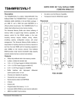
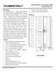
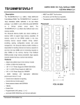
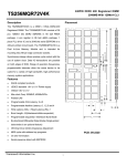
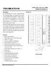
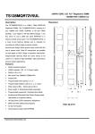
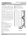
240PIN DDR2 667 Fully Buffered DIMM
2GB With 128Mx4 CL5
TS256MFB72V6K-T
Description
Programmable CAS Latency: 3, 4, 5
The TS256MFB72V6K-T is a 256M x 72bits DDR2-667
Automatic DDR2 DRAM bus and channel calibration
Fully Buffered DIMM. The TS256MFB72V6K-T consists
MBIST and IBIST Test functions
of 36pcs 128Mx4bits DDR2 DRAM in 60 balls FBGA
Hot add-on and Hot Remove Capability
package, 1 pc AMB IC, and a 2048 bits serial EEPROM
Transparent mode for DRAM test support
on
a
240-pin
printed
circuit
board.
The
Placement
TS256MFB72V6K-T is a 240pin fully buffered dual in-line
memory module.
The Advanced Memory Buffer also allows buffering of
memory traffic to support large memory capacities. All
memory control for the DRAM resides in the host,
including memory request initiation, timing, refresh,
B
scrubbing, sparing, configuration access, and power
D
management. The Advanced Memory Buffer interface is
FE
responsible for handling channel and memory requests to
and from the local DIMM and for forwarding requests to
A
AMB
other DIMM on the memory channel. Fully Buffered DIMM
provides a high memory bandwidth, large capacity
channel solution that has a narrow host interface.
Features
C
RoHS compliant products.
240pin fully buffered dual in-line memory module
3.2Gb/s, 4.0Gb/s link transfer rate
G
H
1.8V +/- 0.1V Power Supply for DRAM VDD/VDDQ
1.5V +/- 0.075V Power Supply for AMB VCC
3.3V +/- 0.3V Power Supply for VDDSPD
M
I
J
Buffer Interface with high-speed differential
K
L
point-to-point Link at 1.5 volt
Channel error detection & reporting
Channel fail over mode support
PCB: 09-2620
Serial presence detect with EEPROM
4Banks
Posted CAS
Transcend Information Inc.
1
240PIN DDR2 667 Fully Buffered DIMM
2GB With 128Mx4 CL5
TS256MFB72V6K-T
Dimensions
Pin Description
Side
Millimeters
Inches
Symbol
A
133.35±0.15
5.250±0.006
SCK
System Clock Input, positive line
B
51.00
2.00
/SCK
System Clock Input, negative line
C
67.00
2.64
PN[13:0]
Primary Northbound Data, positive lines
D
5.00
0.197
/PN[13:0]
Primary Northbound Data, negative lines
E
2.50
0.0980
F
1.50
0.059
PS[9:0]
Primary Southbound Data, positive lines
G
5.175
0.204
/PS[9:0]
Primary Southbound Data, negative lines
H
2.175
0.086
SN[13:0]
Secondary Northbound Data, positive lines
I
3.00
0.118
/SN[13:0]
Secondary Northbound Data, negative lines
J
9.50
0.374
SS[9:0]
Secondary Southbound Data, positive lines
K
17.30
0.681
/SS[9:0]
Secondary Southbound Data, negative lines
L
30.35±0.15
1.2±0.006
SCL
Serial Presence Detect (SPD) Clock Input
M
1.27±0.10
0.050±0.004
SDA
(Refer Placement)
SA[2:0]
VID[1:0]
AMB reset signal
RFU
Reserved for Future Use
VTT
AMB Core Power and AMB Channel interface
Power (1.5 Volt)
DRAM Power and AMB DRAM I/O Power (1.8
Volt)
DRAM Address/Command/Clock Termination
Power (VDD/2)
VDDSPD
SPD Power
VSS
Ground
The DNU/M Test pin provides an external
connection R/Cs A-D for testing the margin of
Vref which is produced by a voltage divider on
the module. It is not intended to be used in
normal system operation and must not be
connected(DNU) in a system. This test pin
may have other features on future card
designs and if it does, will be included in this
specification at that time.
VDD
DNU/M_Test
2
SPD Data Input / Output
SPD Address Input, also used to select the
DIMM number in the AMB
Voltage ID: these pins must be unconnected
for DDR2-base Fully Buffered DIMMs
VID[0] is VDD value:OPEN=1.8V,GND=1.5V
VID[1] is Vcc value:OPEN=1.5V,GND=1.2V
RESET
VCC
Transcend Information Inc.
Function
240PIN DDR2 667 Fully Buffered DIMM
2GB With 128Mx4 CL5
TS256MFB72V6K-T
Pinouts:
Pin
Pin
Pin
Pin
Pin
Pin
Pin
Pin
Pin
Pin
No
Name
No
Name
No
Name
No
Name
No
Name
01 VDD
41 /PN13
81 VSS
121 VDD
161 /SN13
02 VDD
42 VSS
82 PS4
122 VDD
162 VSS
03 VDD
43 VSS
83 /PS4
123 VDD
163 VSS
04 VSS
44 RFU*
84 VSS
124 VSS
164 RFU*
05 VDD
45 RFU*
85 VSS
125 VDD
165 RFU*
06 VDD
46 VSS
86 RFU*
126 VDD
166 VSS
07 VDD
47 VSS
87 RFU*
127 VDD
167 VSS
08 VSS
48 PN12
88 VSS
128 VSS
168 SN12
09 VCC
49 /PN12
89 VSS
129 VCC
169 /SN12
10 VCC
50 VSS
90 PS9
130 VCC
170 VSS
11 VSS
51 PN6
91 /PS9
131 VSS
171 SN6
12 VCC
52 /PN6
92 VSS
132 VCC
172 /SN6
13 VCC
53 VSS
93 PS5
133 VCC
173 VSS
14 VSS
54 PN7
94 /PS5
134 VSS
174 SN7
15 VTT
55 /PN7
95 VSS
135 VTT
175 /SN7
16 VID1
56 VSS
96 PS6
136 VID0
176 VSS
17 /RESET
57 PN8
97 /PS6
137 DNU/M_ Test 177 SN8
18 VSS
58 /PN8
98 VSS
138 VSS
178 /SN8
19 RFU**
59 VSS
99 PS7
139 RFU**
179 VSS
20 RFU**
60 PN9
100 /PS7
140 RF**
180 SN9
21 VSS
61 /PN9
101 VSS
141 VSS
181 /SN9
22 PN0
62 VSS
102 PS8
142 SN0
182 VSS
23 /PN0
63 PN10
103 /PS8
143 /SN0
183 SN10
24 VSS
64 /PN10
104 VSS
144 VSS
184 /SN10
25 PN1
65 VSS
105 RFU**
145 SN1
185 VSS
26 /PN1
66 PN11
106 RFU**
146 /SN1
186 SN11
27 VSS
67 /PN11
107 VSS
147 VSS
187 /SN11
28 PN2
68 VSS
108 VDD
148 SN2
188 VSS
29 /PN2
69 VSS
109 VDD
149 /SN2
189 VSS
30 VSS
70 PS0
110 VSS
150 VSS
190 SS0
31 PN3
71 /PS0
111 VDD
151 SN3
191 /SS0
32 /PN3
72 VSS
112 VDD
152 /SN3
192 VSS
33 VSS
73 PS1
113 VDD
153 VSS
193 SS1
34 PN4
74 /PS1
114 VSS
154 SN4
194 /SS1
35 /PN4
75 VSS
115 VDD
155 /SN4
195 VSS
36 VSS
76 PS2
116 VDD
156 VSS
196 SS2
37 PN5
77 /PS2
117 VTT
157 SN5
197 /SS2
38 /PN5
78 VSS
118 SA2
158 /SN5
198 VSS
39 VSS
79 PS3
119 SDA
159 VSS
199 SS3
40 PN13
80 /PS3
120 SCL
160 SN13
200 /SS3
RFU = Reserved Future Use
* These pin position are reserved for forwarded clocks to be used in future module implementations
** These pin positions are reserved for future architecture flexibility
Transcend Information Inc.
3
Pin
No
201
202
203
204
205
206
207
208
209
210
211
212
213
214
215
216
217
218
219
220
221
222
223
224
225
226
227
228
229
230
231
232
233
234
235
236
237
238
239
240
Pin
Name
VSS
SS4
/SS4
VSS
VSS
RFU*
RFU*
VSS
VSS
SS9
/SS9
VSS
SS5
/SS5
VSS
SS6
/SS6
VSS
SS7
/SS7
VSS
SS8
/SS8
VSS
RFU**
RFU**
VSS
SCK
/SCK
VSS
VDD
VDD
VDD
VSS
VDD
VDD
VTT
VDDSPD
SA0
SA1