1
X9SPU-F
USER’S MANUAL
Revision 1.0
The information in this User’s Manual has been carefully reviewed and is believed to be accurate.
The vendor assumes no responsibility for any inaccuracies that may be contained in this document,
makes no commitment to update or to keep current the information in this manual, or to notify any
person or organization of the updates. Please Note: For the most up-to-date version of this
manual, please see our web site at www.supermicro.com.
Super Micro Computer, Inc. ("Supermicro") reserves the right to make changes to the product
described in this manual at any time and without notice. This product, including software and documentation, is the property of Supermicro and/or its licensors, and is supplied only under a license.
Any use or reproduction of this product is not allowed, except as expressly permitted by the terms
of said license.
IN NO EVENT WILL SUPER MICRO COMPUTER, INC. BE LIABLE FOR DIRECT, INDIRECT,
SPECIAL, INCIDENTAL, SPECULATIVE OR CONSEQUENTIAL DAMAGES ARISING FROM THE
USE OR INABILITY TO USE THIS PRODUCT OR DOCUMENTATION, EVEN IF ADVISED OF
THE POSSIBILITY OF SUCH DAMAGES. IN PARTICULAR, SUPER MICRO COMPUTER, INC.
SHALL NOT HAVE LIABILITY FOR ANY HARDWARE, SOFTWARE, OR DATA STORED OR USED
WITH THE PRODUCT, INCLUDING THE COSTS OF REPAIRING, REPLACING, INTEGRATING,
INSTALLING OR RECOVERING SUCH HARDWARE, SOFTWARE, OR DATA.
Any disputes arising between manufacturer and customer shall be governed by the laws of Santa
Clara County in the State of California, USA. The State of California, County of Santa Clara shall
be the exclusive venue for the resolution of any such disputes. Supermicro's total liability for all
claims will not exceed the price paid for the hardware product.
FCC Statement: This equipment has been tested and found to comply with the limits for a Class B
digital device pursuant to Part 15 of the FCC Rules. These limits are designed to provide reasonable protection against harmful interference in a residential installation. This equipment generates,
uses, and can radiate radio frequency energy and, if not installed and used in accordance with the
manufacturer’s instruction manual, may cause interference with radio communications. However,
there is no guarantee that interference will not occur in a particular installation. If this equipment
does cause harmful interference to radio or television reception, which can be determined by turning the equipment off and on, you are encouraged to try to correct the interference by one or more
of the following measures:
•Reorient or relocate the receiving antenna.
•Increase the separation between the equipment and the receiver.
•Connect the equipment into an outlet on a circuit different from that to which the
receiver is connected.
•Consult the dealer or an experienced radio/television technician for help.
California Best Management Practices Regulations for Perchlorate Materials: This Perchlorate warning applies only to products containing CR (Manganese Dioxide) Lithium coin cells. “Perchlorate
Material-special handling may apply. See www.dtsc.ca.gov/hazardouswaste/perchlorate”.
WARNING: Handling of lead solder materials used in this product
may expose you to lead, a chemical known to the State of California
to cause birth defects and other reproductive harm.
Manual Revision 1.0
Release Date: June 29, 2012
Unless you request and receive written permission from Super Micro Computer, Inc., you may not
copy any part of this document. Information in this document is subject to change without notice.
Other products and companies referred to herein are trademarks or registered trademarks of their
respective companies or mark holders.
Copyright © 2012 by Super Micro Computer, Inc. All rights reserved.
Printed in the United States of America
Preface
Preface
This manual is written for system integrators, PC technicians and
knowledgeable PC users. It provides information for the installation and use of the
X9SPU-F motherboard.
About This Motherboard
The
X9SPU-F Motherboard supports a single Intel® Xeon E3-1200 v2
processor family and Gen-2 Core-i3 (LGA 1155) processors. It is also backward
compatible with Xeon E3-1200 processors.
With the Intel® C216 series chipset built in, the X9SPU-F Motherboard offers exceptional system performance using Supermicro's unique Universal I/O (UIO) form
factor. Features such as two SATA 3 ports, four SATA 2 ports, support for up to
256GB of memory, RAID 0, 1, 5, 10 support, dual 1Gb LAN, TPM support and eight
USB ports make the X9SPU-F series ideal for server platforms.
Please refer to our website (http://www.supermicro.com/products/) for processor
and memory support updates.
*This product is intended to be installed and serviced by professional technicians.
Manual Organization
Chapter 1 describes the features, specifications and performance of the motherboard, and provides detailed information on the Intel Patsburg chipset.
Chapter 2 provides hardware installation instructions. Read this chapter when installing the processor, memory modules and other hardware components into the
system. If you encounter any problems, see Chapter 3, which describes troubleshooting procedures for video, memory and system setup stored in the CMOS.
Chapter 4 includes an introduction to the BIOS, and provides detailed information
on running the CMOS Setup utility.
Appendix A provides BIOS Error Beep Codes.
Appendix B lists software program installation instructions.
Appendix C contains the UEFI BIOS Recovery instructions.
iii
X9SPU-F Motherboard User’s Manual
Conventions Used in the Manual:
Special attention should be given to the following symbols for proper installation and
to prevent damage done to the components or injury to yourself:
Danger/Caution: Instructions to be strictly followed to prevent catastrophic
system failure or to avoid bodily injury
Warning: Critical information to prevent damage to the components or
data loss.
Important: Important information given to ensure proper system installation or to relay safety precautions.
Note: Additional Information given to differentiate various models or provides information for correct system setup.
iv
Contacting Supermicro
Contacting Supermicro
Headquarters
Address:
Super Micro Computer, Inc.
980 Rock Ave.
San Jose, CA 95131 U.S.A.
Tel:
+1 (408) 503-8000
Fax:
+1 (408) 503-8008
Email:
[email protected] (General Information)
[email protected] (Technical Support)
Web Site:
www.supermicro.com
Europe
Address:
Super Micro Computer B.V.
Het Sterrenbeeld 28, 5215 ML
's-Hertogenbosch, The Netherlands
Tel:
+31 (0) 73-6400390
Fax:
+31 (0) 73-6416525
Email:
[email protected] (General Information)
[email protected] (Technical Support)
[email protected] (Customer Support)
Asia-Pacific
Address:
Super Micro Computer, Inc.
4F, No. 232-1, Liancheng Rd.
Chung-Ho 235, Taipei County
Taiwan, R.O.C.
Tel:
+886-(2) 8226-3990
Fax:
+886-(2) 8226-3991
Web Site:
www.supermicro.com.tw
Technical Support:
Email:
[email protected]
Tel: +886-(2) 8226-5990
v
X9SPU-F Motherboard User’s Manual
Table of Contents
Preface
About This Motherboard................................................................................................. iii
Manual Organization...................................................................................................... iii
Conventions Used in the Manual:..................................................................................iv
Contacting Supermicro....................................................................................................v
Chapter 1
Introduction
1-1Overview.......................................................................................................... 1-1
Checklist........................................................................................................... 1-1
Motherboard Features...................................................................................... 1-7
1-2
Chipset Overview .......................................................................................... 1-10
Intel C216 Chipset Features.......................................................................... 1-10
1-3 Special Features.............................................................................................1-11
Recovery from AC Power Loss.......................................................................1-11
1-4 PC Health Monitoring......................................................................................1-11
Fan Status Monitor with Firmware Control ....................................................1-11
Environmental Temperature Control...............................................................1-11
System Resource Alert.................................................................................. 1-12
1-5 ACPI Features................................................................................................ 1-12
Slow Blinking LED for Suspend-State Indicator............................................ 1-12
1-6 Power Supply................................................................................................. 1-12
1-7 Super I/O........................................................................................................ 1-13
Chapter 2
Installation
2-1
Static-Sensitive Devices................................................................................... 2-1
Precautions...................................................................................................... 2-1
Unpacking........................................................................................................ 2-1
2-2
Processor and Heatsink Installation................................................................ 2-2
Installing the LGA1155 Processor .................................................................. 2-2
Installing a Passive CPU Heatsink.................................................................. 2-5
Removing the Heatsink.................................................................................... 2-6
2-3 Installing DDR3 Memory
2-7
DIMM Installation............................................................................................. 2-7
Removing Memory Modules............................................................................ 2-7
vi
Table of Contents
Memory Support............................................................................................... 2-8
Memory Population Guidelines........................................................................ 2-8
Memory Population Guidelines........................................................................ 2-9
2-4
Motherboard Installation................................................................................. 2-10
Tools Needed................................................................................................. 2-10
Location of Mounting Holes........................................................................... 2-10
Installing the Motherboard..............................................................................2-11
2-5
Connectors/IO Ports....................................................................................... 2-12
Motherboard I/O Backpanel........................................................................... 2-12
Universal Serial Bus (USB)....................................................................... 2-13
Ethernet Ports (LAN1/LAN2)..................................................................... 2-14
IPMI Port (IPMI) ....................................................................................... 2-14
Unit Identifier Switch (UID)........................................................................ 2-14
VGA Connector (VGA).............................................................................. 2-15
Serial Ports................................................................................................ 2-15
Front Control Panel........................................................................................ 2-16
Front Control Panel Pin Definitions............................................................... 2-17
Power LED ............................................................................................... 2-17
HDD LED................................................................................................... 2-17
Power Fail LED......................................................................................... 2-17
NIC1/NIC2 (LAN1/LAN2)........................................................................... 2-18
Unit ID LED (Front Panel) / OH / Fan Failure.......................................... 2-18
NMI Button................................................................................................ 2-19
Reset Button ............................................................................................ 2-19
Power Button ............................................................................................ 2-19
2-6
Connecting Cables & Optional Devices......................................................... 2-20
ATX Main PWR (JPW1) & GPU PWR Connectors (JPW2)..................... 2-20
Fan Headers (FAN1~5)............................................................................. 2-21
Chassis Intrusion (JL1)............................................................................. 2-21
Legacy Wake-On-LAN Header (JSTBY1)................................................. 2-22
Power Supply I2C (JPI2C2)...................................................................... 2-22
DOM PWR Connector (JSD1)................................................................... 2-23
TPM Header (JTPM)................................................................................. 2-23
T-SGPIO1~2 Headers (T-SGPIO)............................................................. 2-24
External Power LED (JLED)..................................................................... 2-24
Internal Buzzer (SPEAKER)...................................................................... 2-25
Speaker (JSPK)......................................................................................... 2-25
Internal Battery (BAT)................................................................................ 2-25
vii
X9SPU-F Motherboard User’s Manual
2-7
Jumper Settings............................................................................................. 2-26
Explanation of Jumpers................................................................................. 2-26
LAN Port Enable/Disable (JPL1/JPL2)...................................................... 2-26
Clear CMOS (JBT1).................................................................................. 2-27
PCI Slot SMB Enable (JI2C2/JI2C3)......................................................... 2-27
Watch Dog Reset (JWD)........................................................................... 2-28
VGA Enable (JPG1).................................................................................. 2-28
BMC Enable/Disable (JPB)....................................................................... 2-29
USB Wake-Up (JPUSB1).......................................................................... 2-29
ME Recovery (JPME1).............................................................................. 2-30
ME Manufacturing Mode........................................................................... 2-30
x16 PCI Setting (JRF1)............................................................................. 2-30
2-8
Onboard Indicators......................................................................................... 2-31
LAN Port LEDs.......................................................................................... 2-31
Standby Power (LE4)................................................................................ 2-31
IPMI Heartbeat LED (LE7)........................................................................ 2-32
Unit ID LED (LE5)..................................................................................... 2-32
2-9
SATA Connections.......................................................................................... 2-33
SATA Connections (I-SATA0~5) ............................................................... 2-33
2-10 Expansion Slots............................................................................................. 2-34
Universal I/O Slot (UIO RISER)................................................................ 2-34
PCI-E 2.0 x4 Slot (SBX2).......................................................................... 2-34
PCI-E 3.0 x16 and PCI-E 2.0 x4 Slot (SBX1 and SBX3)......................... 2-34
Chapter 3
Troubleshooting
3-1 Troubleshooting Procedures............................................................................ 3-1
Before Power On............................................................................................. 3-1
No Power......................................................................................................... 3-1
No Video.......................................................................................................... 3-2
Memory Errors ................................................................................................ 3-2
When You Lose the System’s Setup Configuration......................................... 3-2
3-2
Technical Support Procedures......................................................................... 3-3
3-3
Frequently Asked Questions............................................................................ 3-4
3-4
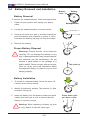
Battery Removal and Installation..................................................................... 3-6
Battery Removal............................................................................................... 3-6
Proper Battery Disposal................................................................................... 3-6
Battery Installation............................................................................................ 3-6
3-5
Returning Merchandise for Service................................................................. 3-7
viii
Table of Contents
Chapter 4
BIOS
4-1Introduction....................................................................................................... 4-1
Starting BIOS Setup Utility............................................................................... 4-1
How To Change the Configuration Data.......................................................... 4-1
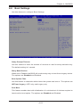
How to Start the Setup Utility.......................................................................... 4-2
4-2 Main Setup....................................................................................................... 4-2
System Overview: The following BIOS information will be displayed:........ 4-3
System Time/System Date ......................................................................... 4-3
Supermicro X9SPU-F.................................................................................. 4-3
Processor.................................................................................................... 4-3
System Memory.......................................................................................... 4-3
4-3 Advanced Setup Configurations...................................................................... 4-4
BOOT Feature............................................................................................... 4-4
Quiet Boot................................................................................................... 4-4
AddOn ROM Display Mode......................................................................... 4-4
Bootup Num-Lock........................................................................................ 4-4
Wait For 'F1' If Error.................................................................................... 4-5
Interrupt 19 Capture.................................................................................... 4-5
Watch Dog Function.................................................................................... 4-5
Power Button Function................................................................................ 4-5
Restore on AC Power Loss......................................................................... 4-5
DeepSx Power Policies............................................................................... 4-5
Processor and Clock Options....................................................................... 4-5
CPU Configuration...................................................................................... 4-6
Clock Spread Spectrum.............................................................................. 4-6
Hardware Prefetcher (Available when supported by the CPU).................. 4-6
Adjacent Cache Line Prefetch (Available when supported by the CPU).... 4-6
Intel® Virtualization Technology (Available when supported by the CPU).. 4-6
Execute-Disable Bit Capability (Available when supported by the OS and
the CPU)...................................................................................................... 4-6
Intel® AES-NI............................................................................................... 4-6
Intel® Hyper Threading Technology............................................................. 4-6
Active Processor Cores............................................................................... 4-7
Power Technology....................................................................................... 4-7
EIST............................................................................................................. 4-7
CPU C3 Report, CPU C6, Report, CPU C7 Report................................... 4-7
C1E.............................................................................................................. 4-7
ix
X9SPU-F Motherboard User’s Manual
Turbo Boost Technology........................................................................... 4-7
Turbo Mode................................................................................................. 4-7
Chipset Configuration.................................................................................... 4-8
IDE/SATA Configuration................................................................................ 4-9
SATA Mode.................................................................................................. 4-9
IDE Mode.................................................................................................... 4-9
Serial ATA Port 0~5..................................................................................... 4-9
AHCI Mode................................................................................................ 4-10
Aggressive Link Power Management........................................................ 4-10
Serial ATA Port 0~5 Hot Plug.................................................................... 4-10
Serial ATA Port 0~5 Staggered Spin Up................................................... 4-10
RAID Mode................................................................................................ 4-10
Serial ATA Port 0~5 Hot Plug.................................................................... 4-10
PCIe/PCI/PnP Configuration ...................................................................... 4-10
PCI Latency Timer..................................................................................... 4-10
Above 4G Decoding.................................................................................. 4-10
Onboard LAN Option ROM Select............................................................ 4-10
Load Onboard LAN1 Option ROM / Load Onboard LAN2 Option ROM...4-11
Boots Graphic Adapter Priority...................................................................4-11
Super IO Configuration ...............................................................................4-11
Serial Port 1...............................................................................................4-11
Serial Port 1 Settings.................................................................................4-11
Serial Port 2...............................................................................................4-11
Serial Port 2 Settings.................................................................................4-11
Serial Port Console Redirection.................................................................. 4-12
COM 1, COM2, SOL................................................................................. 4-12
Console Redirection.................................................................................. 4-12
Serial Port for Out-of-Band Management/Windows Emergency Management
Services (EMS)......................................................................................... 4-13
Console Redirection (for EMS)................................................................. 4-13
Hardware Health Configuration................................................................... 4-14
Fan Speed Control Mode.......................................................................... 4-14
CPU Temperature...................................................................................... 4-15
System Temperature / Peripheral Temperature........................................ 4-15
Fan 1 ~ Fan 5 Speed................................................................................ 4-15
VCORE, 12V, VDIMM, 5VCC, -12V, AVCC, 3.3VCC, VSB, VBAT........... 4-15
ACPI Settings.............................................................................................. 4-15
High Precision Event Timers..................................................................... 4-15
WHEA Support.......................................................................................... 4-16
x
Table of Contents
PCH-FW Configuration................................................................................ 4-16
MDES BIOS Status Code......................................................................... 4-16
Firmware Update Configuration............................................................. 4-16
Me FW Image Re-Flash............................................................................ 4-16
Intel ICC...................................................................................................... 4-16
Use Watchdog Timer for ICC.................................................................... 4-16
Turn off unused PCI/PCIe clocks.............................................................. 4-16
Lock ICC registers..................................................................................... 4-17
4-4
Event Logs..................................................................................................... 4-17
Change SmBIOS Event Log Settings......................................................... 4-17
Smbios Event Log..................................................................................... 4-17
Erase Event Log........................................................................................ 4-17
When Log is Full....................................................................................... 4-17
Log System Boot Event............................................................................ 4-18
MECI.......................................................................................................... 4-18
METW........................................................................................................ 4-18
Log OEM Codes........................................................................................ 4-18
Convert OEM Codes................................................................................. 4-18
View SmBIOS Event Log.......................................................................... 4-18
4-5
IPMI Settings.................................................................................................. 4-19
System Event Log.................................................................................. 4-19
When SEL Full.......................................................................................... 4-19
Log EFI Status Codes............................................................................... 4-19
BMC Network Configuration................................................................... 4-20
Update IPMI LAN Configuration................................................................ 4-20
Configuration Source................................................................................. 4-20
4-6
Boot Settings.................................................................................................. 4-21
Setup Prompt Timeout.............................................................................. 4-21
Retry Boot Devices................................................................................... 4-21
Boot Option Filter...................................................................................... 4-21
Fast Boot................................................................................................... 4-21
Boot Options Priorities.............................................................................. 4-22
Boot Option #1, Boot option #2, etc......................................................... 4-22
Network Device BBS Priorities.................................................................. 4-22
4-8
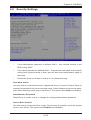
Security Settings............................................................................................ 4-23
Password Check....................................................................................... 4-23
Administrator Password ........................................................................... 4-23
xi
X9SPU-F Motherboard User’s Manual
Secure Boot Control.................................................................................. 4-23
Secure Boot Policy...................................................................................... 4-24
Internal FV................................................................................................. 4-24
Option ROM, Removable Media, Fixed Media......................................... 4-24
Key Management........................................................................................ 4-24
Platform Key (PK)..................................................................................... 4-24
Key Exchange Key Database (KEK)......................................................... 4-24
Authorized Signature Database (DB)........................................................ 4-24
Forbidden Signature Database (DBX)...................................................... 4-25
Manage All Factory Keys (PK, KEK, DB, DBX)........................................ 4-25
Install Factory Defaults.............................................................................. 4-25
4-9
Save & Exit.................................................................................................... 4-26
Discard Changes and Exit ....................................................................... 4-26
Save Changes and Reset......................................................................... 4-26
Discard Changes....................................................................................... 4-26
Restore Defaults........................................................................................ 4-27
Save As User Defaults.............................................................................. 4-27
Restore User Defaults............................................................................... 4-27
Boot Override............................................................................................ 4-27
Appendix A
BIOS Error Beep Codes
A-1 BIOS Error Beep Codes..................................................................................A-1
Appendix B
Software Installation Instructions
B-1 Installing Drivers...............................................................................................B-1
B-2 Configuring SuperDoctor® III...........................................................................B-2
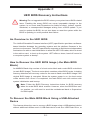
Appendix C
UEFI BIOS Recovery Instructions
An Overview to the UEFI BIOS...................................................................................C-1
How to Recover the UEFI BIOS Image (-the Main BIOS Block)................................C-1
To Recover the Main BIOS Block Using a USB-Attached Device..............................C-1
xii
Chapter 1: Introduction
Chapter 1
Introduction
1-1Overview
Checklist
Congratulations on purchasing your computer motherboard from an acknowledged
leader in the industry. Supermicro boards are designed with the utmost attention to
detail to provide you with the highest standards in quality and performance.
Please check that the following items have all been included with your motherboard.
If anything listed here is damaged or missing, contact your retailer.
The following items are included in the retail box.
•One (1) Supermicro Mainboard
•Six (6) SATA cables
•One (1) I/O shield
•One (1) Supermicro CD containing drivers and utilities
•One (1) User's Manual
1-1
X9SPU-F Motherboard User’s Manual
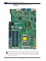
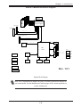
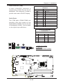
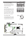
X9SPU-F Motherboard Image
Note: All graphics shown in this manual were based upon the latest PCB
Revision available at the time of publishing of the manual. The motherboard
you've received may or may not look exactly the same as the graphics
shown in this manual.
1-2
Chapter 1: Introduction
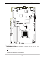
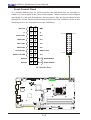
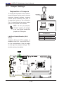
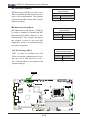
Motherboard Layout
J28
LE5
A
SW1
MH8
KB/MS
USB4/5/IPMI_LAN
C
VGA
UID-LED
J4
1
COM1
COM1
7
LAN1
JLAN1
JLAN2
LAN2
JPUSB1:B/P USB WAKE UP
UIOP
JI2C1/JI2C2
ON:Enable
OFF:Disable
JI2C2
MH3
1
JI2C1
1
1
JPUSB1
4
J8
JPUSB1
1-2:ENABLE
2-3:DISABLE
JTPM
R137
J5
LE7
JPG1 VGA
1-2:ENABLE
2-3:DISABLE
C
JSTBY1
1
JPG1
SBX2: PCI-E 2.0 X4 in X8
A
1
3
3
1
1
JPL2
JPL1
+
SPEAKER
JPME1
JPME2
CMOS CLEAR
JBT1
JPME1
ON:ME RECOVERY
OFF:NORMAL
GND
GND
JSPK
JPME2
ON:ME MANUFACTURING MODE
OFF:NORMAL
JSD1:DOM_PWR
5V
1
J16
JSPK:
Buzzer/Speaker
SPKR1
JPL1 LAN1
1-2:ENABLE
2-3:DISABLE
JPL2 LAN2
1-2:ENABLE
2-3:DISABLE
COM2
1
3
C768
JSD1
J2
I-SATA5
USB3.0-2/3
I-SATA3
JLED:Power LED
REV:1.00
JWD
1-2:RST
2-3:NMI
X9SPU-F
JL1:CHASSIS INSTRUSION
JL1
JWD
I-SATA2
JLED
SBX1: PCI-E 3.0/2.0 X16 or X8+X8
JPB:BMC
1-2:ENABLE
2-3:DISABLE
JUSB4
I-SATA4
JPB
DESIGNED IN USA
T-SGPIO1
J29
B1
I-SATA1
MAC CODE
BAR CODE
I-SATA0
MH2
J31
1
PWR ON
+
J1
JPI2C
JF1
20
CPU
10
JUSB3
11
JF1
DDR3 1600/1333/1066 UDIMM/RDIMM required
DIMMA1
DIMMA2
DIMMB1
DIMMB2
J3
USB 3.0-0/1
SBX3: PCI-E 2.0 X4
USB 12/13
J15
RST PS UID NIC NIC HDD PWR X NMI
2
1 LED LED
FAIL PF
OH/FF
T-SGPIO2
JPI2C:PWR I2C
MH4
JPW1
1
MH7
1
JPW2
A
C
FAN1
LE2
LE3 LE4
C
C
A
A
MH5
FAN5
FAN2
MH6
FAN4
4
FAN3
RT1
JRF1
1
3
JRF1
1-2:AUTO
2-3:FORCE TO X8+X8
Important Notes to the User
•See Chapter 2 for detailed information on jumpers, I/O ports and JF1 front
panel connections.
•"
" indicates the location of "Pin 1".
•Jumpers not indicated are for testing only.
1-3
X9SPU-F Motherboard User’s Manual
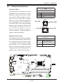
X9SPU-F Motherboard Quick Reference
J28
LE5
A
SW1
MH8
1
UIO RISER
COM1
COM1
UID-LED
JI2C1/JI2C2
ON:Enable
OFF:Disable
JI2C2
7
LAN2
MH3
1
JI2C1
1
1
J8
JTPM
JUSB4
JWD
1-2:RST
2-3:NMI
T-SGPIO1
BAT
RST PS UID NIC NIC HDD PWR X NMI
2
1 LED LED
FAIL PF
OH/FF
1
+
PWR ON
JF1
DDR3 1600/1333/1066 UDIMM/RDIMM required
DIMMA1
DIMMA2
DIMMB1
DIMMB2
J1
J31
MH4
JPI2C:PWR I2C
T-SGPIO2
I-SATA0 3.0
I-SATA1 3.0
USB 12/13
J3
USB 3.0-0/1
SBX3: PCI-E 2.0 X4
USB 12/13
J15
MAC CODE
BAR CODE
I-SATA0
MH2
JWD
J29
B1
SBX1
JPI2C
JPI2C2
JF1
20
CPU
JF1
10
JUSB3
11
REV:1.00
JLED:Power LED
DESIGNED IN USA
I-SATA1
SBX3
JLED
JWD
X9SPU-F
JL1:CHASSIS INSTRUSION
JL1
JPME2
JLED
I-SATA2
COM2
USB3.0-2/3
SBX1: PCI-E 3.0/2.0 X16 or X8+X8
JPB:BMC
1-2:ENABLE
2-3:DISABLE
COM2
JSPK
JSPK
JPME2
ON:ME MANUFACTURING MODE
OFF:NORMAL
JSTBY1
JPL2
JPME1
JUSB4
JPB
I-SATA3
1
J16
I-SATA4
JPB
JPME1
JPME2
JSD1
I-SATA5
JPL2
JPL1
1
3
J2
JPME1
ON:ME RECOVERY
OFF:NORMAL
I-SATA5
I-SATA4
I-SATA3
I-SATA2
5V
C768
3
1
GND
1
3
1
GND
JSTBY1
1
JBT1
JSD1:DOM_PWR
JPG1
SPEAKER
JPG1 VGA
1-2:ENABLE
2-3:DISABLE
JSPK:
Buzzer/Speaker
SPKR1
JPL1 LAN1
1-2:ENABLE
2-3:DISABLE
JPL2 LAN2
1-2:ENABLE
2-3:DISABLE
CMOS CLEAR
R137
SPEAKER
JBT1
JSD1
JPG1
JPL1
J5
JTPM
C
+
SBX2: PCI-E 2.0 X4 in X8
A
JPUSB1
JPUSB1
1-2:ENABLE
2-3:DISABLE
USB4/5
LE7
SBX2
JPUSB1
4
LE7
KB/MS
LAN1
JLAN1
JLAN2
JPUSB1:B/P USB WAKE UP
UIOP
JI2C2
JI2C1
JL1
T-SGPIO1
T-SGPIO2
IPMI
KB/MS
USB4/5/IPMI_LAN
C
COM1
VGA
UID-LED
J4
VGA
LAN2 LAN1
LE5
JPW1
1
JUSB3
MH7
1
A
LE4
LE3 LE4
C
C
A
A
MH5
FAN5
JPW2
FAN2
FAN4
4
FAN5
C
JPW1
FAN1
LE2
DIMMB2
DIMMB1
DIMMA2
DIMMA1
FAN3
FAN4 FAN3
RT1
JRF1
1
3
JRF1
1-2:AUTO
2-3:FORCE TO X8+X8
JRF1
1-4
JPW2 FAN2
MH6
FAN1
Chapter 1: Introduction
X9SPU-F Motherboard Headers/Connectors
Connector/Switch
Description
UID-LED
Unit ID Switch
SBX2
Slot for Supemicro riser card P/N RSC-R1UW-E8R
SBX1, SBX3, UIO-RISER
Slots for Supermicro riser card
T-SGPIO1~T-SGPIO2
Serial Link General Purpose I/O Headers (5V Gen1/Gen 2)
I-SATA0, I-SATA1
SATA 3.0 Connectors via PCH (6Gb/s)
I-SATA2~I-SATA5
SATA 2.0 Connectors via PCH (3Gb/s)
KB/MS
PS/2 Keyboard and Mouse Ports
FAN1~FAN5
System/CPU Fan Headers
SPEAKER
Internal Speaker (Leave jumper on JSPK installed, pins 1-2)
JSD1
SATA Disk On Module (DOM) Power Connector
JSTBY1
Legacy Wake On LAN Header
JPW1
24-pin Main ATX Power Connector
JPW2
8-pin Secondary Power Connector for the GPU
JPI2C2
Power Supply SMBus I2C Header
JF1
Front Panel Control Header
JL1
Chassis Intrusion Header
JLED
3-pin Power LED Header
JSPK
Internal Speaker/Buzzer Select or External Speaker Header
USB4/5
Rear USB Ports
JUSB4, JUSB3
Internal USB 3.0 Headers USB0/1, USB2/3
USB12/13
Internal USB 2.0 Headers USB12/13
BAT
Onboard Battery
JTPM
Trusted Platform Module (TPM) Header
LAN1/LAN2
Rear LAN Connectors (1Gb)
COM1, COM2
Rear Serial Port (COM1), Serial Port Header (COM2)
VGA
Rear VGA Port
DIMMA1~DIMMB2
DIMM Memory Slots
IPMI
Rear IPMI LAN Port
1-5
X9SPU-F Motherboard User’s Manual
X9SPU-F Motherboard Jumpers
Jumper
Description
Default
JPG1
Onboard VGA Enable
Pins 1-2 (Enabled)
JI2C1~JI2C2
SMB to PCI Slots
Pins 1-2 (Enabled)
JWD
Watch Dog Timer Reset
Pins 1-2 (Reset)
JRF1
x16 PCIe Setting, Force to x8+x8
Pins 1-2 (Auto)
JPL1/JPL2
LAN1/LAN2 Enable/Disable
Pins 1-2 (Enabled)
JPB
BMC Enable
Pins 1-2 (Enabled)
JPME1
ME Recovery Mode Select
Pins 2-3 (Disabled)
JPME2
ME Manufacture Mode
Pins 2-3 (Disabled)
JUSB1
USB Wake-up Enable (Rear USB Ports)
Pins 1-2 (Enabled)
JBT1
CMOS Clear
See Chapter 2
X9SPU-F Motherboard LED Indicators
LED
Description
Color/State
Status
LE7
IPMI Heartbeart
Green: Blinking
IPMI Normal
LE4
Standby Power LED
Green: Solid On
Standby Power On
LE5
Unit ID LED
Blue: Solid On
Unit ID Switch is On
1-6
Chapter 1: Introduction
Motherboard Features
CPU
Single Intel® Xeon E3-1200 v2 processor family and Gen-2
Core-i3 (LGA 1155) processors. It is also backward compatible with Xeon E3-1200 processors.
Memory
Four (4) UDIMM slots support up to 32GB of DDR3 Unbuffered, ECC or non-ECC UDIMM memory, 1333/1600MHz..
Supports dual-channel memory bus
DIMM sizes
UDIMM
1GB, 2GB, 4GB, 8GB
Chipset
Intel® C216 Express
Expansion
PCI Slots (Supported on Supermicro Riser Cards)
One (1) PCI-Express 3.0 x16 slot
One (1) PCI-Express 2.0 x4 in x8 slot
One (1) PCI-Express 2.0 x4 in proprietary slot
One (1) Universal I/O (UIO) Slot
Network Connections
Integrated LAN
Two (2) Intel 82574L Gb LAN ports
I/O Devices
SATA Connections
SATA 3.0 Ports
Two (2) 6 Gb/s
SATA 2.0 Ports
Four (4) 3 Gb/s
RAID 0, 1, 5, 10
USB Devices
Two (2) USB 2.0 ports on the rear I/O panel
Two (2) USB 2.0 via one header for front panel access
Four (4) USB 3.0 via two headers for front panel access
Serial (COM) Ports
Two (2) Fast UART 16550 connections on the I/O
backpanel and one header
Super I/O
Winbond Super I/O NCT6776F
BIOS
32 Mb SPI AMI BIOS® SM Flash BIOS
Plug & Play, DMI 2.3, ACPI 1.0 (Limited), USB Keyboard
support
Power Configuration
ACPI/ACPM Power Management
Main Switch Override Mechanism
Power-on mode for AC power recovery
1-7
X9SPU-F Motherboard User’s Manual
PC Health Monitoring
CPU & Chassis Monitoring
Onboard voltage monitors for CPU core, +3.3V, +5V, +/12V, +3.3V Stdby, +5V Stdby, VBAT, HT, Memory, Chipset
CPU 4-phase switching voltage regulator
CPU/System overheat LED and thermal control
CPU Thermal Trip support
CPU & Chassis Environment Monitor
Fan Control
Fan status monitoring with firmware 4-pin (Pulse Width
Modulation) fan speed control
Low noise fan speed control
System Management
PECI (Platform Environment Configuration Interface) 2.0
support
System resource alert via SuperDoctor III
SuperoDoctor III, Watch Dog, NMI
Chassis Intrusion header and detection
CD Utilities
BIOS flash upgrade utility
Drivers and software for Intel® C216 chipset utilities
Other
ROHS 6/6 (Full Compliance, Lead Free)
TPM 1.2 on board
DOM (Disk on Module) Power Connector Support
FCC B, EuP Lot 6, WHQL
Dimensions
8" x 13" UIO form factor, 6 layers
1-8
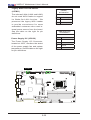
Chapter 1: Introduction
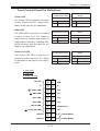
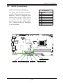
X9SPU-F Motherboard Block Diagram
#1-6
#1-5
#1-4
#1-3
#1-2
#1-1
VR12
5+1 PHASE
130 W
DDRIII
800/1066/1333
P0
Intel
E5-1600/E5-2600 Series
8 SNB CORE DDR-III
P1
SXB1/JPCIE1
PCI-E X16
PCI-E X16
SXB2/JPCIE2
#2
#3
#1
DMI2
PCI-E X16 G3
PCI-E X16 G3
CPU1 SLOT3 PCI-E 3.0 X8
PCI-E X8
PCI-E X8 G3
DMI2
4GB/s
DMI2
PCI-E X4
SATA 2.0
PORTs#0~3
SATA/SAS
G2
LAN
LANE1/2/3/4
i350
LANE6
#5
#4
#3
#2
#1
#0
PCH
6.0 Gb/S
FOR PORT 0/1
SATA
LANE5
SSB-A
CPU0
3.0 Gb/S
FOR PORT 2-5
Infineon
28
DEBUG
PORT
PCI 32bit
VGA
USB 2.0
24-28
USB
BMC
#6
#5
#3
#2
#1
#0
PORT 0/1 Rear
PORT 2-5 Front
SMB:28
Vcore/Vsa
CHIL8113
SMB:2A
VDDQAB
CHIL8113
SMB:2C
VDDQCD
HW MONITOR
NCT7904
COM1
External
SIO
W83527
NI
SPI
FAN SPEED
CTRL
FRONT PANEL
Rev. 1.01
SYSTEM POWER
System Block Diagram
Note: This is a general block diagram and may not exactly represent the features on
your motherboard. See the Motherboard Features pages for the actual specifications
of each motherboard.
1-9
X9SPU-F Motherboard User’s Manual
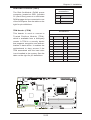
1-2 Chipset Overview
The Intel® C216 series is a single chip solution that is designed for dedicated servers and workstations. It supports high-speed SAS, SATA and advanced requirements for Intel Xeon platforms.
Intel C216 Chipset Features
•Direct Media Interface (up 5 Gt/s transfer, Full Duplex)
•Intel® Matrix Storage Technology and Intel Rapid Storage Technology
•2 SATA Gen 3, RAID, 4 SATA Gen 2 Support
•Manageability Engine (ME 8.0)
•PCI Express 2.0 Interface (up to 5.0 GT/s)
•PCI Express 3.0 Interface (up to 8.0 GT/s)
•SATA 3.0 ports (up to 6Gb/s)
1-10
Chapter 1: Introduction
1-3 Special Features
Recovery from AC Power Loss
Basic I/O System (BIOS) provides a setting for you to determine how the system
will respond when AC power is lost and then restored to the system. You can
choose for the system to remain powered off (in which case you must press the
power switch to turn it back on), or for it to automatically return to a power-on state.
See the Advanced BIOS Setup section to change this setting. The default setting
is Last State.
1-4 PC Health Monitoring
This section describes the PC health monitoring features of the board. All have an
onboard System Hardware Monitoring chip that supports PC health monitoring. An
onboard voltage monitor will scan these onboard voltages continuously: CPU core,
+3.3V, +5V, +/-12V, +3.3V Stdby, +5V Stdby, VBAT, HT, Memory, Chipset. Once a
voltage becomes unstable, a warning is given, or an error message is sent to the
screen. The user can adjust the voltage thresholds to define the sensitivity of the
voltage monitor.
Fan Status Monitor with Firmware Control
PC health monitoring in the BIOS can check the RPM status of the cooling fans. The
onboard CPU and chassis fans are controlled by Thermal Management via BIOS
(under the Hardware Monitoring section in the Advanced Setting).
Environmental Temperature Control
The thermal control sensor monitors the CPU temperature in real time and will turn
on the thermal control fan whenever the CPU temperature exceeds a user-defined
threshold. The overheat circuitry runs independently from the CPU. Once the thermal sensor detects that the CPU temperature is too high, it will automatically turn
on the thermal fans to prevent the CPU from overheating. The onboard chassis
thermal circuitry can monitor the overall system temperature and alert the user when
the chassis temperature is too high.
Note: To avoid possible system overheating, please be sure to provide
adequate airflow to your system.
1-11
X9SPU-F Motherboard User’s Manual
System Resource Alert
This feature is available when the system is used with Supero Doctor III in the Windows OS
environment or used with Supero Doctor II in Linux. Supero Doctor is used to notify the user of
certain system events. For example, you can also configure Supero Doctor to provide you with
warnings when the system temperature, CPU temperatures, voltages and fan speeds go beyond
predefined thresholds.
1-5 ACPI Features
ACPI stands for Advanced Configuration and Power Interface. The ACPI specification defines a flexible and abstract hardware interface that provides a standard
way to integrate power management features throughout a PC system, including
its hardware, operating system and application software. This enables the system
to automatically turn on and off peripherals such as CD-ROMs, network cards, hard
disk drives and printers.
In addition to enabling operating system-directed power management, ACPI also
provides a generic system event mechanism for Plug and Play, and an operating
system-independent interface for configuration control. ACPI leverages the Plug and
Play BIOS data structures, while providing a processor architecture-independent
implementation that is compatible with the Microsoft® Windows® series of Operating Systems.
Slow Blinking LED for Suspend-State Indicator
When the CPU goes into a suspend state, the chassis power LED will start to blink
to indicate that the CPU is in suspend mode. When the user presses any key, the
CPU will "wake up", and the LED will automatically stop blinking and remain on.
1-6 Power Supply
As with all computer products, a stable power source is necessary for proper and
reliable operation. It is even more important for processors that have high CPU
clock rates.
This motherboard accommodates 24-pin ATX power supplies. Although most power
supplies generally meet the specifications required by the CPU, some are inadequate. In addition, the 12V 8-pin power connectors located at JPW2 and (JPW3 if
supported) are also required to ensure adequate power supply to the system. Also
your power supply must supply 1.5A for the Ethernet ports.
Warning! To prevent damage to the power supply or motherboard, please
use a power supply that contains a 24-pin and a 8-pin power connectors.
1-12
Chapter 1: Introduction
Be sure to connect these connectors to the 24-pin (JPW1) and the 8-pin
(JPW2/JPW3) power connectors on the motherboard. Failure in doing so
will void the manufacturer warranty on your power supply and motherboard.
It is strongly recommended that you use a high quality power supply that
meets ATX power supply Specification 2.02 or above. It must also be SSI
compliant. (For more information, please refer to the web site at http://www.
ssiforum.org/). Additionally, in areas where noisy power transmission is
present, you may choose to install a line filter to shield the computer from
noise. It is recommended that you also install a power surge protector to
help avoid problems caused by power surges.
1-7 Super I/O
The Super I/O supports two high-speed, 16550 compatible serial communication
ports (UARTs). Each UART includes a 16-byte send/receive FIFO, a programmable
baud rate generator, complete modem control capability and a processor interrupt
system. Both UARTs provide legacy speed with baud rate of up to 115.2 Kbps
as well as an advanced speed with baud rates of 250 K, 500 K, or 1 Mb/s, which
support higher speed modems.
The Super I/O provides functions that comply with ACPI (Advanced Configuration
and Power Interface), which includes support of legacy and ACPI power management through an SMI or SCI function pin. It also features auto power management
to reduce power consumption.
1-13
X9SPU-F Motherboard User’s Manual
Notes
1-14
Chapter 2: Installation
Chapter 2
Installation
2-1 Static-Sensitive Devices
Electrostatic-Discharge (ESD) can damage electronic components. To avoid damaging your system board, it is important to handle it very carefully. The following
measures are generally sufficient to protect your equipment from ESD.
Precautions
• Use a grounded wrist strap designed to prevent static discharge.
• Touch a grounded metal object before removing the board from the antistatic
bag.
• Handle the board by its edges only; do not touch its components, peripheral
chips, memory modules or gold contacts.
• When handling chips or modules, avoid touching their pins.
• Put the motherboard and peripherals back into their antistatic bags when not in
use.
• For grounding purposes, make sure your computer chassis provides excellent
conductivity between the power supply, the case, the mounting fasteners and
the motherboard.
• Use only the correct type of onboard CMOS battery. Do not install the onboard
battery upside down to avoid possible explosion.
Unpacking
The motherboard is shipped in antistatic packaging to avoid static damage. When
unpacking the board, make sure that the person handling it is static protected.
2-1
X9SPU-F Motherboard User’s Manual
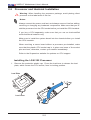
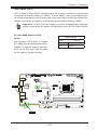
2-2 Processor and Heatsink Installation
!
Warning: When handling the processor package, avoid placing direct
pressure on the label area of the fan.
Notes:
Always connect the power cord last, and always remove it before adding,
removing or changing any hardware components. Make sure that you install the processor into the CPU socket before you install the CPU heatsink.
If you buy a CPU separately, make sure that you use an Intel-certified
multi-directional heatsink only.
Make sure to install the system board into the chassis before you install
the CPU heatsink.
When receiving a server board without a processor pre-installed, make
sure that the plastic CPU socket cap is in place and none of the socket
pins are bent; otherwise, contact your retailer immediately.
Refer to the Supermicro website for updates on CPU support.
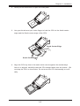
Installing the LGA1155 Processor
1. Remove the protective plastic cap. Press the load lever to release the load
plate, which covers the CPU socket, from its locking position.
Load Plate
Load Lever
2-2
Chapter 2: Installation
2. Gently lift the load lever to open the load plate.
3. Use your thumb and your index finger to hold the CPU at the North center
edge and the South center edge of the CPU.
North Center Edge
South Center Edge
4. Align the CPU key that is the semi-circle cutouts against the socket keys.
Once it is aligned, carefully lower the CPU straight down into the socket. (Do
not drop the CPU on the socket. Do not move the CPU horizontally or vertically.
2-3
X9SPU-F Motherboard User’s Manual
1. Do not rub the CPU against the surface or against any pins of the socket to
avoid damaging the CPU or the socket.)
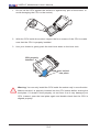
2. With the CPU inside the socket, inspect the four corners of the CPU to make
sure that the CPU is properly installed.
3. Use your thumb to gently push the load lever down to the lever lock.
CPU properly
installed
Load lever locked
into place
Warning: You can only install the CPU inside the socket only in one direction.
Make sure that it is properly inserted into the CPU socket before closing the
load plate. If it doesn't close properly, do not force it as it may damage your
CPU. Instead, open the load plate again and double-check that the CPU is
aligned properly.
2-4
Chapter 2: Installation
Installing a Passive CPU Heatsink
1. Do not apply any thermal grease to the heatsink or the CPU die -- the required amount has already been applied.
2. Place the heatsink on top of the CPU so that the four mounting holes are
aligned with those on the Motherboard's and the Heatsink Bracket underneath.
3. Screw in two diagonal screws (i.e., the #1 and the #2 screws) until just snug
(-do not over-tighten the screws to avoid possible damage to the CPU.)
4. Finish the installation by fully tightening all four screws.
Screw#1
Screw#2
Motherboard
Mounting Holes
Recommended Supermicro
heatsink:
SNK-P0046P heatsink with BKT0028L bottom bracket
Heatsink Bracket
2-5
X9SPU-F Motherboard User’s Manual
Removing the Heatsink
!
Warning: We do not recommend that the CPU or the heatsink be removed.
However, if you do need to uninstall the heatsink, please follow the instructions below to uninstall the heatsink to prevent damage done to the CPU
or the CPU socket.
1. Unscrew the heatsink screws from the motherboard in the sequence as shown
in the illustration below.
2. Gently wriggle the heatsink to loosen it from the CPU. (Do not use excessive
force when wriggling the heatsink!!)
3. Once the CPU is loosened, remove the CPU from the CPU socket.
4. Clean the surface of the CPU and the heatsink, removing the used thermal
grease. Reapply the proper amount of thermal grease on the surface before
re-installing the CPU and the heatsink.
Loosen screws in
sequence as shown.
Screw#4
Screw#1
Screw#2
Motherboard
Screw#3
Remove the Heatsink
Bracket from underneath
the motherboard.
2-6
Chapter 2: Installation
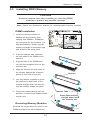
2-3 Installing DDR3 Memory
CAUTION
Exercise extreme care when installing or removing DIMM
modules to prevent any possible damage.
1
FAN1
JPW1
JPI2C:PWR I2C
MH6
20
J31
JWD
1-2:RST
2-3:NMI
JPI2C
JWD
JLED
USB3.0-2/3
JPME1
JPME2
SPEAKER
JPME1
ON:ME RECOVERY
OFF:NORMAL
JSPK:
Buzzer/Speaker
SPKR1
JPL1 LAN1
1-2:ENABLE
2-3:DISABLE
JPL2 LAN2
1-2:ENABLE
2-3:DISABLE
J5
CMOS CLEAR
JF1
JBT1
J28
J1
JTPM
CPU
COM1
COM1
RST PS UID NIC NIC HDD PWR X NMI
2
1 LED LED
FAIL PF
OH/FF
1
VGA
I-SATA3
I-SATA4
5V
3
1
FAN3
MH5
DIMMB2
I-SATA1
3
J3
MH7
SBX2: PCI-E 2.0 X4 in X8
J2
1
FAN4
DIMMA2
DIMMB1
I-SATA0
MH2
C768
GND
GND
JSD1:DOM_PWR
1
C
LE2
10
2. Push the release tabs outwards
on both ends of the DIMM slot to
unlock it.
3. Align the key of the DIMM module with the receptive point on the
memory slot.
4. Align the notches on both ends of
the module against the receptive
points on the ends of the slot.
Notches
5. Use two thumbs together to press
the notches on both ends of the
module straight down into the slot
until the module snaps into place.
6. Press the release tabs to the lock
positions to secure the DIMM module
into the slot.
Removing Memory Modules
Reverse the steps above to remove the
DIMM modules from the motherboard.
2-7
Release Tabs
Press both notches
straight down into
the memory slot.
A
FAN5
JUSB3
USB 3.0-0/1
1
J15
USB 12/13
A
T-SGPIO2
11
JPB:BMC
1-2:ENABLE
2-3:DISABLE
JPB
T-SGPIO1
A
SBX3: PCI-E 2.0 X4
JL1:CHASSIS INSTRUSION
LE3 LE4
C
C
4
SBX1: PCI-E 3.0/2.0 X16 or X8+X8
UIOP
JL1
UID-LED
MH8
1
JSD1
JI2C1/JI2C2
ON:Enable
OFF:Disable
JI2C1
JI2C2
J4
J8
DDR3 1600/1333/1066 UDIMM/RDIMM required
DIMMA1
I-SATA2
I-SATA5
SW1
C
LE5
A
A
7
LE7
C
JLAN2
X9SPU-F
LAN2
DESIGNED IN USA
REV:1.00
BAR CODE
JLAN1
RT1
JRF1
LAN1
MAC CODE
JRF1
1-2:AUTO
2-3:FORCE TO X8+X8
B1
+
1
1. Insert the desired number of
DIMMs into the memory slots,
starting with DIMMA1, DIMM(see
the next page for the location). For
best performance, please use the
memory modules of the same type
and speed in the same bank.
PWR ON
1
4
+
JPME2
ON:ME MANUFACTURING MODE
OFF:NORMAL
JPW2
FAN2
JPL2
JPL1
J29
1
JF1
JUSB4
J16
1
JPG1
JSPK
JPG1 VGA
1-2:ENABLE
2-3:DISABLE
MH3
1
JLED:Power LED
3
R137
MH4
3
1
JPUSB1
1-2:ENABLE
2-3:DISABLE
JPUSB1
COM2
JPUSB1:B/P USB WAKE UP
JSTBY1
KB/MS
USB4/5/IPMI_LAN
DIMM Installation
1
Note: Check the Supermicro website for recommended memory modules.
X9SPU-F Motherboard User’s Manual
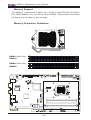
Memory Support
The X9SPU-F motherboard supports up to 32GB of 1600/1333 MHz ECC/NonECC DDR3 DIMMs in four (4) memory slots (UDIMM). Please refer to the illustration below and the table on the next page:
Memory Population Guidelines
DIMMA1 (Blue Slot)
DIMMA2
DIMMB1 (Blue Slot)
1
FAN1
JPW1
JPI2C:PWR I2C
JF1
MH6
20
MH4
J31
JWD
1-2:RST
2-3:NMI
JPI2C
JWD
JLED
USB3.0-2/3
JPME1
JPME2
FAN2
JPL2
JPL1
J29
1
JSPK:
Buzzer/Speaker
SPKR1
JPL1 LAN1
1-2:ENABLE
2-3:DISABLE
JPL2 LAN2
1-2:ENABLE
2-3:DISABLE
JPME1
ON:ME RECOVERY
OFF:NORMAL
SPEAKER
J5
CMOS CLEAR
JF1
JBT1
J28
J1
JTPM
CPU
COM1
COM1
RST PS UID NIC NIC HDD PWR X NMI
2
1 LED LED
FAIL PF
OH/FF
1
VGA
PWR ON
1
4
+
JPME2
ON:ME MANUFACTURING MODE
OFF:NORMAL
JPW2
JPUSB1
JUSB4
J16
1
JPG1
JSPK
JPG1 VGA
1-2:ENABLE
2-3:DISABLE
MH3
1
JLED:Power LED
3
R137
COM2
1
JPUSB1
1-2:ENABLE
2-3:DISABLE
3
JPUSB1:B/P USB WAKE UP
JSTBY1
KB/MS
USB4/5/IPMI_LAN
1
DIMMB2
I-SATA3
I-SATA4
5V
3
1
FAN3
DDR3 1600/1333/1066 UDIMM/RDIMM required
DIMMA1
DIMMB2
I-SATA1
3
MH5
I-SATA0
MH2
JSD1
J3
MH7
SBX2: PCI-E 2.0 X4 in X8
1
LE2
C
2-8
10
FAN5
A
JUSB3
USB 3.0-0/1
1
J15
USB 12/13
A
T-SGPIO2
11
JPB:BMC
1-2:ENABLE
2-3:DISABLE
JPB
T-SGPIO1
A
SBX3: PCI-E 2.0 X4
JL1:CHASSIS INSTRUSION
LE3 LE4
C
C
4
SBX1: PCI-E 3.0/2.0 X16 or X8+X8
UIOP
JL1
JI2C2
J2
JI2C1
1
FAN4
DIMMA2
DIMMB1
I-SATA2
I-SATA5
C768
GND
1
JI2C1/JI2C2
ON:Enable
OFF:Disable
J4
J8
GND
JSD1:DOM_PWR
MH8
UID-LED
C
SW1
1
LE5
A
A
7
LE7
C
JLAN2
X9SPU-F
LAN2
DESIGNED IN USA
REV:1.00
BAR CODE
JLAN1
RT1
JRF1
LAN1
MAC CODE
JRF1
1-2:AUTO
2-3:FORCE TO X8+X8
B1
+
Chapter 2: Installation
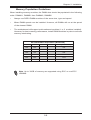
Memory Population Guidelines
When installing memory modules, the DIMM slots should be populated in the following
order: DIMMA1, DIMMB1 then DIMMA2, DIMMB2
•
Always use DDR3 DIMM modules of the same size, type and speed.
•
Mixed DIMM speeds can be installed. However, all DIMMs will run at the speed
of the slowest DIMM.
•
The motherboard will support odd-numbered modules (1 or 3 modules installed).
However, for best memory performance, install DIMM modules in pairs to activate
memory interleaving.
Recommended Population (Balanced)
DIMMA1
DIMMB1
2GB
2GB
2GB
2GB
4GB
4GB
4GB
4GB
8GB
8GB
8GB
8GB
DIMMA2
DIMMB2
Total System Memory
2GB
2GB
8GB
4GB
4GB
16GB
4GB
8GB
16GB
8GB
8GB
32GB
Note: Up to 32GB of memory are supported using ECC or non-ECC
UDIMMs.
2-9
X9SPU-F Motherboard User’s Manual
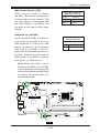
2-4 Motherboard Installation
All motherboards have standard mounting holes to fit different types of chassis.
Make sure that the locations of all the mounting holes for both motherboard and
chassis match. Although a chassis may have both plastic and metal mounting fasteners, metal ones are highly recommended because they ground the motherboard
to the chassis. Make sure that the metal standoffs click in or are screwed in tightly.
Then use a screwdriver to secure the motherboard onto the motherboard tray.
Tools Needed
1
FAN1
JPW1
JPI2C:PWR I2C
JF1
MH6
20
J31
JWD
1-2:RST
2-3:NMI
JPI2C
JWD
JLED
USB3.0-2/3
JPME1
JPME2
JSPK:
Buzzer/Speaker
SPKR1
JPL1 LAN1
1-2:ENABLE
2-3:DISABLE
JPL2 LAN2
1-2:ENABLE
2-3:DISABLE
JPME1
ON:ME RECOVERY
OFF:NORMAL
SPEAKER
J5
CMOS CLEAR
JF1
JBT1
J28
J1
JTPM
CPU
COM1
COM1
RST PS UID NIC NIC HDD PWR X NMI
2
1 LED LED
FAIL PF
OH/FF
1
VGA
PWR ON
1
4
+
JPME2
ON:ME MANUFACTURING MODE
OFF:NORMAL
JPW2
FAN2
JPL2
JPL1
J29
1
MH4
JUSB4
J16
1
JSPK
JPG1 VGA
1-2:ENABLE
2-3:DISABLE
MH3
1
JPG1
Standoffs
JLED:Power LED
3
R137
JPUSB1
Philips Screws
COM2
1
JPUSB1
1-2:ENABLE
2-3:DISABLE
3
JPUSB1:B/P USB WAKE UP
JSTBY1
KB/MS
USB4/5/IPMI_LAN
1
Philips Screwdriver
I-SATA3
I-SATA4
5V
3
1
FAN3
DDR3 1600/1333/1066 UDIMM/RDIMM required
DIMMA1
MH5
I-SATA0
MH2
JSD1
I-SATA1
DIMMB2
J3
MH7
SBX2: PCI-E 2.0 X4 in X8
1
C
LE2
10
FAN5
A
JUSB3
USB 3.0-0/1
1
J15
USB 12/13
A
T-SGPIO2
11
JPB:BMC
1-2:ENABLE
2-3:DISABLE
JPB
T-SGPIO1
A
SBX3: PCI-E 2.0 X4
JL1:CHASSIS INSTRUSION
LE3 LE4
C
C
4
SBX1: PCI-E 3.0/2.0 X16 or X8+X8
UIOP
JL1
JI2C2
J2
JI2C1
1
FAN4
DIMMA2
DIMMB1
I-SATA2
I-SATA5
C768
GND
1
3
JI2C1/JI2C2
ON:Enable
OFF:Disable
J4
J8
GND
JSD1:DOM_PWR
MH8
UID-LED
C
SW1
1
LE5
A
A
7
LE7
C
JLAN2
X9SPU-F
LAN2
DESIGNED IN USA
REV:1.00
BAR CODE
JLAN1
RT1
JRF1
LAN1
MAC CODE
JRF1
1-2:AUTO
2-3:FORCE TO X8+X8
B1
+
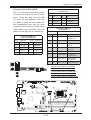
Location of Mounting Holes
Caution: 1) To prevent damage to the motherboard and its components,
please do not use a force greater than 8 lb/inch on each mounting screw
during motherboard installation. 2) Some components are very close to the
mounting holes. Please take precautionary measures to avoid damaging
these components when installing the motherboard to the chassis.
2-10
Chapter 2: Installation
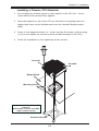
Installing the Motherboard
1. Install the I/O shield into the chassis.
2. Locate the mounting holes on the motherboard.
3. Locate the matching mounting holes on the chassis. Align the mounting holes
on the motherboard against the mounting holes on the chassis.
Pan head screws (8 pieces)
4. Install standoffs in the chassis as needed.
5. Install the motherboard into the chassis carefully to avoid damaging motherboard components.
6. Using the Philips screwdriver, insert a Pan head #6 screw into a mounting
hole on the motherboard and its matching mounting hole on the chassis.
7. Repeat Step 5 to insert #6 screws into all mounting holes.
8. Make sure that the motherboard is securely placed in the chassis.
Note: Images displayed are is for illustration only. Your chassis or components might look different from those shown in this manual.
2-11
X9SPU-F Motherboard User’s Manual
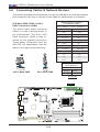
2-5 Connectors/IO Ports
The I/O ports are color coded in conformance with the PC 99 specification. See the
figure below for the colors and locations of the various I/O ports.
JPL2
JPL1
1
F
JPW1
JPI2C:PWR I2C
JF1
20
J31
JWD
1-2:RST
2-3:NMI
JPI2C
JWD
JLED
USB3.0-2/3
JPME1
JPME2
J29
1
MH4
JUSB4
J16
1
JSPK:
Buzzer/Speaker
SPKR1
JPL1 LAN1
1-2:ENABLE
2-3:DISABLE
JPL2 LAN2
1-2:ENABLE
2-3:DISABLE
JPME1
ON:ME RECOVERY
OFF:NORMAL
SPEAKER
J5
CMOS CLEAR
JF1
JBT1
J28
J1
JTPM
CPU
COM1
COM1
RST PS UID NIC NIC HDD PWR X NMI
2
1 LED LED
FAIL PF
OH/FF
1
VGA
PWR ON
1
4
+
JPME2
ON:ME MANUFACTURING MODE
OFF:NORMAL
JPW2
JSPK
JPG1 VGA
1-2:ENABLE
2-3:DISABLE
MH3
1
JPG1
JLED:Power LED
3
R137
JPUSB1
COM2
1
JPUSB1
1-2:ENABLE
2-3:DISABLE
3
JPUSB1:B/P USB WAKE UP
JSTBY1
KB/MS
USB4/5/IPMI_LAN
1
Motherboard I/O Backpanel
I-SATA3
DDR3 1600/1333/1066 UDIMM/RDIMM required
DIMMA1
DIMMA2
DIMMB1
I-SATA2
5V
I-SATA4
I-SATA5
JSD1
I-SATA0
MH2
C768
GND
1
DIMMB2
I-SATA1
3
J3
MH7
SBX2: PCI-E 2.0 X4 in X8
1
1
SBX1: PCI-E 3.0/2.0 X16 or X8+X8
JUSB3
11
T-SGPIO2
J15
USB 12/13
USB 3.0-0/1
10
3
6
2
T-SGPIO1
JL1
JPB
1
SBX3: PCI-E 2.0 X4
JL1:CHASSIS INSTRUSION
7
4
5
Motherboard I/O Backpanel
1. PS/2 Keyboard Port
6. COM1
2. PS/2 Mouse Port
7. VGA
3. IPMI LAN
8. LAN 1
4. USB 3
9. LAN 2
5. USB 4
10. UID Switch
2-12
8
9
10
1
UIOP
JPB:BMC
1-2:ENABLE
2-3:DISABLE
JI2C2
J2
JI2C1
JI2C1/JI2C2
ON:Enable
OFF:Disable
J4
J8
GND
JSD1:DOM_PWR
MH8
UID-LED
C
SW1
1
LE5
A
A
7
LE7
C
JLAN2
X9SPU-F
LAN2
DESIGNED IN USA
REV:1.00
BAR CODE
JLAN1
LAN1
MAC CODE
B1
+
Chapter 2: Installation
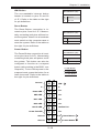
Universal Serial Bus (USB)
Back Panel USB (2.0)
Pin Definitions
Two (2) Universal Serial Bus (USB)
2.0 ports are located on the I/O back
panel. There are also four (4) USB
3.0 ports on two headers, and two
(2) USB 2.0 ports on one header on
the motherboard that may be used
to provide front chassis access using
USB cables (not included). See the
tables on the right for pin definitions.
Pin# Definition
Definition
Pin #
Definition
1
+5V
2
+5V
3
USB_PN2
4
USB_PN3
5
USB_PP2
6
USB_PP3
7
Ground
8
Ground
9
Key
10
Ground
Definition
+5V
5
+5V
2
USB_PN1
6
USB_PN0
3
USB_PP1
7
USB_PP0
4
Ground
8
Ground
Back Panel USB (3.0)
Pin Definitions
Front Panel USB (2.0)
Header Pin Definitions
Pin #
Pin#
1
Pin#
Pin#
Signal Name
Description
1
10
VBUS
Power
2
11
D-
USB 2.0 Differential Pair
3
12
D+
4
13
Ground
Ground for PWR
Return
5
1