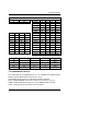
1
586SG USER'S MANUAL ¯ Support Intel Pentium, MMX/Cyrix/IBM 6x86MX & AMD K5,K6 CPUs. ¯ Support auto detect CPU Voltage. ¯ Support auto detect four positive Voltages and Fan Speed. ¯ Support Parity check or Ecc Function. ¯ Support Ultra DMA/33 Function. ¯ Support Fully AGP 1.0 Specification. ¯ Support switching mode Voltage regulator on Board. ¯ Support 60/66/75 MHz and 83MHz (optional). ¯ Support Wake on Lan. ¯ Support K/B Power-on , modem Ring-on , Win95 Power off , RTC Alarm. ¯ Support 3 steps ACPI LED. ¯ Thermal Protection : 1.When the system is overheating, it will stop for a few secs. 2.Then back to normal status after the system’s temp. step down . 3. Users better check CPU fan immediately. Pentium Processor PCI - ISA BUS MAINBOARD REV. 1.0 First Edition Release Date 98.01.06 R-10-01-080106 586SG The author assumes no responsibility for any errors or omissions which may appear in this document nor does it make a commitment to update the information contained herein. ¯THIRD-PARTY BRANDS AND NAMES ARE THE PROPERTY OF THEIR RESPECTIVE OWNERS. JANUARY 6, 1998 Taipei, Taiwan 1 Quick Installation Guide I. Quick Installation Guide: CPU 1. Pentium Processor 90 MHz 2. SW1 SW2 SW3 SW4 SW5 SW6 SW7 SW8 ON JP4 JP5 JP6 OFF OFF OFF OFF OFF ON OFF 2-3 2-3 2-3 Pentium Processor 100 OFF OFF OFF OFF OFF OFF ON OFF 2-3 2-3 2-3 MHz 3. Pentium Processor 120 ON ON OFF OFF OFF OFF ON OFF 2-3 2-3 2-3 Pentium Processor 133 OFF ON OFF OFF OFF OFF ON OFF 2-3 2-3 2-3 ON ON ON OFF OFF OFF ON OFF 2-3 2-3 2-3 OFF ON ON OFF OFF OFF ON OFF 2-3 2-3 2-3 ON OFF ON OFF OFF OFF ON OFF 2-3 2-3 2-3 OFF OFF ON OFF OFF OFF ON OFF 2-3 2-3 2-3 9. Intel MMX-150MHz ON ON ON OFF OFF OFF ON OFF 2-3 2-3 2-3 10. Intel MMX-166MHz OFF ON ON OFF OFF OFF ON OFF 2-3 2-3 2-3 11. Intel MMX-200MHz OFF OFF ON OFF OFF OFF ON OFF 2-3 2-3 2-3 12. Intel MMX-233MHz OFF OFF OFF OFF OFF OFF ON OFF 2-3 2-3 2-3 13. P54CT-150 MHz ON ON ON OFF OFF OFF ON OFF 2-3 2-3 2-3 14. P54CT-166 MHz OFF ON ON OFF OFF OFF ON OFF 2-3 2-3 2-3 15. P54CTB-150 MHz ON ON ON OFF OFF OFF ON OFF 2-3 2-3 2-3 MHz 4. MHz 5. Pentium Processor 150 MHz 6. Pentium Processor 166 MHz 7. Pentium Processor 180 MHz 8. Pentium Processor 200 MHz 2 586SG 16. P54CTB-166 MHz OFF ON ON OFF OFF OFF ON OFF 2-3 2-3 2-3 17. P54CTB-180 MHz ON OFF ON OFF OFF OFF ON OFF 2-3 2-3 2-3 18. P54CTB-200 MHz OFF OFF ON OFF OFF OFF ON OFF 2-3 2-3 2-3 19. AMDK5-PR133 OFF ON OFF OFF OFF OFF ON OFF 2-3 2-3 2-3 20. AMDK5-PR166 OFF ON ON ON OFF 2-3 2-3 2-3 SW1 SW2 SW3 SW4 SW5 SW6 SW7 SW8 JP4 JP5 JP6 21. AMD-K6/166 (2.9V) OFF ON ON OFF OFF ON ON OFF 2-3 2-3 2-3 22. AMD-K6/180 (2.9V) ON OFF ON OFF OFF ON ON OFF 2-3 2-3 2-3 23. AMD-K6/200 (2.9V) OFF OFF ON OFF OFF ON ON OFF 2-3 2-3 2-3 24. AMD-K6/233 (3.2V) OFF OFF OFF OFF OFF ON OFF 2-3 2-3 2-3 CPU 25. Cyrix/IBM 6x86-120MHzPR150+ 26. Cyrix/IBM 6x86-133MHzPR166+ 27. Cyrix/IBM 6x86-150MHzPR200+ 28. Cyrix/IBM 6x86L- PR150+ (2.8V) 29. Cyrix/IBM 6x86L-PR166+ (2.8V) 30. Cyrix/IBM 6x86L-PR200+ (2.8V) 31. Cyrix/IBM 6x86MX-PR150 (60*2 2.9V) 32. Cyrix/IBM 6x86MX-PR166 (60*2.5 2.9V) 33. Cyrix/IBM 6x86MX-PR166 (66*2 2.9V) 34. Cyrix/IBM 6x86MX-PR200 (60*3 2.9V) OFF OFF OFF ON ON ON OFF OFF OFF OFF ON OFF 2-3 2-3 2-3 OFF ON OFF OFF OFF OFF ON OFF 2-3 2-3 2-3 OFF ON OFF OFF OFF OFF ON OFF 1-2 2-3 1-2 ON ON OFF OFF OFF OFF ON OFF 2-3 2-3 2-3 OFF ON OFF OFF OFF OFF ON OFF 2-3 2-3 2-3 OFF ON OFF OFF OFF OFF ON OFF 1-2 2-3 1-2 ON ON OFF OFF OFF ON ON OFF 2-3 2-3 2-3 ON ON ON OFF OFF ON ON OFF 2-3 2-3 2-3 OFF ON OFF OFF OFF ON ON OFF 2-3 2-3 2-3 ON OFF ON ON ON OFF 2-3 2-3 2-3 OFF OFF 3 Quick Installation Guide 35. Cyrix/IBM 6x86MX-PR200 (66*2.5 2.9V) 36. Cyrix/IBM 6x86MX-PR200 OFF ON ON OFF OFF ON ON OFF 2-3 2-3 2-3 OFF ON OFF OFF OFF ON ON OFF 1-2 2-3 1-2 OFF OFF ON OFF OFF ON ON OFF 2-3 2-3 2-3 OFF ON OFF OFF ON ON OFF 1-2 2-3 1-2 SW1 SW2 SW3 SW4 SW5 SW6 SW7 SW8 JP4 JP5 JP6 (75*2 2.9V) 37. Cyrix/IBM 6x86MX-PR233 (66*3 2.9V) 38. Cyrix/IBM 6x86MX-PR233 (75*2.5 2.9V) CPU 39. Cyrix/IBM 6x86MX-PR233 (83*2 2.9V) 40. Cyrix/IBM 6x86MX-PR266 (66*3.5 2.9V) 41. Cyrix/IBM 6x86MX-PR266 (75*3 2.9V) 42. Cyrix/IBM 6x86MX-PR266 (83*2.5 2.9V) ON ON ON OFF OFF OFF ON ON OFF 1-2 1-2 2-3 OFF OFF OFF OFF OFF ON ON OFF 2-3 2-3 2-3 OFF OFF ON OFF OFF ON ON OFF 1-2 2-3 1-2 ON ON OFF OFF ON ON OFF 1-2 1-2 2-3 ON ¬ Note : If Cyrix 6x86 is being used, please check the CPU Date Code after 605. ¬ Note : We don’t recommend you to setup up your system speed up to 75 or 83 MHz because they are not the standard spec.of pheriphrals. If you want to run 75 or 83 MHz in your system properly, it depends on your hardware configurations : CPU, SDRAM, Cards, etc. 4 586SG 5 Quick Installation Guide 1. Pentium Processor 90 MHz 8 7 6 5 4 3 2 1OFF R Pentium + + Processor 90 MHz ON + 1 1 1 1 JP6 JP4 SW JP4 JP5 JP6 1 2 3 J J 4 1 5 8 1 CPU 1 JP5 1 1 DIMM1 1 1 1 DIMM2 BANK1 1 1 1 1 1 BANK0 1 2. 1 1 1 1 Pentium Processor 100 MHz 8 7 6 5 4 3 2 1OFF R Pentium + + Processor 100 MHz ON + 1 1 1 1 JP6 JP4 SW JP4 JP5 JP6 1 2 3 J J 4 1 5 8 1 CPU 1 JP5 1 1 1 DIMM1 1 DIMM2 BANK1 1 1 1 BANK0 1 1 1 1 1 1 6 1 1 586SG 3. Pentium Processor 120 MHz 8 7 6 5 4 3 2 1 R Pentium + + Processor 120 MHz OFF ON + 1 1 1 1 JP6 JP4 SW JP4 JP5 JP6 1 2 3 J J 4 1 5 8 1 CPU 1 JP5 1 1 DIMM1 1 1 1 DIMM2 BANK1 1 1 1 1 1 BANK0 1 4. 1 1 1 1 Pentium Processor 133 MHz 8 7 6 5 4 3 2 1 R Pentium + + Processor 133 MHz OFF ON + 1 1 1 1 JP6 JP4 SW JP4 JP5 JP6 1 2 3 J J 4 1 5 8 1 CPU 1 JP5 1 1 1 DIMM1 1 DIMM2 BANK1 1 1 1 BANK0 1 1 1 1 1 1 7 1 1 Quick Installation Guide 5. Pentium Processor 150 MHz 8 7 6 5 4 3 2 1 R Pentium + + Processor 150 MHz OFF ON + 1 1 1 1 JP6 JP4 SW JP4 JP5 JP6 1 2 3 J J 4 1 5 8 1 CPU 1 JP5 1 1 DIMM1 1 1 1 DIMM2 BANK1 1 1 1 1 1 BANK0 1 6. 1 1 1 1 Pentium Processor 166 MHz 8 7 6 5 4 3 2 1 R Pentium + + Processor 166 MHz OFF ON + 1 1 1 1 JP6 JP4 SW JP4 JP5 JP6 1 2 3 J J 4 1 5 8 1 CPU 1 JP5 1 1 1 DIMM1 1 DIMM2 BANK1 1 1 1 BANK0 1 1 1 1 1 1 8 1 1 586SG 7. Pentium Processor 180 MHz 8 7 6 5 4 3 2 1 R Pentium + + Processor 180 MHz OFF ON + 1 1 1 1 JP6 JP4 SW JP4 JP5 JP6 1 2 3 J J 4 1 5 8 1 CPU 1 JP5 1 1 DIMM1 1 1 1 DIMM2 BANK1 1 1 1 1 1 BANK0 1 8. 1 1 1 1 Pentium Processor 200 MHz 8 7 6 5 4 3 2 1 R Pentium + + Processor 200 MHz OFF ON + 1 1 1 1 JP6 JP4 SW JP4 JP5 JP6 1 2 3 J J 4 1 5 8 1 CPU 1 JP5 1 1 1 DIMM1 1 DIMM2 BANK1 1 1 1 BANK0 1 1 1 1 1 1 9 1 1 Quick Installation Guide 9. Intel MMX-150 MHz 8 7 6 5 4 3 2 1 Intel MMX-150MHz + + OFF ON + 1 1 1 1 JP6 JP4 SW JP4 JP5 JP6 1 2 3 J J 4 1 5 8 1 CPU 1 JP5 1 1 DIMM1 1 1 1 DIMM2 BANK1 1 1 1 1 1 BANK0 1 1 1 1 1 10. Intel MMX-166 MHz 8 7 6 5 4 3 2 1 Intel MMX-166MHz + + OFF ON + 1 1 1 1 JP6 JP4 SW JP4 JP5 JP6 1 2 3 J J 4 1 5 8 1 CPU 1 JP5 1 1 1 DIMM1 1 DIMM2 BANK1 1 1 1 BANK0 1 1 1 1 1 1 10 1 1 586SG 11. Intel MMX-200 MHz 8 7 6 5 4 3 2 1 Intel MMX-200MHz + + OFF ON + 1 1 1 1 JP6 JP4 SW JP4 JP5 JP6 1 2 3 J J 4 1 5 8 1 CPU 1 JP5 1 1 DIMM1 1 1 1 DIMM2 BANK1 1 1 1 1 1 BANK0 1 1 1 1 1 12. Intel MMX-233 MHz 8 7 6 5 4 3 2 1 Intel MMX-233MHz + + OFF ON + 1 1 1 1 JP6 JP4 SW JP4 JP5 JP6 1 2 3 J J 4 1 5 8 1 CPU 1 JP5 1 1 1 DIMM1 1 DIMM2 BANK1 1 1 1 BANK0 1 1 1 1 1 1 11 1 1 Quick Installation Guide 13. P54CT-150 MHz 8 7 6 5 4 3 2 1 OFF P54CT-150 MHz ON + + + 1 1 1 1 JP6 JP4 SW JP4 JP5 JP6 1 2 3 J J 4 1 5 8 1 CPU 1 JP5 1 1 DIMM1 1 1 1 DIMM2 BANK1 1 1 1 1 1 BANK0 1 1 1 1 1 14. P54CT-166 MHz 8 7 6 5 4 3 2 1 P54CT-166 MHz + + OFF ON + 1 1 1 1 JP6 JP4 SW JP4 JP5 JP6 1 2 3 J J 4 1 5 8 1 CPU 1 JP5 1 1 1 DIMM1 1 DIMM2 BANK1 1 1 1 BANK0 1 1 1 1 1 1 12 1 1 586SG 15. P54CTB-150 MHz 8 7 6 5 4 3 2 1 P54CTB-150 MHz + + OFF ON + 1 1 1 1 JP6 JP4 SW JP4 JP5 JP6 1 2 3 J J 4 1 5 8 1 CPU 1 JP5 1 1 DIMM1 1 1 1 DIMM2 BANK1 1 1 1 1 1 BANK0 1 1 1 1 1 16. P54CTB-166 MHz 8 7 6 5 4 3 2 1 P54CTB-166 MHz + + OFF ON + 1 1 1 1 JP6 JP4 SW JP4 JP5 JP6 1 2 3 J J 4 1 5 8 1 CPU 1 JP5 1 1 1 DIMM1 1 DIMM2 BANK1 1 1 1 BANK0 1 1 1 1 1 1 13 1 1 Quick Installation Guide 17. P54CTB-180 MHz 8 7 6 5 4 3 2 1 P54CTB-180 MHz + + OFF ON + 1 1 1 1 JP6 JP4 SW JP4 JP5 JP6 1 2 3 J J 4 1 5 8 1 CPU 1 JP5 1 1 DIMM1 1 1 1 DIMM2 BANK1 1 1 1 1 1 BANK0 1 1 1 1 1 18. P54CTB-200 MHz 8 7 6 5 4 3 2 1 P54CTB-200 MHz + + OFF ON + 1 1 1 1 JP6 JP4 SW JP4 JP5 JP6 1 2 3 J J 4 1 5 8 1 CPU 1 JP5 1 1 1 DIMM1 1 DIMM2 BANK1 1 1 1 BANK0 1 1 1 1 1 1 14 1 1 586SG 19. AMDK5-PR133 8 7 6 5 4 3 2 1 AMDK5-PR133 + + OFF ON + 1 1 1 1 JP6 JP4 SW JP4 JP5 JP6 1 2 3 J J 4 1 5 8 1 CPU 1 JP5 1 1 DIMM1 1 1 1 DIMM2 BANK1 1 1 1 1 1 BANK0 1 1 1 1 1 20. AMDK5-PR166 8 7 6 5 4 3 2 1 AMDK5-PR166 + + OFF ON + 1 1 1 1 JP6 JP4 SW JP4 JP5 JP6 1 2 3 J J 4 1 5 8 1 CPU 1 JP5 1 1 1 DIMM1 1 DIMM2 BANK1 1 1 1 BANK0 1 1 1 1 1 1 15 1 1 Quick Installation Guide 21. AMD-K6/166 (2.9V) 8 7 6 5 4 3 2 1 AMD-K6/166 (2.9V) + + OFF ON + 1 1 1 1 JP6 JP4 SW JP4 JP5 JP6 1 2 3 J J 4 1 5 8 1 CPU 1 JP5 1 1 DIMM1 1 1 1 DIMM2 BANK1 1 1 1 1 1 BANK0 1 1 1 1 1 22. AMD-K6/180 (2.9V) 8 7 6 5 4 3 2 1 AMD-K6/180 (2.9V) + + OFF ON + 1 1 1 1 JP6 JP4 SW JP4 JP5 JP6 1 2 3 J J 4 1 5 8 1 CPU 1 JP5 1 1 1 DIMM1 1 DIMM2 BANK1 1 1 1 BANK0 1 1 1 1 1 1 16 1 1 586SG 23. AMD-K6/200 (2.9V) 8 7 6 5 4 3 2 1 AMD-K6/200 (2.9V) + + OFF ON + 1 1 1 1 JP6 JP4 SW JP4 JP5 JP6 1 2 3 J J 4 1 5 8 1 CPU 1 JP5 1 1 DIMM1 1 1 1 DIMM2 BANK1 1 1 1 1 1 BANK0 1 1 1 1 1 24. AMD-K6/233 (3.2V) 8 7 6 5 4 3 2 1 AMD-K6/233 (3.2V) + + OFF ON + 1 1 1 1 JP6 JP4 SW JP4 JP5 JP6 1 2 3 J J 4 1 5 8 1 CPU 1 JP5 1 1 1 DIMM1 1 DIMM2 BANK1 1 1 1 BANK0 1 1 1 1 1 1 17 1 1 Quick Installation Guide 25. Cyrix / IBM 6x86-120 MHz-PR150+ 8 7 6 5 4 3 2 1 Cyrix/IBM 6x86-120MHz-PR150+ + + OFF ON + 1 1 1 1 JP6 JP4 SW JP4 JP5 JP6 1 2 3 J J 4 1 5 8 1 CPU 1 JP5 1 1 DIMM1 1 1 1 DIMM2 BANK1 1 1 1 1 1 BANK0 1 1 1 1 1 26. Cyrix /IBM 6x86-133 MHz-PR166+ 8 7 6 5 4 3 2 1 Cyrix/IBM 6x86-133MHz-PR166+ + + OFF ON + 1 1 1 1 JP6 JP4 SW JP4 JP5 JP6 1 2 3 J J 4 1 5 8 1 CPU 1 JP5 1 1 1 DIMM1 1 DIMM2 BANK1 1 1 1 BANK0 1 1 1 1 1 1 18 1 1 586SG 27. Cyrix /IBM 6x86-150 MHz-PR200+ 8 7 6 5 4 3 2 1 Cyrix/IBM 6x86-150MHz-PR200+ + + OFF ON + 1 1 1 1 JP6 JP4 SW JP4 JP5 JP6 1 2 3 J J 4 1 5 8 1 CPU 1 JP5 1 1 DIMM1 1 1 1 DIMM2 BANK1 1 1 1 1 1 BANK0 1 1 28. Cyrix / IBM 6x86L-PR150+ 1 1 1 (2.8V) 8 7 6 5 4 3 2 1 Cyrix/IBM 6x86L-PR150+ (2.8V) + + OFF ON + 1 1 1 1 JP6 JP4 SW JP4 JP5 JP6 1 2 3 J J 4 1 5 8 1 CPU 1 JP5 1 1 1 DIMM1 1 DIMM2 BANK1 1 1 1 BANK0 1 1 1 1 1 1 19 1 1 Quick Installation Guide 29. Cyrix / IBM 6x86L-PR166+ (2.8V) 8 7 6 5 4 3 2 1 Cyrix/IBM 6x86L-PR166+ (2.8V) + + OFF ON + 1 1 1 1 JP6 JP4 SW JP4 JP5 JP6 1 2 3 J J 4 1 5 8 1 CPU 1 JP5 1 1 DIMM1 1 1 1 DIMM2 BANK1 1 1 1 1 1 BANK0 1 1 1 1 1 30. Cyrix / IBM 6x86L-PR200+ (2.8V) 8 7 6 5 4 3 2 1 Cyrix/IBM 6x86L-PR200+ (2.8V) + + OFF ON + 1 1 1 1 JP6 JP4 SW JP4 JP5 JP6 1 2 3 J J 4 1 5 8 1 CPU 1 JP5 1 1 1 DIMM1 1 DIMM2 BANK1 1 1 1 BANK0 1 1 1 1 1 1 20 1 1 586SG 31. Cyrix / IBM 6x86MX-PR150 (60x2 2.9V) 8 7 6 5 4 3 2 1 Cyrix/IBM 6x86MX-PR150 (60*2 + + 2.9V) OFF ON + 1 1 1 1 JP6 JP4 SW JP4 JP5 JP6 1 2 3 J J 4 1 5 8 1 CPU 1 JP5 1 1 DIMM1 1 1 1 DIMM2 BANK1 1 1 1 1 1 BANK0 1 1 1 1 1 32. Cyrix / IBM 6x86MX-PR166 (60x2.5 2.9V) 8 7 6 5 4 3 2 1 Cyrix/IBM 6x86MX-PR166 (60*2.5 + + 2.9V) OFF ON + 1 1 1 1 JP6 JP4 SW JP4 JP5 JP6 1 2 3 J J 4 1 5 8 1 CPU 1 JP5 1 1 1 DIMM1 1 DIMM2 BANK1 1 1 1 BANK0 1 1 1 1 1 1 21 1 1 Quick Installation Guide 33. Cyrix / IBM 6x86MX-PR166 (66x2 2.9V) 8 7 6 5 4 3 2 1 Cyrix/IBM 6x86MX-PR166 (66*2 + + 2.9V) OFF ON + 1 1 1 1 JP6 JP4 SW JP4 JP5 JP6 1 2 3 J J 4 1 5 8 1 CPU 1 JP5 1 1 DIMM1 1 1 1 DIMM2 BANK1 1 1 1 1 1 BANK0 1 1 1 1 1 34. Cyrix / IBM 6x86MX-PR200 (60x3 2.9V) 8 7 6 5 4 3 2 1 Cyrix/IBM 6x86MX-PR200 (60*3 + + 2.9V) OFF ON + 1 1 1 1 JP6 JP4 SW JP4 JP5 JP6 1 2 3 J J 4 1 5 8 1 CPU 1 JP5 1 1 1 DIMM1 1 DIMM2 BANK1 1 1 1 BANK0 1 1 1 1 1 1 22 1 1 586SG 35. Cyrix / IBM 6x86MX-PR200 (66x2.5 2.9V) 8 7 6 5 4 3 2 1 Cyrix/IBM 6x86MX-PR200 (66*2.5 + + 2.9V) OFF ON + 1 1 1 1 JP6 JP4 SW JP4 JP5 JP6 1 2 3 J J 4 1 5 8 1 CPU 1 JP5 1 1 DIMM1 1 1 1 DIMM2 BANK1 1 1 1 1 1 BANK0 1 1 1 1 1 36. Cyrix / IBM 6x86MX-PR200 (75x2 2.9V) 8 7 6 5 4 3 2 1 Cyrix/IBM 6x86MX-PR200 (75*2 + + 2.9V) OFF ON + 1 1 1 1 JP6 JP4 SW JP4 JP5 JP6 1 2 3 J J 4 1 5 8 1 CPU 1 JP5 1 1 1 DIMM1 1 DIMM2 BANK1 1 1 1 BANK0 1 1 1 1 1 1 23 1 1 Quick Installation Guide 37. Cyrix / IBM 6x86MX-PR233 (66x3 2.9V) 8 7 6 5 4 3 2 1 Cyrix/IBM 6x86MX-PR233 (66*3 + + 2.9V) OFF ON + 1 1 1 1 JP6 JP4 SW JP4 JP5 JP6 1 2 3 J J 4 1 5 8 1 CPU 1 JP5 1 1 DIMM1 1 1 1 DIMM2 BANK1 1 1 1 1 1 BANK0 1 1 1 1 1 38. Cyrix / IBM 6x86MX-PR233 (75x2.5 2.9V) 8 7 6 5 4 3 2 1 Cyrix/IBM 6x86MX-PR233 (75*2.5 + + 2.9V) OFF ON + 1 1 1 1 JP6 JP4 SW JP4 JP5 JP6 1 2 3 J J 4 1 5 8 1 CPU 1 JP5 1 1 1 DIMM1 1 DIMM2 BANK1 1 1 1 BANK0 1 1 1 1 1 1 24 1 1 586SG 39. Cyrix / IBM 6x86MX-PR233 (83x2 2.9V) 8 7 6 5 4 3 2 1 Cyrix/IBM 6x86MX-PR233 (83*2 + + 2.9V) OFF ON + 1 1 1 1 JP6 JP4 SW JP4 JP5 JP6 1 2 3 J J 4 1 5 8 1 CPU 1 JP5 1 1 DIMM1 1 1 1 DIMM2 BANK1 1 1 1 1 1 BANK0 1 1 1 1 1 40. Cyrix / IBM 6x86MX-PR266 (66x3.5 2.9V) 8 7 6 5 4 3 2 1 Cyrix/IBM 6x86MX-PR266(66*3.5 + + 2.9V) OFF ON + 1 1 1 1 JP6 JP4 SW JP4 JP5 JP6 1 2 3 J J 4 1 5 8 1 CPU 1 JP5 1 1 1 DIMM1 1 DIMM2 BANK1 1 1 1 BANK0 1 1 1 1 1 1 25 1 1 Quick Installation Guide 41. Cyrix / IBM 6x86MX-PR266 (75x3 2.9V) 8 7 6 5 4 3 2 1 Cyrix/IBM 6x86MX-PR266 (75*3 + + 2.9V) OFF ON + 1 1 1 1 JP6 JP4 SW JP4 JP5 JP6 1 2 3 J J 4 1 5 8 1 CPU 1 JP5 1 1 DIMM1 1 1 1 DIMM2 BANK1 1 1 1 1 1 BANK0 1 1 1 1 1 42. Cyrix / IBM 6x86MX-PR266 (83x2.5 2.9V) 8 7 6 5 4 3 2 1 Cyrix/IBM 6x86MX-PR266 (83*2.5 + + 2.9V) OFF ON + 1 1 1 1 JP6 JP4 SW JP4 JP5 JP6 1 2 3 J J 4 1 5 8 1 CPU 1 JP5 1 1 1 DIMM1 1 DIMM2 BANK1 1 1 1 BANK0 1 1 1 1 1 1 26 1 1 586SG II. Quick Installation Guide of Jumper setting: PWR : ACPI LED / Key-Lock Connector + + + 1 JP4 JP5 JP6 SW 1 23 4 1 5 8 CPU Pin No. Function 1 LED anode (+) 2 NC 3 Signal 4 Key Lock 1 1 BANK0 1 1 5 BANK1 1 1 GND 1 DIMM1DIMM2 1 1 1 1 1 1 1 1 SPK : Speaker Connector + ++ 1 JP4 JP5 JP6 SW 123 4 1 5 8 CPU Pin No. Function 1 VCC 2 NC 3 NC 4 Data 1 1 BANK1 1 BANK0 1 1 1 27 1 1 1 1 1 1 DIMM1 DIMM2 1 1 1 Quick Installation Guide TD : Turbo LED Connector + + + 1 JP4 JP5 JP6 SW 1 23 4 1 5 8 CPU Pin No. 1 Function 2 LED cathode (-) 1 1 1 BANK0 1 1 1 1 DIMM1DIMM2 LED anode (+) BANK1 1 1 1 1 1 1 1 1 TB : Turbo Switch Connector + + + JP4 JP5 JP6 SW 1 23 4 1 5 8 CPU Function Reserved. 1 1 BANK0 1 1 28 BANK1 1 1 1 1 1 1 1 1 DIMM1 DIMM2 1 1 1 586SG RST : Reset Switch + + + 1 SW JP4 JP5 JP6 Open : 1 23 Normal operation. 4 1 5 8 CPU 1 Close : 1 For hardware reset system. 1 BANK1 1 BANK0 1 1 1 1 DIMM1DIMM2 1 1 1 1 1 1 1 1 GN : Green Function Switch + + + 1 SW JP4 JP5 JP6 Open : 1 23 Normal operation. 4 1 5 8 CPU 1 Close : 1 For system entering Green mode. 1 BANK1 1 BANK0 1 1 1 29 1 1 1 1 1 1 DIMM1DIMM2 1 1 1 Quick Installation Guide HD : IDE Hard Disk Active LED + + 1 + JP4 JP5 JP6 SW 1 23 4 1 5 8 CPU Function 1 2 LED anode (+) LED cathode (-) 1 1 1 BANK1 1 1 1 1 1 1 1 1 BANK0 1 1 1 1 DIMM1DIMM2 Pin No. SOFT PWR : POWER ON/OFF (For ATX Power Supply Use Only) + + + 1 JP4 JP5 JP6 SW 1 23 Pin No. Function 1 GND 2 CTRL Signal 1 5 8 CPU 1 Two Option : 1. Instant On/Off:Power On/Off system immediately 1 BANK1 BANK0 1 1 1 30 1 1 1 1 1 1 DIMM1DIMM2 1 1 2.Delay 4 Seconds:Power. Off system.Press over 4 Secs 4 1 1 586SG JP3: FAN : CPU Cooling Fan Power Connector + + + JP4 JP5 JP6 SW 1 1 23 4 1 5 8 CPU 1 1 BANK1 1 BANK0 1 1 1 DIMM1DIMM2 1 1 Pin No. Function GND 1 +12V 2 3 Signal 1 1 1 1 1 1 1 J4 : USB Port + + + VCC 2 USBD0- 3 USBD0+ 4 GND 5 VCC 6 USBD1- 7 USBD1+ 8 GND SW 1 23 1 JP4 JP5 JP6 Function Pin No. 4 1 5 8 CPU 1 1 BANK1 1 BANK0 1 1 1 31 1 1 1 1 1 1 DIMM1DIMM2 1 1 1 Quick Installation Guide J3 : PS/2 Mouse ++ + JP4 JP5 JP6 SW 1 23 4 1 5 8 CPU 1 RED 1 1 BANK1 1 BANK0 1 1 1 1 DIMM1 DIMM2 1 1 1 1 1 1 1 1 J2 : Keyboard Connector + + + 1 4 JP4 JP5 JP6 SW 2 1 23 5 3 4 1 5 8 CPU Pin No. Function 1 Key Clock. 2 Key Data 1 1 NC 1 BANK1 BANK0 VCC 1 GND 5 1 4 1 32 1 1 1 1 1 1 DIMM1DIMM2 3 1 1 1 586SG CN2 : COM A + + + JP4 JP5 JP6 SW 1 23 4 1 5 8 1 CPU RED LINE 1 1 BANK1 1 BANK0 1 1 1 1 DIMM1 DIMM2 1 1 1 1 1 1 1 1 CN3 : COM B + + + JP4 JP5 JP6 SW 1 23 4 1 5 8 CPU 1 RED LINE 1 1 BANK1 1 BANK0 1 1 1 1 DIMM1 DIMM2 1 1 1 1 1 1 1 1 33 Quick Installation Guide CN4 : LPT PORT + + + JP4 JP5 JP6 SW 123 4 1 5 8 1 CPU 1 1 BANK1 1 BANK0 1 1 1 1 DIMM1DIMM2 1 RED 1 1 1 1 1 1 1 J1 : AT Power Connector + + + 1 JP4 JP5 JP6 SW 1 23 4 1 5 8 CPU Pin No. 1 1 1 BANK1 1 BANK0 1 1 34 1 1 11 1 1 DIMM1 DIMM2 1 1 Function Power Good signal 2,10,11,12 VCC (+5V) +12V 3 -12V 4 5,6,7,8 GND 9 -5V 1 1 586SG U1 : ATX Power Connector ++ SW JP4 JP5 JP6 1 + 1 23 11 4 1 5 8 CPU Function Pin No. GND 3,5,7,13,154,6,19,20 VCC (+5V) +12V 10 -12V 12 -5V 18 Power Good 8 5V SB (Stand by +5V) 9 14 PS-ON (Soft ON/OFF) 1 1 BANK1 1 BANK0 1 1 1 1 DIMM1 DIMM2 1 1 1 1 1 1 1 1 CN1 : FLOPPY PORT ++ + JP4 JP5 JP6 SW 1 23 4 1 5 8 CPU 1 1 BANK1 1 BANK0 1 1 1 1 DIMM1 DIMM2 1 1 1 1 1 1 1 1 35 RED 1 Quick Installation Guide IDE1 : For Primary IDE port ++ RED LINE SW JP4 JP5 JP6 1 + 1 23 4 1 5 8 CPU 1 1 BANK1 1 BANK0 1 1 1 1 DIMM1 DIMM2 1 1 1 1 1 1 1 1 IDE2 : For Secondary IDE port + ++ RED LINE SW JP4 JP5 JP6 1 1 23 4 1 5 8 CPU 1 1 BANK1 1 BANK0 1 1 1 36 1 1 1 1 1 1 DIMM1 DIMM2 1 1 1 586SG JP15 : Wake on Lan (with intel 82557 chip) (for ATX Power Supply only) ++ + JP4 JP5 JP6 SW 1 23 4 1 5 8 CPU 1 1 1 BANK1 1 BANK0 1 1 1 1 DIMM1 DIMM2 1 Pin No. 1 Function 1 +5V SB 2 GND 3 Signal 1 1 1 1 1 1 JP2 : Keyboard Power-on (for ATX Power Supply only) ++ + JP4 JP5 JP6 SW 1 23 4 1 5 8 CPU 1 1 1 BANK1 1 BANK0 1 1 1 1 DIMM1 DIMM2 1 1 1 1 1 1 1 1 37 Open : Normal Setting. Close : Support Keyboard Power-on function . 1 th . Short this jumper. 2 nd. Then go to BIOS setting menu to set Keyboard password. Quick Installation Guide SW : For CPU INT./EXT.FREQ. Hz 60 MHz 66 MHz Speed JP4 JP5 JP6 1 2 3 JP4 JP5 JP6 1 2 3 JP4 JP5 JP6 1 2 3 JP4 JP5 JP6 1 2 33 JP4 JP5 JP6 1 2 3 JP4 JP5 JP6 1 2 3 OFF ON 75 MHz 1 2 3 Hz 8 7 65 4 3 21 1 2 3 ON JP4 OFF ON JP5 x 5.5 JP6 8 7 65 4 3 21 OFF JP4 JP5 ON 8 7 65 4 3 21 1 2 3 OFF OFF ON JP4 JP5 x5 JP6 8 7 65 4 3 21 8 7 65 4 3 21 1 2 33 ON JP4 OFF OFF ON JP5 x 4.5 JP6 8 7 65 4 3 21 JP6 ON 8 7 65 4 3 21 1 2 3 OFF OFF ON JP4 JP5 x4 JP6 8 7 65 4 3 21 1 2 3 ON 8 7 65 4 3 21 1 2 3 OFF ON JP4 JP5 x 3.5 JP6 8 7 65 4 3 21 OFF JP4 JP5 ON 8 7 65 4 3 21 1 2 3 OFF OFF ON JP4 JP5 x3 JP6 8 7 65 4 3 21 JP6 ON 1 2 3 OFF 8 7 65 4 3 21 1 2 3 x 2.5 ON JP4 JP5 JP6 8 765 4 3 21 OFF JP4 JP5 ON 8 7 65 4 3 21 1 2 3 OFF OFF ON JP4 JP5 JP6 x2 8 7 65 4 3 21 JP6 ON 8 7 65 4 3 21 1 2 3 OFF JP4 JP5 JP6 8 765 4 3 21 x 1.5 83 MHz Speed JP4 JP5 JP6 1 2 3 JP4 JP5 JP6 1 2 3 ON 38 1 2 3 OFF JP4 JP5 ON 8 7 65 4 3 21 1 2 3 OFF OFF ON JP4 JP5 x3 JP6 8 7 65 4 3 21 JP6 ON 1 2 3 OFF 8 7 65 4 3 21 1 2 3 x 2.5 ON JP4 JP5 JP6 8 765 4 3 21 OFF JP4 JP5 ON 8 7 65 4 3 21 1 2 3 OFF OFF ON JP4 JP5 JP6 x2 8 7 65 4 3 21 JP6 ON 8 7 65 4 3 21 1 2 3 OFF JP4 JP5 JP6 8 765 4 3 21 x 1.5 586SG * AUTO VOLTAGE: INTEL, CYRIX, AMDK5 2.9V:AMD-K6/166/180/200 3.2V:AMD-K6/233 1 1 1 1 JP6 JP4 1 1 CPU JP5 1 SW AUTO 2.0 V 2.1 V 2.2 V 2.3 V 2.4 V 2.5 V 4 X X X X X O O 5 X X X O O X X 6 X X O X O X O 2.6 V O O X X 2.7 V O O O X 7 O X X X X X X 2.8 V X O X X X X 2.9 V O O 3.0 V X O X O 3.1 V X O O O 3.2 V O X X O 3.3 V O X O O 3.4 V 3.5 V O O O O X O O O X O : : JP6 JP5 2-3 2-3 2-3 ON 60 2-3 2-3 2-3 OFF 66 1-2 2-3 1-2 OFF 75 2-3 1-2 1-2 ON 83 OFF ON 39 JP4 SW1 MHz Quick Installation Guide III. Top Performance Test Setting: Users have to modify the value for each item in chipset features as follow: Chipset features setup ROM PCI / ISA BIOS CHIPSET FEATURES SETUP AWARD SOFTWARE, INC. RAS Pulse Width Refresh : 6T RAS Precharge Time RAS to CAS Delay CPU to PCI Post Write : 4T : 4T : 4T ISA Bus Clock Frequency NA# Enable : 7.159MHz : Enabled SDRAM CAS Latency SDRAM WR Retire Rate : X-1-1-1 SDRAM Wait State Control RAMW# Assertion Timing CAS Precharge Time (EDO) CAS# Pulse Width for EDO CAS Precharge Time (FP) CAS# Pulse Width for FP Enhanced Memory Write Read Prefetch Memory RD CPU to PCI Burst Mem. WR MA Current Rating *Linear Mode SRAM Support AGP Aperture Size : 2T : 0WS : 2T : 1T : 1T : 1T : 1T : Enabled : Enabled : Enabled : 8mA : Enabled : 64MB System BIOS Cacheable Video BIOS Cacheable : Enabled : Enabled Memory Hole at 15M-16M : Disabled Temperature Control Current CPUFAN Speed Current CPU VCore Current +3.3 V Current +5 V Current +12 V : Auto : 0 RPM : 2.84 V : 3.61 V : 5.21 V : 12.41 V ESC F1 F5 F6 F7 : Quit : Help PU/PD/+/: Old Values (Shift)F2 : Load BIOS Defaults : Load Setup Defaults : Select Item : Modify : Color * This item shows up when Cyrix CPU is installed. ** Each value of items as above depends on your hardware configuration : CPU , SDRAM , Cards , etc. Please modify each value of items If your system does not work properly . 40 Table of Contents TABLE OF CONTENTS 1. INTRODUCTION............................................................................... 1-1 1.1. PREFACE .................................................................................. 1-1 1.2. KEY FEATURES ........................................................................ 1-1 1.3. PERFORMANCE LIST ............................................................... 1-2 1.4. BLOCK DIAGRAM ..................................................................... 1-3 1.5. INTRODUCE THE PCI - BUS ..................................................... 1-4 1.6. FEATURES ................................................................................ 1-4 1.7. What is AGP ? ........................................................................... 1-5 2. SPECIFICATION .............................................................................. 2-1 2.1. HARDWARE .............................................................................. 2-1 2.2. SOFTWARE .............................................................................. 2-2 2.3. ENVIRONMENT......................................................................... 2-2 3. HARDWARE INSTALLATION........................................................... 3-1 3.1. UNPACKING.............................................................................. 3-1 3.2. MAINBOARD LAYOUT............................................................... 3-2 3.3. QUICK REFERENCE FOR JUMPERS & CONNECTORS ........... 3-2 3.4. DRAM INSTALLATION............................................................... 3-4 3.5. SRAM INSTALLATION............................................................... 3-8 Sync. SRAM (Pipeline Burst SRAM) ........................................... 3-8 3.6. CPU INSTALLATION AND JUMPERS SETUP............................ 3-9 3.7. CMOS RTC & ISA CFG CMOS SRAM........................................ 3-9 3.8. SPEAKER CONNECTOR INSTALLATION ................................. 3-9 3.9. POWER LED & KEY LOCK CONNECTOR INSTALLATION ....... 3-10 40 586SG 3.10. TURBO SWITCH CONNECTOR INSTALLATION ..................... 3-10 3.11. TURBO LED CONNECTOR INSTALLATION ............................ 3-10 3.12. HARDWARE RESET SWITCH CONNECTOR INSTALLATION 3-10 3.13. GREEN FUNCTION INSTALLATION........................................ 3-10 3.14. PERIPHERAL DEVICE INSTALLATION ................................... 3-10 4. BIOS CONFIGURATION .................................................................. 4-1 4.1. ENTERING SETUP .................................................................... 4-1 4.2. CONTROL KEYS ....................................................................... 4-2 4.3. GETTING HELP......................................................................... 4-3 4.3.1. Main Menu....................................................................... 4-3 4.3.2. Status Page Setup Menu / Option Page Setup Menu ........ 4-3 4.4. THE MAIN MENU....................................................................... 4-3 4.5. STANDARD CMOS SETUP MENU............................................. 4-5 4.6. BIOS FEATURES SETUP .......................................................... 4-10 4.7. CHIPSET FEATURES SETUP.................................................... 4-15 4.8. POWER MANAGEMENT SETUP ............................................... 4-21 4.9. PNP/PCI CONFIGURATION ...................................................... 4-26 4.10. LOAD BIOS DEFAULTS........................................................... 4-27 4.11. LOAD SETUP DEFAULTS........................................................ 4-29 4.12. INTEGRATED PERIPHERALS ................................................. 4-30 4.13. SUPERVISOR / USER PASSWORD ...................................... 4-36 4.14. IDE HDD AUTO DETECTION................................................... 4-37 4.15. SAVE & EXIT SETUP ............................................................. 4-38 4.16. EXIT WITHOUT SAVING........................................................ 4-39 41 Introduction 1. INTRODUCTION 1.1. PREFACE Welcome to use the 586SG motherboard. The motherboard is a Pipeline 512 KB CACHE Pentium Processor based PC / AT compatible system with ISA bus and PCI Local Bus, and has been designed to be the fastest PC / AT system. There are some new features allow you to operate the system with the performance you want. This manual also explains how to install the motherboard for operation, and how to set up your CMOS CONFIGURATION with BIOS SETUP program. 1.2. KEY FEATURES q Pentium Processor based PC / AT compatible mainboard with PCI / ISA / AGP Bus. q 4 PCI Bus slots, 2 ISA Bus slots, 1 AGP slot. q Supports Pentium Processor running at 90-233 MHz, P54CT (150 / 166), MMX (150 / 166 / 200 / 233), P54CTB (150 / 166 / 180 / 200), AMDK5 (PR133 / PR166), AMD-K6(166/180/200 (2.9V) /233 (3.2V)), Cyrix / IBM 6x86-120/ 133/150(PR150+/PR166+/PR200+), Cyrix / IBM 6x86L (PR150+ / PR166+/PR200+(2.8V)), Cyrix / IBM 6x86MX (PR166 (60x2.5 2.9V) / PR200 (66x2.5 2.9V) (75x2 2.9V)/ PR233 (66x3 2.9V) (75x2.5 2.9V)) / PR266 (66x3.5 2.9V) (75x3 2.9V) (83x2.5 2.9V)). q Supports true 64 bits CACHE and DRAM access mode. q Supports 321 Pins (Socket 7) ZIF white socket on board. nd q Supports 512 KB Pipeline Burst Sync. 2 Level Cache. q CPU L1 / L2 Write-Back cache operation. q Supports 8 - 768 MB DRAM memory on board. q Supports 2*168 pin 64/72 Bit DIMM module. q Supports 4*72 pin 32/36 Bit SIMM module. q Supports 2-channel Ultra DMA/33 Enhanced PCI IDE ports for 4 IDE Devices. q Supports 2*COM (16550), 1*LPT (EPP / ECP), 1*1.44MB Floppy port. q Supports Green function, Plug & Play function. 1-1 586SG q Licensed AWARD BIOS, FLASH RAM for BIOS update. q 22cm*25cm, AT Form factor. q Supports USB port & PS/2 Mouse port. q Supports 3 steps ACPI LED. 1.3. PERFORMANCE LIST The following list of performance data is the testing results of some popular benchmark testing programs. These data are just referred by users, and there is no responsibility for different testing data values gotten by users. (The different Hardware & Software configuration will result in different benchmark testing results.) Pentium Processor MMX-233 MHz , Cyrix 6x86MX- • CPU PR233 , AMD K6-233 • DRAM DIMM, SDRAM 32 MB * 1 pcs. Total 32 MB TOSHIBA (TC5951608AFT-12A) • CACHE SIZE 512KB 2nd Level Cache on board. • DISPLAY S3 Trio64V2/DX • STORAGE Onboard IDE port + Quantum Fireball ST4320AT (Ultra DMA/33) • O.S. Windows95 with Display Driver at 1024 x 768 x 256 colors & SiS IDE Driver (Ultra DMA supported) ×Windows 95Ø-With S3 Trio64V2/DX Display Driver 1024*768*256 -With SiS IDE Driver Program Intel-MMX 233MHz AMD K6-233 Cyrix MX-PR233 (66x3.5) (66x3.5) (66x3 ) WinBench 97 Business Database 8.04 8.07 9.27 WinBench 97 Business Publishing 8.79 8.47 9.96 8.36 8.26 9.23 WinBench 97 Business WP/SS Business Winstone 97 47.3 48 51.6 High End Winstone 97 20.4 20.4 20.7 1-2 Introduction 1.4. BLOCK DIAGRAM 66MHz 66MHz PBSRAM PLL 52C64-05 CPU Host Address Host Data Bus Tag RAM MD Bus MA Bus SDRAM AGP DEVICE SiS 5591 66MHz IDE DEVICE 66MHz 33MHz PCI Bus 14.318MHz 33MHz PLL 52C64-09 PCI Device PCI Device PCI Device PCI Device 33MHz USB SiS 5595 48MHz BIOS 24MHz Winbond I/O ComA ComB LPT FDD 14.318MHz ISA Bus ISA Device ISA Device 1-3 GPIO Keyboard 66MHz 586SG 1.5. INTRODUCE THE PCI - BUS Connecting devices to a CPU local bus can dramatically increase the speed of I/O-bound peripherals with only a slight increase in cost over traditional systems. This price / Performance point has created a vast market potential for local bus products. The main barrier to this market has been the lack of an accepted standard for local bus peripherals. Many mainboard and chipset manufactures developed their own local bus implementations, but they are incompatible with each other. The VL (Video Electronics Standards Association) local bus and PCI (Peripheral Component Interconnect) bus specification was created to end this confusion. The PCI - bus standard, under development since Jun. 1992, which is designed to bring workstation-level performance to standard PC platform. The PCI - bus removes many of the bottlenecks that have hampered PC for several years. On the PCI - bus, peripherals operate at the native speed of the computer system, thus enabling data transfer between peripherals and the system at maximum speed. This performance is critical for bandwidth-constrained devices such as video, multimedia, mass storage, and networking adapters. PCI - bus standard provides end-users with a low-cost, extendible and portable local bus design, which will allow system and peripherals from different manufactures to work together. 1.6. FEATURES q 32 bits bus transfer mode. q Bus Master or Slave access. q Memory burst transfer to 132 MB/sec. q 33 MHz operation speed. q 10 device loading ability. q CPU independent. 1-4 Introduction 1.7. What is AGP? The Accelerated Graphics Port (AGP) is a new port on the Host-To-PCI bridge device that supports an AGP port. The main purpose of the AGP port is to provide fast access to system memory. The AGP port can be used either as fast PCI port (32-bits at 66MHz vs. 32bits at 33MHz) or as an AGP port which supports 2x data-rate, a read queue, and side band addressing. When the 2x-data rate is used the port can transmit data at 533Mb/sec (66.6*2*4). The read-queue can be used to pipeline reads – removing the effects of the reads-latency. Side band addressing can be used to transmit the data address on a separate line in order to further speed the transaction. 1-5 586SG 2. SPECIFICATION 2.1. HARDWARE • CPU − Pentium Processor 90 - 233 MHz, MMX, P54CT, P54CTB, AMDK5(PR133 / PR166), AMD-K6 (166 / 180 / 200 (2.9V) / 233 (3.2V) ), Cyrix / IBM 6x86 ( PR150+ / PR166+ / PR200+), Cyrix / IBM 6x86L (PR150+/ PR166+/ PR200+( 2.8V)), Cyrix / IBM 6x86MX (PR166 (60x2.5 2.9V) / PR200 (66x2.5 2.9V) (75x2 2.9V)/ PR233 (66x3 2.9V) (75x2.5 2.9V) (83x2)/PR266 (66x3.5) (75x3) (83x2.5) − 321 pins (socket 7) ZIF white socket on board. − 3.52V / 2.0V-3.5V Dual Power Ready. • COPROCESSOR • SPEED − Included in processor. − 60 / 66 / 75/ 83MHz system speed. − 60 / 66 MHz AGP-Bus speed. − 30 / 33 MHz PCI-Bus speed. − 7.5 / 8 MHz AT bus speed. • DRAM MEMORY − 2 bank 4 Sockets 72 pins SIMM module on board. − 2 banks 168 pins DIMM module socket on board. − Use 4 / 8 / 16 / 32 / 64 /128 MB 60~70 ns SIMM module DRAM. − 8 ~ 768 MB DRAM size. − Supports Fast Page / EDO DRAM access mode. • CACHE MEMORY − 16 / 24 / 32 / 64KB L1cache included in CPU. nd − 512 KB 2 Level cache on board. − Supports Write Back cache function for both CPU & on board cache. • I/O BUS SLOTS − 4 xMaster / Slave PCI-BUS Slots. − 2 x16 bits ISA BUS Slots. − 1 xAGP Slot. 2-1 Specification • IDE PORTS − 2-channel Ultra DMA/33 Enhanced IDE port on board.(Using IRQ14,15) − Supports Mode 3,4 IDE & ATAPI CD - ROM. • I/O PORTS − Supports 2 x16550 COM ports. (Using IRQ4, 3) − Supports 1 x EPP/ECP LPT port. (Using IRQ7 or 5 and DMA3 or 1) − Supports 1 x 1.44/2.88 MB Floppy port. (Using DMA2 & IRQ6) − Supports PS/2 Mouse. (Using IRQ12 ) • GREEN FUNCTION − Standby & Suspend mode support. − Green switch & ACPI LED support. − IDE & Display power down support. − Monitor all IRQ / DMA / Display / I/O events. • BIOS − 1Mbit FLASH RAM. − Supports Plug & Play Function. • DIMENSION − AT Form Factor, 4 layers PCB. 2.2. SOFTWARE • BIOS − Licensed AWARD BIOS. − AT CMOS Setup, BIOS / Chipset Setup, Green • O.S. Setup, Hard Disk Utility included. − Operation with MS-DOS, Windows95, WINDOWS NT, OS/2, NOVELL and SCO UNIX. 2.3. ENVIRONMENT • Ambient Temp. • Relative Hum. • Altitude • Vibration • Electricity − 0°C to +50°C (Operating). − 0 to +85% (Operating). − 0 to 10,000 feet (Operating). − 0 to 1,000 Hz. − 4.9 V to 5.2 V. − Max. 20A current at 5V. 2-2 586SG 3. HARDWARE INSTALLATION 3.1. UNPACKING The mainboard package should contain the following: • The 586SG mainboard. • USER’S MANUAL for mainboard. • Cable set for IDE ¡ BFloppy & I/O Port . • Diskette for Driver. The mainboard contains sensitive electric components which can be easily damaged by static electricity, so the mainboard should be left in its original packing until it is installed. Unpacking and installation should be done on a grounded anti-static mat. The operator should be wearing an anti static wristband, grounded at the same point as the anti-static mat. Inspect the mainboard carton for obvious damage. Shipping and handling may cause damage to your board. Be sure there are no shipping and handling damage on the board before proceeding. After opening the mainboard carton, extract the system board and place it only on a grounded anti-static surface component side up. Again inspect the board for damage. Press down on all of the socket IC’s to make sure that they are properly seated. Do this only on with the board placed on a firm flat surface. M DO NOT APPLY POWER TO THE BOARD IF IT HAS BEEN DAMAGED. It is assumed that the chassis is designed for a standard IBM XT/AT mainboard mounting. Place the chassis on the anti-static mat and remove the cover. Take the plastic clips, Nylon stand-off and screws for mounting the system board, and keep them separate. 3-1 Hardware Installation 3.2. MAINBOARD LAYOUT + + + PWR SW SLOT4 SLOT3 SLOT2 SLOT1 JP4 JP5 JP6 1 2 3 8 1 PSL3 1 J4 5 1 PSL4 CPU USB 1 4 BIOS U9 1 PSL2 1 1 1 PSL1 JP3 U8 AGP1 JP2 586SG JP15 U1 1 1 DIMM1 1 1 CN3 DIMM2 IDE2 IDE1 LPT CN4 CN2 1 1 J3 J1 1 1 1 SIMM4 SIMM3 1 BANK1 U1 1 1 CN1 SIMM2 BANK0 SIMM1 ×Figure 3.1Ø 3.3. QUICK REFERENCE FOR JUMPERS & CONNECTORS t J,1,2,3,CN1,2,3,4,IDE1,IDE2,U1 J1 For Power Connector (AT) J2 For Keyboard Connector J3 For PS/2 Mouse port CN4 CN3 CN2 For LPT port. For Serial port2 (COM B). For Serial port1 (COM A). CN1 IDE1 For Floppy port. For Primary IDE port. IDE2 U1 For Secondary IDE port. For Power Connector (ATX) 3-2 J2 KB FLOPPY 586SG t PWR : ACPI LED /Key-Lock Connector Pin No. t Function 1 LED anode (+). 2 NC. 3 LED cathode (-). 4 Key Lock 5 GND J4 : USB Port Pin No. 1 VCC. 2 SBD0-. 3 SBD0+. 4 GND. 5 VCC. 6 SBD1-. 7 SBD1+. 8 GND. Function t JP2: Keyboard Power-on Connector Pin No. Function Close Keyboard Power-on enabled Open Keyboard Power-on disabled t JP3: CPU Cooling FAN Power Connector Pin No. Function 1 GND 2 +12V 3 Signal t JP15: Wake on LAN Connector Pin No. 1 +5VSB 2 GND 3 Signal 3-3 Function Hardware Installation t SW: CPU INT./ EXT. FREQ. RATIO X OFF SW O ON AUTO 2.0 V 2.1 V 2.2 V 2.3 V 2.4 V SW 2 3 8 2.5 V x 1.5 X X X 2.6 V x2 O X X 2.7 V x 2.5 O O X 2.8 V x3 X O X 2.9 V x 3.5 X X X 3.0 V x4 O X O 3.1 V x 4.5 O O O 3.2 V x5 X O O 3.3 V x 5.5 X X O 3.4 V 3.5 V 4 X X X X X O O O O X X X X O O O O 5 X X X O O X X O O X X O O X X O O MHz 60 JP6 JP5 JP4 2-3 2-3 2-3 66 2-3 1-2 2-3 2-3 2-3 1-2 2-3 1-2 1-2 75 83 6 X X O X O X O X O X O X O X O X O 7 O X X X X X X X X O O O O O O O O SW1 ON OFF OFF ON 3.4. DRAM INSTALLATION The mainboard can be installed with 4 / 8 / 16 / 32 MB 72 pins SIMM module DRAM, and the DRAM speed must be 60 or 70 ns. The DRAM memory system on mainboard consists of Bank0 Bank1 ,DIMM1&DIMM2. Each bank consists of 2 sockets for 72 pins SIMM module DRAM. Because of the 72 pins SIMM module is 32 bits width, using 2pcs which can match a 64 bits system. 3-4 586SG The total memory size is 8 - 768 MB. For the DRAM installation position, please refer to Figure 3.1. Note that the Pin 1 of SIMM module must match with the Pin 1 of SIMM socket when the DRAM SIMM module is installed. Insert the DRAM SIMM module into the SIMM socket at 45 degree angle. If there is a wrong direction of Pin 1, the DRAM SIMM module couldn't be inserted into socket completely. After completely insert SIMM module into socket, then press the SIMM module in vertical direction until the left and right metal holders can keep the SIMM module standing up firmly. DRAM configuration table: (Bank1 and DIMM1 can not install at same time) Bank0 Bank1 DIMM1 DIMM2 4MB * 2pcs. 8MB 8MB 8MB 8MB * 2pcs. 4MB * 2pcs. TOTAL 16MB 4MB * 2pcs. 16MB 16MB 4MB * 2pcs. 8MB * 2pcs. 16MB 8MB 8MB 16MB 8MB 8MB 24MB 8MB 16MB 24MB 8MB 24MB 16MB 16MB 32MB 4MB * 2pcs. 8MB 16MB 32MB 8MB * 2pcs. 8MB 8MB 32MB 8MB * 2pcs. 8MB * 2pcs. 32MB 16MB * 2pcs. 32MB 8MB * 2pcs. 4MB * 2pcs. 4MB * 2pcs. 32MB 32MB 16MB 32MB 16MB * 2pcs. 40MB 32MB 3-5 40MB Hardware Installation Bank0 Bank1 DIMM1 DIMM2 TOTAL 4MB * 2pcs. 16MB 16MB 40MB 8MB * 2pcs. 8MB 16MB 40MB 8MB 32MB 40MB 16MB * 2pcs. 8MB 4MB * 2pcs. 8MB * 2pcs. 16MB 32MB 48MB 8MB 32MB 48MB 16MB 16MB 16MB * 2pcs. 8MB * 2pcs. 16MB * 2pcs. 40MB 48MB 8MB * 2pcs. 48MB 48MB 16MB * 2pcs. 8MB 8MB 48MB 8MB * 2pcs. 32MB 16MB * 2pcs. 16MB 4MB * 2pcs. 16MB 32MB 56MB 8MB * 2pcs. 8MB 32MB 56MB 16MB * 2pcs. 16MB 8MB 56MB 48MB 48MB 32MB 32MB 64MB 8MB * 2pcs. 16MB 32MB 64MB 16MB * 2pcs. 16MB 16MB 64MB 16MB * 2pcs. 16MB * 2pcs. 64MB 32MB * 2pcs. 64MB 64MB 64MB 16MB * 2pcs. 32MB 64MB 32MB * 2pcs. 8MB 72MB 4MB * 2pcs. 32MB 4MB * 2pcs. 32MB * 2pcs. 16MB * 2pcs. 8MB * 2pcs. 32MB 72MB 72MB 8MB 32MB 72MB 8MB 64MB 72MB 16MB 64MB 80MB 32MB * 2pcs. 80MB 3-6 586SG Bank0 DIMM1 DIMM2 TOTAL 8MB * 2pcs. 32MB 32MB 80MB 16MB * 2pcs. 16MB 32MB 80MB 32MB * 2pcs. 8MB 8MB 32MB * 2pcs. 16MB 32MB * 2pcs. 8MB 16MB 88MB 32MB 64MB 96MB 32MB * 2pcs. 16MB * 2pcs. Bank1 8MB * 2pcs. 80MB 80MB 80MB 32MB * 2pcs. 96MB 16MB * 2pcs. 32MB 32MB 96MB 32MB * 2pcs. 16MB 16MB 96MB 32MB * 2pcs. 16MB * 2pcs. 96MB 32MB * 2pcs. 32MB 32MB * 2pcs. 8MB 32MB 104MB 96MB 32MB * 2pcs. 16MB 32MB 112MB 64MB * 2pcs. 32MB * 2pcs. 128MB 32MB * 2pcs. 32MB * 2pcs. 64MB * 2pcs. 64MB * 2pcs. 128MB 32MB 32MB 128MB 64MB 64MB 128MB 8MB 136MB 8MB * 2pcs. 144MB 64MB * 2pcs. 16MB 64MB * 2pcs. 8MB 8MB 144MB 64MB * 2pcs. 8MB 16MB 152MB 64MB * 2pcs. 144MB 16MB * 2pcs. 160MB 64MB * 2pcs. 16MB 64MB * 2pcs. 32MB 64MB * 2pcs. 8MB 32MB 168MB 64MB * 2pcs. 16MB 32MB 176MB 64MB * 2pcs. 32MB * 2pcs. 16MB 160MB 160MB 192MB 3-7 Hardware Installation Bank0 DIMM1 DIMM2 TOTAL 64MB * 2pcs. 32MB 32MB 192MB 64MB * 2pcs. 64MB 8MB 200MB 64MB * 2pcs. 64MB 16MB 208MB 64MB * 2pcs. 64MB 32MB 224MB 64MB * 2pcs. Bank1 64MB * 2pcs. 64MB * 2pcs. 256MB 64MB 64MB 256MB 128MB * 2pcs. 8MB 8MB 272MB 128MB * 2pcs. 8MB 16MB 280MB 128MB * 2pcs. 128MB * 2pcs. 8MB * 2pcs. 272MB 16MB * 2pcs. 128MB * 2pcs. 288MB 16MB 16MB 288MB 128MB * 2pcs. 8MB 32MB 296MB 128MB * 2pcs. 16MB 32MB 304MB 128MB * 2pcs. 32MB * 2pcs. 128MB * 2pcs. 320MB 32MB 32MB 320MB 128MB * 2pcs. 8MB 64MB 328MB 128MB * 2pcs. 16MB 64MB 336MB 128MB * 2pcs. 32MB 64MB 352MB 128MB * 2pcs. 64MB * 2pcs. 128MB * 2pcs. 384MB 64MB 64MB 384MB 3.5. SRAM INSTALLATION Sync. SRAM (Pipeline Burst SRAM) If Sync SRAM Chip is installed, it consists of Pipeline Burst 1 Pc 64 K x 64 512KByte. There is no jumper for cache size setting. 3-8 586SG 3.6. CPU INSTALLATION AND JUMPERS SETUP The system speed depends on the frequency of CLOCK GENERATOR. The user can change SW selection to set up the system speed to 60 or 66 or 75 or 83 MHz for 3.3V/2.5V Pentium Processor (90-233 MHz) / AMDK5(PR133 / PR166) / AMD-K6(166/180/200(2.9V)/233(3.2V)), Cyrix / IBM 6x86 (PR150+ / PR166+/ PR200+), Cyrix / IBM 6x86L (PR150+/PR166+/PR200+ (2.8V)), Cyrix / IBM 6x86MX (PR166 (60x2.5 2.9V) / PR200 (66x2.5 2.9V) (75x2 2.9V)/ PR233 (66x3 2.9V) (75x2.5 2.9V) / PR266 (66x3.5 2.9V) (75x3 2.9V) (83x2.5 2.9V)). The mainboard can use Pentium Processor, P54CT, MMX or P54CTB, AMDK5, AMD-K6, Cyrix / IBM 6x86, CPU, and the CPU speed must match with the frequency of CLOCK GEN. It will cause system hanging up if the CLOCK GEN.'S frequency is faster than CPU's. M The CPU is a sensitive electric component and it can be easily damaged by static electricity, so users must keep it away from metal surface when the CPU is installed onto mainboard. M When the user installs the CPU on socket, please notice that the PIN 1 of CPU is in the same corner as the PIN 1 of socket! M Before the CPU is installed, the mainboard must be placed on a flat plane in order to avoid being broken by the pressure of CPU installation. 3.7. CMOS RTC & ISA CFG CMOS SRAM Built-in Real Time Clock (RTC) With 256B CMOS SRAM in SiS5595. 3.8. SPEAKER CONNECTOR INSTALLATION There is a speaker in AT system for sound purpose. The 4 - Pins connector SPK is used to connect speaker. The speaker can work well in both direction of connector when it is installed to the connector SPK on mainboard. 3-9 Hardware Installation 3.9. ACPI LED & KEY LOCK CONNECTOR INSTALLATION This mainboard uses the existing power LED as ACPI LED .The ACPI LED will light on when system is power-on .The ACPI LED is off when the system is power-off. The ACPI LED will blink when system is in Green mode.This connector should be installed to ACPI LED jumper of the mainboard in correct direction. 3.10. TURBO SWITCH CONNECTOR INSTALLATION Function Reserved. 3.11. TURBO LED CONNECTOR INSTALLATION The TURBO LED on panel can indicate the current speed status of system. The TURBO LED connector should be installed to TD in correct direction. 3.12. HARDWARE RESET SWITCH CONNECTOR INSTALLATION The RESET switch on panel provides users with HARDWARE RESET function which is almost the same as power-on/off. The system will do a cold start after the RESET switch is pushed and released by user. The RESET switch is a 2 PIN connector and should be installed to RST on mainboard. 3.13. GREEN FUNCTION INSTALLATION There is one jumper for the purpose of power saving, GN , to indicate the power saving function . This mainboard uses the existing power LED as ACPI LED . If the ACPI LED is blinking, the system is in green mode. The GN switch will force the system into green mode . 3.14. PERIPHERAL DEVICE INSTALLATION After installation of the device and setup of the jumpers, the mainboard can be mounted into the case and fixed by screw. To complete the mainboard installation, the peripheral devices could be installed now. The basic system needs a display interface card and a storage device. If a PCI - Bus device is to be installed in the system, any one of four PCI Bus slots can be used for Slave or Master PCI - Bus device. After installing the peripheral device, the user should check everything again and prepare to power-on the system. 3-10 586SG 4. BIOS CONFIGURATION Award's BIOS ROM has a built-in Setup program that allows users to modify the basic system configuration. There're RTC & CMOS SRAM on board; they have a power supply from external battery to keep the DATA inviolate & effective. The RTC is a REALTIME CLOCK device, which provides the DATE & TIME to system. The CMOS SRAM is used for keeping the information of system configuration, so the system can automatically boot OS every time. Since the lifetime of internal battery is 5 years, the user can change a new Battery to replace old one after it cannot work. M Danger of explosion if battery is incorrectly replaced. M Replace only with the same or equivalent type recommended by the manufacturer. M Dispose of used batteries according to the manufacturer’s instructions. 4.1. ENTERING SETUP Power ON the computer and press <Del> immediately will allow you to enter Setup. The other way to enter Setup is to power on the computer, when the below message appears briefly at the bottom of the screen during the POST (Power On Self Test), press <Del> Key or simultaneously press <Ctrl>, <Alt>, and <Esc> keys. Ÿ Press DEL to enter SETUP. If the message disappears before you respond and you still wish to enter Setup, restart the system to try again by turning it OFF then ON or pressing the "RESET" bottom on the system case. You may also restart by simultaneously press <Ctrl>,<Alt>, and <Del> keys. 4-1 BIOS Configuration 4.2. CONTROL KEYS Up arrow Move to previous item. Down arrow Move to next item. Left arrow Move to the item in the left hand. Right arrow Move to the item in the right hand. Esc key Main Menu - Quit and not save changes into CMOS Status Page Setup Menu and Option Page Setup Menu Exit current page and return to Main Menu. PgUp key Increase the numeric value or make changes. PgDn key Decrease the numeric value or make changes. F1 key General help, only for Status Page Setup Menu and Option Page Setup Menu. F2 key Change color from total 16 colors. F3 key Calendar, only for Status Page Setup Menu. F4 key Reserved. F5 key Restore the previous CMOS value from CMOS, only for Option Page Setup Menu. F6 key Load the default CMOS value from BIOS default table, only for Option Page Setup Menu. F7 key Load the default. F8 key Reserved. F9 key Reserved. F10 key Save all the CMOS changes, only for Main Menu. 4-2 586SG 4.3. GETTING HELP 4.3.1. Main Menu The on-line description of the highlighted setup function is displayed at the bottom of the screen. 4.3.2. Status Page Setup Menu / Option Page Setup Menu Press F1 to pop up a small help window that describes the appropriate keys to use and the possible selections for the highlighted item. To exit the Help Window press <Esc>. 4.4. THE MAIN MENU Once you enter Award BIOS CMOS Setup Utility, the Main Menu (Figure 4.1) will appear on the screen. The Main Menu allows you to select setup functions and exit choices. Use arrow keys to select among the items and press <Enter> to accept or enter the sub-menu. ROM PCI / ISA BIOS CMOS SETUP UTILITY AWARD SOFTWARE, INC. STANDARD CMOS SETUP INTEGRATED PERIPHERALS BIOS FEATURES SETUP SUPERVISOR PASSWORD CHIPSET FEATURES SETUP USER PASSWORD POWER MANAGEMENT SETUP IDE HDD AUTO DETECTION PNP/PCI CONFIGURATION SAVE & EXIT SETUP LOAD BIOS DEFAULTS EXIT WITHOUT SAVING LOAD SETUP DEFAULTS ESC : Quit F10 : Save & Exit Setup : Select Item (Shift)F2 Time, Date, Hard Disk Type, ... Figure 4.1: Main Menu 4-3 : Change Color BIOS Configuration • Standard CMOS setup This setup page includes all the items in a standard compatible BIOS. • BIOS features setup This setup page includes all the items of Award special enhanced features. • Chipset features setup This setup page includes all the items of chipset special features. • Power management setup This setup page includes all the items of Green function features. • PNP/PCI configuration This setup page includes all the items of PNP/PCI configuration features. • Load BIOS defaults BIOS defaults indicates the most appropriate value of the system parameter which the system would be in safe configuration. • Load setup defaults BIOS defaults indicates the most appropriate value of the system parameter which the system would be in safe configuration. • Integrated Peripherals This setup page includes all the items of peripherals features. • Supervisor Password Change, set, or disable password. It allows you to limit access to the system and Setup, or just to Setup. • User Password Change, set, or disable password. It allows you to limit access to the system. • IDE HDD auto detection Automatically configure hard disk parameter. • Save & exit setup Save CMOS value changes to CMOS and exit setup. • Exit without save Abandon all CMOS value changes and exit setup. 4-4 586SG 4.5. STANDARD CMOS SETUP MENU The items in Standard CMOS Setup Menu (Figure 4.2) are divided into 9 categories. Each category includes no, one or more than one setup items. Use the arrows to highlight the item and then use the <PgUp> or <PgDn> keys to select the value you want in each item. ROM PCI / ISA BIOS STANDARD CMOS SETUP AWARD SOFTWARE, INC. Date (mm:dd:yy): Wed, Jan 14 1998 Time (hh:mm:ss): 11 HARD DISKS : 08 : 12 TYPE SIZE Primary Master : Auto 0 0 Primary Slave : None 0 0 Secondary Master : None 0 Secondary Slave : None 0 Drive A : 1.44 , 3.5 in Drive B : None CYLS HEAD PRECOMP LANDZ 0 0 0 0 Auto 0 0 0 0 --------- 0 0 0 0 0 --------- 0 0 0 0 0 --------- Floppy 3 Mode Support : Disabled Video : EGA/VGA Halt On : No Errors ESC : Quit F1 : Help : Select Item (Shift)F2 SECTOR MODE Base Memory: 640 K Extended Memory: 31744 K Other Memory: 384 K Total Memory: 32768 K PU/PD/+/- : Change Color Figure 4.2: Standard CMOS Setup Menu 4-5 : Modify BIOS Configuration • Date The date format is <day>, <date> <month> <year>. Press <F3> to show the calendar. Day Date Month Year • The day, from Sun to Sat, determined by the BIOS and is display-only The date, from 1 to 31 (or the maximum allowed in the month) The month, Jan. through Dec. The year, from 1994 through 2079 Time The time format in <hour> <minute> <second>. The time is calculated base on the 24-hour military-time clock. For example, 1 p.m. is 13:00:00. • Primary HDDs / Secondary HDDs The category identify the types of hard disk from drive C to drive F 4 devices that has been installed in the computer. There are three options for definable type; User, Auto and None . Type User is user-definable; and type Auto means automatically detecting HDD's type and None means No IDE HDD installed. If you select Type User, related information is asked to be entered to the following items. Enter the information directly from the keyboard and press <Enter>. Those information should be provided in the documentation from your hard disk vendor or the system manufacturer. 4-6 586SG CYLS. number of cylinders HEADS number of heads PRECOMP write precomp LANDZONE landing zone SECTORS number of sectors If a hard disk has not been installed select NONE and press <Enter>. • Drive A type / Drive B type The category identify the types of floppy disk drive A or drive B that has been installed in the computer. • None No floppy drive installed 360K, 5.25 in. 5-1/4 inch PC-type standard drive; 360 kilobyte capacity. 1.2M, 5.25 in. 5-1/4 inch AT-type high-density drive; 1.2 megabyte capacity (3-1/2 inch when 3 Mode is Enabled). 720K, 3.5 in. 3-1/2 inch double-sided drive; 720 kilobyte capacity 1.44M, 3.5 in. 3-1/2 inch capacity. double-sided drive; 1.44 megabyte 2.88M, 3.5 in. 3-1/2 inch capacity. double-sided drive; 2.88 megabyte Floppy 3 Mode Support (for Japan Area) Disable Normal Floppy Drive. Drive A Drive A is 3 mode Floppy Drive. Drive B Drive B is 3 mode Floppy Drive. Both Drive A & B are 3 mode Floppy Drive. 4-7 BIOS Configuration • Video The category detects the type of adapter used for the primary system monitor that must match your video display card and monitor. Although secondary monitors are supported, you do not have to select the type in setup. • EGA/VGA Enhanced Graphics Adapter/Video Graphics Array. For EGA, VGA, SVGA, or PGA monitor adapters CGA 40 Color Graphics Adapter, power up in 40 column mode CGA 80 Color Graphics Adapter, power up in 80 column mode MONO Monochrome adapter, monochrome adapters includes high resolution Halt on The category determines whether the computer will stop if an error is detected during power up. • NO Errors The system boot will not be stopped for any error that may be detected All Errors Whenever the BIOS detects a non-fatal error, the system will be stopped and you will be prompted All, But Keyboard The system boot will not stop for a keyboard error; it will stop for all other errors All, But Diskette The system boot will not stop for a disk error; it will stop for all other errors All, But Disk/Key The system boot will not stop for a keyboard or disk error; it will stop for all other errors Memory The category is display-only which is determined by POST (Power On Self Test) of the BIOS. 4-8 586SG Base Memory The POST of the BIOS will determine the amount of base (or conventional) memory installed in the system. The value of the base memory is typically 512 K for systems with 512 K memory installed on the motherboard, or 640 K for systems with 640 K or more memory installed on the motherboard. Extended Memory The BIOS determines how much extended memory is present during the POST. This is the amount of memory located above 1 MB in the CPU's memory address map. Expanded Memory Expanded Memory in memory defined by the Lotus / Intel / Microsoft (LIM) standard as EMS. Many standard DOS applications can not utilize memory above 640, the Expanded Memory Specification (EMS) swaps memory which not utilized by DOS with a section, or frame, so these applications can access all of the system memory. Memory can be swapped by EMS is usually 64K within 1 MB or memory above 1 MB, depends on the chipset design. Expanded memory device driver is required to use memory as Expanded Memory. Other Memory This refers to the memory located in the 640 to 1024 address space. This is memory that can be used for different applications. DOS uses this area to load device drivers to keep as much base memory free for application programs. Most use for this area is Shadow RAM. 4-9 BIOS Configuration 4.6. BIOS FEATURES SETUP ROM PCI / ISA BIOS BIOS FEATURES SETUP AWARD SOFTWARE, INC. Virus Warning : Disabled Video BIOS Shadow : Enabled CPU Internal Cache : Enabled C8000 - CBFFF Shadow : Disabled External Cache : Enabled CC000 - CFFFF Shadow : Disabled Quick Power On Self Test : Enabled D0000 - D3FFF Shadow : Disabled Boot Sequence Swap Floppy Drive : A, C, SCSI : Disabled D4000 - D7FFF Shadow D8000 - DBFFF Shadow : Disabled : Disabled Boot Up Floppy Seek : Enabled : On : Disabled DC000 - DFFFF Shadow : Disabled Boot Up NumLock Status Memory Parity/ECC Check Typematic Rate Setting : Disabled Typematic Rate (Chars/Sec) :6 : 250 Typematic Delay (Msec) Security Option PCI/VGA Palette Snoop OS Select For DRAM >64MB : Setup : Disabled : Non-OS2 ESC : Quit : Select Item F1 : Help PU/PD/+/- : Modify F5 : Old Values (Shift)F2 : Color F6 : Load BIOS Defaults F7 : Load Setup Defaults Figure 4.3: BIOS Features Setup • Virus Warning If it is set to enable, the category will flash on the screen when there is any attempt to write to the boot sector or partition table of the hard disk drive. The system will halt and the warning message will appear in the mean time. You can run anti-virus program to locate the problem. The default value is Disabled. Enabled Disabled Activate automatically when the system boots up causing a warning message to appear when anything attempts to access the boot sector or hard disk partition table. No warning message appears when anything attempts to access the boot sector or hard disk partition table. 4-10 586SG • CPU Internal Cache / External Cache These two categories speed up memory access. However, it depends on CPU / chipset design. The default value is Enabled. • Enabled Enable cache function. Disabled Disable cache function. Quick Power On Self Test This category speeds up Power On Self Test (POST) after you power on the computer. If it set to Enable, BIOS will skip some check items during POST. The default value is Enabled. Enabled Disabled • Enable quick POST. Normal POST. Boot Sequence This category determines which drive computer searches first for the disk operating system (i.e., DOS). The default value is A,C,SCSI. A,C,SCSI System will first search for floppy disk drive then hard disk (C) drive and SCSI drive. C,A,SCSI System will first search for hard disk (C) drive then floppy disk drive and SCSI drive. C,CDROM,A System will first search for hard disk (C) drive then CDROM drive and floppy disk drive. CDROM,C,A System will first search for CDROM drive then hard disk (C) drive and floppy disk drive. D,A,SCSI System will first search for hard disk (D) drive then floppy disk drive and SCSI drive. E,A,SCSI System will first search for hard disk (E) drive then floppy disk drive and SCSI drive. 4-11 BIOS Configuration • F,A,SCSI System will first search for hard disk (F) drive then floppy disk drive and SCSI drive. SCSI,A,C System will first search for SCSI drive then floppy disk drive and hard disk (C) drive . SCSI,C,A System will first search for SCSI drive and hard disk (C) drive then floppy disk drive . C only System will only search for hard disk (C) drive. LS/ZIP,C System will first search for floppy disk drive (LS) or ZIP drive then hard disk (C) drive. Swap Floppy Drive The default value is Disabled. • Enabled Floppy A & B will be swapped under DOS. Disabled Floppy A & B will be normal definition. Boot Up Floppy Seek During POST, BIOS will determine if the floppy disk drive installed is 40 or 80 tracks. 360 type is 40 tracks while 720 , 1.2 and 1.44 are all 80 tracks. The default value is Enabled. Enabled Disabled • BIOS searches for floppy disk drive to determine if it is 40 or 80 tracks. Note that BIOS can not tell from 720, 1.2 or 1.44 drive type as they are all 80 tracks. BIOS will not search for the type of floppy disk drive by track number. Note that there will not be any warning message if the drive installed is 360 . Boot Up NumLock Status The default value is On. On Off Keypad is number keys. Keypad is arrow keys. 4-12 586SG • Memory Parity / ECC Check The default value is Disabled. Enabled Disabled • Enable Memory Parity / ECC Check. Disable Memory Parity / ECC Check. Typematic Rate Setting The default value is Disabled. Enabled Disabled • Enable Keyboard Typematic rate setting. Disable Keyboard Typematic rate setting. Typematic Rate (Chars / Sec) The default value is 6. 6-30 • Set the maximum Typematic rate from 6 chars. per second to 30 chars. per second. Typematic Delay (Msec) The default value is 250. 250-1000 • Set the time delay from first key to repeat the same key in to computer. Security option The default value is Setup. Setup The system will boot and access to Setup will be denied if the correct password is not entered at the prompt. System The system will not boot and access to Setup will be denied if the correct password is not entered at the prompt. M To disable security, select PASSWORD SETTING at Main Menu and then you will be asked to enter password. If the user does not type anything and just press <Enter>, it will disable security. Once the security is disabled, the system will boot and you can enter Setup 4-13 BIOS Configuration freely. • PCI/VGA Palette Snoop The default value are Disabled. Enabled For having Video Card on ISA Bus and VGA Card on PCI Bus. Disabled • For VGA Card only. OS Select For DRAM>64MB The default value is Non-OS2. • Non-OS2 Using non-OS2 operating system. OS2 Using OS2 operating system and DRAM>64MB. Video BIOS Shadow It determines whether video BIOS will copied to RAM, however, it is optional from chipset design. Video Shadow will increase the video speed. The default value is Enable. Enabled Disabled • Video shadow is enabled. Video shadow is disabled. C8000 - CFFFF Shadow / D0000 - DFFFF Shadow These categories determine whether optional ROM will be copied to RAM by 16 byte. The default value are Disabled. Enabled Optional shadow is enabled. Disabled Optional shadow is disabled. 4-14 586SG 4.7. CHIPSET FEATURES SETUP ROM PCI / ISA BIOS CHIPSET FEATURES SETUP AWARD SOFTWARE, INC. RAS Pulse Width Refresh : 7T RAS Precharge Time RAS to CAS Delay : 5T : 5T CPU to PCI Post Write ISA Bus Clock Frequency NA# Enable : 4T : 7.159MHz : Disabled SDRAM CAS Latency SDRAM WR Retire Rate : X-2-2-2 : 3T SDRAM Wait State Control RAMW# Assertion Timing CAS Precharge Time (EDO) CAS# Pulse Width for EDO CAS Precharge Time (FP) CAS# Pulse Width for FP Enhanced Memory Write Read Prefetch Memory RD CPU to PCI Burst Mem. WR MA Current Rating *Linear Mode SRAM Support AGP Aperture Size : 1WS : 3T : 2T : 2T : 2T : 2T : Disabled : Disabled : Disabled : 8mA : Disabled : 64MB System BIOS Cacheable Video BIOS Cacheable : Enabled : Enabled Memory Hole at 15M-16M : Disabled Temperature Control Current CPUFAN Speed Current CPU VCore Current +3.3 V Current +5 V Current +12 V : Auto : 0 RPM : 2.84 V : 3.61 V : 5.21 V : 12.41 V ESC F1 F5 F6 F7 : Quit : Help PU/PD/+/: Old Values (Shift)F2 : Load BIOS Defaults : Load Setup Defaults Figure 4.4: Chipset Features Setup * This item shows up when Cyrix CPU is installed. • RAS Pulse width Refresh The default value is 7T 4T 5T 6T 7T Set RAS Pulse width Refresh to 4T. Set RAS Pulse width Refresh to 5T. Set RAS Pulse width Refresh to 6T. Set RAS Pulse width Refresh to 7T. 4-15 : Select Item : Modify : Color BIOS Configuration • RAS Precharge Time The default value is 5T 2T 3T 4T 5T • Set RAS Precharge Time to 2T. Set RAS Precharge Time to 3T. Set RAS Precharge Time to 4T. Set RAS Precharge Time to 5T. RAS to CAS Delay The default value is 5T 2T 3T 4T 5T • Set RAS to CAS Delay to 2T. Set RAS to CAS Delay to 3T. Set RAS to CAS Delay to 4T. Set RAS to CAS Delay to 5T. CPU to PCI Post Write The default value is 4T 3T 4T Disabled • Set CPU to PCI Post Write to 3T. Set CPU to PCI Post Write to 4T. Set CPU to PCI Post Write to Disabled. ISA Bus Clock Frequency The default value is 7.159MHz PCICLK/3 PCICLK/4 7.159MHz • Set ISA Bus Clock Frequency to PCICLK/3. Set ISA Bus Clock Frequency to PCICLK/4. Set ISA Bus Clock Frequency to 7.159MHz. NA# Enable The default value is Disabled Enabled Enabled NA#. 4-16 586SG Disabled • Disabled NA#. SDRAM CAS Latency The default value is 3T 2T 3T • Set SDRAM CAS Latency to 2T. Set SDRAM CAS Latency to 3T. SDRAM WR Retire Rate The default value is X-2-2-2 X-1-1-1 X-2-2-2 • Set SDRAM WR Retire Rate to X-1-1-1. Set SDRAM WR Retire Rate to X-2-2-2. SDRAM Wait State Control The default value is 1WS 0WS 1WS • Set SDRAM Wait State Control to 0WS. Set SDRAM Wait State Control to 1WS. RAMW# Assertion Timing The default value is 3T 2T 3T • Set RAMW# Assertion Timing to 2T. Set RAMW# Assertion Timing to 3T. CAS Precharge Time (EDO) The default value is 2T 1T 2T 1T/2T • CAS Precharge Time (EDO) 1T. CAS Precharge Time (EDO) 2T. CAS Precharge Time (EDO) 1T/2T. CAS# Pulse Width for EDO 4-17 BIOS Configuration The default value is 2T. 1T 2T • CAS# Pulse Width (EDO) 1T. CAS# Pulse Width (EDO) 2T. CAS Precharge Time (FP) The default value is 2T 1T 2T 1T/2T • CAS Precharge Time (FP) 1T. CAS Precharge Time (FP) 2T. CAS Precharge Time (FP) 1T/2T. CAS# Pulse Width for FP The default value is 2T 1T 2T • CAS# Pulse Width (FP) 1T. CAS# Pulse Width (FP) 2T. Enhanced Memory Write The default value is Disabled. • Enabled Enabled Enhanced Memory Write . Disabled Disabled Enhanced Memory Write. Read Prefetch Memory RD The default value is Disabled. • Enabled Enabled Read Prefetch Memory RD. Disabled Disabled Read Prefetch Memory RD. CPU to PCI Burst Mem. WR The default value is Disabled. Disabled Disabled CPU to PCI Burst Mem. WR. 4-18 586SG Enabled • Enabled CPU to PCI Burst Mem. WR. MA Current Rating The default value is 8mA. • 8mA Set MA Current Rating is 8mA. 16mA Set MA Current Rating is 16mA. Linear Mode SRAM Support The default value is Disabled. • Enabled Enable Linear Mode SRAM Support. Disabled Disable Linear Mode SRAM Support. AGP Aperture Size The default value is 64MB. • 4MB Set AGP Aperture Size to 4MB. 8MB Set AGP Aperture Size to 8MB. 16MB Set AGP Aperture Size to 16MB. 32MB Set AGP Aperture Size to 32MB. 64MB Set AGP Aperture Size to 64MB. 128MB Set AGP Aperture Size to 128MB. 256MB Set AGP Aperture Size to 256MB. System BIOS Cacheable The default value is Enabled. • Enabled Enable System BIOS cacheable. Disabled Disable System BIOS cacheable. Video BIOS Cacheable The default value is Enabled. Enabled Enable video BIOS cacheable. 4-19 BIOS Configuration Disabled • Disable video BIOS cacheable. Memory Hole at 15M-16M The default value is Disabled . Disabled Normal Setting. Enabled Set Address=15-16MB relocate to ISA BUS. 4-20 586SG • Temperature Control The default value is Auto. Auto 65°C / 149°F 70°C / 158°F 75°C / 167°F 80°C / 176°F • Monitors CPU Temp. automatically. Monitor CPU Temp. at 65°C / 149°F, if Temp. > 65°C / 149°F will cause system stop for a few Secs.& slow down CPU speed. Monitor CPU Temp. at 70°C / 158°F, if Temp. > 70°C / 158°F will cause system stop for a few Secs. & slow down CPU speed. Monitor CPU Temp. at 75°C / 167°F, if Temp. > 75°C / 167°F will cause system stop for a few Secs. & slow down CPU speed. Monitor CPU Temp. at 80°C / 176°F, if Temp. > 80°C / 176°F will cause system stop for a few Secs. & slow down CPU speed. Current CPUFAN Speed Detect CPU Fan speed status automatically. • Current CPU Vcore ,+3.3V ,+5V ,+12V Detect system’s 4 positive voltage status automatically. 4-21 BIOS Configuration 4.8. POWER MANAGEMENT SETUP ROM PCI / ISA BIOS POWER MANAGEMENT SETUP AWARD SOFTWARE, INC. Power Management Video Off Method Doze Speed (div by) Stdby Speed (div by) : Enabled : DPMS Supported : 2/8 : 1/8 CPUFAN Off In Susp. Power Supply Type : Enabled : Auto ** PM Timers ** HDD Off After Doze Mode Standby Mode Suspend Mode : Disable : Disable : Disable : Disable ** PM Events ** HDD Ports Activity COM Ports Activity LPT Ports Activity VGA Activity IRQ 3,4,5,6,7,9,A,B,D,E,F,NMI : Disabled : Disabled : Disabled : Disabled : Disabled ESC : Quit : Select Item F1 : Help PU/PD/+/- F5 : Old Values (Shift)F2 F6 F7 : Load BIOS Defaults : Load Setup Defaults : Modify : Color Figure 4.5: Power Management Setup • Power Management The default value is Enabled. Enabled Disabled Enable Green function. Disable Green function. Please disable Green Function for Non-S CPU in OS/2, Unix, Window NT & Novell system. 4-22 586SG • Video off Method The default value is DPMS Supported. V/H SYNC+Blank Blank Screen DPMS Supported • BIOS will turn off V/H-SYNC when gets into Green mode for Green monitor power saving. BIOS will only black monitor when gets into Green mode. BIOS will use DPMS Standard to control VGA card. (The Green type VGA card will turn off V/HSYNC automatically.) Doze Speed (div by) The default value is 2/8. 1/8 – 8/8 • Set Doze Speed from 1/8 to 8/8. Stdby Speed (div by) The default value is 1/8. 1/8 – 8/8 • Set Stdby Speed from 1/8 to 8/8. HDD Off After The default value is Disable. Disabled 1min-15min • Disable HDD Off After. Set HDD timer to get into power down mode. Doze Mode The default value is Disable. Disable 10 sec-4 hours Disable Standby Mode. Setup the timer to enter Doze Mode. 4-23 BIOS Configuration • Standby Mode The default value is Disable. • Disable Disable Standby Mode. 10 sec-4 hours Setup the timer to enter Standby Mode. Suspend Mode The default value is Disable. Disable 10 sec-4 hours • Disable Suspend Mode. Setup the timer to enter Suspend Mode. HDD Ports Activity The default value is Disabled. Disabled Enabled • Disable HDD Ports Activity. Enable HDD Ports Activity. COM Ports Activity The default value is Disabled. Disabled Enabled • Disable COM Ports Activity. Enable COM Ports Activity. LPT Ports Activity The default value is Disabled. Disabled Enabled • Disable LPT Ports Activity. Enable LPT Ports Activity. VGA Activity The default value is Disabled. Disabled Disable VGA Activity. Enabled Enable VGA Activity. 4-24 586SG • IRQ [3-7,9,A,B,D,E,F] , NMI The default value is Disabled. Disabled Disable this function. Enabled Enable monitor IRQ [3-7, 9,A,B,D,E,F],NMI for Green event. • CPUFan Off In Susp. The default value is Enabled. Disabled Disable this function. Enabled Stop CPU FAN when entering Suspend mode. • Power Supply Type The default value is Auto. Auto Auto-detect which type of power supply is used. P8&P9 Power-Supply Type is P8&P9. ATX Power-Supply Type is ATX. 4-25 BIOS Configuration 4.9.PNP/PCI CONFIGURATION ROM PCI / ISA BIOS PNP/PCI CONFIGURATION AWARD SOFTWARE, INC. Resources Controlled by Reset Configuration Data : Manual : Disabled IRQ-3 IRQ-4 IRQ-5 IRQ-7 assigned to assigned to assigned to assigned to : Legacy ISA : Legacy ISA : PCI/ISA PnP : Legacy ISA IRQ-9 IRQ-10 IRQ-11 IRQ-12 IRQ-14 assigned to assigned to assigned to assigned to assigned to : PCI/ISA PnP : PCI/ISA PnP : PCI/ISA PnP : PCI/ISA PnP : Legacy ISA IRQ-15 assigned to DMA-0 assigned to DMA-1 assigned to DMA-3 assigned to : Legacy ISA : PCI/ISA PnP : PCI/ISA PnP : PCI/ISA PnP DMA-5 DMA-6 DMA-7 : PCI/ISA PnP : PCI/ISA PnP : PCI/ISA PnP assigned to assigned to assigned to PCI IDE IRQ Map To Primary Secondary IDE INT# IDE INT# ESC : Quit F1 F5 F6 F7 : Help PU/PD/+/: Old Values (Shift)F2 : Load BIOS Defaults : Load Setup Defaults Figure 4.6: PCI Slot Configuration • Resources Controlled By The default value is Manual. Manual Set Resources Controlled By Manual. Auto Set Resources Controlled By Auto. • Reset Configuration Data The default value is Disabled. Enabled Enabled Reset Configuration Data. Disabled Disabled Reset Configuration Data. 4-26 : PCI-AUTO :A :B : Select Item : Modify : Color 586SG • IRQ (3,4,5,7,9,10,11,12,14,15), DMA(0,1,3,5,6,7) assigned to The default value is "Legacy ISA" or "PCI/ISA PnP". Legacy ISA PCI/ISA PnP • The resource is used by Legacy ISA device. The resource is used by PCI/ISA PnP device (PCI or ISA). PCI IDE IRQ Map To PCI-AUTO ISA • Map PCI IDE IRQ to PCI slot automatically. Map PCI IDE IRQ to ISA slot. Primary/Secondary IDE INT# A Set INTA for primary/secondary PCI IDE. B Set INTB for primary/secondary PCI IDE. C Set INTC for primary/secondary PCI IDE. D Set INTD for primary/secondary PCI IDE. 4-27 BIOS Configuration 4.10. LOAD BIOS DEFAULTS ROM PCI / ISA BIOS CMOS SETUP UTILITY AWARD SOFTWARE, INC. STANDARD CMOS SETUP INTEGRATED PERIPHERALS BIOS FEATURES SETUP SUPERVISOR PASSWORD CHIPSET FEATURES SETUP USER PASSWORD POWER MANAGEMENT SETUP IDE HDD AUTO DETECTION PNP/PCI CONFIGURATION SAVE & EXIT SETUP LOAD BIOS DEFAULTSLoad BIOS Defaults (Y/N)? N EXIT WITHOUT SAVING LOAD SETUP DEFAULTS ESC F10 : Quit : Save & Exit Setup (Shift)F2 : Select Item : Change Color Load BIOS Defaults except Standard CMOS SETUP Figure 4.7: Load BIOS Defaults • Load BIOS Defaults To load BIOS defaults value to CMOS SRAM, enter "Y". If not, enter "N". 4-28 586SG 4.11. LOAD SETUP DEFAULTS ROM PCI / ISA BIOS CMOS SETUP UTILITY AWARD SOFTWARE, INC. STANDARD CMOS SETUP INTEGRATED PERIPHERALS BIOS FEATURES SETUP SUPERVISOR PASSWORD CHIPSET FEATURES SETUP USER PASSWORD POWER MANAGEMENT SETUP IDE HDD AUTO DETECTION PNP/PCI CONFIGURATION SAVE & EXIT SETUP LOAD BIOS DEFAULTS Load SETUP Defaults (Y/N)? N EXIT WITHOUT SAVING LOAD SETUP DEFAULTS ESC F10 : Quit : Save & Exit Setup (Shift)F2 : Select Item : Change Color Load SETUP Defaults except Standard CMOS SETUP Figure 4.8: Load Setup Defaults • Load SETUP Defaults To load SETUP defaults value to CMOS SRAM, enter "Y". If not, enter "N". M If there is any problem occurred, loading BIOS DEFAULTS step is recommended. 4-29 BIOS Configuration 4.12. INTEGRATED PERIPHERALS ROM PCI / ISA BIOS INTEGRATED PERIPHERALS AWARD SOFTWARE, INC. Internal PCI/IDE IDE Primary Master PIO : Both : Auto IDE Primary Slave PIO IDE Secondary Master PIO IDE Secondary Slave PIO Primary Master UltraDMA : Auto : Auto : Auto : Auto Primary Slave UltraDMA Secondary Master UltraDMA Secondary Slave UltraDMA IDE Burst Mode IDE Data Port Post Write : Auto : Auto : Auto : Disabled : Disabled IDE HDD Block Mode Onboard FDD Controller Onboard Serial Port1 Onboard Serial Port2 Onboard Parallel Port : Enabled : Enabled : 3F8/IRQ4 : 2F8/IRQ3 : 378/IRQ7 Onboard Parallel Mode : ECP/EPP :3 * ECP Mode Use DMA ** Parallel Port EPP Type * USB Controller USB Keyboard Support Power Button Over Ride Ring Power Up Control KB Power ON Password Power Up by Alarm : Enabled : Disabled : Instant Off : Enabled : Enter : Enabled Month Alarm : NA Day of Month Alarm :0 Week Alarm *** SUN MON TUE WED THU FRI SAT *** Off Off Off Off Off Off Off Time (hh:mm:ss) Alarm : 0: 0: 0 : EPP1.9 Figure 4.9: Integrated Peripherals This item will show up if On board Parallel Mode set to ECP or ECP/EPP. ** This item will show up if On board Parallel Mode set to EPP/SPP or ECP/EPP. • Internal PCI/IDE The default value is Both. Disabled Disabled Internal PCI/IDE . Primary Set Internal PCI/IDE to Primary. Secondary Set Internal PCI/IDE to Secondary . Both Set Internal PCI/IDE to Both. 4-30 586SG • IDE Primary Master PIO (for onboard IDE 1st channel). The default value is Auto. Auto BIOS will automatically detect the IDE HDD Accessing mode. Mode0~4 • Manually set the IDE Accessing mode. IDE Primary Slave PIO (for onboard IDE 1st channel). The default value is Auto. Auto BIOS will automatically detect the IDE HDD Accessing mode. Mode0~4 • Manually set the IDE Accessing mode. IDE Secondary Master PIO (for onboard IDE 2nd channel). The default value is Auto. Auto BIOS will automatically detect the IDE HDD Accessing mode. Mode0~4 • Manually set the IDE Accessing mode. IDE Secondary Slave PIO (for onboard IDE 2nd channel). The default value is Auto. Auto BIOS will automatically detect the IDE HDD Accessing mode. Mode0~4 • Manually set the IDE Accessing mode. Primary Master UltraDMA (for onboard IDE 1st channel). The default value is Auto. Auto BIOS will automatically set the IDE HDD to Ultra Disabled Disable Ultra DMA HDD Function. DMA/33 Mode. 4-31 BIOS Configuration • Primary Slave UltraDMA (for onboard IDE 1st channel). The default value is Auto. • Auto BIOS will automatically set the IDE HDD to Ultra DMA/33 Mode. Disabled Disable Ultra DMA HDD Function. Secondary Master UltraDMA (for onboard IDE 2nd channel). The default value is Auto. Auto BIOS will automatically set the IDE HDD to Ultra DMA/33 Mode. Disabled Disable Ultra DMA HDD Function. • Secondary Slave UltraDMA (for onboard IDE 2nd channel). The default value is Auto. Auto BIOS will automatically set the IDE HDD to Ultra DMA/33 Mode. Disabled Disable Ultra DMA HDD Function. • IDE Burst Mode The default value is Disabled. Enabled Disabled • Enable IDE Burst Mode. Disable IDE Burst Mode. IDE Data Port Post Write The default value is Disabled. Enabled Disabled • Enable IDE Data Port Post Write. Disable IDE Data Port Post Write. IDE HDD Block Mode The default value is Enabled. Enabled Enable IDE HDD Block Mode. Disabled Disable IDE HDD Block Mode. 4-32 586SG • Onboard FDD Controller The default value is Enabled. • Enabled Enable onboard FDD port. Disabled Disable onboard FDD port. Onboard Serial Port 1 The default value is 3F8/IRQ4. Auto 3F8/IRQ4 2F8/IRQ3 3E8/IRQ4 2E8/IRQ3 Disabled • BIOS will automatically setup the port 1 address. Enable onboard Serial port 1 and address is 3F8. Enable onboard Serial port 1 and address is 2F8. Enable onboard Serial port 1 and address is 3E8. Enable onboard Serial port 1 and address is 2E8. Disable onboard Serial port 1. Onboard Serial Port 2 The default value is 2F8/IRQ3. Auto 3F8/IRQ4 2F8/IRQ3 3E8/IRQ4 2E8/IRQ3 Disabled • BIOS will automatically setup the port 2 address. Enable onboard Serial port 2 and address is 3F8. Enable onboard Serial port 2 and address is 2F8. Enable onboard Serial port 2 and address is 3E8. Enable onboard Serial port 2 and address is 2E8. Disable onboard Serial port 2. Onboard Parallel port The default value is 378/IRQ7. 378/IRQ7 278/IRQ5 3BC/IRQ7 Disabled Enable onboard LPT port and address is 378/IRQ7. Enable onboard LPT port and address is 278/IRQ5. Enable onboard LPT port and address is 3BC/IRQ7. Disable onboard LPT port. 4-33 BIOS Configuration • Onboard Parallel Mode The default value is SPP. SPP Using Parallel port as Normal Printer Port. EPP/SPP Using Parallel port as Enhanced Parallel Port / Normal Printer Port. ECP Using Parallel port as Extended Capabilities Port. ECP/EPP Using Parallel port as Extended Capabilities Port mode/Enhanced Parallel Port. ¯ As ECP,ECP/EPP Mode is selected, two options can be defined: 1. 2. ECP Mode use DMA: 3 ECP Mode use DMA: 1 ¯¯ As EPP/SPP, ECP/EPP Mode is Selected, two options can be defined: 1. 2. • Parallel Port EPP Type : EPP 1.9 Parallel Port EPP Type : EPP 1.7 USB Controller The default value is Enabled. Disabled Disable USB Controller. Enabled Enable USB Controller. • USB Keyboard Support The default value is Disabled. Disabled Disable USB Keyboard Support. Enabled Enable USB Keyboard Support. • Power Button Over Ride The default value is Instant Off. Instant Off Delay 4 Sec. Press Soft PWR switch ON/OFF to POWER ON/OFF Press Soft PWR switch Over 4sec. to POWER OFF. 4-34 586SG • Ring Power Up Control The default value is Enabled. Disabled Disable Modem Ring-on . Enabled • KB Power ON Password Enter • Enable Modem Ring-on . Enter from 1 to 8 characters to set the Keyboard Password. Power Up by Alarm The default value is Disabled. Disabled Disable this function. Enabled Enable alarm function to POWER ON system. If the default value is Enabled. Month Alarm : NA,1~12 Date of Month Alarm : 0~31 Week Alarm : *** SUN MON TUE WED THU FRI SAT *** Off Off Off Off Off Off Off Time ( hh: mm: ss) (0~23) : (0~59) : (0~59) Alarm : 4-35 BIOS Configuration 4.13. SUPERVISOR / USER PASSWORD When you select this function, the following message will appear at the center of the screen to assist you in creating a password. ENTER PASSWORD ROM PCI / ISA BIOS CMOS SETUP UTILITY AWARD SOFTWARE, INC. STANDARD CMOS SETUP INTEGRATED PERIPHERALS BIOS FEATURES SETUP SUPERVISOR PASSWORD CHIPSET FEATURES SETUP USER PASSWORD POWER MANAGEMENT SETUP IDE HDD AUTO DETECTION PNP/PCI CONFIGURATION SAVE & EXIT SETUP LOAD BIOS DEFAULTSEnter Password: EXIT WITHOUT SAVING LOAD SETUP DEFAULTS ESC F10 : Quit : Save & Exit Setup (Shift)F2 : Select Item : Change Color Change / Set / Disable Password Figure 4.10: Password Setting Type the password, up to eight characters, and press <Enter>. The password typed now will clear previously entered password from CMOS memory. You will be asked to confirm the password. Type the password again and press <Enter>. To disable password, just press <Enter> when you are prompted to enter password. A message will confirm the password being disabled. Once the password is disabled, the system will boot and you can enter Setup freely. PASSWORD DISABLED If you select System at Security Option of BIOS Features Setup Menu, you will be prompted for the password every time the system is rebooted or any time you try to enter Setup. If you select Setup at Security Option of BIOS Features Setup Menu, you will be prompted only when you try to enter Setup. 4-36 586SG 4.14. IDE HDD AUTO DETECTION ROM PCI / ISA BIOS CMOS SETUP UTILITY AWARD SOFTWARE, INC. HARD DISKS TYPE SIZE CYLS. HEAD PRECOMP LANDZ SECTOR MODE Primary Master: Select Primary Master Option (N = S k i p ) : N OPTIONS SIZE CYLS. HEAD PRECOMP LANDZ 1 (Y) 521 2 1060 16 65535 1059 63 521 530 32 1059 63 LBA 3 521 530 32 1059 63 LARGE 0 65535 SECTOR MODE NORMAL Note: some O S e s ( l i k e S C O - U N I X ) m u s t u s e " N O R M A L " f o r i n s t a l l a t i o n E S C : Skip Figure 4.11: IDE HDD Auto Detection Type "Y" will accept the H.D.D. parameter reported by BIOS. Type "N" will keep the old H.D.D. parameter setup. If the hard disk cylinder NO. is over 1024, then the user can select LBA mode or LARGE mode for DOS partition LARGER than 528 MB. 4-37 BIOS Configuration 4.15. SAVE & EXIT SETUP ROM PCI / ISA BIOS COMS SETUP UTILITY AWARD SOFTWARE, INC. STANDARD CMOS SETUP INTEGRATED PERIPHERALS BIOS FEATURES SETUP SUPERVISOR PASSWORD CHIPSET FEATURES SETUP USER PASSWORD POWER MANAGEMENT SETUP IDE HDD AUTO DETECTION PNP/PCI CONFIGURATION SAVE & EXIT SETUP LOAD BIOS DEFAULTS SAVE to CMOS and EXITEXIT (Y/N)?WITHOUT N SAVING LOAD SETUP DEFAULTS ESC F10 : Quit : Save & Exit Setup (Shift)F2 : Select Item : Change Color Save Data to CMOS & Exit SETUP Figure 4.12: Save & Exit Setup Type "Y" will quit the Setup Utility and save the user setup value to RTC CMOS SRAM. Type "N" will return to Setup Utility. 4-38 586SG 4.16. EXIT WITHOUT SAVING ROM PCI / ISA BIOS CMOS SETUP UTILITY AWARD SOFTWARE, INC. STANDARD CMOS SETUP INTEGRATED PERIPHERALS BIOS FEATURES SETUP SUPERVISOR PASSWORD CHIPSET FEATURES SETUP USER PASSWORD POWER MANAGEMENT SETUP IDE HDD AUTO DETECTION PNP/PCI CONFIGURATION SAVE & EXIT SETUP LOAD BIOS DEFAULTS Quit Without Saving (Y/N)? NEXIT WITHOUT SAVING LOAD SETUP DEFAULTS ESC F10 : Quit : Save & Exit Setup (Shift)F2 : Select Item : Change Color Abandon all Datas & Exit SETUP Figure 4.13: Exit Without Saving Type "Y" will quit the Setup Utility without saving to RTC CMOS SRAM. Type "N" will return to Setup Utility. 39 FCC Compliance Statement: DECLARATION OF CONFORMITY Per FCC Part 2 Section 2. 1077(a) This equipment has been tested and found to comply with limits for a Class B digital device , pursuant to Part 15 of the FCC rules. These limits are designed to provide reasonable protection against harmful interference in residential installations. This equipment generates, uses, and can radiate radio frequency energy, and if not installed and used in accordance with the instructions, may cause harmful interference to radio communications. However, there is no Eric Lu guarantee that interference will not occur in a particular installation. If this equipment does cause interference to radio or television equipment reception, which can be determined by turning the equipment off and on, the user is encouraged to try to correct the interference by one or more of the following measures: Responsible Party Name: G.B.T. INC. Address: 18305 Valley Blvd., Suite#A LA Puent, CA 91744 Phone/Fax No: (818) 854-9338/ (818) 854-9339 hereby declares that the product Product Name: Mother Board Model Number: GA586SG Conforms to the following specifications: FCC Part 15, Subpart B, Section 15.107(a) and Section 15.109(a), Class B Digital Device Supplementary Information: This device complies with part 15 of the FCC Rules. Operation is subject to the following two conditions: (1) This device may not cause harmful and (2) this device must accept any inference received, including that may cause undesired operation. Representative Person's Name: ERIC LU Signature: Date: JAN. 15, 1998 -Reorient or relocate the receiving antenna -Move the equipment away from the receiver -Plug the equipment into an outlet on a circuit different from that to which the receiver is connected -Consult the dealer or an experienced radio/television technician for additional suggestions You are cautioned that any change or modifications to the equipment not expressly approve by the party responsible for compliance could void Your authority to operate such equipment. This device complies with Part 15 of the FCC Rules. Operation is subjected to the following two conditions 1) this device may not cause harmful interference and 2) this device must accept any interference received, including interference that may cause undesired operation. part 12 sound and television signals CE marking (EC conformity marking) The manufacturer also declares the conformity of above mentioned product with the actual required safety standards in accordance with LVD 73/23 EEC EN 60065 Safety requirements for mains operated electronic and related apparatus for household and similar general use EN 60950 Safety for information technology equipment including electrical business equipment EN 60335 Safety of household and similar electrical appliances EN 50091-1 General and Safety requirements for uninterruptible power systems (UPS) Manufacturer/Importer Signature : (Stamp) Date : Jan. 15, 1998 Name : Rex Lin Rex Lin