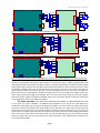
1
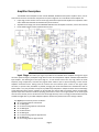
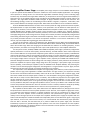
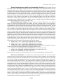
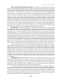
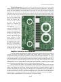
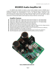
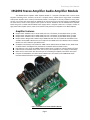
Preliminary Data Manual IRS2092 Stereo Amplifier Audio Amplifier Module The IRS2092 Stereo Amplifier Audio Amplifier Module is a complete assembled Class D Stereo Audio Amplifier containing all the necessary circuits for a complete stereo, scalable power stage, based on IRS2092S audio power amplifier driver made by International Rectifier. The amplifier is currently available in three power versions, one version with output power of 2x200W at 4Ω; the second version with output power of 2x400W at 4Ω; the third version, which has the highest output power can deliver 2x700W at 4Ω. The IRS2092 Stereo Amplifier board along with a suitable Switched Mode Power Supply offers a complete solution for a compact, medium to high power audio amplifier system, which can be used for newly built custom amplifiers or for OEM amplifiers. Amplifier Features: Output Power: 2x206W at 4Ω, or 117W at 8Ω, with max. 0.1% THD+N, for the 200W version, @ ±45V Output Power: 2x411W at 4Ω, or 228W at 8Ω, with max. 0.1% THD+N, for the 400W version, @ ±62V Output Power: 2x726W at 4Ω, or 373W at 8Ω, with max. 0.1% THD+N, for the 700W version, @ ±86V Output Power in Bridge mode: 738W at 4Ω or 409W at 8Ω with max. 0.1% THD+N for the 200W version 1373W at 4Ω or 818W at 8Ω with max. 0.1% THD+N for the 400W version and 2376W at 4Ω or 1420W at 8Ω with max. 0.1% THD+N for the 700W version.¹ Audiophile sound Quality: 0.01% THD+N at 178W at 4Ω or 94W at 8Ω for the 200W version, 362W at 4Ω or 185W at 8Ω for the 400W version, 607W at 4Ω or 329W at 8Ω for the 700W version, High efficiency: Up to 97.2% at 2x386W at 8Ω for 700W version, supplied at +-84V and allowing 1% THD. Full Protection set included: Short-circuit, over-current, over-temperature, over-voltage, under-voltage. Mute control, status and DC fast disconnect pins for controlling the amplifier status within the system. Compact size 100x100mm, and 40mm tall for 200W version, and 50mm tall for 400&700W version including PCB board thickness and clearance under. Figure 1: IRS2092 Stereo Audio Amplifier Module Page 1 Preliminary Data Manual Amplifier Description: The IRS2092 Stereo Amplifier is built around IRS2092S, dedicated audio power amplifier driver, one for each channel as well as several other components to system integration. The main blocks of this amplifier are: • Input stage, which contains one low-noise high performance Operational Amplifier for impedance match and to allow both balanced and unbalanced input connections; • Amplifier Power Stage, built around IRS2092S dedicated Class D amplifier controller, one for each channel; • House-keeping power supply and protections circuits. Figure 2: IRS2092 Stereo Audio Amplifier Module Schematic Diagram Input Stage: The audio input signal is provided to the IRS2092 Stereo Amplifier through the Signal connector passes through a preamplifier stage which has the role of impedance adapter and balanced/unbalanced input adapter. The default gain of this input stage is 1. It also remove some of the very high, above the audio frequency range components, and allow only signals below 27KHz to pass to prevent beating or other class-D amplifiers associated issues. Having both the inverted and non-inverted inputs routed to the Signal Input connector, a quick and easy installation is possible, changing the modes from balanced to unbalanced as well as Stereo to BTL is very easy and does not require any additional preamplifier or adapter. Another inherent advantage of fully balanced input is that the amplifier can be used with one channel 180° out of phase and the corresponding speaker output also inverted to avoid bus pumping phenomenon. There is one single capacitor in the entire signal chain for each channel, C12 for Left Channel and C37 for Right Channel, and in is strongly recommended to be kept and NOT changed with any so called audiophile capacitor because the performances won’t change in better. The Signal input connector pinout is as follows: Pin 1: Inverting Input for Left Channel Pin 2: GND Signal Pin 3: Non-Inverting Input for Left Channel Pin 4: GND Signal Pin 5: Mute Control Pin 6: GND Signal Pin 7: Non-Inverting Input for Right Channel Pin 8: GND Signal Pin 9: Inverting Input for Right Channel Page 2 Preliminary Data Manual Amplifier Power Stage: The amplifier power stage comprises of one IRS2092S dedicated driver IC plus two special selected MOS-FET transistors suitable for class D Audio amplifier applications. The topology used represents an analog version of a second-order sigma-delta modulation having a Class D switching stage inside the loop. The benefit of the sigma-delta modulation, in comparison to the carrier-signal based modulation, is that all the error in the audible frequency range is shifted to the inaudible upper-frequency range by nature of its operation. Also, sigma-delta modulation allows a designer to apply a sufficient amount of error correction. This self-oscillating topology consists of the following functional blocks: Integrator, Comparator, Level-shifter, Gate drivers, Power MOS-FET’s and Output Low-pass Filter. More details are available on the IC manufacturer website. Since the IRS2092S dedicated driver contains all the necessary blocks for a high performance class D amplifier, the implementation is simple and reliable. However, some parameters must be defined to allow operation in a wide range of conditions, from low power, 2x200W IRS2092 Stereo Amplifier module version, to highest power, 2x700W IRS2092 Stereo Amplifier module version. These parameters are: amplifier gain, switching frequency, dead-time and several other parameters related to protection, such as Over-Current threshold, Over-temperature, and supply voltage limits, Under-voltage and over-voltage. Since all these parameters are optimally configured and tested during manufacturing for each board and each batch separately, there is no reason for end-user to change any of these parameters because it can worsen the operation conditions or even lead to malfunctions. In this manual, only a brief explanation regarding gain choice will be written. The gain of Left Channel is given by the following ratio: (R2+R9)/R14 and for Right Channel (R36+R44)/R49. The default value is 30.6. The recommended values for R9 & R44 are within 100-150K range, and for R14 & R49 are within 2k7 and 3k6 range. Note that changing the R9 & R44 will have influence on switching frequency, control loop parameters, and values out of range will result in poor audio performance, or even amplifier malfunction. For each power version, 2x200W, 2x400W and 2x700W the amplifier power stage is particularly configured for optimal performance in terms of sound quality, electrical efficiency, and EMI radiation. Some critical components such as Power MOS-FET’s and output filter components (power inductor, low-pass filter capacitors, Zobel Network resistors and capacitors) as well as several smaller components which are version dependant, have different values from one version to another. Thus the supply voltage must be carefully chosen to prevent malfunction or damage if the supply voltage choice is wrong for a given amplifier version, especially for 2x200W and 2x400W versions. Note that although each board has Under-voltage and over-voltage protections, these protections are intended to protect the amplifier from power supply voltage swing due to bus pumping if a poor power supply is used (low current capability, small electrolytic capacitors) with the IRS2092 Stereo Amplifier Module, and protecting the module in case of excessively higher voltages than was designed for is not guaranteed in any form. Again, end-user should never intervene and/or change any of these components in any situation. The output filter of the IRS2092 Stereo Amplifier uses high-quality power inductors, made of special selected powder cores for high power applications. Notable characteristics are high resistivity, low hysteresis and eddy current losses and excellent inductance stability under both DC and AC conditions and no thermal aging, make them most suitable choice for Output power inductor of a class D amplifier. Among these, Magnetics® Kool-Mu, MPP and HF are used, as well as Micrometals®–2 materials, with excellent RF properties for some higher power versions. Although the current tendency on the market for similar IRS2092 amplifiers is to use a smaller and cheaper ferrite core inductor (more or less genuine) made by Sagami® and several other no-name brands, these are only suitable for low-power and high load impedance versions, such as up to 200W at 4 Ω or 300W at 8 Ω due to their sharp saturation characteristics. Once the saturation current is reached, inductance sharply drops leading to high distortion and possible amplifier failure if the over-current protection isn’t properly designed. The amplifier has built-in Mute circuit, which allows silent turn ON/OFF without any click/pop noise and can be operated with or without an external speaker protection circuit. However, if the amplifier is high power version, or is used with some expensive speakers, a speaker protection circuit can be considered as an extra level of protection. The latest amplifier versions include DC protection and quick-disconnect signals for SMPS in the unlikely event of DC signal present at the output of the amplifier. Matched power supply for amplifiers with this feature under development and will be available around April-May 2013. The Fast-disconnect signal is a logic signal, open collector, active on low, with 1k series resistor, so it must be biased and monitored for proper operation. Once the fault is asserted, the Fast-disconnect pin is pulled to GND and the power supply must shut-down immediately to prevent any possible damage to the speakers or the rest of the components from the amplifier. Note that this kind of fault is an abnormal situation never encountered in normal operation. The Fast-disconnect is available on pin 2 of AuxSupply connector. Page 3 Preliminary Data Manual House-keeping power supply and protections circuits: Both the amplifier stage and input stage requires several supply voltages for operation. These voltages are normally derived from the main differential supply, with the addition on the last batches of an optional Auxiliary supply connector for optimizing the efficiency and reducing the temperature build-up due to power dissipation of the linear regulators which are the default source for all the house-keeping circuits. If the IRS2092 Stereo Amplifier module is supplied with separate voltages for house-keeping circuits, through the small 8 pin AuxSupply connector present on the latest versions, the resistors R74, R75, R79 have to be removed and three voltages must be supplied, one voltage for driver stage, in range of 18V to 25V at 100mA max. and one differential voltage in range of ±18 to ±30V at 4050mA max. for the Input stage and IRS2092 IC’s. Note that for 2x200W amplifier version, using the aux. supply is not necessary as the temperature rise for this amplifier version is not high enough to justify the complication unless dedicated SMPS which provide these voltages is used. Recommended power supply: For proper operation, the power supply choice is an important aspect as it affects the overall performances and reliability. The easiest to configure and use a mains transformer and a high current rated Rectifier Bridge to provide rectified and unfiltered DC voltage to the IRS2092 Stereo Amplifier Module, and using the existing on board large electrolytic capacitors for filtering purpose only. This kind of power supply is only recommended if is readily available, or the high performance is not the main target but the cost or availability. In the default configuration, the amplifier only requires a differential supply voltage in range of: ±42V to ±47V for the 200W version, ±60V to ±66V for the 400W version, and ±80V to ±92V for the 700W version. These are suitable supply voltages needed for proper operation for each version, and required voltages to obtain the specified power ratings are regulated ±45V for the 200W version, ±64V for the 400W version, and ±86V for the 700W version. Supply voltages out of range will automatically mute the amplifier, and if the supply voltage is significantly higher than maximum allowed (15-20% more) can damage the amplifier. The rule of thumb is that the power supply must be able to provide at least the power required by the amplifier in any conditions (considering the efficiency figures as well). With audio signal the peak to average ratio is currently 8 but both the power supplies and the amplifiers are designed for a more aggressive value of 3. Following values are are measured during audition tests with combined musical program at levels near clipping: • 2x200W version, +-45V -- 143W average, 478W peak power consumption • 2x400W version, +-62V -- 282W average, 938W peak power consumption • 2x700W version, +-86V -- 512W average, 1783W peak power consumption Currently there are few suitable Switched Mode Power Supplies available from Connexelectonic which are suitable to be used for the following IRS2092 Stereo Amplifier Module versions: • 2x200W version: SMPS500RxE, SMPS500R, SMPS800RE for one module in BTL mode • 2x400W version: SMPS800RE, A1000SMPS, SMPS2000R for one module in BTL mode • 2X700W version: SMPS2000R both for SE and BTL mode. Several other power supplies are under development and as soon as will be available this list will be updated. Over-current Protection: The IRS2092 Stereo Audio Amplifier Module has built-in over-current protection circuitry to protect itself and the output transistors from short-circuit conditions The low-side current sensing feature protects the low side MOSFET from an overload condition in negative load current by measuring drain-to-source voltage across RDS(ON) during its on state. OCP shuts down the switching operation if the drain-tosource voltage exceeds a preset trip level. The voltage setting on the OCSET pin programs the threshold for lowside over-current sensing. When the VS voltage during low-side conduction gets higher than the OCSET voltage, the IRS2092 turns off outputs and pulls CSD down to -VSS.At this values, the over-current threshold is set at 36 A. The high-side current sensing protects the high side MOSFET from an overload condition in positive load current by measuring drain-to-source voltage across RDS(ON) during its on state. OCP shuts down the switching operation if the drain-to-source voltage exceeds a preset trip level. High-side over-current sensing monitors drain-to-source voltage of the high-side MOSFET while it is in the on state through the CSH and VS pins. The CSH pin detects the drain voltage with reference to the VS pin, which is the source of the high-side MOSFET. In contrast to the low-side current sensing, the threshold of CSH pin to trigger OC protection is internally fixed at 1.2V. An external resistive divider is used to program a threshold An external reverse blocking diode is required to block high voltage feeding into the CSH pin during low-side conduction. By subtracting a forward voltage drop of 0.6V at D4, the minimum threshold which can be set for the high-side is 0.6V across the drain-to-source Page 4 Preliminary Data Manual Under-voltage and Overvoltage Protection: The IRS2092 Stereo Amplifier Module senses the power rails through a dedicated detection circuit. The under-voltage and over-voltage thresholds are determined by the values of the resistors in the networks, and are power version dependent. If the supply voltage falls outside the upper and lower limits determined by the detection circuit, the IRS2092 Stereo Amplifier module shuts enters in Mute condition. The removal of the over-voltage or under-voltage condition returns the IRS2092 Stereo Amplifier module to normal operation. Please note that trip points specified in the Electrical Characteristics table are at 25°C and may change over temperature. The nominal operating voltage will typically be chosen as the supply “center point.” This allows the supply voltage to fluctuate, both above and below, the nominal supply voltage. Once the supply comes back into the supply voltage operating range (as defined by the supply sense resistors), the IRS2092 Stereo Amplifier module will automatically be un-muted and will begin to amplify. There is a small hysteresis range on both the under-voltage and over-voltage thresholds. If the amplifier is powered up in the hysteresis band the IRS2092 Stereo Amplifier module might misbehave and this supply voltage values must be avoided. Thus, the usable supply range is the difference between the over-voltage turn-off and under-voltage turnoff for both the V+ and V- supplies. It should be noted that there is a timer of approximately 300mS with respect to the over and under voltage sensing circuit. Thus, the supply voltage must be outside of the user defined supply range for greater than 200-300mS for the IRS2092 Stereo Amplifier module to be muted. Bus Pumping: An unwanted and potentially troublesome phenomenon present in all single-ended Class D amplifiers is the power supply pumping effect. It is caused by the flowing of the current from the output filter inductor into the power supply filter capacitors in opposite direction as the DC load sink current. The phenomenon is more evident at low-frequency and high amplitude signals, and if is not prevented it will trip the Overvoltage protection circuit, causing the amplifier to enter in Mute state until the supply voltage drop below the lower overvoltage protection threshold. Another cause of the Bus pumping is the DC offset which if is larger than 100-200mV, opposite voltage rail will start increasing the voltage until the Overvoltage protection circuit will trip, and Mute the amplifier. The IRS2092 Stereo Amplifier module does not need any kind of DC offset adjustment it has a very low DC offset, below 10mV. However, if the user is tempted to play with the input capacitor, and change it with some kind of audiophile potato size capacitor, or use no capacitor at all, relying on some sort of DC servo circuits, or not even such circuits, the smallest DC component present at the input of the amplifier will lead to DC offset at output and consequently lead to bus-pumping. For this reason we strongly suggest to NOT change the input capacitor or at most, if there’s no way to convince of uselessness of this action, use a similar value and size. There are few solutions to reduce the Bus-pumping. If the pumping effect is too high, this will lead to amplifier oscillations between ON/OFF states, since the under-voltage and over-voltage protection is not latched shutdown. The first solution is to use large Electrolytic capacitors on each power supply voltage rail to absorb the pumped supply current and to use-it in the next switching cycle. This method is less efficient when the output amplitude increase and the frequency decrease, being ineffective with DC signal. The best solution to avoid BusPumping is to drive one amplifier channel 180° out of phase with respect to the other. This setup will reduce the Bus-pumping because each channel is pumping out of phase with the other, and the net effect is a cancellation of pumping currents in the power supply. The phase of the audio signals needs to be corrected by connecting one of the speakers in the opposite polarity as the other channel. To achieve the phase shift, the input signal must be connected as shown in Figure 4-7, and taking advantage of using the amplifier with differential audio signal input when is available. EMI Reduction: Each power MOS-FET has a fast recovery diode connected in parallel for reduction of ringing on the outputs of the MOS-FET’s. They shunt the inductive energy generated in the parasitic inductance of the components leads and PCB tracks. The diodes are connected close to MOS-FET transistors, in “Drain to Drain” and “Source to Source” topology to minimize the ringing. The diodes are SMD type, which have very fast switching timings and very low stray inductance. For some amplifier version, the diodes are redundant since the MOS-FET’s body diodes are hyper-fast type and external diodes are not absolutely required. Furthermore, for reducing the ringing, few bypass capacitors are placed close to output power MOS-FET’s. There are 2 types of capacitors: one type is X7R material, ceramic capacitors, SMD1206 footprint placed on the bottom side of the PCB, very close to the output MOS-FET’s and the other type are electrolytic capacitors, for energy storage during peaks. The ceramic capacitors are connected between V+ and GND, V- and GND and V+ to V-. They provide extremely low stray inductance and ESR, which is helpful for reducing ringing. The electrolytic capacitors acts as energy storage tank during peak power consumption, as well as minimizing the pumping effect which switching amplifiers experience at high power outputs and low frequencies Page 5 Preliminary Data Manual Thermal Management: The amplifier modules, especially the highest power version require cooling to keep the temperature low. The temperature increase is mainly due to the linear regulators for +-12V which are regulating this low voltage down from the main high voltage rails, and when the supply voltage is high (high power version) the voltage difference and dissipated power is also high. the reason why was chosen to use linear regulators for the initial versions was that they have much lower noise than switching regulators, allow higher input voltage and there aren't many available switching regulators with low noise and high input voltage. On the last version, a small connector was added for separate aux. supply voltage to reduce this idle power. This was done on the later version because there was no suitable power supply yet at the time the first version was released and it would be way too complicated for most users to build themselves a differential aux. supply and a bias supply referenced to V-. For the 2x400W Amp version the temperature can be reasonable even without a fan. The PCB of the IRS2092 Stereo Amplifier was carefully designed to allow best cooling for the compact size heatsink which was used, without affecting its cooling capabilities. 11 holes were designed in the PCB for best cooling and airflow through the heatsink fins, even if a fan is not used. For high power an 80mm fan is recommended to be installed on the top of the PCB and air should pass through the fins and PCB holes, cooling the output inductors as well. Figure 3: IRS2092 Stereo Audio Amplifier Module layout Amplifier Connection and Operation: For proper operation the IRS2092 Stereo Amplifier module must be used according with the instructions provided in this manual. The IRS2092 Stereo Amplifier Audio Amplifier Module can be connected in several configurations, depending on the system requirements. The most common and simple configuration uses a mains transformer and a properly rated Rectifier Bridge to provide rectified and unfiltered DC voltage to the IRS2092 Stereo Amplifier Module, and using the existing on board large electrolytic capacitors for filtering purpose only. In the current manual will only be described the connection of the main supply, without details for the AuxSupply implementation till all the suitable SMPS for each models will be available, to avoid issues due to wrong connection by the users. At the time when all the dedicated power supplies will be available, the power supplies will be provided with compatible cables to connect 1:1 directly to the AuxSupply connector. Next, two Signal Input connector and two Speaker connectors are needed. Below are few connection diagrams showing the inter-connection. For proper operation and best performances, the IRS2092 Stereo Amplifier requires to be supplied with a balanced or unbalanced audio signal with the maximum amplitude in range of 0.775V to 1.5V depending on the gain setting. The audio signal must be applied at the input of the Amplifier, on the Signal connector as can be seen in the following schematics. In the below schematics, the signal phase is inverted for left channel to prevent or reduce bus pumping phenomenon. To be able to conveniently adjust the listening volume it is strongly recommended to use a potentiometer, logarithmic type with value Ω of or 50K maximum 100KΩ. The potentiometer must be connected as in the Figure 6 example. Page 6 Preliminary Data Manual SMPS800RE IRS2092 Audio Amplifier +Vcc 2 GND + Out R - GND 4 1 Speaker Right 1 9 8 7 6 5 4 3 2 1 Signal -Vcc 3 +Vcc Output GND -Vcc 1 2 3 4 Mains +Aux2 -Aux2 +Aux1 -Aux1 + GND - Out L 3 2 Mute/Play 2 3 Speaker Left Power 1 4 AuxPower Mains Switch Figure 4: IRS2092 Stereo Audio Amplifier Module & SMPS800RE Interconnection using Balanced XLR connectors SMPS800RE IRS2092 Audio Amplifier +Vcc 2 GND Speaker Right + Out R - GND 9 8 7 6 5 4 3 2 1 Signal -Vcc 3 +Vcc Output GND 1 2 3 4 Mains +Aux2 -Aux2 +Aux1 -Aux1 + GND - Out L 1 Input Right Mute/Play Input Left 1 4 3 2 -Vcc 4 3 2 1 Speaker Left Power AuxPower Mains Switch Figure 5: IRS2092 Stereo Audio Amplifier Module & SMPS800RE Interconnection using unbalanced RCA connectors IRS2092 Audio Amplifier SMPS800RE 2 GND 3 -Vcc Speaker Right + Out R - GND +Vcc Output GND -Vcc + 1 2 3 4 Mains +Aux2 -Aux2 +Aux1 -Aux1 - GND Out L 9 8 7 6 5 4 3 2 1 Signal 4 3 2 +Vcc 1 Pot 50K Input Right Mute/Play Input Left 1 Pot 50K 4 3 2 1 Speaker Left Power AuxPower Mains Switch Figure 6: IRS2092 Stereo Audio Amplifier & SMPS800RE Interconnection using unbalanced RCA connectors and potentiometer Mute control: When the Mute pin 5 of the Signal connector is connected to GND the amplifier both channels are muted (both high and low-side transistors are turned off). There is a delay of approximately 300 milliseconds between the de-assertion of MUTE and the un-muting of the IRS2092 Stereo Audio Amplifier Module which prevents false activation due to possible noise induced in the Mute wires from nearby noise sources. When the amplifier is Muted, either from an external Mute control signal, or due to an over-current, overvoltage or under-voltage condition, both channels Mute LED’s will lit and the ON LED’s will not lit. Also, when the ampler is in Mute state, the pin1 of the AuxSupply connector will toggle from +5V to -5V to indicate the amplifier state to the power supply circuits which might act accordingly. This is an I/O pin also used for delay turn ON of the amplifier when all the supply voltages are steady and amplifier ready to run. This function adds one more level of protection to the loudspeakers which are used with this amplifier. BTL mode operation: If the output power delivered by the amplifier in Single-Ended operation mode is not enough for a given application, the IRS2092 Stereo Amplifier can be used in BTL mode without any modification to the board, by just wiring the input signals accordingly, one channel 180° out of phase with respect to another. The theoretical output power in BTL mode is 4 times the power of a single channel on the same load, but practical output power which can be achieved with THD within low limits are between 3.2 to 3.7 times the output power of a single channel. Operating the amplifier in BTL mode will cancel the Bus-Pumping phenomenon due to the fact that each channel is driven with 180 ˚ out of phase Audio Signal, and at any time power will be drawn from both supply rails, by each channel power stage alternatively. BTL implementation example can be seen in the following Figure. Page 7 Preliminary Data Manual SMPS800RE IRS2092 Audio Amplifier 1 +Vcc 2 GND Speaker Right + Out R - GND 9 8 7 6 5 4 3 2 1 Signal -Vcc 3 +Vcc Output GND -Vcc GND Mains +Aux2 -Aux2 +Aux1 -Aux1 Input Left 1 Pot 50K 4 3 2 1 2 3 4 Mute/Play Power AuxPower Mains Switch Figure 7: IRS2092 Stereo Amplifier Module BTL configuration Amplifier Efficiency: The IRS2092 Stereo Audio Amplifier Module efficiency is given by the Output Power divided to the Input Power: η = POUT/PIN. The Input Power can be considered as: • PIN = PDRIVER + PSW + PSMPS + P+5V + POUT ((RS + RON + RCOIL + RL)/RL)^2 where: • PDRIVER = Power dissipated in the IRS2092S = 0.55W/channel, • PSW = 2 x (0.01) x Qg (Qg is the gate charge of M, in nano-coulombs), • RCOIL = Resistance of the output filter inductor (typically around 16-20mΩ), • PSMPS = Power dissipated in the Auxiliary power supply While the Input Power Level can be measured precisely, and the Output Power can also be measured on a resistive load, driving sinus signal, the practical efficiency can be determined. Note that the efficiency is dependent on the Output power level, at low power, has low values, and is increasing as the Output Power is higher. This is mainly due to switching losses which can be considered constant, and the IRS2092 power consumption which can be also considered constant. One factor which greatly influences the switching losses and the global efficiency is the dead-time setting, which is a compromise between efficiency and sound quality. The highest efficiency is achieved for a dead-time value of 120nS. From the practical measurements, the average achieved efficiency was up to 97.2% at 2x386W on 8Ω load impedance for 700W version, supplied at +-84V and allowing 1% THD during measurements. Note that below 3-5% THD cannot be detected by most peoples. Layout: The PCB Layout design has an important contribution to the overall performance of the TA3020 Audio Amplifier Module. That’s why double layer, FR-4 material with 1.6mm thickness and copper tracks thickness of 70um or 2 oz was chosen. The tracks width, were calculated to withstand the currents which they have to carry, and also the distance between adjacent tracks which carries higher voltages than 50V is big enough to satisfy the clearance conditions imposed by the design standards. The size of the PCB is 100 x 100 mm or 4 x 4 inch, and has 5 mounting holes, 4 isolated holes are on the corner of the PCB and one at the top-middle side of the PCB. The mounting holes are 3.2mm diameter or 0.12 inch, copper plated and reinforced with 8 vias around the main hole, for better mechanical strength. The distance from the edge of the board to the mounting holes is 4mm for each hole, thus the mounting holes are arranged in a 92x92mm perimeter, which we adopt as a standard for all our 100x100mm boards including amplifiers and power supplies. The main components layout and the Input and Output connectors pin out can be seen in the Figure 3. It is recommended to use heavy gauge wires for Power Supply and Loudspeaker Output and short shielded cables for Audio Input. The central mounting hole is connected to GND and should be considered if will be connected to chassis or not. The layout is symmetrical for Left and Right channel with respect to center axis, for better performances and aesthetical reasons. The heat sink is mounted directly onto the PCB and does not require additional support. The PCB has 11 large holes which allow air circulation through heatsink fins. The holes must be left open for ventilation purpose. For 2x400W and 2x700W versions, a cooling fan is recommended to be used, and installed on top of the board blowing air through heatsink. Wiring the amplifier to connectors, potentiometers, transformers, auxiliary boards, must be done with proper size wires and the cables must be laid carefully to avoid parasitic couplings, both capacitive and inductive, which will degrade the S/N ratio and amplifier performances. The input cables should be wired with shielded cables as short as possible, far from the amplifier output section or SMPS. The power connections, to the loudspeakers and SMPS must be wired with wires which are able to carry currents in excess of 10A. Attention must be paid to insulation, especially for the mains powered wires, where double insulation wires must be used. Page 8 Preliminary Data Manual Connectors Pinout: The Signal input connector pinout is as follows: Pin 1: Inverting Input for Left Channel Pin 2: GND Signal Pin 3: Non-Inverting Input for Left Channel Pin 4: GND Signal Pin 5: Mute Control Pin 6: GND Signal Pin 7: Non-Inverting Input for Right Channel Pin 8: GND Signal Pin 9: Inverting Input for Right Channel The Power connector pinout (from Left to right, holding the module with connector down) is as follows: Pin 1: Right Loudspeaker Output Pin 2: GND for Right Loudspeaker Pin 3: V+ Pin 4: GND Power Pin 5: VPin 6: GND for Left Loudspeaker Pin 7: Left Loudspeaker Output The AuxSupply connector pinout is as follows: Pin 1: Shut-Down I/O Pin 2: Fast-Disconnect Pin 3: +V aux, 18-30V @ 40-50mA referenced to GND Signal pin 4 Pin 4: GND Signal for Aux voltages Pin 5: +V aux, 18-30V @ 40-50mA referenced to GND Signal pin 4 Pin 6: ---Not connected for clearance purpose--Pin 7: Vbias 18-25V @ 100mA referenced to –Vcc pin 8 Pin 8: -Vcc Warning: Before you proceed with installation, make sure you have read this warning: The IRS2092 Stereo Amplfier Module contains potentially hazardous voltages up to 190V DC or 140V AC. This voltage levels are present on the top and bottom of the board, and during installation and operation should never touch any part of the board while it is connected to the mains and at least 5 minutes after complete disconnect from mains. If any adjustment or reconnection needs to be done, disconnect the unit from the mains and allow all capacitors to discharge for at least 5 minutes before handling it. Any ignorance of this warning will be made on user’s responsibility, and can lead to serious injuries and possible death by electrocution if is handled improperly. This product has no serviceable parts other than the on-board mains fuse. In case of blown fuse, only replace the fuse with the same type and rating. Do not attempt to change any other component from the board. A safety clearance of at least 6mm must be kept between the board and the case, or any conductive part of the amplifier. For best performances and long term reliable operation read before proceed!!! Peaking phenomenon will occur when the amplifier input is connected or disconnected while the amplifier is powered ON or the input is touched by hand to “test” if the amplifier is working. This is a very stupid mistake for any kind of amplifier, as the body static voltage corroborated with the voltage induced by the near electromagnetic field, less than ideal mains to amplifier ground isolation, will lead to high voltages build-up usually tens of volts which have 90% chances to damage any kind of amplifier with input impedance bigger than 10KΩ. Although the mains hum is dominant when “testing” the amplifier using this rude method, there is a full, rich spectrum of frequencies up to tens or hundreds of KHz, something which any normal amplifier should never expect. To prevent the amplifier failure, and making it “idiot-proof”, a more or less complex circuit can be employed but this will reduce its performances and sound quality, and due to this fact we strongly believe that the user know what he’s doing and will avoid torturing the amplifier for its own good. Page 9 Preliminary Data Manual Although the amplifier comes with optimized components, yet some peoples still want to “improve the improvements”. The very common mistake found on Class D and T amplifier while tuning the amplifier, is to replace the input capacitors with bigger size, sometimes as big as a coke can input capacitors. This is one of the biggest mistakes which can be possibly done on such amplifier. Not only that these placebo capacitors will not improve the sound, they will make it worse, and in some cases will damage the amplifier. Because as I wrote few rows above, the input should not be touched by hand or tools while is working, NEVER!!! (and this is often done during the tuning process) and these capacitors with their large volume and area will act like antennas which will pick-up the switching noise from the power stage, from the power supply, from environment, and also common mode noise from the amplifier housing if is made of metal and they are touching the case, even without electrical contact due to the stray capacitance between the capacitor and metal parts in close proximity. Disclaimer: The IRS2092 Audio Amplifier shall be used according with the instructions provided in this document. The user should NOT attempt to modify or change any of the parameters of this product, which can lead to malfunction. The designer and manufacturer of the product, and the official distributor, Connexelectronic, will not be liable for any kind of loss or damage, including but not limited to incidental or consequential damages. Due to the mains voltages of this board, the user should take all the caution measures needed when working with mains voltages, should not touch any unisolated part of the board or connectors, or short-circuit any part of the board or connectors. Any misusage will be made on user responsibility. The designer and manufacturer reserve the right to make changes or modifications on both the product functions and performances without notice. The schematic and PCB design is Connexelectronic proprietary and shall not be distributed, copied or published without the Connexelectronic written agreement. Connexelectronic reserve the right to offer limited support for the boards purchased directly from Connexelectronicor Connexelectronic, and no support at all for the similar boards which aren’t purchased directly from Connexelectronicand Connexelectronic, or future listed resellers, and from various reasons they look or pretend to be similar, exactly same, or improved version products. Purchasing the product means that you are aware and agree with all this conditions. Distribution network: We are continuously striving to offer the best product quality and availability for our products and part of our policy, however, since the shipping and delivery time becomes more and more a burden, we have decided to provide our products through our distributors networks as well. The current distributors are shown below, and the list will be updated. • Audiophonics, France, and near European Countries: http://www.audiophonics.fr • Enigma, UK, and near European Countries: http://www.enigma-shop.com Page 10