1
KV-32XBR400/36XBR400/38DRC1/38DRC1C
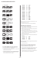
3-8. RASTER CENTER ADJUSTMENT
3.7 WHITE BALANCE (CRT) AND SUB
BRIGHT ADJUSTMENT
1. Input a monoscope signal.
2. Set to NTSC (DRC) mode.
White Balance
3. Enter service mode and set the following:
1. Input an all white 480I (15.734KHz) signal into the
VIDEO 1 input terminal to perform the white balance
(highlight, cut-off) adjustments. The parameters to adjust are
in the CXA2150P in service mode.
CXA2150P-2
No.
06
Name
AGNG
Control Function
AGING1, AGING2
Avg. Data
2
CXA2150D-2
No.
00
02
Name
HBLK
HSIZ
Control Function
Blanking enable
Horiz Size
Avg. Data
0
31
2. Set the following:
Picture: Full Mode
Pro Mode
Color:
Center
3. Adjust white balance in the service mode and set the
following data:
4. Reduce HSIZ to see sides of raster.
5. Adjust H-Center with CXA2150D-2 00.
2150P-1
No.
05
06
07
08
09
10
6. Adjust the best screen position with H-CENT and write data.
Name
RDRV
GDRV
BDRV
RCUT
GCUT
BCUT
Control Function
R-DRIVE
G-DRIVE
B-DRIVE
R-CUT OFF
G-CUT OFF
B-CUT-OFF
7. Restore aging, HSIZ and HBLK to original condition.
Avg. Data
Fix: 41
Adjust
Adjust
Fix: 41
Adjust
Adjust
3-9. PICTURE DISTORTION ADJUSTMENTS
CXA2150D-1 and CXA2150D-2
4. Adjust sub-brightness: Input an all black signal (to IRE 7.5%
set up) 480i (15.75KHz) signal into the VIDEO 1 input
terminal and adjust the following parameter of the
CXA2150P-1.
0.
VPOS ( V-POSITION)
CXA2150P-1
No.
04
1.
VSIZ (V-SIZE)
2.
VLIN (V-LINE)
3.
VSCO (VS-COR)
4.
HCNT (H-CENTERING)
5.
HSIZ (H-SIZE)
Name
SBRT
Control Function
SUB-BRIGHT
Avg. Data
Adjust
5. Check INITIAL DATA (Important)
2150P-1
No.
00
12
Name
SBOT
SBOF
6. Repeat steps 3 to 5.
Control Function
Avg. Data
SUB-BRT OFFSET
7
SUB-BRT OFFSET
63
— 21 —
KV-32XBR400/36XBR400/38DRC1/38DRC1C
6.
PIN (PIN AMP)
0
7.
UCP (UP COR PIN COR)
8.
LCP (LOW CO PIN COR)
9.
PPHA(PIN PHASE)
10. VANG (AFC-ANGLE)
A2150-D1
A2150-D1
A2150-D1
A2150-D1
A2150-D1
A2150-D1
A2150-D1
00
01
02
03
04
05
07
VPOS
VSIZ
VLIN
VSCO
VCEN
VPIN
HTPZ
A2150-D2
A2150-D2
A2150-D2
A2150-D2
A2150-D2
A2150-D2
A2150-D2
A2150-D2
A2150-D2
A2150-D2
A2150-D2
01
02
03
05
06
07
13
14
15
16
17
HPOS
HSIZ
SLIN
PIN
UCP
LCP
PPHA
VANG
LANG
VBOW
LBOW
Make sure picture size is within specs. Vertical size is 11.8 sq.
and Horizontal size is 15.8 sq.
4. Write data into memory then set screen to 1080i Mode.
11. VBOW (AFC-BOW)
1080i HD mode adjustment
1. Input a 1080i HD cross-hatch signal and an HD monoscope
signal that contains overscan markers.
12. VPIN (V-PIN)
2. Adjust raster position per section 3-8 only if this procedure
was not performed for full mode.
3. Adjust geometry similar to Full DRC mode. Vertical size is
11.8 sq. and Horizontal size is 15.8 sq if monoscope signal is
available. Otherwise use Vertical size as 91.5% scan,
Horizontal size as 90% scan.
13. HTPZ (H-TRAPEZOID)
4. Use the following registers to adjust vertical and horizontal
parameters:
14. LANG (L-ANGLE)
A2150-D2
A2150-D1
A2150-D1
A2150-D2
15. LBOW (L-BOW)
01
05
10
11
HPOS
VPIN
ASPT
SCRL
If necessary, touch up geometry using the data registers listed
above for Full mode.
5. Write data into memory.
Vertical Compressed Mode Adjustment
1. Input a monoscope and a cross-hatch signal.
3-10. NTSC (DRC) Full mode adjustment
1. Face picture tube to east or west direction.
2. Complete VPIN and VCEN adjustment first. (A2150-D1 05
VPIN, A2150-D1 04 VCEN)
3. Input a monoscope and a cross-hatch signal. Adjust picture
distortion with the following service parameters to balance
the best condition for these two signals.
2. Touch up geometry using the data registers listed above for
Full mode, however no adjustment should be necessary.
Vertical size is 11.8 sq. and Horizontal size is 15.8 sq.
3. Check Full mode for any side effect for any adjustments to
Vertical Compressed mode or 1080i HD mode.
— 22 —
KV-32XBR400/36XBR400/38DRC1/38DRC1C
SECTION 4
SAFETY RELATED ADJUSTMENTS
RV8001, RV8002, RV8003 CONFIRMATION METHOD AND HV SERVICE ADJUSTMENTS
The following adjustments should always be performed when replacing the following components which are marked with
schematic diagram:
D BOARD:
on the
DY, CRT, IC6503, IC8001, IC8003, IC8004, D8004, D8014, R8016, R8021, R8028, R8041, R8042,
R8044, R8072, R8073, R8074, R8077, R8078, R8080, R8081, R8082, R8091, R8095
B+ Max Confirmation: Standard: 135.3 + 1 VCD
Check Condition:
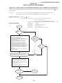
HV Service Flowchart
Start
Is RHT Changed?
AC input voltage : 120 (± 2) VAC at Board Adjustment Process
130 ( ± 2) VAC at QC
120 ( ± 2 ) VAC at Overall Adjustment (After aging)
*Note: If using stabilized power supply, make sure the distortion factor is 3% or less.
Setting Mode:
Full mode
Signal input :
Cross hatch of NTSC at QC
Initial setting :
Reset condition at QC
Confirm point :
Across C6544 for B+ of [D] board.
No
Yes
Replace RV8001,RV8002 and RV8003 with same value.
HV protect adjust and inspection
1. Turn RV8001and RV8003 fully counter clockwise.
2. Turn set on with black video signal then adjust RV8002
slowly to obtain 35.5kv.
3. Adjust RV8001 clockwise slowly until hold down
protection just activates, turn off set. Turn back
RV8001 about 1/16 turn; then turn set back on.
4. Turn RV8003 (fine adjust) slowly clockwise until hold
down protect just activates. Then turn the set off.
5. Adjust RV8002 clockwise, then turn the set on. Change
video to white field then slowly turn RV8002 counter
clockwise to get 35.0 ±0.2 kv. Confirm set does NOT
TURN OFF at this condition. If yes then repeat from
step 1 again.
6. Finally, set back RV8002 to 31.50kv ± 0.2kv at video
cut off ( black video).
Change any
or
marked parts?
No
Yes
Is D board
replaced?
Yes
If all adjustment are finished, then seal and secure
RV8001,RV8002 and RV8003 with epoxy to prevent any
possible misadjustment by non- trained technical service.
Confirm +B, Vd and check Hold down on D
board with black video with the following steps:
1. Confirm +B across C6544 to make sure it is
135.3 ± 1 V dc.
2. Confirm Vd at pin 2 CN6506 or at TP-Vd for
4.9 v < Vd < 5.1 V dc.
3. Apply 5.5 +0.5 VDC at pin 2 of CN6544
then confirm set holds down.
Is +B Vd. and
Hold down
confirmed?
No
Start from
the beginning.
Yes
Finish for
hold-down check
— 23 —
No
KV-32XBR400/36XBR400/38DRC1/38DRC1C
SECTION 5
CIRCUIT ADJUSTMENTS
ELECTRICAL ADJUSTMENTS BY REMOTE COMMANDER
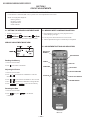
Use the Remote Commander (RM-Y74) to perform the circuit adjustments in this section.
NOTE: Test Equipment Required:
•
•
•
•
Pattern generator
Frequency counter
Digital multimeter
Audio oscillator
5-1. SETTING THE SERVICE ADJUSTMENT MODE
5-2. MEMORY WRITE CONFIRMATION METHOD
1. Standby mode (power off).
1. After adjustment, remove the power plug from the AC
outlet, then plug it in again.
2.
2. Turn the power switch ON and set to service mode.
on Remote Commander (press each button within a second).
3. Call the adjusted items again to confirm they were adjusted
.
SERVICE ADJUSTMENT MODE VIEW
5-3. ADJUSTMENT BUTTONS AND INDICATORS
WRITE INTO
MEMORY
SERVICE MODE
Reading the Memory
ITEM UP
1. Enter into Service Mode
2. Press
DATA UP
on the remote commander.
ITEM DOWN
DATA DOWN
Adjusting the Picture
DEVICE ITEM DOWN
1. Enter into Service Mode.
or
2. Press
device item.
on the Remote Commander to select the
2. Press
or
on the Remote Commander to select an item.
3. Press
or
on the Remote Commander to change the data.
4. Press
then
INITIALIZE
WRITE INTO MEMORY
REVIEW MEMORY
to save into the memory.
Resetting the Data
1. Enter into Service Mode.
2. Press
then press
Commander.
on the Remote
RM-Y174
— 24 —
— 25 —
SNNR
ID1
CCD&VCHIP
OP
ID
# 15
# 16
# 17
# 18
# 19
IC201 / A-board
IC201 / A-board
IC3001 / B-board
IC5513 / D-board
IC5511 / D-board
IC7001 / A-board
IC4101 / S-board
IC3408 / B-board
IC3408 / B-board
IC3408 / B-board
IC3408 / B-board
IC701 / A-board
IC2004 / BC-board
IC3048 (Main) / B-board
IC201 / A-board
IC3603 / B-board
IC3602 (Main) / B-board
IC3601 (Sub) / B-board
IC701 / A-board
IC701 / A-board
CXA2150Q
CXA2150Q
CXA2151Q
CXA8070P
CXA2026AS
BH3868FS
NJM2180M
CXD9509AQ
CXD9509AQ
CXD9509AQ
CXD9509AQ
M306V2ME-150FP
µPD64082
CXA2103Q
CXA2150Q
CXD2085M
M306V2ME-150FP
M306V2ME-150FP
CXP85840A-039Q
CXA2103Q
Service Control
Device Reference Number
IC2004 / BC-board
IC3048 (Main) / B-board
IC3110 (Sub) / B-board
Service Control
Device Name
µPD64082
Slave Address: 84h
Slave Address: DEh
Slave Address: 8Eh
Slave Address: 82h
Controlled through CXA1315M ( IC4103 / S-board, Slave Address: 48h )
Slave Address: 2Eh { Controlled through MID-X Micro ( IC3090 / B-board / 64h ) }
Slave Address: 2Eh { Controlled through MID-X Micro ( IC3090 / B-board / 64h ) }
Slave Address: 2Eh { Controlled through MID-X Micro ( IC3090 / B-board / 64h ) }
Slave Address: 2Eh { Controlled through MID-X Micro ( IC3090 / B-board / 64h ) }
System Micro (Version 1.0) with ROM correction (Patch A), Slave Address: 60h
Slave Address: B8h (Write) & B9h (Read)
Slave Address: 9Ah
Slave Address: 86h
Slave Address: 40h
CCD&Vchip Micro (Version 2.14), Slave Address: 68h (Main)
CCD&Vchip Micro (Version 2.14), Slave Address: 6Ch (Sub)
System Micro (Version 1.0) with ROM correction (Patch A), Slave Address: 60h
System Micro (Version 1.0) with ROM correction (Patch A), Slave Address: 60h
Slave Address: 86h
Slave Address: 86h
Service Control
Device Slave Address & Microprocessor Version
Slave Address: B8h (Write) & B9h (Read)
Slave Address: 9Ah
Slave Address: 9Eh
DX1A Service List ------ Contents
M306V2ME-150FP (MASK), Software Version 1.0 {with ROM correction (Patch A)}, IC701/A-board (Slave Adress: 60h)
MB94918RPF-G-128-BND (MASK1), Software Version 03/30/00, IC3090/B-board (Slave Address: 64h)
MB94918RPF-G-130-BND (MASK2), Software Version 04/20/00, IC3090/B-board (Slave Address: 64h)
DX1A CCD&Vchip Micro Software: CXP85840A-039Q (MASK), Software Version 2.14, IC3602/B-board (Main/Slave Address: 68h) & IC3601/B-board (Sub/Slave Address: 6Ch)
Note:
DX1A System Micro & Software:
DX1A MID-X Micro & Software:
3D-COMB
CXA2103-1 (Main)
CXA2103-2 (Sub)
CXA2150P-1
CXA2150P-2
CXA2150P-3
CXA2150P-4
CXA2150D-1
CXA2150D-2
CXA2150D-3
CXA2151
D-CONV
CXA2026
AP
TRUS
MID1
MID2
MID3
MID5
OSD
#1
# 2-1
# 2-2
# 3-1
# 3-2
# 3-3
# 3-4
# 4-1
# 4-2
# 4-3
#5
#6
#7
#8
#9
# 10
# 11
# 12
# 13
# 14
Service Control
Category Number & Name
5-4. SERVICE DATA LISTS
KV-27FS12/27FS16/29FS12/29FS12C
Control Register
Function & Link
— 26 —
CDL
DYCO
DYGA
DCCO
DCGA
YNRL
CNRL
6
7
8
9
10
11
12
SNNR Setting-based Control Table for YPFT & YHFG
18 YPFT Y peaking filter (BPF) center frequency
19 YPFG Y peaking filter (BPF) gain
13 VTRH
0~3
0~3
C
C
0~3
Data Data
Type Range
2
0~3
0~3
0~15
Nonstandard
0
C: Common data
CVideo (CV): CVideo1~4 inputs
SVideo (SV): SVideo1~3 inputs
2
1
2
1
VAPG1 Data Based on MENU/VM Setting
VAPG2 Data Based on SNNR/Offset-setting
VM = Off VM = Low VM = Mid VM = High
SNNR = 0
SNNR = 1 SNNR = 2 SNNR = 3
0
2
3
4
0
0
0
0
4 (32V) / 8 (36V) {Initial Data: 8 (36V)}
4
4
4
SNNR Setting (-Offset)
SNNR = 0 SNNR = 1 SNNR = 2
SNNR = 3
0
0
0
0
0
7
0
1
2
3
1
0~7
0~31
0
Standard
SVideo
Nonstandard
3
Comment
NRMD = 0 NRMD = 1 NRMD = 2 NRMD = 3
2
2
2
2
10
10
10
10
5
5
5
5
5
5
5
5
1
1
UHF/VHF Video1~4 Video5&6
Video1~4: CVideo1~4 & SVideo1~3 inputs
Video5&6: YCbCr-480i/480p/1080i inputs
1
1
1
3
1
UHF/VHF & CVideo
NonStandard
standard
0
0
0
1
3
3
Standard
SVideo
Data Initial Setting
(32V&36V CRTs)
UHF/VHF & CVideo
NonStandard
standard
0
1
0~3
0~3
Selection for standard/non-satndard signal processing
0~3
Selection for inter-frame/inter-line processing
C
0~3
Killer processing selection
C
0~3
C-signal phase with respect to the Y-signal
C
0~7
(Fine adjustment at 70 ns/step)
NRMD Setting-based Control Table for DYCO, DYGA, DCCO, DCGA
DY detection coring level (Y motion detection coring)
0~15
DY detection gain (Y motion detection gain)
0~15
DC detection coring level (C motion detection coring)
0~15
DC detection gain (C motion detection gain)
0~15
Frame recersive YNR nonlinear filter limit level
C
0~3
Frame recersive CNR nonlinear filter limit level
C
0~3
Hysteresis for Hsync non-standard signal detection
(out-of-Hsync intra-field)
Sensitivity for Hsync non-standard signal detection
14 VTRR
(out-of-Hsync intra-field)
Sensitivity for frame non-standard signal detection
15 LDSR
(out-of-Hsync inter-frame)
VM&SNNR Setting-based Control Table for VAPG & VAPI
VAPG= VAPG1 - VAPG2
16 VAPG V-aperture compensation gain
17 VAPI V-aperture compensation convergence point
NSDS
MSS
KILS
3
4
5
0 NRMD Operation mode setting
Y-output correction
1 YAPS
(V-aperture compensation & Y-peaking filtering)
2 CLKS System clock setting
Register
No & Name
Device Name: µPD64082 { 3D-Comb Filter / NEC } / IC2004 (BC-board)
Slave Address: B8h (Write Address) / B9h (Read Address)
DX1A SERVICE LIST (#1): 3D-COMB / µPD64082 (Part 1)
KV-27FS12/27FS16/29FS12/29FS12C
Control Register
Function & Link
— 27 —
Internal burst gate width
{Gate Width = 0.25 x BGPW + 0.5 (ms)}
Test bit {0: Normal mode, 1: Test mode (forbidden setting)}
Amount of noise detection coring
Internal burst gate start position
{Gate Start Position from Hsync center = 0.25 x BGPS + 2 (ms)}
41 LIND DRC-M line-doubling setting for non-standard signals
42 PFGO (YPFG offset at GR on) --- Not used for DX1A
39 TEST
40 WSC
38 BGPW
37 BGPS
Micro
---
C
C
C
C
C
C
35 CC3N Selection of a line-comb filter C separation filter characteristic
36 HDP Fine adjustment of the system H-phase
0, 1
C
C
0~7
0~15
C
C
C
0~63
0~7
0, 1
0~3
0~15
0~15
0, 1
0~7
0, 1
0, 1
0~255
0, 1
0, 1
0, 1
0, 1
0~3
0, 1
0~15
0~15
0~3
C
C
C
C
YHCO
YHCG
HSSL
VSSL
ADCL
Data Data
Type Range
28 NR1 Noise reduction on/off
29 NR2 SNNR control on/off
30 WSL Noise level detection data
31 HPLL H-PLL filter (Must be set to 1 when MN signal is input.)
32 BPLL Burst PLL filter
33 FSCF Burst extraction gain
34 PLLF PLL loop gain
20
21
22
23
24
SNNR Setting-based Control Table for YHCO & YHCG
Y output high frequency component coring
Y output high frequency component coring gain
Hsync slice level
Vsync slice level
ADC clock delay
NRMD Setting-based Control Table for D2GA
25 D2GA Moving detection gain
26 KILR Killer detection reference
Option1:
27 OP1
Selection of comb filter & recursive noise reduction types
Register
No. & Name
Device Name: µPD64082 { 3D-Comb Filter / NEC } / IC2004 (BC-board)
Slave Address: B8h (Write Address) / B9h (Read Address)
0
1
UHF/VHF & Video1~4 Video5&6
0
2
(Not used for DX1A)
3
10
4
UHF/VHF CVideo1
SVideo1
0
0
1
0
1 Byte Data from Read Register WSL
1
1
0
1
UHF/VHF Video1~4 Video5&6
0
0
0
5
1
CVideo3
0
SVideo3
1
Video1~4: CVideo1~4 & SVideo1~3 inputs
Video5&6: YCbCr-480i/480p/1080i inputs
SVideo2
1
Comment
(Not SNNR Offset Data)
YHCO&YHCG settings are sent
directly to 3D-Comb device.
This setting is used for non-standard signals
such as Play Station signals.
CVideo2
0
SNNR = 0 SNNR = 1 SNNR = 2 SNNR = 3
1
1
1
1
0
0
0
0
C: Common data
12
8
3
NRMD = 0 NRMD = 1 NRMD = 2 NRMD = 3
4
4
4
4
3
Data Initial Setting
(32V&36V CRTs)
DX1A SERVICE LIST (#1): 3D-COMB / µPD64082 (Part 2)
KV-27FS12/27FS16/29FS12/29FS12C
DX1A SERVICE LIST (#2-1): CXA2103-1 {Main}
SHAP
SHF0
PREO
BPF0
BPFQ
BPSW
TRAP
LPF
6
7
8
9
10
11
12
13
Y/C delay time
SNNR Data-related Settings
Adj.
0~3
0~15
0~15
0~15
— 28 —
CBOF
CROF
ATPD
DCTR
20
21
22
23
Auto-pedestal Inflection Point
DC Transmission Ratio
CXA2150P-4/#13 UBLK Setting-related Controls for ATPD & DCTR
Cb-Offset1 of Cb IN (Pin34)
Cb-Offset2 of EXT Cb (Pin38)
Cr-Offset1 of Cr IN (Pin35)
Cr-Offset2 of EXT Cr (Pin39)
0~3
0~3
0~(31)~63
0~(31)~63
0, 1
0~3
0~3
0, 1
0, 1
0~15
YDLY
5
Sub hue
Adj.
Adj.
0~63
0~63
Data
Range
14 AFCG AFC Loop Gain (PLL between Hsync & HVCO)
15 CDMD V countdown system mode selector
16 SSMD H&Vsync slide level setting
17 HMSK Masking of macrovision signal on/off
18 HALI H automatic adjustment on/off
19 PPHA H TIM phase adjustment for video
SHUE
4
Sub contrast
Sub color
Data
Type
0~15
0~3
0~3
0~3
0~3
0, 1
0, 1
0, 1
SCON
SCOL
2
3
Y-Out gain
Cb&Cr-Out gains
Control Register
Function & Link
Sharpness
Sharpness f0 selector
Sharpness pre/over-shoot ratio
Chroma band filter f0 setting
Chroma band filter Q setting
Chroma band filter on/off
Y bolck chroma trap filter on/off
YCbCr-Output LPF on/off
YLEV
CLEV
0
1
Register
No & Name
Video
27*
55*
P&P-Left
(M)-1080i
0
0
31
31
1
1
UBLK = 1
2
1
UBLK = 2
3
1
UBLK = 3
31*
31*
P&P-Left
(M)-480i
4
0
0
0
3
0
0
0
YCbCr
480i
31*
31*
P&P-Left
(M)-480i
YCbCr-480i
P&P-Left
(M)-DRC
0
3
0
1
0
7
YCbCr
480i
4
0
0
0
3
0
0
0
SVideo
28
32
P&P-Left
(M)-DRC
P&P & Favorite
31*
31
UBLK = 0
31*
P&P-Left
(M)-1080i
31
P&P-Left
(M)-DRC
UHF/VHF & Video
0
3
0
1
0
7
Video
UHF/VHF
1
3
0
1
0
7
4
0
0
0
3
0
0
0
CVideo
6
0
3
3
0
1
0
0
UHF/VHF
7 [Adj.] 7 [Adj.]
7 [Adj.] 7 [Adj.]
7
7
[-2steps] [-2steps]
0
0
UHF/VHF
23
17
P&P-Left
(M)-DRC
YCbCr-480i
1
SNNR=1
(-offset)
1
2
UBLK = 4
2
2
UBLK = 5
3
2
UBLK = 6
P&P & Favorite
2
SNNR=2
(-offset)
*: Settings not used
(31): The center setting = 31
CVideo: CVideo1~4 Inputs
SVideo: SVideo1~3 Inputs
0
SNNR=0
(-offset)
Adj.: Adjusted data
[-2steps]: The adjusted data - 2 steps
2
3
UBLK = 7
3
SNNR=3
(-offset)
Video: CVideo1~4 & SVideo1~3 Inputs
P&P-Left (M)-1080i&480i: If P&P-Left is
1080i/480p signal, the signal from the main
chroma decoder is sent to MID/VDO input.
*: Settings not used
(32V&36V CRTs)
(32V&36V CRTs)
UHF/VHF & Video
Data Initial Setting
Data Initial Setting & [Adjusted Data]
Device Name: CXA2103Q { NTSC-YCT (Chroma Decoder) / SONY } / IC3048 (B-board)
Slave Address: 9Ah { Main }
0
0
UBLK=0~7
Single
Note
KV-27FS12/27FS16/29FS12/29FS12C
DX1A SERVICE LIST (#2-2): CXA2103-2 {Sub}
— 29 —
SCON
SCOL
SHUE
YDLY
SHAP
SHF0
PREO
BPF0
BPFQ
BPSW
TRAP
LPF
2
3
4
5
6
7
8
9
10
11
12
13
Sharpness
Sharpness f0 selector
Sharpness pre/over-shoot ratio
Chroma band filter f0 setting
Chroma band filter Q setting
Chroma band filter on/off
Y bolck chroma trap filter on/off
YCbCr-Output LPF on/off
SNNR Data-related Settings
Y/C delay time
Sub hue
Sub contrast
Sub color
Y-Out gain
Cb&Cr-Out gains
Control Register
Function & Link
CBOF
CROF
ATPD
DCTR
20
21
22
23
Auto-pedestal Inflection Point
DC Transmission Ratio
CXA2150P-4/#13 UBLK Setting-related Controls for ATPD & DCTR
Cb-Offset1 of Cb IN (Pin34)
Cb-Offset2 of EXT Cb (Pin38)
Cr-Offset1 of Cr IN (Pin35)
Cr-Offset2 of EXT Cr (Pin39)
14 AFCG AFC Loop Gain
15 CDMD V countdown system mode selector
16 SSMD H&Vsync slide level setting
17 HMSK Masking of macrovision signal on/off
18 HALI H automatic adjustment on/off
19 PPHA H TIM phase adjustment for video
YLEV
CLEV
0
1
Register
No & Name
Adj.
Adj.
Adj.
Data
Type
0~3
0~3
0~(31)~63
0~(31)~63
0, 1
0~3
0~3
0, 1
0, 1
0~15
0~15
0~3
0~3
0~3
0~3
0, 1
0, 1
0, 1
0~3
0~15
0~15
0~15
0~63
0~63
Data
Range
Video
22
16
P&P-Right
(S)-DRC
0
0
UBLK = 0
31
31
P&P-Right
(S)
31*
31*
1
1
UBLK = 1
2
1
UBLK = 2
3
1
UBLK = 3
31*
31*
P&P-Right
(S)-DRC
YCbCr-480i
P&P-Right
(S)
4
0
0
0
0
0
0
0
SVideo
P&P & Favorite
31
31
P&P-Right
(S)-DRC
UHF/VHF & CVideo
0
3
0
1
0
7
Video
UHF/VHF
1
3
0
1
0
7
4
0
0
0
0
0
0
0
CVideo
6
0
3
0
0
0
0
0
UHF/VHF
7 [Adj.] 7 [Adj.]
7 [Adj.] 7 [Adj.]
7
7
[-2steps] [-2steps]
0
0
UHF/VHF
23
18
P&P-Right
(S)
1
SNNR=1
(-offset)
1
2
UBLK = 4
2
2
UBLK = 5
3
2
UBLK = 6
P&P & Favorite
2
SNNR=2
(-offset)
*: Settings not used
(31): The center setting = 31
CVideo: CVideo1~4 Inputs
SVideo: SVideo1~3 Inputs
0
SNNR=0
(-offset)
Adj.: Adjusted data
[-2steps]: The adjusted data - 2 steps
2
3
UBLK = 7
3
SNNR=3
(-offset)
Video: CVideo1~4 & SVideo1~3 Inputs
P&P-Right (S)-DRC: If P&P-Left is 1080i/
480p signal, the signal from the sub chroma
decoder is switched to DRC path.
(32V&36V CRTs)
(32V&36V CRTs)
UHF/VHF & Video
Data Initial Setting
Data Initial Setting & [Adjusted Data]
Device Name: CXA2103Q { NTSC-YCT (Chroma Decoder) / SONY } / IC3110 (B-board)
Slave Address: 9Eh { Sub }
0
0
UBLK=0~7
Single
Note
KV-27FS12/27FS16/29FS12/29FS12C
SBOT
YOF
CBOF
CROF
SBRT
RDRV
GDRV
BDRV
RCUT
GCUT
BCUT
Offset for SBRT
Y_OFFSET: DC-offset for Y signal
CB_OFFSET: DC-offset for Cb signal
CR_OFFSET: DC-offset for Cr signal
SUB_BRIGHT: Sub Bright
R_DRIVE: R output drive
G_DRIVE: G output drive
B_DRIVE: B output drive
R_CUTOFF: R output cutoff
G_CUTOFF: G output cutoff
B_CUTOFF: B output cutoff
Control Register
Function & Link
— 30 —
Note:
WB_SW: White balance offset on/off
11 WBSW
(Related to UTMP seetings)
12 SBOF Offset for SBRT
13 RDOF Offset for RDRV
14 GDOF Offset for GDRV
15 BDOF Offset for BDRV
16 RCOF Offset for RCUT
17 GCOF Offset for GCUT
18 BCOF Offset for BCUT
0
1
2
3
4
5
6
7
8
9
10
Register
No & Name
Device Name: CXA2150Q { CRT Driver / SONY } / IC201 (A-board)
Slave Address: 86h
Adj.
C
Adj.
Adj.
C
Adj.
Adj.
Data
Type
0~(63)~127
0~(63)~127
0~(63)~127
0~(63)~127
0~(63)~127
0~(63)~127
0~(63)~127
0, 1
0~(7)~15
0~(7)~15
0~(31)~63
0~(31)~63
0~63
0~63
0~63
0~63
0~63
0~63
0~63
Data
Range
7
0
31
31
11
22
36
33
24
7
0
33
42
[Adj.]
41
[Adj.]
[Adj.]
41
[Adj.]
[Adj.]
YCbCr
480i
(Warm)
63
63**
66**
76**
63**
66**
78**
63
63
63
63
63
63
63
63
63
63
63
63
63
63
1
Movie
7
0
31
31
YCbCr
1080i
(Neutral)
7
0
30
36
YCbCr
480p
(Cool)
Standard
7
0
31
31
SV
0
Vivid
7
0
31
31
CV
0
UHF
VHF
(32V&36V CRTs)
Data Initial Settings & [Adjusted Data]
DX1A SERVICE LIST (#3-1): CXA2150P-1 {Picture Controls: P1}
63
63
63
63
63
63
63
0
Pro
7
0
13
23
P&P
**: The color
temporature
offset data
C:
Common data
Adj.:
Adjusted data
CV:
CVideo1~4
SV:
SVideo1~3
( ): Settings at
center
Comment
KV-27FS12/27FS16/29FS12/29FS12C
— 31 —
RGBS
BLKB
LIML
PABL
SABL
AGNG
AKBO
1
2
3
4
5
6
7
Note:
8 SYPH
9 CLPH
10 CLGA
11 JAXS
12 BLKO
ALBK
0
Register
No & Name
SYNC_PHASE: Hsync delay with respect to Video (100%: H-period)
CLP_PHASE: Internal clamp pulse phase (100%: H-period)
CLP_GATE: Switch for the gated internal clamp pulse with Hsync input
JAXIS: Color axis switch
BLKO: Blanking switch
PIC_ON: RGB output including AKB reference pulse on/off
(Setting = 0 for power on reset) --- G2 adjustment register setting
R_ON/G_ON/B_ON: R/G/B outputs on/off
(AKB reference pusle can not be turned on/off.) (0,1/0,1/0,1)
BLK_BTM: RGB output bottom limit level (Black Limit)
(AKB reference pusle DC-voltage)
PLIMIT_LEV: Threshold level for excessively high inputs (White Limit)
P_ABL: DC-level in RGB output detection for PEAK ABL
S_ABL: S_ABL gain
AGING_W/AGING_B: AGING_W/AGING_B modes on/off
(Set luminance to 80/01IRE flat-field signal.)
AKBOFF: Automatic/Manual-Cutoff setting
Control Register
Function & Link
Device Name: CXA2150Q { CRT Driver / SONY } / IC201 (A-board)
Slave Address: 86h
0~3
C
C
C
0~3
0~3
0, 1
0, 1
0, 1
0~3
0~15
0~3
0~3
(0,1/0,1)
0, 1
0~7
C
C
C
C
0, 1
Data
Range
C
Data
Type
YCbCr
480i
0
3
0
U/VHF &
Video1~4
0
3
0
0
0
0
0
0
15
0
3
7
1
0
3
0
YCbCr
480p
0
3
0
YCbCr
1080i
(32V&36V CRTs)
Data Initial Settings
DX1A SERVICE LIST (#3-2): CXA2150P-2 {Picture Controls: P2}
0
3
0
P&P
Video1~4:
CVideo1~4 &
SVideo1~3
C:
Common data
Comment
KV-27FS12/27FS16/29FS12/29FS12C
— 32 —
SYSM
UVML
VMMO
VMCR
VMLM
VMF0
VMDL
SHOF
SHF0
PROV
F1LV
CDSP
LTLV
LTMD
CTLV
CTMD
UBOF
UCOF
UHOF
MIDE
Note:
0
1
2
3
4
5
6
7
8
9
10
11
12
13
14
15
16
17
18
19
Register
No & Name
SYSTEM: Signal bandwidth setting
VM_LEV: VM_OUT level
System Micro pin#40
VM_COR: VM_OUT coring level
VM_LMT: VM_OUT limit level
VM_F0: VM_f0
VM_DLY: VM_OUT phase (defined by phase difference from R_OUT)
Offset for USHP = SHOF x 4
SHP_F0: Sharpness circuit f0
PRE/OVER: Y signal pre/over-shoot ratio
SHP_F1: Sharpness for higher f0 (4.2/5.6 MHz @ NORMAL mode)
SHP_CD: Sharpness in part of high color saturaion
LTI_LEV: Luminance transient improvement (LTI)
LTI_MODE: LTI mode setting
CTI_LEV: Chrominance transient improvement (CTI)
CTI_MODE: CTI mode setting
Offset for UBRT (Picture clarity adjustment)
Offset for UCOL = UCOF x 2 (Picture clarity adjustment)
Offset for UHUE (Picture clarity adjustment)
MID enhancement setting
Control Register
Function & Link
Device Name: CXA2150Q { CRT Driver / SONY } / IC201 (A-board)
Slave Address: 86h
C
Data
Type
0~3
0~3
0, 1
0~3
0~3
0~3
0~3
0~3
0, 1
0~3
0~3
0~3
0~3
0~3
0~3
0~3
0~(7)~15
0~3
0~3
0~15
Data
Range
1
3
0
3
3
2
3
2
1
3
0
3
3
0
0
0
7
3
0
3
UHF
VHF
0
3
3
2
3
2
1
3
3
3
3
0
0
0
7
3
0
3
1
CV
0
3
3
2
3
2
1
3
3
3
3
0
0
0
7
3
0
3
1
SV
0
3
3
2
3
3
1
1
3
3
3
0
0
0
7
3
0
7
1
YCbCr
480i
0
3
3
2
3
3
1
3
3
3
3
0
0
0
7
3
0
11
1
YCbCr
480p
Picture Mode: Vivid
0
3
3
2
1
0
0
0
3
3
3
0
2
0
10
0
0
---
2
YCbCr
1080i
Data Initial Settings (32V&36V CRTs)
DX1A SERVICE LIST (#3-3): CXA2150P-3 {Picture Controls: P3} (Part-1)
0
3
3
2
3
2
1
3
3
3
3
1
0
0
7
3
0
---
2
P&P
( ): Settings at
center
C:
Common data
CV:
CVideo1~4
SV:
SVideo1~3
These settings
continue to
the next page.
Comment
KV-27FS12/27FS16/29FS12/29FS12C
#0 SYSM (cont.)
#1 UVML (cont.)
#2 VMMO (cont.)
#3 VMCR (cont.)
#4 VMLM (cont.)
#5 VMF0 (cont.)
#6 VMDL (cont.)
#7 SHOF (cont.)
#8 SHF0 (cont.)
#9 PROV (cont.)
#10 F1LV (cont.)
#11 CDSP (cont.)
#12 LTLV (cont.)
#13 LTMD (cont.)
#14 CTLV (cont.)
#15 CTMD (cont.)
#16 UBOF (cont.)
#17 UCOF (cont.)
#18 UHOF (cont.)
#19 MIDE (cont.)
Register
No & Name
1
3
0
3
3
2
1
0
0
3
0
3
2
1
0
0
7
3
0
2
UHF
VHF
1
0
3
3
2
3
3
1
3
3
3
2
1
0
0
7
3
0
2
0
3
3
2
3
3
1
3
3
3
2
1
0
0
7
3
0
2
SV
1
CV
0
3
3
2
3
3
1
1
3
3
2
1
0
0
7
3
0
6
1
YCbCr
480i
0
3
3
2
3
3
1
3
3
3
2
1
0
0
7
3
0
10
1
YCbCr
480p
0
3
3
2
1
0
0
0
3
3
2
1
2
0
7
0
0
---
2
YCbCr
1080i
Picture Mode: Standard
0
3
3
2
3
2
1
3
3
3
3
1
0
0
7
3
0
---
2
P&P
Data Initial Settings (32V&36V CRTs)
1
0
0
3
3
2
1
0
0
3
0
0
0
1
0
0
7
0
0
1
UHF
VHF
0
3
3
2
1
3
0
3
0
0
0
1
0
0
7
0
0
1
1
CV
0
3
3
2
1
3
0
3
0
0
0
1
0
0
7
0
0
1
1
SV
0
3
3
2
1
3
0
1
0
0
0
1
0
0
7
0
0
5
1
YCbCr
480i
0
3
3
2
1
3
0
3
0
0
0
0
0
0
7
0
0
9
1
YCbCr
480p
Picture Mode: Movie
0
3
3
2
1
0
0
0
0
0
0
0
0
0
7
0
0
---
2
YCbCr
1080i
Data Initial Settings (32V&36V CRTs)
0
3
3
2
3
3
1
3
3
0
0
1
0
0
7
0
0
---
2
P&P
1
0
0
3
3
2
1
0
0
3
0
0
0
1
0
0
7
0
0
0
UHF
VHF
0
3
3
2
1
3
0
3
0
0
0
1
0
0
7
0
0
0
1
CV
0
3
3
2
1
3
0
3
0
0
0
1
0
0
7
0
0
0
1
SV
0
3
3
2
1
3
0
1
0
0
0
1
0
0
7
0
0
4
1
YCbCr
480i
0
3
3
2
1
3
0
3
0
0
0
0
0
0
7
0
0
8
1
YCbCr
480p
Picture Mode: Pro
0
3
3
2
1
0
0
0
0
0
0
0
0
0
7
0
0
---
2
YCbCr
1080i
Data Initial Settings (32V&36V CRTs)
CXA2150P-3 {Picture Controls: P3} (Part 2)
0
3
3
2
3
3
1
3
3
0
0
1
0
0
7
0
0
---
2
P&P
— 33 —
-1
0
0
0
0
0
0
+1
0
0
0
0
0
0
SNNR=0 SNNR=1
(Offset) (Offset)
0
0
-2
0
0
+2
0
SNNR=2
(Offset)
0
0
-3
0
0
+3
0
SNNR=3
(Offset)
Data Initial Settings (32V&36V CRTs)
KV-27FS12/27FS16/29FS12/29FS12C
— 34 —
AGAM GAMMA/GAMMA_L (Av Pro user control) --- Void Data
9
DCTR
16 DPIC
17 DSBO
18 ABLM
15
Item # 15~18 pack FI data controls
(Av Pro user control) --- Void Data
13 UBLK
14 ABLK
DC_TRAN: Y signal DC transmission
(8 types of DCTR data based on UBLK values)
DPIC_LEV: Y signal AUTO PEDESTAL level
Offset for SBRT
ABL_MODE: ABL mode
UBLK Setting-related Controls for DCTR
Offset for SBRT (8 types of GSBO data based on UGAM values)
Offset for UCOL
Offset for UHUE
10 GSBO
11 GCOO
12 GHUO
UGAM Setting-related Controls for GSBO, GCOO, GHUO
GAMMA/GAMMA_L: RGB output GAMMA correction setting (B7~6)
GAMMA L: Slight GAMMA correction on/off (B0)
UGAM
8
COL_AXIS: Color matrix setting
SHARPNESS: Sharpness
Color Temporature (0: Warm, 1: Neutral, 2: Cool)
DCOL: Dynamic color setting
AXIS
USHP
UTMP
UDCL
4
5
6
SNNR Setting-related Controls for USHP
PICTURE: Picture
BRIGHT: Brightness
COLOR: Color
HUE: Hue
Control Register
Function & Link
---
Data
Type
0~3
0~63
0~2
0~3
0~63
0~63
0~63
0~63
Data
Range
0~3
0~(7)~15
0~3
0~3
0~7
0~7
0~3
0~3
0~3
0~7
(0~3/0,1)
0~7
(0~3/0,1)
Slave Address: 86h
Slave Address: 40h
44
1
2
42
28
33
31
---
34
0
2
31
28
33
31
3
0
0
0
UGAM
=4
5
YCbCr
480p
0
0
0
UGAM
=3
5
YCbCr
1080i
3
2
7
1
3
2
7
1
7
7
0 (Void data)
2
7
1
3
7
YCbCr
480p
2
7
1
3
7
YCbCr
1080i
0
0
0
1
7
1
2
7
31
1
0
31
31
31
31
Pro
0
0
0
UGAM
=1
P&P
UGAM
=2
5
P&P
3
P&P
32&36V
Movie
YCbCr
1080i
Picture Mode: Vivid
0
0
0
UGAM
=5
YCbCr
480i
0
0
0
UGAM
=6
5
YCbCr
480i
UHF/VHF
Video1~4
0
0
0
UGAM
=7
5
3
YCbCr
480p
Picture Mode: Vivid
3
3
UHF/VHF
Video1~4
48
1
2
46
26
33
31
36V
Standard
32V
Picture Mode: Vivid / Standard / Movie
42
2
2
63
22
38
31
36V
YCbCr
480i
Vivid
UHF/VHF
Video1~4
38
2
2
63
25
34
31
32V
(32V&36V CRTs)
Data Initial Settings
DX1A SERVICE LIST (#3-4): CXA2150P-4 {Picture Controls: P4} (Part-1)
CXA2150Q { CRT Driver / SONY } / IC201 (A-board)
CXD2085 { ID-1 Decoder / SONY } / IC3603 (B-board)
7
UPIC
UBRT
UCOL
UHUE
0
1
2
3
Register
No & Name
Device Name:
Device Name:
These settings
continue to
the next page.
( ): Seetings at
center
These settings
continue to
the next page.
Video1~4:
CVideo1~4 &
SVideo1~3
These settings
continue to
the next page.
This setting
continues to
the next page.
Settings for
36V CRTs
are used for
initial
settings.
Comment
KV-27FS12/27FS16/29FS12/29FS12C
— 35 —
3
2
2
YCbCr
480i
4
2
1
7
1
4
2
1
7
1
#13 UBLK (Cont.)
#15 DCTR (Cont.)
#16 DPIC (Cont.)
#17 DSBO (Cont.)
#18 ABLM (Cont.)
0
0
0
2
YCbCr
480p
2
1
7
1
4
YCbCr
480p
Picture Mode: Standard
YCbCr
480i
U/VHF
Video1~4
=0
3
YCbCr
480p
Picture Mode: Standard
3
UGAM
4
SNNR
=3
Picture Mode: Pro
3
YCbCr
480i
1
0
SNNR
=2
UHF/VHF
Video1~4
SNN
R
=1
YCbCr
1080i
P&P
2
1
7
1
4
YCbCr
1080i
2
YCbCr
1080i
3
2
1
7
1
4
P&P
2
P&P
3
U/V
HF
1
1
7
0
1
UH
F/V
0
0
YCbCr
480p
0
YCbCr
1080i
1
1
7
0
1
YCbCr
480i
1
1
7
0
1
YCbCr
480p
1
1
7
0
1
YCbCr
1080i
Picture Mode: Movie
0
YCbCr
480i
Picture Mode: Movie
(32V&36V CRTs)
(32V&36V CRTs)
SNNR
=0
Data Initial Settings
Data Initial Settings
UHF/VHF
Video1~4
#10 GSBO (cont.)
#11 GCOO (cont.)
#12 GHUO (cont.)
#8 UGAM (Cont.)
#7 AXIS (Cont.)
#4 USHP (cont.)
SNNR Setting
(-Offset)
Register
No & Name
1
1
7
0
1
P&P
0
P&P
0
1
0
7
0
1
0
7
0
0
0
YCbCr
1080i
1
0
7
0
0
YCbCr
480p
1
0
7
0
0
YCbCr
1080i
Picture Mode: Pro
YCbCr
480i
0
YCbCr
480p
Picture Mode: Pro
YCbCr
480i
0
UH
F/V
0
U/V
HF
(32V&36V CRTs)
Data Initial Settings
1
0
7
0
0
P&P
0
P&P
3
2
7
1
2
3
7
0
2
2
7
0
2
1
7
1
1
3
7
0
1
2
7
0
1
1
7
0
1
0
7
0
UBLK =
UBLK = UBLK = UBLK = UBLK = UBLK =
UBLK = 2
4
3
0
7
6
5
DX1A SERVICE LIST (#3-4): CXA2150P-4 {Picture Controls: P4} (Part-2)
KV-27FS12/27FS16/29FS12/29FS12C
— 36 —
DATA
27
Note:
IDSW
26
23 SCON
24 CLOF
25 HUOF
SPOF
ABLC
EPOF
20
21
22
ABLT
19
Register
No & Name
Selection of geometry-forced vertical compression modes
Switch for activating the selection in #26 DATA
CXD2085 Service Controls
SUB_CONTRAST: SUB PICTURE
Offset for UCOL
Offset for UHUE
Offset for UPIC = SPOF x (UPIC/64) --- Data Not Used
ID-1 and P&P Modes
C
C
---
0~3
0, 1
0~15
0~(7)~15
0~7~15
0~31
0~255
0~31
---
Control of CXA2026 {0Ch -- DAC0} (*)
Offset for UPIC = EPOF x (UPIC/63) (for power save) --- Void Data
Data
Range
0~15
Data
Type
ABL_TH: ABL currect detection Vth control
Control Register
Function & Link
Vcomp2
2
Vcomp1
1
10
7
3
0
11
9
3
YCbCr
1080i
66
Vcomp2
Full
8
8
3
9
8
4
0
YCbCr
480i
UHF/VHF
Video1~4
YCbCr
480p
66
0
0 (Not used)
Vcomp1
0
Full
(32V&36V CRTs)
Data Initial Settings
DX1A SERVICE LIST (#3-4): CXA2150P-4 {Picture Controls: P4} (Part-3)
9
8
4
P&P
C:
Common data
( ): Settings at
center
Full:
480p/960i
(4x3)
Vcomp1:
480p/960i
(16x9)
Vcomp2:
1080i
(16x9)
Comment
KV-27FS12/27FS16/29FS12/29FS12C
— 37 —
VSAW1_DC: Rotation
V_POSITION: Vertical position (V_DRV siganl DC-bias)
V_SIZE: Vertical size (V_DRV signal gain)
V_LINEARITY: Vertical linearity
(Gain for V DRV signal secondary component)
S_CORRECTION: Vertical S-correction
VSAW0_DCH/VSAW0_DCL: Vertical center adjustment
VSAW0_DCH: VSAW0 waveform DC component (high 2-bits)
VSAW0 DCL: VSAW0 waveform DC component (low 4-bits)
VSAW0_AMP: Vertical PIN adjustment
VSAW0 waveform SAW component amplitude
Control Register
Function & Link
Note:
7 HTPZ VSAW1_AMP: Horizontal trapezoid
8 ZOOM ZOOM_SW: Zoom switch
9 APSW ASP_SW: Aspect switch
10 ASPT V_ASPECT: Aspect ratio
11 SCRL V_SCROLL: Vertical scroll
12 UVLN UP_VLIN: Upper vertical linearity
13 LVLN LO_VLIN: Lower vertical linearity
NSCO
VCEN
4
6
VSCO
3
VPIN
VLIN
2
5
VPOS
VSIZ
0
1
Register
No & Name
Device Name: CXA2150Q { CRT Driver / SONY } / IC201 (A-board)
Slave Address: 86h
Data
Range
0~(7)~15
0~(7)~15
0~(7)~15
Adj. 0~(15)~31
0, 1
0, 1
Adj.
0~63
Adj. 0~(31)~63
0~15
0~15
Adj.
Adj. 0~(15)~31
Adj. 0~(31)~63
Adj.
Adj.
Adj. 0~(31)~63
Adj. 0~(31)~63
Data
Type
0
1
47
31
0
0
15 [15]
Full
Vcomp2
1
47
32
15 [15]
7 [7or8]
0
0
0
0
47
32
15 [Copty1]
31 [31]
7 [8]
7 [9]
31 [26]
15 [19]
Vcomp1
Data Initial Settings & [Adjusted Data]
(32V&36V CRTs)
DX1A SERVICE LIST (#4-1): CXA2150D-1 {Deflection Controls: D1}
[7or8]: NSCO can be set to 7 or 8.
(If not enough, feedback/check
with to the DY attachment
process.)
[Copy1]: Copy the adjusted data
for Full mode.
VCEN-L(Low bit)
VCEN-H(High bit)
Adj.: Adjusted data
( ): Settings at center
Full: 480p/960i (4x3)
Vcomp1: 480p/960i (16x9)
Vcomp2: 1080i (16x9)
Comment
KV-27FS12/27FS16/29FS12/29FS12C
— 38 —
HPOS
HSIZ
SLIN
MPIN
PIN
UCP
LCP
UXCG
LXCG
UXCP
LXCP
XCPP
PPHA
VANG
LANG
VBOW
LBOW
CPY1
1
2
3
4
5
6
7
8
9
10
11
12
13
14
15
16
17
18
Note:
HCNT
0
Register
No & Name
H_SIZE: Horizontal size
MP_PARA_DC: Horizontal S-correction
MP_PARA_AMP: Horizontal middle pin
PIN_AMP: Horizontal pin
UP_CPIN: Upper corner pin
LO_CPIN: Lower corner pin
UP_UCG: Upper extra corner pin gain
LO_UCG: Lower extra corner pin gain
UP_UCP: Upper extra corner pin position
LO_UCP: Lower extra corner pin postion
UC_POL: Extra corner pin polarity
PIN_PHASE: Pin phase
AFC_ANGLE: AFC angle
HC_PARA_PHASE: Linearity angle
AFC_BOW: AFC bow
HC_PARA_AMP: Linearity bow
Copy Function 1: (Set CPY1=1, then press MUTE + Enter.)
Copy all CXA2150D-2 data for Full mode to Vcomp1&2 modes.
H_POSITION: Horizontal position
HC_PARA_DC: Horizontal center
Control Register
Function & Link
Device Name:
CXA2150Q { CRT Driver / SONY } / IC201 (A-board)
Slave Address: 86h
Data
Range
Micro
0, 1
Adj. 0~(31)~63
Adj.
0~15
0~15
Adj. 0~(31)~63
Adj. 0~(31)~63
Adj. 0~(31)~63
0~3
0~3
0~3
0~3
0, 1
Adj. 0~(31)~63
Adj. 0~(31)~63
Adj. 0~(31)~63
Adj. 0~(31)~63
Adj. 0~(31)~63
Adj. 0~(31)~63
Adj. 0~(31)~63
Data
Type
Full
31
[31]
0
45 [45]
7 [3]
9
31 [35]
31 [38]
31 [42]
2
2
2
2
0
31 [15]
31 [31]
31 [31]
31 [31]
31 [31]
31 [31]
Vcomp1
(32V&36V CRTs)
31
[-6steps]
Vcomp2
Data Initial Settings & [Adjusted Data]
DX1A SERVICE LIST (#4-2): CXA2150D-2 {Deflection Controls: D2}
For engineering design use only
( ): Settings at center setting
[Adj.]: Adjusted data
[-6steps]: The adj. Vcomp2 data =
the adj. Full data - 6
Full: 480p/960i (4x3)
Vcomp1: 480p/960i (16x9)
Vcomp2: 1080i (16x9)
Comment
KV-27FS12/27FS16/29FS12/29FS12C
— 39 —
HBLK
LBLK
RBLK
VBLK
TBLK
BBLK
VCMP
HCMP
ACMP
PCMP
AFCM
VFRQ
VON
JUMP
VDJP
VDST
EWDC
AKBT
Note:
0
1
2
3
4
5
6
7
8
9
10
11
12
13
14
15
16
17
Register
No & Name
HBLK_SW: Horizontal blanking switch
LEFT_BLK: Left blanking
RIGHT_BLK: Right blanking
VBLK_SW: Vertical blanking switch
UP_BLK: Top blanking
LO_BLK: Bottom blanking
V_COMP: Vertical compensation
H_COMP: Horizontal compensation
AFC_COMP: AFC compensation
PIN_COMP: Pin compensation
AFC_MODE: AFC loop gain
V_FREQ: Vertical frequency
V_ON: Vertical drive on
JMP_SW: Reference pulse jump swtich
VDRV_SW: Vertical drive jump switch
RST_SW: Vertical drive start switch
EW_DC: Pin DC level shift
AKBTIM: AKB timing
Control Register
Function & Link
Device Name:
CXA2150Q { CRT Driver / SONY } / IC201 (A-board)
Slave Address: 86h
Data
Type
0, 1
0~63
0~63
0, 1
0~(7)~15
0~(7)~15
0~15
0~15
0~7
0~7
0~3
0~3
0, 1
0, 1
0, 1
0, 1
0, 1
0~31
Data
Range
0
0
0
0
20
1
1
0
0
0
0
0
Full
3
45
24
20
0
0
1
1
8
13
0
1
Vcomp1
(32V&36V CRTs)
0
1
0
0
0
1
Data Initial Settings
10
1
1
2
12
13
0
50
27
Vcomp2
DX1A SERVICE LIST (#4-3): CXA2150D-3 {Deflection Controls: D3}
( ): Settings at center
Full: 480p/960i (4x3)
Vcomp1: 480p/960i (16x9)
Vcomp2: 1080i (16x9)
Comment
KV-27FS12/27FS16/29FS12/29FS12C
CBGN
VTC
HWID
HSEP
TEST
FRGB
2
3
4
5
6
7
— 40 —
Hsync masking in vertical retrace
0~15
C
C
C
CPY2
10
Note:
SBHS
YBWU
YBWL
RSAP
RUBW
RLBW
LSAP
LUBW
LLBW
CADJ
0
1
2
3
4
5
6
7
8
9
Register
No & Name
DC AMP3: DC shift
VCA9: Upper Y-bow
VCA10: Lower Y-bow
DC AMP2: Right H-AMP
VCA5: Right upper bow
VCA6: Right lower bow
DC AMP1: Left H-AMP
VCA1: Left upper bow
VCA2: Left lower bow
DC AMP4: Offset adjustment (ADJ)
Copy Function 2: (Set CPY2=1, then press MUTE + Enter.)
Copy all CXA8070 data for Full mode to Vcomp1&2 modes.
Control Register
Function & Link
0, 1
0, 1
0, 1
0, 1
0~3
0~3
0~3
C
C
C
0~3
Data
Range
Micro
Data
Type
Full
0
0
0
Video5
1
1
9
0
0
480i
(15.75 KHz)
1
Vcomp1
0
Video6
0
480p
(31.50 KHz)
Data Initial Settings
(32V&36V CRTs)
Micro
Adj.
Adj.
Adj.
Adj.
Adj.
Adj.
Adj.
Adj.
Adj.
Adj.
Data
Type
0, 1
0~63
0~63
0~63
0~63
0~63
0~63
0~63
0~63
0~63
0~63
Data
Range
[31]
[31]
[31]
[31]
[31]
[31]
[31]
[31]
[31]
Full
31
31
31
31
31
31
31
31
31
0
31
31
31
31
31
31
31
31
31
31 [48]
Vcomp1
[31]
[31]
[31]
[31]
[31]
[31]
[31]
[31]
[31]
Vcomp2
0
Vcomp2
0
Sub
1
Comment
C: Common data
Full: 480p/960i (4x3)
Vcomp1: 480p/960i (16x9)
Vcomp2: 1080i (16x9)
Video5&6:
YCbCr-480i/480p/1080i inputs
Sub: 480i input from the sub-channel
Comment
For engineering design use only
Adj.: Adjusted data
Full: 480p/960i (4x3) display mode
Vcomp1: 480p/960i (16x9) display mode
Vcomp2: 1080i (16x9) display mode
1080i
(33.75 KHz)
Data Initial Settings & [Adjusted Data]
(32V&36V CRTs)
DX1A SERVICE LIST (#6): D-CONV / CXA8070
HSEP_SEL: Setting for the sync separation system
TEST: Test mode selection (for device tests)
The forced RGB selection (for tests)
{0: MAT OUT = MTRX (#0), 1: MAT OUT = MTRX (#3)}
MAT_OUT: Selection of color matrix conversion types
GAIN_SEL:
Selection of output signals for SELYOUT, SELCBOUT, SELCROUT
YGAIN, CBGAIN, CRGAIN:
The gain control of SELYOUT, SELCBOUT, & SELCROUT
V_TC: Setting of Vsync separation time constant
H_WIDTH: Setting of the output pulsewidth of SELHOUT
Control Register
Function & Link
Device Name:
CXA8070P { DY-Convergence Control / SONY } / IC5513 (D-board)
Slave Address: DEh
HMSK
GAIN
1
8
MTRX
0
Register
No & Name
Device Name:
CXA2151Q { Component I/F & Sync Seperation / SONY } / IC3001 (B-board)
Slave Address: 84h
DX1A SERVICE LIST (#5): CXA2151Q
KV-27FS12/27FS16/29FS12/29FS12C