1
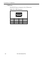
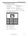
BOX-PC
IPC-BX/M560(PCW)
User's Manual
Copyright
Copyright 1999 CONTEC Co., LTD. ALL RIGHTS RESERVED
No part of this document may be copied or reproduced in any form by
any means without prior written consent of CONTEC Co., LTD.
CONTEC Co., LTD. makes no commitment to update or keep current
the information contained in this document. The information in this
document is subject to change without notice.
All relevant issues have been considered in the preparation of this
document. Should you notice an omission or any questionable item in
this document, please feel free to notify CONTEC Co., LTD.
Regardless of the foregoing statement, CONTEC assumes no
responsibility for any errors that may appear in this document nor for
results obtained by the user as a result of using this product.
Trademarks
Award is trademark of Award Software Inc. Other brand and product
names are trademarks of their respective holder.
FCC NOTICE
NOTE
This equipment has been tested and found to comply with the limits for a Class A digital
device, pursuant to part 15 of the FCC Rules. These limits are designed to provide reasonable
protection against harmful interference when the equipment is operated in commercial
environment.
This equipment generates, uses, and can radiate radio frequency energy and, if not installed
and used in accordance with the instruction manual, may cause harmful interference to radio
communications. Operation of this equipment in a residential area is likely to cause harmful
interference at his own expense.
WARNING TO USER
Change or modifications not expressly approved the manufacturer can void the user's
authority to operate this equipment.
CAUTIO
Connection between peripherals of the computer equipment must be
made with low voltage shielded computer data cables.
WARNIN
A single shielded power cord must be used to connect AC power to the unit.
IPC-BX/M560(PCW)
i
Handling Precautions
Be sure to read the following precautions before using your BOX-PC so
that you may use it trouble free for many years to come:
• Do not use or store the equipment where it is exposed to extremely
high or low temperature or to an abrupt change in temperature.
Examples: - Under direct sunlight
- Near a heat source
• Do not use or store the equipment in a highly humid or dusty place. It
is very dangerous to use the equipment with water, liquid, or
conductive dust left inside. If the equipment must be used in such an
unfavorable environment, install it in a dusttight structure such as a
dust-proof control panel.
• Do not use or store the equipment where it is subject to shock or
vibration.
• Do not use the equipment near a device generating a strong magnetic
field or noise, or the field or noise may cause the equipment to
malfunction.
• Do not use or store the equipment where it is exposed to any chemical
directly or as vapor in the air.
• The heat sink on top of the equipment may heat up to cause a burn.
Do not touch the heat sink directly when the equipment is on or
immediately after turning the power supply off. Avoid installing the
equipment where one can inadvertently touch the heat sink.
• To clean the equipment, wipe it carefully with a soft cloth damped
with water or a solution of neutral detergent. Keep in mind that using
a volatile solvent, such as benzine or thinner, or a chemical can cause
the coating to peel or discolor.
• For continuous operation with a hard disk drive (HDD), be sure to use
the HDD in standby mode. Using the HDD not in standby mode for
continuous operation considerably shortens the lifespan.
(For details, refer to the warning document attached to the optional
product (2.5inch HDD).
• Be sure to unplug the power cable before mounting or demounting an
expansion board (on Model EP) or before connecting or
disconnecting a cable to any connector.
• CONTEC bears absolutely no responsibility for the equipment which
has been modified.
• If you find any fault or abnormal symptom (such as an unusual smell
or overheat), unplug the power cable first and consult your local
retailer or the CONTEC.
• Use an AC cable which conforms to the rated supply voltage and wall
outlet to be used. (The attached cable is for 125VAC.)
ii
IPC-BX/M560(PCW)
• Life Expectancy of Constituent Parts
• Power supply
Assuming continuous use at 25°C, the expected life of the power
supply is approximately 60,000 hours. This may be lower given
use at higher temperatures.
• Battery
A lithium primary battery is used to back up the internal calendar
time and CMOS RAM. The backup time when the power supply
is turned off is more than 10 years at 25°C.
* The replacement of consumables is handled as a repair (charges
will be assessed)
IPC-BX/M560(PCW)
iii
Table of Contents
Copyright ............................................................................i
Trademarks ........................................................................i
FCC NOTICE .................................................................i
Handling Precautions ...................................................ii
1. Introduction ............................................................. 1
Features.........................................................................1
Limited One-Year Warranty .........................................2
How to Obtain Service ..................................................2
Liability .........................................................................2
2. Overview .................................................................. 3
Specifications.....................................................................3
System Configuration and Options ..................................5
System Configuration ...................................................5
Options List...................................................................6
Dimensions ........................................................................7
3. Hardware Setup........................................................ 9
Setup Overview .................................................................9
Setting up Hardware ......................................................10
Removing the top cover and the HDD bracket ..........10
Positions and Settings of Connectors and Jumpers .. 11
Installing the Hard Disk Drive ..................................13
Installing Main Memory (DIMMs).............................15
Installation Conditions ...............................................17
4. BIOS Setup ............................................................ 19
Setting up the BIOS....................................................19
Invoking BIOS Setup ..................................................19
Key Operations ...........................................................19
Main Menu ..................................................................20
STANDARD CMOS SETUP .......................................22
BIOS FEATURES SETUP..........................................25
iv
IPC-BX/M560(PCW)
POWER MANAGEMENT SETUP .............................28
PNP/PCI CONFIGURATION .....................................30
INTEGRATED PERIPHERALS.................................31
SUPERVISOR PASSWORD .......................................33
USER PASSWORD .....................................................33
5. Functions of Components ......................................... 35
Names of Controls.......................................................35
Keyboard Interface .....................................................37
Mouse Interface...........................................................37
Floppy Disk Interface .................................................38
Serial Port Interface ...................................................40
CRT Interface..............................................................49
PCMCIA Slots (Model C and CP) ...............................50
Printer Port Interface .................................................52
RAS Features ..............................................................53
Watchdog Timer ..........................................................55
General-purpose Inputs/Outputs and Remote Reset 61
SW1 (General-purpose Switches for the User) ..........65
Reset Switch................................................................65
ALARM LED ...............................................................65
USB Ports....................................................................66
Ethernet (Models E and EP).......................................67
LCD Interface..............................................................68
IDE Interfaces .............................................................70
Expansion Slots (Model EP and CP) ..........................72
6. Appendix ................................................................ 75
Memory Map....................................................................75
I/O Port Addresses...........................................................76
Interrupt Levels ..............................................................77
IPC-BX/M560(PCW)
v
List of Figures
Figure 2.1.
System Configuration Diagram................................. 5
Figure 2.2.
IPC-BX/M560(PCW)E, C Dimensions ..................... 7
Figure 2.3.
IPC-BX/M560(PCW)EP, CP Dimensions ................. 8
Figure 3.1.
Removing the Top Cover ........................................ 10
Figure 3.2.
Removing the HDD Bracket ................................... 10
Figure 3.3.
Jumpers, Connectors, and Switches
under the Top Cover ................................................11
Figure 3.4.
Mounting the HDD................................................. 14
Figure 3.5.
Mounting the HDD (Side View).............................. 14
Figure 3.6.
Removing the Memory Cover................................. 15
Figure 3.7.
DIMM Attaching Method ....................................... 16
Figure 3.8.
DIMM Removing Method ...................................... 16
Figure 3.9.
Installation Orientations.......................................... 17
Figure 3.10. Distances between the Main Unit and
the Surroundings..................................................... 18
Figure 4.1.
Initial Screen .......................................................... 19
Figure 4.2.
Main Menu Screen.................................................. 20
Figure 4.3.
STANDARD CMOS SETUP Screen ...................... 22
Figure 4.4.
BIOS FEATURES SETUP Screen .......................... 25
Figure 4.5.
POWER MANAGEMENT SETUP Screen............. 28
Figure 4.6.
PNP/PCI CONFIGURATION Screen ..................... 30
Figure 4.7.
INTEGRATED PERIPHERALS Screen ................. 31
Figure 5.1.
Names of Controls .................................................. 35
Figure 5.2.
Terminating Resistor Setting ................................... 42
Figure 5.3.
Half-duplex Connection (JP19 1-2 Connection) ...... 43
vi
IPC-BX/M560(PCW)
Figure 5.4.
Full-duplex Connection (JP19 2-3 Connection)....... 43
Figure 5.5.
Slot Numbers and Positions .................................... 50
Figure 5.6.
Attaching a Card Stopper Bracket ........................... 50
Figure 5.7.
sing the Watchdog Timer ........................................ 56
Figure 5.8.
WDT Control Port (0139h) ..................................... 57
Figure 5.9.
WDT Counter Port (013Ah).................................... 57
Figure 5.10. Event Output Control Port (013Bh)......................... 58
Figure 5.11. RAS Status Port (013Ch) ........................................ 59
Figure 5.12. RAS Port Protect Port (013Ch) ............................... 59
Figure 5.13. Switch Data (013Dh) .............................................. 60
Figure 5.14. Using General-purpose Inputs/Outputs and
Remote Reset ......................................................... 62
Figure 5.15. General-purpose I/O Port (0138h)........................... 62
Figure 5.16. Event Output Control Port (013Bh)......................... 63
Figure 5.17. Port Protect Control Port (013Ch)........................... 64
Figure 5.18. Input Circuit ........................................................... 64
Figure 5.19. Output Circuit......................................................... 64
Figure 5.20. Data in General-purpose Switches for the User ....... 65
Figure 5.21. SW1 Factory Settings ............................................. 65
Figure 5.22. Dimensions of Expansion Board............................. 72
Figure 5.23. Removing the Expansion Slot Cover....................... 73
Figure 5.24. Installing an Expansion Board ................................ 74
Figure 6.1.
Memory Map.......................................................... 75
IPC-BX/M560(PCW)
vii
List of Tables
Table 2.1. Function Specifications ................................................. 3
Table 2.2. Installation Environment Conditions.............................. 4
Table 3.1. Jumpers....................................................................... 12
Table 3.2. Internal Connectors ..................................................... 12
Table 4.1. Key Functions ............................................................. 19
Table 5.1. Functions of Controls .................................................. 36
Table 5.2. Keyboard Connector ................................................... 37
Table 5.3. Mouse Connector ........................................................ 37
Table 5.4. FD Connector.............................................................. 38
Table 5.5. I/O Addresses and IRQs for SERIAL1/2 ..................... 40
Table 5.6. Serial Port Connectors................................................. 40
Table 5.7. I/O Addresses and IRQ for SERIAL4 .......................... 41
Table 5.8. Output Connector (RAS Connector)
with RS-422/RS-485 Used...................................... 41
Table 5.9. I/O Addresses.............................................................. 44
Table 5.10. Register Functions <1/4>........................................... 45
Table 5.10. Register Functions <2/4>........................................... 46
Table 5.10. Register Functions <3/4>........................................... 47
Table 5.10. Register Functions <4/4>........................................... 48
Table 5.11. Baud Rate Settings..................................................... 48
Table 5.12. CRT Connector ......................................................... 49
Table 5.13. Card Supplied Power................................................. 51
Table 5.14. Printer Port and I/O Addresses................................... 52
Table 5.15. Printer Port Connector............................................... 52
Table 5.16. RAS Connector ......................................................... 53
viii
IPC-BX/M560(PCW)
Table 5.17. Changing the Port Addresses for RAS Features
(SW1-3, SW1-4)..................................................... 54
Table 5.18. Setting the Alarm-out Output State
(SW1-1, SW1-2)..................................................... 60
Table 5.19. USB Connectors........................................................ 66
Table 5.20. Ethernet Connector.................................................... 67
Table 5.21. Supported LCD List .................................................. 68
Table 5.22. I/O Addresses and IRT for SERIAL3......................... 69
Table 5.23. Primary IDE Connector (CN1) .................................. 70
Table 5.24. Secondary IDE Connector (CN2) .............................. 71
Table 5.25. Expansion Slots......................................................... 72
Table 6.1. I/O Port Addresses....................................................... 76
Table 6.2. Hardware Interrupt Levels (Factory Settings) .............. 77
IPC-BX/M560(PCW)
ix
x
IPC-BX/M560(PCW)
Introduction
1. Introduction
The BOX-PC is a FA computer incorporating the required features
into a compact unit. CONTEC provides four different types of
BOX-PCs so that you can construct the optimum built-in controller
for your need: Model C with PCMCIA slots, Model CP with
PCMCIA slots and PCI/ISA expansion slots, Model E with LAN
interface, and Model EP with LAN interface and PCI/ISA expansion
slots.
Features
• Fast CPU (MMX Pentium 266)
• Fan-less structure with a large heat sink
• LCD interface that can directly connect a CONTEC VGA or
SVGA flat panel display
• PCMCIA slots (TYPE II x 2) (Model C and CP)
• Ethernet interface (100/10M) (Models E and EP)
• Expansion slots (for up to two PCI and/or ISA half-size boards).
(Model EP and CP)
• High reliability guaranteed by development and production
management by CONTEC (ISO-9001 certified factory)
IPC-BX/M560(PCW)
1
Introduction
Limited One-Year Warranty
CONTEC Interface boards are warranted by CONTEC Co., LTD. to
be free from defects in material and workmanship for up to one year
from the date of purchase by the original purchaser.
Repair will be free of charge only when this device is returned
freight prepaid with a copy of the original invoice and a Return
Merchandise Authorization to the distributor or the CONTEC group
office, from which it was purchased.
This warranty is not applicable for scratches or normal wear, but
only for the electronic circuitry and original boards. The warranty is
not applicable if the device has been tampered with or damaged
through abuse, mistreatment, neglect, or unreasonable use, or if the
original invoice is not included, in which case repairs will be
considered beyond the warranty policy.
How to Obtain Service
For replacement or repair, return the device freight prepaid, with a
copy of the original invoice. Please obtain a Return Merchandise
Authorization Number (RMA) from the CONTEC group office
where you purchased before returning any product.
* No product will be accepted by CONTEC group without the
RMA number.
Liability
The obligation of the warrantor is solely to repair or replace the product.
In no event will the warrantor be liable for any incidental or
consequential damages due to such defect or consequences that arise
from inexperienced usage, misuse, or malfunction of this device.
2
IPC-BX/M560(PCW)
Overview
2. Overview
Specifications
Table 2.1. Function Specifications
Model
CPU
Chip Set
Memory
IPC-BX/M560(PCW)C
IPC-BX/M560(PCW)E
IPC-BX/M560(PCW)EP IPC-BX/M560(PCW)CP
MMX Pentium 266MHz (Intel)
430TX (Intel)
L2 Cache
512KByte PB-SRAM
Main
144 pin SO-DIMM socket x 2 (Memory modules are optional.)
Memory
Up to 256MB (Initially none).
3.3V 144pin SDRAM type SO-DIMMs are acceptable.
Video
BIOS ROM
128KByte E0000H~FFFFFH (AWARD)
Controller
69000 (Chips & Technologies)
Video RAM
2MByte
Video BIOS
40KB (C0000H to CFFFFH) or 32KB (C0000H to C7FFFH)
CRT I/F
15pin HD-SUB connector
640 x 480/800 x 600 (16M Color), 1024 x 768 (65K Color), 1280 x 1024 (256 Color)
LCD I/F
TFT color LCD: 6bits for R/G/B signals, respectively
Dedicated 50pin half-pitch connector (CONTEC flat panel display acceptable)
FDD I/F
Dedicated 26pin half-pitch connector 2 mode (Optional FDD: PC-FDD25BH)
IDE HDD I/F
Capable of incorporating one 2.5inch IDE HDD or silicon disk drive (Drives are optional.)
RS-232C (general-purpose): 2channels (serial ports 1 and 2) with DB-9 connectors
Serial interfaces
RS-232C (touch panel): 1channel (serial port 3) [in the LCD connector] *1
RS-422/485 (general-purpose): 1channel (serial port 4) [in the RAS connector]
Parallel interface
LAN
Centronics-compatible bidirectional DB-25 connector
I/F
---
Ethernet 100Base-TX/10Base-T RJ-45 connector
---
Controller
---
21143 (Intel)
---
USB I/F
2ch
Keyboard interface
PC/AT keyboard compatible (6pin MINI DIN connector)
Mouse interface
PS/2 mouse compatible (6pin MINI DIN connector)
General-purpose
input / output
Photocoupler insulation type: 3 input and 3 output channels
(Note that one output channel and one input channel are switched for use as a
WDT external output and remote reset input, respectively.)
WDT: 10ms to 300s (RESET or NMI + external output enabled at a time-out)
RAS functions
Remote reset: External input signal
Slot
PC Card *2
PCMCIA Type I/II x 2
Controller
PCMCIA Type I/II x 2
---
or Type III x 1
or Type III x 1
---
RL5C476A (RICOH)
RL5C476A (RICOH)
PCI/ISA shared slot x 2
---
Expansion board slots
Maximum acceptable
board length: Max. 200mm
RTC/CMOS
Backed up by a lithium battery whose lifespan is at least 10 years.(25ºC)
Power supply
Rated Voltage
100-240VAC (Continuous Input), 50/60Hz
Main Body
Maximum
LCD *3
Power
Expansion Slots
Consumption
Total
40VA
45VA
25VA
--65VA
45VA
115VA
+5V: 2A
Expansion board supplied
power capacity
---
-5V: Not supplied
+12V: 0.5A -12V: 0.1A
Outside dimensions (mm)
262(W) x 230(D) x 62(H)
262(W) x 230(D) x 140(H)
Weight
3.3kg
4.7kg
*1 Used for the CONTEC touch panel display. (See "Options List" for the applicable product.)
*2 The PC cannot be booted from the PC card. CARD-BUS and ZV Card not support.
*3 Used for Flat panel display IPC-DT/L30S(PC)T.
IPC-BX/M560(PCW)
3
Overview
Table 2.2. Installation Environment Conditions
Requirement
Item
Power supply specifications
Allowable duration of
momentary power failure
Dielectric strength
20ms or less
3.0kVAC (input-output), 2.0kVAC (input-FG),
0.5kVAC (output-FG) for one minute each
Insulation resistance
50MΩ (500VDC)
Environment specifications
0-50ºC (with SDD)
Ambient operating temperature
0-45ºC (with HDD)
5-45ºC (with FDD)
Ambient storage temperature *1
-10~60ºC
Ambient humidity *2
20~90%RH
Floating dust
Normal
Corrosive gas
Noise
resistance
None
Line noise
AC line: 2kV, Signal line: 1kV (IEC1000-4-4Level 3, EN61000-4-4Level 3)
Electrostatic
durability
Contact: 4kV (IEC1000-4-2Level 2, EN61000-4-2Level 2)
Airborne: 8kV (IEC1000-4-2Level 2, EN61000-4-2Level 3)
10-50Hz/Single-side amplitude 0.15mm; 50-500Hz/2.0G
Vibration
resistance *3
Sweep durability X/Y/Z directions for 23 minutes each
(Conforming to JIS C0040 and IEC68-2-6)
Fixed vibration
endurance
Impact resistance *3
16.7Hz/2G, X/Y/Z directions for 30 minutes each
(Conforming to JIS C0040 and IEC68-2-6)
10G in the X/Y/Z directions for 11ms; Half-sine wave
(Conforming to JIS C0041 and IEC68-2-27)
*1
When the BOX-PC is stored at an ambient temperature of 0ºC or less, the orientation of the main unit
is restricted. (See "Installation Conditions" in Chapter 3 "Hardware Setup".)
*2
Assuming that no floppy disk is used.
*3
Assuming that neither HDD nor FDD is used.
4
IPC-BX/M560(PCW)
Overview
System Configuration and Options
System Configuration
2.5inch hard (silicon) disk drive
Integrated
RS-485
IPC-BX/M560(PCW)EP
Printer
Terminal
General-purpose I/O
strip
(three channels)
IPC-PSD-20
RAS
USB
Dedicated FD drive
PC-FDD25BH
LAN
(Models E and EP) *
* On Model C and CP
this part is a PCMCIA card slot.
RS-232C
Dedicated LCD cable (2m)
IPC-P4CL-2H
Mouse
Main memory
144pin SO-DIMM
Keyboard
Expansion slot
(Model EP and CP)
CRT display
Dedicated
LCD
Dedicated LCD
IPC-DS/L400(PC)
IPC-DS/L400(PC)T
IPC-DS/L30S(PC)T
IPC-DT/L400(PC)
IPC-DT/L400(PC)T
IPC-DT/L30S(PC)T
IPC-DT/M30(PC)T
For using three or more slots or a full-size board
PC-HELPER
series
PCI/ISA half-size board
Expansion
bus adapter
FA-PAC(PC) series
Figure 2.1. System Configuration Diagram
IPC-BX/M560(PCW)
5
Overview
Options List
Memory (144pin SO-DIMM)
• PC-MSD64-144
64-MB SD memory module
• PC-MSD128-144
128-MB SD memory module
Floppy disk unit
• PC-FDD25BH
3.5inch floppy disk drive (with cable)
Hard disk drive
• PC-HDD3200
3.2-GB hard disk
Silicon disk drive
• PC-SDD4A
• PC-SDD12A
• PC-SDD32H
• PC-SDD64H
• PC-SDD320H
• PC-SDD500H
• PC-SDD1000H
4-MB flash disk
12-MB flash disk
32-MB flash disk
64-MB flash disk
320-MB flash disk
500-MB flash disk
1-GB flash disk
Terminal block for RAS connectors
• IPC-PSD-20
Dedicated D-STN Color LCD (12.1inch, 800 x 600 dot S-VGA)
• IPC-DS/L400(PC)
Without a touch panel
• IPC-DS/L400(PC)T
With a touch panel
• IPC-DS/L30S(PC)T
With a touch panel
Dedicated TFT Color LCD (12.1inch, 800 x 600 dot S-VGA)
• IPC-DT/L400(PC)
Without a touch panel
• IPC-DT/L400(PC)T
With a touch panel
• IPC-DT/L30S(PC)T
With a touch panel
Dedicated TFT Color LCD (10.4inch, 640 x 480 dot VGA)
• IPC-DT/M30(PC)T
With a touch panel
LCD dedicated cable
• IPC-P4CL-2H
6
Display cable (2m)
IPC-BX/M560(PCW)
Overview
Dimensions
IPC-BX/M560(PCW)E, C
302
284
262
5
R2.5
RAS
PRINTER
MOUSE
PCMCIA
ALARM
R5.5
CARD
HDD
FD
USB
KB
RST
SERIAL1
SERIAL2
VG A
LCD
POWER
4-φ5
[mm]
Figure 2.2. IPC-BX/M560(PCW)E, C Dimensions
IPC-BX/M560(PCW)
7
Overview
IPC-BX/M560(PCW)EP, CP
302
284
262
5
R2.5
R5.5
4-φ5
[mm]
Figure 2.3. IPC-BX/M560(PCW)EP, CP Dimensions
8
IPC-BX/M560(PCW)
Hardware Setup
3. Hardware Setup
Setup Overview
Follow the steps below to set up your BOX-PC according to the
instructions in this manual:
Step 1
Installing a hard disk drive and main memory (DIMMs)
and Setting Jumper Switches
See Chapter 3 to install the hard disk drive and main
memory and set the required jumper switches.
Step 2
Connecting Cables
Connect the cables for the required external devices such
as a printer and a CRT display to the BOX-PC.
Step 3
Turning the Power On
Make sure again that you have taken Steps 1 and 2
correctly, then turn the power supply on. If you find or
suspect any problem after turning the power on, turn it off
immediately and check whether the BOX-PC has been set
up correctly.
Step 4
Setting up the BIOS
See Chapter 4 to set up the BIOS. Note that BIOS Setup
requires the keyboard and monitor connected correctly to
the BOX-PC.
*Be sure to execute "LOAD SETUP DEFAULTS" to
initialize the BIOS setup states before using the BOX-PC
for the first time. (See "Main Menu" in Chapter 4.)
IPC-BX/M560(PCW)
9
Hardware Setup
Setting up Hardware
Removing the top cover and the HDD bracket
• Make sure that the power supply is off in advance.
• Do not loosen any screw other than those specified.
(1) Remove the top cover.
Figure 3.1. Removing the Top Cover
(2) Remove the HDD bracket.
Figure 3.2. Removing the HDD Bracket
10
IPC-BX/M560(PCW)
Hardware Setup
Positions and Settings of Connectors and Jumpers
When you have removed the top cover and the HDD bracket, you
can see the following jumper as shown below:
2 4
JP16
2 4 6
1 3
JP15
JP1
1
1 3 5
SOCKET1
2
3
CN2
2 4 6 8
1 3 5 7
JP2
EF
0 12
JP19
CN1
8 9A
JP18
67
345
BC D
ON
3 2 1
SW1
1 2 3 4 5 6 OFF
SW2
Figure 3.3. Jumpers, Connectors, and Switches under the
Top Cover
IPC-BX/M560(PCW)
11
Hardware Setup
Table 3.1. Jumpers
Function
No.
Factory setting
JP1
Reserved
JP2
CPU clock multiplier selection
Reference page
1-2: Connect
Remarks
---
1-2: Connect
3-4: Connect
---
5-6: Open
266MHz
(66MHz x 4)
7-8: Open
JP15
Reserved
5-6: Connect
JP16
Reserved
3-4: Connect
---
JP18
RS-485 termination setting
Open
41
JP19
RS-485 receiver gate control
2-3: Connect
43
1, 2, 5, 6
OFF
53
3, 4
ON
60
SW1
WDT output setting, RAS port selection
SW2
Display setting
---
0
68
Table 3.2. Internal Connectors
Name
Reference page
Primary IDE connector (44pin pin header)
70
CN2
Secondary IDE connector (44pin pin header)
70
Spare socket
---
SOCKET1
12
Function
CN1
IPC-BX/M560(PCW)
RAS port: 0138h
SVGA LCD mode
Hardware Setup
Installing the Hard Disk Drive
(1) Connect the HDD cable bundled with the hard disk (silicon
disk) drive.
Note!
Connect the HDD cable with its connector justified to the left-hand
side of the connector on the back of the HDD. The four right-most
pins in the HDD connector are left unconnected, which are
master/slave setting pins. Use meticulous care when connecting the
HDD cable because turning the power on with the connector shifted
to the right may damage the HDD and/or the cable.
(2) Fasten the HDD onto the HDD bracket using four screws with
the cable passing through the slot in the HDD bracket.
• Use upper screw holes in the HDD bracket.
• Use either inner or outer screw holes in the HDD bracket,
depending on the type of the HDD you are installing. (The inner
screw holes are used in the example in Figure 3.4. below.)
(3) Connect the other end of the HDD cable to CN1 on the main unit
and mount the HDD bracket on the main unit using four screws.
(4) Close the top cover and tighten the screws.
IPC-BX/M560(PCW)
13
Hardware Setup
2 .5 in ch H D D
T h e fo u r righ t-m o s t p in s a re n o t c on n ected .
CN 1
Figure 3.4. Mounting the HDD
HD D
H D D b ra ck et
H D D c ab le
CN1
Figure 3.5. Mounting the HDD (Side View)
14
IPC-BX/M560(PCW)
Hardware Setup
Installing Main Memory (DIMMs)
Acceptable types of DIMMs
Although CONTEC recommends using the dedicated option, the
BOX-PC can use the following types of SO-DIMMs available on
the market instead:
• Package type
: 144pin small outline DIMM
• Specifications
: 3.3V, access time of 60ns or less
• Capacity
: 16/32/64/128MB
• Architecture
: SDRAM
• Optional memory * : 64MB : PC-MSD64-144
128MB : PC-MSD128-144
* Using a memory product other than the dedicated option may
yield unpredictable results.
Main memory (DIMM) installation procedure
(1) Remove the memory cover.
M o de l E o r C
Bo ttom
M od el E P or C P
B otta om
T h e m e m or y s ock e ts a re fou n d b e yo n d th e ex pa n s ion slots .
I f a b oa rd is in a n ex pa n sio n s lot, rem ov e th e b o a rd .
Figure 3.6. Removing the Memory Cover
IPC-BX/M560(PCW)
15
Hardware Setup
(2) Follow the steps below to install a DIMM in an on-board
DIMM socket.
When installing only one DIMM, you can use either of the two
DIMM sockets.
Figure 3.7. DIMM Attaching Method
DIMM removing method
Figure 3.8. DIMM Removing Method
(3) Close the memory cover.
16
IPC-BX/M560(PCW)
Hardware Setup
Installation Conditions
The BOX-PC can be installed in any of forms (1) to (3) shown
below. Do not install the BOX-PC in any of forms (4) to (6) because
it may be hard to release heat sufficiently. Allow clearance of at
least 100mm above and 50mm next to and behind the main unit.
Installation orientations
(1)
(2) *
(3)
Floor
Connectors
Wall
Wall
(4)
(5)
(6)
Connectors
Ceiling
Wall
Wall
* Do not install the BOX-PC in form (2) if the ambient storage temperature is 0ºC or less.
Figure 3.9. Installation Orientations
IPC-BX/M560(PCW)
17
Hardware Setup
Distances between the Main Unit and the Surroundings
50mm or more (side)
50mm or more (side)
100mm or more (top)
50mm or more (back)
Connectors
Figure 3.10. Distances between the Main Unit and the
Surroundings
18
IPC-BX/M560(PCW)
BIOS Setup
4. BIOS Setup
Setting up the BIOS
BIOS Setup is the program for making a variety of initial settings for
the entire system at every (re)boot. When using your BOX-PC for
the first time, therefore, be sure to run BIOS Setup. Once run, BIOS
Setup backs up the settings you made.
Invoking BIOS Setup
When you turn the system power on, the following screen appears as
long as the system is normal. Press the <Del> key at the keyboard.
Figure 4.1. Initial Screen
Key Operations
Table 4.1 lists the functions of the major keys to be used during setup.
Table 4.1. Key Functions
Key
Function
↑, ↓, →, ←
Selects the item to be set up.
<Enter>
Switches the screen from the Main Menu to the Setup Menu for the currently selected item.
PU, PD, +, −
Changes the current setting.
<Esc>
Main Menu : Aborts BIOS Setup without saving changes to settings.
Setup Menu: Returns to the Main Menu.
F10
Saves setting data and terminates BIOS Setup if pressed with the Main Menu displayed.
IPC-BX/M560(PCW)
19
BIOS Setup
Main Menu
Figure 4.2. Main Menu Screen
STANDARD CMOS SETUP
: Set up the clock/calendar and
IDE hard disks.
BIOS FEATURES SETUP
: Set up the boot drive sequence,
cache memory, and shadow
memory.
CHIPSET FEATURES SETUP
: You should leave this setup
untouched.
POWER MANAGEMENT SETUP : Set up the power save mode.
When the BOX-PC contains a
hard disk drive, set the period
of HDD Power Down time to
suspend the HDD after no
access for that period of time,
protecting the HDD from
excessively wearing.
20
PNP/PCI CONFIGURATION
: Manually make bus settings
such as the IRQs to the PCI bus.
LOAD BIOS DEFAULTS
: Reset the BIOS setup items to
the minimum required values.
Use this option to if the system
malfunctions.
IPC-BX/M560(PCW)
BIOS Setup
LOAD SETUP DEFAULTS
: Reset the BIOS setup items to
the normally used, optimum
values. Select this option once
when you use the BOX-PC for
the first time, then change
settings as required.
INTEGRATED PERIPHERALS
: Set up the IDE and
serial/parallel controllers.
SUPERVISOR PASSWORD
: Set the password that is
prompted for input at a
(re)boot and at BIOS setup.
USER PASSWORD
: Set the password that is
prompted for input at a
(re)boot.
IDE HDD AUTO DETECTION
: Detect the currently connected
IDE HDD. Usually, this
option is not required when
TYPE and MODE for the
HDD on the STANDARD
CMOS SETUP menu have
been set to AUTO.
SAVE & EXIT SETUP
: Save all changes you made to
the BIOS settings and
terminates BIOS Setup.
EXIT WITHOUT SAVING
: Quit BIOS Setup without
saving any changes you made
to the BIOS settings.
IPC-BX/M560(PCW)
21
BIOS Setup
STANDARD CMOS SETUP
Figure 4.3. STANDARD CMOS SETUP Screen
22
Date (mm:dd:yy)
: Set the clock/calendar in the main unit to
the current date.
Time (hh:mm:ss)
: Set the clock/calendar in the main unit to
the current time.
Primary Master
: Set up the master HDD connected to the
primary IDE connector (CN1).
Primary Slave
: Set up the slave HDD connected to the
primary IDE connector (CN1). (Normally,
the primary slave HDD is not used on this
machine.)
Secondary Master
: Set up the master HDD connected to the
secondary IDE connector (CN2).
(Normally, the secondary master HDD is
not used on this machine.)
IPC-BX/M560(PCW)
BIOS Setup
Secondary Slave
: Set up the slave HDD connected to the
secondary IDE connector (CN2).
(Normally, the secondary slave HDD is not
used on this machine.)
* Set TYPE and MODE usually to [AUTO]. (The HDD type will be
detected automatically at a (re)boot.)
* For each HDD which is not used (connected), set TYPE to
[NONE].
Drive A
: Select the FDD type. Leave [1.44M, 3.5in]
as it is on this machine.
Drive B
: Leave NONE as it is because this machine
does not use the secondary FDD.
Floppy 3Mode Support : Leave [Disabled] as it is because this
machine does not support the 3 mode FDD.
Video
: Leave [EGA/VGA] as it is.
Halt On
: Select the error condition that stops the
system if it occurs at a (re)boot.
[All Errors]
: Stops the system on
occurrence of any error.
[No Errors]
: Prevents any error
from stopping the
system on occurrence
of it.
[All,But Keyboard] : Stops the system
on occurrence of a
non-keyboard error.
[All,But Diskette] : Stops the system on
occurrence of a nonFDD error.
IPC-BX/M560(PCW)
23
BIOS Setup
[All,But Disk/Key] : Stops the system on
occurrence of a nonkeyboard and nonFDD error. If you
select this option, the
system is booted
without stopping even
with neither FDD nor
keyboard connected.
24
IPC-BX/M560(PCW)
BIOS Setup
BIOS FEATURES SETUP
Figure 4.4. BIOS FEATURES SETUP Screen
Virus Warning
: Setting this item to [Enabled] prevents
the boot sector and partition table on
the hard disk from being writeaccessed inadvertently (via the BIOS).
If an attempt is made to write to the
boot sector or partition table with this
item set to [Enabled], the system stops
with a message. Note, however, that
the item must be set to [Disabled]
when you install an OS.
CPU Internal Cache
: You can set the CPU's internal cache
to [Disabled] if necessary. Usually,
leave it [Enabled].
External Cache
: You can set the L2 cache to
[Disabled] if necessary. Usually,
leave it [Enabled].
Quick Power On Self Test
: Setting this item to [Enabled] run the
POST confirmation message from
being displayed.
IPC-BX/M560(PCW)
25
BIOS Setup
26
Boot Sequence
: Set the sequence of drives to be
accessed at a boot. The drives are
accessed in the order in which they
are specified here and the OS
encountered first is loaded.
Swap Floppy Drive
: Leave this item [Disabled].
Boot Up Floppy Seek
: If [Enabled], the system seeks the
FDD at a boot.
Boot Up Num Lock Status
: Specify the Num Lock key status
upon completion of boot-up.
Gate A20 Option
: Usually, leave this item set to [First].
Typematic Rate Setting
: Although you can enable the
typematic feature, set this item
usually to [Disabled]. Setting this
item to [Enabled] enables the
following two key settings:
Typematic Rate (Char/Sec)
: Set the repeat detection rate with a
key held down.
Typematic Delay (Msec)
: Set the interval between the key
press and the first repeat of the
keystroke.
Security Option
: Specify the timing(s) at which the
password is prompted. Setting this
item to [Setup] prompts the
password at BIOS setup. Setting it
to [System] prompts the password at
every (re)boot and BIOS setup. The
system prompts no password when
no password has been set.
PCI/VGA Palette Snoop
: Leave this item [Disabled].
Assign IRQ For VGA
: Leave this item [Enabled].
IPC-BX/M560(PCW)
BIOS Setup
OS Select For DRAM>64MB :
You can select [OS2] to run
the machine with at least 64M bytes
of DRAM under OS2. To use any
other OS, set this item to [Non-OS2].
Video BIOS Shadow
: Setting this item to [Enabled] copies
the contents of video BIOS ROM to
RAM. This makes access to the
video BIOS faster than in ROM.
C8000-CBFFF Shadow
CC000-CFFFF Shadow
D0000-D3FFF Shadow
D4000-D7FFF Shadow
D8000-DBFFF Shadow
DC000-DFFFF Shadow
: If ROM has been located in the
specified area, setting the item to
[Enabled] copies the contents to
RAM. Although this speeds up
access to that area, be sure to set the
item to [Disabled] if the contents of
the area are variable.
IPC-BX/M560(PCW)
27
BIOS Setup
POWER MANAGEMENT SETUP
Figure 4.5. POWER MANAGEMENT SETUP Screen
28
Power Management
: Set the power management service
status. Setting this item to [User
Define] allows you to set the individual
items. If you use an IDE HDD while
power management is not used, set the
item to [User Define] and set the period
of HDD Power Down time to reduce
degradation of the lifespan of the HDD
by continuous operation.
PM Control by APM
: Enable or disable control by APM
(Advanced Power Management).
Video Off Method
: Select the method of turning the
monitor off.
Video Off After
: Select the mode in which the monitor
is turned off.
Doze Mode
: Set the period of time after which the
CPU slows down the operating speed.
Standby Mode
: Set the period of time after which the
HDD and the monitor are turned off.
IPC-BX/M560(PCW)
BIOS Setup
Suspend Mode
: Set the period of time after which all
peripheral devices are turned off.
HDD Power Down
: Set the period of time after the last
access to the HDD, after which the
HDD is turned off.
Throttle Duty Cycle
: Set the CPU operation ratio in the
Doze mode.
ZZ Active in Suspend
: Leave this item [Disabled].
PCI/VGA Act-Monitor
: When this item is [Enabled], a VGA
operation returns the peripherals from
the suspend mode.
Resume by Alarm
: Set the alarm condition that resumes
the system.
Reload Global Timer Events :
If you set an item to
[Enabled], the item returns the
peripherals from the suspend mode.
IPC-BX/M560(PCW)
29
BIOS Setup
PNP/PCI CONFIGURATION
Figure 4.6. PNP/PCI CONFIGURATION Screen
PNP OS Installed
: Set this item to [Yes] when you use a
PNP (Plug-and-Play) OS.
Resources Controlled By : Setting this item to [Auto] automatically
sets the IRQs and DMA channels for
PnP devices.
* If your ISA board or PCMCIA card
does not operate normally either under
an OS (DOS or Windows NT) which
is not PnP compliant or by PnP
configuration under a PnP compliant
OS, set this item to [Manual] and
change the IRQ and DMA channel for
the ISA board or PCMCIA card to
[Legacy ISA].
Reset Configuration Data : Set this item to [Disabled].
30
PCI IDE IRQ Map To
: Set this item to [ISA].
Assign IRQ For USB
: Setting this item to [Enabled] assigns an
IRQ to the USB controller.
IPC-BX/M560(PCW)
BIOS Setup
INTEGRATED PERIPHERALS
Figure 4.7. INTEGRATED PERIPHERALS Screen
IDE HDD Block Mode
: Select whether to use the IDE HDD
block mode. Usually, set this item
to [Enabled].
IDE Primary Master PIO
: Set the transfer rate of the master
drive connected to the IDE primary
connector (CN1). Usually, set this
item to [Auto].
IDE Primary Slave PIO
:Set the transfer rate of the slave
drive connected to the IDE primary
connector (CN1). Usually, set this
item to [Auto].
IDE Primary Master UDMA
: Set the UltraDMA mode of the
master drive connected to the IDE
primary connector (CN1). Usually,
set this item to [Auto].
IPC-BX/M560(PCW)
31
BIOS Setup
IDE Primary Slave UDMA
: Set the UltraDMA mode of the
slave drive connected to the IDE
primary connector (CN1). Usually,
set this item to [Auto].
IDE Secondary Master PIO
: Set the transfer rate (PIO mode) or
IDE Secondary Slave PIO
UDMA mode of the master/slave
IDE Secondary Master UDMA drive connected to the IDE IDE
Secondary Slave UDMA
secondary connector (CN2).
Usually, set these items to [Auto].
On-Chip Primary PCI IDE
: Select whether to use the internal
primary IDE controller. Usually,
set this item to [Enabled].
On-Chip Secondary PCI IDE : Select whether to use the internal
secondary IDE controller. Usually,
set this item to [Enabled].
* Setting this item to [Disabled]
makes interrupt IRQ15 available
to the user.
32
USB Keyboard Support
: To connect the keyboard to a USB
port, set this item to [Enabled].
Onboard FD Controller
: Select whether to use the internal
FD controller. Usually, set this
item to [Enabled].
Onboard Serial Port 1
: Set the port address and IRQ for
internal serial port 1.
Onboard Serial Port 2
: Set the port address and IRQ for
internal serial port 2.
UART2 Mode
: This item is not used on this
machine. Leave it set to
[Standard].
Onboard Parallel Port
: Set the port address and IRQ for
the internal parallel port.
IPC-BX/M560(PCW)
BIOS Setup
Parallel Port Mode
: Set the operation mode of the
parallel port.
ECP Mode Use DMA
: Set the DMA channel for the
parallel port to be used in the ECP
mode.
Onboard Serial Port 3
: Set the port address for internal
serial port 3 (touch panel).
Serial Port 3 Use IRQ
: Set the IRT for internal serial port 3.
Onboard Serial Port 4
: Set the port address for internal
serial port 4 (RS-422/485).
Serial Port 4 Use IRQ
: Set the IRT for internal serial port 4.
SUPERVISOR PASSWORD
The password set here takes effect when prompted at a boot and
BIOS setup. After setting the password, set "Security Option" in the
BIOS FEATURES SETUP menu to the desired password prompt
timing(s). To disable the password which has been set, press only
the Enter key as the new password.
* Be careful not to forget the password set for the machine.
USER PASSWORD
The password set here takes effect when prompted at a boot and
BIOS setup (with no supervisor password set). After setting the
password, set "Security Option" in the BIOS FEATURES SETUP
menu to the desired password prompt timing(s). Note, however, that
you cannot use the user password to enter BIOS Setup if the
supervisor password has been set. To disable the password which
has been set, press only the Enter key as the new password.
* Be careful not to forget the password set for the machine.
IPC-BX/M560(PCW)
33
BIOS Setup
34
IPC-BX/M560(PCW)
Functions of Components
5. Functions of Components
Names of Controls
IPC-BX/M560(PCW)C
Top cover
RAS
MOUSE
PRINTER
PCMCIA slots 1, 2
Power switch
(side face)
ALARM LED
RAS
CARD LED
PCMCIA
PRINTER
MOUSE
ALARM
AC inlet
(side face)
FD
FD
USB
KB
SERIAL1
RST
Keyboard RST
USB
VGA
SERIAL2
SERIAL1
SERIAL2
HD LED
HDD
POWER LED
POWER
LCD
VGA
CARD
LCD
* The IPC-BX/M560(PCW)CP is expansion-slot built-in version of Model C.
IPC-BX/M560(PCW)EP
UTP(ETHERNET)
LINK LED
ALARM LED
RAS
PRINTER
MOUSE
UTP
ALARM
LINK
100M
FDX LED
FDX
HDD
FD
USB
KB
RST
SERIAL1
SERIAL2
VGA
LCD
POWER
100MLED
Expansion slot (PCI/ISA) x 2
* The IPC-BX/M560(PCW)E is an expansion-slot-less version of Model E.
Figure 5.1. Names of Controls
IPC-BX/M560(PCW)
35
Functions of Components
Table 5.1. Functions of Controls
Name
36
Function
Reference page
KB
Keyboard connector (6pin mini-DIN connector)
37
MOUSE
PS/2 mouse connector (6pin mini-DIN connector)
37
FD
FDD connector (26pin half-pitch connector)
38
SERIAL1
Serial port 1 connector (DB-9 connector)
40
SERIAL2
Serial port 2 connector (DB-9 connector)
40
VGA
CRT connector (DB-15 connector)
49
PCMCIA
PCMCIA card slot (Model C and CP)
50
PRINTER
Parallel port connector (DB-25 connector)
52
RAS
RAS feature and RS-485 connector (DB-15 connector)
53
RST
Hardware reset pushbutton
65
ALARM LED
RAS alarm indicator
65
USB
USB port connectors
66
UTP
Ethernet connector (Models E and EP)
67
LCD
LCD connector (50pin half-pitch connector)
68
EXPANSION SLOT
PCI/ISA expansion board slot x 2 (Model EP and CP)
72
POWER LED
Power-on indicator
---
HD LED
Internal hard disk access lamp
---
CARD LED
PCMCIA card access lamp (Model C and CP)
---
LINK LED
Ethernet link indicator (Models E and EP)
67
FDX LED
Ethernet full-duplex mode indicator (Models E and EP)
67
100M LED
Ethernet 100Mbps indicator (Models E and EP)
67
IPC-BX/M560(PCW)
Functions of Components
Keyboard Interface
The BOX-PC has a keyboard connector designated as KB (6pin
MINI-DIN connector).
Table 5.2. Keyboard Connector
Connector type TCS7910-16-201 (Hoshiden) or equivalent
6
5
4
3
2
1
Pin No.
Signal name
Pin No.
Signal name
1
+KBD DATA
5
+KBD CLK
2
N.C.
6
N.C.
3
GND
SHELD
GND
4
+5.0V DC
---
Mouse Interface
The BOX-PC has a mouse connector designated as MOUSE (6pin
MINI-DIN connector).
Table 5.3. Mouse Connector
Connector type
TCS7910-16-201 (Hoshiden) or equivalent
6
5
4
3
2
1
Pin No.
Signal name
Pin No.
Signal name
1
+MOUSE DATA
5
+MOUSE CLK
2
N.C.
6
N.C.
3
GND
SHELD
GND
4
+5.0V DC
---
IPC-BX/M560(PCW)
37
Functions of Components
Floppy Disk Interface
The BOX-PC has an FD controller, allowing the FD connector on
the front panel to accept one FD drive. The connector is designated
as FD.
As the FD drive, use the dedicated option.
Table 5.4. FD Connector
26pin half-pitch connector: 175928-4(AMP) or equivalent
Connector type
25
1
26
38
2
Pin No.
Signal name
Direction
Pin No.
Signal name
Direction
1
HDSEL
Output
2
WRTPRT
Input
3
RDATA
Input
4
TRK0
Input
5
GND
-----
6
GND
-----
7
GND
-----
8
WGATE
Output
-----
9
GND
-----
10
GND
11
WDATA
Output
12
GND
-----
13
DENSEL
Output
14
STEP
Output
15
DENSEL
Output
16
DIR
Output
17
N.C.
-----
18
MTR_ON
Output
19
DRV_SEL
Output
20
N.C.
-----
21
+5V
-----
22
DSKCHG
Input
23
+5V
-----
24
N.C.
-----
25
INDEX
Input
26
+5V
-----
IPC-BX/M560(PCW)
Functions of Components
Acceptable cable-side connectors
Plug connector : AMP, P/N 1756774-4
(AWG #28 for pressure welding)
Shield case kit : AMP, P/N 1756774-4
or
Plug connector : 3M, P/N 10126-6000EL
(AWG #28 for pressure welding)
Shell
: 3M, P/N 10326-3210-000
or
Plug connector : 3M, P/N 10126-3000VE
(AWG #24-#30 with solder)
Shell system : 3M, P/N 10326-52F0-008 (Non-shield shell kit)
Cable length
The FDD cable should be within 60cm.
IPC-BX/M560(PCW)
39
Functions of Components
Serial Port Interface
RS-232C Port (SERIAL PORT 1, 2)
The BOX-PC has two RS-232C serial port connectors (serial port 1
designated as SERIAL1 and serial port 2 as SERIAL2). Each port
can be set up as COM1 to COM4 or as being unused by BIOS Setup
(described in Chapter 4). (Note, however, that the same COM
number cannot be assigned to different ports).
Table 5.5. I/O Addresses and IRQs for SERIAL1/2
COM I/O address range
1
IRQ
3F8h-3FFh
IRQ 4
2
2F8h-2FFh
IRQ 3
3
3E8h-3EFh
IRQ 4
4
2E8h-2EFh
IRQ 3
Table 5.6. Serial Port Connectors
Connector on the main unit
1
DB-9 connector (male)
5
No. 4-40UNC
inch screw
6
40
9
Pin No.
signal name
1
CD
Carrier detect
2
RD
Receive data
3
TD
Transmit data
Output
Output
Description
Direction
Input
Input
4
DTR
Data terminal ready
5
GND
Signal ground
-----
6
DSR
Data set ready
Input
7
RTS
Request to send
Output
8
CTS
Clear to send
Input
9
RI
Ring indicator (RI)
Input
IPC-BX/M560(PCW)
Functions of Components
RS-422/RS-485 port (SERIAL PORT4)
The RAS connector contains a single-channel serial port for which
an I/O address range and IRQ or the "unused" status can be set by
BIOS Setup (described in Chapter 4). (Note that the I/O address
range or IRQ assigned to any other device cannot be assigned.)
Table 5.7. I/O Addresses and IRQ for SERIAL4
COM
I/O address range
IRQ
1
3F8h-3FFh
IRQ 3
2
2F8h-2FFh
IRQ 4
3
3E8h-3EFh
IRQ 5
4
2E8h-2EFh
IRQ 10
ORG1 *
130h-137h
IRQ 11
ORG2 *
1E0h-1E7h
IRQ 15
* ORG1 and ORG2 are CONTEC proprietary ports.
RS-422/RS-485 specifications
• Transmission system
: Asynchronous, half-/full-duplex
serial transmission conforming to
RS-422/RS-485
• Baud rate
: 19200 to 50bps (programmable)
• Signal extensible distance : 1.2km Max.
Output connector with RS-422/RS-485 used
Table 5.8. Output Connector (RAS Connector) with
RS-422/RS-485 Used
Pin No.
Signal name
Description
2
TX +
Transmit data +
10
TX -
Transmit data -
3
RX +
Receive data +
11
RX -
Receive data -
For details on the RAS connector, see Table 5.16. "RAS Connector".
IPC-BX/M560(PCW)
41
Functions of Components
Terminating resistor with RAS-485 used
Set the terminating resistor using JP18 under the top cover. The
jumper is open (no terminating resistor) by factory default.
JP18
JP18
Open
No receiver terminating resistor
Connected
Receiver terminating resistor provided
Figure 5.2. Terminating Resistor Setting
Transmit data control in half-duplex mode
In half-duplex mode, the transmission buffer must be controlled to
prevent transmit data from causing a collision. The BOX-PC uses
the RTS signal and bit 1 in the modem control register to control
transmit data.
Modem control register
(Setting I/O address +4H) bit 1: 0 ··· RTS high
(Disables transmission)
1 ··· RTS low
(Enables transmission)
42
IPC-BX/M560(PCW)
Functions of Components
Setting the RS-422/RS-485 receiver disable control jumper
When the RS-422/RS-485 port is used, the RTS signal is used for
driver enable control. Connecting JP19 pins 1 and 2 disables the
receiver at the same time, preventing the port from receiving output
data to an external device.
TXD
RTS
D
RAS connector
RX− 11
JP19
1 2 3
RX+ 3
TX− 10
RXD
TX+ 2
R
JP18
* The input/output connection for RS-485 (two-line transmission) must be done
inside the DB connector.
Figure 5.3. Half-duplex Connection (JP19 1-2 Connection)
TXD
RTS
D
RAS connector
JP19
1 2 3
RX− 11
R
TX+ 2
RX+ 3
TX− 10
RXD
JP18
Figure 5.4. Full-duplex Connection (JP19 2-3 Connection)
IPC-BX/M560(PCW)
43
Functions of Components
I/O addresses and instructions
The table below lists I/O addresses for use as COM1.
Table 5.9. I/O Addresses
I/O address DLAB Read/Write
Register
W
Transmitter holding register
THR
R
Receiver buffer register
RBR
1
W
Divisor latch register (LSB)
DLL
1
W
Divisor latch register (MSB)
DLM
0
W
Interrupt enable register
IER
03FAH
X
R
Interrupt ID register
IIR
03FBH
X
W
Line control register
LCR
03FCH
X
W
Modem control register
MCR
03FDH
X
R
Line status register
LSR
03FEH
X
R
Modem status register
MSR
03FFH
X
R/W
Scratch register
SCR
03F8H
03F9H
0
DLAB (Divisor Latch Access Bit): Value of bit 7 in the line control register
44
IPC-BX/M560(PCW)
Functions of Components
Table 5.10. Register Functions <1/4>
I/O address
03F8H
Contents
THR: Transmitter Holding Register [DLAB=0]
D7 D6 D5 D4 D3 D2 D1
D0
bit0
LSB
bit7
MSB
Dedicated register for writing transmit data
03F8H
RBR: Reciever Buffer Register [DLAB=O]
D7 D6 D5 D4 D3 D2 D1
D0
bit0
LSB
bit7
MSB
Dedicated register for reading transmit data
03F8H
DLL: Divisor Latch (LSB) [DLAB=1]
D7 D6 D5 D4 D3 D2
D1
D0
bit0
LSB
bit7
MSB
Baud rate setting register (LSB)
03F9H
DLH: Divisor Latch (MSB) [DLAB=1]
D7 D6 D5 D4 D3 D2
D1
D0
bit0
LSB
bit7
MSB
Baud rate setting register (MSB)
03F9H
IER: Interrupt Enable Register [DLAB=0]
D7 D6 D5 D4 D3 D2 D1
0
0
0
0
EMS ELSI ETHREI
D0
ERDAI
Receive data
interrupt enable
Receive data register empty
interrupt enable
Receiver line status
interrupt enable
Modem status interrupt enable
[Always 0]
1: Interrupt enable
0: Interrupt disable
IPC-BX/M560(PCW)
45
Functions of Components
Table 5.10. Register Functions <2/4>
I/O address
03FAH
Contents
IIR : Interrupt Identification Register
D7 D6 D5 D4
D3 D2
0
0
0
0
D1
D0
0
Interrupt
bit2 bit1 bit0 Priority
03FBH
1: Interrupt not generated
0: Interrupt generated
Description
No interrupt is generated
0
0
1
1
1
0
1
0
0
2
An interrupt is generated when the receiver
buffer register goes ready. It is cleared when
the receiver buffer is read.
0
1
0
3
An interrupt is generated when the transmitter holding
register becomes empty. It is cleared when the IIR is
read or when transmit data is written to the THR.
0
0
0 4 (Bottom) A modem status interrupt is generated.
(CTS, DSR, RI, CD)
It is cleared when the modem status register is read.
1 (Top) An interrupt is generated at an overrun error,
parity error, framing error, or break interrupt.
LCR : Line Contror Regester
D7
D6
D5
D4
D3
D2
D1
D0
D1 D0 Bit table
5
0
0
0
1
6
1
0
7
1
1
8
0: 1 stop bit
1: 1.5 stop bit for 5bit length
2 stop bits for 6/7/8bit length
0: Parity disable
1: Parity enable
0: Even parity
1: Odd parity
0: Stick parity disable
1: Stick parity enable
0: Break off
1: Break signal transmit
DLAB (Divisor Latch Access Bit)
Set this bit to 1 to access the divisor latch register.
Set it to 0 to access other registers.
46
IPC-BX/M560(PCW)
Functions of Components
Table 5.10. Register Functions <3/4>
I/O address
03FCH
Contents
MCR: Modem Control Register
D7
D6
D5
D4 D3
0
0
0
Loop IRQ
D2
X
D1
D0
RTS DTR
DTR 0: Inactive [HIGH]
1: Active [LOW]
RTS 0: Inactive [HIGH]
1: Active [LOW]
Interrupt control bit
0: Disable
1: Enable
Diagnostic local loopback test
0: Disable
1: Enable
03FDH
LSR: Line Status Regester
D7
0
D6
D5
TEMT THRE
D4
D3
D2
D1
D0
BI
FE
PE
OE
DR
Data ready
(1: Receive data present)
Overrun error (1:
Error occurred)
Parity error (1: Error occurred)
Framing error (1: Error occurred)
Break interrupt (1: Detects break status)
Transmitter holding register empty
(1: Transmission buffer empty)
Transmitter empty
(1: Both of the transmitter holding register and
transmitter shift register are empty.)
IPC-BX/M560(PCW)
47
Functions of Components
Table 5.10. Register Functions <4/4>
I/O address
03FEH
Contents
MSR : Modem Status Register
D7
D6 D5
D4 D3
DCD
RI
D2
D1
D0
DSR CTS DDCD TERI DDSR DCTS
Delta CTS
Delta DSR
Since these status are
not used for RS-485,
Trailing edge RI
data is invalid.
Delta data carrier detect
CTS
DSR
RI
DCD
03FFH
SCR : Scratchpad Register
8bit readable/writable register. The user can use this register for temporarily
saving data.
Setting the baud rate
The baud rate is set with software by dividing the clock input
(1.8432MHz). The baud rate is set by writing the corresponding
values to the divisor latch registers (LSB, MSB) as shown below:
Table 5.11. Baud Rate Settings
Baud rate
Value written to divisor latch registers Setting error (%)
50
2304
75
1536
-----
110
1047
0.026
134 .5
857
0.058
150
768
---
300
384
---
600
192
---
1200
96
---
1800
64
---
2000
58
0.69
2400
48
---
3600
32
---
4800
24
---
7200
16
---
9600
12
---
19200
6
---
Example: To set 9600bps, write 00 and 12 (decimal) to the divisor latch registers
(MSB and LSB), respectively.
48
IPC-BX/M560(PCW)
Functions of Components
CRT Interface
The BOX-PC has a CRT interface designated as VGA (DB-15
connector).
Table 5.12. CRT Connector
Connector type
DB-15 connector (Male)
5
1
10
6
15
11
Signal name
Pin No.
Signal name
Pin No.
1
RED
9
N.C.
2
GREEN
10
GND
3
BLUE
11
N.C.
4
N.C.
12
N.C.
5
GND
13
HSYNC
6
GND
14
VSYNC
7
GND
15
N.C.
8
GND
Display driver
The display driver for each OS is available as an option. Purchase
the driver separately from the BOX-PC.
Option Display driver soft (Windows 98/95/NT 4.0) :
IPC-DSP2-DRV
IPC-BX/M560(PCW)
49
Functions of Components
PCMCIA Slots (Model C and CP)
The BOX-PC (Model C) has PCMCIA card slots (Type II size
slots x 2, including Type III size slot x 1).
Slot 1
Slot 2
Figure 5.5. Slot Numbers and Positions
Note!
To use a Type III card, insert it in slot 2.
Attaching a card stopper bracket
Figure 5.6. Attaching a Card Stopper Bracket
50
IPC-BX/M560(PCW)
Functions of Components
Card power supply
The table below lists the applicable card voltages and the current
capacities per slot.
Table 5.13. Card Supplied Power
Voltage
+5V
Current capacity (Max.)
1A/Slot
+3.3V
1A/Slot
+12V
Not supplied
IPC-BX/M560(PCW)
51
Functions of Components
Printer Port Interface
The BOX-PC has a printer port interface designated as PRN. The
port can be set up LPT1 to LPT3 or as being unused by BIOS Setup
(described in Chapter 4).
Table 5.14. Printer Port and I/O Addresses
LPT
I/O address range
IRQ
1
3BCh-3BFh
IRQ 7
2
378h-37Fh
IRQ 7
3
278h-27Fh
IRQ 5
Table 5.15. Printer Port Connector
52
IPC-BX/M560(PCW)
Functions of Components
RAS Features
The BOX-PC has watchdog timer, remote reset, and generalpurpose I/O functions as RAS features. The inputs and outputs for
the individual functions are implemented in the RAS connector.
Table 5.16. RAS Connector
Connector type
DB-15 connector (Female) (DALC-J15SAF-20L9) JAE
8
15
1
9
Function
Pin No.
Pin name
1
SPK
9
GND
External speaker ground
2
TX +
RS-485 transmission line
10
TX -
3
RX +
11
RX -
4
NCOM
12
PO2/WDT
5
PO0
13
PO1
6
NCOM
7
PI1
14
PI2/RST
8
PCOM
15
PI0/NMI
External speaker signal
RS-485 reception line
PO2-dedicated minus common pin
General-purpose output or watchdog timer alarm output
General-purpose output
General-purpose output minus common pin
General-purpose input
General-purpose input or remote reset input
General-purpose input plus common pin
General-purpose input, NMI interrupt input
Fixing screw: No. 4-40UNC inch screw
IPC-BX/M560(PCW)
53
Functions of Components
Changing the port addresses for RAS features
The I/O port addresses for RAS features can be changed by setting
SW1-3 and SW1-4.
Table 5.17. Changing the Port Addresses for RAS Features
(SW1-3, SW1-4)
SW1
SW1-3
SW1-4
RAS port addresses
ON
ON
0138h~013Dh
OFF
ON
0338h~033Dh
ON
OFF
0538h~053Dh
OFF
OFF
0738h~073Dh
* Factory settings
The "Watchdog Timer" and "General-purpose Inputs/Outputs and
Remote Reset" sections that follow assume that the I/O port
addresses for RAS features are the factory settings without being
changed.
54
IPC-BX/M560(PCW)
Functions of Components
Watchdog Timer
The watchdog timer is activated by output of data (this can be
undefined) to I/O port address 0139h. Executing the out instruction
to the same port within the pre-set time-out period retriggers the
watchdog timer. If a time-out occurs, the watchdog timer generates
a reset or an NMI interrupt depending on the port (013Bh) setting. It
can also supply an alarm-out output to an external device depending
on the port (013Bh) setting.
The time-out period can be set between 10msec and 300sec (port
setting, 013Ah).
The watchdog timer stops by reading I/O port address 0139h). The
alarm-out output is also canceled at the same time.
The alarm-out signal is output from PO2/WDT (12-pin) in the RAS
connector. It is canceled at a reset.
The alarm-out output can be set to the state which exists when the
power is turned on by the switch (SW1), when the watchdog timer is
started, or when the watchdog timer causes a time-out.
The I/O addresses used for RAS features can be changed by setting
SW1.
Specifications
• Time-out period
• Interrupt or reset
: 10msec to 300sec (Port setting)
: A reset or NMI is generated when a timeout occurs. (Port setting)
• External alarm output : Photocoupler insulated open collector
output (The output state is switch-set.)
For detailed specifications, see the
specifications for general-purpose
inputs/outputs.
• I/O address
: 0139h to 013Dh (Changeable in 512bytes
by the switch)
IPC-BX/M560(PCW)
55
Functions of Components
Usage
Set SW1
Power on
Unprotect
... Output 0A5h to the 013Ch port to unprotect.
Set event output
control
... Output data to the 013Bh port to set the event
output mode and external alarm.
Execute WDT stop
instruction
... Read the 0139h port, stop the watchdog timer,
and turn off the alarm output.
Set timer value
... Output setting data to the 013Ah port.
Output data (undefined) to the 0139H port starts
Start and clear WDT ... the watchdog timer and execute the out instruction
to the same port to clear the watchdog timer.
Application
NO
Time value
changed?
... The watchdog timer must be stopped before the
timer value can be changed during operation.
YES
* WDT: Watchdog timer
Figure 5.7. sing the Watchdog Timer
56
IPC-BX/M560(PCW)
Functions of Components
I/O Addresses and Instructions
* 0139h: Watchdog timer control
D7
D6
D5
D4
D3
D2
D1
D0
R/W
Figure 5.8. WDT Control Port (0139h)
R
: Stops the watchdog timer and cancels the alarm. The data
read is undefined.
W
: Starts and clears the watchdog timer. The data to be
output can be undefined.
* 013Ah: Watchdog timer counter
D7
D6
D5
D4
D3
D2
D1
D0
D7
D6
D5
D4
D3
D2
D1
D0
R/W RESET: FFh(H) FFh(L)
Figure 5.9. WDT Counter Port (013Ah)
R
: Reads watchdog timer count data.
Watchdog timer counter time-out period data (16bits) is
read. Data is read twice in the L-to-H order. The value
read is output not as the current count value but as the
count data that has been set.
W
: Writes watchdog timer count data.
Watchdog timer counter time-out period data is written.
Data is written in the L-to-H order. The clock for the
watchdog timer counter is 4.58 µ sec. The time-out period
is set as in the following examples:
0.5sec à
006Dh
1sec à
00DAh
4sec à
0369h
8sec à
06D2h
15sec à
0CC6h
30sec à
1996h
120sec
à 6658h
240sec
à CCB1h
IPC-BX/M560(PCW)
57
Functions of Components
* 013Bh: Event output control
D7
D6
D5
PO2
M
PI2M
rsv*
D4
D3
PI0M NMIE
D2
D1
D0
rsv*
WDT
M
WDT
E
R/W RESET: 10X00X00b
Figure 5.10. Event Output Control Port (013Bh)
WDTE : Enables the watchdog timer event output.
0 : Disables the output event when the watchdog timer
causes a time-out.
1 : Enables the output event when the watchdog timer
causes a time-out.
WDTM : Watchdog timer event output mode
0 : Sets the event output when the watchdog timer causes
a time-out to NMI.
1 : Sets the event output when the watchdog timer causes
a time-out to RESET.
PO2M : PO2/WDT(12) output mode
0 : Sets the RAS connector PO2/WDT(12) signal to PO2
(general-purpose output).
1 : Sets the RAS connector PO2/WDT(12) signal to
alarm-out output.
• The ALARM LED on the front panel of the main unit comes on if
an alarm output occurs in the alarm-out output mode.
58
IPC-BX/M560(PCW)
Functions of Components
* 013Ch: RAS status port & port write control
D7
D6
D5
D4
rsv*
rsv*
rsv*
rsv*
D3
D2
D1
D0
rsv*
WDT
R
(RESET: XXXXXXX0B)
Figure 5.11. RAS Status Port (013Ch)
R
: RAS status port
WDT : Watchdog timer status
The status of the watchdog timer. This bit is
cleared by stopping the watchdog timer (by
reading the 0139h).
0 : Watchdog timer either being stopped or
counting
1 : Watchdog timer time-out
D7
D6
D5
D4
D3
D2
D1
D0
WP7
WP6
WP5
WP4
WP3
WP2
WP1
WP0
W
Figure 5.12. RAS Port Protect Port (013Ch)
W
: Protects the RAS port (0139h-013Dh).
The RAS port is protected or unprotected. The RAS port
is protected when the power is turned on and when a reset
occurs.
00h : Protect
A5h : Unprotect
Note!
Do not change the setting for any " rsv" bit because it is system
reserved.
IPC-BX/M560(PCW)
59
Functions of Components
* 013Dh: Switch data
D7
D6
D5
D4
rsv*
rsv*
SW6
SW5
D3
D2
D1
D0
rsv*
rsv*
rsv*
R
(RESET: XXXXXXX0B)
Figure 5.13. Switch Data (013Dh)
R
: Switch data
SW6 : SW1-6 data
0 : SW1-6 on
1 : SW1-6 open
SW5 : SW1-5 data
0 : SW1-5 on
1 : SW1-5 open
Note!
Do not change the setting for any " rsv" bit because it is system
reserved.
Setting the alarm-out output state
SW1-1 and SW1-2 can be used to set the alarm-out output state.
Table 5.18. Setting the Alarm-out Output State
(SW1-1, SW1-2)
SW1
External alarm output state
SW1-1 SW1-2
Power off
Power on
WDT
WDT
WDT start
WDT time-out
OFF
OFF
OFF
OFF
OFF
ON
ON
OFF
OFF
OFF
ON
OFF
OFF
ON
OFF
ON
ON
OFF
ON
ON
OFF
ON
OFF
ON
*
* Factory Settings
ALARM LED
If you set the PO2M (D7) bit of event output control (013Bh) to 1,
the ALARM LED on the front panel of the main unit comes on in
either of the following conditions:
• The watchdog timer (WDT) causes a time-out.
• 1 is written to the P2 (D2) bit of the general-purpose I/O port
(0138h).
60
IPC-BX/M560(PCW)
Functions of Components
General-purpose Inputs/Outputs and Remote Reset
The BOX-PC has three channels for both of general-purpose
insulated inputs and outputs. The inputs can also be used as
interrupt or remote reset inputs.
Specifications
[Inputs]
• Input specification
: Photocoupler-insulated current driven
input
• Input resistance
: 4.7k Ω
• Number of
input signals
: 3 channels (including one which is also
available as a remote reset input. Bit
2 fixed)
• Bit available as
an interrupt input
: Bit 0 (fixed)
• Interrupt level
: NMI
• Input protection circuit : Provided with a reverse-connected
protection diode
• Input response time
: Within 100 µ sec
• External circuit
power supply
: 12 to 24VDC (±10%)
[Outputs]
• Output specification
: Photocoupler-insulated open collector
output
• Output rating
: 30VDC Max., 100mA
• Number of
output signals
: 3 channels (including one which is also
available as a watchdog timer alarm
output. Bit 2 fixed)
• Output response time : Within 10 µ sec
[Common]
• I/O address
: 0138h, 013Bh, 013Ch (Capable of
being set in 512bytes by the switch)
IPC-BX/M560(PCW)
61
Functions of Components
Usage
Unprotect
... Output 0A5h to the 013Ch port to unprotect.
Control event
output
... Output data to the 013Bh port to set the PI0, PI2, and PO2 modes.
Input/output
... Use the 0138h port for input/output.
Figure 5.14. Using General-purpose Inputs/Outputs and
Remote Reset
I/O addresses and instructions
* 0138h: General-purpose input/output
D7
D6
D5
D4
D3
D2
D1
D0
P2
P1
P0
R/W
Figure 5.15. General-purpose I/O Port (0138h)
62
R
: Input data
• Input bit data = 1 : The input contact is on (conductive).
• Input bit data = 0 : The input contact is off
(not conductive).
W
: Output data
• Output bit data = 1 : The output transistor is on.
• Output bit data = 0 : The output transistor is off (reset).
IPC-BX/M560(PCW)
Functions of Components
* 013Bh: Event output control
D7
D6
D5
D4
D3
D2
D1
D0
PO2
M
PI2M
rsv*
PI0M
NMIE
rsv*
WDT
M
WDT
E
R/W RESET: 10X00X00b
Figure 5.16. Event Output Control Port (013Bh)
NMIE
: Enables PI0 NMIs.
0 : Enables NMIs by the PI0/NMI(15) signal in the RAS
connector.
1 : Disables NMIs by the PI0/NMI(15) signal in the RAS
connector.
PI0M : PI0/NMI(15) input mode
0 : Sets the PI0/NMI(15) signal in the RAS connector to
PI0 (general-purpose input).
1 : Sets the PI0/NMI(15) signal in the RAS connector to
an NMI interrupt input.
PI2M : PI2/RST(14) input mode
0 : Sets the PI2/RST(14) signal in the RAS connector to
PI2 (general-purpose input).
1 : Sets the PI2/RST(14) signal in the RAS connector to
a RESET input.
PO2M : PO2/WDT(12) output mode
0: Sets the PO2/WDT(12) signal in the RAS connector to
PO2 (general-purpose output).
1: Sets the PO2/WDT(12) signal in the RAS connector to
an alarm-out output.
• If general-purpose output P2 is set in the alarm output mode, the
ALARM LED on the front panel of the main unit comes on.
Note!
Do not change the setting for any " rsv" bit because it is system
reserved.
IPC-BX/M560(PCW)
63
Functions of Components
* 013Ch: Port protect control
D7
D6
D5
D4
D3
D2
D1
D0
WP7
WP6
WP5
WP4
WP3
WP2
WP1
WP0
W
Figure 5.17. Port Protect Control Port (013Ch)
W
: Protects the general-purpose I/O port (0138h).
This port protects and unprotects the general-purpose I/O
port. The general-purpose I/O port is protected when the
power is turned on and when a reset occurs.
00h : Protect
A5h : Unprotect
External I/O circuits
(External circuit)
(PCOM)
10kΩ
(IN)
4.7kΩ
PC817
External
power supply
(12~24VDC)
Internal reset
(PI 0~2)
Input
contact
RAS connector
Figure 5.18. Input Circuit
(External circuit)
Load
4.7kΩ
(PO 0~2)
PC817
2N3904
4.7kΩ
(NCOM)
RAS connector
Figure 5.19. Output Circuit
64
IPC-BX/M560(PCW)
External
power supply
(Max. 30VDC)
Functions of Components
SW1 (General-purpose Switches for the User)
Bits 1 to 4 in SW1 serve as RAS feature setting switches.
Bits 5 and 6 in SW1 serves as general-purpose switches for the user.
This section describes how to use bits 5 and 6.
For bits 1 to 4, see the "RAS Features" and "Watchdog Timer" sections.
I/O Address and data
I/O address: 013Dh
Data can be read in the following format:
b7
b5
b4
b3
b2
b1
b0
X
bit6
bit5
X
X
X
X
SW1 bit5 ON : 0
OFF : 1
SW1 bit6 ON : 0
OFF : 1
Figure 5.20. Data in General-purpose Switches for the User
ON
1
2
3
4
5
6
OFF
SW1
Figure 5.21. SW1 Factory Settings
Reset Switch
The BOX-PC has a hardware reset switch. The switch is hard to
press, by design, to prevent it from being pressed accidentally. To
press it, therefore, use a pointed object.
ALARM LED
If the PO2M (D7) bit in the event output control port (013Bh) has been
set to 1, the ALARM LED comes on when a WDT time-out occurs or
when the P2 bit in the general-purpose I/O port (0138h) is set.
IPC-BX/M560(PCW)
65
Functions of Components
USB Ports
The BOX-PC has two channels of the USB interface.
Table 5.19. USB Connectors
Pin No.
66
B1
B4
A1
A4
Signal name
Pin No.
Signal name
A1
USB0 Vcc
B1
USB1 Vcc
A2
USB0 -Data
B2
USB1 -Data
A3
USB0 +Data
B3
USB1 +Data
A4
USB0 GND
B4
USB1 GND
IPC-BX/M560(PCW)
Functions of Components
Ethernet (Models E and EP)
Models E and EP have a Fast-Ethernet interface.
• Network type
: 100BASE-TX/10BASE_T
• Transmission rate
: 100M/10Mbps
• Maximum network path length : 100m/segment
• Controller
: 21143 (Intel) or DE21143
(DEC)
* The category-5 cable is required for transmission at 100Mbps.
Table 5.20. Ethernet Connector
Connector type
RJ-45
8
1
Pin No.
Signal name
Description
1
TD+
Transmit data (+)
2
TD-
Transmit data (-)
3
RD+
Receive data (+)
4
N.C.
Not connected
5
N.C.
Not connected
6
RD-
Receive data (+)
7
N.C.
Not connected
8
N.C.
Not connected
Network status display LEDs
LINK : Normal connection
FDX : Full-duplex mode
100M : Connection at 100Mbps
IPC-BX/M560(PCW)
67
Functions of Components
LCD Interface
The BOX-PC has an LCD connector for connection to a CONTEC
LCD (liquid crystal display). The table below lists the displays that
can be connected to the BOX-PC.
The BOX-PC requires an optional connection cable (IPC-P4CL-2H)
for connection to the LCD. Set SW2 appropriately depending on the
display to be used.
Table 5.21. Supported LCD List
Display
Model
12.1-inch STN desktop
12.1-inch STN desktop
with touch panel
IPC-DS/L400(PC)T
12.1-inch panel mount
IPC-DS/L30S(PC)T
12.1-inch TFT desktop
IPC-DT/L400(PC)
12.1-inch TFT desktop
with touch panel
12.1-inch TFT panel mount
with touch panel
10.4-inch TFT panel mount
with touch panel
Resolution
SW2
IPC-DS/L400(PC)
IPC-DT/L400(PC)T
4
SVGA
(800 x 600)
0
*
IPC-DT/L30S(PC)T
IPC-DT/M30(PC)T
VGA
(640 x 480)
CRT alone
2
A
* Factory setting
- Although the CRT display (plugged to the VGA connector) can be
used along with the LCD at the same time, the display area of the
CRT follows that of the LCD. When you use the CRT alone, set
SW2 to "A".
- When you use the CRT alone, set SW2 to "A".
68
IPC-BX/M560(PCW)
Functions of Components
Touch-panel serial interface
For an LCD with a touch panel, the BOX-PC has a serial port
(SERIAL3) for communication with the touch panel. The I/O
address range and IRQ or the "unused" status can be set by BIOS
Setup (described in Chapter 4). (Note that the I/O address range or
IRQ assigned to any other device cannot be assigned.)
When installing touch panel driver software (option), specify the
values saved by BIOS Setup.
Option Touch Panel driver soft (Windows 98/95/NT 4.0) :
IPC-TPB2-DRV
Table 5.22. I/O Addresses and IRT for SERIAL3
COM
I/O address range
IRQ
1
3F8h-3FFh
IRQ3
IRQ4
2
2F8h-2FFh
3
3E8h-3EFh
4
2E8h-2EFh
IRQ11
ORG1
130h-137h
IRQ15
IRQ5
IRQ10
* I/O addresses 1E0h-1E8h cannot be used.
Set these addresses during BIOS setup.
IPC-BX/M560(PCW)
69
Functions of Components
IDE Interfaces
Internal drive connector (primary IDE connector)
The BOX-PC has an E-IDE controller, allowing the on-board
connector CN1 to accept a 2.5inch IDE hard disk.
Table 5.23. Primary IDE Connector (CN1)
70
IPC-BX/M560(PCW)
Functions of Components
Spare IDE connector (Secondary IDE connector CN2)
This connector allows you to temporarily connect an additional
device such as a CD-ROM drive when installing software.
Prepare the required cable and drive power supply. Note that the top
cover cannot be closed when this connector is being used.
Table 5.24. Secondary IDE Connector (CN2)
IPC-BX/M560(PCW)
71
Functions of Components
Expansion Slots (Model EP and CP)
The BOX-PC has two PCI/ISA slots which can accept both PCI and
ISA boards.
Acceptable board dimensions
200mm(Max.)
122mm(Max.)
Figure 5.22. Dimensions of Expansion Board
Note!
Some boards which use the end (hatched portion) of the board edge
connector may not be installed.
Expansion slot power supply
The table below lists the total voltage and current capacities that can
be used by the boards in the expansion slots.
Table 5.25. Expansion Slots
Voltage Current capacity (Max.)
+5V
2A
+12V
0.5A
-12V
0.13A
-5V
Not supplied
Note!
Be careful not to let the total current consumption by the boards
plugged in the expansion slots exceed the above current capacity.
72
IPC-BX/M560(PCW)
Functions of Components
Board installation procedure
(1) Make sure that the power supply is off.
(2) Remove the expansion slot cover.
Board stopper bracket
Expansion slot cover
Figure 5.23. Removing the Expansion Slot Cover
IPC-BX/M560(PCW)
73
Functions of Components
(3) Remove the board stopper bracket.
Removing the screw on top releases the bracket toward you.
(4) Insert the board in a slot and fasten it by tightening the screw.
Slot 1
Slot 2
PCI connector
ISA connector
PCI connector
ISA connector
Figure 5.24. Installing an Expansion Board
Note!
Each expansion slot accepts either a PCI or ISA board. Insert the
PCI and ISA boards into the PCI and ISA connectors, respectively.
Make sure that the board has been fit into the connector.
(5) Attach the board stopper bracket. A board whose height is
110mm or more can be held by the bracket.
(6) Attach the expansion slot cover back in place.
74
IPC-BX/M560(PCW)
Appendix
6. Appendix
Memory Map
FFFFFFF
Extended memory area
0100000
00FFFFF
00E0000
00DFFFF
00D0000
00CFFFF
00CC000
00CBFFF
00C0000
00BFFFF
00A0000
009FFFF
Main BIOS
(128KB)
Extended ROM area
(Open to the user)
Reserved for the BIOS
VGA BIOS
(48KB)
Video RAM area
(128KB)
RAM
(640KB)
0 00 00 0 0
Figure 6.1. Memory Map
IPC-BX/M560(PCW)
75
Appendix
I/O Port Addresses
Table 6.1. I/O Port Addresses
ADDRESS(HEX)
76
Content
Remarks
000-00F
DMA controller 1 (Slave)
Channels 0-3 (8bit transfer)
010-01F
System-reserved
020-03F
Interrupt controller 1 (Master)
040-05F
Timer
060-06F
Keyboard controller
070-07F
RTC, NMI mask
080-09F
DMA page register
0A0-0BF
Interrupt controller 2 (Slave)
0C0-0DF
DMA controller 2 (Master)
0E0-0FF
System-reserved
100-12F
User-definable
Available to expansion bus (Model EP and CP)
130-137
Serial port 3/4
Touch panel, RS-485
138
General-purpose I/O
RAS features
139-13D
Watchdog timer
RAS features
13C-13F
System-reserved
140-16F
User-definable
Available to expansion bus (Model EP and CP)
170-17F
IDE hard disk controller
Secondary
180-18F
System-reserved
190-1DF
User-definable
Available to expansion bus (Model EP and CP)
1E0-1E7
Serial port 4
RS-485
1E8-1EF
System-reserved
1F0-1FF
IDE hard disk controller
Primary
200-277
User-definable
Available to expansion bus (Model EP and CP)
278-27F
Parallel port
LPT2
280-2E7
User-definable
Available to expansion bus (Model EP and CP)
2E8-2EF
Serial port
COM4
2F0-2F7
User-definable
Available to expansion bus (Model EP and CP)
2F8-2EF
Serial port
COM2
300-35F
User-definable
Available to expansion bus (Model EP and CP)
360-36F
LAN controller
Model E and DP
370-375
System-reserved
376-377
IDE hard disk controller
Secondary
378-3AF
Parallel port
LPT1
3B0-3BB
System-reserved
3BC-3BF
Parallel port
3C0-3DF
System-reserved
3E0-3E7
PCMCIA
Model C and CP
3E8-3EF
Serial port
COM3
3F0-3F7
FD controller
3F8-3FF
Serial port
4D0-4DF
System-reserved
CF0-CFF
System-reserved
46E8
System-reserved
83D0-B3D3
System-reserved
Channels 5-7 (16bit transfer)
LPT3
COM1
IPC-BX/M560(PCW)
Appendix
Interrupt Levels
Table 6.2. Hardware Interrupt Levels (Factory Settings)
Type
8259
NMI
Content
Priority
Top
Vector
-I/O CH CK or WDT
02H
08H
Remarks
IRQ0
MASTER
↑
Timer 0
IRQ1
"
|
Keyboard
09H
IRQ2
"
|
Interrupt controller 2 (Slave)
0AH
IRQ8
SLAVE
|
Real-time clock
70H
IRQ9
"
|
Unused
71H
IRQ10
"
|
Serial port 3
72H
IRQ11
"
|
Serial port 4
73H
IRQ12
"
|
Reserved for PS-2 mouse
74H
IRQ13
"
|
Reserved for coprocessor
75H
IRQ14
"
|
Reserved for HDD
76H
Primary
IRQ15
"
|
Reserved for HDD
77H
Secondary
IRQ3
MASTER
|
Serial port 2 (COM2)
0BH
IRQ4
"
|
Serial port 1 (COM1)
0CH
IRQ5
"
|
Parallel port (LP2)
0DH
IRQ6
"
↓
Reserved for FDD
0EH
IRQ7
"
Bottom
Parallel port 1 (LPT1, LP3)
0FH
IPC-BX/M560(PCW)
User-definable
77
A-46-056
LZJ2611
021030 [990817]
CONTEC Group
JAPAN
: Headquarters
CONTEC Co., LTD.
3-9-31, Himesato, Nishiyodogawa-ku, Osaka 555-0025, Japan
Tel
: +81 (6) 6477-5219
Fax : +81 (6) 6477-1692
E-mail
: [email protected]
U.S.A.
: CONTEC MICROELECTRONICS U.S.A. INC.
744 South Hillview Drive, Milpitas, CA 95035 U.S.A.
Tel
: +1 (408) 719-8200
Fax : +1 (408) 719-6750
E-mail
: [email protected]
EUROPE
: CONTEC MICROELECTRONICS EUROPE B.V.
Binnenweg 4, 2132 CT, Hoofddorp, The Netherlands
Tel
: +31 (23) 567-3030
Fax : +31 (23) 567-3035
E-mail
: [email protected]
KOREA
: HYOJIN CONTEC Co., LTD.
Ki-im Bldg. #399, Shindolim-Dong, Kuro-ku, Seoul, Korea
Tel
: +82 (2) 2636-4277/8
Fax : +82 (2) 2636-4279
E-mail
: [email protected]
CHINA
:
INTERNATIONAL CONTEC TECHNOLOGY CO., LTD.
B-8F, Hua Tong Building, No. B19, Che Gong Zhuang West Road,
Hai Dian District, Beijing 100044, China
Tel
: +86(10)8801-8228
Fax : +86 (10)8801-8209
E-mail
: [email protected]
SHANGHAI CONTEC MICROELECTRONICS CORP.
No. 481 Gui Ping Road, Cao He Jing Hi-Tech Park Shanghai, 200233, China
Tel
: +86 (21) 6485-1907
Fax : +86 (21) 6485-0330
E-mail
: [email protected]
SHENYANG CONTEC MICROELECTRONICS Co., LTD.
No. 169, Qingnian Street, Shenhe District, Shenyang 110015, China
Tel
: +86 (24) 2392-9771
Fax : +86 (24) 2392-9773
TAIWAN
: MACROMATE CORP.
8F, Universal Center, No.179, Ta-Tung Rd., Sec.1 Hsi-Chih, Taipei Hsien, Taiwan,
R.O.C
Tel
: +886 (2) 2647-9353
Fax : +886 (2) 2647-9373
E-mail
: [email protected]
A-46-368
Ver. 2001. 02. 06