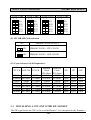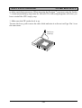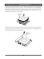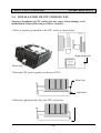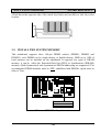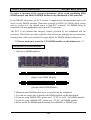
1
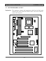
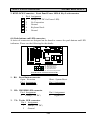
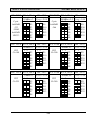
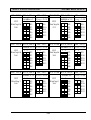
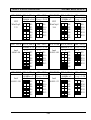
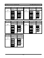
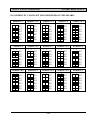
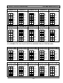
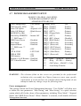
PT-5VMX VIA MVP3 ATX MAINBOARD OPERATION MANUAL DOC NO. UM-VMX-E3 ………………………………………………………………………………………………………………………Printed in Taiwan VIA MVP3 ATX SYSTEM BOARD OPERATION MANUAL DOC NO. UM-VMX-O3 ………………………………………………………………………………………………………………………Printed in Taiwan.. MVP3 ATX SYSTEM BOARD TABLE OF CONTENTS TABLE OF CONTENTS Chapter & Section Page 1. INTRODUCTION ......................................................................................... 1-1 1.1 SYSTEM OVERVIEW ........................................................................... 1-1 1.2 SYSTEM BOARD LAYOUT ................................................................. 1-2 2. FEATURES .................................................................................................... 2-1 2.1 MAINBOARD SPECIFICATIONS ...................................................... 2-1 2.2 AMAZING WAYS TO POWER ON THE PC SYSTEM ................... 2-3 2.3 POWER OFF THE PC SYSTEM.......................................................... 2-5 3. HARDWARE SETUP ................................................................................... 3-1 3.1 UNPACKING........................................................................................... 3-1 3.2 HARDWARE CONFIGURATION....................................................... 3-2 3.2.1 CONNECTORS............................................................................. 3-2 3.2.2 JUMPERS ...................................................................................... 3-12 3.3 INSTALLING A CPU ONTO THE ZIF SOCKET ............................. 3-24 3.4 INSTALLATION OF CPU COOLING FAN....................................... 3-27 3.5 INSTALL THE SYSTEM MEMORY .................................................. 3-28 4. AWARD BIOS SETUP ................................................................................. 4-30 4.1 GETTING STARTED............................................................................. 4-30 4.2 MAIN MENU........................................................................................... 4-31 4.3 CONTROL KEYS ................................................................................... 4-32 4.4 STANDARD CMOS SETUP .................................................................. 4-33 4.5 BIOS FEATURES SETUP ..................................................................... 4-34 4.6 CHIPSET FEATURES SETUP ............................................................. 4-36 4.7 POWER MANAGEMENT SETUP....................................................... 4-38 4.8 PNP/PCI CONFIGURATION ............................................................... 4-39 4.9 INTEGRATED PERIPHERALS........................................................... 4-42 4.10 LOAD SETUP DEFAULTS ................................................................... 4-43 4.11 SUPERVISOR PASSWORD / USER PASSWORD ............................ 4-43 4.12 IDE HDD AUTO DETECTION ............................................................ 4-43 4.13 SAVE &EXIT SETUP ............................................................................ 4-44 4.14 EXIT WITHOUT SAVING.................................................................... 4-44 i MV3 ATX SYSTEM BOARD TRADEMARDKS All trademarks used in this manual are the property of their respective owners. NOTE The “LOAD SETUP DEFAULTS” function loads the default settings directly from BIOS default table, these default settings are the best-case values that will optimize the system performance and increase the system stability. This strongly recommended when you first receive this system board, or the system CMOS data is corrupted. Move the selection bar to “LOAD SETUP DEFAULTS” and then press the “ENTER” key and then the SETUP default values will be loaded into the system. (Please refers to the Chapter 4 AWARD BIOS SETUP procedures in this manual.) NOTICE Information presented in this manual has been carefully checked for reliability; however, no responsibility is assumed for inaccuracies. The information contained in this manual is subject to change without prior notice. ii MVP3 ATX SYSTEM BOARD INTRODUCTION 1. INTRODUCTION 1.1 SYSTEM OVERVIEW This mainboard is an ATX form-factor PCI Local Bus Pentium TM system board with the updated AGP interface designed onboard. The most updated VIA MVP3 chipset for 100MHz Front Side Bus (FSB) is choosen for this mainboard and it gives the most outstanding performance for different applications. This mainboard is designed for the high performance PentiumTM or other equivalent processors for high-end application and it is a true GREEN-PC computer system. The FSB (Front Side Bus) clock speed can be adjusted to 100MHz when we are installing the 100MHz FSB processor. This system board supports the Peripheral Component Interconnect (PCI) Local Bus standard (PCI Specification Rev. 2.1 compliant). It not only breaks through the I/O bottlenecks of the traditional ISA mainboard, but also provides the ultra high performance for networking and multi-user environments. The mainboard has built-in two channels PIO and Bus Master Enhanced PCI IDE port, one Floppy Disk control port, two high speed Serial ports (UARTs), one multi-mode Parallel port, one PS/2 keyboard port, one PS/2 mouse port, one IR port, two USB ports. The Accelerated Graphic Port (A.G.P.) on the board is designed for the updated AGP 3D video display card. Unlike the traditional PCI-based display cards, AGP technology provides lightening data throughput to fully facilitate the 3Diminsional and multimedia graphic display. The data transfer rate on the AGP port can be as fast as 133MHz and it is much faster than the traditional 33MHz PCI VGA cards. The AGP is a new video display technology and it requires the device driver or new operating system to enable the accelerated graphic feature. Windows® 98 will supports AGP directly, but Windows® 95 still needs the appropriate device drivers to enable the AGP feature. Please don’t worry about the device driver, you can always find the device driver included in the AGP card. 1-1 MVP3 ATX SYSTEM BOARD INTRODUCTION 1.2 SYSTEM BOARD LAYOUT Explanation : The connectors, jumpers and components which has the black point marked on the corner means the location of pin-1 side of the connector, jumper and component. Socket 7 CPU CN13 IDE 1 CN12 IDE 2 VIA VT82C598 JP5 JP6 JP7 JP8 CN9 FDC. SPS FAN CN3 JP9 JP10 JP11 JP12 JP13 DIMM 1 DIMM 2 DIMM 3 CN8 ATX PWR. CN6 LPT1 CN2 COM2 CN1 COM1 CN5 USB JP2 JP3 JP4 CN4 CN11 CPU FAN AGP CN10 WOL PCI 3 SPK KEYLOCK PCI 2 RS HL TL SL PW PCI 4 ISA 1 ISA 2 ISA 3 1-2 SYS. BIOS CN7 IR BAT1 JP1 Winbond W83877F VIA VT82C586B PCI 1 MVP3 ATX SYSTEM BOARD FEATURES 2. FEATURES 2.1 MAINBOARD SPECIFICATIONS ¨ Chipset VIA MVP3 (VT82C598MVP, VT82C586B) and Winbond W83877F / TF. ¨ CPU Intel : Pentium TM processor and OverDrive processor 90 / 100 / 120 / 133 / 150 / 166 / 200 / 233 MHz. Cyrix : 6x86 / 6x86L - P150+ / P166+ / P200+. 6x86MX - PR166 / PR200 / PR233,6x86MII - 266/300/333/366 IBM : 6x86MX - PR166 / PR200 / PR233 / PR266/PR300/PR333 AMD : K5 - PR90 / PR100 / PR120 / PR133 / PR150 / PR166. K6-166 / 200 / 233 / 266 / 300 K6-2 -300 / 333 / 350 / 366 / 380 / 400 / 450. K6-3 –400 / 450. IDT : Win Chip C6-180 / 200 / 225 / 240. WinChip 2A – 200 / 233 / 266 / 300. WinChip 3 – 266 / 300 / 333 / 350. ¨ CPU Voltage (1).CPU I/O voltage : “+3.3V DC” or ”+3.5V DC”. (2).CPU CORE voltage : +1.3V DC ~ +3.5V DC. ¨ System Clock 60 / 66 / 75 / 83 / 95 / 100 MHz ¨ Memory DRAM :Three banks, each bank can be single or double sided. Memory size up to 1GB. Supports SDRAM memory (use 168 pin DIMM module x 3). Supports Parity / ECC (Error Checking and Correcting) SRAM : 512KB or 1MB (optional) pipelined burst SRAM on board. ¨ BIOS AWARD System BIOS. 128KB x 8 Flash ROM (for Plug & Play BIOS). 2-1 MVP3 ATX SYSTEM BOARD FEATURES Expansion Slots AGP Slots: 32-bit x 1 (Supports 1x/2x AGP graphics cards) PCI Slots : 32-bit x 4 (All Master / Slave, PCI 2.1 Compliant). ISA Slots : 16-bit x 3 (PCI / ISA slot share one slot). ¨ IDE Ports Two channel PIO and “Ultra DMA/33” Bus Master PCI IDE ports, which will connect maximum 4 IDE devices like IDE Hard Disk and ATAPI CD-ROM device. PIO Mode 4 transfer rate up to 14 Mbytes/s transfer rates and supports “Ultra DMA/33” mode transfers up to 33 Mbytes/sec. ¨ ACPI 1.Power on by Panel-Switch, or Modem Ring-in or LAN signal. 2.Power off (Soft-off) by OS or Panel-Switch. 3.Resume by several system devices (such as modem ring-in, RTC alarm). ¨ WOL One WOL connector supports Wake-On-LAN. ¨ USB Ports Two Universal Serial Bus (USB) ports. ¨ Super I/O Ports 1.Two high speed NS16C550 compatible Serial ports (UARTs). 2.One SPP / EPP / ECP mode Bi-directional parallel port. 3.One Floppy Disk Control port. ¨ IR Port One HPSIR and ASKIR compatible Infrared port. ¨ Mouse and Keyboard Supports PS/2 Mouse connector, PS/2 Keyboard connector ¨ Software compatibility MS-DOS, Windows NT, OS/2, UNIX, NOVELL, MS Windows, CAD/CAM, Windows 98 (Beta), ...etc. 2-2 MVP3 ATX SYSTEM BOARD FEATURES ¨ DIMENSION Width & Length : 304 mm x 200 mm. Height : 3/4 inches with components mounted. PCB Thickness : 4-layers, 0.05 inches normal. Weight : 20 ounces. ¨ ENVIRONMENT Operating Temperature : 10°C to 40°C. (50°F to 104°F). Require Airflow : 50 linear feet per minute across CPU. Storage Temperature : -40°C to 70°C. (-40°F to 158°F). Humidity : 0 to 90% non-condensing. Altitude : 0 to 10,000 feet. 2.2 AMAZING WAYS TO POWER ON THE PC SYSTEM When the mainboard has been installed successfully, there are several ways to power on the system. Please read the following description for all the details. ¨ POWER BUTTON The power button can be programmed by COMS setup program and it has different features. Please refer to page 3-11 for detail function description. ¨ RTC ALARM PC system can be waked up by the RTC setting in the CMOS. You can set the alarming date and time in the RTC memory, When RTC alarms, the PC system will be triggered and wakes up automatically. Enable the “Resume by Alarm” selection in the BIOS setup utility, and then input the accurate date and time in following fields. (the “Resume by Alarm” is located in the “POWER MANAGEMENT SETUP”, please refer to Section 4-7), Having stored the RTC alarm setting, the PC system will be turned on automatically according to the date and time which is recorded in the CMOS memory. Same as the above, you have to reboot the PC system and wait for the POST (Power On Self Test) is completed to enable the RTC alarm. 2-3 MVP3 ATX SYSTEM BOARD FEATURES ¨ MODEM RING-IN Everyone knows that a PC system can be used as a fax machine to send or receive fax messages. But most people still use fax machine to receive their messages because it is not practical to have the system powered on all day long waiting for the incoming messages. Now the problem can be solved by using this mainboard. This mainboard can be triggered by a modem ring-in signal. When you have a external modem installed, you can leave the PC system power off. Whenever there is the incoming message, the PC system will be triggered by the ring-in signal and wake up automatically to receive the message for you. From now on, you can tell your PC system to receive the fax message for you. In order to use the ring-in signal to wake up your PC system, you will have to use the EXTERNAL MODEM and have it connected to one of the SERIAL PORTS ( COMA or COM B ). When the system power is off, this mainboard will continue to detect the serial port status. When it detects the ring-in signal from the serial port, the system power will be turned on and start to receive the incoming messages automatically. To enable the Modem Ring-In feature, you have to run the BIOS setup utility and enable the “Resume by Ring or LAN” option (it is located in the “POWER MANAGEMENT SETUP”, please refer to Section 4-7 for the settings). Having completed the BIOS setup, you have to reboot the PC system so that BIOS can verify the setting. (the “DMI pool data” will be verified by the BIOS when loading the operating system). Simply speaking, shut down the PC system and then re-start the system. The modem ring-in feature will be enabled when the operation system has been loaded. Note: This function is not available when using the internal MODEM card. ¨ WAKE ON LAN ( WOL ) There is a WOL connector CN10 (see page 3-8) on the mainboard which is designed to connect to the signal from a LAN card which supports the Wake On LAN feature. When such LAN card is installed, you may turn on the PC system from your remote server and monitor the PC status. 2-4 MVP3 ATX SYSTEM BOARD FEATURES To enable this feature, you will have to use the BIOS setup utility to enable the “Resume by Ring or LAN” (it is located at “POWER MANAGEMENT SETUP”, please refer to Section 4-7 for the settings). Having completed the BIOS setup, you have to reboot the PC system so that BIOS can verify the setting. ( the “DMI pool data” will be verified by the BIOS when loading the operating system). Simply speaking, reboot the PC system, the Wake On LAN feature will be enabled when the operation system has been loaded Note: This function will be disabled if you turn off the power before the system can verify the DMI pool data. 2.3 POWER OFF THE PC SYSTEM There are two ways to power off the system. They are “Shut Down by Power Button” and “ Shut Down by OS”. (such as Windows® 95 and Windows® 98, you can choose the Shut Down from the file menu and the system will be powered off immediately ). 2-5 MVP3 ATX SYSTEM BOARD AWARD BIOS SETUP 3. HARDWARE SETUP This chapter explains how to configure the mainboard hardware. When you are installing the mainboard, you will have to make jumper settings and cable connections. Please refer to the following sections for the details: 3.1 UNPACKING The system board package contains the following parts : This system board. Operation manual. A CD diskette which includes device driver and utility program The mainboard contains electric sensitive components which can be easily damaged by static electricity, please leave the mainboard sealed in its original packing until when installation. Unpacking and installation shall be done on a grounded anti-static mat. The operator will have to wear an anti static wristband, grounded at the same point as the anti-static mat. Inspect the mainboard carton to see whether there is any obvious damage. Shipping and handling may cause damage to your board. Be sure there is no shipping or handling damages on the board before proceeding. After opening the motherboard color box, extract the mainboard and place it only on a grounded anti-static surface with the component side up. Inspect the board again to see whether there is any damage. Press on all sockets of IC‘s to make sure that they are properly seated. Please put the mainboard on a firm flat surface when you are installing the component to the socket on the mainboard.. 3-1 MVP3 ATX SYSTEM BOARD AWARD BIOS SETUP 3.2 HARDWARE CONFIGURATION Before the system board is ready for operating, the hardware must be configured to make sure it will work properly with different environment. To configure the system board is a simple task, only a few jumpers, connectors, cables and sockets needs to be selected and installed. 3.2.1 CONNECTORS A connector is two or more pins that are used make connections to the system standard accessories (such as power, mouse, printer,...etc.). The following is a list of connectors on board, as well as descriptions of each individual connector. (A) BAT1 Non-rechargeable battery (Use 3V Lithium battery : CR2032) BAT1: Battery Socket Pin name Pin# Pin name Battery Positive Ground Pin# + CN2 CN9 FDC. CN6 CN1 CN5 CN4 USB CN8 ATX PWR. DIMM 3 DIMM 2 DIMM 1 SYS. BIOS CN12 IDE 2 CN13 IDE 1 3-2 Socket 7 AGP PCI 1 PCI 2 PCI 3 SL1 PCI4 SL2 SL3 CPU MVP3 ATX SYSTEM BOARD AWARD BIOS SETUP (B) CN1 COM 1 (Serial Port 1) connector (C) CN2 COM 2 (Serial Port 2) connector CN1 COM 1 CN2 COM 2 CN2 CN6 CN5 CN4 USB CN1 CN8 ATX PWR. DIMM 3 DIMM 2 DIMM 1 CN9 FDC. Socket 7 AGP PCI 1 PCI 3 PCI 2 PCI4 SL1 SL2 SL3 CPU CN12 IDE 2 CN13 IDE 1 SYS. BIOS Ping assignment of serial port connector: Signal name Pin # Signal name 1 6 Pin # 1 DCD (Data Carrier Detect) 6 DSR (Data Set Ready) 2 RD (Received Data) 7 RTS (Request To Send) 3 TD (Transmit Data) 8 CTS (Clear To Send) 4 DTR (Data Terminal Ready) 9 RI (Ring Indicator) 5 Ground 5 9 I/O address 3F8H/2F8H/3E8H/2E8H, IRQ3/IRQ4, selected by CMOS setup. (D) CN4 PS/2 Mouse and Keyboard Connector PS/2 Mouse Connector PS/2 Keyboard Connector CN2 CN9 FDC. CN6 CN1 CN5 CN4 USB CN8 ATX PWR. DIMM 3 DIMM 2 DIMM 1 SYS. BIOS CN12 IDE 2 CN13 IDE 1 3-3 Socket 7 AGP PCI 1 PCI 2 PCI 3 SL1 PCI4 SL2 SL3 CPU MVP3 ATX SYSTEM BOARD AWARD BIOS SETUP Pin assignment of PS/2 mouse connector: Pin # Signal name Pin # Pin # Signal name 1 Mouse Data 3 Ground 5 2 No Connection 4 + 5V DC 6 Signal name Mouse Clock No Connection Pin assignment of keyboard connector Pin # Signal name Pin # Signal name 1 Keyboard Data 3 Ground 2 No Connection 4 + 5V DC Signal name Keyboard Clock No Connection (E) CN5 Pin # 5 6 USB (Universal Serial Bus) connector USB 1 USB 2 CN2 CN9 FDC. CN6 CN1 CN5 CN4 USB CN8 ATX PWR. DIMM 3 DIMM 2 DIMM 1 CN12 IDE 2 CN13 IDE 1 SYS. BIOS Socket 7 AGP PCI 1 PCI 2 PCI 3 SL1 PCI4 SL2 SL3 CPU . Pin assignment of USB connector: USB 1 1 5 2 3 Pin1: +5VDC Pin2: DATAPin3: DATA+ Pin4: Ground Pin5: Ground Pin6: Ground USB 2 4 1 6 5 2 3 4 6 3-4 MVP3 ATX SYSTEM BOARD (F) CN6 AWARD BIOS SETUP Parallel Port Connector (Supports SPP/EPP/ECP mode, using IRQ7 or IRQ5, ECP modes use DMA channel 3 or channel 1, and it can be programmed by CMOS setup) Parallel Port CN6 CN2 CN1 CN5 CN4 USB CN8 ATX PWR. DIMM 3 DIMM 2 DIMM 1 CN9 FDC. SYS. BIOS Pin assignment of parallel port: 1 14 Pin # Signal name 1 STROBE 2 Data Bit 0 3 Data Bit 1 4 Data Bit 2 5 Data Bit 3 6 Data Bit 4 7 Data Bit 5 8 Data Bit 6 9 Data Bit 7 10 ACK 11 BUSY 12 PE 13 SLCT 13 25 Socket 7 AGP PCI 1 PCI 2 PCI 3 SL1 PCI4 SL2 SL3 CPU CN12 IDE 2 CN13 IDE 1 Pin # 14 15 16 17 18 19 20 21 22 23 24 25 Signal name AUTO FEED ERROR INIT SLCT IN Ground Ground Ground Ground Ground Ground Ground Ground 3-5 MVP3 ATX SYSTEM BOARD (G) CN7 AWARD BIOS SETUP IR (Infrared Rays) transmission connector IR (INFRARED RAYS) CONNECTOR 1 ( +5VDC ) 2 ( NO CONNECTION ) 3 ( IR RECEIVE ) 4 ( GROUND ) 5 ( IR TRANSMIT ) CN2 CN5 CN4 USB CN1 CN8 ATX PWR. DIMM 3 DIMM 2 DIMM 1 CN9 FDC. CN12 IDE 2 CN13 IDE 1 SYS. BIOS (H) CN8 Socket 7 AGP PCI 1 PCI 2 PCI 3 SL1 PCI4 SL2 SL3 CPU ATX Power connector CN8 ATX Power connector CN2 CN9 FDC. CN1 CN5 CN4 USB CN8 ATX PWR. DIMM 3 DIMM 2 DIMM 1 SYS. BIOS CN12 IDE 2 CN13 IDE 1 3-6 Socket 7 AGP PCI 1 PCI 2 PCI 3 SL1 PCI4 SL2 SL3 CPU MVP3 ATX SYSTEM BOARD AWARD BIOS SETUP Pin assignment of ATX power connector 11 1 Pin # 11 12 13 14 15 16 17 18 19 20 Signal name + 3.3V DC - 12V DC Ground PS-ON Ground Ground Ground - 5V DC + 5V DC + 5V DC Pin # 1 2 3 4 5 6 7 8 9 10 Signal name + 3.3V DC + 3.3V DC Ground + 5V DC Ground + 5V DC Ground PW-OK + 5V SB + 12V DC 20 10 (I) CN9 Floppy Disk Control Port connector (Using IRQ6, DMA channel 2) CN9: FDC Connector CN2 CN9 FDC. CN1 CN5 CN4 USB CN8 ATX PWR. DIMM 3 DIMM 2 DIMM 1 SYS. BIOS Socket 7 AGP PCI 1 PCI 2 PCI 3 SL1 PCI4 SL2 SL3 CPU CN12 IDE 2 CN13 IDE 1 (J) CN10: WOL (Wake On LAN) Connector In order to use the WOL LAN card to trigger the power of the PC system, the switching power supply must be able to provide at least 700mA current driving ability on the “5V standby” voltage. 3-7 MVP3 ATX SYSTEM BOARD AWARD BIOS SETUP CN 10 WOL 1 CN2 COM2 CN1 COM1 CN6 LPT1 BAT1 2 3 CN5 USB CN4 CN8 ATX PWR. CN9 FDC. DIMM 3 DIMM 2 DIMM 1 AGP PCI 1 PCI 2 PCI 3 SL1 PCI4 SL2 SL3 CPU CN12 IDE 2 CN13 IDE 1 SYS. BIOS Pin assignment of WOL Connector 1 2 3 Pin # Signal name Pin # Signal name 1 5V standby 2 Ground (K) CN11 CPU Cooling Fan Power connector (optional) GND +12V Fan Sense Signal CN11 1 2 3 CN2 CN9 FDC. CN1 CN5 CN4 USB CN8 ATX PWR. DIMM 3 DIMM 2 DIMM 1 SYS. BIOS CN12 IDE 2 CN13 IDE 1 3-8 Socket 7 AGP PCI 1 PCI 2 PCI 3 SL1 PCI4 SL2 SL3 CPU Pin # Signal name 3 WOL Signal MVP3 ATX SYSTEM BOARD AWARD BIOS SETUP (L) CN12 IDE 1 Connector (Primary IDE Port, using IRQ14) (M) CN13 IDE 2 Connector (Secondary IDE Port, using IRQ15) CN2 CN9 FDC. CN5 CN4 USB CN1 CN8 ATX PWR. DIMM 3 DIMM 2 DIMM 1 Socket 7 AGP PCI 1 PCI 2 PCI4 PCI 3 SL1 SL2 SL3 CPU CN12 IDE 2 CN13 IDE 1 SYS. BIOS CN12: IDE 2 CN13: IDE 1 (N) SPK & KEYLOCK Connector: CN2 COM2 CN1 COM1 CN6 LPT1 BAT1 CN9 FDC. CN5 USB CN4 CN8 ATX PWR. DIMM 3 DIMM 2 DIMM 1 AGP PCI 1 PCI 2 PCI 3 SL1 PCI4 SL2 SL3 CPU CN12 IDE 2 CN13 IDE 1 SYS. BIOS 1 2 3SPKR 4 5 1 2 3 4 5 SPK PWR-LED & KBLOCK SPK & KEYLOCK CONNECTORS 1. SPK: Speaker connector 1 ● ● ● ● 4 Pin # 1 2 3 4 Assignment +5V DC No Connection No Connection Speaker Data Signal 3-9 MVP3 ATX SYSTEM BOARD AWARD BIOS SETUP 2. KEYLOCK Connector: Front Panel Power LED & Key-Lock connector 1 ● ● ● ● ● 5 Pin # 1 2 3 4 5 Assignment Pullup (+5V DC for Power LED) No Connection Ground Keyboard Lock Ground (O) Push buttons and LED connectors A series of connectors are designed on the board to connect the push buttons and LED indicators. Please see the following for the details: CN2 COM2 CN1 COM1 CN6 LPT1 BAT1 CN5 USB CN4 CN8 ATX PWR. CN9 FDC. DIMM 3 DIMM 2 DIMM 1 AGP PCI 1 PCI 2 PCI 3 SL1 PCI4 SL2 SL3 CPU CN12 IDE 2 CN13 IDE 1 SYS. BIOS PW SL TL HL RS RS: Reset Button Connector HL: HDD LED Connector TL: Turbo LED Connector SL: Sleep LED Connector PW: Power On/Off & Suspend switch PUSH BUTTONS AND LED CONNECTORS 1. RS: Reset Button connector Open : No action Pin # Assignment 1 Reset Control Short : System Reset Pin # Assignment 2 Ground 2. HL: IDE HDD LED connector Pin # Assignment 1 Pullup (+5V DC) Pin # Assignment 2 Signal Pin 3. TL: Turbo LED connector Pin # Assignment 1 Pullup (+5V DC) 2 Ground 3-10 MVP3 ATX SYSTEM BOARD AWARD BIOS SETUP 4. SL: Sleep LED Connector This LED will be lightened when the AC power is connected and the system is power off, darkened when the AC power is disconnected or the system is powered on. Pin # Signal name 1 Signal Pin 2 Ground 5. PW: Power On/Off and External Suspend Switch Connector According to the setup in CMOS, the PW connector has two functions. It can be the Power Switch or Suspend Switch of your PC system. (please refer to Section- 4-7 “Soft-Off by PWRBTN”) (1) The setup in CMOS is “Instant-off”: A. When system power is off : Click on this switch, the system will be powered on immediately. B. When system power is on : Click on this switch, the system will be powered off instantly (2) If the setup in CMOS is “Delay 4 Sec.”, the switch function will be: A. When system is power off : Press this switch, the system will power on immediately. B. When system power is on : a. The system is in Full-ON mode : a-1. Click on this switch ( less than 4 seconds ), the system will be turned into Suspend mode. (get into a GREEN mode) a-2. Press and hold this switch for more than 4 seconds, the system will be powered off. b. When the system is in Suspend mode : b-1. Click on this switch ( less than 4 seconds ), the system will return to Full-ON mode. b-2. Press and hold this switch more than 4 seconds, the system will be powered off. 3-11 MVP3 ATX SYSTEM BOARD 3.2.2 AWARD BIOS SETUP JUMPERS A jumper is a set of two, three or more jumper pins which allows you to make different system configuration by putting the plastic connector plug (mini-jumper) on it. The jumper setting is necessary when installing different components onto the mainboard. Please make sure all jumper settings are correct before you can installation the mainboard into the PC system. (A) JP1 Clear CMOS button Pin # Function 1-2 Normal Operation 2-3 Clear CMOS Note: Improper BIOS setting may cause hang-up to the PC system, In case that it be happened and you can not handle your PC system any more, you can use JP1 to clear the system configuration information which is stored in the CMOS memory and get the PC system back to normal status.. Due to the VIA MVP3 chipset features, Clear the CMOS when the power is on is recommended. Please refer to the following steps to clear the CMOS 1. Open the system cabinet and leave the system power on. 2. Move the mini-mumper to Pin2 and Pin3. 3. Click on the Reset button to reboot the PC system to clear the CMOS. 4. Return the mini-jumper to its normal position ( Pin1 and Pin2). (B) JP2~ JP4, JP6~JP8: CPU frequency selection (C) JP9~JP13: CPU Voltage selection CN2 COM2 CN1 COM1 CN6 LPT1 BAT1 CN5 USB CN4 CN8 ATX PWR. CN9 FDC. DIMM 3 DIMM 2 DIMM 1 AGP PCI 1 PCI 2 PCI 3 SL1 PCI4 SL2 SL3 CPU CN12 IDE 2 CN13 IDE 1 SYS. BIOS JP 9 3-12 JP 11 JP 4 JP 10 JP 3 JP 8 JP 13 JP 2 JP 7 JP 12 JP 6 MVP3 ATX SYSTEM BOARD CPU TYPE JP2~4, JP6~8 AWARD BIOS SETUP JP9 ~ JP13 CPU TYPE JP2~4, JP6~8 60MHz x 1.5 VCORE = 3.5V AMD 1 2 1 2 K5–PR90 JP2 JP9 K5–PR120 JP3 JP10 JP4 JP11 JP6 JP12 JP7 JP13 JP8 CPU TYPE JP2~4, JP6~8 AMD K5-PR150 66MHz x 1.5 VCORE = 3.5V 1 2 1 2 JP2 JP9 JP3 JP10 JP4 JP11 JP6 JP12 JP7 JP13 JP8 CPU TYPE JP2~4, JP6~8 60MHz x 2.5 VCORE = 3.5V 1 2 1 2 JP2 JP9 JP3 JP10 JP4 JP11 JP6 JP12 JP7 JP13 JP8 CPU TYPE JP2~4, JP6~8 AMD K6 / PR2 -166 JP9 ~ JP13 AMD K5-PR100 K5-PR133 JP9 ~ JP13 AMD K5-PR166 3-13 AMD K6 / PR2 -200 JP9 ~ JP13 66MHz x 2.5 VCORE = 3.5V 1 2 1 2 JP2 JP9 JP3 JP10 JP4 JP11 JP6 JP12 JP7 JP13 JP8 CPU TYPE JP2~4, JP6~8 66MHz x 2.5 VCORE = 2.9V 1 2 1 2 JP2 JP9 JP3 JP10 JP4 JP11 JP6 JP12 JP7 JP13 JP8 JP9 ~ JP13 66MHz x 3 1 2 JP2 JP3 JP4 JP6 JP7 JP8 JP9 ~ JP13 VCORE = 2.9V 1 2 JP9 JP10 JP11 JP12 JP13 MVP3 ATX SYSTEM BOARD CPU TYPE JP2~4, JP6~8 AMD K6 - 233 CPU TYPE JP2~4, JP6~8 JP9 ~ JP13 AMD K6 - 266 K6-2/266 66MHz x 4 1 2 JP2 JP3 JP4 JP6 JP7 JP8 CPU TYPE JP2~4, JP6~8 66MHz x 4.5 VCORE = 2.2V 1 2 1 2 JP2 JP9 JP3 JP10 JP4 JP11 JP6 JP12 JP7 JP13 JP8 CPU TYPE JP2~4, JP6~8 AMD K6-2/333 JP9 ~ JP13 66MHz x 3.5 VCORE = 3.2V 1 2 1 2 JP2 JP9 JP3 JP10 JP4 JP11 JP6 JP12 JP7 JP13 JP8 CPU TYPE JP2~4, JP6~8 AMD K6 - 300 AWARD BIOS SETUP JP9 ~ JP13 AMD K6–2/300 100MHz x 3 1 2 JP2 JP3 JP4 JP6 JP7 JP8 CPU TYPE JP2~4, JP6~8 95MHz x 3.5 VCORE = 2.2V 1 2 1 2 JP2 JP9 JP3 JP10 JP4 JP11 JP6 JP12 JP7 JP13 JP8 3-14 JP9 ~ JP13 VCORE = 2.2V 1 2 JP9 JP10 JP11 JP12 JP13 JP9 ~ JP13 VCORE = 2.2V 1 2 JP9 JP10 JP11 JP12 JP13 JP9 ~ JP13 100MHz x 3.5 VCORE = 2.2V AMD 1 2 1 2 K6–2/350 JP2 JP9 JP3 JP10 JP4 JP11 JP6 JP12 JP7 JP13 JP8 MVP3 ATX SYSTEM BOARD CPU TYPE JP2~4, JP6~8 AMD K6-2/366 100MHz x 4 1 2 JP2 JP3 JP4 JP6 JP7 JP8 CPU TYPE JP2~4, JP6~8 AMD K6-3/400 JP9 ~ JP13 CPU TYPE JP2~4, JP6~8 66MHz x 5.5 VCORE = 2.2V 1 2 1 2 JP2 JP9 JP3 JP10 JP4 JP11 JP6 JP12 JP7 JP13 JP8 CPU TYPE JP2~4, JP6~8 AMD K6-2/400 AWARD BIOS SETUP 100MHz x 4 1 2 JP2 JP3 JP4 JP6 JP7 JP8 JP9 ~ JP13 AMD K6–2/380 95MHz x 4 1 2 JP2 JP3 JP4 JP6 JP7 JP8 CPU TYPE JP2~4, JP6~8 VCORE = 2.2V 1 2 JP9 JP10 JP11 JP12 JP13 JP9 ~ JP13 JP9 ~ JP13 VCORE = 2.2V 1 2 JP9 JP10 JP11 JP12 JP13 JP9 ~ JP13 100MHz x 4.5 VCORE = 2.4V AMD 1 2 1 2 K6–2/450 JP2 JP9 JP3 JP10 JP4 JP11 JP6 JP12 JP7 JP13 JP8 CPU TYPE JP2~4, JP6~8 VCORE = 2.4V 1 2 JP9 JP10 JP11 JP12 JP13 3-15 JP9 ~ JP13 100MHz x 4.5 VCORE = 2.4V AMD 1 2 1 2 K6–3/450 JP2 JP9 JP3 JP10 JP4 JP11 JP6 JP12 JP7 JP13 JP8 MVP3 ATX SYSTEM BOARD CPU TYPE JP2~4, JP6~8 Cyrix / IBM 6x86 -P166+ 66MHz x 2 1 2 JP2 JP3 JP4 JP6 JP7 JP8 CPU TYPE JP2~4, JP6~8 Cyrix / IBM 6x86 -P200+ 75MHz x 2 1 2 JP2 JP3 JP4 JP6 JP7 JP8 CPU TYPE JP2~4, JP6~8 Cyrix / IBM 6x86MX -PR166 66MHz x 2 1 2 JP2 JP3 JP4 JP6 JP7 JP8 AWARD BIOS SETUP JP9 ~ JP13 CPU TYPE JP2~4, JP6~8 VCORE = 3.5V 1 2 Cyrix / JP9 IBM 6x86L JP10 -P166+ JP11 JP12 JP13 JP9 ~ JP13 66MHz x 2 1 2 JP2 JP3 JP4 JP6 JP7 JP8 CPU TYPE JP2~4, JP6~8 VCORE = 3.5V 1 2 Cyrix / JP9 IBM 6x86L JP10 -P200+ JP11 JP12 JP13 JP9 ~ JP13 75MHz x 2 1 2 JP2 JP3 JP4 JP6 JP7 JP8 CPU TYPE JP2~4, JP6~8 VCORE = 2.9V 1 2 JP9 JP10 JP11 JP12 JP13 3-16 Cyrix / IBM 6x86MX -PR200 (66MHz Bus) JP9 ~ JP13 VCORE = 2.8V 1 2 JP9 JP10 JP11 JP12 JP13 JP9 ~ JP13 VCORE = 2.8V 1 2 JP9 JP10 JP11 JP12 JP13 JP9 ~ JP13 66MHz x 2.5 VCORE = 2.9V 1 2 1 2 JP2 JP9 JP3 JP10 JP4 JP11 JP6 JP12 JP7 JP13 JP8 MVP3 ATX SYSTEM BOARD CPU TYPE JP2~4, JP6~8 Cyrix / IBM 6x86MX -PR200 (75MHz Bus) 75MHz x 2 1 2 JP2 JP3 JP4 JP6 JP7 JP8 CPU TYPE JP2~4, JP6~8 Cyrix / IBM 6x86MX -PR233 (75MHz Bus) JP9 ~ JP13 CPU TYPE JP2~4, JP6~8 VCORE = 2.9V 1 2 JP9 JP10 JP11 JP12 JP13 JP9 ~ JP13 Cyrix / IBM 6x86MX -PR233 (66MHz Bus) 66MHz x 3 1 2 JP2 JP3 JP4 JP6 JP7 JP8 CPU TYPE JP2~4, JP6~8 75MHz x 2.5 VCORE = 2.9V 1 2 1 2 JP2 JP9 JP3 JP10 JP4 JP11 JP6 JP12 JP7 JP13 JP8 CPU TYPE JP2~4, JP6~8 Cyrix 6x86MII -300 / IBM 6x86MX -PR300 (66MHz Bus) AWARD BIOS SETUP JP9 ~ JP13 Cyrix 6x86MII -266 / IBM 6x86MX -PR266 3-17 Cyrix 6x86MII -300 / IBM 6x86MX -PR300 (75MHz Bus) VCORE = 2.9V 1 2 JP9 JP10 JP11 JP12 JP13 JP9 ~ JP13 83MHz x 2.5 VCORE = 2.9V 1 2 1 2 JP2 JP9 JP3 JP10 JP4 JP11 JP6 JP12 JP7 JP13 JP8 CPU TYPE JP2~4, JP6~8 66MHz x 3.5 VCORE = 2.9V 1 2 1 2 JP2 JP9 JP3 JP10 JP4 JP11 JP6 JP12 JP7 JP13 JP8 JP9 ~ JP13 75MHz x 3 1 2 JP2 JP3 JP4 JP6 JP7 JP8 JP9 ~ JP13 VCORE = 2.9V 1 2 JP9 JP10 JP11 JP12 JP13 MVP3 ATX SYSTEM BOARD CPU TYPE JP2~4, JP6~8 Cyrix 6x86MII -333 / IBM 6x86MX -PR333 83MHz x 3 1 2 JP2 JP3 JP4 JP6 JP7 JP8 CPU TYPE JP2~4, JP6~8 IDT C6-180 60MHz x 3 1 2 JP2 JP3 JP4 JP6 JP7 JP8 CPU TYPE JP2~4, JP6~8 IDT C6-225 75MHz x 3 1 2 JP2 JP3 JP4 JP6 JP7 JP8 AWARD BIOS SETUP JP9 ~ JP13 CPU TYPE JP2~4, JP6~8 VCORE = 2.9V 1 2 JP9 JP10 JP11 JP12 JP13 JP9 ~ JP13 Cyrix 6x86MII -366 100MHz x 2.5 VCORE = 2.9V 1 2 1 2 JP2 JP9 JP3 JP10 JP4 JP11 JP6 JP12 JP7 JP13 JP8 CPU TYPE JP2~4, JP6~8 VCORE = 3.5V 1 2 JP9 JP10 JP11 JP12 JP13 JP9 ~ JP13 IDT C6-200 66MHz x 3 1 2 JP2 JP3 JP4 JP6 JP7 JP8 CPU TYPE JP2~4, JP6~8 VCORE = 3.5V 1 2 JP9 JP10 JP11 JP12 JP13 3-18 IDT C6-240 JP9 ~ JP13 60MHz x 4 1 2 JP2 JP3 JP4 JP6 JP7 JP8 JP9 ~ JP13 VCORE = 3.5V 1 2 JP9 JP10 JP11 JP12 JP13 JP9 ~ JP13 VCORE = 3.5V 1 2 JP9 JP10 JP11 JP12 JP13 MVP3 ATX SYSTEM BOARD CPU TYPE JP2~4, JP6~8 IDT WinChip2A 200 66MHz x 3 1 2 JP2 JP3 JP4 JP6 JP7 JP8 CPU TYPE JP2~4, JP6~8 AWARD BIOS SETUP JP9 ~ JP13 CPU TYPE JP2~4, JP6~8 VCORE = 3.5V 66MHz x 3.5 VCORE = 3.5V 1 2 IDT 1 2 1 2 JP9 WinChip2A JP2 JP9 JP10 233 JP3 JP10 JP11 JP4 JP11 JP12 JP6 JP12 JP13 JP7 JP13 JP8 JP9 ~ JP13 CPU TYPE JP2~4, JP6~8 100MHz x 2.33 VCORE = 3.5V IDT WinChip2A 266 1 2 1 2 JP2 JP3 JP4 JP6 JP7 JP8 CPU TYPE JP2~4, JP6~8 JP9 ~ JP13 JP9 JP10 JP11 JP12 JP13 JP9 ~ JP13 100MHz x 2.5 VCORE = 3.5V IDT 1 2 1 2 WinChip2A JP2 JP9 300 JP3 JP10 JP4 JP11 JP6 JP12 JP7 JP13 JP8 CPU TYPE JP2~4, JP6~8 66MHz x 3.5 VCORE = 2.8V IDT 1 2 1 2 WinChip 3 JP2 JP9 266 JP3 JP10 JP4 JP11 JP6 JP12 JP7 JP13 JP8 JP9 ~ JP13 IDT WinChip3 300 3-19 66MHz x 4 1 2 JP2 JP3 JP4 JP6 JP7 JP8 JP9 ~ JP13 VCORE = 2.8V 1 2 JP9 JP10 JP11 JP12 JP13 MVP3 ATX SYSTEM BOARD CPU TYPE JP2~4, JP6~8 AWARD BIOS SETUP JP9 ~ JP13 CPU TYPE JP2~4, JP6~8 100MHz x 2.66 VCORE = 2.8V IDT WinChip3 333 1 2 1 2 JP2 JP3 JP4 JP6 JP7 JP8 CPU TYPE JP2~4, JP6~8 Intel 80502-90 JP9 JP10 JP11 JP12 JP13 JP9 ~ JP13 CPU TYPE JP2~4, JP6~8 60MHz x 1.5 VCORE = 3.3V 1 2 1 2 JP2 JP9 JP3 JP10 JP4 JP11 JP6 JP12 JP7 JP13 JP8 CPU TYPE JP2~4, JP6~8 Intel 80502-120 IDT WinChip3 350 60MHz x 2 1 2 JP2 JP3 JP4 JP6 JP7 JP8 95MHz x 3 1 2 JP2 JP3 JP4 JP6 JP7 JP8 JP9 ~ JP13 Intel 80502-100 Intel 80502-133 3-20 VCORE = 2.8V 1 2 JP9 JP10 JP11 JP12 JP13 JP9 ~ JP13 66MHz x 1.5 VCORE = 3.3V 1 2 1 2 JP2 JP9 JP3 JP10 JP4 JP11 JP6 JP12 JP7 JP13 JP8 CPU TYPE JP2~4, JP6~8 VCORE = 3.3V 1 2 JP9 JP10 JP11 JP12 JP13 JP9 ~ JP13 66MHz x 2 1 2 JP2 JP3 JP4 JP6 JP7 JP8 JP9 ~ JP13 VCORE = 3.3V 1 2 JP9 JP10 JP11 JP12 JP13 MVP3 ATX SYSTEM BOARD CPU TYPE JP2~4, JP6~8 Intel 80502-166 66MHz x 2.5 1 2 JP2 JP3 JP4 JP6 JP7 JP8 CPU TYPE JP2~4, JP6~8 Intel 80503-166 JP9 ~ JP13 CPU TYPE JP2~4, JP6~8 VCORE = 3.3v 1 2 JP9 JP10 JP11 JP12 JP13 JP9 ~ JP13 Intel 80502-200 66MHz x 3 1 2 JP2 JP3 JP4 JP6 JP7 JP8 CPU TYPE JP2~4, JP6~8 66MHz x 2.5 VCORE = 2.8V 1 2 1 2 JP2 JP9 JP3 JP10 JP4 JP11 JP6 JP12 JP7 JP13 JP8 CPU TYPE JP2~4, JP6~8 Intel 80503-233 AWARD BIOS SETUP Intel 80503-200 JP9 ~ JP13 66MHz x 3.5 VCORE = 2.8V 1 2 1 2 JP2 JP9 JP3 JP10 JP4 JP11 JP6 JP12 JP7 JP13 JP8 3-21 66MHz x 3 1 2 JP2 JP3 JP4 JP6 JP7 JP8 JP9 ~ JP13 VCORE = 3.3v 1 2 JP9 JP10 JP11 JP12 JP13 JP9 ~ JP13 VCORE = 2.8V 1 2 JP9 JP10 JP11 JP12 JP13 MVP3 ATX SYSTEM BOARD AWARD BIOS SETUP (D) OTHER CPU CLOCK SETTING RESERVED ON THE BOARD : 66MHz x 5 1 2 JP2 JP3 JP4 JP6 JP7 JP8 66MHz x 5.5 1 2 JP2 JP3 JP4 JP6 JP7 JP8 75MHz x 3.5 1 2 JP2 JP3 JP4 JP6 JP7 JP8 75MHz x 4 1 2 JP2 JP3 JP4 JP6 JP7 JP8 75MHz x 4.5 1 2 JP2 JP3 JP4 JP6 JP7 JP8 75MHz x 5 1 2 JP2 JP3 JP4 JP6 JP7 JP8 75MHz x 5.5 1 2 JP2 JP3 JP4 JP6 JP7 JP8 83MHz x 3 1 2 JP2 JP3 JP4 JP6 JP7 JP8 83MHz x 3.5 1 2 JP2 JP3 JP4 JP6 JP7 JP8 83MHz x 4 1 2 JP2 JP3 JP4 JP6 JP7 JP8 83MHz x 4.5 1 2 JP2 JP3 JP4 JP6 JP7 JP8 83MHz x 5 1 2 JP2 JP3 JP4 JP6 JP7 JP8 83MHz x 5.5 1 2 JP2 JP3 JP4 JP6 JP7 JP8 95MHz x 2.5 1 2 JP2 JP3 JP4 JP6 JP7 JP8 95MHz x 3 1 2 JP2 JP3 JP4 JP6 JP7 JP8 3-22 MVP3 ATX SYSTEM BOARD AWARD BIOS SETUP 95MHz x 3.5 1 2 JP2 JP3 JP4 JP6 JP7 JP8 95MHz x 4 1 2 JP2 JP3 JP4 JP6 JP7 JP8 95MHz x 4.5 1 2 JP2 JP3 JP4 JP6 JP7 JP8 95MHz x 5 1 2 JP2 JP3 JP4 JP6 JP7 JP8 95MHz x 5.5 1 2 JP2 JP3 JP4 JP6 JP7 JP8 100MHz x 3.5 1 2 JP2 JP3 JP4 JP6 JP7 JP8 100MHz x 4 1 2 JP2 JP3 JP4 JP6 JP7 JP8 100MHz x 4.5 1 2 JP2 JP3 JP4 JP6 JP7 JP8 100MHz x 5 1 2 JP2 JP3 JP4 JP6 JP7 JP8 100MHz x 5.5 1 2 JP2 JP3 JP4 JP6 JP7 JP8 (E) OTHER CPU VOLTAGE SETTING RESERVED ON THE BOARD: VCORE = 3.4V 1 2 JP9 JP10 JP11 JP12 JP13 VCORE = 3.1V 1 2 JP9 JP10 JP11 JP12 JP13 VCORE = 3.0V 1 2 JP9 JP10 JP11 JP12 JP13 VCORE = 2.7V 1 2 JP9 JP10 JP11 JP12 JP13 VCORE = 2.6V 1 2 JP9 JP10 JP11 JP12 JP13 VCORE = 2.5V 1 2 JP9 JP10 JP11 JP12 JP13 VCORE = 2.4V 1 2 JP9 JP10 JP11 JP12 JP13 VCORE = 2.3V 1 2 JP9 JP10 JP11 JP12 JP13 VCORE = 2.1V 1 2 JP9 JP10 JP11 JP12 JP13 VCORE = 2.0V 1 2 JP9 JP10 JP11 JP12 JP13 3-23 MVP3 ATX SYSTEM BOARD VCORE = 1.9V 1 2 JP9 JP10 JP11 JP12 JP13 VCORE = 1.8V 1 2 JP9 JP10 JP11 JP12 JP13 AWARD BIOS SETUP VCORE = 1.7V 1 2 JP9 JP10 JP11 JP12 JP13 VCORE = 1.6V 1 2 JP9 JP10 JP11 JP12 JP13 (F) JP5 DRAM Clock selection JP5 1 2 JP5 SDRAM CLOCK SELECT SDRAM CLOCK = CPU CLOCK 1 2 JP5 SDRAM CLOCK = AGP CLOCK (G) Cross-reference of all frequencies: CPU Clk AGP Clk 60MHz 66.8MHz 75MHz 75MHz 83.3MHz 95.2MHz 100MHz 60MHz 66.8MHz 75MHz 60MHz 66.6MHz 63.5MHz 66.6MHz PCI Clk 30MHz 33.4MHz 37.5MHz 30MHz 33.3MHz 31.75MHz 33.3MHz SDRAM SDRAM Clock Clock JP5=Short JP5=Open 60MHz 60MHz 66.8MHz 66.8MHz 75MHz 75MHz 60MHz 75MHz 66.6MHz 83.3MHz 63.5MHz 95.2MHz 66.6MHz 100MHz JP6 JP7 JP8 Short Open Open Short Open Short Open Short Short Open Short Short Open Open Short Short Short Open Open Open Open 3.3 INSTALLING A CPU ONTO THE ZIF SOCKET The ZIP type Socket for CPU is the so called Socket 7. It is designed for the Pentium TM 3-24 MVP3 ATX SYSTEM BOARD AWARD BIOS SETUP or other equivalent processors. When inserting the Pentium TM processor onto the Socket 7, certain precautionary steps must be followed. The following diagrams will show you how to install the CPU step by step. 1. Make sure the ZIF socket level is up. To raise the lever, pull it out to the side a little and raise it as far as it will go. Pin 1 is at the arm corner. Pull lever out & up. 3-25 MVP3 ATX SYSTEM BOARD AWARD BIOS SETUP 2.Align the CPU and socket pin 1 corners. Match the processor corner containing the blunt edge and the white dot to the socket corner with the distinctive pin arrangement. The pins on the bottom should have aligned with the inner 3 rings of holes in the socket, Place the CPU into the socket and it will goes into the socket easily. If it won’t, pull the level up a little more and try again. Align CPU & insert it mark Pin 1 3.Press the lever down. The plate will slide forward. You will feel some resistance as the pressure starts to secure the CPU in the socket. When the CPU is installed, the lever will snap into place at the side of the socket. Pull lever down. 3-26 MVP3 ATX SYSTEM BOARD AWARD BIOS SETUP 3.4 INSTALLATION OF CPU COOLING FAN Improper installation of CPU cooling fan may cause serious damage to the motherboard. Please follow the procedures carefully: 1.There is a metal clip attached to the CPU cooler as shown below. Right hand side Metal clip 2.Place the CPU cooler squarely on the top of CPU. Metal clip right hand 3.Hook the right hand side clip to the CPU socket first. 3-27 MVP3 ATX SYSTEM BOARD AWARD BIOS SETUP 4.Push down the opposite side of the metal clip firmly and carefully to lock the cooler in place. 3.5 INSTALL THE SYSTEM MEMORY This mainboard supports three 168-pin DIMM sockets (DIMM1, DIMM2 and DIMM3), each DIMM can be single-density or double-density, 8MB up to 1GB of local memory can be installed on the mainboard. It supports two types of DRAM memory, it can be either the Extended Data Out (EDO) or Synchronous (SDRAM) memory. (Both Symmetrical and Asymmetrical DRAM addressing are supported.) The recommended DIMM modules must be 3.3V, unbuffered and DRAMs‘ speed must be 60ns or 70ns,. CN2 COM2 CN1 COM1 CN6 LPT1 BAT1 CN9 FDC. CN5 USB CN8 ATX PWR. DIMM 3 DIMM 2 DIMM 1 AGP PCI 1 PCI 2 PCI 3 SL1 PCI4 SL2 SL3 CPU CN12 IDE 2 CN13 IDE 1 SYS. BIOS DIMM 3 DIMM 2 DIMM 1 Picture of DRAM sub-system 3-28 CN4 MVP3 ATX SYSTEM BOARD AWARD BIOS SETUP In order to increase of the system performance, please avoid populating EDO DIMM module and SDRAM DIMM module on the mainboard at the same time. In the DRAM subsystem, the ECC feature is supported by the mainboard and it will check on the DRAM interface (Functions selected by BIOS via CMOS setup, please refer to section 4-5, the default status is Non-ECC selected.) All DIMMs must be populated with true parity bit to implement ECC functions. The ECC is an optional data integrity feature provided by the mainboard and the processor. This feature provides single-bit error correction, multiple-bit error detection, and detection of all errors confined to single nibble for DRAM memory subsystem. *** Plaease make sure to use the 3.3V DIMM modules on the mainboard.. *** Installation of DIMM modules: 1. Outlook of DIMM modules: (Single-Side DIMM Module) ( Double-Side DIMM Module ) 2. Minimum one DIMM module must be installed on the mainboard. 3. You can use single side or double side DIMM module on this mainboard. 4. If you are using 66MHz CPU, please use 3.3V PC-66 or PC-100 DIMM module. 5. If you are using 100MHz CPU, please use 3.3V PC-100 DIMM module.. 6. Please install the DIMM module starting from DIMM1 or DIMM2 first. 3-29 MVP3 ATX SYSTEM BOARD AWARD BIOS SETUP 4. AWARD BIOS SETUP 4.1 GETTING STARTED When the system is powered on or reset, the BIOS will execute the Power-On Self Test routines (POST) and checks the functionality of every component in the PC system. During the POST, you will see a copyright message on the screen followed by a diagnostics and initialization procedure. (If an EGA or VGA card is installed, the copyright message of the video card maybe displayed on the screen first.) When the system detects any error, it will gives a series of beeping sounds or display the error message on your screen. Basically, the following screen will be displayed when the system is powered on: Fig. 4-1 Initial Power-On screen. 4-30 MVP3 ATX SYSTEM BOARD AWARD BIOS SETUP After the POST routines are completed, you will find the following message appears on the lower-left screen : “ Press DEL to enter SETUP ” To execute the Award BIOS Setup program, press the DEL key and the “MAIN MENU” of the BIOS setup utility as shown in Fig 4-2 will be triggered. 4.2 MAIN MENU ROM PCI / ISA BIOS (2A5LEXXX) CMOS SETUP UTILITY AWARD SOFTWARE, INC. STANDARD CMOS SETUP SUPERVISOR PASSWORD BIOS FEATURES SETUP USER PASSWORD CHIPSET FEATURES SETUP IDE HDD AUTO DETECTION POWER MANAGEMENT SETUP SAVE & EXIT SETUP PNP/PCI CONFIGURATION EXIT WITHOUT SAVING INTEGRATED PERIPHERALS LOAD SETUP DEFAULTS ESC : Quit F10 : Save & Exit Setup áâßà : Select Item (Shift)F2 : Change Color Time, Date, Hard Disk Type … Fig. 4-2 CMOS SETUP MAIN MENU screen. 4-31 MVP3 ATX SYSTEM BOARD AWARD BIOS SETUP 4.3 CONTROL KEYS Listed below is an explanation of the keys displayed at the bottom of the screens which will be used in the BIOS SETUP program : Arrow Keys Enter F1 (Shift)F2 ESC PgUp(-)/PgDn(+) F7 F10 : Use the arrow keys to move the cursor to the desired item. : To select the desired item. : Display the help screen for the selected feature. : To change the screen color, total 16 colors. : Exit to the previous screen. : To modify or change the default value of the highlighted item. : Loads the SETUP default values from BIOS default table, (only for the current page will be recovered) : Save all changes made to CMOS RAM in the MAIN MENU. The following sections shows all the screens which you will find in the CMOS SETUP routine, each screen contains the selection options and its default settings. At the bottom of some screen display, you may find the description of all function key which you can use it to change the settings. If you are not quite sure of the definition for some specific items, please consult your mainboard supplier for details. 4-32 MVP3 ATX SYSTEM BOARD AWARD BIOS SETUP 4.4 STANDARD CMOS SETUP ROM PCI / ISA BIOS (2A5LEXXX) STANDARD CMOS SETUP AWARD SOFTWARE, INC. Date (mm : dd : yy) Time (hh : mm : ss) HARD DISKS 1998 TYPE SIZE CYLS HEAD PRECOMP Primary Master Primary Slave Secondary Master Secondary Drive A Drive B Fri Jul 17 9 : 6 : 45 Auto None Auto None 0 0 0 0 0 0 0 0 0 0 0 0 LANDZ SECTOR 0 0 0 0 0 0 0 0 MODE 0 0 0 0 Auto -----Auto ------ : 1.44M, 3.5 in. : None Base Memory : 640 K Extended Memory : xxxxxx K Other Memory : xxxxxx K Video Halt On : EGA/VGA : All Errors ESC : Quit F1 : Help Total Memory : xxxxxx K áâßà (Shift)F2 : : Select Item Change Color PU/PD/+/- : Modify Fig. 4-3 STANDARD CMOS SETUP screen. MODE: The BIOS on the mainboard is the updated one and which provides three different modes to support both normal size IDE hard disk drive and the hard disk drive above 528MB: l NORMAL : For IDE hard disk drives which is smaller than 528MB. l LBA : For IDE hard disk drive which is above 528MB (ideally, it can be as big as 8.4GB ) that use Logic Block Addressing (LBA) mode. l Large : For IDE hard disks size larger then 528MB but it does not support the LBA mode. 4-33 MVP3 ATX SYSTEM BOARD AWARD BIOS SETUP Note: Large mode is a new technology and it is not fully supported by most operation systems so far. So only MS-DOS is recommended on such hard disk drive. Fortunately, such hard disk drive is not very common nowadays. Note : Some certain operation system (like SCO-UNIX) will have to choose the “NORMAL” mode when installation. 4.5 BIOS FEATURES SETUP ROM PCI / ISA BIOS (2A5LEXXX) BIOS FEATURES SETUP AWARD SOFTWARE, INC. Virus Warning CPU Internal Cache External Cache Quick Power On Self Test Boot Sequence Swap Floppy Drive Boot Up Floppy Seek Boot Up NumLock Status Gate A20 Option Memory Parity/ECC Check Typematic Rate Setting Typematic Rate (Chars/Sec) Typematic Delay (Msec) Security Option IDE Second Channel Control PS/2 mouse function control PCI/VGA Palette Snoop OS Select For DRAM>64MB Report No FDD For WIN95 : Disabled : Enabled : Enabled : Enabled : A,C,SCSI : Disabled : Enabled : On : Normal : Enabled : Disabled :6 : 250 : Setup : Enabled : Enabled : Disabled : Non-OS2 : No Video BIOS C8000-CBFFF CC000-CFFFF D0000-D3FFF D4000-D7FFF D8000-DBFFF DC000-DFFFF ESC F1 F5 F7 Shadow Shadow Shadow Shadow Shadow Shadow Shadow Enabled Disabled Disabled Disabled Disabled Disabled Disabled : Quit áâßà : Select Item : Help PU/PD/+/- : Modify : Old Values (Shift)F2 : Color : Load Setup Defaults Fig. 4-4 BIOS FEATURES SETUP screen. 4-34 : : : : : : : MVP3 ATX SYSTEM BOARD AWARD BIOS SETUP Virus Warning : (Default values is “Disabled”) In order to avoid virus infection happens on your PC system, this mainboard provides the virus warning features in the BIOS. During and after the operation system is loaded, any attempt to write to the boot sector or partition table on the IDE hard disk drive will trigger this feature and give you some warning messages on the screen and then halt the system. When you find the message on your screen, please run an anti-virus program to see whether your system is infected by a virus or not. Enabled : Activate automatically when the system boots up causing a warning message to appear on the screen when anything attempts to access the boot sector of the hard disk partition table. Disabled : No warning message to appear when anything attempts to access the boot sector or hard disk partition table. CPU Internal Cache : This option enables CPU‘s internal (L1) cache memory. If you want to use the internal (L1) cache memory and external (L2) cache memory, you may use this option to enable or disable the setting. External Cache : This option enables L2 (secondary) external cache memory. If there is no external cache memory on board you have to select “disabled”, 4-35 MVP3 ATX SYSTEM BOARD AWARD BIOS SETUP 4.6 CHIPSET FEATURES SETUP ROM PCI / ISA BIOS (2A5LEXXX) CMOS SETUP UTILITY CHIPSET FEATURES SETUP Bank 0/1 DRAM Timing Bank 2/3 DRAM Timing Bank 4/5 DRAM Timing SDRAM Cycle Length DRAM Read Pipeline : : : : : SDRAM 10ns FP/EDO 70ns FP/EDO 70ns 3 Enabled Cache Rd+CPU Wt Pipeline : Enabled Cache Timing : Fast Video BIOS Cacheable System BIOS Cacheable Memory Hole At 15Mb Addr. AGP Aperture Size : : : : OnChip USB USB Keyboard Support : Disabled : Disabled Auto Detect DIMM/PCI CLK Spread Spectrum : Enabled : Disabled Enabled Enabled Disabled 64M ESC F1 F5 F7 : : : : Quit áâßà : Select Item Help PU/PD/+/- : Modify Old Values (Shift)F2 : Color Load Setup Defaults Fig. 4-5 CHIPSET FEATURES SETUP screen. WARNING : The selection fields on this screen are provided for the professional technician who can modify the Chipset features to meet some specific requirement. If you do not have the related technical background, do not attempt to make any change except the following items. Bank 0/1 ( 2/3, 4/5)DRAM Timing : BANK 0/1: DIMM1 BANK 2/3: DIMM2 BANK 4/5: DIMM3 4-36 MVP3 ATX SYSTEM BOARD AWARD BIOS SETUP The memory modules inserted onto the memory subsystem will be detected by the system BIOS automatically. For example, when you insert a SDRAM module onto the DIMM sockets, “SDRAM 10ns” will be displayed on the screen shown above. (It will be “FP/EDO 70ns” when SDRAM module is absent on the DIMM subsystem.) There are two optimum values suggested for the chipset and CPU registers. You may select either 60ns or 70ns for EDO modules. Basically, “60 ns” will let you have better performance. However, “70ns” is recommended in most case causes it works with most EDO DRAM modules, As for SDRAM modules, “10ns” is suggested for most modules. “8ns” will let you have begtter performance, but it may cause system unstable when SDRAM modules are not fast enough. 4-37 MVP3 ATX SYSTEM BOARD AWARD BIOS SETUP 4.7 POWER MANAGEMENT SETUP ROM PCI / ISA BIOS (2A5LEXXX) POWER MANAGEMENT SETUP AWARD SOFTWARE, INC. Power Management PM Control by APM Video Off Option Video Off Method MODEM Use IRQ Soft-Off by PWRBTN ** PM Timers ** HDD Power Down Doze Mode Suspend Mode ** PM Events ** VGA LPT & COM HDD & FDD DMA/master Modem or LAN Resume RTC Alarm Resume : User Define : Yes : Suspend->Off : Blank Screen :3 : Instant-Off. : Disabled : Disabled : Disabled : OFF : LPT/COM : ON : OFF : Disabled : Disabled Primary INTR IRQ3 (COM 2) IRQ4 (COM 1) IRQ5 (LPT2) IRQ6 (Floppy Disk) IRQ7 (LPT1) IRQ8 (RTC Alarm) IRQ9 (IRQ2 Redir) IRQ10 (Reserved) IRQ11 (Reserved) IRQ12 (PS/2 Mouse) IRQ13 (Coprocessor) IRQ14 (Hard Disk) IRQ15 (Reserved) ESC F1 F5 F7 : ON : Primary : Primary : Primary : Primary : Primary : Disabled : Secondary : Secondary : Secondary : Primary : Primary : Primary : Disabled : Quit áâßà : Select Item : Help PU/PD/+/- : Modify : Old Values (Shift)F2 : Color : Load Setup Defaults Fig. 4-6 POWER MANAGEMENT SETUP screen. WARNING : The selection fields on this screen are provided for the professional technician who can modify the Chipset features to meet some specific requirement. If you do not have the related technical background, do not attempt to make any change except the following items. Power management : This setting controls the Power Management functions. “User Define” will allow user to define his own parameters. “Min Saving” and “Max Saving” is a quick selection option which will fix the values of four parameters, including “Doze Mode”, “Suspend Mode” and “HDD Power Down”. When “Disable” is selected, it will disable all Power Management functions. 4-38 MVP3 ATX SYSTEM BOARD AWARD BIOS SETUP 4.8 PNP/PCI CONFIGURATION ROM PCI / ISA BIOS (2A5LEXXX) PNP/PCI CONFIGURATION AWARD SOFTWARE, INC. PNP OS Installed : No Resources Controlled By : Manual Reset Configuration Data : Disabled ACPI I/O Device Node : Enabled IRQ-3 assigned to : PCI/ISA PnP IRQ-4 assigned to : PCI/ISA PnP IRQ-5 assigned to : PCI/ISA PnP IRQ-7 assigned to : PCI/ISA PnP IRQ-9 assigned to : PCI/ISA PnP IRQ-10 assigned to : PCI/ISA PnP IRQ-11 assigned to : PCI/ISA PnP IRQ-12 assigned to : PCI/ISA PnP IRQ-14 assigned to : PCI/ISA PnP IRQ-15 assigned to : PCI/ISA PnP DMA-0 assigned to : PCI/ISA PnP DMA-1 assigned to : PCI/ISA PnP DMA-3 assigned to : PCI/ISA PnP DMA-5 assigned to : PCI/ISA PnP DMA-6 assigned to : PCI/ISA PnP DMA-7 assigned to : PCI/ISA PnP CPU to PCI Write Buffer PCI Dynamic Bursting PCI Master 0 WS Write PCI Delay Transaction PCI Master Read Prefetch PCI #2 Access #1 Retry AGP Master 1 WS Write AGP Master 1 WS Read : Enabled : Enabled : Enabled : Enabled : Enabled : Disabled : Enabled : Disabled PCI IRQ Actived By Assign IRQ For USB Assign IRQ For VGA : Level : Enabled : Enabled ESC F1 F5 F7 : Quit áâßà : Select Item : Help PU/PD/+/- :Modify : Old Values (Shift)F2 :Color : Load Setup Defaults Fig. 4-7 PNP/PCI CONFIGURATION setup screen. WARNING : The selection fields on this screen are provided for the professional technician who can modify the Chipset features to meet some specific requirement. If you do not have the related technical background, do not attempt to make any change except the following items. 4-39 MVP3 ATX SYSTEM BOARD AWARD BIOS SETUP Resources Controlled by : Manual : The system BIOS will not refer to the ESCD data to assign IRQ & DMA. Instead, it will refer to the information recorded in this field when assigning the IRQ & DMA resource. ( Anyhow, the system BIOS will always refer to the ESCD data to assign the I/O and memory space resources ). Auto : The system BIOS will refer to the ESCD segment for all legacy information. Reset Configuration Data : Disabled : The system BIOS will do nothing. Enabled : The system BIOS will clear/reset the ESCD during “POST”. After clearing the ESCD, the system BIOS will then change this item‘s value back to “Disable”, otherwise, the ESCD will become useless. There are only 15 IRQs and 8 DMAs available on the mainboard and most of them are assigned for some specific purposes. Sometimes, user may feel like to have some more IRQ and DMA in order to install the new add on cards. In this case, you may use this field to assign some certain IRQ and DMA to “PCI/ISA PnP” so that the new add on card will find the free IRQ or DMA available for it. Legacy : The system BIOS will skip and never assign the specified IRQ/DMA ISA resource to PCI or ISA PnP devices and the IRQ and DMA can only be sued by their specified Legacy ISA cards. PCI/ISA: PnP When the “PCI/ISA PnP” is been selected, the related IRQ and DMA will be released and they can be used by other PCI or ISA devices. Whenever there is the new PCI or ISA devices plugged onto the mainboard, the system BIOS will detect it and assign a free IRQ or DMA for the new devices. 4-40 MVP3 ATX SYSTEM BOARD AWARD BIOS SETUP Note: Most IRQ and DMA have its own purpose and they can not be assigned to “PCI/ISA PnP”. For example, IRQ14 and IRQ15 are used by the onboard IDE device. If you change the setting on IRQ14 and IRQ15, you will be unable to connect the hard disk drive or CD-ROM drive to the IDE interface on the mainboard. So please make sure to check the IRQ and DMA assignment in your system before you proceed to do the setting. For instance, if you do not have the printer (IRQ7) or PS/2™ mouse (IRQ12) connected to your PC system, you may assign IRQ7 and IRQ12 to “PCI/ISA PnP” so that you can have more IRQs available for new add on cards. Explanation for technical issue: PnP device : Device that has Plug & Play compatibility. That means it will request for DMA, IRQ, I/O and Memory from the PnP BIOS and all these requests can be relocatable. In other words, these devices do not utilize any fixed resources. All PCI devices and all ISA PnP devices are PnP devices. Legacy device : A legacy device is a device that all its resources are fixed by hardware (or selected by jumpers). All ISA Non-PnP devices are legacy device. Extended System Configuration Data (ESCD) : A media between the user and the system BIOS for passing the legacy devices information‘s. This information is stored in the onboard NVRAM (flash ROM). 4-41 MVP3 ATX SYSTEM BOARD AWARD BIOS SETUP 4.9 INTEGRATED PERIPHERALS ROM PCI / ISA BIOS (2A5LEXXX) INTEGRATED PERIPHERALS AWARD SOFTWARE, INC. On-Chip IDE First Channel On-Chip IDE Second Channel IDE Prefetch Mode IDE HDD Block Mode IDE Primary Master PIO IDE Primary Slave PIO IDE Secondary Master PIO IDE Secondary Slave PIO : : : : : : : : Enabled Enabled Enabled Enabled Auto Auto Auto Auto IDE Primary Master UDMA IDE Primary Slave UDMA IDE Secondary Master UDMA IDE Secondary Slave UDMA Init Display First : : : : : Auto Auto Auto Auto PCI Slot Onboard FDC Controller : Enabled Onboard Serial Port 1 Onboard Serial Port 2 UART 2 Mode : 3F8 / IRQ 4 : 2F8 / IRQ 3 : Standard Onboard Parallel Port Onboard Parallel Mode ESC F1 F5 F7 : : : : : 378 / IRQ 7 : SPP Quit áâßà : Select Item Help PU/PD/+/- : Modify Old Values (Shift)F2 : Color Load Setup Defaults Fig. 4-8 INTEGRATED PERIPHERALS setup screen. WARNING : The selection fields on this screen are provided for the professional technician who can modify the Chipset features to meet some specific requirement. If you do not have the related technical background, do not attempt to make any change except the following items. UART 2 Mode : This setting determines the IR port (CN7) function mode. Supports both HPSIR and ASKIR. Onboard Parallel Mode : This setting determines the onboard parallel port (CN6) transmission mode. Supports either SPP, EPP, ECP, or ECP+EPP. 4-42 MVP3 ATX SYSTEM BOARD AWARD BIOS SETUP 4.10 LOAD SETUP DEFAULTS If you lost the CMOS data or you don’t know how to complete the setup procedure, you may use this option to load the SETUP default values from the BIOS default table. It is easy to load the default value, simply highlight the “LOAD SETUP DEFAULTS” field and then press the “Enter” key, when you see the “LOAD SETUP DEFAULTS (Y/N)” displayed on the screen, response to it with “Y” and then press the “Enter” key. The SETUP default values will be loaded. Basically, the SETUP default settings are the best-case values that will optimize system performance and increase system stability. In case that the CMOS data is corrupted, the SETUP DEFAULTS settings will be loaded automatically when you press the “Del” key and enter the main setup screen. So you may select “SAVE & EXIT SETUP” to leave setup program and the system is loaded with the default settings. 4.11 SUPERVISOR PASSWORD / USER PASSWORD The “SUPERVISOR PASSWORD” and “USER PASSWORD” will be used to check the authority when power-on. Whenever there is the password stored in either of these fields, the correct password will be requested so that the PC system will continue to load the operation system. You can enter up to eight alphanumeric characters here. When you have typed in the password and pressed the “Enter” key, you will be asked to reconfirm your password again to complete password setup. If you press the “Enter” key twice without any alphanumeric character entered, the PASSWORD will be disabled. If the “User Password” and the “Supervisor Password” are both enabled and they have different password setup, “Supervisor Password” is always has the higher priority, Basically, an “User” is only authorized to change the content of “User Password”, while a “Supervisor” has the authorization to dominate all settings. 4.12 IDE HDD AUTO DETECTION In order to make the IDE hard disk known to the system, you need to tell the system what kind of hard disk is connected to the mainboard by giving a set of hard disk parameters. Sometimes it is not easy for users to find the proper parameters for their IDE hard disk drive. In order to help users to find the parameters, the system BIOS provides a convent way – the auto detection of IDE hard disk drive. 4-43 MVP3 ATX SYSTEM BOARD AWARD BIOS SETUP To run the auto detection program is extremely easy. Move the selection bar to “IDE HDD AUTO DETECTION” and then press “Enter”, the system BIOS take over the job and try to detect the type of IDE hard disk. If it succeeds, you will see a list of hard disk with its related parameters. You may press on the “Y” key (or select one of the hard disk type listed on the screen ). The system BIOS will transfer the parameters to the corresponding fields in the STANDARD CMOS SETUP menu and you have completed the IDE hard disk setup. 4.13 SAVE &EXIT SETUP This option will save all setup values to CMOS RAM & EXIT SETUP routine, by moving the selection bar to “SAVE & EXIT SETUP” and pressing “Enter” key, then types “Y” and “Enter” key, the values will be saved and all the information will be stored in the CMOS memory, and then the setup program will be terminated and the system will start to reboot. 4.14 EXIT WITHOUT SAVING This item exit the setup routine without saving any changed values to CMOS RAM, When you do not want to save your change to the CMOS memory, you may choose to run this option and the setting what you made in the BIOS setup routine will be given away. Move the selection bar to “EXIT WITHOUT SAVING” and click on the “Enter” key, then you will be asked to confirm the action to exit, press the “Y” and “Enter” key, the setup program will be terminated and the system will start to reboot. 4-44 Printed in Taiwan Edition : 08 / 20 / 99