1
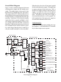
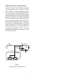
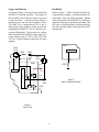
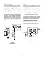
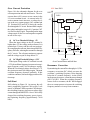
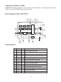
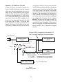
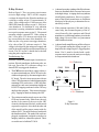
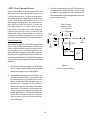
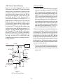
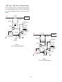
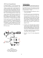
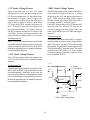
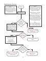
NTDMOD02
TOSHIBA
Service Training
PROJECTION
TELEVISIONS
Main Power Supply
& Complete
Shutdown Guide
TP43H60
TP43H95
TP50H15
TP50H50
TP50H60
TP50H64
TP50H95
TP55H60
Copyright 1999
TOSHIBA AMERICA CONSUMER PRODUCTS, INC.
NATIONAL SERVICE DIVISION
1420-B TOSHIBA DRIVE, LEBANON, TN 37087
TP55H64
TP55H95
TP61H60
TZ43V61
TZ50V51
TZ50V61
TZ55V61
TZ61V61
Contents
Main Power Supply............... 3
Overall Block Diagram .................................................................................... 4
Operation........................................................................................................... 5
Surge Protection Relay ................................................................................... 6
Start-up and Over Voltage Protect ................................................................. 7
Logic and Drivers............................................................................................. 8
Oscillator ........................................................................................................... 8
Oscillator Control ............................................................................................. 9
Latch .................................................................................................................. 9
Thermal Shock Detection Block .................................................................... 9
Over Current Protection................................................................................. 10
Soft Start ........................................................................................................... 10
Resonance Correction ................................................................................... 10
Additional Information on Q801 .................................................................... 11
Block Diagram of Q801 (STR-Z4117) ............................................................ 11
Pin Descriptions .............................................................................................. 11
Waveforms ....................................................................................................... 12
Troubleshooting Flowchart ........................................................................... 13
Shutdown Guide .................15
Summary of Shutdown Circuits .................................................................... 16
Peak-Response Meter .................................................................................... 17
No Peak-Response Meter .............................................................................. 18
Monitoring Circuits ......................................................................................... 18
X-Ray Protect ................................................................................................... 19
+125V Over Current Protect .......................................................................... 20
+36V Over Current Protect ............................................................................ 21
+18V and – 18V Over Current Protect .......................................................... 22
+35V Over Current Protect ............................................................................ 23
+9V Under Voltage Protect ............................................................................. 24
+35V Under Voltage Protect ........................................................................... 24
+200V Under Voltage Protect ........................................................................ 24
Troubleshooting Flowchart ........................................................................... 25
Main Power Supply
3
Overall Block Diagram
When the relay closes, the AC line input is applied
directly to the main power supply. The supply starts
to operate and turns ON the television. D801 is
the full-wave bridge rectifier for the main power
supply. It rectifies the 120V AC line input to
165Vdc and applies it to the main switching IC,
Q801. The primary side of the power supply is
not isolated and, therefore, is at live ground. Detailed explanations of the main power supply are
covered in the remainder of this section.
Figure 1 is the overall block diagram of the main
switching power supply and the standby power
supply. The standby supply is always active when
the television is plugged into an AC line source.
This supply delivers a 5V VDD and a Reset 5V to
the microprocessor to keep the microprocessor functioning at all times, even when the television is not
operating. Transformer T840 isolates the standby
supply from the live ground, and D840 is a fullwave bridge rectifier that supplies 12Vdc to voltage regulator Q840 and relay SR81 (connection
not shown). When the microprocessor receives an
ON command from the remote control or power
key, on the front of the television, it sends 5V to
relay drivers QB30 and Q843 to close relay SR81.
Troubleshooting Tip:
If SR81 never closes, check the standby power supply. Both the 5V VDD and the Reset 5V are mandatory for the microprocessor to operate.
Stand-By Supply
Rectifier &
Isolation Trans.
Main Power Supply
Stand-by
Regulator
Microprocessor
+5-1
D840
T840
Q840
5V
VDD
5V Reset
30V
Q760 Reg.
Rectifiers
QA01
5V=Relay On
0V=Relay Off
11
D856
9
D855
QB30
Q843
Relay Drivers
9
D851
Main Switching IC
10
D854
12
D886
13
D889
To Q752 & Q751
Conv. Outputs
+36
From Shutdown
+18
5V
Q754 Reg.
To Digital Conv. PC,
Q764 & Q767
9V
Q755 Reg.
To Q752
Conv. Output
-18
To Q752 & Q751
Conv. Outputs
Rectifier
SR81
AC Line
Input
D801
165V
4
Q801
Relay
Q756
-9V
Reg.
Q430
9V
Reg.
+38
To Digital Conv. PC,
To Q601 Audio Out
7
C870
To Q752
Conv. Output
14
D891
15
D894
16
D882
17
D884
+12
+125
To Q501
Horizontal Start-up
To Shutdown & Surge protect:
Q846,SR82,Q757, & Q758
Q832
9V
Reg.
+9-2 To Numerous Circuits
Q830
5V&9V
Reg.
+5-2 To Numerous Circuits
+9-1 To Numerous Circuits
Q831
5V
Reg.
+5-3 To PIP Module & QBB3
D101
32V
Reg.
T862
Photo
Coupler
Feedback
To Horizontal Output
Error
Amp.
Q862
Z801
Figure 1.
Power Supply Block Diagram
4
To Tuner(s)
Reg.= Regulator
Conv.= Convergence
Operation
rent, the oscillator frequency decreases and operates closer to the LC resonant frequency. The closer
the switching frequency is to resonance, the higher
the current flow through the primary windings of
T862 and the larger the electromagnetic field. The
larger the electromagnetic field is when it collapses,
the higher the induced current is in the secondary
winding. When the load decreases and requires
less current, the switching frequency increases and
moves away from resonance. As a result, less current is induced in the secondary windings.
The main power supply is a current resonant switching power supply. Figure 2 is a basic block diagram for this supply. The primary winding of T862
and capacitor C870 create an LC series resonant
circuit. An oscillator (OSC), drive circuit, and two
MOSFETs are located internally to Q801 (STRZ4117). The OSC determines the power supply’s
switching frequency. The drive circuit alternately
switches the MOSFETs ON and OFF. The two
power MOSFETs, in a push-pull configuration,
alternate the current flow through the LC circuit
during normal operation. The alternating current
continually builds and collapses an electromagnetic
field around T862’s primary windings. The collapsing of the electromagnetic field induces current into the secondary windings of T862. A fullwave bridge rectifier converts the induced current
into 125Vdc.
To regulate the 125Vdc, an error amplifier moni-
Load
Current
Increased
Load
Decreased
Load
O
S
C
D
r
i
v
e
Q801
T862
ng
.
q
Fre
eq.
Figure 2
Operational Block Diagram
Switching
Freq.
rati
Z801
Ope
r
nt F
ona
Photo
Coupler
Q862
Error
Amp
Res
C870
125V +B
Normal Operating Frequency is 70-80kHz
Figure 3
Load Current Characteristics
tors the voltage and supplies a negative feedback
to the oscillator through photo-coupler Q862.
Q862 isolates the primary side of the power supply from the secondary side.
Refer to Figure 3. The power supply’s switching
frequency operates above the LC resonant frequency. When the load on the secondary side of
the power supply increases and requires more cur5
Surge Protection Relay
Figure 4 shows the surge protection operation. To
prolong the life of the power supply, a surge circuit reduces current through the main power supply at startup. When the television is OFF, relays
SR81 and SR82 are open. At turn-on, SR81
closes and the switching power supply begins to
operate. During this time, the power supply draws
a large amount of current. To reduce the current,
the ground path for bridge rectifier D801 is
through resistor R810. Once the power supply
becomes fully operational and produces output
voltages, one of these voltages is applied to the
base of transistor Q846. This voltage turns Q846
ON and allows current to flow through the coil of
SR82. SR82’s switch closes and creates a direct
ground path for D801 by bypassing R810. SR82
remains closed during normal operation.
Troubleshooting Tip:
R810 is a fusible resistor. If SR82 does not close
after the power supply is fully operational, R810 eventually opens and prevents the power supply from operating. Whenever troubleshooting the power supply, check R810 first. If R810 is open, replace it,
using Toshiba part number 24007061, and look for
cold solder joints around Q846 and R846.
Main Power Supply
Relay
SR81
D801
125V
Q801
and
T862
12V
R809
R846
R810
SR82
Figure 4
Surge Protect
6
Q846
Start-up and Over Voltage Protect
The positive cycle of the AC line input supplies a
16V start-up pulse to pin 8 of Q801 via resistor
R861. Figure 5 is the block diagram for this circuit. After start-up, a drive circuit consisting of a
secondary winding of T862, diode D864, and capacitor C868 supply 16-20Vdc to pin 8 of Q801 to
maintain its operation. The voltage developed by
the drive circuit fluctuates with the switching frequency of the power supply. Therefore, the voltage on pin 8 is also applied to an over voltage protect (OVP) block internal to Q801. If the voltage
on pin 8 increases to 25V, the OVP triggers the
latch and switching stops. Refer to the Latch section for further information. D876 is a 27V zener
diode that protects Q801 by preventing excess voltage increases on pin 8.
R861
From
D801
D864 R871
D876
16-20 Vdc
OVP
T862
C868
8 Vcc
Q801
Start
Figure 5
Start-up and Over Current Protect
7
Logic and Drivers
Oscillator
As shown in Figure 6, the logic block controls the
MOSFETs’ switching frequency. The outputs of
the logic block feed two drivers that are powered
by the start block. After the start-up voltage is
applied to pin 8, the start block supplies a drive
Vcc (DRI Vcc) of approximately 8V to pin 9.
Delaying the driver supplies at start-up prevents
damaging the MOSFETs. The 8V on pin 9 powers driver B internally. To power driver A, resistor
R862 and diode D862 add the voltage from pin 9
to the voltage on pin 15. D875, C863, D873 and
C873 are voltage regulators and filters for these
supplies.
Refer to Figure 7. Q801’s internal Oscillator develops the power supply’s switching frequency by
generating a ramp waveform internally. During
normal operation, both MOSFETs are OFF for a
short time when they are alternately switching. This
OFF time is called dead time and determined by
the value of resistor R867 on the dead time (DT)
terminal pin 7.
Q801
D873
C873
OSC
R862
DRI Vcc
8 Vcc
9
D862
D875
C863
VB
15
Q801
7 DT
VIN
1
R867
B+
130V
Start
Logic
A
Out
14
Figure 7
Q801’s Internal Oscillator
To
T862
B
COM.
12
Figure 6
Logic Circuit
8
Oscillator Control
Latch
If the load current drawn from the 125Vdc line increases, the 125Vdc voltage begins to drop, decreasing the current through Q862’s LED side. The
current drop causes the LED to couple less light to
the photo transistor side and reduce the current flow
into pin 4 of Q801. This reduction in current flow
varies the OSC frequency, moving it closer to resonance to increase the supply of current to maintain
the 125Vdc level. Conversely, if the load current
decreases, the 125Vdc rises and increases the light
through Q862 and the current into pin 4 of Q801.
The increased current causes the OSC operating
frequency to move away from resonance to decrease the current supplied to the load and level the
125Vdc.
The latch block stops the operation of Q801 until
the voltage on pin 1 of Q801 is removed by turning OFF the television. As outlined in Figure 9,
any one of the following detection blocks can trigger the latch.
• Over voltage protection (OVP) Block (Refer
to Start-up section)
• Thermal shock detection (TSD) Block
• Over current protection (OCP) Block
The charging time of capacitor C869, connected
to the capacitor delay (CD) terminal pin 6, delays
the operation of the latch circuit during start-up.
Thermal Shock Detection Block
The thermal shock detection block triggers the latch
if Q801’s internal temperature exceeds 150°C.
OSC
Control
125 Vdc Load
1
B+
R883
Q862
OSC
Q801
Q801
Cont. 4
Z801
R864
Out
C869
6
CD
TSD
OVP
Delay
Latch
Q862
3
OC/RC
R884
C891
Figure 9 Latch
Figure 8
Oscillator Control
9
1 VIN
Over Current Protection
165V from D801
Figure 10 is the schematic diagram for the over
current protection and soft start circuits. The over
current detect (OC) senses excess current in the
LC series resonant circuit. As current in the LC
series resonant circuit increases, a voltage develops at the over current protect (OC) terminal pin
10. Resistor R870 and C874 detect the current
flow through the LC circuit. Resistor R866 samples
the voltage and applies it to pin 10. Capacitor C867
is a filter to reduce ripple. Depending on the input
voltage on pin 10, the over current protect responds
in one of two ways:
R872
Q801
OC 10
OSC
Control
OC
OSC
RC
5
Css
11 RC
To pin 14,
Q801
(1) OC Low Threshold Voltage: +2V
When the input voltage at the OC terminal is
higher than +2V, the voltage at the soft start (Css)
terminal pin 5 lowers and the soft start engages.
By reengaging the soft start, the main oscillator frequency increases, reducing the current flow through
the LC circuit. The soft start continues to operate
until the voltage on pin 10 drops below 2V.
T862
C872
R866
C866
C867
R870
C874
C870
Figure 10
Over Current Protect and Soft Start
(2) OC High Threshold Voltage: +2.5V
If the input voltage at the OC terminal exceeds
+2.5V, the oscillator frequency increases to its maximum frequency and C866 discharges rapidly.
When the Css terminal voltage decreases to 0.7V,
the circuit resets and C866 charges again. The main
oscillator frequency decreases gradually. If this
condition continues, the latch engages and oscillation stops.
Resonance Correction
By monitoring the current flow through pin 11, The
resonance correction (RC) block prevents the
oscillator’s switching frequency from dropping
below the LC resonate frequency. As the switching frequency decreases, current increases through
pin 11 of Q801. When the switching frequency
comes close to resonance, the RC block engages
the over current protect to increase the switching
frequency and move it away from resonance.
Soft Start
Still referring to Figure 10. At start-up, the soft
start is engaged by capacitor C866 on pin 5, soft
start (Css) terminal. While capacitor C866 charges,
the switching frequency increases to reduce surge
current through the MOSFETs. Once C866 is fully
charged, the switching frequency goes to its normal operating frequency (approximately 70-80
kHz).
10
Additional Information on Q801
Caution: Different input signals may cause a variance in voltage readings. The Voltages and waveforms
below were recorded while displaying a color bar signal.
Block Diagram of Q801 (STR-Z4117)
To
Out
R861 to VB
Vcc 8
From
DRI Vcc
9 DRI Vcc
15 VB
Q801
CD
6
From
C869
TSD
OVP
Start
Delay
Latch
Ref.
1
VIN
A
10
OC
From
R866
OSC
Control
OC
Logic
14
Out
B
OSC
12
COM.
RC
5
Css
From
C866
4
Cont.
From
R864
11
RC
7
DT
From
R867
3
GND
From
C872
Pin Descriptions
Pin Name
1
VIN
3
GND
4 CONT
5
Css
6
CD
7
DT
8
VCC
9
DRI
10
OC
11
RC
12 COM
14 OUT
15
VB
Vdc
165
0
7.2
3.9
.4
5.7
19.6
8
.7
.06
0
82
90
Description
Half bridge power input
Control unit ground
Oscillator control terminal
Soft start capacitor terminal
Delay latch capacitor terminal
Dead time resistor terminal
Control unit power terminal
Gate drive power output
Over current detection
Resonance correction terminal
Half bridge GND
Half bridge output
High side gate drive power input
11
Waveforms
Q801 Internal
Oscillator
1.5Vpp
Dead Time
Internal Q801
Internal Q801
MOSFET (A)
On
Off
On
Internal Q801
MOSFET (B)
Off
On
Off
Pin 14, Q801
160Vpp
140Vpp
Across C870
12
Troubleshooting Flowchart
Start
Caution:
Before removing or adding fuses,
remove all power from the
television and always use an Isolation
transformer when troubleshooting.
Open fuse F470.
Does relay
SR81 close when the
Power button is
pushed?
Yes
No
Check R810
Check the relay drive,
microprocessor and standby
power supply circuits.
No
Does the
power supply make
a soft "tick-tick"
sound?
Using the isolated
ground, check the
voltage on the power
supply side of fuse
F470 with the fuse
still removed.
Yes
Connect a 100W
light bulb to F470’s
supply side.
No
Yes
Check D864,R871 and C868.
Does a
constant voltage
appear at F470’s
supply side?
Does the
voltage regulate
at 125Vdc?
Check Q862, C870, R865,
R870, C866, C869, and Z801.
No
Turn to next page.
Yes
The power supply is
operating normally.
13
Caution:
Before removing or adding fuses,
remove all power from the
television and always use an Isolation
transformer when troubleshooting.
Continued from the
previous page.
With fuse F470 still open,
check the voltage on the power
supply side of F470 when the
television is first turned on.
Voltage appears then drops.
Check Q862, C870, R865,
R870, C866, and C869.
Yes
Does the
voltage at F470 rise
to >100V then drop, or does
the voltage never
appear?
Voltage is present.
Is pin 14
or 15 of Q801 shorted
to pin 12?
Voltage never appears.
Using the
live ground, check
for 165V on pin 1
of Q801.
No voltage.
Check F860,C810,
D801 and R810.
No
Change IC801
Check D876, R861, C869,
D873, D862 and D875.
14
Shutdown Guide
15
Summary of Shutdown Circuits
in a shutdown condition. In this scenario, the blinking LED indicates that the problem is related to the
microprocessor’s serial clock and data lines. If the
relay doesn’t energize or remains closed and the
power LED remains steady, the television is not in
shutdown. The main indicator of a shutdown condition is that the relay immediately disengages after closing, and the power cord must be unplugged
and plugged back in for the relay to reengage.
Beware! The relay may disengage so quickly after closing, a person may only hear one “click” and
not realize the relay disengaged. To determine if
the relay is engaged, check the voltage drop across
the relay solenoid. An 11V drop across it engages
the relay.
Toshiba incorporates an elaborate shutdown circuit in every projection television for customer
safety and to prevent damaging the television if a
failure occurs. If the shutdown circuit engages,
neither the front panel power switch, nor the remote power switch operates the TV. Refer to Figure 1. Although the standby power supply remains
operational, power relay SR81 disengages to cut
the power to the main supply and the power LED
in the front of the TV blinks. To reset the shutdown circuit, the AC power cord must be unplugged. If the power LED blinks, but the relay
still operates or remains closed, the television is not
Because Z801 is supplied by the stand by 5V,
the TV must be unplugged to reset shutdown.
AC Line Plug
Stand-By Power
Supply
SR81
5V
Microprocessor
(QA01)
12V
11V drop
activates relay.
15
Shutdown Curcuit
(Z801)
16
Relay Drives
The shutdown circuit
Q843 and QB30
bypasses the microprocessor
5V TV ON
to turn OFF the relay drivers.
0V TV OFF
Main Power Supply
+125V for main power
Figure 1.
Shutdown Operation
16
Peak-Response Meter
The second input to Z801 is an x-ray protect between pins 11 and 13. Pin 11 is the reference voltage and pin 13 monitors a dc voltage developed by
the flyback transformer. Shutdown takes place
when the voltage on pin 13 rises above the voltage
on pin 11.
The third shutdown input is pin 14. This input
connects to several monitoring circuits. If any
monitoring circuit triggers, 1V or more is applied
to pin 14 to engage the shutdown.
When the relay opens at shutdown, the condition
that caused the shutdown disappears. This makes
troubleshooting difficult. Therefore, a peak-response (or min-max) meter is required for pinpointing the momentary cause of the shutdown. A peakresponse meter measures and holds the highest
voltage that occurs at a test point.
The main component in the shutdown circuit is
Z801. When the shutdown circuit engages, Z801
holds pin 16 low (0 volts), causing the relay drivers to turn OFF and de-energize the relay. This
causes all power in the TV to drop, except for the
standby power supply. Because Z801 is powered
by the standby supply, the television must be unplugged to reset Z801’s internal latch. Refer to
Figure 2. Three inputs to Z801 monitor for shutdown. The first one is between pins 1 and 2 of
Z801. It is the 125V over current protect (OCP).
This monitors the current through the main 125V
supply and triggers the shutdown if the current is
excessive.
Shutdown occurs with one of the following:
(a) the voltage on Pin 14 rises above 1V.
(b) the voltage on pin 13 rises above the 25V on pin 11.
(c) the voltage drop across R470 rises above 1.5V.
Figure 2.
Block Diagram of Shutdown Circuit
Protect out to
relay driver QB30
5V from standby
power supply
0V = Shutdown
+ 5V = Normal
+ 36V OCP
1
R7782
Q768
+ 18V OCP
R7750
Q759
- 18V OCP
R7765
Q762
+ 125V OVP
16
Z801
R470
2
D7701
X-RAY REF. 25V from main
power supply
11
R889
15
14
D471
13
X-Ray Protect
D315
D370
OVP = Over Voltage Protect
OCP = Over Current Protect
UVP = Under Voltage Protect
Q340
Q341
+ 200V UVP
R370
Q370
+ 35V OCP
+ 9V UVP
D428
+ 35V UVP
D429
17
No Peak-Response Meter
If a peak-response meter is not available, try using
an oscilloscope on the dc setting. The scope reacts
quicker that the digital voltmeter, and the change
in dc level can be seen on the CRT of the scope.
However, most scopes do not have a dc voltage
readout or the ability to record the value. This can
make it difficult to get an accurate dc voltage reading. Therefore, the peak-response meter is the preferred method for measurement.
Caution: Always use an isolation transformer when
troubleshooting televisions.
Monitoring Circuits
To help find the cause of a shutdown condition, it
is necessary to know the operation of each monitoring circuit and the conditions that trigger shutdown. The following circuit explanations describe
the operation of each monitoring circuit, give a test
point for each circuit, and provide troubleshooting
tips to help in the repair of the TV. Use the troubleshooting flowchart at the end of this section to help
determine which monitoring circuit is causing shutdown. Please take note: the troubleshooting tips
and flowcharts in the following sections are intended as a troubleshooting guide, NOT an answer
to all situations.
Warning!!
Toshiba does not recommend disconnecting the
shutdown circuit for troubleshooting. Disconnecting the shutdown increases the possibility of a failure damaging the television.
18
X-Ray Protect
Refer to Figure3. The x-ray protect circuit senses
excessive high voltage. Pin 13 of Z801 compares
a voltage developed by the flyback transformer to
a reference voltage on pin 11 (approximately 25
volts). If the voltage on pin 13 increases to a value
GREATER than the voltage on pin 11, Z801 activates shutdown. To determine if x-ray radiation
protection is causing a shutdown condition, connect a peak-response meter to pin 13. The normal
operating voltage is around 22V. If the voltage at
pin 13 rises above 25V, then excessive high voltage is most likely the cause of the shutdown. Another way the x-ray protect can trigger shutdown,
is by a loss of the 25V reference on pin 11. This
voltage is developed by the main power supply and
used for the audio amplifier and horizontal start-up
circuit. The 25V on pin 11 should also be checked
using the peak-response meter.
Troubleshooting Tips:
Problems with the horizontal output’s resonance capacitors, flyback transformer, deflection yokes, anode caps, loss of the 25V-reference voltage, or a
shorted CRT may trigger the shutdown.
•
•
•
A shorted secondary winding of the flyback transformer or distributor block can cause an increase
in the high voltage. A ringing check may indicate
a bad flyback transformer. However, replacement of the flyback transformer or distributor
block may be the only way to determine for certain if they are bad.
•
If the resonant capacitors C444 and C440 become leaky, the resonant frequency of the LC
circuit formed by the capacitors and flyback
transformer, would change and may increase the
high voltage. However, this is very uncommon
with Toshiba televisions.
•
A shorted audio amplifier may pull the reference
25V to ground causing the voltage on pin 11 to
drop below the voltage on pin 13, triggering shutdown. Pin 11 must be checked with a peakresponse meter because the main power supply
is not operational after shutdown.
25V Reference
D885
The CRTs are the most likely culprit with an xray protection shutdown. Each CRT can be disconnected separately by disconnecting the drive
PC board. The television can operate with one
of the CRTs disconnected without damaging the
remaining CRTs or television. A CRT may intermittently arc and cause intermittent shutdown.
LIGHTLY tapping on the neck of the CRT may
duplicate the symptom. Take caution when tapping. Tapping too hard can damage the CRT.
R889
11
R472
T461
Z801
D471
C471
13
22V Normal
> 25V Shutdown
The sealant around an anode cap on one of the
CRTs may become leaky. If this occurs, the sealant has to be removed, the area on the CRT
cleaned with denatured alcohol, and the anode
cap must be replaced. Also check the other end
of the anode lead for proper contact with distributor Z450. The anode lead may bend inside
the distributor block. The anode lead can be unplugged, straightened, and tined to reinforce its
integrity; otherwise, it should be replaced. This is
covered in service bulletin TV9610.
Figure 3.
X-Ray Protection
19
•
+125V Over Current Protect
Figure 4 shows the over current protect (OCP) for
the main 125V B+ line. Resistor R470 is the over
current sensing resistor. As the current increases
through the load, the voltage drop across R470 increases. If the voltage drop rises to or above 1.5V,
Z801 engages the shutdown. The normal operating voltage across R470 is about 0.2V, and it can
have approximately a 1V drop at turn on due to
surge current. To test this circuit, connect the peakresponse meter directly across resistor R470 and
measure the voltage drop at shutdown. Because
of the physical location of the resistor, it is easier to
take the measurement from R470 rather than Z801.
Over Current
Monitor Point
0.2V Normal
> 1.5V Shutdown
T862
Troubleshooting Tips:
To check the main power supply, refer to the Main
Power Supply troubleshooting chart within the
main power supply section of this module.
•
A shorted horizontal output is the most likely culprit of this problem. However, the output might
be shorted because of a shorted flyback transformer, arcing in the CRTs and anode caps, or a
shorted yoke. A ringing test may indicate a
shorted yoke or primary winding of the flyback
transformer. Nevertheless, replacement of the
yoke and transformer might be necessary to determine the failed part. For tips on troubleshooting the CRT, resonance capacitors, and anode
caps, refer to the x-ray protect circuit in the previous paragraphs.
D883
R470
To
Load
D884
R479
Many things can cause the 125V OCP to trigger shutdown. A shorted horizontal output, flyback transformer, or the horizontal output’s resonance capacitors can pull excessive current through R470. Another possibility is improper power supply regulation.
The main power supply may produce too much current and cause the shutdown. Finally, R470 can change
value and increase the voltage drop across it and cause
shutdown.
•
The over current sensing resistor R470 can increase
in value and cause a false shutdown. R470’s value
may increase only slightly and cause a shutdown condition intermittently or when the high voltage first comes
up due to surge current.
C472
R471
2
1
Figure 4.
+125 Over Current Protect
20
Z801
+36V Over Current Protect
Troubleshooting Tips:
Figure 5 is the circuit diagram for the +36 over
current protect. Resistor R7782 is the over current
sensing resistor. It monitors the current flow to the
convergence pump-up circuit. An increase in current increases the voltage drop across R7782.
During normal operation, Q768 and Q758 are
turned OFF and Q757 is ON. Because Q757 is
turned ON, the voltage at its collector is 0V. A
slight increase in voltage across R7782 turns ON
Q768 and increases its collector voltage. Then,
Q758 turns ON, and its collector voltage drops to
ground and turns OFF Q757. The emitter-collector current of Q757 stops, and the voltage on the
collector rises to a logic HIGH (approximately 2.1V
or higher). The logic HIGH is applied to pin 14 of
Z801 through D7701, and shutdown takes place.
Because Q758 and Q757 are also controlled by
Q759, the collector of Q768 should be used as the
test point. A voltage of 5V or GREATER at this
point indicates the transistor is turning ON and activating shutdown.
•
+36V
* The television can power up without the digital convergence board in place, but the television will be out
of convergence. The raster bows in from all sides
because the horizontal and vertical scanning are not
going all the way to the edges of the CRTs. Do not
let the television run for an extended time in this condition. If left in this condition long enough, it can burn
the phosphorous. If additional testing is required in
this condition, turn the contrast and brightness all the
way down to reduce the risk.
R7782
•
Load
R7783
R7784
C7770
Stand by
+5V
R7742
Q768
D7701
R7745
R7785
Q758
If excess current is pulled from the power supply,
check the convergence output ICs (Q752 and
Q751 located on the convergence output PC
board) and the surrounding biasing resistors. The
digital convergence board can cause Q752 and
Q751 to work too hard and pull excess current.
If this is suspected, remove the digital convergence board from the television with the television unplugged. Plug the television back in and
turn it ON if necessary. If the television comes
ON*, the digital convergence board may be bad.
If the television still shuts down, Q752, Q751, or
their surrounding biasing circuits may be bad.
To pin 14
of Z801.
Q757
0V Normal
> 5V Shutdown
From
Q759
Figure 5.
+36V Over Current Protect
21
The over current sensing resistor can increase in
value and cause a false or intermittent shutdown.
Make certain the current sensing resistor is the
proper value.
+18V and – 18V Over Current Protect
The +18V and –18V over current protect operates
in a similar fashion as the +36V over current protect. Refer to Figures 6 and 7 for the circuit diagrams.
+18V
R7750
Load
R7749
R7751
C7760
Stand by
+5V
R7742
Q759
D7701
R7745
R7747
Q758
To pin 14
of Z801.
-18V
Q757
R7765
Load
0V Normal
> 5 V Shutdown
R7764
R7763
From
Q758
Stand-By
+5V
C7763
R7742
Q762
Figure 6.
+18V Over Current Protect
D7701
R7745
To pin 14
of Z801.
Q761
R7758
Q757
1.5V Normal
> -5V Shutdown
R7757
Figure 7.
-18V Over Current Protect
22
+35V Over Current Protect
Troubleshooting Tips:
As outlined in Figure 8, +35V develops at the cathode of diode D302 during normal operation. That
voltage is a supply for the vertical output Q301,
vertical blanking, the DPC, and high voltage regulation circuits, and it is monitored by the +35V over
current protect (OCP). During normal operation,
current flows through the current sensing resistor
R370. If the load current becomes excessive, the
voltage drop across R370 increases and turns ON
transistor Q370. When Q370 turns ON, the collector voltage increases towards the +35V supply.
Zener diode D370 conducts and delivers a voltage
to pin 14 of Z801. Use the peak-response meter
on the collector of Q370 for a test reading and the
“process of elimination” to determine if the load is
drawing excessive current. If Q370 is being turned
ON, check the +9 under voltage protect (UVP) and
+35 UVP. If neither of the UVP circuits are turning Q370 ON, an increase voltage drop across
R370 is the cause.
The vertical output Q301 and the high voltage regulation IC Q483 are located on the deflection PC
board. Either of these ICs or the dynamic pincushion
(DPC) circuit are the likely causes of excessive current draw from the + 35V line.
•
If the vertical output fails, usually, pins 1 and 2 or
1 and 6 short together.
•
If the DPC board is suspect, look for discoloration or cold solder joints on the PC board. The
discoloration may give an indication of which component is drawing excessive current. Also wiggle
the PC board. It is possible the female connector (part number: 23902863) on the deflection
board is bad. Try to resolder or clean the connector; otherwise, replace it. Refer to service
bulletin TV9625
•
IC Q483 is part of the high voltage regulation
circuit. Pins 1 or 9 of the IC can draw excessive
current and trigger shutdown. These pins can be
disconnected for troubleshooting. The television
can power-up with the regulation circuit inoperative. With no regulation, the picture height and
width change with picture brightness.
•
Check the + 9V and +35V under voltage protect
circuits.
+35 V
D302
R370
Load
T461
C310
R372
R371
Q370
D428
(30V)
+9V
D429
(30V)
+35V
0V Normal
> 9V Shutdown
R373
D370 D371
To pin 14
of Z801.
Figure 8.
+35V Over Current Protect,
+9V Under Voltage Protect, and
+35V Under Voltage Protect
23
+ 9V Under Voltage Protect
+200V Under Voltage Protect
Figure 8 also shows the +9V and +35V Under
Voltage protect circuits. An under voltage protect
(UVP) circuits monitors the +9V line which is regulated from the 12V supply. The 12V supply is developed at the secondary side of the main power
supply. Refer to Figure 8. If the 9V drops below
5V, zener diode D428 conducts and turns ON
Q370. When Q370 turns ON, the collector voltage increases toward the +35V supply. Zener diode D370 conducts and delivers a voltage to pin
14 of Z801. Use the peak-response meter on the
anode of D428 to determine if the +9V is present.
The flyback transformer T461 produces about 200V
at the cathode of D406 (not shown). A voltage
divider drops it to 6.8V and applies it to the base of
Q340. Under normal operation, Q340 is turned
ON thus, keeping Q341 turned OFF with a collector voltage around 0 V. Refer to Figure 9.
If the 200V drops to about 160V, Q340 turns OFF,
and Q341 turns ON. When Q 341 turns ON, its
collector voltage goes to about 6 volts. The 6 volts
sends a logic HIGH to pin 14 of Z801 and triggers
shutdown.
Troubleshooting Tip:
The dynamic pincushion circuit (DPC) is a plug-in
module and the most likely cause of triggering the
200V UVP circuit. The 200V UVP is located on the
DPC module. It is possible the female connector (PN
2390286) that the DPC plugs into is bad. This would
result in a loss of 200V to the UVP. Try to re-solder
or clean the connector; otherwise, replace it. Refer
to service bulletin TV9625.
Troubleshooting Tip:
If the + 9V UVP is causing shutdown, check fusible
resistor R830 and the voltage regulation circuit consisting of transistor Q830 and zener diode D830.
Refer to the appropriate service manual for part numbers and schematic diagrams.
+ 35V Under Voltage Protect
The + 35V lines operates in the same manner as the
+9V UVP. Refer to that circuit’s explanation for the
operation.
+ 9V
Troubleshooting Tip:
Check the high voltage regulation circuit: Q483, R497,
R485, D483, and D481. Q483 can be disconnected
for troubleshooting. With Q483 out of circuit, the
television picture fluctuates with brightness, but the
television should power-up and display a picture.
Refer to the appropriate service manual for part numbers and schematic diagrams.
200V
0V Normal
> 3.6 V Shutdown
R389
R390
D315
R347
Q340
R346
Q341
D341
C340
Figure 9.
+200V Under Voltage Protect
24
R392
Troubleshooting Flowchart
Caution:
Before removing or adding
fuses, remove all power from
the television and always use
an Isolation transformer when
troubleshooting.
No
Connect a 100W light
bulb between the power
supply side of F470 and
isolated Ground. Check
the voltage across it.
Yes
Remove light bulb and put
F470 back in circuit.
Notes:
This flow chart is to help isolate
the cause of shutdown. Refer
to the circuit explanations for
additional information.
Start
Remove fuse
F470.
Apply
power to the TV.
Does it still
shutdown?
Key:
OVP = Over Voltage Protect
OCP = Over Current Protect
UVP = Under Voltage Protect
Yes
Check the +18V OCP
-18V OCP and + 36V OCP
(Section one)
Does the
voltage regulate
at +125V?
No
Check the main power
supply.
Check Q370’s
Collector with a
Peak-response meter.
No
With F470 open, the power
LED blinks whether the
television is in shutdown or not.
The indication of shutdown is
the relay disengaging after
closing, and the power must be
removed and restored to the
TV to re-engage the relay.
Does
Q370’s peak
collector voltage go
to or above 9V?
Yes
Check +35V OCP, +9V UVP
and +35V UVP
(Section two)
Check +125V OCP, X-ray
Protect, and +200V UVP.
(Section three)
25