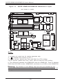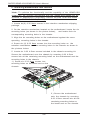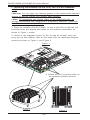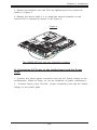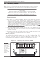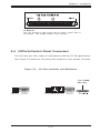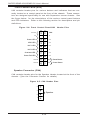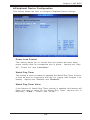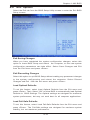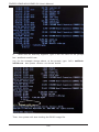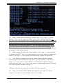
1
SUPER
SUPER i2DMR-8G2
SUPER i2DMR-iG2
USER’S MANUAL
Revision 1.0
®
The information in this User’s Manual has been carefully reviewed and is believed to be
accurate. The vendor assumes no responsibility for any inaccuracies that may be
contained in this document, makes no commitment to update or to keep current the
information in this manual, or to notify any person or organization of the updates.
Please Note: For the most up-to-date version of this manual, please
see our web site at www.supermicro.com.
SUPERMICRO COMPUTER reserves the right to make changes to the product described in
this manual at any time and without notice. This product, including software, if any, and
documentation may not, in whole or in part, be copied, photocopied, reproduced, translated
or reduced to any medium or machine without prior written consent.
IN NO EVENT WILL SUPERMICRO COMPUTER BE LIABLE FOR DIRECT, INDIRECT,
SPECIAL, INCIDENTAL, OR CONSEQUENTIAL DAMAGES ARISING FROM THE USE OR
INABILITY TO USE THIS PRODUCT OR DOCUMENTATION, EVEN IF ADVISED OF THE
POSSIBILITY OF SUCH DAMAGES. IN PARTICULAR, THE VENDOR SHALL NOT HAVE
LIABILITY FOR ANY HARDWARE, SOFTWARE, OR DATA STORED OR USED WITH THE
PRODUCT, INCLUDING THE COSTS OF REPAIRING, REPLACING, INTEGRATING,
INSTALLING OR RECOVERING SUCH HARDWARE, SOFTWARE, OR DATA.
Any disputes arising between manufacturer and customer shall be governed by the laws of
Santa Clara County in the State of California, USA. The State of California, County of
Santa Clara shall be the exclusive venue for the resolution of any such disputes.
Supermicro's total liability for all claims will not exceed the price paid for the hardware
product.
Unless you request and receive written permission from SUPER MICRO COMPUTER, you
may not copy any part of this document.
Information in this document is subject to change without notice. Other products and
companies referred to herein are trademarks or registered trademarks of their respective
companies or mark holders.
Copyright © 2003 by SUPER MICRO COMPUTER INC.
All rights reserved.
Printed in the United States of America
Preface
Preface
About This Manual
This manual is written for system integrators, PC technicians and
knowledgeable PC users. It provides information for the installation and use
of the SUPER i2DMR-8G2/i2DMR-iG2 motherboard. The SUPER i2DMR-8G2/
i2DMR-iG2 supports single or dual Intel Itanium ® 2 processors at a 400
MHz front side bus. Uniquely designed for demanding enterprise and technical applications, the Itanium 2 processor with 6 MB L3 Cache can provide
performance increases of up to 30 to 50 percent or more over the original
Intanium 2 processor. With its massive execution resources, 6.4GB/sec
system bus bandwidth and 1.5GHz core speed, the latest Itanium 2 processor offers
high-end reliability, flexibility, and scalability features for
business critical computing and the most data-intensive applications.
Please refer to the motherboard specifications pages on our web site (http:/
/www.supermicro.com/Product_page/product-m.htm) for updates on supported processors. This product is intended to be professionally installed.
Manual Organization
Chapter 1 begins with a checklist of what should be included in your
mainboard box, describes the features, specifications and performance of
the motherboard and provides detailed information about the chipset.
Chapter 2 begins with instructions on handling static-sensitive devices.
Read this chapter when you want to install the processor and DIMM memory
modules and when mounting the mainboard in the chassis. Also refer to
this chapter to connect the floppy and hard disk drives, SCSI drives, the IDE
interfaces, the parallel and serial ports, the keyboard and mouse, the power
supply and various control panel buttons and indicators.
If you encounter any problems, see Chapter 3, which describes troubleshooting procedures for the video, the memory and the setup configuration
stored in CMOS. For quick reference, a general FAQ [Frequently Asked
Questions] section is provided.
Chapter 4 includes an introduction to BIOS and provides detailed information on running the CMOS Setup utility.
Chapter 5 provides instructions on software,
Appendix A provides BIOS POST codes.
iii
drivers and OS installation.
SUPER i2DMR-8G2/i2DMR-iG2 User's Manual
Table of Contents
Preface
About This Manual ...................................................................................................... iii
Manual Organization ................................................................................................... iii
Chapter 1: Introduction
1-1
Overview ......................................................................................................... 1-1
Checklist .................................................................................................... 1-1
Contacting Supermicro ............................................................................ 1-2
Super i2DMR-8G2/i2DMR-iG2 Image ..................................................... 1-3
Super i2DMR-8G2/i2DMR-iG2 Layout .................................................... 1-4
Super i2DMR-8G2/i2DMR-iG2 Quick Reference .................................. 1-5
Motherboard Features ............................................................................. 1-6
Intel E7505 Chipset: System Block Diagram ........................................ 1-9
1-2
Chipset Overview ......................................................................................... 1-10
1-3
Special Features ........................................................................................... 1-11
1-4
PC Health Monitoring .................................................................................... 1-11
1-5
ACPI Features ............................................................................................... 1-12
Recovery from AC Power Loss ......................................................... 1-11
1-6
Power Supply ............................................................................................... 1-13
1-7
Super I/O ......................................................................................................... 1-13
Chapter 2: Installation
2-1
Static-Sensitive Devices ............................................................................... 2-1
Precautions ............................................................................................... 2-1
Unpacking .................................................................................................. 2-1
2-2
Itanium 2 Processor, Heatsink and Motherboard Installation .................. 2-2
2-3
Installing DIMMs ............................................................................................. 2-10
2-4
I/O Ports/Control Panel Connectors ........................................................... 2-11
2-5 Connecting Cables ........................................................................................ 2-13
EPS 12V Power Connector .................................................................. 2-13
Processor VRM Power Connectors ................................................... 2-13
Power Fail LED ....................................................................................... 2-13
NMI Button ................................................................................................ 2-13
Power LED .............................................................................................. 2-13
HDD LED .................................................................................................. 2-14
NIC1 LED ................................................................................................. 2-14
NIC2 LED ................................................................................................. 2-14
iv
Table of Contents
Overheat LED ......................................................................................... 2-14
Reset Button ........................................................................................... 2-15
Power Button ......................................................................................... 2-15
Universal Serial Bus (USB0/1, USB2/3) ............................................ 2-15
Front Panel Universal Serial Bus Headers (USB4/5) ...................... 2-16
Serial Ports ............................................................................................. 2-16
GLAN (Ethernet Port) ............................................................................. 2-16
Chassis Intrusion ................................................................................... 2-16
Fan Headers ........................................................................................... 2-17
Speaker Header ..................................................................................... 2-17
Wake-On-Ring ......................................................................................... 2-17
Power Fault Header ............................................................................... 2-18
SMB (System Management Bus) .......................................................... 2-18
Alarm Reset ............................................................................................. 2-18
SMB_Power Connector .......................................................................... 2-18
2-6
Jumper Settings ............................................................................................ 2-19
Explanation of Jumpers ........................................................................ 2-19
GLAN Enable/Disable ............................................................................. 2-19
CMOS Clear ............................................................................................. 2-19
Watch Dog Enable/Disable .................................................................... 2-20
VGA Enable/Disable ............................................................................... 2-20
SCSI Enable/Disable .............................................................................. 2-20
SCSI Termination Enable/Disable ........................................................ 2-20
Force-Power-On Control ....................................................................... 2-21
2-7
Onboard Indicators ...................................................................................... 2-21
2-8
Serial Port/Hard Disk Drive and SCSI Connections ................................ 2-22
GLAN LEDs .............................................................................................. 2-21
COM Port Connectors ........................................................................... 2-22
IDE Connectors ...................................................................................... 2-22
IPMI Connector ....................................................................................... 2-23
Ultra 320 SCSI Connectors .................................................................. 2-23
Chapter 3: Troubleshooting
3-1
Troubleshooting Procedures ........................................................................ 3-1
Before Power On .................................................................................... 3-1
No Power .................................................................................................. 3-1
No Video ................................................................................................... 3-2
Memory Errors .......................................................................................... 3-2
Losing the System’s Setup Configuration ........................................... 3-2
v
SUPER i2DMR-8G2/i2DMR-iG2 User's Manual
3-2
Technical Support Procedures .................................................................... 3-2
3-3
Frequently Asked Questions ........................................................................ 3-3
3-4
Returning Merchandise for Service ............................................................ 3-4
Chapter 4: BIOS
4-1
Introduction ....................................................................................................... 4-1
4-2
Main BIOS Setup .............................................................................................. 4-2
4-3
Advanced Setup .............................................................................................. 4-3
4-4
PCI/PnP Configuration ................................................................................... 4-11
4-5
Security Setup ............................................................................................... 4-12
4-6
Exit Options .................................................................................................... 4-13
Appendices:
Appendix A: BIOS POST Codes ............................................................................ A - 1
vi
Chapter 1: Introduction
1-1
Introduction
Chapter 1
Introduction
Overview
Checklist
Congratulations on purchasing your computer motherboard from an acknowledged leader in the industry. Supermicro boards are designed with
the utmost attention to detail to provide you with the highest standards in
quality and performance.
Check that the following items have all been included with your motherboard. If anything listed here is damaged or missing, contact your retailer.
One (1) Supermicro Itanium2 Mainboard
One (1) ribbon cable for IDE devices (CBL-036)
One (1) heatsink retention(w/Mounting screws) (SKT-0147-RM-IT2)
Two (2) Power Pods (-VRM mechanism for the Itanium 2 CPUs)
(VRM-0008)
One (1) Supermicro CD ROM
One (1) User's/BIOS Manual
1-1
SUPER i2DMR-8G2/i2DMR-iG2 User's Manual
Contacting Supermicro
Introduction
Headquarters
Address:
Tel:
Fax:
Email:
Web Site:
SuperMicro Computer, Inc.
980 Rock Ave.
San Jose, CA 95131 U.S.A.
+1 (408) 503-8000
+1 (408) 503-8008
[email protected] (General Information)
[email protected] (Technical Support)
www.supermicro.com
Europe
Address:
Tel:
Fax:
Email:
SuperMicro Computer B.V.
Het Sterrenbeeld 28, 5215 ML
's-Hertogenbosch, The Netherlands
+31 (0) 73-6400390
+31 (0) 73-6416525
[email protected] (General Information)
[email protected] (Technical Support)
[email protected] (RMA Dept.)
Asia-Pacific
Address:
SuperMicro, Taiwan
D5, 4F, No. 16 Chien-Ba Road
Chung-Ho 235, Taipei Hsien, Taiwan, R.O.C.
Tel:
+886-(2) 8226-3990
Fax:
+886-(2) 8226-3991
Web Site:
www.supermicro.com.tw
Technical Support:
Email:
[email protected]
Tel:
+886-2-8228-1366, ext.132 or 139
1-2
Chapter 1: Introduction
Introduction
Figure 1-1. SUPER i2DMR-8G2/i2DMR-iG2 Image
Note: The difference between the i2DMR-8G2 and the i2DMR-iG2:
There is Adaptec 7902 Ultra 320 SCSI on the i2DMR-8G2, and there is
no SCSI on the i2DMR-iG2.
1-3
SUPER i2DMR-8G2/i2DMR-iG2 User's Manual
Figure 1-2.
SUPER i2DMR-8G2/i2DMR-iG2 Motherboard Layout
(not drawn to scale)
1
J16
5
DIMM5
J15
DIMM2
J13
DIMM6
J14
MRH-D
J6
J1
J5
J27
SMB
PW
PWR Pod
(VRM)
J30
3
7
J12
PW Pod
(VRM)(top)
4
DIMM4
J9
ATI-RAGE
_XL(bottom)
DIMM8
J10
WD
Reset
VGA
Enabled
JV1
PCI-X (256 Pin)
J19
SNC
(North
Bridge)
Battery
SCSI
J A 1 Enable
7902
SCSI
Controller
J3
SCSI Ch.B
Fan8
C N 1 Termination
P64H
SMB
J22
IPMI
S6
S5
S4
BIOS4BIOS5 BIOS6
J35
CN3
SCSI Ch.A
Termination
J7
GLAN
GLAN
Enable
CTLR
82546
J26
SIOH
ICH4
SPKR
S3
S2
S1
BIOS3 BIOS2 BIOS1
SCSI A J 1 8 C N 4
Speaker
(South
Bridge)
J31
J37
MRH-D
J29
Fan4
Fan2
24-Pin PW2
J36
J L A N 1J L A N 2
MRH-D
CPU2
IDE2
IDE1
COM2
J38
J4
LAN1
USB2/3
J11
LAN2
CPU1
MRH-D
DIMM7
VGA
ITP
Connector
WOR
DIMM3
J2
Fan3 Fan1 J 3 4
U62 CN5 J 2 8
P W R Alarm
Fault Reset
8
COM1
USB0/1 6 2
DIMM1
SCSI B
Introduction
J 2 0 24Pin PW1
Fan7
S I/O
Front Panel
JBT1
CTLR
CLR
J25
U66
C
h
a
s
s
i
s
J21
CMOS
USB4/5
Intrusion
Fan5
Fan6
Notes:
1. Jumpers not noted are for testing purposes only.
2. "
" indicates the location of Pin 1.
3. For 1U servers, please use Fan1 and Fan2 for CPU cooling.
For 2U servers, please use Fan1, Fan2, Fan3 & Fan4 for CPU cooling.
4. The difference between the i2DMR-8G2 and the i2DMR-iG2: There is Adaptec
7902 Ultra 320 SCSI on the i2DMR-8G2, and there is no SCSI on the i2DMR-iG2.
Warning:
The heatsink on the MRH-D chip has been pre-installed by the
manufacturer. Please do not touch it. Turning the heatsink in a wrong way will
damage it and will void the manufacturer's warranty.
1-4
Chapter 1: Introduction
Quick Reference (i2DMR-8G2/i2DMR-iG2)
Jumper
Description
CN1, CN3
SCSI Cha.A(CN3)/Cha.B(CN1)Termination (*Note4)
Open (Enabled)
GLAN Enable/Disable
Pins 1-2 (Enabled)
Watch Dog
Pins 1-2 (Reset)
CMOS Clear
(*Note 4)
SCSI Enable/Disable (*Note5)
Pins 1-2 (Enabled)
VGA Enable/Disable
Pins 1-2 (Enabled)
J7
J31
JBT1
JA1
JV1
Connector
Default Setting
Description
Alarm Reset (CN5)
Fail Alarm Reset Switch
BIOS#1-6 (S1-6)
BIOS#1-6
Chassis Intrusion (J25) Chassis Intrusion Header
COM1 (J5), COM2 (J38)COM1 & COM2 Serial Port and Header
CPU1(J30), CPU2 (J29) CPU 1/2 Sockets
DIMM#1-#8 (J9-J16)
Memory (RAM) Slots:DIMM1(J16),DIMM2 (J13),
DIMM3 (J11), DIMM4(J9), DIMM5 (J15),
DIMM6 (J14), DIMM7 (J12), DIMM8 (J10)(*Note 2)
Fan Headers (1-8)
Fan1-Fan8 Headers.
Front Panel CTRL (U66)Front Control Panel Connector (*Note 3)
IDE1 (J37), IDE2 (J35) IDE1/2 Hard Disk Drive Connectors
IPMI (J26)
IPMI 1.5, 2.0 Connector
ITP (J34)
ITP Connector (For Testing Only)
PCI-X (J19)
PCI-X Bus 256-Pin Slot
PWR1(J20), PWR2(J36) Power1 and Power2 24-Pin-Connectors
PWR Fault (U62)
Power Fault Connector
Speaker (CN4)
Speaker Connector(*Note3)
SMB (J22)
System Management Bus Connector
SMB_Power (J27)
System Management Bus Power Header
SCSI A&B (J18,J3)
SCSI A Connector(J18), SCSI B Connector(J3)
(*Note 4)
USB 0/1(J1),USB2/3(J4)Back Panel Universal Serial Ports
USB4/5 (J21)
Front Panel USB Headers
VGA Connector (J2)
VGA Connector
WOR (J6)
Wake-on-Ring Header
(*Notes: 1. For 1U servers, use Fan1&Fan2 for CPU cooling. For 2U
servers, use Fan1, Fan2, Fan3, Fan4 for CPU cooling.
2. See Chapter 2 for Memory Installation Instructions.
3. See Chapter 2 for detailed information.
4. For i2DMR-8G2 only)
1-5
Introduction
(*Please refer to Chapter 2 for pin definitions and detailed
information.)
SUPER i2DMR-8G2/i2DMR-iG2 User's Manual
Motherboard Features
CPU
Introduction
• Two Intel Itanium 2 Processor sockets and power pod sites support:
Single or dual Intel ® Itanium 2TM processors at a 400 MHz front side
bus (system) speed up to 1.5 GHz, 6MB L3 Cache. (*Notes: Please refer to
the support section of our web site for a complete listing of supported processors (http://
www.supermicro.com/TECHSUPPORT/TechSupport.htm)
Chipset
• Intel E8870 chipset
• SNC-M(Scalable Node Controller) of the E8870 chipset
• SIOH (Server I/O Hub) of the E8870 chipset
• Four Memory Repeater Hubs-DDR(MRH-D) components of the E8870
chipset
• One P64H2 PCI-X bridge component
• Network Interface Controller (NIC) 10/100/1000 Ethernet controller that
provides two GLAN ports
• One I/O Control Hub 4 (ICH 4) component:
-6 USB ports (4 at the rear, 2 headers),
-2 IDE bus routed through the flex cable to the peripheral board
supporting one ATA100 master device
• 6-MB Flash using 6 Firmware Hub (FWH) components
Memory
• Eight 184-pin DIMM sockets supporting up to 16 GB Registered ECC
DDR-200 (PC1600) SDRAM (utilizing DDR266 operating at 200 MHz)
Note: 4-way Interleaved memory; requires at least 4 pieces of identical memory modules to be
installed at the same time. See Section 2-3 for details.
Expansion Slots
*For 1U Server:
• One 64-bit PCI-X 100 slot(*For i2DMR-8G2), One 64-bit PCI-X 133 slot
(*For i2DMR-iG2)
*For 2U servers: it can support up to 3 PCI-X slots:
• One 64-bit PCI-X 100 slot(*For i2DMR-8G2), One 64-bit PCI-X 133 slot
(*For i2DMR-iG2)
• Two 64-bit PCI-X 133 slots
1-6
Chapter 1: Introduction
BIOS
• 6-MB AMI ® Flash BIOS (total of 6 BIOS chips)
• PCI 2.2, BIOS chips, Plug and Play (PnP), SMBIOS 2.3
PC Health Monitoring
• Onboard voltage monitors for CPU cores, system voltages
• Fan status monitor with firmware/software on/off Speed control
• CPU/chassis temperature monitors
• CPU fan speed control
• CPU slow-down on temperature overheat
• CPU thermal trip support for processor protection, +5V standby alert
LED
• Power-up mode control for recovery from AC power loss
• Auto-switching for VRMs
• System overheat LED and control
• Chassis intrusion detection
Thermal Control
• Overheat LED Indication
• Thermal control
• 8 Fan connectors
ACPI Features
• Internal/external modem ring-On
• Control of power-on mode for recovery of power loss
• CPU thermal trip support for processor protection
• Main switch override mechanism
Onboard I/O
• Adaptec 7902 Dual Channel Ultra 320 SCSI (*i2DMR-8G2 only)
• One IPMI 1.5 & 2.0 socket
• One Intel 82546 Gigabit Ethernet controller which supports two GLAN
ports
• Onboard ATI Rage XL 8MB PCI Graphic Control
• Super I/O (W83627)
• Winbond Hardware Monitoring IC (W82791)
• Low Pin Count(LPC) Super I/O with one external serial port and an
internal header supporting 2 Fast UART 16550A compatible serial ports
• Dual ATA100 channels
1-7
Introduction
• ACPI (limited)
SUPER i2DMR-8G2/i2DMR-iG2 User's Manual
• Up to 6 USB 2.0 (4 ports and 2 headers)
Other
• Internal/external modem ring-on
Introduction
• Console redirection
• Watch Dog & Supero DoctorIII for system manageability
• In-Target Probe (ITP) port
• Joint Test Action Group (JTAG)/boundary scan support through ITP or
external source
• Core ratio programming via the SNC-M
• Clock Buffering
• Embedded D2D converters
•
I 2 C Logic: Includes:
-Field Replacement Unit (FRU) device ID that is accessed through a
private I2 C bus
-Temperature sensors
CD ROM
• BIOS flash upgrade utility and device drivers
Dimensions
• ATX Ext. 12.25" x 13.05" (311.2mm x 331.5 mm)
1-8
Processor 1
Introduction
Chapter 1: Introduction
Processor 2
16GB Max. DDR200
MRH_D
MRH_D
LPC Bus
IDE1
USB #
0,1,2,
3,4,5
UDMA100
UDMA100
VGA
SNC
IDE2
MRH_D
3x1MB
FWH
PCI32bit
USB 2.0
MRH_D
Hublink0
ICH4
SIOH
Hublink1
P64H2
82546
PCIX-133 2GLAN
Ports
PCIX-100
Hublink2
LPC Bus
DIMM1
DIMM5
DIMM2
DIMM6
DIMM3
DIMM7
DIMM4
DIMM8
VXB Slot
LPC 3x1MB
Super
FWH
I/O
IPMI
SCSI 7902
P64H2
COM1
Figure 1-9.
COM2
(*i2DMR8G2 Only)
PCI Slot
1U Riser
Card
(*For 1U only)
PCI Slot 1
PCI Slot 2
PCI Slot 3
2U Riser Card (*For 2U only)
Block Diagram of the i2DMR-8G2/i2DMR-iG2 Motherboard
Note: This is a general block diagram. Please see the previous Motherboard
Features pages for details on the features of the motherboard.
1-9
SUPER i2DMR-8G2/i2DMR-iG2 User's Manual
1-2
Chipset Overview
Introduction
Built upon the functionality and the capability of the Intel E8870 (870)
chipset, the i2DMR-8G2/i2DMR-iG2 motherboard provides the performance
and feature set required for high-end server platforms with configuration
options optimized for communications, presentation, storage, computation or
database applications. The Intel E8870 chipset consists of the following
four primary components: the Scalable Node Controller (SNC), Server I/O
Hub (SIOH), the Memory Repeater Hub for Synchronous Double Data Rate
Memory(MRH_D) and Scalability Port Switch (SPS) (*Note Below). Complementary components include the I/O Hub Controller (Intel ICH4), the Firmware Hub (FWH), and the PCI Bus Bridge (P64H2).
The major bus groups are:
Processor system bus: supporting up to two processors and one Scalable
Node Controller (SNC), with a maximum operating frequency of 200
MHz@400 MT/s.
Rambus and SNC Interface: the Interconnection between the SNC and
Memory Repeater Hub (MRH-D), operating at a maximum frequency of 400
MHz.
Synchronous DDR Interface: interface between the MRH-D and up to four
DIMM sockets, operating at the operating clock frequency of 100 MHz per
branch channel.
Scalability Port (SP) Interface: a 400MHz, double-pumped, simultaneous bidirectional signaling (SBD) interface.
Hub Interface 2.0: interface between the SIOH and the P64H2 using 266
MHz strobes on a 16-bit wide data bus.
Hub Interface 1.5: interface between the SIOH and the ICH4 using 133 MHz
strobes on a 8-bit wide data bus.
Local Firmware Hub (LPC): Interface between the SNC and local firmware.
System Management Bus (SMBus): a subset of the I 2C serial bus integrated
into the SNC, SPS, and SIOH.
(*Note: The Scalability Port Switch-SPS is not used in the i2DMR-8G2/iG2.)
1-10
Chapter 1: Introduction
Complementary Components include:
The ICH4 is the fourth-generation I/O Controller Hub subsystem that integrates many of the input/output functions of the chipset, including a twochannel ATA100 Bus Master IDE controller. The ICH4 also interfaces with
PCI and various communications ports. Nearly all communications between
the GMCH and the ICH4 takes place over the hub Interface, which is a 66
MHz/266 MB/s bus.
P64H2 PCI-X Hub (P64H2)
The P64H2 PCI-X Hub provides a 16-bit connection to the MCH for highperformance I/O capability and two 64-bit PCI-X interfaces.
1-3
Special Features
Recovery from AC Power Loss
BIOS provides a setting for you to determine how the system will respond
when AC power is lost and then restored to the system. You can choose
for the system to remain powered off (in which case you must hit the
power switch to turn it back on) or for it to automatically return to a poweron state. See the Power Lost Control setting in the Advanced BIOS Setup
section (Peripheral Device Configuration) to change this setting. The default setting is Last State.
1-4
PC Health Monitoring
This section describes the PC health monitoring features of the SUPER
i2DMR-8G2/i2DMR-iG2. All have an onboard System Hardware Monitor chip
that supports PC health monitoring.
Fan Status Monitor with Firmware/Software On/Off Control
The PC health monitor can check the RPM status of the cooling fans. The
onboard 3-pin chassis fans are controlled by the power management functions.
1-11
Introduction
I/O Controller Hub (ICH4)
SUPER i2DMR-8G2/i2DMR-iG2 User's Manual
CPU Overheat LED and Control
Introduction
This feature is available when the user enables the CPU overheat warning
function in the BIOS. This allows the user to define an overheat temperature. When this temperature is exceeded, fans will speed up, and the
warning LED is triggered.
Auto-Switching Voltage Regulator for the CPU Core
The auto-switching voltage regulator for the CPU core can support up to
20A current and auto-sense voltage IDs ranging from 1.1V to 1.5V (*supported by VRMs only). This will allow the regulator to run cooler and thus
make the system more stable.
1-5 ACPI Features
External Modem Ring-On
Wake-up events can be triggered by a device such as the external modem
ringing when the system is in the SoftOff state. Note that external modem
ring-on can only be used with an SSI compliant power supply.
1-6 Power Supply
As with all computer products, a stable power source is necessary for
proper and reliable operation. It is even more important for processors that
have high CPU clock rates.
The SUPER i2DMR-8G2/i2DMR-iG2 requires a 24-pin connector and two 4pin 12V/15A connectors for CPU VRMs. Although most power supplies
generally meet the specifications required by the CPU, some are inadequate.
You should use one that will supply at least 500W of power, and an even
higher wattage power supply is recommended for high-load configurations.
Also your power supply must supply 2A for the Ethernet ports and the
E8870 chipset.
It is strongly recommended that you use a high quality power supply that
meets SSI EPS 12V 1U 500W PS Specification. To verify the status of SSI
compliance, please visit the web site at http://www.ssiforum.org/. Additionally, in areas where noisy power transmission is present, you may
choose to install a line filter to shield the computer from noise. It is recom-
1-12
Chapter 1: Introduction
mended that you also install a power surge protector to help avoid problems
1-7 Super I/O
The disk drive adapter functions of the Super I/O provides two high-speed,
16550 compatible serial communication ports (UARTs). Each UART includes
a 16-byte send/receive FIFO, a programmable baud rate generator, complete modem control capability and a processor interrupt system. Both
UARTs provide legacy speed with baud rate of up to 115.2 Kbps as well as
an advanced speed with baud rates of 250 K, 500 K, or 1 Mb/s, which
support higher speed modems.
1-13
Introduction
caused by power surges.
SUPER i2DMR-8G2/i2DMR-iG2 User's Manual
Notes
Introduction
1-14
Chapter 2: Installation
Chapter 2
Installation
2-1
Static-Sensitive Devices
Electric-Static-Discharge (ESD) can damage electronic components. To prevent damage to your system board, it is important to handle it very carefully.
The following measures are generally sufficient to protect your equipment
from ESD.
Precautions
• Use a grounded wrist strap designed to prevent static discharge.
• Touch a grounded metal object before removing the board from the antistatic bag.
• Handle the board by its edges only; do not touch its components, peripheral chips, memory modules or gold contacts.
• When handling chips or modules, avoid touching their pins.
• Put the motherboard and peripherals back into their antistatic bags when
not in use.
• For grounding purposes, make sure your computer chassis provides excellent conductivity between the power supply, the case, the mounting
fasteners and the motherboard.
Unpacking
The motherboard is shipped in antistatic packaging to avoid static damage.
When unpacking the board, make sure the person handling it is static protected.
2-1
SUPER i2DMR-8G2/i2DMR-iG2 User's Manual
2-2
Itanium2 Processor and Heatsink Installation
!
When handling the processor package, avoid placing direct
pressure on the label area of the fan. Also, do not place the
motherboard on a conductive surface, which can damage the
BIOS battery and prevent the system from booting up.
IMPORTANT: Always connect the power cord last and always remove it
before adding, removing or changing any hardware components. Make
sure that you install the processor into the CPU socket before you install
the CPU heat sink.
Note: To optimize the functionality and capability of the i2DMR-8G2/
i2DMR-iG2, we recommend that i2DMR-8G2/i2DMR-iG2 be installed in
Supermicro chassis only.
Warning:
The heatsink on the MRH-D chip has been pre-installed by the
manufacturer. Please do not touch it. Turning the heatsink in a wrong
way will damage it and will void the manufacturer's warranty.
A. Locating the components included in the shipping package
Locate the following components, which are included in the shipping
package.
Two (2) Power Pod (VRM-0008)
Two (2 )Itanium 2 Heatsinks (SNK-0046)(*not included; sold separately)
One Package of Retention Mechanism, including:
One (1) Retention Mechanism (SKT-0147-RM-IT2)
Eight (8) M3 5mm Screws
Three (3) 6-32 4.5mm Screws
Six (6) 6-32 8mm Screws
One (1) M2.5 Hex Key (*for CPU removal and locking)
2-2
Chapter 2: Installation
B. Installing the Heatsink Retention Mechanism on the
Motherboard
1. Place the retention mechanism (P/N SKT-0147-RM-IT2) on the motherboard as shown in the picture below:
2. Secure the retention mechanism onto the motherboard by screwing
three (3) 6-32 4.5MM screws into the mounting holes on the back of the
motherboard.
1.) Place the retention
mechanism on the
motherboard
2.) Screw in three 6-32
4.5mm screws on the
reverse side of the
motherboard
2-3
SUPER i2DMR-8G2/i2DMR-iG2 User's Manual
C. Installing Motherboard into chassis
*Note: To optimize the functionality and the capability of the i2DMR-8G2/
i2DMR-iG2, we strongly recommend that the i2DMR-8G2/i2DMR-iG2 be
installed in Supermicro's proprietary chassis only-the SC813HS-500W
(*for 1 U), SC823HS-500W (*for 2U).
1. Locate six(6) 6-32 8mm screws in the retention mechanism shipping
package.
2. On the retention mechanism located on the motherboard, locate the six
mounting holes (as shown in the picture below), and locate their six
corresponding mounting holes in the chassis.
3. Align the six mounting holes on the motherboard against the corresponding mounting holes in the chassis.
4. Screw six (6) 6-32 8mm screws into the mounting holes on the
retention mechanism and the mounting holes in the chassis as shown in
the pictures below.
5. Locate six 6-32 4.5mm screws included in the chassis mounting kit.
Secure the motherboard onto the chassis by screwing 6-32 4.5mm
screws into all the remaining mounting holes on the motherboard and the
mounting holes in the chassis.
1.) Screw six 6-32 8mm screws into
mounting holes on the board and on the
chassis.
2.) Secure the motherboard
onto the chassis by screwing
6-32 4.5mm screws into all the
remaining mounting holes on
the board and on the chassis.
2-4
Chapter 2: Installation
D. Installing and securing the Itanium 2 CPU onto the
motherboard
1. Insert the Itanium 2 CPU into the CPU1 Socket. Make sure that CPU Pin
1 is aligned with the cut angle of the CPU socket. (*See Note) as shown
in the picture below:
CPU1 Socket
Itanium 2 CPU
2. Use an M2.5 Hex Key to secure the Itanium 2 CPU as shown in the
picture below:
Use an M 2.5 Hex Key
to secure the CPU.
3. Repeat Step 1 and Step 2 to install the second Itanium2 CPU as
needed. (*See Note)
(*Notes: Please refer to Chapter 1 Page 1-4 for the locations of CPU1
Socket and CPU2 Socket.)
2-5
SUPER i2DMR-8G2/i2DMR-iG2 User's Manual
E. Installing and securing the Power Pod onto the Itanium 2
CPU
(*Notes: 1.The CPU Power Pod is a VRM mechanism specially designed
for the Itanium 2 processors.)
1. Locate the opening slot on the CPU Power Pod, and align the opening
slot with the Itanium2 CPU installed on the motherboard.
2. Carefully push the Edge Connector of the Power Pod toward the CPU
until the Signal Pins on both edges of the CPU are fully seated in the
Edge Connector and you hear a click. (*Warning: Unless the Signal
Pins of the CPU are fully seated in the Edge Connector of the
Power Pod, the CPU will not function correctly!!)
1.) Align the opening slot of
the CPU Power Pod with the
CPU.
Opening slot of the
Power Pod
CPU Power Pod
2.) Push the Edge
Connector toward the
CPU until you hear a
click and the Signal
Pins are fully seated in
the Edge Connector.
*Edge Connector
Itanium2 CPU
*Signal Pins
2-6
Chapter 2: Installation
3. Locate four(4) M3 screws in the VRM-008 package. Secure the Power
Pod onto the motherboard with four(4) M3 screws as shown in the
picture below:
3.) Secure the Power Pod onto the
motherboard with four(4) M3 screws.
4. Repeat Step 1 and Step 2 to install the second Itanium2 CPU (w/Power
Pod) as needed.
Dual Itanium 2 Processors (w/ Power Pods installed)
2-7
SUPER i2DMR-8G2/i2DMR-iG2 User's Manual
F. Installing the Heatsink on the CPU(*for CPU w/o Heatsink
only)
(*Warning: Do not apply any thermal grease to the heatsink-the required
amount of thermal grease has already been applied.)
(*Note: To maximizing the cooling effect of the i2DMR-8G2/iG2, we
strongly recommend that Supermicro's proprietary heatsinks (SNK-046)
be used with the Itanium 2 CPUs.)
1. Place the heatsink (P/N SKT-0046) on top of the CPU so that the four
mounting holes are aligned with those on the retention mechanism as
shown in Figure 1 below.
2. Screw in two diagonal screws (ie the #1 and #2 screws) until just
snug (do not fully tighten), then do the same with the remaining diagonal
screws as shown in Figure 2 and Figure 3.
Figure 1
1) Locate the four mounting holes on
the heatsink retention module.
Figure 2
Figure 3
2-8
Chapter 2: Installation
3. Secure the heatsink onto the CPU by tightening all four screws as
shown in Figure 3.
4. Repeat the above steps 1-3 to install the second heatsink on the
second CPU if needed as shown in the Figure 4.
Figure 4
The i2DMR-8G2/iG2 with two heatsinks installed
G. Connecting AC Power to the motherboard and the Power
Pods
1. Connect the 24-pin power connector from the AC Power Supply to the
motherboard. (Refer to Page 1-4 for the locations of power connectors.)
2. Connect two(2) 4-pin 12V/15A
Supply to the power pods.
power connectors from the AC Power
2-9
SUPER i2DMR-8G2/i2DMR-iG2 User's Manual
2-3
Installing DIMMs
Note: Check the Supermicro web site for recommended memory modules:
http://www.supermicro.com/TECHSUPPORT/FAQs/Memory_vendors.htm
CAUTION
Exercise extreme care when installing or removing DIMM
modules to prevent any possible damage. Also note that the
memory is interleaved to improve performance (see step 1).
DIMM Installation
1. Insert either 4 or 8 identical DIMMs (-Memory of the same size and type)
into the memory slots, starting with DIMM1(J16), DIMM2(J13),
DIMM3(J11) & DIMM4(J9). (DIMM1-DIMM4 are the DIMM sockets colored
in blue.) If four more DIMMs are used, insert DIMM5(J15), DIMM6(J14),
DIMM7(J12) and DIMM8(J10) into the slots. (DIMM5-DIMM8 are the DIMM
sockets colored in black.) The memory scheme is interleaved, and you
must install four modules at a time, beginning with DIMM1, DIMM2,
DIMM3, DIMM4 (blue slots).
2. Insert each DIMM module vertically into its slot. Pay attention to the
notch along the bottom of the module to prevent inserting the DIMM
module incorrectly.
3. Gently press down on the DIMM module until it snaps into place in the
slot. Repeat for all modules (see step 1 above).
Memory Support
The i2DMR-8G2/i2DMR-iG2 supports up to 16 GB of buffered, Reg. ECC
DDR-200 (utilizing DDR 266 memory operating at DDR 200). All
motherboards were designed to support 2 GB modules in each slot.
Figure 2-2.
Installing and Removing DIMMs
To Install:
Insert module
vertically and
press down
until it snaps
into place.
Pay attention
to the
alignment
notch at the
bottom.
2-10
Chapter 2: Installation
To Remove:
Use your thumbs to gently push near the edge of both ends of
the module. This should release it from the slot.
2-4
I/OPorts/Control Panel Connectors
The I/O ports are color coded in conformance with the PC 99 specification.
See Figure 2-3 below for the colors and locations of the various I/O ports.
Figure 2-3.
I/O Port Locations and Definitions
(*For i2DMR8G2 only)
2-11
SUPER i2DMR-8G2/i2DMR-iG2 User's Manual
Front Control Panel (U66)
U66 contains header pins for various buttons and indicators that are normally located on a control panel at the front of the chassis. These connectors are designed specifically for use with Supermicro server chassis. See
the figure below for the descriptions of the various control panel buttons
and LED indicators. Refer to the following section for descriptions and pin
definitions.
Figure 2-4: Front Control Panel-U66
20
Header Pins
19
Ground
NMI
X
X
Power LED
Vcc
HDD LED
Vcc
NIC1 LED
Vcc
NIC2 LED
X
Overheat LED
Vcc
Power Fail LED
Vcc
Ground
Ground
2
Reset
Reset Button
Pwr
Power Button
1
Speaker Connector (CN4)
CN4 contains header pins for the Speaker Header located at the front of the
chassis. (*See the Connector Section for details.)
Figure 2-5: CN4 Header Pins
4
3
Speaker
2
1
2-12
Chapter 2: Installation
2-5
Connecting Cables
EPS 12V Power
Connector
There are two 24-pin main power
supply connector(J20, J36) on the
i2DMR-8G2/i2DMR-iG2. These
power connectors meet the SSI
EPS 12V specification. (*Only one
main power supply is needed.)
See the table on the right for pin
definitions.
EPS 12V Power Supply 24-pin Connectors:
J20,J36--Pin Definitions
Pin Number Definition Pin Number Definition
1
+3.3V
13
+3.3V
2
+3.3V
14
-12V
3
COM
15
COM
4
+5V
16
PS_ON#
5
COM
17
COM
6
+5V
18
COM
7
COM
19
COM
8
PWR_OK
20
Res(NC)
9
5VSB
21
+5V
10
+12V
22
+5V
11
+12V
23
+5V
12
+3.3V
24
COM
Processor Power
Connectors
EPS 12V Power Supply 4-pin Connectors:
Pin Definitions
In addition to the primary SSI
EPS12V 24-pin power connectors
(above), there are also two 4-pin
EPS 12V/15A power connectors to
be connected to CPU Power Pods
(VRMs). Refer to the table on the
right for pin definitions.
Pin
Pin
Number Definition Number Definition
1
Thru
2
Ground
3
Thru
4
+12V
Power Fail LED Pin
Definitions
(U66)
Power Fail LED
The Power Fail LED connection is
located on pins 5 and 6 of U66.
Refer to the table on the right for
pin definitions.
Pin
Number Definition
Vcc
5
6
GND
NMI Button
The non-maskable interrupt button
header is located on pins 19 and
20 of U66. Refer to the table on
the right for pin definitions.
NMI Button Pin
Definitions (U66)
Pin
Definition
Number
Control
19
Ground
20
Power LED
The Power LED connection is located on pins 15 and 16 of U66.
Refer to the table on the right for
pin definitions.
2-13
PWR_LED Pin Definitions
(U66)
Pin
Definition
Number
Vcc
15
Control
16
SUPER i2DMR-8G2/i2DMR-iG2 User's Manual
HDD LED
The HDD LED connection is located
on pins 13 and 14 of U66. Attach
the hard drive LED cable here to
display disk activity (for any hard
drives on the system, including
SCSI, Serial ATA and IDE). See
the table on the right for pin definitions.
HDD LED Pin
Definitions
(U66)
Pin
Number Definition
13
Vcc
14
HD Active
NIC1 LED
The NIC (Network Interface Controller) LED connection for the
GLAN port is located on pins 11
and 12 of U66. Attach the NIC LED
cable to display network activity.
Refer to the table on the right for
pin definitions.
NIC LED Pin
Definitions
(U66)
Pin
Number Definition
11
Vcc
12
GND
NIC2 LED
The NIC (Network Interface Controller) LED connection for the
GLAN port is located on pins 9 and
10 of U66. Attach the NIC LED
cable to display network activity.
Refer to the table on the right for
pin definitions.
NIC 2 LED Pin
Definitions
(U66)
Pin
Number Definition
9
Vcc
10
GND
Overheat LED (OH)
Connect an LED to the OH connection on pins 7 and 8 of U66 to provide advanced warning of chassis
overheating. Refer to the table on
the right for pin definitions.
2-14
Overheat (OH) LED
Pin Definitions
(U66)
Pin
Number Definition
7
Vcc
8
GND
Chapter 2: Installation
Reset Button
Reset Pin
Definitions
(U66)
The Reset Button connection is located on pins 3 and 4 of U66. Attach it to the hardware reset
switch on the computer case.
Refer to the table on the right for
pin definitions.
Pin
Number Definition
Reset
3
Ground
4
Power Button
Power Butto n
Connector
Pin Definitions
(JF2)
The Power Button connection is
located on pins 1 and 2 of U66.
Momentarily contacting both pins
will power on/off the system. This
button can also be configured to
function as a suspend button
(with a setting in BIOS - see Chapter 4). To turn off the power
when set to suspend mode, depress the button for at least 4
seconds. Refer to the table on the
right for pin definitions.
Universal Serial Bus
(USB0/1, USB2/3)
Pin
Number Definition
PW _O N
1
Ground
2
Universal Serial Bus Pin Definitions
USB0(J1), USB2(J4) USB1(J1), USB3(J4)
Two USB 2.0 ports:USB0/1 (J1)
and USB2/3 (J4) are located on
the back panel. USB0 is the bottom
connector and USB1 is the top
connector of J1. USB2 is the bottom connector and USB3 is the top
connector of J4. See the table on
the right for pin definitions.
2-15
Pin
Number
1
2
3
4
5
Definition
+5V
P0P0+
Ground
N/A
Pin
Number
1
2
3
4
5
Definition
+5V
P0P0+
Ground
Key
SUPER i2DMR-8G2/i2DMR-iG2 User's Manual
Front Panel Universal
Serial Bus Header
Front Panel Universal Serial Bus(J21) Pin
Definitions
FPUSB4/FPUSB5
Pin
Number
1
2
3
4
5
Two extra USB headers (USB4/
USB5) (J21) can be used for front
side USB access. You will need a
USB cable to use either connection. Refer to the tables on the
right for pin definitions.
Definition
+5V
P0P0+
Ground
Key
Serial Ports
There are two Serial Ports on the
i2DMR-8G2/i2DMR-iG2 The COM1
serial port (J5) is located under
the parallel port (see Figure 2-3)
and the COM2 header (J38) is located next to the GLAN1 port.
See the tables on the right for pin
definitions.
Serial Ports Pin Definitions
(COM1-J5, COM2-J38)
Pin Number
1
2
3
4
5
Definition Pin Number
DCD
6
Serial In
7
Serial Out
8
DTR
9
Ground
GLAN Ports (Ethernet
Ports)
Two G-bit Ethernet ports (designated LAN1, LAN2) are located
between Keyboard/Mouse connectors and the VGA connector.
This port accepts RJ45 type
cables.
Chassis Intrusion
A Chassis Intrusion header (J25)
is located below the S I/O chip.
Attach the appropriate cable to inform you of a chassis intrusion.
See the tables on the right for pin
definitions.
2-16
Chassis Intrusion
Pin Definitions
(J25)
Pin
Number Definition
1
Instrusion
2
Ground
Definition
DSR
RTS
CTS
RI
Chapter 2: Installation
Fan Headers
The i2DMR-8G2/i2DMR-iG2 has
eight fan headers. See the table
on the right for pin definitions.
Fan H eader Pin Definitions
Pin
Number
1
2
3
Definition
Ground (black)
+12V (red)
Tachometer
Caution: Fan headers are DC
power.
Speaker Header
CN4
The Speaker header is located on
CN4. See the table on the right for
speaker pin definitions. Note: The
speaker connector pins are for
use with an external speaker. If
you wish to use the onboard
speaker, you should close pins 3,
and 4 with a jumper to enable it.
4
3
Speaker
2
1
Wake-On-Ring
The Wake-On-Ring header is designated JWOR(J6). This function
allows your computer to receive
and "wake-up" by an incoming call
to the modem when in suspend
state. See the table on the right
for pin definitions. You must have
a Wake-On-Ring card and cable to
use this feature.
2-17
Wake-on-Ring
Pin Definitions
(JWOR-J6)
Pin
Number Definition
1
Ground
2
Wake-up
SUPER i2DMR-8G2/i2DMR-iG2 User's Manual
Power Fault
Connect a cable from your power
supply to the U62 header to provide warning of power supply failure.
This warning signal is
passed through the PWR_LED pin
on U66 to indicate of a power failure on the chassis. See the table
on the right for pin definitions.
Power Fault
Pin Definitions (U62)
Pin
Number
1
2
3
4
Definition
P/S 1 Fail Signal
P/S 2 Fail Signal
P/S 3 Fail Signal
Reset (from MB)
Note: This feature is only available when using
redundant Supermicro power supplies.
SMB Header
Pin Definitions (J22)
SMB
A System Management Bus
header is located at J22. Connect
the appropriate cable here to utilize SMB on your system.
Pin
Number
1
2
3
4
Definition
Data
Ground
Clock
No Connection
Alarm Reset
The system will notify you in the
event of a power supply failure.
This feature assumes that Supermicro redundant power supply
units are installed in the chassis.
If you only have a single power
supply installed, you should disable this (the default setting) with
(CN5) to prevent false alarms.
See the table on the right for
jumper settings. (The Alarm Re-
Alarm Reset Jumper
Settings
(CN5)
Jumper
Position
Open
Closed
Definition
Enabled
Disabled
set header is located next to
the PWR Fault header and
close to Fan3.)
SMB Power (I2 C)
Connector
SMB PWR
Pin Definitions (J27)
I2 C Connector (J27), located between the PWR ForceOn Header
and the PWR Fault header, monitors the status of PWR Supply,
Fan and system temperature.
2-18
Pin #
1
2
3
4
5
Definition
Clock
Data
N/A
N/A
N/A
Chapter 2: Installation
2-6
Jumper Settings
Explanation of
Jumpers
To modify the operation of the
motherboard, jumpers can be
used to choose between
optional settings.
Jumpers
create shorts between two pins
to change the function of the
connector. Pin 1 is identified
with a square solder pad on
the printed circuit board. See
the motherboard layout pages
for jumper locations.
Note : On two pin jumpers,
"Closed" means the jumper is
on and "Open" means the
Connector
Pins
3
2
1
3
2
1
Jumper
Cap
Setting
Pin 1-2 short
jumper is off the pins.
GLAN Enable/Disable
J7 enables or disables the GLAN
port(s) on the motherboard. See
the table on the right for jumper
settings. The default setting is
enabled.
GLAN
Enable/Disable
Jumper Settings
(J7)
Jumper
Position
Pins 1-2
Pins 2-3
CMOS Clear
JBT1 is not literally a jumper but consists of two contact pads. To clear
the contents of CMOS, short these
pads together by touching them both
with a metal conductor such as the
head of a small screwdriver. JBT1 is
located between the FPUSB4/5(J21)
and Chassis Intrusion(J25) headers
on the motherboard. For ATX/SSI
power supplies, you must completely
shut down the system and remove
the AC power cord before clearing
CMOS.
2-19
JBT1
Definition
Enabled
Disabled
SUPER i2DMR-8G2/i2DMR-iG2 User's Manual
Watch Dog
J31 controls Watch Dog, a system
monitor that takes action when a
software application freezes the
system. Pins 1-2 will have WD reset the system if a program
freezes. Pins 2-3 will generate a
non-maskable interrupt for the program that has frozen (requires software implementation). Watch Dog
must also be enabled in BIOS.
VGA Enable/Disable
JV1 allows you to enable or disable the VGA port. The default position is on pins 1 and 2 to enable
VGA. See the table on the right for
jumper settings.
Watch Dog
Jumper Settings (J31)
Jumper
Position
Pins 1-2
Pins 2-3
Open
Definition
WD to Reset
WD to NMI
Disabled
VGA Enable/Disable
Jumper Settings
(JV1)
Jumper
Definition
Position
Enabled(default)
1-2
Disabled
2-3
SCSI Enable/Disable
(*i2DMR-8G2 only)
The SCSI jumper at JA1 allows you
to enable or disable the onboard
SCSI controller. The normal (default) position is on pins 1-2 to enable SCSI termination. See the
table on the right for jumper settings.
SCSI Enable/Disable
Jumper Settings
(JA1)
Jumper
Position
Pins 1-2
Pins 2-3
Definition
Enabled
Disabled
SCSI Termination Enable/
Disable (*i2DMR-8G2 only)
Jumpers CN1 and CN3 allow you to
enable or disable termination for the
SCSI connectors. Jumper CN3 controls SCSI channel A and CN1 is for
SCSI channel B. The default setting
is open to enable (terminate) both
SCSI channels. See the table on
the right for jumper settings.
2-20
SCSI Channel Termination
Enable/Disable
Jumper Settings
(CN1, CN3)
Jumper
Position
Open
Closed
Definition
Enabled
Disabled
Chapter 2: Installation
Force-Power-On Enable/
Disable
Jumper J23, located next to the 24Pin power connector, allows you
to enable or disable the function of
Force-Power-On. If enabled, the
power will always stay on automatically. If this function disabled,
the user needs to press the power
button to power on the system.
2-7
Force Power On
(J23)
Jumper
Definition
Position
Normal
Off
Force On
On
Onboard Indicators
GLAN LEDs
1 Gb LAN Right LED
Indicator
Each of the Gigabit Ethernet LAN
ports (located beside the COM2
port) has two LEDs. The yellow
LED indicates activity while the
other LED may be green, orange
or off to indicate the speed of the
connection. See the table at right
for the functions associated with
the second LED.
2-21
LED
Color
Off
Green
Orange
Definition
No Connection
100 Mb
1 Gb
SUPER i2DMR-8G2/i2DMR-iG2 User's Manual
2-8
COM Port, IDE, IPMI and SCSI Connections
Note the following when connecting the hard disk drive cable:
• A red mark on a wire typically designates the location of pin 1.
COM Port 1 (J5) & COM 2
Header (J38)
The COM Port 1 is located on J5,
and the COM 2 Header is located
on J38.
IDE Connectors
There are no jumpers to
configure the onboard IDE#1
and #2 connectors (at J37
and J35, respectively). See
the table on the right for pin
definitions.
IDE Connector Pin Definitions
(J35, J37)
Pin Number
1
3
5
7
9
11
13
15
17
19
21
23
25
27
29
31
33
35
37
39
2-22
Function
Pin Number
Function
Reset IDE
2
GND
Host Data 7
4
Host Data 8
Host Data 6
6
Host Data 9
Host Data 5
8
Host Data 10
Host Data 4
10
Host Data 11
Host Data 3
12
Host Data 12
Host Data 2
14
Host Data 13
Host Data 1
16
Host Data 14
Host Data 0
18
Host Data 15
GND
20
Key
DRQ3
22
GND
I/O W rite24
GND
I/O Read26
GND
IOCHRDY
28
BALE
DACK330
GND
IRQ14
32
IOCS16Addr 1
34
GND
Addr 0
36
Addr 2
Chip Select 0
38
Chip Select 1Activity
40
GND
Chapter 2: Installation
IPMI
J26 is designated as the IPMI
Socket for the i2DMR-8G2/i2DMRiG2 Motherboard.
Ultra 320 SCSI Connectors
(*i2DMR-8G2 only)
Refer to the table below for the pin
definitions of the Ultra 320 SCSI
connectors: SCSI A (located on J18),
and SCSI B (located on J3.)
68-pin Ultra 320SCSI Connectors (J18 and J3)
Connector
Contact
Number
1
2
3
4
5
6
7
8
9
10
11
12
13
14
15
16
17
18
19
20
21
22
23
24
25
26
27
28
29
30
31
32
33
34
Signal Names
Connector
Contact
Number
Signal Names
+DB(12)
+DB(13)
+DB(14)
+DB(15)
+DB(P1)
+DB(0)
+DB(1)
+DB(2)
+DB(3)
+DB(4)
+DB(5)
+DB(6)
+DB(7)
+DB(P)
GROUND
DIFFSENS
TERMPW R
TERMPW R
RESERVED
GROUND
+ATN
GROUND
+BSY
+ACK
+RST
+MSG
+SEL
+C/D
+REQ
+I/O
+DB(8)
+DB(9)
+DB(10)
+DB(11)
35
36
37
38
39
40
41
42
43
44
45
46
47
48
49
50
51
52
53
54
55
56
57
58
59
60
61
62
63
64
65
66
67
68
-DB(12)
-DB(13)
-DB(14)
-DB(15)
-DB(P1)
-DB(0)
-DB(1)
-DB(2)
-DB(3)
-DB(4)
-DB(5)
-DB(6)
-DB(7)
-DB(P)
GROUND
GROUND
TERMPW R
TERMPW R
RESERVED
GROUND
-ATN
GROUND
-BSY
-ACK
-RST
-MSG
-SEL
-C/D
-REQ
-I/O
-DB(8)
-DB(9)
-DB(10)
-DB(11)
2-23
SUPER i2DMR-8G2/i2DMR-iG2 User's Manual
Notes
2-24
Chapter 3: Troubleshooting
Chapter 3
Troubleshooting
3-1
Troubleshooting Procedures
Use the following procedures to troubleshoot your system. If you have
followed all of the procedures below and still need assistance, refer to the
‘Technical Support Procedures’ and/or ‘Returning Merchandise for Service’
section(s) in this chapter.
Note: Always disconnect the power cord before adding, changing
or installing any hardware components.
Notes:
1) It might take longer than usual (up to 40 seconds) to boot up the system.
(The larger the memory size is, the longer it will take to boot the
system.)
2) Please wait at least 10 seconds between power off and power on for
proper VRMs discharge.
3) The i2DMR-8G2/iG2 supports Limited ACPI functions (only the functions
of: “S0-Active”, and “S5-Complete power off” are supported).
4) The minimum power requirement is 500W and above. Also, two 4-pin
12V/15A power connectors are required for CPU Power Pods (VRMs).
5) There is no BIOS Recovery function available. Should a problem occur
after flashing BIOS, all six BIOS chips will have to be replaced.
Before Power On
1. Make sure no short circuits exist between the motherboard and chassis.
2. Disconnect all ribbon/wire cables from the motherboard, including those
for the keyboard and mouse.
3. Remove all add-on cards.
4. Install one CPU (making sure it is fully seated) and connect the chassis
speaker and the power LED to the motherboard. (Check all jumper
settings as well.)
No Power
1. Make sure no short circuits exist between the motherboard and the chassis. (*Disconnect the AC plug from the power supply for more than 2
minutes to reset short circuit protection.)
2. Verify that all jumpers are set to their default positions.
3. Check that the 115V/230V switch on the power supply is properly set.
4. Connect the AC plug to the power supply, and turn the power switch on
3-1
SUPER i2DMR-8G2/i2DMR-iG2 User's Manual
and off to test the system.
5. The battery on your motherboard may be old. Check to verify that it still
supplies ~3VDC. If it does not, replace it with a new one.
No Video
1. If the power is on but you have no video, remove all the add-on cards
and cables.
2. Use the speaker to determine if any beep codes exist. Refer to the
Appendix for details on beep codes.
3. Make sure that the CPU is securely locked in the CPU socket.
4. Make sure that the 4-pin 12V/15A connector is used on the VRM Power
Pod.
5. Make sure that the CPU is completely inserted into the VRM Power Pod.
(*Please refer to Page 2-6 in Chapter 2.)
NOTE
If you are a system integrator, VAR or OEM, a POST diagnostics card is recommended. For BIOS POST codes, refer to App.
A.
Memory Errors
1. Make sure the DIMM modules are properly and fully installed.
2. Determine if different speeds of DIMMs have been installed. It is recommended to use the same RAM speed for all DIMMs in the system.
3. Make sure you are using the correct type of ECC DDR-200 SDRAM (utilizing DDR-266 operating at 200 MHz). EDO SDRAM and PC100/133
SDRAM are not supported.
4. Make sure all memory modules are fully seated in their slots. As an
interleaved memory scheme is used, you must install four or eight identical memory modules at the same time, beginning with DIMM1DIMM4(sockets colored in blue). (If eight DIMMs are used, install DIMM5DIMM8((sockets colored in black.) (see Section 2-3).
5. Check the position of the 115V/230V switch on the power supply.
Losing the System’s Setup Configuration
1. Ensure that you are using a high quality power supply. A poor quality
power supply may cause the system to lose the CMOS setup information. Refer to Section 1-6 for details on recommended power supplies.
2. The battery on your motherboard may be old. Check to verify that it still
supplies ~3VDC. If it does not, replace it with a new one.
3. If the above steps do not fix the Setup Configuration problem, contact
your vendor for repairs.
3-2
Chapter 3: Troubleshooting
3-2
Technical Support Procedures
Before contacting Technical Support, please take the following steps. Also,
note that as a motherboard manufacturer, Super Micro does not sell directly
to end-users, so it is best to first check with your distributor or reseller for
troubleshooting services. They should know of any possible problem(s)
with the specific system configuration that was sold to you.
1. Please go through the ‘Troubleshooting Procedures’ and 'Frequently
Asked Question' (FAQ) sections in this chapter or see the FAQs on our
web site(http://www.supermicro.com/TECHSUPPORT/TechSupport.htm) before contacting Technical Support.
2. BIOS upgrades can be downloaded from our web site at
http://www.supermicro.com/techsupport/download.htm.
Note: Not all BIOS can be flashed depending on the modifications
to the boot block code.
3. If you still cannot resolve the problem, include the following information
when contacting Super Micro for technical support:
•Motherboard model and PCB revision number
•BIOS release date/version (this can be seen on the initial display when
your system first boots up)
•System configuration
An example of a Technical Support form is on our web site at
http://www.supermicro.com/techsupport/contact_support.htm.
4. Distributors: For immediate assistance, please have your account number
ready when placing a call to our technical support department. We can
be reached by e-mail at [email protected] or by phone at:
(408) 503-8000, option 2. You can also send fax to us at (408) 5038019.
3-3
Frequently Asked Questions
Question: What are the various types of memory that my motherboard can support?
Answer: The i2DMR-8G2/i2DMR-iG2 has eight 184-pin DIMM slots that support registered ECC DDR-200 (PC1600) SDRAM modules (-utilizing DDR-266
operating at 200 MHz). It is strongly recommended that you do not mix
memory modules of different speeds and sizes. (Either 4 or 8 of identical
DIMMs shall be installed.)
3-3
SUPER i2DMR-8G2/i2DMR-iG2 User's Manual
Question: How do I update my BIOS?
Answer: It is recommended that you do not upgrade your BIOS if you are
experiencing no problems with your system. Updated BIOS files are located
on our web site at http://www.supermicro.com. Please check our BIOS
warning message and the information on how to update your BIOS on our
web site. Also, check the current BIOS revision and make sure it is newer
than your BIOS before downloading. (*Note: There is no BIOS Recovery
function available for the motherboard. Should a problem occur after you
flash the BIOS, you will need to change all six BIOS chips.)
Question: What's on the CD that came with my motherboard?
Answer: The supplied compact disc has quite a few drivers and programs
that will greatly enhance your system. We recommend that you review the
CD and install the applications you need.
3-4
Returning Merchandise for Service
A receipt or copy of your invoice marked with the date of purchase is
required before any warranty service will be rendered. You can obtain
service by calling your vendor for a Returned Merchandise Authorization
(RMA) number. When returning to the manufacturer, the RMA number
should be prominently displayed on the outside of the shipping carton, and
mailed prepaid or hand-carried. Shipping and handling charges will be applied for all orders that must be mailed when service is complete.
This warranty only covers normal consumer use and does not cover damages incurred in shipping or from failure due to the alternation, misuse,
abuse or improper maintenance of products.
During the warranty period, contact your distributor first for any product
problems.
3-4
Chapter 4: AMI BIOS
Chapter 4
AMIBIOS
4-1
Introduction
This chapter describes the AMIBIOS for the i2DRM-8G2/i2DRM-iG2. The AMI
ROM BIOS is stored in a Flash EEPROM and can be easily upgraded using a
floppy disk-based program. This chapter describes the basic navigation of
the AMI BIOS Setup Utility setup screens.
Starting BIOS Setup Utility
To enter the AMI BIOS Setup Utility screens, hit the <Delete> key while the
system is booting-up.
(*Note: In most cases, the <Delete> key is used to invoke the BIOS setup
screen. There are a few cases when other keys are used, such as <F1>,
<F2>, and so on.)
Each main BIOS menu option is described in this user’s guide. The Main
BIOS setup menu screen has two main frames. The left frame displays all
the options that can be configured. “Grayed-out” options cannot be configured. Options in blue can be configured by the user. The right frame displays the key legend. Above the key legend is an area reserved for a text
message. When an option is selected in the left frame, it is highlighted in
white. Often a text message will accompany it.
(*Note: AMIBIOS has default text messages built in. Supermicro retains the
option to include, omit, or change any of these text messages.)
The AMI BIOS setup/utility uses a key-based navigation system called hot
keys. Most of the BIOS setup utility hot keys can be used at any time during
the setup navigation process. These keys include <F1>, <F10>, <Enter>,
<ESC>, <Arrow> keys, and so on.
(*Note: Options printed in Bold are default settings. )
4-1
SUPER i2DMR-8G2/i2DMR-iG2 User’s Manual
4-2 Main Setup
When you first enter the BIOS Setup Utility, you will enter the Main setup
screen. You can always return to the Main setup screen by selecting the
Main tab on the top of the screen. The Main BIOS Setup screen is shown
below.
When you select the Main Setup, the following items will be automatically
displayed:
AMI BIOS Version
BIOS Biult Date
BIOS ID
System Memory
Language Menu
This option allows you to set the default Language used by the BIOS.
Select English (US) if you wants to use English as your default
Language.
BSP Information
When you select this option, AMI BIOS will automatically display the
status of each of the following items:
BSP
BSP
BSP
BSP
BSP
BSP
BSP
Type
Speed
CPU1 ID
CPU2 ID
L1 Cache
L2 Cache
L3 Cache
System Time/System Date
Use this option to change the system time and date. Highlight System Time
or System Date using the <Arrow> keys. Enter new values through the
4-2
Chapter 4: AMI BIOS
keyboard. Press the <Tab> key or the <Arrow> keys to move between
fields. The date must be entered in DAY/MM/DD/YY format. The time is
entered in HH:MM:SS format. ( *Note: The time is in 24-hour format. For example, 5:30 A.M. appears as 05:30:00, and 5:30P.M. as 17:30:00.)
4-3
Advanced BIOS Setup
The Advanced BIOS Setup screen and sub menus are listed below:
Setup Warning
When you first enter the Advanced Setup screen, the Setup Warning will
be displayed. Please follow the instruction and set the correct value for
each item to prevent the system from malfunctioning.
! Super IO Configuration Sub Menu
4-3
SUPER i2DMR-8G2/i2DMR-iG2 User’s Manual
Serial Port1 Address/Serial Port2 Address
This option specifies the base I/O port addresses and Interrupt Request
addresses of Serial Port 1 and Serial Port2. Select "Disabled" to prevent
the serial ports from accessing any system resources. When this option is
set to Disabled, the serial ports physically becomes unavailable . The options are: "Enabled", and "Disabled."
The default setting for Serial Port1 is "Enabled". When "Enabled" is selected for Serial Port1, the address for Serial Port1 will be automatically set
to 2F8/IRQ3.
The default setting for Serial Port2 is "Disabled". When "Disabled" is selected for Serial Port2, Serial Port2 will physically become unavailable.
! IDE Configurations Sub Menu
The screen for the Primary IDE Master is shown below.
When you select this Sub Menu, AMI BIOS automatically displays the status
of the following items.
Device
Vendor
Size
LBA Mode
PIO Node
Async DMA
Ultra DMA
S. M. A. R. T
4-4
Chapter 4: AMI BIOS
Primary IDE Master/Slave, Secondary IDE Master/Slave
Sub Menu
From the Advanced Setup screen, press <Enter> to access this sub menu
for the primary and secondary IDE master and slave drives. Use this screen
to select options for the Primary and Secondary IDE drives. Use the up and
down <Arrow> keys to select an item. Use the <Plus> and <Minus> keys to
change the value of the selected option.
Type
Select the type of device connected to the system. The options are "Not
Installed", "Auto", "CDROM" and "ARMD".
LBA/Large Mode
LBA (Logical Block Addressing) is a method of addressing data on a disk
drive. In LBA mode, the maximum drive capacity is 137 GB. For drive capacities over 137 GB, your system must be equipped with 48-bit LBA mode
addressing. If not, contact your manufacturer or install an ATA/133 IDE
controller card that supports 48-bit LBA mode. The options are "Disabled" or
"Auto".
Block (Multi-Sector Transfer)
Block mode boosts IDE drive performance by increasing the amount of data
transferred. Only 512 bytes of data can be transferred per interrupt if block
mode is not used. Block mode allows transfers of up to 64 KB per interrupt.
Select "Disabled" to allow the data to be transferred from and to the device
one sector at a time. Select "Auto" to allows the data transfer from and to
the device occur multiple sectors at a time if the device supports it. The
options are "Auto" and "Disabled".
PIO Mode
IDE PIO (Programmable I/O) mode programs timing cycles between the IDE
drive and the programmable IDE controller. As the PIO mode increases, the
cycle time decreases. The options are "Auto", "0", "1", "2", "3", and "4".
Select Auto to allow the BIOS to auto detect the PIO mode. Use this value if
the IDE disk drive support cannot be determined. Select 0 to allow the BIOS
to use PIO mode 0. It has a data transfer rate of 3.3 MBs. Select 1 to allow
the BIOS to use PIO mode 1. It has a data transfer rate of 5.2 MBs. Select
2 to allow the BIOS to use PIO mode 2. It has a data transfer rate of 8.3
MBs. Select 3 to allow the BIOS to use PIO mode 3. It has a data transfer
rate of 11.1 MBs. Select 4 to allow the BIOS to use PIO mode 4. It has a data
transfer rate of 16.6 MBs. This setting generally works with all hard disk
drives manufactured after 1999. For other disk drives, such as IDE CD-ROM
drives, check the specifications of the drive.
4-5
SUPER i2DMR-8G2/i2DMR-iG2 User’s Manual
DMA Mode
Select Auto to allow the BIOS to auto detect the DMA mode. Use this value
if the IDE disk drive support cannot be determined. Select SWDMA0 to
allow the BIOS to use Single Word DMA mode 0. It has a data transfer rate
of 2.1 MBs. Select SWDMA1 to allow the BIOS to use Single Word DMA
mode 1. It has a data transfer rate of 4.2 MBs. Select SWDMA2 to allow the
BIOS to use Single Word DMA mode 2. It has a data transfer rate of 8.3
MBs. Select MWDMA0 to allow the BIOS to use Multi Word DMA mode 0. It
has a data transfer rate of 4.2 MBs. Select MWDMA1 to allow the BIOS to
use Multi Word DMA mode 1. It has a data transfer rate of 13.3 MBs. Select
MWDMA2 to allow the BIOS to use Multi-Word DMA mode 2. It has a data
transfer rate of 16.6 MBs. Select UDMA0 to allow the BIOS to use Ultra DMA
mode 0. It has a data transfer rate of 16.6 MBs. It has the same transfer
rate as PIO mode 4 and Multi Word DMA mode 2. Select UDMA1 to allow
the BIOS to use Ultra DMA mode 1. It has a data transfer rate of 25 MBs.
Select UDMA2 to allow the BIOS to use Ultra DMA mode 2. It has a data
transfer rate of 33.3 MBs. Select UDMA3 to allow the BIOS to use Ultra DMA
mode 3. It has a data transfer rate of 66.6 MBs. Select UDMA4 to allow the
BIOS to use Ultra DMA mode 4 . It has a data transfer rate of 100 MBs.
The Options are "Auto","SWDMA0", "SWDMA1", "SWDMA2", "MWDMA0",
"MWDMA1", "MWDMA2","UDMA0", "UDMA1", "UDMA2", "UDMA3" and
"UDMA4".
S.M.A.R.T. For Hard disk drives
Self-Monitoring Analysis and Reporting Technology (SMART) can help predict impending drive failures. Select "Auto" to allow BIOS to auto detect
hard disk drive support. Select "Disabled" to prevent the BIOS from using
the S.M.A.R.T. Select "Enabled" to allow the BIOS to use the S.M.A.R.T. to
support hard drive disk. The options are "Disabled", "Enabled", and "Auto."
32Bit Data Transfer
Select "Enabled" to activate the function of 32-Bit data transfer. Select
"Disabled" to deactivate the function. The options are "Enabled" and "Disabled".
ARMD Emulation Type
The feature allows the BIOS to set ARMD Emulation type.
are:"Auto", "Floppy" and "Hard Disk."
4-6
The options
Chapter 4: AMI BIOS
ATA(PI) Detect Time Out
The feature allows AMI BIOS to set the time out value for detecting ATA(PI)
devices . The options are:"0", "5", "10", "15", "20", "25" and "30."
ATA(PI) 80Pin Cable Detection
This feature allows the BIOS to auto-detect 80Pin ATA(PI) Cable. The options are:"Host & Device", "Host" and "Device."
! BIOS Settings Configuration
This item allows the user to configure the system's boot settings.
Quiet Boot
Set this value to allow the boot up screen options to be modified between
POST messages or OEM logo. The default setting is Disabled. Select Disabled to allow the computer system to display the POST messages. Select
Enabled to allow the computer system to display the OEM logo.
4-7
SUPER i2DMR-8G2/i2DMR-iG2 User’s Manual
!System Health Monitor
This feature allows the BIOS to automatically display the status of the following items:
Advanced System Health
CPU Overheat
CPUI Temperature/CPU2 Temperature
(*for 2U systems)
Voltage Status
Fan Speeds
4-8
Chapter 4: AMI BIOS
!Peripheral Device Configuration
This feature allows the user to configure Peripheral Device settings
Power Loss Control
This setting allows you to choose how the system will react when
power returns after an unexpected loss of power. Options are "Stay
Off", "Power On" and "Last State."
Watch Dog Timer
This setting is used to enable or disabled the Watch Dog Timer function.
It must be used in conjunction with the J31 jumper (see Chapter 2 for
details). Options are "Enabled" and "Disabled."
Watch Dog Timer Value
If the function of Watch Dog Timer (above) is enabled, this feature will
allow the user to value for the Watch Dog Timer. Options are "2
Min(utes)", "5 Min.", "10 Min." and "15 Min."
4-9
SUPER i2DMR-8G2/i2DMR-iG2 User’s Manual
!UBS Configuration
This feature allows the user to configure USB settings
USB Function
Select "Enabled" to enable the USB Host Controller. The options are
"Disabled", and "Enabled."
Legacy USB Support
Select "Enabled" to enable the support for USB Legacy. The options are
"Disabled", and "Enabled."
4-10
Chapter 4: AMI BIOS
4-4 PCI/PnP Configuration
This feature allows the user to set PCI/PnP configurations:
PCI Latency Timer
This option sets the latency of all PCI devices on the PCI bus. The default
setting is "64." Select "32" to set the PCI latency to 32 PCI clock cycles.
Select "64" to set the PCI latency to 64 PCI clock cycles. Select "96" to set
the PCI latency to 96 PCI clock cycles. Select "128" to set the PCI latency to
128 PCI clock cycles. Select "160" to set the PCI latency to 160 PCI clock
cycles. Select "192" to set the PCI latency to 192 PCI clock cycles. Select
"224" to set the PCI latency to 224 PCI clock cycles. Select "248" to set the
PCI latency to 248 PCI clock cycles.
Allocate IRQ to PCI VGA
Set this value to allow or restrict the system from giving the VGA adapter
card an interrupt address. The options are "Yes" and "No".
PCI IDE BusMaster
Set this value to allow or prevent the use of PCI IDE busmastering. Select
"Enabled" to allow the BIOS to use PCI busmaster for reading and writing to
IDE drives. The options are "Disabled" and "Enabled".
PCI Slot1 Option ROM
Select "Enabled" to enable the function of PCI Slot1 Option
options are "Disabled" and "Enabled".
4-11
ROM.
The
SUPER i2DMR-8G2/i2DMR-iG2 User’s Manual
!Hardware Health Monitoring
H/W Health Function
Select "Enabled" to enable the function of Hardware Health Monitoring
Device. The Options are "Enabled" and "Disabled".
Overheat Temperature Trips
The feature allows the user to set the CPU temperature threshold. The
options range from "65 oC" to "90 oC. The default setting is "78 o C".
4-5
Security Settings
AMI BIOS provides a Supervisor and a User password. If you use both
passwords, the Supervisor password must be set first.
Change Supervisor Password
Select this option and press <Enter> to access the sub menu, and then,
type in the password.
Change User Password
Select this option and press <Enter> to access the sub menu, and then,
type in the password.
Clear User Password
Select this option and press <Enter> to access the sub menu. You can use
the sub menu to clear the user password.
4-12
Chapter 4: AMI BIOS
4-6
Exit Options
Select the Exit tab from the BIOS Setup Utility screen to enter the Exit BIOS
Setup screen.
Exit Saving Changes
When you have completed the system configuration changes, select this
option to leave BIOS Setup and reboot the computer, so the new system
configuration parameters can take effect. Select Save Changes and Exit
from the Exit menu and press <Enter>.
Exit Discarding Changes
Select this option to quit BIOS Setup without making any permanent changes
to the system configuration and reboot the computer. Select Discard
Changes and Exit from the Exit menu and press <Enter>.
Load Optimal Defaults
To set this feature, select Load Optimal Defaults from the Exit menu and
press <Enter>. Then, Select "OK" to allow BIOS to automatically load Optimal
Defaults to BIOS Settings. The Optimal settings are designed for maximum
system performance, but may not work best for all computer applications.
Load Fail-Safe Defaults
To set this feature, select Load Fail-Safe Defaults from the Exit menu and
press <Enter>. The Fail-Safe settings are designed for maximum system
stability, but not maximum performance.
4-13
SUPER i2DMR-8G2/i2DMR-iG2 User’s Manual
Discarding Changes
Select this option and press <Enter> to discard all the changes and return to
the BIOS Utility Program.
4-14
Chapter 5: Software Installation
Chapter 5
Software Drivers and the Operating System
Installation
After all the hardware has been installed, you need to install the operating
system, and other software drivers. The necessary drivers are all
included on the Supermicro CDs that came packaged with your
motherboard.
5-1 Introduction to the EFI Platform
5-1
Primitives
OS Loader
OS
Data
Abstracts
System
protocols
EFI
Drivers
BIOS
Devices
The EFI (Extensible Firmware Interface) Platform
is a new firmware architecture that provides
interface between the operating system and the
computer firmware (BIOS). It abstracts system
data specified in the system BIOS and translates
it into an object-oriented language that can be
easily accessed by the OS. It provides a rich
environment for system pre-installation. EFI
initializes chipset, buses, drivers, and locates OS
loaders. Once the EFI Firmware boots up the
system, it hands over the system operation to the
OS. When running in the background in the OS
environment, EFI still provides the system with
simple runtime services such as monitoring
firmware settings and system reset. Due to the
interoperability between the OS and the system
BIOS, EFI optimizes the performance of the 64-bit
Itanium2 systems.
Hardware
SUPER i2DMR-8G2/i2DMR-iG2 User's Manual
5-2 Flash AMI BIOS:
1. Obtain a USB Pen, or a USB storage device (2.0 recommended).
2. From our web site, download the following two files into the USB pen or
device: [amiflash.efi], and [bios.rom] (*The link to the files is:
www.supermicro.com)
3. Connect the USB device to one of the USB ports (*See Page 1-4 for USB
port locations.)
4. Bootup the system with the USB pen connected to a USB port. The
system will boot to the “EFI Boot Manager”. Highlight the “EFI Shell [Built-in]”
and press <Enter> to select it.
Boot to EFI Boot Manager
5. Once the "EFI shell (Built-in)" is selected, you enter the "EFI Shell". In the
“EFI Shell,” locate the USB device (for example fs0 or fs1...)
5-2
Chapter 5: Software Installation
The location of the USB device
(Example)
Locate the USB device (Example)
6. At the Shell command prompt, type: Shell> fsX: (*X: is the number of
sector which your USB pen is located at.)
(*This command will change the directory from [Shell] to [fsX])
7. Now, you can start flashing BIOS by typing:
fsX:\> amiflash bios.rom (*X: is the sector number that your USB pen is
located at.)
8. When asked “Reset NVRAM to default value? (y/n),” please choose
accordingly:
5-3
SUPER i2DMR-8G2/i2DMR-iG2 User's Manual
9.
When the fsx directory appears, type in the file name at the prompt.
fsx:\ amiflash ami64.rom
(eg: for the example shown above, at the prompt, type
ami64.rom and press <Enter> as shown below:
Then, the system will start loading the BIOS Image file.
5-4
fs0:\> amiflash
Chapter 5: Software Installation
After the BIOS Image file is loaded, the following screen will appear:
10. When asked "Reset NVRAM to default value? (y/n), type "y" at the
prompt, if you want to reset all default values after flashing the BIOS.(*y:
This will reset your NVRAM which typically resets your boot options in EFI to
manufacturer defaults. If you previously added options to boot from CDROM
or Windows, these will disappear after NVRAM is reset, and in this case
you will have to re-add the options. n: This will leave NVRAM alone, thus,
your boot options will still remain the same as before BIOS flashed.) Type
"n" at the prompt if you want to keep the default values after BIOS flashing
as shown in the screen above.
11. When asked "Proceed with flash update? (y/n), type "y" at the prompt
to update the BIOS. Type "n" at the prompt if you do not want to update the
BIOS. If you type "y", the system will automatically update the BIOS file.
12. After BIOS is updated, you will be asked "Reset CMOS to default
values (will be done during the next boot?) y/n? as shown in the screen
below. (*y: if you want to reset BIOS to manufacturer’s default settings
during the next boot, or n: if you only want to update BIOS without resetting
it to manufacturer’s default settings.)
(*Please note that this reset will not affect EFI boot options.)
13. Then, you will be asked "Reset the system? y/n? Type "y" at the
prompt if you want to automatically reboot the system.
5-5
SUPER i2DMR-8G2/i2DMR-iG2 User's Manual
Brief instruction for adding the "CDROM" boot
option in EFI:
1. Power on the system and go into the “EFI Boot
Manager”
2. Select “Boot Option Maintenance Menu."
3. Select “Add a Boot Option.”
4. Select “Removable Media Boot [Acpi(PNP0A03,0)/
Pci(1F|1)/ATA(Secondary,Master)]”
(* Please note: if your CDROM drive is connected to the
primary IDE connector, you must choose it accordingly.)
5. Enter a new description such as “CDROM.”
6. When asked: “Enter Boot Option Data", type [A-Ascii UUnicode N-No boot Option]:” Then, press <Enter>.
7. When asked: “Enter bootOption Data, type [Data will be
stored as Unicode string:]” Then, press <Enter>.
8. When asked: “Save changes to NVRAM [Y-Yes N-No]:”,
press Y
9. Select "Exit" option to exit the "Add Boot option menu".
10.Select the "Exit" option to exit the "Boot Maintenance
Menu"
11.Once you’re back to the EFI Boot Manager, you now
can select the CDROM boot option to boot from the OS
installation CD.
5-6
Chapter 5: Software Installation
Brief instruction for IA64 OS (include Windows XP
64bit, Windows 2003 Enterprise 64bit, Red Hat
Linux 64 bit and SUSE Linux 64bit for Itanium)
Installation on IDE hard drive:
(*Note: The Itanium2 board does not have a floppy connector, so
the user cannot install Windows driver through a floppy device.
This procedure uses ramdisk to add the boot device driver in EFI so
that Windows OS will automatically pick up driver from there.)
1. Make sure that the driver for boot device (SCSI or RAID
controller) is supported by Itanium2.
2. Copy ramdisk.efi and driver files into a USB device (such
as USB pen). (*2.0 is recommended.)
3. Connect the USB device into one of USB ports and power on
the system. (Refer to Page 1-4 for the location of the USB
ports).
4. Once the system goes into the “EFI Boot Manager,” choose
“EFI Shell [Built-in]”
5. Under the “EFI Shell,” locate the USB device (for example:
fsx, fs0 or fs1...)
6. At the Shell command prompt, type: Shell> fsX: (*X=the num
ber of the file that your USB pen is located at.) (*This com
mand will change the directory from [Shell] to [fsX].)
7. At the new command prompt, type fsX:\> load ramdisk.efi
(*This command will create a virtual block inside the EFI. This
virtual block contains image of all files you have in your USB
device including boot device driver. This new block will be
the very last block under EFI shell. (*For example, if you
previously had total 6 blocks, the virtual block will be block 7
[blk7].)
8. Type: fsX:\> exit (*This command will exit from fsX device and
go back to “EFI Boot Manager.”)
9. Select “EFI Shell [Built-in]” again.
10: At the Shell command prompt, type: Shell> copy -r blkX: blk0:
*This command will copy the images from the virtual block (in
this example blk7) to block 0 (blk0). Now your driver is ready to
be used by the Windows OS.
5-7
SUPER i2DMR-8G2/i2DMR-iG2 User's Manual
11. At the Shell command prompt, type: Shell> exit (*This command will
exit EFI Shell and go back to “EFI Boot Manager.”)
12. Select “CDROM” boot option to boot from Windows OS installation CD
after you have already added CDROM boot option under EFI Boot
Manager.
13. Follow OS instruction to setup OS.
5-8
Appendix A: BIOS POST Checkpoint Codes
Appendix A
BIOS POST Checkpoint Codes
When AMIBIOS performs the Power On Self Test, it writes checkpoint codes to I/O
port 0080h. If the computer cannot complete the boot process, diagnostic equipment
can be attached to the computer to read I/O port 0080h.
A-1
IA-32 Post Codes
The IA-32 Post Codes are listed in order of execution:
Checkpoint
Code Description
D0h
The NMI is disabled. Power on delay is starting. Next, the initialization
code checksum will be verified.
Initializing the DMA controller, performing the keyboard controller
BAT test, starting memory refresh, and entering 4 GB flat mode next.
Starting memory sizing next.
Returning to real mode. Executing any OEM patches and setting the
Stack next.
Passing control to the uncompressed code in shadow RAM at
E000:0000h. The initialization code is copied to segment 0 and control
will be transferred to segment 0.
Control is in segment 0. Next, checking if <Ctrl> <Home> was pressed
and verifying the system BIOS checksum. If either <Ctrl> <Home>
was pressed or the system BIOS checksum is bad, next will go to
checkpoint code E0h. Otherwise, going to checkpoint code D7h.
D1h
D3h
D4h
D5h
D6h
A-1
SUPER i2DMR-8G2/i2DMR-iG2 User’s Manual
Checkpoint
Code Description
03h
The NMI is disabled. Next, checking for a soft reset or a power on
condition.
The BIOS stack has been built. Next, disabling cache memory.
Uncompressing the POST code next.
Next, initializing the CPU and the CPU data area.
The CMOS checksum calculation is done next.
The CMOS checksum calculation is done. Initializing the CMOS status
register for date and time next.
The CMOS status register is initialized. Next, performing any required
initialization before the keyboard BAT command is issued.
The keyboard controller input buffer is free. Next, issuing the BAT
command to the keyboard controller.
The keyboard controller BAT command result has been verified.
Next, performing any necessary initialization after the keyboard
controller BAT command test.
The initialization after the keyboard controller BAT command test is
done. The keyboard command byte is written next.
The keyboard controller command byte is written. Next, issuing the
Pin 23 and 24 blocking and unblocking command.
Next, checking if <End or <Ins> keys were pressed during power on.
Initializing CMOS RAM if the Initialize CMOS RAM in every boot
AMIBIOS POST option was set in AMIBCP or the <End> key was
pressed.
Next, disabling DMA controllers 1 and 2 and interrupt controllers 1 and
2.
The video display has been disabled. Port B has been initialized. Next,
initializing the chipset.
The 8254 timer test will begin next.
The 8254 timer test is over. Starting the memory refresh test next.
The memory refresh line is toggling. Checking the 15 second on/off
time next.
Passing control to the video ROM to perform any required configuration before the video ROM test.
All necessary processing before passing control to the video ROM
is done. Looking for the video ROM next and passing control to it.
The video ROM has returned control to BIOS POST. Performing any
required processing after the video ROM had control.
Reading the 8042 input port and disabling the MEGAKEY Green
PC feature next. Making the BIOS code segment writable and
performing any necessary configuration before initializing the
interrupt vectors.
05h
06h
07h
08h
0Ah
0Bh
0Ch
0Eh
0Fh
10h
11h
12h
13h
14h
19h
1Ah
2Bh
2Ch
2Dh
23h
A-2
Appendix A: BIOS POST Checkpoint Codes
Checkpoint
Code Description
24h
The configuration required before interrupt vector initialization
has completed. Interrupt vector initialization is about to begin.
Interrupt vector initialization is done. Clearing the password if the
POST DIAG switch is on.
Any initialization before setting video mode will be done next.
Initialization before setting the video mode is complete. Configuring
the monochrome mode and color mode settings next.
Bus initialization system, static, output devices will be done next, if
present. See the last page for additional information.
Completed post-video ROM test processing. If the EGA/VGA
controller is not found, performing the display memory read/write
test next.
The EGA/VGA controller was not found. The display memory read/
write test is about to begin.
The display memory read/write test passed. Look for retrace
checking next.
The display memory read/write test or retrace checking failed.
Performing the alternate display memory read/write test next.
The alternate display memory read/write test passed. Looking for
alternate display retrace checking next.
Video display checking is over. Setting the display mode next.
The display mode is set. Displaying the power on message next.
Initializing the bus input, IPL, general devices next, if present. See the
last page of this chapter for additional information.
Displaying bus initialization error messages. See the last page of this
chapter for additional information.
The new cursor position has been read and saved. Displaying the
Hit <DEL> message next.
The Hit <DEL> message is displayed. The protected mode memory
test is about to start.
Preparing the descriptor tables next.
The descriptor tables are prepared. Entering protected mode for the
memory test next.
Entered protected mode. Enabling interrupts for diagnostics mode
next.
Interrupts enabled if the diagnostics switch is on. Initializing data to
check memory wraparound at 0:0 next.
Data initialized. Checking for memory wraparound at 0:0 and finding
the total system memory size next.
The memory wraparound test is done. Memory size calculation has
been done. Writing patterns to test memory next.
25h
27h
28h
2Ah
2Eh
2Fh
30h
31h
32h
34h
37h
38h
39h
3Ah
3Bh
40h
42h
43h
44h
45h
46h
A-3
SUPER i2DMR-8G2/i2DMR-iG2 User’s Manual
Checkpoint Code Description
47h
48h
49h
4Bh
4Ch
4Dh
4Eh
4Fh
50h
51h
52h
53h
54h
57h
58h
59h
The memory pattern has been written to extended memory. Writing
patterns to the base 640 KB memory next.
Patterns written in base memory. Determining the amount of memory
below 1 MB next.
The amount of memory below 1 MB has been found and verified.
Determining the amount of memory above 1 MB memory next.
The amount of memory above 1 MB has been found and verified.
Checking for a soft reset and clearing the memory below 1 MB for
the soft reset next. If this is a power on situation, going to checkpoint
4Eh next.
The memory below 1 MB has been cleared via a soft reset. Clearing
the memory above 1 MB next.
The memory above 1 MB has been cleared via a soft reset. Saving
the memory size next. Going to checkpoint 52h next.
The memory test started, but not as the result of a soft reset.
Displaying the first 64 KB memory size next.
The memory size display has started. The display is updated during
the memory test. Performing the sequential and random memory test
next.
The memory below 1 MB has been tested and initialized. Adjusting
the displayed memory size for relocation and shadowing next.
The memory size display was adjusted for relocation and shadowing.
Testing the memory above 1 MB next.
The memory above 1 MB has been tested and initialized. Saving
the memory size information next.
The memory size information and the CPU registers are saved.
Entering real mode next.
Shutdown was successful. The CPU is in real mode. Disabling the
Gate A20 line, parity, and the NMI next.
The A20 address line, parity, and the NMI are disabled. Adjusting
the memory size depending on relocation and shadowing next.
The memory size was adjusted for relocation and shadowing.
Clearing the Hit <DEL> message next.
The Hit <DEL> message is cleared. The <WAIT...> message is
displayed. Starting the DMA and interrupt controller test next.
A-4
Appendix A: BIOS POST Checkpoint Codes
Checkpoint
Code Description
60h
The DMA page register test passed. Performing the DMA Controller
1 base register test next.
The DMA controller 1 base register test passed. Performing the DMA
controller 2 base register test next.
The DMA controller 2 base register test passed. Programming DMA
controllers 1 and 2 next.
Completed programming DMA controllers 1 and 2. Initializing the 8259
interrupt controller next.
Completed 8259 interrupt controller initialization.
Extended NMI source enabling is in progress.
The keyboard test has started. Clearing the output buffer and
checking for stuck keys. Issuing the keyboard reset command next.
A keyboard reset error or stuck key was found. Issuing the keyboard
controller interface test command next.
The keyboard controller interface test completed. Writing the command byte and initializing the circular buffer next.
The command byte was written and global data initialization has
completed. Checking for a locked key next.
Locked key checking is over. Checking for a memory size mismatch
with CMOS RAM data next.
The memory size check is done. Displaying a soft error and checking
for a password or bypassing WINBIOS Setup next.
The password was checked. Performing any required programming
before WINBIOS Setup next.
The programming before WINBIOS Setup has completed.
Uncompressing the WINBIOS Setup code and executing the
AMIBIOS Setup or WINBIOS Setup utility next.
Returned from WINBIOS Setup and cleared the screen. Performing
any necessary programming after WINBIOS Setup next.
The programming after WINBIOS Setup has completed. Displaying the
power on screen message next.
The first screen message has been displayed. The <WAIT...>
message is displayed. Performing the PS/2 mouse check and
extended BIOS data area allocation check next.
Programming the WINBIOS Setup options next.
The WINBIOS Setup options are programmed. Resetting the hard disk
controller next.
The hard disk controller has been reset. Configuring the floppy drive
controller next.
The floppy drive controller has been configured. Configuring the hard
disk drive controller next.
62h
65h
66h
67h
7Fh
80h
81h
82h
83h
84h
85h
86h
87h
88h
89h
8Bh
8Ch
8Dh
8Fh
91h
A-5
SUPER i2DMR-8G2/i2DMR-iG2 User’s Manual
Checkpoint
Code Description
95h
Initializing the bus option ROMs from C800 next. See the last page of
this chapter for additional information.
Initializing before passing control to the adaptor ROM at C800.
Initialization before the C800 adaptor ROM gains control has completed. The adaptor ROM check is next.
The adaptor ROM had control and has now returned control to BIOS
POST. Performing any required processing after the option ROM
returned control.
Any initialization required after the option ROM test has completed.
Configuring the timer data area and printer base address next.
Set the timer and printer base addresses. Setting the RS-232 base
address next.
Returned after setting the RS-232 base address. Performing any
required initialization before the Coprocessor test next.
Required initialization before the Coprocessor test is over. Initializing
the Coprocessor next.
Coprocessor initialized. Performing any required initialization after
the Coprocessor test next.
Initialization after the Coprocessor test is complete. Checking the
extended keyboard, keyboard ID, and Num Lock key next. Issuing the
keyboard ID command next.
Displaying any soft errors next.
The soft error display has completed. Setting the keyboard typematic
rate next.
Initialization before passing control to the adaptor ROM at E000h
completed. Passing control to the adaptor ROM at E000h next.
Returned from adaptor ROM at E000h control. Performing any
initialization required after the E000 option ROM had control next.
Initialization after E000 option ROM control has completed. Displaying
the system configuration next.
The system configuration is displayed.
Copying any code to specific areas.
Code copying to specific areas is done. Passing control to EFI.
96h
97h
98h
99h
9Ah
9Bh
9Ch
9Dh
9Eh
A2h
A3h
A8h
A9h
Aah
B0h
B1h
00h
A-6
Appendix A: BIOS POST Checkpoint Codes
A-2 Common Debug Codes
Common Debug Codes for the motherboard are listed below:
Checkpoints
DS4
On
On
Off
Off
Code Description
DS3
On:
Off:
On:
Off:
SNC found and start memory sizing
Initial system memory and SIOH
Valid memory and SIOH found
ICH4 found
A-7
SUPER i2DMR-8G2/i2DMR-iG2 User’s Manual
Notes
A-8