1
Intel® E8870 Scalable Node Controller
(SNC) Datasheet
Product Features
■
■
Intel® Itanium® 2 Processor System Bus
— Itanium 2 processor system bus
interface (44-bit address, 128-bit data)
at 400 MHz data bus frequency
— Full multiprocessor support for up to
four Itanium 2 processors on the system
bus
— Parity protection on address and control
signals
— ECC protection on each 64-bit chunk of
the 128-bit data signals on the
Itanium 2 processor system bus
— Eight-deep in-order queue
— Non-blocking transaction handling::
Transactions receive Normal
Completion, Retry, or Defer;
All transactions normally deferred;
No chipset snoop stalls
— GTL+ bus driver technology
— Chipset adds only one load to the
system bus
PC1600 DDR SDRAM Memory via DDR
Memory Hub (DMH)
— Supports up to four DMHs
— 1, 2, 3, or 4 different types of DIMMs
per branch channel
— Supports 128-, 256-, 512-, 1024-Mb
devices in X4 and X8 configurations
— Supports from 512 MB (128 Mb
devices) to 128 GB (1 Gb devices) of
memory in 128 MB increments
■
■
■
■
— 6.4 GB/s peak bandwidth
— Server Error Correction Code corrects
for any single failed X4 memory
device, and limited correction on data
errors from X8 memory devices
— ECC with error correction and periodic
scrubbing of the memory
Scalability Port (SP)
— Two SPs with 3.2 GB/s peak bandwidth
per direction per SP
— Bidirectional SPs for a total bandwidth
of 12.8 GB/s
Firmware
— Firmware hub interface for processorspecific firmware
Reliability, Availability, and Serviceability
(RAS)
— Sideband access to configuration
registers via SMBus or JTAG.
— End-to-end ECC for all interfaces
— Fault detection and logging
— Signal connectivity testing via
boundary scan
Packaging
— 49.5mm x 49.5mm
— 1357-pin organic LAN grid array
(OLGA) package-2B
Document Number: 251112-001
August 2002
INFORMATION IN THIS DOCUMENT IS PROVIDED IN CONNECTION WITH INTEL® PRODUCTS. EXCEPT AS PROVIDED IN INTEL’S TERMS
AND CONDITIONS OF SALE FOR SUCH PRODUCTS, INTEL ASSUMES NO LIABILITY WHATSOEVER, AND INTEL DISCLAIMS ANY EXPRESS
OR IMPLIED WARRANTY RELATING TO SALE AND/OR USE OF INTEL PRODUCTS, INCLUDING LIABILITY OR WARRANTIES RELATING TO
FITNESS FOR A PARTICULAR PURPOSE, MERCHANTABILITY, OR INFRINGEMENT OF ANY PATENT, COPYRIGHT, OR OTHER
INTELLECTUAL PROPERTY RIGHT.
Intel may make changes to specifications and product descriptions at any time, without notice.
Designers must not rely on the absence or characteristics of any features or instructions marked “reserved” or “undefined.” Intel reserves these for
future definition and shall have no responsibility whatsoever for conflicts or incompatibilities arising from future changes to them.
The Intel® E8870 scalable node controller (SNC) may contain design defects or errors known as errata which may cause the product to deviate from
published specifications. Current characterized errata are available on request.
Contact your local Intel sales office or your distributor to obtain the latest specifications and before placing your product order.
Copies of documents which have an order number and are referenced in this document, or other Intel literature, may be obtained by calling
1-800-548-4725, or by visiting Intel’s website at http://www.intel.com.
Intel and Itanium are trademarks or registered trademarks of Intel Corporation or its subsidiaries in the United States and other countries.
Copyright © 2002, Intel Corporation. All rights reserved.
*Other names and brands may be claimed as the property of others.
ii
Intel® E8870 Scalable Node Controller (SNC) Datasheet
Contents
1
Introduction......................................................................................................................1-1
1.1
Overview ............................................................................................................1-1
1.2
Scalable Node Controller (SNC) Overview ........................................................1-1
1.3
Architectural Overview .......................................................................................1-3
1.4
Interfaces............................................................................................................1-4
1.4.1 Intel® Itanium® 2 Processor System Bus ..............................................1-4
1.4.2 Main Channel ........................................................................................1-4
1.4.3 Scalability Port (SP) Interface ...............................................................1-5
1.4.4 Low Pin Count/Firmware Hub Interface ................................................1-5
1.4.5 JTAG Interface ......................................................................................1-5
1.4.6 SMBus Slave Interface..........................................................................1-6
1.5
Terminology........................................................................................................1-6
1.6
References .........................................................................................................1-8
1.7
Revision History .................................................................................................1-8
2
Signal Description ...........................................................................................................2-1
2.1
Conventions .......................................................................................................2-1
2.2
SNC Signal List ..................................................................................................2-2
3
Configuration Registers...................................................................................................3-1
3.1
Access Mechanisms...........................................................................................3-1
3.2
SNC Fixed Memory Mapped Registers..............................................................3-1
3.2.1 SPADA: Scratch Pad Alias....................................................................3-2
3.2.2 SPADSA: Sticky Scratch Pad Alias.......................................................3-2
3.2.3 BOFLA: Boot Flag Alias ........................................................................3-2
3.2.4 CBCA1: Chip Boot Configuration Alias .................................................3-2
3.2.5 CBCA2: Chip Boot Configuration Alias .................................................3-2
3.2.6 CBCA3: Chip Boot Configuration Alias .................................................3-3
3.3
SNC I/O Space Registers...................................................................................3-3
3.3.1 CFGADR: Configuration Address Register ...........................................3-3
3.3.2 CFGDAT: Configuration Data Register .................................................3-4
3.4
SNC Configuration Registers .............................................................................3-4
3.5
PCI Standard Registers......................................................................................3-4
3.5.1 VID: Vendor Identification Register .......................................................3-4
3.5.2 DID: Device Identification Register........................................................3-5
3.5.3 CCR: Class Code Register....................................................................3-5
3.5.4 RID: Revision Identification Register.....................................................3-6
3.5.5 HDR: Header Type Register .................................................................3-6
3.5.6 SVID: Subsystem Vendor Identification Register ..................................3-6
3.5.7 SID: Subsystem Identity ........................................................................3-7
3.6
Address Mapping Registers ...............................................................................3-7
3.6.1 MAR[5:0]: Memory Attribute Region Registers .....................................3-7
3.6.2 ASE: Address Space Enable Register ..................................................3-8
3.6.3 MMIOH: High Memory Mapped I/O Space Register .............................3-8
3.6.4 MMIOL: Low Memory Mapped I/O Space Register...............................3-9
3.6.5 AGP1: Advanced Graphics Port Sub-Range 1 Register .....................3-10
3.6.6 MMCFG: Memory Mapped Configuration Space Register..................3-10
3.6.7 IORD: I/O Redirection Register ...........................................................3-11
Intel® E8870 Scalable Node Controller (SNC) Datasheetiii
3.7
3.8
3.9
3.10
iv
3.6.8 SMRAM: SMM RAM Control Register.................................................3-11
3.6.9 MIR[9:0]: Memory Interleave Range Registers ...................................3-12
Memory Controller Registers ...........................................................................3-13
3.7.1 MC: Memory Control Settings .............................................................3-13
3.7.2 MIT[9:0]: Memory Interleave Technology Registers............................3-14
3.7.3 STM: DDR-SDRAM Timing Register...................................................3-16
3.7.4 DRC: DRAM Maintenance Control Register .......................................3-18
3.7.5 RCD: RAMBUS* Configuration Data Register ....................................3-19
3.7.6 SCC: DDR SDRAM Configuration Command Register.......................3-19
3.7.7 MTS: Memory Test and Scrub Register ..............................................3-21
3.7.8 XTPR[7:0]: External Task Priority Register .........................................3-22
Reset, Boot and Control Registers...................................................................3-23
3.8.1 SYRE: System Reset ..........................................................................3-23
3.8.2 CVDR: Configuration Values Driven on Reset ....................................3-23
3.8.3 CVCR: Configuration Values Captured on Reset................................3-25
3.8.4 SPAD: Scratch Pad .............................................................................3-26
3.8.5 SPADS: Sticky Scratch Pad ................................................................3-26
3.8.6 BOFL: Boot Flag .................................................................................3-27
3.8.7 CBC: Chip Boot Configuration ............................................................3-27
3.8.8 SPC: Scalability Port Control Register ................................................3-28
3.8.9 FSBC: Processor Bus Control Register ..............................................3-29
3.8.10 FWHSEL: FWH Device Select ............................................................3-29
3.8.11 SNCINCO: SNC Interface Control.......................................................3-30
3.8.12 SP0INCO, SP1INCO: SP Interface Control ........................................3-31
Error Registers .................................................................................................3-33
3.9.1 ERRCOM: Error Command.................................................................3-33
3.9.2 FERRST: First Error Status.................................................................3-33
3.9.3 SERRST: Second Error Status ...........................................................3-38
3.9.4 ERRMASK: ERRST MASK .................................................................3-38
3.9.5 RECFSB: Recoverable Error Control Information of
Processor Bus .....................................................................................3-39
3.9.6 NRECFSB: Non-recoverable Error Control Information of
Processor Bus .....................................................................................3-40
3.9.7 RECSPP: Recoverable Error Control Information of SPP...................3-41
3.9.8 NRECSPP: Non-recoverable Error Control Information of SPP..........3-41
3.9.9 RED: Non-Fatal Error Data Log ..........................................................3-41
3.9.10 REDSPL[1:0]: SP Non-fatal Error Data Log........................................3-42
3.9.11 RECSPL[1:0]: Recoverable Error Control Information of SP[1:0] .......3-42
3.9.12 RECMEM: Recoverable Error Control Information of Memory............3-43
3.9.13 REDMEM: Memory Read Data Error Log ...........................................3-43
Performance Monitoring Registers...................................................................3-44
3.10.1 PERFCON: Performance Monitor Master Control...............................3-44
3.10.2 PTCTL: Timer Control .........................................................................3-46
3.10.3 PMINIT: Timer Initial Value Register ...................................................3-48
3.10.4 PMTIM: Timer Current Value ..............................................................3-48
3.10.5 FSBPMD[1:0]: Processor Bus Performance Monitor Data..................3-48
3.10.6 FSBPMC[1:0]: Processor Bus Performance Compare........................3-48
3.10.7 FSBPMR[1:0]: Processor Bus Performance Monitor Response .........3-49
3.10.8 FSBPMEL[1:0]: Processor Bus Performance Monitor Events LO.......3-52
3.10.9 FSBPMEH[1:0]: Processor Bus Performance Monitor Events HI .......3-53
3.10.10 FSBPMER[1:0]: Processor Bus Performance Monitor
Resource Events .................................................................................3-54
Intel® E8870 Scalable Node Controller (SNC) Datasheet
3.10.11 FSBPMEU[1:0]: Processor Bus Perform Monitor
Utilization Events.................................................................................3-55
3.10.12 SPPMD[1:0]: SP Performance Monitor Data.......................................3-57
3.10.13 SPPMC[1:0]: SP Performance Compare ............................................3-57
3.10.14 SPPMR[1:0]: SP Performance Monitor Response ..............................3-58
3.10.15 SPPME[1:0]: SP Performance Monitor Events ...................................3-60
3.10.16 HPPMR: Hot Page Control and Response..........................................3-61
3.10.17 HPADDR: Hot Page Index ..................................................................3-63
3.10.18 HPDATA: Hot Page Data ....................................................................3-63
3.10.19 HPCMP: Hot Page Count Compare ....................................................3-63
3.10.20 HPBASE: Hot Page Range Base ........................................................3-64
3.10.21 HPMAX: Hot Page Max Range Address .............................................3-64
3.10.22 HPRCTR: Hot Page Range Counter ...................................................3-65
4
System Address Map ......................................................................................................4-1
4.1
Memory Map ......................................................................................................4-1
4.1.1 Compatibility Region .............................................................................4-2
4.1.2 System Region ......................................................................................4-3
4.1.3 High and Low Memory Mapped I/O (MMIO) .........................................4-7
4.1.4 Memory Mapped Configuration Space..................................................4-8
4.1.5 Main Memory Region ............................................................................4-8
4.2
Memory Address Disposition............................................................................4-12
4.2.1 Registers Used for Address Routing ...................................................4-12
4.2.2 Inbound Transactions to SIOH ............................................................4-16
4.2.3 Local/Remote Decoding for Requests to Main Memory......................4-18
4.2.4 Default SP Requirement in Single Node .............................................4-18
4.3
I/O Address Map ..............................................................................................4-18
4.3.1 Special I/O addresses .........................................................................4-18
4.3.2 Outbound I/O Access ..........................................................................4-19
4.3.3 Inbound I/Os........................................................................................4-20
4.4
Configuration Space.........................................................................................4-20
4.5
Illegal Addresses ..............................................................................................4-21
4.5.1 Master Abort........................................................................................4-21
4.5.2 Processor Requests ............................................................................4-21
4.5.3 Scalability Port Requests ....................................................................4-21
5
Memory Subsystem.........................................................................................................5-1
5.1
Memory Controller Operation .............................................................................5-1
5.1.1 Memory Arbitration ................................................................................5-1
5.1.2 Reads ....................................................................................................5-2
5.1.3 Writes ....................................................................................................5-3
5.2
Error Correction..................................................................................................5-4
5.2.1 Scrub Address Generation ....................................................................5-4
5.2.2 Correction for System Accesses ...........................................................5-5
5.2.3 Software Scrubs ....................................................................................5-5
5.2.4 Memory Error Correction Code .............................................................5-5
5.2.5 Memory Device Failure Correction and Failure Isolation ......................5-8
5.2.6 Memory Test .........................................................................................5-8
5.3
DDR Organization ..............................................................................................5-9
5.3.1 DDR Configuration Rules ......................................................................5-9
5.3.2 DDR Features Supported....................................................................5-10
5.3.3 Power Management ............................................................................5-14
5.3.4 DDR Maintenance Operations ............................................................5-15
Intel® E8870 Scalable Node Controller (SNC) Datasheet v
6
Reliability, Availability, and Serviceability........................................................................ 6-1
6.1
Data Integrity...................................................................................................... 6-1
6.1.1 End-to-end Error Correction ..................................................................6-5
6.1.2 Data Poisoning ......................................................................................6-6
6.1.3 Error Reporting......................................................................................6-6
6.1.4 Interface Details ....................................................................................6-7
6.1.5 Time-Out ...............................................................................................6-8
6.2
RAS: System Components Roles and Responsibilities .....................................6-9
6.2.1 Machine Check Architecture (MCA) ......................................................6-9
6.2.2 Server Management (SM) ...................................................................6-10
6.2.3 OS/System Software ...........................................................................6-10
6.2.4 Device Driver.......................................................................................6-10
6.2.5 Summary .............................................................................................6-11
6.3
Availability ........................................................................................................6-11
6.4
Hot-Plug ...........................................................................................................6-12
6.4.1 Hot-Plug Support on SP ......................................................................6-12
6.5
Chipset Error Record .......................................................................................6-13
6.5.1 Generating the Error Record...............................................................6-13
6.5.2 Chipset Record Section ......................................................................6-13
6.5.3 Error Interpretation Guidelines ............................................................6-15
6.5.4 ESP Error Logs ...................................................................................6-20
7
Clocking .......................................................................................................................... 7-1
7.1
System Clocking ................................................................................................7-1
7.2
Clock Gearing and Fractional Ratios .................................................................7-1
7.3
Master Clock ...................................................................................................... 7-1
7.4
Itanium® 2 Processor Bus Clock ........................................................................ 7-3
7.4.1 Differential Reference Clock (BUSCLK & BUSCLK#) ...........................7-3
7.5
RAC Clocking Support .......................................................................................7-3
7.6
DDR SDRAM Clocking Support .........................................................................7-4
7.7
Firmware Hub Clocking ......................................................................................7-4
7.8
JTAG ..................................................................................................................7-5
7.9
SMBus Clocking.................................................................................................7-5
7.10
Other Functional and Electrical Requirements...................................................7-5
7.10.1 Spread Spectrum Support.....................................................................7-5
7.10.2 PLL Lock Time .....................................................................................7-5
7.11
Analog Power Supply Pins.................................................................................7-5
8
System Reset..................................................................................................................8-1
8.1
Reset Types .......................................................................................................8-1
8.2
Reset Sequences...............................................................................................8-2
8.2.1 Power-up Reset Sequence ...................................................................8-3
8.2.2 Hard Reset ............................................................................................ 8-7
8.2.3 Soft Reset ...........................................................................................8-12
8.2.4 Software initialization ..........................................................................8-12
8.2.5 Memory after Hard Reset ....................................................................8-12
8.3
Reset Signals ...................................................................................................8-12
8.3.1 ICH4: PWROK ....................................................................................8-13
8.3.2 Basic Reset Distribution ......................................................................8-13
8.3.3 SIOH: DET ..........................................................................................8-13
8.3.4 ICH4: PCIRST#...................................................................................8-13
8.3.5 SNC and SIOH and SPS: RESETI#....................................................8-14
8.3.6 SIOH: RESET66# ...............................................................................8-15
vi
Intel® E8870 Scalable Node Controller (SNC) Datasheet
8.3.7
8.3.8
8.3.9
8.3.10
8.3.11
8.3.12
8.3.13
8.3.14
8.3.15
8.3.16
8.3.17
8.3.18
P64H2: RSTIN#...................................................................................8-15
SNC: RESETO# ..................................................................................8-15
SNC: RESET# and Processor Power-on Configuration......................8-15
SNC and DMH: MEMRST# .................................................................8-15
SNC and DMH: R[3:0]SCK,R[3:0]SIO,R[3:0]CMD ..............................8-15
SNC: LRESET#...................................................................................8-15
SNC: BNR# .........................................................................................8-16
SNC: BINIT#........................................................................................8-16
SNC: INIT# ..........................................................................................8-16
P64H2: CLK66,PXPCLKO,PXPCLKI ..................................................8-16
SIOH: CLK33.......................................................................................8-16
SNC and SPS and SIOH: NODEID,BUSID.........................................8-16
9
Electrical Specifications...................................................................................................9-1
9.1
Non-operational Maximum Rating......................................................................9-1
9.2
Operational Power Delivery Specification ..........................................................9-1
9.3
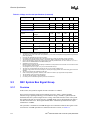
SNC System Bus Signal Group..........................................................................9-2
9.3.1 Overview ...............................................................................................9-2
9.3.2 Signal Group .........................................................................................9-3
9.3.3 DC Specifications ..................................................................................9-4
9.4
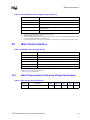
Scalability Port (SP) Signal Group .....................................................................9-4
9.5
Main Channel Interface ......................................................................................9-5
9.5.1 Main Channel Interface Reference Voltage Specification .....................9-5
9.5.2 DC Specifications ..................................................................................9-6
9.5.3 AC Specifications ..................................................................................9-6
9.6
LPC Signal Group ..............................................................................................9-7
9.6.1 DC Specifications ..................................................................................9-7
9.6.2 AC Specifications ..................................................................................9-7
9.7
SMBus and TAP Electrical Specifications ..........................................................9-7
9.7.1 DC Specifications ..................................................................................9-8
9.7.2 AC Specifications ..................................................................................9-9
9.7.3 AC Timing Waveforms ........................................................................9-10
9.8
Miscellaneous Signal Pins................................................................................9-11
9.8.1 Signal Groups......................................................................................9-11
9.8.2 DC Characteristics ..............................................................................9-12
9.8.3 AC Specification ..................................................................................9-13
9.9
Clock Signal Groups.........................................................................................9-15
9.9.1 AC Specification ..................................................................................9-15
10
Ballout and Package Information ..................................................................................10-1
10.1
1357-ball OLGA2b Package Information..........................................................10-1
10.2
Ball-out Specifications ......................................................................................10-3
10.2.1 Ball-out Lists........................................................................................10-3
11
Testability ......................................................................................................................11-1
11.1
Test Access Port (TAP)....................................................................................11-1
11.1.1 The TAP Logic.....................................................................................11-1
11.1.2 Accessing the TAP Logic ....................................................................11-2
11.2
Public TAP Instructions ....................................................................................11-4
11.3
Private TAP Instructions...................................................................................11-5
11.4
TAP registers....................................................................................................11-5
Intel® E8870 Scalable Node Controller (SNC) Datasheetvii
Figures
1-1
1-2
1-3
4-1
4-2
4-3
4-4
4-5
4-6
5-1
5-2
5-3
7-1
7-2
7-3
8-1
8-2
8-3
8-4
8-5
8-6
8-7
8-8
8-9
9-1
9-2
9-3
9-4
10-1
10-2
10-3
11-1
11-2
11-3
11-4
viii
Typical Itanium® 2-Based Server Configuration.................................................1-2
Scalable Node Controller Queueing Structures .................................................1-3
Scalable Node Controller Interfaces ..................................................................1-4
System Memory Address Space........................................................................ 4-1
Firmware Map Example using Intel® E8870 Chipset and Intel 82802 FWH
with Local Firmware Enabled .............................................................................4-5
Firmware Map Example using Intel® E8870 Chipset and Intel 82802 FWH
with Local Firmware Disabled ............................................................................4-6
Use of MIRs to Interleave Blocks of Varying Size Across Different Nodes ......4-10
Reflections Used to Recover Memory Behind Enabled Spaces ......................4-11
System I/O Address Space ..............................................................................4-19
Error Correction Code Layout on Main Channels 0 and 1 .................................5-6
Error Correction Code Layout on Main Channels 2 and 3 .................................5-7
Typical DDR-SDRAM Memory System ............................................................5-10
Clock Distribution Scheme .................................................................................7-2
Differential Bus Clock to Processors and SNC ..................................................7-3
Firmware Hub Clocks .........................................................................................7-4
Power-up Reset Timing......................................................................................8-3
Hard Reset Deassertion Timing .........................................................................8-3
Warm RESETI# Sampling.................................................................................. 8-6
Synchronization Point for Determinism .............................................................. 8-7
Reset Re-triggering Limitations..........................................................................8-9
Deterministic Hard Reset Timing .....................................................................8-10
Simplest Power Good Distribution ...................................................................8-13
Basic System Reset Distribution ......................................................................8-14
Basic System Reset Timing .............................................................................8-14
TAP DC Thresholds ...........................................................................................9-9
TAP and SMBus Valid Delay Timing Waveform ..............................................9-10
TCK and SM_CLK Clock Waveform ................................................................9-11
Generic Differential Clock Waveform ...............................................................9-16
1357-ball OLGA2b Package Dimensions – Top View......................................10-1
1357-ball OLGA2b Package Dimensions – Bottom View ................................10-2
1357-ball OLGA2b Solder Balls Detail .............................................................10-3
TAP Controller Signals.....................................................................................11-1
Simplified Block Diagram of TAP Controller.....................................................11-2
TAP Controller State Diagram..........................................................................11-3
TAP Instruction Register ..................................................................................11-6
Intel® E8870 Scalable Node Controller (SNC) Datasheet
Tables
1-1
2-1
2-2
2-3
2-4
3-1
3-2
3-3
3-4
3-5
3-6
3-7
3-8
4-1
4-2
4-3
4-4
4-5
4-6
4-7
4-8
5-1
5-2
5-3
5-4
5-5
5-6
5-7
6-1
6-2
6-3
6-4
6-5
6-6
6-7
6-8
8-1
8-2
8-3
8-4
9-1
9-2
9-3
9-4
9-5
9-6
9-7
9-8
9-9
Chipset Component Markings ............................................................................1-1
Buffer Technology Types ...................................................................................2-1
Buffer Signal Directions......................................................................................2-2
Signal Naming Conventions ...............................................................................2-2
SNC Signal List ..................................................................................................2-2
Register Attributes Definitions ............................................................................3-1
Register Grouping by Function...........................................................................3-4
MAR Register Mappings ....................................................................................3-8
MIT Definition for DDR SDRAM .......................................................................3-14
Legal Combinations of TRW, TWR ..................................................................3-18
DDR IOP Decodes ...........................................................................................3-21
Enabling the LPC/FWH Interface .....................................................................3-31
Checkword Encoding .......................................................................................3-44
MAR Settings .....................................................................................................4-2
SNC Memory Mapping Registers.....................................................................4-12
SPS Memory Mapping Registers .....................................................................4-13
SIOH Memory Mapping Registers....................................................................4-13
Destinations (ATTR).........................................................................................4-13
Address Disposition for Processor ...................................................................4-14
Intel® E8870 Chipset SAPIC Interrupt Message Routing and Delivery............4-16
Address Disposition for Inbound Transactions.................................................4-16
General Memory Characteristics........................................................................5-1
Indices to Re-Ordering Queues..........................................................................5-3
DDR-SDRAM Total Memory Per SNC .............................................................5-10
Bits Used in MCP Packet for Different DDR Technologies ..............................5-12
DDR Address Bit Mapping ...............................................................................5-12
Interleave Field Mapping for DDR ....................................................................5-13
MCP Bits Forced by RAFIX and DIV Fields for DIMM Splitting........................5-14
Intel® E8870 Chipset Errors ...............................................................................6-2
RAS Roles of Different System Components...................................................6-11
Intel® E8870 Chipset Error Status and Log Registers......................................6-14
E8870 Chipset Errors, Transaction, and Class Information .............................6-17
Control: SP Request Header Error Log............................................................6-20
Control: SP Response Header Error Log .........................................................6-20
Link Layer Errors: Data Log Fields...................................................................6-21
Link Layer Errors: LLR and Phit Fields.............................................................6-21
Intel® E8870 chipset Reset Types......................................................................8-1
Reset Response Sequences Summary .............................................................8-2
Power-up and Hard Reset Deassertion Timings ................................................8-4
Critical Initialization Timings ...............................................................................8-4
Absolute Maximum Non-operational DC Ratings at the Package Pin................9-1
Voltage and Current Specifications ....................................................................9-1
SNC System Bus Signal Groups........................................................................9-3
SNC AGTL+ DC Parameters .............................................................................9-4
Scalability Port Interface Signal Group...............................................................9-4
DMH Main Channel Signal Groups ....................................................................9-5
Main Channel Vref Specification ........................................................................9-5
RSL Data Group, DC Parameters ......................................................................9-6
RSL Clocks, DC Parameters..............................................................................9-6
Intel® E8870 Scalable Node Controller (SNC) Datasheetix
9-10
9-11
9-12
9-13
9-14
9-15
9-16
9-17
9-18
9-19
9-20
9-21
9-22
9-23
9-24
9-25
9-26
9-27
9-28
9-29
9-30
9-31
9-32
9-33
10-1
10-2
11-1
11-2
11-3
11-4
x
RAMBUS “CMOS 1.8 I/O” DC Parameters ........................................................9-6
LPC Interface Signal Group ...............................................................................9-7
LPC DC Parameters ..........................................................................................9-7
SMBus and TAP Interface Signal Group............................................................9-8
TAP Signal Terminations ...................................................................................9-8
TAP DC Parameters ..........................................................................................9-8
SMBus DC Parameters ......................................................................................9-9
SMBus Signal Group AC Specifications ............................................................9-9
TAP Signal Group AC Specifications ...............................................................9-10
Signal Groups ..................................................................................................9-11
CMOS 1.3V DC Parameters ............................................................................9-12
CMOS 1.5V OD DC Parameters......................................................................9-12
CMOS 1.5V DC Parameters ............................................................................9-12
CMOS 1.8V Output DC Parameters ................................................................9-13
CMOS 3.3V DC Parameters ............................................................................9-13
CMOS 1.3V Open-Drain AC Parameters .........................................................9-13
CMOS 1.5V Open-Drain AC Parameters .........................................................9-13
CMOS 1.5V AC Parameters ............................................................................9-14
CMOS1.5 I/O OD AC Parameters....................................................................9-14
CMOS 1.8V AC Parameters ............................................................................9-14
CMOS 3.3 V AC Parameters ...........................................................................9-14
Clock Signal Groups ........................................................................................9-15
LVHSTL Clock DC Parameters........................................................................9-15
LVHSTL Differential Clock AC Specification ....................................................9-15
SNC Ball List ....................................................................................................10-4
SNC Signal-Ball Number................................................................................10-22
TAP Signal Definitions .....................................................................................11-1
Public TAP Instructions ....................................................................................11-4
Private TAP instructions...................................................................................11-5
Example of Configuration Access Data Register Format.................................11-6
Intel® E8870 Scalable Node Controller (SNC) Datasheet
1
Introduction
1.1
Overview
The Intel® E8870 chipset delivers new levels of availability, features and performance for servers.
It provides flexible common modular architecture support for the Intel® Itanium® 2 processors.
The Intel E8870 chipset supports up to four processors, and up to eight processors with the
Scalability Port Switch (SPS) component, delivering stability to the platforms through reuse and
common architecture support.
The component names used throughout this document refer to the component markings listed in
Table 1-1.
Table 1-1. Chipset Component Markings
Component Name
1.2
Product Marking
SNC
E8870
SIOH
E8870IO
SPS
E8870SP
DMH
E8870DH
P64H2
82870P2
ICH4
82801DB
FWH
82802AC
Scalable Node Controller (SNC) Overview
The SNC is the processor system bus interface and memory controller for the E8870 chipset. It
supports the Itanium 2 processors, DDR SDRAM main memory, a firmware hub interface to
support multiple firmware hubs, two scalability ports (SPs) for access to I/O and coherent memory
on other nodes.
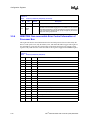
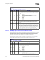
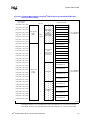
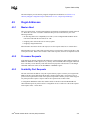
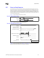
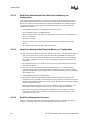
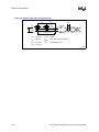
The SNC may be connected to a SPS for scaling to large systems as shown in Figure 1-1. The SNC
is connected directly to an SIOH for single-node system implementations.
Intel® E8870 Scalable Node Controller (SNC) Datasheet
1-1
Introduction
Figure 1-1. Typical Itanium® 2-Based Server Configuration
Itanium ® 2
Processor
Itanium ® 2
Processor
Itanium ® 2
Processor
Itanium ® 2
Processor
SNC
(Scalable Node
Controller)
Flash
BIOS
Itanium ® 2
Processor
Flash
BIOS
Memory
SP
(Scalability Port)
Switch
SIOH
(Serv er Input/Output
Hub)
HI 1.5
Port
Itanium ® 2
Processor
Itanium ® 2
Processor
Itanium ® 2
Processor
SNC
(Scalable Node
Controller)
Memory
SP
(Scalability Port)
Switch
SIOH
(Serv er Input/Output
Hub)
Flash
BIOS
ICH4
I/O Bridge
32-bit, 33MHz PCI
4x HI 2.0
Ports
Super I/O
4x HI 2.0
Ports
USB 2.0
P64H2
PCI/PCI-X
Bridge
64-bit, 33/66/
100/133 MHz
IDE CD-ROM
BMIDE HDDs
P64H2
PCI/PCI-X
Bridge
64-bit, 33/66/
100/133 MHz
001247
1-2
Intel® E8870 Scalable Node Controller (SNC) Datasheet
Introduction
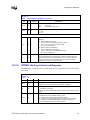
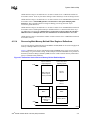
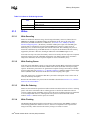
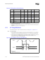
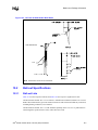
1.3
Architectural Overview
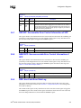
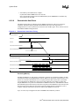
Figure 1-2 is a conceptual depiction of the SNC’s queueing structures. The system bus logic
includes the In Order Queue (IOQ) that tracks pipelined in order transactions.
Figure 1-2. Scalable Node Controller Queueing Structures
System Bus Interface
RAC Channel
Memory
Controller
RAC Channel
LATT and RATT
Queueing Structures
RAC Channel
Data
Buffer
RAC Channel
SP0
SP1
001257
The local access transaction tracker (LATT) is a buffer that holds processor requests until they are
completed. The LATT then converts processor requests into scalability port (SP) requests, which it
inserts into the SP Request Out Queue for SP0 or SP1. The response returns in the SP Response In
Queue on the same SP. The LATT picks a request from one SP or the other, and sends it to the
processor system bus interface. See Section 1.4.3 for more information on SP queues.
The remote access transaction tracker (RATT) pulls SP requests from the SP Request In Queue
from one SP or the other. The request is stored in the RATT until completed.
Requests entering the SNC are presented to Conflict Resolution logic one at a time to resolve
coherency races. If a request is to the same address as a request already stored in the LATT or
RATT, Conflict Resolution logic blocks progress of one request or another until ordering is
resolved.
Memory writes from the various sources are posted in the Write Post Queue, and reads into the
Read Re-ordering Queue. From there, the memory controller selects them for issue to maximize
memory performance. See Chapter 5, “Memory Subsystem” for more information on the queueing
structures in the memory controller.
All data passes through the data buffer when it moves between the processor system bus, memory
and the SPs. The LATT provides configuration register access for processors, and the RATT
provides access from the SP port.
Intel® E8870 Scalable Node Controller (SNC) Datasheet
1-3
Introduction
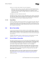
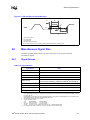
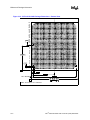
1.4
Interfaces
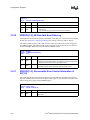
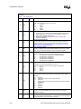
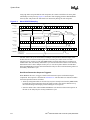
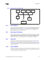
Figure 1-3 illustrates the SNC and all of its interfaces, which consist of the processor system bus,
four main channels, a firmware hub interface, two scalability ports as well as JTAG and SMBus
ports. The processor system bus interfaces with one to four processors. The two SPs interface to the
scalability port switch or SIOH. Each of the main channels interface to the DMH for DDRSDRAM support.
Figure 1-3. Scalable Node Controller Interfaces
Itanium® 2 Processor
400 MHz
6.4 GB/s
RAC Channels
FWH
JTAG
SNC
SMBus
Scalability Ports
SP0
800 MHz
6.4 GB/s
Memory Bus
System Bus
800 MHz
6.4 GB/s
SP1
800 MHz
6.4 GB/s
000631a
1.4.1
Intel® Itanium® 2 Processor System Bus
The SNC will support up to four Itanium 2 processors. The processor bus consists of 128 bits of
data and 16 bits of ECC. It supports 128-byte cache lines, and with 6.4 GB/s peak bandwidth.
1.4.2
Main Channel
The four main channels on the SNC are extended Direct RAMBUS* channels. The interface has
three row request, five column request, and 18 data signals. Packets up to eight transfers long are
driven on these lines at 800 MT/s. A lower frequency serial chain runs along each channel.
Propagation delays on the main channels can exceed one clock cycle. The channel is divided into
domains of one clock period. When given a serial command, all devices within a domain delay
their transmit data so that it arrives at the domain edge at the same time. Software then determines
the domain of each device by write/read trial and error. Software configures each device with a
coarse delay corresponding to its domain so that data from all devices arrive at the channel master
at the same time.
1-4
Intel® E8870 Scalable Node Controller (SNC) Datasheet
Introduction
A clock generator must be provided for each channel that is compliant with the Direct RAMBUS
Clock Generator Specification. The SNC will provide a pair of clock phase references for each of
the four main channels. An external clock generator will use these references to generate the
400 MHz differential clock to master (CTM) so that it arrives at the SNC co-incident with the SNC
core clock.
1.4.3
Scalability Port (SP) Interface
The scalability port interface is a high speed interface for connecting the SNC to other chipset
components such as the SIOH. The SP interface serves as a link to I/O when connected to an SIOH.
As the name implies, the SP also allows a system to scale beyond one node. This is done by
connecting a scalability port switch (SPS) to the SNC’s SP interface. Refer to Figure 1-1 “Typical
Itanium® 2-Based Server Configuration” for example interconnect schemes.
There are two SPs per SNC. Each SP interface contains a Request Out and Response In queue to
pass data to and from the LATT and a Request In and Response Out queue to pass data to and from
the RATT. These queues are 20 entries deep.
The SP uses SBD signaling technology, which allows simultaneous transmission of information in
both directions on the same wire, providing a peak bandwidth of 6.4 GB/s per port (3.2 GB/s in
each direction).
1.4.4
Low Pin Count/Firmware Hub Interface
The SNC interfaces directly to a firmware hub (FWH) component. The low cost FWH interface
comprises four address/data pins (LAD[3:0]) and one framing signal (LFRAME#). Electrically and
with regards to timing, these signals comply with 33 MHz, 3.3V PCI requirements (refer to the PCI
Local Bus Specification, Rev. 2.2).
The firmware hub/low pin count (FWH/LPC) interface supports up to four loads using two clocks,
one clock output per two FWH or LPC components.The SEL_LPC strapping pin selects either the
LPC or FWH protocol for this port.
The SNC supports only slave components. The purpose of this interface is to provide for local
firmware for the processors interfacing to this particular SNC component. Any connected firmware
hub devices must adhere to the Intel® 82802AB/82802AC Firmware Hub (FWH) Specification.
This interface is only accessible from the processor bus, not the scalability port, JTAG, or SMBus.
The cooperation of a local processor is required to perform firmware updates or check firmware
version.
The LPC features clock speeds of up to 33 MHz and IO/memory/DMA/bus master cycle support.
The LPC interface on the SNC will only support flash devices. The SNC will not tolerate 5V levels
on the LPC interface.
1.4.5
JTAG Interface
This port is used for component configuration and testing. In Boundary Scan testing, system clocks
are not running, so all events are synchronous to the JTAG clock.
In system debug, this port is controlled by the in-target probe (ITP), which is a PCI card driven by
an application running on a PC. JTAG runs asynchronously to the system clocks at no more that
1/8th the bus clock frequency.
Intel® E8870 Scalable Node Controller (SNC) Datasheet
1-5
Introduction
1.4.6
SMBus Slave Interface
This port is controlled by an autonomous platform manager during system operation. The chipset
will support serial data transfers at 100 kHz. The chipset is designed to limit the worst case
probability of metastability on SMBus command transfers to less than one in 1011.
1.5
Terminology
Address Bit Permuting
Address bits are distributed among channel selects, DRAM
selects and bank selects so that a linear address stream
accesses these resources in a certain sequence.
Bit Interleave
The way the bits in a cache line are mapped to channels,
devices, banks, rows, columns (RDRAM) or stacks, banks,
rows, columns (DDR SDRAM) of memory.
Cache Line Interleave
The way a series of cache lines are mapped to DRAM
devices.
Critical Word First
The SNC will deliver the words of a cache line in a particular
order such that the word addressed in the request appears in
the first data transfer.
DDR SDRAM
Double Data Rate SDRAM
DIMM
Dual-in-Line Memory Module
DMH
DDR Memory Hub
Device Row
A set of devices that provide a cache line. Since the second
64 bytes of a 128-byte line are from a page hit on the same
devices, the device row is the same for 64-byte lines and
128-byte lines.
A 4-bit DDR SDRAM device row consists of eight sets of 18
devices that respond to a main channel request. Typically,
these would appear on one side of a DIMM. An 8-bit DDR
SDRAM device row consists of eight sets of nine devices on
each DIMM that respond to a main channel request.
1-6
DRAM Page (Row)
The DRAM cells selected by the row address.
DRCG/DMCG
Direct RAMBUS Clock Generator.
Dirty Node
The node which owns a modified cache line.
Direct Connect/Single Node
Up to 4-way Intel Itanium 2/ E8870 platform configuration
that consists of one SIOH and SNC that are directly
connected by Scalability Ports.
Explicit Write-Back (EWB)
The transaction issued by a processor evicting a cache line.
Home Node
The SNC that controls the memory on which a particular
cache line resides.
Host, Processor, CPU
The E8870 chipset supports Itanium 2 processor.
Intel® E8870 Scalable Node Controller (SNC) Datasheet
Introduction
Implicit Write-Back (IWB)
IWB is used to describe the hit-modified-snoop response to a
processor bus request. Although this is a response, it
modifies the handling of the original read. The new behavior
is independent of the original read type. In effect, the SNC
converts the original request into an IWB. A hit to a modified
line in the SIOH can also be called an IWB.
Inbound (IB)/Outbound (OB)
Upstream/Downstream,
Northbound/Southbound,
Upbound/Downbound
Up, North, or Inbound is in the direction of the processor.
Down, South, or Outbound is in the direction of I/O.
Line
Cache line.
Local
Requests that are initiated by processors on the same bus as a
given SNC.
Main Channel
The RAC memory interface used by SNC.
Master Abort
A response to an illegal request. Reads receive all 1’s data.
Writes have no effect.
Memory Data Quantum
The smallest memory access for the E8870 chipset. Each of
the four main channels deliver 16B on an access. This 64byte quantity is a quanta. Memory error correction is applied
on a quantum basis.
MDFC
Memory Device Failure Correction
Nodes
Two uses: The first is in the context of the scalability port
agent, i.e. SNC, SPS or SIOH. The second refers to processor
nodes only (e.g. single node system).
Page Replace (Page Miss), Row
Hit/Page Miss
An access to a row that has another page open. The page
must be transferred back from the memory devices to the
array, and the bank must be precharged.
Page Hit
An access to an open page, or DRAM row. For the Itanium 2
processor, the E8870 chipset makes two 64B accesses for a
cache line. The two halves of the cache line are always
placed on the same page, so that only one row command is
used. Outside of a cache line the E8870 chipset maps address
bits to optimize random accesses, at the expense of page hits.
Thus page hits outside a cache line are rare.
Page Miss (Empty Page)
An access to a page that is not buffered in sense amps and
must be fetched from DRAM array.
RAMBUS ASIC Cell (RAC)
It is the embedded cell designed by RAMBUS that interfaces
with the RAMBUS devices using RSL signaling. The RAC
communicates to the RMC.
Remote
Requests that enter the SNC from a SP.
RSL
RAMBUS signaling level is the name of the signaling
technology used by SNC on the main channel.
RCLK
The period of the CTM and CFM clocks at 2.5 ns.
SEC/DED
Single Error Correct/Double Error Detect
SIOH
The Intel E8870IO server input/output hub: connects two
SPs to five hub interface ports.
Intel® E8870 Scalable Node Controller (SNC) Datasheet
1-7
Introduction
1.6
SNC
Scalable Node Controller. This chipset component interface
with the Itanium 2 processor, main memory, and SP links.
SPS
Intel E8870SP Scalability Port Switch. The crossbar/central
snoop filter that connects the SNCs and SIOHs.
SPP
Scalability Port Protocol Logic. The SNC cluster that
controls sequencing of coherent requests.
SSO
Simultaneous Switching Output
System Bus
A generic term used to refer to the Itanium 2 processor
system bus (128 bits wide).
Virtual Channel
Requests and responses on the SP are time multiplexed on
the SP wires, but separate flow control is provided so that
one channel makes progress even if the other is blocked. The
logical effect is as if there were separate “virtual channels”
for requests and responses.
DEN#,HITM#,ADS#,A[44:0]#
Processor bus signals.
References
The reader of this specification should also be familiar with material and concepts presented in the
following documents:
•
•
•
•
•
•
•
•
1.7
IEEE 1149.1a-1993
Jedec Standard 79 (JESD79)
PCI Local Bus Specification, Rev. 2.2
Intel® Itanium® 2 Processor Datasheet
Intel® E8870IO Server I/O Hub (SIOH) Datasheet
Intel® E8870DH DDR Memory Hub (DMH) Datasheet
Intel® 82802AB/82802AC Firmware Hub (FWH)
LPC Interface Specifications, Rev. 1.0
Revision History
Revision
Number
-001
1-8
Description
Initial release of this document.
Date
August 2002
Intel® E8870 Scalable Node Controller (SNC) Datasheet
2
Signal Description
2.1
Conventions
The terms assertion and deassertion are used extensively when describing signals, to avoid
confusion when working with a mix of active-high and active-low signals. The term assert, or
assertion, indicates that the signal is active, independent of whether the active level is represented
by a high or low voltage. The term deassert, or deassertion, indicates that the signal is inactive.
Signal names may or may not have a “#” appended to them. The “#” symbol at the end of a signal
name indicates that the active, or asserted state occurs when the signal is at a low voltage level.
When “#” is not present after the signal name the signal is asserted when at the high voltage level.
When discussing data values used inside the component, the logical value is used. For instance.,a
data value described as “1101b” would appear as “1101b” on an active-high bus, and as “0010b”
on an active-low bus. When discussing the assertion of a value on the actual signal, the physical
value is used; i.e. asserting an active-low signal produces a “0” value on the signal.
Table 2-1 and Table 2-2 list the reference terminology used later for buffer technology types (e.g.
LVTTL, etc.) used and buffering signal types (e.g. input, output, etc.) used.
Table 2-1. Buffer Technology Types
Buffer
Buffer Type
Description
AGTL+
1.2 V
Open drain Advanced GTL+ interface.
SBD
1.3 V
Simultaneous Bi-Directional.
Differential
LVHSTL
Itanium® 2 processor-based system low voltage differential
input clock.
CMOS1.3
1.3 V
CMOS, push/pull, type I/O or I.
CMOS1.5
1.5 V
CMOS, push/pull, type I/O or I.
CMOS3.3
3.3V
CMOS, push/pull, type I/O or I.
CMOS1.5OD
1.5 V
Open-Drain CMOS type I/O.
CMOS3.3OD
3.3 V
Open-Drain CMOS type I/O.
CMOS1.8
1.8 V
CMOS, push/pull, type I/O.
RCMOS1.8
1.8 V
CMOS, push/pull, type I/O or O. No boundary scan on output,
boundary-scan only on input in the main channel interface.
LPC
LPC
LPC I/O input with a voltage level of 3.3V and max. frequency of
33 MHz.
RSL
RSL
High-speed (800 MHz) RAMBUS ASIC Cell (RAC) I/O with
differential inputs. XOR-tree instead of boundary-scan.
SSTL_2
SSTL-2
DDR bus interface signal type.
JTAG
JTAG
Open-drain CMOS type I/O at 1.5V, without boundary scan
logic.
Analog
Analog
Typically a voltage reference or specialty power supply.
Intel® E8870 Scalable Node Controller (SNC) Datasheet
2-1
Signal Description
Table 2-2. Buffer Signal Directions
Buffer Direction
Description
I
Input signal.
O
Output signal.
OD
Output open drain.
I/O
Bidirectional (input/output) signal.
SBD
Simultaneous Bi-directional signal.
Some signals or groups of signals have multiple versions. These signal groups may represent
distinct but similar ports or interfaces, or may represent identical copies of the signal used to reduce
loading effects. Table 2-3 shows the conventions SNC use.
Table 2-3. Signal Naming Conventions
Convention
Expands To
RR{0/1/2}XX
Expands to: RR0XX, RR1XX, and RR2XX.
RR[2:0]
Expands to: RR[2], RR[1], and RR[0]. This denotes a bus.
RR# or RR[2:0]#
Denotes an active low signal or bus.
Only the PLL power-supply signals are listed. No other power-supplies are listed.
Typically, upper case groups, (“A, B, C”) represent functionally similar but logically distinct
signals. Each signal provides an independent control and may or may not be asserted at the same
time as the other signals in the grouping. In contrast, lower case groups, (“a, b, c”) typically
represent identical duplicates of a common signal. Such duplicates are provided to reduce loading.
2.2
SNC Signal List
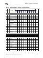
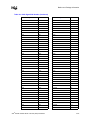
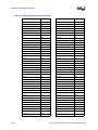
Table 2-4 lists all of the SNC signals.
Table 2-4. SNC Signal List
Signal
Type
Frequency
Description
Main Channels 0, 1, 2, 3
2-2
R{0/1/2/3}DQA[8:0]
I /O
RSL
800 MHz
RAMBUS Data(A)
Data signals used for read and write operations on RAMBUS data
bus “A”.
R{0/1/2/3}DQB[8:0]
I/O
RSL
800 MHz
RAMBUS Data(B)
Data signals used for read and write operations on RAMBUS
databus “B”.
R{0/1/2/3}RQ[7:0]
O
RSL
800 MHz
Request Control Signals
R{0/1/2/3}RQ[7:0] are used for sending control packets on
RAMBUS channel. The RAMBUS specification defines the
mapping of RAMBUS packets to these lines for RDRAM. The DMH
Component Specification defines the mapping for DDR.
R{0/1/2/3}EXRC
O
RSL
800 MHz
Row Expansion Signal
These signals are not used by SNC.
Intel® E8870 Scalable Node Controller (SNC) Datasheet
Signal Description
Table 2-4. SNC Signal List (Continued)
Signal
Type
Frequency
Description
Main Channels 0, 1, 2, 3 (continued)
R{0/1/2/3}EXCC
O
RSL
800 MHz
Column Expansion Signal
These signals are not used by SNC.
R{0/1/2/3}CTM
I
RSL
400 MHz
Clock to Master
One of the two differential transmit clock signals used for RDRAM
operations on the corresponding RAMBUS channel. It is input to
SNC and is generated by an external clock generator.
R{0/1/2/3}CTMN
I
RSL
400 MHz
Clock to RAMBUS Master Complement
One of the two differential transmit clock signals used for RDRAM
operations on the corresponding RAMBUS channel. It is
complement of clock signal R{0/1/2/3}CTM.
R{0/1/2/3}CFM
O
RSL
400 MHz
Clock from Master
One of the two differential signals used to clock RAMBUS packets
driven by the SNC. These signals are of type I/O in the RTL as
defined by RAMBUS.
R{0/1/2/3}CFMN
O
RSL
400 MHz
Clock from Master Complement
One of the two differential signals used to clock RAMBUS packets
driven by the SNC. These signals are of type I/O in the RTL as
defined by RAMBUS.
R{0/1/2/3}SYNCLKN
O
RCMOS1.8
33 MHz
Phase Detect Signal
This signal is sent to DRCG for generating 400 MHz clock. This
signal is generated from SYNCLKN of the corresponding RAC.
This signal trace must be delay matched with R{0/1/2/3}PCLKM
trace.
R{0/1/2/3}PCLKM
O
RCMOS1.8
33 MHz
Phase Detect Signal
This signal is sent to the DRCG for generating the 400 MHz clock.
This signal is generated from the SNC core clock.
R{0/1/2/3}SCK
O
RCMOS1.8
1 MHz
or
100 MHz
Serial Clock
Clock source used for timing of the R{0/1/2/3}SIO and R{0/1/2/
3}CMD signals.
R{0/1/2/3}SIO
I/O
RCMOS1.8
1 MHz
or
100 MHz
Serial Input/Output Chain
Bi-directional serial data signal used for reading and writing control
registers.
R{0/1/2/3}CMD
O
RCMOS1.8
1 MHz
or
100 MHz
Serial Command
Serial command input used for control register read and write
operations.
I
Analog
N/A
Voltage Reference
Supplies Vref for input buffers.
I
Analog
N/A
Impedance Update
Used to adjust the impedance of I/O drivers CMOS1.5
R{0/1/2/3}VREF[1:0]
Scalability Port 0, 1
SP{0/1}ZUPD[1:0]
SP{0/1}SYNC
I/O
CMOS1.3
N/A
Reset Synchronization
Provides synchronization between ports for impedance control and
reference voltage adjustment. This signal is also used by the SP
reset logic to determine when SP comes out of reset.
SP{0/1}SYNC is released when ports at both ends of the link are
ready.
I
CMOS1.3
N/A
Scalability Port Present
Signals the scalability port of an impending hot plug event
SP{0/1}AVREFH[3:0]
I/O
Analog
N/A
Strand A Voltage reference
3/4 VCC-SP Reference
SP{0/1}AVREFL[3:0]
I/O
Analog
N/A
Strand A Voltage Reference
1/4 VCC-SP Reference
SP{0/1}ASTBP[1:0]
I/O
SBD
400 MHz
P Strobes
Positive phase data strobes for strand A to transfer data at the 2x
rate (800 MHz)
SP{0/1}PRES
Intel® E8870 Scalable Node Controller (SNC) Datasheet
2-3
Signal Description
Table 2-4. SNC Signal List (Continued)
Signal
Type
Frequency
Description
Scalability Port 0, 1 (continued)
SP{0/1}ASTBN[1:0]
SP{0/1}AD[15:0]
I/O
SBD
I/O
SBD
400 MHz
800 MHz
N Strobes
Negative phase data strobes for strand A to transfer data at the 2x
rate (800 MHz)
Data Bus
16 bits of the data portion of a phit on strand A. These bits are SSO
encoded. SP{0/1}ASSO determines if these are out of an inverter
or not.
SP{0/1}BD[15:0]=DATA[31:16].
SP{0/1}AEP[2:0]
I/O
SBD
800 MHz
Parity/ECC
Two of these signals carry the ECC information for the data
flits. There are four bits of ECC for each data phit. The header
flits are not ECC protected. The third signal is for parity. Each
phit is always protected by two bits of parity.
SP{0/1}AEP[1:0] = GEP[1:0]. AEP[2]=TEP[0].
SP{0/1}ALLC
I/O
SBD
800 MHz
Link Layer Control
For each PHIT these signals carry two of the four bits of link layer
control information.
SP{0/1}ASSO
I/O
SBD
800 MHz
SSO Encode
This signal is asserted to indicate that the data bits over Strand A
are inverted.
SP{0/1}ARSVD
I/O
SBD
800 MHz
Reserved
SP{0/1}BVREFH[3:0]
I/O
Analog
N/A
Strand B Voltage reference
3/4 VCC Reference
SP{0/1}BVREFL[3:0]
I/O
Analog
N/A
Strand B Voltage Reference
1/4 VCC Reference
SP{0/1}BSTBP[1:0]
I/O
SBD
400 MHz
P Strobes
Positive phase data strobes for strand B to transfer data at the 2x
rate (800 MHz)
SP{0/1}BSTBN[1:0]
I/O
SBD
400 MHz
N Strobes
Negative phase data strobes for strand B to transfer data at the 2x
rate (800 MHz)
SP{0/1}BD[15:0]
I/O
SBD
800 MHz
Data Bus
16 bits of the data portion of a PHIT on strand B. These bits are
SSO encoded. SP{0/1}BSSO determines if these are out of an
inverter or not.
SP{0/1}BD[15:0]=DATA[31:16].
SP{0/1}BEP[2:0]
I/O
SBD
800 MHz
Parity/ECC
Two of these signals carry the ECC information for the data flits.
There are four bits of ECC for each data PHIT. The header flits are
not ECC protected. The third signal is for parity. Each PHIT is
always protected by two bits of parity.
SP{0/1}BEP[1:0] = GEP[3:2].
SP{0/1}BEP[2]=TEP[1].
2-4
SP{0/1}BLLC
I/O
SBD
800 MHz
Link Layer Control
For each PHIT these signals carry two of the four bits of link layer
control information.
SP{0/1}BSSO
I/O
SBD
800 MHz
SSO Encode
This signal is asserted to indicate that the data bits over Strand B
are inverted.
SP{0/1}BRSVD
I/O
SBD
800 MHz
Reserved
Intel® E8870 Scalable Node Controller (SNC) Datasheet
Signal Description
Table 2-4. SNC Signal List (Continued)
Signal
Type
Frequency
Description
Scalability Port 0, 1 (continued)
SP{0/1}GPIO[1:0]
I/O
CMOS1.5 OD
N/A
Scalability Port General Purpose I/O
These pins are asynchronous open drain I/O signals. To filter
glitches on the inputs, the value of the input only changes when
the same value has been sampled over four consecutive 200 MHz
clock cycles. Similarly, to ensure accurate sampling of these
signals by other devices, the output value will be asserted for a
minimum of 6 consecutive 200 MHz cycles.
LPC I/O Interface
LAD[3:0]
I/O
LPC
33 MHz
LFRAME#
O
LPC
33 MHz
LRESET#
O
LPC
33 MHz
LPCCLKOUT0
O
LPC
33 MHz
LPCCLKOUT1
O
LPC
33 MHz
LPCCLKOUT2
O
LPC
33 MHz
Multiplexed Address, Command and Data
LAD[3:0] are used to communicate:
• Start of a cycle
• Transfer type (Memory or I/O)
• Read or Write
• Address
• Data
• Stop (abort a cycle)
Frame
SNC asserts this signal to indicate the start of a LPC or FWH cycle
and termination of an aborted cycle.
LPC Reset
LPC I/O reset. The SNC drives this signal during a hard reset to
initialize devices on the LPC interface.
LPC Clock Out
Clock generated from the core clock to FWH or LPC device. This
signal trace is delay matched with the other two LPCCLKOUT
signals.
LPC Clock Out
Clock generated from the core clock to FWH or LPC device. This
signal trace is delay matched with the other two LPCCLKOUT
signals.
LPC Clock Out
Clock generated from the core clock to SNC. This signal trace is
delay matched with the two LPCCLKOUT signals and is connected
to the LCLK input.
LPCSEL
I
CMOS1.5
N/A
LPC/FWH Mode Select
When set to ‘1’ SNC generates LPC I/O reads and writes; when
set to ‘0’ SNC generated FWH I/O reads and writes.
LPCEN
I
CMOS1.5
N/A
LPC/FWH Present
When set to ‘1’ enables support of an LPC or FWH device attached
to the LPC I/O interface.
LCLK
I
LPC
33 MHz
LPC Clock In
Clock input for the LPC I/O interface that is asynchronous to the
SNC core clock This input may change asynchronous to BUSCLK.
Performance, Debug, and Error Signals
NODEID[4:0] /
DBG[4:0]#
I/O
CMOS1.5
N/A
NodeID
Strap bits that indicate the NodeID of this SNC. The NodeID is
captured on the rising edge of RESETI# and stored in the CBC
register. The captured value is sent on the IDLE flits. For E8870
chipset-based systems, NodeID[4:3] should always be set to “11”.
When the SNC is connected to switches other than the SPS,
NodeID[4:3] may be set to other values. For Itanium 2 processorbased systems supporting the SAPIC model, each SNC must have
a unique NodeID. BusID is not examined when routing SAPIC
interrupts.
These signals should be pulled up or down with weak resistors that
will not draw more than the specified IOL or IOH of these signals
when they are driven with debug values after reset.
Intel® E8870 Scalable Node Controller (SNC) Datasheet
2-5
Signal Description
Table 2-4. SNC Signal List (Continued)
Signal
Type
Frequency
Description
Performance, Debug, and Error Signals (continued)
BusID
Strap bits that indicate the configuration bus number of this SNC.
These bits are captured by the CBC register on the rising edge of
RESETI#. The captured value is sent on the IDLE flits.
BUSID[2:0] /
DBG[7:5]#
I/O
CMOS1.5
N/A
For E8870 chipset systems, BusID should always be set to “111”.
When the SNC is used with switches other than the SPS, BusID
may be set to other values.
These signals should be pulled up or down with weak resistors that
will not draw more than the specified IOL or IOH of these signals
when they are driven with debug values after reset.
DBG[7:0]#
INT_OUT#
BINITIN#
I
CMOS1.5
Debug Bus
These bits form part of an 8-bit debug bus. Once the NodeID is
captured after hard reset, debug signals selected by the DEVT
register may be driven on these signals.
200 MHz
Interrupt Request
This signal is asserted by SNC when the SPINCO register sets a
flag that has been configured to request an interrupt. The SNC
drives this signal for a minimum of 6 cycles.
200 MHz
Assert BINIT
This signal is driven by the system logic. When asserted, the SNC
should drive BINIT# on the processor bus according to protocol.
This signal must be sampled at the same value four consecutive
cycles before changing state. This input may change
asynchronous to BUSCLK.
BERRIN#
I
CMOS1.5
200 MHz
Assert BERR
This signal is driven by the system logic. When asserted, the SNC
should drive BERR# on the processor bus according to protocol.
This signal must be sampled at the same value four consecutive
cycles before changing state. This input may change
asynchronous to BUSCLK.
BINITOUT#
O
CMOS3.3
200 MHz
Processor asserted BINIT
The SNC asserts this signal for at least 12 cycles when BINIT# is
sampled asserted, but not driven by the SNC.
BERROUT#
O
CMOS3.3
200 MHz
Processor asserted BERR
The SNC asserts this signal for at least 12 cycles when BERR# is
sampled asserted, but not driven by the SNC.
ERR[2:0]#
EV[3:0]#
2-6
O
CMOS1.5 OD
N/A
I/O
CMOS1.5 OD
I/O
CMOS1.5 OD
200 MHz
200 MHz
Error Code
The SNC drives and samples error information on these signals.
• ERR[0] is asserted for correctable errors.
• ERR[1] is asserted for non-correctable errors.
• ERR[2] is asserted for fatal errors.
The FERRST register samples these signals up till the cycle
before the SNC drives. The SNC drives these for a minimum of 12
cycles. The input must be sampled at the same value four
consecutive cycles before changing state.This input may change
asynchronous to BUSCLK.
Events
These signals are driven and sampled by performance monitoring
and debug logic. The SNC drives these for a minimum of 12
cycles. The input must be sampled at the same value four
consecutive cycles before changing state.This input may change
asynchronous to BUSCLK.
Intel® E8870 Scalable Node Controller (SNC) Datasheet
Signal Description
Table 2-4. SNC Signal List (Continued)
Signal
Type
Frequency
Description
Clocking
200 MHz
Bus Clock
This is one of the two differential reference clock inputs to the
Phase Locked Loop (PLL) in the SNC core. The circuit board
transmission line driving this signal must be delay-matched to the
corresponding processor clock signal generated by the system
board logic.
200 MHz
Bus Clock Complement
This is the other one of the two differential reference clock inputs to
the PLL in the SNC core. The circuit board transmission line
driving this signal must be delay-matched to the corresponding
processor clock signal generated by the system board logic.
I
Analog
N/A
VCC
PLL Analog Voltage for the processor bus PLL.
VCCASP
I
Analog
N/A
VCC
PLL Analog Voltage for the SP PLL.
VCCACORE
I
Analog
N/A
VCC
PLL Analog Voltage for the core PLL.
VSSAFSB
I
Analog
N/A
VSS
PLL Analog Ground for the processor bus PLL.
VSSASP
I
Analog
N/A
VSS
PLL Analog Ground for the SP PLL.
VSSACORE
I
Analog
N/A
VSS
PLL Analog Ground for the core PLL.
BUSCLK
I
Differential
BUSCLK#
I
Differential
VCCAFSB
System Management
SPDCLK
I/O
CMOS3.3 OD
SPDCLK
SMBus for Serial Presence Detect Clock. Unused.
SPDDA
I/O
CMOS3.3 OD
SPDCLK
SMBus for Serial Presence Detect Address/Data. Unused.
SCL
I/O
CMOS3.3 OD
SCL
SMBus Clock
This input may change asynchronous to BUSCLK.
SDA
I/O
CMOS3.3 OD
SCL
SMBus Address/Data
This input may change asynchronous to BUSCLK.
TDIOANODE
I/O
Analog
N/A
Thermal Diode Anode
This is the anode of the thermal diode.
TDIOCATHODE
I/O
Analog
N/A
Thermal Diode Cathode
This is the cathode of the thermal diode.
CPUPRES#
I
CMOS1.5
N/A
CPU Present
When asserted, at least one CPU is present. Requires external
pull-up. This is tied to all CPUPRES# signals of the Itanium 2
processor socket.
PWRGOOD
I
CMOS1.5
N/A
Power Good
Clears the SNC. This signal is held low until all power supplies are
in specification. This signal may be pulsed after power-up to
completely reset the SNC.
RESETI#
I
CMOS1.5
N/A
Reset Input
This is the hard reset input to the SNC. This input may change
asynchronous to BUSCLK.
RESET#
O
AGTL+
N/A
CPU Reset
This signal is the processor bus reset. Asserted due to RESETI#,
or writes to SYRE register.
O
CMOS1.5
N/A
Reset Output
Asserted when system hard reset field in SYRE register is written.
May be routed by the system to the component that asserts reset.
Reset
RESETO#
Intel® E8870 Scalable Node Controller (SNC) Datasheet
2-7
Signal Description
Table 2-4. SNC Signal List (Continued)
Signal
Type
Frequency
Description
Reset (continued)
MEMRST0#
O
CMOS1.8
N/A
Memory Subsystem Reset
This signal is asserted by SNC to reset the DMHs (DDR Memory
Hubs). It is pulsed just after the deassertion of RESETI#. This is
pulsed on every SNC RESETI# deassertion.
MEMRST1#
O
CMOS1.8
N/A
Memory Subsystem Reset
This is the same as MEMRST0#. This is used so that MEMRST0#
is not overloaded.
Bit 0 :ITPODTDIS#
COMPCNTRL[1:0]#
I
CMOS1.5
N/A
On-die-termination disable on RESET# and BPM[5:0]#, to allow
connection of an In-Target-Probe to those processor bus pins.
Bit 1 :COMPCNTRL[1]#
Enables glitch filters on STBP[7:0]# and STBN[7:0]#. Recommend
being able to strap either way.
FSBSLWCRES[1:0]
I
Analog
N/A
Compensation Resistors
Compensation Resistors for the processor bus slew rate.
FSBODTCRES[1:0]
I
Analog
N/A
Compensation Resistors
Compensation Resistors for the processor bus on-die termination.
RACODTCRES[1:0]
I
Analog
N/A
Compensation Resistors
Compensation Resistors for the RAC on-die termination.
RACODTEN[1:0]
I
CMOS1.5
N/A
On-die Termination
RAC on-die termination enable.
LVHSTLODTEN
I
CMOS1.5
N/A
On-die Termination
BUSCLK and BUSCLK# on-die termination enable.
VTTMK
I
Analog
N/A
Itanium 2 Processor Bus Termination Voltage
(67 occurrences)
VCCSP
I
Analog
N/A
Scalability Port Supply Voltage
(34 occurrences)
VCCRIO
I
Analog
N/A
RAMBUS Termination Voltage
(24 occurrences)
VCCRA
I
Analog
N/A
RAC DLL Supply Voltage
(8 occurrences)
VCC3.3LPC
I
Analog
N/A
LPC I/O Supply Voltage
(2 occurrences)
VCCI2C
I
Analog
N/A
SMB and miscellaneous 3.3-volt I/O supply voltage.
TCK
I
JTAG
TCK
JTAG Test Clock
Clock input used to drive Test Access Port (TAP) state machine
during test and debugging. This input may change asynchronous
to BUSCLK.
TDI
I
JTAG
TCK
JTAG Test Data In
Data input for test mode. Used to serially shift data and instructions
into TAP.
TDO
O
JTAG
TCK
JTAG Test Data Out
Data output for test mode. Used to serially shift data out of the TAP.
TMS
I
JTAG
TCK
JTAG Test Mode Select
This signal is used to control the state of the TAP controller.
TRST#
I
JTAG
N/A
JTAG Test Reset
This signal resets the TAP controller logic. It should be pulled down
unless TCK is active. This input may change asynchronous to
BUSCLK.
Power
Test Access Port (JTAG)
2-8
Intel® E8870 Scalable Node Controller (SNC) Datasheet
Signal Description
Table 2-4. SNC Signal List (Continued)
Signal
Type
Frequency
Description
®
Itanium 2 Processor Bus
A[43:3]#
I/O
AGTL+
200 MHz
Address Signals
Processor Address Bus. During processor cycles these are inputs.
SNC drives A[43:3]# for transactions originating from SP and for
deferred reply transactions.
ADS#
I/O
AGTL+
200 MHz
Address/Data Strobe
Indicates the first cycle of any request phase. This signal is driven
and sampled by SNC.
AP[1:0]#
I/O
AGTL+
200 MHz
Address Parity
Parity protection on the address bus. SNC will generate AP[1:0]#
for its own transactions. SNC will also monitor AP[1:0]# for all
transactions and check parity on the address bus.
BERR#
I/O
AGTL+
200 MHz
Bus Error
BERR# indicates unrecoverable bus protocol violation. SNC will
sample and drive BERR#. SNC will drive BERR# according to the
protocol when the signal BERRIN gets asserted.
BINIT#
I/O
AGTL+
200 MHz
Bus Initialization
This signal is asserted to reinitialize bus state machines. SNC will
terminate any ongoing transactions at this time. This signal does
not affect the state of configuration registers and error logging
registers.
BNR#
I/O
AGTL+
200 MHz
Block Next Request
SNC will assert this signal when it runs out of internal resources
while a locked transaction is in progress. SNC may also assert this
signal during a hard reset sequence. SNC will also monitor this
signal when driven by a processor to block any of its transactions
from being issued on the bus.
SNC asserts BNR# for debug.
BPM[5:0]#
I/O
AGTL+
200 MHz
Breakpoint/Debug Bus
This group of signals is used by the system debug logic and SNC
for communicating debug information. SNC drives BPM[3:0]# and
BPM[5]#. BPM[4]# is not driven by SNC.
BPRI#
O
AGTL+
200 MHz
Priority Agent Bus Request
SNC asserts this signal to drive requests originating from SP and
to issue a deferred reply transaction in some special cases. SNC
will also assert this signal to block the processors from issuing
transactions. BPRI# assertion will have the same effect as BNR#
assertion in this case with the exception that SNC will drive its
snoop requests on the processor bus. Symmetric agents do not
drive this signal. This signal is sampled by SNC internally.
BREQ0#
I/O
AGTL+
200 MHz
Physical Bus Request
SNC drives BREQ[0]# during reset and deasserts it one clock after
SNC samples reset deasserted.
BREQ[3:1]#
I
AGTL+
200 MHz
Physical Bus Request
SNC does not drive BREQ[3:1]#. SNC observes active
BREQ[3:0]# from processors to determine deassertion of BPRI# to
transfer bus ownership to the processor.
D[127:0]#
I/O
AGTL+
400 MHz
Data Bus
128 bits of data driven by the agent responsible for driving the data
during the Data phase.
DBSY#
I/O
AGTL+
200 MHz
Data Bus Busy
Indicates that the data bus is owned by the agent responsible for
driving the data during the Data phase. DBSY# assertion does not
imply that data is being transferred that cycle.
DEFER#
O
AGTL+
200 MHz
Defer
SNC asserts DEFER# for all processor initiated transactions with
DEN# on. SNC will also generate deferred responses for these
transactions except for the cases when an in-order retry is forced.
Intel® E8870 Scalable Node Controller (SNC) Datasheet
2-9
Signal Description
Table 2-4. SNC Signal List (Continued)
Signal
Type
Frequency
Description
®
Itanium 2 Processor Bus (continued)
DEP[15:0]#
I/O
AGTL+
400 MHz
Data Bus ECC
ECC coverage for 128 bits of data. SNC generates this ECC when
it drives data during the Data phase. SNC also checks ECC for
incoming data.
DRDY#
I/O
AGTL+
200 MHz
Data Ready
Indicates that data is valid on the data bus during any cycle
DRDY# is asserted. SNC asserts DRDY# for each valid data
transfer.
GSEQ#
O
AGTL+
200 MHz
Guaranteed Sequentially
SNC asserts this signal along with DEFER# to guarantee that the
chipset will maintain the order of writes.
HIT#
HITM#
I/O
AGTL+
I/O
AGTL+
200 MHz
200 MHz
Snoop Hit
SNC captures the value of HIT# for transactions that are deferred
and returns it using DHIT# during the Deferred Phase.
SNC asserts HIT# to initiate a HIT# or snoop stall for debug (HIT#
and HITM# asserted together). SNC does not drive HIT# during
normal operation.
Snoop Hit with Modified
SNC observes HITM# and when asserted drives TRDY# for
implicit writeback.
SNC asserts HITM# to initiate a snoop stall for debug (HIT# and
HITM# asserted together). SNC does not drive HITM# during
normal operation.
ID[9:0]#
O
AGTL+
200 MHz
Transaction Identifier
These are driven during the Deferred Phase and indicate the
transaction ID of the deferred transaction. On the second clock of
the deferred phase (IDS# +1), IDb[1:0]# carries the parity for the ID
signals. IDb[2]# renamed as DHIT# is asserted by SNC if the
snoop phase of the original transaction resulted in HIT#.
IDS#
O
AGTL+
200 MHz
Transaction Identifier Strobe
IDS# is asserted by SNC to indicate the first cycle of the deferred
phase.
INIT#
O
AGTL+
200 MHz
Initialization Signal
INIT# is asserted to initiate soft reset of the processors.
LOCK#
I
AGTL+
200 MHz
Bus Lock
Indicates atomicity of transactions. SNC will never assert LOCK#.
REQ[5:0]#
I/O
AGTL+
200 MHz
Request Command
Asserted during both clocks of the Request phase. During the first
clock, these signals carry enough information to initiate a snoop
request. In the second clock these signals carry additional
information to completely define the transaction type.
These are sampled and driven by SNC.
200 MHz
Request Command Parity
Parity protection on ADS# and REQ[5:0]# signals. RP# is driven by
SNC for its own transactions. RP# is also sampled by SNC to
check parity on the Request phase signals.
RS[2:0]#
O
AGTL+
200 MHz
Response Status
Indicates the types of response generated by SNC. Valid
responses are Hard Fail, Implicit Writeback, Normal, No Data,
Deferred and Retry.
RSP#
O
AGTL+
200 MHz
Response Status Parity
Parity protection on RS[2:0]#
SBSY#
I/O
AGTL+
RP#
I/O
AGTL+
200 MHz
Strobe Bus Busy
Indicates that Strobes are used by an agent. It is driven by an
agent transferring data when it owns the strobe bus.
SBSY# is driven and sampled by SNC.
2-10
Intel® E8870 Scalable Node Controller (SNC) Datasheet
Signal Description
Table 2-4. SNC Signal List (Continued)
Signal
Type
Frequency
Description
®
Itanium 2 Processor Bus (continued)
STBN[7:0]#
I/O
AGTL+
200 MHz
Data Strobes
Used to transfer data at the 2x rate. STBn[7:0]# is the negative
phase data strobe. Data transfer occurs when the voltage levels of
STBn and STPp are equal. SNC drives and samples STBn[7:0]#.
STBP[7:0]#
I/O
AGTL+
200 MHz
Data Strobes
Used to transfer data at the 2x rate. STBp[7:0]# is the positive
phase data strobe. Data transfer occurs when the voltage levels of
STBn and STPp are equal. SNC drives and samples STBp[7:0]#.
TND#
I/O
AGTL+
TLB Purge Not Done
200 MHz
SNC asserts TND# at the requesting node until the Purge TC is
completed globally.
SNC observed TND# to determine completion of Purge TC.
TRDY#
O
AGTL+
200 MHz
Target Ready
Indicates that the target for the host transaction is able to enter the
data transfer phase.
Intel® E8870 Scalable Node Controller (SNC) Datasheet
2-11
Signal Description
2-12
Intel® E8870 Scalable Node Controller (SNC) Datasheet
3
Configuration Registers
3.1
Access Mechanisms
The SNC configuration registers can be accessed from the following sources:
• Configuration Read and Write from either scalability port (SP)
• System Management Bus (SMBus)
• JTAG
:
Table 3-1. Register Attributes Definitions
Abbreviation
Attribute
3.2
Description
Read Only
RO
The bit is set by the hardware only and software can only read the bit.
Writes to the register have no effect. A hard reset will set the bit to its default
value.
Read/Write
RW
The bit can be read and written by software. A hard reset will set the bit to its
default value.
Read/Write
Once
RWO
The bit can be read by software. It can also be written by software but the
hardware prevents writing it more than once without a prior reset. Since the
smallest register access is one byte, this protection applies on a byte-bybyte basis. That is, if only one byte of a field is written, only that byte will be
locked. The other byte has separate write protection.
Read/Clear
RC
The bit can be either read or cleared by software. In order to clear an RC bit,
the software must write a one to it. Writing a zero to an RC bit will have no
effect. A hard reset will set the bit to its default value.
Sticky
RWS, RCS,
ROS
The bit is “sticky” or unchanged by a hard reset. Read/Write, Read/Clear,
and Read Only bits may be sticky. These bits are only reset with
PWRGOOD.
Reserved
RV
This bit is reserved for future expansion and must not be written. The PCI
Local Bus Specification, Revision 2.2 requires that reserved bits must be
preserved. Any software that modifies a register that contains a reserved bit
is responsible for reading the register, modifying the desired bits, and writing
back the result.
Unique
*
Any attribute with an asterisk (*) suffix indicates an unique behavior. Please
consult the associated description for details.
SNC Fixed Memory Mapped Registers
These registers are mapped into the “SNC Memory Mapped Configuration Register Range” shown
in Table 4-6, “Address Disposition for Processor.” These appear at fixed addresses to support the
boot process. These registers also appear in the SNC configuration space. This mechanism is
independent of the more general Memory Mapped Configuration mechanism.
Intel® E8870 Scalable Node Controller (SNC) Datasheet
3-1
Configuration Registers
3.2.1
SPADA: Scratch Pad Alias
This is a memory mapped alias of the register described in Section 3.8.4, “SPAD: Scratch Pad.”
This register may be read or written only by 4-byte accesses.
Memory Address:FE60_C400h
3.2.2
Bit
Attr
Default
31:0
RW
0
Description
Scratch pad for system.
SPADSA: Sticky Scratch Pad Alias
This is a memory mapped alias of the register described in Section 3.8.5, “SPADS: Sticky Scratch
Pad.” This register may be read or written only by 4-byte accesses.
Memory Address:FE60_C800h
3.2.3
Bit
Attr
Default
31:0
RWS
0
Description
Sticky Scratch pad for system.
BOFLA: Boot Flag Alias
Only 4-byte reads may be made to this register. Writes will have no effect.
Memory Address:FE60_7400h
See Section 3.8.6, “BOFL: Boot Flag.”
3.2.4
CBCA1: Chip Boot Configuration Alias
This register may be read or written only by 4-byte accesses.
Memory Address:FE62_7400h
Bits 31:0 of the register described in Section 3.8.7, “CBC: Chip Boot Configuration.”
3.2.5
CBCA2: Chip Boot Configuration Alias
This register may be read or written only by 4-byte accesses.
Memory Address:FE62_7800h
Bits 63:32 of the register described in Section 3.8.7.
3-2
Intel® E8870 Scalable Node Controller (SNC) Datasheet
Configuration Registers
3.2.6
CBCA3: Chip Boot Configuration Alias
This register may be read or written only by 4-byte accesses.
Memory Address:FE62_7C00h
Bits 95:64 of the register described in Section 3.8.7.
3.3
SNC I/O Space Registers
3.3.1
CFGADR: Configuration Address Register
CFGADR is written only when a processor I/O transaction to CF8 is:
• Referenced as a Dword.
• The Bus Number field matches the Bus field in the CBC register.
• The Device Number matches the NodeID field in the CBC register.
A Byte or Word reference will not access this register, but will generate a I/O read and write on SP.
If the reference is Dword, but the Bus Number and Device Number do not match, a configuration
read/write on the SP will be sent out. The CFGADR register contains the Bus Number, Device
Number, Function Number, and Register Number for which a subsequent CFGDAT access is
intended.
I/O Address:CF8h
Bit
Attr
Default
Description
CFGE
31
RW
0
30:24
RV
0
23:16
RW
0
15:11
RW
0
Configuration Enable Unless this bit is set, accesses to the CFGDAT
register will not produce a configuration access, but will be treated as other I/O
accesses. This bit is strictly an enable for the CFC/CF8 access mechanism
and is not forwarded to PCONR/W address.
Reserved
Bus Number
Compared against CBC.Bus to define local SNC configuration space.
Device Number
Compared against CBC.NodeID to define local SNC configuration space.
Function Number
This field is used to select the function of a locally addressed register.
10:8
RW
0
If this field is 0, 1, 2, or 3, this field specifies the SNC function of the addressed
register.
Otherwise, writes will be discarded and reads will return all ones as defined by
the PCI specification.
Register Offset
7:2
RW
0
If this register specifies an access to SNC registers, this field specifies a group
of four bytes to be addressed. The bytes accessed are defined by the Byte
enables of the CFGDAT register access.
Otherwise, writes will be discarded and reads will return all 0s as defined by
the PCI specification.
1:0
RW*
0
Writes to these bits will have no effect; reads return 0.
Intel® E8870 Scalable Node Controller (SNC) Datasheet
3-3
Configuration Registers
3.3.2
CFGDAT: Configuration Data Register
CFGDAT provides data for the four bytes of configuration space defined by CFGADR. This
register is only accessed if there is an access to I/O address CFCh on the processor bus and
CFGADR.CFGE is set. The byte enables with the I/O access define how many configuration bytes
are accessed.
I/O Address:CFCh
Bit
Attr
Default
31:0
RW
0
Description
Configuration Data Window
3.4
The data written or read to the configuration register (if any) specified by
CFGADR.
SNC Configuration Registers
The SNC is viewed by the system as a single PCI device with four different functions. Offsets 0 to
40h are used for the standard PCI header as defined in PCI Local Bus Specification, Rev. 2.2.
Table 3-2 lists the configuration address maps for each function of the SNC.
Configuration reads to other functions return all 1’s. Reads to undefined (reserved) registers return
all 0’s. Writes to other functions and undefined registers are dropped.
Table 3-2. Register Grouping by Function
Function
Types of Registers
0
Processor bus control.
1
Memory controller.
2
Scalability Port 0 and registers common to both SPs.
3
Scalability Port 1 and global performance monitoring.
3.5
PCI Standard Registers
3.5.1
VID: Vendor Identification Register
This register identifies Intel as the manufacturer of the SNC. Writes to this register have no effect.
Device: NodeID
Function: 0,1,2,3
Offset:
00 - 01h
Bit
15:0
3-4
Attr
RO
Default
8086h
Description
Vendor Identification Number
This is the standard 16-bit value assigned to Intel.
Intel® E8870 Scalable Node Controller (SNC) Datasheet
Configuration Registers
3.5.2
DID: Device Identification Register
This register combined with the Vendor Identification register uniquely identifies the SNC. Writes
to this register have no effect.
Device: NodeID
Function: 0,1,2,3
Offset:
02 - 03h
Bit
Attr
Default
Description
Device Identification Number
Identifies each function of the SNC.
15:0
3.5.3
RO
Fixed Value
(see Description)
0500h: SNC Function0
0501h: SNC Function1
0502h: SNC Function2
0503h: SNC Function3
0508h: Reserved
0509h: Reserved
050Ah: Reserved
050Bh: Reserved
CCR: Class Code Register
This register contains the Class Code for the SNC, specifying the device function.
Device: NodeID
Function: 0,1,2,3
Offset:
09-0Bh
Bit
Attr
Default
Description
Base Class
23:16
RO
06h
This field indicates the general device category. For the SNC, this field is
hardwired to 06h, indicating it is a “Bridge Device.”
Sub-Class
15:8
RO
0
This field qualifies the Base Class, providing a more detailed
specification of the device function. For the SNC, this field is hardwired
to 00h, indicating it is a “Host Bridge.”
Register-Level Programming Interface
7:0
RO
0
This field identifies a specific programming interface that device
independent software can use to interact with the device. There is no
such interfaces defined for host bridge, and this field is hardwired to 00h.
Intel® E8870 Scalable Node Controller (SNC) Datasheet
3-5
Configuration Registers
3.5.4
RID: Revision Identification Register
This register contains the revision number of the SNC.
Device: NodeID
Function: 0,1,2,3
Offset:
08h
Bit
Attr
Default
Description
Revision Identification Number
7:0
3.5.5
RO
See Description
00h = A0 stepping
01h = A1 stepping
02h = A2 stepping
03h = A3 stepping
10h = B0 stepping
20h = C0 stepping
HDR: Header Type Register
This register identifies the header layout of the configuration space.
Device: NodeID
Function: 0,1,2,3
Offset:
0Eh
Bit
Attr
Default
Description
Multi-function Device
7
RO
1
This bit indicates if the SNC is a multi-function device. The SNC has more than 256
bytes of configuration registers alloted to a single function. Therefore, the SNC is
defined to be a multifunction device, and this bit is hardwired to 1.
Configuration Layout
6:0
3.5.6
RO
0
This field identifies the format of the standard PCI configuration header space (10h
through 3Fh space). The SNC uses header type “00”. These bits are hardwired to
00h.
SVID: Subsystem Vendor Identification Register
This register identifies the manufacturer of the system. This 16-bit register, combined with the
Device Identification Register, uniquely identifies any PCI device.
Device: NodeID
Function: 0,1,2,3
Offset:
2Ch
Bit
Attr
Default
Description
Vendor Identification Number
15:0
3-6
RWO 8086h
The default value specifies Intel as the subsytem vendor ID for the SNC. Each byte
of this register will be writable once. Second and successive writes to a byte will
have no effect.
Intel® E8870 Scalable Node Controller (SNC) Datasheet
Configuration Registers
3.5.7
SID: Subsystem Identity
This register identifies the system.
Device:
Node_ID
Function: 0, 1, 2, 3
Offset:
2Eh
Bit
Attr
15:0
RWO
Default
Description
Subsystem Identification Number
8086h
The default value specifies Intel as the system ID for the SNC. Each byte of this
register will be writable once. Second and successive writes to a byte will have no
effect.
3.6
Address Mapping Registers
3.6.1
MAR[5:0]: Memory Attribute Region Registers
This register defines the memory attributes on the 11 memory segments in the 512 Kbyte to
1 MByte address range. These attributes determine whether the SNC routes a processor request to
main memory or to the compatibility bus. The SNC takes no special action if the request is to be
routed to memory. If the request is to be routed to the compatibility bus, it is directed out to the
scalability port as if it were a remote memory read, but with a attribute field set to CB. Each
register holds the attributes for two segments (see Table 4-6 “Address Disposition for Processor” ).
Table 3-3 shows the MAR registers and the associated attribute bits.
Software on Itanium 2 processors must map C_0000-F_FFFFh to main memory for the SNC.
Device: NodeID
Function: 0
Offset:
54h, 55h, 56h, 57h, 58h, 59h
Bit
Attr
Default
Description
7:6
RV
0
Reserved
5
RW
0
4
RW
0
When set, route write requests to main memory. Otherwise, route to
compatibility bus.
3:2
RV
0
Reserved
1
RW
0
0
RW
0
WE1: Segment 1, Write Enable
When set, route write requests to main memory. Otherwise, route to
compatibility bus.
RE1: Segment 1, Read Enable
WE0: Segment 0, Write Enable
When set, route write requests to main memory. Otherwise, route to
compatibility bus.
RE0: Segment 0, Read Enable
When set, route write requests to main memory. Otherwise, route to
compatibility bus.
Intel® E8870 Scalable Node Controller (SNC) Datasheet
3-7
Configuration Registers
Table 3-3. MAR Register Mappings
Register
Bits
Attribute Bits
Memory Segment
3:0
Default
Reserved
0
7:4
–
–
WE
RE
0F0000h - 0FFFFFh
0
3:0
–
–
WE
RE
0C0000h - 0C3FFFh
0
7:4
–
–
WE
RE
0C4000h - 0C7FFFh
0
MAR0 (54h)
MAR1 (55h)
3:0
–
–
WE
RE
0C8000h - 0CBFFFh
0
7:4
–
–
WE
RE
0CC000h - 0CFFFFh
0
3:0
–
–
WE
RE
0D0000h - 0D3FFFh
0
7:4
–
–
WE
RE
0D4000h - 0D7FFFh
0
MAR2 (56h)
MAR3 (57h)
3:0
–
–
WE
RE
0D8000h - 0DBFFFh
0
7:4
–
–
WE
RE
0DC000h - 0DFFFFh
0
3:0
–
–
WE
RE
0E0000h - 0E7FFFh
0
7:4
–
–
WE
RE
0E8000h - 0EFFFFh
0
MAR4 (58h)
MAR5 (59h)
3.6.2
ASE: Address Space Enable Register
This register defines the Video Graphics Adapter and Monochrome Display Address ranges.
Table 4-6 define the usage of these bits.
]
Device: NodeID
Function: 0
Offset:
5Bh
Bit
Attr
Default
7:3
RV
0
2
RW
0
Description
Reserved
ISAEN: ISA Aliasing Enable
If set, I/O addresses X100 - X3FFh, X500 - X7FFh, X900 - XBFFh, and
XD00 - XFFFh may be redirected to compatibility bus.
MDASE: Monochrome Display Adapter Space Enable
1
RW
0
This bit affects the attribute field and request type applied to outbound SP
requests for memory addresses in the range B_0000 - B_7FFFh and I/O
requests to 3B4h, 3B5h, 3B8h, 3B9h, 3BAh and 3BFh.
VGASE: VGA I/O Space Enable
0
3.6.3
RW
0
This bit affects the attribute field and request type applied to outbound SP
requests for memory addresses in the range (A_0000 - B_FFFFh) and I/O
addresses in the (03B0h - 03BBh and 03C0h - 03DFh) ranges.
MMIOH: High Memory Mapped I/O Space Register
This register defines the High Memory Mapped I/O space. It starts at FF_FFFF_FFFFh and
extends downward in 4-GB increments to a minimum lower limit of 1_0000_0000h.
3-8
Intel® E8870 Scalable Node Controller (SNC) Datasheet
Configuration Registers
Processor requests to this space are directed to a particular SP port as a function of the SPINCO
and AGP1 registers. This routing forces a single path to each Memory Mapped I/O location. This
enables writes to be pipelined while maintaining sequential order.
Processor requests to this range are non-coherent. Non-coherent Read/Write are issued on the SP.
An address is in the High MMIO space if:
• (A[43:40] = 0h) AND (A[39:32] > BASE)
Device: NodeID
Function: 0
Offset:
60h
Bit
15:8
Attr
RV
Default
0
Description
Reserved
BASE
7:0
3.6.4
RW
FFh
Defines the lower limit of High MMIO range. These bits are compared against
A[39:32]. This field is one less than A[39:32] for the lowest address in the High
MMIO range. If FFh, this range is disabled. This register should be set to the
same value as the MMIOBH register in the SIOH.
MMIOL: Low Memory Mapped I/O Space Register
This register defines the Low Memory Mapped I/O space. It starts at FDFF_FFFFh and extends
downward in 16MB increments to a minimum value of 64MB. This region is described in “High
and Low Memory Mapped I/O (MMIO)” in Chapter 4, “System Address Map.”
Processor requests to this space are directed to a particular SP port as a function of the SPINCO
and AGP1 registers. This routing forces a single path to each Memory Mapped I/O location. This
enables writes to be pipelined while maintaining sequential order.
Processor requests to this range are non-coherent. Non-coherent Read/Write are issued on the SP.
The memory behind this range can be recovered using reflection. The SNC will not scrub any
memory mapped to this range and will only scrub the memory recovered from this range in MIRs
with the RFLCT bit set. See Section 5.2.1, “Scrub Address Generation.”
An address is in the Low MMIO space if:
• (A[43:32] = 000h) AND (FDh >= A[31:24] > BASE)
Device: NodeID
Function: 0
Offset:
64h
Bit
15:8
Attr
RV
Default
0
Description
Reserved
BASE
7:0
RW
FFh
Defines the lower limit of the Low MMIO range. These bits are compared
against A[31:24]. This field is one less than A[31:24] for the lowest address in
the Low MMIO range. If >= FDh, this range is disabled. This register should be
set to the same value as the MMIOBL register in the SIOH.
Intel® E8870 Scalable Node Controller (SNC) Datasheet
3-9
Configuration Registers
3.6.5
AGP1: Advanced Graphics Port Sub-Range 1 Register
In general, transactions to the High and Low MMIO range are routed out the default SP. This
register defines a sub-range within either the High or Low MMIO range, which is routed out the
non-default SP to balance loading. An enabled AGP1 range must be configured to fall within either
the High or Low MMIO range (see Section 3.6.3, “MMIOH: High Memory Mapped I/O Space
Register” and Section 3.6.4, “MMIOL: Low Memory Mapped I/O Space Register”). Otherwise,
this range is considered null.
An address falls in AGP1 range if:
HI/LO AND A[43:40]=0h AND (MMIOH.BAS <= AGP1.BAS < A[39:32] <= AGP1.LIM) OR
!HI/LO AND A[43:32] =000h AND (MMIOL.BAS <= AGP1.BAS < A[31:24] <= AGP1.LIM <= FDh)
Device: NodeID
Function: 0
Offset:
4C-4Eh
Bit
24:16
Attr
RV
Default
0
Description
Reserved
HI/LO
16
RW
0
If set, the AGP1 range falls in the High MMIO range. Otherwise it falls in the
low MMIO range. If in the high range, AGP1_LIM and AGP1_BASE are
compared against A[39:32], otherwise A[31:24].
LIM
15:8
RW
0
7:0
RW
0
This field specifies the upper limit for the AGP1 sub-range within an MMIO
region. This field is A[39:32] (High MMIO) or A[31:24] (Low MMIO) for the
highest address in the AGP1 range.
BAS
3.6.6
This field specifies the lower limit for the AGP1 sub-range within an MMIO
region. This field is one less than A[39:32] (High MMIO) or A[31:24] (Low
MMIO) address bits for the lowest address in the AGP1 range.
MMCFG: Memory Mapped Configuration Space Register
This register defines the Memory Mapped Configuration space. This space maps the entire PCI
configuration space into memory. This space is relocatable in 64 MB increments above 4 GB
(1_0000_0000h). It may not overlap MMIOH. It may not overlap High MMIO or any other space.
To avoid race conditions, software may only modify this register by CF8/CFC. Software must also
guarantee that there is no race between issue of MMCFG requests and changes in this register. That
is, all MMCFG accesses that expect the old register value must be completed before any write to
this register is issued, and the register write must complete on the processor bus before any
MMCFGs are issued that expect the new register value. See Table 4-8, “Address Disposition for
Inbound Transactions.”
The address of requests in this range are compared against CBC.NodeID and CBC.Bus to
determine whether the request accesses registers on this SNC. If not, it is converted into a noncoherent configuration Read/Write and issued on one of the SPs.
An address is in the MMCFG space if:
• The space is enabled: (BASE > 03Fh)
• A[43:26] == BASE
3-10
Intel® E8870 Scalable Node Controller (SNC) Datasheet
Configuration Registers
Device: NodeID
Function: 0
Offset:
50h
Bit
Attr
Default
31:18
RV
0
17:0
RW
0
Description
Reserved
BASE
3.6.7
Defines the lower limit of MMCFG range. These bits are compared against
A[43:26]. If less than 40h, this range is disabled.
IORD: I/O Redirection Register
This register is used to redirect I/O segments to the compatibility PCI bus. Certain I/O addresses
(e.g. MDA,VGA,CFC/CF8) are not redirected according to this register. Section 4.3.2.1,
“Outbound I/Os” defines the types of I/O accesses that are not governed by this register. Each bit in
this register corresponds with a 4-KB I/O segment.
Device: NodeID
Function: 0
Offset:
68h
Bit
Attr
Default
Description
I/O Redirection Bits
15:0
3.6.8
RW
Each bit corresponds with a 4-KB I/O segment. Bit 0 corresponds with the
lowest 4 KBs, Bit 1 corresponds with the next 4 KBs, etc. If an IORD bit is
asserted, requests to the corresponding addresses will have a Attr field of the
SP I/O Read/Write request be set to CB.
0
SMRAM: SMM RAM Control Register
This register must be programmed consistently with the SMRAM register in the SIOH. As the
Itanium 2 processor does not support SMM, undefined system operation will result if this register
is written. The default value leaves SMM space disabled.
Device: NodeID
Function: 0
Offset:
5C - 5Fh
Bit
31:0
Attr
RV
Default
0
Description
Reserved
Intel® E8870 Scalable Node Controller (SNC) Datasheet
3-11
Configuration Registers
3.6.9
MIR[9:0]: Memory Interleave Range Registers
These registers define 10 ranges in which all the main memory supported by this SNC falls.
Collectively, all the MIRs that cover a range and the Memory Interleave Technology (MIT)
associated with them define a cache line interleave. The cache line interleave is the repeating
sequence of channels, devices, and internal banks over which a linear stream of cache line accesses
cycle.
The MIRs on an SNC define whether an access is directed to local memory or sent to a scalability
port switch for further routing. The MIRs on the SP switch define the SNC that services each cache
line of memory. There is not a 1:1 association of SP switch MIRs with SNC MIRs. Multiple SNC
MIRs may cover the same range as one way of an SP switch MIR. One SNC MIR may describe a
contiguous address range covered by a series of SP switch MIRs.
All the memory covered by an SNC MIR must be the same technology. There is one Memory
Interleave Technology (MIT) Register in each SNC associated with each MIR. The MIT defines
the number of rows, columns, and banks addressed. The MIR and MIT jointly define how cache
lines are interleaved across devices, channels, and banks.
To support interleave across different technologies, up to four MIRs on the same or different SNCs
may be set to the same address range. The ways field of each MIR is used to divide cache lines
among the MIRs sharing an address range. Each MIR may cover 1, 2, or 4 ways. The remainder of
the 32-way interleave is across devices, banks, or channels of identical technology as defined by
the MIT registers and the address bit assignments in Section 5.3.2.5, “DDR Address Bit Mapping.”
The WAYS, BASE and SIZE fields define the existence and extent of this interleave. An address
falls in this interleave if:
• WAYS[A[8:7]] AND [BASE <= A[43:27] < BASE + 2SIZE]
Device: NodeID
Function: 1
Offset:
60h,64h,68h,6Ch,70h,74h,78h,7Ch,C4h,C8h
Bit
Attr
Default
31:26
RV
0
25:9
RW
0
Description
Reserved
BASE
This defines the lowest address in the interleave. These bits are compared
against A[43:27]. This field must be set to a multiple of the Interleave size
defined below.
SIZE
2 SIZE is the number of 128-MB blocks in the interleave range. To describe all
the memory supported by a given set of devices. For example, for DDR this
field should be set according to the contents of the MIT register with the same
index as follows:
8:4
RW
0
MIR[i].SIZE = 32B (bytes per quantum) • 4 (Banks) • MIT[i].NUMROW •
MIT[i].NUMCOL • MIT[i].SIDES • MIR[i].W • MIT[i].DIV
Where MIR[i].W is 4 divided by the number of ones in the WAYS field, below.
(This memory can also be divided among multiple MIRs covering different
ranges.) MIT[i].DIV should be interpreted to have values 1, 1/2, or 1/4. The
MIR used to recover memory by reflection will not follow the equation above. It
should have a size field as small as possible to cover maximum anticipated
expansion of the reflected region.
3-12
Intel® E8870 Scalable Node Controller (SNC) Datasheet
Configuration Registers
Device: NodeID
Function: 1
Offset:
60h,64h,68h,6Ch,70h,74h,78h,7Ch,C4h,C8h (Continued)
Bit
Attr
Default
Description
WAYS
If the bit in this field selected by A[8:7] is set, the access is sent to the devices
described by the corresponding MIT register. Each way bit of every Memory
Interleave Range must be set in exactly one MIR.
[3]
[2]
[1]
[0]
3:0
RW
=
=
=
=
Selected if A[8:7] = 11
Selected if A[8:7] = 10
Selected if A[8:7] = 01
Selected if A[8:7] = 00
Any MIR can cover 1, 2, or 4 ways of an interleave. Only certain combinations
are consistent with the address bit mapping described in Table 5-5 “DDR
Address Bit Mapping” and Table 5-6, “Interleave Field Mapping for DDR.”
0
0000
0001
0010
0100
1000
0101
1010
1111
Range disabled: This SNC has no memory in this range.
This MIR decodes way 0 - (A[8:7]=00)
This MIR decodes way 1 - (A[8:7]=01
This MIR decodes way 2 - (A[8:7]=10)
This MIR decodes way 3 - (A[8:7]=11)
This MIR decodes way 0 and 2 - (A[7]=0)
This MIR decodes way 1 and 3 - (A[7]=1)
This MIR decodes all ways in this range.
3.7
Memory Controller Registers
3.7.1
MC: Memory Control Settings
Device: NodeID
Function: 1
Offset:
40h
Bit
15:13
Attr
RV
Default
0
Description
Reserved
RROE: DDR Read to Read Optimization
12
RW
0
11:8
RV
0
0 = STM.Trr determines the spacing between any read on the same DDR
channel. This setting must be used when some DRAM devices do not
support concurrent auto-precharge. The lack of concurrent autoprecharge support can be inferred from DRAM specification that mention
an “access period” following RDA or WRA.
1 = Back-to-back Reads can be made to the same DDR device. STM.Trr
determines the spacing between reads to different devices on the same
DDR channel.
Reserved
MWBL: Minimum Write Burst Length Enable
7
RW
0
The minimum number of writes required for issue. Prior to normal operation,
this bit should be 0, so that all writes flush in the absence of reads. In normal
operation, this bit should be set to 1 so that incoming reads are not delayed by
write unnecessary write flushes.
0 = Writes are issued in the absence of reads
1 = Writes are not issued unless four are posted. Up to three posted writes
may persist in the SNC indefinitely.
Intel® E8870 Scalable Node Controller (SNC) Datasheet
3-13
Configuration Registers
Device: NodeID
Function: 1
Offset:
40h (Continued)
Bit
Attr
Default
Description
MECBD: Memory Error Correction Bypass Disable
6
RW
0 = Normal Operation: Correction path is not taken unless correction is
required.
1 = All data is forced through the correction path.
0
MECE: Memory Error Correction Enable
0 = No memory read errors are corrected. Logging is unaffected, but
poisoning will not occur. Good SEC/DED will be generated for all memory
reads.
1 = Enable Error correction (see Section 5.2, “Error Correction”). This bit
should not be set if MECBD=1.
5
RW
0
4
RW
1
0 = Reserved
1 = Synchronous DDR DRAM.
3:0
RV
0
Reserved
MT: Memory Type
3.7.2
MIT[9:0]: Memory Interleave Technology Registers
These registers define the mapping of address bits to DDR channels, devices, internal banks, rows,
and columns for this node. Each MIT groups together similar devices to maximize interleave
across channels, devices and banks.
There is one MIT for each memory range defined by the MIRs. All devices covered by one MIT
must be the same size and technology. If the ways field of the associated MIR indicates that this
interleave is disabled, the settings of this MIT are not applied.
Table 3-4. MIT Definition for DDR SDRAM
Device: NodeID
Function: 1
Offset:
A0h,A4h,A8h,ACh,B0h,B4h,B8h,BCh,CCh,D0h
Bit
31:19
Attr
RV
Default
0
Description
Reserved
RFLCT: MIR used for Reflection
18
RW
0
17:15
RV
0
14
RW
0
If set, this Memory Interleave Range is used to recover memory behind
MMIOL. In this MIR, the SNC will only scrub locations in the recovered range
(see Section 5.2.1, “Scrub Address Generation”). If this bit is set, the
corresponding MIR.SIZE may not cover the entire DIMM, but should be 4GB
maximum.
Reserved
Channel
3-14
Defines the DDR channel this DIMM occupies. Modifies the Channel number
in the MCP.
Intel® E8870 Scalable Node Controller (SNC) Datasheet
Configuration Registers
Table 3-4. MIT Definition for DDR SDRAM (Continued)
Device: NodeID
Function: 1
Offset:
A0h,A4h,A8h,ACh,B0h,B4h,B8h,BCh,CCh,D0h (Continued)
Bit
Attr
Default
Description
RAFIX
13:11
RW
0
This field defines which portion of the DIMM is mapped by this register. This is
accomplished by assigning fixed values to the most significant Row address
bits for this technology. The same half or quarter of a DIMM should not be
mapped by different MITs. Table 5-7 “MCP Bits Forced by RAFIX and DIV
Fields for DIMM Splitting” defines how this affects address bit mapping.
0
1
2
3
=
=
=
=
This MIR/MIT maps the first quarter or first half of the DIMM
This MIR/MIT maps the second quarter of the DIMM
This MIR/MIT maps the third quarter or second half of the DIMM
This MIR/MIT maps the fourth quarter of the DIMM
ROW
10:9
RW
0
Defines the Chip Selects (CS) connected to this DIMM. Together with the
SIDES field, determines the chip select fields in the MCP. Single-sided DIMMs
are only connected to the first CS of the pair.
0
1
2
3
8
RV
0
=
=
=
=
CS0 and CS1
CS2 and CS3
CS4 and CS5
CS6 and CS7
Reserved
SIDES
7
RW
0
Defines the number of sides this DIMM has. Modifies the Interleave field
mapping to ping-pong across Chip Selects as defined in Table 5-6, “Interleave
Field Mapping for DDR.”
0 = single-sided
1 = double-sided
DIV
6:5
RW
0
This field can be set to split a DIMM among 2, 3, or 4 MIR/MIT pairs. The
different portions can be assigned to independent address ranges as defined
by the RAFIX field. Table 5-7 “MCP Bits Forced by RAFIX and DIV Fields for
DIMM Splitting” defines how this affects address bit mapping.
0
1
2
3
=
=
=
=
This MIR/MIT maps the entire DIMM
Reserved
This MIR/MIT maps 1/2 of the DIMM
This MIR/MIT maps 1/4 of the DIMM
NUMROW: Technology – Number of Rows
4:3
RW
0
The number of rows within the devices of this interleave. See Section 5-4,
“Bits Used in MCP Packet for Different DDR Technologies” for legal
combinations with other fields.
0 = 4096
1 = 8192
2 = 16384
NUMCOL: Technology – Number of Columns
The number of columns within the devices of this interleave.See Section 5-4
for legal combinations with other Technology fields.
2:0
RW
0
0
1
2
3
4
=
=
=
=
=
512
1024
2048
4096
8192
Intel® E8870 Scalable Node Controller (SNC) Datasheet
3-15
Configuration Registers
A MIT may not describe more than one DIMM. Multiple MITs can apply to the same DIMM if the
associated MIR registers define different address ranges.
The DMH specifies the correlation between CS to SPD address bits on DIMMs and the format of
the Memory Control Packets (MCP).
3.7.3
STM: DDR-SDRAM Timing Register
This register defines timing parameters that work with all DDR SDRAMs in the memory
subsystem. The parameters for these devices can be obtained by serial presence detect (see
Section 3.7.5, “RCD: RAMBUS* Configuration Data Register”). This register must be set to
provide timings that satisfy the specifications of all DRAMs detected. If DRAMs present have
different Tcas, the maximum should be used to program this register.
Consult DDR SDRAM specifications for the technology of the devices in use. Consult the Northbridge Levelization Procedure section of the Intel® E8870DH DDR Memory Hub (DMH)
Datasheet for procedures to set these timing parameters.
Device: NodeID
Function: 1
Offset:
C0h
Bit
31
Attr
RV
Default
0
Description
Reserved
TRD: Read MCP to Data Delay
TRD defines the delay from the beginning of a read/write MCP to first data
sample in RClk resolution.
30:27
RW
2h
Read to data delay = 2 • tRD+20; (20-46)
Write to data delay = 2 • tRD +17; (17-43)
legal values are 0000 through 1101
The tcwd (DMH Main channel Write delay) parameter in the DMH should be
set to 2 • tRD +13.
26:22
RV
0
Reserved
TRQ: RAC RQ Transmit Timing
21:20
RW
3h
Selects one of the four programmable timing points within SyncClk period
(10ns) for transmitting RQ. The four timing points are identical to the Tselect
timing in the Direct RAC Data Sheet. TRQ should always be set to 11.
00
01
10
11
Reserved
Reserved
Reserved
Transmit RQData with Tselect = 1000 timing
TRW: Read to Write Delay
19:18
RW
2h
The minimum delay from the Read command to the next Write command on
the same branch DDR channel. This parameter is varied to avoid data strobe
protocol violations on the DIMM data bus. Table 3-5 defines the settings of this
parameter as a function of DMH parameters.
00
01
10
11
3-16
30 ns
40 ns
50 ns
60 ns
Intel® E8870 Scalable Node Controller (SNC) Datasheet
Configuration Registers
Device: NodeID
Function: 1
Offset:
C0h (Continued)
Bit
Attr
Default
Description
TWR: Write to Read Delay
17:16
RW
1h
The minimum delay from the Write command to the next Read command on
the same branch DDR channel.This parameter is varied to avoid data strobe
protocol violations on the DIMM data bus. Table 3-5 defines the settings of this
parameter as a function of DMH parameters.
00
01
10
11
10 ns
20 ns
30 ns
40 ns
RWAC: Read or Write during Write Access Period
15
RW
0
This bit may be set if all the DRAM controlled by the SNC can perform
concurrent auto-precharge operations to different banks. If 0, the maximum
rate of auto-precharge writes to a DIMM will be one write every 50ns. The
MC.RROE bit should be set to limit reads and writes during read access
periods.
0
1
14
RV
0
Some DIMMs do not support reads or writes during write access period.
All DIMMs support reads or writes during write access period.
Reserved
TRR: Read to Read Delay
13:12
RW
2h
The minimum delay from one Read command to another Read command on a
channel. MC.RROE determines whether this applies to all reads on a channel
or just reads to a different DIMM on the same channel. This parameter is
varied to avoid data strobe protocol violations on the DIMM data bus.
00
01
10
11
Reserved.
Reserved.
30 ns
40 ns (Supported only for memory initialization)
TWW: Write to Write Delay
The minimum delay from the Write command to the next Write command on
the same branch DDR channel.
11:10
RW
1h
00
01
10
11
Reserved.
20 ns
30 ns (Supported only for memory initialization)
40 ns
TRCD: Ras to Cas Delay
9:8
RW
0
The minimum delay from the RAS to a subsequent CAS to the same DIMM
Row. This parameter is programmed according to the highest tRCD and tRAP
parameters of the DDR DIMMs present.
00
01
10
11
20 ns ( tRCD= tRAP)
30 ns ( tRCD< tRAP)
Reserved.
Reserved.
TRA: Read to Activate Delay
7:6
RW
0
The minimum delay from the Read command to the next ACT command to the
same bank. This parameter is programmed according to the timing calculation:
tRAS + tRP - tRCD. Refer to DDR AC Characteristics specification for the timing
parameters in the calculations.
00
01
10
11
Intel® E8870 Scalable Node Controller (SNC) Datasheet
50 ns
60 ns
Reserved
Reserved
3-17
Configuration Registers
Device: NodeID
Function: 1
Offset:
C0h (Continued)
Bit
Attr
Default
Description
TWA: Write to Activate Delay
5:4
RW
2h
The minimum delay from the Read command to the next ACT command to the
same bank. This parameter is programmed according to the DIMM timing
parameters:
tWR + tRP + 30ns
Refer to DDR AC Characteristics specification for the timing parameters in the
calculations.
00
01
10
11
50 ns
60 ns
70 ns
Reserved
TRFC: Auto Refresh to Act Delay
The minimum delay from the Auto Refresh command to the next ACT
command to the same device. This parameter is set to the largest tRFC of the
DIMMs present.
3:1
RW
1h
000
001
010
011
100
101
110
111
70 ns
80 ns
90 ns
100 ns
120 ns
130 ns
140 ns
160 ns
TRC: Act to Act Delay
0
RW
1h
The minimum delay from the Act command to the next ACT command to the
same device. This parameter is programmed according to the largest tRRD of
the DIMMs present.
0
1
10 ns
20 ns
Table 3-5 defines the legal combinations for TRW, TWR as a function of DIMM data bus timing
parameters configured in the DMH. There may be a small variation across DMHs and across the
DIMMs on each DMH in the sum of tCL + tDPL + tDSD. The maximum must be used.
Note:
tCL is the DIMM CAS Latency. tDPL is the DIMM Path Latency, and tDSD is DIMM Strobe Offset.
Table 3-5. Legal Combinations of TRW, TWR
DMH Maximum
tCL + tDPL + t DSD
3.7.4
TRW
(STM[19:18])
TWR
(STM[17:16])
15-17.5ns (6-7 Rclks)
01
10
20-25ns (8-11 Rclks)
10
01
27.5-35ns (12-15 Rclks)
11
00
DRC: DRAM Maintenance Control Register
The Refresh Value field specifies the number of cycles (nominally 5ns) between refreshes. Since
refreshes are generated for all 16 supported DIMM sides, the refresh interval for any given DIMM
is 16 times as long as the Refresh Value field. A value of 195 sets the DIMM refresh interval to the
standard value of 15.6 us.
3-18
Intel® E8870 Scalable Node Controller (SNC) Datasheet
Configuration Registers
A value of 0 indicates that refreshes should not be generated. For more information on refresh see
Section 5.3.4, “DDR Maintenance Operations.”
Device: NodeID
Function: 1
Offset:
46h
Bit
Attr
Default
15:12
RV
0
11:0
RW
0
Description
Reserved
Refresh Value
3.7.5
For DDR, the number of cycles between refreshes. For testing purposes, this
field may be set from 0 to 50.
RCD: RAMBUS* Configuration Data Register
This register is used with the SCC register to access DMH registers or serial presence detect
information. This register is written for write data and holds the result of any operation specified by
the SCC register. Each operation is shifted out the serial interfaces for each RAMBUS
concurrently. There is one 16-bit field in this register for the data to/from each RAMBUS.
Device: NodeID
Function: 1
Offset:
48h
Bit
3.7.6
Attr
Default
Description
63:48
RW
0
R3D: RAMBUS 3 data.
47:32
RW
0
R2D: RAMBUS 2 data.
31:16
RW
0
R1D: RAMBUS 1 data.
15:0
RW
0
R0D: RAMBUS 0 data.
SCC: DDR SDRAM Configuration Command Register
This register is used with the RCD register to access DDR SDRAM and DMH control registers or
serial presence detect information. The SCC specifies the command to be executed. Writing this
register causes transactions on the RAMBUS serial control bus which may be translated by
expanders into serial presence detect transactions. The data for operations comes from, or is
returned to the RCD register. The frequency of SCLK never exceeds 1MHz.
Device: NodeID
Function: 1
Offset:
54h
Bit
31:30
Attr
RV
Default
0
Description
Reserved
MOE: Maintenance Operation Enable
29
RW
0
When set, the SNC issues maintenance operations such as refresh,
temperature calibration, etc. This bit defaults to 0 so that these operations will
not interfere with initialization operations controlled by this register. When
memory initialization is complete, software must set this bit. It may be up to
100 ms before this bit takes effect.
Intel® E8870 Scalable Node Controller (SNC) Datasheet
3-19
Configuration Registers
Device: NodeID
Function: 1
Offset:
54h (Continued)
Bit
28:26
Attr
RV
Default
0
Description
Reserved
IIO: Initiate Initialization Operation
When set to 1, the execution of the initialization operation specified by the IOP
starts. After the execution is completed, the SNC clears this bit to 0. The
software must check to see if this bit is 0 before writing to this bit. The
operations which specify register data read from the DDR-SDRAM will have
the data valid in the RCD register when this is cleared to 0.
25
RW
0
24
RV
0
23:21
RW
0
20
RW
0
This field enables the DMH on every main channel. BA will appear in the
packet and will not affect chipset operation.
19
RV
0
Reserved
18:11
RW
0
Reserved
CID
Select one out of one DMH on amain channel. CID will appear in the packet
and will not affect chipset operation.
BA
MRA: DMH Register Address
This field specifies the register address for the register read and write
operations and the byte address for Serial Presence Detect Operations.
DIMM
10:5
RW
0
This field specifies the DIMM to be addressed by Serial Presence Detect IOPs.
The mapping of values in this field to DIMMs is as specified in the Intel®
E8870DH DDR Memory Hub (DMH) Datasheet. “Correspondence between
SPD DIMM numbers and DIMM Rows in MIT register” defines how the values
in this field map to those in the MIT register.
IOP: Initialization Opcode
This field specifies the initialization operation to be done on DDR SDRAM or
DMH.
4:0
RW
0
Bits[4:0]
Operation Specified
00000
00001
01001
01101
01110
11000
11001
11010
00011
00111
11011
11100
11101
11110
DMH Register Read
DMH Register Write
DMH SIO reset
Serial Presence Detect Write
Serial Presence Detect Read
SNC RACs Manual Current Calibration
SNC RAC Load RAC 0 Config Register
SNC RAC Load RAC 1 Config Register
SNC RAC Load RAC 2 Config Register
SNC RAC Load RAC 3 Config Register
SNC RAC Initialize
SNC RAC Auto Current Calibration
SNC RAC Thermal Calibration
DMH Time Sync
Refer to Intel® E8870DH DDR Memory Hub (DMH) Datasheet.
All combinations not shown above are reserved.
3-20
Intel® E8870 Scalable Node Controller (SNC) Datasheet
Configuration Registers
Table 3-6. DDR IOP Decodes
Operation Name
3.7.7
Details
DMH Register Read
The serial read of the DMH register specified by the MRA field. The data read will be
available in RCD register when IIO bit is cleared by hardware to 0.
DMH Register Write
The serial write of the DMH register specified by the MRA field. The write data is
provided in the RCD register.
DMH SIO Reset
A SIO pin initialization sequence is sent to the DMH. When this operation occurs, the
DMH serial interface is reset. This does not affect DMH configuration.
Serial Presence
Detect Write
Initiate a SPD register write via the serial I/O to the DMH. This will cause an SPD
operation to the DIMM specified by the DIMM field. The SNC also issues an SPD
write on the SMBus. The MRA field specifies the byte addressed.
Serial Presence
Detect Read
Initiate a SPD register read via the serial I/O to the DMH. This will cause an SPD
operation to the DIMM specified by the DIMM field. The SNC also issues an SPD
write on the SMBus. The MRA field specifies the byte addressed.
SNC RAC Manual
Current Calibration
Loads all four RAC Current Control Registers with the values in the RCD register.
Load SNC RAC[n]
Configuration Register
Loads the least significant 32 bits in the RCD register into the RAC config register
within RAC[n]. n may be one of 0, 1, 2, 3.
SNC RAC Initialize
Initiate Power-up sequence, Current Calibration, and Temperature Calibration of
SNC RACS. This sequence takes about 250us. This operation will only be executed
once after each PWRGOOD deassertion. Subsequent RAC initialize operations will
have no effect other than to set the IIO flag to indicate completion.
SNC RAC Auto
Current Calibration
Initiate the Automatic Current Control Sequence defined by RAMBUS.
SNC RAC Thermal
Calibration
Perform Slew Rate operation defined by RAMBUS.
DMH Time Synch
Send a Time Synchronization packet to the DMH.
MTS: Memory Test and Scrub Register
This register is used to control an engine that initializes, tests, and corrects errors in memory.
Device: NodeID
Function: 1
Offset:
58h
Bit
Attr
Default
31
RV
0
30
RW
0
Description
Reserved
Validation Mode
0 = Counter increments by 1.
1 = For validation purposes, counter increments by 128 MB.
Scrub Enable
29
RW
0
0 = Test mode: When the Go bit is set, the engine performs the block copies
described in Section 5.2.6, “Memory Test.”
1 = Thirty-two data buffers are reserved for memory test.
1 = Scrub mode: the engine will continuously read then write each address
described by the MIR registers. See Section 5.2, “Error Correction.”
Intel® E8870 Scalable Node Controller (SNC) Datasheet
3-21
Configuration Registers
Device: NodeID
Function: 1
Offset:
58h (Continued)
Bit
Attr
Default
Description
Go
Used only in test mode.
28
RW
When set, initiates the test. When the test is complete, the SNC will reset this
bit. This bit can therefore be polled to determine when the test is complete.
Writing a 1 to this bit while it is already set will have no effect. Writing a 0 to this
bit will have no effect.
0
Reduce Test Range
This field is used for validation. It must be set to 000 in scrub mode.
27:25
RW
0
000
100
010
001
24:4
RV
0
Reserved
3:0
RW
0
Test entire range defined by MIR
Test only the lowest 512K defined by the MIR
Test only the lowest 64K defined by the MIR
Test only the lowest 16K defined by the MIR
MIRNUML
3.7.8
Identifies the index of the Memory Interleave Range to be tested. See
Section 3.6.9, “MIR[9:0]: Memory Interleave Range Registers.”
XTPR[7:0]: External Task Priority Register
These registers define the redirectable interrupt priority for APIC agents on the node. The contents
of these registers are modified by the xTPR_Update transaction on the processor bus. Index into
the XTPR registers is defined by Ab[23:21]#. These registers are used for lowest priority delivery
through interrupt redirection by the chipset. Whenever this register is updated, the Logical
Submode bit in the FSBC register is also updated.
Device: NodeID
Function: 0
Offset:
0:A4h,1:A8h,2:ACh,3:B0h,4:B4h,5:B8h,6:BCh,7:C0h
Bit
Attr
Default
Description
31:8
RV
0
Reserved
7
RW
0
This bit reflects the value of Ab[31]#. When Ab[31]# is asserted, the value of
this bit will be 0.
6:4
RV
0
Reserved
EN: TPR Enable
TPR: Task Priority
3:0
3-22
RW
0
The processor with the lowest enabled value will be assigned the re-directable
interrupt. This field is updated with Ab[30:27]# of the xTPR_Update
transaction.
Intel® E8870 Scalable Node Controller (SNC) Datasheet
Configuration Registers
3.8
Reset, Boot and Control Registers
3.8.1
SYRE: System Reset
This register controls SNC reset behavior. Any resets produced by a write to this register must be
delayed until the configuration write is completed on the initiating interface (SP, processor bus,
SMBus, JTAG).
Device: NodeID
Function: 0
Offset:
40h
Bit
15:14
Attr
RV
Default
0
Description
Reserved
SAVCFG: Preserve Configuration
13
RW*
0
When this bit is set, SNC configuration register contents (except for this bit and
SAVMEM) are not cleared by hard reset. As this bit is cleared by reset,
software must set it after each reset if this behavior is desired for the next
reset. If this bit is set, BOFL will not be cleared by reset. Software should use
the Boot Flag Reset bit to re-enable the BOFL mechanism.
SAVMEM: Preserve Memory
This bit must not be set unless the SCC.MOE is set to enable the memory
operation timers. Otherwise, the SNC will not complete its reset procedure,
and a PWRGOOD pulse will be required to recover.
12
RW*
0
When this bit is set, memory contents are preserved through hard reset. The
registers in Section 3.7, “Memory Controller Registers” retain their values
through reset. As this bit is cleared by reset, software must set it after each
reset if this behavior is desired for the next reset.
This bit should not be set unless the SCC.MOE bit is set to enable memory
maintenance operations.
Boot Flag Reset
11
RW*
0
10
RW*
0
9
RW*
0
When this bit is set, the boot flag register (BOFL) is returned to its default
value. The SNC will clear this bit once this action is complete.
SNC Reset
The rising edge on this bit will initiate the Hard Reset sequence. The SNC will
clear this bit once Hard Reset is asserted.
Node Soft Reset
The rising edge on this bit will lead to the assertion of the INIT# pin for four
cycles. The SNC will clear this bit once this action is complete.
System Hard Reset
3.8.2
8
RW*
0
7:0
RV
0
The rising edge on this bit will lead to the assertion of the RESETO# pin.
Depending on system reset routing, this reset can be used to reset just the
local node, or the entire system. The SNC will clear this bit once this action is
complete. The timing of this RESETO# assertion should not be affected by
Hard Reset.
Reserved
CVDR: Configuration Values Driven on Reset
The SNC drives the contents of this register on A[31:3]# whenever it asserts RESET# due to hard
reset deassertion. These values are driven during RESET# assertion, and for two host clocks past
the trailing edge of RESET#. The bit numbers in this register correspond to the index of the address
bit driven. For example, if CVDR[10] is set, A[10]# will be asserted.
Intel® E8870 Scalable Node Controller (SNC) Datasheet
3-23
Configuration Registers
This register is sticky through reset; that is, the contents of the register remain unchanged during
and following a Hard Reset. This allows system configuration software to modify the default
values and reset the system to pass those values to all host bus devices. The default values shown
above represent the state of the register following a power-good reset.
The CVDR bits do not affect SNC operation except for driving A[31:3]#. In order to enable
external system logic to override the values driven by the SNC, the values captured from A[31:3]#
affect SNC operation.
Device: NodeID
Function: 0
Offset:
44h
Bit
Attr
Default
Description
SNC: CPU Kill
31:28
RWS 0
When set, these bits disable the corresponding processor so that the
remainder of the machine may be rebooted. The Agent numbers are those
established by BR[0]# rotation. In systems that use on die termination for the
processor bus, the CPU providing the termination should not be disabled. It is
permissible to set the CPU Kill bits when the corresponding processor is not
present so that the corresponding bits in the CVCR register reflect the number
of working processors on the node. The Itanium 2 processor uses Agent[2:1].
A[31]#
A[30]#
A[29]#
A[28]#
Tristate Agent 6,7
Tristate Agent 4,5
Tristate Agent 2,3
Tristate Agent 0,1
A[27:22]# Value
27:22
RWS
0
/RV
21:17
RWS 0
16
RV
15
RWS 0
If A[15]# is set, Itanium 2 processors may park on the system bus. This should
not be set if FSBC.ASOEN is set.
14:13
RWS
0
/RV
Drive A[14:13]#
12:11
RWS 0
10
RWS 0
9
RWS 0
8
RWS 0
7
RWS 0
6
RWS 0
0
The use of these address bits during reset is reserved by the processor.
Processor Core to Bus Clock Ratio
A[21:17]# define the bus to core clock ratio for the Itanium 2 processor.
Reserved
Request Bus Parking Enable
The use of these address bits during reset is reserved.
APIC Cluster ID
This value is driven on A[12:11]#. It is easier for firmware to directly configure
the APIC ID register than to set these bits and reset.
Enable BINIT# Observation
If set A[10]# will be asserted and All host bus agents will enable BINIT#
observation logic.
Enable BERR# Input
If set, A[9]# will be asserted and all host bus agents will enable BERR#
observation by the processors.
Drive A[8]#
If set, A[8]# will be asserted.
In-order Queue Depth 1
If set, A[7]# will be asserted, and all agents on the host bus will limit their InOrder Queue Depth to 1.
1 MEG Power-on Reset Vector
3-24
If set, A[6]# will be asserted, and all agents on the host bus will begin fetching
code below 1MB (000F_FFF0h) instead of below 4GB (00_FFFF_FFF0h).
Intel® E8870 Scalable Node Controller (SNC) Datasheet
Configuration Registers
Device: NodeID
Function: 0
Offset:
44h (Continued)
Bit
3.8.3
Attr
Default
Description
5:4
RWS
0
/RV
Drive A[5:4]#
3
RWS
0
/RV
Drive A[3]#
2:0
RV
The use of these address bits during reset is reserved by the processor.
The use of these address bits during reset is reserved by the processor.
Drive A[34:32]#
0
The use of these address bits during reset is reserved by the processor.
CVCR: Configuration Values Captured on Reset
This register holds the values of A[31:3]# sampled. The sampled values are driven by the SNC
according to the CVDR register. Whereas the CVDR register only affects the pins driven at reset,
SNC operation is affected by some of the sampled values. The default values shown above
represent the state of the register following a power-good reset.
Device: NodeID
Function: 0
Offset:
48h
Bit
Attr
Default
Description
CPU Kill
31:28
RO
0
Captured from the A[31:28]# pins. When set, these bits indicate that the
corresponding CPU has been disabled since the last reset. Software may use
these bits to determine the number of working processors on the node.
A[31]#
A[30]#
A[29]#
A[28]#
Tristate Agent 6,7
Tristate Agent 4,5
Tristate Agent 2,3
Tristate Agent 0,1
A[27:22]# Value
27:22
RV
0
Captured from A[27:22]#. The use of these address bits during reset is
reserved.
Processor Core to Bus Clock Ratio
This field is set to the values of A#[21:16] sampled on RESET#.
21:16
RO
0
Bits 21:17 define the bus to core clock ratio for the Itanium 2 processor. Bit 16
should not be set in the Itanium 2 processor-based systems.
SNC operation is not affected by this field.
The default value of 0 will select the lowest clock frequency so that any speed
processor will be able to execute following PWRGD reset.
Request Bus Parking Enable
15
RO
0
14:13
RO
0
12:11
RO
0
10
RO
0
Captured from A[15]#. This bit, when set, indicates that the Itanium 2
processors will park on the system bus. This bit should not be set if the
FSBC.ASOEN is set. SNC operation is not affected by this bit.
A[14:13]# Value
Captured from A[14:13]#. The use of these address bits during reset is
reserved by the processor. SNC operation is not affected by this bit.
APIC Cluster ID
Captured from A[12:11]#. This field represents the APIC Cluster identifier.
Enable BINIT# Input
Captured from A[10]#. If set, the SNC will enable BINIT# logic.
Intel® E8870 Scalable Node Controller (SNC) Datasheet
3-25
Configuration Registers
Device: NodeID
Function: 0
Offset:
48h (Continued)
Bit
Attr
Default
9
RO
0
8
RO
0
7
RO
0
Description
Enable BERR# Input
Captured from A[9]#. If set, the SNC will enable BERR# reporting.
A[8]# Value
Captured from A[8]#. The use of these address bits during reset is reserved.
In-order Queue Depth 1
Captured from A[7]#. If set, the SNC will limit its In-Order Queue Depth to 1,
instead of the usual 8.
1 MEG Power-on Reset Vector
3.8.4
6
RO
0
5:4
RO/
RV
0
3
RO/
RV
0
2:0
RO/
RV
0
Captured from A[6]#. Indicates that all agents on the host bus will begin
fetching code below 1MB (000F_FFF0h) instead of below 4GB
(00_FFFF_FFF0h).
A[5:4]# Value
Captured from A[5:3]#. The use of these address bits during reset is reserved.
Capture A[3]#
The use of these address bits during reset is reserved by the processor.
Capture A[34:32]#
The use of these address bits during reset is reserved by the processor.
SPAD: Scratch Pad
This register provides 32 bits of storage for power-on software usage before memory is configured.
This register is used during the boot process and SP Hot-Plug. This register is also memory
mapped. See Section 3.2, “SNC Fixed Memory Mapped Registers.”
Device: NodeID
Function: 0
Offset:
C4h
Bit
31:0
3.8.5
Attr
Default
RW
0
Description
Scratch pad value.
SPADS: Sticky Scratch Pad
This register provides 32 bits of sticky storage for power-on software usage before memory is
configured. The content of this register remains sticky through reset. This regster is used during the
boot process and SP Hot-Plug. This register is also memory mapped. See Section 3.2, “SNC Fixed
Memory Mapped Registers.”
Device: NodeID
Function: 0
Offset:
C8h
Bit
31:0
3-26
Attr
RWS
Default
0
Description
Scratch pad value
The contents of this register is sticky.
Intel® E8870 Scalable Node Controller (SNC) Datasheet
Configuration Registers
3.8.6
BOFL: Boot Flag
This register is used to select boot strap CPU. The first time this register is read, it will return a
non-zero signature. All reads thereafter will return 0s. This register can be re-initialized to the
default value by the Boot Flag Reset bit in the SYRE register.This register is also memory mapped.
See Section 3.2, “SNC Fixed Memory Mapped Registers.”
Device: NodeID
Function: 0
Offset:
74h
Bit
3.8.7
Attr
Default
Description
31:8
RV
0
Reserved
7:0
RO*
(see Description)
A5h
Signature
CBC: Chip Boot Configuration
This register is used to relocate E8870 chipset’s configuration space to a different PCI bus.
Information captured from the idle flits is valid only when the Idle detected bit in the SPINCO
register is set. The default value may be overwritten with any value before becoming valid. The bus
[7:0] may not be written to 0, which is reserved for the compatibility bus.
Device: NodeID
Function: 2
Offset:
74h(31:0), 78h(63:32),7Ch(71:64)
Bit
95:79
Attr
RV
Default
0
Description
Reserved
CPU Present
78
RO
CPUPRES Pin
This bit reflects the state of the CPUPRES pin.
0 = No CPU is present on this node
1 = at least one CPU is present
77
RW
0
Node Initialization Done
When set, local node initialization is done by the node BSP.
Node ID [4:0]
76:72
RW
NODEID Pins at Reset
Those bits define the device number of this SNC. The default
value is captured from the NODEID pins on the rising edge of
RESETI#. This information is used for configuration accesses
steering and to set fields in the SP packet. They are sent in the
SP idle flits to connected components.
Bus [7:3]
71:67
RW
11111
The top five bits of this chip’s configuration bus number. They are
sent in the SP idle flits to connected components. This value
should not be changed for E8870 chipset-based systems. This
value may be overwritten if the SNC is used in other systems.
Bus [2:0]
66:64
RW
BUSID Pins at Reset
63:45
RV
0
Intel® E8870 Scalable Node Controller (SNC) Datasheet
The lower three bits of this chip’s configuration bus number. The
default value is captured from the BUSID pins on the rising edge
of RESETI#. See device mapping for details. They are sent in
the SP idle flits to connected components.
Reserved
3-27
Configuration Registers
Device: NodeID
Function: 2
Offset:
74h(31:0), 78h(63:32),7Ch(71:64) (Continued)
Bit
Attr
Default
44:40
RO
11111
39:32
RO
FFh
31:16
RV
0
Description
SP1 Node ID [4:0]
Device # received from SP1’s idle flits.
SP1 Bus [7:0]
Bus # received from SP1’s idle flits.
Reserved
StopOnErr
0 - An agent will send idle or info flits when in
RETRY_LOCAL_IDLE state.
15
RWS 0
1 - If an agent has detected an error and has sent an LLRReq
and its local retry state machine is in RETRY_LOCAL_IDLE
state, then it should not send any info or idle flits and sends a Ctrl
flit with LLRIdle.
SndMultAck
0 - 0 or 1 ACK is sent in LCC[7] of idle flits. Byte D = 0.
14
RWS 0
1 - LCC[7] = 0. Up to 25 ACKs will be sent in Byte D[4:0] of idle
flits. Idle flits are forced whenever there are multiple acks to
send.
RcvMultAck
0 - 0 or 1 ACK is extracted from LCC[7] of idle flits.
3.8.8
13
RWS 0
12:8
RO
11111
7:0
RO
FFh
1 - Up to 25 ACKs may be extracted from idle flits. Ack[4:0] =
LCC[7] || Byte D[4:0]. Any particular idle flit will use either LCC[7]
or Byte D, but not both.
SP0 Node ID [4:0]
Device number received from SP0’s idle flits.
SP0 Bus [7:0]
Bus number received from SP0’s idle flits.
SPC: Scalability Port Control Register
This register controls the SP cluster.
Device:
NodeID
Function: 2
Offset:
70h
Bit
31:1
Attr
RV
Default
0
Description
Reserved
SPBS: Single Processor Bus System
0
3-28
RW
1
This bit should be set when the SNC is directly connected to an SIOH. The
SNC must order coherency operations according to the processor bus order,
rather than rely on the SPS to provide ordering information.
Intel® E8870 Scalable Node Controller (SNC) Datasheet
Configuration Registers
3.8.9
FSBC: Processor Bus Control Register
Device: NodeID
Function: 0
Offset:
6Ch
Bit
Attr
Default
Description
BERRINDIS: BERRIN# Disable
15
RW
0
If 0, SNC drives BERR# when BERRIN# is driven.
If 1, SNC never drives BERR#.
14:11
RV
0
Reserved
SST: Anti-Starvation Service Entry Threshold
10
RW
0 = The “service entry threshold” is 1. The first retry issued by the SNC while
in normal mode will be considered the “first retry” for service.
1 = The SNC will remain in watch mode until it retries a given agent 32
consecutive times.
0
FEATEN: Feature Space Enable
9
RW
This bit defines the value of A[22]# on the LPC/FWH interface.
If set, A[22]# should be 0. If clear A[22]# should be 1.
0
This bit must be set to allow access to 82802 Feature space to unlock blocks
so flash can be modified.
16BEN: Enable 16-byte FWH Reads
8
RW
If set, the SNC will perform 16-byte FWH reads for processor reads to local
firmware range with a length of 16 bytes or more.
0
If this bit is cleared, all local firmware reads will be performed as single-byte
reads.
3.8.10
7:5
RV
0
4
RW
0
3:0
RV
0
Reserved
GSEQ# Drive Enable
When set, the SNC may assert GSEQ#.
Reserved
FWHSEL: FWH Device Select
This register defines how the SNC translates addresses to IDSEL field for FWH cycles. This
register applies only to FWH devices. It has no effect if LPC flash devices are used.
Device: NodeID
Function: 0
Offset:
70h
Bit
Attr
Default
31:28
RW
0
27:24
RW
0
23:20
RW
0
19:16
RW
0
Description
IDSEL for F8 Range
IDSEL for the local firmware address range FFF8_0000h - FFFF_FFFFh.
IDSEL for F0 Range
IDSEL for the local firmware address range FFF0_0000h - FFF7_FFFFh.
IDSEL for E8 Range
IDSEL for the local firmware address range FFE8_0000h - FFEF_FFFFh.
IDSEL for E0 Range
IDSEL for the local firmware address range FFE0_0000h - FFE7_FFFFh.
Intel® E8870 Scalable Node Controller (SNC) Datasheet
3-29
Configuration Registers
Device: NodeID
Function: 0
Offset:
70h (Continued)
Bit
3.8.11
Attr
Default
15:12
RW
0
11:8
RW
0
7:4
RW
0
3:0
RW
0
Description
IDSEL for D8 Range
IDSEL for the local firmware address range FFD8_0000h - FFDF_FFFFh.
IDSEL for D0 Range
IDSEL for the local firmware address range FFD0_0000h - FFD7_FFFFh.
IDSEL for C8 Range
IDSEL for the local firmware address range FFC8_0000h - FFCF_FFFFh.
IDSEL for C0 Range
IDSEL for the local firmware address range FFC0_0000h - FFC7_FFFFh.
SNCINCO: SNC Interface Control
This register controls all the physical interfaces of the chip except SP.
Device: NodeID
Function: 0
Offset:
6Ah
Bit
15:8
Attr
RV
Default
0
Description
Reserved
Default SP
7
RW
0
All SNCs must have the same default switch network
This bit affects SP request routing.
SP0 is selected.
SP1 is selected.
6
RV
0
5
RWS 0
Reserved
Disable Processor Bus Interface
When set, this bit will tri-state all processor bus outputs and mask all inputs.
Any snoop requests required by the SP should return clean responses.
LPCSEL
4
RO
0
Allows software to inspect the state of the LPCSEL strap pin.This strap pin
defines the protocol of devices on the LPC/FWH interface.
Use FWH protocol to access the flash devices.
Use LPC protocol to access the flash devices.
LPC Clock Ratio
3:2
RV
1
Those bits determines the clock divide ratio of central clock vs. LPC clock. The
initial central clock is assumed to be 200 MHz.
Note: Writing this field has no effect. Only the 6:1 encoding is supported.
LPCDIS: Disable LPC Interface
1
RWS 0
0
RO
Allows software to disable LPC/FWH interface. Table 3-7 defines the effect of
this bit on the LPC/FWH interface.
LPCENPIN: LPC Strap Disable
3-30
0
Allows software to inspect the state of the LPCEN strap pin. The polarity of this
bit is inverted relative to the pin. Table 3-7 defines the effect of this bit on the
LPC/FWH interface.
Intel® E8870 Scalable Node Controller (SNC) Datasheet
Configuration Registers
Table 3-7. Enabling the LPC/FWH Interface
3.8.12
LPCEN Pin
SNCINCO Bit[0]:
LPCENPIN
SNCINCO Bit[1]:
LPCDIS
0
1
1
0
1
0
1
0
1
Tri-state all LPC outputs and mask all
inputs. All LPC traffic (accesses to
BIOS/PAL/SAL and FWH feature space)
are routed to the SP.
1
0
0
LPC/FWH is enabled.
LPC
SP0INCO, SP1INCO: SP Interface Control
These registers are common across all E8870 chipset components, and they provide the control and
status for each SP. Associated with each SP are two GPIO pins (GPIO[1:0]). These pins are open
drain, and are observable and controllable from this register.
The SNC uses the Enable_SP field to override internal assignment of transactions to ports. A
transaction targeted toward one SP will be re-routed to the other SP if the targeted SP is disabled. If
neither of the SPs are enabled, all transactions sent to SP’s are master-aborted.
Device: NodeID
Function:2 for SP0INCO, 3 for SP1INCO
Offset:
C0h
Bit
Attr
Default
Description
Scratch Bits
31:26
RWS 0
These bits may be used by software to record information specific to this
SP. For example, hot-plug sequencing history.
GPIO1 STATE
25
RO
GPIO1
This bit is used to monitor the state of the SPGPIO1 pin.
0 = GPIO1 pin is high (inactive)
1 = GPIO1 pin is low (active)
GPIO0 STATE
24
RO
GPIO0
This bit is used to monitor the state of the SPGPIO0 pin.
0 = GPIO0 pin is high (inactive)
1 = GPIO0 pin is low (active)
GPIO1 EN
23
RWS 0
This bit is used to control the state of the SPGPIO1 pin.
0 = Do not drive the GPIO1 pin (input only)
1 = Drive the GPIO1 pin low (open drain output)
GPIO0 EN
22
RWS 0
This bit is used to control the state of the SPGPIO0 pin.
0 = Do not drive the GPIO0 pin (input only)
1 = Drive the GPIO0 pin low (open drain output)
INT_OUT
21
RW
0
0 = This port does not drive the INT_OUT# pin low.
1 = Drive the INT_OUT# pin low (open drain output)
SPAlign
20:19
RO
0
The value of this field reflects the staging delays through the scalability port
input mux to frame the transfer of data from the SP source synchronous
data transfer to the core clock of the component.
Intel® E8870 Scalable Node Controller (SNC) Datasheet
3-31
Configuration Registers
Device: NodeID
Function:2 for SP0INCO, 3 for SP1INCO
Offset:
C0h (Continued)
Bit
Attr
Default
Description
Response Credits
18:16
RWS 101
15:13
RWS 101
12
RW
Credits supported by this SP port on the response VC. Credit = 2size except
that when size >= 101, credit = 25 instead of 32. These bits are sent in the
idle flits. Must be set to a value <= to 25 for reliable SP operation.
Request Credits
Credit supported by this SP port on request VC. Credit = 2size except that
when size >= 101, credit = 25 instead of 32. These bits are sent in the idle
flits. Must be set to a value <= 25 for reliable SP operation.
Disable SP Link Level Retry (LLR)
0
When set, this bit will disable link level retry on SP.
Note: SP LLR is always disabled during framing/initialization.
Connecting SP Response Credits
11:9
RO
0
Credits supported by the response VC of the device connected to this SP
port. Credit = 2size except that when size= 101, credit = 25 instead of 32.
This field is captured and updated from the idle flits.
Connecting SP Request Credits
8:6
RO
0
Credits supported by the request VC of the device connected to this SP
port. Credit = 2size except that when size = 101, credit = 25 instead of 32.
This field is captured and updated from the idle flits.
Enable SP
5
RW
!LPCEN OR’ed
!CPUPRES
Pins
4
RO
0
3
RO
0
0 = The port is disabled. The outputs of the SP excluding SPSync are tristated. Deassertion will cause the port to deassert SPSync and enter
initialization sequence. Disabling an SP should not be done with a
configuration transaction from the same SP as the one being disabled.
The configuration write will not complete.
1 = Enable SP output drivers. The port must complete initialization and
framing before data can be transferred.
Idle Flit Acknowledgment Detected
Detected idle_ack from the idle flits received by this SP. This bit is cleared
at the beginning of the initialization sequence.
Idle Flit Detected
Set during framing when 256 valid idle flits in a row are detected by the SP
receiver. This bit is cleared at the beginning of the initialization sequence.
Interrupt on SP Idle Flit State Change
1 = A 0->1 transition of the Idle-flit-detected bit in the above field will
trigger an interrupt from this chip via INT_OUT#.
2
RW
0
0 = Deassert the interrupt request controlled by this bit. The open drain
interrupt pin (INT_OUT#) may remain asserted if other interrupt
conditions exist.
Note: The detection mechanism is initialized at the start of port framing
only.
SP_PRES State
1
0
3-32
RO
RW
SP_PRES
0
This bit follows the SP_PRES pin associated with this SP. When
deasserted, the output of the SP are tri-stated, and transactions targeting
the SP are master-aborted.
Interrupt on Pin SP_PRES State Change
1 = A 0->1 or 1->0 transition in the above field will trigger an interrupt from
this chip (via INT_OUT#).
0 = Deassert the interrupt request controlled by this bit. The open drain
interrupt pin (INT_OUT#) may remain asserted if other interrupt
conditions exist.
Intel® E8870 Scalable Node Controller (SNC) Datasheet
Configuration Registers
3.9
Error Registers
3.9.1
ERRCOM: Error Command
This register enables error checking and flagging on various error conditions.
Device: NodeID
Function: 2
Offset:
A4h
Bit
Attr
Default
Description
31:9
RV
0
Reserved
8:4
RV
11111
Reserved
3
RV
0
Reserved
2
RW
0
FTLFRZ: Error Freeze on Fatal Error
0 = Normal operation.
1 = Disable processor and SP interfaces when a Fatal error is observed or
signaled on the error pins.
NCOFRZ: Error Freeze Upon Non-correctable Error
1
RW
0
0 = Normal operation.
1 = Disable processor and SP interfaces when a non-correctable error is
observed or signaled on the error pins.
CORFRZ: Error Freeze Upon Recoverable Error
0
3.9.2
RW
0
0 = Normal operation.
1 = Disable processor and SP interfaces when a correctable error is observed
or signaled on the error pins.
FERRST: First Error Status
Errors are classified into two basic types: fatal (or non-recoverable) and non-fatal (or recoverable).
Non-fatal errors are further classified into correctable and non-correctable errors. First fatal and/or
non-fatal errors are flagged in the FERRST register. At most, two errors can be reported by the
FERRST; one for non-recoverable (or fatal) errors, one for recoverable (or uncorrectable and
correctable) errors. If errors of the same type (non-recoverable or recoverable) are detected
simultaneously, the error with the more significant bit is flagged.
Associated with some of the errors flagged in the FERRST register are control and data logs. When
an error is detected by an SP, a field in the FERRST register identify which SP has the
corresponding error log. Once a first error for a type of error has been flagged (and logged), the log
registers for that error type remain fixed until either the bit associated with the error type in the
FERRST is cleared or a power-up reset (See 8.2.1, Power-up Reset Sequence). Contents of the
error logs are not reliable unless an error associated with the log is reported in FERRST.
When the first error of a type is detected (fatal, uncorrectable, correctable), the value of the error
status pin associated with the error type is latched in the FERRST register.
See Chapter 6, “Reliability, Availability, and Serviceability” for detailed description of each error,
the response, what is logged, and the name of the log register.
Intel® E8870 Scalable Node Controller (SNC) Datasheet
3-33
Configuration Registers
Device: NodeID
Function: 2
Offset:
80h(31:0), 84h(63:32), 88h(96:64)
Bit
Attr
Default
ERR
Type
Description
Last ERR[2]# Value
If set, the ERR[2]# was asserted for four cycles before the SNC drives
ERR[2]# for the first fatal error. This implies that some other
component drove ERR[2]# first.
95
ROS
0
N/A
If this bit is clear, but set in all other components, this component
drove ERR#[2] first.
When all fatal bits are cleared in this register, ERR[2]# sampling is reenabled.
This bit does not get cleared automatically, but is cleared by writing a
“1” to it.
Last ERR[1]# Value
If set, the ERR[1]# pin was asserted for four cycles before the SNC
drives ERR[1]# for the first non-fatal error. This implies that some
other component drove ERR[1]# first.
94
ROS
0
N/A
If this bit is clear, but set in all other components, this component
drove ERR[1]# first.
When all uncorrectable bits are cleared in this register, ERR[1]#
sampling is re-enabled.
This bit does not get cleared automatically, but is cleared by writing a
“1” to it.
Last ERR[0]# Value
If set, the ERR[0]# pin was asserted for four cycles before the SNC
drives ERR[0]# for the first non-fatal error. This implies that some
other component drove ERR[0]# first.
93
ROS
0
N/A
If this bit is clear, but set in all other components, this component
drove ERR[0]# first.
When all correctable bits are cleared in this register, ERR[0]#
sampling is re-enabled.
This bit does not get cleared automatically, but is cleared by writing a
“1” to it.
Processor Bus Errors
92
RCS
0
Fatal
F1: Illegal or Unsupported Transaction
91
RCS
0
Fatal
90
RCS
0
Fatal
89
RCS
0
Fatal
The address may be corrupted, but if the request is without error, the
SNC will complete the request.
88
RCS
0
Fatal
F5:Bus Request Parity Error
F2: Bus Protocol Error
Set if the SNC observes HITM on explicit write-back.
F3: BINIT# Observed
Set when the signal is asserted by any bus agent.
F4: System Bus Address Parity Error
F6:Outbound Multi-Bit ECC Error
Outbound Multi-Bit ECC Error on FWH write
3-34
87
RCS
0
Unc
The SNC will generate poisoned ECC and forward to the SP, memory,
or FWH bus. Section 6.1.1, “End-to-end Error Correction” describes
the action taken at these interfaces.
86
RV
0
Unc
Reserved
Intel® E8870 Scalable Node Controller (SNC) Datasheet
Configuration Registers
Device: NodeID
Function: 2
Offset:
80h(31:0), 84h(63:32), 88h(96:64) (Continued)
Bit
Attr
Default
ERR
Type
Description
Processor Bus Errors (Continued)
85
RCS
0
Unc
F8:BERR# Observed
Set when the signal is asserted but not driven by the SNC.
F9:Partial Merge Multi-Bit ECC error on IWB
84
RCS
0
Unc
83
RCS
0
Corr
82
RV
0
Corr
81
RCS
0
Corr
A multi-bit error was detected when merging a partial memory write
with the rest of the line supplied by IWB. The write must be less than
8 bytes and the error must have been in that 8-byte boundary. The
error may have been in the initiator supplied data or the IWB. ECC
checking, correction and/or poisoning is done within the 8-byte
boundary of the partial write.
F10:Outbound Single-Bit ECC Error
Error in data from processor bus.
Reserved
F12:Illegal Outbound Address
MIR miss when SPBS=1, SPS not connected.
F13:Partial Merge Single-Bit ECC Error on IWB
80
RCS
0
Corr
A single-bit error was detected when merging a partial memory write
with the rest of the line supplied by IWB. The write must be less than
8 bytes and the error must have been in that 8-byte boundary. The
error may have been in the initiator supplied data or the IWB. ECC
checking, correction and/or poisoning is done within the 8B boundary
of the partial write.
LPC Errors
L1: LPC SYNC
79
RCS
0
Fatal
78
RCS
0
Corr
Set if no LPC/FWH device drives a valid SYNC after four consecutive
clocks.
0
N/A
Reserved
LPD slave device indicates error of sync/response handshake in error.
L2: LPC Time-out
Memory Errors
77:40
RV
M1: Multi-Bit Memory ECC Error on Write
39
RCS
0
Unc
The SNC has poisoned the 32-byte memory ECC codeword that
contains the error and written the data to memory. See Section 5.2,
“Error Correction.”
M2: Uncorrectable Memory ECC Error on Read
38
RCS
0
Unc
For confirmed memory reads, the SNC has returned data with
poisoned SEC/DED ECC to the processor bus or SP. All four of the
8-byte SEC/DED codewords that came from the Memory ECC
codeword in error will be poisoned. For this reason, both FERRST
and SERRST register bits will be set in any component that detects
the poisoned SEC/DED codewords.
If the memory read was speculative, and never confirmed, the data
will have been discarded and no other errors indicated.
If the memory read is part of the read-modify write for a partial write,
the 32-byte memory ECC codeword that contains the error is
poisoned when the data is written to memory. Section 5.2, “Error
Correction.”
Intel® E8870 Scalable Node Controller (SNC) Datasheet
3-35
Configuration Registers
Device: NodeID
Function: 2
Offset:
80h(31:0), 84h(63:32), 88h(96:64) (Continued)
Bit
Attr
Default
ERR
Type
Description
Memory Errors (Continued)
M3: Uncorrectable Memory ECC Error on Memory Scrub
37
RCS
0
Unc
The SNC has poisoned the Memory ECC codeword that contained
the error and written the data back to memory. See Section 5.2, “Error
Correction.”
M4: Partial Merge Multi-Bit Data ECC Error
36
RCS
0
Unc
35
RV
0
Corr
A multi-bit error was detected when merging a partial memory write
with the rest of the line read from memory. The write must be less
than 8 bytes and the error must be in that 8-byte boundary. The error
may be in the initiator supplied data. The 32-byte Memory ECC
codeword that contains the error is poisoned when the data is written
to memory.
Reserved
M6: Single-Bit Memory ECC Error on Write
34
RCS
0
Corr
The SNC has corrected the error and generated valid chipset Memory
ECC for the data in memory.
M7: Correctable Memory ECC Error on Read or Memory Scrub
33
RCS
0
Corr
For memory reads, the SNC has returned corrected data with
SEC/DED ECC to the processor bus or SP.
For Scrubs, the SNC has corrected the error and generated valid
chipset Memory ECC for the data in memory.
M8: Partial Merge Single-Bit DATA ECC Error
32
RCS
0
Corr
A single-bit error was detected when merging a partial memory write
with the rest of the line read from memory. The write must be less
than 8 bytes and the error must be in that 8-byte boundary. The error
may be in the initiator supplied data or the read data. The SNC has
corrected the error and generated valid chipset Memory ECC for the
data in memory.
Scalability Port Physical Layer Errors
31:24
RV
0
N/A
Reserved
SPL Fatal Error Pointer
23
ROS
0
N/A
If an SPL has reported the first fatal error, this field indicates which
scalability port has reported the error.
0 = Scalability Port 0
1 = Scalability Port 1
SPL Uncorrectable Error Pointer
22
ROS
0
N/A
21
ROS
0
N/A
20
RCS
0
Fatal
If an SPL has reported the first non-fatal error and the error is an
uncorrectable error, this field indicates which SP has reported the
error.
SPL Correctable Error Pointer
If an SPL has reported the first non-fatal error and the error is a
correctable error, this field indicates which SP has reported the error.
S1: Link Error
3-36
A parity error was detected in an incoming flit and Link Level Retry
was disabled or the maximum number of retries was exceeded.
Intel® E8870 Scalable Node Controller (SNC) Datasheet
Configuration Registers
Device: NodeID
Function: 2
Offset:
80h(31:0), 84h(63:32), 88h(96:64) (Continued)
Bit
Attr
Default
ERR
Type
Description
Scalability Port Physical Layer Errors (Continued)
S2: SP Multi-Bit Data ECC Error
19
RCS
0
Unc
An uncorrectable ECC error was detected in data on an incoming flit.
The uncorrected data will be passed to the processor bus, memory
interface or configuration space. Section 6.1.1, “End-to-end Error
Correction” describes the action taken at these interfaces.
S3: Idle Flit Duplication Error
18
RCS
0
Corr
17
RCS
0
Corr
When a link is not carrying requests or responses, it is sending an idle
pattern. This bit is set when an error is detected in the pattern. It is an
indication of signaling problems on the link, but no information is lost.
S4: Parity Error on the Link
A parity error was detected in an incoming flit. If the Link Error bit is
not also set, Link Level Retry is in progress or has succeeded.
S5: SP Single-Bit Data ECC Error
16
RCS
0
Corr
An correctable ECC error was detected in data on an incoming flit. It is
not corrected at this point, but passed to the processor bus, memory
interface or configuration space. Section 6.1.1, “End-to-end Error
Correction” describes the action taken at these interfaces.
Scalability Port Protocol Layer Errors
15:10
RV
0
NA
Reserved
9
RCS
0
Fatal
8
RV
0
NA
Reserved
7
RCS
0
Fatal
P3: Received Failed or Unexpected Unsupported SP Request
Response Status
6
RCS
0
Fatal
5
RCS
0
Unc
4
RCS
0
Corr
P1: SP Protocol Error
Log request header.
P5: Strayed Transactions
Set when strayed transactions (responses with no matching requests)
are detected by the cluster.
P6: Partial Merge Multi-Bit Data ECC Error
Set when a multi-bit ECC error is detected on a remote partial write.
P9: Partial Merge Single-Bit Data ECC Error
Set when a single-bit ECC error is detected on a remote partial write.
P8: Illegal SP Address Error
3
RCS
0
Corr
This includes access to SP port that is disabled or inoperative,
inbound SP requests with illegal attributes. See Section 4.5.3,
“Scalability Port Requests.”
P10: Received Master Abort Response
The SNC received a Response with status = “master abort.” The SNC
will complete processor reads with all 1’s and drop any state
associated with writes.
2
RCS
0
Corr
If the response type in the RECSPP is PSNRM, the error should be
considered fatal rather than correctable. This response cannot be
generated by working hardware. After receiving this response, the
SNC does not guarantee continued operation.
If a request was generated to an inoperative or disabled SP port, the
SNC may have generated the master abort internally.
Intel® E8870 Scalable Node Controller (SNC) Datasheet
3-37
Configuration Registers
Device: NodeID
Function: 2
Offset:
80h(31:0), 84h(63:32), 88h(96:64) (Continued)
Bit
Attr
ERR
Type
Default
Description
Configuration Access Errors
C1: Multi-Bit Data ECC Error on Configuration Write
3.9.3
1
RCS
0
Fatal
0
RCS
0
Corr
The SNC will complete the configuration write on all interfaces, but not
perform the register write.
C2: Single-Bit Data ECC Error on Configuration Write
The SNC will correct the error and perform the register write.
SERRST: Second Error Status
This register is used to report subsequent fatal and non-fatal errors. Multiple bits can be set in this
register. This register has the same format as register FERRST.
Device: NodeID
Function: 2
Offset:8Ch(31:0), 90h(63:32), 94h(95:64)
Bit
3.9.4
Attr
Default
Description
95:93
RV
0
Reserved
92:78
RCS
0
See register FERRST for the definition of each bit.
77:40
RV
0
Reserved
39:32
RCS
0
See register FERRST for the definition of each bit.
31:24
RV
0
Reserved
23:16
RCS
0
See register FERRST for the definition of each bit.
15:10
RV
0
Reserved
9:0
RCS
0
See register FERRST for the definition of each bit.
ERRMASK: ERRST MASK
The bit assignments of this register matches the format of FERRST register. Each bit in this register
will mask the corresponding bit in FERRST and SERRST. “Mask” here means that while the
corresponding bit in FERRST or SERRST register can still be set or cleared, but does not trigger
assertions on ERR pins. The default value is set so that no error is signalled after reset. This
prevents a cycle in which an error detected before this register can be written causes system logic
to assert RESETI#, restarting the sequence that caused the error which causes RESETI#.
Device: NodeID
Function: 2
Offset:98h(31:0), 9Ch(63:32), A0h(71:64)
Bit
3-38
Attr
Default
Description
95:93
RV
0
Reserved
92:78
RW
1
0 = no effect.
1 = mask the corresponding bit in FERRST and SERRST.
Intel® E8870 Scalable Node Controller (SNC) Datasheet
Configuration Registers
Device: NodeID
Function: 2
Offset:98h(31:0), 9Ch(63:32), A0h(71:64) (Continued)
Bit
3.9.5
Attr
Default
Description
77:40
RV
0
Reserved
39:32
RW
1
0 = no effect.
1 = mask the corresponding bit in FERRST and SERRST.
31:21
RV
0
Reserved
20:16
RW
1
0 = no effect.
1 = mask the corresponding bit in FERRST and SERRST.
15:10
RV
0
Reserved
9:0
RW
1
0 = no effect.
1 = mask the corresponding bit in FERRST and SERRST.
RECFSB: Recoverable Error Control Information of
Processor Bus
This register latches control information in the response phase of the first non-fatal processor bus
error detected by the SNC. For LPC time-out errors, only the address, write, and read fields will be
logged. The contents of this register is only valid when one of the errors that set this register is
logged in the FERRST register.
Device: NodeID
Function: 0
Offset:
CCh(31:0), D0h(63:32), D4h(95:64)
Bit
Attr
Default
Description
95:77
RV
0
Reserved
76
ROS
0
SNC initiated this transaction
75
ROS
0
Write
74
ROS
0
Read
73
ROS
0
Special transaction
72
ROS
0
Clean Line Replace
71
ROS
0
Purge Translation Cache
70
ROS
0
Bus Invalidate Line
69
ROS
0
SNC deferred
68
ROS
0
SNC asserted GSEQ.
67
ROS
0
Received HITM Snoop Result.
66
ROS
0
SNC issued Hardfail Response.
65
ROS
0
SNC issued Deferred Response.
64
ROS
0
SNC issued No Data Response.
63
ROS
0
SNC issued Retry Response.
62:60
ROS
0
Data length.
59:52
ROS
0
Byte enables.
51
ROS
0
SNC will assert TRDY#.
Intel® E8870 Scalable Node Controller (SNC) Datasheet
3-39
Configuration Registers
Device: NodeID
Function: 0
Offset:
CCh(31:0), D0h(63:32), D4h(95:64) (Continued)
Bit
50:41
Attr
Default
ROS
0
Description
Defer ID.
A[43:3]:
40:0
3.9.6
RWS/
ROS
0
This field is used for address logging and is not writable. For non-coherent
and I/O write transactions on the SP, this address is the same as the one in
the SP request packet. A[6:3]#, A[5:3]#, A[4:3]#, or A[3]# may be zeroed to
satisfy burst ordering requirements.
NRECFSB: Non-recoverable Error Control Information of
Processor Bus
This register latches the control information for the first fatal processor bus error detected by the
SNC. For LPC synch errors, only the address, write, and read fields will be logged. This register is
not valid until 10 cycles after the response phase of the transaction logged. The contents of this
register is only valid when one of the errors that set this register is logged in the FERRST register.
Device: NodeID
Function: 0
Offset:
DCh(31:0), E0h(63:32), E4h(95:64)
Bit
3-40
Attr
Default
Description
95:77
RV
0
Reserved
76
ROS
0
SNC initiated this transaction
75
ROS
0
Write
74
ROS
0
Read
73
ROS
0
Special transaction
72
ROS
0
CLR
71
ROS
0
Purge TC
70
ROS
0
BIL
69
ROS
0
SNC deferred
68
ROS
0
SNC asserted GSEQ
67
ROS
0
Received HITM Snoop Result
66
ROS
0
SNC issued Hardfail Response
65
ROS
0
SNC issued Deferred Response.
64
ROS
0
SNC issued No Data Response.
63
ROS
0
SNC issued Retry Response.
62:60
ROS
0
Data length.
59:52
ROS
0
Byte enables.
51
ROS
0
SNC will assert TRDY#.
Intel® E8870 Scalable Node Controller (SNC) Datasheet
Configuration Registers
Device: NodeID
Function: 0
Offset:
DCh(31:0), E0h(63:32), E4h(95:64) (Continued)
Bit
50:41
Attr
Default
ROS
0
Description
DID[9:0].
A[43:3]:
40:0
3.9.7
RWS/
ROS
This field is used for address logging and is not writable. For non-coherent
and I/O write transactions on the SP, this address is the same as the one in
the SP request packet. A[6:3]#, A[5:3]#, A[4:3]#, or A[3]# may be zeroed to
satisfy burst ordering requirements.
0
RECSPP: Recoverable Error Control Information of SPP
This register latches control information for the first non-fatal error detected in the scalability port
protocol layer and configuration accesses. The contents of this register is only valid when one of
the errors that set this register is logged in the FERRST register.
Device: NodeID
Function: 2
Offset:
40h(31:0), 44h(63:32)
Bit
63:0
3.9.8
Attr
ROS
Default
0
Description
SP request/response header or internal request/response header.
NRECSPP: Non-recoverable Error Control Information of
SPP
This register latches control information for the first fatal error detected in the scalability port
protocol layer and configuration accesses. The contents of this register is only valid when one of
the errors that sets this register is logged in the FERRST register. Not all errors have logs (See
Table 6-1 “Intel® E8870 Chipset Errors” ).
Device: NodeID
Function: 2
Offset:
48h(31:0), 4Ch(63:32)
Bit
63:0
3.9.9
Attr
ROS
Default
0
Description
SP request/response header or internal request/response header.
RED: Non-Fatal Error Data Log
This register latches information for the first data error detected by the SNC that is not an SP
physical layer or memory read error. See Section 6.5, “Chipset Error Record” for a listing of the
errors that use this log.
The contents of this register is only valid when one of the errors that set this register is logged in
the FERRST register. The contents of this register is defined 10 clocks after the error is detected,
and is not changed until the bit is cleared from the FERRST register.
Intel® E8870 Scalable Node Controller (SNC) Datasheet
3-41
Configuration Registers
Device: NodeID
Function: 2
Offset:
50h(31:0), 54h(63:32),58h(71:64)
Bit
3.9.10
Attr
Default
Description
71:64
ROS
0
DEP[7:0]
63:0
ROS
0
D[63:0]
Data in error.
This could be the upper half or the lower half of the data bus.
REDSPL[1:0]: SP Non-fatal Error Data Log
This register latches Syndrome and ECC information for the first ECC error detected on incoming
SP data. See Section 6.5, “Chipset Error Record” for a listing of the errors that use this log.
The contents of this register is only valid when one of the errors that set this register is logged in
the FERRST register. The contents of this register is defined 10 clocks after the error is detected,
and is not changed until the bit is cleared from the FERRST register.
Device: NodeID
Function: 2 (REDSLP0), 3(REDSPL1)
Offset:
CCh
Bit
Attr
Default
Description
Syndrome
3.9.11
15:8
ROS
0
7:0
ROS
0
This field is the calculated syndrome. This field points to the error type (multi
or single bit) and the data bit in error for single-bit errors.
ECC
This field is the ECC packet received on the SP for the flit in error.
RECSPL[1:0]: Recoverable Error Control Information of
SP[1:0]
This register latches the control information for the first non-fatal error detected by the physical
layers of Scalability Ports 0 and 1. The contents of this register is only valid when one of the errors
that set this register is logged in the FERRST register.
Device: NodeID
Function: 2(SP0), 3(SP1)
Offset:
C4h(31:0), C8h(63:32)
Bit
63:0
3-42
Attr
ROS
Default
0
Description
SP request/response header or SP PHIT#, PHIT parity and PHIT, SP LLR
retry counts.
Intel® E8870 Scalable Node Controller (SNC) Datasheet
Configuration Registers
3.9.12
RECMEM: Recoverable Error Control Information of
Memory
This register latches control information for the first non-fatal memory error detected by the SNC.
The address of the error can be inferred from the MIR and MIT register settings. The contents of
this register is only valid when one of the errors that set this register is logged in the FERRST
register.
Device: NodeID
Function: 1
Offset:
E0h(31:0), E4h(63:32)
Bit
Attr
Default
63:40
RV
0
39
ROS
0
38:34
ROS
0
33:28
ROS
0
27:13
ROS
0
12:0
ROS
0
Description
Reserved
Channel
This identifies one of the two DDR channels on each DMH on which the error
occurred.
Device
This identifies the DIMM selected by each DMH in which the error occurred
Bank
Row
See Table 5-4, “Bits Used in MCP Packet for Different DDR Technologies.”
Column
3.9.13
See “Fixed Field” in Section 5.3.2.5, “DDR Address Bit Mapping.” CA[10] is
always set to indicate auto-precharge.
REDMEM: Memory Read Data Error Log
This register latches data information for the first memory read error detected by the SNC. The
contents of this register must be valid when a memory read or scrub error is logged in the FERRST.
The contents of this register is defined 10 clocks after the error is detected, and is not changed until
the bit is cleared from the FERRST register.
The code used to protect memory is the Server ECC code described in Section 5.2.4, “Memory
Error Correction Code.”
Device: NodeID
Function: 1
Offset:D4h(31:0), D8h(63:32), DCh(95:66)
Bit
95:66
Attr
RV
Default
0
Description
Reserved
Checkword
65:64
ROS
0
Identifies the checkword in error. Table 3-8 defines the encodings. The SNC
transfers critical 64-bytes first, so the half of the cacheline containing the
requested address will be in the first transfer.
Intel® E8870 Scalable Node Controller (SNC) Datasheet
3-43
Configuration Registers
Device: NodeID
Function: 1
Offset:D4h(31:0), D8h(63:32), DCh(95:66) (Continued)
Bit
Attr
Default
Description
Syndrome
63:32
ROS
0
The bit in error can be calculated from this field and the Locator field.
Section 5.2.4, “Memory Error Correction Code” describes the H matrix used
for this calculation.
Locator
The Server ECC Locator which identifies the symbol in error for correctable
errors. Exactly one bit should be set if the error is correctable.
Bit Symbol
31:0
ROS
0
0 RAMBUS0, Symbol A
1 RAMBUS0, Symbol B
2 RAMBUS0, Symbol C
...
7 RAMBUS0, Symbol H
8 RAMBUS1, Symbol A
...
31 RAMBUS3, Symbol H
Table 3-8. Checkword Encoding
Checkword
SNC
00
First checkword in first transfer.
01
Second checkword in first transfer.
10
First checkword in second transfer.
11
Second checkword in second transfer.
3.10
Performance Monitoring Registers
3.10.1
PERFCON: Performance Monitor Master Control
The PERFCON register is a global register used to indicate event status of the performance counter
logic in the component and provides global control of the counters. Event count status bits are
cleared via the associated PMR register for the counter, or by starting a new sample. PERFCON
also provides the ability to control the EV pins from the SNC. The event pins are bidirectional open
drain signals, so that any component or external test device can drive the pin active (low state).
These pins may be connected to interrupts within the system. A usage model for the event pins is
for one event pin (EV0) to be used as the control to start and stop the sample interval, and another
event pin (EV1) to be used to report overflow or max count compare status, for all enabled counters
throughout the E8870 chipset-based system.
3-44
Intel® E8870 Scalable Node Controller (SNC) Datasheet
Configuration Registers
Device: NodeID
Function: 3
Offset:
50h
Bit
15:10
Attr
Default
RV
0
Description
Reserved
SPPM Count Status
The OR of both Event Status bits reported by either SPPM module for an
overflow or max comparison condition, i.e.,
SPPMR[0].EventStatus[0] OR
9
RO
0
SPPMR[0].EventStatus[1] OR
SPPMR[1].EventStatus[0] OR
SPPMR[1].EventStatus[1]
The status condition can be cleared by writing zeros to the Event Status field of
the affected PMR register.
FSBPM Count Status
The OR of both Event Status bits reported by either FSBPM module for an
overflow or max comparison condition, i.e.,
FSBPMR[0].EventStatus[0] OR
8
RO
0
FSBPMR[0].EventStatus[1] OR
FSBPMR[1].EventStatus[0] OR
FSBPMR[1].EventStatus[1]
The status condition can be cleared by writing zeros to the Event Status field of
the affected PMR register.
Hot Page Status
Status reported by Hot Page (see HPPMR) module for a timer completion or
max comparison condition.
HPPMR[0].Max Count Compare Status OR
7
RO
0
HPPMR[0].Timer Completion Status OR
HPPMR[1].Max Count Compare Status OR
HPPMR[1].Timer Completion Status
The status condition can be cleared by writing zeros to the Max Count Compare
Status field and the TimerCompletion Status field of the HPPMR register.
Timer Completion Status
6
RO
0
This is a duplication of the Timer Completion Status bit of the PTCTL register.
It is cleared by writing a’0’ to the Timer Completion Status bit in the PTCTL
register.
EV[3:0]# Control
A’1’ will activate the associated event signal, and ’0’ will inactivate the signal.
When using the Interval Timer this field must be set to the inactive state “0000”.
5:2
RW
0
xxx1
xx1x
x1xx
1xxx
Drives EV[0]# event signal active
Drives EV[1]# event signal active
Drives EV[2]# event signal active
Drives EV[3]# event signal active.
Intel® E8870 Scalable Node Controller (SNC) Datasheet
3-45
Configuration Registers
Device: NodeID
Function: 3
Offset:
50h (Continued)
Bit
Attr
Default
Description
Local Count Enable
1
RW
Setting this bit to a ’1’ will enable any counter on this component which has
“local count enable” assigned as the enable source in the CE_Src field of its
individual PMR register. Writing a ’0’ to this bit will disable the counters.
0
Note: When using the Interval Timer this field must be set to ’0’.
Reset
0
RW
Setting this bit to a ’1’ will reset all perfmon registers in this component to the
default state. This includes timer registers, hotpage registers, and PM module
registers. This bit is automatically cleared to ’0’ by hardware after the registers
are reset.
0
Note: This register is not affected.
3.10.2
PTCTL: Timer Control
The countdown timer can be used to control the sample interval for the SNC, as well as throughout
the chipset. The timer can be programmed to assert an EV pin when active (see Timer Control
Output field), and counters in the chipset can be programmed to be enabled on the same EV pin.
This type of control allows fine-grained sampling (at levels that cannot be accomplished by a
software-only control).
The timer can also be placed in a repetitive mode where the sample interval is repeated (until the
timer is disabled). This feature is used in conjunction with the max-compare (CMP) capabilities in
the event modules provides the capability of gathering data on event frequencies over discrete time
intervals.
The timer can be set to increment for each clock, or a multiple of clock periods (see Timer
Prescale field). The maximum increment is 128 cycles, providing a total timer period of
approximately 40 minutes.
Device: NodeID
Function: 3
Offset:
52h
Bit
Attr
Default
15
RW
0
14
RV
0
Description
Timer Status Output Enable
1 = Enable Timer Status Output as defined in bits 5:4 of this register.
Reserved
Timer Disable Source
This field selects a source to disable the interval timer. The “Timer Enable”
control (bit 0) and “Repetitive Mode” control (bit 7) will be disabled if the
selected signal is activated. The activation of the selected signal will disable
the interval timer, i.e. the control is edge sensitive.
13:11
3-46
RW
0
000
001
010
011
100
101
110
111
No disable source
Any local counter status condition on this component
GE0 (Global DFT/Debug Event 0)
GE1 (Global DFT/Debug Event 1)
EV[0]#
EV[1]#
EV[2]#
EV[3]#
Intel® E8870 Scalable Node Controller (SNC) Datasheet
Configuration Registers
Device: NodeID
Function: 3
Offset:
52h (Continued)
Bit
Attr
Default
Description
Timer Prescale
This field determines the rate at which the timer will count in terms of the SNC
internal clock.
10:8
RW
0
000
001
010
011
100
101
110
111
1x
2x
4x
8x
16x
32x
64x
128x
Repetitive Mode
7
RW
0
Setting this bit to ’1’ enables the interval timer repetitive mode. In the repetitive
mode, when the interval timer completes a time interval, it automatically
restarts another time interval after a delay of 12 clocks. This is repeated
continuously until this bit is cleared to a ’0’ or a signal selected by the Timer
Disable Source field becomes active, which will clear this bit to a ’0’. The
interval timer is loaded with the contents of the PMINIT register at the start of
each time interval. Timer Completion Status is not reported nor is the Timer
Enable bit cleared in repetitive mode when the interval timer completes a time
interval.
Timer Completion Status
0 - Timer sample period not complete or is inactive
1 - Timer sample period complete
6
RW
0
This bit is sticky in that once the timer completion occurs, it remains active until
it is cleared by writing a’0’ to this bit, or when another time interval is started by
setting the Timer Enable bit in this register. This timer status is also visible in
the PERFCON register.
Timer Status Output
5:4
RW
0
When not in repetitive mode, timer completion status is reported in PERFCON.
In addition, timer completion status can be driven on an event pin. The “Timer
Status Output Enable” control in bit 15 of this register must be set, otherwise
no event pins will be driven.
00 - timer completion status driven on EV[0]#
01 - timer completion status driven on EV[1]#
10 - timer completion status driven on EV[2]#
11 - timer completion status driven on EV[3]#
Timer Control Output
This field selects how the Interval Timer controls the enables to the counters.
When the timer is > 0 and the timer is enabled, this field allows the timer to
control the EV pins or the “local count enable.” The PERFCON register is not
used for control when using the timer.
3:1
RW
0
000
001
010
011
100
101
110
111
“Local Count Enable” active when “Timer Enable” and Timer value > 0
Reserved
Reserved
Reserved
EV[0]# active when “Timer Enable” and Timer value > 0
EV[1]# active when “Timer Enable” and Timer value > 0
EV[2]# active when “Timer Enable” and Timer value > 0
EV[3]# active when “Timer Enable” and Timer value > 0
Timer Enable
0
RW
0
This bit is set to enable the counter. This is cleared by hardware when the
contents of the timer underflows and repetitive mode is disabled. In repetitive
mode, software must clear this bit to disable counting.
Intel® E8870 Scalable Node Controller (SNC) Datasheet
3-47
Configuration Registers
3.10.3
PMINIT: Timer Initial Value Register
The contents of this register is preloaded into the Interval Timer at the start of each sample period.
A sample period is initiated by setting the Timer Enable bit in the PTCTL register or is
automatically re-initiated in the repetitive mode after the completion of each sample interval.
Device: NodeID
Function: 3
Offset:
54h
Bit
Attr
Default
Description
Initial value of the Countdown Timer
31:0
3.10.4
RW
FFFF_FFFFh
This value is loaded when the contents of the timer is 0 and the timer is
enabled. This field, together with the PTCTL Timer Prescale field define the
sample interval.
PMTIM: Timer Current Value
This is the value of the Interval Timer. After reset, it will have a value of FFFF_FFFFh, and after a
timer sample interval has expired, it will have a value of 0000_0000h. The actual count value of the
timer is reflected in this register during the sample interval.
Device: NodeID
Function: 3
Offset:
58h
Bit
31:0
3.10.5
Attr
RO
Default
FFFF_FFFFh
Description
Current Value of the Countdown Timer.
FSBPMD[1:0]: Processor Bus Performance Monitor Data
This is the performance monitor counter. The overflow bit can be cleared via the PMR register
without perturbing the value of the counter. This counter is reset at the beginning of a sample
period unless preloaded since a prior sample. Therefore, the counter can be preloaded to cause an
early overflow, otherwise it will be reset at the start of a sample period.
Device: NodeID
Function: 3
Offset:
A8h (FSBPMD0), E8h(FSBPMD1)
Bit
3.10.6
Attr
Default
Description
31
RW
0
Overflow.
30:0
RW
0
Current Counter Value.
FSBPMC[1:0]: Processor Bus Performance Compare
The compare register can be used in three different ways as selected in the “Compare Mode” field
of the PMR register. First, when PMD is incremented, the value of PMD is compared to the value
of PMC. If PMD is greater than PMC, this status is reflected in the PERFCON register and/or on
EV pins as selected in the “Event Status Output” field of the PMR register. Secondly, update the
PMC register with the value of PMD if the PMD register exceeds the contents of PMC.
3-48
Intel® E8870 Scalable Node Controller (SNC) Datasheet
Configuration Registers
Note:
For these first two methods, bit 31 of the PMC should typically be set to 0. The comparison does
include bit 31 (overflow) of the PMD counter, but since the overflow sets the counter status, a
subsequent comparison will not affect the status condition.
The third mode is an address comparison mode. PMD0 compares on addresses greater than the
PMC0 register and PMD1 compares on addresses less than or equal to PMC1. The “AND” of these
two comparisons is the address range comparison and qualifies the other match event conditions
for both counters. Note that the contents of PMC is compared to A[38:7]#.
Device: NodeID
Function: 3
Offset:
A4h (FSBPMC0), E4h(FSBPMC1)
Bit
31:0
3.10.7
Attr
RW
Default
FFFF_FFFFh
Description
Counter Compare Value.
FSBPMR[1:0]: Processor Bus Performance Monitor
Response
The PMR register controls operation of its associated counter, and provides overflow or max
compare status information.
Device: NodeID
Function: 3
Offset:
A0h (FSBPMR0), E0h(FSBPMR1)
Bit
31:26
Attr
RV
Default
0
Description
Reserved
Event Group Selection
Selects which PME register to use for event decodes
25:24
RW
0
00 - Bus events (FSBPMEH and FSBPMEL registers)
01 - Resource events (FSBPMER register)
10 - Resource utilizations (FSBPMEU register)
11 - Reserved
Intel® E8870 Scalable Node Controller (SNC) Datasheet
3-49
Configuration Registers
Device: NodeID
Function: 3
Offset:
A0h (FSBPMR0), E0h(FSBPMR1) (Continued)
Bit
Attr
Default
Description
Compare Mode
This field defines how the PMC (compare) register is to be used.
00 - Compare mode disabled (PMC register not used)
01 - Max compare only: The PMC register value is compared with the counter
value. If the counter value is greater, the Count Compare Status (bit 13) of the
“Event Status” field of this register will be set.
Note: Bit 31 of the PMC should typically be set to ’0’. The comparison does
include bit 31 (overflow) of the PMD counter, but since the overflow sets the
counter status, a subsequent comparison will not affect the status condition.
23:22
RW
0
10 - Max compare with update of PMC at end of sample: The PMC register
value is compared with the counter value, and if the counter value is greater,
the PMC register is updated with the counter value.
Note: The Event Status field is not affected in this mode. Bit 31 of the PMC
should typically be set to ’0’. The comparison does include bit 31 (overflow) of
the PMD counter, but since the overflow sets the counter status, a subsequent
comparison will not affect the status condition.
11 - Address compare mode where the PMC register is compared with the
address field. Counter 0 of a counter pair will compare on an address greater
than the register, and counter 1 will compare on an address equal to or lesser
than the register (inverse of greater than). When both comparisons are valid,
an address range comparison qualification is generated. This mode will cause
the results of the address range comparison to be AND’ed with the event
qualification specified in the selected PME register of each counter. The Event
Status field is not affected in this mode.
Note: Address comparison range is A[38:7]#.
Reset Event Select
Counter and event status will reset and counting will continue.
Note: Delay from an event causing an EV pin activation until reset of the
counter is 13 clocks.
21:19
RW
0
000 - No reset condition
001 - Partner event status: When the partner counter causes an event status
condition to be activated, either by a counter overflow or max comparison,
then this counter will reset and continue counting.
010 - Partner PME register event: When the partner counter detects a match
condition which meets its selected PME register qualifications, then this
counter will reset and continue counting.
011
Reserved
100
EV[0]#
101
EV[1]#
110
EV[2]#
111
EV[3]#
Count Event Select
Selects the condition for incrementing the performance monitor counter.
18:16
3-50
RW
0
000
001
010
011
100
101
110
111
PME register event
Partner event status (max compare or overflow)
All clocks when enabled
Reserved
EV[0]#
EV[1]#
EV[2]#
EV[3]#
Intel® E8870 Scalable Node Controller (SNC) Datasheet
Configuration Registers
Device: NodeID
Function: 3
Offset:
A0h (FSBPMR0), E0h(FSBPMR1) (Continued)
Bit
Attr
Default
Description
Count Mode
00 - Count event selected by Count Event Select field.
01 - Count clocks after event selected by Count Event Select field.
15:14
RW
0
10 - Count transaction length, in quad words, of event defined by the Bus
Events PME registers (FSBPMEL and FSBPMEH.)
Note: The Count Event field and Event Group Selection fields should select
the Bus Events PME registers.
11 - Reserved
Event Status
This status bit captures an overflow or count compare event. The Event Status
Output field can be programmed to allow this bit to be driven to an external
event pin.
00 - No event
x1 - Overflow – The PMD counter overflow status. (Write’0’ or start an interval
to clear.)
13:12
RW
0
1x - Count compare – PMD counter greater than PMC register when in
compare mode. (Write’0’ or start an interval to clear.)
This bit is sticky in that once an event is reported the status remains even
though the original condition is no longer valid. This bit can be cleared by
software or by starting a sample. Event status is always visible in the
PERFCON register, except if “Event Status Output” field is in cascade mode.
Note: If in address compare mode (compare mode = 11), the count compare
bit is not activated.
Event Status Output
This field selects where the event status is reported.
11:9
RW
0
000 Event status reported only in PERFCON register (address comparison
not reported)
001 Cascade mode, status not reported
100 Event status or address comparison in PERFCON and on EV[0]# pin
101 Event status or address comparison in PERFCON and on EV[1]# pin
110 Event status or address comparison in PERFCON and on EV[2]# pin
111
Event status or address comparison in PERFCON and on EV[3]# pin
CD_Src: Counter Disable Source
These bits control which input disables the counter.
8:5
RW
0
Note: If the “Enable Source” is inactive counting is also disabled. (Delay from
an event causing an EV pin activation until disable of the counter is
13 clocks.)
1xxx
x1xx
xx1x
xxx1
EV[3]# pin
EV[2]# pin
EV[1]# pin
EV[0]# pin
CE_Src: Counter Enable Source
These bits identify which input enables the counter. Default value disables
counting.
4:2
RW
0
000
001
010
011
100
101
110
111
Intel® E8870 Scalable Node Controller (SNC) Datasheet
Disabled
PERFCON local_count_enable field
Partner event status (max compare, overflow, cascade)
Reserved
EV[0]# pin
EV[1]# pin
EV[2]# pin
EV[3]# pin
3-51
Configuration Registers
Device: NodeID
Function: 3
Offset:
A0h (FSBPMR0), E0h(FSBPMR1) (Continued)
Bit
Attr
Default
Description
Clear Overflow
1
RW
0
This bit clears overflow bit in associated PMD counter. The counters
continues counting. This bit is cleared by hardware when the operation is
complete.
Reset
0
RW
0
Setting this bit resets all registers associated with this counter to the default
state. It does not change this PMR register since any desired value can be
loaded while setting the Reset bit. This Reset bit will by cleared after the reset
is completed. For diagnostic purposes, the contents of the other registers can
be read to verify operation of this bit.
Note: There is also a reset bit in the PERFCON register which clears all
counter registers including the PMR.
3.10.8
FSBPMEL[1:0]: Processor Bus Performance Monitor
Events LO
This register is the least significant of the two used to select bus events. Use of the event registers is
mutually exclusive with other processor bus event registers. Each major bit field in this register is
AND’ed with other major bit fields (in both the FSBPMEL and FSBPMEH registers) to select the
event. If one field does not match, then the counter will not count.
Device:
NodeID
Function: 3
Offset:
ACh (FSBPMEL0), ECh(FSBPMEL1)
Bit
Attr
Default
Description
LOCK
31:30
RW
0
01 - select unlocked cycles
10 - select locked cycle
Snoop Phase Signals (AND’ed Group)
29:23
RW
0
1xxxxxx
x1xxxxx
xx1xxxx
xxx1xxx
xxxx1xx
xxxxx1x
xxxxxx1
normal inorder (no snoop signals during snoop phase)
HITM
HIT
DHIT (Deferred Phase Data Hit – cache cannot go owned.
OR'ed with other group qualifications, not AND’ed)
DEFER (Signal)
VSBL (Write visibility guaranteed)
TND (Purge TC Not Done)
Completion Status (AND’ed Group)
22:18
3-52
RW
0
1xxxx
x1xxx
xx1xx
xxx1x
xxxx1
Retried – all
Retried – address collision
In Order (Non-deferred)
Deferred
Hard Failure
Intel® E8870 Scalable Node Controller (SNC) Datasheet
Configuration Registers
Device:
NodeID
Function: 3
Offset:
ACh (FSBPMEL0), ECh(FSBPMEL1) (Continued)
Bit
Attr
Default
Description
Request Type (AND’ed Group)
17:5
RW
1xxxxxxxxxxxxDeferred Phase (OR’ed with other group qualifications,
not AND’ed)
x1xxxxxxxxxxxDeferred Replies (Address range must be programmed
inactive)
xx1xxxxxxxxxxInterrupt Acknowledge
xxx1xxxxxxxxxSpecial Cycles
xxxx1xxxxxxxxCache Line Replacement
xxxxx1xxxxxxxMemory Read Current
xxxxxx1xxxxxxI/O Reads
xxxxxxx1xxxxxI/O Writes
xxxxxxxx1xxxxMemory Read Invalidates
xxxxxxxxx1xxxMemory Code Reads
xxxxxxxxxx1xxMemory Data Reads
xxxxxxxxxxx1xNon-Retryable Writes (non snooped)
xxxxxxxxxxxx1Retryable Writes (snooped)
0
Cycle Length (AND’ed Group)
4:0
3.10.9
RW
1xxxx
x1xxx
xx1xx
xxx1x
xxxx1
0
Length = 128 bytes
Length = 64 bytes
Length = 32 bytes
Length = 16 bytes
Length =< 8 bytes
FSBPMEH[1:0]: Processor Bus Performance Monitor
Events HI
This register is the most significant one of the two used to select bus events. Use of the event
registers is mutually exclusive with other processor bus event registers. Each major bit field in the
register is AND’ed with other major bit fields to select the event. If one field does not match, then
the counter will not count.
Device:
NodeID
Function: 3
Offset:
B0h (FSBPMEH0), F0h(FSBPMEH1)
Bit
Attr
Default
Description
31:19
RV
0
Reserved
18:15
RV
0
Reserved
Processor Thread (If Supported by Processor)
14:13
RW
0
Note: If Threads are not supported by the processor select “11” for this field.
01 - Thread0
10 - Thread1
Core ID (If Supported by Processor)
12:11
RW
0
Note: If Core ID is not supported by the processor select “11” for this field.
01 - Core 0
10 - Core 1
10:9
RW
0
Local or Remote
Local node access versus remote node accesses from the processor bus.
01 - local only
10 - remote only
Intel® E8870 Scalable Node Controller (SNC) Datasheet
3-53
Configuration Registers
Device:
NodeID
Function: 3
Offset:
B0h (FSBPMEH0), F0h(FSBPMEH1) (Continued)
Bit
Attr
Default
Description
Agent IDs (AND’ed Group)
8:4
RW
1xxxx
x1xxx
xx1xx
xxx1x
xxxx1
0
SNC
CPU/Package 3
CPU/Package 2
CPU/Package 1
CPU/Package 0
Extended Functions (AND’ed Group)
Note: “0000” will match anything.
3:0
3.10.10
RW
1xxx
x1xx
xx1x
xxx1
0
EXF4
EXF3
EXF2
EXF1
FSBPMER[1:0]: Processor Bus Performance Monitor
Resource Events
This register is used to select resource events. Use of this event register is mutually exclusive with
other processor bus event registers. Match results from each field of this register are OR’ed to
select the event.
Device:
NodeID
Function: 3
Offset:
B4h (FSBPMER0), F4h(FSBPMER1)
Bit
Attr
Default
31:11
RV
0
10
RW
0
Description
Reserved
Copy Hit
Indicates a Read transaction hit an entry in the Write Buffer and was copied
rather than accessing memory.
Snoop Stall Event
9
RW
0
This is the event of a processor bus snoop stall, i.e. HIT and HITM active
concurrently.
Note: Only one event is recorded when HIT and HITM continue to be active
every other clock, indicating one snoop stall event.
BNR Event
8
RW
0
This is the event of a BNR activation on the bus.
Note only one event is recorded when BNR is continuously active for multiple
clocks.
3-54
Intel® E8870 Scalable Node Controller (SNC) Datasheet
Configuration Registers
Device:
NodeID
Function: 3
Offset:
B4h (FSBPMER0), F4h(FSBPMER1) (Continued)
Bit
Attr
Default
Description
Queue Events
This field selects a queue to monitor and which event measurement to make
for that queue. The “no measurement” selection should be selected to disable
this measurement.
7:6 - Queue selection
• 00 - In Order Queue
• 01 - Read Queue
7:4
RW
0
• 10 - Write Queue
• 11 - SP Output Request Queue
5:4 - Queue measurement
• 00 - No measurement
• 01 - Input Arrival
• 10 - Output Arrival
• 11 - Output Departure
Data Buffer Allocation Event (OR’ed group)
This register selects the destination and cycle type when a transaction is
allocated to the data buffer.
3:0
3.10.11
RW
0
1xxx
x1xx
xx1x
xxx1
Remote Write
Remote Read
Local Write
Local Read
FSBPMEU[1:0]: Processor Bus Perform Monitor Utilization
Events
This register is used to select bus related utilization events, (i.e., to count number of clocks the
selected comparison is active). Use of this event register is mutually exclusive with other processor
system bus event registers. Each of these bit fields are OR’ed together, except the Threshold
Comparison field, which is a comparison value for the Queue of Buffer Select field. In all cases the
clock frequency used to measure a clock count is the system clock (200 MHz).
Device:
NodeID
Function: 3
Offset:
B8h (FSBPMEU0), F8h (FSBPMEU1)
Bit
31:23
Attr
RV
Default
0
Description
Reserved
Queue or Buffer Select
This field selects the queue or buffer to compare with the Threshold Comparison
field. Clocks are counted (utilization), if the number of entries in the queue are
greater than the value in the Threshold Comparison field.
22:20
RW
0
000
001
010
011
100
101
110
111
None
In Order Queue
Memory Read Queue
Memory Write Queue
Data Buffer
LATT – Local Address Transaction Table
RATT – Remote Address Translation Table
SP Outbound Request Queue
Intel® E8870 Scalable Node Controller (SNC) Datasheet
3-55
Configuration Registers
Device:
NodeID
Function: 3
Offset:
B8h (FSBPMEU0), F8h (FSBPMEU1) (Continued)
Bit
Attr
Default
Description
Threshold Comparison
19:13
RW
0
12
RW
0
11
RW
0
10
RW
0
9
RW
0
8
RW
0
7
RW
0
6
RW
0
5
RW
0
4
RW
0
3
RW
0
2
RW
0
Value compared against number of entries in the selected queue of buffer.
Clocks are counted (utilization), if the number of entries in the queue are greater
than the value in the Threshold Comparison field.
TRDY Utilization
Number of clocks TRDY# is active
DRDY Utilization
Number of clocks DRDY# is active
DBSY Utilization
Number of clocks DBSY# is active
BNR Utilization
Number of clocks BNR# is active
BPRI Utilization
Number of clocks BPRI# is active
Processor bus Data Bus Utilization
This is the number of clocks when DBSY# or DRDY# are active.
Processor Bus Address Bus Utilization
Selected by “Bus Select.” Approximated by three clocks for the Itanium 2
processor per ADS, plus BNR# utilization.
Memory Row Address Busy
Utilization count due to the memory row address bus in use.
Memory Column Address Busy
Utilization count due to the memory column address bus in use.
Memory Data Bus Busy
Utilization of actual data transfers on the memory data bus.
Memory Precharge Stall
Utilization count during time RAS is held off due to precharge conditions.
Read or Copy Queue Stall
1
RW
0
0
RW
0
Utilization count when the number of read queue entries available are below the
processor bus stall threshold of the copy queue is full – BNR# is issued to the
system bus.
Write Buffer Stall
3-56
Utilization count when the number of write posting buffer entries available are
below the processor bus stall threshold – BNR# is issued to the system bus.
Intel® E8870 Scalable Node Controller (SNC) Datasheet
Configuration Registers
3.10.12
SPPMD[1:0]: SP Performance Monitor Data
This is the performance monitor counter. The overflow bit can be cleared via the PMR register
without perturbing the value of the counter. This counter is reset at the beginning of a sample
period unless preloaded since a prior sample. Therefore, the counter can be preloaded to cause an
early overflow, otherwise it will be reset at the start of a sample period.
Device: NodeID
Function: 2
Offset:
E8h (SPPMD0), F8h (SPPMD1)
Bit
3.10.13
Attr
Default
Description
31
RW
0
Overflow.
30:0
RW
0
Current Counter Value.
SPPMC[1:0]: SP Performance Compare
The compare register can be used three ways as selected in the “Compare Mode” field of the PMR
register. First, when PMD is incremented, the value of PMD is compared to the value of PMC. If
PMD is greater than PMC, this status is reflected in the PERFCON register and/or on EV pins as
selected in the “Event Status Output” field of the PMR register. Secondly, update the PMC register
with the value of PMD if the PMD register exceeds the contents of PMC.
Note:
For these first two methods, bit 31 of the PMC should typically be set to 0. The comparison does
include bit 31 (overflow) of the PMD counter, but since the overflow sets the counter status, a
subsequent comparison will not affect the status condition.
The third mode is an address comparison mode. PMD0 compares on addresses greater than the
PMC0 register and PMD1 compares on addresses less than or equal to PMC1. The “AND” of these
two comparisons is the address range comparison and qualifies the other match event conditions
for both counters. Note that the contents of PMC is compared to A[38:7]#.
Device: NodeID
Function: 2
Offset:
E4h (SPPMC0), F4h (SPPMC1)
Bit
31:0
Attr
RW
Default
FFFF_FFFFh
Description
Counter Compare Value.
Intel® E8870 Scalable Node Controller (SNC) Datasheet
3-57
Configuration Registers
3.10.14
SPPMR[1:0]: SP Performance Monitor Response
The PMR register controls operation of its associated counter, and provides overflow or max
compare status information.
Device: NodeID
Function: 2
Offset:
E0h (SPPMR0), F0h(SPPPMR1)
Bit
Attr
Default
Description
31:26
RV
0
Reserved
25
RW
0
0 = Request Bus
1 = Response Bus
24
RW
0
This bit has no effect on SNC operation.
Req/RspType Bus Select
Compare Mode
This field defines how the PMC (compare) register is to be used.
00 - compare mode disabled (PMC register not used)
01 - Max compare only: The PMC register value is compared with the counter
value. If the counter value is greater then Count Compare Status (bit 13) of
the “Event Status” field of this register will be set.
Note: Bit 31 of the PMC should typically be set to’0’. The comparison does
include bit 31 (overflow) of the PMD counter, but since the overflow sets the
counter status, a subsequent comparison will not affect the status condition.
23:22
RW
0
10 - Max compare with update of PMC at end of sample: The PMC register
value is compared with the counter value, and if the counter value is greater,
the PMC register is updated with the counter value. The Event Status field is
not affected in this mode.
11 - Address compare mode where the PMC register is compared with the
address field. Counter 0 of a counter pair will compare on an address greater
than the register, and counter 1 will compare on an address equal to or lesser
than the register (inverse of greater than). When both comparisons are valid,
an address range comparison qualification is generated. This mode will
cause the results of the address range comparison to be AND’ed with the
event qualification specified in the selected PME register of each counter.
The Event Status field is not affected in this mode. The address comparison
range is A[38:7]#.
Reset Event Select
Counter and event status will reset and counting will continue.
000
001
21:19
RW
0
010
011
100
101
110
111
3-58
No reset condition
Partner’s event status: When the partner counter causes an event
status condition to be activated, either by a counter overflow or max
comparison, then this counter will reset and continue counting.
Partners PME register event: When the partner counter detects a
match condition which meets its selected PME register qualifications,
then this counter will reset and continue counting.
Reserved
EV0 pin
EV1 pin
EV2 pin
EV3 pin
Intel® E8870 Scalable Node Controller (SNC) Datasheet
Configuration Registers
Device: NodeID
Function: 2
Offset:
E0h (SPPMR0), F0h(SPPPMR1) (Continued)
Bit
Attr
Default
Description
Count Event Select
This field determines the counter enable source.
18:16
RW
000
001
010
011
100
101
110
111
0
PME register event
Partner event status (max compare or overflow)
All clocks when enabled
Reserved
EV0 pin
EV1 pin
EV2 pin
EV3 pin
Count Mode
00 = count event selected by Count Event Select field.
15:14
RW
0
01 = count clocks after event selected by Count Event Select field.
10 = count transaction length of event, selected by SPPME register.
11 = Reserved
Event Status
This status bit captures an overflow or count compare event. The Event
Status Output field can be programmed to allow this bit to be driven to an
external EV pin.
00 - no event
x1 - overflow – The PMD counter overflow status. (Write’0’ or start an interval
to clear.)
13:12
RW
0
1x - count compare – PMD counter greater than PMC register when in
compare mode. (Write’0’ or start an interval to clear.)
This bit is sticky in that once an event is reported the status remains even
though the original condition is no longer valid. This bit can be cleared by
software or by starting a sample. Event status is always visible in the
PERFCON register, except if Event Status Output field is in cascade mode.
If in address compare mode (compare mode = 11), the count compare bit is
not activated.
Event Status Output
This field selects where the event status is reported.
000
11:9
RW
0
001
100
101
110
111
Event status reported only in PERFCON register
(address comparison not reported)
Event status (overflow) reported to partner only;
used for cascading event counters
Event status or address comparison on PERFCON and EV0 pin
Event status or address comparison on PERFCON and EV1 pin
Event status or address comparison on PERFCON and EV2 pin
Event status or address comparison on PERFCON and EV3 pin
CD_Src: Counter Disable Source
These bits control which input disables the counter.
Note: If the “Enable Source” is inactive counting is also disabled.
8:5
RW
0
1xxx
x1xx
xx1x
x x1x
Intel® E8870 Scalable Node Controller (SNC) Datasheet
EV3 pin
EV2 pin
EV1 pin
EV0 pin
3-59
Configuration Registers
Device: NodeID
Function: 2
Offset:
E0h (SPPMR0), F0h(SPPPMR1) (Continued)
Bit
Attr
Default
Description
CE_Src: Counter Enable Source
These bits identify which input enables the counter. Default value disables
counting.
4:2
RW
000
000
001
010
011
100
101
110
111
Disabled
PERFCON local_count_enable field
Partner event status (max compare, overflow, cascade)
Reserved
EV0 pin
EV1 pin
EV2 pin
EV3 pin
Clear Overflow
1
RW
0
This bit clears overflow bit in associated PMD counter. The counters
continues counting. This bit is cleared by hardware when the operation is
complete.
Reset
0
3.10.15
RW
0
Setting this bit resets all registers associated with this counter to the default
state. It does not change this PMR register since any desired value can be
loaded while setting the Reset bit. This Reset bit will by cleared after the reset
is completed.For diagnostic purposes, the contents of the other registers can
be read to verify operation of this bit. There is also a reset bit in the
PERFCON register that clears all counter registers including the PMR.
SPPME[1:0]: SP Performance Monitor Events
The SP performance counter logic provides the ability to monitor those packets that are received by
the SP interface of the SNC. Events related to inbound requests packets such as processor bus
snoop and/or memory requests generated by the SPS or SIOH can be monitored. Responses to
earlier SNC SP requests can also be monitored (i.e. outbound read completions).
The PME register is divided into major sub-groups. For some sub-groups, the events within a
group are OR’d together. Each major group is AND’ed together to select the event.
Device: NodeID
Function: 2
Offset:
ECh (SPPMD0), FCh(SPPMD1)
Bit
31:28
Attr
RV
Default
0
Description
Reserved
DLEN Field
Selects the data length of the transaction.
27:25
RW
0h
24:21
RW
0
111
000
001
010
011
100
101 - 110
Any length
0-8 bytes
16 bytes
32 bytes
64 bytes
128 bytes
Reserved
Attribute
3-60
1111
xxxx
All attributes selected
Matches the attribute field of the packet (except 1111)
Intel® E8870 Scalable Node Controller (SNC) Datasheet
Configuration Registers
Device: NodeID
Function: 2
Offset:
ECh (SPPMD0), FCh(SPPMD1) (Continued)
Bit
Attr
Default
Description
Packet Src Node
20:16
RW
0
15:14
RW
0
1111
xxxxx
All sources
Src Node ID (except 11111)
SP Port Select
x1 - SP0
1x - SP1
Packet Type Selection Group
Type Data
XXXXYYC
13:7
RW
For request packets, the fields are:
[13:10] - XXXX is the request type major encoding
[9:8] - YY is the request type minor encoding
[7] - C is the coherency bit
For response packets, the fields are:
[13:10] - XXXX is the response type
[9:8] - YY indicates the completion bit value (0Y)
[7] - C is the coherency bit
0
Type_Mask
6:0
3.10.16
RW
This is a mask field for the Type Data field. It determines which bits of the
Type_Data field to be used in selecting the event. A ’1’ in a bit position will
“don’t care” that bit, therefore a value of 7Fh (all 1’s) selects all packets
regardless of the value of the Type Data field.
0
HPPMR: Hot Page Control and Response
The PMR register controls operation of the Hot Page counters and provides max count and counter
index status.
Device: NodeID
Function: 3
Offset:
60h
Bit
31:21
Attr
RO
Default
0
Description
Hot Page RAM Index
Pointer to the entry that exceeded the comparison conditions.
AutoRange Mode
20
RW
0
1 - AutoRange mode active.
Note: The Comparison Mode field should be enabled in one of the three active
modes.
Comparison Mode
This field defines how the HPCMP register is used:
19:18
RW
0
00 - Disabled. (No comparison with the HPCMP register.
01 - Compare count with HPCMP register for Local or Remote accesses.
10 - Compare count with HPCMP register for Remote accesses only.
11 - Update HPCMP register when count is greater.
Intel® E8870 Scalable Node Controller (SNC) Datasheet
3-61
Configuration Registers
Device: NodeID
Function: 3
Offset:
60h (Continued)
Bit
Attr
Default
Description
Resolution
Determines the address range for each counter
17:15
RW
0
000
001
010
011
100
64-bytes
4 KB
128 KB
8 MB
256 MB
Filter Select (Conditioned Addresses)
14
RW
0
0 = All transaction types. The retried transactions are also counted. To filter
retried transactions, set this bit and use the FSBPME0 “completion
status” field to eliminate retried cycles.
1 = Transactions qualified with the event selection of Processor Bus
Performance Module 0.
Max Count Compare Status
13
RW
0
12
RO
0
This bit is sticky in that once an event is reported the status remains even
though the original condition is no longer valid. This bit can be cleared by
software (write a ’0’) or by starting a sample. Hot Page Max Count status is
always visible in the PERFCON register.
Timer Completion Status
This bit is a reflection of the Timer Underflow Status bit in the PTCTL register
(bit 6). It can be cleared by writing a ’0’ to bit 6 of the PTCTL register.
Event Status Output
This field selects how the Timer Completion Status is reported.
11:9
RW
0
000
100
101
110
111
Hot Page status reported only in PERFCON register
Hot Page status on EV[0]# pin
Hot Page status on EV[1]# pin
Hot Page status on EV[2]# pin
Hot Page status on EV[3]# pin
CD_Src: Counter Disable Source
These bits control which input disables the counter.
Note: If the “Enable Source” is inactive counting is also disabled.
8:5
RW
0
1xxx
x1xx
xx1x
xxx1
EV3 pin
EV2 pin
EV1 pin
EV0 pin
CE_Src: Counter Enable Source
These bits identify which input enables the counter. Default value disables
counting.
4:2
RW
0
000
001
010
011
100
101
110
111
Disabled
PERFCON or PTCTL Local Count Enable field
Reserved
Enable. (writing a one causes the Hot Page counters to be enabled
immediately.)
EV0# pin
EV1# pin
EV2# pin
EV3# pin
AutoZero
1
RW
0
0
RW
0
Writing a ’1 will clear all SRAM entries. This bit is reset to zero after the
operation is complete.
Reset
3-62
Set hotpage registers to default values: 1 = reset. Does not reset this register
nor the counter array. This bit is cleared by hardware.
Intel® E8870 Scalable Node Controller (SNC) Datasheet
Configuration Registers
3.10.17
HPADDR: Hot Page Index
This register is used in conjunction with the HPDATA register to access the Hot Page Counter
Array. It contains the index used to access the array. If the most significant bit is set, the index is
automatically incremented after each access to the HPDATA register. The size of the Hot Page
counter array is 2KB.
Device: NodeID
Function: 3
Offset:
64h
Bit
Attr
Default
Description
Array Index Auto-increment
3.10.18
If set, the Hot Page counter array index is automatically incremented to the
next address each time after the Hot Page Data register (HPDATA) is
accessed. In this mode, the entire Hot Page counter array can be read without
having to modify the index.
15
RW
0
14:11
RV
0
Reserved
10:0
RW
0
Hot Page Counter Array Index.
HPDATA: Hot Page Data
This register is used in conjunction with the HPADDR register to access the Hot Page Counter
Array. When read, the contents of the counter array entry as indicated by HPADDR is returned.
When written, the counter array entry will be updated.
Device: NodeID
Function: 3
Offset:
68h
Bit
31:0
3.10.19
Attr
RW
Default
0
Description
Hot Page Data.
HPCMP: Hot Page Count Compare
This register contains the maximum comparison value for the AutoRange feature. It also is used in
the update mode to capture the largest count that occurred during the sample interval. The
comparison is true when the count is greater than the compare value in the register; e.g. for a
compare value of “0”, the comparison will be true when the count is “1”.
Device: NodeID
Function: 3
Offset: 6Ch
Bit
31:0
Attr
RW
Default
Description
FFFF_FFFFh Compare Value.
Intel® E8870 Scalable Node Controller (SNC) Datasheet
3-63
Configuration Registers
3.10.20
HPBASE: Hot Page Range Base
This register contains the base address used to index the Hot Page counter array. A 2K-entry
counter array can scan up to 512 GB of contiguous physical addresses when the address resolution
is 256 MB.
Device: NodeID
Function: 3
Offset:
70h
Bit
31:27
Attr
RV
Default
0
Description
Reserved
Base Address of the Counter Array
Corresponds to A[43:17]#. The least significant bits are ignored dependent on
the resolution:
26:0
3.10.21
RW
A[43:17]# valid when the resolution is 64 Bytes
A[43:23]# valid when the resolution is 4 KBytes
A[43:28]# valid when the resolution is 128 KBytes
A[43:34]# valid when the resolution is 8 MBytes
A[43:39]# valid when the resolution is 256 MBytes
0
HPMAX: Hot Page Max Range Address
This register contains the maximum range address used to index the Hot Page counter array when
in the AutoRange mode. When the Hot Page Range counter exceeds this value, the Range counter
is reloaded with the value in the Hot Page Range Base register (HPBASE).
Device: NodeID
Function: 3
Offset:
74h
Bit
31:27
Attr
RV
Default
11111
Description
Reserved
Maximum Base Address of the Counter Array
Corresponds to A[43:17]#. The least significant bits are ignored dependent on
the resolution:
26:0
3-64
RW
7FF_FFFFh
A[43:17]# valid when the resolution is 64 Bytes
A[43:23]# valid when the resolution is 4 KBytes
A[43:28]# valid when the resolution is 128 KBytes
A[43:34]# valid when the resolution is 8 MBytes
A[43:39]# valid when the resolution is 256 MBytes
Intel® E8870 Scalable Node Controller (SNC) Datasheet
Configuration Registers
3.10.22
HPRCTR: Hot Page Range Counter
This register contains the value of the Range counter which is used in the AutoRange mode. This
counter is initially loaded with the Hot Page Base (HPBASE) register. After each sample interval,
defined by the interval timer, the Range Counter is incremented to the next range of 512 address
blocks. When the Range Counter is incremented to an address higher than the HPMAX register
then the counter is pre-loaded with the value in the Hot Page Base register.
Device: NodeID
Function: 3
Offset:
78h
Bit
31:27
Attr
RV
Default
0
Description
Reserved
AutoRange Counter Address of the Counter Array
Corresponds to A[43:17]#.
26:0
RO
0
Note: Least significant bits are ignored dependent on the resolution.
Therefore,
A[43:17]# valid when the resolution is 64 Bytes
A[43:23]# valid when the resolution is 4 KBytes
A[43:28]# valid when the resolution is 128 KBytes
A[43:34]# valid when the resolution is 8 MBytes
A[43:39]# valid when the resolution is 256 MBytes
Intel® E8870 Scalable Node Controller (SNC) Datasheet
3-65
Configuration Registers
3-66
Intel® E8870 Scalable Node Controller (SNC) Datasheet
4
System Address Map
4.1
Memory Map
The Itanium 2 processor provides address bits for a 50-bit address space. The SNC support 44 bits
of addressing 1.
The E8870 chipset treats accesses to several address ranges in different ways. There are fixed
ranges like the compatibility region below 1 MB, interrupt delivery range, and the system region
located in the 32 MB directly below 4 GB. In addition, there is a variable region for memorymapped I/O. The locations of these ranges in the memory map are illustrated in Figure 4-1.
In this chapter, we are going to use the Intel E8870SP scalability port switch (SPS) as an example
to illustrate one possible implementation. Other SP switches will have different implementations.
Figure 4-1. System Memory Address Space
FFF_0000_0000h
FFF_FFFF_FFFFh
16 TB-4 GB
4 GB-16 MB
System
Memory
High
Extended
Memory
Medium
Extended
Memory
High MMIO
MMCFG
1_0000_0000h
1_0000_0000h
FFFF_FFFFh
FFFF_FFFFh
Low
Extended
Memory
64 MB
Local Firmware
4 MB
Global Firmware
12 MB
Processor
4 MB
Chipset
12 MB
FFC0_0000h
System
Memory
15 MB
FF_FFFF_FFFFh
M x 4 GB
FF00_0000h
FEC0_0000h
FE00_0000h
Low MMIO
N x 16 MB
10_0000h
1 MB
Compatibility
Area
F_FFFFh
400_0000h
System
BIOS
128K
C and D
Segments
128K
VGA
Memory
128K
DOS
Region
640K
E_0000h
C_0000h
Areas are not
drawn to scale.
A_0000h
0
001144
1.
The SNC does not connect to A[49:44]. An illegal address (A[49:44] > 0) may not be detected by the SNC.
Intel® E8870 Scalable Node Controller (SNC) Datasheet
4-1
System Address Map
4.1.1
Compatibility Region
This is the range from 0 to 1 MB (0_0000h to F_FFFFh). Requests to the compatibility region are
directed to main memory, the compatibility bus, or the VGA device. Physical DRAM addressed by
requests in this region that are mapped to the compatibility bus is not recovered.
This region is divided into four ranges. Regions below 1MB that are mapped to memory are
accessible by the processors and by any PCI bus.
Note:
4.1.1.1
DRAM that has a physical address between 0 and 1 MB must not be recovered, relocated or
reflected. This range must always be available to the OS as DRAM, even if addresses in this range
are sent to the compatibility bus or VGA or other non-DRAM areas at times.
DOS Region
DOS applications execute in the lowest 640 KB, in the address range 0h to 9_FFFFh. This range is
always mapped to main memory. Note that older chipsets allowed the range from 8_0000h to
9_FFFFh to be mapped to the compatibility bus. The E8870 chipset does not support this legacy
feature.
4.1.1.2
VGA Memory Range
The 128 KB Video Graphics Adapter Memory range (A_0000h to B_FFFFh) can be mapped to the
VGA device that may be on any Hub Interface, or it can be mapped to main memory. This space is
mapped to main memory at power-on.
BIOS must explicitly enable the VGA range before it can be used. This region can be redirected by
BIOS to point to any bus that has a VGA card. Only one bus per domain may be enabled for VGA.
4.1.1.3
MDA Memory Range
This is the range from B_0000h to B_7FFFh and is used for the monochrome region. If the MDA is
enabled, all requests in this range are sent to the SP with Attr = CB. If MDA is not enabled, this is
part of VGA space. The monochrome display adapter is always on the compatibility bus.
4.1.1.4
C and D Segments
Writes and reads may be directed to different destinations in the range C_0000h to D_FFFFh.
Typically, these blocks were used to shadow ISA device’s BIOS code. For the E8870 chipset, these
regions are used to provide address space to PCI devices requiring memory space below 1MB. The
range is divided into eleven subranges. There is one MAR field for each subrange that defines the
routing of reads and writes.
Table 4-1. MAR Settings
MAR value
4-2
Writes Go To
Reads Go To
Result
00
Compatibility Bus
Compatibility Bus
Mapped to the Compatibility PCI
01
Compatibility Bus
Main Memory
Memory Write Protect
10
Main Memory
Compatibility Bus
In-line Shadowed
11
Main Memory
Main Memory
Mapped to main memory
Intel® E8870 Scalable Node Controller (SNC) Datasheet
System Address Map
The default for these segments at power-on is that they are mapped read/write to the compatibility
bus. Software should not set cacheable memory attributes for any of these ranges unless both reads
and writes are mapped to main memory. In the write protect case, the E8870 chipset cannot
guarantee write protection if an Implicit write-back occurs. This will result in a write-back to
memory. If a Bus Read Invalidate Line or explicit write-back is issued, the E8870 chipset will
malfunction.
In the In-Line-Shadowed case, the E8870 chipset will complete operations, but does not guarantee
coherency. The E8870 chipset will complete, but does not guarantee the atomicity of locked access
to this range when writes and reads are mapped to separate destinations.
For Itanium 2-based systems, SNC MAR registers must be configured to map this range to main
memory.
4.1.1.5
System BIOS (E and F Segments)
The 128 KB region from E0000h to F_FFFFh is treated as a single block. Read/write attributes
defined in the MAR registers may be used to direct accesses to the compatibility bus or main
memory. At power-on, this area is mapped read/write to the firmware hub devices on the SNC.
When this region is mapped to the local FWH, this region is only accessible from the processors on
that node and not from processors on a different node, PCI or any other I/O device. When this
region is mapped to the ICH4 FWH, it may be accessed from any processor bus, but inbound
accesses will access main memory. This main memory would not be used in this case. When
accesses are directed to the SNC FWH port, this region addresses the same range as FFFE_0000hFFFF_FFFFh. This means A[31:20]# will be active on the LPC interface.
The default for these segments at power-on is that they are mapped read/write to the compatibility
bus. Software should not set cacheable memory attributes for any of these ranges unless both reads
and writes are mapped to main memory. In the write protect case, the E8870 chipset cannot
guarantee write protection if an implicit write-back occurs. This will result in a written back to
memory. If a Bus Read Invalidate Line or explicit write-back is issued, the E8870 chipset will
malfunction.
In the In-Line-Shadowed case, the E8870 chipset will complete operations, but does not guarantee
coherency. The E8870 chipset will complete, but does not guarantee the atomicity of locked access
to this range when writes and reads are mapped to separate destinations.
For Itanium 2-based systems, SNC MAR registers must be configured to map this range to main
memory.
4.1.2
System Region
The System Region occupies the 32 MB directly below the 4-GB address. It consists of sub-regions
for firmware, processor memory mapped functions, and E8870 chipset specific registers. All
memory in this system region must not be marked as write-back.
4.1.2.1
Local Firmware Range
The E8870 chipset supports 4 MB of firmware on the SNC FWH port. Processor requests in the
address range FFC0_0000h to FFFF_FFFFh are sent to the SNC FWH port if it is enabled.
Otherwise, the request is sent to the compatibility bus. Inbound accesses will be master aborted.
Only 4 MB is addressable on this interface, and only A[21:0]# are mapped to this interface.
A[31:23]# are set high except for A[22]#, which is controlled by the Feature Space Enable bit in
the SNC FSBC register.
Intel® E8870 Scalable Node Controller (SNC) Datasheet
4-3
System Address Map
Some FWH components implement more than 4 MB of firmware space. These components
support internal paging registers to allow software to map the SNC 4MB window into the larger
component. In other words, software will first program the paging register to move the base
address and subsequent accesses to the firmware will be offset by that amount.
Only single-byte writes are supported to this range. These writes are interpreted as commands by
the Flash device. Locked accesses to this range are not supported.
Figure 4-2 depicts the E8870 chipset firmware map using 82802 firmware hub devices as an
example for Local Firmware Range enabled. Figure 4-3 depicts the E8870 chipset firmware map
using 82802 Flash devices as an example for Local Firmware Range disabled.
4.1.2.2
Global Firmware Range
The Global Firmware Range (12 MB) lies from FF00_0000h to FFBF_FFFFh if Local Firmware
Range is enabled (see Figure 4-2). If Local Firmware is disabled (see Figure 4-3), Global Firmware
range includes the FFC0_0000 to FFFF_FFFFh address range. Requests in this range are directed
to the compatibility bus. The ICH4 will route these to its FWH interface. This range is accessible
from any processor bus and can be written inbound.
4.1.2.3
Processor Specific Region
This 4-MB range is used for processor-specific applications. It lies between FEC0_0000h and
FEFF_FFFFh, and is split into four 1MB segments.
Interrupt Range
Requests to the address range FEE0_0000h to FEEF_FFFFh are used to deliver interrupts. Memory
reads or write transactions to this range are illegal from the processor. The processor issues
interrupt transactions to this range. Inbound interrupts in the form of memory writes to this range
are converted by the SIOH to non-coherent memory writes in SP, with Attr = INT.
Reserved Ranges
The E8870 chipset will master abort requests to the FEF0_0000h - FEFF_FFFFh or FED0_0000h FEDF_FFFFh ranges.
I/O APIC Controller and Hot-Plug Controller Range (SAR)
This address range FEC0_0000h to FECF_FFFFh is used to program the IOAPIC controller in the
P64H2 and for targeted EOI writes. The FECx_xxxxh area is also used for the Hot Plug controller
in the P64H2. The attribute field in request packets to this range is set to MMIO.
In a multi-node environment, this region can be partitioned into two contiguous sub-ranges, one for
each SIOH. The SIOH with the compatibility bus must be assigned the lowest sub-range, since the
Interrupt Re-direction Register in the ICH4 is hard-coded to the FEC0_0000h address. These subranges may be divided into nine sub-ranges, which may be allotted to the different PCI buses
connected to the hublinks.
The SIOH supports a relocatable IOAPIC register range, but the SNC does not.
4-4
Intel® E8870 Scalable Node Controller (SNC) Datasheet
System Address Map
Figure 4-2. Firmware Map Example using Intel® E8870 Chipset and Intel 82802 FWH with
Local Firmware Enabled
Processor System
Bus Address
Register for IDSELs
FWH A22
FFF8_0000h - FFFF_FFFFh
SNC.FWHSEL: F8 Range
FFF0_0000h - FFF7_FFFFh
SNC.FWHSEL: F0 Range
FFE8_0000h - FFEF_FFFFh
FFE0_0000h - FFE7_FFFFh
FFD8_0000h - FFDF_FFFFh
Local Firmware
Range
(4 MB)
FFD0_0000h - FFD7_FFFFh
FSBC.
FEATEN
North BIOS or
North Register
Space
(Depends on
FEATEN Field in
FSBC Register)
SNC.FWHSEL: E8 Range
SNC.FWHSEL: E0 Range
SNC.FWHSEL: D8 Range
SNC.FWHSEL: D0 Range
FFC8_0000h - FFCF_FFFFh
SNC.FWHSEL: C8 Range
FFC0_0000h - FFC7_FFFFh
SNC.FWHSEL: C0 Range
FFB8_0000h - FFBF_FFFFh
ICH4.FWHBIOS: F8
FFB0_0000h - FFB7_FFFFh
ICH4.FWHBIOS: F0
FFA8_0000h - FFAF_FFFFh
ICH4.FWHBIOS: E8
FFA0_0000h - FFA7_FFFFh
FF98_0000h - FF9F_FFFFh
Four 1 MB 82802
Device Maximum
0
FF90_0000h - FF97_FFFFh
Unused Register
Space
(BIOS Cannot be
Accessed for
These Devices)
ICH4.FWHBIOS: E0
ICH4.FWHBIOS: D8
ICH4.FWHBIOS: D0
FF88_0000h - FF8F_FFFFh
ICH4.FWHBIOS: C8
FF80_0000h - FF87_FFFFh
ICH4.FWHBIOS: C0
FF78_0000h - FF7F_FFFFh
ICH4.FWHBIOS2: 70
FF70_0000h - FF77_FFFFh
FF68_0000h - FF6F_FFFFh
ICH4.FWHBIOS2: 60
Global Firmware
Range
FF58_0000h - FF5F_FFFFh
(12 MB)
FF60_0000h - FF67_FFFFh
Four 1 MB 82802
Device Maximum
South BIOS
1
ICH4.FWHBIOS2: 50
FF50_0000h - FF57_FFFFh
FF48_0000h - FF4F_FFFFh
ICH4.FWHBIOS2: 40
FF40_0000h - FF47_FFFFh
FF38_0000h - FF3F_FFFFh
ICH4.FWHBIOS2: 70
FF30_0000h - FF37_FFFFh
FF28_0000h - FF2F_FFFFh
ICH4.FWHBIOS2: 60
FF20_0000h - FF27_FFFFh
FF18_0000h - FF1F_FFFFh
0
South Register
Space
ICH4.FWHBIOS2: 50
FF10_0000h - FF17_FFFFh
FF08_0000h - FF0F_FFFFh
ICH4.FWHBIOS2: 40
FF00_0000h - FF07_FFFFh
001145a
North BIOS: Elements of system BIOS that reside in the FWH device(s) connected to the SNC.
South BIOS: Elements of system BIOS that reside in the FWH devices connected to the ICH4.
Intel® E8870 Scalable Node Controller (SNC) Datasheet
4-5
System Address Map
Figure 4-3. Firmware Map Example using Intel® E8870 Chipset and Intel 82802 FWH with
Local Firmware Disabled
Processor System
Bus Address
Register for IDSELs
A22
FFF8_0000h - FFFF_FFFFh
ICH4.FWHBIOS: F8
FFF0_0000h - FFF7_FFFFh
ICH4.FWHBIOS: F0
FFE8_0000h - FFEF_FFFFh
ICH4.FWHBIOS: E8
FFE0_0000h - FFE7_FFFFh
ICH4.FWHBIOS: E0
1
Upper South BIOS
FFD8_0000h - FFDF_FFFFh
ICH4.FWHBIOS: D8
FFD0_0000h - FFD7_FFFFh
ICH4.FWHBIOS: D0
FFC8_0000h - FFCF_FFFFh
ICH4.FWHBIOS: C8
FFC0_0000h - FFC7_FFFFh
ICH4.FWHBIOS: C0
FFB8_0000h - FFBF_FFFFh
ICH4.FWHBIOS: F8
FFB0_0000h - FFB7_FFFFh
ICH4.FWHBIOS: F0
FFA8_0000h - FFAF_FFFFh
ICH4.FWHBIOS: E8
FFA0_0000h - FFA7_FFFFh
0
FF98_0000h - FF9F_FFFFh
Upper South
Register
Space
ICH4.FWHBIOS: E0
ICH4.FWHBIOS: D8
FF90_0000h - FF97_FFFFh
ICH4.FWHBIOS: D0
FF88_0000h - FF8F_FFFFh
ICH4.FWHBIOS: C8
FF80_0000h - FF87_FFFFh
FF78_0000h - FF7F_FFFFh
Four 1MB 82802
Devices Maximum
ICH4.FWHBIOS: C0
Global Firmware
Range
(16 MB)
ICH4.FWHBIOS2: 70
FF70_0000h - FF77_FFFFh
FF68_0000h - FF6F_FFFFh
ICH4.FWHBIOS2: 60
FF60_0000h - FF67_FFFFh
1
Four 1MB 82802
Devices Maximum
Lower South BIOS
FF58_0000h - FF5F_FFFFh
ICH4.FWHBIOS2: 50
FF50_0000h - FF57_FFFFh
FF48_0000h - FF4F_FFFFh
ICH4.FWHBIOS2: 40
FF40_0000h - FF47_FFFFh
FF38_0000h - FF3F_FFFFh
ICH4.FWHBIOS2: 70
FF30_0000h - FF37_FFFFh
FF28_0000h - FF2F_FFFFh
ICH4.FWHBIOS2: 60
FF20_0000h - FF27_FFFFh
0
FF18_0000h - FF1F_FFFFh
Lower South
Register
Space
ICH4.FWHBIOS2: 50
FF10_0000h - FF17_FFFFh
FF08_0000h - FF0F_FFFFh
ICH4.FWHBIOS2: 40
FF00_0000h - FF07_FFFFh
001146a
4-6
Intel® E8870 Scalable Node Controller (SNC) Datasheet
System Address Map
4.1.2.4
Chipset Specific Range
The address range FE00_0000h - FFBF_FFFFh region is reserved for chipset specific functions.
FE60_0000h - FE6F_FFFFh is used for memory mapped SNC registers. They are accessible only
from the processor bus on that SNC. The E8870 chipset will master abort requests to the remainder
of this region.
4.1.3
High and Low Memory Mapped I/O (MMIO)
Two variable-sized MMIO regions are directed to I/O buses. The Low MMIO region starts at 4 GB
to 32 MB (FDFF_FFFFh), and may extend downward no lower than 64 MB (400_0000h). The
High MMIO region starts below 1 TB (FF_FFFF_FFFFh) and may extend downward in 4-GB
increments no lower than 4 GB (1_0000_0000h). Thus, neither MMIO region overlaps any fixed
regions. No addresses in these regions may have the write-back or write-through cacheability
attribute, but cache flushes to this region are possible. The size of the region is defined by MMIOL
and MMIOH registers in the SNC.
These regions can be divided in half by the SP switches if two SIOHs are present. The MMIOL
register divides the MMIOL region with 64-MB granularity. The MMIOH register divides the
MMIOH region in half with 4-GB granularity.
The subrange assigned to each SIOH can be sub-divided into variable sized spaces for each Hub
Interface. Each Hub Interface can be allocated a multiple of 16 MB (for MMIOL) or 64 MB (for
MMIOH). The subranges allotted to all Hub Interfaces connected to a particular SIOH must be
contiguous. They must also be assigned in this order (highest to lowest) for the SIOH:
HI0,HI1,HI2,HI3,HI4. The subranges allotted to all PCI buses connected to a particular Hub
Interface must be contiguous. The subranges allotted to all PCI buses connected to a particular Hub
Interface device (e.g. P64H2) must be contiguous. This subdivision is controlled by the MMIOBL,
MMIOLL, MMIOBH, and MMIOLH registers in the SIOH.
MMIO also includes the ranges for the Hot-plug controller of the P64H2 and the SAPIC addresses.
Addresses in this range will not be interleaved like memory accesses, but will be directed to one
SPS to enable ordering. For this reason, the SNC routes most addresses in this range to the default
SP.
SNC MMIO Routing
Registers in the SNC define the High and Low MMIO ranges. Any
processor request (SNC should not receive SP requests to this range) to
either of these regions is directed out the default scalability port with a
destination of MMIO in the Attr field.
SPS MMIO Routing
The SPS routes requests with Attr = MMIO one of two SIOHs. For each
domain, the MMIO range may be directed to one SIOH or the other, or
split between the two. Therefore, each SPS port has a set of registers for
the high and low MMIO ranges (MMIOLS and MMIOHS) that define
boundaries between the subranges routed to each SP port. The MMIOLS
registers are applied if the address is below 4G. Otherwise, MMIOHS
registers are applied.
SIOH MMIO Routing
The SIOH has registers that define the MMIO range and the subranges
routed to each Hub Interface. A request from a Hub Interface that falls in
a local Hub Interface subrange is routed there. A Hub Interface request
that falls in the MMIO range, but is not mapped to any Hub Interface in
that SIOH will be sent to a scalability port with Attr = MMIO. The SPS
will route it to the other SIOH. An SP requests that falls in a local Hub
Intel® E8870 Scalable Node Controller (SNC) Datasheet
4-7
System Address Map
Interface subrange is routed there. An SP request that falls in the MMIO
range, but is not mapped to any Hub Interface in that SIOH will be
master aborted.
4.1.4
Memory Mapped Configuration Space
The entire PCI configuration space is mapped into the MMCFG address range of the SNC. The
processor bus address defines the configuration register to be accessed and the processor bus data
either returns or provides register contents. As opposed to CF8/CFC-based configuration accesses,
this mechanism is atomic. This space is 64 MB in size, must be above 4 GB, and may not overlap
High MMIO. Physical memory that is mapped to this range may not be used or recovered.
Accesses to this range must be 1, 2, 3, or 4 bytes in length. Only UC memory attribute is supported
in this range.
This space is not accessible inbound, only by processors. Inbound accesses to this range will reach
the SNC. If no main memory exists in this space, the SNC will provide a master abort response
status. If (unused) main memory does exist in this space, that memory will be accessed. This access
will not affect other system operations.
If a processor request falls in this range, it may access a configuration register in the SNC or be
converted into a configuration Read/Write to SP. The configuration Read/Write to SP from
MMCFG are routed to an E8870 chipset component configuration register or out a hub interface
like any other configuration Read/Write to SP.
4.1.5
Main Memory Region
4.1.5.1
Application of Coherency Protocol
Table 4-6 defines the conditions under which processor transactions are routed to main memory.
Table 4-8 defines the conditions under which inbound transactions are routed to main memory.
There may be differences in the range C_0000h-F_FFFFh and SMM range. The E8870 chipset
applies the coherency protocol to any accesses to main memory. The E8870 chipset may
malfunction if processors issue.
Software must not set cacheable attributes for these areas. However, processors belonging to the
Itanium processor family may flush a cache prior to making a range non-cacheable, whether it had
ever been cacheable before or not. Therefore, the SNC will drop any BILs to non-coherent space.
Although it is illegal, the E8870 chipset will complete certain coherent operations in the MAR
regions. See Section 4.1.1.4, “C and D Segments” and Section 4.1.1.5, “System BIOS (E and F
Segments).”
The Memory Interleave Range (MIR) registers define the mapping of address space to physical
memory. The MIRs can be programmed to map physical memory contiguously or sparsely. Any
address that is directed with Attr = DRAM that doesn’t map within the MIR region is sent to CB
for a master abort.
4.1.5.2
Routing Memory Requests Initiated on a Processor Bus
When a request appears on the processor bus of a node, and it does not fall in any special region, it
is compared against the MIRs on an SNC. Those registers describe all the memory addressed by
that SNC. If the address is mapped to that node, the request is routed to local memory. If no MIR
matches, the request is directed to the scalability port. Any region of main memory may be mapped
local or remote. In single node systems, all memory is local. In multiple processor bus systems,
4-8
Intel® E8870 Scalable Node Controller (SNC) Datasheet
System Address Map
memory is generally global. Multiple processor bus systems use local memory while booting,
however. Local memory can be defined during system operation in multiple processor bus systems,
but this possibility is not validated for E8870 chipset-based systems.
4.1.5.3
Routing Memory Requests Initiated on a Hub Interface
When a request appears on a Hub Interface, and it does not fall in any special region, the request is
directed to the scalability port (SP) with Attr = DRAM. That is, the SIOH routes to SP by
subtractive decode.
4.1.5.3.1
SPS Memory Request Routing
Each port in the scalability port switch (SPS) has a set of MIR registers, which enable different
main memory maps to be defined for each domain. If the destination of a request is DRAM, the
request is compared against the SPS MIRs. The SPS MIRs define the home of each cache line. The
request is directed to the SP specified by the matching MIR. (To minimize decoding time, MIRs
define physical SP numbers rather than node numbers.) If no MIR matches, the SPS will route the
transaction to the node identified by MIR0/Way0.
4.1.5.3.2
Handling Memory Requests at the Home Node
Requests entering the SP to the home SNC are compared against the MIRs to determine local
interleave. The address of a remote request that fails to match a MIR will be captured, and the
illegal address flag will be set in the FERRST register. A response status of master abort is
returned.
4.1.5.3.3
Node Interleaving
Memory covered by each MIR may be interleaved across up to four nodes in two granularities: at
the 128-byte level or at blocks. If the GRAN bit in a MIR specifies 128-byte granularity, bytes 0 to
127 would be located on one node, 128 to 255 on the next node, 256 to 383 on the next, and so on.
If the GRAN bit specifies Block interleaving, the range is divided into four equal-sized blocks,
each of which can be assigned to a different node. For example, 0h to 3FFF_FFFFh of a 4-GB
Memory Interleave range would be located on one node, 4000_0000h to 7FFF_FFFFh on the next
node, and so on.
Both granularities can be used in different ranges at the same time. The 128-byte granularity is
used to distribute memory bandwidth in ranges where a very localized area of memory may
sometimes get very heavy utilization. The Block granularity is used when it is desirable to
associate different ranges with particular nodes (for non-uniform memory access optimizations, or
in systems that support hot add/removal).
4.1.5.3.4
Limitations
• Memory Interleave Range must be a power of two in size and start on a multiple of its size.
That is, a 2-GB range can only start at 2 GB, 4 GB, 8 GB, etc.
• Each SPS MIR defines four nodes that can be interleaved by blocks or at 128-byte granularity.
• Each SNC has eight Memory Interleave Range registers, SPS’s have six MIRs.
• SNC MIRs can define no more than one DDR DIMM row. However, a DDR DIMM row can
be split between multiple MIRs. When this happens, address restrictions apply to the split
interleaves.
Intel® E8870 Scalable Node Controller (SNC) Datasheet
4-9
System Address Map
4.1.5.3.5
128-byte Interleave Example
Figure 4-4 describes the 128-byte interleaving of 16 GB of memory in a single-domain system with
various amounts of memory and different technologies on each node. The SPS MIRs define global
interleave ranges. An address range and the nodes assigned to each of the four ways is associated
with each SPS MIR. SNC MIRs define local interleaves. Each SNC MIR defines an address range
and specifies a range of memory of a given technology, size and the ways it owns.
Figure 4-4. Use of MIRs to Interleave Blocks of Varying Size Across Different Nodes
16 GB
MIR[5]
2 GB
0, 3, 0, 3
14 GB
13 GB
MIR[4]
1 GB
0, 3, 0, 3
MIR[3]
1 GB, Tech C
01, 11
MIR[3]
2 GB, Tech A
00, 10
MIR[3]
1 GB
0, 1, 0, 1
MIR[2]
500 MB, Tech E
01, 11
MIR[3]
500 MB, Tech B
01, 11
12 GB
MIR[2]
2 GB
0, 1, 0, 1
10 GB
MIR[1]
2 GB
0, 1, 3, 5
MIR[2]
1 GB, Tech A
00, 10
MIR[1]
500 GB, Tech A
00
8 GB
MIR[2]
1 GB, Tech B
01, 11
MIR[1]
500 MB, Tech B
01
MIR[1]
500 MB, Tech D
10
MIR[3]
500 MB, Tech G
11
MIR[2]
500 MB, Tech H
11
MIR[0]
8 GB
0, 1, 3, 5
MIR[0]
2 GB, Tech A
00
MIR[0]
2 GB, Tech B
01
MIR[0]
2 GB, Tech C
10
MIR[1]
500 MB, Tech G
11
MIR[0]
1 GB, Tech F
11
0
SPS
All Ports
SNC 0
5.5 GB
SNC 1
4 GB
SNC 2
4 GB
SNC 3
2.5 GB
001147
Cases that illustrate particular MIR limitations or flexibility are in bold.
Global interleave range 0 extends from 0 to 8 GB. It consists of four 2-GB blocks interleaved
across SNC0, 1, 2, 3.
• Way 00 belongs to SNC0. The remaining memory on SNC0 is all Technology A, but must
be split into many local interleaves since it is included in other global interleaves. These
other global interleaves assign SNC0 different ways.
• Ways 01 and 10 belong to SNC1 and SNC2.
• Way 11 belongs to SNC3. Three different local interleaves (different technologies) on
SNC3 are included in global interleave 0.
Global interleave range 1 extends from 8 to 10 GB. It consists of four 500-MB blocks interleaved
across SNC0, 1, 2, 3. SNC3 has run out of memory, so the remainder of memory cannot be
interleaved four ways.
4-10
Intel® E8870 Scalable Node Controller (SNC) Datasheet
System Address Map
Global interleave range 2 extends from 10 to 12 GB. It consists of two 1-GB blocks interleaved
across SNCs 0 and 1. Even ways 00 and 10 belong to SNC0. Odd ways 01 and 11 belong to SNC1.
Global interleave range 3 extends from 12 to 13 GB. It consists of two 500-MB blocks interleaved
across SNCs 0 and 1. SNC0 MIR[3] defines a local interleave that spans multiple global
interleaves. This is possible whenever a single technology can occupy the same way in
consecutive global interleaves.
Global interleave range 4 extends from 13 to 14 GB. It consists of two 500 MB blocks interleaved
across SNCs 0 and 2. Although the memory in Global interleave 5 is interleaved the same way, a
new MIR must be used because global interleave 4 started at 13 GB. To satisfy the rule that a
MIR must start at a multiple of its size, the maximum size of Global Interleave 4 is 1 GB.
Global interleave range 5 extends from 14 GB to 16 GB. It consists of two 1-GB blocks interleaved
across SNCs 0 and 3.
4.1.5.4
Recovering Main Memory Behind Other Regions: Reflections
To recover the memory behind the range from MMIOL to 4GB, MIRs can be used to map physical
memory to multiple addresses (reflection).
Figure 4-5 illustrates how memory lost behind System and MMIO spaces can be recovered in the
second image of a given interleave range. In this example, Firmware and MMIO cover portions of
the Memory Interleave Range (defined by MIR1) between 2 and 4 GB. The memory behind these
spaces is unusable at these addresses.
Figure 4-5. Reflections Used to Recover Memory Behind Enabled Spaces
Spaces Defined by
Chipset Registers
Spaces Reported to
Operating System
8 GB
MIR 2 Maps the
Same Physical
Memory at 6-8 GB
Memory
Block 2
Alias of
Block 1
4GB
System
System
MMIO
MMIO
MIR 1 Maps 2 GB
of Memory at
2-4 GB
Memory Block 1
2GB
0
001148
Intel® E8870 Scalable Node Controller (SNC) Datasheet
4-11
System Address Map
To avoid memory scrubbing problems, reflection size must be 4 GB maximum. The highest
address of the reflection is restricted to end on a 4-GB boundary. Both the highest address in the
MIR and the reflection of address FFFF_FFFFh must appear just below a 4-GB boundary
(Nx4GB - 1). This ensures that the address bits A[31:0]# are the same for the reflection of an
address and the original.
The physical memory mapped by MIR1 to 2 to 4 GB can also be mapped to 6 to 8 GB by MIR2.
MIR2/MIT2 is programmed identically to MIR1/MIT1 except for a start address of 6 GB. BIOS
only informs the O/S about the memory in the lower image that is not covered by Firmware or
MMIO, and the remaining physical memory in the upper image. The physical memory “behind”
MMIO and System space in the lower image can be addressed in the upper image. The O/S will not
allocate memory for the regions that are not reported. If an address were (illegally) generated for
the lower portion of MIR2, it would address the same locations as Memory Block1. To improve the
ability of the E8870 chipset to detect illegal addresses, the size of the reflection should be no larger
than required to accommodate MMIOL expansion.
The interleaving used behind MMIOL must be the same as the interleaving in the reflected range.
For example, if the memory behind MMIOL is interleaved across four DIMMs, the same four
DIMMs must be mapped in the reflection. This requires four spare MIRs on whatever SNCs map
those DIMMs.
To avoid memory scrubbing problems, reflections are limited to 4 GB in size. The highest address
of the reflection is restricted to end on a 4-GB boundary. Both the highest address in the MIR and
the reflection of address FFFF_FFFFh must appear just below a four GB boundary.
4.2
Memory Address Disposition
4.2.1
Registers Used for Address Routing
4.2.1.1
SNC Registers
Table 4-2. SNC Memory Mapping Registers
Name
4.2.1.2
Function
MAR[5:0]
Defines attributes of individual Compatibility ranges.
Supports shadowing by routing reads and writes to Memory or PCI.
MIR[7:0]
Identifies cache lines located on this node.
MMIOL_BAS,MMIOL_LIM
Defines the size of the Memory Mapped I/O Region below 4 GB.
MMIOH_BAS,MMIOH_LIM
Defines the size of the Memory Mapped I/O Region above 4 GB.
ASE
Contains enable bits for VGA, and other ranges and local-firmware.
MMCFG
Defines the location of the Memory Mapped Configuration range.
SPS Registers
Each SP has a copy of these registers. Addresses that do not hit inside the MIR are sent to the
compatibility bus.
4-12
Intel® E8870 Scalable Node Controller (SNC) Datasheet
System Address Map
Table 4-3. SPS Memory Mapping Registers
Name
4.2.1.3
Function
MIR[5:0]
Defines the home node for each cache line of main memory.
MMIOLS
Splits the low MMIO range into subranges that are routed to different SIOHs.
MMIOHS
Splits the high MMIO range into subranges that are routed to different SIOHs.
VGA_PORT
Defines the port number of the SIOH that holds the VGA bus.
CB_PORT
Defines the port number of the SIOH that holds the compatibility bus.
SARS
Splits the SAR range into subranges that are routed to different SIOHs.
IOPORTS
Splits the I/O space into subranges that are routed to different SIOHs.
IOH_MAP
Defines the two ports that may have SIOHs attached.
SIOH Registers
Table 4-4. SIOH Memory Mapping Registers
Name
4.2.1.4
Function
MMIOSL[5:0]
Defines the range of Memory Mapped I/O Region for each Hub Interface
< 4 GB.
MMIOSH[5:0]
Defines the range of Memory Mapped I/O Region for each Hub Interface
> 4 GB.
MMIOBL, MMIOLL
Defines the total range of Memory Mapped I/O Region that is < 4 GB.
MMIOBH, MMIOLH
Defines the total range of Memory Mapped I/O Region that is > 4 GB.
IOCTL
Defines Compatibility and VGA Hub Interface ports.
SSEG[5:0]
Sub-divides the SAPIC range allowed to an SIOH into 9 sub-ranges. Each
16-bit Hub Interface gets two subranges, The 8-bit Hub Interface gets 1.
IOL[5:0]
Defines the range per Hub Interface port of I/O space.
Routing by SP Attribute
The E8870 chipset routes requests according to the type and address of the request and chipset
configuration register settings. In order to simplify routing, some E8870 chipset components pass
destination information to others in non-coherent request packets. Coherent accesses do not use the
Attr field for routing. This destination information is encoded in the Attr field of the request packet.
Subsequent components will route according to the Attr field. Refer to Table 4-5 for the destination
encoding used for routing by the chipsets.
Table 4-5. Destinations (ATTR)
Destination
Encoding
DND
0000
Destination not decoded. This field is not used for routing
requests of this type.
VGA
0101
Graphics cards.
DRAM
0011
Main memory.
MMIO
0010
Memory mapped I/O.
CB
0100
Compatibility bus.
INT
0001
Interrupt to be delivered to processor bus.
Intel® E8870 Scalable Node Controller (SNC) Datasheet
Description
4-13
System Address Map
Any other encodings are treated as DND. That is, they are not used for routing. The Attr field is not
used in the routing of coherent requests.
The following tables define the address disposition for the E8870 chipset. Table 4-6 defines the
disposition of outbound requests entering the SNC on the processor bus. Table 4-8 defines the
disposition of inbound requests entering the SIOH on hublinks.
Table 4-6. Address Disposition for Processor
Address Range
Conditions
SNC Behavior
SPS Behavior
DOS
0h to 09_FFFFh
Coherent Request to Main
Memory
Route to SNC according to MIR
registers. Apply Coherence Protocol.
VGA/MDA
(0A_0000h to 0A_FFFFh or
0B_8000h to 0B_FFFFh) and
VGASE = 0.
Coherent Request to Main
Memory
Route to SNC according to MIR
registers. Apply Coherence Protocol.
Issue non-coherent Read/
Write to SP,
Route to SIOH node specified by
VGA_PORT register.
0B_0000h to 0B_7FFFh and
VGASE = 0 and MDASE = 0.
(0A_0000h to 0A_FFFFh or
0B_8000h to 0B_FFFFh) and
VGASE = 1.
Attr = VGA
0B_0000h to 0B_7FFFh and
MDASE = 0 and VGASE = 1.
0B_0000h to 0B_7FFFh and
MDASE = 1.
MDA:
Issue non-coherent Read/
Write to SP,
Route to SIOH node in CB_PORT
register.
Attr = CB
C and D BIOS
Segments
0C_0000h to 0D_FFFFh and MAR
= 11
(See Table 4-1 for
a definition of
MAR encodings)
Write to
0C_0000h to 0D_FFFFh and MAR
= 10
Coherent Request to Main
Memory
Route to SNC according to MIR
registers. Apply Coherence Protocol.
Issue non-coherent Read/
Write to SP,
Route to SIOH node specified by
CB_PORT register.
Read to
0C_0000h to 0DFFFFh and MAR =
01
Read to
0C_0000h to 0D_FFFFh and MAR
= 10
Attr = CB
Write to
0C_0000h to 0D_FFFFh and MAR
= 01
0C_0000h to 0D_FFFFh and MAR
= 00
E and F BIOS
Segments
(See Table 4-1 for
a Definition of
MAR encodings)
0E_0000h to 0F_FFFFh and
MAR=11 (SNC MARs must be set
to this value.)
Coherent Request to Main
Memory
Route to SNC according to MIR
registers. Apply Coherence Protocol.
If LPC is enableda, set
A[21:20] and issue requests
to LPC,
Route any SP request to SIOH node
specified by CB_PORT register.
Writes to 0E_0000h-0F_FFFFh
and MAR = 10.
Reads to 0E_0000h-0F_FFFFh
and MAR = 01.
Writes to 0E_0000h-0F_FFFFh
and MAR = 01.
Reads to 0E_0000h-0F_FFFFh
and MAR = 10.
0E_0000h-0F_FFFFh and
MAR=00
4-14
else,
Issue non-coherent Read/
Write to SP,
Attr = CB
Intel® E8870 Scalable Node Controller (SNC) Datasheet
System Address Map
Table 4-6. Address Disposition for Processor (Continued)
Address Range
Conditions
MMIOL.BASE b
Low MMIO
Above
FDFF_FFFFh.
E8870 Chipset
Specific
to
SNC Behavior
SPS Behavior
Issue non-coherent Read/
Write to SP,
Attr = MMIO
Route to SIOH according to MMIOLS.
FE00_0000h to FEBF_FFFFh AND
valid SNC memory mapped
register address
Issue configuration access to
memory mapped register
inside SNC.
N/A
FE00_0000h to FEBF_FFFFh AND
NOT a valid SNC memory mapped
register address.
Issue non-coherent Read/
Write to SP,
Attr = CB
(Master Abort)
Route to SIOH node specified by
CB_PORT register.
SAPIC Registers
FEC0_0000 to FECF_FFFFh
Issue non-coherent Read/
Write to SP,
Attr = MMIO
Route to SIOH according to SARS.
Reserved
FED0_0000h to FEDF_FFFFh
Writes are dropped without
SP issue.
for reads: Issue noncoherent Read to SP,
Attr = CB
(Master Abort)
Route PRNCs to SIOH node specified
by CB_PORT register.
Interrupt
Interrupt transaction to
FEE0_0000h - FEEF_FFFFh
(not really memory space).
See Table 4-7
See Table 4-7
Memory transaction to
FEE0_0000h to FEEF_FFFFh
Issue non-coherent Read/
Write to SP,
Attr = CB
(Master Abort)
Route to SIOH node specified by
CB_PORT register.
Reserved
FEF0_0000h to FEFF_FFFFh
Issue non-coherent Read/
Write to SP,
Attr = CB
(Master Abort)
Route to SIOH node specified by
CB_PORT register.
Global Firmware
FF00_0000h to FFBF_FFFFh
Issue non-coherent Read/
Write to SP,
Route to SIOH node specified by
CB_PORT register.
Local Firmware
FFC0_0000h to FFFF_FFFFh
If LPC is enabled, issue LPC
access,
else, Issue non-coherent
Read/Write to SP,
Attr = CB
Route any SP request to SIOH node
specified by CB_PORT register.
High MMIO
Enabled MMIOH.BASEc to
FF_FFFF_FFFFh
Issue non-coherent Read/
Write to SP,
Attr = MMIO
Route to SIOH according to MMIOHS.
MMCFG
64 MB above enabled
MMCFG.BASEd.
Access SNC register, or
issue configuration Read/
Write to SP.
Route like any other configuration
Read/Write.
Main Memory
All other Conditions
Coherent Request to Main
Memory.
Route to SNC according to MIR
registers. Apply Coherence Protocol.
Attr = CB
a.
b.
c.
d.
The local firmware hub can be disabled by the LPCEN strapping pin or a bit in the SNC SNCINCO register.
See the MMIOL (Low Memory Mapped I/O Space Register) in Section 3.6.4, “MMIOL: Low Memory Mapped I/O Space Register.”
See the MMIOH (High Memory Mapped I/O Space Register) in Section 3.6.3, “MMIOH: High Memory Mapped I/O Space Register.”
See the MMCFG (Memory Mapped Configuration Space Register) in Section 3.6.6, “MMCFG: Memory Mapped Configuration Space Register.”
Intel® E8870 Scalable Node Controller (SNC) Datasheet
4-15
System Address Map
Table 4-7.
Intel® E8870 Chipset SAPIC Interrupt Message Routing and Delivery
Source
SIOH
SNC, NodeId =
A[19:15]#
SNC, NodeId
!= A[19:15]#
Type
Routing
Physical Directed
Delivered to SNC with NodeId = A[8:4]#. Message is presented directly on processor
bus.
Physical Redirectable
Delivered to SNC with NodeId = A[8:4]#. Redirection is performed by the SNC.
Physical Directed
SNC completes transaction. The interrupt is not sent to the SP, because destination
node = source node of interrupt.
Physical Redirectable
Redirection is performed by the SNC.The interrupt is not sent to the SP because
destination node = source node of interrupt.
Physical Directed
SNC delivers to SP, where the message is delivered to SNC with NodeId = A[8:4]#.
Message is presented directly on processor bus at the destination node.
Physical Redirectable
SNC delivers to SP, where the message is delivered to SNC with NodeId = A[8:4]#.
Redirection is performed by the SNC on the destination node.
4.2.2
Inbound Transactions to SIOH
Table 4-8.
Address Disposition for Inbound Transactions
Address Range
Inbound
Writes
Inbound
Reads
SIOH Behavior for Inbound
SPS Behavior
0h to 09_FFFFh
DRAM
DRAM
Issue Coherent Request to SP.
Route to SNC according to MIR
registers. Apply Coherence
Protocol.
(0A_0000h to 0A_FFFFh or
0B_8000h to 0B_FFFFh)
AND (VGA_port = none)
DRAM
DRAM
Route to SPS,
Attr = DRAM.
Route to SNC according to MIR
registers. Apply Coherence
Protocol.
(0A_0000h to 0A_FFFFh or
0B_8000h to 0B_FFFFh)
AND (VGA_port = none)
Unclaimed
Unclaimed
Master Abort.
N/A
(0A_0000h to 0A_FFFFh or
0B_8000h to 0B_FFFFh)
AND (VGA_port = local)
VGA Port
Unclaimed
Writes: Local peer-to-peer to VGA.
N/A
(0A_0000h to 0A_FFFFh or
0B_8000h to 0B_FFFFh)
AND (VGA_port = remote)
VGA Port
0B_0000h to 0B_7FFFh
and (MDA_en = 1) and
(CB_local = 1)
CB Port
0B_0000h to 0B_7FFFh
and (MDA_en = 1) and
(CB_local = 0)
CB Port
0B_0000h to 0B_7FFFh
and (MDA_en = 0) and
(VGA_port = local)
VGA Port
0B_0000h to 0B_7FFFh
and (MDA_en = 0) and
(VGA_port = remote)
VGA Port
0B_0000h to 0B_7FFFh
and (MDA_en = 0) and
(VGA_port = none)
Unclaimed
4-16
Reads: Master Abort.
Unclaimed
Writes: Remote peer-to-peer to
VGA port.
Route to SIOH node specified by
VGA_PORT register.
Reads: Master Abort.
Unclaimed
Writes: Local peer-to-peer to CB.
N/A
Reads: Master Abort.
Unclaimed
Writes: Remote peer-to-peer to CB
port.
Route to SIOH node specified by
CB_PORT register.
Reads: Master Abort.
Unclaimed
Writes: Local peer-to-peer to VGA
port.
N/A
Reads: Master Abort.
Unclaimed
Writes: Remote peer-to-peer to
VGA port.
Route to SIOH node specified by
VGA_PORT register.
Reads: Master Abort.
Unclaimed
Master Abort both reads and
writes.
N/A
Intel® E8870 Scalable Node Controller (SNC) Datasheet
System Address Map
Table 4-8.
Address Disposition for Inbound Transactions (Continued)
Address Range
Inbound
Writes
Inbound
Reads
SIOH Behavior for Inbound
SPS Behavior
0B_0000h to 0B_7FFFh
and (MDA_en = 0) and
(VGA_port = none)
DRAM
DRAM
Route to SPS, Attr=DRAM.
Route to SNC according to MIR
registers. Apply Coherence
Protocol.
0C_0000h to 0F_FFFFh
DRAM
DRAM
Issue Coherent Request to SP.
Route to SNC according to MIR
registers. Apply Coherence
Protocol.
10_0000h to MMIOBL
DRAM
DRAM
Issue Coherent Request to SP.
Route to SNC according to MIR
registers. Apply Coherence
Protocol.
10_0000h to MMIOBL
Unclaimed
Unclaimed
Master Abort.
N/A
(MMIOBL< Address <=
MMIOLL) AND NOT
(MMIOSL[5] < ADDRESS
<= MMIOSL[0])
Peer-peer
to remote
SIOH
Unclaimed
Reads: Master Abort.
Writes: Route to SP, Attr = MMIO.
Route to SIOH according to
MMIOLS.
MMIOSL[5] < ADDRESS
<= MMIOSL[0]
Peer-peer
to local
SIOH
Unclaimed
Reads: Master Abort.
N/A
FEC0_0000h to
FECF_FFFFh
Peer write
to SAR/
HPR range
Unclaimed
FED0_0000h to
FEDF_FFFFh
Unclaimed
Unclaimed
Master Abort.
N/A
FEE0_0000h to
FEEF_FFFFh
Turned into
Interrupt
transaction
on
processor
bus
Unclaimed
Reads: Master Abort
Writes: Forward to SP, Attr = INT.
Forward to correct node based
on node ID of register CBC, this
gets turned into an interrupt by
SNC.
FEF0_0000h to
FEFF_FFFFh
Unclaimed
Unclaimed
Master Abort.
N/A
(FF00_0000h to
FFBF_FFFFh) AND CB is
in local SIOH
ICH4 BIOS
Unclaimed
Reads: Master Abort.
N/A
(FF00_0000h to
FFBF_FFFFh) AND CB is
in remote SIOH
ICH4 BIOS
FFC0_0000h to
FFFF_FFFFh
Illegal
Illegal
Master Abort.
N/A
Above 1_0000_0000h AND
not (MMIOBH < ADDRESS
<= MMOILH)
DRAM
DRAM
Coherent Request.
Route to SNC according to MIR
registers.
MMIOSH[5] < ADDRESS
<= MMIOSH[0]
Peer-peer
to local
SIOH
Unclaimed
Reads: Master Abort.
N/A
(MMIOBH< Address <=
MMIOLH) AND NOT
(MMIOSH[5] < ADDRESS
<= MMIOSH[0])
Peer-peer
to remote
SIOH
Unclaimed
Writes: Route to correct HI based
on MMIO and SAPIC range
registers.
Reads: Master Abort.
Route to node based on SARS.
Writes: Route to HI if match with
SAR range, else send to SPS,
Attr=MMIO.
Writes: Attr = CB; send to CB
based on IOCTL.
Unclaimed
Reads: Master Abort.
Writes: Route to SP,
Attr = CB.
Route to SIOH node specified by
CB_PORT register.
Writes: Route to correct HI based
on MMIOSH[5:0].
Reads: Master Abort.
Writes: Route to SPS,
Attr = MMIO.
Intel® E8870 Scalable Node Controller (SNC) Datasheet
Route to SIOH according to
MMIOHS.
4-17
System Address Map
4.2.3
Local/Remote Decoding for Requests to Main Memory
The SNC treats all accesses to main memory as coherent. For main memory accesses, the address
is compared against the local1 MIR registers to determine whether it accesses local memory or
memory on a different node. Generally, for local accesses, the SP request is just a snoop, and any
memory access is performed by the memory controller. For remote memory accesses, the SP
request will include a read or write to the home node.
Local memory requests are serviced by the SNC memory controller.
4.2.4
Default SP Requirement in Single Node
The default SP port on the SNC and SIOH select which of the two SP ports is used for most I/O
(including memory mapped) and special transactions. It also controls the interleaving between SP
ports for coherent (to main memory) accesses.
For single node systems, the default SP that is programmed into the SNC and the SIOH need to
match. While changing default SPs, there may be a small window where they are different, but
software should make them the same as soon as it can. For example, if the SNCINCO.DefaultSP
was changed to 1, then the default SP in the SIOH (IOCTL.Default_SP) must be changed as soon
as possible after it is known to be a single node configuration. During this window, there should not
be any inbound I/O activity.
4.3
I/O Address Map
4.3.1
Special I/O addresses
Three classes of I/O addresses are specifically decoded by the E8870 chipset:
• I/O addresses used for MDA controllers. These addresses are specifically decoded so they can
be mapped to the CB bus.
• I/O addresses used for VGA controllers. Some of these are also MDA addresses. MDA
remapping takes precedence over VGA remapping.
• I/O addresses used for the PCI Configuration Space Enable (CSE) protocol. The I/O addresses
0CF8h and 0CFCh are specifically decoded as part of the CSE protocol.
The legacy 64 KB I/O space actually was 64 KB+3 bytes. For the extra 3 bytes, A[16]# is asserted.
The E8870 chipset decodes only A[15:3]# when the request encoding indicates an I/O cycle.
Therefore, accesses with A[16]# asserted are decoded as if they were accesses to address 0 and
have been forwarded to the compatibility bus. The full address is sent to the SIOH and the P64H2
or ICH4.
At power-on, all I/O accesses are mapped to the compatibility bus.
1.
The SNCs MIRs define local interleave ranges. The SPS’s MIRs define global interleave ranges.
4-18
Intel® E8870 Scalable Node Controller (SNC) Datasheet
System Address Map
4.3.2
Outbound I/O Access
The E8870 chipset allows I/O addresses to be mapped to resources supported on the I/O buses
underneath the E8870 chipset controller. This I/O space is partitioned into 32 2KB segments. Each
of the I/O buses can have from 0 to 32 segments mapped to it. Each PCI bus gets contiguous
blocks. All PCI buses on a given SIOH must be assigned contiguous blocks. The lowest block,
from 0 to 0FFFh, is always sent to the compatibility bus.
Figure 4-6. System I/O Address Space
1_0003
+3 Bytes
(Decoded as 0 000X)
FFFF
Segment 31
F800
2000
Segment 3
1800
Segment 2
1000
Segment 1
Compatibility Bus Only
800
Segment 0
Compatibility Bus Only
0000
001149
4.3.2.1
Outbound I/Os
The SNC applies these routing rules in order: (A[2:0]# for the following is not physically present
on the processor bus, but are calculated from BE[7:0])
1. I/O Addresses Used for MDA Controllers:
If the MDASE bit in the ASE register is set, and any of the bytes addressed meet this test
(A[15:10] are ignored for this decode): A[9:0] = 3B4h, 3B5h, 3B8h, 3B9h, 3BAh, or 3BFh , an
I/O Read/Write will be sent out the default SP with Attr = CB. For example, a 4-byte read
Intel® E8870 Scalable Node Controller (SNC) Datasheet
4-19
System Address Map
starting at 53BCh includes 53BC-53BFh. Since A[9:0] = 3BFh for 53BFh, it should be routed
to CB.
2. I/O Addresses Used for VGA Controllers:
If the VGASE bit in the ASE register is set, and each addressed byte is in the following range
(A[15:10] are ignored for this decode): A[9:0] = 3B0h-3BBh, 3C0h-3DFh, an I/O Read/Write
will be sent out the default SP with Attr=VGA. For example, a 2-byte read starting at 23BBh
includes 23BB-23BCh. Since A[9:0] = 3BCh (not one of the VGA bytes), the access is not
routed to VGA.
3. Configuration Accesses:
If a request is a DW accesses to 0CF8h (see CFGDAT register) and 1 to 4B accesses to 0CFCh
with configuration space is enabled (see bit 31 of CFGADR register), the request is considered
a configuration access. If the device and bus match the SNC, it will cause an internal
configuration access. If not, a configuration Read/Write is sent to the SP.
4. ISA Aliases:
If the ASE.ISAEN is set, addresses X100h-X3FFh, X500h-X7FFh, X900h-XBFFh, and
XD00h-XFFFh will result in a I/O Read/Write sent out the default SP with Attr = CB.
5. Redirection to Compatibility:
The SNC IORD register enables any 4KB aligned pair of 2KB segments of the I/O space to be
redirected to the compatibility bus. The SNC will issue I/O Read/Write with Attr = CB.
6. Otherwise, an I/O Read/Write is sent to the SPS with Attr = DND.
The SPS will:
• Send I/O Read/Writes with a Attr of VGA to the port as determined by VGA_PORT.
• Send I/O Read/Writes with a Attr of CB to the port as determined by CB_PORT.
• Send I/O Read/Writes accesses to the correct port according to IOPORTS and SIOH_MAP
registers.
The SIOH will forward accesses as follows:
• I/O Read/Writes with Attr = VGA are sent to the VGA link defined in the IOCTL register. If
no VGA link is defined, the SIOH master aborts.
• I/O Read/Writes with Attr = CB are sent to the compatibility bus link. If the CB enable is not
set in the IOCTL register, SIOH master aborts.
• I/O Read/Writes with Attr = DND are sent to the link defined by the IOL register. The IOL
register must be configured to route addresses less than 1000h to the compatibility bus. If the
request falls outside the I/O range defined by the IOL, the SIOH master aborts.
4.3.3
Inbound I/Os
Inbound I/Os are not supported. The E8870 chipset does not support peer-to-peer reads or writes to
I/O space. Any Inbound I/O access that makes it to Hub Interface will receive a master abort
response.
4.4
Configuration Space
The P64H2 and ICH4 will not accept PCI Configuration Cycles. The SIOH will master abort any
configuration cycles on Hub Interface.
4-20
Intel® E8870 Scalable Node Controller (SNC) Datasheet
System Address Map
The E8870 chipset provides memory mapped configuration mechanisms. See Section 4.1.4,
“Memory Mapped Configuration Space” and Section 4.1.2.4, “Chipset Specific Range.”
4.5
Illegal Addresses
4.5.1
Master Abort
The term “master abort” is used in E8870 chipset specifications as shorthand for “Reads return all
1’s. Writes have no effect.” The SNC will master abort processor transactions by one of the
following methods:
• Re-directing them to the compatibility bus. That is, a non-configuration Read/Write will be
routed out an SP with the Attr field set to “CB”.
• Dropping writes without SP issue or memory update.
• Dropping 0 length transactions.
When the SNC must master abort a SP request, it sets the response status bits to “master abort.”
When the SNC receives a master abort response status to a read request, it must provide all 1’s data
on the processor bus. When a write returns a master abort response, the write is completed as usual.
4.5.2
Processor Requests
If the SNC has no memory mapped to this address in systems without an SPS (Address matches no
MIR when SPBS bit in CBC register is set), memory writes and IWBs will be dropped without SP
issue or memory access. Memory reads with clean snoop response will return all 1’s. The Illegal
Outbound Address bit will be set in the FERRST or SERRST register.
4.5.3
Scalability Port Requests
The SNC will check the address of any SP requests that may require a memory access against the
MIRs. If the SP request falls outside the memory supported on that SNC, no memory access or
processor bus request will be issued. If the request is a speculative memory read, it will be dropped.
Any SP request that requires a response will set the response status to master abort.
A configuration Read/Write whose bus number and device ID do not match CBC.BusID and
CBC.NodeID respectively will not cause a configuration access. It will receive the usual response
with response status = master abort.
Intel® E8870 Scalable Node Controller (SNC) Datasheet
4-21
System Address Map
4-22
Intel® E8870 Scalable Node Controller (SNC) Datasheet
5
Memory Subsystem
The memory subsystem consists of:
• Memory controller and data buffers
• DDR-SDRAM memory hub interface component (DMH) and DDR DIMMs
Table 5-1. General Memory Characteristics
Item
Description
DRAM Types
DDR-SDRAM
Memory Modules
72-bit DDR-SDRAM DIMMs
DRAM Technologies
128, 256, 512 Mb and 1 Gba densities
Speed Grades
DDR: Tcas = 1.5, 2.0, 2.5. Trcd = 20, 30, 40 ns
Peak Bandwidth
6.4 GB/s
Interface
Four main channels operated in parallel
Maximum Memory
128 GB (1 Gb DDR-SDRAM)
Minimum Memory
512 MB (128 Mb DDR-SDRAM)
a.
1Gb devices are not validated at the time of writing.
The memory subsystem architecture requires that all memory control reside in the SNC, including
memory request initiation, refresh, configuration access and power management.
The timing of all accesses is completely controlled by the SNC.
The memory controller will re-order accesses to minimize bubbles due to page replacement and
read/write transitions. Reads may pass writes. Read data to the same address as a pending write
will be supplied from SNC data buffers; so that the write need not be flushed to memory before
issuing the read.
5.1
Memory Controller Operation
5.1.1
Memory Arbitration
Only in rare cases does arbiter bandwidth limit performance. The memory decoder can accept one
request each cycle. This rate may fall behind memory issue in some circumstances since processor
requests to remote memory must be discarded. For balanced loads in a four-node system, 75% of
local requests may be remote. For the Itanium 2 processor, one request can be forwarded every four
cycle. Memory requests can be handled by the copy engine when a read hits a posted writes, but
can only dispatch one request every eight cycles.
The memory controller accepts requests from the processor bus, Remote Memory Request Queue
and Local Memory Request Queue. Processor requests are granted priority access to the decoder so
that processor request service is simplified by having a fixed pipeline. The processor request does
not take up more than 1/3 of the decoder bandwidth because of their limited issue rates. Whenever
a processor request is not present, remote and local requests are granted in a round-robin fashion.
Intel® E8870 Scalable Node Controller (SNC) Datasheet
5-1
Memory Subsystem
5.1.2
Reads
5.1.2.1
Read Decoding
The request is decoded for interleave range, then for targeted memory resources (channel, device/
DIMM row, DRAM row, DRAM column) and destination. If a read does not fall in a range covered
by the SNC MIRs (a “MIR miss”, see Section 3.6.9, “MIR[9:0]: Memory Interleave Range
Registers”), the memory controller will drop the request. A MIR miss on a processor request means
the addressed memory is in another SNC, or the access was a programming error. SP initiated MIR
misses can only occur due to mis-configuration or address corruption.
5.1.2.2
Read to Same Line as a Posted Write
In parallel with the decode, the read address is compared against the posted writes waiting in the
write request buffer. If there is a match, the data in the buffer allocated to the most recent write,
which is copied to the data buffer allocated to the read.
5.1.2.3
Read Issue in the Idle Case
If the read is not to the same address as a posted write, and no older enqueued to be issued, the
memory read is issued without conflict check to the memory array.
5.1.2.4
Read Cancellation
The memory controller performs speculative reads for any processor read request that decodes to
local memory or whenever a speculative memory read is received on the SP. If they have not
advanced beyond the arbitration stage where they are committed to issue, they may be canceled.
This happens if the processor request receives an implicit write-back response or a speculative
memory read cancel request on the SP. It can also happen whenever a coherency conflict is
detected, or a processor transaction is retried. In the idle case, a cancellation is rarely in time to
prevent issue, but under load, when reads accumulate in the re-order buffers, the cancellation can
save memory bandwidth. If a cancel is issued too late, the returned data will not be used.
5.1.2.5
Read Queueing
There is a 31 entry read queue and four two-entry re-order queues. When there are 27 reads in the
read queue, BPRI# will be asserted and the remote memory queue will not be popped until the level
of the queue drops to 20.
5.1.2.6
Read Re-Ordering
The SNC always issues the critical main channel packet (MCP) first. That is, the addressed byte
always appears in the first of the two MCP packets issued to satisfy a processor memory read.
If an older read is ready to issue, or the required memory resources are busy, the read will be sorted
into one of four re-ordering queues. The reads are sorted so that all accesses with timing
dependencies on each other will appear in the same queue. The reads at the head of the re-ordering
queues are checked in round-robin order for resource conflicts against outstanding accesses.
Requests with timing conflicts are not selected for issue.
Table 5-2 defines how the queues are indexed. The least significant index is the channel bit if the
cache line interleave in the range of interest may cross channels. If the interleave stays on one
DIMM, the least significant index is Bank[1].
5-2
Intel® E8870 Scalable Node Controller (SNC) Datasheet
Memory Subsystem
Table 5-2. Indices to Re-Ordering Queues
DDR
Index
All Cases
1
Bank[0] is selected.
0
If all bits of MIR.WAY are set, Bank[1] is selected; If not, Channel[0] is selected.
5.1.3
Writes
5.1.3.1
Write Decoding
Writes are decoded for interleave range, then for targeted memory resources (channel, device/
SDRAM row, DRAM row, DRAM column) and destination. If the write is not in any range
described by the MIRs on that SNC (a “MIR miss”, see Section 3.6.9, “MIR[9:0]: Memory
Interleave Range Registers”), the memory controller will drop the request. The scalability port
protocol cluster is informed of processor initiated MIR misses (must be a remote access or
addressing error), so that it will request data from the other node. The scalability port protocol
cluster has a dedicated copy of the MIR decoder to verify that an SP initiated write hits memory
supported by that SNC. Otherwise, the Illegal Address bit in the FERRST register is set.
If no reads are ready to be issued, the memory resources accessed by the new request are compared
against the resources used by outstanding transactions. If no timing conflict exists, and data is
ready in the data buffer, the write request is eligible for issue to the memory array.
5.1.3.2
Write Posting Queue
If the write is not immediately issued, it is stored in a Write Posting Buffer. This buffer can hold 64
writes. If there are 60 writes in this buffer, BNR# will be asserted, and SNC will stop accepting
requests. All but three posted writes are guaranteed to complete as long as the memory controller
stops accepting reads (see Section 5.1.3.3, “Write Re-Ordering”). When the number of writes drops
below 56, BNR# will be deasserted and the SNC will start accepting writes again.
Once SNC posts a write, it guarantees that data is provided to subsequent reads, as if the write to
memory had already taken place.
Reads to the same address as a posted write are handled as described in Section 5.1.2.2, “Read to
Same Line as a Posted Write.”
5.1.3.3
Write Re-Ordering
Writes are selected from the posted write buffer in FIFO order and stored in one of four re-ordering
queues. The writes at the head of the re-ordering queues are checked in round-robin order for
resource conflicts against outstanding accesses. Since the writes in different queues are guaranteed
to access independent resources, selecting them from queues in round-robin order reduces
conflicts. Table 5-2 defines how the queues are indexed.
5.1.3.4
Write Flushing
The Minimum Write Burst Length bit in the Memory Control register (MC.MWBL) controls a
write bursting optimization. If this bit is not set, writes are not required to meet a quota before
being issued. They will be issued to the memory as long as no reads are issued.
Intel® E8870 Scalable Node Controller (SNC) Datasheet
5-3
Memory Subsystem
If this bit is set, the SNC will accumulate writes before bursting them:
• Whenever no reads are ready to be issued, and a sufficient interval has elapsed since the last
read to allow a write to be issued immediately, and there are four writes to flush, at least four
writes will be issued. This burst will continue until all writes are completed or a read is
accepted by the memory controller. According to this policy, up to three writes can be posted
indefinitely in the SNC.
MC.MWBL can be cleared to flush writes in the SNC.
Each DMH can hold up to eight writes. In order to flush all these writes to memory, software must
issue eight writes to different cache lines. Ideally these will be full-line writes, because partials will
cause a read-modify-write sequence in memory that may be undesirable. Writes to different lines
will avoid processor bus retries and write combining of partials in the SNC.
5.1.3.5
Partial Writes
The SNC is optimized for cache line writes and reads. For write operations of less than a cache line
in size, the SNC will perform a read-modify-write cycle in the DRAM, by merging the write data
with the previously read data. The SNC only handles one partial write at a time. The SNC does not
post partial writes until the merge is complete. During the merge, any processor access to the same
line as a partial write will be retried.
5.2
Error Correction
To correct errors in memory, the memory controller will “walk” the MIR registers, reading, then
writing each location. When an error is detected, the memory controller will log the address and
syndrome, signal a correctable error on the error pins, and write back the corrected or poisoned (for
non-correctable) value to memory. A non-correctable memory error uncovered by the scrub engine
is not a fatal error.
Scrubbing will be disabled by default. To enable this function, the Scrub Enable bit in the MTS
register (see Section 3.7.7, “MTS: Memory Test and Scrub Register”) must be set.
5.2.1
Scrub Address Generation
One location is scrubbed every 64-K cycles. The scrub engine starts with MIR[0].Base and scrubs
each address defined by MIR[0].Ways until it reaches the highest address in the Interleave Range
specified by MIR[0].Base and MIR[0].Size. Then it scrubs the addresses covered by MIR[1] and so
on, until all the addresses defined by all the MIR registers are scrubbed. Disabled MIRs
(Ways=0000) are skipped. When all MIRs are scrubbed, it starts over with MIR[0].
The SNC must perform the scrub read-modify-write atomically. That is, they must be enqueued
back-to-back to ensure that no system write is ordered between them. If this happens, the scrub
may overwrite a system write. To detect such a conflict, addresses of scrub writes are compared
against processor writes. The processor bus addresses are compared rather than the decoded
memory address (row, column, bank).
When reflection is used to recover memory “behind” the range from the bottom of MMIOL to
4 GB, multiple MIRs can describe different addresses that select the same physical memory
location. Section 4.1.5.4, “Recovering Main Memory Behind Other Regions: Reflections”
describes this technique.
5-4
Intel® E8870 Scalable Node Controller (SNC) Datasheet
Memory Subsystem
The operating system guarantees that only one of these addresses will be generated by a processor.
No conflict will be detected between a processor write to the legitimate address and a scrub write to
the alias. Therefore, the scrub engine must not generate writes to the aliases. Use of reflections are
limited to recovering memory behind MMIOL to allow scrub hardware to identify these aliases.
Then there are only two cases of aliases, addresses in the range MMIOL.BASE - 4 GB, and the
complementary range in any MIRs used for the upper reflection. To avoid these aliases, the scrub
engine will not generate writes to these two address ranges:
(A[43:32] = 000h) AND (FFh >= A[31:24] > MMIOL.BASE)
MIT.RFLCT AND (A[31:24] <= MMIOL.BASE)
The MIT.RFLCT bit will be set for any MIR used for MMIOL reflection. The top of the reflection
is restricted to end on a 4-GB boundary so to eliminate addresses in the reflected range which may
or may not be aliases. The reflection of the range from MMIOL.BASE to 4 GB is scrubbed, but no
other addresses in the reflected MIR.
5.2.2
Correction for System Accesses
Correctable errors found in normal read traffic will be corrected and forwarded to the processor bus
or SP, but not written back to memory. Any error remains in memory until they are scrubbed. One
data buffer will be reserved for the scrub engine, so that it does not need to perform data buffer
allocation.
Data from memory normally does not flow through correction logic. If the SNC encounters an
error, data flow will switch to a “correction pipe” with longer latencies. The SNC will continue to
deliver data with a longer latency until a break in traffic allows data flow to be returned to the
normal pipe.
5.2.3
Software Scrubs
Since read errors are not corrected immediately, one memory error may result in frequent
correctable error interrupts. To reduce the possibility of a second failure producing an uncorrectable error, and to avoid performance loss until the scrub engine reaches the error, software
scrub is recommended.
5.2.4
Memory Error Correction Code
The code layout is illustrated in Figure 5-1 and Figure 5-2. Each packet on the four SNC main
channels is split into two codewords. The first codeword appears in transfers 0-3, and the second in
transfers 4-7. The codeword spans the four SNC main channels, consisting of 32-bytes of data
covered by 32 checkbits. An SNC fetch of 128-bytes will be four codewords.
The figures show the position of each data bit (D[255:0]) of the 32-bytes of data and the 32
checkbits (C[31:0]) in each codeword. The least significant 32-bytes of the 64-byte access is
transferred first.
Each code word consists of 32 symbols, eight on each of the four main channels. The division of
bits into symbols is the same on each channel, but checkbits are assigned to different symbols on
different channels. On each main channel, symbols a, b, c, d, e, and f are 8-bit symbols, while g and
h are 12-bit. One symbol in each codeword can be corrected. Errors in more than one symbol are
not correctable. More than 99.9999% of errors confined to two symbols are guaranteed detected.
Intel® E8870 Scalable Node Controller (SNC) Datasheet
5-5
Memory Subsystem
Figure 5-1. Error Correction Code Layout on Main Channels 0 and 1
First Codeword
R
A
C
C
H
A
N
N
E
L
0
R
A
C
C
H
A
N
N
E
L
1
5-6
Second Codeword
clk phase
0
clk phase
1
clk phase
2
clk phase
3
clk phase
0
clk phase
1
clk phase
2
clk phase
3
DQB8
D42
g2
D45
g5
D48
g8
D51
g11
D42
g2
D45
g5
D48
g8
D51
g11
DQB7
D54
h2
D57
h5
D60
h8
D63
h11
D54
h2
D57
h5
D60
h8
D63
h11
DQB6
D41
g1
D44
g4
D47
g7
D50
g10
D41
g1
D44
g4
D47
g7
D50
g10
DQB5
D33
f1
D35
f3
D37
f5
D39
f7
D33
f1
D35
f3
D37
f5
D39
f7
DQB4
D25
e1
D27
e3
D29
e5
D31
e7
D25
e1
D27
e3
D29
e5
D31
e7
DQB3
D17
d1
D19
d3
D21
d5
D23
d7
D17
d1
D19
d3
D21
d5
D23
d7
DQB2
D9
c1
D11
c3
D13
c5
D15
c7
D9
c1
D11
c3
D13
c5
D15
c7
DQB1
D1
b1
D3
b3
D5
b5
D7
b7
D1
b1
D3
b3
D5
b5
D7
b7
DQB0
C1
a1
C3
a3
C5
a5
C7
a7
C1
a1
C3
a3
C5
a5
C7
a7
DQA8
D53
h1
D56
h4
D59
h7
D62
h10
D53
h1
D56
h4
D59
h7
D62
h10
DQA7
D52
h0
D55
h3
D58
h6
D61
h9
D52
h0
D55
h3
D58
h6
D61
h9
DQA6
D40
g0
D43
g3
D46
g6
D49
g9
D40
g0
D43
g3
D46
g6
D49
g9
DQA5
D32
f0
D34
f2
D36
f4
D38
f6
D32
f0
D34
f2
D36
f4
D38
f6
DQA4
D24
e0
D26
e2
D28
e4
D30
e6
D24
e0
D26
e2
D28
e4
D30
e6
DQA3
D16
d0
D18
d2
D20
d4
D22
d6
D16
d0
D18
d2
D20
d4
D22
d6
DQA2
D8
c0
D10
c2
D12
c4
D14
c6
D8
c0
D10
c2
D12
c4
D14
c6
DQA1
D0
b0
D2
b2
D4
b4
D6
b6
D0
b0
D2
b2
D4
b4
D6
b6
DQA0
C0
a0
C2
a2
C4
a4
C6
a6
C0
a0
C2
a2
C4
a4
C6
a6
DQB8
C10
g2
C13
g5
C16
g8
C19
g11
C10
g2
C13
g5
C16
g8
C19
g11
DQB7
D114
h2
D117
h5
D120
h8
D123
h11
D114
h2
D117
h5
D120
h8
D123
h11
DQB6
C9
g1
C12
g4
C15
g7
C18
g10
C9
g1
C12
g4
C15
g7
C18
g10
DQB5
D105
f1
D107
f3
D109
f5
D111
f7
D105
f1
D107
f3
D109
f5
D111
f7
DQB4
D97
e1
D99
e3
D101
e5
D103
e7
D97
e1
D99
e3
D101
e5
D103
e7
DQB3
D89
d1
D91
d3
D93
d5
D95
d7
D89
d1
D91
d3
D93
d5
D95
d7
DQB2
D81
c1
D83
c3
D85
c5
D87
c7
D81
c1
D83
c3
D85
c5
D87
c7
DQB1
D73
b1
D75
b3
D77
b5
D79
b7
D73
b1
D75
b3
D77
b5
D79
b7
DQB0
D65
a1
D67
a3
D69
a5
D71
a7
D65
a1
D67
a3
D69
a5
D71
a7
DQA8
D113
h1
D116
h4
D119
h7
D122
h10
D113
h1
D116
h4
D119
h7
D122
h10
DQA7
D112
h0
D115
h3
D118
h6
D121
h9
D112
h0
D115
h3
D118
h6
D121
h9
DQA6
C8
g0
C11
g3
C14
g6
C17
g9
C8
g0
C11
g3
C14
g6
C17
g9
DQA5
D104
f0
D106
f2
D108
f4
D110
f6
D104
f0
D106
f2
D108
f4
D110
f6
DQA4
D96
e0
D98
e2
D100
e4
D102
e6
D96
e0
D98
e2
D100
e4
D102
e6
DQA3
D88
d0
D90
d2
D92
d4
D94
d6
D88
d0
D90
d2
D92
d4
D94
d6
DQA2
D80
c0
D82
c2
D84
c4
D86
c6
D80
c0
D82
c2
D84
c4
D86
c6
DQA1
D72
b0
D74
b2
D76
b4
D78
b6
D72
b0
D74
b2
D76
b4
D78
b6
DQA0
D64
a0
D66
a2
D68
a4
D70
a6
D64
a0
D66
a2
D68
a4
D70
a6
Intel® E8870 Scalable Node Controller (SNC) Datasheet
Memory Subsystem
Figure 5-2. Error Correction Code Layout on Main Channels 2 and 3
First Codeword
clk phase
0
R
A
C
C
H
A
N
N
E
L
2
R
A
C
C
H
A
N
N
E
L
3
clk phase
1
clk phase
2
Second Codeword
clk phase
3
clk phase
0
clk phase
1
clk phase
2
clk phase
3
DQB8
D174
g2
D177
g5
D180
g8
D183
g11
D174
g2
D177
g5
D180
g8
D183
g11
DQB7
D186
h2
D189
h5
D192
h8
D195
h11
D186
h2
D189
h5
D192
h8
D195
h11
DQB6
D173
g1
D176
g4
D179
g7
D182
g10
D173
g1
D176
g4
D179
g7
D182
g10
DQB5
D165
f1
D167
f3
D169
f5
D171
f7
D165
f1
D167
f3
D169
f5
D171
f7
DQB4
D157
e1
D159
e3
D161
e5
D163
e7
D157
e1
D159
e3
D161
e5
D163
e7
DQB3
D149
d1
D151
d3
D153
d5
D155
d7
D149
d1
D151
d3
D153
d5
D155
d7
DQB2
D141
c1
D143
c3
D145
c5
D147
c7
D141
c1
D143
c3
D145
c5
D147
c7
DQB1
D133
b1
D135
b3
D137
b5
D139
b7
D133
b1
D135
b3
D137
b5
D139
b7
DQB0
D125
a1
D127
a3
D129
a5
D131
a7
D125
a1
D127
a3
D129
a5
D131
a7
DQA8
D185
h1
D188
h4
D191
h7
D194
h10
D185
h1
D188
h4
D191
h7
D194
h10
DQA7
D184
h0
D187
h3
D190
h6
D193
h9
D184
h0
D187
h3
D190
h6
D193
h9
DQA6
D172
g0
D175
g3
D178
g6
D181
g9
D172
g0
D175
g3
D178
g6
D181
g9
DQA5
D164
f0
D166
f2
D168
f4
D170
f6
D164
f0
D166
f2
D168
f4
D170
f6
DQA4
D156
e0
D158
e2
D160
e4
D162
e6
D156
e0
D158
e2
D160
e4
D162
e6
DQA3
D148
d0
D150
d2
D152
d4
D154
d6
D148
d0
D150
d2
D152
d4
D154
d6
DQA2
D140
c0
D142
c2
D144
c4
D146
c6
D140
c0
D142
c2
D144
c4
D146
c6
DQA1
D132
b0
D134
b2
D136
b4
D138
b6
D132
b0
D134
b2
D136
b4
D138
b6
DQA0
D124
a0
D126
a2
D128
a4
D130
a6
D124
a0
D126
a2
D128
a4
D130
a6
DQB8
C22
g2
C25
g5
C28
g8
C31
g11
C22
g2
C25
g5
C28
g8
C31
g11
DQB7
D246
h2
D249
h5
D252
h8
D255
h11
D246
h2
D249
h5
D252
h8
D255
h11
DQB6
C21
g1
C24
g4
C27
g7
C30
g10
C21
g1
C24
g4
C27
g7
C30
g10
DQB5
D237
f1
D239
f3
D241
f5
D243
f7
D237
f1
D239
f3
D241
f5
D243
f7
DQB4
D229
e1
D231
e3
D233
e5
D235
e7
D229
e1
D231
e3
D233
e5
D235
e7
DQB3
D221
d1
D223
d3
D225
d5
D227
d7
D221
d1
D223
d3
D225
d5
D227
d7
DQB2
D213
c1
D215
c3
D217
c5
D219
c7
D213
c1
D215
c3
D217
c5
D219
c7
DQB1
D205
b1
D207
b3
D209
b5
D211
b7
D205
b1
D207
b3
D209
b5
D211
b7
DQB0
D197
a1
D199
a3
D201
a5
D203
a7
D197
a1
D199
a3
D201
a5
D203
a7
DQA8
D245
h1
D248
h4
D251
h7
D254
h10
D245
h1
D248
h4
D251
h7
D254
h10
DQA7
D244
h0
D247
h3
D250
h6
D253
h9
D244
h0
D247
h3
D250
h6
D253
h9
DQA6
C20
g0
C23
g3
C26
g6
C29
g9
C20
g0
C23
g3
C26
g6
C29
g9
DQA5
D236
f0
D238
f2
D240
f4
D242
f6
D236
f0
D238
f2
D240
f4
D242
f6
DQA4
D228
e0
D230
e2
D232
e4
D234
e6
D228
e0
D230
e2
D232
e4
D234
e6
DQA3
D220
d0
D222
d2
D224
d4
D226
d6
D220
d0
D222
d2
D224
d4
D226
d6
DQA2
D212
c0
D214
c2
D216
c4
D218
c6
D212
c0
D214
c2
D216
c4
D218
c6
DQA1
D204
b0
D206
b2
D208
b4
D210
b6
D204
b0
D206
b2
D208
b4
D210
b6
DQA0
D196
a0
D198
a2
D200
a4
D202
a6
D196
a0
D198
a2
D200
a4
D202
a6
Intel® E8870 Scalable Node Controller (SNC) Datasheet
5-7
Memory Subsystem
The 18 main channel data bits cannot be evenly divided among the eight devices providing the
packet (this is why there are some 12-bit symbols and some 8-bit). Therefore, IDM defines a
rotating series of eight addresses over which each device drives each symbol.
Since the main channel request lines are duplicated for each of the four main channels, an address
error outside the SNC is highly likely to be detected prior to use. If an address error occurs on one
channel during a read, that channel will provide data from some other location. This will be
detected unless that data happens to form a valid codeword with the data in other channels. If a
fault occurs during a write, the error will be detected when that address is read.
The checkbits must be stored in memory so that a device that does not respond to a request
produces an illegal code. Since the main channels use open drain technology, the high termination
returns all 0’s. Therefore the SNC will invert all write data checkbits when they are submitted to
the RAC. Read data checkbits will be “un-inverted” when sampled.
When an uncorrectable error is detected in memory write data, the memory ECC is poisoned. This
is achieved by inverting symbol g on RAC1 and RAC3.
5.2.5
Memory Device Failure Correction and Failure Isolation
In order to isolate all detectable errors to a Field Replacable Unit (FRU), the data must be
partitioned into codewords so that each codeword comes from a single FRU. However, Memory
Device Failure Correction (MDFC) can only be achieved when the errors produced by a single
device are correctable.
In some cases there are as few as eight devices on an FRU (single-sided DIMM with X8 DRAMs).
If a codeword came from the same FRU, and one of those DRAMs failed, one eighth of all the bits
in a codeword would be corrupted. This number of errors cannot be corrected with the number of
checkbits provided in standard 72-bit DIMMs. Therefore, both MDFC and isolation to the DIMM
have not been provided by E8870 chipsets for X8 devices.
5.2.5.1
FRU Isolation
The main channel data packet is provided by a DIMM Row, which is comprised of one DIMM side
on each of the four main channels. Isolation information is captured in the REDMEM register. The
channel field identifies one of the two DDR branches and the device field identifies the Chip Select
associated with the failed DIMM side on that DDR channel. For uncorrectable errors, only the
failed DIMM Row can be reliably isolated. However, if the error was correctable, the locator field
will identify the symbol in error.
By consulting Figure 5-1, the main channel on which the error occurred can be identified. This is
sufficient to identify the failed DIMM side.
5.2.6
Memory Test
The SNC can autonomously test memory while code is running to support fast boots. The test will
initialize memory to legal ECC values. Section 3.7.7, “MTS: Memory Test and Scrub Register”
describes the register that controls memory testing. The MIRNUM field in the MTS register
defines a Memory Interleave Range to be tested, and MTS.GO bit for run control.
The engine tests memory prior to normal operation. 32 data buffers are not available for normal
operation during memory test. The Local, Remote, and Total data buffer quotas must be reduced by
this amount. The test engine is local to the memory controller and cannot generate remote memory
accesses.
5-8
Intel® E8870 Scalable Node Controller (SNC) Datasheet
Memory Subsystem
All addresses mapped by the MIR will be tested whether they fall in ranges mapped to main
memory or not. For example, addresses will still be tested where the MIR overlaps MMIOL.
Prior to test, the first 32 lines in the MIR must be written with a test pattern. Setting the MTS
MTS.GO bit causes the test pattern to be duplicated throughout the range.
The memory controller must be able to service processor requests to addresses outside the test
range while memory test is running. When the operation is complete, the go bit is reset. After the
go bit is reset, the data at the end of the range can be inspected. If the data values at the end of the
range match the values at the beginning of the range before the test, then all locations in the range
have been written to the correct values and read out (only the data values for enabled ways should
be examined). If the data values do not match, all cache lines above the fault should be corrupted.
Binary search of the range will quickly isolate the faulty address. Multiple patterns must be run to
stress memory fault mechanisms.
5.3
DDR Organization
DDR organization is shown in Figure 5-3. Up to four DIMMs can be placed on each of the two
DDR channels supported by the DMH. Exactly one DMH is placed on each main channel.
5.3.1
DDR Configuration Rules
5.3.1.1
Permissible Configurations
• Exactly one DMH on each main channel.
• The DIMMs off each DMH must be symmetrical with the DIMMs off all the other DMHs.
Therefore, each slot must hold the same type of DIMM on DMH 0, 1, 2, and 3. The memory
upgrade granularity is the row of four DIMMs, one on each DMH, which collectively provide
a cache line.
• 1, 2, 3, or 4 DIMMs of different types can be placed on each DMH DDR channel.
• The two DDR channels on a DMH need not have the same number or type of DIMMs.
• Electrical considerations restrict DIMM placement to be contiguous starting with the furthest
slot. Only these configurations will be validated.
• Up to eight different DIMM technologies (banks, rows, columns) are supported. Thus each of
the eight possible DIMM rows can be different technologies.
Intel® E8870 Scalable Node Controller (SNC) Datasheet
5-9
Memory Subsystem
Figure 5-3. Typical DDR-SDRAM Memory System
Processor Bus
DDR DIMMs
RD[17:0]
DDR DIMMs
DMH
SNC
DDR DIMMs
RD[35:18]
DDR DIMMs
DMH
DDR DIMMs
RD[53:36]
DDR DIMMs
DMH
DDR DIMMs
DDR DIMMs
RD[71:54]
DMH
5.3.1.2
Configuration for Performance
For best performance, the amount of memory on each DMH DDR channel should be the same.
Table 5-3. DDR-SDRAM Total Memory Per SNC
Total Number of DIMMs in the Memory System
DIMM size
4
8
16
32
16M x 72
512 MB
1 GB
2 GB
4 GB
32M x 72
1 GB
2 GB
4 GB
8 GB
64M x 72
2 GB
4 GB
8 GB
16 GB
128M x 72
4 GB
8 GB
16 GB
32 GB
256M x 72
8 GB
16 GB
32 GB
64 GB
512M x 72
16 GB
32 GB
64 GB
128 GB
5.3.2
DDR Features Supported
5.3.2.1
Write Posting in the DMH
Writes will be posted in the DMH to eliminate the bubble produced when writes must be delayed
until read data returns from the DIMMs. When the SNC issues a write, the data from the previous
write is sent. This allows write data to be issued on the main channel with the same delay between
column command and data as reads.
The DMH can post 512 bytes of data, so it posts four 128-byte writes when connected to the SNC.
Writes are posted in an four-deep FIFO queue in the DMH.
5-10
Intel® E8870 Scalable Node Controller (SNC) Datasheet
Memory Subsystem
The DMH will compare read addresses to the posted writes and substitute queued data for DIMM
data with the same timing as a DIMM read. The SNC delays read and write issue on the main
channels to avoid timing conflicts on the DDR data bus and in the DRAMs. Since the write issued
on main channel causes a write to a different address on the DDR bus, the SNC must use the DDR
address for timing conflict checks.
5.3.2.2
DDR Reordering Policies
See Section 5.1.2.6, “Read Re-Ordering”and Section 5.1.3.3, “Write Re-Ordering” for a discussion
of SNC re-ordering in general. DDR timing conflict detection for purposes of re-ordering are
handled as follows:
The SNC will store the channel, device (DIMM side) and bank of the four most recent reads,
writes, or refreshes in four Busy Bank registers. It will issue no requests to the same channel,
device and bank as a valid Busy Bank registers. A request in a Busy Bank registers is invalidated:
• Eight cycles after the decision to issue the request.
• When changing from read issue to write issue. The timing must be such that reads in the Busy
Bank registers never delay write issue and vice-versa.
As the DMH invariably issues column commands with auto-precharge, the bank is always closed
after access. Therefore, the SNC will not issue page hits back to back or give page hits any priority
above requests in the other three queues as it does in RDRAM mode. A page hit will conflict with
any requests still in the Busy Bank registers and will not be issued until they are invalidated.
Requests to the same channel, but different DIMM side (device) will not be issued until the DIMM
data turnaround timing conflict is cleared. For 64-byte accesses, the last request comparison only
prevents issue in the slot (RAMBUS packet) after the last request. For 128-byte accesses, the last
request comparison prevents issue in the two slots following the last request.
5.3.2.3
Refresh
Regardless of the number of DIMMs installed, the SNC will issue 16 refreshes every 15.6 us. The
16 refresh cycle through all eight DIMM sides and both channels. This will not be synchronized to
the RAMBUS maintenance operations.
5.3.2.4
Access Size
The SNC memory read and write commands (MCPs) on main channel perform 128-byte transfers.
The four DMHs that provide each transfer must be configured to transfer 32-bytes when connected.
When in 32-byte mode, the DMH transfers two main channel data packets for each request. The
SNC sets MCP address so that the critical 64-bytes is transferred first.
5.3.2.5
DDR Address Bit Mapping
Each DIMM on an SNC will be assigned a Memory Interleave register. The address bit mapping
can be different for each DIMM. DIMMs of the same or different technology may be interleaved.
When eight DIMMs are populated, all MIRs will be used. This means that each DIMM can only be
interleaved one way.
Within each interleave, address bits are mapped to the channel, device, row, column, and bank bits
in different ways depending on the number of DIMM sides in the interleave. For details, see the
description of the MIR and MIT registers. The mapping scheme is arranged to minimize the delay
associated with address bit mapping.
Intel® E8870 Scalable Node Controller (SNC) Datasheet
5-11
Memory Subsystem
The minimum configuration is 512 MB: 1 DIMM (total of 128MB) device on each DMH. The
maximum configuration is 128 GB: 8 DIMMs (total of 32GB) devices on each DMH.
Table 5-4. Bits Used in MCP Packet for Different DDR Technologies
Technology
128 Mb
256 Mb
512 Mb
1 Gba
a.
Organization
Row Bits
Column Lines
Bank Lines
16M x 8
RA11-RA0
CA9-CA0
B1-B0
32M x 4
RA11-RA0
CA11, CA9-CA0
B1-B0
32M x 8
RA12-RA0
CA9-CA0
B1-B0
64M x 4
RA12-RA0
CA11, CA9-CA0
B1-B0
64M x 8
RA12-RA0
CA11, CA9-CA0
B1-B0
128M x 4
RA12-RA0
CA12,CA11, CA9-CA0
B1-B0
128M x 8
RA13-RA0
CA11, CA9-CA0
B1-B0
256M x 4
RA13-RA0
CA12, CA11, CA9-CA0
B1-B0
1Gb devices are not validated at the time of writing.
Fixed Field
Table 5-5 shows address bit mapping for various DDR technologies. In order to minimize address
mapping hardware, as many address bits as possible are directly mapped to row and column bits in
the Fixed field. Note that CA[7,8] and RA[9] do not appear in the Fixed field as they must appear
in the interleave field for some cases.
Table 5-5. DDR Address Bit Mapping
Field
Address Line
High-Order Field
43:26
Fixed Field
Interleave Field
Row Column or Bank Bits
Any bits required by technology, but not in interleave field are
assigned to address bits in this order (lsb first):
CA[7],CA[8],CA[9],CA[11],CA[12],
RA[9],RA[10],RA[11],RA[12],RA[13]
25
RA[8]
24
RA[7]
23
RA[6]
22
RA[5]
21
RA[4]
20
RA[3]
19
RA[2]
18
RA[1]
17
RA[0]
16
CA[2]
15
CA[3]
14
CA[4]
13
CA[5]
12
CA[6]
11:6
See Table 5-6.
Since the size of the minimum SNC memory access is 64-bytes (one packet on each main channel),
address bits below A[6] are not mapped to the main channel packet. SNC always sets CA[0] = 0.
Conceivably, the main channel packet could be split into a early and late half, and the DMH could
5-12
Intel® E8870 Scalable Node Controller (SNC) Datasheet
Memory Subsystem
provide the critical word in the early half of the main channel data packet. However, the SNC does
not perform this optimization. All main channel data packets have the same data bit mapping. The
SNC always sets CA[10] to indicate auto-precharge, and it is never mapped to any address bit.
Interleave Field
Table 5-6 shows how low-order address bits are mapped to any DDR Channels, DIMM sides and
DRAM Banks that are included in an interleave. In some cases, there are not enough of these
resources to fill the interleave range, in which case Column [7:8] or Row [9] are used to fill in.
Column[1] is mapped to A[6] for 128-byte lines so that the second 64-byte access hits the same
page as the first.
The maximum DDR configuration has eight DIMMs. Therefore, each DIMM can be assigned one
of the eight MIR/MIT register pairs. The ways field of the MIR registers can be used to include
multiple DIMMs in an interleave. This is indicated by the “MIR” entries in the tables below.
Entries marked MIR indicate that these bits are used to match the ways field of a MIR register.
One MIR entry in a column imply a two-way interleave across a pair of MIRs. Optimally, the
DIMMs described by the two MIR/MITs should be on different channels.
Two MIR entries in a column imply an interleave across four MIRs. Optimally, the MIRs selected
by the least significant address bit should describe different channels. The four-way interleave
increases the probability of data turnarounds, but reduces the probability of page replacements. The
net result is improved performance. The other MIRs in an interleave may or may not describe a
different technology.
Accesses to different DDR channels and banks within the same device will not have timing
dependencies. Accesses to different DIMM sides on the same channel will have to wait for a bus
turnaround. Accesses to different column bits in the same bank will have to wait for a precharge.
Notice the pattern irregularity in the Single-Sided 4/4 column. B0 and CA7 are swapped to avoid a
page replace bubble in a linear access sequence for 64B lines.
Table 5-6. Interleave Field Mapping for DDR
Address
Bank (B), Device (D), Channel (Ch), Column (C)
Line Length
128B
64B
A[11]
Single-Sided
Double-Sided
# Ways
# Ways
1/4
2/4
4/4
1/4
2/4
4/4
A[10]
CA[7]
CA[8]
CA[9]
D[0]
CA[7]
CA[8]
A[10]
A[9]
B[0]
CA[7]
CA[8]
B[0]
D[0]
CA[7]
A[9]
A[6]
B[1]
B[0]
B[0]
B[1]
B[0]
D[0]
A[8]
A[8]
MIR
B[1]
CA[7]
MIR
B[1]
B[0]
A[7]
A[7]
MIR
MIR
B[1
MIR
MIR
B[1]
A[6]
A[11]
CA[1]
CA[1]
CA[1]
CA[1]
CA[1]
CA[1]
A [7:8] is used to define the ways of the Memory Interleave Ranges. Read-Reorder Queue index
[1] is set to Bank[0]. Index[0] is set to Bank[1] for 4/4 ways or Channel[0] for 1/4 and 2/4 ways.
Optimal configurations will map A[7] to Channel[0] by having the MIRs selected by A[7] = 0
control one channel, and MIRs selected by A[7] = 1 controlling the other channel.
Intel® E8870 Scalable Node Controller (SNC) Datasheet
5-13
Memory Subsystem
High-order Field
Bits that are required to address a given technology (the number of rows, columns or channels
specified by the MIT register), but do not appear in the fixed or interleave fields, appear in the
high-order range. These bits are assigned to address bits as defined in Table 5-5.
Note:
CA[10] does not appear in this field, since DDR uses this for an auto-precharge indication.
No bit in the high-order field is mapped to an address bit under all conditions. RA[10] and RA[11]
are used for all technologies, but may be forced to 1 or 0 for DIMM splitting described rather than
being assigned to an address bit (see “DIMM Splitting” ).
RA[12] and RA[13] only exist for larger technologies. They may also be forced for DIMM
splitting. CA[7] and CA[8] exist for all technologies, but may be used in the interleave field.
CA[10], CA[11], and CA[12] only exist for larger technologies.
DIMM Splitting
In order to interleave larger DIMMs with smaller, it is necessary to “split” the larger DIMM into
smaller portions. For each memory location to have a unique address, the most significant row bits
of each portion must be assigned mutually exclusive values. This can be done by restricting the
address ranges (using MIR.BASE) to which the portions are assigned, but this complicates
memory mapping software. The MIT.DIV and MIT.RAFIX fields have been introduced to allow
each portion to be assigned arbitrary address ranges.
MIT.DIV defines whether a DIMM is whole or split into halves or quarters. MIT.RAFIX assigns
1 or 0 values to the necessary number of most significant row bits. Then the different portions can
be assigned arbitrary address ranges (MIR.BASE) (see Table 5-7).
Table 5-7. MCP Bits Forced by RAFIX and DIV Fields for DIMM Splitting
NUMROW
5.3.3
0
1
2
If DIMM is split (MIT.DIV[1]=1) then RAFIX[1] is assigned to:
RA[11]
RA[12]
RA[13]
If DIMM is split in four (MIT.DIV[0]=1) then RAFIX[0] is assigned to:
RA[10]
RA[11]
RA[12]
Power Management
DIMMs can be powered down by programming DMH registers using the DMH register write
command in the SCC register.
Clock control will not be provided by the DMH to the DDR DIMMs. The major factor contributing
to DDR power dissipation is the access rate and the data patterns associated with the requests. The
SNC will not determine if the access rate and associated data patterns are high enough to pose a
danger to DDR devices. The SNC will not monitor the temperature of DDR devices. The SNC will
not provide a mechanism to throttle traffic if another agent detects an over temperature among the
SDRAMs. It will be the responsibility of the system designers to ensure enough air flow and
ambient temperature to guarantee that maximum device temperatures are not exceeded.
5-14
Intel® E8870 Scalable Node Controller (SNC) Datasheet
Memory Subsystem
5.3.4
DDR Maintenance Operations
The maintenance operations that may occur are DIMM Refresh, DMH Current Calibration, DMH
Temperature Calibration, SNC RAC Temperature Calibration, and SNC RAC Current Calibration.
The current and temperature calibration period (100 ms) is long enough that there is not a
significant performance impact.
DDR refreshes are issued for all 16 possible Device Rows every 15.6 us. Refreshes are issued
whether the DIMMs are populated or not. They are equally spaced in time. The SNC issues REFA
commands on the main channels. The DIMM to be refreshed is specified by the device field of the
REFA command. The SNC will hold off reads and writes to DIMMs that are executing a refresh.
Accesses to other DIMMs can be issued.
5.3.4.1
Serial Control Register Bus
The SCC and DRC registers provide a configuration mechanism to access DMH registers via the
Main Channel Serial I/O (MSIO) bus. The DMH translates this bus to an SPD bus to the DIMMs so
that the DIMMs can be interrogated for size and type.
5.3.4.2
Memory Device Failure Correction
The SNC error correction code described in Section 5.2.5, “Memory Device Failure Correction and
Failure Isolation.” It can correct any data errors from a X4 DDR device. An error in eight out of
every nine X8 devices will be corrected. If more than four errors occur in one out of nine X8
devices, it cannot always be corrected.
Intel® E8870 Scalable Node Controller (SNC) Datasheet
5-15
Memory Subsystem
5-16
Intel® E8870 Scalable Node Controller (SNC) Datasheet
Reliability, Availability, and
Serviceability
6
This section describes the features provided by the E8870 chipset that play a role in the design and
development of high Reliability, Availability and Serviceability (RAS) systems. This chapter
describes the E8870 chipset support for system integrity. The E8870 chipset provides error logging
and employs a method called end-to-end error detection for data errors. These features support
identification of the first system error and its source. A summary of all errors, their classification,
and the chipset response and logging registers is provided.
This chapter also describes the features and their use to support availability and serviceability of
systems built using E8870 chipset components. An overview of the roles and responsibilities of
firmware and system software to support high RAS systems is provided. There is also description
on how high availability is supported by the chipset through a fast re-boot in a degraded mode upon
the occurrence of a fatal hardware error. Finally, support on hot-plug for PCI and SP is described.
6.1
Data Integrity
Errors are classified into two basic types: fatal (or non-recoverable) and non-fatal (or
recoverable).1 Fatal errors include protocol errors, parity errors on header fields, time-outs, failed
link-level retry, etc. For fatal errors, continued operation of the chipset may be compromised.
For non-fatal errors chipset operations can continue (transactions are completed, resources
deallocated, etc.). Non-fatal errors are further classified into correctable and non-correctable errors.
Non-correctable errors are those that are not “corrected” by the chipset. Non-correctable errors
may or may not be correctable by software. Correctable errors include single bit ECC errors,
successful link level retry, and those transactions where the chipset performs a master abort of the
transaction.
Each component in the chipset indicates an error condition on external pins. A pin (open drain) is
provided for each error type (fatal, uncorrectable, and correctable). It is up to the system to decide
what is the best course of action upon the detection of an error.
Each E8870 chipset component provides error logging and error status for the first error detected
by the component and error status for subsequent errors. Errors are detected and logged at
intermediate entry points (on the inbound SP interface, for example). Errors are detected but not
logged at the end points (where the packet is consumed or translated to another interface with
different error coverage/detection). This method of error correction and error logging is called endto-end error correction.
Table 6-1 provides a summary of all errors detected by the E8870 chipset components. In this table
the error type and the chipset response is listed. If an error is the first error on the component (see
Section 6.1.3, “Error Reporting”) then information may be logged for the error. If a log exists for
the error, the information that is logged, and the name of the error log is provided. Some errors may
be detected in more than one component
1.
These are hardware definitions used by the E8870 chipset, and are not the same error types that are used by software (MCA).
Intel® E8870 Scalable Node Controller (SNC) Datasheet
6-1
Reliability, Availability, and Serviceability
Table 6-1. Intel® E8870 Chipset Errors
ERR#
Type
Error Name
Response
Log
Log
Registers
Processor Bus
F1
Fatal
Illegal or Unsupported Transactiona,b
Hardfail, drop
transaction.c
Control
NRECFSB
F2
Fatal
Bus Protocol Errord
Hardfail.
Control
NRECFSB
N/A
N/A
F3
Fatal
BINIT# Observed
SNC reset, memory
maintained.
F4
Fatal
Processor Bus Address Parity Errorb
Hardfail, drop
transaction.c
Control
NRECFSB
F5
Fatal
Bus Request Parity Errorb
Hardfail, drop
transaction.c
Control
NRECFSB
Outbound Multi-Bit ECC Error
Propagate ECC
Control,
ECC, 64-bit
data.
RECFSB
RED
F6
Unc
Outbound Single-Bit or Multi-Bit ECC
Complete as normal on
Error (Target FWH)
processor bus, drop
Outbound Data Parity Error (Target
transaction.
FWH)
F8
Unc
BERR# Observed
N/A
N/A
N/A
F9e
Unc
Partial Merge Multi-Bit Data ECC
Poison ECC.
N/A
N/A
F10
Corr
Outbound Single-Bit ECC Error
(except for FWH writes, see F6)
Propagate ECC.
Control,
ECC, 64-bit
data.
RECFSB
RED
F12
Corr
Illegal Outbound Address (single
node only)
Master abort.
Control
RECFSB
F13e
Corr
Partial Merge Single-Bit DATA ECC
Error on Implicit Writebacke
Correct.
N/A
N/A
L1
Fatal
LPC SYNCf
Hardfail
drop transaction.
Control g
NRECFSB
L2
Corr
FWH Time-outh
Master abort to bus
terminate on FWH
Control
RECFSB
Unc
Multi-Bit Memory ECC Error on Write
Poison 32-byte ECC
codeword in memory.
Control
RECMEM
M2
Unc
Reads: Poison 32 bytes
of returned data.
Control,
Uncorrectable Memory ECC Error on
Partial Writes: poison
syndrome.
Read
32-byte ECC codeword
in memory.
RECMEM
REDMEM
M3
Unc
Uncorrectable Memory ECC Error on Poison 32-byte ECC
Memory Scrub
codeword in memory.
Control,
syndrome.
RECMEM
REDMEM
M4e
Unc
Partial Merge Multi-Bit Data ECC
Errore
Poison 32-byte ECC
codeword in memory.
N/A
N/A
M6e
Corr
Single-Bit Memory ECC Error on
Write
Correct error and write
to memory
N/A
N/A
FWH
Memory
M1e
6-2
Intel® E8870 Scalable Node Controller (SNC) Datasheet
Reliability, Availability, and Serviceability
Table 6-1. Intel® E8870 Chipset Errors (Continued)
ERR#
Type
Error Name
Response
Log
Log
Registers
Memory (cont)
M7
Corr
Correctable Memory ECC Error on
Read or Memory Scrub
Reads: Correct
returned data.
Scrub: Correct error
and write to memory.
Control,
syndrome.
RECMEM,
REDMEM
M8 e
Corr
Partial Merge Single-Bit DATA ECC
Errore
Correct error and write
to memory.
N/A
N/A
SP Link Layer
S1
Fatal
Link Error; Failed SP LLR or LLR not
enabled
Deassert idle flit
acknowledge.
N/A
N/A
S2
Unc
SP Multi-Bit Data ECC Error
N/A
Control,
ECC,
syndrome.
RECSPL
REDSPL
S3
Corr
Idle Flit Duplication Error
Enter LLR if enabled.
# of retries,
parity,
RECSPLi
phit_no, phit.
S4
Corr
Parity Error on the Link
Enter LLR if enabled.
# of retries,
parity,
RECSPLi
phit_no, phit.
S5
Corr
SP Single-Bit Data ECC Error
N/A
Control,
ECC,
syndrome.
RECSPL
REDSPL
N/A
See
component
FERRST
register.
NRECSPP
NRESPPC(S
PS)j
SP Protocol Layer
P1
Fatal
SP Protocol Error
NRECSPP(S
NC)
LATT Time-out Error (SNC)
P2
Fatal
SPT Time-out Error (SPS)
N/A
Request
header.
NRESPPC(S
PS)
NRECSPP(S
IOH)
LRB Time-out Error (SIOH)
SNC: Hardfail
SPS: Propagate status
as part of normal
transaction flows.
SIOH HI: Target abort.
Response
header.
NRECSPP
NRESPPC(S
PS)
PCISTS(SIO
H),
P3
Fatal
Received failed or unexpected
unsupported SP request status
response.
P4
Fatal
SPS Snoop Filter Uncorrectable
ECC Error
Failed response.
SF entry.
NRESPPC
P5
Fatal
Strayed Transactionsk
Drop response if no
matching request.
Response
header.
NRECSPP
NRESPPC(S
PS)
P6 e
Unc
Partial Merge Multi-Bit DATA ECC
Errore
Poison ECC.
N/A
N/A
P7
Corr
SPS Snoop Filter Correctable ECC
Error
Correct.
SF entry.
RECSPPC
P9 e
Corr
Partial Merge Single-Bit DATA ECC
Errore
Correct.
N/A
N/A
Intel® E8870 Scalable Node Controller (SNC) Datasheet
6-3
Reliability, Availability, and Serviceability
Table 6-1. Intel® E8870 Chipset Errors (Continued)
ERR#
Type
Error Name
Response
Log
Log
Registers
SP Protocol Layer (cont)
P8
Corr
Illegal SP Address Errorl
Master abort.
Request
header.
RECSPP
RECSPPD(S
PS)
P10
Corr
Received Master Abort Responsem
Master abort.
Response
header.
RECSPP
RECSPPC(S
PS)
C1e
Fatal
Configuration Multi-Bit DATA ECC
Error (write only)
Register contents not
updated; normal
completion response.
N/A
N/A
C2e
Corr
Configuration Single-Bit DATA ECC
Error (write only)
Correct.
N/A
N/A
Config
Hub Interface (SIOH)
H1
Fatal
Hub Interface Header Multi-Bit ECC
Error (HI2.0) or Parity Error (HI1.5)
Transaction should be
dropped without
affecting SIOH state.
Header,
parity or
ECC.
NRECHUB
PCISTS
H2
Fatal
Hub Interface – Received
DO_SERR# Message
N/A
N/A
N/A
Illegal Inbound Hub Interface
Request
Request should be
dropped without
affecting SIOH state.
Request
header.
Unexpected or Invalid response
Response should be
dropped without
affecting SIOH state.
Response
header.
Response
header.
(HI only)
H3
NRECHUB
H4
Unc
Received Hub Interface Target
Abortn
Poison data (reads),
normal completion
(delayed writes).
H5
Unc
Inbound Hub Interface Multi-Bit Data
ECC Error (HI2.0) or Parity Error
(HI1.5)o
Header,
Propagate ECC (HI2.0), data, parity.
poison data (HI1.5).
(HI1.5)/ECC
(HI2.0)
RECHUB
REDHUB
PCISTS
H6e
Unc
Outbound Multi-Bit Data ECC Error
at Hub Interface 1.5 Clusterp
Poison data.
N/A
N/A
H7
Corr
Inbound Hub Interface Single Bit
Data ECC Error (HI2.0 only) o
Propagate ECC.
Header,
data, ECC.
RECHUB
REDHUB
H8
Corr
Received Hub Interface Header
Single Bit ECC Error (HI2.0 only)
Correct.
Header
RECHUB
H9e
Corr
Outbound Single Bit Data ECC error
at HI1.5
Correct.
N/A
N/A
H10
Corr
Hub Interface Illegal Address Errorl
(Inbound)
Master abort.
Request
header.
RECHUB
H11
Corr
Received master abort on Hub
Interface or Unimplemented Special
Cycle
Master abort.
N/A
PCISTS,AP
CISTS
a.
b.
c.
d.
6-4
Fatal
RECHUB
PCISTS
Decoding errors (unsupported DLEN, etc.).
Detected only on processor initiated requests.
Transactions are completed on the processor bus without causing SP issue or FWH writes or memory writes. Memory reads
may be issued. Resources such as LATT entries or data buffers may be permanently allocated.
HITM# observed on explicit writeback.
Intel® E8870 Scalable Node Controller (SNC) Datasheet
Reliability, Availability, and Serviceability
e.
f.
g.
h.
i.
j.
k.
l.
m.
n.
o.
p.
6.1.1
ECC checking, correction and/or poisoning is done within the 8B boundary of the partial write.
FWH slave device indicates error or sync/response handshake in error.
Address A[31:3] and transaction type only is logged.
Set if no LPC/FWH device drives a valid SYNC after four consecutive clocks.
Number of retries logged if LLR is successful.
Contents of the error log will be all 0’s if the error cannot be tied to a transaction.
There are two instances of strayed transactions. The first is when a response with no matching request is detected. The
second is when the DestNodeId field of the response packet does not match NodeId of the component.
This includes access to SP port that is disabled, inbound SP requests with illegal attributes.
Provides the ability to detect master abort responses received from the CB or Hub Interface interfaces.
Outbound reads only.
This error applies to data flowing inbound (inbound write and outbound read completion).
This error applies to data flowing outbound (outbound write and inbound read completion).
End-to-end Error Correction
ECC errors are passed along to the end point. If the data path does not have ECC all the way, single
bit errors will be corrected just before the 1st ECC-less interface. Intermediate interfaces will not
correct single bit ECC errors. The ECC checkbits and parity checkbits are always passed along
with data internally. A typical error will leave a trail behind in each component it passes. The
system can use this to pinpoint source of error and recover from error conditions.
The SNC has the following end points for data:
• Memory:
— Correct single bit error before the data are converted to MDFC ECC on write.
— Store data with poisoned MFDC ECC if multi-bit ECC errors are encountered.
— Correct all correctable errors and convert to good SEC/DED ECC on read.
— Generate poisoned SEC/DED ECC if uncorrectable errors are detected on read.
• SNC FWH (FWH Error Detection is Merged with Processor Bus):
— On outbound cycles, convert to firmware hub (FWH) cycles if no error is detected by
ECC.
— On outbound cycles, drop the transaction if single-bit (1x ECC) or multi-bit ECC (2x
ECC) errors are detected.
— On FWH initiated cycles, generate good ECC.
• Configuration Registers:
— On write, convert to internal configure cycles if no error is detected by ECC.
— On write, convert to internal configure cycles after single bit ECC errors are corrected.
— On write, the write is not performed if an uncorrectable ECC error is detected.
— On read, generate good ECC.
• Partial (8-byte) Write Merge Buffers:
— Merge the buffers and re-generate ECC if no error is detected by ECC.
— Merge the buffers and re-generate ECC after single bit ECC errors are corrected.
— Merge and poison the buffers if multi-bit ECC errors are detected.
Intel® E8870 Scalable Node Controller (SNC) Datasheet
6-5
Reliability, Availability, and Serviceability
6.1.1.1
Exceptions
• No checks will be done on FWH and configuration register read transactions.
• Write to FWH will be checked at processor bus. Processor bus errors will be logged. Failing
FWH write data will not be logged.
6.1.2
Data Poisoning
Data covered by SEC/DED ECC is poisoned by flipping checkbits[7:1].
Memory write data, which is covered by chipset memory ECC, is poisoned by flipping symbol g
on RAC1 and RAC3. This will be detected as a non-correctable Memory ECC error when the
memory location is read. When this happens, all four SEC/DED code words that correspond to the
Memory ECC code word will be poisoned and propagated to the requestor.
When data is covered by parity it is poisoned by flipping all parity bits associated with the data.
6.1.3
Error Reporting
6.1.3.1
Error Status and Log Registers
Error status registers are provided: FERRST (first error status register), and SERRST (second error
status register). First fatal and/or first non-fatal errors are flagged in the FERRST register,
subsequent errors are indicated in the SERRST. Associated with some of the errors flagged in the
FERRST register are control and data logs. SP0 and SP1 share logging registers (RECSPL and
REDSPL). The SPL Fatal Data Error Pointer bit in the FERRST register records which SP detected
the error.
The contents of FERRST and SERRST are “sticky” across a reset (while PWRGOOD remains
asserted). This provides the ability for firmware to perform diagnostics across reboots. Note that
only the contents of FERRST affects the update of the any error log registers.
6.1.3.2
Error Logs
For some errors, control and/or data logs are provided. The “non-recoverable” error logs are used
to log information associated with first fatal errors. The “recoverable” error logs are used for first
non-fatal errors.
Once a first error for a type (fatal, non-fatal, recoverable) of error has been flagged (and logged),
the log registers for that error type remain fixed until either (1) any errors in the FERRST register
for which the log is valid are cleared or, (2) a power-on reset.
6.1.3.3
Error Signaling
Three open-drain error pins are associated with each of FERRST/SERRST register, one for each
error type: fatal, uncorrectable and correctable (ERR[2:0]# respectively). If not masked (ERRMSK
register), these pins will reflect the error status of each type in the two error status registers. The
value of the error pins when an error is flagged is also stored in the FERRST to facilitate the
identification of the first error in the system. For example, when a first fatal error is detected on the
component, the value of the error status pin associated with fatal errors is also latched into the
FERRST.
6-6
Intel® E8870 Scalable Node Controller (SNC) Datasheet
Reliability, Availability, and Serviceability
For reliable signaling of errors in the system, each component guarantees that the pin associated
with the error is asserted within four system clock cycles (200 MHz) after the error is detected by
the component. For example, if a multi-bit ECC error is detected at the SP interface in cycle x, the
uncorrectable error pin (ERR[1]#) is asserted in cycle x+3.
6.1.4
Interface Details
Major interfaces in the chipset can be enabled/disabled via software to aid fault isolation. Any
requests routed to a disabled interface will be master-aborted. Any responses will be absorbed.
That is, no issue is required on the disabled interface, but the disabled interface must not assert
internal flow control.
6.1.4.1
Processor Bus
• ECC or parity will be checked at the input pins only when the processor is an initiator of the
processor bus transaction.
• Parity protection is provided on the Itanium 2 processor address bus and control bus. ECC
protection is provided on the Itanium 2 processor data bus.
• BERR# is asserted on the processor bus by the SNC when BERRIN# is asserted. BINIT# is
asserted on the processor bus by the SNC when BINITIN# is asserted. Both signals are
asynchronous inputs, and are sampled over four consecutive system clocks (200 MHz) to filter
glitches. When a assertion edge of these signals is observed, BERR# and BINIT# on the node
are asserted according to the protocol requirements of the host bus. Multiple assertion edges of
BERRIN# and BINITIN# are ignored until the host bus assertion of BERR# and/or BINIT#
has been completed.
• The SNC may not detect errors in implicit write-back data for full-line writes. In this case the
implicit write-back data is completely overwritten, so its value does not affect operation. This
error is not reported to prevent unnecessary corrective action by software that might reduce
reliability. Since software cannot tell that the uncorrected data was discarded, it might kill an
application or reset the system.
6.1.4.2
Scalability Port (SP)
• Data is protected by ECC. ECC is checked only on entry of packets.
• Flit transfers are protected by parity.
• The information contained in the SP control and idle flits packet are protected by both parity
and duplication (each field is duplicated on different wires to enhance error detection).
• Link level retry is supported on the SP. Link level retry is entered when parity errors are
detected on flits, or when phits within an idle flit have a duplication error.
6.1.4.3
DRAM
• The addresses that are logged in the error registers are the decoded memory addresses
(channel, devices, bank, row, column). Software can determine from the log which bit failed
on correctable errors and which DIMM failed for uncorrectable errors.
Note:
In the event of a multiple error, it may not be possible to isolate the failed device when the MDFC
feature is enabled.
• If MDFC is enabled, correctable ECC errors will be corrected as the data is read from memory.
Intel® E8870 Scalable Node Controller (SNC) Datasheet
6-7
Reliability, Availability, and Serviceability
• If MDFC is enabled, uncorrectable ECC errors on a memory read will poison the SEC/DED
ECC. For uncorrectable ECC errors detected on memory writes, the MFDC code is poisoned.
• To correct single-bit errors in memory, the memory controller will “walk” the memory,
reading, then writing each location. The interval between each “scrub” is 65536 cycles of 200
MHz clocks. Errors remain in memory until they are scrubbed.
6.1.4.4
Firmware Hub (FWH)
• ECC in outbound packets is checked at the processor bus.
• FWH has no hardware error protection. Error protection for FWH devices is done through
software CRC or checksum.
6.1.4.5
Configuration Register
• ECC is checked on configuration writes.
6.1.4.6
Partial Write Merge Buffer
• ECC is checked before the merge.
6.1.4.7
SMBus
• The SMBus port supports the optional Packet Error Correction feature. This feature allows the
slave to append an 8-bit CRC to read completions.
6.1.5
Time-Out
6.1.5.1
SIOH
Transactions in the LRB of the SIOH SPP cluster are tracked by timer(s). A time-out transaction is
logged in the error registers as a fatal error. Transactions that time-out are not removed from
internal data structures.
6.1.5.2
SPS
Transactions in SPT of the SPS SPPC cluster are tracked by timer(s). A time-out transaction is
logged in the error registers as a fatal error. Transactions that time-out are not removed from
internal data structures.
6.1.5.3
Timer Implementation
When an entry in the queue is allocated, it becomes valid and is tracked by the master timer logic.
The timer is a 24-bit wrap-around counter, incrementing at 25 MHz (200 MHz core clock divided
by 8). This provides approximately a maximum time-out period of 640 ms. The actual time-out
period is programmable (a value in the ERRCOM register that determines the size of the counter).
The timer interval must be greater than the worst-case latency required in the system to de-allocate
the queue entry. For example, the LATT interval must be set to greater than the worst-case latency
from the SP issue to the response, including contention scenarios for all resources the request must
acquire.
6-8
Intel® E8870 Scalable Node Controller (SNC) Datasheet
Reliability, Availability, and Serviceability
An entry times-out if the counter wraps around (toggles the high-order) bit twice. As a result, the
time-out period can be from 1 x to 2 x the timer value.
Using such a mechanism, it is possible for multiple entries in a queue to time-out simultaneously.
When a time-out occurs, the hardware selects one entry as the “first error” for logging in the
FERRST. The presence of more than one error is indicated in the SERRST register.
6.2
RAS: System Components Roles and
Responsibilities
The fault isolation process is greatly enhanced with active monitoring and logging of error
conditions by the server management and the MCA handler. High RAS systems based on this
chipset are not possible without well-designed server management and machine check architecture
(MCA) handler.
Upon booting/re-booting, the error logs and SP interfaces can be checked by firmware (SAL/PAL/
System Management) to identify faulty nodes. Faulty nodes can be isolated/disabled by the
firmware, and the system can be rebooted with the revised hardware configuration. Faulty modules
can be hot-replaced, and a new boot can be scheduled at a convenient time to integrate the modules
into the system.
6.2.1
Machine Check Architecture (MCA)
MCA provides “in-band” error handling features for high RAS systems on the Itanium processor
family. Some of the highlights of MCA are listed below. For details on MCA, refer to Itanium™
Processor Family Error Handling Guide.
•
•
•
•
Error containment.
Error correction.
Error logging (this log may be combined with SMs error log).
Error classification. This classification scheme assists firmware and O/S handler development.
Note that the error classification scheme used by MCA may be different than the error types
and classification used by the chipset.
• Platform error signaling and escalation:
— BERR#: It is recommended that hardware errors that are uncorrectable or fatal be reported
as BERR#. The system hardware may choose to assert BERR# locally to a particular SNC
node or globally to all SNC nodes (using BERRIN#). A processor assertion of BERR# is
observable on SNC BERROUT#.
— BINIT#: It is strongly recommended that the system hardware let software promote an
error from BERR# to BINIT#.A processor assertion of BINIT# is observable on the SNC
BINITOUT#. System hardware may choose to assert BINIT# globally to all SNC nodes
(via BINITIN#).
— PMI: Although platform events including errors can reported and logged through PMI
(Itanium processor family), this is not recommended because it violates the Developer’s
Interface Guide for IA-64 Servers requirements of not reporting errors via PMI.2x ECC or
Hardfail response.
Intel® E8870 Scalable Node Controller (SNC) Datasheet
6-9
Reliability, Availability, and Serviceability
6.2.2
Server Management (SM)
SM provides “out-of-band” error handling features for high RAS systems on the Itanium processor
family:
• Error logging.
• Remote diagnostics.
• Re-configuration (graceful degradation). In case of a catastrophic event, SM can analyze and
isolate troublesome components and assist the system boot after a reset.
6.2.3
OS/System Software
• Resume from correctable errors.
• Recover:
— Re-configuration: Disable malfunctioning hardware components without crashing the
system.
— Hot plug: online repair and upgrade.
— Shoot down crashed processes/threads/applications.
— Communicate I/O errors to device drivers.
• Reboot from fatal hardware and uncorrectable hardware errors that are not recoverable by
system software.
6.2.4
Device Driver
• Retry failed I/O transactions.
• Support for fail-over.
6-10
Intel® E8870 Scalable Node Controller (SNC) Datasheet
Reliability, Availability, and Serviceability
6.2.5
Summary
Table 6-2 summarizes the different roles played by different RAS components. RAS components
must be designed to work closely with each other to provide good system RAS.
Table 6-2.
RAS Roles of Different System Components
RAS Tasks
Hardware
MCA
SM
Device Driver
OS/BIOS
Error
Logging
1 instance
NVRAM
NVRAM
Report to OS
Report to MCA.
Error
Containment
Data poisoning, hardfail
response, machine check via
BERR#/MCERR#.
Rendezvous
N/A
Discard
uncorrectable
error.
Kill processes/
threads/application.
Rendezvous
Re-configuration
during reset/boot.
Error
Recovery or
correction
Correct SBECC
Detect DBECC
Link Level Retry
Retry
Retry
Fail-over
Hot plug
Retry
Re-configuration
Kill processes/
threads/application.
Error
Signaling
From:
ERR[2:0]#;
BERR#; BINIT#; PMI; hard
fail response; regular
interrupts.
BERR#; BINIT#;
RESET#
PMI; BERR#;
BINIT#; Regular
Interrupts
Regular
Interrupts;
NMI; report to
OS.
Transfer to MCA or
Device driver.
Error
Signaling To:
Error detection circuit;
BINITIN#; BERRIN#.
BERR#; BINIT#;
hard fail response;
CPU internal errors.
ERR[2:0]#;
Chipset registers;
system sensors.
Regular
Interrupts; bad
software CRC.
Regular interrupts;
PMI; MCA; Device
driver.
Remote
Management
SMBus ports on all chipset
components.
Detailed error logs.
Out-of-band
access for the
remote node.
NA
In-band access for
the remote node.
Reconfiguration
6.3
Interface enabling/disabling.
Hot plug on SP, PCI and
Infiniband.
Diagnose the
problem and then
transfer to OS.
Issue reset.
Fail-over
During reset/boot.
Online repair
and upgrade
(PCI hot-plug).
On-line repair and
upgrade (hot-plug).
Availability
This chipset supports a system in which modules and interfaces can be duplicated to increase
availability. In the event that there is a fatal error, many of the features in the chipset are designed
so that a fast reboot in a degraded configuration is possible. The availability of the system is
increased in that there is “no-single-point-of-failure” that prohibits a fast reboot. Firmware can
interrogate the error status and log registers of the chipset and system error logs to determine if a
reboot in degraded mode is needed. There are many possible degraded system configurations.
Some are listed below.
• Single SPS. One of two SPSs failed. Every component that is connected to the failed SPS
disables the corresponding SP.
• Failed SNC nodes. The whole node is bad and cannot be salvaged. Each SPS connecting to the
failed node disables the corresponding SP.
•
•
•
•
•
Some of the CPUs on a node failed. The failed CPU is “killed” by tri-stating (not hanging).
All of the CPUs on a node have failed (memory only node).
Failed DIMM modules. Part of the memory system may still be salvaged.
Memory subsystem failed (CPU-only node).
Failed SIOH nodes. The whole node has failed and cannot be salvaged. Each connecting
component disables the corresponding SP.
Intel® E8870 Scalable Node Controller (SNC) Datasheet
6-11
Reliability, Availability, and Serviceability
• Failed PCI slots. Failed PCI slots is isolated by PCI hot-plug hardware.
• Failed P64H2. Failed P64H2 is isolated by disabling the Hub Interface 2.0 interface.
• Failed ICH4. Failed ICH4 is isolated by disabling the Hub Interface 1.5 interface.
6.4
Hot-Plug
Care must be taken on module partitioning to enable maximum RAS. For example, if the two SPS
switches are put on the same module, it is not possible to replace one of them without bringing the
system down. The system vendor is responsible for RAS features on other critical components in
the system, like dual oscillators, fail-over I/O cards, redundant hot-plug power and cooling, etc.
The PCI slots interfaces are all hot-pluggable to provide finer-granularity RAS.
Chipset components reside on Field Replaceable Units (FRU) that are defined by each system
vendor. In this document, these FRUs are referred to as modules to distinguish them from lowergranularity FRUs such as DIMMs. The E8870 chipset supports the design of a “no-single-pointfailure” system. This is made possible by the chipset modularity and redundancy. In high RAS
configurations, the modules are connected by the SPS switches through the high speed scalability
ports (SPs) that are hot-pluggable. The SPS switches play a central role in the RAS.
This chipset supports hot-plug on SP and PCI. The PCI bus Hot-Plug is done through P64H2. All
hot-plugs are done under the strict control of system software.
6.4.1
Hot-Plug Support on SP
Each SP has the following built-in hot-plug support functions:
• Idle/control packets. Idle and control packets are used in the link level retry, hot-plug and reset.
Idle packets are sent over the SPs whenever the SPs are not in use. Control flits are used during
initialization and framing. The following information is carried in idle and control packet:
— Bus # and device # of the attached device.
— The maximum credit per VC.
— Acknowledgment of receipt of the idle pattern of another device.
— The current FLIT sequence # (used mainly for link-level retry).
— Error indicators.
— No link level retry for next FLIT.
— FLIT sequence # for the 1st bad FLIT.
• A bit to enable/disable SP. When an SP is disabled, its outputs (with the exception of
SPSYNC) are tri-stated and all transactions targeting the SP are master aborted. Note that
disabling/enabling one side of a link causes both sides the SP link to re-initialize and reframe.
• Idle pattern detection. An interrupt can be generated upon change of idle pattern state at
initialization.
• SP{0/1}PRES is used to indicate a present component on the port, and all SP outputs
(including SPSYNC) are tri-stated when SP{0/1}PRES is deasserted. An interrupt can also be
generated upon change of the pin state.The assertion (rising edge) of SP{0/1}PRES also
triggers the SP initialization and framing.
• Two GPIO pins for each SP. Those GPIOs can be used to control additional MUXs or power
circuits.
6-12
Intel® E8870 Scalable Node Controller (SNC) Datasheet
Reliability, Availability, and Serviceability
• The ability for system software to generate an interrupt through the SP, and software scratch
bits provided per SP port. This allows system software to use one interrupt for hot-plug
addition and removal sequencing.
• Control and status is provided in a register provided per SP interface. On the SPS, this register
is called the SPINCO register.
• The REMCDEF register on the SPS is used to indicate to the centralized protocol layer the
presence of a component on the port. The SPS uses the contents of this register to determine if
a node should receive a broadcast transaction or a back-invalidate.
• The SIOH provides a mechanism to flush the SIOH write cache. These lines must be flushed
to memory before an SIOH can be hot-removed. Control for flushing the SIOH write cache is
in the IOCTL register.
6.5
Chipset Error Record
This section provides an example of the contents of a chipset error record. The platform error
record consists of a generic header, followed by a number of sections. Each section consists of a
section header followed by a section body. An example section header and body for the E8870
chipset is described here, the chipset using one section. Guidelines for creating the error record are
also provided.
6.5.1
Generating the Error Record
The simplest approach to creating an error record is to read the contents of the FERRST and
SERRST registers in each of the E8870 components in the system. Based on the contents of
FERRST, an error log register is also captured (see Table 6-1 to identify log registers associated
with errors). The FERRST is designed to support status and logging of the first fatal and/or first
non-fatal errors. Once the error status and any associated log registers are captured, errors are
cleared by writing (1’s) to the error bits in SERRST, and FERRST of each component.
It is recommended that the SERRST be cleared before the FERRST so that any subsequent errors
that may occur during the error handling are recorded and logged in the proper order. Also note that
the FERRST/SERRST registers must be cleared for each error for reliable error logging and
parsing.
6.5.2
Chipset Record Section
The chipset section consists of a section header followed by a section body. A section header may
consist of the following fields:
GUID
//Globally Unique ID
//128 bits, this value will uniquely identify the E8870 chipset
revision #
section length //bytes, length of header and section body
The chipset section body is organized by function where each function includes a component
header followed by a set of reg_id, reg_value pairs1. A single component in the chipset may report
more than one function.
The following is an example of the fields that may be part of the component header:
1.
See Table 6-3.
Intel® E8870 Scalable Node Controller (SNC) Datasheet
6-13
Reliability, Availability, and Serviceability
BusNum
// Bus number on which component resides
DevNum
// Device number of the component, also known as E8870 NodeId
FuncNum
// Function ID
DevID
// PCI device ID (identifies the component)
RevID
// Device revision
ConfigSpaceNumReg// Number of registers listed for this function
Length
// length of this function log in byte
Table 6-3. Intel® E8870 Chipset Error Status and Log Registers
Component
6-14
Function
Reg_ID
Register Name
Size
(Bytes)
Description
SNC
0
CC
RECFSB
12
Processor Bus non-fatal error log.
SNC
0
DC
NRECFSB
12
Processor Bus fatal error log.
SNC
1
D4
REDMEM
12
Memory data log.
SNC
1
E0
RECMEM
8
Memory control log for non-fatal
errors.
SNC
2
40
RECSPP
8
SP Protocol log for non-fatal errors.
SNC
2
48
NRECSPP
8
SP Protocol log for fatal errors.
SNC
2
58
RED
9
Data log for non-fatal errors.
a
SNC
2
80
FERRST
12
First error status register.
SNC
2
8C
SERRSTa
12
Second error status register.
SNC
2
C4
RECSPL0
8
SP0 Link layer control log for nonfatal errors.
SNC
2
CC
REDSPL0
2
SP0 Link layer data log for non-fatal
errors.
SNC
3
C4
RECSPL1
8
SP1 Link layer control log for nonfatal errors.
SNC
3
CC
REDSPL1
8
SP1 Link layer data log for non-fatal
errors.
SPS
0-5
44
RECSPL
8
SP0-SP5 Link layer control log for
non-fatal errors.
SPS
0-5
4C
REDSPL
2
SP0-SP5 Link layer data log for
non-fatal errors.
SPS
0-5
64
RECSPPD
8
SP0-SP5 Distributed protocol layer
control log for non-fatal errors.
SPS
6,7
40
NRESPPC0
8
SP Bi-interleave 0,2 central protocol
layer control log for fatal errors.
SPS
6,7
48
RECSPPC0
8
SP Bi-interleave 0,2 central protocol
layer control log for non-fatal errors.
SPS
6,7
C0
NRESPPC1
8
SP Bi-interleave 1,3 central protocol
layer control log for fatal errors.
SPS
6,7
C8
RECSPPC1
8
SP Bi-interleave 1,3 central protocol
layer control log for non-fatal errors.
SPS
6
9C, A8
FERRST0a,
FERRST1a
4
First error status register, domain0
and domain1.
SPS
6
A0,AC
SERRST0a,
SERRST1a
4
Subsequent error status register,
domain0 and domain1.
SIOH
0-4
4C
RECHUB
16
Hub Interface control log for nonfatal errors.
Intel® E8870 Scalable Node Controller (SNC) Datasheet
Reliability, Availability, and Serviceability
Table 6-3. Intel® E8870 Chipset Error Status and Log Registers (Continued)
Component
Function
Reg_ID
Register Name
Size
(Bytes)
Description
SIOH
0-4
5C
REDHUB
12
Hub Interface data log for non-fatal
errors.
SIOH
0-4
68
NRECHUB
16
Hub Interface control log for fatal
errors.
SIOH
6
84
RECSPL0
8
SP0 Link layer control log for nonfatal errors.
SIOH
6
8C
REDSPL0
2
SP0 Link layer data log for non-fatal
errors.
SIOH
6
A0
RECSPL1
8
SP1 Link layer control log for nonfatal errors.
SIOH
6
AC
REDSPL1
8
SP1 Link layer data log for non-fatal
errors.
SIOH
6
44
FERRSTa
12
First error status register.
a
SIOH
6
4C
SERRST
12
Second error status register.
SIOH
6
64
RECSPP
8
SP Protocol log for non-fatal errors.
SIOH
6
78
NRECSPP
8
SP Protocol log for fatal errors.
a.
must be part of the error record.
For E8870 chipset components, the DevNum shown in the example above is the same as the
NodeId that is used to identify nodes. There may be more than one component reporting SNC
functions and registers, with a different value for DevNum. This would occur if there is more than
one SNC in the platform.
It is not necessary for all error log registers provided by the component to be part of the error
record. Only the error log associated with the fatal/non-fatal errors identified by FERRST need be
included.
6.5.3
Error Interpretation Guidelines
This section provides general guidelines regarding interpretation of the information contained in
the chipset error record. To assist in the interpretation of the error record, errors can be classified
into four different classes (these classes are separate from the error type used in signaling the error
to the system).
• Non-continuable (NC)
General system processing may be compromised. These are errors associated with coherency
protocols, the operation of the processor bus or scalability port, etc. These errors may cause
other errors to occur in the system.
• Non-continuable-Subsystem (NCS)
These errors may not compromise general system processing, but further operations of the
subsystem (bus, interface) may be compromised. On the E8870 chipset, these errors generally
impact the I/O buses or devices.
• Continuable Single (CS)
These errors do not compromise further system operation. These errors do not propagate
across components.
• Continuable Trailing (CT)
Intel® E8870 Scalable Node Controller (SNC) Datasheet
6-15
Reliability, Availability, and Serviceability
These errors do not compromise further chipset operation. These errors leave an error status
and log trail as the error propagates from one component to its destination. There are three
types of trailing errors detected by the chipset: 2x ECC, 1x ECC, and master abort. Each CT
error can be an error source, midpoint, and/or endpoint.
Table 6-4 provides general information for all of the errors detected by the E8870 chipset. An error
may or may not be associated with a transaction. For example, an inbound 2x ECC error detected
by the SNC can only be the result of a processor read from memory or I/O. On the other hand, an
assertion of BINIT# on the node would not occur as a result of any specific transaction.
Table 6-4 provides information as to the type of transaction that is associated with an error. Also
provided is the error class. For CT errors, the trailing error type is provided, along with the
detection point (source, mid or end). The type of trailing error along with an understanding of
whether an error can be a source, midpoint, or endpoint can be used in determining the error trail.
6.5.3.1
Error Parsing
The error record can be viewed as the raw data. Identifying the error source is useful for scheduling
system maintenance, recovery, reconfiguration on boot after error, etc. For example, a frequently
occurring parity on a scalability port (corrected using link-level retry) may be an indication of
problems with the connector on that port.
The FERRST register of each component has a Last_Err_Value field for each error type (fatal, unc,
cor). As each component detects a fatal and/or non-fatal error, it latches the value of its error pin
associated with the error type. As a result, the value of the Last_Err_Value can be used to help
identify the error source for fatal and non-fatal errors. This relies on platform specific support for
this feature.1
There are cases where parsing of the error record cannot be accomplished in a reliable way. For the
purposes of these guidelines, parsing an error means to analyze the contents of the error record
(using an algorithm) to determine the source of the error in the platform. Some error parsing
guidelines are:
• When the first fatal error in the platform is NC, parsing of any other errors is unreliable.
• If there is an NC error reported in any of the components, parsing of any error in the platform
may be unreliable.
• If the first non-fatal error is CT, parsing the CT error may be unreliable if there are NCS errors
in the system.
• When the first non-fatal error is CT, multiple errors have been detected if there are other CT
errors detected by the chipset that have different trailing types.
• Since CS errors do not propagate, determining the error source of CS errors is implied (source
is the component that detected the error). Allowing CS errors to populate the FERRST may
compromise the parsing of an error trail for subsequent CT errors.
• For CT errors, the trail can be recreated using the src, mid, and endpoint attributes of each
error. For example, a 2xECC error on the processor bus for a write to local memory will have
F6 reported in the FERRST, and M1 reported in the SERRST. F6 is a source of a CT error, and
M1 is shown as an endpoint. In addition, the value for LastERR2 in the FERRST will show the
SNC detected the first uncorrectable error in the system. Note that the error trail in a multinode E8870 platform can have up to two branches (this situation can occur on a implicit write
back that has a 2xECC error where the requesting node that receives the poisoned data is
different than the home node – that gets the memory update
1.
6-16
A larger system may provide this information in external logic to support this feature.
Intel® E8870 Scalable Node Controller (SNC) Datasheet
Reliability, Availability, and Serviceability
.
Table 6-4.
E8870 Chipset Errors, Transaction, and Class Information
Transaction
ERR
#
Type
Error Name
Proc
read,
coh
Proc
read,
noncoha
Proc
Proc
write,
write,
noncoh
coha
Read
from
I/O,
coh
Write
from
I/O,
coh
Write
from
I/Ob
SPS
Back
Invalidate
No
SPS
Broad- Transcastc action
Error
Class
Processor Bus
F1
Fatal
Illegal or Unsupported
Transaction
F2
Fatal
Bus Protocol Error
x
NC
F3
Fatal
BINIT# Observed
x
NC
F4
Fatal
Processor Bus Address
Parity Error
x
x
x
x
NC
F5
Fatal
Bus Request Parity Error
x
x
x
x
NC
Outbound Multi-Bit ECC
Error
srcd
src
src
F6
Unc
x
x
x
x
Outbound ECC Error
(Target LPC)
Outbound data parity
error (Target LPC)
NC
srcd
srcd
src
CT:2xECC
end
F8
Unc
BERR#/MCERR#
Observed
F9
Unc
Partial Merge Multi-Bit
Data ECC
F10
Corr
Outbound Single-Bit ECC
Error
src
F12
Corr
Illegal Outbound Address
(single node only)
x
F13
Corr
Partial Merge Single-Bit
DATA ECC Error on
Implicit Writeback
CT:2xECC
x
mid
x
CS
CT:2xECC
src
src
x
x
src
src
src
CT:1xECC
CS
end
CT:1xECC
LPC
L1
Fatal
LPC SYNC
x
L2
Corr
LPC Time-out
x
x
NC
CS
Memory
M1
Unc
Multi-Bit Memory ECC
Error on Write
ende
end
ende
ende
M2
Unc
Uncorrectable Memory
ECC Error on Read
src,end
src f
src
srcf
M3
Unc
Uncorrectable Memory
ECC Error on Memory
Scrub
M4
Unc
Partial Merge Multi-Bit
Data ECC Error
M5
Corr
RDRAM Overheating
Error
M6
Corr
Single-Bit Memory ECC
Error on Write
M7
Corr
Correctable Memory ECC
Error on Read or Memory
Scrub
M8
Corr
Partial Merge Single-Bit
DATA ECC Error
ende
CT:2xECC
CT:2xECC
x
mid
CT:2xECC
x
end
end
x
end
Intel® E8870 Scalable Node Controller (SNC) Datasheet
CS
ende
end
x
x
end
CS
CT:1xECC
CS
CT:1xECC
6-17
Reliability, Availability, and Serviceability
Table 6-4.
E8870 Chipset Errors, Transaction, and Class Information (Continued)
Transaction
ERR
#
Type
Error Name
Proc
read,
coh
Proc
read,
noncoha
Proc
Proc
write,
write,
noncoh
coha
Read
from
I/O,
coh
Write
from
I/O,
coh
Write
from
I/Ob
SPS
Back
Invalidate
No
SPS
Broad- Transc
action
cast
Error
Class
SP Link Layer
S1
S2
Fatal
Link Error; Failed SP LLR
or LLR not Enabled
Unc
SP Multi-Bit Data ECC
Error
x
src,mid
(NSI)g
end(N)
src,mid
(NSI)
end(N)
src,m
id
(NSI)
src,m
src,mid
id
(NSI)
(NSI)
end(I) end(I)h
src,mid
(NSI)
h
src,mid
(NSI)
end(I)h
src,mid src,mid
(NSI)
(NSI)
NC
CT:2xECC
S3
Corr
Idle Flit Duplication Error
x
CS
S4
Corr
Parity Error on the Link
x
CS
S5
Corr
SP Single-Bit Data ECC
Error
src,mid
(NSI)
end(N)
src,mid
(NSI)
end(N)
src,m
id
(NSI)
src,m
id
(NSI)
src,mid
(NSI)
src,mid
(NSI)
src,mid
(NSI)
src,mid
(NSI)
src,mid
(NSI)
CT:1xECC
SP Protocol Layer
P1
P2
Fatal
Fatal
SP Protocol Error
x
LATT Time-out Error
(SNC)
x
SPT Time-out Error (SPS)
x
x
x
x
NC
NC
x
LRB Time-out Error
(SIOH)
x
x
x
x
x
x
x
x
x
src
src
x
NC
NC
P3
Fatal
Received failed or
unexpected unsupported
SP request status
response
x
P4
Fatal
SPS Snoop Filter
Uncorrectable ECC Error
src
P5
Fatal
Strayed Transactions
P6
Unc
Partial Merge Multi-Bit
DATA ECC Error
P7
Corr
SPS Snoop Filter
Correctable ECC Error
P8
Corr
Partial Merge Single-Bit
DATA ECC Error
P9
Corr
Illegal SP Address Error
src
src
src
src
src
src
src
src
src
CT:MA
P10
Corr
Received Master Abort
Response
end
end
end
end
end
end
end
end
end
CT:MA
x
x
x
src
x
x
NC
NC
x
mid
x
x
x
end
NC
mid
CT:2xECC
x
CS
end
CT:1xECC
Config
C1
Fatal
Configuration Multi-Bit
DATA ECC Error (write
only)
end
CT:2xECC
C2
Corr
Configuration Single-Bit
DATA ECC Error (write
only)
end
CT:1xECC
Hub Interface (SIOH)
H1
Fatal
Hub Interface Header
Multi-Bit ECC Error
(HI2.0) or Parity Error
(HI1.5)i
H2
Fatal
Hub Interface – Received
DO_SERR# Message
6-18
x
x
x
endj
endj
endj
x
x
x
NCS
endj
NCS/
CT:2xECC
Intel® E8870 Scalable Node Controller (SNC) Datasheet
Reliability, Availability, and Serviceability
Table 6-4.
E8870 Chipset Errors, Transaction, and Class Information (Continued)
Transaction
ERR
#
Type
Error Name
Proc
read,
coh
Proc
read,
noncoha
Proc
Proc
write,
write,
noncoh
coha
Read
from
I/O,
coh
Write
from
I/O,
coh
Write
from
I/Ob
x
x
SPS
Back
Invalidate
No
SPS
Broad- Transc
action
cast
Error
Class
Hub Interface (SIOH)
H3
Fatal
Illegal Inbound Hub
Interface Request,
Unexpected or Invalid
Response
H4
Unc
Received Hub Interface
Target Abort
src
H5
Unc
Inbound Hub Interface
Multi-Bit Data ECC Error
(HI2.0) or Parity Error
(HI1.5)
src
H6
Unc
Outbound Multi-Bit Data
ECC Error at HI 1.5
Cluster
H7
Corr
Inbound Hub Interface
Single Bit Data ECC Error
(HI2.0 only)
H8
Corr
Received Hub Interface
Header Single Bit ECC
Error (HI2.0 only)
H9
Corr
Outbound Single Bit Data
ECC Error at HI 1.5
H10
Corr
Hub Interface Illegal
Address Error
H11
Corr
Received Master Abort on
Hub Interface or
Unimplemented Special
Cycle
a.
b.
c.
d.
e.
f.
g.
h.
i.
j.
x
x
src
src
end
end
src
x
x
x
end
end
x
src
src
src
x
NCS
src
CT:2xECC
src
CT:2xECC
end
CT:2xECC
src
src
src
CT:1xECC
x
x
x
CS
end
CT:1xECC
x
x
CS
src
CT:MA
A memory mapped I/O or I/O transaction.
Peer-to-peer write.
PLCK, PWNC (attr=INT), PPTC, PEOI, PULCK.
Implicit write-back on a snoop.
Memory update on implicit write-back.
Partial write.
N=SNC, S=SPS, I=SIOH.
In smart PCI card error model where P64H2 is not programmed to send a DO_SERR special cycle.
Headers included on both request and completion packets.
Assumes that P64H2 programmed to send a DO_SERR special cycle for ECC errors on outbound data or if PERR#/SERR# observed on PCI
bus. Used in dumb PCI card error model.
Intel® E8870 Scalable Node Controller (SNC) Datasheet
6-19
Reliability, Availability, and Serviceability
6.5.4
ESP Error Logs
This section provides the format of the contents of the log registers for SP link layer and SP
protocol layer errors. The contents of the error logs vary with the type of the error that is detected.
Table 6-5 and Table 6-6 show the contents of the error log when the type of information that is
logged for the error is “control” information.
.
Table 6-5. Control: SP Request Header Error Log
SP Request Header Fields
Field Name
Description
Number of Bits in
Header
Error Log Field
PktType
2
Packet Type: Req/Resp, Data/NoData
63
(Req/Resp)
DestNodeID
6
Destination Node ID
Coh
1
(hardware) Coherent or Not
62
SrcTxnID
6
Transaction ID assigned by Source Node
61:56
SrcNodeID
5
Source Node ID
55:51
StreamID
6
ID of Stream within the Source Node
50:47
(low order bits)
Attr
4
Transaction Attributes
Ord
2
Transaction ordering semantics
ReqType
6
Request Type
DLen
3
Requested Data Length
ByteEn
8
Byte Enables
Addr
47
To support 50 bits physical address
Reserved
31
For future use
ErrProt
16
Eight Error Protection bits for 64b information
Total Bits
46:41
40:0
(A43-A3)
144
64
Table 6-6. Control: SP Response Header Error Log
SP Response Header Fields
Field Name
6-20
Description
Number of Bits
in Header
Error Log Field
PktType
2
Packet Type: Req/Resp, Data/NoData
63:62
DestNodeID
6
Destination Node ID
61:59
(low order bits)
Coh
1
(hardware) Coherent or Not
58
SrcTxnID
6
Transaction ID assigned by Source Node
57:52
SrcNodeID
5
Source Node ID
51:47
Attr
4
Transaction Attributes
46:43
CMP
1
Transaction Completion bit
42
RespType
4
Response Type
41:38
DLen
3
Length of Data Associated with the Packet
37:35
Route
2
Bits for efficient routing of response packets
34:33
Intel® E8870 Scalable Node Controller (SNC) Datasheet
Reliability, Availability, and Serviceability
Table 6-6. Control: SP Response Header Error Log (Continued)
SP Response Header Fields
Field Name
XAddr
Description
Number of Bits
in Header
6
X Address bits from request packet are returned
in this field for routing of response
Reserved
87
For future use
Prot
16
Error protection
Total Bits
Error Log Field
32:27
144
37
For SP link layer ECC errors, information is logged in a data log register (REDSPL). Table 6-7
shows the contents of this log. For SP link layer errors related to flit transfer, phit specific
information is logged in the RECSPL register. Table 6-8 shows the contents of the RECSPL for
those errors.
Table 6-7. Link Layer Errors: Data Log Fields
Field Name
Description
Log Field
Syn
Syndrome
15:8
ECC
ECC Checkbits
7:0
Table 6-8. Link Layer Errors: LLR and Phit Fields
Field Name
Description
Log field
LLRnum
Number of retries
63:61
Reserved
N/A
60:46
Phit_no
Phit number
45:42
SSO
SSO
41:40
Par
Phit parity
39:38
LLC
Phit LLC
37:36
ECC
Phit ECC
35:32
Data
Phit data
31:0
Intel® E8870 Scalable Node Controller (SNC) Datasheet
6-21
Reliability, Availability, and Serviceability
6-22
Intel® E8870 Scalable Node Controller (SNC) Datasheet
Clocking
7.1
7
System Clocking
In systems employing the E8870 chipset, the phase of the clock routed to each component can be
arbitrary, although the variation in phase (drift) must be controlled. All of the signals between the
SNC, SPS, and SIOH are source synchronous, or function asynchronously, allowing greater
flexibility in the distribution of the system level clocks.
Agents that have common clock interfaces need clocks delivered in-phase. This condition exists at
the processor bus and the Hub Interface interfaces. The SIOH provides clocks which can be used
by the downstream I/O components (P64H2 and ICH4), and are in phase with SIOH component
core clocks.
7.2
Clock Gearing and Fractional Ratios
There is no support for fractional ratios in the E8870 chipset components. A single clock is used at
each external interface. It is not possible to run the processor bus or HI buses at a frequency
independent of the core or other interfaces. All of these frequencies have fixed ratios to the other
frequencies of the other interfaces. For example, on the SNC the processor bus control signals
work at the same frequency as the core. The SP I/Os always work at 4x that frequency.
Figure 7-1 illustrates the clock distribution scheme the chip set is designed to support.
7.3
Master Clock
The Master System Clock is driven from a central oscillator or frequency synthesizer. A crystal
oscillator is preferred to avoid cascading PLLs. Cascaded PLLs can amplify jitter. The frequency
synthesizer defined for the E8870 chipset supports spread spectrum clocking to minimize EMI.
The clock synthesizer is also capable of operating in non-SSC mode. Nominally this oscillator runs
at 200MHz.
For highly available systems, two Master Oscillators can drive the Master Clock. If the primary
fails, the backup oscillator can be selected by SMBus control.
The Master Clock is distributed to the processor node (processor and SNC), SPSs, and SIOHs
without phase matching. This creates the following timing domains: each node, each SPS, each
SIOH. These domains all run at multiples of the same frequency, but the phase between domains
may vary. The SPs compensate for phase differences between these domains.
Intel® E8870 Scalable Node Controller (SNC) Datasheet
7-1
Clocking
Clock Distribution Scheme
CPU Node Connector n
Processor n
RAC Interface Clocks
CTM / CFM
to/from MRH-Ds
x4 pairs
2
2
2
2
SYNCLK/N
x4
33MHz
2
2
PCLK/M
x4
DMCG
FWH
FWH
DMCG
CKMREF
DMH
DMH
DMH
DMH
PCI Slot 0
P64H2
n 33/66/100/133MHz
P64H2
P64H2
PCI Slot n
66MHz
CKFF
66MHz PCI
Clock
Buffer
66MHz
66MHz
48MHz
48MHz
33MHz
66MHz FBCLK
14.3MHz
Ext. Clock
Source
SPS
Spares
Legacy Connector
SIOH
33MHz
ICH4
LVPECL Distribution
LVHSTL Distribution
Other Distribution
Differential Clocks
Single-Ended Clocks
7-2
Memory Connector
Memory Connector
SNC
Distr.
Buffer
I/O Connector
Clock
Gen.
CK-HBUF System Bus Clock Driver
CPU Node Connector 1
Processor 0
CK-HBUF System Bus Clock Driver
Figure 7-1.
n
FWH
FWH
FWH
FWH
Intel® E8870 Scalable Node Controller (SNC) Datasheet
Clocking
Processor and chipset reference clock inputs are differential. Each chipset component has a pair of
differential clock input pins, BUSCLK+ and BUSCLK- on the SNC components, and SYSCLK+
and SYSCLK- on the SIOHs and SPS. These pins are the reference clock inputs for the PLL that
supplies clocks to the core and I/Os. LVHSTL signaling is used. Lengths of processor bus clock
traces must be matched to ensure the processors node bus I/Os are in-phase. Lengths of HI clock
traces must be matched to ensure the SIOH and P64H2/ICH4 I/Os in-phase.
The SNC uses a divided BUSCLK to provide a 25 MHz clock for the common-clocked FWH
components. This clock feeds both sides of the interface. Internal phase synchronizers are used to
synchronize the external interface with the SNC core.
The SIOH uses a regenerated and divided SYSCLK to provide a 66 MHz clock for the commonclocked Hub Interface buses.
7.4
Itanium® 2 Processor Bus Clock
7.4.1
Differential Reference Clock (BUSCLK & BUSCLK#)
A 200 MHz common clock, originating from a vendor-supplied system clock generator, is
provided to all processors and the SNC. This is the SNC system bus and Scalability Port reference
clock. This 200 MHz clock is provided in-phase so that the processor bus can achieve maximum
performance. The SNC and processors use this clock to drive and sample system bus common
clock signals. All clocks generated by the SNC such as main memory channels, FWH, processor
bus strobe, and SP transmission clocks are all derived from this clock.
Figure 7-2. Differential Bus Clock to Processors and SNC
Clock traces from buffer
to
processors and SNC
must
be delay matched
System
Clock
Generator
BUSCLK
Processor
Processor
BUSCLK#
BUSCLK
Buffer
BUSCLK#
BUSCLK
SNC
BUSCLK#
Clock gearing is not be available in the SNC. This means that as the input frequency is increased,
all subsystems must scale in frequency. That includes the SNC core, processor system bus, FWH,
SP, RAC and DRCG/DMCG.
7.5
RAC Clocking Support
Clocking for the RAMBUS ASIC Cell (RAC) in the SNC is provided by the external Direct
RAMBUS Clock Generator (DRCG/DMCG) components. These components require either a
50MHz or 100 MHz single-ended clock source. This clock is provided by the system designer.
Intel® E8870 Scalable Node Controller (SNC) Datasheet
7-3
Clocking
Each Clock Generator requires two phase difference signals from each RAC within the SNC. The
SNC provides a SYNCLK/PCLKN pair for each main channel. The PCLK and SYNCCLK divider
must be cleared by reset to guarantee determinism.
For each main channel, the SNC provides a clock (RxSCK) for serial operations. This clock is
normally 1 MHz, but will change to the SYNCLK frequency (100 MHz) for specific operations.
This clock will be held low from the time PWRGOOD is asserted until after RESETI# rises so that
it does not exceed the specified frequency before PLLs are stabilized.
7.6
DDR SDRAM Clocking Support
All DDR SDRAM clocking support is provided by the DMH component. The DMH converts the
RAC signals of the SNC to interface to DDR SDRAMs. The DRCG/DMCG CTM clocks are used
by the DMH to generate the clocks to the SDRAMs. Refer to the Intel® E8870DH DDR Memory
Hub (DMH) Datasheet for details.
7.7
Firmware Hub Clocking
The FWH device connecting to the SNC requires a 33 MHz common clock signals. This clock is
divided off of the core clock and output from the SNC to an external clock distribution amplifier
with matched output traces to both the SNC and the FWH device.
The 33 MHz clock is provided to both sides of the interface in-phase. This clock is not in-phase
with the core clock. Instead, synchronizers are used for these few signals. Data sampled with the
incoming LCLK is transferred three core clock cycles (nominally 15 ns) after LCLKOUT is driven.
This addresses metastability issues and ensures that FWH reads are deterministic while allowing a
wide range in the length of external clock traces.
Figure 7-3. Firmware Hub Clocks
33 MHz
Matched External Traces
Firmware
Hub
Q
SET
D
33 MHz
PLL
Q
CLR
SNC
7-4
Intel® E8870 Scalable Node Controller (SNC) Datasheet
Clocking
7.8
JTAG
The external TCK is synchronized to the internal core clock for interfacing to the TAP controller
private chains. A metastability-hardened synchronizer is provided for this purpose. TCK interface
to boundary scan uses TCK directly. TCK can be active 10 ms after RESET deassertion. When
inactive, TCK should be deasserted (low). TCK can be clocked from 1 to 20 MHz.
The TCK high time is a minimum of five BUSCLK cycles in duration. The TCK low time is a
minimum of five BUSCLK cycles in duration. This need not be in phase with the BUSCLK for
public chain access.
7.9
SMBus Clocking
The external SMBus clock on the SNC is always a master. It is synchronized to the SNC core
clock. Data driven to the SNC is handled with respect to the serial clock pin SCL. Data received on
the SDA pin with respect to the slave agent’s SCL is synchronized to the core using a metastabilityhardened synchronizer. SCL can be active 10 ms after RESET deassertion. When active, SCL
should be deasserted (high). SCL can be clocked at 100 kHz and 400 kHz.
7.10
Other Functional and Electrical Requirements
7.10.1
Spread Spectrum Support
The E8870 chipset will support Spread Spectrum Clocking (SSC). SSC is a frequency modulation
technique for EMI reduction. Instead of maintaining a constant frequency, SSC modulates the
clock frequency/period along a predetermined path (i.e., the modulation profile). The SNC is
designed to support a nominal modulation frequency of 30 kHz with a downspread percentage of
0.5%.
7.10.2
PLL Lock Time
All chipset PLLs will lock within 1 ms of PWRGOOD assertion. This requires that the differential
BUSCLKs be stable at least 1 ms prior to the assertion of PWRGOOD. The assertion of
PWRGOOD initiates the PLL lock process. External clocks dependent on the PLL are LPC,
memory main channels, SP strobes, and processor bus strobes.
7.11
Analog Power Supply Pins
The SNC uses three PLLs. Each PLL requires an Analog Vcc and Analog Vss pin and external LC
filter.
Note:
The filter is NOT to be connected to board Vss. The ground connection of the filter will be routed
through the package and grounded to on-die Vss.
Intel® E8870 Scalable Node Controller (SNC) Datasheet
7-5
Clocking
7-6
Intel® E8870 Scalable Node Controller (SNC) Datasheet
8
System Reset
8.1
Reset Types
The Intel E8870 chipset supports several reset types. Table 8-1 describes their causes,
characteristics and the sequences they trigger. describes these sequences in detail.
Table 8-1. Intel® E8870 chipset Reset Types
Reset Type
Power-up Reset
Section 8.2.1
Hot-Plug Power-up
Section 8.2.1
Triggered by
Description
System power logic or
reset button results in
PWRGOOD assertion. This
must be followed by a
RESETI# deassertion.
Resets all E8870 chipset
components to a known
reset state.
One component powers up
while the rest of the system
is in normal operation.
Resets the hot-plugged
module to a known reset
state.
Sequence
PWRGOOD Deassertion,
PWRGOOD Assertion,
Hard Reset Deassertion
Produces a sync point for
deterministic resets to
follow.
PWRGOOD Deassertion,
PWRGOOD Assertion,
Hard Reset Deassertion
Determinism is no longer
possible after the module
is brought on-line.
Hard Resets
Second and successive
Resets all E8870 chipset
RESETI# assertions.
components to a known
Ultimate cause depends on reset state.
system RESETI#
distribution.
Deterministic
Hard Reset
SNC SYRE.SysHardReset A type of Warm Reset that
produces determinism.
configuration bit. This
asserts RESETO# which
may be routed to RESETI#.
Section 8.2.2.6
Hard Reset Assertion,
Hard Reset Deassertion
Second and successive
RESETI# assertions,
steered by system logic to
appropriate components.
A type of Warm Reset that
only affects SNCs and
processors. E8870 chipset
configuration is preserved.
SNC Local Hard
Reset
Section 8.2.2.7
SNC SYRE.SNCReset
configuration bit.
Hard Reset Assertion,
Warm Reset to SNC,
processors, DMH and LPC Hard Reset Deassertion
components.
SIOH Local Hard
Reset
Section 8.2.2.7
SIOH SYRE.SIOHReset
configuration bit.
A hard reset that only
affects components
controlled by the SIOH.
BINIT# Reset
Processor bus BINIT#
SNC is reset.
Local memory access is
provided after reset.
Hard Reset Assertion,
Hard Reset Deassertion
Soft Reset
If SNC drives INIT#,
SNC.SoftReset
configuration bit.
Forces the processor to
start execution at the boot
vector.
INIT# Assertion
Processor-Only
Hard Reset
Section 8.2.2.7
Section 8.2.3
If ICH4 drives INIT#, I/O
events.
Intel® E8870 Scalable Node Controller (SNC) Datasheet
8-1
System Reset
8.2
Reset Sequences
All E8870 chipset reset sequences with the sub-sequences are summarized in Table 8-2.
Table 8-2.
Sequence
PWRGOOD
Deassertion
PWRGOOD
Assertion
Reset Response Sequences Summary
Begins
Ends
SNC
When PWRGOOD
falls or as the
power rails rise.
(not possible to
define behavior
prior to power
supplies in spec)
System Logic
asserts
PWRGOOD
PWRGOOD rises.
Internal clocks not
stable yet.
Continue to clear all logic that can be reset in a single cycle except as
RESETI#
needed to assert required outputs. Configuration bits are set to default
deassertion.
Internal clocks values.
stable.
SPS are disabled if
SPs enabled.
booted from local FWH.
Assert RESET# and
LRESET#
SPS
N/A
SIOH
Assert RESET66#
Asynchronously clear all logic that can be reset in a single cycle (as
opposed to arrays which require a sequential initialization). Outputs
tristated.
Reset any lower
frequency clocks on
exit.
N/A
Reset any lower
frequency clocks on
exit (if DET).
First RESETI#
Deassertion
Sticky Configuration bits are cleared.
First time RESETI# A few cycles
after it begins. Starts divide-by-8 for subsequent RESETI# sampling.
rises after
Hard reset deassertion sequence.
PWRGOOD is
high.
Reset references for
Snoop Filter
Reset references for
lower frequency clocks. initialization.
lower frequency
clocks (if DET).
Hard Reset
Assertion
Assertion of:
RESETI# (warm),
SYRE.HardReset,
SYRE.SNCreset,
SYRE.SIOHreset,
BINIT#
Cycle after
sequence
begins.
Deassertion of:
When
sequence
completes:
101ms max.
Section 8.2.2.1
Hard Reset
Deassertion
Section 8.2.2
Warm Reset,
SYRE.HardReset,
SYRE.SNCreset,
SYRE.SIOHreset,
BINIT#
Configuration bits that are not protected by SYRE.SAVMEM or
SYRE.SAVCFG are set to default values.
SPS are disabled if
SPs enabled.
booted from local FWH.
Logic that can be cleared in a single cycle is
Clear all logic that can
reset.
be reset in a single
cycle except that
covered by
SYRE.SAVCFG or
SYRE.SAVMEM and
sticky configuration bits,
memory maintenance
logic. Any outstanding
RAMBUS operations
must not be interrupted.
Multi-cycle initialization.
Clear all logic except
that covered by
SYRE.SAVCFG or
SYRE.SAVMEM and
sticky configuration bits.
BNR stall. Optional
MEMRST and
CPURST.
Clear all logic
except sticky
configuration bits.
Multi-cycle
initialization.
Multi-cycle initialization.
Soft Reset
Section 8.2.3
8-2
SNC SYRE. Soft
Reset.
When
sequence
completes.
Assert INIT#
None
Intel® E8870 Scalable Node Controller (SNC) Datasheet
System Reset
8.2.1
Power-up Reset Sequence
The following sections define the timing required of external E8870 chipset signals at power-up.
The power-up sequence is described in 3 phases: PWRGOOD deassertion, PWRGOOD assertion,
and hard reset deassertion. Each component must see this timing at power-up, although they may
not see the sequence at the same time. For example, if an SNC is hot-plugged, system logic on the
hot-plug module must drive the SNC RESETI# pin as specified, but the connected SPS will be out
of reset and operating normally.
Figure 8-1 shows the E8870 chipset power-up timing.
Figure 8-1. Power-up Reset Timing
T1=10ms
PWRGOOD
T3
RESETI#
Figure 8-2 shows the timing for a hard reset deassertion.
Figure 8-2. Hard Reset Deassertion Timing
RESETI#
Hard Reset De-Assertion
CPU RESET# (if asserted)
T5
T10
BNR# (if asserted for BINIT#)
MEMRST# (if asserted)
LPCRST#
T12
T7
RESET66#
T4
T9
Hub Interface to ICH4
ICH4 CPU_RST_DONE_ACK Sequence
Table 8-3 specifies the timings drawn in Figure 8-1 and Figure 8-2. Nominal clock frequencies are
described. Specifications still hold for de-rated clock frequencies.
Intel® E8870 Scalable Node Controller (SNC) Datasheet
8-3
System Reset
Table 8-3. Power-up and Hard Reset Deassertion Timings
Description
Min
Max
Comments
T1
Power stable to PwrGood active
10ms
As close to
10ms as
possible.
T3
PWRGOOD assertion to RESETI#
deassertion
1ms
2ms
T4
RESETI# deassertion to
RESET66#
deassertion
4002 SYSCLKs 4007 SYSCLKs Variation is due to alignment
of 66 MHz clocks and
SYSCLK.
T5
RESETI# deassertion to processor
RESET# deassertion.
200,000
SYSCLKs
200,000
SYSCLKs
Meets 1ms minimum Pulse
width.
T7
RESETI# deassertion to LRESET#
deassertion.
2
LPCCLKOUTs
10
LPCCLKOUTs
LPCCLKOUT is 25-33 MHz
clocks.
T9
RESET66# deassertion reset
sequence (SIOH to ICH4).
16 CLK66s
20 CLK66s
66 MHz.
T10
Hard reset deassertion to BNR
Throttle stops
3000/1500
BUSCLKs
3000/1500
BUSCLKs
BUSCLK is 200 MHz
This delay can be provided
by system logic, or in nondeterministic systems by the
ICH4.
Table 8-4. Critical Initialization Timings
Sequence
8-4
Started By
Maximum Length
(200 MHz Clocks)
Covered by Timing
Parameter
SP Initialization in Half Speed
Mode Including Framing
Hard reset deassertion
2864
T5
SPS Snoop Filter initialization
Redundancy download
complete
8000
T5
SNC Memory Array initialization
Hard reset deassertion
128
T10
DRCG Lock
Stable PCLKN and
SYNCLKN from SNC
800,000
Software
Initialization
LPC
Stable LPCCLKOUT and
LRESET deassertion
4000
T5
SNC, SIOH Core clock PLL
capture time
PWRGOOD Assertion
1000
T3
SPS DLL Capture
PWRGOOD Assertion
2000
T3
CLK66 PLL Capture
First Hard reset dassertion
1000
T4
P64H2 PLL Capture
CLK66 stable
6000
T4
Hub Interface Impedance
Compensation
CLK66 stable
1000
T5- T4
ICH4 CPURST Handshake
RESET66# deassertion
300
SIOH Array initialization
Hard reset deassertion
512
T5
Intel® E8870 Scalable Node Controller (SNC) Datasheet
System Reset
8.2.1.1
PWRGOOD Deassertion
While PWRGOOD is deasserted, the SNC asserts RESET# to processors and LRESET# to the
LPC interface asynchronously.
The SIOH asserts RESET66# asynchronously.
Since internal clocks will not be within specifications while PWRGOOD is deasserted,
PWRGOOD must act asynchronously. All E8870 chipset components will reset any core logic that
can be asynchronously reset, and all logic must be forced into a non-destructive state. For example,
multiple drivers must not attempt to drive the same signal to different logic values. JTAG chains
and any logic clocked by TCK should be cleared. The TAP will not be operational until
PWRGOOD is asserted. TCK may or may not be active at this time. All outputs (except for any
reset outputs) are placed in a high impedance state.
RESETI# must be asserted when PWRGOOD rises.
If the E8870 chipset is operating, PWRGOOD can be deasserted to produce a total reset. In this
case power supplies and external clocks have been stable for more than 10ms, so PWRGOOD need
not be held inactive for more than 80ns.
8.2.1.2
PWRGOOD Assertion Sequence
RESETI# must be asserted by the system for 1ms after PWRGOOD rises to allow E8870 chipset
PLLs to lock. All logic in E8870 chipset components may be reset while RESETI# is asserted the
first time after PWRGOOD. Public JTAG chains and any logic clocked by TCK must be
operational (even though RESETI# is still asserted). Private JTAG chains need not be operational
while RESETI# is asserted.
SIOH should drive RESET66# to reset Hub Interface devices asynchronously.
The SNC continues to assert RESET# to processors until the first RESETI# deassertion.
8.2.1.3
First RESETI# Deassertion Sequence
SIOH should continue to drive RESET66# until T4 expires. Snoop Filter initialization is done next.
The first RESETI# deassertion after PWRGOOD is the synchronizing event for determinism.
RESETI# may or may not be distributed synchronously to 200 MHz core clock, but deassertion
must be detected by sampling with the 200 MHz internal core clock in each E8870 chipset
component.
References to clocks slower than 200 MHz generated by the E8870 chipset are reset by the first
RESETI# deassertion. The references must achieve their new phase ten clocks after the clock that
sampled the first RESETI# inactive. Any PLLs associated with those references may have to recapture. This does not imply that external clocks rise on the same picosecond. The important thing
is that when the slower clocks transfer data to the 200 MHz domain, the transfer occurs on the same
200 MHz edge on each reset and across different systems. Examples of slow clocks are
LPCCLKOUT, SPDCLK, SYNCLKN and PCLKN, and CLK66.
In the SNC, SPS, and SIOH, a modulo-8 counter is started on the first RESETI# deassertion. This
counter qualifies RESETI# sampling so that it is effectively sampled at 25 MHz. System logic is
allowed ~20ns (allowing for maximum 200 MHz clock skew between components and 5ns of
output delay + input setup) to distribute RESETI# to all components. Due to variation in clocks this
reset distribution, the counters in all components may not be in phase, but if the first RESETI#
Intel® E8870 Scalable Node Controller (SNC) Datasheet
8-5
System Reset
rising edge makes setup and hold at each component, the counters will all have the same phase
relationship on each power-up. Figure 8-3 shows how this sampling guarantees that RESETO#
from any SNC will produce the same hard reset deassertion phasings in each component.
Figure 8-3.
Warm RESETI# Sampling
SNC Modulo-8
counter
0
1
2
3
4
5
6
7
0
1
2
3
4
5
6
7
0
1
2
3
4
5
6
7
0
1
2
3
4
1ms
SNC RESETO#
SNC drives
RESETO when
counters=0
SNC Hard Reset
De-Assertion
RESETI#
Distribution Delay
Variation
Distribution Delay
Variation
SPS RESETI#
HRDs asserted when
counters=1
When 2 metastability flops are
accounted for, RESETI# is
sampled when counters = 6
SPS Modulo-8
counter
0
1
2
3
4
5
6
7
0
1
2
3
4
5
6
7
0
1
2
3
4
5
6
0
7
0
1
2
3
4
SPS Hard Reset
De-Assertion
SIOH Modulo-8
counter
SIOH Hard Reset
De-Assertion
0
1
2
3
4
5
6
7
0
1
2
3
4
5
6
7
0
1
2
3
4
5
6
0
7
0
1
2
3
4
5
6
7
Modulo 8 counters may
be out of phase due to
clock phase differences
and different number of
clocks in First RESETI#
distribution
The SNC starts a 240 cycle counter that is a multiple of the periods of all E8870 chipset clock
dividers that are not cleared on subsequent resets. The 240 cycle counter is not reset with
subsequent resets, staying in synch until PWRGOOD is asserted. When memory operations are
enabled in the SNC, the memory maintenance cycle is started when this counter=0. The memory
maintenance timer is also a multiple of 240 cycles, so it is also in phase with the clock dividers.
Subsequent RESETI# assertions can be deterministic if they are driven with fixed timing relative to
the memory maintenance cycle.
Hard Reset Deassertion Sequence Triggered
When RESETI# first rises, it triggers a hard reset deassertion sequence in all E8870 chipset
components. This sequence is described in Section 8.2.2.4. The first hard reset deassertion differs
from subsequent deassertions as follows:
• All sticky configuration bits are cleared. They may have already been cleared by PWRGOOD,
but clocks have been invalid since then. The inputs to sticky state must be masked to keep
them from latching invalid inputs produced during the reset sequence.
• Since the default value of SNC SYRE.SAVMEM is 0, the hard reset deassertion sequence in
the SNC is not delayed by the memory maintenance cycle.
8-6
Intel® E8870 Scalable Node Controller (SNC) Datasheet
System Reset
Figure 8-4.
Synchronization Point for Determinism
SNC,IOH,SPS PWRGD
RESETI#
Hard Reset De-Assertion
DivideBy3 reset by first
rising edge RESETI#
200MHz PLLlock
533MHz PLLlock
CPU RESET#
Transfers from slower domains are
synchronized to this point
240
240
240
240
240
240
240
240
240
240
All clock frequencies repeat the same
phasing at 240 (200MHz) clock
intervals
Memory Maintenance Operation Enable (MOE)
Memory Maintenance Cycle
Mem Maintenance cycle started on
first 240 cycle boundary after MOE
100ms
RESETO#
8.2.2
Hard Reset
8.2.2.1
Hard Reset Assertion Sequence
Mem Maintenance cycle is
a multiple of 240 cycles
SNC asserts RESETO# on Memory
Maintenance cycle boundaries with fixed
phase relative to clock alignments
• RESETI# assertions need only be 80ns in width. Since hard reset assertion is a synchronous
response and core clocks are not valid during PWRGOOD, no hard reset assertion occurs in
the power-up sequence.
• Setting SYRE.SNCReset in SNC and SYRE.SIOHReset in SIOH.
• BINIT# assertion on SNC.
• Setting SYRE.HardReset configuration bits in the SNC.
Only the first hard reset assertion restarts clocks and clock references.
All logic that can be cleared in a single cycle may be cleared (for example flops with individual
resets, as opposed to arrays of non resetable storage that requires a sequencer to write 0’s to each
storage element in the array). Configuration bits are set to default values. Logic that remains
functioning through hard reset such as sticky configuration bits, SNC configuration protected by
SYRE.SAVCFG and Memory Maintenance Logic (when SYRE.SAVMEM is set) must not be
affected during hard reset. This logic must be protected from invalid inputs during reset. This
includes inputs from de-activated buses, initialization sequences, and spurious inputs on internal
interfaces. All operations initiated on the interface to this logic must be completed legally before
hard reset deassertion. The SNC will assert BNR# or RESET# on the processor bus until hard reset
deassertion and SPs will be disabled (if there are processors on the bus and Local firmware) to
support Itanium 2 processor BINIT#.
Logic that need not function through reset, (such as all logic in the SPS and SIOH, and all SNC
logic when neither SYRE.SAVCFG or SYRE.SAVMEM are set) may be held reset as long as
RESETI# is asserted.
Intel® E8870 Scalable Node Controller (SNC) Datasheet
8-7
System Reset
8.2.2.2
Hard Reset Assertion that Does Not Preserve Memory nor
Configuration
As the default value of SAVMEM is 0, power-up reset follows this path. Internal clocks are not
stable when PWRGOOD rises, so these actions are not guaranteed to immediately take effect.
However, the clocks will become stable long enough before RESETI# rises for these actions to
succeed. The SNC will respond to hard reset deassertion that does not preserve memory nor
configuration as follows:
• Assert RESET# and Power-on Configuration to the processor bus.
• Assert LRESET# and clear the FWH interface.
• The SNC holds all logic reset. Multi-cycle initialization does not start, so arrayed structures
are not yet initialized.
• The SPs are disabled.
• The SNC is ready to proceed to hard reset deassertion as soon as the deassertion trigger
arrives.
• No configuration bits are reset due to hard reset assertion.
8.2.2.3
Hard Reset Assertion that Preserves Memory or Configuration
The SNC will respond to hard reset deassertion that preserves memory or configuration as follows :
• New requests on the processor bus are blocked. The SNC asserts BNR# according to the
processor bus protocol. The SPs are disabled. If the reset is local to the SNC, this will hang
other chipset components. A hard reset that does not apply to all chipset components is not
continuable.
• No configuration bits are reset. Sticky bits may need to be protected from spurious changes
caused by initialization.
• The SNC may reset any logic not required to maintain memory or to complete memory
operations already initiated. The logic that tracks the DMH write queues is cleared, but any
operations already initiated must complete without violating DDR timing. Memory Scrubbing
logic should be reset.
• Assert LRESET# and clear the FWH interface.
• Any operations already initiated on main channel, and main channel serial interface are
completed correctly externally. A limited number of new operations stored in the SNC may be
initiated if that simplifies the design of the logic running through reset. All operations initiated
should be completed correctly.
• Memory maintenance operations such as current calibration, temperature calibration, and
refresh must continue through reset. The sequence of refresh banks is not disturbed.
• Delay hard reset deassertion until the memory maintenance cycle completes. If memory
maintenance operations are not enabled by SCC.MOE, the memory maintenance cycle is
completed every 240 cycles.
8.2.2.4
Hard Reset Deassertion Sequence
Whenever a hard reset deassertion is detected, all components begin to initialize their internal
structures. The timing of hard reset deassertion sequence is shown in Figure 8-2.
8-8
Intel® E8870 Scalable Node Controller (SNC) Datasheet
System Reset
CLK66 and CLK33 references are reset only on the First Reset deassertion. After a delay to allow
CLK33 and CLK66 to stabilize, the SIOH deasserts RESET66# and initiates the ICH4 CPURST
handshake sequence. Subsequent resets have no effect on these clocks.
SP initialization and framing is started. SPs are enabled in all components except SNCs with local
firmware and processors attached. SP framing will not complete until software enables those SPs.
The SNC holds off processor requests. Unless BINIT# was the cause of the hard reset, the SNC
holds CPU RESET# and power-on-configuration for 1ms. If BINIT# was the cause, The SNC
toggles BNR# until the SNC completes multi-cycle initialization. MEMRST# is asserted to clear
any posted writes in the DMH. All multi-cycle initialization processes are started at this point.
Strapping pins (such as NODEID and BUSID) that are defined to be sampled when RESETI# rises,
are sampled.
When the hard reset deassertion sequence is complete, all logic should be initialized except for
sticky configuration bits and SNC configuration covered by SYRE.SAVMEM and
SYRE.SAVCFG. All logic associated with memory maintenance should be reset such that the
memory maintenance counter is not disturbed. Inputs from buses tristated during reset must be
masked until it is guaranteed that bus values are electrically and logically valid.
A hard reset deassertion will be re-triggerable within 50 clocks, as shown in Figure 8-5.
Figure 8-5. Reset Re-triggering Limitations
50 System Clocks
RESETI#
Incomplete
Initialization
8.2.2.5
Complete Initialization
Hard Reset Deassertion
The SNC will respond to hard reset deassertion as follows:
• Release LRESET#.
• Release any resets on SNC logic held while RESETI# was asserted.
• Start SP initialization. The SPs are disabled if there is local firmware and processors present.
In that case SP framing will not complete until the SPs are enabled by software.
• If BINIT# caused the reset,
Toggle BNR#.
else
Clear non-sticky configuration register bits that are not protected by SYRE.SAVCFG or
SYRE.SAVMEM. This includes SYRE.SAVMEM and SYRE.SAVCFG. Software must
set these bits again for them to take effect on the next reset.
Assert RESET# and capture address bits in the CVCR register.
• Multi-cycle initialization processes are started. The LATT and RATT should be initialized
within 200 cycles. The data buffers need not be initialized. The SNC never reads a data buffer
before it is written.
Intel® E8870 Scalable Node Controller (SNC) Datasheet
8-9
System Reset
• After Multi-cycle initialization is complete,
If ((MC.MT indicated DDR before the reset) OR
(this is the First Reset Deassertion after PWRGOOD)), Pulse MEMRST# to invalidate any
writes buffered in the DMH.
8.2.2.6
Deterministic Hard Reset
The E8870 chipset behavior following the first RESETI# deassertion will not necessarily be
repeatable. The E8870 chipset guarantees determinism only from resets triggered by a
configuration write to the system hard reset bit in the SNC SYRE register. First, software must set
the SYRE.SAVMEM configuration bit.
Figure 8-6.
Deterministic Hard Reset Timing
SYRE.SysHardReset
RESETO#
RESETI#
SNC,IOH,SPS Hard Reset Assertion
SPS, IOH Hard Reset De-Assertion
100ms memory maintenance cycle
100ms memory maintenance cycle
100ms memory maintenance cycle
SNC Hard Reset De-Assertion
RESET# to processors (if driven)
BNR# (if RESET# driven)
BNR# (if driven instead of RESET#)
Preserving Memory
If SYRE.SAVMEM is set (and memory maintenance operations are enabled SCC.MOE), the SNC
will maintain memory through RESETI# assertions. Hard reset deassertion will clear this bit, so it
must be set each time a deterministic reset is required. Software then sets the SNC system hard
reset configuration bit. RESETO# is driven from a flop enabled by the modulo-8 counter that
samples RESETI#. The system routes RESETO# to RESETI# in the SNC, and RESETI# to SIOH.
SPS and SIOH perform their hard reset deassertion sequences when RESETI# is deasserted, but the
SNC does not begin its hard reset deassertion sequence until the memory maintenance cycle is
complete. Memory maintenance operations continue while RESETI# is asserted.
Up to 72 writes may be dropped in the SNC and DMH unless flushed by software.
8-10
Intel® E8870 Scalable Node Controller (SNC) Datasheet
System Reset
DDR-SDRAM refresh is not synchronized to the memory maintenance cycle. The DDR refresh
counter in the SNC will be cleared on hard reset deassertion to maintain determinism. In the worst
case, this can double one refresh interval. Since refreshes rotate across the 16 possible DIMM
sides, a given DIMM side may experience a refresh interval 17/16ths longer than usual. To
guarantee that each DIMM side receives one refresh every 15.6 us, the refresh rate must be set 17/
16 higher than required by DDR specifications. Writes buffered in the DMH and the corresponding
timing conflict trackers in the SNC will be cleared on hard reset deassertion.
If the SYRE.SAVMEM configuration bit is set, the SNC hard reset deassertion sequence starts at
the end of the memory maintenance cycle, the determinism synchronization point. BNR# is
toggled until the end of the next memory maintenance cycle. At that point, a hard reset deassertion
response starts. Unless BINIT# was the cause of the reset, BNR# is deasserted and RESET# is
asserted to the processors. If BINIT# was the cause of reset, BNR# is toggled instead. In either
case, the first processor request, which initiates all system activity, occurs with fixed timing
relative to all E8870 chipset clocks.
Non-deterministic Hard Resets
Since a hot-plugged component does not get the same synchronization point as the rest of the
system, deterministic operation is not possible after it is brought on-line. The hot-plugged
component never received the same synchronization point as the rest of the system. Only a Powerup Reset Sequence can provide this synchronization point.
If the SYRE.SAVMEM bit is not set in the SNC, memory maintenance operations are not enabled,
the RESETI# is not delivered synchronously, or the reset is not triggered by SNC
SYRE.SysHardReset configuration bit, the E8870 chipset operates as previously described, but
determinism is not guaranteed. The Hard Reset Assertion and Hard Reset Deassertion sequences
remain the same.
8.2.2.7
Local Resets
Local Resets clear some E8870 chipset components but not others. If there are any outstanding
transactions, the portion of the E8870 chipset system that is not reset will hang. If system operation
is expected to continue, software must guarantee that all transactions are complete.
The SNC Reset bit in the SYRE register initiates a hard reset sequence in the SNC, which will reset
processors and the LPC interface. This bit will be reset when the hard reset deassertion sequence is
complete. This reset is delayed long enough to allow an SP configuration write that sets the bit to
complete in the idle case.
The SIOH Reset bit in the SYRE register initiates a hard reset sequence in the SIOH, which will
reset all Hub Interfaces. This reset is delayed long enough to allow an SP configuration write that
sets the bit to complete in the idle case.
Processor-only resets clear some E8870 chipset components but not others. If there are any
outstanding transactions, the portion of the E8870 chipset system not reset will hang. If system
operation is expected to continue, software must guarantee that all transactions are complete. A
processor only reset preserves E8870 chipset configuration through reset. SYRE.SAVCFG is
cleared by RESETI# assertions, so it must be set before each write to the system hard reset bit in
the SNCs SYRE register.
Whenever an SP is reset, both sides of the bus re-initialize.
Intel® E8870 Scalable Node Controller (SNC) Datasheet
8-11
System Reset
8.2.2.8
Itanium® 2 Processor BINIT# Reset
A BINIT# assertion on the Itanium 2 processor bus triggers a hard reset assertion sequence
followed by a hard reset deassertion sequence in the SNC. The hard reset assertion sequences
results in the processor and SP buses being blocked while outstanding memory accesses are
completed. RESET# and associated processor power-up configuration values are not driven. BNR#
is deasserted when the memory maintenance cycle is complete. Local memory and local flash will
be accessible after the sequence completes. This enables the processor to dump state into local
memory. Only local memory access is possible following a BINIT#. Continued machine check
operation after BINIT# is not supported on systems with no local flash.
Resetting the SNC during normal operation will hang the remainder of the system. In order to store
the memory image to disk, software must set the SYRE.SAVMEM bit which was cleared by the
BINIT hard reset deassertion. Then it must initiate a reboot by setting the system hard reset bit in
the SNC SYRE register. Providing that SYRE.SAVMEM was set in all SNCs of the system during
reboot, the memory image may be saved to disk.
8.2.3
Soft Reset
If the SNC SYRE.SoftReset configuration bit is set, INIT# is asserted
8.2.4
Software initialization
8.2.4.1
SNC SPs
On an SNC that has working processors and local firmware present, the SPs will come up disabled.
Once the node completes node boot, software will enable the SPs, and the framing process will
complete.
8.2.5
Memory after Hard Reset
Software need not re-initialize memory after a reset when the SNC SYRE.SAVMEM bit is set. If
SAVMEM is not set, the memory must be initialized as it was for power-up. Any software using
this feature must remember that memory has been initialized through a reset; the SNC will provide
no indication.
8.3
Reset Signals
The E8870 chipset signals that are involved in reset are summarized in the following sections. The
timing of these signals is described in Section 8.2, “Reset Sequences.”
PWRGOOD will be deasserted as the voltage supplies come up, or may be pulsed after power-on
to clear the system. The assertion of the PWRGOOD signal indicates that external clocks and
power at the particular E8870 chipset component is stable.
Figure 8-7 provides an example of the simplest power-good signal distribution. It is not necessary
that the PWRGOOD signal is distributed in this fashion. For example, hot-plug considerations may
require each SNC to have a separate PWRGOOD signal. Figure 8-1 shows the required timing.
8-12
Intel® E8870 Scalable Node Controller (SNC) Datasheet
System Reset
Figure 8-7. Simplest Power Good Distribution
SPSs
SNCs
Processors
DMHs
PWRGOOD
PWRGOOD
PWRGOOD
PWRGOOD
PWRGOOD
SIOHs
PWROK
DET
ICH4s
Power Good
Logic
8.3.1
ICH4: PWROK
This pin causes the ICH4 to assert PCIRST#. It may be connected to PWRGOOD pins of all E8870
chipset components (as illustrated in Figure 8-7), or the result of an OR of PWRGOOD, SNC
RESETO# pins, or other sources of hard reset (as illustrated by Figure 8-8). PWROK must be
delayed until SIOH clocks to the ICH4 are stable.
8.3.2
Basic Reset Distribution
Figure 8-8 shows an example on the reset distribution of an E8870 chipset system. The ICH4 will
generate PCIRST# from either PWRGOOD or writes to certain registers. This PCIRST# will be
buffered and distributed to each component’s RESETI#. The SIOH generates RESET66# on each
Hub Interface, and the SNC generates RESET# to processors, MEMRST#, and LRESET#.
8.3.3
SIOH: DET
The DET pin is strapped high to enable determinism in the E8870 chipset. If high, CLK33 and
CLK66 references are reset on first hard reset deassertion as described in Section 8.2.2.4, “Hard
Reset Deassertion Sequence”. If this pin is low, the dividers that provide references for these clocks
can come up at an arbitrary phase relative to the same clocks on other SIOHs and SNC memory
maintenance operations.
8.3.4
ICH4: PCIRST#
ICH4 will drive PCIRST# for a minimum of 1ms after the deassertion of its PWROK pin or when the
hard reset sequence is initiated through the CF9 I/O register. For non-deterministic systems, this may
be connected to RESETI# of the SNC, SIOH, and SPS.
Intel® E8870 Scalable Node Controller (SNC) Datasheet
8-13
System Reset
Figure 8-8. Basic System Reset Distribution
SPSs
DET
Processor
Processor
RESET#
RESET#
SIOHs
RESET66#
CPURST#
RESETI#
P64Hs
SNCs
LPCRST#
LPC
RESETO#
MEMRST#
PCIRST#
DMH
PCI
P64H
Agents
P64H
P64H
PCIRST#
ICH4
PWROK
PWRGOOD from Power supplies
Other Resets
Figure 8-9. Basic System Reset Timing
SYSCLK
CLK33, CLK66
SPS, SIOH, SNC:
PWRGOOD
>4000 SYSCLK
ICH4: PWROK
ICH4: PCIRST#,
SPS, SNC,
SIOH: RESETI#
>1ms
~4000 SYSCLK (T4+T9)
SIOH: RESET66#
Hub Interface
to ICH4
8.3.5
CPU_RST_DONE_ACK Sequence
SNC and SIOH and SPS: RESETI#
This pin is the hard reset input to the SNC, SPS and SIOH. It may be driven by the ICH4 PCIRST#
signal (Figure 8-8) or, if determinism is required, by system reset control logic.
8-14
Intel® E8870 Scalable Node Controller (SNC) Datasheet
System Reset
8.3.6
SIOH: RESET66#
This pin is asserted combinationally while RESETI# is asserted or asynchronously after
PWRGOOD assertion, or if the hard reset bit is set in the SIOH SYRE register. RESET66# will rise
synchronously to CLK66. This pin will be driven to the P64H2 RSTIN# pin.
8.3.7
P64H2: RSTIN#
The SIOH drives this with RESET66#. All P64H2 logic is cleared synchronously when RSTIN# is
asserted.
8.3.8
SNC: RESETO#
The SNC drives its RESETO# pin after the system hard reset bit in the SYRE register is written. It
does not reset the SNC or any other E8870 chipset logic. RESETO# assertion is delayed until the
Memory Maintenance Cycle completes so that resets are synchronized with memory maintenance
operations.
8.3.9
SNC: RESET# and Processor Power-on Configuration
The SNC drives the RESET# pin on the processor bus to hard reset the processors. The SNC drives
power-on configuration from its CVDR register to certain processor bus address lines while this
signal is asserted.
The SNC drives the RESET# signal asynchronously on this interface while PWRGOOD is
deasserted.
After PWRGOOD is asserted, RESETI# will be asserted; RESET# is still driven asynchronously.
When RESETI# is deasserted, RESET# is deasserted synchronous to BUSCLK.
8.3.10
SNC and DMH: MEMRST#
The SNC asserts MEMRST# to the DMH. It is pulsed just as RESETI# is deasserted. MEMRST#
clears posted writes inside the DMH, so when memory is present, it is pulsed on every SNC Hard
Reset De-assertion.
8.3.11
SNC and DMH: R[3:0]SCK,R[3:0]SIO,R[3:0]CMD
The SNC holds SCK in reset until RESETI# is deasserted. After that it toggles at 1 MHz. Firmware
initializes the DMH through this interfaces.
8.3.12
SNC: LRESET#
The SNC asserts LRESET# to the LPC/FWH port. It is driven active while RESETI# is asserted
and deasserted synchronous to LPCCLKOUT after SNC hard reset deassertion. LRESET# must be
driven active for at least 100ns and no LPC access must occur for 20us.
Intel® E8870 Scalable Node Controller (SNC) Datasheet
8-15
System Reset
8.3.13
SNC: BNR#
The SNC toggles BNR# to prevent requests from being initiated on the processor bus until the
E8870 chipset initialization is complete.
8.3.14
SNC: BINIT#
In the SNC, this pin initiates the reset described in Section 8.2.2.8, “Itanium® 2 Processor BINIT#
Reset”.
8.3.15
SNC: INIT#
Asserting the INIT# signal to the processors forces them to start execution at the boot vector. The
SNC provides an INIT# output that is asserted when the Soft Reset bit in the SYRE register is set.
System logic should combine the SNC INIT# signal with INIT# signals from other sources (such
as the ICH4), and drive the result to the processors.
The SNC does not respond to INIT# assertion.
8.3.16
P64H2: CLK66,PXPCLKO,PXPCLKI
The P64H2 gets 66 MHz phasing information from the SIOH CLK66. The P64H2 uses these and
the 200MHz to produce a 66 MHz internal clock that is in phase with CLK66. This is phase locked
to the P64H2 core clock which is locked to the PxPCLKO. This is distributed to the PCI devices.
PxPCLKI is delay matched by system logic so that it arrives at the P64H2 at the same time as it
arrives at the other devices on the bus. The P64H2 supports a mode in which the skew between
CLK66 and PxPCLKI is controlled. Synchronous transfers can be made between the Hub Interface
domain and PCI domain.
8.3.17
SIOH: CLK33
This clock is CLK66 divided by two. The system must control CLK33 routing delays between
SIOH and ICH4 in order to meet ICH4 clock phasing requirements.
8.3.18
SNC and SPS and SIOH: NODEID,BUSID
These straps are sampled as RESETI# deasserted.
8-16
Intel® E8870 Scalable Node Controller (SNC) Datasheet
9
Electrical Specifications
9.1
Non-operational Maximum Rating
The absolute maximum non-operational DC ratings are provided in Table 9-1. T. Functional
operation at the absolute maximum and minimum ratings is neither implied nor guaranteed. The
SNC should not receive a clock while subjected to these conditions. Functional operating
conditions are given in the AC and operational DC tables. Furthermore, although the SNC contains
protective circuitry to resist damage from static discharge, one should always take precautions to
avoid high static voltages or electric fields.
Table 9-1. Absolute Maximum Non-operational DC Ratings at the Package Pin
Symbol
9.2
Parameter
Min
Max
Unit
Tstorage
SNC storage temperature
–10
45
°C
Vcc (All)
SNC supply voltage with respect to Vss
–0.50
Operating
voltage +
0.50
V
Vin (AGTL+)
AGTL+ buffer DC input voltage with
respect to Vss
–0.50
VTTMK +
0.50
V
Vcc (CMOS)
CMOS buffer DC input voltage with
respect to Vss
–0.50
VCC
(CMOS) +
0.50
V
Notes
Operational Power Delivery Specification
SNC power requirements are outlined in this section. All parameters in Table 9-2 are specified at
the pin of the component package.
Table 9-2. Voltage and Current Specifications
Symbol
Parameter
Min
Typical
Max
Unit
Notes
1.425
1.5
1.575
V
a,b
3.0
6
A
c
1
2
A/ns
1.2
1.2+1.5%
V
d
3.6
7.2
A
e
0.75
1.0
2
A/ns
ODT-5%
ODT
ODT+5%
Ohm
Core Voltage and I/O
VCC
Core Voltage
ICCCORE
SNC Core Current
dICC/dt(Core)
Transient Core Slew Rate
System Bus
VTTMK
System Bus Termination
Voltage
IVTTMK
System Bus Termination
Current
dIVTTMK/dt
System Bus Termination
Transient Slew Rate
Termination Resistor
AGTL+ Termination
Resistor
Intel® E8870 Scalable Node Controller (SNC) Datasheet
1.2-1.5%
f,g
9-1
Electrical Specifications
Table 9-2. Voltage and Current Specifications (Continued)
Symbol
Parameter
Min
Typical
Max
Unit
1.71
1.8
1.89
V
Notes
Memory main channel Interface
VCCRIO
Termination Voltage
Irio
Termination Current
650
mA
dIrio/dt
Transient Slew Rate
0.025
A/ns
1.391
V
j,k,l
Scalability Port
h
Interfacei
VCCSP
Scalability Port Supply
Voltage
Isp
Scalability Port Current
0.50
A
m,n
dIsp/dt
Transient Slew Rate
1.0
A/ns
o
3.3
3.465
V
p
140
230
mA
0.35
0.55
A/ns
1.209
1.30
LPC and I2C
Vcc3.3lpc,VccI2C
LPC and I 2C Voltage
Iv
LPC and I 2C Current
3.135
2
dIv/dt
a.
b.
c.
d.
e.
f.
g.
h.
i.
j.
k.
l.
m.
n.
o.
p.
q.
LPC and I C Transient
Current
q
Core voltage for SNC.
Specification comprehends all AC and DC components.
The maximum ICC current is the worst case specification, (i.e. Vcc max, low temperature and application mix) intended for
power supply design.
Itt max can be calculated from Ron (min) at Vol (max).
Only applies to the SNC terminating and not the entire processor’s system bus termination current requirement.
The on-die Rtt is measured at Vol of the AGTL+ output driver. Refer to component I/O buffer model for I/V curve.
ODT (on-die termination) nominal value is driven from the externally installed resistor, 86.7 Ohm resistor at 1%, 0.1W, or
better, across the FSBODTCRES0 and FSBODTCRES1 pins.
Specification is per main channel.
Estimated values provided for power budgeting considerations; these parameters are not tested. This is the same SP interface as specified in SIOH and SPS.
Vccsp budget is ±3% DC, and (DC + AC) at ±7% noise delivered at the pin.
The power pins are separated at the package from the Vcc core or other supplies on-die.
The power supply must be local to each component. The SP power supply between two communicating ports needs to be
separate.
The current requirement per scalability port (SP) port.
Under normal operating conditions. However, under certain test conditions, Isp might exceed the specification.
The specification is per SP port at the package pin.
Two pins can be tied together on the motherboard.
I2C circuitry does not contribute significantly to the 3.3V transient load.
9.3
SNC System Bus Signal Group
9.3.1
Overview
In this section, the system bus signals relevant to the SNC are outlined.
SNC system bus interface signals use the Itanium processor’s AGTL+ (assisted gunning
transceiver logic) signaling technology. The termination voltage, VTTMK, is generated on the
baseboard and is the system bus high reference voltage. The buffers that drive most of the system
bus signals on the SNC are actively driven to VTTMK during a low-to-high transition to improve
rise times and reduce noise. These signals should still be considered open-drain and do require
termination to VTTMK.
The system bus is terminated to VTTMK through active termination within the bus agents at each
end of the bus. VTTMK specification is outlined in the Power section, see Table 9-2.
9-2
Intel® E8870 Scalable Node Controller (SNC) Datasheet
Electrical Specifications
AGTL+ inputs use differential receivers which require a reference signal (Vref). The SNC
generates Vref on-die so there is no need for external logic.
9.3.2
Signal Group
Table 9-3 contains the SNC system bus signals that are combined into groups by buffer type and
whether they are inputs, outputs, or bidirectional with respect to the SNC.
Most of the system bus signals use assisted gunning transceiver logic (AGTL+) signaling
technology. This signaling technology provides improved noise margins and reduced ringing.
AGTL+ output signals require termination to VTTMK. In this section, “AGTL+ Input Signals”
refers to the AGTL+ input group, as well as the AGTL+ I/O group when receiving. Similarly,
“AGTL+ Output Signals” refers to the AGTL+ output group as well as the AGTL+ I/O group when
driving.
The SNC system bus interface signal pins are terminated via on-die termination to VTTMK supply
voltage, so no external termination resistor is required.
The system bus clock signals are LVHSTL, which are compatible with the Itanium 2 processor
differential clock inputs. All miscellaneous and clock signals are documented in Section 9.8 and
Section 9.9.
.
Table 9-3. SNC System Bus Signal Groups
Signal Group
AGTL+ Output Signals
Signal
BPRI#, DEFER#, GSEQ#, ID[9:0]#, IDS#, RESET#, RS[2:0]#, RSP#,
TRDY#
A[43:3]#, ADS#, AP[1:0]#, BERR#, BINIT#, BNR#, BPM[5:0]#, BREQ0#,
D[127:0]#, DBSY#, DRDY#, DEP[15:0]#, DRDY#, HIT#, HITM#, REQ[5:0]#,
RP#, SBSY#, STBN[7:0]#, STBP[7:0]#, TND#
Signals
REQ[5:0]#,A[49:3]#
Associated Strobe
ADS#
D[15:0]#, DEP[1:0]#
STBP[0]#, STBN[0]#
D[31:16]#, DEP[3:2]#
STBP[1]#, STBN[1]#
D[47:32]#, DEP[5:4]#
STBP[2]#, STBN[2]#
D[63:48]#, DEP[7:6]#
STBP[3]#, STBN[3]#
D[79:64]#, DEP[9:8]#
STBP[4]#, STBN[4]#
D[95:80]#, DEP[11:10]#
STBP[5]#, STBN[5]#
D[111:96]#, DEP[13:12]#
STBP[6]#, STBN[6]#
D[127:112]#, DEP[15:14]#
STBP[7]#, STBN[7]#
AGTL+ I/O Signals
AGTL+ Input Signals
BREQ[3:1]#, LOCK#
Special AGTL+ Asynchronous
Output Signals
INIT#
Power/Othera
VCCb, VTTMKc, VSS
d
Analog Input
a.
b.
VCCAFSBe, VSSAFSB, FSBSLWCRES[1:0]f, FSBODTCRES[1:0]g
The SNC generates system bus Vref on-die.
SNC core voltage. See Table 9-2.
Intel® E8870 Scalable Node Controller (SNC) Datasheet
9-3
Electrical Specifications
c.
d.
e.
f.
g.
9.3.3
VTTMK, the system bus termination voltage. See Table 9-2.
PLL analog voltage input.
Connect to 1.5V ±5% supply on the motherboard through a network filter.
Connect 1K Ohm, 1%, 0.1W, resistor across the FSBSLWCRES0 and FSBSLWCRES1.
Connect 86.7 Ohm 1%, 0.1 W, resistor across the FSBODTCRES0 and FSBODTCRES1.
DC Specifications
The DC specifications for all the system bus interface signals are contained in Table 9-4.
Table 9-4. SNC AGTL+ DC Parametersa,b
Symbol
Min
Vil
Input Low Voltage
Vih
Input High Voltage
Vol
Output Low Voltage
Voh
Output High Voltage
1.05
Iol
Output Low Current
17
Ili
Input Leakage Current
CAGTL+
AGTL+ Pin Capacitance
a.
b.
c.
9.4
Parameter
Max
Unit
Notes
0.585
V
c
V
c
V
c
V
c
0.915
0.40
2.8
mA
50
µA
4.0
pF
All specifications are at the pin of the package.
Parameters applies to input, output and I/O buffer.
All specifications are measured into a 50-ohm test load connected to 1.2V.
Scalability Port (SP) Signal Group
The SP interface is a source-synchronous interface with coincident data and continuous strobe
transmission. The data and strobe signals are launched simultaneously and are expected to arrive at
the receiver with the same timing relationship to one another.
Each SP port consists of two strands that are further subdivided into two bundles. Each SP port
consists of 32 data bits, 4 ECC bits, 2 parity bits, 2 SSO coding bits, 2 link layer control (LLC) bits,
4 strobe pairs (8 signal pins), reserved pins, and 8 reference voltage pairs (16 signal pins).
The simultaneous bi-directional (SBD) signaling can create conditions for three logic levels on the
interconnect (0, 0.65, 1.3)V, depending on the data values driven from each end of the trace.
All SBD signals are terminated via on-die termination. The reference voltages are generated on die
and are set to 1/4VCCSP and 3/4VCCSP, so no external logic is needed to generate these reference
voltages.
Each SP voltage reference pin is required to be interlinked to the corresponding SP port.
Table 9-5 summarizes the signal grouping of the SP interface. The “x” in the signal names is
replaced with the specific SP port on the SIOH (0 or 1).
Table 9-5. Scalability Port Interface Signal Group
Signal
9-4
Signal Description
SBD I/O
SPxAD[15;0],SPxBD[15;0], SPxASTBP[1:0], SPxASTBPN[1:0],
SPxBSTBP[1:0], SPxBSTBPN[1:0], SPxAEP[2:0], SPxBEP[2:0], SPxALLC,
SPxBLLC, SPxASSO, SPxBSSO
CMOS1.5 I/O ODa
SPxGPIO[1:0]
Intel® E8870 Scalable Node Controller (SNC) Datasheet
Electrical Specifications
Table 9-5. Scalability Port Interface Signal Group (Continued)
Signal
CMOS1.3 INPUTa
SPxPRES
CMOS1.3 I/O a
SPxSYNC
Power/Other
VCCSP b, VSS
Analog I/O c
SPxZUPD[1:0]d, SPxAVREFH[3:0], SPxBVREFH[3:0], SPxAVREFL[3:0],
SPxBVREFL[3:0]e
SP Analog Input
VCCASPe, VSSASP
a.
b.
c.
d.
e.
9.5
Signal Description
See Section 9.8 for “CMOS1.3” specifications.
VCCSP is to be supplied to the SP port externally. See Table 9-2.
Reference voltages are generated on-die.
SPxZUPD0 impedance update pins are connected through a 45-ohm, 1% resistor to Vccsp; SPxZUPD1 impedance update
pins are connected through 45-ohm, 1% resistor to Vss.
PLL analog voltage for SP, connected on the motherboard to Vcc15 supply (1.5V nominal ±5%) through a filter network.
Main Channel Interface
Table 9-6. DMH Main Channel Signal Groups
Signal Group
Signal
RSL I/O Pins
R{0/1/2/3}DQA[8:0], R{0/1/2/3}DQB[8:0]
RSL Input Pins
R{0/1/2/3}RQ[7:0], R{0/1/2/3}CFM, R{0/1/2/3}CFMN (differential clock)
RSL Input Pins
R{0/1/2/3}CTM, R{0/1/2/3}CTMN (differential clock)
CMOS 1.8 Output Pinsa
R(0/1/2/3}SCK, R{0/1/2/3}CMD, R{0/1/2/3}SYNCLKN, R{0/1/2/3}PCLKM
CMOS 1.8 I/O Pinsb
R{0/1/2/3}SIO
Power/Other
VCCRA, R{0/1}VREF[1:0]c, VSS
a. See Table 9-23 and Table 9-29 for “CMOS 1.8” specification.
b. See Table 9-10 for “CMOS 1.8 I/O” specification.
c. See Table 9-7 for Vref specification.
9.5.1
Main Channel Interface Reference Voltage Specification
Table 9-7. Main Channel Vref Specification
Symbol
Vref,r
Parameter
Main Channel Reference Voltage
Min
Typical
Max
Units
Notes
1.25
1.40
1.53
V
a
a. Vref is generated from 1.8V voltage (VCCRIO on the SNC).
Intel® E8870 Scalable Node Controller (SNC) Datasheet
9-5
Electrical Specifications
9.5.2
DC Specifications
Table 9-8. RSL Data Group, DC Parameters (a, b)
Symbol
Parameter
Min
Max
Unit
Notes
Vil
Input Low Voltage
Vref,r – 0.5
Vref,r –
0.175
V
c
Vih
Input High Voltage
Vref,r +
0.175
Vref,r + 0.5
V
c
VDIS
Data Voltage Swing
0.54
1.10
V
ADI
Data Input Asymmetry about VREF
–15%
15%
VDIS
Iol
Output Low Current
30
mA
Ili
Input Leakage Current
5
µA
Ilo
Output Leakage Current
5
µA
a.
b.
c.
d.
d
All specifications are at the pin of the package.
Applies to RSL input, output and I/O buffers.
Vref here refers to “Typical” value of the RAMBUS reference voltage. See Table 9-7 for Vref specification.
Current per I/O.
Table 9-9. RSL Clocks, DC Parameters (a, b)
Min.
Max
Unit
VCIS,CTM
Symbol
Clock Input Voltage Swing on CTM
Pin
Parameter
0.25
–
V/ns
VCIS,CFM
Clock Input Voltage Swing on CFM
Pin
0.25
–
V/ns
VX
Clock Differential Crossing-point
Voltage
1.30
1.80
V
VCM
Clock Input Common-mode Voltage
1.40
1.70
V
Min
Max
Unit
Notes
a. VCIS applies to both Clock and Clock#.
b. Parameters apply to RSL input, output, and I/O buffers.
Table 9-10. RAMBUS “CMOS 1.8 I/O” DC Parameters (a, b)
Symbol
Parameter
Vil
Input Low Voltage
–0.3
1/
2(VCCRIO)
–0.25
V
Vih
Input High Voltage
1/2
(VCCRIO) +
0.25
VCCRACc +
0.30
V
Ili
Input Leakage Current
20
µA
Ilo
Output Leakage Current
20
µA
Notes
a. All specifications are at the pin of the package.
b. Parameters apply to “CMOS 1.8” input, output, and I/O buffers.
c. Refer to Intel® E8870DH DDR Memory Hub (DMH) Datasheet.
9.5.3
AC Specifications
For complete RAMBUS data sheet, including the AC specifications, timing relationships, etc.,
please refer to the RAMBUS website.
9-6
Intel® E8870 Scalable Node Controller (SNC) Datasheet
Electrical Specifications
9.6
LPC Signal Group
The seven required and five supporting signals used for the low pin count (LPC) interface are listed
in the following table. Many of the signals are the same as signals found on the PCI interface.
Table 9-11. LPC Interface Signal Group
Signal Group
Signal
LPC I/O
LAD[3:0]
LPC Output
LFRAME#, LRESET#, LPCCLKOUT[2:0]
LPC Input
LCLK
CMOS 1.5 Input
a.
9.6.1
a
LPCSEL, LPCEN
See Section 9.8 for CMOS 1.5V specifications.
DC Specifications
Table 9-12. LPC DC Parametersa,b
Symbol
Vil
Input Low Voltage
Vih
Input High Voltage
Vol
Output Low Voltage
Voh
Output High Voltage
CkVol
Clock Output Low Voltage
CkVoh
Clock Output High Voltage
Ili
Input Leakage Current
CClk
Clock Input Capacitance
a.
b.
c.
d.
e.
9.6.2
Parameter
Min
Max
Unit
0.99
V
1.65
V
0.33
2.97
V
c
V
d
V
c
V
d
150
µA
e
10
pF
0.66
1.98
0.5
Notes
All specifications are at the pin of the package.
Parameters apply to LPC inputs, outputs, I/O buffers and clock output.
At 1.5 mA minimum.
At -0.5 mA minimum.
Requires external 10k ohm pull-up resistor.
AC Specifications
For a complete LPC data sheet including AC specifications and timing relationships, refer to the
Low Pin Count (LPC) Interface Specification.
9.7
SMBus and TAP Electrical Specifications
The SNC uses open-drain outputs and has its own defined logic levels, which are different than
CMOS logic levels.
The TAP connection input signals require external termination. No reference voltage is required for
these signals.
The SMBus and TAP signals require termination to 3.3V and 1.5V on the motherboard,
respectively.
Intel® E8870 Scalable Node Controller (SNC) Datasheet
9-7
Electrical Specifications
For specifications related to components or external tools that will interface with the SNC
components, refer to that component or tool’s associated specification.
Table 9-13. SMBus and TAP Interface Signal Group
Signal Group
Signal
SMBus (I/O)
SPDCLK, SPDDA, SCL, SDA
TAP (Input)
TCK, TDI, TMS, TRST#
TAP (Output)
TDO
Table 9-14. TAP Signal Terminationsa,b
TCK
27-ohm to GND
TMS
39-ohm to VCC
TDIc
150-ohm to VCC
TDO, TDI
75-ohm to VCC
TRST#
500 to 680-Ohm to GND
a.
Termination values for input pins are based on requirements of Intel’s in-target
probe. Requirements for other applications may differ.
All resistances are nominal with a tolerance allowance of ±5%.
This TDI pull-up value applies only to TDI inputs driven by Intel’s in-target probe
TAP controller.
b.
c.
9.7.1
DC Specifications
Table 9-15. TAP DC Parametersa
Symbol
Min
Max
Unit
Notes
Vil
Input Low Voltage
-0.4
0.76
V
Vih
Input High Voltage
1.16
1.8
V
VT-
Negative-going Threshold Voltage
0.76
1.03
V
b
VT+
Positive-going Threshold Voltage
0.91
1.16
V
b
VH
Hysteresis Voltage
130
mV
b
Vol
Output Low Voltage
0.34
0.49
V
c
Ili
Input Leakage Current
50
µA
c
Iol
Output Low Current
mA
c
a.
b.
c.
9-8
Parameter
12.7
All specifications are at the pin of the package.
See Figure 9-1
Measured with a 75-ohm ±10% test load to Vcc.
Intel® E8870 Scalable Node Controller (SNC) Datasheet
Electrical Specifications
Figure 9-1. TAP DC Thresholds
VT+ (max)
VT+ (min)
TAP
Signal
VH (min)
VT - (max)
VT- (min)
VH (min)
Table 9-16. SMBus DC Parametersa,b
Symbol
Mi
Max
Unit
Vil
Input Low Voltage
–0.5
0.8
V
Vih
Input High Voltage
2.1
3.47
V
Vol
Output Low Voltage
0.4
V
Ili
Input Leakage Current
50
µA
Ipullup
Current through Pull-up Resistor
Cin
Input Capacitance
Vnoise
Signal Noise Immunity
a.
b.
c.
d.
e.
9.7.2
Parameter
4.0
Notes
c
mA
10
300
pF
d,e
mV
All specifications are at the pin of the package.
Parameters apply to SMBus inputs, outputs and I/O buffers.
At Vol max, Iol = 4 mA.
At 1 MHz to 5 MHz range.
Peak-to-peak.
AC Specifications
Table 9-17. SMBus Signal Group AC Specificationsa
Symbol
Parameter
Minimum
Maximum
Unit
Figure
10
100
kHz
1.0
us
9-2
ns
9-2
ns
9-2
Notes
fsmb
Operating Frequency
T60
SMBus Output Valid
Delay
T61
SMBus Input Setup Time
250
T62
SMBus Input Hold Time
300
Tr
Clock/Data Rise Time
1000
ns
b
Tf
Clock/Data Fall Time
300
ns
c
µs
d
Bus Free Time
a.
b.
c.
d.
4.70
All AC timings for the SMBus signals are referenced to the SM_CLK signal at 0.5 • SM_VCC at the package pins. All SMBus
signal timings (SM_DAT, SM_ALERT#, etc.) are referenced at 0.5 • SM_VCC at the package pins.
Tr = (Vil,max-0.15) to (Vih,min+0.15)
Tf = (Vih,min+0.15) to (Vil,max-0.15)
Minimum time allowed between request cycles.
Intel® E8870 Scalable Node Controller (SNC) Datasheet
9-9
Electrical Specifications
Table 9-18. TAP Signal Group AC Specificationsa
Symbol
Minimum
Maximum
Unit
Figure
TCK Frequency
1.0
20
MHz
9-3
T58
TCK, TMS, TDI Rise
Time
0.5
16
ns
9-3
T59
TCK, TMS, TDI Fall Time
0.5
16
ns
b
TDO Rise Time
2.3
4.6
ns
b
TDO Fall Time
1.2
5.3
ns
b
T60
TDO Clock to Output
Delay
2.5
10
ns
9-2
c
T61
TDI, TMS Setup Time
5
ns
9-2
d,e
T62
TDI, TMS Hold Time
18
ns
9-2
d,e
TRST#
Assert Time
300
ns
a.
b.
c.
d.
Notes
b
All AC timings for the TAP signals are referenced to TCK at 50% voltage level.
Rise and fall times are measured from the 20% to 80% points of the signal swing.
Referenced to the falling edge of TCK.
Specification for a minimum swing defined between TAP V IL_MAX to V IH_MIN. This assumes a minimum edge rate of
0.5V per ns.
Referenced to the rising edge of TCK at the component pin.
e.
9.7.3
Parameter
AC Timing Waveforms
The following figures are used in conjunction with the AC timing Table 9-13 and Table 9-14.
Note:
The following apply:
1. All AC timings for the TAP signals are referenced to the TCK signal at 0.5 • Vcc_tap at the
component pin. All TAP signal timings (TMS, TDI, etc.) are referenced at the package pin.
2. All AC timings for the SMBus signals are referenced to the SM_CLK signal at 0.5 • SM_Vcc
at the component pin. All SMBus signal timings (SM_DAT, SM_ALERT#, etc.) are
referenced at 0.5 • SM_Vcc at the package pin.
Figure 9-2. TAP and SMBus Valid Delay Timing Waveform
Clock
Tx
Signal
Tx
Ta
Th
V
9-10
=
=
=
=
Ts
Th
V
Valid
T60 (Valid Time)
T61 (Setup Time)
T62 (Hold Time)
0.5* SM_Vcc for SMBus Signal Group
Intel® E8870 Scalable Node Controller (SNC) Datasheet
Electrical Specifications
Figure 9-3. TCK and SM_CLK Clock Waveform
TTr r
TThh
**VV22
Clock
Clock
**VV11
TTf f
TTl l
TTpp
Tr
Tf
Th
Tl
Tp
=
=
=
=
=
T58, T74 (Rise Time)
T59, T75 (Fall Time)
T72 (High Time)
T73 (Low Time)
T55 (TCK, SM_CLK Period)
V1, V2: For rise and fall times, TCK and SM_CLK are measured between 20% and 80% points.
9.8
Miscellaneous Signal Pins
All buffer types that do not belong to one of the major buses in the system are listed as
miscellaneous signals.
9.8.1
Signal Groups
Table 9-19. Signal Groups
Signal Group
Signal
CMOS1.3 Input
SP{0/1}PRES
CMOS1.3 I/O
SP{0/1}SYNC
CMOS1.5 I/O OD
ERR[2:0]#, EV[3:0]#,SP{0/1}GPIO[1:0]
CMOS1.5 O OD
INT_OUT#
CMOS1.5 Input
BPIN, CPUPRES#, COMPCNTRL[1:0]#a, BUSID[2:0], BINITIN#, BERRIN#,
LVHSTLODTEN, NODEID[4:0], PWRGOOD, RESETI#b, RACODTEN[1:0]c
CMOS1.5 Output
RESETO#
CMOS1.8 Output
MEMRST[1:0]#
CMOS3.3 Output
BERROUT#, BINITOUT#
Analog Input VCC
VCCACOREd, VSSACORE
a.
b.
c.
d.
COMPCNTRL[0]: A pull-down (330 ohm) disables the on-die termination on the RESET# and BPM# (debug pins for use by
the in-target probe [ITP]) signals. A pull-up (330 ohm) enables the on-die termination on the RESET# and BPM# (debug pin
for use by the ITP).
COMPCNTRL[1]: A pull-down (330 ohm) enables glitch filter on the system bus STB{P/N}[7:0]#. A pull-up (330 Ohm) disables the glitch filter on the system bus STB {P/N}[7:0]# signals.
Requires external 330 Ohm pull-up resistor.
On Die Termination Select:
ODT
RACODTEN[0]
RACODTEN[1]
OFF
330-ohm to VSS
330-ohm to VSS
100-ohm 330-ohm to VCC
330-ohm to VSS
65-ohm
330-ohm to VCC(1.5V) 300-ohm to VCC(1.5V) --> Recommended Value
PLL analog voltage input for core PLL, connect to 1.5V ±5% through a network filter.
Intel® E8870 Scalable Node Controller (SNC) Datasheet
9-11
Electrical Specifications
9.8.2
DC Characteristics
Table 9-20. CMOS 1.3V DC Parametersa,b
Symbol
Parameter
Min
Max
Unit
Notes
Vil
Input Low Voltage
–0.3
0.35
V
Vih
Input High Voltage
1.11
VCCSP +
0.3
V
Vol
Output Low Voltage
–0.15
0.26
V
c
Voh
Output High Voltage
1.21
1.39
V
c
Ili
Input Leakage Current
10
µA
Ron_p
On-resistance p-device
300
700
Ohm
Ron_n
On-resistance n-device
27
72
Ohm
Min
Max
Unit
a.
b.
c.
All specifications are at the pin of the package.
Parameters apply to all CMOS 1.3V buffer types unless otherwise noted.
Not applicable for CMOS 1.3V Input buffer types.
Table 9-21. CMOS 1.5V OD DC Parametersa
Symbol
Parameter
Notes
VIH
Input High Voltage
1.15
VCC + 0.3
V
VIL
Input Low Voltage
–0.3
0.70
V
VoH
Output High Voltage
1.3
VCC + 0.3
V
b
VoL
Output Low Voltage
0.54
V
c
Iol
Output Low Current
52.0
mA
c
Ili
Input Leakage Current
50
µA
Min
Max
Unit
a.
b.
c.
Supply voltage at 1.5V ±5% tolerance.
RI = 50 or 25 ohms.
RI = 25 ohms.
Table 9-22. CMOS 1.5V DC Parametersa
Symbol
VIH
Input High Voltage
0.90
Vcc+0.3
V
VIL
Input Low Voltage
–0.30
0.70
V
VoH
Output High Voltage
0.8 • Vcc
VCC+0.3
V
VoL
Output Low Voltage
0.20 • VCC
V
80
ohm
70
µA
Vhysteresis
Hysteresis Voltage
0.10
Ron
Output Impedance
30
Ili
Input Leakage Current
a.
9-12
Parameter
Notes
V
Supply voltage at 1.5V ±5% tolerance.
Intel® E8870 Scalable Node Controller (SNC) Datasheet
Electrical Specifications
Table 9-23. CMOS 1.8V Output DC Parametersa
Symbol
Parameter
VoH
Output High Voltage
VoL
Output Low Voltage
Ron
Output Impedance, Pull-down
Ron
Output Impedance, Pull-up
Ili
Input Leakage current
a.
Min
Max
Unit
0.20
V
40
ohm
24
40
ohm
–500
500
µA
Min
Max
Unit
2.0
VCC + 0.3
V
0.50
1.50
20
Notes
V
Supply voltage at 1.5V ±5% tolerance.
Table 9-24. CMOS 3.3V DC Parameters
Symbol
VIH
9.8.3
Parameter
Input High Voltage
VIL
Input Low Voltage
–0.3
VoH
Output High Voltage
2.80
VoL
Output Low Voltage
Vhysteresis
Hysteresis Voltage
Ill
Input Leakage Current
CIli
Input Pin Capacitance
Ron
Ron
Notes
V
V
0.40
120
V
mV
25
µA
0.50
10
pF
Pull-down
8
28
ohm
Pull-up
16
40
ohm
Parameter
Min
Max
Unit
Tco
Clock to Output Valid Delay
0.15
15.0
ns
SRf
Output Slew Rate Fall
0.25
0.7
V/ns
SRr
Output Slew Rate Rise
0.5
15.0
V/ns
Parameter
Min
Max
Unit
Notes
Clock to Output Valid Delay
0.15
2.69
ns
d,e
AC Specification
Table 9-25. CMOS 1.3V Open-Drain AC Parametersa
Symbol
a.
Notes
Clock delay is in reference to the 200 MHz clock.
Table 9-26. CMOS 1.5V Open-Drain AC Parametersa,b,c
Symbol
Tco
Tsu
Input Setup Time
0.98
ns
Thold
Input Hold Time
0.38
ns
SRf
Output Slew Rate Fall
0.25
0.91
V/ns
e
SRr
Output Slew Rate Rise
0.37
1.18
V/ns
e
4.71
ns
Signal: INT_OUT#
Tco
a.
b.
c.
d.
e.
Clock to Output Valid Delay
Supply voltage at 1.5V ±5% tolerance.
Clock delay is in reference to the 200 MHz clock.
Specification doesn’t apply to signals EV[3:0]#, ERR[2:0]#,SP{0/1}GPIO[1:0]. See Table 9-28.
Specification doesn’t apply to INT_OUT#.
RI = 25 ohms.
Intel® E8870 Scalable Node Controller (SNC) Datasheet
9-13
Electrical Specifications
Table 9-27. CMOS 1.5V AC Parametersa,b
Symbol
Tco
Parameter
Clock to Output Valid Delay
Min
Max
Unit
Notes
–0.28
1.44
ns
c
Tsu
Input Setup Time
0.84
ns
Thold
Input Hold Time
0.35
ns
SRf
Output Slew Rate Fall
2.00
5.00
V/ns
SRr
Output Slew Rate Rise
1.90
4.9
V/ns
1.35
ns
Max
Unit
6.45
ns
Signal: RESETO#
Tco
a.
b.
c.
Clock to Output Valid Delay
Supply voltage at 1.5V ±5% tolerance.
Clock delay is in reference to the 200 MHz clock.
Specification doesn’t apply to RESETO#.
Table 9-28. CMOS1.5 I/O OD AC Parameters
Symbol
Parameter
Min
Notes
Signals: EV[3:0]#, ERR[2:0]#
Tco
Clock to Output Valid Delay
Tsu
Input Setup Time
0.85
Thold
Input Hold Time
–0.73
SRf
Output Slew Rate Fall
0.25
0.91
V/ns
SRr
Output Slew Rate Rise
0.37
1.18
V/ns
4.8
ns
ns
ns
Signal: SP{0/1}GPIO[1:0]
Tco
Clock to Output Valid Delay
Tsu
Input Setup Time
0.84
ns
Thold
Input Hold Time
–0.78
ns
SRf
Output Slew Rate Fall
0.25
0.91
V/ns
SRr
Output Slew Rate Rise
0.37
1.18
V/ns
Parameter
Min
Max
Unit
Tco
Clock to Output Valid Delay
0.5
2.5
ns
SRf
Output Slew Rate Fall
1
3
V/ns
SRr
Output Slew Rate Rise
1
3
V/ns
Parameter
Min
Max
Unit
Tco
Clock to Output Valid Delay
0.9
3.9
ns
Tsu
Input Setup Time
1
ns
Thold
Input Hold Time
0
ns
Table 9-29. CMOS 1.8V AC Parameters
Symbol
Notes
Table 9-30. CMOS 3.3 V AC Parametersa,b
Symbol
9-14
Notes
Intel® E8870 Scalable Node Controller (SNC) Datasheet
Electrical Specifications
Table 9-30. CMOS 3.3 V AC Parametersa,b (Continued)
Symbol
Min
Max
Unit
SRf
Output Slew Rate Fall
1
4
V/ns
SRr
Output Slew Rate Rise
1
4
V/ns
a.
b.
9.9
Parameter
Notes
Supply voltage at 1.5V ±5% tolerance.
Clock delay is in reference to the 200 MHz clock.
Clock Signal Groups
Table 9-31. Clock Signal Groups
Signal Group
Signals
LVHSTL Differential Inputs
BUSCLK, BUSCLK#
Table 9-32. LVHSTL Clock DC Parameters
Symbol
9.9.1
Parameter
Min
Typ
Max
Unit
VIH
Input High Voltage
0.78
1.3
V
VIL
Input Low Voltage
–0.3
0.5
V
VX
Input Crossover Voltage
0.55
0.85
V
CCLK
Input Capacitance
1.0
11.5
pF
AC Specification
Table 9-33. LVHSTL Differential Clock AC Specification
Symbol
Parameter
Min
Typ
Max
Unit
Notes
ns
a
200
MHz
a,b
100
ps
a,c
Tperiod
BUSCLK Period
fBCLK
BUSCLK Frequency
Tjitter
BUSCLK Input Jitter
Thigh
BUSCLK High Time
2.25
2.5
2.75
ns
a,d
Tlow
BUSCLK Low Time
2.25
2.5
2.75
ns
a,d
Trise
BUSCLK Rise Time
333
500
667
ps
a
Tfall
BUSCLK Fall Time
333
500
667
ps
a
VPP
Minimum Input Swing
mV
a,e
a.
b.
c.
d.
e.
5.0
200
600
See Figure 9-4.
Measured on cross point of rising edge of BUSCLK and falling edge of BUSCLK#. Long term jitter is defined as peak-to-peak
variation measured by accumulating a large number of clock cycles and recording peak-to-peak jitter.
Long term jitter is defined as peak-to-peak variation measured by accumulating a large number of clock cycles and recording
peak-to-peak jitter.
Measured on cross point of rising edge of BUSCLK and falling edge of BUSCLK#.
VPPmin is defined as the minimum input differential voltage which will cause no increase in the clock receiver timing.
Intel® E8870 Scalable Node Controller (SNC) Datasheet
9-15
Electrical Specifications
Figure 9-4. Generic Differential Clock Waveform
Thigh
Tlow
Trise
Vpp
Tfall
Tjitter
BCLKN
80%
20%
Tperiod
BCLKP
Trise = Rise Time
Tperiod = Period
Tfall = Fall Time
Tjitter
= Long Term Peak-to-Peak Jitter
Thigh = High Time
Vpp
= Peak-to-Peak Swing
Tlow = Low Time
000615
9-16
Intel® E8870 Scalable Node Controller (SNC) Datasheet
10
Ballout and Package Information
10.1
1357-ball OLGA2b Package Information
The 1357-ball OLGA2b package has an exposed die mounted on a package substrate. The
package’s coplanarity has a mean of approximately 8 mils and a tolerance at 4-sigma of
approximately 4 mils. A heatsink, with appropriate interface material and retention capabilities, is
required for proper operation.
Figure 10-1. 1357-ball OLGA2b Package Dimensions – Top View
Handling Exclusion Area
Die Keepout Area
0.914in.
0.614in.
0.100in.
0.200in.
0.100in.
0.879in. 0.679in.
SNC
Die
27.50mm.
39.50mm
49.50mm
0.100in.
27.50mm.
39.50mm
49.50mm
Intel® E8870 Scalable Node Controller (SNC) Datasheet
10-1
Ballout and Package Information
Figure 10-2. 1357-ball OLGA2b Package Dimensions – Bottom View
AU
AT
AR
AP
AN
AM
AL
AK
AJ
AH
AG
AF
AE
AD
1.27 AC
AB
AA
Y
W
V
U
T
R
P
N
M
24.765
L
K
J
H
G
F
E
1.27
D
C
B
A
A-
1 2 3 4 5 6 7 8 9 10 11 12 13 14 15 16 17 18 19 20 21 22 23 24 25 26 27 28 29 30 31 32 33 34 35 36 37
1.27
22.86
2X 1.905 MIN
-B-
45.72
0.20 A B
NOTE: All dimensions are in millimeters.
10-2
Intel® E8870 Scalable Node Controller (SNC) Datasheet
Ballout and Package Information
Figure 10-3. 1357-ball OLGA2b Solder Balls Detail
OLGA SUBSTRATE
D IE
2.140 +/- 0.150
NOTE: All dimensions shown here are estimations.
10.2
Ball-out Specifications
10.2.1
Ball-out Lists
Table 10-1 list the respective ball-outs and Table 10-2 the respective signal lists for SNC.
All ball locations marked “N/C” are no-connects. All ball locations marked “RSVD” are reserved.
Both of these ball location types must remain unconnected. This restriction forbids any connection,
including floating conductors, to be attached.
All ball locations marked “P/U” or “P/D” should be pulled up to the core VCC or pulled down to
VSS through the specified resistor value, unless otherwise noted.
Intel® E8870 Scalable Node Controller (SNC) Datasheet
10-3
Ballout and Package Information
Table 10-1. SNC Ball List
Ball Number
10-4
Signal
Ball Number
Signal
A3
VTTMK
B7
ID[5]#
A4
ID[6]#
B8
VTTMK
A5
ID[0]#
B9
A[7]#
A6
VSS
B10
A[12]#
A7
ID[1]#
B11
VSS
A8
ID[3]#
B12
A[5]#
A9
VSS
B13
VSS
A10
A[6]#
B14
VSS
A11
A[4]#
B15
D[25]#
A12
VSS
B16
D[24]#
A13
VTTMK
B17
VTTMK
A14
D[30]#
B18
D[20]#
A15
VSS
B19
D[19]#
A16
D[27]#
B20
VSS
A17
D[23]#
B21
D[13]#
A18
VSS
B22
D[12]#
A19
D[17]#
B23
VSS
A20
N/C
B24
D[7]#
A21
VTTMK
B25
STBP[0]#
A22
D[11]#
B26
VTTMK
A23
D[14]#
B27
N/C
A24
VSS
B28
VTTMK
A25
D[1]#
B29
VSS
A26
D[4]#
B30
SP0AD[13]
A27
VSS
B31
VSS
A28
VSS
B32
VSS
A29
SP0AD[14]
B33
VCCSP
A30
VSS
B34
VSS
A31
VSS
B35
VSS
A32
VSS
B36
VSS
A33
VSS
C1
VSS
A34
VSS
C2
VSS
A35
VSS
C3
REQ[1]#
B2
VSS
C4
VTTMK
B3
RSP#
C5
ID[4]#
B4
RS[0]#
C6
ID[7]#
B5
VSS
C7
VSS
B6
ID[2]#
C8
A[11]#
Intel® E8870 Scalable Node Controller (SNC) Datasheet
Ballout and Package Information
Table 10-1. SNC Ball List (Continued)
Ball Number
Signal
Ball Number
Signal
C9
A[13]#
D11
A[3]#
C10
VSS
D12
VSS
C11
A[10]#
D13
VSS
C12
VTTMK
D14
DEP[2]#
C13
VTTMK
D15
VSS
C14
DEP[3]#
D16
D[26]#
C15
D[29]#
D17
D[22]#
C16
VSS
D18
VTTMK
C17
STBN[1]#
D19
D[21]#
C18
STBP[1]#
D20
D[18]#
C19
VSS
D21
VSS
C20
D[16]#
D22
D[9]#
C21
DEP[1]#
D23
D[15]#
C22
VTTMK
D24
VSS
C23
D[8]#
D25
D[10]#
C24
STBN[0]#
D26
D[5]#
C25
VSS
D27
VTTMK
C26
D[3]#
D28
VTTMK
C27
D[2]#
D29
VSS
C28
VSS
D30
SP0AVREFH[3]
C29
SP0AD[12]
D31
VCCSP
C30
VSS
D32
SP0AVREFL[3]
C31
SP0AD[15]
D33
VSS
C32
VSS
D34
SP0AD[7]
C33
VSS
D35
VCCSP
C34
VSS
D36
SP0AD[6]
C35
SP0AD[5]
D37
VSS
C36
VSS
E1
VSS
C37
VSS
E2
VSS
D1
VSS
E3
REQ[4]#
D2
VTTMK
E4
REQ[3]#
D3
VSS
E5
VTTMK
D4
REQ[0]#
E6
IDS#
D5
ID[8]#
E7
RS[2]#
D6
VSS
E8
VSS
D7
ID[9]#
E9
A[8]#
D8
A[23]#
E10
A[21]#
D9
VTTMK
E11
VSS
D10
A[14]#
E12
A[9]#
Intel® E8870 Scalable Node Controller (SNC) Datasheet
10-5
Ballout and Package Information
Table 10-1. SNC Ball List (Continued)
Ball Number
E13
10-6
Signal
VTTMK
Ball Number
F15
Signal
D[63]#
E14
VTTMK
F16
VSS
E15
D[31]#
F17
D[58]#
E16
D[54]#
F18
D[48]#
E17
VSS
F19
VTTMK
E18
D[28]#
F20
D[49]#
E19
D[53]#
F21
DEP[4]#
E20
VSS
F22
VSS
E21
DEP[0]#
F23
D[38]#
E22
D[42]#
F24
D[45]#
E23
VTTMK
F25
VSS
E24
D[6]#
F26
D[37]#
E25
D[40]#
F27
D[35]#
E26
VSS
F28
VTTMK
E27
D[0]#
F29
VCCSP
E28
VSS
F30
SP0ARSVD
E29
SP0AD[11]
F31
VSS
E30
VSS
F32
SP0AD[10]
E31
SP0ASSO
F33
VCCSP
E32
VSS
F34
SP0AD[3]
E33
SP0AVREFH[1]
F35
VSS
E34
VSS
F36
SP0AEP[0]
E35
SP0AVREFL[1]
F37
VSS
E36
VSS
G1
VSS
E37
SP0AD[4]
G2
VSS
F1
VSS
G3
VSS
F2
VTTMK
G4
SBSY#
F3
TRDY#
G5
REQ[2]#
F4
VSS
G6
VTTMK
F5
RS[1]#
G7
HIT#
F6
DBSY#
G8
A[33]#
F7
VSS
G9
VSS
F8
BINIT#
G10
A[26]#
F9
A[17]#
G11
A[20]#
F10
VTTMK
G12
VSS
F11
A[15]#
G13
VSS
F12
A[18]#
G14
DEP[7]#
F13
VSS
G15
VTTMK
F14
DEP[6]#
G16
D[61]#
Intel® E8870 Scalable Node Controller (SNC) Datasheet
Ballout and Package Information
Table 10-1. SNC Ball List (Continued)
Ball Number
G17
Signal
Ball Number
Signal
STBN[3]#
H19
D[52]#
G18
VSS
H20
VTTMK
G19
D[56]#
H21
DEP[5]#
G20
D[50]#
H22
D[46]#
G21
VSS
H23
VSS
G22
D[32]#
H24
STBN[2]#
G23
D[41]#
H25
D[39]#
G24
VTTMK
H26
VSS
G25
STBP[2]#
H27
D[33]#
G26
D[34]#
H28
VTTMK
G27
VSS
H29
VSS
G28
VSS
H30
SP0ALLC
G29
SP0ASTBP[1]
H31
VCCSP
G30
VSS
H32
SP0AD[9]
G31
SP0ASTBN[1]
H33
VSS
G32
VSS
H34
SP0AD[1]
G33
SP0ASTBP[0]
H35
VCCSP
G34
VSS
H36
SP0AEP[1]
G35
SP0ASTBN[0]
H37
VSS
G36
VSS
J1
VSS
G37
SP0AD[2]
J2
VSS
H1
VSS
J3
BREQ[3]#
H2
VTTMK
J4
VSS
H3
BREQ0#
J5
REQ[5]#
H4
LOCK#
J6
RP#
H5
VSS
J7
VTTMK
H6
DRDY#
J8
AP[1]#
H7
HITM#
J9
A[25]#
H8
VSS
J10
VSS
H9
A[24]#
J11
A[19]#
H10
A[22]#
J12
A[28]#
H11
VTTMK
J13
VSS
H12
A[16]#
J14
D[62]#
H13
VTTMK
J15
D[59]#
H14
VSS
J16
VTTMK
H15
D[60]#
J17
D[55]#
H16
D[57]#
J18
D[51]#
H17
VSS
J19
VSS
H18
STBP[3]#
J20
N/C
Intel® E8870 Scalable Node Controller (SNC) Datasheet
10-7
Ballout and Package Information
Table 10-1. SNC Ball List (Continued)
Ball Number
J21
10-8
Signal
D[47]#
Ball Number
K23
Signal
D[71]#
J22
VSS
K24
VSS
J23
D[43]#
K25
D[67]#
J24
D[44]#
K26
D[65]#
J25
VTTMK
K27
VSS
J26
D[36]#
K28
VTTMK
J27
N/C
K29
VCCSP
J28
VSS
K30
SP0AD[8]
J29
SP0AVREFL[2]
K31
VSS
J30
VSS
K32
N/C
J31
SP0AVREFH[2]
K33
VCCSP
J32
VSS
K34
SP0AD[0]
J33
SP0AVREFL[0]
K35
VSS
J34
VSS
K36
N/C
J35
SP0AVREFH[0]
K37
VSS
J36
VSS
L1
VSS
J37
SP0AEP[2]
L2
VSS
K1
VSS
L3
VSS
K2
VTTMK
L4
N/C
K3
VTTMK
L5
VSS
K4
BPRI#
L6
TND#
K5
GSEQ#
L7
BREQ[2]#
K6
VSS
L8
VTTMK
K7
DEFER#
L9
A[34]#
K8
AP[0]#
L10
A[32]#
K9
VSS
L11
VSS
K10
A[37]#
L12
BNR#
K11
A[31]#
L13
VSS
K12
VTTMK
L14
VSS
K13
VTTMK
L15
D[92]#
K14
D[94]#
L16
D[93]#
K15
VSS
L17
VTTMK
K16
D[87]#
L18
D[84]#
K17
D[91]#
L19
D[88]#
K18
VSS
L20
VSS
K19
D[81]#
L21
D[78]#
K20
N/C
L22
D[76]#
K21
VTTMK
L23
VSS
K22
D[75]#
L24
D[68]#
Intel® E8870 Scalable Node Controller (SNC) Datasheet
Ballout and Package Information
Table 10-1. SNC Ball List (Continued)
Ball Number
Signal
Ball Number
Signal
L25
STBP[4]#
M27
D[73]#
L26
L27
VTTMK
M28
VTTMK
N/C
M29
VSS
L28
VSS
M30
SP0BVREFH[2]
L29
N/C
M31
VCCSP
L30
VSS
M32
SP0BVREFL[2]
L31
SP0BD[8]
M33
VSS
L32
VSS
M34
SP0BVREFH[0]
L33
N/C
M35
VCCSP
L34
VSS
M36
SP0BVREFL[0]
L35
N/C
M37
VSS
L36
VSS
N1
VSS
L37
SP0BD[0]
N2
VSS
M1
VSS
N3
VSS
M2
VTTMK
N4
BPM[2]#
M3
N/C
N5
RESET#
M4
VTTMK
N6
VSS
M5
BREQ[1]#
N7
ADS#
M6
N/C
N8
N/C
M7
VSS
N9
VTTMK
M8
N/C
N10
A[30]#
M9
A[36]#
N11
A[29]#
M10
VSS
N12
VSS
M11
A[38]#
N13
VSS
M12
VTTMK
N14
DEP[10]#
M13
VTTMK
N15
VSS
M14
DEP[11]#
N16
D[95]#
M15
D[89]#
N17
D[85]#
M16
VSS
N18
VTTMK
M17
STBN[5]#
N19
D[82]#
M18
STBP[5]#
N20
D[80]#
M19
VSS
N21
VSS
M20
D[83]#
N22
D[77]#
M21
DEP[9]#
N23
D[79]#
M22
VTTMK
N24
VSS
M23
D[72]#
N25
D[74]#
M24
STBN[4]#
N26
D[64]#
M25
VSS
N27
VTTMK
M26
D[66]#
N28
VSS
Intel® E8870 Scalable Node Controller (SNC) Datasheet
10-9
Ballout and Package Information
Table 10-1. SNC Ball List (Continued)
Ball Number
N29
10-10
Signal
SP0BD[9]
Ball Number
P31
Signal
VSS
N30
VSS
P32
SP0BSTBP[1]
N31
SP0BLLC
P33
VCCSP
N32
VSS
P34
SP0BSTBN[0]
N33
SP0PRES
P35
VSS
N34
VSS
P36
SP0BSTBP[0]
N35
SP0BD[1]
P37
VSS
N36
VSS
R1
VSS
N37
SP0BEP[2]
R2
VSS
P1
VSS
R3
N/C
P2
VSS
R4
BPM[4]#
P3
VSS
R5
VSS
P4
BPM[0]#
R6
BPM[1]#
P5
VTTMK
R7
VSS
P6
BPM[3]#
R8
BPM[5]#
P7
BERR#
R9
A[39]#
P8
VSS
R10
VTTMK
P9
A[35]#
R11
A[40]#
P10
A[41]#
R12
A[42]#
P11
VSS
R13
VTTMK
P12
A[27]#
R14
DEP[14]#
P13
VSS
R15
D[124]#
P14
VTTMK
R16
VSS
P15
D[90]#
R17
D[127]#
P16
D[122]#
R18
D[118]#
P17
VSS
R19
VTTMK
P18
D[86]#
R20
D[117]#
P19
D[112]#
R21
DEP[12]#
P20
VSS
R22
VSS
P21
DEP[8]#
R23
D[101]#
P22
D[111]#
R24
D[106]#
P23
VTTMK
R25
VSS
P24
D[69]#
R26
D[102]#
P25
D[96]#
R27
D[99]#
P26
VSS
R28
VSS
P27
D[70]#
R29
SP0BD[10]
P28
VTTMK
R30
VSS
P29
VCCSP
R31
SP0BRSVD
P30
SP0BSTBN[1]
R32
VSS
Intel® E8870 Scalable Node Controller (SNC) Datasheet
Ballout and Package Information
Table 10-1. SNC Ball List (Continued)
Ball Number
R33
Signal
SP0SYNC
Ball Number
T35
Signal
VCCSP
R34
VSS
T36
SP0BD[3]
R35
SP0BD[2]
T37
VSS
R36
VSS
U1
VSS
R37
SP0BEP[1]
U2
R0DQA[7]
T1
VSS
U3
VSS
T2
VSS
U4
R0DQA[8]
T3
VSS
U5
VSS
T4
N/C
U6
R1DQA[7]
T5
N/C
U7
VSS
T6
N/C
U8
R1DQA[8]
T7
N/C
U9
VCC
T8
FSBODTCRES[0]
U10
BUSID[2]
T9
VSS
U11
COMPCNTRL[1]#
T10
A[43]#
U12
FSBSLWCRES[0]
T11
FSBODTCRES[1]
U13
VTTMK
T12
FSBSLWCRES[1]
U14
VSS
T13
VSS
U15
D[126]#
T14
DEP[15]#
U16
D[120]#
T15
VTTMK
U17
VSS
T16
D[125]#
U18
STBP[7] #
T17
STBN[7]#
U19
D[113]#
T18
VSS
U20
VTTMK
T19
D[116]#
U21
DEP[13]#
T20
D[114]#
U22
D[109]#
T21
VSS
U23
VSS
T22
D[105]#
U24
STBN[6]#
T23
D[108]#
U25
D[100]#
T24
VTTMK
U26
VSS
T25
STBP[6]#
U27
D[97]#
T26
D[98]#
U28
VSS
T27
VSS
U29
SP0BVREFL[3]
T28
VSS
U30
VSS
T29
VSS
U31
SP0BVREFH[3]
T30
SP0BSSO
U32
VSS
T31
VCCSP
U33
SP0ZUPD[0]
T32
SP0BD[11]
U34
VSS
T33
VSS
U35
SP0BVREFL[1]
T34
SP0BEP[0]
U36
VSS
Intel® E8870 Scalable Node Controller (SNC) Datasheet
10-11
Ballout and Package Information
Table 10-1. SNC Ball List (Continued)
Ball Number
U37
10-12
Signal
SP0BVREFH[1]
Ball Number
Signal
W2
R0DQA[2]
V1
R0DQA[5]
W3
VSS
V2
VCCRIO
W4
R0DQA[4]
V3
R0DQA[6]
W5
VSS
V4
VSS
W6
R1DQA[2]
V5
R1DQA[5]
W7
VSS
V6
VCCRIO
W8
R1DQA[4]
V7
R1DQA[6]
W9
TMS
V8
VSS
W10
BUSID[0]
V9
BUSID[1]
W11
VCC
V10
VSS
W12
ERR[2]#
V11
ERR[1]#
W13
N/C
V12
COMPCNTRL[0]#
W14
VCC
V13
VSS
W15
VSS
V14
D[123]#
W16
VCC
V15
D[121]#
W17
VSS
V16
VTTMK
W18
VCC
V17
D[119]#
W19
VSS
V18
D[115]#
W20
VCC
V19
VSS
W21
VSS
V20
N/C
W22
VCC
V21
D[110]#
W23
VSS
V22
VSS
W24
VCC
V23
D[107]#
W25
330-ohm P/D
V24
D[103]#
W26
330-ohm P/D
V25
VTTMK
W27
VCC
V26
D[104]#
W28
VSS
V27
N/C
W29
SP0BD[14]
V28
VTTMK
W30
VSS
V29
VCCSP
W31
SP0BD[13]
V30
SP0BD[15]
W32
VSS
V31
VSS
W33
SP0ZUPD[1]
V32
SP0BD[12]
W34
VSS
V33
VCCSP
W35
SP0BD[5]
V34
SP0BD[7]
W36
VSS
V35
VSS
W37
SP0BD[6]
V36
SP0BD[4]
Y1
R0DQA[1]
V37
VSS
Y2
VSS
W1
VSS
Y3
R0DQA[3]
Intel® E8870 Scalable Node Controller (SNC) Datasheet
Ballout and Package Information
Table 10-1. SNC Ball List (Continued)
Ball Number
Y4
Signal
VSS
Ball Number
AA6
Signal
R1DQA[0]
Y5
R1DQA[1]
AA7
VSS
Y6
VSS
AA8
VCCRIO
Y7
R1DQA[3]
AA9
TDI
Y8
VSS
AA10
VSS
Y9
VCC
AA11
BINITIN#
Y10
NODEID[4]
AA12
EV[3]#
Y11
ERR[0]#
AA13
TDIOANODE
Y12
VSS
AA14
VCC
Y13
INIT#
AA15
VSS
Y14
VSS
AA16
VCC
Y15
VCC
AA17
VSS
Y16
VSS
AA18
VCC
Y17
VCC
AA19
VSS
Y18
VSS
AA20
VCC
Y19
VCC
AA21
VSS
Y20
VSS
AA22
VCC
Y21
VCC
AA23
VSS
Y22
VSS
AA24
VCC
Y23
VCC
AA25
BUSCLK#
Y24
VSS
AA26
330-ohm P/D
Y25
BUSCLK
AA27
330-ohm P/D
Y26
VSS
AA28
VSS
Y27
330-ohm P/D
AA29
SP1AD[12]
Y28
330-ohm P/D
AA30
VSS
Y29
VSS
AA31
SP1AD[15]
Y30
SP1AD[13]
AA32
VSS
Y31
VCCSP
AA33
SP1ZUPD[1]
Y32
SP1AD[14]
AA34
VSS
Y33
VSS
AA35
SP1AD[4]
Y34
SP1AD[6]
AA36
VSS
Y35
VCCSP
AA37
SP1AD[7]
Y36
SP1AD[5]
AB1
R0CFMN
Y37
VSS
AB2
VSS
AA1
VSS
AB3
R0CFM
AA2
R0DQA[0]
AB4
VSS
AA3
VSS
AB5
R1CFMN
AA4
VCCRIO
AB6
VSS
AA5
VSS
AB7
R1CFM
Intel® E8870 Scalable Node Controller (SNC) Datasheet
10-13
Ballout and Package Information
Table 10-1. SNC Ball List (Continued)
Ball Number
AB8
10-14
Signal
VSS
Ball Number
AC10
Signal
NODEID[0]
AB9
TDO
AC11
INT_OUT#
AB10
NODEID[1]
AC12
VSS
AB11
VCC
AC13
EV[0]#
AB12
EV[2]#
AC14
VCC
AB13
TDIOCATHODE
AC15
VSS
AB14
VSS
AC16
VCC
AB15
VCC
AC17
VSS
AB16
VSS
AC18
VCC
AB17
VCC
AC19
VSS
AB18
VSS
AC20
VCC
AB19
VCC
AC21
VSS
AB20
VSS
AC22
VCC
AB21
VCC
AC23
VSS
AB22
VSS
AC24
VCC
AB23
VCC
AC25
330-ohm P/D
AB24
VSS
AC26
VSS
AB25
330-ohm P/D
AC27
330-ohm P/D
AB26
330-ohm P/D
AC28
VSS
AB27
VCC
AC29
SP1AD[11]
AB28
330-ohm P/D
AC30
VSS
AB29
VCCSP
AC31
SP1ASSO
AB30
SP1AVREFH[3]
AC32
VSS
AB31
VSS
AC33
SP1ZUPD[0]
AB32
SP1AVREFL[3]
AC34
VSS
AB33
VCCSP
AC35
SP1AD[3]
AB34
SP1AVREFH[1]
AC36
VSS
AB35
VSS
AC37
SP1AEP[0]
AB36
SP1AVREFL[1]
AD1
R0RQ[6]
AB37
VSS
AD2
VCCRAa
AC1
VSS
AD3
R0RQ[7]
AC2
R0CTM
AD4
VSS
AC3
VCCRAa
AD5
R1RQ[6]
AC4
R0CTMN
AD6
VCCRAa
AC5
VSS
AD7
R1RQ[7]
AC6
R1CTM
AD8
VSS
AC7
VCCRAa
AD9
TRST#
AC8
R1CTMN
AD10
VSS
AC9
VCC
AD11
BERRIN#
Intel® E8870 Scalable Node Controller (SNC) Datasheet
Ballout and Package Information
Table 10-1. SNC Ball List (Continued)
Ball Number
Signal
AD12
EV[1]#
AD13
AD14
Ball Number
Signal
AE14
VCC
RACODTEN[0]
AE15
VSS
VSS
AE16
VCC
AD15
VCC
AE17
VSS
AD16
VSS
AE18
VCC
AD17
VCC
AE19
VSS
AD18
VSS
AE20
VCC
AD19
VCC
AE21
VSS
AD20
VSS
AE22
VCC
AD21
VCC
AE23
VSS
AD22
VSS
AE24
VCC
AD23
VCC
AE25
SP1GPIO[1]
AD24
VSS
AE26
SP0GPIO[0]
AD25
VSS
AE27
VCC
AD26
PWRGOOD
AE28
VSS
AD27
330-ohm P/D
AE29
SP1ASTBP[1]
AD28
330-ohm P/D
AE30
VSS
AD29
VSS
AE31
SP1ASTBN[1]
AD30
SP1ARSVD
AE32
VSS
AD31
VCCSP
AE33
SP1SYNC
AD32
SP1AD[10]
AE34
VSS
AD33
VSS
AE35
SP1ASTBP[0]
AD34
SP1AEP[1]
AE36
VSS
AD35
VCCSP
AE37
SP1ASTBN[0]
AD36
SP1AD[2]
AF1
R0EXCC
AD37
VSS
AF2
VSS
AE1
VSS
AF3
R0RQ[4]
AE2
R0RQ[5]
AF4
VSS
AE3
VCCRIO
AF5
R1EXCC
AE4
R0EXRC
AF6
VSS
AE5
VSS
AF7
R1RQ[4]
AE6
R1RQ[5]
AF8
VSS
AE7
VCCRIO
AF9
VCC
AE8
R1EXRC
AF10
NODEID[3]
AE9
TCK
AF11
RACODTCRES[1]
AE10
NODEID[2]
AF12
VSS
AE11
VCC
AF13
SDA
AE12
RACODTEN[1]
AF14
SCL
AE13
MEMRST1#
AF15
VSS
Intel® E8870 Scalable Node Controller (SNC) Datasheet
10-15
Ballout and Package Information
Table 10-1. SNC Ball List (Continued)
Ball Number
AF16
10-16
Signal
N/C
Ball Number
AG18
Signal
VSS
AF17
VSS
AG19
LAD[3]
AF18
N/C
AG20
VCC3.3LPC
AF19
VSS
AG21
LAD[2]
AF20
LAD[1]
AG22
LPCSEL
AF21
LAD[0]
AG23
VSS
AF22
LPCCLKOUT0
AG24
LVHSTLODTEN
AF23
VCC
AG25
VSS
AF24
SP0GPIO[1]
AG26
VSSACORE
AF25
VSS
AG27
VCCASP
AF26
VSSASP
AG28
VSS
AF27
SP1GPIO[0]
AG29
SP1AVREFL[2]
AF28
330-ohm P/D
AG30
VSS
AF29
VCCSP
AG31
SP1AVREFH[2]
AF30
SP1ALLC
AG32
VSS
AF31
VSS
AG33
SP1PRES
AF32
SP1AD[9]
AG34
VSS
AF33
VCCSP
AG35
SP1AVREFL[0]
AF34
SP1AEP[2]
AG36
VSS
AF35
VSS
AG37
SP1AVREFH[0]
AF36
SP1AD[1]
AH1
R0DQB[0]
AF37
VSS
AH2
VSS
AG1
VSS
AH3
R0RQ[1]
AG2
R0RQ[2]
AH4
VSS
AG3
VSS
AH5
R1DQB[0]
AG4
R0RQ[3]
AH6
VSS
AG5
VSS
AH7
R1RQ[1]
AG6
R1RQ[2]
AH8
VSS
AG7
VSS
AH9
BERROUT#
AG8
R1RQ[3]
AH10
BINITOUT#
AG9
ITEST
AH11
VCC
AG10
VSS
AH12
330-ohm P/U
AG11
RACODTCRES[0]
AH13
SPDCLK
AG12
VCC3.3I2C
AH14
N/C
AG13
VCC
AH15
VSS
AG14
SPDDA
AH16
N/C
AG15
R2PCLKM
AH17
VSS
AG16
VCCRIO
AH18
LRESET#
AG17
R3PCLKM
AH19
VCC
Intel® E8870 Scalable Node Controller (SNC) Datasheet
Ballout and Package Information
Table 10-1. SNC Ball List (Continued)
Ball Number
Signal
Ball Number
Signal
AH20
LFRAME#
AJ22
LCLK
AH21
LPCCLKOUT1
AJ23
N/C
AH22
VSS
AJ24
VCC
AH23
CPUPRES#
AJ25
RESETI#
AH24
RESETO#
AJ26
VCCAFSB
AH25
VSS
AJ27
VSSAFSB
AH26
VCCACORE
AJ28
N/C
AH27
VSS
AJ29
N/C
AH28
N/C
AJ30
VSS
AH29
VSS
AJ31
SP1BD[8]
AH30
SP1AD[8]
AJ32
VSS
AH31
VCCSP
AJ33
N/C
AH32
N/C
AJ34
VSS
AH33
VSS
AJ35
N/C
AH34
SP1AD[0]
AJ36
VSS
AH35
VCCSP
AJ37
SP1BD[0]
AH36
N/C
AK1
R0DQB[3]
AH37
VSS
AK2
VSS
AJ1
VSS
AK3
R0DQB[2]
AJ2
R0DQB[1]
AK4
VSS
AJ3
VCCRIO
AK5
R1DQB[3]
AJ4
R0RQ[0]
AK6
VSS
AJ5
VSS
AK7
R1DQB[2]
AJ6
R1DQB[1]
AK8
VSS
AJ7
VCCRIO
AK9
VSS
AJ8
R1RQ[0]
AK10
R3DQA[8]
AJ9
VCC
AK11
VSS
AJ10
MEMRST0#
AK12
R3DQA[4]
AJ11
330-ohm P/U
AK13
VSS
AJ12
VSS
AK14
VCCRIO
AJ13
N/C
AK15
VSS
AJ14
VCC
AK16
R3CTMN
AJ15
R2SYNCLKN
AK17
VSS
AJ16
VCCRIO
AK18
R3EXRC
AJ17
R3SYNCLKN
AK19
VSS
AJ18
VSS
AK20
R3RQ[3]
AJ19
LPCCLKOUT2
AK21
VSS
AJ20
LPCEN
AK22
R3RQ[0]
AJ21
VCC3.3LPC
AK23
VSS
Intel® E8870 Scalable Node Controller (SNC) Datasheet
10-17
Ballout and Package Information
Table 10-1. SNC Ball List (Continued)
Ball Number
10-18
Signal
Ball Number
AL26
Signal
AK24
R3DQB[4]
VSS
AK25
VSS
AL27
R3CMD
AK26
R3DQB[8]
AL28
VSS
AK27
VSS
AL29
SP1BD[9]
AK28
R3SIO
AL30
VSS
AK29
VCCSP
AL31
SP1BLLC
AK30
SP1BVREFH[2]
AL32
VSS
AK31
VSS
AL33
SP1BEP[2]
AK32
SP1BVREFL[2]
AL34
VSS
AK33
VCCSP
AL35
SP1BD[1]
AK34
SP1BVREFH[0]
AL36
VSS
AK35
VSS
AL37
SP1BEP[1]
AK36
SP1BVREFL[0]
AM1
R0DQB[7]
AK37
VSS
AM2
VCCRIO
AL1
VSS
AM3
R0DQB[6]
AL2
R0DQB[5]
AM4
VSS
AL3
VSS
AM5
R1DQB[7]
AL4
R0DQB[4]
AM6
VCCRIO
AL5
VSS
AM7
R1DQB[6]
AL6
R1DQB[5]
AM8
VSS
AL7
VSS
AM9
VSS
AL8
R1DQB[4]
AM10
R3DQA[7]
AL9
VSS
AM11
VCCRIO
AL10
VSS
AM12
R3DQA[2]
AL11
R3DQA[6]
AM13
VSS
AL12
VSS
AM14
R3DQA[0]
AL13
R3DQA[3]
AM15
VSS
AL14
VSS
AM16
R3CTM
AL15
R3CFM
AM17
VCCRAa
AL16
VCCRAa
AM18
R3RQ[5]
AL17
R3RQ[7]
AM19
VSS
AL18
VCCRIO
AM20
R3RQ[2]
AL19
R3RQ[4]
AM21
VSS
AL20
VSS
AM22
R3DQB[1]
AL21
R3RQ[1]
AM23
VSS
AL22
VCCRIO
AM24
R3DQB[5]
AL23
R3DQB[2]
AM25
VCCRIO
AL24
VSS
AM26
R3VREF[1]
AL25
R3DQB[6]
AM27
VSS
Intel® E8870 Scalable Node Controller (SNC) Datasheet
Ballout and Package Information
Table 10-1. SNC Ball List (Continued)
Ball Number
Signal
Ball Number
AN30
Signal
AM28
R3SCK
VSS
AM29
VSS
AN31
SP1BRSVD
AM30
SP1BSTBN[1]
AN32
VSS
AM31
VCCSP
AN33
SP1BEP[0]
AM32
SP1BSTBP[1]
AN34
VSS
AM33
VSS
AN35
SP1BD[3]
AM34
SP1BSTBN[0]
AN36
VSS
AM35
VCCSP
AN37
SP1BD[2]
AM36
SP1BSTBP[0]
AP1
R0VREF[0]
AM37
VSS
AP2
VSS
AN1
VSS
AP3
R0CMD
AN2
R0VREF[1]
AP4
VSS
AN3
VSS
AP5
R1VREF[0]
AN4
R0DQB[8]
AP6
VSS
AN5
VSS
AP7
R1CMD
AN6
R1VREF[1]
AP8
VSS
AN7
VSS
AP9
VSS
AN8
R1DQB[8]
AP10
R2DQA[8]
AN9
VSS
AP11
VSS
AN10
VSS
AP12
R2DQA[4]
AN11
R3DQA[5]
AP13
VSS
AN12
VSS
AP14
VCCRIO
AN13
R3DQA[1]
AP15
VSS
AN14
VSS
AP16
R2CTMN
AN15
R3CFMN
AP17
VSS
AN16
VSS
AP18
R2EXRC
AN17
R3RQ[6]
AP19
VSS
AN18
VSS
AP20
R2RQ[3]
AN19
R3EXCC
AP21
VSS
AN20
VSS
AP22
R2RQ[0]
AN21
R3DQB[0]
AP23
VSS
AN22
VSS
AP24
R2DQB[4]
AN23
R3DQB[3]
AP25
VSS
AN24
VSS
AP26
R2DQB[8]
AN25
R3DQB[7]
AP27
VSS
AN26
VSS
AP28
R2SIO
AN27
R3VREF[0]
AP29
VCCSP
AN28
VSS
AP30
SP1BSSO
AN29
SP1BD[10]
AP31
VSS
Intel® E8870 Scalable Node Controller (SNC) Datasheet
10-19
Ballout and Package Information
Table 10-1. SNC Ball List (Continued)
Ball Number
AP32
10-20
Signal
SP1BD[11]
Ball Number
AR34
Signal
VSS
AP33
VCCSP
AR35
SP1BD[4]
AP34
SP1BVREFL[1]
AR36
VSS
AP35
VSS
AR37
VSS
AP36
SP1BVREFH[1]
AT2
VSS
AP37
VSS
AT3
VSS
AR1
VSS
AT4
R0PCLKM
AR2
VCCRIO
AT5
VSS
AR3
R0SCK
AT6
R1PCLKM
AR4
VSS
AT7
VSS
AR5
R0SIO
AT8
R1SIO
AR6
VCCRIO
AT9
VSS
AR7
R1SCK
AT10
R2DQA[7]
AR8
VSS
AT11
VCCRIO
AR9
VSS
AT12
R2DQA[2]
AR10
VSS
AT13
VSS
AR11
R2DQA[6]
AT14
R2DQA[0]
AR12
VSS
AT15
VSS
AR13
R2DQA[3]
AT16
R2CTM
AR14
VSS
AT17
VCCRAa
AR15
R2CFM
AT18
R2RQ[5]
AR16
a
VCCRA
AT19
VSS
AR17
R2RQ[7]
AT20
R2RQ[2]
AR18
VCCRIO
AT21
VSS
AR19
R2RQ[4]
AT22
R2DQB[1]
AR20
VSS
AT23
VSS
AR21
R2RQ[1]
AT24
R2DQB[5]
AR22
VCCRIO
AT25
VCCRIO
AR23
R2DQB[2]
AT26
R2VREF[1]
AR24
VSS
AT27
VSS
AR25
R2DQB[6]
AT28
R2SCK
AR26
VSS
AT29
VSS
AR27
R2CMD
AT30
SP1BD[15]
AR28
VSS
AT31
VSS
AR29
SP1BVREFL[3]
AT32
SP1BD[12]
AR30
VSS
AT33
VSS
AR31
SP1BVREFH[3]
AT34
SP1BD[6]
AR32
VSS
AT35
VCCSP
AR33
SP1BD[7]
AT36
VSS
Intel® E8870 Scalable Node Controller (SNC) Datasheet
Ballout and Package Information
Table 10-1. SNC Ball List (Continued)
Ball Number
AU3
Signal
Signal
VSS
AU4
VSS
AU5
R0SYNCLKN
AU6
VSS
AU7
R1SYNCLKN
AU8
VSS
AU9
VSS
AU10
VSS
AU11
R2DQA[5]
AU12
VSS
AU13
R2DQA[1]
AU14
VSS
AU15
R2CFMN
AU16
VSS
AU17
R2RQ[6]
AU18
VSS
AU19
R2EXCC
AU20
VSS
AU21
R2DQB[0]
AU22
VSS
AU23
R2DQB[3]
AU24
VSS
AU25
R2DQB[7]
AU26
VSS
AU27
R2VREF[0]
AU28
VSS
AU29
SP1BD[14]
AU30
VSS
AU31
SP1BD[13]
AU32
VSS
AU33
SP1BD[5]
AU34
VSS
AU35
VSS
a.
Ball Number
Tied to VCC.
Intel® E8870 Scalable Node Controller (SNC) Datasheet
10-21
Ballout and Package Information
Table 10-2. SNC Signal-Ball Number
Signal
10-22
Ball Number
Signal
Ball Number
ADS#
N7
A[6]#
A10
A[10]#
C11
A[7]#
B9
A[11]#
C8
A[8]#
E9
A[12]#
B10
A[9]#
E12
A[13]#
C9
AP[0]#
K8
A[14]#
D10
AP[1]#
J8
A[15]#
F11
BERRIN#
AD11
A[16]#
H12
BERR#
P7
A[17]#
F9
BERROUT#
AH9
A[18]#
F12
BINITIN#
AA11
A[19]#
J11
BINIT#
F8
A[20]#
G11
BINITOUT#
AH10
A[21]#
E10
BNR#
L12
A[22]#
H10
BPM[0]#
P4
A[23]#
D8
BPM[1]#
R6
A[24]#
H9
BPM[2]#
N4
A[25]#
J9
BPM[3]#
P6
A[26]#
G10
BPM[4]#
R4
A[27]#
P12
BPM[5]#
R8
A[28]#
J12
BPRI#
K4
A[29]#
N11
BREQ0#
H3
A[3]#
D11
BREQ[1]#
M5
A[30]#
N10
BREQ[2]#
L7
A[31]#
K11
BREQ[3]#
J3
A[32]#
L10
BUSCLK
Y25
A[33]#
G8
BUSCLK#
AA25
A[34]#
L9
BUSID[0]
W10
A[35]#
P9
BUSID[1]
V9
A[36]#
M9
BUSID[2]
U10
A[37]#
K10
COMPCNTRL[0]#
V12
A[38]#
M11
COMPCNTRL[1]#
U11
A[39]#
R9
330-ohm P/D
AA27
A[4]#
A11
CPUPRES#
AH23
A[40]#
R11
N/C
AJ23
A[41]#
P10
DBSY#
F6
A[42]#
R12
DEFER#
K7
A[43]#
T10
DEP[0]#
E21
A[5]#
B12
DEP[1]#
C21
Intel® E8870 Scalable Node Controller (SNC) Datasheet
Ballout and Package Information
Table 10-2. SNC Signal-Ball Number (Continued)
Signal
Ball Number
Signal
Ball Number
DEP[10]#
N14
D[120]#
U16
DEP[11]#
M14
D[121]#
V15
DEP[12]#
R21
D[122]#
P16
DEP[13]#
U21
D[123]#
V14
DEP[14]#
R14
D[124]#
R15
DEP[15]#
T14
D[125]#
T16
DEP[2]#
D14
D[126]#
U15
DEP[3]#
C14
D[127]#
R17
DEP[4]#
F21
D[13]#
B21
DEP[5]#
H21
D[14]#
A23
DEP[6]#
F14
D[15]#
D23
DEP[7]#
G14
D[16]#
C20
DEP[8]#
P21
D[17]#
A19
DEP[9]#
M21
D[18]#
D20
D[0]#
E27
D[19]#
B19
D[1]#
A25
D[2]#
C27
D[10]#
D25
D[20]#
B18
D[100]#
U25
D[21]#
D19
D[101]#
R23
D[22]#
D17
D[102]#
R26
D[23]#
A17
D[103]#
V24
D[24]#
B16
D[104]#
V26
D[25]#
B15
D[105]#
T22
D[26]#
D16
D[106]#
R24
D[27]#
A16
D[107]#
V23
D[28]#
E18
D[108]#
T23
D[29]#
C15
D[109]#
U22
D[3]#
C26
D[11]#
A22
D[30]#
A14
D[110]#
V21
D[31]#
E15
D[111]#
P22
D[32]#
G22
D[112]#
P19
D[33]#
H27
D[113]#
U19
D[34]#
G26
D[114]#
T20
D[35]#
F27
D[115]#
V18
D[36]#
J26
D[116]#
T19
D[37]#
F26
D[117]#
R20
D[38]#
F23
D[118]#
R18
D[39]#
H25
D[119]#
V17
D[4]#
A26
D[12]#
B22
D[40]#
E25
Intel® E8870 Scalable Node Controller (SNC) Datasheet
10-23
Ballout and Package Information
Table 10-2. SNC Signal-Ball Number (Continued)
Signal
10-24
Ball Number
Signal
Ball Number
D[41]#
G23
D[77]#
N22
D[42]#
E22
D[78]#
L21
D[43]#
J23
D[79]#
N23
D[44]#
J24
D[8]#
C23
D[45]#
F24
D[80]#
N20
D[46]#
H22
D[81]#
K19
D[47]#
J21
D[82]#
N19
D[48]#
F18
D[83]#
M20
D[49]#
F20
D[84]#
L18
D[5]#
D26
D[85]#
N17
D[50]#
G20
D[86]#
P18
D[51]#
J18
D[87]#
K16
D[52]#
H19
D[88]#
L19
D[53]#
E19
D[89]#
M15
D[54]#
E16
D[9]#
D22
D[55]#
J17
D[90]#
P15
D[56]#
G19
D[91]#
K17
D[57]#
H16
D[92]#
L15
D[58]#
F17
D[93]#
L16
D[59]#
J15
D[94]#
K14
D[6]#
E24
D[95]#
N16
D[60]#
H15
D[96]#
P25
D[61]#
G16
D[97]#
U27
D[62]#
J14
D[98]#
T26
D[63]#
F15
D[99]#
R27
D[64]#
N26
DRDY#
H6
D[65]#
K26
ERR[0]#
Y11
D[66]#
M26
ERR[1]#
V11
D[67]#
K25
ERR[2]#
W12
D[68]#
L24
EV[0]#
AC13
D[69]#
P24
EV[1]#
AD12
D[7]#
B24
EV[2]#
AB12
D[70]#
P27
EV[3]#
AA12
D[71]#
K23
330-ohm P/D
AB26
D[72]#
M23
FSBODTCRES[0]
T8
D[73]#
M27
FSBODTCRES[1]
T11
D[74]#
N25
FSBSLWCRES[0]
U12
D[75]#
K22
FSBSLWCRES[1]
T12
D[76]#
L22
GSEQ#
K5
Intel® E8870 Scalable Node Controller (SNC) Datasheet
Ballout and Package Information
Table 10-2. SNC Signal-Ball Number (Continued)
Signal
Ball Number
Signal
Ball Number
N/C
AJ28
N/C
L33
N/C
AH28
N/C
AJ33
HITM#
H7
N/C
K32
HIT#
G7
N/C
M3
ID[0]#
A5
N/C
L29
ID[1]#
A7
N/C
AH32
ID[2]#
B6
N/C
AJ29
ID[3]#
A8
N/C
M6
ID[4]#
C5
N/C
M8
ID[5]#
B7
N/C
N8
ID[6]#
A4
N/C
R3
ID[7]#
C6
N/C
T4
ID[8]#
D5
N/C
T5
ID[9]#
D7
N/C
T6
IDS#
E6
NODEID[0]
AC10
INIT#
Y13
NODEID[1]
AB10
INT_OUT#
AC11
NODEID[2]
AE10
ITEST
AG9
NODEID[3]
AF10
LAD[0]
AF21
NODEID[4]
Y10
LAD[1]
AF20
330-ohm P/D
AC25
LAD[2]
AG21
330-ohm P/D
AB25
LAD[3]
AG19
330-ohm P/D
W25
LCLK
AJ22
330-ohm P/D
AA26
LFRAME#
AH20
330-ohm P/D
W26
LOCK#
H4
330-ohm P/D
AD27
LPCCLKOUT0
AF22
330-ohm P/D
AC27
LPCCLKOUT1
AH21
330-ohm P/D
AF28
LPCCLKOUT2
AJ19
330-ohm P/D
AB28
LPCEN
AJ20
PWRGOOD
AD26
LPCSEL
AG22
R0CFM
AB3
LRESET#
AH18
R0CFMN
AB1
LVHSTLODTEN
AG24
R0CMD
AP3
MEMRST0#
AJ10
R0CTM
AC2
MEMRST1#
AE13
R0CTMN
AC4
N/C
L4
R0DQA[0]
AA2
N/C
T7
R0DQA[1]
Y1
N/C
AF16
R0DQA[2]
W2
N/C
AF18
R0DQA[3]
Y3
N/C
AH16
R0DQA[4]
W4
Intel® E8870 Scalable Node Controller (SNC) Datasheet
10-25
Ballout and Package Information
Table 10-2. SNC Signal-Ball Number (Continued)
Signal
10-26
Ball Number
Signal
Ball Number
R0DQA[5]
V1
R1DQA[5]
V5
R0DQA[6]
V3
R1DQA[6]
V7
R0DQA[7]
U2
R1DQA[7]
U6
R0DQA[8]
U4
R1DQA[8]
U8
R0DQB[0]
AH1
R1DQB[0]
AH5
R0DQB[1]
AJ2
R1DQB[1]
AJ6
R0DQB[2]
AK3
R1DQB[2]
AK7
R0DQB[3]
AK1
R1DQB[3]
AK5
R0DQB[4]
AL4
R1DQB[4]
AL8
R0DQB[5]
AL2
R1DQB[5]
AL6
R0DQB[6]
AM3
R1DQB[6]
AM7
R0DQB[7]
AM1
R1DQB[7]
AM5
R0DQB[8]
AN4
R1DQB[8]
AN8
R0EXCC
AF1
R1EXCC
AF5
R0EXRC
AE4
R1EXRC
AE8
R0PCLKM
AT4
R1PCLKM
AT6
R0RQ[0]
AJ4
R1RQ[0]
AJ8
R0RQ[1]
AH3
R1RQ[1]
AH7
R0RQ[2]
AG2
R1RQ[2]
AG6
R0RQ[3]
AG4
R1RQ[3]
AG8
R0RQ[4]
AF3
R1RQ[4]
AF7
R0RQ[5]
AE2
R1RQ[5]
AE6
R0RQ[6]
AD1
R1RQ[6]
AD5
R0RQ[7]
AD3
R1RQ[7]
AD7
R0SCK
AR3
R1SCK
AR7
R0SIO
AR5
R1SIO
AT8
R0SYNCLKN
AU5
R1SYNCLKN
AU7
R0VREF[0]
AP1
R1VREF[0]
AP5
R0VREF[1]
AN2
R1VREF[1]
AN6
R1CFM
AB7
R2CFM
AR15
R1CFMN
AB5
R2CFMN
AU15
R1CMD
AP7
R2CMD
AR27
R1CTM
AC6
R2CTM
AT16
R1CTMN
AC8
R2CTMN
AP16
R1DQA[0]
AA6
R2DQA[0]
AT14
R1DQA[1]
Y5
R2DQA[1]
AU13
R1DQA[2]
W6
R2DQA[2]
AT12
R1DQA[3]
Y7
R2DQA[3]
AR13
R1DQA[4]
W8
R2DQA[4]
AP12
Intel® E8870 Scalable Node Controller (SNC) Datasheet
Ballout and Package Information
Table 10-2. SNC Signal-Ball Number (Continued)
Signal
Ball Number
Signal
Ball Number
R2DQA[5]
AU11
R3DQA[5]
AN11
R2DQA[6]
AR11
R3DQA[6]
AL11
R2DQA[7]
AT10
R3DQA[7]
AM10
R2DQA[8]
AP10
R3DQA[8]
AK10
R2DQB[0]
AU21
R3DQB[0]
AN21
R2DQB[1]
AT22
R3DQB[1]
AM22
R2DQB[2]
AR23
R3DQB[2]
AL23
R2DQB[3]
AU23
R3DQB[3]
AN23
R2DQB[4]
AP24
R3DQB[4]
AK24
R2DQB[5]
AT24
R3DQB[5]
AM24
R2DQB[6]
AR25
R3DQB[6]
AL25
R2DQB[7]
AU25
R3DQB[7]
AN25
R2DQB[8]
AP26
R3DQB[8]
AK26
R2EXCC
AU19
R3EXCC
AN19
R2EXRC
AP18
R3EXRC
AK18
R2PCLKM
AG15
R3PCLKM
AG17
R2RQ[0]
AP22
R3RQ[0]
AK22
R2RQ[1]
AR21
R3RQ[1]
AL21
R2RQ[2]
AT20
R3RQ[2]
AM20
R2RQ[3]
AP20
R3RQ[3]
AK20
R2RQ[4]
AR19
R3RQ[4]
AL19
R2RQ[5]
AT18
R3RQ[5]
AM18
R2RQ[6]
AU17
R3RQ[6]
AN17
R2RQ[7]
AR17
R3RQ[7]
AL17
R2SCK
AT28
R3SCK
AM28
R2SIO
AP28
R3SIO
AK28
R2SYNCLKN
AJ15
R3SYNCLKN
AJ17
R2VREF[0]
AU27
R3VREF[0]
AN27
R2VREF[1]
AT26
R3VREF[1]
AM26
R3CFM
AL15
RACODTCRES[0]
AG11
R3CFMN
AN15
RACODTCRES[1]
AF11
R3CMD
AL27
RACODTEN[0]
AD13
R3CTM
AM16
RACODTEN[1]
AE12
R3CTMN
AK16
330 ohm P/U
AH12
R3DQA[0]
AM14
REQ[0]#
D4
R3DQA[1]
AN13
REQ[1]#
C3
R3DQA[2]
AM12
REQ[2]#
G5
R3DQA[3]
AL13
REQ[3]#
E4
R3DQA[4]
AK12
REQ[4]#
E3
Intel® E8870 Scalable Node Controller (SNC) Datasheet
10-27
Ballout and Package Information
Table 10-2. SNC Signal-Ball Number (Continued)
Signal
REQ[5]#
10-28
Ball Number
J5
Signal
SP0ASTBP[0]
Ball Number
G33
RESETI#
AJ25
SP0ASTBP[1]
G29
RESET#
N5
SP0AVREFH[0]
J35
RESETO#
AH24
SP0AVREFH[1]
E33
RP#
J6
SP0AVREFH[2]
J31
RS[0]#
B4
SP0AVREFH[3]
D30
RS[1]#
F5
SP0AVREFL[0]
J33
RS[2]#
E7
SP0AVREFL[1]
E35
RSP#
B3
SP0AVREFL[2]
J29
N/C
AJ13
SP0AVREFL[3]
D32
N/C
AH14
SP0BD[0]
L37
SBSY#
G4
SP0BD[1]
N35
SCL
AF14
SP0BD[10]
R29
SDA
AF13
SP0BD[11]
T32
SP0AD[0]
K34
SP0BD[12]
V32
SP0AD[1]
H34
SP0BD[13]
W31
SP0AD[10]
F32
SP0BD[14]
W29
SP0AD[11]
E29
SP0BD[15]
V30
SP0AD[12]
C29
SP0BD[2]
R35
SP0AD[13]
B30
SP0BD[3]
T36
SP0AD[14]
A29
SP0BD[4]
V36
SP0AD[15]
C31
SP0BD[5]
W35
SP0AD[2]
G37
SP0BD[6]
W37
SP0AD[3]
F34
SP0BD[7]
V34
SP0AD[4]
E37
SP0BD[8]
L31
SP0AD[5]
C35
SP0BD[9]
N29
SP0AD[6]
D36
SP0BRSVD
R31
SP0AD[7]
D34
SP0BEP[0]
T34
SP0AD[8]
K30
SP0BEP[1]
R37
SP0AD[9]
H32
SP0BEP[2]
N37
SP0ARSVD
F30
SP0BLLC
N31
SP0AEP[0]
F36
N/C
L35
SP0AEP[1]
H36
SP0BSSO
T30
SP0AEP[2]
J37
SP0BSTBN[0]
P34
SP0ALLC
H30
SP0BSTBN[1]
P30
N/C
K36
SP0BSTBP[0]
P36
SP0ASSO
E31
SP0BSTBP[1]
P32
SP0ASTBN[0]
G35
SP0BVREFH[0]
M34
SP0ASTBN[1]
G31
SP0BVREFH[1]
U37
Intel® E8870 Scalable Node Controller (SNC) Datasheet
Ballout and Package Information
Table 10-2. SNC Signal-Ball Number (Continued)
Signal
Ball Number
SP0BVREFH[2]
M30
SP0BVREFH[3]
SP0BVREFL[0]
Signal
Ball Number
SP1AVREFH[0]
AG37
U31
SP1AVREFH[1]
AB34
M36
SP1AVREFH[2]
AG31
SP0BVREFL[1]
U35
SP1AVREFH[3]
AB30
SP0BVREFL[2]
M32
SP1AVREFL[0]
AG35
SP0BVREFL[3]
U29
SP1AVREFL[1]
AB36
SP0GPIO[0]
AE26
SP1AVREFL[2]
AG29
SP0GPIO[1]
AF24
SP1AVREFL[3]
AB32
SP0PRES
N33
SP1BD[0]
AJ37
SP0SYNC
R33
SP1BD[1]
AL35
SP0ZUPD[0]
U33
SP1BD[10]
AN29
SP0ZUPD[1]
W33
SP1BD[11]
AP32
SP1AD[0]
AH34
SP1BD[12]
AT32
SP1AD[1]
AF36
SP1BD[13]
AU31
SP1AD[10]
AD32
SP1BD[14]
AU29
SP1AD[11]
AC29
SP1BD[15]
AT30
SP1AD[12]
AA29
SP1BD[2]
AN37
SP1AD[13]
Y30
SP1BD[3]
AN35
SP1AD[14]
Y32
SP1BD[4]
AR35
SP1AD[15]
AA31
SP1BD[5]
AU33
SP1AD[2]
AD36
SP1BD[6]
AT34
SP1AD[3]
AC35
SP1BD[7]
AR33
SP1AD[4]
AA35
SP1BD[8]
AJ31
SP1AD[5]
Y36
SP1BD[9]
AL29
SP1AD[6]
Y34
SP1BRSVD
AN31
SP1AD[7]
AA37
SP1BEP[0]
AN33
SP1AD[8]
AH30
SP1BEP[1]
AL37
SP1AD[9]
AF32
SP1BEP[2]
AL33
SP1ARSVD
AD30
SP1BLLC
AL31
SP1AEP[0]
AC37
N/C
AJ35
SP1AEP[1]
AD34
SP1BSSO
AP30
SP1AEP[2]
AF34
SP1BSTBN[0]
AM34
SP1ALLC
AF30
SP1BSTBN[1]
AM30
N/C
AH36
SP1BSTBP[0]
AM36
SP1ASSO
AC31
SP1BSTBP[1]
AM32
SP1ASTBN[0]
AE37
SP1BVREFH[0]
AK34
SP1ASTBN[1]
AE31
SP1BVREFH[1]
AP36
SP1ASTBP[0]
AE35
SP1BVREFH[2]
AK30
SP1ASTBP[1]
AE29
SP1BVREFH[3]
AR31
Intel® E8870 Scalable Node Controller (SNC) Datasheet
10-29
Ballout and Package Information
Table 10-2. SNC Signal-Ball Number (Continued)
Signal
SP1BVREFL[0]
10-30
Ball Number
AK36
Signal
Ball Number
STBP[6]#
T25
SP1BVREFL[1]
AP34
STBP[7]#
U18
SP1BVREFL[2]
AK32
TCK
AE9
SP1BVREFL[3]
AR29
330 ohm P/U
AJ11
SP1GPIO[0]
AF27
TDI
AA9
SP1GPIO[1]
AE25
TDIOANODE
AA13
SP1PRES
AG33
TDIOCATHODE
AB13
SP1SYNC
AE33
TDO
AB9
SP1ZUPD[0]
AC33
TMS
W9
SP1ZUPD[1]
AA33
TND#
L6
330-Ohm P/D
Y28
TRDY#
F3
330-Ohm P/D
AD28
TRST#
AD9
330-Ohm P/D
Y27
VCC
AA14
SPDCLK
AH13
VCC
AA16
SPDDA
AG14
VCC
AA18
N/C
B27
VCC
AA20
N/C
A20
VCC
AA22
N/C
J27
VCC
AA24
N/C
J20
VCC
AB11
N/C
L27
VCC
AB15
N/C
K20
VCC
AB17
N/C
V27
VCC
AB19
N/C
V20
VCC
AB21
N/C
W13
VCC
AB23
STBN[0]#
C24
VCC
AB27
STBN[1]#
C17
VCC
AC9
STBN[2]#
H24
VCC
AC14
STBN[3]#
G17
VCC
AC16
STBN[4]#
M24
VCC
AC18
STBN[5]#
M17
VCC
AC20
STBN[6]#
U24
VCC
AC22
STBN[7]#
T17
VCC
AC24
STBP[0]#
B25
VCC
AD15
STBP[1]#
C18
VCC
AD17
STBP[2]#
G25
VCC
AD19
STBP[3]#
H18
VCC
AD21
STBP[4]#
L25
VCC
AD23
STBP[5]#
M18
VCC
AE11
Intel® E8870 Scalable Node Controller (SNC) Datasheet
Ballout and Package Information
Table 10-2. SNC Signal-Ball Number (Continued)
Signal
Ball Number
Signal
Ball Number
AE14
VCCRAa
AD6
VCC
AE16
VCCRAa
AL16
VCC
AE18
VCCRAa
AM17
VCC
AE20
a
VCCRA
AR16
VCC
AE22
VCCRAa
AT17
VCC
AE24
VCCRIO
AA4
VCC
AE27
VCCRIO
AA8
VCC
VCC
AF9
VCCRIO
AE3
VCC
AF23
VCCRIO
AE7
VCC
AG13
VCCRIO
AG16
VCC
AH11
VCCRIO
AJ3
VCC
AH19
VCCRIO
AJ7
VCC
AJ9
VCCRIO
AJ16
VCC
AJ14
VCCRIO
AK14
VCC
AJ24
VCCRIO
AL18
VCC
U9
VCCRIO
AL22
VCC
W11
VCCRIO
AM2
VCC
W14
VCCRIO
AM6
VCC
W16
VCCRIO
AM11
VCC
W18
VCCRIO
AM25
VCC
W20
VCCRIO
AP14
VCC
W22
VCCRIO
AR2
VCC
W24
VCCRIO
AR6
VCC
W27
VCCRIO
AR18
VCC
Y9
VCCRIO
AR22
VCC
Y15
VCCRIO
AT11
VCC
Y17
VCCRIO
AT25
VCC
Y19
VCCRIO
V2
VCC
Y21
VCCRIO
V6
VCC
Y23
VCCSP
AB29
VCC3.3I2C
AG12
VCCSP
AB33
VCC3.3LPC
AG20
VCCSP
AD31
VCC3.3LPC
AJ21
VCCSP
AD35
VCCACORE
AH26
VCCSP
AF29
VCCAFSB
AJ26
VCCSP
AF33
VCCASP
AG27
VCCSP
AH31
VCCRAa
AC3
VCCSP
AH35
a
VCCRA
AC7
VCCSP
AK29
VCCRAa
AD2
VCCSP
AK33
Intel® E8870 Scalable Node Controller (SNC) Datasheet
10-31
Ballout and Package Information
Table 10-2. SNC Signal-Ball Number (Continued)
Signal
VCCSP
10-32
Ball Number
AM31
Signal
VSS
Ball Number
AA3
VCCSP
AM35
VSS
AA5
VCCSP
AP29
VSS
AA7
VCCSP
AP33
VSS
AA10
VCCSP
AT35
VSS
AA15
VCCSP
B33
VSS
AA17
VCCSP
D31
VSS
AA19
VCCSP
D35
VSS
AA21
VCCSP
F29
VSS
AA23
VCCSP
F33
VSS
AG25
VCCSP
H31
VSS
AA28
VCCSP
H35
VSS
AA30
VCCSP
K29
VSS
AA32
VCCSP
K33
VSS
AA34
VCCSP
M31
VSS
AA36
VCCSP
M35
VSS
AB2
VCCSP
P29
VSS
AB4
VCCSP
P33
VSS
AB6
VCCSP
T31
VSS
AB8
VCCSP
T35
VSS
AB14
VCCSP
V29
VSS
AB16
VCCSP
V33
VSS
AB18
VCCSP
Y31
VSS
AB20
VCCSP
Y35
VSS
AB22
VSS
A6
VSS
AB24
VSS
A9
VSS
AB31
VSS
A12
VSS
AB35
VSS
A15
VSS
AB37
VSS
A18
VSS
AC1
VSS
A24
VSS
AC5
VSS
A27
VSS
AC12
VSS
A28
VSS
AC15
VSS
A30
VSS
AC17
VSS
A31
VSS
AC19
VSS
A32
VSS
AC21
VSS
A33
VSS
AC23
VSS
A34
VSS
AC26
VSS
A35
VSS
AC28
VSS
AA1
VSS
AC30
VSS
AC32
VSS
AF37
VSS
AC34
VSS
AG1
VSS
AC36
VSS
AG3
Intel® E8870 Scalable Node Controller (SNC) Datasheet
Ballout and Package Information
Table 10-2. SNC Signal-Ball Number (Continued)
Signal
Ball Number
Signal
Ball Number
VSS
AD4
VSS
AG5
VSS
AD8
VSS
AG7
VSS
AD10
VSS
AG10
VSS
AD14
VSS
AG18
VSS
AD16
VSS
AG23
VSS
AD18
VSS
AG28
VSS
AD20
VSS
AG30
VSS
AD22
VSS
AG32
VSS
AD24
VSS
AG34
VSS
AD25
VSS
AG36
VSS
AD29
VSS
AH2
VSS
AD33
VSS
AH4
VSS
AD37
VSS
AH6
VSS
AE1
VSS
AH8
VSS
AE5
VSS
AH15
VSS
AE15
VSS
AH17
VSS
AE17
VSS
AH22
VSS
AE19
VSS
AH25
VSS
AE21
VSS
AH27
VSS
AE23
VSS
AH29
VSS
AE28
VSS
AH33
VSS
AE30
VSS
AH37
VSS
AE32
VSS
AJ1
VSS
AE34
VSS
AJ5
VSS
AE36
VSS
AJ12
VSS
AF2
VSS
AJ18
VSS
AF4
VSS
AJ30
VSS
AF6
VSS
AJ32
VSS
AF8
VSS
AJ34
VSS
AF12
VSS
AJ36
VSS
AF15
VSS
AK2
VSS
AF17
VSS
AK4
VSS
AF19
VSS
AK6
VSS
AF25
VSS
AK8
VSS
AF31
VSS
AK9
VSS
AF35
VSS
AK11
VSS
AK13
VSS
AN1
VSS
AK15
VSS
AN3
VSS
AK17
VSS
AN5
VSS
AK19
VSS
AN7
VSS
AK21
VSS
AN9
VSS
AK23
VSS
AN10
Intel® E8870 Scalable Node Controller (SNC) Datasheet
10-33
Ballout and Package Information
Table 10-2. SNC Signal-Ball Number (Continued)
Signal
10-34
Ball Number
Signal
Ball Number
VSS
AK25
VSS
AN12
VSS
AK27
VSS
AN14
VSS
AK31
VSS
AN16
VSS
AK35
VSS
AN18
VSS
AK37
VSS
AN20
VSS
AL1
VSS
AN22
VSS
AL3
VSS
AN24
VSS
AL5
VSS
AN26
VSS
AL7
VSS
AN28
VSS
AL9
VSS
AN30
VSS
AL10
VSS
AN32
VSS
AL12
VSS
AN34
VSS
AL14
VSS
AN36
VSS
AL20
VSS
AP2
VSS
AL24
VSS
AP4
VSS
AL26
VSS
AP6
VSS
AL28
VSS
AP8
VSS
AL30
VSS
AP9
VSS
AL32
VSS
AP11
VSS
AL34
VSS
AP13
VSS
AL36
VSS
AP15
VSS
AM4
VSS
AP17
VSS
AM8
VSS
AP19
VSS
AM9
VSS
AP21
VSS
AM13
VSS
AP23
VSS
AM15
VSS
AP25
VSS
AM19
VSS
AP27
VSS
AM21
VSS
AP31
VSS
AM23
VSS
AP35
VSS
AM27
VSS
AP37
VSS
AM29
VSS
AR1
VSS
AM33
VSS
AR4
VSS
AM37
VSS
AR8
VSS
AR9
VSS
AU22
VSS
AR10
VSS
AU24
VSS
AR12
VSS
AU26
VSS
AR14
VSS
AU28
VSS
AR20
VSS
AU30
VSS
AR24
VSS
AU32
VSS
AR26
VSS
AU34
VSS
AR28
VSS
AU35
VSS
AR30
VSS
B2
Intel® E8870 Scalable Node Controller (SNC) Datasheet
Ballout and Package Information
Table 10-2. SNC Signal-Ball Number (Continued)
Signal
Ball Number
Signal
Ball Number
VSS
AR32
VSS
B5
VSS
AR34
VSS
B11
VSS
AR36
VSS
B13
VSS
AR37
VSS
B14
VSS
AT2
VSS
B20
VSS
AT3
VSS
B23
VSS
AT5
VSS
B29
VSS
AT7
VSS
B31
VSS
AT9
VSS
B32
VSS
AT13
VSS
B34
VSS
AT15
VSS
B35
VSS
AT19
VSS
B36
VSS
AT21
VSS
C1
VSS
AT23
VSS
C2
VSS
AT27
VSS
C7
VSS
AT29
VSS
C10
VSS
AT31
VSS
C16
VSS
AT33
VSS
C19
VSS
AT36
VSS
C25
VSS
AU3
VSS
C28
VSS
AU4
VSS
C30
VSS
AU6
VSS
C32
VSS
AU8
VSS
C33
VSS
AU9
VSS
C34
VSS
AU10
VSS
C36
VSS
AU12
VSS
C37
VSS
AU14
VSS
D1
VSS
AU16
VSS
D3
VSS
AU18
VSS
D6
VSS
AU20
VSS
D12
VSS
D13
VSS
G30
VSS
D15
VSS
G32
VSS
D21
VSS
G34
VSS
D24
VSS
G36
VSS
D29
VSS
H1
VSS
D33
VSS
H5
VSS
D37
VSS
H8
VSS
E1
VSS
H14
VSS
E2
VSS
H17
VSS
E8
VSS
H23
VSS
E11
VSS
H26
VSS
E17
VSS
H29
Intel® E8870 Scalable Node Controller (SNC) Datasheet
10-35
Ballout and Package Information
Table 10-2. SNC Signal-Ball Number (Continued)
Signal
10-36
Ball Number
Signal
Ball Number
VSS
E20
VSS
H33
VSS
E26
VSS
H37
VSS
E28
VSS
J1
VSS
E30
VSS
J2
VSS
E32
VSS
J4
VSS
E34
VSS
J10
VSS
E36
VSS
J13
VSS
F1
VSS
J19
VSS
F4
VSS
J22
VSS
F7
VSS
J28
VSS
F13
VSS
J30
VSS
F16
VSS
J32
VSS
F22
VSS
J34
VSS
F25
VSS
J36
VSS
F31
VSS
K1
VSS
F35
VSS
K6
VSS
F37
VSS
K9
VSS
G1
VSS
K15
VSS
G2
VSS
K18
VSS
G3
VSS
K24
VSS
G9
VSS
K27
VSS
G12
VSS
K31
VSS
G13
VSS
K35
VSS
G18
VSS
K37
VSS
G21
VSS
L1
VSS
G27
VSS
L2
VSS
G28
VSS
L3
VSS
L5
VSS
P13
VSS
L11
VSS
P17
VSS
L13
VSS
P20
VSS
L14
VSS
P26
VSS
L20
VSS
P31
VSS
L23
VSS
P35
VSS
L28
VSS
P37
VSS
L30
VSS
R1
VSS
L32
VSS
R2
VSS
L34
VSS
R5
VSS
L36
VSS
R7
VSS
M1
VSS
R16
VSS
M7
VSS
R22
VSS
M10
VSS
R25
VSS
M16
VSS
R28
Intel® E8870 Scalable Node Controller (SNC) Datasheet
Ballout and Package Information
Table 10-2. SNC Signal-Ball Number (Continued)
Signal
Ball Number
Signal
Ball Number
VSS
M19
VSS
R30
VSS
M25
VSS
R32
VSS
M29
VSS
R34
VSS
M33
VSS
R36
VSS
M37
VSS
T1
VSS
N1
VSS
T2
VSS
N2
VSS
T3
VSS
N3
VSS
T9
VSS
N6
VSS
T13
VSS
N12
VSS
T18
VSS
N13
VSS
T21
VSS
N15
VSS
T27
VSS
N21
VSS
T28
VSS
N24
VSS
T29
VSS
N28
VSS
T33
VSS
N30
VSS
T37
VSS
N32
VSS
U1
VSS
N34
VSS
U3
VSS
N36
VSS
U5
VSS
P1
VSS
U7
VSS
P2
VSS
U14
VSS
P3
VSS
U17
VSS
P8
VSS
U23
VSS
P11
VSS
U26
VSS
U28
VSS
Y26
VSS
U30
VSS
Y29
VSS
U32
VSS
Y33
VSS
U34
VSS
Y37
VSS
U36
VSSACORE
AG26
VSS
V4
VSSAFSB
AJ27
VSS
V8
VSSASP
AF26
VSS
V10
VTTMK
A3
VSS
V13
VTTMK
A13
VSS
V19
VTTMK
A21
VSS
V22
VTTMK
B8
VSS
V31
VTTMK
B17
VSS
V35
VTTMK
B26
VSS
V37
VTTMK
B28
VSS
W1
VTTMK
C4
VSS
W3
VTTMK
C12
VSS
W5
VTTMK
C13
VSS
W7
VTTMK
C22
Intel® E8870 Scalable Node Controller (SNC) Datasheet
10-37
Ballout and Package Information
Table 10-2. SNC Signal-Ball Number (Continued)
Signal
Signal
Ball Number
VSS
W15
VTTMK
N27
VSS
W17
VTTMK
D2
VSS
W19
VTTMK
D9
VSS
W21
VTTMK
D18
VSS
W23
VTTMK
D27
VSS
W28
VTTMK
D28
VSS
W30
VTTMK
E5
VSS
W32
VTTMK
E13
VSS
W34
VTTMK
E14
VSS
W36
VTTMK
E23
VSS
Y2
VTTMK
F2
VSS
Y4
VTTMK
F10
VSS
Y6
VTTMK
F19
VSS
Y8
VTTMK
F28
VSS
Y12
VTTMK
G6
VSS
Y14
VTTMK
G15
VSS
Y16
VTTMK
G24
VSS
Y18
VTTMK
H2
VSS
Y20
VTTMK
H11
VSS
Y22
VTTMK
H13
VSS
Y24
VTTMK
H20
VTTMK
J7
VTTMK
H28
VTTMK
J16
VTTMK
V28
VTTMK
J25
VTTMK
P5
VTTMK
K2
VTTMK
P14
VTTMK
K3
VTTMK
P23
VTTMK
K12
VTTMK
P28
VTTMK
K13
VTTMK
R10
VTTMK
K21
VTTMK
R13
VTTMK
K28
VTTMK
R19
VTTMK
L8
VTTMK
T15
VTTMK
L17
VTTMK
T24
VTTMK
L26
VTTMK
U13
VTTMK
M2
VTTMK
U20
VTTMK
M4
VTTMK
V16
VTTMK
M12
VTTMK
V25
VTTMK
M13
VTTMK
M22
VTTMK
M28
VTTMK
N9
VTTMK
N18
a.
10-38
Ball Number
Tied to VCC.
Intel® E8870 Scalable Node Controller (SNC) Datasheet
11
Testability
The SNC implements the Test Access Port (TAP) logic for testability purpose. The TAP complies
with the IEEE 1149.1 (JTAG) specification. Basic Functionality of the 1149.1-compatible test logic
is described here., but this document does not describe the IEEE 1149.1 standard in detail. For
details of the IEEE 1149.1 Specification, the reader is referred to the published standard1, and to
other industry standard material on the subject.
For specific boundary scan chain information, please reference the Intel SNC Boundary Scan
Descriptor Language (BSDL) Model.
11.1
Test Access Port (TAP)
Figure 11-1 illustrates the input and output signals for the TAP.
Figure 11-1. TAP Controller Signals
TDI
TMS
TCK
TRST#
11.1.1
TDO
The TAP Logic
The TAP logic is accessed serially through 5 dedicated pins on each component shown in
Table 11-1.
Table 11-1. TAP Signal Definitions
TCK
TAP Clock Input.
TMS
Test Mode Select. Controls the TAP finite state machine.
TDI
Test Data Input. The serial input for test instructions and data.
TDO
Test Data Output. The serial output for the test data.
TRST#
Test Reset Input.
TMS, TDI and TDO operate synchronously with TCK, which is independent of all other chipset
clocks. TRST# is an asynchronous input signal. This 5-pin interface operates as defined in the
1149.1 specification.
1.
ANSI/IEEE Std. 1149.1-1990 (including IEEE Std. 1149.1a-1993), “IEEE Standard Test Access Port and Boundary Scan Architecture,”
IEEE Press, Piscataway NJ, 1993.
Intel® E8870 Scalable Node Controller (SNC) Datasheet
11-1
Testability
A simplified block diagram of the TAP used in the this chipset components is shown in
Figure 11-2. This TAP logic consists of a finite state machine controller, a serially-accessible
instruction register, instruction decode logic, and data registers. The set of data registers includes
those described in the 1149.1 standard (the bypass register, device ID register, etc.), plus chipsetspecific additions. The private data registers used to control the test and debug features are not
shown.
Figure 11-2. Simplified Block Diagram of TAP Controller
Boundary Scan Register
Device Identification
BYPASS Register
Control Signals
Instruction Decode /
Control
Logic
Control
Logic
TDO Mux
TDI
Instruction Register
TMS
TCK
TRST#
TAP
Controller
Machine
TDO
11.1.2
Accessing the TAP Logic
The TAP is accessed through an IEEE 1149.1-compliant TAP controller finite state machine. This
finite state machine, shown in Figure 11-3, contains a reset state, a run-test/idle state, and two
major branches. These branches allow access either to the TAP Instruction Register or to one of the
data registers. The TMS pin is used as the controlling input to traverse this finite state machine.
TAP instructions and test data are loaded serially (in the Shift-IR and Shift-DR states, respectively)
using the TDI pin. State transitions are made on the rising edge of TCK.
The following is a brief description of each of the states of the TAP controller state machine. Refer
to the IEEE 1149.1 standard for detailed descriptions of the states and their operation.
• Test-Logic-Reset: In this state, the test logic is disabled so that the processor operates
normally. In this state, the instruction in the Instruction Register is forced to IDCODE.
Regardless of the original state of the TAP Finite State Machine (TAPFSM), it always enters
Test-Logic-Reset when the TMS input is held asserted for at least five clocks. The controller
also enters this state immediately when the TRST# pin is asserted, and automatically upon
power-on. The TAPFSM cannot leave this state as long as the TRST# pin is held asserted.
• Run-Test/Idle: A controller state between scan operations. Once entered the controller will
remain in this state as long as TMS is held low. In this state, activity in selected test logic
occurs only in the presence of certain instructions. For instructions that do not cause functions
to execute in this state, all test data registers selected by the current instructions retain their
previous state.
• Select-IR-Scan: This is a temporary controller state in which all test data registers selected by
the current instruction retain their previous state.
11-2
Intel® E8870 Scalable Node Controller (SNC) Datasheet
Testability
Figure 11-3. TAP Controller State Diagram
1
Test-LogicReset
0
0
Run-Test/
Idle
1 TMS
SelectDR-Scan
SelectIR-Scan
0
1
0
1
Capture-DR
Capture-IR
0
0
0
Shift-DR
1
1
Exit1-DR
1
Exit1-IR
0
0
0
Pause-DR
0
Pause-IR
1
1
0
Exit2-DR
Exit2-IR
1
1
Update-DR
1
0
Shift-IR
1
0
1
Update-IR
0
1
0
000683
• Capture-IR: In this state, the shift register contained in the Instruction Register loads a fixed
value (of which the two least significant bits are “01”) on the rising edge of TCK. The parallel,
latched output of the Instruction Register (current instruction) does not change in this state.
• Shift-IR: The shift register contained in the Instruction Register is connected between TDI
and TDO and is shifted one stage toward its serial output on each rising edge of TCK. The
output arrives at TDO on the falling edge of TCK. The current instruction does not change in
this state.
• Exit-IR: This is a temporary state and the current instruction does not change in this state.
• Pause-IR: Allows shifting of the Instruction Register to be temporarily halted. The current
instruction does not change in this state.
• Exit2-IR: This is a temporary state and the current instruction does not change in this state.
• Update-IR: The instruction which has been shifted into the Instruction Register is latched into
the parallel output of the Instruction Register on the falling edge of TCK. Once the new
instruction has been latched, it remains the current instruction until the next Update-IR (or
until the TAPFSM is reset).
Intel® E8870 Scalable Node Controller (SNC) Datasheet
11-3
Testability
• Select-DR-Scan: This is a temporary controller state and all test data registers selected by the
current instruction retain their previous values.
• Capture-DR: In this state, data may be parallel-loaded into test data registers selected by the
current instruction on the rising edge of TCK. If a test data register selected by the current
instruction does not have a parallel input, or if capturing is not required for the selected test,
then the register retains its previous state.
• Shift-DR: The data register connected between TDI and TDO as a result of selection by the
current instruction is shifted one stage toward its serial output on each rising edge of TCK. The
output arrives at TDO on the falling edge of TCK. If the data register has a latched parallel
output then the latch value does not change while new data is being shifted in.
• Exit1-DR: This is a temporary state and all data registers selected by the current instruction
retain their previous values.
• Pause-DR: Allows shifting of the selected data register to be temporarily halted without
stopping TCK. All registers selected by the current instruction retain their previous values.
• Exit2-DR: This is a temporary state and all registers selected by the current instruction retain
their previous values.
• Update-DR: Some test data registers may be provided with latched parallel outputs to prevent
changes in the parallel output while data is being shifted in the associated shift register path in
response to certain instructions. Data is latched into the parallel output of these registers from
the shift-register path on the falling edge of TCK.
11.2
Public TAP Instructions
Table 11-2 contains descriptions of the encoding and operation of the public TAP instructions.
There are four 1149.1-defined instructions implemented in this chipset device. These instructions
select from among three different TAP data registers – the boundary scan, device ID, and bypass
registers. The public instructions can be executed with only the standard connection of the JTAG
port pins. This means the only clock required will be TCK. Full details of the operation of these
instructions can be found in the 1149.1 standard. The opcodes are 1149.1-compliant, and are
consistent with the Intel-standard encodings.
A brief description of each instruction follows. For more thorough descriptions refer to the
IEEE 1149.1 specification.
Table 11-2. Public TAP Instructions
Instruction
Encoding
Data Register
Selected
BYPASS
1111111
Bypass
The BYPASS command selects the Bypass Register, a single bit
register connected between TDI and TDO pins. This allows more
rapid movement of test data to and from other components in the
system.
0000000
Boundary
Scan
The EXTEST Instruction allows circuitry or wiring external to the
devices to be tested. Boundary-Scan Register Cells at outputs
are used to apply stimulus while Boundary-Scan Cells at input
pins are used to capture data.
EXTEST
11-4
Description
Intel® E8870 Scalable Node Controller (SNC) Datasheet
Testability
Table 11-2. Public TAP Instructions (Continued)
Instruction
Encoding
Data Register
Selected
Description
The SAMPLE/PRELOAD Instruction is used to allow scanning of
the boundary-scan register without causing interference to the
normal operation of the device. Two functions can be performed
by use of the Sample/Preload Instruction.
SAMPLE/
PRELOAD
0000001
Boundary
Scan
SAMPLE – allows a snapshot of the data flowing into & out of the
device to be taken without affecting the normal operation of the
device.
PRELOAD – allows an initial pattern to be placed into the
boundary-scan register cells. This allows initial known data to be
present prior to the selection of another boundary-scan test
operation.
11.3
IDCODE
0000010
IDCODE
The IDCODE instruction is forced into the parallel output latches
of the instruction register during the Test-Logic-Reset Tap state.
This allows the device identification register to be selected by
manipulation of the broadcast TMS and TCK signals for testing
purposes, as well as by a conventional instruction register scan
operation.
CLAMP
0000100
Boundary
Scan
This allows static "guarding values" to be set onto components
that are not specifically being tested while maintaining the
Bypass register as the serial path through the device.
HIGHZ
0001000
Boundary
Scan
The HIGHZ Instruction is used to force all outputs of the device
(except TDO) into a high impedance state. This instruction shall
select the Bypass Register to be connected between TDI and
TDO in the Shift-DR controller state.
Private TAP Instructions
Table 11-3 contains descriptions of the encoding and operation of the private, SNC TAP
instructions.
Table 11-3. Private TAP instructions
Instruction
JCONF
Config Access
11.4
Binary
Hex
Description
1000010
42
This instruction is used to read or write configuration
registers in the chipset. Details of the bit definitions can be
found in section (Config Access Register).
TAP registers
The following is a list of all test registers which can be accessed through the TAP.
1. Boundary Scan Register
The Boundary Scan register consists of several single-bit shift registers. The boundary scan
register provides a shift register path from all the input to the output pins on the SNC. Data is
transferred from TDI to TDO through the boundary scan register.
2. Bypass Register
The bypass register is a one-bit shift register that provides the minimal path length between
Intel® E8870 Scalable Node Controller (SNC) Datasheet
11-5
Testability
TDI and TDO. The bypass register is selected when no test operation is being performed by a
component on the board. The bypass register loads a logic zero at the start of a scan cycle.
3. Device Identification (ID) Register
The device ID register contains the manufacturer’s identification code, version number, and
part number. The device ID register has a fixed length of 32 bits, as defined by the IEEE
1149.1 specification.
4. Instruction Register
This register consists of a 7-bit shift register (connected between TDI and TDO), and the
actual instruction register (which is loaded in parallel from the shift register). The parallel
output of the TAP instruction register goes to the TAP instruction decoder shown in
Figure 11-4.
Figure 11-4. TAP Instruction Register
Parallel Output
MSB
LSB
Actual Instruction Register
Shift Register
TDI
TDO
Fixed Capture Value
5. Configuration Access Register
This register allows SNC to access the configuration registers via the JTAG TAP. An
acceptable configuration access chain format is shown.
Table 11-4. Example of Configuration Access Data Register Format
JCONF encode: 1000010
Bit
Attr
Default
Description
63:56
RW
00h
Data Byte3: MSB of the read/write data, Data[31:24]
55:48
RW
00h
Data Byte2: Next MSB of the read/write data, Data[23:16]
47:40
RW
00h
Data Byte1: Next LSB of the read/write data, Data[15:8]
39:32
RW
00h
Data Byte0: LSB of the read/write data, Data[7:0]
31:24
RW
00h
23:19
RW
00h
18:16
RW
000
15:8
RW
00h
Register Address:
Address of a register located in a device on a bus within a group of registers
assign to a function.
Device ID:
PCI equivalent to uniquely identify a device on a bus.
Function Number:
11-6
PCI equivalent of a function number to obtain access to register banks within a
device.
Bus Number:
PCI equivalent of a bus number to recognize devices connected to this bus.
Intel® E8870 Scalable Node Controller (SNC) Datasheet
Testability
Table 11-4. Example of Configuration Access Data Register Format (Continued)
JCONF encode: 1000010
Bit
Attr
Default
Description
Status:
7:4
RW
0h
[7]: Error bit set when a config request returns a Hard Fail condition.
[6:5]: Reserved
[4]: Busy bit. Set when read or write operation is in progress.
Command:
0xxx = NOP used in polling the chain to determine if the unit is busy.
3:0
RW
0h
1001 = write byte
1010 = write word
1011 = write dword
1100 = read dword
Intel® E8870 Scalable Node Controller (SNC) Datasheet
11-7
Testability
11-8
Intel® E8870 Scalable Node Controller (SNC) Datasheet