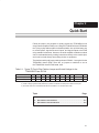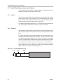
1
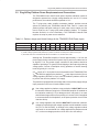
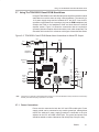
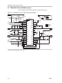
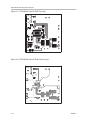
TPA032D03 Mono ClassĆD Audio Power Amplifier With Stereo Headphone Amplifier Evaluation Module User’s Guide September 2000 Mixed-Signal Products SLOU082 IMPORTANT NOTICE Texas Instruments and its subsidiaries (TI) reserve the right to make changes to their products or to discontinue any product or service without notice, and advise customers to obtain the latest version of relevant information to verify, before placing orders, that information being relied on is current and complete. All products are sold subject to the terms and conditions of sale supplied at the time of order acknowledgment, including those pertaining to warranty, patent infringement, and limitation of liability. TI warrants performance of its semiconductor products to the specifications applicable at the time of sale in accordance with TI’s standard warranty. Testing and other quality control techniques are utilized to the extent TI deems necessary to support this warranty. Specific testing of all parameters of each device is not necessarily performed, except those mandated by government requirements. Customers are responsible for their applications using TI components. In order to minimize risks associated with the customer’s applications, adequate design and operating safeguards must be provided by the customer to minimize inherent or procedural hazards. TI assumes no liability for applications assistance or customer product design. TI does not warrant or represent that any license, either express or implied, is granted under any patent right, copyright, mask work right, or other intellectual property right of TI covering or relating to any combination, machine, or process in which such semiconductor products or services might be or are used. TI’s publication of information regarding any third party’s products or services does not constitute TI’s approval, warranty or endorsement thereof. Copyright 2000, Texas Instruments Incorporated Preface Related Documentation From Texas Instruments J J J J TI Plug-N-Play Audio Amplifier Evaluation Platform (TI Literature Number SLOU011) provides detailed information on the evaluation platform and its use with TI audio evaluation modules. TPA032D03 CLASS-D AUDIO POWER AMPLIFIER (TI Literature Number SLOS283) This is the data sheet for the TPA032D03 audio amplifier integrated circuit. Design Considerations for Class-D Audio Power Amplifiers, (TI Literature Number SLOA031) This application report provides detailed information on designing audio power amplifier systems using TI class-D amplifier ICs Reducing and Eliminating the Class-D Output Filter, (TI Literature Number SLOA023) This application report covers output filter theory and design for class-D audio power amplifiers. FCC Warning This equipment is intended for use in a laboratory test environment only. It generates, uses, and can radiate radio frequency energy and has not been tested for compliance with the limits of computing devices pursuant to subpart J of part 15 of FCC rules, which are designed to provide reasonable protection against radio frequency interference. Operation of this equipment in other environments may cause interference with radio communications, in which case the user at his own expense will be required to take whatever measures may be required to correct this interference. Trademarks PowerPAD is a trademark of Texas Instruments. Chapter Title—Attribute Reference iii iv Running Title—Attribute Reference Contents 1 Introduction . . . . . . . . . . . . . . . . . . . . . . . . . . . . . . . . . . . . . . . . . . . . . . . . . . . . . . . . . . . . . . . . . . . . . 1.1 Feature Highlights . . . . . . . . . . . . . . . . . . . . . . . . . . . . . . . . . . . . . . . . . . . . . . . . . . . . . . . . . . 1.2 Description . . . . . . . . . . . . . . . . . . . . . . . . . . . . . . . . . . . . . . . . . . . . . . . . . . . . . . . . . . . . . . . . 1.3 TPA032D03 Class-D EVM Specifications . . . . . . . . . . . . . . . . . . . . . . . . . . . . . . . . . . . . . . 1.3.1 Maximum . . . . . . . . . . . . . . . . . . . . . . . . . . . . . . . . . . . . . . . . . . . . . . . . . . . . . . . . . . . 1.3.2 Typical . . . . . . . . . . . . . . . . . . . . . . . . . . . . . . . . . . . . . . . . . . . . . . . . . . . . . . . . . . . . . 1-1 1-2 1-3 1-4 1-4 1-4 2 Quick Start . . . . . . . . . . . . . . . . . . . . . . . . . . . . . . . . . . . . . . . . . . . . . . . . . . . . . . . . . . . . . . . . . . . . . . 2.1 Precautions . . . . . . . . . . . . . . . . . . . . . . . . . . . . . . . . . . . . . . . . . . . . . . . . . . . . . . . . . . . . . . . . 2.2 Quick Start List for Platform . . . . . . . . . . . . . . . . . . . . . . . . . . . . . . . . . . . . . . . . . . . . . . . . . . 2.3 Quick Start List for Stand-Alone . . . . . . . . . . . . . . . . . . . . . . . . . . . . . . . . . . . . . . . . . . . . . . 2-1 2-2 2-3 2-4 3 Details . . . . . . . . . . . . . . . . . . . . . . . . . . . . . . . . . . . . . . . . . . . . . . . . . . . . . . . . . . . . . . . . . . . . . . . . . . 3-1 3.1 Precautions . . . . . . . . . . . . . . . . . . . . . . . . . . . . . . . . . . . . . . . . . . . . . . . . . . . . . . . . . . . . . . . . 3-2 3.2 Plug-N-Play Platform Power Requirements and Connections . . . . . . . . . . . . . . . . . . . . . 3-3 3.3 Plug-N-Play Platform Inputs and Outputs . . . . . . . . . . . . . . . . . . . . . . . . . . . . . . . . . . . . . . 3-4 3.3.1 Inputs . . . . . . . . . . . . . . . . . . . . . . . . . . . . . . . . . . . . . . . . . . . . . . . . . . . . . . . . . . . . . . 3-4 3.3.2 Outputs . . . . . . . . . . . . . . . . . . . . . . . . . . . . . . . . . . . . . . . . . . . . . . . . . . . . . . . . . . . . 3-4 3.4 Control and Indicator Circuits . . . . . . . . . . . . . . . . . . . . . . . . . . . . . . . . . . . . . . . . . . . . . . . . . 3-5 3.5 TPA032D03 Class-D EVM Test Points . . . . . . . . . . . . . . . . . . . . . . . . . . . . . . . . . . . . . . . . . 3-5 3.6 Module Switches . . . . . . . . . . . . . . . . . . . . . . . . . . . . . . . . . . . . . . . . . . . . . . . . . . . . . . . . . . . 3-6 3.6.1 S1 — Shutdown . . . . . . . . . . . . . . . . . . . . . . . . . . . . . . . . . . . . . . . . . . . . . . . . . . . . . 3-6 3.6.2 S2 — Mute Switch . . . . . . . . . . . . . . . . . . . . . . . . . . . . . . . . . . . . . . . . . . . . . . . . . . . 3-6 3.7 Using The TPA032D03 Class-D EVM Stand-Alone . . . . . . . . . . . . . . . . . . . . . . . . . . . . . . 3-7 3.7.1 Power Connections . . . . . . . . . . . . . . . . . . . . . . . . . . . . . . . . . . . . . . . . . . . . . . . . . . 3-7 3.7.2 Input Connections . . . . . . . . . . . . . . . . . . . . . . . . . . . . . . . . . . . . . . . . . . . . . . . . . . . 3-8 3.7.3 Output Connections . . . . . . . . . . . . . . . . . . . . . . . . . . . . . . . . . . . . . . . . . . . . . . . . . . 3-8 3.7.4 Controls and Indicators . . . . . . . . . . . . . . . . . . . . . . . . . . . . . . . . . . . . . . . . . . . . . . . 3-8 3.8 TPA032D03 Class-D EVM Bill of Materials . . . . . . . . . . . . . . . . . . . . . . . . . . . . . . . . . . . . . 3-9 3.9 TPA032D03 Class-D EVM Schematic . . . . . . . . . . . . . . . . . . . . . . . . . . . . . . . . . . . . . . . . 3-10 3.10 TPA032D03 Class-D EVM PCB Layers . . . . . . . . . . . . . . . . . . . . . . . . . . . . . . . . . . . . . . . 3-11 Chapter Title—Attribute Reference v Running Title—Attribute Reference Figures 1–1 1–2 2–1 3–1 3–2 3–3 3–4 3–5 3–6 3–7 3–8 3–9 3–10 The TI TPA032D03 Mono Class-D Audio Power Amplifier EVM — Top View . . . . . . . . . . 1-3 The TI TPA032D03 Mono Class-D Audio Power Amplifier EVM — Bottom View . . . . . . . 1-3 Quick Start Platform Map . . . . . . . . . . . . . . . . . . . . . . . . . . . . . . . . . . . . . . . . . . . . . . . . . . . . . . 2-2 The TI Plug-N-Play Audio Amplifier Evaluation Platform . . . . . . . . . . . . . . . . . . . . . . . . . . . . 3-2 Typical Headphone Plug . . . . . . . . . . . . . . . . . . . . . . . . . . . . . . . . . . . . . . . . . . . . . . . . . . . . . . . 3-4 TPA032D03 Class-D EVM Stand-Alone Connections for Mono BTL Output . . . . . . . . . . . 3-7 TPA032D03 Class-D EVM Schematic Diagram. . . . . . . . . . . . . . . . . . . . . . . . . . . . . . . . . . . 3-10 TPA032D03 Class-D EVM Top Assembly. . . . . . . . . . . . . . . . . . . . . . . . . . . . . . . . . . . . . . . . 3-11 TPA032D03 Class-D EVM Bottom Assembly . . . . . . . . . . . . . . . . . . . . . . . . . . . . . . . . . . . . 3-11 TPA032D03 Class-D EVM Top Layer . . . . . . . . . . . . . . . . . . . . . . . . . . . . . . . . . . . . . . . . . . . 3-12 TPA032D03 Class-D EVM Second Layer. . . . . . . . . . . . . . . . . . . . . . . . . . . . . . . . . . . . . . . . 3-12 TPA032D03 Class-D EVM Third Layer. . . . . . . . . . . . . . . . . . . . . . . . . . . . . . . . . . . . . . . . . . 3-13 TPA032D03 Class-D EVM Bottom Layer. . . . . . . . . . . . . . . . . . . . . . . . . . . . . . . . . . . . . . . . . 3-13 Tables 2–1 2–2 3–1 3–2 3–3 3–4 vi Typical TI Plug-N-Play Platform Jumper and Switch Settings for the TPA032D03 Class-D EVM . . . . . . . . . . . . . . . . . . . . . . . . . . . . . . . . . . . . . . . . . . . . . . . . . . . . Platform Jumper and Switch Settings for the TPA032D03 . . . . . . . . . . . . . . . . . . . . . . . . . . Platform Jumper and Switch Settings for the TPA032D03 EVM Power Inputs . . . . . . . . . TPA032D03 Class-D EVM Fault Indicator Table . . . . . . . . . . . . . . . . . . . . . . . . . . . . . . . . . . . TPA032D03 Class-D EVM Test Points . . . . . . . . . . . . . . . . . . . . . . . . . . . . . . . . . . . . . . . . . . . TPA032D03 Class-D EVM Bill of Materials . . . . . . . . . . . . . . . . . . . . . . . . . . . . . . . . . . . . . . . 2-1 2-3 3-3 3-5 3-5 3-9 Chapter 1 Introduction This chapter provides an overview of the Texas Instruments (TI) TPA032D03 mono class-D audio power amplifier evaluation module (SLOP310). It includes a list of EVM features, a brief description of the module illustrated with a pictorial diagram, and a list of EVM specifications. Topic Page 1.1 Feature Highlights . . . . . . . . . . . . . . . . . . . . . . . . . . . . . . . . . . . . . . . . . . . . 1–2 1.2 Description . . . . . . . . . . . . . . . . . . . . . . . . . . . . . . . . . . . . . . . . . . . . . . . . . . . 1–3 1.3 TPA032D03 Class-D EVM Specifications . . . . . . . . . . . . . . . . . . . . . . . . 1–4 Introduction 1-1 Feature Highlights 1.1 Feature Highlights The TI TPA032D03 mono class-D audio power amplifier evaluation module and the TI plug-n-play audio amplifier evaluation platform include the following features: - TPA032D03 Mono Class-D Audio Power Amplifier with Stereo Headphone Amplifier Evaluation Module J J J J J J J J J J J - J J J J - 1-2 Single channel, class D bridge-tied load (BTL) only operation 12 V operation 10 W BTL output into 4 Ω at 12 V Low current consumption in shutdown/mute mode (20 µA/10 mA) ?? Internal gain set to 25 dB IC shutdown, mute, and mode control inputs — TTL logic level High efficiency Class AB stereo headphone driver — capable of 50 mW into 32 Ω Onboard stereo headphone output jack CE tested and approved. Quick and Easy Configuration With the TI Plug-N-Play Audio Amplifier Evaluation Platform J - Internal depop circuitry to greatly reduce turn-on transients in outputs Evaluation module is designed to simply plug into the platform, automatically making all signal, control, and power connections Platform provides flexible power options Jumpers on the platform select power and module control options Switches on the platform route signals Platform provides quick and easy audio input and output connections Platform Power Options J J J J External 5-V – 15-V VCC supply inputs External regulated VDD supply input Socket for onboard 5 V/3.3 V VDD voltage regulator EVM Onboard overvoltage and reverse polarity power protection Platform Audio Input and Output Connections J J J J J Left and right RCA phono jack inputs Miniature stereo phone jack input Left and right RCA phono jack outputs Left and right compression speaker terminal outputs Miniature stereo headphone jack output Introduction Description 1.2 Description The TPA032D03 mono class-D audio power amplifier evaluation module is a complete, 10-W mono audio power amplifier. It consists of the TI TPA032D03 mono class-D audio power amplifier IC along with a small number of other parts mounted on a circuit board that measures approximately 2 inches by 1 inches (Figure 1–1 and 1–2). ¼ ¾ Figure 1–1. The TI TPA032D03 Mono Class-D Audio Power Amplifier EVM — Top View C19 SLOP310 TPA032D03 EVM Board GND VCC C20 R11 R12 R13 R14 J1 Texas Instruments 2000 C5 C16 R9 R10 C12 U1 C18 TP1 R1 Mode Mute SD C3 OUT– C4 C11 + VDD GND L2 L1 R2 C2 R6 R5 R3 –IN+ GND LHP Note: SD S1 Mute S2 R7 R8 C17 TP2 TP3 RHP GND C1 R4 OUT+ VCC Capacitor C11 is optional (not assembled) and a location for it on the EVM PCB has been provided to increase design flexibility and allow decoupling capacitance to be added. Figure 1–2. The TI TPA032D03 Mono Class-D Audio Power Amplifier EVM — Bottom View C23 C22 C10 C21 C6 C7 C9 C15 C13 C8 C14 Introduction 1-3 TPA032D03 Class-D EVM Specifications Single in-line header pins extend from the underside of the module circuit board to allow the EVM to either be plugged into the TI plug-n-play audio amplifier evaluation platform, or to be wired directly into existing circuits and equipment when used stand-alone. The platform has room for a single TPA032D03 class-D evaluation module and is a convenient vehicle for demonstrating TI’s audio power amplifier and related evaluation modules. The EVM simply plugs into the platform, which automatically provides power to the modules, interconnects them correctly, and connects them to a versatile array of standard audio input and output jacks and connectors. Easy-to-use configuration controls allow the platform and EVMs to quickly model many possible end-equipment configurations. There is nothing to build, nothing to solder, and nothing but the speakers included with the platform to hook up. 1.3 TPA032D03 Class-D EVM Specifications All measurements made with VDD = 12 V and RL = 4 Ω, unless otherwise noted. 1.3.1 Maximum Supply voltage range, VDD . . . . . . . . . . . . . . . . . . . . . . . . . . . . . . . . . . . . . . . . . . . . . . . . 9 V to 14 V Supply current, IDD . . . . . . . . . . . . . . . . . . . . . . . . . . . . . . . . . . . . . . . . . . . . . . . . . . . . . . . . . . . . 4.6 A Continuous output power per channel, BTL, PO . . . . . . . . . . . . . . . . . . . . . . . . . . . . . . . . . . . 10 W Continuous output power per channel, headphones, PO: 32-Ω SE . . . . . . . . . . . . . . . . . . 50 mW Audio input voltage, class-D, VI . . . . . . . . . . . . . . . . . . . . . . . . . . . . . . . . . . . . . . . . . . . . 350 mVrms Audio input voltage, headphone, VI . . . . . . . . . . . . . . . . . . . . . . . . . . . . . . . . . . . . . . . . . . . 1.6 Vrms 1.3.2 Typical Supply current, no input, class-D active, IDD . . . . . . . . . . . . . . . . . . . . . . . . . . . . . . . . . . . . . 55 mA Supply current, no input, headphone active, IDD . . . . . . . . . . . . . . . . . . . . . . . . . . . . . . . . . 10 mA Supply current, EVM mute, class-D active, IDD . . . . . . . . . . . . . . . . . . . . . . . . . . . . . . . . . . 2.5 mA Supply current, EVM mute, headphone active, IDD . . . . . . . . . . . . . . . . . . . . . . . . . . . . . . . . 2 mA Supply current, EVM shutdown, IDD . . . . . . . . . . . . . . . . . . . . . . . . . . . . . . . . . . . . . . . . . . . . 147 µA Gain, class-D . . . . . . . . . . . . . . . . . . . . . . . . . . . . . . . . . . . . . . . . . . . . . . . . . . . . . . . . . . . . . . . . . 25 dB Gain, headphone . . . . . . . . . . . . . . . . . . . . . . . . . . . . . . . . . . . . . . . . . . . . . . . . . . . . . . . . . . . . . . 0 dB Crosstalk, headphone, PO = 30 mW @ 1 kHz . . . . . . . . . . . . . . . . . . . . . . . . . . . . . . . . . . . . – 70 dB Total harmonic distortion + noise, class-D, PO = 1 W @ 1 kHz . . . . . . . . . . . . . . . . . . . . . . 0.14 % Total harmonic distortion + noise, headphone, PO = 30 mW @ 1 kHz . . . . . . . . . . . . . . . . . 0.3 % 1-4 Introduction Chapter 2 Quick Start Follow the steps in this chapter to quickly prepare the TPA032D03 mono class-D audio amplifier EVM for use. Using the TPA032D03 class-D EVM with the TI plug-n-play audio amplifier evaluation platform is a quick and easy way to connect power, signal and control inputs, and signal outputs to the EVM using standard connectors. However, the audio amplifier evaluation module can be used stand-alone by making connections directly to the module pins, and it can be wired directly into existing circuits or equipment. The platform switch and jumper settings shown in Table 2–1 are typical for the TPA032D03 class-D EVM. There are no jumpers or switches to set on the TPA032D03 class-D EVM board, itself. Table 2–1. Typical TI Plug-N-Play Platform Jumper and Switch Settings for the TPA032D03 Class-D EVM POWER TYPE (Note 2) JP1 JP2 JP3 JP4 JP5 JP6 JP7 JP8 S1 S2 (Note 3) S3 VCC (J1) ON OFF OFF ON ON Mute X Lo ON OFF U5 AC/DC (J2) OFF ON OFF ON ON Mute X Lo ON OFF U5 Notes: 1) ON = Jumper installed, OFF = Jumper NOT Installed, X = Don’t care 2) Install a voltage regulator EVM (SLVP097) in platform socket U6 for VDD power to EVM control inputs. 3) Set to ON when Tone Control Board SLOP109 is installed in U1, otherwise set to OFF. Topic Page 2.1 Precautions . . . . . . . . . . . . . . . . . . . . . . . . . . . . . . . . . . . . . . . . . . . . . . . . . . 2–2 2.2 Quick Start List for Platform . . . . . . . . . . . . . . . . . . . . . . . . . . . . . . . . . . . 2–3 2.3 Quick Start List for Stand-Alone . . . . . . . . . . . . . . . . . . . . . . . . . . . . . . . . 2–5 Quick Start 2-1 Precautions 2.1 Precautions Power Supply Input Polarity and Maximum Voltage Always ensure that the polarity and voltage of the external power connected to VCC power input connector J1, J2, and/or VDD power input connector J6 are correct. Overvoltage or reverse-polarity power applied to these terminals can open onboard soldered-in fuses and cause other damage to the platform, installed evaluation modules, and/or the power source. Inserting or Removing EVM Boards Do not insert or remove EVM boards with power applied — damage to the EVM board, the platform, or both may result. Figure 2–1. Quick Start Platform Map 1 8 On C1+ 10 ICC VR2 JP4 F2 + Speaker Output – Left Out On Conditioning J9 Stereo Headphone Output J10 + HP Out R4 4 5 Left Out + S3 HP Source Spk(U2-U4) C3 C2 JP8 U5 JP7 HP(U5) U2-U4 R3 14 + JP6 U4 U5 GND TP1 TEXAS INSTRUMENTS 1997 2 J6 VDD In/Out + Right – Out U2 U1 J5 Left In 3 16 J8 J7 Right Out LED2 VDD U3 Off S2 J4 Stereo In Plug-N-Play Audio Amplifier Evaluation Platform SLOP097 Rev. C.1 Mode Mute Polarity Lo Hi ****CAUTION**** Do not insert or remove EVM boards with power applied 2-2 U6 JP5 IDD Audio Power Amps 17 DC Power In/Out R2 R1 LED1 VCC J3 Right In Audio Input 13 POWER B1 SUPPLY S1 Pwr VR1 Signal Conditioning 12 11 D1 D2 D3 D4 J2 AC/DC In Power Input Off J1 JP3 Batt JP2 AC/DC JP1 (J2) VCC(J1) DC SOURCE VCC In + 7 F1 9 R5 6 Quick Start Quick Start List for Platform 2.2 Quick Start List for Platform Follow these steps when using the TPA032D03 class-D EVM with the TI plug-n-play audio amplifier evaluation platform (see the platform user’s guide, SLOU011, for additional details). Numbered callouts for selected steps are shown in Figure 2–1 and details appear in Chapter 3. - Platform Preparations 1) Ensure that all external power sources and platform power switch S1 are set to OFF. 2) Install a TPA032D03 module in platform socket U2, taking care to align the module pins correctly (EVM power pins engage sockets U2 and U3). 3) Set switch S2 to OFF. 4) Set switch S3 to U5. 5) Set jumper JP6 to select the Mute control input. 6) Set control signal Polarity jumper JP8 to Lo. Table 2–2. Platform Jumper and Switch Settings for the TPA032D03 POWER TYPE (Note 2) JP1 JP4 JP5 JP6 JP7 JP8 S1 S2 (Note3) S3 VCC (J1) ON ON ON Mute X Lo ON OFF U5 Notes: 1) ON = Jumper installed, OFF = Jumper NOT Installed, X = Don’t care 2) Install a voltage regulator EVM (SLVP097) in platform socket U6 for VDD power to EVM control inputs. 3) Set to ON Tone Control Board SLOP109 is installed in U1. - Power supply 7) Connect a 12-V regulated power supply (ensure power supply is set to OFF ) to J1, taking care to observe marked polarity. 8) Set jumper JP1 for dc source to be from input J1. 9) Set jumper JP4 for VCC power to EVMs. 10) Install a voltage regulator EVM (SLVP097) in platform socket U6. - 11) Set jumper JP5 for VDD power to EVMs. Inputs and outputs 12) Ensure that the audio signal source level is set to minimum. 13) Connect the audio source to left and right RCA phono jacks J3 and J5 or mono miniature phone jack J4. - 14) Connect 4-Ω – 8-Ω speakers to left RCA jack J9 or to stripped wire speaker connectors J8. Power up 15) Verify correct voltage and input polarity and set the external power supply and platform power switch S1 to ON. Platform LED1 and LED2 should light indicating the presence of VCC and VDD, and the evaluation module(s) installed on the platform should begin operation. 16) Set switch S2 to ON if tone control board SLOP109 is installed in U1. 17) Adjust the signal source level as needed. Quick Start 2-3 Quick Start List for Stand-Alone 2.3 Quick Start List for Stand-Alone Follow these steps to use the TPA032D03 class-D EVM stand-alone or to connect it into existing circuits or equipment. Connections to the TPA032D03 module header pins can be made via individual sockets, wire-wrapping, or soldering to the pins, either on the top or the bottom of the module circuit board. - Power supply 1) Ensure that all external power sources are set to OFF. 2) Connect an external regulated power supply set to 12 V to the module VCC and GND pins taking care to observe marked polarity. It is only necessary to use the ground pins adjacent to the module power pins. 3) Connect an external regulated power supply set to 5 V to the module VDD pin taking care to observe marked polarity. - Inputs and outputs 4) Ensure that audio signal source level adjustments are set to minimum. 5) Connect the audio source across the module IN+ and IN– pins for class-D operation, taking care to observe marked polarity. For single-ended input, the negative input pin (IN–) should be connected to the ground of the audio signal source. 6) Connect a control signal to the module Mute pin, if necessary. The control signal should be high (2 V to 5 V or left floating) for normal operation, or low (tied to ground) to mute the output. 7) Connect a control signal to the module SD pin, if necessary. The control signal should be high (2 V to 5 V or left floating) for normal operation, or low (tied to ground) to shut down the TPA032D03 amplifier IC on the EVM. Note that the control signals applied to the EVM Mute and SD inputs must have sufficient current capability to overcome the 100-kΩ pullup resistor on each input. Miniature pushbutton switches on the EVM allow manual shutdown (S2) and manual muting (S1) of the amplifier. 8) Connect a 4-Ω – 8-Ω speaker to the module OUT+ and OUT– pins, taking care to observe marked polarity. - Power up 9) Verify correct voltage and input polarity and set the external power supply to ON. The EVM should begin operation. 10) Adjust the signal source level as needed. 2-4 Quick Start Chapter 3 Details This chapter provides details on the TPA032D03 IC evaluation module, a parts list for the TPA032D03 class-D evaluation module, and module PCB layer illustrations. Topic Page 3.1 Precautions . . . . . . . . . . . . . . . . . . . . . . . . . . . . . . . . . . . . . . . . . . . . . . . . . . 3-2 3.2 Plug-N-Play Platform Power Requirements and Connections . . . . . 3-3 3.3 Plug-N-Play Platform Inputs and Outputs . . . . . . . . . . . . . . . . . . . . . . . 3-4 3.4 Control and Indicator Circuits . . . . . . . . . . . . . . . . . . . . . . . . . . . . . . . . . . 3-5 3.5 TPA032D03 Class-D EVM Test Points . . . . . . . . . . . . . . . . . . . . . . . . . . . 3-5 3.6 Module Switches . . . . . . . . . . . . . . . . . . . . . . . . . . . . . . . . . . . . . . . . . . . . . . 3-6 3.7 Using The TPA032D03 Class-D EVM Stand-Alone . . . . . . . . . . . . . . . . 3-7 3.8 TPA032D03 Bill of Materials . . . . . . . . . . . . . . . . . . . . . . . . . . . . . . . . . . . . 3-9 3.9 TPA032D03 Class-D EVM Schematic . . . . . . . . . . . . . . . . . . . . . . . . . . . 3-10 3.10 TPA032D03 Class-D EVM PCB Layers . . . . . . . . . . . . . . . . . . . . . . . . . 3-11 Details 3-1 Precautions 3.1 Precautions Power Supply Input Polarity and Maximum Voltage Always ensure that the polarity and voltage of the external power connected to VCC power input connector J1, J2, and/or VDD power input connector J6 are correct. Overvoltage or reverse-polarity power applied to these terminals can open onboard soldered-in fuses and cause other damage to the platform, installed evaluation modules, and/or the power source. Inserting or Removing EVM Boards Do not insert or remove EVM boards with power applied — damage to the EVM board, the platform, or both may result. Figure 3–1. The TI Plug-N-Play Audio Amplifier Evaluation Platform C1+ On Off ICC VR2 JP4 VR1 F2 + J6 VDD In/Out J8 J7 Right Out LED2 VDD + Right – Out U3 Off S2 J4 Stereo In U2 U1 Speaker Output – Left Out On Conditioning J5 Left In J9 Left Out + Stereo Headphone Output HP Out J10 + S3 HP Source R4 Spk(U2-U4) C3 C2 JP8 U5 JP7 HP(U5) U2-U4 U5 GND TP1 TEXAS INSTRUMENTS 1997 R3 + JP6 U4 Mode Mute Polarity Lo Hi ****CAUTION**** Do not insert or remove EVM boards with power applied 3-2 U6 JP5 IDD LED1 VCC J3 Right In Audio Power Amps Plug-N-Play Audio Amplifier Evaluation Platform SLOP097 Rev. C.1 DC Power In/Out R2 R1 Signal Conditioning Audio Input POWER B1 D1 D2 D3 D4 J2 AC/DC In SUPPLY S1 Pwr J1 JP3 Batt JP2 AC/DC JP1 (J2) VCC(J1) DC SOURCE VCC In + Power Input F1 R5 Details Plug-N-Play Platform Power Requirements and Connections 3.2 Plug-N-Play Platform Power Requirements and Connections The TPA032D03 mono class-D audio power amplifier evaluation module is designed to operate from a supply voltage between 9 V and 14 V. For best performance, the module should be operated at 12 V. The TI plug-n-play audio amplifier evaluation platform provides several options for powering the TPA032D03 class-D EVM. Table 3–1 shows the platform jumper and switch settings for each power source option (see the User’s Guide for the TI plug-n-play audio amplifier platform, TI Literature Number SLOU011 for more information). The TPA032D03 class-D EVM requires no setup for power source selection. Table 3–1. Platform Jumper and Switch Settings for the TPA032D03 EVM Power Inputs POWER TYPE (Note 2) Notes: JP1 JP2 JP3 JP4 JP5 JP6 JP7 JP8 S1 S2 (Note 3) S3 VCC (J1) ON OFF OFF ON ON Mute X Lo ON OFF U5 AC/DC (J2) OFF ON OFF ON ON Mute X Lo ON OFF U5 1) ON = Jumper installed, OFF = Jumper NOT Installed, X = Don’t care 2) Install a voltage regulator EVM (SLVP097) in platform socket U6 for VDD power to EVM control inputs. 3) Set to ON when Tone Control Board SLOP109 is installed in U1, otherwise set to OFF. Although the TPA032D03 amplifier IC draws approximately 1.6 A from the power supply during continuous full power output, peak current draw can be as high as 2.3 A. Any power supply connected to the platform should be capable of providing 2.3 A (peak) to avoid clipping of the output signal during voltage peaks. Current consumption driving speakers at normal listening levels is typically 0.1 A or less. A VDD supply of 5 V is required for normal operation of the TPA032D03 EVM. VDD can either be applied to the platform VDD power input terminals (J6) or a voltage regulator (SLVP097 or equiv.) can be installed in platform socket U6 to provide VDD from the platform VCC supply. The platform is equipped with overvoltage and reverse-polarity supply voltage input protection in the form of fused crowbar circuits. - - VDD voltage applied to platform screw terminals J6 MUST NOT exceed the absolute maximum rating for the TPA032D03 amplifier IC installed on the evaluation module (5.5 V) or damage to the IC may result. In no case should VDD voltage of the incorrect polarity or in excess of 6.0 V be applied to screw terminals J6 of the platform, or the power protection circuit on the VDD line will trip. VCC voltage applied to the platform MUST NOT exceed the maximum voltage input specified for the voltage regulator module installed in socket U6 (12 V for the SLVP097), or damage to the voltage regulator module may result. In no case should VCC voltage applied to the platform exceed 15 V, or the overvoltage protection circuit on the VCC bus will trip. Details 3-3 Plug-N-Play Platform Inputs and Outputs 3.3 Plug-N-Play Platform Inputs and Outputs The TI plug-n-play audio amplifier evaluation platform is equipped with several standard conectors for audio inputs and outputs. 3.3.1 Inputs In most cases, audio signals enter the platform through either a pair of RCA phono jacks (J3 and J5) or a miniature (1/8″) mono phone jack (J4). Certain signal conditioning and amplifier EVMs, however, may have additional signal input connectors mounted on the module circuit board. The platform audio signal input jacks (J3, J4, and J5) are of the closed-circuit type, grounding the signal input lines when no plugs are inserted. 3.3.2 Outputs Amplified audio output signals leave the platform through the left RCA phono jack (J9) and the left pair of compression connectors for stripped speaker wires (J8). The audio output lines from the power amplifiers are separate all the way to the edge of the platform (output jacks J8 and J9) — the OUT+ and OUT– lines from the power amplifier sockets are not tied to each other or to platform ground. This allows the TPA032D03 class-D power amplifier EVM to operate in the highly-efficient bridge-tied load configuration when driving speakers. The headphone jack (J10) is capacitively coupled to source select switch S3, which connects J10 to the output lines of either the headphone amplifier socket or the power amplifier sockets (Figure 3 – 2). Figure 3–2. Typical Headphone Plug Left 3-4 Right GND Details Plug-N-Play Platform Inputs and Outputs 3.4 Control and Indicator Circuits Three main control circuits are provided with the TPA032D03. The mute circuit grounds the output of the active amplifier, the mode circuit selects between the class-D amplifier and the headphone amplifier, and the shutdown circuit places the entire device into a power-saving sleep mode to minimize current consumption. Each of these inputs is TTL compatible: less than 0.8 V applied to these pins is considered a logic low, and any voltage greater than 2 V is considered a logic high. Two indicator pins are also provided for feedback when an under-voltage or thermal fault exists. Module pins are provided for easy connection of off-board control and monitoring. There are two active low fault indicator pins on the TPA032D03 amplifier IC (IC pins 41 and 42) that provide feedback when a fault condition exists. Signals on these pins provide the status of the acvtive amplifier: operational, thermal fault, and under-voltage lockout. Table 3–2 lists the possible output conditions of these pins and a description of the fault indicated. Table 3–2. TPA032D03 Class-D EVM Fault Indicator Table FAULT 0 (TP 1) FAULT 1 (TP 2) 1 1 No fault. — The device is operating normally. 0 1 Charge pump under-voltage lockout (VCP-UV) fault. All low-side transistors are turned on, shorting the load to ground. Normal operation resumes when the charge pump voltage is restored (not a latched fault), however the Fault indication remains active until cleared by cycling MUTE, SHUTDOWN, or the power supply. 0 0 Thermal fault. All of the low-side transistors are turned on, shorting the load to ground. Once the junction temperature drops by 20°C, normal operation resumes (not a latched fault). The Fault indication remains active until cleared by cycling MUTE, SHUTDOWN, or the power supply. DESCRIPTION 3.5 TPA032D03 Class-D EVM Test Points Test points have been included on the TPA032D03 class-D EVM to facilitate user analysis of device performance and design adjustments. Table 3–3 lists each test point and its corresponding function. Table 3–3. TPA032D03 Class-D EVM Test Points TEST POINT IC PIN or EVM FUNCTION FUNCTION 1 HPVCC 2 FAULT_1 Onboard 5-V supply MSB for logic-level fault output signal, open drain 3 FAULT_0 LSB for logic-level fault output signal, open drain Details 3-5 Plug-N-Play Platform Inputs and Outputs 3.6 Module Switches The TPA032D03 mono class-D audio amplifier evaluation module is equipped with two pushbutton switches that allow the module shutdown and mute functions to be manually activated. 3.6.1 S1 — Shutdown Switch To have the module amplifier IC enter the shutdown mode, press the Shutdown switch (S2) on the module. S2 connects the amplifier IC SHUTDOWN pin to ground, forcing it into a low-power state. This function can be controlled by an external control input to the SD module pin. The shutdown mode reduces the amplifier IC current consumption to less than 1 µA compared to approximately 2.5 mA in the mute mode. The EVM shutdown current is based on VCC, VDD, R2, R5, and R6, and capacitor leakage currents, but will typically be 97 µA ±5% for VCC = 12 V and VDD = 5 V. The plug-n-play platform typically draws 60 mA of current. 3.6.2 S2 — Mute Switch Pushbutton switch S1 on the TPA032D03 class-D EVM allows manual muting of the amplifier IC. S1 connects the amplifier IC MUTE pin to ground, muting the output. The EVM Mute control input pin also allows external control of this function. In the mute mode, the amplifier IC lowside output transistors are turned on, shorting the load to ground. This reduces the EVM current to 2.5 mA. 3.6.3 J1 — Headphone Jack Mode Switch EVM headphone jack J1 is equipped with an internal switch that grounds the amplifier MODE pin until a plug is inserted into the jack. When a plug is inserted into the headphone jack, the IC MODE pin goes high and the IC headphone amplifier goes active and the class-D amplifier shuts off. 3-6 Details Using The TPA032D03 Class-D EVM Stand-Alone 3.7 Using The TPA032D03 Class-D EVM Stand-Alone Using the TPA032D03 mono class-D audio power amplifier evaluation module stand-alone is much the same as using it with the platform. The same 9-V to 14-V power supply range and the isolated OUT+ and OUT– lines for BTL operation requirements exist. Inserting a plug into the EVM headphone jack switches the EVM to the headphone mode and shuts down the class-D amplifier section. Figure 3–3 shows the connections that are required for operation (with the exception of the fault monitor circuit, which is optional). The discussion in this section is in reference to this figure unless otherwise noted. Figure 3–3. TPA032D03 Class-D EVM Stand-Alone Connections for Mono BTL Output LED 1 5V 12 V R Fault Monitor R LED 0 C19 SLOP310 C20 Headphone Output Jack R11 R12 R13 R14 J1 C16 Mute R9 R10 U1 C18 TP1 C12 SD S1 Mute S2 Texas Instruments 2000 C5 Mute SD Shutdown C3 OUT– C4 R2 C2 + VDD GND VCC L2 C11 R6 R5 R3 L1 Left HP Input –IN+ GND LHP Audio Line Inputs R1 Mode Mode R7 R8 C17 TP2 C1 R4 TP3 RHP GND Right HP Input TPA032D03 EVM Board GND VCC OUT+ 5V Note: 3.7.1 Capacitor C11 is optional (not assembled) and a location for it on the EVM PCB has been provided to increase design flexibility and allow decoupling capacitance to be added. Power Connections Power must be connected to both the VCC and VDD module pins. Power supply ground can be connected to any module ground pin, although best results are achieved if power supply grounds are connected to the pins adjacent to the VCC and VDD module pins. The ground and power wires should be twisted to reduce inductance and noise pickup if they are long. Details 3-7 Using The TPA032D03 Class-D EVM Stand-Alone 3.7.2 Input Connections The class-D amplifier input signals can be connected in either of two ways: differential or single-ended. For differential operation, connect the signal source to the positive and negative inputs (IN+ and IN– module pins). For single-ended operation, the input signal line should be connected to the IN+ module pin and the signal source ground wire should be connected to the IN– module pin. The EVM headphone amplifier inputs are single-ended, and the signal source should be connected to the RHP and LHP module pins. For best results, the ground of the signal source should be connected to the module GND pins at the EVM headphone inputs to provide a return path for the current. The input signal and ground wires should be twisted to reduce inductance and noise pickup if the lead lengths are long and the cable is not shielded. 3.7.3 Output Connections The speaker should be connected between the OUT+ and the OUT– module pins. Inserting a plug into the EVM headphone jack switches the EVM to the headphone mode and shuts down the class-D amplifier section. 3.7.4 Controls and Indicators The mute, mode, and shutdown functions may be controlled externally via the module Mute, Mode, and SD pins. An active-low input to the module Mute pin mutes the selected amplifier. An active-low input to the module Mode pin switches the EVM to the class-D mode and shuts off the headphone amplifier. An active-low input to the module SD pin shuts down the device. A signal of 2 V or higher, allows normal operation. Note that the mute, mode, and shutdown signals applied to the EVM control input pins must be able to supply enough current to overcome the pullup resistor on the module (100 kΩ). The fault indicator circuit can be monitored at FAULT0 (TP1) and FAULT1 (TP2). These are open-drain outputs with 100-kΩ resistors connected to VDD (5 V). A fault table is shown in Section 3.2.1 and in the device data sheet. 3-8 Details TPA032D03 Class-D EVM Bill of Materials 3.8 TPA032D03 Class-D EVM Bill of Materials The components in the bill of materials (Table 3–4) were selected for their common values, availability, and the smallest size available to meet these criteria. Table 3–4. TPA032D03 Class-D EVM Bill of Materials Reference Description Size EVM Qty. Manufacturer/ Part Number C1, C2, C15 Capacitor, Ceramic Chip, 0.1 µF, ±10%, 50 V, X7R 0805 3 Kemet C0805C104J5RAC C3, C4, C7, C8, C9, C12, C13, C23 Capacitor, Ceramic Chip, 1 µF, ±10%, 25 V, X7R 1206 8 Kemet C1206C105K3RAC C16 Capacitor, Ceramic Chip, 0.047 µF, ±10%, 50 V, X7R 0805 1 Kemet C0805V473K5RAC C17, C18 Capacitor, Ceramic Chip, 5.6 pF, ±5%, 50 V, C0G, 0603 2 Kemet C0603C569J5GAC C5, C6 Capacitor, Ceramic Chip, 1 nF, ±5%, 50 V, C0G, 0805 2 Kemet C0805C102J5GAC C10 Capacitor, Ceramic Chip, 10 µF, +80%–20%, 25 V, Y5V 1210 1 muRata GRM235Y5V106Z25 C19, C20 Capacitor, Aluminum Electrolytic, Radial Lead, 33 µF, ±20%, 35 V, FC Series, 80 mΩ @ 100 kHz, 175 ma Ripple, –55°C to +105°C 0.197” × 0.0197” × 0.078” 2 Panasonic EEUFC1V333 C21, C22 Capacitor, Ceramic Chip, 0.22 µF, ±10%, 50 V, X7R 1206 2 Kemet C1206C224K5RAC C11† Not assembled 0.492” × 0.0236” × 0.197” 1 L1, L2 Inductor, SMT, 15 µH, ±20%, 2.2 ADC, 47.2 mΩ @ 1 kHz, –20 to +90°C 0.398” × 0.398” × 0.236” 2 TDK SLF10145T–150M2R2 R1 – R7, R10 Resistor, Thick Film Chip, SMD, 100 kΩ, ±5%, 1/10 W, 100 V, –50 to 150°C, ±200 ppm/°C 0603 8 Vishay/Dale CRCW0603104J R8, R9 Resistor, Thick Film Chip, SMD, 1 kΩ, ±5%, 1/10 W, 100 V, –50 to 150°C, ±200 ppm/°C 0603 2 Vishay/Dale CRCW0603101J R13 Resistor, Thick Film Chip, SMD, 500 kΩ, ±5%, 1/10 W, 100 V, –50 to 150°C, ±200 ppm/°C 0603 1 Vishay/Dale CRCW0603504J R14 Resistor, Thick Film Chip, SMD, 150 kΩ, ±5%, 1/10 W, 100 V, –50 to 150°C, ±200 ppm/°C 0603 1 Vishay/Dale CRCW0603154J TP1 – TP3 Test Points, Red 3 Farnell 240–345 J1 Mini Phone Jack, 3.5 mm, N/C, Stereo 0.512” × 0.472” 1 Mouser 161–3504 Header Pins, Gold, Single, 0.5” Long, 0.25” Wide, 0.100” centers 0.5”, 0.25”, 0.1” 16 Samtec TSW–19–8–G–S S1, S2 Switch, Momentary, Push Button, 12 VDC, 50 mA 0.291” × 0.138” × 0.134” 2 Panasonic EVQ-PJS04K U1 IC, Audio Amplifier, Class-D, 10 W, 48 pin, DCA pkg TSSOP48 1 TI TPA032D03DCA † Capacitor C11 is optional (not assembled) and a location for it on the EVM PCB has been provided to increase design flexibility and allow decoupling capacitance to be added. Details 3-9 TPA032D03 Class-D EVM Schematic 3.9 TPA032D03 Class-D EVM Schematic The TPA032D03 class-D EVM schematic is shown in Figure 3–4. Figure 3–4. TPA032D03 Class-D EVM Schematic Diagram J1 VDD R3 100k R5 100k R6 100k Ring Mode SD Mute S2 Mute R1 100k Mode S1 SD LIN– LIN+ C11† C10 10µF C9 1µF C7 1µF MUTE 3 MODE 4 INN 5 INP 6 COMP 7 AGND 8 9 VCC 10 C22 LOUT+ C23 1µF LOUT– TIP LHP 0.22µF C21 0.22µF L1 15µH 11 12 13 L2 15µH 14 15 16 C20 33µF R2 100k C18 5.6 pF R10 100k C2 0.1µF 17 18 19 20 21 VCC 22 23 C13 1µF SHUTDOWN 2 C3 1µF C4 1µF C6 1000pF C15 0.1µF R8 1k TPA032D03 1 24 3 B COSC AGND AGND AGND AGND AGND FAULT_0 48 46 42 41 PVDD 40 39 NC 38 NC 37 PGND 36 PGND 35 NC 34 NC 33 PVDD 32 HPVCC 31 HPROUT 30 HPRIN 29 V2P5 28 PVDD 27 PGND 26 HPDR 25 CP2 PGND OUTN OUTN PVDD HPREG HPLOUT HPLIN AGND PVDD VCP HPDL CP1 5V 12 V VDD 43 PVDD PGND 1 44 FAULT_1 OUTP R9 1k 45 VDD OUTP C5 1000pF 47 A 2 TIP VCC TP3 TP2 C8 1µF VCC VDD TP1 R13 500k C12 1µF R14 150k C19 33µF RING C18 R7 100k 5.6 pF RHP C11 1µF R4 C1 100k 0.1µF C16 0.047µF † Capacitor C11 is optional (not assembled) and a location for it on the EVM PCB has been provided to increase design flexibility and allow decoupling capacitance to be added. 3-10 Details TPA032D03 Class-D EVM PCB Layers 3.10 TPA032D03 Class-D EVM PCB Layers The following illustrations depict the TPA032D03 class-D EVM PCB assembly and layers. These drawings are not to scale. Gerber plots can be obtained from any TI Sales Office. Figure 3–5. TPA032D03 Class-D EVM Top Assembly Figure 3–6. TPA032D03 Class-D EVM Bottom Assembly Details 3-11 TPA032D03 Class-D EVM PCB Layers Figure 3–7. TPA032D03 Class-D EVM Top Layer Figure 3–8. TPA032D03 Class-D EVM Second Layer 3-12 Details TPA032D03 Class-D EVM PCB Layers Figure 3–9. TPA032D03 Class-D EVM Third Layer Figure 3–10. TPA032D03 Class-D EVM Bottom Layer Details 3-13 3-14 Details