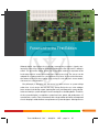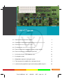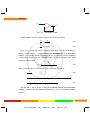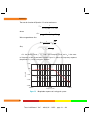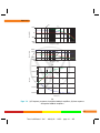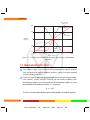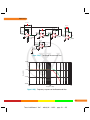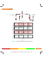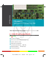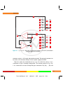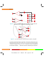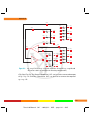
1
ANALOG SYSTEM
LAB MANUAL
Second Edition
ANALOG SYSTEM
LAB MANUAL
Second Edition
Learning to Design Analog Systems
using
Analog System Lab Starter Kit
Dr. K.R.K. Rao and Dr. C.P. Ravikumar
Texas Instruments, India
Bagmane Tech Park
CV Raman Nagar
Bangalore 560093
India
Analog System Lab Manual Second Edition
Learning to Design Analog Systems using Analog System Lab Starter Kit
Copyright © 2012 by Texas Instruments
All rights reserved. No part of this book may be reproduced, stored in a retrieval system, or transmitted in any form
or by any means, electronic, mechanical, photocopying, recording or scanning without the written permission of
Texas Instruments
Limits of Liability: While the publisher and the author have used their best efforts in preparing this book, Wiley
and the author make no representation or warranties with respect to the accuracy or completeness of the contents
of this book, and specifically disclaim any implied warranties of merchantability or fitness for any particular
purpose. There are no warranties which extend beyond the descriptions contained in this paragraph. No warranty
may be created or extended by sales representatives or written sales materials. The accuracy and completeness of the
information provided herein and the opinions stated herein are not guaranteed or warranted to produce any
particular results, and the advice and strategies contained herein may not be suitable for every individual. Neither
Wiley India nor the author shall be liable for any loss of profit or any other commercial damages, including but not
limited to special, incidental, consequential, or other damages.
Disclaimer: The contents of this book have been checked for accuracy. Since deviations cannot be precluded
entirely, Wiley or its author cannot guarantee full agreement. As the book is intended for educational purpose, Wiley
or its author shall not be responsible for any errors, omissions or damages arising out of the use of the information
contained in the book. This publication is designed to provide accurate and authoritative information with regard
to the subject matter covered. It is sold on the understanding that the Publisher is not engaged in rendering
professional services.
Trademarks: All brand names and product names used in this book are trademarks, registered trademarks, or trade
names of their respective holders. Wiley is not associated with any product or vendor mentioned in this book.
Other Wiley Editorial Offices:
John Wiley & Sons, Inc. 111 River Street, Hoboken, NJ 07030, USA
Wiley-VCH Verlag GmbH, Pappellaee 3, D-69469 Weinheim, Germany
John Wiley & Sons Australia Ltd, 42 McDougall Street, Milton, Queensland 4064, Australia
John Wiley & Sons (Asia) Pte Ltd, 1 Fusionopolis Walk #07-01 Solaris, South Tower, Singapore 138628
John Wiley & Sons Canada Ltd, 22 Worcester Road, Etobicoke, Ontario, Canada, M9W 1L1
First Edition: 2011
Second Edition: 2012
ISBN: 978-81-265-3742-6
www.wileyindia.com
Printed at: Paras Printers, Delhi
Foreword to the Second Edition
The first version of this manual, released in 2011, has been received with great
enthusiasm by teachers and students. We thank everyone for this warm reception.
We are happy to place in your hands the revised version of the Analog System
Lab Manual. The Analog System Lab Kit and the associated manual were created to
help colleges in India in updating their curriculum for courses related to analog. Analog electronics occupies a very special and significant place in modern-day systems.
In the past decade, India has seen the emergence of a number of system design companies. Manufacturing of electronic products has also received a significant boost.
These companies look for system-level design skills in both analog and digital domains.
Unfortunately, analog system design is not emphasized in the conventional way of
teaching analog. Our attempt is to help bridge this gap at an early stage in undergraduate coursework. We believe that the ASLK can be adopted by both undergraduate and
postgraduate students.
v
Texas Lab Manual: “tlm” - 2012/8/14 - 14:55 - page v - #1
Foreword to the Second Edition
Since ASLK Starter kit was introduced, close to 100 colleges in India have introduced it in their teaching curriculum. We have interacted with hundreds of Indian
teachers in the faculty development programs on Analog System Design that were conducted in the last year. Several colleges have independently conducted such hands-on
workshops for teachers as well as students. We are encouraged by the acceptance of
the kit as an educational tool that is easy to use. We are grateful to all the comments
and feedback we have received from academia. Several teachers have told us that they
have designed new experiments in the areas of communications and controls. Several
companies used ASLK in their in-house training programs. To see the reaction from
students, we made it mandatory for participants of TI India Analog Design Contest to
carry out a challenging experiment on the ASLK. We could not have expected a more
positive response! Some students even surprised us by using ASLK for new experiments such as motor control and simulation of chaos in oscillators! We encourage
students and teachers to explore such innovative applications of ASLK. TI has a vast
portfolio of analog ICs to select from. Please make use of TI’s "free samples" program
to carry out additional experiments on ASLK.
Based on the feedback we received, we have introduced a few changes in this version of the manual. We are sure you will like the aesthetic improvements to the manual,
including the colored illustrations. A pin diagram of the ASLK is included with the kit
to facilitate the connections. We have added several additional exercises in almost
all chapters. These additional exercises are marked with a star; we have provided
the component values and typical simulation results in these exercises. The starred
exercises can be good starting points when one begins to use ASLK. However, we
emphasize the importance of the other exercises which involve design. We suggest
that a teacher assigns a mix of starred and the other exercises in the lab work.
We are pleased to acknowledge the help from several persons in preparing this
manual. Ms Meenakshi Sehrawat of Wiley-India has done a creditable job of editing.
We thank Praveen Settigere of Wiley-India for his continued support. Joyan Gratian
Sanctis of TI India has taken the excellent picture of the ASLK included in this manual.
We are indebted to Sagar Juneja for his constant help in all aspects of ASLK promotion.
vi
Texas Lab Manual: “tlm” - 2012/8/14 - 14:55 - page vi - #2
Foreword to the Second Edition
We thank Cranes Software for their manufacturing and promotion of ASLK. We thank
all our colleagues in TI India for their constant support and encouragement.
As always, we are eager to know your feedback!
K.R.K. Rao
C.P. Ravikumar
July 2012
Texas Instruments, India
Bagmane Tech Park
CV Raman Nagar
Bangalore 560093
India
vii
Texas Lab Manual: “tlm” - 2012/8/14 - 14:55 - page vii - #3
Texas Lab Manual: “tlm” - 2012/8/14 - 14:55 - page viii - #4
Foreword to the First Edition
Although digital signal processing is the most common way to process signals, analog signal processing cannot be completely avoided since the real world is analog in
nature. The goal of the Analog System Lab is to provide students an exposure to the
fascinating world of analog and mixed-signal signal processing. The course can be
adapted for an undergraduate or a postgraduate curriculum. As part of the lab course,
the student will build analog systems using analog ICs and study their macro models,
characteristics and limitations.
Our philosophy in designing this lab course has been to focus on system design
rather than circuit design. We feel that many Analog Design classes in the colleges
focus on the circuit design aspect, ignoring the issues encountered in system design.
In the real world, a system designer uses the analog ICs as building blocks. The focus
of the system designer is to optimize system-level cost, power and performance. IC
manufacturers such as Texas Instruments offer a large number of choices of integrated
circuits keeping in mind the diverse requirements of system designers. A designer must
ix
Texas Lab Manual: “tlm” - 2012/8/14 - 14:55 - page ix - #5
Foreword to the First Edition
be aware of these diverse offerings of semiconductors and select the right IC for the
right application. We have tried to emphasize this aspect in designing the experiments
in this manual.
We believe that there is a need to make a significant change to the way analog
design is taught in the engineering colleges today. The conventional way of starting
with device physics and moving on to the design and analysis of analog circuits at the
transistor-level needs rethinking. What is proposed is a two-tier approach to teaching
analog design – start with analog systems and then move to circuits. Analog systems
are part of every electronic system today and we believe they must be taught in the
“building block” spirit that has worked well for digital design. There are many system
design companies today looking for engineers who can design using analog ICs; they
hardly ever design or even use a common emitter amplifier or a Wien-bridge oscillator!
There are 10 experiments in the Analog System Lab, which can be carried out either
individually or by groups of two or three students. In the first phase of experiments,
two basic analog building blocks are introduced, namely, Operational Amplifiers and
Analog Multipliers. In the second phase, we explain how larger analog systems such
as integrators, differentiators, filters, function generators, VCO, PLL, DC-DC converters
and regulators can be constructed using the basic building blocks. The emphasis is
on learning by paper design, simulation through SPICE, hardware construction, and
analysis of results. With each experiment, we provide brief theoretical background,
references to literature (mostly online and easy to access), the specification of the
design experiment, measurements to be taken, and the documents to be submitted at
the end of the experiment. A teacher’s manual can be made available on request.
This manual is the result of almost a year’s effort. We have received support from
a number of individuals when we were working on this manual. It is our pleasure
to acknowledge their contribution. We acknowledge the encouragement and support from Syd Coppersmith (WW Manager, TI Analog University Program) throughout
this endeavor. A number of colleagues at Texas Instruments, India have helped us
and encouraged us at different stages of the development of the kit and the manual.
Our sincere thanks are due to all of them. Mr Krishnamurthy Bhat of Basaveshwara
x
Texas Lab Manual: “tlm” - 2012/8/14 - 14:55 - page x - #6
Foreword to the First Edition
Engineering College (Bagalkot, Karnataka, India) spent several months with us, helping us realize the kit as a product. He was ably helped by Sagar Juneja, then a student
intern at TI India. Sagar has also read various drafts of this manual and provided helpful
comments. Ullas Taneja, another student intern, helped in recording the video lectures
that provide more information on these experiments. Pulkit Jain, also an intern, helped
us by drawing many of the diagrams in this manual. We thank the faculty members who
attended the faculty development programs where initial drafts of this manual and the
Analog System Lab Kit were used; their feedback has been useful in improving the kit
as well as the manual.
We thank Mr. E.S. Kannan of YEE YES and Mr. Ashfaq Ibrahim of Cranes Software
for their support. We thank Mr. Praveen Settigere of Wiley India for his interest in this
project and for all the help he provided in publishing the manual.
We hope you and your students will find the Analog Systems Lab Kit and the experiments in this manual rewarding. We intend to continue to develop more experiments
and learning materials in the future; we will share them on the TI India University Program website (www.uniti.in). We are eager to know your critique of the kit as well as
the manual. Do write to us!
K.R.K. Rao
C.P. Ravikumar
November, 2010
Texas Instruments, India
Bagmane Tech Park
CV Raman Nagar
Bangalore 560093
India
xi
Texas Lab Manual: “tlm” - 2012/8/14 - 14:55 - page xi - #7
Texas Lab Manual: “tlm” - 2012/8/14 - 14:55 - page xii - #8
Contents
0
Introduction
1
0.1
Analog System Lab
1
0.2
Organization of the Analog System Lab Course
3
0.3
Lab Setup
6
0.3.1
6
0.4
Important Notes
System Lab Kit ASLKv2010 Starter: An Overview
7
0.4.1
Hardware
7
0.4.2
Software
10
0.5
Familiarizing with ASLKv2010 Starter Kit
11
0.6
Organization of the Manual
14
xiii
Texas Lab Manual: “tlm” - 2012/8/14 - 14:55 - page xiii - #9
Contents
1
2
Experiment 1 Negative Feedback Amplifiers and
Instrumentation Amplifier
15
1.1
Goal of the Experiment
15
1.2
Brief Theory and Motivation
15
1.2.1
15
Unity Gain Amplifier
1.3
Specifications
20
1.4
Measurements to be Taken
22
1.5
What Should you Submit
24
1.6
Exercises
25
1.7
Other Related ICs
28
1.8
Related Reading
28
Experiment 2 Regenerative Feedback System, Astable and
Monostable Multivibrator
29
2.1
Goal of the Experiment
29
2.2
Brief Theory and Motivation
29
2.2.1
Inverting Regenerative Comparator
29
2.2.2
Astable Multivibrator
32
2.2.3
Monostable Multivibrator (Timer)
32
2.3
Specifications
34
2.4
Measurements to be Taken
34
2.5
What Should you Submit
35
2.6
Exercises
35
xiv
Texas Lab Manual: “tlm” - 2012/8/14 - 14:55 - page xiv - #10
Contents
3
4
5
Experiment 3 Integrators and Differentiators
37
3.1
Goal of the Experiment
37
3.2
Brief Theory and Motivation
37
3.2.1
Integrators
38
3.2.2
Differentiators
38
3.3
Specifications
39
3.4
Measurements to be Taken
39
3.5
What Should you Submit
40
3.6
Exercise: Grounded Capacitor Topologies of Integrator and Differentiator
43
Experiment 4 Analog Filters
45
4.1
Goal of the Experiment
45
4.2
Brief Theory and Motivation
45
4.2.1
47
Frequency Response of Filters
4.3
Specifications
47
4.4
Measurements to be Taken
48
4.5
What Should you Submit
49
4.6
Exercises
50
4.7
Related ICs
52
Experiment 5 Self-tuned Filter
53
5.1
Goal of the Experiment
53
5.2
Brief Theory and Motivation
53
5.2.1
55
Multiplier as a Phase Detector
xv
Texas Lab Manual: “tlm” - 2012/8/14 - 14:55 - page xv - #11
Contents
6
5.3
Specification
60
5.4
Measurements to be Taken
60
5.5
What Should you Submit
60
5.6
Exercises
61
5.7
Related ICs
63
Experiment 6 Function Generator and Voltage-Controlled
Oscillator
65
6.1
Goal of the Experiment
65
6.2
Brief Theory and Motivation
65
• VCO
• Function Generator
• FM/FSK Generator
7
6.3
Specifications
68
6.4
Measurements to be Taken
68
6.5
What Should you Submit
68
6.6
Exercises
69
Experiment 7 Phase Locked Loop
71
7.1
Goal of the Experiment
71
7.2
Brief Theory and Motivation
71
• Phase Lock Loop
7.3
Specifications
73
7.4
Measurements to be Taken
73
7.5
What Should you Submit
74
7.6
Exercises
75
xvi
Texas Lab Manual: “tlm” - 2012/8/14 - 14:55 - page xvi - #12
Contents
8
Experiment 8 Automatic Gain Control (AGC)/Automatic
Volume Control (AVC)
79
8.1
Goal of the Experiment
79
8.2
Brief Theory and Motivation
79
• Automatic Gain/Volume Control
9
8.3
Specification
81
8.4
Measurements to be Taken
81
8.5
What Should you Submit
81
8.6
Exercises
82
Experiment 9 DC–DC Converter
85
9.1
Goal of the Experiment
85
9.2
Brief Theory and Motivation
85
• DC/DC Converter
• Class-D Power Amplifier
9.3
Specification
86
9.4
What Should you Submit
86
9.5
Exercises
89
10 Experiment 10 Low Dropout (LDO)/Linear Regulator
91
10.1 Goal of the Experiment
91
10.2 Brief Theory and Motivation
91
• Linear Regulator
10.3 Specifications
92
xvii
Texas Lab Manual: “tlm” - 2012/8/14 - 14:55 - page xvii - #13
Contents
A
10.4 Measurements to be Taken
94
10.5 What Should you Submit
94
10.6 Exercises
95
ICs used in ASLKv2010 Starter Kit
97
A.1
TL082: JFET-Input Operational Amplifier
97
A.1.1
Features
97
A.1.2
Applications
98
A.1.3
Description
98
A.1.4
Download Datasheet
98
A.2
A.3
A.4
MPY634: Wide-Bandwidth Analog Precision Multiplier
99
A.2.1
Features
99
A.2.2
Applications
99
A.2.3
Description
100
A.2.4
Download Datasheet
100
DAC 7821: 12 Bit, Parallel, Multiplying DAC
100
A.3.1
Features
100
A.3.2
Applications
101
A.3.3
Description
102
A.3.4
Download Datasheet
102
TPS40200: Wide-Input, Non-Synchronous Buck DC/DC Controller
102
A.4.1
Features
102
A.4.2
Applications
104
xviii
Texas Lab Manual: “tlm” - 2012/8/14 - 14:55 - page xviii - #14
Contents
A.5
B
C
D
A.4.3
Description
104
A.4.4
TPS40200EVM-002
105
A.4.5
Download Datasheet
105
TLV700xx: 200mA, Low IQ, Low Dropout Regulator for Portables
105
A.5.1
Features
105
A.5.2
Applications
106
A.5.3
Description
106
A.5.4
TLV70018EVM-503 Evaluation Module
107
A.5.5
Download Datasheet
107
Introduction to Macromodels
109
B.1
Micromodels
110
B.2
Macromodels
112
Activity: To Convert your PC/Laptop into an Oscilloscope
113
C.1
Introduction
113
C.2
Limitations
115
System Lab Kit ASLKv2010 Starter Kit Connection
Diagrams
117
Bibliography
125
Index
129
xix
Texas Lab Manual: “tlm” - 2012/8/14 - 14:55 - page xix - #15
Texas Lab Manual: “tlm” - 2012/8/14 - 14:55 - page xx - #16
List of Figures
0-1 Signal chain in an electronic system
2
0-2 Dependence among experiments on the ASLKv2010 Starter
5
0-3 Picture of ASLKv2010 Starter kit
8
0-4 Pin diagram for ASLKv2010 Starter kit
9
0-5 External connections needed for using the analog multiplier
13
0-6 External connections needed for using the DAC
13
1-1 An ideal dual-input, single-output Op-Amp
16
1-2 A unity gain system
17
1-3 Magnitude response of a unity gain system
18
1-4 Time response of an amplifier for a step input of size Vp
19
1-5 (a) Non-inverting amplifier of gain 2; (b) inverting amplifier of gain 2
20
xxi
Texas Lab Manual: “tlm” - 2012/8/14 - 14:55 - page xxi - #17
List of Figures
1-6 (a) Frequency response of negative feedback amplifiers; (b) time response
of negative feedback amplifiers
21
1-7 Transfer characteristics of unity-gain, non-inverting, and inverting
amplifiers
22
1-8 Instrumentation amplifier configurations with (a) three; (b) two operational
amplifiers
23
1-9 (a) An inverting amplifier with analog gain control
26
1-9 (b) Simulation of the circuit for Figure 1-9(a) when V3 = 1 V
27
1-10 Digitally controlled amplifier
27
2-1 Inverting Schmitt trigger and its hysteresis characteristic
30
2-2 Symbols for (a) inverting; (b) non-inverting Schmitt trigger circuits
31
2-3 Non-inverting Schmitt trigger and its hysteresis characteristic
31
2-4 Astable multivibrator
32
2-5 Simulation results for (a) astable multivibrator; monostable multivibrator
33
2-6 Monostable multivibrator
34
3-1 Integrator
38
3-2 Differentiator
38
3-3 Frequency response of integrator and differentiator
41
3-4 Outputs of integrator and differentiator for (a) square-wave;
(b) triangular-wave inputs
42
3-5 Circuits for Exercise
43
4-1 A second-order universal active filter
47
4-2 Simulation waveform for a universal active filter
48
4-3 Magnitude response of BPF, BSF
50
xxii
Texas Lab Manual: “tlm” - 2012/8/14 - 14:55 - page xxii - #18
List of Figures
4-4 (a) Third-order Butterworth filter
51
4-4 (b) Frequency response of the Butterworth filter
51
4-5 (a) Tow-Thomas biquad filter
52
4-5 (b) Frequency response of the filter
52
5-1 (a) Symbol of an analog multiplier; (b) multiplier as a phase detector
54
5-2 Voltage controlled filter with frequency (a) ∝
1
; (b) ∝ Vc
Vc
56
5-3 (a) A self-tuned filter based on a voltage-controlled filter or
voltage-controlled phase generator; (b) a simple voltage-controlled
phase generator that can become part of a self-tuned filter
57
5-4 Output of the self-tuned filter based on simulation. Vo1 corresponds to BPF,
Vo2 corresponds to BSF, Vc is the control voltage and Vi is the input voltage
58
5-5 (a) Simulation of the self-tuned filter shown in Figure 5-5(b) when
VG1 = 0. 1 V.
61
5-5 (b) Self-tuned filter
62
6-1 Voltage-Controlled Oscillator (VCO)
66
6-2 Simulation outputs for (a) function generator; (b) FSK generator
67
6-3 (a) Function generator
69
6-3 (b) Simulation of the function generator of Figure 6-3(a)
70
6-4 Digitally Controlled Oscillator (DCO)
70
7-1 (a) Phase Locked Loop (PLL) circuit; (b) characteristics of the PLL
72
7-2 Sample output waveform for the Phase Locked Loop (PLL) for a
square-wave input waveform
74
7-3 (a) Phase locked loop
76
xxiii
Texas Lab Manual: “tlm” - 2012/8/14 - 14:55 - page xxiii - #19
List of Figures
7-3 (b) Simulation of the PLL at free-running frequency, when input
amplitude is 1 V
76
7-4 Block diagram of frequency optimizer
77
8-1 Automatic Gain Control (AGC)/Automatic Volume Control (AVC)
80
8-2 Input–output characteristics of AGC/AVC
80
8-3 Output of AGC circuit
82
8-4 (a) AGC circuit
83
8-4 (b) Simulation of the AGC circuit for output voltage = 2V peak
83
9-1 (a) DC–DC converter; (b) waveforms from simulation
87
9-2 PWM and Class-D output waveforms
88
10-1 Low Dropout Regulator (LDO)
92
10-2 (a) A regulator system with startup; (b) load regulation output;
(c) line regulation output
93
A-1 TL082 – JFET-input operational amplifier
98
A-2 MPY634 – Analog multiplier
99
A-3 DAC 7821 – Digital to analog converter
101
A-4 TPS40200 – DC/DC controller
103
A-5 TLV700XX – Low dropout regulators
106
C-1 Buffer circuit needed to interface an analog signal to oscilloscope
114
D-1 Floorplan of the ASLKv2010 Starter kit
118
D-2 Power connections in ASLKv2010 Starter kit. Only connect ±10 V and
ground connections
118
D-3 Op-Amp IC-1 (Dual Op-Amp with two amplifiers, 1A and 1B) connected in
Type-1 configuration (Inverting)
xxiv
Texas Lab Manual: “tlm” - 2012/8/14 - 14:55 - page xxiv - #20
119
List of Figures
D-4 Op-Amp IC-2 (Dual Op-Amp with two amplifiers, 2A and 2B. 2A can be
connected in Type-1 configuration (Inverting; 2B is a spare)
120
D-5 Op-Amp IC-3 (Dual Op-Amp with two spare amplifiers, 3A and 3B)
120
D-6 Op-Amp IC-4 (Dual Op-Amp with amplifiers 4A and 4B. Op-Amp 4A and
4B can be used in inverting or non-inverting configuration)
121
D-7 (a) PCB connections for analog multipliers 1, 2 and 3 on
ASLKv2010 Starter; (b) External connections needed to use the
multiplier MPY634
122
D-8 (a) PCB connections for the DAC on ASLKv2010 Starter; (b) external
connections needed to use the DAC to make it four-quadrant
123
xxv
Texas Lab Manual: “tlm” - 2012/8/14 - 14:55 - page xxv - #21
Texas Lab Manual: “tlm” - 2012/8/14 - 14:55 - page xxvi - #22
List of Tables
1-1 Measurement of slew rate: Method 1
24
1-2 Measurement of slew rate: Method 2
25
1-3 Plot of magnitude and phase variation w.r.t. input frequency
25
1-4 DC transfer characteristic
25
2-1 Plot of hysteresis w.r.t. regenerative feedback
35
3-1 Plot of magnitude and phase w.r.t. input frequency for the integrator
40
3-2 Plot of magnitude and phase w.r.t. input frequency
for the differentiator
41
3-3 Variation of peak-to-peak value of output w.r.t. peak value
of input
43
4-1 Transfer functions of active filters
46
4-2 Frequency response of a BPF with F0 = 1 kHz, Q = 1
49
4-3 Frequency response of a BSF with F0 = 10 kHz, Q = 10
49
xxvii
Texas Lab Manual: “tlm” - 2012/8/14 - 14:55 - page xxvii - #23
List of Tables
5-1 Variation of output amplitude with input frequency
60
6-1 Change in frequency as a function of control voltage
69
7-1 Output phase as a function of input frequency
75
7-2 Control voltage as a function of input frequency
75
8-1 Transfer characteristic of the AGC system
81
9-1 Variation of output voltage with control voltage in a DC–DC converter
88
9-2 Variation of duty cycle with control voltage in a DC–DC converter
89
10-1 Variation of load regulation with load current in an LDO
94
10-2 Variation of line regulation with input voltage in an LDO
95
10-3 Ripple rejection
95
B-1 Operational amplifiers available from Texas Instruments
xxviii
Texas Lab Manual: “tlm” - 2012/8/14 - 14:55 - page xxviii - #24
111
Chapter Zero
Introduction
0.1 Analog System Lab
Although digital signal processing is the most common form of processing signals, analog signal processing cannot be completely avoided since the real world is analog in
nature. Consider a typical signal chain (Figure 0-1).
•
•
1 A sensor converts the real-world signal into an analog electrical signal. This
analog signal is often weak and noisy.
2 Amplifiers are needed to strengthen the signal. Analog filtering may be necessary
to remove noise from the signal. This “front end” processing improves the signalto-noise ratio. Three of the most important building blocks used in this stage are
(a) Operational Amplifiers, (b) Analog Multipliers and (c) Analog Comparators.
•
3 An analog-to-digital converter transforms the analog signal into a stream of 0s
and 1s.
1
Texas Lab Manual: “tlm” - 2012/8/14 - 14:55 - page 1 - #25
Introduction
Amplifier
Temperature
Pressure
Position
Speed
Flow
Humidity
Sound
Light
Power management
Amplifier
Figure 0-1
A/D
converter
D/A
converter
Logic
Embedded
processing
Communication
Signal chain in an electronic system
•
4 The digital data is processed by a CPU, such as a DSP, a microprocessor, or
a microcontroller. The choice of the processor depends on how intensive the
computation is. A DSP may be necessary when real-time signal processing
is needed and the computations are complex. Microprocessors and microcontrollers may suffice in other applications.
•
•
•
5 Digital-to-analog conversion (DAC) is necessary to convert the stream of 0s and
1s back into analog form.
6 The output of the DAC has to be amplified before the analog signal can drive an
external actuator.
7 A Power Management block is needed to provide power to the various blocks.
In modern-day VLSI chips, power dissipation is a major consideration so that we
can keep the power density under control. Since the source of power can be a
battery, it is important to ensure long battery life through techniques such as clock
gating, power gating, etc. The Power Management block is responsible for these
functions.
It is evident that analog circuits play a crucial role in the implementation of an
electronic system.
2
Texas Lab Manual: “tlm” - 2012/8/14 - 14:55 - page 2 - #26
Introduction
The goal of the Analog System Lab Course is to provide students an exposure to
the fascinating world of analog and mixed-signal signal processing. The course can be
adapted for an undergraduate or a postgraduate curriculum. As part of the lab course,
the student will build analog systems using analog ICs and study their macro models,
characteristics and limitations.
Our philosophy in designing this lab course has been to focus on system design
rather can circuit design. We feel that many Analog Design classes in the colleges
focus on the circuit design aspect, ignoring the issues encountered in system design.
In the real world, a system designer uses the analog ICs as building blocks. The focus
of the system designer is to optimize system-level cost, power, and performance. IC
manufacturers such as Texas Instruments offer a large number of choices of integrated
circuits keeping in mind the diverse requirements of system designers. As a student,
you must be aware of these diverse offerings of semiconductors and select the right
IC for the right application. We have tried to emphasize this aspect in designing the
experiments in this manual.
0.2 Organization of the Analog System Lab Course
In designing the lab course, we have assumed that there are about 12 lab sessions
during a semester. We have designed 10 experiments that can be carried out either
individually or by groups of two or three students. The experiments in Analog System
Lab can be categorized as follows:
•
1 Part I: In the first part, the student will be exposed to the operation of the basic
building blocks of analog systems. Most of the experiments in the Analog System
Lab Course are centered around the following two components:
• The Op-Amp TL082, a general-purpose JFET-input Operational Amplifier, made
by Texas Instruments.
• Wide-bandwidth, precision Analog Multiplier MPY634 from Texas Instruments.
3
Texas Lab Manual: “tlm” - 2012/8/14 - 14:55 - page 3 - #27
Introduction
Using these components, the student will build gain stages, buffers, instrumentation amplifiers and voltage regulators. These experiments bring out several
important issues, such as measurement of gain-bandwidth product, slew-rate and
saturation limits of the operational amplifiers.
•
We then introduce the analog comparator, which is a mixed-mode device – its
input is analog and output is digital. In a comparator, the rise time, fall time and
delay time are important apart from input offset.
2 Part-II: The second part concentrates on building analog systems using the blocks
mentioned in the previous point.
First, we introduce integrators and differentiators that are essential for implementing filters that can band-limit a signal prior to the sampling process to avoid
aliasing errors.
A function generator is also a mixed-mode system that uses an integrator and
a regenerative comparator as building blocks. The function generator is capable
of producing a triangular waveform and square waveform as outputs. It is also
useful in Pulse Width Modulation in DC-to-DC converters, switched-mode power
supplies and Class-D power amplifiers.
The analog multiplier, which is a voltage or current controlled amplifier, finds
applications in communication circuits in the form of mixer, modulator, demodulator and phase detector. We use the multiplier in building Voltage Controlled
Oscillators (VCO), Frequency Modulated Waveform Generators, or Frequency
Shift Key Generators in modems, Automatic Gain Controllers, Amplitude Stabilized Oscillators, Self-tuned Filters and Frequency Locked Loop. Voltage controlled
phase generators and VCOs that use multiplier as a phase detector are built and
their lock range and capture range estimated and verified.
In the Analog System Lab, the frequency range of all applications has been
restricted to 1–10 kHz, with the following in mind: (a) Simple macromodels can
be used for active devices in simulation, (b) A PC can be used in place of an
oscilloscope. We have also included an experiment that can help the student use
a PC as an oscilloscope. We also suggest an experiment on the development of
macromodels for an Op-Amp.
4
Texas Lab Manual: “tlm” - 2012/8/14 - 14:55 - page 4 - #28
Introduction
Figure 0-2 shows the dependence among the experiments included in Analog System Lab. The sequence in which the experiments are carried out can be altered
using this dependence graph. We believe that the students must carry out all the
experiments.
At the end of Analog System Lab, we believe you will have the following know-how
about analog system design:
•
•
1 You will learn about the characteristics and specification of analog ICs used in
electronic systems
2 You will learn how to develop a macromodel for an IC based on its terminal characteristics, I/O characteristics, DC-transfer characteristics, frequency response,
stability characteristics and sensitivity characteristics
Exp-1
Negative feedback
amplifiers and
instrumentation amplifier
Exp-2
Regenerative feedback
systems – astable and
monostable multivibrators
Exp-3
Integrators and
differentiators
Exp-8
Automatic gain
control
Exp-4
Analog filters
Exp-5
Self-tuned filter
Exp-10
Low dropout regulator
Exp-6
Function generator and
voltage-controlled
oscillator
Exp-7
Phase locked loop
(Frequency locked
loop)
Exp-9
DC-DC converter
Class-D amplifier
Figure 0-2 Dependence among experiments on the ASLKv2010 Starter
5
Texas Lab Manual: “tlm” - 2012/8/14 - 14:55 - page 5 - #29
Introduction
••
3 You will be able to make the right choice for an IC for a given application
4 You will be able to perform basic fault diagnosis of an electronic system
0.3 Lab Setup
The setup for the Analog System Lab is very simple and requires the following:
•
•
1 ASLKv2010 Starter kit and the associated Lab Manual from Texas Instruments, India – the lab kit comes with required connectors. Refer to Section 0.4
for an overview of the kit.
2 A low frequency operation oscilloscope which can operate in the frequency range
of 1 to 10 MHz. Texas Instruments also offers an oscilloscope card which can be
plugged into laptops so that the laptop can work as an oscilloscope (See [30]).
Alternately, we also provide an experiment that helps you build a circuit to directly
interface analog outputs to a PC (See Appendix C).
••
•
3 Dual power supply with the operating voltages of ±10 V.
4 Function generators which can operate in the range on 1 to 10 MHz and capable
of generating sine, square and triangular waves.
5 A computer with simulation software such as TINA [9] or PSPICE [32] and design
software from Texas Instruments (FilterPro and SwitcherPro) installed
on it.
0.3.1 Important Notes
In all the experiments of Analog System Lab, please note the following:
•
1 When we do not explicitly mention the magnitude and frequency of the input
waveform, please use 0 to 1 V as the amplitude of the input and 1 kHz as the
frequency.
6
Texas Lab Manual: “tlm” - 2012/8/14 - 14:55 - page 6 - #30
Introduction
•
•
2 Always use sinusoidal input when you plot the frequency response and use square
wave-input when you plot the transient response.
3
•
4
•
•
Note to students: With every experiment, we have included tables that
can be used to record the experimental data that you collect during the
experiment. We have shown four blank entries in every table to illustrate
the type of data the student must collect; the student must actually record many
more data points.
Precaution! Please note that TL082 is a dual Op-Amp. This means that
the IC has two Op-Amp circuits. If your experiment requires only one of
the two Op-Amp circuits, do not leave the inputs and output of the other
Op-Amp open; instead, place the second Op-Amp in unity-gain mode and ground
the input.
5
Precaution! Never connect any point from the board to the oscilloscope.
Instead, use a probe that is connected to the oscilloscope to investigate
different points on the board!
6
Advisory to Students and Instructors: We strongly advise that the student
performs the simulation experiments outside the lab hours. The student
must bring a copy of the simulation results from SPICE simulation to the
class and show it to the instructor at the beginning of the class. The lab hours must
be utilized only for the hardware experiment and comparing the actual outputs
with simulation results.
0.4 System Lab Kit ASLKv2010 Starter: An
Overview
0.4.1 Hardware
ASLKv2010 Starter kit (see Figure 0-3; Pin diagram is shown in Figure 0-4) has
been developed at Texas Instruments, India. This kit is designed for undergraduate
7
Texas Lab Manual: “tlm” - 2012/8/14 - 14:55 - page 7 - #31
Figure 0-3 Picture of ASLKv2010 Starter kit
Texas Lab Manual: “tlm” - 2012/8/14 - 14:55 - page 8 - #32
Figure 0-4 Pin diagram for ASLKv2010 Starter kit
Texas Lab Manual: “tlm” - 2012/8/14 - 14:55 - page 9 - #33
Introduction
engineering students to perform analog lab experiments. The main idea behind
ASLKv2010 Starter kit is to provide a cost-efficient platform or test bed for
students to realize almost any analog system using general-purpose ICs such as
Op-Amps and analog multipliers.
ASLKv2010 Starter kit comes with four general-purpose operational amplifiers
(TL082) and three wide-bandwidth precision analog multipliers (MPY634) from Texas
Instruments. There is also a provision to include a 12-bit parallel-input multiplying
digital-to-analog converter DAC7821. A portion of ASLKv2010 Starter kit is left for
general-purpose prototyping and can be used for carrying out mini-projects.
The kit has a provision to connect ±10 V DC power supplies. The kit comes with
the necessary short and long connectors, as well as connectors for power supplies. Figure D-2 (Appendix D) shows the way power supply connections are made
on ASLKv2010 Starter kit. The ±10 V supplies are connected internally to all the
ICs that require ±10 V supplies, namely, the operational amplifiers and the multipliers.
Since the DAC requires 5 V supply, the student has three options – to use the output
from one of the potmeters to provide 5 V supply, to generate a 5 V supply (see the DC-DC
converter experiment in this manual) or to use an external 5 V supply.
This comprehensive user manual included with the kit gives complete insight of
how to use ASLKv2010 Starter kit. The manual covers exercises of analog system design along with brief theory and simulation results obtained using simulation
software.
Refer to Appendix A for the details of the integrated circuits that are included in
ASLKv2010 Starter kit. Refer to Appendix D for additional details of ASLKv2010
Starter kit.
0.4.2 Software
The following softwares are necessary to carry out the experiments suggested in this
manual:
••
1 A SPICE-based simulation software, such as TINA [9], Multisim [15] or PSPICE [32].
2 FilterPro – a software program for designing analog filters.
10
Texas Lab Manual: “tlm” - 2012/8/14 - 14:55 - page 10 - #34
Introduction
•
••
•
3 SwitcherPro – a software program for designing switched-mode power supplies.
4 MDACBufferPro – a software for designing multiplying D/A converters.
5 ADCPro – a software for designing A/D converters.
6 ClockPro – a software for synthesizing clock generators.
Several SPICE-based simulation software [9, 32] are available today to verify the
behavior of circuits before they are implemented. These are powerful and easy-touse simulators for electronic circuits. It allows the simulation of circuits with passive
components such as resistors, capacitors and inductors, as well as active components
like transistors and analog integrated circuits. Texas Instruments makes macromodels
of integrated circuits available for the users of the simulation programs. (Appendix B
explains what macromodels are.) We will assume that you are familiar with the concept
of simulation, and are able to simulate a given circuit in TINA or PSPICE.
FilterPro is a program for designing active filters. At the time of writing this
manual, FilterPro Version 3.0 is the latest. It supports the design of different types
of filters, namely Bessel, Butterworth, Chebychev, Gaussian and linear-phase filters.
The software can be used to design Low Pass filters, High Pass filters, Band Stop filters,
and Band Pass filters with up to 10 poles. The software can be downloaded from [10].
0.5 Familiarizing with ASLKv2010 Starter Kit
The Analog System Lab ASLKv2010 Starter kit is divided into many sections. Refer
to the picture in Figure 0-5 when you read the following description. Please also refer
to the floorplan of the chip shown in Figure D-1 (Appendix D).
Figure D-1 shows the overall floorplan of the ASLKv2010 Starter kit. We have
shown the power connections in ASLKv2010 Starter in Figure D-2. Note that the
±10 V power and ground connections have to be connected to the power inlets at the
side of the kit; the power and ground are internally connected to the Op-Amps and
analog multipliers. If you wish to carry out an experiment using the DAC integrated
11
Texas Lab Manual: “tlm” - 2012/8/14 - 14:55 - page 11 - #35
Introduction
circuits on the board, you must use an external 5 V supply and ground connection, as
shown in Figure D-2. There are three potmeters included in the kit, each of which is
connected across 10 V and ground. The output of the potmeter can be used to derive a
voltage in the range of 0 to 10 V; this can be useful in generating a reference voltage or
even in generating a 5 V power supply for the DAC.
•
1 There are four TL082 Op-Amp ICs labeled 1, 2, 3 and 4 on ASLKv2010 Starter
kit. Each of these ICs has two amplifiers, which are labeled A and B. Thus, 1A
and 1B are the two Op-Amps in the Op-Amp IC 1, etc. The eight Op-Amps are
categorized as shown in the following table:
Op-Amp IC Op-Amp
Label on Kit
Type
Purpose
1
TYPE 1-1
TYPE 1-2
TYPE 1-3
TYPE SPARE-1
TYPE SPARE-2
TYPE SPARE-3
TYPE 2-1
TYPE 2-2
TYPE-1
TYPE-1
TYPE-1
SPARE
SPARE
SPARE
TYPE-2
TYPE-2
Inverting Configuration only
Inverting Configuration only
Inverting Configuration only
Spare
Spare
Spare
Inverting or Non-inverting
Inverting or Non-inverting
2
3
4
1A
1B
2A
2B
3A
3B
4A
4B
Refer to the floorplan of the kit and identify the Op-Amp ICs (Figure D-1). It will
also be helpful to refer to the power connections shown in Figure D-2. Please see
connection diagrams shown in Figures D-3, D-4, D-5 and D-6. The Op-Amps are
marked TYPE 1, TYPE 2 or SPARE on the board. The Op-Amps marked TYPE
1 can be connected in the inverting configuration (only). With the help of connectors, either resistors or capacitors can be used in the feedback loop of the
amplifier. There are three TYPE 1 amplifiers. There are three spare Op-Amps
and two TYPE-2 amplifiers. TYPE-2 amplifiers can be connected in inverting or
non-inverting configurations. All the Op-Amps ICs operate on ±10 V; the power
supply and ground connections are internally provided and the user need not
worry about these.
12
Texas Lab Manual: “tlm” - 2012/8/14 - 14:55 - page 12 - #36
Introduction
Input 1
1
14
2
13
3
4
Input 2
12
MPY-634
Output
11
5
10
6
9
7
8
Figure 0-5 External connections needed for using the analog multiplier
10 k
10 k
VDD
VDD RFB
DAC 7821
−15 V ≤Vin ≤ +15 V GND
5k
Iout1
Iout2
C1
−
TL082
+
C2
−
TL082
Vout
+
−10 V ≤Vout ≤ +10 V
Figure 0-6 External connections needed for using the DAC
•
2 Three analog multipliers are included in the kit. These are wide-bandwidth precision analog multipliers from Texas Instruments (MPY634). Each multiplier is a
14-pin IC and operates on ±10 V supply. The power supply connections for the
multipliers are provided internally. In order to use the analog multiplier IC on
the ASLKv2010 Starter kit, the external connections shown in Figure 0-5 are
required.
•
3 Two digital-to-analog converters (DAC), labeled DAC1 and DAC2 are provided
in the kit. Both the DACs are DAC7821 from Texas Instruments. They are 12-bit,
parallel-input multiplying DACs that can be used in place of analog multipliers in
circuits like AGC/AVC. Ground and power supplies are provided internally to the
DAC. Pins U9P3 and U8P3 of DAC1 and DAC2 are to be grounded and U9P18 and
13
Texas Lab Manual: “tlm” - 2012/8/14 - 14:55 - page 13 - #37
Introduction
U8P18 of DAC1 and DAC2 are to be connected to +5 V. In order to use the DAC integrated circuit on the ASLKv2010 Starter kit, the external connections shown
in Figure 0-6 are required.
•
4 The kit has a provision to connect ±10 V power supplies. In addition, using the
potentiometers, variable voltage can be obtained if needed for any circuit or IC.
All the ICs on the board except DAC are internally connected to power supply,
but in case external connection is required, it can be taken easily from Power
Distribution Pins. Please refer to Appendix D for experimental configurations of
ASLKv2010 Starter kit.
•
5 The top left portion of the kit is a general-purpose area which uses a proto-board.
0.6 Organization of the Manual
There are 10 experiments in this manual and the next 10 chapters are devoted to them,
We recommend that in the first cycle of experiments, the instructor introduces the
ASLKv2010 Starter kit and ensure that all the students are familiar with a SPICEbased simulation program. A warm-up exercise can be included, where the students
are asked to use such a simulation program. For each of the experiments, we have
clarified the goal of the experiment and provided the theoretical background. The Analog System Lab can be conducted parallel to a theory course on Analog Design or as a
separate lab that follows a theory course. The student should have the following skills
to pursue Analog System Lab:
••
••
1 Basic understanding of electronic circuits.
2 Basic computer skills required to run the tools such as TINA, PSPICE,
FilterPro and SwitcherPro.
3 Ability to use the oscilloscope.
4 Concepts of gain, bandwidth, transfer function, filters, regulators and wave
shaping.
14
Texas Lab Manual: “tlm” - 2012/8/14 - 14:55 - page 14 - #38
Chapter One
Experiment 1 Negative
Feedback Amplifiers and
Instrumentation Amplifier
1.1 Goal of the Experiment
The goal of this experiment is two-fold. In the first part, we will understand the application of negative feedback in designing amplifiers. In the second part, we will build an
instrumentation amplifier.
1.2 Brief Theory and Motivation
1.2.1 Unity Gain Amplifier
An Op-Amp [8] can be used in negative feedback mode to build unity-gain amplifiers,
non-inverting amplifiers and inverting amplifiers. While an ideal Op-Amp is assumed to
have infinite gain and infinite bandwidth, real Op-Amps have finite numbers for these
15
Texas Lab Manual: “tlm” - 2012/8/14 - 14:55 - page 15 - #39
Experiment 1
parameters. Therefore, it is important to understand some limitations of real Op-Amps,
such as finite Gain-Bandwidth Product (GB). Similarly, the slew rate and saturation limits of an operational amplifier are equally important. Given an Op-Amp, how do we
measure these parameters? Since the frequency and transient response of an amplifier are affected by these parameters, we can measure the parameters if we have
the frequency and transient response of the amplifier. You can obtain these response
characteristics by applying sinusoidal and square wave input, respectively. We invite
the reader to view the recorded lecture [18].
An Op-Amp may be considered as a Voltage-Controlled Voltage Source (VCVS) with
the voltage gain tending toward ∞, or a Current-Controlled Current Source (CCCS) with
current gain tending toward ∞. For finite output voltage, the input voltage is practically zero. This is the basic theory of Op-Amp in the negative feedback configuration.
Figure 1-1 shows a differential input, single-ended-output Op-Amp which uses dual
supply ±Vss for biasing, so that the output offset voltage can be made zero when the
input offset voltage is zero.
Vo = A0 · (V1 − V2 )
V1 − V2 =
Vo
A0
(1.1)
(1.2)
In the above equations, A0 is the open-loop gain; for real amplifiers, A0 is in the range
of 103 to 106 and hence V1 ≈ V2 .
−Vss
V2
−
Vo = A0 [ V1 − V 2 ]
V1
+
+Vss
Figure 1-1
An ideal dual-input, single-output Op-Amp
16
Texas Lab Manual: “tlm” - 2012/8/14 - 14:55 - page 16 - #40
Experiment 1
Vi
+
−
Vo
Figure 1-2 A unity gain system
A unity feedback circuit is shown in Figure 1-2. It is easy to see that
A0
Vo
=
Vi
(1 + A0 )
(1.3)
Vo
→ 1 as A0 → ∞
Vi
(1.4)
In Op-Amps, closed loop gain A is frequency-dependent, as shown in Equation 1.5,
where ωd1 and ωd2 (ωd1 < ωd2 ) are known as the dominant poles of the operational
amplifier. This transfer function is typical in an Op-Amp that has internal frequency
compensation. Please view the recorded lecture [19] to get to know more about
frequency compensation.
A=
A0
(1 + s/ωd1 )(1 + s/ωd2 )
(1.5)
We can now write the transfer function T for a unity-gain amplifier as
T =
1
1 + 1/A
=
1
1 + 1/A0 + s/A0 · ωd1 + s/A0 · ωd2 + s 2 /A0 · ωd1 · ωd2
=
1
1 + s/GB + s/A0 · ωd2 + s 2 /GB · ωd2
(1.6)
(1.7)
The term GB = A0 ωd1 , known as the gain bandwidth product of the operational
amplifier, is one of the most important parameters in Op-Amp negative feedback
circuits.
17
Texas Lab Manual: “tlm” - 2012/8/14 - 14:55 - page 17 - #41
Experiment 1
The transfer function in Equation 1.7 can be rewritten as
T =
where
1
1 + s/ω0 Q + s 2 /ω02
1
Q=
ωd2 /GB + (1/A) GB/ωd2
We can approximate Q as
1
=
Q≈
ωd2 /GB
Also,
ω0 =
GB
ωd2
GB · ωd2
Q is the Quality Factor, ζ = 1/2Q is the Damping Factor, and ω0 is the natural frequency of the second-order system. Figure 1-3 shows the frequency response
(magnitude vs ω/ω0 ) of a unity gain amplifier.
10.00
Gain (dB)
0.00
−10.00
−20.00
−30.00
100.00 k
1.00 M
Frequency (Hz)
Figure 1-3 Magnitude response of a unity gain system
18
Texas Lab Manual: “tlm” - 2012/8/14 - 14:55 - page 18 - #42
10.00 M
Experiment 1
2.00
Voltage (V)
1.50
1.00
500.00 m
0.00
0.00
250.00 n
500.00 n
750.00 n
1.00 μ
Time (s)
Figure 1-4
Time response of an amplifier for a step input of size Vp
If we apply a step voltage of amplitude Vp to the unity gain amplifier, and if Vp · GB <
slew rate, then the output appears as shown in Figure 1-4 if Q > 1/2 or ζ < 1.
Q is approximately equal to the total number
peaks in the step response
of visible
(Figure 1-4) and the frequency of ringing is ω0 1 − 1/4Q 2 .
Slew rate is known as the maximum rate at which the output of the Op-Amps is
capable of rising; in other words, slew rate is the maximum value that dVo/dt can
attain. In this experiment, as we increase the amplitude Vp of the step input, at some
value of Vp , the rate at which the output starts rising remains constant and no longer
increases with Vp ; this rate is called slew rate. The slew rate can, therefore, be determined by applying a square wave of amplitude Vp at certain high frequency (close to
gain bandwidth product) and increasing the magnitude of the input.
19
Texas Lab Manual: “tlm” - 2012/8/14 - 14:55 - page 19 - #43
Experiment 1
Vi
+
+
Vo
−
Vo
−
2R
R
R
R
Vi
(a)
(b)
Figure 1-5 (a) Non-inverting amplifier of gain 2; (b) inverting amplifier of gain 2
A non-inverting amplifier with a gain of 2 is shown in Figure 1-5(a). An inverting
amplifier with a gain of 2 is shown in Figure 1-5(b). Figure 1-6 illustrates the frequency
response (magnitude and phase) of the three different negative feedback amplifier
topologies.
••
•
1 Vo1 is the frequency response of the unity-gain amplifier.
2 Vo2 is the frequency response of the non-inverting amplifier.
3 Vo3 is the frequency response of the inverting amplifier.
The figure also shows the time-domain response of the amplifier. Figure 1-7 shows
the output of the three types of amplifiers for a square-wave input, illustrating the
limitations due to slew rate.
1.3 Specifications
Design the following amplifiers: (a) a unity gain amplifier, (b) a non-inverting amplifier with a gain of 2 [Figure 1-5(a)] and an inverting amplifier with the gain of 2
[Figure 1-5(b)].
20
Texas Lab Manual: “tlm” - 2012/8/14 - 14:55 - page 20 - #44
Experiment 1
V o2
V o3
Gain (dB)
10.0
0
V o1
−10.0
−20.0
100.0 k
1.0 M
Frequency (Hz)
Phase (deg)
200.0
10.0 M
V o3
100.0
V o1
0
−100.0
V o2
−200.0
100.0 k
1.0 M
Frequency (Hz)
10.0 M
(a)
30.0mV
V o2
20.0mV
V o1
Output
10.0mV
Vi
0
Vo 3
−10.0mV
−20.0mV
0
100.0
200.0
300.0
Time (ns)
400.0
500.0
(b)
Figure 1-6 (a) Frequency response of negative feedback amplifiers; (b) time response
of negative feedback amplifiers
21
Texas Lab Manual: “tlm” - 2012/8/14 - 14:55 - page 21 - #45
Experiment 1
Non-inv amp
(gain = 3)
10.0
5.0
Unity gain
Output
voltage (V)
0
−5.0
Inv amp
(gain = 2)
−10.0
−10.0
−5.0
0
Input voltage (V)
5.0
10.0
Figure 1-7 Transfer characteristics of unity-gain, non-inverting, and inverting
amplifiers
1.4 Measurements to be Taken
•
•
1 Time response: Apply a square wave of fixed magnitude and study the effect of
slew rate on the three types of feedback amplifiers, namely, unity-gain, inverting
and non-inverting amplifiers.
2 Frequency response: Obtain the gain bandwidth product of the three types of feedback amplifiers, namely, unity-gain, inverting and non-inverting amplifiers, from
the frequency response. If we refer to the gain of the feedback amplifier as A and
the bandwidth of the feedback amplifier as ω, notice that
A · ω = GB
This illustrates the tradeoff between gain and bandwidth in a feedback amplifier.
22
Texas Lab Manual: “tlm” - 2012/8/14 - 14:55 - page 22 - #46
Experiment 1
R
V1
+
R
−
−
Vo
+
R
mR
R
R
R
−
V2
+
(a)
V1
V2
+
+
−
R
Vo
R
−
R
mR
R
(b)
Figure 1-8
Instrumentation amplifier configurations with (a) three; (b) two operational
amplifiers
•
3 DC transfer characteristics: When we increase the gain of the feedback amplifier,
the input range over which the output of the amplifier remains linear with respect
to input voltage will begin to reduce. In fact, this range is given by 2 · Vss /A.
From the DC-transfer characteristic of Table 1-4, determine the input range of the
amplifier where the output remains linear with respect to the input voltage.
23
Texas Lab Manual: “tlm” - 2012/8/14 - 14:55 - page 23 - #47
Experiment 1
•
4 Determine the second pole of an Op-Amp and develop the macromodel for the
given Op-Amp IC TL082. See Appendix B for an introduction to the topic of analog
macromodels.
1.5 What Should you Submit
•
•
•
1 Submit the simulation results for time response, frequency response and DC
transfer characteristics.
2 Take the plots of time response, frequency response and DC transfer characteristics from the oscilloscope and compare them with your simulation results.
3 Apply a square wave of amplitude 1 V at the input. Change the input frequency and
study the peak-to-peak amplitude of the output. Take the readings in Table 1-1 and
compute the slew rate. (Hint for calculating the slew rate: After the slew rate has
been achieved, the peak-to-peak amplitude of output starts falling.)
•
•
•
4 Apply a high-frequency square wave and increase the peak-to-peak amplitude of
the input. Compute the slew rate. Take the readings in Table 1-2.
5 Frequency response: Apply sine wave input to the system and study the magnitude
and phase response. Take your readings in Table 1-3.
6 DC transfer characteristics: Vary the DC input voltage and study its effect on the
output voltage. Take your readings in Table 1-4.
Table 1-1 Measurement of slew rate: Method 1
S. No.
Input Frequency
Peak-to-Peak Amplitude of Output (Vpp )
1
2
3
4
24
Texas Lab Manual: “tlm” - 2012/8/14 - 14:55 - page 24 - #48
Experiment 1
Table 1-2 Measurement of slew rate: Method 2
S. No.
Input Voltage
Peak-to-Peak Amplitude of Output (Vpp )
1
2
3
4
Table 1-3
S. No.
Plot of magnitude and phase variation w.r.t. input frequency
Input Frequency
Magnitude Variation
Phase Variation
1
2
3
4
Table 1-4 DC transfer characteristic
S. No.
DC Input Voltage
DC Output Voltage
1
2
3
4
1.6 Exercises
•
1 Design an instrumentation amplifier of a differential mode gain Ad of 3 using three
Op-Amps. Refer to Figure 1-8(a) for the circuit diagram and determine the values
of the resistors. Assume that the resistors have tolerance δ of 1% and determine the Common Mode Rejection Ratio (CMRR) of the setup using the following
equation.
Ad
CMRR =
2·δ
Estimate the bandwidth of the instrumentation amplifier. We invite the reader to
view the recorded lecture [20].
25
Texas Lab Manual: “tlm” - 2012/8/14 - 14:55 - page 25 - #49
Experiment 1
•
•
2 Design an instrumentation amplifier with a differential-mode gain Ad of 5 using two
Op-Amps. Refer to Figure 1-8(b) for the circuit diagram and determine the values
of the resistors. Assume that the resistors have 1% tolerance and determine the
CMRR of the setup. Estimate the bandwidth of the instrumentation amplifier.
∗ 3 Figure 1-9(a) shows an inverting amplifier whose gain is inversely proportional to
the control voltage V3 . Show that the gain of the amplifier is 10/V3 . Remember that
the multiplier has a scaling factor of 0.1/V. Measure the gain and bandwidth of the
amplifier when V3 = 1 V. Repeat this experiment for V3 = 2 V and 5 V. How is this
amplifier topology better than that of Figure 1-5(a)? Can you think of an application
for this amplifier?
+
+
V2 12 V
VG1
−
+
+
+
U1 TL082
VF1
V1 12 V
U2 * U1
U2 100 k
V3 1 V
Figure 1-9(a)
+
An inverting amplifier with analog gain control
26
Texas Lab Manual: “tlm” - 2012/8/14 - 14:55 - page 26 - #50
Experiment 1
10.00
Voltage (V)
5.00
0.00
−5.00
−10.00
250.00 u
0.00
500.00 u
750.00 u
1.00 m
Time (s)
Figure 1-9(b)
Simulation of the circuit for Figure 1-9(a) when V3 = 1 V
∗ 4 A digitally controlled (programmable) amplifier is shown in Figure 1-10. It is an
•
inverting amplifier whose gain (magnitude) G is given by
Vout
R2
4096
= .
11
Vin
R1 A0 · 2 n
0
Determine the maximum and minimum limits of the gain G. Note that the input to
the DAC is a 12-bit binary word (A11 , . . . , A0 ). Can you think of an application for
such an amplifier? Compare the circuits of Figure 1-9(a) and Figure 1-10.
Vdd
C1
−
TL082
+
R2
Vin
R1
+
TL082
−
Figure 1-10
Vdd
Iout 1
Iout 2
Rfb
DAC7821 Vref
GND
Vout
Digitally controlled amplifier
27
Texas Lab Manual: “tlm” - 2012/8/14 - 14:55 - page 27 - #51
Experiment 1
1.7 Other Related ICs
Specific ICs from Texas Instruments that can be used as instrumentation amplifiers are
INA114, INA118 and INA128. Additional ICs from Texas Instruments that can be used as
general purpose Op-Amps are OPA703, OPA357, etc. See [3].
1.8 Related Reading
Datasheets of all these ICs are available at www.ti.com. An excellent reference about
operational amplifiers is the “Handbook of Operational Amplifier Applications” by
Carter and Brown [5]. The book “OPAMPS For Everyone” by Carter and Mancini is also
an excellent resource [8].
28
Texas Lab Manual: “tlm” - 2012/8/14 - 14:55 - page 28 - #52
Chapter Two
Experiment 2 Regenerative
Feedback System, Astable and
Monostable Multivibrator
2.1 Goal of the Experiment
This experiment illustrates the use of positive regenerative feedback used in all
ON–OFF control systems such as temperature controllers, pulse width modulators and
Class-D amplifiers. The goal of this experiment is to understand the basics of hysteresis
and the need of hysteresis in switching circuits.
2.2 Brief Theory and Motivation
2.2.1 Inverting Regenerative Comparator
In the earlier experiment, we had discussed the use of only negative feedback. Let us
now introduce the case of regenerative positive feedback as shown in the Figure 2-1.
29
Texas Lab Manual: “tlm” - 2012/8/14 - 14:55 - page 29 - #53
Experiment 2
Vi
−
Vo
+
10.0
5.0
R2
R1
Voltage (V)
−bVss
0
bVss
−5.0
−10.0
−10.0
−5.0
0
Input voltage (V)
5.0
10.0
Figure 2-1 Inverting Schmitt trigger and its hysteresis characteristic
The reader will benefit by listening to the recorded lecture at [22]. The relation between
1
the input voltage Vi and output voltage Vo is given by Equation 2.3, where β = R R+R
.
1
Vo = −A0 (Vi − βVo )
1
1 − A0 β
1
β
=
1
1−
A0 β
Vo /Vi = −A0
2
(2.1)
(2.2)
(2.3)
There are three cases to be considered.
•
•
•
1 Case 1 – |A0 · β| < 1: In this case, the circuit behaves as an amplifier and the
output voltage has a linear relation to the input voltage. However, the gain is very
sensitive to variations in |A0 β|
2 Case 2 – |A0 · β| = 1: In this case, the amplifier becomes unstable and its output
saturates.
3 Case 3 – |A0 · β| >> 1: The output voltage is no longer related linearly to input
voltage. This configuration is useful in interface circuits, where the output voltage
behaves in a “digital” way and shows two stable states, namely, +Vss and −Vss .
30
Texas Lab Manual: “tlm” - 2012/8/14 - 14:55 - page 30 - #54
Experiment 2
When the input is a large negative value, the output saturates at +Vss . As
the input is increased, the output remains constant at +Vss , and when the input
reaches β · Vss , the device enters into the regenerative feedback mode and the
output changes from +Vss to −Vss . Now when the input is decreased, the circuit
can change state only when the input becomes −βVss . See Figure 2-1. Thus there
is a hysteresis of ±βVss on either side of origin and there is a total hysteresis
of 2 · β · Vss . This kind of comparator is required when driving a MOSFET as a
switch in ON–OFF controllers, SMPS (Switched Mode Power Supply), pulse width
modulators and Class-D audio power amplifiers. The symbol for this invertingtype Schmitt trigger is shown in Figure 2-2(a). One can similarly construct a
non-inverting Schmitt trigger, for which the symbol is shown in Figure 2-2(b). The
non-inverting Schmitt trigger circuit is shown in Figure 2-3.
Vi
Vo
Vi
Vo
Figure 2-2 Symbols for (a) inverting; (b) non-inverting Schmitt trigger circuits
10.0
5.0
Vi
Voltage (V)
R2
R1
+
−
0
−R1
R 2Vss
R1
R 2Vss
−5.0
Vo
−10.0
−10.0
−5.0
0
Input voltage (V)
5.0
10.0
Figure 2-3 Non-inverting Schmitt trigger and its hysteresis characteristic
31
Texas Lab Manual: “tlm” - 2012/8/14 - 14:55 - page 31 - #55
Experiment 2
2.2.2 Astable Multivibrator
An astable multivibrator is shown in Figure 2-4. The first two waveforms Vo1 and Vo2
shown in Figure 2-5, namely, square and the triangular waveforms, are generated using
the astable multivibrator. We refer to β as the regenerative feedback factor. The time
period of the square waveform generated by the multivibrator is given by
1+β
T = 2 · RC · ln
(2.4)
1−β
βVss refers to the peak amplitude of the triangular waveform.
2.2.3 Monostable Multivibrator (Timer)
The circuit diagram for a monostable multivibrator is shown in Figure 2-6. The trigger
waveform is applied to the monostable multivibrator at the positive terminal, which
produces the outputs Vo3 and Vo4 at the output, as shown in Figure 2-5. The monostable
remains in the “ON” state until it is triggered; at this time, the circuit switches to the
R
−
C
Vo
+
R2
R1
Figure 2-4
Astable multivibrator
32
Texas Lab Manual: “tlm” - 2012/8/14 - 14:55 - page 32 - #56
Experiment 2
20.00
Vo1
−20.00
6.00
Vo2
−6.00
20.00 m
22.50 m
25.00 m
Time (s)
27.50 m
30.00 m
10.0 V
Vo3
−10.0 V
1.0 V
Vo4
−5.0 V
150.0
160.0
170.0
180.0
Time (ms)
190.0
200.0
Figure 2-5 Simulation results for (a) astable multivibrator;
(b) monostable multivibrator
“OFF” state for a period equal to τ . The equation for τ is shown below.
1
τ = RC ln
1−β
(2.5)
After triggering the monostable at time t , the next trigger pulse must be applied after
t + τ . The formula for τ is given below.
1+β
(2.6)
τ = RC ln
β
33
Texas Lab Manual: “tlm” - 2012/8/14 - 14:55 - page 33 - #57
Experiment 2
R
−
C
+
R2
Neg.
trigger
R1
Figure 2-6 Monostable multivibrator
2.3 Specifications
Design a regenerative feedback circuit with a hysteresis of ±1 V. Refer to Figure 2-3
for the circuit diagram.
2.4 Measurements to be Taken
Obtain the DC transfer characteristics of the system. Estimate the hysteresis and see
how it can be controlled by varying the regenerative feedback factor. Vary either R1 or
R2 in order to vary β.
Apply the triangular waveform with the peak voltage of 10 V at a given frequency
and observe the output waveform. Observe the delay between the input and the output
waveforms at the zero-crossover point. Enter the reading of the delay in the rightmost
column of the Table 2-1. As you vary the hysteresis, the delay must also vary in direct
proportion to the hysteresis.
34
Texas Lab Manual: “tlm” - 2012/8/14 - 14:55 - page 34 - #58
Experiment 2
Table 2-1
S. No.
Plot of hysteresis w.r.t. regenerative feedback
Regenerative Feedback Factor β
Hysteresis (Width)
Delay
1
2
3
4
2.5 What Should you Submit
Use Table 2-1 to note down your readings.
••
•
1 Submit the DC transfer characteristics obtained using simulation.
2 Take the plot of DC transfer characteristics from the oscilloscope and compare it
with simulation result.
3 Vary the regenerative feedback and observe the variation in the hysteresis. Is the
hysteresis directly proportional to regenerative feedback factor β?
2.6 Exercises
•
•
1 Design an astable multivibrator using charging and discharging of capacitor
C through resistance R between input and output of the Schmitt trigger. See
Figure 2-4. Assume that frequency f = 1/T = 1 kHz.
2 Design a monostable multivibrator (Timer) for τ = 10 ms and estimate RC using
Equation 2.5.
35
Texas Lab Manual: “tlm” - 2012/8/14 - 14:55 - page 35 - #59
Texas Lab Manual: “tlm” - 2012/8/14 - 14:55 - page 36 - #60
Chapter Three
Experiment 3 Integrators and
Differentiators
3.1 Goal of the Experiment
The goal of the experiment is to understand the advantages and disadvantages of using
integrators or differentiators as building blocks in building N th order filters.
3.2 Brief Theory and Motivation
Integrators and differentiators can be used as building blocks for filters. Filters are
essential blocks in analog signal processing to improve signal to noise ratio. An
Op-Amp can be used to construct an integrator or a differentiator. This experiment is
to understand the advantage of using integrators instead of differentiators as building
blocks. Differentiators are rejected because of their good response to noise.
37
Texas Lab Manual: “tlm” - 2012/8/14 - 14:55 - page 37 - #61
Experiment 3
C
Vi
−
R
Vo
+
Figure 3-1 Integrator
3.2.1 Integrators
An integrator circuit that uses an Op-Amp is shown in Figure 3-1.
Assuming A = GB/s, the transfer function of the integrator is given by
Vo
= −
Vi
1+
1
sCR
s
1
+
GB · RC
GB
The output goes to saturation in practice. To make it work, a high valued resistance
across C must be added in order to bring the Op-Amp to the active region where it can
act as an integrator.
3.2.2 Differentiators
A differentiator circuit that uses an Op-Amp is shown in Figure 3-2.
R
−
Vi
C
+
Vo
Figure 3-2 Differentiator
38
Texas Lab Manual: “tlm” - 2012/8/14 - 14:55 - page 38 - #62
Experiment 3
Again, assuming that A = GB/s, the transfer function of the differentiator is given by
−sRC
s
RC
2
+s ·
1+
GB
GB
Vo
=
Vi
−sRC
=
s
s2
1+
+ 2
ω0 Q ω0
(3.1)
(3.2)
The output of the differentiator remains at input offset (approximately 0). However,
any sudden disturbance at the input causes it to go to ringing at natural frequency ω0 .
3.3 Specifications
Fix the RC time constant of the integrator or differentiator so that the phase shift
and magnitude variation of the ideal block remains unaffected by the active device
parameters.
3.4 Measurements to be Taken
•
•
1 Time response: Apply a step input and a square-wave input to the integrator
and study the output response. Apply a triangular and square-wave input to the
differentiator and study the output response.
2 Frequency response: Apply the sine-wave input and study the phase error and
magnitude error for integrator and differentiator.
39
Texas Lab Manual: “tlm” - 2012/8/14 - 14:55 - page 39 - #63
Experiment 3
3.5 What Should you Submit
•
•
•
1 Simulate the integrator and differentiator using a simulator software and obtain
the transient response.
2 Take the plots of transient response on an oscilloscope and compare them with
simulation results.
3 Frequency response: Apply a sine wave to the integrator (similarly to the differentiator) and vary the input frequency to obtain phase and magnitude errors. Prepare
a table of the form Table 3-1. Figure 3-3 shows the typical frequency response for
integrators and differentiators. The first two plots, VF1 and VF2 , are the magnitude
responses of the integrator and differentiator, respectively. The next two plots VF1
and VF2 are the phase responses of the integrator and differentiator, respectively.
For an integrator, the plot shows a phase lag proportional to ω/GB. The magnitude
decreases with increasing frequency. For the differentiator, the phase will change
rapidly at natural frequency in direct proportion to Quality Factor. The magnitude
peaks at natural frequency and is directly proportional to the Quality Factor.
•
4 Time response: Apply a square-wave input of amplitude Vp to the integrator. Vary
the peak amplitude of the square wave and obtain the peak-to-peak value Vpp of
the output. Vpp is directly proportional to Vp and is given by Vpp = Vp T /2RC, where
T = 1/f , f being the input frequency. Figure 3-4 shows sample output waveforms
obtained through simulation. In Figure 3-4(a), the input waveform is a square wave;
the triangular waveform is the output of the integrator and the ringing waveform is
Table 3-1
S. No.
Plot of magnitude and phase w.r.t. input
frequency for the integrator
Input Frequency
Magnitude
Phase
1
2
3
4
5
40
Texas Lab Manual: “tlm” - 2012/8/14 - 14:55 - page 40 - #64
Experiment 3
−10.00
VF1
−40.00
80.00
VF2
10.00
90.00
VF1
88.00
0.00
VF2
−300.00
0
5k
10 k
Frequency (Hz)
15 k
20 k
Figure 3-3 Frequency response of integrator and differentiator
Table 3-2 Plot of magnitude and phase w.r.t. input frequency
for the differentiator
S. No.
Input Frequency
Magnitude
Phase
1
2
3
4
5
the output of the differentiator. We leave it as an exercise for the student to figure
out which are the outputs of the integrator and differentiator in Figure 3-4(b).
41
Texas Lab Manual: “tlm” - 2012/8/14 - 14:55 - page 41 - #65
Experiment 3
5.0
Output (V)
2.5
0
−2.5
−5.0
0
1.0
2.0
3.0
Time (ms)
4.0
5.0
(a)
5.0
Output (V)
2.5
0
−2.5
−5.0
0
1.0
2.0
3.0
4.0
5.0
Time (ms)
(b)
Figure 3-4 Outputs of integrator and differentiator for (a) square-wave;
(b) triangular-wave inputs
42
Texas Lab Manual: “tlm” - 2012/8/14 - 14:55 - page 42 - #66
Experiment 3
Table 3-3 Variation of peak-to-peak value of output w.r.t. peak value
of input
S. No.
Peak Value of Input Vp
Peak-to-Peak Value of Output
1
2
3
4
3.6 Exercise: Grounded Capacitor Topologies of Integrator
and Differentiator
Determine the function of the circuits shown in Figure 3-5. What are the advantages and disadvantages of these circuits when compared to their conventional
counterparts?
R
Vi
R
R
+
C
Vo
−
+
R
Vo
−
R
R
R
R
C
Vi
Deboo’s integrator
(a)
(b)
Figure 3-5 Circuits for Exercise
43
Texas Lab Manual: “tlm” - 2012/8/14 - 14:55 - page 43 - #67
Texas Lab Manual: “tlm” - 2012/8/14 - 14:55 - page 44 - #68
Chapter Four
Experiment 4 Analog Filters
4.1 Goal of the Experiment
To understand the working of four types of second-order filters, namely, Low Pass,
High Pass, Band Pass, and Band Stop filters, and study their frequency characteristics
(phase and magnitude).
4.2 Brief Theory and Motivation
Second-order filters (or biquard filters) are important since they are the building blocks
in the construction of N th -order filters, for N > 2. When N is odd, the N th -order filter
can be realized using (N − 1)/2 second-order filters and one first-order filter. When N
45
Texas Lab Manual: “tlm” - 2012/8/14 - 14:55 - page 45 - #69
Experiment 4
is even, we need N/2 second-order filters. Please listen to the recorded lecture at [21]
for a detailed explanation of active filters.
Second-order filter can be used to construct four different types of filters. The transfer functions for the different filter types are shown in Table 4-1, where ω0 = 1/RC and
H0 is the low frequency gain of the transfer function. The filter names are often abbreviated as LPF (Low Pass Filter), HPF (High Pass Filter), BPF (Band Pass Filter), and BSF
(Band Stop Filter). In this experiment, we will describe a universal active filter that provides all four filter functionalities. Figure 4-5(b) shows a second-order universal filter
Table 4-1
Transfer functions of active filters
Low Pass Filter
+H0
Vo3
=
Vi
s2
s
+ 2
1+
ω0 Q ω0
High Pass Filter
s2
H0 ·
ωo2
Vo1
=
Vi
s2
s
+ 2
1+
ω0 Q ω0
Band Pass Filter
s
−H0 ·
ω0
Vo2
=
Vi
Band Stop Filter
s2
s
s2
1+
+ 2
ω0 Q ω0
− 1 + 2 · H0
ω0
Vo4
=
Vi
s
s2
1+
+
ω0 Q ω02
46
Texas Lab Manual: “tlm” - 2012/8/14 - 14:55 - page 46 - #70
Experiment 4
C
C
BPF
LPF
−
+
R
+
R
R
QR
+
−
−
R
R
HPF
R
−
R /H 0
+
Vi
BSF
Figure 4-1 A second-order universal active filter
realized using two integrators. Note that there are different outputs of the circuit that
realize LPF, HPF, BPF and BSF functions.
4.2.1 Frequency Response of Filters
The magnitude response of two of the filters, BPF and BSF, are shown in Figure 4-3.
The phase sensitivity δφ/δω is maximum at ω = ω0 and is given by −2Q/ω0 . This
information about phase variation can be used to tune the filter to a desired frequency
ω0 . This is demonstrated in the next experiment. For the BPF, the magnitude response
peaks at ω = ω0 and is given by H0 Q. The BSF shows a null magnitude response at
ω = ω0 .
4.3 Specifications
Design a Band Pass and a Band Stop filter. For the BPF, assume F0 = 1 kHz and Q = 1.
For the BSF, assume F0 = 10 kHz and Q = 10.
47
Texas Lab Manual: “tlm” - 2012/8/14 - 14:55 - page 47 - #71
Experiment 4
4.4 Measurements to be Taken
•
1 Steady-state response: Apply a square-wave input (try f = 1 kHz and f = 10 kHz)
to both BPF and BSF circuits and observe the outputs. A sample output is shown
in Figure 4-2.
• Band Pass output will output the fundamental frequency of the square wave
multiplied by the gain at the center frequency. The amplitude at this frequency
4 · Vp
is given by
, where Vp is the peak amplitude of the input square wave.
π · H0 · Q
200.0 mV
V o2
200.0 mV
10.0 mV
Vo 4
10.0 mV
10.0 mV
Vi
10.0 mV
80.0 ms
85.0 ms
90.0 ms
95.0 ms
Time
Figure 4-2 Simulation waveform for a universal active filter
48
Texas Lab Manual: “tlm” - 2012/8/14 - 14:55 - page 48 - #72
100.0 ms
Experiment 4
• The BSF output will carry all the harmonics of the square wave, other than the
fundamental frequency. This illustrates the application of BSF as a distortion
analyzer.
•
2 Frequency response: Apply a sine-wave input and obtain the magnitude and the
phase response.
4.5 What Should you Submit
•
•
•
1 Simulate the circuits in using a simulator software and obtain the steady-state
response and frequency response for both the filters.
2 Take the plots of the steady-state response and frequency response from the
oscilloscope for both the filters and compare the results with simulation results.
3 Frequency response: Apply a sine-wave input and vary its input frequency to
obtain the phase and magnitude error. Use Tables 4-2 and 4-3 to note your
readings. The nature of graphs should be as shown in Figure 4-3.
Table 4-2
Frequency response of a BPF with F0 = 1 kHz, Q = 1
Band Pass
S. No.
Input
frequency
Phase
Magnitude
Band Stop
Phase
Magnitude
1
2
3
4
Table 4-3 Frequency response of a BSF with F0 = 10 kHz, Q = 10
Band Pass
S. No.
Input
frequency
Phase
Magnitude
Band Stop
Phase
Magnitude
1
2
3
4
49
Texas Lab Manual: “tlm” - 2012/8/14 - 14:55 - page 49 - #73
Experiment 4
30.0
Vo2
20.0
Gain (dB)
10.0
0
−10.0
Vo4
−20.0
−30.0
−40.0
100
125
150
Frequency (Hz)
175
200
Figure 4-3 Magnitude response of BPF, BSF
4.6 Exercises
•
1 Higher-order filters are normally designed by cascading second-order filters and,
if needed, one first-order filter. Design a third-order Butterworth Low Pass Filter
using FilterPro and obtain the frequency response as well as the transient
response of the filter. The specifications are: bandwidth of the filter ω0 = 2 · π · 104
rad/s and H0 = 10.
•
•
2 Design a notch filter (Band Stop filter) to eliminate the 50 Hz power line frequency. In order to test this circuit, synthesize a waveform v(t ) = sin (100π t ) +
0. 1 sin (200π t ) Volts and use it as the input to the filter. What output did you obtain?
∗ 3 A third-order Butterworth filter is designed as shown. It realizes a transfer
function,
1 + 2(sCR)1
1
+ 2(sCR)2 + (sCR)3
with C = 1 µF and R = 1 k. Determine its bandwidth. The desired transfer function
is realized using cascading of a second-order filter with Q of 1 and a first-order
filter.
50
Texas Lab Manual: “tlm” - 2012/8/14 - 14:55 - page 50 - #74
Experiment 4
C1 1u
C3 1 u
R4 1 k
9
J1
+ U TL082
1
V1 10
+
VF1
+
9
−
9
J1
U2 TL082
9
+
+
9
R9 1 k
J1
U3 TL082
J2
9
9
−
+
9
9
−
R10 1 k
J2
+
9
+
+
9
9
R3 1 k
9
9
−
9
9
J2
R2 1 k
9
V2 10
J2
9
R1 1 k
C2 1 u
9
+
9
VF2
J1
U5 TL082
R6 1 k
+
R7 1 k
9
−
+
9
J2
9
+
9
R5 1 k
9
R8 1 k
J1 U4 TL082
VG1
Figure 4-4(a)
Third-order Butterworth filter
10.00
Gain (dB)
0.00
−10.00
−20.00
10
Figure 4-4(b)
100
Frequency (Hz)
1k
Frequency response of the Butterworth filter
51
Texas Lab Manual: “tlm” - 2012/8/14 - 14:55 - page 51 - #75
Experiment 4
∗ 4 The filter of Figure 4-5(a) is known as Tow-Thomas Biquad Filter. It is designed for
•
a pole Q of 10 and pole frequency of 10 krad/sec. Obtain its frequency response
VF1 /VG1 and VF2 /VG2 .
R5 10 kOhm
C2 100 nF
C1 100 nF
VF1
J2
2
−
1
8
VG1
3
J1 U1 TL082
+
+
+
2
−
J1
U2 TL082
3
+
J2
+
1
J1
8
+
+
+
R3 1 kOhm
1
8
3
R6 1 kOhm
4
R2 1 kOhm
4
R1 1 kOhm
2
−
J2
4
+
V2 5 V
R4 1 kOhm
VF2
V1 5 V
U3 TL082
Figure 4-5(a)
Tow-Thomas biquad filter
30.00
Gain (dB)
15.00
0.00
−15.00
Phase (deg)
−30.00
0.00
−100.00
−200.00
−300.00
100
Figure 4-5(b)
1k
Frequency (Hz)
10k
Frequency response of the filter
4.7 Related Circuits
The circuit described in Figure 4-5(b) is a universal active filter circuit. While this circuit
can be built with Op-Amps, a specialized IC called UAF42 from Texas Instruments
provides the functionality of the universal active filter. We encourage you to use this
circuit and understand its function. Datasheet of UAF42 is available from www.ti.com.
Also refer to the application notes [7], [12], and [13].
52
Texas Lab Manual: “tlm” - 2012/8/14 - 14:55 - page 52 - #76
Chapter Five
Experiment 5 Self-tuned Filter
5.1 Goal of the Experiment
The goal of this experiment is to learn the concept of tuning a filter. The idea is to adjust
the RC time constants of the filter so that given in-phase response of a Low Pass filter,
the output phase w.r.t. input is exactly 90◦ at the incoming frequency. This principle is
utilized in distortion analyzers and spectrum analyzers. Such self-tuned filters are used
to lock on to the fundamental frequency and harmonics of the input.
5.2 Brief Theory and Motivation
In order to design self-tuned filters and other analog systems in subsequent experiments, we need to introduce one more building block, the analog multiplier. The reader
53
Texas Lab Manual: “tlm” - 2012/8/14 - 14:55 - page 53 - #77
Experiment 5
will benefit from viewing the recorded lecture at [23]. In the ASLKv2010 Starter kit,
we have used the MPY634 analog multiplier from Texas Instruments. Figure 5-1 shows
the symbol of an analog multiplier. In our experiments, we will use Vr = 10 V. We
also show the output of the multiplier when two sinusoidal waveforms are multiplied;
note that the output of the multiplier depends on the phase difference between the two
inputs and can, therefore, be used as a measure of the phase difference.
Vo = Voffset + Kx × Vx + Ky × Vy + Ko × Vx × Vy + ξ
V1
X
Vo =
(5.1)
V1V2
Vr
V2
(a)
+1.0 V
+500.0 mV
Output
V2
V1
Vo
0
−500.0 mV
−1.0 V
0
1.0
2.0
Time (ms)
3.0
4.0
(b)
Figure 5-1 (a) Symbol of an analog multiplier; (b) multiplier as a phase detector
54
Texas Lab Manual: “tlm” - 2012/8/14 - 14:55 - page 54 - #78
Experiment 5
where ξ is a non-linear term in Vx and Vy . Kx and Ky are called feedthrough
components and Ko is called the normalizing component. We define
Vr =
1
Ko
For a precision multiplier, Vr ≤ Vx and Vy ≤ Vr , where Vr is the parameter defined
above. Hence, for precision amplifiers, Vo = Vx × Vy /Vr .
In Experiment 4, if we replace the integrator with a multiplier followed by integrator,
then the circuit becomes a Voltage-Controlled Filter (or a Voltage-Controlled Phase
Generator) shown in Figure 5-2. This forms the basic circuit for self tuned filter. See
Figure 5-3(a). The output of the self-tuned filter for a square-wave input, including the
control voltage waveform, is shown in Figure 5-4. The figure brings out the aspect of
automatic control and self-tuning. A simpler version of the voltage-controlled phase
generator, which can be part of a self-tuned filter, is shown in Figure 5-3(b). You may
use this simpler circuit which uses only two Op-Amps; note that the circuit of Figure
5-3(a) uses four Op-Amps. In the simpler circuit, you can study the variation of the
phase in direct proportion to Vref for a given sine-wave input frequency.
5.2.1 Multiplier as a Phase Detector
In the circuit of Figure 5-1, assume that
Vx = Vp sin (ωt )
Vy =
Vp sin (ωt
+ φ)
(5.2)
(5.3)
Then the output of the multiplier is
Vo =
Vp Vp
2Vr
· [ cos φ − cos (ωt + φ)]
(5.4)
55
Texas Lab Manual: “tlm” - 2012/8/14 - 14:55 - page 55 - #79
Experiment 5
VC
X
C
R
−
BPF
X
+
R
C
R
LPF
−
−
+
R
HPF
+
R
R
−
QR
Vi
BSF
+
R/H 0
(a)
VC
X
X
C
R
−
BPF
+
C
R
−
+
R
QR
−
Vi
R/H 0
R
LPF
−
R
HPF
+
R
BSF
+
(b)
Figure 5-2
Voltage controlled filter with frequency (a) ∝
1
; (b) ∝ Vc
Vc
56
Texas Lab Manual: “tlm” - 2012/8/14 - 14:55 - page 56 - #80
Experiment 5
VC
Vref
R
Vi
HPF/LPF
Vo1(BPF)
R
Vo2 (BSF)
C
−
X
VCP/ VCF
+
Vi
(a)
X
X
Vref
C
C
R
C
R
R
R
−
Vp sin(wt)
+
−
+
−
X
R
Vc
+
−
+
(b)
Figure 5-3 (a) A self-tuned filter based on a voltage-controlled filter or
voltage-controlled phase generator; (b) a simple voltage-controlled phase generator
that can become part of a self-tuned filter
57
Texas Lab Manual: “tlm” - 2012/8/14 - 14:55 - page 57 - #81
Experiment 5
2.0 V
Vo1
−2.0 V
200.0 mV
Vo2
−200.0 mV
400.0 mV
Vc
200.0 mV
100.0 mV
Vi
−100.0 mV
20.0 ms
30.0 ms
40.0 ms
50.0 ms
Time
Figure 5-4 Output of the self-tuned filter based on simulation. Vo1 corresponds to BPF,
Vo2 corresponds to BSF, Vc is the control voltage and Vi is the input voltage
After passing through the LPF, the high frequency component gets filtered out and
only the average value of output Vav remains.
Vav =
Kpd =
Vp Vp
2Vr
cos φ
dVav
dφ
Kpd is called the phase detector sensitivity and is measured in Volts/radians.
58
Texas Lab Manual: “tlm” - 2012/8/14 - 14:55 - page 58 - #82
(5.5)
(5.6)
Experiment 5
For φ = 90o , Vav becomes 0. This information is used to tune the voltage-controlled
filter (VCF) automatically. ω0 of the VCF is given by
ω0 =
Vr
Vc · RC
Therefore,
dω0
−Vr
= 2
= ω0 /Vc
dVc
Vc · RC
The sensitivity of VCF is
dφ
radians/sec/Volts. Now,
dVc
dφ
dφ dω0
=
·
dVc
dω0 dVc
If we consider the low-pass output, then
+H0
Vo
=
Vi
s
s2
1+
+ 2
ω0 Q ω0
⎡ ωr
ω0 Q
⎤
⎢
⎥
⎢
⎥
φ = tan−1 ⎢ ⎥
2
⎣
ωr ⎦
1−
ω0
dφ
2Q
=
dω0
ω0
Hence, sensitivity of VCF (KVCF ) is equal to
dφ
= −2Q/Vc .
dVc
For varying input frequency the output phase will always lock to the input phase with
phase difference between the two if Vav = 0.
90◦
59
Texas Lab Manual: “tlm” - 2012/8/14 - 14:55 - page 59 - #83
Experiment 5
Table 5-1 Variation of output amplitude with input frequency
S. No.
Input Voltage =
Input Frequency
Output Amplitude
1
2
3
4
5.3 Specification
Assuming that the input frequency is 1 kHz, design a high-Q BPF whose center
frequency gets tuned to 1 kHz.
5.4 Measurements to be Taken
Apply a square-wave input and observe the amplitude of the Band Pass output for
fundamental and its harmonics.
5.5 What Should you Submit
••
•
1 Simulate the circuits and obtain the transient response of the system.
2 Take the plots of transient response from oscilloscope and compare them with
simulation results.
3 Measure the output amplitude of the fundamental (Band Pass output) at varying
input frequency at fixed input amplitude.
Output amplitude should remain constant for varying input frequency within the lock
range of the system.
60
Texas Lab Manual: “tlm” - 2012/8/14 - 14:55 - page 60 - #84
Experiment 5
5.6 Exercises
•
•
•
1 Determine the lock range of the self-tuned filter you designed. The lock range
is defined as the range of input frequencies where the amplitude of the output
voltage remains constant at H0 × Q × Vp .
2 Repeat the experiment above with other periodic input waveforms such as the
triangular waveform.
∗ 3 A self-tuned filter is shown in Figure 5-5(b). Determine its lock range. Estimate the
output at VF1 and the control voltage VF3 for a square wave input VG1 of 0.1 V
magnitude. Repeat for VG1 = 0. 2 V.
2.00
Output
1.00
0.00
−1.00
−2.00
337.00 m
339.00 m
341.00 m
343.00 m
Time (s)
Figure 5-5(a)
Simulation of the self-tuned filter shown in Figure 5-5(b) when
VG1 = 0. 1 V
61
Texas Lab Manual: “tlm” - 2012/8/14 - 14:55 - page 61 - #85
V2 12
+
V1 12
J1
+
J2
9
+
−
U1 TL082
9
R5 1 k
J2
+
J1
9
9
U5 100 k
9
R1 2.2 k
U1 * U2
VF1
VG1
R8 1 k
9
R6 10 k
9
+
9
J1
+
J1
U4 TL082
+
J2
R7 1 k
−
+
J2
9
9
R9 2.2 k
VF2
U2 TL082
−
9
C1 100 n
+
−
+
J1
U3 TL082
9
9
R3 1 k
J2
R4 1 k
9
9
R2 1 k
9
9
9
U 1 * U2
U6 100 k
9
+
−
J1
J2
+
U7 TL082
9
R10 1 k
C3 1 u
9
9
C2 100 n
+
9
9
Figure 5-5(b)
Self-tuned filter
Texas Lab Manual: “tlm” - 2012/8/14 - 14:55 - page 62 - #86
9
VF3
Experiment 5
5.7 Related ICs
Texas Instruments also manufactures the following related ICs – Voltage-controlled
amplifiers (e.g. VCA820) and multiplying DAC (e.g. DAC7821) that can be used in place
of analog multiplier. Refer to www.ti.com for application notes.
63
Texas Lab Manual: “tlm” - 2012/8/14 - 14:55 - page 63 - #87
Texas Lab Manual: “tlm” - 2012/8/14 - 14:55 - page 64 - #88
Chapter Six
Experiment 6 Function
Generator and
Voltage-Controlled Oscillator
6.1 Goal of the Experiment
The goal of this experiment is to design and build a function generator capable of
generating a square wave and a triangular wave of a known frequency f . We will
also convert a function generator to a Voltage-Controlled Oscillator which is a versatile
building block that finds numerous applications.
6.2 Brief Theory and Motivation
The function generator circuit consists of a feedback loop, which includes a Schmitt
trigger and an integrator. Recall that the Schmitt trigger is a two-bit A/D converter (at
±Vss levels). If the integrator in a function generator is replaced by a combination of a
65
Texas Lab Manual: “tlm” - 2012/8/14 - 14:55 - page 65 - #89
Experiment 6
R2
10 k
R1
+
1k
+
Vo1
−
1k
X
Vo2
−
R
Vc
1 mF
C
Figure 6-1 Voltage-Controlled Oscillator (VCO)
multiplier and an integrator, we get a Voltage-Controlled Oscillator (VCO) as shown in
Figure 6-1. You will benefit from listening to the recorded video lectures from [28]. The
output of the VCO is shown in Figure 6-2.
The function generator produces a square wave at the Schmitt trigger output and
a triangular wave at the integrator output with the frequency of oscillation equal to
f = (1/4RC) · (R2 /R1 ). The function generator circuit can be converted as a linear VCO
by using the multiplier integrator combination as shown in Figure 6-1.
The frequency of oscillation of the VCO becomes
f =
Vc · R2
4 · RC · Vr · R1
KVCO , the sensitivity of the VCO, is an important parameter and is given by
KVCO =
df R2
f
=
= Hz/Volts
dVc
4RC · Vr R1
Vc
(6.1)
VCO is an important analog circuit and finds many applications. It is used in the
generation of FSK/FM waveforms and constitutes the “modulator” part of the MODEM.
In this role, the VCO is also called “mod of modem”. As a VCO, it finds use in the Phase
Locked Loop (PLL) which we will study in Chapter 7. The VCO can also be used as
a reference oscillator for a Class-D amplifier and the Switched Mode Power Supply
(SMPS).
66
Texas Lab Manual: “tlm” - 2012/8/14 - 14:55 - page 66 - #90
Experiment 6
10.0
Vo1
Vc
5.0
0
−5.0
−10.0
70.0
72.5
75.0
77.5
80.0
Time (ms)
(a)
Vo1
10.0
5.0
Output (V)
Output (V)
Vo2
Vc
Vo2
0
−5.0
−10.0
0
20.0
40.0
Time (ms)
60.0
80.0
(b)
Figure 6-2
Simulation outputs for (a) function generator; (b) FSK generator
67
Texas Lab Manual: “tlm” - 2012/8/14 - 14:55 - page 67 - #91
Experiment 6
6.3 Specifications
Design a function generator to generate both square and triangular waveforms for a
frequency of 1 kHz.
6.4 Measurements to be Taken
Determine the frequency of oscillations of square and triangular waves. Theoretically,
the frequency of oscillation should be
f =
1
× (R2 /R1 )
4RC
Convert the function generator into a VCO. Measure the sensitivity of the VCO, defined
df
as
.
dVc
6.5 What Should you Submit
•
•
•
1 Simulate the circuits and obtain the print-out of the waveforms generated by the
function generator.
2 Build the function generator in ASLKv2010 Starter kit and observe the waveforms generated by the circuit on an oscilloscope. Compare the results with
simulation results.
3 Vary the control voltage of the VCO and see its effect on the frequency of the
output waveform. Measure the sensitivity (KVCO ) of the VCO. Use Table 6-1 to note
your readings and compute the sensitivity.
68
Texas Lab Manual: “tlm” - 2012/8/14 - 14:55 - page 68 - #92
Experiment 6
Table 6-1 Change in frequency as a function of control voltage
S. No.
Control Voltage (Vc )
Change in Frequency
1
2
3
4
6.6 Exercises
•
•
•
1 Design a function generator that can generate square wave and triangular wave
outputs of 10 kHz frequency.
2 Apply 1 V, 1 kHz square wave over 2 V DC and observe the FSK for a VCO designed
for 10 kHz frequency.
∗ 3 For the function generator of Figure 6-3(a) which uses Deboo’s integrator and an
inverting Schmitt trigger, determine the frequency of oscillation. Transform this
circuit into a VCO using an analog multiplier.
R3 1 k
+
V2 12
J2
−
3
+
1
+
8
+
VF1
1
J1
U1 TL082
+
V1 12
R6 1 k
C1 1u
2
4
VF2
−
+
8
2
3
R1 1 k
J2
4
R2 1 k
J1
U2 TL082
R5 1 k
R4 1 k
Figure 6-3(a)
Function generator
69
Texas Lab Manual: “tlm” - 2012/8/14 - 14:55 - page 69 - #93
Experiment 6
20.00
Output
10.00
0.00
−10.00
−20.00
11.00 m
13.00 m
15.00 m
17.00 m
Time (s)
∗4
•
Figure 6-3(b)
Simulation of the function generator of Figure 6-3(a)
(a) A digitally controlled oscillator (DCO) is shown in Figure 6-4. The frequency
of oscillation is given by
11
A0 2 n
R1
1
0
1+
.
f =
4RC
R2
4096
R = 1 k and C = 1 µF. R1 = R2 = 1 k. Determine the maximum and minimum
frequency of oscillation in the linear range.
(b) Design a digitally controlled Band Pass filter with Q = 10 using the same
integrator with multiplying DAC.
V
dd
C1u
C1
−
TL082
+
R1k
−
TL082
+
−
TL082
+
R1
Vdd
Iout 1
Rfb
DAC7821
Iout 2
Vref
GND
Vout
R2
Figure 6-4 Digitally Controlled Oscillator (DCO)
70
Texas Lab Manual: “tlm” - 2012/8/14 - 14:55 - page 70 - #94
Chapter Seven
Experiment 7 Phase Locked
Loop
7.1 Goal of the Experiment
The goal of this experiment is to make you aware of the functionality of the Phase
Locked Loop, commonly referred to as PLL. The PLL is mainly used for generating
stable, high-frequency clocks in the 100 MHz – GHz range.
7.2 Brief Theory and Motivation
Crystals can be used to generate stable clocks in the range of a few hundreds of kilohertz to a few megahertz. If we need stable clocks of much larger frequency, we can
use the clock waveform from the crystal source as a reference clock and additional
analog circuits to multiply the frequency of the reference clock. Such a circuit is called
71
Texas Lab Manual: “tlm” - 2012/8/14 - 14:55 - page 71 - #95
Experiment 7
a Phase Locked Loop. The reader will benefit from viewing the recorded lecture at
[24]. The PLL uses the same concept that was introduced earlier in this lab, namely,
self-tuned filter (Experiment 5). If we replace the voltage-controlled phase generator,
voltage-controlled filter with a VCO, we obtain a PLL. This is shown in Figure 7-1.
The sensitivity of the PLL is given by KVCO :
KVCO =
Vc
dω
dVc
(7.1)
A0
Vref
R
C
X
VCO
R
Vo1
Vi
(a)
1/K vco
Voltage
VCQ
0
π
WoQ
w
Lock range
(b)
Figure 7-1 (a) Phase Locked Loop (PLL) circuit; (b) characteristics of the PLL
72
Texas Lab Manual: “tlm” - 2012/8/14 - 14:55 - page 72 - #96
Experiment 7
Here, ω = Vc /4Vr · RC is the frequency of oscillation of the VCO. Therefore,
KVCO =
dω
1
=
= ω/Vc
dVc
4Vr · RC
When no input voltage is applied to the system, the system oscillates at the freerunning frequency of the VCO, given by ω0Q with corresponding control voltage of VCQ .
If an input voltage Vi with the frequency same as ω0Q is applied, the PLL will continue
to run at the free-running frequency and the phase difference between the two signals
V0 and Vi gets adjusted to 90◦ since Vc is 0. This was explained in Chapter 5. As the
frequency of input signal is changed, the control voltage will change correspondingly,
so as to lock the frequency of the output to the input frequency. As a result, there
the phase difference between the input and output signals shifts away from 90◦ . The
range of input frequencies for which the output frequency gets locked to the input
frequency is called the lock range of the system. If Kpd denotes the sensitivity of the
phase detector, the lock range is given by
Lock Range = Kpd ×
π
× A0 × KVCO
2
(7.2)
on either side of ω0Q .
7.3 Specifications
Design a PLL to get locked to frequency of 1.59 kHz when the free-running frequency is
1.59 kHz.
7.4 Measurements to be Taken
••
1 Measure the lock range of the system.
2 Measure the change in the phase of the output signal as input frequency is varied
within the lock range.
73
Texas Lab Manual: “tlm” - 2012/8/14 - 14:55 - page 73 - #97
Experiment 7
Vi
V o1
10.0
Vc
Output (V)
5.0
0
−5.0
−10.0
8.0
8.5
9.0
Time (ms)
9.5
10.0
Figure 7-2 Sample output waveform for the Phase Locked Loop (PLL) for a
square-wave input waveform
•
3 Vary the input frequency and obtain the change in the control voltage and plot
the output. A sample output characteristic of the PLL is shown in Figure 7-2. In
the diagram, the square wave of ±10 V is the input waveform, the square wave
of ±8 V is the output waveform. The slow-varying waveform in thick line is the
control voltage.
7.5 What Should you Submit
••
1 Simulate the system and predict the output waveforms of the PLL.
2 Build the PLL system using ASLKv2010 Starter kit and take the plots of
the output waveform on the oscilloscope. Compare the simulation results with
74
Texas Lab Manual: “tlm” - 2012/8/14 - 14:55 - page 74 - #98
Experiment 7
Table 7-1 Output phase as a function of input frequency
S. No.
Input Frequency
Output Phase
1
2
3
4
Table 7-2
S. No.
Control voltage as a function of input frequency
Input Frequency
Control Voltage
1
2
3
4
the actual waveforms. Observe what happens to the output frequency when the
system is not locked. What do you see as the control voltage waveform then?
•
•
3 Measure the change in the phase of the output signal as input frequency is varied
within the lock range.
4 Vary the input frequency and obtain the change in the control voltage. Use
Table 7-2 to record your readings.
7.6 Exercises
∗ 1 For the PLL/FLL shown in Figure 7-3(a), determine the free-running frequency.
•
Determine the lock ranges when the input is a square-wave of amplitude 0.5 V.
Repeat the experiment when the input amplitude is 1 V.
75
Texas Lab Manual: “tlm” - 2012/8/14 - 14:55 - page 75 - #99
Experiment 7
R2 10 k
J1
U1 100 k
R1 1 k
VF2
C1 1u
+
U1 * U2
VG1
1 V square wave
J2
C2 100 n
J1
U1 * U2
U4 TL082
VF1
9
−
+
9
9
+
9
+
+
R3 1 k
9
9
R4 1 k 9
−
U2 100 k
9
J2
9
J2
V2 10
+
9
J1
J1
U3 TL082
+
V3 10
R5 2.2 k
Figure 7-3(a)
Phase locked loop
10.00
Output
5.00
0.00
−5.00
−10.00
10.00 m
12.50 m
15.00 m
17.50 m
20.00 m
Time (s)
Figure 7-3(b)
Simulation of the PLL at free-running frequency, when input
amplitude is 1 V
76
Texas Lab Manual: “tlm” - 2012/8/14 - 14:55 - page 76 - #100
Experiment 7
•
2 Design a frequency synthesizer to generate a waveform of 1 MHz frequency from
a 100 kHz crystal as shown in Figure 7-4.
N × 100 kHz
100 kHz (Crystal oscillator)
LPF
Amplifier
VCO
Divided by
N counter
100 kHz
Figure 7-4 Block diagram of frequency optimizer
77
Texas Lab Manual: “tlm” - 2012/8/14 - 14:55 - page 77 - #101
Texas Lab Manual: “tlm” - 2012/8/14 - 14:55 - page 78 - #102
Chapter Eight
Experiment 8 Automatic Gain
Control (AGC)/Automatic
Volume Control (AVC)
8.1 Goal of the Experiment
In the front-end electronics of a system, we may require that the gain of the amplifier
is adjustable, since the amplitude of the input keeps varying. Such a system can be
designed using feedback. This experiment demonstrates one such system.
8.2 Brief Theory and Motivation
The reader will benefit from the recorded lectures at [27]. Another useful reference
is the application note on Automatic Level Controller for Speech Signals using PID
Controllers [2].
79
Texas Lab Manual: “tlm” - 2012/8/14 - 14:55 - page 79 - #103
Experiment 8
Vo
X
X
+
R
Vc
−
Vref
R
Vi
C
Figure 8-1 Automatic Gain Control (AGC)/Automatic Volume Control (AVC)
In the signal chain of an electronic system, the output of the sensor can vary depending on the strength of the input. To adapt to wide variations in the magnitude of the input,
we can design the amplifier such that its gain can be adjusted dynamically. This is possible when the input signal has a narrow bandwidth and the control system is called
Automatic Gain Control (AGC). Since we may wish to maintain the output voltage of the
amplifier at a constant level, we also use the term Automatic Volume Control (AVC).
Figure 8-1 shows an AGC system. The typical I/O characteristic of AGC/AVC system is
shown in Figure 8-2. As shown in Figure 8-2, the output value of the system remains
√
√
constant at 2Vr Vref beyond input voltage Vpi = 2Vr Vref .
Vpo
2 Vr Vref
Vpi
Vi
Figure 8-2 Input–output characteristics of AGC/AVC
80
Texas Lab Manual: “tlm” - 2012/8/14 - 14:55 - page 80 - #104
Experiment 8
8.3 Specification
Design an AGC/AVC system to maintain a peak amplitude of sine-wave output at 2 V.
8.4 Measurements to be Taken
Transfer Characteristics: Plot the input versus output characteristics for the AGC/AVC.
8.5 What Should you Submit
•
•
•
1 Simulate the system of Figure 8-1 and plot the output of the AGC system. Assume
that the input comes from a function generator; use a sine-wave input of a single
frequency.
2 Build the AGC system of Figure 8-1 using ASLKv2010 Starter kit. Note the
output of the AGC system from the oscilloscope and compare the output with
simulation result.
3 Plot the output as a function of input voltage. Take sufficient number of readings.
Does the output remain constant as the magnitude of the input is increased?
Beyond what value of the input voltage does the gain begin to stabilize? Use
Table 8-1 to record your readings. We have included sample output waveform for
the AGC system in Figure 8-3.
Table 8-1 Transfer characteristic of the AGC system
S. No.
Input Voltage
Output Voltage
Control Voltage
1
2
3
4
81
Texas Lab Manual: “tlm” - 2012/8/14 - 14:55 - page 81 - #105
Experiment 8
8.0
Vi
6.0
4.0
Vc
Output (V)
2.0
0
Vo
–2.0
–4.0
–6.0
–8.0
0
2.0
4.0
6.0
Time (ms)
Figure 8-3 Output of AGC circuit
8.6 Exercises
•
•
1 Determine the lock range for the AGC that was built as part of the experiment. The
lock range is defined as the range of input values for which output voltage remains
constant.
∗ 2 The AGC/AVC circuit of Figure 8-4(a) is designed for V = 0. 2 V. Determine the
1
peak amplitude of the output VF3 and control voltage VF2 when the input VG1 =
0. 1 V. Repeat for VG1 = 1 V, 2 V, 4 V, and 8 V.
82
Texas Lab Manual: “tlm” - 2012/8/14 - 14:55 - page 82 - #106
Experiment 8
9
+
+
9
+
C1 1 u
U2 100 k
R1 1 k
U1 * U2
J2
9
−
9
+
9
VF3
U1 * U2
VG1
R2 1 k
+
9
+
U1 100 k
V3 12
J2
U4 TL082
V1 200 m
VF1
+
J1
9
−
9
J2
9
9
J1
+
V2 12
U3 TL082
VF2
Figure 8-4(a)
AGC circuit
8.00
6.00
4.00
Output
2.00
0.00
−2.00
−4.00
−6.00
−8.00
110.00 m
112.50 m
115.00 m
117.50 m
120.00 m
Time (s)
Figure 8-4(b)
Simulation of the AGC circuit for output voltage = 2 V peak
83
Texas Lab Manual: “tlm” - 2012/8/14 - 14:55 - page 83 - #107
Texas Lab Manual: “tlm” - 2012/8/14 - 14:55 - page 84 - #108
Chapter Nine
Experiment 9 DC–DC Converter
9.1 Goal of the Experiment
The goal of this experiment is to design a DC–DC converter using a general-purpose
Op-Amp and a comparator, and to study its characteristics. We also aim to study the
characteristics of a DC–DC converter integrated circuit; we select the wide-input nonsynchronous buck DC–DC converter TPS40200 from Texas Instruments. Our aim is to
design a DC–DC converter with high efficiency using a general purpose Op-Amp for
a variety of applications like Switched Mode Power Supply (SMPS), audio amplifier
(Class-D Power Amplifier), etc.
9.2 Brief Theory and Motivation
The reader will benefit from viewing the recorded lecture at [26]. Also refer to the
application note, Design Considerations for Class-D Audio Power Amplifiers [17].
85
Texas Lab Manual: “tlm” - 2012/8/14 - 14:55 - page 85 - #109
Experiment 9
The function generator, which we studied in Chapter 6, is a basic building block in a
DC–DC converter. The triangular output of the function generator with peak amplitude
Vp and frequency f is fed as an input to a comparator, whose second input comes from
a reference voltage Vref . The output of the comparator is a Pulse Width Modulation
(PWM) waveform whose duty cycle is given by
τ
1
= (1 − Vref /Vp )
T
2
where T = 1/f is the time period of the triangular waveform. The duty cycle is directly
proportional to reference voltage Vref . If we connect a lossless Low Pass filter (LC filter)
at the output of the comparator, as shown in Figure 9-1, it is possible to get a stable DC
voltage Vav given by
Vav = −Vref · Vss /Vp
(9.1)
We thus get a converter with high conversion efficiency. We can also insert a PMOS
switch in between the comparator and the LC filter to achieve Class-D operation.
9.3 Specification
Design a DC–DC converter using a switching frequency of 10 kHz and 100 kHz using an
available reference voltage, for an output voltage of 5 V.
9.4 What Should you Submit
•
1 Simulate the system and plot the output waveforms of the comparator and the Low
Pass filter output as shown in Figure 9-1. We have included a DC–DC converter and
typical simulation results in Figure 9-2. Vss in the system is the unregulated input.
Vo is the converted output.
86
Texas Lab Manual: “tlm” - 2012/8/14 - 14:55 - page 86 - #110
Experiment 9
Vss
+
Vo1
Triangular waveform
Vo2
L
−
generator
S
RL
C
−Vss
Vc
(a)
9.0 V
V o1
1.0 V
7.0 V
V o2
3.0 V
8.0 V
Vi
2.0 V
1.0 V
Vc
–1.0 V
10.0
10.5
11.0
11.5
12.0
Time (ms)
(b)
Figure 9-1 (a) DC–DC converter; (b) waveforms from simulation
87
Texas Lab Manual: “tlm” - 2012/8/14 - 14:55 - page 87 - #111
Experiment 9
V o1
Vi
9.0
Output (V)
7.0
V o2
5.0
3.0
1.0
10.0
10.25
10.5
Time (ms)
10.75
11.0
Figure 9-2 PWM and Class-D output waveforms
•
•
•
2 Build the DC–DC converter using ASLKv2010 Starter kit and observe the
waveforms mentioned above. Compare with simulation results.
3 Plot the average output voltage Vav as a function of control voltage Vc and obtain
the plot. Use a table similar to Table 9-1 to take your readings. Is the plot linear?
Determine the peak-to-peak ripple at the output of the LPF.
4 Plot the duty cycle τ/T as a function of control voltage Vc . Use a table similar to
Table 9-2 to take your readings. Is the plot linear?
Table 9-1 Variation of output voltage with control voltage
in a DC–DC converter
S. No.
Control Voltage
Controlled Voltage
1
2
3
4
88
Texas Lab Manual: “tlm” - 2012/8/14 - 14:55 - page 88 - #112
Experiment 9
Table 9-2
S. No.
Variation of duty cycle with control voltage
in a DC–DC converter
Control Voltage
Duty Cycle τ /T
1
2
3
4
9.5 Exercises
•
•
1 Explain how a PMOS switch can be used to achieve Class-D operation for the
DC–DC converter system we studied. Show the block diagram. You may need a
diode in your system – why?
2 Perform the same experiment with the specialized IC for DC–DC converter from
Texas Instrument TPS40200 and compare the characteristics of both the systems.
89
Texas Lab Manual: “tlm” - 2012/8/14 - 14:55 - page 89 - #113
Texas Lab Manual: “tlm” - 2012/8/14 - 14:55 - page 90 - #114
Chapter Ten
Experiment 10 Low Dropout
(LDO)/Linear Regulator
10.1 Goal of the Experiment
The goal of this experiment is to design a Low Dropout/Linear regulator using a general
purpose Op-Amp and study its characteristics. We will also see that an integrated
circuit family of regulators, called TLV700xx, is available for the purpose and study their
characteristics. Our aim is to design a linear voltage regulator with high efficiency,
used in low noise, high efficiency applications.
10.2 Brief Theory and Motivation
Please view the recorded lectures at [25] for a detailed description of voltage regulators. In the case of the DC–DC converter studied in the previous experiment, the
91
Texas Lab Manual: “tlm” - 2012/8/14 - 14:55 - page 91 - #115
Experiment 10
VUN
RS
Vref
−
PMOS
Transistor
+
Vo
R2
R
R1
Figure 10-1
Low Dropout Regulator (LDO)
switching activity exemplified by the PWM waveform is a source of noise. As a result,
DC–DC converter of the previous chapter is not suitable for low noise applications. An
LDO is better suited in such cases. An LDO system is shown in Figure 10-1. It uses a
PMOS current amplifier along with an Op-Amp so that power dissipation in Op-Amp
and PMOS combination is minimal. The efficiency of the LDO, defined as the ratio of
the output voltage to input voltage, is high. The regulated output voltage is given by
Vo = Vref
R2
1+
R1
10.3 Specifications
Generate a 3 V output when input voltage is varying from 4 V to 5 V.
92
Texas Lab Manual: “tlm” - 2012/8/14 - 14:55 - page 92 - #116
(10.1)
Experiment 10
VUN
R2
R1
−
Vo
+
Vref
Ra
Rb
Voltage (V)
(a)
12.05
500.0
600.0 700.0 800.0 900.0
Input resistance (ohms)
1.0 k
Voltage (V)
(b)
12.05
14.0
16.0
18.0
Input voltage (V)
20.0
(c)
Figure 10-2
(a) A regulator system with startup; (b) load regulation output;
(c) line regulation output
93
Texas Lab Manual: “tlm” - 2012/8/14 - 14:55 - page 93 - #117
Experiment 10
Table 10-1 Variation of load regulation with load current in an LDO
S. No.
Load Current
Output Voltage
1
2
3
4
10.4 Measurements to be Taken
•
•
•
1 Obtain the Load Regulation: Vary the load such that load current varies and obtain
the output voltage; see the point till where output voltage remains constant. After
that, the output will fall as the load current increases.
2 Obtain the Ripple Rejection: Apply the input ripple voltage and see the output
ripple voltage; with the input ripple voltage, the output ripple voltage will rise.
3 Obtain the Line Regulation: Vary the input voltage and plot the output voltage as
a function of the input voltage. Until the input reaches a certain value, the output
voltage remains constant; after this point, the output voltage will rise as the input
voltage is increased.
•
4 Calculate the Output Impedance.
10.5 What Should you Submit
•
•
1 Simulate the systems and compute the output characteristics, transfer characteristics and ripple rejection.
2 Take the plots of output characteristics, transfer characteristics and ripple
rejection from the oscilloscope and compare them with simulation results.
94
Texas Lab Manual: “tlm” - 2012/8/14 - 14:55 - page 94 - #118
Experiment 10
Table 10-2 Variation of line regulation with input voltage in an LDO
S. No.
Input Voltage
Output Voltage
1
2
3
4
Table 10-3 Ripple rejection
S. No.
Ripple Input Voltage
Ripple Output Voltage
1
2
3
4
10.6 Exercises
•
1 Perform the same experiment with the specialized IC for LDO from Texas Instrument TLV700xx family and compare the characteristics of both the systems.
95
Texas Lab Manual: “tlm” - 2012/8/14 - 14:55 - page 95 - #119
Texas Lab Manual: “tlm” - 2012/8/14 - 14:55 - page 96 - #120
APPENDIX A
ICs used in
ASLKv2010 Starter Kit
Texas Instruments Analog ICs used in ASLKv2010 Starter kit
A.1 TL082: JFET-Input Operational Amplifier
A.1.1 Features
••
••
••
•
1 Low power consumption.
2 Wide common-mode and differential voltage ranges.
3 Input bias and offset currents.
4 Output short-circuit protection.
5 Low total harmonic distortion: . . . 0.003% Typ.
6 High input impedance: . . . JFET-input stage.
7 Latch-up-free operation.
97
Texas Lab Manual: “tlm” - 2012/8/14 - 14:55 - page 97 - #121
Appendix A
Output A
Inverting input A
Non-inverting input A
V−
Figure A-1
1
8
2
7
V+
Output B
3
4
−
A
+ +
B
−
6
5
Inverting input B
Non-inverting input B
TL082 – JFET-input operational amplifier
••
••
8 High slew rate: . . . 13 V/µs Typ.
9 Common-mode input voltage range includes VCC+ .
A.1.2 Applications
1 Instrumentation Amplifiers
2 Filters
A.1.3 Description
The TL08x JFET-input operational amplifier family is designed to offer a wider selection
than any previously developed operational amplifier family. Each of these JFET-input
operational amplifiers incorporates well-matched, high-voltage JFET and bipolar transistors in a monolithic integrated circuit. The devices feature high slew rates, low
input bias and offset currents, and low offset voltage temperature coefficient. Offset
adjustment and external compensation options are available within the TL08x family.
The C-suffix devices are characterized for operation from 0◦ C to 70◦ C. The I-suffix
devices are characterized for operation from −40◦ C to 85◦ C. The Q-suffix devices are
characterized for operation from −40◦ C to 125◦ C.
A.1.4 Download Datasheet
http://focus.ti.com/lit/ds/symlink/tl082.pdf
98
Texas Lab Manual: “tlm” - 2012/8/14 - 14:55 - page 98 - #122
Appendix A
A.2 MPY634: Wide-Bandwidth Analog Precision Multiplier
A.2.1 Features
••
•
••
••
•
1 Wide-bandwidth: 10 MHz Typ
2 0.5% max four-quadrant accuracy
3 Internal wide-bandwidth Op-Amp
A.2.2 Applications
1 Precision analog signal processing.
2 Modulation and demodulation.
3 Voltage-controlled amplifiers.
4 Video signal processing.
5 Voltage-controlled filters and oscillators.
X1
+ VS
Voltage
reference
and bias
SF
1
−VS
+
Transfer function
V-I
X2
Y1
2
6
−
VOUT = A
Z1
7
11
10
− (Z1 − Z2)
+
−
VOUT
A
−
+
0.75 Atten
1
14 +VS
X2 Input
2
13
NC
NC
3
12
Output
4
11 Z1 Input
NC
5
10 Z2 Input
Y1 Input
6
9
NC
Y2 Input
7
8
–VS
Scale Factor
+
V-I
Z2
SF
Multiplier
core
V-I
Y2
(X1 − X2) (Y1 − Y2)
X1 Input
Precision
output
0p-Amp
−
Figure A-2
12
MPY634 – Analog multiplier
99
Texas Lab Manual: “tlm” - 2012/8/14 - 14:55 - page 99 - #123
Appendix A
A.2.3 Description
The MPY634 is a wide bandwidth, high accuracy, four-quadrant analog multiplier. Its
accurately laser-trimmed multiplier characteristics make it easy to use in a wide variety
of applications with a minimum of external parts, often eliminating all external trimming.
Its differential X, Y and Z inputs allow configuration as a multiplier, squarer, divider,
square-rooter and other functions, while maintaining high accuracy. The wide bandwidth of this new design allows signal processing at IF, RF and video frequencies. The
internal output amplifier of the MPY634 reduces design complexity compared to other
high frequency multipliers and balanced modulator systems. It is capable of performing frequency mixing, balanced modulation and demodulation with excellent carrier
rejection. An accurate internal voltage reference provides precise setting of the scale
factor. The differential Z input allows user-selected scale factors from 0.1 to 10 using
external feedback resistors.
A.2.4 Download Datasheet
http://focus.ti.com/lit/ds/symlink/mpy634.pdf
A.3 DAC 7821: 12 Bit, Parallel, Multiplying DAC
A.3.1 Features
••
••
••
1 2.5 V to 5.5 V supply operation.
2 Fast parallel interface: 17 ns write cycle.
3 Update rate of 20.4 MSPS.
4 10 MHz multiplying bandwidth.
5 10 V input.
6 Low glitch energy: 5 nVs.
100
Texas Lab Manual: “tlm” - 2012/8/14 - 14:55 - page 100 - #124
Appendix A
VDD
I OUT1
1
20 RFB
IOUT2
2
19 VREF
3
18 VDO
DB11 (MSB) 4
17 R /W
GND
VREF
R
DAC7821
Power-on
reset
12-Bit
R-2R DAC
RFB
I OUT1
I OUT2
DAC register
DB10
5
DB9
6
DB8
7
14 DB1
DB7
8
13 DB2
DB6
9
12 DB3
DB5 10
11 DB4
16 CS
DAC7821
Input latch
15 DBO (LSB)
CS
R/W
Control
logic
Parallel bus
GND
DB0
DB11
Figure A-3 DAC 7821 – Digital to analog converter
••
••
••
••
7 Extended temperature range: −40◦ C to +125◦ C.
8 20-lead TSSOP packages.
9 12-Bit monotonic.
10 1LSB INL.
11 Four-quadrant multiplication.
12 Power-on reset with brownout detection.
13 Read back function.
14 Industry-standard pin configuration.
A.3.2 Applications
••
••
1 Portable battery-powered instruments.
2 Waveform generators.
3 Analog processing.
4 Programmable amplifiers and attenuators.
101
Texas Lab Manual: “tlm” - 2012/8/14 - 14:55 - page 101 - #125
Appendix A
••
••
5 Digitally controlled calibration.
6 Programmable filters and oscillators.
7 Composite video.
8 Ultrasound.
A.3.3 Description
The DAC7821 is a CMOS 12-bit current output digital-to-analog converter (DAC). This
device operates from a single 2.5V to 5.5V power supply, making it suitable for batterypowered and many other applications. This DAC operates with a fast parallel interface.
Data read back allows the user to read the contents of the DAC register via the DB
pins. On power-up, the internal register and latches are filled with zeroes and the DAC
outputs are at zero scale. The DAC7821offers excellent 4-quadrant multiplication characteristics, with a large signal multiplying and width of 10 MHz. The applied external
reference input voltage (Vref ) determines the full-scale output current. An integrated
feedback resistor (RFB ) provides temperature tracking and full-scale voltage output
when combined with an external current-to-voltage precision amplifier. The DAC7821
is available in a 20-lead TSSOP package.
A.3.4 Download Datasheet
http://focus.ti.com/lit/ds/symlink/dac7821.pdf
A.4 TPS40200: Wide-Input, Non-Synchronous Buck
DC/DC Controller
A.4.1 Features
••
1 Input voltage range 4.5 to 52 V.
2 Output voltage (700 mV to 90% Vin ).
102
Texas Lab Manual: “tlm” - 2012/8/14 - 14:55 - page 102 - #126
Appendix A
TPS40200
COMP 3
FB 4
E/A and
SS
reference
SS 2
Soft-start
and
overcurrent Enable
E/A
ISNS 7
−
+
700 mV
8 VDD
GDRV voltage
swing limited
to (Vin−8V)
PWM
Logic
Driver
6 GDRV
OSC
RC 1
5 GND
UVLO
(a)
Vin
R5
C3
C1
TPS40200
1 RC
VDD 8
RSENSE
C4
2 SS
R3
ISNS 7
C5
3 COMP GDRV 6
4 FB
R4
Q1 L1
GND 5
D1
R1
VOUT
C2
R2
C6
(b)
Figure A-4
TPS40200 – DC/DC controller
••
•
3 200 mA internal P-Channel FET driver.
4 Voltage feed-forward compensation.
5 Under-voltage lockout.
103
Texas Lab Manual: “tlm” - 2012/8/14 - 14:55 - page 103 - #127
Appendix A
••
••
••
•
6 Programmable fixed frequency (35–500 kHz) operation.
7 Programmable short circuit protection.
8 Hiccup overcurrent fault recovery.
9 Programmable closed loop soft start.
10 700 mV 1% reference voltage.
11 External synchronization.
12 Small 8-pin SOIC (D) and QFN (DRB) packages.
A.4.2 Applications
••
••
•
1 Industrial control.
2 Distributed power systems.
3 DSL/Cable modems.
4 Scanners.
5 Telecom.
A.4.3 Description
The TPS40200 is a flexible non-synchronous controller with a built in 200 mA driver
for P-channel FETs. The circuit operates with inputs up to 52 V with a power-saving
feature that turns off driver current once the external FET has been fully turned on. This
feature extends the flexibility of the device, allowing it to operate with an input voltage
up to 52 V without dissipating excessive power. The circuit operates with voltage-mode
feedback and has feed-forward input-voltage compensation that responds instantly to
input voltage change. The integral 700 mV reference is trimmed to 2%, providing the
means to accurately control low voltages. The TPS40200 is available in an 8-pin SOIC,
and supports many of the features of more complex controllers.
104
Texas Lab Manual: “tlm” - 2012/8/14 - 14:55 - page 104 - #128
Appendix A
A.4.4 TPS40200EVM-002
The TPS40200EVM-002 evaluation module (EVM) uses the TPS40200 non-synchronous
buck controller to provide a resistor selected 3.3 V output voltage that delivers up to
2.5 A from a 24 V input bus. The EVM operates from a single supply and uses a single P-channel power FET and Schottky Diode to produce a low cost buck converter.
The part operates at a 200 kHz clock frequency as determined by an external resistor and capacitor. TPS40200EVM-002 is designed to operate with an 18 to 36 V input
and to produce a regulated 3.3 V output with a load current from 0.125 to 2.5 A. The
TPS40200EVM-002 demonstrates using the TPS40200 in a typical buck converter application. The ASLKv2010 Starter kit sacrifices some layout density to provide ample
test points for module evaluation. This EVM can be modified to support output voltages
from 0.7 V to 5 V and above by changing a single feedback resistor. A table is included
in the User Guide that lists specific 1% resistors for some common output voltages.
A.4.5 Download Datasheet
http://focus.ti.com/lit/ds/symlink/tps40200.pdf
A.5 TLV700xx: 200mA, Low IQ, Low Dropout Regulator
for Portables
A.5.1 Features
••
••
•
1 Very low dropout:
2 43 mV at IOUT = 50 mA, VOUT = 2.8 V.
3 85 mV at IOUT = 100 mA, VOUT = 2.8 V.
4 175 mV at IOUT = 200 mA, VOUT = 2.35 V.
5 2% accuracy.
105
Texas Lab Manual: “tlm” - 2012/8/14 - 14:55 - page 105 - #129
Appendix A
IN
Vin
OUT
Cin
IN
1
6 EN
GND
2
5 N/C
3
4 N/C
OUT
Figure A-5
COUT
TLV700xx
V
1 µF OUT
Ceramic
On
Off
EN
GND
TLV700XX – Low dropout regulators
••
••
••
••
••
••
•
6 Low IQ: 31 µA.
7 Available in fixed-output voltages from 0.7 V to 4.8 V.
8 High PSRR: 68 dB at 1 kHz.
9 Stable with effective capacitance of 0.1 µF .
10 Thermal shutdown and overcurrent protection.
11 Available in 1.5 mm × 1.5 mm SON-6, SOT23-5, and SC-70 packages.
A.5.2 Applications
1 Wireless handsets
2 Smart phones, PDAs
3 MP3 players
4 ZigBeeTM Networks
5 BluetoothTM Devices
6 Li-Ion operated handheld products
7 WLAN and other PC add-on cards
A.5.3 Description
The TLV700xx/TLV701xx series of low-dropout (LDO) linear regulators from
Texas Instruments are low quiescent current devices with excellent line and load
106
Texas Lab Manual: “tlm” - 2012/8/14 - 14:55 - page 106 - #130
Appendix A
transient performance. These LDOs are designed for power-sensitive applications. A
precision bandgap and error amplifier provides overall 2% accuracy. Low output noise,
very high power-supply rejection ratio (PSRR), and low dropout voltage make this
series of devices ideal for most battery-operated handheld equipment. All device versions have thermal shutdown and current limit for safety. Furthermore, these devices
are stable with an effective output capacitance of only 0.1 µF. This feature enables
the use of cost-effective capacitors that have higher bias voltages and temperature
derating.
A.5.4 TLV70018EVM-503 Evaluation Module
The evaluation module TLV70018EVM-503 facilitates evaluation of the IC TLV70018
from Texas Instruments, which is a Low Dropout Regulator (200mA, low IQ LDO
regulator in the DCK (2.0 x 2.1mm SC70-5) package.
A.5.5 Download Datasheet
http://focus.ti.com/lit/ds/symlink/tlv70012.pdf
107
Texas Lab Manual: “tlm” - 2012/8/14 - 14:55 - page 107 - #131
Texas Lab Manual: “tlm” - 2012/8/14 - 14:55 - page 108 - #132
APPENDIX B
Introduction to Macromodels
Simulation models are very useful in the design phase of an electronic system. Before
a system is actually built using real components, it is necessary to perform a “software
breadboarding” exercise through simulation to verify the functionality of the system
and to measure its performance. If the system consists of several building blocks
B1 , B2 , . . . , Bn , the simulator requires a mathematical representation of each of these
building blocks in order to predict the system performance. Let us consider a very simple example of a passive component such as a resistor. Ohm’s law can be used to model
the resistor if we intend to use the resistor in a DC circuit. But if the resistor is used in a
high frequency application, we may have to think about the parasitic inductances and
capacitances associated with the resistor. Similarly, the voltage and current may not
have a strict linear relation due to the dependence of the resistivity on temperature of
operation, skin effect, and so on. This example illustrates that there is no single model
for an electronic component. Depending on the application and the accuracy desired,
we may have to use simpler or more complex mathematical models.
109
Texas Lab Manual: “tlm” - 2012/8/14 - 14:55 - page 109 - #133
Appendix B
We will use another example to illustrate the above point. The MOS transistor, which
is the building block of most integrated circuits today, is introduced at the beginning of
a course on VLSI design. In a digital circuit, the transistor may be simply modeled as
an ideal switch that can be turned on or off by controlling the gate voltage. This model
is sufficient if we are only interested in understanding the functionality of the circuit.
If we wish to analyze the speed of operation of the circuit or the power dissipation
in the circuit, we will need to model the parasitics associated with the transistors. If
the same transistor is used in an analog circuit, the model that we use in the analysis would depend on the accuracy which we want in the analysis. We may perform
different kinds of analysis for an analog circuit – DC analysis, transient analysis, and
steady-state analysis. Simulators such as SPICE require the user to specify the model
for the transistor. There are many different models available today for the MOS transistor, depending on the desired accuracy. The level-1 model captures the dependence
of the drain-to-source current on the gate-to-source and drain-to-source voltages, the
mobility of the majority carrier, the width and length of the channel, and the gate oxide
thickness. It also considers non-idealities such as channel length modulation in the
saturation region, and the dependence of the threshold voltage on the source-to-bulk
voltage. More complex models for the transistor are available, which have more than
50 parameters.
B.1 Micromodels
If you have built an operational amplifier using transistors, a straight-forward way to
analyze the performance of the Op-Amp is to come up with the micromodel of the
Op-Amp where each transistor is simply replaced with its corresponding simulation
model. Micromodels will lead to accurate simulation, but will prove computationally
intensive. As the number of nodes in the circuit increases, the memory requirement
will be higher and the convergence of the simulation can take longer.
A macromodel is a way to address the problem of space-time complexity mentioned
above. In today’s electronic systems, we make use of analog circuits such as operational amplifiers, data converters, PLL, VCO, voltage regulators, and so on. The goal
110
Texas Lab Manual: “tlm” - 2012/8/14 - 14:55 - page 110 - #134
Appendix B
Table B-1 Operational amplifiers available from Texas Instruments
1
2
3
4
5
6
7
8
9
10
11
12
13
14
15
16
17
Characteristic
Number of Varieties
Standard Linear Amplifier
Fully Differential Amplifier
Voltage Feedback
Current Feedback
Rail to Rail
JFET/CMOS
DSL/Power Line
Precision Amplifier
Low Power
High Speed Amplifier (≥ 50 MHz)
Low Input Bias Current/FET Input
Low Noise
Wide Bandwidth
Low Offset Voltage
High Voltage
High Output Current
LCD Gamma Buffer
240
28
68
47
14
23
19
641
144
182
38
69
175
121
4
54
22
of the system designer is not only to get a functionally correct design, but also to
optimize the cost and performance of the system. The system-level cost and performance depend on the way the building blocks B1 , B2 , . . . , Bn have been implemented.
For example, if B1 is an Op-Amp, we may have several choices of operational amplifiers. Texas Instruments offers a large number of operational amplifiers that a system
designer can choose from. Refer to Table B-1. As you will see, there are close to
2000 types of operational amplifiers available! These are categorized into 17 different
bins to make the selection simpler. However, you will notice that 240 varieties are available in the category of Standard Linear amplifiers! How does a system designer select
from this large collection? To understand this, you must look at the characteristics of a
standard linear amplifier – these include the number of operational amplifiers in a single package, the Gain Bandwidth Product of the amplifier, the CMRR, Vs( min ) , Vs( max ) ,
and so on. See http://tinyurl.com/ti-std-linear. The website allows
you to specify these parameters and narrow your choices.
111
Texas Lab Manual: “tlm” - 2012/8/14 - 14:55 - page 111 - #135
Appendix B
But how does one specify the parameters for the components? The overall system
performance will depend on the way the parameters for the individual components
have been selected. For example, the gain-bandwidth product of an operational amplifier B1 will influence a system-level parameter such as the noise immunity or stability.
If one has n components in the system, and there are m choices for each component, there are m · n possible system configurations. Even if we are able to narrow
the choices through some other considerations, we may still have to evaluate several
system configurations. Performing simulations using micromodels will be a painstaking
and non-productive way of selecting system configurations.
B.2 Macromodels
A macromodel is a mathematical convenience that helps reduce simulation complexity. The idea is to replace the actual circuit by something that is simpler, but is
nearly equivalent in terms of input characteristics, output characteristics, and feedforward characteristics. Simulation of a complete system becomes much more simple
when we use macromodels for the blocks. Manufacturers of semiconductors provide
macromodels for their products to help system designers in the process of system
configuration selection. You can download the models for TI analog ICs from http:
//tinyurl.com/ti-macromodels – these files have a .tsm extension.
As you can guess, there is no single macromodel for an IC. A number of macromodels can be derived, based on the level of accuracy desired and the computational
complexity that one can afford. A recommended design methodology is to start with
a simple macromodel for the system components and simulate the system. A stepwise refinement procedure may be adopted and more accurate models can be used
for selected components when the results are not satisfactory.
112
Texas Lab Manual: “tlm” - 2012/8/14 - 14:55 - page 112 - #136
APPENDIX C
Activity: To Convert your
PC/Laptop into an Oscilloscope
C.1 Introduction
In any analog lab, an oscilloscope is required to display waveforms at different points
in the circuit under construction in order to verify circuit operation and, if necessary, redesign the circuit. High-end oscilloscopes are needed for measurements and
characterization in labs. Today, solutions are available to students for converting a
PC into an oscilloscope [31]. These solutions require some additional hardware to
route the analog signals to the PC for observation; they also require software that
provides the graphical user interface to convert a PC display into an oscilloscope.
Since most students have access to a PC or laptop today, we have designed the Analog System Lab such that a PC-based oscilloscope solution can be used along with
ASLKv2010 Starter kit. We believe this will reduce the dependence of the student
113
Texas Lab Manual: “tlm” - 2012/8/14 - 14:55 - page 113 - #137
Appendix C
on a full-fledged lab. In this chapter, we will review a solution for a PC-based oscilloscope. The components on the ASLKv2010 Starter kit can be used to build the
interface circuit needed to convert the PC into an oscilloscope.
One of the solutions for a “PC oscilloscope” is Zelscope [36] which works on personal computers running MS/Windows XP. The hardware requirements for the PC are
modest (300+ MHz clock, 64+ MB memory). It uses the sound card in the PC for converting the analog signals into digital form. The Zelscope software, which requires about
1 MB space, is capable of using the digitized signal to display waveforms as well as
the frequency spectrum of the analog signal.
At the “line in” jack of the sound card, the typical voltage should be about 1 V AC;
hence it is essential to protect the sound card from over voltages. A buffer amplifier
circuit is required to protect the sound card from over voltages. Two copies of such
a circuit are needed to implement a dual-channel oscilloscope. The buffer amplifier
circuit is shown in Figure C-1 and has been borrowed from [35].
AC coupling, 1 M impedance 150 V input protection
x1 / x10 amplifier
Output trimmer
+12 V
C1
BNC .01 μF
R2
47k 1/2W
D1
1N914
+
R1
1M
Zin = 1 M
⏐Vin⏐ < 150 V
C3
C2
20 pF 100 pF
1/2 IC1
TL082
D2
1N914
R3
4.7k
D3
1N914
−12 V
⏐Vout⏐ < 12 V
−
R4
3k
R5
27 k
RCA
R6
100 k
S1
Two identical circuits required for two channels
All resistors are 1/4 W, 5% unless noted otherwise
All capacitors are ceramic discs
Adapted from a circuit in:
Horowitz, P. and Hill, W., 2nd ed, 1989
Figure C-1
The art of Electronics
Oscilloscope probe to sound card line in buffer
by Tim Witham
July 20, 1996
Buffer circuit needed to interface an analog signal to oscilloscope
114
Texas Lab Manual: “tlm” - 2012/8/14 - 14:55 - page 114 - #138
Appendix C
C.2 Limitations
•
••
1 Not possible to display DC voltages (as the input capacitor of sound card blocks
DC)
2 Low frequency range (10 Hz–20 kHz)
3 Measurement is not very accurate
115
Texas Lab Manual: “tlm” - 2012/8/14 - 14:55 - page 115 - #139
Texas Lab Manual: “tlm” - 2012/8/14 - 14:55 - page 116 - #140
APPENDIX D
System Lab Kit ASLKv2010
Starter Kit Connection
Diagrams
Figure D-1 shows the overall floorplan of the ASLKv2010 Starter kit. We have
shown the power connections in ASLKv2010 Starter in Figure D-2. Note that the
±10 V power and ground connections have to be connected to the power inlets at the
side of the kit; the power and ground is internally connected to the OPAMPs and analog multipliers. If you wish to carry out an experiment using the DAC integrated circuits
on the board, you must use an extern 5 V supply and ground connection, as shown in
Figure D-2. There are three potmeters included in the kit, each of which is connected
across 10 V and ground. The output of the potmeter can be used to derive a voltage
in the range 0 to 10 V; this can be useful in generating a reference voltage or even in
generating a 5 V power supply for the DAC.
The student must become familiar with the general floorplan of the kit. Begin by
understanding the power and ground connections to the kit. Note that ±10 V and
ground connections must be fed to the kit from the inlets at the left-hand side. This
automatically powers the operational amplifiers and the analog multipliers. Each of the
117
Texas Lab Manual: “tlm” - 2012/8/14 - 14:55 - page 117 - #141
Appendix D
Figure D-1
Floorplan of the ASLKv2010 Starter kit
+5V
MPY634
MPY634
MPY634
Multiplier-1
Multiplier-2
Multiplier-3
7821–
DAC-2
DIODE-2
+10V
GND
−10V
7821–
DAC-1
DIODE-1
General-purpose
prototype board
MOSFET
POTMETERS
TL082
Dual OPAMP IC-1
(1A = TYPE-1,
1B = TYPE-1)
TL082
Dual OPAMP IC-2
(2A = SPARE,
2B = TYPE-1)
TL082
Dual
OPAMP
IC-3
(3A = SPARE,
3B = SPARE)
TL082
Dual OPAMP IC-4
(4A = TYPE-2,
4B = TYPE-2)
Figure D-2 Power connections in ASLKv2010 Starter kit. Only connect ±10 V
and ground connections
118
Texas Lab Manual: “tlm” - 2012/8/14 - 14:55 - page 118 - #142
Appendix D
U1P6
R10p
10 k
R 9p
4.7 k
R 8p
1 μF
C 8p
2.2 k
0.1 μF
C 7p
R 7p
1k
0.1 μF
C 6p
R6p
1k
0.01 μF
C 5p
U1P 2
−
U1P1
1A
U1P 3
R1p
1k
0.01 μF
C 1p
R 2p
1k
0.1 μF
C 2p
R 3p
2.2 k
0.1 μF
C 3p
R4p
4.7 k
1 μF
C 4p
R 5p
10 k
+
5
+
U1P7
1B
6
Figure D-3
−
Op-Amp IC-1 (Dual Op-Amp with two amplifiers, 1A and 1B) connected in
Type-1 configuration (Inverting)
potmeters receives +10 V supply and ground connection. The output of a potmeter can
be used as a DC reference voltage or even as power supply for the DAC.
Figure D-3 shows the connections for Op-Amp IC-1, which has two Op-Amps
connected in Type-1 (inverting) configuration. The inverting terminal of Op-Amp
1-A is connected to resistors through Berg pin connections R1p, R2p, . . . , R5p and
119
Texas Lab Manual: “tlm” - 2012/8/14 - 14:55 - page 119 - #143
Appendix D
U 2P2
−
U2P1
2A
U 2P3
R11p
1k
0.01 μF
C 9p
R12p
1k
0.1 μF
C 10p
R13p
2.2 k
0.1 μF
C 11p
R14p
4.7 k
1 μF
C 12p
R15p
10 k
+
U 2P5
+
U 2P7
2B
U2P6
−
Figure D-4 Op-Amp IC-2 (Dual Op-Amp with two amplifiers, 2A and 2B. 2A can be
connected in Type-1 configuration (Inverting; 2B is a spare)
U 3P2
−
U 3P1
3A
U 3P3
+
U 3P5
+
U 3P7
3B
U 3P6
−
Figure D-5
Op-Amp IC-3 (Dual Op-Amp with two spare amplifiers, 3A and 3B)
to capacitors through the Berg pin connections C1p, C2p, C3p, C4p. Note that each
Berg connection has three pins and the user can use any one of them for making
an electrical connection. The Op-Amp 1-B is connected to resistors through Berg
pin connections R6p, R7p, . . . , R10p and to capacitors through Berg pin connections
120
Texas Lab Manual: “tlm” - 2012/8/14 - 14:55 - page 120 - #144
Appendix D
U4P6
1 μF
C 20p
R 27p
1k
R 28p
4.7 k
R 29p
10 k
R 30p
2.2 k
R 31p
1k
0.01 μF C 22p
R 16p
1k
0.01 μF C16p
R 17p
4.7 k
R 18p
10 k
R 19p
2.2 k
R 20p
1k
U4P5
R 24p
R 25p
R 26p
1 μF
1k
10 k
2.2 k
0.1 μF
C 23p
0.1 μF C 21p
C 24p
0.01 μF C 25p
U4P2
−
U4P1
4A
U4P3
+
R 21p
+
U4P7
4B
R 22p
1k
10 k
0.1 μF C 19p
0.1 μF C 18p
−
R 23p
Figure D-6
2.2 k
0.1 μF C15p
1 μF
1 μF
C14p
C 17p
Op-Amp IC-4 (Dual Op-Amp with amplifiers 4A and 4B. Op-Amp 4A and
4B can be used in inverting or non-inverting configuration)
C5p, C6p, C7p, C8p. The Berg pin connection U1P1 can be used to connect the output
of Op-Amp 1-A. Similarly, connnection U1P7 can be used to connect the output of
Op-Amp 1-B.
121
Texas Lab Manual: “tlm” - 2012/8/14 - 14:55 - page 121 - #145
Appendix D
U5P14
U5P12 U5P11 U5P10 U5P8
U5P14
MPY634
U5P12 U5P11 U5P10 U5P8
U5P14
MPY634
U5P1 U5P2 U5P4 U5P6 U5P7
U5P12 U5P11 U5P10 U5P8
MPY634
U7P1 U7P2 U7P4 U7P6 U7P7
U6P1 U6P2 U6P4 U6P6 U6P7
(a)
Input 1
1
14
2
13
12
3
4
Input 2
MPY– 634
Output
11
5
10
6
9
7
8
(b)
Figure D-7 (a) PCB connections for analog multipliers 1, 2 and 3 on
ASLKv2010 Starter; (b) External connections needed
to use the multiplier MPY634
122
Texas Lab Manual: “tlm” - 2012/8/14 - 14:55 - page 122 - #146
Appendix D
U9P19 U9P18 U9P17 U9P16 U9P15 U9P14 U9P13 U9P12
U9P20
U8P19 U8P18 U8P17 U8P16 U8P15 U8P14 U8P13 U8P12
U8P20
U9P11
U8P11
7821–DAC–1
7821–DAC–1
U9P10
U9P1
U9P2 U9P3 U9P4
U9P5 U9P6 U9P7 U9P8
U8P10
U8P1
U9P9
U8P2 U8P3 U8P4
U8P5 U8P6 U8P7 U8P8
U8P9
(a)
10 k
10 k
VDD
−15 V ≤Vin ≤ +15 V
VDD RFB
I OUT1
DAC7821
I OUT2
GND
5k
C1
−
TL082
+
C2
−
TL082
+ −10 V ≤V
VOUT
OUT ≤
+10 V
(b)
Figure D-8 (a) PCB connections for the DAC on ASLKv2010 Starter; (b) external
connections needed to use the DAC to make it four-quadrant
123
Texas Lab Manual: “tlm” - 2012/8/14 - 14:55 - page 123 - #147
Texas Lab Manual: “tlm” - 2012/8/14 - 14:55 - page 124 - #148
Bibliography
[1] ADCPro (TM) – Analog to Digital Conversion Evaluation Software. Free. Available from
http://focus.ti.com/docs/toolsw/folders/print/adcpro.html
[2] F. Archibald. Automatic Level Controller for Speech Signals Using PID Controllers.
Application Notes from Texas Instruments. Available from http://focus.ti.com/
lit/wp/spraaj4/spraaj4.pdf
[3] High-Performance Analog. Available from www.ti.com/analog
[4] Wide Bandwidth Precision Analog Multiplier MPY634, Burr Brown Products from
Texas Instruments, Available from http://focus.ti.com/lit/ds/sbfs017a/
sbfs017a.pdf
[5] B. Carter and T. Brown. Handbook Of Operational Amplifier Applications. Texas Instruments Application Report. 2001. Available from http://focus.ti.com/lit/an/
sboa092a/sboa092a.pdf
[6] B. Carter. Op Amp and Comparators – Don’t Confuse Them! Texas Instruments Application
Report, 2001. Available from http://tinyurl.com/carter-opamp-comp
[7] B. Carter. Filter Design in Thirty Seconds. Application Report from Texas Instruments.
Downloadable from http://focus.ti.com/lit/an/sloa093/sloa093.pdf
[8] B. Carter and R. Mancini. OPAMPS For Everyone. Elsevier Science Publishers, 2009.
125
Texas Lab Manual: “tlm” - 2012/8/14 - 14:55 - page 125 - #149
Bibliography
[9] DesignSoft. TINA – the complete analog lab. www.tina.com
[10] FilterPro (TM) – Active Filter Design Application. Free software. Available from
http://tinyurl.com/filterpro-download
[11] Thomas Kuehl and Faisal Ali. Active Filter Synthesis Made Easy With FilterPro V3.0.
Tutorial presented in TI Technology Days 2010 (May), USA. Available from
http://www.ti.com/ww/en/techdays/2010/index.shtml
[12] J. Molina. DESIGN A 60Hz Notch Filter with the UAF42. Application note from BurrBrown (Texas Instruments), 2000. Available from http://focus.ti.com/lit/an/
sbfa012/sbfa012.pdf
[13] J. Molina. Digitally Programmable, Time-Continuous Active Filter, 2000. Application
note from Burr-Brown (Texas Instruments), http://focus.ti.com/lit/an/
sbfa005/sbfa005.pdf
[14] George S. Moschytz. From Printed Circuit Boards to Systems-on-a-chip. IEEE Circuits and
Systems magazine, Vol 10, Number 2, 2010.
[15] National Instruments. www.ni.com/multisim
[16] Phase-locked loop. Wikipedia entry. http://en.wikipedia.org/wiki/Phaselocked\_loop
[17] R. Palmer. Design Considerations for Class-D Audio Amplifiers. Application Note from
Texas Instruments. Available from http://focus.ti.com/lit/an/sloa031/
sloa031.pdf
[18] K.R.K. Rao. Electronics for Analog Signal Processing – Part II. Op-Amp in Negative Feedback. Recorded lecture available through NPTEL. http://tinyurl.com/
krkrao-nptel-lec7 and http://tinyurl.com/krkrao-nptel-lec8
[19] K.R.K. Rao. Electronics for Analog Signal Processing – Part II. Frequency Compensation
in Negative Feedback. Recorded lecture available through NPTEL. http://tinyurl.
com/krkrao-nptel-lec16 and http://tinyurl.com/krkrao-nptel-lec17
[20] K.R.K. Rao. Electronics for Analog Signal Processing – Part II. Instrumentation
Amplifier. Recorded lecture available through NPTEL. http://tinyurl.com/
krkrao-nptel-lec11
[21] K.R.K. Rao. Electronics for Analog Signal Processing – Part II. Active Filters. Recorded
lecture available through NPTEL. http://tinyurl.com/krkrao-nptel-lec12
[22] K.R.K. Rao. Electronics for Analog Signal Processing – Part II. Positive Feedback
(Regenerative). Recorded lecture available through NPTEL. http://tinyurl.com/
krkrao-nptel-lec9
126
Texas Lab Manual: “tlm” - 2012/8/14 - 14:55 - page 126 - #150
Bibliography
[23] K.R.K. Rao. Analog ICs. Self-Tuned Filter. Recorded lecture available through NPTEL.
http://tinyurl.com/krkrao-nptel-ic-lec23
[24] K.R.K. Rao. Analog ICs. Phase Locked Loop. Recorded lecture available through NPTEL.
http://tinyurl.com/krkrao-nptel-ic-lec24,
http://tinyurl.com/krkrao-nptel-ic-lec25,
http://tinyurl.com/krkrao-nptel-ic-lec26, and
http://tinyurl.com/krkrao-nptel-ic-lec27
[25] K.R.K. Rao. Electronics for Analog Signal Processing – Part II. Voltage Regulators.
Recorded lecture available through NPTEL.
http://tinyurl.com/krkrao-nptel-26,
http://tinyurl.com/krkrao-nptel-27,
http://tinyurl.com/krkrao-nptel-28
[26] K.R.K. Rao. Electronics for Analog Signal Processing – Part II. Converters. Recorded
lecture available through NPTEL.
http://tinyurl.com/krkrao-nptel-28,
[27] K.R.K. Rao. Electronics for Analog Signal Processing – Part II. AGC/AVC. http://
tinyurl.com/krkrao-nptel-33, http://tinyurl.com/krkrao-nptel-34,
http://tinyurl.com/krkrao-nptel-35,
http://tinyurl.com/krkrao-nptel-36
[28] K.R.K. Rao. Analog ICs. Voltage Controlled Oscillator. Recorded lectures available from
http://tinyurl.com/krkrao-vco-1,
http://tinyurl.com/krkrao-vco-2
[29] Thomas Kugesstadt. Active Filter Design Techniques. Texas Instruments. Available from
http://focus.ti.com/lit/ml/sloa088/sloa088.pdf
[30] Oscilloscope Solutions from Texas Instruments – Available from http://focus.ti.
com/docs/solution/folders/print/437.html
[31] PC Based Test and Instrumentation. Available from http://www.pctestinstruments.
com
[32] PSpice. http://en.wikipedia.org/wiki/PSpice
[33] SwitcherPro (TM) – Switching Power Supply Design Tool.
http://focus.ti.com/docs/toolsw/folders/print/switcherpro.html
[34] Texas Instruments Analog eLAB – SPICE Model Resources. Macromodels for TI analog ICs
are downloadable from http://tinyurl.com/ti-macromodels
[35] How to use PC as Oscilloscope. Available from www.trickswindows.com
[36] Zelscope: Oscilloscope and Spectrum Analyzer. Available from www.zelscope.com
127
Texas Lab Manual: “tlm” - 2012/8/14 - 14:55 - page 127 - #151
Texas Lab Manual: “tlm” - 2012/8/14 - 14:55 - page 128 - #152
Index
Kpd , 58, 73
KVCF , 59
KVCO , 73
Q, 18, 38
ωd1 , 17
ωd2 , 17
ζ , 18
FilterPro, 6, 10, 50
SwitcherPro, 6
TINA-TI, 6, 9
A/D Converter, 65
AGC, 13, 79, 80
Analog Comparator, 4
Analog Multiplier, 11, 99
Astable Multivibrator, 33
Automatic Level
Controller, 79
AVC, 79
Band Pass Filter, 46, 70
Band Stop Filter, 46
Bandwidth, 25
Buck Controller, 105
Buck Converter, 105
Buffer Amplifier, 114
Butterworth Filter, 50
CCCS, 16
Class-D, 29, 66, 85, 88
Clock Generator, 11
CMRR, 25
Communication Circuits, 4
Control Voltage, 58, 73, 81
Crystal, 71
DAC, 12, 65
DAC7821, 63, 101
Damping Factor, 18
DC Analysis, 110
DC-DC Converter, 85, 86,
87, 91, 92
Delay Time, 4
Demodulator, 4
Differential Equation, 35
Differentiator, 4, 39
Digital-to-Analog
Converter, 102
Distortion Analyzer, 49
Dominant Pole, 17
Fall Time, 4
Feedback, 16
Filter, 4, 49
Filter Design, 50
FM, 4, 66
Frequency
Compensation, 17
129
Texas Lab Manual: “tlm” - 2012/8/14 - 14:55 - page 129 - #153
Index
Frequency Response, 18,
24, 50
Frequency Synthesizer,
68, 78
FSK, 66
Function Generator, 4, 65,
65, 66, 81
Fundamental Frequency,
48, 49, 53
Gain Bandwidth
Product, 19, 22
Gain Stage, 4
Gain, Closed-Loop, 16
Gain, Open-Loop, 16
Gain-Bandwidth
Product, 16
GB, 16
Grounded Capacitor, 43
Harmonics, 49, 60
High-pass Filter, 46
Hysteresis, 27, 29
INA1xx, 27
Instrumentation Amplifier,
4, 26
Integrator, 4, 39, 55, 66
Inverting Amplifier, 26
Inverting Schmitt
Trigger, 30
LC Filter, 86
LDO, 91
Line Regulation, 93
Load Regulation, 93
Lock Range, 60, 72, 73, 79
Low Noise, 82
Low Dropout Regulator,
92, 111
Low Pass Filter, 46, 50, 53
Macromodel, 4, 24, 112
Magnitude Response, 19,
46, 50
Micromodel, 110
Mixed-mode, 4
Mixer, 4
MODEM, 66
Modulator, 4
Monostable Multivibrator,
32, 33
MPY634, 11, 50, 99
Multiplier, 55
Natural Frequency, 18
Negative Feedback, 16
Noise, 37
Non-inverting Amplifier, 20
Non-inverting Schmitt
Trigger, 31
OPA3xx, 27
OPA7xx, 27
Operational Amplifier, 4,
11, 97, 101
Oscillation, 66, 73
Oscillator, 4, 66
Oscilloscope, 6, 24, 81, 113
Output Characteristic, 94
Phase Detector, 4, 51, 58
Phase Response, 46, 51
PID Controller, 71
PLL, 72, 73
Power Supply, 13, 107
Power Amplifier, 29, 85
Prototyping, 8
PSPICE, 9
PWM, 27, 86
Quality Factor, 18, 40
Reference Voltage, 86
Regenerative
Feedback, 34
Regulator, 82, 105
Ringing, 18
Ripple Rejection, 94, 95
Rise Time, 4
Sampling, 4
Saturation Limit, 16
Schmitt Trigger, 66
Second Order System, 18
Second-order Filter, 45, 46
Self-Tuned Filter, 51, 53, 73
Sensitivity, 58, 59, 66, 73
Signal Chain, 2
Signal Processing, 2
Signal to Noise Ratio, 37
Simulation, 110, 112
Slew-Rate, 20
SMPS, 66, 85
Spare, 11
SPICE, 110
Square Wave, 40
Standard Linear
Amplifiers, 111
Steady-state Analysis, 110
Steady-state Response, 50
Step Response, 18
Switching Circuit, 29
Time Constant, 53
Time Response, 39
130
Texas Lab Manual: “tlm” - 2012/8/14 - 14:55 - page 130 - #154
Index
Timer, 32
TINA, 6
TL082, 24, 98
TLV70018, 107
TLV700xx, 95
TPS40200, 104
TPS40200EVM, 105
Transfer Characteristic,
25, 35, 81, 94
Transfer Function, 18
Transient Analysis, 110
Triangular Wave, 67
UAF42, 52
Unity Gain Amplifier, 20
Unity Gain, 16
Universal Active Filter, 52
VCA820, 63
VCF, 57, 59
VCO, 4, 66, 62, 73, 68
VCVS, 16
Voltage Controlled Voltage
Source, 16
Voltage Gain, 16
131
Texas Lab Manual: “tlm” - 2012/8/14 - 14:55 - page 131 - #155
Texas Lab Manual: “tlm” - 2012/8/14 - 14:55 - page 132 - #156