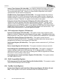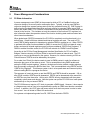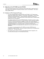
1
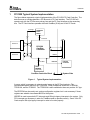
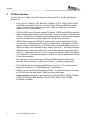
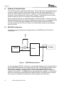
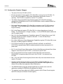
Application Report SCPA033 - October 2002 PCI1520 Implementation Guide Computer Connectivity Solutions ABSTRACT This document is provided to assist platform designers using the PCI1520 dual-socket PC Card controller. Detailed information can be found in the PCI1520 data manual. However, this document provides design suggestions for the various options when designing in the PCI1520. 1 2 3 4 5 6 7 8 9 10 11 12 13 14 Contents PCI1520 Typical System Implementation ....................................................................................................................... 3 Power Considerations...................................................................................................................................................... 4 2.1 Internal Voltage Regulator ........................................................................................................................................ 4 2.2 Clamping Rails .......................................................................................................................................................... 4 2.3 Bypass Capacitors .................................................................................................................................................... 4 Power Switch Implementation......................................................................................................................................... 5 PCI Bus Interface.............................................................................................................................................................. 6 PC Card Interface.............................................................................................................................................................. 7 Miscellaneous Pin Interface............................................................................................................................................. 8 6.1 Multifunction Terminals ............................................................................................................................................. 8 6.2 SPKROUT................................................................................................................................................................. 8 6.3 SUSPEND#............................................................................................................................................................... 8 Interrupt Configurations .................................................................................................................................................. 9 7.1 Parallel PCI Interrupts Only....................................................................................................................................... 9 7.2 Parallel IRQ and Parallel PCI Interrupts.................................................................................................................... 9 7.3 Serial IRQ and Parallel PCI Interrupts....................................................................................................................... 9 7.4 Serial IRQ and Serial PCI Interrupts ......................................................................................................................... 9 Software Considerations ............................................................................................................................................... 10 8.1 EEPROM Configuration .......................................................................................................................................... 10 8.2 BIOS Considerations............................................................................................................................................... 11 8.2.1 PCI Configuration Registers (Standard).................................................................................................... 11 8.2.2 PCI Configuration Registers (TI Extension) .............................................................................................. 12 8.2.3 ExCA Compatibility Registers ................................................................................................................... 12 8.2.4 CardBus Socket Registers........................................................................................................................ 12 Power Management Considerations ............................................................................................................................. 13 9.1 D3 Wake Information .............................................................................................................................................. 13 9.1.1 GRST# Only Registers ............................................................................................................................. 14 9.1.2 PME# Context Registers........................................................................................................................... 15 9.2 PME#/RI_OUT# Behavior ....................................................................................................................................... 15 9.3 CLKRUN# Protocol ................................................................................................................................................. 15 9.4 SUSPEND#............................................................................................................................................................. 16 Pin Compatibility with Other Devices ........................................................................................................................... 16 Migration to the PCI1520 from the PCI1420.................................................................................................................. 17 11.1 Hardware and Pin Assignment Changes ................................................................................................................ 17 11.2 Configuration Register Changes ............................................................................................................................. 18 11.3 Other Functional Differences .................................................................................................................................. 19 Migration to the PCI1420 from the PCI1225.................................................................................................................. 20 12.1 Hardware and Pin Assignment Changes ................................................................................................................ 20 12.2 Configuration Register Changes ............................................................................................................................. 21 12.3 Other Functional Differences .................................................................................................................................. 21 Reference Schematics ................................................................................................................................................... 22 References ...................................................................................................................................................................... 24 1 SCPA033 Figure 1. Figure 2. Figure 3. Figure 4. Figure 5. Figures Typical System Implementation .......................................................................................................................3 Power Switch Implementation..........................................................................................................................5 EEPROM Implementation................................................................................................................................10 Reference Schematics – Page 1.....................................................................................................................22 Reference Schematics – Page 2.....................................................................................................................23 Document History Revised by 2 Date DGB 8/6/02 DGB 8/8/02 DGB 8/9/02 Document Name Revision Comments PCI1520 Implementation Guide – 1.00.doc PCI1520 Implementation Guide – 1.10.doc *Initial Draft PCI1520 Implementation Guide – 1.11.doc *Fixed typo in Rev History PCI1520 Implementation Guide *Added information about switchable pullup/pulldown on CSTSCHG to Section 5 *Corrected explanation of single socket implementation in Section 5 *Added PCLK to list of SUSPEND# gated signals in Section 6.3 *Corrected bit number for INTRTIE in Section 7 *Changed description of Cache Line Size Reg in Section 8.2.1 *Removed duplicate Dev Cntl Reg in Section 8.2.2 *Corrected PC Card Standard rev number in Section 14 SCPA033 PCI1520 Typical System Implementation The figure below represents a typical implementation of the PCI1520 PC Card Controller. The device serves as a bridge between a PCI Bus and a PC Card interface. The PCI1520 will operate only with the PCI Bus as a primary bus and the PC Card interface as the secondary bus. The PC Card interface operates with both CardBus (32-bit) and 16-bit PC Cards. Vcc/Vpp TPS2226A Power Switch 4 3 P2C Bus Socket A PCI1520 CardBus Controller PCI Bus 1 Socket B PME# 2 I2C Bus IRQSER Interrupt Controller Serial EEPROM (Optional) CardBus Controller Block Figure 1. System Side Typical System Implementation A power switch is necessary in order to control power to the PC Card sockets. The recommended power switch is the TPS2226A. Other possibilities include the TPS2224A, TPS2216A, and the TPS2206. The TPS2223A is also available but does not provide 12V Vpp. The EEPROM can be used to set various configuration registers but is not necessary if those registers are settable via software/BIOS for the system. IRQSER is used to pass both PCI interrupts and ISA style legacy interrupts to the system. Only PCI interrupts are necessary in order for CardBus cards to operate correctly. Some 16-bit PC Cards require ISA style legacy interrupts in order to function properly. PCI1520 Implementation Guide 3 SCPA033 2 Power Considerations 2.1 Internal Voltage Regulator One of the major differences between the PCI1520 and previous Texas Instruments CardBus controllers is that the PCI1520 uses an internal voltage regulator to power the core logic at 2.5V. This allows for a more than 50% reduction in power consumption over previous controllers. The voltage regulator is enabled using the VR_EN# pin. If VR_EN# is high, the voltage regulator is disabled and VRPORT serves as a 2.5V external input to power the core. If VR_EN# is low, the voltage regulator is enabled and VRPORT serves as a 2.5V output. This 2.5V output cannot be used to power other devices and is only available externally in order to provide a 1µF bypass capacitor. VRPORT must have a 1µF bypass capacitor to ground in order for proper operation if the voltage regulator is enabled. 2.2 Clamping Rails The PCI1520 has 3 clamping rails: VCCP, VCCA, and VCCB. VCCP is the PCI interface I/O clamp rail and can be either 3.3V or 5V depending on the system implementation. The PCI1520 will only signal on the PCI bus at 3.3V but is 5V tolerant. VCCA and VCCB are connected to the PC Card power rails for Socket A and Socket B, respectively. These terminals serve as the clamping inputs for the PC Card interface to the PCI1520. 2.3 Bypass Capacitors Standard design rules for power supply bypass should be followed. A value of 0.1µF is recommended for each of the power pins VCC, VCCP, VCCA, and VCCB. 4 PCI1520 Implementation Guide SCPA033 Power Switch Implementation The following figure shows the serial interface between the PCI1520 and the TPS2226A power switch: VPPA CLOCK VCCA VCCB 3 VCCA DATA PCI1520 TPS2226A Pull-down for I2C interface (optional) Figure 2. VPPB VCCB LATCH Socket A Socket B Pulldown if using internal clock Power Switch Implementation A power switch is necessary in order to control power to the PC Card sockets. When the PCI1520 receives a socket power request, it sends the appropriate data across the P2C interface (CLOCK, DATA, and LATCH). In turn, the power switch turns on the appropriate levels for VCC and VPP for that socket. A 2.7kΩ pulldown on LATCH is used to indicate to the PCI1520 that an EEPROM is being used to program the PCI1520. CLOCK can be provided either internally or externally depending on bit 27 in System Control register in the PCI configuration space at offset 80h. If an external clock is used, the frequency should be between 32kHz and 100kHz. If the internal clock is used, a 43k pulldown resistor is necessary. PCI1520 Implementation Guide 5 SCPA033 4 PCI Bus Interface The PCI1520 has a 33MHz, 32 bit PCI Interface compliant with PCI Local Bus Specification Revision 2.2. 6 • PCLK, AD31:0, C/BE#3:0, PAR, DEVSEL#, FRAME#, STOP#, TRDY#, IRDY#, GNT#, and REQ# are required PCI signals. All except PCLK, GNT#, and REQ# are bussed signals. PCLK is a 33MHz point-to-point clock. GNT# and REQ# are point-to-point signals form the PCI bus arbitrator. • PERR#, SERR#, and LOCK# are optional PCI signals. PERR# and SERR# are bussed signals and should be pulled up to VCC if unused. LOCK# is available on a Multifunction Terminal. If LOCK# is not needed for system implementation, it should not be configured as such in the Multifunction Routing register (PCI configuration offset 8Ch). • GRST# (Global reset) and PRST# (PCI reset) are both used to initialize the PCI1520. The assertion of GRST# puts the PCI1520 in its default state. The assertion of PRST# does not initialize GRST# only bits. PRST# also does not initialize PME# context bits if PME# in enabled. More information can be found in Section 9.1 – D3 Wake Information. • IDSEL should be resistively coupled (100Ω) to one of the address lines between AD31 and AD11. Please refer to Section 3.2.2.3.5 (System Generation of IDSEL) and Section 4.2.6, footnote 31 (Pinout Recommendation) of the PCI Local Bus Specification Revision 2.2 for more information. • PCI Interrupts can be routed through INTA# and INTB# through the Multifunction terminals. More information can be found in Section 7 – Interrupt Configurations. • PCI CLKRUN# can be routed through Multifunction terminal 6. For more information, please refer to Section 9 – Power Management Considerations. • PME# is used to signal Power Management Events. This signal is important for waking the PCI1520 from low power states. PME# is an open-drain signal. • Pullup resistors are needed on the following PCI terminals: IRDY#, TRDY#, FRAME#, STOP#, DEVSEL#, PERR#, SERR#, LOCK#, PRST#, GRST#, INTA#, INTB#, CLKRUN#, and PME#. PCI1520 Implementation Guide SCPA033 5 PC Card Interface There are two different modes on the PC Card interface. The first is 16-bit mode which is analogous to the legacy ISA bus. The second is 32-bit CardBus mode which is very similar to a PCI Bus. The terminal functions for these two modes are multiplexed and routed to the PC Card sockets. The following suggestions apply to the PC Card interface: • Pullup resistors for the PC Card interface have been integrated into the PCI1520. These include: A14/CPERR#, A15/CIRDY#, A19/CBLOCK#, A20/CSTOP#, A21/CDEVSEL#, A22/CTRDY#, BVD2(SPKR#)/CAUDIO, CD1#/CCD1#, CD2#/CCD2#, INPACK#/CREQ#, READY/CINT#, RESET/CRST#, VS1#/CVS1, VS2#/CVS2, WAIT#/CSERR#, WP(IOIS16#)/CCLKRUN#. • A switchable pullup/pulldown resistor has been implemented on BVD1(STSCHG#)/CSTSCHG. The pulldown is implemented when a CardBus card is being used or when the socket is empty. A pullup is implemented when a 16-bit PC card is being used. • A damping resistor is necessary on the CCLK terminals between the PCI1520 and the PC Card sockets. The value is system dependent. If line impedance is in the range of 60-90Ω, a 47Ω resistor is recommended. For more information, please see the PC Card Standard Revision 7.1, Section 5.3.2.1.4. • CD# line noise filtering is no longer required because the PCI1520 has an integrated digital noise filter. • Three PC Card terminals on each socket are not necessary for CardBus mode but are necessary for 16-bit mode. These terminals are: CRSVD/D14, CRSVD/A18, and CRSVD/D2. These terminals must be connected to the PC Card Socket according to their 16-bit designations. By default, when in CardBus mode, these terminals are driven low. They can be tristated by setting bit 22 (CBRSVD) in the System Control register at PCI configuration offset 80h. • Texas Instruments provides single socket CardBus controllers such as the PCI1510 for systems requiring only one PC card socket. However, the PCI1520 can be used as a single socket controller simply by leaving the Socket B interface floating. PCI1520 Implementation Guide 7 SCPA033 6 Miscellaneous Pin Interface 6.1 Multifunction Terminals The multifunction terminals (MFUNC6:0) can be programmed to serve many different roles using the Multifunction Routing register at PCI configuration offset 8Ch. The discrete ISA interrupts (IRQ15:2), INTA#, INTB#, and IRQSER are explained in Section 7 – Interrupt Configurations. CLKRUN#, D3STAT#, and RI_OUT# are discussed in Section 9 – Power Management Considerations. ZVSTAT, ZVSEL1#, and ZVSEL0# are used for ZV control. For more information, please refer to the PCI1520 Data Manual. LED_SKT, LEDA1, and LEDA2 can be used to indicate socket activity. When a PC Card is being accessed, these outputs will be driven high. LED_SKT will be driven high for access to either socket. LEDA1 and LEDA2 will only be driven high during access to their respective socket. GPE#, GPIx, and GPOx can be used to signal general purpose events to the system. CAUDPWM provides a PWM output for the CAUDIO terminals (as opposed to the binary output SPKROUT). PCI LOCK# is an optional PCI signal as mentioned in Section 4 – PCI Bus Interface. All unused multifunction terminals require a 43kΩ pullup resistor. 6.2 SPKROUT SPKROUT is the output to the host system that can carry SPKR# or CAUDIO through the PCI1520 from the PC Card interface. If SPKROUT is enabled for both sockets, it is driven as an exclusive-OR of the two inputs. A 43k pulldown resistor is required to prevent oscillation when SPKROUT is disabled and therefore tristated. 6.3 SUSPEND# The assertion of SUSPEND# gates PRST#, GRST#, and PCLK from the PCI1520. More information can be found in Section 9 – Power Management Considerations. A 43kΩ pullup resistor is required on SUSPEND#. SUSPEND# cannot be low during boot. 8 PCI1520 Implementation Guide SCPA033 7 Interrupt Configurations The PCI1520 provides system designers with great flexibility in configuring interrupts. The PCI1520 allows four interrupt modes which are selected via bits 2:1 of the Device Control register at PCI offset 92h. PCI interrupts are available on INTA# and INTB#. These signals are available on MFUNC0 and MFUNC1 respectively. The Multifunction Routing register at PCI configuration offset 8Ch must be programmed correspondingly. If MFUNC1 is not available (i.e. EEPROM implementations which use MFUNC1 as SDA), the INTRTIE bit can be set at bit 29 in the System Control register at PCI offset 80h. This allows both INTA# and INTB# signaling to both be reported on INTA#. PCI interrupts can also be signaled through IRQSER. ISA style IRQ interrupts are available on IRQ15:2. These signals are available on MFUNC6:0. These interrupts are necessary for some 16-bit PC Cards to function properly. IRQ interrupts can also be signaled through IRQSER. IRQSER is available on MFUNC3 and requires a 43k pullup resistor to VCC. 7.1 Parallel PCI Interrupts Only The parallel PCI interrupts only mode is selected by programming bits 2:1 to a value of 00b. This allows interrupts to be routed through INTA# and INTB#. This is not a recommended interrupt configuration because many 16-bit PC Cards require legacy ISA interrupts and will not function properly. 7.2 Parallel IRQ and Parallel PCI Interrupts The parallel IRQ and parallel PCI interrupts mode is selected by programming bits 2:1 to a value of 01b. This allows interrupts to be routed through IRQ15:2, INTA#, and INTB#. This is not a recommended interrupt configuration because this requires all the multifunction terminals to be used as interrupts which limits other functions on the PCI1520. 7.3 Serial IRQ and Parallel PCI Interrupts The serial IRQ and parallel PCI interrupts mode is selected by programming bits 2:1 a value of 10b. This allows interrupts to be routed through IRQSER, INTA#, and INTB#. This is the recommended interrupt configuration for a PCI add-in card implementation of the PCI1520. INTA# and INTB# can be routed through the PCI edge connector while IRQSER must be attached to a Serial IRQ input on the motherboard. If no Serial IRQ input is available, this mode still allows CardBus cards to function properly. However, many 16-bit cards will not. 7.4 Serial IRQ and Serial PCI Interrupts The serial IRQ and serial PCI interrupts mode is selected by programming bits 2:1 to a value of 11b. This allows all interrupts to be routed through IRQSER. This is the recommended interrupt configuration for all designs other than PCI add-in cards. It is the simplest method of routing interrupts and allows the other multifunction terminals to be used for other purposes. PCI1520 Implementation Guide 9 SCPA033 8 Software Considerations The PCI1520 is natively supported by Windows XP. The PCI1520 will be recognized natively as a Generic CardBus Controller under Windows 2000, Windows ME, and Windows 98SE. The device will function properly using this driver. However, it is recommended that new drivers provided by Texas Instruments be used for non-XP systems. These drivers have a few small tweaks and allow the device to be reported in Device Manager properly. Other operating systems are not supported directly by Texas Instruments. However, many nonMicrosoft operating systems have generic CardBus device drivers which are compatible with the PCI1520. Any driver which was compatible with a previous Texas Instruments CardBus controller (such as the PCI1225 or PCI1420) or the Intel 82365SL should also be compatible with the PCI1520. 8.1 EEPROM Configuration The following diagram represents the implementation of an EEPROM for the PCI1520 for configuration: Vcc LATCH SDA EEPROM SCL Figure 3. TPS2226A PCI1520 EEPROM Implementation On the rising edge of GRST#, if LATCH is low, the Serial Bus Detect bit (bit 3, PCI offset B3h) is set and the EEPROM contents are loaded into the PCI1520. MFUNC1 and MFUNC4 become SDA and SCL respectively. In order for the PCI1520 to detect the EEPROM and load configuration information, a pulldown resistor must be implemented on LATCH. Pullups are needed on SDA and SCL. The EEPROM slave address should be 1010000b. If the Serial Bus Detect bit is cleared after the EEPROM data is loaded, MFUNC1 and MFUNC4 are returned to their functions as indicated by the Multifunction Routing Register (PCI offset 8Ch). 10 PCI1520 Implementation Guide SCPA033 The EEPROM loading map can be found in the data manual. The following is an example data file which could be loaded into the EEPROM for use with the PCI1520: ; EEPROM Programming Data for the PCI1520 Customer Board ; Configured for IRQ serialized interrupts and parallel PCI interrupts ; Register 00 01 02 03 04 05 06 07 08 09 0a 0b 0c 0d 0e 0f 10 11 12 13 14 15 16 17 18 8.2 Data Description 0x01 0x03 0x78 0x56 0x34 0x12 0xe0 0x03 0x00 0x00 0x60 0xd0 0x28 0x02 0x10 0x00 0x00 0xc0 0x00 0x44 0x00 0x00 0x84 0x00 0x00 ;Reference 1 ;04h Command Register, bit 8 (mapped from EEPROM bit 7), 6-5, 2-0 ;40h Sub-System Vendor ID Byte 0 ;40h Sub-System Vendor ID Byte 1 ;42h Sub-System ID Byte 0 ;42h Sub-System ID Byte 1 ;44h Legacy Bar Byte 0, bits 7-1 ;44h Legacy Bar Byte 1 ;44h Legacy Bar Byte 2 ;44h Legacy Bar Byte 3 ;80h System Control Byte 0 (default) ;80h System Control Byte 1 (MRBURSTU=1 all others default) ;80h System Control Byte 3 (INTRTIE=1, P2CCLK=1) ;8ch MFUNC Byte 0 (MFUNC1=SDA, MFUNC0=INTA) ;8ch MFUNC Byte 1 (MFUNC3=IRQSER, MFUNC2=GPI2) ;8ch MFUNC Byte 2 (MFUNC5=GPI4, MFUNC4=SCL) ;8ch MFUNC Byte 3 (MFUNC6=RSVD) ;90h Retry Status bits 7, 6 (PCI Retry, CardBus Retry) ;91h Card Control bits 7, 5 (Ring Indicate Enable, ZV Port Select) ;92h Dev Cntr bits 6, 3-0 (3V Capa, IRQ serialized and parallel PCI) ;93h Diagnostic bits 7, 4-0 ;a2h Power Management Capabilities bit 15 (PME#_Supp from D3cold=0) ;00h ExCA ID and Revision bits 7-0 ;Och+CB Socket Force Event Function 0 bit 27 (ZVSUPPORT=0) ;Och+CB Socket Force Event Function 1 bit 27 (ZVSUPPORT=0) BIOS Considerations This section provides a high-level overview of the registers which need to be programmed by the BIOS upon initialization. In general, the only registers which must be programmed for proper operation within a Windows operating system are those registers which are EEPROM loadable. Other registers may need to be changed according to system implementation. Microsoft provides the following reference documents concerning initialization of CardBus controllers in Windows: http://www.microsoft.com/hwdev/bus/cardbus/cardbus1.asp http://www.microsoft.com/hwdev/bus/pci/pcibridge-cardbus.asp 8.2.1 PCI Configuration Registers (Standard) Cache Line Size Register (PCI offset 0Ch) – This register indicates the size in doublewords of a cache line. This register is system architecture dependent. PCI1520 Implementation Guide 11 SCPA033 Latency Timer Register (PCI offset 0Dh) – This register indicates the number of PCI clocks the PCI1520 will be allowed access to the PCI bus if another master has its REQ# asserted. The recommended value is 40h. However, the value should be dependent on the system implementation and which devices need priority. CardBus Latency Timer Register (PCI offset 1Bh) – This register indicates the number of CardBus clocks the PCI1520 will be allowed access on the CardBus interface. Because the CardBus interface is a point-to-point interface, the PCI1520 does not deassert CGNT# until a transaction is finished. Therefore, this register has little effect on the system. Subsystem Vendor ID and Subsystem ID Registers (PCI offsets 40h and 42h) – These registers are used for subsystem and option card identification purposes. Typically, these registers contain the OEM vendor ID and an OEM identified designator. These fields can be programmed using the EEPROM or BIOS. If using BIOS, the SUBSYSRW bit (System Control register, bit 5) must be cleared to 0. The SSVID and SSID registers can now be written. The SUBSYSRW bit should be set to 1 after the registers are written. 8.2.2 PCI Configuration Registers (TI Extension) System Control Register (PCI offset 80h) – This register contains many important system dependent variables. Please refer to the datasheet for more details. Of possible interest to the BIOS programmer: SER_STEP, INTRTIE, P2CCLK, MRBURSTDN, MRBURSTUP, and RIMUX. Multifunction Routing Register (PCI offset 8Ch) – This register controls the seven multifunction terminals of the PCI1520. This register must be set before the interrupt mode is programmed in the Device Control register (PCI offset 92h). Card Control Register (PCI offset 91h) – This register contains enable bits for RI_OUT# and SPKROUT. Device Control Register (PCI offset 92h) – This register contains the interrupt mode bits. Power Management Capabilities Register (PCI offset A2h) – This register is important for systems needing to wake from the D3 power state. Bit 15 reflects whether or not PME# is supported from D3cold. Bit 4 is tied to bit 15 indicating that if PME# is supported from D3cold, the system must be providing auxiliary power. Power Management Control and Status Register (PCI offset A4h) – This register contains the PME# enable bit (bit 8). 8.2.3 ExCA Compatibility Registers ExCA Interrupt and General-Control Register (ExCA offset 03/43h) – This register is used to route CSTSCHG interrupts via PCI interrupts. 8.2.4 CardBus Socket Registers Socket Control Register and Socket Power Management Register (CB offsets 10h and 20h) – These registers can be used to characterize how CB CLKRUN# functions. 12 PCI1520 Implementation Guide SCPA033 9 Power Management Considerations 9.1 D3 Wake Information A power management event (PME) is the process by which a PCI or CardBus function can request a change of its current power consumption state. Typically, a device uses PME# to request a change from a power savings state to the fully operational state, D0. PME Context is defined as the functional state information and logic required to generate PMEs, report PME status, and enable PMEs. PCI Function Context refers to the small amounts of information held internal to the function. This includes not only the contents of the function’s PCI registers, but also information about the operation states of the function including state machine context and other internal mechanisms. When global reset (GRST#) is asserted, the PCI1520 is completely non-functional and is in a default state. Output buffers are tristated and internal registers are reset. The result of PCI reset (PRST#) being asserted is dependent on whether PME# is enabled or not. When PRST# is asserted with neither function enabled for PME#, it causes the PCI1520 to tristate all output buffers and reset all internal registers except for those considered ‘GRST# Only Registers’. If PME# is enabled for either socket, the PCI1520 will maintain its ‘PME# Context Registers’. According to the PCI Bus Power Management Interface Specification for PCI to CardBus Bridges, a device returning to D0 from D3hot is required to assert an internal reset. The PCI reset may or may not be asserted by the system. However, for a device returning to D0 from D3cold however, PRST# must be asserted by the system. For a wake from D3cold, the device needs to save its PME# context in order for software to determine the source of the wake-up event. This is accomplished using PME# enable and saving the PME# context registers. However, the device must also maintain certain registers that are normally configured by BIOS at boot time. This is accomplished using GRST# and the ‘GRST# Only Registers.’ This allows a system to be in a low power state and resumed quickly without needing BIOS to reprogram the device. The sequence of events at power up are that GRST# and PRST# should be asserted. 100 µs after PCLK is stable, GRST# can be deasserted. PRST# can be deasserted at the same time as GRST# or any time there after. At this point, GRST# will stay deasserted until the system completely cycles power and reboots. Now the system can put the PCI1520 into a lower power state and may or may not assert PRST#. The PCI1520 does not require a PCI clock to generate a PME# signal. However, it does require a voltage source such as Vaux to be supplied and the pullup on PME# must also be connected to Vaux. In addition, the VCCP pins and power switch must also have power in order to wake from a card. Vaux is limited to 200mA for each socket. For systems not implementing wake from D3, GRST# can be tied to PRST#. PCI1520 Implementation Guide 13 SCPA033 9.1.1 GRST# Only Registers Global reset places all registers in their default state regardless of the state of the PME enable bit. The GRST# signal is gated only by the SUSPEND# signal. This means that assertion of SUSPEND# blocks the GRST# signal internally, thus preserving all register contents. The registers cleared only by GRST# are: 14 • Status register (PCI offset 06h): bits 15-11, 8 • Secondary status register (PCI offset 16h): bits 15-11, 8 • Interrupt pin register (PCI offset 3Dh): bits 1,0 (function 1 only) • Subsystem vendor ID register (PCI offset 40h): bits 15-0 • Subsystem ID register (PCI offset 42h): bits 15-0 • PC Card 16-bit legacy mode base address register (PCI offset 44h): bits 31-1 • System control register (PCI offset 80h): bits 31-29, 27-13, 11, 6-0 • Multifunction routing register (PCI offset 8Ch): bits 27-0 • Retry status register (PCI offset 90h): bits 7-5, 3, 1 • Card control register (PCI offset 91h): bits 7-5, 2-0 • Device control register (PCI offset 92h): bits 7-5, 3-0 • Diagnostic register (PCI offset 93h): bits 7-0 • Power management capabilities register (PCI offset A2h): bit 15 • General-purpose event status register (PCI offset A8h): bits 15-14 • General-purpose event enable register (PCI offset AAh): bits 15-14, 11, 8, 4-0 • General-purpose output (PCI offset AEh): bits 4-0 • Serial bus data (PCI offset B0h): bits 7-0 • Serial bus index (PCI offset B1h): bits 7-0 • Serial bus slave address register (PCI offset B2h): bits 7-0 • Serial bus control and status register (PCI offset B3h): bits 7, 5-0 • ExCA identification and revision register (ExCA offset 00h): bits 7-0 • ExCA global control register (ExCA offset 1Eh): bits 2-0 • Socket present state register (CardBus offset 08h): bit 29 • Socket power management register (CardBus offset 20h): bits 25-24 PCI1520 Implementation Guide SCPA033 9.1.2 PME# Context Registers If the PME# enable bit (bit 8) of the power-management control/status register (PCI offset A4h) is asserted, then the assertion of PRST# will not clear the following PME# context bits. If the PME# enable bit is not asserted, then the PME# context bits are cleared with PRST#. The PME# context bits are: 9.2 • Bridge control register (PCI offset 3Eh): bit 6 • System control register (PCI offset 80h): bits 10, 9, 8 • Power-management control/status register (PCI offset A4h): bits 15, 8 • ExCA power control register (ExCA offset 802h): bits 7, 5†, 4-3, 1-0 (†82365SL mode only) • ExCA interrupt and general control register (ExCA offset 803h): bits 6-5 • ExCA card status change register (ExCA offset 804h): bits 11-8, 3-0 • ExCA card status-change-interrupt configuration register (ExCA offset 805h): bits 3-0 • CardBus socket event register (CardBus offset 00h): bits 3-0 • CardBus socket mask register (CardBus offset 04h): bits 3-0 • CardBus socket present state register (CardBus offset 08h): bits 13-7, 5-1 • CardBus socket control register (CardBus offset 10h): bits 6-4, 2-0 PME#/RI_OUT# Behavior PME# and RI_OUT# are very important for power management. The PME# signal is useful for PCI power management systems. The RI_OUT# (Ring Indicate Out) signal is used for legacy power management systems. PME# and RI_OUT# are multiplexed on the same pin. The PCI1520 can also provide RI_OUT# on the Multifunction terminals. To enable passage of Ring signals from the PC Card interface, RINGEN (bit 7 ExCA offset 803) must be set to ‘1’, and RIENB (bit 7 PCI offset 91h) must be set to ‘1’. This is a per socket function. 9.3 CLKRUN# Protocol CLKRUN# is a hardware method of clock control that can be used in parallel with other types of power management. For the PCI1520, PCI CLKRUN# can be programmed using the Multifunction Routing Register (PCI offset 8Ch) on MFUNC6. CardBus CLKRUN# is a required signal incorporated into the PC Card interface. The following bits can be used to adjust the operation of how PCI and CB CLKRUN# affect the PCI1520: Multifunction Routing register – MFUNC6 (PCI offset 8Ch, bits 27-24 set to 0001b). Requires a 43kΩ pullup. KEEPCLK – System Control Register (PCI offset 80h, bit 1). Setting this bit to a ‘1’ will never allow the PCI CLKRUN# protocol to stop or slow the PCI clock. PCI1520 Implementation Guide 15 SCPA033 STOPCLK – Socket Control Register (CB offset 10h, bit 7). This bit determines whether the CB CLKRUN# protocol is affected by the PCI CLKRUN# protocol. CLKCTRLEN – Socket Power Management Register (CB offset 20h, bit 16). This bit enables the CB CLKRUN# protocol. CLKCTRL – Socket Power Management Register (CB offset 20h, bit 0). This bit determines whether the CB CLKRUN# protocol will either stop or slow CCLK. 9.4 SUSPEND# The assertion of the SUSPEND# signal gates PCLK, GRST#, PRST# from the PCI1520. The recommended implementation for SUSPEND# is to not use it for power management and simply connect a 43kΩ pullup resistor. SUSPEND# is an unstandardized method of power management and causes many implementation problems. The following guidelines are provided to help reduce implementation issues. The main purpose of the PCI1520 SUSPEND# pin is to prevent PCI reset from clearing all register context which would require the reconfiguration of the PCI1520 by software. Asserting the PCI1520 SUSPEND# signal will also tri-state the controllers PCI outputs and gate the PCLK internally to the controller if there isn't any PCI transaction currently in process. Due to the tristated PCI outputs, it is important that the PCI bus not be parked on the PCI1520 when SUSPEND# is asserted. Another major point to note is that powerdown of a card slot due to card removal requires the use of either the Internal Oscillator or an externally supplied clock to the power switch. If an external clock is used and is removed during Suspend, the card slot will not power down and will remain powered. This opens the possibility of potential card damage. If a 3.3V card is inserted into the hot slot that was powered to 5V, card damage will most likely occur. It is therefore recommended that P2CCLK, bit 27 at PCI offset 80h is set to a '1' so that the Internal Oscillator is enabled. The CLOCK signal will then always be available as long as power is applied to the CB controller. 10 Pin Compatibility with Other Devices The PCI1520 is pin compatible with the PCI1620 PC Card, Flash Media, and Smart Card Controller. This device has flash media and smart card terminals multiplexed on the PC Card interface to allow for convenient access to many different media types. In order to design a PCB for an upgrade path to the PCI1620, one change must be made from a normal PCI1520 PCB. A 48MHz clock is needed on the PCI1620. This clock input is located on pin 81 for the PDV package and pin W11 for the GHK package. The PCI1520 can also be designed on to the same PCB as other Texas Instruments CardBus controllers such as the single socket PCI1510 controller even though the two devices are not pin compatible. This can be done using a dual footprint for the devices on the PCB. For example, a designer may want the option of having a single or dual socket implementation on a single PCB. In this instance, a PCI1510 BGA (GGU) footprint can be placed inside a PCI1520 QFP (PDV) footprint. The traces for the PC Card socket A on the PCI1520 footprint are then connected to the PC Card socket traces on the PCI1510 footprint. For single socket implementations, only one PC Card socket is populated along with the PCI1510 controller. For dual socket implementation, both PC Card sockets are populated along with the PCI1520 controller. 16 PCI1520 Implementation Guide SCPA033 11 Migration to the PCI1520 from the PCI1420 The major differences between the PCI1520 and PCI1420 are pinout, lower power consumption, and lower cost. The pinout is changed on the PCI1520 in order to incorporate an internal voltage regulator which allows the core to operate at 2.5V. When moving from the PCI1225 to the PCI1520, please see Section 13 for the differences between the PCI1225 and PCI1420 in addition to the changes from this section. 11.1 Hardware and Pin Assignment Changes • The pinout on the PCI1520 is significantly changed from the PCI1420. This requires a PCB redesign. • A low dropout voltage regulator is integrated into the PCI1520 to supply 2.5V core voltage. A voltage regulator enable pin (VR_EN#) has been added in place of one of the VCCP pins. A core voltage input/output (VRPORT) pin has been added in place of the VCCI pin. This pin is used to either input core voltage or allow for an external 1.0µF bypass capacitor depending on the value of VR_EN#. A typical implementation would enable the regulator by grounding VR_EN# and adding the bypass capacitor from VRPORT to ground. For further details, see the datasheet. • The PCI1520 does not have a VCCI pin. Signals clamped to VCCI on the PCI1420 are clamped to VCCP on the PCI1520. • A new power switch has been introduced for dual socket CardBus controllers. The TPS2226A is recommended for new designs although the TPS2216 and TPS2206 are still compatible with the PCI1520. All three power switches have very similar functionality and can be designed onto the same footprint. • The PCI1520 has integrated pullup resistors on the two CCLKRUN#//WP(IOIS16#) terminals. All necessary pullup resistors on the PC Card interface have been integrated in the PCI1520. • A switchable pullup/pulldown resistor has been implemented on the two CSTSCHG//BVD1(STSCHG#/RI#) terminals. The pullup is active when the 16BITCARD bit (bit 4 in the Socket Present State register) is ‘1’, otherwise the pulldown resistor is activated. This prevents unexpected PME# assertion. PCI1520 Implementation Guide 17 SCPA033 11.2 Configuration Register Changes 18 • The device ID for the PCI1520 is AC55. • Bit 23 in the System Control register (PCI offset 80h) is reserved on the PCI1520. On the PCI1420, this enabled PCI Bus power management specification revision 1.1 reporting. The PCI1520 is compliant to revision 1.1 by default. • The default value of the Multifunction Routing register (PCI offset 8Ch) has been changed from 00000000h on the PCI1420 to 00001000h in order to enable IRQSER on MFUNC3 by default. • Bit 6 in the Diagnostic register (PCI offset 93h) is reserved on the PCI1520 instead of AOSPMEN. The AOSPMEN feature of disabling oscillator power management is no longer necessary. • Bit 0 in the Diagnostic register (PCI offset 93h) is no longer Asynchronous Interrupt Enable. The functionality is no longer necessary. It is now STDZVEN which enables the new ZV register model. • Bits 2-0 in the Power Management Capabilities register (PCI offset A2h) are now ‘010b’ indicating that the PCI1520 is compliant to Revision 1.1 of the PCI Bus Power Management Specification. • Bit 4 (AUX_PWR) in the Power Management Capabilities register (PCI offset A2h) is now tied to bit 15 (PME#_Support for D3Cold). • D3_STAT# functionality has been added to MFUNC5, MFUNC4, and MFUNC2. D3_STAT# is asserted when PME# is enabled and both functions are placed in D3 power state. • Bit 27 in the Socket Present State register (Socket offset 08h) now indicates Zoom Video Support in that socket for the PCI1520. It is reserved in the PCI1420. • Bit 27 in the Socket Force Event register (Socket offset 0Ch) now causes the ZVSUPPORT bit mentioned above to be set in the PCI1520. It is reserved in the PCI1420. • Bits 11-9 in the Socket Control register (Socket offset 10h) were reserved and now are used for ZV control. • Registers and bits previously referring to centralized or distributed DMA are now reserved (bits 19-16 System Control register at PCI offset 80h, DMA registers at PCI offsets 94h and 98h) (see explanation about DMA below). • The EEPROM loading map has changed significantly to provide more control for applications needing an EEPROM (see datasheet for details). • Two registers have been added to the PME# context list (ExCA Power Control register and ExCA Interrupt and General Control register). PCI1520 Implementation Guide SCPA033 11.3 Other Functional Differences • The PCI1520 is natively supported by Windows XP. The PCI1520 will be recognized natively as a Generic CardBus Controller under Windows 2000, Windows ME, and Windows 98SE. The device will function properly using this driver. However, it is recommended that new drivers provided by Texas Instruments be used for non-XP systems. These drivers have a few small tweaks and allow the device to be reported in Device Manager properly. • The latest version of the PC Card Standard (Revision 8.0) no longer supports centralized or distributed DMA for PC Cards. Therefore, the PCI1520 no longer supports centralized or distributed DMA. DMA was used by very few PC Cards, most of which are obsolete (DOS-based sound cards, DVD decoders). • A new standardized ZV register model has been implemented in the PCI1520 (see datasheet for details). The PCI1520 is backward compatible with the legacy ZV register model used in previous CardBus controllers. • The timing condition erratum which disabled the MFUNC1 and MFUNC4 pins because a non-existent EEPROM was detected has been fixed. • SPKROUT# signal behavior is changed. The signal will stay low during socket power on an off. A pulldown resistor is required to prevent oscillation. • Setting bit 15 of the Power Management Capabilities register is no longer required to preserve PME# context for a D3hot to D0 transition. This was an erratum in the PCI1420. PCI1520 Implementation Guide 19 SCPA033 12 Migration to the PCI1420 from the PCI1225 The major differences between the PCI1420 and PCI1225 are the ability to wake from the D3 power state and the integration of the pullup resistors on the PC Card interface. This is done using a global reset pin. 12.1 Hardware and Pin Assignment Changes • The pinout changed slightly from the PCI1225 to the PCI1420. A VCC pin has been replaced by a global reset pin (GRST#). This requires a PCB redesign. This pin allows for wake from the D3 power state. Certain configuration registers are reset only by GRST# and not PRST#. This allows the device to save context since PCI Reset must be asserted on a D3 to D0 transition. For systems requiring wake from D3, GRST# should be connected to a power-on reset and PRST# should be connected to the system PCI Reset. When implementing GRST# in this way, it must be treated similar to PRST# in that PCI Clock must be stable for 100µs before deassertion. The sequence of events should be: 1) Power on with GRST# and PRST# asserted, 2) Clock becomes stable, 3) 100µs later GRST# can be deasserted, 4) PRST# can be deasserted at the same time or any time after GRST# is deasserted. For systems not requiring wake from D3, GRST# can be tied to PRST# which is connected to system PCI Reset. For more information, please refer to the datasheet and the Section 9.1 – D3 Wake Information. • 20 All necessary pullup resistors on the PC Card interface have been integrated on the PCI1420 with the exception of CCLKRUN#//WP(IOIS16#). PCI1520 Implementation Guide SCPA033 12.2 Configuration Register Changes • The device ID for the PCI1420 is AC51. • The PCI1420 is both Intel 82365SL-DF and 82365SL register compatible. The PCI1225 is only 82365SL-DF register compatible. Bit 2 in the System Control register (PCI offset 80h) is now ExCA Power instead of reserved to allow for SL compatibility. The ExCA Power Control register (ExCA offset 02h) also changes in SL mode. • Bit 23 in the System Control register (PCI offset 80h) is now used to allow the PCI1420 to report as compliant to either revision 1.0 or 1.1 of the PCI Bus Power Management Specification. In the PCI1225, this bit is reserved. • Some of the values of the Multifunction Routing register (PCI offset 8Ch) matrix have changed. When MFUNC5 = 1001b, it is now reserved instead of IRQ9. When MFUNC4 = 1111b, it is now reserved instead of IRQ15. When MFUNC2 = 1011b, it is now reserved instead of IRQ11. • Bit 7 in the Device Control register (PCI offset 92h) is now SKTPWR_LOCK instead of RSVD. This bit, when set to ‘1b’, stops software from powering down the PC Card socket while in the D3 power state. This may be necessary for wake on LAN. • Bit 6 in the Diagnostic register (PCI offset 93h) is now AOSPMEN which disables the oscillator power management features. This bit is reserved in the PCI1225. • Bit 14 in the Power Management Capabilities register (PCI offset A2h) is now read/write with a default of 1 indicating the PCI1420 supports PME# from D3cold when Vaux is provided. This bit is read-only zero in the PCI1225. 12.3 Other Functional Differences • The PCI1420 and PCI1225 are both natively supported by Windows XP, Windows 2000, Windows ME, and Windows 98SE. PCI1520 Implementation Guide 21 SCPA033 13 Reference Schematics The following schematics show the most basic implementation of the PCI1520 possible. These schematics provide minimum functionality. All interrupts are routed using IRQSER. NOTE: THESE ARE THE PCI TERMINALS. PLEASE REFER TO SECTION 4 FOR INFORMATION ON WHICH TERMINALS NEED PULLUP RESISTORS. 3.3VCC C10 .1uF C11 VCCP PAR SERR# PERR# STOP# DEVSEL# TRDY# IRDY# FRAME# C/BE#[3..0] C12 .1uF .1uF AD7 AD6 AD5 AD4 AD3 AD2 AD1 AD0 C/BE#0 152 153 154 155 AD10 AD9 AD8 C/BE0# AD7 GND AD6 AD5 AD4 AD3 AD2 AD1 AD0 C/BE#2 AD16 AD12 AD13 AD14 AD15 C/BE1# PAR SERR# PERR# STOP# GND DEVSEL# TRDY# IRDY# VCC FRAME# C/BE2# AD16 1 2 3 4 5 6 7 8 9 10 11 12 13 AD17 AD18 AD19 AD20 AD21 AD22 GND AD23 IDSEL PCLK AD24 VCCP AD26 AD27 GRST# AD28 AD29 VCC MFUNC0 MFUNC1 SUSPEND# MFUNC2 MFUNC3 MFUNC4 MFUNC5 MFUNC6/CLKRUN# C/BE3# RI_OUT#/PME# GND AD25 PRST# GNT# REQ# AD31 AD30 AD11 U2A AD10 AD9 AD8 SPKROUT# LATCH CLOCK DATA AD17 AD18 AD19 AD20 AD21 AD22 191 190 189 188 187 186 185 184 183 182 181 180 179 178 177 176 175 174 AD23 AD24 AD26 AD27 AD28 AD29 PCI1520 (PCI) AD31 AD30 AD11 R5 43K AD25 C/BE#3 156 157 158 159 160 161 162 163 164 165 166 167 168 169 170 171 172 173 R4 43K IDSEL PCLK REQ# GNT# PRST# PME# 208 207 206 205 204 203 202 201 200 199 198 197 196 195 194 193 192 AD12 AD13 AD14 AD15 C/BE#1 AD[31..0] NOTE: R4 PULL-DOWN ON CLOCK REQUIRED WHEN USING INTERNAL OSC GRST# 3.3VCC R6 43K R7 43K R8 43K R9 43K R10 43K R11 43K R12 43K NOTE: GRST# IS A POWER-ON RESET. IT SHOULD BE ASSERTED AT POWER UP, WAIT AT LEAST 100US AFTER PCLK IS STABLE, THEN BE DEASSERTED FOR PROPER INITIALIZATION. R13 43K PCI12V NOTE: IRQSER SHOULD BE ROUTED TO AN INTERRUPT CONTROLLER. PCI5V C13 10uF C14 IRQSER U3 C15 .1uF AVPP C17 .1uF 1 2 3 4 5 6 7 8 9 10 11 12 13 14 15 5VIN 5VIN DATA CLOCK LATCH NC 12VIN AVPP AVCC AVCC AVCC GND NC RESET# 3.3VIN 5VIN NC NC NC NC SHDN# 12VIN BVPP BVCC BVCC BVCC NC OC# 3.3VIN 3.3VIN 30 29 28 27 26 25 24 23 22 21 20 19 18 17 16 C16 10uF .1uF BVPP C18 .1uF TPS2226A AVCC PCI3.3V C19 C20 10uF .1uF Figure 4. 22 C21 .1uF BVCC C22 .1uF Reference Schematics – Page 1 PCI1520 Implementation Guide SCPA033 BVCC AVCC 1uF A_A5 A_RESET A_A6 A_VS2# A_A25 A_A7 A_A24 A_A12 A_A23 A_REG# A_A3 A_INPACK# A_A4 A_WP A_BVD1 A_BVD2 A_WAIT# A_READY A_VS1# A_A0 A_A1 A_A2 A_D8 A_D0 A_CD2# C1 A_D10 A_D2 A_D9 A_D1 3.3VCC C2 C7 151 150 149 148 147 146 145 144 143 142 141 140 139 138 137 136 135 134 133 132 131 130 129 128 127 126 125 124 123 122 121 120 119 118 U1B .1uF C8 .1uF B_CE2# B_OE# B_A11 B_IORD# B_IOWR# B_A9 B_A17 B_A8 B_A18 B_A13 B_A19 B_A14 R3 B_A16 B_A20 B_WE# B_A21 B_A22 B_A15 B_A23 B_A12 B_A24 B_A7 B_A25 B_VS2# B_A6 B_RESET B_A5 B_A4 B_INPACK# BVPP BVCC C4 .1uF C9 .1uF A_CIRDY#//A_A15 A_CTRDY#//A_A22 A_CCLK//A_A16 VCCA A_CDEVSEL#//A_A21 A_CGNT#//A_WE# A_CSTOP#//A_A20 GND A_CPERR#//A_A14 A_CBLOCK#//A_A19 A_CPAR//A_A13 A_RSVD//A_A18 A_CC/BE1#//A_A8 A_CAD16//A_A17 A_CAD14//A_A9 A_CAD15//A_IOWR# A_CAD13//A_IORD# A_CAD12//A_A11 A_CAD11//A_OE# A_CAD10//A_CE2# A_CAD9//A_A10 A_CC/BE0#//A_CE1# GND A_CAD8//A_D15 A_CAD7//A_D7 A_RSVD//A_D14 VCC A_CAD5//A_D6 A_CAD6//A_D13 A_CAD3//A_D5 A_CAD4//A_D12 A_CAD1//A_D4 A_CAD2//A_D11 A_CAD0//A_D3 A_CCD1#//A_CD1# 49 50 51 52 53 54 55 56 57 58 59 60 61 62 63 64 65 66 67 68 69 70 71 72 73 74 75 76 77 78 79 80 81 82 47 .1uF A_A15 A_A22 117 116 115 114 113 112 111 110 109 108 107 106 105 104 103 102 101 100 99 98 97 96 95 94 93 92 91 90 89 88 87 86 85 84 83 R1 A_A16 A_A21 A_WE# A_A20 47 A_A14 A_A19 A_A13 A_A18 A_A8 A_A17 A_A9 A_IOWR# A_IORD# A_A11 A_OE# A_CE2# A_A10 A_CE1# A_D15 A_D7 A_D14 A_D6 A_D13 A_D5 A_D12 A_D4 A_D11 A_D3 A_CD1# PCI1520 (CARDBUS) B_D10 R2 100 VCC B_CCD1#//B_CD1# B_CAD0//B_D3 B_CAD2//B_D11 B_CAD1//B_D4 B_CAD4//B_D12 B_CAD3//B_D5 B_CAD6//B_D13 B_CAD5//B_D6 B_RSVD//B_D14 GND B_CAD7//B_D7 B_CAD8//B_D15 B_CC/BE0#//B_CE1# B_CAD9//B_A10 VR_EN# B_CAD10//B_CE2# B_CAD11//B_OE# B_CAD12//B_A11 B_CAD13//B_IORD# B_CAD15//B_IOWR# B_CAD14//B_A9 B_CAD16//B_A17 B_CC/BE1#//B_A8 B_RSVD//B_A18 VCC B_CPAR//B_A13 B_CBLOCK#//B_A19 B_CPERR#//B_A14 GND B_CSTOP#//B_A20 B_CGNT#//B_WE# B_CDEVSEL#//B_A21 VCCB B_CCLK//B_A16 B_WAIT# B_BVD2 B_BVD1 B_WP B_CD2# B_D0 B_D8 B_D1 B_D9 B_D2 B_D7 B_D15 B_CE1# B_A10 14 15 16 17 18 19 20 21 22 23 24 25 26 27 28 29 30 31 32 33 34 35 36 37 38 39 40 41 42 43 44 45 46 47 48 C3 .1uF B_CTRDY#//B_A22 B_CIRDY#//B_A15 B_CFRAME#//B_A23 B_CC/BE2#//B_A12 B_CAD17//B_A24 B_CAD18//B_A7 B_CAD19//B_A25 B_CVS2//B_VS2# B_CAD20//B_A6 B_CRST#//B_RESET B_CAD21//B_A5 B_CAD22//B_A4 B_CREQ#//B_INPACK# GND B_CAD23//B_A3 B_CC/BE3#//B_REG# B_CAD24//B_A2 B_CAD25//B_A1 B_CAD26//B_A0 B_CVS1//B_VS1# B_CINT#//B_READY(IREQ#) VCC B_CSERR#//B_WAIT# B_CAUDIO//B_BVD2(SPKR#) B_CSTSCHG//B_BVD1(STSCHG#/RI#) B_CCLKRUN#//B_WP(IOIS16#) B_CCD2#//B_CD2# B_CAD27//B_D0 B_CAD28//B_D8 B_CAD29//B_D1 B_CAD30//B_D9 B_RSVD//B_D2 NC B_CAD31//B_D10 B_CD1# B_D3 B_D11 B_D4 B_D12 B_D5 B_D13 B_D6 B_D14 B_A3 B_REG# B_A2 B_A1 B_A0 B_VS1# B_READY C6 .1uF A_CAD31//A_D10 A_RSVD//A_D2 A_CAD30//A_D9 A_CAD29//A_D1 GND A_CAD28//A_D8 A_CAD27//A_D0 A_CCD2#//A_CD2# VCC A_CCLKRUN#//A_WP(IOIS16#) A_CSTSCHG//A_BVD1(STSCHG#/RI#) A_CAUDIO//A_BVD2(SPKR#) A_CSERR#//A_WAIT# A_CINT#//A_READY(IREQ#) A_CVS1//A_VS1# A_CAD26//A_A0 A_CAD25//A_A1 A_CAD24//A_A2 VCC A_CC/BE3#//A_REG# A_CAD23//A_A3 A_CREQ#//A_INPACK# A_CAD22//A_A4 VR_OUT A_CAD21//A_A5 A_CRST#//A_RESET A_CAD20//A_A6 A_CVS2//A_VS2# A_CAD19//A_A25 A_CAD18//A_A7 A_CAD17//A_A24 A_CC/BE2#//A_A12 A_CFRAME#//A_A23 VCC C5 .1uF AVCC AVPP P1 B_CD1# B_D3 B_D11 B_D4 B_D12 B_D5 B_D13 B_D6 B_D14 B_D7 B_D15 B_CE1# B_CE2# B_A10 B_VS1# B_OE# B_IORD# B_A11 B_IOWR# B_A9 B_A17 B_A8 B_A18 B_A13 B_A19 B_A14 B_A20 B_WE# B_A21 B_READY B_A16 B_A22 B_A15 B_A23 B_A12 B_A24 B_A7 B_A25 B_A6 B_VS2# B_A5 B_RESET B_A4 B_WAIT# B_A3 B_INPACK# B_A2 B_REG# B_A1 B_BVD2 B_A0 B_BVD1 B_D0 B_D8 B_D1 B_D9 B_D2 B_D10 B_WP B_CD2# 75 74 73 72 71 70 69 68 67 66 65 64 63 62 61 60 59 58 57 56 55 54 53 52 51 50 49 48 47 46 45 44 43 42 41 40 39 38 37 36 35 34 33 32 31 30 29 28 27 26 25 24 23 22 21 20 19 18 17 16 15 14 13 12 11 10 9 8 7 6 5 4 3 2 1 GND GND B_CD1 B_D3 B_D11 B_D4 B_D12 B_D5 GND B_D13 B_D6 B_D14 B_D7 B_D15 B_CE1 B_CE2 GND B_A10 B_VS1 B_OE B_IORD B_A11 B_IOWR B_A9 GND B_A17 B_A8 B_A18 B_A13 B_A19 B_A14 B_A20 GND B_WE B_A21 B_READY/IREQ B_VCC B_NC B_VPP B_A16 B_A22 B_A15 GND B_A23 B_A12 B_A24 B_A7 B_A25 B_A6 B_VS2 GND B_A5 B_RESET B_A4 B_WAIT B_A3 B_INPACK B_A2 GND B_REG B_A1 B_BVD2/SPKR B_A0 B_BVD1/STSCHG B_D0 B_D8 GND B_D1 B_D9 B_D2 B_D10 B_WP/IOIS16 B_CD2 GND GND GND GND A_CD1 A_D3 A_D11 A_D4 A_D12 A_D5 GND A_D13 A_D6 A_D14 A_D7 A_D15 A_CE1 A_CE2 GND A_A10 A_VS1 A_OE A_IORD A_A11 A_IOWR A_A9 GND A_A17 A_A8 A_A18 A_A13 A_A19 A_A14 A_A20 GND A_WE A_A21 A_READY/IREQ A_VCC A_NC A_VPP A_A16 A_A22 A_A15 GND A_A23 A_A12 A_A24 A_A7 A_A25 A_A6 A_VS2 GND A_A5 A_RESET A_A4 A_WAIT A_A3 A_INPACK A-A2 GND A_REG A_A1 A_BVD2/SPKR A_A0 A_BVD1/STSCHG A_D0 A_D8 GND A_D1 A_D9 A_D2 A_D10 A_WP/IOIS16 A_CD2 GND GND 150 149 148 147 146 145 144 143 142 141 140 139 138 137 136 135 134 133 132 131 130 129 128 127 126 125 124 123 122 121 120 119 118 117 116 115 114 113 112 111 110 109 108 107 106 105 104 103 102 101 100 99 98 97 96 95 94 93 92 91 90 89 88 87 86 85 84 83 82 81 80 79 78 77 76 A_CD1# A_D3 A_D11 A_D4 A_D12 A_D5 A_D13 A_D6 A_D14 A_D7 A_D15 A_CE1# A_CE2# A_A10 A_VS1# A_OE# A_IORD# A_A11 A_IOWR# A_A9 A_A17 A_A8 A_A18 A_A13 A_A19 A_A14 A_A20 A_WE# A_A21 A_READY A_A16 A_A22 A_A15 A_A23 A_A12 A_A24 A_A7 A_A25 A_A6 A_VS2# A_A5 A_RESET A_A4 A_WAIT# A_A3 A_INPACK# A_A2 A_REG# A_A1 A_BVD2 A_A0 A_BVD1 A_D0 A_D8 A_D1 A_D9 A_D2 A_D10 A_WP A_CD2# C-1318619_R2 (CB Connector) Figure 5. Reference Schematics – Page 2 PCI1520 Implementation Guide 23 SCPA033 14 References 1. 2. 3. 4. 5. 24 PCI1520 GHK/PDV PC Card Controllers Data Manual (SCPS065A) PCI Local Bus Specification Revision 2.2 PC Card Standard Revision 7.1 PCI Bus Power Management Interface Specification Revision 1.1 PCI Mobile Design Guide Revision 1.0 PCI1520 Implementation Guide IMPORTANT NOTICE Texas Instruments Incorporated and its subsidiaries (TI) reserve the right to make corrections, modifications, enhancements, improvements, and other changes to its products and services at any time and to discontinue any product or service without notice. Customers should obtain the latest relevant information before placing orders and should verify that such information is current and complete. All products are sold subject to TI’s terms and conditions of sale supplied at the time of order acknowledgment. TI warrants performance of its hardware products to the specifications applicable at the time of sale in accordance with TI’s standard warranty. Testing and other quality control techniques are used to the extent TI deems necessary to support this warranty. Except where mandated by government requirements, testing of all parameters of each product is not necessarily performed. TI assumes no liability for applications assistance or customer product design. Customers are responsible for their products and applications using TI components. To minimize the risks associated with customer products and applications, customers should provide adequate design and operating safeguards. TI does not warrant or represent that any license, either express or implied, is granted under any TI patent right, copyright, mask work right, or other TI intellectual property right relating to any combination, machine, or process in which TI products or services are used. Information published by TI regarding third–party products or services does not constitute a license from TI to use such products or services or a warranty or endorsement thereof. Use of such information may require a license from a third party under the patents or other intellectual property of the third party, or a license from TI under the patents or other intellectual property of TI. Reproduction of information in TI data books or data sheets is permissible only if reproduction is without alteration and is accompanied by all associated warranties, conditions, limitations, and notices. Reproduction of this information with alteration is an unfair and deceptive business practice. TI is not responsible or liable for such altered documentation. Resale of TI products or services with statements different from or beyond the parameters stated by TI for that product or service voids all express and any implied warranties for the associated TI product or service and is an unfair and deceptive business practice. TI is not responsible or liable for any such statements. Mailing Address: Texas Instruments Post Office Box 655303 Dallas, Texas 75265 Copyright 2002, Texas Instruments Incorporated