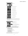
1
MD-MT877/MD-MT877C
SERVICE MANUAL
No. S3118MDMT877/
PORTABLE MINIDISC RECORDER
MD-MT877(S)
MODEL MD-MT877C(S)
• In the interests of user-safety the set should be restored to its
original condition and only parts identical to those specified be
used.
CONTENTS
Page
SPECIFICATIONS ................................................................................................................................................................. 2
NAMES OF PARTS ............................................................................................................................................................... 3
OPERATION MANUAL .......................................................................................................................................................... 5
DISASSEMBLY .................................................................................................................................................................... 10
REMOVING AND REINSTALLING THE MAIN PARTS ....................................................................................................... 11
ADJUSTMENT ...................................................................................................................................................................... 12
NOTES ON SCHEMATIC DIAGRAM .................................................................................................................................. 28
TYPES OF TRANSISTOR AND DIODE .............................................................................................................................. 28
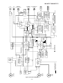
BLOCK DIAGRAM ............................................................................................................................................................... 29
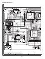
SCHEMATIC DIAGRAM ...................................................................................................................................................... 30
WIRING SIDE OF P.W.BOARD ........................................................................................................................................... 32
VOLTAGE ............................................................................................................................................................................ 36
WAVEFORMS OF MD CIRCUIT ......................................................................................................................................... 37
TROUBLESHOOTING ......................................................................................................................................................... 38
FUNCTION TABLE OF IC .................................................................................................................................................... 41
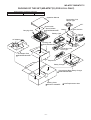
PARTS GUIDE/EXPLODED VIEW
PACKING OF THE SET (MD-MT877(S) FOR U.S.A. ONLY)
SHARP CORPORATION
This document has been published to be used
for after sales service only.
The contents are subject to change without notice.
MD-MT877/MD-MT877C
FOR A COMPLETE DESCRIPTION OF THE OPERATION OF THIS UNIT, PLEASE REFER TO
THE OPERATION MANUAL.
SPECIFICATIONS
Power source
DC 1.2V:
DC 5V:
DC 1.5V:
DC 1.5V:
Rechargeable Nickel-Metal Hydride battery (AD-N55BT) x 1
AC adaptor (AC 120V, 60 Hz)
Commercially available, “AA” size (LR6), alkaline battery x 1
Separately available car adaptor, AD-CA55X (for cars with a 12-24V DC negative ground electrical system) (Used with separately available plug adaptor (AD-M66PA))
Power consumption 7 W (AC adaptor)
Output power
RMS; 10 mW (5 mW + 5 mW) (0.2% T.H.D.)
Charging time
Approx. 3.5 hours
Input sensitivity
MIC H: reference input level 0.25 mV
input impedance
10 k ohms
MIC L: reference input level 2.5 mV
input impedance
10 k ohms
LINE: reference input level 100 mV
input impedance
20 k ohms
Output level
Earphones: maximum output level 5 mW + 5 mW
load impedance
32 ohms
LINE:
specified output
250 mV (-12 dB) load impedance
10 k ohms
Dimensions
Width: 2-27/32” (71.9 mm) Height: 11/16” (16.8 mm) Depth: 3-1/8” (78.7 mm)
Weight
0.29 lbs. (131 g) with rechargeable battery
Input jack
Output jack
Type
Signal readout
Audio channels
Frequency response
Rotation speed
Error correction
Coding
Recording method
Sampling frequency
Wow and flutter
Battery life
Line/optical digital, microphone (powered by the main unit)
Earphones (impedance: 32 ohms)/remote control unit
Portable MiniDisc recorder
Non-contact, 3-beam semiconductor laser pickup
Stereo 2 channels/monaural (long-play mode) 1 channel
20 – 20,000 Hz (± 3 dB)
Approx. 400 – 1,350 rpm
ACIRC (Advanced Cross Interleave Reed-Solomon Code)
ATRAC/ATRAC3 (Adaptive TRansform Acoustic Coding), 24-bit computed type
Magnetic modulation overwrite method
44.1 kHz (32 kHz and 48 kHz signals are converted to 44.1 kHz, and then recorded.)
Unmeasurable (less than ±0.001% W. peak)
When using the rechargeable battery
(fully charged) included with the unit
When using one, commercially available, high capacity, “AA” size (LR6), alkaline battery (The rechargeable battery is in the unit, discharged.)
When using one, commercially available, high capacity, “AA” size (LR6), alkaline battery with the rechargeable battery (fully charged)
Stereo
Continuous Continuous
recording:
play:
Approx.
Approx.
6.5 hours
12 hours
Continuous Continuous
recording:
play:
Approx.
Approx.
6 hours
16 hours
Continuous Continuous
recording:
play:
Approx.
Approx.
15 hours
29 hours
2 times long
Continuous Continuous
recording: play:
Approx.
Approx.
9 hours
13.5 hours
Continuous Continuous
recording: play:
Approx.
Approx.
10 hours
19.5 hours
Continuous Continuous
recording: play:
Approx.
Approx.
22 hours
33 hours
● The above values are the standard values when the unit is operated horizontally and charged at an ambient temperature of 77°F (25°C). (The
operable duration with the rechargeable battery will be shorter when the
unit is carried around.)
4 times long
Continuous Continuous
recording: play:
Approx.
Approx.
11.5 hours 15 hours
Continuous Continuous
recording: play:
Approx.
Approx.
13 hours
22 hours
Continuous Continuous
recording: play:
Approx.
Approx.
30 hours
40 hours
● Operable duration with a commercially available battery varies depending on its maker, type, and conditions of use.
● “Fully charged” means that the charging is complete after approximately
3.5 hours since the remaining amount of the battery is reduced to “
”
(1 bar).
● The volume level is set at “VOL 15”.
● The LED is set at “LIGHT OFF”.
Specifications for this model are subject to change without prior
notice
–2–
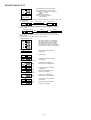
MD-MT877/MD-MT877C
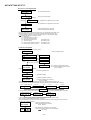
NAMES OF PARTS
Main unit
1. Record/Track Mark Button
2. Mode Button
3. Volume/Cursor/Fast Forward/Fast Reverse/
Recording Level/Name Select Button
4. Stop/Power Off/Hold Button
5. Open Lever
6. Display/Character Select Button
7. Edit/Auto Mark/Time Mark Button
8. Play/Pause Button
9. Enter/Fast Play/Synchro Button
10. Bass/Delete Button
11. Rechargeable Battery Cover
12. Handstrap Holder
13. Optical/Line Input Jack
14. Microphone Input Jack
15. Remote Control/Earphones/Line Output Jack
1
2
3
8
4
9
10
5
6
7
11
15
12
13
7
8
9
10
11
12
1
2
3
4
5
6
Main unit display panel
1. Level Meter
02. Record Indicator
03. Synchro Recording Indicator
04. Operation Indicator
05. Long-play/Recording Mode Indicator
6. Character/Time Information Indicator
7. Repeat Indicator
8. Battery Indicator
9. Random Indicator
10. Track Number Indicator
11. TOC Indicator
12. Disc Name Indicator
Yellowgreen Blue Orange
3-color LED
Various modes are indicated with three colors of lights.
Charging
Lighting starting with yellow-green light.
Refresh
Extinguishing starting with orange light
after all the lights are lit.
Playback
Flashing the color of the activated playback mode.
Recording
Flashing the color of the activated recording mode.
Fast Forward Flashing starting with yellow-green light.
Fast Reverse Flashing starting with orange light.
Volume (+)
Lighting starting with yellow-green light.
Volume (–)
Extinguishing instantly starting with orange light after all the lights are lit.
TOC
Reading: flashing at random.
–3–
14
MD-MT877/MD-MT877C
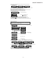
Remote control unit
1.
2.
3.
4.
5.
6.
7.
8.
9.
Remote control display panel
1.
02.
03.
04.
05.
06.
07.
08.
09.
10.
1
Earphones Jack
Fast Forward/Fast Reverse Button
Display Button
Play Mode Button
Sound/Track Mark Button
Stop/Power Off Button
Play/Pause Button
Volume Button
Hold Switch
Record Indicator
Track Number Indicator
Operation Indicator
Character/Time Information Indicator
Battery Indicator
Random Indicator
Synchro Recording Indicator
Total Track Number Indicator
Long-play/Recording Mode Indicator
Repeat Indicator
2
7
6
1
2
7
3
4
5
9
8
3
4
8
5
6
9
10
2
Battery charger
1. Remote Control Holder
(You can hang the remote control on it.)
2. Lock Detector
3. Hook For Fixing The Main Unit
4. Charge/Operation Switch
5. Stand
6. AC Adaptor Connecting Jack
3
1
CHAR
GE
OPER
ATIO
N
4
5
6
–4–
MD-MT877/MD-MT877C
OPERATION MANUAL
Using with the Rechargeable Battery
Charging
Do not force the
battery cover
open too far.
When the rechargeable battery is used for the first
time or when you want to use it after a long period of
disuse, be sure to charge it fully.
1
2
3
AC 120V
60Hz
Insert the rechargeable battery.
Move the Charge/Operation switch to
charge mode.
Place the portable MD into the battery
charger and connect the AC adaptor.
● After the rechargeable battery is charged or used, it will
get slightly warm. This is normal.
Charge
mode
● When the portable MD is turned on or operating, the bat-
tery will not be charged.
To the DC IN
5V jack
Checking Displays
Checking the remaining amount of
battery level
The remaining amount of battery level is shown
by the battery indicator (
) during operation.
How to read the battery indicator
When the battery
level is high
When the battery
low is very low
● When the battery is completely discharged, the battery
indicator will flash. Recharge the battery or replace the
alkaline battery with a new one.
● When the battery has run completely out, “BATT EMPTY
(LoBATT)” will appear. Then, the power will be disconnected automatically.
Notes:
● If you use the battery which you stopped charging halfway, “
” may appear. It does not mean that the battery is completely charged.
● The battery indicator will not correctly display the remaining capacity for approximately 20 seconds after the power
has been turned on.
● When the AC adaptor or a separately available car adaptor is used, the battery indicator will not be shown.
● The number of bars shown in the battery indicator may
increase or decrease, depending on the operation being performed. This is normal.
–5–
MD-MT877/MD-MT877C
Error Messages
ERROR MESSAGES
BATT EMPTY
MEANING
REMEDY
● The battery is run down.
● Nothing is recorded.
● Charge the rechargeable battery or replace the alkaline battery (or use the AC adaptor for power).
● Replace the disc with a recorded disc.
● You tried to record from a copy prohibited
MiniDisc.
● A track cannot be edited.
● Record using the analog cable. (MD-MT877(S))
● Record using the analogue cable. (MD-MT877C(S))
● Change the stop position of the track and then edit it.
● The disc data cannot be read because the disc
is damaged.
● Reload the disc.
● Replace it with another recorded disc.
● Recording cannot be performed correctly due to
vibration or shock.
● Stamp function does not work.
● Cannot save the TOC information correctly to a
MiniDisc. (A large portion of the disc has been
damaged.)
● The Charge/Operation switch is not set to the
operation mode when using this unit with the AC
adaptor.
● The disc is scratched.
● Re-record or replace it with another recordable disc.
(LoBATT)
BLANK MD
(BLANK)
Can’t COPY
(Can’tC)
Can’t EDIT
(Can’tE)
Can’t READ *
(Can’tS)
(Can’tT)
(Can’tU)
Can’t REC
(Can’tR)
Can’t STAMP
Can’t WRITE
(Can’tW)
CHARGEmode
DEFECT
(DEFECT)
DISC FULL
Er-MD **
(ErMD*)
HOLD
● The disc is out of recording space.
● The microprocessor has reported a system fault
and the unit is out of order.
● The unit is in the hold mode.
● Check the number of tracks.
● Replace the disc with another recordable disc.
● Set the Charge/Operation switch to the operation mode.
●
●
●
●
If the sound you hear is not right, record again.
Replace the disc with another recordable disc.
Replace it with another recordable disc.
To have it repaired, go to the distributor where you purchased the unit.
● Return the HOLD switch to its original position.
(HOLD)
LOCKED
(Can’tLOCK)
● You removed a MiniDisc while recording or
editing.
● Turn off the power and remove the MiniDisc.
Error Messages : continued
ERROR MESSAGES
NO DISC
NO SIGNAL
(noSIG.)
PLAY MD
MEANING
REMEDY
● A disc has not been loaded.
● Load a disc.
● Poor connection of the digital cable.
● Connect the digital cable securely.
● No output signal comes out from the connected ● If the portable CD player has a function to prevent sound
unit to playback.
skips, deactivate it.
● The input signal has improper sampling fre- ● Playback with the connected unit.
quency.
● You recorded on a playback-only disc.
● Replace it with a recordable disc.
(PLAYmd)
POWER ?
● The battery charger is defective.
PROTECTED
● The write protection tab of a MiniDisc is set to
the protected position.
● You tried to record on a playback-only disc.
● Since a track number is currently being located
or updated, the unit cannot accept your command.
● The temperature is too high.
SORRY
(Sorry)
TEMP OVER
● To have it repaired, go to the distributor where you
purchased the unit.
● Move the write protection tab back to its original position.
● Replace it with a recordable MiniDisc.
● Wait for a while and try the operation again.
● Turn off the power, and wait for a while.
(TEMP!)
TOC FORM **
● There is an error in the recording signal.
● Erase all of the tracks, and then record again.
● There is no space left for recording character
information (track names, disc names, etc.).
● The track has been protected from being erased.
● A disc which contains data other than music was
played.
● There is an error in the signal recorded on the
disc.
● Stamping is not possible.
● Replace it with another recordable disc.
(Tform**)
TOC FULL
Tr. Protect
? DISC
(? DISC)
( ) : Error messages seen on the remote control.
Number or symbol appears in * position.
–6–
● Edit the track with the device on which it was recorded.
● A disc which contains non-music data cannot be played.
● Replace it with another recorded disc.
● Retry.
MD-MT877/MD-MT877C
MiniDisc System Limitations
The unit may have the following symptoms while recording or editing. The unit is not out of order.
SYMPTOM
LIMITATIONS
“DISC FULL” or “TOC FULL” appears More than 255 tracks (maximum) cannot be recorded regardless of the reeven though the MiniDisc still has re- cording time.
cording time left.
If the MiniDisc is recorded or edited repeatedly or if it has scratches (recording skips scratched parts), you may not be able to record the maximum
tracks above.
The remaining recording time does not The unit does not count non-recorded portions that last 12 or fewer seconds
increase even though you erased tracks. to display the remaining recording time. The time may not increase even if
you erase short tracks.
The total of the recorded time and the One cluster (approximately 2 seconds) is the minimum unit for recording.
remaining time does not match the maxi- For example, a 3-second track uses 2 clusters (approximately 4 seconds).
mum recordable time.
Therefore, the actual recordable time may be shorter than the displayed
time.
Combine function does not work.
A MiniDisc on which recording and editing are repeated may not allow the
combine function.
Sound skips in fast reverse/forward.
One track is divided and recorded in separate places on a repeatedly recorded or edited MiniDisc.
Sound may skip.
A track number is created in the middle A track number may be created if there are scratches or dust on the MiniDisc.
of a track.
Troubleshooting
Many potential “problems” can be resolved by the owner without calling a service technician.
If something seems to be wrong with this product, check the following before calling your authorized SHARP dealer or
service center.
PROBLEM
CAUSE
PROBLEM
The unit does not ● Is the AC adaptor disconnected?
turn on.
● Is the battery exhausted?
● Is the unit in the hold mode?
● Has condensation formed inside the
unit?
● Is the unit being influenced by mechanical shock or by static electricity?
No sound is ● Is the volume set too low?
heard from the ● Is the remote control unit or the earearphones.
phones plugged in?
● Are you trying to play a MiniDisc with
data on it instead of a MiniDisc containing music?
When the opera- ● Is the unit in the hold mode?
tion buttons are ● Is the battery exhausted?
pressed, the unit ● Is the remote control unit plug or the
earphones plug inserted firmly?
does not respond.
Some sounds ● Is the battery exhausted?
● Is the unit being subjected to excesare skipped.
sive vibration?
–7–
CAUSE
The MiniDisc can- ● Has the track number or character
not be ejected.
information been updated on the
disc yet?
● Is the unit in the recording or editing mode?
Recording and ● Is the MiniDisc protected against
editing are imaccidental erasure?
possible.
● Is the unit connected properly to the
other equipment?
● Is the AC adaptor unplugged or did a
power failure occur while recording or
editing?
● Is the unit in the hold mode?
● Is an optical signal being output from
the stereo system?
Read the operation manual for the
stereo system.
The battery cannot ● Is the select switch for charging/
be charged.
operation set on the charging side?
● Is the jack clean?
Nothing appears ● Is the remote control display set to
on the remote
“LIGHT OFF”?
control display.
MD-MT877/MD-MT877C
1
2
Insert a MiniDisc
Inserte un minidisco
2
Connect the AC adaptor
Conecte el adaptador de CA
Insert according to the direction of the arrow.
4
Insértelo de acuerdo con la dirección de la flecha.
AC 120V, 60 Hz
120V CA, 60Hz
3
1
To an AC outlet
A un tomacorriente
de CA
RELEASE
LOCK
1 Slide the OPEN lever to re- 3 Insert a MiniDisc as shown.
lease the compartment door.
Deslice la palanca OPEN para
abrir la puerta del compartimiento.
To the DC IN 5V jack
Inserte un minidisco como se
muestra.
A la toma DC IN 5V
4 Close the compartment.
Insértelo con seguridad a fondo.
Cierre el compartimiento.
2 Lift it up.
Levantelo.
When you record on a MiniDisc,
check that the erase prevention tab
is set to the “recordable” position.
Recordable
Para poder
grabar
3
Recording
prevented
Para no poder
grabar
switch to Operation mode
(LOCK).
Mueva el selector de carga/
operación al modo de carga
Mueva el selector de carga/
operación al modo de operación
(LOCK).
the battery charger.
4 Plug the AC adaptor.
Enchufe el adaptador de CA.
Inserte el MD portátil en el
cargador de baterías.
Before using the unit with a rechargeable battery, the battery has to be charged. Refer
to “Using with the rechargeable battery”.
Antes de emplear el aparato con una batería recargable, se deberá cargar la
batería. Consulte el apartado de "Empleo con la batería recargable".
Preparation for use
Preparación para su utilización
The unit does not work if the • / –HOLD button is set to HOLD.
Este aparato no funciona si el botón • / –HOLD está puesto en HOLD.
Red: To Right
Rojo: A la
derecha
Press the • / –HOLD button for 2 seconds or more.
Pulse el botón • /–HOLD durante 2 o más segundos.
White: To Left
Blanco: A la
izquierda
RIGHT LEFT
3 Move the Charge/Operation
switch to Charge mode (RELEASE).
2 Insert the portable MD into
Connection
Conexión
LINE OUT
1 Move the Charge/Operation
(RELEASE).
Cuando desee grabar en un
minidisco, compruebe que la
lengüeta de protección contra
borrado esté colocada en la posición
para "poder grabar".
OPTICAL/
LINE IN
Insert securely, all the way in.
Hold
Retención
Released
Liberación
To a stereo system with “LINE OUT” or “AUDIO OUT”
jacks (See left. Analog connection)
Note:
If the audio system has only one pair of jack then they are usually
input only and recording via this connection is not possible.
Operation mode
A un sistema estéreo provisto de tomas de salida de
línea "LINE OUT" o de salida de audio "AUDIO OUT"
(Vea a la izquierda, Conexión analógica)
Modo de operación
Nota:
Si el sistema de audio sólo tiene un par de tomas, normalmente
son sólo de entrada y no puede realizarse la grabación mediante
esta conexión.
For operations
Para operaciones
Move it to operation mode when playing back or recording.
Muévalo a la posición del modo de operación para la reproducción o grabación.
CAUTION:
It is not recommendable to put the MiniDisc into a rear
pocket, as this may damage the product when sitting.
PRECAUCIÓN:
No se recomienda ponerse un minidisco en el bolsillo
trasero del pantalón, porque podría dañarlo al sentarse.
–8–
MD-MT877/MD-MT877C
Recording
Grabación
Check that the unit is connected to the stereo system.
Compruebe que el aparato esté conectado al sistema estéreo.
4 Press the PAUSE button on the stereo system to enter the playback pause mode at the point you wish to start recording.
Pulse el botón PAUSE del sistema estéreo para entrar en el modo de pausa
de reproducción en el punto en el que desee iniciar la grabación.
5 Press the MODE button repeatedly to select the recording mode.
Pulse repetidamente el botón MODE para seleccionar el modo de grabación.
6 Press the
Pulse el botón
button to start recording.
para iniciar la grabación.
7 Begin playback on the stereo system, the output will be recorded.
Inicie la reproducción del sistema estéreo, y se grabará la salida.
1 Press the REC button.
To stop recording
Press the • / :OFF button.
2 Begin playback on the stereo system connected to this unit.
When recording stops, “TOC” appears
(Table Of Contents). While “TOC” appears, the MiniDisc recorded contents
have not yet been updated.
Pulse el botón REC.
Inicie la reproducción en el sistema estéreo conectado a este aparato.
3 Press the
Para detener la grabación
Pulse el botón • /:OFF.
button to adjust the recording level.
or
Cuando se detenga la grabación,
aparecerá “TOC” (índice). Mientras
aparece “TOC”, aún no se habrá
actualizado el contenido grabado en el MD.
Adjust the recording level so that the maximum sound volume from the
source makes the reading swing somewhere between –4 dB and 0 dB.
Pulse el botón
o
para ajustar el nivel de grabación.
Ajuste el nivel de grabación para que el volumen de sonido máximo de la fuente
produzca una indicación de entre –4 dB y 0 dB.
TOC display
Visualización
TOC
Indicador del medidor de nivel
0dB
4dB
Playing
Reproducción
1 Insert the earphones plug firmly into the earphones jack on
the remote control unit.
Inserte firmemente la clavija de los auriculares en la toma de auriculares del
controlador remoto.
Enchufe el controlador remoto a la toma
jack on the unit.
del aparato.
3 Insert
a MiniDisc.
Inserte un MD
4 Press the
Pulse el botón
button.
.
To stop playback
Press the • / :OFF button (Remote
control: press the button).
Para detener la reproducción
Pulse el botón • /:OFF. (Controlador
remoto: pulse el botón .)
If the unit is not operated for at least 2
minutes while in the stop mode, the
power will shut off automatically.
Si el aparato no se utiliza durante un
mínimo de 2 minutos en el modo de
parada, la alimentación se desconectará
automáticamente.
The power turns off after recorded
contents have been updated on the
MiniDisc.
Para actualizar el contenido
grabado del MD
Pulse el botón • /:OFF en el modo de
parada.
La alimentación se desconectará después
de haber actualizado el contenido grabado
en el MD.
Level meter indicator
2 Plug the remote control into the
To update the recorded contents
of the MiniDisc
Press the • / :OFF button while in
the stop mode.
–9–
MD-MT877/MD-MT877C
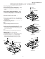
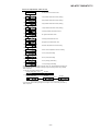
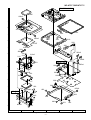
DISASSEMBLY
Cares before disassembling
When assembling the machine after disassembling or
repair, observe the following requirements so as to ensure
safety and performance.
1. Remove the batteries from the machine, and take out the
mini-disc.
2. When assembling after repair, be sure to position the
wires in the same location.
Use the specified screws to fix the cabinet and the
mechanism unit. The use of the screws with length other
than specified may cause contact with the mechanism
unit resulting in malfunction.
3. When repairing, pay close attention so not to damage the
IC from static electricity.
PROCEDURE
FIGURE
1
Bottom Cabinet
1. Screw ..................... (A1) x5
10-1
2
Top Cabinet
1. Open the Top cabinet.
2. Screw ..................... (B1) x4
3. Flexible PWB .......... (B2) x1
10-1
3
Main PWB
1. Open the rechargeable
battery compartment of the
direction indicated by arrows.
2. Screw .................... (C1) x1
3. Flexible PWB ......... (C2) x2
10-2
1. Pull the main frame to the A
direction and remove the MD
mechanism upward.
2. Screw .................... (D1) x1
10-3
1. Screw ...................... (E1) x6
2. Hook ....................... (E2) x4
10-4
5
MD Mechanism
LCD PWB
(A1) x 1
ø 1.4 x 2 mm
OOP
PEE
NN
(B1) x 2
ø 1.4 x 2 mm
Bottom Cabinet
EN
OP
EJECT
Knob
(A1) x 1
ø 1.4 x 2 mm
(A1) x 1
ø 1.4 x 2 mm
Figure 10-1
10-2
(C2) x 1(1*)
(B2) x 1
(C2) x 1
Main PWB
Battery
Cover
pull
(C1) x 1
ø 1.4 x 2.5 mm
pull
2
1
EN
4
REMOVAL
(A1) x 2
ø 1.4 x 2 mm
OP
STEP
(B1) x 2
ø 1.4 x 2 mm Top Cabinet
Main Frame
Caution:
Carefully handle the main PWB and flexible PWB. After removing the
flexible PWB (1*) for the optical pickup from the connector, do not
touch directly the front end of flexible PWB with your hand so as to
prevent damage of optical pickup by static electricity.
(E1) x 6
ø 1.4 x 2 mm
Figure 10-2
MD Mechanism
(E2) x 4
LCD PWB
OP
EN
A
Main Frame
(D1) x 1
ø 1.4 x 1.5 mm
Top Cabinet
Figure 10-3
Figure 10-4
– 10 –
MD-MT877/MD-MT877C
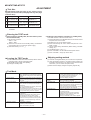
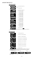
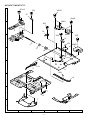
REMOVING AND REINSTALLING THE MAIN PARTS
Remove the mechanism according to the disassembling methods 1 to 4. (See Page 10.)
How to remove the spindle motor (See Fig. 11-1.)
1. Remove the solder joints (A1) x 4 of flexible PWB.
2. Remove the screws (A2) x 3 pcs., and remove the spindle
motor.
(A2) x 3
ø 1.4 x 3 mm
Spindle Motor
How to remove the lift motor (See Fig. 11-2.)
Solder joints
(A1) x 4
1. Remove the solder joints (B1) x 2 of lift motor lead wire.
2. Remove the screw (B2) x 1 pc., and remove the lift motor.
Note:
Take care so that the motor gear is not damaged.
(If the gear is damaged, noise is caused.)
How to remove the sled motor (See Fig. 11-3.)
1. Remove the stop washer (C1) x 1 pc., and remove the drive
gear (C2) x 1 pc.
2. Remove the screws (C3) x 2 pcs.
3. Remove the solder joints (C4) x 3 of flexible PWB., and
remove the sled motor.
Note:
Take care so that the motor gear is not damaged.
(If the gear is damaged, noise is caused.)
MD Mechanism
Figure 11-1
(B2) x 1
ø 1.4 x 3.8 mm
How to remove the magnetic head (See Fig. 11-4.)
Lift Motor
1. Remove the screws (D1) x 2 pcs. of the magnetic head and
the optical pickup, and remove the solder joints (D2) x 2 pcs.
of the head flexible plate.
Note:
Mount carefully so as not to damage the magnetic head.
Solder Joints
(B1) x 2
How to reinstall the optical pickup
(See Fig. 11-4.)
MD Mechanism
1. Remove the screw (E1) x 1 pc., and remove the grip spring.
2. Remove the screw (E2) x 1 pc. to remove the thrust
spring, and remove the drive screw and the optical
pickup from MD mechanism.
Then, remove the drive screw from the optical pickup.
Figure 11-2
(C3) x 2
ø 1.4 x 1.2 mm
Sled
Motor
(E1) x 1
ø 1.4 x 1.8 mm
Grip Spring
Drive
Screw
(C1) x 1
(C2) x 1
(D1) x 2
ø1.4 x 1.8 mm
(C4) x 3
Solder
Joints
(D2)x2
Solder Joints (E2) x 1
ø 1.7 x 3.5 mm
Optical Pickup
Magnetic
head
Thrust
Spring
MD Mechanism
Figure 11-3
MD Mechanism
Figure 11-4
– 11 –
MD-MT877/MD-MT877C
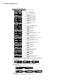
ADJUSTMENT
Test disc
MD adjustment needs two types of disc, namely recording disc (low reflection disc) and playback-only disc (high
reflection disc).
Type
Test disc
Parts No.
1 High reflection disc MMD-110
88GMMD-110
(TEAC Test MD)
2 Low reflection disc MMD-213A
88GMMD-213A
(TEAC Test MD)
3 Low reflection disc Recording
minidisc disc
UDSKM0001AFZZ
Note: Use the low reflection disc on which music has been
recorded.
Entering the TEST mode
1. Setting at port (in standby state, disc-free state or power
nonconnected state)
(1) Set the port as follows.
TEST1 : "Low"
TEST0 : "High"
(2) Press the PLAY button in the standby state (it is allowed to
close the disc lid or to connect the power supply).
(3) Test Mode STOP [ T E S T _ ]
2. Setting by special button operation (in standby state)
Test mode: Perform it with the remote control.
(1) Press and hold the "PLAY MODE" button on the remote control
and press the "PLAY" button.
(2) Release only the "PLAY MODE" button.
(3) Press and hold only the "PLAY" button and press the "VOLUME–" button.
(4) Normal mode setting initialization (BASS setting, VOLUME
setting, etc.)
(5) Test Mode STOP [ T E S T _ ]
(6) Press "VOLUME+" to check the microcomputer version.
(7) Press "VOLUME–" to light up all the LCDs.
Leaving the TEST mode
Shipping setting method
(1) Press the STOP button in the TEST mode stop state or version
indicating state or whole LCD lighting state.
(2) EEPROM rewrite-enable area updating.
(3) Change to standby state
(1) Insert the rechargeable battery. Do not close the compartment.
(2) Close the battery lid twice in succession while pressing the
VOLUME– button and the PLAY button on the main unit at the
same time. (Turn on and off the power twice)
(3) Make sure the display changes from [INIT] to [BYE OK].
Test Mode
1. AUTO 1 Mode
2. AUTO 2 Mode
3. TEST-PLAY Mode
4. TEST-REC Mode
5. MANUAL 1 Mode
6. MANUAL 2 Mode
• Perform preliminary automatic adjustment.
• If the combination of mechanism and pickup
PWB has been changed, be sure to start from
AUTO1.
• Perform ATT (attenuator) automatic adjustment.
• Perform continuous playback (error rate display,
jump test)
• Continuous playback from the specified address
is performed.
• 1 line, 10 lines or 100 steps manual jump is
performed.
• C1 error rate display (pit section), ADIP error
rate display (groove section)
• The temperature correction is performed only when
servo start is performed, but the posture correction
is not performed during continuous playback.
• Continuous record from the specified address
is performed.
• Change of record laser output (servo gain is
also changed according to laser output).
• The temperature correction is performed only
when servo start is performed, but the posture
correction is not performed during continuous
recording.
• Temperature is displayed.
• Seeing the displayed adjustment value, perform
preliminary manual adjustment.
(Error rate indication, jump test)
7. ERROR INFORMATION
Mode
8. NORMAL Mode
9. EEPROM Mode
– 12 –
• Temperature is displayed.
• Seeing the displayed adjustment value, perform
ATT (attenuator) manual adjustment.
• Continuous playback is performed
(error rate display, jump test).
• Error information is displayed.
• Error information is initialized
• The mode is changed from the TEST mode to
the normal mode without adjustment.
• In the normal mode the internal operation mode,
memory capacity, etc. areindicated.
• In the normal mode both temperature correction
and posture correction are performed.
• Factors of digital servo are changed manually.
• Cut-off frequency of BASS1, BASS2 and BASS3
is selected manually.
• Temperature detection terminal voltage is
measured, and the reference value is set.
• Defaults are selected and set.
• Setting of EEPROM protect area is updated.
MD-MT877/MD-MT877C
Operation in each TEST mode
1. AUTO1 Mode
5. TEST-PLAY Mode
• When the STOP button is pressed while the AUTO1 menu appears
or during automatic adjustment, the mode changes to the TEST
mode stop state. At this time the adjustment value is not output.
• Be sure to adjust, using the specified disc MMD-213A.
• Adjustment NG; Adjustment item out of range, focus ON failure, and
adjustment error
• When the PLAY button is pressed while ADJ. OK is displayed, AUTO2 is executed.
• When the STOP button is pressed while the TEST-PLAY menu
appears, or in TEST-PLAY or continuous playback mode, the mode
changes to the TEST mode stop state.
• When the PLAY button is pressed while the TEST-PLAY menu
appears, continuous playback is initiated from the current pickup
position.
• Whenever the DISP button is pressed in the TEST-PLAY menu, the
target address changes as follows.
0032 — 03C0 — 0700 — 08A0 — 0950— 0032 —
When the PLAY button is pressed while a target address is displayed, continuous playback is performed after searching that
address.
• Each time the MODE button is pressed while the TEST-PLAY mode
target address is displayed, the digit which is changed by pressing
the FAST FORWARD/REVERSE button is changed as follows.
0032 — 0032 — 0032 — 0032 —
• When the FAST FORWARD button is pressed in the TEST-PLAY
mode target address is displayed, the digit of address specified by
the MODE button is set to +1h. (0 to F)
• When the FAST REVERSE button is pressed in the TEST-PLAY
mode target address is displayed, the digit of address specified by
the MODE button is set to -1h. (0 to F)
* When the FAST FORWARD/REVERSE button is held down, the
setting changes continuously, one cycle being 100 ms.
• When the BASS button is pressed in the continuous playback mode,
the number of jump lines changes as follows.
1 — 10 — 100 step — 1
* After the number of jump lines is indicated for one second, the
address indication is restored. [
T R ] or [ 100 stp ]
• When the FAST FORWARD button is pressed in the continuous
playback mode, the specified number of lines is jumped in the FWD
direction.
• When the FAST REVERSE button is pressed in the continuous
playback mode, the specified number of lines is jumped in the REV
direction.
* When the FAST FORWARD/REVERSE button is held down, jump
is repeated every approx. 100 ms.
2. AUTO2 Mode
• When the STOP button is pressed while the AUTO2 menu appears
or during automatic adjustment, the mode changes to the TEST
mode stop state. At this time the adjustment value is not output.
• Adjustment NG; Adjustment item out of range, and adjustment error.
• When the PLAY button is pressed while ADJ. OK is displayed, TEST
_PLAY is executed.
3. MANUAL1 Mode
• Adjustment item to be made in AUTO1 mode is performed manually.
• When the VOLUME+ button is pressed during adjustment, the setting increases, and the new setting is output.
• When the VOLUME– button is pressed during adjustment, the setting decreases and the new setting is output.
• If the VOLUME+/– button is held down, the setting changes continuously with 100 ms cycle.
*In this operation, the setting change is performed for each digit. The
digit is changed by pressing the MODE button.
• If the setting is within the allowable range, the RANDOM display
lights.
• When the STOP button is pressed during MANUAL1 menu or measurement or adjustment, the state is changed to the TEST mode
stop state.
4. MANUAL2 Mode
• Adjustment item to be made in AUTO2 mode is performed manually.
• When the VOLUME+ button is pressed during adjustment, the setting increases, and the new setting is output.
• When the VOLUME– button is pressed during adjustment, the setting decreases and the new setting is output.
• If the VOLUME+/– button is held down, the setting changes continuously with 100 ms cycle.
*In this operation, the setting change is performed for each digit. The
digit is changed by pressing the MODE button.
• If the setting is within the allowable range, the RANDOM display
lights.
• When the STOP button is pressed during MANUAL2 menu or measurement or adjustment, the state is changed to the TEST mode
stop state.
• When the PLAY button is pressed in B-ATT set state, the mode is
changed to the continuous playback mode.
• As for operation during continuous playback refer to "TEST-PLAY
mode explanation".
• Whenever the DISP button is pressed in the continuous playback
mode, the indication changes as follows.
* Pre-mastered disc
Continuous playback
(SUBQ address indication)
|
Continuous playback
(C1 error indication)
|
Continuous playback
(SUBQ address indication)
* Recordabl disk
Continuous playback
(ADIP address indication)
|
Continuous playback
(C1 error indication)
|
Continuous playback
(ADIP error indication)
|
Continuous playback
(ADIP address indication)
– 13 –
[ S Q
]
[ C E
]
[ S Q
]
[ A P
]
[ C E
]
[ A E
]
[ A P
]
MD-MT877/MD-MT877C
6. TEST-REC Mode
7. NORMAL Mode
• When the STOP button is pressed while the TEST-REC menu
appears, or in the TEST-REC mode or continuous record mode, the
mode changes to the TEST mode stop state.
• Whenever the DISP button is pressed in the TEST-REC menu, the
target address changes as follows.
• When the STOP button is pressed while the NORMAL menu
appears, the mode changes to the TEST mode stop state.
• Indication during operation
Indication of memory capacity on main unit LCD
[
] + Level meter
: Internal mode
: Address (Cluster section)
: Address (Sector section)
• Selection of sound volume, BASS, etc. is possible (without indication)
• Recording is also possible.
• If the STOP button is pressed during operation in the NORMAL
mode, the NORMAL mode is cancelled, and the power is turned off.
0032 — 03C0 — 0700 — 08A0 —0950 — 0032 —
When the PLAY button is pressed while a target address is displayed, continuous playback is performed after searching that
address.
• Whenever the MODE button is pressed in the TEST-REC mode
target address is displayed, the digit which is changed by the FAST
FORWARD/REVERSE button changes as follows.
0032 — 0032 — 0032 — 0032 —
• When the FAST FORWARD button is pressed in the TEST-REC
mode target address is displayed, the digit of address specified by
the MODE button is set to +1h.(0 to F)
• When the FAST REVERSE button is pressed in the TEST-REC
mode target address is displayed, the digit of address specified by
the MODE button is set to -1h. (0 to F)
* When the FAST FORWARD/REVERSE button is held down, the
setting changes continuously, one cycle being 100 ms.
• When the VOLUME+/– button is pressed in the TEST-REC mode or
continuous record mode, the laser record power changes.
(Servo gain changes also according to record power.)
* After the laser record power is indicated for one second, the ad]
dress indication is restored. [ R P W _
•
: Address
•
: Laser power cord
• Operation is disabled if the premastered disc or disc is in miseraseprotected state.
Explanation of error history code
8. Error data display Mode
• Reversing when FAST REVERSE button is pressed
• When the STOP button is pressed while the error data indication
menu appears or during error data indication, the mode changes to
the TEST mode stop state.
• Error data 0 is the latest error.
• Error which occurred in the TEST mode is also stored in the memory.
• When the DISP button is pressed while the error data indication
menu appears, the error data is initialized.
[ C L E A R _ ]
•
: Error Code
Error messages
13h : Adjustment servo retraction excessive retrial
16h : C. IN detection time-over
17h : A, B, E, F, and TCRSO offset measurement value out of
tolerable range
21h : Focus retraction completion allowable time-over
23h : Track search completion allowable time-over
32h : P-TOC read failure
42h : U-TOC read failure
44h : U-TOC write data write disabled/read check error
45h : U-TOC write test failure
52h : SD write data write disabled
72h : EEPROM data read check sum error
73h : Record head drive disabled (by EJECT lever)
91h : Ambient temperature is higher that the allowable temperature
– 14 –
Can't READ
The details ' '
'f': Focus
'a': Servo adjustment
's': Track such
'r': TOC information reading
'u': UTOC information reading
'w': At the time of data writing
'p': Spindle start
Er-MD
The details '
'
'41': UTOC light test error
'80': EEPROM information reading error
MD-MT877/MD-MT877C
EEPROM (IC402) writing procedure
1. Procedure to replace EEPROM and write initial
value of microcomputer in EEPROM
(1) Replace EEPROM.
(2) Refer to the latest EEPROM data list.
(3) Start the test mode. (Refer to page 12 "Entering the
TEST mode".)
(4) Version display (At the time of settlement of the test
mode by the button operation.)
[Ver.
]
(7) Press the "BASS" button, and press 1 time the "FAST
REVERSE" button.
[ E E P R O M ]
(8) Perform the operation to display "EEPROM SETTING
MODE CHART", compare the EEPROM DATA LIST
with the display, and set according to the EEPROM
DATA LIST with the VOLUME+ or VOLUME– button.
(9) Set the temperature reference. (Refer to the Temperature reference setting method.)
(10) Set according to the EEPROM DATA LIST.
(11) Press the STOP button.
[ T E S T ]
(12) Press the STOP button.
(13) After data is written in EEPROM, turn off power .
EEPROM version (c ~ z)
Microcomputer ROM
version
(5) The whole LCD lights.
(6) Test mode stop state.
[ T E S T ]
2. Temperature reference setting method
[1] Measurement, calculation and setting procedure
(1) Set the TEST mode.
(2) Start the EEPROM mode 'Temp' menu.
• Button operation in order of BASS, FAST REVERSE x
1 time, PLAY, PLAY in the test mode STOP state.
• 'TM$$%%' is displayed. ($$= Temperature code, %%
= Temperature reference)
(3) Once press FAST FORWARD, and determine the displayed microcomputer TEMP input AD value.
• 'TPin##' is displayed. (## = TEMP input AD value)
[2] Temperature measurement value correction table
Ambient
temperature
Temperature
correction
+ 8oC ~ +10oC
+11oC ~ +13oC
- 05h
- 04h
Center
temperature
+ 9.1oC
+ 12.0oC
+14oC ~ +16oC
- 03h
+17oC ~ +19oC
- 02h
+20oC ~ +22oC
- 01h
Temperature
correction
Center
temperature
+ 14.9oC
- 9oC ~ +10oC
08h
+ 0.5oC
+ 17.8oC
+ 3oC ~ +21oC
+ 23.6oC
+26oC ~ +28oC
+ 01h
+ 26.9oC
o
o
+ 02h
+ 29.4oC
o
o
+ 03h
+ 32.3oC
07h
+ 12.0oC
o
o
06h
+ 23.6oC
o
o
05h
+ 35.0oC
+15 C ~ +33 C
+ 20.7oC
± 00h
+31 C ~ +33 C
[3] Temperature code identification
Check that the temperature code indicated after the servo
control corresponds to the temperature limits below
Ambient
temperature
+23oC ~ +25oC
+29 C ~ +30 C
(4) At the ambient temperature, determine the temperature corrected value from the temperature measurement value correction table.
(5) Determine the temperature reference, using the following formula.
• Temperature reference = Microcomputer TEMP input
AD value + Temperature corrected value.
(6) Set the temperature reference value by button operation, and check whether the temperature code indication corresponds to "Temperature Code Identification
Table".
+26 C ~ +43 C
– 15 –
MD-MT877/MD-MT877C
EEPROM DATA LIST (EEPROM version C)
Fucus setting
Spindle setting
Item display
FG1 _
Item display
Set values
44H
SPG _
Set values
30H
FG2 _
FF0 _
70H
10H
SPi _
SPm _
9AH
62H
FF1 _
FF2 _
70H
E8H
SPo _
PGM _
4FH
E0H
Ff0
Ff1
_
_
10H
48H
SP1 _
SP2 _
10H
60H
Ff2 _
FZH _
EAH
EDH
SP3 _
SP4 _
F2H
F2H
FLn _
FLp _
09H
06H
SP5 _
Sp2 _
10H
60H
DJG _
FSS _
0FH
28H
Sp5 _
SD1 _
10H
7FH
FTS _
FSB _
18H
40H
SD2 _
SPK _
7FH
EBH
FTB _
FGM _
38H
66H
MPG _
SPL _
28H
60H
TVG _
TO1 _
84H
50H
SPW _
SPB _
0FH
66H
TO5 _
TOR _
58H
58H
SRi _
SRm _
C0H
9AH
SRo _
7BH
Tracking setting
Item display
TG1 _
TG2 _
Sled setting
Set values
14H
2AH
Item display
SKS _
Set values
7FH
TF0 _
TF1 _
10H
70H
SKL _
SLC _
7FH
24H
TF2 _
Tf0 _
E0H
10H
STL _
STM _
07H
42H
Tf1
Tf2
_
_
40H
E4H
STE _
SDV _
A6H
60H
TFS _
TBo _
00H
20H
SJP _
WTm _
03H
18H
TBt _
TKo _
12H
20H
SRV _
SLT _
54H
5CH
TKt _
TDo _
0DH
67H
MVS _
SLS _
0AH
28H
TDt _
SCo _
34H
00H
SKE _
SDE _
0EH
1CH
SCt _
SCm _
3AH
48H
CLp _
CLr _
24H
30H
JPI _
K10 _
0EH
65H
THP _
THG _
02H
02H
TOP _
TOG _
00H
F4H
T1P _
20H
– 16 –
MD-MT877/MD-MT877C
Control setting
BASS setting
Item display
B1A _
B1B _
Item display
Set values
3FH
00H
B1C _
B2A _
00H
1FH
B2B _
B2C _
00H
00H
B3A _
B3B _
E2H
00H
B3C _
00H
CT0 _
ADJ.SET setting
Item display
COK _
Set values
28H
FAT _
TAT _
C0H
3EH
CAT _
FAB _
40H
H
Digital EQ setting
Item display
HQ1 _
HQ2 _
Set values
90H
90H
Set values
02H
CT1 _
CT2 _
01H
30H
CT3 _
CT4 _
20H
D0H
CT5 _
CT6 _
4BH
18H
RC0 _
RC1 _
C0H
FEH
SYC _
PWL _
A6H
54H
DR1 _
DR2 _
24H
22H
IN1 _
IN2 _
17H
11H
INH _
DRH _
00H
64H
PLE _
RCE _
A6H
94H
ELT _
X2T _
A0H
C0H
SDF _
CHV _
1FH
50H
HSG _
HSO _
11H
FDH
DRS _
DUP _
5AH
00H
LQ1 _
LQ2 _
90H
90H
RFL _
CG1 _
D0H
66H
LSG _
LSO _
11H
00H
FB0 _
RST _
FCH
00H
GQ1 _
GQ2 _
98H
84H
R20 _
R21 _
80H
20H
GSG _
EQP _
11H
00H
R40 _
R41 _
BFH
02H
FBL _
MC2 _
16H
00H
MC4 _
L2H _
00H
81H
L4H _
SPM _
80H
00H
MSL _
US0 _
80H
00H
US1 _
US2 _
00H
00H
– 17 –
MD-MT877/MD-MT877C
Do the following when replacing the mechanism, the pickup, the
EEPROM (IC402), the LSI(IC201) or the main PWB unit.
Enter the test mode, move the pickup to the most internal periphery and execute AUTO1.
(Use the disc of MMD-213A.)
AUTO1
PLAY
(During the spare style automatic adjustment)
AT1
Normality completion
ADJ.OK
PLAY
(During the adjustment that ATT is automatic)
AT2
Normality completion
ADJ.OK
Remote controller P-MODE button
(During the focus balance adjustment)
The indication of RAMDOM
(Adjustment completion)
STOP is pushed
The indication of "TEST"
Move the pickup to the most internal periphery and press the BASS button
(Fast Forward Button)
AUTO2 It is made to carry it out
PLAY
ADJ.OK
PLAY
(Continuance is regenerating)
It confirms that an address proceeds
AP####
STOP is pushed
BYE
OK
Indication disappears
All the supply of the power supply is turned off
(In such cases as the battery)
If you replaced EEPROM, set the EEPROM valume to the final version.
Test Mode Start · Completion methool
• Starting method of the test mode
When the unit is in the stand-by state (with no display), the test mode is started by performing
the following operation using the remote control.
Press the [PLAY] button while pressing the [PLAY-MODE] button, and release the [PLAY-MODE] button
while keeping the [PLAY] button pressed, and press the [VOLUME–] button.
Indication after the start :
TEST
: To the test mode stop ([Test mode menu])
Performance mode
Playback volume
LINE REC volume
Microphone REC volume
Resume setting
Volume+
=Normal
=28
=30
=20
=Cancellation
: Version indication 2 seconds
EEPROM version
Destination
Volume -
All the lighting
Program version
: LCD all the lighting two seconds
• How to cancel the test mode
TEST
: Test mode stop
STOP
BYE
BYE
OK
POWER OFF
: [OK] or [NG]
Check the microcomputer RAM and EEPROM with
the contents of the preliminary adjustment.
Pickup position initialisation
EEPROM contents renewal
– 18 –
MD-MT877/MD-MT877C
Change of Tset Mode Menus
BASS
TEST
: Test mode stop
SKIP DOWN
SKIP UP
Slide external
periphery move
Slide internal
periphery move
SKIP DOWN
AUTO1
: Pre-automatic adjustment menu
SKIP UP
SKIP DOWN
AUTO2
SKIP UP
T
SKIP DOWN
PLAY
SKIP UP
T
: ATT auto adjustment menu
: Continuous playback menu
SKIP DOWN
REC
SKIP UP
: Continuous record menu
SKIP DOWN
MANU1
SKIP UP
: Pre-manual adjustment menu
SKIP DOWN
MANU2
SKIP UP
: ATT manual adjustment menu
SKIP DOWN
RSLT1
SKIP UP
: Pre-adjustment value check menu
SKIP DOWN
: ATT adjustment value check menu
RSLT2
SKIP UP
SKIP DOWN
: Digital input signal monitor menu
DinMon
SKIP UP
E
SKIP DOWN
DATA
SKIP UP
: Error history display menu
SKIP DOWN
NORMAL
SKIP UP
: Test mode normal play menu
SKIP DOWN
EEPROM
: EEPROM setting menu
SKIP UP
* When the [STOP] button is pressed in specific menu, the "TEST MODE STOP" state is set.
* When the [VOLUME+] button is pressed in the "TEST MODE STOP" state, the program version
is displayed for 2 seconds
* When the [VOLUME–] button is pressed in the "TEST MODE STOP" state, all the displays
appear for 2 seconds.
Servo Preautomatic Adjustment
AUTO1
: Preautomatic adjustment menu
Adjustment error
PLAY
AT1
: During preautomatic adjustment
Adjustment error
Normal end
ADJ. NG
ADJ. OK
: Preadjustment error (adjustment value output)
: Preadjustment normal end (adjustment value output)
PLAY
AT2
: During ATT automatic adjustment
* When the [STOP] button is pressed in specific menu, the "TEST MODE STOP" state is set.
* Move the pickup lens manually to the innermost periphery before performing the servo
preliminary auto adjustment. (Refer to "Change of test mode menus" for the operation method.)
*"
" is the internal processing number, the meanings of the numbers are as follows.
0 0 : Initial setting
0 2 : ABEF input offset measurement
0 4 : AB input (ABMAXO) level setting
0 5 : Focus ATT tentative setting
0 6 : Pit section EF input level setting
0 7 : COUT level setting for pit section adjustment
0 8 : Sled external periphery move
0 9 : Groove section EF input level setting
1 0 : COUT level setting for groove section adjustment
1 1 : TCRS input level setting
1 2 : Tracking ATT initial setting
1 3 : AB input (LPFABO) level setting
1 4 : Focus ATT initial setting
1 6 : TCRS input offset measurement
* It is necessary for each test mode where servo operation is made to complete the preliminary
adjustment. (Otherwise, "ErADJ." appears.)
* The preliminary adjustment complete state is stored on the EEPROM (protected field).
– 19 –
MD-MT877/MD-MT877C
Servo ATT Auto Adjustment
AUTO2
: ATT auto adjustment menu
PLAY
AT2
: During ATT auto adjustment
Adjustment error
Normal end
ADJ. NG
: ATT adjustment error (adjustment value output)
: ATT adjustment error (adjustment value output)
ADJ. OK
PLAY
SQ####
AP####
: Continuous playback (high reflection)
: Continuous playback (low reflection)
* When the [STOP] button is pressed in specific menu, the "TEST MODE STOP" state is set.
* Move the pickup lens manually to the innermost periphery before performing the servo
ATT auto adjustment. (Refer to "Change of test mode menus" for the operation method.)
*"
" represent the adjustment number as follows.
0 0 : Initial setting
0 3 : Pit section tracking ATT setting
0 4 : Pit section focus ATT setting
0 6 : Sled external periphery move
(low reflection only)
0 7 : TCRS ATT setting
(low reflection only)
0 8 : Groove section tracking ATT setting
(low reflection only)
0 9 : Groove section focus ATT setting
(low reflection only)
Continuous Playback
• Continuous playback from current pickup position
T
: Continuous playback menu
PLAY
PLAY
NO
AUTO1 Practice finish?
ErADJ
YES
NO
AUTO2 Practice finish?
YES
YES
AUTO2 Practice
No error?
NO
A D J. N G
SQ####
AP####
SQ : Continuous playback (pit section)
AP : Continuous playback (groove section)
# # # # : Address
• Continuous playback from any address
T
PLAY
: Continuous playback menu
DISP
Ad 0 0 3 2
: Start address setting
PLAY
SQ####
AP####
: Continuous playback (pit section)
: Continuous playback (groove section)
# # # # : Address
* When the [STOP] button is pressed in specific menu, the "TEST MODE STOP" state is set.
* In the start address set state the start address changes as follows when the [DISP] button is pressed.
0 0 3 2 H (initial value)
03C0H
0700H
08A0H
DISP
DISP
Ad0 3 C 0
Ad0 0 3 2
DISP
Ad0 7 0 0
Ad0 8 A 0
0950H
Ad0950
DISP
* In the start address setting state the start address change digit changes when the [P-MODE] button is pressed.
1st digit (initial value)
2nd digit
3rd digit
MODE
Ad0 0 5 0
MODE
Ad0 0 50
Ad0 0 50
MODE
* In the start address set state the value of selection digit changes in the range of "0h to Fh"
when the [FAST FORWARD/REVERSE] button is pressed
* If the [P-MODE] button is pressed in the continuous playback state, the mode is changed to the B-ATT setting
state of the ATT manual adjustment.
: Continuous playback (pit section)
SQ####
: Continuous playback (groove section)
# # # # : Address
AP####
P-MODE
HB
LB
: High-reflection pit section B-ATT (focus) setting
: Low-reflection groove section B-ATT (focus) setting
: ATT setting
– 20 –
MD-MT877/MD-MT877C
* In the continuous playback state the number of jump lines changes as follows shown
the [BASS] button is pressed.
1 (initial value)
10
1TR
BASS
BASS
10TR
100stp
100s tep
BASS
* When the [FAST FORWARD] button is pressed in the continued playback mode, jump of specified
number of lines occurs in the external periphery direction.
If the key is held down jump occurs continuously (100 ms cycle).
* When the [FAST REVERSE] button is pressed in the continuous playback mode, jump of
specified number of lines occurs in the internal periphery direction.
If the key is held down, jump occurs continuously (100 ms cycle).
• Focus balance Adjustment mode
T-PLAY Each indication
: Continuous playback menu
PLAY
b###
: Focus balance Adjustment mode
: Focus balance
# # # : Jitter error
DISP
Others indication
* The focus balance adjustment mode is available only for low reflection discs.
* The RANDOM marker lights up in the focus balance adjustment mode.
* The focus balance (
) can be changed by the VOL UP/DOWN button operation.
* If the PLAY button is pressed in the focus balance adjustment mode, the unit returns to the
continuous playback mode.
Continuous Record
Enter the EEPROM setting mode, and press the FAST FORWARD button.
Change the MSL setting value from 00 to 08 by using CTRL_ (control setting menu).
(If the MSL remains in 00, no signal is recorded.)
• Continuous record from the current pickup position
T
: Continuous record menu
REC
PLAY
AUTO1 Practice finish?
NO
ErADJ
YES
AUTO2 Practice finish?
NO
AUTO2 Practice
YES
YES
No error?
NO
AP####
A D J. N G
: Continuous record
# # # #: Address
• Continuous record playback from any address
T
REC
: Continuous record menu
DISP
Ad 0 0 3 2
: Start address setting
PLAY
AP# # # #
: Continuous record
# # # #: Address
* When the [STOP] button is pressed in specific condition, the "TEST MODE STOP" state is set.
* In the start address set state the start address changes as follows when the [DISP] button is pressed.
0 0 3 2 H (initial value)
03C0H
0700H
08A0H
DISP
DISP
DISP
Ad0 0 3 2
Ad0 3 C 0
Ad0 7 0 0
Ad0 8 A 0
0950H
Ad0950
DISP
* In the start address setting state the start address change digit changes when the [P-MODE] button is pressed.
1st digit (initial value)
2nd digit
3rd digit
MODE
MODE
Ad0 0 50
Ad0 0 5 0
Ad0 0 5 0
MODE
* In the start address set state the value of selection digit changes in the range of 0h to Fh when
the [FAST FORWARD/REVERSE] button is pressed.
* In the continuous record state and start address set state the record laser power changes in the
range of "0h to Fh" when the [VOLUME +/–] button is pressed. (Initial value 0DH)
– 21 –
MD-MT877/MD-MT877C
Servo Pre-Manual Adjustment
MANU1
: Pre-Manual Adjustment menu
PLAY
TMP
SKIP UP
: Temperature code indication
$ $ : Temperature code
$ $
SKIP DOWN
: A signal offset (AINO) measurement
: Measurement value
Ah
SKIP UP
SKIP DOWN
: B signal offset (BINO) measurement
: Measurement value
Bh
SKIP UP
SKIP DOWN
: E signal offset (EINO) measurement
: Measurement value
Eh
SKIP UP
SKIP DOWN
: F signal offset (FINO) measurement
: Measurement value
Fh
SKIP UP
LON
SKIP UP
SKIP DOWN
: Laser ON (play power)
P
SKIP DOWN
: AB signal level measurement (ABMAXO)
: Measurement value
AB
SKIP UP
SKIP DOWN
: A-ATT (focus) tentative setting
: ATT setting
Sa
SKIP UP
SKIP DOWN
: B-ATT (focus) tentative setting
: ATT setting
Sb
SKIP UP
SKIP DOWN
: Pit section EF signal level measurement (LPFEFO)
: Measurement value
ef
SKIP UP
SKIP DOWN
: Pit section adjustment COUT level setting
: COUT level setting
PCH
SKIP UP
SKIP DOWN
: Groove section EF signal level measurement (LPFEFO)
: Measurement value
ef
SKIP UP
SKIP DOWN
: Groove section adjustment COUT level setting
: COUT level setting
GCH
SKIP UP
SKIP DOWN
: TCRS signal level measurement (TCRSMIO)
: Measurement value
TC
SKIP UP
SKIP DOWN
: E-ATT (tracking) initial setting
: ATT setting
SE
SKIP UP
SKIP DOWN
: F-ATT (tracking) initial setting
: ATT setting
SF
SKIP UP
SKIP DOWN
: AB input level measurement (LPFABO)
: Measurement value
ab
SKIP UP
SKIP DOWN
: A-ATT (focus) initial setting
: ATT setting
SA
SKIP UP
SKIP DOWN
: B-ATT (focus) initial setting
: ATT setting
SB
SKIP UP
SKIP DOWN
: TCRS signal offset (TCRSO) measurement
: Measurement value
TH
* When the [STOP] button is pressed in specific condition, the "TEST MODE STOP" state is set.
* If the [BASS] button is pressed in the laser ON state (with no disc or the lid open), laser power
changes as follows.
Play back
Record power
Maximum power
BASS
BASS
1 (initial value)
10
384
LON
P
LON
R
LON
M
BASS
* In the specific setting display state the setting change digit changes when the [P-MODE]
button is pressed.
• In the case of the setup value two digits.
1st digit (initial value)
2nd digit
P-MODE
P-MODE
• In the case of the setup value three digits.
1st digit (initial value)
2nd digit
3nd digit
P-MODE
P-MODE
P-MODE
* In the specific state the setting changes in the range of "0h to Fh" when the [VOLUME +/–]
button is pressed.
* If the [DISP] button is pressed, the display changes as follows.
– 22 –
MD-MT877/MD-MT877C
• ABMAXO measurement value
Sa
Sb
: A-ATT (focus) tentative setting
: B-ATT (focus) tentative setting
DISP
DISP
: ABMAXO measurement value indication
"1" Mark lighting
AB
• LPFABO measurement value
: A-ATT (focus) tentative setting
: B-ATT (focus) tentative setting
SA
SB
DISP
DISP
: LPFABO measurement value indication
"1" Mark lighting
ab
• LPFEFO measurement value
: Pit section adjustment COUT level setting
: Group section adjustment COUT level setting
PCH
GCH
DISP
DISP
: LPFEFO measurement value indication
"1" Mark lighting
ef
• LPFEINO/EFMIO measurement value
SE
: E-ATT (tracking) initial setting
DISP
: LPFEINO measurement value indication
"1" Mark lighting
e i
DISP
DISP
EF
: EFMIO measurement value indication
"REPEAT", "1" Mark lighting
• LPFFINO/EFMIO measurement value
: F-ATT (tracking) initial setting
SF
DISP
: LPFFINO measurement value indication
"1" Mark lighting
f i
DISP
DISP
EF
: EFMIO measurement value indication
"REPEAT", "1" Mark lighting
Servo ATT Manual Adjustment
MANU2
: ATT manual adjustment menu
PLAY
TMP
SKIP UP
LON
SKIP UP
$ $
SKIP DOWN
P
: Pit section E-ATT (tracking) setting
: ATT setting
SKIP DOWN
: Pit section F-ATT (tracking) setting
: ATT setting
PF
SKIP UP
SKIP DOWN
: High reflection A-ATT (focus) setting
: Low reflection A-ATT (focus) setting
: ATT setting
HA
La
SKIP UP
SKIP DOWN
: High reflection B-ATT (focus) setting
: Low reflection B-ATT (focus) setting
: ATT setting
HB
Lb
SKIP UP
SKIP DOWN
GC
SKIP UP
:Groove section E-ATT (tracking) setting
: ATT setting
SKIP DOWN
:Groove section F-ATT (tracking) setting
: ATT setting
GF
SKIP UP
SKIP DOWN
: Low reflection A-ATT (focus) setting
: ATT setting
LA
SKIP UP
: TCRS ATT setting
: ATT setting
SKIP DOWN
GE
SKIP UP
: Laser ON (play power)
SKIP DOWN
PE
SKIP UP
: Temperature code indication
$ $
: Temperature code
SKIP DOWN
: Low reflection B-ATT (focus) setting
: ATT setting
* When the [STOP] button is pressed in specific condition, the "TEST MODE STOP" state is set.
* If the [PLAY] button is pressed in the B-ATT setting state, the mode is changed to the continuous
playback mode.
And if the [P-MODE] button is pressed in the continuous playback state, the mode is changed to
the B-ATT setting state of the ATT manual adjustment.
LB
– 23 –
MD-MT877/MD-MT877C
g
j
HB
Lb
LB
: High-reflection pit section B-ATT (focus) setting
: Low-reflection pit section B-ATT (focus) setting
: Low-reflection groove section B-ATT (focus) setting
: ATT setting
PLAY
P-MODE
: Continuous playback (pit section)
: Continuous playback (groove section)
# # # # : Address
SQ####
AP####
* If the [BASS] button is pressed in the laser ON state (with no disc or the lid open), laser power
changes as follows.
Playback power
Record power
Maximum power
BASS
LON
BASS
LON
P
R
LON
M
BASS
* In the specific setting display state the setting change digit changes when the [P-MODE]
button is pressed.
1st digit (initial value)
2nd digit
3rd digit
P-MODE
P-MODE
MODE
* In the specific state the setting changes in the range of "0h to Fh" when the [VOLUME +/-]
button is pressed.
* If the [DISP] button is pressed, the display changes as follows.
• LPFABO measurement value
: High-reflection pit section A-ATT (focus) setting
: High-reflection pit section B-ATT (focus) setting
: Low-reflection pit section A-ATT (focus) setting
: Low-reflection pit section B-ATT (focus) setting
: Low-reflection groove section A-ATT (focus) setting
: Low-reflection groove section B-ATT (focus) setting
HA
HB
La
Lb
LA
LB
DISP
DISP
: LPFABO measurement value indication
"1" Mark lighting
ab
• TCRSMIO measurement value
: TCRS ATT setting
GC
DISP
DISP
: TCRSMIO measurement value indication
"1" Mark lighting
TC
• LPFEINO/EFMIO measurement value
PE
GE
: Pit section E-ATT (tracking) setting
: Groove section E-ATT (tracking) setting
DISP
: LPFEINO measurement value indication
"1" Mark lighting
e i
DISP
EF
DISP
: EFMIO measurement value indication
"REPEAT", "1" Mark lighting
• LPFFINO/EFMIO measurement value
: Pit section F-ATT (tracking) setting
: Groove section F-ATT (tracking) setting
PF
GF
DISP
: LPFFINO measurement value indication
"1" Mark lighting
f i
DISP
EF
DISP
: EFMIO measurement value indication
"REPEAT", "1" Mark lighting
– 24 –
MD-MT877/MD-MT877C
Servo Pre-adjustment Value Check
RSLT1
: Pre-adjustment Value Check menu
PLAY
AH
SKIP UP
: A signal offset measurement value (setting)
SKIP DOWN
BH
SKIP UP
: B signal offset measurement value (setting)
SKIP DOWN
EH
SKIP UP
: E signal offset measurement value (setting)
SKIP DOWN
FH
SKIP UP
: F signal offset measurement value (setting)
SKIP DOWN
TH
SKIP UP
: TCRS signal offset measurement value
SKIP DOWN
ef
SKIP UP
: EF signal measurement value
SKIP DOWN
TC
SKIP UP
: TCRS signal measurement value
SKIP DOWN
ab
SKIP UP
: AB signal input measurement value
SKIP DOWN
PCH
SKIP UP
: Pit section adjustment COUT level setting
SKIP DOWN
GCH
SKIP UP
: Groove section adjustment COUT level setting
SKIP DOWN
SA
SKIP UP
: A-ATT (focus) initial setting
SKIP DOWN
SB
SKIP UP
: B-ATT (focus) initial setting
SKIP DOWN
SE
SKIP UP
: E-ATT (tracking) initial setting
SKIP DOWN
SF
: F-ATT (tracking) initial setting
* When the [STOP] button is pressed in specific menu, the "TEST MODE STOP" state is set.
* In the specific setting display state the setting change digit changes when the [P-MODE]
button is pressed.
• In the case of the setup value two digits.
1st digit (initial value)
2nd digit
P-MODE
P-MODE
• In the case of the setup value three digits.
1st digit (initial value)
2nd digit
3nd digit
P-MODE
P-MODE
P-MODE
* In the specific state the setting changes in the range of "0h to Fh" when the [VOLUME +/–]
button is pressed.
– 25 –
MD-MT877/MD-MT877C
Error History Display
• Error history clear
E
DATA
: Error history indication menu
After one second
DISP
CLEAR
: Error history clear
• Error history indication
E
DATA
: Error history indication menu
PLAY
: Error history 0 indication
$ $ : Error code
E0$$
SKIP UP
SKIP DOWN
: Error history 1 indication
$ $ : Error code
E1$$
SKIP UP
SKIP DOWN
: Error history 2 indication
$ $ : Error code
E2$$
SKIP UP
SKIP DOWN
: Error history 3 indication
$ $ : Error code
E3$$
SKIP UP
SKIP DOWN
: Error history 4 indication
$ $ : Error code
E4$$
SKIP UP
SKIP DOWN
: Error history 5 indication
$ $ : Error code
E5$$
SKIP UP
SKIP DOWN
: Error history 6 indication
$ $ : Error code
E6$$
SKIP UP
SKIP DOWN
: Error history 7 indication
$ $ : Error code
E7$$
SKIP UP
SKIP DOWN
: Error history 8 indication
$ $ : Error code
E8$$
SKIP UP
SKIP DOWN
: Error history 9 indication
$ $ : Error code
E9$$
SKIP UP
SKIP DOWN
RC
: Total recording time
* When the [STOP] button is pressed in specific menu, the "TEST MODE STOP" state is set.
ATT Setting Check
RSLT2
: ATT Setting Check menu
PLAY
PE
SKIP UP
: Pit section E-ATT (tracking) setting
SKIP DOWN
PF
SKIP UP
: Pit section F-ATT (tracking) setting
SKIP DOWN
GE
SKIP UP
: Groove section E-ATT (tracking) setting
SKIP DOWN
GF
SKIP UP
: Groove section F-ATT (tracking) setting
SKIP DOWN
HA
SKIP UP
: High-reflection A-ATT (focus) setting
SKIP DOWN
HB
SKIP UP
: High-reflection B-ATT (focus) setting
SKIP DOWN
: Low-reflection A-ATT (focus) setting
LA
SKIP UP
SKIP DOWN
LB
SKIP UP
: Low-reflection B-ATT (focus) setting
SKIP DOWN
GC
: TCRS-ATT setting
* When the [STOP] button is pressed in specific menu, the "TEST MODE STOP" state is set.
* In the specific setting display state the setting change digit changes when the [P-MODE]
button is pressed.
• In the case of the setup value three digits.
1st digit (initial value)
2nd digit
3nd digit
P-MODE
P-MODE
* In the specific state the setting changes in the range of "0h to Fh" when the [VOLUME +/–]
button is pressed.
– 26 –
MD-MT877/MD-MT877C
Test Mode Normal Playback
NORMAL
: Test mode normal playback menu
PLAY
: Normal playback mode
@@@@@@: Mode and address indication
@@@@@@
* When the [STOP] button is pressed in specific menu, the "TEST MODE STOP" state is set.
EEPROM Setting
• Menu transition
EEPROM
: EEPROM setting menu
PLAY
SKIP DOWN
Temp
SKIP UP
Focus
SKIP UP
: Focus setting menu
SKIP DOWN
Track
SKIP UP
: Tracking setting menu
SKIP DOWN
Spin
: Spin setting menu
SKIP UP
SKIP DOWN
Sled
: Sled setting menu
SKIP UP
SKIP DOWN
Bass
: BASS setting menu
SKIP UP
SKIP DOWN
: Adjustment setting menu
ADJSET
SKIP UP
SKIP DOWN
DEQSET
SKIP UP
: Digital EQ setting menu
SKIP DOWN
CTRL
SKIP UP
SKIP UP
LSI
: TEMP setting menu
SKIP DOWN
: Control setting menu
SKIP DOWN
: LSI setting TEST mode menu
IF
* When the [STOP] button is pressed in specific menu, the "TEST MODE STOP" state is set.
• TEMP Setting
Temp
: Temp setting menu
PLAY
TM$$
SKIP UP
SKIP DOWN
T P i n
: TEMP standard value setup
: Setup value
$ $ : Temperature code
: TEMP A/D input value indication
* When the [STOP] button is pressed in specific menu, the "TEST MODE STOP" state is set.
* When the [DISP] button operation is performed in the specific state, the menu changes to
"TEMP SETTING menu".
* When the [P-MODE] button is pressed in each state, the set digit is changed.
1st digit (initial value)
2nd digit
P-MODE
P-MODE
* In the specific state the setting changes in the range of "0h to Fh" when the [VOLUME +/–]
button is pressed.
• Setup except for TEMP
Each setup menu
: Each setup menu except for TEMP
PLAY
Setup item
: Each setup item except for TEMP
: Setup value
* When the [STOP] button is pressed in specific menu, the "TEST MODE STOP" state is set.
* When the [DISP] button operation is performed in the specific state, the menu changes to
"TEMP SETTING menu".
* In the specific setting display state the setting change digit changes when the [P-MODE]
button is pressed.
1st digit (initial value)
2nd digit
P-MODE
P-MODE
* In the specific state the setting changes in the range of "0h to Fh" when the [VOLUME +/–]
button is pressed.
– 27 –
MD-MT877/MD-MT877C
NOTES ON SCHEMATIC DIAGRAM
• Resistor:
To differentiate the units of resistors, such symbol as K and
M are used: the symbol K means 1000 ohm and the symbol
M means 1000 kohm and the resistor without any symbol is
ohm-type resistor. Besides, the one with “Fusible” is a fuse
type.
• Capacitor:
To indicate the unit of capacitor, a symbol P is used: this
symbol P means pico-farad and the unit of the capacitor
without such a symbol is microfarad. As to electrolytic
capacitor, the expression “capacitance/withstand voltage” is
used.
(CH), (TH), (RH), (UJ): Temperature compensation
(ML): Mylar type
• The indicated voltage in each section is the one measured
by Digital Multimeter between such a section and the chassis with no signal given.
• Parts marked with “
”(
) are important for
maintaining the safety of the set. Be sure to replace these
parts with specified ones for maintaining the safety and
performance of the set.
DESCRIPTION
REF. NO
SW401
EJECT
OFF—ON
SW901
DISC PROTECT
OFF—ON
SWA01
RECORD
OFF—ON
SWA02
PLAY
OFF—ON
SWA03
BASS
OFF—ON
SWA04
EDIT
OFF—ON
SWA05
DISPLAY
OFF—ON
SWA06
VOLUME –
OFF—ON
SWA07
VOLUME +
OFF—ON
SWA08
STOP
OFF—ON
SWA09
MODE
OFF—ON
SWA10
FAST REVERSE
OFF—ON
SWA11
FAST FORWARD
OFF—ON
SWA12
ENTER
OFF—ON
SWA13
OPEN/CLOSE
OFF—ON
TYPES OF TRANSISTOR AND DIODE
TOP VIEW
TOP VIEW
B
(G)
(3)
E
(S)
1
TOP
VIEW
C
(D)
(2)
1
6
2
5
3
4
RN4904
RN4911
F10J2E
2SA17457
2SA1832 GR
2SC4738 GR
2SD1979 S
DTC144 EE
RN1104
RN1444 A
2
3
1
FDN339 N
TOP VIEW
TOP VIEW
TOP VIEW
HRB0103B
1SS372
1SS361
SBE803
TOP VIEW
1
6
1
8
1
6
2
5
2
7
5
4
2
3
3
4
6
5
3
4
FDG312 P
FTD2017
– 28 –
POSITION
HN1C01 FU
– 29 –
Figure 29 BLOCK DIAGRAM
M902
SLED
MOTOR
39,41,43
27,31,
40,45
VM
IC601
MOTOR DRIVE
BD6640KV
PLAYBACK SIGNAL
RECORD SIGNAL
7,10,12
55,60
+2.5V
29,40
IC402
EEPROM
58X2404T
IC404
GATE IC
N7SZ86P5
IC431
RESET
S-80820LNP
1-3,17,27,52,64
2
1
8
66
2,5
76
59
1-11,36,38,
73,74,93
68
2,5,6,7
KEY UNIT
SWA01-13
1-3
31-33
40,47,
48,81,
91,92
96-99
4,7
49,72
4
SW901
DISC
PROTECT
12,53,54,62
SW401
EJECT
2
+B
14,51,62 +1.5V
74
73
2.5V REGULATOR
IC200 62GR2522
82-84,86,
89-100
IC401
SYSTEM
MICROCOMPUTER
IX0419AW
AVCC
+2.5V
17-22,
24,25
LR378161
3 ENDEC/SERVO/ATRAC
IC201
57,58
26-30,
32-37,
39-46
2-5,7-11
14-23
2 R-CH
2
5
+2.3V
+2.35V 5
VCC
9,16
1
(-1.5V)
2
2
2
VCC
IC822 IR3M14N
DC/DC
CONVERTER
IC821 CPH3413
N-CH MOS FET
IC842
62GR2522
2.5V REGULATOR
+2.7V
5,6
VEE
17
L-CH 2
R-CH 3
Q721
RIPPLE
FILTER
3
2
3
4
5,6
F841
0.4A,DC 60V
IC271 FT75S54FU
OP AMP.
IC251 S-80808LNP
RESET
1-2V IC801 S-80814ALNP
RESET
Q251-Q254,Q261
Q801,Q802,Q821
IC871
TC7S86FU
EXCLUSIVE
OR GATE
L-CH
R-CH
BATTERY
TERMINAL
EXTENSION
TERMINAL
IC873
62GR4522
4.5V REGULATOR
IC841
XC6372C281PR
2.8V UP CONVERTER
1
17
8
24 L-CH
22 R-CH
-2.7V
6,19
VEE
IC703
AUDIO AMP.
IR3R59N
VCC
20
IC701
AUDIO AMP.
IR3R54N
(+1.5V)
IC852 IR3M14N
DC/DC
CONVERTER
IC851 CPH3413
N-CH MOS FET
2.3V REGULATOR
IC771 62GR2322
5
3 L-CH
IC501
8
AD/DA
9 CONVERTER 16 R-CH 4
AK4551VT 15 L-CH 21
10
12
5 6
L-CH
R-CH
J703
REMOTE CONTROL
TERMINAL
M
T
IC101
RF SIGNAL 37
PROCESSOR
IR3R58M
50
+2.7V
1,12
OPTICAL
+2.7V
J703
EARPHONES
TERMINAL
M901
SPINDLE
MOTOR
M
F
1-2
+2.7V
2,3
IC202
IX2824AF
16M BIT D-RAM
J702
MIC IN
(READY FOR
J701
LINE IN PLUG/IN POWER)
PICK
+2.5V
+2.7V
VS
VCC
OPIC
LASER
HEAD
HEAD DRIVE
IC351 74ACT02FT
IC354 CPH5608
IC353 FTD2005
+2.7V
1
VCC
IC651
MOTOR
DRIVE
LB1938T
J701
OPTICAL IN
M903
LIFT MOTOR
M
6,7
MD-MT877/MD-MT877C
MD-MT877/MD-MT877C
+B
TP202
TP139
L103
LDVAR
LDON
OPICGA
TP113
TP114
TP115
TP116
TP117
TP118
TP119
TP120
TP121
TP105
TP106
TP107
TP108
TP109
TP110
TP111
TP101
TP102
TP103
C
15
C121
220P
9
TP487
RAA11
RAD0
RAD1
RAWEX
RARASX
RAA9
RAD3
RAD2
RACASX
DGND
RAOEX
RAA8
RAA7
RAA6
SLDRR
RAA5
SPDRF
RAA4
SPDRR
VDD2
RAA3
RAA10
RAA2
RAA0
RAA1
ACRCER
PLCK
EFMO
X700KO
TCRS
48
49
50
51
52
IC201
LR378161
ENDEC/SERVO
/ATRAC
23
24
25
26
27
1 EFMMON
2 AVCC
98 SYWRX
99 SYRDX
100 SYRS
1 2 3 4 5 6 7 8 9 10 11 12 13 14 15 16 17 18 19 20 21 22 23 24 25
+1.5V
TP201A
TP201
TP206
C207
0.1
R206
100K
R205
27K
L171
10µH
LDVAR
LDON
DGND
DGND
VCC
B
A
COM
CVCC
MP/R
RF2
AGND
VCC
RF4
RF3
E
F
RF1
T+
F+
T–
F–
ADDATA
DADATA
FEMON
TOTMON
TEMON
HDON
EFMO
TP205
50
49
48
47
46
45
44
43
42
41
40
39
38
37
36
35
34
33
32
31
30
29
28
27
26
CK224
TP203
CK222
1
2
3
4
5
6
TP200
VCCDRAM
73
74
75
76
77
78
2
22
LDCNT2
LDCNT1
DFCK
BCLK
LRCK
DGND
PLLBVC
DOUT
DIN
X1O
X1I
DGND
VDD1
VPO
VXI
EMPH
LDCNT2
LDCNT1
LEDON1
DILOCK
TEST1
TEST0
OPTCNT
DAPON
ADPON
FOK
SENSE
COUT
MCCK
DINTX
VDD2
DGND
RSTX
SYSD0
SYSD1
SYSD2
SYSD3
SYSD4
SYSD5
SYSD6
SYSD7
+B
1 2 3 4 5 6 7 8 9 10 11 12 13 14 15 16 17 18 19 20 21 22
CN101
1
R101
22K
R161
1.2K
C165
0.033
TP122
C124
330P
R102
22K
75 74 73 72 71 70 69 68 67 66 65 64 63 62 61 60 59 58 57 56 55 54 53 52 51
76
77
78
79
80
81
FOK CK204
82
SENSE CK205
83
CIN CK206
84
85
DINT C203
86
0.1 87
R204
88
1K
XRT
89
SYD0
90
SYD1
91
SYD2
92
SYD3
93
SYD4
94
SYD5
95
SYD6
96
SYD7
97
SYWR
98
SYRD
99
SYRS
100
TP209
TP210
1
2
3
L100
10µH
GND
I/O4
I/O3
CAS
OE
A9
24
23
22
21
20
19
7 A10
8 A0
9 A1
10 A2
11 A3
12 VCC
C202
47/6.3
A8
A7
A6
A5
A4
GND
18
17
16
15
14
13
IC202
IX2824A
16MBIT
D-RAM
L202
10µH
6
5
4
VCC2R5V
Q103
FDG312 P
C151
0.01
+B
TP105A
VCC
I/O1
I/O2
WE
RAS
N.C.
12
C201
10/6.3
TP100
TP212
CK225
SPDRF
SPDRR
R103
22K
+B
C204
0.47
XL201
33.8688MHz
C100
10/6.3
TP211
TP208
TP207
R139
39K
C133
0.22
C211 5P(CH)
CK207
X176KO
FODRF
FODRR
TRDRF
TRDRR
4
3
TEMP
L204
TP204
C205
0.1
SGAIN
25
IC101 IR3R58M
RF SIGNAL PROCESSOR
T–
T+
F+
F–
10
R222
1M
C212
8P(CH)
EFMI
AGND
AVCC2
VREF
WBI
TCG
AIN
BIN
EIN
FIN
VBAT
VDD1
DGND
TEST2
X176KO
FODRF
FODRR
TRDRF
TRDRR
SLDRF
DTEMP
14
R207
680
C209
0.1
DCNF
CK108
R140
390K
R138
390K
1
11
+2.5V
TP131
TP132
TP133
TP130
R135
56K
R137
56K
13 14 15 16 17 18 19 20 21 22 23 24
R136
390K
CK201
ADIP
AGC
RFADD
TCGO
TCGI
AOUT
BOUT
EOUT
FOUT
EIN
12
FIN
FSW
150K
BOUT
EOUT
ESW
IC101
B
CK203
CK202
BPF
BIAS
VCC1
PIN
3+4
GND1
EFMO
48 47 46 45 44 43 42 41 40 39 38 37
C131
1234 1+2
0.1
EFMAGC
CK111
2-1 36
1 RF1 R
CK112
ADAGI
C132
RF2
35
2
and
0.22
CK113
34 ADAGC
3 RF3 SW DIFF
CK114
33 ADIPNF
4 RF4
ADIPO 32 N.C.
C103 C102 1 5 REFI
1
GND2 31
REFO
6
TP144
WBO
TP144
C113
30
7 AOUT BIAS
1
R131 ASW
R132
VCC2
29
8
1M
OPICPW
150K AIN
SW 28 N.C.
9
CK102
BIN
MODE
27
10
DISC
R133 BSW
R134
26
11
1M
PLAYBACK SIGNAL
RECORD SIGNAL
C122 C123
220P 330P
R112
220K
C112
0.1
R104
22K
R111
12K
C114
5P(CH)
C109
1
C107
0.1
C106
1
C111
1
C110
0.22
C108
1
MAIN PWB-A
PITG
NIN
A
+2.7V
TP487A
C172
33/6.3
C171
33/6.3
R151
100K
OPIC
OPTICAL PICKUP
EFMO
R920
100K
R411
100K
R422
100K
FP66
TP411A
R416
1K
TP413
(GREEN)
TP40
XRT
HREC
EMPH0
PCNT2
DCON
PCNT3
PBAULT
TP40
BATON
DCNT1
(OG)
STOP
(BLUE)
ELON
R402
100K
TP402
LDON
R407
100K
XL401
3.68MHz
TP406
_DCIN
R403
1K
2
3
1
TP901
SW901
DISC PROTECT
R405
10K
TP400
TP411
R415
1K
SYD7
SYD6
SYD5
SYD4
SYD3
SYD2
SYD1
SYD0
SYWR
SYRD
SYRS
RCAULT
OPICGA
JPNP
TEST0
TEST1
RCPCNT
INPGCK
INPGI
MCPGI
VSS
RCLAT
VCC
SYD7
SYD6
SYD5
SYD4
SYD3
SYD2
SYD1
SYD0
SYWR
N.C.
R406
22K
SW401
EJECT
L608
10µH
C608
1
FOK
DCEXT
RMDAT
PCLDI
SCK0
SLCNT3
SLCNT2
SLCNT1
RPLAY
SENSE
FOK
DCEXT
R904
10K
74
75
76
77
78
RKEY
STDCK
PLVDCI
PLVBAT
EEPD
EPCS
LEDCNT2
CKSTP
XRST
REC
_PLAY
EMPH0
PCNT2
DCON
PCNT3
PBLAT
LDON
BATON
DCNT1
LEDCNT3
STOP
LEDCNT1
ELON
51 52 53 54 55 56 57 58 59 60 61 62 63 64 65 66 67 68 69 70 71 72 73 74 75
R424
22K
R903
470
49
50
51
52
RKCNG
TEMP
HKEY2
HKEY1
FP67
HKEY2
HKEY1
RKEY
STDCK
R908
100K
SYRS
SYRD
EEPK
EPRT
PCNT1
IC401
IX0419AW
SYSTEM
MICROCOMPUTER
FP59
N.C.
N.C.
N.C.
N.C.
1 2 3 4 5 6 7 8 9 10 11 12 13 14 15 16
13
R907
180K
TP661
TP660
TP659
TP658
TP657
TP656
TP655
TP654
TP653
TP652
TP651
IC601
BD6640KV
MOTOR DRIVE
X176K
FODRF
F
IC601
62 H1FOUT
63 H1PG
64 IN1F
R905
100K
TEMP
1
2
98
99
100
RFPCNT
BUZOUT
SGAIN
DISCP
MCMON
R414
1K
100
99
98
97
96
95
94
93
92
91
90
89
88
87
86
85
84
83
82
81
80
79
78
77
76
C401
0.1
D432
1SS372
R408
100K
AURESET
L604
22µH
ASGND
BRK–
BRK+
FG
CSL2
CSL1
CST
19 SPVIN
RIB
18 SPUIN
17 PWIN1 SPCOM
SPWIN
32 S2
31 S1
30 SGND
LDVAR
R425
22K
R423
22K
L603
4.7µH
49 C2P
50 C1M
51 C1P
32
31
30
R906
29
270K
28
SPDRR
27
26 C910 0.047
25
C909 0.047
24
C908 0.33
23
22
21
C907 0.0022
20
19 C906 0.0022
C905 0.0022
18
17
23
24
25
26
27
DISCPR
C603
1
L601
22µH
C601
1
EXTCLK
N.C.
H2PG2
H2ROUT
H2VM
H2FOUT
H2PG
H1PG1
H1ROUT
H1VM
IN2R
STALL
STHB
SPVM1
SPUOUT
SPPG1
N.C.
SPVOUT
SPVM2
SPWOUT
SPPG2
PWVM
PWOUT
PWPG
L602
22µH
+B
VG
VCC1
VCC2
SLVM1
SLUOUT
SLPG1
SLVOUT
SLVM2
SLWOUT
SLPG2
SLCOM
BEMFW
BEMFV
BEMFU
S3
C911
0.1
C130
0.1
RACLK
RADAT
CHGCNT
DSPDAT
DSPSTB
DSPSCK
PBOPON
P11
CIN
SPIN
DINT
DISCPR
ARQD
P17
AVSS
LDVAR
OSC1
_RESET
_DCIN
uSTBY
VCC
XTAL
VSS
EXTAL
FWE
MD2
EJSW
SLCNT3
SLCNT2
SLCNT1
RPLAY
SENSE
CIN
SPIN
DINT
DISCPR
SLCNT3
SLCNT2
SLCNT1
48 47 46 45 44 43 42 41 40 39 38 37 36 35 34 33
49
50
51
52
53
54
55
56
57
58
59
60
61
62
63
64
DCNT1
C602
1
C912
0.1
C2M
IC354
CPH5608
HEAD DRIVER
IC353
FTD2005
HEAD DRIVER
C604
1
11 10 9 8 7 6 5 4 3 2 1
M902
SLED
MOTOR
D431
1SS361
M
M903
LIFT
MOTOR
C431
0.47
R431
330K
IC431
S-80820LNP
RESET
1
OUT
2
VDD
VSS
4
3
R462
22K
N.C.
100K
M
+
+B
100K
–
C600
22/6.3
R461
U
W
V
W
U
V
M901
SPINDLE
MOTOR
TP610
C605
0.1
HEAD
COM
M
+B
1
R463
+B
11
G
TP412
C901
1
C361
0.039
CN601
C902
0.01
R404
100K
D2
S2
S2
G2
D1
S1
S1
G1
R909
10K
26
27
28
29
30
31
32
33
34
35
36
37
38
39
40
41
42
43
44
45
46
47
48
49
50
Vref
AVCC
MD0
MD1
LDCNT1
LDCNT2
SPIN
IC651
LB1938T
MOTOR DRIVE
1234
TP415
AUSCLK
AUDATA
CHGCNT
DSPDAT
DSPSTB
DSPSCK
PBMUTE
N.C.
4
3
2
1
FP31
N.C. G
O2 I2
O1 I1
G VCC
FP32
8 76 5
IN1R
IN2F
R361
15
5
6
7
8
FODRR
TRDRF
TRDRR
2
IC353
D351
SBE803
4
3
C351
N.C. 2
47P 5
1
(CH)
D1 G1
S
D2 G2
IC354
E
1
25 24 23 22 21 20 19 18 17 16 15 14 13 12 11 10 9 8 7 6 5 4 3 2 1
DISC
TP351
TP408
N.C.
+B
INPGCK
INPGIN
MCPGIN
BEEP
SGAIN
D651
F10J2E
R351
3.9
C353
10/6.3
RFPCNT
OPICGA
R412
15K
5
6
7
8
TP409
TP417
TP416
0V
IC40
58X24
EEPR
TP401
Q901
RN1104
1
C354 0.1
543
+B
3 0V
2
4.22V
N.C.
10
11
12
13
14 VCC
7
6
5
4
3
2
1
SPDRF
C357
0.1
GND
N.C.
8
9
PLVDCI
PLVBAT
IC351
C652
0.1
IC351
74ACT02FT
HEAD DRIVER
TP352
HDON
+B
D
R464
220K
C454
0.0022
MECHANISM FLEXIBLE
H
• NOTES ON SCHEMATIC DIAGRAM can be found on page 28.
• The numbers 1 to 15 are waveform numbers shown in page 37.
1
2
3
4
Figure 30 SCHEMATIC DIAGRAM (1/2)
– 30 –
5
6
MD-MT877/MD-MT877C
LCD ASS'Y
10
11
12
13
14
TLGU1008
470
C509 1
470
C510 1
TP410
TP411
DISPLAY
SWA06
VOLUME–
SWA07
SWA08
SWA09
VOLUME+
STOP
MODE
SWA10
FAST REVERSE
SWA11
FAST FORWARD
SWA12
ENTER
AGND
LIHP
LOUT
3
0V
IC404
N7SZ86P5
GATE IC
C703
0.01
VEE
DGND
AMP&GAIN SEL.
LHPVEE
+B
3.3/10
C722
R+
R765
15
R766 C766
0.22
15
C753
1
D494
15AZ7.5Y
N.C.
RDATA
L457
L458
D493
015Z5.1Y
ELON
2.73V
2.21V
R
J702
MIC IN
6
5
2
4
3
1
7
8
J703
REMOTE
CONTROL/
EARPHONES
TERMINAL
C451
0.022
R495
1K
Q493
2SA1832 GR
R496
22
(–)
C493
0.47
R416
1K
4
C774
1
C869
47/6.3
TP726
TP725
TP722
TP724
TP723
TP721
TP727
TP728
L453
D491
015Z5.1Y
+B
C771
IC771
47/6.3
62GR2322
2.3V REGULATOR
5
TP711
L452
C491
0.1
L454
D492
15AZ7.5Y
+2.7V
1
2
3
C773
0.22
3.3/10
R492
1K
C765
0.22
IC703
IR3R59N
AUDIO AMP.
L
R724
6.8K L714 TP714
4
L713 TP713
2
R-CH L712 TP712
3
L711
1
L456
KEY
PLAY
C763
1
L-CH
VCC
Vout
GND
L-CH
D496
MA8075M
L491
33
RKEY
RPLAY
PBMUTE
BEEP
R731
47K
R723
6.8K
R727
8.2K
C721
4.7K
7
9
8
6
1
2
3
4
5
C724
0.001
N.C.
R733
47K
EMPH0
C492
1
L+
RIN
LIN
ATT
ATT
LLPFO RLPFO
LPF
LPF
L–
R–
7 6 5 4 3 2 1
D495
MA8075M
R762
100K
HP
BEEP
LAT
CLK
LOGIC
R713
10K
L703
C723
0.001
N.C.
RHPVEE
AMP&GAIN SEL.
4.7K
R730
13 14 15 16 17 18 19 20 21 22 23 24
R442
820
Q442
RN4911
BIAS
DAT
LHPVCC RHPVCC
R757
2.2K
C760
0.1
R732
47K
R729
N.C.
TP701
TP702
TP703
TP704
TP705
L702
GND
C711
C712
L704
100P
100P(CH)
R714
(CH)
J701
10K
OPTICAL/
C714
Q721
Q721
LINE
4.47V
1
3.91V
2SD1979 S
R725 RIPPLE
R726
39K
4.43V 100
FILTER
C726
3.3/10
C725
3.3/10
R728 C731
1K 0.22
C764
1 R-CH
TP772
6
5
4
IC701
IR3R54N
AUDIO
AMP.
TP706
TP708
TP707
C715
0.1
C713
1
2
1.87V
1 0V
L-CH
R-CH
C754
1
12 11 10 9 8
R718
1K
R710
47
RN1444 A
R715
100K
R716
100K
13 14 15 16 17 18 19 20 21 22 23 24
N.C.C701 R703
10/6.3 100K
C758
1
R761
390K
R758
100
RCAULT
AUSCLK
AUDATA
1
2
3
RDATA
GND
6.8K
R701
100
R754
180K
IC200
62GR2522
2.5V REGULATOR
5
4
R711
5
CTRL
OSC
VREF
D841
F10J2E
2
OUT
VCC
STAND
BY
CTRL
D821
D1FH3
C822
22/6.3
D
IC821
4
3
1
C841
1
C850 R850
22K
0.1
R841
100K
C860
1
C838
0.1
L821
10µH
G
4
DCON
2
R833
C832 47
0.1
S
TP842
5
N.C.
1
D832
D831
HRB0103B HRB0103B
C825 C834
1
0.1
IC841
1
2
3
C848
1
4
5
3
2
1
PCNT2
IC842
62GR2522
2.5V
REGULATOR
R812
100K
R815 R814
100K 27K
R803
Q803
2SA17457 1K R801
5.38V
Q821
HN1C01FU
R822
100K
1
2
3
0.86V
R254 R274
1M
56K
4.81V
5.39V
R255
560K
6
5
4
R258
330K
R259
2.2K
C253
0.01
R277
2.2K
0.1
PLVBAT
BATON
R256
100K
R278
22
R282
47K
R281
1K
C292
0.01
STDCK
R292
100K
8
9
10
Figure 31 SCHEMATIC DIAGRAM (2/2)
– 31 –
11
IC251
S-80808LNP
RESET
R275
15K
R276
120K
4
5
C273
0.1
CHGCNT
VCCMICOM
7
EXTENSION
TERMINAL,+
TP801
D801
RB521S30
1.3V
C274
C454
0.0022
EE
IC801
S-80814ALNP
RESET DC-IN
R821 Q254
2.2K 2SA1832 GR
C821
3.3
IC821 CPH3413 N-CH MOS FET
IC822 IR3M14N DC/DC CONVERTER
IC841 XC6372C281PR 2.8V UP CONVERTER
IC851 CPH3413 N-CH MOS FET
IC852 IR3M14N DC/DC CONVERTER
Q825
R817
100K
IC801
R257
1M
100K
R464
220K
3
C830
1
C843
0.22
BUF
Q R
CMP RSFF
S
GND
+B
OPEN
STOP
HPLAY
HREC
4
L841
4.7
3 0V
1 0V DTC144
47K
Q801
RN4904
1
6 R805
2
1 OUT 4
1
6
5 1M
VSS
3
4
2
5
2 VDD 3 N.C. 3
4
Q804
TP841
HN1C01 FU R806
Q806
5.39V
0V
HN1C01FU
100K
1
6
Q261
R802
R804
4.65V 100K
2
5
HN1C01 FU
330K
3
4
1
6 R261
Q805
1M
2
5
2SA1832 GR
R807
R264
3
4
100K
100
Q252
R263
R262
R810 R809 C840
FTD2017
100K
330K
22K 47K 220/4
5 G2 G1 4
NI-MH TP803
1.3V
R253
6 S2 S1 3
33K
R251 C251
7 S2 S1 2
1
6
22
8 D D1
0.1
0.78V
2
5
1.3V
R252
3
4
Q251
560K
1 OUT 4
2SA17457
Q253
VSS
RN4904
C252
2 VDD 3 N.C.
0.1
Q802
FDN339N
2
3
0V
1
F841
0.4A
DC60V
C847
1
C846
0.1
R844
47
0V
0.85V
2
(–)
C881
0.027
R808
560K
BUF
Q R
CMP RSFF
S
STAND
BY
OSC
VREF
C839
0.33
C836
0.47
C828
1
C823
220/4
C837
1
3
2
1
R818
47K
R291
2.2K
C272
0.1
3
+- 2
1
IC271
75S54FU
OP AMP.
BATTERY
TERMINAL,+
EXTENSION
TERMINAL,+
BATTERY
TERMINAL,–
TP804
R271
470K
R273
47K
N.C.
OUT
VCC
R828
2.2K
C845 D842
0.1 HRB0103B
C851
3.3
GND
IC822
C833
0.1
+4.5V
4
L851
10µH
IC851
R816
100K
6 54
Q807
HN1C01 FU
123
IC871
C876
1
TC7S86FU
EXCLUSIVE
OR GATE
5
4
GND
C775
1
C858
D851 1
G
F10J2E S
R854
10K C857
ERRAMP
5 EO
R857
33P
560K
EIN
(CH) 6
R832
180K
7 EIP
R834 R853
270K
1.5M
8 ROSC
C827
R826 R824 82P
10K (CH) ERRAMP
3.9M
5 EO
R825
6 EIN
390K
C826
82P(CH)
R827
R823 7 EIP
270K
270K
8 ROSC
D822
HRB0103B
C401
0.1
D432
1SS372
VCC
IC852
C856
150P
(CH)
IC873
62GR4522
4.5V REGULATOR
R831
180K
R855
180K
–2.7V
TP401
C859
1
D
1
2
3
R829
100K
D861
F10J2E
C817
0.1
R881 R882
18K 10K
C842
33/6.3
C863
1
R813
2.2K
IC871
R871
10K
C862
1
C852
22/6.3
BATON
DCNT1
(OG)
STOP
(BLUE)
ELON
D862
F10J2E
D852
F10J2E
TP404
D771
F10J2E
+1.5V
C776
1
C844
10/6.3
TP405
_DCIN
DCEXT
PLVDCI
D772
F10J2E
PCNT3
+4.5V
(GREEN)
R463
EDIT
SWA05
LI
RI
C702
10/6.3
0V
TP413
EMPH0
PCNT2
DCON
PCNT3
PBAULT
SWA04
R717
1K
Q711
6.8K
C734
0.1
C733
7 6 5 4 3 2 1 0.1
12 11 10 9 8
INPGCK
INPGIN
MCPGIN
0V
R413
1K
TP407
4
3
2
1
VCC
R712
R719
6.8K
R702
100
R445
10K
IC404
1
2
3
IC402
58X2404T
EEPROM
R720
6.8K
–2.7V
(–)
Q443
2SC4738 GR
4
3
2
1
5
C200
C210
1
0.1
+B
XRT
HREC
RECORD
PLAY
BASS
RA16
330
LEDA04
TLOU1008
VCC
AURESET
R200
100K
7 8 6
IC200
TP411A
CL190HBX
R502
R441
120
+B
+2.7V
R415
1K
LEDA03
14 LEDA02
8 7 6 5 4 3 2 1 C503
3.3/10
5
+B
4
RA06
8.2K
RA07
18K
RA08
56K
10K
IC501
AK4551VT
AD/DA CONVERTER
C502
0.0022
9 10 11 12 13 14 15 16 C505
0.001
VCC2R5V
409
QA01
2SC4738GR
RA15
R501
L202
10µH
8
RA05
5.6K
ROUT
C511
0.1
C506
0.001
R412
15K
5
6
7
8
33K
RIHP
C500
10/6.3
IC202
IX2824AF
16MBIT
D-RAM
R411
100K
18K
RA12
TP771
18
17
16
15
14
13
1
1
2
3
4
5
6
7
8
9
PBAULT
A8
A7
A6
A5
A4
GND
VCCADDA
TP500
7 A10
8 A0
9 A1
10 A2
11 A3
12 VCC
C202
47/6.3
TP451
TP452
TP453
TP454
TP455
TP456
TP457
TP458
TP459
TP460
TP461
TP462
TP463
TP464
RA01
5.6K
RA02
8.2K
RA03
18K
RA04
56K
RA14
SWA01
SWA02
SWA03
+2.7V
C501
0.0022
24
23
22
21
20
19
SDTO
DEM1
DEM0
VDD
VSS
AINL
AINR
VCOM
GND
I/O4
I/O3
CAS
OE
A9
IC501
VCC
I/O1
I/O2
WE
RAS
N.C.
OPEN
+2.7V
DSPSTB
DSPSCK
DSPDAT
HREC
HPLAY
HKEY2
HKEY1
STOP
SDTI
LRCK
MCLK
SCLK
PWAD
PWDA
AOUTL
AOUTR
1
2
3
4
5
6
CN451
+B
RA13
18K
CNLAND1
BCLK
LRCK
ADPON
DAPON
OPTCNT
DIN
EMPH1
CA01
0.1
CA02
0.1
DADATA
ADDATA
DFCK
CNA01
LCD/KEY PWB-B
76 54321
SWA13
OPEN/CLOSE
C270
1
R272
470K
CONTROL
TERMINAL
TP805
GND
TERMINAL,–
TP806
C291
1
12
MD-MT877/MD-MT877C
MAIN PWB-A (TOP VIEW)
20
60
15
IC401
R762
10
C724
L713
R729
4
L712
6
R492
13
CK113
R723
R724
L714
C725
1
L704
C912
R412
Q711
1
2
C353
8
R206
IC353
R292
R361
L702 2
R351
C361
D351
R291
C351
C731
C291
L703
C713
3
1
5
R713
J701
OPTICAL/LINE IN
: Through-hole where the top, bottom and +B patterns are connected.
: Through-hole where the top, bottom and hround patterns are connected.
: Through-hole where the top and bottom patterns are connected.
• The numbers 1 to 15 are waveform numbers shown in page 37.
1
2
3
4
1
R714
R726
J702
MIC IN
1
5
IC354
C911
R716
C703
5
IC351
3 14
5
6
R725
Q721
7
10
D651 C357
49
4
8
C292
4
L711
R703 R730
J703
REMOTE CONTROL/
EARPHONES
48
C901
4
20
5
1
C652
1
50
45
40
2
C722
R205
3
IC651
IC601
R905
C711 C721 C723
C734 C733
1
C210 R200
R920
C908
R906
24
CN601
8
55
R908
C758
4
5
25
31
32 35
1
11
60
IC701
5
5
20
30
C491
1
8
IC200
5
Q901
R719
5
C204
1
16
C905 17 15
R909
C754
R754
C602
R907
D494 12
L456
D496
R758
R712
10
2
1
100
TP411A
IC402
R413
R715
C714
D492
L491
15
90
R415
C726
R720
4
85
64
C451
R711
C766
20
L454
L452
R414
C601
C605
C906
C907
R903
C760
24
3
1
R728
R727
R441
R442
5
R461
R463
R462
R733 R464
R732
R404
1 R731
5
R757
L453
C604
1
R904
C712 R761
C765
D495
4
100 1
95
85
C909
C910
15
80
95
C200
80
R416
12
C492
5
R411
75
1
R768
D491
13
10
10
R445
4
IC703
15
IC201
76
3
10
12
25
20
5
CN451
4
5
R766
30
R422
75
C902
R767 R765
35
70
70
L204 C774
R207 C753
7
40
55
3
C503 C773
8
26
50
TP201A
FP66
R407
65
C454
G
51
65
14
IC771
1
L458
CK114
C212
55
C603
4
R406
FP67
R405
TP105A
5
14
L457
45
L103
25
30
35
40
IC404
C500
C511
SW401
EJECT
R817
R814
R815
R816 R802
C881
45
50
Q442
13
FP31
C165 R161
FP32
C201
C211
CK112R222
26
51
Q443
1
R818
R812
R801
R806
R808
R831
5
XL201
1
C130
R871 R425
1 R423
C834
IC842
1
C848
FLEXIBLE PWB
CN101
R402
IC871
R841
11
FLEXIBLE PWB
12
6
C209
R431
R832
FP59
C431
CK111 22
D432
R424
D431
C401
1
D822
3
F
1
R813
Q805
2
3
4
C833 R408
C844
FROM
LCD/KEY PWB
P34 3-A
Q807
C828 C825
D831
C837
5
7
IC202
R204
C203
C838 D832
FROM
MECHANISM
FLEXIBLE PWB
P35 9-A
H
Q825
C205 C207
R855
C832
13
4
Figure 32 WIRING SIDE OF P.W.BOARD (1/4)
– 32 –
5
6
C354
C856
R829
C839IC431
3
4
18
60
IC873
E
R882
R803
R804
R805
R881
Q802
C876 R834
R854
R853
R857
8
19
R833
3
4
D
IC852
R856
1
1
1
5
8
R825
R826
C826 C827
C836 TP487A
5
R827
C857
R824
R823
IC822
C
R261
R263
R828
4
C860
24
1
Q803
IC271
R810
R822
R809
1
4
4
R807
C830
FLEXIBLE PWB
Q801
2
C274 R277 R278 Q806
C270
R274
1
4
5
R273
C273
R275
R254
R264
R271
R272
3
Q254 R276
R255
C272
R258
C253
22
R257
R821
R256
Q821
FROM
OPTICAL
PICKUP
P35 9-G
R259
B
IC801
Q261 Q804 3
C251
C817
R251
IC251
R262
1
D801
A
MD-MT877/MD-MT877C
MAIN PWB-A (BOTTOM VIEW)
GND
TERMINAL,-
CONTROL
TERMINAL
EXTENSION
BATTERY
TERMINAL,+
EXTENSION
TERMINAL,+
BATTERY TERMINAL,+
TP206
C202
TP804
TP805
R282
L202
TP200 R281
R151
Q103
TP841
C132
C112 C110 R112
CK225
CK222
CK205
R103
L821
TP660 TP659
C846
D772
C775
TP352
C858
TP702
TP707
R710
L602
L601
L603
L604
C776
C822
IC501
10
TP202
C869 C771
TP500
C506
C505
C823
TP771
TP351
IC851
7
8
TP412
9
C502
D851
D
S
C764
C510
TP708
TP772
G
15 16
9
C600
TP706
D862
C863
C715
D852
8
C862
TP205
TP408
D861
1
TP452
TP651
TP654
R718
R717
TP655
1
C842
5
D771
CK201
TP201
5
C841 C843
TP463
D841
TP653
TP652
9
L841
C845
D821
TP656
TP657
L608
3
4
TP464
R844
C847
D842
C821
TP409
TP461
C509
TP661
TP658
TP460 C608
D
4
D493
IC841
TP407
1
11
G
C493
R496
IC821
TP411
L171
TP454
S
Q493
C763
TP610
C171
3
R495
TP842
C172
TP456
TP209 TP405
TP210
F841
0.4A,
DC60V
TP458
CK206
CK204
TP401
TP208
CK202
TP451
C850
R104
TP211
R134
TP131
CK203
TP459
TP455
TP417
TP453
R850
C121 R101
C133
R133 TP130
R139
R137
R140
R135
R131
R132
TP457
TP204 CK207
TP416
25
R138
R136
TP132
R102
24
C123
C124
20
13
C122
15
12
XL401
TP212
TP207
CK102
30
10
TP400
TP103
TP117
TP105
TP415
Q253
TP119
TP115
TP704
TP487
R702
C702
R502
35
TP133
40
C252
TP413
TP110
TP106
C131
IC101
5
TP120
TP121 TP462
TP139
CK108 TP203 CK224
36
Q252
TP402
TP410
TP107 TP111
TP101
37
TP404
TP122
TP102
C108
R111 C107
TP118
TP116
TP108
C106
TP144 48 45
1
TP114
TP113
R252
TP109
R253
C113
C103
C111
C102
TP801
L100 TP100
C109
C114
Q251
2
C151
C100
10
TP803
15
14
TP713
6
8
7
5
R501
TP727
C501 TP724
BATTERY TERMINAL,-
TP722
TP714
TP703
C840
TP723
TP725
C859
SW901
DISC
PROTECT
R701
TP712
C701
TP726
L851
TP701
TP806
C851
C852
TP711
TP705
R403
TP901
TP721
TP728
J701
OPTICAL/LINE IN
7
8
TP406 1
J703
REMOTE CONTROL/
EARPHONES
J702
MIC IN
9
3
10
Figure 33 WIRING SIDE OF P.W.BOARD (2/4)
– 33 –
11
12
2
MD-MT877/MD-MT877C
LCD/KEY PWB-B(TOP VIEW)
1
A
CN451
TO MAIN PWB
P32 2-F
14
FLEXIBLE
PWB
B
C
D
LCD/KEY PWB-B(BOTTOM VIEW)
E
LEDA04
P35 7-H
LCD ASS'Y
LEDA03
F
LEDA02
RA12
RA14
RA13
CA02
7
RA15
CNA01
QA01
SWA08
STOP
SWA07
VOLUME+
RA08
SWA05
DISPLAY
RA04
RA03
RA02
1
SWA02
PLAY
SWA06
VOLUME–
SWA01
RECORD SWA09
MODE
RA06 RA01
RA07
SWA12
ENTER
SWA11
FAST FORWARD
G
RA05
CA01
RA16
SWA13
OPEN/
CLOSE
SWA03
BASS
SWA04
EDIT
SWA10
FAST
REVERSE
H
: Through-hole where the top and bottom patterns are connected.
1
2
3
4
Figure 34 WIRING SIDE OF P.W.BOARD (3/4)
– 34 –
5
6
MD-MT877/MD-MT877C
M902
SLED MOTOR
CN601 TO MAIN PWB
P32 2-D
MAGNETIC HEAD(3)
M903
LIFT MOTOR
MECHANISM
FLEXIBLE PWB(5)
M901
SPINDLE MOTOR
LCD ASS'Y(217)
OPTICAL PICKUP(4)
CN101
TO MAIN PWB
P32 2-B
CNA01
TO LCD/KEY PWB
P34 4-F
7
8
9
10
Figure 35 WIRING SIDE OF P.W.BOARD (4/4)
– 35 –
11
12
MD-MT877/MD-MT877C
VOLTAGE
IC101
PIN
NO.
1
2
3
4
5
6
7
8
9
10
11
12
13
14
15
16
17
18
19
20
21
22
23
24
25
26
27
28
29
30
31
32
33
34
35
36
37
38
39
40
41
42
43
44
45
46
47
48
VOLTAGE
0.26 V
0.26 V
0.26 V
0.26 V
1.25 V
1.25 V
1.25 V
1.25 V
1.25 V
1.25 V
1.25 V
1.25 V
1.25 V
1.25 V
1.25 V
1.25 V
1.25 V
1.25 V
1.25 V
1.25 V
1.25 V
1.25 V
1.25 V
0.26 V
1.48 V
0V
0V
2.49 V
2.49 V
1.78 V
0V
1.25 V
1.25 V
0.26 V
1.25 V
1.25 V
1.3 V
1.28 V
0.7 V
2.49 V
1.51 V
0V
1.25 V
0.28 V
0.28 V
1.25 V
0.28 V
0.28 V
IC202
PIN
NO.
1
2
3
4
5
6
7
8
9
10
11
12
13
14
15
16
17
18
19
20
21
22
23
24
PIN
NO.
1
2
3
4
5
6
7
8
9
10
11
12
13
14
15
16
17
18
19
20
21
22
23
24
25
26
27
28
29
30
31
32
33
34
35
36
37
38
39
40
41
42
43
44
45
46
47
48
49
50
VOLTAGE
1.24 V
0V
0V
0V
2.5 V
0V
0V
0V
0V
0V
–
1.55 V
0V
0.67 V
0.67 V
2.7 V
1.24 V
–
0V
1.24 V
1.24 V
0V
0V
0V
1.23 V
1.23 V
1.23 V
0V
0V
0V
0V
2.5 V
0V
0V
1.25 V
2.5 V
2.5 V
0V
2.5 V
–
0.8 V
0.8 V
1.25 V
0.7 V
1.25 V
1.4 V
0.7 V
2.49 V
2.49 V
0V
VOLTAGE
2.71 V
1.59 V
1.66 V
2.47 V
1.85 V
0V
1.07 V
1.39 V
0.55 V
0.55 V
0.55 V
2.71 V
0V
0.58 V
0.94 V
0.94 V
0.94 V
0.94 V
1.07 V
1.8 V
2.01 V
1.61 V
1.61 V
0V
VOLTAGE
0.85 V
0.9 V
0.9 V
0V
0V
0.77 V
IC404
IC351
PIN
NO.
1
2
3
4
5
6
7
8
9
10
11
12
13
14
VOLTAGE
0V
0V
4.45 V
0V
0V
4.45 V
0V
1.13 V
4.45 V
0V
1.13 V
4.45 V
0V
4.51 V
PIN
NO.
1
2
3
4
5
2.5 V
2.5 V
0V
0V
2.5 V
IC200
PIN
NO.
1
2
3
4
5
PIN
NO.
1
2
3
4
VOLTAGE
22.5 V
2.5 V
0V
0V
Q802
PIN
NO.
1
2
3
VOLTAGE
0V
1.3 V
0.85 V
Q804
PIN
NO.
1
2
3
4
5
6
VOLTAGE
0V
0V
0V
0V
0.58 V
0.86 V
IC401
PIN VOLTAGE PIN VOLTAGE
NO.
NO.
51
–
0.27 V
1
52
2.49 V
0.98 V
2
53
2.49 V
2.5 V
3
54
4
0.7 V
2.5 V
0.8 V
2.5 V
55
5
–
2.5 V
56
6
–
2.39 V
57
7
–
0V
58
8
59
–
2.4 V
9
60
10
–
2.5 V
61
–
2.5 V
11
2.5 V
2.5 V
62
12
0V
1.27 V
13
63
64
0V
0V
14
65
2.1 V
0.64 V
15
66
2.68
V
0V
16
67
2.57 V
1.6 V
17
68
2.5 V
1.97 V
18
0V
0V
69
19
70
2.49 V
0V
20
2.49 V
71
0V
21
0V
1.4 V
72
22
0V
0V
23
73
0V
0V
24
74
0V
1.33 V
25
75
0V
0V
26
76
0V
1.4 V
27
77
78
0V
0V
28
79
0V
0V
29
80
0V
0V
30
81
0V
2.49 V
31
82
2.38 V
0V
32
83
2.49 V
2.47 V
33
84
2.5 V
2.47 V
34
85
0V
0V
35
86
0
V
2.49 V
36
37
87
2.47 V
0V
38
88
2.49 V
0V
39
89
0V
2.49 V
90
40
2.44 V
0V
91
0V
2.47 V
41
92
0V
2.47 V
42
93
0V
2.5 V
43
94
–
2.49 V
44
95
2.34 V
0V
45
96
1.47 V
2.5 V
46
97
2.49 V
2.49 V
47
98
2.49 V
0V
48
49
99
2.49 V
2.49 V
100
2.49 V
2.49 V
50
Preform the measurement on
the IC401 pin 37 in the TEST
mode with GND short-circuited.
(LCD is in "TEST" state.)
VOLTAGE
IC873
PIN
NO.
1
2
3
4
5
VOLTAGE
0V
2.7 V
1.34 V
0V
2.5 V
IC431
Q801
PIN
NO.
1
2
3
4
5
6
IC201
VOLTAGE PIN
NO.
51
0.79 V
2.49 V
52
1.3 V
53
0V
54
2.49 V
55
1.25 V
56
1.25 V
57
1.25 V
58
1.25 V
59
1.25 V
60
1.25 V
61
1.25 V
62
1V
63
64
1.55 V
0V
65
0V
66
1.24 V
67
0V
68
0V
69
0V
70
0V
71
0V
72
0V
73
0V
74
0V
75
0.55 V
76
0.55 V
77
78
0.55 V
79
1.39 V
80
1.06 V
81
2.5 V
82
0.58 V
83
0.94 V
0.94 V
84
0.94 V
85
0.94 V
86
1.8 V
87
0V
88
2.02 V
89
90
1.6 V
91
1.6 V
92
1.07 V
1.85 V
93
2.48 V
94
1.65 V
95
1.59 V
96
1.07 V
97
2.39 V
98
1.88 V
99
100
1.13 V
VOLTAGE
0V
7.43 V
2.5 V
0V
4.49 V
VOLTAGE
2.7 V
0V
0V
0V
0V
0V
0V
2.7 V
Q442
PIN
NO.
1
2
3
4
5
6
VOLTAGE
5.17 V
4.66 V
4.66 V
1.8 V
0V
0V
PIN
NO.
1
2
3
4
5
6
VOLTAGE
2.5 V
2.5 V
0.2 V
2.5 V
2.5 V
2.5 V
IC841
PIN
NO.
1
2
3
4
5
VOLTAGE
1.28 V
2.8 V
1.36 V
1.28 V
0V
IC353
PIN
NO.
1
2
3
4
5
6
7
8
Q103
IC354
PIN
NO.
1
2
3
4
5
VOLTAGE
–
–
0V
0V
0V
Q252
PIN
NO.
1
2
3
4
5
6
7
8
Q261
PIN
NO.
1
2
3
4
5
6
VOLTAGE
1.3 V
1.3 V
1.3 V
5.38 V
4.94 V
–
–
1.3 V
IC601
PIN
NO.
1
2
3
4
5
6
7
8
9
10
11
12
13
14
15
16
17
18
19
20
21
22
23
24
25
26
27
28
29
30
31
32
33
34
35
36
37
38
39
40
41
42
43
44
45
46
47
48
49
50
51
52
53
54
55
56
57
58
59
60
61
62
63
64
VOLTAGE
0V
0V
0V
0V
0.55 V
1.15 V
VOLTAGE
5.39 V
0V
0V
0V
2.5 V
5.37 V
0V
0V
0V
2.47 V
2.47 V
0V
0V
0V
–
0V
0V
0V
0V
1.3 V
0V
0V
0V
0V
0V
0V
–
0V
0.8 V
0V
0.8 V
2.46 V
0V
0.65 V
0V
0V
2.5 V
2.5 V
2.5 V
0V
0V
0V
1.67 V
0V
1.66 V
1.3 V
1.62 V
0V
1.62 V
1.3 V
2.5 V
2.5 V
7.25 V
1.24 V
6.11 V
1.24 V
3.72 V
1.24 V
0V
0V
0V
1.3 V
0V
0V
0V
0V
1.3 V
0V
0V
0V
VOLTAGE
1.3 V
1.3 V
–
0V
IC271
PIN
NO.
1
2
3
4
5
VOLTAGE
1V
0V
0.66 V
1V
2.7 V
Q807
Q806
PIN
NO.
1
2
3
4
5
6
– 36 –
VOLTAGE
0V
0.56 V
4.6 V
0V
0V
0V
PIN
NO.
1
2
3
4
5
6
VOLTAGE
0V
0V
2.5 V
–
–
2.46 V
IC501
IC701
PIN
NO.
1
2
3
4
5
6
7
8
9
10
11
12
13
14
15
16
17
18
19
20
21
22
23
24
VOLTAGE
0V
0V
0V
0V
0V
0V
0V
0V
0V
0V
0V
0V
0V
0V
0V
0V
-2.48 V
0V
0V
2.29 V
0.85 V
0V
0V
0V
IC703
PIN
NO.
1
2
3
4
5
6
7
8
9
10
11
12
13
14
15
16
17
18
19
20
21
22
23
24
VOLTAGE
0V
0V
0V
0V
0V
1.76 V
-1.76 V
0V
1.76 V
0V
0.88 V
0V
2.27 V
0V
0V
1.76 V
0V
-1.76 V
-1.76 V
0V
0V
0V
0V
0V
IC402
PIN
NO.
1
2
3
4
5
6
7
8
IC251
PIN
NO.
1
2
3
4
Q253
PIN
NO.
1
2
3
4
5
6
VOLTAGE
VOLTAGE
0V
2.5 V
0V
0V
2.5 V
0V
2.5 V
2.5 V
PIN
NO.
1
2
3
4
5
6
7
8
9
10
11
12
13
14
15
16
VOLTAGE
2.7 V
0V
0V
0V
–
0.5 V
0.5 V
0V
VOLTAGE
0V
2.7 V
2.7 V
0V
2.3 V
VOLTAGE
0V
2.8 V
2.6 V
0V
2.5 V
IC851
PIN
NO.
D
S
G
VOLTAGE
1.28 V
0V
0.55 V
IC852
PIN
NO.
1
2
3
4
5
6
7
8
VOLTAGE
1.28 V
2.8 V
0.47 V
0V
1.17 V
1.17 V
1.16 V
1.26 V
IC871
PIN
NO.
1
2
3
4
5
VOLTAGE
1.24 V
2.49 V
0V
1.25 V
2.5 V
IC801
PIN
NO.
1
2
3
4
VOLTAGE
0V
0.8 V
–
0V
IC821
PIN
NO.
D
S
G
VOLTAGE
1.28 V
0V
0.3 V
IC822
PIN
NO.
1
2
3
4
5
6
7
8
IC771
PIN
NO.
1
2
3
4
5
0V
0V
0V
0V
2.3 V
0V
0V
0V
0V
1.24 V
1.22 V
1.23 V
0V
0V
0.27 V
0.31 V
IC842
PIN
NO.
1
2
3
4
5
IC651
PIN
NO.
1
2
3
4
5
6
7
8
VOLTAGE
VOLTAGE
1.25 V
2.8 V
0.7 V
0V
1.2 V
1.17 V
1.16 V
1.25 V
Q821
PIN
NO.
1
2
3
4
5
6
VOLTAGE
0V
0.5 V
0V
0V
2.5 V
5.37 V
MD-MT877/MD-MT877C
WAVEFORMS OF MD CIRCUIT
T
Stopped
CH1=1mV
DC 10:1
1
CH2=500mV
DC 10:1
CH3=5V
DC 10:1
TP208
(FEMON)
5
IC501(9)
(SDTi)
6
IC501(12)
(SCLK)
TP120
(F+)
CK206
(CIN)
4
CK204
(FOK)
7
8
T
CH2=2V
DC 10:1
CH3=500mV
DC 10:1
1994 / 12 / 16 01:03:40
2ms/div
(2ms/div)
ENV
TP201
(EFMMON)
1
TP210
10 (TEMON)
IC501(10)
(LRCK)
T
2
11
TP209
(TOTMON)
IC501(11)
(MCLK)
4
CH1
CH2
CH3
CH4
=Offset=
:
0.00V
:
0.000V
:
0.00V
:
0.00V
=Record Length=
Main :
10K
Zoom : 10K
T
Stopped
CH1=2V
DC 10:1
CH2=2V
DC 10:1
=Trigger=
Mode : NORMAL
Type : EDGE CH4
Detay :
0.0ns
Hold OFF :
MINIMUM
=Filter=
Smoothiing : OFF
BW : FULL
1994 / 12 / 15 23:31:21
50ms/div
(50ms/div)
ENV
Stopped
CH1=2V
DC 10:1
T
1
IC201(25)
(SPDRR)
1
=Offset=
:
0.00V
:
0.00V
:
0.00V
:
0.00V
CH1
CH2
CH3
CH4
CH2=2V
DC 10:1
=Record Length=
Main :
5K
Zoom : 5K
CH3=2V
DC 10:1
=Trigger=
Mode : AUTO
Type : EDGE CH3
Detay :
0.0ns
Hold OFF :
MINIMUM
=Filter=
Smoothiing : OFF
BW : FULL
1994 / 12 / 18 09:26:46
CH4=2V
1s/div
DC 10:1
(1s/div)
ENV
Stopped
CH1=2V
DC 10:1
=Offset=
:
0.00V
:
0.00V
:
0.000V
:
0.00V
CH1
CH2
CH3
CH4
=Record Length=
Main :
10K
Zoom : 10K
=Trigger=
Mode : NORMAL
Type : EDGE CH2
Detay :
0.0ns
Hold OFF :
MINIMUM
1994 / 12 / 16 01:23:16
500ms/div
(500ms/div)
MORM:200MS/s
TP208
(FEMON)
1
10
VM
T
Stopped
CH1=1V
DC 10:1
9
3
3
=Filter=
Smoothiing : OFF
BW : FULL
13
1994 / 12 / 16 00:24:17
CH4=2V
50us/div
DC 10:1
(50us/div)
NORM:100MS / s
T
4
12
CH3=2V
DC 10:1
2
2
3
CH2=2V
DC 10:1
1
1
2
T
Stopped
CH1=2V
DC 10:1
1994 / 12 / 15 22:54:19
CH4=2V
50ms/div
DC 10:1
(50ms/div)
NORM:200kS / s
TP210
(TEMON)
9
T
TP201
(EFMMON)
T
2
2
1
=Tracel=
Bandwidth
FULL
20MHz
=Filter=
Smoothiing : OFF
BW : FULL
CH1
CH2
CH3
CH4
=Offset=
:
0.00V
:
0.00V
:
0.00V
:
0.00V
=Record Length=
Main :
10K
Zoom : 10K
T
Stopped
CH1=2V
DC 10:1
CH2=2V
DC 10:1
CH3=500mV
DC 10:1
=Trigger=
Mode : NORMAL
Type : EDGE CH1
Detay :
0.0ns
Hold OFF :
MINIMUM
=Filter=
Smoothiing : OFF
BW : FULL
1994 / 12 / 15 08:57:26
2ms/div
(2ms/div)
ENV
CH1
CH2
CH3
CH4
Stopped
CH1=2V
DC 10:1
P-P
1.280V
Smooth
OFF ON
=Offset=
:
0.00V
:
0.00V
:
0.00V
:
0.00V
CH2=2V
DC 10:1
=Record Length=
Main :
10K
Zoom : 10K
CH3=2V
DC 10:1
=Trigger=
Mode : AUTO
Type : EDGE CH2
Detay :
0.0ns
Hold OFF :
MINIMUM
=Filter=
Smoothiing : OFF
BW : FULL
CH1
CH2
CH3
CH4
Stopped
CH1=2V
DC 10:1
1994 / 12 / 15 09:58:45
CH4=2V
1s/div
DC 10:1
(1s/div)
ENV
=Offset=
:
0.000V
:
0.00V
:
0.00V
:
0.00V
CH2=2V
DC 10:1
=Record Length=
Main :
1K
Zoom : 1K
CH3=2V
DC 10:1
=Trigger=
Mode : AUTO
Type : EDGE CH1
Detay :
0.0ns
Hold OFF :
MINIMUM
1994 / 12 / 15 08:39:46
1s/div
(1s/div)
NORM:1kS/s
T
9
1
TP201
(EFMMON)
TP208
(FEMON)
1
TP210
10 (TEMON)
2
10
TP210
(TEMON)
12
IC201(25)
(SPDRR)
13
VM
T
1
2
T
10
TP210
(TEMON)
11
TP209
(TOTMON)
1
=Filter=
Smoothiing : OFF
BW : FULL
CH1
CH2
CH3
CH4
Stopped
CH1=500mV
DC 10:1
=Offset=
:
0.00V
:
0.00V
:
0.000V
:
0.0V
=Record Length=
Main :
10K
Zoom : 10K
=Trigger=
Mode : NORMAL
Type : EDGE CH1
Detay :
0.0ns
Hold OFF :
MINIMUM
3
4
=Filter=
Smoothiing : OFF
BW : FULL
=Offset=
:
0.00V
:
0.00V
:
0.00V
:
0.00V
9
TP201
(EFMMON)
10
TP210
(TEMON)
=Record Length=
Main :
10K
Zoom : 10K
T
Stopped
CH1=2V
DC 10:1
1994 / 12 / 15 09:10:03
20us/div
(20us/div)
ENV
CH2=2V
DC 10:1
CH1
CH2
CH3
CH4
CH2=2V
DC 10:1
CH3=1V
DC 10:1
=Trigger=
Mode : AUTO
Type : EDGE CH1
Detay :
0.0ns
Hold OFF :
MINIMUM
=Filter=
Smoothiing : OFF
BW : FULL
CH1
CH2
CH3
CH4
=Offset=
:
0.00V
:
0.00V
:
0.00V
:
0.0V
=Record Length=
Main :
10K
Zoom : 10K
=Trigger=
Mode : AUTO
Type : EDGE CH1
Detay :
0.0ns
Hold OFF :
MINIMUM
1994 / 12 / 15 21:54:52
CH4=1V
500us/div
DC 10:1
(500us/div)
ENV
1
14
CK108
(ADIPO)
T
T
2
3
15
=Filter=
Smoothiing : OFF
BW : FULL
CH1
CH2
CH3
CH4
=Offset=
:
0.000V
:
0.00V
:
0.000V
:
0.0V
=Record Length=
Main :
4K
Zoom : 4K
=Trigger=
Mode : NORMAL
Type : EDGE CH1
Detay :
0.0ns
Hold OFF :
MINIMUM
TP121
(T-)
4
=Filter=
Smoothiing : OFF
BW : FULL
CH1
CH2
CH3
CH4
=Offset=
:
0.00V
:
0.00V
:
0.00V
:
0.00V
For TP208, TP209, and TP210, use the specific LPF, and
observe the waveform.
10K
=Record Length=
Main :
10K
Zoom : 10K
=Trigger=
Mode : NORMAL
Type : EDGE CH2
Detay :
0.0ns
Hold OFF :
MINIMUM
When watching the EEM monitor (TP201)
Set MSL from 00H to 80H with EEPROM control setting. After
completion restore 00H.
Measurement
TP
1000P
– 37 –
MD-MT877/MD-MT877C
TROUBLESHOOTING
Use the test mode which indicates trouble causes before repairing the unit. This mode records maximum 2 past error
causes as codes. Refer them for repairing.
Preparations
If dusts and foreign materials are accumulated on the pickup lens, playback sounds can be skipped or the TOC (Table of Contains)
can't be displayed. Clean the object lens and check the playback. When lens are dirty, do the following.
Turn off the power and wipe lens softly with a cleaning paper and a little marketing so as not to damage them.
Do not touch lens with bare hands.
If the unit doesn't work.
If the unit doesn't start after cleaning the pickup objects lens lens, check the unit as follows.
Is the power supply turned on when the remote control
button or main unit
button is pressed ?
No
Perform the check stated in item "Power is not turned on
when the /
button is pressed".
Yes
Perform the check stated in item "Abnormal display".
Does the display operate normally ?
No
Yes
Is playback state set ?
No
Yes
Perform the check stated in item "Playback state cannot be
set".
Perform the check stated in item "Audio playback circuit".
Is audio output normal ?
No
Yes
Is recording/playback operation normal ?
No
• Power is not turned on when the
pressed.
/
button is Yes
Perform the check stated in item "Recording/playback
operation".
• If "HOLD" appears, press and hold down STOP on
the main unit and cancel the HOLD mode.
No
Is power turned on when the remote control
pressed ?
button is
Yes
Normal.
No
Is operation normal when the main body button is pressed ?
Yes
No
Does the pin 63 of IC401 oscillate ?
No
– 38 –
Check the remote control, headphone terminals on the
main unit (J703), IC401 and IC404.
Replace XL401.
MD-MT877/MD-MT877C
• Abnormal display.
Is waveform output from CN451 pins 3 to 5 ?
Are the pin 2 (VCC) and pin 12, 13 (GND) normal ?
Is waveform output from IC401 pins 31 to 33 ?
No
No
Yes
Yes
Check between IC401 and
CN451.
Check the periphery of IC401.
Check for pattern breakage of flexible PWB, check for
defects of display microcomputer (replace the display unit).
• Audio playback clrcult.
In the normal playback mode, LCD play time display functions, but no audio is heard.
Is audio waveform output from IC501 pins 15 and 16 ?
No
Check IC201 pins 70 to 72, pin 74 and IC501 pins 9, 10, 11,
12.
Yes
Is audio waveform output from IC703 pins 8 and 17.
No
Check the pins 4 and 21 of IC703.
Yes
Is audio waveform output from J703 pins 3 and 4.
No
Check for defective solder joint of audio signal line between
IC703 and J703.
Yes
Check headphones jack, and periphery of headphone.
• The spindle motor fails to run. Does the head move.
Does the waveform appear on the IC201 pins 24 and 25 after
TEST mode AUTO2 completion and in this state ?
No
Check the IC201 periphery.
Yes
Does waveform appear on the IC601 pin 15 ?
No
Replace IC601.
Yes
Does waveform appear on IC601 pins 7, 10 and 12 ?
No
Yes
Replace the spindle motor.
– 39 –
L608, IC201, IC601, CN601 and flex, etc. soldering check.
MD-MT877/MD-MT877C
• Recording/playback operation.
Insert a low reflection disc, and ascertain audio output by normal playback, and then set TEST REC mode.
Change MSL from 00H to 80H by the control setting of EEPROM. After completing the operation, return in to 00H.
Does the head move down, failing to start record even
when the continuous record mode is set after address ?
No
Yes
Does the RF waveform appear at TP201 when recording/
Playback is performed.
Check voltage of pins 57 and 58 of IC201, pins 2, 3, 6, and 7 of
IC651, pins 4 and 5 of CN601. Check whether disc is recordinhibited.
Yes
No
Does level of pins 43 of IC401 and pin 86 of change
depending on record and playback ?
No
Check periphery of IC401 and IC101.
Yes
Is RF pattern output from IC201 pin 50 ?
No
Check for soldering failure of IC201 .
Yes
Check whether there is any damage in IC101, periphery of
laser diode.
Check for defects of IC351 in head drive flexible PWB,
head, flexible PWB.
Check whether input waveform is observed on the pins 5
and 6 of IC701.
No
Check whether the audio signal line between IC701 and J701 is
defective.
No
Check whether the voltage of pins 13 to 15 of IC701 varies with
the recording VOLUME +/– button operation. Check whether the
soldering of IC701 is poor.
No
Check whether the pin 7 of IC501 and the pin 81 of IC201 are in
H state.
Yes
Is audio waveform observed on the pins 10 and 12 of IC701 ?
Yes
Is the output waveform output to the pin 8 of IC501 ?
Yes
Check the periphery of IC501 and the waveform of the pins
70 to 73 of IC201.
– 40 –
MD-MT877/MD-MT877C
FUNCTION TABLE OF IC
IC401 RH-iX0419AWZZ :System Microcomputer (IX0419AW) (1/2)
Pin No.
Port Name
Terminal Name Input/Output
Function
1
PE5
SYRS
Output
System LSI register selection output.
2
PE6
_SYRD
Output
System LSI read enable output.
3
PE7
_SYWR
Output
System LSI write enable output.
4-11
PD0-PD7
SYD0-SYD7
12
CVCC
CVCC
Input/Output
Input
13
PC0
PCLAT
Output
14
Vss
VSS
15
PC1
_MCPGI
Input
Microphone plug insertion detection input.
16
PC2
_INPGI
Input
Line/digital plug insertion detection.
17
PC3
INPGCK
Input
Line/digital plug type detection.
18
PC4
RCPCNT
Input/Output
19*
PC5
TEST1
Input
Test mode setting input 1.
20*
PC6
TEST0
Input
Test mode setting input 0.
21
PC7
JPNP
22
PB0
OPICGA
Output
P.U detection sensitivity switching output.
23
PB1
RFRCNT
Output
RF_LSI power supply ON/OFF control output.
24
TIOCC3
BUZOUT
Output
Beep sound pulse output.
25
PB3
SGAIN
Output
RF amp gain pllarity switching output.
26
PB4
DISCP
Output
RF amp TE polarity switching output.
—
Input
System LSI parallel data bus.
Power supply of internal voltage drop circuit.
Record audio IC data latch output.
Ground potential.
Record circuit power control output.
Kana conversion/Kana input existence/nonexistence discrimination.
27*
TIOCB4
MCMON
Output
Internal operation status monitor.
28
PB6
RACLK
Output
Audio IC data clock output.
29
PB7
RADAT
Output
Audio IC serial data output.
30
PA0
CHGCNT
Output
Charge control.
31
TxD2
DSPDAT
Output
Unit indication data output.
32
PA2
DSPSTB
Output
Unit display strobe output.
33
SCK2
DSPSCK
Output
Unit indication data clock output.
34
P10
PBOPON
Output
Audio IC output stage control output.
35*
P11
P11
Output
36
P12/TCLKA
CIN
Input
37
TCLKB
SPIN
Input
Spindle motor FG pulse detection input.
38
IRQ0
_DINT
Input
System LSI interruption.
39
P15
DISCPR
Input
Disc record inhibition switch input.
40
IRQ1
ARQD
Input
Disk cap opens and closes detection/it is started and required.
41*
P17
P17
42
AVSS
AVSS
43
DA1
LDVAR
Output
44*
DA0
PA0
Output
45
AN7
RKCNG
46
AN6
TEMP
Input
Ambient temperature detection input.
47
AN5
HKEY2
Input
Unit button operation detection input 2.
48
AN4
HKEY1
Input
Unit button operation detection input 1.
49
AN3
RKEY
Input
Remote control button operation detection input.
50
AN2
STDCK
Input
Lithium battery voltage detection input.
51
AN1
PLVDCI
Input
DC IN voltage detection input.
52
AN0
PLVBAT
Input
DC voltage detection input.
53
Vref
VREF
—
54
AVCC
AVCC
Input
A/D and D/A converter positive power supply.
55
MD0
MD0
Input
Operation mode selection input 0.
56
MD1
MD1
Input
57*
OSC2
OSC2
Output
—
Input
—
Reserve
Track cross signal/focus drive detection.
Reserve
A/D and D/A converter ground potential.
P.U. laser power setting output.
Reserve
Remote control button operation detection input.
A/D and D/A converter reference voltage.
Operation mode selection input 1.
Sub clock (not used).
In this unit, the terminal with asterisk mark (*) is open terminal which is not connected to the outside.
– 41 –
MD-MT877/MD-MT877C
IC401 RH-iX0419AWZZ :System Microcomputer (IX0419AW) (2/2)
Pin No.
Port Name
Terminal Name Input/Output
—
Function
58
OSC1
OSC1
59
RES
_RESET
Input
Microcomputer hard reset input.
60
NMI
DCIN
Input
DC IN edge detection.
61
STBY
_STBY
Input
Microcomputer standby input (not used).
62
VCC
VCC
Input
63
XTAL
XTAL
—
Crystal connection terminal.
64
Vss
VSS
—
Ground potential.
65
EXTAL
EXTAL
—
Crystal connection terminal.
66
FWE
FWE
Input
67
MD2
MD2
Input
Operation mode selection input 2.
68
PF7
_EJSW
Input
Ejection lever operation detection input.
69
PF6
SLCNT3
Output
Stepping control 3.
70
PF5
SLCNT2
Output
Stepping control 2.
71
PF4
SLCNT1
Output
Stepping control 1.
72
PF3/ADTRG
_RPLAY
Input
73
PF2
SENSE
Input
System LSI servo sense input.
74
PF1
_FOK
Input
Focus OK signal input.
75
FP0/IRQ2
_DCEXT
Input
DC-IN detection (level).
76
TxD0
RMDAT
Output
77
RxD0
PCLDI
Input
78*
SCK0
SCK0
Output
Serial I/O clock output (not used).
79
P33
_ELON
Output
EL lighting control output L.
80
P34
LEDCTB
Output
81
P35
_STOP
82
P36
LEDCTR
Output
83
P77
DCNT
Output
Mechanism driver enable output.
84
P76
BATON
Output
Battery power supply line ON/OFF.
85
P75
LDON
Output
P.C. laser ON/OFF control output.
86
P74
PBLAT
Output
Audio PC data clock output.
87
P73
PCNT3
Output
_DC IN input control output.
88
P72
DCON
Output
DC power supply line ON/OFF.
89
P71
PCNT2
Output
START Tr ON/OFF.
90
P70
EMPH0
Output
Audio output emphasis control 0.
91
PG0/IRQ6
_PLAY
Input
Unit PLAY button operation detection input.
92
PG1/IRQ7
_REC
Input
Unit REC button operation detection.
93
PG2
_XRST
Output
System LSI hard reset output.
94
PG3
CKSTP
Output
Microcomputer standby operation monitor.
95
PG4
LEDCTG
Output
LED lighting control (Yellow-green).
96
PE0
_EPCS
Output
EEPROM chip selection output.
97
PE1
EEPD
Input/Output
98
PE2
EEPK
Output
EEPROM serial clock output.
99
PE3
EPRT
Output
EEPROM write protection control output.
100
PE4
PCNT1
Output
System power supply ON/OFF control output.
Input
Sub clock.
Positive power supply.
Flash write enable.
Remote control PLAY button operation detection input.
Remote control indication data/PC link data output.
PC link data input.
LED lighting control (Blue).
Unit stop button control detection input.
LED lighting control (Orange).
EEPROM serial data input/output.
In this unit, the terminal with asterisk mark (*) is open terminal which is not connected to the outside.
– 42 –
MD-MT877/MD-MT877C
IC201 VHiLR378161-1 :Endec/Servo/Atrac (LR378161)
System LSI expansion output port
Pin No.
Port Name
Terminal Name Input/Output
Function
Remarks
56*
EXPORT4
Undecided justice
Output
Not used
Not used
57
EXPORT5
LDCNT1
Output
Recording head raising-lowering control output 0.
See the separate table *3.
58
EXPORT6
LDCNT2
Output
Recording head raising-lowering control output 1.
See the separate table *3.
59
EXPORT7
EMPH1
Output
Audio emphasis control output 1.
See the separate table *2.
78
EXPORT3
HDON
Output
Recording head.
'H': Record electric current
79
EXPORT2
OPTCNT
Output
Optical digital input circuit ON/OFF control.
'H': Circuit operation ON
80
EXPORT0
DAPON
Output
D/A converter operation control output.
'H': Operation ON
81
EXPORT1
ADPON
Output
A/D converter operation control output.
'H': Operation ON
In this unit, the terminal with asterisk mark (*) is open terminal which is not connected to the outside.
*1: List of TEST port settings
*2: List of EMPH port settings
EMPH1
EMPH0
Normal mode
H
H
L
No adjustment mode
H
H
Test mode
L
L
(Settings prohibited)
L
TEST1
TEST0
H
H
H
L
L
Details
*3: List of LDCNT port settings
LDCNT2
LDCNT1
fs=32K: 'ON'
H
H
Brake
L
fs=48K: 'ON'
H
L
Drive UP
H
OFF
L
H
Drive DOWN
L
fs=44.1K: 'ON'
L
L
Output OFF
Details
– 43 –
Details
MD-MT877/MD-MT877C
—MEMO—
– 44 –
MD-MT877/MD-MT877C
PARTS GUIDE
PORTABLE MINIDISC RECORDER
MD-MT877(S)
MODEL MD-MT877C(S)
“HOW TO ORDER REPLACEMENT PARTS”
To have your order filled promptly and correctly, please furnish the
following information.
1. MODEL NUMBER
2. REF. No.
3. PART NO.
4. DESCRIPTION
For U.S.A. only
Contact your nearest SHARP Parts Distributor to order.
For location of SHARP Parts Distributor,
Please call Toll-Free;
1-800-BE-SHARP
MARK: SPARE PARTS-DELIVERY SECTION
Explanation of capacitors/resistors parts codes
Capacitors
Resistors
VCC ....................... Ceramic type
VCK ........................ Ceramic type
VCT ........................ Semiconductor type
VC • • MF ............... Cylindrical type (without lead wire)
VC • • MN ............... Cylindrical type (without lead wire)
VC • • TV ................ Square type (without lead wire)
VC • • TQ ............... Square type (without lead wire)
VC • • CY ............... Square type (without lead wire)
VC • • CZ ............... Square type (without lead wire)
VC • • • • • • • • • J .. The 13th character represents capacity difference.
("J" ±5%, "K" ±10%, "M" ±20%, "N" ±30%,
"C" ±0.25 pF, "D" ±0.5 pF, "Z" +80-20%.)
VRD ....................... Carbon-film type
VRS ........................ Carbon-film type
VRN ....................... Metal-film type
VR • • MF ............... Cylindrical type (without lead wire)
VR • • MN ............... Cylindrical type (without lead wire)
VR • • TV ................ Square type (without lead wire)
VR • • TQ ............... Square type (without lead wire)
VR • • CY ............... Square type (without lead wire)
VR • • CZ ............... Square type (without lead wire)
VR • • • • • • • • • J .. The 13th character represents error.
("J" ±5%, "F" ±1%, "D" ±0.5%.)
If there are no indications for the electrolytic capacitors, error is ±20%.
If there are no indications for other parts, the resistors are ±5%
carbon-film type.
NOTE:
Parts marked with “
” are important for maintaining the safety of the set.
Be sure to replace parts with specified ones for maintaining the safety and performance of the set.
MD-MT877/MD-MT877C
NO.
PRICE
RANK
PARTS CODE
DESCRIPTION
PRICE
RANK
PARTS CODE
DESCRIPTION
COILS
INTEGRATED CIRCUITS
IC101
IC200
IC201
IC202
IC251
IC271
IC351
IC353
IC354
IC401
VHIIR3R58M/-1
VHI62GR2522-1
VHILR378161-1
RH-IX2824AFZZ
VHIS80808LN-1
VHI75S54FU+-1
VHI74ACT02T-1
VHIFTD2005/-1
VHICPH5608/-1
RH-IX0419AWZZ
J
J
J
J
J
J
J
J
J
J
AM
AG
BQ
AX
AE
AG
AE
AG
AH
BE
IC402
IC404
IC431
IC501
IC601
IC651
IC701
IC703
IC771
IC801
IC821
IC822
IC841
VHI58X2404T-1
VHIN7SZ86P5-1
VHIS80820LN-1
VHIAK4551VT-1
VHIBD6640KV-1
VHILB1938T+-1
VHIIR3R54N/-1
VHIIR3R59N/-1
VHI62GR2322-1
VHIS80814LN-1
VSCPH3413++-1
VHIIR3M14N/-1
VHI6372C281-1
J
J
J
J
J
J
J
J
J
J
J
J
J
AF
AE
AD
AU
BA
AL
AQ
AN
AF
AE
AE
AK
AH
IC842
IC851
IC852
IC871
IC873
VHI62GR2522-1
VSCPH3413++-1
VHIIR3M14N/-1
VHITC7S86FU-1
VHI62GR4522-1
J
J
J
J
J
AG
AE
AK
AE
AG
RF Signal Processor,IR3R58M
2.5V Regulator,62GR2522
Endec/Servo/Atrac,LR378161
16MBit D-RAM,IX2824AF
Reset,S-80808LNP
OP AMP,FT75S54FU
Head Driver,74ACT02FT
Head Driver,FTD2005
Head Driver,CPH5608
System Microcomputer,
IX0419AW
EEPROM,58X2404T
Gate IC,N7SZ86P5
Reset,S-80820LNP
AD/DA Converter,AK4551VT
Moter Drive,BD6640KV
Motor Drive,LB1938T
Audio Amp.,IR3R54N
Audio Amp.,IR3R59N
2.3V Regulator,62GR2322
Reset,S-80814ALNP
N-ch MOS FET,CPH3413
DC/DC Converter,IR3M14N
2.8V UP Converter,
XC6372C281PR
2.5V Regulator,62GR2522
N-ch MOS FET,CPH3413
DC/DC Converter,IR3M14N
Exclusive or Gate,TC7S86FU
4.5V Regulator,62GR4522
TRANSISTORS
Q103
Q251
Q252
Q253
VHIFDG312P/-1
VS2SA17457/-1
VSFTD2017++-1
VHIRN4904//-1
J
J
J
J
AD
AB
AL
AD
Q254
Q261
Q442
Q443
Q493
Q711
Q721
Q801
VS2SA1832GR-1
VHIHN1C01FU-1
VSRN4911+++-1
VS2SC4738GR-1
VS2SA1832GR-1
VSRN1444A//-1
VS2SD1979S+-1
VHIRN4904//-1
J
J
J
J
J
J
J
J
AC
AD
AD
AC
AC
AC
AC
AD
Q802
Q803
Q804
Q805
Q806,807
Q821
Q825
Q901
QA01
VSFDN339N++-1
VS2SA17457/-1
VHIHN1C01FU-1
VS2SA1832GR-1
VHIHN1C01FU-1
VHIHN1C01FU-1
VSDTC144EE/-1
VSRN1104///-1
VS2SC4738GR-1
J
J
J
J
J
J
J
J
J
AG
AB
AD
AC
AD
AD
AB
AB
AC
P-ch Power MOS,FDG312 P
Silicon,PNP,2SA17457
N-ch MOS FET,FTD2017
Power Select Charge Drive,
RN4904
Silicon,PNP,2SA1832 GR
Power Transistor,HN1C01 FU
Digital Transistor,RN4911
Silicon,NPN,2SC4738 GR
Silicon,PNP,2SA1832 GR
Digital,NPN,RN1444 A
Silicon,NPN,2SD1979 S
Power Select Charge Drive,
RN4904
N-ch MOS FET,FDN339 N
Silicon,PNP,2SA17457
Power Transistor,HN1C01 FU
Silicon,PNP,2SA1832 GR
Power Transistor,HN1C01 FU
Power Transistor,HN1C01 FU
Digital,NPN,DTC144 EE
Digital,NPN,RN1104
Silicon,NPN,2SC4738 GR
VHDSBE803//-1
VHD1SS361//-1
VHD1SS372//-1
VHE015Z5R1Y-1
VHE15AZ7R5Y-1
VHE015Z5R1Y-1
VHE15AZ7R5Y-1
VHEMA8075M/-1
VHDF10J2E//-1
VHDF10J2E//-1
VHDRB521S30-1
VHDD1FH3+++-1
VHDHRB0103B-1
VHDHRB0103B-1
VHDF10J2E//-1
VHDHRB0103B-1
VHDF10J2E//-1
VHDF10J2E//-1
VHPTLGU1008-1
VHPCL190HBX-1
VHPTLOU1008-1
J
J
J
J
J
J
J
J
J
J
J
J
J
J
J
J
J
J
J
J
J
AD
AB
AD
AD
AC
AD
AC
AC
AC
AC
AC
AE
AC
AC
AC
AC
AC
AC
AE
AR
AE
Silicon,SBE803
Silicon,1SS361
Silicon,1SS372
Zener,5.1V,015Z5.1Y
Zener,7.5V,15AZ7.5Y
Zener,5.1V,015Z5.1Y
Zener,7.5V,15AZ7.5Y
Zener,7.5V,MA8075M
Silicon,F10J2E
Silicon,F10J2E
Silicon,RB521S30
Schottky,D1FH3
Silicon,HRB0103B
Silicon,HRB0103B
Silicon,F10J2E
Silicon,HRB0103B
Silicon,F10J2E
Silicon,F10J2E
LED,Yellow-green,TLGU1008
LED,Blue,CL190HBX
LED,Orange,TLOU1008
DIODES
D351
D431
D432
D491
D492
D493
D494
D495,496
D651
D771,772
D801
D821
D822
D831,832
D841
D842
D851,852
D861,862
LEDA02
LEDA03
LEDA04
NO.
L100
L103
L171
L202
L204
L452
L453,454
L456~458
L491
L601,602
L603
L604
L608
L702,703
L704
L711
L712~714
L821
L841
L851
VPBNN100K0000
RCILC0353AFZZ
RCILC0356AFZZ
VPBNN100K0000
RCILC0353AFZZ
RCILC0352AFZZ
RCILC0353AFZZ
RCILC0353AFZZ
VRS-TV2AB330J
RCILC0372AFZZ
RCILC0358AFZZ
RCILC0372AFZZ
RCILC0356AFZZ
RCILC0353AFZZ
RCILC0352AFZZ
RCILC0352AFZZ
RCILC0353AFZZ
RCILC0005AWZZ
RCILC0358AFZZ
RCILC0005AWZZ
10 µH
Tip Solid Induction,100mA
10 µH
10 µH
Tip Solid Induction,100mA
Tip Impeder,150mA
Tip Solid Induction,100mA
Tip Solid Induction,100mA
33 ohms,1/10W
22 µH,Choke
4.7 µH,Choke
22 µH,Choke
10 µH
Tip Solid Induction,100mA
Tip Impeder,150mA
Tip Impeder,150mA
Tip Solid Induction,100mA
10 µH,Choke
4.7 µH,Choke
10 µH,Choke
J
J
J
J
J
J
J
J
J
J
J
J
J
J
J
J
J
J
J
J
AC
AB
AC
AC
AB
AB
AB
AB
AA
AC
AC
AC
AC
AB
AB
AB
AB
AF
AC
AF
J
J
AH Crystal,33.8688 MHz
AF Ceramic,3.68 MHz
J
J
J
J
J
J
J
J
J
J
J
J
J
J
J
J
J
J
J
J
J
J
J
J
J
J
J
J
J
J
J
J
J
J
J
J
J
J
J
J
J
J
J
J
J
J
J
J
J
J
J
J
AD
AC
AC
AB
AC
AB
AC
AB
AC
AB
AB
AB
AB
AB
AB
AB
AD
AC
AD
AD
AB
AC
AB
AB
AB
AB
AB
AB
AB
AC
AB
AC
AB
AA
AD
AB
AB
AB
AB
AC
AB
AB
AA
AC
AC
AD
AB
AD
AB
AC
AB
AG
VIBRATORS
XL201
XL401
RCRSC0028AFZZ
RCRM-0039AWZZ
CAPACITORS
C100
C102,103
C106
C107
C108,109
C110
C111
C112
C113
C114
C121,122
C123,124
C130,131
C132,133
C151
C165
C171,172
C200
C201
C202
C203
C204
C205
C207
C209,210
C211
C212
C251,252
C253
C270
C272~274
C291
C292
C351
C353
C354
C357
C361
C401
C431
C451
C454
C491
C492
C493
C500
C501,502
C503
C505,506
C509,510
C511
C600
–1–
VCSAPR0JJ106M
VCKYCY0JB105K
VCKYCY0JB105K
VCKYCZ1AB104K
VCKYCY0JB105K
VCKYCY1AB224K
VCKYCY0JB105K
VCKYCZ1AB104K
VCKYCY0JB105K
VCCCCZ1HH5R0C
VCKYCZ1HB221K
VCKYCZ1HB331K
VCKYCZ1AB104K
VCKYCY1AB224K
VCKYCZ1CB103K
VCKYCZ1AB333K
RC-SZ0002AWZZ
VCKYCY0JB105K
VCSAPR0JJ106M
VCSATK0JJ476M
VCKYCZ1AB104K
VCKYCY1AB474K
VCKYCZ1AB104K
VCKYCZ1AB104K
VCKYCZ1AB104K
VCCCCZ1HH5R0C
VCCCCZ1HH8R0D
VCKYCZ1AB104K
VCKYCZ1CB103K
VCKYCY0JB105K
VCKYCZ1AB104K
VCKYCY0JB105K
VCKYCZ1CB103K
VCCCCY1HH470J
VCSAPR0JJ106M
VCKYCZ1AB104K
VCKYCZ1AB104K
VCKYTV1HB393K
VCKYCZ1AB104K
VCKYCY1AB474K
VCKYCY1EB223K
VCKYCZ1HB222K
VCKYTV1CB104K
VCKYCY0JB105K
VCKYCY1AB474K
VCSAPR0JJ106M
VCKYCZ1HB222K
VCSAPR1AJ335M
VCKYCZ1HB102K
VCKYCY0JB105K
VCKYCZ1AB104K
RC-SZ0001AWZZ
10 µF,6.3V,Electrolytic,Tantalum
1 µF,6.3V
1 µF,6.3V
0.1 µF,10V
1 µF,6.3V
0.22 µF,10V
1 µF,6.3V
0.1 µF,10V
1 µF,6.3V
5 pF (CH),50V
220 pF,50V
330 pF,50V
0.1 µF,10V
0.22 µF,10V
0.01 µF,16V
0.033 µF,10V
33 µF,6.3V,Electrolytic
1 µF,6.3V
10 µF,6.3V,Electrolytic,Tantalum
47 µF,6.3V,Electrolytic,Tantalum
0.1 µF,10V
0.47 µF,10V
0.1 µF,10V
0.1 µF,10V
0.1 µF,10V
5 pF (CH),50V
8 pF (CH),50V
0.1 µF,10V
0.01 µF,16V
1 µF,6.3V
0.1 µF,10V
1 µF,6.3V
0.01 µF,16V
47 pF (CH),50V
10 µF,6.3V,Electrolytic,Tantalum
0.1 µF,10V
0.1 µF,10V
0.039 µF,50V
0.1 µF,10V
0.47 µF,10V
0.022 µF,25V
0.0022 µF,50V
0.1 µF,16V
1 µF,6.3V
0.47 µF,10V
10 µF,6.3V,Electrolytic,Tantalum
0.0022 µF,50V
3.3 µF,10V,Electrolytic,Tantalum
0.001 µF,50V
1 µF,6.3V
0.1 µF,10V
22 µF,6.3V,Electrolytic,Tantalum
MD-MT877/MD-MT877C
NO.
C601~604
C605
C608
C652
C701,702
C703
C711,712
C713,714
C715
C721,722
C723,724
C725,726
C731
C733,734
C753,754
C758
C760
C763,764
C765,766
C771
C773
C774~776
C817
C821
C822
C823
C825
C826,827
C828
C830
C832,833
C834
C836
C837
C838
C839
C840
C841
C842
C843
C844
C845,846
C847,848
C850
C851
C852
C856
C857
C858~860
C862,863
C869
C876
C881
C901
C902
C905~907
C908
C909,910
C911,912
CA01,02
PRICE
RANK
PARTS CODE
VCKYCY0JB105K
VCKYCZ1AB104K
VCKYTV1AB105K
VCKYCZ1AB104K
VCSAPR0JJ106M
VCKYCZ1CB103K
VCCCCZ1HH101J
VCKYCY0JB105K
VCKYCZ1AB104K
VCSAPR1AJ335M
VCKYCZ1HB102K
VCSAPR1AJ335M
VCKYCY1AB224K
VCKYCZ1AB104K
VCKYCY0JB105K
VCKYCY0JB105K
VCKYCZ1AB104K
VCKYCY0JB105K
VCKYCY1AB224K
VCSATE0JJ476M
VCKYCY1AB224K
VCKYCY0JB105K
VCKYCZ1AB104K
VCKYTQ1AB335K
RC-SZ0001AWZZ
VCEAPW0GW227M
VCKYCY0JB105K
VCCCCZ1HH820J
VCKYCY0JB105K
VCKYCY0JB105K
VCKYCY1CB104K
VCKYCZ1AB104K
VCKYCY1AB474K
VCKYCY0JB105K
VCKYCY1CB104K
VCKYCY1AB334K
VCEAPW0GW227M
VCKYCY0JB105K
RC-SZ0002AWZZ
VCKYCY1AB224K
VCSAPR0JJ106M
VCKYCZ1AB104K
VCKYCY0JB105K
VCKYCZ1AB104K
VCKYTQ1AB335K
RC-SZ0001AWZZ
VCCCCZ1EH151J
VCCCCZ1HH330J
VCKYCY0JB105K
VCKYCY0JB105K
VCSATE0JJ476M
VCKYCY0JB105K
VCKYCZ1AB273K
VCKYCY0JB105K
VCKYCZ1CB103K
VCKYCZ1HB222K
VCKYCY1AB334K
VCKYCZ1AB473K
VCKYCZ1AB104K
VCKYCY1CB104K
DESCRIPTION
NO.
J
J
J
J
J
J
J
J
J
J
J
J
J
J
J
J
J
J
J
J
J
J
J
J
J
J
J
J
J
J
J
J
J
J
J
J
J
J
J
J
J
J
J
J
J
J
J
J
J
J
J
J
J
J
J
J
J
J
J
J
AC
AB
AD
AB
AD
AB
AB
AC
AB
AD
AB
AD
AB
AB
AC
AC
AB
AC
AB
AD
AB
AC
AB
AF
AG
AD
AC
AB
AC
AC
AB
AB
AC
AC
AB
AC
AD
AC
AD
AB
AD
AB
AC
AB
AF
AG
AB
AB
AC
AC
AD
AC
AB
AC
AB
AB
AC
AB
AB
AB
1 µF,6.3V
0.1 µF,10V
1 µF,10V
0.1 µF,10V
10 µF,6.3V,Electrolytic,Tantalum
0.01 µF,16V
100 pF (CH),50V
1 µF,6.3V
0.1 µF,10V
3.3 µF,10V,Electrolytic,Tantalum
0.001 µF,50V
3.3 µF,10V,Electrolytic,Tantalum
0.22 µF,10V
0.1 µF,10V
1 µF,6.3V
1 µF,6.3V
0.1 µF,10V
1 µF,6.3V
0.22 µF,10V
47 µF,6.3V,Electrolytic,Tantalum
0.22 µF,10V
1 µF,6.3V
0.1 µF,10V
3.3 µF,10V
22 µF,6.3V,Electrolytic,Tantalum
220 µF,4.0V,Electrolytic
1 µF,6.3V
82 pF (CH),50V
1 µF,6.3V
1 µF,6.3V
0.1 µF,16V
0.1 µF,10V
0.47 µF,10V
1 µF,6.3V
0.1 µF,16V
0.33 µF,10V
220 µF,4.0V,Electrolytic
1 µF,6.3V
33 µF,6.3V,Electrolytic,Tantalum
0.22 µF,10V
10 µF,6.3V,Electrolytic,Tantalum
0.1 µF,10V
1 µF,6.3V
0.1 µF,10V
3.3 µF,10V
22 µF,6.3V,Electrolytic,Tantalum
150 pF (CH),25V
33 pF (CH),50V
1 µF,6.3V
1 µF,6.3V
47 µF,6.3V,Electrolytic,Tantalum
1 µF,6.3V
0.027 µF,10V
1 µF,6.3V
0.01 µF,16V
0.0022 µF,50V
0.33 µF,10V
0.047 µF,10V
0.1 µF,10V
0.1 µF,16V
J
J
J
J
J
J
J
J
J
J
J
J
J
J
J
J
J
J
J
AB
AB
AB
AA
AA
AA
AA
AA
AA
AA
AA
AA
AB
AA
AA
AB
AA
AB
AA
0 ohm,Jumper,0.5×1.0mm
22 kohms,1/16W
12 kohms,1/16W
220 kohms,1/16W
150 kohms,1/16W
1 Mohm,1/16W
150 kohms,1/16W
1 Mohm,1/16W
56 kohms,1/16W
390 kohms,1/16W
56 kohms,1/16W
390 kohms,1/16W
39 kohms,1/16W
390 kohms,1/16W
100 kohm,1/16W
1.2 kohms,1/16W
100 kohm,1/16W
1 kohm,1/16W
27 kohms,1/16W
RESISTORS
R101~104
R111
R112
R131
R132
R133
R134
R135
R136
R137
R138
R139
R140
R151
R161
R200
R204
R205
VRS-CZ1JB000J
VRS-CZ1JB223J
VRS-CZ1JB123J
VRS-CZ1JB224J
VRS-CZ1JB154D
VRS-CZ1JB105D
VRS-CZ1JB154D
VRS-CZ1JB105D
VRS-CZ1JB563D
VRS-CZ1JB394D
VRS-CZ1JB563D
VRS-CZ1JB394D
VRS-CZ1JB393J
VRS-CZ1JB394J
VRS-CZ1JB104J
VRS-CZ1JB122J
VRS-CZ1JB104D
VRS-CZ1JB102J
VRS-CZ1JB273D
–2–
R206
R207
R222
R251
R252
R253
R254
R255
R256
R257
R258
R259
R261
R262
R263
R264
R271,272
R273
R274
R275
R276
R277
R278
R281
R282
R291
R292
R351
R361
R402
R403
R404
R405
R406
R407,408
R411
R412
R413~416
R422
R423
R424,425
R431
R441
R442
R445
R461
R462
R463
R464
R492
R495
R496
R501,502
R701,702
R703
R710
R711,712
R713,714
R715,716
R717,718
R719,720
R723,724
R725
R726
R727
R728
R729,730
R731~733
R754
R757
R758
R761
R762
R765,766
R801
R802
R803
R804
R805
R806,807
R808
R809
PRICE
RANK
PARTS CODE
VRS-CZ1JB104D
VRS-CZ1JB681J
VRS-CZ1JB105J
VRS-CZ1JB220J
VRS-CZ1JB564J
VRS-CZ1JB333J
VRS-CZ1JB105J
VRS-CZ1JB564J
VRS-CZ1JB104J
VRS-CZ1JB105J
VRS-CZ1JB334J
VRS-CZ1JB222J
VRS-CZ1JB105J
VRS-CZ1JB334J
VRS-CZ1JB104J
VRS-CZ1JB101J
VRS-CZ1JB474D
VRS-CZ1JB473D
VRS-CZ1JB563D
VRS-CZ1JB153D
VRS-CZ1JB124D
VRS-CZ1JB222J
VRS-CZ1JB220J
VRS-CZ1JB102J
VRS-CZ1JB473J
VRS-CZ1JB222J
VRS-CZ1JB104J
VRS-TV2AB3R9J
VRS-TQ2BB150J
VRS-CZ1JB104D
VRS-CZ1JB102J
VRS-CZ1JB104J
VRS-CZ1JB103J
VRS-CZ1JB223J
VRS-CZ1JB104J
VRS-CZ1JB104J
VRS-CZ1JB153J
VRS-CZ1JB102J
VRS-CZ1JB104J
VRS-CZ1JB223D
VRS-CZ1JB223J
VRS-CZ1JB334J
VRS-CZ1JB121J
VRS-CZ1JB821J
VRS-CZ1JB103J
VRS-CZ1JB104J
VRS-CZ1JB223J
VRS-CZ1JB104J
VRS-CZ1JB224J
VRS-CZ1JB102J
VRS-CZ1JB102J
VRS-CZ1JB220J
VRS-CZ1JB471J
VRS-CZ1JB101J
VRS-CZ1JB104J
VRS-CZ1JB470J
VRS-CZ1JB682J
VRS-CZ1JB103J
VRS-CZ1JB104J
VRS-CZ1JB102J
VRS-CZ1JB682J
VRS-CZ1JB682J
VRS-CZ1JB101J
VRS-CZ1JB393J
VRS-CZ1JB822J
VRS-CZ1JB102J
VRS-CZ1JB472J
VRS-CZ1JB473J
VRS-CZ1JB184J
VRS-CZ1JB222J
VRS-CZ1JB101J
VRS-CZ1JB394J
VRS-CZ1JB104J
VRS-CZ1JB150J
VRS-CZ1JB473J
VRS-CZ1JB104J
VRS-CZ1JB102J
VRS-CZ1JB334J
VRS-CZ1JB105J
VRS-CZ1JB104J
VRS-CZ1JB564J
VRS-CZ1JB473J
J
J
J
J
J
J
J
J
J
J
J
J
J
J
J
J
J
J
J
J
J
J
J
J
J
J
J
J
J
J
J
J
J
J
J
J
J
J
J
J
J
J
J
J
J
J
J
J
J
J
J
J
J
J
J
J
J
J
J
J
J
J
J
J
J
J
J
J
J
J
J
J
J
J
J
J
J
J
J
J
J
J
AA
AB
AB
AB
AA
AB
AB
AA
AA
AB
AA
AB
AB
AA
AA
AB
AA
AA
AA
AA
AB
AB
AB
AB
AA
AB
AA
AA
AA
AA
AB
AA
AA
AB
AA
AA
AA
AB
AA
AB
AB
AA
AB
AA
AA
AA
AB
AA
AA
AB
AB
AB
AA
AB
AA
AB
AB
AA
AA
AB
AB
AB
AB
AB
AA
AB
AB
AA
AB
AB
AB
AA
AA
AB
AA
AA
AB
AA
AB
AA
AA
AA
DESCRIPTION
100 kohm,1/16W
680 ohms,1/16W
1 Mohm,1/16W
22 ohms,1/16W
560 kohms,1/16W
33 kohms,1/16W
1 Mohm,1/16W
560 kohms,1/16W
100 kohm,1/16W
1 Mohm,1/16W
330 kohms,1/16W
2.2 kohms,1/16W
1 Mohm,1/16W
330 kohms,1/16W
100 kohm,1/16W
100 ohm,1/16W
470 kohms,1/16W
47 kohms,1/16W
56 kohms,1/16W
15 kohms,1/16W
120 kohms,1/16W
2.2 kohms,1/16W
22 ohms,1/16W
1 kohm,1/16W
47 kohms,1/16W
2.2 kohms,1/16W
100 kohm,1/16W
3.9 ohms,1/10W
15 ohms,1/8W
100 kohm,1/16W
1 kohm,1/16W
100 kohm,1/16W
10 kohm,1/16W
22 kohms,1/16W
100 kohm,1/16W
100 kohm,1/16W
15 kohms,1/16W
1 kohm,1/16W
100 kohm,1/16W
22 kohms,1/16W
22 kohms,1/16W
330 kohms,1/16W
120 ohms,1/16W
820 ohms,1/16W
10 kohm,1/16W
100 kohm,1/16W
22 kohms,1/16W
100 kohm,1/16W
220 kohms,1/16W
1 kohm,1/16W
1 kohm,1/16W
22 ohms,1/16W
470 ohms,1/16W
100 ohm,1/16W
100 kohm,1/16W
47 ohms,1/16W
6.8 kohms,1/16W
10 kohm,1/16W
100 kohm,1/16W
1 kohm,1/16W
6.8 kohms,1/16W
6.8 kohms,1/16W
100 ohm,1/16W
39 kohms,1/16W
8.2 kohms,1/16W
1 kohm,1/16W
4.7 kohms,1/16W
47 kohms,1/16W
180 kohms,1/16W
2.2 kohms,1/16W
100 ohm,1/16W
390 kohms,1/16W
100 kohm,1/16W
15 ohms,1/16W
47 kohms,1/16W
100 kohm,1/16W
1 kohm,1/16W
330 kohms,1/16W
1 Mohm,1/16W
100 kohm,1/16W
560 kohms,1/16W
47 kohms,1/16W
MD-MT877/MD-MT877C
NO.
R810
R812
R813
R814
R815~817
R818
R821
R822
R823
R824
R825
R826
R827
R828
R829
R831,832
R833
R834
R841
R844
R850
R853
R854
R855
R857
R871
R881
R882
R903
R904
R905
R906
R907
R908
R909
R920
RA01
RA02
RA03
RA04
RA05
RA06
RA07
RA08
RA12
RA13,14
RA15
RA16
PRICE
RANK
PARTS CODE
VRS-CZ1JB223J
VRS-CZ1JB104J
VRS-CZ1JB222J
VRS-CZ1JB273J
VRS-CZ1JB104J
VRS-CZ1JB473J
VRS-CZ1JB222J
VRS-CZ1JB104J
VRS-CZ1JB274J
VRS-CZ1JB103J
VRS-CZ1JB394D
VRS-CZ1JB395J
VRS-CZ1JB274D
VRS-CZ1JB222J
VRS-CZ1JB104J
VRS-CZ1JB184D
VRS-CZ1JB470J
VRS-CZ1JB155J
VRS-CZ1JB104J
VRS-CZ1JB470J
VRS-CZ1JB223J
VRS-CZ1JB274J
VRS-CZ1JB103J
VRS-CZ1JB184D
VRS-CZ1JB564D
VRS-CZ1JB103J
VRS-CZ1JB183J
VRS-CZ1JB103J
VRS-CZ1JB471J
VRS-CZ1JB103J
VRS-CZ1JB104J
VRS-CZ1JB274J
VRS-CZ1JB184J
VRS-CZ1JB104J
VRS-CZ1JB103J
VRS-CZ1JB104J
VRS-CY1JB562J
VRS-CY1JB822J
VRS-CY1JB183J
VRS-CY1JB563J
VRS-CY1JB562J
VRS-CY1JB822J
VRS-CY1JB183J
VRS-CY1JB563J
VRS-CY1JB333F
VRS-CY1JB183F
VRS-CY1JB103J
VRS-CY1JB331J
J
J
J
J
J
J
J
J
J
J
J
J
J
J
J
J
J
J
J
J
J
J
J
J
J
J
J
J
J
J
J
J
J
J
J
J
J
J
J
J
J
J
J
J
J
J
J
J
DESCRIPTION
AB
AA
AB
AA
AA
AA
AB
AA
AB
AA
AA
AA
AK
AB
AA
AB
AB
AA
AA
AB
AB
AB
AA
AB
AA
AA
AA
AA
AA
AA
AA
AB
AB
AA
AA
AA
AA
AA
AA
AA
AA
AA
AA
AA
AA
AA
AA
AA
22 kohms,1/16W
100 kohm,1/16W
2.2 kohms,1/16W
27 kohms,1/16W
100 kohm,1/16W
47 kohms,1/16W
2.2 kohms,1/16W
100 kohm,1/16W
270 kohms,1/16W
10 kohm,1/16W
390 kohms,1/16W
3.9 Mohms,1/16W
270 kohms,1/16W
2.2 kohms,1/16W
100 kohm,1/16W
180 kohms,1/16W
47 ohms,1/16W
1.5 Mohms,1/16W
100 kohm,1/16W
47 ohms,1/16W
22 kohms,1/16W
270 kohms,1/16W
10 kohm,1/16W
180 kohms,1/16W
560 kohms,1/16W
10 kohm,1/16W
18 kohms,1/16W
10 kohm,1/16W
470 ohms,1/16W
10 kohm,1/16W
100 kohm,1/16W
270 kohms,1/16W
180 kohms,1/16W
100 kohm,1/16W
10 kohm,1/16W
100 kohm,1/16W
5.6 kohms,1/16W
8.2 kohms,1/16W
18 kohms,1/16W
56 kohms,1/16W
5.6 kohms,1/16W
8.2 kohms,1/16W
18 kohms,1/16W
56 kohms,1/16W
33 kohms,1/16W
18 kohms,1/16W
10 kohm,1/16W
330 ohms,1/16W
AM
AG
AF
AF
AE
AT
AG
AL
AW
AT
AW
AE
AF
AC
AC
AC
AC
AC
AC
AC
AC
AC
AC
AC
AC
AE
Socket,22Pin
Socket,14Pin
Socket,11Pin
Socket,7Pin
Square Tip Type Fuse,0.4A,DC60V
Jack,Optical/Line
Jack,Mic In
Jack,Remote Control/Earphones
Motor [Spindle]
Motor [Sled]
Motor [Lift]
Switch,Key Type [Eject]
Switch,Push Type [Disc Protect]
Switch,Key Type [Record]
Switch,Key Type [Play]
Switch,Key Type [Bass]
Switch,Key Type [Edit]
Switch,Key Type [Display]
Switch,Key Type [Volume -]
Switch,Key Type [Volume +]
Switch,Key Type [Stop]
Switch,Key Type [Mode]
Switch,Key Type [Fast Reverse]
Switch,Key Type [Fast Forward]
Switch,Key Type [Enter]
Switch,Push Type [Open/Close]
OTHER CIRCUITRY PARTS
CN101
CN451
CN601
CNA01
1 F841
J701
J702
J703
M901
M902
M903
SW401
SW901
SWA01
SWA02
SWA03
SWA04
SWA05
SWA06
SWA07
SWA08
SWA09
SWA10
SWA11
SWA12
SWA13
QCNCW046XAWZZ J
QCNCW862PAFZZ J
QCNCW862LAFZZ J
QCNCW047GAWZZ J
QFS-L401AAFNZ
J
VHLGP1FD202-1
J
QJAKM0018AWZZ J
QJAKM0015AWZZ J
RMOTV0031AWZZ J
RMOTS0002AWZZ J
RMOTV0033AWZZ J
QSW-M0010AWZZ J
QSW-M0008AWZZ J
QSW-K0237AFZZ J
QSW-K0237AFZZ J
QSW-K0237AFZZ J
QSW-K0237AFZZ J
QSW-K0237AFZZ J
QSW-K0237AFZZ J
QSW-K0237AFZZ J
QSW-K0237AFZZ J
QSW-K0237AFZZ J
QSW-K0237AFZZ J
QSW-K0237AFZZ J
QSW-K0237AFZZ J
QSW-M0009AWZZ J
MD MECHANISM PARTS
1
2
NGERH0125AWZZ J
NSFTD0007AWZZ J
NO.
3
14
5
6
7
9
10
11
12
13
14
15
16
17
501
502
503
504
505
506
507
508
M901
M902
M903
PRICE
RANK
PARTS CODE
RCILH0003AWM1
RCTRH8210AFZZ
QPWBH0010AWZZ
LHLDX3008AWM2
MLEVF0058AWFW
MSPRT0041AWFJ
LANGK0211AWZZ
LCHSM0107AWM1
MSPRP0044AWFJ
MLEVF0056AWFW
MLEVF0057AWFW
NGERH0096AWZZ
MSPRP0043AWFJ
NBRGC0004AWZZ
LX-BZ0049AWZZ
LX-BZ0050AWZZ
LX-BZ0051AWZZ
LX-BZ0823AFZZ
LX-JZ0027AWZZ
LX-JZ0167AFZZ
LX-WZ9290AFZZ
LX-WZ9296AFZZ
RMOTV0031AWZZ
RMOTS0002AWZZ
RMOTV0033AWZZ
J
J
J
J
J
J
J
J
J
J
J
J
J
J
J
J
J
J
J
J
J
J
J
J
J
AT
BM
AH
AM
AD
AB
AC
AL
AB
AC
AC
AC
AB
AB
AB
AB
AB
AA
AA
AB
AA
AA
AW
AT
AW
DESCRIPTION
Magnetic Head Ass’y
Optical Pickup
Mechanism Flexible PWB
Cartridge Holder Ass’y
Lift Lever
Spring,Eject Lever
Bracket,Cancel
Main Chassis Ass’y
Spring,Thrust Plate
Lift Connection Lever
Lift Working Lever
Gear,Drive
Spring,Grip
Metal
Screw,ø1.4×1.8mm
Screw,ø1.4×2.5mm
Screw,ø1.4×3.8mm
Screw,ø1.4×1.2mm
Screw,ø1.7×3.5mm
Screw,ø1.4×3.0mm
Washer,ø0.8×ø2.4×0.25mm
Washer,ø1.5×ø3.5×0.25mm
Motor [Spindle]
Motor [Sled]
Motor [Lift]
CABINET PARTS
201
202
GCABA3008AWM1 J
GCABB3010AWM1 J
202
GCABB3013AWM1 J
203
204
205
207
208
209
210
212
213
214
215
216
217
218
219
220
221
223
224
225
226
227
228
229
230
231
232
233
234
235
236
237
238
239
240
241
242
601
602
603
604
GCABA1213AWSA
GFTAB1029AWSA
HDECQ0649AWSA
PSHEZ0095AWZZ
GMADI0007AWSA
GMADI0008AWSA
GMADI0009AWSA
LANGT0072AWFW
JKNBZ0757AWSA
JKNBZ0758AWSA
HDECQ0650AWSA
LHLDZ1291AWZZ
RUNTZ0025AWZZ
JKNBK0081AWSA
LHLDZ3017AWM2
LANGZ0031AWM2
LHLDZ1282AWZZ
GCOVH1021AWZZ
GCOVH1020AWZZ
QTANB9028AWFQ
QTANB9032AWFQ
PSHEZ0085AWZZ
LANGT0080AWFW
GCOVH1023AWSA
PSHEZ0098AWZZ
PSHET0046AWZZ
PSPAZ0031AWZZ
PCUSG0068AWZZ
QTANB9029AWFQ
PSHEZ0105AWZZ
PSPAZ0028AWZZ
PSPAZ0027AWZZ
PSHET0052AWZZ
PSHET0053AWZZ
PSHET0059AWZZ
PCUSG0078AWZZ
PSHET0060AWZZ
LX-BZ0047AWFC
LX-BZ0048AWFN
LX-BZ1008AFFC
LX-BZ0800AFZZ
J
J
J
J
J
J
J
J
J
J
J
J
J
J
J
J
J
J
J
J
J
J
J
J
J
J
J
J
J
J
J
J
J
J
J
J
J
J
J
J
J
BA Top Cabinet Ass’y
AU Bottom Cabinet Ass’y
[MD-MT877 (S)]
Bottom Cabinet Ass’y
[MD-MT877C (S)]
AM Center Cabinet
AE Cover,Battery
AL Decoration Plate
AE Sheet,Button
AC LED Window A
AC LED Window B
AC LED Window C
AB Bracket,Center Cabinet
AQ Button,Operation A
AK Button,Operation B
AF Decoration Plate
AF Holder,LCD
BB LCD Ass’y
AE Knob,Eject
AQ Main Frame Ass’y
AG Battery Terminal,+
AF Holder,Battery
AB Cover,Extension Terminal B
AB Cover,Extension Terminal A
AC Extension Terminal,A
AG Battery Terminal,AC Sheet,Insulation
AC Bracket,Lock
AB Cover,Charging Stand
AB Sheet,Flexible PWB Protection
AD Sheet,PWB
AB Spacer,PWB B
AB Cushion,Terminal
AC Charging Stand Terminal
AA Sheet,Main Frame
AA Spacer,PWB A
AB Spacer,Main Frame
AC Sheet,Button Guide
AA Sheet,Button
AA Sheet,Open/Close Button
Cushion,Bracket
Sheet,Button
AB Screw,ø1.4×1.5mm
AC Screw,ø1.4×2.5mm
AB Screw,ø1.4×2mm
AA Screw,ø1.4×2.5mm
PACKING PARTS
(MD-MT877 (S) Except for U.S.A./MD-MT877C (S) for
Canada)
SPAKA0284AWZZ
SPAKC1155AWZZ
SPAKC1229AWZZ
AB Wheel,Drive
AL Screw,Drive
–3–
J
J
J
AE Packing Add.
Packing Case [MD-MT877 (S)]
Packing Case [MD-MT877C (S)]
MD-MT877/MD-MT877C
NO.
PRICE
RANK
PARTS CODE
SPAKZ0630AWZZ
SPAKZ0692AWZZ
SSAKA0009AWZZ
J
J
J
DESCRIPTION
NO.
Pad,AC Adaptor
AB Sheet,Bubble
AA Polyethylene Bag,Battery Charger
ACCESSORIES
1
GCASZ0002AWSA J
QCNWG0029AWZZ J
AL
QCNWG0382AFZZ J
AK
QCNWG0422AFZZ
RADPA3048AWZZ
RPHOH0176AFSA
RRMCW0011AWSA
AQ
AW
AT
BK
J
J
J
J
RRMCW0012AWSA J
RUNTZ0032AWM1 J
TINSK0115AWZZ J
BL
AH
TINSZ0639AWZZ
TINSZ0640AWZZ
TLABZ0695AWZZ
UBAGC0005AWZZ
UBAGC0006AWSA
UBATM0006AWSA
AE
AC
AA
AD
AH
AY
J
J
J
J
J
J
Battery Case
Connecting Cord,RCA Type
(From Serial No.105×××××)
Connecting Cord,RCA Type
(To Serial No.104×××××)
Connecting Cord,Optical Type
AC Adaptor
Earphones
Remote Control
(To Serial No.102×××××)
Remote Control
(From Serial No.103×××××)
Battery Charger
Operation Manual
[MD-MT877C (S)]
Operation Manual [MD-MT877 (S)]
Quick Guide [MD-MT877 (S)]
Label,Caution (Battery Case)
Battery Carrying Case
Carrying Case
Battery
P.W.B. ASSEMBLY (Not Replacement Item)
PWB-A
PWB-B
92LPWB3664MDSS J
92LPWB3532KEYS J
—
—
Main
LCD/Key
OTHER SERVICE PARTS
UDSKM0001AFZZ
88GMMD-110
J
J
88GMMD-213A
J
AZ Recording Mini Disc
BV High Reflection Disc MMD-110
(TEAC Test MD)
BT Low Reflection Disc MMD-213A
(TEAC Test MD)
BATTEY CHARGER PARTS
22
22- 1
22- 2
RUNTZ0032AWM1 J
GCABA1223AW01 J
————
BL
22- 3
22- 4
22- 5
22- 6
22- 7
22- 8
22- 9
LHLDZ1283AWSA
LHLDZ1285AWSA
GLEGG0002AWZZ
GLEGG0003AWZZ
XEBSN20P05000
TLABM0107AWZZ
TLABZ0855AWZZ
AE
AF
AB
AB
AA
J
J
J
J
J
J
J
—
Battery Charger
Front Cabinet
Back Cabinet Unit
(Not Replacement Unit)
Remote Control Stand
Stand
Cushion A
Cushion B
Screw,ø2×5mm
Label,Specifications
Label,Caution
–4–
PARTS CODE
PRICE
RANK
DESCRIPTION
MD-MT877/MD-MT877C
501x2
501
506x3
16
A
504x2
M901
502
B
3
10
M902
505
12
4
C
503
507
2
M903
15
17
1
D
14
E
6
11
508
13
F
G
9
7
5
H
1
2
3
4
Figure 5 MD MECHANISM EXPLODED VIEW
–5–
5
6
MD-MT877/MD-MT877C
MD MECHANISM
205
A
603x2
B
201
OP
EN
203
218
236
603x2
235
237
C
219
220
207
209
221
210
204
EN
OP
208
D
212
241
212
223x2
601
212x3
224x2
MAIN PWB
213
601
225x4
226
E
214
242
216
215
232
233
602 227
234
F
228
217
229
230
238
G
603x2
239x3
603
LCD PWB
202
240
236
231
603
601
604x4
H
603
603
1
2
3
4
Figure 6 CABINET EXPLODED VIEW
–6–
5
6
MD-MT877/MD-MT877C
A
22-1
B
22-7
22-6
22-3
C
22-7
22-4
22
D
22-8
22-5x2
E
22-2
F
22-5x2
G
22-9
H
1
2
3
4
Figure 7 BATTERY CHARGER EXPLODED VIEW
–7–
5
6
MD-MT877/MD-MT877C
PACKING OF THE SET (MD-MT877(S) FOR U.S.A. ONLY)
Setting position of switches and knobs
Remote Control
HOLD
CANCEL
Operation Manual
Connecting Cord,
Optical Type
Quick Guide
Carrying Case
Sheet, Bubble
SPAKZ0692AWZZ
Battery
Label, Caution
Battery Case
Remote
Control
AC Adaptor
Packing Add.
SPAKA0284AWZZ
Connecting Cord,
RCA Type
Battery
Carrying
Case
AC Adaptor Pad
SPAKZ0630AWZZ
Earphones
Battey Charger
Polyethylene Bag, Battey Charger
SSAKA0009AWZZ
Packing Case
SPAKC1155AWZZ
–8–
:Not Replacement Item
MD-MT877/MD-MT877C
—MEMO—
–9–
MD-MT877/MD-MT877C
—MEMO—
– 10 –
MD-MT877/MD-MT877C
COPYRIGHT
© 2001 BY SHARP CORPORATION
ALL RIGHTS RESERVED.
No part of this publication may be reproduced,
stored in a retrieval system, or transmitted in
any form or by any means, electronic, mechanical,
photocopying, recording, or otherwise, without
prior written permission of the publisher.
SHARP CORPORATION
Communication Systems Group
Quality & Reliability Control Center
Higashihiroshima, Hiroshima 739-0192, Japan
Printed in Japan
A0103-1267DS•HA•M
SC • LAG • SL