1
H8S/H8SX Series
Direct Drive LCD Design Guide Version 2.6
User’s Manual
Direct Drive Solution
Rev. 2.60
September, 2009
Renesas Technology America
america.renesas.com
Direct Drive LCD Design Guide
Index
1.
INTRODUCTION................................................................................................................................................ 3
1.1
DIRECT DRIVE LCD OVERVIEW ...................................................................................................................... 3
1.1.1
Philosophy ...................................................................................................................................3
1.1.2
Capabilities..................................................................................................................................3
2.
DRIVER CONFIGURATION............................................................................................................................. 4
2.1
LCD DIRECT DRIVE CONFIGURATION MACROS .............................................................................................. 4
2.2
FRAME BUFFER CONFIGURATION .................................................................................................................... 6
2.2.1
FRAME_HEIGHT .......................................................................................................................6
2.2.2
FRAME_WIDTH .........................................................................................................................6
2.2.3
V_LINES_INVERT.......................................................................................................................6
2.2.4
H_DOT_INVERT.........................................................................................................................6
2.2.5
PANEL_ROTATE .........................................................................................................................6
2.2.6
LCD_FRAMES ............................................................................................................................6
2.2.7
MAX_FRAME_REGIONS ...........................................................................................................6
2.3
DRIVER MODE SELECTION .............................................................................................................................. 8
2.3.1
SRAM_DD ...................................................................................................................................8
2.3.2
SRAM_NOMUX_DD ...................................................................................................................8
2.3.3
SDRAM_DD ................................................................................................................................8
2.3.4
SDRAM_CLUSTER_DD .............................................................................................................8
2.3.5
Dot Clock Hardware Connections...............................................................................................8
2.4
DRIVER MODE CONFIGURATION ..................................................................................................................... 9
2.4.1
DOT_CLOCK_FREQUENCY_DATA..........................................................................................9
2.4.2
DOT_CLOCK_FREQUENCY_BLANK.......................................................................................9
2.4.3
DESIRED_FRAME_RATE ..........................................................................................................9
2.4.4
MINIMUM_MCU_ACCESS_PCT...............................................................................................9
2.5
LCD PANEL CONFIGURATION .......................................................................................................................... 9
2.5.1
DOT_INVERT..............................................................................................................................9
2.5.2
V_LINES_xx and H_DOT_xx ......................................................................................................9
2.6
LCD PLATFORM CONFIGURATION ................................................................................................................. 10
2.6.1
FRAME_CS ...............................................................................................................................10
2.6.2
FRAME_BUS_CYCLES.............................................................................................................10
2.6.3
CAS_LATENCY .........................................................................................................................10
2.6.4
SDRAM_PAGE_SIZE ................................................................................................................10
2.6.5
EDMAC_DD..............................................................................................................................10
2.6.6
Xxxx_PORT ...............................................................................................................................10
2.6.7
Xxxx_PIN...................................................................................................................................10
2.6.8
Xxxx_INTC ................................................................................................................................10
2.6.9
Xxxx_VECT................................................................................................................................10
2.6.10
Xxxx_TPU_CHANNEL..............................................................................................................11
2.6.11
Xxxx_TPU_PIN .........................................................................................................................11
3.
TYPICAL LCD PANEL CONNECTIONS ...................................................................................................... 12
3.1
LCD PANEL INTERFACE ................................................................................................................................. 12
3.1.1
Power Supplies ..........................................................................................................................12
3.1.2
Clock..........................................................................................................................................12
3.1.3
HSync.........................................................................................................................................12
3.1.4
VSync .........................................................................................................................................12
3.1.5
Data Enable...............................................................................................................................13
3.1.6
RGB (Red Green Blue) Data .....................................................................................................13
3.1.7
Touch Screen..............................................................................................................................13
3.2
HARDWARE DESIGN ...................................................................................................................................... 14
1
Direct Drive LCD Design Guide
4.
LCD API DEFINITION..................................................................................................................................... 15
4.1.1
4.1.2
4.1.3
4.1.4
4.1.5
4.1.6
4.1.7
4.1.8
4.1.9
4.1.10
Standard Redefines ....................................................................................................................15
LCD API Data Types .................................................................................................................15
LCDInit......................................................................................................................................16
LCDBacklight ............................................................................................................................17
LCDSetFrameRate.....................................................................................................................18
LCDGetFrameRate....................................................................................................................19
LCDSetActiveRaster ..................................................................................................................20
LCDGetActiveFrame .................................................................................................................21
LCDSetRasterOffset...................................................................................................................22
LCDSetLineSource ....................................................................................................................23
WEBSITE AND SUPPORT ...................................................................................................................................... 24
REVISION RECORD................................................................................................................................................ 24
2
Direct Drive LCD Design Guide
1. Introduction
This document provides technical information of how to configure the LCD panel parameters required by
Renesas LCD Direct Driver according to the LCD panel datasheet published by the manufacturers. This
document will also describe all the APIs (Application Programming Interface) in the LCD Direct Driver and
their usages.
An overview of the system hardware is also provided
1.1 Direct Drive LCD Overview
The H8S and H8SX device families include several peripherals that enable the direct connection of RGB
interface TFT panels directly to the MCU data bus. These peripherals include the ExDMA (external DMA
controller unit) and the TPU (Timer Pulse Unit). With these peripherals and an external RAM device (for
LCD frame buffer use), the LCD panel can be refreshed using less than 5% of the MCU processing
capacity.
1.1.1
Philosophy
The Direct Drive LCD solution was developed to provide a low cost, long life solution for driving TFT
panels for use in GUI applications with limited animation requirements. This solution reduces the risk for
products with relatively long life on volatile components (such as stand alone LCD controllers, TFT panels
with integrated LCD controllers, or application specific microprocessors).
1.1.2
Capabilities
The current features of the Direct Drive LCD solution are:
• Ability to use standard PSRAM, SRAM or SDRAM as frame buffer.
• Ability to create multiple frame buffers within the available RAM.
• Ability to dynamically modify frame rate to accommodate varying system update requirements.
• Ability to drive RGB panels at 16bpp up to WVGA resolution at up to 60Hz frame rates.
• Ability to pan larger display regions within a portion of the LCD panel area.
• Very simple operation model…user code manipulates images in the frame buffer. The frame buffer
is transparently transferred to the LCD panel.
The Direct Drive LCD solution is highly configurable, and capable of producing many different timing
configurations which drive the input signals of TFT-LCD panels from various panel manufacturers. The
signal timing generated from the Direct Drive LCD solution depends on your choice panel resolution,
frame buffer memory, and desired panel refresh and animation rates.
Although Renesas provides guidelines and examples for configuring the signal timing, Renesas is not
responsible for meeting the AC timing specifications of your specific choice of TFT-LCD panel. Please
contact your TFT-LCD panel manufacturer to ensure the Direct Drive LCD solution complies with the
panel timing limitations.
3
Direct Drive LCD Design Guide
2. Driver Configuration
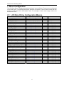
The LCD Direct Driver is configured through the setting of macro definitions. These macros are illustrated
in the sample code. The following table briefly describes the location of each of these macros and their
location in LCD Direct Drive demonstration code. For examples of each macro usage, refer to the
demonstration code.
2.1 LCD Direct Drive Configuration Macros
Macro Name
Units
Demo Location
ICLK_FREQUENCY
PCLK_FREQUENCY
BCLK_FREQUENCY
Description
System Clock Configuration
Clock frequency of MCU core
Clock frequency of peripherals
Clock frequency of external bus
Hz
Hz
Hz
HWSetup.h
HWSetup.h
HWSetup.h
FRAME_HEIGHT
FRAME_WIDTH
V_LINES_INVERT
H_DOT_INVERT
PANEL_ROTATE
LCD_FRAMES
MAX_FRAME_REGIONS
Frame Buffer Configuration
Frame Buffer Configuration
Frame Buffer Configuration
Frame Buffer Configuration
Frame Buffer Configuration
Frame Buffer Configuration
Frame Buffer Configuration
Lines
Dots
Select
Select
Select
Frames
Regions
DirectLCD_CNF.h
DirectLCD_CNF.h
DirectLCD_CNF.h
DirectLCD_CNF.h
DirectLCD_CNF.h
DirectLCD_CNF.h
DirectLCD_CNF.h
SRAM_DD
SRAM_NOMUX_DD
SDRAM_DD
SDRAM_CLUSTER_DD
Driver Mode Selection
Driver Mode Selection
Driver Mode Selection
Driver Mode Selection
Select
Select
Select
Select
DirectLCD_CNF.h
DirectLCD_CNF.h
DirectLCD_CNF.h
DirectLCD_CNF.h
DOT_CLOCK_FREQUENCY_DATA
DOT_CLOCK_FREQUENCY_BLANK
DESIRED_FRAME_RATE
MINIMUM_MCU_ACCESS_PCT
Driver Mode Configuration
Driver Mode Configuration
Driver Mode Configuration
Driver Mode Configuration
Hz
Hz
Hz
%
DirectLCD_CNF.h
DirectLCD_CNF.h
DirectLCD_CNF.h
DirectLCD_CNF.h
DOT_INVERT
V_LINES_PULSE
V_LINES_BACK_PORCH
V_LINES_DISPLAY
V_LINES_FRONT_PORCH
H_DOT_PULSE
H_DOT_BACK_PORCH
H_DOT_DISPLAY
H_DOT_FRONT_PORCH
LCD Panel Configuration
LCD Panel Configuration
LCD Panel Configuration
LCD Panel Configuration
LCD Panel Configuration
LCD Panel Configuration
LCD Panel Configuration
LCD Panel Configuration
LCD Panel Configuration
Select
Lines
Lines
Lines
Lines
Dots
Dots
Dots
Dots
DirectLCD_CNF(panel).h
DirectLCD_CNF(panel).h
DirectLCD_CNF(panel).h
DirectLCD_CNF(panel).h
DirectLCD_CNF(panel).h
DirectLCD_CNF(panel).h
DirectLCD_CNF(panel).h
DirectLCD_CNF(panel).h
DirectLCD_CNF(panel).h
4
Direct Drive LCD Design Guide
Macro Name
FRAME_CS
FRAME_BUS_CYCLES
CAS_LATENCY
SDRAM_PAGE_SIZE
VSYNC_PORT
VSYNC_PIN
HSYNC_PORT
HSYNC_PIN
DOTCLK_PORT
DOTCLK_PIN
LCD_BACKLIGHT_PORT
LCD_BACKLIGHT_PIN
EXDMAC_DD
EXDMAC_DD_INTC
EXDMAC_DD_VECT
EXDMAC_DD_REQ_PORT
EXDMAC_DD_REQ_PIN
DOTCLK_TPU_INTC
DOTCLK_TPU_CHANNEL
DOTCLK_TPU_PIN
DOTCLK_TPU_VECT
DOTPER_TPU_CHANNEL
DOTPER_TPU_PIN
DOTPER_TPU_VECT
HPER_TPU_INTC
HPER_TPU_CHANNEL
HPER_TPU_PIN
HPER_TPU_VECT
HSYNC_TPU_INTC
HSYNC_TPU_CHANNEL
HSYNC_TPU_PIN
HSYNC_TPU_VECT
VSYNC_TPU_INTC
VSYNC_TPU_CHANNEL
VSYNC_TPU_PIN
VSYNC_TPU_VECT
HDEN_TPU_INTC
HDEN_TPU_CHANNEL
HDEN_TPU_PIN
HDEN_TPU_VECT
HDEN2_TPU_CHANNEL
HDEN2_TPU_PIN
HDEN2_TPU_VECT
Description
Platform Configuration
Platform Configuration
Platform Configuration
Platform Configuration
Platform Configuration
Platform Configuration
Platform Configuration
Platform Configuration
Platform Configuration
Platform Configuration
Platform Configuration
Platform Configuration
Platform Configuration
Platform Configuration
Platform Configuration
Platform Configuration
Platform Configuration
Platform Configuration
Platform Configuration
Platform Configuration
Platform Configuration
Platform Configuration
Platform Configuration
Platform Configuration
Platform Configuration
Platform Configuration
Platform Configuration
Platform Configuration
Platform Configuration
Platform Configuration
Platform Configuration
Platform Configuration
Platform Configuration
Platform Configuration
Platform Configuration
Platform Configuration
Platform Configuration
Platform Configuration
Platform Configuration
Platform Configuration
Platform Configuration
Platform Configuration
Platform Configuration
5
Units
CS #
Bclk
Bclk
Words
Port #
Pin #
Port #
Pin #
Port #
Pin #
Port #
Pin #
SFR root
SFR bits
Vector #
Port #
Pin #
SFR bits
Channel #
Pin Letter
Vector #
Channel #
Pin Letter
Vector #
SFR bits
Channel #
Pin Letter
Vector #
SFR bits
Channel #
Pin Letter
Vector #
SFR bits
Channel #
Pin Letter
Vector #
SFR bits
Channel #
Pin Letter
Vector #
Channel #
Pin Letter
Vector #
Demo Location
DirectLCD_CNF(platform).h
DirectLCD_CNF(platform).h
DirectLCD_CNF(platform).h
DirectLCD_CNF(platform).h
DirectLCD_CNF(platform).h
DirectLCD_CNF(platform).h
DirectLCD_CNF(platform).h
DirectLCD_CNF(platform).h
DirectLCD_CNF(platform).h
DirectLCD_CNF(platform).h
DirectLCD_CNF(platform).h
DirectLCD_CNF(platform).h
DirectLCD_CNF(platform).h
DirectLCD_CNF(platform).h
DirectLCD_CNF(platform).h
DirectLCD_CNF(platform).h
DirectLCD_CNF(platform).h
DirectLCD_CNF(platform).h
DirectLCD_CNF(platform).h
DirectLCD_CNF(platform).h
DirectLCD_CNF(platform).h
DirectLCD_CNF(platform).h
DirectLCD_CNF(platform).h
DirectLCD_CNF(platform).h
DirectLCD_CNF(platform).h
DirectLCD_CNF(platform).h
DirectLCD_CNF(platform).h
DirectLCD_CNF(platform).h
DirectLCD_CNF(platform).h
DirectLCD_CNF(platform).h
DirectLCD_CNF(platform).h
DirectLCD_CNF(platform).h
DirectLCD_CNF(platform).h
DirectLCD_CNF(platform).h
DirectLCD_CNF(platform).h
DirectLCD_CNF(platform).h
DirectLCD_CNF(platform).h
DirectLCD_CNF(platform).h
DirectLCD_CNF(platform).h
DirectLCD_CNF(platform).h
DirectLCD_CNF(platform).h
DirectLCD_CNF(platform).h
DirectLCD_CNF(platform).h
Direct Drive LCD Design Guide
2.2 Frame Buffer Configuration
The frame buffer is the external memory area that is used to store the 16bpp image data that will be
presented on the LCD screen. The quantity of frame buffers is typically 2 or more. This allows the MCU to
be updating one frame wile the ExDMA is transferring the other frame to the LCD panel, this behavior
allows for fast transitions and the user does not see operations occurring in the non-displayed buffers.
Typically, the frame buffer is configured to the same dimensions as the LCD panel; however the frame
buffer can be larger to allow the LCD panel to act as a “window” into the frame buffer (allowing for fast
panning of large images).
The following macros control the sizing of the frame buffer.
2.2.1 FRAME_HEIGHT
Defines the number of lines in each of the frame buffers.
2.2.2 FRAME_WIDTH
Defines the number of dots (columns) in each of the frame buffer lines.
2.2.3 V_LINES_INVERT
If defined flips the presentation of lines on the display.
2.2.4 H_DOT_INVERT
If defined flips the presentation of dots (columns) on the display.
2.2.5 PANEL_ROTATE
Rotates the presentation of data (rows/columns) on the LCD panel. Only available on H8SX SRAM based
modes.
2.2.6 LCD_FRAMES
Defines the number of frame buffers allocated in the driver. The demonstration code value is two by
default. This value can be set to zero in which case, the user code is responsible for the allocation of
frame buffers.
2.2.7 MAX_FRAME_REGIONS
Defines the number of horizontal screen “splits” that can be used within the driver. The demonstration
code default value is 1 (no splits). This capability allows different source regions to be used with horizontal
screen areas (control GUI + panning image view for example).
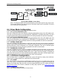
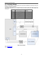
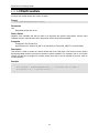
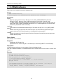
The default display sequence of a LCD panel is shown in Figure 1. The origin of the display is shown as
the green dot in the picture. By default the driver will send the raster image to the LCD panel in the same
sequence. If necessary, there are two macros available to change the sequence of data presented to the
panel. V_LINES_INVERT sends the top line first and sequences to the bottom and H_DOT_INVERT
sends the right side of the line first and sequences to the left. Either or both of these macros can be
specified at the same time. PANEL_ROTATE (only available on H8SX) is the macro to allow user image to
be rotated in transfer to the panel as shown in the Figure 2.
6
Direct Drive LCD Design Guide
Figure 1. RAM Frame Raster Data
Figure 2. PANEL_ROTATE Mode
Figure 3. Images from Various Display Settings
7
Direct Drive LCD Design Guide
2.3 Driver Mode Selection
There are several different modes of operation currently supported in the Direct Drive LCD driver. The
selection of operation mode depends on RAM type selection and LCD panel resolution.
2.3.1 SRAM_DD
Defining this macro selects a mode of operation that utilizes SRAM (or PSRAM) as the frame buffer. In this
operation mode, the ExDMA ACK signal supplies the Dot Clock during data transfer and the TPU supplies
the dot clock during blanking. This is currently the only mode supported on the H8S family of MCUs.
2.3.2 SRAM_NOMUX_DD
Defining this macro selects a mode of operation that utilizes SRAM (or PSRAM) as the frame buffer. In this
operation mode, the TPU supplies the dot clock during data transfer and blanking. This operation mode
can currently only be used on the H8SX on panels that do not require driving a “data enable” signal.
2.3.3 SDRAM_DD
Defining this macro selects a mode of operation that utilizes SDRAM as the frame buffer. In this operation
mode, the ExDMA ACK signal supplies the Dot Clock during data transfer and the TPU supplies the dot
clock during blanking.
2.3.4 SDRAM_CLUSTER_DD
Defining this macro selects a mode of operation that utilizes SDRAM as the frame buffer. In this operation
mode, the Bus Clock signal supplies the Dot Clock during data transfer and the TPU supplies the dot clock
during blanking. This mode is intended for LCD panels that have relatively high dot clock requirements
(VGA+) because the high speed Bus clock is used to drive the dot clock.
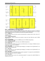
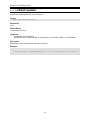
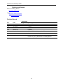
2.3.5 Dot Clock Hardware Connections
From the microcontroller, the EDACK signal is fed into a mux with the Dot Clock to ensure the clock edge
is sent at the time the valid data is on the bus.
Figure 4 H8S SRAM and H8SX SDRAM Dot Clock Logic
Note 1: When using the H8S devices, or the H8SX devices with SDRAM, it is also necessary to
connect the EDREQ (active low) line to the mux. This ensures that the clock remains
synchronized in the time between blocks of data. The H8SX running with SRAM uses a ExDMA
mode which has a deterministic number of clocks between blocks, and so can be relied on to give
predictable timing – the other modes have a latency which may take 4 or 5 clocks, and so
hardware synchronization is necessary.
Note 2: If the panel you are connecting to requires a Dot Clock inversion (falling edge data
transfers) you must place an inverter gate between EDACK and the mux and define
DOT_INVERT in the driver code.
8
Direct Drive LCD Design Guide
Figure 5 H8SX SDRAM in Cluster Mode
Note 1: To create the highest LCD Dot Clock frequency on the H8SX requires using cluster mode.
In this mode, EDACK is not generated and an equivalent signal must be generated. The above
circuit creates the necessary timing.
2.4 Driver Mode Configuration
The driver characteristics are configured with the following macros.
2.4.1 DOT_CLOCK_FREQUENCY_DATA
This macro configures the dot clock frequency during the data transfer portion of the LCD update cycle.
This value must be achievable by the configured BCLK_FREQUENCY and RAM configuration. This value
is checked against other system parameters and an error will be generated if the value is not achievable.
2.4.2 DOT_CLOCK_FREQUENCY_BLANK
This macro configures the dot clock frequency during the blanking portion of the LCD update cycle. This
value must be achievable by the configured PCLK_FREQUENCY as it generated by the TPU. This value
is checked against other system parameters and an error will be generated if the value is not achievable.
2.4.3 DESIRED_FRAME_RATE
This macro configures the initial selection of LCD frame rate. The frame rate can also be modified at
runtime via the LCDSetFrameRate API call. To achieve the desired frame rate, the vertical blanking time is
extended beyond the values configured in the LCD panel configuration. This value is checked against
other system parameters and an error will be generated if the value is not achievable.
2.4.4 MINIMUM_MCU_ACCESS_PCT
This macro configures the user’s minimum acceptable percentage of time that the MCU core has access
to the frame RAM (the MCU core only has access to the frame RAM during the vertical blanking time).
This value interacts with DESIRED_FRAME_RATE macro…higher access percentage is achievable at
lower frame rates (as the bus is less consumed with frame updates). This value is checked against other
system parameters and an error will be generated if the value is not achievable.
2.5 LCD Panel Configuration
The LCD Direct Driver is configured to operate with a given LCD panel by setting macro definitions.
These values are readily available in the data sheet for the selected panel.
2.5.1 DOT_INVERT
This macro is used to control whether the RGB data is latched on the rising or the falling edge of the dot
clock. If the macro is not defined, the data is latched on the rising edge, if it is defined, the data will be
latched on the falling edge. Note that when using the multiplexed EDACK and TPU modes, the EDACK
signal will also need to be inverted in hardware for falling edge operation (see section on dot clock
hardware connections).
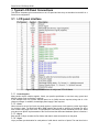
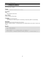
2.5.2 V_LINES_xx and H_DOT_xx
Refer to the following diagram for definition of these values.
9
Direct Drive LCD Design Guide
Figure 6 LCD Panel Macro Definitions
2.6 LCD Platform Configuration
The LCD Direct Driver is configured to operate with a given hardware platform by setting macro definitions.
These values will have to be determined from the schematics on the hardware platform. As an example,
the demonstration code can be compared the LCD direct drive hardware schematics.
2.6.1 FRAME_CS
This is the numeric value of the CS pin used for the frame buffer, for example if CS2 is used, a value of “2”
would be entered.
2.6.2 FRAME_BUS_CYCLES
Enter the number of BCLK cycles that are required to access the frame RAM (only used in SRAM
configurations).
2.6.3 CAS_LATENCY
Enter the configured CAS latency for the SDRAM (only used in SDRAM configurations).
2.6.4 SDRAM_PAGE_SIZE
Enter the SDRAM page size in words (only used in SDRAM configurations).
2.6.5 EDMAC_DD
Enter the name of the ExDMAC being used for the LCD Direct Drive. For example, if ExDMAC channel 2
is being used, set the value to “EXDMAC2”.
2.6.6 Xxxx_PORT
Enter the associated port for the requested signal mapping. For example if the LCD_BACKLIGHT is on
port PM1, set the port value to “M”.
2.6.7 Xxxx_PIN
Enter the associated port for the requested signal mapping. For example if the LCD_BACKLIGHT is on
port PM1, set the pin value to “1”.
2.6.8 Xxxx_INTC
Enter the SFR field for the associated interrupt controller peripheral. For example if the H8SX ExDMAC 2
is being used, enter “INTC.IPRJ.BIT._EXDMAC2”.
2.6.9 Xxxx_VECT
Enter the interrupt vector number for the associated peripheral. For example if the H8SX ExDMAC 2 is
being used, enter “142”.
10
Direct Drive LCD Design Guide
2.6.10 Xxxx_TPU_CHANNEL
Enter the channel number for the requested TPU signal. For example if the H8SX DOTCLK is mapped to
TPU TIOCB0, enter “0”.
2.6.11 Xxxx_TPU_PIN
Enter the pin letter for the requested TPU signal. For example if the H8SX DOTCLK is mapped to TPU
TIOCB0, enter “B”.
11
Direct Drive LCD Design Guide
3. Typical LCD Panel Connections
This section illustrates typical connections on an LCD panel and how they are interfaced to the MCU in a
Direct Drive configuration.
3.1 LCD panel interface
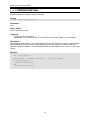
Figure 7 Example Connections for a Kyocera TFT-LCD Panel
3.1.1 Power Supplies
Many panels require multiple supplies. Check your panel’s specification to see how many ground and
different voltage level connections it requires.
In the example case of a Kyocera 320x240 panel, 6x 0v (GND) lines are required, along with 2x +3.3v
reference voltages. In addition, the backlight power supply is also required.
3.1.2 Clock
Often referred to as the Dot Clock, the panel requires a synchronous clock signal to provide logic edges
for clocking in data. The Red-Green-Blue (RGB) parallel data should be present on the data bus at the
time of each rising edge of the clock. This provides the color setting for each individual pixel in turn. Read
more about our specific implementation of the Dot Clock and the associated hardware options in Section 4
3.1.3 HSync
Each period of HSync contains the Dot Clocks and data for each horizontal line on the panel
3.1.4 VSync
Vsync provides synchronization for each packet of valid data in each line of pixels. The total time for the
12
Direct Drive LCD Design Guide
entire panel to fill with valid pixels is the maximum refresh rate. Displays in existing media systems usually
have refresh rates between 48Hz and 120Hz to avoid visible flicker.
HSync, VSync and Dot Clock are all generated using TPU channels of the H8S or H8SX microcontrollers.
The TPU allows timer compare actions which synchronize these signals to the ExDMA request line. This
ensures that the clocks are generated when valid data is available on the bus.
3.1.5 Data Enable
Many panels require an additional signal to frame the valid data – this enable signal is sent at the time the
valid data is latched onto the bus – the panel will then clock in the data on the next edge of Dot Clock. It
provides added synchronization for the timing of data, but this signal can often be left in the active state if
the Dot Clock synchronization to the data is predictable.
3.1.6 RGB (Red Green Blue) Data
The data is presented to the panel in parallel. LCD panels have connections for 6 or 8bits of data for each
color totaling 18 or 24bits of color resolution. Our solution uses a 16bit data bus, so the most significant
bits of the data are presented to the panel. RGB 5-6-5 is the most common 16 bit solution. The least
significant bits can be tied low, or better still, to the MSB which would give a slightly improved range over
tying to ground.
Specifically with respect to Renesas H8S and H8SX devices, we use the ExDMA module to control the
data bus transfers.
3.1.7 Touch Screen
Our support is currently for popular resistive touch screen panels which have 4 connections (endpoints of
an X axis resistance and Y axis resistance). These inputs provide resistances proportional to the touched
location particular X and Y coordinates on the panel.
The host system (microcontroller plus logic) drives the resistive endpoints with a known reference voltage,
and the level on the channel is read into an analog to digital converter (ADC). With calibration and scaling
in the microcontroller driver code, it is possible to pinpoint the area of the panel that was touched. Action
can be taken accordingly.
An example of interface circuitry between the MCU and touch-screen is shown in Figure 6 below.
R2
TOUCH_Y U
1K
Y _DRIVE
1
2
C1
10nF
R1
DNF
U1A
3
HC126A
R4
X_DRIVE
4
5
4
HC126A
3
10
VCC
9
TOUCH_XL
J4
U1B
6
1K
C2
10nF
R3
DNF
2
U1C
8
1
R9
HC126A
TOUCH_Y L
MOLEX_52044
1K
13
12
U1D
11
C4
10nF
R8
DNF
HC126A
R11
TOUCH_XR
1K
C5
10nF
Figure 8 Touch Screen Circuit
13
R10
DNF
Direct Drive LCD Design Guide
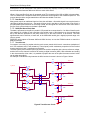
3.2 Hardware Design
Below is a block diagram of a LCD system which uses Flash and SRAM for respectively storing and
buffering the images to be displayed.
The following table describes the TPU channels and pins used for direct drive. Note that the TPU
synchronization capability is used to create a common time base between the HDEN, HSYNC and
VSYNC pins.
Suggested
Signal
TPU Channel Requirements Channel
DOTCLK Output using PWM 1 Mode
1, 2, 4 or 5
DOTPER TGR to set period of DOTCLK same as DOTCLK
HDEN
Output using PWM 2 Mode
1, 2, 4 or 5
HDEN2
TGR for PWM 2 Mode
same as HDEN
HSYNC
Output using PWM 1 Mode
0 or 3
VSYNC
Output using PWM 1 Mode
same as HSYNC
HPER
TGR to set horizontal period
same as HSYNC
Figure 9 Block Diagram
Note 1: Dot Clock Logic
Note 2: Touch Screen
14
Direct Drive LCD Design Guide
4. LCD API Definition
4.1.1
Standard Redefines
These following type have been redefined in order to make the code easier for formatting.
typedef
typedef
typedef
typedef
typedef
typedef
4.1.2
unsigned char
signed char
unsigned short
signed short
unsigned long
signed long
uI08;
sI08;
uI16;
sI16;
uI32;
sI32;
//
//
//
//
//
//
Unsigned Integer 8-bits
Signed Integer 8-bits
Unsigned Integer 16-bits
Signed Integer 16-bits
Unsigned Integer 32-bits
Signed Integer 32-bits
LCD API Data Types
These data types are used within the API to support API calls
typedef enum
{
LCDAPI_SUCCESS = 0,
LCDAPI_ERR_UNINITIALIZED, // lcd api called prior to initialization
LCDAPI_ERR_UNSUPPORTED,
LCDAPI_ERR_INVALID_PARAMETER,
LCDAPI_ERR_NULL_POINTER,
LCDAPI_ERR_ODDADDRESS
// frame buffer must lie on even address
}LCDErrorType;
15
Direct Drive LCD Design Guide
4.1.3
LCDInit
Direct Driver Initialization.
Format
LCDErrorType LCDInit(void);
Parameters
none
Return Values
0 if successful, non-zero if failure.
Properties
Prototyped in file ”DirectLCD.h”
Implemented in file “DirectLCD_SBF.c” for H8S family or “DirectLCD_XBCFT.c” for H8SX family.
Description
This function is used to initialize the hardware necessary for the Direct Drive LCD to execute. This function
uses the configuration macros to set up the TPU and ExDMAC peripherals to transfer data from the frame
RAM to the LCD panel. After this function successfully executes the transfer of data to the panel by
ExDMAC will start and interrupts will be generated on every line to service the ExDMAC.
Example
{
LCDErrorType error = LCDInit();
if (error != 0) …
}
16
Direct Drive LCD Design Guide
4.1.4
LCDBacklight
Direct Driver backlight control.
Format
void LCDBacklight(int state);
Parameters
state
Requested backlight state 0=off, non-0 = on.
Return Values
None
Properties
Prototyped in file ”DirectLCD.h”
Implemented in file “DirectLCD_SBF.c” for H8S family or “DirectLCD_XBCFT.c” for H8SX family.
Description
This function is used to control the state of the LCD backlight.
Example
{
LCDBacklight(1);
/* turn backlight on */
}
17
Direct Drive LCD Design Guide
4.1.5
LCDSetFrameRate
Configure the vertical refresh rate of the LCD panel.
Format
sI16 LCDSetFrameRate(sI16 rate);
Parameters
rate
Requested refresh rate (in Hz)
Return Values
Negative value indicates rate was not able to be achieved with system configuration. Positive value
indicates success, returned value will be the percent of MCU access time available.
Properties
Prototyped in file ”DirectLCD.h”
Implemented in file “DirectLCD_SBF.c” for H8S family or “DirectLCD_XBCFT.c” for H8SX family.
Description
This function is used to control the vertical refresh rate of the LCD panel. This function can be used to
dynamically adapt the MCU access time based on system conditions. For example, prior to a full buffer
refresh, the rate can be dropped to increase access time, than it can be restored to previous value for
normal operation.
Example
{
sI16 success = LCDSetFrameRate(60); /* set frame rate to 60Hz */
if (success < 0)… /* process error */
}
18
Direct Drive LCD Design Guide
4.1.6
LCDGetFrameRate
Request the vertical refresh rate of the LCD panel.
Format
sI16 LCDGetFrameRate(void);
Parameters
none
Return Values
Current frame rate in Hz.
Properties
Prototyped in file ”DirectLCD.h”
Implemented in file “DirectLCD_SBF.c” for H8S family or “DirectLCD_XBCFT.c” for H8SX family.
Description
Request the current vertical refresh rate of the LCD panel.
Example
{
sI16 old_rate = LCDGetFrameRate();
}
19
/* get frame rate prior to change */
Direct Drive LCD Design Guide
4.1.7
LCDSetActiveRaster
Set memory frame to display.
Format
uI16 * LCDSetActiveRaster(uI16 frame);
Parameters
frame
Requested frame buffer index.
Return Values
Pointer to first pixel of frame raster.
Properties
Prototyped in file ”DirectLCD.h”
Implemented in file “DirectLCD_SBF.c” for H8S family or “DirectLCD_XBCFT.c” for H8SX family.
Description
Request the current vertical refresh rate of the LCD panel.
Note that LCDSetActiveRaster, LCDSetRasterOffset and LCDSetLineSource are similar in function and
interact.
Example
uI16 frame_request;
uI16* select_buffer;
……
frame_request = 1; /* Select frame 1 to display */
select_buffer = LCDSetActiveRaster(frame_request); /* switch buffer */
20
Direct Drive LCD Design Guide
4.1.8
LCDGetActiveFrame
Request which memory frame is currently displayed
Format
uI16 LCDGetActiveFrame(void);
Parameters
none
Return Values
Index of active frame raster.
Properties
Prototyped in file ”DirectLCD.h”
Implemented in file “DirectLCD_SBF.c” for H8S family or “DirectLCD_XBCFT.c” for H8SX family.
Description
Request which memory frame is currently displayed. Note that this function only returns valid information
when LCDSetActiveRaster is used to control the display content (as opposed to LCDSetLineSource).
Note that LCDSetActiveRaster, LCDSetRasterOffset and LCDSetLineSource are similar in function and
interact.
Example
uI16
frame_request;
……
frame_request = LCDGetActiveFrame();
if (frame_request == 0)
LCDSetActiveRaster(1);
else
LCDSetActiveRaster(0);
21
/* switch buffers */
Direct Drive LCD Design Guide
4.1.9
LCDSetRasterOffset
Request display location within larger raster image
Format
sI16 LCDSetRasterOffset(sI16 x, sI16 y);
Parameters
x
X offset in pixels within the raster.
y
Y offset in pixels within the raster.
Return Values
0 on success, non-0 on failure
Properties
Prototyped in file ”DirectLCD.h”
Implemented in file “DirectLCD_SBF.c” for H8S family or “DirectLCD_XBCFT.c” for H8SX family.
Description
LCDSetRasterOffset changes the display position within the raster. The offset is limited to be within area
allocated by the FRAME_HEIGHT x FRAME_WIDTH space. If raster is the same size as the panel, the
offset cannot be changed (fixed to 0,0).
Note that LCDSetActiveRaster, LCDSetRasterOffset and LCDSetLineSource are similar in function and
interact.
Example
sI16 x = 40, y=20;
……
If (LCDSetRasterOffset (x, y) !=
// handle error;
0)
22
//set raster offset
Direct Drive LCD Design Guide
4.1.10 LCDSetLineSource
Defines the source regions of the active display window.
Format
sI16 LCDSetLineSource
(sI16 Region, sI16 LineCount, uI16 *pSource, sI16 LineStep);
Parameters
Region
Region of display (horizontal strip). Ranging from 0 to MAX_FRAME_REGIONS (defined in
DirectLCD_CNF.h). Normally, region 0 starts at the bottom of the screen. However; when
V_LINES_INVERT is defined to change line presentation on the screen, region 0 will start at the top
of the screen. MAX_FRAME_REGIONS should be set to 1 if multiple regions are not used (this will
eliminate any associated runtime overhead).
LineCount
Is the number of lines associated with this region. This value can vary from 1 to V_LINES_PANEL.
pSource
Address of the first pixel of the first line within the region. The entire memory space of the region
must be within the “LCD_Frames” section, or the request will not be accepted.
LineStep
Distance (in pixels/uI16’s) from first pixel of first line to first pixel of second line (source regions can
be wider than the panel).
Return Values
0 on success, non-0 on failure
Properties
Prototyped in file ”DirectLCD.h”
Implemented in file “DirectLCD_SBF.c” for H8S family or “DirectLCD_XBCFT.c” for H8SX family.
Description
LCDSetLineSource defines the source regions of the active display window.
Note that LCDSetActiveRaster, LCDSetRasterOffset and LCDSetLineSource are similar in function and
interact.
Example
#pragma section LCD_Frames
// SRAM allocated for GUI display
uI16 GUI_buffer[50 * H_DOT_DISPLAY];
// allocate panning buffer 4x panel
uI16 Image_buffer[2* V_LINES_PANEL * 2 * H_DOT_DISPLAY];
#pragma section
……
(void)LCDSetLineSource (0,50,GUI_buffer, H_DOT_DISPLAY); //GUI Region
(void)LCDSetLineSource (1,V_LINES_PANEL-50,
&Image_buffer[ offset], 2*H_DOT_DISPLAY); //Pan Region
……
23
Direct Drive LCD Design Guide
Website and Support
Renesas Technology Website
http://www.renesas.com/
Inquiries
http://www.renesas.com/inquiry
[email protected]
Revision Record
Description
Page
Summary
—
First edition issued
Updated
—
Updated
Rev.
1.00
1.10
2.20
Date
Jan.28.08
Apr.28.08
Jan.13.09
2.30
Mar.16.09
Updated
2.40
May.11.09
Added LCDSetLineSource to the API.
2.50
June.8.09
Reformatted to new API style.
2.60
Sept.25.2009
Renamed V_LINES_RESOURCE to FRAME_HEIGHT.
Renamed H_DOT_RESOURCE to FRAME_WIDTH.
24
Direct Drive LCD Design Guide
Notes regarding these materials
1.
2.
3.
4.
5.
6.
7.
8.
9.
10.
11.
12.
13.
This document is provided for reference purposes only so that Renesas customers may select the appropriate
Renesas products for their use. Renesas neither makes warranties or representations with respect to the
accuracy or completeness of the information contained in this document nor grants any license to any intellectual
property rights or any other rights of Renesas or any third party with respect to the information in this document.
Renesas shall have no liability for damages or infringement of any intellectual property or other rights arising out
of the use of any information in this document, including, but not limited to, product data, diagrams, charts,
programs, algorithms, and application circuit examples.
You should not use the products or the technology described in this document for the purpose of military
applications such as the development of weapons of mass destruction or for the purpose of any other military
use. When exporting the products or technology described herein, you should follow the applicable export
control laws and regulations, and procedures required by such laws and regulations.
All information included in this document such as product data, diagrams, charts, programs, algorithms, and
application circuit examples, is current as of the date this document is issued. Such information, however, is
subject to change without any prior notice. Before purchasing or using any Renesas products listed in this
document, please confirm the latest product information with a Renesas sales office. Also, please pay regular
and careful attention to additional and different information to be disclosed by Renesas such as that disclosed
through our website. (http://www.renesas.com)
Renesas has used reasonable care in compiling the information included in this document, but Renesas
assumes no liability whatsoever for any damages incurred as a result of errors or omissions in the information
included in this document.
When using or otherwise relying on the information in this document, you should evaluate the information in light
of the total system before deciding about the applicability of such information to the intended application.
Renesas makes no representations, warranties or guaranties regarding the suitability of its products for any
particular application and specifically disclaims any liability arising out of the application and use of the
information in this document or Renesas products.
With the exception of products specified by Renesas as suitable for automobile applications, Renesas products
are not designed, manufactured or tested for applications or otherwise in systems the failure or malfunction of
which may cause a direct threat to human life or create a risk of human injury or which require especially high
quality and reliability such as safety systems, or equipment or systems for transportation and traffic, healthcare,
combustion control, aerospace and aeronautics, nuclear power, or undersea communication transmission. If you
are considering the use of our products for such purposes, please contact a Renesas sales office beforehand.
Renesas shall have no liability for damages arising out of the uses set forth above.
Notwithstanding the preceding paragraph, you should not use Renesas products for the purposes listed below:
(1) artificial life support devices or systems
(2) surgical implantations
(3) healthcare intervention (e.g., excision, administration of medication, etc.)
(4) any other purposes that pose a direct threat to human life
Renesas shall have no liability for damages arising out of the uses set forth in the above and purchasers who
elect to use Renesas products in any of the foregoing applications shall indemnify and hold harmless Renesas
Technology Corp., its affiliated companies and their officers, directors, and employees against any and all
damages arising out of such applications.
You should use the products described herein within the range specified by Renesas, especially with respect to
the maximum rating, operating supply voltage range, movement power voltage range, heat radiation
characteristics, installation and other product characteristics. Renesas shall have no liability for malfunctions or
damages arising out of the use of Renesas products beyond such specified ranges.
Although Renesas endeavors to improve the quality and reliability of its products, IC products have specific
characteristics such as the occurrence of failure at a certain rate and malfunctions under certain use conditions.
Please be sure to implement safety measures to guard against the possibility of physical injury, and injury or
damage caused by fire in the event of the failure of a Renesas product, such as safety design for hardware and
software including but not limited to redundancy, fire control and malfunction prevention, appropriate treatment
for aging degradation or any other applicable measures. Among others, since the evaluation of microcomputer
software alone is very difficult, please evaluate the safety of the final products or system manufactured by you.
In case Renesas products listed in this document are detached from the products to which the Renesas products
are attached or affixed, the risk of accident such as swallowing by infants and small children is very high. You
should implement safety measures so that Renesas products may not be easily detached from your products.
Renesas shall have no liability for damages arising out of such detachment.
This document may not be reproduced or duplicated, in any form, in whole or in part, without prior written
approval from Renesas.
Please contact a Renesas sales office if you have any questions regarding the information contained in this
document, Renesas semiconductor products, or if you have any other inquiries.
© 2008. Renesas Technology Corp., All rights reserved.
25