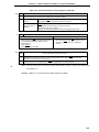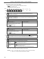
1
User’s Manual
µPD78058F, 78058FY Subseries
8-Bit Single-Chip Microcontrollers
µPD78056F
µPD78058F
µPD78P058F
µPD78058F(A)
µPD78056FY
µPD78058FY
µPD78P058FY
µPD78058FY(A)
Document No. U12068EJ2V0UM00 (2nd edition)
Date Published April 1998 N CP (K)
©
Printed in Japan
1997
[MEMO]
2
NOTES FOR CMOS DEVICES
1
PRECAUTION AGAINST ESD FOR SEMICONDUCTORS
Note:
Strong electric field, when exposed to a MOS device, can cause destruction of the gate oxide and
ultimately degrade the device operation.
Steps must be taken to stop generation of static
electricity as much as possible, and quickly dissipate it once, when it has occurred. Environmental
control must be adequate. When it is dry, humidifier should be used. It is recommended to avoid
using insulators that easily build static electricity. Semiconductor devices must be stored and
transported in an anti-static container, static shielding bag or conductive material. All test and
measurement tools including work bench and floor should be grounded. The operator should be
grounded using wrist strap. Semiconductor devices must not be touched with bare hands. Similar
precautions need to be taken for PW boards with semiconductor devices on it.
2
HANDLING OF UNUSED INPUT PINS FOR CMOS
Note:
No connection for CMOS device inputs can be cause of malfunction. If no connection is provided
to the input pins, it is possible that an internal input level may be generated due to noise, etc., hence
causing malfunction. CMOS devices behave differently than Bipolar or NMOS devices. Input
levels of CMOS devices must be fixed high or low by using a pull-up or pull-down circuitry. Each
unused pin should be connected to V DD or GND with a resistor, if it is considered to have a
possibility of being an output pin. All handling related to the unused pins must be judged device
by device and related specifications governing the devices.
3
STATUS BEFORE INITIALIZATION OF MOS DEVICES
Note:
Power-on does not necessarily define initial status of MOS device. Production process of MOS
does not define the initial operation status of the device. Immediately after the power source is
turned ON, the devices with reset function have not yet been initialized. Hence, power-on does
not guarantee out-pin levels, I/O settings or contents of registers. Device is not initialized until
the reset signal is received. Reset operation must be executed immediately after power-on for
devices having reset function.
FIP, EEPROM, and IEBus are trademarks of NEC Corporation.
MS-DOS, Windows, and WindowsNT are either registered trademarks or trademarks of Microsoft Corporation in the United States and/or other countries.
IBM DOS, PC/AT, and PC DOS are trademarks of International Business Machines Corporation.
HP9000 Series 700 and HP-UX are trademarks of Hewlett-Packard Company.
SPARCstation is a trademark of SPARC International, Inc.
SunOS is a trademark of Sun Microsystems, Inc.
Ethernet is a trademark of XEROX Corporation.
NEWS and NEWS-OS are trademarks of SONY Corporation.
OSF/Motif is a trademark of Open Software Foundation, Inc.
TRON is an abbreviation of The Realtime Operating System Nucleus.
ITRON is an abbreviation of Industrial TRON.
3
The export of this product from Japan is regulated by the Japanese government. To export this product may be prohibited without
governmental license, the need for which must be judged by the customer. The export or re-export of this product from a country
other than Japan may also be prohibited without a license from that country. Please call an NEC sales representative.
The application circuits and their parameters are for reference only and are not intended for use in actual design-ins.
Purchase of NEC I2C components conveys a license under the Philips I2C Patent Rights to use these
components in an I2C system, provided that the system conforms to the I2C Standard Specification as defined
by Philips.
The information in this document is subject to change without notice.
No part of this document may be copied or reproduced in any form or by any means without the prior written
consent of NEC Corporation. NEC Corporation assumes no responsibility for any errors which may appear in
this document.
NEC Corporation does not assume any liability for infringement of patents, copyrights or other intellectual property
rights of third parties by or arising from use of a device described herein or any other liability arising from use
of such device. No license, either express, implied or otherwise, is granted under any patents, copyrights or other
intellectual property rights of NEC Corporation or others.
While NEC Corporation has been making continuous effort to enhance the reliability of its semiconductor devices,
the possibility of defects cannot be eliminated entirely. To minimize risks of damage or injury to persons or
property arising from a defect in an NEC semiconductor device, customers must incorporate sufficient safety
measures in its design, such as redundancy, fire-containment, and anti-failure features.
NEC devices are classified into the following three quality grades:
"Standard", "Special", and "Specific". The Specific quality grade applies only to devices developed based on a
customer designated “quality assurance program“ for a specific application. The recommended applications of
a device depend on its quality grade, as indicated below. Customers must check the quality grade of each device
before using it in a particular application.
Standard: Computers, office equipment, communications equipment, test and measurement equipment,
audio and visual equipment, home electronic appliances, machine tools, personal electronic
equipment and industrial robots
Special: Transportation equipment (automobiles, trains, ships, etc.), traffic control systems, anti-disaster
systems, anti-crime systems, safety equipment and medical equipment (not specifically designed
for life support)
Specific: Aircrafts, aerospace equipment, submersible repeaters, nuclear reactor control systems, life
support systems or medical equipment for life support, etc.
The quality grade of NEC devices is "Standard" unless otherwise specified in NEC's Data Sheets or Data Books.
If customers intend to use NEC devices for applications other than those specified for Standard quality grade,
they should contact an NEC sales representative in advance.
Anti-radioactive design is not implemented in this product.
M7 96.5
4
Regional Information
Some information contained in this document may vary from country to country. Before using any NEC
product in your application, please contact the NEC office in your country to obtain a list of authorized
representatives and distributors. They will verify:
• Device availability
• Ordering information
• Product release schedule
• Availability of related technical literature
• Development environment specifications (for example, specifications for third-party tools and
components, host computers, power plugs, AC supply voltages, and so forth)
• Network requirements
In addition, trademarks, registered trademarks, export restrictions, and other legal issues may also vary
from country to country.
NEC Electronics Inc. (U.S.)
NEC Electronics (Germany) GmbH
NEC Electronics Hong Kong Ltd.
Santa Clara, California
Tel: 408-588-6000
800-366-9782
Fax: 408-588-6130
800-729-9288
Benelux Office
Eindhoven, The Netherlands
Tel: 040-2445845
Fax: 040-2444580
Hong Kong
Tel: 2886-9318
Fax: 2886-9022/9044
NEC Electronics Hong Kong Ltd.
Velizy-Villacoublay, France
Tel: 01-30-67 58 00
Fax: 01-30-67 58 99
Seoul Branch
Seoul, Korea
Tel: 02-528-0303
Fax: 02-528-4411
NEC Electronics (France) S.A.
NEC Electronics Singapore Pte. Ltd.
Milton Keynes, UK
Tel: 01908-691-133
Fax: 01908-670-290
Spain Office
Madrid, Spain
Tel: 01-504-2787
Fax: 01-504-2860
United Square, Singapore 1130
Tel: 65-253-8311
Fax: 65-250-3583
NEC Electronics Italiana s.r.1.
NEC Electronics (Germany) GmbH
Milano, Italy
Tel: 02-66 75 41
Fax: 02-66 75 42 99
Scandinavia Office
Taeby, Sweden
Tel: 08-63 80 820
Fax: 08-63 80 388
NEC Electronics (France) S.A.
NEC Electronics (Germany) GmbH
Duesseldorf, Germany
Tel: 0211-65 03 02
Fax: 0211-65 03 490
NEC Electronics (UK) Ltd.
NEC Electronics Taiwan Ltd.
Taipei, Taiwan
Tel: 02-719-2377
Fax: 02-719-5951
NEC do Brasil S.A.
Cumbica-Guarulhos-SP, Brasil
Tel: 011-6465-6810
Fax: 011-6465-6829
J98. 2
5
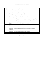
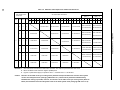
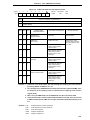
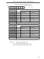
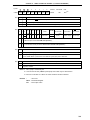
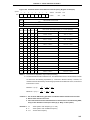
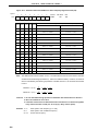
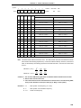
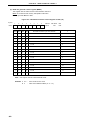
MAJOR REVISIONS IN THIS EDITION
Page
Throughout
Major Revision from Previous Edition
The following products have already been developed:
µPD78056FGC-×××-8BT, 78058FGC-×××-8BT, 78P058FGC-8BT, 78056FYGC-×××-8BT,
78058FYGC-×××-8BT
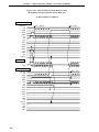
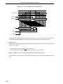
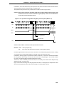
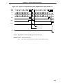
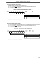
P133 to
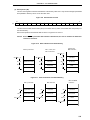
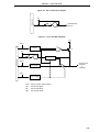
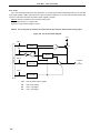
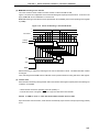
The block diagrams of the following ports were changed.
P137, P143
Figures 6-5 and 6-7 P20, P21, P23 to P26 Block Diagram, Figures 6-6 and 6-8 P22 and P27 Block
Diagram, Figure 6-9 P30 to P37 Block Diagram, Figure 6-16 P71 and P72 Block Diagram
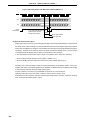
P159
Table 7-2 Relationship between CPU Clock and Minimum Instruction Execution Time was added.
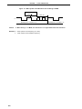
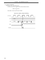
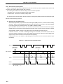
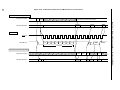
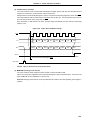
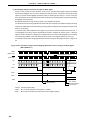
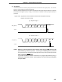
P230, P235
Figures 9-10 and 9-13 Square-Wave Output Operation Timing were added.
P295
Note related to operation controls when using the SBI mode of serial interface channel 0 was added.
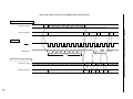
P297
Note related to BSYE in Figure 16-5 Serial Bus Interface Control Register Format was changed.
P308
Cautions were added to 16.4.3 (2) (a) Bus release signal (REL), and (b) Command signal (CMD)
P435, P436
CSCK was deleted from Figure 19-1 Serial Interface Channel 2 Block Diagram, and Figure 19-2
Baud Rate Generator Block Diagram.
P438
Figure 19-3 Serial Operating Mode Register 2 Format was changed.
P440
Table 19-2 Serial Interface Channel 2 Operating Mode Settings (2) 3-wire serial I/O mode was
changed.
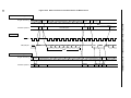
P459
Figure 19-10 Receive Error Timing was changed.
P468
19.4.4 Restrictions on using UART mode was added.
P565
APPENDIX A DIFFERENCES AMONG µPD78054, 78058F, AND 780058 SUBSERIES was added.
P567
APPENDIX B DEVELOPMENT TOOLS
Overall revision: Contents were adapted to correspond to in-circuit emulators IE-78K0-NS and
IE-78001-R-A
P582
APPENDIX C EMBEDDED SOFTWARE
Overall revision: Fuzzy inference development support system was deleted.
P591
APPENDIX E REVISION HISTORY was added.
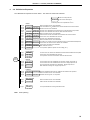
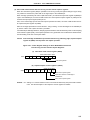
The mark
6
shows major revised points.
PREFACE
Readers
This manual has been prepared for user engineers who want to understand the
functions of the µPD78058F and 78058FY Subseries and design and develop its
application systems and programs.
Affected versions are each of the versions in the following Subseries.
µPD78058F Subseries
: µPD78056F, 78058F, 78P058F, 78058F(A)
µPD78058FY Subseries : µPD78056FY, 78058FY, 78P058FY, 78058FY(A)
Purpose
This manual is intended for users to understand the functions described in the
Organization below.
Organization
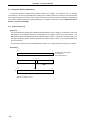
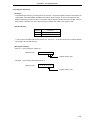
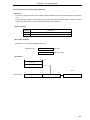
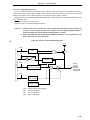
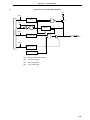
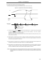
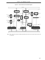
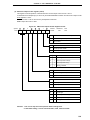
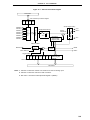
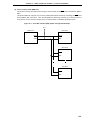
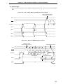
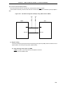
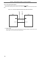
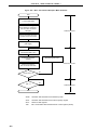
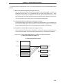
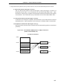
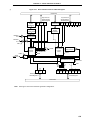
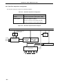
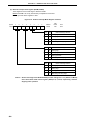
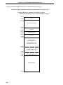
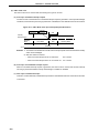
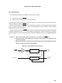
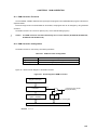
The µPD78058F, 78058FY Subseries manual is organized by two volumes: this
manual and the instruction edition (common to the 78K/0 Series).
µPD78058F, 78058FY
Subseries
User’s Manual
78K/0 Series
User’s Manual
Instructions
(This Manual)
Pin functions
CPU functions
Internal block functions
Instruction set
Interrupt
Explanation of each instruction
Other on-chip peripheral functions
7
How to Read This Manual
Before reading this manual, you should have general knowledge of electric and logic
circuits and microcontrollers.
For persons who use this manual as the manual for the µPD78058F(A) and
78058FY(A),
→ The µPD78058F and 78058FY differ from the µPD78058F(A) and 78058FY(A)
only in their quality grades. For products with (A), please change the readings
for the product name as follows.
µPD78058F → µPD78058F(A)
µPD78058FY → µPD78058FY(A)
When you want to understand the functions in general:
→ Read this manual in the order of the contents.
To know the µPD78058F and 78058FY Subseries instruction function in detail:
→ Refer to the 78K/0 Series User's Manual: Instructions (U12326E)
How to interpret the register format:
→ For the circled bit number, the bit name is defined as a reserved word in
RA78K/0, and in CC78K/0, already defined in the header file named sfrbit.h.
To learn the function of a register whose register name is known:
→ Refer to APPENDIX D REGISTER INDEX.
To know the electrical specifications of the µPD78058F and 78058FY Subseries:
→ Refer to separately available Data Sheet.
To know the details regarding the functions of the µPD78058F and 78058FY
Subseries:
→ Refer to separately available Application Notes.
Caution
Examples used in this manual are prepared for “Standard” product
quality grade products for general electronic equipment.
If the
examples of use in this manual are utilized in applications where a
“Special” product quality grade is required, please study concerning the quality grade of each part and each circuit that will actually
be used.
8
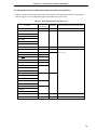
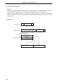
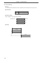
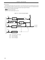
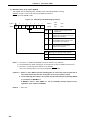
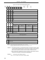
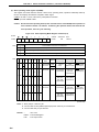
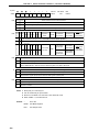
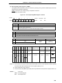
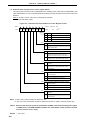
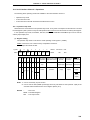
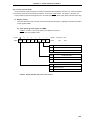
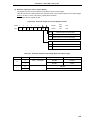
Chapter Organization
This manual divides the descriptions for the µPD78058F and 78058FY Subseries into
different chapters as shown below. Read only the chapters related to the device you use.
Chapter
µPD78058F Subseries µPD78058FY Subseries
Chapter 1
Outline ( µ PD78058F Subseries)
√
—
Chapter 2
Outline ( µ PD78058FY Subseries)
—
√
Chapter 3
Pin Function ( µ PD78058F Subseries)
√
—
Chapter 4
Pin Function ( µ PD78058FY Subseries)
—
√
Chapter 5
CPU Architecture
√
√
Chapter 6
Port Functions
√
√
Chapter 7
Clock Generator
√
√
Chapter 8
16-Bit Timer/Event Counter
√
√
Chapter 9
8-Bit Timer/Event Counter
√
√
Chapter 10
Watch Timer
√
√
Chapter 11
Watchdog Timer
√
√
Chapter 12
Clock Output Control Circuit
√
√
Chapter 13
Buzzer Output Control Circuit
√
√
Chapter 14
A/D Converter
√
√
Chapter 15
D/A Converter
√
√
Chapter 16
Serial Interface Channel 0
√
—
—
√
( µ PD78058F Subseries)
Chapter 17
Serial Interface Channel 0
( µ PD78058FY Subseries)
Chapter 18
Serial Interface Channel 1
√
√
Chapter 19
Serial Interface Channel 2
√
√
Chapter 20
Real-Time Output Port
√
√
Chapter 21
Interrupt and Test Functions
√
√
Chapter 22
External Device Expansion Function
√
√
Chapter 23
Standby Function
√
√
Chapter 24
Reset Function
√
√
Chapter 25
ROM Correction
√
√
Chapter 26
µ PD78P058F, µ PD78P058FY
√
√
Chapter 27
Instruction Set
√
√
9
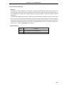
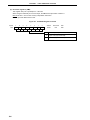
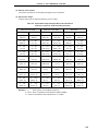
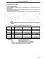
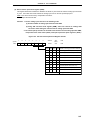
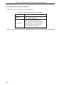
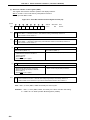
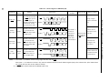
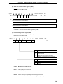
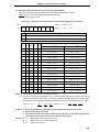
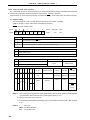
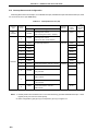
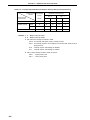
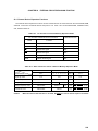
Differences between µPD78058F and µPD78058FY Subseries:
The µPD78058F and µPD78058FY Subseries are different in the following functions
of the serial interface channel 0.
µPD78058F
Subseries
µPD78058FY
Subseries
3-wire serial I/O mode
√
√
2-wire serial I/O mode
√
√
SBI (serial bus interface) mode
√
—
I2C bus mode
—
√
Modes of Serial Interface Channel 0
√
: Supported
— : Not supported
Conventions
Data significance
:
Higher digits on the left and lower digits on the right
Active low representations
:
××× (overscore over pin or signal names)
Note
:
Footnotes for item marked with Note in the text
Caution
:
Information requiring particular attention
Remarks
:
Supplementary information
Numeral representations
:
Binary ... ×××× or ××××B
Decimal ... ××××
Hexadecimal ... ××××H
10
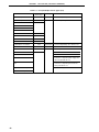
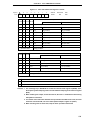
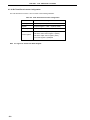
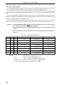
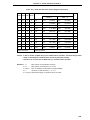
Related Documents
The related documents indicated in this publication may include preliminary
versions. However, preliminary versions are not marked as such.
Related Documents for µPD78058F Subseries
Document No.
Document Name
Japanese
English
µPD78056F, 78058F Data Sheet
U11795J
U11795E
µPD78P058F Data Sheet
U11796J
U11796E
µPD78058F(A) Data Sheet
U12325J
U12325E
µPD78058F, 78058FY Subseries User’s Manual
U12068J
This manual
78K/0 Series User’s Manual—Instruction
U12326J
U12326E
78K/0 Series Instruction Table
U10903J
—
78K/0 Series Instruction Set
U10904J
—
78K/0 Series Application Note Basic (III)
U10182J
U10182E
Related Documents for µPD78058FY Subseries
Document No.
Document Name
Japanese
English
µPD78056FY, 78058FY Data Sheet
U12142J
U12142E
µPD78P058FY Data Sheet
U12076J
U12076E
µPD78058F, 78058FY Subseries User’s Manual
U12068J
This manual
78K/0 Series User’s Manual — Instructions
U12326J
U12326E
78K/0 Series Instruction Table
U10903J
—
78K/0 Series Instruction Set
U10904J
—
78K/0 Series Application Note Basic (III)
U10182J
U10182E
Caution The above documents are subject to change without prior notice. Be sure to use the latest
document for designing.
11
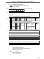
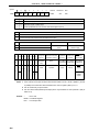
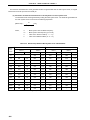
Development Tool Documents (User’s Manuals)
Document No.
Document Name
Japanese
RA78K0 Assembler Package
Operation
U11802J
U11802E
Assembly language
U11801J
U11801E
Structured assembler language
U11789J
U11789E
U12323J
EEU-1402
Operation
U11517J
U11517E
Language
U11518J
U11518E
Programming know-how
U13034J
EEA-1208
RA78K Series Structured Assembler Preprocessor
CC78K0 C Compiler
CC78K0 C Compiler Application Note
English
CC78K Series Library Source File
U12322J
—
PG-1500 PROM Programmer
U11940J
U11940E
PG-1500 Controller PC-9800 Series (MS-DOS™) Base
EEU-704
EEU-1291
PG-1500 Controller IBM PC Series (PC DOS™) Base
EEU-5008
U10540E
IE-78K0-NS
To be prepared
To be prepared
IE-78001-R-A
To be prepared
To be prepared
IE-780308-NS-EM1
To be prepared
To be prepared
IE-78064-R-EM
EEU-905
EEU-1443
IE-780308-R-EM
U11362J
U11362E
EP-78230
EEU-985
EEU-1515
EP-78054GK-R
EEU-932
EEU-1468
SM78K0 System Simulator Windows™ Base
Reference
U10181J
U10181E
SM78K Series System Simulator
External component user
U10092J
U10092E
U12900J
To be prepared
open interface specifications
ID78K0-NS Integrated Debugger
ID78K0 Integrated Debugger EWS Base
Reference
U11151J
—
ID78K0 Integrated Debugger PC Base
Reference
U11539J
—
ID78K0 Integrated Debugger Windows Base
Guide
U11649J
—
Caution The above documents are subject to change without prior notice. Be sure to use the latest
document for designing.
12
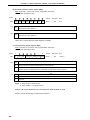
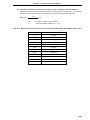
Documents for Embedded Software
(User’s Manual)
Document No.
Document Name
Japanese
78K/0 Series Real-Time OS
OS for 78K/0 Series MX78K0
English
Basics
U11537J
U11537E
Installation
U11536J
U11536E
Basics
U12257J
U12257E
Other Documents
Document No.
Document Name
Japanese
English
IC PACKAGE MANUAL
C10943X
Semiconductor Device Mounting Technology Manual
C10535J
C10535E
Quality Grade on NEC Semiconductor Devices
C11531J
C11531E
Reliability Quality Control on NEC Semiconductor Devices
C10983J
C10983E
Guide to Prevent Damage for Semiconductor Devices by Electrostatic Discharge (ESD)
C11892J
C11892E
Guide to Quality Assurance for Semiconductor Devices
Microcontroller Related Product Guide — Third Party Manufacturers
—
U11416J
MEI-1202
—
Caution The above documents are subject to change without prior notice. Be sure to use the latest
document for designing.
13
[MEMO]
14
CONTENTS
CHAPTER 1 OUTLINE (µPD78058F SUBSERIES) ............................................................................. 35
1.1
1.2
1.3
1.4
1.5
1.6
1.7
1.8
1.9
1.10
Features ..................................................................................................................................
Applications ...........................................................................................................................
Ordering Information .............................................................................................................
Quality Grade .........................................................................................................................
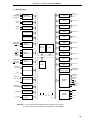
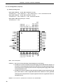
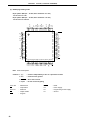
Pin Configuration (Top View) ................................................................................................
78K/0 Series Expansion ........................................................................................................
Block Diagram ........................................................................................................................
Outline of Function ................................................................................................................
Differences Between the µPD78058F and µPD78058F(A) ..................................................
Mask Options .........................................................................................................................
35
36
36
37
38
41
43
44
45
46
CHAPTER 2 OUTLINE (µPD78058FY SUBSERIES) ........................................................................... 47
2.1
2.2
2.3
2.4
2.5
2.6
2.7
2.8
2.9
2.10
Features ..................................................................................................................................
Applications ...........................................................................................................................
Ordering Information .............................................................................................................
Quality Grade .........................................................................................................................
Pin Configuration (Top View) ................................................................................................
78K/0 Series Expansion ........................................................................................................
Block Diagram ........................................................................................................................
Outline of Function ................................................................................................................
Differences Between the µPD78058FY and µPD78058FY(A) .............................................
Mask Options .........................................................................................................................
47
48
48
49
50
53
55
56
57
58
CHAPTER 3 PIN FUNCTION (µPD78058F SUBSERIES) .................................................................... 59
3.1
3.2
Pin Function List .................................................................................................................... 59
3.1.1
Normal operating mode pins ........................................................................................................
59
3.1.2
PROM programming mode pins (PROM versions only) ...............................................................
64
Description of Pin Functions ................................................................................................ 65
3.2.1
P00 to P07 (Port 0) ......................................................................................................................
65
3.2.2
P10 to P17 (Port 1) ......................................................................................................................
66
3.2.3
P20 to P27 (Port 2) ......................................................................................................................
66
3.2.4
P30 to P37 (Port 3) ......................................................................................................................
67
3.2.5
P40 to P47 (Port 4) ......................................................................................................................
68
3.2.6
P50 to P57 (Port 5) ......................................................................................................................
68
3.2.7
P60 to P67 (Port 6) ......................................................................................................................
68
3.2.8
P70 to P72 (Port 7) ......................................................................................................................
69
3.2.9
P120 to P127 (Port 12) ................................................................................................................
70
3.2.10 P130 and P131 (Port 13) .............................................................................................................
70
3.2.11 AVREF0 ...........................................................................................................................................
70
3.2.12 AVREF1 ...........................................................................................................................................
70
3.2.13 AVDD .............................................................................................................................................
71
15
3.2.14 AVSS ..............................................................................................................................................
3.3
71
3.2.15 RESET .........................................................................................................................................
71
3.2.16 X1 and X2 ....................................................................................................................................
71
3.2.17 XT1 and XT2 ................................................................................................................................
71
3.2.18 VDD ...............................................................................................................................................
71
3.2.19 VSS ................................................................................................................................................
71
3.2.20 VPP (PROM versions only) ............................................................................................................
71
3.2.21 IC (Mask ROM version only) ........................................................................................................
72
Input/output Circuits and Recommended Connection of Unused Pins ........................... 73
CHAPTER 4 PIN FUNCTION (µPD78058FY SUBSERIES) ................................................................. 77
4.1
4.2
4.3
Pin Function List .................................................................................................................... 77
4.1.1
Normal operating mode pins ........................................................................................................
77
4.1.2
PROM programming mode pins (PROM versions only) ...............................................................
82
Description of Pin Functions ................................................................................................ 83
4.2.1
P00 to P07 (Port 0) ......................................................................................................................
83
4.2.2
P10 to P17 (Port 1) ......................................................................................................................
84
4.2.3
P20 to P27 (Port 2) ......................................................................................................................
84
4.2.4
P30 to P37 (Port 3) ......................................................................................................................
85
4.2.5
P40 to P47 (Port 4) ......................................................................................................................
86
4.2.6
P50 to P57 (Port 5) ......................................................................................................................
86
4.2.7
P60 to P67 (Port 6) ......................................................................................................................
86
4.2.8
P70 to P72 (Port 7) ......................................................................................................................
87
4.2.9
P120 to P127 (Port 12) ................................................................................................................
88
4.2.10 P130 and P131 (Port 13) .............................................................................................................
88
4.2.11 AVREF0 ...........................................................................................................................................
88
4.2.12 AVREF1 ...........................................................................................................................................
88
4.2.13 AVDD .............................................................................................................................................
89
4.2.14 AVSS ..............................................................................................................................................
89
4.2.15 RESET .........................................................................................................................................
89
4.2.16 X1 and X2 ....................................................................................................................................
89
4.2.17 XT1 and XT2 ................................................................................................................................
89
4.2.18 VDD ...............................................................................................................................................
89
4.2.19 VSS ................................................................................................................................................
89
4.2.20 VPP (PROM versions only) ............................................................................................................
89
4.2.21 IC (Mask ROM version only) ........................................................................................................
90
Input/output Circuits and Recommended Connection of Unused Pins ........................... 91
CHAPTER 5 CPU ARCHITECTURE ..................................................................................................... 95
5.1
5.2
16
Memory Spaces ...................................................................................................................... 95
5.1.1
Internal program memory space ..................................................................................................
98
5.1.2
Internal data memory space .........................................................................................................
99
5.1.3
Special Function Register (SFR) area .........................................................................................
99
5.1.4
External memory space ...............................................................................................................
99
5.1.5
Data memory addressing ............................................................................................................. 100
Processor Registers .............................................................................................................. 103
5.3
5.4
5.2.1
Control registers ........................................................................................................................... 103
5.2.2
General registers .......................................................................................................................... 106
5.2.3
Special Function Register (SFR) .................................................................................................. 108
Instruction Address Addressing .......................................................................................... 112
5.3.1
Relative addressing ...................................................................................................................... 112
5.3.2
Immediate addressing .................................................................................................................. 113
5.3.3
Table indirect addressing ............................................................................................................. 114
5.3.4
Register addressing ..................................................................................................................... 115
Operand Address Addressing .............................................................................................. 116
5.4.1
Implied addressing ....................................................................................................................... 116
5.4.2
Register addressing ..................................................................................................................... 117
5.4.3
Direct addressing ......................................................................................................................... 118
5.4.4
Short direct addressing ................................................................................................................ 119
5.4.5
Special-Function Register (SFR) addressing ............................................................................... 121
5.4.6
Register indirect addressing ......................................................................................................... 122
5.4.7
Based addressing ........................................................................................................................ 123
5.4.8
Based indexed addressing ........................................................................................................... 124
5.4.9
Stack addressing .......................................................................................................................... 124
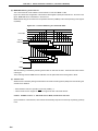
CHAPTER 6 PORT FUNCTIONS .......................................................................................................... 125
6.1
6.2
Port Functions ........................................................................................................................ 125
Port Configuration ................................................................................................................. 130
6.2.1
Port 0 ............................................................................................................................................ 130
6.2.2
Port 1 ............................................................................................................................................ 132
6.2.3
Port 2 (µPD78058F Subseries) .................................................................................................... 133
6.2.4
Port 2 (µPD78058FY Subseries) .................................................................................................. 135
6.2.5
Port 3 ............................................................................................................................................ 137
6.2.6
Port 4 ............................................................................................................................................ 138
6.2.7
Port 5 ............................................................................................................................................ 139
6.2.8
Port 6 ............................................................................................................................................ 140
6.2.9
Port 7 ............................................................................................................................................ 142
6.2.10 Port 12 .......................................................................................................................................... 144
6.2.11 Port 13 .......................................................................................................................................... 145
6.3
6.4
6.5
Port Function Control Registers .......................................................................................... 146
Port Function Operations ...................................................................................................... 152
6.4.1
Writing to input/output port ........................................................................................................... 152
6.4.2
Reading from input/output port ..................................................................................................... 152
6.4.3
Operations on input/output port .................................................................................................... 153
Selection of Mask Option ...................................................................................................... 153
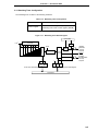
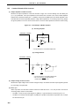
CHAPTER 7 CLOCK GENERATOR ..................................................................................................... 155
7.1
7.2
7.3
7.4
Clock Generator Functions ...................................................................................................
Clock Generator Configuration ............................................................................................
Clock Generator Control Register ........................................................................................
System Clock Oscillator ........................................................................................................
7.4.1
155
155
157
161
Main system clock oscillator ......................................................................................................... 161
17
7.5
7.6
7.4.2
Subsystem clock oscillator ........................................................................................................... 162
7.4.3
Scaler ........................................................................................................................................... 164
7.4.4
When no subsystem clocks are used ........................................................................................... 164
Clock Generator Operations ................................................................................................. 165
7.5.1
Main system clock operations ...................................................................................................... 166
7.5.2
Subsystem clock operations ........................................................................................................ 167
Changing System Clock and CPU Clock Settings .............................................................. 167
7.6.1
Time required for switchover between system clock and CPU clock ........................................... 167
7.6.2
System clock and CPU clock switching procedure ...................................................................... 169
CHAPTER 8 16-BIT TIMER/EVENT COUNTER ................................................................................... 171
8.1
8.2
8.3
8.4
8.5
8.6
Overview of the µPD78058F and 78058FY Subseries On-Chip Timers .............................
16-Bit Timer/Event Counter Functions ................................................................................
16-Bit Timer/Event Counter Configuration ..........................................................................
16-Bit Timer/Event Counter Control Registers ...................................................................
16-Bit Timer/Event Counter Operations ...............................................................................
171
173
174
178
187
8.5.1
Interval timer operations ............................................................................................................... 187
8.5.2
PWM output operations ................................................................................................................ 189
8.5.3
PPG output operation ................................................................................................................... 192
8.5.4
Pulse width measurement operations .......................................................................................... 193
8.5.5
External event counter operation ................................................................................................. 200
8.5.6
Square-wave output operation ..................................................................................................... 202
8.5.7
One-shot pulse output operation .................................................................................................. 204
16-Bit Timer/Event Counter Operating Precautions ........................................................... 208
CHAPTER 9 8-BIT TIMER/EVENT COUNTERS .................................................................................. 211
9.1
9.2
9.3
9.4
9.5
8-Bit Timer/Event Counter Function .................................................................................... 211
9.1.1
8-bit timer/event counter mode .................................................................................................... 211
9.1.2
16-bit timer/event counter mode .................................................................................................. 214
8-Bit Timer/Event Counter Configuration ............................................................................ 216
8-Bit Timer/Event Counter Control Registers ..................................................................... 220
8-Bit Timer/Event Counter Operation ................................................................................... 225
9.4.1
8-bit timer/event counter mode .................................................................................................... 225
9.4.2
16-bit timer/event counter mode .................................................................................................. 230
Cautions on 8-Bit Timer/Event Counters ............................................................................. 236
CHAPTER 10 WATCH TIMER .............................................................................................................. 239
10.1
10.2
10.3
10.4
18
Watch Timer Functions .......................................................................................................
Watch Timer Configuration .................................................................................................
Watch Timer Control Registers ..........................................................................................
Watch Timer Operations .....................................................................................................
239
240
240
244
10.4.1
Watch timer operation ............................................................................................................. 244
10.4.2
Interval timer operation ............................................................................................................ 244
CHAPTER 11 WATCHDOG TIMER ...................................................................................................... 245
11.1
11.2
11.3
11.4
Watchdog Timer Functions ................................................................................................
Watchdog Timer Configuration ..........................................................................................
Watchdog Timer Control Registers ...................................................................................
Watchdog Timer Operations ...............................................................................................
245
247
248
251
11.4.1
Watchdog timer operation ....................................................................................................... 251
11.4.2
Interval timer operation ............................................................................................................ 252
CHAPTER 12 CLOCK OUTPUT CONTROL CIRCUIT ......................................................................... 253
12.1
12.2
12.3
Clock Output Control Circuit Functions ............................................................................ 253
Clock Output Control Circuit Configuration ..................................................................... 254
Clock Output Function Control Registers ......................................................................... 254
CHAPTER 13 BUZZER OUTPUT CONTROL CIRCUIT ....................................................................... 257
13.1
13.2
13.3
Buzzer Output Control Circuit Functions .......................................................................... 257
Buzzer Output Control Circuit Configuration ................................................................... 257
Buzzer Output Function Control Registers ....................................................................... 258
CHAPTER 14 A/D CONVERTER .......................................................................................................... 261
14.1
14.2
14.3
14.4
14.5
A/D Converter Functions ....................................................................................................
A/D Converter Configuration ..............................................................................................
A/D Converter Control Registers .......................................................................................
A/D Converter Operations ...................................................................................................
261
262
265
269
14.4.1
Basic operations of A/D converter ........................................................................................... 269
14.4.2
Input voltage and conversion results ....................................................................................... 271
14.4.3
A/D converter operating mode ................................................................................................ 272
A/D Converter Cautions ...................................................................................................... 274
CHAPTER 15 D/A CONVERTER .......................................................................................................... 279
15.1
15.2
15.3
15.4
15.5
D/A Converter Functions ....................................................................................................
D/A Converter Configuration ..............................................................................................
D/A Converter Control Registers .......................................................................................
Operations of D/A Converter ..............................................................................................
Cautions Related to D/A Converter ....................................................................................
279
280
282
283
284
CHAPTER 16 SERIAL INTERFACE CHANNEL 0 (µPD78058F SUBSERIES) ................................... 285
16.1
16.2
16.3
16.4
Serial Interface Channel 0 Functions .................................................................................
Serial Interface Channel 0 Configuration ..........................................................................
Serial Interface Channel 0 Control Registers ....................................................................
Serial Interface Channel 0 Operations ...............................................................................
286
288
292
299
16.4.1
Operation stop mode ............................................................................................................... 299
16.4.2
3-wire serial I/O mode operation ............................................................................................. 300
19
16.4.3
SBI mode operation ................................................................................................................. 305
16.4.4
2-wire serial I/O mode operation ............................................................................................. 331
16.4.5
SCK0/P27 pin output manipulation ......................................................................................... 336
CHAPTER 17 SERIAL INTERFACE CHANNEL 0 (µPD78058FY SUBSERIES) ................................. 337
17.1
17.2
17.3
17.4
Serial Interface Channel 0 Functions .................................................................................
Serial Interface Channel 0 Configuration ..........................................................................
Serial Interface Channel 0 Control Registers ....................................................................
Serial Interface Channel 0 Operations ...............................................................................
338
340
345
353
17.4.1
Operation stop mode ............................................................................................................... 353
17.4.2
3-wire serial I/O mode operation ............................................................................................. 354
17.4.3
2-wire serial I/O mode operation ............................................................................................. 358
17.4.4
I2C bus mode operation ........................................................................................................... 363
17.4.5
Cautions on use of I2C bus mode ............................................................................................ 380
17.4.6
Restrictions in I2C bus mode ................................................................................................... 383
17.4.7
SCK0/SCL/P27 pin output manipulation ................................................................................. 385
CHAPTER 18 SERIAL INTERFACE CHANNEL 1 ............................................................................... 387
18.1
18.2
18.3
18.4
Serial Interface Channel 1 Functions .................................................................................
Serial Interface Channel 1 Configuration ..........................................................................
Serial Interface Channel 1 Control Registers ....................................................................
Serial Interface Channel 1 Operations ...............................................................................
387
388
391
399
18.4.1
Operation stop mode ............................................................................................................... 399
18.4.2
3-wire serial I/O mode operation ............................................................................................. 400
18.4.3
3-wire serial I/O mode operation with automatic transmit/receive function ............................. 403
CHAPTER 19 SERIAL INTERFACE CHANNEL 2 ............................................................................... 433
19.1
19.2
19.3
19.4
Serial Interface Channel 2 Functions .................................................................................
Serial Interface Channel 2 Configuration ..........................................................................
Serial Interface Channel 2 Control Registers ....................................................................
Serial Interface Channel 2 Operation .................................................................................
19.4.1
433
434
438
446
Operation stop mode ............................................................................................................... 446
19.4.2
Asynchronous serial interface (UART) mode .......................................................................... 448
19.4.3
3-wire serial I/O mode ............................................................................................................. 461
19.4.4
Restrictions on using UART mode .......................................................................................... 468
CHAPTER 20 REAL-TIME OUTPUT PORT ......................................................................................... 471
20.1
20.2
20.3
Real-Time Output Port Functions ...................................................................................... 471
Real-Time Output Port Configuration ................................................................................ 472
Real-Time Output Port Control Registers ......................................................................... 474
CHAPTER 21 INTERRUPT AND TEST FUNCTIONS .......................................................................... 477
21.1
20
Interrupt Function Types .................................................................................................... 477
21.2
21.3
21.4
21.5
Interrupt Sources and Configuration ................................................................................. 478
Interrupt Function Control Registers ................................................................................. 482
Interrupt Servicing Operations ........................................................................................... 491
21.4.1
Non-maskable interrupt acknowledge operation ..................................................................... 491
21.4.2
Maskable Interrupt request reception ...................................................................................... 494
21.4.3
Software interrupt request acknowledge operation ................................................................. 497
21.4.4
Multiple interrupt servicing ....................................................................................................... 497
21.4.5
Interrupt request reserve ......................................................................................................... 501
Test Functions ..................................................................................................................... 502
21.5.1
Registers controlling the test function ..................................................................................... 502
21.5.2
Test input signal acknowledge operation ................................................................................. 504
CHAPTER 22 EXTERNAL DEVICE EXPANSION FUNCTION ............................................................ 505
22.1
22.2
22.3
External Device Expansion Functions ............................................................................... 505
External Device Expansion Function Control Register ................................................... 508
External Device Expansion Function Timing .................................................................... 510
CHAPTER 23 STANDBY FUNCTION ................................................................................................... 515
23.1
23.2
Standby Function and Configuration ................................................................................ 515
23.1.1
Standby function ...................................................................................................................... 515
23.1.2
Standby function control register ............................................................................................. 516
Standby Function Operations ............................................................................................ 517
23.2.1
HALT mode .............................................................................................................................. 517
23.2.2
STOP mode ............................................................................................................................. 520
CHAPTER 24 RESET FUNCTION ........................................................................................................ 523
24.1
Reset Function ..................................................................................................................... 523
CHAPTER 25 ROM CORRECTION ...................................................................................................... 527
25.1
25.2
25.3
25.4
25.5
25.6
25.7
ROM Correction Functions .................................................................................................
ROM Correction Configuration ...........................................................................................
ROM Correction Control Registers ....................................................................................
ROM Correction Application ...............................................................................................
ROM Correction Example ...................................................................................................
Program Execution Flow .....................................................................................................
Cautions on ROM Correction .............................................................................................
527
527
529
530
533
534
536
CHAPTER 26 µPD78P058F, 78P058FY ............................................................................................... 537
26.1
26.2
26.3
Memory Size Switching Register ....................................................................................... 538
Internal Expansion RAM Size Switching Register ............................................................ 539
PROM Programming ............................................................................................................ 540
26.3.1
Operating modes ..................................................................................................................... 540
26.3.2
PROM write procedure ............................................................................................................ 542
21
26.3.3
26.4
PROM read procedure ............................................................................................................ 546
Screening of One-Time PROM Versions ........................................................................... 547
CHAPTER 27 INSTRUCTION SET ....................................................................................................... 549
27.1
Legends Used in Operation List ......................................................................................... 550
27.1.1
27.2
27.3
Operand identifiers and description methods .......................................................................... 550
27.1.2
Description of “operation” column ........................................................................................... 551
27.1.3
Description of “flag” column ..................................................................................................... 551
Operation List ...................................................................................................................... 552
Instructions Listed by Addressing Type ........................................................................... 560
APPENDIX A DIFFERENCES AMONG µPD78054, 78058F, AND 780058 SUBSERIES ................... 565
APPENDIX B DEVELOPMENT TOOLS ............................................................................................... 567
B.1 Language Processing Software ........................................................................................... 570
B.2 PROM Programming Tool ..................................................................................................... 571
B.2.1
Hardware ...................................................................................................................................... 571
B.2.2
Software ....................................................................................................................................... 571
B.3 Debugging Tool ...................................................................................................................... 572
B.3.1
Hardware ...................................................................................................................................... 572
B.3.2
Software ....................................................................................................................................... 574
B.4 OS for IBM PC ........................................................................................................................ 576
B.5 Upgrading Former In-circuit Emulators for 78K/0 Series to IE-78001-R-A ....................... 576
APPENDIX C EMBEDDED SOFTWARE .............................................................................................. 581
C.1 Real-time OS ........................................................................................................................... 582
APPENDIX D REGISTER INDEX .......................................................................................................... 585
D.1 Register Index ........................................................................................................................ 585
APPENDIX E REVISION HISTORY ...................................................................................................... 591
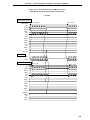
22
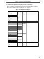
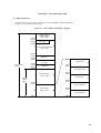
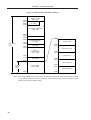
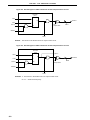
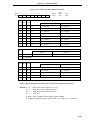
LIST OF FIGURES (1/8)
Figure No.
Title
Page
3-1
List of Pin Input/Output Circuit ..........................................................................................................
75
4-1
List of Pin Input/Output Circuit ..........................................................................................................
93
5-1
Memory Map (µPD78056F, 78056FY) ..............................................................................................
95
5-2
Memory Map (µPD78058F, 78058FY) ..............................................................................................
96
5-3
Memory Map (µPD78P058F, µPD78P058FY) ..................................................................................
97
5-4
Data Memory Addressing (µPD78056F, 78056FY) ...........................................................................
100
5-5
Data Memory Addressing (µPD78058F, 78058FY) ...........................................................................
101
5-6
Data Memory Addressing (µPD78P058F, 78P058FY) ......................................................................
102
5-7
Program Counter Format ..................................................................................................................
103
5-8
Program Status Word Format ...........................................................................................................
103
5-9
Stack Pointer Format ........................................................................................................................
105
5-10
Data to Be Saved to Stack Memory ..................................................................................................
105
5-11
Data to Be Reset from Stack Memory ..............................................................................................
105
5-12
General Register Configuration ........................................................................................................
107
6-1
Port Types .........................................................................................................................................
125
6-2
P00 and P07 Block Diagram .............................................................................................................
131
6-3
P01 to P06 Block Diagram ................................................................................................................
131
6-4
P10 to P17 Block Diagram ................................................................................................................
132
6-5
P20, P21, P23 to P26 Block Diagram ...............................................................................................
133
6-6
P22 and P27 Block Diagram .............................................................................................................
134
6-7
P20, P21, P23 to P26 Block Diagram ...............................................................................................
135
6-8
P22 and P27 Block Diagram .............................................................................................................
136
6-9
P30 to P37 Block Diagram ................................................................................................................
137
6-10
P40 to P47 Block Diagram ................................................................................................................
138
6-11
Block Diagram of Falling Edge Detection Circuit ..............................................................................
138
6-12
P50 to P57 Block Diagram ................................................................................................................
139
6-13
P60 to P63 Block Diagram ................................................................................................................
141
6-14
P64 to P67 Block Diagram ................................................................................................................
141
6-15
P70 Block Diagram ...........................................................................................................................
142
6-16
P71 and P72 Block Diagram .............................................................................................................
143
6-17
P120 to P127 Block Diagram ............................................................................................................
144
6-18
P130 and P131 Block Diagram .........................................................................................................
145
6-19
Port Mode Register Format ..............................................................................................................
148
6-20
Pull-Up Resistor Option Register Format .........................................................................................
149
6-21
Memory Expansion Mode Register Format ......................................................................................
150
6-22
Key Return Mode Register Format ...................................................................................................
151
7-1
Block Diagram of Clock Generator ...................................................................................................
156
7-2
Subsystem Clock Feedback Resistor ...............................................................................................
157
7-3
Processor Clock Control Register Format ........................................................................................
158
23
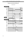
LIST OF FIGURES (2/8)
Figure No.
Title
Page
7-4
Oscillation Mode Selection Register Format .....................................................................................
159
7-5
Main System Clock Waveform due to Writing to OSMS ...................................................................
160
7-6
External Circuit of Main System Clock Oscillator ..............................................................................
161
7-7
External Circuit of Subsystem Clock Oscillator .................................................................................
162
7-8
Examples of Resonator with Incorrect Connection ...........................................................................
162
7-9
Main System Clock Stop Function ....................................................................................................
166
7-10
System Clock and CPU Clock Switching ..........................................................................................
169
8-1
16-Bit Timer/Event Counter Block Diagram ......................................................................................
175
8-2
16-Bit Timer/Event Counter Output Control Circuit Block Diagram ..................................................
176
8-3
Timer Clock Selection Register 0 Format .........................................................................................
179
8-4
16-Bit Timer Mode Control Register Format .....................................................................................
181
8-5
Capture/Compare Control Register 0 Format ...................................................................................
182
8-6
16-Bit Timer Output Control Register Format ...................................................................................
183
8-7
Port Mode Register 3 Format ...........................................................................................................
184
8-8
External Interrupt Mode Register 0 Format ......................................................................................
185
8-9
Sampling Clock Select Register Format ...........................................................................................
186
8-10
Control Register Settings for Interval Timer Operation .....................................................................
187
8-11
Interval Timer Configuration Diagram ...............................................................................................
188
8-12
Interval Timer Operation Timings ......................................................................................................
188
8-13
Control Register Settings for PWM Output Operation ......................................................................
190
8-14
Example of D/A Converter Configuration with PWM Output .............................................................
191
8-15
TV Tuner Application Circuit Example ..............................................................................................
191
8-16
Control Register Settings for PPG Output Operation .......................................................................
192
8-17
Control Register Settings for Pulse Width Measurement with Free-Running Counter and
8-18
8-19
One Capture Register .......................................................................................................................
193
Configuration Diagram for Pulse Width Measurement by Free-Running Counter ............................
194
Timing of Pulse Width Measurement Operation by Free-Running Counter and One Capture
Register (with Both Edges Specified) ...............................................................................................
194
8-20
Control Register Settings for Two Pulse Width Measurements with Free-Running Counter ............
195
8-21
Timing of Pulse Width Measurement Operation with Free-Running Counter
(with Both Edges Specified) ..............................................................................................................
8-22
Two Capture Registers .....................................................................................................................
8-23
8-24
8-25
197
Timing of Pulse Width Measurement Operation by Free-Running Counter and Two Capture
Registers (with Rising Edge Specified) .............................................................................................
198
Control Register Settings for Pulse Width Measurement by Means of Restart ................................
199
Timing of Pulse Width Measurement Operation by Means of Restart
(with Rising Edge Specified) .............................................................................................................
24
196
Control Register Settings for Pulse Width Measurement with Free-Running Counter and
199
8-26
Control Register Settings in External Event Counter Mode ..............................................................
200
8-27
External Event Counter Configuration Diagram ................................................................................
201
8-28
External Event Counter Operation Timings (with Rising Edge Specified) ........................................
201
8-29
Control Register Settings in Square-Wave Output Mode .................................................................
202
8-30
Square-Wave Output Operation Timing ............................................................................................
203
LIST OF FIGURES (3/8)
Figure No.
Title
Page
8-31
Control Register Settings for One-Shot Pulse Output Operation Using Software Trigger ................
204
8-32
Timing of One-Shot Pulse Output Operation Using Software Trigger ...............................................
205
8-33
Control Register Settings for One-Shot Pulse Output Operation Using External Trigger .................
206
8-34
Timing of One-Shot Pulse Output Operation Using External Trigger (with Rising Edge Specified) ..
207
8-35
16-Bit Timer Register Start Timing ....................................................................................................
208
8-36
Timings After Change of Compare Register during Timer Count Operation .....................................
208
8-37
Capture Register Data Retention Timing ..........................................................................................
209
8-38
Operation Timing of OVF0 Flag ........................................................................................................
210
9-1
8-Bit Timer/Event Counter Block Diagram ........................................................................................
217
9-2
Block Diagram of 8-Bit Timer/Event Counter Output Control Circuit 1 .............................................
218
9-3
Block Diagram of 8-Bit Timer/Event Counter Output Control Circuit 2 .............................................
218
9-4
Timer Clock Select Register 1 Format ..............................................................................................
221
9-5
8-Bit Timer Mode Control Register Format .......................................................................................
222
9-6
8-Bit Timer Output Control Register Format .....................................................................................
223
9-7
Port Mode Register 3 Format ...........................................................................................................
224
9-8
Interval Timer Operation Timings ......................................................................................................
225
9-9
External Event Counter Operation Timings (with Rising Edge Specified) ........................................
228
9-10
Square-Wave Output Operation Timing ............................................................................................
230
9-11
Interval Timer Operation Timing ........................................................................................................
231
9-12
External Event Counter Operation Timings (with Rising Edge Specified) ........................................
233
9-13
Square-Wave Output Operation Timing ............................................................................................
235
9-14
8-Bit Timer Registers Start Timing ....................................................................................................
236
9-15
Event Counter Operation Timing ......................................................................................................
236
9-16
Timing After Compare Register Change During Timer Count Operation ..........................................
237
10-1
Watch Timer Block Diagram .............................................................................................................
241
10-2
Timer Clock Select Register 2 Format ..............................................................................................
242
10-3
Watch Timer Mode Control Register Format ....................................................................................
243
11-1
Watchdog Timer Block Diagram .......................................................................................................
247
11-2
Timer Clock Select Register 2 Format ..............................................................................................
249
11-3
Watchdog Timer Mode Register Format ...........................................................................................
250
12-1
Remote Controlled Output Application Example ...............................................................................
253
12-2
Clock Output Control Circuit Block Diagram .....................................................................................
254
12-3
Timer Clock Select Register 0 Format ..............................................................................................
255
12-4
Port Mode Register 3 Format ...........................................................................................................
256
13-1
Buzzer Output Control Circuit Block Diagram ...................................................................................
257
13-2
Timer Clock Select Register 2 Format ..............................................................................................
259
13-3
Port Mode Register 3 Format ...........................................................................................................
260
25
LIST OF FIGURES (4/8)
Figure No.
Title
Page
14-1
A/D Converter Block Diagram ...........................................................................................................
263
14-2
A/D Converter Mode Register Format ..............................................................................................
266
14-3
A/D Converter Input Select Register Format ....................................................................................
267
14-4
External Interrupt Mode Register 1 Format ......................................................................................
268
14-5
A/D Converter Basic Operation ........................................................................................................
270
14-6
Relationship Between Analog Input Voltage and A/D Conversion Result .........................................
271
14-7
A/D Conversion by Hardware Start ...................................................................................................
272
14-8
A/D Conversion by Software Start ....................................................................................................
273
14-9
Example of Method of Reducing Current Consumption in Standby Mode .......................................
274
14-10
Connection of Analog Input Pin ........................................................................................................
275
14-11
A/D Conversion End Interrupt Request Generation Timing ..............................................................
276
14-12
Connection of AVDD Pin .....................................................................................................................
277
15-1
D/A Converter Block Diagram ...........................................................................................................
280
26
15-2
D/A Converter Mode Register Format ..............................................................................................
282
15-3
Use Example of Buffer Amplifier .......................................................................................................
284
16-1
Serial Bus Interface (SBI) System Configuration Example ...............................................................
287
16-2
Serial Interface Channel 0 Block Diagram ........................................................................................
289
16-3
Timer Clock Select Register 3 Format ..............................................................................................
293
16-4
Serial Operating Mode Register 0 Format ........................................................................................
294
16-5
Serial Bus Interface Control Register Format ...................................................................................
296
16-6
Interrupt Timing Specify Register Format .........................................................................................
298
16-7
3-Wire Serial I/O Mode Timings ........................................................................................................
303
16-8
RELT and CMDT Operations ............................................................................................................
303
16-9
Circuit of Switching in Transfer Bit Order ..........................................................................................
304
16-10
Example of Serial Bus Configuration with SBI ..................................................................................
305
16-11
SBI Transfer Timings ........................................................................................................................
307
16-12
Bus Release Signal ..........................................................................................................................
308
16-13
Command Signal ..............................................................................................................................
308
16-14
Addresses .........................................................................................................................................
309
16-15
Slave Selection with Address ............................................................................................................
309
16-16
Commands ........................................................................................................................................
310
16-17
Data ..................................................................................................................................................
310
16-18
Acknowledge Signal .........................................................................................................................
311
16-19
BUSY and READY Signals ...............................................................................................................
312
16-20
RELT, CMDT, RELD, and CMDD Operations (Master) .....................................................................
317
16-21
RELT and CMDD Operations (Slave) ...............................................................................................
317
16-22
ACKT Operation ................................................................................................................................
318
16-23
ACKE Operations .............................................................................................................................
319
16-24
ACKD Operations .............................................................................................................................
320
16-25
BSYE Operation ...............................................................................................................................
320
16-26
Pin Configuration ..............................................................................................................................
323
LIST OF FIGURES (5/8)
Figure No.
Title
Page
16-27
Address Transmission from Master Device to Slave Device (WUP = 1) ..........................................
325
16-28
Command Transmission from Master Device to Slave Device .........................................................
326
16-29
Data Transmission from Master Device to Slave Device ..................................................................
327
16-30
Data Transmission from Slave Device to Master Device ..................................................................
328
16-31
Serial Bus Configuration Example Using 2-Wire Serial I/O Mode ....................................................
331
16-32
2-Wire Serial I/O Mode Timings ........................................................................................................
334
16-33
RELT and CMDT Operations ............................................................................................................
335
16-34
SCK0/P27 Pin Configuration ............................................................................................................
336
17-1
Serial Bus Configuration Example Using I2C Bus .............................................................................
339
17-2
Serial Interface Channel 0 Block Diagram ........................................................................................
341
17-3
Timer Clock Select Register 3 Format ..............................................................................................
346
17-4
Serial Operating Mode Register 0 Format ........................................................................................
348
17-5
Serial Bus Interface Control Register Format ...................................................................................
349
17-6
Interrupt Timing Specify Register Format .........................................................................................
351
17-7
3-Wire Serial I/O Mode Timings ........................................................................................................
356
17-8
RELT and CMDT Operations ............................................................................................................
356
17-9
Circuit of Switching in Transfer Bit Order ..........................................................................................
357
17-10
Serial Bus Configuration Example Using 2-Wire Serial I/O Mode ....................................................
358
17-11
2-Wire Serial I/O Mode Timings ........................................................................................................
361
17-12
RELT and CMDT Operations ............................................................................................................
362
17-13
Example of Serial Bus Configuration Using I2C Bus .........................................................................
363
17-14
I2C Bus Serial Data Transfer Timing .................................................................................................
364
17-15
Start Condition ..................................................................................................................................
365
17-16
Address .............................................................................................................................................
365
17-17
Transfer Direction Specification ........................................................................................................
365
17-18
Acknowledge Signal .........................................................................................................................
366
17-19
Stop Condition ..................................................................................................................................
366
17-20
Wait Signal ........................................................................................................................................
367
17-21
Pin Configuration ..............................................................................................................................
372
17-22
Data Transmission from Master to Slave (Both Master and Slave Selected 9-Clock Wait) .............
374
17-23
Data Transmission from Slave to Master (Both Master and Slave Selected 9-Clock Wait) .............
377
17-24
Start Condition Output ......................................................................................................................
380
17-25
Slave Wait Release (Transmission) ..................................................................................................
381
17-26
Slave Wait Release (Reception) .......................................................................................................
382
17-27
SCK0/SCL/P27 Pin Configuration ....................................................................................................
385
17-28
SCK0/SCL/P27 Pin Configuration ....................................................................................................
385
17-29
Logic Circuit of SCL Signal ...............................................................................................................
386
18-1
Serial Interface Channel 1 Block Diagram ........................................................................................
389
18-2
Timer Clock Select Register 3 Format ..............................................................................................
392
18-3
Serial Operating Mode Register 1 Format ........................................................................................
393
18-4
Automatic Data Transmit/Receive Control Register Format .............................................................
394
27
LIST OF FIGURES (6/8)
Figure No.
Title
18-5
Automatic Data Transmit/Receive Interval Specify Register Format ................................................
395
18-6
3-Wire Serial I/O Mode Timings ........................................................................................................
401
18-7
Circuit of Switching in Transfer Bit Order ..........................................................................................
402
18-8
Basic Transmission/Reception Mode Operation Timings .................................................................
411
18-9
Basic Transmission/Reception Mode Flowchart ...............................................................................
412
18-10
Internal Buffer RAM Operation in 6-Byte Transmission/Reception (in Basic Transmit/Receive
Mode) ................................................................................................................................................
413
18-11
Basic Transmission Mode Operation Timings ...................................................................................
415
18-12
Basic Transmission Mode Flowchart ................................................................................................
416
18-13
Internal Buffer RAM Operation in 6-Byte Transmission (in Basic Transmit Mode) ...........................
417
18-14
Repeat Transmission Mode Operation Timing ..................................................................................
419
18-15
Repeat Transmission Mode Flowchart .............................................................................................
420
18-16
Internal Buffer RAM Operation in 6-Byte Transmission (in Repeat Transmit Mode) .........................
421
18-17
Automatic Transmission/Reception Suspension and Restart ...........................................................
423
18-18
System Configuration When the Busy Control Option Is Used .........................................................
424
18-19
Operation Timings When Using Busy Control Option (BUSY0 = 0) ..................................................
425
18-20
Busy Signal and Wait Cancel (When BUSY0 = 0) ............................................................................
426
18-21
Operation Timings When Using Busy & Strobe Control Option (BUSY0 = 0) ...................................
427
18-22
28
Page
Operation Timing of the Bit Slippage Detection Function Through the Busy Signal
(When BUSY0 = 1) ...........................................................................................................................
428
18-23
Automatic Transmit/Receive Interval Time .......................................................................................
429
18-24
Operation Timing with Automatic Data Transmit/Receive Function Performed by Internal Clock ....
430
19-1
Serial Interface Channel 2 Block Diagram ........................................................................................
435
19-2
Baud Rate Generator Block Diagram ...............................................................................................
436
19-3
Serial Operating Mode Register 2 Format ........................................................................................
438
19-4
Asynchronous Serial Interface Mode Register Format .....................................................................
439
19-5
Asynchronous Serial Interface Status Register Format ....................................................................
441
19-6
Baud Rate Generator Control Register Format ................................................................................
442
19-7
Asynchronous Serial Interface Transmit/Receive Data Format ........................................................
455
19-8
Asynchronous Serial Interface Transmission Completion Interrupt Request Generation Timing .....
457
19-9
Asynchronous Serial Interface Reception Completion Interrupt Request Generation Timing ..........
458
19-10
Receive Error Timing ........................................................................................................................
459
19-11
Receive Buffer Register (RXB) Status and Receive Completion Interrupt Request (INTSR)
Generation When Receiving Is Terminated ......................................................................................
460
19-12
3-Wire Serial I/O Mode Timing ..........................................................................................................
466
19-13
Circuit of Switching in Transfer Bit Order ..........................................................................................
467
19-14
Receive Completion Interrupt Request Generation Timing (When ISRM = 1) ..................................
468
19-15
Period that Reading Receive Buffer Register Is Prohibited ..............................................................
469
20-1
Real-time Output Port Block Diagram ...............................................................................................
472
20-2
Real-time Output Buffer Register Configuration ...............................................................................
473
20-3
Port Mode Register 12 Format .........................................................................................................
474
LIST OF FIGURES (7/8)
Figure No.
Title
Page
20-4
Real-time Output Port Mode Register Format ..................................................................................
474
20-5
Real-time Output Port Control Register Format ................................................................................
475
21-1
Basic Configuration of Interrupt Function .........................................................................................
480
21-2
Interrupt Request Flag Register Format ...........................................................................................
483
21-3
Interrupt Mask Flag Register Format ................................................................................................
484
21-4
Priority Specify Flag Register Format ...............................................................................................
485
21-5
External Interrupt Mode Register 0 Format ......................................................................................
486
21-6
External Interrupt Mode Register 1 Format ......................................................................................
487
21-7
Sampling Clock Select Register Format ...........................................................................................
488
21-8
Noise Elimination Circuit Input/Output Timing (During Rising Edge Detection) ................................
489
21-9
Program Status Word Format ...........................................................................................................
490
21-10
Flowchart from the Time a Non-maskable Interrupt Request Is Generated Until It Is Received ......
492
21-11
Non-Maskable Interrupt Request Acknowledge Timing ....................................................................
492
21-12
Non-Maskable Interrupt Request Acknowledge Operation ...............................................................
493
21-13
Interrupt Request Acknowledge Processing Algorithm .....................................................................
495
21-14
Interrupt Request Acknowledge Timing (Minimum Time) .................................................................
496
21-15
Interrupt Request Acknowledge Timing (Maximum Time) ................................................................
496
21-16
Multiple Interrupt Example ................................................................................................................
499
21-17
Interrupt Request Hold ......................................................................................................................
501
21-18
Basic Configuration of Test Function ................................................................................................
502
21-19
Format of Interrupt Request Flag Register 1L ..................................................................................
503
21-20
Format of Interrupt Mask Flag Register 1L .......................................................................................
503
21-21
Key Return Mode Register Format ...................................................................................................
504
22-1
Memory Map When Using External Device Expansion Function .....................................................
506
22-2
Memory Expansion Mode Register Format ......................................................................................
508
22-3
Memory Size Switching Register Format ..........................................................................................
509
22-4
Instruction Fetch from External Memory ...........................................................................................
511
22-5
External Memory Read Timing .........................................................................................................
512
22-6
External Memory Write Timing ..........................................................................................................
513
22-7
External Memory Read Modify Write Timing .....................................................................................
514
23-1
Oscillation Stabilization Time Select Register Format ......................................................................
516
23-2
HALT Mode Clear upon Interrupt Request Generation .....................................................................
518
23-3
HALT Mode Release by RESET Input ..............................................................................................
519
23-4
STOP Mode Release by Interrupt Request Generation ....................................................................
521
23-5
Release by STOP Mode RESET Input .............................................................................................
522
24-1
Block Diagram of Reset Function .....................................................................................................
523
24-2
Timing of Reset Input by RESET Input .............................................................................................
524
24-3
Timing of Reset due to Watchdog Timer Overflow ............................................................................
524
24-4
Timing of Reset Input in STOP Mode by RESET Input .....................................................................
524
29
LIST OF FIGURES (8/8)
Figure No.
Title
Page
25-1
Block Diagram of ROM Correction ...................................................................................................
527
25-2
Correction Address Registers 0 and 1 Format ..................................................................................
528
25-3
Correction Control Register Format ..................................................................................................
529
25-4
Storing Example to EEPROM (When One Place Is Corrected) ........................................................
530
25-5
Connecting Example with EEPROM (Using 2-Wire Serial I/O Mode) ..............................................
530
25-6
Initialization Routine ..........................................................................................................................
531
25-7
ROM Correction Operation ...............................................................................................................
532
25-8
ROM Correction Example .................................................................................................................
533
25-9
Program Transition Diagram (When One Place Is Corrected) ..........................................................
534
25-10
Program Transition Diagram (When Two Places Are Corrected) ......................................................
535
26-1
Memory Size Switching Register Format ..........................................................................................
538
26-2
Internal Expansion RAM Size Switching Register Format ................................................................
539
26-3
Page Program Mode Flowchart ........................................................................................................
542
26-4
Page Program Mode Timing .............................................................................................................
543
26-5
Byte Program Mode Flowchart .........................................................................................................
544
26-6
Byte Program Mode Timing ..............................................................................................................
545
26-7
PROM Read Timing ..........................................................................................................................
546
B-1
Development Tool Configuration .......................................................................................................
568
B-2
EV-9200GC-80 Drawings (For Reference Only) ...............................................................................
577
B-3
EV-9200GC-80 Footprints (For Reference Only) ..............................................................................
578
B-4
TGK-080SDW Drawings (For Reference) (unit: mm) .......................................................................
579
30
LIST OF TABLES (1/3)
Table No.
Title
Page
1-1
Differences Between the µPD78058F and µPD78058F(A) ..............................................................
45
1-2
Mask Options of Mask POM Versions ..............................................................................................
46
2-1
Differences Between the µPD78058FY and µPD78058FY(A) ..........................................................
57
2-2
Mask Options of Mask ROM Versions ..............................................................................................
58
3-1
Pin Input/Output Circuit Types ..........................................................................................................
73
4-1
Pin Input/Output Circuit Types ..........................................................................................................
91
5-1
Vector Table ......................................................................................................................................
98
5-2
Corresponding of General Register Absolute Address .....................................................................
106
5-3
Special-Function Register List ..........................................................................................................
109
6-1
Port Functions (µPD78058F Subseries) ...........................................................................................
126
6-2
Port Functions (µPD78058FY Subseries) .........................................................................................
128
6-3
Port Configuration .............................................................................................................................
130
6-4
Pull-up Resistor of Port 6 ..................................................................................................................
140
6-5
Port Mode Register and Output Latch Settings When Using Alternate Functions ............................
147
6-6
Comparison Between Mask ROM Version and PROM Version ........................................................
153
7-1
Clock Generator Configuration .........................................................................................................
155
7-2
Relationship Between CPU Clock and Minimum Instruction Execution Time ...................................
159
7-3
Maximum Time Required for CPU Clock Switchover .......................................................................
168
8-1
Timer/Event Counter Operation ........................................................................................................
172
8-2
16-Bit Timer/Event Counter Interval Times .......................................................................................
173
8-3
16-Bit Timer/Event Counter Square-Wave Output Ranges ..............................................................
174
8-4
16-Bit Timer/Event Counter Configuration ........................................................................................
174
8-5
INTP0/TI00 Pin Valid Edge and CR00 Capture Trigger Valid Edge ..................................................
177
8-6
16-Bit Timer/Event Counter Interval Times .......................................................................................
189
8-7
16-Bit Timer/Event Count Square-Wave Output Ranges ..................................................................
203
9-1
8-Bit Timer/Event Counter Interval Times .........................................................................................
212
9-2
8-Bit Timer/Event Counter Square-Wave Output Ranges ................................................................
213
9-3
Interval Times When 8-Bit Timer/Event Counters are Used as 16-Bit Timer/Event Counter ............
214
9-4
Square-Wave Output Ranges When 8-Bit Timer/Event Counters are Used as
16-Bit Timer/Event Counter ..............................................................................................................
215
9-5
8-Bit Timer/Event Counter Configuration ..........................................................................................
216
9-6
8-Bit Timer/Event Counter 1 Interval Time ........................................................................................
226
9-7
8-Bit Timer/Event Counter 2 Interval Time ........................................................................................
227
9-8
8-Bit Timer/Event Counter Square-Wave Output Ranges ................................................................
229
9-9
Interval Times When 2-Channel 8-Bit Timer/Event Counters (TM1 and TM2) are Used
as 16-Bit Timer/Event Counter ..........................................................................................................
232
31
LIST OF TABLES (2/3)
Table No.
9-10
32
Title
Page
Square-Wave Output Ranges When 2-Channel 8-Bit Timer/Event Counters
(TM1 and TM2) are Used as 16-Bit Timer/Event Counter ................................................................
234
10-1
Interval Timer Interval Time ..............................................................................................................
239
10-2
Watch Timer Configuration ...............................................................................................................
240
10-3
Interval Timer Interval Time ..............................................................................................................
244
11-1
Watchdog Timer Runaway Detection Times .....................................................................................
245
11-2
Interval Times ....................................................................................................................................
246
11-3
Watchdog Timer Configuration .........................................................................................................
247
11-4
Watchdog Timer Runaway Detection Time .......................................................................................
251
11-5
Interval Timer Interval Time ..............................................................................................................
252
12-1
Clock Output Control Circuit Configuration .......................................................................................
254
13-1
Buzzer Output Control Circuit Configuration .....................................................................................
257
14-1
A/D Converter Configuration .............................................................................................................
262
15-1
D/A Converter Configuration .............................................................................................................
280
16-1
Differences Among Channels 0, 1, and 2 .........................................................................................
285
16-2
Serial Interface Channel 0 Configuration ..........................................................................................
288
16-3
Various Signals in SBI Mode .............................................................................................................
321
17-1
Differences Among Channels 0, 1, and 2 .........................................................................................
337
17-2
Serial Interface Channel 0 Configuration ..........................................................................................
340
17-3
Serial Interface Channel 0 Interrupt Request Signal Generation ......................................................
344
2C
17-4
Signals in I
Bus Mode ...................................................................................................................
371
18-1
Serial Interface Channel 1 Configuration ..........................................................................................
388
18-2
Interval Timing Through CPU Processing (When the Internal Clock Is Operating) ..........................
430
18-3
Interval Timing Through CPU Processing (When the External Clock Is Operating) .........................
431
19-1
Serial Interface Channel 2 Configuration ..........................................................................................
434
19-2
Serial Interface Channel 2 Operating Mode Settings .......................................................................
440
19-3
Relationship Between Main System Clock and Baud Rate ..............................................................
444
19-4
Relationship Between ASCK Pin Input Frequency and Baud Rate (When BRGC Is Set to 00H) ....
445
19-5
Relationship Between Main System Clock and Baud Rate ..............................................................
453
19-6
Relationship Between ASCK Pin Input Frequency and Baud Rate (When BRGC Is Set to 00H) ....
454
19-7
Receive Error Causes .......................................................................................................................
459
20-1
Real-time Output Port Configuration .................................................................................................
472
LIST OF TABLES (3/3)
Table No.
Title
Page
20-2
Operation in Real-time Output Buffer Register Manipulation ............................................................
473
20-3
Real-time Output Port Operating Mode and Output Trigger .............................................................
475
21-1
Interrupt Source List .........................................................................................................................
478
21-2
Various Flags Corresponding to Interrupt Request Sources .............................................................
482
21-3
Times from Maskable Interrupt Request Generation to Interrupt Service .........................................
494
21-4
Interrupt Request Enabled for Multiple Interrupt During Interrupt Servicing .....................................
498
21-5
Test Input Factors .............................................................................................................................
502
21-6
Flags Corresponding to Test Input Signals .......................................................................................
502
22-1
Pin Functions in External Memory Expansion Mode ........................................................................
505
22-2
State of Ports 4 to 6 Pins in External Memory Expansion Mode ......................................................
505
22-3
Values When the Memory Size Switching Register Is Reset ............................................................
509
23-1
HALT Mode Operating Status ...........................................................................................................
517
23-2
Operation After HALT Mode Release ................................................................................................
519
23-3
STOP Mode Operating Status ..........................................................................................................
520
23-4
Operation After STOP Mode Release ...............................................................................................
522
24-1
Hardware Status After Reset ............................................................................................................
525
25-1
ROM Correction Configuration .........................................................................................................
527
26-1
Differences Between µPD78P058F, 78P058FY and Mask ROM Versions .......................................
537
26-2
Examples of Memory Size Switching Register Settings ...................................................................
538
26-3
Value Set to the Internal Expansion RAM Size Switching Register ..................................................
539
26-4
PROM Programming Operating Modes ............................................................................................
540
27-1
Operand Identifiers and Description Methods ..................................................................................
550
A-1
Major Differences Among µPD78054, 78058F, and 780058 Subseries ............................................
565
B-1
OS for IBM PC ..................................................................................................................................
576
B-2
Upgrading Former In-circuit Emulators for 78K/0 Series to IE-78001-R-A .......................................
576
33
[MEMO]
34
CHAPTER 1 OUTLINE (µPD78058F SUBSERIES)
1.1 Features
Compared to the conventional µPD78054 Subseries, EMI (Electro Magnetic Interference) noise has been
reduced.
On-chip high-capacity ROM and RAM
Item
Data Memory
Program Memory
(ROM)
Internal High-Speed RAM
µPD78056F
48 Kbytes
1024 bytes
µPD78058F
60 Kbytes
Part Number
µPD78P058F
Notes
60
KbytesNote 1
Internal Buffer RAM
32 bytes
Internal Expansion RAM
None
1024 bytes
1024
bytesNote 1
1024 bytesNote 2
1. The capacities of internal PROM and internal high-speed RAM can be changed by means of the
memory size switching register (IMS).
2. The capacity of internal expansion RAM can be changed by means of the internal expansion RAM
size switching register (IXS).
External Memory Expansion Space: 64 Kbytes
Minimum instruction execution time changeable from high speed (0.4 µs: In main system clock 5.0 MHz operation)
to ultra-low speed (122 µs: In subsystem clock 32.768-kHz operation)
Instruction set suited to system control
• Bit manipulation possible in all address spaces
• Multiply and divide instructions
69 I/O ports: (4 N-ch open-drain ports)
8-bit resolution A/D converter: 8 channels
8-bit resolution D/A converter: 2 channels
Serial interface: 3 channels
• 3-wire serial I/O/SBI/2-wire serial I/O mode: 1 channel
• 3-wire serial I/O mode (Automatic transmit/receive function): 1 channel
• 3-wire serial I/O/UART mode: 1 channel
Timer: 5 channels
• 16-bit timer/event counter : 1 channel
• 8-bit timer/event counter : 2 channels
• Watch timer : 1 channel
• Watchdog timer : 1 channel
22 vectored interrupt sources
Two test inputs
Two types of on-chip clock oscillators (main system clock and subsystem clock)
Supply voltage: VDD = 2.7 to 6.0 V
35
CHAPTER 1
OUTLINE (µPD78058F SUBSERIES)
1.2 Applications
In the case of the µPD78056F, 78058F and 78P058F,
Cellular phones, pagers, printers, AV equipment, air conditioners, cameras, PPC’s, fuzzy home appliances,
vending machines, etc.
In the case of the µPD78058F (A),
Controllers for car electronics, gas detection and shut-off devices, various safety devices, etc.
1.3 Ordering Information
Part Number
Package
Internal ROM
µPD78056FGC-×××-3B9
80-pin plastic QFP (14 × 14 mm, Resin thickness: 2.7 mm)
Mask ROM
µPD78056FGC-×××-8BT
80-pin plastic QFP (14 × 14 mm, Resin thickness: 1.4 mm)
Mask ROM
µPD78058FGC-×××-3B9
80-pin plastic QFP (14 × 14 mm, Resin thickness: 2.7 mm)
Mask ROM
µPD78058FGC-×××-8BT
80-pin plastic QFP (14 × 14 mm, Resin thickness: 1.4 mm)
Mask ROM
µPD78058FGK-×××-BE9
80-pin plastic TQFP (Fine pitch) (12 × 12 mm)
Mask ROM
µPD78058FGC(A)-×××-3B9
80-pin plastic QFP (14 × 14 mm, Resin thickness: 2.7 mm)
Mask ROM
µPD78P058FGC-3B9
80-pin plastic QFP (14 × 14 mm, Resin thickness: 2.7 mm)
One-time PROM
µPD78P058FGC-8BT
80-pin plastic QFP (14 × 14 mm, Resin thickness: 1.4 mm)
One-time PROM
Remark
36
××× indicates ROM code suffix.
CHAPTER 1
OUTLINE (µPD78058F SUBSERIES)
1.4 Quality Grade
Part Number
Package
Quality Grade
µPD78056FGC-×××-3B9
80-pin plastic QFP (14 × 14 mm, Resin thickness: 2.7 mm)
Standard
µPD78056FGC-×××-8BT
80-pin plastic QFP (14 × 14 mm, Resin thickness: 1.4 mm)
Standard
µPD78058FGC-×××-3B9
80-pin plastic QFP (14 × 14 mm, Resin thickness: 2.7 mm)
Standard
µPD78058FGC-×××-8BT
80-pin plastic QFP (14 × 14 mm, Resin thickness: 1.4 mm)
Standard
µPD78058FGK-×××-BE9
80-pin plastic TQFP (Fine pitch) (12 × 12 mm)
Standard
µPD78058FGC(A)-×××-3B9
80-pin plastic QFP (14 × 14 mm, Resin thickness: 2.7 mm)
Special
µPD78P058FGC-3B9
80-pin plastic QFP (14 × 14 mm, Resin thickness: 2.7 mm)
Standard
µPD78P058FGC-8BT
80-pin plastic QFP (14 × 14 mm, Resin thickness: 1.4 mm)
Standard
Remark
××× indicates ROM code suffix.
Please refer to Quality grade on NEC Semiconductor Devices (Document number C11531E) published by
NEC Corporation to know the specification of quality grade on the devices and its recommended applications.
37
CHAPTER 1
OUTLINE (µPD78058F SUBSERIES)
1.5 Pin Configuration (Top View)
(1) Normal operating mode
80-pin plastic QFP (14 × 14 mm, Resin thickness: 2.7 mm)
µPD78056FGC-×××-3B9, 78058FGC-×××-3B9, 78058FGC(A)-×××-3B9, 78P058FGC-3B9
80-pin plastic QFP (14 × 14 mm, Resin thickness: 1.4 mm)
µPD78056FGC-×××-8BT, 78058FGC-×××-8BT, 78P058FGC-8BT
µPD78058FGK-×××-BE9
80 79 78 77 76 75 74 73 72 71 70 69 68 67 66 65 64 63 62 61
60
1
59
2
58
3
57
4
56
5
55
6
54
7
53
8
52
9
51
10
50
11
49
12
48
13
47
14
46
15
45
16
44
17
43
18
42
19
41
20
21 22 23 24 25 26 27 28 29 30 31 32 33 34 35 36 37 38 39 40
RESET
P127/RTP7
P126/RTP6
P125/RTP5
P124/RTP4
P123/RTP3
P122/RTP2
P121/RTP1
P120/RTP0
P37
P36/BUZ
P35/PCL
P34/TI2
P33/TI1
P32/TO2
P31/TO1
P30/TO0
P67/ASTB
P66/WAIT
P65/WR
P42/AD2
P43/AD3
P44/AD4
P45/AD5
P46/AD6
P47/AD7
P50/A8
P51/A9
P52/A10
P53/A11
P54/A12
P55/A13
VSS
P56/A14
P57/A15
P60
P61
P62
P63
P64/RD
P15/ANI5
P16/ANI6
P17/ANI7
AVSS
P130/ANO0
P131/ANO1
AVREF1
P70/SI2/RxD
P71/SO2/TxD
P72/SCK2/ASCK
P20/SI1
P21/SO1
P22/SCK1
P23/STB
P24/BUSY
P25/SI0/SB0
P26/SO0/SB1
P27/SCK0
P40/AD0
P41/AD1
P14/ANI4
P13/ANI3
P12/ANI2
P11/ANI1
P10/ANI0
AVREF0
AVDD
XT1/P07
XT2
IC (VPP)
X1
X2
VDD
P06/INTP6
P05/INTP5
P04/INTP4
P03/INTP3
P02/INTP2
P01/INTP1/TI01
P00/INTP0/TI00
80-pin plastic TQFP (Fine pitch) (12 × 12 mm)
Cautions 1. Be sure to connect Internally Connected (IC) pin to VSS directly.
2. The AVDD pin is used in common as the power supply for the A/D converter and port. If
this device is used in application fields where reduction of noise generated internally in
the microprocessor is required, please connect to a separate power supply with the same
electrical potential as VDD.
3. The AVSS pin is used in common as the ground for the A/D converter, D/A converter and
port. If this device is used in application fields where reduction of noise generated
internally in the microprocessor is required, please connect it to a ground line which is
separate from VSS.
Remark
38
Pin connection in parentheses is intended for the µPD78P058F.
CHAPTER 1
OUTLINE (µPD78058F SUBSERIES)
Pin Identifications
A8 to A15
:
Address Bus
P130, P131
:
Port13
AD0 to AD7
:
Address/Data Bus
PCL
:
Programmable Clock
ANI0 to ANI7
:
Analog Input
RD
:
Read Strobe
ANO0, ANO1
:
Analog Output
RESET
:
Reset
ASCK
:
Asynchronous Serial Clock
RTP0 to RTP7
:
Real-Time Output Port
ASTB
:
Address Strobe
RxD
:
Receive Data
AVDD
:
Analog Power Supply
SB0, SB1
:
Serial Bus
AVREF0, 1
:
Analog Reference Voltage
SCK0 to SCK2
:
Serial Clock
AVSS
:
Analog Ground
SI0 to SI2
:
Serial Input
BUSY
:
Busy
SO0 to SO2
:
Serial Output
BUZ
:
Buzzer Clock
STB
:
Strobe
IC
:
Internally Connected
TI00, TI01
:
Timer Input
INTP0 to INTP6
:
Interrupt from Peripherals
TI1, TI2
:
Timer Input
P00 to P07
:
Port0
TO0 to TO2
:
Timer Output
P10 to P17
:
Port1
TxD
:
Transmit Data
P20 to P27
:
Port2
VDD
:
Power Supply
P30 to P37
:
Port3
VPP
:
Programming Power Supply
P40 to P47
:
Port4
VSS
:
Ground
P50 to P57
:
Port5
WAIT
:
Wait
P60 to P67
:
Port6
WR
:
Write Strobe
P70 to P72
:
Port7
X1, X2
:
Crystal (Main System Clock)
P120 to P127
:
Port12
XT1, XT2
:
Crystal (Subsystem Clock)
39
CHAPTER 1
OUTLINE (µPD78058F SUBSERIES)
(2) PROM programming mode
80-pin plastic QFP (14 × 14 mm, Resin thickness: 2.7 mm)
µPD78P058FGC-3B9
80-pin plastic QFP (14 × 14 mm, Resin thickness: 1.4 mm)
VDD
(L)
PGM
(L)
A9
(L)
A2
A3
A4
A5
A6
A7
A8
A16
A10
A11
A12
A13
VSS
A14
A15
A0
A1
Cautions 1. (L)
2. VSS
RESET
(L)
D7
D6
D5
D4
D3
D2
D1
D0
(L)
CE
OE
VSS
(L)
80 79 78 77 76 75 74 73 72 71 70 69 68 67 66 65 64 63 62 61
60
1
59
2
58
3
57
4
56
5
55
6
54
7
53
8
52
9
51
10
50
11
49
12
48
13
47
14
46
15
45
16
44
17
43
18
42
19
41
20
21 22 23 24 25 26 27 28 29 30 31 32 33 34 35 36 37 38 39 40
(L)
(L)
VSS
VDD
(L)
Open
VPP
(L)
Open
VDD
(L)
µPD78P058FGC-8BT
: Connect independently to VSS via a pull-down resistor.
: Connect to the ground.
3. RESET : Set to the low level.
4. Open
: Do not connect anything.
A0 to A16
: Address Bus
RESET
: Reset
CE
: Chip Enable
VDD
: Power Supply
D0 to D7
: Data Bus
VPP
: Programming Power Supply
OE
: Output Enable
VSS
: Ground
PGM
: Program
40
CHAPTER 1
OUTLINE (µPD78058F SUBSERIES)
1.6 78K/0 Series Expansion
The 78K/0 Series expansion is shown below. The names in frames are subseries.
Products in mass production
Products under development
Y subseries products are compatible with I2C bus.
Control
100-pin
100-pin
100-pin
100-pin
80-pin
80-pin
80-pin
64-pin
64-pin
64-pin
64-pin
64-pin
64-pin
64-pin
42-/44-pin
µPD78075B
µ PD78078 µ PD78078Y
µPD78070A µPD78070AY
µPD780018AY
µPD780058 µPD780058YNote
µPD78058F µPD78058FY
µ PD78054 µ PD78054Y
µ PD780034 µ PD780034Y
µ PD780024 µ PD780024Y
µPD78014H
µPD78018F µPD78018FY
µ PD78014 µ PD78014Y
µ PD780001
µ PD78002 µ PD78002Y
µ PD78083
EMI-noise reduced version of the µ PD78078
Timer was added to the µ PD78054 and the external interface function was enhanced
ROM-less versions of the µPD78078
Serial I/O of the µ PD78078Y was enhanced and only selected functions are provided
Serial I/O of the µ PD78054 was enhanced. EMI-noise reduced version
EMI-noise reduced version of the µ PD78054
UART and D/A converter were added to the µ PD78014 and I/O was enhanced
A/D converter of the µ PD780024 was enhanced
Serial I/O of the µ PD78018F was enhanced
EMI-noise reduced version of the µ PD78018F
Low-voltage (1.8 V) operation versions of the µPD78014 with choice of several ROM and RAM capacities
A/D converter and 16-bit timer were added to the µ PD78002
A/D converter was added to the µ PD78002
Basic subseries for control
On-chip UART, capable of operation at a low voltage (1.8 V)
Inverter control
64-pin
64-pin
64-pin
78K/0
Series
µ PD780988
µ PD780964
µ PD780924
The inverter control, timer, and SIO of theµ PD780964 were enhanced. ROM size and RAM size were expanded
A/D converter of the µ PD780924 was enhanced
On-chip inverter control circuit and UART. EMI-noise reduced version
FIP TM drive
100-pin
100-pin
80-pin
80-pin
µPD780208
µ PD780228
µ PD78044H
µ PD78044F
I/O and FIP C/D of the µ PD78044F were enhanced. Display output total: 53
I/O and FIP C/D of the µ PD78044H were enhanced. Display output total: 48
N-ch open-drain I/O was added to the µ PD78044F. Display output total: 34
Basic subseries for driving FIP. Display output total: 34
LCD drive
100-pin
100-pin
100-pin
µ PD780308 µ PD780308Y SIO of the µPD78064 was enhanced. ROM size and RAM size were expanded
EMI-noise reduced version of the µ PD78064
µPD78064B
µPD78064 µPD78064Y Subseries for driving LCDs. On-chip UART
IEBus TM supported
Note
80-pin
80-pin
µPD78098B
µPD78098
EMI-noise reduced version of the µ PD78098
IEBus controller was added to the µ PD78054
80-pin
Meter control
µ PD780973
On-chip controller/driver for driving automobile meters
Under planning
41
CHAPTER 1
OUTLINE (µPD78058F SUBSERIES)
The differences between the major functions of each subseries are shown below.
Function
Subseries
Control
ROM
Timer
Capacity
8-bit 16-bit Watch WDT
µPD78075B
32 K to 40 K 4 ch
µPD78078
48 K to 60 K
µPD78070A
1 ch
1 ch
8-bit 10-bit 8-bit
1 ch
A/D
A/D
8 ch
—
I/O
2 ch 3 ch (UART: 1 ch)
88
1.8 V
61
2.7 V
—
24 K to 60 K 2 ch
3 ch (time-division
UART: 1 ch)
68
1.8 V
µPD78058F
48 K to 60 K
3 ch (UART: 1 ch)
69
2.7 V
µPD78054
16 K to 60 K
µPD780034
8 K to 32 K
—
8 ch
—
—
2 ch
µPD78014
8 K to 32 K
µPD780001
8K
µPD78002
8 K to 16 K
—
Inverter µPD780988
32 K to 60 K 3 ch Note 1
control
8 K to 32 K
—
1 ch
1 ch
—
—
8 ch
—
1 ch
µPD780208
32 K to 60 K 2 ch
1 ch
1 ch
drive
µPD780228
48 K to 60 K 3 ch
—
—
1 ch
1 ch
16 K to 40 K
µPD780308
48 K to 60 K 2 ch
µPD78064B
32 K
µPD78064
16 K to 32 K
IEBUS
µPD78098B
40 K to 60 K 2 ch
support
µPD78098
32 K to 60 K
Meter
control
µPD780973
24 K to 32 K 3 ch
Notes
8 ch
—
39
—
53
√
1 ch (UART: 1 ch)
33
1.8 V
—
3 ch (UART: 2 ch)
47
4.0 V
√
1 ch
8 ch
—
8 ch
—
—
2.7 V
2 ch
74
2.7 V
—
1 ch
72
4.5 V
68
2.7 V
57
2.0 V
—
69
2.7 V
√
56
4.5 V
—
2 ch
1 ch
1 ch
1 ch
8 ch
—
—
3 ch (time-division
UART: 1 ch)
2 ch (UART: 1 ch)
1 ch
1 ch
1 ch
8 ch
—
1 ch
1 ch
1 ch
5 ch
—
1. 16-bit timer: 2 channels
10-bit timer: 1 channel
2. 10-bit timer: 1 channel
42
1.8 V
53
2 ch (UART: 2 ch)
FIP
µPD78044F
—
Note 2
µPD780924
µPD78044H 32 K to 48 K 2 ch
51
2.7 V
µPD78083
µPD780964
3 ch (UART: 1 ch, time
-division 3-wire: 1 ch)
µPD78014H
8 K to 60 K
√
2.0 V
8 ch
µPD78018F
External
MIN. value extension
µPD780058
µPD780024
LCD
drive
VDD
Serial Interface
D/A
2 ch 3 ch (UART: 1 ch)
—
2 ch (UART: 1 ch)
CHAPTER 1
OUTLINE (µPD78058F SUBSERIES)
1.7 Block Diagram
TO0/P30
TI00/INTP0/P00
TI01/INTP1/P01
TO1/P31
TI1/P33
TO2/P32
TI2/P34
16-bit TIMER/
EVENT COUNTER
8-bit TIMER/
EVENT COUNTER 1
8-bit TIMER/
EVENT COUNTER 2
PORT 0
P00
P01 to P06
P07
PORT 1
P10 to P17
PORT 2
P20 to P27
PORT 3
P30 to P37
PORT 4
P40 to P47
PORT 5
P50 to P57
PORT 6
P60 to P67
PORT 7
P70 to P72
PORT 12
P120 to P127
PORT 13
P130, P131
WATCHDOG TIMER
WATCH TIMER
SI0/SB0/P25
SO0/SB1/P26
SCK0/P27
SERIAL
INTERFACE 0
78K/0
CPU CORE
SI1/P20
SO1/P21
SCK1/P22
STB/P23
BUSY/P24
ROM
SERIAL
INTERFACE 1
SI2/RxD/P70
SO2/TxD/P71
SCK2/ASCK/P72
SERIAL
INTERFACE 2
RAM
ANI0/P10 to
ANI7/P17
REAL-TIME
OUTPUT PORT
A/D CONVERTER
RTP0/P120 to
RTP7/P127
AVREF0
ANO0/P130,
ANO1/P131
EXTERNAL
ACCESS
D/A CONVERTER
AVREF1
INTP0/P00 to
INTP6/P06
BUZ/P36
INTERRUPT
CONTROL
RD/P64
WR/P65
WAIT/P66
ASTB/P67
RESET
BUZZER OUTPUT
X1
SYSTEM
CONTROL
PCL/P35
AD0/P40 to
AD7/P47
A8/P50 to
A15/P57
CLOCK OUTPUT
CONTROL
VDD
VSS
AVDD AVSS
IC
(VPP)
X2
XT1/P07
XT2
Remarks 1. The internal ROM and RAM capacities depend on the product.
2. Pin connection in parentheses is intended for the µPD78P058F.
43
CHAPTER 1
OUTLINE (µPD78058F SUBSERIES)
1.8 Outline of Function
Part Number
µPD78056F
Item
Internal
memory
ROM
µPD78058F
Mask ROM
PROM
48 Kbytes
High-speed RAM
1024 bytes
Buffer RAM
32 bytes
Expansion RAM
None
Memory space
µPD78P058F
60 Kbytes
60 KbytesNote 1
1024 bytesNote 1
1024 bytes
1024 bytesNote 2
64 Kbytes
General register
8 bits × 8 × 4 banks
Minimum With main system clock selected
instruction
execution With subsystem clock selected
time
0.4 µs/0.8 µs/1.6 µs/3.2 µs/6.4 µs/12.8 µs (at 5.0-MHz operation)
Instruction set
122 µs (at 32.768-kHz operation)
• 16-bit operation
• Multiply/divide (8 bits × 8 bits, 16 bits ÷ 8 bits)
• Bit manipulate (set, reset, test, and Boolean operation)
• BCD adjust, etc.
I/O port
• Total
: 69
• CMOS input
:2
• CMOS I/O
: 63
• N-ch open-drain I/O : 4
A/D converter
8-bit resolution × 8 channels
D/A converter
8-bit resolution × 2 channels
Serial interface
• 3-wire serial I/O/SBI/2-wire serial I/O mode selection possible : 1 channel
• 3-wire serial I/O mode (Max. 32-byte on-chip auto-transmit/receive) : 1 channel
• 3-wire serial I/O/UART mode selectable : 1 channel
Timer
• 16-bit timer/event counter
: 1 channel
• 8-bit timer/event counter
: 2 channels
• Watch timer
: 1 channel
• Watchdog timer
: 1 channel
Timer output
Three outputs: (14-bit PWM output enable: 1)
Clock output
19.5 kHz, 39.1 kHz, 78.1 kHz, 156 kHz, 313 kHz, 625 kHz, 1.25 MHz,
2.5 MHz, 5.0 MHz (at 5.0-MHz operation with main system clock)
32.768 kHz (at 32.768-kHz operation with subsystem clock)
Notes
1. The capacities of the internal PROM and the internal high-speed RAM can be changed using the
memory size switching register (IMS).
2. The capacity of the internal expansion RAM can be changed using the internal expansion RAM size
switching register (IXS).
44
OUTLINE (µPD78058F SUBSERIES)
CHAPTER 1
Part Number
µPD78056F
Item
Buzzer output
µPD78058F
µPD78P058F
1.2 kHz, 2.4 kHz, 4.9 KHz, 9.8 kHz (main system clock at 5.0-MHz
operation)
Vectored
Maskable
Internal: 13
interrupt
sources
External: 7
Non-maskable
Internal: 1
Software
1
Test input
Internal: 1
External: 1
Supply voltage
VDD = 2.7 to 6.0 V
Operating ambient temperature
TA = –40 to +85 °C
Package
• 80-pin plastic QFP (14 × 14 mm, Resin thickness : 2.7 mm)
• 80-pin plastic QFP (14 × 14 mm, Resin thickness : 1.4 mm)
• 80-pin plastic TQFP (Fine pitch) (12 × 12 mm) (µPD78058F only)
1.9 Differences Between the µPD78058F and µPD78058F(A)
Table 1-1. Differences Between the µPD78058F and µPD78058F(A)
Part Number
µPD78058F
Item
µPD78058F(A)
Quality grade
Standard
Special
Package
• 80-pin Plastic QFP
• 80-pin Plastic QFP
(14 × 14 mm, Resin thickness: 2.7 mm)
(14 × 14 mm, Resin thickness: 2.7 mm)
• 80-pin Plastic QFP
(14 × 14 mm, Resin thickness: 1.4 mm)
• 80-pin Plastic TQFP (Fine Pitch)
(12 × 12 mm)
45
CHAPTER 1
OUTLINE (µPD78058F SUBSERIES)
1.10 Mask Options
There are mask options in the mask ROM versions (µPD78056F, 78058F). By specifying the mask option when
ordering, you can have the pull-up resistors shown in Table 1-2 incorporated on-chip. If a mask option is used when
pull-up resistors are required, the number of parts can be reduced and package area can be shrunk.
The mask option provided for the µPD78058F Subseries is shown in Table 1-2.
Table 1-2. Mask Options of Mask POM Versions
46
Pin Names
Mask Options
P60 to P63
Pull-up resistors can be incorporated in 1-bit units.
CHAPTER 2 OUTLINE (µPD78058FY SUBSERIES)
2.1 Features
Compared to the conventional µPD78054Y Subseries, EMI (Electro Magnetic Interference) noise has been
reduced.
On-chip high-capacity ROM and RAM
Item
Part Number
Program Memory
(ROM)
µPD78056FY
48 Kbytes
µPD78058FY
60 Kbytes
µPD78P058FY
60 KbytesNote 1
Notes
Data Memory
Internal High-Speed RAM
1024 bytes
Internal Buffer RAM
32 bytes
Internal Expansion RAM
None
1024 bytes
1024 bytesNote 1
1024 byesNote 2
1. The capacities of internal PROM and internal high-speed RAM can be changed by means of the
memory size switching register (IMS).
2. The capacity of internal expansion RAM can be changed by means of the internal expansion RAM
size switching register (IXS).
External Memory Expansion Space: 64 Kbytes
Minimum instruction execution time changeable from high speed (0.4 µs: In main system clock 5.0 MHz operation)
to ultra-low speed (122 µs: In subsystem clock 32.768 kHz operation)
Instruction set suited to system control
• Bit manipulation possible in all address spaces
• Multiply and divide instructions
I/O ports: 69 (N-ch open-drain ports: 4)
8-bit resolution A/D converter: 8 channels
8-bit resolution D/A converter: 2 channels
Serial interface: 3 channels
• 3-wire serial I/O/2-wire serial I/O/I2C bus mode: 1 channel
• 3-wire serial I/O mode (Automatic transmit/receive function): 1 channel
• 3-wire serial I/O/UART mode: 1 channel
Timer: 5 channels
• 16-bit timer/event counter : 1 channel
• 8-bit timer/event counter : 2 channels
• Watch timer : 1 channel
• Watchdog timer : 1 channel
22 vectored interrupts
Two test inputs
Two types of on-chip clock oscillators (main system clock and subsystem clock)
Supply voltage: VDD = 2.7 to 6.0 V
47
CHAPTER 2
OUTLINE (µPD78058FY SUBSERIES)
2.2 Applications
In the case of the µPD78056FY, 78058FY and 78P058FY,
Cellular phones, pagers, printers, AV equipment, air conditioners, cameras, PPCs, fuzzy home appliances, vending
machines, etc.
In the case of the µPD78058FY (A),
Controllers for car electronics, gas detection and shut-off devices, various safety devices, etc.
2.3 Ordering Information
Part Number
Package
Internal ROM
µPD78056FYGC-×××-3B9
80-pin plastic QFP (14 × 14 mm, Resin thickness: 2.7 mm)
Mask ROM
µPD78056FYGC-×××-8BT
80-pin plastic QFP (14 × 14 mm, Resin thickness: 1.4 mm)
Mask ROM
µPD78058FYGC-×××-3B9
80-pin plastic QFP (14 × 14 mm, Resin thickness: 2.7 mm)
Mask ROM
µPD78058FYGC-×××-8BT
80-pin plastic QFP (14 × 14 mm, Resin thickness: 1.4 mm)
Mask ROM
µPD78058FYGK-×××-BE9
80-pin plastic TQFP (Fine pitch) (12 × 12 mm)
Mask ROM
µPD78058FYGC(A)-×××-3B9
80-pin plastic QFP (14 × 14 mm, Resin thickness: 2.7 mm)
Mask ROM
µPD78P058FYGC-3B9
80-pin plastic QFP (14 × 14 mm, Resin thickness: 2.7 mm)
One-time PROM
µPD78P058FYGC-8BTNote
80-pin plastic QFP (14 × 14 mm, Resin thickness: 1.4 mm)
One-time PROM
Note
Under development
Remark
48
××× indicates ROM code suffix.
CHAPTER 2
OUTLINE (µPD78058FY SUBSERIES)
2.4 Quality Grade
Part Number
Package
Quality Grade
µPD78056FYGC-×××-3B9
80-pin plastic QFP (14 × 14 mm, Resin thickness: 2.7 mm)
Standard
µPD78056FYGC-×××-8BT
80-pin plastic QFP (14 × 14 mm, Resin thickness: 1.4 mm)
Standard
µPD78058FYGC-×××-3B9
80-pin plastic QFP (14 × 14 mm, Resin thickness: 2.7 mm)
Standard
µPD78058FYGC-×××-8BT
80-pin plastic QFP (14 × 14 mm, Resin thickness: 1.4 mm)
Standard
µPD78058FYGK-×××-BE9
80-pin plastic TQFP (Fine pitch)(12 × 12 mm)
Standard
µPD78058FYGC(A)-×××-3B9
80-pin plastic QFP (14 × 14 mm, Resin thickness: 2.7 mm)
Special
µPD78P058FYGC-3B9
80-pin plastic QFP (14 × 14 mm, Resin thickness: 2.7 mm)
Standard
µPD78P058FYGC-8BTNote
80-pin plastic QFP (14 × 14 mm, Resin thickness: 1.4 mm)
Standard
Note
Under development
Remark
××× indicates ROM code suffix.
Please refer to Quality grade on NEC Semiconductor Devices (Document number C11531E) published by
NEC Corporation to know the specification of quality grade on the devices and its recommended applications.
49
CHAPTER 2
OUTLINE (µPD78058FY SUBSERIES)
2.5 Pin Configuration (Top View)
(1) Normal operating mode
80-pin plastic QFP (14 × 14 mm, Resin thickness: 2.7 mm)
µPD78056FYGC-×××-3B9, 78058FYGC-×××-3B9, 78058FYGC(A)-×××-3B9, µPD78P058FYGC-3B9
80-pin plastic QFP (14 × 14 mm, Resin thickness: 1.4 mm)
µPD78056FYGC-×××-8BT, 78058FYGC-×××-8BT, 78P058FYGC-8BTNote
80-pin plastic TQFP (Fine pitch) (12 × 12 mm)
P14/ANI4
P13/ANI3
P12/ANI2
P11/ANI1
P10/ANI0
AVREF0
AVDD
XT1/P07
XT2
IC (VPP)
X1
X2
VDD
P06/INTP6
P05/INTP5
P04/INTP4
P03/INTP3
P02/INTP2
P01/INTP1/TI01
P00/INTP0/TI00
µPD78058FYGK-×××-BE9
80 79 78 77 76 75 74 73 72 71 70 69 68 67 66 65 64 63 62 61
60
1
59
2
58
3
57
4
56
5
55
6
54
7
53
8
52
9
51
10
50
11
49
12
48
13
47
14
46
15
45
16
44
17
43
18
42
19
41
20
21 22 23 24 25 26 27 28 29 30 31 32 33 34 35 36 37 38 39 40
RESET
P127/RTP7
P126/RTP6
P125/RTP5
P124/RTP4
P123/RTP3
P122/RTP2
P121/RTP1
P120/RTP0
P37
P36/BUZ
P35/PCL
P34/TI2
P33/TI1
P32/TO2
P31/TO1
P30/TO0
P67/ASTB
P66/WAIT
P65/WR
P42/AD2
P43/AD3
P44/AD4
P45/AD5
P46/AD6
P47/AD7
P50/A8
P51/A9
P52/A10
P53/A11
P54/A12
P55/A13
VSS
P56/A14
P57/A15
P60
P61
P62
P63
P64/RD
P15/ANI5
P16/ANI6
P17/ANI7
AVSS
P130/ANO0
P131/ANO1
AVREF1
P70/SI2/RxD
P71/SO2/TxD
P72/SCK2/ASCK
P20/SI1
P21/SO1
P22/SCK1
P23/STB
P24/BUSY
P25/SI0/SB0/SDA0
P26/SO0/SB1/SDA1
P27/SCK0/SCL
P40/AD0
P41/AD1
Note
Under development
Cautions 1. Be sure to connect Internally Connected (IC) pin to VSS directly.
2. The AVDD pin is used in common as the power supply for the A/D converter and port. If
this device is used in application fields where reduction of noise generated internally in
the microprocessor is required, please connect to a separate power supply with the same
electrical potential as VDD.
3. The AVSS pin is used in common as the ground for the A/D converter, D/A converter and
port. If this device is used in application fields where reduction of noise generated
internally in the microprocessor is required, please connect it to a ground line which is
separate from VSS.
Remark
50
Pin connection in parentheses is intended for the µPD78P058FY.
CHAPTER 2
OUTLINE (µPD78058FY SUBSERIES)
Pin Identifications
A8 to A15
:
Address Bus
PCL
:
Programmable Clock
AD0 to AD7
:
Address/Data Bus
RD
;
Read Strobe
ANI0 to ANI7
:
Analog Input
RESET
:
Reset
ANO0, ANO1
:
Analog Output
RTP0 to RTP7
:
Real-Time Output Port
ASCK
:
Asynchronous Serial Clock
RxD
:
Receive Data
ASTB
:
Address Strobe
SB0, SB1
:
Serial Bus
AVDD
:
Analog Power Supply
SCK0 to SCK2
:
Serial Clock
AVREF0, 1
:
Analog Reference Voltage
SCL
:
Serial Clock
AVSS
:
Analog Ground
SDA0, SDA1
:
Serial Data
BUSY
:
Busy
SI0 to SI2
:
Serial Input
BUZ
:
Buzzer Clock
SO0 to SO2
:
Serial Output
IC
:
Internally Connected
STB
:
Strobe
INTP0 to INTP6
:
Interrupt from Peripherals
TI00, TI01
:
Timer Input
P00 to P07
:
Port0
TI1, TI2
:
Timer Input
P10 to P17
:
Port1
TO0 to TO2
:
Timer Output
P20 to P27
:
Port2
TxD
:
Transmit Data
P30 to P37
:
Port3
VDD
:
Power Supply
P40 to P47
:
Port4
VPP
:
Programming Power Supply
P50 to P57
:
Port5
VSS
:
Ground
P60 to P67
:
Port6
WAIT
:
Wait
P70 to P72
:
Port7
WR
:
Write Strobe
P120 to P127
:
Port12
X1, X2
:
Crystal (Main System Clock)
P130, P131
:
Port13
XT1, XT2
:
Crystal (Subsystem Clock)
51
CHAPTER 2
OUTLINE (µPD78058FY SUBSERIES)
(2) PROM programming mode
80-pin plastic QFP (14 × 14 mm, Resin thickness: 2.7 mm)
µPD78P058FYGC-3B9
80-pin plastic QFP (14 × 14 mm, Resin thickness: 1.4 mm)
(L)
VDD
(L)
Note
PGM
(L)
A9
(L)
A2
A3
A4
A5
A6
A7
A8
A16
A10
A11
A12
A13
VSS
A14
A15
A0
A1
RESET
(L)
D7
D6
D5
D4
D3
D2
D1
D0
(L)
CE
OE
VSS
80 79 78 77 76 75 74 73 72 71 70 69 68 67 66 65 64 63 62 61
60
1
59
2
58
3
57
4
56
5
55
6
54
7
53
8
52
9
51
10
50
11
49
12
48
13
47
14
46
15
45
16
44
17
43
18
42
19
41
20
21 22 23 24 25 26 27 28 29 30 31 32 33 34 35 36 37 38 39 40
(L)
(L)
VSS
VDD
(L)
Open
VPP
(L)
Open
VDD
(L)
µPD78P058FYGC-8BTNote
Under development
Cautions 1. (L)
2. VSS
: Connect independently to VSS via a pull-down resistor.
: Connect to the ground.
3. RESET : Set to the low level.
4. Open
: Do not connect anything.
A0 to A16
: Address Bus
RESET
: Reset
CE
: Chip Enable
VDD
: Power Supply
D0 to D7
: Data Bus
VPP
: Programming Power Supply
OE
: Output Enable
VSS
: Ground
PGM
: Program
52
CHAPTER 2
OUTLINE (µPD78058FY SUBSERIES)
2.6 78K/0 Series Expansion
The 78K/0 Series expansion is shown below. The names in frames are subseries.
Products in mass production
Products under development
Y subseries products are compatible with I2C bus.
Control
100-pin
100-pin
100-pin
100-pin
80-pin
80-pin
80-pin
64-pin
64-pin
64-pin
64-pin
64-pin
64-pin
64-pin
42-/44-pin
µPD78075B
µ PD78078 µ PD78078Y
µPD78070A µPD78070AY
µPD780018AY
µPD780058 µPD780058YNote
µPD78058F µPD78058FY
µ PD78054 µ PD78054Y
µ PD780034 µ PD780034Y
µ PD780024 µ PD780024Y
µPD78014H
µPD78018F µPD78018FY
µ PD78014 µ PD78014Y
µ PD780001
µ PD78002 µ PD78002Y
µ PD78083
EMI-noise reduced version of the µ PD78078
Timer was added to the µ PD78054 and the external interface function was enhanced
ROM-less versions of the µPD78078
Serial I/O of the µ PD78078Y was enhanced and only selected functions are provided
Serial I/O of the µ PD78054 was enhanced. EMI-noise reduced version
EMI-noise reduced version of the µ PD78054
UART and D/A converter were added to the µ PD78014 and I/O was enhanced
A/D converter of the µ PD780024 was enhanced
Serial I/O of the µ PD78018F was enhanced
EMI-noise reduced version of the µ PD78018F
Low-voltage (1.8 V) operation versions of the µPD78014 with choice of several ROM and RAM capacities
A/D converter and 16-bit timer were added to the µ PD78002
A/D converter was added to the µ PD78002
Basic subseries for control
On-chip UART, capable of operation at a low voltage (1.8 V)
Inverter control
64-pin
64-pin
64-pin
78K/0
Series
µ PD780988
µ PD780964
µ PD780924
The inverter control, timer, and SIO of theµ PD780964 were enhanced. ROM size and RAM size were expanded
A/D converter of the µ PD780924 was enhanced
On-chip inverter control circuit and UART. EMI noise reduced version
FIP drive
100-pin
100-pin
80-pin
80-pin
µPD780208
µ PD780228
µ PD78044H
µ PD78044F
The I/O and FIP C/D of the µPD78044F were enhanced. Display output total: 53
The I/O and FIP C/D of the µPD78044H were enhanced. Display output total: 48
N-ch open-drain I/O was added to the µ PD78044F. Display output total: 34
Basic subseries for driving FIP. Display output total: 34
LCD drive
100-pin
100-pin
100-pin
µ PD780308 µ PD780308Y SIO of the µPD78064 was enhanced. ROM size and RAM size were expanded
EMI-noise reduced version of the µ PD78064
µPD78064B
µPD78064 µPD78064Y Subseries for driving LCDs. On-chip UART
IEBus supported
Note
80-pin
80-pin
µPD78098B
µPD78098
EMI-noise reduced version of the µ PD78098
IEBus controller was added to the µ PD78054
80-pin
Meter control
µ PD780973
On-chip controller/driver for driving automobile meters
Under planning
53
CHAPTER 2
OUTLINE (µPD78058FY SUBSERIES)
The differences between the major functions of each subseries are shown below.
Function
Subseries
Control
µPD78078Y
µPD78070AY
ROM
Capacity
48 K to 60 K
—
µPD780018AY 48 K to 60 K
µPD780058Y
24 K to 60 K
µPD78058FY
48 K to 60 K
µPD78054Y
16 K to 60 K
µPD780034Y
8 K to 32 K
µPD780024Y
µPD78018FY
µPD78014Y
LCD
8 K to 60 K
8 K to 32 K
54
88
1.8 V
3-wire with automatic send/receive function.
: 1 ch
61
2.7 V
3-wire/UART
: 1 ch
3-wire with automatic send/receive function.
: 1 ch
Time-division 3-wire
: 1 ch
I 2C
: 1 ch
Bus (Multi Master compatible)
3-wire/2-wire/I2C
: 1 ch
3-wire with automatic send/receive function.
: 1 ch
3-wire/Time division UART
: 1 ch
3-wire/2-wire/I 2C
: 1 ch
3-wire with automatic send/receive function.
: 1 ch
3-wire/UART
: 1 ch
UART
: 1 ch
3-wire
: 1 ch
I 2C
: 1 ch
Bus (Multi Master compatible)
3-wire/2-wire/I2C
: 1 ch
3-wire with automatic send/receive function.
: 1 ch
3-wire/2-wire/SBI/I 2C
: 1 ch
3-wire with automatic send/receive function.
: 1 ch
: 1 ch
8 K to 16 K
µPD780308Y
48 K to 60 K
3-wire/2-wire/I2C
: 1 ch
3-wire/Time division UART
: 1 ch
3-wire
: 1 ch
3-wire/2-wire/I2C
: 1 ch
3-wire/UART
: 1 ch
16 K to 32 K
VDD
MIN. Value
: 1 ch
µPD78002Y
µPD78064Y
I/O
3-wire/2-wire/I2C
3-wire/2-wire/SBI/I 2C
drive
Remark
Serial Interface
Functions other than the serial interface are common with Subseries without the Y.
88
68
1.8 V
69
2.7 V
2.0 V
51
1.8 V
53
2.7 V
57
2.0 V
CHAPTER 2
OUTLINE (µPD78058FY SUBSERIES)
2.7 Block Diagram
TO0/P30
TI00/INTP0/P00
TI01/INTP1/P01
TO1/P31
TI1/P33
TO2/P32
TI2/P34
16-bit TIMER/
EVENT COUNTER
8-bit TIMER/
EVENT COUNTER 1
8-bit TIMER/
EVENT COUNTER 2
PORT 0
P00
P01 to P06
P07
PORT 1
P10 to P17
PORT 2
P20 to P27
PORT 3
P30 to P37
PORT 4
P40 to P47
PORT 5
P50 to P57
PORT 6
P60 to P67
PORT 7
P70 to P72
PORT 12
P120 to P127
PORT 13
P130, P131
WATCHDOG TIMER
WATCH TIMER
SI0/SB0/SDA0/P25
SO0/SB1/SDA1/P26
SCK0/SCL/P27
SERIAL
INTERFACE 0
78K/0
CPU CORE
SI1/P20
SO1/P21
SCK1/P22
STB/P23
BUSY/P24
ROM
SERIAL
INTERFACE 1
SI2/RxD/P70
SO2/TxD/P71
SCK2/ASCK/P72
SERIAL
INTERFACE 2
RAM
ANI0/P10 to
ANI7/P17
REAL-TIME
OUTPUT PORT
A/D CONVERTER
RTP0/P120 to
RTP7/P127
AVREF0
ANO0/P130,
ANO1/P131
AVSS
EXTERNAL
ACCESS
D/A CONVERTER
AVREF1
INTP0/P00 to
INTP6/P06
BUZ/P36
INTERRUPT
CONTROL
RD/P64
WR/P65
WAIT/P66
ASTB/P67
RESET
BUZZER OUTPUT
X1
SYSTEM
CONTROL
PCL/P35
AD0/P40 to
AD7/P47
A8/P50 to
A15/P57
CLOCK OUTPUT
CONTROL
VDD
VSS
AVDD AVSS
IC
(VPP)
X2
XT1/P07
XT2
Remarks 1. The internal ROM and RAM capacities depend on the product.
2. Pin connection in parentheses is intended for the µPD78P058FY.
55
CHAPTER 2
OUTLINE (µPD78058FY SUBSERIES)
2.8 Outline of Function
Part Number
µPD78056FY
Item
Internal
memory
ROM
µPD78058FY
Mask ROM
PROM
48 Kbytes
High-speed RAM
1024 bytes
Buffer RAM
32 bytes
Expansion RAM
None
Memory space
µPD78P058FY
60 Kbytes
60 KbytesNote 1
1024 bytesNote 1
1024 bytes
1024 bytesNote 2
64 Kbytes
General register
8 bits × 8 × 4 banks
Minimum With main system clock selected
instruction
execution With subsystem clock selected
time
0.4 µs/0.8 µs/1.6 µs/3.2 µs/6.4 µs/12.8 µs (at 5.0-MHz operation)
Instruction set
• 16-bit operation
122 µs (at 32.768-kHz operation)
• Multiply/divide (8 bits × 8 bits, 16 bits ÷ 8 bits)
• Bit manipulate (set, reset, test, and Boolean operation)
• BCD adjust, etc.
I/O port
• Total
: 69
• CMOS input
:2
• CMOS I/O
: 63
• N-ch open-drain I/O : 4
A/D converter
8-bit resolution × 8 channels
D/A converter
8-bit resolution × 2 channels
Serial interface
• 3-wire serial I/O/2-wire serial I/O/I2C bus mode selection possible : 1 channel
• 3-wire serial I/O mode (Max. 32-byte on-chip auto-transmit/receive) : 1 channel
• 3-wire serial I/O/UART mode selectable : 1 channel
Timer
• 16-bit timer/event counter
Timer output
: 1 channel
• 8-bit timer/event counter
: 2 channels
• Watch timer
: 1 channel
• Watchdog timer
: 1 channel
Three outputs: (14-bit PWM output enable: 1)
Clock output
19.5 kHz, 39.1 kHz, 78.1 kHz, 156 kHz, 313 kHz, 625 kHz, 1.25 MHz,
2.5 MHz, 5.0 MHz (at 5.0-MHz operation with main system clock)
32.768 kHz (at 32.768-kHz operation with subsystem clock)
Buzzer output
Notes
1.2 kHz, 2.4 kHz, 4.9 kHz, 9.8 kHz (at 5.0-MHz operation with main system
clock)
1. The capacities of the internal PROM and the internal high-speed RAM can be changed using the
memory switching register (IMS).
2. The capacity of the internal expansion RAM can be changed using the internal expansion RAM size
switching register (IXS).
56
CHAPTER 2
OUTLINE (µPD78058FY SUBSERIES)
Part Number
µPD78056FY
Item
Vectored
Maskable
µPD78P058FY
Internal: 13
interrupt
sources
µPD78058FY
External: 7
Non-maskable
Internal: 1
Software
1
Test input
Internal: 1
External: 1
Supply voltage
VDD = 2.7 to 6.0 V
Operating ambient temperature
TA = –40 to +85°C
Package
• 80-pin plastic QFP (14 × 14 mm, Resin thickness: 2.7 mm)
• 80-pin plastic QFP (14 × 14 mm, Resin thickness: 1.4 mm)Note
• 80-pin plastic TQFP (Fine pitch)(12 × 12 mm) (µPD78058FY only)
Note
Under development for the µPD78P058FY only.
2.9 Differences Between the µPD78058FY and µPD78058FY(A)
Table 2-1. Differences Between the µPD78058FY and µPD78058FY(A)
Part Number
µPD78058FY
Item
µPD78P058FY(A)
Quality grade
Standard
Special
Package
• 80-pin Plastic QFP
• 80-pin Plastic QFP
(14 × 14 mm, Resin thickness: 2.7 mm)
(14 × 14 mm, Resin thickness: 2.7 mm)
• 80-pin Plastic QFP
(14 × 14 mm, Resin thickness: 1.4 mm)
• 80-pin Plastic TQFP (Fine Pitch)
(12 × 12 mm)
57
CHAPTER 2
2.10
OUTLINE (µPD78058FY SUBSERIES)
Mask Options
The mask ROM versions (µPD78056FY, 78058FY) provide pull-up resistor mask options which allow users to
specify whether to connect a pull-up resistor to a specific port pin when the user places an order for the device
production. Using this mask option when pull-up resistors are required reduces the number of components to add
to the device, resulting in board space saving.
The mask options provided in the µPD78058FY Subseries are shown in Table 2-2.
Table 2-2. Mask Options of Mask ROM Versions
Pin Names
P60 to P63
58
Mask Options
Pull-up resistor connection can be specified in 1-bit units.
CHAPTER 3 PIN FUNCTION (µPD78058F SUBSERIES)
3.1 Pin Function List
3.1.1 Normal operating mode pins
(1) Port pins (1/3)
Pin Name Input/Output
Function
After Reset Alternate Function
P00
Input
Port 0.
Input only
Input
INTP0/TI00
P01
Input/
8-bit input/output port.
Input/output mode can be specified
Input
INTP1/TI01
P02
output
bit-wise.
INTP2
P03
If used as an input port, an on-chip
INTP3
P04
pull-up resistor can be used by
INTP4
P05
software.
INTP5
P06
INTP6
P07Note 1
Input
P10 to P17
Input/
Port 1.
output
8-bit input/output port.
Input only
Input
XT1
Input
ANI0 to ANI7
Input
SI1
Input/output mode can be specified bit-wise.
If used as input port, an on-chip pull-up resistor can be used by
softwareNote 2.
P20
Input/
Port 2.
P21
output
8-bit input/output port.
P22
Input/output mode can be specified bit-wise.
P23
If used as an input port, an on-chip pull-up resistor can be used by
P24
software.
SO1
SCK1
STB
BUSY
P25
SI0/SB0
P26
SO0/SB1
P27
SCK0
Notes
1. When the P07/XT1 pin is used as an input port, set the bit 6 (FRC) of the processor clock control register
(PCC) to 1 (do not use the feedback resistor internal to the subsystem clock oscillator).
2. When using pins P10/ANI0 to P17/ANI7 as analog input for the A/D converter, set port 1 to the input
mode. The on-chip pull-up resistor will be automatically disabled.
59
CHAPTER 3
PIN FUNCTION (µPD78058F SUBSERIES)
(1) Port pins (2/3)
Pin Name Input/Output
Function
After Reset Alternate Function
P30
Input/
Port 3.
Input
TO0
P31
output
8-bit input/output port.
TO1
P32
Input/output mode can be specified bit-wise.
TO2
P33
If used as an input port, an on-chip pull-up resistor can be used by
TI1
P34
software.
TI2
P35
PCL
P36
BUZ
P37
—
P40 to P47
Input/
Port 4.
output
8-bit input/output port.
Input
AD0 to AD7
Input
A8 to A15
Input
—
Input/output mode can be specified in 8-bit units.
If used as an input port, an on-chip pull-up resistor can be used by
software.
Test input flag (KRIF) is set to 1 by falling edge detection.
P50 to P57
Input/
Port 5.
output
8-bit input/output port.
LED can be driven directly.
Input/output mode can be specified bit-wise.
If used as an input port, an on-chip pull-up resistor can be used by software.
P60
Input/
Port 6.
P61
output
8-bit input/output port.
P62
Input/output mode can be
P63
specified bit-wise.
N-ch open-drain input/output port.
On-chip pull-up resistor can be
specified by mask option (Mask
ROM version only).
LEDs can be driven directly.
P64
If used as an input port, an on-chip
RD
P65
pull-up resistor can be used by
WR
P66
software.
WAIT
P67
ASTB
P70
Input/
Port 7.
P71
output
3-bit input/output port.
Input
SI2/RxD
SO2/TxD
Input/output mode can be specified bit-wise.
P72
60
If used as an input port, an on-chip pull-up resistor can be used by software.
SCK2/ASCK
CHAPTER 3
PIN FUNCTION (µPD78058F SUBSERIES)
(1) Port pins (3/3)
Pin Name Input/Output
P120 to P127
Function
Input/
Port 12.
output
8-bit input/output port.
After Reset Alternate Function
Input
RTP0 to RTP7
Input
ANO0 to ANO1
Input/output mode can be specified bit-wise.
If used as an input port, an on-chip pull-up resistor can be used by software.
P130, P131
Input/
Port 13.
output
2-bit input/output port.
Input/output mode can be specified bit-wise.
If used as an input port, an on-chip pull-up resistor can be used by software.
Cautions
For pins which have alternate functions as port output, do not execute the following
operations during A/D conversion. If performed, then the general error standards cannot
be maintained during A/D conversion.
<1> If it is used as a port, rewriting the output latch of its output.
<2> Even if it is not used as a port, changing the output level of pins used as outputs.
61
CHAPTER 3
PIN FUNCTION (µPD78058F SUBSERIES)
(2) Non-port pins (1/2)
Pin Name Input/Output
INTP0
Input
INTP1
Function
External interrupt request inputs with specifiable valid edges (rising
After Reset Alternate Function
Input
edge, falling edge, both rising and falling edges).
P00/TI00
P01/TI01
INTP2
P02
INTP3
P03
INTP4
P04
INTP5
P05
INTP6
P06
SI0
Input
Serial interface serial data input
Input
P25/SB0
SI1
P20
SI2
P70/RxD
SO0
Output
Serial interface serial data output
Input
P26/SB1
SO1
P21
SO2
P71/TxD
SB0
Input/
SB1
output
SCK0
Input/
SCK1
output
Serial interface serial data input/output
Input
P25/SI0
P26/SO0
Serial interface serial clock input/output
Input
P27
P22
SCK2
P72/ASCK
STB
Output
Serial interface automatic transmit/receive strobe output
Input
P23
BUSY
Input
Serial interface automatic transmit/receive busy input
Input
P24
RxD
Input
Asynchronous serial interface serial data input
Input
P70/SI2
TxD
Output
Asynchronous serial interface serial data output
Input
P71/SO2
ASCK
Input
Asynchronous serial interface serial clock input
Input
P72/SCK2
TI00
Input
External count clock input to 16-bit timer (TM0)
Input
P00/INTP0
TI01
Capture trigger signal input to capture register (CR00)
TI1
External count clock input to 8-bit timer (TM1)
P33
TI2
External count clock input to 8-bit timer (TM2)
P34
TO0
Output
16-bit timer (TM0) output (also used for 14-bit PWM output)
P01/INTP1
Input
P30
TO1
8-bit timer (TM1) output
P31
TO2
8-bit timer (TM2) output
P32
PCL
Output
Clock output (for main system clock and subsystem clock trimming)
Input
P35
BUZ
Output
Buzzer output
Input
P36
RTP0 to RTP7
Output
Real-time output port outputting data in synchronization with trigger
Input
P120 to P127
62
CHAPTER 3
PIN FUNCTION (µPD78058F SUBSERIES)
(2) Non-port pins (2/2)
Pin Name Input/Output
Function
AD0 to AD7 Input/Output Low-order address/data bus when expanding external memory
After Reset Alternate Function
Input
P40 to P47
A8 to A15
Output
High-order address bus when expanding external memory
Input
P50 to P57
RD
Output
Strobe signal output for read operation from external memory
Input
P64
WR
Strobe signal output for write operation to external memory
WAIT
Input
ASTB
Output
P65
Wait insertion when accessing external memory
Input
P66
Strobe output externally latching address information output to ports 4,
Input
P67
A/D converter analog input
Input
P10 to P17
D/A converter analog output
Input
P130, P131
5 to access external memory
ANI0 to ANI7
Input
ANO0, ANO1 Output
AVREF0
Input
A/D converter reference voltage input
—
—
AVREF1
Input
D/A converter reference voltage input
—
—
AVDD
—
A/D converter analog power supply. (Common with the port power supply)
—
—
AVSS
—
Ground potential (common with the port’s ground potential) of the A/D
—
—
converter and D/A converter.
RESET
Input
System reset input
—
—
X1
Input
Crystal connection for main system clock oscillation
—
—
X2
—
—
—
XT1
Input
Input
P07
XT2
—
—
—
VDD
—
Positive power supply (Except the port)
—
—
VPP
—
High-voltage application for program write/verify.
Connect directly to VSS in the normal operation mode.
—
—
VSS
—
Ground potential (Except the port)
—
—
IC
—
Internally connected. Connect directly to VSS.
—
—
Crystal connection for subsystem clock osicllation
Cautions 1. The AVDD pin is used in common as the power supply for the A/D converter and port. If
this device is used in application fields where reduction of noise generated internally in
the microprocessor is required, please connect to a separate power supply with the same
electrical potential as VDD.
2. The AVSS pin is used as the ground potential for the A/D converter and D/A converter,
and also as the ground potential for the ports. If this device is used in application fields
where reduction of noise generated internally in the microprocessor is required, please
connect it to a ground line which is separate from VSS.
63
CHAPTER 3
PIN FUNCTION (µPD78058F SUBSERIES)
3.1.2 PROM programming mode pins (PROM versions only)
Pin Name Input/Output
RESET
Input
Function
PROM programming mode setting.
When +5 V or +12.5 V is applied to the VPP pin or a low level voltage is applied to the RESET pin,
the PROM programming mode is set.
VPP
Input
High-voltage application for PROM programming mode setting and program write/verify.
A0 to A16
Input
Address bus
D0 to D7
64
Input/output Data bus
CE
Input
PROM enable input/program pulse input
OE
Input
Read strobe input to PROM
PGM
Input
Program/program inhibit input in PROM programming mode
VDD
—
Positive power supply
VSS
—
Ground potential
CHAPTER 3
PIN FUNCTION (µPD78058F SUBSERIES)
3.2 Description of Pin Functions
3.2.1 P00 to P07 (Port 0)
These are 8-bit input/output ports. Besides serving as input/output ports, they function as an external interrupt
request input, an external count clock input to the timer, a capture trigger signal input, and crystal connection for
subsystem oscillation.
The following operating modes can be specified bit-wise.
(1) Port mode
P00 and P07 function as input-only ports and P01 to P06 function as input/output ports.
P01 to P06 can be specified for input or output ports bit-wise with a port mode register 0 (PM0). When they
are used as input ports, on-chip pull-up resistors can be used to them by defining the pull-up resistor option
register L (PUOL).
(2) Control mode
In this mode, these ports function as an external interrupt request input, an external count clock input to the
timer, and crystal connection for subsystem clock oscillation.
(a) INTP0 to INTP6
INTP0 to INTP6 are external interrupt request input pins which can specify valid edges (rising edge, falling
edge, and both rising and falling edges). INTP0 or INTP1 becomes a 16-bit timer/event counter capture
trigger signal input pin with a valid edge input.
(b) TI00
Pin for external count clock input to 16-bit timer/event counter
(c) TI01
Pin for capture trigger signal to capture register (CR00) of 16-bit timer/event counter
(d) XT1
Crystal connect pin for subsystem clock oscillation
65
CHAPTER 3
PIN FUNCTION (µPD78058F SUBSERIES)
3.2.2 P10 to P17 (Port 1)
These are 8-bit input/output ports. Besides serving as input/output ports, they function as an A/D converter analog
input.
The following operating modes can be specified bit-wise.
(1) Port mode
These ports function as 8-bit input/output ports. They can be specified bit-wise as input or output ports with
a port mode register 1 (PM1). If used as input ports, on-chip pull-up resistors can be used to these ports by
defining the pull-up resistor option register L (PUOL).
(2) Control mode
These ports function as A/D converter analog input pins (ANI0 to ANI7). The on-chip pull-up resistor is
automatically disabled when the pins specified for analog input.
3.2.3 P20 to P27 (Port 2)
These are 8-bit input/output ports. Besides serving as input/output ports, they function as data input/output to/
from the serial interface, clock input/output, automatic transmit/receive busy input, and strobe output functions.
The following operating modes can be specified bit-wise.
(1) Port mode
These ports function as 8-bit input/output ports. They can be specified bit-wise as input or output ports with
port mode register 2 (PM2). When they are used as input ports, on-chip pull-up resistors can be used to them
by defining the pull-up resistor option register L (PUOL).
(2) Control mode
These ports function as serial interface data input/output, clock input/output, automatic transmit/receive busy
input, and strobe output functions.
(a) SI0, SI1, SO0, SO1
Serial interface serial data input/output pins
(b) SCK0 and SCK1
Serial interface serial clock input/output pins
(c) SB0 and SB1
NEC standard serial bus interface input/output pins
66
CHAPTER 3
PIN FUNCTION (µPD78058F SUBSERIES)
(d) BUSY
Serial interface automatic transmit/receive busy input pins
(e) STB
Serial interface automatic transmit/receive strobe output pins
Caution
When this port is used as a serial interface pin, the I/O and output latches must be set
according to the function the user requires. For the setting, refer to Figure 16-4 “Serial
Operating Mode Register 0 Format” and Figure 18-3 “Serial Operating Mode Register
1 Format.”
3.2.4 P30 to P37 (Port 3)
These are 8-bit input/output ports. Beside serving as input/output ports, they function as timer input/output, clock
output and buzzer output.
The following operating modes can be specified bit-wise.
(1) Port mode
These ports function as 8-bit input/output ports. They can be specified bit-wise as input or output ports with
port mode register 3 (PM3). When they are used as input ports, on-chip pull-up resistors can be used by
defining the pull-up resistor option register L (PUOL).
(2) Control mode
These ports function as timer input/output, clock output, and buzzer output.
(a) TI1 and TI2
Pin for external count clock input to the 8-bit timer/event counter.
(b) TO0 to TO2
Timer output pins.
(c) PCL
Clock output pin.
(d) BUZ
Buzzer output pin.
67
CHAPTER 3
PIN FUNCTION (µPD78058F SUBSERIES)
3.2.5 P40 to P47 (Port 4)
These are 8-bit input/output ports. Besides serving as input/output ports, they function as an address/data bus.
The test input flag (KRIF) can be set to 1 by detecting a falling edge.
The following operating mode can be specified in 8-bit units.
(1) Port mode
These ports function as 8-bit input/output ports. They can be specified in 8-bit units for input or output ports
by using the memory expansion mode register (MM). When they are used as input ports, on-chip pull-up
resistors can be used by defining the pull-up resistor option register L (PUOL).
(2) Control mode
These ports function as low-order address/data bus pins (AD0 to AD7) in external memory expansion mode.
When pins are used as an address/data bus, the on-chip pull-up resistor is automatically disabled.
3.2.6 P50 to P57 (Port 5)
These are 8-bit input/output ports. Besides serving as input/output ports, they function as an address bus.
Port 5 can drive LEDs directly.
The following operating modes can be specified bit-wise.
(1) Port mode
These ports function as 8-bit input/output ports. They can be specified bit-wise as input/output ports with port
mode register 5 (PM5). When they are used as input ports, on-chip pull-up resistors can be used by defining
the pull-up resistor option register L (PUOL).
(2) Control mode
These ports function as high-order address bus pins (A8 to A15) in external memory expansion mode. When
pins are used as an address bus, the on-chip pull-up resistor is automatically disabled.
3.2.7 P60 to P67 (Port 6)
These are 8-bit input/output ports. Besides serving as input/output ports, they are used for control in external
memory expansion mode. P60 to P63 can drive LEDs directly.
The following operating modes can be specified bit-wise.
68
CHAPTER 3
PIN FUNCTION (µPD78058F SUBSERIES)
(1) Port mode
These ports function as 8-bit input/output ports. They can be specified bit-wise as input or output ports with
port mode register 6 (PM6).
P60 to P63 are N-ch open drain outputs. Mask ROM version can contain pull-up resistors with the mask option.
When P64 to P67 are used as input ports, on-chip pull-up resistors can be used by defining the pull-up resistor
option register L (PUOL).
(2) Control mode
These ports function as control signal output pins (RD, WR, WAIT, ASTB) in external memory expansion mode.
When a pin is used as a control signal output, the on-chip pull-up resistor is automatically disabled.
Caution When external wait is not used in external memory expansion mode, P66 can be used as an
input/output port.
3.2.8 P70 to P72 (Port 7)
This is a 3-bit input/output port. In addition to its use as an input/output port, it also has serial interface data input/
output and clock input/output functions.
The following operating modes can be specified bit-wise.
(1) Port mode
Port 7 functions as a 3-bit input/output port. Bit-wise specification as an input port or output port is possible
by means of port mode register 7 (PM7). When used as input ports, on-chip pull-up resistors can be used
by defining the pull-up resistor option register L (PUOL).
(2) Control mode
Port 7 functions as serial interface data input/output and clock input/output.
(a) SI2, SO2
Serial interface serial data input/output pins
(b) SCK2
Serial interface serial clock input/output pin.
(c) RxD, TxD
Asynchronous serial interface serial data input/output pins.
(d) ASCK
Asynchronous serial interface serial clock input/output pin.
Caution When this port is used as a serial interface pin, the I/O and output latches must be set
according to the function the user requires.
For the setting, refer to Table 19-2 “Serial Interface Channel 2 Operating Mode Settings of
List”.
69
CHAPTER 3
PIN FUNCTION (µPD78058F SUBSERIES)
3.2.9 P120 to P127 (Port 12)
These are 8-bit input/output ports. Besides serving as input/output ports, they function as a real-time output port.
The following operating modes can be specified bit-wise.
(1) Port mode
These ports function as 8-bit input/output ports. They can be specified bit-wise as input or output ports with
port mode register 12 (PM12). When they are used as input ports, on-chip pull-up resistors can be used by
defining the pull-up resistor option register H (PUOH).
(2) Control mode
These ports function as real-time output ports (RTP0 to RTP7) outputting data in synchronization with a
trigger.
3.2.10 P130 and P131 (Port 13)
These are 2-bit input/output ports. Besides serving as input/output ports, they are used for D/A converter analog
output.
The following operating modes can be specified bit-wise.
(1) Port mode
These ports function as 2-bit input/output ports. They can be specified bit-wise as input or output ports with
port mode register 13 (PM13). When they are used as input ports, on-chip pull-up resistors can be used by
defining the pull-up resistor option register H (PUOH).
(2) Control mode
These ports allow D/A converter analog output (ANO0 and ANO1).
Caution When only either one of the D/A converter channels is used with AVREF1 > VDD, the other pins
that are not used as analog outputs must be set as follows:
•
Set PM13× bit of the port mode register 13 (PM13) to 1 (input mode) and connect the pin
•
Set PM13× bit of the port mode register 13 (PM13) to 0 (output mode) and the output latch
to VSS.
to 0, to output low level from the pin.
3.2.11 AVREF0
A/D converter reference voltage input pin.
When A/D converter is not used, connect this pin to VSS.
3.2.12 AVREF1
D/A converter reference voltage input pin.
When D/A converter is not used, connect this pin to VDD.
70
CHAPTER 3
PIN FUNCTION (µPD78058F SUBSERIES)
3.2.13 AVDD
This is the analog power supply pin of the A/D converter and the port’s power supply pin. Always use the same
voltage as that of the VDD pin even when the A/D converter is not used.
3.2.14 AVSS
This is the ground potential pin for the A/D converter and D/A converter, and the ground potential pin for the port.
Even when the A/D converter and D/A converter are not used, always use the same potential as that of the VSS pin.
3.2.15 RESET
This is a low-level active system reset input pin.
3.2.16 X1 and X2
Crystal resonator connect pins for main system clock oscillation.
For external clock supply, input it to X1 and its inverted signal to X2.
3.2.17 XT1 and XT2
Crystal resonator connect pins for subsystem clock oscillation.
For external clock supply, input it to XT1 and its inverted signal to XT2.
3.2.18 VDD
Positive power supply pin (Except the port)
3.2.19 VSS
Ground potential pin (Except the port)
3.2.20 VPP (PROM versions only)
High-voltage apply pin for PROM programming mode setting and program write/verify. When in the normal
operating mode, connect directly to VSS.
71
CHAPTER 3
PIN FUNCTION (µPD78058F SUBSERIES)
3.2.21 IC (Mask ROM version only)
The IC (Internally Connected) pin is provided to set the test mode to check the µPD78058F Subseries at delivery.
Connect it directly to the VSS with the shortest possible wire in the normal operating mode.
When a voltage difference is produced between the IC pin and VSS pin because the wiring between those two pins
is too long or an external noise is input to the IC pin, the user's program may not run normally.
Connect IC pins to VSS pins directly.
VSS IC
As short as possible
72
CHAPTER 3
PIN FUNCTION (µPD78058F SUBSERIES)
3.3 Input/output Circuits and Recommended Connection of Unused Pins
Table 3-1 shows the input/output circuit types of pins and the recommended conditions for unused pins.
Refer to Figure 3-1 for the configuration of the input/output circuit of each type.
Table 3-1. Pin Input/Output Circuit Types (1/2)
Input/Output
Circuit Type
Input/Output
P00/INTP0/TI00
2
Input
P01/INTP1/TI01
8-D
Input/output
16
Input
P10/ANI0 to P17/ANI7
11-C
Input/output
Connect independently via a resistor
P20/SI1
8-D
Input/output
to VDD or VSS.
P21/SO1
5-J
P22/SCK1
8-D
P23/STB
5-J
P24/BUSY
8-D
Pin Name
Recommended Connection of Unused Pins
Connect to VSS.
Connect independently via a resistor to VSS.
P02/INTP2
P03/INTP3
P04/INTP4
P05/INTP5
P06/INTP6
P07/XT1
Connect to VDD.
P25/SI0/SB0
P26/SO0/SB1
10-C
P27/SCK0
P30/TO0
5-J
Input/output
P31/TO1
P32/TO2
P33/TI1
8-D
P34/TI2
P35/PCL
5-J
P36/BUZ
P37
P40/AD0 to P47/AD7
5-O
Input/output
Connect independently via a
resistor to VDD.
P50/A8 to P57/A15
5-J
Input/output
Connect independently via a resistor to VDD or VSS.
73
CHAPTER 3
PIN FUNCTION (µPD78058F SUBSERIES)
Table 3-1. Pin Input/Output Circuit Types (2/2)
Pin Name
Input/Output
Circuit Type
Input/Output
Recommended Connection of Unused Pins
P60 to P63 (Mask ROM version)
13-I
Input/output
Connect independently via a resistor to VDD.
P60 to P63 (PROM version)
13-H
P64/RD
5-D
Input/output
Connect independently via a resistor to VDD or VSS.
Input/output
Connect independently via a resistor to VSS.
Input
—
P65/WR
P66/WAIT
P67/ASTB
P70/SI2/RxD
8-D
P71/SO2/TxD
5-J
P72/SCK2/ASCK
8-D
P120/RTP0 to P127/RTP7
5-J
P130/ANO0, P131/ANO1
12-B
RESET
2
XT2
16
AVREF0
AVREF1
AVDD
—
—
Leave open.
Connect to VSS.
Connect to VDD.
Connect to a separate power supply with
the same potential as VDD.
AVSS
Connect to a separate ground with the
same potential as VSS.
IC (Mask ROM version)
VPP (PROM version)
74
Connect directly to VSS.
PIN FUNCTION (µPD78058F SUBSERIES)
CHAPTER 3
Figure 3-1. List of Pin Input/Output Circuit (1/2)
Type 2
Type 8-D
AVDD
pull-up
enable
P-ch
IN
AVDD
data
P-ch
IN/OUT
Schmitt-Triggered Input with
Hysteresis Characteristics
output
disable
N-ch
AVSS
Type 5-J
Type 10-C
AVDD
pull-up
enable
AVDD
pull-up
enable
P-ch
P-ch
AVDD
data
AVDD
P-ch
data
P-ch
IN/OUT
output
disable
IN/OUT
open drain
output disable
N-ch
N-ch
AVSS
AVSS
input
enable
AVDD
Type 5-O
pull-up
enable
P-ch
P-ch
AVDD
data
P-ch
IN/OUT
P-ch
IN/OUT
output
disable
AVDD
pull-up
enable
AVDD
data
Type 11-C
output
disable
comparator
AVSS
+
–
N-ch
AVSS
VREF (Threshold voltage)
N-ch
AVSS
N-ch
P-ch
input
enable
75
PIN FUNCTION (µPD78058F SUBSERIES)
CHAPTER 3
Figure 3-1. List of Pin Input/Output Circuit (2/2)
Type 12-B
Type 13-I
AVDD
pullup
enable
AVDD
Mask
Option
P-ch
IN/OUT
AVDD
data
data
output disable
P-ch
N-ch
AVSS
AVDD
IN/OUT
output
disable
N-ch
AVSS
P-ch
RD
input
enable
P-ch
analog output
voltage
medium breakdown
input buffer
N-ch
AVSS
Type 13-H
Type 16
feedback
cut-off
IN/OUT
data
output disable
N-ch
P-ch
AVSS
AVDD
RD
P-ch
medium breakdown
input buffer
76
XT1
XT2
CHAPTER 4 PIN FUNCTION (µPD78058FY SUBSERIES)
4.1 Pin Function List
4.1.1 Normal operating mode pins
(1) Port pins (1/3)
Pin Name Input/Output
Function
After Reset Alternate Function
P00
Input
Port 0.
Input only
Input
INTP0/TI00
P01
Input/
8-bit input/output port.
Input/output mode can be specified
Input
INTP1/TI01
P02
output
bit-wise.
INTP2
P03
If used as an input port, an on-chip
INTP3
P04
pull-up resistor can be used by
INTP4
P05
software.
INTP5
P06
INTP6
P07Note 1
Input
P10 to P17
Input/
Port 1.
output
8-bit input/output port.
Input only
Input
XT1
Input
ANI0 to ANI7
Input
SI1
Input/output mode can be specified bit-wise.
If used as input port, an on-chip pull-up resistor can be used by
softwareNote 2.
P20
Input/
Port 2.
P21
output
8-bit input/output port.
P22
Input/output mode can be specified bit-wise.
P23
If used as an input port, an on-chip pull-up resistor can be used by
P24
software.
SO1
SCK1
STB
BUSY
P25
SI0/SB0/SDA0
P26
SO0/SB1/SDA1
P27
SCK0/SCL
Notes
1. When the P07/XT1 pin is used as an input port, set the bit 6 (FRC) of the processor clock control register
(PCC) to 1 (do not use the feedback resistor internal to the subsystem clock oscillator).
2. When using pins P10/ANI0 to P17/ANI7 as analog input for the A/D converter, set port 1 to the input
mode. The on-chip pull-up resistor will be automatically disabled.
77
CHAPTER 4
PIN FUNCTION (µPD78058FY SUBSERIES)
(1) Port pins (2/3)
Pin Name Input/Output
Function
After Reset Alternate Function
P30
Input/
Port 3.
Input
TO0
P31
output
8-bit input/output port.
TO1
P32
Input/output mode can be specified bit-wise.
TO2
P33
If used as an input port, an on-chip pull-up resistor can be used by
TI1
P34
software.
TI2
P35
PCL
P36
BUZ
P37
—
P40 to P47
Input/
Port 4.
output
8-bit input/output port.
Input
AD0 to AD7
Input
A8 to A15
Input
—
Input/output mode can be specified in 8-bit units.
If used as an input port, an on-chip pull-up resistor can be used by
software.
Test input flag (KRIF) is set to 1 by falling edge detection.
P50 to P57
Input/
Port 5.
output
8-bit input/output port.
LED can be driven directly.
Input/output mode can be specified bit-wise.
If used as an input port, an on-chip pull-up resistor can be used by software.
P60
Input/
Port 6.
P61
output
8-bit input/output port.
P62
Input/output mode can be
P63
specified bit-wise.
N-ch open drain input/output port.
On-chip pull-up resistor can be
specified by mask option.
(Mask ROM version only).
LEDs can be driven directly.
P64
If used as an input port, an on-chip
RD
P65
pull-up resistor can be used by
WR
P66
software.
WAIT
P67
ASTB
P70
Input/
Port 7.
P71
output
3-bit input/output port.
P72
Input/output mode can be specified bit-wise.
If used as an input port, an on-chip pull-up resistor can be used by software.
78
Input
SI2/RxD
SO2/TxD
SCK2/ASCK
CHAPTER 4
PIN FUNCTION (µPD78058FY SUBSERIES)
(1) Port pins (3/3)
Pin Name Input/Output
P120 to P127
Function
Input/
Port 12.
output
8-bit input/output port.
After Reset Alternate Function
Input
RTP0 to RTP7
Input
ANO0 to ANO1
Input/output mode can be specified bit-wise.
If used as an input port, an on-chip pull-up resistor can be used by software.
P130 to P131
Input/
Port 13.
output
2-bit input/output port.
Input/output mode can be specified bit-wise.
If used as an input port, an on-chip pull-up resistor can be used by software.
Cautions For pins which have alternate functions as port output, do not execute the following
operations during A/D conversion. If performed, then the general error standards cannot
be maintained during A/D conversion.
<1> If it is used as a port, rewriting the output latch of its output.
<2> Even if it is not used as a port, changing the output level of pins used as outputs.
79
CHAPTER 4
PIN FUNCTION (µPD78058FY SUBSERIES)
(2) Non-port pins (1/2)
Pin Name Input/Output
INTP0
Input
INTP1
Function
External interrupt request inputs with specifiable valid edges (rising
After Reset Alternate Function
Input
edge, falling edge, both rising and falling edges).
P00/TI00
P01/TI01
INTP2
P02
INTP3
P03
INTP4
P04
INTP5
P05
INTP6
P06
SI0
Input
Serial interface serial data input
Input
P25/SB0/SDA0
SI1
P20
SI2
P70/RxD
SO0
Output
Serial interface serial data output
Input
P26/SB1/SDA1
SO1
P21
SO2
P71/TxD
SB0
Input/
SB1
output
Serial interface serial data input/output
Input
P25/SI0/SDA0
P26/SO0/SDA1
SDA0
P25/SI0/SB0
SDA1
P26/SO0/SB1
SCK0
Input/
SCK1
output
Serial interface serial clock input/output
Input
P27/SCL
P22
SCK2
P72/ASCK
SCL
P27/SCK0
STB
Output
Serial interface automatic transmit/receive strobe output
Input
P23
BUSY
Input
Serial interface automatic transmit/receive busy input
Input
P24
RxD
Input
Asynchronous serial interface serial data input
Input
P70/SI2
TxD
Output
Asynchronous serial interface serial data output
Input
P71/SO2
ASCK
Input
Asynchronous serial interface serial clock input
Input
P72/SCK2
TI00
Input
External count clock input to 16-bit timer (TM0)
Input
P00/INTP0
TI01
Capture trigger signal input to capture register (CR00)
TI1
External count clock input to 8-bit timer (TM1)
P33
TI2
External count clock input to 8-bit timer (TM2)
P34
TO0
Output
16-bit timer (TM0) output (also used for 14-bit PWM output)
P01/INTP1
Input
P30
TO1
8-bit timer (TM1) output
P31
TO2
8-bit timer (TM2) output
P32
PCL
Output
Clock output (for main system clock and subsystem clock trimming)
Input
P35
BUZ
Output
Buzzer output
Input
P36
RTP0 to RTP7
Output
Real-time output port outputting data in synchronization with trigger
Input
P120 to P127
80
CHAPTER 4
PIN FUNCTION (µPD78058FY SUBSERIES)
(2) Non-port pins (2/2)
Pin Name Input/Output
Function
AD0 to AD7 Input/Output Low-order address/data bus when expanding external memory
After Reset Alternate Function
Input
P40 to P47
A8 to A15
Output
High-order address bus when expanding external memory
Input
P50 to P57
RD
Output
Strobe signal output for read operation from external memory
Input
P64
WR
Strobe signal output for write operation to external memory
WAIT
Input
ASTB
Output
P65
Wait insertion when accessing external memory
Input
P66
Strobe output externally latching address information output to ports 4,
Input
P67
A/D converter analog input
Input
P10 to P17
D/A converter analog output
Input
P130, P131
5 to access external memory
ANI0 to ANI7
Input
ANO0, ANO1 Output
AVREF0
Input
A/D converter reference voltage input
—
—
AVREF1
Input
D/A converter reference voltage input
—
—
AVDD
—
A/D converter analog power supply. (Common with the port power supply)
—
—
AVSS
—
Ground potential (common with the port’s ground potential) of the A/D
—
—
converter and D/A converter.
RESET
Input
System reset input
—
—
X1
Input
Crystal connection for main system clock oscillation
—
—
X2
—
—
—
XT1
Input
Input
P07
XT2
—
—
—
VDD
—
Positive power supply (Except the port)
—
—
VPP
—
High-voltage application for program write/verify. Connect directly to
—
—
Crystal connection for subsystem clock oscillation
VSS in the normal operating mode.
VSS
—
Ground potential (Except the port)
—
—
IC
—
Internally connected. Connect directly to VSS.
—
—
Cautions 1. The AVDD pin is used in common as the power supply for the A/D converter and port.
If this device is used in application fields where reduction of noise generated internally
in the microprocessor is required, please connect to a separate power supply with the
same electrical potential as VDD.
2. The AV SS pin is used as the ground potential for the A/D converter and
D/A convertor, and as the ground potential for the ports. If this device is used in
application fields where reduction of noise generated internally in the microprocessor
is required, please connect it to a ground line which is separate from VSS.
81
CHAPTER 4
PIN FUNCTION (µPD78058FY SUBSERIES)
4.1.2 PROM programming mode pins (PROM versions only)
Pin Name Input/Output
RESET
Input
Function
PROM programming mode setting.
When +5 V or +12.5 V is applied to the VPP pin or a low level voltage is applied to the RESET pin,
the PROM programming mode is set.
VPP
Input
High-voltage application for PROM programming mode setting and program write/verify.
A0 to A16
Input
Address bus
D0 to D7
82
Input/output Data bus
CE
Input
PROM enable input/program pulse input
OE
Input
Read strobe input to PROM
PGM
Input
Program/program inhibit input in PROM programming mode
VDD
—
Positive power supply
VSS
—
Ground potential
CHAPTER 4
PIN FUNCTION (µPD78058FY SUBSERIES)
4.2 Description of Pin Functions
4.2.1 P00 to P07 (Port 0)
These are 8-bit input/output ports. Besides serving as input/output ports, they function as an external interrupt
request input, an external count clock input to the timer, a capture trigger signal input, and crystal connection for
subsystem oscillation.
The following operating modes can be specified bit-wise.
(1) Port mode
P00 and P07 function as input-only ports and P01 to P06 function as input/output ports.
P01 to P06 can be specified for input or output ports bit-wise with a port mode register 0 (PM0). When they
are used as input ports, on-chip pull-up resistors can be used to them by defining the pull-up resistor option
register L (PUOL).
(2) Control mode
In this mode, these ports function as an external interrupt request input, an external count clock input to the
timer, and crystal connection for subsystem clock oscillation.
(a) INTP0 to INTP6
INTP0 to INTP6 are external interrupt request input pins which can specify valid edges (rising edge, falling
edge, and both rising and falling edges). INTP0 or INTP1 becomes a 16-bit timer/event counter capture
trigger signal input pin with a valid edge input.
(b) TI00
Pin for external count clock input to 16-bit timer/event counter
(c) TI01
Pin for capture trigger signal to capture register (CR00) of 16-bit timer/event counter
(d) XT1
Crystal connect pin for subsystem clock oscillation
83
CHAPTER 4
PIN FUNCTION (µPD78058FY SUBSERIES)
4.2.2 P10 to P17 (Port 1)
These are 8-bit input/output ports. Besides serving as input/output ports, they function as an A/D converter analog
input.
The following operating modes can be specified bit-wise.
(1) Port mode
These ports function as 8-bit input/output ports. They can be specified bit-wise as input or output ports with
a port mode register 1 (PM1). If used as input ports, on-chip pull-up resistors can be used to these ports by
defining the pull-up resistor option register L (PUOL).
(2) Control mode
These ports function as A/D converter analog input pins (ANI0 to ANI7). The on-chip pull-up resistor is
automatically disabled when the pins specified for analog input.
4.2.3 P20 to P27 (Port 2)
These are 8-bit input/output ports. Besides serving as input/output ports, they function as data input/output to/
from the serial interface, clock input/output, automatic transmit/receive busy input, and strobe output functions.
The following operating modes can be specified bit-wise.
(1) Port mode
These ports function as 8-bit input/output ports. They can be specified bit-wise as input or output ports with
port mode register 2 (PM2). When they are used as input ports, on-chip pull-up resistors can be used to them
by defining the pull-up resistor option register L (PUOL).
(2) Control mode
These ports function as serial interface data input/output, clock input/output, automatic transmit/receive busy
input, and strobe output functions.
(a) SI0, SI1, SO0, SO1, SB0, SB1, SDA0, SDA1
Serial interface serial data input/output pins
(b) SCK0, SCK1, SCL
Serial interface serial clock input/output pins
(c) BUSY
Serial interface automatic transmit/receive busy input pins
(d) STB
Serial interface automatic transmit/receive strobe output pins
Caution
When this port is used as a serial interface pin, the I/O and output latches must be set
according to the function the user requires. For the setting, refer to Figure 17-4 “Serial
Operating Mode Register 0 Format” and Figure 18-3 “Serial Operating Mode Register
1 Format.”
84
CHAPTER 4
PIN FUNCTION (µPD78058FY SUBSERIES)
4.2.4 P30 to P37 (Port 3)
These are 8-bit input/output ports. Beside serving as input/output ports, they function as timer input/output, clock
output, and buzzer output.
The following operating modes can be specified bit-wise.
(1) Port mode
These ports function as 8-bit input/output ports. They can be specified bit-wise as input or output ports with
port mode register 3 (PM3). When they are used as input ports, on-chip pull-up resistors can be used by
defining the pull-up resistor option register L (PUOL).
(2) Control mode
These ports function as timer input/output, clock output, and buzzer output.
(a) TI1 and TI2
Pin for external count clock input to the 8-bit timer/event counter.
(b) TO0 to TO2
Timer output pins.
(c) PCL
Clock output pin.
(d) BUZ
Buzzer output pin.
85
CHAPTER 4
PIN FUNCTION (µPD78058FY SUBSERIES)
4.2.5 P40 to P47 (Port 4)
These are 8-bit input/output ports. Besides serving as input/output ports, they function as an address/data bus.
The test input flag (KRIF) can be set to 1 by detecting a falling edge.
The following operating mode can be specified in 8-bit units.
(1) Port mode
These ports function as 8-bit input/output ports. They can be specified in 8-bit units for input or output ports
by using the memory expansion mode register (MM). When they are used as input ports, on-chip pull-up
resistors can be used by defining the pull-up resistor option register L (PUOL).
(2) Control mode
These ports function as low-order address/data bus pins (AD0 to AD7) in external memory expansion mode.
When pins are used as an address/data bus, the on-chip pull-up resistor is automatically disabled.
4.2.6 P50 to P57 (Port 5)
These are 8-bit input/output ports. Besides serving as input/output ports, they function as an address bus.
Port 5 can drive LEDs directly.
The following operating modes can be specified bit-wise.
(1) Port mode
These ports function as 8-bit input/output ports. They can be specified bit-wise as input/output ports with port
mode register 5 (PM5). When they are used as input ports, on-chip pull-up resistors can be used by defining
the pull-up resistor option register L (PUOL).
(2) Control mode
These ports function as high-order address bus pins (A8 to A15) in external memory expansion mode. When
pins are used as an address bus, the on-chip pull-up resistor is automatically disabled.
4.2.7 P60 to P67 (Port 6)
These are 8-bit input/output ports. Besides serving as input/output ports, they are used for control in external
memory expansion mode. P60 to P63 can drive LEDs directly.
The following operating modes can be specified bit-wise.
(1) Port mode
These ports function as 8-bit input/output ports. They can be specified bit-wise as input or output ports with
port mode register 6 (PM6).
P60 to P63 are N-ch open drain outputs. Mask ROM version can contain pull-up resistors with the mask option.
When P64 to P67 are used as input ports, on-chip pull-up resistors can be used by defining the pull-up resistor
option register L (PUOL).
(2) Control mode
These ports function as control signal output pins (RD, WR, WAIT, ASTB) in external memory expansion mode.
When a pin is used as a control signal output, the on-chip pull-up resistor is automatically disabled.
Caution When external wait is not used in external memory expansion mode, P66 can be used as an
input/output port.
86
CHAPTER 4
PIN FUNCTION (µPD78058FY SUBSERIES)
4.2.8 P70 to P72 (Port 7)
This is a 3-bit input/output port. In addition to its use as an input/output port, it also has serial interface data input/
output and clock input/output functions.
The following operating modes can be specified bit-wise.
(1) Port mode
Port 7 functions as a 3-bit input/output port. Bit-wise specification as an input port or output port is possible
by means of port mode register 7 (PM7). When used as input ports, on-chip pull-up resistors can be used
by defining the pull-up resistor option register L (PUOL).
(2) Control mode
Port 7 functions as serial interface data input/output and clock input/output.
(a) SI2, SO2
Serial interface serial data input/output pins
(b) SCK2
Serial interface serial clock input/output pin.
(c) RxD, TxD
Asynchronous serial interface serial data input/output pins.
(d) ASCK
Asynchronous serial interface serial clock input/output pin.
Caution When this port is used as a serial interface pin, the I/O and output latches must be set
according to the function the user requires.
For the setting, refer to Table 19-2 “Serial Interface Channel 2 Operating Mode Settings of
List.”
87
CHAPTER 4
PIN FUNCTION (µPD78058FY SUBSERIES)
4.2.9 P120 to P127 (Port 12)
These are 8-bit input/output ports. Besides serving as input/output ports, they function as a real-time output port.
The following operating modes can be specified bit-wise.
(1) Port mode
These ports function as 8-bit input/output ports. They can be specified bit-wise as input or output ports with
port mode register 12 (PM12). When they are used as input ports, on-chip pull-up resistors can be used by
defining the pull-up resistor option register H (PUOH).
(2) Control mode
These ports function as real-time output ports (RTP0 to RTP7) outputting data in synchronization with a trigger.
4.2.10 P130 and P131 (Port 13)
These are 2-bit input/output ports. Besides serving as input/output ports, they are used for D/A converter analog
output.
The following operating modes can be specified bit-wise.
(1) Port mode
These ports function as 2-bit input/output ports. They can be specified bit-wise as input or output ports with
port mode register 13 (PM13). When they are used as input ports, on-chip pull-up resistors can be used by
defining the pull-up resistor option register H (PUOH).
(2) Control mode
These ports allow D/A converter analog output (ANO0 and ANO1).
Caution When only either one of the D/A converter channels is used with AVREF1< VDD, the other pins
that are not used as analog outputs must be set as follows:
• Set PM13× bit of the port mode register 13 (PM13) to 1 (input mode) and connect the pin
to VSS.
• Set PM13× bit of the port mode register 13 (PM13) to 0 (output mode) and the output latch
to 0, to output low level from the pin.
4.2.11 AVREF0
A/D converter reference voltage input pin.
When A/D converter is not used, connect this pin to VSS.
4.2.12 AVREF1
D/A converter reference voltage input pin.
When D/A converter is not used, connect this pin to VDD.
88
CHAPTER 4
PIN FUNCTION (µPD78058FY SUBSERIES)
4.2.13 AVDD
This is the analog power supply pin of the A/D converter and the port’s power supply pin. Always use the same
voltage as that of the V DD pin even when the A/D converter is not used.
4.2.14 AVSS
This is the ground potential pin for the A/D converter and D/A converter, and the ground potential pin for the port.
Even when the A/D converter and D/A converter are not used, always use the same potential as that of the VSS pin.
4.2.15 RESET
This is a low-level active system reset input pin.
4.2.16 X1 and X2
Crystal resonator connect pins for main system clock oscillation.
For external clock supply, input it to X1 and its inverted signal to X2.
4.2.17 XT1 and XT2
Crystal resonator connect pins for subsystem clock oscillation.
For external clock supply, input it to XT1 and its inverted signal to XT2.
4.2.18 VDD
Positive power supply pin (Except the port)
4.2.19 VSS
Ground potential pin (Except the port)
4.2.20 VPP (PROM versions only)
High-voltage apply pin for PROM programming mode setting and program write/verify. Connect directly to VSS
in normal operating mode.
When in the normal operating mode, connect directly to VSS.
89
CHAPTER 4
PIN FUNCTION (µPD78058FY SUBSERIES)
4.2.21 IC (Mask ROM version only)
The IC (Internally Connected) pin is provided to set the test mode to check the µPD78058FY Subseries at delivery.
Connect it directly to the VSS with the shortest possible wire in the normal operating mode.
When a voltage difference is produced between the IC pin and VSS pin because the wiring between those two pins
is too long or an external noise is input to the IC pin, the user's program may not run normally.
Connect IC pins to VSS pins directly.
VSS IC
As short as possible
90
CHAPTER 4
PIN FUNCTION (µPD78058FY SUBSERIES)
4.3 Input/output Circuits and Recommended Connection of Unused Pins
Table 4-1 shows the input/output circuit types of pins and the recommended connection for unused pins.
Refer to Figure 4-1 for the configuration of the input/output circuit of each type.
Table 4-1. Pin Input/Output Circuit Types (1/2)
Pin Name
Input/Output
Circuit Type
Input/Output
Recommended Connection of Unused Pins
Input
Connect to VSS.
P00/INTP0/TI00
2
P01/INTP1/TI01
8-D
Input/output
Connect independently via a resistor to VSS.
16
Input
Connect to VDD
P02/INTP2
P03/INTP3
P04/INTP4
P05/INTP5
P06/INTP6
P07/XT1
P10/ANI0 to P17/ANI7
11-C
Input/output
Connect independently via a resistor
P20/SI1
8-D
Input/output
to VDD or VSS.
P21/SO1
5-J
P22/SCK1
8-D
P23/STB
5-J
P24/BUSY
8-D
P25/SI0/SB0/SDA0
10-C
P26/SO0/SB1/SDA1
P27/SCK0/SCL
P30/TO0
5-J
Input/output
P31/TO1
P32/TO2
P33/TI1
8-D
P34/TI2
P35/PCL
5-J
P36/BUZ
P37
P40/AD0 to P47/AD7
5-O
Input/output
Connect independently via a resistor to VDD.
P50/A8 to P57/A15
5-J
Input/output
Connect independently via a resistor to VDD or VSS.
91
CHAPTER 4
PIN FUNCTION (µPD78058FY SUBSERIES)
Table 4-1. Pin Input/Output Circuit Types (2/2)
Pin Name
Input/Output
Circuit Type
Input/Output
Recommended Connection of Unused Pins
P60 to P63 (Mask ROM version)
13-I
Input/output
Connect independently via a resistor to VDD.
P60 to P63 (PROM version)
13-H
Input/output
Connect independently via a resistor to VDD or VSS.
P64/RD
5-D
Input/output
Connect independently via a resistor to VSS.
Input
—
P65/WR
P66/WAIT
P67/ASTB
P70/SI2/RxD
8-D
P71/SO2/TxD
5-J
P72/SCK2/ASCK
8-D
P120/RTP0 to P127/RTP7
5-J
P130/ANO0 to P131/ANO1
12-B
RESET
2
XT2
16
AVREF0
—
—
Leave open.
Connect to VSS.
AVREF1
Connect to VDD.
AVDD
Connect to a separate power supply with
the same potential as VDD.
AVSS
Connect to a separate ground with the
same potential as VSS.
IC (Mask ROM version)
VPP (PROM version)
92
Connect directly to VSS.
CHAPTER 4
PIN FUNCTION (µPD78058FY SUBSERIES)
Figure 4-1. List of Pin Input/Output Circuit (1/2)
Type 2
Type 8-D
AVDD
pullup
enable
P-ch
IN
AVDD
data
P-ch
IN/OUT
Schmitt-Triggered Input with
Hysteresis Characteristics
output
disable
N-ch
AVSS
Type 5-J
Type 10-C
AVDD
pullup
enable
AVDD
pullup
enable
P-ch
P-ch
AVDD
data
AVDD
P-ch
data
P-ch
IN/OUT
output
disable
IN/OUT
open drain
output disable
N-ch
N-ch
AVSS
AVSS
input
enable
AVDD
Type 5-O
pullup
enable
P-ch
P-ch
AVDD
data
P-ch
IN/OUT
P-ch
IN/OUT
output
disable
AVDD
pullup
enable
AVDD
data
Type 11-C
output
disable
comparator
AVSS
+
–
N-ch
AVSS
VREF (Threshold voltage)
N-ch
AVSS
N-ch
P-ch
input
enable
93
PIN FUNCTION (µPD78058FY SUBSERIES)
CHAPTER 4
Figure 4-1. List of Pin Input/Output Circuit (2/2)
Type 12-B
Type 13-I
AVDD
pullup
enable
AVDD
Mask
Option
P-ch
IN/OUT
AVDD
data
data
output disable
P-ch
N-ch
AVSS
AVDD
IN/OUT
output
disable
N-ch
AVSS
input
enable
P-ch
RD
P-ch
analog output
voltage
medium breakdown
input buffer
N-ch
AVSS
Type 13-H
Type 16
feedback
cut-off
IN/OUT
data
output disable
N-ch
P-ch
AVSS
AVDD
RD
P-ch
medium breakdown
input buffer
94
XT1
XT2
CHAPTER 5 CPU ARCHITECTURE
5.1 Memory Spaces
64-Kbyte memory spaces can be accessed in the µPD78058F, 78058FY Subseries.
Figures 5-1 to 5-3 show memory maps.
Figure 5-1. Memory Map (µPD78056F, 78056FY)
FFFFH
FF00H
FEFFH
FEE0H
FEDFH
Special Function
Registers (SFRs)
256 × 8 bits
General Registers
32 × 8 bits
Internal High-speed RAM
1024 × 8 bits
FB00H
FAFFH
Reserved
FAE0H
FADFH
Data memory
space
FAC0H
FABFH
FA80H
FA7FH
BFFFH
Internal Buffer RAM
32 × 8 bits
Reserved
Program Area
1000H
0FFFH
CALLF Entry Area
External Memory
14976 × 8 bits
0800H
07FFH
Program Area
Program
memory
space
0080H
007FH
C000H
BFFFH
CALLT Table Area
Internal ROM
49152 × 8 bits
0040H
003FH
Vector Table Area
0000H
0000H
95
CHAPTER 5
CPU ARCHITECTURE
Figure 5-2. Memory Map (µPD78058F, 78058FY)
FFFFH
FF00H
FEFFH
FEE0H
FEDFH
Special Function
Registers (SFRs)
256 × 8 bits
General Registers
32 × 8 bits
Internal High-speed RAM
1024 × 8 bits
FB00H
FAFFH
Reserved
FAE0H
FADFH
FAC0H
FABFH
Data memory
space
F800H
F7FFH
EFFFH
Internal Buffer RAM
32 × 8 bits
Reserved
0800H
07FFH
Program Area
F400H
F3FFH
Reserved
Note
F000H
EFFFH
0080H
007FH
CALLT Table Area
Internal ROM
61440 × 8 bits
0040H
003FH
Vector Table Area
0000H
Note
1000H
0FFFH
CALLF Entry Area
Internal
Expansion RAM
1024 × 8 bits
Program
memory
space
Program Area
0000H
When internal ROM size is 60 Kbytes, the area F000H to F3FFH cannot be used. F000H to F3FFH
can be used as external memory by setting the internal ROM size to less than 56 Kbytes by the
memory size switching register (IMS).
96
CHAPTER 5
CPU ARCHITECTURE
Figure 5-3. Memory Map (µPD78P058F, µPD78P058FY)
FFFFH
FF00H
FEFFH
FEE0H
FEDFH
Special Function
Registers (SFRs)
256 × 8 bits
General Registers
32 × 8 bits
Internal High-speed RAM
1024 × 8 bits
FB00H
FAFFH
Reserved
FAE0H
FADFH
FAC0H
FABFH
Data memory
space
F800H
F7FFH
EFFFH
Internal Buffer RAM
32 × 8 bits
Reserved
Program Area
1000H
0FFFH
CALLF Entry Area
Internal
Expansion RAM
1024 × 8 bits
0800H
07FFH
Program Area
F400H
F3FFH
Reserved
Note
F000H
EFFFH
Program
memory
space
0080H
007FH
CALLT Table Area
Internal PROM
61440 × 8 bits
0040H
003FH
Vector Table Area
0000H
Note
0000H
When internal PROM size is 60 Kbytes, the area F000H to F3FFH cannot be used. F000H to F3FFH
can be used as external memory by setting the internal PROM size to less than 56 Kbytes by the
memory size switching register (IMS).
97
CHAPTER 5
CPU ARCHITECTURE
5.1.1 Internal program memory space
The µPD78056F and µPD78056FY are Mask ROM with a 49152 x 8 bit configuration, the µPD78058F and
µPD78058FY are Mask ROM with a 61440 x 8 bit configuration and the µPD78P058F and µPD78P058FY are PROM
with a 61440 x 8 bit configuration. They store program and table data, etc. Normally, they are addressed by the
program counter (PC).
The areas shown below are allocated to the internal program memory space.
(1) Vector table area
The 64-byte area 0000H to 003FH is reserved as a vector table area. The RESET input and program start
addresses for branch upon generation of each interrupt request are stored in the vector table area. Of the
16-bit address, low-order 8 bits are stored at even addresses and high-order 8 bits are stored at odd addresses.
Table 5-1. Vector Table
Vector Table Address
98
Interrupt Sources
0000H
RESET input
0004H
INTWDT
0006H
INTP0
0008H
INTP1
000AH
INTP2
000CH
INTP3
000EH
INTP4
0010H
INTP5
0012H
INTP6
0014H
INTCSI0
0016H
INTCSI1
0018H
INTSER
001AH
INTSR/INTCSI2
001CH
INTST
001EH
INTTM3
0020H
INTTM00
0022H
INTTM01
0024H
INTTM1
0026H
INTTM2
0028H
INTAD
003EH
BRK
CHAPTER 5
CPU ARCHITECTURE
(2) CALLT instruction table area
The 64-byte area 0040H to 007FH can store the subroutine entry address of a 1-byte call instruction (CALLT).
(3) CALLF instruction entry area
The area 0800H to 0FFFH can perform a direct subroutine call with a 2-byte call instruction (CALLF).
5.1.2 Internal data memory space
The µPD78058F and 78058FY Subseries units incorporate the following RAMs.
(1) Internal high-speed RAM
This RAM has a 1024 x 8 bit configuration. In this area, four banks of general registers, each bank consisting
of eight 8-bit registers, are allocated in the 32-byte area FEE0H to FEFFH.
The internal high-speed RAM can also be used as a stack memory.
(2) Internal buffer RAM
Internal buffer RAM is allocated to the 32-byte area from FAC0H to FADFH. The internal buffer RAM is used
to store transmit/receive data of serial interface channel 1 (in 3-wire serial I/O mode with automatic transfer/
receive function). If the 3-wire serial I/O mode with automatic transfer/receive function is not used, the internal
buffer RAM can also be used as normal RAM. Internal buffer RAM can also be used as normal RAM.
(3) Internal expansion RAM (µPD78058F, 78058FY, 78P058F, 78P058FY only)
Internal expansion RAM is allocated to the 1024-byte area from F400H to F7FFH.
5.1.3 Special Function Register (SFR) area
An on-chip peripheral hardware special-function register (SFR) is allocated in the area FF00H to FFFFH. (Refer
to Table 5-3. Special-Function Register List in Section 5.2.3 Special Function Register (SFR)).
Caution Do not access addresses where the SFR is not assigned.
5.1.4 External memory space
The external memory space is accessible by setting the memory expansion mode register (MM). External memory
space can store program, table data, etc. and allocate peripheral devices.
99
CHAPTER 5
CPU ARCHITECTURE
5.1.5 Data memory addressing
The method to specify the address of the instruction to be executed next, or the address of a register or memory
to be manipulated when an instruction is executed is called addressing.
The address of the instruction to be executed next is addressed by the program counter PC (for details, refer to
Section 5.3 Instruction Address Addressing).
On the other hand, concerning addressing of memory which is the object of operations during execution of a
command, in the µPD78058F and µPD78058FY Subseries, abundant addressing modes have been provided in
consideration of operability, etc. Particularly in areas (FB00H to FFFFH) where data memory is incorporated special
addressing which matches the respective functions of the special function register (SFR), general purpose register,
etc., is possible. Figure 5-4 to 5-6 show the data memory addressing modes. For details of each addressing, refer
to Section 5.4 Operand Address Addressing.
Figure 5-4. Data Memory Addressing (µPD78056F, 78056FY)
FFFFH
FF20H
FF1FH
FF00H
FEFFH
FEE0H
FEDFH
Special Function
Registers (SFRs)
256 × 8 bits
General Registers
32 × 8 bits
SFR Addressing
Register Addressing
Short Direct
Addressing
Internal High-speed RAM
1024 × 8 bits
FE20H
FE1FH
FB00H
FAFFH
Reserved
FAE0H
FADFH
Direct Addressing
Internal Buffer RAM
32 × 8 bits
FAC0H
FABFH
Reserved
FA80H
FA7FH
C000H
BFFFH
Internal ROM
49152 × 8 bits
100
Based Addressing
Based Indexed
Addressing
External Memory
14976 × 8 bits
0000H
Register Indirect
Addressing
CHAPTER 5
CPU ARCHITECTURE
Figure 5-5. Data Memory Addressing (µPD78058F, 78058FY)
FFFFH
FF20H
FF1FH
FF00H
FEFFH
FEE0H
FEDFH
Special Function
Registers (SFRs)
256 × 8 bits
General Registers
32 × 8 bits
SFR Addressing
Register Addressing
Short Direct
Addressing
Internal High-speed RAM
1024 × 8 bits
FE20H
FE1FH
FB00H
FAFFH
Reserved
FAE0H
FADFH
Direct Addressing
Internal Buffer RAM
32 × 8 bits
FAC0H
FABFH
Reserved
F800H
F7FFH
Register Indirect
Addressing
Based Addressing
Based Indexed
Addressing
Internal Expansion RAM
1024 × 8 bits
F400H
F3FFH
Reserved
Note
F000H
EFFFH
Internal ROM
61440 × 8 bits
0000H
Note
When internal ROM size is 60 Kbytes, the area F000H to F3FFH cannot be used. F000H to F3FFH
can be used as external memory by setting the internal ROM size to less than 56 Kbytes by the
memory size switching register.
101
CHAPTER 5
CPU ARCHITECTURE
Figure 5-6. Data Memory Addressing (µPD78P058F, 78P058FY)
FFFFH
FF20H
FF1FH
FF00H
FEFFH
FEE0H
FEDFH
Special Function
Registers (SFRs)
256 × 8 bits
General Registers
32 × 8 bits
SFR Addressing
Register Addressing
Short Direct
Addressing
Internal High-speed RAM
1024 × 8 bits
FE20H
FE1FH
FB00H
FAFFH
Reserved
FAE0H
FADFH
Direct Addressing
Internal Buffer RAM
32 × 8 bits
FAC0H
FABFH
Reserved
F800H
F7FFH
Register Indirect
Addressing
Based Addressing
Based Indexed
Addressing
Internal Expansion RAM
1024 × 8 bits
F400H
F3FFH
Reserved
Note
F000H
EFFFH
Internal PROM
61440 × 8 bits
0000H
Note
When internal PROM size is 60 Kbytes, the area F000H to F3FFH cannot be used. F000H to F3FFH
can be used as external memory by setting the internal PROM size to less than 56 Kbytes by the
memory size switching register (IMS).
102
CHAPTER 5
CPU ARCHITECTURE
5.2 Processor Registers
The µPD78058F and 78058FY Subseries units incorporate the following processor registers.
5.2.1 Control registers
The control registers control the program sequence, statuses and stack memory. The control registers consist
of a program counter (PC), a program status word (PSW) and a stack pointer (SP).
(1) Program counter (PC)
The program counter is a 16-bit register which holds the address information of the next program to be
executed.
In normal operation, the PC is automatically incremented according to the number of bytes of the instruction
to be fetched. When a branch instruction is executed, immediate data and register contents are set.
RESET input sets the reset vector table values at addresses 0000H and 0001H to the program counter.
Figure 5-7. Program Counter Format
15
PC
PC15
0
PC14
PC13
PC12 PC11
PC10
PC9
PC8
PC7
PC6
PC5
PC4
PC3
PC2
PC1
PC0
(2) Program status word (PSW)
The program status word is an 8-bit register consisting of various flags to be set/reset by instruction execution.
Program status word contents are automatically stacked upon interrupt request generation or PUSH PSW
instruction execution and are automatically reset upon execution of the RETB, RETI and POP PSW instructions.
RESET input sets the PSW to 02H.
Figure 5-8. Program Status Word Format
7
PSW
IE
0
Z
RBS1
AC
RBS0
0
ISP
CY
103
CHAPTER 5
CPU ARCHITECTURE
(a) Interrupt enable flag (IE)
This flag controls the interrupt request acknowledge operations of the CPU.
When IE = 0, all interrupts except non-maskable interrupt requests are disabled (DI status).
When IE = 1, interrupts are enabled (EI status). At this time, acknowledgment of interrupts is controlled
with an inservice priority flag (ISP), an interrupt mask flag for various interrupt sources, and a priority
specify flag.
This flag is reset (0) when the DI command is executed or when an interrupt request is acknowledged
and is set (1) when the EI command is executed.
(b) Zero flag (Z)
When the operation result is zero, this flag is set (1). It is reset (0) in all other cases.
(c) Register bank select flags (RBS0 and RBS1)
These are 2-bit flags to select one of the four register banks.
In these flags, the 2-bit information which indicates the register bank selected by SEL RBn instruction
execution is stored.
(d) Auxiliary carry flag (AC)
If the operation result has a carry from bit 3 or a borrow at bit 3, this flag is set (1). It is reset (0) in all
other cases.
(e) In-service priority flag (ISP)
This flag manages the priority of acknowledgeable maskable vectored interrupts. When ISP = 0,
acknowledgment of a vector interrupt request specified to be low by the priority order instruction flag
register (PR0L, PR0H, PR1L) (See 21.3 (3), Priority specify flag registers (PR0L, PR0H, PR1L)) is
prohibited. Furthermore, whether or not an interrupt request can actually be acknowledged or not is
controlled by the status of the interrupt enable (IE) flag.
(f) Carry flag (CY)
This flag stores overflow and underflow upon add/subtract instruction execution. It stores the shift-out
value upon rotate instruction execution and functions as a bit accumulator during bit manipulation
instruction execution.
104
CHAPTER 5
CPU ARCHITECTURE
(3) Stack pointer (SP)
This is a 16-bit register to hold the start address of the memory stack area. Only the internal high-speed RAM
area (FB00H to FEFFH) can be set as the stack area.
Figure 5-9. Stack Pointer Format
15
SP
0
SP15
SP14
SP13
SP12
SP11
SP10
SP9
SP8
SP7
SP6
SP5
SP4
SP3
SP2
SP1
SP0
The SP is decremented ahead of write (save) to the stack memory and is incremented after read (reset) from
the stack memory.
Each stack operation saves/resets data as shown in Figures 5-10 and 5-11.
Caution Since RESET input makes SP contents indeterminate, be sure to initialize the SP before
instruction execution.
Figure 5-10. Data to Be Saved to Stack Memory
PUSH rp Instruction
Interrupt and
BRK Instruction
CALL, CALLF, and
CALLT Instruction
SP
SP
SP _ 2
SP
SP _ 2
SP _ 3
SP _ 3
PC7-PC0
SP _ 2
Register Pair Lower
SP _ 2
PC7-PC0
SP _ 2
PC15-PC8
SP _ 1
Register Pair Upper
SP _ 1
PC15-PC8
SP _ 1
PSW
SP
SP
SP
Figure 5-11. Data to Be Reset from Stack Memory
POP rp Instruction
SP
RETI and RETB
Instruction
RET Instruction
SP
Register Pair Lower
SP
PC7-PC0
SP
PC7-PC0
SP + 1
Register Pair Upper
SP + 1
PC15-PC8
SP + 1
PC15-PC8
SP + 2
PSW
SP + 2
SP
SP + 2
SP
SP + 3
105
CHAPTER 5
CPU ARCHITECTURE
5.2.2 General registers
A general register is mapped at particular addresses (FEE0H to FEFFH) of the data memory. It consists of 4 banks,
each bank consisting of eight 8-bit registers (X, A, C, B, E, D, L and H).
Each register can also be used as an 8-bit register. Two 8-bit registers can be used in pairs as a 16-bit register
(AX, BC, DE and HL).
They can be described in terms of function names (X, A, C, B, E, D, L, H, AX, BC, DE and HL) and absolute names
(R0 to R7 and RP0 to RP3).
Register banks to be used for instruction execution are set with the CPU control instruction (SEL RBn). Because
of the 4-register bank configuration, an efficient program can be created by switching between a register for normal
processing and a register for interruption for each bank.
Table 5-2. Corresponding Table of General Register Absolute Address
Register
Register
Bank Name Function Absolute Absolute Address
BANK0
BANK1
106
Name
Name
H
R7
F E F F H
L
R6
D
Bank Name Function Absolute Absolute Address
Name
BANK2
Name
H
R7
F E E F H
F E E E H
L
R6
F E E E H
R5
F E E D H
D
R5
F E E D H
E
R4
F E F C H
E
R4
F E E C H
B
R3
F E F B H
B
R3
F E E B H
C
R2
F E F A H
C
R2
F E E A H
A
R1
F E F 9 H
A
R1
F E E 9 H
X
R0
F E F 8 H
X
R0
F E E 8 H
H
R7
F E F 7 H
H
R7
F E E 7 H
L
R6
F E F 6 H
L
R6
F E E 6 H
D
R5
F E F 5 H
D
R5
F E E 5 H
E
R4
F E F 4 H
E
R4
F E E 4 H
B
R3
F E F 3 H
B
R3
F E E 3 H
C
R2
F E F 2 H
C
R2
F E E 2 H
A
R1
F E F 1 H
A
R1
F E E 1 H
X
R0
F E F 0 H
X
R0
F E E 0 H
BANK3
CHAPTER 5
CPU ARCHITECTURE
Figure 5-12. General Register Configuration
(a) Absolute Name
16-Bit Processing
8-Bit Processing
FEFFH
R7
BANK0
RP3
R6
FEF8H
FEF7H
R5
BANK1
RP2
R4
FEE0H
FEEFH
R3
RP1
BANK2
R2
FEE8H
FEE7H
R1
RP0
BANK3
R0
FEE0H
15
0
7
0
(b) Function Name
16-Bit Processing
8-Bit Processing
FEFFH
H
BANK0
HL
L
FEF8H
FEF7H
D
BANK1
DE
E
FEF0H
FEEFH
B
BC
BANK2
C
FEE8H
FEE7H
A
AX
BANK3
X
FEE0H
15
0
7
0
107
CHAPTER 5
CPU ARCHITECTURE
5.2.3 Special Function Register (SFR)
Unlike a general register, each special-function register has special functions.
It is allocated in the FF00H to FFFFH area.
The special-function register can be manipulated like the general register, with the operation, transfer and bit
manipulation instructions. Manipulatable bit units, 1, 8 and 16, depend on the special-function register type.
Each manipulation bit unit can be specified as follows.
• 1-bit manipulation
Describe the symbol reserved with assembler for the 1-bit manipulation instruction operand (sfr.bit).
This manipulation can also be specified with an address.
• 8-bit manipulation
Describe the symbol reserved with assembler for the 8-bit manipulation instruction operand (sfr).
This manipulation can also be specified with an address.
• 16-bit manipulation
Describe the symbol reserved with assembler for the 16-bit manipulation instruction operand (sfrp).
When addressing an address, describe an even address.
Table 5-3 gives a list of special-function registers. The meaning of items in the table is as follows.
• Symbol
Symbols indicating the addresses of special function register. These symbols are reserved words for the RA78K/
0 and defined by header file sfrbit.h for the CC78K/0, and can be used as the operands of instructions when
the RA78K/0, ID78K0-NS, ID78K0, and SM78K0 are used.
• R/W
Indicates whether the corresponding special-function register can be read or written.
R/W : Read/write enable
R
: Read only
W
: Write only
• Manipulatable bit units
√ indicates bit units (1, 8 or 16 bits) in which the register can be manipulated. — indicates that the register cannot
be manipulated in the indicated bit units.
• After reset
Indicates each register status upon RESET input.
108
CHAPTER 5
CPU ARCHITECTURE
Table 5-3. Special-Function Register List (1/3)
Manipulatable Bit Unit
Address
Special-Function Register (SFR) Name
Symbol
R/W
R/W
1 bit
8 bits
16 bits
√
√
—
FF00H
Port0
P0
FF01H
Port1
P1
√
√
—
FF02H
Port2
P2
√
√
—
FF03H
Port3
P3
√
√
—
FF04H
Port4
P4
√
√
—
FF05H
Port5
P5
√
√
—
FF06H
Port6
P6
√
√
—
FF07H
Port7
P7
√
√
—
FF0CH
Port12
P12
√
√
—
FF0DH
Port13
P13
√
√
—
FF10H
Capture/compare register 00
CR00
—
—
√
Capture/compare register 01
CR01
—
—
√
After Reset
00H
Undefined
00H
Undefined
FF11H
FF12H
FF13H
16-bit timer register
TM0
R
—
—
√
0000H
FF16H
Compare register 10
CR10
R/W
—
√
—
Undefined
FF17H
Compare register 20
CR20
—
√
—
FF18H
8-bit timer register 1
—
√
FF19H
8-bit timer register 2
—
√
FF1AH
Serial I/O shift register 0
SIO0
—
√
—
FF1BH
Serial I/O shift register 1
SIO1
—
√
—
FF1FH
A/D conversion result register
ADCR
R
—
√
—
FF20H
Port mode register 0
PM0
R/W
√
√
—
FF21H
Port mode register 1
PM1
√
√
—
FF22H
Port mode register 2
PM2
√
√
—
FF23H
Port mode register 3
PM3
√
√
—
FF25H
Port mode register 5
PM5
√
√
—
FF26H
Port mode register 6
PM6
√
√
—
FF27H
Port mode register 7
PM7
√
√
—
FF2CH
Port mode register 12
PM12
√
√
—
FF2DH
Port mode register 13
PM13
√
√
—
FF30H
Real-time output buffer register L
RTBL
—
√
—
FF31H
Real-time output buffer register H
RTBH
—
√
—
FF34H
Real-time output port mode register
RTPM
√
√
—
FF36H
Real-time output port control register
RTPC
√
√
—
FF14H
FF15H
TMS
TM1
R
TM2
R/W
√
00H
Undefined
FFH
00H
109
CHAPTER 5
CPU ARCHITECTURE
Table 5-3. Special-Function Register List (2/3)
Manipulatable Bit Unit
Address
Special-Function Register (SFR) Name
FF38H
FF39H
Correction address register 0Note
FF3AH
Correction address register 1Note
Symbol
R/W
1 bit
8 bits
16 bits
—
—
√
CORAD1
—
—
√
CORAD0
R/W
After Reset
0000H
FF3BH
FF40H
Timer clock select register 0
TCL0
√
√
—
FF41H
Timer clock select register 1
TCL1
—
√
—
FF42H
Timer clock select register 2
TCL2
—
√
—
FF43H
Timer clock select register 3
TCL3
—
√
—
88H
FF47H
Sampling clock select register
SCS
—
√
—
00H
FF48H
16-bit timer mode control register
TMC0
√
√
—
FF49H
8-bit timer mode control register 1
TMC1
√
√
—
FF4AH
Watch timer mode control register
TMC2
√
√
—
FF4CH
Capture/compare control register 0
CRC0
√
√
—
04H
FF4EH
16-bit timer output control register
TOC0
√
√
—
00H
FF4FH
8-bit timer output control register
TOC1
√
√
—
FF60H
Serial operating mode register 0
CSIM0
√
√
—
FF61H
Serial bus interface control register
SBIC
√
√
—
FF62H
Slave address register
SVA
—
√
—
Undefined
FF63H
Interrupt timing specify register
SINT
√
√
—
00H
FF68H
Serial operating mode register 1
CSIM1
√
√
—
FF69H
Automatic data transmit/receive control register
ADTC
√
√
—
FF6AH
Automatic data transmit/receive address pointer
ADTP
—
√
—
FF6BH
Automatic data transmit/receive interval specify register
ADTI
√
√
—
FF70H
Asynchronous serial interface mode register
ASIM
√
√
—
FF71H
Asynchronous serial interface status register
ASIS
R
—
√
—
FF72H
Serial operating mode register 2
CSIM2
RW
√
√
—
FF73H
Baud rate generator control register
BRGC
—
√
—
FF74H
Transmit shift register
TXS
—
√
—
Receive buffer register
RXB
√
√
—
01H
00H
FF80H
A/D converter mode register
SIO2
ADM
W
R/W
A/D converter input select register
ADIS
—
√
—
FF8AH
Correction control registerNote
CORCN
√
√
—
FF90H
D/A conversion value set register 0
DACS0
—
√
—
FF91H
D/A conversion value set register 1
DACS1
—
√
—
FF98H
D/A converter mode register
DAM
√
√
—
110
FFH
R
FF84H
Note
00H
This register is provided only in the µPD78058F, 78058FY, 78P058F and 78P058FY.
CHAPTER 5
CPU ARCHITECTURE
Table 5-3. Special-Function Register List (3/3)
Manipulatable Bit Unit
Address
FFD0H to
Special-Function Register (SFR) Name
Symbol
R/W
1 bit
8 bits
16 bits
√
√
—
IF0L
√
√
IF0H
√
√
IF1L
√
√
External access areaNote 1
R/W
FFDFH
IF0
After Reset
Undefined
FFE0H
Interrupt request flag register 0L
FFE1H
Interrupt request flag register 0H
FFE2H
Interrupt request flag register 1L
FFE4H
Interrupt mask flag register 0L
MK0 MK0L
√
√
FFE5H
Interrupt mask flag register 0H
MK0H
√
√
FFE6H
Interrupt mask flag register 1L
√
√
FFE8H
Priority order specify flag register 0L
PR0L
√
√
FFE9H
Priority order specify flag register 0H
PR0H
√
√
FFEAH
Priority order specify flag register 1L
PR1L
√
√
—
FFECH
External interrupt mode register 0
INTM0
—
√
—
FFEDH
External interrupt mode register 1
INTM1
—
√
—
FFF0H
Memory size switching register
IMS
—
√
—
Note 2
FFF2H
Oscillation mode selection register
OSMS
W
—
√
—
00H
FFF3H
Pull-up resistor option register H
PUOH
R/W
√
√
—
FFF4H
Internal expansion RAM size
IXS
W
—
√
—
R/W
√
√
—
02H
MK1L
PR0
switching registerNote 3
√
00H
—
√
FFH
—
√
00H
0AH
FFF6H
Key return mode register
KRM
FFF7H
Pull-up resistor option register L
PUOL
√
√
—
00H
FFF8H
Memory expansion mode register
MM
√
√
—
10H
FFF9H
Watchdog timer mode register
WDTM
√
√
—
00H
FFFAH
Oscillation stabilization time select register
OSTS
—
√
—
04H
FFFBH
Processor clock control register
PCC
√
√
—
Notes
1. The external access area cannot be accessed in SFR addressing. Access the area with direct
addressing.
2. The value after reset depends on products.
µPD78056F, 78056FY: CCH, µPD78058F, 78058FY: CFH, µPD78P058F, 78P058FY: CFH
3. This register is provided only in the µPD78058F, 78058FY, 78P058F, and 78P058FY.
111
CHAPTER 5
CPU ARCHITECTURE
5.3 Instruction Address Addressing
An instruction address is determined by program counter (PC) contents. The contents of PC are normally
incremented (+1 for each byte) automatically according to the number of bytes of an instruction to be fetched each
time another instruction is executed. When a branch instruction is executed, the branch destination information is
set to the PC and branched by the following addressing. (For details of instructions, refer to 78K/0 Series User’s
Manual – Instruction (U12326E).
5.3.1 Relative addressing
[Function]
The value obtained by adding 8-bit immediate data (displacement value: jdisp8) of an instruction code to the
start address of the following instruction is transferred to the program counter (PC) and branched.
The
displacement value is treated as signed two's complement data (–128 to +127) and bit 7 becomes a sign bit. In
the relative addressing modes, execution branches in a relative range of –128 to +127 from the first address of
the next instruction.
This function is carried out when the BR $addr16 instruction or a conditional branch instruction is executed.
[Illustration]
15
0
... PC indicates the start address
of the instruction
after the BR instruction.
PC
+
15
8
α
7
0
6
S
jdisp8
15
PC
When S = 0, all bits of α are 0.
When S = 1, all bits of α are 1.
112
0
CHAPTER 5
CPU ARCHITECTURE
5.3.2 Immediate addressing
[Function]
Immediate data in the instruction word is transferred to the program counter (PC) and branched.
This function is carried out when the CALL !addr16 or BR !addr16 or CALLF !addr11 instruction is executed.
The CALL !addr16 and BR !addr16 instruction can branch in the entire memory space. The CALLF !addr11
instruction branches to an area of addresses 0800H through 0FFFH.
[Illustration]
In the case of CALL !addr16 and BR !addr16 instructions
7
0
CALL or BR
Low Addr.
High Addr.
15
8 7
0
PC
In the case of CALLF !addr11 instruction
7 6
4
3
0
CALLF
fa10–8
fa7–0
15
PC
0
11 10
0
0
0
8 7
0
1
113
CHAPTER 5
CPU ARCHITECTURE
5.3.3 Table indirect addressing
[Function]
Table contents (branch destination address) of the particular location to be addressed by bits 1 to 5 of the
immediate data of an operation code are transferred to the program counter (PC) and branched.
Before the CALLT [addr5] instruction is executed, table indirect addressing is performed. This instruction
references an address stored in the memory table at addresses 40H through 7FH, and can branch in the entire
memory space.
[Illustration]
7
Operation Code
6
1
5
1
1
ta4–0
1
15
Effective Address
0
7
0
0
0
0
0
0
Memory (Table)
0
8
7
6
0
0
1
5
1 0
0
0
Low Addr.
High Addr.
Effective Address+1
15
PC
114
8
7
0
CHAPTER 5
CPU ARCHITECTURE
5.3.4 Register addressing
[Function]
Register pair (AX) contents to be specified with an instruction word are transferred to the program counter (PC)
and branched.
This function is carried out when the BR AX instruction is executed.
[Illustration]
7
rp
0
7
A
15
0
X
8
7
0
PC
115
CHAPTER 5
CPU ARCHITECTURE
5.4 Operand Address Addressing
The following various methods are available to specify the register and memory (addressing) which undergo
manipulation during instruction execution.
5.4.1 Implied addressing
[Function]
The register which functions as an accumulator (A and AX) in the general register is automatically (illicitly)
addressed.
Of the µPD78058F and 78058FY Subseries instruction words, the following instructions employ
implied
addressing.
Instruction
Register to be Specified by Implied Addressing
MULU
A register for multiplicand and AX register for product storage
DIVUW
AX register for dividend and quotient storage
ADJBA/ADJBS
A register for storage of numeric values which become decimal correction targets
ROR4/ROL4
A register for storage of digit data which undergoes digit rotation
[Operand format]
Because implied addressing can be automatically employed with an instruction, no particular operand format is
necessary.
[Description example]
In the case of MULU X
With an 8-bit × 8-bit multiply instruction, the product of A register and X register is stored in AX. In this example,
the A and AX registers are specified by implied addressing.
116
CHAPTER 5
CPU ARCHITECTURE
5.4.2 Register addressing
[Function]
This addressing accesses a general register as an operand. The general register accessed is specified by the
register bank select flags (RBS0 and RBS1) and register specify code (Rn or RPn) in an instruction code.
Register addressing is carried out when an instruction with the following operand format is executed. When an
8-bit register is specified, one of the eight registers is specified with 3 bits in the operation code.
[Operand format]
Identifier
Description
r
X, A, C, B, E, D, L, H
rp
AX, BC, DE, HL
'r' and 'rp' can be described with function names (X, A, C, B, E, D, L, H, AX, BC, DE and HL) as well as absolute
names (R0 to R7 and RP0 to RP3).
[Description example]
MOV A, C; when selecting C register as r
Operation code
0 1 1 0 0 0 1 0
Register specify code
INCW DE; when selecting DE register pair as rp
Operation code
1 0 0 0 0 1 0 0
Register specify code
117
CHAPTER 5
CPU ARCHITECTURE
5.4.3 Direct addressing
[Function]
This addressing directly addresses the memory indicated by the immediate data in an instruction word.
[Operand format]
Identifier
Description
addr16
Label or 16-bit immediate data
[Description example]
MOV A, !0FE00H; when setting !addr16 to FE00H
Operation code
1 0 0 0 1 1 1 0
OP code
0 0 0 0 0 0 0 0
00H
1 1 1 1 1 1 1 0
FEH
[Illustration]
7
0
OP code
saddr16 (low)
saddr16 (high)
Memory
118
CHAPTER 5
CPU ARCHITECTURE
5.4.4 Short direct addressing
[Function]
The memory to be manipulated in the fixed space is directly addressed with 8-bit data in an instruction word.
The fixed space to which this address is applied is a 256-byte space of addresses FE20H through FF1FH. An
internal RAM and a special-function register (SFR) are mapped at FE20H to FEFFH and FF00H to FF1FH,
respectively.
The SFR area (FF00H through FF1FH) to which short direct addressing is applied is a part of the entire SFR
area. To this area, ports frequently accessed by the program, and the compare registers and capture registers
of timer/event counters are mapped. These SFRs can be manipulated with a short byte length and a few clocks.
When 8-bit immediate data is at 20H to FFH, bit 8 of an effective address is set to 0. When it is at 00H to 1FH,
bit 8 is set to 1. Refer to [Illustration] on next page.
[Operand format]
Identifier
Description
saddr
Label of FE20H to FF1FH immediate data
saddrp
Label of FE20H to FF1FH immediate data (even address only)
119
CHAPTER 5
CPU ARCHITECTURE
[Description example]
MOV 0FE30H, #50H; when setting saddr to FE30H and immediate data to 50H
Operation code
0 0 0 1 0 0 0 1
OP code
0 0 1 1 0 0 0 0
30H (saddr-offset)
0 1 0 1 0 0 0 0
50H (immediate data)
[Illustration]
7
0
OP code
saddr-offset
Short Direct Memory
15
Effective Address
1
8 7
1
1
1
1
1
1
α
When 8-bit immediate data is 20H to FFH, α = 0
When 8-bit immediate data is 00H to 1FH, α = 1
120
0
CHAPTER 5
CPU ARCHITECTURE
5.4.5 Special-Function Register (SFR) addressing
[Function]
The memory-mapped special-function register (SFR) is addressed with 8-bit immediate data in an instruction
word.
This addressing is applied to the 240-byte spaces FF00H to FFCFH and FFE0H to FFFFH. However, the SFR
mapped at FF00H to FF1FH can be accessed with short direct addressing.
[Operand format]
Identifier
Description
sfr
Special-function register name
sfrp
16-bit manipulatable special-function register name (even address only)
[Description example]
MOV PM0, A; when selecting PM0 (FF20H) as sfr
Operation code
1 1 1 1 0 1 1 0
OP code
0 0 1 0 0 0 0 0
20H (sfr-offset)
[Illustration]
7
0
OP code
sfr-offset
SFR
15
Effective Address
1
8 7
1
1
1
1
1
1
0
1
121
CHAPTER 5
CPU ARCHITECTURE
5.4.6 Register indirect addressing
[Function]
This addressing addresses the memory with the contents of a register pair specified as an operand. The register
pair to be accessed is specified by the register bank select flags (RBS0 and RBS1) and register pair specify code
in an instruction code. This addressing can be carried out for all the memory spaces.
[Operand format]
Identifier
Description
—
[DE], [HL]
[Description example]
MOV A, [DE]; when selecting [DE] as register pair
Operation code
1 0 0 0 0 1 0 1
[Illustration]
16
DE
8 7
E
D
7
Contents of addressed
memory are transferred.
7
A
122
0
0
Memory
0
Memory address specified
by register pair DE
CHAPTER 5
CPU ARCHITECTURE
5.4.7 Based addressing
[Function]
This addressing addresses the memory by adding 8-bit immediate data to the contents of the HL register pair
which is used as a base register and by using the result of the addition. The HL register pair to be accessed
is in the register bank specified by the register bank select flags (RBS0 and RBS1). The offset data is first
expanded as a positive number to 16 bits and then added. A carry from the 16th bit is ignored. This addressing
can be carried out for all the memory spaces.
[Operand format]
Identifier
—
Description
[HL + byte]
[Description example]
MOV A, [HL + 10H]; when setting byte to 10H
Operation code
1 0 1 0 1 1 1 0
0 0 0 1 0 0 0 0
123
CHAPTER 5
CPU ARCHITECTURE
5.4.8 Based indexed addressing
[Function]
This addressing addresses the memory by adding the contents of the HL register, which is used as a base register,
to the contents of the B or C register specified in the instruction word, and by using the result of the addition.
The HL, B, and C registers to be accessed are registers in the register bank specified by the register bank select
flags (RBS0 and RBS1). The contents of the B register or C register are expanded to 16 bits as a positive number,
and then added. A carry from the 16th bit is ignored. This addressing can be carried out for all the memory spaces.
[Operand format]
Identifier
—
Description
[HL + B], [HL + C]
[Description example]
In the case of MOV A, [HL + B]
Operation code
1 0 1 0 1 0 1 1
5.4.9 Stack addressing
[Function]
The stack area is indirectly addressed with the stack pointer (SP) contents.
This addressing method is automatically employed when the PUSH, POP, subroutine call and RETURN
instructions are executed or the register is saved/reset upon generation of an interrupt request.
Stack addressing enables to address the internal high-speed RAM area only.
[Description example]
In the case of PUSH DE
Operation code
124
1 0 1 1 0 1 0 1
CHAPTER 6 PORT FUNCTIONS
6.1 Port Functions
The µPD78058F and 78058FY Subseries units incorporate two input ports and sixty-seven input/output ports.
Figure 6-1 shows the port configuration. Every port is capable of 1-bit and 8-bit manipulations and can carry out
considerably varied control operations. Besides port functions, the ports can also serve as on-chip hardware input/
output pins.
Figure 6-1. Port Types
P50
P00
Port 0
Port 5
P57
P07
P60
P10
Port 1
Port 6
P67
P17
P70
P20
Port 7
P72
Port 2
P120
P27
Port 12
P30
P127
Port 3
P130
Port 13
P131
P37
P40 to P47
8
Port 4
125
CHAPTER 6
PORT FUNCTIONS
Table 6-1. Port Functions (µPD78058F Subseries) (1/2)
Pin Name
Function
Alternate Function
P00
Port 0.
Input only
INTP0/TI00
P01
8-bit input/output port.
Input/output mode can be specified
INTP1/TI01
P02
bit-wise.
INTP2
P03
If used as an input port, an on-chip pull-up
INTP3
P04
resistor can be used by software.
INTP4
P05
INTP5
P06
INTP6
P07
P10 to P17
Input only
Port 1.
XT1
ANI0 to ANI7
8-bit input/output port.
Input/output mode can be specified bit-wise.
If used as an input port, an on-chip pull-up resistor can be used by software.
P20
Port 2.
SI1
P21
8-bit input/output port.
SO1
P22
Input/output mode can be specified bit-wise.
P23
If used as an input port, an on-chip pull-up resistor can be used by software.
SCK1
STB
P24
BUSY
P25
SI0/SB0
P26
SO0/SB1
P27
SCK0
P30
Port 3.
TO0
P31
8-bit input/output port.
TO1
P32
Input/output mode can be specified bit-wise.
TO2
P33
If used as an input port, an on-chip pull-up resistor can be used by software.
TI1
P34
TI2
P35
PCL
P36
BUZ
P37
—
P40 to P47
Port 4.
AD0 to AD7
8-bit input/output port.
Input/output mode can be specified in 8-bit units.
If used as an input port, an on-chip pull-up resistor can be used by software.
Test input flag (KRIF) is set to 1 by falling edge detection.
P50 to P57
Port 5.
8-bit input/output port.
LED can be driven directly.
Input/output mode can be specified bit-wise.
If used as an input port, an on-chip pull-up resistor can be used by software.
126
A8 to A15
CHAPTER 6
PORT FUNCTIONS
Table 6-1. Port Functions (µPD78058F Subseries) (2/2)
Pin Name
Function
P60
Port 6.
N-ch open-drain input/output port.
P61
8-bit input/output port.
On-chip pull-up resistor can be specified by
P62
Input/output mode can be specified
mask option. (Mask ROM version only).
P63
bit-wise.
LEDs can be driven directly.
Alternate Function
—
P64
If used as an input port, an on-chip pull-up
RD
P65
resistor can be used by software.
WR
P66
WAIT
P67
ASTB
P70
Port 7.
SI2/RxD
3-bit input/output port.
P71
SO2/TxD
Input/output mode can be specified bit-wise.
P72
P120 to P127
SCK2/ASCK
If used as an input port, an on-chip pull-up resistor can be used by software.
Port 12.
RTP0 to RTP7
8-bit input/output port.
Input/output mode can be specified bit-wise.
If used as an input port, on-chip pull-up resistor can be used by software.
P130 and P131 Port 13.
ANO0, ANO1
2-bit input/output port.
Input/output mode can be specified bit-wise.
If used as an input port, on-chip pull-up resistor can be used by software.
Cautions For pins which have alternate functions as port output (See 3.1.1 Normal operating mode pins,
(1) Port Pins), do not execute the following operations during A/D conversion. If performed,
then the general error standards cannot be maintained during A/D conversion.
<1>
If it is used as a port, rewriting the output latch of its output.
<2>
Even if it is not used as a port, changing the output level of pins used as outputs.
127
CHAPTER 6
PORT FUNCTIONS
Table 6-2. Port Functions (µPD78058FY Subseries) (1/2)
Pin Name
Function
Alternate Function
P00
Port 0.
Input only
INTP0/TI00
P01
8-bit input/output port.
Input/output mode can be specified
INTP1/TI01
P02
bit-wise.
INTP2
P03
If used as an input port, an on-chip pull-up
INTP3
P04
resistor can be used by software.
INTP4
P05
INTP5
P06
INTP6
P07
P10 to P17
Input only
Port 1.
XT1
ANI0 to ANI7
8-bit input/output port.
Input/output mode can be specified bit-wise.
If used as an input port, an on-chip pull-up resistor can be used by software.
P20
Port 2.
SI1
P21
8-bit input/output port.
SO1
P22
Input/output mode can be specified bit-wise.
P23
If used as an input port, an on-chip pull-up resistor can be used by software.
SCK1
STB
P24
BUSY
P25
SI0/SB0/SDA0
P26
SO0/SB1/SDA1
P27
SCK0/SCL
P30
Port 3.
TO0
P31
8-bit input/output port.
TO1
P32
Input/output mode can be specified bit-wise.
TO2
P33
If used as an input port, an on-chip pull-up resistor can be used by software.
TI1
P34
TI2
P35
PCL
P36
BUZ
P37
—
P40 to P47
Port 4.
AD0 to AD7
8-bit input/output port.
Input/output mode can be specified in 8-bit units.
If used as an input port, an on-chip pull-up resistor can be used by software.
Test input flag (KRIF) is set to 1 by falling edge detection.
P50 to P57
Port 5.
8-bit input/output port.
LED can be driven directly.
Input/output mode can be specified bit-wise.
If used as an input port, an on-chip pull-up resistor can be used by software.
128
A8 to A15
CHAPTER 6
PORT FUNCTIONS
Table 6-2. Port Functions (µPD78058FY Subseries) (2/2)
Pin Name
Function
P60
Port 6.
N-ch open drain input/output port.
P61
8-bit input/output port.
On-chip pull-up resistor can be specified by
P62
Input/output mode can be specified
mask option. (Mask ROM version only).
P63
bit-wise.
LEDs can be driven directly.
Alternate Function
—
P64
If used as an input port, an on-chip pull-up
RD
P65
resistor can be used by software.
WR
P66
WAIT
P67
ASTB
P70
Port 7.
SI2/RxD
3-bit input/output port.
P71
SO2/TxD
Input/output mode can be specified bit-wise.
P72
P120 to P127
SCK2/ASCK
If used as an input port, an on-chip pull-up resistor can be used by software.
Port 12.
RTP0 to RTP7
8-bit input/output port.
Input/output mode can be specified bit-wise.
If used as an input port, on-chip pull-up resistor can be used by software.
P130 and P131 Port 13.
ANO0, ANO1
2-bit input/output port.
Input/output mode can be specified bit-wise.
If used as an input port, on-chip pull-up resistor can be used by software.
Cautions For pins which have alternate functions as port output (See 4.1.1 Normal operating mode pins,
(1) Port Pins), do not execute the following operations during A/D conversion. If performed,
then the general error standards cannot be maintained during A/D conversion.
<1>
If it is used as a port, rewriting the output latch of its output.
<2>
Even if it is not used as a port, changing the output level of pins used as outputs.
129
CHAPTER 6
PORT FUNCTIONS
6.2 Port Configuration
A port consists of the following hardware:
Table 6-3. Port Configuration
Item
Control register
Configuration
Port mode register (PMm: m = 0 to 3, 5 to 7, 12, 13)
Pull-up resistor option register (PUOH, PUOL)
Memory expansion mode register (MM)Note
Key return mode register (KRM)
Port
Total: 69 ports (2 inputs, 67 inputs/outputs)
Pull-up resistor
• Mask ROM version
Total: 67 (Software control: 63, Mask-option control: 4)
• PROM version Total: 63
Note
MM specifies I/O for port 4.
6.2.1 Port 0
Port 0 is an 8-bit input/output port with output latch. P01 to P06 pins can specify the input mode/output mode in
1-bit units with the port mode register 0 (PM0). P00 and P07 pins are input-only ports. When P01 to P06 pins are
used as input ports, an on-chip pull-up resistor can be used to them in 6-bit units with a pull-up resistor option register
L (PUOL).
Alternate functions include external interrupt request input, external count clock input to the timer and crystal
connec-tion for subsystem clock oscillation.
RESET input sets port 0 to input mode.
Figures 6-2 and 6-3 show block diagrams of port 0.
Caution Because port 0 also serves for external interrupt request input, when the port function output
mode is specified and the output level is changed, the interrupt request flag is set. Thus, when
the output mode is used, set the interrupt mask flag to 1.
130
CHAPTER 6
PORT FUNCTIONS
Figure 6-2. P00 and P07 Block Diagram
Internal bus
RD
P00/INTP0/TI00,
P07/XT1
Figure 6-3. P01 to P06 Block Diagram
AVDD
WRPUO
PUO0
P-ch
RD
Internal bus
Selector
WRPORT
Output Latch
(P01 to P06)
P01/INTP1/TI01.
P02/INTP2
to
P06/INTP6
WRPM
PM01 to PM06
PUO : Pull-up resistor option register
PM
: Port mode register
RD
: Port 0 read signal
WR : Port 0 write signal
131
CHAPTER 6
PORT FUNCTIONS
6.2.2 Port 1
Port 1 is an 8-bit input/output port with output latch. It can specify the input mode/output mode in 1-bit units with
a port mode register 1 (PM1). When P10 to P17 pins are used as input ports, an on-chip pull-up resistor can be used
to them in 8-bit units with a pull-up resistor option register L (PUOL).
Alternate function includes an A/D converter analog input.
RESET input sets port 1 to input mode.
Figure 6-4 shows a block diagram of port 1.
Caution An on-chip pull-up resistor cannot be used for pins used as A/D converter analog input.
Figure 6-4. P10 to P17 Block Diagram
AVDD
WRPUO
PUO1
P-ch
RD
Internal bus
Selector
WRPORT
Output Latch
(P10 to P17)
WRPM
PM10 to PM17
PUO : Pull-up resistor option register
PM
: Port mode register
RD
: Port 1 read signal
WR : Port 1 write signal
132
P10/ANI0,
to
P17/ANI7
CHAPTER 6
PORT FUNCTIONS
6.2.3 Port 2 (µPD78058F Subseries)
Port 2 is an 8-bit input/output port with output latch. P20 to P27 pins can specify the input mode/output mode in
1-bit units with the port mode register 2 (PM2). When P20 to P27 pins are used as input ports, an on-chip pull-up
resistor can be used to them in 8-bit units with a pull-up resistor option register L (PUOL).
Alternate functions include serial interface data input/output, clock input/output, automatic transmit/receive busy
input, and strobe output.
RESET input sets port 2 to input mode.
Figures 6-5 and 6-6 show block diagrams of port 2.
Cautions 1.
When used as a serial interface pin, set the input/output and output latch according to its
functions. For the setting method, refer to Figure 16-4 Serial Operating Mode Register 0
Format and Figure 18-3 Serial Operating Mode Register 1 Format.
2.
When reading the pin state in SBI mode, set PM2n bit of PM2 to 1 (n = 5, 6) (See 16.4.3 (10),
How to determine the slave busy state.)
Figure 6-5. P20, P21, P23 to P26 Block Diagram
AVDD
WRPUO
PUO2
P-ch
RD
Internal bus
Selector
WRPORT
Output Latch
(P20, P21, P23 to P26)
P20/SI1,
P21/SO1,
P23/STB,
P24/BUSY,
P25/SI0/SB0,
P26/SO0/SB1
WRPM
PM20, PM21
PM23 to PM26
Alternate Function
PUO : Pull-up resistor option register
PM
: Port mode register
RD
: Port 2 read signal
WR : Port 2 write signal
133
CHAPTER 6
PORT FUNCTIONS
Figure 6-6. P22 and P27 Block Diagram
AVDD
WRPUO
PUO2
P-ch
RD
Internal bus
Selector
WRPORT
Output Latch
(P22, P27)
WRPM
PM22, PM27
Alternate Function
PUO : Pull-up resistor option register
PM
: Port mode register
RD
: Port 2 read signal
WR : Port 2 write signal
134
P22/SCK1,
P27/SCK0
CHAPTER 6
PORT FUNCTIONS
6.2.4 Port 2 (µPD78058FY Subseries)
Port 2 is an 8-bit input/output port with output latch. P20 to P27 pins can specify the input mode/output mode in
1-bit units with the port mode register 2 (PM2). When P20 to P27 pins are used as input ports, an on-chip pull-up
resistor can be used to them in 8-bit units with a pull-up resistor option register L (PUOL).
Alternate functions include serial interface data input/output, clock input/output, automatic transmit/receive busy
input, and strobe output.
RESET input sets port 2 to input mode.
Figures 6-7 and 6-8 show block diagrams of port 2.
Caution When used as a serial interface pin, set the input/output and output latch according to its
functions. For the setting method, refer to Figure 17-4 Serial Operating Mode Register 0 Format
and Figure 18-3 Serial Operating Mode Register 1 Format.
Figure 6-7. P20, P21, P23 to P26 Block Diagram
AVDD
WRPUO
PUO2
P-ch
RD
Internal bus
Selector
WRPORT
Output Latch
(P20, P21, P23 to P26)
WRPM
P20/SI1,
P21/SO1,
P23/STB,
P24/BUSY,
P25/SI0/SB0/SDA0,
P26/SO0/SB1/SDA1
PM20, PM21
PM23 to PM26
Alternate Function
PUO : Pull-up resistor option register
PM
: Port mode register
RD
: Port 2 read signal
WR : Port 2 write signal
135
CHAPTER 6
PORT FUNCTIONS
Figure 6-8. P22 and P27 Block Diagram
AVDD
WRPUO
PUO2
P-ch
RD
Internal bus
Selector
WRPORT
Output Latch
(P22 and P27)
WRPM
PM22, PM27
Alternate Function
PUO : Pull-up resistor option register
PM
: Port mode register
RD
: Port 2 read signal
WR : Port 2 write signal
136
P22/SCK1,
P27/SCK0/SCL
CHAPTER 6
PORT FUNCTIONS
6.2.5 Port 3
Port 3 is an 8-bit input/output port with output latch. P30 to P37 pins can specify the input mode/output mode in
1-bit units with the port mode register 3 (PM3). When P30 to P37 pins are used as input ports, an on-chip pull-up
resistor can be used to them in 8-bit units with a pull-up resistor option register L (PUOL).
Alternate functions include timer input/output, clock output, and buzzer output.
RESET input sets port 3 to input mode.
Figure 6-9 shows a block diagram of port 3.
Figure 6-9. P30 to P37 Block Diagram
AVDD
WRPUO
PUO3
P-ch
RD
Internal bus
Selector
WRPORT
Output Latch
(P30 to P37)
WRPM
P30/TO0
to
P32/TO2,
P33/TI1,
P34/TI2,
P35/PCL,
P36/BUZ,
P37
PM30 to PM37
Alternate Function
PUO : Pull-up resistor option register
PM
: Port mode register
RD
: Port 3 read signal
WR : Port 3 write signal
137
CHAPTER 6
PORT FUNCTIONS
6.2.6 Port 4
Port 4 is an 8-bit input/output port with output latch. P40 to P47 pins can specify the input mode/output mode in
8-bit units with the memory expansion mode register (MM). When P40 to P47 pins are used as input ports, an onchip pull-up resistor can be used to them in 8-bit units with pull-up resistor option register L (PUOL).
The test input flag (KRIF) can be set to 1 by detecting falling edges.
Alternate functions include address/data bus function in external memory expansion mode.
RESET input sets port 4 to input mode.
Figures 6-10 and 6-11 show a block diagram of port 4 and block diagram of falling edge detection circuit,
respectively.
Figure 6-10. P40 to P47 Block Diagram
AVDD
WRPUO
PUO4
P-ch
RD
Internal bus
Selector
WRPORT
P40/AD0
to
P47/AD7
Output Latch
(P40 to P47)
WRMM
MM
PUO : Pull-up resistor option register
MM : Memory expansion mode register
RD
: Port 4 read signal
WR : Port 4 write signal
Figure 6-11. Block Diagram of Falling Edge Detection Circuit
P40
P41
P42
P43
Falling Edge
Detection Circuit
KRIF Set Signal
KRMK
Standby Release
Signal
P44
P45
P46
P47
138
CHAPTER 6
PORT FUNCTIONS
6.2.7 Port 5
Port 5 is an 8-bit input/output port with output latch. P50 to P57 pins can specify the input mode/output mode in
1-bit units with the port mode register 5 (PM5). When P50 to P57 pins are used as input ports, an on-chip pull-up
resistor can be used to them in 8-bit units with a pull-up resistor option register L (PUOL).
Port 5 can drive LEDs directly.
Alternate function includes address bus function in external memory expansion mode.
RESET input sets port 5 to input mode.
Figure 6-12 shows a block diagram of port 5.
Figure 6-12. P50 to P57 Block Diagram
AVDD
WRPUO
PUO5
P-ch
RD
Internal bus
Selector
WRPORT
Output Latch
(P50 to P57)
P50/A8
to
P57/A15
WRPM
PM50 to PM57
PUO : Pull-up resistor option register
PM
: Port mode register
RD
: Port 5 read signal
WR : Port 5 write signal
139
CHAPTER 6
PORT FUNCTIONS
6.2.8 Port 6
Port 6 is an 8-bit input/output port with output latch. P60 to P67 pins can specify the input mode/output mode in
1-bit units with the port mode register 6 (PM6).
This port has functions related to pull-up resistors as shown below. These functions depending on whether the
higher 4 bits or lower 4 bits of a port are used, and whether the mask ROM model or PROM model is used.
Table 6-4. Pull-up Resistor of Port 6
Higher 4 Bits (P64 through P67 pins)
Mask ROM
On-chip pull-up resistor can be connected in 4-bit
version
PROM version
units by PUO6
Lower 4 bits (P60 through P63 pins)
Pull-up resistor can be connected in 1-bit units by
mask option
Pull-up resistor is not connected
PUO6: Bit 6 of pull-up resistor option register L (PUOL)
Pins P60 to P63 can drive LEDs directly.
Pins P64 to P67 also serve as the control signal output in external memory expansion mode.
RESET input sets port 6 to input mode.
Figures 6-13 and 6-14 show block diagrams of port 6.
Cautions 1. When external wait is not used in external memory expansion mode, P66 can be used as an
input/output port.
2. The value of the low-level input leakage current flowing to the P60 through P63 pins differ
depending on the following conditions:
[Mask ROM version]
• When pull-up resistor is connected: always –3 µA (MAX.)
• When pull-up resistor is not connected
·
For duration of 1.5 clock (no wait) when instruction to read port 6 (P6) and port mode
register 6 (PM6) is executed: –200 µA (MAX.)
·
Other than above:
–3 µA (MAX.)
[PROM version]
• For duration of 1.5 clock (no wait) when instruction to read port 6 (P6) and port mode
register 6 (PM6) is executed: –200 µA (MAX.)
• Other than above:
140
–3 µA (MAX.)
CHAPTER 6
PORT FUNCTIONS
Figure 6-13. P60 to P63 Block Diagram
AVDD
RD
Internal bus
Selector
Mask Option Resistor
Mask ROM products
only. PROM versions
have no pull-up resistor.
WRPORT
Output Latch
(P60 to P63)
P60 to P63
WRPM
PM60 to PM63
PM : Port mode register
RD : Port 6 read signal
WR : Port 6 write signal
Figure 6-14. P64 to P67 Block Diagram
AVDD
WRPUO
PUO6
P-ch
RD
Internal bus
Selector
WRPORT
Output Latch
(P64 to P67)
P64/RD,
P65/WR,
P66/WAIT,
P67/ASTB
WRPM
PM64 to PM67
PUO : Pull-up resistor option register
PM
: Port mode register
RD
: Port 6 read signal
WR : Port 6 write signal
141
CHAPTER 6
PORT FUNCTIONS
6.2.9 Port 7
This is a 3-bit input/output port with output latches. Input mode/output mode can be specified bit-wise by means
of port mode register 7 (PM7). When pins P70 to P72 are used as input port pins, an on-chip pull-up resistor can
be used as a 3-bit unit by means of pull-up resistor option register L (PUOL).
Alternate functions include serial interface channel 2 data input/output and clock input/output.
RESET input sets the input mode.
Figures 6-15 and 6-16 show block diagrams of port 7.
Caution When used as a serial interface pin, set the input/output and output latch according to its
functions. For the setting method, refer to Table 19-2 Serial Interface Channel 2 Operating Mode
Settings of List.
Figure 6-15. P70 Block Diagram
AVDD
WRPUO
PUO7
P-ch
RD
Internal bus
Selector
WRPORT
Output Latch
(P70)
WRPM
PM70
PUO : Pull-up resistor option register
PM
: Port mode register
RD
: Port 7 read signal
WR : Port 7 write signal
142
P70/SI2/RxD
CHAPTER 6
PORT FUNCTIONS
Figure 6-16. P71 and P72 Block Diagram
AVDD
WRPUO
PUO7
P-ch
RD
Internal bus
Selector
WRPORT
Output Latch
(P71 and P72)
P71/SO2/TxD,
P72/SCK2/ASCK
WRPM
PM71, PM72
Alternate Function
PUO : Pull-up resistor option register
PM
: Port mode register
RD
: Port 7 read signal
WR : Port 7 write signal
143
CHAPTER 6
PORT FUNCTIONS
6.2.10 Port 12
This is an 8-bit input/output port with output latches. Input mode/output mode can be specified bit-wise by means
of port mode register 12 (PM12). When pins P120 to P127 are used as input port pins, an on-chip pull-up resistor
can be used as an 8-bit unit by means of pull-up resistor option register H (PUOH).
Alternate function includes real-time output.
RESET input sets the input mode.
Figure 6-17 shows a block diagram of port 12.
Figure 6-17. P120 to P127 Block Diagram
AVDD
WRPUO
PUO12
P-ch
RD
Internal bus
Selector
WRPORT
Output Latch
(P120 to P127)
WRPM
PM120 to PM127
PUO : Pull-up resistor option register
PM
: Port mode register
RD
: Port 12 read signal
WR : Port 12 write signal
144
P120/RTP0
to
P127/RTP7
CHAPTER 6
PORT FUNCTIONS
6.2.11 Port 13
This is a 2-bit input/output port with output latches. Input mode/output mode can be specified bit-wise by means
of port mode register 13 (PM13). When pins P130 and P131 are used as input port pins, an on-chip pull-up resistor
can be used as a 2-bit unit by means of pull-up resistor option register H (PUOH).
Alternate function includes D/A converter analog output.
RESET input sets the input mode.
Figure 6-18 shows a block diagram of port 13.
Caution When only either one of the D/A converter channels is used with AVREF1< VDD, the other pins
that are not used as analog outputs must be set as follows:
• Set PM13 × bit of the port mode register 13 (PM13) to 1 (input mode) and connect the pin
to VSS.
• Set PM13 × bit of the port mode register 13 (PM13) to 0 (output mode) and the output latch
to 0, to output low level from the pin.
Figure 6-18. P130 and P131 Block Diagram
AVDD
WRPUO
PUO13
P-ch
RD
Internal bus
Selector
WRPORT
Output Latch
(P130 and P131)
P130/ANO0,
P131/ANO1
WRPM
PM130, PM131
PUO : Pull-up resistor option register
PM
: Port mode register
RD
: Port 13 read signal
WR : Port 13 write signal
145
CHAPTER 6
PORT FUNCTIONS
6.3 Port Function Control Registers
The following four types of registers control the ports.
• Port mode registers (PM0 to PM3, PM5 to PM7, PM12, PM13)
• Pull-up resistor option register (PUOH, PUOL)
• Memory expansion mode register (MM)
• Key return mode register (KRM)
(1) Port mode registers (PM0 to PM3, PM5 to PM7, PM12, PM13)
These registers are used to set port input/output in 1-bit units.
PM0 to PM3, PM5 to PM7, PM12, and PM13 are independently set with a 1-bit or 8-bit memory manipulation
instruction
RESET input sets registers to FFH.
When port pins are used as the dual-function pins, set the port mode register and output latch according to
Table 6-5.
Cautions 1. Pins P00 and P07 are input-only pins.
2. As port 0 has a dual function as external interrupt request input, when the port function
output mode is specified and the output level is changed, the interrupt request flag is
set. When the output mode is used, therefore, the interrupt mask flag should be set to
1 beforehand.
3. I/O specification for pins P40 to P47 is set using the memory expansion mode register
(MM).
146
CHAPTER 6
PORT FUNCTIONS
Table 6-5. Port Mode Register and Output Latch Settings When Using Alternate Functions
Alternate Functions
Pin Name
PM××
P××
Input/Output
INTP0
Input
1 (Fixed)
None
TI00
Input
1 (Fixed)
None
INTP1
Input
1
×
TI01
Input
1
×
P02 to P06
INTP2 to INTP6
Input
1
×
P07Note 1
XT1
Input
1 (Fixed)
None
P10 to P17Note 1
ANI0 to ANI7
Input
1
×
P30 to P32
TO0 to TO2
Output
0
0
P33, P34
TI1, TI2
Input
1
×
P35
PCL
Output
0
0
P36
BUZ
Output
0
0
P40 to P47
AD0 to AD7
Input/Output
×Note 2
P50 to P57
A8 to A15
Output
×Note 2
P64
RD
Output
×Note 2
P65
WR
Output
×Note 2
P66
WAIT
Input
×Note 2
P67
ASTB
Output
×Note 2
P120 to P127
RTP0 to RTP7
Output
0
desired value
P130, P131Note 1
ANO0, ANO1
Output
1
×
P00
P01
Notes
Name
1. If these ports are read out when these pins are used in the alternate function mode, undefined values
are read.
2. When the P40 to P47 pins P50 to P57 pins, and P64 to P67 pins are used for alternate functions, set
the function by the memory expansion mode register (MM).
Cautions 1. When not using external wait in the external memory extension mode, the P66 pin can be used
as an I/O port.
2. When port 2 and port 7 are used for serial interface pin, the I/O latch or output latch must
be set according to its function.
For the setting methods, see Figure 16-4 “Serial
Operation Mode Register 0 Format,” Figure 17-4 “Serial Operating Mode Register 0
Format,” Figure 18-3 “Serial Operating Mode Register 1 Format”, and Table 19-2 “Serial
Interface Channel 2 Operating Mode Settings of List”.
Remarks ×
: don’t care
PM×× : port mode register
P××
: port output latch
147
CHAPTER 6
PORT FUNCTIONS
Figure 6-19. Port Mode Register Format
Symbol
7
PM0
1
6
5
4
3
2
1
PM06 PM05 PM04 PM03 PM02 PM01
0
Address
After
Reset
R/W
1
FF20H
FFH
R/W
PM1
PM17 PM16 PM15 PM14 PM13 PM12 PM11 PM10
FF21H
FFH
R/W
PM2
PM27 PM26 PM25 PM24 PM23 PM22 PM21 PM20
FF22H
FFH
R/W
PM3
PM37 PM36 PM35 PM34 PM33 PM32 PM31 PM30
FF23H
FFH
R/W
PM5
PM57 PM56 PM55 PM54 PM53 PM52 PM51 PM50
FF25H
FFH
R/W
PM6
PM67 PM66 PM65 PM64 PM63 PM62 PM61 PM60
FF26H
FFH
R/W
PM72 PM71 PM70
FF27H
FFH
R/W
PM12 PM127 PM126 PM125 PM124 PM123 PM122 PM121 PM120
FF2CH
FFH
R/W
PM13
FF2DH
FFH
R/W
PM7
1
1
1
1
1
1
1
1
1
1
1
PM131 PM130
PMmn
148
Pmn Pin Input/Output Mode Selection
(m=0 to 3, 5 to 7, 12, 13 : n=0 to 7)
0
Output mode (output buffer ON)
1
Input mode (output buffer OFF)
CHAPTER 6
PORT FUNCTIONS
(2) Pull-up resistor option register (PUOH, PUOL)
This register is used to set whether to use an internal pull-up resistor at each port or not. A pull-up resistor
is internally used at bits which are set to the input mode at a port where on-chip pull-up resistor use has been
specified with PUOH, PUOL. No on-chip pull-up resistors can be used to the bits set to the output mode or
to the bits used as an analog input pin, irrespective of PUOH or PUOL setting.
PUOH and PUOL are set with a 1-bit or 8-bit memory manipulation instruction.
RESET input sets this register to 00H.
Cautions 1. P00 and P07 pins do not incorporate a pull-up resistor.
2. When ports 1, 4, 5, and P64 to P67 pins are used as dual-function pins, an on-chip pullup resistor cannot be used even if 1 is set in PUOm bit of PUOH, PUOL (m = 1, 4 to 6).
3. Pins P60 to P63 can be connected with pull-up resistor by mask option only for mask
ROM version.
Figure 6-20. Pull-Up Resistor Option Register Format
Symbol
7
6
PUOH
0
0
7
6
PUOL
5
4
PUO13 PUO12
5
4
3
2
1
0
Address
After
Reset
R/W
0
0
0
0
FFF3H
00H
R/W
3
2
1
0
FFF7H
00H
R/W
PUO7 PUO6 PUO5 PUO4 PUO3 PUO2 PUO1 PUO0
PUOm
Caution
Pm On-chip Pull-up Resistor Selection
(m=0 to 7, 12, 13)
0
On-chip pull-up resistor not used
1
On-chip pull-up resistor used
Bits 0 to 3, 6, and 7 of PUOH should be set to 0.
149
CHAPTER 6
PORT FUNCTIONS
(3) Memory expansion mode register (MM)
This register is used to set input/output of port 4.
MM is set with a 1-bit or 8-bit memory manipulation instruction.
RESET input sets this register to 10H.
Figure 6-21. Memory Expansion Mode Register Format
Symbol
7
6
5
4
3
2
1
0
Address
After
Reset
R/W
MM
0
0
PW1
PW0
0
MM2
MM1
MM0
FFF8H
10H
R/W
MM2 MM1
MM0
0
0
0
0
0
1
0
1
1
1
0
Single-chip/Memory
Expansion Mode
Selection
Single-chip mode
Memory
expansion
mode
256-byte
mode
P40 to P47 P50 to P53
P54, P55
P56, P57
P64 to P67
Port mode
Port Input
mode Output
Port mode
AD0 to AD7
P64=RD
P65=WR
4-Kbyte
mode
0
P40 to P47, P50 to P57, P64 to P67 Pin State
A8 to A11
Port mode
P66=WAIT
P67=ASTB
1
0
1
16-Kbyte
mode
1
1
1
Full
address
modeNote
Other than above
Port mode
A14, A15
Setting prohibited
PW1 PW0
Wait Control
0
0
No wait
0
1
Wait (one wait state insertion)
1
0
Setting prohibited
1
1
Wait control by external wait pin
Note
A12, A13
The full address mode allows external expansion for all areas of the 64-Kbyte address space,
except the internal ROM, RAM, SFR, and use-prohibited areas.
Remarks 1. P60 to P63 pins enter the port mode in both the single-chip mode and memory expansion mode.
2. Besides setting port 4 input/output, MM also sets the wait count and external expansion area.
150
CHAPTER 6
PORT FUNCTIONS
(4) Key return mode register (KRM)
This register sets enabling/disabling of standby function release by a key return signal (falling edge detection
of port 4).
KRM is set with a 1-bit or 8-bit memory manipulation instruction.
RESET input sets KRM to 02H.
Figure 6-22. Key Return Mode Register Format
Symbol
7
6
5
4
3
2
KRM
0
0
0
0
0
0
1
0
KRMK KRIF
Address
After
Reset
R/W
FFF6H
02H
R/W
KRIF
Key Return Signal Detection Flag
0
Not Detected
1
Detected (Falling edge detection of port 4)
KRMK Standby Mode Control by Key Return Signal
0
Standby mode release enabled
1
Standby mode release disabled
Caution When falling edge detection of port4 is used, KRIF should be cleared to 0 (not cleared to 0
automatically).
151
CHAPTER 6
PORT FUNCTIONS
6.4 Port Function Operations
Port operations differ depending on whether the input or output mode is set, as shown below.
6.4.1 Writing to input/output port
(1) Output mode
A value is written to the output latch by a transfer instruction, and the output latch contents are output from
the pin.
Once data is written to the output latch, it is retained until data is written to the output latch again.
(2) Input mode
A value is written to the output latch by a transfer instruction, but since the output buffer is OFF, the pin status
does not change.
Once data is written to the output latch, it is retained until data is written to the output latch again.
Caution In the case of 1-bit memory manipulation instruction, although a single bit is manipulated
the port is accessed as an 8-bit unit. Therefore, on a port with a mixture of input and output
pins, the output latch contents for pins specified as input are undefined except for the
manipulated bit.
6.4.2 Reading from input/output port
(1) Output mode
The output latch contents are read by a transfer instruction. The output latch contents do not change.
(2) Input mode
The pin status is read by a transfer instruction. The output latch contents do not change.
152
CHAPTER 6
PORT FUNCTIONS
6.4.3 Operations on input/output port
(1) Output mode
An operation is performed on the output latch contents, and the result is written to the output latch. The output
latch contents are output from the pins.
Once data is written to the output latch, it is retained until data is written to the output latch again.
(2) Input mode
The output latch contents are undefined, but since the output buffer is OFF, the pin status does not change.
Caution In the case of 1-bit memory manipulation instruction, although a single bit is manipulated
the port is accessed as an 8-bit unit. Therefore, on a port with a mixture of input and output
pins, the output latch contents for pins specified as input are undefined, even for bits other
than the manipulated bit.
6.5 Selection of Mask Option
The following mask option is provided in mask ROM version. The PROM versions have no mask options.
Table 6-6. Comparison Between Mask ROM Version and PROM Version
Pin Name
Mask option for pins P60 to P63
Mask ROM Version
Bit-wise-selectable on-chip pull-up resistors
PROM Version
No on-chip pull-up resistor
153
[MEMO]
154
CHAPTER 7 CLOCK GENERATOR
7.1 Clock Generator Functions
The clock generator generates the clock to be supplied to the CPU and peripheral hardware. The following two
types of system clock oscillators are available.
(1) Main system clock oscillator
This circuit oscillates at frequencies of 1 to 5.0 MHz. Oscillation can be stopped by executing the STOP
instruction or setting the processor clock control register (PCC).
(2) Subsystem clock oscillator
The circuit oscillates at a frequency of 32.768 kHz. Oscillation cannot be stopped. If the subsystem clock
oscillator is not used, not using the internal feedback resistor can be set by the processor clock control register
(PCC). This enables to decrease power consumption in the STOP mode.
7.2 Clock Generator Configuration
The clock generator consists of the following hardware.
Table 7-1. Clock Generator Configuration
Item
Control register
Configuration
Processor clock control register (PCC)
Oscillation mode selection register (OSMS)
Oscillator
Main system clock oscillator
Subsystem clock oscillator
155
CHAPTER 7
CLOCK GENERATOR
Figure 7-1. Block Diagram of Clock Generator
FRC
X1
X2
Subsystem
Clock
Oscillator
f XT
Main
fX
System
Clock
Scaler
Oscillator
fX
2
Prescaler
Prescaler
f XX
f XX
2
f XX
f XX 4
f XX 23 2
22
Watch Timer,
Clock Output
Function
Clock to
Peripheral
Hardware
1/2
f XT
2
Selector
XT2
Selector
XT1/P07
Standby
Control
Circuit
3
Wait
Control
Circuit
CPU Clock
(fCPU)
To INTP0
Sampling Clock
STOP
MCS
MCC FRC CLS CSS PCC2 PCC1 PCC0
Oscillation Mode
Selection Register
Processor Clock Control Register
Internal Bus
156
CHAPTER 7
CLOCK GENERATOR
7.3 Clock Generator Control Register
The clock generator is controlled by the following two registers:
• Processor clock control register (PCC)
• Oscillation mode selection register (OSMS)
(1) Processor clock control register (PCC)
The PCC sets whether to use CPU clock selection, the ratio of division, main system clock oscillator operation/
stop and subsystem clock oscillator internal feedback resistor.
The PCC is set with a 1-bit or 8-bit memory manipulation instruction.
RESET input sets the PCC to 04H.
Figure 7-2. Subsystem Clock Feedback Resistor
FRC
P-ch
Feedback resistor
XT1
XT2
157
CHAPTER 7
CLOCK GENERATOR
Figure 7-3. Processor Clock Control Register Format
Symbol
7
6
5
4
3
PCC
MCC
FRC
CLS
CSS
0
R/W
CSS PCC2 PCC1 PCC0
1
2
0
PCC2 PCC1 PCC0
Address
After
Reset
R/W
FFFBH
04H
R/WNote 1
CPU CIock Selection (fCPU)
MCS = 1
0
1
0
0
0
fXX
0
0
1
fXX/2
R/W
R/W
fx /2
fx/2
2
fx/24
0
fXX/2
0
1
1
fXX/23
fx/23
4
4
0
0
0
0
0
0
0
1
0
1
0
0
1
1
1
0
0
fXX/2
fx/2
2
fx/23
1
1
fx/2
fx/2
2
0
Other than above
R
fx
MCS = 0
fx/2
5
fXT/2
Setting prohibited
CPU Clock Status
CLS
0
Main system clock
1
Subsystem clock
Subsystem Clock Feedback Resistor Selection
FRC
0
Internal feedback resistor used
1
Internal feedback resistor not used
Main System Clock Oscillation Control
MCC
0
Oscillation possible
1
Oscillation stopped
Note 2
Notes 1. Bit 5 is Read Only.
2. When the CPU is operating on the subsystem clock, MCC should be used to stop the main
system clock oscillation. A STOP instruction should not be used.
Caution Bit 3 must be set to 0.
Remarks 1. fXX
: Main system clock frequency (fX or fX/2)
2. fX
: Main system clock oscillator frequency
3. fXT
: Subsystem clock oscillator frequency
4. MCS : Bit 0 of oscillation mode selection register (OSMS)
158
CHAPTER 7
CLOCK GENERATOR
The fastest instruction of the µPD78075F and 78075FY Subseries can be executed in two clocks of the CPU clock.
The relationship between the CPU clock (fCPU) and the minimum instruction execution time is shown in Table 7-2.
Table 7-2. Relationship Between CPU Clock and Minimum Instruction Execution Time
CPU Clock (fCPU)
Minimum Instruction Execution Time: 2/fCPU
fX
0.4 µs
fX/2
0.8 µs
fX/22
1.6 µs
fX/23
3.2 µs
fX/24
6.4 µs
fX/25
12.8 µs
fXT/2
122 µs
fX = 5.0 MHz, fXT = 32.768 kHz
fX : Main system clock oscillation frequency
fXT : Subsystem clock oscillation frequency
(2) Oscillation mode selection register (OSMS)
This register specifies whether the clock output from the main system clock oscillator without passing through
the scaler is used as the main system clock, or the clock output via the scaler is used as the main system
clock.
OSMS is set with 8-bit memory manipulation instruction.
RESET input sets OSMS to 00H.
Figure 7-4. Oscillation Mode Selection Register Format
Symbol
7
6
5
4
3
2
1
0
Address
After
Reset
R/W
OSMS
0
0
0
0
0
0
0
MCS
FFF2H
00H
W
MCS
Caution
Main System Clock Scaler Control
0
Scaler used
1
Scaler not used
1. Writing to OSMS should be performed only immediately after reset signal release and before
peripheral hardware operation starts. As shown in Figure 7-5 below, writing data (including
same data as previous) to OSMS cause delay of main system clock cycle up to 2/fx during
the write operation. Therefore, if this register is written during the operation, in peripheral
hardware which operates with the main system clock, a temporary error occurs in the count
clock cycle of timer, etc. Also, when switching the oscillation mode, the clock supplied to
the CPU is switched as well as the clock supplied to the peripheral hardware. Therefore, it
is recommended that the instruction for writing to OSMS be executed only once after
releasing the reset and before operating the peripheral hardware.
159
CHAPTER 7
CLOCK GENERATOR
Figure 7-5. Main System Clock Waveform due to Writing to OSMS
Write to OSMS
(MCS
0)
Max. 2/fX
fXX
Operating at fXX = fX/2 (MCS = 0)
Caution
2. When writing “1” to MCS, VDD must be 2.7 V or higher before the write execution.
Remarks fxx : Main system clock frequency (fx or fx/2)
fx
160
Operating at fXX = fX/2 (MCS = 0)
: Main system clock oscillation frequency
CHAPTER 7
CLOCK GENERATOR
7.4 System Clock Oscillator
7.4.1 Main system clock oscillator
The main system clock oscillator oscillates with a crystal resonator or a ceramic resonator (standard: 5.0 MHz)
connected to the X1 and X2 pins.
External clocks can be input to the main system clock oscillator. In this case, input a clock signal to the X1 pin
and an antiphase clock signal to the X2 pin.
Figure 7-6 shows an external circuit of the main system clock oscillator.
Figure 7-6. External Circuit of Main System Clock Oscillator
(a) Crystal and ceramic oscillation
(b) External clock
X2
X2
X1
IC
External
Clock
µ PD74HCU04
X1
Crystal
or
Ceramic Resonator
Caution When an external clock is input, do not execute the STOP instruction or set MCC (bit 7 of the
processor clock control register (PCC)) to 1. If the STOP instruction is executed or MCC is set
to 1, the main system clock will stop operating so that pin X2 can be pulled up to VDD.
161
CHAPTER 7
CLOCK GENERATOR
7.4.2 Subsystem clock oscillator
The subsystem clock oscillator oscillates with a crystal resonator (standard: 32.768 kHz) connected to the XT1
and XT2 pins.
External clocks can be input to the main system clock oscillator. In this case, input a clock signal to the XT1 pin
and an antiphase clock signal to the XT2 pin.
Figure 7-7 shows an external circuit of the subsystem clock oscillator.
Figure 7-7. External Circuit of Subsystem Clock Oscillator
(a) Crystal oscillation
(b) External clock
IC
32.768
kHz
XT2
XT2
External
Clock
XT1
XT1
µ PD74HCU04
Cautions 1. When using a main system clock oscillator and a subsystem clock oscillator, carry out wiring
in the broken line area in Figures 7-6 and 7-7 to prevent any effects from wiring capacities.
●
Minimize the wiring length.
●
Do not allow wiring to intersect with other signal lines. Do not allow wiring to come near
changing high current.
●
Set the potential of the grounding position of the oscillator capacitor to that of VSS. Do
not ground to any ground pattern where high current is present.
●
Do not fetch signals from the oscillator.
Take special note of the fact that the subsystem clock oscillator is a circuit with low-level
amplification so that current consumption is maintained at low levels.
Figure 7-8 shows examples of resonator having incorrect connection.
Figure 7-8. Examples of Resonator with Incorrect Connection (1/2)
(a) Wiring of connection
(b) Signal lines intersect each other
circuits is too long
PORTn
(n = 0 to 7, 12, 13)
X2
Remark
X1
IC
X1
IC
When using a subsystem clock, replace X1 and X2 with XT1 and XT2, respectively. Further, insert
resistors in series on the side of XT2.
162
X2
CHAPTER 7
CLOCK GENERATOR
Figure 7-8. Examples of Resonator with Incorrect Connection (2/2)
(c) Changing high current is too near a
signal line
(d) Current flows through the grounding line
of the resonator (potential at points A, B,
and C fluctuate)
AV DD
Pnm
X2
X1
IC
High
Current
X2
A
X1
B
IC
C
High
Current
(e) Signals are fetched
X2
Remark
X1
IC
When using a subsystem clock, replace X1 and X2 with XT1 and XT2, respectively. Also, insert resistors
in series on the XT2 side.
Cautions 2. If XT2 and X1 are wired in parallel, the crosstalk noise of X1 may be transmitted along XT2
and cause malfunctions. To prevent that from occurring, it is recommended to wire XT2
and X1 so that they are not in parallel, and to correct the IC pin between XT2 and X1 directly
to VSS.
163
CHAPTER 7
CLOCK GENERATOR
7.4.3 Scaler
The scaler divides the main system clock oscillator output (fXX) and generates various clocks.
7.4.4 When no subsystem clocks are used
If it is not necessary to use subsystem clocks for low power consumption operations and clock operations,
connect the XT1 and XT2 pins as follows.
XT1 : Connect to VDD
XT2 : Leave open
In this state, however, some current may leak via the internal feedback resistor of the subsystem clock oscillator
when the main system clock stops. To suppress the leakage current, disconnect the above internal feedback resistor
by using the bit 6 (FRC) of the processor clock control register (PCC). In this case also, connect the XT1 and XT2
pins as described above.
164
CHAPTER 7
CLOCK GENERATOR
7.5 Clock Generator Operations
The clock generator generates the following various types of clocks and controls the CPU operating mode
including the standby mode.
• Main system clock
• Subsystem clock
• CPU clock
fXX
fXT
fCPU
• Clock to peripheral hardware
The following clock generator functions and operations are determined with the processor clock control register
(PCC) and the oscillation mode selection register (OSMS).
(a) Upon generation of RESET signal, the lowest speed mode of the main system clock (12.8 µs when operated
at 5.0 MHz) is selected (PCC = 04H, OSMS = 00H). Main system clock oscillation stops while low level is
applied to RESET pin.
(b) With the main system clock selected, one of the six CPU clock types (0.4µs. 0.8µs, 1.6µs, 3.2µs, 6.4µs, 12.8µs
@ 5.0 MHz) can be selected by setting the PCC and OSMS.
(c) With the main system clock selected, two standby modes, the STOP and HALT modes, are available. In a
system where the subsystem clock is not used, the current consumption in the STOP mode can be further
reduced by specifying with bit 6 (FRC) of the PCC not to use the feedback resistor.
(d) The PCC can be used to select the subsystem clock and to operate the system with low current consumption
(122 µs when operated at 32.768 kHz).
(e) With the subsystem clock selected, main system clock oscillation can be stopped with the PCC. The HALT
mode can be used. However, the STOP mode cannot be used. (Subsystem clock oscillation cannot be
stopped.)
(f)
The main system clock is divided and supplied to the peripheral hardware. The subsystem clock is supplied
to 16-bit timer/event counter, the watch timer, and clock output functions only. Thus, 16-bit timer/event counter
(when selecting watch timer output for count clock operating with subsystem clock), the watch function, and
the clock output function can also be continued in the standby state. However, since all other peripheral
hardware operate with the main system clock, the peripheral hardware also stops if the main system clock
is stopped. (Except external input clock operation)
165
CHAPTER 7
CLOCK GENERATOR
7.5.1 Main system clock operations
When operated with the main system clock (with bit 5 (CLS) of the processor clock control register (PCC) set to
0), the following operations are carried out by PCC setting.
(a) Because the operation guarantee instruction execution speed depends on the power supply voltage, the
minimum instruction execution time can be changed by bits 0 to 2 (PCC0 to PCC2) of the PCC.
(b) If bit 7 (MCC) of the PCC is set to 1 when operated with the main system clock, the main system clock oscillation
does not stop. When bit 4 (CSS) of the PCC is set to 1 and the operation is switched to subsystem clock
operation (CLS = 1) after that, the main system clock oscillation stops (see Figure 7-9).
Figure 7-9. Main System Clock Stop Function (1/2)
(a) Operation when MCC is set after setting CSS with main system clock operation
MCC
CSS
CLS
Main System Clock Oscillation
Subsystem Clock Oscillation
CPU Clock
(b) Operation when MCC is set in case of main system clock operation
MCC
CSS
L
CLS
L
Oscillation does not stop.
Main System Clock Oscillation
Subsystem Clock Oscillation
CPU Clock
166
CHAPTER 7
CLOCK GENERATOR
Figure 7-9. Main System Clock Stop Function (2/2)
(c) Operation when CSS is set after setting MCC with main system clock operation
MCC
CSS
CLS
Main System Clock Oscillation
Subsystem Clock Oscillation
CPU Clock
7.5.2 Subsystem clock operations
When operated with the subsystem clock (with bit 5 (CLS) of the processor clock control register (PCC) set to 1),
the following operations are carried out.
(a) The minimum instruction execution time remains constant (122 µs when operated at 32.768 kHz) irrespective
of bits 0 to 2 (PCC0 to PCC2) of the PCC.
(b) Watchdog timer counting stops.
Caution Do not execute the STOP instruction while the subsystem clock is in operation.
7.6 Changing System Clock and CPU Clock Settings
7.6.1 Time required for switchover between system clock and CPU clock
The system clock and CPU clock can be switched over by means of bits 0 to 2 (PCC0 to PCC2) and bit 4 (CSS)
of the processor clock control register (PCC).
The actual switchover operation is not performed directly after writing to the PCC, but operation continues on the
pre-switchover clock for several instructions (see Table 7-3).
Whether the system is operating on the main system clock or the subsystem clock can be determined with bit 5
(CLS) of the PCC register.
167
168
Table 7-3. Maximum Time Required for CPU Clock Switchover
Set Values before
Switchover
Set Values After Switchover
MSC = 1
MSC = 0
CSS PCC2 PCC1 PCC0 CSS PCC2 PCC1 PCC0 CSS PCC2 PCC1 PCC0 CSS PCC2 PCC1 PCC0 CSS PCC2 PCC1 PCC0 CSS PCC2 PCC1 PCC0 CSS PCC2 PCC1 PCC0
CSS
PCC2 PCC1 PCC0
0
0
0
1
0
1
0
0
0
1
0
0
1
16 instructions
0
1
0
8 instructions
4 instructions
2 instructions
0
0
1
16 instructions
8 instructions
4 instructions
2 instructions
0
0
0
1
1
16 instructions
8 instructions
4 instructions
2 instructions
0
1
0
0
16 instructions
8 instructions
4 instructions
2 instructions
1
×
×
×
0
0
1 instruction
1 instruction
1 instruction
×
×
Remarks 1.
2.
3.
Caution
×
1 instruction
1 instruction
1 instruction
×
fX/4fXT instruction
(39 instructions)
fX/4fXT instruction
fX/8fXT instruction
(39 instructions)
(20 instructions)
fX/8fXT instruction
fX/16fXT instruction
(20 instructions)
(10 instructions)
fX/16fXT instruction fX/32fXT instruction
(5 instructions)
fX/32fXT instruction fX/64fXT instruction
1 instruction
1 instruction
×
(77 instructions)
(5 instructions)
1
×
fX/2fXT instruction
(10 instructions)
1
1
1 instruction
One instruction is the minimum instruction execution time with the pre-switchover CPU clock.
MCS: Oscillation mode selection register (OSMS) bit 0
Figures in parentheses apply to operation with fX = 5.0 MHz and fXT = 32.768 kHz.
Selection of the CPU clock cycle scaling factor (PCC0 to PCC2) and switchover from the main system
clock to the subsystem clock (changing CSS from 0 to 1) should not be performed simultaneously.
Simultaneous setting is possible, however, for selection of the CPU clock cycle scaling factor (PCC0 to
PCC2) and switchover from the subsystem clock to the main system clock (changing CSS from 1 to 0).
(3 instructions)
CLOCK GENERATOR
0
0
0
CHAPTER 7
0
0
CHAPTER 7
CLOCK GENERATOR
7.6.2 System clock and CPU clock switching procedure
This section describes switching procedure between system clock and CPU clock.
Figure 7-10. System Clock and CPU Clock Switching
VDD
RESET
Interrupt
Request
Signal
fXX
System Clock
CPU Clock
fXX
Minimum Maximum Speed
Operation
Speed
Operation
Wait (26.2 ms : 5.0 MHz)
fXT
Subsystem Clock
Operation
fXX
High-Speed
Operation
Internal Reset Operation
(1) The CPU is reset by setting the RESET signal to low level after power-on. After that, when reset is released
by setting the RESET signal to high level, main system clock starts oscillation. At this time, oscillation
stabilization time (217/fX) is secured automatically.
After that, the CPU starts executing the instruction at the minimum speed of the main system clock (12.8 µs
when operated at 5.0 MHz).
(2) After the lapse of a sufficient time for the VDD voltage to increase to enable operation at maximum speeds,
the processor clock control register (PCC) and oscillation mode selection register (OSMS) are rewritten and
the maximum-speed operation is carried out.
(3) Upon detection of a decrease of the VDD voltage due to an interrupt request signal, the main system clock
is switched to the subsystem clock (which must be in an oscillation stable state).
(4) Upon detection of VDD voltage reset due to an interrupt request signal, 0 is set to the bit 7 (MCC) of PCC and
oscillation of the main system clock is started. After the lapse of time required for stabilization of oscillation,
the PCC and OSMS are rewritten and the maximum-speed operation is resumed.
Caution When subsystem clock is being operated while main system clock was stopped, if switching to
the main system clock is made again, be sure to switch after securing oscillation stable time by
software.
169
[MEMO]
170
CHAPTER 8 16-BIT TIMER/EVENT COUNTER
8.1 Overview of the µPD78058F and 78058FY Subseries On-Chip Timers
This chapter describes the 16-bit timer/event counter and begins with an overview of the on-chip timers and
related devices of the µPD78058F and 78058FY Subseries.
(1) 16-bit timer/event counter (TM0)
The TM0 can be used for an interval timer, PWM output, pulse widths measurement (infrared ray remote control
receive function), external event counter, square wave output of any frequency or one-shot pulse output.
(2) 8-bit timers/event counters 1 and 2 (TM1 and TM2)
TM1 and TM2 can be used to serve as an interval timer and an external event counter and to output square
waves with any selected frequency. Two 8-bit timer/event counters can be used as one 16-bit timer/event
counter (See CHAPTER 9 8-BIT TIMER/EVENT COUNTER).
(3) Watch timer (TM3)
This timer can set a flag every 0.5 sec. and simultaneously generates interrupts request at the preset time
intervals (See CHAPTER 10 WATCH TIMER).
(4) Watchdog timer (WDTM)
WDTM can perform the watchdog timer function or generate non-maskable interrupts, maskable interrupts
request and RESET at the preset time intervals (See CHAPTER 11 WATCHDOG TIMER).
(5) Clock output control circuit
This circuit supplies other devices with the divided main system clock and the subsystem clock (See CHAPTER
12 CLOCK OUTPUT CONTROL CIRCUIT).
(6) Buzzer output control circuit
This circuit outputs the buzzer frequency obtained by dividing the main system clock (See CHAPTER 13
BUZZER OUTPUT CONTROL CIRCUIT).
171
CHAPTER 8
16-BIT TIMER/EVENT COUNTER
Table 8-1. Timer/Event Counter Operation
Operation
mode
Function
16-bit Timer/
8-bit Timer/event
event Counter
Counters 1 and 2
Watch Timer
Watchdog Timer
2 channelsNote 3
2 channels
1 channelNote 1
1 channelNote 2
External event counter
√
√
—
—
Timer output
√
√
—
—
PWM output
√
—
—
—
Pulse width measurement
√
—
—
—
Square-wave output
√
√
—
—
One-shot pulse output
√
—
—
—
Interrupt request
√
√
√
√
Test input
—
—
√
—
Interval timer
Notes 1. Watch timer can perform both watch timer and interval timer functions at the same time.
2. Watchdog timer can perform either the watchdog timer function or the interval timer function.
3. When capture/compare registers 00, 01 (CR00, CR01) are specified as compare registers.
172
CHAPTER 8
16-BIT TIMER/EVENT COUNTER
8.2 16-Bit Timer/Event Counter Functions
The 16-bit timer/event counter (TM0) has the following functions.
• Interval timer
• PWM output
• Pulse width measurement
• External event counter
• Square-wave output
• One-shot pulse output
PWM output and pulse width measurement can be used at the same time.
(1) Interval timer
TM0 generates interrupts request at the preset time interval.
Table 8-2. 16-Bit Timer/Event Counter Interval Times
Minimum Interval Time
MCS = 1
Maximum Interval Time
MCS = 0
2 × TI00 input cycle
—
(400 ns)
Resolution
MCS = 0
216 × TI00 input cycle
2 × 1/fX
—
MCS = 1
216 × 1/fX
MCS = 1
MCS = 0
TI00 input edge cycle
—
(13.1 ms)
1/fX
(200 ns)
2 × 1/fX
22 × 1/fX
(400 ns)
(800 ns)
(13.1 ms)
(26.2 ms)
(200 ns)
(400 ns)
22 × 1/fX
23 × 1/fX
217 × 1/fX
218 × 1/fX
2 × 1/fX
22 × 1/fX
(800 ns)
(1.6 µs)
(26.2 ms)
(52.4 ms)
(400 ns)
(800 ns)
23 × 1/fX
24 × 1/fX
218 × 1/fX
219 × 1/fX
22 × 1/fX
23 × 1/fX
(1.6 µs)
(3.2 µs)
(52.4 ms)
(104.9 ms)
(800 ns)
(1.6 µs)
2 × watch timer output cycle
216 × 1/fX
217 × 1/fX
216 × watch timer output cycle
1/fX
2 × 1/fX
Watch timer output edge cycle
Remarks 1. fX: Main system clock oscillation frequency
2. MCS: Bit 0 of oscillation mode selection register (OSMS)
3. Values in parentheses when operated at fX = 5.0 MHz
(2) PWM output
TM0 can generate 14-bit resolution PWM output.
(3) Pulse width measurement
TM0 can measure the pulse width of an externally input signal.
(4) External event counter
TM0 can measure the number of pulses of an externally input signal.
173
CHAPTER 8
16-BIT TIMER/EVENT COUNTER
(5) Square-wave output
TM0 can output a square wave with any selected frequency.
Table 8-3. 16-Bit Timer/Event Counter Square-Wave Output Ranges
Minimum Pulse Width
MCS = 1
Maximum Pulse Width
MCS = 0
MCS = 1
2 × TI00 input cycle
216
MCS = 0
× TI00 input cycle
2 × 1/fX
—
2 × 1/fX
22
(400 ns)
(800 ns)
22
× 1/fX
(800 ns)
23
× 1/fX
(1.6 µs)
216
—
(400 ns)
23
× 1/fX
× 1/fX
(1.6 µs)
24
× 1/fX
(3.2 µs)
2 × watch timer output cycle
216
× 1/fX
× 1/fX
× 1/fX
(200 ns)
(400 ns)
× 1/fX
2 × 1/fX
22 × 1/fX
(52.4 ms)
(400 ns)
(800 ns)
× 1/fX
23 × 1/fX
(800 ns)
(1.6 µs)
× 1/fX
(104.9 ms)
× watch timer output cycle
22
Watch timer output edge cycle
Remarks 1. fX: Main system clock oscillation frequency
2. MCS: Bit 0 of oscillation mode selection register (OSMS)
3. Values in parentheses when operated at fX = 5.0 MHz
(6) One-shot pulse output
TM0 is able to output one-shot pulse which can set any width of output pulse.
8.3 16-Bit Timer/Event Counter Configuration
The 16-bit timer/event counter consists of the following hardware.
Table 8-4. 16-Bit Timer/Event Counter Configuration
Item
Configuration
Timer register
16 bits × 1 (TM0)
Register
Capture/compare register: 16 bits × 2 (CR00, CR01)
Timer output
1 (TO0)
Control register
Timer clock select register 0 (TCL0)
16-bit timer mode control register (TMC0)
Capture/compare control register 0 (CRC0)
16-bit timer output control register (TOC0)
Port mode register 3 (PM3)
External interrupt mode register 0 (INTM0)
Sampling clock select register (SCS)Note
Note Refer to the Figure 21-1 Basic Configuration of Interrupt Function.
174
(200 ns)
(26.2 ms)
219
(52.4 ms)
216
1/fX
—
2 × 1/fX
218
(26.2 ms)
218
× 1/fX
1/fX
217
× 1/fX
MCS = 0
TI00 input edge cycle
(13.1 ms)
(13.1 ms)
217
Resolution
MCS = 1
CHAPTER 8
16-BIT TIMER/EVENT COUNTER
Figure 8-1. 16-Bit Timer/Event Counter Block Diagram
Internal bus
Capture/Compare
Control Register 0
CRC02 CRC01 CRC00
Selector
INTP1
TI01/
P01/INTP1
16-Bit Capture/Compare
Register 00 (CR00)
INTTM00
PWM Pulse
Output
Controller
Match
TI00/P00/
INTP0
Selector
INTTM3
2f XX
f XX
f XX/2
f XX/22
Note 2
TMC01 to TMC03
16-Bit Timer Register (TM0)
Clear
Clear Circuit
Note 1
TMC01 to TMC03
Match
3
TCL06 TCL05 TCL04
TO0/P30
2
INTTM01
3
Timer Clock
Selection
Register 0
16-Bit Timer/Event
Counter Output
Control Circuit
16-Bit Capture/Compare
Register 01 (CR01)
INTP0
TMC03 TMC02 TMC01 OVF0
OSPT OSPETOC04 LVS0 LVR0 TOC01 TOE0
16-Bit Timer Mode
Control Register
CRC02
16-Bit Timer Output
Control Register
Internal Bus
Notes 1. Edge detection circuit
2. The configuration of the 16-bit timer/event counter output control circuit is shown in Figure 8-2.
175
CHAPTER 8
16-BIT TIMER/EVENT COUNTER
Figure 8-2. 16-Bit Timer/Event Counter Output Control Circuit Block Diagram
PWM Pulse
Output Control
Circuit
Level
Inversion
CRC00
INTTM00
Edge
Detection
Circuit
TI00/P00/
INTP0
Selector
Selector
CRC02
INTTM01
INV
S
One-Shot Pulse
Output Control
Circuit
Q
TO0/P30
R
3
2
ES11 ES10
External Interrupt
Mode Register 0
OSPT OSPE TOC04 LVS0 LVR0 TOC01 TOE0
16-Bit Timer Output
Control Register
TMC03 TMC02 TMC01
16-Bit Timer Mode
Control Register
Internal Bus
Remark
176
The circuitry enclosed by the dotted line is the output control circuit.
P30 Output
Latch
PM30
Port Mode
Register 3
CHAPTER 8
16-BIT TIMER/EVENT COUNTER
(1) Capture/compare register 00 (CR00)
CR00 is a 16-bit register which has the functions of both a capture register and a compare register. Whether
it is used as a capture register or as a compare register is set by bit 0 (CRC00) of capture/compare control
register 0.
When CR00 is used as a compare register, the value set in CR00 is constantly compared with the 16-bit timer
register (TM0) count value, and an interrupt request (INTTM00) is generated if they match. It can also be
used as the register which holds the interval time when TM0 is set to interval timer operation, and as the register
which sets the pulse width when TM0 is set to PWM operating mode.
When CR00 is used as a capture register, it is possible to select the valid edge of the INTP0/TI00 pin or the
INTP1/TI01 pin as the capture trigger. The valid edge of INTP0/TI00 and INTP1/TI01 are set by external
interrupt mode register 0 (INTM0).
If CR00 is specified as a capture register and capture trigger is specified to be the valid edge of the INTP0/
TI00 pin, the situation is as shown in the following table.
Table 8-5. INTP0/TI00 Pin Valid Edge and CR00 Capture Trigger Valid Edge
ES11
ES10
0
0
Falling edge
Rising edge
0
1
Rising edge
Falling edge
1
0
Setting prohibited
1
1
Both rising and falling edges
Remark
INTP0/TI00 Pin Valid Edge
CR00 Capture Trigger Valid Edge
No capture operation
ES10, ES11: Bits 2 and 3 of external interrupt mode register 0 (INTM0)
CR00 is set by a 16-bit memory manipulation instruction.
After RESET input, the value of CR00 is undefined.
Cautions 1. Set the data of PWM (14 bits) to the higher 14 bits of CR00. At this time, clear the lower
2 bits to 00.
2. Set a value other than 0000H to CR00. When the event counter function is used, therefore,
one pulse cannot be counted.
3. If the new value of CR00 is less than the value of the 16-bit timer register (TM0), TM0
continues counting, overflows, and then starts counting again from 0. If the new value
of CR00 is less than the old value, the timer must be restarted after changing the value
of CR00.
(2) Capture/compare register 01 (CR01)
CR01 is a 16-bit register which has the functions of both a capture register and a compare register. Whether
it is used as a capture register or a compare register is set by bit 2 (CRC02) of capture/compare control register
0.
When CR01 is used as a compare register, the value set in the CR01 is constantly compared with the 16bit timer register (TM0) count value, and an interrupt request (INTTM01) is generated if they match.
When CR01 is used as a capture register, it is possible to select the valid edge of the INTP0/TI00 pin as the
capture trigger. The valid edge of INTP0/TI00 is set by interrupt mode register 0 (INTM0).
CR01 is set with a 16-bit memory manipulation instruction.
After RESET input, the value of CR01 is undefined.
177
CHAPTER 8
16-BIT TIMER/EVENT COUNTER
Caution If the valid edge of the TIO0/P00 pin is input while CR01 is read, CR01 does not perform the
capture operation and retains the current data. However, the interrupt request flag (PIF0)
is set.
(3) 16-bit timer register (TM0)
TM0 is a 16-bit register which counts the count pulses.
TM0 is read by a 16-bit memory manipulation instruction. When TM0 is read, capture/compare register (CR01)
should first be set as a capture register.
RESET input sets TM0 to 0000H.
Caution As reading of the value of TM0 is performed via CR01, the previously set value of CR01 is
lost.
8.4 16-Bit Timer/Event Counter Control Registers
The following seven types of registers are used to control the 16-bit timer/event counter.
• Timer clock select register 0 (TCL0)
• 16-bit timer mode control register (TMC0)
• Capture/compare control register 0 (CRC0)
• 16-bit timer output control register (TOC0)
• Port mode register 3 (PM3)
• External interrupt mode register 0 (INTM0)
• Sampling clock select register (SCS)
(1) Timer clock select register 0 (TCL0)
This register is used to set the count clock of the 16-bit timer register.
TCL0 is set with a 1-bit or 8-bit memory manipulation instruction.
RESET input sets TCL0 value to 00H.
Remark
TCL0 has the function of setting the PCL output clock in addition to that of setting the count clock
of the 16-bit timer register.
178
CHAPTER 8
16-BIT TIMER/EVENT COUNTER
Figure 8-3. Timer Clock Selection Register 0 Format
Symbol
7
6
5
4
3
2
1
0
TCL0 CLOE TCL06 TCL05 TCL04 TCL03 TCL02 TCL01 TCL00
Address
After Reset
R/W
FF40H
00H
R/W
PCL Output Clock Selection
TCL03 TCL02 TCL01 TCL00
MCS = 1
MCS = 0
0
0
0
0
fXT (32.768 kHz)
0
1
0
1
fXX
fX (5.0 MHz)
fX/2 (2.5 MHz)
0
1
1
0
fXX/2
fX/2 (2.5 MHz)
fX/2 (1.25 MHz)
0
1
1
1
fXX/2
2
fX/2 (1.25 MHz)
1
0
0
0
fXX/2
3
fX/2 (625 kHz)
1
0
0
1
fXX/2
4
fX/2 (313 kHz)
1
0
1
0
fXX/2
5
fX/2 (156 kHz)
1
0
1
1
fXX/2
6
fX/2 (78.1 kHz)
1
1
0
0
fXX/2
7
fX/2 (39.1 kHz)
Other than above
2
2
fX/2 (625 kHz)
3
3
fX/2 (313 kHz)
4
fX/2 (156 kHz)
5
fX/2 (78.1 kHz)
6
fX/2 (39.1 kHz)
7
fX/2 (19.5 kHz)
4
5
6
7
8
Setting prohibited
16-Bit Timer Register Count Clock Selection
TCL06 TCL05 TCL04
MCS = 1
MCS = 0
0
0
0
TI00 (Valid edge specifiable)
0
0
1
2fXX
Setting prohibited
fX (5.0 MHz)
0
1
0
fXX
fX (5.0 MHz)
fX/2 (2.5 MHz)
0
1
1
fXX/2
fX/2 (2.5 MHz)
fX/2 (1.25 MHz)
1
0
0
fXX/2
1
1
1
Watch timer output (INTTM 3)
Other than above
2
2
fX/2 (1.25 MHz)
2
3
fX/2 (625 kHz)
Setting prohibited
PCL Output Control
CLOE
0
Output disabled
1
Output enabled
Cautions 1. The valid edge of pin TI00/INTP0 is set with the external mode register 0 (INTM0). Also,
the frequency of the sampling clock is selected with the sampling clock selection register
(SCS).
2. When enabling PCL output, set TCL00 to TCL03, then set 1 in CLOE with a 1-bit memory
manipulation instruction.
3. To read the count value when TI00 has been specified as the TM0 count clock, the value
should be read from TM0, not from 16-bit capture/compare register 01 (CR01).
4. When rewriting TCL0 to other data, stop the timer operation beforehand.
179
CHAPTER 8
Remarks 1. fXX
16-BIT TIMER/EVENT COUNTER
: Main system clock frequency (fX or fX/2)
2. fX
: Main system clock oscillation frequency
3. fXT
: Subsystem clock oscillation frequency
4. TI00 : 16-bit timer/event counter input pin
5. TM0 : 16-bit timer register
6. MCS : Bit 0 of oscillation mode selection register (OSMS)
7. Figures in parentheses apply to operation with fX = 5.0 MHz of fXT = 32.768 kHz.
(2) 16-bit timer mode control register (TMC0)
This register sets the 16-bit timer operating mode, the 16-bit timer register clear mode and output timing, and
detects an overflow.
TMC0 is set with a 1-bit or 8-bit memory manipulation instruction.
RESET input sets TMC0 value to 00H.
Caution The 16-bit timer register starts operation at the moment a value other than 0, 0, 0 (operation
stop mode) is set in TMC01 to TMC03, respectively. Set 0, 0, 0 in TMC01 to TMC03 to stop
the operation.
180
CHAPTER 8
16-BIT TIMER/EVENT COUNTER
Figure 8-4. 16-Bit Timer Mode Control Register Format
Symbol
7
6
5
4
TMC0
0
0
0
0
3
2
1
0
TMC03 TMC02 TMC01 OVF0
OVF0
Address
After Reset
R/W
FF48H
00H
R/W
16-Bit Timer Register Overflow Detection
0
Overflow not detected
1
Overflow detected
Operating Mode
Clear Mode Selection
TMC03 TMC02 TMC01
TO0 Output Timing Selection
Interrupt Generation
0
0
0
Operation stop
(TM0 cleared to 0)
No change
Not Generated
0
0
1
PWM mode
(free running)
PWM pulse output
0
1
0
Free running mode
Match between TM0 and
CR00 or match between
TM0 and CR01
Generated on match
between TM0 and CR00,
and match between TM0
and CR01
0
1
1
1
0
0
1
0
1
1
1
0
1
1
1
Match between TM0 and
CR00, match between
TM0 and CR01 or TI00
valid edge
Clear & start on TI00
valid edge
Match between TM0 and
CR00 or match between
TM0 and CR01
Match between TM0 and
CR00, match between
TM0 and CR01 or TI00
valid edge
Clear & start on match
between TM0 and CR00
Match between TM0 and
CR00 or match between
TM0 and CR01
Match between TM0 and
CR00, match between
TM0 and CR01 or TI00
valid edge
Cautions 1. Switch the clear mode and the T00 output timing after stopping the timer operation
(by setting TMC01 to TMC03 to 0, 0, 0).
2. The valid edge of pin TI00/INTP0 is set with the external mode register 0 (INTM0). Also,
the frequency of the sampling clock is selected with the sampling clock selection
register (SCS).
3. When using the PWM mode, set the PWM mode and then set data to CR00.
4. If clear & start mode on match between TM0 and CR00 is selected, when the set value
of CR00 is FFFFH and the TM0 value changes from FFFFH to 0000H, OVF0 flag is set
to 1.
Remarks TO0
: 16-bit timer/event counter output pin
TI00
: 16-bit timer/event counter input pin
TM0
: 16-bit timer register
CR00 : Compare register 00
CR01 : Compare register 01
181
CHAPTER 8
16-BIT TIMER/EVENT COUNTER
(3) Capture/compare control register 0 (CRC0)
This register controls the operation of the capture/compare registers 00, 01 (CR00, CR01).
CRC0 is set with a 1-bit or 8-bit memory manipulation instruction.
RESET input sets CRC0 value to 04H.
Figure 8-5. Capture/Compare Control Register 0 Format
Symbol
7
6
5
4
3
CRC0
0
0
0
0
0
2
1
0
CRC02 CRC01 CRC00
Address
After Reset
R/W
FF4CH
04H
R/W
CRC00
CR00 Operating Mode Selection
0
Operates as compare register
1
Operates as capture register
CRC01
CR00 Capture Trigger Selection
0
Captures on valid edge of TI01
1
Captures on valid edge of TI00
CRC02
CR01 Operating Mode Selection
0
Operates as compare register
1
Operates as capture register
Cautions 1. The timer operation must be stopped before setting CRC0.
2. When clear & start mode on a match between TM0 and CR00 is selected with the 16bit timer mode control register (TMC0), CR00 should not be specified as a capture
register.
(4) 16-bit timer output control register (TOC0)
This register controls the operation of the 16-bit timer/event counter output control circuit. It sets R-S type
flip-flop (LV0) setting/resetting, the active level in PWM mode, inversion enabling/disabling in modes other
than PWM mode, 16-bit timer/event counter timer output enabling/disabling, one-shot pulse output operation
enabling/disabling, and output trigger for a one-shop pulse by software.
TOC0 is set with a 1-bit or 8-bit memory manipulation instruction.
RESET input sets TOC0 value to 00H.
182
CHAPTER 8
16-BIT TIMER/EVENT COUNTER
Figure 8-6. 16-Bit Timer Output Control Register Format
Symbol
7
TOC0
0
6
5
4
3
2
1
0
OSPT OSPE TOC04 LVS0 LVR0 TOC01 TOE0
Address
After Reset
R/W
FF4EH
00H
R/W
TOE0
16-Bit Timer/Event Counter Output Control
0
Output disabled (Port mode)
1
Output enabled
In PWM Mode
In Other Modes
Active level selection
Timer output F/F control
by match of CR00 and
TM0
0
Active high
Inversion operation disabled
1
Active low
Inversion operation enabled
TOC01
LVS0 LVR0
16-Bit Timer/Event Counter Timer
Output F/F Status Setting
0
0
No change
0
1
Timer output F/F reset (0)
1
0
Timer output F/F set (1)
1
1
Setting prohibited
TOC04
Timer output F/F control by match of CR01 and TM0
0
Inversion operation disabled
1
Inversion operation enabled
OSPE
One-Shot Pulse Output Control
0
Continuous pulse output
1
One-shot pulse output
OSPT
Control of One-Shot Pulse Output Trigger by Software
0
One-shot pulse trigger not used
1
One -shot pulse trigger used
Cautions 1. Timer operation must be stopped before setting TOC0 (except for OSPT).
2. If LVS0 and LVR0 are read after data is set, they will be 0.
3. OSPT is cleared automatically after data setting, and will therefore be 0 if read.
183
CHAPTER 8
16-BIT TIMER/EVENT COUNTER
(5) Port mode register 3 (PM3)
This register sets port 3 input/output in 1-bit units.
When using the P30/TO0 pin for timer output, set PM30 and output latch of P30 to 0.
PM3 is set with a 1-bit or 8-bit memory manipulation instruction.
RESET input sets PM3 value to FFH.
Figure 8-7. Port Mode Register 3 Format
Symbol
7
6
5
4
3
2
1
0
PM3 PM37 PM36 PM35 PM34 PM33 PM32 PM31 PM30
Address
After Reset
R/W
FF23H
FFH
R/W
PM3n
184
P3n Pin Input/Output Mode Selection (n = 0 to 7)
0
Output mode (output buffer ON)
1
Input mode (output buffer OFF)
CHAPTER 8
16-BIT TIMER/EVENT COUNTER
(6) External interrupt mode register 0 (INTM0)
This register is used to set INTP0 to INTP2 valid edges.
INTM0 is set with an 8-bit memory manipulation instruction.
RESET input sets INTM0 value to 00H.
Figure 8-8. External Interrupt Mode Register 0 Format
Symbol
7
6
5
4
3
2
INTM0 ES31 ES30 ES21 ES20 ES11 ES10
1
0
Address
After Reset
R/W
0
0
FFECH
00H
R/W
ES11
ES10
INTP0 Valid Edge Selection
0
0
Falling edge
0
1
Rising edge
1
0
Setting prohibited
1
1
Both falling and rising edges
ES21
ES20
0
0
Falling edge
0
1
Rising edge
1
0
Setting prohibited
1
1
Both falling and rising edges
ES31
ES30
0
0
Falling edge
0
1
Rising edge
1
0
Setting prohibited
1
1
Both falling and rising edges
INTP1 Valid Edge Selection
INTP2 Valid Edge Selection
Caution Before setting the valid edge of the INTP0/TI00/P00 pin, stop the timer operation by clearing bits
1 through 3 (TMC01 through TMC03) of the 16-bit timer mode control register (TMC0) to 0, 0, 0.
185
CHAPTER 8
16-BIT TIMER/EVENT COUNTER
(7) Sampling clock select register (SCS)
This register sets clocks which undergo clock sampling of valid edges to be input to INTP0. When remote
controlled reception is carried out using INTP0, digital noise is removed with sampling clock.
SCS is set with an 8-bit memory manipulation instruction.
RESET input sets SCS value to 00H.
Figure 8-9. Sampling Clock Select Register Format
Symbol
7
6
5
4
3
2
SCS
0
0
0
0
0
0
1
0
SCS1 SCS0
Address
After Reset
R/W
FF47H
00H
R/W
INTP0 Sampling Clock Selection
SCS1 SCS0
MCS = 1
0
0
fXX/2
N
0
1
fXX/2
7
fX/2 (39.1 kHz)
1
0
fXX/2
5
fX/2 (156.3 kHz)
1
1
fXX/2
6
fX/2 (78.1 kHz)
MCS = 0
7
fX/2 (19.5 kHz)
8
5
fX/2 (78.1 kHz)
6
fX/2 (39.1 kHz)
6
7
Caution fXX/2N is the clock supplied to the CPU, and fXX/25, fXX/26, and fXX/27 are clocks supplied to
peripheral hardware. fXX/2N is stopped in HALT mode.
Remarks
1. N
: Value set in bits 0 to 2 (PCC0 to PCC2) of the processor clock control register (PCC)
2. fXX
: Main system clock frequency (fX or fX/2)
3. fX
: Main system clock oscillation frequency
(N= 0 to 4)
4. MCS : Bit 0 of oscillation mode selection register (OSMS)
5. Figures in parentheses apply to operation with fX = 5.0 MHz.
186
CHAPTER 8
16-BIT TIMER/EVENT COUNTER
8.5 16-Bit Timer/Event Counter Operations
8.5.1 Interval timer operations
Setting the 16-bit timer mode control register (TMC0) and capture/compare control register 0 (CRC0) as shown
in Figure 8-10 allows operation as an interval timer. Interrupt requests are generated repeatedly using the count value
set in 16-bit capture/compare register 00 (CR00) beforehand as the interval.
When the count value of the 16-bit timer register (TM0) matches the value set to CR00, counting continues with
the TM0 value cleared to 0 and the interrupt request signal (INTTM00) is generated.
Count clock of the 16-bit timer/event counter can be selected with bits 4 to 6 (TCL04 to TCL06) of the timer clock
select register 0 (TCL0).
For the operation when the value of the compare register has been changed during timer count operation, refer
to section 8.6 (3) Operation after compare register change during timer count operation.
Figure 8-10. Control Register Settings for Interval Timer Operation
(a) 16-bit timer mode control register (TMC0)
TMC03 TMC02 TMC01 OVF0
TMC0
0
0
0
0
1
1
0/1
0
Clear & start on match TM0 and CR00
(b) Capture/compare control register 0 (CRC0)
CRC02 CRC01 CRC00
CRC0
0
0
0
0
0
0/1
0/1
0
CR00 set as compare register
Remark 0/1 : Setting 0 or 1 allows another function to be used simultaneously with the interval timer. See
the description of the respective control registers for details.
187
CHAPTER 8
16-BIT TIMER/EVENT COUNTER
Figure 8-11. Interval Timer Configuration Diagram
16-Bit Capture/Compare Register 00 (CR00)
INTTM00
INTTM3
Selector
2fXX
fXX
fXX/2
2
fXX/2
TI00/P00/INTP0
OVF0
16-Bit Timer Register (TM0)
Clear Circuit
Figure 8-12. Interval Timer Operation Timings
t
Count Clock
TM0 Count Value
0000
0001
Count Start
CR00
N
N
0000 0001
N
Clear
0000 0001
N
Clear
N
N
N
INTTM00
Interrupt Request Acknowledge
Interrupt Request Acknowledge
Interval Time
Interval Time
TO0
Interval Time
Remark
188
Interval time = (N + 1) × t : N = 0001H to FFFFH.
CHAPTER 8
16-BIT TIMER/EVENT COUNTER
Table 8-6. 16-Bit Timer/Event Counter Interval Times
TCL06
TCL05
TCL04
0
0
0
0
0
1
Minimum Interval Time
MCS = 1
MCS = 0
Maximum Interval Time
MCS = 1
2 × TI00 input cycle
MCS = 0
Resolution
MCS = 1
216 × TI00 input cycle
MCS = 0
TI00 input edge cycle
Setting
2 × 1/fX
Setting
216 × 1/fX
Setting
1/fX
prohibited
(400 ns)
prohibited
(13.1 ms)
prohibited
(200 ns)
216
217
0
1
0
2 × 1/fX
(400 ns)
22
× 1/fX
(800 ns)
× 1/fX
(13.1 ms)
× 1/fX
(26.2 ms)
1/fX
(200 ns)
2 × 1/fX
(400 ns)
0
1
1
22 × 1/fX
(800 ns)
23 × 1/fX
(1.6 µs)
217 × 1/fX
(26.2 ms)
218 × 1/fX
(52.4 ms)
2 × 1/fX
(400 ns)
22 × 1/fX
(800 ns)
1
0
0
23 × 1/fX
(1.6 µs)
24 × 1/fX
(3.2 µs)
218 × 1/fX
(52.4 ms)
219 × 1/fX
(104.9 ms)
22 × 1/fX
(800 ns)
23 × 1/fX
(1.6 µs)
1
1
1
Other than above
2 × watch timer output cycle
216 × watch timer output cycle
Watch timer output edge cycle
Setting prohibited
Remarks 1. fX
2. MCS
: Main system clock oscillation frequency
: Bit 0 of oscillation mode selection register (OSMS)
3. TCL04 to TCL06 : Bits 4 to 6 of timer clock selection register 0 (TCL0)
4. Figures in parentheses apply to operation with fX = 5.0 MHz
8.5.2 PWM output operations
Setting the 16-bit timer mode control register (TMC0), capture/compare control register 0 (CRC0), and the 16-bit
timer output control register (TOC0) as shown in Figure 8-13 allows operation as PWM output. Pulses with the duty
rate determined by the value set in 16-bit capture/compare register 00 (CR00) beforehand are output from the TO0/
P30 pin.
Set the active level width of the PWM pulse to the high-order 14 bits of CR00. Select the active level with bit 1
(TOC01) of the 16- bit timer output control register (TOC0).
This PWM pulse has a 14-bit resolution. The pulse can be converted to an analog voltage by integrating it with
an external low-pass filter (LPF). The PWM pulse is formed by a combination of the basic cycle determined by 28/
Φ and the sub-cycle determined by 214/Φ so that the time constant of the external LPF can be shortened. Count clock
Φ can be selected with bits 4 to 6 (TCL04 to TCL06) of the timer clock select register 0 (TCL0).
PWM output enable/disable can be selected with bit 0 (TOE0) of TOC0.
Cautions 1. PWM operation mode should be selected before setting CR00.
2. Be sure to write 0 to bits 0 and 1 of CR00.
3. Do not select PWM operation mode for external clock input from the TI00/P00/INTP0 pin.
189
CHAPTER 8
16-BIT TIMER/EVENT COUNTER
Figure 8-13. Control Register Settings for PWM Output Operation
(a) 16-bit timer mode control register (TMC0)
TMC03 TMC02 TMC01 OVF0
TMC0
0
0
0
0
0
0
1
0
PWM mode
(b) Capture/compare control register 0 (CRC0)
CRC02 CRC01 CRC00
CRC0
0
0
0
0
0
0/1
0/1
0
CR00 set as compare register
(c) 16-bit timer output control register (TOC0)
OSPT OSPE TOC04 LVS0 LVR0 TOC01 TOE0
TOC0
0
×
×
×
×
×
0/1
1
TO0 Output Enabled
Specifies Active Level
Remarks 1. 0/1 : Setting 0 or 1 allows another function to be used simultaneously with PWM output.
See the description of the respective control registers for details.
2. ×
190
: Don't care
CHAPTER 8
16-BIT TIMER/EVENT COUNTER
By integrating 14-bit resolution PWM pulses with an external low-pass filter, they can be converted to an analog
voltage and used for electronic tuning and D/A converter applications, etc.
The analog output voltage (VAN) used for D/A conversion with the configuration shown in Figure 8-14 is as follows.
VAN = VREF ×
capture/compare register 00 (CR00) value
216
VREF: External switching circuit reference voltage
Figure 8-14. Example of D/A Converter Configuration with PWM Output
µ PD78058F, 78058FY
VREF
TO0/P30
PWM
signal
Switching Circuit
Low-Pass Filter
Analog Output (VAN)
Figure 8-15 shows an example in which PWM output is converted to an analog voltage and used in a voltage
synthesizer type TV tuner.
Figure 8-15. TV Tuner Application Circuit Example
+110 V
µ PD78058F, 78058FY
22 kΩ
47 kΩ
47 kΩ
47 kΩ
100 pF
TO0/P30
8.2 kΩ
2SC
2352
0.22 µ F
µ PC574J
0.22 µ F
0.22 µ F
Electronic
Tuner
8.2 kΩ
VSS
GND
191
CHAPTER 8
16-BIT TIMER/EVENT COUNTER
8.5.3 PPG output operations
Setting the 16-bit timer mode control register (TMC0) and capture/compare control register 0 (CRC0) as shown
in Figure 8-16 allows operation as PPG (Programmable Pulse Generator) output.
In the PPG output operation, square waves are output from the TO0/P30 pin with the pulse width and the cycle
that correspond to the count values set beforehand in 16-bit capture/compare register 01 (CR01) and in 16-bit capture/
compare register 00 (CR00), respectively.
Figure 8-16. Control Register Settings for PPG Output Operation
(a) 16-bit timer mode control register (TMC0)
TMC03 TMC02 TMC01 OVF0
TMC0
0
0
0
0
1
1
0
0
Clear & start on match of TM0 and CR00
(b) Capture/compare control register 0 (CRC0)
CRC02 CRC01 CRC00
CRC0
0
0
0
0
0
0
x
0
CR00 set as compare register
CR01 set as compare register
(c) 16-bit timer output control register (TOC0)
OSPT OSPE TOC04 LVS0 LVR0 TOC01 TOE0
TOC0
0
0
0
1
0/1
0/1
1
1
TO0 Output Enabled
Inversion of output on match of TM0 and CR00
Specified TO0 output F/F initial value
Inversion of output on match of TM0 and CR01
One-shot pulse output disabled
Remark
× : Don't care
Caution Values in the following range should be set in CR00 and CR01:
0000H ≤ CR01 < CR00 ≤ FFFFH
192
CHAPTER 8
16-BIT TIMER/EVENT COUNTER
8.5.4 Pulse width measurement operations
It is possible to measure the pulse width of the signals input to the TI00/P00 pin and TI01/P01 pin using the
16-bit timer register (TM0).
There are two measurement methods: measuring with TM0 used in free-running mode, and measuring by
restarting the timer in synchronization with the edge of the signal input to the TI00/P00 pin.
(1) Pulse width measurement with free-running counter and one capture register
When the 16-bit timer register (TM0) is operated in free-running mode (see register settings in Figure 8-17),
and the edge specified by external interrupt mode register 0 (INTM0) is input to the TI00/P00 pin, the value
of TM0 is taken into 16-bit capture/compare register 01 (CR01) and an external interrupt request signal (INTP0)
is set.
Any of three valid edge specifications can be selected – rising, falling, or both edges – by means of bits 2
and 3 (ES10 and ES11) of INTM0.
For valid edge detection, sampling is performed at the interval selected by means of the sampling clock
selection register (SCS), and a capture operation is only performed when a valid level is detected twice, thus
eliminating noise with a short pulse width.
Figure 8-17. Control Register Settings for Pulse Width Measurement with
Free-Running Counter and One Capture Register
(a) 16-bit timer mode control register (TMC0)
TMC03 TMC02 TMC01 OVF0
TMC0
0
0
0
0
0
1
0/1
0
Free-Running Mode
(b) Capture/compare control register 0 (CRC0)
CRC02 CRC01 CRC00
CRC0
0
0
0
0
0
1
0/1
0
CR00 set as compare register
CR01 set as capture register
Remark
0/1: Setting 0 or 1 allows another function to be used simultaneously with pulse width measurement. See the description of the respective control registers for details.
193
CHAPTER 8
16-BIT TIMER/EVENT COUNTER
Figure 8-18. Configuration Diagram for Pulse Width Measurement by Free-Running Counter
INTTM3
Selector
2fXX
fXX
fXX/2
fXX/2
16-Bit Timer Register (TM0)
OVF0
2
16-Bit Capture/Compare
Register 01 (CR01)
TI00/P00/INTP00
INTP0
Internal Bus
Figure 8-19. Timing of Pulse Width Measurement Operation by Free-Running Counter
and One Capture Register (with Both Edges Specified)
t
Count Clock
TM0 Count Value
0000
0001
D0
D1
FFFF 0000
D2
D3
TI00 Pin Input
CR01 Captured Value
D0
D1
D2
INTP0
OVF0
(D1 – D0) × t
194
(10000H – D1 + D2) × t
(D3 – D2) × t
D3
CHAPTER 8
16-BIT TIMER/EVENT COUNTER
(2) Measurement of two pulse widths with free-running counter
When the 16-bit timer register (TM0) is operated in free-running mode (see register settings in Figure 8-20),
it is possible to simultaneously measure the pulse widths of the two signals input to the TI00/P00 pin and the
TI01/P01 pin.
When the edge specified by bits 2 and 3 (ES10 and ES11) of external interrupt mode register 0 (INTM0) is
input to the TI00/P00 pin, the value of TM0 is taken into 16-bit capture/compare register 01 (CR01) and an
external interrupt request signal (INTP0) is set.
Also, when the edge specified by bits 4 and 5 (ES20 and ES21) of INTM0 is input to the TI01/P01 pin, the
value of TM0 is taken into 16-bit capture/compare register 00 (CR00) and an external interrupt request signal
(INTP1) is set.
Any of three edge specifications can be selected – rising, falling, or both edges – as the valid edge for the
TI00/P00 pin and the TI01/P01 pin by means of bits 2 and 3 (ES01 and ES11) and bits 4 and 5 (ES20 and
ES21) of INTM0, respectively.
For TI00/P00 pin valid edge detection, sampling is performed at the interval selected by means of the sampling
clock selection register (SCS), and a capture operation is only performed when a valid level is detected twice,
thus eliminating noise with a short pulse width.
Figure 8-20. Control Register Settings for Two Pulse Width Measurements with Free-Running Counter
(a) 16-bit timer mode control register (TMC0)
TMC03 TMC02 TMC01 OVF0
TMC0
0
0
0
0
0
1
0/1
0
Free-Running Mode
(b) Capture/compare control register 0 (CRC0)
CRC02 CRC01 CRC00
CRC0
0
0
0
0
0
1
0
1
CR00 set as capture register
Captured in CR00 on valid edge of TI01/P01 Pin
CR01 set as capture register
Remark
0/1: Setting 0 or 1 allows another function to be used simultaneously with pulse width measurement. See the description of the respective control registers for details.
195
CHAPTER 8
16-BIT TIMER/EVENT COUNTER
Figure 8-21. Timing of Pulse Width Measurement Operation with
Free-Running Counter (with Both Edges Specified)
t
Count Clock
TM0 Count Value
0000 0001
D0
D1
FFFF 0000
D2
D3
TI00 Pin Input
CR01 Captured Value
D0
D1
D2
INTP0
TI01 Pin Input
CR00 Captured Value
D1
INTP1
OVF0
(D1 – D0) × t
(10000H – D1 + D2) × t
(D3 – D2) × t
(10000H – D1 + (D2 + 1)) × t
196
D3
CHAPTER 8
16-BIT TIMER/EVENT COUNTER
(3) Pulse width measurement with free-running counter and two capture registers
When the 16-bit timer register (TM0) is operated in free-running mode (see register settings in Figure 8-22),
it is possible to measure the pulse width of the signal input to the TI00/P00 pin.
When the edge specified by bits 2 and 3 (ES10 and ES11) of external interrupt mode register 0 (INTM0) is
input to the TI00/P00 pin, the value of TM0 is taken into 16-bit capture/compare register 01 (CR01) and an
external interrupt request signal (INTP0) is set.
Also, on the inverse edge input of that of the capture operation into CR01, the value of TM0 is taken into 16bit capture/compare register 00 (CR00).
Either of two edge specifications can be selected – rising or falling – as the valid edges for the TI00/P00 pin
by means of bits 2 and 3 (ES10 and ES11) of INTM0.
For TI00/P00 pin valid edge detection, sampling is performed at the interval selected by means of the sampling
clock selection register (SCS), and a capture operation is only performed when a valid level is detected twice,
thus eliminating noise with a short pulse width.
Caution If the valid edge of TI00/P00 is specified to be both rising and falling edge, capture/compare
register 00 (CR00) cannot perform the capture operation.
Figure 8-22. Control Register Settings for Pulse Width Measurement with
Free-Running Counter and Two Capture Registers
(a) 16-bit timer mode control register (TMC0)
TMC03 TMC02 TMC01 OVF0
TMC0
0
0
0
0
0
1
0/1
0
Free-Running Mode
(b) Capture/compare control register 0 (CRC0)
CRC02 CRC01 CRC00
CRC0
0
0
0
0
0
1
1
1
CR00 set as capture register
Captured in CR00 on invalid edge of
TI00/P00 Pin
CR01 set as capture register
Remark
0/1: Setting 0 or 1 allows another function to be used simultaneously with pulse width measurement. See the description of the respective control registers for details.
197
CHAPTER 8
16-BIT TIMER/EVENT COUNTER
Figure 8-23. Timing of Pulse Width Measurement Operation by Free-Running
Counter and Two Capture Registers (with Rising Edge Specified)
t
Count Clock
TM0 Count Value
0000
0001
D0
D1
FFFF 0000
D2
D3
TI00 Pin Input
CR01 Captured Value
D0
CR00 Captured Value
D2
D1
D3
INTP0
OVF0
(D1-D0) × t
198
(10000H-D1 + D2) × t
(D3-D2) × t
CHAPTER 8
16-BIT TIMER/EVENT COUNTER
(4) Pulse width measurement by means of restart
When input of a valid edge to the TI00/P00 pin is detected, the count value of the 16-bit timer register (TM0)
is taken into 16-bit capture/compare register 01 (CR01), and then the pulse width of the signal input to the
TI00/P00 pin is measured by clearing TM0 and restarting the count (see register settings in Figure 8-24).
The edge specification can be selected from two types, rising and falling edges by external interrupt mode
register 0 (INTM0) bits 2 and 3 (ES10 and ES11).
In a valid edge detection, the sampling is performed by a cycle selected by the sampling clock selection register
(SCS), and a capture operation is only performed when a valid level is detected twice, thus eliminating noise
with a short pulse width.
Caution If the valid edge of TI00/P00 is specified to be both rising and falling edge, the 16-bit capture/
compare register 00 (CR00) cannot perform the capture operation.
Figure 8-24. Control Register Settings for Pulse Width Measurement by Means of Restart
(a) 16-bit timer mode control register (TMC0)
TMC03 TMC02 TMC01 OVF0
TMC0
0
0
0
0
1
0
0/1
0
Clear & start with valid edge of TI00/P00 pin
(b) Capture/compare control register 0 (CRC0)
CRC02 CRC01 CRC00
CRC0
0
0
0
0
0
1
1
1
CR00 set as capture register
Captured in CR00 on invalid
edge of TI00/P00 Pin
CR01 set as capture register
Remark
0/1: Setting 0 or 1 allows another function to be used simultaneously with pulse width measurement. See the description of the respective control registers for details.
Figure 8-25. Timing of Pulse Width Measurement Operation by
Means of Restart (with Rising Edge Specified)
t
Count Clock
TM0 Count Value
0000
0001
D0
0000
0001
D1
D2
0000
0001
TI00 Pin Input
CR01 Captured Value
D0
CR00 Captured Value
D2
D1
INTP0
D1 × t
D2 × t
199
CHAPTER 8
16-BIT TIMER/EVENT COUNTER
8.5.5 External event counter operation
The external event counter counts the number of external clock pulses to be input to the TI00/P00 pin with the
16-bit timer register (TM0).
TM0 is incremented each time the valid edge specified with the external interrupt mode register 0 (INTM0) is input.
When the TM0 counted value matches the 16-bit capture/compare register 00 (CR00) value, TM0 is cleared to
0 and the interrupt request signal (INTTM00) is generated.
Set a value for CR00 other than 0000H (1-pulse count operation is not possible).
The rising edge, the falling edge or both edges can be selected with bits 2 and 3 (ES10 and ES11) of INTM0.
Because operation is carried out only after the valid edge is detected twice by sampling at the interval selected
with the sampling clock select register (SCS), noise with short pulse widths can be removed.
Figure 8-26. Control Register Settings in External Event Counter Mode
(a) 16-bit timer mode control register (TMC0)
TMC03 TMC02 TMC01 OVF0
TMC0
0
0
0
0
1
1
0/1
0
Clear & start with match of TM0 and CR00
(b) Capture/compare control register 0 (CRC0)
CRC02 CRC01 CRC00
CRC0
0
0
0
0
0
0/1
0/1
0
CR00 set as compare register
Remark
0/1: Setting 0 or 1 allows another function to be used simultaneously with the external event
counter. See the description of the respective control registers for details.
200
CHAPTER 8
16-BIT TIMER/EVENT COUNTER
Figure 8-27. External Event Counter Configuration Diagram
16-Bit Capture/Compare
Register 00 (CR00)
INTTM00
Clear
OVF0
16-Bit Timer Register (TM0)
TI00 Valid Edge
INTP0
16-Bit Capture/Compare
Register 01 (CR01)
Internal Bus
Figure 8-28. External Event Counter Operation Timings (with Rising Edge Specified)
TI00 Pin Input
TM0 Count Value
CR00
0000
0001 0002 0003
0004
0005
N-1
N
0000 0001 0002 0003
N
INTTM0
Caution When reading the external event counter count value, TM0 should be read.
201
CHAPTER 8
16-BIT TIMER/EVENT COUNTER
8.5.6 Square-wave output operation
Operates as a square wave output at the desired frequency with the count value set previously in the 16 bit capture/
conveyor register 00 (CR00) as the interval.
The TO0/P30 pin output status is reversed at intervals of the count value preset to CR00 by setting bit 0 (TOE0)
and bit 1 (TOC01) of the 16-bit timer output control register (TOC0) to 1. This enables a square wave with any selected
frequency to be output.
Figure 8-29. Control Register Settings in Square-Wave Output Mode
(a) 16-bit timer mode control register (TMC0)
TMC03 TMC02 TMC01 OVF0
TMC0
0
0
0
0
1
1
0/1
0
Clear & start on match of TM0 and CR00
(b) Capture/compare control register 0 (CRC0)
CRC02 CRC01 CRC00
CRC0
0
0
0
0
0
0/1
0/1
0
CR00 set as compare register
(c) 16-bit timer output control register (TOC0)
OSPT OSPE TOC04 LVS0
TOC0
0
0
0
0
0/1
LVR0 TOC01 TOE0
0/1
1
1
TO0 Output Enabled
Inversion of output on match of TM0 and CR00
Specified TO0 output F/F initial value
No inversion of output on match of TM0 and CR01
One-shot pulse output disabled
Remark
0/1: Setting 0 or 1 allows another function to be used simultaneously with square-wave output.
See the description of the respective control registers for details.
202
CHAPTER 8
16-BIT TIMER/EVENT COUNTER
Figure 8-30. Square-Wave Output Operation Timing
Count Clock
TM0 Count Value
0000
0001
CR00
0002
N-1
N
0000
0001
0002
N-1
N
0000
N
INTTM00
TO0 Pin Output
Table 8-7. 16-Bit Timer/Event Count Square-Wave Output Ranges
Minimum Pulse Width
MCS = 1
MCS = 0
Maximum Pulse Width
MCS = 1
2 × TI00 input cycle
216
2 × 1/fX
—
2 × 1/fX
(400 ns)
(800 ns)
22
× 1/fX
23
× 1/fX
(1.6 µs)
(800 ns)
23
× 1/fX
× 1/fX
24
(1.6 µs)
× 1/fX
(3.2 µs)
2 × watch timer output cycle
Remarks 1. fX
MCS = 1
× TI00 input cycle
—
(400 ns)
22
MCS = 0
Resolution
216
TI00 input edge cycle
× 1/fX
—
(13.1 ms)
216
× 1/fX
(13.1 ms)
217
× 1/fX
(26.2 ms)
218
× 1/fX
(52.4 ms)
216
MCS = 0
1/fX
(200 ns)
1/fX
2 × 1/fX
(26.2 ms)
(200 ns)
(400 ns)
× 1/fX
2 × 1/fX
22 × 1/fX
(52.4 ms)
(400 ns)
(800 ns)
× 1/fX
23 × 1/fX
(800 ns)
(1.6 µs)
217
218
219
× 1/fX
× 1/fX
(104.9 ms)
× watch timer output cycle
22
Watch timer output edge cycle
: Main system clock oscillation frequency
2. MCS : Bit 0 of oscillation mode selection register (OSMS)
3. Values in parentheses when operated at fX = 5.0 MHz
203
CHAPTER 8
16-BIT TIMER/EVENT COUNTER
8.5.7 One-shot pulse output operation
It is possible to output one-shot pulses synchronized with a software trigger or an external trigger (TI00/P00 pin
input).
(1) One-shot pulse output using software trigger
If the 16-bit timer mode control register (TMC0), capture/compare control register 0 (CRC0), and the 16-bit
timer output control register (TOC0) are set as shown in Figure 8-31, and 1 is set in bit 6 (OSPT) of TOC0
by software, a one-shot pulse is output from the TO0/P30 pin.
By setting 1 in OSPT, the 16-bit timer/event counter is cleared and started, and output is activated by the count
value set beforehand in 16-bit capture/compare register 01 (CR01). Thereafter, output is inactivated by the
count value set beforehand in 16-bit capture/compare register 00 (CR00).
TM0 continues to operate after one-shot pulse is output. To stop TM0, 00H must be set to TMC0.
Caution When outputting one-shot pulse, do not set 1 in OSPT. When outputting one-shot pulse
again, execute after INTTM00 (interrupt match signal with CR00) is generated.
Figure 8-31. Control Register Settings for One-Shot Pulse Output Operation Using Software Trigger
(a) 16-bit timer mode control register (TMC0)
TMC03 TMC02 TMC01 OVF0
TMC0
0
0
0
0
1
1
0
0
Clear & start with match of TM0 and CR00
(b) Capture/compare control register 0 (CRC0)
CRC02 CRC01 CRC00
CRC0
0
0
0
0
0
0
0/1
0
CR00 set as compare register
CR01 set as compare register
(c) 16-bit timer output control register (TOC0)
OSPT OSPE TOC04 LVS0
TOC0
0
0
1
1
0/1
LVR0 TOC01 TOE0
0/1
1
1
TO0 Output Enabled
Inversion of output on match of TM0 and CR00
Specified TO0 output F/F initial value
Inversion of output on match of TM0 and CR01
One-shot pulse output mode
Set 1 in case of output
Remark
0/1: Setting 0 or 1 allows another function to be used simultaneously with one-shot pulse output.
See the description of the respective control registers for details.
Caution Values in the following range should be set in CR00 and CR01.
0000H ≤ CR01 < CR00 ≤ FFFFH
204
CHAPTER 8
16-BIT TIMER/EVENT COUNTER
Figure 8-32. Timing of One-Shot Pulse Output Operation Using Software Trigger
Set 0CH to TMC0
(TM0 count start)
Count Clock
TM0 Count Value
0000
0001
N
N+1
0000
N-1
N
M-1
M
0000 0001 0002
CR01 Set Value
N
N
N
N
CR00 Set Value
M
M
M
M
OSPT
INTTM01
INTTM00
TO0 Pin Output
Caution The 16-bit timer register starts operation at the moment a value other than 0, 0, 0 (operation
stop mode) is set to TMC01 to TMC03, respectively.
205
CHAPTER 8
16-BIT TIMER/EVENT COUNTER
(2) One-shot pulse output using external trigger
If the 16-bit timer mode control register (TMC0), capture/compare control register 0 (CRC0), and the 16-bit
timer output control register (TOC0) are set as shown in Figure 8-33, a one-shot pulse is output from the TO0/
P30 pin with a TI00/P00 valid edge as an external trigger.
Any of three edge specifications can be selected – rising, falling, or both edges – as the valid edges for the
TI00/P00 pin by means of bits 2 and 3 (ES10 and ES11) of external interrupt mode register 0 (INTM0).
When a valid edge is input to the TI00/P00 pin, the 16-bit timer/event counter is cleared and started, and output
is activated by the count values set beforehand in 16-bit capture/compare register 01 (CR01). Thereafter,
output is inactivated by the count value set beforehand in 16-bit capture/compare register 00 (CR00).
Caution When outputting one-shot pulses, external trigger is ignored if generated again.
Figure 8-33. Control Register Settings for One-Shot Pulse Output Operation Using External Trigger
(a) 16-bit timer mode control register (TMC0)
TMC03 TMC02 TMC01 OVF0
TMC0
0
0
0
0
1
0
0
0
Clear & start with valid edge of TI00/P00 pin
(b) Capture/compare control register 0 (CRC0)
CRC02 CRC01 CRC00
CRC0
0
0
0
0
0
0
0/1
0
CR00 set as compare register
CR01 set as compare register
(c) 16-bit timer output control register (TOC0)
OSPT OSPE TOC04 LVS0 LVR0 TOC01 TOE0
TOC0
0
0
1
1
0/1
0/1
1
1
TO0 Output Enabled
Inversion of output on match of TM0 and CR00
Specified TO0 output F/F initial value
Inversion of output on match of TM0 and CR01
One-shot pulse output mode
Remark
0/1: Setting 0 or 1 allows another function to be used simultaneously with one-shot pulse output.
See the description of the respective control registers for details.
Caution Values in the following range should be set in CR00 and CR01.
0000H ≤ CR01 < CR00 ≤ FFFFH
206
CHAPTER 8
16-BIT TIMER/EVENT COUNTER
Figure 8-34. Timing of One-Shot Pulse Output Operation Using
External Trigger (with Rising Edge Specified)
Set 08H to TMC0
(TM0 count start)
Count Clock
TM0 Count Value
0000
0001
0000
N
N+1
N+2
M–2
M–1
M
M+1
CR01 Set Value
N
N
N
N
CR00 Set Value
M
M
M
M
M+2
M+3
TI00 Pin Input
INTTM01
INTTM00
TO0 Pin Output
Caution The 16-bit timer register starts operation at the moment a value other than 0, 0, 0 (operation
stop mode) is set to TMC01 to TMC03, respectively.
207
CHAPTER 8
16-BIT TIMER/EVENT COUNTER
8.6 16-Bit Timer/Event Counter Operating Precautions
(1) Timer start errors
An error with a maximum of one clock may occur concerning the time required for a match signal to be
generated after timer start. This is because the 16-bit timer register (TM0) is started asynchronously with the
count pulse.
Figure 8-35. 16-Bit Timer Register Start Timing
Count Pulse
TM0 Count Value
0000H
0001H
0002H
0003H
0004H
Timer Start
(2) 16-bit compare register setting
Set a value other than 0000H to the 16-bit capture/compare register 00 (CR00).
Thus, when using the 16-bit capture/compare register as event counter, one-pulse count operation cannot
be carried out.
(3) Operation after compare register change during timer count operation
If the value after the 16-bit capture/compare register (CR00) is changed is smaller than that of the 16-bit timer
register (TM0), TM0 continues counting, overflows and then restarts counting from 0. Thus, if the value (M)
after CR00 change is smaller than that (N) before change, it is necessary to restart the timer after changing
CR00.
Figure 8-36. Timings After Change of Compare Register during Timer Count Operation
Count Pulse
CR00
TM0 Count Value
Remark
208
M
N
X-1
N>X>M
X
FFFFH
0000H
0001H
0002H
CHAPTER 8
16-BIT TIMER/EVENT COUNTER
(4) Capture register data retention timings
If the valid edge of the TI00/P00 pin is input during 16-bit capture/compare register 01 (CR01) read, CR01
holds data without carrying out capture operation. However, the interrupt request flag (PIF0) is set upon
detection of the valid edge.
Figure 8-37. Capture Register Data Retention Timing
Count Pulse
TM0 Count Value
N
N+1
N+2
M
M+1
M+2
Edge Input
Interrupt
Request Flag
Capture Read Signal
CR01 Captured Value
X
N+1
Capture Operation
Ignored
(5) Valid edge setting
Set the valid edge of the TI00/P00/INTP0 pin after setting bits 1 to 3 (TMC01 to TMC03) of the 16-bit timer
mode control register (TMC0) to 0, 0, 0, respectively, and then stopping timer operation.
Valid edge setting is carried out with bits 2 and 3 (ES10 and ES11) of external interrupt mode register 0 (INTM0).
(6) Re-trigger of one-shot pulse
(a) One-shot pulse output using software
When outputting one-shot pulse, do not set bit 6 (OSPT) of the 16-bit timer output control register (TOC0).
When outputting one-shot pulse again, wait for interrupt INTTM00, which coincides with CR00, to be
generated first.
(b) One-shot pulse output using external trigger
When outputting one-shot pulses, external trigger is ignored if generated again.
209
CHAPTER 8
16-BIT TIMER/EVENT COUNTER
(7) Operation of OVF0 flag
OFV0 flag is set to 1 in the following case.
The clear & start mode on match between TM0 and CR00 is selected.
↓
CR00 is set to FFFFH.
↓
When TM0 is counted up from FFFFH to 0000H.
Figure 8-38. Operation Timing of OVF0 Flag
Count Pulse
CR00
FFFFH
TM0
FFFEH
OVF0
INTTM00
210
FFFFH
0000H
0001H
CHAPTER 9 8-BIT TIMER/EVENT COUNTERS
9.1 8-Bit Timer/Event Counter Function
The on-chip 8-bit timer/event counters of the µPD78058F, 78058FY Subseries have two modes: a mode in which
the two 8-bit timer/event counter channels are separately used (8-bit timer/event counter mode), and a mode in which
the two 8-bit timer/event counter channels are used combined as a 16-bit timer/event counter (16-bit timer/event
counter mode).
9.1.1 8-bit timer/event counter mode
The 8-bit timer/event counters 1 and 2 (TM1 and TM2) have the following functions.
• Interval timer
• External event counter
• Square-wave output
211
CHAPTER 9
8-BIT TIMER/EVENT COUNTERS
(1) 8-bit interval timer
Interrupt requests are generated at the preset time intervals.
Table 9-1. 8-Bit Timer/Event Counter Interval Times
Minimum Interval Time
Maximum Interval Time
Resolution
MCS = 1
MCS = 0
MCS = 1
MCS = 0
MCS = 1
MCS = 0
2 × 1/fX
22 × 1/fX
29 × 1/fX
210 × 1/fX
2 × 1/fX
22 × 1/fX
(400 ns)
(800 ns)
(102.4 µs)
(204.8 µs)
(400 ns)
(800 ns)
22 × 1/fX
23 × 1/fX
210 × 1/fX
211 × 1/fX
22 × 1/fX
23 × 1/fX
(800 ns)
(1.6 µs)
(204.8 µs)
(409.6 µs)
(800 ns)
(1.6 µs)
23 × 1/fX
24 × 1/fX
211 × 1/fX
212 × 1/fX
23 × 1/fX
24 × 1/fX
(1.6 µs)
(3.2 µs)
(409.6 µs)
(819.2 µs)
(1.6 µs)
(3.2 µs)
24 × 1/fX
25 × 1/fX
212 × 1/fX
213 × 1/fX
24 × 1/fX
25 × 1/fX
(3.2 µs)
(6.4 µs)
(819.2 µs)
(1.64 ms)
(3.2 µs)
(6.4 µs)
25 × 1/fX
26 × 1/fX
213 × 1/fX
214 × 1/fX
25 × 1/fX
26 × 1/fX
(6.4 µs)
(12.8 µs)
(1.64 ms)
(3.28 ms)
(6.4 µs)
(12.8 µs)
26 × 1/fX
27 × 1/fX
214 × 1/fX
215 × 1/fX
26 × 1/fX
27 × 1/fX
(12.8 µs)
(25.6 µs)
(3.28 ms)
(6.55 ms)
(12.8 µs)
(25.6 µs)
27 × 1/fX
28 × 1/fX
215 × 1/fX
216 × 1/fX
27 × 1/fX
28 × 1/fX
(25.6 µs)
(51.2 µs)
(6.55 ms)
(13.1 ms)
(25.6 µs)
(51.2 µs)
28 × 1/fX
29 × 1/fX
216 × 1/fX
217 × 1/fX
28 × 1/fX
29 × 1/fX
(51.2 µs)
(102.4 µs)
(13.1 ms)
(26.2 ms)
(51.2 µs)
(102.4 µs)
29 × 1/fX
210 × 1/fX
217 × 1/fX
218 × 1/fX
29 × 1/fX
210 × 1/fX
(102.4 µs)
(204.8 µs)
(26.2 ms)
(52.4 ms)
(102.4 µs)
(204.8 µs)
211 × 1/fX
212 × 1/fX
219 × 1/fX
220 × 1/fX
211 × 1/fX
212 × 1/fX
(409.6 µs)
(819.2 µs)
(104.9 ms)
(209.7 ms)
(409.6 µs)
(819.2 µs)
Remarks 1. fX
: Main system clock oscillation frequency
2. MCS : Bit 0 of oscillation mode selection register (OSMS)
3. Values in parentheses when operated at fX = 5.0 MHz.
212
CHAPTER 9
8-BIT TIMER/EVENT COUNTERS
(2) External event counter
The number of pulses of an externally input signal can be measured.
(3) Square-wave output
A square wave with any selected frequency can be output.
Table 9-2. 8-Bit Timer/Event Counter Square-Wave Output Ranges
Minimum Pulse Width
Maximum Pulse Width
Resolution
MCS = 1
MCS = 0
MCS = 1
MCS = 0
MCS = 1
MCS = 0
2 × 1/fX
22 × 1/fX
29 × 1/fX
210 × 1/fX
2 × 1/fX
22 × 1/fX
(400 ns)
(800 ns)
(102.4 µs)
(204.8 µs)
(400 ns)
(800 ns)
22 × 1/fX
23 × 1/fX
210 × 1/fX
211 × 1/fX
22 × 1/fX
23 × 1/fX
(800 ns)
(1.6 µs)
(204.8 µs)
(409.6 µs)
(800 ns)
(1.6 µs)
23 × 1/fX
24 × 1/fX
211 × 1/fX
212 × 1/fX
23 × 1/fX
24 × 1/fX
(1.6 µs)
(3.2 µs)
(409.6 µs)
(819.2 µs)
(1.6 µs)
(3.2 µs)
24 × 1/fX
25 × 1/fX
212 × 1/fX
213 × 1/fX
24 × 1/fX
25 × 1/fX
(3.2 µs)
(6.4 µs)
(819.2 µs)
(1.64 ms)
(3.2 µs)
(6.4 µs)
25 × 1/fX
26 × 1/fX
213 × 1/fX
214 × 1/fX
25 × 1/fX
26 × 1/fX
(6.4 µs)
(12.8 µs)
(1.64 ms)
(3.28 ms)
(6.4 µs)
(12.8 µs)
26 × 1/fX
27 × 1/fX
214 × 1/fX
215 × 1/fX
26 × 1/fX
27 × 1/fX
(12.8 µs)
(25.6 µs)
(3.28 ms)
(6.55 ms)
(12.8 µs)
(25.6 µs)
27 × 1/fX
28 × 1/fX
215 × 1/fX
216 × 1/fX
27 × 1/fX
28 × 1/fX
(25.6 µs)
(51.2 µs)
(6.55 ms)
(13.1 ms)
(25.6 µs)
(51.2 µs)
28 × 1/fX
29 × 1/fX
216 × 1/fX
217 × 1/fX
28 × 1/fX
29 × 1/fX
(51.2 µs)
(102.4 µs)
(13.1 ms)
(26.2 ms)
(51.2 µs)
(102.4 µs)
29 × 1/fX
210 × 1/fX
217 × 1/fX
218 × 1/fX
29 × 1/fX
210 × 1/fX
(102.4 µs)
(204.8 µs)
(26.2 ms)
(52.4 ms)
(102.4 µs)
(204.8 µs)
211 × 1/fX
212 × 1/fX
219 × 1/fX
220 × 1/fX
211 × 1/fX
212 × 1/fX
(409.6 µs)
(819.2 µs)
(104.9 ms)
(209.7 ms)
(409.6 µs)
(819.2 µs)
Remarks 1. fX
: Main system clock oscillation frequency
2. MCS : Bit 0 of oscillation mode selection register (OSMS)
3. Values in parentheses when operated at fX = 5.0 MHz.
213
CHAPTER 9
8-BIT TIMER/EVENT COUNTERS
9.1.2 16-bit timer/event counter mode
(1) 16-bit interval timer
Interrupt requests can be generated at the preset time intervals.
Table 9-3. Interval Times When 8-Bit Timer/Event Counters
are Used as 16-Bit Timer/Event Counter
Minimum Interval Time
Maximum Interval Time
Resolution
MCS = 1
MCS = 0
MCS = 1
MCS = 0
MCS = 1
MCS = 0
2 × 1/fX
22 × 1/fX
217 × 1/fX
218 × 1/fX
2 × 1/fX
22 × 1/fX
(400 ns)
(800 ns)
(26.2 ms)
(52.4 ms)
(400 ns)
(800 ns)
22 × 1/fX
23 × 1/fX
218 × 1/fX
219 × 1/fX
22 × 1/fX
23 × 1/fX
(800 ns)
(1.6 µs)
(52.4 ms)
(104.9 ms)
(800 ns)
(1.6 µs)
23 × 1/fX
24 × 1/fX
219 × 1/fX
220 × 1/fX
23 × 1/fX
24 × 1/fX
(1.6 µs)
(3.2 µs)
(104.9 ms)
(209.7 ms)
(1.6 µs)
(3.2 µs)
24 × 1/fX
25 × 1/fX
220 × 1/fX
221 × 1/fX
24 × 1/fX
25 × 1/fX
(3.2 µs)
(6.4 µs)
(209.7 ms)
(419.4 ms)
(3.2 µs)
(6.4 µs)
25 × 1/fX
26 × 1/fX
221 × 1/fX
222 × 1/fX
25 × 1/fX
26 × 1/fX
(6.4 µs)
(12.8 µs)
(419.4 ms)
(838.9 ms)
(6.4 µs)
(12.8 µs)
26 × 1/fX
27 × 1/fX
222 × 1/fX
223 × 1/fX
26 × 1/fX
27 × 1/fX
(12.8 µs)
(25.6 µs)
(838.9 ms)
(1.7 s)
(12.8 µs)
(25.6 µs)
27 × 1/fX
28 × 1/fX
223 × 1/fX
224 × 1/fX
27 × 1/fX
28 × 1/fX
(25.6 µs)
(51.2 µs)
(1.7 s)
(3.4 s)
(25.6 µs)
(51.2 µs)
28 × 1/fX
29 × 1/fX
224 × 1/fX
225 × 1/fX
28 × 1/fX
29 × 1/fX
(51.2 µs)
(102.4 µs)
(3.4 s)
(6.7 s)
(51.2 µs)
(102.4 µs)
29 × 1/fX
210 × 1/fX
225 × 1/fX
226 × 1/fX
29 × 1/fX
210 × 1/fX
(102.4 µs)
(204.8 µs)
(6.7 s)
(13.4 s)
(102.4 µs)
(204.8 µs)
211 × 1/fX
212 × 1/fX
227 × 1/fX
228 × 1/fX
211 × 1/fX
212 × 1/fX
(409.6 µs)
(819.2 µs)
(26.8 s)
(53.7 s)
(409.6 µs)
(819.2 µs)
Remarks 1. fX
: Main system clock oscillation frequency
2. MCS : Bit0 of oscillation mode selection register (OSMS)
3. Values in parentheses when operated at fX = 5.0 MHz.
214
CHAPTER 9
8-BIT TIMER/EVENT COUNTERS
(2) External event counter
The number of pulses of an externally input signal can be measured.
(3) Square-wave output
A square wave with any selected frequency can be output.
Table 9-4. Square-Wave Output Ranges When 8-Bit Timer/Event
Counters are Used as 16-Bit Timer/Event Counter
Minimum Pulse Width
Maximum Pulse Width
Resolution
MCS = 1
MCS = 0
MCS = 1
MCS = 0
MCS = 1
MCS = 0
2 × 1/fX
22 × 1/fX
217 × 1/fX
218 × 1/fX
2 × 1/fX
22 × 1/fX
(400 ns)
(800 ns)
(26.2 ms)
(52.4 ms)
(400 ns)
(800 ns)
22 × 1/fX
23 × 1/fX
218 × 1/fX
219 × 1/fX
22 × 1/fX
23 × 1/fX
(800 ns)
(1.6 µs)
(52.4 ms)
(104.9 ms)
(800 ns)
(1.6 µs)
23 × 1/fX
24 × 1/fX
219 × 1/fX
220 × 1/fX
23 × 1/fX
24 × 1/fX
(1.6 µs)
(3.2 µs)
(104.9 ms)
(209.7 ms)
(1.6 µs)
(3.2 µs)
24 × 1/fX
25 × 1/fX
220 × 1/fX
221 × 1/fX
24 × 1/fX
25 × 1/fX
(3.2 µs)
(6.4 µs)
(209.7 ms)
(419.4 ms)
(3.2 µs)
(6.4 µs)
25 × 1/fX
26 × 1/fX
221 × 1/fX
222 × 1/fX
25 × 1/fX
26 × 1/fX
(6.4 µs)
(12.8 µs)
(419.4 ms)
(838.9 ms)
(6.4 µs)
(12.8 µs)
26 × 1/fX
27 × 1/fX
222 × 1/fX
223 × 1/fX
26 × 1/fX
27 × 1/fX
(12.8 µs)
(25.6 µs)
(838.9 ms)
(1.7 s)
(12.8 µs)
(25.6 µs)
27 × 1/fX
28 × 1/fX
223 × 1/fX
224 × 1/fX
27 × 1/fX
28 × 1/fX
(25.6 µs)
(51.2 µs)
(1.7 s)
(3.4 s)
(25.6 µs)
(51.2 µs)
28 × 1/fX
29 × 1/fX
224 × 1/fX
225 × 1/fX
28 × 1/fX
29 × 1/fX
(51.2 µs)
(102.4 µs)
(3.4 s)
(6.7 s)
(51.2 µs)
(102.4 µs)
29 × 1/fX
210 × 1/fX
225 × 1/fX
226 × 1/fX
29 × 1/fX
210 × 1/fX
(102.4 µs)
(204.8 µs)
(6.7 s)
(13.4 s)
(102.4 µs)
(204.8 µs)
211 × 1/fX
212 × 1/fX
227 × 1/fX
228 × 1/fX
211 × 1/fX
212 × 1/fX
(409.6 µs)
(819.2 µs)
(26.8 s)
(53.7 s)
(409.6 µs)
(819.2 µs)
Remarks 1. fX
: Main system clock oscillation frequency
2. MCS : Bit 0 of oscillation mode selection register (OSMS)
3. Values in parentheses when operated at fX = 5.0 MHz.
215
CHAPTER 9
8-BIT TIMER/EVENT COUNTERS
9.2 8-Bit Timer/Event Counter Configuration
The 8-bit timer/event counters 1 and 2 consist of the following hardware.
Table 9-5. 8-Bit Timer/Event Counter Configuration
Item
Configuration
Timer register
8 bits × 2 (TM1, TM2)
Register
Compare register: 8 bits × 2 (CR10, CR20)
Timer output
2 (TO1, TO2)
Timer clock select register 1 (TCL1)
Control register
8-bit timer mode control register 1 (TMC1)
8-bit timer output control register (TOC1)
Port mode register 3 (PM3)Note
Note See Figure 6-9 P30 to P37 Block Diagram.
216
CHAPTER 9
8-BIT TIMER/EVENT COUNTERS
Figure 9-1. 8-Bit Timer/Event Counter Block Diagram
Internal Bus
INTTM1
Selector
8-Bit Compare
Register 20 (CR20)
8-Bit Compare
Register 10 (CR10)
Match
11
f XX/2
8-Bit Timer
Register 1 (TM1)
Note
TO2/P32
4
TI1/P33
Clear
Selector
9
f XX/2-fXX/2
Selector
Match
8-Bit Timer/
Event Counter
Output Control
Circuit 2
8-Bit Timer
Register 2 (TM2)
4
INTTM2
Clear
11
f XX/2
Selector
Selector
9
f XX/2-fXX/2
TI2/P34
8-Bit Timer/
Event Counter
Output Control
Circuit 1
4
Note
TO1/P31
4
TCL TCL TCL TCL TCL TCL TCL TCL
17 16 15 14 13 12 11 10
Timer Clock
Select Register 1
TMC12 TCE2
TCE1
8-Bit Timer Mode
Control Register
LVS2 LVR2 TOC TOE2 LVS1 LVR1 TOC TOE1
15
11
8-Bit Timer Output
Control Register
Internal Bus
Note
Refer to Figures 9-2 and 9-3 for details of 8-bit timer/event counters 1 and 2 output control circuits 1 and
2, respectively.
217
CHAPTER 9
8-BIT TIMER/EVENT COUNTERS
Figure 9-2. Block Diagram of 8-Bit Timer/Event Counter Output Control Circuit 1
Level F/F
(LV1)
LVR1
R
LVS1
S
Q
TOC11
TO1/P31
P31
Output Latch
INV
PM31
INTTM1
TOE1
Remark
The section in the broken line is an output control circuit.
Figure 9-3. Block Diagram of 8-Bit Timer/Event Counter Output Control Circuit 2
Level F/F
(LV2)
fSCK
LVR2
R
Q
LVS2
TOC15
TO2/P32
S
P32
Output Latch
INV
INTTM2
TOE2
Remarks 1. The section in the broken line is an output control circuit.
2. fSCK : Serial clock frequency
218
PM32
CHAPTER 9
8-BIT TIMER/EVENT COUNTERS
(1) Compare registers 10 and 20 (CR10, CR20)
These are 8-bit registers to compare the value set to CR10 to the 8-bit timer register 1 (TM1) count value,
and the value set to CR20 to the 8-bit timer register 2 (TM2) count value, and, if they match, generate an
interrupt request (INTTM1 and INTTM2, respectively).
CR10 and CR20 are set with an 8-bit memory manipulation instruction. They cannot be set with a 16-bit
memory manipulation instruction. When the compare register is used as 8-bit timer/event counter, the 00H
to FFH values can be set. When the compare register is used as 16-bit timer/event counter, the 0000H to
FFFFH values can be set.
RESET input makes CR10 and CR20 undefined.
Cautions 1. When using the compare register as a 16-bit timer/event counter, be sure to stop the timer
operation before setting data.
2. If the values after CR10 and CR20 are changed smaller than those of the 8-bit timer registers
(TM1 and TM2), TM1 and TM2 continue counting, overflow, and then restart counting from
0. Thus, if the values after CR10 and CR20 change are smaller than the values before the
change, it is necessary to restart the timer after changing CR10 and CR20.
(2) 8-bit timer registers 1, 2 (TM1, TM2)
These are 8-bit registers to count count pulses.
When TM1 and TM2 are used in the 8-bit timer × 2-channel mode, they are read with an 8-bit memory manipulation instruction. When TM1 and TM2 are used as 16-bit timer × 1-channel mode, 16-bit timer register (TMS)
is read with a 16-bit memory manipulation instruction.
RESET input sets TM1 and TM2 to 00H.
219
CHAPTER 9
8-BIT TIMER/EVENT COUNTERS
9.3 8-Bit Timer/Event Counter Control Registers
The following four types of registers are used to control the 8-bit timer/event counter.
• Timer clock select register 1 (TCL1)
• 8-bit timer mode control register 1 (TMC1)
• 8-bit timer output control register (TOC1)
• Port mode register 3 (PM3)
(1) Timer clock select register 1 (TCL1)
This register sets count clocks of 8-bit timer registers 1 and 2.
TCL1 is set with an 8-bit memory manipulation instruction.
RESET input sets TCL1 to 00H.
220
CHAPTER 9
8-BIT TIMER/EVENT COUNTERS
Figure 9-4. Timer Clock Select Register 1 Format
Symbol
7
6
5
4
3
2
1
0
Address
After Reset
R/W
FF41H
00H
R/W
TCL1 TCL17 TCL16 TCL15 TCL14 TCL13 TCL12 TCL11 TCL10
8-Bit Timer Register 1 Count Clock Selection
TCL13 TCL12 TCL11 TCL10
MCS = 1
0
0
0
0
TI1 falling edge
0
0
0
1
TI1 rising edge
0
1
1
0
fXX/2
0
1
1
1
2
fXX/2
4
fX/2
0
0
fXX/2
1
0
0
1
fXX/2
1
1
1
1
1
0
0
1
1
1
1
1
1
0
0
1
1
0
1
0
1
0
1
Other than above
fX/2
fX/2
0
5
fXX/2
6
fXX/2
7
fXX/2
8
fXX/2
9
fXX/2
11
fXX/2
(2.5 MHz)
2
3
1
1
fX/2
(1.25 MHz)
MCS = 0
2
(1.25 MHz)
3
(625 kHz)
4
(313 kHz)
5
(156 kHz)
6
(78.1 kHz)
7
(39.1 kHz)
8
(19.5 kHz)
9
(9.8 kHz)
10
(4.9 kHz)
12
(1.2 kHz)
fX/2
fX/2
3
(625 kHz)
fX/2
4
(313 kHz)
fX/2
5
fX/2
(156 kHz)
6
fX/2
(78.1 kHz)
7
fX/2
(39.1 kHz)
8
fX/2
(19.5 kHz)
9
fX/2
(9.8 kHz)
11
fX/2
(2.4 kHz)
fX/2
fX/2
fX/2
fX/2
fX/2
fX/2
Setting prohibited
8-Bit Timer Register 2 Count Clock Selection
TCL17 TCL16 TCL15 TCL14
MCS = 1
0
0
0
0
TI2 falling edge
0
0
0
1
TI2 rising edge
0
1
1
0
fXX/2
0
1
1
1
1
1
1
1
1
1
0
0
0
0
1
1
1
1
1
0
0
1
1
0
0
1
1
Other than above
1
0
1
0
1
0
1
0
1
2
fXX/2
3
fXX/2
4
fXX/2
5
fXX/2
6
fXX/2
7
fXX/2
8
fXX/2
9
fXX/2
11
fXX/2
fX/2
2
fX/2
3
fX/2
4
fX/2
5
fX/2
6
fX/2
7
fX/2
8
fX/2
9
fX/2
11
fX/2
(2.5 MHz)
(1.25 MHz)
(625 kHz)
(313 kHz)
(156 kHz)
(78.1 kHz)
(39.1 kHz)
(19.5 kHz)
(9.8 kHz)
(2.4 kHz)
MCS = 0
2
(1.25 MHz)
3
(625 kHz)
4
(313 kHz)
5
(156 kHz)
6
(78.1 kHz)
7
(39.1 kHz)
8
(19.5 kHz)
9
(9.8 kHz)
10
(4.9 kHz)
12
(1.2 kHz)
fX/2
fX/2
fX/2
fX/2
fX/2
fX/2
fX/2
fX/2
fX/2
fX/2
Setting prohibited
Caution When rewriting TCL1 to other data, stop the timer operation beforehand.
Remarks 1.
2.
3.
4.
5.
6.
:
fXX
fX
:
TI1 :
TI2 :
MCS :
Figures
Main system clock frequency (fX or fX/2)
Main system clock oscillation frequency
8-bit timer register 1 input pin
8-bit timer register 2 input pin
Bit 0 of oscillation mode selection register (OSMS)
in parentheses apply to operation with fX = 5.0 MHz
221
CHAPTER 9
8-BIT TIMER/EVENT COUNTERS
(2) 8-bit timer mode control register (TMC1)
This register enables/stops operation of 8-bit timer registers 1 and 2 and sets the operating mode of 8-bit timer
register 1 and 2.
TMC1 is set with a 1-bit or 8-bit memory manipulation instruction.
RESET input sets TMC1 to 00H.
Figure 9-5. 8-Bit Timer Mode Control Register Format
Symbol
7
6
5
4
3
TMC1
0
0
0
0
0
2
1
0
TMC12 TCE2 TCE1
Address
After Reset
R/W
FF49H
00H
R/W
TCE1
8-Bit Timer Register 1 Operation Control
0
Operation stop (TM1 clear to 0)
1
Operation enable
TCE2
8-Bit Timer Register 2 Operation Control
0
Operation stop (TM2 clear to 0)
1
Operation enable
TMC12
Operating Mode Selection
0
8-Bit timer register × 2 channel mode (TM1, TM2)
1
16-Bit timer register × 1 channel mode (TMS)
Cautions 1. Before switching the operation mode, stop the timer operation.
2. When 8-bit timer registers 1 and 2 are used as a 16-bit timer register, operation enable/stop
should be set with TCE1.
222
CHAPTER 9
8-BIT TIMER/EVENT COUNTERS
(3) 8-bit timer output control register (TOC1)
This register controls operation of 8-bit timer/event counter output control circuits 1 and 2.
It sets/resets the R-S flip-flops (LV1 and LV2) and enables/disables inversion and 8-bit timer output of 8-bit
timer registers 1 and 2.
TOC1 is set with a 1-bit or 8-bit memory manipulation instruction.
RESET input sets TOC1 to 00H.
Figure 9-6. 8-Bit Timer Output Control Register Format
Symbol
7
6
5
4
3
2
1
0
TOC1 LVS2 LVR2 TOC15 TOE2 LVS1 LVR1 TOC11 TOE1
Address
After Reset
R/W
FF4FH
00H
R/W
TOE1
8-Bit Timer/Event Counter 1 Outptut Control
0
Output disable (port mode)
1
Output enable
TOC11
8-Bit Timer/Event Counter 1 Timer Output F/F Control
0
Inverted operation disable
1
Inverted operation enable
LVS1 LVR1 8-Bit Timer/Event Counter 1 Timer Output F/F Status Set
0
0
Unchanged
0
1
Timer output F/F reset (0)
1
0
Timer output F/F set (1)
1
1
Setting prohibited
TOE2
8-Bit Timer/Event Counter 2 Output Control
0
Output disable (port mode)
1
Output enable
TOC15
8-Bit Timer/Event Counter 2 Timer Output F/F Control
0
Inverted operation disable
1
Inverted operation enable
LVS2 LVR2 8-Bit Timer/Event Counter 2 Timer Output F/F Status Set
0
0
Unchanged
0
1
Timer output F/F reset (0)
1
0
Timer output F/F set (1)
1
1
Setting prohibited
Cautions 1. Be sure to stop the timer operation before setting TOC1.
2. After data setting, 0 can be read from LVS1, LVS2, LVR1 and LVR2.
223
CHAPTER 9
8-BIT TIMER/EVENT COUNTERS
(4) Port mode register 3 (PM3)
This register sets port 3 input/output in 1-bit units.
When using the P31/TO1 and P32/TO2 pins for timer output, set PM31, PM32, and output latches of P31 and
P32 to 0.
PM3 is set with a 1-bit or 8-bit memory manipulation instruction.
RESET input sets PM3 to FFH.
Figure 9-7. Port Mode Register 3 Format
Symbol
PM3
7
6
5
4
3
2
1
0
PM37 PM36 PM35 PM34 PM33 PM32 PM31 PM30
Address
After Reset
R/W
FF23H
FFH
R/W
PM3n
224
P3n Pin Input/Output Mode Selection (n=0 to 7)
0
Output mode (output buffer ON)
1
Input mode (output buffer OFF)
CHAPTER 9
8-BIT TIMER/EVENT COUNTERS
9.4 8-Bit Timer/Event Counter Operation
9.4.1 8-bit timer/event counter mode
(1) Interval timer operations
Operates as an interval timer which generates interrupt requests repeatedly with the count values set
previously in the 8 bit conveyor registers 10 and 20 (CR10, CR20) as the interval.
When the count values of the 8-bit timer registers 1 and 2 (TM1 and TM2) match the values set to CR10 and
CR20, counting continues with the TM1 and TM2 values cleared to 0 and the interrupt request signals (INTTM1
and INTTM2) are generated.
Count clock of TM1 can be selected with bits 0 to 3 (TCL10 to TCL13) of the timer clock select register 1 (TCL1).
Count clock of TM2 can be selected with bits 4 to 7 (TCL14 to TCL17) of the timer clock select register 1 (TCL1).
For the operation when the value of the compare register has been changed during timer count operation,
refer to section 9.5 (3) Operation after compare register change during timer count operation.
Figure 9-8. Interval Timer Operation Timings
t
Count Clock
TM1 Count Value
00
01
Count Start
CR10
N
N
00
01
N
Clear
00
01
N
Clear
N
N
N
INTTM1
Interrupt Request Acknowledge
Interrupt Request Acknowledge
TO1
Interval Time
Remark
Interval Time
Interval Time
Interval time = (N + 1) × t : N = 00H to FFH
225
CHAPTER 9
8-BIT TIMER/EVENT COUNTERS
Table 9-6. 8-Bit Timer/Event Counter 1 Interval Time
Minimum Interval Time
Maximum Interval Time
MCS = 1
MCS = 1
Resolution
TCL13 TCL12 TCL11 TCL10
MCS = 0
MCS = 0
MCS = 1
MCS = 0
0
0
0
0
TI1 input cycle
28 × TI1 input cycle
TI1 input edge cycle
0
0
0
1
TI1 input cycle
28 × TI1 input cycle
TI1 input edge cycle
0
1
1
0
0
1
1
1
1
0
0
0
1
0
0
1
1
0
1
0
1
0
1
1
1
1
0
0
1
1
0
1
1
1
1
0
1
1
1
1
Other than above
Remarks 1. fX
2. MCS
2 × 1/fX
22 × 1/fX
29 × 1/fX
210 × 1/fX
2 × 1/fX
22 × 1/fX
(400 ns)
(800 ns)
(102.4 µs)
(204.8 µs)
(400 ns)
(800 ns)
22 × 1/fX
23 × 1/fX
210 × 1/fX
211 × 1/fX
22 × 1/fX
23 × 1/fX
(800 ns)
(1.6 µs)
(204.8 µs)
(409.6 µs)
(800 ns)
(1.6 µs)
23 × 1/fX
24 × 1/fX
211 × 1/fX
212 × 1/fX
23 × 1/fX
24 × 1/fX
(1.6 µs)
(3.2 µs)
(409.6 µs)
(819.2 µs)
(1.6 µs)
(3.2 µs)
24 × 1/fX
25 × 1/fX
212 × 1/fX
213 × 1/fX
24 × 1/fX
25 × 1/fX
(3.2 µs)
(6.4 µs)
(819.2 µs)
(1.64 ms)
(3.2 µs)
(6.4 µs)
25 × 1/fX
26 × 1/fX
213 × 1/fX
214 × 1/fX
25 × 1/fX
26 × 1/fX
(6.4 µs)
(12.8 µs)
(1.64 ms)
(3.28 ms)
(6.4 µs)
(12.8 µs)
26 × 1/fX
27 × 1/fX
214 × 1/fX
215 × 1/fX
26 × 1/fX
27 × 1/fX
(12.8 µs)
(25.6 µs)
(3.28 ms)
(6.55 ms)
(12.8 µs)
(25.6 µs)
27 × 1/fX
28 × 1/fX
215 × 1/fX
216 × 1/fX
27 × 1/fX
28 × 1/fX
(25.6 µs)
(51.2 µs)
(6.55 ms)
(13.1 ms)
(25.6 µs)
(51.2 µs)
28 × 1/fX
29 × 1/fX
216 × 1/fX
217 × 1/fX
28 × 1/fX
29 × 1/fX
(51.2 µs)
(102.4 µs)
(13.1 ms)
(26.2 ms)
(51.2 µs)
(102.4 µs)
29 × 1/fX
210 × 1/fX
217 × 1/fX
218 × 1/fX
29 × 1/fX
210 × 1/fX
(102.4 µs)
(204.8 µs)
(26.2 ms)
(52.4 ms)
(102.4 µs)
(204.8 µs)
211 × 1/fX
212 × 1/fX
219 × 1/fX
220 × 1/fX
211 × 1/fX
212 × 1/fX
(409.6 µs)
(819.2 µs)
(104.9 ms)
(209.7 ms)
(409.6 µs)
(819.2 µs)
Setting prohibited
: Main system clock oscillation frequency
: Bit 0 of oscillation mode selection register (OSMS)
3. TCL10 to TCL13 : Bits 0 to 3 of timer clock selection register 1 (TCL1)
4. Values in parentheses when operated at fX = 5.0 MHz.
226
CHAPTER 9
8-BIT TIMER/EVENT COUNTERS
Table 9-7. 8-Bit Timer/Event Counter 2 Interval Time
Minimum Interval Time
Maximum Interval Time
MCS = 1
MCS = 1
Resolution
TCL17 TCL16 TCL15 TCL14
MCS = 0
MCS = 0
MCS = 1
MCS = 0
0
0
0
0
TI2 input cycle
28 × TI2 input cycle
TI2 input edge cycle
0
0
0
1
TI2 input cycle
28 × TI2 input cycle
TI2 input edge cycle
0
1
1
0
0
1
1
1
1
0
0
0
1
0
0
1
1
0
1
0
1
0
1
1
1
1
0
0
1
1
0
1
1
1
1
0
1
1
1
1
Other than above
Remarks 1. fX
2. MCS
2 × 1/fX
22 × 1/fX
29 × 1/fX
210 × 1/fX
2 × 1/fX
22 × 1/fX
(400 ns)
(800 ns)
(102.4 µs)
(204.8 µs)
(400 ns)
(800 ns)
22 × 1/fX
23 × 1/fX
210 × 1/fX
211 × 1/fX
22 × 1/fX
23 × 1/fX
(800 ns)
(1.6 µs)
(204.8 µs)
(409.6 µs)
(800 ns)
(1.6 µs)
23 × 1/fX
24 × 1/fX
211 × 1/fX
212 × 1/fX
23 × 1/fX
24 × 1/fX
(1.6 µs)
(3.2 µs)
(409.6 µs)
(819.2 µs)
(1.6 µs)
(3.2 µs)
24 × 1/fX
25 × 1/fX
212 × 1/fX
213 × 1/fX
24 × 1/fX
25 × 1/fX
(3.2 µs)
(6.4 µs)
(819.2 µs)
(1.64 ms)
(3.2 µs)
(6.4 µs)
25 × 1/fX
26 × 1/fX
213 × 1/fX
214 × 1/fX
25 × 1/fX
26 × 1/fX
(6.4 µs)
(12.8 µs)
(1.64 ms)
(3.28 ms)
(6.4 µs)
(12.8 µs)
26 × 1/fX
27 × 1/fX
214 × 1/fX
215 × 1/fX
26 × 1/fX
27 × 1/fX
(12.8 µs)
(25.6 µs)
(3.28 ms)
(6.55 ms)
(12.8 µs)
(25.6 µs)
27 × 1/fX
28 × 1/fX
215 × 1/fX
216 × 1/fX
27 × 1/fX
28 × 1/fX
(25.6 µs)
(51.2 µs)
(6.55 ms)
(13.1 ms)
(25.6 µs)
(51.2 µs)
28 × 1/fX
29 × 1/fX
216 × 1/fX
217 × 1/fX
28 × 1/fX
29 × 1/fX
(51.2 µs)
(102.4 µs)
(13.1 ms)
(26.2 ms)
(51.2 µs)
(102.4 µs)
29 × 1/fX
210 × 1/fX
217 × 1/fX
218 × 1/fX
29 × 1/fX
210 × 1/fX
(102.4 µs)
(204.8 µs)
(26.2 ms)
(52.4 ms)
(102.4 µs)
(204.8 µs)
211 × 1/fX
212 × 1/fX
219 × 1/fX
220 × 1/fX
211 × 1/fX
212 × 1/fX
(409.6 µs)
(819.2 µs)
(104.9 ms)
(209.7 ms)
(409.6 µs)
(819.2 µs)
Setting prohibited
: Main system clock oscillation frequency
: Bit 0 of oscillation mode selection register (OSMS)
3. TCL14 to TCL17 : Bits 4 to 7 of timer clock selection register 1 (TCL1)
4. Values in parentheses when operated at fX = 5.0 MHz
227
CHAPTER 9
8-BIT TIMER/EVENT COUNTERS
(2) External event counter operation
The external event counter counts the number of external clock pulses to be input to the TI1/P33 and TI2/
P34 pins with 8-bit timer registers 1 and 2 (TM1 and TM2).
TM1 and TM2 are incremented each time the valid edge specified with the timer clock select register (TCL1)
is input. Either the rising or falling edge can be selected.
When the TM1 and TM2 counted values match the values of 8-bit compare registers (CR10 and CR20), TM1
and TM2 are cleared to 0 and the interrupt request signals (INTTM1 and INTTM2) are generated.
Figure 9-9. External Event Counter Operation Timings (with Rising Edge Specified)
TI1 Pin Input
TM1 Count Value
00
01
CR10
INTTM1
Remark
228
N = 00H to FFH
02
03
04
05
N
N-1
N
00
01
02
03
CHAPTER 9
8-BIT TIMER/EVENT COUNTERS
(3) Operation as a Square Wave Output
Operates as a square wave output at the desired frequency with the values set previously in the 8 bit conveyor
registers 10 and 20 (CR10, CR20) as the interval.
The TO1/P31 or TO2/P32 pin output status is reversed at intervals of the count value preset to CR10 or CR20
by setting bit 0 (TOE1) or bit 4 (TOE2) of the 8-bit timer output control register (TOC1) to 1. This enables
a square wave with any selected frequency to be output.
Table 9-8. 8-Bit Timer/Event Counter Square-Wave Output Ranges
Minimum Pulse Width
Maximum Pulse Width
Resolution
MCS = 1
MCS = 0
MCS = 1
MCS = 0
MCS = 1
MCS = 0
2 × 1/fX
22 × 1/fX
29 × 1/fX
210 × 1/fX
2 × 1/fX
22 × 1/fX
(400 ns)
(800 ns)
(102.4 µs)
(204.8 µs)
(400 ns)
(800 ns)
22 × 1/fX
23 × 1/fX
210 × 1/fX
211 × 1/fX
22 × 1/fX
23 × 1/fX
(800 ns)
(1.6 µs)
(204.8 µs)
(409.6 µs)
(800 ns)
(1.6 µs)
23 × 1/fX
24 × 1/fX
211 × 1/fX
212 × 1/fX
23 × 1/fX
24 × 1/fX
(1.6 µs)
(3.2 µs)
(409.6 µs)
(819.2 µs)
(1.6 µs)
(3.2 µs)
24 × 1/fX
25 × 1/fX
212 × 1/fX
213 × 1/fX
24 × 1/fX
25 × 1/fX
(3.2 µs)
(6.4 µs)
(819.2 µs)
(1.64 ms)
(3.2 µs)
(6.4 µs)
25 × 1/fX
26 × 1/fX
213 × 1/fX
214 × 1/fX
25 × 1/fX
26 × 1/fX
(6.4 µs)
(12.8 µs)
(1.64 ms)
(3.28 ms)
(6.4 µs)
(12.8 µs)
26 × 1/fX
27 × 1/fX
214 × 1/fX
215 × 1/fX
26 × 1/fX
27 × 1/fX
(12.8 µs)
(25.6 µs)
(3.28 ms)
(6.55 ms)
(12.8 µs)
(25.6 µs)
27 × 1/fX
28 × 1/fX
215 × 1/fX
216 × 1/fX
27 × 1/fX
28 × 1/fX
(25.6 µs)
(51.2 µs)
(6.55 ms)
(13.1 ms)
(25.6 µs)
(51.2 µs)
28 × 1/fX
29 × 1/fX
216 × 1/fX
217 × 1/fX
28 × 1/fX
29 × 1/fX
(51.2 µs)
(102.4 µs)
(13.1 ms)
(26.2 ms)
(51.2 µs)
(102.4 µs)
29 × 1/fX
210 × 1/fX
217 × 1/fX
218 × 1/fX
29 × 1/fX
210 × 1/fX
(102.4 µs)
(204.8 µs)
(26.2 ms)
(52.4 ms)
(102.4 µs)
(204.8 µs)
211 × 1/fX
212 × 1/fX
219 × 1/fX
220 × 1/fX
211 × 1/fX
212 × 1/fX
(409.6 µs)
(819.2 µs)
(104.9 ms)
(209.7 ms)
(409.6 µs)
(819.2 µs)
Remarks 1. fX
: Main system clock oscillation frequency
2. MCS : Bit 0 of oscillation mode selection register (OSMS)
3. Values in parentheses when operated at fX = 5.0 MHz.
229
CHAPTER 9
8-BIT TIMER/EVENT COUNTERS
Figure 9-10. Square-Wave Output Operation Timing
Count Clock
TM1 Count Value
00
01
02
N–1
N
00
01
02
N–1
N
00
Count Start
CR10
N
TO1Note
Note
The initial value of TO1 output can be set with bits 2 and 3 (LVR1 and LVS1) of the 8-bit timer output control
register (TOC1).
9.4.2 16-bit timer/event counter mode
When bit 2 (TMC12) of the 8-bit timer mode control register (TMC1) is set to 1, the 16-bit timer/event counter mode
is entered.
In this mode, the count clock is selected with bits 0 to 3 (TCL10 to TCL13) of the timer clock select register 1 (TCL1).
The overflow signal of the 8-bit timer/event counter 1 (TM1) is used as the count clock of the 8-bit timer/event counter
2 (TM2).
The count operation in this mode is enabled/disabled with bit 0 (TCE1) of TMC1.
(1) Interval timer operations
The 8-bit timer/event counters 1 and 2 operate as interval timers which generate interrupt requests repeatedly
at intervals of the count value preset in the 2-channel 8-bit compare registers (CR10 and CR20). To set the
count value, assign the higher 8 bits of the value to CR20 and the lower 8 bits of the value to CR10. For the
count values (interval times) that can be set, refer to Table 9-9.
When the count value of the 8-bit timer register 1 (TM1) matches the value assigned to CR10 and the count
value of the 8-bit timer register 2 (TM2) matches the value assigned to CR20, counting continues after the
TM1 and TM2 values are cleared to 0 and the interrupt request signal (INTTM2) is generated. For the operation
timing of the interval timer, refer to Figure 9-11.
The count clock is selected with bits 0 to 3 (TCL10 to TCL13) of the timer clock select register 1 (TCL1). The
overflow signal of TM1 is used as the count clock of TM2.
230
CHAPTER 9
8-BIT TIMER/EVENT COUNTERS
Figure 9-11. Interval Timer Operation Timing
t
Count Clock
TMS (TM1, TM2) Count Value
0000
0001
Count Start
CR10, CR20
N
N
0000 0001
N
0000 0001
Clear
Clear
N
N
N
N
INTTM2
Interrupt Request Acknowledge
Interrupt Request Acknowledge
Interval Time
Interval Time
TO2
Interval Time
Remark
Interval time = (N + 1) × t : N = 0000H to FFFFH
Caution Even if the 16-bit timer/event counter mode is used, when the TM1 count value matches the
CR10 value, interrupt request (INTTM1) is generated and the F/F of 8-bit timer/event counter
output control circuit 1 is inverted. Thus, when using 8-bit timer/event counter as 16-bit
interval timer, set the INTTM1 mask flag TMMK1 to 1 to disable INTTM1 acknowledgment.
When reading the 16-bit timer register (TMS) count value, use the 16-bit memory manipulation instruction.
231
CHAPTER 9
8-BIT TIMER/EVENT COUNTERS
Table 9-9. Interval Times When 2-Channel 8-Bit Timer/Event Counters (TM1 and TM2)
are Used as 16-Bit Timer/Event Counter
Minimum Interval Time
Maximum Interval Time
MCS = 1
MCS = 1
Resolution
TCL13 TCL12 TCL11 TCL10
MCS = 0
MCS = 0
MCS = 1
MCS = 0
0
0
0
0
TI1 input cycle
28 × TI1 input cycle
TI1 input edge cycle
0
0
0
1
TI1 input cycle
28 × TI1 input cycle
TI1 input edge cycle
0
1
1
0
0
1
1
1
1
0
0
0
1
0
0
1
1
0
1
0
1
0
1
1
1
1
0
0
1
1
0
1
1
1
1
0
1
1
1
1
Other than above
Remarks 1. fX
2. MCS
2 × 1/fX
22 × 1/fX
217 × 1/fX
218 × 1/fX
2 × 1/fX
22 × 1/fX
(400 ns)
(800 ns)
(26.2 ms)
(52.4 ms)
(400 ns)
(800 ns)
22 × 1/fX
23 × 1/fX
218 × 1/fX
219 × 1/fX
22 × 1/fX
23 × 1/fX
(800 ns)
(1.6 µs)
(52.4 ms)
(104.9 ms)
(800 ns)
(1.6 µs)
23 × 1/fX
24 × 1/fX
219 × 1/fX
220 × 1/fX
23 × 1/fX
24 × 1/fX
(1.6 µs)
(3.2 µs)
(104.9 ms)
(209.7 ms)
(1.6 µs)
(3.2 µs)
24 × 1/fX
25 × 1/fX
220 × 1/fX
221 × 1/fX
24 × 1/fX
25 × 1/fX
(3.2 µs)
(6.4 µs)
(209.7 ms)
(419.4 ms)
(3.2 µs)
(6.4 µs)
25 × 1/fX
26 × 1/fX
221 × 1/fX
222 × 1/fX
25 × 1/fX
26 × 1/fX
(6.4 µs)
(12.8 µs)
(419.4 ms)
(838.9 ms)
(6.4 µs)
(12.8 µs)
26 × 1/fX
27 × 1/fX
222 × 1/fX
223 × 1/fX
26 × 1/fX
27 × 1/fX
(12.8 µs)
(25.6 µs)
(838.9 ms)
(1.7 s)
(12.8 µs)
(25.6 µs)
27 × 1/fX
28 × 1/fX
223 × 1/fX
224 × 1/fX
27 × 1/fX
28 × 1/fX
(25.6 µs)
(51.2 µs)
(1.7 s)
(3.4 s)
(25.6 µs)
(51.2 µs)
28 × 1/fX
29 × 1/fX
224 × 1/fX
225 × 1/fX
28 × 1/fX
29 × 1/fX
(51.2 µs)
(102.4 µs)
(3.4 s)
(6.7 s)
(51.2 µs)
(102.4 µs)
29 × 1/fX
210 × 1/fX
225 × 1/fX
226 × 1/fX
29 × 1/fX
210 × 1/fX
(102.4 µs)
(204.8 µs)
(6.7 s)
(13.4 s)
(102.4 µs)
(204.8 µs)
211 × 1/fX
212 × 1/fX
227 × 1/fX
228 × 1/fX
211 × 1/fX
212 × 1/fX
(409.6 µs)
(819.2 µs)
(26.8 s)
(53.7 s)
(409.6 µs)
(819.2 µs)
Setting prohibited
: Main system clock oscillation frequency
: Bit 0 of oscillation mode selection register (OSMS)
3. TCL10 to TCL13 : Bits 0 to 3 of timer clock selection register 1 (TCL1)
4. Values in parentheses when operated at fX = 5.0 MHz.
232
CHAPTER 9
8-BIT TIMER/EVENT COUNTERS
(2) External event counter operations
The external event counter counts the number of external clock pulses to be input to the TI1/P33 pin with 2channel 8-bit timer registers 1 and 2 (TM1 and TM2).
Each time TM1 overflows, the overflow signal is used as a counter clock and TM2 is incremented.
When the TM1 and TM2 counted values match the values of 8-bit compare registers 10 and 20 (CR10 and
CR20), TM1 and TM2 are cleared to 0 and the interrupt request signal (INTTM2) is generated.
Figure 9-12. External Event Counter Operation Timings (with Rising Edge Specified)
TI1 Pin Input
TM1, TM2 Count Value
0000 0001 0002 0003 0004 0005
CR10, CR20
N-1
N
0000 0001 0002 0003
N
INTTM2
Caution Even if the 16-bit timer/event counter mode is used, when the TM1 count value matches the
CR10 value, interrupt request (INTTM1) is generated and the F/F of 8-bit timer/event counter
output control circuit 1 is inverted. Thus, when using 8-bit timer/event counter as 16-bit
interval timer, set the INTTM1 mask flag TMMK1 to 1 to disable INTTM1 acknowledgment.
When reading the 16-bit timer register (TMS) count value, use the 16-bit memory manipulation instruction.
233
CHAPTER 9
8-BIT TIMER/EVENT COUNTERS
(3) Operation as a Square Wave Output
Operates as a square wave output at the desired frequency with the values set previously in the 8 bit conveyor
registers 10 and 20 (CR10, CR20) as the interval. When setting the count value, the value of the upper 8
bits is set in CR20 and the value of the lower 8 bits is set in CR10.
The TO2/P32 pin output status is reversed at intervals of the count value preset to CR10 and CR20 by setting
bit 4 (TOE2) of the 8-bit timer output control register (TOC1) to 1. This enables a square wave with any selected
frequency to be output.
Table 9-10. Square-Wave Output Ranges When 2-Channel 8-Bit Timer/Event Counters
(TM1 and TM2) are Used as 16-Bit Timer/Event Counter
Minimum Pulse Width
Maximum Pulse Width
Resolution
MCS = 1
MCS = 0
MCS = 1
MCS = 0
MCS = 1
MCS = 0
2 × 1/fX
22 × 1/fX
217 × 1/fX
218 × 1/fX
2 × 1/fX
22 × 1/fX
(400 ns)
(800 ns)
(26.2 ms)
(52.4 ms)
(400 ns)
(800 ns)
22 × 1/fX
23 × 1/fX
218 × 1/fX
219 × 1/fX
22 × 1/fX
23 × 1/fX
(800 ns)
(1.6 µs)
(52.4 ms)
(104.9 ms)
(800 ns)
(1.6 µs)
23 × 1/fX
24 × 1/fX
219 × 1/fX
220 × 1/fX
23 × 1/fX
24 × 1/fX
(1.6 µs)
(3.2 µs)
(104.9 ms)
(209.7 ms)
(1.6 µs)
(3.2 µs)
24 × 1/fX
25 × 1/fX
220 × 1/fX
221 × 1/fX
24 × 1/fX
25 × 1/fX
(3.2 µs)
(6.4 µs)
(209.7 ms)
(419.4 ms)
(3.2 µs)
(6.4 µs)
25 × 1/fX
26 × 1/fX
221 × 1/fX
222 × 1/fX
25 × 1/fX
26 × 1/fX
(6.4 µs)
(12.8 µs)
(419.4 ms)
(838.9 ms)
(6.4 µs)
(12.8 µs)
26 × 1/fX
27 × 1/fX
222 × 1/fX
223 × 1/fX
26 × 1/fX
27 × 1/fX
(12.8 µs)
(25.6 µs)
(838.9 ms)
(1.7 s)
(12.8 µs)
(25.6 µs)
27 × 1/fX
28 × 1/fX
223 × 1/fX
224 × 1/fX
27 × 1/fX
28 × 1/fX
(25.6 µs)
(51.2 µs)
(1.7 s)
(3.4 s)
(25.6 µs)
(51.2 µs)
28 × 1/fX
29 × 1/fX
224 × 1/fX
225 × 1/fX
28 × 1/fX
29 × 1/fX
(51.2 µs)
(102.4 µs)
(3.4 s)
(6.7 s)
(51.2 µs)
(102.4 µs)
29 × 1/fX
210 × 1/fX
225 × 1/fX
226 × 1/fX
29 × 1/fX
210 × 1/fX
(102.4 µs)
(204.8 µs)
(6.7 s)
(13.4 s)
(102.4 µs)
(204.8 µs)
211 × 1/fX
212 × 1/fX
227 × 1/fX
228 × 1/fX
211 × 1/fX
212 × 1/fX
(409.6 µs)
(819.2 µs)
(26.8 s)
(53.7 s)
(409.6 µs)
(819.2 µs)
Remarks 1. fX
: Main system clock oscillation frequency
2. MCS : Bit 0 of oscillation mode selection register (OSMS)
3. Values in parentheses when operated at fX = 5.0 MHz.
234
CHAPTER 9
8-BIT TIMER/EVENT COUNTERS
Figure 9-13. Square-Wave Output Operation Timing
Count Clock
TM1
00H
TM2
00H
01H
N N+1
CR10
N
CR20
M
FFH 00H
FFH 00H
01H
02H
FFH 00H 01H
M–1 M
N 00H 01H
00H
Interval Time
TO2
Count Start
Level Inversion
Counter Clear
235
CHAPTER 9
8-BIT TIMER/EVENT COUNTERS
9.5 Cautions on 8-Bit Timer/Event Counters
(1) Timer start errors
An error of one clock maximum may occur concerning the time required for a match signal to be generated
after timer start. This is because the 8-bit timer registers 1 and 2 (TM1 and TM2) are started asynchronously
with the count pulse.
Figure 9-14. 8-Bit Timer Registers Start Timing
Count Pulse
TM1, TM2 Count Value
00H
01H
02H
03H
04H
Timer Start
(2) 8-bit compare register 10 and 20 setting
The 8-bit compare registers 10 and 20 (CR10 and CR20) can be set to 00H.
Thus, when these 8-bit compare registers are used as event counters, one-pulse count operation can be
carried out.
When the 8-bit compare register is used as 16-bit timer/event counter, write data to CR10 and CR20 after
setting bit 0 (TCE1) of the 8-bit timer mode control register 1 (TMC1) to 0 and stopping timer operation.
Figure 9-15. Event Counter Operation Timing
TI1, TI2, Input
CR10, CR20
TM1, TM2 Count Value
TO1, TO2
Interrupt Request Flag
236
00H
00H
00H
00H
00H
CHAPTER 9
8-BIT TIMER/EVENT COUNTERS
(3) Operation after compare register change during timer count operation
If the values after the 8-bit compare registers 10 and 20 (CR10 and CR20) are changed are smaller than those
of 8-bit timer registers (TM1 and TM2), TM1 and TM2 continue counting, overflow and then restart counting
from 0. Thus, if the value (M) after CR10 and CR20 change is smaller than value (N) before the change, it
is necessary to restart the timer after changing CR10 and CR20.
Figure 9-16. Timing After Compare Register Change During Timer Count Operation
Count Pulse
CR10, CR20
TM1, TM2 Count Value
Remark
N
X-1
M
X
FFH
00H
01H
02H
N>X>M
237
[MEMO]
238
CHAPTER 10 WATCH TIMER
10.1 Watch Timer Functions
The watch timer has the following functions.
• Watch timer
• Interval timer
The watch timer and the interval timer can be used simultaneously.
(1) Watch timer
When the 32.768 kHz subsystem clock is used, a flag (WTIF) is set at 0.5 second or 0.25 second intervals.
When the 4.19 MHz (standard: 4.194304 MHz) main system clock is used, a flag (WTIF) is set at 0.5 second
or 0.25 second intervals.
Caution 0.5-second intervals cannot be generated with the 5.0-MHz main system clock. You should
switch to the 32.768 kHz subsystem clock to generate 0.5-second intervals.
(2) Interval timer
Interrupt requests (INTTM3) are generated at the preset time interval.
Table 10-1. Interval Timer Interval Time
Interval Time
When operated at
fXX = 5.0 MHz
When operated at
fXX = 4.19 MHz
When operated at
fXT = 32.768 kHz
24 × 1/fW
410 µs
488 µs
488 µs
25 × 1/fW
819 µs
977 µs
977 µs
26 × 1/fW
1.64 ms
1.95 ms
1.95 ms
27 × 1/fW
3.28 ms
3.91 ms
3.91 ms
28 × 1/fW
6.55 ms
7.81 ms
7.81 ms
29 × 1/fW
13.1 ms
15.6 ms
15.6 ms
fXX : Main system clock frequency (fX or fX/2)
fX : Main system clock oscillation frequency
fXT : Subsystem clock oscillation frequency
fW : Watch timer clock frequency (fXX/27 or fXT)
239
CHAPTER 10
WATCH TIMER
10.2 Watch Timer Configuration
The watch timer consists of the following hardware.
Table 10-2. Watch Timer Configuration
Item
Counter
Control register
Configuration
5 bits × 1
Timer clock select register 2 (TCL2)
Watch timer mode control register (TMC2)
10.3 Watch Timer Control Registers
The following two types of registers are used to control the watch timer.
• Timer clock select register 2 (TCL2)
• Watch timer mode control register (TMC2)
(1) Timer clock select register 2 (TCL2) (Refer to Figure 10-2.)
This register sets the watch timer count clock.
TCL2 is set with an 8-bit memory manipulation instruction.
RESET input sets TCL2 to 00H.
Remark
Besides setting the watch timer count clock, TCL2 sets the watchdog timer count clock and buzzer
output frequency.
240
CHAPTER 10
WATCH TIMER
Figure 10-1. Watch Timer Block Diagram
Prescaler
fW fW fW
24 25 26
fW fW
27 28
5-Bit Counter
Clear
fW
29
fW
213
INTWT
INTTM3
To 16-Bit Timer/
Event Counter
3
TCL24
Selector
f XT
fW
fW
214
Selector
f XX /2
Clear
Selector
7
Selector
TMC21
TMC26 TMC25 TMC24 TMC23 TMC22 TMC21 TMC20
Watch Timer Mode
Control Register
Timer Clock
Select Register 2
Internal Bus
241
CHAPTER 10
WATCH TIMER
Figure 10-2. Timer Clock Select Register 2 Format
Symbol
7
6
5
4
3
TCL2 TCL27 TCL26 TCL25 TCL24
0
2
1
0
Address
TCL22 TCL21 TCL20
FF42H
After
Reset
00H
R/W
R/W
Watchdog Timer Count Clock Selection
TCL22 TCL21 TCL20
MCS = 1
MCS = 0
0
0
0
f XX /2
3
f X /23 (625 kHz)
f X /24 (313 kHz)
0
0
1
f XX /24
f X /24 (313 kHz)
f X /25 (156 kHz)
0
1
0
f XX /25
f X /25 (156 kHz)
f X /26 (78.1 kHz)
0
1
1
f XX /26
f X /26 (78.1 kHz)
f X /27 (39.1 kHz)
1
0
0
f XX /27
f X /27 (39.1 kHz)
f X /28 (19.5 kHz)
1
0
1
f XX /28
f X /28 (19.5 kHz)
f X /29 (9.8 kHz)
1
1
0
f XX /29
f X /29 (9.8 kHz)
f X /210 (4.9 kHz)
1
1
1
f XX /211
f X /211 (2.4 kHz)
f X /212 (1.2 kHz)
Watchdog Timer Count Clock Selection
TCL24
MCS = 1
0
f XX /27
1
f XT (32.768 kHz)
MCS = 0
f X /27 (39.1 kHz)
f X /28 (19.5 kHz)
Buzzer Output Frequency Selection
TCL27 TCL26 TCL25
MCS = 1
MCS = 0
0
×
×
Buzzer output disable
1
0
0
f XX /29
f X /29 (9.8 kHz)
f X /210 (4.9 kHz)
1
0
1
f XX /210
f X /210 (4.9 kHz)
f X /211 (2.4 kHz)
1
1
0
f XX /211
f X /211 (2.4 kHz)
f X /212 (1.2 kHz)
1
1
1
Setting prohibited
Caution When rewriting TCL2 to other data, stop the timer operation beforehand.
Remarks 1. fXX
: Main system clock frequency (fX or fX/2)
2. fX
: Main system clock oscillation frequency
3. fXT
: Subsystem clock oscillation frequency
4. ×
: Don't care
5. MCS : Bit 0 of oscillation mode selection register (OSMS)
6. Figures in parentheses apply to operation with fX = 5.0 MHz or fXT = 32.768 kHz.
242
CHAPTER 10
WATCH TIMER
(2) Watch timer mode control register (TMC2)
This register sets the watch timer operating mode, watch flag set time and prescaler interval time and enables/
disables prescaler and 5-bit counter operations.
TMC2 is set with a 1-bit or 8-bit memory manipulation instruction.
RESET input sets TMC2 to 00H.
Figure 10-3. Watch Timer Mode Control Register Format
Symbol
7
TMC2
0
6
5
4
3
2
1
0
Address
TMC26 TMC25 TMC24 TMC23 TMC22 TMC21 TMC20
FF4AH
After
Reset
00H
R/W
R/W
Watch Operating Mode Selection
TMC20
0
Normal operating mode (flag set at f W /214 )
1
Fast feed operating mode (flag set at f W /25)
TMC21
Prescaler Operation Control
0
Clear after operation stop
1
Operation enable
TMC22
5-Bit Counter Operation Control
0
Clear after operation stop
1
Operation enable
Watch Flag Set Time Selection
TMC23
f XX = 5.0 MHz Operation
0
1
14
2 /f W (0.4 sec)
f XX = 4.19 MHz Operation
2 /f W (0.5 sec)
13
213/f W (0.25 sec)
2 /f W (0.5 sec)
13
2 /f W (0.2 sec)
f XT = 32.768 kHz Operation
14
2 /f W (0.25 sec)
14
Prescaler Interval Time Selection
TMC26 TMC25 TMC24
f XX = 5.0 MHz Operation
f XX = 4.19 MHz Operation
f XT = 32.768 kHz Operation
0
0
0
2 /f W (410 µ s)
2 /f W (488 µ s)
24/f W (488 µ s)
0
0
1
25/f W (819 µ s)
25/f W (977 µ s)
25/f W (977 µ s)
0
1
0
26/f W (1.64 ms)
26/f W (1.95 ms)
26/f W (1.95 ms)
0
1
1
27/f W (3.28 ms)
27/f W (3.91 ms)
27/f W (3.91 ms)
1
0
0
28/f W (6.55 ms)
28/f W (7.81 ms)
28/f W (7.81 ms)
1
0
1
29/f W (13.1 ms)
29/f W (15.6 ms)
29/f W (15.6 ms)
4
Other than above
4
Setting prohibited
Caution When the watch timer is used, the prescaler should not be cleared frequently.
Remarks
fW
: Watch timer clock frequency (fXX/27 or fXT)
fXX
: Main system clock frequency (fX or fX/2)
fX
: Main system clock oscillation frequency
fXT
: Subsystem clock oscillation frequency
243
CHAPTER 10
WATCH TIMER
10.4 Watch Timer Operations
10.4.1 Watch timer operation
When the 32.768-kHz subsystem clock or 4.19-MHz main system clock is used, the timer operates as a watch
timer with a 0.5-second or 0.25-second interval.
The watch timer sets the test input flag (WTIF) to 1 at the constant time interval. The standby state (STOP mode/
HALT mode) can be cleared by setting WTIF to 1.
When bit 2 (TIMC22) of the watch timer mode control register (TMC2) is set to 0, the 5-bit counter is cleared and
the count operation stops.
For simultaneous operation of the interval timer, zero-second start can be achieved by setting TMC22 to 0
(maximum error: 26.2 ms when operated at fXX = 5.0 MHz).
10.4.2 Interval timer operation
The watch timer operates as interval timer which generates interrupt requests repeatedly at an interval of the preset
count value.
The interval time can be selected with bits 4 to 6 (TMC24 to TMC26) of the watch timer mode control register
(TMC2).
Table 10-3. Interval Timer Interval Time
TMC26 TMC25 TMC24
Interval Time
When operated at
fXX = 5.0 MHz
When operated at
fXX = 4.19 MHz
When operated at
fXT = 32.768 kHz
0
0
0
24 × 1/fW
410 µs
488 µs
488 µs
0
0
1
25 × 1/fW
819 µs
977 µs
977 µs
0
1
0
26 × 1/fW
1.64 ms
1.95 ms
1.95 ms
0
1
1
27 × 1/fW
3.28 ms
3.91 ms
3.91 ms
1
0
0
28 × 1/fW
6.55 ms
7.81 ms
7.81 ms
1
0
1
29 × 1/fW
13.1 ms
15.6 ms
15.6 ms
Other than above
Setting prohibited
fXX : Main system clock frequency (fX or fX/2)
fX : Main system clock oscillation frequency
fXT : Subsystem clock oscillation frequency
fW : Watch timer clock frequency (fXX/27 or fXT)
TMC24 to TMC26 : Bits 4 to 6 of watch timer mode control register (TMC2)
244
CHAPTER 11 WATCHDOG TIMER
11.1 Watchdog Timer Functions
The watchdog timer has the following functions.
• Watchdog timer
• Interval timer
Caution Select the watchdog timer mode or the interval timer mode with the watchdog timer mode register
(WDTM) (The watchdog timer and interval timer cannot be used at the same time).
(1) Watchdog timer mode
An inadvertent program loop (runaway) is detected. Upon detection of the runaway, a non-maskable interrupt
request or RESET can be generated.
Table 11-1. Watchdog Timer Runaway Detection Times
Runaway Detection Time
MCS = 1
MCS = 0
211 × 1/fXX
211 × 1/fX (410 µs)
212 × 1/fX (819 µs)
212 × 1/fXX
212 × 1/fX (819 µs)
213 × 1/fX (1.64 ms)
213 × 1/fXX
213 × 1/fX (1.64 ms)
214 × 1/fX (3.28 ms)
214 × 1/fXX
214 × 1/fX (3.28 ms)
215 × 1/fX (6.55 ms)
215 × 1/fXX
215 × 1/fX (6.55 ms)
216 × 1/fX (13.1 ms)
216 × 1/fXX
216 × 1/fX (13.1 ms)
217 × 1/fX (26.2 ms)
217 × 1/fXX
217 × 1/fX (26.2 ms)
218 × 1/fX (52.4 ms)
219 × 1/fXX
219 × 1/fX (104.9 ms)
220 × 1/fX (209.7 ms)
Remarks 1. fXX
2. fX
: Main system clock frequency (fX or fX/2)
: Main system clock oscillation frequency
3. MCS : Bit 0 of oscillation mode selection register (OSMS)
4. Figures in parentheses apply to operation with fX = 5.0 MHz.
245
CHAPTER 11
WATCHDOG TIMER
(2) Interval timer mode
Interrupt requests are generated at the preset time intervals.
Table 11-2. Interval Times
Interval Time
MCS = 1
CS = 0
211 × 1/fXX
211 × 1/fX (410 µs)
212 × 1/fX (819 µs)
212 × 1/fXX
212 × 1/fX (819 µs)
213 × 1/fX (1.64 ms)
213 × 1/fXX
213 × 1/fX (1.64 ms)
214 × 1/fX (3.28 ms)
214 × 1/fXX
214 × 1/fX (3.28 ms)
215 × 1/fX (6.55 ms)
215 × 1/fXX
215 × 1/fX (6.55 ms)
216 × 1/fX (13.1 ms)
216 × 1/fXX
216 × 1/fX (13.1 ms)
217 × 1/fX (26.2 ms)
217 × 1/fXX
217 × 1/fX (26.2 ms)
218 × 1/fX (52.4 ms)
219 × 1/fXX
219 × 1/fX (104.9 ms)
220 × 1/fX (209.7 ms)
Remarks 1. fXX
2. fX
: Main system clock frequency (fX or fX/2)
: Main system clock oscillation frequency
3. MCS : Bit 0 of oscillation mode selection register (OSMS)
4. Figures in parentheses apply to operation with fX = 5.0 MHz.
246
CHAPTER 11
WATCHDOG TIMER
11.2 Watchdog Timer Configuration
The watchdog timer consists of the following hardware.
Table 11-3. Watchdog Timer Configuration
Item
Configuration
Timer clock select register 2 (TCL2)
Control register
Watchdog timer mode control register (WDTM)
Figure 11-1. Watchdog Timer Block Diagram
Internal Bus
Prescaler
TMMK4
f XX f XX f XX f XX f XX f XX f XX
24 25 26 27 28 29 211
RUN
Selector
f XX /23
TMIF4
8-Bit Counter
Control
Circuit
RESET
INTWDT
Non-Maskable
Interrupt
Request
3
TCL22 TCL21 TCL20
INTWDT
Maskable
Interrupt
Request
RUN WDTM4 WDTM3
Timer Clock Select Register 2
Watchdog Timer Mode Register
Internal Bus
247
CHAPTER 11
WATCHDOG TIMER
11.3 Watchdog Timer Control Registers
The following two types of registers are used to control the watchdog timer.
• Timer clock select register 2 (TCL2)
• Watchdog timer mode register (WDTM)
(1) Timer clock select register 2 (TCL2)
This register sets the watchdog timer count clock.
TCL2 is set with 8-bit memory manipulation instruction.
RESET input sets TCL2 to 00H.
Remark
Besides setting the watchdog timer count clock, TCL2 sets the watch timer count clock and buzzer
output frequency.
248
CHAPTER 11
WATCHDOG TIMER
Figure 11-2. Timer Clock Select Register 2 Format
Symbol
7
5
6
4
3
TCL2 TCL27 TCL26 TCL25 TCL24
0
2
1
0
Address
TCL22 TCL21 TCL20
FF42H
After
Reset
00H
R/W
R/W
Watchdog Timer Count Clock Selection
TCL22 TCL21 TCL20
MCS = 1
0
0
0
3
f XX /2
4
MCS = 0
3
f X /2 (625 kHz)
4
f X /2
4
(313 kHz)
5
(156 kHz)
0
0
1
f XX /2
f X /2 (313 kHz)
f X /2
0
1
0
f XX /25
f X /25 (156 kHz)
f X /26 (78.1 kHz)
0
1
1
f XX /26
f X /26 (78.1 kHz)
f X /27 (39.1 kHz)
1
0
0
f XX /27
f X /27 (39.1 kHz)
f X /28 (19.5 kHz)
1
0
1
f XX /28
f X /28 (19.5 kHz)
f X /29 (9.8 kHz)
1
1
0
f XX /29
f X /29 (9.8 kHz)
f X /210 (4.9 kHz)
1
1
1
f XX /211
f X /211 (2.4 kHz)
f X /212 (1.2 kHz)
Watch Timer Count Clock Selection
TCL24
MCS = 1
7
MCS = 0
7
8
f X /2 (39.1 kHz)
0
f XX /2
1
f XT (32.768 kHz)
f X /2 (19.5 kHz)
Buzzer Output Frequency Selection
TCL27 TCL26 TCL25
MCS = 1
MCS = 0
0
×
×
Buzzer output disable
1
0
0
f XX /2
f X /29 (9.8 kHz)
f X /210 (4.9 kHz)
1
0
1
f XX /210
f X /210 (4.9 kHz)
f X /211 (2.4 kHz)
1
1
0
f XX /211
f X /211 (2.4 kHz)
f X /212 (1.2 kHz)
1
1
1
Setting prohibited
9
Caution When rewriting TCL2 to other data, stop the timer operation beforehand.
Remarks 1. fXX
: Main system clock frequency (fX or fX/2)
2. fX
: Main system clock oscillation frequency
3. fXT
: Subsystem clock oscillation frequency
4. ×
: Don't care
5. MCS : Bit 0 of oscillation mode selection register (OSMS)
6. Figures in parentheses apply to operation with fX = 5.0 MHz or fXT = 32.768 kHz.
249
CHAPTER 11
WATCHDOG TIMER
(2) Watchdog timer mode register (WDTM)
This register sets the watchdog timer operating mode and enables/disables counting.
WDTM is set with a 1-bit or 8-bit memory manipulation instruction.
RESET input sets WDTM to 00H.
Figure 11-3. Watchdog Timer Mode Register Format
Symbol
7
WDTM RUM
6
5
0
0
4
3
WDTM4 WDTM3
2
1
0
Address
After
Reset
R/W
0
0
0
FFF9H
00H
R/W
Watchdog Timer Operation Mode
SelectionNote 1
WDTM4 WDTM3
0
×
Interval timer modeNote 2
(Maskable interrupt request occurs upon
generation of an overflow.)
1
0
Watchdog timer mode 1
(Non-maskable interrupt request occurs
upon generation of an overflow.)
1
1
Watchdog timer mode 2
(Reset operation is activated upon
generation of an overflow.)
RUN
Watchdog Timer Operation Mode SelectionNote 3
0
Count stop
1
Counter is cleared and counting starts.
Notes 1. Once set to 1, WDTM3 and WDTM4 cannot be cleared to 0 by software.
2. The watchdog timer starts operating as an interval timer as soon as RUN has been set to 1.
3. Once set to 1, RUN cannot be cleared to 0 by software.
Thus, once counting starts, it can only be stopped by RESET input.
Cautions 1. When 1 is set in RUN so that the watchdog timer is cleared, the actual overflow time is
up to 0.5% shorter than the time set by timer clock select register 2 (TCL2).
2. To use watchdog timer modes 1 and 2, make sure that the interrupt request flag (TMIF4)
is 0, and then set WDTM4 to 1.
If WDTM4 is set to 1 when TMIF4 is 1, the non-maskable interrupt request occurs,
regardless of the contents of WDTM3.
Remark
250
×: Don’t care
CHAPTER 11
WATCHDOG TIMER
11.4 Watchdog Timer Operations
11.4.1 Watchdog timer operation
When bit 4 (WDTM4) of the watchdog timer mode register (WDTM) is set to 1, the watchdog timer is operated
to detect any runaway.
The watchdog timer count clock (runaway detection time interval) can be selected with bits 0 to 2 (TCL20 to TCL22)
of the timer clock select register 2 (TCL2).
Watchdog timer starts by setting bit 7 (RUN) of WDTM to 1. After the watchdog timer is started, set RUN to 1
within the set runaway detection time interval. The watchdog timer can be cleared and counting is started by setting
RUN to 1. If RUN is not set to 1 and the runaway detection time is past, system reset or a non-maskable interrupt
request is generated according to the WDTM bit 3 (WDTM3) value.
By setting RUN to 1, the watchdog timer can be cleared.
The watchdog timer continues operating in the HALT mode but it stops in the STOP mode. Thus, set RUN to 1
before the STOP mode is set, clear the watchdog timer and then execute the STOP instruction.
Cautions 1. The actual runaway detection time may be shorter than the set time by a maximum of
0.5%.
2. When the subsystem clock is selected for CPU clock, watchdog timer count operation is
stopped.
Table 11-4. Watchdog Timer Runaway Detection Time
TCL22 TCL21 TCL20
Runaway Detection Time
MCS = 1
MCS = 0
0
0
0
211 × 1/fXX
211 × 1/fX (410 µs)
212 × 1/fX (819 µs)
0
0
1
212 × 1/fXX
212 × 1/fX (819 µs)
213 × 1/fX (1.64 ms)
0
1
0
213 × 1/fXX
213 × 1/fX (1.64 ms)
214 × 1/fX (3.28 ms)
0
1
1
214 × 1/fXX
214 × 1/fX (3.28 ms)
215 × 1/fX (6.55 ms)
1
0
0
215 × 1/fXX
215 × 1/fX (6.55 ms)
216 × 1/fX (13.1 ms)
1
0
1
216 × 1/fXX
216 × 1/fX (13.1 ms)
217 × 1/fX (26.2 ms)
1
1
0
217 × 1/fXX
217 × 1/fX (26.2 ms)
218 × 1/fX (52.4 ms)
1
1
1
219 × 1/fXX
219 × 1/fX (104.9 ms)
220 × 1/fX (209.7 ms)
Remarks 1. fXX
: Main system clock frequency (fX or fX/2)
2. fX
: Main system clock oscillation frequency
3. MCS
: Bit 0 of oscillation mode selection register (OSMS)
4. TCL20 to TCL22 : Bits 0 to 2 of timer clock select register 2 (TCL2)
5. Figures in parentheses apply to operation with fX = 5.0 MHz
251
CHAPTER 11
WATCHDOG TIMER
11.4.2 Interval timer operation
The watchdog timer operates as an interval timer which generate interrupt request repeatedly at an interval of the
preset count value when bit 4 (WDTM4) of the watchdog timer mode register (WDTM) is set to 0.
A count clock (interval time) can be selected by the bits 0 through 2 (TCL20 through TCL22) of the timer clock
select register 2 (TCL2). By setting the bit 7 (RUN) of WDTM to 1, the watchdog timer starts operating as an interval
timer.
When the watchdog timer operated as interval timer, the interrupt mask flag (TMMK4) and priority specify flag
(TMPR4) are validated and the maskable interrupt request (INTWDT) can be generated. Among maskable interrupt
requests, the INTWDT default has the highest priority.
The interval timer continues operating in the HALT mode but it stops in STOP mode. Thus, set bit 7 (RUN) of
WDTM to 1 before the STOP mode is set, clear the interval timer and then execute the STOP instruction.
Cautions 1. Once bit 4 (WDTM4) of WDTM is set to 1 (with the watchdog timer mode selected), the interval
timer mode is not set unless RESET input is applied.
2. The interval time just after setting with WDTM may be shorter than the set time by a maximum
of 0.5%.
3. When the subsystem clock is selected for CPU clock, watchdog timer count operation is
stopped.
Table 11-5. Interval Timer Interval Time
TCL22 TCL21 TCL20
Interval Time
MCS = 1
MCS = 0
0
0
0
211 × 1/fXX
211 × 1/fX (410 µs)
212 × 1/fX (819 µs)
0
0
1
212 × 1/fXX
212 × 1/fX (819 µs)
213 × 1/fX (1.64 ms)
0
1
0
213 × 1/fXX
213 × 1/fX (1.64 ms)
214 × 1/fX (3.28 ms)
0
1
1
214 × 1/fXX
214 × 1/fX (3.28 ms)
215 × 1/fX (6.55 ms)
1
0
0
215 × 1/fXX
215 × 1/fX (6.55 ms)
216 × 1/fX (13.1 ms)
1
0
1
216 × 1/fXX
216 × 1/fX (13.1 ms)
217 × 1/fX (26.2 ms)
1
1
0
217 × 1/fXX
217 × 1/fX (26.2 ms)
218 × 1/fX (52.4 ms)
1
1
1
219 × 1/fXX
219 × 1/fX (104.9 ms)
220 × 1/fX (209.7 ms)
Remarks 1. fXX
: Main system clock frequency (fX or fX/2)
2. fX
: Main system clock oscillation frequency
3. MCS
: Bit 0 of oscillation mode selection register (OSMS)
4. TCL20 to TCL22 : Bits 0 to 2 of timer clock select register 2 (TCL2)
5. Figures in parentheses apply to operation with fX = 5.0 MHz.
252
CHAPTER 12 CLOCK OUTPUT CONTROL CIRCUIT
12.1 Clock Output Control Circuit Functions
The clock output control circuit is intended for carrier output during remote controlled transmission and clock output
for supply to peripheral LSI. Clocks selected with the timer clock select register 0 (TCL0) are output from the PCL/
P35 pin.
Follow the procedure below to output clock pulses.
(1) Select the clock pulse output frequency (with clock pulse output disabled) with bits 0 to 3 (TCL00 to TCL03)
of TCL0.
(2) Set the P35 output latch to 0.
(3) Set bit 5 (PM35) of port mode register 3 to 0 (set to output mode).
(4) Set bit 7 (CLOE) of TCL 0 to 1.
Caution Clock output cannot be used when setting P35 output latch to 1.
Remark
When clock output enable/disable is switched, the clock output control circuit does not output pulses
with narrow width (See the portions marked with * in Figure 12-1).
Figure 12-1. Remote Controlled Output Application Example
CLOE
*
*
PCL/P35 Pin Output
253
CHAPTER 12
CLOCK OUTPUT CONTROL CIRCUIT
12.2 Clock Output Control Circuit Configuration
The clock output control circuit consists of the following hardware.
Table 12-1. Clock Output Control Circuit Configuration
Item
Configuration
Timer clock select register 0 (TCL0)
Control register
Port mode register 3 (PM3)
Figure 12-2. Clock Output Control Circuit Block Diagram
f XX
f XX /2
f XX /23
f XX /24
f XX /25
Selector
f XX /22
Synchronizing
Circuit
PCL /P35
f XX /26
f XX /27
f XT
4
P35
Output Latch
CLOE TCL03 TCL02 TCL01 TCL00
PM35
Port Mode Register 3
Timer Clock Select Register 0
Internal Bus
12.3 Clock Output Function Control Registers
The following two types of registers are used to control the clock output function.
• Timer clock select register 0 (TCL0)
• Port mode register 3 (PM3)
(1) Timer clock select register 0 (TCL0)
This register sets PCL output clock.
TCL0 is set with a 1-bit or 8-bit memory manipulation instruction.
RESET input sets TCL0 to 00H.
Remark
254
Besides setting PCL output clock, TCL0 sets the 16-bit timer register count clock.
CHAPTER 12
CLOCK OUTPUT CONTROL CIRCUIT
Figure 12-3. Timer Clock Select Register 0 Format
Symbol
7
6
5
4
3
2
1
0
Address
TCL0 CLOE TCL06 TCL05 TCL04 TCL03 TCL02 TCL01 TCL00
FF40H
After
Reset
00H
R/W
R/W
PCL Output Clock Selection
TCL03 TCL02 TCL01 TCL00
MCS = 1
MCS = 0
0
0
0
0
f XT (32.768 kHz)
0
1
0
1
f XX
fX
0
1
1
0
f XX /2
f X /2 (2.5 MHz)
f X /22 (1.25 MHz)
0
1
1
1
f XX /22
f X /22 (1.25 MHz)
f X /23 (625 kHz)
1
0
0
0
f XX /23
f X /23 (625 kHz)
f X /24 (313 kHz)
1
0
0
1
f XX /24
f X /24 (313 kHz)
f X /25 (156 kHz)
1
0
1
0
f XX /25
f X /25 (156 kHz)
f X /26 (78.1 kHz)
1
0
1
1
f XX /26
f X /26 (78.1 kHz)
f X /27 (39.1 kHz)
1
1
0
0
f XX /27
f X /27 (39.1 kHz)
f X /28 (19.5 kHz)
(5.0 MHz)
f X /2 (2.5 MHz)
Setting prohibited
Other than above
16-Bit Timer Register Count Clock Selection
TCL06 TCL05 TCL04
MCS = 1
MCS = 0
0
0
0
TI00 (Valid edge specifiable)
0
0
1
2f XX
Setting prohibited
f X (5.0 MHz)
0
1
0
f XX
f X (5.0 MHz)
f X /2 (2.5 MHz)
0
1
1
f XX /2
f X /2 (2.5 MHz)
f X /22 (1.25 MHz)
1
0
0
f XX /22
f X /22 (1.25 MHz)
f X /23 (625 kHz)
1
1
1
Watch Timer Output (INTTM3)
Other than above
Setting prohibited
PCL Output Control
CLOE
0
Output disable
1
Output enable
Cautions 1. The valid edge of pin TI00/P00/INTP0 is set with the external mode register 0 (INTM0).
Also, the frequency of the sampling clock is selected with the sampling clock selection
register (SCS).
2. When enabling PCL output, set TCL00 to TCL03, then set 1 in CLOE with a 1-bit memory
manipulation instruction.
3. To read the count value when TI00 has been specified as the TM0 count clock, the value
should be read from TM0, not from 16-bit capture/compare register 01 (CR01).
4. When rewriting TCL0 to other data, stop the clock operation beforehand.
255
CHAPTER 12
Remarks 1. fXX
CLOCK OUTPUT CONTROL CIRCUIT
: Main system clock frequency (fX or fX/2)
2. fX
: Main system clock oscillation frequency
3. fXT
: Subsystem clock oscillation frequency
4. TI00 : 16-bit timer/event counter input pin
5. TM0 : 16-bit timer register
6. MCS : Bit 0 of oscillation mode selection register (OSMS)
7. Figures in parentheses apply to operation with fX = 5.0 MHz or fXT = 32.768 kHz.
(2) Port mode register 3 (PM3)
This register set port 3 input/output in 1-bit units.
When using the P35/PCL pin for clock output function, set PM35 and output latch of P35 to 0.
PM3 is set with a 1-bit or 8-bit memory manipulation instruction.
RESET input sets PM3 to FFH.
Figure 12-4. Port Mode Register 3 Format
Symbol
PM3
7
6
5
4
3
2
1
0
Address
After
Reset
R/W
FF23H
FFH
R/W
PM37 PM36 PM35 PM34 PM33 PM32 PM31 PM30
PM3n
256
P3n Pin Input/Output Mode Selection (n = 0 to 7)
0
Output mode (output buffer ON)
1
Input mode (output buffer OFF)
CHAPTER 13 BUZZER OUTPUT CONTROL CIRCUIT
13.1 Buzzer Output Control Circuit Functions
The buzzer output control circuit outputs 1.2 kHz, 2.4 kHz, 4.9 kHz, or 9.8 kHz frequency square waves. The buzzer
frequency selected with timer clock select register 2 (TCL2) is output from the BUZ/P36 pin.
Follow the procedure below to output the buzzer frequency.
(1) Select the buzzer output frequency with bits 5 to 7 (TCL25 to TCL27) of TCL2.
(2) Set the P36 output latch to 0.
(3) Set bit 6 (PM36) of port mode register 3 to 0 (Set to output mode).
Caution Buzzer output cannot be used when setting P36 output latch to 1.
13.2 Buzzer Output Control Circuit Configuration
The buzzer output control circuit consists of the following hardware.
Table 13-1. Buzzer Output Control Circuit Configuration
Item
Configuration
Control register
Timer clock select register 2 (TCL2)
Port mode register 3 (PM3)
Figure 13-1. Buzzer Output Control Circuit Block Diagram
Selector
f XX /29
f XX /210
f XX /211
BUZ/P36
3
TCL27 TCL26 TCL25
P36
Output Latch
PM36
Port Mode Register 3
Timer Clock Select Register 2
Internal Bus
257
CHAPTER 13
BUZZER OUTPUT CONTROL CIRCUIT
13.3 Buzzer Output Function Control Registers
The following two types of registers are used to control the buzzer output function.
• Timer clock select register 2 (TCL2)
• Port mode register 3 (PM3)
(1) Timer clock select register 2 (TCL2)
This register sets the buzzer output frequency.
TCL2 is set with an 8-bit memory manipulation instruction.
RESET input sets TCL2 to 00H.
Remark
Besides setting the buzzer output frequency, TCL2 sets the watch timer count clock and the
watchdog timer count clock.
258
CHAPTER 13
BUZZER OUTPUT CONTROL CIRCUIT
Figure 13-2. Timer Clock Select Register 2 Format
Symbol
7
5
6
4
3
TCL2 TCL27 TCL26 TCL25 TCL24
0
2
1
0
Address
TCL22 TCL21 TCL20
FF42H
After
Reset
00H
R/W
R/W
Watchdog Timer Count Clock Selection
TCL22 TCL21 TCL20
MCS = 1
MCS = 0
0
0
0
f XX /23
f X /23 (625 kHz)
f X /24 (313 kHz)
0
0
1
f XX /24
f X /24 (313 kHz)
f X /25 (156 kHz)
0
1
0
f XX /25
f X /25 (156 kHz)
f X /26 (78.1 kHz)
0
1
1
f XX /26
f X /26 (78.1 kHz)
f X /27 (39.1 kHz)
1
0
0
f XX /27
f X /27 (39.1 kHz)
f X /28 (19.5 kHz)
1
0
1
f XX /28
f X /28 (19.5 kHz)
f X /29 (9.8 kHz)
1
1
0
f XX /29
f X /29 (9.8 kHz)
f X /210 (4.9 kHz)
1
1
1
f XX /211
f X /211 (2.4 kHz)
f X /212 (1.2 kHz)
Watch Timer Count Clock Selection
TCL24
MCS = 1
7
MCS = 0
7
8
f X /2 (39.1 kHz)
0
f XX /2
1
f XT (32.768 kHz)
f X /2 (19.5 kHz)
Buzzer Output Frequency Selection
TCL27 TCL26 TCL25
MCS = 1
0
×
×
Buzzer output disable
1
0
0
f XX /2
1
0
1
1
1
1
1
9
MCS = 0
f X /29 (9.8 kHz)
f X /210 (4.9 kHz)
f XX /210
f X /210 (4.9 kHz)
f X /211 (2.4 kHz)
0
f XX /211
f X /211 (2.4 kHz)
f X /212 (1.2 kHz)
1
Setting prohibited
Caution When rewriting TCL2 to other data, stop the timer operation beforehand.
Remarks 1. fXX
: Main system clock frequency (fX or fX/2)
2. fX
: Main system clock oscillation frequency
3. fXT
: Subsystem clock oscillation frequency
4. ×
: don't care
5. MCS : Bit 0 of oscillation mode selection register (OSMS)
6. Figures in parentheses apply to operation with fX = 5.0 MHz or fXT = 32.768 kHz.
259
CHAPTER 13
BUZZER OUTPUT CONTROL CIRCUIT
(2) Port mode register 3 (PM3)
This register sets port 3 input/output in 1-bit units.
When using the P36/BUZ pin for buzzer output function, set PM36 and output latch of P36 to 0.
PM3 is set with a 1-bit or 8-bit memory manipulation instruction.
RESET input sets PM3 to FFH.
Figure 13-3. Port Mode Register 3 Format
Symbol
PM3
7
6
5
4
3
2
1
0
Address
After
Reset
R/W
FF23H
FFH
R/W
PM37 PM36 PM35 PM34 PM33 PM32 PM31 PM30
PM3n
260
P3n Pin Input/Output Mode Selection (n = 0 to 7)
0
Output mode (output buffer ON)
1
Input mode (output buffer OFF)
CHAPTER 14 A/D CONVERTER
14.1 A/D Converter Functions
The A/D converter converts an analog input into a digital value. It consists of 8 channels (ANI0 to ANI7) with an
8-bit resolution.
The conversion method is based on successive approximation and the conversion result is held in the 8-bit A/D
conversion result register (ADCR).
The following two methods are used for starting an A/D conversion operation.
(1) Hardware start
Conversion is started by trigger input (INTP3).
(2) Software start
Conversion is started by setting the A/D converter mode register (ADM).
Select 1 channel from the analog inputs ANI0 to ANI7 and execute A/D conversion. An A/D conversion operation
ends after the A/D conversion operation at hardware start is completed and an interrupt request (INTAD) is generated.
In the case of software start, the A/D conversion operation is repeated. Each time an A/D conversion ends, an interrupt
request (INTAD) is generated.
Cautions
For pins which have common functions with a port (See 3.1.1 or 4.1.1 Normal operating mode
pins, (1) Port pins), do not execute the following operations during A/D conversion.
If
performed, then the general error standards cannot be maintained during A/D conversion.
<1> If it is used as a port, rewriting the output latch of its output.
<2> Even if it is not used as a port, changing the output level of pins used as outputs.
261
CHAPTER 14
A/D CONVERTER
14.2 A/D Converter Configuration
The A/D converter consists of the following hardware.
Table 14-1. A/D Converter Configuration
Item
Analog input
Configuration
8 Channels (ANI0 to ANI7)
A/D converter mode register (ADM)
Control register
A/D converter input select register (ADIS)
External interrupt mode register 1 (INTM1)
Register
262
Successive approximation register (SAR)
A/D conversion result register (ADCR)
CHAPTER 14
A/D CONVERTER
Figure 14-1. A/D Converter Block Diagram
Internal Bus
A/ D Converter Input Select Register
ADIS3 ADIS2 ADIS1 ADIS0
4
Note 2
Sample & Hold Circuit
AVSS
Voltage
Comparator
Successive
Approximation
Register (SAR)
Tap Selector
Note 1
Selector
Series Resistor String
Selector
ANI0/P10
ANI1/P11
ANI2/P12
ANI3/P13
ANI4/P14
ANI5/P15
ANI6/P16
ANI7/P17
AVDD
AVREF0
AVSS
3
ADM1 to ADM3
Edge
Detector
INTP3/P03
Control
Circuit
INTAD
INTP3
Note 3
ES40, ES41
3
Trigger Enable
CS TRG FR1 FR0 ADM3 ADM2 ADM1 HSC
A/ D Conversion
Result Register
(ADCR)
A/D Converter Mode Register
Internal Bus
Notes 1. Selector to select the number of channels to be used for analog input.
2. Selector to select the channel for A/D conversion.
3. Bits 0 and 1 of External Interrupt Mode Register 1 (INTM1)
263
CHAPTER 14
A/D CONVERTER
(1) Successive approximation register (SAR)
The analog input voltage value and the voltage tap (comparative voltage) value from the serial resistance string
are compared and the results are stored in this register from the most significant bit (MSB).
If values are stored to the least significant bit (LSB) (after A/D conversion), the contents of the SAR are
transferred to the A/D conversion results register (ADCR).
(2) A/D conversion result register (ADCR)
This register holds the A/D conversion result. Each time A/D conversion terminates, the conversion result
is loaded from the successive approximation register (SAR).
ADCR is read with an 8-bit memory manipulation instruction.
RESET input makes ADCR undefined.
(3) Sample & hold circuit
The sample & hold circuit samples each analog input signal sequentially applied from the input circuit and
sends it to the voltage comparator. This circuit holds the sampled analog input voltage value during A/D
conversion.
(4) Voltage comparator
The voltage comparator compares the analog input to the series resistor string output voltage.
(5) Series resistor string
The serial resistance string is connected between AVREF0 and AVSS, and generates voltages which are
compared to analog inputs.
(6) ANI0 to ANI7 pins
These are 8-channel analog input pins to input analog signals to undergo A/D conversion to the A/D converter.
Pins other than those selected as analog input by the A/D converter input select register (ADIS) can be used
as input/output ports.
Cautions 1. Use ANI0 to ANI7 input voltages within the specified range. If a voltage higher than
AVREF0 or lower than AVSS is applied (even if within the absolute maximum ratings),
the converted value of the corresponding channel becomes indeterminate and may
adversely affect the converted values of other channels.
2. Pins ANI0 to ANI7 are also used as I/O port (port 1) pins. If one of pins ANI0 to ANI7 is
selected to perform A/D conversion, do not execute an input instruction for port 1 during
conversion, as this could lower the conversion resolution.
Also, if a digital pulse is applied to a pin that is adjacent to a pin for which A/D conversion
is being performed, it is possible that the A/D conversion value will not be as expected
due to coupling noise. Therefore, do no apply a pulse to a pin adjacent to a pin for which
A/D conversion is being performed.
264
CHAPTER 14
A/D CONVERTER
(7) AVREF0 pin
This pin inputs the A/D converter reference voltage.
It converts signals input to ANI0 to ANI7 into digital signals according to the voltage applied between AVREF0
and AVSS.
The current flowing in the series resistor string can be reduced by setting the voltage to be input to the AVREF0
pin to AVSS level in standby mode.
Caution A series resistor string of approximately 10 kΩ is connect between the AVREF0 pin and the
AVSS pin. Therefore, if the output impedance of the reference voltage source is high, this
will result in an active line connected in parallel to the series resistor string between the
AVREF0 pin and the AVSS pin, causing a large reference voltage error.
(8) AVSS pin
This is a GND potential pin of the A/D converter. Keep it at the same potential as the VSS pin when not using
the A/D converter.
(9) AVDD pin
This is an A/D converter analog power supply pin. Keep it at the same potential as the VDD pin when not using
the A/D converter.
14.3 A/D Converter Control Registers
The following three types of registers are used to control the A/D converter.
• A/D converter mode register (ADM)
• A/D converter input select register (ADIS)
• External interrupt mode register 1 (INTM1)
(1) A/D converter mode register (ADM)
This register sets the analog input channel for A/D conversion, conversion time, conversion start/stop and
external trigger.
ADM is set with a 1-bit or 8-bit memory manipulation instruction.
RESET input sets ADM to 01H.
265
CHAPTER 14
A/D CONVERTER
Figure 14-2. A/D Converter Mode Register Format
Symbol
7
6
5
ADM
CS
TRG
FR1
4
3
2
1
0
After
Reset
01H
Address
FR0 ADM3 ADM2 ADM1 HSC
FF80H
R/W
R/W
Analog Input Channel Selection
ADM3 ADM2 ADM1
0
0
0
ANI0
0
0
1
ANI1
0
1
0
ANI2
0
1
1
ANI3
1
0
0
ANI4
1
0
1
ANI5
1
1
0
ANI6
1
1
1
ANI7
A/D Conversion Time SelectionNote 1
FR1
FR0
HSC
fX = 5.0 MHz Operation
MCS = 1
0
0
0
1
1
1
40/f X (Setting prohibited
Note 2
) 80/f X (Setting prohibited
Note 2
) 100/f X (20.0 µ s)
0
50/f X (Setting prohibited
1
0
1
100/f X (20.0 µ s)
MCS = 1
) 160/f X (32.0 µ s)
80/f X (Setting prohibited
0
Other than above
MCS = 0
Note 2
1
fX = 4.19 MHz Operation
MCS = 0
80/f X (19.1 µ s)
Note 2
)
200/f X (40.0 µ s)
160/f X (38.1 µ s)
40/f X (Setting prohibited
Note 2
) 80/f X (19.1 µ s)
50/f X (Setting prohibited
Note 2
) 100/f X (23.8 µ s)
100/f X (23.8 µ s)
200/f X (47.7 µ s)
Setting prohibited
External Trigger Selection
TRG
0
No external trigger (software starts)
1
Conversion started by external trigger (hardware starts)
A/D Conversion Operation Control
CS
0
Operation stop
1
Operation start
Notes 1. Set so that the A/D conversion time is 19.1 µs or more.
2. Setting prohibited because A/D conversion time is less than 19.1 µs.
Cautions 1. The following sequence is recommended for power consumption reduction of A/D
converter when the standby function is used: Clear bit 7 (CS) to 0 first to stop the
A/D conversion operation, and then execute the HALT or STOP instruction.
2. When restarting the stopped A/D conversion operation, start the A/D conversion
operation after clearing the interrupt request flag (ADIF) to 0.
Remarks fX
: Main system clock oscillation frequency
MCS : Bit 0 of oscillation mode selection register (OSMS)
266
CHAPTER 14
A/D CONVERTER
(2) A/D converter input select register (ADIS)
This register determines whether the ANI0/P10 to ANI7/P17 pins should be used for analog input channels
or ports. Pins other than those selected as analog input can be used as input/output ports.
ADIS is set with an 8-bit memory manipulation instruction.
RESET input sets ADIS to 00H.
Cautions 1. Set the analog input channel in the following order.
(1) Set the number of analog input channels with ADIS.
(2) Using A/D converter mode register (ADM), select one channel to undergo A/D
conversion from among the channels set for analog input with ADIS.
2. No internal pull-up resistor can be used to the channels set for analog input with ADIS,
irrespective of the value of bit 1 (PUO1) of the pull-up resistor option register L (PUOL).
Figure 14-3. A/D Converter Input Select Register Format
Symbol
7
6
5
4
ADIS
0
0
0
0
3
2
1
0
ADIS3 ADIS2 ADIS1 ADIS0
Address
After
Reset
R/W
FF84H
00H
R/W
ADIS3 ADIS2 ADIS1 ADIS0 Number of Analog Input Channel Selection
0
0
0
0
No analog input channel (P10 to P17)
0
0
0
1
1 channel (ANI0, P11 to P17)
0
0
1
0
2 channel (ANI0, ANI1, P12 to P17)
0
0
1
1
3 channel (ANI0 to ANI2, P13 to P17)
0
1
0
0
4 channel (ANI0 to ANI3, P14 to P17)
0
1
0
1
5 channel (ANI0 to ANI4, P15 to P17)
0
1
1
0
6 channel (ANI0 to ANI5, P16, P17)
0
1
1
1
7 channel (ANI0 to ANI6, P17)
1
0
0
0
8 channel (ANI0 to ANI7)
Other than above
Setting prohibited
267
CHAPTER 14
A/D CONVERTER
(3) External interrupt mode register 1 (INTM1)
This register sets the valid edge for INTP3 to INTP6.
INTM1 is set with an 8-bit memory manipulation instruction.
RESET input sets INTM1 to 00H.
Figure 14-4. External Interrupt Mode Register 1 Format
Symbol
7
6
5
4
3
2
1
0
INTM1 ES71 ES70 ES61 ES60 ES51 ES50 ES41 ES40
Address
After
Reset
R/W
FFEDH
00H
R/W
ES41 ES40
0
0
Falling edge
0
1
Rising edge
1
0
Setting prohibited
1
1
Both falling and rising edges
ES51 ES50
INTP4 Valid Edge Selection
0
0
Falling edge
0
1
Rising edge
1
0
Setting prohibited
1
1
Both falling and rising edges
ES61 ES60
INTP5 Valid Edge Selection
0
0
Falling edge
0
1
Rising edge
1
0
Setting prohibited
1
1
Both falling and rising edges
ES71 ES70
268
INTP3 Valid Edge Selection
INTP6 Valid Edge Selection
0
0
Falling edge
0
1
Rising edge
1
0
Setting prohibited
1
1
Both falling and rising edges
CHAPTER 14
A/D CONVERTER
14.4 A/D Converter Operations
14.4.1 Basic operations of A/D converter
(1) Set the number of analog input channels with A/D converter input select register (ADIS).
(2) From among the analog input channels set with ADIS, select one channel for A/D conversion with A/D converter
mode register (ADM).
(3) The voltage input to the selected analog input channel is sampled by the sample & hold circuit.
(4) Sampling for the specified period of time sets the sample & hold circuit to the hold state so that the circuit
holds the input analog voltage until termination of A/D conversion.
(5) Bit 7 of the sequential conversion register (SAR) is set. The serial resistance string’s voltage tap is set at (1/
2) AVREF0 by the tap selector.
(6) The difference in voltages between the serial resistance string’s voltage tap and the analog input is compared
by the voltage comparator. If the analog input is greater than (1/2) AVREF0, the MSB of SAR remains set as
is. Also, if it is less than (1/2) AVREF0, the MSB is reset.
(7) Next, bit 6 of SAR is automatically set and the operation proceeds to the next comparison. In this case, the
series resistor string voltage tap is selected according to the preset value of bit 7 as described below.
• Bit 7 = 1 : (3/4) AVREF0
• Bit 7 = 0 : (1/4) AVREF0
The voltage tap and analog input voltage are compared and bit 6 of SAR is manipulated with the result as
follows.
• Analog input voltage ≥ Voltage tap : Bit 6 = 1
• Analog input voltage < Voltage tap : Bit 6 = 0
(8) Comparison of this sort continues up to bit 0 of SAR.
(9) Upon completion of the comparison of 8 bits, any effective digital resultant value remains in SAR and the
resultant value is transferred to and latched in the A/D conversion result register (ADCR).
At the same time, the A/D conversion termination interrupt request (INTAD) can also be generated.
269
CHAPTER 14
A/D CONVERTER
Figure 14-5. A/D Converter Basic Operation
Conversion
Time
Sampling Time
A/D Converter
Operation
Sampling
SAR
Undefined
A/D Conversion
80H
C0H
or
40H
ADCR
Conversion
Result
Conversion
Result
INTAD
A/D conversion operations are performed continuously until bit 7 (CS) of ADM is reset (0) by software.
If a write to the ADM is performed during an A/D conversion operation, the conversion operation is initialized, and
if the CS bit is set (1), conversion starts again from the beginning.
After RESET input, the value of ADCR is undefined.
270
CHAPTER 14
A/D CONVERTER
14.4.2 Input voltage and conversion results
The relation between the analog input voltage input to the analog input pins (ANI0 to ANI7) and the A/D conversion
result (the value stored in A/D conversion result register (ADCR)) is shown by the following expression.
VIN
ADCR = INT (
× 256 + 0.5)
AVREF0
or
(ADCR – 0.5) ×
Where,
AVREF0
≤ VIN < (ADCR + 0.5) × AVREF0
256
256
INT( ) : Function which returns integer parts of value in parentheses.
VIN
: Analog input voltage
AVREF0 : AVREF0 pin voltage
ADCR : Value of A/D conversion result register (ADCR)
Figure 14-6 shows the relation between the analog input voltage and the A/D conversion result.
Figure 14-6. Relationship Between Analog Input Voltage and A/D Conversion Result
255
254
A/D Conversion
Results
(ADCR)
253
3
2
1
0
1
1
3
2
5
3
512 256 512 256 512 256
507 254 509 255 511
512 256 512 256 512
1
Input Voltage/AVREF0
271
CHAPTER 14
A/D CONVERTER
14.4.3 A/D converter operating mode
Select 1 analog input channel from ANI0-ANI7 by the A/D converter input select register (ADIS) and the A/D
converter mode register (ADM) and begin A/D conversion.
The following two methods are used for starting an A/D conversion operation.
• Hardware start: Conversion is started by trigger input (INTP3).
• Software start: Conversion is started by setting ADM.
The A/D conversion result is stored in the A/D conversion result register (ADCR) and the interrupt request signal
(INTAD) is simultaneously generated.
(1) A/D conversion by hardware start
When bit 6 (TRG) and bit 7 (CS) of A/D converter mode register (ADM) are set to 1, the A/D conversion standby
state is set. When the external trigger signal (INTP3) is input, the A/D conversion starts on the voltage applied
to the analog input pins specified with bits 1 to 3 (ADM1 to ADM3) of ADM.
Upon termination of the A/D conversion, the conversion result is stored in the A/D conversion result register
(ADCR) and the interrupt request signal (INTAD) is generated. After one A/D conversion operation is started
and terminated, another operation is not started until a new external trigger signal is input.
If data with CS set to 1 is written to ADM again during A/D conversion, the converter suspends its A/D
conversion operation and waits for a new external trigger signal to be input. When the external trigger input
signal is reinput, A/D conversion is carried out from the beginning.
If data with CS set to 0 is written to ADM during A/D conversion, the A/D conversion operation stops
immediately.
Figure 14-7. A/D Conversion by Hardware Start
INTP3
ADM Rewrite
CS=1, TRG=1
ADM Rewrite
CS=1, TRG=1
A /D Conversion
Standby
State
ADCR
ANIn
ANIn
INTAD
Remarks 1. n = 0, 1, ... , 7
2. m = 0, 1, ... , 7
272
ANIn
Standby
State
ANIn
ANIn
Standby
State
ANIn
ANIm
ANIm
ANIm
ANIm
ANIm
CHAPTER 14
A/D CONVERTER
(2) A/D conversion operation in software start
When bit 6 (TRG) and bit 7 (CS) of A/D converter mode register (ADM) are set to 0 and 1, respectively, the
A/D conversion starts on the voltage applied to the analog input pins specified with bits 1 to 3 (ADM1 to
ADM3) of ADM.
Upon termination of the A/D conversion, the conversion result is stored in the A/D conversion result register
(ADCR) and the interrupt request signal (INTAD) is generated. After one A/D conversion operation is started
and terminated, the next A/D conversion operation starts immediately. The A/D conversion operation continues repeatedly until new data is written to ADM.
If data with CS set to 1 is written to ADM again during A/D conversion, the converter suspends its A/D
conversion operation and starts A/D conversion on the newly written data.
If data with CS set to 0 is written to ADM during A/D conversion, the A/D conversion operation stops immediately.
Figure 14-8. A/D Conversion by Software Start
Conversion Start
CS=1, TRG=0
A /D Conversion
ANIn
ANIn
ADM Rewrite
CS=1, TRG=0
ADM Rewrite
CS=0, TRG=0
ANIn
ANIm
ANIm
Conversion suspended
Conversion results are
not stored
ADCR
ANIn
ANIn
Stop
ANIm
INTAD
Remarks 1. n = 0, 1, ... , 7
2. m = 0, 1, ... , 7
273
CHAPTER 14
A/D CONVERTER
14.5 A/D Converter Cautions
(1) Power consumption in standby mode
The A/D converter operates on the main system clock. Therefore, its operation stops in STOP mode or in
HALT mode with the subsystem clock. As a current still flows in the AVREF0 pin at this time, this current must
be cut in order to minimize the overall system power dissipation. In Figure 14-9, the power dissipation can
be reduced by outputting a low-level signal to the output port in standby mode. However, there is no precision
to the actual AVREF0 voltage, and therefore the conversion values themselves lack precision and can only be
used for relative comparison.
Figure 14-9. Example of Method of Reducing Current Consumption in Standby Mode
AVDD
Output Port
AVSS
µ PD78058F, 78058FY
AVREF0
.. DD
AVREF0=V
Series Resistor String
AVSS
(2) Input range of ANI0 to ANI7
The input voltages of ANI0 to ANI7 should be within the specification range. In particular, if a voltage above
AVREF0 or below AVSS is input (even if within the absolute maximum rating range), the conversion value for
that channel will be indeterminate. The conversion values of the other channels may also be affected.
274
CHAPTER 14
A/D CONVERTER
(3) Noise countermeasures
In order to maintain 8-bit resolution, attention must be paid to noise on pins AVREF0 and ANI0 to ANI7. Since
the effect increases in proportion to the output impedance of the analog input source, it is recommended that
a capacitor be connected externally as shown in Figure 14-10 in order to reduce noise.
Figure 14-10. Connection of Analog Input Pin
If there is possibility that noise whose
level is AVREF0 or higher or AVSS or lower may be input,
clamp with a diode with a small VF (0.3 V or less).
Reference
Voltage Input
AVREF0
ANI0 to ANI7
VDD
C=100 to 1000 pF
VDD
Note
AVDD
AVSS
VSS
Note
In order to realize EMI noise reduction, supply power separately to VDD and AVDD and connect separate
grounds to VSS and AVSS.
(4) Pins ANI0/P10 to ANI7/P17
The analog input pins ANI0 to ANI7 also function as input/output port (PORT1) pins. If one of pins ANI0 to
ANI7 is selected to perform A/D conversion, do not execute an input instruction for port 1 during conversion,
as this could lower the conversion resolution.
Also, if digital pulses are applied to a pin adjacent to the pin in the process of A/D conversion, the expected
A/D conversion value may not be obtainable due to coupling noise. Therefore, avoid applying pulses to pins
adjacent to the pin undergoing A/D conversion.
(5) AVREF0 pin input impedance
A series resistor string of approximately 10 kΩ is connected between the AVREF0 pin and the AVSS pin.
Therefore, if the output impedance of the reference voltage source is high, this will result in parallel connection
to the series resistor string between the AVREF0 pin and the AVSS pin, and there will be a large reference voltage
error.
275
CHAPTER 14
A/D CONVERTER
(6) Interrupt request flag (ADIF)
The interrupt request flag (ADIF) is not cleared even if the A/D converter mode register (ADM) is changed.
Caution is therefore required since, if a change of analog input pin is performed during A/D conversion, the
A/D conversion result and ADIF for the analog input before the change may be set just before the ADM rewrite.
If ADIF is read immediately after the ADM rewrite, ADIF will be set regardless of whether A/D conversion of
the analog input after the change has been completed.
When the A/D conversion is stopped and then resumed, clear the ADIF before it is resumed.
Figure 14-11. A/D Conversion End Interrupt Request Generation Timing
ADM Rewrite
(Start of ANIn Conversion)
A /D Conversion
ADCR
INTAD
276
ANIn
ADM Rewrite
(Start of ANIm Conversion)
ANIn
ANIn
ANIm
ANIn
ADIF is set but ANIm
conversion has not ended
ANIm
ANIm
ANIm
CHAPTER 14
A/D CONVERTER
(7) AVDD pin
The AVDD pin is the analog circuit power supply pin, and supplies power to the input circuits of ANI0/P10 to
ANI7/P17.
Therefore, be sure to apply the same voltage as VDD to this pin even when the application circuit is designed
so as to switch to a backup battery.
Figure 14-12. Connection of AVDD Pin
AVREF0
Note
Main
power
supply
VDD
AVDD
Capacitor
for back-up
AVSS
VSS
Note
In order to realize EMI noise reduction, supply power separately to VDD and AVDD and connect separate
grounds to VSS and AVSS.
(8) Port Operations Among A/D Converter Operations
For pins which have common functions with a port (See 3.1.1 or 4.1.1 Normal operating mode pins, (1)
Port pins), do not execute the following operations during A/D conversion. If performed, then the general
error standards cannot be maintained during A/D conversion.
<1> If it is used as a port, rewriting the output latch of its output.
<2> Even if it is not used as a port, changing the output level of pins used as outputs.
277
[MEMO]
278
CHAPTER 15 D/A CONVERTER
15.1 D/A Converter Functions
The D/A converter converts a digital input into an analog value. It consists of two 8-bit resolution channels of voltage
output type D/A converter.
The conversion method used is the R-2R resistor ladder method.
D/A conversion is started by setting the DACE0 and DACE1 of the D/A converter mode register (DAM).
There are two types of modes for the D/A converter, as follows.
(1) Normal mode
Outputs an analog voltage signal immediately after the D/A conversion.
(2) Real-time output mode
Outputs an analog voltage signal synchronously with the output trigger after the D/A conversion.
Since a sine wave can be generated in this mode, it is useful for an MSK modem for cordless telephone sets.
279
CHAPTER 15
D/A CONVERTER
15.2 D/A Converter Configuration
The D/A converter consists of the following hardware.
Table 15-1. D/A Converter Configuration
Item
Configuration
D/A conversion value set register 0 (DACS0)
Register
D/A conversion value set register 1 (DACS1)
Control register
D/A converter mode register (DAM)
Figure 15-1. D/A Converter Block Diagram
Internal Bus
D/A Conversion Value
Set Register 1
(DACS1)
DACS1 Write
INTTM2
DACS0 Write
D/A Conversion Value
Set Register 0
(DACS0)
INTTM1
2R
ANO1/P131
AVREF1
2R
R
2R
R
Selector
AVSS
2R
2R
ANO0/P130
2R
R
2R
R
Selector
2R
DAM5 DAM4 DACE1 DACE0
D/A Converter Mode Register
Internal Bus
280
CHAPTER 15
D/A CONVERTER
(1) D/A conversion value set register 0, 1 (DACS0, DACS1)
DACS0 and DACS1 are registers where values are set for determining the analog voltage output respectively
to pins ANO0 and ANO1.
DACS0 and DACS1 are set with 8-bit memory manipulation instructions.
RESET input sets these registers to 00H.
Analog voltage output to the ANO0 and ANO1 pins is determined by the following expression.
ANOn output voltage = AVREF1 ×
where,
DACSn
256
n = 0, 1
Cautions 1. In the real-time output mode, when data that are set in DACS0 and DACS1 are read before
an output trigger is generated, the previous data are read rather than the set data.
2. In the real-time output mode, data should be set to DACS0 and DACS1 after an output
trigger and before the next output trigger.
281
CHAPTER 15
D/A CONVERTER
15.3 D/A Converter Control Registers
The D/A converter mode register (DAM) controls the D/A converter. This register sets D/A converter operation
enable/stop.
The DAM is set with a 1-bit or 8-bit memory manipulation instruction.
RESET input sets this register to 00H.
Figure 15-2. D/A Converter Mode Register Format
Symbol
7
6
DAM
0
0
5
4
DAM5 DAM4
3
2
0
0
1
0
DACE1 DACE0
Address
After
Reset
R/W
FF98H
00H
R/W
DACE0
D/A Converter Channel 0 Control
0
D/A conversion stop
1
D/A conversion enable
DACE1
D/A Converter Channel 1 Control
0
D/A conversion stop
1
D/A conversion enable
DAM4
D/A Converter Channel 0 Operating Mode
0
Normal mode
1
Real-time output mode
DAM5
D/A Converter Channel 1 Operating Mode
0
Normal mode
1
Real-time output mode
Cautions 1. When using the D/A converter, a dual-function port pin should be set to the input mode, and
a pull-up resistor should be disconnected.
2. Always set bits 2, 3, 6, and 7 to 0.
3. When D/A conversion is stopped, the output state is high-impedance.
4. The output triggers are INTTM1 and INTTM2 for channel 0 and channel 1, respectively, in the
real-time output mode.
282
CHAPTER 15
D/A CONVERTER
15.4 Operations of D/A Converter
(1) Select the operation mode for channel 0 using bit 4 (DAM4) of the D/A converter mode register (DAM), and
select the operation mode for channel 1 using bit 5 (DAM5).
(2) Set data corresponding to the analog voltage values output respectively to pins ANO0/P130 and ANO1/P131
in D/A conversion setting registers 0 and 1 (DACS0 and DACS1).
(3) It is possible to start A/D conversion operation for channels 0 and 1 by setting bits 0 and 1 (DACE0, DACE1)
of DAM.
(4) After D/A conversion, when in the normal mode, analog voltages are output immediately to pins ANO0/P130
and ANO1/P131. When in the real time output mode, analog voltages are output in sync with the output trigger.
(5) In the normal mode, the analog voltage signals to be output are held until new data are set in DACS0 and
DACS1. In the realtime output mode, new data are set in DACS0 and DACS1 and then they are held until
the next trigger is generated.
Caution Set DACE0 and DACE1 after setting data in DACS0 and DACS1.
283
CHAPTER 15
15.5
D/A CONVERTER
Cautions Related to D/A Converter
(1) Output impedance of D/A converter
Because the output impedance of the D/A converter is high, use of current flowing from the ANOn pins
(n = 0,1) is prohibited. If the input impedance of the load for the converter is low, insert a buffer amplifier
between the load and the ANOn pins. In addition, wiring from the ANOn pins to the buffer amplifier or the
load should be as short as possible (because of high output impedance). If the wiring may be long, design
the ground pattern so as to be close to those lines or use some other expedient to achieve shorter wiring.
Figure 15-3. Use Example of Buffer Amplifier
(a) Inverting amplifier
C
µPD78058F, 78058FY
R2
R1
ANOn
• The input impedance of the buffer amplifier is R1.
(b) Voltage-follower
µPD78058F, 78058FY
R
ANOn
R1
C
• The input impedance of the buffer amplifier is R1 .
• If R1 is not connected, the output becomes
undefined when RESET is low.
(2) Output voltage of D/A converter
Because the output voltage of the converter changes in steps, use the D/A converter output signals in general
by connecting a low-pass filter.
(3) AVREF1 pin
When only either one of the D/A converter channels is used with AVREF1 < VDD, the pin that is not used as
an analog output must be set as follows.
•
Set PM13 × bit of the port mode register 13 (PM13) to 1 (input mode) and connect the pin to VSS.
•
Set PM13 × bit of the port mode register 13 (PM13) to 0 (output mode) and the output latch to 0, to output
low level from the pin.
284
CHAPTER 16 SERIAL INTERFACE CHANNEL 0 (µPD78058F SUBSERIES)
The µPD78058F Subseries incorporates three channels of serial interfaces. Differences between channels 0,
1, and 2 are as follows (Refer to CHAPTER 18 SERIAL INTERFACE CHANNEL 1 for details of the serial interface
channel 1. Refer to CHAPTER 19 SERIAL INTERFACE CHANNEL 2 for details of the serial interface channel
2).
Table 16-1. Differences Among Channels 0, 1, and 2
Channel 0
Serial Transfer Mode
3-wire serial I/O
Clock selection
Transfer method
Channel 1
Channel 2
fXX/2, fXX/22, fXX/23,
fXX/2, fXX/22, fXX/23,
Baud rate generator
fXX/24, fXX/25, fXX/26,
fXX/24, fXX/25, fXX/26,
output
fXX/27, fXX/28,
fXX/27, fXX/28,
external
external
clock, TO2 output
clock, TO2 output
MSB/LSB switchable
MSB/LSB switchable
MSB/LSB switchable
as the start bit
as the start bit
as the start bit
Automatic transmit/
receive function
Transfer end flag
SBI (serial bus interface)
Serial transfer end
Serial transfer end
Serial transfer end
interrupt request flag
interrupt request flag
interrupt request flag
(CSIIF0)
(CSIIF1)
(SRIF)
Enable
None
None
2-wire serial I/O
UART
None
Enable
(Asynchronous serial interface)
285
CHAPTER 16
SERIAL INTERFACE CHANNEL 0 (µPD78058F SUBSERIES)
16.1 Serial Interface Channel 0 Functions
Serial interface channel 0 employs the following four modes.
• Operation stop mode
• 3-wire serial I/O mode
• SBI (serial bus interface) mode
• 2-wire serial I/O mode
Caution Do not switch the operating mode (3-wire serial I/O/ 2-wire serial I/O/SBI) while operation of serial
interface channel 0 is enabled. If switching the operation mode, first terminate the serial
operation, then carry out switching.
(1) Operation stop mode
This mode is used when serial transfer is not carried out. Power consumption can be reduced.
(2) 3-wire serial I/O mode (MSB-/LSB-first selectable)
This mode is used for 8-bit data transfer using three lines, one each for serial clock (SCK0), serial output (SO0)
and serial input (SI0). This mode enables simultaneous transmission/reception and therefore reduces the data
transfer processing time.
The start bit of transferred 8-bit data is switchable between MSB and LSB, so that devices can be connected
regardless of their start bit recognition.
This mode should be used when connecting with peripheral I/O devices or display controllers that incorporate
a conventional synchronous clocked serial interface as is the case with the 75X/XL, 78K, and 17K series.
(3) SBI (serial bus interface) mode (MSB-first)
This mode is used for 8-bit data transfer with two or more devices using two lines of serial clock (SCK0) and
serial data bus (SB0 or SB1).
The SBI mode is compatible with the NEC Serial Bus Format and sends and receives data distinguishing
between 3 different types, “Address”, “Command” and “Data”.
• Address
: Data used to select a device which is the target of serial communications.
• Command : Data which gives a command to the target device.
• Data
: Data which are actually transmitted.
In actual transmission, first, the master device outputs the “address” on the serial bus and selects the slave
device which is the target of the transmission from among multiple devices. After that, by transmitting
‘Commands’ and ‘Data’ between the master device and slave device, serial transmission is possible. The
receiving side can determine automatically through its hardware whether transmission data are “address”,
“command” or “data”.
This function enables the input/output ports to be used effectively and the application program serial interface
control portions to be simplified.
In this mode, the wake-up function for handshake and the output function of acknowledge and busy signals
can also be used.
286
SERIAL INTERFACE CHANNEL 0 (µPD78058F SUBSERIES)
CHAPTER 16
(4) 2-wire serial I/O mode (MSB-first)
This mode is used for 8-bit data transfer using two lines of serial clock (SCK0) and serial data bus (SB0 or
SB1).
This mode enables to cope with any one of the possible data transfer formats by controlling the SCK0 level
and the SB0 or SB1 output level. Thus, the handshake line previously necessary for connection of two or
more devices can be removed, resulting in the increased number of available input/output ports.
Figure 16-1. Serial Bus Interface (SBI) System Configuration Example
AVDD
Master CPU
Slave CPU1
SCK0
SB0
SCK0
SB0
Slave CPU2
SCK0
SB0
Slave CPUn
SCK0
SB0
287
CHAPTER 16
SERIAL INTERFACE CHANNEL 0 (µPD78058F SUBSERIES)
16.2 Serial Interface Channel 0 Configuration
Serial interface channel 0 consists of the following hardware.
Table 16-2. Serial Interface Channel 0 Configuration
Item
Register
Configuration
Serial I/O shift register 0 (SIO0)
Slave address register (SVA)
Timer clock select register 3 (TCL3)
Serial operating mode register 0 (CSIM0)
Control register
Serial bus interface control register (SBIC)
Interrupt timing specify register (SINT)
Port mode register 2 (PM2)Note
Note
288
See Figure 6-5 P20, P21, P23 to P26 Block Diagram and Figure 6-6 P22 and P27 Block Diagram.
SERIAL INTERFACE CHANNEL 0 (µPD78058F SUBSERIES)
CHAPTER 16
Figure 16-2. Serial Interface Channel 0 Block Diagram
Internal Bus
Serial Bus Interface
Control Register
Serial Operating Mode Register 0
CSIE0 COI WUP
CSIM CSIM CSIM CSIM CSIM
04
03
02
01
00
Slave Address
Register (SVA)
BSYE ACKD ACKE ACKT CMDD RELD CMDT RELT
SVAM
Match
Control
Circuit
SI0/SB0/
P25
Selector
P25
Output Latch
PM25
Output
Control
CLR SET
D
Q
Serial I/O Shift
Register 0 (SIO0)
Busy/
Acknowledge
Output Circuit
Selector
SO0/SB1/
P26
PM26
Bus Release/
Command/
Acknowledge
Detector
Output
Control
CLD
ACKD
CMDD
RELD
WUP
Interrupt
Request
Signal
Generator
P26 Output Latch
Serial Clock
Counter
SCK0/
P27
INTCSI0
TO2
PM27
Output
Control
Serial Clock
Control Circuit
Selector
Selector
CSIM00
CSIM01
CSIM00
CSIM01
f xx/2 to f xx/28
4
P27
Output Latch
CLD
SIC
SVAM
TCL33 TCL32 TCL31 TCL30
Interrupt Timing
Specify Register
Timer Clock
Select
Register 3
Internal Bus
Remark
Output Control performs selection between CMOS output and N-ch open-drain output.
289
CHAPTER 16
SERIAL INTERFACE CHANNEL 0 (µPD78058F SUBSERIES)
(1) Serial I/O shift register 0 (SIO0)
This is an 8-bit register to carry out parallel/serial conversion and to carry out serial transmission/reception
(shift operation) in synchronization with the serial clock.
SIO0 is set with an 8-bit memory manipulation instruction.
When bit 7 (CSIE0) of serial operating mode register 0 (CSIM0) is 1, writing data to SIO0 starts serial operation.
In transmission, data written to SIO0 is output to the serial output (SO0) or serial data bus (SB0/SB1). In
reception, data is read from the serial input (SI0) or SB0/SB1 to SIO0.
Note that, if a bus is driven in the SBI mode or 2-wire serial I/O mode, the bus pin must serve for both input
and output. Thus, in the case of a device for reception, write FFH to SIO0 in advance (except when address
reception is carried out by setting bit 5 (WUP) of CSIM0 to 1).
In the SBI mode, the busy state can be cleared by writing data to SIO0. In this case, bit 7 (BSYE) of the serial
bus interface control register (SBIC) is not cleared to 0.
RESET input makes SIO0 undefined.
(2) Slave address register (SVA)
This is an 8-bit register to set the slave address value for connection of a slave device to the serial bus.
This register is not used in the 3-wire serial I/O mode.
SVA is set with an 8-bit memory manipulation instruction.
The master device outputs a slave address for selection of a particular slave device to the connected slave
device. These two data (the slave address output from the master device and the SVA value) are compared
with an address comparator. If they match, the slave device has been selected. In that case, bit 6 (COI) of
serial operating mode register 0 (CSIM0) becomes 1.
Also, by setting bit 4 (SVAM) of the interrupt timing instruction register (SINT) at (1), the address can be
compared with the higher order 7 bits, with the LSB being masked.
If no match is detected when the address is received, bit 2 (RELD) of the serial bus interface control register
(SBIC) is cleared to 0. Furthermore, when in the SBI mode, the wake up function can be used by setting bit
5 (WUP) of CSIM0 at (1). In this case, the interrupt request signal (INTCSI0) is generated only when the slave
address output by the master coincides with the value of SVA, and it can be learned by this interrupt request
that the master requests for communication. If the bit 5 (SIC) of the interrupt timing specify register (SINT)
is set to 1, the wake-up function cannot be used even if WUP is set to 1 (an interrupt request signal is generated
when bus release is detected). To use the wake-up function, clear SIC to 0.
Further, errors can be detected using the SVA when sending data as a master or slave while in the SBI mode
or the 2-wire serial I/O mode.
RESET input makes SVA undefined.
290
CHAPTER 16
SERIAL INTERFACE CHANNEL 0 (µPD78058F SUBSERIES)
(3) SO0 latch
This latch holds the SI0/SB0/P25 and SO0/SB1/P26 pin levels. It can be directly controlled by software. In
the SBI mode, this latch is set upon termination of the 8th serial clock.
(4) Serial clock counter
This counter counts the serial clocks to be output and input during transmission/reception and to check whether
8-bit data has been transmitted/received.
(5) Serial clock control circuit
This circuit controls serial clock supply to the serial I/O shift register 0 (SIO0). When the internal system clock
is used, the circuit also controls clock output to the SCK0/P27 pin.
(6) Interrupt request signal generator
This circuit controls interrupt request signal generation. It generates the interrupt request signal in the following
cases.
• In the 3-wire serial I/O mode and 2-wire serial I/O mode
This circuit generates an interrupt request signal every eight serial clocks.
• In the SBI mode
When WUPNote is 0 ..... Generates an interrupt request signal every eight serial clocks.
When WUPNote is 1 ..... Generates an interrupt request signal when the serial I/O shift register 0 (SIO0)
value matches the slave address register (SVA) value after address reception.
Note
WUP is the wake-up function specify bit. It is bit 5 of serial operating mode register 0 (CSIM0). To
use the wake-up function (WUP = 1), clear bit 5 (SIC) of the interrupt timing specify register (SINT)
to 0.
(7) Busy/acknowledge output circuit and bus release/command/acknowledge detector
These two circuits output and detect various control signals in the SBI mode.
These do not operate in the 3-wire serial I/O mode and 2-wire serial I/O mode.
291
CHAPTER 16
SERIAL INTERFACE CHANNEL 0 (µPD78058F SUBSERIES)
16.3 Serial Interface Channel 0 Control Registers
The following four types of registers are used to control serial interface channel 0.
• Timer clock select register 3 (TCL3)
• Serial operating mode register 0 (CSIM0)
• Serial bus interface control register (SBIC)
• Interrupt timing specify register (SINT)
(1) Timer clock select register 3 (TCL3)
This register sets the serial clock of serial interface channel 0.
TCL3 is set with an 8-bit memory manipulation instruction.
RESET input sets TCL3 to 88H.
292
CHAPTER 16
SERIAL INTERFACE CHANNEL 0 (µPD78058F SUBSERIES)
Figure 16-3. Timer Clock Select Register 3 Format
Symbol
7
6
5
4
3
2
1
0
TCL3 TCL37 TCL36 TCL35 TCL34 TCL33 TCL32 TCL31 TCL30
Address
After Reset
FF43H
R/W
88H
R/W
Serial Interface Channel 0 Serial Clock Selection
TCL33 TCL32 TCL31 TCL30
MCS = 1
MCS = 0
0
1
1
0
fXX/2
Setting prohibited
fX/22 (1.25 MHz)
0
1
1
1
fXX/22
fX/22 (1.25 MHz)
fX/23 (625 kHz)
1
0
0
0
fXX/23
fX/23 (625 kHz)
fX/24 (313 kHz)
1
0
0
1
fXX/24
fX/24 (313 kHz)
fX/25 (156 kHz)
1
0
1
0
fXX/25
fX/25 (156 kHz)
fX/26 (78.1 kHz)
1
0
1
1
fXX/26
fX/26 (78.1 kHz)
fX/27 (39.1 kHz)
1
1
0
0
fXX/27
fX/27 (39.1 kHz)
fX/28 (19.5 kHz)
1
1
0
1
fXX/28
fX/28 (19.5 kHz)
fX/29 (9.8 kHz)
Other than above
Setting prohibited
Serial Interface Channel 1 Serial Clock Selection
TCL37 TCL36 TCL35 TCL34
MCS = 1
MCS = 0
0
1
1
0
fXX/2
Setting prohibited
fX/2 (1.25 MHz)
0
1
1
1
fXX/22
fX/22 (1.25 MHz)
fX/23 (625 kHz)
1
0
0
0
fXX/23
fX/23 (625 kHz)
fX/24 (313 kHz)
1
0
0
1
fXX/24
fX/24 (313 kHz)
fX/25 (156 kHz)
1
0
1
0
fXX/25
fX/25 (156 kHz)
fX/26 (78.1 kHz)
1
0
1
1
fXX/26
fX/26 (78.1 kHz)
fX/27 (39.1 kHz)
1
1
0
0
fXX/27
fX/27 (39.1 kHz)
fX/28 (19.5 kHz)
1
1
0
1
fXX/28
fX/28 (19.5 kHz)
fX/29 (9.8 kHz)
Other than above
2
Setting prohibited
Caution When rewriting TCL3 to other data, stop the serial transfer operation beforehand.
Remarks 1. fXX
2. fX
: Main system clock frequency (fX or fX/2)
: Main system clock oscillation frequency
3. MCS : Bit 0 of oscillation mode selection register (OSMS)
4. Figures in parentheses apply to operation with fX = 5.0 MHz.
293
CHAPTER 16
SERIAL INTERFACE CHANNEL 0 (µPD78058F SUBSERIES)
(2) Serial operating mode register 0 (CSIM0)
This register sets serial interface channel 0 serial clock, operating mode, operation enable/stop wake-up
function and displays the address comparator match signal.
CSIM0 is set with a 1-bit or 8-bit memory manipulation instruction.
RESET input sets CSIM0 to 00H.
Caution Do not switch the operating mode (3-wire serial I/O/ 2-wire serial I/O/SBI) while operation of
serial interface channel 0 is enabled. If switching the operation mode, first terminate the
serial operation, then carry out switching.
Figure 16-4. Serial Operating Mode Register 0 Format (1/2)
Symbol
7
6
5
CSIM0 CSIE0 COI
R/W
R/W
4
WUP
3
2
1
0
CSIM04 CSIM03 CSIM02 CSIM01 CSIM00
Address
FF60H
After Reset
00H
0
×
Input Clock to SCK0 pin from off-chip
1
0
8-bit timer register 2 (TM2) output
1
1
Clock specified with bits 0 to 3 of timer clock select register 3 (TCL3)
CSIM CSIM CSIM
Operation
Mode
PM25 P25 PM26 P26 PM27 P27
0
03
02
0
×
Note 2 Note 2
1
1
×
0
0
0
1
0
×
×
1
0
0
0
0
0
1
Start Bit
3-wired serial
l/O mode
MSB
SBI mode
MSB
Note 3 Note 3
1
LSB
SIO/SB0/P25
Pin Function
SO0/SB1/P26
Pin Function
SCK0/P27
Pin Function
SI0Note 2
(Input)
SO0
(CMOS output)
SCK0 (CMOS
input/output)
P25 (CMOS
input/output)
SB1 (N-ch
open-drain
input/output)
SCK0 (CMOS
input/output)
SB0 (N-ch
open-drain
input/output)
P26 (CMOS
input/output)
P25 (CMOS
input/output)
SB1 (N-ch
open-drain
input/output)
SB0 (N-ch
open-drain
input/output)
P26 (CMOS
input/output)
0
Note 3 Note 3
×
×
0
1
0
0
0
1
Note 3 Note 3
×
0
1
R/WNote 1
Serial Interface Channel 0 Clock Selection
CSIM01 CSIM00
04
R/W
×
2-wired serial
l/O mode
MSB
SCK0 (N-ch
open-drain
input/output)
1
Note 3 Note 3
1
0
0
×
×
0
1
(Continued)
Notes 1. Bit 6 (COI) is a read-only bit.
2. Can be used as P25 (CMOS input/output) when used only for transmission.
3. Can be used freely as port function.
Remark
×
: don’t care
PMXX : Port Mode Register
PXX
294
: Port Output Latch
CHAPTER 16
SERIAL INTERFACE CHANNEL 0 (µPD78058F SUBSERIES)
Figure 16-4. Serial Operating Mode Register 0 Format (2/2)
R/W
R
R/W
Wake-up Function ControlNote 1
WUP
0
Interrupt request signal generation with each serial transfer in any mode
1
Interrupt request signal generation when the address received after bus release (when CMDD = RELD = 1)
matches the slave address register (SVA) data in SBI mode
Slave Address Comparison Result FlagNote 2
COI
0
Slave address register (SVA) not equal to serial I/O shift register 0 (SIO0) data
1
Slave address register (SVA) equal to serial I/O shift register 0 (SIO0) data
Serial Interface Channel 0 Operation ControlNote 3
CSIE0
0
Operation stopped
1
Operation enable
Notes 1. To use the wake-up function (WUP = 1), clear the bit 5 (SIC) of the interrupt timing specify register
(SINT) to 0.
2. When CSIE0 = 0, COI becomes 0.
3. In the SBI mode, the operation of serial interface channel 0 should be stopped (CSIE ← 0) after
clearing WUP to “0”. If WUP is not “0”, P25 is fixed at high level, and it is not possible to use it
as a normal port.
295
CHAPTER 16
SERIAL INTERFACE CHANNEL 0 (µPD78058F SUBSERIES)
(3) Serial bus interface control register (SBIC)
This register sets serial bus interface operation and displays statuses.
SBIC is set with a 1-bit or 8-bit memory manipulation instruction.
RESET input sets SBIC to 00H.
Figure 16-5. Serial Bus Interface Control Register Format (1/2)
Symbol
7
6
5
4
3
2
1
0
SBIC BSYE ACKD ACKE ACKT CMDD RELD CMDT RELT
R/W
After Reset
FF61H
R/W
00H
R/WNote
RELT
Used for bus release signal output.
When RELT = 1, SO0 Iatch is set to 1. After SO0 latch setting, automatically cleared to 0.
Also cleared to 0 when CSIE0 = 0.
CMDT
Used for command signal output.
When CMDT = 1, SO0 Iatch is cleared to (0). After SO0 latch clearance, automatically cleared to 0.
Also cleared to 0 when CSIE0 = 0.
R/W
R
Address
RELD
Bus Release Detection
Clear Conditions (RELD = 0)
• When transfer start instruction is executed
• If SIO0 and SVA values do not match in
address reception
• When CSIE0 = 0
• When RESET input is applied
R CMDD
• When transfer start instruction is executed
• When bus release signal (REL) is detected
• When CSIE0 = 0
• When RESET input is applied
ACKT
Note
• When bus release signal (REL) is detected
Command Detection
Clear Conditions (CMDD = 0)
R/W
Set Conditions (RELD =1)
Set Conditions (CMDD = 1)
• When command signal (CMD) is detected
Acknowledge signal is output in synchronization with the falling edge clock of SCK0 just after execution
of the instruction to be set to 1, and after acknowledge signal output, automatically cleared to 0.
Used as ACKE=0. Also cleared to 0 upon start of serial interface transfer or when CSIE0 = 0.
Bits 2, 3, and 6 (RELD, CMDD and ACKD) are read-only bits.
Remarks 1. Bits 0, 1, and 4 (RELD, CMDT, and ACKT) are 0 when read after data setting.
2. CSIE0: Bit 7 of Serial Operation Mode Register 0 (CSIM0)
296
CHAPTER 16
SERIAL INTERFACE CHANNEL 0 (µPD78058F SUBSERIES)
Figure 16-5. Serial Bus Interface Control Register Format (2/2)
R/W
ACKE
0
Acknowledge Signal Automatic Output Control
Acknowledge signal automatic output disable (output with ACKT enable)
Before completion of
transfer
Acknowledge signal is output in synchronization with the 9th clock
falling edge of SCK0 (automatically output when ACKE = 1).
After completion of
transfer
Acknowledge signal is output in synchronization with the falling edge of
SCK0 just after execution of the instruction to be set to 1
(automatically output when ACKE = 1).
However, not automatically cleared to 0 after acknowledge signal output.
1
R
ACKD
Acknowledge Detection
Set Conditions (ACKD = 1)
Clear Conditions (ACKD = 0)
• Falling edge of the SCK0 immediately after the busy
mode is released while executing the transfer
start instruction
• When CSIE0 = 0
• When RESET input is applied
R/W
• When acknowledge signal (ACK) is detected at the
rising edge of SCK0 clock after completion of
transfer
Note
BSYE
Synchronizing Busy Signal Output Control
0
Disables busy signal which is output in synchronization with the falling edge of SCK0 clock just after
execution of the instruction to be cleared to 0.
1
Outputs busy signal at the falling edge of SCK0 clock following the acknowledge signal.
Note
The busy mode can be canceled by starting serial interface transfer. However, the BSYE flag is
not cleared to 0.
Remark
CSIE0: Bit 7 of Serial Operation Mode Register 0 (CSIM0)
297
CHAPTER 16
SERIAL INTERFACE CHANNEL 0 (µPD78058F SUBSERIES)
(4) Interrupt timing specify register (SINT)
This register sets the bus release interrupt and address mask functions and displays the SCK0/P27 pin level
status.
SINT is set with a 1-bit or 8-bit memory manipulation instruction.
RESET input sets SINT to 00H.
Figure 16-6. Interrupt Timing Specify Register Format
Symbol
7
6
SINT
0
CLD
5
4
SIC SVAM
3
2
1
0
Address
0
0
0
0
FF63H
After Reset
00H
R/W
R/WNote 1
R/W
SVAM
SVA Bit to be Used as Slave Address
0
Bits 0 to 7
1
Bits 1 to 7
R/W
SIC
INTCSI0 Interrupt Source SelectionNote 2
0
CSIIF0 is set upon termination of serial interface
channel 0 transfer
1
CSIIF0 is set upon bus release detection or
termination of serial interface channel 0 transfer
R
SCK0/P27 Pin LevelNote 3
CLD
0
Low level
1
High level
Caution Be sure to set bits 0 to 3 to 0.
Notes 1. Bit 6 (CLD) is a read-only bit.
2. When using wake-up function in the SBI mode, set SIC to 0.
3. When CSIE0 = 0, CLD becomes 0.
Remark
SVA
: Slave address register
CSIIF0 : Interrupt request flag corresponding to INTCSI0
CSIE0 : Bit 7 of Serial Operation Mode Register 0 (CSIM0)
298
CHAPTER 16
SERIAL INTERFACE CHANNEL 0 (µPD78058F SUBSERIES)
16.4 Serial Interface Channel 0 Operations
The following four operating modes are available to the serial interface channel 0.
• Operation stop mode
• 3-wire serial I/O mode
• SBI mode
• 2-wire serial I/O mode
16.4.1 Operation stop mode
Serial transfer is not carried out in the operation stop mode. Thus, power consumption can be reduced. The serial
I/O shift register 0 (SIO0) does not carry out shift operation either and thus it can be used as ordinary 8-bit register.
In the operation stop mode, the P25/SI0/SB0, P26/SO0/SB1 and P27/SCK0 pins can be used as ordinary input/
output ports.
(1) Register setting
The operation stop mode is set with serial operating mode register 0 (CSIM0).
CSIM0 is set with a 1-bit or 8-bit memory manipulation instruction.
RESET input sets CSIM0 to 00H.
Symbol
7
6
CSIM0 CSIE0 COI
R/W
5
WUP
4
3
2
1
0
CSIM04 CSIM03 CSIM02 CSIM01 CSIM00
CSIE0
Address
FF60H
After Reset
00H
R/W
R/W
Serial Interface Channel 0 Operation Control
0
Operation stopped
1
Operation enabled
299
CHAPTER 16
SERIAL INTERFACE CHANNEL 0 (µPD78058F SUBSERIES)
16.4.2 3-wire serial I/O mode operation
The 3-wire serial I/O mode is valid for connection of peripheral I/O units and display controllers which incorporate
a conventional synchronous clocked serial interface as is the case with the 75X/XL, 78K, and 17K Series.
Communication is carried out with three lines of serial clock (SCK0), serial output (SO0), and serial input (SI0).
(1) Register setting
The 3-wire serial I/O mode is set with serial operating mode register 0 (CSIM0) and the serial bus interface
control register (SBIC).
(a) Serial operating mode register 0 (CSIM0)
CSIM0 is set with a 1-bit or 8-bit memory manipulation instruction.
RESET input sets CSIM0 to 00H.
300
CHAPTER 16
Symbol
7
6
5
CSIM0 CSIE0 COI
R/W
R/W
SERIAL INTERFACE CHANNEL 0 (µPD78058F SUBSERIES)
4
WUP
3
2
1
CSIM04 CSIM03 CSIM02 CSIM01 CSIM00
R/W
Address
FF60H
After Reset
00H
0
×
Input Clock to SCK0 pin from off-chip
1
0
8-bit timer register 2 (TM2) output
1
1
Clock specified with bits 0 to 3 of timer clock select register 3 (TCL3)
CSIM CSIM CSIM
04
03
0
×
Operation
Mode
02
0
R/W
R/W Note 1
Serial Interface Channel 0 Clock Selection
CSIM01 CSIM00
PM25 P25 PM26 P26 PM27 P27
R/W
0
Note 2 Note 2
1
1
×
0
0
0
1
3-wire serial
l/O mode
Start Bit
MSB
LSB
SIO/SB0/P25
Pin Function
Note 2
SI0
(Input)
SO0/SB1/P26
Pin Function
SCK0/P27
Pin Function
SO0
(CMOS output)
SCK0 (CMOS
input/output)
1
0
SBI mode (see section 16.4.3 SBI mode operation.)
1
1
2-wire serial I/O mode (see section 16.4.4 2-wire serial I/O mode operation.)
Wake-up Function ControlNote 3
WUP
0
Interrupt request signal generation with each serial transfer in any mode
1
Interrupt request signal generation when the address received after bus release
(when CMDD=RELD=1) matches the slave address register (SVA) data in SBI mode
CSIE0
Serial Interface Channel 0 Operation Control
0
Operation stopped
1
Operation enabled
Notes 1. Bit 6 (COI) is a read-only bit.
2. Can be used as P25 (CMOS input/output) when used only for transmission.
3. Be sure to set WUP to 0 when the 3-wire serial I/O mode is selected.
Remark
×
: don’t care
PMXX : Port Mode Register
PXX
: Port Output Latch
301
CHAPTER 16
SERIAL INTERFACE CHANNEL 0 (µPD78058F SUBSERIES)
(b) Serial bus interface control register (SBIC)
SBIC is set with a 1-bit or 8-bit memory manipulation instruction.
RESET input sets SBIC to 00H.
Symbol
7
6
5
4
3
2
1
0
SBIC BSYE ACKD ACKE ACKT CMDD RELD CMDT RELT
R/W
R/W
Address
FF61H
00H
R/W
R/W
RELT
When RELT = 1, SO0 Iatch is set to 1. After SO0 Iatch setting, automatically cleared to 0.
Also cleared to 0 when CSIE0 = 0.
CMDT
When CMDT = 1, SO0 Iatch is cleared to 0. After SO0 latch clearance, automatically cleared to 0.
Also cleared to 0 when CSIE0 = 0.
CSIE0: Bit 7 of Serial Operation Mode Register 0 (CSIM0)
302
After Reset
SERIAL INTERFACE CHANNEL 0 (µPD78058F SUBSERIES)
CHAPTER 16
(2) Communication operation
The 3-wire serial I/O mode is used for data transmission/reception in 8-bit units. Bit-wise data transmission/
reception is carried out in synchronization with the serial clock.
Shift operation of the serial I/O shift register 0 (SIO0) is carried out at the falling edge of the serial clock (SCK0).
The transmitted data is held in the SO0 latch and is output from the SO0 pin. The received data input to the
SI0 pin is latched in SIO0 at the rising edge of SCK0.
Upon termination of 8-bit transfer, SIO0 operation stops automatically and the interrupt request flag (CSIIF0)
is set.
Figure 16-7. 3-Wire Serial I/O Mode Timings
SCK0
1
2
3
4
5
6
7
8
SI0
DI7
DI6
DI5
DI4
DI3
DI2
DI1
DI0
SO0
DO7
DO6
DO5
DO4
DO3
DO2
DO1
DO0
CSIIF0
End of Transfer
Transfer Start at the Falling Edge of SCK0
The SO0 pin is a CMOS output pin and outputs current SO0 latch statuses. Thus, the SO0 pin output status
can be manipulated by setting bit 0 (RELT) and bit 1 (CMDT) of serial bus interface control register (SBIC).
However, do not carry out this manipulation during serial transfer.
Control the SCK0 pin output level in the output mode (internal system clock mode) by manipulating the P27
output latch (refer to 16.4.5 SCK0/P27 pin output manipulation).
(3) Other signals
Figure 16-8 shows RELT and CMDT operations.
Figure 16-8. RELT and CMDT Operations
SO0 latch
RELT
CMDT
303
CHAPTER 16
SERIAL INTERFACE CHANNEL 0 (µPD78058F SUBSERIES)
(4) MSB/LSB switching as the start bit
The 3-wire serial I/O mode enables to select transfer to start from MSB or LSB.
Figure 16-9 shows the configuration of the serial I/O shift register 0 (SIO0) and internal bus. As shown in the
figure, MSB/LSB can be read/written in reverse form.
MSB/LSB switching as the start bit can be specified with bit 2 (CSIM02) of the serial operating mode register
0 (CSIM0).
Figure 16-9. Circuit of Switching in Transfer Bit Order
7
6
Internal Bus
1
0
LSB-first
MSB-first
Read/Write Gate
Read/Write Gate
SO0 Latch
SI0
Serial I/O Shift Register 0 (SIO0)
D
Q
SO0
SCK0
Start bit switching is realized by switching the bit order for data write to SIO0. The SIO0 shift order remains
unchanged.
Thus, switching between MSB-first and LSB-first must be performed before writing data to SIO0.
(5) Transfer start
Serial transfer is started by setting transfer data to the serial I/O shift register 0 (SIO0) when the following two
conditions are satisfied.
• Serial interface channel 0 operation control bit (CSIE0) = 1.
• Internal serial clock is stopped or SCK0 is a high level after 8-bit serial transfer.
Caution If CSIE0 is set to “1” after data write to SIO0, transfer does not start.
Upon termination of 8-bit transfer, serial transfer automatically stops and the interrupt request flag (CSIIF0)
is set.
304
CHAPTER 16
SERIAL INTERFACE CHANNEL 0 (µPD78058F SUBSERIES)
16.4.3 SBI mode operation
SBI (Serial Bus Interface) is a high-speed serial interface in compliance with the NEC serial bus format.
SBI uses a single master device and employs the clocked serial I/O format with the addition of a bus configuration
function. This function enables devices to communicate using only two lines. Thus, when making up a serial bus
with two or more microcontrollers and peripheral ICs, the number of ports to be used and the number of wires on
the board can be decreased.
The master device outputs three kinds of data to slave devices on the serial data bus: “addresses” to select a device
to be communicated with, “commands” to instruct the selected device, and “data” which is actually required.
The slave device can identify the received data into “address”, “command”, or “data”, by hardware. Through this
function, the application program which controls serial interface channel 0 can be simplified.
The SBI function is incorporated into various devices including 75X/XL-Series and 78K-Series.
Figure 16-10 shows a serial bus configuration example when a CPU having a serial interface compliant with SBI
and peripheral ICs are used.
In SBI, the SB0 (SB1) serial data bus pin is an open-drain output pin and therefore the serial data bus line behaves
in the same way as the wired-OR configuration. In addition, a pull-up resistor must be connected to the serial data
bus line.
When the SBI mode is used, refer to (11) SBI mode precautions (d) described later.
Figure 16-10. Example of Serial Bus Configuration with SBI
AVDD
Serial Clock
SCK0
SCK0
Slave CPU
SB0 (SB1)
Address 1
SCK0
Slave CPU
SB0 (SB1)
Address 2
Master CPU
Serial Data Bus
SB0 (SB1)
•
•
•
•
•
•
SCK0
Slave IC
SB0 (SB1)
Address N
Caution When exchanging the master CPU/slave CPU, a pull-up resistor is necessary for the serial clock
line (SCK0) as well because serial clock line (SCK0) input/output switching is carried out
asynchronously between the master and slave CPUs.
305
CHAPTER 16
SERIAL INTERFACE CHANNEL 0 (µPD78058F SUBSERIES)
(1) SBI functions
In the conventional serial I/O format, when a serial bus is configured by connecting two or more devices, many
ports and wiring are necessary, to provide chip select signal to identify command and data, and to judge the
busy state, because only the data transfer function is available. If these operations are to be controlled by
software, the software must be heavily loaded.
In SBI, a serial bus can be configured with two signal lines of serial clock SCK0 and serial data bus SB0 (SB1).
Thus, use of SBI leads to reduction in the number of microcontroller ports and that of wiring and routing on
the board.
The SBI functions are described below.
(a) Address/command/data identify function
Serial data is distinguished into addresses, commands, and data.
(b) Chip select function by address transmission
The master executes slave chip selection by address transmission.
(c) Wake-up function
The slave can easily judge address reception (chip select judgement) with the wake-up function (which
can be set or cleared by the software).
When the wake-up function is set, the interrupt request signal (INTCSI0) is generated upon reception of
a match address.
Thus, when communication is executed with two or more devices, the CPU except the selected slave
devices can operate regardless of underway serial communications.
(d) Acknowledge signal (ACK) control function
The acknowledge signal to check serial data reception is controlled.
(e) Busy signal (BUSY) control function
The busy signal to report the slave busy state is controlled.
306
CHAPTER 16
SERIAL INTERFACE CHANNEL 0 (µPD78058F SUBSERIES)
(2) SBI definition
The SBI serial data format and the signals to be used are defined as follows.
Serial data to be transferred with SBI consists of three kinds of data: “address”, “command”, and “data”.
Figure 16-11 shows the address, command, and data transfer timings.
Figure 16-11. SBI Transfer Timings
Address Transfer
8
SCK0
A7
SB0 (SB1)
Command Transfer
Bus Release
Signal
9
A0
ACK
BUSY
Address
Command Signal
9
SCK0
SB0 (SB1)
C7
C0 ACK
BUSY
READY
BUSY
READY
Command
Data Transfer
SCK0
SB0 (SB1)
8
D7
9
D0 ACK
Data
Remark
The dotted line indicates READY status.
The bus release signal and the command signal are output by the master device. BUSY is output by the slave
signal. ACK can be output by either the master or slave device (normally, the 8-bit data receiver outputs).
Serial clocks continue to be output by the master device from 8-bit data transfer start to BUSY reset.
307
CHAPTER 16
SERIAL INTERFACE CHANNEL 0 (µPD78058F SUBSERIES)
(a) Bus release signal (REL)
The bus release signal is a signal with the SB0 (SB1) line which has changed from the low level to the
high level when the SCK0 line is at the high level (without serial clock output).
This signal is output by the master device.
Figure 16-12. Bus Release Signal
SCK0
"H"
SB0 (SB1)
The bus release signal indicates that the master device is going to transmit an address to the slave device.
The slave device incorporates hardware to detect the bus release signal.
Caution When the SCK0 line is high level and the SB0 (SB1) changes from low level to high level,
this is recognized as a bus release signal. Therefore, if there are shifts in the bus change
timing due to influences such as the board capacity, this may be judged to be a bus
release signal even though data is being sent. Thus, much care is requiring in wiring.
(b) Command signal (CMD)
The command signal is a signal with the SB0 (SB1) line which has changed from the high level to the
low level when the SCK0 line is at the high level (without serial clock output). This signal is output by
the master device.
Figure 16-13. Command Signal
SCK0
"H"
SB0 (SB1)
The command signal indicates that from this point, the master will send a command to the slave (however,
command signals following bus release signals indicate that an address will be sent).
The slave has incorporated the hardware for detecting command signals.
Caution When the SCK0 line is high level and the SB0 (SB1) changes from high level to low level,
this is recognized as a command signal. Therefore, if there are shifts in the bus change
timing due to influences such as the board capacity, this may be judged to be a command
signal even though data is being sent. Thus, much care is requiring in wiring.
308
CHAPTER 16
SERIAL INTERFACE CHANNEL 0 (µPD78058F SUBSERIES)
(c) Address
An address is 8-bit data which the master device outputs to the slave device connected to the bus line
in order to select a particular slave device.
Figure 16-14. Addresses
1
SCK0
A7
SB0 (SB1)
2
A6
3
A5
4
5
A4
A3
6
A2
7
A1
8
A0
Address
Bus Release
Signal
Command Signal
8-bit data following bus release and command signals is defined as an “address”. In the slave device,
this condition is detected by hardware and whether or not 8-bit data matches the own specification number
(slave address) is checked by hardware. If the 8-bit data matches the slave address, the slave device
has been selected. After that, communication with the master device continues until a release instruction
is received from the master device.
Figure 16-15. Slave Selection with Address
Master
Slave 2
Address Transmission
Slave 1
Not Selected
Slave 2
Selected
Slave 3
Not Selected
Slave 4
Not Selected
309
CHAPTER 16
SERIAL INTERFACE CHANNEL 0 (µPD78058F SUBSERIES)
(d) Command and data
The master device transmits commands to, and transmits/receives data to/from the slave device selected
by address transmission.
Figure 16-16. Commands
SCK0
1
SB0 (SB1)
2
C7
3
C6
4
C5
5
C4
6
C3
7
C2
8
C1
C0
Command
Command Signal
Figure 16-17. Data
SCK0
SB0 (SB1)
1
D7
2
D6
3
D5
4
5
D4
D3
6
D2
7
D1
8
D0
Data
8-bit data following a command signal is defined as “command” data. 8-bit data without command signal
is defined as “data”. Command and data operation procedures are allowed to determine by user according
to communications specifications.
310
CHAPTER 16
SERIAL INTERFACE CHANNEL 0 (µPD78058F SUBSERIES)
(e) Acknowledge signal (ACK)
The acknowledge signal is used to check serial data reception between transmitter and receiver.
Figure 16-18. Acknowledge Signal
[When output in synchronization with 11th clock SCK0]
SCK0
8
9
10
11
SB0 (SB1)
ACK
[When output in synchronization with 9th clock SCK0]
SCK0
SB0 (SB1)
Remark
8
9
ACK
The dotted line indicates READY status.
The acknowledge signal is one-shot pulse to be generated at the falling edge of SCK0 after 8-bit data
transfer. It can be positioned anywhere and can be synchronized with any clock SCK0.
After 8-bit data transmission, the transmitter checks whether the receiver has returned the acknowledge
signal. If the acknowledge signal is not returned for the preset period of time after data transmission, it
can be judged that data reception has not been carried out correctly.
311
SERIAL INTERFACE CHANNEL 0 (µPD78058F SUBSERIES)
CHAPTER 16
(f) Busy signal (BUSY) and ready signal (READY)
The BUSY signal is intended to report to the master device that the slave device is preparing for data
transmission/reception.
The READY signal is intended to report to the master device that the slave device is ready for data
transmission/reception.
Figure 16-19. BUSY and READY Signals
SCK0
SB0 (SB1)
8
9
ACK
BUSY
READY
In SBI, the slave device notifies the master device of the busy state by setting SB0 (SB1) line to the low
level.
The BUSY signal output follows the acknowledge signal output from the master or slave device. It is set/
reset at the falling edge of SCK0. When the BUSY signal is reset, the master device automatically
terminates the output of SCK0 serial clock.
When the BUSY signal is reset and the READY signal is set, the master device can start the next transfer.
Caution In SBI, after specifying reset of BUSY, the BUSY signal is output until the fall of the next
serial clock. If WUP = 1 is set during this interval by mistake, it will be impossible to
reset BUSY. Therefore, after resetting the BUSY signal, confirm that the level of the SB0
(SB1) pin has gone high before setting WUP to “1”.
(3) Register setting
The SBI mode is set with serial operating mode register 0 (CSIM0), the serial bus interface control register
(SBIC), and the interrupt timing specify register (SINT).
(a) Serial operating mode register 0 (CSIM0)
CSIM0 is set with a 1-bit or 8-bit memory manipulation instruction.
RESET input sets CSIM0 to 00H.
312
CHAPTER 16
Symbol
7
6
5
CSIM0 CSIE0 COI
R/W
R/W
SERIAL INTERFACE CHANNEL 0 (µPD78058F SUBSERIES)
4
WUP
3
2
1
0
Address
After Reset
FF60H
CSIM04 CSIM03 CSIM02 CSIM01 CSIM00
00H
R/W Note 1
Serial Interface Channel 0 Clock Selection
CSIM01 CSIM00
0
×
Input Clock to SCK0 pin from off-chip
1
0
8-bit timer register 2 (TM2) output
1
1
Clock specified with bits 0 to 3 of timer clock select register 3 (TCL3)
CSIM CSIM CSIM
PM25 P25 PM26 P26 PM27 P27
Operation
Mode
Start Bit
SI0/SB0/P25
Pin Function
04
03
02
0
×
3-wired serial I/O mode (16.4.2, 3-wire serial I/O mode operation.)
SO0/SB1/P26
Pin Function
Note 2 Note 2
0
1
×
×
0
0
0
SBI mode
Note 2 Note 2
1
R/W
R
R/W
1
0
0
×
×
0
SB1 (N-ch
open-drain
input/output)
P25 (CMOS
input/output)
1
0
1
R/W
MSB
SB0 (N-ch
open-drain
input/output)
1
P26 (CMOS
input/output)
SCK0/P27
Pin Function
SCK0 (CMOS
input/output)
2-wired serial I/O mode (see section 16.4.4, 2-wire serial I/O mode operation.)
Wake-up Function Control
WUP
Note 3
0
Interrupt request signal generation with each serial transfer in any mode
1
Interrupt request signal generation when the address received after bus release
(when CMDD = RELD = 1) matches the slave address register (SVA) data in SBI mode
COI
Slave Address Comparison Result Flag
Note 4
0
Slave address register (SVA) not equal to serial I/O shift register (SIO0) 0 data
1
Slave address register (SVA) equal to serial I/O shift register (SIO0) 0 data
CSIE0
Serial Interface Channel 0 Operation Control
0
Operation stopped
1
Operation enabled
Note 5
Notes 1. Bit 6 (COI) is a read-only bit.
2. Can be used as a port.
3. To use the wake-up function (WUP = 1), clear the bit 5 (SIC) of the interrupt timing specify
register (SINT) to 0.
4. When CSIE0 = 0, COI becomes 0.
5. In the SBI mode, the operation of serial interface channel 0 should be stopped after WUP is
cleared to “0”. If WUP is not cleared to “0”, P25 is fixed to high-level, and it may become
impossible to use it as a normal port.
Remark
×
: don’t care
PMXX : Port Mode Register
PXX
: Port Output Latch
313
CHAPTER 16
SERIAL INTERFACE CHANNEL 0 (µPD78058F SUBSERIES)
(b) Serial bus interface control register (SBIC)
SBIC is set with a 1-bit or 8-bit memory manipulation instruction.
RESET input sets SBIC to 00H.
The shaded area is used in the SBI mode.
Symbol
7
6
5
4
3
2
1
0
SBIC BSYE ACKD ACKE ACKT CMDD RELD CMDT RELT
R/W
FF61H
00H
R/W
R/WNote
Used for bus release signal output.
When RELT = 1, SO0 Iatch is set to (1). After SO0 latch setting, automatically cleared to (0).
Also cleared to 0 when CSIE0 = 0.
CMDT
Used for command signal output.
When CMDT = 1, SO0 Iatch is cleared to (0). After SO0 latch clearance, automatically cleared to (0).
Also cleared to 0 when CSIE0 = 0.
RELD
Bus Release Detection
Clear Conditions (RELD = 0)
Set Conditions (RELD = 1)
• When transfer start instruction is executed
• If SIO0 and SVA values do not match in address
reception (only when WUP = 1)
• When CSIE0 = 0
• When RESET input is applied
R CMDD
Set Conditions (CMDD = 1)
• When transfer start instruction is executed
• When bus release signal (REL) is detected
• When CSIE0 = 0
• When RESET input is applied
R/W
ACKT
Acknowledge Signal Automatic Output Control
Acknowledge signal automatic output disable (output with ACKT enable)
Before completion of
transfer
Acknowledge signal is output in synchronization with the 9th clock falling edge of
SCK0 (automatically output when ACKE = 1).
After completion of
transfer
Acknowledge signal is output in synchronization with falling edge clock
of SCK0 just after execution of the instruction to be set to 1
(automatically output when ACKE = 1).
However, not automatically cleared to 0 after acknowledge signal output.
1
Note
• When command signal (CMD) is detected
Acknowledge signal is output in synchronization with the falling edge clock of SCK0 just after execution
of the instruction to be set to (1) and, after acknowledge signal output, automatically cleared to (0).
Used as ACKE=0. Also cleared to (0) upon start of serial interface transfer or when CSIE0 = 0.
ACKE
0
• When bus release signal (REL) is detected
Command Detection
Clear Conditions (CMDD = 0)
R/W
After Reset
RELT
R/W
R
Address
Bits 2, 3, and 6 (RELD, CMDD and ACKD) are read-only bits.
(Continued)
Remarks 1. Bits 0, 1, and 4 (RELD, CMDT, and ACKT) are 0 when read after data setting.
2. CSIE0: Bit 7 of Serial Operation Mode Register 0 (CSIM0)
314
CHAPTER 16
R
SERIAL INTERFACE CHANNEL 0 (µPD78058F SUBSERIES)
ACKD
Acknowledge Detection
Set Conditions (ACKD = 1)
Clear Conditions (ACKD = 0)
• SCK0 fall immediately after the busy mode is
released during the transfer start instruction execution.
• When CSIE0 = 0
• When acknowledge signal (ACK) is detected at the
rising edge of SCK0 clock after completion of
transfer
• When RESET input is applied
R/W
Note
BSYE
Synchronizing Busy Signal Output Control
0
Disables busy signal which is output in synchronization with the falling edge of SCK0 clock just after
execution of the instruction to be cleared to (0) (sets READY status).
1
Outputs busy signal at the falling edge of SCK0 clock following the acknowledge signal.
Note
Busy mode can be cleared by starting serial interface transfer.
Remark
CSIE0: Bit 7 of Serial Operation Mode Register 0 (CSIM0)
315
CHAPTER 16
SERIAL INTERFACE CHANNEL 0 (µPD78058F SUBSERIES)
(c) Interrupt timing specify register (SINT)
SINT is set with a 1-bit or 8-bit memory manipulation instruction.
RESET input sets SINT to 00H.
Symbol
7
6
SINT
0
CLD
5
4
SIC SVAM
3
2
1
0
Address
0
0
0
0
FF63H
After Reset
00H
R/W
R/WNote 1
R/W
SVAM
SVA Bit to be Used as Slave Address
0
Bits 0 to 7
1
Bits 1 to 7
R/W
SIC
INTCSI0 Interrupt Source SelectionNote 2
0
CSIIF0 is set upon termination of serial interface
channel 0 transfer
1
CSIIF0 is set upon bus release detection or
termination of serial interface channel 0 transfer
R
SCK0/P27 Pin LevelNote 3
CLD
0
Low level
1
High level
Caution Be sure to set bits 0 to 3 to 0.
Notes 1. Bit 6 (CLD) is a read-only bit.
2. When using wake-up function in the SBI mode, set SIC to 0.
3. When CSIE0 = 0, CLD becomes 0.
Remark
SVA
: Slave address register
CSIIF0: Interrupt request flag corresponding to INTCSI0
CSIE0 : Bit 7 of Serial Operation Mode Register 0 (CSIM0)
316
CHAPTER 16
SERIAL INTERFACE CHANNEL 0 (µPD78058F SUBSERIES)
(4) Various signals
Figures 16-20 to 16-25 show various signals and flag operations in SBI. Table 16-3 lists various signals in
SBI.
Figure 16-20. RELT, CMDT, RELD, and CMDD Operations (Master)
Slave address write to SIO0
(Transfer Start Instruction)
SIO0
SCK0
SB0 (SB1)
RELT
CMDT
RELD
CMDD
Figure 16-21. RELT and CMDD Operations (Slave)
Write FFH to SIO0
(Transfer Start Instruction)
SIO0
SCK0
Transfer Start Instruction
A7
A6
1
2
A7
A6
A1
7
A0
8
9
READY
SB0 (SB1)
A1
Slave Address
A0
ACK
When Addresses Match
RELD
When Addresses do not Match
CMDD
317
CHAPTER 16
SERIAL INTERFACE CHANNEL 0 (µPD78058F SUBSERIES)
Figure 16-22. ACKT Operation
SCK0
SB0 (SB1)
6
7
D2
8
D1
9
D0
ACK
ACKT
When set during
this period
Caution Do not set ACKT before termination of transfer.
318
ACK signal is output for
a period of one clock
just after setting
SERIAL INTERFACE CHANNEL 0 (µPD78058F SUBSERIES)
CHAPTER 16
Figure 16-23. ACKE Operations
(a) When ACKE = 1 upon completion of transfer
2
1
SCK0
D7
SB0 (SB1)
7
D6
D2
8
D1
9
D0
ACK signal is output
at 9th clock
ACK
ACKE
When ACKE = 1 at this point
(b) When set after completion of transfer
SCK0
SB0 (SB1)
7
6
D2
8
D1
9
D0
ACK
ACK signal is output for
a period of one clock
just after setting
ACKE
If set during this period and ACKE = 1
at the falling edge of the next SCK0
(c) When ACKE = 0 upon completion of transfer
1
SCK0
2
D7
SB0 (SB1)
7
D6
D2
8
D1
9
ACK signal is not output
D0
ACKE
When ACKE = 0 at this point
(d) When “ACKE = 1” period is short
SCK0
SB0 (SB1)
D2
D1
D0
ACK signal is not output
ACKE
If set and cleared during this period
and ACKE = 0 at the falling edge of SCK0
319
SERIAL INTERFACE CHANNEL 0 (µPD78058F SUBSERIES)
CHAPTER 16
Figure 16-24. ACKD Operations
(a) When ACK signal is output at 9th clock of SCK0
Transfer Start
Instruction
SIO0
Transfer Start
6
SCK0
7
D2
SB0 (SB1)
8
D1
9
D0
ACK
ACKD
(b) When ACK signal is output after 9th clock of SCK0
Transfer Start
Instruction
SIO0
Transfer Start
6
SCK0
7
D2
SB0 (SB1)
8
9
ACK
D0
D1
ACKD
(c) Clear timing when transfer start is instructed in BUSY
Transfer Start
Instruction
SIO0
SCK0
6
7
D2
SB0 (SB1)
8
D1
9
D0
ACK
BUSY
D7
D6
ACKD
Figure 16-25. BSYE Operation
SCK0
SB0 (SB1)
7
6
D2
8
D1
9
D0
ACK
BUSY
BSYE
When BSYE = 1 at this point
320
If reset during this period and
BSYE = 0 at the falling edge of SCK0
Table 16-3. Various Signals in SBI Mode (1/2)
Signal Name
Acknowledge
signal
(ACK)
Busy signal
(BUSY)
SB0 (SB1) rising edge
when SCK0 = 1
SCK0
Condition
Effects on Flag
CMD signal is output
to indicate that
transmit data is an
address.
• CMDT set
• CMDD set
i) Transmit data is an
address after REL
signal output.
ii) REL signal is not
output and transmit data is an
command.
<1> ACKE = 1
<2> ACKT set
• ACKD set
Completion of
reception
• RELT set
SB0 (SB1)
Master
Master/
slave
Slave
SB0 (SB1) falling edge
when SCK0 = 1
Low-level signal to be
output to SB0 (SB1) during
one-clock period of SCK0
after completion of serial
reception
[Synchronous BUSY signal]
Low-level signal to be
output to SB0 (SB1)
following Acknowledge
signal
SCK0
Slave
High-level signal to be
output to SB0 (SB1) before
serial transfer start and
after completion of serial
transfer
Meaning of Signal
• RELD set
• CMDD clear
"H"
"H"
SB0 (SB1)
[Synchronous BUSY output]
ACK
SB0 (SB1)
• BSYE = 1
9
SCK0
SB0 (SB1)
D0
—
Serial receive disable
because of processing
—
Serial receive enable
BUSY
D0
READY
ACK
Ready signal
(READY)
Output
Timing Chart
BUSY
READY
<1> BSYE = 0
<2> Execution of
instruction for
data write
to SIO0
(transfer start
instruction)
SERIAL INTERFACE CHANNEL 0 (µPD78058F SUBSERIES)
Command
signal
(CMD)
Master
Definition
CHAPTER 16
Bus release
signal
(REL)
Output
Device
321
322
Table 16-3. Various Signals in SBI Mode (2/2)
Signal Name
Master
Synchronous clock to
output address/command/
data, ACK signal, synchroSCK0
nous BUSY signal, etc.
Address/command/data are
SB0 (SB1)
transferred with the first
eight synchronous clocks.
Master
8-bit data to be transferred
in synchronization with
SCK0 after output of REL
and CMD signals
1
Commands
(C7 to C0)
Data
(D7 to D0)
Master
Master/
slave
2
SCK0
7
8
9
10
1
2
7
8
1
2
7
8
1
2
7
8
SB0 (SB1)
REL
8-bit data to be transferred
in synchronization with
SCK0 after output of only
CMD signal without REL
signal output
Output
Condition
Timing Chart
CMD
SCK0
SB0 (SB1)
Effects on Flag
Meaning of Signal
Timing of signal
output to serial data
bus
Address value of
When CSIE0 = 1,
slave device on the
execution of
instruction for
CSIIF0 set (rising serial bus
data write to
edge of 9th clock
SIO0 (serial
of SCK0)Note 1
transfer start
instruction)Note 2
Instructions and
messages to the
slave device
CMD
8-bit data to be transferred
SCK0
in synchronization with
SCK0 without output of
SB0 (SB1)
REL and CMD signals
Numeric values to be
processed with slave
or master device
Notes 1. When WUP = 0, CSIIF0 is set at the rising edge of the 9th clock of SCK0.
When WUP = 1, an address is received. Only when the address matches the slave address register (SVA) value, CSIIF0 is set. (if the address does
not coincide with the value of SVA, RELD is cleared).
2. In BUSY state, transfer starts after the READY state is set.
SERIAL INTERFACE CHANNEL 0 (µPD78058F SUBSERIES)
Address
(A7 to A0)
Definition
CHAPTER 16
Serial clock
(SCK0)
Output
Device
CHAPTER 16
SERIAL INTERFACE CHANNEL 0 (µPD78058F SUBSERIES)
(5) Pin configuration
The serial clock pin SCK0 and serial data bus pin SB0 (SB1) have the following configurations.
(a) SCK0 ............ Serial clock input/output pin
<1> Master .. CMOS and push-pull output
<2> Slave .... Schmitt input
(b) SB0 (SB1) .... Serial data input/output dual-function pin
Both master and slave devices have an N-ch open drain output and a Schmitt input.
Because the serial data bus line has an N-ch open-drain output, an external pull-up resistor is necessary.
Figure 16-26. Pin Configuration
Slave Device
Master Device
(Clock Output)
SCK0
SCK0
Clock Output
Clock Input
Serial Clock
(Clock Input)
AVDD
N-ch Open-Drain
RL
SB0 (SB1)
N-ch Open-Drain
Serial Data Bus
SO0
AVSS
SI0
SB0 (SB1)
SO0
AVSS
SI0
Caution When receiving data, it is necessary to set the N-ch open drain output in the high impedance
state, so please write FFH in serial I/O shift register 0 (SIO0) in advance. This will keep it
in the high impedance state at all times during transmission. However, in the case of the
wake up function instruction bit (WUP) = 1, the N-ch open drain output is always in the high
impedance state, so it is not necessary to write FFH in SIO0 before reception.
323
CHAPTER 16
SERIAL INTERFACE CHANNEL 0 (µPD78058F SUBSERIES)
(6) Address match detection method
In the SBI mode, the master transmits a slave address to select a specific slave device.
Coincidence of the addresses can be automatically detected by hardware. CSIIF0 is set only when the slave
address transmitted by the master coincides with the address set to SVA when the wake-up function specify
bit (WUP) = 1.
If the bit 5 (SIC) of the interrupt timing specify register (SINT) is set, the wake-up function cannot be used
even if WUP is set (an interrupt request signal is generated when bus release is detected). To use the wakeup function, clear SIC to 0.
Cautions 1. Slave selection/non-selection is detected by matching of the slave address received after
bus release (RELD = 1).
For this match detection, match interrupt request (INTCSI0) of the address to be
generated with WUP = 1 is normally used.
Thus, execute selection/non-selection
detection by slave address when WUP = 1.
2. When detecting selection/non-selection without the use of interrupt request with
WUP = 0, do so by means of transmission/reception of the command preset by program
instead of using the address match detection method.
(7) Error detection
In the SBI mode, the serial bus SB0 (SB1) status being transmitted is fetched into the destination device, that
is, the serial I/O shift register 0 (SIO0). Thus, transmit errors can be detected in the following way.
(a) Method of comparing SIO0 data before transmission to that after transmission
In this case, if two data differ from each other, a transmit error is judged to have occurred.
(b) Method of using the slave address register (SVA)
Transmit data is set to both SIO0 and SVA and is transmitted. After termination of transmission, COI bit
(match signal coming from the address comparator) of the serial operating mode register 0 (CSIM0) is
tested. If “1”, normal transmission is judged to have been carried out. If “0”, a transmit error is judged
to have occurred.
(8) Communication operation
In the SBI mode, the master device selects normally one slave device as communication target from among
two or more devices by outputting an “address” to the serial bus.
After the communication target device has been determined, commands and data are transmitted/received
and serial communication is realized between the master and slave devices.
Figures 16-27 to 16-30 show data communication timing charts.
Shift operation of the serial I/O shift register 0 (SIO0) is carried out at the falling edge of serial clock (SCK0).
Transmit data is latched into the SO0 latch and is output with MSB set as the first bit from the SB0/P25 or
SB1/P26 pin. Receive data input to the SB0 (or SB1) pin at the rising edge of SCK0 is latched into the SIO0.
324
Figure 16-27. Address Transmission from Master Device to Slave Device (WUP = 1)
Master Device Processing (Transmitter)
Program Processing
CMDT
Set
RELT
Set
CMDT
Set
Write
to SIO0
Interrupt Servicing
(Preparation for the Next Serial Transfer)
Serial Transmission
INTCSI0
ACKD
SCK0
Generation
Set
Stop
SCK0 Pin
1
SB0 (SB1) Pin
A7
2
A6
3
4
A5
5
A4
A3
6
A2
7
A1
8
9
A0
ACK
READY
BUSY
Address
Slave Device Processing (Receiver)
ACKT
Set
BUSY
INTCSI0
ACK BUSY
BUSY
Generation
Output Output
Clear
Program Processing
Hardware Operation
WUP←0
CMDD CMDD CMDD
Set
Clear
Set
RELD
Set
Serial Reception
(When SVA = SIO0)
Clear
SERIAL INTERFACE CHANNEL 0 (µPD78058F SUBSERIES)
Transfer Line
CHAPTER 16
Hardware Operation
325
326
Figure 16-28. Command Transmission from Master Device to Slave Device
Master Device Processing (Transmitter)
Program Processing
CMDT
Set
Write
to SIO0
Interrupt Servicing
(Preparation for the Next Serial Transfer)
Serial Transmission
INTCSI0
ACKD
SCK0
Generation
Set
Stop
SCK0 Pin
1
SB0 (SB1) Pin
C7
2
C6
3
4
C5
5
C4
C3
6
C2
7
C1
8
9
C0
ACK
BUSY
Command
Slave Device Processing (Receiver)
SIO0
Read
Program Processing
Hardware Operation
CMDD
Set
Serial Reception
Command ACKT
analysis
Set
BUSY
Clear
INTCSI0
ACK BUSY
Generation
Output
Output
BUSY
Clear
READY
SERIAL INTERFACE CHANNEL 0 (µPD78058F SUBSERIES)
Transfer Line
CHAPTER 16
Hardware Operation
Figure 16-29. Data Transmission from Master Device to Slave Device
Master Device Processing (Transmitter)
Program Processing
Write
to SIO0
Interrupt Servicing
(Preparation for the Next Serial Transfer)
Serial Transmission
INTCSI0
ACKD
SCK0
Generation
Set
Stop
SCK0 Pin
SB0 (SB1) Pin
1
D7
2
D6
3
4
D5
D4
5
D3
6
D2
7
D1
8
9
D0
ACK
BUSY
Data
Slave Device Processing (Receiver)
SIO0
Read
Program Processing
Hardware Operation
Serial Reception
ACKT
Set
BUSY
Clear
INTCSI0
ACK BUSY
Generation
Output
Output
BUSY
Clear
READY
SERIAL INTERFACE CHANNEL 0 (µPD78058F SUBSERIES)
Transfer Line
CHAPTER 16
Hardware Operation
327
328
Figure 16-30. Data Transmission from Slave Device to Master Device
Master Device Processing (Receiver)
SIO0
Read
FFH Write
to SIO0
Program Processing
Serial Reception
Stop
Set
INTCSI0
ACK
Generation
Output
to SIO0
Receive data processing
Serial
Reception
SCK0 Pin
SB0 (SB1) Pin
1
BUSY
READY
D7
2
D6
3
4
D5
D4
5
D3
6
D2
7
D1
8
9
1
D0
ACK
BUSY
READY
Data
Slave Device processing (Transmitter)
Program Processing
Write
to SIO0
Hardware Operation
BUSY
Clear
Write
to SIO0
Serial Transmission
INTCSI0
ACKD
Generation
Set
BUSY
Output
BUSY
Clear
2
D7
D6
SERIAL INTERFACE CHANNEL 0 (µPD78058F SUBSERIES)
Transfer Line
CHAPTER 16
SCK0
Hardware Operation
ACKT FFH Write
CHAPTER 16
SERIAL INTERFACE CHANNEL 0 (µPD78058F SUBSERIES)
(9) Transfer start
Serial transfer is started by setting transfer data to the serial I/O shift register 0 (SIO0) when the following two
conditions are satisfied.
• Serial interface channel 0 operation control bit (CSIE0) = 1
• Internal serial clock is stopped or SCK0 is at high level after 8-bit serial transfer.
Cautions 1. If CSIE0 is set to “1” after data write to SIO0, transfer does not start.
2. When receiving data, it is necessary to set the N-ch open drain output in the high
impedance state, so please write FFH in SIO0 in advance. However, in the case of the
wake up function instruction bit (WUP) = 1, the N-ch open drain output is always in the
high impedance state, so it is not necessary to write FFH in SIO0 before reception.
3. If data is written to SIO0 when the slave is busy, the data is not lost.
When the busy state is cleared and SB0 (or SB1) input is set to the high level (READY)
state, transfer starts.
Upon termination of 8-bit transfer, serial transfer automatically stops and the interrupt request flag (CSIIF0)
is set.
Furthermore, after inputting RESET in the pin used as the data input and output (SB0 or SB1), be sure to make
the following settings before serial transmission of the first byte of data.
<1> Set 1 to the P25 and P26 output latches.
<2> Set 1 to bit 0 (RELT) of the serial bus interface control register (SBIC).
<3> Set 0 to the P25 and P26 output latches to swhich 1 was set.
329
CHAPTER 16
SERIAL INTERFACE CHANNEL 0 (µPD78058F SUBSERIES)
(10) How to determine the slave busy state
When a device is in the master mode, use the following procedure to determine if the slave is in the busy state
or not.
<1> Detect the generation of an acknowledge signal (ACK) or interrupt request signal.
<2> Set the port mode register PM25 (or PM26) of pin SB0/P25 (or SB1/P26) in the input mode.
<3> Read the terminal’s status (the pin is in the ready state if it is in the high level).
After detecting the ready state, set 0 in the port mode register and return to the output mode.
(11) SBI mode precautions
(a) Slave selection/non-selection is detected by match detection of the slave address received after bus
release (RELD = 1).
For this match detection, match interrupt (INTCSI0) of the address to be generated with WUP = 1 is
normally used. Thus, execute selection/non-selection detection by slave address when WUP = 1.
(b) When detecting selection/non-selection without the use of interrupt with WUP = 0, do so by means of
transmission/reception of the command preset by program instead of using the address match detection
method.
(c) In SBI, after specifying reset of BUSY, the BUSY signal is output until the fall of the next serial clock. If
WUP = 1 is set during this interval by mistake, it will be impossible to reset BUSY. Therefore, after resetting
the BUSY signal, confirm that the level of the SB0 (SB1) pin has gone high before setting WUP to “1”.
(d) For pins that are to be used for data input/output, be sure to carry out the following settings before serial
transfer of the 1st byte after RESET input.
<1> Set the P25 and P26 output latches to 1.
<2> Set bit 0 (RELT) of the serial bus interface control register (SBIC) to 1.
<3> Reset the P25 and P26 output latches from 1 to 0.
(e) When the SCK0 line is high level and the SB0 (SB1) line changes from low level to high level, or from
high level to low level, this is recognized as a bus release signal or command signal. Therefore, if there
are shifts in the bus change timing due to influences such as the board capacity, this may be judged to
be a bus release signal (or command signal) even though data is being sent. Thus, much care should
be taken in wiring.
330
CHAPTER 16
SERIAL INTERFACE CHANNEL 0 (µPD78058F SUBSERIES)
16.4.4 2-wire serial I/O mode operation
The 2-wire serial I/O mode can cope with any communication format by program.
Communication is basically carried out with two lines of serial clock (SCK0) and serial data input/output (SB0 or
SB1).
Figure 16-31. Serial Bus Configuration Example Using 2-Wire Serial I/O Mode
AVDD
AVDD
Master
Slave
SCK0
SB0 (SB1)
SCK0
SB0 (SB1)
(1) Register setting
The 2-wire serial I/O mode is set with the serial operating mode register 0 (CSIM0), serial bus interface control
register (SBIC), and interrupt timing specify register (SINT).
(a) Serial operating mode register 0 (CSIM0)
CSIM0 is set with a 1-bit or 8-bit memory manipulation instruction.
RESET input sets CSIM0 to 00H.
331
CHAPTER 16
Symbol
7
6
5
CSIM0 CSIE0 COI
R/W
R/W
SERIAL INTERFACE CHANNEL 0 (µPD78058F SUBSERIES)
4
WUP
3
2
1
0
CSIM04 CSIM03 CSIM02 CSIM01 CSIM00
Address
FF60H
After Reset
00H
0
×
Input Clock to SCK0 pin from off-chip
1
0
8-bit timer register 2 (TM2) output
1
1
Clock specified with bits 0 to 3 of timer clock select register 3 (TCL3)
CSIM CSIM CSIM
Operation
Mode
02
Start Bit
SIO/SB0/P25
SO0/SB1/P26
SCK0/P27
Pin Function
Pin Function
Pin Function
04
03
0
×
3-wire Serial I/O mode (see section 16.4.2 3-wire serial I/O mode operation.)
1
0
SBI mode (see section 16.4.3 SBI mode operation.)
Note 2 Note 2
×
0
1
R/W
×
1
0
0
0
1
2-wire serial
l/O mode
Note 2 Note 2
1
R
0
0
×
×
0
1
P25 (CMOS
input/output
SB1 (N-ch
open-drain
input/output)
SB0 (N-ch
open-drain
input/output)
P26 (CMOS
input/output)
MSB
Wake-up Function ControlNote 3
WUP
0
Interrupt request signal generation with each serial transfer in any mode
1
Interrupt request signal generation when the address received after bus release
(when CMDD=RELD=1) matches the slave address register (SVA) data in SBI mode
COI
Slave Address Comparison Result Flag Note 4
0
Slave address register (SVA) not equal to serial I/O shift register 0 (STO0) data
1
Slave address register (SVA) equal to serial I/O shift register 0 (STO0) data
CSIE0
Serial Interface Channel 0 Operation Control
0
Operation stopped
1
Operation enabled
Notes 1. Bit 6 (COI) is a read-only bit.
2. Can be used freely as port function.
3. Be sure to set WUP to 0 when the 2-wire serial I/O mode.
4. When CSIE0 = 0, COI becomes 0.
Remark
×
: don’t care
PMXX : Port Mode Register
PXX
332
R/WNote 1
Serial Interface Channel 0 Clock Selection
CSIM01 CSIM00
PM25 P25 PM26 P26 PM27 P27
R/W
R/W
: Port Output Latch
SCK0 (N-ch
open-drain
input/output)
CHAPTER 16
SERIAL INTERFACE CHANNEL 0 (µPD78058F SUBSERIES)
(b) Serial bus interface control register (SBIC)
SBIC is set with a 1-bit or 8-bit memory manipulation instruction.
RESET input sets SBIC to 00H.
Symbol
7
6
5
4
3
2
1
0
Address
SBIC BSYE ACKD ACKE ACKT CMDD RELD CMDT RELT
R/W
R/W
FF61H
After Reset
00H
R/W
R/W
RELT
When RELT = 1, SO0 Iatch is set to 1. After SO0 Iatch setting, automatically cleared to 0.
Also cleared to 0 when CSIE0 = 0.
CMDT
When CMDT = 1, SO0 Iatch is cleared to 0. After SO0 latch clearance, automatically cleared to 0.
Also cleared to 0 when CSIE0 = 0.
CSIE0: Bit 7 of Serial Operation Mode Register 0 (CSIM0)
(c) Interrupt timing specify register (SINT)
SINT is set with a 1-bit or 8-bit memory manipulation instruction.
RESET input sets SINT to 00H.
Symbol
7
6
5
4
3
2
1
0
Address
SINT
0
CLD
SIC
SVAM
0
0
0
0
FF63H
After Reset
00H
R/W
R/WNote 1
R/W
SIC
INTCSI0 Interrupt Source Selection
0
CSIIF0 is set upon termination of serial interface
channel 0 transfer
1
CSIIF0 is set upon bus release detection or
termination of serial interface channel 0 transfer
R
SCK0/P27 Pin LevelNote 2
CLD
0
Low level
1
High level
Caution Be sure to set bits 0 to 3 to 0.
Notes 1. Bit 6 (CLD) is a read-only bit.
2. When CSIE0 = 0, CLD becomes 0.
Remark
CSIIF0: Interrupt request flag corresponding to INTCSI0
CSIE0 : Bit 7 of Serial Operation Mode Register 0 (CSIM0)
333
CHAPTER 16
SERIAL INTERFACE CHANNEL 0 (µPD78058F SUBSERIES)
(2) Communication operation
The 2-wire serial I/O mode is used for data transmission/reception in 8-bit units. Data transmission/reception
is carried out bit-wise in synchronization with the serial clock.
Shift operation of the serial I/O shift register 0 (SIO0) is carried out in synchronization with the falling edge
of the serial clock (SCK0). The transmit data is held in the SO0 latch and is output from the SB0/P25 (or SB1/
P26) pin on an MSB-first basis. The receive data input from the SB0 (or SB1) pin is latched into the shift register
at the rising edge of SCK0.
Upon termination of 8-bit transfer, the shift register operation stops automatically and the interrupt request
flag (CSIIF0) is set.
Figure 16-32. 2-Wire Serial I/O Mode Timings
SCK0
SB0 (SB1)
1
2
D7
3
D6
4
D5
5
D4
6
D3
7
D2
8
D1
D0
CSIIF0
End of Transfer
Transfer Start at the Falling Edge of SCK0
Since the SB0 (SB1) pin specified in the serial data bus is an N-ch open-drain input output, it is necessary
for it to be pulled up externally. Also, it is necessary for the N-ch open-drain output to be set in the high
impedance state when receiving data, so write FFH in SIO0 in advance.
The SB0 (or SB1) pin generates the SO0 latch status and thus the SB0 (or SB1) pin output status can be
manipulated by setting bit 0 (RELT) and bit 1 (CMDT) of serial bus interface control register (SBIC). However,
do not carry out this manipulation during serial transfer.
Control the SCK0 pin output level in the output mode (internal system clock mode) by manipulating the P27
output latch (refer to 16.4.5 SCK0/P27 pin output manipulation).
334
CHAPTER 16
SERIAL INTERFACE CHANNEL 0 (µPD78058F SUBSERIES)
(3) Other signals
Figure 16-33 shows RELT and CMDT operations.
Figure 16-33. RELT and CMDT Operations
SO0 Latch
RELT
CMDT
(4) Transfer start
Serial transfer is started by setting transfer data to the serial I/O shift register 0 (SIO0) when the following two
conditions are satisfied.
• Serial interface channel 0 operation control bit (CSIE0) = 1
• Internal serial clock is stopped or SCK0 is at high level after 8-bit serial transfer.
Cautions 1. If CSIE0 is set to “1” after data write to SIO0, transfer does not start.
2. It is necessary to set the N-ch open-drain output in the high impedance state when
receiving data, so write FFH in SIO0 in advance.
Upon termination of 8-bit transfer, serial transfer automatically stops and the interrupt request flag (CSIIF0)
is set.
(5) Error detection
In the 2-wire serial I/O mode, the serial bus SB0 (SB1) status being transmitted is fetched into the destination
device, that is, serial I/O shift register 0 (SIO0). Thus, transmit error can be detected in the following way.
(a) Method of comparing SIO0 data before transmission to that after transmission
In this case, if two data differ from each other, a transmit error is judged to have occurred.
(b) Method of using the slave address register (SVA)
Transmit data is set to both SIO0 and SVA and is transmitted. After termination of transmission, COI bit
(match signal coming from the address comparator) of the serial operating mode register 0 (CSIM0) is
tested. If “1”, normal transmission is judged to have been carried out. If “0”, a transmit error is judged
to have occurred.
335
CHAPTER 16
SERIAL INTERFACE CHANNEL 0 (µPD78058F SUBSERIES)
16.4.5 SCK0/P27 pin output manipulation
Because the SCK0/P27 pin incorporates an output latch, static output is also possible by software in addition to
normal serial clock output.
P27 output latch manipulation enables any value of SCK0 to be set by software. (SI0/SB0 and SO0/SB1 pin to
be controlled with the RELT and CMDT bits of serial bus interface control register (SBIC).)
SCK0/P27 pin output manipulating procedure is described below.
<1> Set the serial operating mode register 0 (CSIM0) (SCK0 pin enabled for serial operation in the output mode).
SCK0 = 1 with serial transfer suspended.
<2> Manipulate the P27 output latch with a bit manipulation instruction.
Figure 16-34. SCK0/P27 Pin Configuration
Manipulated by bit
manipulation instruction
SCK0/P27
To Internal
Circuit
P27 Output
Latch
SCK0 (1 while transfer is stopped)
From Serial Clock
Control Circuit
When CSIE0 = 1
and
CSIM01 and CSIM00 are 1 and 0, or 1 and 1.
336
CHAPTER 17 SERIAL INTERFACE CHANNEL 0 (µPD78058FY SUBSERIES)
The µPD78058FY Subseries incorporates three channels of serial interfaces. Differences between channels
0, 1, and 2 are as follows (Refer to CHAPTER 18 SERIAL INTERFACE CHANNEL 1 for details of the serial interface
channel 1. Refer to CHAPTER 19 SERIAL INTERFACE CHANNEL 2 for details of the serial interface channel
2).
Table 17-1. Differences Among Channels 0, 1, and 2
Channel 0
Serial Transfer Mode
3-wire serial I/O
Clock selection
Transfer method
Channel 1
Channel 2
fXX/2, fXX/22, fXX/23,
fXX/2, fXX/22, fXX/23,
Baud rate generator
fXX/24, fXX/25, fXX/26,
fXX/24, fXX/25, fXX/26,
output
fXX/27, fXX/28, external
fXX/27, fXX/28, external
clock, TO2 output
clock, TO2 output
MSB/LSB switchable
MSB/LSB switchable
MSB/LSB switchable
as the start bit
as the start bit
as the start bit
Automatic transmit/
receive function
Transfer end flag
2-wire serial I/O
Serial transfer end
Serial transfer end
Serial transfer end
interrupt request flag
interrupt request flag
interrupt request flag
(CSIIF0)
(CSIIF1)
(SRIF)
Use possible
None
None
I2C bus (Inter IC Bus)
UART
None
Use possible
(Asynchronous serial interface)
337
CHAPTER 17
SERIAL INTERFACE CHANNEL 0 (µPD78058FY SUBSERIES)
17.1 Serial Interface Channel 0 Functions
Serial interface channel 0 employs the following four modes.
• Operation stop mode
• 3-wire serial I/O mode
• 2-wire serial I/O mode
• I2C (Inter IC) bus mode
Caution Do not switch the operating mode (3-wire serial I/O/ 2-wire serial I/O/I2C bus) while operation of
serial interface channel 0 is enabled. The operation mode should be switched after stopping the
serial operation.
(1) Operation stop mode
This mode is used when serial transfer is not carried out. Power consumption can be reduced.
(2) 3-wire serial I/O mode (MSB-/LSB-first selectable)
This mode is used for 8-bit data transfer using three lines, one each for serial clock (SCK0), serial output (SO0)
and serial input (SI0). This mode enables simultaneous transmission/reception and therefore reduces the data
transfer processing time.
The start bit of transferred 8-bit data is switchable between MSB and LSB, so that devices can be connected
regardless of their start bit recognition.
This mode should be used when connecting with peripheral I/O devices or display controllers which incorporate
a conventional synchronous clocked serial interface as is the case with the 75X/XL, 78K, and 17K series.
(3) 2-wire serial I/O mode (MSB-first)
This mode is used for 8-bit data transfer using two lines of serial clock (SCK0) and serial data bus (SB0 or
SB1).
This mode enables to cope with any one of the possible data transfer formats by controlling the SCK0 level
and the SB0 or SB1 output level. Thus, the handshake line previously necessary for connection of two or
more devices can be removed, resulting in the increased number of available input/output ports.
338
CHAPTER 17
SERIAL INTERFACE CHANNEL 0 (µPD78058FY SUBSERIES)
(4) I2C (Inter IC) bus mode (MSB-first)
This mode is used for 8-bit data transfer with two or more devices using two lines of serial clock (SCL) and
serial data bus (SDA0 or SDA1).
This mode is in compliance with the I2C bus format. In this mode, the transmitter outputs three kinds of data
onto the serial data bus: “start condition”, “data”, and “stop condition”, to be actually sent or received. The
receiver automatically distinguishes the received data into “start condition”, “data”, or “stop condition”, by
hardware.
Figure 17-1. Serial Bus Configuration Example Using I2C Bus
AVDD AVDD
Master CPU
Slave CPU1
SCL
SDA0 (SDA1)
SCL
SDA0 (SDA1)
Slave CPU2
SCL
SDA0 (SDA1)
Slave CPUn
SCL
SDA0 (SDA1)
339
CHAPTER 17
SERIAL INTERFACE CHANNEL 0 (µPD78058FY SUBSERIES)
17.2 Serial Interface Channel 0 Configuration
Serial interface channel 0 consists of the following hardware.
Table 17-2. Serial Interface Channel 0 Configuration
Item
Register
Configuration
Serial I/O shift register 0 (SIO0)
Slave address register (SVA)
Timer clock select register 3 (TCL3)
Serial operating mode register 0 (CSIM0)
Control register
Serial bus interface control register (SBIC)
Interrupt timing specify register (SINT)
Port mode register 2 (PM2)Note
Note
340
See Figure 6-7 P20, P21, P23 to P26 Block Diagram and Figure 6-8 P22 and P27 Block Diagram.
SERIAL INTERFACE CHANNEL 0 (µPD78058FY SUBSERIES)
CHAPTER 17
Figure 17-2. Serial Interface Channel 0 Block Diagram
Internal Bus
Serial Bus Interface
Control Register
Serial Operating Mode Register 0
CSIE0 COI WUP
CSIM CSIM CSIM CSIM CSIM
04
03
02
01
00
Slave Address
Register (SVA)
BSYE ACKD ACKE ACKT CMDD RELD CMDT RELT
SVAM
Match
BSYE
Control
Circuit
SI0/SB0/
SDA0/P25
Selector
P25
Output Latch
PM25
Output
Control
Serial I/O Shift
Register 0 (SIO0)
CLR SET
D
Q
Acknowledge
Output Circuit
Selector
SO0/SB1/
SDA1/P26
PM26
Stop Condition/
Start Condition/
Acknowledge
Detector
Output
Control
CLD
ACKD
CMDD
RELD
WUP
Interrupt
Request
Signal
Generator
P26 Output Latch
Serial Clock
Counter
SCK0/
SCL/P27
INTCSI0
TO2
PM27
Output
Control
Serial Clock
Control Circuit
CSIM00
CSIM01
Selector
1/16
Divider
CSIM00
CSIM01
2
Selector
f xx/2 to f xx/28
4
P27
Output Latch
CLD
SIC
SVAM CLC WREL WAT1 WAT0
TCL33 TCL32 TCL31 TCL30
Interrupt Timing
Specify Register
Timer Clock
Select
Register 3
Internal Bus
Remark
Output Control performs selection between CMOS output and N-ch open-drain output.
341
CHAPTER 17
SERIAL INTERFACE CHANNEL 0 (µPD78058FY SUBSERIES)
(1) Serial I/O shift register 0 (SIO0)
This is an 8-bit register to carry out parallel-serial conversion and to carry out serial transmission/reception
(shift operation) in synchronization with the serial clock.
SIO0 is set with an 8-bit memory manipulation instruction.
When bit 7 (CSIE0) of serial operating mode register 0 (CSIM0) is 1, writing data to SIO0 starts serial operation.
In transmission, data written to SIO0 is output to the serial output (SO0) or serial data bus (SB0/SB1). In
reception, data is read from the serial input (SI0) or SB0/SB1 to SIO0.
Note that, if a bus is driven in the I2C bus mode or 2-wire serial I/O mode, the bus pin must serve for both
input and output. Therefore, the transmission N-ch open-drain output of the device which will start reception
of data must be turned off beforehand. Consequently, write FFH to SIO0 in advance.
In the I2C bus mode, set SIO0 to FFH with bit 7 (BSYE) of the serial bus interface control register (SBIC) set
to 0.
RESET input makes SIO0 undefined.
Caution Do not execute an instruction that writes SIO0 in the I2C bus mode while WUP (bit 5 of the
serial operating mode register 0 (CSIM0)) = 1. Even if such an instruction is not executed,
data can be received when the wake-up function is used (WUP = 1). For the detail of the wakeup function, refer to 17.4.4 (1) (c) Wake-up function.
(2) Slave address register (SVA)
This is an 8-bit register to set the slave address value for connection of a slave device to the serial bus.
This register is not used in the 3-wire serial I/O mode.
SVA is set with an 8-bit memory manipulation instruction.
The master device outputs a slave address for selection of a particular slave device to the connected slave
device. These two data (the slave address output from the master device and the SVA value) are compared
with an address comparator. If they match, the slave device has been selected. In that case, bit 6 (COI) of
serial operating mode register 0 (CSIM0) becomes 1.
Also, by setting bit 4 (SVAM) of the interrupt timing instruction register (SINT) at (1), the address can be
compared with the higher order 7 bits, with the LSB being masked.
If a match is not detected during address reception, bit 2 (RELD) of the serial bus interface control register
(SBIC) is cleared to 0. Furthermore, when in the I2C bus mode, the wake up function can be used by setting
bit 5 (WUP) of CSIM0 at (1). In this case, the interrupt request signal (INTCSI0) is generated when the slave
address output by the master coincides with the value of SVA (the interrupt request signal is also generated
when the stop condition is detected), and it can be learned by this interrupt request that the master requests
for communication. To use the wake-up function, set SIC to 1.
Further, when in the 2-wire serial I/O mode or in the I2C bus mode, when sending as a master or as a slave,
SVA can be used to detect errors.
RESET input makes SVA undefined.
342
CHAPTER 17
SERIAL INTERFACE CHANNEL 0 (µPD78058FY SUBSERIES)
(3) SO0 latch
This latch holds SI0/SB0/SDA0/P25 and SO0/SB1/SDA1/P26 pin levels. It can be directly controlled by
software.
(4) Serial clock counter
This counter counts the serial clocks to be output and input during transmission/reception and to check whether
8-bit data has been transmitted/received.
(5) Serial clock control circuit
This circuit controls serial clock supply to the serial I/O shift register 0 (SIO0). When the internal system clock
is used, the circuit also controls clock output to the SCK0/SCL/P27 pin.
(6) Interrupt signal generator
This circuit controls interrupt request signal generation. It generates interrupt request signals according to
the settings of interrupt timing specification register (SINT) bits 0 and 1 (WAT0, WAT1) and serial operation
mode register 0 (CSIM0) bit 5 (WUP), as shown in Table 17-3.
(7) Acknowledge output circuit and stop condition/start condition/acknowledge detector
These two circuits output and detect various control signals in the I2C mode.
These do not operate in the 3-wire serial I/O mode and 2-wire serial I/O mode.
343
CHAPTER 17
SERIAL INTERFACE CHANNEL 0 (µPD78058FY SUBSERIES)
Table 17-3. Serial Interface Channel 0 Interrupt Request Signal Generation
Serial Transfer mode
3-wire or 2-wire serial I/O
BSYE WUP WAT1 WAT0 ACKE
0
0
0
0
0
mode
An interrupt request signal is generated each
time 8 serial clocks are counted.
Other than above
I2C bus mode (transmit)
Description
0
0
1
Setting prohibited
0
0
An interrupt request signal is generated each
time 8 serial clocks are counted (8-clock wait).
Normally, during transmission the settings WAT21,
WAT0 = 1, 0, are not used. They are used only
when wanting to coordinate receive time and
processing systematically using software. ACK
information is generated by the receiving side,
thus ACKE should be set to 0 (disable).
1
1
0
An interrupt request signal is generated each
time 9 serial clocks are counted (9-clock wait).
ACK information is generated by the receiving
side, thus ACKE should be set to 0 (disable).
Other than above
I2C bus mode (receive)
1
0
1
Setting prohibited
0
0
An interrupt request signal is generated each
time 8 serial clocks are counted (8-clock wait).
ACK information is output by manipulating
ACKT by software after an interrupt request is
generated.
1
1
0/1
An interrupt request signal is generated each
time 9 serial clocks are counted (9-clock wait).
To automatically generate ACK information,
preset ACKE to 1 before transfer start. However,
in the case of the master, set ACKE to 0
(disable) before receiving the last data.
1
1
1
1
1
After address is received, if the values of the
serial I/O shift register 0 (SI00) and the slave
address register (SVA) match, and if the stop
condition is detected, an interrupt request signal
is generated.
To automatically generate ACK information,
preset ACKE to 1 (enable) before transfer start.
Other than above
BSYE: Bit 7 of serial bus interface control register (SBIC)
ACKE: Bit 5 of serial bus interface control register (SBIC)
344
Setting prohibited
CHAPTER 17
SERIAL INTERFACE CHANNEL 0 (µPD78058FY SUBSERIES)
17.3 Serial Interface Channel 0 Control Registers
The following four types of registers are used to control serial interface channel 0.
• Timer clock select register 3 (TCL3)
• Serial operating mode register 0 (CSIM0)
• Serial bus interface control register (SBIC)
• Interrupt timing specify register (SINT)
(1) Timer clock select register 3 (TCL3)
This register sets the serial clock of serial interface channel 0.
TCL3 is set with an 8-bit memory manipulation instruction.
RESET input sets TCL3 to 88H.
345
CHAPTER 17
SERIAL INTERFACE CHANNEL 0 (µPD78058FY SUBSERIES)
Figure 17-3. Timer Clock Select Register 3 Format
Symbol
7
6
5
4
3
2
1
0
Address
TCL3 TCL37 TCL36 TCL35 TCL34 TCL33 TCL32 TCL31 TCL30
After Reset
FF43H
R/W
88H
R/W
Serial Interface Channel 0 Serial Clock Selection
TCL33 TCL32 TCL31 TCL30
Serial Clock in I2C Bus Mode
MCS = 1
MCS = 0
5
Serial Clock in 2-Wire or 3-Wire
Serial I/O Mode
MCS = 1
MCS = 0
0
1
1
0
f XX/2
Setting prohibited
f X/2 (78.1 kHz)
f XX/2
Setting prohibited
f X/2 (1.25 MHz)
0
1
1
1
f XX/26
f X/26 (78.1 kHz)
f X/27 (39.1 kHz)
f XX/22
f X/22 (1.25 MHz)
f X/23 (625 kHz)
1
0
0
0
f XX/27
f X/27 (39.1 kHz)
f X/28 (19.5 kHz)
f XX/23
f X/23 (625 kHz)
f X/24 (313 kHz)
1
0
0
1
f XX/28
f X/28 (19.5 kHz)
f X/29 (9.77 kHz)
f XX/24
f X/24 (313 kHz)
f X/25 (156 kHz)
1
0
1
0
f XX/29
f X/29 (9.77 kHz)
f X/210 (4.88 kHz) f XX/25
f X/25 (156 kHz)
f X/26 (78.1 kHz)
1
0
1
1
f XX/210 f X/210 (4.88 kHz) f X/211 (2.44 kHz) f XX/26
f X/26 (78.1 kHz)
f X/27 (39.1 kHz)
1
1
0
0
f XX/211 f X/211 (2.44 kHz) f X/212 (1.22 kHz) f XX/27
f X/27 (39.1 kHz)
f X/28 (19.5 kHz)
1
1
0
1
f XX/212 f X/212 (1.22 kHz) f X/213 (0.61 kHz) f XX/28
f X/28 (19.5 kHz)
f X/29 (9.8 kHz)
Other than above
6
2
Setting prohibited
Serial Interface Channel 1 Serial Clock Selection
TCL37 TCL36 TCL35 TCL34
MCS = 0
MCS = 1
0
1
1
0
f XX/2
Setting prohibited
f X/2 (1.25 MHz)
0
1
1
1
f XX/22
f X/22 (1.25 MHz)
f X/23 (625 kHz)
1
0
0
0
f XX/23
f X/23 (625 kHz)
f X/24 (313 kHz)
1
0
0
1
f XX/24
f X/24 (313 kHz)
f X/25 (156 kHz)
1
0
1
0
f XX/25
f X/25 (156 kHz)
f X/26 (78.1 kHz)
1
0
1
1
f XX/26
f X/26 (78.1 kHz)
f X/27 (39.1 kHz)
1
1
0
0
f XX/27
f X/27 (39.1 kHz)
f X/28 (19.5 kHz)
1
1
0
1
f XX/28
f X/28 (19.5 kHz)
f X/29 (9.8 kHz)
Other than above
2
Setting prohibited
Caution When rewriting TCL3 to other data, stop the serial transfer operation beforehand.
Remarks 1. fXX
2. fX
: Main system clock frequency (fX or fX/2)
: Main system clock oscillation frequency
3. MCS : Bit 0 of oscillation mode selection register (OSMS)
4. Figures in parentheses apply to operation with fX = 5.0 MHz.
346
CHAPTER 17
SERIAL INTERFACE CHANNEL 0 (µPD78058FY SUBSERIES)
(2) Serial operating mode register 0 (CSIM0)
This register sets serial interface channel 0 serial clock, operating mode, operation enable/stop wake-up
function and displays the address comparator match signal.
CSIM0 is set with a 1-bit or 8-bit memory manipulation instruction.
RESET input sets CSIM0 to 00H.
Caution Do not switch the operating mode (3-wire serial I/O/ 2-wire serial I/O/I2C bus) while operation
of serial interface channel 0 is enabled. The operation mode should be switched after
stopping the serial operation.
347
CHAPTER 17
SERIAL INTERFACE CHANNEL 0 (µPD78058FY SUBSERIES)
Figure 17-4. Serial Operating Mode Register 0 Format
Symbol
7
6
5
CSIM0 CSIE0 COI
R/W
R/W
4
WUP
3
2
1
FF60H
×
Input Clock to SCK0/SCL pin from off-chip
1
0
8-bit timer register 2 (TM2) output Note2
1
1
Clock specified with bits 0 to 3 of timer clock select register 3 (TCL3)
CSIM CSIM CSIM
04
03
0
×
Operation
Mode
02
0
R/W
00H
0
1
Note 3 Note 3
1
1
×
0
0
0
1
0
×
×
1
0
0
0
0
0
1
0
1
1
Note 4 Note 4
R/W
After Reset
R/WNote 1
Serial Interface Channel 0 Clock Selection
CSIM01 CSIM00
Note 4 Note 4
R
Address
CSIM04 CSIM03 CSIM02 CSIM01 CSIM00
PM25 P25 PM26 P26 PM27 P27
R/W
0
×
×
Start Bit
3-wire serial
l/O mode
MSB
2-wire serial
l/O mode
or
I2C Bus Mode
MSB
LSB
SI0/SB0/SDA0/ SO0/SB1/SDA1/ SCK0/SCL/P27
P25 Pin Function P26 Pin Function Pin Function
SI0Note 3
(Input)
SO0
(CMOS output)
SCK0 (CMOS
input/output)
P25 (CMOS
input/output)
SB1/SDA1
(N-ch open-drain
input/output)
SCK0/SCL
(N-ch opendrain input/
output)
SB0/SDA0
(N-ch open-drain
input/output)
P26 (CMOS
input/output)
Wake-up Function Control
WUP
Note 5
0
Interrupt request signal generation with each serial transfer in any mode
1
Interrupt request signal generation when the address received after detecting start condition
(when CMDD = 1) matches the slave address register (SVA) data in I2C bus mode
Slave Address Comparison Result Flag
COI
Note 6
0
Slave address register (SVA) not equal to serial I/O shift register (SIO0) 0 data
1
Slave address register (SVA) equal to serial I/O shift register (SIO0) 0 data
Serial Interface Channel 0 Operation Control
CSIE0
0
Operation stopped
1
Operation enabled
Notes 1.
2.
3.
4.
5.
Bit 6 (COI) is a read-only bit.
I2C bus mode, the clock frequency becomes 1/16 of that output from TO2.
Can be used as P25 (CMOS input/output) when used only for transmission.
Can be used freely as port function.
To use the wake-up function (WUP = 1), set the bit 5 (SIC) of the interrupt timing specify register
(SINT) to 1. Do not execute an instruction that writes the serial I/O shift register 0 (SIO0) while
WUP = 1.
6. When CSIE0 = 0, COI becomes 0.
Remark
×
: don’t care
PMXX : Port Mode Register
PXX
348
: Port Output Latch
CHAPTER 17
SERIAL INTERFACE CHANNEL 0 (µPD78058FY SUBSERIES)
(3) Serial bus interface control register (SBIC)
This register sets serial bus interface operation and displays statuses.
SBIC is set with a 1-bit or 8-bit memory manipulation instruction.
RESET input sets SBIC to 00H.
Figure 17-5. Serial Bus Interface Control Register Format (1/2)
Symbol
7
6
5
4
3
2
1
0
SBIC BSYE ACKD ACKE ACKT CMDD RELD CMDT RELT
R/W
After Reset
FF61H
00H
R/W
R/WNote
RELT
Used for stop condition signal output.
When RELT = 1, SO0 Iatch is set to 1. After SO0 latch setting, automatically cleared to 0.
Also cleared to 0 when CSIE0 = 0.
CMDT
Used for start condition signal output.
When CMDT = 1, SO0 Iatch is cleared to (0). After SO0 latch clearance, automatically cleared to 0.
Also cleared to 0 when CSIE0 = 0.
R/W
R
Address
RELD
Stop Condition Detection
Clear Conditions (RELD = 0)
• When transfer start instruction is executed
• If SIO0 and SVA values do not match in
address reception
• When CSIE0 = 0
• When RESET input is applied
R CMDD
• When transfer start instruction is executed
• When stop condition signal is detected
• When CSIE0 = 0
• When RESET input is applied
ACKT
Note
• When stop condition signal is detected
Start Condition Detection
Clear Conditions (CMDD = 0)
R/W
Set Conditions (RELD = 1)
Set Conditions (CMDD = 1)
• When start condition signal is detected
Used to generate the ACK signal by software when 8-clock wait mode is selected.
Keeps SDA0 (SDA1) low from set instruction (ACKT=1) execution to the next falling edge of SCL.
Also cleared to 0 upon start of serial interface transfer or when CSIE0 = 0.
Bits 2, 3, and 6 (RELD, CMDD and ACKD) are read-only bits.
Remark
CSIE0: Bit 7 of Serial Operation Mode Register 0 (CSIM0)
349
CHAPTER 17
SERIAL INTERFACE CHANNEL 0 (µPD78058FY SUBSERIES)
Figure 17-5. Serial Bus Interface Control Register Format (2/2)
R/W
Acknowledge Signal Output ControlNote 1
ACKE
Disables acknowledge signal automatic output. (However, output with ACKT is enabled)
Used for reception when 8-clock wait mode is selected or for transmission. Note 2
0
1
R
Enables acknowledge signal automatic output.
Outputs acknowledge signal in synchronization with the falling edge of the 9th SCL clock cycle
(automatically output when ACKE = 1).
However, not automatically cleared to 0 after acknowledge signal output.
Used in reception with 9-clock wait mode selected.
ACKD
Acknowledge Detection
Clear Conditions (ACKD = 0)
• While executing the transfer start instruction
• When CSIE0 = 0
• When RESET input is applied
R/W
Set Conditions (ACKD = 1)
• When acknowledge signal (ACK) is detected at the
rising edge of SCL clock after completion of
transfer
Note3
Control of N-ch Open-Drain Output for Transmission in I2C Bus ModeNote 4
BSYE
0
Output enabled (transmission)
1
Output disabled (reception)
Notes 1. Setting should be performed before transfer.
2. If 8-clock wait mode is selected, the acknowledge signal at reception time must be output using
ACKT.
3. The busy mode can be canceled by start of serial interface transfer or reception of address signal.
However, the BSYE flag is not cleared to 0.
4. When using the wake-up function, be sure to set BSYE to 1.
Remark
350
CSIE0: Bit 7 of Serial Operation Mode Register 0 (CSIM0)
CHAPTER 17
SERIAL INTERFACE CHANNEL 0 (µPD78058FY SUBSERIES)
(4) Interrupt timing specify register (SINT)
This register sets the bus release interrupt and address mask functions and displays the SCK0/SCL pin level
status. SINT is set with a 1-bit or 8-bit memory manipulation instruction.
RESET input sets SINT to 00H.
Figure 17-6. Interrupt Timing Specify Register Format (1/2)
Symbol
7
6
SINT
0
CLD
R/W
5
4
3
2
1
SIC SVAM CLC WREL WAT1 WAT0
0
Address
After Reset
FF63H
00H
R/W
R/WNote 1
Wait and Interrupt Control
WAT1 WAT0
0
0
Generates interrupt service request at rising edge of 8th SCK0 clock cycle.
(keeping clock output in high impedance)
0
1
Setting prohibited
1
0
Used in I2C bus mode. (8-clock wait)
Generates interrupt service request at rising edge of 8th SCK0 clock cycle.
(In the case of master device, makes SCL output low to enter wait state after 8 clock pulses are
output. In the case of slave device, makes SCL output low to request wait state after 8 clock
pulses are input.)
1
1
Used in I2C bus mode. (9-clock wait)
Generates interrupt service request at rising edge of 9th SCK0 clock cycle.
(In the case of master device, makes SCL output low to enter wait state after 9 clock pulses are
output. In the case of slave device, makes SCL output low to request wait state after 9 clock
pulses are input.)
R/W
WREL
Wait Sate Cancellation Control
0
Wait state has been cancelled.
1
Cancels wait state. Automatically cleared to 0 when the state is cancelled.
(Used to cancel wait state by means of WAT0 and WAT1.)
R/W
Note 2
CLC
Clock Level Control
0
Used in I2C bus mode.
Make output level of SCL pin low unless serial transfer is being performed.
1
Used in I2C bus mode.
Make SCL pin enter high-impedance state unless serial transfer is being performed.
(except for clock line which is kept high)
Used to enable master device to generate start condition and stop condition signals.
Notes 1. Bit 6 (CLD) is a read-only bit.
2. When not using the I2C mode, set CLC to 0.
351
CHAPTER 17
SERIAL INTERFACE CHANNEL 0 (µPD78058FY SUBSERIES)
Figure 17-6. Interrupt Timing Specify Register Format (2/2)
R/W
R/W
R
SVA Bit to be Used as Slave Address
SVAM
0
Bits 0 to 7
1
Bits 1 to 7
INTCSI0 Interrupt Source SelectionNote1
SIC
0
CSIIF0 is set to 1 upon termination of serial interface channel 0 transfer
1
CSIIF0 is set to 1 upon stop condition detection or termination of serial interface channel 0 transfer
SCK0/SCL Pin LevelNote 2
CLD
0
Low level
1
High level
Notes 1. When using wake-up function in the I2C mode, set SIC to 1.
2. When CSIE0 = 0, CLD becomes 0.
Remark
SVA
: Slave address register
CSIIF0 : Interrupt request flag corresponding to INTCSI0
CSIE0 : Bit 7 of Serial Operation Mode Register 0 (CSIM0)
352
CHAPTER 17
SERIAL INTERFACE CHANNEL 0 (µPD78058FY SUBSERIES)
17.4 Serial Interface Channel 0 Operations
The following four operating modes are available to the serial interface channel 0.
• Operation stop mode
• 3-wire serial I/O mode
• 2-wire serial I/O mode
• I2C (Inter IC) bus mode
17.4.1 Operation stop mode
Serial transfer is not carried out in the operation stop mode. Thus, power consumption can be reduced. The serial
I/O shift register 0 (SIO0) does not carry out shift operation either and thus it can be used as ordinary 8-bit register.
In the operation stop mode, the P25/SI0/SB0/SDA0, P26/SO0/SB1/SDA1 and P27/SCK0/SCL pins can be used
as general input/output ports.
(1) Register setting
The operation stop mode is set with the serial operating mode register 0 (CSIM0).
CSIM0 is set with a 1-bit or 8-bit memory manipulation instruction.
RESET input sets CSIM0 to 00H.
Symbol
7
6
CSIM0 CSIE0 COI
R/W
5
WUP
4
3
2
1
0
CSIM04 CSIM03 CSIM02 CSIM01 CSIM00
CSIE0
Address
FF60H
After Reset
00H
R/W
R/W
Serial Interface Channel 0 Operation Control
0
Operation stopped
1
Operation enabled
353
CHAPTER 17
SERIAL INTERFACE CHANNEL 0 (µPD78058FY SUBSERIES)
17.4.2 3-wire serial I/O mode operation
The 3-wire serial I/O mode is valid for connection of peripheral I/O units and display controllers which incorporate
a conventional synchronous clocked serial interface as is the case with the 75X/XL, 78K, and 17K Series.
Communication is carried out with three lines of serial clock (SCK0), serial output (SO0), and serial input (SI0).
(1) Register setting
The 3-wire serial I/O mode is set with the serial operating mode register 0 (CSIM0) and serial bus interface
control register (SBIC).
(a) Serial operating mode register 0 (CSIM0)
CSIM0 is set with a 1-bit or 8-bit memory manipulation instruction.
RESET input sets CSIM0 to 00H.
Symbol
7
6
5
CSIM0 CSIE0 COI
R/W
R/W
4
WUP
3
2
1
0
CSIM04 CSIM03 CSIM02 CSIM01 CSIM00
Address
After Reset
FF60H
00H
0
×
Input Clock to SCK0 pin from off-chip
1
0
8-bit timer register 2 (TM2) output
1
1
Clock specified with bits 0 to 3 of timer clock select register 3 (TCL3)
CSIM CSIM CSIM
Operation
Mode
PM25 P25 PM26 P26 PM27 P27
03
0
×
1
1
02
0
R/W Note 1
Serial Interface Channel 0 Clock Selection
CSIM01 CSIM00
04
R/W
Note 2 Note 2
1
1
×
0
0
0
1
3-wire serial
l/O mode
Start Bit
MSB
LSB
SIO/SB0/SDA0 SO0/SB1/SDA1 SCK0/SCL/P27
/P25 Pin Function /P26 Pin Function Pin Function
Note 2
SI0
(Input)
SO0
(CMOS output)
SCK0 (CMOS
input/output)
2-wired serial I/O mode (see the section 17.4.3 2-wire serial I/O mode operation.)
or
2
2
I C bus mode (see the section 17.4.4 I C bus mode operation.)
R/W
R/W
Wake-up Function ControlNote 3
WUP
0
Interrupt request signal generation with each serial transfer in any mode
1
Interrupt request signal generation when the address received after detecting start condition
(when CMDD=1) matches the slave address register (SVA) data in I2C bus mode
CSIE0
Serial Interface Channel 0 Operation Control
0
Operation stopped
1
Operation enabled
Notes 1. Bit 6 (COI) is a read-only bit.
2. Can be used as P25 (CMOS input/output) when used only for transmission.
3. Be sure to set WUP to 0 when the 3-wire serial I/O mode is selected.
Remark
×
: don’t care
PMXX : Port Mode Register
PXX
354
: Port Output Latch
CHAPTER 17
SERIAL INTERFACE CHANNEL 0 (µPD78058FY SUBSERIES)
(b) Serial bus interface control register (SBIC)
SBIC is set with a 1-bit or 8-bit memory manipulation instruction.
RESET input sets SBIC to 00H.
Symbol
7
6
5
4
3
2
1
0
SBIC BSYE ACKD ACKE ACKT CMDD RELD CMDT RELT
R/W
R/W
Address
FF61H
After Reset
00H
R/W
R/W
RELT
When RELT = 1, SO0 Iatch is set to 1. After SO0 Iatch setting, automatically cleared to 0.
Also cleared to 0 when CSIE0 = 0.
CMDT
When CMDT = 1, SO0 Iatch is cleared to 0. After SO0 latch clearance, automatically cleared to 0.
Also cleared to 0 when CSIE0 = 0.
CSIE0: Bit 7 of Serial Operation Mode Register 0 (CSIM0)
355
SERIAL INTERFACE CHANNEL 0 (µPD78058FY SUBSERIES)
CHAPTER 17
(2) Communication operation
The 3-wire serial I/O mode is used for data transmission/reception in 8-bit units. Bit-wise data transmission/
reception is carried out in synchronization with the serial clock.
Shift operation of the serial I/O shift register 0 (SIO0) is carried out at the falling edge of the serial clock (SCK0).
The transmitted data is held in the SO0 latch and is output from the SO0 pin. The received data input to the
SI0 pin is latched in SIO0 at the rising edge of SCK0.
Upon termination of 8-bit transfer, SIO0 operation stops automatically and the interrupt request flag (CSIIF0)
is set.
Figure 17-7. 3-Wire Serial I/O Mode Timings
SCK0
1
2
3
4
5
6
7
8
SI0
DI7
DI6
DI5
DI4
DI3
DI2
DI1
DI0
SO0
DO7
DO6
DO5
DO4
DO3
DO2
DO1
DO0
CSIIF0
End of Transfer
Transfer Start at the Falling Edge of SCK0
The SO0 pin is a CMOS output pin and outputs current SO0 latch statuses. Thus, the SO0 pin output status
can be manipulated by setting bit 0 (RELT) and bit 1 (CMDT) of serial bus interface control register (SBIC).
However, do not carry out this manipulation during serial transfer.
Control the SCK0 pin output level in the output mode (internal system clock mode) by manipulating the P27
output latch (refer to 17.4.7 SCK0/SCL/P27 pin output manipulation).
(3) Other signals
Figure 17-8 shows RELT and CMDT operations.
Figure 17-8. RELT and CMDT Operations
SO0 latch
RELT
CMDT
356
CHAPTER 17
SERIAL INTERFACE CHANNEL 0 (µPD78058FY SUBSERIES)
(4) MSB/LSB switching as the start bit
The 3-wire serial I/O mode enables to select transfer to start from MSB or LSB.
Figure 17-9 shows the configuration of the serial I/O shift register 0 (SIO0) and internal bus. As shown in the
figure, MSB/LSB can be read/written in reverse form.
MSB/LSB switching as the start bit can be specified with bit 2 (CSIM02) of the serial operating mode register
0 (CSIM0).
Figure 17-9. Circuit of Switching in Transfer Bit Order
7
6
Internal Bus
1
0
LSB-first
MSB-first
Read/Write Gate
Read/Write Gate
SO0 Latch
SI0
Serial I/O Shift Register 0 (SIO0)
D
Q
SO0
SCK0
Start bit switching is realized by switching the bit order for data write to SIO0. The SIO0 shift order remains
unchanged.
Thus, switching between MSB-first and LSB-first must be performed before writing data to the shift register.
(5) Transfer start
Serial transfer is started by setting transfer data to the serial I/O shift register 0 (SIO0) when the following two
conditions are satisfied.
• Serial interface channel 0 operation control bit (CSIE0) = 1.
• Internal serial clock is stopped or SCK0 is a high level after 8-bit serial transfer.
Caution If CSIE0 is set to “1” after data write to SIO0, transfer does not start.
Upon termination of 8-bit transfer, serial transfer automatically stops and the interrupt request flag (CSIIF0)
is set.
357
CHAPTER 17
17.4.3
SERIAL INTERFACE CHANNEL 0 (µPD78058FY SUBSERIES)
2-wire serial I/O mode operation
The 2-wire serial I/O mode can cope with any communication format by program.
Communication is basically carried out with two lines of serial clock (SCK0) and serial data input/output (SB0 or
SB1).
Figure 17-10. Serial Bus Configuration Example Using 2-Wire Serial I/O Mode
AVDD
AVDD
Master
Slave
SCK0
SB0 (SB1)
SCK0
SB0 (SB1)
(1) Register setting
The 2-wire serial I/O mode is set with the serial operating mode register 0 (CSIM0), serial bus interface control
register (SBIC), and interrupt timing specify register (SINT).
358
CHAPTER 17
SERIAL INTERFACE CHANNEL 0 (µPD78058FY SUBSERIES)
(a) Serial operating mode register 0 (CSIM0)
CSIM0 is set with a 1-bit or 8-bit memory manipulation instruction.
RESET input sets CSIM0 to 00H.
Symbol
7
6
5
CSIM0 CSIE0 COI
R/W
R/W
4
WUP
3
2
1
0
CSIM04 CSIM03 CSIM02 CSIM01 CSIM00
×
Input Clock to SCK0 pin from off-chip
1
0
8-bit timer register 2 (TM2) output
1
1
Clock specified with bits 0 to 3 of timer clock select register 3 (TCL3)
CSIM CSIM CSIM
04
03
0
×
1
Operation
Mode
02
R/W
R/W Note 1
Start Bit
SIO/SB0/SDA0
SO0/SB1/SDA1
/P25 Pin Function /P26 Pin Function
SCK0/SCL/P27
Pin Function
3-wired serial I/O mode (see section 17.4.2 3-wire serial I/O mode operation.)
0
×
×
0
0
0
1
2-wire serial
l/O mode
or
I2C bus mode
MSB
P25 (CMOS
input/output
SB1/SDA1
SCK0/SCL
(N-ch open-drain (N-ch open-drain
input/output)
input/output)
1
SB0/SDA0
(N-ch open-drain
input/output)
Note 2 Note 2
1
R/W
00H
0
Note 2 Note 2
R
FF60H
After Reset
Serial Interface Channel 0 Clock Selection
CSIM01 CSIM00
PM25 P25 PM26 P26 PM27 P27
R/W
Address
0
0
×
×
0
1
P26 (CMOS
input/output)
Wake-up Function ControlNote 3
WUP
0
Interrupt request signal generation with each serial transfer in any mode
1
Interrupt request signal generation when the address received after detecting start condition
(when CMDD=1) matches the slave address register (SVA) data in I2C bus mode
Slave Address Comparison Result FlagNote 4
COI
0
Slave address register (SVA) not equal to serial I/O shift register 0 (SIO0) data
1
Slave address register (SVA) equal to serial I/O shift register 0 (SIO0) data
CSIE0
Serial Interface Channel 0 Operation Control
0
Operation stopped
1
Operation enabled
Notes 1. Bit 6 (COI) is a read-only bit.
2. Can be used freely as port function.
3. Be sure to set WUP to 0 when the 2-wire serial I/O mode.
4. When CSIE0=0, COI becomes 0.
Remark
×
: don’t care
PMXX : Port Mode Register
PXX
: Port Output Latch
359
CHAPTER 17
SERIAL INTERFACE CHANNEL 0 (µPD78058FY SUBSERIES)
(b) Serial bus interface control register (SBIC)
SBIC is set with a 1-bit or 8-bit memory manipulation instruction.
RESET input sets SBIC to 00H.
Symbol
7
6
5
4
3
2
1
0
SBIC BSYE ACKD ACKE ACKT CMDD RELD CMDT RELT
R/W
R/W
Address
After Reset
FF61H
00H
R/W
R/W
RELT
When RELT = 1, SO0 Iatch is set to 1. After SO0 Iatch setting, automatically cleared to 0.
Also cleared to 0 when CSIE0 = 0.
CMDT
When CMDT = 1, SO0 Iatch is cleared to 0. After SO0 latch clearance, automatically cleared to 0.
Also cleared to 0 when CSIE0 = 0.
CSIE0: Bit 7 of Serial Operation Mode Register 0 (CSIM0)
(c) Interrupt timing specify register (SINT)
SINT is set with a 1-bit or 8-bit memory manipulation instruction.
RESET input sets SINT to 00H.
Symbol
7
6
SINT
0
CLD
R/W
SIC
R
5
4
3
2
1
0
SIC SVAM CLC WREL WAT1 WAT0
Address
After Reset
FF63H
00H
R/W
R/W Note 1
INTCSI0 Interrupt Source Selection
0
CSIIF0 is set upon termination of serial interface channel 0 transfer
1
CSIIF0 is set upon bus release detection or termination of serial interface channel 0 transfer
SCK0 Pin LevelNote 2
CLD
0
Low level
1
High level
Notes 1. Bit 6 (CLD) is a read-only bit.
2. When CSIE0 = 0, CLD becomes 0.
Caution Be sure to set bits 0 to 3 to 0 in the 2-wire serial I/O mode is used.
CSIIF0: Interrupt request flag corresponding to INTCSI0
360
CHAPTER 17
SERIAL INTERFACE CHANNEL 0 (µPD78058FY SUBSERIES)
(2) Communication operation
The 2-wire serial I/O mode is used for data transmission/reception in 8-bit units. Data transmission/reception
is carried out bit-wise in synchronization with the serial clock.
Shift operation of the serial I/O shift register 0 (SIO0) is carried out in synchronization with the falling edge
of the serial clock (SCK0). The transmit data is held in the SO0 latch and is output from the SB0/SDA0/P25
(or SB1/SDA1/P26) pin on an MSB-first basis. The receive data input from the SB0 (or SB1) pin is latched
into the shift register at the rising edge of SCK0.
Upon termination of 8-bit transfer, the shift register operation stops automatically and the interrupt request
flag (CSIIF0) is set.
Figure 17-11. 2-Wire Serial I/O Mode Timings
SCK0
SB0 (SB1)
1
2
D7
3
D6
4
D5
5
D4
6
D3
7
D2
8
D1
D0
CSIIF0
End of Transfer
Transfer Start at the Falling Edge of SCK0
Pin SB0 (or SB1) specified in the serial data bus is an N-ch open-drain input and output, so it is necessary
to pull it up externally. It is also necessary to set the N-ch open-drain output in the high impedance state when
receiving data, so write FFH in SIO0 in advance.
The SB0 (or SB1) pin generates the SO0 latch status and thus the SB0 (or SB1) pin output status can be
manipulated by setting bit 0 (RELT) and bit 1 (CMDT) of serial bus interface control register (SBIC). However,
do not carry out this manipulation during serial transfer.
Control the SCK0 pin output level in the output mode (internal system clock mode) by manipulating the P27
output latch (refer to 17.4.7 SCK0/SCL/P27 pin output manipulation).
361
CHAPTER 17
SERIAL INTERFACE CHANNEL 0 (µPD78058FY SUBSERIES)
(3) Other signals
Figure 17-12 shows RELT and CMDT operations.
Figure 17-12. RELT and CMDT Operations
SO0 Latch
RELT
CMDT
(4) Transfer start
Serial transfer is started by setting transfer data to the serial I/O shift register 0 (SIO0) when the following two
conditions are satisfied.
• Serial interface channel 0 operation control bit (CSIE0) = 1
• Internal serial clock is stopped or SCK0 is at high level after 8-bit serial transfer.
Cautions 1. If CSIE0 is set to “1” after data write to SIO0, transfer does not start.
2. It is necessary to set the N-ch open-drain output in the high impedance state when
receiving data, so write FFH in SIO0 in advance.
Upon termination of 8-bit transfer, serial transfer automatically stops and the interrupt request flag (CSIIF0)
is set.
(5) Error detection
In the 2-wire serial I/O mode, the serial bus SB0 (SB1) status being transmitted is fetched into the destination
device, that is, serial I/O shift register 0 (SIO0). Thus, transmit error can be detected in the following way.
(a) Method of comparing SIO0 data before transmission to that after transmission
In this case, if two data differ from each other, a transmit error is judged to have occurred.
(b) Method of using the slave address register (SVA)
Transmit data is set to both SIO0 and SVA and is transmitted. After termination of transmission, COI bit
(match signal coming from the address comparator) of the serial operating mode register 0 (CSIM0) is
tested. If “1”, normal transmission is judged to have been carried out. If “0”, a transmit error is judged
to have occurred.
362
CHAPTER 17
17.4.4
SERIAL INTERFACE CHANNEL 0 (µPD78058FY SUBSERIES)
I2C bus mode operation
The I2C bus mode is provided for when communication operations are performed between a single master device
and multiple slave devices. This mode configures a serial bus that includes only a single master device, and is
based on the clocked serial I/O format with the addition of bus configuration functions, which allows the master
device to communicate with a number of (slave) devices using only two lines: serial clock (SCL) line and serial data
bus (SDA0 or SDA1) line. Consequently, when the user plans to configure a serial bus which includes multiple
microcontrollers and peripheral devices, using this configuration results in reduction of the required number of port
pins and on-board wires.
In the I2C bus specification, the master sends start condition, data, and stop condition signals to slave devices
through the serial data bus, while slave devices automatically detect and distinguish the type of signals due to the
signal detection function incorporated as hardware. This simplifies the application program controlling the I2C bus.
An example of a serial bus configuration is shown in Figure 17-13. This system below is composed of CPUs and
peripheral ICs having serial interface hardware that complies with the I2C bus specification.
Note that pull-up resistors are required to connect to both serial clock line and serial data bus line, because opendrain buffers are used for the serial clock pin (SCL) and the serial data bus pin (SDA0 or SDA1) on the I2C bus.
The signals used in the I2C bus mode are described in Table 17-4.
Figure 17-13. Example of Serial Bus Configuration Using I2C Bus
AVDD AVDD
Master CPU
Slave CPU1
SCL
SDA0(SDA1)
Serial clock
Serial data bus
SCL
SDA0(SDA1)
Slave CPU2
SCL
SDA0(SDA1)
Slave IC
SCL
SDA
363
CHAPTER 17
SERIAL INTERFACE CHANNEL 0 (µPD78058FY SUBSERIES)
(1) I2C bus mode functions
In the I2C bus mode, the following functions are available.
(a) Automatic identification of serial data
Slave devices automatically detect and identifies start condition, data, and stop condition signals sent in
series through the serial data bus.
(b) Chip selection by specifying device addresses
The master device can select a specific slave device connected to the I2C bus and communicate with it
by sending in advance the address data corresponding to the destination device.
(c) Wake-up function
During a slave operation, if the received address matches the value in the slave address register (SVA),
an interrupt request is generated (an interrupt request is generated even when the stop condition is
detected). Therefore, CPUs other than the selected slave device on the I2C bus can perform independent operations during the serial communication.
(d) Acknowledge signal (ACK) control function
The master device and a slave device send and receive acknowledge signals to confirm that the serial
communication has been executed normally.
(e) Wait signal (WAIT) control function
When a slave device is preparing for data transmission or reception and requires more waiting time, the
slave device outputs a wait signal on the bus to inform the master device of the wait status.
(2) I2C bus definition
This section describes the format of serial data communications and functions of the signals used in the
I2C bus mode.
First, the transfer timings of the start condition, data, and stop condition signals, which are output onto the
signal data bus of the I2C bus, are shown in Figure 17-14.
Figure 17-14. I2C Bus Serial Data Transfer Timing
SCL
1-7
8
9
1-7
8
9
1-7
8
9
SDA0(SDA1)
Start
Address
Condition
R/W ACK
Data
ACK
Data
ACK
Stop
Condition
The start condition, slave address, and stop condition signals are output by the master. The acknowledge
signal (ACK) is output by either the master or the slave device (normally by the device which has received
the 8-bit data that was sent). A serial clock (SCL) is continuously supplied from the master device.
364
CHAPTER 17
SERIAL INTERFACE CHANNEL 0 (µPD78058FY SUBSERIES)
(a) Start condition
When the SDA0 (SDA1) pin level is changed from high to low while the SCL pin is high, this transition is
recognized as the start condition signal. This start condition signal, which is created using the SCL and
SDA0 (or SDA1) pins, is output from the master device to slave devices to initiate a serial transfer. See
section 17.4.5 Cautions on use of I2C bus mode for details of the start condition output.
The start condition signal is detected by hardware incorporated in slave devices.
Figure 17-15. Start Condition
H
SCL
SDA0(SDA1)
(b) Address
The 7 bits following the start condition signal are defined as an address.
The 7-bit address data is output by the master device to specify a specific slave from among those
connected to the bus line. Each slave device on the bus line must therefore have a different address.
Therefore, after a slave device detects the start condition, it compares the 7-bit address data received
and the data of the slave address register (SVA). After the comparison, only the slave device in which
the data are a match becomes the communication partner, and subsequently performs communication
with the master device until the master device sends a start condition or stop condition signal.
Figure 17-16. Address
SCL
1
2
A6
SDA0(SDA1)
3
A5
4
A4
5
A3
6
A2
7
A1
A0
R/W
Address
(c) Transfer direction specification
The 1 bit that follows the 7-bit address data will be sent from the master device, and it is defined as the
transfer direction specification bit. If this bit is 0, it is the master device which will send data to the slave.
If it is 1, it is the slave device which will send data to the master.
Figure 17-17. Transfer Direction Specification
SCL
SDA0(SDA1)
1
2
A6
3
A5
4
A4
5
A3
6
A2
8
7
A1
A0
R/W
Transfer direction
specification
365
CHAPTER 17
SERIAL INTERFACE CHANNEL 0 (µPD78058FY SUBSERIES)
(d) Acknowledge signal (ACK)
The acknowledge signal indicates that the transferred serial data has definitely been received. This
signal is used between the sending side and receiving side devices for confirmation of correct data
transfer. In principle, the receiving side device returns an acknowledge signal to the sending device
each time it receives 8-bit data. The only exception is when the receiving side is the master device and
the 8-bit data is the last transfer data; the master device outputs no acknowledge signal in this case.
The sending side that has tranferred 8-bit data waits for the acknowledge signal which will be sent from
the receiving side. If the sending side device receives the acknowledge signal, which means a successful data transfer, it proceeds to the next processing. If this signal is not sent back from the slave device,
this means that the data sent has not been received by the slave device, and therefore the master
device outputs a stop condition signal to terminate subsequent transmissions.
Figure 17-18. Acknowledge Signal
SCL
1
2
A6
SDA0 (SDA1)
3
A5
4
A4
5
A3
6
A2
7
A1
8
A0
9
R/W
ACK
(e) Stop condition
If the SDA0 (SDA1) pin level changes from low to high while the SCL pin is high, this transition is defined
as a stop condition signal.
The stop condition signal is output from the master to the slave device to terminate a serial transfer.
The stop condition signal is detected by hardware incorporated in the slave device.
Figure 17-19. Stop Condition
H
SCL
SDA0(SDA1)
366
SERIAL INTERFACE CHANNEL 0 (µPD78058FY SUBSERIES)
CHAPTER 17
(f)
Wait signal (WAIT)
The wait signal is output by a slave device to inform the master device that the slave device is in wait
state due to preparing for transmitting or receiving data.
During the wait state, the slave device continues to output the wait signal by keeping the SCL pin low to
delay subsequent transfers. When the wait state is released, the master device can start the next transfer. For the releasing operation of slave devices, see section 17.4.5, "Cautions on Use of I2C Bus
Mode."
Figure 17-20. Wait Signal
(a) Wait of 8 Clock Cycles
Set low because slave device drives low,
though master device returns to Hi-Z state.
No wait is inserted after 9th clock cycle.
(and before master device starts next transfer.)
SCL of
Master Device
6
7
8
9
1
2
3
4
SCL of
Slave Device
SCL
D2
SDA0(SDA1)
D1
D0
ACK
D7
D6
D5
D4
Output by manipulating ACKT
(b) Wait of 9 Clock Cycles
Set low because slave device drives low,
though master device returns to Hi-Z state.
SCL of
Master Device
6
7
8
9
1
2
3
SCL of
Slave Device
SCL
SDA0(SDA1)
D2
D1
D0
ACK
D7
D6
D5
Output based on the value set in ACKE in advance
367
SERIAL INTERFACE CHANNEL 0 (µPD78058FY SUBSERIES)
CHAPTER 17
(3) Register setting
The I2C bus mode is set by the serial operating mode register 0 (CSIM0), serial bus interface control
register (SBIC), and interrupt timing specify register (SINT).
(a) Serial operating mode register 0 (CSIM0)
CSIM0 is set by a 1-bit or 8-bit memory manipulation instruction.
RESET input sets 00H.
Symbol
7
6
CSIM0 CSIE0 COI
R/W
R/W
5
WUP
CSIM01 CSIM00
0
×
1
0
1
1
CSIM CSIM
04
03
0
1
×
1
1
1
4
3
2
1
0
Address
CSIM04 CSIM03 CSIM02 CSIM01 CSIM00
After Reset
FF60H
00H
R/W
R/W
Note 1
Serial Interface Channel 0 Clock Selection
Input clock from off-chip to SCL pin
8-bit timer register 2 (TM2) outputNote 2
Clock specified with bits 0 to 3 of timer clock select register 3 (TCL3)
CSIM PM25 P25 PM26 P26 PM27 P27
02
Operation
Mode
Start
Bit
SI0/SB0/SDA0/ SO0/SB1/SDA1/ SCK0/SCL/P27
P25 Pin Function P26 Pin Function Pin Function
3-wire serial I/O mode (see section 17.4.2 3-wire serial I/O mode operation.)
0
×
×
0
0
0
1
2-wire
MSB
P25
SB1/SDA1
Note 3 Note 3
serial I/O or
(CMOS I/O)
N-ch openI2C bus mode
drain I/O
1
0
0
×
×
0
Note 3 Note 3
1
2-wire
MSB
serial I/O or
I2C bus mode
SB0/SDA0
N-ch opendrain I/O
P26
(CMOS I/O)
SCK0/SCL
N-ch opendrain I/O
SCK0/SCL
N-ch opendrain I/O
R/W
WUP
0
1
Wake-up Function ControlNote 4
Interrupt request signal generation with each serial transfer in any mode
In I2C bus mode, interrupt request signal is generated when the address data received after start condition
detection (when CMDD = 1) matches data in slave address (SVA) register.
R
COI
0
1
Slave Address Comparison Result FlagNote 5
Slave address register (SVA) not equal to data in serial I/O shift register 0 (SIO0)
Slave address register (SVA) equal to data in serial I/O shift register 0 (SIO0)
R/W
CSIE0
0
1
Serial Interface Channel 0 Operation Control
Stops operation.
Enables operation.
Notes 1. Bit 6 (COI) is a read-only bit.
2. In the I2C bus mode, the clock frequency is 1/16 of the clock frequency output by TO2.
3. Can be used freely as a port.
4. To use the wake-up function (WUP = 1), set the bit 5 (SIC) of the interrupt timing specify register (SINT)
to 1. Do not execute an instruction that writes the serial I/O shift register 0 (SIO0) while WUP = 1.
5. When CSIE0 = 0, COI is 0.
Remark ×
: don’t care
PMXX : Port Mode Register
PXX
368
: Port Output Latch
CHAPTER 17
SERIAL INTERFACE CHANNEL 0 (µPD78058FY SUBSERIES)
(b) Serial bus interface control register (SBIC)
SBIC is set by a 1-bit or 8-bit memory manipulation instruction.
RESET input sets SBIC to 00H.
Symbol
7
6
5
4
3
2
1
0
SBIC BSYE ACKD ACKE ACKT CMDD RELD CMDT RELT
Address
After Reset
FF61H
00H
R/W
R/W
Note 1
R/W
RELT
Use for stop condition output. When RELT = 1, SO0 latch is set to 1. After SO0 latch setting, automatically cleared to 0. Also cleared to 0 when CSIE0 = 0.
R/W
CMDT
Use for start condition output. When CMDT = 1, SO0 latch is cleared to 0. After clearing SO0 latch,
automatically cleared to 0. Also cleared to 0 when CSIE0 = 0.
R
RELD
R
Stop Condition Detection
Clear Conditions (RELD = 0)
Setting Condition (RELD = 1)
• When transfer start instruction is executed
• If SIO0 and SVA values do not match in address reception
• When CSIE0 = 0
• When RESET input is applied
• When stop condition is detected
CMDD
Clear Conditions (CMDD = 0)
Start Condition Detection
Setting Condition (CMDD = 1)
• When transfer start instruction is executed
• When stop condition is detected
• When CSIE0 = 0
• When RESET input is applied
R/W
ACKT
R/W
ACKE
R
R/W
• When start condition is detected
SDA0 (SDA1) is set to low after the Set instruction execution (ACKT = 1) before the next SCL falling edge.
Used for generating an ACK signal by software if the 8-clock wait mode is selected. Cleared to 0 if
CSIE = 0 when a transfer by the serial interface is started.
Acknowledge Signal Automatic Output ControlNote 2
0
Disabled (with ACKT enabled). Used when receiving data in the 8-clock wait mode or when transmitting
data.Note 3
1
Enabled.
After completion of transfer, acknowledge signal is output in synchronization with the 9th falling edge of
SCL clock (automatically output when ACKE = 1). However, not automatically cleared to 0 after acknowledge signal output. Used for reception when the 9-clock wait mode is selected.
ACKD
Clear Conditions (ACKD = 0)
• When transfer start instruction is executed
• When CSIE0 = 0
• When RESET input is applied
BSYE
Note 4
0
1
Acknowledge Detection
Setting Condition (ACKD = 1)
• When acknowledge signal is detected at the rising
edge of SCL clock after completion of transfer
Control of N-ch Open-Drain Output for Transmission in I2C Bus ModeNote 5
Output enabled (transmission)
Output disabled (reception)
Notes 1. Bits 2, 3, and 6 (RELD, CMDD, ACKD) are read-only bits.
2. This setting must be performed prior to transfer start.
3. In the 8-clock wait mode, use ACKT for output of the acknowledge signal after normal data reception.
4. The busy mode can be released by the start of a serial interface transfer or reception of an address
signal. However, the BSYE flag is not cleared.
5. When using the wake-up function, be sure to set BSYE to 1.
CSIE0: Bit 7 of Serial Operation Mode Register 0 (CSIM0)
369
CHAPTER 17
SERIAL INTERFACE CHANNEL 0 (µPD78058FY SUBSERIES)
(c) Interrupt timing specification register (SINT)
SINT is set by the 1-bit or 8-bit memory manipulation instruction.
RESET input sets SINT to 00H.
Symbol
7
6
5
SINT
0
CLD
SIC
R/W
R/W
R/W
R/W
R/W
R
4
3
2
1
0
Address
SVAM CLC WREL WAT1 WAT0
After Reset
FF63H
00H
R/W
R/W
Note 1
Interrupt Control by WaitNote 2
WAT1
WAT0
0
0
Interrupt service request is generated on rise of 8th SCK0 clock cycle (clock output is high
impedance).
0
1
Setting prohibited
1
0
Used in I2C bus mode (8-clock wait)
Generates an interrupt service request on rise of 8th SCL clock cycle. (In case of master device,
SCL pin is driven low after output of 8 clock cycles, to enter the wait state. In case of slave device,
SCL pin is driven low after input of 8 clock cycles, to require the wait state.)
1
1
Used in I2C bus mode (9-clock wait)
Generates an interrupt service request on rise of 9th SCL clock cycle. (In case of master device,
SCL pin is driven low after output of 9 clock cycles, to enter the wait state. In case of slave device,
SCL pin is driven low after input of 9 clock cycles, to require the wait state.)
WREL
Wait Release Control
0
Indicates that the wait state has been released.
1
Releases the wait state. Automatically cleared to 0 after releasing the wait state. This bit is used to release
the wait state set by means of WAT0 and WAT1.
CLC
Clock Level Control
0
Used in I2C bus mode. In cases other than serial transfer, SCL pin output is driven low.
1
Used in I2C bus mode. In cases other than serial transfer, SCL pin output is set to high impedance. (Clock
line is held high.) Used by master device to generate the start condition and stop condition signals.
SVAM
SVA Bits Used as Slave Address
0
Bits 0 to 7
1
Bits 1 to 7
INTCSI0 Interrupt Source SelectionNote 3
SIC
0
CSIIF0 is set to 1 after end of serial interface channel 0 transfer.
1
CSIIF0 is set to 1 after end of serial interface channel 0 transfer or when stop condition is detected.
SCL Pin LevelNote 4
CLD
0
Low level
1
High level
Notes 1. Bit 6 (CLD) is read-only.
2. When the I2C bus mode is used, be sure to set 1 and 0, or 1 and 1 in WAT0 and WAT1, respectively.
3. When using the wake-up function in I2C mode, be sure to set SIC to 1.
4. When CSIE0 = 0, CLD is 0.
Remark SVA
: Slave address register
CSIIF0 : Interrupt request flag corresponding to INTCSI0
CSIE0 : Bit 7 of Serial Operation Mode Register 0 (CSIM0)
370
CHAPTER 17
SERIAL INTERFACE CHANNEL 0 (µPD78058FY SUBSERIES)
(4) Various signals
A list of signals in the I2C bus mode is given in Table 17-4.
Table 17-4. Signals in I2C Bus Mode
Signal Name
Start condition
Definition :
Description
SDA0 (SDA1) falling edge when SCL is high Note 1
Function :
Indicates that serial communication starts and subsequent data are address data.
Signaled by :
Master
Signaled when :
CMDT is set.
Affected flag(s) : CMDD (is set.)
Stop condition
Definition :
SDA0 (SDA1) rising edge when SCL is high Note 1
Function :
Indicates end of serial transmission.
Signaled by :
Master
Signaled when :
RELT is set.
Affected flag(s) : RELD (is set) and CMDD (is cleared)
Acknowledge signal (ACK)
Definition :
Low level of SDA0(SDA1) pin during one SCL clock cycle after serial reception
Function :
Indicates completion of reception of 1 byte.
Signaled by :
Master or slave
Signaled when :
ACKT is set with ACKE = 1.
Affected flag(s) : ACKD (is set.)
Wait (WAIT)
Definition :
Low-level signal output to SCL
Function :
Indicates state in which serial reception is not possible.
Signaled by :
Slave
Signaled when :
WAT1, WAT0 = 1×.
Affected flag(s) : None
Serial Clock (SCL)
Definition :
Synchronization clock for output of various signals
Function :
Serial communication synchronization signal.
Signaled by :
Master
Signaled when :
See Note 2 below.
Affected flag(s) : CSIIF0. Also see Note 3 below.
Address (A6 to A0)
Definition :
7-bit data synchronized with SCL immediately after start condition signal
Function :
Indicates address value for specification of slave on serial bus.
Signaled by :
Master
Signaled when :
See Note 2 below.
Affected flag(s) : CSIIF0. Also see Note 3 below.
Transfer direction (R/W)
Definition :
1-bit data output in synchronization with SCL after address output
Function :
Indicates whether data transmission or reception is to be performed.
Signaled by :
Master
Signaled when :
See Note 2 below.
Affected flag(s) : CSIIF0. Also see Note 3 below.
Data (D7 to D0)
Definition :
8-bit data synchronized with SCL, not immediately after start condition
Function :
Contains data actually to be sent.
Signaled by :
Master or slave
Signaled when :
See Note 2 below.
Affected flag(s) : CSIIF0. Also see Note 3 below.
Notes 1. The serial clock level can be controlled by bit 3 (CLC) of the interrupt timing specify register (SINT).
2. Execution of instruction to write data to SIO0 when CSIE0 = 1 (serial transfer start directive). In the
wait state, the serial transfer operation will be started after the wait state is released.
3. If the 8-clock wait is selected when WUP = 0, CSIIF0 is set at the rising edge of the 8th clock cycle
of SCL. If the 9-clock wait is selected when WUP = 0, CSIIF0 is set at the rising edge of the 9th clock
cycle of SCL. CSIIF0 is set if an address is received and that address coincides with the value of
the slave address register (SVA) when WUP = 1, or if the stop condition is detected.
371
CHAPTER 17
SERIAL INTERFACE CHANNEL 0 (µPD78058FY SUBSERIES)
(5) Pin configurations
The configurations of the serial clock pin SCL and the serial data bus pins SDA0 (SDA1) are shown below.
(a) SCL
Pin for serial clock input/output dual-function pin.
<1> Master ..... N-ch open-drain output
<2> Slave ....... Schmitt input
(b) SDA0 (SDA1)
Serial data input/output dual-function pin.
Uses N-ch open-drain output and Schmitt-input buffers for both master and slave devices.
Note that pull-up resistors are required to connect to both serial clock line and serial data bus line,
because open-drain buffers are used for the serial clock pin (SCL) and the serial data bus pin (SDA0 or
SDA1) on the I2C bus.
Figure 17-21. Pin Configuration
Slave Devices
AVDD
Master Device
SCL
Clock Output
SCL
(Clock Output)
AVDD
AVSS
AVSS
(Clock Input)
Clock Input
SDA0(SDA1)
SDA0(SDA1)
Data Output
AVSS
Data Input
Caution
Data Output
AVSS
Data Input
It is necessary for the N-ch open-drain output to be set in the high impedance state when
receiving data, so set 1 in bit 7 (BSYE) of the serial bus interface control register (SBIC)
in advance and write FFH in serial I/O shift register 0 (SIO0).
However, when the wake up function is used (when bit 5 (WUP) of serial operation mode
register 0 (CSIM0) is set), do not write FFH in SIO0 before reception. Even if FFH is not
written in SIO0, the N-ch open-drain output is always in the high impedance state.
(6) Address match detection method
In the I2C mode, the master can select a specific slave device by sending slave address data.
CSIIF0 is set if the slave address transmitted by the master coincides with the value set to the slave
address register (SVA) when a slave device address has a slave register (SVA), and the wake-up function
specify bit (WUP) = 1 (CSIIF0 is also set when the stop condition is detected).
When using the wake-up function, set SIC to 1.
Caution
Be sure to set the WUP bit to 1 before the master device sends slave address data to slave
devices. Each slave device recognizes whether the slave device is selected or not by
master device by comparing the content of the SVA register (which is in each slave device)
and the slave address data, which is sent by master device immediately after the start
condition signal. Only if the WUP bit has been set to 1 when they match, the slave device
generates INTCSI0 signal.
372
CHAPTER 17
SERIAL INTERFACE CHANNEL 0 (µPD78058FY SUBSERIES)
(7) Error detection
In the I2C bus mode, transmission error detection can be performed by the following methods because the
serial bus SDA0 (SDA1) status during transmission is also taken into the serial I/O shift register 0 (SIO0)
register of the transmitting device.
(a) Comparison of SIO0 data before and after transmission
In this case, a transmission error is judged to have occurred if the two data values are different.
(b) Using the slave address register (SVA)
Transmit data is set in SIO0 and SVA before transmission is performed. After transmission, the COI bit
(match signal from the address comparator) of serial operating mode register 0 (CSIM0) is tested: "1"
indicates normal transmission, and "0" indicates a transmission error.
(8) Communication operation
In the I2C bus mode, the master selects the slave device to be communicated with from among multiple
devices by outputting address data onto the serial bus.
After the slave address data, the master sends the R/W bit which indicates the data transfer direction, and
starts serial communication with the selected slave device.
Data communication timing charts are shown in Figures 17-22 and 17-23.
In the transmitting device, the serial I/O shift register 0 (SIO0) shifts transmission data to the SO latch in
synchronization with the falling edge of the serial clock (SCL), the SO0 latch outputs the data on an MSBfirst basis from the SDA0 or SDA1 pin to the receiving device.
In the receiving device, the data input from the SDA0 or SDA1 pin is taken into the SIO0 in synchronization with the rising edge of SCL.
(9) Start of transfer
A serial transfer is started by setting transfer data in serial I/O shift register 0 (SIO0) if the following two
conditions have been satisfied:
• The serial interface channel 0 operation control bit (CSIE0) = 1.
• After an 8-bit serial transfer, the internal serial clock is stopped or SCL is low.
Cautions 1. Be sure to set CSIE0 to 1 before writing data in SIO0. Setting CSIE0 to 1 after writing
data in SIO0 does not initiate transfer operation.
2. It is necessary for the N-ch open drain output to be set in the high impedance state when
receiving data, so set 1 in bit 7 (BSYE) of the serial bus interface control register (SBIC)
in advance and write FFH in serial I/O shift register 0 (SIO0).
However, when the wake up function is used (when bit 5 (WUP) of serial operation mode
register 0 (CSIM0) is set), do not write FFH in SIO0 before reception. Even if FFH is not
written in SIO0, the N-ch open drain output is always in the high impedance state.
3. If data is written to SIO0 while the slave is in the wait state, that data is held. The transfer
is started when SCL is output after the wait state is cleared.
When an 8-bit data transfer ends, serial transfer is stopped automatically and the interrupt request flag
(CSIIF0) is set.
373
CHAPTER 17
SERIAL INTERFACE CHANNEL 0 (µPD78058FY SUBSERIES)
Figure 17-22.
Data Transmission from Master to Slave
(Both Master and Slave Selected 9-Clock Wait) (1/3)
(a) Start Condition to Address
Master Device Operation
SIO0 ← Address
Write SIO0
SIO0 ← Data
COI
ACKD
CMDD
RELD
L
CLD
P27
WUP
BSYE
ACKE
H
L
L
L
CMDT
RELT
L
CLC
WREL
L
SIC
L
INTCSI0
Transfer Line
SCL
1 2 3
4
5
6
7 8 9
A6 A5 A4 A3 A2 A1 A0 W ACK
SDA0
1 2
3 4
5
D7 D6 D5 D4 D3
Slave Device Operation
SIO0 ← FFH
Write SIO0
COI
ACKD
CMDD
RELD
L
CLD
P27
WUP
BSYE
ACKE
CMDT
WREL
L
L
L
SIC
H
RELT
CLC
INTCSI0
CSIE0
PM25
H
L
L
PM27
L
P25
374
H
H
L
CHAPTER 17
SERIAL INTERFACE CHANNEL 0 (µPD78058FY SUBSERIES)
Figure 17-22.
Data Transmission from Master to Slave
(Both Master and Slave Selected 9-Clock Wait) (2/3)
(b) Data
Master Device Operation
SIO0 ← Address
Write SIO0
SIO0 ← Data
COI
ACKD
CMDD
RELD
L
CLD
P27
ACKE
H
L
L
L
CMDT
L
RELT
WUP
BSYE
CLC
L
L
WREL
L
SIC
L
INTCSI0
Transfer Line
SCL
1 2 3
D7
SDA0
4
5
6
7 8 9
D6 D5 D4 D3 D2 D1 D0 ACK
1 2
3 4
5
D7 D6 D5 D4 D3
Slave Device Operation
SIO0 ← FFH
Write SIO0
SIO0 ← FFH
COI
ACKD
CMDD
RELD
L
CLD
P27
WUP
BSYE
ACKE
CMDT
L
H
H
L
WREL
L
L
L
SIC
H
RELT
CLC
INTCSI0
CSIE0
PM25
H
L
L
PM27
L
P25
375
CHAPTER 17
SERIAL INTERFACE CHANNEL 0 (µPD78058FY SUBSERIES)
Figure 17-22.
Data Transmission from Master to Slave
(Both Master and Slave Selected 9-Clock Wait) (3/3)
(c) Stop Condition
Master Device Operation
SIO0 ← Address
SIO0 ← Data
Write SIO0
COI
ACKD
CMDD
RELD
L
CLD
P27
WUP
BSYE
ACKE
H
L
L
L
CMDT
RELT
CLC
WREL
SIC
L
L
INTCSI0
Transfer Line
SCL
1 2 3 4 5
D7
SDA0
6
7 8 9
1
D6 D5 D4 D3 D2 D1 D0 ACK
SIO0 ← FFH
COI
ACKD
CMDD
RELD
CLD
P27
WUP
BSYE
ACKE
CMDT
H
H
L
RELT
CLC
L
WREL
L
SIC
H
INTCSI0
CSIE0
P25
PM25
PM27
376
L
4
A6 A5 A4 A3
Slave Device Operation
Write SIO0
2 3
SIO0 ← FFH
CHAPTER 17
SERIAL INTERFACE CHANNEL 0 (µPD78058FY SUBSERIES)
Figure 17-23.
Data Transmission from Slave to Master
(Both Master and Slave Selected 9-Clock Wait) (1/3)
(a) Start Condition to Address
Master Device Operation
SIO0 ← FFH
SIO0 ← Address
Write SIO0
COI
ACKD
CMDD
RELD
L
CLD
P27
WUP
H
L
BSYE
ACKE
CMDT
RELT
L
CLC
WREL
SIC
L
L
INTCSI0
Transfer Line
SCL
1 2 3
4
5
6
7 8
9
A6 A5 A4 A3 A2 A1 A0 R ACK
SDA0
1
D7
2
3 4
5
D6 D5 D4 D3
Slave Device Operation
SIO0 ← Data
Write SIO0
COI
ACKD
CMDD
RELD
L
CLD
P27
WUP
BSYE
ACKE
CMDT
L
RELT
L
L
CLC
WREL
L
SIC
H
INTCSI0
CSIE0
PM25
H
L
L
PM27
L
P25
377
SERIAL INTERFACE CHANNEL 0 (µPD78058FY SUBSERIES)
CHAPTER 17
Figure 17-23.
Data Transmission from Slave to Master
(Both Master and Slave Selected 9-Clock Wait) (2/3)
(b) Data
Master Device Operation
SIO0 ← FFH
SIO0 ← FFH
Write SIO0
COI
ACKD
CMDD
RELD
L
CLD
P27
WUP
BSYE
ACKE
CMDT
H
L
H
H
L
CLC
L
L
WREL
L
SIC
L
RELT
INTCSI0
Transfer Line
SCL
1 2 3 4 5
D7
SDA0
6
7 8
9
D6 D5 D4 D3 D2 D1 D0 ACK
1 2
D7
3 4
D6 D5 D4 D3
Slave Device Operation
SIO0 ← Data
Write SIO0
COI
ACKD
CMDD
RELD
L
CLD
P27
WUP
BSYE
ACKE
CMDT
L
L
L
WREL
L
L
L
SIC
H
RELT
CLC
INTCSI0
CSIE0
PM25
H
L
L
PM27
L
P25
378
L
5
SIO0 ← Data
SERIAL INTERFACE CHANNEL 0 (µPD78058FY SUBSERIES)
CHAPTER 17
Figure 17-23.
Data Transmission from Slave to Master
(Both Master and Slave Selected 9-Clock Wait) (3/3)
(c) Stop Condition
Master Device Operation
SIO0 ← FFH
Write SIO0
SIO0 ← Address
COI
ACKD
CMDD
RELD
L
CLD
P27
WUP
H
L
BSYE
ACKE
CMDT
RELT
CLC
WREL
SIC
L
L
INTCSI0
Transfer Line
SCL
1 2 3
D7
SDA0
4
5
6
7 8
9
D6 D5 D4 D3 D2 D1 D0 NAK
1
2 3
4
A6 A5 A4 A3
Slave Device Operation
SIO0 ← Data
Write SIO0
COI
ACKD
CMDD
RELD
CLD
P27
WUP
BSYE
ACKE
CMDT
L
RELT
L
L
CLC
WREL
SIC
INTCSI0
CSIE0
H
PM25
H
L
L
PM27
L
P25
379
CHAPTER 17
SERIAL INTERFACE CHANNEL 0 (µPD78058FY SUBSERIES)
17.4.5 Cautions on use of I2C bus mode
(1) Start condition output (master)
The SCL pin normally outputs a low-level signal when no serial clock is output. It is necessary to change
the SCL pin to high in order to output a start condition signal. To set pin SCL to high level, set bit 3 (CLC)
of the interrupt timing specification register (SINT) to 1.
After setting CLC, clear CLC to 0 and return the SCL pin to low. If CLC remains 1, no serial clock is
output.
To output the start condition or stop condition from the master, set CLC to “1”, then make sure that bit 6
(CLD) of SINT is “1”. This procedure must be followed because there is a possibility that the slave has set
SCL to low level (wait status).
Figure 17-24. Start Condition Output
SCL
SDA0(SDA1)
CLC
CMDT
CLD
380
CHAPTER 17
SERIAL INTERFACE CHANNEL 0 (µPD78058FY SUBSERIES)
(2) Slave wait release (slave transmission)
Slave wait status is released by WREL flag (bit 2 of interrupt timing specify register (SINT)) setting or
execution of an serial I/O shift register 0 (SIO0) write instruction.
If the slave sends data, the wait is immediately released by execution of an SIO0 write instruction and the
clock rises without the start transmission bit being output in the data line. Therefore, as shown in Figure
17-25, data should be transmitted by manipulating the P27 output latch through the program. At this time,
control the low-level width ("a" in Figure 17-25) of the first serial clock at the timing used for setting the
P27 output latch to 1 after execution of an SIO0 write instruction.
In addition, if the acknowledge signal from the master is not output (if data transmission from the slave is
completed), set 1 in the WREL flag of SINT and release the wait.
For these timings, see Figure 17-23.
Figure 17-25. Slave Wait Release (Transmission)
Master Device Operation
Writing
FFH
to SIO0
Software Operation
Setting Setting
ACKD CSIIF0
Hardware Operation
Serial Reception
Transfer Line
SCL
SDA0(SDA1)
9
A0
R
a 1
ACK
D7
2
3
D6
D5
Slave Device Operation
P27
Write
output
data
to
SIO0
latch 0
Software Operation
Hardware Operation
ACK Setting
output CSIIF0
Wait
release
P27
output
latch 1
Serial Transmission
381
CHAPTER 17
SERIAL INTERFACE CHANNEL 0 (µPD78058FY SUBSERIES)
(3) Slave wait release (slave reception)
The slave is released from the wait status when the WREL flag (bit 2 of the interrupt timing specify register
(SINT)) is set or when an instruction that writes data to the serial I/O shift register 0 (SIO0) is executed.
When the slave receives data, the first bit of the data sent from the master may not be received if the SCL
line immediately goes into a high-impedance state after an instruction that writes data to SIO has been
executed.
This is because SIO0 does not start operating if the SCL line is in the high-impedance state while the
instruction that writes data to SIO0 is executed (until the next instruction is executed).
Therefore, receive the data by manipulating the output latch of P27 by program, as shown in Figure 17-26.
For this timing, refer to Figure 17-22.
Figure 17-26. Slave Wait Release (Reception)
Master Device Operation
Writing
data to
SIO0
Software Operation
Setting Setting
ACKD CSIIF0
Hardware Operation
Serial Transmission
Transfer Line
SCL
SDA0 (SDA1)
9
A0
W
1
ACK
D7
2
3
D6
D5
Slave Device Operation
P27
Write
output FFH
latch 0 to SIO0
Software Operation
Hardware Operation
382
ACK Setting
Output CSIIF0
Wait
release
P27
output
latch 1
Serial Reception
CHAPTER 17
SERIAL INTERFACE CHANNEL 0 (µPD78058FY SUBSERIES)
(4) Reception completion of salve
In the reception completion processing of the slave, check the bit 3 (CMDD) of the serial bus interface
control register (SBIC) and bit 6 (COI) of the serial operation mode register 0 (CSIM0) (when CMDD = 1).
This is to avoid the situation where the slave cannot judge which of the start condition and data comes first
and therefore, the wake-up condition cannot be used when the slave receives the undefined number of
data from the master.
17.4.6 Restrictions in I2C bus mode
The following restrictions are applied to the µPD78058FY Subseries.
• Restrictions when used as slave device in I2C bus mode
Subject:
µPD78056FY, 78058FY, 78P058FY, IE-78064-R-EMNote, IE-780308-R-EM,
IE-780308-NS-EM1
Note Maintenance product
Description:
If the wake-up function is executed (by setting the bit 5 of the serial operating mode
register 0 (CSIM0) to 1) in the serial transfer statusNote, the µPD78058FY subseries
checks the address of the data between the other slave and master. If that data happens to coincide with the slave address of the µPD78058FY subseries, the µPD78058FY
subseries takes part in communication, destroying the communication data.
Note The serial transfer status is the status since data has been written to the serial I/
O shift register 0 (SIO0) until the interrupt request flag (CSIIF0) is set to 1 by
completion of the serial transfer.
Preventive measure: The above phenomenon can be avoided by modifying the program.
Before executing the wake-up function, execute the following program that clears the
serial transfer status. When executing the wake-up function, do not execute an instruction that writes data to SIO0. Even if such an instruction is not executed, data can be
received while the wake-up function is executed.
This program releases the serial transfer status. To release the serial transfer status,
the serial interface channel 0 must be once disabled (by clearing the CSIE0 flag (bit 7 of
the serial operating mode register (CSIM0) to 0). If the serial interface channel 0 is
disabled in the I2C bus mode, however, the SCL pin outputs a high level, and SDA0
(SDA1) pin outputs a low level, affecting communication of the I2C bus. Therefore, this
program makes the SCL and SDA0 (SDA1) pins go into a high-impedance state to prevent the I2C bus from being affected.
In this example, the SDA0 (/P25) pin is used as a serial data input/output pin. When the
SDA1 (/P26) is used, take P2.5 and PM2.5 in the program example below as P2.6 and
PM2.6.
For the timing of each signal when this program is executed, refer to Figure 17-22.
383
CHAPTER 17
SERIAL INTERFACE CHANNEL 0 (µPD78058FY SUBSERIES)
• Example of program releasing serial transfer status
SET1
P2.5;
<1>
SET1
PM2.5;
<2>
SET1
PM2.7;
<3>
CLR1
CSIE0;
<4>
SET1
CSIE0;
<5>
SET1
RELT;
<6>
CLR1
PM2.7;
<7>
CLR1
P2.5;
<8>
CLR1
PM2.5;
<9>
<1>
This instruction prevents the SDA0 pin from outputting a low level when the I2C bus mode is restored
by instruction <5>. The output of the SDA0 pin goes into a high-impedance state.
<2>
This instruction sets the P25 (/SDA0) pin in the input mode to protect the SDA0 line from adverse
influence when the port mode is set by instruction <4>. The P25 pin is set in the input mode when
instruction <2> is executed.
<3>
This instruction sets the P27 (/SCL) pin in the input mode to protect the SCL line from adverse influence when the port mode is set by instruction <4>. The P27 pin is set in the input mode when
instruction <3> is executed.
<4>
This instruction changes the mode from I2C bus mode to port mode.
<5>
This instruction restores the I2C bus mode from the port mode.
<6>
This instruction prevents the SDA0 pin from outputting a low level when instruction <8> is executed.
<7>
This instruction sets the P27 pin in the output mode because the P27 pin must be in the output mode
in the I2C bus mode.
<8>
This instruction clears the output latch of the P25 pin to 0 because the output latch of the P25 pin
must be set to 0 in the I 2C bus mode.
<9>
This instruction sets the P25 pin in the output mode because the P25 pin must be in the output mode
in the I2C bus mode.
Remark
384
RELT: Bit 0 of serial bus interface control register (SBIC)
CHAPTER 17
SERIAL INTERFACE CHANNEL 0 (µPD78058FY SUBSERIES)
17.4.7 SCK0/SCL/P27 pin output manipulation
The SCK0/SCL/P27 pin can execute static output via software, in addition to outputting the normal serial clock.
The value of serial clocks can also be arbitrarily set by software (the SI0/SB0/SDA0 and SO0/SB1/SDA1 pins are
controlled with the RELT and CMDT bits of serial bus interface control register (SBIC)).
The SCK0/SCL/P27 pin output should be manipulated as described below.
(1) In 3-wire serial I/O mode and 2-wire serial I/O mode
The output level of the SCK0/SCL/P27 pin is manipulated by the P27 output latch.
<1> Set the serial operating mode register 0 (CSIM0) (SCK0 pin is set in the output mode and serial operation is enabled). SCK0 = 1 while serial transfer is stopped.
<2> Manipulate the content of the P27 output latch by executing the bit manipulation instruction.
Figure 17-27. SCK0/SCL/P27 Pin Configuration
Manipulated by bit manipulation instruction
SCK0/SCL/P27
To Internal Logic
P27
output latch
SCK0 (1 while transfer is stopped)
CSIE0 = 1 and CSIM01, CSIM00 are 1, 0 or 1, 1, respectively
From serial clock
controller
(2) In I2C bus mode
The output level of the SCK0/SCL/P27 pin is manipulated by bit 3 (CLC) of the interrupt timing specify
register (SINT).
<1> Set the serial operating mode register 0 (CSIM0) (SCL pin is set in the output mode and serial operation is enabled). Set 1 to the P27 output latch. SCL = 0 while serial transfer is stopped.
<2> Manipulate the CLC bit of SINT by executing the bit manipulation instruction.
Figure 17-28. SCK0/SCL/P27 Pin Configuration
Set 1
SCK0/SCL/P27
To Internal Logic
P27
output latch
SCL
CSIE0 = 1 and CSIM01 and CSIM00 are 1, 0 or 1, 1, respectively
Note
Note
From serial clock
controller
The level of the SCL signal is in accordance with the contents of the logic circuits shown in Figure
17-29.
385
CHAPTER 17
SERIAL INTERFACE CHANNEL 0 (µPD78058FY SUBSERIES)
Figure 17-29. Logic Circuit of SCL Signal
CLC (manipulated by bit manipulation instruction)
SCL
Wait request signal
Serial clock (low while transfer is stopped)
Remarks 1. This figure indicates the relation of the signals and does not indicate the internal circuit.
2. CLC: Bit 3 of interrupt timing specify register (SINT)
386
CHAPTER 18 SERIAL INTERFACE CHANNEL 1
18.1 Serial Interface Channel 1 Functions
Serial interface channel 1 employs the following three modes.
• Operation stop mode
• 3-wire serial I/O mode
• 3-wire serial I/O mode with automatic transmit/receive function
(1) Operation stop mode
This mode is used when serial transfer is not carried out to reduce power consumption.
(2) 3-wire serial I/O mode (MSB-/LSB-first switchable)
This mode is used for 8-bit data transfer using three lines, each for serial clock (SCK1), serial output (SO1)
and serial input (SI1).
The 3-wire serial I/O mode enables simultaneous transmission/reception and so decreases the data transfer
processing time.
Since the start bit of 8-bit data to undergo serial transfer is switchable between MSB and LSB, connection
is enabled with either start bit device.
The 3-wire serial I/O mode is valid for connection of peripheral I/O units and display controllers which
incorporate a conventional synchronous serial interface such as the 75X/XL, 78K and 17K Series.
(3) 3-wire serial I/O mode with automatic transmit/receive function (MSB-/LSB-first switchable)
This is the mode that an automatic transmit/receive function is appended to the above mode, (2) 3-wire serial
I/O mode.
The automatic transmit/receive function is used to transmit/receive data with a maximum of 32 bytes. This
function enables the hardware to transmit/receive data to/from the OSD (On Screen Display) device and a
device with built-in display controller/driver independently of the CPU, thus the software load can be alleviated.
387
CHAPTER 18
SERIAL INTERFACE CHANNEL 1
18.2 Serial Interface Channel 1 Configuration
Serial interface channel 1 consists of the following hardware.
Table 18-1. Serial Interface Channel 1 Configuration
Item
Register
Configuration
Serial I/O shift register 1 (SIO1)
Automatic data transmit/receive address pointer (ADTP)
Timer clock select register 3 (TCL3)
Serial operating mode register 1 (CSIM1)
Control register
Automatic data transmit/receive control register (ADTC)
Automatic data transmit/receive interval specify register (ADTI)
Port mode register 2 (PM2)Note
Note
See Figure 6-5 and Figure 6-7 P20, P21, P23 to P26 Block Diagram and Figure 6-6 and Figure 6-8
P22 and P27 Block Diagram.
388
CHAPTER 18
SERIAL INTERFACE CHANNEL 1
Figure 18-1. Serial Interface Channel 1 Block Diagram
Internal Bus
Automatic Data
Transmit/Receive
Address Pointer
(ADTP)
Buffer RAM
Internal Bus
Automatic Data
Transmit/Receive Interval
Specify Register
ATE
DIR
DIR
ADTI ADTI ADTI ADTI ADTI ADTI
7
4
3
2
1
0
Serial I/O
Shift Register 1
(SIO1)
SI1/
P20
Match
RE
Automatic Data
Transmit/Receive
Control Register
ARLD ERCE ERR
Serial Operating
Mode Register 1
TRF STRB BUSY BUSY
1
0
TRF
ADTI0 to ADTI4
PM21
SO1/
P21
PM23
CSIE1 DIR ATE CSIM CSIM
11 10
Selector
P21 Output
Latch
STB/
P23
BUSY/
P24
5-Bit Counter
Handshake
ARLD
Selector
Serial Clock
Counter
SCK1/
P22
INTCSI1
SIOI write
Clear
R
Q
Selector
Selector
TO2
f xx/2 to f xx/28
4
S
PM22
P22 Output Latch
TCL TCL TCL TCL
37 36 35 34
Timer Clock
Select Register 3
Internal Bus
389
CHAPTER 18
SERIAL INTERFACE CHANNEL 1
(1) Serial I/O shift register 1 (SIO1)
This is an 8-bit register to carry out parallel/serial conversion and to carry out serial transmission/reception
(shift operation) in synchronization with the serial clock.
SIO1 is set with an 8-bit memory manipulation instruction.
When the value in bit 7 (CSIE1) of serial operating mode register 1 (CSIM1) is 1, writing data to SIO1 starts
serial operation.
In transmission, data written to SIO1 is output to the serial output (SO1). In reception, data is read from the
serial input (SI1) to SIO1.
RESET input makes SIO1 undefined.
Caution Do not write data to SIO1 while the automatic transmit/receive function is activated.
(2) Automatic data transmit/receive address pointer (ADTP)
This register stores value of (the number of transmit data bytes-1) while the automatic transmit/receive function
is activated. As data is transferred/received, it is automatically decremented.
ADTP is set with an 8-bit memory manipulation instruction. The high-order 3 bits must be set to 0.
RESET input sets ADTP to 00H.
Caution Do not write data to ADTP while the automatic transmit/receive function is activated.
(3) Serial clock counter
This counter counts the serial clocks to be output and input during transmission/reception to check whether
8-bit data has been transmitted/received.
390
CHAPTER 18
SERIAL INTERFACE CHANNEL 1
18.3 Serial Interface Channel 1 Control Registers
The following four types of registers are used to control serial interface channel 1.
•
Timer clock select register 3 (TCL3)
•
Serial operating mode register 1 (CSIM1)
•
Automatic data transmit/receive control register (ADTC)
•
Automatic data transmit/receive interval specify register (ADTI)
(1) Timer clock select register 3 (TCL3)
This register sets the serial clock of serial interface channel 1.
TCL3 is set with an 8-bit memory manipulation instruction.
RESET input sets TCL3 to 88H.
Remark
Besides setting the serial clock of serial interface channel 1, TCL3 sets the serial clock of serial
interface channel 0.
391
CHAPTER 18
SERIAL INTERFACE CHANNEL 1
Figure 18-2. Timer Clock Select Register 3 Format
Symbol
7
6
5
4
3
2
1
0
TCL3 TCL37 TCL36 TCL35 TCL34 TCL33 TCL32 TCL31 TCL30
Address
FF43H
After Reset
88H
R/W
R/W
Serial Interface Channel 1 Serial Clock Selection
TCL37 TCL36 TCL35 TCL34
MCS = 1
MCS = 0
0
1
1
0
fXX/2
Setting prohibited
fX/22 (1.25 MHz)
0
1
1
1
fXX/22
fX/22 (1.25 MHz)
fX/23 (625 kHz)
1
0
0
0
fXX/23
fX/23 (625 kHz)
fX/24 (313 kHz)
1
0
0
1
fXX/24
fX/24 (313 kHz)
fX/25 (156 kHz)
1
0
1
0
fXX/25
fX/25 (156 kHz)
fX/26 (78.1 kHz)
1
0
1
1
fXX/26
fX/26 (78.1 kHz)
fX/27 (39.1 kHz)
1
1
0
0
fXX/27
fX/27 (39.1 kHz)
fX/28 (19.5 kHz)
1
1
0
1
fXX/28
fX/28 (19.5 kHz)
fX/29 (9.8 kHz)
Other than above
Setting prohibited
Caution When rewriting other data to TCL3 , stop the serial transfer operation beforehand.
Remarks 1. fXX
2. fX
: Main system clock frequency (fX or fX/2)
: Main system clock oscillation frequency
3. MCS : Bit 0 of oscillation mode selection register (OSMS)
4. Figures in parentheses apply to operation with fX = 5.0 MHz
392
CHAPTER 18
SERIAL INTERFACE CHANNEL 1
(2) Serial operating mode register 1 (CSIM1)
This register sets serial interface channel 1 serial clock, operating mode, operation enable/stop and automatic
transmit/receive operation enable/stop.
CSIM1 is set with a 1-bit or 8-bit memory manipulation instruction.
RESET input sets CSIM1 to 00H.
Figure 18-3. Serial Operating Mode Register 1 Format
Symbol
7
6
CSIM1 CSIE1 DIR
5
4
3
2
ATE
0
0
0
1
0
CSIM11 CSIM10
Address
FF68H
After Reset
00H
R/W
R/W
Serial Interface Channel 1 Clock Selection
CSIM11 CSIM10
0
×
Clock externally input to SCK1 pinNote 1
1
0
8-bit timer register 2 (TM2) output
1
1
Clock specified with bits 4 to 7 of timer clock select register 3 (TCL3)
ATE
Serial Interface Channel 1 Operating Mode Selection
0
3-wire serial I/O mode
1
3-wire serial I/O mode with automatic transmit/receive function
DIR
Start Bit
SI1 Pin Function
SO1 Pin Function
0
MSB
1
LSB
SI1/P20
(Input)
SO1
(CMOS output)
CSIE1 CSIM11 PM20 P20 PM21 P21 PM22 P22
Note 2 Note 2 Note 2 Note 2 Note 2 Note 2
0
×
×
×
×
×
0
×
×
1
×
0
1
Shift Register Serial Clock Counter SI1/P20 Pin SO1/P21 Pin SCK1/P22
1 Operation Operation Control
Function
Function
Pin Function
Operation
stop
Clear
Operation
Count
enable
operation
P20 (CMOS P21 (CMOS P22 (CMOS
input/output) input/output) input/output)
SI1Note 3 SO1 (CMOS
(input)
output)
SCK1
(Input)
Note 3 Note 3
1
1
×
0
0
1
SCK1
(CMOS
output)
Notes 1. If the external clock input has been selected with CSIM11 set to 0, set bit 1 (BUSY1) and bit 2 (STRB)
of the automatic data transmit/receive control register (ADTC) to 0, 0.
2. Can be used freely as port function.
3. Can be used as P20 (CMOS input/output) when only transmitter is used (clear bit 7 (RE) of ADTC to 0).
Remark
×
: Don't care
PMXX : Port Mode Register
PXX
: Port Output Latch
393
CHAPTER 18
SERIAL INTERFACE CHANNEL 1
(3) Automatic data transmit/receive control register (ADTC)
This register sets automatic receive enable/disable, the operating mode, strobe output enable/disable, busy
input enable/disable, error check enable/disable and displays automatic transmit/receive execution and error
detection.
ADTC is set with a 1-bit or 8-bit memory manipulation instruction.
RESET input sets ADTC to 00H.
Figure 18-4. Automatic Data Transmit/Receive Control Register Format
Symbol
ADTC
7
RE
6
5
4
ARLD ERCE ERR
3
2
1
0
Address
TRF STRB BUSY1 BUSY0
R/W
R/W
R
R
R/W
R/W
R/W
After Reset
FF69H
00H
R/W
R/WNote 1
BUSY1 BUSY0
Busy Input Control
0
×
Not using busy input
1
0
Busy input enable (active high)
1
1
Busy input enable (active low)
STRB
Strobe Output Control
0
Strobe output disable
1
Strobe output enable
TRF
Status of Automatic Transmit/Receive FunctionNote 2
0
Detection of termination of automatic transmission/
reception (This bit is set to 0 upon suspension of
automatic transmission/reception or when ARLD = 0.)
1
During automatic transmission/reception
(This bit is set to 1 when data is written to SIO1.)
ERR
Error Detection of Automatic Transmit/Receive
Function
0
No error
(This bit is set to 0 when data is written to SIO1)
1
Error occurred
ERCE
Error Check Control of Automatic Transmit/
Receive Function
0
Error check disable
1
Error check enable (only when BUSY1 = 1)
ARLD
Operating Mode Selection of Automatic Transmit/
Receive Function
0
Single operating mode
1
Repetitive operating mode
RE
Receive Control of Automatic Transmit/Receive
Function
0
Receive disable
1
Receive enable
Notes 1. Bits 3 and 4 (TRF and ERR) are Read-Only bits.
2. The end of auto transmission should be determined by TRF not CSIIF1 (interrupt request flag).
Caution When an external clock input is selected with bit 1 (CSIM11) of the serial operating mode register
1 (CSIM1) set to 0, set STRB and BUSY1 of ADTC to 0, 0 (handshake control cannot be executed
when the external clock is input).
Remark
394
×: Don't care
CHAPTER 18
SERIAL INTERFACE CHANNEL 1
(4) Automatic data transmit/receive interval specify register (ADTI)
This register sets the automatic data transmit/receive function data transfer interval.
ADTI is set by a 1-bit or 8-bit memory manipulation instruction.
RESET input sets ADTI to 00H.
Figure 18-5. Automatic Data Transmit/Receive Interval Specify Register Format (1/4)
Symbol
7
ADTI ADTI7
6
5
0
0
4
3
2
1
0
ADTI4 ADTI3 ADTI2 ADTI1 ADTI0
ADTI7
Address
FF6BH
After Reset
00H
R/W
R/W
Data Transfer Interval Control
0
No control of interval by ADTINote 1
1
Control of interval by ADTI (ADTI0 to ADTI4)
Data Transfer Interval Specification (fXX = 5.0 MHz Operation)
ADTI4 ADTI3 ADTI2 ADTI1 ADTI0
MinimumNote 2
MaximumNote 2
0
0
0
0
0
18.4 µ s + 0.5/fSCK
20.0 µ s + 1.5/fSCK
0
0
0
0
1
31.2 µ s + 0.5/fSCK
32.8 µ s + 1.5/fSCK
0
0
0
1
0
44.0 µ s + 0.5/fSCK
45.6 µ s + 1.5/fSCK
0
0
0
1
1
56.8 µ s + 0.5/fSCK
58.4 µ s + 1.5/fSCK
0
0
1
0
0
69.6 µ s + 0.5/fSCK
71.2 µ s + 1.5/fSCK
0
0
1
0
1
82.4 µ s + 0.5/fSCK
84.0 µ s + 1.5/fSCK
0
0
1
1
0
95.2 µ s + 0.5/fSCK
96.8 µ s + 1.5/fSCK
0
0
1
1
1
108.0 µ s + 0.5/fSCK
109.6 µ s + 1.5/fSCK
0
1
0
0
0
120.8 µ s + 0.5/fSCK
122.4 µ s + 1.5/fSCK
0
1
0
0
1
133.6 µ s + 0.5/fSCK
135.2 µ s + 1.5/fSCK
0
1
0
1
0
146.4 µ s + 0.5/fSCK
148.0 µ s + 1.5/fSCK
0
1
0
1
1
159.2 µ s + 0.5/fSCK
160.8 µ s + 1.5/fSCK
0
1
1
0
0
172.0 µ s + 0.5/fSCK
173.6 µ s + 1.5/fSCK
0
1
1
0
1
184.8 µ s + 0.5/fSCK
186.4 µ s + 1.5/fSCK
0
1
1
1
0
197.6 µ s + 0.5/fSCK
199.2µs + 1.5/fSCK
0
1
1
1
1
210.4 µ s + 0.5/fSCK
212.0 µ s + 1.5/fSCK
Notes 1. The interval is dependent only on CPU processing.
2. The data transfer interval includes an error. The data transfer minimum and maximum intervals are
found from the following expressions (n: Value set in ADTI0 to ADTI4). However, if a minimum which
is calculated by the following expressions is smaller than 2/fSCK, the minimum interval time is 2/fSCK.
Minimum = (n+1) ×
Cautions 1.
26
fXX
+
28
fXX
+ 0.5 , Maximum = (n+1) ×
fSCK
26 + 36 + 1.5
fXX
fSCK
fXX
Do not write ADTI during operation of automatic data transmit/receive function.
2.
Bits 5 and 6 must be set to zero.
3.
If the auto send and receive data transmission interval time is controlled using ADTI, busy
control becomes invalid (see 18.4.3 (4) (a) Busy control option).
Remarks 1. fXX
2. fX
: Main system clock frequency (fX or fX/2)
: Main system clock oscillation frequency
3. fSCK : Serial clock frequency
395
CHAPTER 18
SERIAL INTERFACE CHANNEL 1
Figure 18-5. Automatic Data Transmit/Receive Interval Specify Register Format (2/4)
Symbol
7
ADTI ADTI7
6
5
0
0
4
3
2
1
0
Address
ADTI4 ADTI3 ADTI2 ADTI1 ADTI0
After Reset
FF6BH
00H
R/W
R/W
Data Transfer Interval Specification (fXX = 5.0 MHz Operation)
ADTI4 ADTI3 ADTI2 ADTI1 ADTI0
MinimumNote
MaximumNote
1
0
0
0
0
223.2 µ s + 0.5/fSCK
224.8 µ s + 1.5/fSCK
1
0
0
0
1
236.0 µ s + 0.5/fSCK
237.6 µ s + 1.5/fSCK
1
0
0
1
0
248.8 µ s + 0.5/fSCK
250.4 µ s + 1.5/fSCK
1
0
0
1
1
261.6 µ s + 0.5/fSCK
263.2 µ s + 1.5/fSCK
1
0
1
0
0
274.4 µ s + 0.5/fSCK
276.0 µ s + 1.5/fSCK
1
0
1
0
1
287.2 µ s + 0.5/fSCK
288.8 µ s + 1.5/fSCK
1
0
1
1
0
300.0 µ s + 0.5/fSCK
301.6 µ s + 1.5/fSCK
1
0
1
1
1
312.8 µ s + 0.5/fSCK
314.4 µ s + 1.5/fSCK
1
1
0
0
0
325.6 µ s + 0.5/fSCK
327.2 µ s + 1.5/fSCK
1
1
0
0
1
338.4 µ s + 0.5/fSCK
340.0 µ s + 1.5/fSCK
1
1
0
1
0
351.2 µ s + 0.5/fSCK
352.8 µ s + 1.5/fSCK
1
1
0
1
1
364.0 µ s + 0.5/fSCK
365.6 µ s + 1.5/fSCK
1
1
1
0
0
376.8 µ s + 0.5/fSCK
378.4 µ s + 1.5/fSCK
1
1
1
0
1
389.6 µ s + 0.5/fSCK
391.2 µ s + 1.5/fSCK
1
1
1
1
0
402.4 µ s + 0.5/fSCK
404.0 µ s + 1.5/fSCK
1
1
1
1
1
415.2 µ s + 0.5/fSCK
416.8 µ s + 1.5/fSCK
Note
The data transfer interval includes an error. The data transfer minimum and maximum intervals
are found from the following expressions (n: Value set in ADTI0 to ADTI4). However, if a minimum
which is calculated by the following expressions is smaller than 2/fSCK, the minimum interval time
is 2/fSCK.
Minimum = (n+1) ×
26
fXX
+
28
fXX
+
0.5
fSCK
Maximum = (n+1) ×
26
fXX
+
36
fXX
+
1.5
fSCK
Cautions 1. Do not write ADTI during operation of automatic data transmit/receive function.
2. Zero must be set in bits 5 and 6.
3. If the auto send and receive data transmission interval time is controlled using ADTI,
busy control becomes invalid (see 18.4.3 (4) (a) Busy control option).
Remarks 1. fXX
2. fX
: Main system clock frequency (fX or fX/2)
: Main system clock oscillation frequency
3. fSCK : Serial clock frequency
396
CHAPTER 18
SERIAL INTERFACE CHANNEL 1
Figure 18-5. Automatic Data Transmit/Receive Interval Specify Register Format (3/4)
Symbol
7
ADTI ADTI7
6
5
0
0
4
3
2
1
0
Address
ADTI4 ADTI3 ADTI2 ADTI1 ADTI0
ADTI7
After Reset
FF6BH
00H
R/W
R/W
Data Transfer Interval Control
0
No control of interval by ADTI
1
Control of interval by ADTI (ADTI0 to ADTI4)
Note 1
Data Transfer Interval Specification (fXX = 2.5 MHz Operation)
ADTI4 ADTI3 ADTI2 ADTI1 ADTI0
MinimumNote 2
MaximumNote 2
0
0
0
0
0
36.8 µ s + 0.5/fSCK
40.0 µ s + 1.5/fSCK
0
0
0
0
1
62.4 µ s + 0.5/fSCK
65.6 µ s + 1.5/fSCK
0
0
0
1
0
88.0 µ s + 0.5/fSCK
91.2 µ s + 1.5/fSCK
0
0
0
1
1
113.6 µ s + 0.5/fSCK
116.8 µ s + 1.5/fSCK
0
0
1
0
0
139.2 µ s + 0.5/fSCK
142.4 µ s + 1.5/fSCK
0
0
1
0
1
164.8 µ s + 0.5/fSCK
168.0 µ s + 1.5/fSCK
0
0
1
1
0
190.4 µ s + 0.5/fSCK
193.6 µ s + 1.5/fSCK
0
0
1
1
1
216.0 µ s + 0.5/fSCK
219.2 µ s + 1.5/fSCK
0
1
0
0
0
241.6 µ s + 0.5/fSCK
244.8 µ s + 1.5/fSCK
0
1
0
0
1
267.2 µ s + 0.5/fSCK
270.4 µ s + 1.5/fSCK
0
1
0
1
0
292.8 µ s + 0.5/fSCK
296.0 µ s + 1.5/fSCK
0
1
0
1
1
318.4 µ s + 0.5/fSCK
321.6 µ s + 1.5/fSCK
0
1
1
0
0
344.0 µ s + 0.5/fSCK
347.2 µ s + 1.5/fSCK
0
1
1
0
1
369.6 µ s + 0.5/fSCK
372.8 µ s + 1.5/fSCK
0
1
1
1
0
395.2 µ s + 0.5/fSCK
398.4 µ s + 1.5/fSCK
0
1
1
1
1
420.8 µ s + 0.5/fSCK
424.0 µ s + 1.5/fSCK
Notes 1. The interval is dependent only on CPU processing.
2. The data transfer interval includes an error. The data transfer minimum and maximum intervals
are found from the following expressions (n: Value set in ADTI0 to ADTI4). However, if a
minimum which is calculated by the following expressions is smaller than 2/fSCK, the minimum
interval time is 2/fSCK.
Minimum = (n+1) ×
26
fXX
+
28
fXX
+ 0.5
fSCK
Maximum = (n+1) ×
26
fXX
+
36
fXX
+ 1.5
fSCK
Cautions 1. Do not write ADTI during operation of automatic data transmit/receive function.
2. Bits 5 and 6 must be set to zero.
3. If the auto send and receive data transmission interval time is controlled using ADTI,
busy control becomes invalid (see 18.4.3 (4) (a) Busy control option).
Remarks 1. fXX
: Main system clock frequency (fX or fX/2)
2. fX
: Main system clock oscillation frequency
3. fSCK
: Serial clock frequency
397
CHAPTER 18
SERIAL INTERFACE CHANNEL 1
Figure 18-5. Automatic Data Transmit/Receive Interval Specify Register Format (4/4)
Symbol
7
ADTI ADTI7
6
5
0
0
4
3
2
1
0
Address
ADTI4 ADTI3 ADTI2 ADTI1 ADTI0
After Reset
FF6BH
00H
R/W
R/W
Data Transfer Interval Specification (fXX = 2.5 MHz Operation)
ADTI4 ADTI3 ADTI2 ADTI1 ADTI0
MinimumNote
MaximumNote
1
0
0
0
0
446.4 µ s + 0.5/fSCK
449.6 µ s + 1.5/fSCK
1
0
0
0
1
472.0 µ s + 0.5/fSCK
475.2 µ s + 1.5/fSCK
1
0
0
1
0
497.6 µ s + 0.5/fSCK
500.8 µ s + 1.5/fSCK
1
0
0
1
1
523.2 µ s + 0.5/fSCK
526.4 µ s + 1.5/fSCK
1
0
1
0
0
548.8 µ s + 0.5/fSCK
552.0 µ s + 1.5/fSCK
1
0
1
0
1
574.4 µ s + 0.5/fSCK
577.6 µ s + 1.5/fSCK
1
0
1
1
0
600.0 µ s + 0.5/fSCK
603.2 µ s + 1.5/fSCK
1
0
1
1
1
625.6 µ s + 0.5/fSCK
628.8 µ s + 1.5/fSCK
1
1
0
0
0
651.2 µ s + 0.5/fSCK
654.4 µ s + 1.5/fSCK
1
1
0
0
1
676.8 µ s + 0.5/fSCK
680.0 µ s + 1.5/fSCK
1
1
0
1
0
702.4 µ s + 0.5/fSCK
705.6 µ s + 1.5/fSCK
1
1
0
1
1
728.0 µ s + 0.5/fSCK
731.2 µ s + 1.5/fSCK
1
1
1
0
0
753.6 µ s + 0.5/fSCK
756.8 µ s + 1.5/fSCK
1
1
1
0
1
779.2 µ s + 0.5/fSCK
782.4 µ s + 1.5/fSCK
1
1
1
1
0
804.8 µ s + 0.5/fSCK
808.0 µ s + 1.5/fSCK
1
1
1
1
1
830.4 µ s + 0.5/fSCK
833.6 µ s + 1.5/fSCK
Note
The data transfer interval includes an error. The data transfer minimum and maximum intervals
are found from the following expressions (n: Value set in ADTI0 to ADTI4). However, if a minimum
which is calculated by the following expressions is smaller than 2/fSCK, the minimum interval time
is 2/fSCK.
Minimum = (n+1) ×
26
fXX
+ 28
fXX
Maximum = (n+1) ×
26
fXX
+ 36 + 1.5
fXX
fSCK
+ 0.5
fSCK
Cautions 1. Do not write ADTI during operation of automatic data transmit/receive function.
2. Bits 5 and 6 must be set to zero.
3. If the auto send and receive data transmission interval time is controlled using ADTI,
busy control becomes invalid (see 18.4.3 (4) (a) Busy control option).
Remarks 1. fXX
2. fX
: Main system clock frequency (fX or fX/2)
: Main system clock oscillation frequency
3. fSCK : Serial clock frequency
398
CHAPTER 18
SERIAL INTERFACE CHANNEL 1
18.4 Serial Interface Channel 1 Operations
The following three operating modes are available to the serial interface channel 1.
• Operation stop mode
• 3-wire serial I/O mode
• 3-wire serial I/O mode with automatic transmit/receive function
18.4.1 Operation stop mode
Serial transfer is not carried out in the operation stop mode. Thus, power consumption can be reduced. The serial
I/O shift register 1 (SIO1) does not carry out shift operation either, and thus it can be used as an ordinary 8-bit register.
In the operation stop mode, the P20/SI1, P21/SO1, P22/SCK1, P23/STB and P24/BUSY pins can be used as
ordinary input/output ports.
(1) Register setting
The operation stop mode is set with the serial operating mode register 1 (CSIM1).
CSIM1 is set with a 1-bit or 8-bit memory manipulation instruction.
RESET input sets CSIM1 to 00H.
Symbol
7
6
CSIM1 CSIE1 DIR
5
4
3
2
ATE
0
0
0
CSIE1 CSIM11 PM20 P20 PM21 P21 PM22 P22
×
×
×
×
×
0
0
CSIM11 CSIM10
Address
FF68H
After Reset
00H
R/W
R/W
Shift Register Serial Clock Counter SI1/P20 Pin SO1/P21 Pin SCK1/P22
1 Operation Operation Control
Function
Function
Pin Function
Note 1 Note 1 Note 1 Note 1 Note 1 Note 1
0
1
×
×
Operation
stop
1
×
Operation
enable
Clear
Count
operation
P20 (CMOS P21 (CMOS P22 (CMOS
input/output) input/output) input/output)
SI1Note 2 SO1 (CMOS
output)
(Input)
SCK1
(Input)
Note 2 Note 2
1
1
×
0
0
0
1
1
SCK1
(CMOS
output)
Notes 1. Can be used freely as port function.
2. Can be used as P20 (CMOS input/output) when only transmitter is used (clear bit 7 (RE) of the
automatic data transmit/receive control register (ADTC) to 0).
Remark
×
: Don't care
PMXX : Port Mode Register
PXX
: Port Output Latch
399
CHAPTER 18
SERIAL INTERFACE CHANNEL 1
18.4.2 3-wire serial I/O mode operation
The 3-wire serial I/O mode is valid for connection of peripheral I/O units and display controllers that incorporate
a conventional synchronous serial interface such as the 75X/XL, 78K and 17K Series.
Communication is carried out with three lines of serial clock (SCK1), serial output (SO1) and serial input (SI1).
(1) Register setting
The 3-wire serial I/O mode is set with the serial operating mode register 1 (CSIM1).
CSIM1 is set with a 1-bit or 8-bit memory manipulation instruction.
RESET input sets CSIM1 to 00H.
Symbol
7
6
CSIM1 CSIE1 DIR
5
4
3
2
ATE
0
0
0
1
0
CSIM11 CSIM10
Address
After Reset
FF68H
00H
R/W
R/W
Serial Interface Channel 1 Clock Selection
CSIM11 CSIM10
0
×
Clock externally input to SCK1 pinNote 1
1
0
8-bit timer register 2 (TM2) output
1
1
Clock specified with bits 4 to 7 of timer clock select register 3 (TCL3)
ATE
Serial Interface Channel 1 Operating Mode Selection
0
3-wire serial I/O mode
1
3-wire serial I/O mode with automatic transmit/receive function
DIR
Start Bit
SO1 Pin Function
SO1 Pin Function
0
MSB
1
LSB
SI1/P20
(Input)
SO1
(CMOS output)
CSIE1 CSIM11 PM20 P20 PM21 P21 PM22 P22
Shift Register 1 Serial Clock Counter
Operation
Note 2 Note 2 Note 2 Note 2 Note 2 Note 2
0
×
×
×
×
×
0
×
×
Operation
stop
1
×
Operation
enable
Operation Control
Clear
Count
operation
SI1/P20 Pin SO1/P21 Pin SCK1/P22
Function
Function
Pin Function
P20 (CMOS P21 (CMOS P22 (CMOS
input/output) input/output) input/output)
SI1Note 3 SO1 (CMOS
output)
(Input)
SCK1
(Input)
Note 3 Note 3
1
1
×
0
0
0
1
1
SCK1
(CMOS
output)
Notes 1. If the external clock input has been selected with CSIM11 set to 0, set bit 1 (BUSY1) and bit 2 (STRB)
of the automatic data transmit/receive control register (ADTC) to 0, 0.
2. Can be used freely as port function.
3. Can be used as P20 (CMOS input/output) when only transmitter is used (clear bit 7 (RE) of ADTC
to 0).
Remark
×
: Don't care
PMXX : Port Mode Register
PXX
400
: Port Output Latch
CHAPTER 18
SERIAL INTERFACE CHANNEL 1
(2) Communication operation
The 3-wire serial I/O mode is used for data transmission/reception in 8-bit units. Bit-wise data transmission/
reception is carried out in synchronization with the serial clock.
Shift operation of the serial I/O shift register 1 (SIO1) is carried out at the falling edge of the serial clock SCK1.
The transmit data is held in the SO1 latch and is output from the SO1 pin. The receive data input to the SI1
pin is latched into SIO1 at the rising edge of SCK1.
Upon termination of 8-bit transfer, the SIO1 operation stops automatically and the interrupt request flag
(CSIIF1) is set.
Figure 18-6. 3-Wire Serial I/O Mode Timings
SCK1
1
2
3
4
5
6
7
8
SI1
DI7
DI6
DI5
DI4
DI3
DI2
DI1
DI0
SO1
DO7
DO6
DO5
DO4
DO3
DO2
DO1
DO0
CSIIF1
End of Transfer
Transfer Start at the Falling Edge of SCK1
SIO1 Write
Caution SO1 pin becomes low level by SIO1 write.
(3) MSB/LSB switching as the start bit
The 3-wire serial I/O mode enables to select transfer to start from MSB or LSB.
Figure 18-7 shows the configuration of the serial I/O shift register 1 (SIO1) and internal bus. As shown in the
figure, MSB/LSB can be read/written in reverse form.
MSB/LSB switching as the start bit can be specified with bit 6 (DIR) of the serial operating mode register 1
(CSIM1).
401
CHAPTER 18
SERIAL INTERFACE CHANNEL 1
Figure 18-7. Circuit of Switching in Transfer Bit Order
7
6
Internal Bus
1
0
LSB-first
MSB-first
Read/Write Gate
Read/Write Gate
SO1 Latch
SI1
Serial I/O Shift Register 1 (SIO1)
D
Q
SO1
SCK1
Start bit switching is realized by switching the bit order write to SIO1. The SIO1 shift order remains unchanged.
Thus, switching between MSB-first and LSB-first must be performed before writing data to SIO1.
(4) Transfer start
Serial transfer is started by setting transfer data to the serial I/O shift register 1 (SIO1) when the following two
conditions are satisfied.
•
Serial interface channel 1 operation control bit (CSIE1) = 1
•
Internal serial clock is stopped or SCK1 is a high level after 8-bit serial transfer.
Caution If CSIE1 is set to "1" after data write to SIO1, transfer does not start.
Upon termination of 8-bit transfer, serial transfer automatically stops and the interrupt request flag (CSIIF1)
is set.
402
CHAPTER 18
SERIAL INTERFACE CHANNEL 1
18.4.3 3-wire serial I/O mode operation with automatic transmit/receive function
This 3-wire serial I/O mode is used for transmission/reception of a maximum of 32-byte data without the use of
software. Once transfer is started, the data prestored in the RAM can be transmitted by the set number of bytes,
and data can be received and stored in the RAM by the set number of bytes.
Handshake signals (STB and BUSY) are supported by hardware to transmit/receive data continuously. OSD (On
Screen Display) LSI and peripheral LSI including LCD controller/driver can be connected without difficulty.
(1) Register setting
The 3-wire serial I/O mode with automatic transmit/receive function is set with the serial operating mode
register 1 (CSIM1), automatic data transmit/receive control register (ADTC), and automatic data transmit/
receive interval specify register (ADTI).
(a) Serial operating mode register 1 (CSIM1)
CSIM1 is set with a 1-bit or 8-bit memory manipulation instruction.
RESET input sets CSIM1 to 00H.
403
CHAPTER 18
Symbol
7
6
CSIM1 CSIE1 DIR
5
4
3
2
ATE
0
0
0
SERIAL INTERFACE CHANNEL 1
1
0
CSIM11 CSIM10
Address
After Reset
FF68H
00H
R/W
R/W
Serial Interface Channel 1 Clock Selection
CSIM11 CSIM10
0
×
Clock externally input to SCK1 pinNote 1
1
0
8-bit timer register 2 (TM2) output
1
1
Clock specified with bits 4 to 7 of timer clock select register 3 (TCL3)
ATE
Serial Interface Channel 1 Operating Mode Selection
0
3-wired serial I/O mode
1
3-wired serial I/O mode with automatic transmit/receive function
DIR
Start Bit
SI1 Pin Function
0
MSB
SI1/P20
SO1
LSB
(Input)
(CMOS output)
1
CSIE1 CSIM11 PM20 P20 PM21 P21 PM22 P22
Note 2 Note 2 Note 2 Note 2 Note 2 Note 2
0
×
×
×
×
×
0
Shift Register 1 Serial Clock Counter
Operation
×
×
Operation
stop
1
×
Operation
enable
Operation Control
Clear
Count
operation
SO1 Pin Function
SI1/P20 Pin SO1/P21 Pin SCK1/P22
Function
Function
Pin Function
P20 (CMOS P21 (CMOS P22 (CMOS
input/output) input/output) input/output)
SI1Note 3 SO1 (CMOS
(Input)
output)
SCK1
(Input)
Note 3 Note 3
1
1
×
0
0
0
1
1
SCK1
(CMOS
output)
Notes 1. If the external clock input has been selected with CSIM11 set to 0, set bit 1 (BUSY 1) and bit
2 (STRB) of the automatic data transmit/receive control register (ADTC) to 0, 0.
2. Can be used freely as port function.
3. Can be used as P20 (CMOS input/output) when only transmitter is used (clear bit 7 (RE) of
ADTC to 0).
Remark
×
: Don't care
PMXX : Port Mode Register
PXX : Port Output Latch
404
CHAPTER 18
SERIAL INTERFACE CHANNEL 1
(b) Automatic data transmit/receive control register (ADTC)
ADTC is set with a 1-bit or 8-bit memory manipulation instruction.
RESET input sets ADTC to 00H.
Symbol
ADTC
7
RE
6
5
4
ARLD ERCE ERR
3
2
1
0
Address
TRF STRB BUSY1 BUSY0
R/W
R/W
R
R
R/W
R/W
R/W
After Reset
FF69H
00H
R/W
R/WNote 1
BUSY1 BUSY0
Busy Input Control
0
×
Not using busy input
1
0
Busy input enable (active high)
1
1
Busy input enable (active low)
Strobe Output Control
STRB
0
Strobe output disable
1
Strobe output enable
TRF
Status of Automatic Transmit/Receive FunctionNote 2
0
Detection of termination of automatic transmission/
reception (This bit is set to 0 upon suspension of
automatic transmission/reception or when ARLD = 0.)
1
During automatic transmission/reception
(This bit is set to 1 when data is written to SIO1.)
ERR
Error Detection of Automatic Transmit/Receive
Function
0
No error
(This bit is set to 0 when data is written to SIO1)
1
Error occurred
ERCE
Error Check Control of Automatic Transmit/
Receive Function
0
Error check disable
1
Error check enable (only when BUSY1 = 1)
ARLD
Operating Mode Selection of Automatic Transmit/
Receive Function
0
Single operating mode
1
Repetitive operating mode
RE
Receive Control of Automatic Transmit/Receive
Function
0
Receive disable
1
Receive enable
Notes 1. Bits 3 and 4 (TRF and ERR) are Read-Only bits.
2. The end of auto transmission should be determined by TRF not CSIIF1 (interrupt request flag).
Caution When an external clock input is selected with bit 1 (CSIM11) of the serial operating
mode register 1 (CSIM1) set to 0, set STRB and BUSY1 of ADTC to 0, 0 (handshake
control cannot be executed when the external clock is input).
Remark
×: Don't care
405
CHAPTER 18
SERIAL INTERFACE CHANNEL 1
(c) Automatic data transmit/receive interval specify register (ADTI)
This register sets the automatic data transmit/receive function data transfer interval.
ADTI is set with a 1-bit or 8-bit memory manipulation instruction. RESET input sets ADTI to 00H.
Symbol
7
ADTI ADTI7
6
5
0
0
4
3
2
1
0
Address
ADTI4 ADTI3 ADTI2 ADTI1 ADTI0
ADTI7
After Reset
FF6BH
00H
R/W
R/W
Data Transfer Interval Control
0
No control of interval by ADTINote 1
1
Control of interval by ADTI (ADTI0 to ADTI4)
Data Transfer Interval Specification (fXX = 5.0 MHz Operation)
ADTI4 ADTI3 ADTI2 ADTI1 ADTI0
MinimumNote 2
MaximumNote 2
0
0
0
0
0
18.4 µ s + 0.5/fSCK
20.0 µ s + 1.5/fSCK
0
0
0
0
1
31.2 µ s + 0.5/fSCK
32.8 µ s + 1.5/fSCK
0
0
0
1
0
44.0 µ s + 0.5/fSCK
45.6 µ s + 1.5/fSCK
0
0
0
1
1
56.8 µ s + 0.5/fSCK
58.4 µ s + 1.5/fSCK
0
0
1
0
0
69.6 µ s + 0.5/fSCK
71.2 µ s + 1.5/fSCK
0
0
1
0
1
82.4 µ s + 0.5/fSCK
84.0 µ s + 1.5/fSCK
0
0
1
1
0
95.2 µ s + 0.5/fSCK
96.8 µ s + 1.5/fSCK
0
0
1
1
1
108.0 µ s + 0.5/fSCK
109.6 µ s + 1.5/fSCK
0
1
0
0
0
120.8 µ s + 0.5/fSCK
122.4 µ s + 1.5/fSCK
0
1
0
0
1
133.6 µ s + 0.5/fSCK
135.2 µ s + 1.5/fSCK
0
1
0
1
0
146.4 µ s + 0.5/fSCK
148.0 µ s + 1.5/fSCK
0
1
0
1
1
159.2 µ s + 0.5/fSCK
160.8 µ s + 1.5/fSCK
0
1
1
0
0
172.0 µ s + 0.5/fSCK
173.6 µ s + 1.5/fSCK
0
1
1
0
1
184.8 µ s + 0.5/fSCK
186.4 µ s + 1.5/fSCK
0
1
1
1
0
197.6 µ s + 0.5/fSCK
199.2 µ s + 1.5/fSCK
0
1
1
1
1
210.4 µ s + 0.5/fSCK
212.0 µ s + 1.5/fSCK
Notes 1. The interval is dependent only on CPU processing.
2. The data transfer interval includes an error. The data transfer minimum and maximum
intervals are found from the following expressions (n: Value set in ADTI0 to ADTI4).
However, if a minimum which is calculated by the following expressions is smaller than 2/
fSCK, the minimum interval time is 2/fSCK.
Minimum = (n+1) ×
26
fXX
+ 28
fXX
+ 0.5
fSCK
, Maximum = (n+1) ×
26 + 36
fXX
fXX
+ 1.5
fSCK
Cautions 1. Do not write ADTI during operation of automatic data transmit/receive function.
2. Zero must be set in bits 5 and 6.
3. If the auto send and receive data transmission interval time is controlled using ADTI,
busy control becomes invalid (see 18.4.3 (4) (a) Busy control option).
Remarks 1. fXX
2. fX
:
Main system clock frequency (fX or fX/2)
:
Main system clock oscillation frequency
3. fSCK :
406
Serial clock frequency
CHAPTER 18
Symbol
7
ADTI ADTI7
6
5
0
0
4
3
2
SERIAL INTERFACE CHANNEL 1
1
0
Address
ADTI4 ADTI3 ADTI2 ADTI1 ADTI0
After Reset
FF6BH
00H
R/W
R/W
Data Transfer Interval Specification (fXX = 5.0 MHz Operation)
ADTI4 ADTI3 ADTI2 ADTI1 ADTI0
MinimumNote
MaximumNote
1
0
0
0
0
223.2 µ s + 0.5/fSCK
224.8 µ s + 1.5/fSCK
1
0
0
0
1
236.0 µ s + 0.5/fSCK
237.6 µ s + 1.5/fSCK
1
0
0
1
0
248.8 µ s + 0.5/fSCK
250.4 µ s + 1.5/fSCK
1
0
0
1
1
261.6 µ s + 0.5/fSCK
263.2 µ s + 1.5/fSCK
1
0
1
0
0
274.4 µ s + 0.5/fSCK
276.0 µ s + 1.5/fSCK
1
0
1
0
1
287.2 µ s + 0.5/fSCK
288.8 µ s + 1.5/fSCK
1
0
1
1
0
300.0 µ s + 0.5/fSCK
301.6 µ s + 1.5/fSCK
1
0
1
1
1
312.8 µ s + 0.5/fSCK
314.4 µ s + 1.5/fSCK
1
1
0
0
0
325.6 µ s + 0.5/fSCK
327.2 µ s + 1.5/fSCK
1
1
0
0
1
338.4 µ s + 0.5/fSCK
340.0 µ s + 1.5/fSCK
1
1
0
1
0
351.2 µ s + 0.5/fSCK
352.8 µ s + 1.5/fSCK
1
1
0
1
1
364.0 µ s + 0.5/fSCK
365.6 µ s + 1.5/fSCK
1
1
1
0
0
376.8 µ s + 0.5/fSCK
378.4 µ s + 1.5/fSCK
1
1
1
0
1
389.6 µ s + 0.5/fSCK
391.2 µ s + 1.5/fSCK
1
1
1
1
0
402.4 µ s + 0.5/fSCK
404.0 µ s + 1.5/fSCK
1
1
1
1
1
415.2 µ s + 0.5/fSCK
416.8 µ s + 1.5/fSCK
Note
The data transfer interval includes an error. The data transfer minimum and maximum intervals
are found from the following expressions (n: Value set in ADTI0 to ADTI4). However, if a minimum
which is calculated by the following expressions is smaller than 2/fSCK, the minimum interval time
is 2/fSCK.
Minimum = (n+1) ×
26
fXX
+ 28
fXX
+ 0.5
fSCK
Maximum = (n+1) ×
26
fXX
+ 36
fXX
+ 1.5
fSCK
Cautions 1. Do not write ADTI during operation of automatic data transmit/receive function.
2. Bits 5 and 6 must be set to zero.
3. If the auto send and receive data transmission interval time is controlled using ADTI,
busy control becomes invalid (see 18.4.3 (4) (a) Busy control option).
Remarks 1. fXX
2. fX
:
Main system clock frequency (fX or fX/2)
:
Main system clock oscillation frequency
3. fSCK :
Serial clock frequency
407
CHAPTER 18
Symbol
7
ADTI ADTI7
6
5
0
0
4
3
2
SERIAL INTERFACE CHANNEL 1
1
0
Address
ADTI4 ADTI3 ADTI2 ADTI1 ADTI0
ADTI7
After Reset
FF6BH
00H
R/W
R/W
Data Transfer Interval Control
ADTINote 1
0
No control of interval by
1
Control of interval by ADTI (ADTI0 to ADTI4)
Data Transfer Interval Specification (fXX = 2.5 MHz Operation)
ADTI4 ADTI3 ADTI2 ADTI1 ADTI0
MinimumNote 2
MaximumNote 2
0
0
0
0
0
36.8 µ s + 0.5/fSCK
40.0 µ s + 1.5/fSCK
0
0
0
0
1
62.4 µ s + 0.5/fSCK
65.6 µ s + 1.5/fSCK
0
0
0
1
0
88.0 µ s + 0.5/fSCK
91.2 µ s + 1.5/fSCK
0
0
0
1
1
113.6 µ s + 0.5/fSCK
116.8 µ s + 1.5/fSCK
0
0
1
0
0
139.2 µ s + 0.5/fSCK
142.4 µ s + 1.5/fSCK
0
0
1
0
1
164.8 µ s + 0.5/fSCK
168.0 µ s + 1.5/fSCK
0
0
1
1
0
190.4 µ s + 0.5/fSCK
193.6 µ s + 1.5/fSCK
0
0
1
1
1
216.0 µ s + 0.5/fSCK
219.2 µ s + 1.5/fSCK
0
1
0
0
0
241.6 µ s + 0.5/fSCK
244.8 µ s + 1.5/fSCK
0
1
0
0
1
267.2 µ s + 0.5/fSCK
270.4 µ s + 1.5/fSCK
0
1
0
1
0
292.8 µ s + 0.5/fSCK
296.0 µ s + 1.5/fSCK
0
1
0
1
1
318.4 µ s + 0.5/fSCK
321.6 µ s + 1.5/fSCK
0
1
1
0
0
344.0 µ s + 0.5/fSCK
347.2 µ s + 1.5/fSCK
0
1
1
0
1
369.6 µ s + 0.5/fSCK
372.8 µ s + 1.5/fSCK
0
1
1
1
0
395.2 µ s + 0.5/fSCK
398.4 µ s + 1.5/fSCK
0
1
1
1
1
420.8 µ s + 0.5/fSCK
424.0 µ s + 1.5/fSCK
Notes 1. The interval is dependent only on CPU processing.
2. The data transfer interval includes an error. The data transfer minimum and maximum
intervals are found from the following expressions (n: Value set in ADTI0 to ADTI4).
However, if a minimum which is calculated by the following expressions is smaller than 2/
fSCK, the minimum interval time is 2/fSCK.
Minimum = (n+1) ×
26
fXX
+ 28
fXX
+ 0.5
fSCK
Maximum = (n+1) ×
26
fXX
+ 36
fXX
+ 1.5
fSCK
Cautions 1. Do not write ADTI during operation of automatic data transmit/receive function.
2. Bits 5 and 6 must be set to zero.
3. If the auto send and receive data transmission interval time is controlled using ADTI,
busy control becomes invalid (see 18.4.3 (4) (a) Busy control option).
Remarks 1. fXX
408
: Main system clock frequency (fX or fX/2)
2. fX
: Main system clock oscillation frequency
3. fSCK
: Serial clock frequency
CHAPTER 18
Symbol
7
ADTI ADTI7
6
5
0
0
4
3
2
SERIAL INTERFACE CHANNEL 1
1
0
Address
ADTI4 ADTI3 ADTI2 ADTI1 ADTI0
After Reset
FF6BH
00H
R/W
R/W
Data Transfer Interval Specification (fXX = 2.5 MHz Operation)
ADTI4 ADTI3 ADTI2 ADTI1 ADTI0
MinimumNote
MaximumNote
1
0
0
0
0
446.4 µ s + 0.5/fSCK
449.6 µ s + 1.5/fSCK
1
0
0
0
1
472.0 µ s + 0.5/fSCK
475.2 µ s + 1.5/fSCK
1
0
0
1
0
497.6 µ s + 0.5/fSCK
500.8 µ s + 1.5/fSCK
1
0
0
1
1
523.2 µ s + 0.5/fSCK
526.4 µ s + 1.5/fSCK
1
0
1
0
0
548.8 µ s + 0.5/fSCK
552.0 µ s + 1.5/fSCK
1
0
1
0
1
574.4 µ s + 0.5/fSCK
577.6 µ s + 1.5/fSCK
1
0
1
1
0
600.0 µ s + 0.5/fSCK
603.2 µ s + 1.5/fSCK
1
0
1
1
1
625.6 µ s + 0.5/fSCK
628.8 µ s + 1.5/fSCK
1
1
0
0
0
651.2 µ s + 0.5/fSCK
654.4 µ s + 1.5/fSCK
1
1
0
0
1
676.8 µ s + 0.5/fSCK
680.0 µ s + 1.5/fSCK
1
1
0
1
0
702.4 µ s + 0.5/fSCK
705.6 µ s + 1.5/fSCK
1
1
0
1
1
728.0 µ s + 0.5/fSCK
731.2 µ s + 1.5/fSCK
1
1
1
0
0
753.6 µ s + 0.5/fSCK
756.8 µ s + 1.5/fSCK
1
1
1
0
1
779.2 µ s + 0.5/fSCK
782.4 µ s + 1.5/fSCK
1
1
1
1
0
804.8 µ s + 0.5/fSCK
808.0 µ s + 1.5/fSCK
1
1
1
1
1
830.4 µ s + 0.5/fSCK
833.6 µ s + 1.5/fSCK
Note
The data transfer interval includes an error. The data transfer minimum and maximum intervals
are found from the following expressions (n: Value set in ADTI0 to ADTI4). However, if a minimum
which is calculated by the following expressions is smaller than 2/fSCK, the minimum interval time
is 2/fSCK.
Minimum = (n+1) ×
26
fXX
+ 28
fXX
Maximum = (n+1) ×
26
fXX
+ 36 + 1.5
fSCK
fXX
+ 0.5
fSCK
Cautions 1. Do not write ADTI during operation of automatic data transmit/receive function.
2. Bits 5 and 6 must be set to zero.
3. If the auto send and receive data transmission interval time is controlled using ADTI,
busy control becomes invalid (see 18.4.3 (4) (a) Busy control option).
Remarks 1. fXX
: Main system clock frequency (fX or fX/2)
2. fX
: Main system clock oscillation frequency
3. fSCK
: Serial clock frequency
409
CHAPTER 18
SERIAL INTERFACE CHANNEL 1
(2) Automatic transmit/receive data setting
(a) Transmit data setting
<1>
Write transmit data from the least significant address FAC0H of internal buffer RAM (up to FADFH
at maximum). The transmit data should be in the order from high-order address to low-order
address.
<2>
Set to the automatic data transmit/receive address pointer (ADTP) the value obtained by
subtracting 1 from the number of transmit data bytes.
(b) Automatic transmit/receive mode setting
<1>
Set bit 7 (CSIE1) and bit 5 (ATE) of serial operating mode register 1 (CSIM1) to “1”.
<2>
Set bit 7 (RE) of the automatic data transmit/receive control register (ADTC) to 1.
<3>
Set a data transmit/receive interval in the automatic data transmit/receive interval specify register
(ADTI).
<4>
Write any value to the serial I/O shift register 1 (SIO1) (transfer start trigger).
Caution Writing any value to SIO1 orders the start of automatic transmit/receive operation and
the written value has no meaning.
The following operations are automatically carried out when (a) and (b) are set.
• After the internal buffer RAM data specified with ADTP is transferred to SIO1, transmission
is carried out (start of automatic transmission/reception).
• The received data is written to the buffer RAM address specified with ADTP.
• ADTP is decremented and the next data transmission/reception is carried out.
Data
transmission/reception continues until the ADTP decremental output becomes 00H and
address FAC0H data is output (end of automatic transmission/reception).
• When automatic transmission/reception is terminated, TRF (bit 3 of ADTC) is cleared to 0.
410
CHAPTER 18
SERIAL INTERFACE CHANNEL 1
(3) Communication operation
(a) Basic transmission/reception mode
This transmission/reception mode is the same as the 3-wire serial I/O mode in which specified number
of data are transmitted/received in 8-bit units.
Serial transmission is started by writing the desired data to serial I/O shift register 1 (SIO1) when bit 7
(CSIE1) of serial operation mode register 1 (CSIM1) is set at 1.
When the final byte has been sent, an interrupt request flag (CSIIF1) is set. However, judge the termination
of auto send and receive, not by CSIIF1 (interrupt request flag) but by bit 3 (TRF) of the auto data send
and receive control register (ADTC).
If busy control and strobe control are not executed, the P23/STB and P24/BUSY pins can be used as
normal input/output ports.
Figure 18-8 shows the basic transmission/reception mode operation timings, and Figure 18-9 shows the
operation flowchart. Figure 18-10 shows the operation of the internal buffer RAM when 6 bytes of data
are transmitted or received.
Figure 18-8. Basic Transmission/Reception Mode Operation Timings
Interval
SCK1
SO1
D7 D6 D5 D4 D3 D2 D1 D0
D7 D6 D5 D4 D3 D2 D1 D0
SI1
D7 D6 D5 D4 D3 D2 D1 D0
D7 D6 D5 D4 D3 D2 D1 D0
CSIIF1
TRF
Cautions 1. Because, in the basic transmission/reception mode, the automatic transmit/receive
function writes/reads data to/from the internal buffer RAM after 1-byte transmission/
reception, an interval is inserted till the next transmission/reception. As the internal
buffer RAM write/read is performed at the same time as CPU processing, the
maximum interval is dependent upon CPU processing and the value of the automatic
data transmit/receive interval specify register (ADTI) (see (5) "Automatic transmit/
receive interval time").
2. When TRF is cleared, the SO1 pin becomes low level.
CSIIF1: Interrupt request flag
TRF
: Bit 3 of the auto data send and receive control register (ADTC)
411
CHAPTER 18
SERIAL INTERFACE CHANNEL 1
Figure 18-9. Basic Transmission/Reception Mode Flowchart
Start
Write transmit data
in internal buffer RAM
Set ADTP to the value (pointer
value) obtained by subtracting 1
from the number of transmit
data bytes
Software Execution
Set the transmission/reception
operation interval time in ADTI
Write any data to SIO1
(Start trigger)
Write transmit data from
internal buffer RAM to SIO1
Transmission/reception
operation
Decrement pointer value
Hardware Execution
Write receive data from
SIO1 to internal buffer RAM
Pointer value = 0
No
Yes
TRF = 0
No
Software Execution
Yes
End
412
ADTP:
Automatic data transmit/receive address pointer
ADTI:
Automatic data transmit/receive interval specify register
SIO1:
Serial I/O shift register 1
TRF:
Bit 3 of automatic data transmit/receive control register (ADTC)
CHAPTER 18
SERIAL INTERFACE CHANNEL 1
In 6-byte transmission/reception (ARLD = 0, RE = 1) in basic transmit/receive mode, internal buffer RAM operates
as follows.
(i)
Before transmission/reception (See Figure 18-10 (a).)
After any data has been written to serial I/O shift register 1 (SIO1) (start trigger: this data is not
transferred), transmit data 1 (T1) is transferred from the internal buffer RAM to SIO1. When
transmission of the first byte is completed, the receive data 1 (R1) is transferred from SIO1 to the
internal buffer RAM, and automatic data transmit/receive address pointer (ADTP) is decremented.
Then transmit data 2 (T2) is transferred from the internal buffer RAM to SIO1.
(ii) 4th byte transmission/reception point (See Figure 18-10 (b).)
Transmission/reception of the third byte is completed, and transmit data 4 (T4) is transferred from
the internal buffer RAM to SIO1. When transmission of the fourth byte is completed, the receive data
4 (R4) is transferred from SIO1 to the internal buffer RAM, and ADTP is decremented.
(iii) Completion of transmission/reception (See Figure 18-10 (c).)
When transmission of the sixth byte is completed, the receive data 6 (R6) is transferred from SIO1
to the internal buffer RAM, and the interrupt request flag (CSIIF1) is set (INTCSI1 generation).
Figure 18-10. Internal Buffer RAM Operation in 6-Byte Transmission/Reception
(in Basic Transmit/Receive Mode) (1/2)
(a) Before transmission/reception
FADFH
FAC5H
Transmit data 1 (T1)
Receive data 1 (R1)
SIO1
5
ADTP
0
CSIIF1
Transmit data 2 (T2)
Transmit data 3 (T3)
Transmit data 4 (T4)
–1
Transmit data 5 (T5)
FAC0H
Transmit data 6 (T6)
413
CHAPTER 18
SERIAL INTERFACE CHANNEL 1
Figure 18-10. Internal Buffer RAM Operation in 6-Byte Transmission/Reception
(in Basic Transmit/Receive Mode) (2/2)
(b) 4th byte transmission/reception
FADFH
FAC5H
Receive data 1 (R1)
Receive data 4 (R4)
SIO1
2
ADTP
0
CSIIF1
Receive data 2 (R2)
Receive data 3 (R3)
Transmit data 4 (T4)
–1
Transmit data 5 (T5)
FAC0H
Transmit data 6 (T6)
(c) Completion of transmission/reception
FADFH
FAC5H
SIO1
Receive data 1 (R1)
Receive data 2 (R2)
Receive data 3 (R3)
0
ADTP
1
CSIIF1
Receive data 4 (R4)
Receive data 5 (R5)
FAC0H
414
Receive data 6 (R6)
CHAPTER 18
SERIAL INTERFACE CHANNEL 1
(b) Basic transmission mode
In this mode, the specified number of 8-bit unit data are transmitted.
Serial transmission is started by writing the desired data to serial I/O shift register 1 (SIO1) when bit 7
(CSIE1) of serial operation mode register 1 (CSIM1) is set at 1.
When the final byte has been sent, an interrupt request flag (CSIIF1) is set. However, judge the termination
of auto send and receive, not by CSIIF1 (interrupt request flag) but by bit 3 (TRF) of the auto data send
and receive control register (ADTC).
If receive operation, busy control and strobe control are not executed, the P20/SI1, P23/STB and P24/
BUSY pins can be used as normal input/ports.
Figure 18-11 shows the basic transmission mode operation timings, and Figure 18-12 shows the operation
flowchart. Figure 18-13 shows the operation of the internal buffer RAM when 6 bytes of data are
transmitted or received.
Figure 18-11. Basic Transmission Mode Operation Timings
Interval
SCK1
SO1
D7 D6 D5 D4 D3 D2 D1 D0
D7 D6 D5 D4 D3 D2 D1 D0
CSIIF1
TRF
Cautions 1. Because, in the basic transmission mode, the automatic transmit/receive function
reads data from the internal buffer RAM after 1-byte transmission, an interval is
inserted till the next transmission. As the internal buffer RAM read is performed at
the same time as CPU processing, the maximum interval is dependent upon CPU
processing and the value of the automatic data transmit/receive interval specify
register (ADTI) (see (5) "Automatic transmit/receive interval time").
2. When TRF is cleared, the SO1 pin becomes low level.
CSIIF1 : Interrupt request flag
TRF
: Bit 3 of the auto data send and receive control register (ADTC)
415
CHAPTER 18
SERIAL INTERFACE CHANNEL 1
Figure 18-12. Basic Transmission Mode Flowchart
Start
Write transmit data
in internal buffer RAM
Set ADTP to the value (pointer
value) obtained by subtracting 1
from the number of transmit
data bytes
Software Execution
Set the transmission/reception
operation interval time in ADTI
Write any data to SIO1
(Start trigger)
Write transmit data from
internal buffer RAM to SIO1
Decrement pointer value
Transmission operation
Hardware Execution
Pointer value = 0
No
Yes
TRF = 0
No
Software Execution
Yes
End
416
ADTP:
Automatic data transmit/receive address pointer
ADTI:
Automatic data transmit/receive interval specify register
SIO1:
Serial I/O shift register 1
TRF:
Bit 3 of automatic data transmit/receive control register (ADTC)
CHAPTER 18
SERIAL INTERFACE CHANNEL 1
In 6-byte transmission (ARLD=0, RE=0) in basic transmit mode, internal buffer RAM operates as follows.
(i)
Before transmission (See Figure 18-13 (a).)
After any data has been written to serial I/O shift register 1 (SIO1) (start trigger: this data is not
transferred), transmit data 1 (T1) is transferred from the internal buffer RAM to SIO1. When
transmission of the first byte is completed, automatic data transmit/receive address pointer (ADTP)
is decremented. Then transmit data 2 (T2) is transferred from the internal buffer RAM to SIO1.
(ii) 4th byte transmission point (See Figure 18-13 (b).)
Transmission of the third byte is completed, and transmit data 4 (T4) is transferred from the internal
buffer RAM to SIO1. When transmission of the fourth byte is completed, ADTP is decremented.
(iii) Completion of transmission (See Figure 18-13 (c).)
When transmission of the sixth byte is completed, the interrupt request flag (CSIIF1) is set (INTCSI1
generation).
Figure 18-13. Internal Buffer RAM Operation in 6-Byte Transmission
(in Basic Transmit Mode) (1/2)
(a) Before transmission
FADFH
FAC5H
Transmit data 1 (T1)
SIO1
Transmit data 2 (T2)
Transmit data 3 (T3)
Transmit data 4 (T4)
5
ADTP
0
CSIIF1
–1
Transmit data 5 (T5)
FAC0H
Transmit data 6 (T6)
417
CHAPTER 18
SERIAL INTERFACE CHANNEL 1
Figure 18-13. Internal Buffer RAM Operation in 6-Byte Transmission
(in Basic Transmit Mode) (2/2)
(b) 4th byte transmission point
FADFH
FAC5H
Transmit data 1 (T1)
SIO1
Transmit data 2 (T2)
Transmit data 3 (T3)
Transmit data 4 (T4)
2
ADTP
0
CSIIF1
–1
Transmit data 5 (T5)
FAC0H
Transmit data 6 (T6)
(c) Completion of transmission
FADFH
FAC5H
SIO1
Transmit data 1 (T1)
Transmit data 2 (T2)
Transmit data 3 (T3)
0
ADTP
1
CSIIF1
Transmit data 4 (T4)
Transmit data 5 (T5)
FAC0H
418
Transmit data 6 (T6)
CHAPTER 18
SERIAL INTERFACE CHANNEL 1
(c) Repeat transmission mode
In this mode, data stored in the internal buffer RAM is transmitted repeatedly.
Serial transmission is started by writing the desired data to serial I/O shift register 1 (SIO1) when bit 7
(CSIE1) of serial operation mode register 1 (CSIM1) is set at 1.
Unlike the case of the basic transmission mode, an interrupt request flag (CSIIF1) is not set after sending
the final byte (FAC0H address data), but the auto data send and receive address pointer (ADTP) is reset
to the value it was at when transmission was started and the contents of the internal buffer’s RAM are
resent.
When a reception operation, busy control and strobe control are not performed, the P20/SI1, P23/STB
and P24/BUSY pins can be used as ordinary input/output ports.
The repeat transmission mode operation timing is shown in Figure 18-14, and the operation flowchart in
Figure 18-15. Figure 18-16 shows the operation of the internal buffer RAM when 6 bytes of data are
transmitted in the repeat transmission mode.
Figure 18-14. Repeat Transmission Mode Operation Timing
Interval
Interval
SCK1
SO1
D7 D6 D5 D4 D3 D2 D1 D0
D7 D6 D5 D4 D3 D2 D1 D0
D7 D6 D5
Caution Since, in the repeat transmission mode, a read is performed on the internal buffer RAM
after the transmission of one byte, the interval is included in the period up to the next
transmission. As the internal buffer RAM read is performed at the same time as CPU
processing, the maximum interval is dependent upon the CPU operation and the value
of the automatic data transmit/receive interval specify register (ADTI) (see (5) "Automatic transmit/receive interval time").
419
CHAPTER 18
SERIAL INTERFACE CHANNEL 1
Figure 18-15. Repeat Transmission Mode Flowchart
Start
Write transmit data
in internal buffer RAM
Set ADTP to the value (pointer
value) obtained by subtracting 1
from the number of transmit
data bytes
Software Execution
Set the transmission/reception
operation interval time in ADTI
Write any data to SIO1
(Start trigger)
Write transmit data from
internal buffer RAM to SIO1
Decrement pointer value
Transmission operation
Hardware Execution
Pointer value = 0
No
Yes
Reset ADTP
420
ADTP:
Automatic data transmit/receive address pointer
ADTI:
Automatic data transmit/receive interval specify register
SIO1:
Serial I/O shift register 1
CHAPTER 18
SERIAL INTERFACE CHANNEL 1
In 6-byte transmission (ARLD = 1, RE = 0) in repeat transmit mode, internal buffer RAM operates as follows.
(i)
Before transmission (See Figure 18-16 (a).)
After any data has been written to serial I/O shift register 1 (SIO1) (start trigger: this data is not
transferred), transmit data 1 (T1) is transferred from the internal buffer RAM to SIO1. When
transmission of the first byte is completed, automatic data transmit/receive address pointer (ADTP)
is decremented. Then transmit data 2 (T2) is transferred from the internal buffer RAM to SIO1.
(ii) Upon completion of transmission of 6 bytes (See Figure 18-16 (b).)
Even when sending of the 6th byte is completed, the interrupt request flag (CSIIF1) is not set. The
initial pointer value is reset in ADTP.
(iii) 7th byte transmission point (See Figure 18-16 (c).)
Transmit data 1 (T1) is transferred from the internal buffer RAM to SIO1 again. When transmission
of the first byte is completed, ADTP is decremented. Then transmit data 2 (T2) is transferred from
the internal buffer RAM to SIO1.
Figure 18-16. Internal Buffer RAM Operation in 6-Byte Transmission
(in Repeat Transmit Mode) (1/2)
(a) Before transmission
FADFH
FAC5H
Transmit data 1 (T1)
SIO1
Transmit data 2 (T2)
Transmit data 3 (T3)
Transmit data 4 (T4)
5
ADTP
0
CSIIF1
–1
Transmit data 5 (T5)
FAC0H
Transmit data 6 (T6)
421
CHAPTER 18
SERIAL INTERFACE CHANNEL 1
Figure 18-16. Internal Buffer RAM Operation in 6-Byte Transmission
(in Repeat Transmit Mode) (2/2)
(b) Upon completion of transmission of 6 bytes
FADFH
FAC5H
Transmit data 1 (T1)
SIO1
Transmit data 2 (T2)
Transmit data 3 (T3)
0
ADTP
0
CSIIF1
Transmit data 4 (T4)
Transmit data 5 (T5)
FAC0H
Transmit data 6 (T6)
(c) 7th byte transmission point
FADFH
FAC5H
Transmit data 1 (T1)
SIO1
Transmit data 2 (T2)
Transmit data 3 (T3)
Transmit data 4 (T4)
5
ADTP
0
CSIIF1
–1
Transmit data 5 (T5)
FAC0H
422
Transmit data 6 (T6)
CHAPTER 18
SERIAL INTERFACE CHANNEL 1
(d) Automatic transmission/reception suspending and restart
Automatic transmission/reception can be temporarily suspended by setting bit 7 (CSIE1) of the serial
operating mode register 1 (CSIM1) to 0.
If during 8-bit data transfer, the transmission/reception is not suspended if bit 7 (CSIE1) is set to 0. It
is suspended upon completion of 8-bit data transfer.
When suspended, bit 3 (TRF) of the automatic data transmit/receive control register (ADTC) is set to 0
after transfer of the 8th bit, and all the port pins used with the serial interface pins for dual function (P20/
SI1, P21/SO1, P22/SCK1, P23/STB and P24/BUSY) are set to the port mode.
To restart auto send and receive, set CSIE1 at 1 and write the desired value in serial I/O shift register
1 (SIO1). The remaining can be transmitted in this way.
Cautions 1. If the HALT instruction is executed during automatic transmission/reception, transfer is suspended and the HALT mode is set if during 8-bit data transfer. When the
HALT mode is cleared, automatic transmission/reception is restarted from the
suspended point.
2. When suspending automatic transmission/reception, do not change the operating
mode to 3-wire serial I/O mode while TRF=1.
Figure 18-17. Automatic Transmission/Reception Suspension and Restart
CSIE1 = 0 (Suspended Command)
Suspend
Restart Command
CSIE1 = 1, Write to SIO1
SCK1
SO1
D7 D6 D5 D4 D3 D2 D1 D0
D7 D6 D5 D4 D3 D2 D1 D0
SI1
D7 D6 D5 D4 D3 D2 D1 D0
D7 D6 D5 D4 D3 D2 D1 D0
CSIE1: Bit 7 of serial operation mode register 1 (CSIM1)
423
CHAPTER 18
SERIAL INTERFACE CHANNEL 1
(4) Synchronization control
Busy control and strobe control are functions for synchronizing sending and receiving between the master
device and slave device.
By using these functions, it is possible to detect bit slippage during sending and receiving.
(a) Busy control option
Busy control is a function which causes the master device’s serial transmission to wait when the slave
device outputs a busy signal to the master device, and maintain the wait state while that busy signal is
active.
When the busy control option is used, the conditions shown below are necessary.
• Bit 5 (ATE) of serial operation mode register 1 (CSIM1) should be set at (1).
• Bit 1 (BUSY1) of the auto data send and receive control register (ADTC) should be set at (1).
The system configuration between the master device and slave device in cases where the busy control
option is used is shown in Figure 18-18.
Figure 18-18. System Configuration When the Busy Control Option Is Used
Master Device
(µPD78058F, 78058FY Subseries)
SCK1
SO1
SI1
Slave Device
SCK1
SO1
SI1
BUSY
The master device inputs the busy signal output by the slave device to pin BUSY/P24. In sync with the
fall of the serial clock, the master device samples the input busy signal. Even if the busy signal becomes
active during sending or receiving of 8 bit data, the wait does not apply. If the busy signal becomes active
at the rise of the serial clock 2 clock cycles after sending or receiving of 8 bit data ends, the busy input
first becomes effective at that point, and thereafter, sending or receiving of data waits during the period
that the busy signal is active.
The busy signal’s active level is set in bit 0 (BUSY0) of ADTC.
BUSY0 = 0: Active High
BUSY0 = 1: Active Low
424
CHAPTER 18
SERIAL INTERFACE CHANNEL 1
Furthermore, in the case that the busy control option is used, select the internal clock for the serial clock.
The busy signal cannot be controlled with an external clock.
The operation timing when the busy control option is used is shown in Figure 18-19.
Caution Busy control cannot be used at the same time as interval timing control using the auto
data send and receive interval instruction register (ADIT). If both are used simultaneously, busy control becomes invalid.
Figure 18-19. Operation Timings When Using Busy Control Option (BUSY0 = 0)
SCK1
SO1
D7 D6 D5 D4 D3 D2 D1 D0
D7 D6 D5 D4 D3 D2 D1 D0
SI1
D7 D6 D5 D4 D3 D2 D1 D0
D7 D6 D5 D4 D3 D2 D1 D0
BUSY
Wait
CSIIF1
Busy Input Release
Busy Input Valid
TRF
Caution When TRF is cleared, the SO1 pin becomes low level.
Remark
CSIIF1: Interrupt request flag
TRF
: Bit 3 of the auto data send and receive control register (ADTC)
If the busy signal becomes inactive, the wait is canceled. If the sampled busy signal is inactive, sending
or receiving of the next 8 bit data begins from the fall of the next serial clock cycle.
Furthermore, the busy signal is asynchronous with the serial clock, so even if the slave side inactivates
the busy signal, it takes nearly 1 clock cycle at the most until it is sampled again. Also, it takes another
0.5 clock cycle after sampling until data transmission resumes.
Therefore, in order to definitely cancel a wait state, it is necessary for the slave side to keep the busy
signal for at least 1.5 clock cycles.
Figure 18-20 shows the timing of the busy signal and wait cancel. In this figure, an example of the case
where the busy signal becomes active when sending or receiving starts is shown.
425
CHAPTER 18
SERIAL INTERFACE CHANNEL 1
Figure 18-20 Busy Signal and Wait Cancel (When BUSY0 = 0)
SCK1
SO1
D7 D6 D5 D4 D3 D2 D1 D0
D7 D6 D5 D4 D3 D2 D1 D0
SI1
D7 D6 D5 D4 D3 D2 D1 D0
D7 D6 D5 D4 D3 D2 D1 D0
BUSY
(Active High)
1.5 clocks (min.)
In the case where the busy
signal becomes inactive
directly when sampled
Wait
BUSY Input Release
BUSY Input Valid
(b) Busy & strobe control option
Strobe control is a function for synchronizing the sending and receiving of data between a master device
and slave device. When sending or receiving of 8 bit data ends, the strobe signal is output by the master
device from pin STB/P23. By doing this, it is possible for the slave device to know the master transmission
end timing. Therefore, even if there is noise in the serial clock and bit slippage occurs, synchronization
is maintained and bit slippage has no effect on transmission of the next byte.
In the case that the strobe control option is used, the conditions shown below are necessary.
• Set bit 5 (ATE) of serial operation mode register 1 (CSIM1) at (1).
• Set bit 2 (STRB) of the auto data send and receive control register (ADTC) at (1).
Normally, busy control and strobe control are used simultaneously as handshake signals. In this case,
together with output of the strobe signal from pin STB/P23, pin BUSY/P24 can be sampled and sending
or receiving can wait while the busy signal is being input.
If strobe control is not carried out, pin P23/STB can be used as a normal I/O port.
Operation timing when busy and strobe control are used is shown in Figure 18-21.
Furthermore, if strobe control is used, the interrupt request flag (CSIIF1), set when sending or receiving
ends, is set after the strobe signal is output.
426
CHAPTER 18
SERIAL INTERFACE CHANNEL 1
Figure 18-21. Operation Timings When Using Busy & Strobe Control Option (BUSY0 = 0)
SCK1
SO1
D7 D6 D5 D4 D3 D2 D1 D0
D7 D6 D5 D4 D3 D2 D1 D0
SI1
D7 D6 D5 D4 D3 D2 D1 D0
D7 D6 D5 D4 D3 D2 D1 D0
STB
BUSY
CSIIF1
Busy Input Release
Busy Input Valid
TRF
Caution When TRF is cleared, the SO1 pin becomes low level.
Remarks CSIIF1: Interrupt request flag
TRF
: Bit 3 of the auto data send and receive control register (ADTC)
427
CHAPTER 18
SERIAL INTERFACE CHANNEL 1
(c) Bit Slippage Detection Function Through the Busy Signal
During an auto send and receive operation, noise occur in the serial clock signal output by the master
device and bit slippage may occur in the slave device side serial clock. At this time, if the strobe control
option is not used, this bit slippage will have an effect on sending of the next byte. In such a case, the
busy control option can be used on the master device side and, by checking the busy signal during sending,
bit slippage can be detected.
Bit slippage detection through the busy signal is accomplished as follows.
The slave side outputs a busy signal after the serial clock rises on the 8th cycle of data sending or receiving
(at this time, if application of the wait state by the busy signal is not desired, the busy signal is made inactive
within 2 clock cycles).
The master device side samples the busy signal in sync with the fall of the serial clock’s front side. If
no bit slippage is occurring, the busy signal will be inactive in sampling for 8 clock cycles. If the busy
signal is found to be active in sampling, it is regarded as an occurrence of bit slippage error processing
is executed (bit 4 (ERR) of the auto data send and receive control register (ADTC) is set at (1)).
The operation timing of the bit slippage detection function through the busy signal is shown in Figure 1822.
Figure 18-22. Operation Timing of the Bit Slippage Detection Function Through the Busy Signal
(When BUSY0 = 1)
SCK1
(Master Side)
Bit Slippage Due to Noise
SO1
(Slave Side)
SO1
D7 D6 D5 D4 D3 D2 D1 D0
D7
D7 D6 D5 D4 D3 D2 D1
D0
SI1
D7 D6 D5 D4 D3 D2 D1 D0
D7
D7 D6 D5 D4 D3 D2 D1
D0
BUSY
CSIIF1
CSIE1
ERR
No Busy Detection
CSIIF1 : Interrupt Request Flag
CSIE1 : Bit 7 of serial operation mode register 1 (CSIM1)
ERR
428
: Bit 4 of the auto data send and receive control register (ADTC)
Error Interrupt
Request Generation
Error Detection
CHAPTER 18
SERIAL INTERFACE CHANNEL 1
(5) Automatic transmit/receive interval time
When using the automatic transmit/receive function, the read/write operations from/to the internal buffer RAM
are performed after transmitting/receiving one byte. Therefore, an interval is inserted before the next transmit/
receive.
Since the read/write operations from/to the internal buffer RAM are performed in parallel with the CPU
processing when using the automatic transmit/receive function by the internal clock, the interval depends on
the value which is set in the automatic transmit/receive interval specification register (ADTI) and the CPU
processing at the rising edge of the eighth serial clock. Whether it depends on the ADTI or not can be selected
by the setting of its bit 7 (ADTI7). When it is set to 0, the interval depends only on the CPU processing. When
it is set to 1, the interval depends on the contents of the ADTI or CPU processing, whichever is greater.
When the automatic transmit/receive function is used by an external clock, it must be selected so that the
interval may be longer than the value indicated in Table 18-3.
Figure 18-23. Automatic Transmit/Receive Interval Time
CSIIF1: Interrupt request flag
Interval
SCK1
SO1
D7 D6 D5 D4 D3 D2 D1 D0
D7 D6 D5 D4 D3 D2 D1 D0
SI1
D7 D6 D5 D4 D3 D2 D1 D0
D7 D6 D5 D4 D3 D2 D1 D0
CSIIF1
429
CHAPTER 18
SERIAL INTERFACE CHANNEL 1
(a) When the automatic transmit/receive function is used by the internal clock
If bit 1 (CSIM11) of serial operation mode register 1 (CSIM1) is set at (1), the internal clock operates.
If the auto send and receive function is operated by the internal clock, interval timing by CPU processing
is as follows.
When bit 7 (ADTI7) of automatic data transmit/receive interval specify register (ADTI) is set to 0, the
interval depends on the CPU processing. When ADTI7 is set to 1, it depends on the contents of the ADTI
or CPU processing, whichever is greater.
Refer to Figure 18-5 Automatic Data Transmit/Receive Interval Specify Register Format for the
intervals which are set by the ADTI.
Table 18-2. Interval Timing Through CPU Processing (When the Internal Clock Is Operating)
CPU Processing
Interval Time
When using multiplication instruction
Max. (2.5TSCK, 13TCPU)
When using division instruction
Max. (2.5TSCK, 20TCPU)
External access 1 wait mode
Max. (2.5TSCK, 9TCPU)
Other than above
Max. (2.5TSCK, 7TCPU)
TSCK
: 1/fSCK
fSCK
: Serial clock frequency
TCPU
: 1/fCPU
fCPU
: CPU clock (set by bits 0 to 2 (PCC0 to PCC2) of the processor clock control register (PCC)
and bit 0 (MCS) of the oscillation mode selection register (OSMS))
MAX. (a, b): a or b, whichever is greater
Figure 18-24. Operation Timing with Automatic Data Transmit/Receive Function Performed by
Internal Clock
fX
TCPU
f CPU
TSCK
Interval
SCK1
SO1
D7
D6
D5
D4
D3
D2
D1
D0
SI1
D7
D6
D5
D4
D3
D2
D1
D0
fX
: Main system clock oscillation frequency
fCPU : CPU clock (set by bit 0 to bit 2 (PCC0 to PCC2) of the processor clock control register (PCC)
and bit 0 (MCS) of the oscillation mode select register (OSMS).
TCPU : 1/fCPU
TSCK : 1/fSCK
fSCK : Serial clock frequency
430
CHAPTER 18
SERIAL INTERFACE CHANNEL 1
(b) When the automatic transmit/receive function is used by the external clock
If bit 1 (CSIM11) of serial operation mode register 1 (CSIM1) is cleared to 0, external clock operation is
set.
When the automatic transmit/receive function is used by the external clock, it must be selected so that
the interval may be longer than the values shown as follows.
Table 18-3. Interval Timing Through CPU Processing (When the External Clock Is Operating)
CPU Processing
Interval Time
When using multiplication instruction
13TCPU
When using division instruction
20TCPU
External access 1 wait mode
9TCPU
Other than above
7TCPU
TCPU
:
fCPU
:
1/fCPU
CPU clock (set by the bits 0 to 2 (PCC0 to PCC2) of the processor clock control
register (PCC) and bit 0 (MCS) of the oscillation mode selection register (OSMS))
431
[MEMO]
432
CHAPTER 19 SERIAL INTERFACE CHANNEL 2
19.1 Serial Interface Channel 2 Functions
Serial interface channel 2 has the following three modes.
• Operation stop mode
• Asynchronous serial interface (UART) mode
• 3-wire serial I/O mode
(1) Operation stop mode
This mode is used when serial transfer is not carried out to reduce power consumption.
(2) Asynchronous serial interface (UART) mode
In this mode, one byte of data is transmitted/received following the start bit, and full-duplex operation is
possible.
A dedicated UART baud rate generator is incorporated, allowing communication over a wide range of baud
rates. In addition, the baud rate can be defined by scaling the input clock to the ASCK pin.
The MIDI standard baud rate (31.25 kbps) can be used by employing the dedicated UART baud rate generator.
(3) 3-wire serial I/O mode (MSB-first/LSB-first switchable)
In this mode, 8-bit data transfer is performed using three lines: the serial clock (SCK2), and serial data lines
(SI2, SO2).
In the 3-wire serial I/O mode, simultaneous transmission and reception is possible, increasing the data transfer
processing speed.
Either the MSB or LSB can be specified as the start bit for an 8-bit data serial transfer, allowing connection
to devices using either as the start bit.
The 3-wire serial I/O mode is useful for connection to peripheral I/Os and display controllers, etc., which
incorporate a conventional synchronous clocked serial interface, such as the 75X/XL Series, 78K Series,
17K Series, etc.
Caution In the 3-wire serial I/O mode of serial interface channel 2, only the output of the internal baud
rate generator can be used for the operation clock. It is not possible to use a clock that is
input to pin SCK2 from the outside.
433
CHAPTER 19
SERIAL INTERFACE CHANNEL 2
19.2 Serial Interface Channel 2 Configuration
Serial interface channel 2 consists of the following hardware.
Table 19-1. Serial Interface Channel 2 Configuration
Item
Register
Configuration
Transmit shift register (TXS)
Receive shift register (RXS)
Receive buffer register (RXB)
Control register
Serial operating mode register 2 (CSIM2)
Asynchronous serial interface mode register (ASIM)
Asynchronous serial interface status register (ASIS)
Baud rate generator control register (BRGC)
Port Mode Register 7 (PM7)Note
Note
434
See Figure 6-15 P70 Block Diagram and Figure 6-16 P71 and P72 Block Diagram.
CHAPTER 19
SERIAL INTERFACE CHANNEL 2
Figure 19-1. Serial Interface Channel 2 Block Diagram
Internal Bus
Asynchronous
Serial Interface
Mode Register
Asynchronous
Serial Interface
Status Register
Receive Buffer
Register
(RXB/SIO2)
PE
FE
OVE
Direction
Control Circuit
TXE RXE PS1 PS0 CL
SL ISRM SCK
Transmit Shift
Register
(TXS/SIO2)
Direction
Control Circuit
Receive Shift
Register (RXS)
RxD/SI2/
P70
TxD/SO2/
P71
PM71
Reception
Control
Circuit
PM72
INTSER
INTSR/INTCSI2
Transmission
Control
Circuit
SCK Output
Control Circuit
INTST
ISRM
ASCK/
SCK2/P72
Baud Rate Generator Note
f xx to f xx/210
CSIE2
TXE
RXE
CSIE2
CSIM CSCK
22
SCK
4
4
MDL3 MDL2 MDL1 MDL0 TPS3 TPS2 TPS1 TPS0
Serial Operating
Mode Register 2
Baud Rate Generator
Control Register
Internal Bus
Note
See Figure 19-2 for the baud rate generator configuration.
435
CHAPTER 19
SERIAL INTERFACE CHANNEL 2
Figure 19-2. Baud Rate Generator Block Diagram
CSIE2
TXE
1/2
Selector
5-Bit
Counter
Selector
Transmit
Clock
Selector
Start Bit
Sampling Clock
Match
ASCK/SCK2/P72
Selector
4
MDL0 to MDL3
Selector
TPS0 to TPS3
SCK
Decoder
Receive
Clock
f xx to f xx/210
4
Match
1/2
5-Bit
Counter
4
RXE
Start Bit Detection
TPS3 TPS2 TPS1 TPS0 MDL3 MDL2 MDL1 MDL0
Baud Rate Generator
Control Register
Internal Bus
436
CHAPTER 19
SERIAL INTERFACE CHANNEL 2
(1) Transmit shift register (TXS)
This register is used to set the transmit data. The data written in TXS is transmitted as serial data.
If the data length is specified as 7 bits, bits 0 to 6 of the data written in TXS are transferred as transmit data.
Writing data to TXS starts the transmit operation.
TXS is written to with an 8-bit memory manipulation instruction. It cannot be read.
TXS value is FFH after RESET input.
Caution TXS must not be written to during a transmit operation.
TXS and the receive buffer register (RXB) are allocated to the same address, and when a read
is performed, the value of RXB is read.
(2) Receive shift register (RXS)
This register is used to convert serial data input to the RxD pin to parallel data. When one byte of data is
received, the receive data is transferred to the receive buffer register (RXB).
RXS cannot be directly manipulated by a program.
(3) Receive buffer register (RXB)
This register holds receive data. Each time one byte of data is received, new receive data is transferred from
the receive shift register (RXS).
If the data length is specified as 7 bits, the receive data is transferred to bits 0 to 6 of RXB, and the MSB of
RXB is always set to 0.
RXB is read with an 8-bit memory manipulation instruction. It cannot be written to.
RXB value is FFH after RESET input.
Caution RXB and the transmit shift register (TXS) are allocated to the same address, so that even
when a write instruction to RXB is performed, the value is written to TXS.
(4) Transmission control circuit
This circuit performs transmit operation control such as the addition of a start bit, parity bit and stop bit to data
written in the transmit shift register (TXS) in accordance with the contents set in the asynchronous serial
interface mode register (ASIM).
(5) Reception control circuit
This circuit controls receive operations in accordance with the contents set in the asynchronous serial interface
mode register (ASIM). It performs error checks for parity errors, etc., during a receive operation, and if an
error is detected, sets a value in the asynchronous serial interface status register (ASIS) in accordance with
the error contents.
437
CHAPTER 19
SERIAL INTERFACE CHANNEL 2
19.3 Serial Interface Channel 2 Control Registers
Serial interface channel 2 is controlled by the following four registers.
• Serial operating mode register 2 (CSIM2)
• Asynchronous serial interface mode register (ASIM)
• Asynchronous serial interface status register (ASIS)
• Baud rate generator control register (BRGC)
(1) Serial operating mode register 2 (CSIM2)
This register is set when serial interface channel 2 is used in the 3-wire serial I/O mode.
CSIM2 is set with a 1-bit or 8-bit memory manipulation instruction.
RESET input sets CSIM2 to 00H.
Figure 19-3. Serial Operating Mode Register 2 Format
Symbol
7
CSIM2 CSIE2
6
5
4
3
0
0
0
0
2
1
CSIM CSCK
22
0
Address
0
FF72H
After Reset
00H
R/W
R/W
Serial Operating Mode Selection
CSCK
0
UART mode
1
3-wire serial I/O mode
First Bit Specification
CSIM22
0
MSB
1
LSB
CSIE2
Operation Control in 3-wire Serial I/O Mode
0
Operation stopped
1
Operation enabled
Cautions 1. Ensure that bits 0 and 3 to 6 are set to 0.
2. When UART mode is selected, CSIM2 should be set to 00H.
438
CHAPTER 19
SERIAL INTERFACE CHANNEL 2
(2) Asynchronous serial interface mode register (ASIM)
This register is set when serial interface channel 2 is used in the asynchronous serial interface mode.
ASIM is set with a 1-bit or 8-bit memory manipulation instruction.
RESET input sets ASIM to 00H.
Figure 19-4. Asynchronous Serial Interface Mode Register Format
Symbol
ASIM
7
6
5
4
3
2
TXE
RXE
PS1
PS0
CL
SL
1
0
ISRM SCK
Address
After Reset
FF70H
SCK
00H
R/W
Clock Selection in Asynchronous Serial Interface
Mode
0
Input clock from off-chip to ASCK pin
1
Dedicated baud rate generator outputNote
ISRM
Control of Reception Completion Interrupt Request
in Case of Error Generation
0
Reception completion interrupt request generated
in case of error generation
1
Reception completion interrupt request not
generated in case of error generation
SL
Transmit Data Stop Bit Length Specification
0
1 bit
1
2 bits
CL
Character Length Specification
0
7 bits
1
8 bits
PS1
PS0
0
0
No Parity
0
1
0 parity always added in transmission
No parity test in reception (parity error not
generated)
1
0
Odd parity
1
1
Even parity
RXE
Parity Bit Specification
Receive Operation Control
0
Receive operation stopped
1
Receive operation enabled
TXE
Note
R/W
Transmit Operation Control
0
Transmit operation stopped
1
Transmit operation enabled
When SCK is set to 1 and the baud rate generator output is selected, the ASCK pin can be used as
an input/output port.
Cautions 1. When the 3-wire serial I/O mode is selected, 00H should be set in ASIM.
2. The operation mode should be switched after stopping the serial transmission operation.
439
CHAPTER 19
SERIAL INTERFACE CHANNEL 2
Table 19-2. Serial Interface Channel 2 Operating Mode Settings
(1) Operation Stop Mode
PM70 P70 PM71 P71 PM72 P72 Start Shift P70/SI2
P71/SO2 P72/SCK2
Bit
Clock /RxD Pin /TxD Pin /ASCK Pin
TXE RXE SCK CSIE2 CSIM22 CSCK
Functions Functions Functions
ASIM
0
CSIM2
×
0
0
×
×
×
Note 1
×
Note 1
×
Note 1
×
Note 1
×
Note 1
×
Note 1
—
—
Other than above
P70
P71
P72
Setting prohibited
(2) 3-wire Serial I/O Mode
PM70 P70 PM71 P71 PM72 P72 Start Shift P70/SI2
P71/SO2 P72/SCK2
Bit
Clock /RxD Pin /TxD Pin /ASCK Pin
TXE RXE SCK CSIE2 CSIM22 CSCK
Functions Functions Functions
ASIM
0
CSIM2
0
0
1
0
1
1
1
1
1
Note 2
×
Note 2
0
1
0
1
MSB Internal
clock
SI2
LSB
SI2
Other than above
Note 2
Note 2
SO2
(CMOS
output)
SCK2 output
SO2
(CMOS
output)
Setting prohibited
(3) Asynchronous Serial Interface Mode
PM70 P70 PM71 P71 PM72 P72 Start Shift P70/SI2
P71/SO2 P72/SCK2
Bit
Clock /RxD Pin /TxD Pin /ASCK Pin
TXE RXE SCK CSIE2 CSIM22 CSCK
Functions Functions Functions
ASIM
1
CSIM2
0
0
0
0
0
×
Note 1
×
Note 1
0
1
×
1
0
1
0
0
0
0
1
×
×
Note 1
×Note 1
1
Note 1
0
0
0
0
1
×
0
Internal
clock
×
External
clock
1
1
Note 1
Other than above
×
1
×
1
LSB External
clock
× Note 1
× Note 1 ×Note 1
1
1
×
1
×
Note 1
P70
TxD
ASCK input
(CMOS
output)
P72
RxD
P71
Internal
clock
P72
TxD
ASCK input
(CMOS
output)
P72
External
clock
Internal
clock
Setting prohibited
Notes 1. Can be used freely as port function.
2. Can be used as P70 (CMOS input/output) when only transmitter is used.
Remark
×
: Don't care
PMXX : Port Mode Register
PXX
440
: Port Output Latch
ASCK input
CHAPTER 19
SERIAL INTERFACE CHANNEL 2
(3) Asynchronous serial interface status register (ASIS)
This is a register which displays the type of error when a reception error is generated in the asynchronous
serial interface mode.
ASIS is read with 8-bit memory manipulation instruction.
In 3-wire serial I/O mode, the contents of the ASIS are undefined.
RESET input sets ASIS to 00H.
Figure 19-5. Asynchronous Serial Interface Status Register Format
Symbol
7
6
5
4
3
2
1
0
ASIS
0
0
0
0
0
PE
FE
OVE
Address
FF71H
OVE
After Reset
00H
R/W
R
Overrun Error Flag
0
Overrun error not generated
1
Overrun error generatedNote 1
(When next receive operation is completed before
data from receive buffer register is read)
FE
Framing Error Flag
0
Framing error not generated
1
Framing error generatedNote 2
(When stop bit is not detected)
PE
Parity Error Flag
0
Parity error not generated
1
Parity error generated (When transmit data parity
does not match)
Notes 1. The receive buffer register (RXB) must be read when an overrun error is generated. Overrun errors
will continue to be generated until RXB is read.
2. Even if the stop bit length has been set as 2 bits by bit 2 (SL) of the asynchronous serial interface
mode register (ASIM), only single stop bit detection is performed during reception.
441
CHAPTER 19
SERIAL INTERFACE CHANNEL 2
(4) Baud rate generator control register (BRGC)
This register sets the serial clock for serial interface channel 2.
BRGC is set with an 8-bit memory manipulation instruction.
RESET input sets BRGC to 00H.
Figure 19-6. Baud Rate Generator Control Register Format (1/2)
Symbol
BRGC
7
6
5
4
3
1
0
TPS3 TPS2 TPS1 TPS0 MDL3 MDL2 MDL1 MDL0
MDL3 MDL2 MDL1 MDL0
Address
FF73H
After Reset
00H
R/W
R/W
k
Baud Rate Generator Input Clock Selection
0
0
0
0
fSCK/16
0
0
0
0
1
fSCK/17
1
0
0
1
0
fSCK/18
2
0
0
1
1
fSCK/19
3
0
1
0
0
fSCK/20
4
0
1
0
1
fSCK/21
5
0
1
1
0
fSCK/22
6
0
1
1
1
fSCK/23
7
1
0
0
0
fSCK/24
8
1
0
0
1
fSCK/25
9
1
0
1
0
fSCK/26
10
1
0
1
1
fSCK/27
11
1
1
0
0
fSCK/28
12
1
1
0
1
fSCK/29
13
1
1
1
0
fSCK/30
14
1
1
1
1
fSCKNote
—
Note
Can only be used in 3-wire serial I/O mode.
Remarks 1. fSCK
2. k
442
2
: 5-bit counter source clock
: Value set in MDL0 to MDL3 (0 ≤ k ≤ 14)
CHAPTER 19
SERIAL INTERFACE CHANNEL 2
Figure 19-6. Baud Rate Generator Control Register Format (2/2)
5-Bit Counter Source Clock Selection
TPS3 TPS2 TPS1 TPS0
n
MCS = 1
MCS = 0
0
0
0
0
fXX/210
fXX/210
(4.9 kHz)
fX/211
(2.4 kHz)
11
0
1
0
1
fXX
fX
(5.0 MHz)
fX/2
(2.5 MHz)
1
0
1
1
0
fXX/2
fX/2
(2.5 MHz)
fX/22
(1.25 MHz)
2
fX/22
(1.25 MHz)
fX/23
(625 kHz)
3
(625 kHz)
fX/24
(313 kHz)
4
(156 kHz)
5
0
1
1
1
fXX/22
1
0
0
0
fXX/23
fX/23
fX/24
(313 kHz)
fX/25
(156 kHz)
fX/26
(78.1 kHz)
6
(39.1 kHz)
7
1
0
0
1
fXX/24
1
0
1
0
fXX/25
fX/25
fX/26
(78.1 kHz)
fX/27
(39.1 kHz)
fX/28
(19.5 kHz)
8
(9.8 kHz)
9
(4.9 kHz)
10
1
0
1
1
fXX/26
1
1
0
0
fXX/27
fX/27
fX/28
(19.5 kHz)
fX/29
fX/29
(9.8 kHz)
fX/210
1
1
0
1
fXX/28
1
1
1
0
fXX/29
Other than above
Setting prohibited
Caution If data is written to BRGC during the communication operation, the baud rate generator
output is disrupted and communication cannot be performed normally.
Therefore, do not write data to BRGC during a communication operation.
Remarks 1. fX
2. fXX
:
Main system clock oscillation frequency
:
Main system clock frequency (fX or fX/2)
3. MCS :
Bit 0 of oscillation mode selection register (OSMS)
4. n
Value set in TPS0 to TPS3 (1 ≤ n ≤ 11)
:
5. Figures in parentheses apply to operation with fX=5.0 MHz
443
CHAPTER 19
SERIAL INTERFACE CHANNEL 2
The baud rate transmit/receive clock generated is either a signal scaled from the main system clock, or a signal
scaled from the clock input from the ASCK pin.
(a) Generation of baud rate transmit/receive clock by means of main system clock
The transmit/receive clocks generated by scaling the main system clock. The baud rate generated from
the main system clock is found from the following expression.
fXX
[Baud rate] =
where,
2n
× (k+16)
[Hz]
fX
: Main system clock oscillation frequency
fXX
: Main system clock frequency (fx or fx/2)
n
: Value set in TPS0 to TPS3 (1 ≤ n ≤ 11)
k
: Value set in MDL0 to MDL3 (0 ≤ k ≤ 14)
Table 19-3. Relationship Between Main System Clock and Baud Rate
Baud
Rate
(bps)
fx=5.0 MHz
fx=4.19 MHz
MCS=1
MCS=0
MCS=1
BRGC Set Value Error (%) BRGC Set Value Error (%) BRGC Set Value
75
–
MCS=0
Error (%) BRGC Set Value Error (%)
00H
1.73
0BH
1.14
EBH
1.14
110
06H
0.88
E6H
0.88
03H
–2.01
E3H
–2.01
150
00H
1.73
E0H
1.73
EBH
1.14
DBH
1.14
300
E0H
1.73
D0H
1.73
DBH
1.14
CBH
1.14
600
D0H
1.73
C0H
1.73
CBH
1.14
BBH
1.14
1200
C0H
1.73
B0H
1.73
BBH
1.14
ABH
1.14
2400
B0H
1.73
A0H
1.73
ABH
1.14
9BH
1.14
4800
A0H
1.73
90H
1.73
9BH
1.14
8BH
1.14
9600
90H
1.73
80H
1.73
8BH
1.14
7BH
1.14
19200
80H
1.73
70H
1.73
7BH
1.14
6BH
1.14
31250
74H
0
64H
0
71H
–1.31
61H
–1.31
38400
70H
1.73
60H
1.73
6BH
1.14
5BH
1.14
76800
60H
1.73
50H
1.73
5BH
1.14
—
—
MCS: Oscillation mode selection register (OSMS) bit 0
444
CHAPTER 19
SERIAL INTERFACE CHANNEL 2
(b) Generation of baud rate transmit/receive clock by means of external clock from ASCK pin
The transmit/receive clock is generated by scaling the clock input from the ASCK pin. The baud rate
generated from the clock input from the ASCK pin is obtained with the following expression.
fASCK
[Baud rate] =
2 × (k+16)
[Hz]
fASCK
:
Frequency of clock input to ASCK pin
k
:
Value set in MDL0 to MDL3 (0 ≤ k ≤ 14)
Table 19-4. Relationship Between ASCK Pin Input Frequency and Baud Rate (When BRGC Is Set to 00H)
Baud Rate (bps)
ASCK Pin Input Frequency
75
2.4 kHz
110
3.52 kHz
150
4.8 kHz
300
9.6 kHz
600
19.2 kHz
1200
38.4 kHz
2400
76.8 kHz
4800
153.6 kHz
9600
307.2 kHz
19200
614.4 kHz
31250
1000.0 kHz
38400
1228.8 kHz
445
CHAPTER 19
SERIAL INTERFACE CHANNEL 2
19.4 Serial Interface Channel 2 Operation
Serial interface channel 2 has the following three modes.
• Operation stop mode
• Asynchronous serial interface (UART) mode
• 3-wire serial I/O mode
19.4.1 Operation stop mode
In the operation stop mode, serial transfer is not performed, and therefore power consumption can be reduced.
In the operation stop mode, the P70/SI2/RxD, P71/SO2/TxD and P72/SCK2/ASCK pins can be used as normal
input/output ports.
(1) Register setting
The operation stop mode is set by the serial operating mode register 2 (CSIM2) and asynchronous serial
interface mode register (ASIM).
(a) Serial operating mode register 2 (CSIM2)
CSIM2 is set with a 1-bit or 8-bit memory manipulation instruction.
RESET input sets CSIM2 to 00H.
Symbol
7
CSIM2 CSIE2
6
0
5
0
4
0
3
0
2
1
CSIM
CSCK
22
0
Address
0
FF72H
CSIE2
00H
R/W
R/W
Operation Control in 3-wire Serial I/O Mode
0
Operation stopped
1
Operation enabled
Caution Ensure that bits 0 and 3 to 6 are set to 0.
446
After Reset
CHAPTER 19
SERIAL INTERFACE CHANNEL 2
(b) Asynchronous serial interface mode register (ASIM)
ASIM is set with a 1-bit or 8-bit memory manipulation instruction.
RESET input sets ASIM to 00H.
Symbol
ASIM
7
6
5
4
3
2
TXE
RXE
PS1
PS0
CL
SL
1
0
ISRM SCK
Address
FF70H
RXE
After Reset
00H
R/W
R/W
Receive Operation Control
0
Receive operation stopped
1
Receive operation enabled
TXE
Transmit Operation Control
0
Transmit operation stopped
1
Transmit operation enabled
447
CHAPTER 19
SERIAL INTERFACE CHANNEL 2
19.4.2 Asynchronous serial interface (UART) mode
In this mode, one byte of data is transmitted/received following the start bit, and full-duplex operation is possible.
A dedicated UART baud rate generator is incorporated, allowing communication over a wide range of baud rates.
In addition, the baud rate can be defined by scaling the input clock to the ASCK pin.
The MIDI standard baud rate (31.25 kbps) can be used by employing the dedicated UART baud rate generator.
(1) Register setting
The UART mode is set by the serial operating mode register 2 (CSIM2), asynchronous serial interface mode
register (ASIM), asynchronous serial interface status register (ASIS), and baud rate generator control register
(BRGC).
(a) Serial operating mode register 2 (CSIM2)
CSIM2 is set with a 1-bit or 8-bit memory manipulation instruction.
RESET input sets CSIM2 to 00H.
When the UART mode is selected, 00H should be set in CSIM2.
Symbol
7
CSIM2 CSIE2
6
5
4
3
0
0
0
0
2
1
CSIM CSCK
22
0
Address
0
FF72H
After Reset
00H
R/W
Serial Operating Mode Selection
CSCK
0
UART mode
1
3-wire serial I/O mode
First Bit Specification
CSIM22
0
MSB
1
LSB
CSIE2
Operation Control in 3-wire Serial I/O Mode
0
Operation stopped
1
Operation enabled
Caution Ensure that bits 0 and 3 to 6 are set to 0.
448
R/W
CHAPTER 19
SERIAL INTERFACE CHANNEL 2
(b) Asynchronous serial interface mode register (ASIM)
ASIM is set with a 1-bit or 8-bit memory manipulation instruction.
RESET input sets ASIM to 00H.
Symbol
ASIM
7
6
5
4
3
2
TXE
RXE
PS1
PS0
CL
SL
1
0
ISRM SCK
Address
After Reset
FF70H
SCK
00H
R/W
Clock Selection in Asynchronous Serial Interface
Mode
0
Input clock from off-chip to ASCK pin
1
Dedicated baud rate generator outputNote
ISRM
Control of Reception Completion Interrupt Request
in Case of Error Generation
0
Reception completion interrupt request generated
in case of error generation
1
Reception completion interrupt request not
generated in case of error generation
SL
Transmit Data Stop Bit Length Specification
0
1 bit
1
2 bits
CL
Character Length Specification
0
7 bits
1
8 bits
PS1
PS0
0
0
No Parity
0
1
0 parity always added in transmission
No parity test in reception (parity error not
generated)
1
0
Odd parity
1
1
Even parity
RXE
Parity Bit Specification
Receive Operation Control
0
Receive operation stopped
1
Receive operation enabled
TXE
Note
R/W
Transmit Operation Control
0
Transmit operation stopped
1
Transmit operation enabled
When SCK is set to 1 and the baud rate generator output is selected, the ASCK pin can be used
as an input/output port.
Caution The serial transmit/receive operation must be stopped before changing the operating
mode.
449
CHAPTER 19
SERIAL INTERFACE CHANNEL 2
(c) Asynchronous serial interface status register (ASIS)
ASIS is set with 8-bit memory manipulation instruction.
RESET input sets ASIS to 00H.
Symbol
7
6
5
4
3
2
1
0
ASIS
0
0
0
0
0
PE
FE
OVE
Address
FF71H
After Reset
00H
R/W
R
Overrun Error Flag
OVE
0
Overrun error not generated
1
Overrun error generatedNote 1
(When next receive operation is completed before
data from receive buffer register is read)
FE
Framing Error Flag
0
Framing error not generated
1
Framing error generatedNote 2
(When stop bit is not detected)
Parity Error Flag
PE
0
Parity error not generated
1
Parity error generated (When transmit data parity
does not match)
Notes 1. The receive buffer register (RXB) must be read when an overrun error is generated. Overrun
errors will continue to be generated until RXB is read.
2. Even if the stop bit length has been set as 2 bits by bit 2 (SL) of the asynchronous serial
interface mode register (ASIM), only single stop bit detection is performed during reception.
450
CHAPTER 19
SERIAL INTERFACE CHANNEL 2
(d) Baud rate generator control register (BRGC)
BRGC is set with an 8-bit memory manipulation instruction.
RESET input sets BRGC to 00H.
Symbol
BRGC
7
6
5
4
3
2
1
0
TPS3 TPS2 TPS1 TPS0 MDL3 MDL2 MDL1 MDL0
MDL3 MDL2 MDL1 MDL0
Address
FF73H
After Reset
00H
R/W
R/W
k
Baud Rate Generator Input Clock Selection
0
0
0
0
fSCK/16
0
0
0
0
1
fSCK/17
1
0
0
1
0
fSCK/18
2
0
0
1
1
fSCK/19
3
0
1
0
0
fSCK/20
4
0
1
0
1
fSCK/21
5
0
1
1
0
fSCK/22
6
0
1
1
1
fSCK/23
7
1
0
0
0
fSCK/24
8
1
0
0
1
fSCK/25
9
1
0
1
0
fSCK/26
10
1
0
1
1
fSCK/27
11
1
1
0
0
fSCK/28
12
1
1
0
1
fSCK/29
13
1
1
1
0
fSCK/30
14
(continued)
fSCK : 5-bit counter source clock
k
: Value set in MDL0 to MDL3 (0 ≤ k ≤ 14)
451
CHAPTER 19
SERIAL INTERFACE CHANNEL 2
5-Bit Counter Source Clock Selection
TPS3 TPS2 TPS1 TPS0
n
MCS = 1
0
0
0
0
fXX/210
0
1
0
1
fXX
fX/210
fX
MCS = 0
(4.9 kHz)
fX/211
(2.4 kHz)
11
(5.0 MHz)
fX/2
(2.5 MHz)
1
(1.25 MHz)
2
0
1
1
0
fXX/2
fX/2
(2.5 MHz)
fX/22
0
1
1
1
fXX/22
fX/22
(1.25 MHz)
fX/23
(625 kHz)
3
fX/23
(625 kHz)
fX/24
(313 kHz)
4
(313 kHz)
fX/25
(156 kHz)
5
(78.1 kHz)
6
1
0
0
0
fXX/23
1
0
0
1
fXX/24
fX/24
fX/25
(156 kHz)
fX/26
(78.1 kHz)
fX/27
(39.1 kHz)
7
(19.5 kHz)
8
1
0
1
0
fXX/25
1
0
1
1
fXX/26
fX/26
fX/27
(39.1 kHz)
fX/28
(19.5 kHz)
fX/29
(9.8 kHz)
9
(9.8 kHz)
fX/210
(4.9 kHz)
10
1
1
0
0
fXX/27
1
1
0
1
fXX/28
fX/28
0
fXX/29
fX/29
1
1
1
Other than above
Setting prohibited
Caution If data is written to BRGC during a communication operation, the baud rate generator
output is disrupted and communication cannot be performed normally.
Therefore, do not write data to BRGC during a communication operation.
Remarks 1. fX
2. fXX
: Main system clock oscillation frequency
: Main system clock frequency (fX or fX/2)
3. MCS : Bit 0 of oscillation mode selection register (OSMS)
4. n
: Value set in TPS0 to TPS3 (1 ≤ n ≤ 11)
5. Figures in parentheses apply to operation with fX = 5.0 MHz.
452
CHAPTER 19
SERIAL INTERFACE CHANNEL 2
The baud rate transmit/receive clock generated is either a signal scaled from the main system clock, or
a signal scaled from the clock input from the ASCK pin.
(i)
Generation of baud rate transmit/receive clock by means of main system clock
The transmit/receive clock is generated by scaling the main system clock. The baud rate generated
from the main system clock is obtained with the following expression.
[Baud rate] =
fX
fXX
2n × (k+16)
[Hz]
: Main system clock oscillation frequency
fXX : Main system clock frequency (fx or fx/2)
n
: Value set in TPS0 to TPS3 (1 ≤ n ≤ 11)
k
: Value set in MDL0 to MDL3 (0 ≤ k ≤ 14)
Table 19-5. Relationship Between Main System Clock and Baud Rate
Baud
Rate
(bps)
fx=5.0 MHz
fx=4.19 MHz
MCS=1
MCS=0
MCS=1
BRGC Set Value Error (%) BRGC Set Value Error (%) BRGC Set Value
75
–
MCS=0
Error (%) BRGC Set Value Error (%)
00H
1.73
0BH
1.14
EBH
1.14
110
06H
0.88
E6H
0.88
03H
–2.01
E3H
–2.01
150
00H
1.73
E0H
1.73
EBH
1.14
DBH
1.14
300
E0H
1.73
D0H
1.73
DBH
1.14
CBH
1.14
600
D0H
1.73
C0H
1.73
CBH
1.14
BBH
1.14
1200
C0H
1.73
B0H
1.73
BBH
1.14
ABH
1.14
2400
B0H
1.73
A0H
1.73
ABH
1.14
9BH
1.14
4800
A0H
1.73
90H
1.73
9BH
1.14
8BH
1.14
9600
90H
1.73
80H
1.73
8BH
1.14
7BH
1.14
19200
80H
1.73
70H
1.73
7BH
1.14
6BH
1.14
31250
74H
0
64H
0
71H
–1.31
61H
–1.31
38400
70H
1.73
60H
1.73
6BH
1.14
5BH
1.14
76800
60H
1.73
50H
1.73
5BH
1.14
—
—
MCS: Oscillation mode selection register (OSMS) bit 0
453
CHAPTER 19
SERIAL INTERFACE CHANNEL 2
(ii) Generation of baud rate transmit/receive clock by means of external clock from ASCK pin
The transmit/receive clock is generated by scaling the clock input from the ASCK pin. The baud rate
generated from the clock input from the ASCK pin is obtained with the following expression.
[Baud rate] =
fASCK
2 × (k+16)
[Hz]
fASCK
:
Frequency of clock input to ASCK pin
k
:
Value set in MDL0 to MDL3 (0 ≤ k ≤ 14)
Table 19-6. Relationship Between ASCK Pin Input Frequency and Baud Rate (When BRGC Is Set to 00H)
454
Baud Rate (bps)
ASCK Pin Input Frequency
75
2.4 kHz
110
3.52 kHz
150
4.8 kHz
300
9.6 kHz
600
19.2 kHz
1200
38.4 kHz
2400
76.8 kHz
4800
153.6 kHz
9600
307.2 kHz
19200
614.4 kHz
31250
1000.0 kHz
38400
1228.8 kHz
CHAPTER 19
SERIAL INTERFACE CHANNEL 2
(2) Communication operation
(a) Data format
The transmit/receive data format is as shown in Figure 19-7.
Figure 19-7. Asynchronous Serial Interface Transmit/Receive Data Format
One Data Frame
Start
Bit
D0
D1
D2
D3
D4
D5
D6
D7
Parity
Bit
Stop Bit
Character Bits
1 data frame is composed of each of the bits shown below.
• Start bits ..................
1 bit
• Character bits .........
7 bits/8 bits
• Parity bits ................
Even parity/odd parity/0 parity/no parity
• Stop bit(s) ...............
1 bit/2 bits
The character bit length, parity selection, and stop bit length for each data frame is specified with the
asynchronous serial interface mode register (ASIM).
When 7 bits are selected as the number of character bits, only the lower 7 bits (bits 0 to 6) are valid; in
transmission the most significant bit (bit 7) is ignored, and in reception the most significant bit (bit 7) is
always "0".
The serial transmission rate is set by ASIM and the baud rate generator control register (BRGC).
If a serial data receive error is generated, the receive error contents can be determined by reading the
status of the asynchronous serial interface status register (ASIS).
455
CHAPTER 19
SERIAL INTERFACE CHANNEL 2
(b) Parity types and operation
The parity bit is used to detect a bit error in the communication data. Normally, the same kind of parity
bit is used on the transmitting side and the receiving side. With even parity and odd parity, a one-bit (odd
number) error can be detected. With 0 parity and no parity, an error cannot be detected.
(i)
Even parity
• Transmission
The number of bits with a value of “1”, including the parity bit, in the transmit data is controlled to
be even.
The value of the parity bit is as follows:
Number of bits with a value of “1” in transmit data is odd: 1
Number of bits with a value of “1” in transmit data is even: 0
• Reception
The number of bits with a value of “1”, including the parity bit, in the receive data is counted. If
it is odd, a parity error occurs.
(ii) Odd parity
• Transmission
Conversely to the situation with even parity, the number of bits with a value of “1”, including the
parity bit, in the transmit data is controlled to be odd. The value of the parity bit is as follows:
Number of bits with a value of “1” in transmit data is odd: 0
Number of bits with a value of “1” in transmit data is even: 1
• Reception
The number of bits with a value of “1”, including the parity bit, in the receive data is counted. If
it is even, a parity error occurs.
(iii) 0 Parity
When transmitting, the parity bit is set to "0" irrespective of the transmit data.
When receiving, the parity bit is not checked. Therefore, a parity error is not generated, irrespective
of whether the parity bit is set to "0" or "1".
(iv) No parity
A parity bit is not added to the transmit data.
At reception, data is received assuming that there is no parity bit. Since there is no parity bit, a parity
error is not generated.
456
CHAPTER 19
SERIAL INTERFACE CHANNEL 2
(c) Transmission
A transmit operation is started by writing transmit data to the transmit shift register (TXS). The start bit,
parity bit and stop bit(s) are added automatically.
When the transmit operation starts, the data in the transmit shift register (TXS) is shifted out, and when
the transmit shift register (TXS) is empty, a transmission completion interrupt request (INTST) is
generated.
Figure 19-8. Asynchronous Serial Interface Transmission Completion Interrupt
Request Generation Timing
(a) Stop bit length: 1
STOP
TxD (Output)
D0
D1
D2
D6
D7
Parity
D7
Parity
START
INTST
(b) Stop bit length: 2
TxD (Output)
D0
D1
D2
D6
STOP
START
INTST
Caution Rewriting of the asynchronous serial interface mode register (ASIM) should not be
performed during a transmit operation. If rewriting of the ASIM register is performed
during transmission, subsequent transmit operations may not be possible (the normal
state is restored by RESET input).
It is possible to determine whether transmission is in progress by software by using a
transmission completion interrupt request (INTST) or the interrupt request flag (STIF)
set by the INTST.
457
CHAPTER 19
SERIAL INTERFACE CHANNEL 2
(d) Reception
When bit 6 (RXE) of the asynchronous serial interface mode register (ASIM) is set (1), a receive operation
is enabled and sampling of the RxD pin input is performed.
RxD pin input sampling is performed using the serial clock specified by ASIM.
When the RxD pin input becomes low, the baud rate generator’s 5 bit counter (see Figure 19-2) starts
counting, and at the time when the half time determined by specified baud rate has passed, the data
sampling start timing signal is output. If the RxD pin input sampled again as a result of this start timing
signal is low, it is identified as a start bit, the 5-bit counter is initialized and starts counting, and data
sampling is performed. When character data, a parity bit and one stop bit are detected after the start
bit, reception of one frame of data ends.
When one frame of data has been received, the receive data in the shift register is transferred to the receive
buffer register (RXB), and a reception completion interrupt request (INTSR) is generated.
Even if an error occurs, the receive data for which the error occurred is transferred to RXB. When an
error occurs, if bit 1 (ISRM) of ASIM is cleared (0), INTSR is generated. If ISRM is set (1), INTSR is not
generated.
If the RXE bit is reset (0) during the receive operation, the receive operation is stopped immediately. In
this case, the contents of RXB and ASIS are not changed, and INTSR and INTSER are not generated.
Figure 19-9. Asynchronous Serial Interface Reception Completion Interrupt Request Generation Timing
STOP
RxD (Input)
D0
D1
D2
D6
D7
Parity
START
INTSR
Caution The receive buffer register (RXB) must be read even if a receive error is generated. If
RXB is not read, an overrun error will be generated when the next data is received, and
the receive error state will continue indefinitely.
458
CHAPTER 19
SERIAL INTERFACE CHANNEL 2
(e) Receive errors
Three kinds of errors can occur during a receive operation: a parity error, framing error, or overrun error.
The data reception result error flag is set in the asynchronous serial interface status register (ASIS) and
at the same time a receive error interrupt request (INTSER) is generated. Receive error causes are shown
in Table 19-7.
It is possible to determine what kind of error was generated during reception by reading the contents of
ASIS in the reception error interrupt servicing (INTSER) (see Figures 19-9 and 19-10).
The contents of ASIS are reset (0) by reading the receive buffer register (RXB) or receiving the next data
(if there is an error in the next data, the corresponding error flag is set).
Table 19-7. Receive Error Causes
Receive Errors
Cause
Parity error
Transmission-time parity specification and reception data parity do not match
Framing error
Stop bit not detected
Overrun error
Reception of next data is completed before data is read from receive register buffer
Figure 19-10. Receive Error Timing
RxD (Input)
D0
D1
D2
D6
D7
Parity
STOP
START
INTSRNote
INTSER (when a framing
error or an overrun error
is generated)
INTSER (when a parity
error is generated)
Note
If a receive error is generated while bit 1 (ISRM) of the asynchronous serial interface mode register
(ASIM) is set to (1), INTSR is not generated.
Cautions 1. The contents of the asynchronous serial interface status register (ASIS) are reset (0) by
reading the receive buffer register (RXB) or receiving the next data. To ascertain the error
contents, ASIS must be read before reading RXB.
2. The receive buffer register (RXB) must be read even if a receive error is generated. If RXB
is not read, an overrun error will be generated when the next data is received, and the
receive error state will continue indefinitely.
459
CHAPTER 19
SERIAL INTERFACE CHANNEL 2
(3) UART mode cautions
(a) If bit 7 (TXE) of the asynchronous serial interface mode register (ASIM) is cleared to (0) during
transmission and sending operation is halt, be sure to set the transmit shift register (TXS) to FFH, then
set TXE to 1 before executing the next transmission.
(b) If bit 6 (RXE) of ASIM is cleared (0) during reception and receiving operation is halt, the status of the receive
buffer register (RXB) and whether or not a receive completion interrupt (INTSR) is generated differ
depending on the timing. The timing is shown in Figure 19-11.
Figure 19-11. Receive Buffer Register (RXB) Status and Receive Completion Interrupt
Request (INTSR) Generation When Receiving Is Terminated
RxD Pin
Parity
RXB
INTSR
<1>
<3>
<2>
When RXE is set to 0 at a time indicated by <1>, RXB holds the previous data and does not generate INTSR.
When RXE is set to 0 at a time indicated by <2>, RXB renews the data and does not generate INTSR.
When RXE is set to 0 at a time indicated by <3>, RXB renews the data and generates INTSR.
460
CHAPTER 19
SERIAL INTERFACE CHANNEL 2
19.4.3 3-wire serial I/O mode
The 3-wire serial I/O mode is useful for connection of peripheral I/Os and display controllers, etc., which incorporate
a conventional synchronous clocked serial interface, such as the 75X/XL Series, 78K Series, 17K Series, etc.
Communication is performed using three lines: the serial clock (SCK2), serial output (SO2), and serial input (SI2).
(1) Register setting
The 3-wire serial I/O mode is set with the serial operating mode register 2 (CSIM2) and serial bus interface
control register (SBIC).
(a) Serial operating mode register 2 (CSIM2)
CSIM2 is set with a 1-bit or 8-bit memory manipulation instruction.
RESET input sets CSIM2 to 00H.
Symbol
7
CSIM2 CSIE2
6
5
4
3
0
0
0
0
2
1
CSIM CSCK
22
0
Address
0
FF72H
After Reset
00H
R/W
R/W
Serial Operating Mode Selection
CSCK
0
UART mode
1
3-wire serial I/O mode
First Bit Specification
CSIM22
0
MSB
1
LSB
CSIE2
Operation Control in 3-wire Serial I/O Mode
0
Operation stopped
1
Operation enabled
Caution Ensure that bits 0 and 3 to 6 are set to 0.
461
CHAPTER 19
SERIAL INTERFACE CHANNEL 2
(b) Asynchronous serial interface mode register (ASIM)
ASIM is set with a 1-bit or 8-bit memory manipulation instruction.
RESET input sets ASIM to 00H.
When the 3-wire serial I/O mode is selected, 00H should be set in ASIM.
Symbol
ASIM
7
6
5
4
3
2
TXE
RXE
PS1
PS0
CL
SL
1
0
ISRM SCK
Address
After Reset
FF70H
SCK
00H
R/W
Clock Selection in Asynchronous Serial Interface
Mode
0
Input clock from off-chip to ASCK pin
1
Dedicated baud rate generator output
ISRM
Control of Reception Completion Interrupt Request
in Case of Error Generation
0
Reception completion interrupt request generated
in case of error generation
1
Reception completion interrupt request not
generated in case of error generation
SL
Transmit Data Stop Bit Length Specification
0
1 bit
1
2 bits
CL
Character Length Specification
0
7 bits
1
8 bits
PS1
PS0
0
0
No Parity
0
1
0 parity always added in transmission
No parity test in reception (parity error not
generated)
1
0
Odd parity
1
1
Even parity
RXE
Parity Bit Specification
Receive Operation Control
0
Receive operation stopped
1
Receive operation enabled
TXE
462
R/W
Transmit Operation Control
0
Transmit operation stopped
1
Transmit operation enabled
CHAPTER 19
SERIAL INTERFACE CHANNEL 2
(c) Baud rate generator control register (BRGC)
BRGC is set with an 8-bit memory manipulation instruction.
RESET input sets BRGC to 00H.
Symbol
BRGC
7
6
5
4
3
2
1
0
TPS3 TPS2 TPS1 TPS0 MDL3 MDL2 MDL1 MDL0
MDL3 MDL2 MDL1 MDL0
Address
FF73H
After Reset
00H
R/W
R/W
k
Baud Rate Generator Input Clock Selection
0
0
0
0
fSCK/16
0
0
0
0
1
fSCK/17
1
0
0
1
0
fSCK/18
2
0
0
1
1
fSCK/19
3
0
1
0
0
fSCK/20
4
0
1
0
1
fSCK/21
5
0
1
1
0
fSCK/22
6
0
1
1
1
fSCK/23
7
1
0
0
0
fSCK/24
8
1
0
0
1
fSCK/25
9
1
0
1
0
fSCK/26
10
1
0
1
1
fSCK/27
11
1
1
0
0
fSCK/28
12
1
1
0
1
fSCK/29
13
1
1
1
0
fSCK/30
14
1
1
1
1
fSCK
—
(continued)
fSCK : 5-bit counter source clock
k
: Value set in MDL0 to MDL3 (0 ≤ k ≤ 14)
463
CHAPTER 19
SERIAL INTERFACE CHANNEL 2
5-Bit Counter Source Clock Selection
TPS3 TPS2 TPS1 TPS0
n
MCS = 1
0
0
0
0
fXX/210
0
1
0
1
fXX
fX/210
fX
MCS = 0
(4.9 kHz)
fX/211
(2.4 kHz)
11
(5.0 MHz)
fX/2
(2.5 MHz)
1
(1.25 MHz)
2
0
1
1
0
fXX/2
fX/2
(2.5 MHz)
fX/22
0
1
1
1
fXX/22
fX/22
(1.25 MHz)
fX/23
(625 kHz)
3
fX/23
(625 kHz)
fX/24
(313 kHz)
4
(313 kHz)
fX/25
(156 kHz)
5
(78.1 kHz)
6
1
0
0
0
fXX/23
1
0
0
1
fXX/24
fX/24
fX/25
(156 kHz)
fX/26
(78.1 kHz)
fX/27
(39.1 kHz)
7
(19.5 kHz)
8
1
0
1
0
fXX/25
1
0
1
1
fXX/26
fX/26
fX/27
(39.1 kHz)
fX/28
(19.5 kHz)
fX/29
(9.8 kHz)
9
(9.8 kHz)
fX/210
(4.9 kHz)
10
1
1
0
0
fXX/27
1
1
0
1
fXX/28
fX/28
0
fXX/29
fX/29
1
1
1
Other than above
Note
Setting prohibited
If data is written to BRGC during a communication operation, the baud rate generator output is
disrupted and communication cannot be performed normally.
Therefore, do not write data to BRGC during a communication operation.
Remarks 1. fX
2. fXX
: Main system clock oscillation frequency
: Main system clock frequency (fX or fX/2)
3. MCS : Bit 0 of oscillation mode selection register (OSMS)
4. n
: Value set in TPS0 to TPS3 (1 ≤ n ≤ 11)
5. Figures in parentheses apply to operation with fX = 5.0 MHz.
464
CHAPTER 19
SERIAL INTERFACE CHANNEL 2
When the internal clock is used as the serial clock in the 3-wire serial I/O mode, set BRGC as described below.
BRGC setting is not required if an external serial clock is used.
(i) When the baud rate generator is not used:
Select a serial clock frequency with TPS0 to TPS3.
Be sure then to set MDL0 to MDL3 to 1,1,1,1.
The serial clock frequency is 1/2 the source clock frequency of the 5-bit counter.
(ii) When the baud rate generator is used:
Select a serial clock frequency with TPS0 to TPS3.
Be sure then to set MDL0 to MDL3 to 1,1,1,1.
The serial clock frequency is calculated by the following formula:
fXX
Serial clock frequency = n
[Hz]
2 x (k + 16)
Remarks 1. fX
: Main system clock oscillation frequency
2. fXX
: Main system clock frequency (fX or fX/2)
3. n
: Value set in TPS0 to TPS3 (1 ≤ n ≤ 11)
4. k
: Value set in MDL0 to MDL3 (0 ≤ k ≤ 14)
465
CHAPTER 19
SERIAL INTERFACE CHANNEL 2
(2) Communication operation
In the 3-wire serial I/O mode, data transmission/reception is performed in 8-bit units. Data is transmitted/
received bit by bit in synchronization with the serial clock.
Transmit shift register (TXS/SIO2) and receive shift register (RXS) shift operations are performed in
synchronization with the fall of the serial clock SCK2. Then transmit data is held in the SO2 latch and output
from the SO2 pin. Also, receive data input to the SI2 pin is latched in the receive buffer register (RXB/SIO2)
on the rise of SCK2.
At the end of an 8-bit transfer, the operation of the TXS/SIO2 or RXS stops automatically, and the interrupt
request flag (SRIF) is set.
Figure 19-12. 3-Wire Serial I/O Mode Timing
SCK2
SI2
SO2
1
2
3
4
5
6
7
8
DI7
DI6
DI5
DI4
DI3
DI2
DI1
DI0
DO7
DO6
DO5
DO4
DO3
DO2
DO1
DO0
SRIF
End of Transfer
Transfer Start at the Falling Edge of SCK2
466
CHAPTER 19
SERIAL INTERFACE CHANNEL 2
(3) MSB/LSB switching as the start bit
The 3-wire serial I/O mode enables to select transfer to start from MSB or LSB.
Figure 19-13 shows the configuration of the transmit shift register (TXS/SIO2) and internal bus. As shown
in the figure, MSB/LSB can be read/written in reverse form.
MSB/LSB switching as the start bit can be specified with bit 2 (CSIM22) of the serial operating mode register
2 (CSIM2).
Figure 19-13. Circuit of Switching in Transfer Bit Order
7
6
Internal Bus
1
0
LSB-first
MSB-first
Read/Write Gate
Read/Write Gate
SO2 Latch
SI2
Transmit Shift Register (TXS/SIO2)
D
Q
SO2
SCK2
Start bit switching is realized by switching the bit order for data write to SIO2. The SIO2 shift order remains
unchanged.
Thus, switching between MSB-first and LSB-first must be performed before writing data to the shift register.
(4) Transfer start
Serial transfer is started by setting transfer data to the transmission shift register (TXS/SIO2) when the
following two conditions are satisfied.
• Serial interface channel 2 operation control bit (CSIE2) =1
• Internal serial clock is stopped or SCK2 is a high level after 8-bit serial transfer.
Caution If CSIE2 is set to "1" after data write to TXS/SIO2, transfer does not start.
Upon termination of 8-bit transfer, serial transfer automatically stops and the interrupt request flag (SRIF) is
set.
467
CHAPTER 19
SERIAL INTERFACE CHANNEL 2
19.4.4 Restrictions on using UART mode
In the UART mode, a receive completion interrupt request (INTSR) is generated after a certain period of time
following the generation and clearing of the receive error interrupt request (INTSER). Thereby, the phenomenon
shown below may occur.
Details
If the bit 1 (ISRM) of the asynchronous serial interface mode register (ASIM) is set to 1, the setting is made
such that receive completion interrupt request (INTSR) will not be generated upon the generation of a receive
error. However, in the receive error interrupt request (INTSER) servicing, if the receive buffer register (RXB)
is read within a certain timing (“a” in Figure 19-14), internal error flag is cleared (to 0). Therefore, no receive
error is judged to have been generated, and INTSR, which is not supposed to be generated, will be generated.
Figure 19-14 illustrates the operation above.
Figure 19-14. Receive Completion Interrupt Request Generation Timing (When ISRM = 1)
fSCK
INTSER (when Framing or
Overrun Error is Generated)
a
Error Flag (Internal Flag)
INTSR
Cleared Upon
Reading RXB
Interrupt Servicing Routine
on CPU Side
RXB Reading
Remark
Judged no receive error has been generated,
and INTSR is generated.
ISRM : Bit 1 of asynchronous serial interface mode register (ASIM)
fSCK
: 5-bit counter source clock of baud rate generator
RXB : Receive buffer register
To avoid this phenomenon, implement the following countermeasures.
Countermeasures
• In the case of framing error or overrun error
Prohibit the reading of the receive buffer register (RXB) for a certain period (“T2” in Figure 19-15) after the
generation of a receive error interrupt request (INTSER).
• In the case of parity error
Prohibit the reading of the receive buffer register (RXB) for a certain period (“T1 + T2” in Figure 19-15) after
the generation of a receive error interrupt request (INTSER).
468
CHAPTER 19
SERIAL INTERFACE CHANNEL 2
Figure 19-15. Period that Reading Receive Buffer Register Is Prohibited
RxD (Input)
D0
D1
D2
D6
D7
Parity
STOP
START
INTSR
INTSER (when Framing or
Overrun Error is Generated)
INTSER (when Parity Error
is Generated)
T1
T2
T1 : The amount of time for one unit of data sent in the baud rate selected with the baud
rate generator control register (BRGC) (1/baud rate)
T2 : The amount of time for 2 clocks of 5-bit counter source clock (fSCK) selected with
BRGC
Example of countermeasures
An example of the countermeasures is shown below.
[Condition]
fX = 5.0 MHz
Processor clock control register (PCC) = 00H
Oscillation mode selection register (OSMS) = 01H
Baud rate generator control register (BRGC) = B0H (when 2400 bps is selected for baud rate)
TCY = 0.4 µs (tCY = 0.2 µs)
T1 =
1
2400
= 416.7 µs
T2 = 12.8 x 2 = 25.6 µs
T1 + T2
= 2212 (clock)
tCY
469
CHAPTER 19
SERIAL INTERFACE CHANNEL 2
[Example]
Main Processing
EI
UART Receive Error Interrupt (INTSER) Servicing
INTSER is Generated
7 Clocks (MIN.) of CPU Clock
(Time from Interrupt Request to Servicing)
Instructions for
2205 clocks (MIN.)
of CPU clock are
required.
MOV A,RXB
RETI
470
CHAPTER 20 REAL-TIME OUTPUT PORT
20.1 Real-Time Output Port Functions
Data set previously in the real-time output buffer register can be transferred to the output latch by hardware
concurrently with timer interrupt request or external interrupt request generation, then output externally. This is called
the real-time output function. The pins that output data externally are called real-time output ports.
By using a real-time output, a signal that has no jitter can be output. This port is therefore suitable for control of
stepping motors, etc.
Port mode/real-time output port mode can be specified bit-wise.
471
CHAPTER 20
REAL-TIME OUTPUT PORT
20.2 Real-Time Output Port Configuration
The real-time output port consists of the following hardware.
Table 20-1. Real-time Output Port Configuration
Item
Configuration
Register
Real-time output buffer register (RTBL, RTBH)
Control register
Port mode register 12 (PM12)
Real-time output port mode register (RTPM)
Real-time output port control register (RTPC)
Figure 20-1. Real-time Output Port Block Diagram
Internal Bus
Real-time Output Port
Control Register
Port Mode
Register 12
(PM12)
BYTE EXTR
INTP2
INTTM1
INTTM2
Output Trigger
Control Circuit
Real-time Output
Buffer Register
Higher 4 Bits
(RTBH)
Real-time Output
Buffer Register
Lower 4 Bits
(RTBL)
Real-time Output port
Mode Register (RTPM)
Output Latch
P127
472
P120
CHAPTER 20
REAL-TIME OUTPUT PORT
(1) Real-time output buffer register (RTBL, RTBH)
Addresses of RTBL and RTBH are mapped individually in the Special function register (SFR) area as shown
in Figure 20-2.
When specifying 4 bits × 2 channels as the operating mode, data are set individually in RTBL and RTBH.
When specifying 8 bits × 1 channel as the operating mode, data are set to both RTBL and RTBH by writing
8-bit data to either RTBL or RTBH.
Table 20-2 shows operations during manipulation of RTBL and RTBH.
Figure 20-2. Real-time Output Buffer Register Configuration
Higher
4 Bits
FF30H
FF31H
Lower
4 Bits
RTBL
RTBH
Table 20-2. Operation in Real-time Output Buffer Register Manipulation
Operating Mode
Register to be
During Read Note 1
During Write Note 2
Manipulated
Higher 4 Bits
Lower 4 Bits
Higher 4 Bits
Lower 4 Bits
RTBL
RTBH
RTBL
Invalid
RTBL
RTBH
RTBH
RTBL
RTBH
Invalid
RTBL
RTBH
RTBL
RTBH
RTBL
RTBH
RTBH
RTBL
RTBH
RTBL
4 bits × 2 channels
8 bits × 1 channel
Notes 1. Only the bits set in the real-time output port mode can be read. When a bit set in the port mode
is read, 0 is read.
2. After setting data in the real-time output port, output data should be set in RTBL and RTBH by the
time a real-time output trigger is generated.
473
CHAPTER 20
REAL-TIME OUTPUT PORT
20.3 Real-Time Output Port Control Registers
The following three registers control the real-time output port.
• Port mode register 12 (PM12)
• Real-time output port mode register (RTPM)
• Real-time output port control register (RTPC)
(1) Port mode register 12 (PM12)
This register sets the input or output mode of port 12 pins (P120 to P127) which are multiplexed with realtime output pins (RTP0 to RTP7). To use port 12 as a real-time output port, the port pin that performs realtime output must be set in the output mode (PM12n = 0: n = 0 to 7).
PM12 is set by using a 1-bit or 8-bit memory manipulation instruction.
This register is set to FFH by RESET input.
Figure 20-3. Port Mode Register 12 Format
Symbol
7
6
5
4
3
2
1
0
PM12 PM127 PM126 PM125 PM124 PM123 PM122 PM121 PM120
Address
After Reset
R/W
FF2CH
FFH
R/W
PM12n
Selects I/O Mode of P12n Pin (n = 0 to 7)
0
Output mode (output buffer ON)
1
Input mode (ourput buffer OFF)
(2) Real-time output port mode register (RTPM)
This register selects the real-time output port mode/port mode bit-wise.
RTPM is set with a 1-bit or 8-bit memory manipulation instruction.
RESET input sets this register to 00H.
Figure 20-4. Real-time Output Port Mode Register Format
Symbol
7
6
5
4
3
2
1
0
RTPM RTPM7 RTPM6 RTPM5 RTPM4 RTPM3 RTPM2 RTPM1 RTPM0
Address
After
Reset
R/W
FF34H
00H
R/W
RTPMn
Real-time Output Port Selection (n = 0 to 7)
0
Port mode
1
Real-time Output Port Mode
Cautions 1. When using these bits as a real-time output port, set the ports to which real-time output
is performed to the output mode (clear the corresponding bit of the port mode register
12 (PM12) to 0).
2. In the port specified as a real-time output port, data cannot be set to the output latch.
Therefore, when setting an initial value, data should be set to the output latch before
setting the real-time output mode.
474
CHAPTER 20
REAL-TIME OUTPUT PORT
(3) Real-time output port control register (RTPC)
This register sets the real-time output port operating mode and output trigger.
Table 20-3 shows the relation between the operating mode of the real-time output port and output trigger.
RTPC is set with a 1-bit or 8-bit memory manipulation instruction.
RESET input sets this register to 00H.
Figure 20-5. Real-time Output Port Control Register Format
Symbol
7
6
5
4
3
2
RTPC
0
0
0
0
0
0
1
0
Address
After
Reset
R/W
FF36H
00H
R/W
BYTE EXTR
EXTR
Real-time Output Control by INTP2
0
INTP2 not specified as real-time output trigger
1
INTP2 specified as real-time output trigger
BYTE
Real-time Output Port Operating Mode
0
4 Bits × 2 Channels
1
8 Bits × 1 Channel
Table 20-3. Real-time Output Port Operating Mode and Output Trigger
BYTE
0
EXTR
Operating Mode
RTBH → Port Output
RTBL → Port Output
0
4 bits × 2 channels
INTTM2
INTTM1
INTTM1
INTP2
1
1
0
1
8 bits × 1 channel
INTTM1
INTP2
475
[MEMO]
476
CHAPTER 21 INTERRUPT AND TEST FUNCTIONS
21.1 Interrupt Function Types
The following three types of interrupt functions are used.
(1) Non-maskable interrupt
This interrupt is acknowledged unconditionally even in the interrupt disabled status. It does not undergo
interrupt priority control and is given top priority over all other interrupt requests.
It generates a standby release signal.
A non-maskable interrupt contains one source of the watchdog timer interrupt request.
(2) Maskable interrupts
These interrupts undergo mask control. Maskable interrupts can be divided into a high interrupt priority group
and a low interrupt priority group by setting the priority specify flag register (PR0L, PR0H, PR1L).
Multiple high priority interrupts can be applied to low priority interrupts. If two or more interrupts with the same
priority are simultaneously generated, each interrupts has a predetermined priority (see Table 21-1).
A standby release signal is generated.
There are 7 external interrupt request source and 13 internal interrupt request source in maskable interrupts.
(3) Software interrupt
This is a vectored interrupt that occurs when the BRK instruction is executed. It is acknowledged even in a
disabled state. The software interrupt does not undergo interrupt priority control.
477
CHAPTER 21
INTERRUPT AND TEST FUNCTIONS
21.2 Interrupt Sources and Configuration
Combining all the factors in interrupts, non-maskable interrupts, maskable interrupts and software interrupts, there
are a total of 22 source (see Table 21-1).
Table 21-1. Interrupt Source List (1/2)
Note 1
Interrupt
Type
Default
Priority
Nonmaskable
–
Interrupt Source
Name
INTWDT
Trigger
Watchdog timer overflow
Internal/
External
Internal
Vector
Table
Address
0004H
Note 2
Basic
Configuration
Type
(A)
(with watchdog timer mode 1 selected)
0
INTWDT
Watchdog timer overflow
(B)
(with interval timer mode selected)
Maskable
1
INTP0
2
0006H
(C)
INTP1
0008H
(D)
3
INTP2
000AH
4
INTP3
000CH
5
INTP4
000EH
6
INTP5
0010H
7
INTP6
0012H
8
INTCSI0
End of serial interface channel 0 transfer
9
INTCSI1
End of serial interface channel 1 transfer
0016H
Serial interface channel 2 UART reception
0018H
10
INTSER
INTSR
Pin input edge detection
External
Internal
0014H
(B)
error generation
End of serial interface channel 2
001AH
UART reception
11
INTCSI2
End of serial interface channel 2
3-wired transfer
12
INTST
End of serial interface channel 2
001CH
UART transfer
Notes 1. Default priorities are intended for two or more simultaneously generated maskable interrupts. 0 is the
highest priority and 18 is the lowest priority.
2. Basic configuration types (A) to (E) correspond to (A) to (E) of Figure 21-1.
478
CHAPTER 21
INTERRUPT AND TEST FUNCTIONS
Table 21-1. Interrupt Source List (2/2)
Note 1
Interrupt
Type
Default
Priority
13
Interrupt Source
Name
INTTM3
Trigger
Reference time interval signal from
Internal/
External
Internal
Vector
Table
Address
001EH
Note 2
Basic
Configuration
Type
(B)
watch timer
INTTM00
14
Generation of 16-bit timer register,
0020H
capture/compare register (CR00)
match signal
INTTM01
Maskable
15
Generation of 16-bit timer register,
0022H
capture/compare register (CR01)
match signal
16
17
INTTM1
Generation of 8-bit timer/event
0024H
counter 1 match signal
INTTM2
Generation of 8 bit timer/event
0026H
counter 2 match signal
Software
18
INTAD
—
BRK
End of A/D converter conversion
BRK instruction execution
0028H
—
003EH
(E)
Notes 1. Default priorities are intended for two or more simultaneously generated maskable interrupts. 0 is the
highest priority and 18 is the lowest priority.
2. Basic configuration types (A) to (E) correspond to (A) to (E) of Figure 21-1.
479
CHAPTER 21
INTERRUPT AND TEST FUNCTIONS
Figure 21-1. Basic Configuration of Interrupt Function (1/2)
(A) Internal non-maskable interrupt
Internal Bus
Vector Table
Address
Generator
Priority Control
Circuit
Interrupt
Request
Standby
Release Signal
(B) Internal maskable interrupt
Internal Bus
MK
Interrupt
Request
IE
PR
ISP
Vector Table
Address
Generator
Priority Control
Circuit
IF
Standby
Release Signal
(C) External maskable interrupt (INTP0)
Internal Bus
Interrupt
Request
Sampling Clock
Select Register
(SCS)
External Interrupt Mode
Register (INTM0)
Sampling
Clock
Edge
Detector
MK
IF
IE
PR
Priority Control
Circuit
ISP
Vector Table
Address
Generator
Standby
Release
Signal
480
CHAPTER 21
INTERRUPT AND TEST FUNCTIONS
Figure 21-1. Basic Configuration of Interrupt Function (2/2)
(D) External maskable interrupt (except INTP0)
Internal Bus
External Interrupt
Mode Register
(INTM0, INTM1)
Interrupt
Request
Edge
Detector
MK
IE
PR
Priority Control
Circuit
IF
ISP
Vector Table
Address
Generator
Standby
Release Signal
(E) Software interrupt
Internal Bus
Interrupt
Request
Remark
Priority Control
Circuit
IF
:
Interrupt request flag
IE
:
Interrupt enable flag
ISP :
Inservice priority flag
MK :
Interrupt mask flag
PR :
Priority specify flag
Vector Table
Address
Generator
481
CHAPTER 21
INTERRUPT AND TEST FUNCTIONS
21.3 Interrupt Function Control Registers
The following six types of registers are used to control the interrupt functions.
• Interrupt request flag register (IF0L, IF0H, IF1L)
• Interrupt mask flag register (MK0L, MK0H, MK1L)
• Priority specify flag register (PR0L, PR0H, PR1L)
• External interrupt mode register (INTM0, INTM1)
• Sampling clock select register (SCS)
• Program status word (PSW)
Table 21-2 gives a listing of interrupt request flags, interrupt mask flags, and priority specify flags corresponding
to interrupt request sources.
Table 21-2. Various Flags Corresponding to Interrupt Request Sources
Interrupt Source
Interrupt Request Flag
Interrupt Mask Flag
Register
Register
TMIF4
INTP0
PIF0
PMK0
PPR0
INTP1
PIF1
PMK1
PPR1
INTP2
PIF2
PMK2
PPR2
INTP3
PIF3
PMK3
PPR3
INTP4
PIF4
PMK4
PPR4
INTP5
PIF5
PMK5
PPR5
INTP6
PIF6
PMK6
PPR6
INTCSI0
CSIIF0
INTCSI1
CSIIF1
CSIMK1
CSIPR1
INTSER
SERIF
SERMK
SERPR
INTSR/INTCSI2
SRIF
SRMK
SRPR
INTST
STIF
STMK
STPR
INTTM3
TMIF3
TMMK3
TMPR3
INTTM00
TMIF00
TMMK00
TMPR00
INTTM01
TMIF01
TMMK01
TMPR01
INTTM1
TMIF1
INTTM2
TMIF2
TMMK2
TMPR2
INTAD
ADIF
ADMK
ADPR
IF0H
IF1L
TMMK4
CSIMK0
TMMK1
MK0L
Register
INTWDT
482
IF0L
Priority Order Specification Flag
MK0H
MK1L
TMPR4
CSIPR0
TMPR1
PR0L
PR0H
PR1L
CHAPTER 21
INTERRUPT AND TEST FUNCTIONS
(1) Interrupt request flag registers (IF0L, IF0H, IF1L)
The interrupt request flag is set to 1 when the corresponding interrupt request is generated or an instruction
is executed. It is cleared to 0 when an instruction is executed upon acknowledgment of an interrupt request
or upon application of RESET input.
IF0L, IF0H, and IF1L are set with a 1-bit or 8-bit memory manipulation instruction. If IF0L and IF0H are used
as a 16-bit register IF0 use a 16-bit memory manipulation instruction for the setting.
RESET input sets these registers to 00H.
Figure 21-2. Interrupt Request Flag Register Format
Symbol
IF0L
7
6
5
4
3
2
PIF6
PIF5
PIF4
PIF3
PIF2
PIF1
7
6
5
4
3
2
1
0
PIF0 TMIF4
1
IF1L WTIF
Note
6
5
4
3
0
0
0
0
2
1
After
Reset
R/W
FFE0H
00H
R/W
FFE1H
00H
R/W
FFE2H
00H
R/W
0
IF0H TMIF01 TMIF00 TMIF3 STIF SRIF SERIF CSIIF1 CSIIF0
7
Address
0
ADIF TMIF2 TMIF1
× × IF×
Note
Interrupt Request Flag
0
No interrupt request signal
1
Interrupt request signal is generated;
Interrupt request state
WTIF is test input flag. Vectored interrupt request is not generated.
Cautions 1. TMIF4 flag is R/W enabled only when a watchdog timer is used as an interval timer. If
a watchdog timer is used in watchdog timer mode 1, set TMIF4 flag to 0.
2. Set always 0 in IF1L bits 3 to 6.
483
CHAPTER 21
INTERRUPT AND TEST FUNCTIONS
(2) Interrupt mask flag registers (MK0L, MK0H, MK1L)
The interrupt mask flag is used to enable/disable the corresponding maskable interrupt service and to set
standby clear enable/disable.
MK0L, MK0H, and MK1L are set with a 1-bit or 8-bit memory manipulation instruction. If MK0L and MK0H
are used as a 16-bit register MK0, use a 16-bit memory manipulation instruction for the setting.
RESET input sets these registers to FFH.
Figure 21-3. Interrupt Mask Flag Register Format
Symbol
7
6
5
4
3
2
MK0L PMK6 PMK5 PMK4 PMK3 PMK2 PMK
6
7
5
4
3
1
0
PMK TMMK4
2
1
Note
MK1L WTMK
6
5
4
3
1
1
1
1
2
1
After
Reset
R/W
FFE4H
FFH
R/W
FFE5H
FFH
R/W
FFE6H
FFH
R/W
0
MK0H TMMK01 TMMK00 TMMK3 STMK SRMK SERMK CSIMK1 CSIMK0
7
Address
0
ADMK TMMK2 TMMK1
× × MK ×
Note
Interrupt Servicing Control
0
Interrupt servicing enabled
1
Interrupt servicing disabled
WTMK controls enable/disable of cancellation of the standby mode. It does not control the interrupt
function.
Cautions 1. If TMMK4 flag is read when a watchdog timer is used in watchdog timer mode 1, MK0 value
becomes undefined.
2. Because port 0 has an alternate function as the external interrupt request input, when
the output level is changed by specifying the output mode of the port function, an
interrupt request flag is set. Therefore, 1 should be set in the interrupt mask flag before
using the output mode.
3. Set always 1 in MK1L bits 3 to 6.
484
CHAPTER 21
INTERRUPT AND TEST FUNCTIONS
(3) Priority specify flag registers (PR0L, PR0H, and PR1L)
The priority specify flag is used to set the corresponding maskable interrupt priority orders.
PR0L, PR0H, and PR1L are set with a 1-bit or 8-bit memory manipulation instruction. If PR0L and PR0H are
used as a 16-bit register PR0, use a 16-bit memory manipulation instruction for the setting.
RESET input sets these registers to FFH.
Figure 21-4. Priority Specify Flag Register Format
Symbol
7
6
5
4
3
2
1
0
PR0L PPR6 PPR5 PPR4 PPR3 PPR2 PPR1 PPR0 TMPR4
7
6
5
4
3
2
1
PR1L
6
5
4
3
1
1
1
1
1
2
1
After
Reset
R/W
FFE8H
FFH
R/W
FFE9H
FFH
R/W
FFEAH
FFH
R/W
0
PR0H TMPR01 TMPR00 TMPR3 STPR SRPR SERPR CSIPR1 CSIPR0
7
Address
0
ADPR TMPR2 TMPR1
× × PR ×
Priority Level Selection
0
High priority level
1
Low priority level
Cautions 1. If a watchdog timer is used in watchdog timer mode 1, set TMPR4 flag to 1.
2. Set always 1 in PR1L bits 3 to 7.
485
CHAPTER 21
INTERRUPT AND TEST FUNCTIONS
(4) External interrupt mode register (INTM0, INTM1)
These registers set the valid edge for INTP0 to INTP6.
INTM0 and INTM1 are set by 8-bit memory manipulation instructions.
RESET input sets these registers to 00H.
Figure 21-5. External Interrupt Mode Register 0 Format
Symbol
7
6
5
4
3
2
INTM0 ES31 ES30 ES21 ES20 ES11 ES10
1
0
Address
After
Reset
R/W
0
0
FFECH
00H
R/W
ES11 ES10
INTP0 Valid Edge Selection
0
0
Falling edge
0
1
Rising edge
1
0
Setting prohibited
1
1
Both falling and rising edges
ES21 ES20
INTP1 Valid Edge Selection
0
0
Falling edge
0
1
Rising edge
1
0
Setting prohibited
1
1
Both falling and rising edges
ES31 ES30
INTP2 Valid Edge Selection
0
0
Falling edge
0
1
Rising edge
1
0
Setting prohibited
1
1
Both falling and rising edges
Caution Set the valid edge of the INTP0/TI00/P00 pin after setting bits 1 to 3 (TMC01 to TMC03)
of the 16-bit timer mode control register (TMC0) to 0, 0, and 0, respectively, and then
stopping timer operation.
486
CHAPTER 21
INTERRUPT AND TEST FUNCTIONS
Figure 21-6. External Interrupt Mode Register 1 Format
Symbol
7
6
5
4
3
2
1
0
INTM1 ES71 ES70 ES61 ES60 ES51 ES50 ES41 ES40
Address
After
Reset
R/W
FFEDH
00H
R/W
ES41 ES40
INTP3 Valid Edge Selection
0
0
Falling edge
0
1
Rising edge
1
0
Setting prohibited
1
1
Both falling and rising edges
ES51 ES50
INTP4 Valid Edge Selection
0
0
Falling edge
0
1
Rising edge
1
0
Setting prohibited
1
1
Both falling and rising edges
ES61 ES60
INTP5 Valid Edge Selection
0
0
Falling edge
0
1
Rising edge
1
0
Setting prohibited
1
1
Both falling and rising edges
ES71 ES70
INTP6 Valid Edge Selection
0
0
Falling edge
0
1
Rising edge
1
0
Setting prohibited
1
1
Both falling and rising edges
487
CHAPTER 21
INTERRUPT AND TEST FUNCTIONS
(5) Sampling clock select register (SCS)
This register is used to set the valid edge clock sampling clock to be input to INTP0. When remote controlled
data reception is carried out using INTP0, digital noise is removed with sampling clocks.
SCS is set with an 8-bit memory manipulation instruction.
RESET input sets SCS to 00H.
Figure 21-7. Sampling Clock Select Register Format
Symbol
7
6
5
4
3
2
SCS
0
0
0
0
0
0
1
0
SCS1 SCS0
Address
After
Reset
R/W
FF47H
00H
R/W
INTP0 Sampling Clock Selection
SCS1 SCS0
MCS = 1
0
0
fxx/2
N
0
1
fxx/2
7
1
0
1
1
7
MCS = 0
8
fx/2 (39.1 kHz)
fx/2 (19.5 kHz)
fxx/25
5
fx/2 (156.3 kHz)
6
fx/2 (78.1 kHz)
fxx/26
6
fx/2 (78.1 kHz)
7
fx/2 (39.1 kHz)
Caution fXX/2N is a clock to be supplied to the CPU and fXX/25, fXX/26 and fXX/27 are clocks to be supplied
to the peripheral hardware. fXX/2N stops in the HALT mode.
Remarks 1. N
:
Value (N=0 to 4) at bits 0 to 2 (PCC0 to PCC2) of processor clock control register
2. fXX
:
Main system clock frequency (fX or fX/2)
3. fX
:
Main system clock oscillation frequency
4. MCS :
Bit 0 of oscillation mode selection register (OSMS)
5. Values in parentheses when operated with fX = 5.0 MHz.
488
CHAPTER 21
INTERRUPT AND TEST FUNCTIONS
The noise elimination circuit sets the interrupt request flag (PIF0) at (1) when the sampled INTP0 input level
is active twice in succession.
Figure 21-8 shows the input/output timing of the noise elimination circuit.
Figure 21-8. Noise Elimination Circuit Input/Output Timing (During Rising Edge Detection)
(a) When input is less than the sampling cycle (tSMP)
tSMP
Sampling Clock
INTP0
PIF0
Since the level of INP0 is not high at any time when it is sampled,
the PIF0 output remains at the low level.
(b) When input is equal to or twice the sampling cycle (tSMP)
tSMP
Sampling Clock
INTP0
<1>
<2>
PIF0
<2> is the second time in succession that sampling has found
the INTP0 level to be high, so the PIF0 flag is set at 1.
(c) When input is twice or more than the cycle frequency (tSMP)
tSMP
Sampling Clock
INTP0
PIF0
At the point when the level of INTP0 is found to be high the
second time in succession, the PIF0 flag is set at 1.
489
CHAPTER 21
INTERRUPT AND TEST FUNCTIONS
(6) Program status word (PSW)
The program status word is a register to hold the instruction execution result and the current status for interrupt
request. The IE flag to set maskable interrupt enable/disable and the ISP flag to control multiple interrupt
processing are mapped.
In addition to being able to perform read and write operations in 8 bit units, operations using bit operation
commands and special commands (EI, DI) can be performed. Also, when a vectored interrupt request is
received or when a BRK command is executed, the contents of the PSW are automatically saved to the stack
and the IE flag is set at (0). Also, when a maskable interrupt request is received, the contents of the received
interrupt priority order specification flag are transferred to the ISP flag. The contents of the PSW are also saved
to the stack by the PUSH PSW command. The stack contents are recovered by the RETI, RETB and POP
PSW commands.
RESET input sets PSW to 02H.
Figure 21-9. Program Status Word Format
PSW
7
6
5
4
3
2
1
0
IE
Z
RBS1
AC
RBS0
0
ISP
CY
After
Reset
02H
Used when normal instruction is executed
ISP
0
490
Priority of Interrupt Currently Being Received
High-priority interrupt servicing
(low-priority interrupt disable)
1
Interrupt request not acknowledged or low-priority
interrupt servicing
(all-maskable interrupts enable)
IE
Interrupt request Acknowledge Enable/Disable
0
Disable
1
Enable
CHAPTER 21
INTERRUPT AND TEST FUNCTIONS
21.4 Interrupt Servicing Operations
21.4.1 Non-maskable interrupt acknowledge operation
A non-maskable interrupt request is received without condition even when in the interrupt request reception
prohibited state. It does not undergo interrupt priority control and has highest priority over all other interrupts.
If a non-maskable interrupt request is acknowledged, the acknowledged interrupt is saved in the program status
word (PSW) and then program counter (PC), the IE and ISP flags are reset to 0, and the vector table contents are
loaded into PC and branched.
A new non-maskable interrupt request generated during execution of a non-maskable interrupt service program
is received after the execution of the non-maskable interrupt service program that is currently processing is completed
(after the RETI command is executed) and 1 command of the main routine is executed. If a new non-maskable interrupt
request is generated twice or more during non-maskable interrupt service program execution, only one non-maskable
interrupt request is acknowledged after termination of the non-maskable interrupt service program execution.
The flowchart from the time a non-maskable interrupt request is generated until it is received is shown in Figure
21-10, the non-maskable interrupt request acknowledge timing is shown in Figure 21-11 and reception operations
in cases where multiple non-maskable interrupt requests are generated are shown in Figure 21-12.
491
CHAPTER 21
INTERRUPT AND TEST FUNCTIONS
Figure 21-10. Flowchart from the Time a Non-maskable Interrupt Request Is Generated Until
It Is Received
Start
WDTM4=1
(with watchdog timer
mode selected)?
No
Interval timer
Yes
Overflow in WDT?
No
Yes
WDTM3=0
(with non-maskable
interrupt selected)?
No
Reset processing
Yes
Interrupt request generation
WDT interrupt servicing?
No
Interrupt request
held pending
Yes
Interrupt control
register unaccessed?
No
Yes
Interrupt
service start
WDTM
: Watchdog timer mode register
WDT
: Watchdog timer
Figure 21-11. Non-Maskable Interrupt Request Acknowledge Timing
CPU Processing
Instruction
Instruction
PSW and PC Save, Jump Interrupt Servicing
to Interrupt Servicing
Program
TMIF4
Interrupt requests generated during this time are received
at the timing indicated by ↑.
TMIF4: Watchdog Timer Interrupt Request Flag
492
CHAPTER 21
INTERRUPT AND TEST FUNCTIONS
Figure 21-12. Non-Maskable Interrupt Request Acknowledge Operation
(a)
If a new non-maskable interrupt request is generated during
non-maskable interrupt servicing program execution
Main Routine
NMI Request <1>
NMI Request <2>
NMI Request <1> executed.
NMI Request <2> held.
1 Instruction Execution
Held NMI Request <2> processed.
(b)
If two non-maskable interrupt requests are generated during
non-maskable interrupt servicing program execution
Main Routine
NMI Request <1>
NMI Request <2>
1 Instruction Execution
NMI Request <3>
NMI Request <1> executed.
NMI Request <2> held
NMI Request <3> held.
Held NMI Request <2> processed.
NMI Request <3> is not received.
Even if more than 2 NMI requests are generated,
they can only be received 1 time.
493
CHAPTER 21
INTERRUPT AND TEST FUNCTIONS
21.4.2 Maskable Interrupt request reception
For a maskable interrupt request, the interrupt request flag is set at (1) and if the mask (MK) flag of that interrupt
is cleared (0), it is possible for it to be received. A vector interrupt request is received if an interrupt enable state
exists (when the IE flag is set at (1)). However, if a high priority order interrupt is being processed (when the ISP
flag is reset (0)), an interrupt request which has a low priority order specified for it is not received.
The timing from the time when a maskable interrupt request is generated until the interrupt is processed is shown
in Table 21-3.
For the timing of interrupt request reception, see Figures 21-14 and 21-15.
Table 21-3. Times from Maskable Interrupt Request Generation to Interrupt Service
Minimum Time
Maximum TimeNote
When ××PR×=0
7 clocks
32 clocks
When ××PR×=1
8 clocks
33 clocks
Note
Remark
If an interrupt request is generated just before a divide instruction, the wait time is maximized.
1 clock :
1
fCPU
(fCPU: CPU clock)
If two or more maskable interrupt requests are generated simultaneously, the request specified for higher priority
with the priority specify flag is acknowledged first. Also, when the priority order specification flag specifies the same
priority order for two interrupts, the interrupt request with the higher default priority order is received first.
Any reserved interrupts request are acknowledged when they become acknowledgeable.
Figure 21-13 shows interrupt request acknowledge processing algorithms.
If a maskable interrupt request is received, the contents of the program status word (PSW) and the program counter
(PC) are saved to the stack in that order, the IE flag is reset (0) and the content of the received interrupt’s priority
order specification flag is saved to the ISP flag. Further, for each interrupt request, data from the predetermined vector
table are loaded to the PC and branched.
Return from the interrupt is possible with the RETI instruction.
494
CHAPTER 21
INTERRUPT AND TEST FUNCTIONS
Figure 21-13. Interrupt Request Acknowledge Processing Algorithm
Start
No
× × IF=1?
Yes (Interrupt Request
Generation)
No
× × MK=0?
Yes
Interrupt request
reserve
Yes (High priority)
× × PR=0?
No (Low Priority)
Yes
Does one of
the simultaneously generated
XXPR=0 interrupt request have a
high priority?
Interrupt request
reserve
No
No
IE=1?
Yes
Interrupt request
reserve
Vectored interrupt
servicing
Any
Simultaneously
generated ××PR=0
interrupt requests?
Yes
Interrupt request
reserve
No
Any
Simultaneously
generated high-priority
interrupt requests?
Yes
Interrupt request
reserve
No
IE=1?
No
Interrupt request
reserve
Yes
ISP=1?
Yes
No
Interrupt request
reserve
Vectored interrupt
servicing
XXIF : Interrupt Request Flag
XXMK : Interrupt Mask Flag
XXPR : Priority Order Specification Flag
IE
: Flag which controls reception of maskable interrupt requests (1 = permitted, 0 = prohibited)
ISP
: Flag which shows the priority order of the interrupt currently being processed (0 = high priority order
interrupt being processed, 1 = no interrupt request being received, or low priority order interrupt being
processed.)
495
CHAPTER 21
INTERRUPT AND TEST FUNCTIONS
Figure 21-14. Interrupt Request Acknowledge Timing (Minimum Time)
6 Clocks
Instruction
CPU Processing
Instruction
PSW and PC Save,
Jump to Interrupt
Servicing
Interrupt
Servicing
Program
× × IF
(× × PR=1)
8 Clocks
× × IF
(× × PR=0)
7 Clocks
Remark
1 clock :
1
(fCPU: CPU clock)
fCPU
Figure 21-15. Interrupt Request Acknowledge Timing (Maximum Time)
25 Clocks
CPU Processing
Instruction
Divide Instruction
× × IF
(× × PR=1)
33 Clocks
× × IF
(× × PR=0)
32 Clocks
Remark
496
1 clock :
1
(fCPU: CPU clock)
fCPU
6 Clocks
PSW and PC Save,
Jump to Interrupt
Servicing
Interrupt
Servicing
Program
CHAPTER 21
INTERRUPT AND TEST FUNCTIONS
21.4.3 Software interrupt request acknowledge operation
A software interrupt request is received by the execution of a BRK command. A software interrupt cannot be
prohibited.
If a software interrupt request is received, the contents of the program status word (PSW) and the program counter
(PC) are saved to the stack in that order, the IE flag is reset (0) and the contents of the vector table (003EH, 003FH)
are loaded in the PC and branched.
Return from the software interrupt is possible with the RETB instruction.
Caution Do not use the RETI instruction for returning from the software interrupt.
21.4.4 Multiple interrupt servicing
During interrupt processing, the capacity to receive other distinct interrupt requests is called multiple interrupts.
Multiple interrupts are not generated (except for nonmaskable interrupts) unless reception of an interrupt request
is permitted (IE = 1). Also, at the point when an interrupt request is received, further reception of an interrupt request
is prohibited (IE = 0). Therefore, to permit multiple interrupts, it is necessary to set the IE flag at (1) by the IE command
during interrupt processing and permit interrupt reception.
Also, even if interrupt reception is permitted, there are some cases where multiple interrupts are not permitted,
but that is controlled by the interrupts’ priority order. There are two types of interrupt priority order, the default priority
order and the programmable priority order, but control of multiple interrupts is controlled by programmable priority
order.
In the interrupt permitted state, if an interrupt request is generated with the same level as, or a higher level of priority
order than the interrupt currently being processed, it is received as a multiple interrupt. If an interrupt request with
a lower priority order than the interrupt currently being processed is generated, it is not received as a multiple interrupt.
An interrupt request generated while interrupts are prohibited, or when multiple interrupts are not permitted due
to the interrupt request’s low priority order, is held. Then, when the interrupt processing currently in progress is
completed, the interrupt request is received after 1 main processing command has been executed.
Furthermore, multiple interrupts are not permitted during processing of a nonmaskable interrupt.
Table 21-4 shows interrupt requests which can be multiple interrupts and Figure 21-16 shows a multiple interrupt
example.
497
CHAPTER 21
INTERRUPT AND TEST FUNCTIONS
Table 21-4. Interrupt Request Enabled for Multiple Interrupt During Interrupt Servicing
Multiple Interrupt
Non-maskable
Request
Interrupt
Interrupt Currently
Being Processed
PR = 0
PR = 1
Request
IE = 1
IE = 0
IE = 1
IE = 0
D
D
D
D
D
ISP=0
E
E
D
D
D
ISP=1
E
E
D
E
D
E
E
D
E
D
Non-maskable interrupt
Maskable interrupt
Maskable Interrupt Request
Software interrupt
Remarks 1. E : Multiple interrupt enable
2. D : Multiple interrupt disable
3. ISP and IE are the flags contained in PSW
ISP=0 : An interrupt with higher priority is being serviced
ISP=1 : An interrupt request is not accepted or an interrupt with lower priority is
being serviced
IE=0
: Interrupt request acknowledge is disabled
IE=1
: Interrupt request acknowledge is enabled
4. PR is a flag contained in PR0L, PR0H, and PR1L
498
PR=0
: Higher priority level
PR=1
: Lower priority level
CHAPTER 21
INTERRUPT AND TEST FUNCTIONS
Figure 21-16. Multiple Interrupt Example (1/2)
Example 1 Example of multiple interrupt requests being generated twice.
Main Processing
INTxx
Servicing
IE=0
INTyy
Servicing
IE=0
EI
IE=0
EI
INTxx
(PR=1)
INTzz
Servicing
EI
INTyy
(PR=0)
INTzz
(PR=0)
RETI
RETI
RETI
During processing of interrupt INTxx, 2 interrupt requests, INTyy and INTzz, are received and multiple
interrupts are generated. Before reception of each interrupt request, the IE command must be issued
and the interrupt request reception permitted status must exist.
Example 2 Example of multiple interrupts not being generated due to priority order control
Main Processing
EI
INTxx
Servicing
INTyy
Servicing
IE=0
EI
INTxx
(PR=0)
INTyy
(PR=1)
1 Instruction
Execution
RETI
IE=0
RETI
During processing of interrupt INTxx, interrupt request INTyy was generated, but the priority order
of this interrupt was lower than that of INTxx, so it was not received and multiple interrupts were not
generated. Interrupt request INTyy was held and received after 1 main processing command was
executed.
PR = 0 : High Priority Order Level
PR = 1 : Low Priority Order Level
IE = 0 : Interrupt Request Reception Prohibited
499
CHAPTER 21
INTERRUPT AND TEST FUNCTIONS
Example 3 Example of a multiple interrupt not being generated because an interrupt was not permitted.
Main Processing
EI
INTxx
Servicing
INTyy
Servicing
IE=0
INTxx
(PR=0)
1 Instruction
Execution
INTyy
(PR=0)
RETI
IE=0
RETI
In processing of interrupt INTxx, interrupt reception was not permitted (the IE command was not
issued), so interrupt request INTyy was not received and multiple interrupts were not generated.
Interrupt request INTyy was held and received after 1 main processing command was executed.
PR = 0 : High Priority Order Level
IE = 0 : Interrupt Request Reception Prohibited
500
CHAPTER 21
INTERRUPT AND TEST FUNCTIONS
21.4.5 Interrupt request reserve
Among the commands, there are some for which, even if an interrupt request is generated while they are being
executed, reception of the interrupt request is held until execution of the next command is completed. The commands
of this type (interrupt request hold commands) are shown below.
• MOV
PSW, #byte
• MOV A, PSW
• MOV
PSW, A
• MOV1
PSW.bit, CY
• MOV1
CY, PSW.bit
• AND1
CY, PSW.bit
• OR1
CY, PSW.bit
• XOR1
CY, PSW.bit
• SET1
PSW.bit
• CLR1
PSW.bit
• RETB
• RETI
• PUSH
PSW
• POP
PSW
• BT
PSW.bit, $addr16
• BF
PSW.bit, $addr16
• BTCLR PSW.bit, $addr16
• EI
• DI
• Manipulate instructions for IF0L, IF0H, IF1L, MK0L, MK0H, MK1L, PR0L, PR0H, PR1L, INTM0, INTM1 registers
Caution The BRK command is not an interrupt request hold command like those above. However, in a
software interrupt that is started by execution of the BRK command, the IE flag is cleared to 0.
Therefore, even if a maskable interrupt is generated during execution of the BRK command, the
interrupt request is not received. However, a non-maskable interrupt request is accepted.
The timing for holding an interrupt request is shown in Figure 21-17.
Figure 21-17. Interrupt Request Hold
CPU processing
Instruction N
Instruction M
Save PSW and PC,
Jump to interrupt service
Interrupt service
program
× × IF
Remarks 1. Instruction N: Instruction that holds interrupts requests
2. Instruction M: Instructions other than instruction N
3. The × ×IF (interrupt request) operation does not receive the effect of the value of × ×PR (priority order
level).
501
CHAPTER 21
INTERRUPT AND TEST FUNCTIONS
21.5 Test Functions
When a clock timer overflow occurs and when the port 4 falling edge is detected, a corresponding test input flag
is set (1) and a standby release signal is generated.
Unlike the interrupt function, vector processing is not executed.
There are two test input factors as shown in Table 21-5. The basic configuration is shown in Figure 21-18.
Table 21-5. Test Input Factors
Test Input Factors
Name
Internal/
External
Trigger
INTWT
Watch timer overflow
Internal
INTPT4
Falling edge detection at port 4
External
Figure 21-18. Basic Configuration of Test Function
Internal bus
MK
Test input
signal
Standby
release signal
IF
Remark IF : test input flag
MK: test mask flag
21.5.1 Registers controlling the test function
The test function is controlled by the following three registers.
• Interrupt request flag register 1L (IF1L)
• Interrupt mask flag register 1L (MK1L)
• Key return mode register (KRM)
The names of the test input flags and test mask flags corresponding to the test input signals are listed in Table
21-6.
Table 21-6. Flags Corresponding to Test Input Signals
Test Input Signal Name
502
Test Input Flag
Test Mask Flag
INTWT
WTIF
WTMK
INTPT4
KRIF
KRMK
CHAPTER 21
INTERRUPT AND TEST FUNCTIONS
(1) Interrupt request flag register 1L (IF1L)
It indicates whether a watch timer overflow is detected or not.
It is set by a 1-bit memory manipulation instruction and 8-bit memory manipulation instruction.
It is set to 00H by the RESET signal input.
Figure 21-19. Format of Interrupt Request Flag Register 1L
Symbol
7
IF1L WTIF
6
5
4
3
0
0
0
0
2
1
0
ADIF TMIF2 TMIF1
Address
After
Reset
R/W
FFE2H
00H
R/W
WTIF
Watch Timer Overflow Detection Flag
0
Not detected
1
Detected
Caution Be sure to set bits 3 through 6 to 0.
(2) Interrupt mask flag register 1L (MK1L)
It is used to set the standby mode enable/disable at the time the standby mode is released by the watch timer.
It is set by a 1-bit memory manipulation instruction and 8-bit memory manipulation instruction.
It is set to FFH by the RESET signal input.
Figure 21-20. Format of Interrupt Mask Flag Register 1L
Symbol
7
MK1L WTMK
6
5
4
3
1
1
0
0
2
1
0
ADMK TMMK2 TMMK1
Address
After
Reset
R/W
FFE6H
FFH
R/W
WTMK
Standby Mode Control by Watch Timer
0
Enables releasing the standby mode.
1
Disables releasing the standby mode.
Caution Be sure to set bits 3 through 6 to 1.
503
CHAPTER 21
INTERRUPT AND TEST FUNCTIONS
(3) Key return mode register (KRM)
This register is used to set enable/disable of standby function clear by key return signal (port 4 falling edge
detection).
KRM is set with a 1-bit or 8-bit memory manipulation instruction.
RESET input sets KRM to 02H.
Figure 21-21. Key Return Mode Register Format
Symbol
7
6
5
4
3
2
KRM
0
0
0
0
0
0
1
0
KRMK KRIF
Address
After
Reset
R/W
FFF6H
02H
R/W
KRIF
Key Return Signal
0
Not detected
1
Detected (port 4 falling edge detection)
KRMK
Standby Mode Control by Key Return Signal
0
Standby mode release enabled
1
Standby mode release disabled
Caution When port 4 falling edge detection is used, be sure to clear KRIF to 0 (not cleared to 0
automatically)
21.5.2 Test input signal acknowledge operation
(1) Internal test signal (INTWT)
When the clock timer overflows, a internal test input signal (INTWT) is generated, and this causes the WTIF
flag to be set. At this time, a standby release signal is generated if not masked by an interrupt mask flag
(WTMK). If the WTIF flag is checked for a shorter period than the clock timer’s overflow period, the clock
function can be realized.
(2) External test signal (INTPT4)
When the falling edge is input to the pins of port 4 (P40 to P47), an external test input signal (INTPT4) is
generated, and this causes the KRIF flag to be set. At this time, a standby release signal is generated if not
masked by an interrupt mask flag (KRMK). By using port 4 as the key matrix key return signal input, it can
be checked if there was key input or not by the status of the KRIF flag.
504
CHAPTER 22
EXTERNAL DEVICE EXPANSION FUNCTION
22.1 External Device Expansion Functions
The external device expansion functions connect external devices to areas other than the internal ROM, RAM,
and SFR. Connection of external devices uses ports 4 to 6. Ports 4 to 6 control address/data, read/write strobe,
wait, address strobe etc.
Table 22-1. Pin Functions in External Memory Expansion Mode
Pin Function at External Device Connection
Name
Alternate Function
Function
AD0 to AD7
Multiplexed address/data bus
P40 to P47
A8 to A15
Address bus
P50 to P57
RD
Read strobe signal
P64
WR
Write strobe signal
P65
WAIT
Wait signal
P66
ASTB
Address strobe signal
P67
Table 22-2. State of Ports 4 to 6 Pins in External Memory Expansion Mode
Ports and bits
External
Expansion Modes
Single-chip mode
Port 4
0 to 7
Port 5
0
1
2
3
4
Port 6
5
6
7
0 to 3
4 to 7
Port
Port
Port
Port
256-byte expansion mode
Address/data
Port
Port
RD, WR, WAIT, ASTB
4-Kbyte expansion mode
Address/data
Port
RD, WR, WAIT, ASTB
16-Kbyte expansion mode
Address/data
Port
RD, WR, WAIT, ASTB
Full address mode
Address/data
Port
RD, WR, WAIT, ASTB
Caution
Address
Address
Address
Port
Port
When the external wait function is not used, the WAIT pin can be used as a port in all modes.
505
CHAPTER 22
EXTERNAL DEVICE EXPANSION FUNCTION
Memory maps when using the external device expansion function are as follows.
Figure 22-1. Memory Map When Using External Device Expansion Function (1/2)
(a) Memory Map of the µPD78056F and 78056FY, and of the
µPD78P058F and 78P058FY when the internal PROM is 48 Kbytes.
FFFFH
SFR
FF00H
FEFFH
Internal High-Speed RAM
FB00H
FAFFH
Reserved
FAE0H
FADFH
Internal Buffer RAM
FAC0H
FABFH
Reserved
FA80H
FA7FH
Full-Address Mode
(when MM2 to MM0 = 111)
or
16-Kbyte Expansion Mode
(when MM2 to MM0 = 101)
D000H
CFFFH
4-Kbyte Expansion Mode
(when MM2 to MM0 = 100)
C100H
C0FFH
C000H
BFFFH
256-byte Expansion Mode
(when MM2 to MM0 = 011)
Single-chip Mode
0000H
506
CHAPTER 22
EXTERNAL DEVICE EXPANSION FUNCTION
Figure 22-1. Memory Map When Using External Device Expansion Function (2/2)
(b) µPD78058F, 78058FY, 78P058F, 78P058FY Memory
map when internal ROM (PROM) size is 56 Kbytes
FFFFH
(c) µPD78058F, 78058FY, 78P058F, 78P058FY Memory
map when internal ROM (PROM) size is 60 Kbytes
FFFFH
SFR
FF00H
FEFFH
SFR
FF00H
FEFFH
Internal High-Speed RAM
FB00H
FAFFH
Reserved
FAE0H
FADFH
Internal Buffer RAM
FAC0H
FABFH
Reserved
F800H
F7FFH
Internal High-Speed RAM
FB00H
FAFFH
Reserved
FAE0H
FADFH
Internal Buffer RAM
FAC0H
FABFH
Reserved
F800H
F7FFH
Internal Expansion RAM
F400H
F3FFH
Internal Expansion RAM
F400H
F3FFH
Full-Address Mode
(when MM2 to MM0 = 111)
or
16-Kbyte Expansion Mode
(when MM2 to MM0 = 101)
F000H
EFFFH
E100H
F0FFH
E000H
DFFFH
4-Kbyte Expansion Mode
(when MM2 to MM0 = 100)
Reserved
F000H
EFFFH
256-byte Expansion Mode
(when MM2 to MM0 = 011)
Single-chip Mode
Single-chip Mode
0000H
0000H
Caution When the internal ROM (PROM) size is 60 Kbytes, the area from F000H to F3FFH cannot be used.
F000H to F3FFH can be used as external memory by setting the internal ROM (PROM) size to
less than 56 Kbytes by the memory size switching register (IMS).
507
CHAPTER 22
22.2
EXTERNAL DEVICE EXPANSION FUNCTION
External Device Expansion Function Control Register
The external device expansion function is controlled by the memory expansion mode register (MM) and memory
size switching register (IMS).
(1) Memory expansion mode register (MM)
MM sets the wait count and external expansion area, and also sets the input/output of port 4.
MM is set with an 1-bit or 8-bit memory manipulation instruction.
RESET input sets this register to 10H.
Figure 22-2. Memory Expansion Mode Register Format
Symbol
7
6
5
4
3
2
MM
0
0
PW1
PW0
0
MM2
MM0
Single-chip/
Memory Expansion
Mode Selection
MM2 MM1
0
0
1
MM1 MM0
0
Single-chip mode
0
0
1
0
1
1
256-byte
mode
0
4K-byte
mode
0
Address
After
Reset
R/W
FFF8H
10H
R/W
P40 to P47, P50 to P57, P64 to P67 Pin state
P40 to P47 P50 to P53 P54, P55
Port Input
mode Output
P56, P57
P64 to P67
Port mode
Port mode
P64=RD
1
0
1
0
Memory
expansion
mode
Port mode
AD0 to
AD7
1
16-Kbyte
mode
1
Full
address
mode Note
P65=WR
P66=WAIT
Port mode P67=ASTB
A8-A11
A12, A13
1
1
Other than above
Setting prohibited
PW1
PW0
0
0
No wait
0
1
Wait (one wait state insertion)
1
0
Setting prohibited
1
1
Wait control by external wait pin
Note
A14, A15
Wait Control
The full address mode allows external expansion to the entire 64-Kbyte address space except for
the internal ROM, RAM, and SFR areas and the reserved areas.
Remark
P60 to P63 enter the port mode without regard to the mode (single-chip mode or memory expansion
mode).
508
CHAPTER 22
EXTERNAL DEVICE EXPANSION FUNCTION
(2) Memory size switching register (IMS)
This register specifies the internal memory size. In principle, use IMS in a default status. However, when
using the external device expansion function with the µPD78058F, 78P058F, 78058FY and 78P058FY, set
IMS so that the internal ROM capacity is 56 Kbytes or lower.
IMS is set with an 8-bit memory manipulation instruction.
RESET input sets this register to the value indicated in Table 22-3.
Figure 22-3. Memory Size Switching Register Format
Symbol
7
6
5
IMS RAM2 RAM1 RAM0
4
0
3
2
1
0
ROM3 ROM2 ROM1 ROM0
Address
After
Reset
R/W
FFF0H
Note
R/W
ROM3 ROM2 ROM1 ROM0 Internal ROM Size Selection
1
1
0
0
48 Kbytes
1
1
1
0
56 Kbytes
1
1
1
1
60 Kbytes
Other than above
Setting prohibited
RAM2 RAM1 RAM0 Internal High-Speed RAM Size Selection
1
1
0
Other than above
Note
1024 bytes
Setting prohibited
The values after reset depend on the product. (See Table 22-3)
Table 22-3. Values When the Memory Size Switching Register Is Reset
Part Number
Reset Value
µPD78056F, 78056FY
CCH
µPD78058F, 78058FY
CFH
509
CHAPTER 22
EXTERNAL DEVICE EXPANSION FUNCTION
22.3 External Device Expansion Function Timing
Timing control signal output pins in the external memory expansion mode are as follows.
(1) RD pin (Alternate function: P64)
Read strobe signal output pin. The read strobe signal is output in data accesses and instruction fetches from
external memory.
During internal memory access, the read strobe signal is not output (maintains high level).
(2) WR pin (Alternate function: P65)
Write strobe signal output pin. The write strobe signal is output in data access to external memory.
During internal memory access, the write strobe signal is not output (maintains high level).
(3) WAIT pin (Alternate function: P66)
External wait signal input pin.
When the external wait is not used, the WAIT pin can be used as an input/output port.
During internal memory access, the external wait signal is ignored.
(4) ASTB pin (Alternate function: P67)
Address strobe signal output pin. Timing signal is output without regard to the data accesses and instruction
fetches from external memory.
The ASTB signal is also output when the internal memory is accessed.
(5) AD0 to AD7, A8 to A15 pins (Alternate function : P40 to P47, P50 to P57)
Address/data signal output pin. Valid signal is output or input during data accesses and instruction fetches
from external memory.
These signals change when the internal memory is accessed (output values are undefined).
Timing charts are shown in Figure 22-4 to 22-7.
510
CHAPTER 22
EXTERNAL DEVICE EXPANSION FUNCTION
Figure 22-4. Instruction Fetch from External Memory
(a) No wait (PW1, PW0 = 0, 0) setting
ASTB
RD
AD0 to AD7
Lower Address
A8 to A15
Operation Code
Higher Address
(b) Wait (PW1, PW0 = 0, 1) setting
ASTB
RD
AD0 to AD7
Lower Address
A8 to A15
Operation Code
Higher Address
Internal Wait Signal
(1-clock wait)
(c) External wait (PW1, PW0 = 1, 1) setting
ASTB
RD
AD0 to AD7
A8 to A15
Lower Address
Operation Code
Higher Address
WAIT
511
CHAPTER 22
EXTERNAL DEVICE EXPANSION FUNCTION
Figure 22-5. External Memory Read Timing
(a) No wait (PW1, PW0 = 0, 0) setting
ASTB
RD
AD0 to AD7
Lower Address
A8 to A15
Read Data
Higher Address
(b) Wait (PW1, PW0 = 0, 1) setting
ASTB
RD
AD0 to AD7
Lower Address
A8 to A15
Read Data
Higher Address
Internal Wait Signal
(1-clock wait)
(c) External wait (PW1, PW0 = 1, 1) setting
ASTB
RD
AD0 to AD7
A8 to A15
WAIT
512
Lower Address
Read Data
Higher Address
CHAPTER 22
EXTERNAL DEVICE EXPANSION FUNCTION
Figure 22-6. External Memory Write Timing
(a) No wait (PW1, PW0 = 0, 0) setting
ASTB
WR
AD0 to AD7
Lower Address
Hi-Z
Write Data
Higher Address
A8 to A15
(b) Wait (PW1, PW0 = 0, 1) setting
ASTB
WR
AD0 to AD7
Lower Address
Hi-Z
Write Data
Higher Address
A8 to A15
Internal Wait Signal
(1-clock wait)
(c) External wait (PW1, PW0 = 1, 1) setting
ASTB
WR
AD0 to AD7
A8 to A15
Lower Address
Hi-Z
Write Data
Higher Address
WAIT
513
CHAPTER 22
EXTERNAL DEVICE EXPANSION FUNCTION
Figure 22-7. External Memory Read Modify Write Timing
(a) No wait (PW1, PW0 = 0, 0) setting
ASTB
RD
WR
AD0 to AD7
Lower Address
Hi-Z
Read Data
Write Data
Higher Address
A8 to A15
(b) Wait (PW1, PW0 = 0, 1) setting
ASTB
RD
WR
AD0 to AD7
Lower Address
Read Data
Hi-Z
Write Data
Higher Address
A8 to A15
Internal Wait Signal
(1-clock wait)
(c) External wait (PW1, PW0 = 1, 1) setting
ASTB
RD
WR
AD0 to AD7
A8 to A15
WAIT
514
Lower Address
Read Data
Hi-Z
Higher Address
Write Data
CHAPTER 23
STANDBY FUNCTION
23.1 Standby Function and Configuration
23.1.1 Standby function
The standby function is designed to decrease power consumption of the system. The following two modes are
available.
(1) HALT mode
HALT instruction execution sets the HALT mode. The HALT mode is intended to stop the CPU operation clock.
System clock oscillator continues oscillation. In this mode, current consumption cannot be decreased as in
the STOP mode. The HALT mode is valid to restart immediately upon interrupt request and to carry out
intermittent operations such as in watch applications.
(2) STOP mode
STOP instruction execution sets the STOP mode. In the STOP mode, the main system clock oscillator stops
and the whole system stops. CPU current consumption can be considerably decreased.
Data memory low-voltage hold (down to VDD = 1.8 V) is possible. Thus, the STOP mode is effective to hold
data memory contents with ultra-low current consumption. Because this mode can be cleared upon interrupt
request, it enables intermittent operations to be carried out.
However, because a wait time is necessary to secure an oscillation stabilization time after the STOP mode
is cleared, select the HALT mode if it is necessary to start processing immediately upon interrupt request.
In any mode, all the contents of the register, flag and data memory just before standby mode setting are held. The
input/output port output latch and output buffer statuses are also held.
Cautions 1. The STOP mode can be used only when the system operates with the main system clock
(subsystem clock oscillation cannot be stopped). The HALT mode can be used with either
the main system clock or the subsystem clock.
2. When proceeding to the STOP mode, be sure to stop the peripheral hardware operation and
execute the STOP instruction.
3. The following sequence is recommended for power consumption reduction of the A/D
converter when the standby function is used: first clear bit 7 (CS) of A/D converter mode
register (ADM) to 0 to stop the A/D conversion operation, and then execute the HALT or STOP
instruction.
515
CHAPTER 23
STANDBY FUNCTION
23.1.2 Standby function control register
A wait time after the STOP mode is cleared upon interrupt request till the oscillation stabilizes is controlled with
the oscillation stabilization time select register (OSTS).
OSTS is set with an 8-bit memory manipulation instruction.
RESET input sets OSTS to 04H. However, it takes 217/fX, not 218/fX, until the STOP mode is cleared by RESET
input.
Figure 23-1. Oscillation Stabilization Time Select Register Format
Symbol
7
6
5
4
3
OSTS
0
0
0
0
0
2
1
0
After
Reset
04H
Address
OSTS2 OSTS1 OSTS0
FFFAH
R/W
R/W
Selection of Oscillation Stabilization
Time when STOP Mode is Released
OSTS2 OSTS1 OSTS0
MCS = 1
0
0
0
2 /f xx 2 /f x(819 µ s)
MCS = 0
12
12
13
2 /f x(1.64 ms)
14
14
0
0
1
2 /f xx 2 /f x(3.28 ms)
15
2 /f x(6.55 ms)
0
1
0
215/f xx 215/f x(6.55 ms)
16
2 /f x(13.1 ms)
0
1
1
216/f xx 216/f x(13.1 ms)
17
2 /f x(26.2 ms)
1
0
0
217/f xx 217/f x(26.2 ms)
18
2 /f x(52.4 ms)
Other than above Setting prohibited
Caution The wait time when clearing the STOP mode does not include the time until clock oscillation
starts after the STOP mode is cleared (“a” in the figure below). This applies to STOP mode
clearance by RESET input as well as STOP mode clearance by interrupt request generation.
STOP Mode Clear
X1 Pin
Voltage
Waveform
a
VSS
Remarks 1. fXX
2. fX
: Main system clock frequency (fX or fX/2)
: Main system clock oscillation frequency
3. MCS : Bit 0 of oscillation mode select register (OSMS)
4. Values in parentheses apply to operating at fX = 5.0 MHz
516
CHAPTER 23
STANDBY FUNCTION
23.2 Standby Function Operations
23.2.1 HALT mode
(1) HALT mode set and operating status
The HALT mode is set by executing the HALT instruction. It can be set with the main system clock or the
subsystem clock.
The operating status in the HALT mode is described below.
Table 23-1. HALT Mode Operating Status
Setting of HALT Mode
On Execution of HALT Instruction during Main
On Execution of HALT Instruction during
System Clock Operation
Subsystem Clock Operation
Without subsystem
With subsystem
When main system clock When main system
Item
clockNote 1
clockNote 1
continues oscillation
Clock generator
Both main system and subsystem clocks can be oscillated. Clock supply to the CPU stops.
CPU
Operation stops.
Port (output latch)
Status before HALT mode setting is held.
16-bit timer/event counter
Operable.
clock stops oscillation
Operable when watch
timer output is selected
as count clock (fXT is
selected as count clock
of watch timer) or when
TI00 is selected.
8-bit timer/event counter
Operable.
Operable when TI1 or
TI2 is selected as
count clock.
Watch timer
Operable when
fXX/27
is
Operable.
Operable when fXT is
selected as count clock.
Watchdog timer
Operable.
A/D converter
Operable.
D/A converter
Operable.
Real-time output port
Serial interface
selected as count clock.
Operation stops.
Operation stops.
Operable.
Other than
Operable.
automatic
Operable when
external SCK is used.
transmit/
receive
function
Automatic
Operation stops.
transmit/
receive
function
External interrupt
INTP0
INTP0 is operable when clock supplied for peripheral hardware is selected
Operation stops.
as sampling clock (fXX/25, fXX/26, fXX/27).
Bus line for
external
INTP1 to INTP6
Operable.
AD0 to AD7
High impedance.
A0 to A15
Status before HALT mode setting is held.
ASTB
Low level.
WR, RD
High level.
WAIT
High impedance.
expansion
Notes 1. Including when external clock is not supplied
2. Including when external clock is supplied
517
CHAPTER 23
STANDBY FUNCTION
(2) HALT mode clear
The HALT mode can be cleared with the following four types of sources.
(a) Clear upon unmasked interrupt request
The HALT mode is cleared when an unmasked interrupt request is generated. If interrupt acknowledge
is enabled, vectored interrupt servicing is performed. If disabled, the next address instruction is executed.
Figure 23-2. HALT Mode Clear upon Interrupt Request Generation
Interrupt
Request
HALT
Instruction
Wait
Standby
Release Signal
Operating
Mode
HALT Mode
Wait
Operating Mode
Oscillation
Clock
Remarks 1. The broken line indicates the case when the interrupt request which has cleared the standby
status is acknowledged.
2. Wait time will be as follows:
• When vectored interrupt service is carried out:
8 to 9 clocks
• When vectored interrupt service is not carried out:
2 to 3 clocks
(b) Clear upon non-maskable interrupt request
When an unmasked interrupt request is generated, the HALT mode is cleared and vectored interrupt
servicing is performed whether interrupt acknowledge is enabled or disabled.
(c) Clear upon unmasked test input
The HALT mode is cleared by unmasked test input and the next address instruction of the HALT instruction
is executed.
518
CHAPTER 23
STANDBY FUNCTION
(d) Clear upon RESET input
The HALT mode is cleared upon RESET signal input. As is the case with normal reset operation, a program
is executed after branching to the reset vector address.
Figure 23-3. HALT Mode Release by RESET Input
Wait
(217/f x : 26.2 ms)
HALT
Instruction
RESET
Signal
Operating
Mode
HALT Mode
Oscillation
Clock
Oscillation
Stabilization
Wait Status
Reset
Period
Oscillation
Stop
Operating
Mode
Oscillation
Remarks 1. fX: main system clock oscillation frequency
2. ( ): fX: 5.0 MHz
Table 23-2. Operation After HALT Mode Release
Release Source
MK××
PR××
IE
ISP
Operation
Maskable interrupt
0
0
0
×
Next address instruction execution
request
0
0
1
×
Interrupt service execution
0
1
0
1
Next address instruction execution
0
1
×
0
0
1
1
1
Interrupt service execution
1
×
×
×
HALT mode hold
Non-maskable interrupt
request
–
–
×
×
Interrupt service execution
Test input
0
–
×
×
Next address instruction execution
1
–
×
×
HALT mode hold
–
–
×
×
Reset processing
RESET input
Remark
x: Don't care
519
CHAPTER 23
STANDBY FUNCTION
23.2.2 STOP mode
(1) STOP mode set and operating status
The STOP mode is set by executing the STOP instruction. It can be set only with the main system clock.
Cautions 1. When the STOP mode is set, the X2 pin is internally connected to VDD via a pull-up resistor
to minimize the leakage current at the crystal oscillator. Thus, do not use the STOP mode
in a system where an external clock is used for the main system clock.
2. Because the interrupt request signal is used to clear the standby mode, if there is an
interrupt source with the interrupt request flag set and the interrupt mask flag reset, the
standby mode is immediately cleared if set. Thus, the STOP mode is reset to the HALT
mode immediately after execution of the STOP instruction. After the wait set using the
oscillation stabilization time select register (OSTS), the operating mode is set.
The operating status in the STOP mode is described below.
Table 23-3. STOP Mode Operating Status
Setting of STOP Mode
Item
With Subsystem Clock
Without Subsystem Clock
Clock generator
Only main system clock stops oscillation.
CPU
Operation stops.
Port (output latch)
Status before STOP mode setting is held.
16-bit timer/event counter
Operable when watch timer output is
selected as count clock (fXT is selected as
count clock of watch timer)
8-bit timer/event counter
Operable when TI1 and TI2 are selected for the count clock.
Watch timer
Operable when fXT is selected for the
count clock.
Watchdog timer
Operation stops.
Operation stops.
Operation stops.
A/D converter
D/A converter
Operable.
Real-time output port
Operable when external trigger is used or TI1 and TI2 are selected for the 8-bit
timer/event counter count clock.
Serial interface
Other than
automatic
transmit/receive
function and
UART
Operable when externally supplied clock is specified as the serial clock.
Automatic
transmit/receive
function and
UART
Operation stops.
External interrupt
Bus line for
external
expansion
520
INTP0
Not operable.
INTP1 to INTP6
Operable.
AD0 to AD7
High impedance.
A0 to A15
Status before STOP mode setting is held.
ASTB
Low level.
WR, RD
High level.
WAIT
High impedance.
CHAPTER 23
STANDBY FUNCTION
(2) STOP mode release
The STOP mode can be cleared with the following three types of sources.
(a) Release by unmasked interrupt request
The STOP mode is cleared upon generation of an unmasked interrupt request. If interrupt acknowledge
is enabled, vectored interrupt servicing is performed after the lapse of the oscillation stabilization time.
If interrupt acknowledge is disabled, the next address instruction is executed.
Figure 23-4. STOP Mode Release by Interrupt Request Generation
Interrupt
Request
STOP
Instruction
Wait
(Time set by OSTS)
Standby
Release Signal
Clock
Operationg
Mode
STOP Mode
Oscillation Stabilization
Wait Status
Oscillation
Oscillation Stop
Oscillation
Operating
Mode
Remark The broken line indicates the case when the interrupt request which has cleared the standby
status is acknowledged.
(b) Release by unmasked test input
The STOP mode is cleared by unmasked test input. After the lapse of the oscillation stabilization time,
the instruction at the next address after the STOP instruction is executed.
521
CHAPTER 23
STANDBY FUNCTION
(c) Release by RESET input
The STOP mode is cleared upon RESET input, and after the lapse of the oscillation stabilization time,
reset operation is performed.
Figure 23-5. Release by STOP Mode RESET Input
Wait
(217/f x : 26.2 ms)
STOP
Instruction
RESET
Signal
Operating
Mode
Reset
Period
STOP Mode
Oscillation
Stabilization
Wait Status
Oscillation Stop
Oscillation
Operating
Mode
Oscillation
Clock
Remarks 1. fX: main system clock oscillation frequency
2. ( ): fX: 5.0 MHz
Table 23-4. Operation After STOP Mode Release
Release Source
Maskable interrupt request
Test input
RESET input
Remark ×: Don't care
522
MK××
PR××
IE
ISP
Operation
0
0
0
×
Next address instruction execution
0
0
1
×
Interrupt service execution
0
1
0
1
Next address instruction execution
0
1
×
0
0
1
1
1
Interrupt service execution
1
×
×
×
STOP mode hold
0
–
×
×
Next address instruction execution
1
–
×
×
STOP mode hold
–
–
×
×
Reset processing
CHAPTER 24 RESET FUNCTION
24.1 Reset Function
The following two operations are available to generate the reset signal.
(1)
External reset input with RESET pin
(2)
Internal reset by watchdog timer overrun time detection
External reset and internal reset have no functional differences. In both cases, program execution starts at the
address at 0000H and 0001H by RESET input.
When a low level is input to the RESET pin or the watchdog timer overflows, a reset is applied and each hardware
is set to the status as shown in Table 24-1. Each pin has high impedance during reset input or during oscillation
stabilization time just after reset clear.
When a high level is input to the RESET input, the reset is cleared and program execution starts after the lapse
of oscillation stabilization time (217/fX). The reset applied by watchdog timer overflow is automatically cleared after
a reset and program execution starts after the lapse of oscillation stabilization time (217/fX) (see Figure 24-2 to 244).
Cautions 1. For an external reset, input a low level for 10 µs or more to the RESET pin.
2. During reset input, main system clock oscillation remains stopped but subsystem clock
oscillation continues.
3. When the STOP mode is cleared by reset, the STOP mode contents are held during reset input.
However, the port pin becomes high-impedance.
Figure 24-1. Block Diagram of Reset Function
RESET
Count Clock
Reset
Signal
Reset Control Circuit
Watchdog Timer
Overflow
Interrupt
Function
Stop
523
CHAPTER 24 RESET FUNCTION
Figure 24-2. Timing of Reset Input by RESET Input
X1
Oscillation
Stabilization
Time Wait
Reset Period
(Oscillation
Stop)
Normal Operation
Normal Operation
(Reset Processing)
RESET
Internal
Reset Signal
Delay
Delay
Hi-Z
Port Pin
Figure 24-3. Timing of Reset due to Watchdog Timer Overflow
X1
Reset Period
(Oscillation
Stop)
Normal Operation
Watchdog
Timer
Overflow
Oscillation
Stabilization
Time Wait
Normal Operation
(Reset Processing)
Internal
Reset Signal
Hi-Z
Port Pin
Figure 24-4. Timing of Reset Input in STOP Mode by RESET Input
X1
STOP Instruction Execution
Stop Status
Normal Operation
(Oscillation
Stop)
Reset Period
(Oscillation
Stop)
Oscillation
Stabilization
Time Wait
RESET
Internal
Reset Signal
Delay
Port Pin
524
Delay
Hi-Z
Normal Operation
(Reset Processing)
CHAPTER 24
RESET FUNCTION
Table 24-1. Hardware Status After Reset (1/2)
Hardware
Program counter (PC)
Note 1
Status after Reset
The contents of reset vector
tables (0000H and 0001H)
are set.
Stack pointer (SP)
Undefined
Program status word (PSW)
RAM
Port (Output latch)
02H
Data memory
Undefined
Note 2
General register
Undefined
Note 2
Ports 0 to 3, Port 7, 12, 13
(P0 to P3, P7, P12, P13)
Ports 4 to 6 (P4 to P6)
00H
Undefined
Port mode register (PM0 to PM3, PM5 to PM7, PM12, PM13)
FFH
Pull-up resistor option register (PUOH, PUOL)
00H
Processor clock control register (PCC)
04H
Oscillation mode selection register (OSMS)
00H
Memory size switching register (IMS)
Note 3
Internal expansion RAM size switching register (IXS)Note 4
0AH
Memory expansion mode register (MM)
10H
Oscillation stabilization time select register (OSTS)
04H
16-bit timer/event counter
00H
Timer register (TM0)
Capture/compare register (CR00, CR01)
8-bit timer/event counter
Undefined
Clock selection register (TCL0)
00H
Mode control register (TMC0)
00H
Capture/compare control register 0 (CRC0)
04H
Output control register (TOC0)
00H
Timer register (TM1, TM2)
00H
Compare registers (CR10, CR20)
Undefined
Clock select register (TCL1)
00H
Mode control registers (TMC1)
00H
Output control register (TOC1)
00H
Notes 1. During reset input or oscillation stabilization time wait, only the PC contents among the hardware
statuses become undefined. All other hardware statuses remains unchanged after reset.
2. If there is a reset while in the standby mode, the status before reset is maintained even after reset is
performed.
3. The values after reset depend on the product.
µPD78056F, 78056FY : CCH,
µPD78058F, 78058FY : CFH, µPD78P058F, 78P058FY: CFH
4. Incorporated only in the µPD78058F, 78058FY, 78P058F, and 78P058FY.
525
CHAPTER 24 RESET FUNCTION
Table 24-1. Hardware Status after Reset (2/2)
Hardware
Watch timer
Watchdog timer
Serial interface
Status after Reset
Mode control register (TMC2)
00H
Clock select register (TCL2)
00H
Mode register (WDTM)
00H
Clock select register (TCL3)
88H
Shift registers (SIO0, SIO1)
Undefined
Mode registers (CSIM0, CSIM1, CSIM2)
00H
Serial bus interface control register (SBIC)
00H
Slave address register (SVA)
Undefined
Automatic data transmit/receive control register (ADTC)
00H
Automatic data transmit/receive address pointer (ADTP)
00H
Automatic data transmit/receive interval specify register (ADTI)
00H
Asynchronous serial interface mode register (ASIM)
00H
Asynchronous serial interface status register (ASIS)
00H
Baud rate generator control register (BRGC)
00H
Transmit shift register (TXS)
FFH
Receive buffer register (RXB)
A/D converter
Interrupt timing specify register (SINT)
00H
Mode register (ADM)
01H
Conversion result register (ADCR)
D/A converter
Real-time output port
ROM correction
Input select register (ADIS)
00H
Mode register (DAM)
00H
Conversion value setting register (DACS0, DACS1)
00H
Mode register (RTPM)
00H
Control register (RTPC)
00H
Buffer register (RTBL, RTBH)
00H
Correction address register (CORAD0, CORAD1)Note
Note
526
0000H
(CORCN)Note
00H
Request flag register (IF0L, IF0H, IF1L)
00H
Mask flag register (MK0L, MK0H, MK1L)
FFH
Priority specify flag register (PR0L, PR0H, PR1L)
FFH
External interrupt mode register (INTM0, INTM1)
00H
Key return mode register (KRM)
02H
Sampling clock select register (SCS)
00H
Correction control register
Interrupt
Undefined
Incorporated only in the µPD78058F, 78058FY, 78P058F, 78P058FY.
CHAPTER 25
ROM CORRECTION
25.1 ROM Correction Functions
The µPD78058F, 78058FY Subseries can replace part of a program in the mask ROM with a program in the internal
expansion RAM.
Instruction bugs found in the mask ROM can be avoided, and program flow can be changed by using the ROM
correction.
The ROM correction can correct two places (max.) of the internal ROM (program).
Caution
The ROM correction cannot be emulated by the in-circuit emulator (IE-78000-R, IE-78000-R-A,
IE-78K0-NS and IE-78001-R-A).
25.2 ROM Correction Configuration
The ROM correction is executed by the following hardware.
Table 25-1. ROM Correction Configuration
Item
Configuration
Register
Correction address registers 0 and 1 (CORAD0, CORAD1)
Control register
Correction control register (CORCN)
Figure 25-1 shows a block diagram of the ROM correction.
Figure 25-1. Block Diagram of ROM Correction
Program counter (PC)
Comparator
Correction address
register n (CORADn)
Match
Correction branch request
signal (BR !7FDH)
CORENn CORSTn
Correction control register
Internal bus
Remark
n = 0, 1
527
CHAPTER 25
ROM CORRECTION
(1) Correction address registers 0 and 1 (CORAD0, CORAD1)
These registers set the start address (correction address) of the instruction(s) to be corrected in the mask ROM.
The ROM correction corrects two places (max.) of the program. Addresses are set to two registers, CORAD0
and CORAD1. If only one place needs to be corrected, set the address to either of the registers.
CORAD0 and CORAD1 are set with a 16-bit memory manipulation instruction.
RESET input sets CORAD0 and CORAD1 to 0000H.
Figure 25-2. Correction Address Registers 0 and 1 Format
Address
After
Reset
R/W
CORAD0
FF38H/FF39H
0000H
R/W
CORAD1
FF3AH/FF3BH
0000H
R/W
Symbol
15
0
Cautions 1. Set the CORAD0 and CORAD1 when bit 1 (COREN0) and bit 3 (COREN1) of the correction
control register (CORCN : see Figure 25-3) are 0.
2. Only addresses where operation codes are stored can be set in CORAD0 and CORAD1.
3. Do not set the following addresses to CORAD0 and CORAD1.
• Address value in table area of table reference instruction (CALLT instruction) : 0040H
to 007FH
• Address value in vector table area : 0000H to 003FH
(2) Comparator
The comparator always compares the correction address value set in correction address registers 0 and 1
(CORAD0, CORAD1) with the fetch address value. When bit 1 (COREN0) or bit 3 (COREN1) of the correction
control register (CORCN) is 1 and the correction address matches the fetch address value, the correction
branch request signal (BR !F7FDH) is generated from the ROM correction circuit.
528
CHAPTER 25
ROM CORRECTION
25.3 ROM Correction Control Registers
The ROM correction is controlled with the correction control register (CORCN).
(1) Correction control register (CORCN)
This register controls whether or not the correction branch request signal is generated when the fetch
address matches the correction address set in correction address registers 0 and 1. The correction control
register consists of correction enable flags (COREN0, COREN1) and correction status flags (CORST0,
CORST1). The correction enable flags enable or disable the comparator match detection signal, and
correction status flags show the values are matched.
CORCN is set with a 1-bit or 8-bit memory manipulation instruction.
RESET input sets CORCN to 00H.
Figure 25-3. Correction Control Register Format
Symbol
7
6
5
4
CORCN
0
0
0
0
3
2
1
0
COREN1 CORST1 COREN0 CORST0
Address
After
Reset
R/W
FF8AH
00H
R/W Note
CORST0 Correction address register 0 and fetch address match detection
0
Not detected
1
Detected
Correction address register 0 and fetch address match
COREN0 detection control
0
Disabled
1
Enabled
CORST1 Correction address register 1 and fetch address match detection
0
Not detected
1
Detected
Correction address register 1 and fetch address match
COREN1 detection control
Note
0
Disabled
1
Enabled
Bits 0 and 2 are read-only bits.
529
CHAPTER 25
25.4
ROM CORRECTION
ROM Correction Application
(1) Store the correction address and instruction after correction (patch program) to nonvolatile memory (such as
EEPROMTM) outside the microcontroller.
When two places should be corrected, store the branch destination judgment program as well. The branch
destination judgment program checks which one of the addresses set to correction address register 0, 1
(CORAD0 or CORAD1) generates the correction branch.
Figure 25-4. Storing Example to EEPROM (When One Place Is Corrected)
Source program
EEPROM
00H
00
01H
10
02H
0D
CSEG AT 1000H
ADD
A, #2
BR
!1002H
RA78K/0
02
9B
02
10
FFH
Figure 25-5. Connecting Example with EEPROM (Using 2-Wire Serial I/O Mode)
µ PD78058F, 78058FY
EEPROM
VDD
VDD
VDD
CE
530
SCK0
SCL
SB1
SDA
P32
CS
CHAPTER 25
ROM CORRECTION
(2) Assemble in advance the initialization routine as shown in Figure 25-6 to correct the program.
Figure 25-6. Initialization Routine
Initialization
ROM correction
Is ROM
correction used ? Note
No
Yes
Load the contents of external nonvolatile memory
into internal expansion RAM
Correction address register setting
ROM correction enabled
Main program
Note
Whether the ROM correction is used or not should be judged by the port input level. For example, when
the P20 input level is high, the ROM correction is used, otherwise, it is not used.
(3) After reset, store the contents that have been previously stored in the external nonvolatile memory with
initialization routine for ROM correction of the user to internal expansion RAM (see Figure 25-6).
Set the start address of the instruction to be corrected to CORAD0 and CORAD1, and set bits 1 and 3
(COREN0, COREN1) of the correction control register (CORCN) to 1.
(4) Set the entire-space branch instruction (BR !addr16) to the specified address (F7FDH) of the internal
expansion RAM with the main program.
(5) After the main program is started, the fetch address value and the values set in CORAD0 and CORAD1 are
always compared by the comparator in the ROM correction circuit. When these values match, the correction
branch request signal is generated. Simultaneously the corresponding correction status flag (CORST0 or
CORST1) is set to 1.
(6) Branch to the address F7FDH by the correction branch request signal.
(7) Branch to the internal expansion RAM address set with the main program by the entire-space branch
instruction of the address F7FDH.
(8) When one place is corrected, the correction program is executed.
When two places are corrected, the correction status flag is checked with the branch destination judgment
program, and branches to the correction program.
531
CHAPTER 25
ROM CORRECTION
Figure 25-7. ROM Correction Operation
Internal ROM program start
Does fetch address
match with correction
address?
Yes
Set correction status flag
Correction branch
(branch to address F7FDH)
Correction program execution
532
No
ROM correction
CHAPTER 25
25.5
ROM CORRECTION
ROM Correction Example
The example of ROM correction when the instruction at address 1000H “ADD A, #1” is changed to “ADD A, #2”
is as follows.
Figure 25-8. ROM Correction Example
Internal Expansion RAM
F400H
Internal ROM
0000H
0080H
Program start
F702H
(3)
1000H
1002H
ADD A, #2
BR !1002H
ADD A, #1
MOV B, A
(2)
(1)
F7FDH
BR
EFFFH
!F702H
F7FFH
(1) Branches to address F7FDH when the preset value 1000H in the correction address register 0, 1 (CORAD0,
CORAD1) matches the fetch address value after the main program is started.
(2) Branches to any address (address F702H in this example) by setting the entire-space branch instruction (BR
!addr16) to address F7FDH with the main program.
(3) Returns to the internal ROM program after executing the substitute instruction ADD A, #2.
533
CHAPTER 25
25.6
ROM CORRECTION
Program Execution Flow
Figures 25-9 and 25-10 show the program transition diagrams when the ROM correction is used.
Figure 25-9. Program Transition Diagram (When One Place Is Corrected)
FFFFH
F7FFH
BR !JUMP
F7FDH
(2)
Correction Program
JUMP
(1)
(3)
Internal ROM
Correction Place
xxxxH
Internal ROM
0000H
(1) Branches to address F7FDH when fetch address matches correction address
(2) Branches to correction program
(3) Returns to internal ROM program
Remark
Area filled with diagonal lines : Internal expansion RAM
JUMP : Correction program start address
534
CHAPTER 25
ROM CORRECTION
Figure 25-10. Program Transition Diagram (When Two Places Are Corrected)
FFFFH
F7FFH
(6)
BR !JUMP
F7FDH
(2)
Correction program 2
yyyyH
(7)
Correction program 1
xxxxH
(3)
Destination judge program
(8)
JUMP
(4)
(5)
Internal ROM
Correction Place 2
(1)
Internal ROM
Correction Place 1
Internal ROM
0000H
(1) Branches to address F7FDH when fetch address matches correction address
(2) Branches to branch destination judgment program
(3) Branches to correction program 1 by branch destination judgment program (BTCLR !CORST0, $xxxxH)
(4) Returns to internal ROM program
(5) Branches to address F7FDH when fetch address matches correction address
(6) Branches to branch destination judgment program
(7) Branches to correction program 2 by branch destination judgment program (BTCLR !CORST1, $yyyyH)
(8) Returns to internal ROM program
Remark
Area filled with diagonal lines : Internal expansion RAM
JUMP : Destination judge program start address
535
CHAPTER 25
25.7
ROM CORRECTION
Cautions on ROM Correction
(1) Address values set in correction address registers 0 and 1 (CORAD0 and CORAD1) must be addresses where
instruction codes are stored.
(2) Correction address registers 0 and 1 (CORAD0 and CORAD1) should be set when the correction enable flags
(COREN0, COREN1) are “0” (when correction branch processing is disabled). If address is set to CORAD0
or CORAD1 when COREN0 or COREN1 is 1 (when the correction branch is in enabled state), the correction
branch may start with the different address from the set address value.
(3) Do not set the address value of instruction immediately after the instruction that sets the correction enable
flag (COREN0, COREN1) to 1, to correction address register 0 or 1 (CORAD0, CORAD1) ; the correction
branch may not start.
(4) Do not set the address value in table area of table reference instruction (CALLT instruction) (0040H to 007FH),
and the address value in vector table area (0000H to 003FH) to correction address registers 0 and 1 (CORAD0,
CORAD1).
(5) Do not set two addresses immediately after the instructions shown below to correction address registers 0
and 1 (CORAD0, CORAD1). (that is, when the mapped terminal address of these instructions is N, do not
set the address values of N+1 and N+2.)
• RET
• RETI
• RETB
• BR $addr16
• STOP
• HALT
536
CHAPTER 26 µPD78P058F, 78P058FY
The µPD78P058F and 78P058FY are products which have one time PROM incorporated into them, which it is only
possible to write to once. The differences between PROM products (µPD78P058F and 78P058FY) and ROM products
(µPD78056F, 78056FY, 78058F and 78058FY) are shown in Table 26-1.
Table 26-1. Differences Between µPD78P058F, 78P058FY and Mask ROM Versions
µPD78P058F, 78P058FY
Item
Mask ROM version
Internal ROM structure
One-time PROM
Mask ROM
Internal ROM capacity
60 Kbytes
µPD78056F, 78056FY: 48 Kbytes
µPD78058F, 78058FY: 60 Kbytes
Internal expansion RAM capacity
1024 bytes
µPD78056F, 78056FY: None
µPD78058F, 78058FY: 1024 bytes
Changing internal ROM and internal highspeed RAM capacities with memory size
switching register
EnableNote 1
Disable
Changing of internal expansion RAM
capacity by internal expansion RAM size
switching register
EnableNote 2
Disable
IC pin
None
Available
VPP pin
Available
None
Pins P60 to P63 pull resistance on-chip
mask option
None
Available
Electrical characteristics
Refer to the separate Data Sheet.
Notes 1. Through the RESET input, the internal PROM capacity becomes 60 Kbytes and the internal high speed
RAM capacity becomes 1024 bytes.
2. Through the RESET input, the internal expansion RAM capacity becomes 1024 bytes.
Caution In PROM products and mask ROM products, the noise resistance and noise emissions differ. In
the process from prototype production to volume production, if the switchover from PROM
product to ROM product is studied, carry out a thorough evaluation of the CS products (not ES
products) among the mask ROM products.
Remark
Only the µPD78058F and 78058FY, 78P058F, 78P058FY are provided with an internal expansion RAM
size switching register.
537
CHAPTER 26
µPD78P058F, 78P058FY
26.1 Memory Size Switching Register
In the µPD78P058F and 78P058FY, internal memory can be selected through the memory size select register
(IMS). The same memory mapping as that of mask ROM versions that have a different internal memory can be done
by setting IMS.
IMS is set with an 8-bit memory manipulation instruction.
RESET input sets IMS to CFH.
Figure 26-1. Memory Size Switching Register Format
Symbol
7
6
5
IMS RAM2 RAM1 RAM0
4
0
3
2
1
0
ROM3 ROM2 ROM1 ROM0
Address
After
Reset
R/W
FFF0H
CFH
R/W
ROM3 ROM2 ROM1 ROM0 Internal ROM Capacity Selection
1
1
0
0
48 Kbytes
1
1
1
0
56 Kbytes Note
1
1
1
1
60 Kbytes
Other than above
Setting prohibited
RAM2 RAM1 RAM0 Internal High-Speed RAM Capacity Selection
1
1
0
1024 bytes
Other than above
Note
Setting prohibited
When using the external device expansion function with µPD78058F, 78P058F, 78058FY and 78P058FY,
the capacity of the internal ROM should be less than 56 Kbytes.
The IMS settings to give the same memory map as mask ROM versions are shown in Table 26-2.
Table 26-2. Examples of Memory Size Switching Register Settings
Relevant Mask ROM Version
538
IMS Setting
µPD78056F, 78056FY
CCH
µPD78058F, 78058FY
CFH
CHAPTER 26
µPD78P058F, 78P058FY
26.2 Internal Expansion RAM Size Switching Register
The internal expansion RAM size of the µPD78P058F and 78P058FY can be defined using the internal expansion
RAM size switching register (IXS), thus enabling memory mapping that is the same as that of mask ROM products
with different internal expansion RAM. The IXS is set by an 8-bit memory manipulation instruction.
RESET signal input sets IXS to 0AH.
Figure 26-2. Internal Expansion RAM Size Switching Register Format
Symbol
7
6
5
4
IXS
0
0
0
0
3
2
1
0
IXRAM3 IXRAM2 IXRAM1 IXRAM0
Address
After
Reset
R/W
FFF4H
0AH
W
IXRAM3 IXRAM2 IXRAM1 IXRAM0 Internal Extension RAM Capacity Selection
1
1
0
0
0 bytes
1
0
1
0
1024 bytes
Other than above
Setting prohibited
The value in the IXS that has the identical memory map to the mask ROM versions is given in Table 26-3.
Table 26-3. Value Set to the Internal Expansion RAM Size Switching Register
Pertinent Mask ROM Versions
Remark
Value Set to IXS
µPD78056F, 78056FY
0CH
µPD78058F, 78058FY
0AH
If a program for the µPD78P058F or 78P058FY which includes “MOV IXS, #0CH” is implemented with
the µPD78056F, or 78056FY, this instruction is ignored and causes no malfunction.
539
CHAPTER 26
µPD78P058F, 78P058FY
26.3 PROM Programming
The µPD78P058F and 78P058FY include on-chip PROM in a 60 Kbyte configuration as program memory. To
write a program into the µ PD78P058F or 78P058FY PROM, make the device enter the PROM programming
mode by setting the levels of the V PP and RESET pins as specified. For the connection of unused pins, see
paragraph (2) PROM programming mode in section 1.5 or 2.5 Pin Configuration (Top View).
Caution Write the program in the range of addresses 0000H to EFFFH (specify the last address as
EFFFH.) The program cannot be correctly written by a PROM programmer which does not have
a write address specification function.
26.3.1 Operating modes
When +5 V or +12.5 V is applied to the VPP pin and a low-level signal is applied to the RESET pin, the µPD78P058F
and µPD78P058FY are set to the PROM programming mode. This is one of the operating modes shown in Table
26-4 below according to the setting of the CE, OE, and PGM pins.
The PROM contents can be read by setting the read mode.
Table 26-4. PROM Programming Operating Modes
Pin
CE
OE
PGM
Page data latch
H
L
H
Data input
Page write
H
H
L
High impedance
L
H
L
Data input
L
L
H
Data output
×
H
H
High impedance
×
L
L
L
L
H
Data output
L
H
×
High impedance
H
×
×
High impedance
RESET
VDD
VPP
D0 to D7
Operating Mode
Byte write
+12.5 V
+6.5 V
Program verify
Program inhibit
L
Read
Output disabled
+5 V
Standby
Remark
+5V
×: L or H
(1) Read mode
Read mode is set by setting CE to L and OE to L.
(2) Output disable mode
If OE is set to H, data output becomes high impedance and the output disable mode is set.
Therefore, if multiple µPD78P058Fs or 78P058FYs are connected to the data bus, data can be read from any
one device by controlling the OE pin.
540
CHAPTER 26
µPD78P058F, 78P058FY
(3) Standby mode
Setting CE to H sets the standby mode.
In this mode, data output becomes high impedance irrespective of the status of OE.
(4) Page data latch mode
Setting CE to H, PGM to H, and OE to L at the start of the page write mode sets the page data latch mode.
In this mode, 1-page 4-byte data is latched in the internal address/data latch circuit.
(5) Page write mode
After a 1-page 4-byte address and data are latched by the page data latch mode, a page write is executed
by applying a 0.1-ms program pulse (active-low) to the PGM pin while CE=H and OE=H. After this, program
verification can be performed by setting CE to L and OE to L.
If programming is not performed by one program pulse, repeated write and verify operations are executed
X times (X ≤ 10).
(6) Byte write mode
A byte write is executed by applying a 0.1-ms program pulse (active-low) to the PGM pin while CE=L and OE=H.
After this, program verification can be performed by setting OE to L.
If programming is not performed by one program pulse, repeated write and verify operations are executed
X times (X ≤ 10).
(7) Program verify mode
Setting CE to L, PGM to H, and OE to L sets the program verify mode.
After writing is performed, this mode should be used to check whether the data was written correctly.
(8) Program inhibit mode
The program inhibit mode is used when the OE pins, VPP pins and pins D0 to D7 of multiple µPD78P058Fs
or 78P058FYs are connected in parallel and any one of these devices must be written to.
The page write mode or byte write mode described above is used to perform a write. At this time, the write
is not performed on the device which has the PGM pin driven high.
541
CHAPTER 26
µPD78P058F, 78P058FY
26.3.2 PROM write procedure
Figure 26-3. Page Program Mode Flowchart
Start
Address = G
VDD = 6.5 V, VPP = 12.5 V
Remark:
G = Start address
X=0
N = Last address of program
Latch
Address = Address + 1
Latch
Address = Address + 1
Latch
Address = Address + 1
Address = Address + 1
Latch
X=X+1
No
X = 10?
0.1-ms program pulse
Yes
Fail
Verify 4 Bytes
Pass
No
Address = N?
Yes
VDD = 4.5 to 5.5 V, VPP = VDD
Pass
All bytes verified?
Fail
All Pass
End of write
542
Defective product
CHAPTER 26
µPD78P058F, 78P058FY
Figure 26-4. Page Program Mode Timing
Page Data Latch
Page
Program
Program Verify
A2 to A16
A0, A1
Hi-Z
D0 to D7
Data Input
Data Output
VPP
VPP
VDD
VDD+1.5
VDD
VDD
VIH
CE
VIL
VIH
PGM
VIL
VIH
OE
VIL
543
CHAPTER 26
µPD78P058F, 78P058FY
Figure 26-5. Byte Program Mode Flowchart
Start
Remark:
Address = G
G = Start address
N = Last address of program
VDD = 6.5 V, VPP = 12.5 V
X=0
X=X+1
No
X = 10?
0.1-ms program pulse
Address = Address + 1
Verify
Yes
Fail
Pass
No
Address = N?
Yes
VDD = 4.5 to 5.5 V, VPP = VDD
Pass
All bytes verified?
Fail
All Pass
End of write
544
Defective product
CHAPTER 26
µPD78P058F, 78P058FY
Figure 26-6. Byte Program Mode Timing
Program
Program Verify
A0 to A16
D0 to D7
Data Input
Data Output
VPP
VPP
VDD
VDD+1.5
VDD
VDD
VIH
CE
VIL
VIH
PGM
VIL
VIH
OE
VIL
Cautions 1. Be sure to apply VDD before applying VPP, and remove it after removing VPP.
2. VPP must not exceed +13.5 V including overshoot voltage.
3. Disconnecting/inserting the device from/to the on-board socket while +12.5 V is being applied
to the VPP pin may have an adverse affect on device reliability.
545
CHAPTER 26
µPD78P058F, 78P058FY
26.3.3 PROM read procedure
PROM contents can be read onto the external data bus (D0 to D7) using the following procedure.
(1) Fix the RESET pin low, and supply +5 V to the VPP pin. Unused pins are handled as shown in paragraph,
(2) PROM programming mode in section 1.5 or 2.5 Pin Configuration (Top View).
(2) Supply +5 V to the VDD and VPP pins.
(3) Input the address of data to be read to pins A0 through A16.
(4) Read mode is entered.
(5) Data is output to pins D0 through D7.
The timing for steps (2) through (5) above is shown in Figure 26-7.
Figure 26-7. PROM Read Timing
A0 to A16
Address Input
CE (Input)
OE (Input)
Hi-Z
D0-D7
546
Hi-Z
Data Output
CHAPTER 26
µPD78P058F, 78P058FY
26.4 Screening of One-Time PROM Versions
One-time PROM versions cannot be fully tested by NEC before shipment due to the structure of one-time PROM.
Therefore, after users have written data into the PROM, screening should be implemented by user: that is, store
devices at high temperature for one day as specified below, and verify their contents after the devices have returned
to room temperature.
Storage Temperature
Storage Time
125°C
24 hours
547
[MEMO]
548
CHAPTER 27 INSTRUCTION SET
This chapter describes each instruction set of the µPD78058F and 78058FY Subseries as list table. For details
of its operation and operation code, refer to the separate document 78K/0 Series USER’S MANUAL—Instructions
(U12326E).
549
CHAPTER 27
INSTRUCTION SET
27.1 Legends Used in Operation List
27.1.1 Operand identifiers and description methods
Operands are described in “Operand” column of each instruction in accordance with the description method of the
instruction operand identifier (refer to the assembler specifications for detail). When there are two or more description
methods, select one of them. Alphabetic letters in capitals and symbols, #, !, $ and [ ] are key words and must be
described as they are. Each symbol has the following meaning.
• # : Immediate data specification
• !
: Absolute address specification
• $ : Relative address specification
• [ ] : Indirect address specification
In the case of immediate data, describe an appropriate numeric value or a label. When using a label, be sure to
describe the #, !, $, and [ ] symbols.
For operand register identifiers, r and rp, either function names (X, A, C, etc.) or absolute names (names in
parentheses in the table below, R0, R1, R2, etc.) can be used for description.
Table 27-1. Operand Identifiers and Description Methods
Identifier
r
Description Method
X (R0), A (R1), C (R2), B (R3), E (R4), D (R5), L (R6), H (R7),
rp
AX (RP0), BC (RP1), DE (RP2), HL (RP3)
sfr
Special-function register symbolNote
sfrp
Special-function register symbol (16-bit manipulatable register even addresses only)Note
saddr
FE20H-FF1FH Immediate data or labels
saddrp
FE20H-FF1FH Immediate data or labels (even address only)
addr16
0000H-FFFFH Immediate data or labels
(Only even addresses for 16-bit data transfer instructions)
addr11
0800H-0FFFH Immediate data or labels
addr5
0040H-007FH Immediate data or labels (even address only)
word
16-bit immediate data or label
byte
8-bit immediate data or label
bit
3-bit immediate data or label
RBn
RB0 to RB3
Note
Addresses from FFD0H to FFDFH cannot be accessed with these operands.
Remark
550
For special-function register symbols, refer to Table 5-3 Special-Function Register List.
CHAPTER 27
INSTRUCTION SET
27.1.2 Description of “operation” column
A
: A register; 8-bit accumulator
X
: X register
B
: B register
C
: C register
D
: D register
E
: E register
H
: H register
L
: L register
AX
: AX register pair; 16-bit accumulator
BC
: BC register pair
DE
: DE register pair
HL
: HL register pair
PC
: Program counter
SP
: Stack pointer
PSW
: Program status word
CY
: Carry flag
AC
: Auxiliary carry flag
Z
: Zero flag
RBS
: Register bank select flag
IE
: Interrupt request enable flag
NMIS : Non-maskable interrupt servicing flag
()
: Memory contents indicated by address or register contents in parentheses
×H, ×L : Higher 8 bits and lower 8 bits of 16-bit register
: Logical product (AND)
: Logical sum (OR)
: Exclusive logical sum (exclusive OR)
——
: Inverted data
addr16 : 16-bit immediate data or label
jdisp8 : Signed 8-bit data (displacement value)
27.1.3 Description of “flag” column
(Blank) : Not affected
0
: Cleared to 0
1
: Set to 1
×
: Set/cleared according to the result
R
: Previously saved value is restored
551
CHAPTER 27
INSTRUCTION SET
27.2 Operation List
Clock
Instruction
Mnemonic
Group
Operands
Byte
r, #byte
MOV
8-bit data
transfer
2
Note 2
4
–
Flag
Operation
3
6
7
(saddr) ← byte
sfr, #byte
3
–
7
sfr ← byte
A, r
Note 3
1
2
–
A←r
r, A
Note 3
1
2
–
r←A
A, saddr
2
4
5
A ← (saddr)
saddr, A
2
4
5
(saddr) ← A
A, sfr
2
–
5
A ← sfr
sfr, A
2
–
5
sfr ← A
A, !addr16
3
8
9+n
A ← (addr16)
!addr16, A
3
8
9+m
(addr16) ← A
PSW, #byte
3
–
7
PSW ← byte
A, PSW
2
–
5
A ← PSW
PSW, A
2
–
5
PSW ← A
A, [DE]
1
4
5+n
A ← (DE)
[DE], A
1
4
5+m
(DE) ← A
A, [HL]
1
4
5+n
A ← (HL)
[HL], A
1
4
5+m
(HL) ← A
A, [HL + byte]
2
8
9+n
A ← (HL + byte)
[HL + byte], A
2
8
9+m
(HL + byte) ← A
A, [HL + B]
1
6
7+n
A ← (HL + B)
[HL + B], A
1
6
7+m
(HL + B) ← A
A, [HL + C]
1
6
7+n
A ← (HL + C)
1
6
7+m
(HL + C) ← A
1
2
–
A↔r
A, saddr
2
4
6
A ↔ (saddr)
A, sfr
2
–
6
A ↔ sfr
A, !addr16
3
8
10 + n + m A ↔ (addr16)
A, [DE]
1
4
6 + n + m A ↔ (DE)
A, r
Note 3
Z AC CY
r ← byte
saddr, #byte
[HL + C], A
XCH
Note 1
A, [HL]
1
4
6 + n + m A ↔ (HL)
A, [HL + byte]
2
8
10 + n + m A ↔ (HL + byte)
A, [HL + B]
2
8
10 + n + m A ↔ (HL + B)
A, [HL + C]
2
8
10 + n + m A ↔ (HL + C)
×
×
×
×
×
×
Notes 1. When the internal high-speed RAM area is accessed or instruction with no data access
2. When an area except the internal high-speed RAM area is accessed.
3. Except "r = A"
Remarks 1. One instruction clock is the length of 1 clock cycle of the CPU clock (fCPU) selected by the processor
clock control register (PCC).
2. This clock cycle applies to internal ROM program.
3. n is the number of waits when external memory expansion area is read from.
4. m is the number of waits when external memory expansion area is written to.
552
CHAPTER 27
Clock
Instruction
Mnemonic
Group
16-bit
data
transfer
MOVW
Operands
Byte
Flag
Operation
Z AC CY
6
–
rp ← word
saddrp, #word
4
8
10
(saddrp) ← word
sfrp, #word
4
–
10
sfrp ← word
AX, saddrp
2
6
8
AX ← (saddrp)
saddrp, AX
2
6
8
(saddrp) ← AX
AX, sfrp
2
–
8
AX ← sfrp
2
–
8
sfrp ← AX
AX, rp
Note 3
1
4
–
AX ← rp
rp, AX
Note 3
1
4
–
rp ← AX
3
10
12 + 2n AX ← (addr16)
3
10
12 + 2m (addr16) ← AX
1
4
–
AX ↔ rp
2
4
–
A, CY ← A + byte
×
×
×
3
6
8
(saddr), CY ← (saddr) + byte
×
×
×
!addr16, AX
AX, rp
Note 3
A, #byte
saddr, #byte
2
4
–
A, CY ← A + r
×
×
×
r, A
2
4
–
r, CY ← r + A
×
×
×
A, saddr
2
4
5
A, CY ← A + (saddr)
×
×
×
A, !addr16
3
8
9+n
A, CY ← A + (addr16)
×
×
×
A, r
8-bit
operation
Note 2
3
AX, !addr16
ADD
Note 1
rp, #word
sfrp, AX
XCHW
INSTRUCTION SET
Note 4
A, [HL]
1
4
5+n
A, CY ← A + (HL)
×
×
×
A, [HL + byte]
2
8
9+n
A, CY ← A + (HL + byte)
×
×
×
A, [HL + B]
2
8
9+n
A, CY ← A + (HL + B)
×
×
×
A, [HL + C]
2
8
9+n
A, CY ← A + (HL + C)
×
×
×
A, #byte
2
4
–
A, CY ← A + byte + CY
×
×
×
saddr, #byte
3
6
8
(saddr), CY ← (saddr) + byte + CY
×
×
×
2
4
–
A, CY ← A + r + CY
×
×
×
2
4
–
r, CY ← r + A + CY
×
×
×
A, r
Note 4
r, A
A, saddr
2
4
5
A, CY ← A + (saddr) + CY
×
×
×
A, !addr16
3
8
9+n
A, CY ← A + (addr16) + CY
×
×
×
A, [HL]
1
4
5+n
A, CY ← A + (HL) + CY
×
×
×
A, [HL + byte]
2
8
9+n
A, CY ← A + (HL + byte) + CY
×
×
×
ADDC
A, [HL + B]
2
8
9+n
A, CY ← A + (HL + B) + CY
×
×
×
A, [HL + C]
2
8
9+n
A, CY ← A + (HL + C) + CY
×
×
×
Notes 1. When the internal high-speed RAM area is accessed or instruction with no data access
2. When an area except the internal high-speed RAM area is accessed
3. Only when rp = BC, DE or HL
4. Except "r = A"
Remarks 1. One instruction clock is the length of 1 clock cycle of the CPU clock (fCPU) selected by the processor
clock control register (PCC).
2. This clock cycle applies to internal ROM program.
3. n is the number of waits when external memory expansion area is read from.
4. m is the number of waits when external memory expansion area is written to.
553
CHAPTER 27
Clock
Instruction
Mnemonic
Group
Operands
Byte
A, #byte
saddr, #byte
4
–
A, CY ← A – byte
×
×
×
3
6
8
(saddr), CY ← (saddr) – byte
×
×
×
4
–
A, CY ← A – r
×
×
×
4
–
r, CY ← r – A
×
×
×
A, saddr
2
4
5
A, CY ← A – (saddr)
×
×
×
A, !addr16
3
8
9+n
A, CY ← A – (addr16)
×
×
×
A, [HL]
1
4
5+n
A, CY ← A – (HL)
×
×
×
A, [HL + byte]
2
8
9+n
A, CY ← A – (HL + byte)
×
×
×
A, [HL + B]
2
8
9+n
A, CY ← A – (HL + B)
×
×
×
A, [HL + C]
2
8
9+n
A, CY ← A – (HL + C)
×
×
×
A, #byte
2
4
–
A, CY ← A – byte – CY
×
×
×
saddr, #byte
3
6
8
(saddr), CY ← (saddr) – byte – CY
×
×
×
2
4
–
A, CY ← A – r – CY
×
×
×
2
4
–
r, CY ← r – A – CY
×
×
×
Note 3
A, saddr
2
4
5
A, CY ← A – (saddr) – CY
×
×
×
A, !addr16
3
8
9+n
A, CY ← A – (addr16) – CY
×
×
×
A, [HL]
1
4
5+n
A, CY ← A – (HL) – CY
×
×
×
A, [HL + byte]
2
8
9+n
A, CY ← A – (HL + byte) – CY
×
×
×
A, [HL + B]
2
8
9+n
A, CY ← A – (HL + B) – CY
×
×
×
A, [HL + C]
2
8
9+n
A, CY ← A – (HL + C) – CY
×
×
×
A, #byte
2
4
–
A←A
×
3
6
8
(saddr) ← (saddr)
saddr, #byte
byte
byte
×
2
4
–
A←A
r, A
2
4
–
r←r
A, saddr
2
4
5
A←A
(saddr)
×
A, !addr16
3
8
9+n
A←A
(addr16)
×
A, r
AND
2
Z AC CY
2
Note 3
r, A
SUBC
Note 2
2
A, r
8-bit
operation
Flag
Operation
Note 1
r, A
A, r
SUB
INSTRUCTION SET
Note 3
r
A
×
×
A, [HL]
1
4
5+n
A←A
(HL)
×
A, [HL + byte]
2
8
9+n
A←A
(HL + byte)
×
A, [HL + B]
2
8
9+n
A←A
(HL + B)
×
A, [HL + C]
2
8
9+n
A←A
(HL + C)
×
Notes 1. When the internal high-speed RAM area is accessed or instruction with no data access
2. When an area except the internal high-speed RAM area is accessed
3. Except "r = A"
Remarks 1. One instruction clock is the length of 1 clock cycle of the CPU clock (fCPU) selected by the processor
clock control register (PCC).
2. This clock cycle applies to internal ROM program.
3. n is the number of waits when external memory expansion area is read from.
554
CHAPTER 27
Clock
Instruction
Mnemonic
Group
Operands
Byte
A, #byte
saddr, #byte
4
–
A ← A byte
×
3
6
8
(saddr) ← (saddr) byte
×
4
–
A←A r
×
4
–
r←r A
×
A, saddr
2
4
5
A ← A (saddr)
×
A, !addr16
3
8
9+n
A ← A (addr16)
×
A, [HL]
1
4
5+n
A ← A (HL)
×
A, [HL + byte]
2
8
9+n
A ← A (HL + byte)
×
A, [HL + B]
2
8
9+n
A ← A (HL + B)
×
A, [HL + C]
2
8
9+n
A ← A (HL + C)
×
A, #byte
2
4
–
A←A
saddr, #byte
3
6
8
(saddr) ← (saddr)
2
4
–
A←A
2
4
–
r←r
Note 3
×
byte
byte
r
×
×
×
A
A, saddr
2
4
5
A←A
(saddr)
×
A, !addr16
3
8
9+n
A←A
(addr16)
×
A, [HL]
1
4
5+n
A←A
(HL)
×
A, [HL + byte]
2
8
9+n
A←A
(HL + byte)
×
A, [HL + B]
2
8
9+n
A←A
(HL + B)
×
A, [HL + C]
2
8
9+n
A←A
(HL + C)
×
A, #byte
2
4
–
A – byte
×
×
×
3
6
8
(saddr) – byte
×
×
×
saddr, #byte
2
4
–
A–r
×
×
×
r, A
2
4
–
r–A
×
×
×
A, saddr
2
4
5
A – (saddr)
×
×
×
A, !addr16
3
8
9+n
A – (addr16)
×
×
×
A, r
CMP
2
Z AC CY
2
Note 3
r, A
XOR
Note 2
2
A, r
8-bit
operation
Flag
Operation
Note 1
r, A
A, r
OR
INSTRUCTION SET
Note 3
A, [HL]
1
4
5+n
A – (HL)
×
×
×
A, [HL + byte]
2
8
9+n
A – (HL + byte)
×
×
×
A, [HL + B]
2
8
9+n
A – (HL + B)
×
×
×
A, [HL + C]
2
8
9+n
A – (HL + C)
×
×
×
Notes 1. When the internal high-speed RAM area is accessed or instruction with no data access
2. When an area except the internal high-speed RAM area is accessed
3. Except "r = A"
Remarks 1. One instruction clock is the length of 1 clock cycle of the CPU clock (fCPU) selected by the processor
clock control register (PCC).
2. This clock cycle applies to internal ROM program.
3. n is the number of waits when external memory expansion area is read from.
555
CHAPTER 27
Clock
Instruction
Mnemonic
Group
16-bit
operation
Multiply/
divide
Bit
manipulate
Byte
Note 1
Note 2
Flag
Operation
Z AC CY
AX, #word
3
6
–
AX, CY ← AX + word
×
×
×
SUBW
AX, #word
3
6
–
AX, CY ← AX – word
×
×
×
CMPW
AX, #word
3
6
–
AX – word
×
×
×
MULU
X
2
16
–
AX ← A × X
DIVUW
C
2
25
–
AX (Quotient), C (Remainder) ← AX ÷ C
r
1
2
–
r←r+1
×
×
saddr
2
4
6
(saddr) ← (saddr) + 1
×
×
r
1
2
–
r←r–1
×
×
saddr
2
4
6
(saddr) ← (saddr) – 1
×
×
INCW
rp
1
4
–
rp ← rp + 1
DECW
rp
1
4
–
rp ← rp – 1
ROR
A, 1
1
2
–
(CY, A7 ← A0, Am – 1 ← Am) × 1 time
×
ROL
A, 1
1
2
–
(CY, A0 ← A7, Am + 1 ← Am) × 1 time
×
RORC
A, 1
1
2
–
(CY ← A0, A7 ← CY, Am – 1 ← Am) × 1 time
×
ROLC
A, 1
1
2
–
(CY ← A7, A0 ← CY, Am + 1 ← Am) × 1 time
×
Increment/
DEC
decrement
BCD
adjust
Operands
ADDW
INC
Rotate
INSTRUCTION SET
ROR4
[HL]
2
10
A3 – 0 ← (HL)3 – 0, (HL)7 – 4 ← A3 – 0,
12 + n + m
(HL)3 – 0 ← (HL)7 – 4
ROL4
[HL]
2
10
12 + n + m
A3 – 0 ← (HL)7 – 4, (HL)3 – 0 ← A3 – 0,
(HL)7 – 4 ← (HL)3 – 0
ADJBA
2
4
–
Decimal Adjust Accumulator after
Addition
×
×
×
ADJBS
2
4
–
Decimal Adjust Accumulator after
Subtract
×
×
×
CY, saddr.bit
3
6
7
CY ← (saddr.bit)
×
CY, sfr.bit
3
–
7
CY ← sfr.bit
×
CY, A.bit
2
4
–
CY ← A.bit
×
CY, PSW.bit
3
–
7
CY ← PSW.bit
×
CY, [HL].bit
2
6
7+n
CY ← (HL).bit
×
saddr.bit, CY
3
6
8
(saddr.bit) ← CY
sfr.bit, CY
3
–
8
sfr.bit ← CY
MOV1
A.bit, CY
2
4
–
A.bit ← CY
PSW.bit, CY
3
–
8
PSW.bit ← CY
[HL].bit, CY
2
6
×
×
8 + n + m (HL).bit ← CY
Notes 1. When the internal high-speed RAM area is accessed or instruction with no data access
2. When an area except the internal high-speed RAM area is accessed
Remarks 1. One instruction clock is the length of 1 clock cycle of the CPU clock (fCPU) selected by the processor
clock control register (PCC).
2. This clock cycle applies to internal ROM program.
3. n is the number of waits when external memory expansion area is read from.
4. m is the number of waits when external memory expansion area is written to.
556
CHAPTER 27
Clock
Instruction
Mnemonic
Group
AND1
OR1
Bit
manipulate
XOR1
SET1
CLR1
SET1
INSTRUCTION SET
Operands
Byte
Note 1
Note 2
Flag
Operation
Z AC CY
CY, saddr.bit
3
6
7
CY ← CY
(saddr.bit)
×
CY, sfr.bit
3
–
7
CY ← CY
sfr.bit
×
CY, A.bit
2
4
–
CY ← CY
A.bit
×
CY, PSW.bit
3
–
7
CY ← CY
PSW.bit
×
CY, [HL].bit
2
6
7+n
CY ← CY
(HL).bit
×
CY, saddr.bit
3
6
7
CY ← CY (saddr.bit)
×
CY, sfr.bit
3
–
7
CY ← CY sfr.bit
×
CY, A.bit
2
4
–
CY ← CY A.bit
×
CY, PSW.bit
3
–
7
CY ← CY PSW.bit
×
CY, [HL].bit
2
6
7+n
CY ← CY (HL).bit
×
CY, saddr.bit
3
6
7
CY ← CY
(saddr.bit)
×
CY, sfr.bit
3
–
7
CY ← CY
sfr.bit
×
CY, A.bit
2
4
–
CY ← CY
A.bit
×
CY, PSW. bit
3
–
7
CY ← CY
PSW.bit
×
CY, [HL].bit
2
6
7+n
CY ← CY
(HL).bit
×
saddr.bit
2
4
6
(saddr.bit) ← 1
sfr.bit
3
–
8
sfr.bit ← 1
A.bit
2
4
–
A.bit ← 1
PSW.bit
2
–
6
PSW.bit ← 1
[HL].bit
2
6
8+n+m
(HL).bit ← 1
saddr.bit
2
4
6
(saddr.bit) ← 0
sfr.bit
3
–
8
sfr.bit ← 0
A.bit
2
4
–
A.bit ← 0
PSW.bit
2
–
6
PSW.bit ← 0
[HL].bit
2
6
8+n+m
(HL).bit ← 0
CY
1
2
–
×
×
×
×
×
×
CY ← 1
1
CLR1
CY
1
2
–
CY ← 0
0
NOT1
CY
1
2
–
CY ← CY
×
Notes 1. When the internal high-speed RAM area is accessed or instruction with no data access
2. When an area except the internal high-speed RAM area is accessed
Remarks 1. One instruction clock is the length of 1 clock cycle of the CPU clock (fCPU) selected by the processor
clock control register (PCC).
2. This clock cycle applies to internal ROM program.
3. n is the number of waits when external memory expansion area is read from.
4. m is the number of waits when external memory expansion area is written to.
557
CHAPTER 27
INSTRUCTION SET
Clock
Instruction
Mnemonic
Group
Operands
Byte
Note 1
Note 2
!addr16
3
7
–
(SP – 1) ← (PC + 3)H, (SP – 2) ← (PC + 3)L,
PC ← addr16, SP ← SP – 2
CALLF
!addr11
2
5
–
(SP – 1) ← (PC + 2)H, (SP – 2) ← (PC + 2)L,
PC15 – 11 ← 00001, PC10 – 0 ← addr11,
SP ← SP – 2
1
6
–
(SP – 1) ← (PC + 1)H, (SP – 2) ← (PC + 1)L,
PCH ← (00000000, addr5 + 1),
PCL ← (00000000, addr5),
SP ← SP – 2
BRK
1
6
–
(SP – 1) ← PSW, (SP – 2) ← (PC + 1)H,
(SP – 3) ← (PC + 1)L, PCH ← (003FH),
PCL ← (003EH), SP ← SP – 3, IE ← 0
RET
1
6
–
PCH ← (SP + 1), PCL ← (SP),
SP ← SP + 2
RETI
1
6
–
PCH ← (SP + 1), PCL ← (SP),
PSW ← (SP + 2), SP ← SP + 3,
NMIS ← 0
R
R
RETB
1
6
–
PCH ← (SP + 1), PCL ← (SP),
PSW ← (SP + 2), SP ← SP + 3
R
R R
PSW
1
2
–
(SP – 1) ← PSW, SP ← SP – 1
rp
1
4
–
(SP – 1) ← rpH, (SP – 2) ← rpL,
SP ← SP – 2
PSW
1
2
–
PSW ← (SP), SP ← SP + 1
R
R
[addr5]
Call/return
PUSH
POP
MOVW
Unconditional
branch
Z AC CY
CALL
CALLT
Stack
manipulate
Flag
Operation
BR
rp
1
4
–
rpH ← (SP + 1), rpL ← (SP),
SP ← SP + 2
SP, #word
4
–
10
SP ← word
SP, AX
2
–
8
SP ← AX
AX, SP
2
–
8
AX ← SP
!addr16
3
6
–
PC ← addr16
$addr16
2
6
–
PC ← PC + 2 + jdisp8
AX
2
8
–
PCH ← A, PCL ← X
$addr16
2
6
–
PC ← PC + 2 + jdisp8 if CY = 1
Conditional BNC
branch
BZ
$addr16
2
6
–
PC ← PC + 2 + jdisp8 if CY = 0
$addr16
2
6
–
PC ← PC + 2 + jdisp8 if Z = 1
BNZ
$addr16
2
6
–
PC ← PC + 2 + jdisp8 if Z = 0
BC
R
R
Notes 1. When the internal high-speed RAM area is accessed or instruction with no data access
2. When an area except the internal high-speed RAM area is accessed
Remarks 1. One instruction clock is the length of 1 clock cycle of the CPU clock (fCPU) selected by the processor
clock control register (PCC).
2. This clock cycle applies to internal ROM program.
3. n is the number of waits when external memory expansion area is read from.
4. m is the number of waits when external memory expansion area is written to.
558
CHAPTER 27
Clock
Instruction
Mnemonic
Group
BT
Operands
Byte
Note 1
Note 2
Flag
Operation
Z AC CY
saddr.bit, $addr16
3
8
9
PC ← PC + 3 + jdisp8 if(saddr.bit) = 1
sfr.bit, $addr16
4
–
11
PC ← PC + 4 + jdisp8 if sfr.bit = 1
A.bit, $addr16
3
8
–
PC ← PC + 3 + jdisp8 if A.bit = 1
PSW.bit, $addr16
3
–
9
PC ← PC + 3 + jdisp8 if PSW.bit = 1
[HL].bit, $addr16
3
10
11 + n
PC ← PC + 3 + jdisp8 if (HL).bit = 1
saddr.bit, $addr16
4
10
11
PC ← PC + 4 + jdisp8 if(saddr.bit) = 0
sfr.bit, $addr16
4
–
11
PC ← PC + 4 + jdisp8 if sfr.bit = 0
A.bit, $addr16
3
8
–
PC ← PC + 3 + jdisp8 if A.bit = 0
PSW.bit, $addr16
4
–
11
PC ← PC + 4 + jdisp8 if PSW. bit = 0
[HL].bit, $addr16
3
10
11 + n
saddr.bit, $addr16
4
10
12
PC ← PC + 4 + jdisp8
if(saddr.bit) = 1
then reset(saddr.bit)
sfr.bit, $addr16
4
–
12
PC ← PC + 4 + jdisp8 if sfr.bit = 1
then reset sfr.bit
A.bit, $addr16
3
8
–
PC ← PC + 3 + jdisp8 if A.bit = 1
then reset A.bit
PSW.bit, $addr16
4
–
12
PC ← PC + 4 + jdisp8 if PSW.bit = 1
then reset PSW.bit
[HL].bit, $addr16
3
10
12 + n + m
PC ← PC + 3 + jdisp8 if (HL).bit = 1
then reset (HL).bit
B, $addr16
2
6
–
B ← B – 1, then
PC ← PC + 2 + jdisp8 if B ≠ 0
C, $addr16
2
6
–
C ← C –1, then
PC ← PC + 2 + jdisp8 if C ≠ 0
saddr. $addr16
3
8
10
(saddr) ← (saddr) – 1, then
PC ← PC + 3 + jdisp8 if(saddr) ≠ 0
RBn
2
4
–
RBS1, 0 ← n
NOP
1
2
–
No Operation
EI
2
–
6
IE ← 1(Enable Interrupt)
BF
Conditional
branch
BTCLR
DBNZ
SEL
CPU
control
INSTRUCTION SET
PC ← PC + 3 + jdisp8 if (HL).bit = 0
DI
2
–
6
IE ← 0(Disable Interrupt)
HALT
2
6
–
Set HALT Mode
STOP
2
6
–
Set STOP Mode
×
×
×
Notes 1. When the internal high-speed RAM area is accessed or instruction with no data access
2. When an area except the internal high-speed RAM area is accessed
Remarks 1. One instruction clock is the length of 1 clock cycle of the CPU clock (fCPU) selected by the processor
clock control register (PCC).
2. This clock cycle applies to internal ROM program.
559
CHAPTER 27
INSTRUCTION SET
27.3 Instructions Listed by Addressing Type
(1) 8-bit instructions
MOV, XCH, ADD, ADDC, SUB, SUBC, AND, OR, XOR, CMP, MULU, DIVUW, INC, DEC, ROR, ROL, RORC,
ROLC, ROR4, ROL4, PUSH, POP, DBNZ
560
CHAPTER 27
INSTRUCTION SET
Second Operand
[HL + byte]
rNote
sfr
ADD
MOV
MOV
MOV
MOV
ADDC
SUB
XCH
ADD
XCH
XCH
ADD
XCH
ADD
SUBC
AND
ADDC
SUB
ADDC ADDC
SUB SUB
ADDC ADDC
SUB SUB
OR
XOR
SUBC
AND
SUBC SUBC
AND AND
SUBC SUBC
AND AND
CMP
OR
XOR
OR
XOR
OR
XOR
OR
XOR
OR
XOR
CMP
CMP
CMP
CMP
CMP
#byte
A
saddr !addr16 PSW
[DE]
[HL]
MOV
MOV
MOV
ROR
XCH
XCH
ADD
XCH
ADD
ROL
RORC
First Operand
A
r
MOV
MOV
[HL + B] $addr16
[HL + C]
1
None
ROLC
MOV
ADD
INC
DEC
ADDC
SUB
SUBC
AND
OR
XOR
CMP
B, C
DBNZ
sfr
saddr
MOV
MOV
MOV
MOV
ADD
ADDC
DBNZ
INC
DEC
SUB
SUBC
AND
OR
XOR
CMP
!addr16
MOV
PSW
MOV
MOV
[DE]
MOV
[HL]
MOV
[HL + byte]
MOV
PUSH
POP
ROR4
ROL4
[HL + B]
[HL + C]
X
MULU
C
DIVUW
Note
Except r = A
561
CHAPTER 27
INSTRUCTION SET
(2) 16-bit instructions
MOVW, XCHW, ADDW, SUBW, CMPW, PUSH, POP, INCW, DECW
Second Operand
#word
AX
rpNote
sfrp
saddrp
!addr16
SP
None
First Operand
AX
ADDW
MOVW
SUBW
XCHW
MOVW
MOVW
MOVW
MOVW
CMPW
rp
MOVW
MOVWNote
INCW
DECW
PUSH
POP
sfrp
MOVW
MOVW
saddrp
MOVW
MOVW
!addr16
MOVW
SP
MOVW
Note
MOVW
Only when rp = BC, DE, HL
(3) Bit manipulation instructions
MOV1, AND1, OR1, XOR1, SET1, CLR1, NOT1, BT, BF, BTCLR
Second Operand
A.bit
sfr.bit
saddr.bit
PSW.bit
[HL].bit
CY
$addr16
None
First Operand
A.bit
MOV1
BT
SET1
BF
CLR1
BTCLR
sfr.bit
MOV1
BT
SET1
BF
CLR1
BTCLR
saddr.bit
MOV1
BT
SET1
BF
CLR1
BTCLR
PSW.bit
MOV1
BT
SET1
BF
CLR1
BTCLR
[HL].bit
MOV1
BT
SET1
BF
CLR1
BTCLR
CY
562
MOV1
MOV1
MOV1
MOV1
MOV1
SET1
AND1
AND1
AND1
AND1
AND1
CLR1
NOT1
OR1
OR1
OR1
OR1
OR1
XOR1
XOR1
XOR1
XOR1
XOR1
CHAPTER 27
INSTRUCTION SET
(4) Call/instructions/branch instructions
CALL, CALLF, CALLT, BR, BC, BNC, BZ, BNZ, BT, BF, BTCLR, DBNZ
Second Operand
AX
!addr16
!addr11
[addr5]
$addr16
First Operand
Basic instruction
BR
CALL
CALLF
CALLT
BR
BR
BC
BNC
BZ
BNZ
Compound
BT
instruction
BF
BTCLR
DBNZ
(5) Other instructions
ADJBA, ADJBS, BRK, RET, RETI, RETB, SEL, NOP, EI, DI, HALT, STOP
563
[MEMO]
564
APPENDIX A. DIFFERENCES AMONG µPD78054, 78058F, AND 780058 SUBSERIES
The major differences among the µPD78054, 78058F, and 780058 Subseries are shown in Table A-1.
Table A-1. Major Differences Among µPD78054, 78058F, and 780058 Subseries (1/2)
µPD78054 Subseries
Product Name
µPD78058F Subseries
µPD780058 Subseries
Item
EMI noise countermeasure
No
Yes
Yes
Power-supply voltage
VDD = 2.0 to 6.0 V
VDD = 2.7 to 6.0 V
VDD = 1.8 to 5.5 V
PROM versions
µPD78P054, 78P058
µPD78P058F
No
Flash memory versions
No
No
µPD78F0058
Internal ROM size
µPD78052
µPD78053
µPD78054
µPD78P054
µuPD78056
µPD78058
µPD78P058
:
:
:
:
:
:
:
Internal high-speed RAM size
µPD78052
: 512 bytes
16
24
32
32
48
60
60
Kbytes
Kbytes
Kbytes
Kbytes
Kbytes
Kbytes
Kbytes
µPD78056F : 48 Kbytes
µPD78058F : 60 Kbytes
µPD78P058F : 60 Kbytes
µPD780053 :
µPD780054 :
µPD780055 :
µPD780056 :
µPD780058 :
µPD78F0058 :
1024 bytes
1024 bytes
24
32
40
48
60
60
Kbytes
Kbytes
Kbytes
Kbytes
Kbytes
Kbytes
µPD78053, 78054, 78P054,
78056, 78058, 78P058
: 1024 bytes
I/O port
AVDD pin
Total
• CMOS input
• CMOS input/output
• N-ch open drain input/output
:
:
:
:
69
2
63
4
Total
• CMOS input
• CMOS input/output
• N-ch open drain input/
output
: 68
: 2
: 62
: 4
Supply power for A/D
Supply power for A/D con-
None (The supply power
converter
verter and port output buffer
for the port output buffer is
VDD0)
AVREF0 pin
Reference voltage input for A/D converter
Reference voltage input and
analog power supply for A/D
Serial interface channel 2
On-chip 3-wire serial I/O/UART mode
3-wire serial I/O / UART
mode with time-sharing
function
External maskable interrupt
7
6
converter
565
APPENDIX A. DIFFERENCES AMONG µPD78054, 78058F, AND 780058 SUBSERIES
Table A-1. Major Differences Among µPD78054, 78058F, and 780058 Subseries (2/2)
Product Name
µPD78054 Subseries
µPD78058F Subseries
µPD780058 Subseries
Item
Emulation probe
EP-78230GC-R,
EP-780058GC-R,
EP-78054GK-R
EP-780058GK-R
Device file
DF78054
DF780058
Package
• 80-pin plastic QFP
(14 × 14 mm, Resin
• 80-pin plastic QFP
(14 × 14 mm, Resin
• 80-pin plastic QFP
(14 × 14 mm, Resin
thickness: 2.7 mm)
• 80-pin plastic QFP
(14 × 14 mm, Resin
thickness: 2.7 mm)
• 80-pin plastic QFP
(14 × 14 mm, Resin
thickness: 2.7 mm)
• 80-pin plastic QFP
(14 × 14 mm, Resin
thickness: 1.4 mm)
• 80-pin ceramics WQFN
(14 × 14 mm: µPD78P054
and 78P058 only)
thickness: 1.4 mm)
• 80-pin plastic TQFP
(Fine pitch, 12 × 12 mm:
µPD78058F only)
thickness: 1.4 mm)
• 80-pin plastic TQFP
(Fine pitch, 12 × 12 mm)
Electrical specifications
Recommended soldering
conditions
566
Refer to the respective data sheet of each output.
APPENDIX B
DEVELOPMENT TOOLS
The following development tools are available for the development of systems that employ the µPD78058F and
78058FY Subseries.
Figure B-1 shows the configuration of the development tools.
567
APPENDIX B
DEVELOPMENT TOOLS
Figure B-1. Development Tool Configuration (1/2)
(1) When using in-circuit emulator IE-78K0-NS
Debugging tools
Language processing software
• Assembler package
• C compiler package
• C library source file
• Device file
• System simulator
• Integrated debugger
• Device file
Tool for PROM writing
Embeded software
• PG-1500 controller
• Real-time OS
• OS
Host machine (PC)
Interface adapter,
PC card interface, etc.
PROM writing environment
In-circuit emulator
PROM programmer
Emulation board
Power supply unit
Programmer
adapter
Emulation probe
Product with
on-chip PROM
Conversion socket or
conversion adapter
Target system
568
APPENDIX B
DEVELOPMENT TOOLS
Figure B-1. Development Tool Configuration (2/2)
(2) When using in-circuit emulator IE-78001-R-A
Debugging tools
Language processing software
• Assembler package
• C compiler package
• C library source file
• Device file
• System simulator
• Integrated debugger
• Device file
Tool for PROM writing
Embeded software
• PG-1500 controller
• Real-time OS
• OS
Host machine (PC or EWS)
Interface board
PROM writing environment
In-circuit emulator
Interface adapter
PROM programmer
Emulation board
I/O board
Programmer
adapter
Probe board
Emulation probe conversion board
Product with
on-chip PROM
Emulation probe
Conversion socket
Target system
Remark
The areas shown with dotted lines differ depending on the development environment. Refer to B.3.1
Hardware.
569
APPENDIX B
DEVELOPMENT TOOLS
B.1 Language Processing Software
RA78K/0
Assembler package
Program that converts program written in mnemonic into object codes that
can be executed by microcontroller.
In addition, automatic functions to generate symbol table and optimize
branch instructions are also provided.
Used in combination with optional device file (DF78054).
<Precautions when using RA78K/0 under PC environment>
This assembler package is a DOS-based application. However, it can also
run under Windows environment by using Project Manager (included in the
assembler package) on Windows.
Part number: µS××××RA78K0
CC78K/0
C compiler package
Program that converts program written in C language into object codes that
can be executed by microcontroller.
Used in combination with optional assembler package and device file.
<Precautions when using CC78K/0 under PC environment>
This C compiler package is a DOS-based application. However, it can also
run under Windows environment by using Project Manager (included in the
assembler package) on Windows.
Part number: µS××××CC78K0
Note
DF78054
Device file
File containing information peculiar to the device.
Used in combination with optional tools (RA78K/0, CC78K/0, SM78K0,
ID78K0-NS, or ID78K0).
Compatible OS and host machine differ depending on tools to be used.
Part number: µS××××DF78054
CC78K/0-L
C library source file
Source program of functions for generating object library included in C
compiler package.
Necessary for changing object library included in C compiler package
according to customer’s specifications.
Being a source file, its operating environment does not depend on OS.
Part number: µS××××CC78K0-L
Note
DF78054 is common file that can be used with the RA78K/0, CC78K/0, SM78K0, ID78K0-NS, and ID78K0.
Remark
×××× in part number differs depending on the host machine and OS used.
µS××××RA78K0
µS××××CC78K0
µS××××DF78054
µS××××CC78K0-L
××××
AA13
AB13
BB13
3P16
3K13
Host Machine
PC-9800 Series
TM
IBM PC/AT and
compatibles
HP9000 series 700
SPARCstation
TM
OS
Windows (Japanese)
3.5-inch 2HD FD
Windows (Japanese)
Notes 1, 2
3.5-inch 2HC FD
Windows (English)
TM
Supply Media
Notes 1, 2
Notes 1, 2
HP-UXTM (Rel. 9.05)
SunOS
TM
(Rel. 4.1.4)
3K15
3R13
3.5-inch 2HC FD
1/4-inch CGMT
NEWS
TM
(RISC)
NEWS-OS
TM
(Rel. 6.1)
Notes 1. Can also be operated in DOS environment.
2. Does not support WindowsNTTM
570
DAT (DDS)
3.5-inch 2HC FD
APPENDIX B
DEVELOPMENT TOOLS
B.2 PROM Programming Tool
B.2.1 Hardware
PG-1500
This is a PROM programmer capable of programming the single-chip microcontroller with on-chip
PROM programmer
PROM by manipulating from the stand-alone or host machine through connection of the
separately available programmer adapter and the attached board. It can also program separate
PROM ICs with a capacity from 256 Kbits to 4 Mbits.
PA-78P054GC
This is a PROM programmer adapter for the µPD78P058F, 78P058FY, and is used connected to
PROM programmer
the PG-1500.
adapter
PA-78P054GC: 80-pin plastic QFP (GC-3B9, GC-8BT type)
B.2.2 Software
PG-1500 controller
This program controls the PG-1500 from the host machine through serial and/or parallel interface
cable(s).
The PG-1500 controller is a DOS-based application. When using Windows, start it from the DOS
prompt.
Part Number: µS××××PG1500
Remark
×××× of the part number differs depending on the host machine and OS used. Refer to the table below.
µS××××PG1500
××××
5A13
Host Machine
PC-9800 Series
OS
MS-DOS
Supply Media
3.5-inch 2HD FD
(Ver. 3.30 to 6.2Note)
7B13
IBM PC/AT and
Refer to B.4
3.5-inch 2HC FD
compatibles
Note
The task swap function cannot be used with this software although this function is
provided in MS-DOS version 5.0 or later.
571
APPENDIX B
DEVELOPMENT TOOLS
B.3 Debugging Tool
B.3.1 Hardware (1/2)
(1) When using in-circuit emulator IE-78K0-NS
IE-78K0-NSNote
The in-circuit emulator serves to debug hardware and software when
In-circuit emulator
developing application systems using a 78K/0 Series product. It corresponds
to integrated debugger (ID78K0-NS). This emulator should be used in
combination with power supply unit, emulation probe, and interface adapter
which is required to connect this emulator to the host machine.
IE-70000-MC-PS-B
This adapter is used for supplying power from a receptacle of 100-V to
Power supply unit
240-V AC.
IE-70000-98-IF-CNote
This adapter is required when using the PC-9800 Series computer (except
Interface adapter
notebook type) as the IE-78K0-NS host machine.
IE-70000-CD-IFNote
This is PC card and interface cable requied when using the PC-9800 Series
PC card Interface
notebook-type computer as the IE-78K0-NS host machine.
IE-70000-PC-IF-CNote
This adapter is required when using the IBM PC/AT and their compatible
Interface adapter
machine as the IE-78K0-NS host machine.
IE-780308-NS-EM1Note
This board emulates the operations of the peripheral hardware peculiar to
Emulation board
a device. It should be used in combination with an in-circuit emulator.
NP-80GC
This probe is used to connect the in-circuit emulator to the target system
Emulation probe
and is designed for 80-pin plastic QFP (GC-3B9, GC-8BT types).
EV-9200GC-80
This conversion socket connects the NP-80GC to the target system board
Conversion socket
designed to mount a 80-pin plastic QFP (GC-3B9, GC-8BT types).
(Refer to Figure B-2)
NP-80GK
This probe is used to connect the in-circuit emulator to the target system
Emulation probe
and is designed for 80-pin plastic QFP (GK-BE9 type).
TGK-080SDW
This conversion adapter connects the TGK-080SDW to the target system
Conversion adapter
board designed to mount a 80-pin plastic QFP (GK-BE9 type).
(Refer to Figure B-3)
Note Under development
Remarks 1. NP-80GC is a product of Naitou Densei Machidaseisakusho Co., Ltd.
Phone
: (044) 822-3813
2. TGK-080SDW is a product of TOKYO ELETECH CORPORATION.
Inquiries : Daimaru Kougyou Co., Ltd.
Phone
: (03) 3820-7112 Tokyo Electronic Component Division
(06) 244-6672
Osaka Electronic Component Division
3. TGK-080SDW is sold on a unit basis.
4. EV-9200GC-80 is sold in sets of five units.
572
APPENDIX B
DEVELOPMENT TOOLS
B.3.1 Hardware (2/2)
(2) When using in-circuit emulator IE-78001-R-A
IE-78001-R-ANote 1
The in-circuit emulator serves to debug hardware and software when
In-circuit emulator
developing application systems using a 78K/0 Series product. It corresponds
to integrated debugger (ID78K0). This emulator should be used in combination
with emulation probe, and interface adapter which is required to connect this
emulator to the host machine.
IE-70000-98-IF-B or
This adapter is required when using the PC-9800 Series computer (except
IE-70000-98-IF-CNote 1
notebook type) as the IE-78001-R-A host machine.
Interface adapter
IE-70000-PC-IF-B or
IE-70000-PC-IF-C
This adapter is required when using the IBM PC/AT and their compatible
Note 1
machine as the IE-78001-R-A host machine.
Interface adapter
IE-78000-R-SV3
This is an adapter and cable necessary when using EWS as a host
Interface adapter
machine for the IE-78000-R-A.
As Ethernet™, 10Base-5 is supported. With other mode, commercially
available conversion adapter is necessary.
IE-780308-NS-EM1Note 1
This board emulates the operations of the peripheral hardware peculiar to
Emulation board
a device. It should be used in combination with an in-circuit emulator and
emulation probe conversion.
IE-78K0-R-EX1
Note 1
Emulation probe
This board is required when using the IE-780308-NS-EM1 with the
IE-78001-R-A.
conversion board
IE-78064-R-EMNote 2
This is a board for emulation of peripheral hardware inherent to this device.
IE-780308-R-EM
(IE-78064-R-EM is for 3.0 to 6.0 V and IE-780308-R-EM is for 2.0 to 5.0 V.)
Emulation board
Use in combination with a IE-78001-R-A.
NP-EP-78230GC-R
This probe is used to connect the in-circuit emulator to the target system
Emulation probe
and is designed for 80-pin plastic QFP (GC-3B9, GC-8BT types).
EV-9200GC-80
This conversion socket connects the EP-78230GC-R to the target system
Conversion socket
board designed to mount a 80-pin plastic QFP (GC-3B9, GC-8BT types).
(Refer to Figure B-2)
NP-EP-78054GK-R
This probe is used to connect the in-circuit emulator to the target system
Emulation probe
and is designed for 80-pin plastic TQFP (GK-BE9 type).
TGK-080SDW
This conversion adapter connects the EP-78054GK-R to the target system
Conversion adapter
board designed to mount a 80-pin plastic TQFP (GK-BE9 type).
(Refer to Figure B-3)
Notes
1. Under development
2. Maintenance product
Remarks 1. TGK-080SDW is a product of TOKYO ELETECH CORPORATION.
Inquiries : Daimaru Kougyou Co., Ltd.
Phone
: (03) 3820-7112 Tokyo Electronic Component Division
(06) 244-6672
Osaka Electronic Component Division
2. EV-9200GC-80 is sold in sets of five units.
3. TGK-080SDW is sold on a unit basis.
573
APPENDIX B
DEVELOPMENT TOOLS
B.3.2 Software (1/2)
SM78K0
This simulator can debug target system at C source level or assembler level while
System simulator
simulating operation of target system on host machine.
SM78K0 runs on Windows.
By using SM78K0, logic and performance of application can be verified without in-circuit
emulator independently of hardware development, so that development efficiency and
software quality can be improved.
This simulator is used with optional device file (DF78054).
Part Number: µS××××SM78K0
Remark
×××× of the part number differs depending on the host machine and OS used. Refer to the table below.
µS××××SM78K0
××××
AA13
AB13
BB13
Note
574
Host Machine
PC-9800 Series
IBM PC/AT and
compatibles
OS
Supply Media
Windows (Japanese)
Note
3.5-inch 2HD FD
Windows (Japanese)
Note
3.5-inch 2HC FD
Windows (English)
Does not support WindowsNT.
Note
APPENDIX B
DEVELOPMENT TOOLS
B.3.2 Software (2/2)
ID78K0-NSNote
This is a control program that is used to debug the 78K/0 Series.
Integrated debugger
It uses Windows on a personal computer and OSF/MotifTM on EWS as a
(Supports the in-circuit
graphical user interface, and has the appearance and operability conforming
emulator IE-78K0-NS)
to these interfaces. Moreover, debugging functions supporting C language
are reinforced, and the trace result can be displayed in C language level
by using a window integrating function that associates the source program,
ID78K0
disassemble display, and memory display with the trace result. In addition,
Integrated debugger
it can enhance the debugging efficiency of a program using a real-time OS
(Supports the in-circuit
by incorporating function expansion modules such as a task debugger and
emulator IE-78001-R-A)
system performance analyzer.
This debugger is used in combination with an optional device file (DF78054).
Part number: µS××××ID78K0-NS, µS××××ID78K0
Note Under development
Remark
×××× in the part number differs depending on the host machine and OS used.
µS××××ID78K0-NS
××××
Host Machine
OS
Supply Media
Note
3.5-inch 2HD FD
3.5-inch 2HC FD
AA13
PC-9800 Series
Windows (Japanese)
AB13
IBM PC/AT and
compatibles
Windows (Japanese)Note
BB13
Note
Windows (English)
Note
Does not support WindowsNT.
µS××××ID78K0
××××
Host Machine
OS
Supply Media
AA13
PC-9800 Series
Windows (Japanese)Note
3.5-inch 2HD FD
AB13
IBM PC/AT and
compatibles
Windows (Japanese)Note
3.5-inch 2HC FD
BB13
Windows (English)Note
3P16
HP9000 series 700
HP-UX (Rel. 9.05)
DAT (DDS)
3K13
SPARCstation
SunOS (Rel. 4.1.4)
3.5-inch 2HC FD
3K15
3R13
Note
1/4-inch CGMT
NEWS (RISC)
NEWS-OS (Rel. 6.1)
3.5-inch 2HC FD
Does not support WindowsNT.
575
APPENDIX B
DEVELOPMENT TOOLS
B.4 OS for IBM PC
The following OSs for the IBM PC are supported.
Table B-1. OS for IBM PC
OS
PC DOS
Version
Ver. 5.02 to Ver. 6.3
J6.1/VNote to J6.3/VNote
IBM DOSTM
J5.02/VNote
MS-DOS
Ver. 5.0 to Ver. 6.22
5.0/VNote to 6.2/VNote
Note Only English mode is supported.
Caution Although Ver. 5.0 or later have a task swap function, this function
cannot be used with this software.
B.5 Upgrading Former In-circuit Emulators for 78K/0 Series to IE-78001-R-A
If you have a former in-circuit emulator for the 78K/0 Series (IE-78000-R or IE-78000-R-A), your in-circuit emulator
can be upgraded to be equivalent to the IE-78001-R-A in-circuit emulator by simply replacing the break board with
the IE-78001-R-BK (under development).
Table B-2. Upgrading Former In-circuit Emulator for 78K/0 Series to IE-78001-R-A
In-circuit Emulator
IE-78000-R
Required
IE-78000-R-A
Not required
Note
576
Cabinet UpgradingNote
To upgrade your cabinet, bring it to NEC.
Board to be Purchased
IE-78001-R-BK
APPENDIX B
DEVELOPMENT TOOLS
Drawing and Footprint for Conversion Socket (EV-9200GC-80)
Figure B-2. EV-9200GC-80 Drawings (For Reference Only)
Based on EV-9200GC-80
(1) Package drawing (in mm)
A
E
M
B
N
O
L
K
S
J
C
D
R
F
EV-9200GC-80
Q
1
No.1 pin index
P
G
H
I
EV-9200GC-80-G1E
ITEM
MILLIMETERS
INCHES
A
18.0
0.709
B
14.4
0.567
C
14.4
0.567
D
18.0
0.709
E
4-C 2.0
4-C 0.079
F
0.8
0.031
G
6.0
0.236
H
16.0
0.63
I
18.7
0.736
J
6.0
0.236
K
16.0
0.63
L
18.7
0.736
M
8.2
0.323
N
8.0
0.315
O
2.5
0.098
P
2.0
0.079
Q
0.35
0.014
R
φ 2.3
φ 0.091
S
φ 1.5
φ 0.059
577
APPENDIX B
DEVELOPMENT TOOLS
Figure B-3. EV-9200GC-80 Footprints (For Reference Only)
Based on EV-9200GC-80
(2) Pad drawing (in mm)
G
J
H
D
E
F
K
I
L
C
B
A
EV-9200GC-80-P1
ITEM
INCHES
A
19.7
0.776
B
15.0
0.591
C
+0.003
0.65±0.02 × 19=12.35±0.05 0.026+0.002
–0.001 × 0.748=0.486 –0.002
D
+0.003
0.65±0.02 × 19=12.35±0.05 0.026+0.002
–0.001 × 0.748=0.486 –0.002
E
15.0
0.591
F
19.7
0.776
G
6.0 ± 0.05
0.236 +0.004
–0.003
H
6.0 ± 0.05
0.236 +0.004
–0.003
I
0.35 ± 0.02
0.014 +0.001
–0.002
J
φ 2.36 ± 0.03
φ 0.093 +0.001
–0.002
K
φ 2.3
φ 0.091
L
φ 1.57 ± 0.03
φ 0.062 +0.001
–0.002
Caution
578
MILLIMETERS
Dimensions of mount pad for EV-9200 and that for target
device (QFP) may be different in some parts. For the
recommended mount pad dimensions for QFP, refer to
“SEMICONDUCTOR DEVICE MOUNTING TECHNOLOGY
MANUAL” (C10535E).
APPENDIX B
DEVELOPMENT TOOLS
Drawing of Conversion Adapter (TGK-080SDW)
Figure B-4. TGK-080SDW Drawings (For Reference) (unit: mm)
Reference diagram: TGK-080SDW
Package dimension (unit: mm)
A
B
C
T
U
V
D
R
Q
Q
Q
M2 screw
G F E
c
e
b
H
P
a
S
O
O
O
N
K
I JJJ
d
Z
W
X
Y
L L LM
g v
f
k
u
r
t
j
s
i
q
h
p
l
Protrusion : 4 places
n
o
m
ITEM
A
B
C
D
MILLIMETERS
18.0
11.77
0.5x19=9.5
INCHES
ITEM
MILLIMETERS
a
0.5x19=9.5±0.10
0.25
0.020x0.748=0.374±0.004
0.010
g
φ 5.3
φ 5.3
φ 1.3
φ 3.55
φ 0.3
φ 0.209
φ 0.209
φ 0.051
φ 0.140
φ 0.012
h
i
1.85±0.2
3.5
0.073±0.008
0.138
j
2.0
0.079
k
l
3.0
0.25
0.118
0.010
0.709
0.463
b
0.020x0.748=0.374
0.020
c
d
0.020x0.748=0.374
e
f
INCHES
E
0.5
0.5x19=9.5
F
G
11.77
18.0
H
I
0.5
0.463
0.709
0.020
1.58
0.062
J
K
1.2
7.64
0.047
0.301
L
M
1.2
1.58
0.047
0.062
m
14.0
0.551
N
O
1.58
1.2
0.062
0.047
n
o
1.4±0.2
1.4±0.2
0.055±0.008
0.055±0.008
P
7.64
0.301
p
h=1.8 φ 1.3
h=0.071 φ 0.051
Q
R
1.2
1.58
0.047
0.062
q
0~5°
0.000~0.197°
r
5.9
0.232
S
φ 3.55
φ 0.140
s
0.8
0.031
T
U
C 2.0
12.31
C 0.079
0.485
t
u
2.4
2.7
0.094
0.106
v
3.9
V
10.17
0.400
W
X
6.8
8.24
0.268
0.324
Y
Z
14.8
1.4±0.2
0.583
0.055±0.008
0.154
TGK-080SDW-G0E
Note Product of TOKYO ELETECH CORPORATION.
579
[MEMO]
580
APPENDIX C
EMBEDDED SOFTWARE
This chapter describes the embedded software that is available for the µPD78058F and 78058FY Subseries to
allow users to develop and maintain application programs for these subseries.
581
APPENDIX C
EMBEDDED SOFTWARE
C.1 Real-time OS (1/2)
RX78K/0
RX78K/0 is real-time OS conforming to µITRON specifications.
Real-time OS
Tool (configurator) that generates nucleus of RX78K/0 and plural information tables is supplied.
Used in combination with an optional assembler package (RA78K/0) and device file (DF78054).
<Precautions when using RX78K/0 under PC environment>
RX78K/0 is a DOS-based application. Therefore run the RX78K/0 from the DOS prompt under
Windows.
Part number: µS××××RX78013-
Caution When purchasing the RX78K/0, fill an application form and conclude the contract for use
permission in advance.
Remark
The part numbers ×××× and
differ depending on the host machine and OS used.
µ S×××× RX78013-
Product Outline
Upper Limit of Quantity for Mass Production
001
Evaluation object
Do not use for mass-produced product
100K
Object for mass-
0.1 million
001M
produced product
1 million
10 million
010M
S01
××××
AA13
Source program
Source program for mass-produced object
Host Machine
PC-9800 Series
OS
Supply Media
Notes 1, 2
3.5-inch 2HD FD
Notes 1, 2
3.5-inch 2HC FD
Windows (Japanese)
Windows (Japanese)
BB13
IBM PC/AT and
compatibles
3P16
HP9000 series 700
HP-UX (Rel. 9.05)
DAT (DDS)
3K13
SPARCstation
SunOS (Rel. 4.1.4)
3.5-inch 2HC FD
AB13
Windows (English)
Notes 1, 2
3K15
3R13
1/4-inch CGMT
NEWS (RISC)
NEWS-OS (Rel. 6.1)
3R15
1/4-inch CGMT
Notes 1. Can be operated in DOS environment.
2. Does not support WindowsNT.
582
3.5-inch 2HC FD
APPENDIX C
EMBEDDED SOFTWARE
Real-time OS (2/2)
MX78K0
µITRON-specification subset OS. Nucleus of MX78K0 is supplied.
OS
This OS performs task management, event management, and time management. It controls the
task execution sequence for task management and selects the task to be executed next.
<Precautions when using MX78K0 under PC environment>
MX78K0 is a DOS-based application. Therefore run the MX78K0 from the DOS prompt under
Windows.
Part number: µS××××MX78K0-
Remark
×××× and
in the part number differ depending on the host machine and OS used.
µ S××××MX78K0-
Product Outline
Upper Limit of Quantity for Mass Production
001
Evaluation object
Use for trial product
××
Object for massproduced product
Use for mass-produced product
S01
Source program
Can be purchased only when object for massproduced product is purchased
××××
AA13
Host Machine
PC-9800 Series
OS
Supply Media
Notes 1, 2
3.5-inch 2HD FD
Notes 1, 2
3.5-inch 2HC FD
Windows (Japanese)
Windows (Japanese)
BB13
IBM PC/AT and
compatibles
3P16
HP9000 series 700
HP-UX (Rel. 9.05)
DAT (DDS)
3K13
SPARCstation
SunOS (Rel. 4.1.4)
3.5-inch 2HC FD
AB13
Notes 1, 2
Windows (English)
3K15
3R13
1/4-inch CGMT
NEWS (RISC)
NEWS-OS (Rel. 6.1)
3.5-inch 2HC FD
Notes 1. Can be operated in DOS environment.
2. Does not support WindowsNT.
583
[MEMO]
584
APPENDIX D
REGISTER INDEX
D.1 Register Index (Register Name)
[A]
A/D conversion result register (ADCR) ............................................................................................................. 264
A/D converter input select register (ADIS) ....................................................................................................... 267
A/D converter mode register (ADM) .................................................................................................................. 265
Asynchronous serial interface mode register (ASIM) .............................................................. 439, 447, 449, 462
Asynchronous serial interface status register (ASIS) .............................................................................. 441, 450
Automatic data transmit/receive address pointer (ADTP) ................................................................................ 390
Automatic data transmit/receive control register (ADTC) ....................................................................... 394, 405
Automatic data transmit/receive interval specify register (ADTI) ........................................................... 395, 406
[B]
Baud rate generator control register (BRGC) .................................................................................. 442, 451, 463
[C]
Capture/compare control register 0 (CRC0) ..................................................................................................... 182
Capture/compare register 00 (CR00) ................................................................................................................ 177
Capture/compare register 01 (CR01) ................................................................................................................ 177
Compare registers 10 (CR10) ........................................................................................................................... 219
Compare registers 20 (CR20) ........................................................................................................................... 219
Correction address register 0 (CORAD0) ......................................................................................................... 528
Correction address register 1 (CORAD1) ......................................................................................................... 528
Correction control register (CORCN) ................................................................................................................ 529
[D]
D/A conversion value set register 0 (DACS0) .................................................................................................. 281
D/A conversion value set register 1 (DACS1) .................................................................................................. 281
D/A converter mode register (DAM) .................................................................................................................. 282
[E]
8-bit timer mode control register (TMC1) .......................................................................................................... 222
8-bit timer output control register (TOC1) ......................................................................................................... 223
8-bit timer register 1 (TM1) ................................................................................................................................ 219
8-bit timer register 2 (TM2) ................................................................................................................................ 219
External interrupt mode register 0 (INTM0) ............................................................................................. 185, 486
External interrupt mode register 1 (INTM1) ............................................................................................. 268, 486
[I]
Internal expansion RAM size switching register (IXS) ..................................................................................... 539
Interrupt mask flag register 0H (MK0H) ............................................................................................................ 484
Interrupt mask flag register 0L (MK0L) ............................................................................................................. 484
Interrupt mask flag register 1L (MK1L) .................................................................................................... 484, 503
Interrupt request flag register 0H (IF0H) ........................................................................................................... 483
Interrupt request flag register 0L (IF0L) ............................................................................................................ 483
585
APPENDIX D
REGISTER INDEX
Interrupt request flag register 1L (IF1L) ................................................................................................... 483, 503
Interrupt timing specify register (SINT) ........................................................................... 298, 316, 351, 360, 370
[K]
Key return mode register (KRM) .............................................................................................................. 151, 504
[M]
Memory expansion mode register (MM) .................................................................................................. 150, 508
Memory size switching register (IMS) ...................................................................................................... 509, 538
[O]
Oscillation mode selection register (OSMS) ..................................................................................................... 159
Oscillation stabilization time select register (OSTS) ........................................................................................ 516
[P]
Port 0 (P0) .......................................................................................................................................................... 130
Port 1 (P1) .......................................................................................................................................................... 132
Port 12 (P12) ...................................................................................................................................................... 144
Port 13 (P13) ...................................................................................................................................................... 145
Port 2 (P2) .......................................................................................................................................................... 133
Port 3 (P3) .......................................................................................................................................................... 137
Port 4 (P4) .......................................................................................................................................................... 138
Port 5 (P5) .......................................................................................................................................................... 139
Port 6 (P6) .......................................................................................................................................................... 140
Port 7 (P7) .......................................................................................................................................................... 142
Port mode register 0 (PM0) ...................................................................................................................... 130, 146
Port mode register 1 (PM1) ...................................................................................................................... 130, 146
Port mode register 12 (PM12) .......................................................................................................... 130, 146, 474
Port mode register 13 (PM13) .................................................................................................................. 130, 146
Port mode register 2 (PM2) ...................................................................................................................... 130, 146
Port mode register 3 (PM3) ..................................................................................... 130, 146, 184, 224, 256, 260
Port mode register 5 (PM5) ...................................................................................................................... 130, 146
Port mode register 6 (PM6) ...................................................................................................................... 130, 146
Port mode register 7 (PM7) ...................................................................................................................... 130, 146
Priority specify flag register 0H (PR0H) ............................................................................................................ 485
Priority specify flag register 0L (PR0L) ............................................................................................................. 485
Priority specify flag register 1L (PR1L) ............................................................................................................. 485
Processor clock control register (PCC) ............................................................................................................. 157
Program status word (PSW) .............................................................................................................................. 490
Pull-up resistor option register H (PUOH) ........................................................................................................ 149
Pull-up resistor option register L (PUOL) .......................................................................................................... 149
[R]
Real-time output buffer register H (RTBH) ....................................................................................................... 473
Real-time output buffer register L (RTBL) ........................................................................................................ 473
Real-time output port control register (RTPC) .................................................................................................. 475
Real-time output port mode register (RTPM) ................................................................................................... 474
Receive buffer register (RXB) ........................................................................................................................... 437
Receive shift register (RXS) .............................................................................................................................. 437
586
APPENDIX D
REGISTER INDEX
[S]
Sampling clock select register (SCS) ......................................................................................................... 186, 488
Serial bus interface control register (SBIC) ............................................ 296, 302, 314, 333, 349, 355, 360, 369
Serial I/O shift register 0 (SIO0) .................................................................................................................290, 342
Serial I/O shift register 1 (SIO1) ......................................................................................................................... 390
Serial operating mode register 0 (CSIM0) .............................................. 294, 300, 312, 331, 347, 354, 359, 368
Serial operating mode register 1 (CSIM1) ................................................................................................. 393, 403
Serial operating mode register 2 (CSIM2) ................................................................................ 438, 446, 448, 461
16-bit time register (TMS) ................................................................................................................................... 219
16-bit timer mode control register (TMC0) ......................................................................................................... 180
16-bit timer output control register (TOC0) ........................................................................................................ 182
16-bit timer register (TM0) .................................................................................................................................. 178
Slave address register (SVA) .................................................................................................... 290, 342, 362, 373
Special-function register (SFR) .......................................................................................................................... 108
Successive approximation register (SAR) ......................................................................................................... 264
[T]
Timer clock select register 0 (TCL0) ..........................................................................................................178, 254
Timer clock select register 1 (TCL1) .................................................................................................................. 220
Timer clock select register 2 (TCL2) ................................................................................................. 240, 248, 258
Timer clock select register 3 (TCL3) ................................................................................................. 292, 345, 391
Transmit shift register (TXS) .............................................................................................................................. 437
[W]
Watch timer mode control register (TMC2) ....................................................................................................... 243
Watchdog timer mode register (WDTM) ............................................................................................................ 250
D.2 Register Index (Register Symbol)
[A]
ADCR:
A/D conversion result register ........................................................................................................ 264
ADIS:
A/D converter input select register ................................................................................................. 267
ADM:
A/D converter mode register .......................................................................................................... 265
ADTC:
Automatic data transmit/receive control register .................................................................. 394, 405
ADTI:
Automatic data transmit/receive interval specify register .................................................... 395, 406
ADTP:
Automatic data transmit/receive address pointer .......................................................................... 390
ASIM:
Asynchronous serial interface mode register ....................................................... 439, 447, 449, 462
ASIS:
Asynchronous serial interface status register ...................................................................... 441, 450
[B]
BRGC:
Baud rate generator control register ............................................................................. 442, 451, 463
[C]
CORAD0: Correction address register 0 ......................................................................................................... 528
CORAD1: Correction address register 1 ......................................................................................................... 528
CORCN:
Correction control register .............................................................................................................. 529
587
APPENDIX D
REGISTER INDEX
CR00:
Capture/compare register 00 .......................................................................................................... 177
CR01:
Capture/compare register 01 .......................................................................................................... 177
CR10:
Compare registers 10 ..................................................................................................................... 219
CR20:
Compare registers 20 ..................................................................................................................... 219
CRC0:
Capture/compare control register 0 ............................................................................................... 182
CSIM0:
Serial operating mode register 0 ......................................... 294, 300, 312, 331, 347, 354, 359, 368
CSIM1:
Serial operating mode register 1 ........................................................................................... 393, 403
CSIM2:
Serial operating mode register 2 ........................................................................... 438, 446, 448, 461
[D]
DACS0:
D/A conversion value set register 0 ............................................................................................... 281
DACS1:
D/A conversion value set register 1 ............................................................................................... 281
DAM:
D/A converter mode register .......................................................................................................... 282
[I]
IF0H:
Interrupt request flag register 0H ................................................................................................... 483
IF0L:
Interrupt request flag register 0L .................................................................................................... 483
IF1L:
Interrupt request flag register 1L ........................................................................................... 483, 503
IMS:
Memory size switching register ............................................................................................. 509, 538
INTM0:
External interrupt mode register 0 ........................................................................................ 185, 486
INTM1:
External interrupt mode register 1 ........................................................................................ 268, 486
IXS:
Internal expansion RAM size switching register ........................................................................... 539
[K]
KRM:
Key return mode register ....................................................................................................... 151, 504
[M]
MK0H:
Interrupt mask flag register 0H ....................................................................................................... 484
MK0L:
Interrupt mask flag register 0L ....................................................................................................... 484
MK1L:
Interrupt mask flag register 1L .............................................................................................. 484, 503
MM:
Memory expansion mode register ......................................................................................... 150, 508
[O]
OSMS:
Oscillation mode selection register ................................................................................................ 159
OSTS:
Oscillation stabilization time select register ................................................................................... 516
[P]
P0:
Port 0 ............................................................................................................................................... 130
P12:
Port 12 ............................................................................................................................................. 144
P13:
Port 13 ............................................................................................................................................. 145
P1:
Port 1 ............................................................................................................................................... 132
P2:
Port 2 ............................................................................................................................................... 133
P3:
Port 3 ............................................................................................................................................... 137
P4:
Port 4 ............................................................................................................................................... 138
P5:
Port 5 ............................................................................................................................................... 139
P6:
Port 6 ............................................................................................................................................... 140
P7:
Port 7 ............................................................................................................................................... 142
588
APPENDIX D
REGISTER INDEX
PCC:
Processor clock control register ..................................................................................................... 157
PM0:
Port mode register 0 .............................................................................................................. 130, 146
PM12:
Port mode register 12 .................................................................................................... 130, 146, 474
PM13:
Port mode register 13 ............................................................................................................ 130, 146
PM1:
Port mode register 1 .............................................................................................................. 130, 146
PM2:
Port mode register 2 .............................................................................................................. 130, 146
PM3:
Port mode register 3 ............................................................................. 130, 146, 184, 224, 256, 260
PM5:
Port mode register 5 .............................................................................................................. 130, 146
PM6:
Port mode register 6 .............................................................................................................. 130, 146
PM7:
Port mode register 7 .............................................................................................................. 130, 146
PR0H:
Priority specify flag register 0H ...................................................................................................... 485
PR0L:
Priority specify flag register 0L ....................................................................................................... 485
PR1L:
Priority specify flag register 1L ....................................................................................................... 485
PSW:
Program status word ....................................................................................................................... 490
PUOH:
Pull-up resistor option register H ................................................................................................... 149
PUOL:
Pull-up resistor option register L .................................................................................................... 149
[R]
RTBH:
Real-time output buffer register H .................................................................................................. 473
RTBL:
Real-time output buffer register L .................................................................................................. 473
RTPC:
Real-time output port control register ............................................................................................ 475
RTPM:
Real-time output port mode register .............................................................................................. 474
RXB:
Receive buffer register ................................................................................................................... 437
RXS:
Receive shift register ...................................................................................................................... 437
[S]
SAR:
Successive approximation register ................................................................................................ 264
SBIC:
Serial bus interface control register .................................... 296, 302, 314, 333, 349, 355, 360, 369
SCS:
Sampling clock select register ............................................................................................... 186, 488
SFR:
Special-function register ................................................................................................................. 108
SINT:
Interrupt timing specify register .................................................................... 298, 316, 351, 360, 370
SIO0:
Serial I/O shift register 0 ........................................................................................................ 290, 342
SIO1:
Serial I/O shift register 1 ................................................................................................................. 390
SVA:
Slave address register ........................................................................................... 290, 342, 362, 373
[T]
TCL0:
Timer clock select register 0 ................................................................................................. 178, 254
TCL1:
Timer clock select register 1 .......................................................................................................... 220
TCL2:
Timer clock select register 2 ......................................................................................... 240, 248, 258
TCL3:
Timer clock select register 3 ......................................................................................... 292, 345, 391
TM0:
16-bit timer register ......................................................................................................................... 178
TM1:
8-bit timer register 1 ........................................................................................................................ 219
TM2:
8-bit timer register 2 ........................................................................................................................ 219
TMC0:
16-bit timer mode control register .................................................................................................. 180
TMC1:
8-bit timer mode control register .................................................................................................... 222
TMC2:
Watch timer mode control register ................................................................................................. 243
TMS:
16-bit time register .......................................................................................................................... 219
TOC0:
16-bit timer output control register ................................................................................................. 182
589
APPENDIX D
REGISTER INDEX
TOC1:
8-bit timer output control register ................................................................................................... 223
TXS:
Transmit shift register ..................................................................................................................... 437
[W]
WDTM:
590
Watchdog timer mode register ....................................................................................................... 250
APPENDIX E REVISION HISTORY
Major revisions by edition and revised chapters are shown below.
Edition
2nd
Major Revisions from Previous Edition
Revised Chapters
The following products have already been developed:
µPD78056GC-×××-8BT, 78058FGC-×××-8BT, 78P058FGC-8BT,
78056FYGC-×××-8BT, 78058FYGC-×××-88BT
Throughout
The block diagrams of the following ports were changed.
Figures 6-5 and 6-7 P20, P21, P23 to P26 Block Diagram, Figures 6-6 and
6-8 P22 and P27 Block Diagram, Figure 6-9 P30 to P37 Block Diagram,
Figure 6-16 P71 and P72 Block Diagram
CHAPTER 6 PORT
FUNCTIONS
Table 7-2 Relationship between CPU Clock and Minimum Instruction
Execution Time was added.
CHAPTER 7 CLOCK
GENERATOR
Figures 9-10 and 9-13 Square-Wave Output Operation Timing were added.
CHAPTER 9 8-BIT
TIME/EVENT COUNTER
Note related to operation control in the SBI mode for serial interface channel 0
was added.
CHAPTER 16 SERIAL
INTERFACE CHANNEL 0
Note related to BSYE in Figure 16-5 Serial Bus Interface Control Register
(µPD78058F SUBSERIES)
Format was changed.
Cautions were added to 16.4.3 (2) (a) Bus release signal (REL) and (b)
Command signal (CMD)
CSCK was deleted from Figure 19-1 Serial Interface Channel 2 Block Diagram
and Figure 19-2 Baud Rate Generator Block Diagram
CHAPTER 19 SERIAL
INTERFACE CHANNEL 2
Figure 19-3 Serial Operating Mode Register 2 Format was changed.
Table 19-2 Serial Interface Channel 2 Operating Mode Settings (2) 3-Wire
serial I/O mode was changed.
Figure 19-10 Receive Error Timing was changed.
19.4.4 Restrictions on using UART mode was added.
APPENDIX A. DIFFERENCES AMONG THE µPD78054, 78058F, AND 780058
SUBSERIES was added.
APPENDIX A
DIFFERENCES
AMONG µPD78054,
78058F, AND 780058
SUBSERIES
Overall revision: Contents were adapted to correspond with in-circuit emulators
IE-78K0-NS and IE-78001-R-A
APPENDIX B
DEVELOPMENT TOOLS
Overall revision: Fuzzy inference development support system was deleted.
APPENDIX C EMBEDDED SOFTWARE
591
[MEMO]
592
Facsimile Message
From:
Name
Company
Tel.
Although NEC has taken all possible steps
to ensure that the documentation supplied
to our customers is complete, bug free
and up-to-date, we readily accept that
errors may occur. Despite all the care and
precautions we've taken, you may
encounter problems in the documentation.
Please complete this form whenever
you'd like to report errors or suggest
improvements to us.
FAX
Address
Thank you for your kind support.
North America
Hong Kong, Philippines, Oceania
NEC Electronics Inc.
NEC Electronics Hong Kong Ltd.
Corporate Communications Dept. Fax: +852-2886-9022/9044
Fax: 1-800-729-9288
1-408-588-6130
Korea
Europe
NEC Electronics Hong Kong Ltd.
NEC Electronics (Europe) GmbH
Seoul Branch
Technical Documentation Dept.
Fax: 02-528-4411
Fax: +49-211-6503-274
South America
NEC do Brasil S.A.
Fax: +55-11-6465-6829
Asian Nations except Philippines
NEC Electronics Singapore Pte. Ltd.
Fax: +65-250-3583
Japan
NEC Semiconductor Technical Hotline
Fax: 044-548-7900
Taiwan
NEC Electronics Taiwan Ltd.
Fax: 02-719-5951
I would like to report the following error/make the following suggestion:
Document title:
Document number:
Page number:
If possible, please fax the referenced page or drawing.
Document Rating
Excellent
Good
Acceptable
Poor
Clarity
Technical Accuracy
Organization
CS 98.2