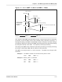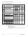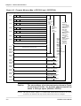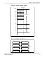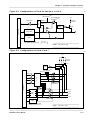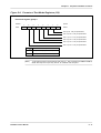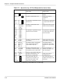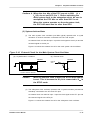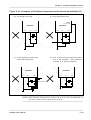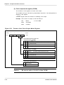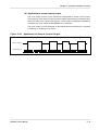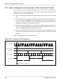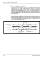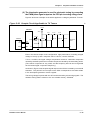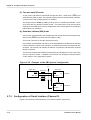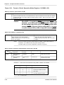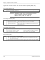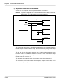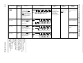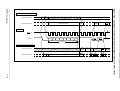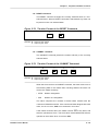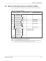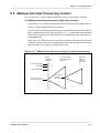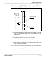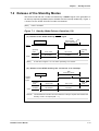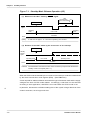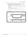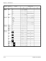
1
USER'S MANUAL µPD75518 4 BIT SINGLE-CHIP MICROCOMPUTER µPD75517 µPD75518 µPD75P518 © NEC Corporation 1990 Document No. IEU-1305E (O. D. No. IEU-743E) Date Published January 1995 P Printed in Japan Cautions on CMOS Devices 1 Countermeasures against static electricity for all MOSs Caution When handling MOS devices, take care so that they are not electrostatically charged. Strong static electricity may cause dielectric breakdown in gates. When transporting or storing MOS devices, use conductive trays, magazine cases, shock absorbers, or metal cases that NEC uses for packaging and shipping. Be sure to ground MOS devices during assembling. Do not allow MOS devices to stand on plastic plates or do not touch pins. Also handle boards on which MOS devices are mounted in the same way. 2 CMOS-specific handling of unused input pins Caution Hold CMOS devices at a fixed input level. Unlike bipolar or NMOS devices, if a CMOS device is operated with no input, an intermediate-level input may be caused by noise. This allows current to flow in the CMOS device, resulting in a malfunction. Use a pull-up or pull-down resistor to hold a fixed input level. Since unused pins may function as output pins at unexpected times, each unused pin should be separately connected to the VDD or GND pin through a resistor. If handling of unused pins is documented, follow the instructions in the document. 3 Statuses of all MOS devices at initialization Caution Theinitial status of a MOS device is unpredictable when power is turned on. Since characteristics of a MOS device are determined by the amount of ions implanted in molecules, the initial status cannot be determined in the manufacture process. NEC has no responsibility for the output statusesofpins,inputandoutputsettings,andthecontentsofregistersatpoweron. However,NECassures operation after reset and items for mode setting if they are defined. When you turn on a device having a reset function, be sure to reset the device first. QTOP is a trademark of NEC Corporation. MS-DOS is a trademark of Microsoft Corporation. PC DOS and PC/AT are trademarks of IBM Corporation. The information in this document is subject to change without notice. No part of this document may be copied or reproduced in any form or by any means without the prior written consent of NEC Corporation. NEC Corporation assumes no responsibility for any errors which may appear in this document. NEC Corporation does not assume any liability for infringement of patents, copyrights or other intellectual property rights of third parties by or arising from use of a device described herein or any other liability arising from use of such device. No license, either express, implied or otherwise, is granted under any patents, copyrights or other intellectual property rights of NEC Corporation or others. The devices listed in this document are not suitable for use in aerospace equipment, submarine cables, nuclear reactor control systems and life support systems. If customers intend to use NEC devices for above applications or they intend to use "Standard" quality grade NEC devices for applications not intended by NEC, please contact our sales people in advance. Application examples recommended by NEC Corporation Standard: Computer, Office equipment, Communication equipment, Test and Measurement equipment, Machine tools, Industrial robots, Audio and Visual equipment, Other consumer products, etc. Special: Automotive and Transportation equipment, Traffic control systems, Antidisaster systems, Anticrime systems, etc. M7 92.6 Major Changes Page Description Preface Documents related to the development tools and other documents have been added. Preface P.1-1 and P.1-8 A caution concerning the reliability of the µPD75P518K has been added. P.1-3 Descriptions of the stack bank selection register (SBS) and stack operation have been added to Section 1.1. P.1-5 Section 1.3 has been added. P.2-9 and P.2-10 Descriptions of the release of the STOP and HALT modes have been added to Sections 2.2.10 and 2.2.11. P.2-12 The descriptions in Section 2.2.20 have been modified. P.2-17 The recommended connections for IC and VPP , listed in Table 2-3, have been modified. P.5-5 Figures 5-3 and 5-4 have been modified. P.5-33 A caution concerning the machine cycle has been added to Table 5-5. P.5-69 Figure 5-38 has been modified. P.5-71 The descriptions and figure in (4) of Section 5.6.4 have been modified. A caution has been added to (4) of Section 5.6.4. P.6-6 The descriptions in (1) of Section 6.3 have been modified. P.6-20 The sample programs given in Section 6.6 have been replaced. P.7-6 Descriptions relating to the use of a crystal have been added to Section 7.2. P.7-7 A caution has been added to Table 7-2. P.7-9 The timing chart in (1) of Section 7.4 has been modified. P.7-12 A caution concerning the switching system clock has been added to (2) of Section 7.4. P.8-3 Table 8-1 has been modified. P.9-7 Section 9.5 has been added. P.A-2 The version of MS-DOS has been upgraded to 5.00A in Appendix A. Therefore, a caution concerning the upgrade has been added. P.C-1 Appendix C has been added. Major changes in this revision are indicated by stars ( ) in the margins. * [MEMO] Preface Readers: This manual is intended for engineers who want to learn the capabilities of the µPD75517, µPD75518, and µPD75P518 to develop application systems based on them. Purpose: The purpose of this manual is to help users understand the hardware capabilities of the µPD75517, µPD75518, and µPD75P518. Guidance: Readers of this manual should have general knowledge of the electronics, logical circuit, and microcomputer fields. To understand the overall functions of the µPD75517, µPD75518, and µPD75P518: -> Read through all chapters sequentially. To check the function of an instruction in detail when the reader knows its mnemonics: -> See the instruction index in Appendix D. To refresh his or her memory of the function of an instruction when the reader does not know its mnemonic but almost understand the function: -> See Section 10.2 to find the mnemonic of the instruction, then see Section 10.4 to confirm its function. To check the electrical characteristics of the µPD75518: -> Refer to the separate data sheet. Unless there is a difference in function between the µPD75517 and µPD75518 or µPD75P518, only the µPD75518 is described in this manual. The user of the µPD75517 or µPD75P518 should read µPD75518 as µPD75517 or µPD75P518. In descriptions common to the one-time PROM product and EPROM product, the term PROM is used to represent both products. The µPD75P518K is not intended for use in mass-produced products; it does not offer a sufficiently high level of reliability for such applications. The use of the µPD75P518K should be restricted to functional evaluation in experimental or trial manufacture. * Notation: Data bit significance : Higher-order bits on the left side Lower-order bits on the right side Active low : xxx (Pin and signal names are overscored.) Memory map address : Low-order address on the upper side High-order address on the lower side (Note) : Explanation of an indicated part of text Caution : Information requesting the user's special attention Remark : Supplementary information Numeric value : Binary: xxxx or xxxxB Decimal: xxxx Hexadecimal: xxxxH Related Documents Documents related to the device Product Document µPD75517 µPD75518 µPD75P518 Data Sheet IC-2672 IC-2706 IC-2839 User’s Manual Application Note This manual Basic IEM-1259 A/D Converter IEA-1236 75X Series Selection Guide IF-1027 Documents related to development tools * Document name Hardware Software Document No. IE-75000-R/IE-75001-R User’s Manual EEU-1416 IE-75000-R-EM User’s Manual EEU-1294 EP-75516GF-R EEU-1315 PG-1500 User’s Manual EEU-1335 RA75X Assembler Package User’s Manual Operation EEU-1346 Language EEU-1343 PG-1500 Controller User’s Manual EEU-1291 Other documents * Document name Document No. Package Manual IEI-1231 SMD Surface Mount Technology Manual IEI-1207 Quality Grades on NEC Semiconductor Devices IEI-1209 Guide to Quality Assurance for Semiconductor Devices IEI-1202 Caution The above documents may be revised without notice. Use the latest versions when designing an application system. [MEMO] Contents Summary of Contents Chapter 1 General ..............................................................................1-1 Chapter 2 Pin Functions ...................................................................2-1 Chapter 3 Data Memory Operations and Memory Map ..............3-1 Chapter 4 Internal CPU Functions ..................................................4-1 Chapter 5 Peripheral Hardware Functions....................................5-1 Chapter 6 Interrupt Function ...........................................................6-1 Chapter 7 Standby Function ............................................................7-1 Chapter 8 Reset Function ................................................................8-1 Chapter 9 Writing to and Verifying Program Memory (PROM) ..........9-1 Chapter 10 Instruction Set ...............................................................10-1 Appendix A Development Tools ............................................................A-1 Appendix B Mask ROM Ordering Procedure ........................................B-1 Appendix C Revision History ................................................................C-1 Appendix D Instruction Index ................................................................D-1 Appendix E Hardware Index ..................................................................E-1 µPD75518 User's Manual TOC - 1 Contents [MEMO] TOC - 2 µPD75518 User's Manual Contents Contents Chapter 1 General ..............................................................................1-1 1.1 Function of the µPD75518 Sub-Series Products............1-3 1.2 Ordering Information ...........................................................1-4 1.3 Differences between the µPD75P518, µPD75517, and µPD75518 .......................................................................1-5 1.4 Block Diagram .......................................................................1-7 1.5 Pin Configuration .................................................................1-8 Chapter 2 Pin Functions ...................................................................2-1 2.1 Pin Functions ........................................................................2-1 2.2 Pin Functions ........................................................................2-6 2.2.1 2.2.2 2.2.3 2.2.4 2.2.5 2.2.6 2.2.7 2.2.8 2.2.9 2.2.10 2.2.11 2.2.12 2.2.13 2.2.14 2.2.15 2.2.16 2.2.17 2.2.18 2.2.19 2.2.20 2.2.21 2.2.22 2.2.23 µPD75518 User's Manual P00-P03 (PORT0), P10-P13 (PORT1), P80-P83 (PORT8), P150-P153 (PORT15) .................................................................2-6 P20-P23 (PORT2), P30-P33 (PORT3), P60-P63 (PORT6), P70-P73 (PORT7), P90-P93 (PORT9), P100-P103 (PORT10), P110-P113 (PORT11) ....................................................................2-7 P40-P43 (PORT4), P50-P53 (PORT5), P120-P123 (PORT12), P130-P133 (PORT13), P140-P143 (PORT14) ...............................2-8 TI0 .................................................................................................2-8 PTO0 .............................................................................................2-8 PCL ...............................................................................................2-8 BUZ ...............................................................................................2-8 SCK0, SO0/SB0, SI0/SB1, SCK1, SO1, SI1 ............................2-9 INT4 ..............................................................................................2-9 INT0, INT1 ....................................................................................2-9 INT2 ............................................................................................2-10 KR0-KR3, KR4-KR7 ..................................................................2-10 PPO .............................................................................................2-10 AN0-AN3, AN4-AN7 ..................................................................2-10 AV REF ................................................................................................................ 2-10 AV SS ................................................................................................................... 2-10 X1, X2 .........................................................................................2-11 XT1, XT2 ....................................................................................2-11 RESET ........................................................................................2-11 IC .................................................................................................2-12 MD0-MD3 (for µPD75P518 only) .............................................2-12 V PP (for µPD75P518 only) ........................................................2-12 V DD ..................................................................................................................... 2-12 TOC - 3 * Contents 2.2.24 V SS ...................................................................................................................... 2-12 2.3 Pin Input/Output Circuits ..................................................2-13 2.4 Connection of Unused Pins .............................................2-16 2.5 Selection of a Mask Option ..............................................2-17 Chapter 3 Data Memory Operations and Memory Map ..............3-1 3.1 Data Memory Bank Structure and Addressing Modes......3-2 3.1.1 3.1.2 Data Memory Bank Structure .....................................................3-2 Data Memory Addressing Modes ...............................................3-4 3.2 General Register Bank Configuration ............................3-17 3.3 Memory-mapped I/O ...........................................................3-22 Chapter 4 Internal CPU Functions ..................................................4-1 4.1 Program Counter (PC) .........................................................4-1 4.2 Program Memory (ROM)......................................................4-2 4.3 Data Memory (RAM) .............................................................4-5 4.3.1 4.3.2 Data Memory Configuration ........................................................4-5 Specification of a Data Memory Bank .......................................4-7 4.4 General Register ...................................................................4-8 4.5 Accumulator ........................................................................4-10 4.6 Stack Pointer (SP) and Stack Bank Select Register (SBS) ....................................................................4-11 4.7 Program Status Word (PSW)............................................4-14 4.8 Bank Select Register (BS) ................................................4-18 Chapter 5 Peripheral Hardware Functions....................................5-1 5.1 Digital I/O Ports ....................................................................5-1 5.1.1 5.1.2 5.1.3 5.1.4 5.1.5 5.1.6 5.2 Clock Generator..................................................................5-21 5.2.1 5.2.2 5.2.3 5.2.4 5.3 Clock Generator Configuration .................................................5-22 Functions and Operations of the Clock Generator ................5-23 System Clock and CPU Clock Setting ....................................5-32 Clock Output Circuit ..................................................................5-35 Basic Interval Timer...........................................................5-38 5.3.1 5.3.2 5.3.3 5.3.4 TOC - 4 Types, Features, and Configurations of Digital I/O Ports .......5-2 I/O Mode Setting ..........................................................................5-9 Digital I/O Port Manipulation Instructions ...............................5-12 Digital I/O Port Operation .........................................................5-15 Specification of Internal Pull-Up/Pull-Down Resistors ...........5-17 I/O Timing of Digital I/O Ports ..................................................5-20 Configuration of the Basic Interval Timer ...............................5-38 Basic Interval Timer Mode Register (BTM) ............................5-39 Operation of the Basic Interval Timer .....................................5-41 Application Examples of the Basic Interval Timer .................5-42 µPD75518 User's Manual Contents 5.4 Clock Timer .........................................................................5-44 5.4.1 5.4.2 5.5 Timer/Event Counter ..........................................................5-46 5.5.1 5.5.2 5.5.3 5.5.4 5.5.5 5.5.6 5.5.7 5.5.8 5.6 Functions of the Timer/Pulse Generator .................................5-60 Timer/Pulse Generator Mode Register (TPGM) .....................5-61 Configuration and Operation of the Timer/Pulse Generator ...5-62 Application of the Timer/Pulse Generator ...............................5-68 Serial Interface (Channel 0) .............................................5-73 5.7.1 5.7.2 5.7.3 5.7.4 5.7.5 5.7.6 µPD75518 User's Manual Configuration of the Timer/Event Counter ..............................5-46 Basic Configuration and Operation of the Timer/Event Counter .......................................................................................5-48 Timer/Event Counter Mode Register (TM0) ............................5-49 Timer/Event Counter Output Enable Flag (TOE0) .................5-51 Operation Mode of the Timer/Event Counter..........................5-51 Time Setting in the Timer/Event Counter ...............................5-53 Notes on Timer/Event Counter Applications ........................... 5-55 Applications of the Timer/Event Counter ................................5-59 Timer/Pulse Generator ......................................................5-60 5.6.1 5.6.2 5.6.3 5.6.4 5.7 Configuration of the Clock Timer .............................................5-44 Watch Mode Register ................................................................5-45 Serial Interface (Channel 0) Functions ...................................5-73 (1) Operation halt mode ..........................................................5-73 (2) Three-wire serial I/O mode ...............................................5-73 (3) Two-wire serial I/O mode ..................................................5-74 (4) Serial bus interface (SBI) mode .......................................5-74 Configuration of Serial Interface (Channel 0) .........................5-74 (1) Serial operation mode register 0 (CSIM0) ...................... 5-76 (2) Serial bus interface control register (SBIC) .................... 5-76 (3) Shift register 0 (SIO0) .......................................................5-76 (4) SO0 latch ............................................................................5-76 (5) Serial clock selector ..........................................................5-76 (6) Serial clock counter ...........................................................5-76 (7) Slave address register (SVA) and address comparator ...5-76 (8) INTCSI0 control circuit ......................................................5-77 (9) Serial clock control circuit .................................................5-77 (10) Busy/acknowledge output circuit and bus release/ command/acknowledge detection circuit.........................5-77 (11) P01 output latch .................................................................5-77 Register Functions .....................................................................5-78 (1) Serial operation mode register 0 (CSIM0) ...................... 5-78 (2) Serial bus interface control register (SBIC).................... 5-82 (3) Shift register 0 (SIO0) .......................................................5-85 (4) Slave address register (SVA) ...........................................5-87 Operation Halt Mode .................................................................5-88 Three-Wire Serial I/O Mode Operations.................................. 5-90 (1) Register setting ..................................................................5-90 (2) Communication operation .................................................5-93 (3) Serial clock selection ........................................................5-94 (4) Signals ................................................................................5-94 (5) Switching between MSB and LSB as the first transfer bit ..........................................................................5-95 (6) Transfer start ......................................................................5-96 (7) Application of the three-wire serial I/O mode .................5-97 Two-Wire Serial I/O Mode ......................................................5-100 (1) Register setting ................................................................5-100 TOC - 5 Contents 5.7.7 5.7.8 5.8 Serial Interface (Channel 1) ...........................................5-145 5.8.1 5.8.2 5.8.3 5.8.4 5.8.5 5.8.6 5.9 Serial Interface (Channel 1) Functions .................................5-145 (1) Operation halt mode ........................................................5-145 (2) Three-wire serial I/O mode .............................................5-145 Serial Interface (Channel 1) Configuration ........................... 5-145 Register Functions ..................................................................5-147 (1) Serial operation mode register 1 (CSIM1) .................... 5-147 (2) Shift register 1 (SIO1) .....................................................5-148 Operation Halt Mode ...............................................................5-148 Three-Wire Serial I/O Mode Operations ...............................5-149 Application of the Serial Interface (Channel 1) .................... 5-151 A/D Converter ...................................................................5-152 5.9.1 5.9.2 5.9.3 5.9.4 5.9.5 5.10 (2) Communication operation ...............................................5-103 (3) Serial clock selection ......................................................5-104 (4) Signals ..............................................................................5-104 (5) Transfer start ...................................................................5-105 (6) Error detection .................................................................5-105 (7) Application of two-wire serial I/O mode ........................5-106 SBI Mode Operation ................................................................5-107 (1) SBI functions ....................................................................5-109 (2) SBI definition ....................................................................5-110 (3) Register setting ................................................................5-116 (4) Serial clock selection ......................................................5-120 (5) Signals ..............................................................................5-121 (6) Pin configuration ..............................................................5-127 (7) Address match detection method .................................. 5-128 (8) Error detection .................................................................5-128 (9) Communication operation ...............................................5-129 (10) Transfer start ...................................................................5-134 (11) Notes on the SBI mode ..................................................5-135 (12) SBI mode ..........................................................................5-136 Manipulation of SCK0 Pin Output ..........................................5-143 Configuration of the A/D Converter .......................................5-152 A/D Converter Operation ........................................................5-156 Notes on the Standby Mode ...................................................5-159 Other Notes on Use ................................................................5-160 Application of A/D Converter ..................................................5-161 Bit Sequential Buffer .......................................................5-162 5.10.1 Applications of the Bit Sequential Buffer ..............................5-163 Chapter 6 Interrupt Function ...........................................................6-1 TOC - 6 6.1 Configuration of the Interrupt Control Circuit ...............6-1 6.2 Types of Interrupt Sources and Vector Tables ..............6-3 6.3 Various Devices of the Interrupt Control Circuit ...........6-5 6.4 Interrupt Sequence ............................................................6-16 6.5 Multiple Interrupt Processing Control ...........................6-17 6.6 Processing of Interrupts Sharing a Vector Address ....6-19 6.7 Machine Cycles for Starting Interrupt Processing ......6-21 6.8 Effective Use of Interrupts ...............................................6-23 µPD75518 User's Manual Contents 6.9 Interrupt Applications........................................................6-23 Chapter 7 Standby Function ............................................................7-1 7.1 Setting of Standby Modes and Operation Status ..........7-3 7.2 Release of the Standby Modes ..........................................7-5 7.3 Operation after a Standby Mode Is Released .................7-8 7.4 Applications of the Standby Modes .................................7-8 Chapter 8 Reset Function ................................................................8-1 Chapter 9 Writing to and Verifying Program Memory (PROM) ..........9-1 9.1 Operating Modes when Writing to and Verifying the Program Memory ...........................................................9-3 9.2 Writing to the Program Memory ........................................9-4 9.3 Reading the Program Memory ...........................................9-6 9.4 Erasing the Program Memory (for the µPD75P518K Only).................................................9-7 9.5 Screening One-Time PROM Products ..............................9-7 Chapter 10 Instruction Set ..................................................................10-1 10.1 Unique Instructions ...........................................................10-2 10.1.1 10.1.2 10.1.3 10.1.4 10.1.5 GETI Instruction .........................................................................10-2 Bit Manipulation Instructions ....................................................10-4 String Effect Instructions ...........................................................10-5 Number System Conversion Instructions ................................10-6 Skip Instructions and the Number of Machine Cycles Required for a Skip ...................................................................10-7 10.2 Instruction Set and Operation .........................................10-8 10.3 Instruction Codes of Each Instruction ........................10-18 10.4 Functions and Applications of the Instructions ........10-24 10.4.1 10.4.2 10.4.3 10.4.4 10.4.5 10.4.6 10.4.7 10.4.8 10.4.9 10.4.10 10.4.11 10.4.12 10.4.13 10.4.14 10.4.15 µPD75518 User's Manual Transfer Instructions ...............................................................10-24 Table Reference Instructions .................................................10-29 Bit Transfer Instructions ..........................................................10-33 Arithmetic/Logical Instructions ...............................................10-34 Accumulator Manipulation Instructions .................................. 10-39 Increment/Decrement Instructions .........................................10-39 Compare Instructions ..............................................................10-40 Carry Flag Manipulation Instructions .....................................10-41 Memory Bit Manipulation Instructions ...................................10-42 Branch Instructions ..................................................................10-44 Subroutine Stack Control Instructions ...................................10-48 Interrupt Control Instructions ..................................................10-51 I/O Instructions ........................................................................10-51 CPU Control Instructions ........................................................10-53 Special Instructions .................................................................10-53 TOC - 7 * Contents Appendix A Development Tools ............................................................A-1 Appendix B Masked ROM Ordering Procedure ....................................B-1 * Appendix C Revision History ................................................................C-1 Appendix D Instruction Index ................................................................D-1 D.1 Instruction Index (By Function) ........................................D-1 D.2 Instruction Index (Alphabetical Order) ............................D-4 Appendix E Hardware Index ..................................................................E-1 TOC - 8 E.1 Hardware Index (Alphabetical Order with Respect to the Hardware Name) ............................................................E-1 E.2 Hardware Index (Alphabetical Order with Respect to the Hardware Symbol).........................................................E-3 µPD75518 User's Manual Contents List of Figures (1/4) Figure 2-1. Pin Input/Output Circuits .......................................................................................2-13 Figure 3-1. Figure 3-2. Figure Figure Figure Figure Figure 3-3. 3-4. 3-5. 3-6. 3-7. Use of MBE = 0 Mode and MBE = 1 Mode ..........................................................3-3 Data Memory Organization and Addressing Range of Each Addressing Mode ............................................................................................3-4 Updating Static RAM Addresses ..........................................................................3-11 Example of Register Bank Selection ....................................................................3-18 General Register Configuration (4-bit Processing) .............................................3-20 General Register Configuration (8-bit Processing) .............................................3-21 µPD75518 I/O Map ................................................................................................3-24 Figure Figure Figure Figure Figure Figure Figure Figure Figure Figure Figure Figure 4-1. 4-2. 4-3. 4-4. 4-5. 4-6. 4-7. 4-8. 4-9. 4-10. 4-11. 4-12. Program Counter Format .........................................................................................4-1 Program Memory Map (µPD75517) .......................................................................4-3 Program Memory Map (µPD75518 and µPD75P518) ..........................................4-4 Data Memory Map ....................................................................................................4-5 General Register Format .........................................................................................4-9 Register Pair Format ................................................................................................4-9 Accumulator ............................................................................................................4-10 Format of Stack Pointer and Stack Bank Select Register .................................4-12 Data Saved to Stack Memory ...............................................................................4-13 Data Restored from Stack Memory ......................................................................4-13 Program Status Word Format ...............................................................................4-14 Bank Select Register Format ................................................................................4-18 Figure Figure Figure Figure Figure Figure Figure Figure Figure Figure 5-1. 5-2. 5-3. 5-4. 5-5. 5-6. 5-7. 5-8. 5-9. 5-10. Data Memory Address Assigned to Digital I/O Ports ...........................................5-1 Configurations of Ports 0, 1, and 8 ........................................................................5-4 Configurations of Ports 3n and 6n (n = 0 to 3).....................................................5-5 Configurations of Ports 2 and 7..............................................................................5-5 Configurations of Ports 4, 5, 12, 13, and 14 .........................................................5-6 Configuration of Port 9 ............................................................................................5-7 Configurations of Ports 10 and 11 .........................................................................5-8 Configuration of Port 15 ..........................................................................................5-8 Formats of Port Mode Registers ..........................................................................5-10 Format of the Pull-up Resistor Register ..............................................................5-18 µPD75518 User's Manual TOC - 9 Contents (2/4) Figure Figure Figure Figure Figure Figure Figure Figure Figure Figure Figure Figure Figure Figure Figure Figure Figure Figure Figure Figure Figure Figure Figure Figure Figure Figure 5-11. 5-12. 5-13. 5-14. 5-15. 5-16. 5-17. 5-18. 5-19. 5-20. 5-21. 5-22. 5-23. 5-24. 5-25. 5-26. 5-27. 5-28. 5-29. 5-30. 5-31. 5-32. 5-33. 5-34. 5-35. 5-36. Figure Figure Figure Figure Figure Figure Figure Figure Figure Figure Figure Figure Figure Figure Figure Figure Figure 5-37. 5-38. 5-39. 5-40. 5-41. 5-42. 5-43. 5-44. 5-45. 5-46. 5-47. 5-48. 5-49. 5-50. 5-51. 5-52. 5-53. TOC - 10 ON Timing of Pull-up Resistors by Software ......................................................5-18 I/O Timing of Digital I/O Ports ..............................................................................5-20 Block Diagram of the Clock Generator ................................................................5-22 Format of the Processor Clock Control Register ................................................5-25 Format of the System Clock Control Register ....................................................5-26 External Circuit for the Main System Clock Oscillator .......................................5-27 External Circuit for the Subsystem Clock Oscillator...........................................5-28 Examples of Oscillator Connections which should be Avoided ........................5-29 Changing the System Clock and CPU Clock ......................................................5-34 Configuration of the Clock Output Circuit ............................................................5-35 Format of the Clock Output Mode Register ........................................................5-36 Application to Remote Control Output .................................................................5-37 Configuration of the Basic Interval Timer ............................................................5-38 Format of the Basic Interval Timer Mode Register ............................................5-40 Block Diagram of the Clock Timer .......................................................................5-44 Format of the Watch Mode Register ....................................................................5-45 Block Diagram of the Timer/Event Counter .........................................................5-47 Timing of Count Operation ....................................................................................5-48 Format of the Timer/Event Counter Mode Register ...........................................5-50 Format of the Timer/Event Counter Output Enable Flag ...................................5-51 Operation in the Count Operation Mode .............................................................5-52 Error at the Start of the Timer ..............................................................................5-55 Format of Timer/Pulse Generator Mode Register ..............................................5-61 Block Diagram of the Timer/Pulse Generator (Timer Mode) .............................5-62 Timer Mode Operation Timing ..............................................................................5-63 Block Diagram of the Timer/Pulse Generator (PWM Pulse Generation Mode) ............................................................................5-67 Sample Configuration of D/A Conversion Using µPD75518 ..............................5-67 Sample Circuit Applicable to TV Tuners..............................................................5-69 Example of the SBI System Configuration ..........................................................5-74 Block Diagram of the Serial Interface (Channel 0).............................................5-75 Format of Serial Operation Mode Register 0 (CSIM0) .......................................5-78 Format of Serial Bus Interface Control Register (SBIC) ....................................5-82 Peripheral Hardware of Shift Register 0 ..............................................................5-86 Example of Three-Wire Serial I/O System Configuration ..................................5-90 Timing of Three-Wire Serial I/O Mode .................................................................5-93 Operations of RELT and CMDT............................................................................5-94 Transfer Bit Switching Circuit ...............................................................................5-95 Example of Two-Wire Serial I/O System Configuration ...................................5-100 Timing of Two-Wire Serial I/O Mode .................................................................5-103 Operations of RELT and CMDT .........................................................................5-104 Example of SBI System Configuration...............................................................5-108 Timing of SBI Transfer ........................................................................................5-110 Bus Release Signal .............................................................................................5-111 µPD75518 User's Manual Contents (3/4) Figure Figure Figure Figure Figure Figure Figure Figure Figure Figure Figure Figure Figure Figure Figure 5-54. 5-55. 5-56. 5-57. 5-58. 5-59. 5-60. 5-61. 5-62. 5-63. 5-64. 5-65. 5-66. 5-67. 5-68. Figure Figure Figure Figure Figure Figure Figure Figure Figure Figure Figure Figure Figure Figure Figure Figure Figure Figure Figure Figure 5-69. 5-70. 5-71. 5-72. 5-73. 5-74. 5-75. 5-76. 5-77. 5-78. 5-79. 5-80. 5-81. 5-82. 5-83. 5-84. 5-85. 5-86. 5-87. 5-88. Figure Figure Figure Figure Figure Figure 5-89. 5-90. 5-91. 5-92. 5-93. 5-94. Command Signal ..................................................................................................5-111 Address .................................................................................................................5-112 Slave Selection Using an Address .....................................................................5-112 Command ..............................................................................................................5-113 Data .......................................................................................................................5-113 Acknowledge Signal .............................................................................................5-114 Busy and Ready Signals .....................................................................................5-115 Operations of RELT, CMDT, RELD, and CMDD (Master) ...............................5-121 Operations of RELT, CMDT, RELD, and CMDD (Slave) .................................5-121 Operation of ACKT ...............................................................................................5-122 Operation of ACKE ..............................................................................................5-123 Operation of ACKD ..............................................................................................5-124 Operation of BSYE ...............................................................................................5-124 Pin Configuration ..................................................................................................5-127 Address Transfer Operation from Master Device to Slave Device (WUP = 1) .............................................................................................................5-130 Command Transfer Operation from Master Device to Slave Device .............5-131 Data Transfer Operation from Master Device to Slave Device .......................5-132 Data Transfer Operation from Slave Device to Master Device .......................5-133 Example of Serial Bus Configuration .................................................................5-136 Transfer Format of the READ Command ..........................................................5-138 Transfer Format of the WRITE and END Commands ......................................5-139 Transfer Format of the STOP Command ..........................................................5-139 Transfer Format of the STATUS Command ......................................................5-140 Status Format of the STATUS Command .........................................................5-140 Transfer Format of the RESET Command ........................................................5-141 Transfer Format of the CHGMST Command ....................................................5-141 Master and Slave Operation in Case of Error ..................................................5-142 SCK0/P01 Pin Circuit Configuration ..................................................................5-143 Block Diagram of the Serial Interface (Channel 1) ..........................................5-146 Format of Serial Operation Mode Register 1 (CSIM1) ....................................5-147 Timing of the Three-wire Serial I/O Mode .........................................................5-149 Block Diagram of the A/D Converter .................................................................5-152 Format of the A/D Conversion Mode Register ..................................................5-154 Timing Chart of A/D Conversion ........................................................................5-157 Relationship (Ideal) between Analog Input Voltages and Results of A/D Conversion ..................................................................................5-158 Reducing Power Consumption in the Standby Mode .......................................5-159 Analog Input Pin Connection ..............................................................................5-160 Format of the Bit Sequential Buffer ...................................................................5-162 Serial Transfer Format (I) ...................................................................................5-164 Serial Transfer Format (II) ..................................................................................5-165 Bus Configuration Example .................................................................................5-165 µPD75518 User's Manual TOC - 11 Contents (4/4) Figure Figure Figure Figure Figure Figure Figure Figure Figure Figure 6-1. 6-2. 6-3. 6-4. 6-5. 6-6. 6-7. 6-8. 6-9. 6-10. Block Diagram of Interrupt Control Circuit ............................................................6-2 Interrupt Vector Table ..............................................................................................6-4 Configurations of the INT0, INT1, and INT4 Circuits ...........................................6-8 I/O Timing of a Noise Eliminator ............................................................................6-9 Format of Edge Detection Mode Registers .........................................................6-10 Configuration of the INT2 and KR0 to KR7 Circuits ..........................................6-12 Interrupt Priority Specification Register ...............................................................6-14 Interrupt Processing Sequence ............................................................................6-16 Multiple Interrupt Processing by a High-order Interrupt .....................................6-17 Multiple Interrupt Processing by Changing the Interrupt Status Flags .............6-18 Figure 7-1. Standby Mode Release Operation .........................................................................7-5 Figure 8-1. Reset Operation by a RESET signal ......................................................................8-1 TOC - 12 µPD75518 User's Manual Contents List of Tables (1/2) Table 1-1. Differences between the µPD75P518, µPD75517, and µPD75518 .................... 1-5 Table Table Table Table Table 2-1. 2-2. 2-3. 2-4. 2-5. Digital I/O Port Pins .................................................................................................2-1 Non-port Pin Functions ............................................................................................2-4 Recommended Connection of Unused Pins ........................................................2-16 Selection of Pull-up and Pull-down Resistors .....................................................2-17 Selection of Feedback Resistors ..........................................................................2-17 Table 3-1. Table 3-2. Table 3-3. Table 3-4. Addressing Modes ....................................................................................................3-5 Register Bank to Be Selected with the RBE and RBS ......................................3-17 Recommended Use of Register Banks with Normal Routines and Interrupt Routines ...........................................................................................3-17 Addressing Modes Applicable to Peripheral Hardware Operation .................... 3-22 Table Table Table Table Table 4-1. 4-2. 4-3. 4-4. 4-5. Stack Area to Be Selected by the Stack Bank Select Register ........................4-11 PSW Flags Saved/Restored in Stack Operation ................................................4-14 Carry Flag Manipulation Instructions ...................................................................4-15 Information Indicated by the Interrupt Status Flag .............................................4-16 Register Bank to Be Selected with the RBE and RBS ......................................4-19 Table Table Table Table Table Table Table Table Table Table Table Table Table Table 5-1. 5-2. 5-3. 5-4. 5-5. 5-6. 5-7. 5-8. 5-9. 5-10. 5-11. 5-12. 5-13. 5-14. Types and Features of Digital I/O Ports ................................................................5-2 I/O Pin Manipulation Instructions .........................................................................5-14 Operations by I/O Port Manipulation Instructions ...............................................5-16 Specification of Internal Pull-Up/Pull-Down Resistors .......................................5-17 Maximum Time Required to Change the System Clock and CPU Clock .........5-32 Resolution and Maximum Set Time .....................................................................5-54 Modulo Register Settings ......................................................................................5-64 Basic and Secondary Periods ...............................................................................5-65 Generation of Notes Using the Timer/Pulse Generator .....................................5-70 Differences between Channel 0 and Channel 1 .................................................5-73 Serial Clock Selection and Application (In the Three-Wire Serial I/O Mode) ....5-94 Serial Clock Selection and Application (In the Two-Wire Serial I/O Mode) .....5-104 Serial Clock Selection and Application (In the SBI Mode) ..............................5-120 Various Signals Used in the SBI Mode .............................................................5-125 µPD75518 User's Manual TOC - 13 * Contents (2/2) Table 5-15. Table 5-16. Serial Clock Selection and Application ..............................................................5-150 Setting of SCC and PCC .....................................................................................5-157 Table Table Table Table 6-1. 6-2. 6-3. 6-4. Interrupt Sources ......................................................................................................6-3 Set Signals for Interrupt Request Flags ................................................................6-6 Interrupt Processing Statuses of IST0 and IST1 ................................................6-15 Determination of an Interrupt Source...................................................................6-19 Table 7-1. Table 7-2. Operation Statuses in the Standby Mode ..............................................................7-3 Selection of a Wait Time with BTM ........................................................................7-7 Table 8-1. Statuses of the Hardware after a Reset ................................................................8-2 Table 9-1. Table 9-2. Pin Functions ............................................................................................................9-1 Operating Modes ......................................................................................................9-3 TOC - 14 µPD75518 User's Manual Chapter 1 General Chapter 1 General The µPD75517, µPD75518, and µPD75P518 are 4-bit single-chip microcomputers. Their features include high-speed operations, a large number of I/O lines, and a variety of capabilities based on the 75X series architecture. The µPD75517 and µPD75518 outperform their predecessor µPD75516 by increasing the ROM and RAM capacities of the µPD75516 and speeding up the instruction execution. The µPD75P518 uses one-time PROM or EPROM, instead of built-in mask ROM which is used in the µPD75518, for increased ROM capacity. The one-time PROM version allows the user to write programs once. It can be used for small quantities of multiple products. It is also useful to shorten product development time. The EPROM version allows the user to write, erase, and rewrite programs. It is best suited for system evaluation. The µPD75517, µPD75518, and µPD75P518 have the following features. The µPD75P518K is not intended for use in mass-produced products; it does not offer a sufficiently high level of reliability for such applications. The use of the µPD75P518K should be restricted to functional evaluation in experimental or trial manufacture. • Function for specifying the instruction execution time (useful for high-speed operation and power saving) • Built-in A/D converter operable on low voltage • Eight channels with 8-bit resolution (Successive approximation system) • VDD = 2.7 to 6.0 V • Sixty-four I/O lines • Two built-in 8-bit serial interfaces • Built-in NEC serial bus interface (SBI) • The µPD75P518 can operate on the same supply voltage as the µPD75517 which uses mask ROM. • VDD = 2.7 to 6.0 V µPD75518 User's Manual 1-1 * Chapter 1 General The µPD75517, µPD75518, and µPD75P518 provide features suitable for control, and therefore can be used for various applications as listed below: • VCR (system control) • Audio equipment (such as CD players) • Push-button telephone • Radio equipment • Data terminal • PPC • Air conditioner 1-2 µPD75518 User's Manual Chapter 1 General 1.1 Function of the µPD75518 Sub-Series Products Product Item µPD75517 µPD75518 µPD75P518 µPD75516 µPD75P516 24448 32640 32640 (PROM) 16256 16256 (PROM) ROM (in bytes) RAM (x 4 bits) 1024 512 General registers (4 bits x 8 or 8 bits x 4) x 4 banks Instruction Main system clock 0.67 µs, 1.33 µs, 2.67 µs, or 10.7 µs (when operating at 6.0 MHz) 0.95 µs, 1.91 µs, 3.82 µs, or 15.3 µs (when operating at 4.19 MHz) Subsystem clock 122 µs (When operating at 32.768 kHz) I/O lines(Note 1) Total 0.95 µs, 1.91 µs, or 15.3 µs (when operating at 4.19 MHz) 64 Number of CMOS input lines 16 (Shared with INT, SIO, PPO, and analog input. Seven lines can be pulled up by software.) Number of CMOS I/O lines 28 (Four lines for LED driving) • 16 lines can be pulled up by software. • Four lines can be pulled down by mask option. Number of N-ch open-drain I/O lines 20 (Eight lines for LED driving. Withstand voltage is 10 V. 20 lines can be pulled up by mask option.) A/D converter 20 (Eight lines for LED driving. Withstand voltage is 9 V. 20 lines can be pulled up by mask option.) • 8 channels with 8-bit resolution (Successive approximation system) Operating voltage VDD = 2.7 to 6.0 V VDD = 3.5 to 6.0 V Timer/counter 4 channels • Timer/event counter • Basic interval timer • Timer/pulse generator (14-bit PWM output enabled) • Clock timer Serial interface 2 channels • NEC standard serial bus interface (SBI)/three-wire SIO: One channel • General synchronous serial interface (three-wire SIO): One channel Stack bank selection register (SBS) Provided Not provided Stack operation 3-byte stack 2-byte stack Vectored interrupt External: 3, internal: 4 Test input External: 1, internal: 1 • Clock test flag provided • Parallel edge detection flag for key scan input provided Instruction set The following instructions the 75X high-end model: • MOVT XA, @BCDE • MOVT XA, @BCXA • BRA !addr1 are added to * * 75X high-end • BR !BCDE • BR !BCXA • CALLA !addr1 Operating power voltage VDD = 2.7 to 6.0 V Package • 80-pin plastic QFP (14 x 20 mm) • 80-pin ceramic WQFN(Note 2) VDD = 4.75 to 5.5 V (Note 1) No mask option is provided for the µPD75P516 or µPD75P518. (Note 2) For the µPD75P516 and µPD75P518 only µPD75518 User's Manual 1-3 Chapter 1 General 1.2 Ordering Information (1) Ordering information Part number Package On-chip ROM µPD75517GF-xxx-3B9 80-pin plastic QFP (14 x 20 mm) Mask ROM µPD75518GF-xxx-3B9 80-pin plastic QFP (14 x 20 mm) Mask ROM µPD75P518GF-3B9 80-pin plastic QFP (14 x 20 mm) One-time PROM µPD75P518K 80-pin ceramic WQFN EPROM Remark xxx is a ROM code number. (2) Quality grade Part number Package Quality grade µPD75517GF-xxx-3B9 80-pin plastic QFP (14 x 20 mm) Standard µPD75518GF-xxx-3B9 80-pin plastic QFP (14 x 20 mm) Standard µPD75P518GF-3B9 80-pin plastic QFP (14 x 20 mm) Standard µPD75P518K 80-pin ceramic WQFN Not applied Remark xxx is a ROM code number. Caution The Quality grade of the µPD75P518K is “Not applied.” Use the µPD75P518K only for functional evaluation. Please refer to "Quality grade on NEC Semiconductor Devices" (Document number IEI1209) published by NEC Corporation to know the specification of quality grade on the devices and its recommended applications. 1-4 µPD75518 User's Manual * Chapter 1 General * 1.3 Differences between the µPD75P518, µPD75517, and µPD75518 The µPD75P518 differs from the µPD75518 in that it uses one-time PROM or EPROM instead of masked ROM. Table 1-1 lists the differences between the µPD75P518, µPD75517, and µPD75518. Always check these differences when intending to mass-produce an application system based on a masked ROM type after completing development using a PROM-based type. Table 1-1. Differences between the µ PD75P518, µ PD75517, and µ PD75518 Item Program memory µPD75517 µPD75518 µPD75P518 24448 x 8 bits Masked ROM 32640 x 8 bits Masked ROM 32640 x 8 bits One-time PROM, EPROM Data memory 1024 x 4 bits Pull-up resistors for ports 4 and 5 Mask option None Pull-up resistors for ports 12 to 14 Pull-down resistor for port 9 Feedback resistor for subsystem clock Pin function Incorporated Pin 4 VDD VPP Pins 38 to 41 P33-P30 P33/MD3-P30/MD0 Electrical characteristics The current drain and several other specifications are different for each product. For details, refer to the corresponding items in each data sheet. Operating voltage range VDD = 2.7 to 6.0 V Operating temperature range –40 ˚C to +85 ˚C Package 80-pin plastic QFP (14 x 20 mm) Others Since each product has a different circuit scale and mask layout, the noise immunity and noise radiation characteristics of each product are different. µPD75518 User's Manual 80-pin plastic QFP (14 x 20 mm) 80-pin ceramic WQFN 1-5 Chapter 1 General Caution 1-6 The PROM and masked ROM products have different noise immunity and noise radiation characteristics. Do not use ES products for evaluation when considering switching from PROM-based products to those using masked ROM upon the transition from preproduction to mass-production. CS products (masked ROM products) should be used in this case. µPD75518 User's Manual 4 P00 - P03 Port 1 4 P10 - P13 TI0/P13 PTO0/P20 Port 2 4 P20 - P23 Port 3 4 P30 - P33 (P30 - P33/ MD0 - MD3)(Note 2) Port 4 4 P40 - P43 Port 5 4 P50 - P53 Port 6 4 P60 - P63 Port 7 4 P70 - P73 Port 8 4 P80 - P83 Port 9 4 P90 - P93 Port 10 4 P100 - P103 INTCSI Port 11 4 P110 - P113 Serial interface 1 Port 12 4 P120 - P123 Port 13 4 P130 - P133 Port 14 4 P140 - P143 Port 15 4 P150 - P153 Timer/event counter #0 CY ALU Program counter (15) SP(8) SBS(2) INTT0 Bank BUZ/P23 Watch timer INTW General register PPO/P80 Timer/pulse generator INTTPG SI0/SB1/P03 SO0/SB0/P02 SCK0/P01 SI1/P83 SO1/P82 SCK1/P81 ROM(Note 1) program memory INT2/P12 fX /2N Interrupt control INT4/P00 Clock output control A/D converter PCL/P22 Stand by control CPU clock Φ Main XT1 XT2 X1 X2 RESET (VPP)(Note 2) VDD VSS Chapter 1 Bit sequential buffer (16) 1-7 General AVREF AVSS Clock divider Clock generator Sub KR0/P60 - KR7/P73 AN0 - AN3 AN4/P150 - AN7/P153 RAM data memory 1024 x 4 bits Serial interface 0 INT0/P10 INT1/P11 Decode and control 1.4 Block Diagram Port 0 INTBT (Note 1) The type of ROM is model-dependent. (Note 2) Pin names in parentheses apply to the µPD75P518. µPD75518 User's Manual Basic interval timer Chapter 1 General P133 P132 P131 P130 P123 P122 P121 P120 AVSS AN7/P153 AN6/P152 AN5/P151 AN4/P150 AN3 1 80 79 78 77 76 75 74 73 72 71 70 69 68 67 66 65 64 P140 AVREF 2 63 P141 VDD (Note 1) VDD (VPP) 3 62 P142 4 61 P143 P113 5 60 RESET P112 6 59 X2 P111 7 58 X1 P110 8 57 IC P103 9 56 XT2 P102 10 55 XT1 P101 11 P100 12 P93 13 P92 14 P91 15 µ PD75517GF-xxx-3B9 µ PD75518GF-xxx-3B9 µ PD75P518GF-3B9 µ PD75P518K AN0 54 VSS 53 P00/INT4 52 P01/SCK0 51 P02/SO0/SB0 50 P03/SI0/SB1 21 44 P21 KR6/P72 22 43 P22/PCL KR5/P71 23 42 P23/BUZ KR4/P70 24 41 25 26 27 28 29 30 31 32 33 34 35 36 37 38 39 40 P30 (P30/MD0)(Note 1) P31 (P31/MD1)(Note 1) P32 (P32/MD2)(Note 1) KR7/P73 P40 P20/PTO0 P33 (P33/MD3)(Note 1) P13/ TI0 45 P41 46 20 P42 19 PPO/P80 VSS SCK1/P81 P43 P12/INT2 P50 47 P51 18 P52 P11/INT1 SO1/P82 P53 P10/INT0 48 KR0/P60 49 17 KR1/P61 16 KR2/P62 P90 SI1/P83 KR3/P63 (Note 2) AN2 AN1 1.5 Pin Configuration IC: Internally connected (Connect to VSS, keeping the wiring as short as possible.) (Note 1) The pin name in parentheses applies to the µPD75P518. (Note 2) Be sure to supply power to both VDD pins. The µPD75P518K is not intended for use in mass-produced products; it does not offer a sufficiently high level of reliability for such applications. The use of the µPD75P518K should be restricted to functional evaluation in experimental or trial manufacture. 1-8 µPD75518 User's Manual * Chapter 1 General Pin name P00-P03 : Port 0 PCL : Clock output P10-P13 : Port 1 BUZ : Fixed frequency output P20-P23 : Port 2 SCK0, SCK1 : Serial clock I/O P30-P33 : Port 3 SO0, SO1 : Serial output P40-P43 : Port 4 SI0, SI1 : Serial input P50-P53 : Port 5 SB0, SB1 : Serial bus I/O P60-P63 : Port 6 INT4 : External vectored interrupt P70-P73 : Port 7 INT0, INT1 : External vectored interrupt P80-P83 : Port 8 INT2 : External test input P90-P93 : Port 9 KR0-KR7 : Key interrupt input P100-P103 : Port 10 PPO : Pulse output P110-P113 : Port 11 AN0-AN7 : Analog input P120-P123 : Port 12 AVREF : Reference voltage for analog signals P130-P133 : Port 13 AVSS : Ground for analog signals P140-P143 : Port 14 X1, X2 : Main system clock oscillation P150-P153 : Port 15 XT1, XT2 : Subsystem clock oscillation TI0 : Timer input RESET : Reset input PTO0 : Timer output VDD : Positive power supply VSS : Ground MD0-MD3 : Write/verify mode selection pin VPP : Program power supply Remark µPD75518 User's Manual The pins in parentheses are used in the µPD75P518. 1-9 Chapter 1 General [MEMO] 1 - 10 µPD75518 User's Manual Chapter 2 Pin Functions Chapter 2 Pin Functions 2.1 Pin Functions Table 2-1. Digital I/O Port Pins (1/3) (Note 1) Pin Input/ output Also used as Function P00 Input INT4 4-bit input port (PORT0). P01 I/O SCK0 For P01 to P03, pull-up resistors P02 I/O SO0/SB0 can be provided by software P03 I/O SI0/SB1 in units of 3 bits. P10 Input INT0 With noise 8 bit I/O When reset I/O circuit type B x Input F -A F -B M -C -C x Input B x Input E-B x Input E-C elimination function P11 INT1 4-bit input port (PORT1). P12 INT2 Pull-up resistors can be provided P13 TI0 by software in units of 4 bits. PTO0 4-bit I/O port (PORT2). P21 — Pull-up resistors can be provided P22 PCL by software in units of 4 bits. P23 BUZ P20 P30(Note 2) I/O (MD0)(Note 3) Programmable 4-bit I/O port P31(Note 2) (MD1)(Note 3) (PORT3). P32(Note 2) (MD2)(Note 3) I/O can be specified bit by bit. P33(Note 2) (MD3)(Note 3) Pull-up resistors can be provided I/O by software in units of 4 bits. (Note 1) I/O circuits enclosed in circles have a Schmitt-triggered input. (Note 2) An LED can be driven directly. (Note 3) The data in parentheses applies only to the µPD75P518. µPD75518 User's Manual 2-1 Chapter 2 Pin Functions Table 2-1. Digital I/O Port Pins (2/3) (Note 1) Pin Input/ output P40-P43(Note 2) I/O Also used as — Function 8 bit I/O When reset N-ch open-drain 4-bit I/O port High level (when a (PORT4). pull-up resistor is A pull-up resistor can be provided provided) or high bit by bit (mask option)(Note 3). impedance I/O circuit type M (M-A)(Note 4) Withstand voltage is 10 V in open-drain mode. P50-P53(Note 2) I/O — N-ch open-drain 4-bit I/O port High level (when a (PORT5). pull-up resistor is A pull-up resistor can be provided bit by bit (mask M (M-A)(Note 4) provided) or high option)(Note 3). impedance Withstand voltage is 10 V in open-drain mode. P60 I/O KR0 Programmable 4-bit I/O port P61 KR1 (PORT6). P62 KR2 I/O can be specified bit by bit. P63 KR3 Input F -C Input F -A Pull-up resistors can be provided by software in units of 4 bits. P70 I/O KR4 4-bit I/O port (PORT7). P71 KR5 A pull-up resistor can be specified P72 KR6 by software in units of 4 bits. P73 KR7 P80 I/O PPO P81 I/O SCK1 F P82 I/O SO1 E P83 Input SI1 I/O — P90-P93 4-bit input port (PORT8) x Input E B 4-bit I/O port (PORT9). x Low level (when a A pull-down resistor can be pull-down resistor is provided bit by bit provided) or high (mask option)(Note 3). P100-P103 I/O — 4-bit I/O port (PORT10) P110-P113 I/O — 4-bit I/O port (PORT11) V impedance x Input E Input E (Note 1) I/O circuits enclosed in circles have a Schmitt-triggered input. (Note 2) An LED can be driven directly. (Note 3) The µPD75P518 does not contain pull-up or pull-down resistors specified by the mask option. (Note 4) The data in parentheses applies only to the µPD75P518. 2-2 µPD75518 User's Manual Chapter 2 Pin Functions Table 2-1. Digital I/O Port Pins (3/3) Pin P120-P123 Input/ output I/O Also used as — Function N-ch open-drain, 4-bit port 8 bit I/O x (PORT12). High level (when a pull-up resistor is A pull-up resistor can be provided bit by bit (mask When reset I/O circuit type M (M-A)(Note 2) provided) or high option)(Note 1). impedance Withstand voltage is 10 V in open-drain mode. P130-P133 I/O — N-ch open-drain, 4-bit port x High level (when a (PORT13). pull-up resistor is A pull-up resistor can be provided provided) or high bit by bit (mask option)(Note 1). impedance M (M-A)(Note 2) Withstand voltage is 10 V in open-drain mode. P140-P143 I/O — N-ch open-drain, 4-bit port x (PORT14). A pull-up resistor can be provided bit by bit (mask High level (when a pull-up resistor is M (M-A)(Note 2) provided) or high option)(Note 1). impedance Withstand voltage is 10 V in open-drain mode. P150-P153 Input AN4-AN7 4-bit input port (PORT15) x Input Y-A (Note 1) The µPD75P518 does not contain pull-up or pull-down resistors specified by the mask option. (Note 2) The data in parentheses applies only to the µPD75P518. µPD75518 User's Manual 2-3 Chapter 2 Pin Functions Table 2-2. Non-port Pin Functions (1/2) (Note 1) Pin TI0 Input/ output Also used as Function When reset I/O circuit type Input P13 External event pulse input for timer/event counter — B PTO0 Output P20 Timer/event counter output Input E-B PCL Output P22 Clock output Input E-B BUZ Output P23 Fixed frequency output Input E-B Input F -A -C (for buzzer or system clock trimming) SCK0 I/O P01 Serial clock I/O SO0/SB0 I/O P02 Serial data output or serial bus I/O Input F -B SI0/SB1 I/O P03 Serial data input or serial bus I/O Input M -C Input P00 Edge detection vectored interrupt input (Either a — INT4 B rising or falling edge is detected.) INT0 Input P10 Edge detection vectored P11 (The edge to be detected is Synchronous — B -C — B -C interrupt input INT1 Asynchronous selectable.) INT2 Input P12 Edge detection testable input Asynchronous KR0-KR3 Input P60-P63 Parallel falling edge detection testable input Input F -C KR4-KR7 Input P70-P73 Parallel falling edge detection testable input Input F -A (Rising edge detection) SCK1 I/O P81 Serial clock I/O Input F SO1 I/O P82 Serial data output Input E SI1 Input P83 Serial data input Input B AN0-AN3 Input — Analog input to A/D converter — Y AN4-AN7 P150- Y-A P153 AVREF Input — A/D converter reference voltage input — Z AV SS — — A/D converter reference GND potential — — Input — Connection to a crystal/ceramic resonator for — — — — X1, X2 main system clock generation. When external clock is used, it is input to X1, and its inverted signal is input to X2. XT1 Input — Connection to a crystal resonator for subsystem clock generation. XT2 — When external clock is used, it is input to XT1, and XT2 is left open.(Note 2) (Note 1) The circuits enclosed in circles have a Schmitt-triggered input. (Note 2) When the subsystem clock is not used, see (5) in Section 5.2.2. 2-4 µPD75518 User's Manual Chapter 2 Pin Functions Table 2-2. Non-port Pin Functions (2/2) (Note) Pin RESET Input/ output Input Also used as Function When reset I/O circuit type — System reset input — B Timer/pulse generator pulse output Input E Provided only in µPD75P518. Input E-C PPO I/O P80 MD0-MD3 I/O P30-P33 Selection of program memory (PROM) write/verify mode. IC — — Internally connected. — — — — * Connect to VSS , keeping the wiring as short as possible. VPP — — Provided only in µPD75P518. Program voltage application for program memory (PROM) write/verify operation. Normally connected to VDD, keeping the wiring as short as possible. +12.5 V is applied for PROM write/verify operation. VDD — — Positive power supply — — VSS — — GND potential — — (Note) µPD75518 User's Manual The circuits enclosed in circles have a Schmitt-triggered input. 2-5 Chapter 2 Pin Functions 2.2 Pin Functions 2.2.1 P00-P03 (PORT0) : Dual Function Pins Used Also for INT4, SCK0, SO0/SB0 and SI0/SB1 P10-P13 (PORT1) : Dual Function Pins Used Also for INT0INT2, and TI0 P80-P83 (PORT8) : Dual Function Pins Used Also for PPO, SCK1, SO1, and SI1 P150-P153 (PORT15) : Dual Function Pins Used Also for AN4AN7 These are the input pins of the 4-bit input ports: Ports 0, 1, 8, and 15. Ports 0, 1, 8, and 15 function as input ports, and also have the functions described below. • Port 0 : Vectored interrupt I/O (INT4) Serial interface I/O (SCK0, SO0/SB0, SI0/SB1) • Port 1 : Vectored interrupt input (INT0, INT1) Edge detection test input (INT2) External event pulse input (TI0) for timer/event counter • Port 8 : Timer/pulse generator pulse output (PPO) Serial interface I/O (SCK1, SO1, SI1) • Port 15 : A/D converter input (AN4 to AN7) Input is always enabled for each pin of ports 0, 1, 8, and 15 regardless of the operation status of the other function of the pin. Schmitt-triggered inputs are used for the pins of ports 0, 1, and 8 (excluding P80 and P82) to prevent malfunction due to noise. In addition, a noise eliminator is provided for P10. (See (2) of Section 6.3.) Use of built-in pull-up resistors can be software-selected for a set of three bits of port 0 (P01 to P03) and for a set of four bits of port 1 (P10 to P13) at a time. This is done by manipulating pull-up resistor specification register group A. A RESET signal input places these pins in the input port mode. 2-6 µPD75518 User's Manual Chapter 2 Pin Functions 2.2.2 P20-P23 (PORT2) : I/O Pins Used Also for PTO0, PCL, and BUZ P30-P33 (PORT3), P60-P63 (PORT6), P70-P73 (PORT7), P90-P93 (PORT9), P100-P103 (PORT10), P110-P113 (PORT11): ThreeState I/O These pins are the I/O pins of the 4-bit I/O ports with output latches, ports 2, 3, 6, 7, and 9 to 11. Ports 2, 6, and 7 function as I/O ports, and also have the following functions: • Port 2 : Timer/event counter (PTO0) Clock output (PCL) Fixed frequency output (BUZ) • Ports 6 and 7 : Key interrupt input (KR0-KR3, KR4-KR7) Port 3 is a high-current output. It can directly drive the LED. An I/O mode is selected by the port mode register. The I/O mode of ports 2, 7, and 9 to 11 can be selected in units of 4 bits, and the I/O mode of ports 3 and 6 can be selected bit by bit. The use of built-in pull-up resistors can be software-selected for ports 2, 3, 6, and 7 in 4-bit units. This can be done by manipulating pull-up resistor specification register group A (POGA). For ports 4 and 5, the use of built-in pull-up resistors can be specified bit by bit by mask option. For port 9, the use of built-in pull-down resistors can be specified bit by bit by mask option. Ports 6 and 7 can be paired for 8-bit I/O. A RESET input clears the output latches in the ports to zero, places ports 2, 3, 6, 7, 10, and 11 in the input mode (output high-impedance state), and drives port 9 low if pulldown resistors are provided or causes port 9 to go into a high-impedance state. µPD75518 User's Manual 2-7 Chapter 2 Pin Functions 2.2.3 P40-P43 (PORT4), P50-P53 (PORT5), P120-P123 (PORT12), P130-P133 (PORT13), P140-P143 (PORT14): N-ch Open-Drain I/O These pins are the I/O pins of the N-ch open-drain, 4-bit I/O ports with output latches, ports 4, 5, and 12 to 14. Each pin is an intermediate withstand voltage (10 V) I/O, so it is suitable for interface with a peripheral circuit operating on a different power supply voltage. For each pin, a pull-up resistor can be provided by mask option. A RESET input clears the output latch of each port to zero, and drives each pin high if a pull-up resistor is provided or places each pin in high-impedance state. The input mode is selected with the port mode register in 4-bit units. Ports 4 and 5, and ports 12 and 13 are paired respectively for 8-bit I/O. 2.2.4 TI0: Input Used Also for Port 1 This is an external event pulse input pin for the programmable timer/event counter. A Schmitt-triggered input is used for the TI0 pin. 2.2.5 PTO0: Output Used Also for Port 2 This is the output signal pin of the time-out flip-flop for the programmable timer/event counter. Square-wave pulses appear on this pin. To output a signal from the programmable timer/event counter, the output latch P20 must be cleared to zero, and the bit for port 2 in the port mode register must be set to 1 (output mode). The output is cleared to 0 by the timer start instruction. 2.2.6 PCL: Output Used Also for Port 2 This is the output pin of the programmable clock output circuit. It is used to supply the clock pulse to a peripheral LSI circuit such as a slave microcomputer or A/D converter. A RESET signal clears the clock mode register (CLOM) to zero, disabling clock output, then the pin is placed in the normal mode to function as a normal port. 2.2.7 BUZ: Output Used Also for Port 2 This is a frequency output pin. A fixed frequency (2.048 kHz) output on this pin can be used for sounding the buzzer or trimming the system clock frequency. This pin is used also as the P23 pin, and can be used only when bit 7 (WM7) of the clock mode register (WM) is set to 1. A RESET signal clears WM7 to 0, then this pin is placed in the normal operation mode as a general port. 2-8 µPD75518 User's Manual Chapter 2 Pin Functions 2.2.8 SCK0, SO0/SB0, SI0/SB1 : Three-State I/O Used Also as Port 0 SCK1, SO1, SI1: Three-State I/O Used Also as Port 8 These are I/O pins for serial interface. They operate according to the setting of the serial operation mode registers (CSIM0, CSIM1). A RESET signal stops serial interface operation and places these pins in the input port mode. A Schmitt-triggered input is used for each pin except P80 and P82. 2.2.9 INT4: Input Used Also as Port 0 INT4 is an external vectored interrupt input pin, which is rising edge active as well as falling edge active. When a signal applied to this pin goes from low to high or from high to low, the interrupt request flag is set. INT4 is an asynchronous input, and can accept a signal with some high level width or low level width regardless of what the CPU clock is. The INT4 pin can also be used to release the STOP and HALT modes. A Schmitttriggered input is used for this pin. 2.2.10 INT0, INT1: Inputs Used Also for Port 1 These are edge detection vectored interrupt input pins. INT0 has a noise eliminator. The edge to be detected can be selected using the edge detection mode registers (IM0, IM1). (1) INT0 (bits 0 and 1 of IM0) (a) Rising edge active (b) Falling edge active (c) Both rising and falling edges active (d) External interrupt signal input disabled (2) INT1 (bit 0 of IM1) (a) Rising edge active (b) Falling edge active INT0 has a noise eliminator. Two different sampling clocks for noise elimination can be switched. The acceptable width of a signal depends on the CPU clock. INT1 is an asynchronous input, and can accept a signal with some high level width regardless of what the CPU clock is. A RESET input clears IM0 and IM1 to zero, selecting rising edge active. The INT1 pin can also be used to release the STOP and HALT modes, but the INT0 pin cannot. Schmitt-triggered inputs are used for the INT0 and INT1 pins. µPD75518 User's Manual 2-9 * Chapter 2 2.2.11 Pin Functions INT2: Input Used Also for Port 1 This is a rising and falling edge active, external test input pin. When INT2 is selected with the edge detection mode register (IM2), or when the signal applied to this pin goes high, the internal test flag (IRQ2) is set. INT2 is an asynchronous input, and can accept a signal with some high level width regardless of the operating clock of the CPU. A RESET signal clears IM2 to zero. In this case, the test flag (IRQ2) is set by a rising edge on the INT2 pin. The INT2 pin can also be used to release the STOP and HALT modes. A Schmitt- * triggered input is used for this pin. 2.2.12 KR0-KR3: Inputs Used Also for Port 6 KR4-KR7: Inputs Used Also for Port 7 KR0 to KR7 are key interrupt input pins. An interrupt is caused when parallel falling edges are detected on them. The interrupt format can be specified with the edge detection mode register (IM2). A RESET signal places these pins in the port 6 and 7 input modes. 2.2.13 PPO: Output Uses Also as Port 8 This is the pin for outputting a pulse signal from the timer/pulse generator. A PWM or square wave pulse signal can be output on this pin. If no pulse output is needed, the PPO pin can be used as a 1-bit output port. When a RESET signal occurs or when the high-impedance mode is set by the timer/ pulse generator mode register (TPGM), the PPO pin enters the input mode (output highimpedance state). 2.2.14 AN0-AN3 AN4-AN7: Input Used as Port 15 These pins are analog signal inputs to the A/D converter. 2.2.15 AVREF This is the reference voltage input pin for the A/D converter. 2.2.16 AVSS This is the ground pin for the A/D converter. Always use the same voltage as that of the VSS pin. * 2 - 10 µPD75518 User's Manual Chapter 2 2.2.17 Pin Functions X1, X2 These pins are used for connection to a crystal or ceramic resonator for main system clock generation. An external clock can also be applied. (a) Crystal/ceramic oscillation (b) External clock µ PD75518 VSS X1 µPD75518 External clock X1 µPD74HC04 X2 X2 Crystal or ceramic resonator 2.2.18 XT1, XT2 These pins are used for connection to a crystal resonator for subsystem clock oscillation. An external clock can also be applied. (a) Crystal oscillation (b) External clock µ PD75518 VSS XT1 µPD75518 External clock XT2 XT1 Open XT2 Crystal Remark 2.2.19 When using no subsystem clock, see (5) in Section 5.2.2. RESET This is the pin for active-low reset input. The RESET input is asynchronous. When a signal with certain low level width is applied to the pin, a RESET signal is generated to cause a system reset, which has priority over any other operations. The RESET signal is used for normal CPU initialize/start operation, and is also used to release the STOP or HALT mode. A Schmitt-triggered input is used for the RESET input pin. µPD75518 User's Manual 2 - 11 Chapter 2 2.2.20 Pin Functions IC The internally connected (IC) pin is used to set the µPD75518 to test mode for inspection * prior to shipping. In normal operation, connect the IC pin to the VSS pin, keeping the writing as short as possible. When the wiring between the IC pin and the VSS pin is too long, or noise is generated on the IC pin, a potential difference may occur between the IC pin and the VSS pin. This may cause your program to malfunction. • Connect the IC pin to the VSS pin, keeping the wiring as short as possible. Keep the wiring as short as possible IC 2.2.21 VDD VDD MD0-MD3 (for µPD75P518 only) These pins are provided for the µPD75P518 only. MD0 to MD3 select a mode for program memory (PROM) write/verify operation. 2.2.22 VPP (for µPD75P518 only) This is a program voltage input pin for program memory (PROM) write/verify operation. For normal use, connect this pin to VDD, keeping the wiring as short as possible. 2.2.23 VDD This is the positive power supply pin. 2.2.24 VSS This is the ground pin. 2 - 12 µPD75518 User's Manual Chapter 2 Pin Functions 2.3 Pin Input/Output Circuits Figure 2-1 shows schematic diagrams of the I/O circuitry of the µPD75518. Figure 2-1. Pin Input/Output Circuits (1/3) Type A Type D VDD VDD Data P-ch P-ch OUT IN Output disable N-ch N-ch Push-pull output which can be set to high-impedance output (off for both P-ch and N-ch) CMOS input buffer Type B Type E Data IN IN/OUT Type D Output disable Type A I/O circuit consisting of a push-pull output of type D and an input buffer of type A Schmitt trigger input with hysteresis Type B - C Type E - B VDD P.U.R. VDD P.U.R. enable P.U.R. P-ch P.U.R. enable P-ch Data Type D IN/OUT Output disable IN Type A P.U.R.: Pull-Up Resistor Schmitt trigger input with hysteresis µPD75518 User's Manual P.U.R.: Pull-Up Resistor 2 - 13 Chapter 2 Pin Functions Figure 2-1. Pin Input/Output Circuits (2/3) Type E - C VDD Type F - B P.U.R. VDD P.U.R. enable P.U.R. P.U.R. enable P-ch Data IN/OUT Type D Output disable P-ch Output disable (P-ch) VDD P-ch IN/OUT Data Output disable N-ch Output disable (N-ch) Type A P.U.R.: Pull-Up Resistor P.U.R.: Pull-Up Resistor Type F VDD Type F - C P.U.R. Data IN/OUT Type D Output disable P.U.R. enable P-ch Data IN/OUT Type D Output disable Type B Type B I/O circuit consisting of a push-pull output of type D and a Schmitt-triggered input of type B P.U.R.: Pull-Up Resistor Type M Type F - A VDD VDD P.U.R. (Mask option) P.U.R. P.U.R. enable P-ch Data Data Type D Output disable IN/OUT IN/OUT Output disable N-ch (Withstand voltage: +10 V) Type B Input buffer with an intermediate withstand voltage of +10 V P.U.R.: Pull-Up Resistor 2 - 14 P.U.R.: Pull-Up Resistor µPD75518 User's Manual Chapter 2 Pin Functions Figure 2-1. Pin Input/Output Circuits (3/3) Type Y Type M - A VDD IN/OUT IN Data N-ch (Withstand voltage: +10 V) Output disable P-ch N-ch + Sampling C VDD – AVSS AVSS Input buffer with an intermediate withstand voltage of +10 V Reference voltage (from voltage tap of serial resistor string) Input enable Type M - C Type Y - A VDD IN instruction P.U.R. P.U.R. enable P-ch VDD IN/OUT Data N-ch IN P-ch N-ch + Sampling C VDD Output disable – AVSS AVSS Reference voltage (from voltage tap of serial resistor string) P.U.R.: Pull-Up Resistor Input enable Type V Type Z Data Type D IN/OUT AVREF Output disable Type A Reference voltage P.D.R. (Mark option) P.D.R.: Pull-Down Resistor µPD75518 User's Manual AVSS 2 - 15 Chapter 2 Pin Functions 2.4 Connection of Unused Pins Table 2-3. Recommended Connection of Unused Pins (1/2) Pin Recommended connection P00/INT4 To be connected to VSS P01/SCK0 To be connected to VSS or V DD P02/SO0/SB0 P03/SI1/SB1 P10/INT0-P12/INT2 To be connected to VSS P13/TI0 P20/PTO0 Input state: To be connected to VSS or V DD P21 Output state: To be left open P22/PCL P23/BUZ P30-P33 (P30/MD0-P33/MD3)(Note) P40-P43 P50-P53 P60/KR0-P63/KR3 P70/KR4-P73/KR7 P80/PPO To be connected to VSS or V DD P81/SCK1 P82/SO1 P83/SI1 P90-P93 Input state: To be connected to VSS or V DD P100-P103 Output state: To be left open P110-P113 P120-P123 P130-P133 P140-P143 P150/AN4-P153/AN7 To be connected to VSS AN0-AN3 XT1 To be connected to VSS or V DD XT2 To be left open AVREF To be connected to VSS AV SS 2 - 16 µPD75518 User's Manual Chapter 2 Pin Functions Table 2-3. Recommended Connection of Unused Pins (2/2) Pin Recommended connection IC To be connected to VSS, keeping the wiring as short as possible (VPP )(Note) To be connected to VDD, keeping the wiring as short as possible (Note) * The pins indicated in parentheses are provided only for the µPD75P518. 2.5 Selection of a Mask Option The following mask options are provided for pins. For the µPD75P518, however, pullup or pull-down resistors are not specified by the mask option. The following pins of the µPD75P518 are always open. (1) Specification of built-in pull-up and pull-down resistors Table 2-4. Selection of Pull-up and Pull-down Resistors Pin P40-P43, P50-P53, Mask option <1> Pull-up resistors provided <2> No pull-up resistor provided (Can be specified bit by bit.) (Can be specified bit by bit.) P120-P123, P130-P133, P140-P143 P90-P93 <1> Pull-down resistors provided <2> No pull-down resistor provided (Can be specified bit by bit.) (Can be specified bit by bit.) (2) Specification of built-in feedback resistors for subsystem clock oscillation Table 2-5. Selection of Feedback Resistors Pin XT1, XT2 Mask option <1> Feedback resistors provided (when a subsystem clock is used) Caution µPD75518 User's Manual <2> No feedback resistors provided (when no subsystem clock is used) Even if built-in feedback resistors are provided when no subsystem clock is used, operation is not affected except for increased power supply current IDD. 2 - 17 * Chapter 2 Pin Functions [MEMO] 2 - 18 µPD75518 User's Manual Chapter 3 Data Memory Operations and Memory Map Chapter 3 Data Memory Operations and Memory Map The 75X architecture of the µPD75518 has the following features: • Internal RAM of up to 4K words x 4 bits (12-bit address) • Up to eight general registers x 4 bits x 16 banks • Peripheral hardware expansibility To provide these features, the following are used: (1) Data memory bank structure (2) General register bank structure (3) Memory-mapped I/O This chapter explains these topics. µPD75518 User's Manual 3-1 Chapter 3 Data Memory Operations and Memory Map 3.1 Data Memory Bank Structure and Addressing Modes 3.1.1 Data Memory Bank Structure In the µPD75518, addresses 000H to 3FFH in data memory space are assigned to static RAM (1024 words x 4 bits), and addresses F80H to FFFH are assigned to peripheral hardware (such as I/O ports and timers). To address a 12-bit location in this data memory space (4K words x 4 bits), the µPD75518 uses such a memory bank structure that the low-order eight bits are specified with an instruction directly or indirectly, and the highorder four bits are used to specify a memory bank. To specify a memory bank (MB), two hardware items are incorporated: • Memory bank enable flag (MBE) • Memory bank select register (MBS) The MBS is a register used to select a memory bank. With the µPD75518, the register can be set to 0, 1, 2, 3, or 15. The MBE is a flag used to determine whether the memory bank selected using the MBS is valid. As shown in Figure 3-1, when the MBE is set to 0, a certain memory bank is always selected regardless of the setting of the MBS. When the MBE is set to 1, memory bank selection depends on the setting of the MBS, thus enabling data memory space expansion. In addressing data memory space, the MBE is usually set to 1 (MBE = 1), and data memory in the memory bank specified in the MBS is operated. However, the MBE = 0 mode or MBE = 1 mode can be selected for each step of processing for more efficient programming. MBE = 0 mode MBE = 1 mode 3-2 Applicable program processing Effect • Interrupt processing MBS save/restoration becomes unnecessary. • Processing that repeats internal hardware and static RAM operations MBS modification becomes unnecessary. • Subroutine processing MBS save/restoration becomes unnecessary. • Usual program processing µPD75518 User's Manual Chapter 3 Data Memory Operations and Memory Map Figure 3-1. Use of MBE = 0 Mode and MBE = 1 Mode <Main program> SET1 MBE <Subroutine> MBE =1 CLR1 MBE MBE = 0 Internal hardware and static RAM operations are repeated. CLR1 MBE MBE =0 RET <Interrupt processing> ; MBE = 0 is to be set in the vector table. SET1 MBE MBE = 0 MEB =1 Remark RETI MBE = 1, MBE = 0 The contents of the MBE are automatically saved or restored at the time of subroutine processing, so that the MBE can be freely modified during subroutine processing. In interrupt processing, the MBE is automatically saved or restored, and when interrupt processing is started, the contents of the MBE can be specified for the interrupt processing by setting the interrupt vector table. This speeds up interrupt processing. The setting of the MBS can be modified for subroutine processing or interrupt processing by saving or restoring the MBS with the PUSH or POP instruction. The MBE is set using the SET1 or CLR1 instruction. The MBS is set using the SEL instruction. Example 1. The MBE is cleared, and a fixed memory bank is used. CLR1 MBE ; MBE <- 0 Example 2. Memory bank 1 is selected. µPD75518 User's Manual SET1 MBE ; MBE <- 1 SEL MB1 ; MBS <- 1 3-3 Chapter 3 Data Memory Operations and Memory Map 3.1.2 Data Memory Addressing Modes With the 75X architecture of the µPD75518, seven addressing modes summarized in Figure 3-2 and Table 3-1 are available to address data memory space efficiently for each bit length of data to be processed. These addressing modes enable more efficient programming. Figure 3-2. Data Memory Organization and Addressing Range of Each Addressing Mode Addressing mode Memory bank enable flag MBE =0 MBE =1 @HL @H + mem.bit MBE =0 MBE =1 @DE @DL – Stack address- fmem.bit ing – – pmem. @L – General resister area 000H 01FH 020H 07FH mem mem.bit MBS =0 MBS =0 SBS =0 MBS =1 MBS =1 SBS =1 Data area Static RAM (memory bank 2) MBS =2 MBS =2 SBS =2 Data area Static RAM (memory bank 3) MBS =3 MBS =3 SBS =3 MBS = 15 MBS = 15 Data area Static RAM (memory bank 0) 0FFH 100H Data area Static RAM (memory bank 1) 1FFH 200H Stack area 2FFH 300H 3FFH Not contained F80H FB0H FBFH FC0H Peripheral hardware area (memory bank 15) FF0H FFFH – : Don't care. 3-4 µPD75518 User's Manual Chapter 3 Data Memory Operations and Memory Map Table 3-1. Addressing Modes Addressing mode Representation format 1-bit direct addressing mem.bit Bit specified by bit at the address specified by MB and mem. In this case: When MBE = 0 and mem = 00H-7FH, MB = 0 mem = 80H-FFH, MB = 15 When MBE = 1, MB = MBS 4-bit direct addressing mem Address specified by MB and mem. In this case: When MBE = 0 and mem = 00H-7FH, MB = 0 mem = 80H-FFH, MB = 15 When MBE = 1, MB = MBS 8-bit direct addressing 4-bit register indirect addressing Specified address Address specified by MB and mem (mem: even address). In this case: When MBE = 0 and mem = 00H-7FH, MB = 0 mem = 80H-FFH, MB = 15 When MBE = 1, MB = MBS @HL Address specified by MB and HL. In this case, MB = MBE·MBS @HL+ @HL– Address specified by MB and HL. In this case, MB = MBE·MBS. HL+ automatically increments the L register after addressing. HL– automatically decrements the L register after addressing. @DE Address specified by DE in memory bank 0 @DL Address specified by DL in memory bank 0 8-bit register indirect addressing @HL Address specified by MB and HL. In this case, MB = MBE·MBS (Bit 0 of the L register is ignored.) Bit manipulation addressing fmem.bit Bit specified by bit at the address specified by fmem. In this case, fmem = FB0H-FBFH (interrupt-related hardware) FF0H-FFFH (I/O ports) pmem.@L Bit specified by the low-order two bits of the L register at the address specified by the high-order 10 bits of pmem and the high-order two bits of the L register. In this case, pmem = FC0H-FFFH @H+mem.bit Bit specified by bit at the address specified by MB, H, and the low-order four bits of mem. In this case, MB = MBE·MBS — Address specified by the stack pointer (SP) in memory bank 0, 1, 2, or 3 selected by the stack bank select register (SBS) Stack addressing µPD75518 User's Manual 3-5 Chapter 3 Data Memory Operations and Memory Map (1) 1-bit direct addressing (mem.bit) In this addressing mode, the operand of an instruction can directly specify any bit in the entire data memory space. A particular memory bank (MB) is always used in this addressing mode. In the MBE = 0 mode, when an address from 000H to 07FH is specified in the operand, memory bank 0 (MB = 0) is always used. When an address from F80H to FFFH is specified, memory bank 15 (MB = 15) is always used. Accordingly, both the data area ranging from 000H to 07FH and the peripheral hardware area ranging from F80H to FFFH can be addressed in the MBE = 0 mode. In the MBE = 1 mode, MB = MBS, and specifiable data memory space can be expanded. This addressing mode can be applied to four instructions: bit set and reset instructions (SET1 and CLR1), and bit test instructions (SKT and SKF). Example FLAG1 is set, FLAG2 is reset, and whether FLAG3 is zero is tested. 3-6 FLAG1 EQU 03FH.1 ; Bit 1 at address 3FH FLAG2 EQU 087H.2 ; Bit 2 at address 87H FLAG3 EQU 0A7H.0 ; Bit 0 at address A7H SET1 MBE ; MBE <- 1 SEL MB0 ; MBS <- 0 SET1 FLAG1 ; FLAG1 <- 1 CLR1 FLAG2 ; FLAG2 <- 0 SKF FLAG3 ; FLAG3 = 0? µPD75518 User's Manual Chapter 3 Data Memory Operations and Memory Map (2) 4-bit direct addressing (mem) In this addressing mode, the operand of an instruction directly specifies any area in the data memory space in units of four bits. As with the 1-bit direct addressing mode, in the MBE = 0 mode, a fixed space consisting of the data area ranging from 000H to 07FH and the peripheral hardware area ranging from F80H to FFFH can be addressed. In the MBE = 1 mode, MB = MBS, and specifiable data memory space can be expanded to the entire space. This addressing mode can be applied to the MOV, XCH, INCS, IN, and OUT instructions. Caution Less efficient program processing results if data associated with an I/O port is stored in the static RAM area of bank 1 as in Example 1. The modification of the MBS, as contained in Example 2, becomes unnecessary in the programming if data associated with an I/O port is stored at addresses 000H to 07FH of bank 0. Example 1. The data contained in BUFF is output on port 8. BUFF EQU 11AH ; BUFF located at address 11AH SET1 MBE ; MBE <- 1 SEL MB1 ; MBS <- 1 MOV A,BUFF ; A <- (BUFF) SEL MB15 ; MBS <- 15 OUT PORT8,A ; PORT8 <- A Example 2. Data on port 4 is entered, and is saved in DATA1. DATA1 EQU µPD75518 User's Manual 5FH ; DATA1 located at address 5FH CLR1 MBE ; MBE <- 0 IN A,PORT4 ; A <- PORT4 MOV DATA1,A ; (DATA1) <- A 3-7 Chapter 3 Data Memory Operations and Memory Map (3) 8-bit direct addressing (mem) In this addressing mode, the operand of an instruction directly specifies any area in the data memory space in units of eight bits. The operand can specify an even address. The 4-bit data at the address specified in the operand and the 4-bit data at the address incremented by 1 are processed as a pair on an 8-bit basis with the 8-bit accumulator (XA register pair). A memory bank is specified in the same way as the 4-bit direct addressing. This addressing mode can be applied to the MOV, XCH, IN, and OUT instructions. Example 1. Eight-bit data from port 4 and port 5 is transferred to addresses 20H and 21H, and the original data at addresses 20H and 21H is output on ports 6 and 7. DATA EQU 020H CLR1 MBE IN XA,PORT4 ; XA <- PORT5 and PORT4 XCH XA,DATA OUT PORT6,XA ; Ports 7 and 6 <- XA ; MBE <- 0 ; XA <—> (21H, 20H) Example 2. Eight-bit data is latched into the serial interface shift register 0 (SIO0), and the transfer data is set at the same time. 3-8 SEL MB15 ; MBS <- 15 XCH XA,SIO0 ; XA <—> SIO0 µPD75518 User's Manual Chapter 3 Data Memory Operations and Memory Map (4) 4-bit register indirect addressing (@rpa) In this addressing mode, the pointer (general register pair) specified in the operand of an instruction indirectly specifies a data memory space in units of four bits. There are three types of data pointers. One is the HL register pair, which can specify any area in the data memory space when MB = MBE·MBS is specified. The other two are the DE register pair and DL register pair, with which memory bank 0 is always used regardless of how the MBE and MBS are specified. More efficient programming is possible by selecting a data pointer according to a data memory bank to be used. When the HL register pair is specified, the L register can be incremented or decremented by one in the automatic increment or automatic decrement mode each time an instruction is executed, thus simplifying the program step. Example The data at 50H to 57H is transferred to 110H to 117H. DATA1 EQU 57H DATA2 EQU 117H SET1 MBE ; MBE <- 1 SEL MB1 ; MBS <- 1 MOV D,#DATA1 SHR4 ; D <- 5 MOV HL,#DATA2 AND 0FFH ; HL <- 17H MOV A,@DL ; A <- (DL) XCH A,@HL– ; A <—> (HL), L <- L – 1 BR LOOP LOOP: The addressing mode using the HL register pair as the data pointer finds a wide range of operations such as data transfer, operations, comparison, and I/O. The addressing mode using the DE register pair or DL register pair is applied to the MOV and XCH instructions. This addressing mode, combined with an increment/decrement instruction for a general register or register pair, enables data memory space addresses to be freely updated as shown in Figure 3-3. µPD75518 User's Manual 3-9 Chapter 3 Data Memory Operations and Memory Map Example 1. The data at 50H to 57H is compared with the data at 110H to 117H. DATA1 EQU 57H DATA2 EQU 117H SET1 MBE SEL MB1 MOV D,#DATA1 SHR4 MOV HL,#DATA2 AND 0FFH MOV A,@DL SKE A,@HL ; A = (HL)? BR NO ; NO DECS L ; YES, L <- L – 1 BR LOOP LOOP: Example 2. The data memory of 00H to FFH is cleared to 0. LOOP: 3 - 10 CLR1 RBE CLR1 MBE MOV XA,#00H MOV HL,#04H MOV @HL,A ; (HL) <- A INCS HL ; HL <- HL + 1 BR LOOP µPD75518 User's Manual Chapter 3 Data Memory Operations and Memory Map Figure 3-3. Updating Static RAM Addresses Low-order 4 bits x 0H x FH 0xH DECS D DECS L @DL 4-bit transfer DECS D DECS E INCS L @DE 4-bit transfer DECS DE INCS D DECS H DECS L DECS HL @HL 4-bit manipulation 8-bit manipulation INCS H INCS DE INCS D Direct addressing Bit manipulation 4-bit transfer 8-bit transfer Highorder 4-bits Automatic decrement INCS E Automatic increment INCS L DECS H @H + mem.bit Bit manipulation INCS HL INCS H FxH µPD75518 User's Manual 3 - 11 Chapter 3 Data Memory Operations and Memory Map (5) 8-bit register indirect addressing (@HL) In this addressing mode, the data pointer (HL register pair) indirectly specifies any area in the data memory space in units of eight bits. The 4-bit data at the address determined with bit 0 of the data pointer (bit 0 of the L register) set to 0 and the 4-bit data at the address incremented by 1 are processed as a pair on an 8-bit basis with the 8-bit accumulator (XA register pair). A memory bank is specified in the same way as the 4-bit register indirect addressing with the HL register specified. In this case, MB = MBE·MBS. This addressing mode can be applied to the MOV, XCH, and SKE instructions. Example 1. A comparison is made to determine whether the value of the count register (T0) of timer/event counter 0 is equal to the data at addresses 30H and 31H. DATA EQU 30H CLR1 MBE MOV HL,#DATA MOV XA,T0 ; XA <- Count register 0 SKE XA,@HL ; XA = (HL)? Example 2. The data memory of 00H to FFH is cleared to 0. LOOP: 3 - 12 CLR1 RBE CLR1 MBE MOV XA,#00H MOV HL,#04H MOV @HL,XA INCS HL INCS HL BR LOOP ; (HL) <- XA µPD75518 User's Manual Chapter 3 Data Memory Operations and Memory Map (6) Bit manipulation addressing This addressing mode is used to perform bit manipulations (such as Boolean operations and bit transfer) for each bit in the data memory space. The 1-bit direct addressing mode can be applied only to the set, reset, and test instructions. On the other hand, the bit manipulation addressing enables a wide variety of bit manipulations such as Boolean operations using the AND1, OR1, and XOR1 instructions, bit transfers using the MOV1 instruction, and test and reset operations using the SKTCLR instruction. There are three types of bit manipulation addressing. The user can choose from these options according to the data memory address used. (a) Specific address bit direct addressing (fmem.bit) In this addressing mode, peripheral equipment that frequently performs bit manipulations involving, for example, I/O ports and interrupt flags, can be processed at all times regardless of memory bank setting. Accordingly, the data memory addresses that allow this addressing mode to be used are FF0H to FFFH where I/O ports are mapped, and FB0H to FBFH where interrupt-related hardware is mapped. Hardware mapped to these data memory areas can freely perform bit manipulations in the direct addressing mode at any time regardless of MBS and MBE setting. Example 1. Example 2. Example 3. Value input to P02 is inverted, and the result is output on P33. MOV1 CY, PORT0.2 NOT1 CY MOV1 PORT3.3, CY The timer 0 interrupt request flag (IRQT0) is tested. The request flag, if set, is cleared, and P63 is reset. SKTCLR IRQT0 ; IRQT0 = 1? BR NO ; NO CLR1 PORT6.3 ; YES If both P30 and P41 are set to 1, P53 is reset. P30 P41 µPD75518 User's Manual P53 MOV1 CY, PORT3.0 ; CY <- P30 AND1 CY, PORT4.1 ; CY∧P41 NOT1 CY ; CY <- CY MOV1 PORT5.3, CY ; P53 <- CY 3 - 13 Chapter 3 Data Memory Operations and Memory Map (b) Specific address bit register indirect addressing (pmem.@L) In this addressing mode, the bits of peripheral hardware I/O ports are indirectly specified using a register to allow continuous manipulations. This addressing mode can be applied to data memory addresses FC0H to FFFH. This range of data memory includes a bit manipulation memory area (see Section 5.10) for more effective addressing in this mode, as well as I/O ports. In this addressing mode, the high-order 10 bits of a 12-bit data memory address is directly specified in the operand, and the low-order two bits and bit address are indirectly specified using the L register. Thus the use of the L register enables 16 bits (four ports) to be continuously manipulated. This addressing mode again enables bit manipulation regardless of MBE and MBS setting. Example 1. Pulses are output on the bits in the order from port 4 to port 7. P40 P41 ·· · P73 LOOP: Example 2. MOV L,#0 SET1 PORT4.@L ; Bits (L1-0) of ports 4 to 7 <- 1 CLR1 PORT4.@L ; Bits (L1-0) of ports 4 to 7 <- 0 INCS L BR LOOP When P30 is high, the 16-bit serial data applied to P31 is transferred to the bit sequential buffer (BSB). LOOP: WAIT: 3 - 14 ·· · MOV L,#0 SKT PORT3.0 BR LOOP MOV1 CY,PORT3.1 ; CY <- P31 MOV1 BSB0.@L,CY ; BSB BIT (L1-0) <- CY SKF PORT3.0 BR WAIT INCS L BR LOOP ; P30 = 1? ; P30 = 0? ; L <- L + 1 µPD75518 User's Manual Chapter 3 Data Memory Operations and Memory Map (c) Specific 1-bit direct addressing (@H+mem.bit) This addressing mode enables any bit in the data memory space to be manipulated. In this addressing mode, the high-order four bits of the data memory address in the memory bank specified by MB = MBE·MBS are indirectly specified using the H register, and the low-order four bits and bit address are directly specified in the operand. This addressing mode enables a wide variety of manipulations for each bit in the entire data memory space. Example Bit 2 at address 32H (FLAG3) is reset if both bit 3 at address 30H (FLAG1) and bit 0 at address 31H (FLAG2) are set to 0 or 1. FLAG1 FLAG2 µPD75518 User's Manual FLAG3 FLAG1 EQU 30H.3 FLAG2 EQU 31H.0 FLAG3 EQU 32H.2 SEL MB0 MOV H,#FLAG1 SHR 6 MOV1 CY, @H+FLAG1 ; CY <- FLAG1 XOR1 CY, @H+FLAG2 ; CY <- CY∨ −FLAG2 MOV1 @H+FLAG3, CY ; FLAG3 <- CY 3 - 15 Chapter 3 Data Memory Operations and Memory Map (7) Stack addressing This addressing mode is used for save/restoration operation in interrupt processing or subroutine processing. In this addressing mode, the address indicated by the stack pointer (SP) of data memory bank 0, 1, 2, or 3 that is selected by the stack bank select register (SBS) is specified. This addressing mode can be used for register save/restoration operation using the PUSH or POP instruction as well as save/restoration operation in interrupt and subroutine processing. Example 1. A register is saved and restored in subroutine processing. SUB PUSH XA PUSH HL PUSH BS ; Save MBS and RBS ·· · POP BS POP HL POP XA RET Example 2. The contents of the HL register pair are transferred to the DE register pair. PUSH HL POP DE ; DE <- HL Example 3. A branch is made to the address indicated by the [XABC] register. PUSH BC PUSH XA RET 3 - 16 ; Branch to address XABC µPD75518 User's Manual Chapter 3 Data Memory Operations and Memory Map 3.2 General Register Bank Configuration The µPD75518 contains four register banks, each consisting of eight general registers: X, A, B, C, D, E, H, and L. These registers are mapped to addresses 00H to 1FH in memory bank 0 of the data memory (Figure 3-2). To specify a general register bank, a register bank enable flag (RBE) and a register bank select register (RBS) are contained. The RBS is a register used to select a register bank, and the RBE is a flag used to determine whether a register bank selected using the RBS is to be enabled. The register bank (RB) enabled at instruction execution is determined as RB = RBE·RBS Table 3-2. Register Bank to Be Selected with the RBE and RBS RBS RBE 0 1 Register bank 3 2 1 0 0 0 x x Bank 0 is always selected. 0 0 Bank 0 is selected. 0 1 Bank 1 is selected. 1 0 Bank 2 is selected. 1 1 Bank 3 is selected. 0 0 Always 0 x: Don’t care The contents of the RBE are automatically saved or restored at the beginning or end of subroutine processing, so that the RBE can be freely modified during subroutine processing. In interrupt processing, the RBE is automatically saved or restored, and when interrupt processing is started, the contents of the RBE can be specified for the interrupt processing by setting the interrupt vector table. Therefore, as indicated in Table 3-3, by selecting a register bank depending on whether the processing is normal or interrupt, the general register need not be saved and restored for the level-one interrupt processing, and only the RBS needs to be saved and restored for the level-two interrupt processing, thus speeding up interrupt processing. Table 3-3. Recommended Use of Register Banks with Normal Routines and Interrupt Routines Normal processing Use register banks 2 and 3 with RBE = 1. Level-one interrupt processing Use register bank 0 with RBE = 0. Level-two interrupt processing Use register bank 1 with RBE = 1. (In this case, the RBS needs to be saved and restored.) Multiple (triple or more) interrupt processing Save and restore the registers with PUSH or POP. µPD75518 User's Manual 3 - 17 Chapter 3 Data Memory Operations and Memory Map Figure 3-4. Example of Register Bank Selection <Main program> SET1 RBE SEL RB2 <Level-one interrupt> <Level-two interrupt> <Level-three interrupt> ; RBE = 0 in the ; RBE = 1 in the ; RBE = 0 in the vector table vector table vector table PUSH BS SEL RB1 RB = 2 RB = 0 RB = 1 Remark RB = 2, RB = 0 POP BS RETI RETI RB = 0, PUSH rp POP rp RETI RB = 1 The setting of the RBS can be modified for subroutine processing or interrupt processing by saving or restoring the RBS with the PUSH or POP instruction. The RBE is set using the SET1 or CLR1 instruction. The RBS is set using the SEL instruction. Example SET1 RBE ; RBE <- 1 CLR1 RBE ; RBE <- 0 SEL RB0 ; RBS <- 0 SEL RB3 ; RBS <- 3 The general register area of the µPD75518 can be used not only on a 4-bit basis, but also on an 8-bit basis with register pairs. This enables users to perform transfers, arithmetic/ logical operations, comparisons, and increments and decrements at a speed comparable to that of an 8-bit microcomputer, and thereby enables to program using mainly general registers. (1) When used as a 4-bit register When the general register area is used on a 4-bit basis, eight general registers, the X, A, B, C, D, E, H, and L registers, are available in the register bank specified with RB = RBE·RBS as shown in Figure 3-4. The A register functions as a 4-bit accumulator which performs transfers, arithmetic/logical operations, and comparisons. The other general registers perform transfers, comparisons, and increments/decrements with the accumulator. 3 - 18 µPD75518 User's Manual Chapter 3 Data Memory Operations and Memory Map (2) When used as an 8-bit register When the general register area is used on an 8-bit basis, the register pairs in the register bank specified by RBE·RBS can be specified as XA, BC, DE, and HL as shown in Figure 3-5, and the register pairs in the register bank that has the inverted value of bit 0 of the register bank (RB) can be specified as XA’, BC’, DE’, and HL’, thus providing up to eight 8-bit registers. The XA register pair functions as an 8-bit accumulator which performs transfers, arithmetic/logical operations, comparisons, and increments/ decrements of 8-bit data. The other register pairs perform transfers, arithmetic/logical operations, comparisons, and increments/decrements with the accumulator. The HL register pair functions mainly as a data pointer, and the DE register pair functions as an auxiliary data pointer. Example 1. INCS HL ; HL <- HL + 1, skip at HL = 00H ADDS XA,BC ; ;XA <- XA + BC, skip at carry SUBC DE’,XA ; DE’ <- DE’ – XA – CY MOV XA,XA’ ; XA <- XA’ MOVT XA,@PCDE ; XA <- (PC12-8 + DE) ROM, reference table SKE XA, BC ; Skip if XA = BC Example 2. The value of the count register (T0) for timer/event counter 0 is tested until it becomes greater than the value of the BC’ register pair. NO: µPD75518 User's Manual CLR1 MBE MOV XA,T0 ; Read count register SUBS XA,BC’ ; XA ≥ BC? BR YES ; YES BR NO ; NO 3 - 19 Chapter 3 Data Memory Operations and Memory Map Figure 3-5. General Register Configuration (4-bit Processing) X A 01H H 00H L 03H D 02H E 05H B 04H C 07H X 06H A 09H H 08H L 0BH D 0AH Register bank 1 (RBE·RBS = 1) E 0DH B 0CH C 0FH X 0EH A 11H H 10H L 13H D 12H Register bank 2 (RBE·RBS = 2) E 15H B 14H C 17H X 16H A 19H H 18H L 1BH D 1AH Register bank 3 (RBE·RBS = 3) E 1DH B 1CH C 1FH 3 - 20 Register bank 0 (RBE·RBS = 0) 1EH µPD75518 User's Manual Chapter 3 Data Memory Operations and Memory Map Figure 3-6. General Register Configuration (8-bit Processing) When RBE•RBS = 0 When RBE•RBS = 1 XA XA’ 00H HL 00H HL’ 02H Register bank 0 DE 02H DE’ 04H BC 04H BC’ 06H XA’ 06H XA 08H HL’ 08H HL 0AH Register bank 1 DE’ 0AH DE 0CH BC’ 0CH BC 0EH 0EH When RBE•RBS = 2 When RBE•RBS = 3 XA XA’ HL 10H 12H 10H HL’ 12H Register bank 2 DE BC XA’ HL’ 14H 16H 18H 1AH DE’ 14H BC’ 16H XA 18H HL 1AH Register bank 3 DE’ BC’ µPD75518 User's Manual 1CH 1EH DE 1CH BC 1EH 3 - 21 Chapter 3 Data Memory Operations and Memory Map 3.3 Memory-mapped I/O The µPD75518 employs memory-mapped I/O, which maps peripheral hardware such as timers and I/O ports to addresses F80H to FFFH in data memory space as shown in Figure 3-7. This means that there is no particular instruction to control peripheral hardware, but all peripheral hardware is controlled using memory manipulation instructions. (Some mnemonics for hardware control are available to make programs readable.) To manipulate peripheral hardware, the addressing modes listed in Table 3-4 can be used. Table 3-4. Addressing Modes Applicable to Peripheral Hardware Operation Bit manipulation 4-bit manipulation Applicable addressing mode Applicable hardware Direct addressing mode specifying mem.bit with MBE = 0 (MBE = 1, MBS = 15) All hardware allowing bit manipulation Direct addressing mode specifying fmem.bit regardless of MBE and MBS setting IST0, IST1, MBE, RBE, EOT, IExxx, IRQxxx, PORTn.x Indirect addressing mode specifying pmem.@L regardless of MBE and MBS setting BSBn.x PORTn.x Direct addressing mode specifying mem with MBE = 0 or (MBE = 1, MBS = 15) All hardware allowing 4-bit manipulation Register indirect addressing mode specifying @HL with (MBE = 1, MBS = 15) 8-bit manipulation Direct addressing mode specifying mem (even address) with MBE = 0 or (MBE = 1, MBS = 15) All hardware allowing 8-bit manipulation Register indirect addressing mode specifying @HL (with the L register containing an even number) with MBE = 1 and MBS = 15 3 - 22 µPD75518 User's Manual Chapter 3 Data Memory Operations and Memory Map Figure 3-7 summarizes the I/O map of the µPD75518. The items in the figure have the following meanings: • Symbol : Name representing incorporated hardware, which can be coded in the operand field of an instruction • R/W : Indicates whether the hardware allows read/write operation. R/W : Both read and write operations possible R : Read only W : Write only • Number of manipulatable bits: Indicates the number of bits that can be processed at a time in hardware manipulation : Bit manipulation is possible in units of the indicated number of bits (1, 4, or 8 bits). ∆ : Particular bits can be manipulated. For these bits, see Remarks. — : Bit manipulation is impossible in units of the indicated number of bits (1, 4, or 8 bits). • Bit manipulation addressing: Bit manipulation addressing applicable in hardware bit manipulation µPD75518 User's Manual 3 - 23 Chapter 3 Data Memory Operations and Memory Map Figure 3-7. µ PD75518 I/O Map (1/4) Hardware name (symbol) Address b3 b2 b1 R/W b0 F80H Stack pointer (SP) Number of bits that can be manipulated 1 bit 4 bits – – – – 8 bits Bit manipulation addressing Bit 0 is always 0. R/W F82H Register bank select register (RBS) Bank select register (BS) F83H Memory bank select register (MBS) F84H Stack bank select register (SBS) F85H Basic interval timer mode register (BTM) W Basic interval timer (BT) R – (Note 1) R – R/W F86H – – mem.bit Only bit 3 can be manipulated mem.bit Only bit 3 can be manipulated. mem.bit Only bit 3 can be manipulated – – W F94H – – Timer/pulse generator modulo register (MODL) R/W – – Timer/pulse generator modulo register (MODH) R/W – – – – – W – – F96H F98H Bits 3 and 2 are always set to 0. – – F90H Timer pulse generator (TPGM) Remarks Clock mode register (WM) – FA0H Timer/event counter 0 mode register (TM0) W – FA2H (Note 2) TOE0 – – W – mem.bit FA4H FA6H Timer/event counter 0 count register (T0) R – – Timer/event counter 0 modulo register (TMOD0) W – – (Note 1) In 4-bit manipulation, RBS and MBS can be manipulated separately. In 8-bit manipulation, these two locations can be manipulated at a time with BS specified. (Note 2) TOE0: Output enable flag (W) of timer/event counter 0 3 - 24 µPD75518 User's Manual Chapter 3 Data Memory Operations and Memory Map Figure 3-7. µ PD75518 I/O Map (2/4) Hardware name (symbol) Address FB0H Number of bits that can be manipulated R/W b3 b2 b1 b0 IST1 IST0 MBE RBE Program status word (PSW) 1 bit 4 bits – – 8 bits Bit manipulation addressing R/W R fmem.bit FB2H Interrupt priority select register (IPS) Remarks W – – FB3H Processor clock control register (PCC) W – FB4H INT0 mode register (IM0) W – FB5H INT1 mode resistor (IM1) W – FB6H INT2 mode register (IM2) W – Manipulated with EI/DI instruction Bit 2 is always 0 – Bits 3, 2, and 1 are always 0 Bits 3 and 2 are always 0 – FB7H FB8H System clock control register (SCC) IE4 IRQ4 IEBT W IRQBT R/W EOT R/W Bits 2 and 1 are always 0 – – FB9H FBAH IEW IRQW R/W FBBH IETPG IRQTPG R/W FBCH IET0 IRQT0 R/W FBDH IECSI0 IRQCSI0 R/W IE0 IRQ0 R/W IE2 IRQ2 R/W FBEH IE1 IRQ1 FBFH – – fmem.bit FC0H Bit sequential buffer 0 (BSB0) R/W FC1H Bit sequential buffer 1 (BSB1) R/W FC2H Bit sequential buffer 2 (BSB2) R/W FC3H Bit sequential buffer 3 (BSB3) R/W FC8H Serial operation mode register 1 (CSIM1) – – mem.bit pmem.@L – W – CSIE1 FCCH Serial I/O shift register 1 (SIO0) Remarks 1. 2. µPD75518 User's Manual R/W – – mem.bit Only bit 7 can be manipulated. – IExxx is an interrupt enable flag. ERQxxx is an interrupt request flag. 3 - 25 Chapter 3 Data Memory Operations and Memory Map Figure 3-7. µ PD75518 I/O Map (3/4) Hardware name (symbol) Address b3 FD0H FD8H b2 b1 R/W SOC EOC 1 bit b0 Clock output mode register (CLOM) Number of bits that can be manipulated W 4 bits b3: 1-bit write b2: 1-bit read – W A/D conversion mode register (ADM) FDAH – – – – – – R SA register (SA) FDCH Pull-up resistor specification register group A (POGA) W – – FE0H Serial operation mode register 0 (CSIM0) W – – FE2H CSIE0 COI WUP CMDD RELD CMDT SBI control register (SBIC) BSYE ACKD ACKE R/W ACKT FE6H Slave address register (SVA) FECH FEEH (Note) 3 - 26 – R/W Serial I/O shift register 0 (SIO0) PM33 PM32 PM31 Port mode register group A (PMGA) PM63 PM62 PM61 – – PM2 Port mode register group B (PMGB) PM7 – PM5 PM11 PM9 PM10 Port mode register group C (PMGC) – (Note) PM14 PM13 mem.bit b6: 1-bit read mem.bit All bits allow bit manipulation only RELT FE4H FE8H Remarks – – ADM1 8 bits Bit manipulation addressing R/W – – W – – W – – W – – W – – – PM30 PM60 – PM4 – (Note) PM12 In program development, the following bits in port mode register group C (PMGC) must be set to 0: FEEH, b0 (corresponding to PM8) FEFH, b3 (corresponding to PM15) This is because I/O ports are specified on the emulator, while on the µPD75518, input ports are specified. µPD75518 User's Manual Chapter 3 Data Memory Operations and Memory Map Figure 3-7. µ PD75518 I/O Map (4/4) Hardware name (symbol) Address b3 b2 b1 R/W Number of bits that can be manipulated 1 bit b0 FF0H Port 0 (PORT0) R FF1H Port 1 (PORT1) R FF2H Port 2 (PORT2) R/W FF3H Port 3 (PORT3) R/W FF4H Port 4 (PORT4) R/W FF5H Port 5 (PORT5) R/W 4 bits 8 bits Bit manipulation addressing Remarks – – FF6H(Note) (Note) FF7H KR3 KR2 Port 6 KR7 KR1 KR0 R/W (PORT6) KR6 KR5 KR4 fmem.bit pmem.@L R/W Port 7 (PORT7) FF8H Port 8 (PORT8) R FF9H Port 9 (PORT9) R/W FFAH Port 10 (PORT10) R/W FFBH Port 11 (PORT11) R/W FFCH Port 12 (PORT12) R/W FFDH Port 13 (PORT13) R/W FFEH Port 14 (PORT14) R/W FFFH Port 15 (PORT15) R – – – (Note) µPD75518 User's Manual – KR0 to KR7 are read-only. In 4-bit parallel input processing, PORT6 or PORT7 is specified. 3 - 27 Chapter 3 Data Memory Operations and Memory Map [MEMO] 3 - 28 µPD75518 User's Manual Chapter 4 Internal CPU Functions Chapter 4 Internal CPU Functions 4.1 Program Counter (PC): 15 Bits The program counter is a 15-bit binary counter for holding program memory address information. Figure 4-1. Program Counter Format PC14 PC13 PC12 PC11 PC10 PC9 PC8 PC7 PC6 PC5 PC4 PC3 PC2 PC1 PC0 PC Usually, each time an instruction is executed, the program counter is automatically incremented according to the number of bytes in the instruction. Note that the reset start address must be set within a space of 16K bytes (0000H to 3FFFH) because a RESET signal initializes program memory contents as follows: PC13-PC8 <- low order six bits of address 0000H PC7-PC0 <- contents of address 0001H PC14 <- 0 • When a branch instruction (BR, BRA, BRCB) is executed, immediate data indicating the branch destination and the contents of a register pair are set in all or some bits of the program counter. • When a subroutine call instruction (CALL, CALLA, CALLF) is executed, or a vectored interrupt occurs, the current contents of the program counter (already incremented return address for fetching the next instruction) are saved in the stack memory (data memory indicated by the stack pointer), then the jump destination address is loaded. • When a return instruction (RET, RETS, RETI) is executed, the contents of the stack memory are set in the program counter. µPD75518 User's Manual 4-1 Chapter 4 Internal CPU Functions 4.2 Program Memory (ROM): 24448 x 8 Bits (µPD75517) 32640 x 8 Bits (µPD75518 and µPD75P518) As the program memory, the µPD75517 is provided with a mask ROM of 24448 x 8 bits, the µPD75518 with a mask ROM of 32640 x 8 bits, and the µPD75P518 with a PROM of 32640 x 8 bits. The program memory is used for storing programs, an interrupt vector table, GETI instruction reference table, table data, and so forth. Figures 4-2 and 4-3 show the program memory maps. Program memory is addressed by the program counter. Table data can be referenced using the table reference instruction (MOVT). Figures 4-2 and 4-3 also show the allowable branch address ranges for the branch instructions and subroutine call instructions. The BRA !addr1 and the CALLA !addr1 instructions allow a direct branch throughout the whole space. The BR $addr instruction allows a branch to addresses (contents of the PC less 15 to one, or plus two to 16) regardless of block boundaries. The program memory is located at addresses 0000H to 5F7FH for the µPD75517, or 0000H to 7F7FH for the µPD75518 and µPD75P518. The following addresses are assigned to special functions. All areas excluding 0000H and 0001H can be used as normal program memory. • 0000H to 0001H Vector address table for holding the MBE and RBE setting values and program start address at the time of a reset allowing a reset start at an arbitrary address within a 16K-byte space (0000H to 3FFFH) • 0002H to 000DH Vector address table for holding the MBE and RBE setting values and program start address for each vectored interrupt allowing interrupt processing to be started at an arbitrary address within a 16K-byte space (0000H to 3FFFH) • 0020H to 007FH Table area referenced by the GETI instruction(Note) (Note) 4-2 The GETI instruction can represent an arbitrary 2-byte or 3-byte instruction or two 1byte instructions in 1 byte, thus reducing the number of program bytes. µPD75518 User's Manual Chapter 4 Internal CPU Functions Figure 4-2. Program Memory Map (µ PD75517) 0000H 0002H 0004H 0006H 0008H 000AH 000CH 7 6 MBE RBE MBE MBE MBE MBE MBE MBE 0 RBE RBE RBE RBE RBE RBE Internal reset start address (high-order 6 bits) Internal reset start address (low-order 8 bits) INTBT/INT4 start address (high-order 6 bits) INTBT/INT4 start address (low-order 8 bits) INT0 start address (high-order 6 bits) INT0 start address (low-order 8 bits) INT1 start address (high-order 6 bits) INT1 start address (low-order 8 bits) INTCSI0 start address (high-order 6 bits) INTCSI0 start address (low-order 8 bits) INTT0 start address (high-order 6 bits) INTT0 start address (low-order 8 bits) INTTPG start address (high-order 6 bits) INTTPG start address (low-order 8 bits) 0020H GETI instruction reference table 007FH 0080H 07FFH 0800H Entry address specified in CALLF !faddr instruction Branch address specified in BRCB !caddr instruction BR BCDE BR BCXA branch address Branch address specified in BRA !addr instruction Branch address specified in CALLA !addr instruction Branch address specified in BR !addr instruction Branch address specified in CALL !addr instruction Relative branch address specified in BR $addr instruction (–15 to –1, +2 to +16) Branch/call address specified in GETI insturction 0FFFH 1000H Branch address specified in BRCB !caddr instruction 1FFFH 2000H Branch address specified in BRCB !caddr instruction 2FFFH 3000H Branch address specified in BRCB !caddr instruction 3FFFH 4000H Branch address specified in BRCB !caddr instruction 4FFFH 5000H Branch address specified in BRCB !caddr instruction 5F7FH Caution Remark µPD75518 User's Manual The start address of an interrupt vector shown in Figure 4-2 consists of 14 bits. So, the start address must be set within a 16K-byte space (0000H to 3FFFH). Although not listed in Figure 4-2, the BR PCDE and BR PCXA instructions can cause a branch to an address with only the low-order 8 bits of the PC changed. 4-3 Chapter 4 Internal CPU Functions Figure 4-3. Program Memory Map (µ PD75518 and µ PD75P518) 0000H 0002H 0004H 0006H 0008H 000AH 000CH 7 6 MBE RBE MBE MBE MBE MBE MBE MBE RBE RBE RBE RBE RBE RBE 0 Internal reset start address (high-order 6 bits) Internal reset start address (low-order 8 bits) INTBT/INT4 start address (high-order 6 bits) INTBT/INT4 start address (low-order 8 bits) INT0 start address (high-order 6 bits) INT0 start address (low-order 8 bits) INT1 start address (high-order 6 bits) INT1 start address (low-order 8 bits) INTCSI0 start address (high-order 6 bits) INTCSI0 start address (low-order 8 bits) INTT0 start address (high-order 6 bits) INTT0 start address (low-order 8 bits) INTTPG start address (high-order 6 bits) INTTPG start address (low-order 8 bits) 0020H GETI instruction reference table 007FH 0080H BR BCDE BR BCXA branch address Branch address specified in BRCB !caddr instruction Branch address specified in BRA !addr instruction Branch address specified in CALLA !addr instruction Branch address specified in BR !addr instruction Branch address specified in CALL !addr instruction Relative branch address specified in BR $addr instruction (–15 to –1, +2 to +16) Branch/call address specified in GETI insturction 07FFH 0800H 0FFFH 1000H Branch address specified in BRCB !caddr instruction 1FFFH 2000H Branch address specified in BRCB !caddr instruction 2FFFH 3000H Branch address specified in BRCB !caddr instruction 3FFFH 4000H Branch address specified in BRCB !caddr instruction 4FFFH 5000H Branch address specified in BRCB !caddr instruction 5FFFH 6000H Branch address specified in BRCB !caddr instruction 6FFFH 7000H Branch address specified in BRCB !caddr instruction 7F7FH Caution Remark 4-4 Entry address specified in CALLF !faddr instruction The start address of an interrupt vector shown in Figure 4-3 consists of 14 bits. So, the start address must be set within a 16K-byte space (0000H to 3FFFH). Although not listed in Figure 4-3, the BR PCDE and BR PCXA instructions can cause a branch to an address with only the low-order 8 bits of the PC changed. µPD75518 User's Manual Chapter 4 Internal CPU Functions 4.3 Data Memory (RAM): 1024 Words x 4 Bits The data memory consists of a data area and peripheral hardware area as shown in Figure 4-4. The data memory consists of the following memory banks with each bank made of 256 words x 4 bits. • Memory banks 0, 1, 2, and 3 (data area) • Memory bank 15 (peripheral hardware area) 4.3.1 Data Memory Configuration Figure 4-4. Data Memory Map Data memory General register area Memory bank 000H (32 x 4) 01FH 0 020H 256 x 4 0FFH 100H Data area Static RAM (1024 x 4) Stack area 256 x 4 1 256 x 4 2 256 x 4 3 1FFH 200H 2FFH 300H 3FFH Not contained F80H Peripheral hardware area 128 x 4 15 FFFH µPD75518 User's Manual 4-5 Chapter 4 Internal CPU Functions (1) Data area The data area consists of a static RAM, and is used for storing data and as stack memory for subroutine and interrupt execution. Battery backup enables the memory to hold data for a long time even if the CPU is stopped in the standby mode. The data area can be manipulated with memory manipulation instructions. The static RAM is mapped to memory banks 0, 1, 2, and 3, with each made up of 256 x 4 bits. Bank 0 is used as a data area, but can also be used as a general register area (000H to 01FH). Whole locations in memory banks 0, 1, 2, and 3 (000H to 3FFH) can be used as a stack area. The static RAM has a configuration of four bits per address. However, the memory can be manipulated in 8 bit units using an 8-bit memory manipulation instruction, and in bit units using a bit manipulation instruction. Note that an even address must be specified in an 8-bit manipulation instruction. (a) General register area The general register area can be manipulated with either general register manipulation instructions or memory manipulation instructions. Up to 32 4-bit registers are available. Of the 32 general registers, registers not used by the program can be used as a data area or stack area. (b) Stack memory area The stack area can be allocated within a bank with the stack pointer (SP). The bank for the stack area is selected from the memory banks 0, 1, 2, and 3 with the stack bank select register (SBS). Stack area can be used as a save area for subroutine or interrupt execution. Use memory manipulation instructions to manipulate the stack bank select register (SBS) and the stack pointer (SP). (2) Peripheral hardware area The peripheral hardware area is mapped at addresses F80H to FFFH of memory bank 15. Memory manipulation instructions are used to manipulate the peripheral hardware area as well as the static RAM area. Note that, however, the number of bits to be manipulated at a time varies according to the individual addresses. Addresses to which no peripheral hardware is assigned cannot be accessed since such address locations contain no data memory. 4-6 µPD75518 User's Manual Chapter 4 Internal CPU Functions 4.3.2 Specification of a Data Memory Bank If the memory bank enable flag (MBE) enables bank specification (MBE = 1), a memory bank is specified with the 4-bit memory bank select register (MBS = 0, 1, 2, 3, 15). If the MBE disables bank specification (MBE = 0), memory bank 0 or 15 is automatically selected according to the addressing mode. Locations in a bank is addressed by 8-bit immediate data or a register pair. For details on the selection of a memory bank and addressing, see Section 3.1. For how to use the particular data memory areas, see the following sections and chapter. • General register area : Section 4.4 • Stack memory area : Section 4.6 • Peripheral hardware area : Chapter 5 µPD75518 User's Manual 4-7 Chapter 4 Internal CPU Functions 4.4 General Register: 8 x 4 Bits x 4 Banks The general registers are mapped to particular addresses in data memory. Four banks of registers are provided, with each bank consisting of eight 4-bit registers (B, C, D, E, H, L, X, and A). The register bank (RB) to be enabled at the time of instruction execution is determined by: RB = RBE·RBS: (RBS = 0 to 3) Each general register allows 4-bit manipulation. In addition, BC, DE, HL, or XA serves as a register pair for 8-bit manipulation. DL also makes a register pair as well as DE and HL. These three register pairs can be used as data pointers. In 8-bit manipulation, the register pairs in the register banks (0 <—> 1, 2 <—> 3) that have the inverted value of bit 0 of the register bank (RB) address can be specified as BC’, DE’, HL’, and XA’ in addition to the register pairs BC, DE, HL, and XA. (See Section 3.2.) A general register area can be addressed and accessed as normal RAM, regardless of whether it is used as a register. 4-8 µPD75518 User's Manual Chapter 4 Internal CPU Functions Figure 4-5. General Register Format Data memory Address 3 0 000H A register 001H X register 002H L register 003H H register 004H E register 005H D register 006H C register 007H B register Register bank 0 ··········· 008H Same as bank 0 Register bank 1 Same as bank 0 Register bank 2 Same as bank 0 Register bank 3 00FH ··········· 010H 017H ··········· 018H 01FH Figure 4-6. Register Pair Format 3 0 3 B 3 C 0 3 D 3 3 H µPD75518 User's Manual 0 One bank L 0 X 0 E 0 3 0 3 0 A 4-9 Chapter 4 Internal CPU Functions 4.5 Accumulator In the µPD75518, the A register and XA register pair function as accumulators. The A register is mainly used for 4-bit data processing instructions, and the XA register pair is mainly used for 8-bit data processing instructions. For a bit manipulation instruction, the carry flag (CY) functions as a bit accumulator. Figure 4-7. Accumulator CY X 4 - 10 Bit accumulator A 4-bit accumulator A 8-bit accumulator µPD75518 User's Manual Chapter 4 Internal CPU Functions 4.6 Stack Pointer (SP) and Stack Bank Select Register (SBS) The µPD75518 uses static RAM as stack memory (LIFO scheme), and the 8-bit register holding the start address of the stack area is the stack pointer (SP). The stack area of the µPD75518 is located at addresses 000H to 3FFH in memory banks 0 to 3. One of memory banks 0 to 3 is selected according to the value of the 4-bit stack bank select register (SBS). (See Table 4-1.) Table 4-1. Stack Area to Be Selected by the Stack Bank Select Register SBS Stack area SBS1 SBS0 0 0 Memory bank 0 0 1 Memory bank 1 1 0 Memory bank 2 1 1 Memory bank 3 The SP is decremented before a write (save) operation to stack memory, and is incremented after a read (restoration) operation from stack memory. The SBS is set by a 4-bit memory manipulation instruction. Note that the high-order two bits (SBS3 and SBS2) are always set to 00. Figures 4-9 and 4-10 show data saved to and restored from stack memory in these stack operations. To place the stack area at a given location, the SP can be initialized with an 8-bit memory manipulation instruction, and the SBS can be initialized with a 4-bit memory manipulation instruction. Both can be read from as well. When the SP is initialized to 00H, a stack operation starts at the high-order address (nFFH) of memory bank (n) specified with the SBS. A stack area must be within the memory bank specified with the SBS. If a stack operation exceeds address n00H, the operation returns to address nFFH in the same bank. Linear stacking beyond memory bank boundaries is enabled only by resetting the SBS. A RESET signal causes the contents of the SP and SBS to be undefined. Remember to initialize the SP and SBS to a desired value at the start of a program. µPD75518 User's Manual 4 - 11 Chapter 4 Internal CPU Functions Figure 4-8. Format of Stack Pointer and Stack Bank Select Register Address F80H Symbol SP7 SP6 SP5 SP4 SP3 SP2 SP1 0 0 0 SBS1 SBS0 F84H SP SBS 000H SBS Memory bank 0 SP Memory bank 1 SP Memory bank 2 SP Memory bank 3 SP 0FFH 100H 1FFH 200H 2FFH 300H 3FFH Example SP initialization Specify memory bank 2 as a stack area to start stack operation at address 2FFH. 4 - 12 SEL MB15 MOV A,#2 MOV SBS,A MOV XA,#00H MOV SP,XA ; or CLR1 MBE ; Specify memory bank 2 as a stack area ; SP <- 00H µPD75518 User's Manual Chapter 4 Internal CPU Functions Figure 4-9. Data Saved to Stack Memory PUSH instruction CALL, CALLA, or CALLF instruction Interrupt Stack Stack Stack SP – 6 SP – 5 0 PC11 - PC8 SP – 6 PC14 PC13 PC12 SP – 5 PC11 - PC8 0 PC14 PC13 PC12 SP – 2 Lower bits of pair register SP – 4 PC3 - PC0 SP – 4 PC3 - PC0 SP – 1 Upper bits of pair register SP – 3 PC7 - PC4 SP – 3 PC7 - PC4 SP – 2 IST1 IST0 MBE RBE PSW CY SK2 SK1 SK0 SP – 2 SP * * MBE RBE (Note) SP – 1 * * * SP – 1 * SP SP Figure 4-10. Data Restored from Stack Memory POP instruction RET or RETS instruction RETI instruction Stack Stack Stack SP Lower bits of pair register SP SP + 1 Upper bits of pair register SP + 1 SP + 2 SP PC14 PC13 PC12 SP + 1 SP + 2 PC3 - PC0 SP + 2 PC3 - PC0 SP + 3 PC7 - PC4 SP + 3 PC7 - PC4 SP + 4 IST1 IST0 MBE RBE PSW CY SK2 SK1 SK0 SP + 4 0 * * MBE RBE (Note) SP + 5 * * * SP + 6 * SP + 5 0 PC14 PC13 PC12 SP + 6 (Note) A PSW other than the MBE or RBE is not saved/restored. Remark Data marked with * is undefined. µPD75518 User's Manual PC11 - PC8 PC11 - PC8 4 - 13 Chapter 4 Internal CPU Functions 4.7 Program Status Word (PSW): 8 Bits The program status word (PSW) consists of various flags closely associated with processor operations. The PSW is mapped to addresses FB0H and FB1H in data memory space. Four bits at address FB0H can be manipulated with a memory manipulation instruction. Address FB1H cannot be manipulated with a normal data memory manipulation instruction. Figure 4-11. Program Status Word Format FB1H Address CY SK2 SK1 FB0H SK0 IST1 Cannot be manipulated IST0 Symbol MBE RBE PSW Can be manipulated Can be manipulated by an instruction specifically provided for controlling this flag All or some of PSW bits are saved to and restored from stack memory when a subroutine call instruction or a hardware interrupt is executed. PSW flags to be manipulated at the time of a stack operation are listed in Table 4-2. Table 4-2. PSW Flags Saved/Restored in Stack Operation Saved/restored flag Save Restore 4 - 14 When a CALL, CALLA, or CALLF instruction is executed MBE and RBE are saved. When a hardware interrupt occurs All PSW bits are saved. When a RET or RETS instruction is executed MBE and RBE are restored. When a RETI instruction is executed All PSW bits are restored. µPD75518 User's Manual Chapter 4 Internal CPU Functions (1) Carry flag (CY) The carry flag is a 1-bit flag used to store information about an overflow or underflow that occurs when an arithmetic operation with a carry (ADDC, SUBC) is executed. The carry flag functions as a bit accumulator, and therefore can be used to store the result of a Boolean algebra operation performed on the CY and a bit at a specified data memory bit address. The carry flag is manipulated using special instructions, independently of the other PSW bits. A RESET signal causes the carry flag to be undefined. Table 4-3. Carry Flag Manipulation Instructions Instruction (mnemonic) Carry flag operation/processing Instruction SET1 CY Sets CY to 1. dedicated to CLR1 CY Clears CY to 0. carry flag NOT1 CY Inverts the state of CY. manipulation SKT CY Skips if CY is 1. Bit transfer MOV1 instruction MOV1 CY, *1 Transfers the state of a specified bit to CY. Bit Boolean AND1 CY, *1 ANDs, ORs, or XORs CY with a specified bit, instruction OR1 CY, *1 then sets the result in CY. XOR1 CY, *1 Interrupt *1 CY Interrupt execution handling Transfers the state of CY to a specified bit. Saves CY and all other PSW bits to stack memory in parallel. RETI Restores CY together with the other PSW bits from stack memory in parallel. Remark * 1 represents the following bit addressing: • fmem.bit • pmem.@L • @H+mem.bit Example Bit 3 at address 3FH is ANDed with P33, then the result is set in P50. µPD75518 User's Manual MOV H,#3H ; Set the high-order 4 bits of the address in H register MOV1 CY,@H+0FH.3 ; CY <- bit 3 at 3FH AND1 CY,PORT3.3 ; CY <- CY∧P33 MOV1 PORT5.0,CY ; P50 <- CY 4 - 15 Chapter 4 Internal CPU Functions (2) Skip flags (SK2, SK1, SK0) The skip flags are used to store skip status, and are automatically set or reset when the CPU executes an instruction. The user cannot directly manipulate these flags by specifying an operand. (3) Interrupt status flag (IST1, IST0) The interrupt status flag is a 2-bit flag used to store the status of processing being performed. Table 4-4. Information Indicated by the Interrupt Status Flag IST1 IST0 0 0 Status of processing Processing and interrupt control being performed Status 0 Normal program processing is being performed. Any interrupts are acceptable. 0 1 Status 1 A lower- or higher-priority interrupt is being serviced. Higher-priority interrupts are acceptable. 1 0 Status 2 A higher-priority interrupt is being serviced. No interrupts are acceptable. 1 1 — Not to be set The interrupt priority control circuit (Figure 6-1) checks this flag to control multiple interrupts. The contents of the IST1 and IST0 are saved as part of the PSW to stack memory if an interrupt is accepted, then are automatically set to a one-step higher status. The RETI instruction restores the contents present before an interrupt occurs. The interrupt status flag can be manipulated using a memory manipulation instruction, and the status of processing being performed can be changed by program control. Caution 4 - 16 The user must always disable interrupts with the DI instruction before manipulating this flag, and must enable interrupts with the EI instruction after manipulating this flag. µPD75518 User's Manual Chapter 4 Internal CPU Functions (4) Memory bank enable flag (MBE) The memory bank enable flag is a 1-bit flag used to specify the address information generation mode for the high-order four bits of a 12-bit data memory address. The MBE can be set or reset any time with a bit manipulation instruction, regardless of memory bank setting. When the MBE is set to 1, the data memory address space is expanded according to the setting of the MBS, allowing all data memory space to be addressed. When the MBE is reset to 0, the data memory address space is fixed, regardless of MBS setting. (See Figure 3-2.) A RESET signal automatically initializes the MBE by setting the MBE to the content of bit 7 at program memory address 0. In vectored interrupt processing, the MBE is automatically set to the content of bit 7 in the vector address table for servicing the interrupt. Usually, the MBE is set to 0 in interrupt processing, and static RAM in memory bank 0 is used. (5) Register bank enable flag (RBE) The register bank enable flag is a 1-bit flag used to determine whether to expand the general register bank configuration. The RBE can be set or reset any time with a bit manipulation instruction, regardless of memory bank setting. When the RBE is set to 1, a set of general registers can be selected from register banks 0 to 3, depending on the setting of the register bank select register (RBS). When the RBE is reset to 0, register bank 0 is always selected as general registers, regardless of the setting of the RBS. A RESET signal automatically initializes the RBE by setting the RBE to the state of bit 6 at program memory address 0. When a vectored interrupt occurs, the RBE is automatically set to the state of bit 6 in the vector address table for servicing the interrupt. Usually, the RBE is set to 0 in interrupt processing. Register bank 0 is used for 4-bit processing, and register banks 0 and 1 are used for 8-bit processing. µPD75518 User's Manual 4 - 17 Chapter 4 Internal CPU Functions 4.8 Bank Select Register (BS) The bank select register (BS) consists of a register bank select register (RBS) and memory bank select register (MBS), which specify a register bank and memory bank to be used, respectively. The RBS and MBS are set using the SEL RBn instruction and SEL MBn instruction, respectively. The contents of the BS can be saved to or restored from a stack memory eight bits at a time by using the PUSH BS/POP BS instruction. Figure 4-12. Bank Select Register Format Address F82H MBS MBS3 MBS2 MBS1 MBS0 Symbol RBS 0 0 RBS1 RBS0 BS (1) Memory bank select register (MBS) The memory bank select register is a 4-bit register used to store the high-order four bits of a 12-bit data memory address. The contents of this register specify a memory bank to be accessed. The µPD75518 allows memory banks 0 to 3 and 15 only to be specified. The MBS is set with the SEL MBn instruction (n = 0, 1, 2, 3, 15). Figure 3-2 shows the range of addressing using MBE and MBS settings. A RESET signal initializes the MBS to 0. (2) Register bank select register (RBS) The register bank select register specifies a register bank to be used as general registers; a register bank can be selected from register banks 0 to 3. The RBS is set by the SEL RBn instruction (n = 0 to 3). A RESET signal initializes the RBS to 0. 4 - 18 µPD75518 User's Manual Chapter 4 Internal CPU Functions Table 4-5. Register Bank to Be Selected with the RBE and RBS RBS RBE 0 1 Register bank 3 2 1 0 0 0 x x Bank 0 is always selected. 0 0 Bank 0 is selected. 0 1 Bank 1 is selected. 1 0 Bank 2 is selected. 1 1 Bank 3 is selected. 0 0 Always 0 x: Don’t care µPD75518 User's Manual 4 - 19 Chapter 4 Internal CPU Functions [MEMO] 4 - 20 µPD75518 User's Manual Chapter 5 Peripheral Hardware Functions Chapter 5 Peripheral Hardware Functions 5.1 Digital I/O Ports The µPD75518 contains digital I/O ports, port 0 to port 15. The µPD75518 employs memory-mapped I/O. This means that all I/O ports are mapped to data memory space. All data memory manipulation instructions are applicable to the ports of the µPD75518, enabling a wide range of control; 8-bit I/O and bit manipulation on a specified bit are enabled as well as 4-bit I/O. Figure 5-1. Data Memory Address Assigned to Digital I/O Ports Address µPD75518 User's Manual 3 2 1 0 Symbol FF0H P03 P02 P01 P00 PORT 0 FF1H P13 P12 P11 P10 PORT 1 FF2H P23 P22 P21 P20 PORT 2 FF3H P33 P32 P31 P30 PORT 3 FF4H P43 P42 P41 P40 PORT 4 FF5H P53 P52 P51 P50 PORT 5 FF6H P63 P62 P61 P60 PORT 6 FF7H P73 P72 P71 P70 PORT 7 FF8H P83 P82 P81 P80 PORT 8 FF9H P93 P92 P91 P90 PORT 9 FFAH P103 P102 P101 P100 PORT 10 FFBH P113 P112 P111 P110 PORT 11 FFCH P123 P122 P121 P120 PORT 12 FFDH P133 P132 P131 P130 PORT 13 FFEH P143 P142 P141 P140 PORT 14 FFFH P153 P152 P151 P150 PORT 15 5-1 Chapter 5 Peripheral Hardware Functions 5.1.1 Types, Features, and Configurations of Digital I/O Ports Table 5-1 lists the types of digital I/O ports. Figures 5-2 to 5-8 show the configurations of the ports. Table 5-1. Types and Features of Digital I/O Ports Port name Function Operation and feature Remarks PORT0 4-bit input Allows read and test at any time regardless of the operation modes of dual function pins. Also used as INT4, SCK0, SO0/SB0, and SI0/SB1. PORT1 PORT2 Also used as INT0 to INT2, and TI0. 4-bit I/O Allows input or output mode setting in units of 4 bits. Also used as PTO0, PCL, and BUZ. Allows input or output mode setting in 1- or 4-bit units. — PORT5(Note) 4-bit I/O (N-channel open-drain 10 V) Allows input or output mode setting in units of 4 bits. Ports 4 and 5 may paired, allowing data I/O in units of 8 bits. The use of pull-up resistors can be specified by mask options in bit units. PORT6 4-bit I/O Allows input or output mode setting in 1- or 4-bit units. Allows input or output mode setting in units of 4 bits. Ports 6 and 7 may be paired, allowing data I/O in units of 8 bits. Also used as KR0 to KR3. PORT3(Note) PORT4(Note) PORT7 Also used as KR4 to KR7. PORT8 4-bit input Allows read and test at any time regardless of the operation modes of dual function pins. Also used as PPO, SCK1, SO1, and SI1. PORT9 4-bit I/O Allows input or output mode setting in units of 4 bits. The use of a pull-down resistor can be specified by a mask option in bit units. PORT10 PORT11 4-bit I/O Allows input or output mode setting in units of 4 bits. — PORT12 PORT13 PORT14 4-bit I/O (N-channel open-drain 10 V) Allows input or output mode setting in units of 4 bits. The use of pull- up resistors can be specified by mask options in bit units. PORT15 4-bit input Allows read and test at any time regardless of the operation modes of dual function pins. Also used as AN4 to AN7. (Note) 5-2 This port can directly drive the LED. µPD75518 User's Manual Chapter 5 Peripheral Hardware Functions Ports 3 and 4 can directly drive the LED. Up to 200 mA (peak value) can flow at the same time in total for all pins. The N-ch transistors at the outputs of ports 4, 5, and 12 to 14 withstand +10 V to allow effective interface with peripheral LSI devices having different power supply voltages. In the µPD75518, a pull-up resistor can be provided for ports 4, 5, and 12 to 14, and a pull-down resistor can be provided for port 9 bit by bit. These ports can therefore be used as input pins for the key switches or key matrix. µPD75518 User's Manual 5-3 Chapter 5 Peripheral Hardware Functions Figure 5-2. Configurations of Ports 0, 1, and 8 SI0 SCK0 INT4 Internal SCK0 SO0 P01 output latch Selector 8 VDD Pull-up resistor Selector CSIM0 P-ch Bit 0 of POGA P00/INT4 P01/SCK0 P02/SO0/SB0 P03/SI0/SB1 Output buffer which can be switched to either push-pull output or N-ch open-drain output Input buffer VDD Internal bus Pull-up resistor P-ch Bit 1 of POGA Φ or fX/64 Input buffer Noise eliminator P10/INT0 P11/INT1 P12/INT2 P13/ TI0 TI0 INT2 INT1 INT0 SI1 8 SO1 SCK1 Input buffer with hysteresis Internal SCK1 PPO CSIM1 P80/PPO P81/SCK1 P82/SO1 P83/SI1 Input buffer 5-4 µPD75518 User's Manual Chapter 5 Peripheral Hardware Functions Figure 5-3. Configurations of Ports 3n and 6n (n = 0 to 3) Key interrupt(Note) Input buffer with hysteresis(Note) PMmn = 0 Input buffer M P X Internal bus * VDD Pull-up resistor PMmn = 1 Bit m of POGA Output latch P-ch Output buffer Pmn PMmn Corresponding bits of port mode register group A m = 3, 6 n = 0 to 3 (Note) For port 6n only Figure 5-4. Configurations of Ports 2 and 7 * VDD Pull-up resistor P-ch Bit m of POGA Key interrupt(Note) PMm = 0 Input buffer M P X PMm = 1 Internal bus Input buffer with hysteresis(Note) Pm0 Pm1 Output latch Pm2 Pm3 Output buffer PMm Bits 2 and 7 of port mode register group B (m = 2, 7) (Note) µPD75518 User's Manual For port 7 only 5-5 Chapter 5 Peripheral Hardware Functions Figure 5-5. Configurations of Ports 4, 5, 12, 13, and 14 VDD Pull-up resistor Mask option (The µ PD75P518 has no mask options.) Input buffer PMm = 0 PMm = 1 Internal bus MPX Pm0 Pm1 Output latch Pm2 Pm3 PMm Open-drain output buffer Bit of port mode register group B (m = 4, 5) : Ports 4 and 5 Bit of port mode register group C (m = 4, 5, 6): Ports 12, 13, and 14 5-6 µPD75518 User's Manual Chapter 5 Peripheral Hardware Functions Figure 5-6. Configuration of Port 9 Bit 1 of port mode register group C PM9 Output buffer P90 P91 Output latch Internal bus P92 P93 Input buffer MPX PM9 = 1 PM9 = 0 Pull-down resistor Mask option (The µ PD75P518 has no mask options.) µPD75518 User's Manual 5-7 Chapter 5 Peripheral Hardware Functions Figure 5-7. Configurations of Ports 10 and 11 Input buffer PMm = 0 MPX PMm = 1 Internal bus Pm0 Pm1 Output latch Pm2 Pm3 CMOS output buffer PMm Bit of port mode register group C (m = 10, 11) Figure 5-8. Configuration of Port 15 Input instruction Input buffer Internal bus AN4/P150 AN5/P151 AN6/P152 AN7/P153 To A /D converter 5-8 µPD75518 User's Manual Chapter 5 Peripheral Hardware Functions 5.1.2 I/O Mode Setting The I/O mode of each I/O port is set by the port mode register as shown in Figure 5-9. The I/O modes of ports 3 and 6 can be set bit by bit by port mode register group A (PMGA). The I/O modes of ports 2, 4, 5, and 7 can be set in units of four bits by port mode register group B (PMGB). The I/O modes of port 8 to port 14 can be set in units of four bits by port mode register group C (PMGC). Each port functions as an input port when the corresponding bit of the port mode register is set to 0, and functions as an output port when the same corresponding bit is set to 1. When the output mode is selected by the port mode register, the contents of the output latch appear on the output pins, and so the contents of the output latch must be changed to a desired value before the output mode is set. An 8-bit memory manipulation instruction is used to set port mode register group A, B, or C. A RESET signal clears all bits of each port mode register to 0. This means that the output buffers are set off, and all ports are placed in the input mode. Example P30, P31, P62, and P63 are used as input pins, and P32, P33, P60, and P61 are used as output pins. µPD75518 User's Manual CLR1 MBE MOV XA,#3CH MOV PMGA,XA ; or SEL MB15 5-9 Chapter 5 Peripheral Hardware Functions Figure 5-9. Formats of Port Mode Registers (1/2) Port mode register group A Address FE8H 7 6 5 4 3 2 1 0 PM63 PM62 PM61 PM60 PM33 PM32 PM31 PM30 Symbol PMGA P30 I/O specification P31 I/O specification P32 I/O specification P33 I/O specification P60 I/O specification P61 I/O specification P62 I/O specification P63 I/O specification Port mode register group B Address FECH 7 6 5 4 3 2 1 0 PM7 — PM5 PM4 — PM2 — — Symbol PMGB Port 2 (P20 - P23) I/O specification Port 4 (P40 - P43) I/O specification Port 5 (P50 - P53) I/O specification Port 7 (P70 - P73) I/O specification Contents of specification Remark 5 - 10 0 Input mode (Output buffer off) 1 Output mode (Output buffer on) —: Don’t care µPD75518 User's Manual Chapter 5 Peripheral Hardware Functions Figure 5-9. Formats of Port Mode Registers (2/2) Port mode register group C Address FEEH 7 6 5 4 3 2 —(Note) PM14 PM13 PM12 PM11 PM10 1 0 PM9 —(Note) Symbol PMGC Port 9 (P90 - P93) I/O specification Port 10 (P100 - P103) I/O specification Port 11 (P110 - P113) I/O specification Port 12 (P120 - P123) I/O specification Port 13 (P130 - P133) I/O specification Port 14 (P140 - P143) I/O specification Contents of specification 0 Input mode (Output buffer off) 1 Output mode (Output buffer on) (Note) µPD75518 User's Manual To develop a program, these bits must be set to 0. They correspond to PM8 and PM15. While this chip is an input-only device, an emulator has I/O ports. 5 - 11 Chapter 5 Peripheral Hardware Functions 5.1.3 Digital I/O Port Manipulation Instructions All I/O ports contained in the µPD75518 are mapped to data memory space, so that all data memory manipulation instructions can be used. Table 5-2 lists the instructions that are particularly useful for I/O pin manipulation and their application ranges. (1) Bit manipulation instructions For digital I/O ports PORT0 to PORT15, specific address bit direct addressing (fmem.bit) and specific address bit register indirect addressing (pmem.@L) can be used. This means that bit manipulation can be freely performed for these ports regardless of MBE and MBS settings. Example P50 is ORed with P81, then the result is output to P61. MOV1 CY,PORT5.0 ; CY <- P50 OR1 CY,PORT8.1 ; CY <- CY∨P81 MOV1 PORT6.1,CY ; P61 <- CY (2) 4-bit manipulation instructions All 4-bit memory manipulation instructions including the IN, OUT, MOV, XCH, ADDS, and INCS instructions can be used. However, before these instructions can be executed, memory bank 15 must be selected. Example 1. The contents of the accumulator are output to port 3. SEL MB15 OUT PORT3,A ; or CLR1 MBE Example 2. The value of the accumulator is added to the data output on port 5, then the result is output. SET1 MBE SEL MB15 MOV HL,#PORT5 ADDS A,@HL ; A <- A+PORT5 @HL,A ; PORT5 <- A NOP MOV 5 - 12 µPD75518 User's Manual Chapter 5 Peripheral Hardware Functions Example 3. Whether the data on port 4 is greater than the value of the accumulator is tested. SET1 MBE SEL MB15 MOV HL,#PORT4 SUBS A,@HL ; A < PORT4 BR NO ; NO ; YES (3) 8-bit manipulation instructions The MOV, XCH, and SKE instructions as well as the IN and OUT instructions can be used for ports 4, 5, 6, and 7 that allow 8-bit manipulation. As with 4-bit manipulation, memory bank 15 must be selected in advance. Example The data contained in the BC register pair is output on the output port specified by 8-bit data applied to ports 4 and 5. µPD75518 User's Manual SET1 MBE SEL MB15 IN XA,PORT4 ; XA <- ports 5,4 MOV HL,XA ; HL <- XA MOV XA,BC ; XA <- BC MOV @HL,XA ; Port (L) <- XA 5 - 13 Chapter 5 Peripheral Hardware Functions Table 5-2. I/O Pin Manipulation Instructions PORT 0 1 2 3 4 5 6 7 8 9 10 11 12 13 14 15 IN A,PORTn(Note 1) IN XA,PORTn(Note 1) OUT PORTn.A(Note 1) OUT PORTn.XA(Note 1) SET1 PORTn.bit — — o — o — SET1 PORTn.@L(Note 2) — — o — o — CLR1 PORTn.bit — — o — o — CLR1 PORTn.@L(Note 2) — — o — o — SKT PORTn.bit o SKT PORTn.@L(Note 2) o SKF PORTn.bit o SKF PORTn.@L(Note 2) o MOV1 CY,PORTn.bit o MOV1 CY,PORTn.@L(Note 2) o MOV1 PORTn.bit,CY — — o — o — MOV1 PORTn.@L,CY(Note 2) — — o — o — AND1 CY,PORTn.bit o AND1 CY,PORTn.@L(Note 2) o OR1 CY,PORTn.bit o OR1 CY,PORTn.@L(Note 2) o XOR1 CY,PORTn.bit o XOR1 CY,PORTn.@L(Note 2) o o — — — — — o o — o — o — — o — — o — — — — — (Note 1) MBE = 0 or (MBE = 1, MBS = 15) must be set before execution. (Note 2) The low-order two bits of an address and bit address are indirectly specified using the L register. 5 - 14 µPD75518 User's Manual Chapter 5 Peripheral Hardware Functions 5.1.4 Digital I/O Port Operation When a data memory manipulation instruction is executed for a digital I/O port, the operation of the port and pins depends on the I/O mode setting (Table 5-3). This is because data taken in on the internal bus is the data input from the pins in the input mode, or the output latch data in the output mode, as obvious from the configurations of I/O ports. (1) Operation when the input mode is set • Data from each pin is taken in when a test instruction such as the SKT instruction, a bit input instruction by the MOV1 instruction, or an instruction for taking in port data on the internal bus in units of four or eight bits (such as an IN, OUT, arithmetic/ logical or comparison instruction) is executed. • When an instruction (the OUT or MOV instruction) is executed to transfer the contents of the accumulator to a port in units of four or eight bits, the data of the accumulator is latched in the output latch, with the output buffers kept off. • When the XCH instruction is executed, the data on each pin is loaded into the accumulator, and the data in the accumulator is latched in the output latch, with the output buffers kept off. • When the INCS instruction is executed, the 4-bit data existing on the pins plus 1 is latched in the output latch, with the output buffers kept off. • When an instruction such as the SET1, CLR1, MOV1, or SKTCLR instruction is executed to rewrite a data memory bit, the output latch data of the specified bit can be rewritten according to the instruction, but the states of the other output latch bits are undefined. (2) Operation when the output mode is set • When a test instruction, bit input instruction, or instruction for taking in port data on the internal bus in units of four or eight bits is executed, output latch data is manipulated. • When an instruction is executed to transfer the contents of the accumulator in units of four or eight bits, the output latch data is rewritten, and is output on the pins. • When the XCH instruction is executed, the output latch data is transferred to the accumulator. The contents of the accumulator are latched in the output latches, and are output on the pins. • When the INCS instruction is executed, the contents of the output latch incremented by 1 are latched in the output latch, and are output on the pins. • When a bit output instruction is executed, the specified bit of the output latch is rewritten, and is output on the pin. µPD75518 User's Manual 5 - 15 Chapter 5 Peripheral Hardware Functions Table 5-3. Operations by I/O Port Manipulation Instructions Instruction Input mode SKT SKF * * Port and pin operation Output mode Pin data is tested. Output latch data is tested. MOV1 CY, * Pin data is transferred to CY. Output latch data is transferred to CY. AND1 OR1 XOR1 CY, CY, CY, * * * An operation is performed on pin data and CY. An operation is performed on output latch data and CY. IN IN MOV MOV A,PORTn XA,PORTn A,@HL XA,@HL Pin data is transferred to the accumulator. Output latch data is transferred to the accumulator. ADDS ADDC SUBS SUBC AND OR XOR A,@HL A,@HL A,@HL A,@HL A,@HL A,@HL A,@HL An operation is performed on pin data and the accumulator. An operation is performed on output latch data and the accumulator. SKE SKE A,@HL XA,@HL Pin data is compared with the accumulator. Output latch data is compared with the accumulator. OUT OUT MOV MOV PORTn,A PORTn,XA @HL,A @HL,XA Accumulator data is transferred to the output latch (with the output buffers kept off). Accumulator data is transferred to the output latch and is output on the pins. XCH XCH XCH A,PORTn XA,PORTn A,@HL Pin data is transferred to the accumulator, and accumulator data is transferred to the output latch Data is exchanged between the output latch and accumulator. XCH XA,@HL (with the output buffers kept off). INCS INCS SET1 CLR1 MOV1 SKTCLR PORTn @HL * * * ,CY * Pin data incremented by 1 is latched in the output latch. Output latch data is incremented by 1. The output latch data of a specified bit is rewritten, but the output latch data of the other bits is undefined. The output pin state is modified according to the instruction. * Represents an addressing mode PORTn.bit or PORTn.@L. 5 - 16 µPD75518 User's Manual Chapter 5 Peripheral Hardware Functions 5.1.5 Specification of Internal Pull-Up/Pull-Down Resistors Each port (excluding P00 and the pins of ports 8, 10, 11, and 15) of the µPD75518 can be provided with an internal pull-up or pull-down resistor. These resistors are specified as follows: • Pull-up resistor : Software or mask option • Pull-down resistor : Mask option only The software uses the pull-up resistor register group A (POGA) to specify whether an internal pull-up resistor is incorporated. Table 5-4 shows how a pull-up or pull-down resistor is specified for each port pin. Specification by software is based on the format given in Figure 5-10. Table 5-4. Specification of Internal Pull-Up/Pull-Down Resistors Port (pin name) Specification of internal pull-up/pull-down resistor Bit in POGA Port 0 (P01-P03)(Note 1) Internal pull-up resistors are specified by software in 3 bit units. Bit 0 Port Port Port Port Port 1 2 3 6 7 Internal pull-up resistors are specified by software in 4-bit units. Bit Bit Bit Bit Bit Port Port Port Port Port 4 (P40-P43) 5 (P50-P53) 12 (P120-P123) 13 (P130-P133) 14 (P140-P143) An internal pull-up resistor is specified bit by bit by mask option.(Note 2) — An internal pull-down resistor is specified bit by bit by mask option.(Note 2) — (P10-P13) (P20-P23) (P30-P33) (P60-P63) (P70-P73) Port 9 (P90-P93) 1 2 3 6 7 (Note 1) The P00 pin cannot be provided with a pull-up resistor. (Note 2) The pins of ports 4, 5, 9, and 12 to 14 of the µPD75P518 cannot be provided with internal pull-up or pull-down resistors. µPD75518 User's Manual 5 - 17 Chapter 5 Peripheral Hardware Functions Figure 5-10. Format of the Pull-up Resistor Register Address FDCH 7 6 5 4 3 2 1 0 Symbol PO7 PO6 — — PO3 PO2 PO1 PO0 POGA Port 0 (P01 to P03) Port 1 (P10 to P13) Port 2 (P20 to P23) Port 3 (P30 to P33) Port 6 (P60 to P63) Port 7 (P70 to P73) Specification Caution 0 Do not use pull-up resistors. 1 Use pull-up resistors. No pull-up resistors are specified for the µPD75P518 by mask option. Figure 5-11 shows the timing at which the use of pull-up resistors is specified by setting of the pull-up resistor register (POGA). Figure 5-11. ON Timing of Pull-up Resistors by Software 2 machine cycles Instruction execution Pull-up resistor setting instruction POGA After rewriting the contents of POGA to specify the use of pull-up resistors, execute NOP instructions before I/O instructions in consideration of external load capacity. 5 - 18 µPD75518 User's Manual Chapter 5 Peripheral Hardware Functions Example Specify the use of pull-up resistors for PORT1, then input the I/O instruction. SEL MB15 MOV XA,#02H MOV POGA,XA ·· ·· ·· IN µPD75518 User's Manual ; Provide pull-up resistors for PORT1 Wait for stabilization of the circuit in consideration of external load A,PORT1 5 - 19 Chapter 5 Peripheral Hardware Functions 5.1.6 I/O Timing of Digital I/O Ports Figure 5-12 shows the timing of data output to an output latch and the timing of taking in pin data or output latch data on the internal bus. Figure 5-12. I/O Timing of Digital I/O Ports (a) When data is input by a 1-machine cycle instruction 1 machine cycle Instruction execution Manipulation instruction Input timing (b) When data is input by a 2-machine cycle instruction 2 machine cycles Instruction execution Manipulation instruction Input timing (c) When data is latched by a 1-machine cycle instruction Instruction execution Manipulation instruction Output latch (output pin) (d) When data is latched by a 2-machine cycle instruction Instruction execution Manipulation instruction Output latch (output pin) 5 - 20 µPD75518 User's Manual Chapter 5 Peripheral Hardware Functions 5.2 Clock Generator The clock generator supplies various clock signals to the CPU and peripheral hardware to control the CPU operation mode. µPD75518 User's Manual 5 - 21 Chapter 5 Peripheral Hardware Functions 5.2.1 Clock Generator Configuration Figure 5-13 shows the configuration of the clock generator. Figure 5-13. Block Diagram of the Clock Generator XT1 XT2 Subsystem clock generator fXT Clock timer Timer/pulse generator X1 X2 Main system clock generator fX • • • • • • • Basic interval timer (BT) Timer/event counter Serial interface Clock timer Clock output circuit A /D converter INT0 noise eliminator 1/8 to 1/4096 Frequency divider 1/2 1/4 1/16 Selector Oscillator disable signal SCC Frequency divider SCC3 Selector 1/4 Φ Internal bus SCC0 • CPU • INT0 noise eliminator • Clock output circuit PCC PCC0 PCC1 4 HALT flip-flop PCC2 S HALT(Note) PCC3 STOP(Note) R PCC2, PCC3 clear signal STOP flip-flop Q Q Wait release signal from BT S RESET signal R (Note) Instruction execution Remarks 1. 2. 3. 4. 5. 6. 5 - 22 Standby release signal from interrupt control circuit fX: Main system clock frequency fXT: Subsystem clock frequency Φ = CPU clock PCC: Processor clock control register SCC: System clock control register One clock cycle (tCY) of the CPU clock (Φ) is equal to one machine cycle of an instruction. µPD75518 User's Manual Chapter 5 Peripheral Hardware Functions 5.2.2 Functions and Operations of the Clock Generator The clock generator generates the following clocks, and controls the CPU operation modes such as the standby mode. • Main system clock fX • Subsystem clock fXT • CPU clock Φ • Clock to peripheral hardware The operation of the clock generator is determined by the processor clock control register (PCC) and system clock control register (SCC). The function and operation of the clock generator are described in (a) to (g) below. (a) A RESET signal selects the lowest-speed mode (10.7 µs: At 6.0 MHz)(Note 1) for the main system clock (PCC = 0, SCC = 0). (b) When the main system clock is selected, the PCC can be set to select one of four CPU clocks (0.67 µs, 1.33 µs, 2.67 µs, and 10.7 µs: At 6.0 MHz) (Note 2). (c) When the main system clock is selected, the two standby modes, STOP mode and HALT mode, are available. (d) The SCC can be set to select the subsystem clock for very low-speed, low-current operation (122 µs: At 32.768 kHz). The value in the PCC does not affect the CPU clock. (e) When the subsystem clock is selected, main system clock generation can be stopped with the SCC. In addition, the HALT mode can be used, but the STOP mode cannot be used. (Subsystem clock generation cannot be stopped.) (f) The clock to be supplied to peripheral hardware is produced by frequencydividing the main system clock signal. The subsystem clock can directly be supplied only to the clock timer. This enables the clock function and the buzzer output function, which operate on the clock signal from the clock timer, to continue operating even in the standby state. (g) When the subsystem clock is selected as the count clock of the clock timer, the clock timer can continue to operate normally. However, other hardware cannot be used when the main system clock is stopped because they operate with the main system clock. (Note 1) At 4.19 MHz: 15.3 µs (Note 2) At 4.19 MHz: 0.95 µs, 1.91 µs, 3.82 µs, an 15.3 µs µPD75518 User's Manual 5 - 23 Chapter 5 Peripheral Hardware Functions (1) Processor clock control register (PCC) The PCC is a 4-bit register for selecting a CPU clock Φ with the low-order two bits and for controlling the CPU operation mode with the high-order two bits. Figure 514 shows the format. When bit 3 or bit 2 is set to 1, the standby mode is set. When the standby mode is released by the standby release signal, these bits are automatically cleared to return to the normal operation mode. (See Chapter 7 for details.) A 4-bit memory manipulation instruction is used to set the low-order two bits of the PCC. (The high-order two bits are set to 0.) Bit 3 and bit 2 are set to 1 using the STOP instruction and HALT instruction, respectively. The STOP instruction and HALT instruction can always be executed regardless of MBE setting. The CPU clock can be selected only while the processor is operated by the main system clock. When the processor is operated by the subsystem clock, the loworder 2 bits of the PCC are invalidated, and fXT/4 is automatically set. The STOP instruction can be executed only when the processor is operated by the main system clock. A RESET signal clears the PCC to 0. Example 1. The machine cycle is set to 0.95 us (at 4.19 MHz). SEL MB15 MOV A,#0011B MOV PCC,A Example 2. The STOP mode is set. (A STOP instruction or HALT instruction must always be followed by an NOP instruction.) STOP NOP 5 - 24 µPD75518 User's Manual Chapter 5 Peripheral Hardware Functions Figure 5-14. Format of the Processor Clock Control Register Address FB3H 3 PCC3 2 1 Symbol 0 PCC2 PCC1 PCC0 PCC CPU clock selection bit (Operation with fX = 6.0 MHz) SCC0 = 0 ( ) is actual frequency at fX = 6.0 MHz SCC0 = 1 ( ) is actual frequency at fXT = 32.768 kHz CPU clock frequency 1 machine cycle CPU clock frequency 1 machine cycle Φ = fXT/4 (8.192 kHz) 122 µs 0 0 Φ = fX /64 (93.7 kHz) 10.7 µs 0 1 Φ = fX /16 (375 kHz) 2.67 µs 1 0 Φ = fX /8 (750 kHz) 1.33 µs 1 1 Φ = fX /4 (1.5 MHz) 0.67 µ s Not to be set 122 µs Φ = fXT/4 (8.192 kHz) (Operation with f X = 4.19 MHz) SCC0 = 0 ( ) is actual frequency at fX = 4.19 MHz SCC0 = 1 ( ) is actual frequency at fXT = 32.768 kHz CPU clock frequency 1 machine cycle CPU clock frequency 1 machine cycle Φ = fXT/4 (8.192 kHz) 122 µs 0 0 Φ = fX /64 (65.5 kHz) 15.3 µs 0 1 Φ = fX /16 (262 kHz) 3.82 µs 1 0 Φ = fX /8 (524 kHz) 1.91 µs 1 1 Φ = fX /4 (1.05 MHz) 0.95 µs Not to be set Φ = fXT/4 (8.192 kHz) 122 µs Remarks 1. fX: Output frequency from the main system clock oscillator 2. fXT: Output frequency from the subsystem clock oscillator CPU operation mode control bits µPD75518 User's Manual 0 0 Normal operation mode 0 1 HALT mode 1 0 STOP mode 1 1 Not to be set 5 - 25 Chapter 5 Peripheral Hardware Functions (2) System clock control register (SCC) The SCC is a 4-bit register for selecting CPU clock Φ with the least significant bit and for controlling the termination of main system clock generation with the most significant bit. Figure 5-15 shows the format. SCC.3 and SCC.0 are located at the same data memory address, but both bits cannot be changed at the same time. Accordingly, SCC.3 and SCC.0 are set using bit manipulation instructions. SCC.3 and SCC.0 can be manipulated regardless of MBE setting. Main system clock generation can be terminated by setting SCC.3 only when the subsystem clock is used for operation. The STOP instruction must be used to terminate main system clock generation. A RESET signal clears the SCC to 0. Figure 5-15. Format of the System Clock Control Register Address FB7H 3 2 1 0 SCC3 — — SCC0 Symbol SCC SCC3 SCC0 CPU clock frequency 0 0 Main system clock 0 1 Subsystem clock 1 0 1 1 Main system clock operation Can oscillate Not to be set Subsystem clock Oscillation stopped Cautions 1. A time period of up to 1/fXT is needed to change the system clock. This means that to terminate main system clock generation, SCC.3 must be set when the machine cycles indicated in Table 5-1 or more have elapsed after the clock is switched from the main system clock to the subsystem clock. 2. When the main system clock is used for operation, setting SCC.3 to stop clock generation does not enter the normal STOP mode. 3. When SCC.3 is set to 1, the X1 input pin is connected to VSS (ground electric potential) to prevent leakage in the crystal oscillator. When an external clock is used as the main system clock, never set SCC.3 to 1. 5 - 26 µPD75518 User's Manual Chapter 5 Peripheral Hardware Functions Cautions 4. When the four bits of the PCC are set to 0001 (Φ = fX/16), do not set SCC.0 to 1. Before switching the main system clock to the subsystem clock, be sure to manipulate the PCC bits so other than 0001 is set. When the system operates on the subsystem clock, the PCC bits must also be other than 0001. (3) System clock oscillator (i) The main system clock oscillator (6.0 MHz typical) operates with a crystal resonator or ceramic resonator connected to the X1 and X2 pins. An external clock can also be input. Input the clock signal to the X1 pin and the reversed signal to the X2 pin. Figure 5-16 shows the external circuit for the main system clock oscillator. Figure 5-16. External Circuit for the Main System Clock Oscillator (a) Crystal/ceramic oscillation (b) External clock µ PD75518 VSS X1 µPD75518 External clock X2 X1 X2 Crystal or ceramic resonator Caution When an external clock is used, the STOP mode cannot be set. This is because the X1 pin is connected to VSS in the STOP mode. (ii) The subsystem clock oscillator operates with a crystal resonator (32.768 kHz standard) connected to the XT1 and XT2 pins. An external clock can also be input. Input the clock signal to the XT1 pin and the reversed signal to the XT2 pin. Figure 5-17 shows the external circuit for the subsystem clock oscillator. µPD75518 User's Manual 5 - 27 Chapter 5 Peripheral Hardware Functions Figure 5-17. External Circuit for the Subsystem Clock Oscillator (a) Crystal oscillation (b) External clock µ PD75518 VSS XT1 XT2 µPD75518 External clock XT1 Open XT2 Crystal Caution When the main system clock or subsystem clock oscillator is used, conform to the following guidelines when wiring at the shaded portions of Figures 5-16 and 5-17 to eliminate the influence of the stray capacitance around the wiring. • The wiring must be as short as possible. • Other signal lines must not run in these areas. Any line carrying a high pulsating current must be kept away as far as possible. • The grounding point of the capacitor of the oscillator must have the same potential as that of VSS. It must not be grounded to a grounding pattern carrying a high current. • No signal must be taken directly from the resonator. Take special care of the subsystem clock oscillator because it has low amplification to minimize current consumption. Figure 5-18 gives examples of oscillator connections which should be avoided. 5 - 28 µPD75518 User's Manual Chapter 5 Peripheral Hardware Functions Figure 5-18. Examples of Oscillator Connections which should be Avoided (1/2) (a) The wiring is too long. (b) The signal lines cross. PORTn (n = 0 to 15) µPD75518 VSS µPD75518 X1 X2 VSS (c) A high pulsating current is too close to the signal line. X1 X2 (d) The current flows through the ground line of the oscillator. (The potential at points A, B, and C fluctuates.) µPD75518 VSS X1 µPD75518 X2 VSS X1 X2 High current A B C High current Remark µPD75518 User's Manual When wiring the subsystem clock, read X1 and X2 as XT1 and XT2 respectively. In this case, a resistor must be added to XT2 in series. 5 - 29 Chapter 5 Peripheral Hardware Functions Figure 5-18. Examples of Oscillator Connections which should be Avoided (2/2) (e) A signal is taken directly from the resonator. (f) The signal lines of the main system clock and subsystem clock are parallel and adjacent to each other. µPD75518 µPD75518 VSS X1 VSS X2 XT1 XT2 X1 X2 XT2 and XT1 are wired in parallel. (See the caution below for the countermeasure.) Remark When wiring the subsystem clock, read X1 and X2 as XT1 and XT2 respectively. In this case, a resistor must be added to XT2 in series. Caution In (f) of Figure 5-18, XT2 and X1 are wired in parallel. This may cause the system to malfunction due to crosstalk noise in XT2 from X1. To prevent this, XT2 and X1 must not be wired in parallel. It is also recommended that the IC pin located between XT2 and X1 be connected to VSS. µPD75518 VSS 5 - 30 XT1 XT2 IC X1 X2 µPD75518 User's Manual Chapter 5 Peripheral Hardware Functions (4) Frequency divider The frequency divider divides the output (fX) of the main system clock oscillator to generate various clocks. (5) Treatment of the subsystem clock pins when not used If the subsystem clock is not required for low power consumption or clock operation, the XT1 and XT2 pins must be treated as follows: XT1 : Connected to VSS or VDD. XT2 : Open In these states, however, a little leakage current flows through the internal feedback resistor of the subsystem clock oscillator when the main system clock is stopped. To prevent this, the internal feedback resistor can be disconnected by a mask option. In this case, the XT1 and XT2 pins must also be treated as listed above. (Specify the mask option for the resistor when ordering the LSI device.) µPD75518 User's Manual 5 - 31 Chapter 5 Peripheral Hardware Functions 5.2.3 System Clock and CPU Clock Setting (1) Time required to change the system clock and CPU clock The system clock and CPU clock can be changed by using the low-order two bits of the PCC and the least significant bit of the SCC. This switching is not performed immediately after the contents of the registers are rewritten, but the system operates with the previous clock for some machine cycles. Accordingly, after this time period, the STOP instruction must be executed or SCC.3 must be set to 1 to terminate main system clock generation. Table 5-5. Maximum Time Required to Change the System Clock and CPU Clock Seting before switching Setting after switching SCC PCC PCC SCC0 PCC1 PCC0 SCC0 PCC1 PCC0 SCC0 PCC1 PCC0 SCC0 PCC1 PCC0 SCC0 PCC1 PCC0 0 0 0 0 0 0 1 0 1 1 0 0 0 0 1 4 machine cycles 1 0 8 machine cycles 8 machine cycles 1 1 16 machine cycles 16 machine cycles 16 machine cycles x x 1 machine cycle Not to be set 1 machine cycle 1 machine cycle 0 0 1 1 1 x x 1 machine cycle 1 machine cycle fX/64fXT machine cycles (3 machine cycles) 4 machine cycles 4 machine cycles Not to be set 8 machine cycles fX/8fXT machine cycles (23 machine cycles) 0 1 Remarks 1. 2. 3. 5 - 32 fX/4fXT machine cycles (46 machine cycles) 1 machine cycle Time indicated in parentheses is required when fX = 6.0 MHz and fXT = 32.768 kHz. x: Don’t care CPU clock Φ is supplied to the CPU. The reciprocal of this frequency is a minimum instruction time (defined as one machine cycle in this manual). µPD75518 User's Manual Chapter 5 Peripheral Hardware Functions Cautions 1. When the four bits of the PCC are set to 0001B (Φ = fX/ 16), do not set SCC.0 to 1. Before switching the main system clock to the subsystem clock, be sure to manipulate the PCC bits so other than 0001B is set. When the system operates on the subsystem clock, the PCC bits must also be other than 0001B. 2. The fluctuation of the ambient temperature around an oscillator and the performance of a load capacity change fX and fXT. In particular, when fX is higher than the nominal value or fXT is lower than the nominal value, the machine cycles calculated by fX/64fXT, fX/ 8fXT, and fX/4fXT in Table 5-5 are longer than the machine cycle calculated by the nominal values of fX and fXT. Therefore, the wait time required to change the system clock and CPU clock should be longer than the machine cycle calculated by the nominal values of fX and fXT. µPD75518 User's Manual 5 - 33 * Chapter 5 Peripheral Hardware Functions (2) Procedure for changing the system clock and CPU clock The procedure for changing the system clock and CPU clock is explained using Figure 5-19. Figure 5-19. Changing the System Clock and CPU Clock Commercial power line voltage ON OFF VDD pin voltage RESET signal Wait (21.8 ms) System clock CPU clock fX = 6.0 MHz fXT = 32.768 kHz fX fX f XT fX 10.7 µs 0.67 µ s 122 µ s 0.67 µ s Internal reset operation <1> A RESET signal starts CPU operation at the lowest speed of the main system clock (10.7 µs: At 6.0 MHz)(Note 1) after a wait time (21.8 ms: At 6.0 MHz)(Note 2) for stable oscillation. <2> The PCC is rewritten for highest-speed operation after a time elapse which is sufficient for the voltage on the VDD pin to be high enough for highest-speed operation. <3> The removal of commercial power is detected using, for example, an interrupt input(Note 3), then SCC.0 is set to 1 to operate with the subsystem clock. (In this case, subsystem clock generation must have been started.) After a time (32 machine cycles) required to switch to the subsystem clock elapses, SCC.3 is set to 1 to terminate main system clock generation. <4> After detecting the input of commercial power by using an interrupt, SCC.3 is cleared to start main system clock generation. After a time required for stable generation, SCC.0 is cleared to 0 to operate at the highest speed. (Note 1) At 4.19 MHz: 31.3 ms (Note 2) At 4.19 MHz: 15.3 µs (Note 3) INT4 is useful. 5 - 34 µPD75518 User's Manual Chapter 5 Peripheral Hardware Functions 5.2.4 Clock Output Circuit (1) Configuration of the clock output circuit Figure 5-20 shows the configuration of the clock output circuit. (2) Functions of the clock output circuit The clock output circuit outputs a clock pulse signal on the P22/PCL pin to output remote control signals or to supply clock pulses to a peripheral LSI device. The procedure for outputting a clock pulse signal is as follows: (a) Select a clock output frequency, and disable clock output. (b) Write a 0 in the P22 output latch. (c) Set the output mode for port 2. (d) Enable clock output. Figure 5-20. Configuration of the Clock Output Circuit From the clock generator Φ Output buffer f X/23 Selector f X/24 PCL/P22 6 f X/2 PORT2.2 CLOM3 0 CLOM1 CLOM0 CLOM P22 output latch Bit 2 of PMGB Port 2 input/ output mode specification bit 4 Internal bus Remark µPD75518 User's Manual The clock output circuit is designed so that pulses with short widths do not appear in enabling or disabling clock output. 5 - 35 Chapter 5 Peripheral Hardware Functions (3) Clock output mode register (CLOM) The CLOM is a 4-bit register to control clock output. The CLOM is set by a 4-bit memory manipulation instruction. No read operation is allowed on this register. A RESET signal clears the CLOM to 0, disabling clock output. Example CPU clock Φ is output on the PCL/P22 pin. SEL MB15 MOV A,#1000B MOV CLOM,A ; or CLR1 MBE Figure 5-21. Format of the Clock Output Mode Register Address FD0H 3 2 CLOM3 0 1 Symbol 0 CLOM1 CLOM0 CLOM Clock output frequency selection bit (Frequency when fX = 6.0 MHz) 0 0 Φ output(Note) (1.50 MHz, 750 kHz, 375 kHz, 93.7 kHz) 0 1 fX/23 output (750 kHz) 1 0 fX/24 output (375 kHz) 1 1 fX/26 output (93.7 kHz) (Frequency when fX = 4.19 MHz) 0 0 Φ output(Note) (1.05 MHz, 524 kHz, 262 kHz, 65.5 kHz) 0 1 fX/23 output (524 kHz) 1 0 fX/24 output (262 kHz) 1 1 fX/26 output (65.5 kHz) (Note) Φ is the CPU clock supply selected by PCC. Clock output enable/disable bit Caution 5 - 36 0 Output disable 1 Output enable Be sure to write a 0 in bit 2 of the CLOM. µPD75518 User's Manual Chapter 5 Peripheral Hardware Functions (4) Application to remote control output The clock output function of the µPD75518 is applicable to remote control output. The frequency of the carrier for remote control output is selected by the clock frequency select bit of the clock output mode register. Pulse output is enabled or disabled by controlling the clock output enable/disable bit by software. The clock output circuit is designed so that pulses with short widths do not appear in enabling or disabling clock output. Figure 5-22. Application to Remote Control Output Bit 3 of CLOM PCL pin output µPD75518 User's Manual 5 - 37 Chapter 5 Peripheral Hardware Functions 5.3 Basic Interval Timer The µPD75518 contains an 8-bit basic interval timer (BT), which has the following functions: (a) Reference time generation (four time intervals) (b) Use as a watchdog timer for detecting program crashes (c) Selection of a wait time for releasing the standby mode, and counting (d) Reading the count value 5.3.1 Configuration of the Basic Interval Timer Figure 5-23 shows the configuration of the basic interval timer. Figure 5-23. Configuration of the Basic Interval Timer From the clock generator Clear signal fX/25 Clear signal Set signal fX/27 Basic interval timer (8-bit frequency divider circuit) MPX fX/29 BT interrupt request flag Vectored interrupt request signal IRQBT fX/212 BT 3 BTM3 SET1(Note) BTM2 BTM1 Wait release signal for standby release BTM0 BTM 8 4 Internal bus (Note) 5 - 38 Instruction execution µPD75518 User's Manual Chapter 5 Peripheral Hardware Functions 5.3.2 Basic Interval Timer Mode Register (BTM) The BTM is a 4-bit register for controlling operation of the basic interval timer. A 4-bit memory manipulation instruction is used to set the BTM. Bit 3 can be independently set using a bit manipulation instruction. When bit 3 is set to 1, the basic interval timer is cleared, and the basic interval timer interrupt request flag (IRQBT) is also cleared (to start the basic interval timer). A RESET signal clears the interval timer to 0, and the longest interrupt request signal generation interval time is set. Example 1. The interrupt generation interval is set to 1.95 ms (at 4.19 MHz). SEL MB15 MOV A,#1111B MOV BTM,A ; or CLR1 MBE ; BTM <- 1111B Example 2. The BT and IRQBT are cleared (to implement a watchdog timer). µPD75518 User's Manual SEL MB15 ; or CLR1 MBE SET1 BTM.3 ; Set bit 3 of BTM to 1 5 - 39 Chapter 5 Peripheral Hardware Functions Figure 5-24. Format of the Basic Interval Timer Mode Register Address F85H 3 2 1 0 BTM3 BTM2 BTM1 BTM0 Symbol BTM (Frequency when fX = 6.0 MHz) Input clock specification Interrupt interval time (wait time for releasing standby) 0 0 0 fX /212 (1.46 kHz) 220/fX (175 ms) 0 1 1 9 fX /2 (11.7 kHz) 2 /fX (21.8 ms) 1 0 1 fX /2 (46.9 kHz) 2 /fX (5.46 ms) 1 1 1 5 fX /2 (188 kHz) 213/fX (1.37 ms) Not to be set – Other setting 7 17 15 (Frequency when fX = 4.19 MHz) Input clock specification Interrupt interval time (wait time for releasing standby) 220/fX (250 ms) 0 0 0 fX /212 (1.02 kHz) 0 1 1 fX /2 (8.18 kHz) 2 /fX (31.3 ms) 1 0 1 7 fX /2 (32.768 kHz) 2 /fX (7.82 ms) 1 1 1 fX /2 (131 kHz) 213/fX (1.95 ms) Not to be set – 9 5 Other setting 17 15 Basic interval timer start control bit When 1 is written to this bit, the basic interval timer operation starts (the counter and the interrupt request flag are cleared). When the operation starts, this bit is automatically reset to 0. 5 - 40 µPD75518 User's Manual Chapter 5 Peripheral Hardware Functions 5.3.3 Operation of the Basic Interval Timer The basic interval timer (BT) is always incremented by the clock supplied from the clock generator, and when it overflows, the interrupt request flag (IRQBT) is set. The count operation of the BT cannot be stopped. One of four interrupt generation intervals can be selected by setting the BTM. (See Figure 5-24.) The basic interval timer and the interrupt request flag can be cleared by setting bit 3 of the BTM to 1 (instruction for starting as an interval timer). The count in the BT can be read using an 8-bit manipulation instruction. Writing to the BT is inhibited. Caution When reading the count from the BT, execute a read instruction twice so that unstable data being counted will not be read. If two read values are reasonable, use the second one as the result. If two read values are far apart from each other, retry all over again. Example The count in the BT is read. SET1 MBE SEL MB15 MOV HL,#BT ; Set the address of BT in HL XA,@HL ; First read LOOP : MOV MOV BC,XA MOV XA,@HL SKE XA,BC BR LOOP ; Second read To obtain a time required for stable system clock generation in releasing the STOP mode, a wait function is available which stops the operation of the CPU until the basic interval timer overflows. The wait time is fixed after a RESET signal is generated. On the other hand, a wait time can be selected by setting the BTM when the STOP mode is released with an interrupt occurrence. In this case, possible wait times are the same as the interval times shown in Figure 5-24. The BTM must be set before the STOP mode is set. (See Chapter 7 for details.) µPD75518 User's Manual 5 - 41 Chapter 5 Peripheral Hardware Functions 5.3.4 Application Examples of the Basic Interval Timer Example 1. A basic interval timer interrupt is enabled, and an interrupt generation interval of 1.95 ms (when a clock of 4.19 MHz is used) is set. SEL MB15 MOV A,#1111B MOV BTM,A EI ; Setting and start ; Enable an interrupt EI IEBT ; Enable a BT interrupt Example 2. Use as a watchdog timer A program is divided into modules each of which can be executed within the time set in the BT, and the BT and the interrupt request flag (IRQBT) are cleared when the execution of each module is completed. If an interrupt occurs, it is treated as a crash. Set an interrupt occurrence interval to 7.8 ms (at 4.19 MHz) and divide a program into modules so that the execution time of each module is less then 7.8 ms. Initialization SEL MB15 MOV A,#1101B ; or CLR1 MBE MOV BTM,A ; Setting and start EI EI Module 1 Module 2 IEBT SEL MB15 SET1 BTM.3 SEL MB15 SET2 BTM.3 Processing completes within 7.8 ms. Processing completes within 7.8 ms. Example 3. A wait time of 7.8 ms (at 4.19 MHz) is set for releasing the STOP mode with an interrupt. SEL MB15 MOV A,#1101B MOV BTM,A STOP ; BTM <- 1101B ; Set STOP mode NOP 5 - 42 µPD75518 User's Manual Chapter 5 Peripheral Hardware Functions Example 4. The high level width of pulses applied to the INT4 interrupt pin (both edges detected). (The pulse width is assumed not to exceed the value set in the BT. The set value in the BT is 7.8 ms or longer.) <INT4 interrupt routine (MBE = 0)> LOOP : MOV XA,BT ; First read MOV BC,XA ; Store data MOV XA,BT ; Second read SKE A,C BR LOOP MOV A,X SKE A,B BR LOOP SKT PORT0.0 ; P00 = 1? BR AA ; NO MOV XA,BC ; Store data in data memory MOV BUFF,XA CLR1 FLAG ; Data present, clear the flag RETI AA : MOV HL,#BUFF MOV A,C SUBC A,@HL INCS L MOV C,A MOV A,B SUBC A,@HL MOV B,A MOV XA,BC MOV BUFF,XA ; Store data SET1 FLAG ; Data present, set the flag RETI µPD75518 User's Manual 5 - 43 Chapter 5 Peripheral Hardware Functions 5.4 Clock Timer The µPD75518 contains one clock timer, which has the following functions. (a) The clock timer sets the test flag (IRQW) every 0.5 seconds. The IRQW can release the standby mode. (b) Either the main system clock or the subsystem clock can be used to produce 0.5second intervals. (c) The fast-forward mode produces an interval 128 times faster (3.91 ms), which is useful for program debugging and testing. (d) A fixed frequency (2.048 kHz) can be output to P23/BUZ, so that it can be used for sounding the buzzer and for system clock frequency trimming. (e) The frequency divider can be cleared to start the clock from zero second. 5.4.1 Configuration of the Clock Timer Figure 5-25 shows the configuration of the clock timer. Figure 5-25. Block Diagram of the Clock Timer fW 7 (256 Hz: 3.91 ms) 2 From the clock generator fX 128 (32.768 kHz) fW fW (32.768 kHz) 214 Selector INTW IRQW set signal Selector Frequency divider 2 Hz 0.5 sec fXT (32.768 kHz) fW (2.048 kHz) 16 Clear signal Output buffer P23/BUZ WM WM7 PORT2.3 0 0 0 0 WM2 WM1 WM0 P23 output latch Bit 2 of PMGB Port 2 input/ output mode 8 Internal bus The values in parentheses are for fX = 4.194304 MHz and fXT = 32.768 kHz. 5 - 44 µPD75518 User's Manual Chapter 5 Peripheral Hardware Functions 5.4.2 Watch Mode Register The watch mode register (WM) is an 8-bit register for controlling the clock timer. Figure 5-26 shows its format. An 8-bit memory manipulation instruction is used to set the watch mode register. A RESET signal clears all bits to 0. Example Time is set using the main system clock (4.19 MHz), and buzzer output is enabled. CLR1 MBE MOV XA,#84H MOV WM,XA ; Set WM Figure 5-26. Format of the Watch Mode Register Address F98H Symbol 7 6 5 4 3 2 1 0 WM7 0 0 0 0 WM2 WM1 WM0 WM Count clock (fW) selection bit Operation mode selection bit Clock operation enable/disable bit BUZ output enable/disable bit Count clock (fW) selection bit 0 Selects divided system clock output: 1 Selects subsystem clock: fXT fX 128 WM0 Operation mode selection bit fW 0 Normal clock mode ( 1 Advanced clock mode ( WM1 214 : sets IRQW at 0.5 s) fW : sets IRQW at 3.91 ms) 7 2 Clock operation enable/disable bit 0 Disables clock operation (clears the frequency dividing circuit) 1 Enables clock operation WM2 BUZ output enable/disable bit 0 Disables BUZ output 1 Enables BUZ output WM7 µPD75518 User's Manual 5 - 45 Chapter 5 Peripheral Hardware Functions 5.5 Timer/Event Counter 5.5.1 Configuration of the Timer/Event Counter The µPD75518 contains one timer/event counter. Figure 5-27 shows the configuration. The timer/event counter has the following functions. (a) Programmable interval timer operation (b) Output of a square wave at a given frequency to the PTO0 pin (c) Event counter operation (d) Frequency divider operation that divides an input to the TI0 pin by N and outputs the result to the PTO0 pin (e) Supply of the serial shift clock signal to a serial interface circuit (f) Function of reading the state of counting 5 - 46 µPD75518 User's Manual 8 (Note 1) SET1 TM0 8 8 TOE0 TMOD0 TM06 TM05 TM04 TM03 TM02 TO enable flag Modulo register (8) PORT2.0 P20 output latch signal Bit 2 of PGMB Port 2 input/ output mode To serial interface 8 PORT1.3 Match Comparator (8) 8 TOUT flip-flop Reset Input buffer P20/PTO0 Output buffer T0 P13/ TI0 INTT0 (Note 2) From the clock generator Count register (8) CP MPX Clear signal IRQT0 set signal Timer operation start signal RESET IRQT0 clear signal Peripheral Hardware Functions 5 - 47 (Note 1) Instruction execution (Note 2) See Figure 5-13. Chapter 5 Figure 5-27. Block Diagram of the Timer/Event Counter µPD75518 User's Manual Internal bus Chapter 5 Peripheral Hardware Functions 5.5.2 Basic Configuration and Operation of the Timer/Event Counter The timer/event counter has several operation modes. A mode can be selected by the timer/event counter mode register (TM0). The basic configuration and operation of the timer/event counter are described below. (1) The count pulse (CP) is selected by setting TM0, and is set in the 8-bit count register (T0). (2) T0 is a binary 8-bit up-counter incremented by one each time the CP is applied. T0 is cleared to 0 when a RESET signal is generated, bit 3 of TM0 is set (to start the timer), or a match signal occurs. T0 can be read at any time with an 8-bit memory manipulation instruction, but cannot be written to. (3) The modulo register (TMOD0) is an 8-bit register for determining the count of T0. A value can be set in TMOD0 with an 8-bit memory manipulation instruction, but cannot be read. A RESET signal initializes TMOD0 to FFH. (4) The comparator compares the contents of T0 with the contents of TMOD0. If they match, the comparator generates a match signal, and sets the interrupt request flag (IRQT0). Figure 5-28 shows the timing of count operation. Figure 5-28. Timing of Count Operation Count pulse (CP) Modulo register (TMOD0) Count register (T0) n 0 1 2 n–1 n 0 Match TOUT flip-flop 1 2 n–1 n 0 1 2 3 4 Match Reset IRQT0 is set IRQT0 is set Timer start request (TM0.3 = 1) 5 - 48 µPD75518 User's Manual Chapter 5 Peripheral Hardware Functions 5.5.3 Timer/Event Counter Mode Register (TM0) The timer/event counter mode register (TM0) is an 8-bit register for controlling the timer/ event counter. Figure 5-29 shows its format. An 8-bit memory manipulation instruction is used to set the timer/event counter mode register. Bit 3 is the timer start bit, and can be set independently of the other bits. Bit 3 is automatically reset to 0 when the timer starts operation. A RESET signal clears all the bits of the timer mode register to 0. Example 1. The timer is started in the interval timer mode with CP = 4.09 kHz. SEL MB15 MOV XA,#01001100B MOV TM0,XA ; or CLR1 MBE ; TM0 <- 4CH Example 2. The timer is restarted according to the setting of the timer mode register. µPD75518 User's Manual SEL MB15 ; or CLR1 MBE SET1 TM0.3 ; TM0.bit3 <- 1 5 - 49 Chapter 5 Peripheral Hardware Functions Figure 5-29. Format of the Timer/Event Counter Mode Register Address FA0H 7 6 — TM06 5 4 TM05 TM04 3 2 1 0 TM03 TM02 — — Symbol TM0 Operation mode Count operation 0 Halts (retains the contents of counting) 1 Count operation Timer start specification bit When 1 is written to this bit, the counter and the IRQT0 flag are cleared. Count operation starts if bit 2 has been set to 1. Count pulse (CP) select bit (Frequency when fX = 6.0 MHz) TM06 TM05 TM04 0 0 0 TI0 input rising edge 0 0 1 TI0 input falling edge 1 0 0 fX /210 (5.86 kHz) 1 0 1 fX /28 (23.4 kHz) 1 1 0 fX /26 (93.8 kHz) 1 1 1 fX /24 (375 kHz) Other setting Count pulse (CP) Not to be set (Frequency when fX = 4.19 MHz) TM06 TM05 TM04 0 0 0 TI0 input rising edge 0 0 1 TI0 input falling edge 1 0 0 fX /210 (4.09 kHz) 1 0 1 fX /28 (16.4 kHz) 1 1 0 fX /26 (65.5 kHz) 1 1 1 fX /24 (262 kHz) Other setting 5 - 50 Count pulse (CP) Not to be set µPD75518 User's Manual Chapter 5 Peripheral Hardware Functions 5.5.4 Timer/Event Counter Output Enable Flag (TOE0) The timer/event counter output enable flag (TOE0) enables or disables output of the time-out flip-flop (TOUT flip-flop) status to the PTO0 pin. The time-out flip-flop is inverted by a match signal received from the comparator. The time-out flip-flop is reset to 0 when bit 3 of the timer mode register (TM0) is set to 1. A RESET signal clears the TOE0 and the TOUT flip-flop to 0. Figure 5-30. Format of the Timer/Event Counter Output Enable Flag Address FA2H 3 TOE0 Timer/event counter output enable flag (W) 0 Disables 1 Enables 5.5.5 Operation Mode of the Timer/Event Counter The timer/event counter operates in the count operation disable mode or in the count operation mode, depending on the setting of the mode register. The following operations are possible, regardless of the setting of the mode register: <1> TI0 pin signal input and test (input test is possible for the other function (P13) of the pin) <2> Output of the time-out flip-flop status to the PTO0(Note) <3> Setting of the modulo register (TMOD0) <4> Reading from the count register (T0) <5> Setting, clearing, and testing of the interrupt request flag (IRQT0) (Note) µPD75518 User's Manual When the timer/event counter output pin (PTO0) is used, set dual-purpose the P20 pin as shown below: <1> Clear the output latch for P20. <2> Set port 2 to the output mode. <3> Cancel the use of pull-up resistor for port 2. 5 - 51 Chapter 5 Peripheral Hardware Functions (1) Count operation disable mode This mode is set when bit 2 of TM0 is set to 0. In this mode, count operation is not performed because count pulse (CP) supply to the count register is stopped. (2) Count operation mode This mode is set when bit 2 of TM0 is set to 1. In this mode, a count pulse signal selected with bits 4 to 6 is supplied to the count register for count operation as shown in Figure 5-28. Timer operation is usually started by the following operations: <1> A count value is set in the modulo register (TMOD0). <2> An operation mode, count clock, and start instruction are set in the mode register (TM0). An 8-bit data transfer instruction is used to set the modulo register. Caution A value other than 0 must be set in the modulo register. Example The value 3FH is set in the modulo register of channel 0. SEL MB15 MOV XA,#3FH MOV TMOD0,XA ; or CLR1 MBE Figure 5-31. Operation in the Count Operation Mode INTT0 (IRQT0 set signal) TI0 MPX CP Count register (T0) Clear signal Internal clock Comparator Match TOUT flip-flop PTO0 Modulo register (TMOD0) To serial interface (Only for channel 0) 5 - 52 µPD75518 User's Manual Chapter 5 Peripheral Hardware Functions 5.5.6 Time Setting in the Timer/Event Counter [Timer set time](period) is [value of the modulo register + 1] divided by [count pulse frequency] selected by the timer mode register. T(SEC) = (n + 1)/fCP = (n + 1) · (resolution) T(SEC) : Timer set time (seconds) fCP (Hz) : Count pulse frequency (Hz) n : Value in the modulo register (n ≠ 0) Once the timer is set, the interrupt request signal (IRQT0) is generated at set time intervals. Table 5-6 indicates the resolution and maximum set time (set when FFH is set in the modulo register) of the timer/event counter for each count pulse signal. Example A time interval of 30 ms is produced (fX = 4.194304 MHz). In this case, the mode with a maximum set time of 62.5 ms is used. . 30 ms/244 µs = 123 =. 7BH Accordingly, 7AH is set in the modulo register. µPD75518 User's Manual SEL MB15 MOV XA,#7AH MOV TMOD0,XA 5 - 53 Chapter 5 Peripheral Hardware Functions Table 5-6. Resolution and Maximum Set Time (When fX = 6.0 MHz) Mode register Timer channel 0 TM06 TM05 TM04 Resolution Maximum set time 1 0 0 171 µs 43.7 ms 1 0 1 42.7 µs 10.9 ms 1 1 0 10.7 µs 2.73 ms 1 1 1 2.67 µs 683 µs (When fX = 4.19 MHz) Mode register 5 - 54 Timer channel 0 TM06 TM05 TM04 Resolution Maximum set time 1 0 0 244 µs 62.5 ms 1 0 1 61.1 µs 15.6 ms 1 1 0 15.3 µs 3.91 ms 1 1 1 3.81 µs 977 µs µPD75518 User's Manual Chapter 5 Peripheral Hardware Functions 5.5.7 Notes on Timer/Event Counter Applications (1) Time error at the start of the timer A maximum error of one count pulse (CP) cycle from a value calculated according to Section 5.5.6 occurs in a time period from the start of the timer (TM0.3 = 1) to the generation of a match signal. This is because the count register is cleared not in phase with the CP as shown in Figure 5-32. Figure 5-32. Error at the Start of the Timer Count pulse (CP) Count register 0 1 2 Timer start 3 0 1 2 Timer start (2) Notes on the start of the timer Usually, when the timer is started (TM0.3 = 1), the count register (T0) and the interrupt request flag (IRQT0) are cleared. However, when the timer is placed in the operation mode, and the setting of IRQT0 and the start of the timer occur at the same time, IRQT0 may not be cleared. This causes no problem if IRQT0 is used for a vectored interrupt. However, if IRQT0 is being tested, a problem arises because IRQT0 is set even if the timer is started. Accordingly, in a situation where the timer is started on such timing that IRQT0 may be set, the timer must be restarted after it is once stopped (TM0.2 = 0), or timer start operation must be performed twice. Example The timer is started on such timing that IRQT0 may be set. SEL MB15 MOV XA,#0 MOV TM0,XA MOV XA,#4CH MOV TM0,XA ; Stop the timer ; Restart or µPD75518 User's Manual SEL MB15 SET1 TM0.3 SET1 TM0.3 ; Restart 5 - 55 Chapter 5 Peripheral Hardware Functions (3) Error in reading the count register The contents of the count register can be read using an 8-bit data memory manipulation instruction at any time. During operation by such an instruction, all count pulse changes are held not to change the count register. This means that if the count pulse signal source is applied to the TI0 input, as many count pulses as corresponding to the time required to execute the instruction are cut. (When an internal clock is used for the count pulse signal, this problem does not occur because of synchronization with the instruction.) Accordingly, in an attempt to read the contents of the count register with a count pulse signal applied to TI0, the signal must have a pulse wide enough to avoid incorrect counting even if count pulses are cut. That is, the contents of the count register are held by a read instruction for one machine cycle, so that a signal applied to the TI0 pin must have a pulse wider than that. Read instruction External clock (TI0) Instruction Count pulse (CP) Count register K–1 K K+1 A change in a count pulse is placed on hold by the instruction. 5 - 56 K+2 A count pulse is canceled by the instruction. µPD75518 User's Manual Chapter 5 Peripheral Hardware Functions (4) Notes on changing the count pulse When the count pulse is changed by rewriting the contents of the timer mode register, this takes effect immediately after the rewrite instruction is executed. Re-set instruction Clock A specified Re-set instruction Clock B specified Clock A specified Clock A Clock B Count pulse (CP) A combination of clocks used for changing count pulse signals can generate a spike (<1> or <2>) count pulse as shown in the figure below. In this case, an incorrect count operation may occur, or the contents of the count register may be destroyed. So when the count pulse is changed, bit 3 of the count mode register must be set to 1, and the timer must be restarted at the same time. Re-set instruction Re-set instruction Clock A specified Clock B specified Clock A specified Clock A Clock B <1> <2> Count pulse (CP) µPD75518 User's Manual 5 - 57 Chapter 5 Peripheral Hardware Functions (5) Operation after the modulo register is changed The contents of the modulo register are changed when an 8-bit data memory manipulation instruction is executed. Count Pulse (CP) n Modulo register m Re-set instruction Count register n 0 1 m Match signal 0 Match signal If the new value of the modulo register is less than the value of the count register, the count register continues count operation until it overflows, then it restarts count operation from 0. Accordingly, if the new value (m) of the modulo register is less than the value (n) before it is changed, the timer must be restarted after the contents of the modulo register are changed. Count pulse (CP) Modulo register Count register n x–1 m x 255 0 1 n>x>m 5 - 58 µPD75518 User's Manual Chapter 5 Peripheral Hardware Functions 5.5.8 Applications of the Timer/Event Counter (1) Timer 0 is used as an interval timer that generates interrupts at intervals of 50 ms. • The high-order four bits of the mode register are set to 0100B to select maximum set time 62.5 ms. • The low-order four bits of the mode register are set to 1100B. • The modulo register is set to the following value: . 50 ms/244 µs = 205 =. CDH <Sample program> SEL MB15 MOV XA,#0CCH MOV TMOD0,XA MOV XA,#01001100B MOV TM0,XA EI EI Remark ; Set the modulo register ; Set the mode register and start the timer ; Enable an interrupt IET0 ; Enable a timer interrupt In this application, the TI0 pin can be used as an input pin. (2) An interrupt is caused when the number of pulses (active high) applied to the TI0 pin reaches 100. • The high-order four bits of the mode register are set to 0000 to select the rising edge. • The low-order four bits of the mode register are set to 1100B. • The modulo register is set to 99 = 100 – 1. <Sample program> SEL MB15 MOV XA,#100-1 MOV TMOD0,XA MOV XA,#00001100B MOV TM0,XA ; Set the mode register IET0 ; Enable INTT0 ; Set the modulo register EI EI µPD75518 User's Manual 5 - 59 Chapter 5 Peripheral Hardware Functions 5.6 Timer/Pulse Generator 5.6.1 Functions of the Timer/Pulse Generator The µPD75518 contains one either timer/pulse generator that can be used as a timer or a pulse generator. It has the following functions: (1) Functions available when the timer/pulse generator is used in the timer mode • 8-bit interval timer operation using one of five clock sources (occurrence of IRQTPG) • Square wave output to the PPO pin (2) Functions available when the timer/pulse generator is used in the PWM pulse generation mode • PWM pulse output to the PPO pin with an accuracy of 14 bits (applicable for electronic tuning when used as an D/A converter) • Generation of interrupts at regular intervals (215/fX = 5.46 ms: At 6.0 MHz) (Note) (Note) At 4.19 MHz: 215/f X = 7.81 ms If pulse output is unnecessary, the PPO pin can be used as a 1-bit output port. 5 - 60 µPD75518 User's Manual Chapter 5 Peripheral Hardware Functions 5.6.2 Timer/Pulse Generator Mode Register (TPGM) The timer/pulse generator mode register (TPGM) is an 8-bit register that controls operation of the timer/pulse generator. Figure 5-33 shows the format of the register. TPGM is set using an 8-bit memory manipulation instruction. Bit 3 enables or disables the transfer (reloading) of the timer/pulse generator modulo register (MODH and MODL) contents to the modulo latch. Bit 3 can be manipulated independently of the other bits. By setting TPGM1 to 0, timer/pulse generator operation can be stopped to decrease current consumption. A RESET signal clears all bits to 0. Figure 5-33. Format of Timer/Pulse Generator Mode Register Address F90H 7 6 TPGM7 — 5 4 3 TPGM5 TPGM4 TPGM3 2 0 1 0 TPGM1 TPGM0 Symbol TPGM Timer/pulse generator operation mode selection bit TPGM0 0 Select PWM pulse generation mode 1 Select timer mode Timer/pulse generator operation enable/disable bit TPGM1 0 Disable timer/pulse generator operation 1 Enable timer/pulse generator operation Modulo register reload enable/disable bit TPGM3 0 Disable reloading of modulo register 1 Enable reloading of modulo register PPO output latch data TPGM4 0 Output 0 to PPO output latch 1 Output 1 to PPO output latch PPO pin output selection bit static/pulse TPGM5 0 Static output on PPO pin 1 Pulse output (square wave/PWM) on PPO pin PPO pin output enable/disable bit TPGM7 µPD75518 User's Manual 0 Disable output on PPO pin (high-impedance) 1 Enable output on PPO pin 5 - 61 Chapter 5 Peripheral Hardware Functions 5.6.3 Configuration and Operation of the Timer/Pulse Generator (1) When the timer/pulse generator is used in the timer mode Figure 5-34 shows the configuration of the timer/pulse generator when it is used in the timer mode. The timer mode is selected by setting bit 0 of TPGM to 1. In the timer mode, TPGM3 must be set to 1, allowing the modulo register to be reloaded at any time. In the timer mode, a prescaler is selected by the modulo register L (MODL), and a frequency or interrupt interval value is set by the modulo register H (MODH). The timer starts when TPGM1 is set to 1. Figure 5-35 shows the operation timing for MODH setting, and Table 5-7 lists frequencies and interrupt intervals that can be set. The output to the PPO pin can be switched between the square wave output and static output. To output a square wave, set TPGM5 and TPGM7 to 1. Figure 5-34. Block Diagram of the Timer/Pulse Generator (Timer Mode) Internal bus 8 8 MODL Modulo register L (8) MODH Modulo register H (8) TPGM3 (Set to 1) INTTPG IRQTPG set signal Modulo latch H (8) 8 Output buffer Match Comparator (8) Frequency divider fX 1/2 CP Prescaler select latch (5) T flip-flop Selector PPO Set 8 Count register (8) TPGM4 TPGM5 TPGM7 TPGM1 Clear 5 - 62 Clear µPD75518 User's Manual Chapter 5 Peripheral Hardware Functions Example 1. Set IRQTPG every 1.95 ms, and output a high on the PPO pin. Caution CLR1 MBE ; or SEL MB15 MOV XA,#00100000B MOV MODL,XA MOV XA,#0FFH MOV MODH,XA MOV XA,#10011011B MOV TPGM,XA ; Timer start, PPO <- 1 When the timer operating in the timer operation mode is stopped, IRQTPG may be set because the T flip-flop is set. Therefore, the timer must be stopped with an interrupt being disabled, then IRQTPG must be cleared. Example 2. DI CLR1 MBE MOV XA,#0 MOV TPGM,XA CLR1 IRQTPG EI Figure 5-35. Timer Mode Operation Timing Count pulse (CP) Modulo register (MODH) Count register N 0 1 2 N–1 N 0 N 0 N 0 T flip-flop (PPO) Set TPGM1. µPD75518 User's Manual Generate IRQTPG. 5 - 63 Chapter 5 Peripheral Hardware Functions Table 5-7. Modulo Register Settings (When fX = 6.0 MHz) MODL bits 2-6 Interrupt generation interval Square wave output frequency 6 5 4 3 2 (f X = 6.0 MHz) (f X = 6.0 MHz) 0 0 0 0 1 256(N+1)/fX = 85.3 µs to 10.9 ms fX/256(N+1) = 91.6 Hz to 11.7 kHz 0 0 0 1 0 128(N+1)/fX = 42.7 µs to 5.45 ms fX/128(N+1) = 183 Hz to 23.4 kHz 0 0 1 0 0 64(N+1)/fX = 21.3 µs to 2.73 ms fX/64(N+1) = 366 Hz to 46.9 kHz 0 1 0 0 0 32(N+1)/fX = 10.7 µs to 1.37 ms fX/32(N+1) = 732 Hz to 93.8 kHz 1 0 0 0 0 16(N+1)/fX = 5.33 µs to 683 µs fX/16(N+1) = 1465 Hz to 188 kHz Interrupt generation interval Square wave output frequency (When fX = 4.19 MHz) MODL bits 2-6 6 5 4 3 2 (f X = 6.0 MHz) (f X = 6.0 MHz) 0 0 0 0 1 256(N+1)/fX = 122 µs to 15.6 ms fX/256(N+1) = 64 Hz to 8 kHz 0 0 0 1 0 128(N+1)/fX = 61.0 µs to 7.81 ms fX/128(N+1) = 128 Hz to 16 kHz 0 0 1 0 0 64(N+1)/fX = 30.5 µs to 3.91 ms fX/64(N+1) = 256 Hz to 32 kHz 0 1 0 0 0 32(N+1)/fX = 15.3 µs to 1.95 ms fX/32(N+1) = 512 Hz to 65 kHz 1 0 0 0 0 16(N+1)/fX = 7.63 µs to 977 µs fX/16(N+1) = 1024 Hz to 131 kHz Cautions 1. A value other than the above cannot be set in MODL. Bits 0, 1, and 7 must be set to 0. 2. N is the value set in MODH. 0 must not be set for N. Be sure to set a value from 1 to 255 for N. 5 - 64 µPD75518 User's Manual Chapter 5 Peripheral Hardware Functions (2) When the timer/pulse generator is used in the PWM pulse generation mode Figure 5-36 shows the configuration of the timer/pulse generator when it is used in the PWM pulse generation mode. The PWM pulse generation mode is selected by setting TPGM0 to 0. TPGM5 and TPGM7 are set to 1 to enable pulse output. In the PWM mode, the PWM pulse signal can be output on the PPO pin, and IRQTPG can be set at intervals of a fixed time period (215 /fX = 5.46 ms: At 6.0 MHz)(Note). PWM pulses output by the µPD75518 are active-low and have a precision of 14 bits. This pulse signal is applicable for electronic tuning and control of a DC motor when it is converted to analog voltage through integration using an external low-pass filter. (See Figure 5-37.) The PWM pulse signal is generated by combining the basic period determined by 210/fX and the secondary period by 215/fX so that the time constant of the external low-pass filter can be decreased. Table 5-8 lists the basic and secondary periods by (Note) oscillator frequency. At 4.19 MHz: 215/f X = 7.81 ms Table 5-8. Basic and Secondary Periods fX = 6.0 MHz fX = 4.19 MHz Basic period (210/fX) 171 µs 244 µs Secondary period (215/fX) 5.46 ms 7.81 ms The low-level width of a PWM pulse depends on the 14-bit modulo latch value. The upper 8 bits of the modulo latch are transferred from the 8 bits of MODH, and the lower 6 bits of the latch are transferred from the upper 6 bits of MODL. When the PWM pulse signal is converted to analog form in the configuration as shown in Figure 5-37, the voltage level of the analog output is obtained as follows: VAN = Vref x Value of modulo latch/ 214 Vref: Reference voltage of external switching circuitry µPD75518 User's Manual 5 - 65 Chapter 5 Peripheral Hardware Functions To prevent an incorrect PWM pulse from being output by unstable modulo latch data being rewritten, in the µPD75518, correct data can be written into MODH and MODL beforehand with 8-bit manipulation instructions, then the written 14-bit data can be transferred to the modulo latch at one time. This transfer is referred to as reloading, and it is controlled by TPGM3. If TPGM3 is 0, reloading is disabled, and if it is 1, reloading is enabled. Follow the procedure below to rewrite the modulo latch contents: <1> Clear TPGM3 to disable reloading. <2> Change the MODH and MODL contents. <3> Set TPGM3 to 1 to enable reloading. Cautions 1. If the modulo register H (MODH) is set to 0, the PWM pulse generator can not function normally. So be sure to set MODH to a value from 1 to 255. 2. If the lower 2 bits of the modulo register L (MODL) is read, the read result is unpredictable. 3. If the modulo latch is changed in a shorter period than the PWM pulse basic period 210/fX (171 µs: At 6.0 MHz)(Note), PWM pulses do not change. (Note) At 4.19 MHz: 210/f X = 244 µs Example Decrease analog output voltage to the lowest level, then increase it to the highest level. 5 - 66 CLR1 MBE MOV XA,#01H MOV MODH,XA ; MODH <- 01 MOV MODL,XA ; MODL <- 01 MOV XA,#10101010B MOV ·· ·· ·· CLR1 TPGM,XA ; Enable PWM pulse output TPGM.3 ; Disable reloading MOV XA,#0FFH MOV MODH,XA MOV MODL,XA SET1 TPGM.3 ; Enable reloading µPD75518 User's Manual Chapter 5 Peripheral Hardware Functions Figure 5-36. Block Diagram of the Timer/Pulse Generator (PWM Pulse Generation Mode) Internal bus 8 8 MODH MODL Modulo register H (8) Modulo register L (8) TPGM3 MODL7-2 (6) MODH (8) Modulo latch (14) TPGM1 fX Output buffer Selector PWM pulse generator 1/2 PPO Frequency divider INTTPG (IRQTPG set signal) TPGM5 TPGM7 (215/fX = 5.46 ms: 6.0 MHz)(Note) (Note) At 4.19 MHz: 215/f X =7.81 ms Figure 5-37. Sample Configuration of D/A Conversion Using µ PD75518 µPD75518 PPO Vref PWM signal Switching circuit Low-pass filter VAN (analog voltage) (3) Static output to the PPO pin When pulse output is unnecessary, the PPO pin can be used as normal static output. In this case, the output data is set in TPGM4 with TPGM5 set to 0 and TPGM7 to 1. µPD75518 User's Manual 5 - 67 Chapter 5 Peripheral Hardware Functions 5.6.4 Application of the Timer/Pulse Generator (1) The timer/pulse generator is used as an interval timer which generates interrupts at 1-ms intervals when fX = 4.194304 MHz. From Table 5-7, an equation for setting the timer to 1 ms is selected. Since N is an integer from 1 to 255, there is some difference between the set time and an actual time. To obtain high resolution (that is, to suppress the difference as little as possible), the value of N must be as large as possible. T = 32(N + 1)/fX (modulo register L (MODL) = 20H) Since T = 1 ms, the value N to be set in modulo register H (MODH) is N = fX/32 x T – 1 = 4.194304 x 10⁶/32 x 1 x 10–3 – 1 = 130.072 Therefore, N is set to 130. When N = 130, the actual time is obtained as follows: T = 32(N + 1)/fX = 32(130 + 1)/4.194304 x 106 = 0.999 (ms) The error is 0.05%. <Sample program> CLR1 MBE MOV XA,#20H MOV MODL,XA MOV XA,#82H MOV MODH,XA MOV XA,#10011011B MOV TPGM,XA EI EI 5 - 68 ; Select resolution ; Determine set value ; Start timer ; Enable interrupt IETPG ; Enable timer interrupt µPD75518 User's Manual Chapter 5 Peripheral Hardware Functions (2) The timer/pulse generator is used for electronic tuning by converting the PWM pulse signal output on the PPO pin to analog voltage form. Figure 5-38 shows a sample circuit which applies to a voltage synthesizer TV tuner. Figure 5-38. Sample Circuit Applicable to TV Tuners * +110 V µPD75518 22 kΩ 47 kΩ 47 kΩ 47 kΩ 0.22 µ F 0.22 µ F 100 pF µPD6252 PPO CS Port 8.2 kΩ SCL SCK0 8.2 kΩ SDA SB0 VSS 2SC 2352 µPC574J 0.22 µ F Electronic tuner VSS Even in the above simple circuit configuration, high performance, including a ripple voltage of 2 mVp-p and a response rate of 100 ms, can be obtained. If fX is 4.19 MHz, the ripple voltage components include a 4.096-kHz component caused by the basic period and a 128-Hz component caused by the secondary period. (The 128-Hz component is very small, and the frequency 256 Hz can be regarded as the lowest ripple component frequency.) As shown in Figure 5-38, the pulse signal output on the PPO is inverted by an external transistor. The period of a low output on the PPO corresponds to the value written in the timer/pulse generator modulo register. The tuning voltage is preset with the AFC and horizontal synchronizing signals. The resultant tuning data is written to the non-volatile memory µPD6252. µPD75518 User's Manual 5 - 69 Chapter 5 Peripheral Hardware Functions (3) Musical notes are output on the PPO pin. (A square wave is output on the PPO pin at a given frequency.) The frequency of clock oscillation is set to 4.19 MHz. Although various frequencies from 64 Hz to 131 kHz are possible by setting the timer/pulse generator modulo register, the resolution is restricted. (See Table 5-7.) This means that generated notes have errors. See Table 5-9. According to the table, to generate a one-octave higher tone the MODL value is doubled. As shown in Table 5-7, to increase the resolution (for fine tuning), the value N must be as large as possible. In Table 5-9, a large value is set in MODL to obtain a large value for N. <Sample program> Tone la: Output 440 Hz. CLR1 MBE MOV XA,#10H MOV MODL,XA MOV XA,#94H MOV MODH,XA MOV XA,#10101011B MOV TPGM,XA ; Select output frequency ; 440Hz ; Start note output Table 5-9. Generation of Notes Using the Timer/Pulse Generator Temperament Modulo register setting Output from PPO Note Frequency [Hz] MODL MODH Frequency [Hz] Error [Hz] La A 440 00010000B 94H 439.8 –0.2 A# 446.16 00010000B 8CH 464.8 –1.36 (–0.29%) B 493.88 00010000B 84H 492.8 –1.08 (–0.22%) Do C5 523.248 00100000B F9H 524.29 1.04 ( 0.20%) C# 554.368 00100000B EBH 555.39 1.02 ( 0.18%) 587.328 00100000B DEH 587.77 662.256 00100000B D2H 621.2 –1.06 (–0.17%) Mi E 659.248 00100000B C6H 658.7 –0.548 (–0.083%) Fa F 698.464 00100000B BBH 697.2 –1.264 (–0.12%) 739.984 00100000B B0H 740.5 0.516 (0.070%) 783.984 00100000B A6H 784.9 0.916 (0.117%) 830.608 00100000B 9DH 829.7 –0.908 (–0.11%) Ti Re D D# F# So G G# 5 - 70 (–0.045%) 0.442 ( 0.075%) µPD75518 User's Manual Chapter 5 Peripheral Hardware Functions (4) A square wave output on the PPO pin is used as a baud rate generator for the serial interface. The PPO is connected to SCK0 as shown below. * µPD75518 Timer/pulse generator Serial interface PPO SCK0 The timer/pulse generator uses the main system clock whose frequency (fX) is divided by two as count pulse. * To obtain a baud rate of 9600, use a system clock whose frequency (fX) is 4.9142 MHz. • The mode register (TPGM) is set to 10111011B (square wave output mode). • The modulo register is set as listed below. Modulo register L (MODL) is set to 08H. Baud rate Modulo register H (MODH) 9600 03H 4800 07H 2400 0FH 1200 1FH 600 3FH 300 7FH 150 FFH Caution µPD75518 User's Manual In this application, a main system clock whose frequency is 4.9152 MHz is used. When selecting CPU clock Φ for the µPD75518, set the PCC to 0010B (1 machine cycle = 1.63 µs at 614 kHz) or 0000B (1 machine cycle = 13 µs at 76.7 kHz). If the PCC is set to 0011B, one machine cycle falls short of 0.95 µs, the minimum value in the specifications. 5 - 71 * Chapter 5 Peripheral Hardware Functions <Sample program> Data is output at 9600 baud starting with LSB. 5 - 72 CLR1 MBE MOV XA,#08H MOV MODL,XA MOV XA,#03H MOV MODH,XA MOV XA,#10111011B MOV TPGM,XA ; Start timer, high output on PPO MOV XA,#1FH ; LSB, PPO -> SCK0, SO0 -> H MOV SIOM,XA ; Transfer start MOV XA,DATA ; Transfer data set MOV SIO0,XA ; Select output frequency band ; 9600 baud µPD75518 User's Manual Chapter 5 Peripheral Hardware Functions 5.7 Serial Interface (Channel 0) The µPD75518 has two channels of serial interface: Channel 0 and channel 1. Table 5-10 lists the differences between channel 0 and channel 1. Table 5-10. Differences between Channel 0 and Channel 1 Serial transfer mode, function Channel 0 Channel 1 3-wire serial I/O Clock selection fX/24, fX/23, TOUT flip-flop, external clock fX/24, f X/23, external clock Transfer method Start bit switchable: MSB/LSB Start bit: MSB Transfer end flag Serial transfer end interrupt request flag (IRQCSI0) Serial transfer end flag (EOT) Available Not available 2-wire serial I/O Serial bus interface 5.7.1 Serial Interface (Channel 0) Functions The serial interface (channel 0) of the µPD75518 has four modes. The functions of the four modes are outlined below. (1) Operation halt mode This mode is used when serial transfer is not performed. This mode reduces power consumption. (2) Three-wire serial I/O mode In this mode, 8-bit data is transferred through three lines: Serial clock (SCK0), serial output (SO0), and serial input (SI0). The three-wire serial I/O mode allows full-duplex transmission, so data transfer can be performed at higher speed. The user can choose 8-bit data transfer starting with the MSB or LSB, so devices starting with either the MSB or LSB can be connected. The three-wire serial I/O mode enables connections to be made with the 75X series, 78K series, and many other types of peripheral I/O devices. µPD75518 User's Manual 5 - 73 Chapter 5 Peripheral Hardware Functions (3) Two-wire serial I/O mode In this mode, 8-bit data is transferred through two lines: Serial clock (SCK0) and serial data bus (SB0 or SB1). By controlling output levels on the two lines by software, communication with multiple devices is enabled. The output levels of SCK0 and SB0 (or SB1) can be controlled by software, so the user can match an arbitrary transfer format. This means that a line that has been required for handshaking to connect multiple lines can be eliminated for more efficient input/output port utilization. (4) Serial bus interface (SBI) mode In this mode, communication with multiple devices can be performed using two lines: Serial clock (SCK0) and serial data bus (SB0 or SB1). This mode conforms to the NEC serial bus format. In this mode, the transmitter can output, on the serial data bus, an address for selecting a device subject to serial communication, commands directed to the remote device, and data. The receiver can identify an address, commands, and data from received data by hardware. This function enables more efficient input/output port utilization as in the case of the two-wire serial I/O mode. In addition, this function can simplify the serial interface control portion of an application program. Figure 5-39. Example of the SBI System Configuration VDD Master CPU Serial clock Slave CPU SCK0 SCK0 #1 Address 1 #N Address N SB0, SB1 SB0, SB1 Address Command Data Slave IC SCK0 SB0, SB1 5.7.2 Configuration of Serial Interface (Channel 0) Figure 5-40 shows the block diagram of the serial interface (channel 0). 5 - 74 µPD75518 User's Manual 8/4 CSIM0 Bit test 8 8 Bit manipulation Bit test 8 SBIC Slave address register (SVA) (8) Coincidence RELT signal Address comparator CMDT (8) P03/SI0/SB1 SET CLR SO0 latch D Q BSYE (8) ACKE Shift register (SIO0) ACKT Selector P02/SO0/SB0 Busy/ acknowledge output circuit Selector Bus release/ command/ acknowledge detection circuit RELD CMDD ACKD INTCSI0 P01/SCK0 P01 output latch Serial clock control circuit INTCSI0 control circuit IRQCSI0 set signal Serial clock selector External SCK0 5 - 75 Peripheral Hardware Functions fx/23 fx/24 fx/26 TOUT flip-flop (from timer/event counter) Chapter 5 Serial clock counter Figure 5-40. Block Diagram of the Serial Interface (Channel 0) µPD75518 User's Manual Internal bus Chapter 5 Peripheral Hardware Functions (1) Serial operation mode register 0 (CSIM0) CSIM0 is an 8-bit register which specifies a serial interface operation mode, serial clock, wake-up function, and so forth. (See (1) in Section 5.7.3 for details.) (2) Serial bus interface control register (SBIC) SBIC is an 8-bit register consisting of bits for controlling the serial bus and flags for indicating the states of input data from the serial bus. SBIC is used mainly in the SBI mode. (See (2) in Section 5.7.3 for details.) (3) Shift register 0 (SIO0) SIO0 is an 8-bit register which converts 8-bit serial data to parallel data, and 8-bit parallel data to serial data. SIO0 performs transfer (shift) in phase with the serial clock. Transfers operations are controlled by writing data to SIO0. (See (3) in Section 5.7.3 for details.) (4) SO0 latch SO0 is a latch to hold the levels of pins SO0 and SB0, or SI0 and SB1, which can be controlled directly by software. In the SBI mode, SO0 is set when the eighth clock of SCK0 has been output. (See (2) in Section 5.7.3 for details.) (5) Serial clock selector The serial clock selector selects the serial clock to be used. (6) Serial clock counter The serial clock counter counts the serial clock to be output or input during transfer, and checks whether 8-bit data has been transferred. (7) Slave address register (SVA) and address comparator • In the SBI mode SVA is used when the µPD75518 is used as a slave device. A slave sets the number assigned to it (slave address) in SVA. The master outputs a slave address to select a particular slave. Two data values (a slave address output from the master and the value of SVA) are compared with each other by the address comparator. If a match is found, the slave is selected. • In the two-wire serial I/O mode or SBI mode SVA detects an error when data is transferred with the µPD75518 operating as the master or a slave. (See (4) in Section 5.7.3 for details.) 5 - 76 µPD75518 User's Manual Chapter 5 Peripheral Hardware Functions (8) INTCSI0 control circuit The IRQCSI0 control circuit controls interrupt request processing. The circuit issues an interrupt request (INTCSI0), and set an interrupt request flag (IRQCSI0) in the following cases. (See Figure 6-1.) • In the three-wire or two-wire serial I/O mode An interrupt request is issued whenever eight serial clocks are counted. • In the SBI mode When WUP7(Note) = 0, an interrupt request is issued whenever eight serial clocks are counted. When WUP = 1, an interrupt request is issued when values of SVA and SIO0 match after an address is received. (Note) WUP: Wake-up function specification bit (bit 5 of CSIM0) (9) Serial clock control circuit The serial clock control circuit controls the serial clock to be supplied to the shift register, or controls the clock to be output to the SCK0 pin when the internal system clock is used. (10) Busy/acknowledge output circuit and bus release/command/acknowledge detection circuit The busy/acknowledge output circuit and bus release/command/acknowledge detection circuit output and detect control signals generated in the SBI mode. These circuits do not operate in the three-wire or two-wire serial I/O mode. (11) P01 output latch The P01 output latch generates serial clock by software after the eighth serial clock has been output. When the RESET signal is entered, this latch is set to 1. To select the internal system clock as the serial clock, set the P01 output latch to 1. µPD75518 User's Manual 5 - 77 Chapter 5 Peripheral Hardware Functions 5.7.3 Register Functions (1) Serial operation mode register 0 (CSIM0) Figure 5-41 shows the format of serial operation mode register 0 (CSIM0). CSIM0 is an 8-bit register which specifies a serial interface (channel 0) operation mode, serial clock, wake-up function, and so forth. CSIM0 is manipulated using an 8-bit memory manipulation instruction. The higher three bits can be manipulated bit by bit. Each bit can be manipulated using its name. Each bit may or may not allow read and/or write operation (see Figure 5-41). Bit 6 allows bit test operation only; any data written to this bit is invalid. When the RESET signal is input, this register is set to 00H. Figure 5-41. Format of Serial Operation Mode Register 0 (CSIM0) (1/3) Address FE0H Symbol 7 6 5 CSIE0 COI WUP 4 3 2 1 0 CSIM04 CSIM03 CSIM02 CSIM01 CSIM00 CSIM0 Serial clock selection bit (W) Serial interface operation mode selection bit (W) Wake-up function specification bit (W) Signal from address comparator (R) Serial interface operation enable/disable specification bit (W) Remark 5 - 78 (R) : Read only (W) : Write only µPD75518 User's Manual Chapter 5 Peripheral Hardware Functions Figure 5-41. Format of Serial Operation Mode Register 0 (CSIM0) (2/3) Serial clock selection bit (W) CSIM01 CSIM00 Serial clock SCK0 pin mode 3-wire serial I/O mode SBI mode 2-wire serial I/O mode 0 0 Input clock externally applied to SCK0 pin Input 0 1 Timer/event counter output (T0) Output 1 0 fX/24 (262 kHz or 375 kHz)(Note) 1 1 fX/23 (524 kHz or 750 kHz)(Note) (Note) fX/26 (65.5 kHz or 93.8 kHz)(Note) The values in parentheses are for fX = 4.19 MHz or 6.0 MHz. Serial interface operation mode selection bit (W) CSIM04 CSIM03 CSIM02 Operation mode Bit order of shift register SO0 pin function SI0 pin function x 0 0 3-wire serial I/O mode SIO0 7-0 <—> XA (Transfer start with MSB) SO0/P02 (CMOS output) SI0/P03 (Input) SB0/P02 (N-ch opendrain I/O) P03 input P02 input SB1/P03 (N-ch opendrain I/O) SB0/P02 (N-ch opendrain I/O) P03 input P02 input SB1/P03 (N-ch opendrain I/O) 1 0 1 0 SIO00-7 <—> XA (Transfer starting with LSB) SBI mode SIO07-0 <—> XA (Transfer starting with MSB) 1 0 1 1 2-wire serial I/O mode 1 Remark µPD75518 User's Manual SIO0 7-0 <—> XA (Transfer starting with MSB) x: Don’t care 5 - 79 Chapter 5 Peripheral Hardware Functions Figure 5-41. Format of Serial Operation Mode Register 0 (CSIM0) (3/3) Wake-up function specification bit (W) WUP 0 Sets IRQCSI0 each time serial transfer is completed in each mode. 1 Used in the SBI mode only to set IRQCSI0 only when an address received after bus release matches the data in the slave address register (wake-up state). SB0 or SB1 goes to highimpedance state. Caution When WUP = 1 is set during BUSY signal output, BUSY is not released. In the SBI mode, the BUSY signal is output until the next falling edge of the serial clock (SCK0) appears after release of BUSY is directed. Before setting WUP = 1, be sure to confirm that pin SB0 (or SB1) is high after releasing BUSY. Signal from address comparator (R) COI(Note) Condition for being cleared (COI = 0) Condition for being set (COI = 1) When the data in the slave address register (SVA) does not match the data in the shift register When the data in the slave address register (SVA) matches the data in the shift register (Note) COI can be read only before serial transfer is started or after serial transfer is completed. An undefined value may result during transfer. COI data written by an 8-bit manipulation instruction is ignored. Serial interface operation enable/disable specification bit (W) CSIE0 Shift register operation Serial clock counter IRQCSI0 flag SO0/SB0 and SI0/SB1 pins 0 Shift operation disabled Cleared Held Used only for port 0 1 Shift operation enabled Count operation Can be set. Used in each mode as well as for port 0 Remarks 1. CSIE0 CSIM03 CSIM02 0 x x Operation halt mode 1 0 x Three-wire serial I/O mode 1 1 0 SBI mode 1 1 1 Two-wire serial I/O mode 2. 5 - 80 Each mode can be selected using CSIE0, CSIM03, and CSIM02. Operation mode x: Don’t care µPD75518 User's Manual Chapter 5 Remarks 3. Peripheral Hardware Functions The P01/SCK0 pin assumes any of the following states according to the state of CSIE0, CSIM01, and CSIM00: CSIE0 CSIM01 CSIM00 0 0 0 Input port 0 0 1 High level output 0 1 0 0 1 1 1 0 0 High impedance 1 0 1 Serial clock output (High level output) 1 1 0 1 1 1 4. P01/SCK0 pin state When clearing CSIE0 during serial transfer, use the following procedure: <1> Disable interrupts by clearing the interrupt enable flag (IECSI0). <2> Clear CSIE0. <3> Clear the interrupt request flag (IRQCSI0). Example 1. fX/24 is selected as the serial clock, serial interrupt IRQCSI0, is generated each time serial transfer is completed, and serial transfer is performed in the SBI mode with the SB0 pin used as the serial data bus. SEL MB15 ; or CLR1 MBE MOV XA,#10001010B MOV CSIM0,XA ; CSIM0 <- 10001010B Example 2. Serial transfer dependent on the contents of CSIM0 is enabled. µPD75518 User's Manual SEL MB15 SET1 CSIE0 ; or CLR1 MBE 5 - 81 Chapter 5 Peripheral Hardware Functions (2) Serial bus interface control register (SBIC) Figure 5-42 shows the format of the serial bus interface control register (SBIC). SBIC is an 8-bit register consisting of bits for controlling the serial bus and flags for indicating the states of input data from the serial bus. SBIC is used mainly in the SBI mode. SBIC is manipulated using a bit manipulation instruction. SBIC cannot be manipulated using a 4-bit or 8-bit memory manipulation instruction. Each bit may or may not allow read and/or write operation (Figure 5-42). When the RESET signal is input, this register is set to 00H. Caution Only the following bits can be used in the three-wire and two-wire serial I/O modes: • Bus release trigger bit (RELT): Sets the SO0 latch. • Command trigger bit (CMDT): Clears the SO0 latch. Figure 5-42. Format of Serial Bus Interface Control Register (SBIC) (1/3) Address FE2H Symbol 7 6 5 4 3 2 1 0 BSYE ACKD ACKE ACKT CMDD RELD CMDT RELT SBIC Bus release trigger bit (W) Command trigger bit (W) Bus release detection flag (R) Command detection flag (R) Acknowledge trigger bit (W) Acknowledge enable bit (R/ W) Acknowledge detection flag (R) Busy enable bit (R/ W) Remark 5 - 82 (R) : Read only (W) : Write only (R/W) : Read/write µPD75518 User's Manual Chapter 5 Peripheral Hardware Functions Figure 5-42. Format of Serial Bus Interface Control Register (SBIC)(2/3) Bus release trigger bit (W) RELT Control bit for bus release signal (REL) trigger output. By setting RELT = 1, the SO0 latch is set to 1. Then the RELT bit is automatically cleared to 0. Caution Never clear SB0 (or SB1) during serial transfer. Be sure to clear SB0 (or SB1) before or after serial transfer. Command trigger bit (W) CMDT Control bit for command signal (CMD) trigger output. By setting CMDT = 1, the SO0 latch is cleared. Then the CMDT bit is automatically cleared. Caution Never clear SB0 (or SB1) during serial transfer. Be sure to clear SB0 (or SB1) before or after serial transfer. Bus release detection flag (R) RELD Condition for being cleared (RELD = 0) Condition for being set (RELD = 1) <1> The bus release signal (REL) is detected. <2> <3> <4> The transfer start instruction is executed. The RESET signal is entered. CSIE0 = 0 (Figure 5-41) SVA does not match SIO0 when an address is received. Command detection flag (R) CMDD Condition for being cleared (CMDD = 0) Condition for being set (CMDD = 1) <1> The command signal (CMD) is detected. <2> <3> <4> The transfer start instruction is executed. The bus release signal (REL) The RESET signal is entered. CSIE0 = 0 (Figure 5-41) µPD75518 User's Manual 5 - 83 Chapter 5 Peripheral Hardware Functions Figure 5-42. Format of Serial Bus Interface Control Register (SBIC) (3/3) Acknowledge trigger bit (W) ACKT When set after transfer, ACK is output in phase with the next SCK0. After ACK signal output, this bit is automatically cleared to 0. Cautions 1. Never set ACKT before or during serial transfer. 2. ACKT cannot be cleared by software. 3. Before setting ACKT, set ACKE = 0. Acknowledge enable bit (R/W) ACKE 0 Disables automatic output of the acknowledge signal (ACK). (Output by ACKT is possible.) 1 When set before transfer ACK is output in phase with the 9th clock of SCK0. When set after transfer ACK is output in phase with SCK0 immediately following the set instruction execution. Acknowledge detection flag (R) ACKD Condition for being cleared (ACKD = 0) Condition for being set (ACKD = 1) <1> The transfer operation is started. <2> The RESET signal is entered. The acknowledge signal (ACK) is detected (in phase with the rising edge of SCK0). Busy enable bit (R/W) BSYE 5 - 84 0 <1> The busy signal is automatically disabled. <2> Busy signal output is stopped in phase with the falling edge of SCK0 immediately after clear instruction execution. 1 The busy signal is output after the acknowledge signal in phase with the falling edge of SCK0. µPD75518 User's Manual Chapter 5 Peripheral Hardware Functions Example 1. A command signal is output. SEL MB15 SET1 CMDT ; or CLR1 MBE Example 2. RELD and CMDD are tested to identify the types of received data and the types of processing accordingly. By setting WUP = 1, this interrupt routine is processed only when an address match is found. SEL MB15 ; or CLR1 MBE SKF RELD ; RELD test BR !ADRS SKT CMDD BR !DATA CMD : ..... ; Command analysis DATA : ..... ; Data processing ADRS : ..... ; Address decode ; CMDD test (3) Shift register 0 (SIO0) Figure 5-43 shows the configuration of peripheral hardware of shift register 0. SIO0 is an 8-bit register which performs parallel-serial conversion and serial transfer (shift) operation in phase with the serial clock. Serial transfer is started by writing data to SIO0. In transmission, data written to SIO0 is output on the serial output (SO0) or serial data bus (SB0 or SB1). In receive operation, data is read from the serial input (SI0) or SB0 or SB1 into SIO0. Data can be read from or written to SIO0 by using an 8-bit manipulation instruction. When the RESET signal is entered during operation, the value of SIO0 is undefined. When the RESET signal is entered in the standby mode, the value of SIO0 is preserved. Shift operation is stopped after 8-bit send or receive operation is completed. µPD75518 User's Manual 5 - 85 Chapter 5 Peripheral Hardware Functions Figure 5-43. Peripheral Hardware of Shift Register 0 Internal bus Address comparator RELT CMDT Shift register 0 SO0 latch SET CLR D Q CLK CSIM0 Shift clock BUSY/ACK N-ch open-drain output The timing for reading SIO0 and start of serial transfer (writing to SIO0) is as follows: • When the serial interface operation enable/disable bit (CSIE0) = 1. However, the case where CSIE0 is set to 1 after data is written to the shift register is excluded. • When the serial clock is masked after 8-bit serial transfer • SCK0 is high. When reading from or writing to SIO0, make sure that SCK0 is high. In the two-wire serial I/O mode and SBI mode, the pins specified for the data bus are used for both input and output. Because the configuration of output pins is N-ch open-drain, write FFH in SIO0 for devices that are to receive data. 5 - 86 µPD75518 User's Manual Chapter 5 Peripheral Hardware Functions (4) Slave address register (SVA) The slave address register (SVA) is an 8-bit register for a slave to set its slave address (number assigned to it). SVA is manipulated using an 8-bit manipulation instruction. SVA allows only write operation. When the RESET signal is entered, the value of SVA is undefined. However, the value of SVA is preserved when the RESET signal is entered in the standby mode. SVA has the following two functions: (a) Slave address detection (in the SBI mode) SVA is used when the µPD75518 is connected as a slave device to the serial bus. The master outputs a slave address to the connected slaves to select a particular slave. Two data values (a slave address output from the master and the value of SVA) are compared with each other by the address comparator. If a match is found, the slave is selected. At this time, bit 6 (COI) of serial operation mode register 0 (CSIM0) is set to 1. If a match with received address data is not found, the bus release detection flag (RELD) is cleared to 0. When WUP = 1 (wake-up state detection), IRQCSI0 is set only when a match is found. With this interrupt request, the µPD75518 can be informed of a communication request transmitted from the master. (b) Error detection (In the two-wire serial I/O mode or SBI mode) SVA detects an error in either of the following cases: • When addresses, commands, or data is transferred with the µPD75518 operating as the master • When data is transferred with the µPD75518 operating as a slave For details, see (6) in Section 5.7.6 and (8) in Section 5.7.7. µPD75518 User's Manual 5 - 87 Chapter 5 Peripheral Hardware Functions 5.7.4 Operation Halt Mode The operation halt mode is used when serial transfer is not performed. This mode reduces power consumption. The shift register does not perform shift operation in this mode, so the shift register can be used as a normal 8-bit register. When the RESET signal is entered, the operation halt mode is set. The P02/SO0/SB0 pin and P03/SI0/SBI pin function as input-only port pins. The P01/SCK0 pin can be used as an input port pin by setting the serial operation mode register. [Register setting] To set the operation halt mode, manipulate serial operation mode register 0 (CSIM0). (For details on CSIM0, see (1) in Section 5.7.3.) CSIM0 is manipulated with an 8-bit manipulation instruction. Only the CSIE0 bit of CSIM0 can be independently manipulated. CSIM0 can also be manipulated using the name of each bit. When the RESET signal is entered, CSIM0 is set to 00H. In the figure below, hatched portions indicate bits used in the operation halt mode. Address 7 FE0H CSIE0 6 COI 5 4 3 2 1 0 Symbol WUP CSIM04 CSIM03 CSIM02 CSIM01 CSIM00 CSIM0 Serial clock selection bit (W)(Note) Serial interface operation mode selection bit (W) Wake-up function specification bit (W) Match signal from address comparator (R) Serial interface operation enable/disable specification bit (W) (Note) The status of the P01/SCK0 pin is selectable. Remark (R) : Read only (W) : Write only Serial interface operation enable/disable specification bit (W) CSIE0 5 - 88 0 Shift register operation Serial clock counter IRQCSI0 flag SO0/SB0 and SI0/SB1 pins Shift operation disabled Cleared Held Used only for port 0 µPD75518 User's Manual Chapter 5 Peripheral Hardware Functions Serial clock selection bit (W) The P01/SCK0 pin assumes the following state according to the setting of CSIM00 and CSIM01: CSIM01 CSIM00 P01/SCK0 pin state 0 0 High impedance 0 1 High level output 1 0 1 1 When clearing CSIE0 during serial transfer, use the following procedure: <1> Disable interrupts by clearing the interrupt enable flag (IECSI0). <2> Clear CSIE0. <3> Clear the interrupt request flag (IRQCSI0). µPD75518 User's Manual 5 - 89 Chapter 5 Peripheral Hardware Functions 5.7.5 Three-Wire Serial I/O Mode Operations The three-wire serial I/O mode is compatible with other modes used in the 75X series, µPD7500 series, and 78K series. Communication is performed using three lines: Serial clock (SCK0), serial output (SO0), and serial input (SI0). Figure 5-44. Example of Three-Wire Serial I/O System Configuration 3-wire serial I/O 3-wire serial I/O Master CPU (µPD75518) Slave CPU SCK0 Remark SCK SO0 SI SI0 SO The µPD75518 can also be used as a slave CPU. (1) Register setting To set the three-wire serial I/O mode, manipulate the following two registers: • Serial operation mode register 0 (CSIM0) • Serial bus interface control register (SBIC) 5 - 90 µPD75518 User's Manual Chapter 5 Peripheral Hardware Functions (a) Serial operation mode register 0 (CSIM0) To use the three-wire serial I/O mode, set CSIM0 as shown below. (For details on CSIM0, see (1) in Section 5.7.3.) CSIM0 is manipulated using an 8-bit manipulation instruction. Bits 7, 6, and 5 of CSIM0 can be manipulated bit by bit. When the RESET signal is input, CSIM0 is set to 00H. In the figure below, hatched portions indicate the bits used in the three-wire serial I/O mode. Address 7 6 FE0H CSIE0 COI 5 4 3 2 1 0 Symbol WUP CSIM04 CSIM03 CSIM02 CSIM01 CSIM00 CSIM0 Serial clock selection bit (W) Serial interface operation mode selection bit (W) Wake-up function specification bit (W) Match signal from address comparator (R) Serial interface operation enable/disable specification bit (W) Remark (R) : Read only (W) : Write only Serial clock selection bit (W) CSIM01 CSIM00 Serial clock SCK0 pin mode 0 0 External clock applied to SCK0 pin Input 0 1 Timer/event counter output (T0) Output 1 0 fX/24 (262 kHz or 375 kHz)(Note) 1 1 fX/23 (524 kHz or 750 kHz)(Note) (Note) The values at 4.19 MHz and 6.0 MHz are indicated in parentheses. Serial interface operation mode selection bit (W) CSIM04 CSIM03 CSIM02 x 0 Remark µPD75518 User's Manual Shift register sequence SO0 pin function SI0 pin function 0 SIO07-0 <—> XA (Transfer starting with MSB) SO0/P02 (CMOS output) SI0/P03 (Input) 1 SIO00-7 <—> XA (Transfer starting with LSB) x: Don’t care 5 - 91 Chapter 5 Peripheral Hardware Functions Wake-up function specification bit (W) WUP 0 Sets IRQCSI0 each time serial transfer is completed. Signal from address comparator (R) COI(Note) Condition for being cleared (COI = 0) Condition for being set (COI = 1) When the slave address register (SVA) does not match the data of the shift register When the slave address register (SVA) matches the data of the shift register (Note) COI can be read only before serial transfer is started or after serial transfer is completed. An undefined value may be read during transfer. COI data written by an 8-bit manipulation instruction is ignored. Serial interface operation enable/disable specification bit (W) CSIE0 1 Shift register operation Serial clock counter IRQCSI0 flag SO0/SB0, SI0/SB1 pin Shift operation enabled Count operation Can be set Used in each mode as well as for port 0 (b) Serial bus interface control register (SBIC) To use the three-wire serial I/O mode, set SBIC as shown below. (For details on SBIC, see (2) in Section 5.7.3.) SBIC is manipulated using a bit memory manipulation instruction. When the RESET signal is input, SBIC is set to 00H. In the figure below, hatched portions indicate the bits used in the three-wire serial I/O mode. Address 7 FE2H 6 5 4 3 2 1 0 Symbol BSYE ACKD ACKE ACKT CMDD RELD CMDT RELT SBIC Do not use these bits in the three-wire serial I/O mode. Bus release trigger bit (W) Command trigger bit (W) Remark 5 - 92 (W): Write only µPD75518 User's Manual Chapter 5 Peripheral Hardware Functions Bus release trigger bit (W) RELT Control bit for bus release signal (REL) trigger output. By setting RELT = 1, the SO0 latch is set to 1. Then the RELT bit automatically cleared to 0. Command trigger bit (W) CMDT Control bit for command signal (CMD) trigger output. By setting CMDT = 1, the SO0 latch is cleared. Then the CMDT bit is automatically cleared. Caution Never use bits other than RELT and CMDT in the threewire serial I/O mode. (2) Communication operation The three-wire serial I/O mode transfers data, with eight bits as one block. Data is transferred bit by bit in phase with the serial clock. The shift register performs shift operation on the falling edge of the serial clock (SCK0). Send data is latched on the SO0 latch, and is output on the SO0 pin. Receive data applied to the SI0 pin is latched in the shift register on the rising edge of SCK0. When eight bits have been transferred, shift register operation automatically terminates setting the interrupt request flag (IRQCSI0). Figure 5-45. Timing of Three-Wire Serial I/O Mode 1 SCK0 2 3 4 5 6 7 8 SI0 DI7 DI6 DI5 DI4 DI3 DI2 DI1 DI0 SO0 DO7 DO6 DO5 DO4 DO3 DO2 DO1 DO0 IRQCSI0 Completion of transfer Transfer operation is started in phase with falling edge of SCK0. Execution of instruction that writes data to SIO0 (Transfer start request) The SO0 pin becomes a CMOS output and outputs the state of the SO0 latch. So the output state of the SO0 pin can be manipulated by setting the RELT bit and CMDT bit. However, this manipulation must not be performed during serial transfer. The output level of the SCK0 pin can be controlled by manipulating the P01 output latch in the output mode (internal system clock mode). (See Section 5.7.8.) µPD75518 User's Manual 5 - 93 Chapter 5 Peripheral Hardware Functions (3) Serial clock selection To select the serial clock, manipulate bits 0 and 1 of serial operation mode register 0 (CSIM0). The serial clock can be selected out of the following four clocks: Table 5-11. Serial Clock Selection and Application (In the Three-Wire Serial I/O Mode) Mode register CSIM0 CSIM0 1 0 Source Serial clock Masking of serial clock 0 0 External SCK0 0 1 TOUT flip-flop 1 0 fX/24 1 1 fX/23 Automatically masked when 8-bit data transfer is completed Timing for shift register R/W and start of serial transfer Application <1> In the operation halt mode (CSIE0 = 0) <2> When the serial clock is masked after 8-bit transfer <3> When SCK0 is high Slave CPU Half-duplex asynchronous transfer (software control) Middle-speed serial transfer High-speed serial transfer (4) Signals Figure 5-46 shows operations of RELT and CMDT. Figure 5-46. Operations of RELT and CMDT SO0 latch RELT CMDT 5 - 94 µPD75518 User's Manual Chapter 5 Peripheral Hardware Functions (5) Switching between MSB and LSB as the first transfer bit The three-wire serial I/O mode has a function that can switch between the MSB and LSB as the first bit of transfer. Figure 5-47 shows the configuration of shift register 0 (SIO0) and internal bus. As shown in Figure 5-47, read or write operation can be performed by switching between the MSB and LSB. This switching can be specified using bit 2 of serial operation mode register 0 (CSIM0). Figure 5-47. Transfer Bit Switching Circuit 7 6 Internal bus 1 0 LSB first Read/write gate MSB first Read/write gate SO0 latch SI0 Shift resister 0 (SIO0) D Q SO0 SCK0 The first bit is switched by changing the order of data bits written to shift register 0 (SIO0). The shift operation order of SIO0 is always the same. Accordingly, the first bit must be switched between the MSB and LSB before writing data to the shift register. µPD75518 User's Manual 5 - 95 Chapter 5 Peripheral Hardware Functions (6) Transfer start Serial transfer is started by writing transfer data into shift register 0 (SIO0), provided that the following two conditions are satisfied: • The serial interface operation enable/disable specification bit (CSIE0) is set to 1. • The internal serial clock is not operating after 8-bit serial transfer, or SCK0 is high. Caution Setting CSIE0 after writing data to the shift register does not start transfer. When eight bits have been transferred, serial transfer automatically terminates setting the interrupt request flag (IRQCSI0). Example To transfer the RAM data specified with the HL register to SIO0, load the SIO0 data to the accumulator and start serial transfer: 5 - 96 MOV XA,@HL ; Fetch transmit data from RAM SEL MB15 XCH XA,SIO0 ; Exchange transmit data and receive data, and start transfer ; or CLR1 MBE µPD75518 User's Manual Chapter 5 Peripheral Hardware Functions (7) Application of the three-wire serial I/O mode Example 1. Data is transferred starting with the MSB on a transfer clock of 262 kHz (in 4.19-MHz operation). (Master operation) <Sample program> CLR1 MBE MOV XA,#10000010B MOV CSIM0,XA ; Set transfer mode MOV XA,TDATA ; TDATA is transfer data storage address MOV SIO0,XA ; Set transfer data, and start transfer Caution A second or subsequent transfer can be started by setting data in SIO0 (MOV SIO0,XA or XCH XA,SIO0). µPD75518 SCK0 SO0/SB0 µPD7225G (LCD controller/driver), etc. SCK SI In this case, the SI0/SBI pin on the µPD75518 can be used as an input. µPD75518 User's Manual 5 - 97 Chapter 5 Peripheral Hardware Functions Example 2. Data is transmitted and received starting with the LSB on an external clock (slave operation). (In this case, the function of inverting the MSB/LSB is used for shift register read/write operation.) µPD75518 Other microcomputers P01/SCK0 SCK SI0/SB1 SO0 SO0/SB0 SI <Sample program> Main routine CLR1 MBE MOV XA,#84H MOV CSIM0,XA ; Serial operation halt, MSB/LSB invert mode, external clock MOV XA,TDATA MOV SIO0,XA EI IECSI0 ; Set transfer data, and start transfer EI Interrupt routine (MBE = 0) MOV XA,TDATA XCH XA,SIO0 MOV RDATA,XA ; Save receive data ; Exchange receive data with transmit data, and start transfer RETI 5 - 98 µPD75518 User's Manual Chapter 5 Peripheral Hardware Functions Example 3. Data is transmitted and received at high speed by using a transfer clock of 524 kHz (at 4.19 MHz). µPD75518 (master) µPD75206, etc. SCK SCK0 SO0/SB0 SI SI0/SB1 SO0 <Sample program> (master side): CLR1 MBE MOV XA,#10000011B MOV CSIM0,XA MOV XA,TDATA MOV ·· ·· ·· ·· · LOOP : SKTCLR µPD75518 User's Manual ; Set transfer mode SIO0,XA ; Set transfer data, and start transfer IRQCSI0 ; Test IRQCSI0 BR LOOP MOV XA,SIO0 ; Read in receive data 5 - 99 Chapter 5 Peripheral Hardware Functions 5.7.6 Two-Wire Serial I/O Mode The two-wire serial I/O mode can be made compatible with any communication format by programming. In this mode, communication is basically performed using two lines: Serial clock (SCK0) and serial data input/output (SB0 or SB1). Figure 5-48. Example of Two-Wire Serial I/O System Configuration 2-wire serial I/O 2-wire serial I/O Master CPU (µPD75518) Slave CPU SCK0 SCK VDD SB0, SB1 Remark SB0, SB1 The µPD75518 can also be used as a slave CPU. (1) Register setting To set the two-wire serial I/O mode, manipulate the following two registers: • Serial operation mode register 0 (CSIM0) • Serial bus interface control register (SBIC) (a) Serial operation mode register 0 (CSIM0) To use the two-wire serial I/O mode, set CSIM0 as shown below. (For details on CSIM0, see (1) in Section 5.7.3.) CSIM0 is manipulated using an 8-bit manipulation instruction. Bits 7, 6, and 5 of CSIM0 can be manipulated bit by bit. When the RESET signal is input, CSIM0 is set to 00H. In the figure below, hatched portions indicate the bits used in the two-wire serial I/O mode. 5 - 100 µPD75518 User's Manual Chapter 5 Address 7 6 FE0H CSIE0 COI 5 4 3 2 1 0 Peripheral Hardware Functions Symbol WUP CSIM04 CSIM03 CSIM02 CSIM01 CSIM00 CSIM0 Serial clock selection bit (W) Serial interface operation mode selection bit (W) Wake-up function specification bit (W) Match signal from address comparator (R) Serial interface operation enable/disable specification bit (W) Remark (R) : Read only (W) : Write only Serial clock selection bit (W) CSIM01 CSIM00 Serial clock SCK0 pin mode 0 0 External clock applied to SCK0 pin Input 0 1 Timer/event counter output (T0) Output 1 0 fX/26 (65.5 kHz or 93.8 kHz) (Note) 1 1 (Note) The values at 4.19 MHz and 6.0 MHz are indicated in parentheses. Serial interface operation mode selection bit (W) CSIM04 CSIM03 CSIM02 0 1 1 Shift register sequence SO0 pin function SI0 pin function SIO07-0 <—> XA (Transfer starting with MSB) SB0/P02 (N-ch open-drain I/O) P03 input P02 input SB1/P03 (N-ch open-drain I/O) 1 Wake-up function specification bit (W) WUP 0 Sets IRQCSI0 each time serial transfer is completed. µPD75518 User's Manual 5 - 101 Chapter 5 Peripheral Hardware Functions Signal from address comparator (R) COI(Note) Condition for being cleared (COI = 0) Condition for being set (COI = 1) When the slave address register (SVA) does not match the data of the shift register When the slave address register (SVA) matches the data of the shift register (Note) COI can be read only before serial transfer is started or after serial transfer is completed. An undefined value may be read during transfer. COI data written by an 8-bit manipulation instruction is ignored. Serial interface operation enable/disable specification bit (W) CSIE0 1 Shift register operation Serial clock counter IRQCSI0 flag SO0/SB0, SI0/SB1 pin Shift operation enabled Count operation Can be set Used in each mode as well as for port 0 (b) Serial bus interface control register (SBIC) To use the two-wire serial I/O mode, set SBIC as shown below. (For details on SBIC, see (2) in Section 5.7.3.) SBIC is manipulated using a bit manipulation instruction. When the RESET signal is input, SBIC is set to 00H. In the figure below, the hatched portions indicate the bits used in the two-wire serial I/O mode. Address 7 FE2H 6 5 4 3 2 1 0 Symbol BSYE ACKD ACKE ACKT CMDD RELD CMDT RELT SBIC Do not use these bits in the two-wire serial I/O mode. Bus release trigger bit (W) Command trigger bit (W) Remark (W): Write only Bus release trigger bit (W) RELT 5 - 102 Control bit for bus release signal (REL) trigger output. By setting RELT = 1, the SO0 latch is set to 1. Then the RELT bit automatically cleared to 0. µPD75518 User's Manual Chapter 5 Peripheral Hardware Functions Command trigger bit (W) CMDT Control bit for command signal (CMD) trigger output. By setting CMDT = 1, the SO0 latch is cleared. Then the CMDT bit is automatically cleared. Caution Never use bits other than RELT and CMDT in the twowire serial I/O mode. (2) Communication operation The two-wire serial I/O mode transfers data, with eight bits as one block. Data is transferred bit by bit in phase with the serial clock. The shift register performs shift operation on the falling edge of the serial clock (SCK0). Transmit data is latched on the SO0 latch, and is output on the SB0/P02 pin or SB1/ P03 pin starting with the MSB. Receive data applied to the SB0 pin or SB1 pin is latched in the shift register on the rising edge of SCK0. When eight bits have been transferred, shift register operation automatically terminates setting the interrupt request flag (IRQCSI0). Figure 5-49. Timing of Two-Wire Serial I/O Mode SCK0 SB0, SB1 1 2 D7 3 D6 4 D5 5 D4 6 D3 7 D2 8 D1 D0 IRQCSI0 Completion of transfer Transfer operation is started in phase with falling edge of SCK0. Execution of instruction that writes date to SIO0 (Transfer start request) The SB0 or SB1 pin becomes an N-ch open-drain I/O when specified as the serial data bus, so the voltage level on that pin must be pulled up externally. When data is received, the N-ch transistor must be turned off, so FFH must be written to SIO0 beforehand. The state of the SO0 latch is output on the SB0/SB1 pin, so the SB0/SB1 pin output states can be controlled by setting the RELT or CMDT bit. However, this operation must not be performed during serial transfer. The output level of the SCK0 pin can be controlled by manipulating the P01 output latch in the output mode (internal system clock mode). (See Section 5.7.8.) µPD75518 User's Manual 5 - 103 Chapter 5 Peripheral Hardware Functions (3) Serial clock selection To select the serial clock, manipulate bits 0 and 1 of serial operation mode register 0 (CSIM0). The serial clock can be selected out of the following three clocks: Table 5-12. Serial Clock Selection and Application (In the Two-Wire Serial I/O Mode) Mode register CSIM0 CSIM0 1 0 0 0 0 1 1 1 0 1 Source Serial clock Masking of serial clock External SCK0 TOUT flip-flop fX/26 Automatically masked when 8-bit data transfer is completed Timing for shift register R/W and start of serial transfer Application <1> In the operation halt mode (CSIE0 = 0) <2> When the serial clock is masked after 8-bit transfer <3> When SCK0 is high Slave CPU Arbitrary-speed serial transfer Low-speed serial transfer (4) Signals Figure 5-50 shows operations of RELT and CMDT. Figure 5-50. Operations of RELT and CMDT SO0 latch RELT CMDT 5 - 104 µPD75518 User's Manual Chapter 5 Peripheral Hardware Functions (5) Transfer start Serial transfer starts by writing transfer data into shift register 0 (SIO0), provided that the following two conditions are satisfied: • The serial interface operation enable/disable specification bit (CSIE0) is set to 1. • The internal serial clock is not operating after 8-bit serial transfer, or SCK0 is high. Cautions 1. Setting CSIE0 to 1 after writing data to the shift register does not start transfer. 2. When data is received, the N-ch transistor must be turned off, so FFH must be written to SIO0 beforehand. When eight bits have been transferred, serial transfer automatically terminates setting the interrupt request flag (IRQCSI0). (6) Error detection In the two-wire serial I/O mode, the state of serial bus SB0 or SB1 being used for communication is loaded into the shift register (SIO0) of the transmitting device. So a transmission error can be detected by the methods described below. (a) Comparing SIO0 data before start of transmission with SIO0 data after start of transmission With this method, the occurrence of a transmission error is assumed when two SIO0 values disagree with each other. (b) Using the slave address register (SVA) Transmit data is set in SIO0 and SVA as well before the data is transmitted. On completion of transmission, the COI bit (match signal from the address comparator) of serial operation mode register 0 (CSIM0) is tested. If the result is 1, the transmission is regarded as successful. If the result is 0, the occurrence of a transmission error is assumed. µPD75518 User's Manual 5 - 105 Chapter 5 Peripheral Hardware Functions (7) Application of two-wire serial I/O mode A serial bus is configured, and multiple devices are connected to it. Example A system is configured with a µPD75518 as the master to which a µPD75104, µPD75402A, and µPD7225G are connected as slaves. VDD µPD75518 (master) Port SCK0 µPD7225G CS SCK SI SO0/SB0 µPD75402A SCK SI SO µPD75104 SCK SI SO The µPD75104 connects the SI and SO pins, manipulates the serial operation mode register except when serial data is output, and frees the bus by setting off the output buffer. The SO pin of the µPD75402A cannot go into a high-impedance state, so that a transistor must be connected as shown in the figure to make open collector output appear on the pin. When data is input, 00H must be set beforehand in the shift register to set the transistor off. The timing of data output by each microcomputer must be predetermined. The µPD75518, which is the master microcomputer, outputs a serial clock, and all slave microcomputers operate with an external clock. 5 - 106 µPD75518 User's Manual Chapter 5 Peripheral Hardware Functions 5.7.7 SBI Mode Operation The SBI (serial bus interface) is a high-speed serial interface that conforms to the NEC serial bus format. To allow communication with multiple devices on a single-master and high-speed serial bus using two signal lines, the SBI has a bus configuration function added to the clock synchronous serial I/O method. So the SBI can reduce ports and wires on boards when multiple microcomputers and peripheral ICs are used to configure a serial bus. The master can output, on the serial data bus, an address for selecting a device subject to serial communication, commands directed to the remote device, and data. A slave can identify an address, commands, and data from received data by hardware. This function simplifies the serial interface (channel 0) control portion of an application program. The SBI function is available with devices such as the 75X series and 78K series 8- and 16-bit single chip microcomputers. Figure 5-51 is an example of the SBI system configuration when the CPU with a serial interface conforming to SBI or peripheral ICs are used. In the SBI mode, the serial data bus pin SB0 or SB1 is an open-drain output. So the serial data bus line is placed in the wired OR state. A pull-up resistor is required for the serial data bus line. µPD75518 User's Manual 5 - 107 Chapter 5 Peripheral Hardware Functions Figure 5-51. Example of SBI System Configuration +VDD SB0, SB1 Master CPU SCK0 Caution 5 - 108 Serial data bus Serial clock SB0, SB1 Slave CPU SCK0 Address 1 SB0, SB1 Slave CPU SCK0 Address 2 SB0, SB1 Slave IC SCK0 Address N To switch between the master and slave, a pull-up resistor is required also for the serial clock line (SCK0), because SCK0 input/output switching is performed between the master and slave asynchronously. µPD75518 User's Manual Chapter 5 Peripheral Hardware Functions (1) SBI functions Conventional serial I/O methods provide only data transfer functions. Therefore, many ports and wires are required to identify chip select signals, commands, and data, and to detect busy states, when the serial bus is configured with multiple devices. Also, these processes are too burdensome to be controlled by software. The SBI method can configure a serial bus with two signal lines: Serial clock SCK0 and serial data bus SB0 or SB1. For this reason, the number of ports on a microcomputer can be reduced and the wiring on a circuit board can be simplified. SBI functions are described below. (a) Address/command/data identification function Serial data is classified into three types: Address, command, and data. (b) Address-based chip select function The master selects a chip for a slave by address transfer. (c) Wake-up function A slave can easily check address reception (for chip select identification) with the wake-up function. This function can be set or released by software. When the wake-up function is set, an interrupt (IRQCSI0) is generated when a match address is received. For this reason, in communication with multiple devices, a CPU other than a selected slave can operate independently of serial communication. (d) Acknowledge signal (ACK) control function The acknowledge signal, which is used to confirm the reception of serial data, can be controlled. (e) Busy signal (BUSY) control function The busy signal, which is used to post the busy state of a slave, can be controlled. µPD75518 User's Manual 5 - 109 Chapter 5 Peripheral Hardware Functions (2) SBI definition The format of serial data and signal used in the SBI mode are described below. Serial data to be transferred in the SBI mode is classified into three types: Address, command, and data. Figure 5-52 is a timing chart for transferring address, command, and data. Figure 5-52. Timing of SBI Transfer Address transfer SCK0 8 SB0, SB1 A7 9 A0 ACK BUSY Bus release signal Command transfer Command signal SCK0 SB0, SB1 9 C7 C0 ACK BUSY READY BUSY READY Data transfer SCK0 SB0, SB1 8 D7 9 D0 ACK The bus release signal and command signal are output by the master. BUSY is output by a slave. ACK is output by either the master or a slave. (Normally, the device which received 8-bit data outputs ACK.) The master continues to output the serial clock from when 8-bit data transfer starts to when BUSY is released. 5 - 110 µPD75518 User's Manual Chapter 5 Peripheral Hardware Functions (a) Bus release signal (REL) When the SCK0 line is high (the serial clock is not output), the SB0 or SB1 line changes from low to high. This signal is called the bus release signal, and is output by the master. Figure 5-53. Bus Release Signal SCK0 "H" SB0, SB1 This signal indicates that the master is to send an address to a slave. Slaves contain hardware to detect the bus release signal. (b) Command signal (CMD) When the SCK0 line is high (the serial clock is not output), the SB0 or SB1 line changes from high to low. This signal is called the command signal, which is output by the master. Figure 5-54. Command Signal SCK0 "H" SB0, SB1 Slaves contain hardware to detect the command signal. µPD75518 User's Manual 5 - 111 Chapter 5 Peripheral Hardware Functions (c) Address An address is 8-bit data and is output by the master to connected slaves to select a particular slave. Figure 5-55. Address SCK0 1 A7 SB0, SB1 2 3 A6 4 A5 5 A4 6 A3 7 A2 8 A1 A0 Address Bus release signal Command signal The 8-bit data following the bus release signal or command signal is defined as an address. A slave detects the condition for the addresses by hardware, and checks whether the 8-bit data matches the number assigned to the slave (slave address). If the 8-bit data matches the slave address, that slave is selected. The selected slave continues to communicate with the master until disconnection is directed by the master. Figure 5-56. Slave Selection Using an Address Master Slave 1 Not selected Slave 2 Selected Slave 3 Not selected Slave 4 Not selected Transmits address for slave 2 5 - 112 µPD75518 User's Manual Chapter 5 Peripheral Hardware Functions (d) Command and data The master sends commands to the slave selected by sending an address. The master also transfers data to or from the slave. Figure 5-57. Command SCK0 1 2 C7 SB0, SB1 3 C6 4 C5 5 C4 6 C3 7 C2 8 C1 C0 Command Command signal Figure 5-58. Data SCK0 SB0, SB1 1 2 D7 3 D6 D5 4 5 D4 6 D3 D2 7 D1 8 D0 Data The 8-bit data following the command signal is defined as a command. The 8bit data without the command signal is defined as data. The usage of commands or data can be selected optionally according to the communication specifications. µPD75518 User's Manual 5 - 113 Chapter 5 Peripheral Hardware Functions (e) Acknowledge signal (ACK) The acknowledge signal confirms the reception of serial data between the transmitter and the receiver. Figure 5-59. Acknowledge Signal [When output in phase with the 11th clock of SCK0] SCK0 8 9 10 SB0, SB1 11 ACK [When output in phase with the 9th clock of SCK0] SCK0 SB0, SB1 8 9 ACK The acknowledge signal is a one-shot pulse output in phase with the falling edge of SCK0 after 8-bit data transfer. This signal may be synchronized with any clock of SCK0. The transmitter checks if the receiver returns the acknowledge signal after 8-bit data transfer. If the acknowledge signal is not returned after a specified period of time, the transmitter can assume that the reception failed. 5 - 114 µPD75518 User's Manual Chapter 5 Peripheral Hardware Functions (f) Busy signal (BUSY) and ready signal (READY) The busy signal informs the master that a slave is getting ready for data transfer. The ready signal informs the master that a slave is ready for data transfer. Figure 5-60. Busy and Ready Signals SCK0 8 SB0, SB1 9 ACK BUSY READY In the SBI mode, a slave notifies the master of the busy state by changing SB0 or SB1 from high to low. The busy signal is output following the acknowledge signal output by the master or a slave. The busy signal is set and released in phase with the falling edge of SCK0. The master automatically terminates output of serial clock SCK0 when the busy signal is released. The master can transfer the next data when the busy signal is released and a slave enters the state in which the ready signal is to be output. µPD75518 User's Manual 5 - 115 Chapter 5 Peripheral Hardware Functions (3) Register setting To set the SBI mode, manipulate the following two registers: • Serial operation mode register 0 (CSIM0) • Serial bus interface control register (SBIC) (a) Serial operation mode register 0 (CSIM0) To use the SBI mode, set CSIM0 as shown below. (For details on CSIM0, see (1) in Section 5.7.3.) CSIM0 is manipulated using an 8-bit manipulation instruction. Bits 7, 6, and 5 of CSIM0 can be manipulated bit by bit. When the RESET signal is input, CSIM0 is set to 00H. In the figure below, hatched portions indicate the bits used in the SBI mode. Address 7 6 FE0H CSIE0 COI 5 4 3 2 1 0 Symbol WUP CSIM04 CSIM03 CSIM02 CSIM01 CSIM00 CSIM0 Serial clock selection bit (W) Serial interface operation mode selection bit (W) Wake-up function specification bit (W) Match signal from address comparator (R) Serial interface operation enable/disable specification bit (W) Remark (R) : Read only (W) : Write only Serial clock selection bit (W) CSIM01 CSIM00 Serial clock SCK0 pin mode 0 0 External clock applied to SCK0 pin Input 0 1 Timer/event counter output (T0) Output 1 0 fX/24 (262 kHz or 375 kHz)(Note) 1 1 fX/23 (524 kHz or 750 kHz)(Note) (Note) The values at 4.19 MHz and 6.0 MHz are indicated in parentheses. 5 - 116 µPD75518 User's Manual Chapter 5 Peripheral Hardware Functions Serial interface operation mode selection bit (W) CSIM04 CSIM03 CSIM02 0 1 0 Shift register sequence SO0 pin function SI0 pin function SIO07-0 <—> XA (Transfer starting with MSB) SB0/P02 (N-ch open-drain I/O) P03 input P02 input SB1/P03 (N-ch open-drain I/O) 1 Wake-up function specification bit (W) WUP 0 Sets IRQCSI0 each time serial transfer is completed in each mode. 1 Used in the SBI mode only to set IRQCSI0 only when an address received after bus release matches the data in the slave address register (wake-up state). SB0/SB1 goes to highimpedance state. Caution When WUP = 1 is set during BUSY signal output, BUSY is not released. In the SBI mode, the BUSY signal is output until the next falling edge of the serial clock (SCK) appears after release of BUSY is directed. Before setting WUP = 1, be sure to confirm that the SB0 (or SB1) pin is high after releasing BUSY. Signal from address comparator (R) COI(Note) Condition for being cleared (COI = 0) Condition for being set (COI = 1) When the slave address register (SVA) does not match the data of the shift register When the slave address register (SVA) matches the data of the shift register (Note) COI can be read only before serial transfer is started or after serial transfer is completed. An undefined value may be read during transfer. COI data written by an 8-bit manipulation instruction is ignored. Serial interface operation enable/disable specification bit (W) CSIE0 1 Shift register operation Serial clock counter IRQCSI0 flag SO0/SB0, SI0/SB1 pin Shift operation enabled Count operation Can be set Used in each mode as well as for port 0 µPD75518 User's Manual 5 - 117 Chapter 5 Peripheral Hardware Functions (b) Serial bus interface control register (SBIC) To use the SBI mode, set SBIC as shown below. (For details on SBIC, see (2) in Section 5.7.3.) SBIC is manipulated using a bit manipulation instruction. When the RESET signal is input, SBIC is set to 00H. In the figure below, hatched portions indicate the bits used in the SBI mode. Address FE2H Symbol 7 6 5 4 3 2 1 0 BSYE ACKD ACKE ACKT CMDD RELD CMDT RELT SBIC Bus release trigger bit (W) Command trigger bit (W) Bus release detection flag (R) Command detection flag (R) Acknowledge trigger bit (W) Acknowledge enable bit (R/ W) Acknowledge detection flag (R) Busy enable bit (R/ W) Remark (R) : Read only (W) : Write only (R/W) : Read/write Bus release trigger bit (W) RELT Control bit for bus release signal (REL) trigger output. By setting RELT = 1, the SO0 latch is set to 1. Then the RELT bit automatically cleared to 0. Caution Never clear SB0 (or SB1) during serial transfer. Be sure to clear SB0 (or SB1) before or after serial transfer. Command trigger bit (W) CMDT Control bit for command signal (CMD) trigger output. By setting CMDT = 1, the SO0 latch is cleared. Then the CMDT bit is automatically cleared. Caution 5 - 118 Never clear SB0 (or SB1) during serial transfer. Be sure to clear SB0 (or SB1) before or after serial transfer. µPD75518 User's Manual Chapter 5 Peripheral Hardware Functions Bus release detection flag (R) RELD Condition for being cleared (RELD = 0) Condition for being set (RELD = 1) <1> The bus release signal (REL) is detected. <2> <3> <4> The transfer start instruction is executed. The RESET signal is entered. CSIE0 = 0 (Figure 5-41) SVA does not match SIO0 when an address is received. Command detection flag (R) CMDD Condition for being cleared (CMDD = 0) Condition for being set (CMDD = 1) <1> The command signal (CMD) is detected. <2> <3> <4> The transfer start instruction is executed. The bus release signal (REL) The RESET signal is entered. CSIE0 = 0 (Figure 5-41) Acknowledge trigger bit (W) ACKT When set after transfer, ACK is output in phase with the next SCK0. After ACK signal output, this bit is automatically cleared to 0. Cautions 1. Never set ACKT before or during serial transfer. 2. ACKT cannot be cleared by software. 3. Before setting ACKT, set ACKE = 0. Acknowledge enable bit (R/W) ACKE 0 Disables automatic output of the acknowledge signal (ACK). (Output by ACKT is possible.) 1 When set before transfer ACK is output in phase with the 9th clock of SCK0. When set after transfer ACK is output in phase with SCK0 immediately following the set instruction execution. Acknowledge detection flag (R) ACKD Condition for being cleared (ACKD = 0) Condition for being set (ACKD = 1) <1> The transfer operation is started. <2> The RESET signal is entered. The acknowledge signal (ACK) is detected (in phase with the rising edge of SCK0). µPD75518 User's Manual 5 - 119 Chapter 5 Peripheral Hardware Functions Busy enable bit (R/W) BSYE 0 <1> The busy signal is automatically disabled. <2> Busy signal output is stopped in phase with the falling edge of SCK0 immediately after clear instruction execution. 1 The busy signal is output after the acknowledge signal in phase with the falling edge of SCK0. (4) Serial clock selection To select the serial clock, manipulate bits 0 and 1 of serial operation mode register 0 (CSIM0). The serial clock can be selected out of the following four clocks: Table 5-13. Serial Clock Selection and Application (In the SBI Mode) Mode register CSIM0 CSIM0 1 0 Source Serial clock Masking of serial clock 0 0 External SCK0 0 1 1 0 TOUT flip-flop fX/24 1 1 fX/23 Automatically masked when 8-bit data transfer is completed Timing for shift register R/W and start of serial transfer Application <1> In the operation halt mode (CSIE0 = 0) <2> When the serial clock is masked after 8-bit transfer <3> When SCK0 is high Slave CPU Arbitrary-speed serial transfer Middle-speed serial transfer High-speed serial transfer When the internal system clock is selected, SCK0 is internally terminated when the 8th clock has been output, and is externally counted until the slave enters the ready state. 5 - 120 µPD75518 User's Manual Chapter 5 Peripheral Hardware Functions (5) Signals Figures 5-61 to 5-66 show signals to be generated in the SBI mode and flag operations on the SBIC. Table 5-14 lists signals used in the SBI mode. Figure 5-61. Operations of RELT, CMDT, RELD, and CMDD (Master) Transfer start request SIO0 SCK0 SO0 latch RELT CMDT RELD CMDD Figure 5-62. Operations of RELT, CMDT, RELD, and CMDD (Slave) Transfer start request Write to SIO0. SIO0 SCK0 1 2 SO0 latch D7 D6 7 D1 8 D0 RELT (Master) CMDT (Master) When address match is found RELD When address mismatch is found CMDD µPD75518 User's Manual 5 - 121 Chapter 5 Peripheral Hardware Functions Figure 5-63. Operation of ACKT SCK0 SB0, SB1 6 7 D2 8 D1 9 D0 ACK ACK signal is output during the first clock cycle immediately after ACKT is set. ACKT When set during this period Caution 5 - 122 Do not set the ACKT until the transfer is completed. µPD75518 User's Manual Chapter 5 Peripheral Hardware Functions Figure 5-64. Operation of ACKE a. When ACKE = 1 at time of transfer completion SCK0 1 SB0, SB1 2 D7 7 D6 D2 9 8 D0 D1 ACK The ACK signal is output during the ninth clock cycle. ACKE When ACKE = 1 at this point b. When ACKE is set after transfer completion SCK0 6 SB0, SB1 7 D2 8 D1 9 D0 ACK The ACK signal is output during the first clock cycle immediately after ACKE is set. ACKE When ACKE is set during this period and ACKE = 1 at the falling edge of the next SCK0 c. When ACKE = 0 at time of transfer completion SCK0 1 SB0, SB1 2 D7 7 D6 D2 9 8 D1 D0 The ACK signal is not output. ACKE When ACKE = 0 at this point d. When ACKE = 1 period is too short SCK0 SB0, SB1 D2 D1 D0 The ACK signal is not output. ACKE When ACKE is set or cleared during this period and ACKE = 0 at the falling edge of SCK0 µPD75518 User's Manual 5 - 123 Chapter 5 Peripheral Hardware Functions Figure 5-65. Operation of ACKD a. When ACK signal is output during the ninth SCK0 clock Transfer start request SIO0 Transfer start SCK0 6 SB0, SB1 7 D2 8 D1 9 D0 ACK ACKD b. When ACK signal is output after the ninth SCK0 clock Transfer start request SIO0 Transfer start SCK0 6 SB0, SB1 7 D2 8 D1 9 D0 ACK ACKD c. Clear timing for case where start of transfer is directed during BUSY Transfer start request SIO0 Transfer start SCK0 6 SB0, SB1 7 D2 8 D1 9 D0 ACK BUSY D7 D6 ACKD Figure 5-66. Operation of BSYE SCK0 SB0, SB1 6 7 D2 8 D1 9 D0 ACK BUSY BSYE When BSYE = 1 at this point 5 - 124 When reset operation is executed during this period and BSYE = 0 at the falling edge of SCK0 µPD75518 User's Manual Bus release signal (REL) Output device Master Rising edge of SB0 or SB1 when SCK0 = 1 Condition for output Timing chart Definition SCK0 Flag operation Meaning of signal • RELT is set. • RELD is set. • CMDD is cleared. Indicates that CMD signal follows and data transmitted is address data. • CMDT is set. • CMDD is set. i) Data transmitted after REL signal output is address. ii) Data transmitted, “H” SB0, SB1 Command signal (CMD) Master Falling edge of SB0 or SB1 when SCK0 = 1 SCK0 “H” SB0, SB1 with REL signal not being output, is command. Acknowledge signal (ACK) Master/ slave Low level signal output on SB0 or SB1 during one SCK0 clock cycle after serial reception is completed Slave (BUSY) [Synchronous BUSY signal] Low level signal output on Slave High level signal output on SB0 or SB1 before serial transfer is started or after serial transfer is completed D0 ACK BUSY READY • BSYE = 1 BUSY D0 ACK – READY <1> BSYE = 0 <2> Execution of instruction to write data to SIO0 (Transfer start request) Indicates that serial reception is disabled because processing is in progress. Indicates that serial reception is enabled. – 5 - 125 Peripheral Hardware Functions Ready signal (READY) SB0, SB1 Indicates completion of reception. Chapter 5 SB0 or SB1 after acknowledge signal • ACKD is set. 9 SCK0 SB0, SB1 Busy signal <1> ACKE = 1 <2> ACKT is set. [Synchronous BUSY output] Table 5-14. Various Signals Used in the SBI Mode (1/2) µPD75518 User's Manual Signal name Synchronous clock for outputting address/ command/data, ACK signal, synchronous BUSY signal, and so on. SCK0 1 2 7 8 9 10 SB0, SB1 Address/command/data is output during first 8 clock cycles. Address Master (A7 - A0) 8-bit data transferred in phase with SCK0 after REL signal and CMD signal output SCK0 Data (D7 - D0) Master slave 7 8 1 2 7 8 1 2 7 8 Timing of signal output on serial data bus Address of slave device on serial bus CMD 8-bit data transferred in phase with SCK0 after only CMD signal is output, with REL signal not being output Master/ 2 IRQCSI0 is set (on rising edge of 9th clock of (Note 1) SCK0) SB0, SB1 REL Command (C7 - C0) 1 Execution of instruction to write data to SIO0 when CSIE = 1 (Serial transfer start request)(Note 2) Meaning of signal Flag operation SCK0 Directions and messages to slave device SB0, SB1 CMD Numeric processed by 8-bit data transferred in phase with SCK0, with SCK0 neither REL signal nor CMD signal being output SB0, SB1 slave or master device Peripheral Hardware Functions Master Condition for output Timing chart Definition Chapter 5 Serial clock (SCK0) Output device Table 5-14. Various Signals Used in the SBI Mode (2/2) 5 - 126 Signal name (Note 1) When WUP = 0, IRQCSI0 is always set on the ninth rising edge of the SCK0 signal. When WUP = 1, IRQCSI0 is set only when the received address matches the value held in the slave address register (SVA). (Note 2) In the BUSY state, data transfer is initiated after the READY state is set. µPD75518 User's Manual Chapter 5 Peripheral Hardware Functions (6) Pin configuration The configurations of serial clock pin SCK0 and serial data bus pin SB0 or SB1 are as follows: (a) SCK0: Pin for serial clock I/O <1> Master : CMOS, push-pull output <2> Slave : Schmitt input (b) SB0, SB1: Pin for serial data I/O Output to SB0 or SB1 is an N-ch open-drain output and input is Schmitt input for both the master and a slave. The serial data bus line must be externally pulled up because it has originally an Nch open-drain output. Figure 5-67. Pin Configuration Slave device Master device SCK0 Clock output (Clock output) SCK0 Clock input Serial clock (Clock input) N-ch open-drain SO0 SI0 Caution µPD75518 User's Manual SB0, SB1 RL Serial data bus SB0, SB1 N-ch open-drain SO0 SI0 When data is received, the N-ch transistor must be turned off, so FFH must be written to SIO0 beforehand. The Nch open-drain output can be turned off at any time during transfer. However, when the wake-up function specification bit (WUP) is set to 1, the N-ch transistor is always off, so there is no need to write FFH to SIO0 before reception. 5 - 127 Chapter 5 Peripheral Hardware Functions (7) Address match detection method In the SBI mode, communication starts when the master selects a particular slave device by outputting an address. An address match is detected by hardware. The slave address register (SVA) is available. In the wake-up state (WUP = 1), IRQCSI0 is set only when the address transmitted by the master and the value held in SVA match. Cautions 1. Whether a slave is selected is determined by detecting a match for a slave address received after bus release (in the state of RELD = 1). An address match is detected usually using an address match interrupt (IRQCSI0) generated when WUP is set to 1. So detect selection/nonselection state by slave address when WUP is set to 1. 2. When determining whether a slave is selected without using an interrupt when WUP is 0, do not use the address match detection method. Instead, use transfer of commands set in advance in a program. (8) Error detection In the SBI mode, the state of serial bus SB0 or SB1 being used for communication is loaded into the shift register (SIO0) of the transmitting device. So a transmission error can be detected by the methods described below. (a) Comparing SIO0 data before start of transmission with SIO0 data after start of transmission With this method, the occurrence of a transmission error is assumed if two SIO0 values disagree with each other. (b) Using the slave address register (SVA) Transmit data is set in SIO0 and SVA as well before the data is transmitted. On completion of transmission, the COI bit (match signal from the address comparator) of serial operation mode register 0 (CSIM0) is tested. If the result is 1, the transmission is regarded as successful. If the result is 0, the occurrence of a transmission error is assumed. 5 - 128 µPD75518 User's Manual Chapter 5 Peripheral Hardware Functions (9) Communication operation In the SBI mode, the master usually selects a slave device to communicate with from multiple devices by outputting the address of the slave to the serial bus. After selecting a device to communicate with, the master exchanges commands and data with the slave device, thus establishing serial communication. Figures 5-68 to 5-71 show the timing charts of data communication operations. In the SBI mode, the shift register performs shift operation on the falling edge of the serial clock (SCK0). Transmit data is held on the SO0 latch, and is output on the SB0/P02 or SB1/P03 pin starting with the MSB. Receive data applied to the SB0 (or SB1) pin is latched in the shift register on the rising edge of SCK0. µPD75518 User's Manual 5 - 129 Write to SIO0 Interrupt handling (preparation for next serial transfer) Hardware operation Stop SCK0 Set ACKD Generate IRQCSI0 Serial transmission Transfer line SCK0 pin 1 SB0 pin 2 A7 A6 3 4 A5 A4 5 A3 6 A2 7 A1 8 9 A0 ACK BUSY READY Address Slave device processing (receiver) Program processing Hardware operation WUP← 0 Set Clear Set CMDD CMDD CMDD Set RELD Serial reception Generate IRQCSI0 (When SVA = SIO0) Set ACKT Clear BUSY Output Output ACK BUSY Clear BUSY Peripheral Hardware Functions Set Set Set CMDT RELT CMDT Chapter 5 Program processing µPD75518 User's Manual Figure 5-68. Address Transfer Operation from Master Device to Slave Device (WUP = 1) 5 - 130 Master device processing (transmitter) Program processing Set CMDT Write to SIO0 Interrupt handling (preparation for next serial transfer) Hardware operation Stop SCK0 Set ACKD Generate IRQCSI0 Serial transmission Transfer line SCK0 pin 1 SB0 pin 2 C7 3 C6 4 C5 5 C4 6 C3 7 C2 8 C1 9 C0 ACK BUSY Command Slave device processing (receiver) Read SIO0 Program processing Set CMDD Serial reception Generate IRQCSI0 Set ACKT Clear BUSY Output Output BUSY ACK Clear BUSY Chapter 5 Hardware operation Analyze command READY Peripheral Hardware Functions 5 - 131 Figure 5-69. Command Transfer Operation from Master Device to Slave Device µPD75518 User's Manual Master device processing (transmitter) Interrupt handling (preparation for next serial transfer) Set ACKD Generate IRQCSI0 Serial transmission Hardware operation Stop SCK0 Transfer line SCK0 pin SB0 pin 1 2 D7 D6 3 4 D5 5 D4 D3 6 D2 7 D1 8 9 D0 ACK BUSY Data Slave device processing (receiver) Read SIO0 Program processing Hardware operation Serial reception Generate IRQCSI0 Set ACKT Clear BUSY Output Output ACK BUSY Clear BUSY READY Peripheral Hardware Functions Write to SIO0 Chapter 5 Program processing µPD75518 User's Manual Figure 5-70. Data Transfer Operation from Master Device to Slave Device 5 - 132 Master device processing (transmitter) Read SIO0 Write FFH to SIO0 Program processing Stop SCK0 Hardware operation Generate IRQCSI0 Serial reception Write Set FFH to ACKT SIO0 Receive data processing Output ACK Serial reception Transfer line SCK0 pin SB0 pin 1 BUSY READY D7 2 D6 3 D5 4 5 D4 6 D3 7 D2 8 D1 9 1 D0 ACK BUSY READY Data Slave device processing (transmitter) Write to SIO0 Hardware operation Clear BUSY Write to SIO0 Serial transmission Generate IRQCSI0 Set Output Clear ACKD BUSY BUSY D7 D6 Chapter 5 Program processing 2 5 - 133 Peripheral Hardware Functions Figure 5-71. Data Transfer Operation from Slave Device to Master Device µPD75518 User's Manual Master device processing (receiver) Chapter 5 Peripheral Hardware Functions (10) Transfer start Serial transfer is started by writing transfer data in shift register 0 (SIO0), provided that the following two conditions are satisfied: • The serial interface operation enable/disable bit (CSIE0) is set to 1. • The internal serial clock is not operating after 8-bit serial transfer, or SCK0 is high. Cautions 1. Transfer cannot be started by setting CSIE0 to 1 after writing data to the shift register. 2. The N-ch transistor needs to be turned off when data is received. So FFH must be written to SIO0 beforehand. However, when the wake-up function specification bit (WUP) is set to 1, the N-ch transistor is always off. So FFH need not be written to SIO0 beforehand for reception. 3. If data is written to SIO0 when the slave is busy, the data is not lost. Transfer is started when the busy state is released and input to SB0 (or SB1) goes high. When eight bits have been transferred, serial transfer automatically terminates setting the interrupt request flag (IRQCSI0). Example When RAM data specified by the HL register is transferred to SIO0, from which data is loaded into the accumulator at the same time, and serial transfer is started. MOV XA,@HL ; Extracts transmit data from RAM SEL MB15 ; or CLR1 MBE XCH XA,SIO0 ; Exchanges transmit data with receive data and starts transfer 5 - 134 µPD75518 User's Manual Chapter 5 Peripheral Hardware Functions (11) Notes on the SBI mode (a) Whether a slave is selected is determined by detecting a match for a slave address received after bus release (in the state of RELD = 1). An address match is detected usually using, an address match interrupt (IRQCSI0) generated when WUP is 1. So detect selection/nonselection state by slave address when WUP is set to 1. (b) When determining whether a slave is selected without using an interrupt when WUP = 0, do not use the address match detection method. Instead, use transfer of commands set in advance in a program. (c) When WUP is set to 1 during BUSY signal output, BUSY is not released. In the SBI mode, after release of BUSY is directed, the BUSY signal is output until the next falling edge of the serial clock (SCK0) appears. Before setting WUP to 1, be sure to confirm that the SB0 or SB1 pin is high after releasing BUSY. µPD75518 User's Manual 5 - 135 Chapter 5 Peripheral Hardware Functions (12) SBI mode This section describes an example of application which performs serial data communication in the SBI mode. In the example, the µPD75518 can be used as either the master CPU or a slave CPU on the serial bus. The master can be switched to another CPU with a command. (a) Serial bus configuration In the serial bus configuration used for the example of this section, a µPD75518 is connected to the bus line as a device on the serial bus. Two pins on the µPD75518 are used: serial data bus SB0 (S02/SO0) and serial clock SCK0 (P01). Figure 5-72 shows an example of the serial bus configuration. Figure 5-72. Example of Serial Bus Configuration VDD Master CPU Slave CPU µ PD75518 µ PD75518 SB0 or SB1 SB0 or SB1 Address 1 SCK0 SCK0 Slave CPU SB0 or SB1 Address 2 SCK0 Slave IC SB0 or SB1 Address N SCK0 5 - 136 µPD75518 User's Manual Chapter 5 Peripheral Hardware Functions (b) Explanation of commands <Types of commands> This example uses the following commands: <1> READ command : Transfers data from slave to master. <2> WRITE command : Transfers data from master to slave. <3> END command : Informs slave of WRITE command completion. <4> STOP command : Informs slave of WRITE command interruption. <5> STATUS command : Reads slave status. <6> RESET command : Sets currently selected slave as non-selected slave. <7> CHGMST command : Passes master authority to slave. <Protocol> The following protocol is used for communication between the master and slaves. <1> The address of a slave with which the master intends to communicate is transmitted to select the slave (chip select). This starts communication. The slave that has received the address returns ACK to engage in communication with the master. (The state of the slave is changed from the non-selected state to selected state.) <2> Commands and data are transferred between the master and the slave selected in <1>. Command and data are transferred between the master and the selected slave on a one-to-one basis, so the other slaves must be placed in the non-selected state. <3> Communication is completed when the selected slave is placed in the non-selected state. This state is caused in the following cases: • The selected slave is placed in the non-selected state when the slave receives a RESET command from the master. • The device that is switched from the master to a slave with a CHGMST command is placed in the non-selected state. µPD75518 User's Manual 5 - 137 Chapter 5 Peripheral Hardware Functions <Command format> The transfer format of each command is described below. <1> READ command The READ command reads data from a slave. One to 256 bytes of data can be read. The data length is specified in a parameter by the master. When 00H is specified as the data length, the 256-byte data transfer is assumed. Figure 5-73. Transfer Format of the READ Command M S M S S S S S READ ACK Data count ACK Data 0 ACK Data N ACK Data Data Data Remarks M : Output by the master S : Output by the slave When the slave receives a transmission data count, if it has data enough for transmit-ting the specified number of bytes of data, the slave returns ACK. If the slave does not have enough data for transmission, an error occurs; ACK is not returned in this case. The master sends ACK to the slave each time it receives one byte. 5 - 138 µPD75518 User's Manual Chapter 5 Peripheral Hardware Functions <2> WRITE command, END command, STOP command These commands write data to a slave. One to 256 bytes of data can be written. The data length is specified in a parameter by the master. When 00H is specified as the data length, the 256-byte data transfer is assumed. Figure 5-74. Transfer Format of the WRITE and END Commands M S M S M S M S M S WRITE ACK Data count ACK Data 0 ACK Data N ACK END ACK Command Data Data Data Command Remarks M : Output by the master S : Output by the slave If the slave has an enough area for storing receive data of the specified length, the slave returns ACK. If the slave does not have an enough area, an error occurs; ACK is not returned in this case. The master transmits an END command when all data have been transferred. The END command informs the slave that all data have been transferred correctly. The slave accepts an END command even before data reception is uncompleted. In this case, the data received just before the acceptance of the END command becomes valid. The master compares the contents of SIO0 before transfer with the contents of SIO0 after transfer to check whether the data has been output onto the bus correctly. If the contents of SIO0 disagree with each other, the master interrupts data transfer by transmitting a STOP command. Figure 5-75. Transfer Format of the STOP Command M S M S Data ACK STOP ACK Data Command Data check error occurs. Data transfer interruption Remarks M : Output by the master S : Output by the slave When the slave receives a STOP command, the slave invalidates the most recently received one byte. µPD75518 User's Manual 5 - 139 Chapter 5 Peripheral Hardware Functions <3> STATUS command The STATUS command reads the status of the current slave. Figure 5-76. Transfer Format of the STATUS Command M S S S STATUS ACK Status ACK Data Command Remarks M : Output by the master S : Output by the slave The slave returns the status in the format shown in Figure 5-77. Figure 5-77. Status Format of the STATUS Command MSB Status LSB 7 6 5 4 3 2 1 0 Bit indicating whether there is data ready for transmission All 0s 0 : No transmit data 1 : Transmit data of one byte or more Bit indicating whether the device is ready for data reception 0 : No receive data storage area 1 : Receive data storage area not smaller than one byte is present. Bit indicating whether an error occurred 0 : No error 1 : Error occurred during previous transfer. Bit indicating whether master can be changed or not 0 : Master cannot be changed. 1 : Master can be changed. When the master receives a status, it returns ACK to the current slave. 5 - 140 µPD75518 User's Manual Chapter 5 Peripheral Hardware Functions <4> RESET command The RESET command changes the currently selected slave to a nonselected slave. When a RESET command is transmitted, any slave can be placed in the non-selected state. Figure 5-78. Transfer Format of the RESET Command M S RESET ACK Command Remarks M : Output by the master S : Output by the slave <5> CHGMST command The CHGMST command passes the master authority to the currently selected slave. Figure 5-79. Transfer Format of the CHGMST Command M S S S CHGMST ACK Data ACK Command Data Remarks M : Output by the master S : Output by the slave When the slave receives a CHGMST command, the slave returns one of the following data to the master after checking whether the slave can receive the master authority: • 0FFH : Master changeable • 00H : Master not changeable The slave compares the contents of SIO0 before transfer with the contents of SIO0 after transfer. If the contents of SIO0 disagree with each other, an error occurs; ACK is not returned in this case. If the master receives 0FFH, the master returns ACK to the slave, and starts to operate as a slave. The slave which transmitted 0FFH starts to operate as the master when it receives ACK. µPD75518 User's Manual 5 - 141 Chapter 5 Peripheral Hardware Functions <Error occurrence> If a communication error occurs, the operation described below is performed. The slave reports the occurrence of an error by not returning ACK to the master. If an error occurs during reception of data, the slave sets the status bit for indicating error occurrence, and cancels all command processing being performed. When the transmission of one byte is completed, the master checks for ACK from the slave. If ACK is not returned from the slave within a predetermined period after transmission completion, the occurrence of an error is assumed; the master outputs the ACK signal as a dummy. Figure 5-80. Master and Slave Operation in Case of Error Reception is completed. Error is assumed, and processing is halted. Processing by slave SB0 Erroneous data ACK ACK wait time Processing by master ACK from slave is checked. Transfer is completed. ACK check is started. Error is assumed. ACK is output. The following errors may occur: • Error that may occur on the slave side <1> Invalid command transfer format <2> Reception of an undefined command <3> Insufficient number of transfer data bytes for a READ command <4> Insufficient area to contain data for a WRITE command <5> Change in data during transmission of a READ, STATUS, or CHGMST command If any of the above types of errors occurs, ACK is not returned. • Error that may occur on the master side If data transmitted with a WRITE command changes during transmission, the master transmits a STOP command to the slave. 5 - 142 µPD75518 User's Manual Chapter 5 Peripheral Hardware Functions 5.7.8 Manipulation of SCK0 Pin Output The SCK0/P01 pin has a built-in output latch, so that this pin allows static output by software manipulation in addition to normal serial clock output. The number of SCK0 pulses can be software-set arbitrarily by manipulating the P01 output latch. (The SO0/SB0/SB1 pin is controlled by manipulating the RELT and CMDT bits of SBIC.) The procedure for manipulating SCK0/P01 pin output is explained below. <1> Set serial operation mode register 0 (CSIM0) (SCK0 pin: output mode. When serial transfer is halted, SCK0 = 1. <2> Manipulate the P01 output latch by using a bit manipulation instruction. Example To output one SCK0 clock cycle by software SEL MB15 ; or CLR1 MBE MOV XA,#00000011B ; SCK0 (fX/2 3), output mode MOV CSIM0,XA CLR1 0FF0H.1 ; SCK0/P01 <- 0 SET1 0FF0H.1 ; SCK0/P01 <- 1 Figure 5-81. SCK0/P01 Pin Circuit Configuration P01/SCK0 To internal circuit Address FF0H.1 P01 output latch SCK0 From the serial clock control circuit SCK0 pin output mode The P01 output latch is mapped to bit 1 of address FF0H. A RESET signal sets the P01 output latch to 1. µPD75518 User's Manual 5 - 143 Chapter 5 Peripheral Hardware Functions Cautions 1. During normal serial transfer, the P01 output latch must be set to 1. 2. The P01 output latch cannot be addressed by specifying PORT0.1 (as described below). The address of the latch (FF0H.1) must be coded in the operand of an instruction directly. However, MBE = 0 (or MBE = 1, MBS = 15) must be specified before the instruction is executed. CLR1 PORT0.1 Not allowed SET1 PORT0.1 CLR1 0FF0H.1 Allowed SET1 0FF0H.1 5 - 144 µPD75518 User's Manual Chapter 5 Peripheral Hardware Functions 5.8 Serial Interface (Channel 1) 5.8.1 Serial Interface (Channel 1) Functions The µPD75518 has two modes. The functions of the two modes are outlined below. (1) Operation halt mode This mode is used when serial transfer is not performed. This mode reduces power consumption. (2) Three-wire serial I/O mode 8-bit data transfer is performed using three lines: Serial clock (SCK1), serial output (SO1), and serial input (SI1). The three-wire serial I/O mode allows full-duplex transmission, so data transfer can be performed at higher speed. 8-bit serial transfer always starts with the MSB. The three-wire serial I/O mode enables connections to be made with the 75X series, 78K series, and many other types of peripheral I/O devices. 5.8.2 Serial Interface (Channel 1) Configuration Figure 5-82 shows the block diagram of the serial interface (channel 1). µPD75518 User's Manual 5 - 145 SIO1 write signal (serial start signal) bit 0 P83/SI1 7 bit 7 SIO1 Shift register 1 (8) Bit manipulation 8 0 CSIM1 Serial operation mode register 1 (8) P82/SO1 Clear Serial clock counter (3) Serial transfer end flag (EOT) Overflow Set Clear P81/SCK1 R Q S µPD75518 User's Manual fX/23 Serial clock selector fX/24 Peripheral Hardware Functions 8 Chapter 5 Bit manipulation Figure 5-82. Block Diagram of the Serial Interface (Channel 1) 5 - 146 Internal bus Chapter 5 Peripheral Hardware Functions 5.8.3 Register Functions (1) Serial operation mode register 1 (CSIM1) Figure 5-83 shows the format of serial operation mode register 1 (CSIM1). CSIM1 is an 8-bit register which specifies a serial interface (channel 1) operation mode and serial clock. CSIM1 is manipulated using an 8-bit memory manipulation instruction. Only the high-order one bit can be manipulated independently. Each bit can be manipulated using its name. The RESET signal resets this register to 00H. Figure 5-83. Format of Serial Operation Mode Register 1 (CSIM1) Address FC8H Symbol 7 6 5 4 3 2 CSIE1 0 0 0 0 0 1 0 CSIM11 CSIM10 CSIM1 Serial clock selection bit (W) Serial interface operation enable/ disable specification bit (W) Remark (W): Write only Serial clock selection bit (W) CSIM11 CSIM10 Serial clock (three-wire serial I/O mode) SCK1 pin mode 0 0 External clock applied to SCK1 pin Input 0 1 Not to be set — 1 0 fX/24 (262 kHz or 375 kHz)(Note) Output 1 1 fX/23 (524 kHz or 750 kHz)(Note) (Note) The values at 4.19 MHz and 6.0 MHz are indicated in parentheses. Serial interface operation enable/disable specification bit (W) CSIE1 Shift register operation Serial clock counter EOT flag SO1 and SI1 pins 0 Shift operation disabled Cleared Held Used only for port 8 1 Shift operation enabled Count operation Can be set Used in each mode as well as for port 8 Caution µPD75518 User's Manual Be sure to write 0 to bits 2 to 6 of the serial operation mode register. 5 - 147 Chapter 5 Peripheral Hardware Functions Example To select fX/24 as the serial clock, and to set the serial transfer end flag EOT to 1 each time serial transfer terminates SEL MB15 ; or CLR1 MBE MOV XA,#10000010B MOV CSIM1,XA ; CSIM1 <- 10000010B (2) Shift register 1 (SIO1) SIO1 is an 8-bit register which performs parallel-serial conversion and serial transfer (shift) operation in phase with the serial clock. Serial transfer is started by writing data to SIO1. In transmission, data written to SIO1 is output on the serial output (SO1). In reception, data is read from the serial input (SI1) into SIO1. Data can be read from or written to SIO1 using an 8-bit manipulation instruction. When the RESET signal is applied during operation, the value of SIO1 becomes undefined. When the RESET signal is applied in the standby mode, the value of SIO1 is preserved. Shift operation is stopped after 8-bit transmission or reception is completed. The timing for reading SIO1 and start of serial transfer (writing to SIO1) is as follows: • When the serial interface operation enable/disable bit (CSIE1) is set to 1, except after data is written to shift register 1. • When the serial clock is masked after 8-bit serial transfer • When SCK1 is high 5.8.4 Operation Halt Mode The operation halt mode is used when serial transfer is not performed, which is set by setting 0 in CSIE1. This mode reduces power consumption. Shift register 1 does not perform shift operation in this mode, so the shift register can be used as a normal 8-bit register. The RESET signal places the device in the operation halt mode. The P82/SO1 and P83/ SI1 pins function as input-only ports. The P81/SCK1 pin can be used as an input port by setting serial operation mode register 1. 5 - 148 µPD75518 User's Manual Chapter 5 Peripheral Hardware Functions 5.8.5 Three-Wire Serial I/O Mode Operations The three-wire serial I/O mode is compatible in other modes used in the 75X series, µPD7500 series, and 78K series. This mode is set by setting CSIE1 to 1. Communication is performed using three lines: Serial clock (SCK1), serial output (SO1), and serial input (SI1). The three-wire serial I/O mode transfers data in eight-bit units. Bits are transferred serially in phase with the serial clock. Shift register 1 is triggered on the falling edge of the serial clock (SCK1). Transmit data is latched on the SO1 latch, and is output on the SO1 pin. Receive data applied to the SI1 pin is latched in the shift register 1 on the rising edge of SCK1. When eight bits have been transferred, operation of shift register 1 automatically terminates, setting the serial transfer end flag (EOT). Setting the serial transfer end flag (EOT) cannot release the standby function. Figure 5-84. Timing of the Three-wire Serial I/O Mode 1 SCK1 2 3 4 5 6 7 8 SI1 DI7 DI6 DI5 DI4 DI3 DI2 DI1 DI0 SO1 DO7 DO6 DO5 DO4 DO3 DO2 DO1 DO0 EOT Completion of transfer Transfer is started in phase with falling edge of SCK1. Execution of instruction that writes data to SIO1 (Transfer start request) µPD75518 User's Manual 5 - 149 Chapter 5 Peripheral Hardware Functions Table 5-15. Serial Clock Selection and Application Mode register CSIM0 CSIM0 1 0 Source Serial clock Masking of serial clock 0 0 0 1 1 0 External SCK1 TOUT flip-flop fX/24 1 1 fX/23 Automatically masked when 8-bit data transfer is completed Timing for shift register R/W and start of serial transfer Application <1> In the operation halt mode (CSIE0 = 0) <2> When the serial clock is masked after 8-bit transfer <3> When SCK1 is high Slave CPU — Middle-speed serial transfer High-speed serial transfer An 8-bit transfer instruction is used to write to or read from shift register 1. The transfer starts with the MSB. Example To transfer the RAM data specified by the HL register pair to SIO1, load the SIO1 data to the accumulator, and start serial transfer: MOV XA,@HL ; Fetch transmit data from RAM SEL MB15 ; or CLR1 MBE XCH XA,SIO1 ; Exchange transmit data and receive data, and start transfer 5 - 150 µPD75518 User's Manual Chapter 5 Peripheral Hardware Functions 5.8.6 Application of the Serial Interface (Channel 1) This section describes how to use the serial interface (channel 1) in the three-wire serial I/O mode with an example. Usually, communication using the serial interface is performed in the following steps. <1> A transfer mode is set. (Data is set in CSIM1.) <2> Data is written to SIO1, then start of transfer is directed. (MOV SIO1,XA or XCH XA,SIO1; in this case, transfer is automatically directed.) Example Data is transferred starting with the MSB on a transfer clock of 262 kHz (in 4.19-MHz operation) (master operation). <Sample program> Caution CLR1 MBE MOV XA,#10000010B MOV CSIM1,XA ; Set transfer mode MOV XA,TDATA ; TDATA is transfer data storage address MOV SIO1,XA ; Set transfer data, and start transfer A second or subsequent transfer can be started by setting data in SIO1 (MOV SIO1,XA or XCH XA,SIO1). µPD75518 µPD7225G (LCD controller/driver), etc. SCK1 SO1 SCK SI In this case, the SI1 pin on the µPD75518 can be used as an input. µPD75518 User's Manual 5 - 151 Chapter 5 Peripheral Hardware Functions 5.9 A/D Converter The µPD75518 contains an 8-bit analog/digital (A/D) converter that has eight analog input channels (AN0 to AN7). The A/D converter employs the successive-approximation method. 5.9.1 Configuration of the A/D Converter Figure 5-85 shows the configuration of the A/D converter. Figure 5-85. Block Diagram of the A/D Converter Internal bus 8 0 ADM6 ADM5 ADM4 SOC EOC ADM1 0 ADM 8 AN0 Control circuit AN1 Sample and hold circuit AN2 + AN3 Multiplexer SA register (8) – AN4 Comparator AN5 AN6 8 AN7 Tap decoder AVREF R/2 R R R R/2 Series resistor string AVSS 5 - 152 µPD75518 User's Manual Chapter 5 Peripheral Hardware Functions (1) Pins of the A/D converter (a) AN0 to AN7 AN0 to AN7 are the input pins for eight analog signal channels. Analog signals subject to A/D conversion are applied to these pins. The A/D converter contains a sample-and-hold circuit, and analog input voltages are internally maintained during A/D conversion. Caution Do not apply voltage out of specification to AN0 to AN7 inputs. If a voltage higher than VDD or lower than VSS is applied even when the maximum absolute rating is not exceeded, the conversion result for an associated channel becomes unpredictable. In addition, the conversion results for other channels may be affected. (b) AV REF A reference voltage for the A/D converter is applied to this pin. By using an applied voltage across AVREF and AVSS, signals applied to AN0 to AN7 are converted to digital signals. (c) AVSS The GND pin for the A/D converter. Always use the same voltage as that of the VSS pin. (2) A/D conversion mode register (ADM) The A/D conversion mode register (ADM) is an 8-bit register used to select analog input channels, direct the start of conversion, detect the completion of conversion, and select the comparator bias voltage. ADM is set using an 8-bit manipulation instruction. Bit 2 (EOC) and bit 3 (SOC) can be manipulated on a bit-by-bit basis. A RESET signal initializes ADM to 04H. That is, only EOC is set to 1, with all bits cleared to 0. Figure 5-86 shows the format of ADM. µPD75518 User's Manual 5 - 153 Chapter 5 Peripheral Hardware Functions Figure 5-86. Format of the A/D Conversion Mode Register Address FD8H Symbol 0 ADM6 ADM5 ADM4 SOC EOC ADM1 0 ADM Comparator bias voltage selection ADM1 0 AVREF ≥ 0.6VDD 1 AVREF ≤ 0.65VDD Remark This bit may be set to either 0 or 1 for 0.6VDD ≤ AVREF ≤ 0.65VDD. Conversion completion detection flag (R) 0 Conversion under way 1 Conversion completed EOC Conversion start direction bit (W) SOC Setting this bit to 1 starts conversion. After conversion is started, the bit is reset to 0 automatically. Analog channel selection bit (W) Caution (Note) 5 - 154 ADM6 ADM5 ADM4 Analog channel 0 0 0 AN0 0 0 1 AN1 0 1 0 AN2 0 1 1 AN3 1 0 0 AN4 1 0 1 AN5 1 1 0 AN6 1 1 1 AN7 A/D conversion is started a maximum of 24/fX seconds (2.67 µs at fX = 6.0 MHz)(Note) after SOC is set. (For details, see Section 5.9.2.) 2 4/f X = 3.81 µs at fX = 4.19 MHz µPD75518 User's Manual Chapter 5 Peripheral Hardware Functions (3) Successive approximation (SA) register The SA register is an 8-bit register to hold the result of A/D conversion. SA is a read-only register from which data is read with an 8-bit manipulation instruction. No data can be bit-manipulated in SA. A RESET signal makes SA undefined. SA is mapped to address FDAH. Caution µPD75518 User's Manual If A/D conversion is started with bit 3 (SOC) of the ADM register set to 1, the result of conversion in SA is destroyed, and SA becomes unpredictable until a new conversion result is stored. 5 - 155 Chapter 5 Peripheral Hardware Functions 5.9.2 A/D Converter Operation Analog input signals subject to A/D conversion are specified with bits 6, 5, and 4 of the A/D conversion mode register (ADM6, ADM5, and ADM4). A/D conversion is started by setting bit 3 (SOC) of ADM to 1. After that, SOC is automatically cleared to 0. A/D conversion is performed by hardware using the successive-approximation method. The resultant 8-bit data is loaded into the SA register. Upon completion of A/ D conversion, ADM bit 2 (EOC) is set to 1. Figure 5-87 shows the timing chart of A/D conversion. Start Select analog input channels and comparator bias voltage. ; Set ADM6, ADM5, ADM4, and ADM1. Can be set concurrently. Direct start of A/D conversion. ; Set SOC. Wait 24/fX s (3.81 µs at fX = 4.19 MHz) No Conversion completed? ; Wait for EOC to be set or wait using a software timer. Yes Read result of A/D conversion. ; Read the SA register. End Caution (Note) 5 - 156 There is a delay of up to 24/fX seconds (2.67 µs at f X = 6.0 MHz)(Note) from the setting of SOC to the clearing of EOC after A/D conversion is started. EOC must be tested when a time indicated in Table 5-16 has elapsed after the setting of SOC. Table 5-16 also indicates A/D conversion times. 2 4/f X = 3.81 µs at fX = 4.19 MHz µPD75518 User's Manual Chapter 5 Peripheral Hardware Functions Table 5-16. Setting of SCC and PCC Setting values of SCC, PCC A/D conversion time Wait time from SOC setting to EOC test Wait time from SOC setting to A/D conversion completion 168/f X seconds(Note) (28.0 µs at fX = 6.0 MHz) Waiting not required 3 machine cycles SCC3 SCC0 PCC1 PCC0 0 0 0 0 0 1 1 machine cycle 11 machine cycles 1 0 2 machine cycles 21 machine cycles 1 1 4 machine cycles 42 machine cycles Waiting not required Waiting not required — — 0 1 x x 1 x x x Conversion stopped (Note) 168/f X = 40.1 µs (fX = 4.19 MHz) Remark x: Don’t care Figure 5-87. Timing Chart of A/D Conversion SOC EOC SA register Previous data Time elapsed before A/D conversion starts (Maximum of 24/fX s) Undefined Result of conversion Sampling time A /D conversion 168/fX s(Note) (Note) µPD75518 User's Manual 168/f X = 28.0 µs (fX = 6.0 MHz) = 40.1 µs (fX = 4.19 MHz) 5 - 157 Chapter 5 Peripheral Hardware Functions Figure 5-88 shows the relationship between analog input voltages and 8-bit digital data obtained by A/D conversion. Figure 5-88. Relationship (Ideal) between Analog Input Voltages and Results of A/D Conversion FFH Digital conversion result FEH FDH 03H 02H 01H 00H 0 1 —— 256 2 —— 256 3 —— 256 253 —— 256 254 —— 256 255 —— 256 1 (x AVREF) Analog input voltage (V) 5 - 158 µPD75518 User's Manual Chapter 5 Peripheral Hardware Functions 5.9.3 Notes on the Standby Mode The A/D converter operates with the main system clock. So its operation stops in the STOP mode, or when the subsystem clock is used, in the HALT mode. A current flows through the AVREF pin even when the A/D converter is stopped, so that the current must be stopped to reduce overall system power consumption. Since pin P113 has a higher drive capability than the other ports, it can supply voltage directly to the AVREF pin (see Figure 5-89). In this case, however, the actual AVREF voltage does not provide precision. This means that the value resulting from conversion does not provide precision and can be used only for relative comparison. In the standby mode, outputting a low on P113 can reduce power consumption. The P113 pin of the peripheral hardware emulator µPD75390 used for emulation has the same drive capability as the other port. Accordingly, as shown in Figure 5-89, AVREF observed during emulation is lower than AVREF observed on the µPD75518, and so the conversion result obtained during emulation is not equal to that on the µPD75518. Figure 5-89. Reducing Power Consumption in the Standby Mode VDD P-ch(Note) P113 AVREF .. VDD AVREF = µ PD75518 AVSS (Note) µPD75518 User's Manual The drive capability of P-ch is higher than that of other ports. 5 - 159 Chapter 5 Peripheral Hardware Functions 5.9.4 Other Notes on Use (a) AN0 to AN7 input range Voltage out of specification must not be applied to AN0 to AN7 inputs. If a voltage higher than VDD or lower than VSS is applied even when the maximum absolute rating is not exceeded, the conversion result for the associated channel becomes unpredictable. In addition, the conversion results for other channels may be affected. (b) Noise protection To maintain 8-bit resolution, the user should pay attention to noise that may be applied to the AVREF, and AN0 to AN7 pins. Noise adversely affects operation to a greater extent when the analog input source has a higher output impedance. As shown in Figure 5-90, a capacitor should be externally connected. Figure 5-90. Analog Input Pin Connection VDD If it is anticipated that noise voltages do not fall in the range of VSS to VDD, clamp this point using a diode with a low Vf (not higher than 0.3 V). AVREF, AN0 - AN7 C = 100 – 1000 pF C µ PD75518 AVSS VSS (c) AN4/P150 to AN7/P153 pins The analog input pins (AN4 to AN7) are also used for an input port (PORT15). When any of AN4 to AN7 is selected for A/D conversion, no input instruction must be executed for PORT15 during A/D conversion. Otherwise, the precision of conversion may deteriorate. If a digital pulse signal is applied to a pin adjacent to a pin being used for A/D conversion, an expected A/D conversion value may not be obtained because of coupling noise. So no digital pulse signal should be applied to a pin adjacent to a pin being used for A/D conversion. 5 - 160 µPD75518 User's Manual Chapter 5 Peripheral Hardware Functions 5.9.5 Application of A/D Converter Example Select channel 0 (AN0) for analog input, and set the following: • SCC3, SCC0 = 0, 0 • PCC1, PCC0 = 1, 0 Use middle-speed mode. <Sample program> TEST: µPD75518 User's Manual CLR1 MBE ; or SEL MB15 MOV XA,#08H ; XA <- 00001000B MOV ADM,XA ; Select AN0, and start A/D conversion NOP ; Wait until EOC flag test NOP ; Wait until EOC flag test SKT EOC BR TEST MOV XA,SA ; EOC flag test ; XA <- A/D conversion result 5 - 161 Chapter 5 Peripheral Hardware Functions 5.10 Bit Sequential Buffer: 16-bit The bit sequential buffer (BSB) is special data memory for bit manipulations. In particular, the buffer allows bit manipulations to be performed very easily by sequentially changing address and bit specifications. So the buffer is useful in processing long data bit by bit. This data memory consists of 16 bits, and allows pmem.@L addressing with a bit manipulation instruction. This addressing uses the L register for indirect bit specification. In this case, only by incrementing or decrementing the L register in a program loop, the bit to be manipulated can be sequentially shifted for continued processing. Figure 5-91. Format of the Bit Sequential Buffer FC3H Address Bit 3 1 FC2H 0 3 BSB3 Symbol L register 2 L=F 2 1 FC1H 0 3 BSB2 L=C L=B 2 FC0H 1 0 3 BSB1 L=8 L=7 2 1 0 BSB0 L=4 L=3 L=0 DECS L INCS L Remarks 1. 2. With pmem.@L addressing, bit specification is shifted according to the L register. With pmem.@L addressing, BSB can be manipulated at any time regardless of MBE/MBS specification. Data can also be manipulated by direct addressing. The buffer can be used for applications such as continuous 1-bit data input or output operations by combining direct 1-bit, 4-bit, and 8-bit addressing with pmem.@L addressing. In 8-bit manipulation, the higher eight bits or lower eight bits are manipulated by specifying BSB0 or BSB2. 5 - 162 µPD75518 User's Manual Chapter 5 5.10.1 Peripheral Hardware Functions Applications of the Bit Sequential Buffer (1) 16-bit data in certain data memory areas BUFF1 and BUFF2 in memory bank 0 is output serially from bit 0 in port 3. <Sample program> LOOP: CLR1 MBE MOV XA,BUFF1 MOV BSB0,XA MOV XA,BUFF2 MOV BSB2,XA MOV L,#0 MOV1 CY,BSB0.@L ; CY <- specified bit in BSB MOV1 PORT3.0 CY ; Bit 0 in port 3 <- CY INCS L ; L <- L + 1 BR LOOP ; Set BSB0 and BSB1 ; Set BSB2 and BSB3 RET µPD75518 User's Manual 5 - 163 Chapter 5 Peripheral Hardware Functions (2) Data is transmitted in arbitrary serial transfer format (1) A serial transfer format shown in Figure 5-92 is used for data output. (P140 is used for serial data output, and P141 is used for the clock. The data to be transferred is already set in BSB2 and BSB3, and bit 3 of BSB1 is set to 1, and bit 2 is set to 0.) Figure 5-92. Serial Transfer Format (I) Serial data (P140) Serial clock (P141) D7 D6 D5 D4 D3 D2 D1 D0 1 2 3 4 5 6 7 8 9 <Sample program> LOOP: 5 - 164 MOV L,#0FH CLR1 PORT14.0 ; Start transfer CLR1 PORT14.1 ; CLK <- 0 MOV1 CY,BSB0.@L MOV1 PORT14.0,CY ; Data output SET1 PORT14.1 ; CLK <- 1 DECS L SKE L,#5 BR LOOP SET1 PORT14.0 ; End transfer µPD75518 User's Manual Chapter 5 Peripheral Hardware Functions (3) Data is transferred in arbitrary serial transfer format (2) A serial transfer format shown in Figure 5-93 is used for data transmission. (Transmission data is 16-bit serial data, and is input and output on the P60 pin. fX = 4.19 MHz, and the minimum instruction execution time is 1 µs.) Figure 5-93. Serial Transfer Format (II) T T D0 D1 W1 W2 D2 D15 W1 = "1" (15 µs) W2 = "2" ( 5 µs) T (20 µs) When data is transmitted and received alternately in the above data transfer format, only one signal line is needed for high-speed data transfer, as shown in Figure 594. Figure 5-94. Bus Configuration Example Master (M) Slave 1 (S1) µPD75518 P60 I/O port Slave 2 (S2) I/O port M→S1 S1→M M→S2 S2→M M→S1 16-bit data µPD75518 User's Manual 5 - 165 Chapter 5 Peripheral Hardware Functions <Sample program for reception> CHECK: MOV L,#0 SKT PORT6.0 ; P60=1? BR CHECK ; NO NOP ; YES NOP NOP MOV1 CY,PORT6.0 MOV BSB0.@L,CY ; NOP NOP INCS L BR CHECK <Sample program for transmission> LOOP: MOV L,#0 SET1 PORT6.0 ; P60 <- 1 MOV1 CY,BSB0.@L ; CY <- transfer data MOV1 PORT6.0,CY ; P60 <- data MOV A,#0EH ; Wait for 8 machine cycles INCS A BR WAIT NOP WAIT: NOP NOP 5 - 166 CLR1 PORT6.0 INCS L BR LOOP ; P60 <- 0 µPD75518 User's Manual Chapter 6 Interrupt Function Chapter 6 Interrupt Function The µPD75518 has seven vectored interrupt sources and two testable interrupt sources, allowing a wide range of applications. In addition, the interrupt control circuitry of the µPD75518 has the following features for very high-speed interrupt processing. (a) An interrupt master enable flag (IME) and interrupt enable flag (IExxx) are provided to control whether to accept interrupts. (b) An interrupt processing start address and the MBE and RBE for interrupt processing can be freely set using a vector table (to speed up the practical start of the interrupt service program). (c) By assigning a higher priority to a given interrupt source, multiple interrupt processing is enabled with that interrupt. (d) An interrupt request flag (IRQxxx) can be tested and cleared. (Generation of an interrupt can be checked by software.) (e) A standby mode (STOP or HALT) can be released by an interrupt request. (A release source can be selected using an interrupt enable flag.) 6.1 Configuration of the Interrupt Control Circuit Figure 6-1 shows the configuration of the interrupt control circuit. Each hardware item is mapped to a data memory space. µPD75518 User's Manual 6-1 2 IM2 IM1 IM0 4 (IME) 2 IPS IST Interrupt enable flag (IExxx) INTBT INT4/ P00 INT0/ P10 INT1/ P11 Noise eliminator Both-edge detection circuit Edge detection circuit Edge detection circuit INTCSI0 INTT0 INTTPG INTW µPD75518 User's Manual INT2/ P12 Rising edge detection circuit KR0/P60 Falling edge detection circuit KR7/P73 Selector Decoder IRQBT IRQ4 VRQn IRQ0 IRQ1 IRQCSI0 Priority control circuit Vector table address generator IRQT0 IRQTPG IRQW IRQ2 IM2 Standby release signal Interrupt Function 2 Chapter 6 2 Figure 6-1. Block Diagram of Interrupt Control Circuit 6-2 Internal bus Chapter 6 Interrupt Function 6.2 Types of Interrupt Sources and Vector Tables Table 6-1 lists the types of interrupt sources, and Figure 6-2 shows vector tables. Table 6-1. Interrupt Sources Interrupt source signal In/out Priority(Note 1) Vectored interrupt request (vector table address) 1 VRQ1 (0002H) INTBT Reference time interval signal from basic interval timer In INT4 Detection of both rising and falling edges Out INT0 INT1 Rising/falling edge detection specification Out Out 2 3 VRQ2 (0004H) VRQ3 (0006H) INTCSI0 Serial data transfer completion signal In 4 VRQ4 (0008H) INTT0 Match signal between programmable timer/ counter count register and modulo register In 5 VRQ5 (000AH) INTTPG Match signal from timer/pulse generator In 6 VRQ6 (000CH) INT2(Note 3) Out Testable input signal (Set IRQ2 and IRQW.) Rising edge detection for an INT2 pin input signal, or falling edge detection for either of KR0 to KR7 pin input signals(Note 2) INTW(Note 3) Signal from clock timer (Note 1) The priority is used when two or more interrupt (Note 2) See (3) in Section 6.3 for details on INT2. (Note 3) These test sources are affected by corresponding interrupt enable flags like other interrupt sources. However, vectored interrupts are not issued. µPD75518 User's Manual 6-3 Chapter 6 Interrupt Function Figure 6-2. Interrupt Vector Table Address 0002H MBE RBE INTBT/INT4 start address (high-order 6 bits) INTBT/INT4 start address (low-order 8 bits) 0004H MBE RBE INT0 start address (high-order 6 bits) INT0 start address (low-order 8 bits) 0006H MBE RBE INT1 start address (high-order 6 bits) INT1 start address (low-order 8 bits) 0008H MBE RBE INTCSI0 start address (high-order 6 bits) INTCSI0 start address (low-order 8 bits) 000AH MBE RBE INT T0 start address (high-order 6 bits) INT T0 start address (low-order 8 bits) 000CH MBE RBE INT TPG start address (high-order 6 bits) INT TPG start address (low-order 8 bits) The column of interrupt priority in Table 6-1 indicates a priority assigned when multiple interrupt requests occur concurrently or are held. A vector table contains interrupt processing start addresses and MBE and RBE setting values during interrupt processing. An assembler pseudo instruction (VENTn) is used to set a vector table. Example A vector table is set for INTBT/INT4. VENT1 MBE = 0, RBE = 0, GOTOBT ↑ <1> ↑ <2> ↑ <3> ↑ <4> <1> Vector table at address 0002 <2> MBE setting value in interrupt service routine <3> RBE setting value in interrupt service routine <4> Symbol for indicating an interrupt service routine start address Caution The vector table specified by VENTn (n = 1 to 6) is located at address 2n. Example Vector tables are set for INTBT/INT4 and INTT0. 6-4 VENT1 MBE = 0, RBE = 0, GOTOBT VENT5 MBE = 0, RBE = 1, GOTOT0 µPD75518 User's Manual Chapter 6 Interrupt Function 6.3 Various Devices of the Interrupt Control Circuit (1) Interrupt request flags and interrupt enable flags The following nine interrupt request flags (IRQxxx) corresponding to the interrupt sources (seven actual interrupts and two test interrupts) are provided. INT0 interrupt request flag (IRQ0) Serial interface interrupt request flag (IRQCSI0) INT1 interrupt request flag (IRQ1) Timer/event counter interrupt request flag (IRQT0) INT2 interrupt request flag (IRQ2) Timer/pulse generator interrupt request flag (IRQTPG) INT4 interrupt request flag (IRQ4) Watch timer interrupt request flag (IRQW) BT interrupt request flag (IRQBT) An interrupt request flag is set to 1 by an interrupt request, and is automatically cleared to 0 when interrupt processing is performed. However, IRQBT and IRQ4 are cleared in a different way because these flags share a vector address. (See Section 6.6.) The following nine interrupt enable flags (IExxx) corresponding to the interrupt request flags are provided. INT0 interrupt enable flag (IE0) Serial interface interrupt enable flag (IECSI0) INT1 interrupt enable flag (IE1) Timer/event counter interrupt enable flag (IET0) INT2 interrupt enable flag (IE2) Timer/pulse generator interrupt enable flag (IETPG) INT4 interrupt enable flag (IE4) Watch timer interrupt enable flag (IEW) BT interrupt enable flag (IEBT) An interrupt enable flag set to 1 enables the corresponding interrupt, and an interrupt enable flag set to 0 disables the corresponding interrupt. When an interrupt request flag and the interrupt enable flag are set to 1, a vectored interrupt request (VRQn) occurs. This condition is also used to release a standby mode. A bit manipulation instruction or 4-bit memory manipulation instruction is used to manipulate an interrupt request flag and interrupt enable flag. A bit manipulation instruction allows direct manipulation regardless of MBE setting. An interrupt enable flag can be manipulated using an EI IExxx instruction or DI IExxx instruction. The SKTCLR instruction is usually used to test an interrupt request flag. Example µPD75518 User's Manual EI IE0 ; Enable INT0 DI IE1 ; Disable INT1 SKTCLR IRQCSI0 ; Skip and clear IRQCSI0 when it is set to 1. 6-5 Chapter 6 Interrupt Function When an interrupt request flag is set using an instruction, even if there is no interrupt request, a vectored interrupt is executed in the same way as when an interrupt is requested. Inputting a RESET signal clears the interrupt request flags IRQ0, IRQBT, IRQCSI, IRQT0, * and IRQW to 0. Since IRQ1, IRQ2, and IRQ4 are undefined after RESET signal input, clear them to 0 using software. Inputting a RESET signal clears the interrupt enable flags to 0, disabling all interrupts. Table 6-2. Set Signals for Interrupt Request Flags 6-6 Interrupt request flag Set signals for interrupt request flags Interrupt enable flag IRQBT Set by a reference time interval signal from the basic interval timer. IEBT IRQ4 Set by a detected rising or falling edge of an INT4/P00 pin input signal. IE4 IRQ0 Set by a detected edge of an INT0/P10 pin input signal. The detection edge is specified by the INT0 mode register (IM0). IE0 IRQ1 Set by a detected edge of an INT1/P11 pin input signal. The detection edge is specified by the INT1 mode register (IM1). IE1 IRQCSI0 Set by a serial data transfer completion signal for the serial interface. IECSI0 IRQT0 Set by a match signal from timer/event counter 0. IET0 IRQTPG Set by a match signal from the timer/pulse generator. IETPG IRQW Set by a signal from the clock timer. IEW IRQ2 Set by a detected rising edge of an INT2/P12 pin input signal, or a detected falling edge of one of a KR0/P60 - KR7/P73 pin input signals. IE2 µPD75518 User's Manual Chapter 6 Interrupt Function (2) Configurations of the INT0, INT1, and INT4 circuits (a) As shown in Figure 6-3 (a), the INT0 circuit accepts an external interrupt at its rising or falling edge. The edge to be detected can be selected. The INT0 circuit has a noise elimination function (see Figure 6-4), called a noise eliminator, using a sampling clock, which removes pulses shorter than two sampling clock cycles(Note) as noise. The INT0 circuit may accept pulses which are longer than one sampling clock cycle and shorter than two cycles as interrupts depending on the sampling timing (see Figure 6-4 <2> (a)). The circuit is sure to accept pulses equal to or longer than two sampling clock cycles as interrupts. The INT0 pin is supplied with sampling clock Φ or f X/64, whichever is selected by bit 3 of the edge detection mode register (IM03) (see (a) of Figure 6-5). Bit 0 (IM00) and bit 1 (IM01) of the edge detection mode register are used to select a detection edge. Figure 6-5 (a) shows the format of IM0. A 4-bit memory manipulation instruction is used to set IM0. A RESET signal clears all bits to 0, and a rising edge is specified to be detected. (Note) When the frequency of a sampling clock is Φ, these cycles are equal to 2tCY. When the frequency of a sampling clock is fX/64, these cycles are equal to 128/fX. Cautions 1. Since the INT0 input is sampled with a clock, INT0 does not operate in a standby mode. 2. Input a pulse wider than two sampling clock cycles to the INT0/P10 pin. Otherwise, the pulse is suppressed as noise by a noise eliminator when the pin is used as a port. (b) As shown in Figure 6-3 (b), the INT1 circuit accepts an external interrupt at its rising or falling edge. The edge detection mode register (IM1) is used to select a detection edge. Figure 6-5 (b) shows the format of IM1. A 4-bit manipulation instruction is used to set IM1. A RESET signal clears all bits to 0, and a rising edge is specified to be detected. (c) As shown in Figure 6-3 (c), the INT4 circuit accepts an external interrupt at its rising and falling edges. µPD75518 User's Manual 6-7 Chapter 6 Interrupt Function Figure 6-3. Configurations of the INT0, INT1, and INT4 Circuits (a) Configuration of the INT0 circuit INT0 Noise elimination circuit INT0/P10 IM01, IM00 Φ Selector 2 IM0 Φ IRQ0 set signal Edge detection circuit fx/64 Detection edge specification Sampling clock selection Input buffer 4 Internal bus (b) Configuration of the INT1 circuit INT1 IRQ1 set signal Edge detection circuit INT1/P11 IM10 IM1 Detection edge specification Input buffer 4 Internal bus (c) Configuration of the INT4 circuit INT4 Both-edge detection circuit INT4/P00 IRQ4 set signal Input buffer Internal bus 6-8 µPD75518 User's Manual Chapter 6 Interrupt Function Figure 6-4. I/O Timing of a Noise Eliminator tSMP <1> Shorter than sampling cycle (tSMP) tSMP L tSMP tSMP tSMP L INT0 Shaped output "L" Removed as noise H H <2> 1 to 2 times INT0 L L L L (a) Shaped output H L INT0 (b) Shaped output "L" Removed as noise H <3> Longer than 2 times INT0 H L L Shaped output Remark µPD75518 User's Manual tSMP = tCY or 64/fX 6-9 Chapter 6 Interrupt Function Figure 6-5. Format of Edge Detection Mode Registers (a) INT0 edge detection mode register (IM0) Address FB4H 3 2 1 0 IM03 0 IM01 IM00 Symbol IM0 Detection edge specification 0 0 Specifies rising edge. 0 1 Specifies falling edge. 1 0 Specifies both rising and falling edges. 1 1 Ignored (interrupt request flag is not set.) Sampling clock 0 Φ 1 fX /64 (at 10.7µs/6.0 MHz, or 15.3 µs/4.19 MHz) (b) INT1 edge detection mode register (IM1) FB5H 0 0 0 IM10 IM1 0 Specifies rising edge. 1 Specifies falling edge. (c) INT2 edge detection mode register (IM2) FB6H 0 0 IM21 IM20 IM2 IM21 IM20 0 0 0 1 1 0 1 1 INT2 interrupt source Interrupt input pin Specifies rising edge of INT2 pin input. INT2 (1) KR4 - KR7 (4) Specifies falling edge of any of KRx pin inputs. KR2 - KR7 (6) KR0 - KR7 (8) Caution is shown on the next page. 6 - 10 µPD75518 User's Manual Chapter 6 Caution Interrupt Function Changing the edge detection mode register may set an interrupt request flag. So, disable the interrupts before changing the edge detection mode register. Then clear the interrupt request flag with a CLR1 instruction and enable the interrupts. When fX/64 is selected as a sampling clock pulse in changing IM0, wait for 16 machine cycles after changing the mode register and clear the interrupt request flag. (3) Configuration of the INT2 and KR0 to KR7 (key interrupt) circuits Figure 6-6 shows the configuration of the INT2 and KR0 to KR7 circuits. IRQ2 is set at one of the following edges selected with the edge detection mode register (IM2): (a) Detection of a rising edge of the INT2 pin input When a rising edge of the INT2 pin input is detected, IRQ2 is set. (b) Detection of a falling edge of one of the KR0 to KR7 pin inputs (key interrupt) One of the pins KR0 to KR7 is selected to be used for an interrupt input pin with the edge detection mode register (IM2). When a falling edge of an input signal applied to the selected pin is detected, IRQ2 is set. Caution If any of the selected pins has been supplied with a lowlevel signal, a falling edge appearing on another pin does not set IRQ2. Figure 6-5 (c) shows the format of IM2. A 4-bit memory manipulation instruction is used to set IM2. A RESET signal clears all bits to 0, and a rising edge is selected for INT2. µPD75518 User's Manual 6 - 11 KR5/P71 KR4/P70 Falling edge detection circuit KR3/P63 KR2/P62 KR1/P61 KR0/P60 Input buffer IM2 4 Internal bus INT2 (IRQ2 set signal) Interrupt Function Selector KR6/P72 Chapter 6 KR7/P73 Figure 6-6. Configuration of the INT2 and KR0 to KR7 Circuits 6 - 12 Rising edge detection circuit INT2/P12 µPD75518 User's Manual Chapter 6 Interrupt Function (4) Interrupt priority specification register (IPS) The interrupt priority specification register selects an interrupt with a higher priority from multiple interrupts using the low-order three bits. Bit 3, interrupt master enable flag (IME), specifies whether to disable all interrupts. The IPS is set using a 4-bit memory manipulation instruction. Bit 3 is set by an EI instruction and reset by a DI instruction. When changing the low-order three bits of the IPS, interrupts must be disabled (IME = 0) beforehand. A RESET signal clears all bits to 0. Figure 6-7 shows the format of the interrupt priority specification register. Example DI µPD75518 User's Manual ; Disable interrupts CLR1 MBE MOV A,#1011 MOV IPS,A ; Assign a higher priority to INT1, then enable interrupts. 6 - 13 Chapter 6 Interrupt Function Figure 6-7. Interrupt Priority Specification Register Address FB2H Symbol 3 2 1 0 IPS3 IPS2 IPS1 IPS0 IPS High-order interrupt selection 0 0 0 All low-order interrupt 0 0 1 The listed vectored VRQ1 (INTBT/INT4) interrupts are treated as high-order interrupts. 0 1 0 VRQ2 (INT0) 0 1 1 VRQ3 (INT1) 1 0 0 VRQ4 (INTCSI0) 1 0 1 VRQ5 (INTT0) 1 1 0 VRQ6 (INTTPG) 1 1 1 This status is disabled. Interrupt master enable flag (IME) 6 - 14 0 All interrupts are disabled and no vectored interrupt is activated. 1 The interrupt enable flag corresponding to an interrupt request flag controls interrupt enabling/disabling. µPD75518 User's Manual Chapter 6 Interrupt Function (5) Interrupt status flags The interrupt status flags (IST0 and IST1), which are contained in the PSW, indicate the status of processing currently executed by the CPU. By using the content of these flags, the interrupt priority control circuit controls multiple interrupts as indicated in Table 6-3. A 4-bit manipulation instruction or bit manipulation instruction can be used to set and reset IST0 and IST1, so that multiple interrupts are enabled by changing the current status of execution. IST0 and IST1 can be manipulated on a single-bit basis at any time regardless of MBE setting. Before IST0 or IST1 is manipulated, the DI instruction must be executed to disable interrupts, then the EI instruction must be executed to enable interrupts. IST1 and IST0 as well as the other PSW bits are saved in the stack memory when an interrupt is accepted and the status of IST0 and IST1 changes to a status one level higher. When a RETI instruction is executed, the former values of IST1 and IST0 are resumed. A RESET signal clears the content of the flag to 0. Table 6-3. Interrupt Processing Statuses of IST0 and IST1 IST1 IST0 Processing CPU operation status Interrupts that After acceptance can be accepted IST1 IST0 0 0 Status 0 Is processing the normal program. All 0 1 0 1 Status 1 Is processing a low- or high-order interrupt. Only high-order interrupts 1 0 1 0 Status 2 Is processing a high-order interrupt. — — 1 1 This status cannot be used. (This status is disabled.) µPD75518 User's Manual No 6 - 15 Chapter 6 Interrupt Function 6.4 Interrupt Sequence When an interrupt occurs, it is processed using the procedure shown in Figure 6-8. Figure 6-8. Interrupt Processing Sequence Interrupt (INTxxx) occurrence IRQxxx setting No IExxx set? Hold until IExxx is set. Yes Corresponding VRQn occurrence IME = 1 No Hold until IME is set. Yes This sequence varies according to the instruction having been executed when IRQn was set. (See Section 6.7.) Is VRQn high-order interrupt? Hold until processing being executed is finished. No Yes (Note 1) No No (Note 1) IST1, 0 = 00 or 01 IST1, 0 = 00 Yes Yes If two or more VRQns occur, select one VRQn according to Table 6-1. Selected VRQn Remaining VRQns Save contents of PC and PSW in stack memory and set data(Note 2) in vector table corresponding to activated VRQn to PC, RBE, and MBE. 2 machine cycles Change contents of IST0 and IST1 from 00 to 01 or from 01 to 10. Reset accepted IRQxxx. See Section 6.6 when those interrupt sources share vector address. Start processing the interrupt service program. (Note 1) IST0 and IST1 are the interrupt status flags (bits 3 and 2 of the PSW). (See Table 6-3.) (Note 2) An interrupt service program start address and MBE and RBE setting values at the start of interrupt are stored in each vector table. 6 - 16 µPD75518 User's Manual Chapter 6 Interrupt Function 6.5 Multiple Interrupt Processing Control The µPD75518 can handle multiple interrupts by either of the following methods. (1) Multiple interrupt processing by a high-order interrupt In this method, the µPD75518 selects an interrupt source among multiple interrupt sources, enabling double interrupt processing. That is, the high-order interrupt specified by the interrupt priority specification register (IPS) is enabled when the processing status is 0 or 1. Other interrupts (interrupts lower than the specified high-order interrupt) are enabled only when the status is 0. (See Figure 6-9.) When only one interrupt is used as a level-two interrupt, using this method saves the user the trouble of enabling or disabling interrupts during an interrupt processing, and holds down the number of nesting levels to two. Figure 6-9. Multiple Interrupt Processing by a High-order Interrupt Normal processing (Status 0) Low- or high-order interrupt processing (Status 1) High-order interrupt processing (Status 2) Interrupt is disabled. IPS setting Interrupt is enabled. Low- or high-order interrupt occurrence µPD75518 User's Manual High-order interrupt occurrence 6 - 17 Chapter 6 Interrupt Function (2) Multiple interrupt processing by changing the interrupt status flags Changing the interrupt status flags with the program causes multiple interrupts to be enabled. That is, when the interrupt processing program changes both IST1 and IST0 to 0 (status 0), multiple interrupt processing is enabled. This method is used when two or more interrupts are to be enabled at a time or when the processing of three or more interrupts is to be performed. When changing IST1 and IST0, interrupts must be disabled beforehand with a DI instruction. Figure 6-10. Multiple Interrupt Processing by Changing the Interrupt Status Flags Normal processing (status 0) Single interrupt Interrupt is disabled. IPS setting Interrupt is enabled. Low- or high-order interrupt occurrence Dual interrupts Triple interrupts Status 1 Interrupt is disabled. Modification of IST Interrupt is enabled. Status 0 Status 1 Low- or high-order interrupt occurrence High-order interrupt occurrence Status 2 Status 0 6 - 18 µPD75518 User's Manual Chapter 6 Interrupt Function 6.6 Processing of Interrupts Sharing a Vector Address Interrupt sources INTBT and INT4 share a vector table, so an interrupt source is selected as described below. (1) Using only one interrupt The interrupt enable flag for desired one of the two interrupt sources sharing a vector table is set to 1, and the interrupt enable flag for the other is cleared to 0. In this case, the enabled (IExxx = 1) interrupt source causes an interrupt request. When the interrupt request is accepted, the interrupt request flag is reset. (The same operation as that of interrupts not sharing a vector address) (2) Using both interrupts The interrupt enable flags corresponding to the two interrupt sources are both set to 1. In this case, the logical sum of the interrupt request flags for the two interrupt sources is used as an interrupt request. In this case, even if an interrupt request or interrupt requests caused by the setting of one or both of the interrupt request flags are accepted, the interrupt request flag or flags are not reset. Accordingly, which of the two interrupt sources caused the interrupt needs to be determined using the interrupt service routine. For this determination, the DI instruction is to be executed at the start of the interrupt service routine, and the interrupt request flags are checked with the SKTCLR instruction. If both interrupt request flags are set, an interrupt request remains even when one interrupt request flag is tested and cleared. When this interrupt is given a higher priority, the remaining interrupt request starts two-level interrupt processing. That is, the interrupt request not to be tested is processed first. When the interrupt is given a lower priority, on the other hand, the remaining interrupt request is held, and the tested interrupt request is processed first. As indicated in Table 6-4, the method to determine the sharing interrupt varies depending on whether the interrupt is high-order or low-order. Table 6-4. Determination of an Interrupt Source For high-order interrupt Disable the interrupt, and test the interrupt request flag to which priority is given. For low-order interrupt Test the interrupt request flag of the interrupt source to which priority is given. µPD75518 User's Manual 6 - 19 Chapter 6 Interrupt Function Example 1. Both INTBT and INT4 are used as high-order interrupts, and INT4 is given a higher priority. * DI SKTCLR IRQ4 BR VSUBBT ; IRQ4=1? ·· ·· · EIRETI: EI INT4 service routine RETI ·· · VSUBBT: SKTCLA IRQBT ; IRQBT=1?(Note) BR EIRETI ; IRQBT∨IRQ4=0 EIRETI INTBT service routine ·· · BR (Note) Always test those interrupts which are not assigned a higher priority. Example 2. Both INTBT and INT4 are used as low-order interrupts, and INT4 is given a higher priority. VSUBBT: SKTCLR IRQ4 BR VSUBBT ·· ·· ·· ·· ·· RETI ·· · CLR1 ·· ·· ·· ; IRQ4=1? INT4 service routine IRQBT INTBT service routine RETI 6 - 20 µPD75518 User's Manual Chapter 6 Interrupt Function 6.7 Machine Cycles for Starting Interrupt Processing With the 75X series, the following machine cycles are used to start the execution of the interrupt service routine after an interrupt request flag (IRQn) is set. (1) When IRQn is set during execution of an interrupt control instruction When IRQn is set during execution of an interrupt control instruction, an instruction preceded by that instruction is executed, and an interrupt processing of three machine cycles is executed, then the interrupt service routine is started. Interrupt control instruction A B C D A: IRQn is set. B: The next instruction is executed (1 to 3 machine cycles according to the instruction). C: Interrupt processing (3 machine cycles) D: Interrupt service routine is executed. Remarks 1. 2. An interrupt control instruction manipulates hardware (address FBx in data memory) which handles interrupt processings. There are two types of interrupt control instruction, a DI instruction and an EI instruction. Three machine cycles required for the interrupt processing include the time to manipulate the stack when an interrupt is accepted. Cautions 1. When a series of interrupt control instructions is executed, an instruction preceded by the interrupt control instruction executed last is executed, and an\ interrupt processing of three machine cycles is executed, then the interrupt service routine is started. 2. When a DI instruction is executed in the period during which IRQn is set (A in the figure), or in the immediately following period (B in the figure), the interrupt request of the set IRQn is held until an EI instruction is executed. µPD75518 User's Manual 6 - 21 Chapter 6 Interrupt Function (2) When IRQn is set during an instruction other than that described in (1) (a) When IRQn is set at the last machine cycle of the instruction being executed In this case, an instruction preceded by the instruction being executed is executed, and an interrupt processing of three machine cycles is executed, then the interrupt service routine is started. An instruction other than interrupt control instruction A B C D A: IRQn is set. B: The next instruction is executed (1 to 3 machine cycles to the instruction). C: Interrupt processing (3 machine cycles) D: Interrupt service routine is executed. Caution When one or more interrupt control instructions follow, an instruction preceded by the interrupt control instructions is executed, and an interrupt processing of three machine cycles is executed, then the interrupt service routine is started. When an instruction to be executed after setting IRQn is a DI instruction, the interrupt request of the set IRQn is held. (b) When IRQn is set earlier than the last machine cycle of the instruction being executed In this case, after executing the instruction being executed, an interrupt processing of three machine cycles is executed, then the interrupt service routine is started. An instruction other than interrupt control instruction A C D A: IRQn is set. C: Interrupt processing (3 machine cycles) D: Interrupt service routine is executed. 6 - 22 µPD75518 User's Manual Chapter 6 Interrupt Function 6.8 Effective Use of Interrupts The interrupt function can be used more effectively in the ways described below. (1) MBE = 0 is set for the interrupt service routine By allocating addresses 00H to 7FH as data memory used by the interrupt service routine and specifying MBE = 0 in an interrupt vector table, the user can code a program without being concerned with a memory bank. If a program must use memory bank 1 for some reason, save the memory bank select register using the PUSH BS instruction before selecting memory bank 1. (2) Register banks are selected depending on whether the routine is a normal or an interrupt In a normal routine, register banks 2 and 3 are used by specifying RBE = 1 and RBS = 2. In a level-one interrupt processing, register bank 0 is selected by specifying RBE = 0 to save the user the trouble of saving and restoring registers. In a leveltwo interrupt processing, RBE = 1 is specified, the register bank is saved using the PUSH BS instruction, and register bank 1 is selected. (3) Use of a software interrupt for debugging Setting an interrupt request flag using an instruction has the same effect as the occurrence of an interrupt. Debug operation for irregular interrupts or concurrently occurring interrupts can be performed more efficiently by setting the interrupt request flags using an instruction. 6.9 Interrupt Applications To use the interrupt function, a main program must: (a) Set a desired interrupt enable flag (using the EI IExxx instruction) (b) Select an active edge when INT0 or INT1 is used (set IM0 or IM1) (c) Set IPS when a level-two interrupt (high-order interrupt) is used (can set IME concurrently.) (d) Set the interrupt master enable flag using the EI instruction When the interrupt service program is used, MBE and RBE are set in a vector table. When an interrupt given a higher priority is processed, however, register banks need to be saved and set with appropriate values. The RETI instruction is used to return from the interrupt service program. µPD75518 User's Manual 6 - 23 Chapter 6 Interrupt Function (1) Interrupt enable/disable <Main program> <1> Reset •• •• •• •• • <2> EI IE0 EI IET1 Interrupt disabled <3> EI •• •• •• •• • INT0 and INTT1 enabled <4> DI IE0 •• •• •• •• • INTT1 enabled <5> DI •• •• •• •• •• •• •• •• •• Interrupt disabled <1> A RESET signal disables all interrupts. <2> Interrupt enable flags are set by the EI IExxx instruction. At this stage, all interrupts are disabled. <3> The interrupt master enable flag is set by the EI instruction. At this stage, INT0 and INTT1 are enabled. <4> An interrupt enable flag is cleared by the DI IExxx instruction to disable INT0. <5> The DI instruction disables all interrupts. 6 - 24 µPD75518 User's Manual Chapter 6 Interrupt Function (2) Example of using INTBT, INT0 (falling edge active), and INTT0 without multiple interrupt processing (Interrupts are all low-order.) <Main program> Reset <1> SEL RB2 <2> MOV MOV CLR1 A, #1 IM0, A IRQ0 <3> EI EI EI EI IEBT IE0 IET0 •• •• •• •• •• •• •• •• •• •• •• •• •• •• •• •• •• •• •• •• •• •• •• •• •• •• •• •• •• •• •• •• •• •• •• •• •• •• • ; RBE = 1, MBE = 0 Status 0 <INT0 service program> ; RBE = 0 <4> INT0 Status 1 Status 0 <4> RETI <1> A RESET signal disables all interrupts, setting status 0. RBE = 1 is specified in the reset vector table, and register banks 2 and 3 are selected by the SEL RB2 instruction. <2> INT0 is set to be falling edge active. <3> Interrupts are enabled by the EI and EI IExxx instructions. <4> On the falling edge of INT0, the INT0 interrupt service program is started, status is set to 1, and all interrupts are disabled. RBE = 0 is set, and register banks 0 and 1 are used. <5> Control is returned from the interrupts by the RETI instruction, status 0 is set again, and interrupts are enabled. Remark µPD75518 User's Manual As shown in the example above, when all interrupts are given lower priorities, selecting register banks 2 and 3 by setting RBE = 1 and RBS = 2 in the main program or selecting register banks 0 and 1 by setting RBE = 0 in the interrupt program saves the user the trouble of saving/restoring registers. 6 - 25 Chapter 6 Interrupt Function (3) Multiple interrupt processing with high-order interrupt (with INTBT handled as high-order and INTT0 and INTCSI0 handled as low-order) Reset SEL EI EI EI <1> MOV MOV •• •• •• •• •• •• •• •• •• •• •• •• •• •• •• •• •• •• •• •• •• •• •• •• •• •• •• •• •• •• •• •• •• •• •• •• •• •• •• •• •• •• •• •• •• •• •• •• •• •• •• •• •• •• •• •• ; RBE = 1, MBE = 0 RB2 IEBT IET0 IECSI0 A, #9 IPS, A Status 0 <INTT0 service program> ; RBE = 0 <INTBT service program> ; RBE = 1 Status 1 <2> INTT0 <4> SEL RB1 Status 2 <3> INTBT <5> SEL RB2 RETI Status 1 Status 0 RETI <1> INTBT is given a higher priority by setting IPS, and the interrupt is enabled. <2> An occurrence of INTT0 with a lower priority causes the INTT0 interrupt service program to start and change to status 1, disabling interrupts with lower priorities. RBE = 0 is set, and register bank 0 is used. <3> An occurrence of INTBT with a higher priority causes two-level interrupt processing and change to status 2. All interrupts are disabled. <4> RBE = 1 and RBS = 1 are set, and register bank 1 is used. Only registers to be used may be saved by the PUSH instruction. <5> RBS is set to 2 and the return status is set to 1 again. 6 - 26 µPD75518 User's Manual Chapter 6 Interrupt Function (4) Execution of held interrupts (interrupt requests when interrupts are disabled) <Main program> Reset EI IE0 •• •• •• •• •• •• •• •• •• •• •• •• •• •• •• •• •• •• • <INT0 service program> <1> INT0 <3> INTCSI0 <2> EI •• •• •• •• •• •• •• •• •• •• •• •• •• •• •• •• •• •• •• •• •• •• •• •• •• •• •• •• •• • <4> EI RETI <INTCSI0 service program> IECSI0 •• •• •• •• •• •• •• •• •• •• •• •• •• •• •• •• •• •• •• •• •• •• •• •• •• •• •• • RETI <1> If INT0 is set when interrupts are disabled, the interrupt request flag is held. <2> When the interrupt is enabled by the EI instruction, the INT0 interrupt service program starts. <3> Same as <1> <4> When the held INTCSI0 flag is enabled, the INTCSI0 interrupt service program starts. µPD75518 User's Manual 6 - 27 Chapter 6 Interrupt Function (5) Execution of held interrupts (when two low-order interrupts are requested concurrently) <Main program> Reset EI IET0 EI IE0 EI <INT0 service program> •• •• •• •• •• •• •• •• •• •• •• •• •• •• •• •• •• •• •• •• •• •• •• •• •• •• •• •• •• •• •• •• •• •• •• •• •• •• •• •• •• •• •• •• •• •• •• •• •• •• •• •• •• •• •• •• •• •• •• •• •• •• •• •• •• •• <1> INT0 INTT0 <2> RETI <INTT0 service routine> RETI <1> When low-order interrupts INT0 and INTT0 occur concurrently (during execution of the same instruction), INT0, with a higher priority, is executed first. (INTT0 is held.) <2> When the INT0 interrupt service program has been executed, the RETI instruction is executed to start the interrupt service program for INTT0, which has been held. 6 - 28 µPD75518 User's Manual Chapter 6 Interrupt Function (6) Execution of held interrupts (when an interrupt request occurs during interrupt processing in the same condition as in (3) above) <Main program> Reset EI IEBT EI IET0 EI IECSI0 MOV A, #9 MOV IPS, A •• •• •• •• •• •• •• •• •• •• •• •• •• •• •• •• •• •• •• •• •• •• •• •• •• •• •• •• •• •• •• •• •• •• •• •• •• •• •• •• •• •• •• •• •• •• •• •• •• •• •• •• •• •• •• •• •• •• •• •• •• •• •• •• •• •• •• •• •• •• •• •• • <INTBT service program> PUSH rp <2> INTCSI0 INTT0 •• •• •• •• •• •• •• •• •• •• •• POP rp <3> RETI <1> <INTCSI0 service program> INTBT <4> RETI <INTT0 service program> RETI <1> When requests for high-order interrupt INTBT and low-order interrupt INTT0 occur concurrently, INTBT is executed first. If it is highly unlikely that a highorder interrupt is requested during high-order interrupt processing, the DI IExx instruction need not be executed. <2> When a request for low-order interrupt INTCSI0 occurs during the high-order interrupt processing, INTCSI0 is held. <3> On completion of the high-order interrupt, INTCSI0 which is given a higher priority among the low- order interrupts being held is executed. <4> On completion of the INTCSI0 interrupt service program, INTT0 which has been held is executed. µPD75518 User's Manual 6 - 29 Chapter 6 Interrupt Function (7) Enabling of level-two interrupts (enabling level-two INTT0 and INT0 interrupts with INTCSI0 and INT4 handled as level-one interrupts) <Main program> Reset EI IET0 EI EI IE0 IECSI0 EI EI IE4 Status 0 <INTCSI0 service program> <2> DI <1> INTCSI0 Status 1 CLR1 IST0 DI IECSI0 DI IE4 EI Status 0 <INTT0 service program> Status 0 <3> INTT0 Status 1 <4> RETI Status 0 <5> EI EI IECSI0 IE4 RETI <1> When an INTCSI0 interrupt not allowed to be a level-two interrupt occurs, the INTCSI0 service program starts, and status 1 is set. <2> Status 0 is set by clearing IST0. INTCSI0 and INT4 not allowed to be leveltwo interrupts are disabled. <3> When INTT0 allowed to be a level-two interrupt occurs, the level-two interrupt is executed, and status 1 is set to disable all interrupts. <4> When INTT0 processing is completed, status 0 is set again. <5> INTCSI0 and INT4 which have been disabled are enabled, then control returns. 6 - 30 µPD75518 User's Manual Chapter 7 Standby Function Chapter 7 Standby Function The µPD75518 provides a standby function to reduce the power consumption by the system. The standby function is available in the two modes: the STOP mode and HALT mode. Differences between these two modes are as follows: (1) STOP mode In the STOP mode, the main system clock oscillator is stopped, and the entire system stops. The current used by the CPU is reduced to quite a low level. In addition, the contents of data memory can be preserved with a low supply voltage of down to VDD = 2 V, that is, this mode is effective to retain data memory with a very low current. The STOP mode of the µPD75518 can be released by an interrupt request to enable intermittent operations. However, when the STOP mode is released, a wait time is needed for stable oscillation. Select the HALT mode when processing must be started immediately after an interrupt request. (2) HALT mode In the HALT mode, the CPU clock is stopped, but the oscillation of the system clock oscillator continues. In this mode, the system uses more current than in the STOP mode. However, the HALT mode is suitable for starting processing immediately after an interrupt request or for intermittent operations such as watch operation. In either mode, all contents of the registers, flags, and data memory that are present immediately before the standby mode is set are preserved. In addition, the states of the output latches of the I/O ports and the states of the output buffers are also preserved, so that the states of the I/O ports are to be processed to minimize the power consumption of the entire system. Cautions 1. The STOP mode can be used only for the main system clock. (Subsystem clock generation cannot be terminated.) The HALT mode can be used for either the main system clock or the subsystem clock. µPD75518 User's Manual 7-1 Chapter 7 Standby Function Cautions 2. A lower power consumption and lower-voltage operation are enabled by switching standby modes or switching CPU and system clocks. However, a switching time as described in Section 5.2.3 is required before operation is started with a new clock after the clock is selected with the control register. For this reason, when the clock switching function is used together with a standby mode, the standby mode must be set after a time needed for switching elapses. 3. Configure I/O ports for minimum power consumption in the stand by mode. Be sure to connect signals which are high or low to input ports. 7-2 µPD75518 User's Manual Chapter 7 Standby Function 7.1 Setting of Standby Modes and Operation Status Table 7-1. Operation Statuses in the Standby Mode STOP mode HALT mode Instruction for setting STOP instruction HALT instruction System clock at setting Main system clock Main system clock Subsystem clock Operation status Clock generator Only the main system clock is stopped. Only CPU clock Φ is stopped (with oscillation continued). Basic interval timer Operation is stopped. Operation is possible(Note). (IRQBT is set at reference time intervals). Serial interface (Channel 0) Operation is possible only when external SCK0 input is selected for the serial clock. Operation is possible(Note). Serial interface (Channel 1) Operation is possible only when external SCK1 input is selected for the serial clock. Operation is possible(Note). Timer/event counter Operation is possible only when TI0 pin input is selected for the count clock. Operation is possible(Note). Watch timer Operation is possible only when fXT is selected for the count clock. Operation is possible. A/D converter Operation is stopped. Operation is possible(Note). Timer/pulse generator Operation is stopped. Operation is possible(Note). External interrupt INT0 is disabled. INT1, INT2, and INT4 are enabled. CPU Operation is stopped. Release signal enabled Interrupt request signals transmitted out from hardware, which are by interrupt enable flags, or RESET input. (Note) µPD75518 User's Manual Applicable only when the main system clock operates. 7-3 Chapter 7 Standby Function A STOP instruction is used to set the STOP mode, and a HALT instruction is used to set the HALT mode. (A STOP instruction sets bit 3 of PCC, and a HALT instruction sets bit 2 of PCC.) STOP instruction or HALT instruction must always be followed by an NOP instruction. When changing a CPU operation clock pulse with the low-order two bits of PCC, a time lag may occur from the time when PCC is rewritten to the time when the CPU clock signal is changed. When changing an operation clock pulse before the standby mode or a CPU clock signal after the standby mode is released, it is necessary to rewrite PCC and set the standby mode after as many machine cycles as required to change the CPU clock pulse have elapsed. In a standby mode, the contents of all registers and data memory that are stopped during the standby mode, including general registers, flags, mode registers, and output latches, are retained. Cautions 1. When the STOP mode is set, the X1 input is internally connected to VSS (ground potential) to suppress leakage at the crystal oscillator circuitry. This means that the STOP mode cannot be used with a system that uses an external clock as the main system clock. 2. Reset all the interrupt request flags before setting the standby mode. If an interrupt source whose interrupt request flag and interrupt enable flag are both set exists, the initiated standby mode is released immediately after it is set (see Figure 6-1). When the STOP mode is set, however, the µPD75518 enters the HALT mode immediately after the STOP instruction is executed, then returns to the operation mode after the wait time specified by the BTM register has elapsed. 7-4 µPD75518 User's Manual Chapter 7 Standby Function 7.2 Release of the Standby Modes The STOP mode and HALT mode are released by a RESET signal or the generation of an interrupt request signal(Note) that is enabled with the interrupt enable flag. Figure 71 shows how the STOP and HALT modes are released. (Note) INT0 is excluded. Figure 7-1. Standby Mode Release Operation (1/2) (a) Release of the STOP mode by RESET signal Wait approximately 21.8 ms/6.0 MHz STOP instruction (Note) RESET signal Clock Operating mode STOP mode HALT mode Oscillation No oscillation Oscillation (Note) Operating mode A wait time is approx. 31.3 ms when operating at 4.19 MHz. (b) Release of the STOP mode by the occurrence of an interrupt Wait (Time set by BTM) STOP instruction Standby release signal Clock Remark µPD75518 User's Manual Operating mode STOP mode HALT mode Oscillation No oscillation Oscillation Operating mode The dashed line indicates the case where the interrupt request that releases the standby mode is accepted (IME = 1). 7-5 Chapter 7 Standby Function Figure 7-1. Standby Mode Release Operation (2/2) (c) Release of the HALT mode by RESET signal Wait approximately 21.8 ms/6.0 MHz (Note) HALT instruction RESET signal Operating mode Operating mode HALT mode Oscillation Clock (Note) A wait time is approx. 31.3 ms when operating at 4.19 MHz. (d) Release of the HALT mode by the occurrence of an interrupt HALT instruction Standby release signal Operating mode Clock Remark HALT mode Operating mode Oscillation The dashed line indicates the case where the interrupt request that releases the standby mode is accepted (IME = 1). When the STOP mode is released by the occurrence of an interrupt, a wait time is determined by the basic interval timer mode register (BTM). (See Table 7-2.) A time required for stable oscillation varies with the type of resonator used and the supply voltage at the time of STOP mode release. Accordingly, a wait time is to be selected according to each application, and BTM is to be set before the STOP mode is set. In particular, because the oscillation settling time of the crystal is longer than that of the ceramic resonator, set a longer wait time. * 7-6 µPD75518 User's Manual Chapter 7 Standby Function Table 7-2. Selection of a Wait Time with BTM (When fX = 6.0 MHz) Wait time (Note). ( ) indicates the value for fX = 6.0 MHz BTM3 BTM2 BTM1 BTM0 — 0 0 0 Approx. 220/fX (Approx. 175 ms) — 0 1 1 Approx. 217/fX (Approx. 21.8 ms) — 1 0 1 Approx. 215/fX (Approx. 5.46 ms) — 1 1 1 Approx. 213/fX (Approx. 1.37 ms) Other than above Use prohibited (When fX = 4.19 MHz) Wait time (Note). ( ) indicates the value for fX = 4.19 MHz BTM3 BTM2 BTM1 BTM0 — 0 0 0 Approx. 220/f X (Approx. 250 ms) — 0 1 1 Approx. 217/fX (Approx. 31.3 ms) — 1 0 1 Approx. 215/fX (Approx. 7.82 ms) — 1 1 1 Approx. 213/fX (Approx. 1.95 ms) Other than above (Note) Use prohibited This time does not include the time from the release of the STOP mode to the start of oscillation. Cautions 1. The wait times used when the STOP mode is released do not include the time (a in the figure below) required before clock oscillation is started following the release of the STOP mode, regardless of whether the STOP mode is released by a RESET signal or the generation of an interrupt. 2. Since the frequency has yet to settle at the start of oscillation, if noise having a frequency higher than that being used is input, that noise may function as a clock. In this case, the wait time may be shorter than the initially set time. Set a longer interval until oscillation starts. STOP mode release Waveform at the X1 pin a VSS µPD75518 User's Manual 7-7 * Chapter 7 Standby Function 7.3 Operation after a Standby Mode Is Released (1) If a standby mode is released by a RESET signal, normal reset operation is performed. (2) If a standby mode is released by the occurrence of an interrupt request, the contents of the interrupt master enable flag (IME) determines whether to perform a vectored interrupt when the CPU resumes instruction execution. (a) When IME = 0 If a standby mode is released, execution restarts with the instruction (NOP instruction) immediately following the instruction used to set the standby mode. The interrupt request flag is held. (b) When IME = 1 If a standby mode is released, a vectored interrupt is executed after the two instructions following the instruction used to set the standby mode are executed. However, if the standby mode is released by INT2 or INTW (input of a test signal), no vectored interrupt occurs, and the same processing as (a) above is performed. 7.4 Applications of the Standby Modes When the standby modes are used, the following steps are used. <1> Detect a standby mode setting factor such as power removal on an interrupt input or port input. (INT4 is useful for power removal detection.) <2> Configure I/O ports for minimum power consumption which are high or low to input ports. Be sure to connect signals <3> Specify interrupts for releasing a standby mode. (INT4 is useful. All interrupt enable flags not used for release are to be cleared.) <4> Specify an operation to be performed after release. (IME is to be manipulated according to whether interrupt processing is performed or not.) <5> Specify a CPU clock to be used after release. (If the CPU clock is changed, required machine cycles must elapse before the standby mode is set.) <6> Select a wait time to be used when a standby mode is released. <7> Set a standby mode using a STOP or HALT instruction. A standby mode when combined with the system clock switch function enables a lower power consumption and lower-voltage operation. 7-8 µPD75518 User's Manual Chapter 7 Standby Function (1) Application of the STOP mode (at fX = 4.19 MHz) <Use of the STOP mode under the following conditions> • The STOP mode is set on the falling edge of INT4, and is released on the rising edge of INT4. (INTBT is not used.) • All I/O ports have a high impedance (when ports are externally configured for minimum power consumption at high impedance). • The INT0 and INTT0 interrupts are used for the program, but are not used to release the STOP mode. • After the STOP mode is released, interrupts are enabled. • After the STOP mode is released, the lowest-speed CPU clock is used for operation. • A wait time used when the STOP mode is released is about 31.3 ms. • After the STOP mode is released, another wait time of 31.3 ms is used for stable power supply operation. The P00/INT4 pin is checked twice to remove chattering. <Timing chart> VDD Voltage on VDD 0V P00/INT4 HALT mode Low-speed High-speed (wait) operation operation CPU operation Operating mode * STOP mode 31.3 ms 31.3 ms INT4 INT4 STOP instruction µPD75518 User's Manual 7-9 Chapter 7 Standby Function <Sample program> (INT4 service program, MBE = 0) VSUB4 WAIT : SKT PORT0.0 ; P00 = 1? BR PDOWN ; Power-down SET1 BTM.3 ; Power-on : SKT IRQBT ; Wait for 31.3 ms. BR WAIT SKT PORT0.0 BR PDOWN MOV A,#0011B MOV PCC,A ; Set high-speed mode. MOV XA.#xxH ; Set port mode register. MOV PMGm,XA EI IE0 EI IET0 ; Chattering check RETI PDOWN : MOV A,#0 MOV PCC,A MOV XA,#00H MOV PMGA,XA MOV PMGB,XA MOV PMGC,XA DI IE0 DI IET0 MOV A,#1011B MOV BTM,A ; Lowest-speed mode ; I/O port high impedance ; Disable INT0 and INTT0 . ; Wait time =. 31.3 ms NOP STOP ; Set STOP mode. NOP RETI 7 - 10 µPD75518 User's Manual Chapter 7 Standby Function (2) Application of the HALT mode (at fX = 4.19 MHz, fXT = 32.768 kHz) <Intermittent operation under the following conditions> • The standby mode is set on the falling edge of INT4, and is released on the rising edge of INT4. • In the standby mode, intermittent operation is performed at intervals of 250 ms (INTBT). • INT4 and INTBT are low-order interrupts. • The lowest-speed CPU clock is used for operation in the standby mode. <Timing chart> VDD Voltage on VDD 0V P00/INT4 Intermittent operation (HALT mode + low-speed operation) CPU operation Operating mode 250 ms INT4 µPD75518 User's Manual Operating mode Operating mode (low-speed) (high-speed) INT4 7 - 11 Chapter 7 Standby Function <Sample program> (INTBT/INT4 service program, MBE = 0) BTAND4 WAIT : SKTCLR IRQ4 ; INT4 = 1? BR VSUBBT ; NO SKT PORT0.0 ; P00 = 1? BR PDOWN ; Power-down SETI BTM.3 ; Start BT. : SKT IRQBT ; Wait for 250 ms. BR WAIT SKT PORT0.0 BR PDOWN MOV A,#0011B MOV PCC,A [EI IEn] ; IEn <- 1 A,#0 ; Lowest-speed mode ; High-speed mode RETI PDOWN SETHLT : MOV MOV PCC,A [DI IEn] ·· ·· ·· ·· ·· : HALT ; IEn <- 0 Reserve 46 machine cycles(Note). ; HALT mode NOP RETI VSUBBT * (Note) * Caution 7 - 12 : CLR1 ·· ·· ·· ·· ·· BR IRQBT Processing at intermittent operation SETHLT See Section 5.2.3 for switching between the system clock and CPU clock. Before the system clock is changed from the main system clock to the subsystem clock, a wait time sufficient for stable subsystem clock generation is required. µPD75518 User's Manual Chapter 8 Reset Function Chapter 8 Reset Function The µPD75518 is reset by a RESET signal. When reset, the hardware is initialized as indicated in Table 8-1. Figure 8-1 shows the timing of reset operation. Figure 8-1. Reset Operation by a RESET signal Wait (approximately 21.8 ms/6.0 MHz)(Note) RESET input Operating mode or standby mode HALT mode Operating mode Internal reset operation (Note) µPD75518 User's Manual A wait time is approx. 31.3 ms when operating at 4.19 MHz. 8-1 Chapter 8 Reset Function Table 8-1. Statuses of the Hardware after a Reset (1/2) Hardware RESET signal in a standby mode RESET signal during operation Program counter (PC) Low-order 6 bits a address 0000H in program memory are set in PC13-8, and the data at address 0001H are set in PC7-0. Low-order 6 bits at address 0000H in program memory are set in PC13-8, and the data at address 0001H are set in PC7-0. PSW Carry flag (CY) Held Undefined Skip flags (SK0 to SK2) 0 0 Interrupt status flags (IST0, IST1) 0 0 Bank enable flags (MBE, RBE) Bit 6 at address 0000H in program memory is set in RBE, and bit 7 is set in MBE. Bit 6 at address 0000H in program memory is set in RBE, and bit 7 is set in MBE. Data memory (RAM) Held(Note) Undefined General registers (X, A, H, L, D, E, B, C) Held Undefined Bank select registers (MBS, RBS) 0, 0 0, 0 Stack pointer (SP) Undefined Undefined Stack bank select register (SBS) Undefined Undefined Basic interval timer Counter (BT) Undefined Undefined Mode register (BTM) 0 0 Counter (T0) 0 0 Modulo register (TMOD0) FFH FFH Mode register (TM0) 0 0 TOE0, TOUT flip-flop 0, 0 0, 0 Modulo registers (MODH, MODL) Held Held Mode register (TPGM) 0 0 Mode register (WM) 0 0 Timer/event counter Timer/pulse generator Clock timer (Note) 8-2 A RESET signal causes data at addresses 08FH-0FDH in data memory to be undefined. µPD75518 User's Manual Chapter 8 Reset Function Table 8-1. Statuses of the Hardware after a Reset (2/2) Hardware Serial interface (Channel 0) Serial interface (Channel 1) A/D converter Clock generator, clock output circuit Interrupt Digital ports RESET signal in a standby mode RESET signal during operation Shift register 0 (SIO0) Held Undefined Operation mode register 0 (CSIM0) 0 0 SBI control register (SBIC) 0 0 Slave address register (SVA) Held Undefined P01/SCK0 output latch 1 1 Shift register (SIO1) Held Undefined Operation mode register 1 (CSIM1) 0 0 Serial transfer end flag (EOT) 0 0 Mode register (ADM), EOC 04H (EOC = 1) 04H (EOC = 1) SA register Undefined Undefined Processor clock control register (PCC) 0 0 System clock control register (SCC) 0 0 Clock output mode register (CLOM) 0 0 Interrupt request flag (IRQxxx) IRQ1, IRQ2, IRQ4 Undefined Undefined Other than above 0 0 Interrupt enable flag (IExxx) 0 0 Interrupt master enable flag (IME) 0 0 INT0, INT1 and INT2 mode registers (IM0, IM1, IM2) 0, 0, 0 0, 0, 0 Output buffer Off Off Output latch Clear (0) Clear (0) I/O mode registers (PMGA, PMGB, PMGC) 0 0 Pull-up resistor specification register (POGA) 0 0 Held Undefined Bit sequential buffers (BSB0 to BSB3) µPD75518 User's Manual * 8-3 Chapter 8 Reset Function [MEMO] 8-4 µPD75518 User's Manual Chapter 9 Writing to and Verifying Program Memory (PROM) Chapter 9 Writing to and Verifying Program Memory (PROM) The program memory in the µPD75P518 consists of a one-time PROM, which can be written into only once, or consists of an EPROM, which can be erased and reprogrammed. The memory capacity is as follows: µPD75P518: 32640 words x 8 bits Writing to and verifying the contents of the one-time PROM is accomplished by using the pins shown in Table 9-1. Note that address inputs are not used; instead, the address is updated using the clock input from the X1 pin. Table 9-1. Pin Functions Pin name Function X1, X2 Address update clock inputs used when writing to the program memory or verifying its contents. The X2 pin is used to input the inverted signal of the X1 pin input. MD0-MD3 (P30 to P33) Operation mode selection pins used when writing to the program memory or verifying its contents. P40 to P43 (loworder four bits) P50 to P53 (highorder four bits) I/O pins for 8-bit data used when writing to the program memory or verifying its contents. VDD Power voltage is applied to this pin. During normal operation, 2.7 to 6.0 V should be applied; +6 V should be applied when writing to the program memory or verifying its contents. VPP Voltage is applied to this pin when writing to the program memory or verifying its contents (normally VDD electric potential). Cautions 1. Pins not to be used for writing into or verifying the program memory are handled as follows. Pins other than XT2: Connected to the VSS via the pull-down resistor XT2: Open µPD75518 User's Manual 9-1 Chapter 9 Writing to and Verifying Program Memory (PROM) Cautions 2. For the µPD75P518K, which has an erasure window, a cover film must be put on the window to shield the light except when the contents of the EPROM are to be erased. 3. The µPD75P518GF with a one-time PROM does not have an erasure window, so the contents of the program memory can not be erased with ultraviolet radiation. 9-2 µPD75518 User's Manual Chapter 9 Writing to and Verifying Program Memory (PROM) 9.1 Operating Modes when Writing to and Verifying the Program Memory If +6 V is applied to the VDD pin and +12.5 V is applied to the VPP pin, the µPD75P518 enters program memory write/verify mode. The specific operating mode is then selected by inputting signals to the MD0 through MD3 pins as listed in Table 9-2. Table 9-2. Operating Modes Operating mode specification VDD VPP +6 V +12.5 V Remark µPD75518 User's Manual Operating mode MD0 MD1 MD2 MD3 H L H L Program memory address clear mode L H H H Write mode L L H H Verify mode H X H H Program inhibit mode X indicates L or H. 9-3 Chapter 9 Writing to and Verifying Program Memory (PROM) 9.2 Writing to the Program Memory The procedure for writing to program memory is described below; high-speed write is possible. (1) Pull low all unused pins to VSS by means of resistors. Bring X1 to low level. (2) Apply 5 V to VDD and to VPP. (3) Wait 10 µs. (4) Select program memory address clear mode. (5) Apply +6 V to VDD and +12.5 V to VPP. (6) Select program inhibit mode. (7) Select write mode for 1 ms duration and write data. (8) Select program inhibit mode. (9) Select verify mode. If write is successful, proceed to step (10). If write fails, repeat steps (7) to (9). (10) Perform additional write for (Number of repetitions of steps (7) to (9)) x 1 ms duration. (11) Select program inhibit mode. (12) Increment the program memory address by inputting four pulses on the X1 pin. (13) Repeat steps 7 to 12 until the last address is reached. (14) Select program memory address clear mode. (15) Apply 5 V to VDD and to VPP. (16) Turn the power off. 9-4 µPD75518 User's Manual Chapter 9 Writing to and Verifying Program Memory (PROM) The timing for steps (2) to (12) is shown below. Repeat x times Write Verify Additional write Address increment VPP VPP VDD VDD VDD +1 VDD X1 P40-P43 P50-P53 Data input Data output Data input MD0 (P30) MD1 (P31) MD2 (P32) MD3 (P33) µPD75518 User's Manual 9-5 Chapter 9 Writing to and Verifying Program Memory (PROM) 9.3 Reading the Program Memory The procedure for reading the contents of program memory is described below. The read is performed in the verify mode. (1) Pull low all unused pins to VSS by means of resistors. Bring X1 to low level. (2) Apply 5 V to VDD and VPP. (3) Wait 10 µs. (4) Select program memory address clear mode. (5) Apply +6 V to VDD and +12.5 V to VPP. (6) Select program inhibit mode. (7) Select verify mode. Data is output sequentially one address at a time for each cycle of four clock pulses appearing on the X1 pin. (8) Select program inhibit mode. (9) Select program memory address clear mode. (10) Apply 5 V to VDD and to VPP. (11) Turn the power off. The timing for steps (2) to (9) is shown below. VPP VPP VDD VDD +1 VDD VDD X1 P40-P43 P50-P53 Data output Data output MD0 (P30) MD1 (P31) “L” MD2 (P32) MD3 (P33) 9-6 µPD75518 User's Manual Chapter 9 Writing to and Verifying Program Memory (PROM) 9.4 Erasing the Program Memory (for the µPD75P518K Only) The contents of data written into the µPD75P518K can be erased by exposing the window to ultraviolet radiation. The wavelength of ultraviolet must be at least 250 nm. To erase data completely, the exposure must be 15 Ws/cm2 (ultraviolet intensity x erasure time). When a commercial ultraviolet lamp (wavelength of 254 nm, intensity of 12 mW/cm2) is used, it takes 15 to 20 minutes to complete erasure. Cautions 1. Exposing the window to direct sunlight or fluorescent light for a long time may cause erasure of data. To protect data, the upper window must be masked with a shielding cover film. Shielding cover films are attached to UV EPROM products of NEC. 2. For normal erasure operation, the ultraviolet lamp must be set not more than 2.5 cm apart from the µPD75P518K. Remark Degradation of the ultraviolet lamp or stains on the package window may cause an erasure operation to take a longer time. 9.5 Screening One-Time PROM Products * NEC cannot execute a complete test of one-time PROM product (µPD78P518GF) due to their structure before shipment. It is recommended that you screen (verify) PROM products after writing necessary data into them and storing them at 125 ˚C for 24 hours. NEC offers a charged service called QTOP microcomputer service. This service includes writing to one-time PROM, marking, screening, and verification. Ask your sales representative for details. µPD75518 User's Manual 9-7 Chapter 9 Writing to and Verifying Program Memory (PROM) [MEMO] 9-8 µPD75518 User's Manual Chapter 10 Instruction Set Chapter 10 Instruction Set The instruction set of the µPD75518 is an improved and extended version of the instruction set used with the µPD7500 series, which is the predecessor of the 75X series. Succeeding the instruction set of the µPD7500 series, the µPD75518 has quite a new, enhanced instruction set with the following features: (1) Bit manipulation instructions allowing a wide variety of applications (2) Efficient 4-bit manipulation instructions (3) Eight-bit data transfer instructions (4) GETI instruction for reducing program sizes (5) String effect instructions and number system conversion instructions for increased program efficiency (6) Table reference instructions suitable for successive references (7) 1-byte relative branch instructions (8) NEC standard mnemonics designed for clarity and readability See Chapter 3 for the addressing modes applicable to data memory manipulation. µPD75518 User's Manual 10 - 1 Chapter 10 Instruction Set 10.1 Unique Instructions This section outlines the unique instructions among the µPD75518 instruction set. 10.1.1 GETI Instruction The GETI instruction converts any of the following instructions to a 1-byte instruction: (a) Subroutine call instruction for the entire space (b) Branch instruction for the entire space (c) Arbitrary 2-byte instruction operating with two machine cycles (Except the BRCB and CALLF instructions) (d) A combination of two 1-byte instructions The GETI instruction references the table located at addresses 0020H to 007FH in program memory, and executes referenced 2-byte data as an instruction of (a), (b), (c), or (d) above. This means that 48 instructions consisting of (a) to (d) can be converted to 1byte instructions. Thus the GETI instruction can be used to convert frequently used instructions of (a) to (d) to 1-byte instructions to reduce the number of program bytes significantly. Cautions 1. A 2-byte instruction which can be referenced by a GETI instruction must be a two-machine-cycle instruction. (Except the BRCB and CALLF instructions) 2. When referencing two 1-byte instructions with a GETI instruction, only the combinations listed in the table below are valid. First byte instruction Second byte instruction MOV A,@HL INCS DECS INCS DECS INCS L L H H HL INCS DECS INCS DECS INCS E E D D DE INCS DECS INCS DECS L L D D MOV @HL,A XCH A,@HL MOV A,@DE XCH A,@DE MOV A,@DL XCH A,@DL 10 - 2 µPD75518 User's Manual Chapter 10 Instruction Set Cautions 3. Branch and subroutine instructions can be referenced by the GETI instruction only when their destination addresses are in the 16K-byte space (0000H to 3FFFH). A branch or subroutine instruction to an address from 4000H to 5F7FH or 4000H to 7F7FH(Note) cannot be referenced by the GETI instruction. (Note) 4000H to 5F7FH: µPD75517 4000H to 7F7FH: µPD75518 and µPD75P518 Since the PC is not incremented during execution of a GETI instruction, control returns to the address next to the GETI instruction after the execution of the GETI instruction. When the instruction before a GETI instruction has the skip function, the GETI instruction is skipped in the same way as for other 1-byte instructions. When the instruction referenced by a GETI instruction has the skip function, the instructions after the GETI instruction are skipped. When a string effect instruction is referenced by a GETI instruction, the following results are obtained. • When the group of the string effect instruction before the GETI instruction is the same as that of the instruction referenced by the GETI instruction, the effect of the string effect instruction is canceled and the referenced instruction is not skipped. • When the group of the instruction after the GETI instruction is the same as that of the instruction referenced by the GETI instruction, the effect of the string effect instruction caused by the referenced instruction is valid and the instructions after the referenced instruction are skipped. µPD75518 User's Manual 10 - 3 Chapter 10 Instruction Set 10.1.2 Bit Manipulation Instructions With the µPD75518, a variety of instructions are available for bit manipulation. (a) Bit setting : SET1 mem.bit SET1 mem.bit* (b) Bit clearing : CLR1 mem.bit CLR1 mem.bit* (c) Bit testing : SKT mem.bit SKT mem.bit* (d) Bit testing : SKF mem.bit SKF mem.bit* (e) Bit testing and clearing : SKTCLR mem.bit* (f) Boolean operation : AND1 CY,mem.bit* OR1 CY,mem.bit* XOR1 CY,mem.bit* (g) Bit transfer : MOV1 CY,mem.bit* MOV1 mem.bit*,CY mem.bit* represents a bit address addressed by using a bit manipulation addressing mode (fmem.bit, pmem.@L, or @H+mem.bit). Particularly, all of these bit manipulation instructions can be used for the I/O ports, so that I/O port manipulation can be performed in a very efficient manner. 10 - 4 µPD75518 User's Manual Chapter 10 10.1.3 Instruction Set String Effect Instructions With the µPD75518, two types of string effect instructions are available. (a) MOV A,#n4 or MOV XA,#n8 (b) MOV HL,#n8 “String effect” means the locating of these two types of instructions at contiguous addresses. Example A0 : MOV A,#0 A1 : MOV A,#1 XA7 : MOV XA,#07 When string effect instructions are arranged as in this example, if execution starts at address A0, the following two instructions are replaced with an NOP instruction. If execution starts at address A1, the following one instruction is replaced with an NOP instruction. That is, only the instruction first executed is valid, and any following instructions are processed as an NOP instruction. By using string effect instructions, a constant can be set in an accumulator (the A register or the XA register pair) or data pointer (the HL register pair) more efficiently. µPD75518 User's Manual 10 - 5 Chapter 10 Instruction Set 10.1.4 Number System Conversion Instructions An application may need to convert the result of a 4-bit data addition or subtraction (performed in binary) to a decimal number. A time-related application may require sexagesimal conversion. For this reason, the instruction set of the µPD75518 contains number system conversion instructions for converting the result of a 4-bit data addition or subtraction to a number in an arbitrary number system. (a) Number system conversion for addition Let m be a desired number system after conversion. The following combination of instructions adds the contents of an accumulator to data in memory (HL), then converts the result of the addition to number system m. ADDS A,#16-m ADDC A,@HL ; A, CY <- A+(HL)+CY ADDS A,#m An overflow is set in the carry flag. If the execution of the instruction ADDC A,@HL generates a carry, the next instruction ADDS A,#m is skipped. If no carry is generated, ADDS A,#m is executed. In this case, the skip function of this instruction (ADDS A,#m) is disabled, so that even if this addition generates a carry, the instruction following this instruction is not skipped. Accordingly, programs can be written after ADDS A,#m. Example An accumulator is added to memory data in decimal. ADDS A,#6 ADDC A,@HL ; A,CY <- A+(HL)+CY ADDS A,#10 ·· · (b) Number system conversion for subtraction Let m be a desired number system after conversion. The following combination of instructions subtracts data in memory (HL) from the contents of an accumulator, then converts the result of the subtraction to number system m. SUBC A,@HL ADDS A,#m An underflow is set in the carry flag. 10 - 6 µPD75518 User's Manual Chapter 10 Instruction Set If the execution of the instruction SUBC A,@HL generates no borrow, the next instruction ADDS A,#m is skipped. If a borrow is generated, the instruction ADDS A,#m is executed. In this case, the skip function of this instruction (ADDS A,#m) is disabled, so that even if this addition generates a carry, the instruction following this instruction is not skipped. Accordingly, programs can be written after ADDS A,#m. 10.1.5 Skip Instructions and the Number of Machine Cycles Required for a Skip The instruction set of the µPD75518 is designed to organize a program by testing a condition with the skip function. When a skip instruction satisfies the skip condition, the immediately following instruction is skipped to execute the instruction immediately after the skipped instruction. A skip requires the following number of machine cycles: (a) When the instruction (to be skipped) immediately following the skip instruction is a 3-byte instruction (that is, the BR !addr or CALL !addr instruction): 2 machine cycles (b) When the instruction (to be skipped) immediately following the skip instruction is an instruction other than the instructions described in (a) above: 1 machine cycle µPD75518 User's Manual 10 - 7 Chapter 10 Instruction Set 10.2 Instruction Set and Operation (1) Operand identifier and description The operand field of an instruction must contain an operand coded according to the description rule for the operand identifier of the instruction. (Refer to RA75X Assembler Package User’s Manual: Language (EEU-1343) for detailed information.) When there are multiple descriptions for an identifier, one item is to be selected. The uppercase letters and + and – signs are keywords, which must be coded as they appear. For immediate data, a proper numeric value or label must be coded. The abbreviations for registers and flags shown in Chapters 3 to 6 can be coded as labels in place of mem, fmem, pmem, and bit. (However, not all labels can be coded for the fmem and pmem.) Representation format Description method reg reg1 X, A, B, C, D, E, H, L X, B, C, D, E, H, L rp rp1 rp2 rp’ rp’1 XA, BC, BC, XA, BC, rpa rpa1 HL, HL+, HL–, DE, DL DE, DL n4 n8 4-bit immediate data or label 8-bit immediate data or label mem bit 8-bit immediate data or label(Note) 2-bit immediate data or label fmem.bit IST1, IST0, MBE, RBE, IExxx, IRQxxx, PORTn.m (n = 0 to 15, m = 0 to 3) pmem BSB0, PORTn (n = 0, 4, 8, 12) addr addr1 0000H-3F7FH immediate data or label 0000H-5F7FH immediate data or label (µPD75517) 0000H-7F7FH immediate data or label (µPD75518, µPD75P518) caddr faddr taddr 12-bit immediate data or label 11-bit immediate data or label 20H-7FH immediate data (bit 0 = 0) or label PORTn IExxx RBn MBn PORT0-PORT15 IEBT, IECSI0, IET0, IE0, IE1,IE2, IE4, IEW, IETPG RB0, RB1, RB2, RB3 MB0, MB1, MB2, MB3, MB15 (Note) 10 - 8 BC, DE, DE BC, DE, DE, HL HL DE, HL, XA’, BC’, DE’, HL’ HL, XA’, BC’, DE’, HL’ Only even address can be specified for 8-bit data processing. µPD75518 User's Manual Chapter 10 Instruction Set (2) Legend A: A register, 4-bit accumulator B: B register, 4-bit accumulator C: C register, 4-bit accumulator D: D register, 4-bit accumulator E: E register, 4-bit accumulator H: H register, 4-bit accumulator L: L register, 4-bit accumulator X: X register, 4-bit accumulator XA: Register pair (XA), 8-bit accumulator BC: Register pair (BC), 8-bit accumulator DE: Register pair (DE), 8-bit accumulator HL: Register pair (HL), 8-bit accumulator XA’: Extended register pair (XA’) BC’: Extended register pair (BC’) DE’: Extended register pair (DE’) HL’: Extended register pair (HL’) PC: Program counter SP: Stack pointer CY: Carry flag, bit accumulator PSW: Program status word MBE: Memory bank enable flag RBE: Register bank enable flag PORTn: Port n (n = 0 to 15) IME: Interrupt master enable flag IPS: Interrupt priority specification register IExxx: Interrupt enable flag RBS: Register bank select register MBS: Memory bank select register BS: Bank select register PCC: Processor clock control register .: µPD75518 User's Manual Address/bit delimiter (xx): Contents addressed by xx xxH: Hexadecimal data 10 - 9 Chapter 10 Instruction Set (3) Explanation of symbols used for the addressing area column *1 ,1 MB = MBE·MBS (MBS = 0, 1, 2, 3, 15) *2 ,2 MB = 0 *3 ,3 MBE = 0 : MB = 0 (000H–07FH) MB = 15 (F80H–FFFH) MBE = 1 : MB = MBS (MBS =0, 1, 2, 3, 15) *4 ,4 MB = 15, fmem = FB0H – FBFH, FF0H – FFFH ,5 *5 MB = 15, pmem = FC0H – FFFH *6 ,6 addr = 0000H – 3F7FH ,7 *7 addr = (Current PC) – 15 to (Current PC) – 1 Data memory addressing addr = (Current PC) + 2 to (Current PC) + 16 *8 ,8 caddr = 0000H – 0FFFH (PC14,13,12 = 000B: All models) 1000H – 1FFFH (PC14,13,12 = 001B: All models) 2000H – 2FFFH (PC14,13,12 = 010B: All models) 3000H – 3FFFH (PC14,13,12 = 011B: All models) 4000H – 4FFFH (PC14,13,12 = 100B: All models ) Program memory addressing 5000H – 5F7FH (PC14,13,12 = 101B: µPD75517) 5000H – 5FFFH (PC14,13,12 = 101B: µPD75518, µPD75P518) 6000H – 6FFFH (PC14,13,12 = 110B: µPD75518, µPD75P518) 7000H – 7F7FH (PC14,13,12 = 111B: µPD75518, µPD75P518) *9 ,9 faddr = 0000H – 07FFH *10 ,10 taddr = 0020H – 007FH ,11 *11 addr1 = 0000H – 5F7FH (µPD75517) addr1 = 0000H – 7F7FH (µPD75518, µPD75P518) Remarks 1. 2. 3. 4. 10 - 10 MB represents an accessible memory bank. For * 2, MB = 0 regardless of the setting of MBE and MBS. For * 4 and * 5, MB = 15 regardless of the setting of MBE and MBS. Each of * 6 to * 11 indicates an addressable area. µPD75518 User's Manual Chapter 10 Instruction Set (4) Explanation of the machine cycle column S represents the number of machine cycles required when a skip instruction with the skip function performs a skip operation. S assumes one of the following values: • When no skip operation is performed: S = 0 • When a 1-byte instruction or 2-byte instruction is skipped: S = 1 • When a 3-byte instruction(Note) is skipped: S = 2 (Note) 3-byte instruction: BR !addr, BRA !addr1, CALL !addr, and CALLA !addr1 instructions Caution The GETI instruction is skipped in one machine cycle. One machine cycle is equal to one cycle of the CPU clock (Φ), and four different machine cycles are available for selection according to the PCC setting. (See Section 5.2.2(1).) µPD75518 User's Manual 10 - 11 Chapter 10 Instruction Set Instruc- Mnetion monic Transfer MOV Table reference XCH MOVT Number of bytes Machine cycle A,#n4 1 1 A <- n4 reg1,#n4 2 2 reg1 <- n4 XA,#n8 2 2 XA <- n8 String effect A HL,#n8 2 2 HL <- n8 String effect B rp2,#n8 2 2 rp2 <- n8 A,@HL 1 1 A <- (HL) *1 A,@HL+ 1 2+S A <- (HL), then L <- L+1 *1 L=0 A,@HL– 1 2+S A <- (HL), then L <- L–1 *1 L=FH A,@rpa1 1 1 A <- (rpa1) *2 XA,@HL 2 2 XA <- (HL) *1 @HL,A 1 1 (HL) <- A *1 @HL,XA 2 2 (HL) <- XA *1 A,mem 2 2 A <- (mem) *3 XA,mem 2 2 XA <- (mem) *3 mem,A 2 2 (mem) <- A *3 mem,XA 2 2 (mem) <- XA *3 A,reg 2 2 A <- reg XA,rp’ 2 2 XA <- rp’ reg1,A 2 2 reg1 <- A rp’1,XA 2 2 rp’1 <- XA A,@HL 1 1 A <-> (HL) *1 A,@HL+ 1 2+S A <-> (HL), then L <- L+1 *1 L=0 A,@HL– 1 2+S A <-> (HL), then L <- L–1 *1 L=FH A,@rpa1 1 1 A <-> (rpa1) *2 XA,@HL 2 2 XA <-> (HL) *1 A,mem 2 2 A <-> (mem) *3 XA,mem 2 2 XA <-> (mem) *3 A,reg1 1 1 A <-> reg1 XA,rp’ 2 2 XA <-> rp’ XA,@PCDE 1 3 XA <- (PC14-8+DE)ROM XA,@PCXA 1 3 XA <- (PC14-8+XA)ROM XA,@BCDE(Note) 1 3 XA <- (B2-0+CDE)ROM * 11 XA,@BCXA(Note) 1 3 XA <- (B2-0+CXA)ROM * 11 Operand (Note) 10 - 12 Operation Addressing area Skip condition String effect A Only lower three bits are valid in the B register. µPD75518 User's Manual Chapter 10 Instruc- Mnetion monic Bit transfer MOV1 ADDS ADDC Arithmetic/logical SUBS SUBC AND OR XOR Instruction Set Number of bytes Machine cycle CY,fmem.bit 2 2 CY <- (fmem.bit) *4 CY,pmem.@L 2 2 CY <- (pmem7-2+L3-2.bit(L1-0)) *5 CY,@H+mem.bit 2 2 CY <- (H+mem3-0.bit) *1 fmem.bit,CY 2 2 (fmem.bit) <- CY *4 pmem.@L,CY 2 2 (pmem7-2+L3-2.bit(L1-0)) <- CY *5 @H+mem.bit,CY 2 2 (H+mem3-0.bit) <- CY *1 A,#n4 1 1+S A <- A+n4 carry XA,#n8 2 2+S XA <- XA+n8 carry A,@HL 1 1+S A <- A+(HL) XA,rp’ 2 2+S XA <- XA+rp’ carry rp’1,XA 2 2+S rp’1 <- rp’1+XA carry A,@HL 1 1 A,CY <- A+(HL)+CY XA,rp’ 2 2 XA,CY <- XA+rp’+CY rp’1,XA 2 2 rp’1,CY <- rp’1+XA+CY A,@HL 1 1+S A <- A-(HL) XA,rp’ 2 2+S XA <- XA–rp’ borrow rp’1,XA 2 2+S rp’1 <- rp’1–XA borrow A,@HL 1 1 A,CY <- A–(HL)–CY XA,rp’ 2 2 XA,CY <- XA–rp’–CY rp’1,XA 2 2 rp’1,CY <- rp’1–XA–CY A,#n4 2 2 A <- A∧n4 A,@HL 1 1 A <- A∧(HL) XA,rp’ 2 2 XA <- XA∧rp’ rp’1,XA 2 2 rp’1 <- rp’1∧XA A,#n4 2 2 A <- A∨n4 A,@HL 1 1 A <- A∨(HL) XA,rp’ 2 2 XA <- XA∨rp’ rp’1,XA 2 2 rp’1 <- rp’1∨XA A,#n4 2 2 A <- A∨n4 A,@HL 1 1 A <- A∨(HL) XA,rp’ 2 2 XA <- XA∨rp’ rp’1,XA 2 2 rp’1 <- rp’1∨XA Operand µPD75518 User's Manual Operation Addressing area *1 Skip condition carry *1 *1 borrow *1 *1 *1 *1 10 - 13 Chapter 10 Instruction Set Increment/decrement Accumulator manipulation Instruc- Mnetion monic Machine cycle Operation Addressing area Skip condition A 1 1 CY <- A0, A3 <- CY, An-1 <- An NOT A 2 2 A <- A INCS reg 1 1+S reg <- reg+1 reg=0 rp1 1 1+S rp1 <- rp1+1 rp1=00H @HL 2 2+S (HL) <- (HL)+1 *1 (HL)=0 mem 2 2+S (mem) <- (mem)+1 *3 (mem)=0 reg 1 1+S reg <- reg–1 reg=FH rp’ 2 2+S rp’ <- rp’–1 rp’=FFH reg,#n4 2 2+S Skip if reg=n4 reg=n4 @HL,#n4 2 2+S Skip if (HL)=n4 *1 (HL)=n4 A,@HL 1 1+S Skip if A=(HL) *1 A=(HL) XA,@HL 2 2+S Skip if XA=(HL) *1 XA=(HL) A,reg 2 2+S Skip if A=reg A=reg XA,rp’ 2 2+S Skip if XA=rp’ XA=rp’ SET1 CY 1 1 CY <- 1 CLR1 CY 1 1 CY <- 0 SKT CY 1 1+S NOT1 CY 1 1 DECS Comparison Carry flags manipulation Number of bytes RORC SKE 10 - 14 Operand Skip if CY=1 CY=1 CY <- CY µPD75518 User's Manual Chapter 10 Instruc- Mnetion monic SET1 CLR1 Memory bit manipulation SKT SKF Number of bytes Machine cycle mem.bit 2 2 (mem.bit) <- 1 *3 fmem.bit 2 2 (fmem.bit) <- 1 *4 pmem.@L 2 2 (pmem7-2+L3-2.bit(L1-0)) <- 1 *5 @H+mem.bit 2 2 (H+mem3-0.bit) <- 1 *1 mem.bit 2 2 (mem.bit) <- 0 *3 fmem.bit 2 2 (fmem.bit) <- 0 *4 pmem.@L 2 2 (pmem7-2+L3-2.bit(L1-0)) <- 0 *5 @H+mem.bit 2 2 (H+mem3-0.bit) <- 0 *1 mem.bit 2 2+S Skip if (mem.bit)=1 *3 (mem.bit)=1 fmem.bit 2 2+S Skip if (fmem.bit)=1 *4 (fmem.bit)=1 pmem.@L 2 2+S Skip if (pmem7-2+L3-2.bit(L1-0))=1 *5 (pmem.@L)=1 @H+mem.bit 2 2+S Skip if (H+mem3-0.bit)=1 *1 (@H+mem.bit)=1 mem.bit 2 2+S Skip if (mem.bit)=0 *3 (mem.bit)=0 fmem.bit 2 2+S Skip if (fmem.bit)=0 *4 (fmem.bit)=0 pmem.@L 2 2+S Skip if (pmem7-2+L3-2.bit(L1-0))=0 *5 (pmem.@L)=0 @H+mem.bit 2 2+S Skip if (H+mem3-0.bit)=0 *1 (@H+mem.bit)=0 2 2+S Skip if (fmem.bit)=1 and clear *4 (fmem.bit)=1 pmem.@L 2 2+S Skip if (pmem7-2+L3-2.bit(L1-0))=1 and clear *5 (pmem.@L)=1 @H+mem.bit 2 2+S Skip if (H+mem3-0.bit)=1 and clear *1 (@H+mem.bit)=1 CY,fmem.bit 2 2 CY <- CY∧ (fmem.bit) *4 CY,pmem.@L 2 2 CY <- CY∧ (pmem7-2+L3-2.bit(L1-0)) *5 CY,@H+mem.bit 2 2 CY <- CY∧ (H+mem3-0.bit) *1 CY,fmem.bit 2 2 CY <- CY∨ (fmem.bit) *4 CY,pmem.@L 2 2 CY <- CY∨ (pmem7-2+L3-2.bit(L1-0)) *5 CY,@H+mem.bit 2 2 CY <- CY∨ (H+mem3-0.bit) *1 CY,fmem.bit 2 2 CY <- CY∨ (fmem.bit) *4 CY,pmem.@L 2 2 CY <- CY∨ (pmem7-2+L3-2.bit(L1-0)) *5 CY,@H+mem.bit 2 2 CY <- CY∨ (H+mem3-0.bit) *1 Operand SKTCLR fmem.bit AND1 OR1 XOR1 Instruction Set µPD75518 User's Manual Operation Addressing area Skip condition 10 - 15 Chapter 10 Instruction Set Instruc- Mnetion monic BR Operand addr1 Number of bytes Machine cycle — — Operation PC14-0 <- addr1 Addressing area Skip condition * 11 (The assembler selects an appropriate instruction from the BR !addr, BRA !addr1, BRCB !caddr, and BR $addr instructions.) 3 3 PC14 <- 0, PC13-0 <- !addr *6 $addr 1 2 PC14-0 <- addr *7 PCDE 2 3 PC14-0 <- PC14-8+DE PCXA 2 3 PC14-0 <- PC14-8+XA BCDE(Note) 2 3 PC14-0 <- B2-0 + CDE * 11 BCXA(Note) 2 3 PC14-0 <- B2-0 + CXA * 11 BRA !addr1 3 3 PC14-0 <- !addr1 * 11 BRCB !caddr 2 2 PC14-0 <- PC14,13,12+caddr11-0 *8 CALL !addr 3 4 (SP–2) <- x,x,MBE,RBE (SP–6)(SP–3)(SP–4) <- PC11-0 (SP–5) <- 0,PC14,PC13, PC12 *6 Branch !addr PC14 <- 0, PC13-0 <- addr, SP <- SP–6 Subroutine stack control CALLA CALLF !addr1 !faddr 2 3 3 (SP–2) <- x,x,MBE,RBE (SP–6)(SP–3)(SP–4) <- PC11-0 (SP–5) <- 0,PC14,PC13, PC12 PC14-0 <- addr, SP <- SP–6 (SP–2) <- x,x,MBE,RBE (SP–6)(SP–3)(SP–4) <- PC11-0 (SP–5) <- 0,PC14,PC13, PC12 PC14-0 <- 0000+faddr, SP <- SP–6 RET 1 3 PC11-0 <- (SP)(SP+3)(SP+2) x,PC14,PC13,PC12 <- (SP+1) x,x,MBE,RBE <- (SP+4) SP <- SP+6 RETS 1 3+S PC11-0 <- (SP)(SP+3)(SP+2) x,PC14,PC13,PC12 <- (SP+1) x,x,MBE,RBE <- (SP+4) SP <- SP+6 Then skip unconditionally RETI 1 3 (Note) 10 - 16 3 * 11 *9 Unconditionally PC11-0 <- (SP)(SP+3)(SP+2) x,PC14,PC13,PC12 <- (SP+1) PSW <- (SP+4)(SP+5), SP <- SP+6 Only lower three bits are valid in the B register. µPD75518 User's Manual Chapter 10 Interrupt control Subroutine stack Instruc- Mnetion monic Number of bytes Machine cycle rp 1 1 (SP–1)(SP–2) <- rp, SP <- SP–2 BS 2 2 (SP–1) <- MBS, (SP–2) <- RBS, SP <- SP–2 rp 1 1 rp <- (SP+1)(SP), SP <- SP+2 BS 2 2 MBS <- (SP+1), RBS <- (SP), SP <- SP+2 2 2 IME(IPS.3) <- 1 2 2 IExxx <- 1 2 2 IME(IPS.3) <- 0 IExxx 2 2 IExxx <- 0 A,PORTn 2 2 A <- PORTn (n=0–15) XA,PORTn 2 2 XA <- PORTn+1, PORTn (n=4,6) 2 2 PORTn <- A (n=2–7,9–14) 2 2 PORTn+1,PORTn <- XA (n=4,6) HALT 2 2 Set HALT Mode (PCC.2 <- 1) STOP 2 2 Set STOP Mode (PCC.3 <- 1) NOP 1 1 No Operation RBn 2 2 RBS <- n (n=0–3) MBn 2 2 MBS <- n (n=0,1,2,3,15) taddr 1 3 For a TBR instruction PC13-0 <- (taddr)4-0+(taddr+1) PC14 <- 0 PUSH POP Operand EI IExxx DI I/O IN(Note) OUT(Note) PORTn,A CPU control PORTn,XA SEL Special GETI 4 Operation Addressing area Instruction Set Skip condition * 10 For a TCALL instruction (SP–5)(SP–6)(SP–3)(SP–4) <- x,PC14-0 (SP–2) <- x,x,MBE,RBE PC13-0 <- (taddr)5-0+(taddr+1) SP <- SP–6 PC14 <- 0 3 For an instruction other than TBR and TCALL (taddr)(taddr+1) Depends upon the referenced instruction (Note) MBE = 0, or MBE = 1 and MBS = 15 must be set when an IN/OUT instruction is executed. Remark The TBR and TCALL instructions are table definition assembler pseudo instructions of the GETI instructions. µPD75518 User's Manual 10 - 17 Chapter 10 Instruction Set 10.3 Instruction Codes of Each Instruction (1) Explanations of the symbols for the instruction codes R2 R1 R0 reg P2 P1 P0 reg-pair 0 0 0 A 0 0 0 XA 0 0 1 X 0 0 1 XA' 0 1 0 L 0 1 0 HL 0 1 1 H 0 1 1 HL' 1 0 0 E 1 0 0 DE 1 0 1 D 1 0 1 DE' 1 1 0 C 1 1 0 BC 1 1 1 B 1 1 1 BC' addressing P2 P1 reg-pair Q2 Q1 Q0 reg reg1 0 0 1 @HL 0 0 XA 0 1 0 @HL+ 0 1 HL 0 1 1 @HL– 1 0 DE 1 0 0 @DE 1 1 BC 1 0 1 @DL N5 N2 N1 N0 IExxx 0 0 0 0 IEBT 0 0 1 0 IEW 0 0 1 1 IETPG 0 1 0 0 IET0 0 1 0 1 IECSI0 0 1 1 0 IE0 0 1 1 1 IE2 1 0 0 0 IE4 1 1 1 0 IE1 @rpa @rpal rp' rp'1 rp rp1 rp2 In : Immediate data for n4 or n8 Dn : Immediate data for mem Bn : Immediate data for bit Nn : Immediate data for n or IExxx Tn : Immediate data for taddr x 1/2 An : Immediate data for the address (2 to 16) relative to branch destination address minus one Sn : Immediate data for the one’s complement of the address (15 to 1) relative to the branch destination address 10 - 18 µPD75518 User's Manual Chapter 10 Instruction Set (2) Bit manipulation addressing instruction codes *1 in the operand field indicates that there are three types of bit manipulation addressing, fmem.bit, pmem.@L, and @H+mem.bit. The table below lists the second byte *2 of an instruction code corresponding to the above addressing. *1 fmem.bit * 2 Second byte of instruction code Accessible bits 1 0 B1 B0 F3 F2 F1 F0 FB0H-FBFH manipulatable bits 1 1 B1 B0 F3 F2 F1 F0 FF0H-FFFH manipulatable bits pmem.@L 0 1 0 FC0H-FFFH manipulatable bits @H+mem.bit 0 0 B1 B0 D3 D2 D1 D0 0 G3 G2 G1 G0 Manipulatable bits of accessible memory bank Bn : Immediate data for bit Fn : Immediate data for fmem (Low-order four bits of address) Gn : Immediate data for pmem (Bits 2 to 5 of address) Dn : Immediate data for mem (Low-order four bits of address) µPD75518 User's Manual 10 - 19 Chapter 10 Instruction Instruction Set Mnemonic Operand Instruction code B1 Transfer MOV XCH Table reference Bit transfer MOVT MOV1 B3 A,#n4 0 1 1 1 I3 I2 I1 I0 reg1,#n4 1 0 0 1 1 0 1 0 I3 I2 I1 I0 1 R2 R1 R0 rp,#n8 1 0 0 0 1 P2 P1 1 I7 I6 I5 I4 I3 I2 I1 I0 A,@rpa 1 1 1 0 0 Q2 Q1 Q0 XA,@HL 1 0 1 0 1 0 1 0 0 0 0 1 1 0 0 0 @HL,A 1 1 1 0 1 0 0 0 @HL,XA 1 0 1 0 1 0 1 0 0 0 0 1 0 0 0 0 A,mem 1 0 1 0 0 0 1 1 D7 D6 D5 D4 D3 D2 D1 D0 XA,mem 1 0 1 0 0 0 1 0 D7 D6 D5 D4 D3 D2 D1 D0 mem,A 1 0 0 1 0 0 1 1 D7 D6 D5 D4 D3 D2 D1 D0 mem,XA 1 0 0 1 0 0 1 0 D7 D6 D5 D4 D3 D2 D1 D0 A,reg 1 0 0 1 1 0 0 1 0 1 1 1 1 R2 R1 R0 XA,rp’ 1 0 1 0 1 0 1 0 0 1 0 1 1 P2 P1 P0 reg1,A 1 0 0 1 1 0 0 1 0 1 1 1 0 R2 R1 R0 rp’1,XA 1 0 1 0 1 0 1 0 0 1 0 1 0 P2 P1 P0 A,@rpa 1 1 1 0 1 Q2 Q1 Q0 XA,@HL 1 0 1 0 1 0 1 0 0 0 0 1 0 0 0 1 A,mem 1 0 1 1 0 0 1 1 D7 D6 D5 D4 D3 D2 D1 D0 XA,mem 1 0 1 1 0 0 1 0 D7 D6 D5 D4 D3 D2 D1 0 A,reg1 1 1 0 1 1 R2 R1 R0 XA,rp’ 1 0 1 0 1 0 1 0 0 1 0 0 0 P2 P1 P0 XA,@PCDE 1 1 0 1 0 1 0 0 XA,@PCXA 1 1 0 1 0 0 0 0 XA,@BCDE 1 1 0 1 0 1 0 1 XA,@BCXA 1 1 0 1 0 0 0 1 CY, * 1 1 0 1 1 1 1 0 1 *2 1 0 0 1 1 0 1 1 *2 * 1 ,CY 10 - 20 B2 µPD75518 User's Manual Chapter 10 Instruction Mnemonic Operand Instruction code B1 Arithmetic/ logical ADDS 0 1 1 0 I3 I2 I1 I0 XA,#n8 1 0 1 1 1 0 0 1 I7 I6 I5 I4 I3 I2 I1 I0 A,@HL 1 1 0 1 0 0 1 0 XA,rp’ 1 0 1 0 1 0 1 0 1 1 0 0 1 P2 P1 P0 rp’1,XA 1 0 1 0 1 0 1 0 1 1 0 0 0 P2 P1 P0 A,@HL 1 0 1 0 1 0 0 1 XA,rp’ 1 0 1 0 1 0 1 0 1 1 0 1 1 P2 P1 P0 rp’1,XA 1 0 1 0 1 0 1 0 1 1 0 1 0 P2 P1 P0 A,@HL 1 0 1 0 1 0 0 0 XA,rp’ 1 0 1 0 1 0 1 0 1 1 1 0 1 P2 P1 P0 rp’1,XA 1 0 1 0 1 0 1 0 1 1 1 0 0 P2 P1 P0 A,@HL 1 0 1 1 1 0 0 0 XA,rp’ 1 0 1 0 1 0 1 0 1 1 1 1 1 P2 P1 P0 rp’1,XA 1 0 1 0 1 0 1 0 1 1 1 1 0 P2 P1 P0 A,#n4 1 0 0 1 1 0 0 1 0 0 1 1 I3 I2 I1 I0 A,@HL 1 0 0 1 0 0 0 0 XA,rp’ 1 0 1 0 1 0 1 0 1 0 0 1 1 P2 P1 P0 rp’1,XA 1 0 1 0 1 0 1 0 1 0 0 1 0 P2 P1 P0 A,#n4 1 0 0 1 1 0 0 1 0 1 0 0 I3 I2 I1 I0 A,@HL 1 0 1 0 0 0 0 0 XA,rp’ 1 0 1 0 1 0 1 0 1 0 1 0 1 P2 P1 P0 rp’1,XA 1 0 1 0 1 0 1 0 1 0 1 0 0 P2 P1 P0 A,#n4 1 0 0 1 1 0 0 1 0 1 0 1 I3 I2 I1 I0 A,@HL 1 0 1 1 0 0 0 0 XA,rp’ 1 0 1 0 1 0 1 0 1 0 1 1 1 P2 P1 P0 rp’1,XA 1 0 1 0 1 0 1 0 1 0 1 1 0 P2 P1 P0 RORC A 1 0 0 1 1 0 0 0 NOT A 1 0 0 1 1 0 0 1 0 1 0 1 1 1 1 1 SUBS SUBC AND OR XOR Accumulator manipulation B2 A,#n4 ADDC µPD75518 User's Manual Instruction Set B3 10 - 21 Chapter 10 Instruction Instruction Set Mnemonic Operand Instruction code B1 Increment/ decrement INCS Carry flag manipulation Memory bit manipulation 1 1 0 0 0 R2 R1 R0 rp1 1 0 0 0 1 P2 P1 0 @HL 1 0 0 1 1 0 0 1 0 0 0 0 0 0 1 0 mem 1 0 0 0 0 0 1 0 D7 D6 D5 D4 D3 D2 D1 D0 reg 1 1 0 0 1 R2 R1 R0 rp’ 1 0 1 0 1 0 1 0 0 1 1 0 1 P2 P1 P0 reg,#n4 1 0 0 1 1 0 1 0 I3 I2 I1 I0 0 R2 R1 R0 @HL,#n4 1 0 0 1 1 0 0 1 0 1 1 0 I3 I2 I1 I0 A,@HL 1 0 0 0 0 0 0 0 XA,@HL 1 0 1 0 1 0 1 0 0 0 0 1 1 0 0 1 A,reg 1 0 0 1 1 0 0 1 0 0 0 0 1 R2 R1 R0 XA,rp’ 1 0 1 0 1 0 1 0 0 1 0 0 1 P2 P1 P0 SET1 CY 1 1 1 0 0 1 1 1 CLR1 CY 1 1 1 0 0 1 1 0 SKT CY 1 1 0 1 0 1 1 1 NOT1 CY 1 1 0 1 0 1 1 0 SET1 mem.bit 1 0 B1 B0 0 1 0 1 D7 D6 D5 D4 D3 D2 D1 D0 SKE *1 CLR1 mem.bit *1 SKT mem.bit *1 SKF SKTCLR 10 - 22 B3 reg DECS Comparison B2 mem.bit 1 0 0 1 1 1 0 1 *2 1 0 B1 B0 0 1 0 0 D7 D6 D5 D4 D3 D2 D1 D0 1 0 0 1 1 1 0 0 *2 1 0 B1 B0 0 1 1 1 D7 D6 D5 D4 D3 D2 D1 D0 1 0 1 1 1 1 1 1 *2 1 0 B1 B0 0 1 1 0 D7 D6 D5 D4 D3 D2 D1 D0 *1 1 0 1 1 1 1 1 0 *2 *1 1 0 0 1 1 1 1 1 *2 AND1 CY, * 1 1 0 1 0 1 1 0 0 *2 OR1 CY, * 1 1 0 1 0 1 1 1 0 *2 XOR1 CY, * 1 1 0 1 1 1 1 0 0 *2 µPD75518 User's Manual Chapter 10 Instruction Mnemonic Operand Instruction code B1 Branch BR !addr $addr Instruction Set B2 1 0 1 0 1 0 1 1 0 0 B3 addr (+16) to (+2) 0 0 0 0 A3 A2 A1 A0 (–1) to (–15) 1 1 1 1 S3 S2 S1 S0 Sub-routine stack control PCDE 1 0 0 1 1 0 0 1 0 0 0 0 0 1 0 0 PCXA 1 0 0 1 1 0 0 1 0 0 0 0 0 0 0 0 BCDE 1 0 0 1 1 0 0 1 0 0 0 0 0 1 0 1 BCXA 1 0 0 1 1 0 0 1 0 0 0 0 0 0 0 1 BRA !addr1 1 0 1 1 1 0 1 0 0 BRCB !caddr 0 1 0 1 CALL !addr 1 0 1 0 1 0 1 1 0 1 addr CALLA !addr1 1 0 1 1 1 0 1 1 0 addr1 CALLF !faddr 0 1 0 0 0 RET 1 1 1 0 1 1 1 0 RETS 1 1 1 0 0 0 0 0 RETI 1 1 1 0 1 1 1 1 PUSH POP I/O IN OUT Interrupt control faddr 0 1 0 0 1 P2 P1 1 BS 1 0 0 1 1 0 0 1 0 0 0 0 0 1 1 1 rp 0 1 0 0 1 P2 P1 0 BS 1 0 0 1 1 0 0 1 0 0 0 0 0 1 1 0 A,PORTn 1 0 1 0 0 0 1 1 1 1 1 1 N3 N2 N1 N0 XA,PORTn 1 0 1 0 0 0 1 0 1 1 1 1 N3 N2 N1 N0 PORTn,A 1 0 0 1 0 0 1 1 1 1 1 1 N3 N2 N1 N0 PORTn,XA 1 0 0 1 0 0 1 0 1 1 1 1 N3 N2 N1 N0 EI 1 0 0 1 1 1 0 1 1 0 1 1 0 0 1 0 IExxx 1 0 0 1 1 1 0 1 1 0 N5 1 1 N2 N1 N0 1 0 0 1 1 1 0 0 1 0 1 1 0 0 1 0 IExxx Special caddr rp DI CPU control addr1 1 0 0 1 1 1 0 0 1 0 N5 1 1 N2 N1 N0 HALT 1 0 0 1 1 1 0 1 1 0 1 0 0 0 1 1 STOP 1 0 0 1 1 1 0 1 1 0 1 1 0 0 1 1 NOP 0 1 1 0 0 0 0 0 SEL GETI µPD75518 User's Manual RBn 1 0 0 1 1 0 0 1 0 0 1 0 0 0 N1 N0 MBn 1 0 0 1 1 0 0 1 0 0 0 1 N3 N2 N1 N0 taddr 0 0 T5 T 4 T 3 T 2 T 1 T 0 10 - 23 Chapter 10 Instruction Set 10.4 Functions and Applications of the Instructions 10.4.1 Transfer Instructions MOV A,#n4 Function: A <- n4 n4 = I3-0: 0-FH Transfers the 4-bit immediate data n4 to the A register (4-bit accumulator). The string effect (group A) can be utilized. When MOV A,#n4 and/or MOV XA,#n8 instructions are located contiguously, the string instructions following an executed instruction are processed as NOP instructions. Examples (1) The data 0BH is set in the accumulator. MOV A,#0BH (2) Data to be output to port 3 is selected from 0 to 2. A0 : MOV A,#0 A1 : MOV A,#1 A2 : MOV A,#2 OUT PORT3,A MOV reg1,#n4 Function: reg1 <- n4 n4 = I3-0: 0-FH Transfers the 4-bit immediate data n4 to register reg1 (A, X, H, L, D, E, B, C). MOV rp,#n8 Function rp <- n8 n8 = I7-0: 00H-FFH Transfers the 8-bit immediate data n8 to register pair rp (XA, HL, DE, BC). When XA or HL is specified as rp, a string effect can be utilized. There are two types of string effects: group A (MOV A,#n4 instruction and MOV XA,#n8 instruction) and group B (MOV HL,#n8 instruction). When instructions in the same group are located contiguously, the string instructions following an executed instruction are processed as NOP instructions. Example The data 5FH is set in the DE register pair. MOV DE,#5FH 10 - 24 µPD75518 User's Manual Chapter 10 Instruction Set MOV A,@rpa Function: A <- (rpa) When rpa = HL+: Skip if L = 0 When rpa = HL–: Skip if L = FH Transfers the data at the data memory location addressed by register pair rpa (HL, HL+, HL–, DE, DL) to the A register. When HL+ (automatic increment) is specified as rpa, automatically increments the contents of the L register by one after the data transfer, and continues the operation until the contents are set to 0. Then skips the immediately following instruction. When HL– (automatic decrement) is specified as rpa, automatically decrements the contents of the L register by one after the data transfer, and continues the operation until the contents are set to FH. Then skips the immediately following instruction. MOV XA,@HL Function: A <- (HL), X <- (HL+1) Transfers the data at the data memory location addressed by the HL register pair to the A register, and transfers the data at the next data memory address to the X register. However, if the contents of the L register are odd- numbered, an address with the loworder bit ignored is specified. Example The data at addresses 3EH and 3FH are transferred to the XA register pair. MOV HL,#3EH MOV XA,@HL MOV @HL,A Function: (HL) <- A Transfers the contents of the A register to the data memory location addressed by the HL register pair. MOV @HL,XA Function: (HL) <- A, (HL+1) <- X Transfers the contents of the A register to the data memory location addressed by the HL register pair, and transfers the contents of the X register to the next memory address. However, if the contents of the L register are odd- numbered, an address with the loworder bit ignored is specified µPD75518 User's Manual 10 - 25 Chapter 10 Instruction Set MOV A,mem Function: A <- (mem) mem = D7-0: 00H-FFH Transfers the data at the data memory location addressed by the 8-bit immediate data mem to the A register. MOV XA,mem Function: A <- (mem), X <- (mem+1) mem = D7-0: 00H-FEH Transfers the data at the data memory location addressed by the 8-bit immediate data mem to the A register, and transfers the data at the next address to the X register. An even address can be specified with mem. Example The data at addresses 40H and 41H are transferred to the XA register pair. MOV XA,40H MOV mem,A Function: (mem) <- A mem = D7-0: 00H-FFH Transfers the contents of the A register to the data memory location addressed by the 8-bit immediate data mem. MOV mem,XA Function: (mem) <- A, (mem+1) <- X mem = D7-0: 00H-FEH Transfers the contents of the A register to the data memory location addressed by the 8-bit immediate data mem, and transfers the contents of the X register to the next memory address. An even address can be specified with mem. MOV A,reg Function: A <- reg Transfers the contents of register reg (X, A, H, L, D, E, B, C) to the A register. MOV XA,rp’ Function: XA <- rp’ Transfers the contents of register pair rp’ (XA, HL, DE, BC, XA’, HL’, DE’, BC’) to the XA register pair. Example The contents of the XA’ register pair are transferred to the XA register pair. MOV XA, XA’ 10 - 26 µPD75518 User's Manual Chapter 10 Instruction Set MOV reg1,A Function: reg1 <- A Transfers the contents of the A register to register reg1 (X, H, L, D, E, B, C). MOV rp’1,XA Function: rp’1 <- XA Transfers the contents of the XA register pair to register pair rp’1 (HL, DE, BC, XA’, HL’, DE’, BC’). XCH A,@rpa Function: A <-> (rpa) When rpa = HL+: Skip if L = 0 When rpa = HL–: Skip if L = FH Exchanges the contents of the A register with the data at the data memory location addressed by register pair rpa (HL, HL+, HL–, DE, DL). When HL+ (automatic increment) or HL– (automatic decrement) is specified as rpa, automatically increments or decrements the contents of the L register by one after the data exchange, and continues this operation until the contents are set to 0 for HL+ or FH for HL–. Then skips the immediately following instruction. Example The data at addresses 20H-2FH are exchanged with the data at addresses 30H3FH. SEL MB0 MOV D,#2 MOV HL,#30H LOOP : XCH A,@HL ; A <-> (3x) XCH A,@DL ; A <-> (2x) XCH A,@HL+ ; A <-> (3x) BR LOOP XCH XA,@HL Function: A <-> (HL), X <-> (HL+1) Exchanges the contents of the A register with the data at the data memory location addressed by the HL register pair, and exchanges the contents of the X register with the data at the next memory address. However, if the contents of the L register are odd- numbered, an address with the loworder bit ignored is specified. µPD75518 User's Manual 10 - 27 Chapter 10 Instruction Set XCH A,mem Function: A <-> (mem) mem = D7-0: 00H-FEH Exchanges the contents of the A register with the data at the data memory location addressed by the 8-bit immediate data mem. XCH XA,mem Function: A <-> (mem), X <-> (mem+1) mem = D7-0: 00H-FEH Exchanges the contents of the A register with the data at the data memory location addressed by the 8-bit immediate data mem, and exchanges the contents of the X register 1 with the data at the next memory address. An even address can be specified with mem. XCH A,reg1 Function: A <-> reg1 Exchanges the contents of the A register with register reg1 (X, H, L, D, E, B, C). XCH XA,rp’ Function: XA <-> rp’ Exchanges the contents of the XA register pair with the contents of register pair rp’ (XA, HL, DE, BC, XA’, HL’, DE’, BC’). 10 - 28 µPD75518 User's Manual Chapter 10 10.4.2 Instruction Set Table Reference Instructions MOVT XA,@PCDE Function: XA <- ROM (PC14-8+DE) Transfers the low-order four bits of the table data in program memory to the A register, and the high-order four bits to the X register. The table data is addressed by the program counter (PC) with its low-order eight bits (PC7-0) exchanged with the contents of the DE register pair. The table address is determined by the contents of the program counter (PC) present when this instruction is executed. The table area must have necessary data loaded by an assembler pseudo instruction (DB instruction). The program counter is not affected by the execution of the pseudo instruction. This instruction is useful for consecutive table data references. Program memory 14 Table address 87 PC14-8 43 D3-0 0 7 43 Table data H E3-0 3 0 3 X µPD75518 User's Manual 0 Table data L 0 A 10 - 29 Chapter 10 Instruction Set Caution The MOVT XA,@PCDE instruction usually references table data in the page containing that instruction. However, when the instruction is located at address xxFFH, table data in the next page is referenced instead of table data in the page containing that instruction. Program memory 7 0 Page 2 02FFH 0300H a Page 3 For example, if MOVT XA,@PCDE is located at a as shown above, the table data in page 3 specified by the contents of the DE register pair is transferred to the XA register pair instead of that in page 2. Example The 16-byte data at addresses xxF0H-xxFFH in program memory is transferred to addresses 30H-4FH in data memory. SUB : SEL MB0 MOV HL,#30H ; HL <- 30H MOV DE,#0F0H ; DE <- F0H XA,@PCDE ; XA <- table data MOV @HL,XA ; (HL) <- XA INCS HL ; HL <- HL+2 INCS HL INCS E BR LOOP LOOP : MOVT ; E <- E+1 RET 10 - 30 ORG xxF0H DB xxH,xxH, ....... ; Table data µPD75518 User's Manual Chapter 10 Instruction Set MOVT XA,@PCXA Function: XA <- ROM (PC14-8+XA) Transfers the low-order four bits of the table data in program memory to the A register, and the high-order four bits to the X register. The table data is addressed by the program counter (PC) with its low-order eight bits (PC7-0) exchanged with the contents of the XA register pair. The table address is determined by the contents of the program counter present when this instruction is executed The table area must have necessary data loaded by an assembler pseudo instruction (DB instruction). The program counter is not affected by the execution of this instruction. Caution µPD75518 User's Manual As with MOVT XA,@PCDE, when the instruction is located at address xxFFH, table data in the next page is transferred. 10 - 31 Chapter 10 Instruction Set MOVT XA,@BCDE Function: XA <- ROM (B2-0+CDE) Transfers the low-order four bits of the table data (eight bits) in program memory to the A register, and the high-order four bits to the X register. The table data is addressed by the low-order three bits of the B register and the contents of the C, D, and E registers. The table area must have necessary data loaded by an assembler pseudo instruction (DB instruction). The program counter is not affected by the execution of this instruction. 14 12 11 B2-0 87 C 43 D 0 E Table data H 3 0 Table data L 3 X 0 A MOVT XA,@BCXA Function: XA <- ROM (B2-0+CXA) Transfers the low-order four bits of the table data (eight bits) in program memory to the A register, and the high-order four bits to the X register. The table data is addressed by the low-order three bits of the B register and the contents of the C, X, and A registers. The table area must have necessary data loaded by an assembler pseudo instruction (DB instruction). The program counter is not affected by the execution of this instruction. 14 12 11 B2-0 87 C 43 X 0 A Table data H 3 0 X 10 - 32 Table data L 3 0 A µPD75518 User's Manual Chapter 10 10.4.3 Instruction Set Bit Transfer Instructions MOV1 CY,fmem.bit MOV1 CY,pmem.@L MOV1 CY,@H+mem.bit Function: CY <- (bit specified in operand) Transfers the data memory bit specified by bit manipulation addressing (fmem.bit, pmem.@L, @H+mem.bit) to the carry flag (CY). MOV1 fmem.bit,CY MOV1 pmem.@L,CY MOV1 @H+mem.bit,CY Function: (bit specified in operand) <- CY Transfers the carry flag bit to the data memory bit specified by bit manipulation addressing (fmem.bit, pmem.@L, @H+mem.bit) Example The flag (bit 3 at address 3FH) in data memory is set in bit 2 of port 3. µPD75518 User's Manual FLAG EQU 3FH.3 SEL MB0 MOV H,#FLAG SHR 6 ; H <- high-order 4 bits of FLAG MOV1 CY,@H+FLAG ; CY <- FLAG MOV1 PORT3.2,CY ; P32 <- CY 10 - 33 Chapter 10 Instruction Set 10.4.4 Arithmetic/Logical Instructions ADDS A,#n4 Function: A <- A+n4 ; Skip if carry. n4 = I3-0: 0-FH Adds the 4-bit immediate data n4 to the contents of the A register in binary, then skips the next instruction if the addition generates a carry. The carry flag is not affected. This instruction, when combined with the ADDC A,@HL or SUBC A,@HL instruction, functions as a number system conversion instruction. (See Section 10.1.4.) ADDS XA,#n8 Function: XA <- XA+n8 ; Skip if carry. n8 = I7-0: 00H-FFH Adds the 8-bit immediate data n8 to the contents of the XA register pair in binary, then skips the next instruction if the addition generates a carry. The carry flag is not affected. ADDS A,@HL Function: A <- A+(HL) ; Skip if carry. Adds the data at the data memory location addressed by the HL register pair to the contents of the A register in binary, then skips the next instruction if the addition generates a carry. The carry flag is not affected. ADDS XA,rp’ Function: XA <- XA+rp’ ; Skip if carry. Adds the contents of register pair rp’ (XA, HL, DE, BC, XA’, HL’, DE’, BC’) to the contents of the XA register pair in binary, then skips the next instruction if the addition generates a carry. The carry flag is not affected. ADDS rp’1,XA Function: rp’ <- rp’1+XA ; Skip if carry. Adds the contents of the XA register pair to the contents of register pair rp’1 (HL, DE, BC, XA’, HL’, DE’, BC’) in binary, then skips the next instruction if the addition generates a carry. The carry flag is not affected. Example The register pair is left-shifted. MOV XA,rp’1 ADDS rp’1,XA NOP 10 - 34 µPD75518 User's Manual Chapter 10 Instruction Set ADDC A,@HL Function: A,CY <- A+(HL)+CY Adds the data at the data memory location addressed by the HL register pair together with the carry flag to the contents of the A register in binary. If the addition generates a carry, the carry flag is set. If no carry is generated, the carry flag is reset. If the execution of this instruction generates a carry when this instruction is immediately followed by the ADDS A,#n4 instruction, the ADDS A,#n4 instruction is skipped. If no carry is generated, the ADDS A,#n4 instruction is executed, and the skip function of the ADDS A,#n4 instruction is disabled. Accordingly, a combination of these instructions can be used for number system conversion. (See Section 10.1.4.) ADDC XA,rp’ Function: XA,CY <- XA+rp’+CY Adds the contents of register pair rp’ (XA, HL, DE, BC, XA’, HL’, DE’, BC’) together with the carry flag to the contents of the XA register pair in binary. If the addition generates a carry, the carry flag is set. If no carry is generated, the carry flag is reset. ADDC rp’1,XA Function: rp’1,CY <- rp’1+XA+CY Adds the contents of the XA register pair together with the carry flag to the contents of register pair rp’1 (HL, DE, BC, XA’, HL’, DE’, BC’) in binary. If the addition generates a carry, the carry flag is set. If no carry is generated, the carry flag is reset. SUBS A,@HL Function: A <- A–(HL) ; Skip if borrow Subtracts the data at the data memory location addressed by the HL register pair from the contents of the A register, then sets the result in the A register. If the subtraction generates a borrow, the immediately following instruction is skipped. The carry flag is not affected. µPD75518 User's Manual 10 - 35 Chapter 10 Instruction Set SUBS XA,rp’ Function: XA <- XA–rp’ ; Skip if borrow Subtracts the contents of register pair rp’ (XA, HL, DE, BC, XA’, HL’, DE’, BC’) from the contents of the XA register pair, then sets the result in the XA register pair. If the subtraction generates a borrow, the immediately following instruction is skipped. The carry flag is not affected. Example Data memory is compared with register pair rp’. MOV XA,mem SUBS XA,rp’ ; (mem) ≥ rp’ ; (mem) < rp’ SUBS rp’1,XA Function: rp’1 <- rp’1+XA ; Skip if borrow Subtracts the contents of the XA register pair from the contents of register pair rp’1 (HL, DE, BC, XA’, HL’, DE’, BC’), then sets the result in register pair rp’1. If the subtraction generates a borrow, the immediately following instruction is skipped. The carry flag is not affected. SUBC A,@HL Function: A,CY <- A–(HL)–CY Subtracts the data at the data memory location addressed by the HL register pair together with the carry flag from the contents of the A register, then sets the result in the A register. If the subtraction generates a borrow, the carry flag is set. If no borrow is generated, the carry flag is reset. If the execution of this instruction generates no borrow when this instruction is followed by the ADDS A,#n4 instruction, the ADDS A,#n4 instruction is skipped. If a borrow is generated, the ADDS A,#n4 instruction is executed, and the skip function of the ADDS A,#n4 instruction is disabled. Accordingly, a combination of these instructions can be used for number system conversion. (See Section 10.1.4.) SUBC XA,rp’ Function: XA,CY <- XA–rp’–CY Subtracts the contents of register pair rp’ (XA, HL, DE, BC, XA’, HL’, DE’, BC’) together with the carry flag from the contents of the XA register pair, then sets the result in the XA register pair. If the subtraction generates a borrow, the carry flag is set. If no borrow is generated, the carry flag is reset. 10 - 36 µPD75518 User's Manual Chapter 10 Instruction Set SUBC rp’1,XA Function: rp’1,CY <- rp’1–XA–CY Subtracts the contents of the XA register pair together with the carry flag from the contents of register pair rp’1 (HL, DE, BC, XA’, HL’, DE’, BC’), then sets the result in register pair rp’1. If the subtraction generates a borrow, the carry flag is set. If no borrow is generated, the carry flag is reset. AND A,#n4 Function: A <- A∧n4 n4 = I3-0: 0-FH ANDs the contents of the A register with the 4-bit immediate data n4, then sets the result in the A register. Example The high-order two bits of an accumulator are set to 0. AND A,#0011B AND A,@HL Function: A <- A∧ (HL) ANDs the contents of the A register with the data at the data memory location addressed by the HL register pair, then sets the result in the A register. AND XA,rp’ Function: XA <- XA∧rp’ ANDs the contents of the XA register pair with the contents of register pair rp’ (XA, HL, DE, BC, XA’, HL’, DE’, BC’), then sets the result in the XA register pair. AND rp’1,XA Function: rp’1 <- rp’1∧XA ANDs the contents of register pair rp’1 (HL, DE, BC, XA’, HL’, DE’, BC’) with the contents of the XA register pair, then sets the result in the specified register pair. OR A,#n4 Function: A <- A∨n4 n4 = I3-0: 0-FH ORs the contents of the A register with the 4-bit immediate data n4, then sets the result in the A register. Example The low-order three bits of an accumulator are set to 1. OR A,#0111B µPD75518 User's Manual 10 - 37 Chapter 10 Instruction Set OR A,@HL Function: A <- A∨ (HL) ORs the contents of the A register with the data at the data memory location addressed by the HL register pair, then sets the result in the A register. OR XA,rp’ Function: XA <- XA∨rp’ ORs the contents of the XA register pair with the contents of register pair rp’ (XA, HL, DE, BC, XA’, HL’, DE’, BC’), then sets the result in the XA register pair. OR rp’1,XA Function: rp’1 <- rp’1∨XA ORs the contents of register pair rp’1 (HL, DE, BC, XA’, HL’, DE’, BC’) with the contents of the XA register pair, then sets the result in register pair rp’1. XOR A,#n4 Function: A <- A∨n4 n4 = I3-0: 0-FH Exclusive-ORs the contents of the A register with the 4-bit immediate data n4, then sets the result in the A register. Example The high-order bit of an accumulator is inverted. XOR A,#1000B XOR A,@HL Function: A <- A∨ (HL) Exclusive-ORs the contents of the A register with the data at the data memory location addressed by the HL register pair, then sets the result in the A register. XOR XA,rp’ Function: XA <- XA∨rp’ Exclusive-ORs the contents of the XA register pair with the contents of register pair rp’ (XA, HL, DE, BC, XA’, HL’, DE’, BC’), then sets the result in the XA register pair. XOR rp’1,XA Function: rp’1 <- rp’1∨XA Exclusive-ORs the contents of register pair rp’1 (HL, DE, BC, XA’, HL’, DE’, BC’) with the contents of the XA register pair, then sets the result in register pair rp’1. 10 - 38 µPD75518 User's Manual Chapter 10 10.4.5 Instruction Set Accumulator Manipulation Instructions RORC A Function: CY <- A0, An-1 <- An, A3 <- CY (n = 1–3) Rotates the contents of the A register (4-bit accumulator) through the carry flag one bit position to the right. A •• •• •• •• CY 3 2 1 0 Before execution 0 0 1 0 1 After execution 1 0 0 1 0 RORC A NOT A Function: A <- A Obtains the one’s complement of the A register (4-bit accumulator), that is, inverts each bit of the A register. 10.4.6 Increment/Decrement Instructions INCS reg Function: reg <- reg+1 ; Skip if reg = 0 Increments the contents of register reg (X, A, H, L, D, E, B, C). If the result of increment produces reg = 0, the immediately following instruction is skipped. INCS rp1 Function: rp1 <- rp1+1 ; Skip if rp1 = 00H Increments the contents of register pair rp1 (HL, DE, BC). If the result of increment produces rp1 = 00H, the immediately following instruction is skipped. INCS @HL Function: (HL) <- (HL)+1 ; Skip if (HL) = 0 Increments the data at the data memory location addressed by the HL register pair. If the result of increment produces data that is 0, the immediately following instruction is skipped. µPD75518 User's Manual 10 - 39 Chapter 10 Instruction Set INCS mem Function: (mem) <- (mem)+1 ; Skip if (mem) = 0, mem = D7-0: 00H-FFH Increments the data at the data memory location addressed by the 8-bit immediate data mem. If the result of increment produces data that is 0, the immediately following instruction is skipped. DECS reg Function: reg <- reg–1 ; Skip if reg = FH Decrements the contents of register reg (X, A, H, L, D, E, B, C). If the result of decrement produces reg = FH, the immediately following instruction is skipped. DECS rp’ Function: rp’ <- rp’–1 ; Skip if rp’ = FFH Decrements the contents of register pair rp’ (XA, HL, DE, BC, XA’, HL’, DE’, BC’). If the result of decrement produces rp’ = FFH, the immediately following instruction is skipped. 10.4.7 Compare Instructions SKE reg,#n4 Function: Skip if reg = n4 n4 = I3-0: 0-FH Skips the immediately following instruction if the contents of register reg (X, A, H, L, D, E, B, C) match the 4-bit immediate data n4. SKE @HL,#n4 Function: Skip if (HL) = n4 n4 = I3-0: 0-FH Skips the immediately following instruction if the data at the data memory location addressed by the HL register pair match the 4-bit immediate data n4. SKE A,@HL Function: Skip if A = (HL) Skips the immediately following instruction if the contents of the A register match the data at the data memory location addressed by the HL register pair. 10 - 40 µPD75518 User's Manual Chapter 10 Instruction Set SKE XA,@HL Function: Skip if A = (HL) and X = (HL+1) Skips the immediately following instruction if the contents of the A register match the data at the data memory location addressed by the HL register pair, and the contents of the X register match the data at the next address in data memory. However, if the contents of the L register are odd- numbered, an address with the lowestorder bit ignored is specified. SKE A,reg Function: Skip if A = reg Skips the immediately following instruction if the contents of the A register match the contents of register reg (X, A, H, L, D, E, B, C). SKE XA,rp’ Function: Skip if XA = rp’ Skips the immediately following instruction if the contents of the XA register pair match the contents of register pair rp’ (XA, HL, DE, BC, XA’, HL’, DE’, BC’). 10.4.8 Carry Flag Manipulation Instructions SET1 CY Function: CY <- 1 Sets the carry flag. CLR1 CY Function: CY <- 0 Clears the carry flag. SKT CY Function: Skip if CY = 1 Skips the immediately following instruction if the carry flag is set to 1. NOT1 CY Function: CY <- CY Inverts the carry flag. If it is 0, it is set to 1, or vice versa. µPD75518 User's Manual 10 - 41 Chapter 10 Instruction Set 10.4.9 Memory Bit Manipulation Instructions SET1 mem.bit Function: (mem.bit) <- 1 mem = D7-0: 00H-FFH, bit = B1-0: 0–3 Sets the bit specified by the 2-bit immediate data bit at the address specified by the 8bit immediate data mem. SET1 fmem.bit SET1 pmem.@L SET1 @H+mem.bit Function: (Bit specified in operand) <- 1 Sets the bit in data memory specified by bit manipulation addressing (fmem.bit, pmem.@L, @H+mem.bit). CLR1 mem.bit Function: (mem.bit) <- 0 mem = D7-0: 00H-FFH, bit = B1-0: 0–3 Clears the bit specified by the 2-bit immediate data bit at the address specified by the 8-bit immediate data mem. CLR1 fmem.bit CLR1 pmem.@L CLR1 @H+mem.bit Function: (Bit specified in operand) <- 0 Clears the bit in data memory specified by bit manipulation addressing (fmem.bit, pmem.@L, @H+mem.bit). SKT mem.bit Function: Skip if (mem.bit) = 1 mem = D7-0: 00H-FFH, bit = B1-0: 0–3 Skips the immediately following instruction if the bit specified by the 2-bit immediate data bit at the address specified by the 8-bit immediate data mem is 1. SKT fmem.bit SKT pmem.@L SKT @H+mem.bit Function: Skip if (bit specified in operand) = 1 Skips the immediately following instruction if the bit in data memory specified by bit manipulation addressing (fmem.bit, pmem.@L, @H+mem.bit) is set to 1. 10 - 42 µPD75518 User's Manual Chapter 10 Instruction Set SKF mem.bit Function: Skip if (mem.bit) = 0 mem = D7-0: 00H-FFH, bit = B1-0: 0–3 Skips the immediately following instruction if the bit specified by the 2-bit immediate data bit at the address specified by the 8-bit immediate data mem is 0. SKF fmem.bit SKF pmem.@L SKF @H+mem.bit Function: Skip if (bit specified in operand) = 0 Skips the immediately following instruction if the bit in data memory specified by bit manipulation addressing (fmem.bit, pmem.@L, @H+mem.bit) is 0. SKTCLR fmem.bit SKTCLR pmem.@L SKTCLR @H+mem.bit Function: Skip if (bit specified in operand) = 1 then clear Skips the immediately following instruction if the bit in data memory specified by bit manipulation addressing (fmem.bit, pmem.@L, @H+mem.bit) is 1, then clears the bit to 0. AND1 CY,fmem.bit AND1 CY,pmem.@L AND1 CY,@H+mem.bit Function: CY <- CY∧ (bit specified in operand) ANDs the content of the carry flag with the bit in data memory specified by bit manipulation addressing (fmem.bit, pmem.@L, @H+mem.bit), then sets the result in the carry flag. OR1 CY,fmem.bit OR1 CY,pmem.@L OR1 CY,@H+mem.bit Function: CY <- CY∨ (bit specified in operand) ORs the content of the carry flag with the bit in data memory specified by bit manipulation addressing (fmem.bit, pmem.@L, @H+mem.bit), then sets the result in the carry flag. µPD75518 User's Manual 10 - 43 Chapter 10 Instruction Set XOR1 CY,fmem.bit XOR1 CY,pmem.@L XOR1 CY,@H+mem.bit Function: CY <- CY∨ (bit specified in operand) Exclusive-ORs the content of the carry flag with the bit in data memory specified by bit manipulation addressing (fmem.bit, pmem.@L, @H+mem.bit), then sets the result in the carry flag. 10.4.10 Branch Instructions BR addr1 Function: PC14-0 <- addr1 addr1 = 0000H-5F7FH (µPD75517) 0000H-7F7FH (µPD75518, µPD75P518) Branches to the address specified by the 15-bit immediate data addr1. This instruction is an assembler pseudo instruction, and the assembler automatically replaces this instruction with the BR !addr instruction, BRA !addr1 instruction, BRCB !caddr instruction, or BR $addr instruction as required at assembly time. BR !addr Function: PC14-0 <- PC13-0 <- !addr addr = 0000H-3FFFH Transfers the 14-bit immediate data addr to the program counter (PC), then branches to the location addressed by the program counter. A branch can occur to any location in the 16K-byte program memory space (0000H to 3FFFH). BR $addr Function: PC14-0 <- addr addr = (PC – 15) to (PC – 1), (PC + 2) to (PC + 16) Relative branch instruction with branch ranges of (–15 to –1) and (+2 to +16) from the current address. The instruction is not affected by page or block boundaries. 10 - 44 µPD75518 User's Manual Chapter 10 Instruction Set BR PCDE Function: PC14-8 <- PC14-8, PC 7-4 <- D, PC3-0 <- E Branches to the address specified by the program counter whose low-order 8 bits (PC7-0) have been replaced with the contents of the DE register pair. The high-order bits of the program counter are not affected. Caution The BR PCDE instruction usually causes a branch within the page containing the instruction. However, if the first byte of the instruction code is located at address xxFEH or xxFFH, a branch to the next page instead of that page occurs. Program memory 7 Page 2 0 02FEH a 02FFH b 0300H Page 3 If the BR PCDE instruction is located at a or b in the figure above, a branch to page 3 instead of page 2 occurs, jumping to the low-order 8 bits of the address specified by the contents of the DE register pair. BR PCXA Function: PC7-4 <- X, PC3-0 <- A Branches to the address specified by the program counter whose low-order 8 bits (PC7-0) have been replaced with the contents of the XA register pair. The high-order bits of the program counter are not affected. Caution µPD75518 User's Manual As with the BR PCDE instruction, if the first byte is located at address xxFEH or xxFFH, a branch to the next page instead of the page containing the instruction occurs. 10 - 45 Chapter 10 Instruction Set BR BCDE Function: PC14-0 <- B2-0+CDE Branches to the address specified by the program counter whose bits have been replaced with the contents of the B2-0, C, D, and E registers. 14 12 11 87 43 0 PC 2 0 3 B 0 3 C 0 3 D 0 E BR BCXA Function: PC14-0 <- B2-0+CXA Branches to the address specified by the program counter whose bits have been replaced with the contents of the B2-0, C, X, and A registers. 14 12 11 87 43 0 PC 2 0 B 3 0 C 3 0 X 3 0 A BRA !addr1 Function: PC14-0 <- !addr1 addr1 = 0000H-5F7FH (µPD75517) 0000H-7F7FH (µPD75P518) Transfers the 15-bit immediate data addr1 to the program counter, then branches to the location addressed by the program counter. A branch can occur to any location in the entire program memory space. 10 - 46 µPD75518 User's Manual Chapter 10 Instruction Set BRCB !caddr Function: PC14-0 <- PC14,13,12+caddr 11-0 caddr = n000H-nFFFH n = PC14,13,12 = 0–7 Branches to the address specified by the program counter whose low-order 12 bits (PC11-0) have been replaced with the 12-bit immediate data caddr. Caution The BRCB !caddr instruction usually causes a branch within the block containing the instruction. However, if the first byte is located at address 0FFEH or 0FFFH, a branch to block 1 instead of block 0 occurs. Program memory 7 Block 0 0FFEH 0FFFH 0 a b 1000H Block 1 If the BRCB !caddr instruction is located at a or b in the figure above, a branch to block 1 instead of block 0 occurs. TBR addr Function: Assembler pseudo instruction of the GETI instruction for table definition. This instruction is used to replace a 3-byte BR !addr instruction with a 1-byte GETI instruction. The 12bit address data must be coded in addr. For detailed information, refer to RA75X Assembler Package User’s Manual: Language. addr = 0000H-3FFFH µPD75518 User's Manual 10 - 47 Chapter 10 Instruction Set 10.4.11 Subroutine Stack Control Instructions CALL !addr Function: (SP–2) <- x, x, MBE, RBE (SP–3) <- PC7-4, (SP–4) <- PC3-0 (SP–5) <- 0, PC14, PC13, PC12 (SP–6) <- PC11-8 PC14 <- 0, PC13-0 <- addr, SP <- SP–6 addr = 0000H-3F7FH CALLA !addr1 Function: (SP–2) <- x, x, MBE, RBE (SP–3) <- PC7-4, (SP–4) <- PC3-0 (SP–5) <- 0, PC14, PC13, PC12 (SP–6) <- PC11-8 PC14-0 <- addr1, SP <- SP–6 Saves the contents of the program counter (return address), MBE, and RBE to the data memory location (stack) addressed by the stack pointer (SP), then branches to the location addressed by the 14-bit immediate data addr after decrementing the stack pointer. CALLF !faddr Function: (SP–2) <- x, x, MBE, RBE (SP–3) <- PC7-4, (SP–4) <- PC3-0 (SP–5) <- 0, PC14, PC13, PC12 (SP–6) <- PC11-8 SP <- SP–6 PC14-0 <- 0000+faddr faddr = 0000H-07FFH Saves the contents of the program counter (PC; Return address), MBE, and RBE to the data memory location (stack) addressed by the stack pointer, then branches to the location addressed by the 11-bit immediate data faddr after decrementing the stack pointer. Only the address range 0000H-07FFH (0-2047) can be called. 10 - 48 µPD75518 User's Manual Chapter 10 Instruction Set TCALL addr Function: Assembler pseudo instruction of the GETI instruction for table definition. This instruction is used to replace a 3-byte CALL !addr instruction with a 1-byte GETI instruction. The 12-bit address data must be coded in addr. For detailed information, refer to RA75X Assembler Package User’s Manual: Language. addr = 0000H-3FFFH RET Function: PC11-8 <- (SP), x, PC14 , PC13, PC 12 <-(SP+1) PC3-0 <- (SP+2), PC 7-4 <- (SP+3) x, x, MBE, RBE <- (SP+4) SP <- SP+6 Restores the program counter, MBE, and RBE with the data at the data memory location (stack) addressed by the stack pointer, then increments the contents of the stack pointer. Caution The program status word is not restored except MBE and RBE. RETS Function: PC11-8 <- (SP), x, PC14 , PC13 , PC12 <-(SP+1) PC3-0 <- (SP+2), PC 7-4 <- (SP+3) x, x, MBE, RBE <- (SP+4) SP <- SP+6 Then skip unconditionally Restores the program counter, MBE, and RBE with the data at the data memory location (stack) addressed by the stack pointer, then skips unconditionally after incrementing the contents of the stack pointer. Caution µPD75518 User's Manual The program status word is not restored except MBE and RBE. 10 - 49 Chapter 10 Instruction Set RETI Function: PC11-8 <- (SP), x, PC14 , PC13, PC 12 <-(SP+1) PC3-0 <- (SP+2), PC 7-4 <- (SP+3) PSWL <- (SP+4), PSWH <- (SP+5), SP <- SP+6, Restores the program counter and program status word (PSW) with the data at the data memory location (stack) addressed by the stack pointer, then increments the contents of the stack pointer. This instruction is used when control is returned from an interrupt service routine. PUSH rp Function: (SP–1) <- rpH, (SP–2) <- rpL, SP <- SP–2 Saves the contents of register pair rp (XA, HL, DE, BC) to the data memory location (stack) addressed by the stack pointer, then decrements the stack pointer. The high-order part of a register pair (rpH: X, H, D, B) is saved to the stack location addressed by (SP–1), and the low-order part (rpL: A, L, E, C) is saved to the stack location addressed by (SP–2). PUSH BS Function: (SP–1) <- MBS, (SP–2) <- RBS, SP <- SP–2 Saves the contents of the memory bank select register (MBS) and the register bank select register (RBS) to the data memory location (stack) addressed by the stack pointer, then decrements the stack pointer. POP rp Function: rpL <- (SP), rpH <- (SP+1), SP <- SP+2 Restores register pair rp (XA, HL, DE, BC) with the data at the data memory location (stack) addressed by the stack pointer, then increments the stack pointer. The low-order part of a register pair (rpL: A, L, E, C) is restored from the contents of (SP), and the high- order part (rpH: X, H, D, B) is restored with the contents of (SP+1). POP BS Function: RBS <- (SP), MBS <- (SP+1), SP <- SP+2 Restores the register bank select register (RBS) and the memory bank select register (MBS) with the data at the data memory location (stack) addressed by the stack pointer, then increments the stack pointer. 10 - 50 µPD75518 User's Manual Chapter 10 Instruction Set 10.4.12 Interrupt Control Instructions EI Function: IME (IPS.3) <- 1 Sets the interrupt master enable flag (bit 3 of the interrupt priority specification register) to 1 to enable interrupts. Whether to accept an interrupt is controlled with the corresponding interrupt enable flag. EI IExxx Function: IExxx <- 1 xxx = N5, N2-0 Sets an interrupt enable flag (IExxx) to 1 to enable an interrupt. (xxx = BT, CSI0, T0, W, TPG, 0, 1, 2, 4) DI Function: IME (IPS.3) <- 0 Resets the interrupt master enable flag (bit 3 of the interrupt priority specification register) to 0 to disable all interrupts regardless of the states of the interrupt enable flags. DI IExxx Function: IExxx <- 0 xxx = N5, N2-0 Resets an interrupt enable flag to 0 to disable an interrupt. (xxx = BT, CSIO, T0, W, TPG, 0, 1, 2, 4) 10.4.13 I/O Instructions IN A,PORTn Function: A <- PORTn n = N3-0: 0–15 Transfers the contents of the port specified by PORTn (n = 0-15) to the A register. Caution µPD75518 User's Manual Before this instruction can be executed, MBE = 0 or (MBE = 1, MBS = 15) must be set. A number from 0 to 15 can be specified as n. Depending on I/O mode specification, output latch data (in the output mode) or pin data (in the input mode) are transferred. 10 - 51 Chapter 10 Instruction Set IN XA,PORTn Function: A <- PORTn, X <- PORTn+1 n = N3-0: 4, 6 Transfers the contents of the port specified by PORTn (n = 4 or 6) to the A register, then transfers the contents of the next port to the X register. Caution Only the number 4 or 6 can be specified as n. Before this instruction can be executed, MBE = 0 or (MBE = 1, MBS = 15) must be set. Depending on I/O mode specification, output latch data (in the output mode) or pin data (in the input mode) are transferred. OUT PORTn,A Function: PORTn <- A n = N3-0: 2–7, 9–14 Transfers the contents of the A register to the output latch of the port specified by PORTn (n = 2–7, 9–14). Caution Before this instruction can be executed, MBE = 0 or (MBE = 1, MBS = 15) must be set. A number from 2 to 7 or 9 to 14 can be specified as n. OUT PORTn,XA Function: PORTn <- A, PORTn+1 <- X n = N3-0: 4, 6 Transfers the contents of the A register to the output latch of the port specified by PORTn (n = 4, 6), then transfers the contents of the X register to the output latch of the next port. Caution 10 - 52 Before this instruction can be executed, MBE = 0 or (MBE = 1, MBS = 15) must be set. Only 4 or 6 can be specified as n. µPD75518 User's Manual Chapter 10 Instruction Set 10.4.14 CPU Control Instructions HALT Function: PCC.2 <- 1 Sets the HALT mode. (This instruction is used to set bit 2 of the processor clock control register.) Caution The instruction immediately following a HALT instruction must be a NOP instruction. STOP Function: PCC.3 <- 1 Sets the STOP mode. (This instruction is used to set bit 3 of the processor clock control register.) Caution The instruction immediately following a STOP instruction must be a NOP instruction. NOP Function: Uses one machine cycle without performing an action. 10.4.15 Special Instructions SEL RBn Function: RBS <- n n = N1-0: 0 to 3 Sets the 2-bit immediate data n in the register bank select register. SEL MBn Function: MBS <- n n = N3-0: 0, 1, 2, 3, 15 Transfers the 4-bit immediate data n to the memory bank select register. µPD75518 User's Manual 10 - 53 Chapter 10 Instruction Set GETI taddr Function: taddr = T5-0, 0 : 20H-7FH • When a table defined by the TBR instruction is referenced(Note) PC13-0 <- (taddr)5-0 + (taddr+1), PC14 <- 0 • When a table defined by the TCALL instruction is referenced(Note) (SP–2) <- x, x, MBE, RBE (SP–3) <- PC7-4, (SP–4) <- PC3-0 (SP–5) <- x, PC14-12, (SP–6) <- PC11-8 PC14 <- 0, PC13-0 <- (taddr)5-0 + (taddr+1) SP <- SP–6 • When a table defined by an instruction other than the TBR or TCALL instruction is referenced An instruction using (taddr) (taddr+1) as its operation code is executed. (Note) Only addresses 0000H to 3FFFH can be specified by the TBR and TCALL instructions. The 2-byte data at the program memory addresses specified by (taddr) and (taddr+1) is referenced and executed as an instruction. Addresses 0020H to 007FH are used as a reference table area. Data must be written to this area beforehand. When a 1-byte instruction or 2-byte instruction is written, its mnemonic can be used directly. For a 3-byte call instruction or 3-byte branch instruction, an assembler pseudo instruction (TCALL, TBR) is used. Only an even address can be specified as taddr. 10 - 54 µPD75518 User's Manual Chapter 10 Caution All 2-byte instructions (except the BRCB instruction and CALLF instruction) set in the reference table must be 2machine-cycle instructions. Pairs of 1-byte instructions can be set as indicated in the table below. First byte instruction Second byte instruction MOV A,@HL MOV @HL,A XCH A,@HL INCS DECS INCS DECS INCS L L H H HL INCS DECS INCS DECS INCS E E D D DE INCS DECS INCS DECS L L D D MOV A,@DE XCH A,@DE MOV A,@DL XCH A,@DL Instruction Set The PC is not incremented during execution of a GETI instruction, so that after a reference instruction is executed, execution is resumed starting at the address immediately after the GETI instruction. If the instruction immediately preceding a GETI instruction has the skip function, the GETI instruction is skipped as with other 1-byte instructions. If an instruction referenced with a GETI instruction has the skip function, the instruction immediately following the GETI instruction is skipped. If a GETI instruction references an instruction having a string effect, the following processing is performed: • If the instruction immediately preceding the GETI instruction also has the string effect in the same group, the execution of the GETI instruction cancels the string effect, and the referenced instruction is not skipped. • If the instruction immediately following the GETI instruction also has the string effect of the same group, the string effect of the referenced instruction remains valid, and the next instruction is skipped. µPD75518 User's Manual 10 - 55 Chapter 10 Instruction Set Example MOV HL,#00H MOV XA,#FFH are replaced with GETI instructions. CALL SUB1 BR SUB2 ORG 10 - 56 20H HL00 : MOV HL,#00H XAFF : MOV XA,#FFH CSUB1 : TCALL SUB1 BSUB2 : TBR ·· ·· ·· ·· ·· SUB2 GETI HL00 ·· ·· ·· ·· ·· ; MOV HL,#00H GETI BSUB2 ·· ·· ·· ·· ·· ; BR SUB2 GETI CSUB1 ·· ·· ·· ·· ·· ; CALL SUB1 GETI XAFF ; MOV XA,#FFH µPD75518 User's Manual Appendix A Development Tools Appendix A Development Tools The following tools are available for the development of µPD75518-based systems. Language processor RA75X relocatable assembler Host machine PC-9800 series IBM PC/ATTM Remark µPD75518 User's Manual OS Distribution media Part number (product name) MS-DOSTM Ver. 3.30 to Ver. 5.00A(Note) 3.5-inch 2HD µS5A13RA75X 5.25-inch 2HD µS5A10RA75X PC DOSTM (Ver. 3.1) 5.25-inch 2HC µS7B10RA75X The RA75X relocatable assembler can run only on the host machine under the OS mentioned above. A-1 * Appendix A Development Tools Tools for writing into PROM Hardware Software PG-1500 A PROM programmer with which programs can be written into PROMs in a standalone mode or by remote control from a host machine, when connected with the accessory board and optional socket board. Products programmable with the PG1500 include commonly-used PROMs (256K-bit to 4M-bit) and single chip microcomputers containing a PROM. PA-75P516GF A PROM programmer adapter for the µPD75P516GF and µPD75P518GF. This programmer is connected to the PG-1500. PA-75P516K A PROM programmer adapter for the µPD75P516K and µPD75P518K. This programmer is connected to the PG-1500. PG-1500 controller This program enables the host machine to control the PG-1500 controller under the serial interface and parallel interface. Host machine PC-9800 series * IBM PC/AT * A-2 OS Distribution media Part number (product name) MS-DOS Ver. 3.30 to Ver. 5.00A(Note) 3.5-inch 2HD µS5A13PG1500 5.25-inch 2HD µS5A10PG1500 5.25-inch 2HC µS7B10PG1500 PC DOS (Ver. 3.1) (Note) MS-DOS versions 5.00 and 5.00A provide a task swap function. This function, however, cannot be used in these software packages. Remark The PG-1500 controller can run only on the host machine under the OS mentioned above. µPD75518 User's Manual Appendix A Development Tools Tools for debugging Hardware IE-75000-R(Note 1) The IE-75000-R is an in-circuit emulator to debug hardware and software when an application system using 75X series is developed. The IE-75000-R is used in combination with an emulation probe. This provision enables affective debugging when connected with the host machine and a PROM programmer. IE-75000-R-EM The IE-75000-R-EM is an emulation board for evaluating an application system using 75X series. The IE-75000-R-EM is used in combination with the IE-75000R or IE-75001-R. The IE-75000-R contains the emulation board. E-75001-R The IE-75001-R is an in-circuit emulator to debug hardware and software when an application system using 75X series is developed. The IE-75001-R is used in combination with an optional emulation board IE75000-R-EM and an emulation probe. This provision enables effective debugging when connected with the host machine and a PROM programmer. EP-75516GF-R The EP-75516GF-R is an emulation probe for the µPD75518. This probe is used in combination with the IE-75000-R or IE-75001-R. The EV-9200G-80 (80-pin conversion socket) is attached to support easy connection with the user system. EV-9200G-80 Software IE control program This program enables the host machine to control the IE-75000-R or IE-75001-R under the RS-232-C and Centronics interfaces. Host machine PC-9800 series IBM PC/AT OS Distribution media Part number (product name) MS-DOS Ver. 3.30 to Ver. 5.00A(Note 2) 3.5-inch 2HD µS5A13IE75X 5.25-inch 2HD µS5A10IE75X 5.25-inch 2HC µS7B10IE75X PC DOS (Ver. 3.1) (Note 1) Maintenance service only (Note 2) MS-DOS versions 5.00 and 5.00A provide a task swap function. This function, however, cannot be used in these software packages. Remark µPD75518 User's Manual * * The IE control program and the assembler can run only on the host machine under the OS mentioned above. A-3 Appendix A A-4 In-circuit emulator Emulation probe IE-75000-R-EM IE control program Host machine PC-9800 series IBM PC/AT (Symbolic debugging is possible.) 80-pin conversion socket EV-9200G-80 PG-1500 controller Product containing PROM PROM programmer PG-1500 Relocatable assembler + Programmer adapter PA-75P516GF(Note 2) PA-75P516K(Note 3) µ PD75P518GF (one-time) µ PD75P518K (WQFN) User sysytem Development Tool Configuration EP-75516GF-R RS-232-C Development Tools IE-75000-R IE-75001-R(Note 1) Centronics interface (Note 1) The IE-75001-R does not contain the IE75000-R-EM (to be separately ordered). (Note 2) For the µPD75P518GF (one-time) (Note 3) For the µPD75P518K (WQFN) µPD75518 User's Manual Appendix B Masked ROM Ordering Procedure Appendix B Masked ROM Ordering Procedure After program development for the µPD75518 is completed, the masked ROM is ordered by the following procedure: <1> Advance notice of an order for masked ROM Give advance notice of masked ROM ordering to a special agent or NEC’s Sales Department. <2> Preparation of media for ordering Use three UV-EPROMs having the same contents, or an 8-inch IBM format floppy disk in ordering a masked ROM. (For products with mask options, prepare a mask option information sheet describing the mask option data.) <3> Preparation of the required documents Prepare the following documents when ordering a masked ROM: • Masked ROM order sheet • Masked ROM order check sheet • Mask option information sheet (for products with mask options) <4> Ordering Send a set of the media created in <2> and the documents created in <3> to a special agent or NEC’s Sales Department by the date indicated in the advance notice. µPD75518 User's Manual B-1 Appendix B Masked ROM Ordering Procedure [MEMO] B-2 µPD75518 User's Manual Appendix C Revision History Appendix C * Revision History The revision history is shown below. The chapter numbers in the revised-chapter column indicate those of the corresponding edition. Edition Fifth Major changes The figure, “Data Transmission from Slave Device to Master Device” has been modified. Revised chapter Chapter 5 A caution concerning the reduction of noise during A/D conversion has been modified. The figure, “Analog Input Pin Connection” has been modified. A caution concerning the standby mode has been added. Chapter 7 The descriptions of the handling of I/O ports have been modified in “Applications of the Standby Modes.” Sixth Descriptions of the IE-75001-R have been added. Appendix A Documents related to the development tools and other documents have been added. Preface A caution concerning the reliability of the µPD75P518K has been added. Preface and Chapter 1 Descriptions of the stack bank selection register (SBS) and stack operation have been added to Section 1.1. Chapter 1 Section 1.3 has been added. Descriptions of the STOP and HALT modes have been added to Sections 2.2.10 and 2.2.11. Chapter 2 The descriptions in Section 2.2.20 have been modified. The recommended connections for IC and VPP , listed in Table 2-3, have been modified. Figures 5-3 and 5-4 have been modified. Chapter 5 A caution concerning the machine cycle has been added to Table 5-5. Figure 5-38 has been modified. The descriptions and figure in (4) of Section 5.6.4 have been modified. A caution has been added to (4) of Section 5.6.4. The descriptions in (1) of Section 6.3 have been modified. Chapter 6 The sample programs given in Section 6.6 have been replaced. µPD75518 User's Manual C-1 Appendix C Revision History Edition Sixth Major changes Descriptions relating to the use of a crystal have been added to Section 7.2. Revised chapter Chapter 7 A caution has been added to Table 7-2. The timing chart in (1) of Section 7.4 has been modified. A caution concerning the switching system clock has been added to (2) of Section 7.4. C-2 Table 8-1 has been modified. Chapter 8 Section 9.5 has been added. Chapter 9 The version of MS-DOS has been upgraded to 5.00A. Therefore, a caution concerning the upgrade has been added. Appendix A µPD75518 User's Manual Appendix D Instruction Index Appendix D Instruction Index D.1 Instruction Index (By Function) [Transfer instructions] [Table reference instructions] MOV A,#n4 ... 10-24 MOVT XA,@PCDE ... 10-29 MOV reg1,#n4 ... 10-24 MOVT XA,@PCXA ... 10-31 MOV rp,#n8 ... 10-24 MOVT XA,@BCDE ... 10-32 MOV A,@rpa ... 10-25 MOVT XA,@BCXA ... 10-32 MOV XA,@HL ... 10-25 MOV @HL,A ... 10-25 [Bit transfer instructions] MOV @HL,XA ... 10-25 MOV1 CY,fmem.bit ... 10-33 MOV A,mem ... 10-26 MOV1 CY,pmem.@L ... 10-33 MOV XA,mem ... 10-26 MOV1 CY,@H+mem.bit ... 10-33 MOV mem,A ... 10-26 MOV1 fmem.bit,CY ... 10-33 MOV mem,XA ... 10-26 MOV1 pmem.@L,CY ... 10-33 MOV A,reg ... 10-26 MOV1 @H+mem.bit,CY ... 10-33 MOV XA,rp’ ... 10-26 MOV reg1,A ... 10-27 [Arithmetic/logical instructions] MOV rp’1,XA ... 10-27 ADDS A,#n4 ... 10-34 XCH A,@rpa ... 10-27 ADDS XA,#n8 ... 10-34 XCH XA,@HL ... 10-27 ADDS A,@HL ... 10-34 XCH A,mem ... 10-28 ADDS XA,rp’ ... 10-34 XCH XA,mem ... 10-28 ADDS rp’1,XA ... 10-34 XCH A,reg1 ... 10-28 ADDC A,@HL ... 10-35 XCH XA,rp’ ... 10-28 ADDC XA,rp’ ... 10-35 ADDC rp’1,XA .. 10-35 µPD75518 User's Manual D-1 Appendix D D-2 Instruction Index SUBS A,@HL ... 10-35 SKE @HL,#n4 ... 10-40 SUBS XA,rp’ ... 10-36 SKE A,@HL ... 10-40 SUBS rp’1,XA ... 10-36 SKE XA,@HL ... 10-41 SUBC A,@HL ... 10-36 SKE A,reg ... 10-41 SUBC XA,rp’ ... 10-36 SKE XA,rp’ ... 10-41 SUBC rp’1,XA ... 10-37 AND A,#n4 ... 10-37 [Carry flag manipulation instructions] AND A,@HL ... 10-37 SET1 CY ... 10-41 AND XA,rp’ ... 10-37 CLR1 CY ... 10-41 AND rp’1,XA ... 10-37 SKT CY ... 10-41 OR A,#n4 ... 10-37 NOT1 CY ... 10-41 OR A,@HL ... 10-38 OR XA,rp’ ... 10-38 [Memory bit manipulation instructions] OR rp’1,XA ... 10-38 SET1 mem.bit ... 10-42 XOR A,#n4 ... 10-38 SET1 fmem.bit ... 10-42 XOR A,@HL ... 10-38 SET1 pmem.@L ... 10-42 XOR XA,rp’ ... 10-38 SET1 @H+mem.bit ... 10-42 XOR rp’1,XA ... 10-38 CLR1 mem.bit ... 10-42 CLR1 fmem.bit ... 10-42 [Accumulator manipulation instructions] CLR1 pmem.@L ... 10-42 RORC A ... 10-39 CLR1 @H+mem.bit ... 10-42 NOT A ... 10-39 SKT mem.bit ... 10-42 SKT fmem.bit ... 10-42 [Increment/decrement instructions] SKT pmem.@L ... 10-42 INCS reg ... 10-39 SKT @H+mem.bit ... 10-42 INCS rp1 ... 10-39 SKF mem.bit ... 10-43 INCS @HL ... 10-39 SKF fmem.bit ... 10-43 INCS mem ... 10-40 SKF pmem.@L ... 10-43 DECS reg ... 10-40 SKF @H+mem.bit ... 10-43 DECS rp’ ... 10-40 SKTCLR fmem.bit ... 10-43 SKTCLR pmem.@L ... 10-43 [Compare instructions] SKTCLR @H+mem.bit ... 10-43 SKE AND1 CY,fmem.bit ... 10-43 reg,#n4 ... 10-40 µPD75518 User's Manual Appendix D Instruction Index AND1 CY,pmem.@L ... 10-43 [Interrupt control instructions] AND1 CY,@H+mem.bit ... 10-43 EI OR1 CY,fmem.bit ... 10-43 EI OR1 CY,pmem.@L ... 10-43 DI OR1 CY,@H+mem.bit ... 10-43 DI XOR1 CY,fmem.bit ... 10-44 XOR1 CY,pmem,@L ... 10-44 [I/O instructions] XOR1 CY,@H+mem.bit ... 10-44 IN A,PORTn ... 10-51 IN XA,PORTn ... 10-52 [Branch instructions] OUT PORTn,A ... 10-52 BR addr1 ... 10-44 OUT PORTn,XA ... 10-52 BR !addr ... 10-44 BR $addr ... 10-44 [CPU control instructions] BR PCDE ... 10-45 HALT ... 10-53 BR PCXA ... 10-45 STOP ... 10-53 BR BCDE ... 10-46 NOP ... 10-53 BR BCXA ... 10-46 BRA !addr1 ... 10-46 [Special instructions] BRCB !caddr ... 10-47 SEL RBn ... 10-53 TBR addr ... 10-47 SEL MBn ... 10-53 GETI taddr ... 10-54 ... 10-51 IExxx ... 10-51 ... 10-51 IExxx ... 10-51 [Subroutine stack control instructions] CALL !addr ... 10-48 CALLA !addr1 ... 10-48 CALLF !faddr ... 10-48 TCALL addr ... 10-49 RET RETS RETI ... 10-49 ... 10-49 ... 10-50 PUSH rp ... 10-50 PUSH BS ... 10-50 POP rp ... 10-50 POP BS ... 10-50 µPD75518 User's Manual D-3 Appendix D Instruction Index D.2 Instruction Index (Alphabetical Order) [A] CLR1 CY ... 10-41 ADDC A,@HL ... 10-35 CLR1 fmem.bit ... 10-42 ADDC rp’1,XA ... 10-35 CLR1 mem.bit ... 10-42 ADDC XA,rp’ ... 10-35 CLR1 pmem.@L ... 10-42 ADDS A,#n4 ... 10-34 CLR1 @H+mem.bit ... 10-42 ADDS A,@HL ... 10-34 ADDS rp’1,XA ... 10-34 [D] ADDS XA,rp’ ... 10-34 DECS reg ... 10-40 ADDS XA,#n8 ... 10-34 DECS rp’ ... 10-40 AND A,#n4 ... 10-37 DI AND A,@HL ... 10-37 DI AND rp’1,XA ... 10-37 AND XA,rp’ ... 10-37 [E] AND1 CY,fmem.bit ... 10-43 EI AND1 CY,pmem.@L ... 10-43 EI AND1 CY,@H+mem.bit ... 10-43 ... 10-51 IExxx ... 10-51 ... 10-51 IExxx ... 10-51 [G] [B] GETI BR addr1 ... 10-44 BR BCDE ... 10-46 [H] BR BCXA ... 10-46 HALT BR PCDE ... 10-45 BR PCXA ... 10-45 [I] BR !addr ... 10-44 IN A,PORTn ... 10-51 BR $addr ... 10-44 IN XA,PORTn ... 10-52 BRA !addr1 ... 10-46 INCS mem ... 10-40 BRCB !caddr ... 10-47 INCS reg ... 10-39 INCS rp1 ... 10-39 INCS @HL ... 10-39 [C] D-4 taddr ... 10-54 CALL !addr ... 10-48 CALLA !addr1 ... 10-48 CALLF !faddr ... 10-48 ... 10-53 µPD75518 User's Manual Appendix D [M] Instruction Index [O] MOV A,mem ... 10-26 OR A,#n4 ... 10-37 MOV A,reg ... 10-26 OR A,@HL ... 10-38 MOV A,#n4 ... 10-24 OR rp’1,XA ... 10-38 MOV A,@rpa ... 10-25 OR XA,rp’ .... 10-38 MOV mem,A ... 10-26 OR1 CY,fmem.bit ... 10-43 MOV mem,XA ... 10-26 OR1 CY,pmem.@L ... 10-43 MOV reg1,A ... 10-24 OR1 CY,@H+mem.bit ... 10-43 MOV reg1,#n4 ... 10-24 OUT PORTn,A ... 10-52 MOV rp,#n8 ... 10-24 OUT PORTn,XA ... 10-52 MOV rp’1,XA ... 10-27 MOV XA,mem ... 10-26 [P] MOV XA,rp’ ... 10-26 POP BS ... 10-50 MOV XA,@HL ... 10-25 POP rp ... 10-50 MOV @HL,A ... 10-25 PUSH BS ... 10-50 MOV @HL,XA ... 10-25 PUSH rp ... 10-50 MOV1 CY,fmem.bit ... 10-33 MOV1 CY,pmem.@L ... 10-33 [R] MOV1 CY,@H+mem.bit ... 10-33 RET ... 10-49 MOV1 fmem.bit,CY ... 10-33 RETI ... 10-50 MOV1 pmem.@L,CY ... 10-33 RETS MOV1 @H+mem.bit,CY ... 10-33 RORC MOVT XA,@BCDE ... 10-32 MOVT XA,@BCXA ... 10-32 [S] MOVT XA,@PCDE ... 10-29 SEL MBn ... 10-53 MOVT XA,@PCXA ... 10-31 SEL RBn ... 10-53 SET1 CY ... 10-41 SET1 fmem.bit ... 10-42 SET1 mem.bit ... 10-42 [N] NOP ... 10-53 ... 10-49 A ... 10-39 NOT A ... 10-39 SET1 pmem.@L ... 10-42 NOT1 CY ... 10-41 SET1 @H+mem.bit ... 10-42 SKE A,reg ... 10-41 SKE A,@HL ... 10-40 µPD75518 User's Manual D-5 Appendix D Instruction Index SKE reg,#n4 ... 10-40 XCH XA,mem ... 10-28 SKE XA,rp’ ... 10-41 XCH XA,rp’ ... 10-28 SKE XA,@HL ... 10-41 XOR A,#n4 ... 10-38 SKE @HL,#n4 ... 10-40 XOR A,@HL ... 10-38 SKF fmem.bit ... 10-43 XOR rp’1,XA ... 10-38 SKF mem.bit ... 10-43 XOR XA,rp’ ... 10-38 SKF pmem.@L ... 10-43 XOR1 CY,fmem.bit ... 10-44 SKF @H+mem.bit ... 10-43 XOR1 CY,pmem,@L ... 10-44 SKT CY ... 10-41 XOR1 CY,@H+mem.bit ... 10-44 SKT fmem.bit ... 10-42 SKT mem.bit ... 10-42 SKT pmem.@L ... 10-42 SKT @H+mem.bit ... 10-42 SKTCLR fmem.bit ... 10-43 SKTCLR pmem.@L ... 10-43 SKTCLR @H+mem.bit ... 10-43 STOP ... 10-53 SUBC A,@HL ... 10-36 SUBC rp’1,XA ... 10-37 SUBC XA,rp’ ... 10-36 SUBS A,@HL ... 10-35 SUBS rp’1,XA ... 10-36 SUBS XA,rp’ ... 10-36 [T] TBR addr ... 10-47 TCALL addr ... 10-49 [X] D-6 XCH A,@rpa ... 10-27 XCH A,mem ... 10-28 XCH A,reg1 ... 10-28 XCH XA,@HL ... 10-27 µPD75518 User's Manual Appendix E Hardware Index Appendix E Hardware Index E.1 Hardware Index (Alphabetical Order with Respect to the Hardware Name) [A] Conversion start direction bit ... 5-154 Acknowledge detection flag ... 5-84 [E] Acknowledge enable bit ... 5-84 Edge detection mode register ... 6-10 Acknowledge trigger bit ... 5-84 A/D conversion mode register ... 5-153 [I] Interrupt priority specification register ... 6-13 [B] Interrupt status flag ... 4-16, 6-15 Basic interval timer ... 5-38 INT0 interrupt enable flag ... 6-5 Basic interval timer mode register ... 5-39 INT1 interrupt enable flag ... 6-5 Bit sequential buffers ... 5-162 INT2 interrupt enable flag ... 6-5 BT interrupt enable flag ... 6-5 INT4 interrupt enable flag ... 6-5 BT interrupt request flag ... 6-5 INT0 interrupt request flag ... 6-5 Bus release detection flag ... 5-83 INT1 interrupt request flag ... 6-5 Bus release trigger bit ... 5-83 INT2 interrupt request flag ... 6-5 Busy enable bit ... 5-84 INT4 interrupt request flag ... 6-5 [C] [M] Carry flag ... 4-15 Memory bank enable flag ... 4-17 Clock output mode register ... 5-36 Memory bank select register ... 4-18 Command detection flag ... 5-83 Command trigger bit ... 5-83 [P] Conversion completion detection flag ... 5-154 Port mode register group A ... 5-9 µPD75518 User's Manual E-1 Appendix E Hardware Index Port mode register group B ... 5-9 [T] Port mode register group C ... 5-9 Timer/event counter count register ... 5-48 Port 0 to port 15 ... 5-1 Timer/event counter interrupt enable Processor clock control register ... 5-24 Program counter ... 4-1 flag ... 6-5 Timer/event counter interrupt request flag ... 6-5 Program status word ... 4-14 Timer/event counter mode register ... 5-49 Pull-up resistor specification register group A ... 5-17 Timer/event counter modulo register ... 5-48 Timer/event counter output enable flag ... 5-51 [R] Register bank enable flag ... 4-17 Timer/pulse generator interrupt enable flag ... 6-5 Register bank select register ... 4-18 Timer/pulse generator interrupt request flag ... 6-5 [S] Timer/pulse generator modulo SA register ... 5-155 register ... 5-62 Serial bus interface control register ... 5-82 Serial interface interrupt enable flag ... 6-5 Serial interface interrupt request flag ... 6-5 Serial interface operation enable/disable [W] Wake-up function specification bit ... 5-80 Watch mode register ... 5-45 specification bit ... 5-80, 5-147 Watch timer interrupt enable flag ... 6-5 Serial operation mode register 0 ... 5-76 Watch timer interrupt request flag ... 6-5 Serial operation mode register 1 ... 5-147 Serial transfer end flag ... 5-149 Shift register 0 ... 5-85 Shift register 1 ...5-148 Signal from address comparator ... 5-80 Skip flag ... 4-16 Slave address register ... 5-87 Stack bank select register ... 4-11 Stack pointer ... 4-11 System clock control register ... 5-26 E-2 µPD75518 User's Manual Appendix E Hardware Index E.2 Hardware Index (Alphabetical Order with Respect to the Hardware Symbol) [A] IE4 ... 6-5 ACKD ... 5-84 IEBT ... 6-5 ACKE ... 5-84 IECSI0 ... 6-5 ACKT ... 5-84 IET0 ... 6-5 ADM ... 5-153 IETPG ... 6-5 IEW ... 6-5 [B] IM0, IM1, IM2 ... 6-10 BSB0-BSB3 ... 5-162 IPS ... 6-13 BSYE ... 5-84 IRQ0 ... 6-5 BT ... 5-38 IRQ1 ... 6-5 BTM ... 5-39 IRQ2 ... 6-5 IRQ4 ... 6-5 [C] IRQBT ... 6-5 CLOM ... 5-36 IRQCSI0 ... 6-5 CMDD ... 5-83 IRQT0 ... 6-5 CMDT ... 5-83 IRQTPG ... 6-5 COI ... 5-80 IRQW ... 6-5 CSIE0 ... 5-80 IST0, IST1 ... 4-16, 6-15 CSIE1 ... 5-147 CSIM0 .. 5-78 [M] CSIM1 ... 5-147 MBE ... 4-17 CY ... 4-15 MBS ... 4-18 MODH, MODL ... 5-62 [E] EOC ... 5-154 [P] EOT ... 5-149 PC ... 4-1 PCC ... 5-24 [I] PMGA ... 5-9 IE0 ... 6-5 PMGB ... 5-9 IE1 ... 6-5 PMGC ... 5-9 IE2 ... 6-5 POGA ... 5-17 µPD75518 User's Manual E-3 Appendix E Hardware Index PORT0-PORT15 ... 5-1 PSW ... 4-14 [R] RBE ... 4-17 RBS ... 4-18 RELD ... 5-83 RELT ... 5-83 [S] SA ... 5-155 SBIC ... 5-82 SBS ... 4-11 SCC ... 5-26 SIO0 ... 5-85 SIO1 ... 5-148 SK0, SK1, SK2 ... 4-16 SOC ... 5-154 SP ... 4-11 SVA ... 5-87 [T] T0 ... 5-48 TOE0 ... 5-51 TM0 ... 5-49 TMOD0 ... 5-48 [W] WM ... 5-45 WUP ... 5-80 E-4 µPD75518 User's Manual