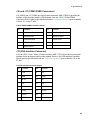
1
Intel NetStructure® ZT 4807
Packet Switched Rear Panel
Transition Board
Technical Product Specification
Document Number: 302768
Revision History
Revision
Date
Revision History
11/16/01
Initial Release
1/17/02
Added note saying Ethernet is not functional on standard product.
Updated Functional Block Diagram.
Clarified power connector documentation.
Added floppy/IDE power cable descriptions.
CTs 6-16 have been removed from the product and documentation.
3/20/02
Documented IDE/floppy cable A86460-001. Removed references to obsolete cables
18031 and 19021.
1/08/03
Corrected Customer Support Information.
5/28/03
Added Warranty information.
7/04
Faceplate change to remove Ethernet ports.
3/24/06
Removed Ethernet connectors J3, J18 and J20.
INFORMATION IN THIS DOCUMENT IS PROVIDED IN CONNECTION WITH INTEL® PRODUCTS. EXCEPT AS PROVIDED IN INTEL’S TERMS
AND CONDITIONS OF SALE FOR SUCH PRODUCTS, INTEL ASSUMES NO LIABILITY WHATSOEVER, AND INTEL DISCLAIMS ANY EXPRESS
OR IMPLIED WARRANTY RELATING TO SALE AND/OR USE OF INTEL PRODUCTS, INCLUDING LIABILITY OR WARRANTIES RELATING TO
FITNESS FOR A PARTICULAR PURPOSE, MERCHANTABILITY, OR INFRINGEMENT OF ANY PATENT, COPYRIGHT, OR OTHER
INTELLECTUAL PROPERTY RIGHT.
Intel Corporation may have patents or pending patent applications, trademarks, copyrights, or other intellectual property rights that relate to the
presented subject matter. The furnishing of documents and other materials and information does not provide any license, express or implied, by
estoppel or otherwise, to any such patents, trademarks, copyrights, or other intellectual property rights.
Intel products are not intended for use in medical, life saving, life sustaining, critical control or safety systems, or in nuclear facility applications.
Intel may make changes to specifications and product descriptions at any time, without notice.
Designers must not rely on the absence or characteristics of any features or instructions marked “reserved” or “undefined.” Intel reserves these for
future definition and shall have no responsibility whatsoever for conflicts or incompatibilities arising from future changes to them.
The Intel NetStructure® ZT 4807 may contain design defects or errors known as errata which may cause the product to deviate from published
specifications. Current characterized errata are available on request.
This manual as well as the software described in it is furnished under license and may only be used or copied in accordance with the terms of the
license. The information in this manual is furnished for informational use only, is subject to change without notice, and should not be construed as a
commitment by Intel Corporation. Intel Corporation assumes no responsibility or liability for any errors or inaccuracies that may appear in this
document or any software that may be provided in association with this document.
Except as permitted by such license, no part of this document may be reproduced, stored in a retrieval system, or transmitted in any form or by any
means without the express written consent of Intel Corporation.
Contact your local Intel sales office or your distributor to obtain the latest specifications and before placing your product order.
Copies of documents which have an ordering number and are referenced in this document, or other Intel literature may be obtained by calling
1-800-548-4725 or by visiting Intel's website at http://www.intel.com.
Intel, Intel Centrino, Intel logo, Intel NetStructure, and Pentium III are trademarks or registered trademarks of Intel Corporation or its subsidiaries in the
United States and other countries.
*Other names and brands may be claimed as the property of others.
Copyright © 2001-2006, Intel Corporation. All rights reserved.
Contents
1. INTRODUCTION ....................................................................................................................................................8
UNPACKING ...............................................................................................................................................................8
PRODUCT DEFINITION ...............................................................................................................................................8
FEATURES OF THE ZT 4807 .....................................................................................................................................9
FUNCTIONAL BLOCKS .............................................................................................................................................10
Rear-Panel I/O..................................................................................................................................................10
PS/2 Keyboard/Mouse Port ............................................................................................................................10
Video Interface .................................................................................................................................................11
Universal Serial Bus ........................................................................................................................................11
Serial Port Connectors (COM1 and COM2).................................................................................................11
EIDE Interface ..................................................................................................................................................11
Speaker Connector..........................................................................................................................................12
Floppy Drive Interface and Power Connector..............................................................................................12
2. COMPACTFLASH OPTION...............................................................................................................................13
COMPACTFLASH INPUT CHARACTERISTICS ...........................................................................................................13
CompactFlash Card Installation and Removal ............................................................................................14
3. CONFIGURATION...............................................................................................................................................15
ZT 4807 SWITCH OPTIONS AND LOCATIONS .........................................................................................................15
Switch Descriptions .........................................................................................................................................15
CUTTABLE TRACES .................................................................................................................................................17
Cuttable Trace Descriptions ...........................................................................................................................17
A. SPECIFICATIONS ..............................................................................................................................................20
ELECTRICAL SPECIFICATIONS ................................................................................................................................20
ENVIRONMENTAL SPECIFICATIONS .........................................................................................................................20
MECHANICAL SPECIFICATIONS ...............................................................................................................................20
Board Dimensions and Weight ......................................................................................................................21
Connectors........................................................................................................................................................22
Cables................................................................................................................................................................30
B. AGENCY APPROVALS .....................................................................................................................................31
CE CERTIFICATION .................................................................................................................................................31
SAFETY....................................................................................................................................................................31
EMISSIONS TEST REGULATIONS.............................................................................................................................31
EN 50081-1 Emissions....................................................................................................................................31
EN 55024 Immunity .........................................................................................................................................31
REGULATORY INFORMATION ...................................................................................................................................32
FCC (USA) ........................................................................................................................................................32
Industry Canada (Canada) .............................................................................................................................32
PRODUCT SAFETY INFORMATION ...........................................................................................................................32
Safety Precautions...........................................................................................................................................32
AC and/or DC Power Safety Warning (AC and/or DC Powered Units) ...................................................34
Rack Mount Enclosure Safety........................................................................................................................34
D. INTEL NETSTRUCTURE® COMPUTE BOARDS & PLATFORM PRODUCTS .......................................35
LIMITED WARRANTY ................................................................................................................................................35
3
Contents
C. CUSTOMER SUPPORT.....................................................................................................................................37
T
TECHNICAL SUPPORT AND RETURN FOR SERVICE ASSISTANCE...........................................................................37
SALES ASSISTANCE ................................................................................................................................................37
4
Tables
Revision History ............................................................................................................................2
CompactFlash Input Characteristics ...........................................................................................13
Cuttable Trace Definitions...........................................................................................................17
Connector Assignments ..............................................................................................................22
J5 Rear-Panel User I/O Connector Pinout ..................................................................................24
J6 Speaker Connector Pinout .....................................................................................................25
J8/J9 Power Connector Pinout....................................................................................................25
J10 Floppy Drive Cable Connector Pinout ..................................................................................26
J11 EIDE Connector Pinout ........................................................................................................27
J13/J14 Universal Serial Bus Connector Pinout .........................................................................28
J15 Keyboard/Mouse Connector Pinout .....................................................................................28
J16/J17 COM1/COM2 Connectors Pinout ..................................................................................29
J19 VGA Interface Connector Pinout ..........................................................................................29
5
Figures
Functional Block Diagram ...........................................................................................................10
Switch and Cuttable Trace Locations..........................................................................................18
Board Dimensions.......................................................................................................................21
Connector Locations ...................................................................................................................23
Backplane Connectors—Pin Locations.......................................................................................23
6
Document Organization
This Technical Product Specification describes the operation and use of the Intel
NetStructure® ZT 4807 Packet Switched Rear Panel Transition Board. The following
summarizes the focus of each major section of this Specification.
Chapter 1, “Introduction,” introduces the key features of the ZT 4807. It includes a
product definition, a list of product features, a functional block diagram, and a brief
description of each block.
Chapter 2, “CompactFlash Option” details how to use a CompactFlash expansion card to
provide external solid-state secondary IDE channel capacity.
Chapter 3, “Configuration,” describes factory default settings and board options
configurable through the ZT 4807’s switches and cuttable traces.
Appendix A, “Specifications,” contains the electrical, environmental, and mechanical
specifications for the ZT 4807. It provides an illustration of connector locations, connector
descriptions, and tables of the connector pin assignments. It also presents information on
cabling recommended by Intel.
Appendix B, “Agency Approvals,” presents agency approvals and certifications pending
for the ZT 4807.
Appendix C, “Customer Support,” provides technical and sales assistance information.
7
1. Introduction
This chapter provides a brief introduction to the Intel NetStructure® ZT 4807 Packet
Switched Rear Panel Transition Board (RPIO). It includes a product definition, a list of
product features, a “ZT 4807 Connector Plate” figure, a functional block diagram, and a
description of each block.
See Chapter 3, “Configuration,” for factory default settings and board options configurable
through the ZT 4807’s switches and cuttable traces.
See Appendix A, “Specifications,” for complete power and temperature requirements, as
well as connector locations, descriptions, pinout tables, and cable recommendations.
Unpacking
Please check the shipping carton for damage. If the shipping carton and contents are
damaged, notify the carrier and Intel for an insurance settlement. Retain the shipping carton
and packing material for inspection by the carrier. Do not return any product to Intel without
a Return Material Authorization (RMA) number. The "Technical Support/Return for Service"
topic in Appendix A provides contact information for obtaining an RMA number from Intel.
Warning: Like all equipment utilizing MOS devices, the ZT 4807 must be protected from
static discharge. Never remove any of the socketed parts except at a static-free
workstation. Use the anti-static bag shipped with your order to handle the boards.
Product Definition
The ZT 4807 is a single slot, 6U board providing rear-panel access to the I/O functions of
an Intel NetStructure® processor board with RPIO pin compatibility (see the pin definitions
for connector J5 in Appendix A). An example of a compatible board is the Intel
NetStructure® ZT 5504. The ZT 4807 is designed to function only in the RPIO slot of a
6U CompactPCI* system such as the Intel NetStructure® ZT 5090 4U General Purpose
Packet Switched Platform.
8
1. Introduction
Features of the ZT 4807
•
•
Rear-panel interface connectors for host processor
board:
−
USB 0 and USB1 ports
−
VGA
−
PS/2 Keyboard/Mouse
−
COM 1
−
COM 2
Internal interfaces not on the connector plate:
−
CompactFlash interface
−
IDE interface (Host processor board secondary
channel)
−
4-pin power connector for external media
−
Floppy interface
−
PC speaker connector
•
Reset Switch
•
NMI Switch
9
1. Introduction
Functional Blocks
Below is a functional block diagram of the ZT 4807. The topics following the diagram
provide overviews of the ZT 4807's functional blocks.
ZT 4807
Functional Block Diagram
J5
Rear-Panel I/O
POWER IN
(J8)
EIDE
POWER OUT
(J9)
COM2
(J17)
FLOPPY
(J10)
SPEAKER
(J6)
COM1
(J16)
KEYBOARD
& MOUSE
(J15)
(CompactFlash and
Secondary Channels)
(J11-J12)
VIDEO
(J19)
USB 0
USB 1
(J13)
(J14)
Rear-Panel I/O
The ZT 4807 transitions signals from a pin-compatible processor board (such as the
ZT 5504 from Intel) through backplane connectors J5.
PS/2 Keyboard/Mouse Port
The ZT 4807 provides rear-panel access to the host processor board keyboard/mouse
interface. The host processor board PS/2 style mouse/keyboard controller is connected via
RPIO connector J5 to 6-pin DINN connector J15, labeled KY/MS on the ZT 4807 Connector
Plate. Using J15 for both the PS/2 keyboard and PS/2 mouse connection requires use of a
PC keyboard/mouse ‘Y’ splitter cable. See the “Cables” topic in Appendix A for cabling
recommendations.
Note: The keyboard and mouse do not function properly if devices are connected to both the Host
processor board and the ZT 4807.
10
1. Introduction
Video Interface
The ZT 4807 provides rear-panel access to the host processor board VGA accelerator. The
host processor board VGA accelerator is connected via RPIO connector J5 to J19, a 15-pin
VGA connector on the ZT 4807 Connector Plate.
Note: Video does not function properly if devices are connected to both the Host processor board
and the ZT 4807.
Universal Serial Bus
The ZT 4807 provides rear-panel access to the host processor board Universal Serial Bus
(USB) signals. The host processor board USB is connected via RPIO connector J5 to USB
connectors J13 and J14 on the ZT 4807 Connector Plate.
Serial Port Connectors (COM1 and COM2)
The ZT 4807 provides rear-panel access to the host processor board serial ports. The host
processor board COM1 and COM2 ports are connected via RPIO connector J5 to 9-pin Dshell connectors J16 and J17, respectively, on the ZT 4807 Connector Plate.
Note: The COM Ports do not function properly if devices are connected to the same COM port
channel on both the host processor board and the ZT 4807.
EIDE Interface
The host processor board secondary channel is connected via RPIO connector J5 to
internal 40-pin 0.1” vertical header J11 and to internal CompactFlash connector J12 on the
ZT 4807.
Only two IDE devices can be connected on any IDE channel. If the ZT 4807 has a
CompactFlash device installed, only a single IDE device can be connected to secondary
IDE channel connector J11. Refer to Chapter 2, “CompactFlash Option,” for installation and
configuration of the ZT 4807 for operation with a CompactFlash device.
Caution: For proper operation, Intel recommends an ATA-5 compliant 80-conductor IDE
cable for external IDE connection. If the external IDE device is configured in a
master/slave combination with an on-board IDE device (CompactFlash or processor
board-mounted hard disk), a custom 80-conductor IDE cable must be used. Use of
industry standard 80-conductor IDE cables in this configuration can cause BIOS drive
detection and configuration errors. See the “Cables” topic in Appendix A for cabling
recommendations.
An IDE drive that requires +12V/GND/+5V to operate can be connected to power output
connector J9. Input power connector J8 must then be connected to a power source
supplying +12V/GND/+5V. Refer to the “Cables” topic in Appendix A for more information.
11
1. Introduction
Speaker Connector
The host processor board speaker interface is connected via RPIO connector J5 to internal
speaker connector J6, allowing connection of a PC speaker.
Floppy Drive Interface and Power Connector
The host processor board floppy drive controller is connected via RPIO connector J5 to
internal 34-pin floppy drive cable connector J10. The ZT 4807 also provides a 4-pin power
connector (J9) that provides +5V, GND, and +12V when input power connector J8 is
connected to an appropriate power source.
Caution: If power is supplied to J8 from the host processor board and the device connected
to J9 draws more power than the host processor board can provide, a power fault or other
problems may occur.
12
2. CompactFlash Option
CompactFlash connector J12 on the ZT 4807 provides external, solid state, secondary IDE
channel capability to a processor board such as the Intel NetStructure® ZT 5504 System
CPU Board with Intel Pentium® III processor. This connector is designed to accommodate
CompactFlash expansion cards operating in True IDE Mode, which appear to the system
as a hard drive and are automatically supported by most operating systems.
CompactFlash Input Characteristics
By default, the ZT 4807’s CompactFlash socket (J12) is set to 5.0V operation (CT5 is in
position B). This setting requires the CompactFlash card to have “Type 2” or “Type 3” input
characteristics, as shown in the “CompactFlash Input Characteristics” table below.
SanDisk* currently manufactures cards meeting these specifications.
CompactFlash Input Characteristics
Min
Type
Parameter
Symbol
Typ.
Max
Min
Typ.
Max
VCC = 3.3 (CT5A)1
VCC = 5.0 (CT5B)2
Input
Vih
2.4
—
—
4.03
—
—
Voltage CMOS
Vil
—
—
0.6
—
—
0.8
Input
Vih
1.5
—
—
2.0
—
—
Voltage CMOS
Vil
—
—
0.6
—
—
0.8
Input
Vth
—
1.8
—
—
2.8
—
Voltage CMOS
Vtl
—
1.0
—
—
2.0
—
1
Units
Volts
2
Volts
3
Volts
Notes:
This table is based on one provided in the CompactFlash Specification Revision 1.3. The shaded area
represents operation not supported on the ZT 4807.
1.
If the CompactFlash socket (J12) is set for VCC = 3.3V operation (CT5 is in the A position), do not connect
a disk drive on the EIDE connector J11. Doing so will damage the CompactFlash device!
2.
Factory default configuration.
3.
CompactFlash cards with “Type 1” input characteristics (operating from VCC = 5.0) should not be used
because the ZT 4807 does not meet the 4.0V minimum input voltage requirement (ZT 4807 EIDE channels
VOH = 2.8V).
13
2. CompactFlash Option
5.0V operation has the advantage of allowing master/slave operation, with an additional
drive connected to the secondary IDE connector J11 on the ZT 4807. See the “SW4-1
(Secondary IDE Master/Slave Selection)” topic in Chapter 3, “Configuration,” for more
information about configuring the CompactFlash card as a master or slave IDE device on
the secondary channel.
Caution: If a CompactFlash device is present, and an IDE device is connected to J11, a
custom 80-conductor IDE cable must be used. Use of industry standard 80-conductor IDE
cables in this configuration can cause BIOS drive detection and configuration errors. See
the “Cables” topic in Appendix A for cabling recommendations.
CompactFlash Card Installation and Removal
Perform the steps below to install or remove a CompactFlash card.
Caution: Perform the installation and removal at a static-free workstation to avoid damage
to the ZT 4807.
Installation
1. Make sure the system is powered off.
2. Put on an anti-static grounding strap.
3. Most CompactFlash cards have an arrow on the top label indicating correct orientation.
Align the arrow on the CompactFlash card with the arrow on the connector and slide the
card into place until the connection is snug. The dimensions of the grooves in the sides
of the CompactFlash card prevent incorrect installation.
Removal
1. Make sure the system is powered off.
2. Put on an anti-static grounding strap.
3. Grasp the card by the sides and pull it out of the connector. Do not apply pressure to
the top of the CompactFlash cards: this can damage some CompactFlash devices such
as the IBM Microdrive*.
14
3. Configuration
The ZT 4807 includes several options that tailor the operation of the board to requirements
of specific applications. Some options are configured with a switch or by cuttable traces.
Configure a switch option by closing or opening a DIP switch. Configure a cuttable trace
option by installing or removing a surface mount 0 Ω resistor.
ZT 4807 Switch Options and Locations
The ZT 4807 includes one bank of switches (SW4) located on the component side of the
board. See the “Switch and Cuttable Trace Locations” figure for the location of the SW4.
SW1 is incorporated into the lower board ejector mechanism. SW2 and SW3 are pushbutton switches located on the connector plate. See the “ZT 4807 Connector Plate” figure in
Chapter 1 for the location of the SW2 and SW3.
Switch Descriptions
The following topics list the switches in numerical order and provide a detailed description
of each switch. Note that where switches are referenced in this Chapter, “SWx”
corresponds to the switch number and “-N” corresponds to the switch segment (for
example, SW2-1 means “switch number 2, segment 1”).
SW1 (Hot Swap Ejector)
The lower ejector incorporates an ejector switch, connected to the processor board’s
Baseboard Management Controller. This switch is used to notify the processor board of the
necessity to shut down so the ZT 4807 can be removed.
SW2 (Reset)
SW2 is a push-button on the ZT 4807's connector plate. See the “ZT 4807 Connector Plate”
figure in Chapter 1 for the location of the SW2. When pressed, SW2 issues a reset to the
host processor board. See the host processor board manual for a detailed description of the
reset feature.
SW3 (NMI)
SW3 is a push-button on the ZT 4807's connector plate. See the “ZT 4807 Connector Plate”
figure in Chapter 1 for the location of the SW3. When pressed, SW2 issues a non-maskable
interrupt to the host processor board. See the host processor board manual for a detailed
description of the reset feature.
15
3. Configuration
SW4-1 (Secondary IDE Master/Slave Selection)
SW4-1 configures the CompactFlash card (installed in J12) as a master or slave IDE device
on the secondary channel. This switch also changes the polarity of the “Cable Select” signal
available at connector J11, pin 28.
If the CompactFlash card is the only device on the secondary IDE channel then it must be
configured as the master (SW4-1 = on).
If another IDE device is connected to the secondary IDE channel (cabled to connector J11)
then the CompactFlash should be configured as a slave (SW4-1 = off) and the other device
should be configured as the master. See the documentation supplied with your IDE device
to see how to configure it as a master.
If a CompactFlash card is not installed in J12, then SW4-1 should be off. SW4-1 affects the
“Cable Select” (J11 pin 28) signal on the IDE cable. For normal “cable select” operation
SW4-1 must be off.
A maximum of two IDE devices may be connected to the secondary channel. If you have a
CompactFlash card installed in J12 then you may have only one IDE device connected to
J11 and you must use a special cable to connect the external IDE device to J11. This cable
is available from Intel as part number ZT 90250. See the “Cables” topic in Appendix A for
more information. If a CompactFlash card is not installed in J12 then two devices may be
installed on the cable connected to J11. A standard 80-pin (UDMA-66 compatible) cable
may be used in this case.
The ZT 4807 is supplied without a CompactFlash card installed in J12. Therefore SW4-1 is
off by default.
See the “CompactFlash Input Characteristics” topic in Chapter 2 for more information.
SW4-2, SW4-3, SW4-4 (Reserved)
These switch segments are reserved for future use. Factory default is open.
16
3. Configuration
Cuttable Traces
The ZT 4807 includes several cuttable traces (0 Ω shorting resistors) that allow the user to
configure certain options not configurable through the processor board's BIOS Setup Utility.
In most cases, the default settings are appropriate for normal operation; however, some
applications may require different settings. The "Switch and Cuttable Trace Locations"
figure shows the placement of the ZT 4807's cuttable traces.
There are two types of cuttable traces on the ZT 4807: single-option and double-option:
•
Single option cuttable traces are implemented using 0603 and 1206 surface mount
pads. A 0 Ω shorting resistor is soldered between these pads to make the connection.
•
Double option cuttable traces are implemented using three 0603 surface mount pads. A
0 Ω shorting resistor is soldered between one set of pads, depending on the chosen
option.
Caution: Only qualified technicians familiar with surface mount soldering techniques
should perform cuttable trace modifications. The product warranty is voided if the board is
damaged by customer modifications.
Cuttable Trace Descriptions
The “Cuttable Trace Definitions” table provides a quick cross-reference for the ZT 4807
cuttable trace descriptions that follow.
Cuttable Trace Definitions
CT#
Default
Description
CT1
Out
Connect Top ESD Strip to Logic Ground
CT2
Out
Connect Bottom ESD Strip to Logic Ground
CT3
Out
Connect Reset Switch Case to Logic Ground
CT4
Out
Connect NMI Switch Case to Logic Ground
CT5
B
Connect Compact Flash Power to Switched 5V
17
3. Configuration
Switch and Cuttable Trace Locations
CT1
CT5
4
3
2
1
SW4
CT3
CT4
SW2
SW3
CT2
18
3. Configuration
CT1-CT4 (Connect Chassis GND to Logic GND)
The ZT 4807's switches and ejectors are on an isolated chassis ground. These components
can be connected to the ZT 4807 logic ground by installing these four cuttable traces. All
four cuttable traces should be installed or all four removed. The factory default is removed.
Position
Function
All In
Front panel connectors connected to logic ground
All Out
Default
Front-panel connectors not connected to logic ground
CT5 (CompactFlash Operating Voltage)
The factory default configuration sets the ZT 4807’s CompactFlash socket (J12) to 5.0V
operation (CT5 in position B). This setting requires the CompactFlash card to have “Type 2”
or “Type 3” input characteristics. See the “CompactFlash Input Characteristics” table in
Chapter 3 for more information.
Caution: If the CompactFlash socket is set for VCC = 3.3V operation (CT5 is in the A
position), do not connect a disk drive on EIDE connector J11. Doing so will damage the
CompactFlash device!
Position
Function
A
Connects the Compact Flash Circuitry to Switched 3.3VDC.
B
Default
Connects the Compact Flash Circuitry to Switched 5VDC.
19
A. Specifications
This Appendix describes the electrical, environmental, and mechanical specifications of the
ZT 4807. It includes illustrations of the board dimensions and connector locations, as well
as connector pinout tables.
Electrical Specifications
Power Requirements
Minimum
Typical
Maximum
Supply Voltage, VCC
4.75V
5.00V
5.25V
Supply Current, VCC = 5.0V
0mA
--
195mA
Environmental Specifications
Operating Temperature: 0° to +70° Celsius
Storage Temperature:
-40° to +85° Celsius
Relative Humidity:
< 95% at 40° Celsius, non-condensing
Mechanical Specifications
The topics listed below provide the following mechanical specifications:
•
Board Dimensions and Weight
•
Connectors (including connector locations, descriptions, and pinouts)
20
A. Specifications
Board Dimensions and Weight
Mechanical dimensions for the ZT 4807 are shown in the "Board Dimensions" illustration
and outlined below.
Board Length:
80mm (3.150 in)
Board Width:
233.35mm (9.187 in)
Board Thickness: 1.6mm (0.063 in)
Board Weight:
202 g (7.13 oz)
80.00 mm
Board Dimensions
233.35 mm
21
A. Specifications
Connectors
As shown in the “Connector Locations” drawing, the ZT 4807 includes several connectors
to interface with application-specific devices. A brief description of each connector is given
in the “Connector Assignments” table. A detailed description and pinout for each connector
is given in the following topics.
Connector Assignments
Connector
Function
J5
Rear-Panel User I/O Connector (110-pin, 2mm x 2mm, female)
J6
Speaker Connector (2-pin, male)
J7
Ejector switch connector
J8
Floppy Drive/IDE Input Power Connector (4-pin, female)
J9
Floppy Drive/IDE Output Power Connector (4-pin, female)
J10
Floppy Drive Cable Connector (34-pin, male)
J11
Secondary EIDE Connector (40-pin, male)
J12
CompactFlash Connector (50-pin, CF Card Slot Header)
J13, J14
Universal Serial Bus Connectors (4-pin, USB, Port 1/Port 1)
J15
PS/2 Keyboard/Mouse Connector (6-pin, DIN)
J16
COM1 Serial Port (9-pin, D-Shell)
J17
COM2 Serial Port (9-pin, D-Shell)
J19
VGA Interface Connector (15-pin D-shell, female)
22
A. Specifications
Connector Locations
J5
Keyboard/Mouse, USB0, USB1,
SVGA, Reset, NMI, Secondary IDE,
CompactFlash, Floppy, COM1,
COM2,Floppy Power, Speaker
J12 CompactFlash
J13 USB 0
J14 USB 1
J19 Video
J1 1 Secondary IDE Channel
J6 Speaker Connector
J15 Keyboard/Mouse Port
J16 COM1
J8 12 VDC In
J9 12 VDC Out
J17 COM2
J10 Floppy Connector
J7 Ejector switch
Backplane Connectors—Pin Locations
E
D
C
B
A 22
J5
1
23
A. Specifications
J5 (Rear-Panel User I/O Connector)
J5 is a 110-pin, 2mm x 2mm, right angle, female connector (AMP 646489-1) capable of
transitioning the following signals for rear-panel I/O:
• Keyboard/Mouse
• COM1
• VGA
• Reset
• Floppy
• USB0, USB1
• Compact Flash
• COM2
• NMI
• IDE
• Floppy Power
• Speaker
See the “J5 Rear-Panel User I/O Connector Pinout” table for pin definitions and the
“Backplane Connectors—Pin Locations” figure showing pin placement.
J5 Rear-Panel User I/O Connector Pinout
A
B
C
D
E
22
USB0+
USB0-
SW-5V
USB1+
USB1-
21
SW-3.3V
GND
GND
GND
GND
20
RED
GND
H-SYNC
GND
SMBD
19
GND
SW-5V
GND
SW-5V
SMBC
18
GREEN
GND
V-SYNC
GND
SMBA-
17
GND
RESV
RP_PRES-
RESV
IPMB PWR
16
BLUE
GND
DDCCLK
KBDAT
KBCLK
15
GND
SW-5V
DDCDAT
MSDAT
MSCLK
14
S1RTS
S1CTS
S1RIN
S1DTR
ENETA-LINK
13
S1DCD
S1TXD
S1RXD
S1DSR
ENETA-ACT
12
S2RTS
S2CTS
S2RIN
S2DTR
ENETB-LINK
11
S2DCD
S2TXD
S2RXD
S2DSR
ENETB-ACT
10
TRK0-
WP-
RDATA-
HDSEL-
DSKCHG-
9
MTR1-
DIR-
STEP-
WDATA-
WGATE-
8
DENSL
INDEX-
MTR0-
DR1-
DR0-
7
CS1S-
CS3S-
DA1
RPELED
RPEJECT-
6
PWRGD
SPKR
NMI-
DA0
DA2
5
DDRQ
IORDY
DI0W-
DDACK
DIOR-
4
DD14
DD0
IDE_ACT
DD15
DRV_IRQ
3
DD3
DD12
DD2
DD13
DD1
2
DD9
DD5
DD10
DD4
DD11
1
PBRST-
DRST-
DD7
DD8
DD6
Pin
A
B
C
D
E
F
Ground Shield
Pin
F
24
A. Specifications
J6 (Speaker Connector)
J6 is a 2-pin connector (Molex 39-27-0021) for connection to an optional PC speaker. The
mating connector is a Molex 39-01-0023 or equivalent. The mating connector also requires
two Molex 39-01-0031 terminals or equivalent. If you experience difficulty locating parts
information from the Molex website, contact your Molex sales representative at 1-80078MOLEX. See the “J6 Speaker Connector Pinout” for pin definitions and the “Connector
Locations” figure to identify J6 on the ZT 4807.
J6 Speaker Connector Pinout
Pin
Function
1
SPK1
2
SPK2
J8, J9 (Floppy Drive/IDE Power Connectors)
J8 and J9 are internal (not available on the faceplate), four position, female power
connectors (AMP 174552-1) with +5V, GND, and +12V pins. Power can be supplied to
input power connector J8 from an appropriate external power source supplying +5V, GND,
and +12V. Output power connector J9 can then supply power to an external device such as
a floppy drive or IDE device. See the “Cables” topic for more information.
Caution: If power is supplied to J8 from the host processor board and the device
connected to J8 draws more power than the host processor board can provide, a power
fault or other problems may occur.
See the”J8/J9 Power Connector Pinout” table for pin definitions and the “Connector
Locations” figure to identify J8 and J9 on the ZT 4807.
J8/J9 Power Connector Pinout
Pin
Function
1
+12V
2
Ground
3
Ground
4
+5V
25
A. Specifications
J10 (Floppy Drive Cable Connector)
J10 is an internal (not available on the faceplate) 34-pin connector (AMP 104340-7)
providing a ribbon cable interface for the processor board's floppy drive signals. See the
“J10 Floppy Drive Cable Connector Pinout” table for pin definitions and the “Connector
Locations” figure to identify J10 on the ZT 4807.
J10 Floppy Drive Cable Connector Pinout
Pin
Function
Pin
Function
1
Ground
2
DENSL
3
Ground
4
N/C
5
Ground
6
N/C
7
Ground
8
INDEX-
9
Ground
10
MTR0-
11
Ground
12
DR1-
13
Ground
14
DR0-
15
Ground
16
MTR1-
17
Ground
18
DIR-
19
Ground
20
STEP-
21
Ground
22
WDATA-
23
Ground
24
WGATE-
25
Ground
26
TRK0-
27
Ground
28
WP-
29
Ground
30
RDATA-
31
Ground
32
HDSEL-
33
Ground
34
DSKCHG-
26
A. Specifications
J11 (EIDE Connector)
J11 is an internal (not on the connector plate), 40-pin, male, unshrouded, 0.25" square
posts on 0.1" 2 x 20 grid connector (T&B 609-4027). J11 provides access to the processor
board's secondary EIDE channel. The secondary channel is connected from RPIO
connector J5 to the internal IDE connector J11 and the CompactFlash Connector J12. See
the “J11 EIDE Connector Pinout” table for pin definitions and the “Connector Locations”
figure to identify J11 on the ZT 4807.
J11 EIDE Connector Pinout
Pin
Function
Pin
Function
1
Reset IDE#
2
Ground
3
Data 7
4
Data 8
5
Data 6
6
Data 9
7
Data 5
8
Data 10
9
Data 4
10
Data 11
11
Data 3
12
Data 12
13
Data 2
14
Data 13
15
Data 1
16
Data 14
17
Data 0
18
Data 15
19
Ground
20
N/C
21
DDRQ
22
Ground
23
DIOW#
24
Ground
25
DIOR#
26
Ground
27
DRDY
28
CSEL (Cable Select pull-down)
29
DDAK#
30
Ground
31
IRQ 14
32
Reserved
33
IDE_A1
34
Reserved
35
IDE_A0
36
IDE_A2
37
IDE_CS1#
38
IDE_CS3#
39
IDE_ACT#
40
Ground
27
A. Specifications
J12 (CompactFlash Connector)
J12 is a 50-pin, surface mount, right angle, CF card slot header (AMP 788667-1) designed
to accommodate a CompactFlash card. Refer to the CompactFlash Specification, Revision
1.X, for pinout and device information. For a copy of the most current specification and
more information about CompactFlash, visit the CompactFlash Association’s website at:
http://www.compactflash.org/
Refer to the “Connector Locations” figure to identify J12 on the ZT 4807.
J13/J14 (Universal Serial Bus Connectors)
J13 and J14 are the rear-panel interface (AMP 440260-1) for the processor board's USB
Ports 0 and 1, respectively. J13 and J14 can be used simultaneously with the USB
connectors on the processor board's connector plate. See the “J13/J14 Universal Serial
Bus Connector Pinout” table for pin definitions and the “Connector Locations” figure to
identify J13 and J14 on the ZT 4807.
J13/J14 Universal Serial Bus Connector Pinout
Pin
Function
1
+5V (Fused)
2
DATA-
3
DATA+
4
Ground
J15 (Keyboard/Mouse Connector)
J15 is a 6-pin DINN connector (AMP 749180-1) for standard PS/2 style keyboard and
Mouse devices. See the “J15 Keyboard/mouse Connector Pinout” table for pin definitions
and the “Connector Locations” figure to identify J15 on the ZT 4807.
J15 Keyboard/Mouse Connector Pinout
Pin
Function
1
Keyboard Data
2
Mouse Data
3
Ground
4
Switched +5V
5
Keyboard Clock
6
Mouse Clock
28
A. Specifications
J16 and J17 (COM1/COM2 Connectors)
J16 (COM1) and J17 (COM2) are 9-pin D-shell connectors (AMP 179952-3) providing an
interface to the processor board’s COM channels. See the “J16/J17 COM1/COM2
Connectors Pinout” table for pin definitions and the “Connector Locations” figure to identify
J16 and J17 on the ZT 4807.
J16/J17 COM1/COM2 Connectors Pinout
Pin
Function
Pin
Function
1
Data Carrier Detect
6
DCE (Data Set) Ready
2
Received Data
7
Request to Send
3
Transmitted Data
8
Clear to Send
4
DTE (Data Terminal) Ready
9
Ring Indicator
5
Signal Ground
J19 (VGA Interface Connector)
J19 is an HD15, 15-pin, female, D-shell connector (AMP 177514-9) providing a rear-panel
interface for the processor board’s video adapter. See the “J19 VGA Interface Connector
Pinout” table for pin definitions and the “Connector Locations” figure to identify J19 on the
ZT 4807.
J19 VGA Interface Connector Pinout
Pin
Function
Pin
Function
1
RED
9
VCC
2
GRN
10
SGND
3
BLUE
11
N/C
4
N/C
12
SDA
5
DGND
13
HYSNC
6
RGND
14
VSYNC
7
GGND
15
SCL
8
BGND
29
A. Specifications
Cables
Intel recommends the following cables for interfacing to the ZT 4807.
IDE
For proper operation, Intel recommends 80-conductor IDE cables for external IDE
connection. If the external IDE device is configured in a master/slave combination with an
on-board IDE device (CompactFlash or processor board mounted hard disk) a custom 80conductor IDE cable must be used. Industry standard 80-conductor IDE cables do not
connect PDIAG to the host connector. This causes BIOS drive detection and configuration
errors when a master/slave pair exists across the interface. An 80-conductor IDE cable for
use with the ZT 4807 is available as an accessory from Intel as part number ZT 90250.
Floppy/IDE Power
An IDE/floppy drive power cable (Intel part number A86460-001) is shipped with the
ZT 4807. This is a 20" Y cable with a 4-pin female D-shell power connector wired to a 4-pin
female mini-plug power connector and a second 4-pin female D-shell power connector. Use
this cable to connect from ZT 4807 output power connector J9 to a floppy drive power input
connector and/or an IDE device power input connector.
PS/2 Keyboard/Mouse
Using the ZT 4807 Keyboard/Mouse connector (J15) for both PS/2 keyboard and PS/2
mouse connection requires use of a PC keyboard/mouse Y splitter cable, such as the IBM
ThinkPad Laptop Y Cable. This cable (P/N BC00210) may be obtained from Black Box
Corporation. Contact Black Box at (724) 746-5500, or visit their website at
http://www.blackbox.com. This cable can also be ordered as an accessory from Intel as
ZT 90249.
30
B. Agency Approvals
CE Certification
The ZT 4807 meets intent of Directive 89/336/EEC for Electromagnetic Compatibility and
Low-Voltage Directive 73/23/EEC for Product Safety. The ZT 4807 has been designed for
NEBS/ETSI compliance.
Safety
UL/cUL 60950
Safety for Information Technology Equipment
(UL File # E179737)
EN/IEC 60950
Safety for Information Technology Equipment
CB Report Scheme
CB certificate and Report
Emissions Test Regulations
FCC Part 15, Subpart B
EN 55022
CISPR 22
Bellcore GR-1089
EN 50081-1 Emissions
GR-1089-CORE
Sections 2 and 3
EN 55022
Class A Radiated
EN 55022
Power Line Conducted Emissions
EN 61000-3-2
Power Line Harmonic Emissions
EN 61000-3-3
Power line Fluctuation and Flicker
EN 55024 Immunity
GR-1089-CORE
Sections 2 and 3
EN 61000 4-2
Electro-Static Discharge (ESD)
EN 61000 4-3
Radiated Susceptibility
EN 61000 4-4
Electrical Fast Transient Burst
EN 61000 4-5
Power Line Surge
EN 61000 4-6
Frequency Magnetic Fields
EN 61000 4-11
Voltage dips, Variations, and Short Interruptions
31
B. Agency Approvals
Regulatory Information
FCC (USA)
This product has been tested and found to comply with the limits for a Class A digital device
pursuant to Part 15 of the FCC rules. These limits are designed to provide reasonable
protection against harmful interference when the equipment is operated in a commercial
environment.
This product generates, uses, and can radiate radio frequency energy and, if not installed
and used in accordance with the instruction manual, may cause harmful interference to
radio communications. Operation of this equipment in a residential area is likely to cause
harmful interference in which case the user will be required to correct the interference at his
own expense.
Note: This device complies with Part 15 of the FCC Rules. Operation is subject to the following two
conditions:
1. This device may not cause harmful interference.
2. This device must accept any interference received, including interference that may
cause undesired operation.
Caution: If you make any modification to the equipment not expressly approved by Intel,
you could void your authority to operate the equipment.
Industry Canada (Canada)
Cet appareil numérique respecte les limites bruits radioélectriques applicables aux
appareils numériques de Classe A prescrites dans la norme sur le matériel brouilleur:
"Appareils Numériques", NMB-003 édictée par le Ministre Canadien des Communications.
This digital apparatus does not exceed the Class A limits for radio noise emissions from
digital apparatus set out in the interference-causing equipment standard entitled: "Digital
Apparatus," ICES-003 of the Canadian Department of Communications.
Product Safety Information
Safety Precautions
Review the following precautions to avoid injury and prevent damage to this product, or any
products to which it is connected. To avoid potential hazards, use the product only as
specified.
32
B. Agency Approvals
Read all safety information provided in the component product user manuals and
understand the precautions associated with safety symbols, written warnings, and cautions
before accessing parts or locations within the unit. Save this document for future reference.
Caution: To Avoid Electric Overload: To avoid electrical hazards (heat shock and/or fire
hazard), do not make connections to terminals outside the range specified for that
terminal. See the product user manual for correct connections.
Caution: To Avoid the Risk of Electric Shock: When supplying power to the system,
always make connections to a grounded main. Always use a power cable with a grounded
plug (third grounding pin). Do not operate in wet, damp, or condensing conditions.
Caution: System Airflow Requirements: Platform components such as processor
boards, Ethernet switches, etc., are designed to operate with external airflow. Components
can be destroyed if they are operated without external airflow. Chassis fans normally
provide external airflow when components are installed in compatible chassis. Filler panels
must be installed over unused chassis slots so that airflow requirements are met. Please
refer to the product data sheet for airflow requirements if you are installing components in
custom chassis.
Caution: Microprocessor Heatsinks May Become Hot During Normal Operation: To
avoid burns, do not allow anything to touch processor heatsinks.
Caution: Do Not Operate Without Covers: To avoid electric shock or fire hazard, do not
operate this product with any removed enclosure covers or panels.
Caution: To Avoid the Risk of Electric Shock: Do not operate in wet, damp, or
condensing conditions.
Caution: Do Not Operate in an Explosive Atmosphere: To avoid injury, fire hazard, or
explosion, do not operate this product in an explosive atmosphere.
Caution: If Your System Has Multiple Power Supply Sources: Disconnect all external
power connections before servicing.
Warning: Power Supplies Must Be Replaced by Qualified Service Personnel Only.
Caution: Lithium Batteries Are Not Field-Replaceable Units: There is a danger of
explosion if a battery is incorrectly replaced or handled. Do not disassemble or recharge
the battery. Do not dispose of the battery in fire. When the battery is replaced, the same
type or an equivalent type recommended by the manufacturer must be used. Used
batteries must be disposed of according to the manufacturer’s instructions. Return the unit
to Intel for battery service.
33
B. Agency Approvals
AC and/or DC Power Safety Warning (AC and/or DC
Powered Units)
The AC and/or DC power cord is your unit’s main AC and/or DC disconnecting
device, and must be easily accessible at all times. Auxiliary AC and/or DC On/Off
switches and/or circuit breaker switches are for power control functions only (NOT THE
MAIN DISCONNECT).
For your safety, use only a power cord with a grounded plug. The enclosure is also
provided with a separate earth ground connection/stud. The earth ground connection
should be installed prior to the application of power or peripheral connections and should
never be disconnected while power or peripheral connections exist.
To reduce the possibility of electric shock from a telephone or Ethernet system, plug your
enclosure into the power source before making these connects. Disconnect these
connections before unplugging your enclosure from the power source.
Warning: Verify Power Cord and Outlet Compatibility. Check to ensure you are using
the appropriate power cords for your power outlet configurations. Visit the following
website for additional information: http://kropla.com/electric2.htm.
Rack Mount Enclosure Safety
Your enclosure may be intended for stationary rack mounting. Mount in a rack designed to
meet the physical strength requirements of NEBS GR-63-CORE and NEBS GR 487. Your
system may have multiple power sources. Disconnect all power sources and external
connections/cables prior to installing or removing your system from a rack frame.
Prior to mounting, Intel recommends you remove all hot-swappable equipment for optimum
weight reduction. Be sure to mount your system in a way that ensures even loading of the
rack. Uneven mechanical loading of weight can result in a hazardous condition. Secure all
mounting bolts when installing the enclosure to the frame/rack.
Caution: Avoid Electric Overload. To avoid electric shock or fire hazard, only connect
your system to an input voltage source as specified in the product user manual.
34
D. Intel NetStructure® Compute Boards &
Platform Products
Limited Warranty
Intel warrants to the original owner that the product delivered in this package will be free
from defects in material and workmanship for two (2) year(s) following the latter of: (i) the
date of purchase only if you register by returning the registration card as indicated thereon
with proof of purchase; or (ii) the date of manufacture; or (iii) the registration date if by
electronic means provided such registration occurs within 30 days from purchase. This
warranty does not cover the product if it is damaged in the process of being installed. Intel
recommends that you have the company from whom you purchased this product install the
product.
THE ABOVE WARRANTY IS IN LIEU OF ANY OTHER WARRANTY, WHETHER
EXPRESS, IMPLIED OR STATUTORY, INCLUDING, BUT NOT LIMITED TO, ANY
WARRANTY OF MERCHANTABILITY, FITNESS FOR A PARTICULAR PURPOSE, ANY
WARRANTY OF INFRINGEMENT OF ANY OTHER PARTY'S INTELLECTUAL PROPERTY
RIGHTS, OR ANY WARRANTY ARISING OUT OF ANY PROPOSAL, SPECIFICATION OR
SAMPLE.
This warranty does not cover replacement of products damaged by abuse, accident, misuse,
neglect, alteration, repair, disaster, improper installation or improper testing. If the product is
found to be otherwise defective, Intel, at its option, will replace or repair the product at no
charge except as set forth below, provided that you deliver the product along with a return
material authorization (RMA) number (see below) either to the company from whom you
purchased it or to Intel. If you ship the product, you must assume the risk of damage or loss
in transit. You must use the original container (or the equivalent) and pay the shipping
charge. Intel may replace or repair the product with either a new or reconditioned product,
and the returned product becomes Intel's property. Intel warrants the repaired or replaced
product to be free from defects in material and workmanship for a period of the greater of: (i)
ninety (90) days from the return shipping date; or (ii) the period of time remaining on the
original two (2) year warranty.
This warranty gives you specific legal rights and you may have other rights which vary from
state to state. All parts or components contained in this product are covered by Intel's limited
warranty for this product. The product may contain fully tested, recycled parts, warranted as
if new.
Returning a Defective Product (RMA)
Before returning any product, contact an Intel Customer Support Group to obtain either a
Direct Return Authorization (DRA) or Return Material Authorization (RMA). Return Material
Authorizations are only available for products purchased within 30 days.
Return contact information by geography:
For the Americas
Return Material Authorization (RMA) credit requests e-mail address:
[email protected]
Direct Return Authorization (DRA) repair requests e-mail address: [email protected]
DRA on-line form: http://support.intel.com/support/motherboards/draform.htm
35
C. Customer Support
Intel Business Link (IBL): www.intel.com/ibl
Telephone No.: 1-800-INTEL4U or 480-554-4904
Office Hours: Monday - Friday 0700-1700 MST Winter / PST Summer
For EMEA
Return Material Authorization (RMA) e-mail address - [email protected]
Direct Return Authorization (DRA) for repair requests e-mail address: [email protected]
Intel Business Link (IBL): http://intel.com/ibl
Telephone No.: 00 44 1793 403063
Fax No.: 00 44 1793 403109
Office Hours: Monday - Friday 0900-1700 UK time
For APAC
RMA/DRA requests email address: [email protected]
Telephone No.: 604-859-3111 or 604-859-3325
Fax No.: 604-859-3324
Office Hours: Monday - Friday 0800-1700 Malaysia time
For IJKK
Return Material Authorization (RMA) requests e-mail address: [email protected]
Telephone No.: 81-298-47-0993 or 81-298-47-5417
Fax No.: 81-298-47-4264
Direct Return Authorization (DRA) for repair requests, contact the JPSS Repair center.
E-mail address: [email protected]
Telephone No.: 81-298-47-8920
Fax No.: 81-298-47-5468
Office Hours: Monday - Friday 0830-1730 Japan time
If the Customer Support Group verifies that the product is defective, they will have the Direct
Return Authorization/Return Material Authorization Department issue you a DRA/RMA
number to place on the outer package of the product. Intel cannot accept any product
without a DRA/RMA number on the package. Limitation of Liability and Remedies
INTEL SHALL HAVE NO LIABILITY FOR ANY INDIRECT OR SPECULATIVE DAMAGES
(INCLUDING , WITHOUT LIMITING THE FOREGOING, CONSEQUENTIAL, INCIDENTAL
AND SPECIAL DAMAGES) ARISING FROM THE USE OF OR INABILITY TO USE THIS
PRODUCT, WHETHER ARISING OUT OF CONTRACT, NEGLIGENCE, TORT, OR
UNDER ANY WARRANTY, OR FOR INFRINGEMENT OF ANY OTHER PARTY'S
INTELLECTUAL PROPERTY RIGHTS, IRRESPECTIVE OF WHETHER INTEL HAS
ADVANCE NOTICE OF THE POSSIBILITY OF ANY SUCH DAMAGES, INCLUDING, BUT
NOT LIMITED TO LOSS OF USE, BUSINESS INTERRUPTIONS, AND LOSS OF
PROFITS. NOTWITHSTANDING THE FOREGOING, INTEL'S TOTAL LIABILITY FOR ALL
CLAIMS UNDER THIS AGREEMENT SHALL NOT EXCEED THE PRICE PAID FOR THE
PRODUCT. THESE LIMITATIONS ON POTENTIAL LIABILITIES WERE AN ESSENTIAL
ELEMENT IN SETTING THE PRODUCT PRICE. INTEL NEITHER ASSUMES NOR
AUTHORIZES ANYONE TO ASSUME FOR IT ANY OTHER LIABILITIES.
Some states do not allow the exclusion or limitation of incidental or consequential damages,
so the above limitations or exclusions may not apply to you.
36
C. Customer Support
C. Customer Support
This appendix offers technical and sales assistance information for this product, and
information on returning an Intel NetStructure® product for service.
Technical Support and Return for Service
Assistance
For all product returns and support issues, please contact your Intel product
distributor or Intel Sales Representative for specific information.
Sales Assistance
If you have a sales question, please contact your local Intel NetStructure® Sales
Representative or the Regional Sales Office for your area. Address, telephone and
FAX numbers, and additional information is available at Intel's website, located at
http://www.intel.com/network/csp/sales/
Intel Corporation
Telephone (in U.S.) 1-800-755-4444
Telephone (Outside U.S.) 1-973-993-3030
FAX 1-973-967-8780
37