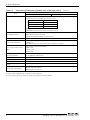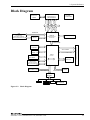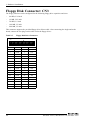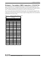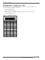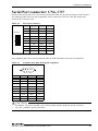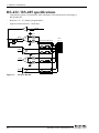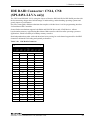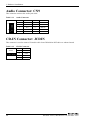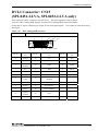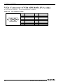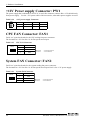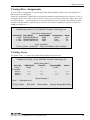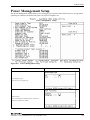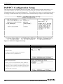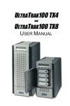
1
SBC Series Single Board Computer Full Size PICMG with LANx2, VGA, Audio SPI-8451-LLVA SPI-8452-LLVA with LAN, VGA, Audio SPI-8451-LVA User’s Manual CONTEC CO.,LTD. Check Your Package Thank you for purchasing the CONTEC product. The product consists of the items listed below. Check, with the following list, that your package is complete. If you discover damaged or missing items, contact your retailer. Product Configuration List - Board (One of the following) [SPI-8451-LLVA/-LVA or SPI-8452-LLVA] …1 - Product Guide …1 - IPC Precaution List …1 - CD-ROM (Driver disk utilities) …1 * 1 - IDE 80 pin Ribbon Cable …1 - IDE 40 pin Ribbon Cable …1 - FDD Ribbon Cable … 1 - 2 serial Ports (9 pin D-SUB male x 2) ribbon cable (with bracket) …1 - Parallel port (25 pin D-SUB female x 1) ribbon cable (with bracket) …1 - Audio jack cable (with bracket) …1 - 6 pin mini-DIN cable (2 in 1 for PS2 Mouse & Keyboard functions) …1 - DVI - Analog RGB conversion adapter (SPI-8451-LLVA, SPI-8452-LLVA only) …1 - +12V power supply cable …1 - Jumper short pin (2 mm) …5 * 1 The CD-ROM contains the driver software and User’s Manual (this Manual) 2 serial ports (9pin D-SUB male x 2) ribbon cable (with bracket) Board Product Guide IPC Precaution List Parallel port Floppy (25pin D-SUB Ribbon Cable female x 1) ribbon cable (with bracket) IDE 80 pin Ribbon Cable Driver disk utility Product Guide IPC Precaution List [CD-ROM] Audio jack ribbon cable (with bracket) SPI-8451-LLVA, SPI-8452-LLVA, SPI-8451-LVA IDE 40 pin Ribbon Cable Jumper short pin (2mm) x5 DVI-Analog RGB Convertion Adapter (SPI-8451-LLVA, SPI-8452-LLVA only) 6 pin mini-DIN cable (2 in 1 for PS2 Mouse & Keyboard functions) i Copyright Copyright 2007 CONTEC CO., LTD. ALL RIGHTS RESERVED. No part of this document may be copied or reproduced in any form by any means without prior written consent of CONTEC CO., LTD. CONTEC CO., LTD. makes been considered in the preparation of this document. Should you notice an omission or any questionable item in this document, please feel free to notify CONTEC CO. LTD. All relevant issues have been considered in the preparation of this document. Should you notice an omission or any questionable item in this document, please feel free to notify CONTEC CO., LTD. Regardless of the foregoing statement, CONTEC assumes no responsibility for any errors that may appear in this document nor for results obtained by the user as a result of using this product. Trademarks Intel, Celeron and Pentium are registered trademarks of Intel Corporation. MS, Microsoft, Windows and Windows NT are trademarks of Microsoft Corporation. Other brand and product names are trademarks of their respective holder. All Other product names or trademarks are properties of their respective owners. Caution about Battery Replace only with the same or equivalent type recommended by the manufacturer. Dispose of used batteries according to the local ordinances or regulations. ii SPI-8451-LLVA, SPI-8452-LLVA, SPI-8451-LVA Table of Contents Check Your Package ................................................................................................................................ i Copyright .................................................................................................................................................ii Trademarks ..............................................................................................................................................ii Caution about Battery..............................................................................................................................ii Table of Contents....................................................................................................................................iii 1. INTRODUCTION 1 Features............................................................................................................................................. 1 Option List........................................................................................................................................ 2 Customer Support .................................................................................................................................... 3 Web Site ........................................................................................................................................... 3 Limited One Year warranty..................................................................................................................... 3 How to Obtain Service ............................................................................................................................ 3 Liability.................................................................................................................................................... 3 Safety Precautions ................................................................................................................................... 3 Safety Information............................................................................................................................ 4 Handling Precautions........................................................................................................................ 4 Environments.................................................................................................................................... 5 Inspection.......................................................................................................................................... 5 Storage .............................................................................................................................................. 5 Disposal ............................................................................................................................................ 5 2. SYSTEM REFERENCE 7 Specification ............................................................................................................................................ 7 Power Requirements.............................................................................................................................. 11 Power Consumption ....................................................................................................................... 11 Connector & Jumper Location .............................................................................................................. 12 Block Diagram....................................................................................................................................... 13 3. HARDWARE INSTALLATIONS 15 Installation procedure ............................................................................................................................ 15 CPU Installation: ................................................................................................................................... 16 Main Memory Installation: DIMM1, DIMM2...................................................................................... 17 ATX Power Control Connector: CN1 ................................................................................................... 18 Front Panel Connector: CN2 ................................................................................................................. 19 Floppy Disk Connector: CN3................................................................................................................ 20 Primary / Secondary IDE Connector: CN13/CN4 ................................................................................ 21 Parallel Port Connector: CN5................................................................................................................ 22 Serial Port connector: CN6, CN7 .......................................................................................................... 23 SPI-8451-LLVA, SPI-8452-LLVA, SPI-8451-LVA iii RS-422 / RS-485 specifications.............................................................................................................24 IDE RAID Connector: CN14, CN8 (SPI-8451-LLVA only)................................................................25 Audio Connector: CN9 ..........................................................................................................................26 CD-IN Connector: JCDIN .....................................................................................................................26 DVI-I Connector: CN15 ........................................................................................................................27 VGA Connector: CN24 (SPI-8451-LVA only).....................................................................................28 LVDS LCD panel Connector: CN11 / CN12 (SPI-8451-LLVA, SPI-8452-LLVA only) ...................29 LCD Backlight Connector: CN10 (SPI-8451-LLVA, SPI-8452-LLVA only)..................................30 GIGA LAN Connector: CN16 (SPI-8451-LLVA, SPI-8452-LLVA only) ..........................................31 10/100 BASE-TX LAN Connector: CN17............................................................................................31 USB Connector: CN18, CN19, CN20 ...................................................................................................32 External Battery Connector: CN21 (SPI-8451-LVA only) ...................................................................32 Keyboard / Mouse Connector: CN22 ....................................................................................................33 EXT. Keyboard Connector: CN23.........................................................................................................33 +12V Power supply Connector: PW1....................................................................................................34 CPU FAN Connector: FAN1 .................................................................................................................34 System FAN Connector: FAN2 .............................................................................................................34 4. JUMPER SETTING 35 RS-232/422/485 Selector: JP1, JP3 .......................................................................................................35 RS-422 Setting .......................................................................................................................................36 RS-485 Setting .......................................................................................................................................37 I/O addresses and instructions ........................................................................................................37 RS-422/485 Terminator: JP2 .................................................................................................................38 Clear CMOS Content: JBAT1 ...............................................................................................................38 5. BOARD RESOURCES 39 System address map ...............................................................................................................................39 PCI Routing Information .......................................................................................................................40 6. RAID CONTROLLER 41 Creating Your Disk Array......................................................................................................................43 Creating an Array for Performance ................................................................................................44 Creating a Security Array with new drives ....................................................................................44 Creating a Security Array with An Existing Data Drive................................................................45 Using FastBuild™ Configuration Utility ..............................................................................................46 Viewing the BIOS Screen...............................................................................................................46 Using the Main Menu .....................................................................................................................47 Creating Arrays Automatically.......................................................................................................48 Viewing Drive Assignments...........................................................................................................49 Viewing Array.................................................................................................................................49 iv SPI-8451-LLVA, SPI-8452-LLVA, SPI-8451-LVA Deleting an array ............................................................................................................................ 50 Rebuilding a mirrored Array .......................................................................................................... 51 Viewing Controller Settings........................................................................................................... 52 Installing the drivers Windows 2000/XP .............................................................................................. 53 Using the FastCheck Monitoring Utility ............................................................................................... 55 Installing FastCheck ....................................................................................................................... 55 Running FastCheck ........................................................................................................................ 55 Closing FastCheck.......................................................................................................................... 56 Using FastCheck Array Windows.................................................................................................. 57 Viewing Arrayed Drive Information.............................................................................................. 58 Rebuilding An Array ...................................................................................................................... 61 Using Controller Windows............................................................................................................. 63 Using Options Windows ................................................................................................................ 65 7. WATCH-DOG-TIMER (WDT) SETTING 71 8. BIOS SETUP 75 Introduction............................................................................................................................................ 75 Starting Setup ................................................................................................................................. 75 Using Setup..................................................................................................................................... 76 Getting Help ................................................................................................................................... 76 In Case of Problems........................................................................................................................ 76 A Final Note About Setup .............................................................................................................. 76 Main Menu............................................................................................................................................. 77 Standard CMOS Setup .......................................................................................................................... 79 IDE Adapters .................................................................................................................................. 80 Advanced BIOS Features Setup ............................................................................................................ 81 Virus Warning ................................................................................................................................ 81 Advanced Chipset Features Setup ......................................................................................................... 85 Integrated Peripherals ............................................................................................................................ 89 Power Management Setup ..................................................................................................................... 95 PnP/PCI Configuration Setup.............................................................................................................. 100 IRQ n Resources .................................................................................................................................. 102 PC Health Status .................................................................................................................................. 103 Frequency / Voltage Control ............................................................................................................... 104 Defaults Menu ..................................................................................................................................... 105 Supervisor/User Password Setting ...................................................................................................... 105 Exit Selecting....................................................................................................................................... 106 POST Messages ................................................................................................................................... 106 POST Beep .......................................................................................................................................... 106 Error Messages .................................................................................................................................... 106 POST Codes......................................................................................................................................... 111 SPI-8451-LLVA, SPI-8452-LLVA, SPI-8451-LVA v vi SPI-8451-LLVA, SPI-8452-LLVA, SPI-8451-LVA 1. Introduction 1. Introduction This product is a full-size PICMG single-board computer that uses the Intel(R) 845GV chipset and can mount a 1.7G - 2.8GHz (FSB400/533MHz) Intel(R) Pentium(R) 4 processor. The board supports a maximum of 2GB DDR SDRAM and features an all-in-one design that incorporates a range of different interfaces. The SPI-8451-LLVA supports Dual View with two LAN ports (one of which provides GigaBit support) and an LVDS interface. The board also incorporates a RAID controller (PDC2065R from Promise Technology Inc.) for RAID 0 and RAID 1 support. The SPI-8452-LLVA supports Dual View with two LAN ports (one of which provides GigaBit support) and an LVDS interface. The SPI-8451-LVA is provided with one LAN port. When connecting external devices or building the system, please read this manual carefully. Features [Common] - The corresponding CPU is as follows : Intel(R) Pentium(R) 4 processor 1.7G - 2.8GHz(FSB400/533MHz), Intel(R) Celeron(R) processor 1.7G - 2.6GHz (FSB400MHz), Intel(R) Celeron(R) D processor 2.26G - 2.8GHz (FSB533MHz) - Full size CPU board that complies with the PICMG specification and is equipped with a range of standard interfaces including EIDE, 6 x USB 2.0 ports, audio, serial, parallel, and PS/2. - Intel(R) 845GV chipset - Max. 2GB DDR SDRAM [SPI-8451-LLVA] - Equipped with DVI-I and LDVS, supports Dual View. - Incorporates an LVDS interface that can connect directly to an LCD display. - Incorporates a RAID controller (Promise PDC2065R) that supports both data striping (RAID 0) and data mirroring (RAID 1). - GIGA bit LAN using Intel 82541 controller [SPI-8452-LLVA] - Equipped with DVI-I and LDVS, supports Dual View. - Incorporates an LVDS interface that can connect directly to an LCD display. - GIGA bit LAN using Intel 82541 controller [SPI-8451-LVA] - Equipped with analog RGB interface SPI-8451-LLVA, SPI-8452-LLVA, SPI-8451-LVA 1 1. Introduction Option List CPU PCP4-28S Pentium 4 2.8GHz CPU with HeatSink-FAN *1 PCP4-28 Pentium 4 2.8 GHz CPU with HeatSink-FAN *2 PCP4-24 Pentium 4 2.4GHz CPU with HeatSink-FAN *2 PCP4C-20S Celeron 2.0GHz CPU with HeatSink-FAN *1 PCP4C-20 Celeron 2.0GHz CPU with HeatSink-FAN *2 *1 This board requires the width for 2 slots (except CPU heatsink-fan hight). Furthermore, since a heatsink-fan *2 This board requires the width for 2 slots (except CPU heatsink-fan hight). Furthermore, since a heatsink-fan interferes to board, the next 3 slots can not use full size board (length of 200mm max.). interferes to board, the next 2 slots can not use full size board (length of 200mm max.). Memory PC-MDD256-184A 184-Pin DDR-Memory (PC2700 , 256MB) PC-MDD512-184A 184-Pin DDR-Memory (PC2700 , 512MB) Cable USB Connector Cable USB Connector shielded cable IDE-66 Cable IDE Ultra ATA 100/66 ribbon cable 2 SPI-8451-LLVA, SPI-8452-LLVA, SPI-8451-LVA 1. Introduction Customer Support CONTEC provides the following support services for you to use CONTC products more efficiently and comfortably. Web Site Japanese http://www.contec.co.jp/ English http://www.contec.com/ Chinese http://www.contec.com.cn/ Latest product information CONTEC provides up-to-date information on products. CONTEC also provides product manuals and various technical documents in the PDF. Free download You can download updated driver software and differential files as well as sample programs available in several languages. Note! For product information Contact your retailer if you have any technical question about a CONTEC product or need its price, delivery time, or estimate information. Limited One Year warranty CONTEC products are warranted by CONTEC CO. LTD. To be free from defects in material and workmanship for up to one year from the date of purchase by the original purchaser. Repair will be free of charge only when this device is returned freight prepaid with a copy of the original invoice boards. The warranty is not applicable if the device has been tampered with or damaged through abuse, mistreatment, neglect, or unreasonable use, or original invoice is not included, in which case repairs will be considered beyond the warranty policy. How to Obtain Service For replacement or repair, return the device freight prepaid, with a copy of the original invoice. Please obtain a Return Merchandise Authorization Number (RMA) from our Sales Administration Department before returning any product. * No product will be accepted by CONTEC group without a RMA number. Liability The obligation of the warrantor is solely to repair or replace the product. In no event will the warrantor be liable for any incidental or consequential damages due to such defect or consequences that arise from inexperienced usage, misuse, or malfunction of this device. Safety Precautions Understand the following definitions and precautions to use the product safely. SPI-8451-LLVA, SPI-8452-LLVA, SPI-8451-LVA 3 1. Introduction Safety Information This document provides safety information using the following symbols to prevent accidents resulting in injury or death and the destruction of equipment and resources. Understand the meanings of these labels to operate the equipment safely. DANGER DANGER indicates an imminently hazardous situation which, if not avoided, will result in death or serious injury. WARNING WARNING indicates a potentially hazardous situation which, if not avoided, could result in death or serious injury. CAUTION CAUTION indicates a potentially hazardous situation which, if not avoided, may result in minor or moderate injury or in property damage. Handling Precautions CAUTION - Do not modify the product. CONTEC will bear no responsibility for problems, etc., resulting from modifying this product. - Do not strike or bend this product. - Otherwise, this product may malfunction, overheat, cause a failure or breakage. - Do not touch this product’s metal plated terminals (edge connector) with your hands. - Otherwise, this product may malfunction, overheat, or cause a failure. by someone’s hands, clean the terminals with industrial alcohol. - There are switches and jumpers on this product that need to be set in advance. Be sure to check these before installing to the expansion slot. - Only set the switches and jumpers on this product to the specified settings. - Otherwise, this product may malfunction, overheat, or cause a failure. - Danger of explosion if battery is incorrectly replaced. Replace only with the same or equivalent type recommended by the manufacturer. Dispose of used batteries according to the manufacture’s instructions. If the terminals are touched DANGER 4 SPI-8451-LLVA, SPI-8452-LLVA, SPI-8451-LVA 1. Introduction Environments Use this product in the following environment. If used in an unauthorized environment, the board may overeat, malfunction, or cause a failure. Operating temperature 0 - 60oC Operating humidity 10 - 90%RH (No condensation) Corrosive gases None Floating dust particles Not to be excessive Inspection Inspection the product periodically as follows to use it safely. - Check that the board has no dust or foreign matter adhering. - Check that the bus connector of the board and its cable have been plugged correctly. - The gold-plated leads of the bus connector have no stain or corrosion. Storage (1) When storing this product, keep it in its original packing form. (2) Put the board in the storage bag. (3) Wrap it in the packing material, then put it in the box. (4) Store the package at room temperature at a place free from direct sunlight, moisture, shock, vibration magnetism, and static electricity. Disposal When disposing of the product, follow the disposal procedures stipulated under the relevant laws and municipal ordinances. SPI-8451-LLVA, SPI-8452-LLVA, SPI-8451-LVA 5 1. Introduction 6 SPI-8451-LLVA, SPI-8452-LLVA, SPI-8451-LVA 2. System Reference 2. System Reference Specification Table 2.1. Functional Specifications [SPI-8451-LLVA, SPI-8452-LLVA] < 1 / 2 > Specifications Type SPI-8451-LLVA SPI-8452-LLVA CPU(Option) Intel(R) Pentium(R) 4 Processor 1.7G - 2.8GHz (FSB400/533MHz) Intel(R) Celeron(R) Processor 1.7G - 2.6GHz (FSB 400 MHz) (Only corresponding to the Northwood core) Intel(R) Celeron(R) D Processor 2.26G - 2.8GHz (FSB 533MHz) Cache Built in CPU Processor socket Socket 478 Memory (Option) Two DIMM 184 pin socket for PC2700 DDR SDRAM up to 2GB. Chipset Intel(R) 845GV Chipset includes GMCH (Graphics and Memory Controller Hub) ICH4 (I/O Controller Hub) and FWH (Firm Ware Hub) BIOS Award BIOS, PnP support VGA Graphics controller built in Intel 845GV chipset One Analog RGB/Panel Link I/F (One DVI-I connector), One LVDS(18bit) I/F (Two box-header 20-pin connectors) Multi I/O Winbond W83627HF Keyboard / Mouse connector One PS/2 keyboard/Mouse connector (Bundled the 2 in 1 cable), One box-header 5-pin connector for external keyboard. Serial I/F Parallel I/F 16550 UART 10-pin connector box-header x 2 (RS-232C x 1, RS-232C/422A/485 x 1) Baud rate: 50 - 115,200bps (programmable) One box-header 26-pin connector, One high-speed parallel port, support SPP/EPP/ECP mode On board expansion bus - LAN Port 1000BASE-T/100BASE-TX/10BASE-T Intel 82541PI controller 100BASE-TX/10BASE-T, Intel ICH4 integrated controller Two RJ-45 connectors, Wake On LAN support IDE I/F SATA I/F Two EIDE ports, up to four IDE devices, Two box-header 40-pin connectors, support Ultra DMA 33/66/100 - FDD I/F One FDD port, up to two floppy drives (360KB, 720KB, 1.2MB, 1,44MB, 2.88MB), One box-header 34-pin connector, 3.5inch 2mode I/F. Compact Flash Slot - SSD Socket - USB Port 6ch USB2.0 compliant ports, Three box-header 10-pin connector Support RAID 0 or 1, Two box-header 40-pin connectors (PDC2026R controller None chip) Support Ultra DMA 33/66/100 RAID *1 Audio AC97 CODEC., One pin-header 10-pin connector for speaker-out, line-in, microphone-in. Watchdog Timer Software programmable 255 levels (1 - 255sec). Reset occurrence at the time of time up. General-purpose I/F - Hardware Monitor Monitoring of the temperature of CPU and board, power supply voltage, and fan speed SPI-8451-LLVA, SPI-8452-LLVA, SPI-8451-LVA 7 2. System Reference Table 2.1. Functional Specifications [SPI-8451-LLVA, SPI-8452-LLVA] < 2 / 2 > Specifications Type RTC/CMOS SPI-8451-LLVA SPI-8452-LLVA The RTC (real-time clock) and CMOS data backup by the lithium battery. The Lithium battery specification is shown in table Specification BR-2/3AC2P Voltage 3V Capacity 1200mAh Weigh 15.5g * Backup time: Over 10 years at none AC power 25ºC. * Real Time Clock accurate: ±3 minutes/month at 25ºC. Power Management Power management setup via BIOS Modem Ring On/Wake One LAN Supports PC98/PC99 ACPI Power management Bus specification/Size (mm) PCI/ISA (PICMG) *2 / 338 (L) x 122 (H) x 28(W) *3 DC Power Requirements +5VDC±5% +12VDC±5% +5VSB (Stand by) ±5% (only when using the ATX power supply) Operating temperature / Operating Humidity Intel Pentium 4 Processor 2.8 GHz : +5VDC, 5.4A +12VDC, 7.0A +5VSB, 0.5A 0 - 60oC (It depends on the specification of CPU and heat sink.) / 10 - 90%RH (No condensation) Storage temperature -20 - 80oC Floating dust particles Not to be excessive Corrosive gases None Weight 517g Operating System Support Windows XP Professional Windows XP Home Edition Power supply specifications (Max.) Windows 2000 Professional *1 : The RAID is not supported Hot Swap. The PC-SDD series is not able to use for the RAID drives. *2 : ISA master and ISA memory refresh are not supported. *3 : This board requires the width for 2slots (except CPU heatsink-fan hight). 8 SPI-8451-LLVA, SPI-8452-LLVA, SPI-8451-LVA 2. System Reference Table 2.2. Functional Specifications[SPI-8451-LVA] < 1 / 2 > Type Specifications CPU(Option) Intel(R) Pentium(R) 4 Processor 1.7G - 2.8GHz (FSB400/533MHz) Intel(R) Celeron(R) Processor 1.7G - 2.6GHz (FSB 400 MHz) (Only corresponding to the Northwood core) Intel(R) Celeron(R) D Processor 2.26G - 2.8GHz (FSB 533MHz) Cache Built in CPU Processor socket Socket 478 Memory (Option) Two DIMM 184 pin socket for PC2700 DDR SDRAM up to 2GB. Chipset Intel(R) 845GV Chipset includes GMCH (Graphics and Memory Controller Hub) ICH4 (I/O Controller Hub) and FWH (Firm Ware Hub) BIOS Award BIOS, PnP support VGA Graphics controller built in Intel 845GV chipset VGA (Analog RGB) I/F: One H-DSUB 15-pin connector Multi I/O Winbond W83627HF Keyboard / Mouse connector One PS/2 keyboard/Mouse connector (Bundled the 2 in 1 cable), One box-header 5-pin connector for external keyboard. Serial I/F Parallel I/F 16550 UART Two box-header 10-pin connector (RS-232C x 1, RS-232C/422A/485 x 1) Baud rate: 50 - 115,200bps (programmable) One box-header 26-pin connector, One high-speed parallel port, support SPP/EPP/ECP mode On board expansion bus - LAN Port 100BASE-TX/10BASE-T, Intel ICH4 integrated controller One RJ-45 connectors, Wake On LAN support IDE I/F SATA I/F Two EIDE ports, up to four IDE devices, Two box-header 40-pin connectors, support Ultra DMA 33/66/100 - FDD I/F One FDD port, up to two floppy drives (360KB, 720KB, 1.2MB, 1,44MB, 2.88MB), One box-header 34-pin connector, 3.5inch 2mode I/F. Compact Flash Slot - SSD Socket - USB Port 6ch USB2.0 compliant ports, Three box-header 10-pin connector - RAID Audio AC97 CODEC., One pin-header 10-pin connector for speaker-out, line-in, microphone-in. Watchdog Timer Software programmable 255 levels (1 - 255sec). Reset occurrence at the time of time up. General-purpose I/F - Hardware Monitor Monitoring of the temperature of CPU and board, power supply voltage, and fan speed RTC/CMOS The RTC (real-time clock) and CMOS data backup by the lithium battery. The coin type Lithium battery specification is shown in table Specification CR2032 Voltage 3V Capacity 220mAh Weigh 3.1g * Backup time: Over 4 years at none AC power 25ºC. * Real Time Clock accurate: ±3 minutes/month at 25ºC. SPI-8451-LLVA, SPI-8452-LLVA, SPI-8451-LVA 9 2. System Reference Table 2.2. Functional Specifications [SPI-8451-LVA] < 2 / 2 > Type Specifications Power Management Power management setup via BIOS Modem Ring On/Wake One LAN Supports PC98/PC99 ACPI Power management Bus specification/Size (mm) PCI/ISA (PICMG) *1 / 338 (L) x 122 (H) x 28(W) *2 DC Power Requirements +5VDC±5% +12VDC±5% +5VSB (Stand by) ±5% (only when using the ATX power supply) Operating temperature / Operating Humidity Intel Pentium 4 Processor 2.8 GHz : +5VDC, 5.4A +12VDC, 7.0A +5VSB, 0.5A 0 - 60oC (It depends on the specification of CPU and heat sink.) 10 - 90%RH (No condensation) Storage temperature -20 - 80oC Floating dust particles Not to be excessive Corrosive gases None Weight 463g Operating System Support Windows XP Professional Windows XP Home Edition Windows 2000 Professional Power supply specifications (Max.) *1 ISA master and ISA memory refresh are not supported. *2 10 This board requires the width for 2slots (except CPU heatsink-fan hight). SPI-8451-LLVA, SPI-8452-LLVA, SPI-8451-LVA 2. System Reference Power Requirements Your system requires a clean, steady power source for reliable performance of the high frequency CPU on the product, the quality of the power supply is even more important. Power Consumption For typical configurations, the CPU board is designed to operate with at least a 250W power supply. A higher-wattage power supply should be used for heavily-loaded configurations. The power supply must meet the following requirements: - Rise time for power supply: 2 ms - 20 ms - Minimum delay for reset to Power Good: 100ms - Minimum Power down warning: 1 ms The following table lists the power supply’s tolerances for DC voltages: Table 2.3. DC voltage tolerance DC Voltage Acceptable Tolerance + 5V +5% + 5VSB (Stand by) +5% + 12V +5% SPI-8451-LLVA, SPI-8452-LLVA, SPI-8451-LVA 11 2. System Reference Connector & Jumper Location DIMM2 DIMM1 CN3 CN5 CN1 JP1 JP2 JP3 JIR1 JCDIN1 CN2 CN9 PW1 CN10 CN24 CN15 CN4 CN14 CN8 CN6: COM1 CN11 CN12 CN13 CN7: COM2 CN16 CN21 BATT1 CN17 CN22 JKB1 JKB2 FAN2 CN18 CN19 CN20 JBAT1 FAN1 CN23 JKB3 JKB4 Figure 2.1. Connector & Jumper Location Item Content Item Content CN1 ATX power control Connector CN21 External Battery Connector (SPI-8451-LVA only) CN2 Front Panel Connector BATT1 Battery Holder (SPI-8451-LVA only) CN3 Floppy Disk Drive Connector CN22 Keyboard / Mouse Connector CN13, CN4 Primary / Secondary IDE Connector CN23 External Keyboard Connector CN5 Parallel Port Connector DIMM1, DIMM2 DIMM Memory Socket CN6, CN7 Serial Port Connector FAN1 CPU FAN Connector CN14, CN8 Primary / Secondary IDE RAID Connector (SPI-8451-LLVA only) FAN2 System FAN Connector CN9 Audio Connector PW1 +12V power supply Connector CN10 Backlight connector JCDIN (SPI-8451-LLVA, SPI-8452-LLVA only) CD-IN Connector CN11, CN12 LVDS Connector JBAT1 (SPI-8451-LLVA, SPI-8452-LLVA only) Clear CMOS CN15 DVI-I Connector JIR1 (SPI-8451-LLVA, SPI-8452-LLVA only) IrDA Connector CN24 VGA Connector (SPI-8451-LVA only) RS-232C/422/485 selector CN16 100/1000 BASE-TX LAN connector JP2 (SPI-8451-LLVA, SPI-8452-LLVA only) CN17 10/100 BASE-TX LAN connector CN18, CN19, USB Connector CN20 12 JP1, JP3 RS-422/485 Terminator JKB1,JKB2, JKB3,JKB4 Keyboard/Mouse signal selector SPI-8451-LLVA, SPI-8452-LLVA, SPI-8451-LVA 2. System Reference Block Diagram SOCKET 478 P4/Celeron D PROCESSOR Processor PWM CLOCK ICS950201 DATA CTRL ADDR AGTL+BUS DATA CTRL ADDR RGB BUS DVI Connector (SPI-8451-LLVA, SPI-8452-LLVA only) TMDS SiI164 GMCH DDRS DRAM BROOKDALE-GV FCBGA760 DVOS BUS IDE Connect USB 2.0 PORT 1- 6 82562ET 10/100 LAN PHY UDMA66/100 PCI CNTRL PCI ADDR/DATA USB ICH4 BGA421 MII LAN DATA GIGA LAN / 82541P1 & Connector PCI CNTRL (SPI-8451-LLVA, SPI-8452-LLVA only) PCI ADDR/DATA FirmWare Hub LPC BUS AC'97 LINK LAN 10/100M Connector PICMG GOLD FINGER HUB LINK AC'97 CODEC LPC IO W83627 Floppy Keyboard Mouse Parallel COM1 / COM2 (RS-422/485) Figure 2.2. Block Diagram SPI-8451-LLVA, SPI-8452-LLVA, SPI-8451-LVA 13 2. System Reference 14 SPI-8451-LLVA, SPI-8452-LLVA, SPI-8451-LVA 3. Hardware Installations 3. Hardware Installations This chapter provides information on how to use the jumpers and connectors on this product in order to set up a workable system. Installation procedure (1) Confirm the power supply is off. (2) Install the processor with correct orientation. (3) Insert the DRAM module with correct orientation. (4) Mount the fan on the top of the processor and connect it to FAN1 connector. (5) Insert +12V Power Supply cable to PW1 connector. (6) The jumpers are set up according to the conditions to be used. (7) Insert all external cables except for flat panel. (Hard disk, floppy, keyboard, Mouse, LAN, etc.). (8) Insert CRT or LCD monitor to VGA connector. (9) Turn on the power. (10) Enter the BIOS setup mode by pressing ‘Del’ key during boot up. (11) Use the “Load BIOS Optimal Defaults” feature. (12) Configure the Peripheral Setup and the Standard Setup correctly. CAUTION The CMOS memory may be in an undefined state at power-on after a period of no battery backup. SPI-8451-LLVA, SPI-8452-LLVA, SPI-8451-LVA 15 3. Hardware Installations CPU Installation: This product supports a single Intel 478pin FC-PGA2 type Pentium 4, Celeron D or Celeron processor. The processor’s VID pins automatically program the voltage regulator on the CPU board to the required processor voltage. The host bus speed is automatically selected. The processor connects to the CPU board through the 478-pins socket. The CPU board supports the processors listed in table below: Table 3.1. CPU list Celeron processor Host Bus frequency Cache size 400MHz 128KB Celeron D processor Host Bus frequency Cache size 533MHz 256KB Pentium 4 processor Host Bus frequency Cache size 400MHz/533MHz 256K/512K/1MB The socket-478 comes with a lever to secure the CPU. Make sure the notch on the corner of the CPU corresponds with the notch on the inside of the socket. The CPU should always have a Heat Sink and a cooling fan attached to prevent overheating. CAUTION Ensure that the CPU heat sink and the CPU top surface are in total contact to avoid CPU overheating problem that would cause your system to hang or be unstable. The heights of the heat sink that optional CPU. PCP4-24, PCP4C-20: 70mm PCP4-28S, PCP4C-20S: 83mm Height 16 SPI-8451-LLVA, SPI-8452-LLVA, SPI-8451-LVA 3. Hardware Installations Main Memory Installation: DIMM1, DIMM2 This product’s PICMG Industrial CPU Board supports one single-side or double-sided DDR200 (PC1600)/266(PC2100)/333(PC2700) unregistered DIMM, 184-pin DIMM sockets for a maximum memory of 2GB. Using the non-ECC DDR SDRAM DIMM. The CPU board supports the following memory features: - 184-pin DDR SDRAM DIMM with gold-plated contacts 200MHz (PC1600) / 266MHz (PC2100) / 333MHz (PC2700) DDR SDRAM (333MHz limited in 533MHz FSB speed) - Non-ECC function support. - Un-buffer single or double-sided DIMM in the following sizes: The CPU board supports single or double-sided DIMMs in the following sizes: Table 3.2. DDR SDRAM DIMM Capacity DDR SDRAM Density DDR SDRAM Organization Front side / Back side Number of Devices 8 64MB 64Mbit 8M x8 / None 64MB 128Mbit 8M x16 / None 4 128MB 64Mbit 8M x8 / 8M x8 16 128MB 128Mbit 16M x8 / None 8 128MB 256Mbit 32M x8 / None 4 256MB 128Mbit 16M x8 / 16M x8 16 256MB 256Mbit 32M x8 / None 8 256MB 512Mbit 32M x16 / None 4 512MB 256Mbit 32M x8 / 32M x8 16 512MB 512Mbit 64M x8 / None 8 1GB 512Mbit 64M x8 / 64M x8 16 CAUTION All memory components and DIMM used with this product’s CPU board must comply with the PC SDRAM Specification. These include: the PC SDRAM Specification (memory component specific), the PC Un-buffered DIMM Specification, and the PC Serial Presence Detect Specification. SPI-8451-LLVA, SPI-8452-LLVA, SPI-8451-LVA 17 3. Hardware Installations ATX Power Control Connector: CN1 When used with an ATX-compliant power supply that supports remote power on/off, the CPU board can turn off the system power through software control. To enable soft-off control in software, advanced power management must be enabled in the Setup program and in the operation system. When the system BIOS receives the correct APM command from the operating system, the BIOS turns off power to the computer. Table 3.3. ATX power control Connector CN1 1 2 3 4 5 6 Pin No. Function 6 PCI_PME# 5 GND 4 PSWIN 3 GND 2 PS_ON 1 5VSB 5VSB CN1 6 5 4 3 2 1 5VSB ATX Power Control signal PS-ON 5VSB PS-ON GND Housing : XHP-6 (JST) Contact : SXH-001T-P0.6 (JST) : Input 5V standby power from ATX power supply. PS_ON : Output for ATX power supply On/Off control. PSWIN : Connect power push switch. The same function as CN2-1pin (PowerBT). PCI_PME# : Connect to PME# signal of PCI bus, this CPU board can wake up from the PCI board which supports PME (Power Management Event) function. When you do not use this function, please keep open. 18 SPI-8451-LLVA, SPI-8452-LLVA, SPI-8451-LVA 3. Hardware Installations Front Panel Connector: CN2 This header can be connected to a front panel power switch. The front panel connector includes headers for these I/O connections: Power switch This header can be connected the power on switch when ATX power supply use. Power LED This header can be connected to an LED that will light when the computer is powered on. Hard drive activity LED This header can be connected to an LED to provide a visual indicator that data is being read from or written to an IDE hard drive. For the LED to function properly, the IDE drive must be connected to the onboard IDE controller. Speaker A speaker can be installed on this product as a manufacturing option. The speaker is enabled by a jumper on pins 9, 11, 13, 15 of the front panel connector. The speaker (onboard or offboard) provides error beep code information during the POST in the event that the computer cannot use the video interface. The speaker is not connected to the audio subsystem and does not receive output from the audio subsystem. Table 3.4. Front Panel Connector CN2 15 1 16 2 Pin No. Function Pin No. 1 Power BT 2 VCC 3 GND 4 IDE ACT 5 RESET 6 N.C. 7 GND 8 VCC 9 VCC 10 VCC 11 GND 12 Power LED Function 13 GND 14 N.C. 15 BUZZER 16 N.C. Speaker 9, 11, 13, 15 Power Button Reset Button 5, 7 Power LED 8, 10, 12 HDD LED Power Switch for ATX 1 HDD Active Indicator LED Reset Switch Power LED External Speaker (E x. 8Ω 0. 25W) 15 1, 3 2, 4 SPI-8451-LLVA, SPI-8452-LLVA, SPI-8451-LVA 19 3. Hardware Installations Floppy Disk Connector: CN3 The floppy interface can be configured for the following floppy drive capacities and sizes: - 360 KB, 5.25-inch - 1.2 MB, 5.25-inch - 720 KB, 3.5-inch - 1.44 MB, 3.5-inch - 2.88 MB, 3.5-inch This connector supports the provided floppy drive ribbon cable. After connecting the single and to the board, connect the two plugs on the other end to the floppy drives. Table 3.5. 33 Floppy Disk Drive Connector CN3 1 34 20 2 Pin No. Function Pin No. Function 1 GND 2 RWC 3 GND 4 N.C. 5 GND 6 N.C. 7 GND 8 INDEX 9 GND 10 DS0 11 GND 12 DS1 13 GND 14 DS2 15 GND 16 MOT ON 17 GND 18 DIR 19 GND 20 STEP 21 GND 22 WD 23 GND 24 WG 25 GND 26 TRCK 0 27 GND 28 WP 29 GND 30 RD 31 GND 32 SIDE 1 33 GND 34 DSK CHG SPI-8451-LLVA, SPI-8452-LLVA, SPI-8451-LVA 3. Hardware Installations Primary / Secondary IDE Connector: CN13/CN4 This product provides two bus-mastering PCI IDE interface. This interface support PIO Mode 3, PIO Mode 4, ATAPI devices (e.g., CD-ROM), and Ultra DMA/33/66/100 synchronous-DMA mode transfers. The BIOS supports logical block addressing (LBA) and extended cylinder head sector (ECHS) translation modes. The BIOS automatically detects the IDE device transfer rate and translation mode. This connector supports the provided IDE hard disk ribbon cable. After connecting the single end to the board, connect the two plugs at the other end to your hard disk(s). If you install two hard disks, you must configure the second drive to Slave mode by setting its jumper accordingly. Please refer to your hard disk documentation for the jumper setting Table 3.6. Primary/Secondary IDE Connector CN13/CN4 39 1 40 2 Pin No. Function Pin No. Function 1 RESET 2 GND 3 D7 4 D8 5 D6 6 D9 7 D5 8 D10 9 D4 10 D11 11 D3 12 D12 13 D2 14 D13 15 D1 16 D14 17 D0 18 D15 19 GND 20 N.C. 21 DREQ 22 GND 23 IOW 24 GND 25 IOR 26 GND 27 IORDY 28 ALE 29 DACK 30 GND 31 IRQ 32 N.C. 33 A1 34 P66DET 35 A0 36 A2 37 CS0 38 CS1 39 HD ACT 40 GND SPI-8451-LLVA, SPI-8452-LLVA, SPI-8451-LVA 21 3. Hardware Installations Parallel Port Connector: CN5 The parallel port bracket can used to add an additional parallel port for additional parallel devices. There are four options for parallel port operation: - Compatible (Standard mode) - Bi-Directional (PS/2 compatible) - Bi-Directional EPP. A driver from the peripheral manufacturer is required for operation. - Bi-Directional High-speed ECP Table 3.7. Parallel Port Connector CN5 25 1 26 2 Pin No. Function Pin No. 1 STROBE 2 ALF 3 PD0 4 ERROR 5 PD1 6 INIT 7 PD2 8 SLCT IN 22 Function 9 PD3 10 GND 11 PD4 12 GND 13 PD5 14 GND 15 PD6 16 GND 17 PD7 18 GND 19 ACK 20 GND 21 BUSY 22 GND 23 PE 24 GND 25 SLCT 26 N.C. SPI-8451-LLVA, SPI-8452-LLVA, SPI-8451-LVA 3. Hardware Installations Serial Port connector: CN6, CN7 Serial1 (CN6) and Serial2 (CN7) are 10-pins box-headers. Both are on board serial ports of the product. The following table shows the pin assignments of these connectors. RS-232C/422/485 assigned for Serial2 (CN7) connector only. Table 3.8. Serial Port connector Pin No. RS-232C RS-422* 1 DCD TX- TX- 2 RXD TX+ TX+ 3 TSD RX+ RX+ 4 DTR RX- RX- 5 GND GND GND 6 DST RTS- N.C. 7 RTS RTS+ N.C. 8 CTS CTS+ N.C. 9 RI CTS- N.C. 10 N.C. N.C. N.C. CN6/CN7 1 6 5 10 RS-485* *RS-422/485 assigned for Serial2(CN7) connector only. Pin assignment after conversion by attached cable (D-SUB 9Pin Male Connector, No.4-40UNC) Table 3.9. Attached cable (9pin D-SUB) pin assignment 1 5 6 9 RS-485 Pin No. RS-232C RS-422 1 DCD TX- TX- 2 RXD TX+ TX+ 3 TXD RX+ RX+ 4 DTR RX- RX- 5 GND GND GND 6 DSR RTS- N.C. 7 RTS RTS+ N.C. 8 CTS CTS+ N.C. 9 RI CTS- N.C. CAUTION - For RS-485, TX+(pin 2) and RX+ (pin 3) must jumper together inside the D type connector. - TX- (pin 1) and RX- (pin 4) is the same. SPI-8451-LLVA, SPI-8452-LLVA, SPI-8451-LVA 23 3. Hardware Installations RS-422 / RS-485 specifications - Transmission system: Asynchronous, half-/full-duplex serial transmission conforming to RS-422/RS-485 - Baud rate: 50 - 115,200bps (programmable) - Signal extensible distance: 1.2km Max. RTS# JP3: 7-8 47k Ω RXD 6.2kΩ R JP3: 4-6 6.2kΩ 47k Ω JP3: 5-6 TXD 10 5 120 Ω JP2: 5-6 120 Ω JP2: 7-8 D +5V CTS# CN7 Terminating Resister 6 1 47k Ω 6.2kΩ R 120 Ω JP2: 1-2 6.2kΩ 47k Ω RTS# Figure 3.1. 24 D 120 Ω JP2: 3-4 RS-422 / RS-485 SPI-8451-LLVA, SPI-8452-LLVA, SPI-8451-LVA 3. Hardware Installations IDE RAID Connector: CN14, CN8 (SPI-8451-LLVA only) The CPU board SPI-8451-LLVA using the chipset of Promise PDC20265R for IDE RAID port that with the bus-mastering design takes full advantage of multi-tasking, multi-threading operating systems and greatly improves performance. Provides scatter/gather DMA mechanism that complies with Revision 1.0 of the programming interface for Bus Master IDE Controller. Scatter/Gather mechanism supports both DMA and PIO IDE drives and ATAPI devices. Allows byte-boundary memory region during Bus Master DMA transfers which benefits operating systems or applications, which has odd byte boundary memory transfers. Dual independent data paths with read ahead and write posting for each channel supported for dual IDE channels to balanced bus loading and optimal performance. Table 3.10. IDE RAID Connector CN14/CN8 39 1 40 2 Pin No. Function Pin No. Function 1 RESET 2 GND 3 D7 4 D8 5 D6 6 D9 7 D5 8 D10 9 D4 10 D11 11 D3 12 D12 13 D2 14 D13 15 D1 16 D14 17 D0 18 D15 19 GND 20 N.C. 21 DREQ 22 GND 23 IOW 24 GND 25 IOR 26 GND 27 IORDY 28 ALE 29 DACK 30 GND 31 IRQ 32 N.C. 33 A1 34 P66DET 35 A0 36 A2 37 CS0 38 CS1 39 HD ACT 40 GND SPI-8451-LLVA, SPI-8452-LLVA, SPI-8451-LVA 25 3. Hardware Installations Audio Connector: CN9 This connector connects the Audio jack cable. Table 3.11. CN9 10 9 2 1 Audio Connector Pin No. Function Pin No. Function 1 LINE-OUT-R 2 LINE-OUT-L 3 GND 4 N.C. 5 N.C. 6 MIC-IN 7 GND 8 GND 9 LINE-IN-R 10 LINE-IN-L CD-IN Connector: JCDIN This connector is used to connect CD Audio cable from CD-ROM or DVD drive to onboard sound. Table 3.12. JCDIN 1 26 4 CD-IN Connector Pin No. Function 1 Audio-L 2 GND 3 GND 4 Audio-R SPI-8451-LLVA, SPI-8452-LLVA, SPI-8451-LVA 3. Hardware Installations DVI-I Connector: CN15 (SPI-8451-LLVA, SPI-8452-LLVA only) This connector is DVI-I connector for CRT/LCD. The pin assignment is shown below. In use the CRT (Analog RGB display), need the DVI-I-Analog RGB conversion adapter. 20 pin and 21 pin are connecting to Serial1 for the touch panel signal. CN6 cannot be used when using this signal. Table 3.13. DVI-Analog RGB converter Connector-type DVI-I 29pin 1 C1 8 C2 C5 9 Pin No. Signal name 17 Pin No. 24 16 C3 Signal name C4 Pin No. Signal name 1 DATA2- 13 N.C. C1 RED 2 DATA2+ 14 +5V C2 GREEN 15 GND C3 BLUE 3 DATA2 SHIELD 4 N.C. 16 HPD C4 HSYNC 5 N.C. 17 DATA0- C5 GND 6 DDC CLK 18 DATA0+ 7 DDC DATA 19 DATA0 SHIELD 8 VSYNC 20 9 DATA1- 21 FPS_IN(RxD) 10 DATA1+ 22 DATA0 SHIELD 23 CLK+ 24 CLK- 11 12 DATA1 SHIELD N.C. FPS_OUT(TxD) SPI-8451-LLVA, SPI-8452-LLVA, SPI-8451-LVA 27 3. Hardware Installations VGA Connector: CN24 (SPI-8451-LVA only) It is a VGA CRT connector. The pin assignments are as follows: Table 3.14. VGA Connector (CN24) 5 10 15 28 1 6 11 PIN No. Function PIN No. Function 1 Red 2 Green 3 Blue 4 N.C 5 GND 6 GND 7 GND 8 GND 9 VCC 10 GND 11 N.C 12 DDC data 13 H-Sync 14 V-Sync 15 DDC clock 16 N.C SPI-8451-LLVA, SPI-8452-LLVA, SPI-8451-LVA 3. Hardware Installations LVDS LCD panel Connector: CN11 / CN12 (SPI-8451-LLVA, SPI-8452-LLVA only) CN11 and CN12 consist of 20-pin connectors that using the Hirose’s DF13A-20DP-1.25V. This product supports LVDS LCD panel display. LVDS 18bit output, VGA (640×480), SVGA (800 x 600), XGA (1024 x 768), SXGA (1280 x 1024) Please ask us the connectable display. Table 3.15. 20 LVDS LCD panel Connector CN11 19 20 19 Pin No. Function Pin No. Function 2 TX0- 1 TX0+ 4 GND 3 GND 6 TX1- 5 TX1+ 8 VDD 7 GND 10 TX3- 9 TX3+ TX2+ 2 1 CN12 12 TX2- 11 14 GND 13 GND 16 CLK1- 15 CLK1+ 18 B_DATA 17 B_CLK 20 VDD 19 GND Pin No. Function Pin No. Function 2 TX4- 1 TX4+ 4 GND 3 GND 6 XT5- 5 TX5+ 8 VDD 7 GND 10 XT7- 9 TX7+ TX6+ 2 1 12 TX6- 11 14 GND 13 GND 16 CLK2- 15 CLK2+ 18 N/C 17 N/C 20 VDD 19 GND VDD : +3.3V LCD power out (1A Max.) Housing: DF13-20DS-1.25C (HIROSE) Contact: DF13-2630SCF (HIROSE) SPI-8451-LLVA, SPI-8452-LLVA, SPI-8451-LVA 29 3. Hardware Installations LCD Backlight Connector: CN10 (SPI-8451-LLVA, SPI-8452-LLVA only) This is a 5-pin connector for backlight connector. Table 3.16. LCD Backlight Connector CN10 1 2 3 4 5 Pin No. Function 1 Backlight 2 GND 3 N.C. 4 GND 5 VCC Housing: PHR-5 (JST) Contact: SPH-002T-P0.5S (JST) Backlight : +12V Backlight power out (1A Max.) VCC : +5V power out (500mA Max.) 30 SPI-8451-LLVA, SPI-8452-LLVA, SPI-8451-LVA 3. Hardware Installations GIGA LAN Connector: CN16 (SPI-8451-LLVA, SPI-8452-LLVA only) This connector is for the 10/100/1000 Base-TX LAN I/F that has LED indicated the Transfer rate / Link / Act status of Ethernet capability of the CPU board. The follow table shows the pin assignments of this connector. Table 3.17. GIGA LAN connector (CN16) Speed LED 8 CN16 Link / ACT LED 1 Pin No. Function Pin No. Function 1 TD0+ 5 TD2+ 2 TD0- 6 TD2- 3 TD1+ 7 TD3+ 4 TD1- 8 TD3- Left LED: Speed LED 10M: OFF, 100M: Green, 1000M: Yellow Right LED: Link/Act LED Link: Green, Act: Blink 10/100 BASE-TX LAN Connector: CN17 This connector is for the 10/100BASE-TX LAN I/F that has LED indicated the 10/100Mbps transfer rate / Link / Act status of Ethernet capability of the product. The follow table shows the pin assignments of this connector. Table 3.18. 10/100 BASE-TX LAN Connector (CN17) Speed LED 8 CN17 Link / ACT LED 1 Pin No. Function Pin No. Function 1 TX+ 5 N.C. 2 TX- 6 RX- 3 RX+ 7 N.C. 4 N.C. 8 N.C. Left LED: Speed LED 10M: OFF, 100M: Orange Right LED: Link/Act LED Link: Green, Act: Blink SPI-8451-LLVA, SPI-8452-LLVA, SPI-8451-LVA 31 3. Hardware Installations USB Connector: CN18, CN19, CN20 This product have three USB (v2.0 compliant) pin-header connector (USB0/1: CN18, USB2/3: CN19, USB4/5: CN20). Table 3.19. USB Pin-header Connector (CN18, CN19, CN20) CN18/19/20 9 1 10 2 Pin No. Function Pin No. 1 VCC0 2 VCC1 3 USBP0- 4 USBP1- 5 USBP0+ 6 USBP1+ 7 USBG 8 USBG 9 N.C. 10 GND Function * Pin 9 is reverse-of the connector and empty pin of prevention. * Optional USB Cable: USB Connector Cable CAUTION Computer systems that have an unshielded cable attached to a USB port may not meet FCC Classrequirements, even if no device or a low-speed USB device is attached to the cable. Use shielded cable that meets the requirements for full-speed devices. External Battery Connector: CN21 (SPI-8451-LVA only) It is a 2 Pin connector used for external battery. An external battery power for used of Real-time clock and CMOS memory. Table 3.20. CN21 2 1 External Battery Connector Pin No. Function 1 GND 2 External battery (3V) Housing: IL-2S-S3L-(N) (JAE) Contact: IL-C2-1-10000 (JAE) SPI-8451-LLVAS / SPI-8452-LLVAS has the large capacity battery connected to this connector as standard. 32 SPI-8451-LLVA, SPI-8452-LLVA, SPI-8451-LVA 3. Hardware Installations Keyboard / Mouse Connector: CN22 The CPU board provides a standard PS/2 keyboard/mouse connector for attaching a PS/2 keyboard/mouse. You will connect with an add-on cable for a PS/2 keyboard/mouse. You can select that plug a PS/2 mouse directly, PS/2 keyboard directly or both (use Y-cable) by jumper setting. The PS2 Connector pin definition is shown below: Table 3.21. Keyboard / Mouse Connector (CN22) Pin No. Function 1 KB or MS Data 2 MS or KB DATA CN22 6 5 4 3 1 2 3 GND 4 +5VSB 5 KB or MS Clock 6 MS or KB Clock Table 3.22. K/B & M/S Select Jumpers: JKB1, JKB2, JKB3, JKB4 Select the function JKB4 JKB1 JKB2 1 2 3 1 2 3 1 2 3 1 2 3 1 2 3 1 2 3 1 2 3 1 2 3 1 2 3 1 2 3 1 2 3 1 2 3 Plug Keyboard Plug PS/2 Mouse JKB3 Plug Keyboard & Mouse * (Y-cable to connection) * Default factory setting EXT. Keyboard Connector: CN23 This is a 5-pin connector for external keyboard. Table 3.23. CN23 5 4 3 2 1 External Keyboard Connector Pin No. Function 5 VCC 4 GND 3 N.C. 2 KB Data 1 KBClock Housing: XHP-5(JST) Contact : SXH-001T-P06(JST) SPI-8451-LLVA, SPI-8452-LLVA, SPI-8451-LVA 33 3. Hardware Installations +12V Power supply Connector: PW1 The power supply that conformed for ATX12V is used, this connector connect 4Pin +12V cable directly from power supply. Use the +12V power cable of the accessories, when other power supplies are used. Table 3.24. PW1 4 3 2 1 +12V power supply Connector Pin No. Function Pin No. Function 2 GND 4 +12V 1 GND 3 +12V CPU FAN Connector: FAN1 FAN1 is a 3-pins box-header for the CPU cooling fan power connector. The fan must be a 12V fan. Pin 3 is for Fan speed sensor input. Table 3.25. FAN1 1 CPU FAN Connector Pin No. 2 3 Function 1 GND 2 POWER 3 FAN Housing Contact : 5102-03 (molex) : 5103 (molex) System FAN Connector: FAN2 FAN2 is a 3-pins box-header for the system cooling fan power connector. The fan must be a 12V fan. Pin 3 is for Fan speed sensor input. Pin 2 is for +12V power supply. Table 3.26. FAN2 1 34 2 3 System FANConnector Pin No. Function 1 GND 2 POWER 3 FAN Housing Contact : 5102-03 (molex) : 5103 (molex) SPI-8451-LLVA, SPI-8452-LLVA, SPI-8451-LVA 4. Jumper Setting 4. Jumper Setting RS-232/422/485 Selector: JP1, JP3 Table 4.1. RS-232C/422/485 Selector (JP1, JP3) RS-232C (Default) RS-422 RS-485 JP1 23 21 19 17 15 13 11 9 7 5 3 1 9 JP3 7 5 3 1 25 22 20 18 16 14 12 1 0 8 6 4 2 10 8 6 4 2 JP1 23 21 19 17 15 13 11 9 7 5 3 1 9 25 22 20 18 16 14 12 1 0 8 6 4 2 10 8 6 4 2 JP1 23 21 19 17 15 13 11 9 7 5 3 1 9 25 22 20 18 16 14 12 1 0 8 6 4 2 10 8 6 4 2 JP3 7 5 3 1 JP3 7 5 3 1 1. For RS-485, TX+(pin 2) and RX+ (pin 3) must jumper together inside the D type connector. 2. TX- (pin 1) and RX- (pin 4) is the same. Transmit data control in half-duplex mode In half-duplex mode, the transmission buffer must be controlled to prevent transmit data from causing a collision. This product uses the RTS signal and bit 1 in the modem control register to control transmit data. Modem control register (Setting I/O address +4H) bit 1: 0 … RTS High (Disables transmission) 1 … RTS low (Enables transmission) Setting the RS-422/RS-485 receiver disable control jumper When the RS-422/RS-485 port is used, the RTS signal is used for driver enable control Connecting JP1 Pins 4 and 6 disables the receiver at the same time, preventing the port from receiving output data to an external device. SPI-8451-LLVA, SPI-8452-LLVA, SPI-8451-LVA 35 4. Jumper Setting RS-422 Setting RTS# SERIAL2 JP3: 7-8 TXD# D 120Ω JP3: 7-8 JP3: 4-6 R RXD# 120Ω JP2: 5-6 JP3: 5-6 RTS TXRTSTX+ RTS+ RX+ CTS+ RXCTS- 6 7 8 9 1 2 3 4 5 D 120Ω JP2: 3-4 CTS R 120Ω JP2: 1-2 Figure 4.1. 36 RS-422 Setting SPI-8451-LLVA, SPI-8452-LLVA, SPI-8451-LVA 4. Jumper Setting RS-485 Setting RTS# SERIAL2 JP8: 7-8 TXD# 6 D 7 120 Ω JP7: 7-8 8 JP8: 4-6 JP8: 5-6 Figure 4.2. RXD# 9 R 120 Ω JP7: 5-6 1 DATA- 2 3 DATA+ 4 5 RS-485 Setting I/O addresses and instructions The table below lists I/O addresses for use as SERIAL2. Table 4.2. I/O address 02F8H I/O Addresses and instructions DLAB 0 1 Read/Write Register W Transmitter holding Register R Receiver buffer Register THR RBR W Divisor latch Register (LSB) DLL DLM 1 W Divisor latch Register (MSB) 0 W Interrupt enable Register IER 02FAH X R Interrupt ID Register IIR 02FBH X W Line control Register LCR 02FCH X W Modem Control Register MCR 02FDH X R Line status Register LSR 02FEH X R Modem Status Register MSR 02FFH X R/W Scratch Register SCR 02F9H SPI-8451-LLVA, SPI-8452-LLVA, SPI-8451-LVA 37 4. Jumper Setting RS-422/485 Terminator: JP2 Table 4.3. RS-422/485 Terminator (JP2) JP2 Terminator Function --- No terminating resister (Default) CTS for RS-422 Terminating resisiter provided RTS for RS-422 Terminating resisiter provided RXD for RS-422/485 Terminating resisiter provided TXD for RS-422/485 Terminating resisiter provided 1 9 10 2 9 1 10 2 9 1 10 2 9 1 10 2 9 1 10 2 Clear CMOS Content: JBAT1 The time, date, and CMOS values can be specified in the Setup program. The CMOS values can be returned to their defaults by using the Setup program. The RAM data contains the password information is powered by the onboard battery. User can erase the CMOS memory content by short pin2 and pin3 of JBAT1. Table 4.4. Clear CMOS Content (JBAT1) JBAT1 38 Function 1 2 3 Normal Operation(Default) 1 2 3 Clear CMOS Content SPI-8451-LLVA, SPI-8452-LLVA, SPI-8451-LVA 5. Board Resources 5. Board Resources System address map The GMCH memory map includes a number of programmable ranges. All of these ranges must be unique and non-overlapping. There are no hardware interlocks to prevent problems in the case of overlapping ranges. Accesses to overlapped ranges may produce indeterminate results. Table 5.1. Compatibility Area Address 0 - 640KB 640 - 768KB 768 - 896KB 896 - 960KB 960 - 1MB Table 5.2. Description DOS area Video Buffer area Expansion Area Extended System BIOS Area System BIOS Area Memory Segment Memory Segments Comments 00000h - 9FFFFh 0 - 640K DOS Region A0000h - BFFFFh Video Buffer B0000h - B7FFFh Monochrome Adapter range C0000h - CBFFFh Video BIOS CC000h - CFFFFh Reserved D0000h - DFFFFh Expansion Area E0000h - EFFFFh Extended System BIOS Area F0000 - FFFFFh System BIOS Area 100000h - 7FFFFFFFh Extended Memory Area 00100000 to Top of Main Memory Main DRAM Address Range Top of Main Memory Extended SMRAM Address Range Top of Main Memory To 4GB PCI Memory Address Range FEC0000h - FECFFFFFh, FEE00000h - FEEFFFFFh APIC configuration space FFE0000h - FFFFFFFFh High BIOS Area SPI-8451-LLVA, SPI-8452-LLVA, SPI-8451-LVA 39 5. Board Resources PCI Routing Information Tabled 5.3. PCI Routing Information IDSEL INT AD23 INT F LAN Intel 82541 AD25 INT G RAID: PDC20265R 40 Onboard Function SPI-8451-LLVA, SPI-8452-LLVA, SPI-8451-LVA 6. RAID Controller 6. RAID Controller Important data protection information You should back up all data before installing any drive controller or storage peripheral. We are not responsible for any loss of data resulting from the use, disuse or misuse of the RAID device. CAUTION When you need to use RAID function, you mast connect compatible IDE device with connector CN8 and CN14. DANGER - Before installing the driver into an existing existing system, backup any necessary data. follow this accepted PC practice could result in data loss. Failure to - When installing the hard drives, if you wish to include your current bootable drive using the Windows 2000 operating system as part of a bootable Mirrored (RAID1) array on your RAID device, do NOT connect the hard drive to the RAID connector yet. You MUST install the Windows 2000 driver software first to this drive while it is still attached to your existing hard drive controller. - This board is not supporting the hot swap of the drive. Hard drives must be Ultra ATA/100, Ultra ATA/66, Ultra ATA/33, EIDE and / or Fast ATA-2 compatible to operate with the RAID controller. For optimal performance, install all identical drives of the same model and capacity. The drive’s matched performance allows the array to function better as a single drive. 1. We recommend using identical drive as part of a “FastTrak1000-Lite” array. If striping for performance, use two new drives. If mirroring for protection, you can use two new drives OR use an existing drive and a new drive (the new drive must be the same size or larger than the existing drive). 2. Configure the jumpers of the hard drive you’re preparing to connect to the RAID device connector using the correct “Master / Slave” or “Cable-Select” settings in the positions described in the table below. CAUTION Sometimes the Master drive with no slave attached is called “Single”. differentiates two drives chained The master slave setting Jumper Settings # of Drives IDE Channel 1 IDE Channel 2 1 M ---- 2 M M 3 M&S M 4 M&S M&S M = Master, S = Slave SPI-8451-LLVA, SPI-8452-LLVA, SPI-8451-LVA 41 6. RAID Controller 3. Install the hard drives into the hard drive bays of your system, including the power cables. 4. Attach one Ultra ATA cable to each hard drive. Then attach one cable to each of the IDE connector on the SPI-8451-LLVA board. The colored edge of the cable(s) indicates pin 1, and the blue cable connector must be attached to the SPI-8451-LLVA connector. CAUTION You must use an 80-wire, 40-pin cable when connecting an Ultra ATA66/100 hard drive to the SPI-8451-LLVA connector 42 SPI-8451-LLVA, SPI-8452-LLVA, SPI-8451-LVA 6. RAID Controller Creating Your Disk Array You will now use the FastBuild™ BIOS utility to create your array using the attached drives. There are three different scenarios in creating this array. You can create an array for performance, you can create a Security array using new hard drives (recommended), or you can create a Security array using an existing hard drive and a new hard drive. DANGER If creating a Security array using an existing hard drive, backup any necessary data. Failure to follow this accepted PC practice could result in data loss. 1. Boot you system. If this is the first time you have booted with the RAID controller and drives installed, the Promise onboard BIOS will display the following screen. FastTrak100 (tm) “Lite” BIOS Version 2.xx.x.xx (c) 1995-2001 Promise Technology, Inc. All rights reserved. No array defined . . . Press <Ctrl-F> to enter FastBuild (tm) Utility or Press <ESC> to continue booting… 2. Press <Ctrl-F> keys to display the FastBuild™ Utility Main Menu. 3. Press “1” to display the Auto Setup Menu below. This is the fastest and easiest method to creating your first array. FastBuild (tm) Utility 1.xx © 1996-2001 Promise Technology, Inc. [Auto Setup Options Menu] Optimize Array for: Performance Typical Application to use: DESKTOP [ Auto Setup Configuration ] Mode…………………………………….Stripe Spare Drive …………………………….0 Drive(s) Used in Array…………………2 Array Disk Capacity (size in MB)…….16126 [ Keys Available ] [↑] Up [↓] Down [←, , Space] Change Option SPI-8451-LLVA, SPI-8452-LLVA, SPI-8451-LVA [ESC] Exit [CTRL-Y] Save 43 6. RAID Controller Creating an Array for Performance CAUTION RAID controller allows users to create striped arrays with 1, 2 drives. To create an array for best performance, follow these steps: 1. Using the Spacebar, choose “Performance” under the Optimize Array for section. 2. Select how you will use your PC most under the Typical Application to use section. are A/V Editing, SERVER, and DESKTOP (the default). 3. Press <Ctrl-Y> keys to Save and create the array. 4. Reboot your system. 5. Once the array has been created, you will need to FDISK and format the array as if it were a new single hard drive. 6. Proceed to Installing Drivers section of the manual. The choices Creating a Security Array with new drives CAUTION RAID controller permit only two drives to be used for a single Mirrored array in Auto Setup. To create an array for data protection using new hard drives, follow these steps: 1. Using the Spacebar, choose “Security” under the Optimize Array for section. 2. Press <Ctrl-Y> keys to save your selection. 3. The window below will appear. Do you want the disk image to be duplicated to another? (Yes/No) Y - Create and Duplicate N - Create Only 4. Press “N” for the Create Only option. 5. A window will appear almost immediately confirming that your Security array has been created. Press any key to reboot the system. Array has been created. <Press Any Key to Reboot> 6. Proceed with normal FDISK and format procedures as if you had just installed a new hard drive. 7. Once the arrayed drives have been formatted, proceed to the Installing Driver your operating system. 44 SPI-8451-LLVA, SPI-8452-LLVA, SPI-8451-LVA 6. RAID Controller Creating a Security Array with An Existing Data Drive CAUTION RAID controller permit only two drives to be used for a single Mirrored array in Auto Setup. You would use this method if you wish to use a drive that already contains data and / or is the bootable system drive in your system. You will need another drive of identical or larger storage capacity. Follow these steps: 1. Using the Spacebar, choose “Security” under the Optimize Array for section. 2. 3. Press <Ctrl-Y> keys to Save your selection. Channel:ID Source Disk Drive Model Capacity (MB) Channel:ID Target Disk Drive Model Capacity (MB) Channel:ID 1 :Master 2 :Master 4. 5. 6. The window below will appear. Do you want the disk image to be duplicated to another? (Yes/No) Y - Create and Duplicate N - Create Only Press “Y” for the Create and Duplicate option. The window below will appear asking you to select the Source drive to use. FastBuild™ will copy all data from the Source drive to the Target drive. [Please Select A Source Disk] Drive Model QUANTUMCR8.4A QUANTUMCR8.4A Capacity (MB) 8063 8063 [↑] Up [↓] [ESC] Exit [Ctrl-Y] Save Use the arrow keys to choose which drive contains the existing data to be copied. Press <Ctrl-Y> keys to save selection and start duplication. appear. The following progress screen will Start to duplicate the image . . . Do you want to continue? (Yes/No) Y – Continue N – Abort Select “Y” to continue. If you choose “N”, you will be returned to step 1. 7. Once complete, the following screen will appear confirming that your Security array has been created. Press any key to reboot the system 8. Array has been created. <Press Any Key to Reboot> Proceed to the Installing Driver on your operating system SPI-8451-LLVA, SPI-8452-LLVA, SPI-8451-LVA 45 6. RAID Controller Using FastBuild™ Configuration Utility The FastBuild™ Configuration Utility offers several menu choice to create an manage the drive array on the RAID controller. For purposes of this manual, it is assumed you have already created an array in the previous chapter and now wish to make a change to the array or view other options. Viewing the BIOS Screen When you boot your system with the RAID controller and drives installed, the Promise onboard BIOS will detect the drives attached and show the following screen. FastTrak100 (tm) “Lite” BIOS Version 2.xx.x.xx (c) 1995-2001 Promise Technology, Inc. All rights reserved. Scanning IDE drives . . . . . If an array exists already, the BIOS will display the following screen showing the board’s BIOS version and status of the array. FastTrak100 (tm) “Lite” BIOS Version 2.xx.x.xx (c) 1995-2001 Promise Technology, Inc. All rights reserved. ID MODE 1 2+0 Stripe SIZE 16126M TRACK-MAPPING 611/128/32 STATUS Functional Press <Ctrl-F> to enter FastBuild (tm) Utility.... The array status consists of three possible conditions: Functional, Critical, Offline. Functional – The array is operational. Critical – A mirrored array contains a drive that has failed or disconnected. The remaining drive member in the array is functional. However, the array has temporarily lost its ability to provide fault tolerance. The user should identify the failed drive through the FastBuild™ Setup utility, and then replace the problem drive. Offline – A striped array has 1 drive that has failed or been disconnected. When the array condition is “offline”, the user must replace the failed drive(s), and then restore data from a backup source. Navigating the FastBuild™ Setup Menu When using the menus, these are some of the basic navigation tips: Arrow keys highlights through choices, <Space> bar key allows to cycle through options, <Enter> selects an options; <ESC> key is used to abort or exit the current menu. 46 SPI-8451-LLVA, SPI-8452-LLVA, SPI-8451-LVA 6. RAID Controller Using the Main Menu This is the first option screen when entering the FastBuild™ Setup. FastBuild (tm) Utility 1.xx (c) 1996-2001 Promise Technology, Inc. [ Main Menu ] Auto Setup……………………………………………….. [ 1 ] View Drive Assignments …………………………………[ 2 ] View Array………………………………………………. [ 3 ] Delete Array………………………………………………[ 4 ] Rebuild Array……………………………………………..[ 5 ] Controller Configuration………………………………….[ 6 ] [ Keys Available ] Press 1..6 to Select Option [ESC] Exit 1. To create a new array automatically, follow the steps under “Creating arrays Automatically”. recommend this option for most users. 2. To view drives assigned to arrays, see “Viewing Drive assignments”. 3. To delete an array (but not delete the data contained on the array), select “Deleting an array”. rebuild a mirrored array, see “Rebuilding an Array”. 4. To view controller settings, see “Viewing Controller Configuration”. We To CAUTION After configuring an array using FastBuild™, you should FDISK and format the arrayed drive(s) if you are using new, blank drives. Depending on the type of array you are using. SPI-8451-LLVA, SPI-8452-LLVA, SPI-8451-LVA 47 6. RAID Controller Creating Arrays Automatically The auto Setup <1> selection from the Main Menu can intuitively help create your disk array. It will assign all available drives appropriate for the disk array you are creating. After making all selections, use Ctrl-Y to save selections. FastBuild™ will automatically build the array. FastBuild (tm) Utility 1.xx © 1996-2001 Promise Technology, Inc. [Auto Setup Options Menu] Optimize Array for: Performance Typical Application to use: DESKTOP [ Auto Setup Configuration ] Mode…………………………………….Stripe Spare Drive …………………………….0 Drive(s) Used in Array…………………2 Array Disk Capacity (size in MB)…….16126 [ Keys Available ] [↑] Up [↓] Down [←, , Space] Change Option [ESC] Exit [CTRL-Y] Save Optimize Array for: Select whether you want Performance (RAID 0), Security (RAID 1) under the “Optimize Array for” setting. Performance (RAID 0 Striping) Supports the maximum performance. The storage capacity equals the number of drives times the capacity of the smallest drive in the disk array. NOTE: Raid controller permits striped arrays using 1, 2 drive attached in Auto Setup mode. Security (RAID 1 Mirroring) Creates a mirrored (or fault tolerant) array for data security. NOTE: Under the Security setting, Raid controller permits two drives to be used for a single Mirrored array only. Defining Typical Application Usage: Allows the user to choose the type of PC usage that will be performed in order to optimize how FastTrak100-Lite handles data blocks to enhance performance. Your choice will determine the block size used. You may choose from: A/V Editing (for audio/vide applications, or any similar application that requires large file transfers), Server (for numerous small file transfers), or DESKTOP (a combination of large and small file sizes). CAUTION If you wish to customize the settings of individual disk arrays (such as block size), you must manually create disk arrays with the Define Array <3> option from the Main Menu. 48 SPI-8451-LLVA, SPI-8452-LLVA, SPI-8451-LVA 6. RAID Controller Viewing Drive Assignments The View Drive Assignments <2> option in the Main Menu displays whether drives are assigned to a disk arrays or are unassigned. Under the “Assignment” column, drives are labeled with their assigned disk array or shown as “Free” if unassigned. Such “Free” drives can be used for a future array or used as a spare drive when a drive fails in a mirrored array. Unassigned drives are not accessible by the OS. The menu also displays the data transfer mode that relates to speed used by each drive (U5 refers to 100MB/sec transfers, U4 refers to 66MB/sec transfer, etc…) FastBuild (tm) Utility 1.xx (c) 1996-2001 Promise Technology, Inc. Channel:ID 1 : Mas 1 : Sla 2 : Mas [ View Drive Assignments ] Drive Model Capacity(MB) Assignment QUANTUMCR8.4A 8063 Array 1 QUANTUMCR8.4A 8063 Free QUANTUMCR8.4A 8063 Array 1 [↑] Up [↓] Down Mode U5 U5 U5 [ Keys Available ] [ESC] Exit Mode (U=UDMA, P=PIO, D=DMA) Viewing Array The Define Array <3> option in the Main Menu displays the define array. FastBuild (tm) Utility 1.xx (c) 1996-2001 Promise Technology, Inc. Array No Array 1 Functional Array 2 Array 3 Array 4 RAID Mode Stripe [Define Array Menu] Total Drv Capacity(MB) 2 16126 —— —— —— —— —— —— — —— —— Status —— —— —— [ Keys Available ] Note: * — Bootable Array [↑] Up [↓] Down [ESC] Exit [Enter] Select SPI-8451-LLVA, SPI-8452-LLVA, SPI-8451-LVA [Space] Change Boot Drive 49 6. RAID Controller Deleting an array The Delete Array <4> Menu option allows for deletion of disk array assignments. This is not the same as deleting data from the drives themselves. If you delete an array by accident (and before it has been used again), the array can normally be recovered by defining the array identically as the deleted array. DANGER Deleting an existing disk array could result in its data loss. Make sure to record all array information including the array type, the disk members, and stripe block size in case you wish to indo a deletion. FastBuild (tm) Utility 1.xx (c) 1996-2001 Promise Technology, Inc. Array No Array 1 Array 2 Array 3 Array 4 [ Delete Array Menu ] RAID Mode Total Drv Capacity(MB) Stripe 2 16126 —— —— —— —— —— —— —— —— —— [ Keys Available ] [↑] Up [↓] Down [ESC] Exit Status Functional —— —— —— [Del] Delete 1. To delete an array, highlight the Array you wish to delete and press the [Del] key. 2. The View Array Definition menu will appear (see below) showing which drives are assigned to this array. FastBuild (tm) Utility 1.xx (c) 1996-2001 Promise Technology, Inc. Array No Array 1 RAID Mode —— [ Define Array Menu ] Total Drv Capacity(MB) —— —— Status —— Stripe Block: 64 KB [ Drive Assignments ] Channel:ID Drive Model Capacity (MB) Assignment 1 : Master QUANTUMCR8.4A 8063 Y 2 : Master QUANTUMCR8.4A 8063 Y 3. 4. 50 Confirm yes to the following warning message with the <Ctrl-Y> key to continue array deletion: Are you sure you want to delete this array? Press Ctrl-Y to Delete, others to Abort After deleting the array, you should create a new array using Auto Setup or the Define Array menu from the FastBuild™ Main Menu. SPI-8451-LLVA, SPI-8452-LLVA, SPI-8451-LVA 6. RAID Controller Rebuilding a mirrored Array Rebuild Array <5> Menu option is necessary to recover from an error in a mirrored disk array. You will receive an error message when booting your system from the FastTrak BIOS. CAUTION Drives MUST be replaced if they contain any physical errors. Follow these steps BEFORE using the Rebuild Array menu option: 1. On boot up, the FasTrak100-Lite Startup BIOS will display an error message identifying which drive has failed. 2. Press <Ctrl-F> keys to enter FastBuild Main Menu. 3. Select submenu Define Array <3>. 4. Select the failed array and identify the Channel and ID of the failed drive. 5. Power off and physically remove the failed drive. 6. Replace the drive with an identical model. 7. Reboot the system and enter the FastBuild™ Main Menu. 8. Select the <5> Rebuild Array option. The following screen will appear. FastBuild (tm) Utility 1.xx (c) 1996-2001 Promise Technology, Inc. Array No Array 1 Array 2 Array 3 Array 4 9. [ Rebuild Array Menu ] RAID Mode Total Drv Capacity(MB) Mirror 2 16126 —— —— —— —— —— —— —— —— —— Status Critical —— —— —— [ Keys Available ] [↑] Up [↓] Down [ESC] Exit [Enter] Select Highlight the array whose Status is Critical. 10. Press [Enter]. The following screen will then appear. FastBuild (tm) Utility 1.xx (c) 1996-2001 Promise Technology, Inc. Array No Array 1 [ Rebuild Array Menu ] RAID Mode Total Drv Capacity(MB) Mirror 2 16126 Status Critical Stripe Block: Not Available Channel:ID 1 : Slave [ Select Drive for Rebuild ] Drive Model Capacity (MB) QUANTUMCR8.4A 8063 [ Keys Available ] [↑] Up [↓] Down [ESC] Exit [Enter] Select 11. Under [Select Drive for Rebuild], highlight the replacement drive. SPI-8451-LLVA, SPI-8452-LLVA, SPI-8451-LVA 51 6. RAID Controller 12. Press [Enter] and confirm that the data will be copied on to the selected drive. All data on the replacement drive will be written over with mirrored information from the array drive. A progress bar will appear as below. Please Wait While Duplicating The Image 10% Complete 13. Once the rebuild process is complete, the user will be asked to reboot the system. Viewing Controller Settings The Controller Configuration <6> menu selection allows you to enable or disable the RAID controller BIOS from halting (the default) if it detects an error on boot up. You may also view the system resources (Interrupt and I/O port address) of FastTrak’s data channels. FastBuild (tm) Utility 1.xx (c) 1996-2001 Promise Technology, Inc. [ Adapter Configuration - Options ] Halt On Error: Enable [ System Resources Configuration ] Channel 1 (IDE1) Interrupt : A I/O Port : FFF0 Channel 2 (IDE2) Interrupt : A I/O Port : FFA8 [ Keys Available ] [←, →, Space] Change Option [ESC] Exit Halting RAID controller BIOS on Boot up Errors The [Adapter Configuration – Options] section allows you to enabled or disable RAID controller to Halt operation at the BIOS startup screen should an error be detected. This is the only option that can be changed on this screen. Viewing RAID Controller System Resource The [System Resources Configurations] section of this submenu displays the PCI slot interrupt and port address used by the RAID controller. The resources used are determined by the SPI-8451-LLVA PCI PnP BIOS for the PCI device resides. In the rare case that there is a resource conflict, refer to the SPI-8451-LLVA BIOS documentation on changes on resources allocated to the RAID Controller. 52 SPI-8451-LLVA, SPI-8452-LLVA, SPI-8451-LVA 6. RAID Controller Installing the drivers Windows 2000/XP Installing Driver During New windows 2000/XP Installation CAUTION Before the Windows 2000/XP installing, please copy the whole files and folder in the folder as follows “RAID\Win2000\” (“RAID\Winxp\”) of the Driver CD-ROM to a floppy disk. 1. Floppy Install: Boot the computer with the Windows 2000 installation diskettes. 2. Floppyless Install: Boot from floppy and type “WINNT”. After files have been copied, the system will reboot. On the reboot, press <F6> after the message “Setup is inspecting your computer’s hardware configuration … “appears. 3. OS CD-ROM Install: Boot from the OS CD-ROM. Press <F6> after message “Press F6 if you need to install third party SCSI or RAID driver” appears. 4. When the “Windows 2000(XP) Setup” window is generated, press “S” to specify an additional device(s). 5. Press “O” to select “Other” and press the “Enter” key. 6. Insert the Promise Technology driver diskette into drive A: and press “Enter” key. 7. Choose “Win2000 Promise FastTrak100™-Lite Controller” (Windows XP Promise FastTrak100™ Controller (PDC20265)”) from the list that appears on screen and then press the “Enter” key. 8. The Windows 2000/XP Setup screen will appear again say in “Setup will load support for the following mass storage devices.” The list will include “Wind2000 Promise FastTrak100-Lite Controller” (“Windows XP Promise FastTrak100™ Controller (PDC20265)”). CAUTION If you need to specify any additional devices to be installed, do so at this time. Once all devices are specifies, continue to next 9. From the windows 2000/XP Setup screen press the [Enter] key. Setup will now load all device files and then continue the Windows 2000/XP installation. SPI-8451-LLVA, SPI-8452-LLVA, SPI-8451-LVA 53 6. RAID Controller Installing Driver in Existing windows 2000/XP System WARNING If you will be moving the boot drive containing the existing Windows 2000/XP operating system to a mirrored RAID 1 array on the controller, the controller driver MUST be loaded to the hard drive while it is still attached to your existing hard drive controller. Do not attach this drive or any other hard drive to the controller before completing this step. After installing the FastTrak100-Lite and rebooting your system, Windows 2000/XP setup will show a “New Hardware Found” dialog box. Under Windows 2000/XP, the “PCI RAID Controller” will be displayed. 1. In the dialog box, choose “Driver from disk provided by hardware manufacturer” button. 2. Insert the Driver CD-ROM into the your CD-ROM drive. 3. Type “D:RAID\Win2000” (RAID\Winxp”) in the text box. Press [Enter] * This case the CD-ROM drive is D: 4. Choose “Win2000 Promise FastTrak100-Lite Controller” (“Windows XP Promise FastTrak100 controller (PDC20265)”) from the list that appears on screen and then press the [Enter] key. 5. The Windows 2000/XP Setup screen will show again “Setup will load support for the following mass storage devices – “Win2000 Promise FastTrak100™-Lite Controller” (“Windows XP Promise FastTrak100™ controller (PDC20265)”). The driver will now be copied on to the system and entered into the Windows 2000/XP driver database. 6. When the “System Settings Change” dialog box appears, remove the floppy diskette and click on [Yes] to restart the system. Windows 2000/XP will then restart for the driver installation to take effect. 7. Power off your system, and then attach your hard drives to the SPI-8451-LLVA’s RAID connectors. Confirming Windows 2000/XP Installation 1. From Windows 2000/XP, open the Control Panel from “My Computer” followed by the system icon. 2. Choose the “Hardware” tab, click the “Device Manager” tab. 3. Click the [+] in front of “SCSI & RAID Controllers hardware type.” The driver “Win2000 Promise FastTrak/FastTrak100-Lite Controller” (“Windows XP Promise FastTrak100™ controller (PDC20165)”) should appear. 54 SPI-8451-LLVA, SPI-8452-LLVA, SPI-8451-LVA 6. RAID Controller Using the FastCheck Monitoring Utility You can monitor the operating status of all arrays and drives configured on the RAID controller using the supplied FastCheck monitoring utility for Windows-based operating system (Windows 2000 / XP). FastCheck generates visual and audible messages alerting you of possible problems with the disk array or controller. FastCheck visually identifies the physical location of attached drives on the RAID controller by IDE channel (1 or 2) and setting (Master / Slave / Cable-select). It also displays which drives are included as part of individual arrays. Administrators can customize FastCheck to maintain operating logs and event notification, set Password access to the utility, and schedule maintenance on Mirrored (RAID 1) arrays. Installing FastCheck 1. Insert the Driver CD-ROM into the CD-ROM drive. 2. Double-click the “Setup” icon inside the “RAID\Utility” folder. 3. Follow the directions from the setup program. 2. During installation, click YES when prompted to run the utility on every startup. If NO is selected, FastCheck™ will not initialize during startup. You may manually execute the utility via the Start button. CAUTION We recommend to have FastCheck load during Startup. post alerts on errors. This insures you that it will be ready to Running FastCheck As described in the Installation section, the default potion for FastCheck is to load during startup of Win2000/XP. It appears minimized on the taskbar under Win2000/XP. 1. From the Start Button on the Windows Taskbar, choose Run. To start FastCheck™, double-click on the FastCheck icon on the taskbar or you may also use the Taskbar Start/Promise/FastTrak/FastCheck menus shown below. SPI-8451-LLVA, SPI-8452-LLVA, SPI-8451-LVA 55 6. RAID Controller Closing FastCheck Once FastCheck is opened (either automatically on startup or manually), the monitoring utility remains running in the background even if go user “closes” the FastCheck windows. To completely shut down FastCheck icon on the Taskbar. 1. Right-click the FastCheck icon on the Taskbar. 2. Select Exit from the pop-up window. 3. FastCheck™ no longer be running and will no longer be monitoring the array. 56 SPI-8451-LLVA, SPI-8452-LLVA, SPI-8451-LVA 6. RAID Controller Using FastCheck Array Windows Once FastCheck is selected, the FastCheck Monitoring Utility window will appear. The main pane has three information window tabs: Array, Controller, and Options. The user can switch screens by clicking on the tab. The Array window is the active screen by default as shown below: The Array Window (see above) displays information about the arrays configured on your FastTrak100-Lite through the FastBuild BIOS. From this window, you can also perform data Synchronization of mirrored arrays, or Rebuild data from one drive to a replacement drive within a mirrored array. While the Array Window does not allow you to change the array configurations directly, it clearly identifies which drives are associated with each array shown in the left pane. Viewing Array Information By left-clicking on the Array#, the right pane shows the following information categories for the array: RAID mode: (Striping, Mirroring) Mapping: (similar to physical drive specifications) describing # of cylinders, heads, and sectors of the array’s “virtual” drive as seen by the system Size: Storage capacity of the array Status: (Functional, Critical, Offline) Functional: Means the array is providing full functionality. Critical: Used only in reference to a Mirroring array (RAID 1). A problem has been detected in one of the drives of the array and the drive has been taken “Offline.” However, a “critical” array will continue to save and retrieve data from the remaining working drive(s). Promise recommends replacing the failed drive as soon as possible since a “Critical” array offers no data redundancy. Offline: This would appear most commonly within a RAID 0. The “Offline” results from a drive having failed which has taken the entire array “offline”. In this case, you have likely lost data. Fix/replace the drive that has failed, and then restore data from a backup source. SPI-8451-LLVA, SPI-8452-LLVA, SPI-8451-LVA 57 6. RAID Controller Viewing Arrayed Drive Information By left-clicking on a drive member of an array in the left pane, the right pane shows the following information categories for that drive: Status: (also shown under the Array Window) can be Functional, Critical, or Offline. The meanings are shown below. Functional: Means the drive is working normally. Critical: A problem has been detected in the drive and the drive taken offline as part of a mirroring array. Mirrored arrays will continue to function without the drive. Fix/replace the drive that has failed, and then restore data from a backup source. Offline: Drives that are NOT identified as “bad” may be taken offline if part of a Striping or spanning array containing a “bad” drive. These drives do NOT need to be replaced, however. S.M.A.R.T. Status: Indicates whether attached hard drive implements Self-Monitoring analysis & Reporting Technology to predict drive failure Size: Indicates capacity of individual drive Location: Shows physical location of drive. Indicates on which IDE channel (1 or 2), and whether drive is Master or Slave on cable. This allows user to identify drives for removal/replacement. Mapping: Indicates physical parameters of drive (cylinders, heads, sectors) Timing: Shows selection of drive timing (directly related to burst speed) based on type of drive and cable used. 58 SPI-8451-LLVA, SPI-8452-LLVA, SPI-8451-LVA 6. RAID Controller Using Array Pull-down Menu At the bottom of the Array window, it indicates to right-click on an Array to perform synchronization or rebuild operations. Right-clicking displays the following pull-down menu: From this menu, users may choose to have the window Always Appear on Top of applications, Minimize, Synchronize mirrored drives, Rebuild a mirrored array, use About to check FastCheck version#, or Exit the on screen window. Synchronizing an Array Synchronization is a periodic maintenance procedure for Mirroring (RAID 1) arrays to maintain data consistency on all mirrored drives. In operation, array synchronization compares data on the mirrored drives for any differences. If there are differences detected, data from the primary drive(s) is automatically copied to the secondary drive(s). This assures that all mirrored drives will contain the exact information. CAUTION You may instead choose to schedule array synchronization automatically under the Options Tab view versus manually initiating synchronization SPI-8451-LLVA, SPI-8452-LLVA, SPI-8451-LVA 59 6. RAID Controller To synchronize, choose the Array Tab View. Right-click on the array you wish to synchronize and choose “Synchronize” from the context menu. Click “Yes” to initiate Synchronization (see below) when the Confirmation window appears. To cancel this option, click the NO button. WARNING Once initiated, synchronization can NOT be halted in order to prevent data errors. Once Synchronization is confirmed, the following information screen appears. Click OK button or close the window to proceed. CAUTION During Array Synchronization, users may continue to access the working array and perform normal PC functions. However, system performance will be slightly degraded and the process will take longer. A progress bar will appear at the bottom of the FastCheck Monitoring window showing synchronization in progress and the percentage that has been completed. 60 SPI-8451-LLVA, SPI-8452-LLVA, SPI-8451-LVA 6. RAID Controller Rebuilding An Array This command effectively copies or overwrites data from an existing data drive in the array on to a blank drive. The operation will be typically used when a failed drive has been replaced with a new drive as part of a mirrored array. To perform a Rebuild, choose the Array Tab View. Right click the array number and choose Rebuild from the context menu. Once Rebuild is selected, you will be asked to “Initialize Rebuild process on Array #” by clicking OK. Using Rebuild wizard Initiating rebuild array will open the Rebuild Wizard step 1 screen shown below. Select the Target drive which will receive data. Make sure you select the blank new or replacement drive. The unselected drive will contain “good” data. It will be the remaining working drive of an array, or a system drive containing existing data that you wish to mirror. WARNING Make absolutely sure and double check the drive which is target. will be over written. SPI-8451-LLVA, SPI-8452-LLVA, SPI-8451-LVA If data exists on the target drive, it 61 6. RAID Controller Click the Next button to proceed to Rebuild Wizard Step 2 or Cancel button to stop. Rebuild Wizard Step 2 confirms the Target or “Rebuild” disk by Array # and drive ID. Click Finish button to initiate physical Rebuild, Back button to review Step 2, or Cancel button to Stop. A final confirmation window appears as below: Click “Yes” to initiate Rebuild. To cancel this option, click the No button. WARNING Once initiated, Array Rebuild can NOT be halted in order to prevent data errors. CAUTION During Array Rebuild, users may continue to access the array and perform normal PC functions however the array will NOT provide data redundancy until Rebuild is completed. If you choose to continue using the PC during rebuild, system performance will be slightly degraded and the process will take longer. Once Array Rebuild has begun, users are returned to the FastCheck Monitoring window. A progress bar showing the rebuild progress in percentage will appear at the bottom of the FastCheck Monitoring window. CAUTION When a “spare” unassigned drive is present on the FastTrak100-Lite, a rebuild will automatically be performed from the remaining working drive. 62 SPI-8451-LLVA, SPI-8452-LLVA, SPI-8451-LVA 6. RAID Controller Using Controller Windows Clicking on the Controller tab, will reveal the Controller Window. This displays physical information about the location of FastTrak100-Lite, data channels on the card, and the attached drives. Viewing Controller Card Information By left-clicking on the FastTrak controller icon, the right pane shows the following information categories for that array: IRQ: Identifies interrupt request assigned to PCI slot Bus Master Base: Shows base address in hex numbering for board’s bus master Input/Output function ROM Base Address: Shows base address in hex numbering for FastTrak’s Flash ROM chip Driver Version: Identifies which version of the Promise FastTrak100-Lite driver you have installed. Hardware Type: Identifies which FastTrak product is installed. SPI-8451-LLVA, SPI-8452-LLVA, SPI-8451-LVA 63 6. RAID Controller Viewing IDE Channel Information Left-clicking on a given Channel icon or # in the left pane, will show the Base IO addresses of the channel in the right pane (used for troubleshooting). Viewing Drive Information Left-clicking on a given Drive icon or ID in the left pane, will show similar information categories as the Array Window Drive Information in the right pane. Status (also shown under the Array Window) can be Functional, Critical, or Offline. are shown below. The meanings Functional: Means the drive is working normally Critical: A problem has been detected in the drive and the drive taken offline as part of a mirroring array. Mirrored arrays will continue to function without the drive. Fix/replace the drive that has failed, and then restore data from a backup source. Offline: Drives that are NOT identified as “bad” may be taken offline if part of a Striping or Spanning array containing a “bad” drive. These drives do NOT need to be replaced, however. 64 SPI-8451-LLVA, SPI-8452-LLVA, SPI-8451-LVA 6. RAID Controller S.M.A.R.T. Status: Indicates whether attached hard drive implements Self-Monitoring Analysis & Reporting Technology to predict drive failure Size: Indicates capacity of individual drive Location: Shows physical location of drive. Indicates on which IDE channel (1 or 2), and whether drive is Master or Slave on cable. This allows user to identify drives for removal/replacement. Mapping: Indicates physical parameters of drive (cylinders, heads, sectors) Timing: Shows selection of drive timing (directly related to burst speed) based on type of drive and cable used. Using Options Windows Clicking on the Options tab reveals the Options Window. Array administrators can customize the FastCheck™ Monitoring Utility in four major areas: Notification, Array Synchronization Scheduling, setting Password, Desktop Appearance. Most options relate to Mirroring arrays (RAID 1). SPI-8451-LLVA, SPI-8452-LLVA, SPI-8451-LVA 65 6. RAID Controller Selecting Notification Options This section of the Options windows allows users to select how they are notified of a system event. A System Event includes driver-initiated Rebuilds (automatic rebuild using a “hot” spare standby drive), user-initiated manual Rebuilds or manual Synchronization, and Error-Handling reporting for these processes. Enable audible prompt checkbox turns on/off an audible alarm of an event (typically a drive failure, or completion of rebuild or synchronization). Popup message box checkbox turns on/off the appearance of an event message box that would typically indicate a drive failure, or completion of rebuild or synchronization. Use log file checkbox allows writing operating event logs of the array activity (alerts and status reports) to a given file name and directory. If a file name is used but the path left blank, the default directory is the same as the FastCheck Utility (typically C:\Program Files\Promise\FastTrak100-Lite). Use NT system event log checkbox is grayed out under Windows 95/98/2000/XP automatically. Under Windows NT4, it permits user to write array logging to NT’s own event log. To view FastCheck™ events under Windows NT, go to Start / Programs /Administrative Tools/Event Viewer. In the Event Viewer, choose “Log” from the menu bar, then check “Application.” Any events generated by FastCheck will appear under the Source column as “FastCheck.” On Errors section offers four radio button choices for the user to select what procedure they would like to perform if an Error is detected during automatic/manual Rebuild or manual Synchronization. There are three types of errors that FastTrak100-Lite detects -- a data mismatch between the primary and secondary drive, a physical media error on source or target drive, or a total disk failure. The options for handling Errors are as follows: Abort: stops any Synchronization or Rebuild process if an error is encountered. Fix: in most cases, FastTrak100-Lite automatically can correct errors. The method of correction varies depending on the type of error. Ignore: FastTrak100-Lite will log the event error and continue the rebuild or synchronization process. Use this setting if you want to detect the presence of errors, but do not want to fix thes errors at the time. The user may then decide what to do about the error(s) detected. WARNING This may result in mismatched drives under RAID 1 Interactive: By checking this option, a selection window will appear each time an error is detected asking the user whether they want to Abort, Fix, or Ignore the error (see Troubleshooting section). Dismiss Error Dialogs designates the length of time (in seconds) that a Message box or Error Dialog box appears on screen. 66 SPI-8451-LLVA, SPI-8452-LLVA, SPI-8451-LVA 6. RAID Controller Scheduling Array Synchronization This section of the Options Window allows a user to schedule when and how often FastTrak100-Lite will perform synchronization maintenance of a mirrored array. Disable checkbox is checked (the default) to turn off automated scheduling of synchronization. When unchecked, the Scheduling section will be highlighted (see above). On Errors section offers four radio button choices for the user to select what procedure they would like to perform if an Error is detected during a scheduled Synchronization. There are three types of errors that FastTrak100-Lite detects -- a data mismatch between the primary and secondary drive, a physical media error on source or target drive, or a total disk failure. The options for handling Errors are as follows: Abort: stops the Synchronization process if an error is encountered. Fix: in most cases, FastTrak100-Lite automatically can correct errors. The method of correction varies depending on the type of error. Ignore: FastTrak100-Lite will log the event error and continue the synchronization process. (Warning: this may result in mismatched drives under RAID 1). Use this setting if you want to detect the presence of errors, but do not want to fix these errors at the time. The user may then decide what to do about the error(s) detected. Interactive: By checking this option, a selection window will appear each time an error is detected asking the user whether they want to Abort, Fix, or Ignore the error (see Troubleshooting for more details). SPI-8451-LLVA, SPI-8452-LLVA, SPI-8451-LVA 67 6. RAID Controller Schedule event drop down box allows scheduling synchronization by minute, by hour, by day, by week, or by month. If enabled, the default is By Month. This allows synchronization to take place during an off-hour when the system is either not in use or not at peak demand. Start time designates hr/min/ am/pm On the designate day of week or by ordinal (1st, 2nd, 3rd....) selection. Setting Rebuild Options Disable Hot Spare/Auto Rebuild checkbox turns off the use of a “hot” spare drive and automatic rebuilding of a mirrored array. The default is unchecked (or enable Hot Spare/Auto Rebuild). Rebuild Rate assigns the amount of importance that FastTrak100-Lite gives to mirroring data from one drive to another in the background. A “high” setting assigns most of FastTrak100-Lite’s resources to the rebuild process at the expense of responding to ongoing read/write data requests by the operating system. A “low” setting gives priority to ongoing read/write data requests by the operating system at the expense of the rebuild process and will typically result in longer rebuild times. The setting shown above is the default. Setting PCI Bus Utilization Option CAUTION In most cases, a user does not need to change this setting since FastTrak100-Lite’s data handling rarely conflicts with another PCI device. However, certain brands of video capture cards can produce a “glitch” on play back of A/V files that may require adjusting the default setting devices (see Tips for Audio/Video Editing for more information). This section of the Options Window allows a user to change how much time the FastTrak100-Lite holds on to the PCI bus to transfer data. The default setting of “High” on the slider bar means FastTrak100-Lite holds on to the PCI bus longer for data transfers to occur. A setting of “Less” reduces the time which FastTrak100-Lite occupies on the PCI bus and frees that time for use by other PCI devices. Once a bus setting has been selected, click the Apply button on the Options window to implement changes immediately. 68 SPI-8451-LLVA, SPI-8452-LLVA, SPI-8451-LVA 6. RAID Controller Setting Disk Parameters Option Enable Write Cache checkbox allows user to enable/disable write cache for hard drives that include this performance feature. FastCheck automatically recognizes such drives and enables the feature as the default setting. For drives that do not use write caching, this option is automatically grayed out. Enable S.M.A.R.T. Check checkbox tells FastCheck to regularly monitor each drive to assure that drive failure prediction is functioning. The default is unchecked, meaning FastCheck will not monitor this function. Setting Screen Preferences This section controls how the FastCheck utility screen is displayed and sets the security password to protect the administrative settings. Start Minimized checkbox allows user to have FastCheck appear on the toolbar only on startup. Click on the icon to see the FastCheck™ utility screen. Always on Top checkbox tells the Utility to appear above all programs until closed or minimized manually. Enable Password checkbox in the Preferences section turns on/off use of a Password every time the FastCheck™ Monitoring Utility icon is selected or the program is run from the Start menu. Disabling use of a current password requires password entry (see Creating Password on next page). SPI-8451-LLVA, SPI-8452-LLVA, SPI-8451-LVA 69 6. RAID Controller Creating Password To create a password, check the Enable Password checkbox in the Preferences section. The “Set Password” window will appear. Type the password you want to use. Press the Tab key or click to retype the same password in the “Confirm New Password” section. Click the OK button. CAUTION Remember to record the password you use in a secure place in case you forget it. A confirmation screen will appear shown that “Password Checking is Enabled”. Click the OK button. Once the password feature is enabled, the following menu will appear before the FastCheck™ window can be opened is enabled, the following menu will appear on each use of FastCheck. Changing Password 1. Input the original password you first created to gain access to FastCheck. 2. Click on Options tab, and then click on the Change button in the Password section. The Set Password screen will appear. 3. Type the password you want to use. Press the Tab key or click to retype the same password in the “Confirm New Password” section. 4. Click OK button. Disabling Password 1. Input the original password you first created to gain access to FastCheck. 2. Click on Options tab 3. Uncheck the “Enable Password” checkbox. Click Apply button on Options window. 70 SPI-8451-LLVA, SPI-8452-LLVA, SPI-8451-LVA 7. Watch-Dog-Timer (WDT) Setting 7. Watch-Dog-Timer (WDT) Setting The watchdog timer serves as a safeguard against possible system lock-up in your industrial computer system. In most industrial environments, there are heavy equipment, generators, high-voltage power lines, or power drops that have adverse effects on your computer system. For instance, when a power drop occurs, it could cause the CPU to come to a halt state or enter into an infinite loop, resulting in a system lock-up. The application software created by user with the watchdog timer enabled, a RESET automatically generated unless the software periodically triggers the timer within the setting time-out interval. That is, while the system gets hung up, the running program can’t trigger the timer periodically. The timer will generate a reset signal to reboot the system. This feature allows a running program to restart in an orderly way when a power glitch or any abnormal condition occurs. The watchdog timer comes with 255-level time-out interval, 1 - 255 seconds per interval, which can be adjusted by software setting. There is a tolerance of 2 second for this time-out interval. For example, if the time-out interval has been set to 32 seconds, your program should trigger the watchdog timer before 28 seconds are escaped. Otherwise, after 28-32 seconds are escaped, the system will automatically reboot. To keep the system running normally, your program should trigger the watchdog timer every 28 seconds. The I/O port is defined at address 2e/2fH. You can trigger/enable disable the timer by writing address 2e/2fH. Here is an example for flow chart and programming how to use the watch-dog-timer. (1) Example flow chart START WDT Initial WDT Start WDT Stop Yes WDT Restart? } If [WDT Stop] is not performed within the limit time set up by [WDT Start], system reset occurs. When performing the re-start of WDT, it repeats [WDT Start] and [WDT Stop]. No END * It is also possible not to perform [WDT Stop] instead of performing [WDT Stop] to [WDT Start], but to perform [WDT Start] continuously at the time of a re-start. SPI-8451-LLVA, SPI-8452-LLVA, SPI-8451-LVA 71 7. Watch-Dog-Timer (WDT) Setting (2) Example programming The following example is written in Intel8086 assembly language. ;=============== ;<WDT Initial> ;=============== ;----------------------------------;Enter the extended function mode ;----------------------------------MOV DX,2EH MOV AL,87H OUT DX,AL OUT DX,AL ;----------------------------------;Set WDT function at pin89 ;----------------------------------MOV DX,2EH MOV AL,2BH OUT DX,AL MOV DX,2FH MOV AL,0DH OUT DX,AL ;-----------------------------------------------;Select logical device WDT(number 8) ;------------------------------------------------MOV DX,2EH MOV AL,07H OUT DX,AL MOV DX,2FH MOV AL,08H OUT DX,AL ;--------------------------------------------------;Activate logical device WDT(number 8) ;--------------------------------------------------MOV DX,2EH MOV AL,30H OUT DX,AL MOV DX,2FH MOV AL,01H OUT DX,AL ;----------------------------------;Set timer unit : second ;----------------------------------MOV DX,2EH MOV AL,F5H OUT DX,AL MOV DX,2FH MOV AL,00H OUT DX,AL 72 SPI-8451-LLVA, SPI-8452-LLVA, SPI-8451-LVA 7. Watch-Dog-Timer (WDT) Setting ;-----------------------------------------;Exit the extended function mode ;-----------------------------------------MOV DX,2EH MOV AL,AAH OUT DX,AL ;================================ ;<WDT START : counter set and a start > ;================================ ;--------------------------------------------;Enter the extended function mode ;--------------------------------------------MOV DX,2EH MOV AL,87H OUT DX,AL OUT DX,AL ;-----------------------------------------------;Select logical device WDT(number 8) ;-----------------------------------------------MOV DX,2EH MOV AL,07H OUT DX,AL MOV DX,2FH MOV AL,08H OUT DX,AL ;-----------------------------------------------------;Set time of WDT and start to count down ;-----------------------------------------------------MOV DX,2EH MOV AL,F6H OUT DX,AL MOV DX,2FH ;---------------------------------------------------------------------------------;The data of an example is 15 seconds.(01H=1sec.- FFH=255sec.) MOV AL,0FH ; 0FH = 15Sec. ;----------------------------------------------------------------------------------OUT DX,AL ;----------------------------------;Exit the extended function mode ;----------------------------------MOV DX,2EH MOV AL,AAH OUT DX,AL SPI-8451-LLVA, SPI-8452-LLVA, SPI-8451-LVA 73 7. Watch-Dog-Timer (WDT) Setting ;============== ;<WDT STOP> ;============== ;----------------------------------;Enter the extended function mode ;----------------------------------MOV DX,2EH MOV AL,87H OUT DX,AL OUT DX,AL ;----------------------------------;Select logical device WDT(number 8) ;----------------------------------MOV DX,2EH MOV AL,07H OUT DX,AL MOV DX,2FH MOV AL,08H OUT DX,AL ;----------------------------------;Stop count down of WDT ;----------------------------------MOV DX,2EH MOV AL,F6H OUT DX,AL MOV DX,2FH ;----------------------------------;The data of 00H is stop WDT MOV AL,00H ;----------------------------------OUT DX,AL ;----------------------------------;Exit the extended function mode ;----------------------------------MOV DX,2EH MOV AL,AAH OUT DX,AL CAUTION The timer’s intervals have a tolerance of ±2 seconds. 74 SPI-8451-LLVA, SPI-8452-LLVA, SPI-8451-LVA 8. BIOS Setup 8. BIOS Setup Introduction This chapter discusses Award’s Setup program built into the FLASH ROM BIOS. The Setup program allows users to modify the basic system configuration. This special information is then stored in battery-backed RAM so that it retains the Setup information when the power is turned off. The rest of this chapter is intended to guide you through the process of configuring your system using Setup. Starting Setup The Award BIOS is immediately activated when you first power on the computer. The BIOS reads the system information contained in the CMOS and begins the process of checking out the system and configuring it. When it finishes, the BIOS will seek an operating system on one of the disks and then launch and turn control over to the operating system. While the BIOS is in control, the Setup program can be activated in one of two ways: 1. By pressing <Del> immediately after switching the system on, or 2. by pressing the <Del> key when the following message appears briefly at the bottom of the screen during the POST (Power On Self-Test). Press DEL to enter SETUP. If the message disappears before you respond and you still wish to enter Setup, restart the system to try again by turning it OFF then ON or pressing the "RESET" button on the system case. You may also restart by simultaneously pressing <Ctrl>, <Alt>, and <Delete> keys. If you do not press the keys at the correct time and the system does not boot, an error message will be displayed and you will again be asked to... Press F1 to continue, DEL to enter SETUP * Notes that the BIOS title of the start screen of SPI-8452-LLVA is displayed as “SPI-8451-LLVA・・・”. The item might be different according to the version of BIOS. SPI-8451-LLVA, SPI-8452-LLVA, SPI-8451-LVA 75 8. BIOS Setup Using Setup In general, you use the arrow keys to highlight items, press <Enter> to select, use the PageUp and PageDown keys to change entries, press <F1> for help and press <Esc> to quit. The following table provides more detail about how to navigate in the Setup program using the keyboard. Table 8.1. Using Setup Key Function Up Arrow Move to the previous item Down Arrow Move to the next item Left Arrow Move to the item on the left (menu bar) Right Arrow Move to the item on the right (menu bar) Esc Main Menu: Quit without saving changes Submenus: Exit Current page to the next higher level menu Move Enter Move to the item you desired PgUp key Increase the numeric value or make changes PgDn key Decrease the numeric value or make changes + key Increase the numeric value or make changes - key Decrease the numeric value or make changes Main Menu -- Quit and not save changes into CMOS Esc key Status Page Setup Menu and Option Page Setup Menu -- Exit current page and return to Main Menu F1 key General help on Setup navigation keys F5 key Load previous values from CMOS F6 key Load the fail-safe defaults from BIOS default table F7 key Load the optimized defaults F10 key Save all the CMOS changes and exit Getting Help Press F1 to pop up a small help window that describes the appropriate keys to use and the possible selections for the highlighted item. To exit the Help Window press <Esc> or the F1 key again. In Case of Problems If, after making and saving system changes with Setup, you discover that your computer no longer is able to boot, the AwardBIOS™ supports an override to the CMOS settings which resets your system to its defaults. The best advice is to only alter settings which you thoroughly understand. To this end, we strongly recommend that you avoid making any changes to the chipset defaults. These defaults have been carefully chosen by both Award and your systems manufacturer to provide the absolute maximum performance and reliability. Even a seemingly small change to the chipset setup has the potential for causing you to use the override. A Final Note About Setup The information in this chapter is subject to change without notice. 76 SPI-8451-LLVA, SPI-8452-LLVA, SPI-8451-LVA 8. BIOS Setup Main Menu Once you enter the Award BIOS CMOS Setup Utility, the Main Menu will appear on the screen. The Main Menu allows you to select from several setup functions and two exit choices. Use the arrow keys to select among the items and press <Enter> to accept and enter the sub-menu. Note that a brief description of each highlighted selection appears at the bottom of the screen. Figure 8.1. Main Manu Setup Items The main menu includes the following main setup categories. all entries. Recall that some systems may not include Standard CMOS Features Use this menu for basic system configuration. Advanced BIOS Features Use this menu to set the Advanced Features available on your system. Advanced Chipset Features Use this menu to change the values in the chipset registers and optimize your system's performance. Integrated Peripherals Use this menu to specify your settings for integrated peripherals. Power Management Setup Use this menu to specify your settings for power management. PnP / PCI Configuration This entry appears if your system supports PnP / PCI. SPI-8451-LLVA, SPI-8452-LLVA, SPI-8451-LVA 77 8. BIOS Setup Load Fail-Safe Defaults Use this menu to load the BIOS default values for the minimal/stable performance for your system to operate. Load Optimized Defaults Use this menu to load the BIOS default values that are factory settings for optimal performance system operations. While Award has designed the custom BIOS to maximize performance, the factory has the right to change these defaults to meet their needs. Supervisor / User Password Use this menu to set User and Supervisor Passwords. Save & Exit Setup Save CMOS value changes to CMOS and exit setup. Exit Without Save Abandon all CMOS value changes and exit setup. 78 SPI-8451-LLVA, SPI-8452-LLVA, SPI-8451-LVA 8. BIOS Setup Standard CMOS Setup Figure 8.2. Standard CMOS Setup The items in Standard CMOS Setup Menu are divided into 10 categories. Each category includes no, one or more than one setup items. Use the arrow keys to highlight the item and then use the <PgUp> or <PgDn> keys to select the value you want in each item. Main Menu Selections This table shows the selections that you can make on the Main Menu Item Options Description Set the system date. Note that the ‘Day’ automatically changes when you set the date Date Month DD YYYY Time HH : MM : SS Set the system time IDE Primary Master Options are in its sub menu Press <Enter> to enter the sub menu of detailed options IDE Primary Slave Options are in its sub menu Press <Enter> to enter the sub menu of detailed options IDE Secondary Master Options are in its sub menu Press <Enter> to enter the sub menu of detailed options IDE Secondary Master Options are in its sub menu Press <Enter> to enter the sub menu of detailed options Drive A Drive B None 360K, 5.25 in 1.2M, 5.25 in 720K, 3.5 in 1.44M, 3.5 in 2.88M, 3.5 in Select the type of floppy disk drive installed in your system Video EGA/VGA CGA 40 CGA 80 MONO Select the default video device SPI-8451-LLVA, SPI-8452-LLVA, SPI-8451-LVA 79 8. BIOS Setup Item Options Description Halt On All Errors No Errors All, but Keyboard All, but Diskette All, but Disk/Key Select the situation in which you want the BIOS to stop the POST process and notify you Base Memory N/A Displays the amount of conventional memory detected during boot up Extended Memory N/A Displays the amount of extended memory detected during boot up Total Memory N/A Displays the total memory available in the system IDE Adapters The IDE adapters control the hard disk drive. drive. Use a separate sub menu to configure each hard disk Use the legend keys to navigate through this menu and exit to the main menu. Item Options Description IDE HDD Auto-detection Press Enter Press Enter to auto-detect the HDD on this channel. If detection is successful, it fills the remaining fields on this menu. IDE Primary Master None Auto Manual Selecting ‘manual’ lets you set the remaining fields on this screen. Selects the type of fixed disk. "User Type" will let you select the number of cylinders, heads, etc. Note: PRECOMP=65535 means NONE ! Capacity Auto Display your disk drive size Disk drive capacity (Approximated). Note that this size is usually slightly greater than the size of a formatted disk given by a disk checking program. Access Mode CHS LBA Large Auto Choose the access mode for this hard disk The following options are selectable only if the ‘IDE Primary Master’ item is set to ‘Manual’ 80 Cylinder Min = 0 Max = 65535 Head Min = 0 Max = 255 Precomp Min = 0 Max = 65535 Hard disk Landing zone Min = 0 Max = 65535 **** Sector Min = 0 Max = 255 Set the number of cylinders for this hard disk. Set the number of read/write heads Number of sectors per track SPI-8451-LLVA, SPI-8452-LLVA, SPI-8451-LVA 8. BIOS Setup Advanced BIOS Features Setup This section allows you to configure your system for basic operation. You have the opportunity to select the system’s default speed, boot-up sequence, keyboard operation, shadowing and security. Figure 8.3. Advanced BIOS Features Setup Virus Warning When enabled, you receive a warning message if a program (specifically, a virus) attempts to write to the boot sector or the partition table of the hard disk drive. You should then run an anti-virus program. Keep in mind that this feature protects only the boot sector, not the entire hard drive. CAUTION Many disk diagnostic programs that access the boot sector table can trigger the virus warning message. If you plan to run such a program, we recommend that you first disable the virus warning. Activates automatically when the system boots up causing a Enabled warning message to appear when anything attempts to access the boot sector or hard disk partition table. Disabled No warning message will appear when anything attempts to access the boot sector or hard disk partition table. SPI-8451-LLVA, SPI-8452-LLVA, SPI-8451-LVA 81 8. BIOS Setup Description Choice CPU L1 & L2 Cache CPU L1/L2 Cache Enabled/Disabled select. Usually, select Enabled. Quick Power On Self Test Select Enabled to reduce the amount of time required to run the power-on self-test (POST). A quick POST skips certain steps. First/Second/Third/Other Boot Device The BIOS attempts to load the operating system from the devices in the sequence selected in these items. Swap Floppy Drive This field is effective only in systems with two floppy drives. Selecting Enabled assigns physical drive B to logical drive A, and physical drive A to logical drive B. If the system has two floppy drives, you can swap the logical drive name assignments. 82 SPI-8451-LLVA, SPI-8452-LLVA, SPI-8451-LVA 8. BIOS Setup Description Choice Boot Up Floppy Seek When Enabled, the BIOS tests (seeks) floppy drives to determine whether they have 40 or 80 tracks. Only 360-KB floppy drives have 40 tracks; drives with 720 KB, 1.2 MB, and 1.44 MB capacity all have 80 tracks. Because very few modern PCs have 40-track floppy drives, we recommend that you set this field to Disabled to save time. Seeks disk drives during boot up. Disabling speeds boot up. Boot Up NumLock Status Toggle between On or Off to control the state of the NumLock key when the system boots. When toggled On, the numeric keypad generates numbers instead of controlling cursor operations. Gate A20 option Gate A20 refers to the way the system addresses memory above 1 MB (extended memory). When set to Fast, the system chipset controls Gate A20. When set to Normal, a pin in the keyboard controller controls Gate A20. Setting Gate A20 to Fast improves system speed, particularly with OS/2 and Windows Typematic Rate Setting When Disabled, the following two items (Typematic Rate and Typematic Delay) are irrelevant. Keystrokes repeat at a rate determined by the keyboard controller in your system. When Enabled, you can select a typematic rate and typematic delay. Typematic Rate (Chars/Sec) When the typematic rate setting is enabled, you can select a typematic rate (the rate at which character repeats when you hold down a key) of 6, 8, 10,12, 15, 20, 24 or 30 characters per second. SPI-8451-LLVA, SPI-8452-LLVA, SPI-8451-LVA 83 8. BIOS Setup Description Choice Typematic Delay (Msec) When the typematic rate setting is enabled, you can select a typematic delay (the delay before key strokes begin to repeat) of 250, 500, 750 or 1000 milliseconds. Security Option Select whether the password is required every time the system boots or only when you enter setup. If you have set a password, select whether the password is required every time the System boots, or only when you enter Setup. System: The system will not boot and access to Setup will be denied if the correct password is not entered at the prompt. Setup: The system will boot, but access to Setup will be denied if the correct password is not entered at the prompt. Note: To disable security, select PASSWORD SETTING at Main Menu and then you will be asked to enter password. Do not type anything and just press <Enter>, it will disable security. Once the security is disabled, the system will boot and you can enter Setup freely. S Select For DRAM > 64MB Select OS2 only if you are running OS/2 operating system with greater than 64 MB of RAM on your system. Report No FDD For Win 95 Select Yes to release IRQ6 when the system contains no floppy drive, for compatibility with Windows 95 logo certification. In the Integrated Peripherals screen, select Disabled for the Onboard FDC Controller field. 84 SPI-8451-LLVA, SPI-8452-LLVA, SPI-8451-LVA 8. BIOS Setup Advanced Chipset Features Setup Figure 8.4. Advanced Chipset Features Setup This section allows you to configure the system based on the specific features of the installed chipset. This chipset manages bus speeds and access to system memory resources, such as DRAM and the external cache. It also coordinates communications between the conventional ISA bus and the PCI bus. It must be stated that these items should never need to be altered. The default settings have been chosen because they provide the best operating conditions for your system. The only time you might consider making any changes would be if you discovered that data was being lost while using your system. Description Choice DRAM Timing Selectable The value in this field depends on performance parameters of the installed memory chips (DRAM). Do not change the value from the factory setting unless you install new memory that has a different performance rating than the original DRAMs CAS Latency Time When synchronous DRAM is installed, the number of clock cycles of CAS latency depends on the DRAM timing. Do not reset this field from the default value specified by the system designer. installed DRAM or the installed CPU. SPI-8451-LLVA, SPI-8452-LLVA, SPI-8451-LVA 85 8. BIOS Setup Description Choice Active to Precharge delay Select the precharge delay timer. DRAM RAS# to CAS# delay This field lets you insert a timing delay between the CAS and RAS strobe signals, used when DRAM is written to, read from, or refreshed. Fast gives faster performance; and Slow gives more stable performance. This field applies only when synchronous DRAM is installed in the system. DRAM RAS# Precharge The precharge time is the number of cycles it takes for the RAS to accumulate its charge before DRAM refresh. If insufficient time is allowed, refresh may be incomplete and the DRAM may fail to retain data. Memory Frequency for Select the memory frequency for DDR200 when install the memory with specification of DDR200, or when install the memory with specification of DDR266, or Auto define by the BIOS. System BIOS Cacheable Selecting Enabled allows caching of the system BIOS ROM at F0000h-FFFFFh, resulting in better system performance. However, if any program writes to this memory area, a system error may result. 86 SPI-8451-LLVA, SPI-8452-LLVA, SPI-8451-LVA 8. BIOS Setup Description Choice Video BIOS Cacheable Selecting Enabled allows caching of the video BIOS ROM at C0000h to CBFFFh, resulting in better video performance. However, if any program writes to this memory area, a system error may result. Memory Hole At 15M-16M You can reserve this area of system memory for ISA adapter ROM. When this area is reserved, it cannot be cached. The user information of peripherals that need to use this area of system memory usually discusses their memory requirements. Delay Transaction The chipset has an embedded 32-bit posted write buffer to support delay transactions cycles. Select Enabled to support compliance with PCI specification version 2.1. Delay Prior to Thermal Select the interval to setup the delay timer for CPU Thermal-Throttling. AGP Aperture Size (MB) Select the size of the Accelerated Graphics Port (AGP) aperture. The aperture is a portion of the PCI memory address range dedicated for graphics memory address space. Host cycles that hit the aperture range are forwarded. Host cycles that hit the aperture range are forwarded to the AGP without any translation. On-Chip VGA setting SPI-8451-LLVA, SPI-8452-LLVA, SPI-8451-LVA 87 8. BIOS Setup Description Choice On-Chip VGA When Enabled to choice the on-board VGA function, otherwise disabled the on-board VGA function. On chip Frame buffer size When Enabled, a fixed VGA frame buffer from A000h to BFFFh and a CPU-to-PCI write buffer are implemented. Boot Display Select the boot display device. CRT: Analog RGB Display LFP: LVDS Display EFP: DVI Display (Only SPI-8451-LLVA and SPI-8452-LLVA are effective.) Panel Number Select the panel device resolution. 88 SPI-8451-LLVA, SPI-8452-LLVA, SPI-8451-LVA 8. BIOS Setup Integrated Peripherals Figure 8.5. Integrated Peripherals Description Choice On-Chip Primary PCI IDE The integrated peripheral controller contains an IDE interface with support for two IDE channels. Select Enabled to activate each channel separately. IDE Primary Master/Slave PIO The four IDE PIO (Programmed Input/Output) fields let you set a PIO mode (0 - 4) for each of the four IDE devices that the onboard IDE interface supports. Modes 0 through 4 provide successively increased performance. In Auto mode, the system automatically determines the best mode for each device. SPI-8451-LLVA, SPI-8452-LLVA, SPI-8451-LVA 89 8. BIOS Setup Description Choice IDE Primary Master/Slave UDMA UDMA (Ultra DMA) is a DMA data transfer protocol that utilizes ATA commands and the ATA bus to allow DMA commands to transfer data at a maximum burst rate of 33 MB/s. When you select Auto in the four IDE UDMA fields (for each of up to four IDE devices that the internal PCI IDE interface supports), the system automatically determines the optimal data transfer rate for each IDE device. On-Chip Secondary PCI IDE The integrated peripheral controller contains an IDE interface with support for two IDE channels. Select Enabled to activate each channel separately. IDE Secondary Master/Slave PIO The four IDE PIO (Programmed Input/Output) fields let you set a PIO mode (0-4) for each of the four IDE devices that the onboard IDE interface supports. Modes 0 through 4 provide successively increased performance. In Auto mode, the system automatically determines the best mode for each device. IDE Secondary Master/Slave UDMA UDMA (Ultra DMA) is a DMA data transfer protocol that utilizes ATA commands and the ATA bus to allow DMA commands to transfer data at a maximum burst rate of 33 MB/s. When you select Auto in the four IDE UDMA fields (for each of up to four IDE devices that the internal PCI IDE interface supports), the system automatically determines the optimal data transfer rate for each IDE device. USB Controller Select Enabled if your system contains a Universal Serial Bus (USB) controller and you have USB peripherals. 90 SPI-8451-LLVA, SPI-8452-LLVA, SPI-8451-LVA 8. BIOS Setup Description Choice USB 2.0 controller Select Enabled if your system contains a Universal Serial Bus (USB 2.0) controller and you have USB peripherals. Disable(Default) USB Init Delay (SPI-8452-LLVA only) It is a setting that delays the initialization of USB. 3 sec 5 sec 8 sec 10 sec USB Keyboard Support Select Enabled if your system contains a Universal Serial Bus (USB) controller and you have a USB keyboard. USB Mouse support Select Enabled if your system contains a Universal Serial Bus (USB) controller and you have a USB mouse. AC’97 Audio Select Enabled to use the audio capabilities of your system. SPI-8451-LLVA, SPI-8452-LLVA, SPI-8451-LVA 91 8. BIOS Setup Description Choice Init Display First Initialize the on board video display before initializing any other display device on the system. Thus the on board display becomes the primary display. (Only SPI-8451-LLVA and SPI-8452-LLVA are effective.) Onboard LAN Select Enabled to active the onboard GIGA-LAN controller, select Disabled to turn-off the onboard GIGA-LAN controller when you do not want to use this function. (Only SPI-8451-LLVA and SPI-8452-LLVA are effective.) Intrernal LAN Select Enabled to active the onboard 10/100-LAN controller, select Disabled to turn-off the onboard 10/100-LAN controller when you do not want to use this function. RAID Function Select Enabled to active the onboard RAID controller, select Disabled to turn-off the onboard RAID controller when you do not want to use this function. (Only SPI-8451-LLVA is effective.) IDE HDD Block mode Block mode is also called block transfer, multiple commands, or multiple sector read/write. If your IDE hard drive supports block mode (most new drives do), select Enabled for automatic detection of the optimal number of block read/writes per sector the drive can support. 92 SPI-8451-LLVA, SPI-8452-LLVA, SPI-8451-LVA 8. BIOS Setup Description Choice Onboard FDC Controller Select Enabled if your system has a floppy disk controller (FDC) installed on the system board and you wish to use it. If you install and-in FDC or the system has no floppy drive, select Disabled in this field. Onboard Serial Port 1 Select an address and corresponding interrupt for the first serial port. Onboard Serial Port 2 Select an address and corresponding interrupt for the second serial port. Onboard Parallel Port Select a logical LPT port name and matching address for the physical parallel (printer) port Parallel Port Mode Selected an operating mode for the onboard parallel port. Select Compatible or extended unless you are certain both your hardware and software support EPP or ECP mode. SPI-8451-LLVA, SPI-8452-LLVA, SPI-8451-LVA 93 8. BIOS Setup Description Choice ECP Mode Use DMA Select a DMA channel for the port 94 SPI-8451-LLVA, SPI-8452-LLVA, SPI-8451-LVA 8. BIOS Setup Power Management Setup The Power Management Setup allows you to configure you system to most effectively save energy while operating in a manner consistent with your own style of computer use. Figure 8.6. Power Management Setup Description Choice Power-Supply Type Select the power supply type. ACPI function Select to Enabled the ACPI function and select Disabled to disable the APCI. SPI-8451-LLVA, SPI-8452-LLVA, SPI-8451-LVA 95 8. BIOS Setup Description Choice Power management Video Off Method This determines the manner in which the monitor is blanked. V/H SYNC+Blank This selection will cause the system to turn off the vertical and horizontal synchronization ports and write blanks to the video buffer. DPMS Initial display power management signaling. Video Off In Suspend This determines the manner in which the monitor is blanked. Suspend Type Select the Suspend Type. MODEM Use IRQ Name the interrupt request (IRQ) line assigned to the modem (if any) on your system. Activity of the selected IRQ always awakens the system. 96 SPI-8451-LLVA, SPI-8452-LLVA, SPI-8451-LVA 8. BIOS Setup Description Choice Suspend Mode HDD Power Down When enabled and after the set time of system inactivity, the hard disk drive will be powered down while all other devices remain active. Soft-Off by PWR-BTTN When “Instant-off”, immediate system is turn off if a power button is pushed. When “Delay 4 Sec.”,system is off if a power button is pushed over about 4sec. SPI-8451-LLVA, SPI-8452-LLVA, SPI-8451-LVA 97 8. BIOS Setup Description Choice Power after PWR Fail Select a Power On status by the BIOS setup when power fails. When use ATX power supply and the setup jumper on the back plane is “AT mode”, select this setting is “on”. CPU THRM-Throttling To select throttling ration for CPU speed down active when CPU temperature up to over specification. Wake up by PCI card When Enabled, your can awakens the system from Suspend mode from PCI card event. Power On by Ring An input signal on the serial Ring Indicator (RI) line (in other words, an incoming call on the modem) awakens the system from a soft off state. 98 SPI-8451-LLVA, SPI-8452-LLVA, SPI-8451-LVA 8. BIOS Setup Description Choice Resume by Alarm When Enabled, your can set the date and time at which the RTC (real-time clock) alarm awakens the system from Suspend mode. Reload Global Timer Events: When Enabled, an event occurring on each listed device restarts the global timer for Standby mode. SPI-8451-LLVA, SPI-8452-LLVA, SPI-8451-LVA 99 8. BIOS Setup PnP/PCI Configuration Setup This section describes configuring the PCI bus system. PCI, or Personal Computer Interconnect, is a system which allows I/O devices to operate at speeds nearing the speed the CPU itself uses when communicating with its own special components. This section covers some very technical items and it is strongly recommended that only experienced users should make any changes to the default settings. Figure 8.7. PnP/PCI Configuration Setup Description Choices PNP OS Installed Select Yes if the system operating environment is Plug-and-Play aware (e.g. Windows 95). Reset Configuration Data Normally, you leave this field Disabled. Select Enabled to reset Extended System Configuration Data (ESCD) when you exit Setup if you have installed a new add-on and the system reconfiguration has caused such a serious conflict that the operating system can not boot. 100 SPI-8451-LLVA, SPI-8452-LLVA, SPI-8451-LVA 8. BIOS Setup Description Choices Resource Controlled by The Award Plug and Play BIOS can automatically configure all the boot and Plug and Play – compatible devices. If you select Auto, all the interrupt request (IRQ) and DMA assignment fields disappear, as the BIOS automatically assigns them SPI-8451-LLVA, SPI-8452-LLVA, SPI-8451-LVA 101 8. BIOS Setup IRQ n Resources Figure 8.8. IRQ n Resources When resources are controlled manually, assign each system interrupt as on of the following type, depending on the type of device using the interrupt. Legacy ISA Devices compliant with the original PC AT bus specification, requiring a specific interrupt (Such as IRQ4 for serial port 1) PCI/ISA PnP Devices compliant with the Plug and Play standard, whether designed for PCI or ISA bus architecture. The Choice: Legacy ISA and PCI/ISA PnP. Description Choices PCI/VGA Palette Snoop Leave this field at Disabled. Assert PCI Device SERR# 102 SPI-8451-LLVA, SPI-8452-LLVA, SPI-8451-LVA 8. BIOS Setup PC Health Status Figure 8.9. PC Health Status The BIOS shows the PC health status in this window. Item Description Current System Temp. This field displays the current system temperature, if your computer contains a monitoring system. Current CPU1 Temp. This field displays the current CPU temperature, if your computer contains a monitoring system. Current CPUFAN1 / CPUFAN2 Speed These fields display the current speed of up to three CPU fans, if your computer contains a monitoring system. Vcore / VCCP / +12V / +5V / +3.3V / VBAT / 5VSB These fields display the current voltage of input lines, if your computer contains a monitoring system. SPI-8451-LLVA, SPI-8452-LLVA, SPI-8451-LVA 103 8. BIOS Setup Frequency / Voltage Control Figure 8.10. Frequency/Voltage Control Description Choices Spread Spectrum When the system clock generator pulses, the extreme values of the pulse generate excess EMI. Enabling pulse spectrum spread modulation changes the extreme values from spikes to flat curves, thus reducing EMI. This benefit may in some cases be outweighed by problems with timing-critical devices, such as a clock-sensitive SCSI device. 104 SPI-8451-LLVA, SPI-8452-LLVA, SPI-8451-LVA 8. BIOS Setup Defaults Menu Selecting “Defaults” from the main menu shows you two options which are described below Load Fail-Safe Defaults When you press <Enter> on this item you get a confirmation dialog box with a message similar to: Load Fail-Safe Defaults (Y/N) ? N Pressing ‘Y’ loads the BIOS default values for the most stable, minimal-performance system operations. Load Optimized Defaults When you press <Enter> on this item you get a confirmation dialog box with a message similar to: Load Optimized Defaults (Y/N) ? N Pressing ‘Y’ loads the default values that are factory settings for optimal performance system operations. Supervisor/User Password Setting You can set either supervisor or user password, or both of then. The differences between are: SUPERVISOR PASSWORD: can enter and change the options of the setup menus. USER PASSWORD: just can only enter but do not have the right to change the options of the setup menus. When you select this unction, the following message will appear at the center of the screen to assist you in creating a password. ENTER PASSWORD: Type the password, up to eight characters in length, and press <Enter>. The password typed now will clear any previously entered password from CMOS memory. You will be asked to confirm the password. Type the password again and press <Enter>. You may also press <Esc> to abort the selection and not enter a password. To disable a password, just press <Enter> when you are prompted to enter the password. A message will confirm the password will be disabled. Once the password is disabled, the system will boot and you can enter Setup freely. PASSWORD DISABLED. When a password has been enabled, you will be prompted to enter it every time you try to enter Setup. This prevents an unauthorized person from changing any part of your system configuration. Additionally, when a password is enabled, you can also require the BIOS to request a password every time your system is rebooted. This would prevent unauthorized use of your computer. You determine when the password is required within the BIOS Features Setup Menu and its Security option (see Section 3). If the Security option is set to “System”, the password will be required both at boot and at entry to Setup. If set to “Setup”, prompting only occurs when trying to enter Setup. SPI-8451-LLVA, SPI-8452-LLVA, SPI-8451-LVA 105 8. BIOS Setup Exit Selecting Load Fail-Safe Defaults Save & Exit Setup Pressing <Enter> on this item asks for confirmation: Save to CMOS and EXIT (Y/N)? Y Pressing “Y” stores the selections made in the menus in CMOS – a special section of memory that stays on after you turn your system off. The next time you boot your computer, the BIOS configures your system according to the Setup selections stored in CMOS. After saving the values the system is restarted again. Exit Without Saving Pressing <Enter> on this item asks for confirmation: Quit without saving (Y/N)? Y This allows you to exit Setup without storing in CMOS any change. The previous selections remain in effect. This exits the Setup utility and restarts your computer. POST Messages During the Power on Self-Test (POST), if the BIOS detects an error requiring you to do something to fix, it will either sound a beep code or display a message. If a message is displayed, it will be accompanied by: PRESS F1 TO CONTINUE, CTRL-ALT-ESC OR DEL TO ENTER SETUP POST Beep Currently there are two kinds of beep codes in BIOS. This code indicates that a video error has occurred and the BIOS cannot initialize the video screen to display any additional information. This beep code consists of a single long beep followed by two short beeps. The other code indicates that your DRAM error has occurred. This beep code consists of a single long beep repeatedly. Error Messages One or more of the following messages may be displayed if the BIOS detects an error during the POST. This list includes messages for both the ISA and the EISA BIOS. CMOS battery has failed CMOS battery is no longer functional. It should be replaced. CMOS checksum error Checksum of CMOS is incorrect. This can indicate that CMOS has become corrupt. This error may have been caused by a weak battery. Check the battery and replace if necessary. 106 SPI-8451-LLVA, SPI-8452-LLVA, SPI-8451-LVA 8. BIOS Setup DISK BOOT failure INSERT SYSTEM DISK AND PRESS ENTER No boot device was found. This could mean that either a boot drive was not detected or the drive does not contain proper system boot files. Insert a system disk into Drive A: and press <Enter>. If you assumed the system would boot from the hard drive, make sure the controller is inserted correctly and all cables are properly attached. Also be sure the disk is formatted as a boot device. Then reboot the system. Diskette drives or types mismatch error RUN SETUP Type of diskette drive installed in the system is different from the CMOS definition. Run Setup to reconfigure the drive type correctly. Display switch is set incorrectly Display switch on the motherboard can be set to either monochrome or color. This indicates the switch is set to a different setting than indicated in Setup. Determine which setting is correct, and then either turn off the system and change the jumper, or enter Setup and change the VIDEO selection. Display type has changed since last BOOT Since last powering off the system, the display adapter has been changed. You must configure the system for the new display type. EISA configuration checksum error PLEASE RUN EISA CONFIGURATION UTILITY The EISA non-volatile RAM checksum is incorrect or cannot correctly read the EISA slot. This can indicate either the EISA non-volatile memory has become corrupt or the slot has been configured incorrectly. Also be sure the card is in-stalled firmly in the slot. EISA configuration is not complete PLEASE RUN EISA CONFIGURATION UTILITY The slot configuration information stored in the EISA non-volatile memory is incomplete. Note: When either of these errors appear, the system will boot in ISA mode, which allows you to run the EISA Configuration Utility. Error encountered initializing hard drive Hard drive cannot be initialized. Be sure the adapter is installed correctly and all cables are correctly and firmly attached. Also be sure the correct hard drive type is selected in Setup. Error initializing hard disk controller Cannot initialize controller. Make sure the cord is correctly and firmly installed in the bus. Be sure the correct hard drive type is selected in Setup. Also check to see if any jumper needs to be set correctly on the hard drive. Floppy disk controller error or no controller present Cannot find or initialize the floppy drive controller. Make sure the controller is installed correctly and firmly. If there are no floppy drives installed, be sure the Diskette Drive selection in Setup is set to NONE. SPI-8451-LLVA, SPI-8452-LLVA, SPI-8451-LVA 107 8. BIOS Setup Invalid EISA configuration PLEASE RUN EISA CONFIGURATION UTILITY The non-volatile memory containing EISA configuration information was programmed incorrectly or has become corrupt. Re-run EISA configuration utility to correctly program the memory. NOTE: When this error appears, the system will boot in ISA mode, which allows you to run the EISA Configuration Utility. Keyboard error or no keyboard present Cannot initialize the keyboard. Make sure the keyboard is attached correctly and no keys are being pressed during the boot. If you are purposely configuring the system without a keyboard, set the error halt condition in Setup to HALT ON ALL, BUT KEYBOARD. This will cause the BIOS to ignore the missing keyboard and continue the boot. Memory address error at … Indicates a memory address error at a specific location. You can use this location along with the memory map for your system to find and replace the bad memory chips. Memory parity error at … Indicates a memory parity error at a specific location. You can use this location along with the memory map for your system to find and replace the bad memory chips. Memory size has changed since last BOOT Memory has been added or removed since the last boot. In EISA mode use Configuration Utility to reconfigure the memory configuration. In ISA mode enter Setup and enter the new memory size in the memory fields. Memory verify error at … Indicates an error verifying a value already written to memory. Use the location along with your system's memory map to locate the bad chip. Offending address not found This message is used in conjunction with the I/O CHANNEL CHECK and RAM PARITY ERROR messages when the segment that has caused the problem cannot be isolated. Offending segment This message is used in conjunction with the I/O CHANNEL CHECK and RAM PARITY ERROR messages when the segment that has caused the problem has been isolated. Press a key to REBOOT This will be displayed at the bottom screen when an error occurs that requires you to reboot. Press any key and the system will reboot. Press F1 to disable NMI, F1 to REBOOT When BIOS detects a Non-maskable Interrupt condition during boot, this will allow you to disable the NMI and continue to boot, or you can reboot the system with the NMI enabled. 108 SPI-8451-LLVA, SPI-8452-LLVA, SPI-8451-LVA 8. BIOS Setup RAM parity error CHECKING FOR SEGMENT ... Indicates a parity error in Random Access Memory. Should be empty but EISA board found PLEASE RUN EISA CONFIGURATION UTILITY A valid board ID was found in a slot that was configured as having no board ID. NOTE; When this error appears, the system will boot in ISA mode, which allows you to run the EISA Configuration Utility. Should have EISA board but not found PLEASE RUN EISA CONFIGURATION UTILITY The board installed is not responding to the ID request, or no board ID has been found in the indicated slot. NOTE: When this error appears, the system will boot in ISA mode, which allows you to run the EISA Configuration Utility. Slot not empty Indicates that a slot designated as empty by the EISA Configuration Utility actually con-tains a board. NOTE: When this error appears, the system will boot in ISA mode, which allows you to run the EISA Configuration Utility. System halted, (CTRL-ALT-DEL) to REBOOT … Indicates the present boot attempt has been aborted and the system must be rebooted. Press and hold down the CTRL and ALT keys and press DEL. Wrong board in slot PLEASE RUN EISA CONFIGURATION UTILITY The board ID does not match the ID stored in the EISA non-volatile memory. NOTE: When this error appears, the system will boot in ISA mode, which allows you to run the EISA Configuration Utility. Floppy disk(s) fail (80) Unable to reset floppy subsystem. Floppy disk(s) fail (40) Floppy Type mismatch. Hard disk(s) fail (80) HDD reset failed. Hard disk(s) fail (40) HDD controller diagnostics failed. SPI-8451-LLVA, SPI-8452-LLVA, SPI-8451-LVA 109 8. BIOS Setup Hard disk(s) fail (20) HDD initialization error. Hard disk(s) fail (10) Unable to recalibrate fixed disk. Hark disk(s) fail (08) Sector Verify failed. Keyboard is locked out – Unlock the key Unlock the key. BIOS detect the keyboard is locked. P17 of keyboard controller is pulled low. Keyboard error or no keyboard present Cannot initialize the keyboard. Make sure the keyboard is attached correctly and no keys are being pressed during the boot. Manufacturing POST loop System will repeat POST procedure infinitely while the P15 of keyboard controller is pull low. This is also used for M/B burn in test. BIOS ROM checksum error – System halted The checksum of ROM address F0000H-FFFFFH is bad. Memory test fail BIOS reports the memory tests fail if the onboard memory is tested error. 110 SPI-8451-LLVA, SPI-8452-LLVA, SPI-8451-LVA 8. BIOS Setup POST Codes POST (hex) CFh C0h Description Test CMOS R/W functionality. Early chipset initialization: -Disable shadow RAM -Disable L2 cache (socket 7 or below) -Program basic chipset registers C1h Detect memory -Auto-detection of DRAM size, type and ECC. -Auto-detection of L2 cache (socket 7 or below) C3h Expand compressed BIOS code to DRAM C5h Call chipset hook to copy BIOS back to E000 & F000 shadow RAM. 01h Expand the Xgroup codes locating in physical address 1000:0 02h Reserved 03h Initial Superio_Early_Init switch. 04h Reserved 05h Call chipset hook to copy BIOS back to E000 & F000 shadow RAM. 06h Expand the Xgroup codes locating in physical address 1000:0 07h Reserved 08h Initial Superio_Early_Init switch. 09h Reserved 0Ah 1. Blank out screen 2. Clear CMOS error flag 0Bh Reserved 0Ch 1. Clear 8042 interface 2. Initialize 8042 self-test 0Dh Reserved 0Eh Test F000h segment shadow to see whether it is R/W-able or not. If test fails, keep beeping the speaker. 0Fh Reserved 10h Auto detect flash type to load appropriate flash R/W codes into the run time area in F000 for ESCD & DMI support. 11h Reserved 12h Use walking 1’s algorithm to check out interface in CMOS circuitry. Also set real-time clock power status, and then check for override. 13h Reserved 14h Program chipset default values into chipset. Chipset default values are MODBINable by OEM customers. 15h Reserved 16h Initial Early_Init_Onboard_Generator switch. 17h Reserved 18h Detect CPU information including brand, SMI type (Cyrix or Intel®) and CPU level (586 or 686). 19h Reserved 1Ah Reserved 1Bh Initial interrupts vector table. If no special specified, all H/W interrupts are directed to SPURIOUS_INT_HDLR & S/W interrupts to SPURIOUS_soft_HDLR. 1Ch Reserved 1Dh Initial EARLY_PM_INIT switch. 1Eh Reserved 1Fh Load keyboard matrix (notebook platform) SPI-8451-LLVA, SPI-8452-LLVA, SPI-8451-LVA 111 8. BIOS Setup POST (hex) Description 20h Reserved 21h HPM initialization (notebook platform) 22h Reserved 23h 1. 2. 3. 4. 5. Check validity of RTC value: e.g. a value of 5Ah is an invalid value for RTC minute. Load CMOS settings into BIOS stack. If CMOS checksum fails, use default value instead. Prepare BIOS resource map for PCI & PnP use. If ESCD is valid, take into consideration of the ESCD’s legacy information. Onboard clock generator initialization. Disable respective clock resource to empty PCI & DIMM slots. Early PCI initialization: -Enumerate PCI bus number -Assign memory & I/O resource -Search for a valid VGA device & VGA BIOS, and put it into C000:0. 24h Reserved 25h Reserved 26h Reserved 27h Initialize INT 09 buffer 28h 29h Reserved 1. 2. 3. 4. 5. Program CPU internal MTRR (P6 & PII) for 0~640K memory address. Initialize the APIC for Pentium class CPU. Program early chipset according to CMOS setup. Example: onboard IDE controller. Measure CPU speed. Invoke video BIOS. 2Ah Reserved 2Bh Reserved 2Ch Reserved 2Dh 1. 2. Initialize multi-language Put information on screen display, including Award title, CPU type, CPU speed …. 2Eh Reserved 2Fh Reserved 30h Reserved 31h Reserved 32h Reserved 33h Reset keyboard except Winbond 977 series Super I/O chips. 34h Reserved 35h Reserved 36h Reserved 37h Reserved 38h Reserved 39h Reserved 3Ah Reserved 3Bh Reserved 3Ch Test 8254 3Dh Reserved 3Eh Test 8259 interrupt mask bits for channel 1. 3Fh Reserved 40h Test 8259 interrupt mask bits for channel 2. 41h Reserved 42h Reserved 43h Test 8259 functionality. 44h Reserved 112 SPI-8451-LLVA, SPI-8452-LLVA, SPI-8451-LVA 8. BIOS Setup POST (hex) Description 45h Reserved 46h Reserved 47h Initialize EISA slot 48h Reserved 49h 1. 2. Calculate total memory by testing the last double word of each 64K page. Program writes allocation for AMD K5 CPU. 4Ah Reserved 4Bh Reserved 4Ch Reserved 4Dh Reserved 4Eh 1. 2. 3. 4. Program MTRR of M1 CPU Initialize L2 cache for P6 class CPU & program CPU with proper cacheable range. Initialize the APIC for P6 class CPU. On MP platform, adjust the cacheable range to smaller one in case the cacheable ranges between each CPU are not identical. 4Fh Reserved 50h Initialize USB 51h Reserved 52h Test all memory (clear all extended memory to 0) 53h Reserved 54h Reserved 55h Display number of processors (multi-processor platform) 56h Reserved 57h 1. 2. Display PnP logo Early ISA PnP initialization -Assign CSN to every ISA PnP device. 58h Reserved 59h Initialize the combined Trend Anti-Virus code. 5Ah Reserved 5Bh (Optional Feature) Show message for entering AWDFLASH.EXE from FDD (optional) 5Ch Reserved 5Dh 1. 2. Initialize Init_Onboard_Super_IO switch. Initialize Init_Onbaord_AUDIO switch. 5Eh Reserved 5Fh Reserved 60h Okay to enter Setup utility; i.e. not until this POST stage can users enter the CMOS setup utility. 61h Reserved 62h Reserved 63h Reserved 64h Reserved 65h Initialize PS/2 Mouse 66h Reserved 67h Prepare memory size information for function call: INT 15h ax=E820h 68h Reserved 69h Turn on L2 cache 6Ah Reserved 6Bh Program chipset registers according to items described in Setup & Auto-configuration table. 6Ch Reserved SPI-8451-LLVA, SPI-8452-LLVA, SPI-8451-LVA 113 8. BIOS Setup POST (hex) 6Dh 6Eh 6Fh Description 1. 2. Assign resources to all ISA PnP devices. Auto assign ports to onboard COM ports if the corresponding item in Setup is set to “AUTO”. Reserved 1. 2. Initialize floppy controller Set up floppy related fields in 40:hardware. 70h Reserved 71h Reserved 72h Reserved 73h (Optional Feature) Enter AWDFLASH.EXE if : -AWDFLASH is found in floppy drive. -ALT+F2 is pressed 74h Reserved 75h Detect & install all IDE devices: HDD, LS120, ZIP, CDROM….. 76h Reserved 77h Detect serial ports & parallel ports. 78h Reserved 79h Reserved 7Ah Detect & install co-processor 7Bh Reserved 7Ch Reserved 7Dh Reserved 7Eh Reserved 7Fh Switch back to text mode if full screen logo is supported. -If errors occur, report errors & wait for keys -If no errors occur or F1 key is pressed to continue: Clear EPA or customization logo. 80h Reserved 81h Reserved 82h 1. 1. 2. 3. Call chipset power management hook. Recover the text fond used by EPA logo (not for full screen logo) If password is set, ask for password. 83h Save all data in stack back to CMOS 84h Initialize ISA PnP boot devices 85h 1. 2. 3. 4. 5. 6. 7. 8. USB final Initialization NET PC: Build SYSID structure Switch screen back to text mode Set up ACPI table at top of memory. Invoke ISA adapter ROMs Assign IRQs to PCI devices Initialize APM Clear noise of IRQs. 86h Reserved 87h Reserved 88h Reserved 89h Reserved 90h Reserved 91h Reserved 92h Reserved 93h Read HDD boot sector information for Trend Anti-Virus code 114 SPI-8451-LLVA, SPI-8452-LLVA, SPI-8451-LVA 8. BIOS Setup POST (hex) Description 94h 1. 2. 3. 4. 5. 6. 7. Enable L2 cache Program boot up speed Chipset final initialization. Power management final initialization Clear screen & display summary table Program K6 write allocation Program P6 class write combining 95h 1. 2. Program daylight saving Update keyboard LED & typematic rate 96h 1. 2. 3. 4. 5. Build MP table Build & update ESCD Set CMOS century to 20h or 19h Load CMOS time into DOS timer tick Build MSIRQ routing table. FFh Boot attempt (INT 19h) SPI-8451-LLVA, SPI-8452-LLVA, SPI-8451-LVA 115 SPI-8451-LLVA SPI-8451-LVA SPI-8452-LLVA User’s Manual CONTEC CO.,LTD. July 2009 Edition 3-9-31, Himesato, Nishiyodogawa-ku, Osaka 555-0025, Japan Japanese http://www.contec.co.jp/ English http://www.contec.com/ Chinese http://www.contec.com.cn/ No part of this document may be copied or reproduced in any form by any means without prior written consent of CONTEC CO., LTD. [07172009] [12082005] [07172009_rev6] Management No. Parts No. A-51-117 LYFM363