1
CY3214
PSoCEVALUSB Kit Guide
Doc No. 001-67030 Rev. *B
Cypress Semiconductor
198 Champion Court
San Jose, CA 95134-1709
Phone (USA): 800.858.1810
Phone (Intnl): 408.943.2600
http://www.cypress.com
Copyrights
Copyrights
© Cypress Semiconductor Corporation, 2011-2012. The information contained herein is subject to change without notice.
Cypress Semiconductor Corporation assumes no responsibility for the use of any circuitry other than circuitry embodied in a
Cypress product. Nor does it convey or imply any license under patent or other rights. Cypress products are not warranted
nor intended to be used for medical, life support, life saving, critical control or safety applications, unless pursuant to an
express written agreement with Cypress. Furthermore, Cypress does not authorize its products for use as critical components
in life-support systems where a malfunction or failure may reasonably be expected to result in significant injury to the user.
The inclusion of Cypress products in life-support systems application implies that the manufacturer assumes all risk of such
use and in doing so indemnifies Cypress against all charges.
Any Source Code (software and/or firmware) is owned by Cypress Semiconductor Corporation (Cypress) and is protected by
and subject to worldwide patent protection (United States and foreign), United States copyright laws and international treaty
provisions. Cypress hereby grants to licensee a personal, non-exclusive, non-transferable license to copy, use, modify, create
derivative works of, and compile the Cypress Source Code and derivative works for the sole purpose of creating custom software and or firmware in support of licensee product to be used only in conjunction with a Cypress integrated circuit as specified in the applicable agreement. Any reproduction, modification, translation, compilation, or representation of this Source
Code except as specified above is prohibited without the express written permission of Cypress.
Disclaimer: CYPRESS MAKES NO WARRANTY OF ANY KIND, EXPRESS OR IMPLIED, WITH REGARD TO THIS MATERIAL, INCLUDING, BUT NOT LIMITED TO, THE IMPLIED WARRANTIES OF MERCHANTABILITY AND FITNESS FOR A
PARTICULAR PURPOSE. Cypress reserves the right to make changes without further notice to the materials described
herein. Cypress does not assume any liability arising out of the application or use of any product or circuit described herein.
Cypress does not authorize its products for use as critical components in life-support systems where a malfunction or failure
may reasonably be expected to result in significant injury to the user. The inclusion of Cypress’ product in a life-support systems application implies that the manufacturer assumes all risk of such use and in doing so indemnifies Cypress against all
charges.
Use may be limited by and subject to the applicable Cypress software license agreement.
PSoC Designer™ is a trademark and PSoC® is a registered trademark of Cypress Semiconductor Corp. All other trademarks
or registered trademarks referenced herein are property of the respective corporations.
Flash Code Protection
Cypress products meet the specifications contained in their particular Cypress PSoC Data Sheets. Cypress believes that its
family of PSoC products is one of the most secure families of its kind on the market today, regardless of how they are used.
There may be methods, unknown to Cypress, that can breach the code protection features. Any of these methods, to our
knowledge, would be dishonest and possibly illegal. Neither Cypress nor any other semiconductor manufacturer can guarantee the security of their code. Code protection does not mean that we are guaranteeing the product as ‘unbreakable’.
Cypress is willing to work with the customer who is concerned about the integrity of their code. Code protection is constantly
evolving. We at Cypress are committed to continuously improving the code protection features of our products.
2
CY3214-PSoCEVALUSB Kit Guide, Doc No. 001-67030 Rev. *B
Contents
1. Introduction
1.1
1.2
1.3
1.4
Kit Contents .................................................................................................................5
Additional Learning Resources....................................................................................6
1.2.1 Reference Documents .....................................................................................6
Document History ........................................................................................................6
Documentation Conventions .......................................................................................6
2. Getting Started
2.1
2.2
2.3
2.4
5.2
19
System Block Diagram ..............................................................................................19
Functional Description ...............................................................................................22
4.2.1 Character LCD Module ..................................................................................22
4.2.2 CapSense® Buttons (P3[0], P3[7]), and Sliders (Port5) ................................23
4.2.3 Legacy DB9 Connector (J1)...........................................................................24
4.2.4 Power Supply Connector (J13) ......................................................................25
4.2.5 LEDs (LED1–4) ..............................................................................................26
4.2.6 Buzzer (LS1) ..................................................................................................26
4.2.7 ISSP Connector (J15) ....................................................................................27
4.2.8 Joystick (JS1).................................................................................................27
4.2.9 Reset Button (S3)...........................................................................................28
4.2.10 ICE-Cube Connector (J14).............................................................................28
4.2.11 USB Connector (P1) ......................................................................................29
4.2.12 Potentiometers (VR1 and VR2)......................................................................29
4.2.13 Buttons (S1 and S2).......................................................................................30
5. Code Examples
5.1
15
Introduction ................................................................................................................15
Square Mouse Example ............................................................................................15
3.2.1 Programming Specifications and Connections...............................................16
4. Hardware
4.1
4.2
9
Kit Installation ..............................................................................................................9
PSoC Designer ..........................................................................................................12
PSoC Programmer ....................................................................................................14
SuiteUSB 3.4 .............................................................................................................14
3. Kit Operation
3.1
3.2
5
31
My First Code Example .............................................................................................31
5.1.1 Project Objective ............................................................................................31
5.1.2 Flowchart .......................................................................................................32
5.1.3 Creating My First PSoC 1 Project ..................................................................33
5.1.4 Verify Output ..................................................................................................48
Buttons and Lights Example ......................................................................................51
CY3214-PSoCEVALUSB Kit Guide, Doc No. 001-67030 Rev. *B
3
Contents
5.3
5.4
5.5
5.6
5.7
5.8
5.9
5.2.1 Project Description......................................................................................... 51
5.2.2 Hardware Connections .................................................................................. 51
5.2.3 Firmware Architecture.................................................................................... 53
5.2.4 Verify Output .................................................................................................. 54
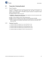
Temperature Sensing Keyboard................................................................................ 55
5.3.1 Project Description......................................................................................... 55
5.3.2 Hardware Connection .................................................................................... 55
5.3.3 Firmware Architecture.................................................................................... 57
5.3.4 Verify Output .................................................................................................. 58
Process Monitoring.................................................................................................... 59
5.4.1 Project Description......................................................................................... 59
5.4.2 Hardware Connection .................................................................................... 60
5.4.3 Firmware Architecture.................................................................................... 61
5.4.4 Verify Output .................................................................................................. 62
Async_PingExample.................................................................................................. 63
5.5.1 Project Description......................................................................................... 63
5.5.2 Hardware Connections .................................................................................. 63
5.5.3 Driver Installation ........................................................................................... 64
5.5.4 Firmware Architecture................................................................................... 67
5.5.5 Verify Output .................................................................................................. 67
Bulk_PingExample .................................................................................................... 68
5.6.1 Project Description......................................................................................... 68
5.6.2 Hardware Connections .................................................................................. 68
5.6.3 Driver Installation ........................................................................................... 69
5.6.4 Firmware Architecture.................................................................................... 70
5.6.5 Verify Output .................................................................................................. 71
ISoc_Example ...........................................................................................................71
5.7.1 Project Description......................................................................................... 71
5.7.2 Hardware Connections .................................................................................. 71
5.7.3 Driver Installation ........................................................................................... 72
5.7.4 Firmware Architecture.................................................................................... 73
5.7.5 Verify Output .................................................................................................. 73
USBUART ................................................................................................................. 74
5.8.1 Project Description......................................................................................... 74
5.8.2 Hardware Connections .................................................................................. 75
5.8.3 Driver Installation ........................................................................................... 76
5.8.4 Firmware Architecture.................................................................................... 77
5.8.5 Verify Output .................................................................................................. 78
Joystick...................................................................................................................... 80
5.9.1 Description ..................................................................................................... 80
5.9.2 Hardware Connection .................................................................................... 80
5.9.3 Firmware Architecture.................................................................................... 82
5.9.4 Verify Output .................................................................................................. 83
A. Appendix
A.1
A.2
A.3
4
85
Schematic.................................................................................................................. 85
Board Layout ............................................................................................................. 86
A.2.1 CY3214 -PSoCEVALUSB Top Copper.......................................................... 86
A.2.2 CY3214-PSoCEVALUSB Top Overlay .......................................................... 87
A.2.3 CY3214 -PSoCEVALUSB Bottom Copper..................................................... 88
Bill of Materials (BOM)............................................................................................... 89
CY3214-PSoCEVALUSB Kit Guide, Doc No. 001-67030 Rev. *B
1.
Introduction
Thank you for your interest in the CY3214-PSoCEVALUSB Kit. This kit includes a development
board for the CY8C24894-24LTXI PSoC® device. Note that the board has the CY8C24094 device,
which is an on-chip debug part for the CY8C24x94 family. You can design your own projects with
PSoC Designer™ or by altering the code examples provided with this kit. It is a combination of
technologies that create opportunities for a new range of low-cost, mixed-signal USB products. This
architecture enables creating customized peripheral configurations that match the requirements of
individual applications.
The CY3214-PSoCEVALUSB Kit is based on the PSoC 1 family of devices. PSoC is a
Programmable System-on-Chip™ platform for 8-bit applications. It combines precision analog and
digital logic with a high-performance CPU. With PSoC, you can create the exact combination of
peripherals and integrated proprietary IP to meet the needs of your applications.
Chapter 2 describes the installation and configuration of the CY3214-PSoCEVALUSB Kit, PSoC
Designer and PSoC Programmer. Chapter 3 describes the kit operation, with the help of the ‘Square
Mouse’ project, which comes as a demonstration with the CY3214-PSoCEVALUSB kit. It also
explains the programming connections of a PSoC 1 device with the PSoC MiniProg and power
supply. Chapter 4 describes the hardware operations. Chapter 5 provides the description of the
execution of simple projects. The Appendix section provides the schematics and bill of materials
(BOM).
1.1
Kit Contents
The CY3214-PSoCEVALUSB Kit includes:
■
PSoCEVALUSB board
■
LCD module
■
MiniProg Programmer
■
USB A to Mini B cable
■
CY3214-PSoCEVALUSB Kit CD
❐
PSoC Designer installation file
❐
PSoC Programmer installation file
❐
Code examples
❐
Hardware files
❐
Kit guide
❐
Quick start guide
❐
Release notes
■
Jumper wire pack
■
CY8C24894-24LTXI sample silicon
Inspect the contents of the kit; if any parts are missing, contact your nearest Cypress sales office for
further assistance.
CY3214-PSoCEVALUSB Kit Guide, Doc No. 001-67030 Rev. *B
5
Introduction
1.2
Additional Learning Resources
Visit www.cypress.com for additional learning resources in the form of data sheets, technical
reference manuals, and application notes.
1.2.1
1.3
Reference Documents
■
Schematic diagram for the CY3214 PSoCEVALUSB board:
http://www.cypress.com/go/CY3214-PSoCEvalUSB
■
CY8C24894-24LTXI data sheet:
http://www.cypress.com/?mpn=CY8C24894-24LTXI
■
PSoC MiniProg1 details:
http://www.cypress.com/go/CY3217-MiniProg1
■
ICE-Cube details:
http://www.cypress.com/go/CY3215-DK
■
PSoC Designer: PSoC Designer Overview
http://www.cypress.com/go/psocdesigner
■
PSoC Designer Training: PSoC Designer On-Demand Training Series and videos
http://www.cypress.com/psoctraining
■
PSoC Programmer, COM Hardware Layer Supported Languages
http://www.cypress.com/go/psocprogrammer
Document History
**
PDF Creation
Date
01/31/2011
Origin of
Change
RKPM
*A
04/27/2011
SASH
Initial version of kit guide
Added My First Code Example section. Content updates throughout
the document
Updated screenshots in the Kit Installation section.
*B
05/03/2012
RKPM
Updated Figure 5-13.
Revision
Description of Change
Updated installer file names.
1.4
Documentation Conventions
Table 1-1. Document Conventions for Guides
Convention
6
Usage
Courier New
Displays file locations, user entered text, and source code:
C:\ ...cd\icc\
Italics
Displays file names and reference documentation:
Read about the sourcefile.hex file in the PSoC Designer User Guide.
[Bracketed, Bold]
Displays keyboard commands in procedures:
[Enter] or [Ctrl] [C]
CY3214-PSoCEVALUSB Kit Guide, Doc No. 001-67030 Rev. *B
Introduction
Table 1-1. Document Conventions for Guides
Convention
Usage
File >> Open
Represents menu paths:
File >> Open >> New Project
Bold
Displays commands, menu paths, and icon names in procedures:
Click the File icon and then click Open.
Times New Roman
Displays an equation:
2+2=4
Text in gray boxes
Describes cautions or unique functionality of the product.
CY3214-PSoCEVALUSB Kit Guide, Doc No. 001-67030 Rev. *B
7
Introduction
8
CY3214-PSoCEVALUSB Kit Guide, Doc No. 001-67030 Rev. *B
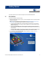
2.
Getting Started
This chapter describes how to install and configure the CY3214-PSoCEVALUSB Kit.
2.1
Kit Installation
To install the kit software, follow these steps:
1. Insert the kit CD into the CD drive of your PC. The CD is designed to auto-run and the kit installer
startup screen appears.
Note You can also download the latest kit installer from http://www.cypress.com/go/CY3214PSoCEvalUSB. Three different types of installers are available for download.
a. CY3214-PSoCEVALUSB Kit ISO: This file (ISO image) is an archive file of the optical disc
provided with the kit. You can use this to create an installer CD or extract information using
WinRar or similar tools.
b. CY3214-PSoCEVALUSB Kit Setup: This executable file installs the contents of the kit CD,
which includes PSoC Programmer, PSoC Designer, kit code examples, kit hardware files, and
user documents.
c. CY3214-PSoCEVALUSB Kit Only (without prerequisites): This executable file installs only the
kit contents, which includes kit code examples, hardware files, and user documents.
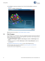
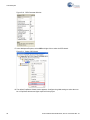
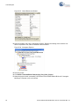
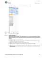
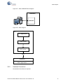
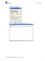
2. Click Install the CY3214-PSoCEVALUSB to start the installation, as shown in Figure 2-1.
Figure 2-1. Kit Installer Startup Screen
CY3214-PSoCEVALUSB Kit Guide, Doc No. 001-67030 Rev. *B
9
Getting Started
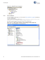
Note If auto-run does not execute, double-click cyautorun.exe file on the root directory of the
CD/DVD, as shown in Figure 2-2.
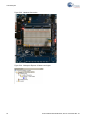
Figure 2-2. Root directory of the CD/DVD
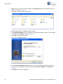
3. On the startup screen, click Next to start the installer.
4. The InstallShield Wizard screen is displayed, with the default location for setup. You can change
the location using Change, as shown in Figure 2-3.
5. Click Next to launch the kit installer.
Figure 2-3. InstallShield Wizard
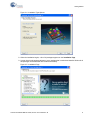
6. On the Product Installation Overview screen, select the installation type that best suits your
requirement. The drop-down menu has three options: Typical, Complete, and Custom; see
Figure 2-4.
7. Click Next to continue the installation.
10
CY3214-PSoCEVALUSB Kit Guide, Doc No. 001-67030 Rev. *B
Getting Started
Figure 2-4. Installation Type Options
8. When the installation begins, a list of all packages appears on the Installation Page.
9. A green check mark appears adjacent to every package that is cached and installed. Wait until all
the packages are downloaded and installed successfully.
Figure 2-5. Installation Page
CY3214-PSoCEVALUSB Kit Guide, Doc No. 001-67030 Rev. *B
11
Getting Started
10.Click Finish to complete the installation of the CY3214-PSoCEVALUSB Kit, as shown in
Figure 2-6.
Figure 2-6. Installation Completion Page
Note Advanced users can skip to Code Examples chapter on page 31.
2.2
PSoC Designer
PSoC Designer is the revolutionary easy-to-use Integrated Development Environment (IDE) that
helps to customize PSoC to meet your specific application requirements. PSoC Designer accelerates system bring-up and time-to-market.
1. Click Start > All Programs > Cypress > PSoC Designer <version> > PSoC Designer <version>.
2. To create a new project, click File > New Project; click File > Project Workspace to open an
existing project.
See Additional Learning Resources on page 6 for links to PSoC Designer training.
The PSoC Designer quick start guide is available at: http://www.cypress.com/?rID=47954.
For more details on PSoC Designer, go to:
<Install_Directory>:\Cypress\PSoC Designer\<version>\Documentation
12
CY3214-PSoCEVALUSB Kit Guide, Doc No. 001-67030 Rev. *B
Getting Started
Figure 2-7. PSoC Designer Interconnect View
CY3214-PSoCEVALUSB Kit Guide, Doc No. 001-67030 Rev. *B
13
Getting Started
2.3
PSoC Programmer
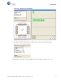
To open the PSoC Programmer, click Start > All Programs > Cypress > PSoC Programmer <version> > PSoC Programmer <version>.
To successfully program the device, follow these steps:
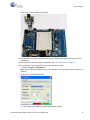
1. Use the Power button to power up the CY3214-PSoCEVALUSB kit before loading the hex file on
to the kit.
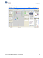
Figure 2-8. PSoC Programmer
2. Click the File Load button to load the respective hex file.
3. Click the Program button to program the hex file to the chip.
4. When programming is successful, Programming Succeeded appears in the Actions pane.
5. Close PSoC Programmer.
Note For more details on PSoC Programmer, go to:
<Install_Directory>:\Cypress\Programmer\<version>\Documents
2.4
SuiteUSB 3.4
The Cypress SuiteUSB 3.4 is a generic USB driver environment that you can freely use to develop
host applications that interact with a USB device.
CyConsole is used to communicate with USB devices that match the CyUSB.sys device driver. The
console supports hot-plugging of USB devices. When a device that matches the driver is plugged
into the PC, it automatically appears in the device list near the top of the CyConsole window.
SuiteUSB 3.4 software can be installed from the link http://www.cypress.com/?rID=34870.
14
CY3214-PSoCEVALUSB Kit Guide, Doc No. 001-67030 Rev. *B
3.
3.1
Kit Operation
Introduction
The CY3214-PSoCEVALUSB kit examples helps you to exchange data between a PC application
and real world I/O. The kit includes a full-speed USB User Module with programmable I/O user
modules to provide instant connection.
3.2
Square Mouse Example
The Square Mouse example is programmed to the CY3214-PSoCEVALUSB board as a default
project for demonstration purposes. If the PSoC on the board has been reprogrammed or erased,
follow the steps in the section, Programming Specifications and Connections on page 16 to program
the board with the square mouse hex file provided in the kit CD (<Install_Directory>:\
Cypress\CY3214-PSoCEVALUSB\<version>\Firmware\squaremouse2_reset.hex).
To execute the program, follow these steps:
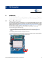
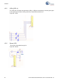
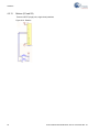
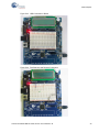
1. Connect the USB2 cable to the Mini USB type B connector on P1, as shown in Figure 3-1.
Ensure that the power selection jumper (shunt) is place on the first two pins (designated as
VBUS).
2. The message ”PSoC Eval USB 1” is displayed on the LCD.
3. Check the movement of the mouse pointer on the screen; note that it moves in a square fashion.
Figure 3-1. USB Cable Connection and Power Jumper Setting
CY3214-PSoCEVALUSB Kit Guide, Doc No. 001-67030 Rev. *B
15
Kit Operation
3.2.1
Programming Specifications and Connections
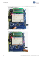
When the MiniProg is connected, you can use PSoC Programmer to program the CY3214PSoCEVALUSB kit. Plug in the USB cable into the MiniProg before attaching it to the ISSP header
on the board. When using a USB cable with MiniProg, keep the length under six feet to avoid signal
integrity issues.
When using MiniProg, the LEDs blink at a variable rate to track connection status. The green LED
near the USB connector turns on after MiniProg is plugged into the computer and is configured by
the operating system. If MiniProg cannot find the correct driver in the system, this LED does not turn
on. After the device is configured, the LED stays on at about a 4-Hz blink rate. This changes during
programming, where the blink duty cycle increases.
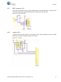
The red LED (Figure 3-2) at the bottom turns on when the MiniProg powers the part. The LED is off
when power is provided by the target board.
Figure 3-2. Programming PSoC Device
16
CY3214-PSoCEVALUSB Kit Guide, Doc No. 001-67030 Rev. *B
Kit Operation
Figure 3-3. PSoC Programmer Screen
File Load
Program
Toggle Power
Follow these steps to program using MiniProg1:
1. Connect the USB cable to the PC and MiniProg1
2. Plug in the MiniProg1 to the ISSP header on the CY3214-PSoCEVALUSB board
3. When USB is connected to the MiniProg1, the LED (green) glows in the MiniProg1
4. Open PSoC Programmer
5. Click the Load File button and browse to the hex file location. Click Open to select the hex file
6. Click Connect or double-click on the respective MiniProg under Port Selection to select or connect to MiniProg
7. Click Program or press [F5] to initiate programming
8. The green LED on the MiniProg1 blinks to indicate the progress of programming
9. After successful programming, the red LED on MiniProg1 is powered off
10.Select the Toggle Power button in PSoC Programmer to power the board and verify output
CY3214-PSoCEVALUSB Kit Guide, Doc No. 001-67030 Rev. *B
17
Kit Operation
18
CY3214-PSoCEVALUSB Kit Guide, Doc No. 001-67030 Rev. *B
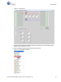
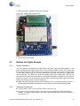
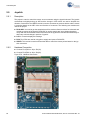
4.
Hardware
This section provides an overview of the hardware, including power system, jumper setting, and
programming interface. To start using the board, go to Code Examples chapter on page 31.
4.1
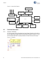
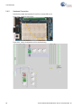
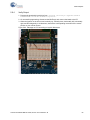
System Block Diagram
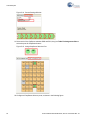
The CY3214-PSoCEVALUSB Kit has the following sections:
■
Character LCD module
■
Buzzer (LS1)
■
Contrast potentiometer (R2)
■
Buttons (S1 and S2)
■
ISSP connector(J15)
■
LEDs (LED 1–4)
■
Potentiometer (VR1 and VR2)
■
USB connector (P1)
■
CapSense buttons (P3[0], P3[7]), and sliders (Port5)
■
Power supply connector (J13)
■
Joystick (JS1)
■
Reset button (S3)
■
Legacy DB9 connector (J1)
■
ICE-Cube connector (J14)
CY3214-PSoCEVALUSB Kit Guide, Doc No. 001-67030 Rev. *B
19
Hardware
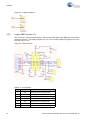
Figure 4-1. CY3214-PSoCEVALUSB Board
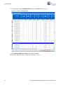
Table 4-1. Functional Pin Table
20
Pin No.
Pin Name
1
P2[3]
Direct switched capacitor block input
Description
2
P2[1]
Direct switched capacitor block input
3
P4[7]
GPIO
4
P4[5]
GPIO
5
P4[3]
GPIO
6
P4[1]
GPIO
7
P3[7]
GPIO
8
P3[5]
GPIO
9
P3[3]
GPIO
10
P3[1]
GPIO
11
P5[7]
GPIO
12
P5[5]
GPIO
13
P5[3]
GPIO
14
P5[1]
GPIO
CY3214-PSoCEVALUSB Kit Guide, Doc No. 001-67030 Rev. *B
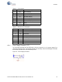
Hardware
Table 4-1. Functional Pin Table
Pin No.
Pin Name
Description
15
P1[7]
I2C serial clock (SCL)
16
P1[5]
I2C serial data (SCA)
17
P1[3]
GPIO
18
P1[1]
I2C serial clock (SCL), ISSP SCLK[2]
19
Vss
Ground connection
20
D+
GPIO
21
D–
GPIO
22
Vdd
Supply voltage
23
P7[7]
GPIO
24
P7[0]
GPIO
25
P1[0]
I2C serial data (SDA), ISSP SDATA[2]
26
P1[2]
GPIO
27
P1[4]
Optional external clock input (EXTCLK)
28
P1[6]
GPIO
29
P5[0]
GPIO
30
P5[2]
GPIO
31
P5[4]
GPIO
32
P5[6]
GPIO
33
P3[0]
GPIO
34
P3[2
GPIO
35
P3[4]
GPIO
36
P3[6]
GPIO
37
P4[0]
GPIO
38
P4[2]
GPIO
39
P4[4]
GPIO
40
P4[6]
GPIO
41
P2[0]
Direct switched capacitor block input
42
P2[2]
Direct switched capacitor block input
43
P2[4]
External analog ground (AGND) input
44
P2[6]
External voltage reference (VREF) input
45
P0[0]
Analog column mux input
46
P0[2]
Analog column mux input
47
P0[4]
Analog column mux input VREF
48
P0[6]
Analog column mux input
49
Vdd
Supply voltage
50
Vss
51
P0[7]
Analog column mux input
Ground connection
52
P0[5]
Analog column mux input and column output
53
P0[3]
Analog column mux input and column output
54
P0[1]
Analog column mux input
55
P2[7]
GPIO
56
P2[5]
GPIO
CY3214-PSoCEVALUSB Kit Guide, Doc No. 001-67030 Rev. *B
21
Hardware
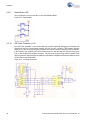
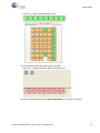
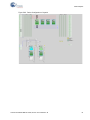
Figure 4-2. Hardware Block Diagram
,663
86%
'&6XSSO\
&RQWUDVW3RWHQWLRPHWHU
&DS6HQVH %XWWRQVDQG
6OLGHUV
&KDUDFWHU/&''LVSOD\
3RZHU6XSSO\
,663 &RQQHFWRU
,&(&XEH&RQQHFWRU
-R\VWLFN
5HVHW%XWWRQ
%X]]HU
36R& %XWWRQV6DQG 6
56,QWHUIDFH
3RWHQWLRPHWHU
95 DQG 95
4.2
Functional Description
4.2.1
Character LCD Module
86%&RQQHFWRU
/('V The kit has a character LCD module, which goes into the character LCD header, P8. The LCD runs
on a 5-V supply and can function regardless of the voltage on which PSoC is powered. There is a
zero-ohm resistor setting available on the LCD section making it possible to convert it to a 3.3-V
LCD. The variable resistor R2 is a contrast potentiometer. It is used to control the LCD contrast.
Figure 4-3. LCD Module
22
CY3214-PSoCEVALUSB Kit Guide, Doc No. 001-67030 Rev. *B
Hardware
4.2.2
CapSense® Buttons (P3[0], P3[7]), and Sliders (Port5)
There are two CapSense buttons and eight element CapSense sliders on the CY3214PSoCEVALUSB kit. CapSense Sigma Delta uses an external modulation capacitor (CMOD), the
copper sensor pad on the CY3214 PSoCEVALUSB board, and bleed resistor (Rb) in addition to the
sensor capacitor (Cx).
Bleed Resistor (Rb): The CSD uses the switched capacitor circuitry to convert the sensor
capacitance into a voltage, which is compared to a reference voltage. When the capacitor voltage
reaches the reference voltage, the comparator triggers a bleed resistor discharging the capacitor.
After the capacitor voltage discharges below the reference voltage, the bleed resistor is left floating
to allow the capacitor to continue charging. The comparator output becomes a bit-stream as it
toggles the bleed resistor and manipulates its input voltage. This bit stream is ANDed with a pulse
width modulator (PWM) to provide consistent stream framing. The number of counts in each frame is
analyzed to determine if the capacitive sensor is activated.
Modulation Capacitor (CMOD): The capacitor CMOD acts to attenuate high-frequency noise. The
pin assignment for CapSense buttons used in the CapSense code example (see My First Code
Example on page 31) are as follows:
B2 – P3[7]
B3 – P3[0]
The slider segments pin assignment used in My First Code Example on page 31 are as follows:
Slider 0 – P5[7]
Slider 1 – P5[5]
Slider 2 – P5[3]
Slider 3 – P5[1]
Slider 4 – P5[0]
Slider 5 – P5[2]
Slider 6 – P5[4]
Slider 7 – P5[6]
Figure 4-4. CapSense Sliders
CY3214-PSoCEVALUSB Kit Guide, Doc No. 001-67030 Rev. *B
23
Hardware
Figure 4-5. CapSense Buttons
4.2.3
Legacy DB9 Connector (J1)
This connector is used for serial interface. Connect the serial cable to the DB9 connector and the
serial port on the PC. The supply voltage is 3.3 V to 5 V; the output voltage Vout (high) is Vcc–0.6 V
and Vout (low) is 0.4 V.
Figure 4-6. DB9 Connector
Table 4-2. IC Description
24
Pin No.
Pin Name
Description
1
C1+
2
V+
Vcc supply
3
C1–
Connected to –ve of capacitor C3
4
C2+
Connected to +ve of capacitor C4
5
C2–
Connected to –ve of capacitor C4
6
V–
7
T2 out
Connected to +ve of capacitor C3
Vcc ground
Request to send (OUT)
CY3214-PSoCEVALUSB Kit Guide, Doc No. 001-67030 Rev. *B
Hardware
Table 4-2. IC Description
Pin No.
Pin Name
Description
8
R2in
9
R2out
Clear to send (OUT)
Clear to send (IN)
10
T2in
Request to send (IN)
11
T1in
Transmitted data (IN)
12
R1out
Receive data (OUT)
13
R1in
Receive data (IN)
14
T1out
Transmitted data (OUT)
15
Gnd
Ground
16
Vcc
Vcc supply
Table 4-3. DB9 Connector Description
4.2.4
Pin No
Pin Name
Description
1
DCD
Carrier detect
2
RD
Receive data
3
TD
Transmit data
4
DTR
5
SGND
System ground
6
DSR
Data set ready
7
RTS
Request to send
8
CTS
Clear to send
9
RI
Ring indicator
Data terminal ready
Power Supply Connector (J13)
You can power the board from the USB cable or from an external 9 V to 12 V power supply. D1 is
used as a protecting diode. The protecting diodes are necessary if the load discharges are slower
than the filter capacitor after the rectification process.
Figure 4-7. Power Supply Connector
CY3214-PSoCEVALUSB Kit Guide, Doc No. 001-67030 Rev. *B
25
Hardware
4.2.5
LEDs (LED1–4)
Four LEDs are accessible through headers LED1–4. LEDs are illuminated by connecting the signal
to Vss (active low, set drive to strong, drive low). These LEDs are active low.
Figure 4-8. LEDs
4.2.6
Buzzer (LS1)
The buzzer is accessible through LS1.
Figure 4-9. Buzzer
26
CY3214-PSoCEVALUSB Kit Guide, Doc No. 001-67030 Rev. *B
Hardware
4.2.7
ISSP Connector (J15)
This is used to program the device using the MiniProg device and the USB cable. To load a hex file
to the PSoC device chip, plug the MiniProg device to the jumper connector (J15).
Figure 4-10. ISSP Connector
4.2.8
Joystick (JS1)
A joystick is used to create a game. JSV (vertical pot value), JSH (horizontal pot value), and JSW
(switch) are accessible through the header on the board.
Figure 4-11. Joystick
CY3214-PSoCEVALUSB Kit Guide, Doc No. 001-67030 Rev. *B
27
Hardware
4.2.9
Reset Button (S3)
The reset button is used to reset the CY3214-PSoCEVALUSB kit.
Figure 4-12. Reset Button
4.2.10
ICE-Cube Connector (J14)
The ICE-Cube (available in the CY3215-DK Kit) provides significant debugging functionality that
requires full two-way communication between the ICE and your computer. This software interface
allows to run, halt, and single-step the processor and view the content of specific memory locations.
It also allows to set complex event points. Event points can start and stop the trace memory on the
ICE, as well as break the program execution. The ICE-Cube supports large memory model PSoC
devices (with more than 256 bytes of RAM) and is backward compatible with previous PSoC devices
(CY8C27x43 and CY8C24x23A).
Figure 4-13. ICE-Cube Connector
28
CY3214-PSoCEVALUSB Kit Guide, Doc No. 001-67030 Rev. *B
Hardware
Table 4-4. Pin Description
Pin No
1
2
3
4
5
6
7
8
4.2.11
Pin Name
OCDHC
GND
XRES
GND
OCDCC
OCDDO
OCDDE
VCC
Pin Description
OCD high-speed clock output
Ground
Reset signal (required only for Reset programming mode)
Ground
OCD CPU clock output
OCD odd data output
OCD even data I/O.
Supply voltage
USB Connector (P1)
The mini USB type B connector is compatible with USB 2.0 connector specifications. The RC filter is
used to isolate the VBUS from the on-board voltage domain.
Figure 4-14. USB Connector
4.2.12
Potentiometers (VR1 and VR2)
A potentiometer is a manually adjustable resistor. The potentiometer used here is of 10 KΩ variable
resistors.They are tied to Vss and Vcc (set drive to analog high-Z).
Figure 4-15. Potentiometers
CY3214-PSoCEVALUSB Kit Guide, Doc No. 001-67030 Rev. *B
29
Hardware
4.2.13
Buttons (S1 and S2)
These are SPST (single pole, single throw) switches.
Figure 4-16. Buttons
30
CY3214-PSoCEVALUSB Kit Guide, Doc No. 001-67030 Rev. *B
5.
Code Examples
All code examples for the CY3214-PSoCEVALUSB kit are available at the following location:
<Install_Directory>:\Cypress\CY3214-PSoCEVALUSB\<version>\Firmware.
5.1
My First Code Example
5.1.1
Project Objective
This example demonstrates how to operate the CapSense buttons and sliders. When you configure
CapSense buttons and sliders in the CSD wizard, the corresponding LEDs check the functionality of
CapSense buttons provided on the board.
The following user modules are used in the project:
■
CSD: The CSD (Capacitive sensing using a Sigma-Delta Modulator) provides CapSense functionality using the switched capacitor technique with a sigma-delta modulator to convert the sensing switched capacitor current to digital code.
■
LCD: The LCD module is used to display a horizontal bar graph when the CapSense slider is
touched.
■
LED (1–2): LEDs 1–2 glows when CapSense buttons are touched.
CY3214-PSoCEVALUSB Kit Guide, Doc No. 001-67030 Rev. *B
31
Code Examples
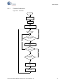
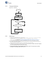
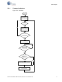
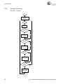
5.1.2
Flowchart
6WDUW
,QLWLDOL]DWLRQRI8VHU
0RGXOHV
6FDQ &DS6HQVH
EXWWRQVDQGVOLGHUV
1R
8SGDWH%DVHOLQHRI
DOOWKHVHQVRUV
,I6HQVRU
YDOXH!)LQJHU
WKUHVKROG
<HV
&KHFN2QDQG2))
VWDWHRIVHQVRUV
,I%XWWRQBLV
SUHVVHG
<HV
1R
1R
/('BLV21
,I%XWWRQBLV
SUHVVHG
<HV
1R
/('BLV21
*HW)LQJHU3RVLWLRQ
IURP6OLGHU
,))LQJHULV
WRXFKHG
<HV
+RUL]RQWDOJUDSK
DSSHDUVRQ/&'
32
CY3214-PSoCEVALUSB Kit Guide, Doc No. 001-67030 Rev. *B
Code Examples
5.1.3
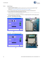
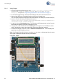
Creating My First PSoC 1 Project
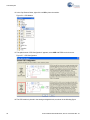
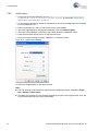
1. Open PSoC Designer.
2. To create a new project, click File > New Project.
3. In the New Project window, select the Chip-level icon. Name the project
Example_My_First_PSoC_Project; see Figure 5-1.
4. Click Browse and navigate to the directory in which the project is being created.
Figure 5-1. New Project Window
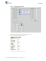
5. Click OK. The Select Project Type window opens.
6. In this window, under Select Target Device, click View Catalog, as shown in Figure 5-2.
Figure 5-2. Select Project Type Window
7. The Device Catalog window opens. Click on the All Devices tab.
CY3214-PSoCEVALUSB Kit Guide, Doc No. 001-67030 Rev. *B
33
Code Examples
8. For this project, click CY8C24894-24LTXI and then click Select. See Figure 5-3.
Figure 5-3. Device Catalog Window
9. Under Generate 'Main' File Using:, select C and click OK.
10.By default, the project opens in chip view, as shown in Figure 5-4.
34
CY3214-PSoCEVALUSB Kit Guide, Doc No. 001-67030 Rev. *B
Code Examples
Figure 5-4. Default View
Now, place and configure the modules required for this design. Also, connect the modules
together and to the pins of the PSoC.
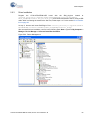
11. In the User Modules window, expand the Cap Sensors folder.
Figure 5-5. User Modules Window
CY3214-PSoCEVALUSB Kit Guide, Doc No. 001-67030 Rev. *B
35
Code Examples
12.In the Cap Sensors folder, right-click on CSD to place the module.
Figure 5-6. CSD Module
13.The splash screen "CSD Configuration" appears; select CSD with PRS8 as clock source.
Figure 5-7. CSD Configuration
14.The CSD module is placed in the analog and digital blocks, as shown in the following figure.
36
CY3214-PSoCEVALUSB Kit Guide, Doc No. 001-67030 Rev. *B
Code Examples
Figure 5-8. Chip View with CSD Module
15.The default parameter window of CSD_1 is shown in Figure 5-9.
Figure 5-9. Default CSD Parameter Window
16.Configure the CSD Module parameter window.
CY3214-PSoCEVALUSB Kit Guide, Doc No. 001-67030 Rev. *B
37
Code Examples
Figure 5-10. CSD Parameter Window
17.In the Workspace Explorer, select CSD and right-click to select the CSD wizard.
Figure 5-11. Select CSD Wizard
18.The default CapSense Wizard window appears. Configure the global settings to select the number of CapSense buttons and lights required for the project.
38
CY3214-PSoCEVALUSB Kit Guide, Doc No. 001-67030 Rev. *B
Code Examples
Figure 5-12. Default View of CSD Wizard
19.Configure the Global Settings window of CSD Wizard, as shown in the following figure.
Figure 5-13. Global Settings Window
20.Similarly, click the slider once and configure the sensor settings, as shown in Figure 5-14.
CY3214-PSoCEVALUSB Kit Guide, Doc No. 001-67030 Rev. *B
39
Code Examples
Figure 5-14. Sensor Settings Window
21.Select each of the CapSense switches SW0 and SW1; drag it to Table Pin Assignment View to
select the ports for CapSense buttons
Figure 5-15. Assign CapSense Switch to Port
22.Configure all CapSense sliders to ports, as shown in the following figure.
40
CY3214-PSoCEVALUSB Kit Guide, Doc No. 001-67030 Rev. *B
Code Examples
Figure 5-16. Assign CapSense Slider to Port
23.The CapSense buttons and sliders appear as follows.
Figure 5-17. Assigned CapSense Buttons and Slider View
24.In the User Module Window, select Misc Digital Folder to select the LCD module.
CY3214-PSoCEVALUSB Kit Guide, Doc No. 001-67030 Rev. *B
41
Code Examples
Figure 5-18. User Module Window
25.Place the module by right-clicking on the LCD and select Place.
42
CY3214-PSoCEVALUSB Kit Guide, Doc No. 001-67030 Rev. *B
Code Examples
Figure 5-19. Select LCD Module
26.Default LCD_1 parameters window are shown in the following figure.
Figure 5-20. Default LCD_1 Parameter Window
27.Rename LCD_1 as LCD and configure the parameters to build the project successfully.
Figure 5-21. LCD Parameter Window
28.In the User Module window, go to Misc Digital folder and select LED.
CY3214-PSoCEVALUSB Kit Guide, Doc No. 001-67030 Rev. *B
43
Code Examples
Figure 5-22. Select LED Module
29.Default LED_1 parameter window appears, as shown in the following figure.
Figure 5-23. Default LED_1 Parameter Window
30.Configure LED_1 parameter to successfully build the project.
Figure 5-24. LED_1 Parameter Window
44
CY3214-PSoCEVALUSB Kit Guide, Doc No. 001-67030 Rev. *B
Code Examples
31.Similarly add another LED module and rename it to build the project.
Figure 5-25. LED_2 Parameter Window
32.Finally, LCD and LED modules are placed in Chip view window.
Figure 5-26. LED and LCD Modules
33.Configure the Global Resources window as shown in the following figure.
CY3214-PSoCEVALUSB Kit Guide, Doc No. 001-67030 Rev. *B
45
Code Examples
Figure 5-27. Global Resources Window
34.Open the existing main.c file in Workspace Explorer. Replace the existing main.c with the contents of CapSense.c file, which is attached to this document.
Figure 5-28. Workspace Explorer
35.Save the project.
36.Click Build > Generate/Build 'Example_My_First_PSoC_Project'.
37.When the project is built successfully, connect the CY3214-PSoCEVALUSB kit to PC through a
MiniProg1 Connector (J15) on the board.
46
CY3214-PSoCEVALUSB Kit Guide, Doc No. 001-67030 Rev. *B
Code Examples
Figure 5-29. Connect MiniProg1 to Board
38.The board can be programmed either through PSoC Designer IDE itself or by launching PSoC
Programmer.
39.To program the board using PSoC Programmer, see PSoC Programmer on page 14.
40.To program the board through PSoC Designer, follow these steps.
a. Click on Program > Program Part.
Note When programming the board from PSoC Designer, close any open instance of PSoC Programmer.
Figure 5-30. Program Part Window
b. In the Program Part window, configure the following settings:
CY3214-PSoCEVALUSB Kit Guide, Doc No. 001-67030 Rev. *B
47
Code Examples
- Port Selection: select MiniProg1/<MiniProg Number> with the status Connected
- Acquire Mode: Power Cycle
- Verification: Off
- Power Settings: 5.0 V
c. Click on the Program button to start programming the board.
d. The programming starts and the status is displayed on the progress bar.
Figure 5-31. Programming Status
e. When the programming is done successfully, the 'Operation Succeeded!' Message is shown.
Figure 5-32. 'Operation Succeeded!' Message
5.1.4
Verify Output
1. Make the following connections on the board using the single strand jumper wires provided.
a. Connect 2-KΩ resistor between Port P0.5 (P05 on J4) and P1.5 (P15 on J9).
b. Connect LED1 to Port P3.1 (P31 on J10) and LED2 to P3.2(P32 on J10).
48
CY3214-PSoCEVALUSB Kit Guide, Doc No. 001-67030 Rev. *B
Code Examples
Figure 5-33. USB Connection to Board
Figure 5-34. Port Selection and Resistor Connection
CY3214-PSoCEVALUSB Kit Guide, Doc No. 001-67030 Rev. *B
49
Code Examples
2. When the CapSense slider is touched, the horizontal bar-graph is displayed on the LCD.
Figure 5-35. Bar-Graph on LCD
3. LED1 glows when CapSense button P30 is touched.
Figure 5-36. LED1 Glows for Button P30
50
CY3214-PSoCEVALUSB Kit Guide, Doc No. 001-67030 Rev. *B
Code Examples
4. LED2 glows when CapSense button P37 is touched.
Figure 5-37. LED2 Glows for Button P37
5. Save and close the project.
5.2
Buttons and Lights Example
5.2.1
Project Description
This code example demonstrates the USB function using the CY3214-PSoCEVALUSB Kit. In this
project, the Buttons and Lights PC Host GUI is used to control the LEDs on board. The GUI also has
four soft buttons and four LEDs. When there is a button press event on the board, the board sends
out the buttons report to the GUI. The GUI updates the local LEDs and sends out a Lights report
back to the board. The LEDs on the board are updated based on this Lights report. The GUI also
provides the LED output as a logical function of soft buttons and buttons on board. The LED output is
a function of 'AND' or 'OR' of soft buttons and real buttons. By default, the LED output is that of real
buttons The following module is used in the project:
■
5.2.2
USB: This module handles requests from the USB host (PC) to communicate with the device. It
handles data packet transfer between the host and device connected to host through USB.
Hardware Connections
■
Connect LEDs 1-4 to P3.2 to P3.5 (P32 to P35 on connector J10).
■
Port pins P2.2 to P2.5 (P22 to P25 on connector J12) are configured as active-low buttons in
firmware. To simulate a button press connect the required port pin to ground (terminal marked '-')
on connector J11.
CY3214-PSoCEVALUSB Kit Guide, Doc No. 001-67030 Rev. *B
51
Code Examples
Figure 5-38. Hardware Connection
Figure 5-39. Workspace Explorer of Buttons and Lights
52
CY3214-PSoCEVALUSB Kit Guide, Doc No. 001-67030 Rev. *B
Code Examples
5.2.3
Firmware Architecture
5.2.3.1
Device Program Firmware Architecture
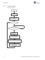
Figure 5-40. Flowchart
67$57
7LPHU
/RFDO%XWWRQ
3UHVV"
&RQQHFWWR
+RVW
<(6
6HQG%XWWRQV
5HSRUW
<(6
8SGDWH/RFDO
/('V
12
/LJKWV5HSRUW
5HFY"
:DLW
12
5HWXUQ
5.2.3.2
Host Program Firmware Architecture
Figure 5-41. Flowchart
67$57
7LPHU
/RRNIRU
GHYLFH
12
8SGDWH/RFDO
/('V
'HYLFH
&RQQHFWHG"
<(6
:DLW
%XWWRQ&OLFN
%XWWRQV
5HSRUW 5HFY"
12
<(6
6HQG/LJKWV
5HSRUW
5HWXUQ
5HWXUQ
CY3214-PSoCEVALUSB Kit Guide, Doc No. 001-67030 Rev. *B
53
Code Examples
5.2.4
Verify Output
1. Load the Example1.hex from <Install_Directory>:\Cypress\CY3214-PSoCEVALUSB\<version>\Firmware\ButtonsAndLights\PSoC Project\Example1, as
explained in Programming Specifications and Connections on page 16.
2. On successful programming, disconnect the MiniProg1 and connect the board to PC.
3. Open the Buttons and Lights GUI (Example1.exe) from
<Install_Directory>:\Cypress\CY3214-PSoCEVALUSB\<version>\Firmware\ButtonsAndLights\PC Software\Example1.
4. Press any of the four soft buttons on the GUI; the corresponding LEDs in the GUI glow (green)
and similar LEDs glow in the kit (red).
Figure 5-42. (a) GUI Display (b) Kit Display
(b)
(a)
Figure 5-43. (a) GUI Display (b) Kit Display
(a)
54
(b)
CY3214-PSoCEVALUSB Kit Guide, Doc No. 001-67030 Rev. *B
Code Examples
5.3
Temperature Sensing Keyboard
5.3.1
Project Description
This project example operates similar to a keyboard, although it does not look like a standard keyboard. The
example is a temperature sensor using potentiometer (VR1 and VR2) as surrogates for real
temperature sensors. When plugged in using USB, the project enumerates as a keyboard and starts
printing out temperature values.
The following modules are used in the project:
5.3.2
■
ADCIN: It is a differential input ADC from where the samples are received and used as the reference values to calculate the real temperature.
■
LCD: It is used to display the values of the real temperatures.
■
PGA: It is used as an amplifier where it amplifies the signal received from ADCINC.
■
USB: This module is used to handle the request from the USB host (PC) to communicate with the
device. It handles all the data packet transfer between the host and device connected to host
through the USB.
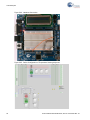
Hardware Connection
1. Connect the jumper wire between S1 on J2 and P3.0 (P30 on J10).
2. Connect the jumper wire between S2 on J2 and P3.1 (P31 on J10).
3. Connect the jumper wire between VR1 on J2 and P3.6 (P36 on J10).
4. Connect the jumper wire between VR2 on J2 and P3.7 (P37 on J10).
5. Connect the jumper wire between P2.7 (P27 on J12) and LS1 on J2.
CY3214-PSoCEVALUSB Kit Guide, Doc No. 001-67030 Rev. *B
55
Code Examples
Figure 5-44. Hardware Connection
Figure 5-45. Device Configuration of Temperature Sensing Keyboard
56
CY3214-PSoCEVALUSB Kit Guide, Doc No. 001-67030 Rev. *B
Code Examples
5.3.3
Firmware Architecture
Figure 5-46. Flowchart
67$57
,QLWLDOL]HDOO8VHU
0RGXOHV
:DLW
:KLOH
,I'DWDLV
DYDLODEOH
<(6
'LVSOD\WHPSHUDWXUH
YDOXHVRQ/&'
12
*HWPRUH
VDPSOHV
(1'
CY3214-PSoCEVALUSB Kit Guide, Doc No. 001-67030 Rev. *B
57
Code Examples
5.3.4
Verify Output
1. Load the Example2.hex from <Install_Directory>:\Cypress\CY3214-PSoCEVALUSB\<version>\Firmware\Temperature Sensing Keyboard\PSoC Project\
Example2\, as explained in Programming Specifications and Connections on page 16.
2. Open either a Microsoft Excel 2003 or 2007 application or a Windows Notepad application on the
computer and plug in the board using USB.
3. Press S1 or S2 to see the temperature values directly in the editor or spreadsheet; the corresponding temperature values are displayed on the LCD.
4. Press the CAPS_LOCK key on the keyboard to toggle the buzzer on and off. Vary the potentiometer (VR1 and VR2) and press S1 and S2 again.
Figure 5-47. Output
58
CY3214-PSoCEVALUSB Kit Guide, Doc No. 001-67030 Rev. *B
Code Examples
Figure 5-48. Temperature Sensor Output on Excel spreadsheet
5.4
Process Monitoring
5.4.1
Project Description
The process monitoring system code demonstrates how to collect the analog data at a rate
determined by the host. The host then displays the data in a graph and is able to save and reload the
data sets.
The following modules are used in the project
■
ADCIN: It is a differential input ADC from where the samples are received and used as the reference values to calculate the real temperature.
■
LCD: It is used to display the values of the real temperatures.
■
PGA: It is used as an amplifier where it amplifies the signal received from ADCINC.
■
USB: This module is used to handle the request from the USB host (PC) to communicate with the
device. It handles all the data packet transfer between the host and device connected to the host
through the USB.
CY3214-PSoCEVALUSB Kit Guide, Doc No. 001-67030 Rev. *B
59
Code Examples
5.4.2
Hardware Connection
Connect the jumper wire between P0.3 (P03 on J4) and VR1 on J2.
Figure 5-49. Hardware Connection
Figure 5-50. Device Configuration of Process Monitoring
60
CY3214-PSoCEVALUSB Kit Guide, Doc No. 001-67030 Rev. *B
Code Examples
5.4.3
Firmware Architecture
Figure 5-51. Flowchart
67$57
&RQQHFWWR+RVW
:DLW
(QDEOH (3
IRU
287WUDQVIHU
:KLOH
12
,IGDWDLVDYDLODEOH
IURP$'&
12
YES
'LVSOD\WKH7HPSHUDWXUH
9DOXHV
,IGDWDLV
VXSSOLHG
<(6
12
,IHQWLUHGDWD
LVVXSSOLHG
<(6
'LVSOD\WKH6DPSOHV
9DOXH
/RDGDQGHQDEOH (3 IRU
,1WUDQVIHU
CY3214-PSoCEVALUSB Kit Guide, Doc No. 001-67030 Rev. *B
61
Code Examples
5.4.4
Verify Output
1. Program the board with Example3.hex from <Install_Directory>:\Cypress\CY3214PSoCEVALUSB\<version>\Firmware\Process Monitoring\PSoC Project\
Example3\, as explained in Programming Specifications and Connections on page 16.
2. On successful programming, disconnect the MiniProg1 and connect the board to the PC.
3. Wait until the HID device is installed (first time only) and run Example3.exe.
The LCD display shows the temperature value but indicates it is waiting for input from Host (PC).
4. Open the Process Monitoring GUI (Example3.exe) from
<Install_Directory>:\Cypress\CY3214-PSoCEVALUSB\<version>\Firmware\Process Monitoring\PC Software\Example3.
5. On the GUI, click the GetSamples button. The PC waits until 256 samples are received from the
board and then displays a graph of Temperature Vs Time.
6. Vary the VR1 on the board and click the GetSamples button again to see the difference in the
graph. This difference can be best viewed when Continuous Sampling is selected.
7. If continuous sampling is required, click the Continuous Samples button. The PC displays the
graph after every 256 samples received.
Note If the Sample Rate slider is kept at a minimum, the time taken to display graph also increases
as the graph is displayed only after receiving 256 samples.
Figure 5-52. Output
62
CY3214-PSoCEVALUSB Kit Guide, Doc No. 001-67030 Rev. *B
Code Examples
Figure 5-53. GUI Display
5.5
Async_PingExample
5.5.1
Project Description
The project demonstrates asynchronous data transfer by sending a series of large USB write (OUT)
and read (IN) requests by using USB functionality, which is available with CY8C24894 device.
The following user module is used in the project:
■
5.5.2
USBFS_1: This module is used to handle the request from the USB host (PC) to communicate
with the device. It handles all the data packet transfer between the host and device connected to
host through the USB.
Hardware Connections
There are no hardware connections required.
Figure 5-54. Device Configuration of Async_PingExample
CY3214-PSoCEVALUSB Kit Guide, Doc No. 001-67030 Rev. *B
63
Code Examples
5.5.3
Driver Installation
The driver installation steps are for Windows XP and not Windows 7. Program the CY3214PSoCEVALUSB board with the Async_ping.hex, located at:
<Install_Directory>:\Cypress\CY3214-PSoCEVALUSB\<version>\Firmware\
Async_PingExample\PSoC Project\async_ping and connect the board to the PC using a
USB cable. When connecting the board for the first time, follow these steps to install the USB driver
for this project.
1. Select Install from a list of specific location (Advanced) and click the Next button.
Figure 5-55. Driver Installation Welcome Page
2. Select Don’t search. I will choose the driver to install and click Next to continue.
Figure 5-56. Installation Options Page
64
CY3214-PSoCEVALUSB Kit Guide, Doc No. 001-67030 Rev. *B
Code Examples
3. Select Have Disk to select the appropriate INF file. Find the Async_PingExample drivers setup
in the following path: <Install_Directory>:\Cypress\CY3214-PSoCEVALUSB\<version>\Firware\Async_PingExample\Driver_Setup
Figure 5-57. Device Driver Path
4. Click on Continue Anyway.
Figure 5-58. Installation Page
5. Click Finish to complete the driver installation.
CY3214-PSoCEVALUSB Kit Guide, Doc No. 001-67030 Rev. *B
65
Code Examples
Figure 5-59. Installation Complete Page
6. After successful driver installation, confirm in the following path: Start > right-click My Computer
> Manage > Device Manager > Universal Serial Bus Controller.
Figure 5-60. Detect Async_Ping Example in Universal Serial Bus Controller
66
CY3214-PSoCEVALUSB Kit Guide, Doc No. 001-67030 Rev. *B
Code Examples
5.5.4
Firmware Architecture
Figure 5-61. Flowchart
67$57
&RQQHFWWR+RVW
(QDEOH (3 IRU287
,QWHUUXSW7UDQVIHU
:KLOH
12
,IF(S&RXQW <(6
/RDGVDQG(QDEOHVWKH
(3 IRUDQ
,1,QWHUUXSWWUDQVIHU
5.5.5
Verify Output
1. Program the board with async_ping.hex from <Install_Directory>:\Cypress\CY3214PSoCEVALUSB\<version>\Firmware\Async_PingExample\PSoC Project\
async_ping, as explained in Programming Specifications and Connections on page 16.
2. On successful programming, disconnect the MiniProg1 and connect the board to the PC.
3. Run Async_Ping_Host.exe from <Install_Directory>:\Cypress\CY3214-PSoCEVALUSB\<version>\Firmware\Async_PingExample\PC_Host_App
4. A DOS-based host program starts and sends out the data transfer requests, reads and compares
the received data and logs the data transfer results.
5. The log file AsyncPing_Log.txt is saved in the application path. This log file gives a detailed
description of each data transfer that occurred
CY3214-PSoCEVALUSB Kit Guide, Doc No. 001-67030 Rev. *B
67
Code Examples
Figure 5-62. Output
5.6
Bulk_PingExample
5.6.1
Project Description
The project demonstrates bulk data transfer by sending a series of end point-sized USB write (out)
and read (in) requests. The host effectively sends blocking writes and reads while the PSoC firmware reads the OUT packets and fills the IN data from it. The following user module is used in the
project:
■
5.6.2
USBFS_1: This module is used to handle the request from the USB host (PC) to communicate
with the device. It handles all the data packet transfer between the host and device connected to
host through USB.
Hardware Connections
No hardware connections are required.
Figure 5-63. Device Configuration of Bulk_PingExample
68
CY3214-PSoCEVALUSB Kit Guide, Doc No. 001-67030 Rev. *B
Code Examples
5.6.3
Driver Installation
Program the CY3214-PSoCEVALUSB board with the Bulk_ping.hex located at
<Install_Directory>:\Cypress\CY3214-PSoCEVALUSB\<version>\Firmware\
Bulk_PingExample\PSoC Project\bulk_ping and connect the board to the PC using a USB
cable. When connecting the board for the first time, follow steps 1 to 5 in the section Driver Installation on page 64.
At step 3, browse and locate BulkPing.inf from <Install_Directory>:\Cypress\CY3214PSoCEVALUSB\<version>\Firmware\Bulk_PingExample\Driver_Setup.
After successful driver installation, confirm in the following path: Start > right-click My Computer >
Manage > Device Manager > Universal Serial Bus Controller.
Figure 5-64. Device Management
CY3214-PSoCEVALUSB Kit Guide, Doc No. 001-67030 Rev. *B
69
Code Examples
5.6.4
Firmware Architecture
Figure 5-65. Flowchart
67$57
&RQQHFWWR+RVW
(QDEOH (3 IRU287%XON
7UDQVIHU
:KLOH
<(6
:KLOHF(S&RXQW
<(6
12
F(S&RXQW
*HWWKHYDOXHRIWKH
(3 FRXQWUHJLVWHU
0RYHGDWDIURP (3 5$0WR'DWD5$0
/RDGDQG(QDEOHWKH (3 IRUDQ
,1%XONWUDQVIHU
70
CY3214-PSoCEVALUSB Kit Guide, Doc No. 001-67030 Rev. *B
Code Examples
5.6.5
Verify Output
1. Program the board with bulk_ping.hex from <Install_Directory>:\Cypress\CY3214PSoCEVALUSB\<version>\Firmware\Bulk_PingExample\PSoC Project\bulk_ping.
2. On successful programming, disconnect the MiniProg1 and connect the board to the PC.
3. Run Bulk_Ping_Host.exe from <Install_Directory>:\Cypress\CY3214-PSoCEVALUSB\<version>\Firmware\Bulk_PingExample\PC_Host_App.
4. A DOS-based Host program starts and sends out the data transfer requests, reads and compares
the received data, and logs the data transfer results.
5. The log file BulkPing_Log.txt is saved in the application path at
<Install_Directory>:\Cypress\CY3214-PSoCEVALUSB\<version>\Firmware\
Bulk_PingExample\PC_Host_App. This log file gives a detailed description of each data
transfer.
Figure 5-66. Output
5.7
ISoc_Example
5.7.1
Project Description
This example demonstrates how to use an ‘alternate’ interface that performs IN transactions with
isochronous communication.The application reads isochronous data from the PSoC device and
measures throughput. The following user module is used in the project
1. USBFS_1: This module is used to handle the request from the USB host (PC) to communicate
with the device. It handles all the data packet transfer between the host and device connected to
host via USB.
5.7.2
Hardware Connections
No hardware connections are required.
CY3214-PSoCEVALUSB Kit Guide, Doc No. 001-67030 Rev. *B
71
Code Examples
Figure 5-67. Device Configuration of ISoc_Example
5.7.3
Driver Installation
Program the CY3214-PSoCEVALUSB board with the Bulk_ping.hex located at
<Install_Directory>:\Cypress\CY3214-PSoCEVALUSB\<version>\Firmware\
ISoc_Example\PSoC Project\isotest and connect the board to the PC using a USB cable.
When connecting the board for the first time, follow steps 1 to 5 in the section Driver Installation on
page 64.
At step 3, browse and locate ISoc.inf from <Install_Directory>:\Cypress\CY3214-PSoCEVALUSB\<version>\Firmware\ISoc_Example\Driver_Setup.
After successful driver installation, confirm in the following path: Start > right-click My Computer >
Manage > Device Manager > Universal Serial Bus Controller.
Figure 5-68. Device Management
72
CY3214-PSoCEVALUSB Kit Guide, Doc No. 001-67030 Rev. *B
Code Examples
5.7.4
Firmware Architecture
Figure 5-69. Flowchart
67$57
&RQQHFWWR+RVW
(QDEOH (3 IRU287
,QWHUUXSW7UDQVIHU
:KLOH
<(6
F2QFH
<(6
F2QFH
0RYHGDWDIURP (3 5$0
WR'DWD5$0
12
/RDGDQG(QDEOH (3 IRUDQ
,1,QWHUUXSW7UDQVIHU
F2QFH
5.7.5
Verify Output
1. Program the board with isotest.hex from <Install_Directory>:\Cypress\CY3214-PSoCEVALUSB\<version>\Firmware\ISoc_Example\PSoC Project\isotest.
2. On successful programming, disconnect the MiniProg1 and connect the board to the PC.
CY3214-PSoCEVALUSB Kit Guide, Doc No. 001-67030 Rev. *B
73
Code Examples
3. Run Streamer.exe located at <Install_Directory>:\Cypress\CY3214-PSoCEVALUSB\
<version>\Firmware\ISoc_Example\PC_Host_App.
4. Click on Start.
5. Observe the button window Successful Transfers.
Figure 5-70. Output
5.8
USBUART
5.8.1
Project Description
The USBUART device uses a USB interface to emulate a COM port.UART like high level functions
are available on the PSoC device side. The primary advantage of using USB as a RS-232 connection is that it makes debugging of PC applications easier. The following user module is used in the
project:
■
74
USBUART_1: This module is used to handle the request from the USB host (PC) to communicate with the device. It handles the data packet transfer between the host and device connected
to host through USB.
CY3214-PSoCEVALUSB Kit Guide, Doc No. 001-67030 Rev. *B
Code Examples
Figure 5-71. Basic USBUART Block Diagram
&<&;
86%8$57
Figure 5-72. Basic Diagram
3&
3&$SSOLFDWLRQ
&20'ULYHU
&'&'ULYHU
86%
86%8$57
36R& $SSOLFDWLRQ
5.8.2
Hardware Connections
No hardware connections are required.
CY3214-PSoCEVALUSB Kit Guide, Doc No. 001-67030 Rev. *B
75
Code Examples
Figure 5-73. USBUART Device Configuration
5.8.3
Driver Installation
For driver installation, follow steps 1 to 6 in the section Driver Installation on page 64 (sample project: Async_PingExample).
At step 3, browse and locate the INF file from <Install_Directory>:\Cypress\CY3214-PSoCEVALUSB\<version>\Firmware\USBUART\USBUART\USBUART\lib.
After the successful installation of the drivers, check it in the following path:
Start > right-click on My Computer > Manage > Device Manager > Ports (COM & LPT)
Figure 5-74. Detecting USBUART in Ports (COM & LPT)
76
CY3214-PSoCEVALUSB Kit Guide, Doc No. 001-67030 Rev. *B
Code Examples
5.8.4
Firmware Architecture
Figure 5-75. Flowchart
67$57
,QLWLDOL]DWLRQRI
8VHU0RGXOHV
:KLOH
<(6
12
*HWWKHFRXQWRI
WKH5HFHLYLQJ'DWD
,IWKHFRXQWRI
5HFHLYHG'DWD
<(6
5HDGDOOWKHGDWDIURP
WKH5HFHLYHEXIIHU
12
:KLOH7UDQVPLW
EXIIHULVUHDG\
WRVHQGGDWD
<(6
,I5HFHLYH
EXIIHU>@
FDUULDJHUHWXUQ
<(6
12
6HQGVDFDUULDJHUHWXUQ['
DQGOLQHIHHG[$WRWKH3&
:ULWHWKHGDWDSUHVHQWLQWKH
5HFHLYHEXIIHU
CY3214-PSoCEVALUSB Kit Guide, Doc No. 001-67030 Rev. *B
77
Code Examples
5.8.5
Verify Output
1. Program the board with USBUART.hex from <Install_Directory>:\Cypress\CY3214PSoCEVALUSB\<version>\Firmware\USBUART\USBUART, as explained in Programming
Specifications and Connections on page 16.
2. On successful programming, disconnect the MiniProg1 and connect a USB cable from the board
to a free USB port on PC.
3. When connecting for the first time, wait for the device to be installed.
4. Ignore the Digital Signature warning when prompted; click on Continue Anyway.
5. Check the Device Manager for the comm port number allotted for USBUART device.
6. Open HyperTerminal and connect to the required comm port.
7. Set the comm port settings as follows: 19200-N-8-1. FlowControl: None.
Figure 5-76. HyperTerminal Settings
An echoed message displays on the HyperTerminal.
Notes
78
■
The local echoing of transmit data in HyperTerminal is disabled by default. (See File > Properties > Settings > ASCII Setup)
■
If enabled, two instances of every character transmitted are seen in the HyperTerminal: once due
to local echoing and the other is the received data
CY3214-PSoCEVALUSB Kit Guide, Doc No. 001-67030 Rev. *B
Code Examples
Figure 5-77. ASCII Setup
Figure 5-78. Messages Displayed on HyperTerminal
CY3214-PSoCEVALUSB Kit Guide, Doc No. 001-67030 Rev. *B
79
Code Examples
5.9
Joystick
5.9.1
Description
This project is used to control the mouse cursor movement using the joystick onboard. The joystick
movements are digitized using an ADC and the change in ADC values are used to decipher the
direction of movement.The USBFS module is used to enumerate as a mouse device and the mouse
is controlled based on the ADC value and direction of movement. The following user modules are
used in the project:
5.9.2
■
DUALADC: It is used to get the samples that will be used as reference values for horizontal and
vertical movement of the joystick. DUALADC is used to sample two input voltages simultaneously. Both the horizontal and vertical movements of the joystick are monitored simultaneously to
detect any minimal change in position of joystick.
■
LCD: It is used to display the message.
■
PGA: Two PGAs are used at unity gain to supply two inputs to DUALADC
■
USBFS: This module is used to transmit the data to control the mouse pointer based on the joystick movement.
Hardware Connection
■
Connect P0.3 (P03 on J4) to JSV(J2).
■
Connect P0.4 (P04 on J4) to JSH(J2).
Figure 5-79. Hardware Connection
80
CY3214-PSoCEVALUSB Kit Guide, Doc No. 001-67030 Rev. *B
Code Examples
Figure 5-80. Device Configuration of Joystick
CY3214-PSoCEVALUSB Kit Guide, Doc No. 001-67030 Rev. *B
81
Code Examples
5.9.3
Firmware Architecture
Figure 5-81. Flowchart
67$57
,QLWLDOL]DWLRQ RI
8VHU0RGXOHV
:KLOH
*HWWKHGDWD
IURP$'&
,I-R\VWLFNLV
PRYHGLV/HIW
'LUHFWLRQ
<(6
7KH0RXVH&XUVRU
VKRXOGJRWRZDUGV
/HIW'LUHFWLRQ
12
,I-R\VWLFNLV
PRYHGLV5LJKW
'LUHFWLRQ
12
<(6
12
7KH0RXVH&XUVRU
VKRXOGJRWRZDUGV
5LJKW'LUHFWLRQ
,I-R\VWLFNLV
PRYHGLV8S
'LUHFWLRQ
<(6
7KH0RXVH&XUVRU
VKRXOGJRWRZDUGV8S
'LUHFWLRQ
12
,I-R\VWLFNLV
PRYHGLV'RZQ
'LUHFWLRQ
<(6
7KH0RXVH&XUVRU
VKRXOGJRWRZDUGV
'RZQ'LUHFWLRQ
82
CY3214-PSoCEVALUSB Kit Guide, Doc No. 001-67030 Rev. *B
Code Examples
5.9.4
Verify Output
1. Program the board with Joystick.hex from <Install_Directory>:\Cypress\CY3214PSoCEVALUSB\<version>\Firmware\Joystick.
2. On successful programming, disconnect the MiniProg1 and connect the board to the PC.
3. When the joystick on the kit is moved vertically up, vertically down, horizontally left, horizontally
right, and also diagonally in all directions, observe the corresponding movement of the mouse
pointer on your monitor screen.
Figure 5-82. Message on LCD according to Joystick Movement
CY3214-PSoCEVALUSB Kit Guide, Doc No. 001-67030 Rev. *B
83
Code Examples
84
CY3214-PSoCEVALUSB Kit Guide, Doc No. 001-67030 Rev. *B
A.
Appendix
Schematic
3
4
VR1
JP4
VCC
1
2
2
VCC
R9
2.7K
I2C Connector
J6
1
2
3
4
2
1K
R12
VCC
1
LED4
24
51
28
50
29
49
30
48
P17
P16
P15
P14
P13
P12
P11
P10
8
7
6
5
4
3
2
1
S3
LED3
P40
P41
P42
P43
P2[7]
P2[6]
P2[5]
P2[4]
P2[3]
P2[2]
P2[1]
P2[0]
4
72
5
70
6
69
7
68
6
8
XRES
U1B
56
3
OCDCC
5
OCDDO
7
OCDDE
R17
60
56
56
56
R18
R19
R20
61
13
12
HCLK
OCDE
1K
1K
R26
1K
VDD
VDD
33
1
TouchPad L
B3
TouchPad R
P4
P5
*DNP
*DNP
P6
P7
1
2
GND
GND
GND
GND
VBUS
TP2
15
84
65
32
TP4
Gnd
*DNP
C10
0.1uF
0.1uF
C11
10uF,10V
1
2
3
TP5
Gnd
TP6
Gnd
VREG
4
2
Vout_Tab
Vout
Vin
Header 3
C12
VCC
R22
0
P11
P10
R16
1K
U3
LM1117-ADJ
Vreg
R21
124, 1%
D1
Vin
3
Diode 1N4001
1
3
2
J13
LED5
C13
470uF,16V
VADJ
100uF,10V
J15
1
2
3
4
5
R23
*DNP
Vcc
GND
XRES
P1[1]
P1[0]
R30
374, 1%
R31
442,1%
D
Title
C14
JP7
ISSP_CON
10uF,10V
Size
1
2
B
Date:
File:
2
VCC
*DNP
TP1
Vin
VCC
P3
C9
1
2
TP3
Gnd
1
2
J10
82
35
R27
1K
J12
C15
100pF
1
P30
LOGO
JP6
R25
1
J5
10
9
8
7
6
5
4
3
2
1
PCB
HDWR
Header 3
CCLK
OCDO
LO1
Radon OCD
J14
R24
P37
C
1
2
3
BREADBOARD
OCDHC
R28
1K
8
7
6
5
4
3
2
1
JP5
R15
DNP
D
P47
P46
P45
P44
P43
P42
P41
P40
10
9
8
7
6
5
4
3
2
1
J11
B
VBUS
Bread Board
1
8
67
9
66
10
64
11
63
adj
4
VCC
1
2
OCDHC
GND
XRES
GND
OCDCC
OCDDO
OCDDE
VCC
8
7
6
5
4
3
2
1
P57
P56
P55
P54
P53
P52
P51
P50
P27
P26
P25
P24
P23
P22
P21
P20
1
2
ICE CONN
VCC
H1
XRES
1
2
3
4
5
6
7
8
9 10
11 12
13 14
15 16
2
20
55
21
54
22
53
23
52
P37
P36
P35
P34
P33
P32
P31
P30
VCC
Header 8X2
34
P4[7]
P4[6]
P4[5]
P4[4]
P4[3]
P4[2]
P4[1]
P4[0]
VCC
C
D-
P5[7]
P5[6]
P5[5]
P5[4]
P5[3]
P5[2]
P5[1]
P5[0]
P1[7]
P1[6]
P1[5]
P1[4]
P1[3]
P1[2]
P1[1]
P1[0]
C7
33nF +/- 10%
C8
DNP
J8
A
B1
Slider
P0[7]
P0[6]
P0[5]
P0[4]
P0[3]
P0[2]
P0[1]
P0[0]
J9
P2
Radon OCD
100
NC
98
NC
96
NC
94
NC
93
NC
92
NC
91
NC
90
NC
89
NC
88
NC
87
NC
86
NC
85
NC
83
NC
80
NC
78
NC
NC
NC
NC
NC
NC
NC
NC
NC
NC
NC
NC
NC
NC
NC
NC
B2
XRES
1K
95
81
97
79
99
77
3
74
J4
2
LED2
1K
R14
Header 4
1
S2
LED1
1K
R13
P15
P17
1
S1
R11
R8
2.7K
P07
P06
P05
P04
P03
P02
P01
P00
8
7
6
5
4
3
2
1
VCC
1
2
B
GND
ID
D+
DVBus
5
4
3
2
1
VR2
I2C Pullup Enable
JP3
Vss
Vdd
Vo
RS
R/W
E
D0
D1
D2
D3
D4
D5
D6
D7
U1A
Radon OCD
0 R7
5.6K R10
R3
22
R4
22
D+
R6
Header 14
1
2
P47
VCC
R5
DNP JP2
1
2
14
25
26
27
31
44
45
46
47
71
73
75
76
P3[7]
P3[6]
P3[5]
P3[4]
P3[3]
P3[2]
P3[1]
P3[0]
VCC
1
2
P16
C6
0.47uF,16V
J7
XRES
DNP JP1
U1C
0.001uF
R2
62
Header 4
6
C2
100K
Q1
XRES
1
2
3
4
R1
VBUS
16
59
17
58
18
57
19
56
RX
CTS
TX
RTS
6
PTC1
250 mA, PTC
8
7
6
5
4
3
2
1
3
1
2
3
4
5
6
7
8
9
10
11
12
13
14
1
C5
VCC
0.47uF,16V
J2
J3
12
9
11
10
15
DB9-F
V-
5
VCC
P1
TP7
ID
P77
P76
P75
P74
P73
P72
P71
P70
R1in R1out
R2in R2out
T1out T1in
T2out T2in
C4
0.47uF,16V
P45
P46
P44
C2-
V+
VCC
36
37
38
39
40
41
42
43
2
+
Speaker
C2+
USB MINI-B
P7[7]
P7[6]
P7[5]
P7[4]
P7[3]
P7[2]
P7[1]
P7[0]
13
8
14
7
C1-
1
2
D2
1K
VCC
HR
2
3
LS1
R29
VB 6
HL HC
4
1
1
6
2
7
3
8
4
9
5
C1+
7
8
MAX3232ECDR
Gnd
J1
A
16
U2
1
Vcc
C3
0.1uF,16V
5
LCD1
VCC
VT 4
VC 5
7
6
VCC
JS1
VCC
C1
1.0uF,16V
PX0
PX1
PX2
PX3
2
VCC
PX5
PX6
PX4
1
1
2
3
4
5
6
7
8
9
10
11
12
13
14
A.1
3
CY3214-PSoCEVALUSB Kit Guide, Doc No. 001-67030 Rev. *B
4
5
PSoC Eval USB
Number Cypress
2700 162ND St SW BLD D
Revision
Lynnwood, WA 98037
9/18/2006
Sheet 1 of 1
C:\Documents and Settings\..\RadonEvalRevD.SchDoc
Drawn By:
D
Mark Hastings
6
85
A.2
Board Layout
A.2.1
CY3214 -PSoCEVALUSB Top Copper
CY3214-PSoCEVALUSB Kit Guide, Doc No. 001-67030 Rev. *B
86
A.2.2
CY3214-PSoCEVALUSB Top Overlay
CY3214-PSoCEVALUSB Kit Guide, Doc No. 001-67030 Rev. *B
87
A.2.3
CY3214 -PSoCEVALUSB Bottom Copper
CY3214-PSoCEVALUSB Kit Guide, Doc No. 001-67030 Rev. *B
88
A.3
Bill of Materials (BOM)
Description
Designator
Footprint
CY3214-PSoC EvalUSB PCB
Qty.
Value
Vender
1
VPN
121R-36800
Capacitor
C1
CC2012-0805
1
1.0uF,16V
Digikey
PCC1849TR-ND
Capacitor
C2
CC2012-0805
1
0.001uF
Digikey
399-1148-2-ND
Capacitor
C3, C9, C10
CC2012-0805
3
0.1uF
Digikey
PCC1864TR-ND
Capacitor
C4, C5, C6
CC2012-0806
3
0.47uF,16V
Digikey
PCC1847TR-ND
Capacitor
C11, C14
EIA3216-18
2
10uF,10V
Digikey
495-2201-1-ND
Capacitor
C12
EIA7343-31
1
100uF,10V
Digikey
495-1529-1-ND
Capacitor
C13
RB3.5X8
1
470uF,16V
Digikey
493-1286-ND
Capacitor
1 Amp General Purpose Rectifier
3M solderless breadboard
super strip
Female DB-9
C15
CC2012-0805
1
100pF
Digikey
399-1121-2-ND
D1, D2
SMB Diode
2
1A,50V
Digikey
S1AB-FDICT-ND
H1
BBoard3.25x2.125 1
J1
DB9F
1
DB9-F
Digikey
A32115-ND
Header, 14-Pin
J2
HDR1X14
1
14
Digikey
929850-01-14-ND
Header, 4-Pin
J3, J6
HDR1X4
2
4
Digikey
929850-01-04-ND
8-Pin Header, Female
J4, J5, J7, J9
HDR8X1
4
8
Digikey
929850-01-08-ND
Header, 2-Pin, Female
J8, J11
HDR2x1
2
2
Digikey
929850-01-02-ND
Header, 10-Pin
J10, J12
HDR1X10
2
10
Digikey
929850-01-10-ND
Power connector
J13
PWRCON
1
Digikey
CP-102A-ND
ICE Connection
J14
RJ45
1
Digikey
A31465-ND
ISSP Conn
J15
ISPCON
1
JP1, JP2, JP3, JP4,
HDR2x1
7
JP5, JP6, JP7
JS1
CTS_MiniStick_252 1
Digikey
WM4203-ND
Digikey
S1011E-36-ND
Header, 2-Pin, Male
Mini Joystick
Standard 14 pin LCD interface LCD1
LCDMODULE-T14 1
LED1, LED2,
LED0805
5
Red LED
LED3, LED4, LED5
Loudspeaker
LS1
CEM-1206S
1
Jameco WBU-301-R
2
Red
Digkey
252A103B60NB-ND
Digikey
929850-01-14-ND
Digikey
67-1552-2-ND
Digikey
102-1155-ND
USB type B connector
P1
USB_MINI-B_TMP 1
Digikey
WM17115-ND
Header, 8-Pin, Dual row
P2
HDR2X8REV
1
Digikey
WM6816-ND
Header, 3-Pin
P3
HDR1X3
1
3
Digikey
A19330-ND
1206
1
250 mA, PTC Digikey
SOT23-3
1
Digikey
250 mA PTC
PTC1
NPN General Purpose AmpliQ1
fier
Resistor, SMT
R1
R2012-0805
1
Potentiometer
R2, R5, R6
POT-3352T
3
Resistor, SMT
R3, R4
R2012-0805
2
Resistor, SMT
R7, R15, R22
R2012-0805
3
Resistor, SMT
R2012-0805
Resistor, SMT
R8, R9
R11, R12, R13,
R14, R16, R24,
R25, R26, R27,
R28, R29
R17, R18, R19,
R20
R21
Resistor, SMT
R30
Resistor, SMT
Swtich, SPST
Resistor, SMT
Resistor, SMT
FMMT491ATR-ND
Digikey
P100KACT-ND
Digikey
3352T-1-103LF-ND
22
Digikey
P22ACT-ND
0
Digikey
P0.0ACT-ND
2
2.7K
Digikey
P2.7KACT-ND
R2012-0805
11
1K
Digikey
P1.0KACT-ND
R2012-0805
4
56
Digikey
P56ACT-ND
R2012-0805
1
124, 1%
Digikey
P124CTR-ND
R2012-0805
1
374, 1%
Digikey
P374CTR-ND
R31
R2012-0805
1
442,1%
Digikey
P442CTR-ND
S1, S2, S3
SW_SPST6.5/4.5
3
Digikey
SW403-ND
CY3214-PSoCEVALUSB Kit Guide, Doc No. 001-67030 Rev. *B
100K
F2110CT-ND
89
Description
Simple Test point
Designator
TP1, TP2, TP3,
TP4, TP5, TP6,
TP7
U1
Footprint
Qty.
TP64
7
100TQFP
1
Radon OCD Part
RS-232 tranceiver (0.47uF
Caps)
Voltage Regulator
U2
SO-16
1
U3
TO-220
1
Capacitor
C7
1206
1
Resistor, SMT
R10
R2012-0805
SPECIAL JUMPER INSTALLATION:
Jumper pins 2 and 3 "VREG"
on P3
DO NOT POPULATE:
Vender
Digikey
RADON
VPN
5006K-ND
Cypress CY8C24094-24AXI
Digikey
296-19851-2-ND
Digikey
497-3456-5-ND
Digikey
PCC2292CT-ND
1
ADJ
0.010uF +/10%
5.6K
Digikey
P5.6KACT-ND
1
2-pos 0.1"
Digikey
STC02SYAN
500
Digikey
3361P-1-501GLFCTND
Potentiometer
R23
POT3361P
1
Capacitor
C8
1206
0
Plug
P4, P6
PIN1
Header, 2-Pin
P5, P7
HDR2x1
CY3214-PSoCEVALUSB Kit Guide, Doc No. 001-67030 Rev. *B
Value
Digikey
478-1548-1-ND
0
0.033uF ±
10%
1
na
na
0
2
na
na
90