1
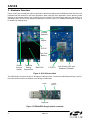
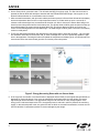
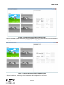
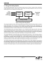
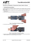
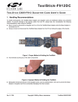
AN588 E NERGY H ARVESTING R EFERENCE D ESIGN U SER ’ S G U ID E 1. Kit Contents The RF to USB Reference Design contains the following items: Si1012 Energy Harvesting Wireless Sensor Node EZRadioPRO® USB Dongle ToolStick Base Adapter 3-foot USB extension cable 2. Introduction The purpose of this reference design is to demonstrate an ultra low power wireless sensor, powered from an energy harvesting source. This application is typical of systems which wake periodically to measure and transmit results. Since it is powered from an energy harvesting source, no batteries need to be replaced for the life of the system (life expectancy is greater than 15 years or 7000 mA-H) and the wireless node can be designed with a very thin profile (battery height is 0.17 mm). The system consists of two components: a wireless Sensor node and an EZRadioPRO® USB Dongle. The Sensor Node uses a Silicon Labs Si1012 wireless MCU. The Dongle uses a Silicon Labs C8051F342 MCU and a Silicon Labs Si4431 radio. The Sensor Node operates at 919.84 MHz and is powered by a solar energy harvesting power supply. When the wireless Sensor Node is not transmitting data, the Si1012 wireless MCU can remain in a low-power state where it only consumes 50 nA. The leakage current of the energy harvesting supply, when enabled, is approximately 3 µA and is cancelled out by as little as 50 lux shining into the solar cell. This allows the energy harvesting supply to power the system for approximately 7 days in a dark closet (in the ON position) or indefinitely if there is a periodic light source that replenishes the lost energy. The system works both in indoor lighting (200 lx) and outdoor lighting (10,000 lx) conditions. Figure 1. Energy Harvesting Sensor Node Rev. 0.2 5/11 Copyright © 2011 by Silicon Laboratories AN588 AN588 3. Hardware Overview Figure 2 and Figure 3 identify the major components of the Sensor Node and the USB Dongle. Both devices come preloaded with the firmware for the demo application. When using the demo application, ensure that the printed antenna on the wireless board is not covered by the user’s fingers. The Sensor Node ships from the factory in a discharged state. Be sure to fully charge the Node prior to first use. Refer to "8. Additional Information" on page 8 for details and charging times. Printed Antenna Button Si1012 Thin Film Battery Power Source Switch ToolStick Debug Connection Solar Cell LTC4071 Low Power LDO and Brownout Detector Figure 2. Si1012 Sensor Node The USB Dongle is powered by the PC through the USB connection. Connect the USB Dongle directly to the PC. No custom drivers need to be installed, as the Dongle is HID-based. Si4431 printed antenna C8051F342 Figure 3. EZRadioPRO Dongle (plastic removed) 2 Rev. 0.2 AN588 4. Software Setup The Energy Harvesting demo application is designed for the Windows operating systems and is distributed as part Wireless Development Suite (WDS). The Wireless Development Suite may be downloaded from the following web page: http://www.silabs.com/MCUDownloads Once WDS is downloaded from the Silicon Labs website, extract the executable from the zip file and run it to install the Wireless Development Environment. Program shortcuts are also added to the Start Menu under the Silicon Laboratories folder. 5. Energy Harvesting Demo The Energy harvesting demo shows how an energy harvesting sensor node can periodically transmit data to the PC. To run the demo, first ensure that the software is installed as described in “4. Software Setup” and that the EZRadioPRO dongle is plugged into a USB port on the PC. 1. Launch the program, which is found by clicking StartAll ProgramsSilicon LaboratoriesWDS3. 2. Select Harvesting Demo 3. Go through the on-screen menu until the Harvesting Demo Application appears. 4. The Energy Harvesting Demo Application is now ready to receive information from the sensor node. Figure 4. Energy Harvesting Demo Application Initial Screen 5. Place the S2 power source switch in the SOLAR position. It takes 15 to 30 seconds for the sensor node to charge a 100 µF capacitor from the solar cell (200 lx minimum), then use the stored energy for a full POR. The green LED should blink 3 times to indicate that the sensor node is powered up. Three red LED blinks indicate that there is not enough energy in the system to start up, and that the sensor node needs to be charged. A combination of green and red blinks indicates that the system has enough energy to start up, but the stored energy level is below 75% of its maximum capacity. Rev. 0.2 3 AN588 6. On the Sensor Node, press the button. This will wake the MCU from sleep mode. The first time the button is pressed the Sensor Node will attempt to associate with the EZRadioPRO USB Dongle. A short green or red blink will indicate whether or not association was successful. 7. After successful association, and upon each subsequent button press, the Sensor Node will transmit the battery level and temperature data from the on-chip temperature sensor. It will also wake up once a second for 3 minutes to transmit the light level, as measured at the solar cell. After 3 minutes, the Sensor Node will go into ultra-low power sleep mode until the next button press. The Sensor Node will blink green each time it wakes up and transmits data if the system charge is higher than 75%. The Sensor Node may blink red if it does not receive an acknowledgement from the USB Dongle. The USB Dongle will blink green each time it successfully receives a valid packet. 8. The Energy Harvesting Application will designate the first Sensor Node to associate as Node 1. Up to 4 nodes are allowed to associate. Cover the solar cell, or shine a flashlight into it to see it dynamically update the light level in the application. Pressing the button will update the temperature and battery level, and will also add one extra minute before the sensor board goes into an ultra-low power sleep mode. Figure 5. Energy Harvesting Demo with one Sensor Node 9. In the Logic tab, the number of connected nodes is displayed and the RSSI (receive signal strength indicator) is displayed for each node board. If you move the transmitting node board away from the dongle, the receive signal strength should decrease. The approximate range is 100–300 feet for a fully charged system. If the energy in the node board drops below 75%, the transmit power is reduced in order to preserve the remaining charge. In this reduced power mode, the green LED will not blink on successful transmission, however the red LED will still blink if a transmitted packet is not acknowledged by the dongle. 4 Rev. 0.2 AN588 Figure 6. Energy Harvesting Demo (Packet View) 10.On the Packet tab, a list of all received packets is displayed. Selecting a packet will decode the raw data and display the extracted information in the VBAT, TEMP, and LIGHT_LEVEL fields. Figure 7. Energy Harvesting Demo (NodeInfo View) 11. On the NodeInfo tab, a summary of the latest sensor data is displayed in a text format. Rev. 0.2 5 AN588 6. Energy Harvesting System The energy harvesting system used in this reference design, shown in Figure 8, consists of three components: energy management circuitry to harvest energy, energy storage, and energy management circuitry to convert the stored energy into a form usable by the wireless sensor. Solar Thermal Vibration RF Energy Energy Management (input) Energy Management (output) Regulated System Voltage Energy Storage Figure 8. Energy Harvesting System The energy management circuitry used for harvesting energy consists of a solar cell which provides dc energy, a rectifier which can be used to convert ac vibration energy into dc energy, and the LTC 4071 which takes in dc energy and regulates it to a constant 4.1 V. The LTC4071 also protects the battery from overdischarge (by disconnecting it from the circuit if its voltage gets too low) and provides a “ship mode” that disconnects the battery during shipping and allows it to hold its energy until the end user starts up the system. The energy storage used in this reference design is a 4.1 V, 700 µA-H thin film battery from IPS. This battery provides enough energy storage to keep the system running for many days without any “harvested” power. In any energy harvesting system, it is important to keep the energy used by the system lower than the amount of “harvested” energy in order to prevent a steady depletion of the stored energy. The larger the energy storage reservoir, the longer the system can go without “harvesting” new energy from the environment. The energy management circuitry at the output of the energy storage converts the 4.1 V thin film battery voltage to a regulated 2.7 V for use by the Si1012 Wireless MCU. The main components of this circuit are an ultra low power LDO (ADP162), a brownout detector (NCP302), and a 100 µF tantalum capacitor to supply the peak currents required for RF transmission. The LDO’s shutdown pin is tied to the output of the brownout detector, so that the system is not powered until the 100 µF capacitor is charged up to at least 3.0 V. This ensures that the system will not attempt to power up unless it has enough stored energy to get it through the power up sequence. The energy harvesting system requires approximately 3 µA to operate. This is easily cancelled out by as little as 50 lux light shining on the solar cell. The energy harvesting system can remain in a dark closet for 1 week before all the stored energy is depleted. When the system is going to be placed in a dark area for a prolonged period of time, it is best to place the S2 switch in “OFF” mode, which activates the “ship mode” and disconnects the battery from the system. This allows the system to hold its current state until the S2 switch is placed in the “SOLAR” position. 6 Rev. 0.2 AN588 7. Ultra Low Power Wireless Sensor The Si1012 Wireless MCU is used for the sensing and RF transmission functions of this reference design. In sleep mode, the Si1012 supply current is approximately 50 nA. When the MCU is awoken from sleep mode using the push button switch, it samples the current temperature using the on-chip temperature sensor, the remaining charge in the thin film battery, and the amount of ambient light at the solar cell. The temperature and remaining charge are transmitted over the RF connection once per button press. The light level is transmitted once a second for three minutes. One of the distinguishing features of the Si1012 which makes it excellent for energy harvesting applications is its ultra low power consumption both in sleep and active modes. Figure 9 shows a simplified activity profile for the active mode (RF packet transmission once a second). The peak current is 29 mA when the RF transmitter is enabled and the average current over the three minute time interval is 51 µA (1 packet per second). 29 mA 19 mA Active Mode TX Active Mode TX Active Mode Rx 0.8 uA Active Mode Rx RTC Sleep 1 mS 1 mS RTC Sleep 998 mS 1 mS 1 mS 998 mS Figure 9. Activity Profile While Transmitting The wireless sensor node uses a 919.84 MHz RF link based on the EZMAC® PRO software library. The RF link data rate is 128 kbps using GFSK modulation (EZRadioPRO channel 19). The output power is +13 dB. The Sensor Node will decrease the output power when the charge on the thin film battery drops below 75%. The printed antenna on the Sensor Node is designed on a 2-layer PCB in order to achieve the lowest possible cost. The expected range with the printed antenna is 100–300 feet (line of sight). Rev. 0.2 7 AN588 8. Additional Information If the power select switch is in the SOLAR position and the Energy Harvesting Node Board is exposed to at least 200 lx for several hours per day, the total charge in the system should never drop below 75%. If the system will be stored in a dark environment for several days (e.g., when traveling, etc), then it is best to place the power select switch in the OFF position. The system will hold its charge indefinitely in the OFF position. If the energy in the system ever gets depleted, then it may be quickly charged (30 minutes) by plugging in a ToolStick Base Adapter and setting the power source switch to USB. Figure 10 shows approximate charging times for a fully depleted system under various charging conditions. Electric Light 200 Lux 24 hours Office Window 1000 Lux Direct Sunlight 100K Lux 6 hours 2 hours USB Charging 30 minutes Figure 10. Charging Time For Various Charging Conditions The energy harvesting Node board may be used for RF development with the Si1012. The ToolStick Base adapter, which allows connection to the Silicon Laboratories IDE, is supplied in the kit. For firmware source code or additional information, please visit the Energy Harvesting Page on the Silicon Laboratories website. http://www.silabs.com/Energy-Harvesting 8 Rev. 0.2 Figure 11. Energy Harvesting Node Schematic (1 of 3) AN588 9. Schematic Rev. 0.2 9 Figure 12. Energy Harvesting Node Schematic (2 of 3) AN588 10 Rev. 0.2 Figure 13. Energy Harvesting Node Schematic (3 of 3) AN588 Rev. 0.2 11 AN588 CONTACT INFORMATION Silicon Laboratories Inc. 400 West Cesar Chavez Austin, TX 78701 Tel: 1+(512) 416-8500 Fax: 1+(512) 416-9669 Toll Free: 1+(877) 444-3032 Please visit the Silicon Labs Technical Support web page: https://www.silabs.com/support/pages/contacttechnicalsupport.aspx and register to submit a technical support request. The information in this document is believed to be accurate in all respects at the time of publication but is subject to change without notice. Silicon Laboratories assumes no responsibility for errors and omissions, and disclaims responsibility for any consequences resulting from the use of information included herein. Additionally, Silicon Laboratories assumes no responsibility for the functioning of undescribed features or parameters. Silicon Laboratories reserves the right to make changes without further notice. Silicon Laboratories makes no warranty, representation or guarantee regarding the suitability of its products for any particular purpose, nor does Silicon Laboratories assume any liability arising out of the application or use of any product or circuit, and specifically disclaims any and all liability, including without limitation consequential or incidental damages. Silicon Laboratories products are not designed, intended, or authorized for use in applications intended to support or sustain life, or for any other application in which the failure of the Silicon Laboratories product could create a situation where personal injury or death may occur. Should Buyer purchase or use Silicon Laboratories products for any such unintended or unauthorized application, Buyer shall indemnify and hold Silicon Laboratories harmless against all claims and damages. Silicon Laboratories and Silicon Labs are trademarks of Silicon Laboratories Inc. Other products or brandnames mentioned herein are trademarks or registered trademarks of their respective holders 12 Rev. 0.2 Mouser Electronics Authorized Distributor Click to View Pricing, Inventory, Delivery & Lifecycle Information: Silicon Laboratories: ENERGY-HARVEST-RD