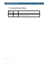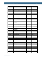
1
Low-power Application Kit (Oryx) - User’s Guide Copyright 2012 © Embedded Artists AB Low-Power Application Kit (Oryx) - powered by LPCXpresso Get Up-and-Running Quickly and Start Developing Your Application On Day 1! EA-USG-1207 Rev A Low-power Application Kit (Oryx) - User’s Guide Page 2 Embedded Artists AB Davidshallsgatan 16 211 45 Malmö Sweden [email protected] http://www.EmbeddedArtists.com Copyright 2012 © Embedded Artists AB. All rights reserved. No part of this publication may be reproduced, transmitted, transcribed, stored in a retrieval system, or translated into any language or computer language, in any form or by any means, electronic, mechanical, magnetic, optical, chemical, manual or otherwise, without the prior written permission of Embedded Artists AB. Disclaimer Embedded Artists AB makes no representation or warranties with respect to the contents hereof and specifically disclaim any implied warranties or merchantability or fitness for any particular purpose. Information in this publication is subject to change without notice and does not represent a commitment on the part of Embedded Artists AB. Feedback We appreciate any feedback you may have for improvements on this document. Please send your comments to [email protected]. Trademarks All brand and product names mentioned herein are trademarks, services marks, registered trademarks, or registered service marks of their respective owners and should be treated as such. Copyright 2012 © Embedded Artists AB Low-power Application Kit (Oryx) - User’s Guide Page 3 Table of Contents 1 Document Revision History 5 2 Introduction 6 2.1 Features 6 2.2 ESD Precaution 7 2.3 General Handling Care 7 2.4 Code Read Protection 7 2.5 Other Products from Embedded Artists 7 2.5.1 Design and Production Services 7 2.5.2 OEM / Education / QuickStart Boards and Kits 8 3 The Low-power Application Board Design 9 3.1 Block Diagram 9 3.2 Board Overview 10 3.3 Usage of CPU Pins 10 3.4 Schematic Walkthrough 12 3.4.1 Page 2 12 3.4.2 Page 3 12 3.4.3 Page 4 13 3.4.4 Page 5 13 3.4.5 Page 6 14 3.4.6 Page 7 15 3.4.7 Page 8-10 15 3.5 Things to Note about the Hardware Trimming Potentiometer 15 3.5.2 Lithium Battery 15 4 Getting Started 16 4.1 Important Note about Lithium Battery 16 4.2 Demo Application 16 4.3 Compiling the Demo Application 17 4.4 Program Download 19 4.5 Default Jumper Positions 24 5 Software Techniques for Low-power Design 5.1 5.1.1 Copyright 2012 © Embedded Artists AB 15 3.5.1 LPC11U37 Operating Modes Low-Power Modes and Debugging 25 25 26 5.2 Typical Software Architecture for Low-Power 27 5.3 The Board Current Consumption 27 5.3.1 The Board Low-Power Modes 27 5.3.2 LCD 27 5.3.3 Real-Time Clock 28 5.3.4 SPI Flash 28 Low-power Application Kit (Oryx) - User’s Guide Page 4 5.3.5 Temperature Sensor 28 5.3.6 Accelerometer Sensor 29 5.3.7 Capacitive Sensor 29 5.3.8 LPC11U37 Brown Out Detector 29 5.4 5.4.1 5.5 How to Measure Current Consumption How to Achieve and Measure 2.5uA Current Consumption The Sample Applications 6 Troubleshooting 29 30 32 6.1.1 Cannot download/debug 32 6.1.2 Battery drain quickly 32 6.1.3 Verify operation of board 32 7 Further Information Copyright 2012 © Embedded Artists AB 29 34 Low-power Application Kit (Oryx) - User’s Guide Page 5 1 Document Revision History Document Revision Date Description A 2011-11-07 First release version. B 2012-08-22 Update for Embedded Artists version of the Oryx board, called Low-power Application Kit (Oryx) Copyright 2012 © Embedded Artists AB Low-power Application Kit (Oryx) - User’s Guide Page 6 2 Introduction Thank you for buying the Low-power Application Kit (Oryx) – powered by LPCXpresso from Embedded Artists. The board demonstrates low power design techniques both in hardware and software. The board has been developed by Embedded Artists in close cooperation with Arrow and NXP. The board contains an LPC11U37 MCU from NXP and has the same embedded-JTAG solution (called LPCLINK) as LPCXpresso target boards. This document is a User’s Guide that primarily describes the hardware design of board. Software solutions are also addressed when applicable in order to describe low-power design solutions. 2.1 Features Embedded Artists’ Low-power Application Kit (Oryx) makes it possible for you to get started with low power design prototyping immediately. It is a platform for low power design solutions around the LPC1100 family from NXP. The board has been designed for evaluation and is not designed for final integration into consumer or industrial end-products. NXP's LPC11U37 ARM Cortex-M0 microcontroller in 48-pin LQFP package, with 10 KByte internal SRAM, 4 KByte E2PROM and 128 Kbyte internal FLASH. 12.0000 MHz crystal for maximum execution speed and standard serial bit rates, including USB requirements. The LPC11U37 runs at frequencies up to 50 MHz. On-board USB Device interface Mini-B USB connector on-board USB connect circuit Proper ESD protection All relevant LPC11U37 pins available on LPCXpresso compatible expansion connector (dual 27 pos, 100 mil/2.54 mm pitch rows, 900 mil apart). Rechargeable Lithium coin battery LIR2032 Flexible charging options (via USB interfaces and external source, like solar panel) Other energy storage also supported (besides coin cell) PCF8523 low-power real time clock with I2C interface PCF8885 8-channel capacitive touch sensor with I2C interface ADXL345 3-axis accelerometer with I2C interface LM75B temperature sensor with I2C interface 96x96 pixel Memory LCD from Sharp with SPI interface 4 Mbit SPI FLASH for storing non-volatile parameters or other data Push button and LED for reset Push button for Wakeup functionality (on PIO0_16) Push button for enabling Bootloader mode of the LPC11U37 LED on pin PIO0_7 SWD/JTAG connector Copyright 2012 © Embedded Artists AB Low-power Application Kit (Oryx) - User’s Guide 2x5 pos, 50 mil/1.27 mm pitch, standard SWD/JTAG connector Compact size: 140 x 85 mm 2.2 Page 7 Four layer PCB design for best noise immunity Embedded JTAG (LPC-LINK) included Can be completely disconnected (in order not to affect power consumption) Standard SWD/JTAG connector (2x5 pos) interface connector ESD Precaution Please note that the Low-power Application Board comes without any case/box and all components are exposed for finger touches – and therefore extra attention must be paid to ESD (electrostatic discharge) precaution. Make it a habit to always first touch the metal surface of one of the USB connectors for a few seconds with both hands before touching any other parts of the boards. That way, you will have the same potential as the board and therefore minimize the risk for ESD. Note that Embedded Artists does not replace boards that have been damaged by ESD. 2.3 General Handling Care Handle the board with care. The board is not mounted in a protective case/box and is not designed for rough physical handling. Connectors can ware out after excessive use. The board is designed for evaluation and prototyping use, and not for integration into consumer or industrial end-products. The Low-power Application Board contains a Memory LCD. Do not exercise pressure on the display glass area or the flex cable connecting the display to the pcb. That will damage the display. Note that Embedded Artists does not replace boards where the LCD has been improperly handled. 2.4 Code Read Protection The LPC11U37 has a Code Read Protection function (specifically CRP3, see LPC11U37 datasheet/user’s manual for details) that, if enabled, will make the LPC11U37 impossible to reprogram (unless the user program has implemented such functionality). Note that Embedded Artists does not replace Low-power Application Boards where the LPC11U37 has CRP3 enabled. It’s the user’s responsibility to not invoke this mode by accident. 2.5 Other Products from Embedded Artists Embedded Artists has a broad range of LPC1000/2000/3000/4000 based boards that are very low cost and developed for prototyping / development as well as for OEM applications. Modifications for OEM applications can be done easily, even for modest production volumes. Contact Embedded Artists for further information about design and production services. 2.5.1 Design and Production Services Embedded Artists provide design services for custom designs, either completely new or modification to existing boards. Specific peripherals and I/O can be added easily to different designs, for example, communication interfaces, specific analog or digital I/O, and power supplies. Embedded Artists has a broad, and long, experience in designing industrial electronics in general and with NXP’s LPC1000/2000/3000/4000 microcontroller families in specific. Our competence also includes wireless and wired communication for embedded systems. For example IEEE802.11b/g (WLAN), Bluetooth™, ZigBee™, ISM RF, Ethernet, CAN, RS485, and Fieldbuses. Copyright 2012 © Embedded Artists AB Low-power Application Kit (Oryx) - User’s Guide 2.5.2 Page 8 OEM / Education / QuickStart Boards and Kits Visit Embedded Artists’ home page, www.EmbeddedArtists.com, for information about other OEM / Education / QuickStart boards / kits or contact your local distributor. Copyright 2012 © Embedded Artists AB Low-power Application Kit (Oryx) - User’s Guide Page 9 3 The Low-power Application Board Design This chapter describes the hardware design of the board. 3.1 Block Diagram The block diagram in Figure 1 below gives a quick overview of a design. It illustrates the major components in the design. The center of the design is the LPC11U37 MCU from NXP. A number of low-power peripherals are connected to the LPC11U37 via the I2C and SPI interfaces. There is also a USB Device interface to the LPC11U37 and all pins are available on an LPCXpresso/mbed compatible expansion connector. The board is powered from a rechargeable Lithium coin cell (LiR2032). The battery can be charged from several different sources; the USB interfaces (when connected to a PC) and the expansion connector. There is also an option to charge the battery from an external source, for example a solar panel (not included). The board runs on 3.0V and there are possibilities to measure the current consumption of the complete board and the LPC11U37 separately. All parts of the design are constantly powered, with the exception of three parts. The constantly powered parts can be put to low-power mode so that the idle current consumption is very low. Power switches have been added on three of the external peripherals in order to allow control the power consumption - (these parts has typically too high low-power consumption. These power switches exist for the SPI flash, the memory LCD and the trimming potentiometer. External power source (solar) Rechargeable Lithium coin battery Power LPCXpresso/ mbed compatible expansion connector Power Current measurement Power LPC-LINK SWD I/F USB interface SWD I/F 3.0V USB interface USB LPC11U37 I2C LPCXpresso compatible embedded SWD/JTAG 3-axis accelerometer I2C interface RTC + Crystal I2C interface AIN ISP enable switch Wakeup switch 4 Mbit SPI FLASH with power switch 8 Capacitive sensors I2C interface SPI#1 96x96 memory LCD, SPI interface with power switch Figure 1 – The Low-power Application Board (Oryx) Block Diagram Copyright 2012 © Embedded Artists AB SPI#0 Temperature sensor I2C interface Trimming potentiometer with power switch Low-power Application Kit (Oryx) - User’s Guide Page 10 There is also an LPCXpresso compatible embedded SWD/JTAG interface (called LPC-LINK). This simplifies program download and debugging. The interface can be completely disconnected in order not to affect the power consumption when running an application on the LPC11U37. 3.2 Board Overview Figure 2 below illustrates the board structure. The upper part is the original LPCXpresso LPC11U37 design. This part is physically compatible with the LPCXpresso format. The bottom part of the board contains the added low-power peripherals. J9 – USB interface for LPCXpresso debugging JP2 J7, pin 28-54 LPCXpresso LPC11U37 part J2 – USB interface for the LPC11U37 J7, pin 1-27 J3 Rechargeable Lithium coin battery Reset, wakeup, ISP and bat.act.buttons Trimming pot. RTC, accelerometer and SPI flash 96x96 pixel LCD and 8 capacitive sensors Figure 2 – The Low-power Application Board (Oryx) Overview 3.3 Usage of CPU Pins The table below lists which LPC11U37 pins that are used in the design. LPC11U37 pin Usage Expansion connector (J7) PIO0_0 Reset Pin 4 PIO0_1 ISP enable push-button Pin 38 PIO0_2 SPI channel#0 SSEL Pin 8 PIO0_3 USB VBUS Pin 39 PIO0_4 I2C-SCL Pin 41 PIO0_5 I2C-SDA Pin 40 PIO0_6 USB connect Pin 23 Copyright 2012 © Embedded Artists AB Indication connector (J3) Low-power Application Kit (Oryx) - User’s Guide Page 11 PIO0_7 LED Pin 11 PIO0_8 LCD disp Pin 6 PIO0_9 SPI channel#0 MOSI Pin 5 PIO0_10 SWD interface SWCLK Pin 24 PIO0_11 RTC irq Pin 15 PIO0_12 Capacitive sensor irq Pin 16 PIO0_13 Accelerometer irq#1 Pin 17 PIO0_14 Accelerometer irq#2 Pin 18 PIO0_15 SWD interface SWDIO Pin 19 PIO0_16 Wakeup push-button Pin 20 PIO0_17 Can be used to digitally indicate power consumption Pin 21 Pin 3 PIO0_18 Can be used to digitally indicate power consumption Pin 10 Pin 4 PIO0_19 Can be used to digitally indicate power consumption Pin 9 Pin 5 PIO0_20 Can be used to digitally indicate power consumption Pin 22 Pin 6 PIO0_21 Can be used to digitally indicate power consumption Pin 42 Pin 7 PIO0_22 Not used, free for expansion Pin 43 PIO0_23 Trimming potentiometer Pin 44 PIO1_13 Trimming potentiometer power control Pin 25 PIO1_14 LCD power control Pin 26 PIO1_15 Capacitive sensor sleep control Pin 27 PIO1_16 SPI flash power control Pin 53 PIO1_19 SPI channel#1 SSEL Pin 12 PIO1_20 SPI channel#1 SCK Pin 13 PIO1_21 SPI channel#1 MISO Pin 14 PIO1_22 SPI channel#1 MOSI Pin 45 PIO1_23 I2C pull-up power control Pin 46 PIO1_24 Not used, free for expansion Pin 47 PIO1_25 Not used, free for expansion Pin 48 PIO1_26 Not used, free for expansion Pin 49 PIO1_27 Not used, free for expansion Pin 50 PIO1_28 Not used, free for expansion Pin 51 PIO1_29 SPI channel#0 SCK Pin 7 Copyright 2012 © Embedded Artists AB Pin 1 Pin 2 Low-power Application Kit (Oryx) - User’s Guide Page 12 PIO1_31 Not used, free for expansion Pin 52 USB-DM USB interface Pin 36 USB-DP USB interface Pin 37 3.4 Schematic Walkthrough 3.4.1 Page 2 The center of the board is the LPC11U37 from NXP. It is a MCU based on the ARM Cortex-M0 core. LPC11U37 has many power modes to save power consumption. See datasheet for details. It is possible to measure the current consumption of the LPC11U37 on both VDD pins separately (IO and VDDCORE). Normally both jumpers in JP1 are inserted but if removed there are 5 ohm resistors that can be used for measuring the current consumption. 10mA current will give a 50mV voltage drop over a 5 ohm resistor. J1 is the SWD interface for LPC11U37, i.e., debug interface. It is the new and smaller footprint standard ARM debug connector. It has 2x5 pins in 50 mil pitch. The LPC11U37 has a USB Device interface. The interface is very straight forward and consists of a mini-B USB connector (J2), ESD protection, VBUS sense and DP pull-up resistor control. SW1 is a reset push-button. There is no external voltage supervisor since the LPC11U37 has its own power-on reset functionality. SW2 is a wake-up push button for waking the LPC11U37 from ‘deep power down mode’. SW2 is connected to PIO0_16, which is the WAKEUP pin. A high-to-low transition on this pin will wake-up the LPC11U37 from ‘deep power down mode’. PIO0_16 is the only pin that can wake-up the LPC11U37 from this mode. SW3 is an ‘ISP enable’ push-button. By pressing SW3 while resetting the LPC11U37 (pressing and releasing SW1) the In-System Programming mode is entered. It is an internal boot loader more of the LPC11U37. It can be useful to enter ISP mode if the application program has programmed the internal PLL:s wrong, or disabled the debug/SWD interface. In these situations, it can be impossible to get contact with the LPC11U37 via the debug/SWD interface. The application program can be erased while in ISP mode and a new, correct application program can be downloaded. R22 is a 100K trimming potentiometer for simulating an arbitrary analog input signal. There is a power switch to keep current consumption low. PIO1_13 controls Q3 (P-channel mosfet). When enabled, the current consumption is 30 uA (= 90 uW). Supply voltage is only needed during an ADC conversion so the mean current consumption can be kept very low. R22 is connected to analog input 7 (AD7), PIO0_23. J3 can be used to signal power consumption digitally. The connector carries 7 pins from the LPC11U37 that can be used to signal different power states. A logic analyzer can be used to capture and analyze the different states (and their length) that the application program changes between. 3.4.2 Page 3 There are many I2C peripherals on the board. Three of them are on page 3 of the schematic. All three chips are constantly powered since they can be put in low-power modes where they consume very low power. There is an optional power control on the two i2c pull-up resistors. Currently there is no use for this feature since disabling the pull-up resistors will not reduce the power consumption. PIO1_23 shall typically always be pulled low (which will enable the pull-up resistors), or R18 shall be mounted It is not possible to communicate over the i2c-bus without having the pull-up resistors enabled. The ADXL345 3-axis accelerometer is from Analog Devices. The ADXL345 has functionality to detect single and double taps (on the board pcb). The chip has two interrupt outputs that can be used to wake-up the LPC11U37 from a power down mode, for example when a user double-tap on the board. Copyright 2012 © Embedded Artists AB Low-power Application Kit (Oryx) - User’s Guide Page 13 There is a current consumption cost for keeping the chip active and detecting (single/double) taps. Exact current consumption depends on setup of detection, for example sample rate. See datasheet for details. If the chip is placed in standby mode, the current consumption is only 100 nA (= 0.3 uW). The I2C address to the ADXL345 chip is 0x1D (0.0.1.1.1.0.1.rw). Details about the ADXL345 chip operation can be found in the datasheet. The PCF8523 real-time clock is from NXP. The current consumption is very low for keeping the realtime clock updated, only 150 nA (= 0.45 uW). When communicating with the PCF8523 over I2C, the current consumption increase to 200 uA (= 600 uW). The communication time is however very short so the power consumption will in mean typically be very low. There is an interrupt output from the PCF8523. This signal can for example be used to wake-up the LPC11U37 once a second or when an alarm time has elapsed. The I2C address to the PCF8523 chip is 0x68 (1.1.0.1.0.0.0.rw). Details about the PCF8523 chip operation can be found in the datasheet. The LM75B temperature sensor is from NXP. The current consumption is only 0.2 uA (= 0.6 uW) when in shutdown mode. While measuring temperature the current consumption increase to 100 uA (= 300 uW) and up to 200 uA (= 600 uW) while communicating over i2c. The I2C address to the LM75B chip is 0x48 (1.0.0.1.0.0.0.rw). Details about the LM75B chip operation can be found in the datasheet. 3.4.3 Page 4 There is a 4Mbit SPI flash S25FL004 from Spansion. Details about the S25FL004 chip operation can be found in the datasheet. The chip is connected to SPI channel #1 of the LPC11U37. The active current consumption is relatively high, but there are two low-power modes of the chip. One is standby mode, which it enters automatically when no transfers are active. It then consumes 20 uA (= 60 uW). There is also a deep power down mode with only 1.5 uA (= 4.5 uW). There is also a power switch for the S25FL004 in case the 4.5 uW is too much. Then it is possible to completely remove the chip from the power consumption. PIO1_16 controls the power switch (Pchannel mosfet, Q4). A low signal enables the voltage. There is a 96x96 pixel memory LCD from Sharp. Details about the LCD operation can be found in the datasheet. The chip is connected to SPI channel #0 of the LPC11U37. The active current consumption is very low. The LCD requires a (about) 1 Hz update rate and is then consuming only 4 uA (= 12 uW). The update rate is not critical and can vary over a range. See datasheet for details. The display requires a refresh signal (lowest rate is 1 Hz). Currently this is done via the SPI interface but there is provision for direct control from the RTC (CLKOUT signal). R24 and R25 must be mounted in this case and R26 removed. There is also a power switch for the LCD in case the display is not used (or 12 uW is too much). Then it is possible to completely remove the chip from the power consumption. PIO1_14 controls the power switch (P-channel mosfet, Q5). A low signal enables the voltage. 3.4.4 Page 5 The 8 capacitive sensors are implemented with the PCF8885 from NXP. The chip handles all low-level details of sensing touches. There is a simple I2C interface to the chip. The I2C address to the PCF8885 chip is 0x20 (0.1.0.0.0.0.0.rw). Details about the PCF8885 chip operation can be found in the datasheet. The 8 sensors are independent buy are grouped physically as 4 independent sensors and 4 sensors in a slider. Slider functionality can be realized with software. There are two methods for signaling touches to the software; Polling via an I2C-register IRQ (interrupt) via PIO0_12. The capacitive sensors can be used to wake-up the LPC11U37 from low-power modes (via interrupt). The current consumption cost for keeping the chip active is 10 uA (= 30 uW). This is the cost for having Copyright 2012 © Embedded Artists AB Low-power Application Kit (Oryx) - User’s Guide Page 14 the possibility to wake-up the LPC11U37 from a low-power mode. If the capacitive sensors are completely disabled (i.e., the PCF8885 is in sleep mode) the current consumption is only 100 nA (= 0.3 uW). Since the sleep mode current consumption is so low, the chip is always powered (i.e., there is no power switch). PIO1_15 can be used to control sleep mode of the PCF8885. 3.4.5 Page 6 The board can be powered from a rechargeable Lithium coin battery (LiR2032). The board contains a coin cell holder for the LiR2032 battery. The Lithium battery is charged via the LTC4071 from Linear Technology, U9. It implements a shunt battery charger system where the battery is disconnected when battery voltage is too low. The LTC4071 allows charging of Lithium coin batteries from very low current, intermittent or continuous charging sources. The low battery latching disconnect function protects the battery from deep discharge and potentially irreparable damage. The disconnect level is programmable via the LBSEL input pin. By default it is set to 2.7V (LBSEL connected to VCC). If the battery is disconnected, the board can still operate but then power must be supplied from an external source. There are 4 different power sources for charging the battery or for powering the board: USB power from the LPC-LINK (embedded SWD/JTAG debug interface). By default this path is enabled via JP2, pin 1-2 and D5. It can be disables as charging/powering option by removing the jumper in JP2, pin 1-2. USB power from the LPC11U37 USB interface. This path is always enabled via D3. External power input from J7, pin 2. Voltage shall be 5.0V. By default this path is enabled via JP2, pin 3-4 and D4. It can be disables as charging/powering option by removing the jumper in JP2, pin 3-4. An external source, either 5V or 10V nominal. It can for example be a solar panel. J5 allow for external power source to be connected. There are additional series resistors for the 10V nominal input since the Lithium charger is designed for 5V nominal input voltage. There is also provision (pads) for protection diodes to keep the input voltage under control, see D11/D12 in the schematic. The LTC4071 further prevents the battery voltage from exceeding a programmed level (set via the ADJ input pin). By default this level is set to 4.2V (ADJ connected to VCC). The design around the LTC4071 is very flexible and alternative energy storage solutions (other than Lithium coin batteries) can be used. Via SJ4 an external battery can be used, for example a thin-film battery from IPS (Infinite Power Solutions). C44 is a voltage conserving capacitor in case the external energy reserve has high internal resistance. This is typically the case when using thin-film batteries. Current surges will create voltage dips unless C44 is properly sized. See LTC4071 datasheet for details about operation in general and alternative energy storage solutions. The capacitance of C44 might need to be increased for other energy storage solutions. The LTC4071 is a shunt charger that can handle up to 50 mA. With the help of R30 (the shunt resistance, Rin) the correct charge voltage and current for the battery is created. R30 is by default 30 ohm which has been carefully selected with trade-offs between input voltage range, maximum charge current and current consumption of the board. R30 = 30 ohm gives the following data for the charger: Maximum input voltage is (Ishunt_max * Rin) + Vbat_min + Vfdiode= (0.050 * 30) + 3.2 + 0.3 = 5.0 V Max power dissipation in R30 occurs when maximum input voltage and minimum battery voltage: (Vin_max – Vbat_min)2 / Rin = (5 – 0.3 – 3.2)2 / 30 = 75 mW The board can also consume current while charging the battery. This will reduce the available charging current, i.e., will increase charging time. Copyright 2012 © Embedded Artists AB Low-power Application Kit (Oryx) - User’s Guide Page 15 R30 can be replaced with R29 via SJ1 (connect pad 2-3 instead of pad 1-2, which is default) if the default value of 30 ohm is not suitable. Be careful to select a proper value for R29 so that the 50 mA maximum shunt current of LTC4071 is not exceeded. See LTC4071 datasheet for details. A low dropout linear voltage regulator is use to convert the battery voltage to 3.0V. TPS78330 from Texas Instruments is used for this. It is a 3.0V/150mA LDO in SOT23-5 package. JP3 is normally shorted with a jumper but if removed the current consumption of the board can be measured over R34 (5 ohm resistor). 10mA current will give a 50mV voltage drop over the 5 ohm resistor. R33 can also be used for measuring the current consumption. It is by default a zero ohm resistor but an arbitrary value can be used to measure current in the best resolution for a specific application. The series resistor value is always a trade-off between voltage drop and noise/resolution in measurement. 3.4.6 Page 7 J7 is an expansion connector that is compatible with the LPCXpresso and mbed products, both signalwise and physically. J7 has the same signal connections as the LPCXpresso LPC11U37 board. 3.4.7 Page 8-10 This part of the design is the embedded SWD/JTAG part, called LPC-LINK. The design is based around the LPC3154 MCU. The LPC-LINK is identical with the LPCXpresso boards and the LPCXpresso IDE can be used to download and debug applications on the LPC11U37 MCU. LPC-LINK is not an open design and there is no possibility to download custom code in the LPC3154. J1 (LPC11U37 SWD interface) and J10 (LPC-LINK SWD/JTAG interface) shall be connected via a 10 pos flat cable (25 mil pitch). The flat cable is included. If another debug interface than the LPCXpresso IDE is needed, for example from IAR, Keil or Rowley, there is a possibility to connect J1 to any other SWD compatible debug interface. Note that not all, and in particular older, JTAG debug probes do not support the SWD interface standard. The flat cable between J1 and J10 is then simply removed. This will disconnect the on-board LPC-LINK completely and it will not affect the current consumption of the board when inactive. 3.5 Things to Note about the Hardware 3.5.1 Trimming Potentiometer When measuring the trimming potentiometer, the voltage (to the trimming pot.) must be present for about 50us before a reliable measurement can be done. The reason for this is because C11 and the trimming potentiometer form a low-pass filter. 3.5.2 Lithium Battery If the Lithium battery is removed and then reinserted into the board, and there is no other power source, then the Lithium battery will be disconnected from the board. This is how the Lithium battery charger (LTC4071) is supposed to work. A short voltage pulse on the input to the Lithium charger is needed to connect the battery again. This is simply done by inserting a USB cable (connected to a PC) on the LPC-LINK side. Make sure that jumper JP2, pos 1-2 is inserted. Alternatively, SW4 is pressed. That will also connect the Lithium battery as a power source. Copyright 2012 © Embedded Artists AB Low-power Application Kit (Oryx) - User’s Guide Page 16 4 Getting Started This chapter contains information about how to get acquainted with the Low-power Application Kit (Oryx). Please read this chapter first before you starts using the board - it will be well spent time! The design contains many different components that interact with software. The demo application and the smaller sample applications can help to get started but there is no way around reading the datasheets for the respective chip before start using it in an application program. This chapter does not describe how to develop an application program (with the LPCXpresso IDE, or other). For that, see other documents. This chapter describes important things how to get started and how to download an application. 4.1 Important Note about Lithium Battery The board is powered by a Lithium battery, LiR2032, 3.6V with 45mAh capacity. Note that there can be restrictions regarding Lithium batteries when traveling by airplane. Normally it should be no problems with a small battery like this (with 45 mAh capacity). It is however YOUR responsibility to check what possible restrictions there are. The Lithium battery is not fully charged when delivered. The board will therefore not start operating until the battery has been charged. Simply connect a USB cable between J9 on the board and a powered PC’s USB interface. Make sure JP2, pin 1-2 is closed by a jumper. See Figure 2 to locate J9 and JP2. Full charging of the Lithium battery takes about 5 hours. The pre-loaded demo application will start running while charging. Lithium batteries can be over-charged. The charger solution used on the board is based on the LTC4071 from Linear Technology. This chip controls the charging and minimizes the risk for overcharging of the battery. Note: Observe special care when removing/inserting the battery in its holder. Do not use metal stick/pin (for example a screw driver) to remove the Lithium battery from the battery holder on the board. It is very easy to short the battery’s positive and negative connection if a metal stick/pin is used. If this happens, the battery is likely damaged. Only use isolating materials, for example a plastic stick to remove the battery. 4.2 Demo Application The board is reloaded with a demonstration application. A number of small, self-explained applications can be selected from a main menu. Use the capacitive sensors to navigate in the menu: Cap sensor C31 is "down" Cap sensor C40 is "up" Cap sensor C41 is "left" Cap sensor C42 is "right" Cap sensor C25 is "OK/select". Applications are typically exited by pressing the wakeup-key. o Some applications require the wakeup-key to be pressed for a while so the application can detect the press. The clock application checks once a second while the slide show application checks once every 5 seconds. The slideshow application relies in bmp pictures in the spi-flash memory. In case the spi-flash content has been altered, the content must be restored in order for the demonstration application to function correctly. Simply download and run the production test application. This program will program the bmp images to the spi-flash. Then download and start the demonstration application. Copyright 2012 © Embedded Artists AB Low-power Application Kit (Oryx) - User’s Guide 4.3 Page 17 Compiling the Demo Application This section describes how to compile the demo application in particular and any sample application in general. The principles are identical between applications how to compile them. First make sure that the latest version of the LPCXpresso IDE is installed. Secondly, import the package of sample application projects into the Eclipse workspace. The demo application is one of the sample applications in this package. The package can be downloaded (as a zip-file) from Embedded Artists support page after registering the product. The zip-file contains all project files and is a simple way to distribute complete Eclipse projects. Select the Import and Export tab in the Quickstart menu and then Import archived projects (zip), see figure below. 1) Select Import and Export 2) Select Import archived projects (zip) Figure 3 – LPCXpresso IDE Import Archived Project Next, browse and select the downloaded zip file containing the archived sample applications. Make sure all sub-projects are selected, see figure below. Copyright 2012 © Embedded Artists AB Low-power Application Kit (Oryx) - User’s Guide Page 18 1) Browse and select archived project file 2) Select all subprojects in list 3) Import project Figure 4 – LPCXpresso IDE Import Archived Project Window All sample projects are now imported. Click (to select) the project named ‘DemoApp’. Browse and edit the project files. Build/clean/debug the project from the Quickstart menu (Start here), see picture below. When debugging a project, make sure the board is connected via USB connector J9 (the LPCLINK side) to the PC because the application will be downloaded to the board via LPC-LINK (SWD debug interface). Copyright 2012 © Embedded Artists AB Low-power Application Kit (Oryx) - User’s Guide Page 19 1) Click (to select) main project 2) Browse and edit project files 3) Build/clean/debug project Figure 5 – LPCXpresso IDE Build/Debug Project 4.4 Program Download This section describes how to download an application to the board, i.e., to the LPC11U37. 1. Connect a USB cable between J9 on the board and the PC. See Figure 2 to locate J9 (upper left corner). J9 is the LPC-LINK debugging interface (the debug interface of LPCXpresso). 2. Make sure that the LPC11U37 is in a mode where the debugger can take command over the processor. When the LPC11U37 is in a low-power mode it sometimes prohibits the debugger from connecting to the processor. The simplest way is to place the LPC11U37 in ISP/bootload mode. While resetting the LPC11U37 press the ISP push-button. See Figure 2 to locate the reset and ISP push-buttons (in the middle of the lower edge, right of the Lithium battery). a. Press both Reset and ISP push-button b. Release the Reset push-button c. Release the ISP push-button d. The LPC11U37 is now in ISP/bootload mode. LED1 will light weakly constantly. This is a sign that the LPC11U37 is in ISP/bootload mode. 3. Make sure that the latest version of the LPCXpresso IDE is installed on the PC. 4. Import the sample application software package into the Eclipse workspace. This package can be downloaded from the Embedded Artists support page after registering the product. The demo application is one of the projects in the sample application package. Copyright 2012 © Embedded Artists AB Low-power Application Kit (Oryx) - User’s Guide Page 20 5. Click on the "Program Flash" icon from the tool bar, see picture below. The icon can be at different places depending on window size. Program Flash Icon Figure 6 – LPCXpresso IDE Program Flash Icon The next step is to select which processor to download to. Select LPC11U37/501 from the list that is presented. Then press OK button. Note that this step is sometimes not needed because the LPCXpresso IDE can itself detect which processor it is connected to. The next step is to browse to the file to download. Press the “Browse” button. Copyright 2012 © Embedded Artists AB Low-power Application Kit (Oryx) - User’s Guide Page 21 Figure 7 – LPCXpresso IDE Program Flash Window Browse to the projects top directory and then “Debug”. In this subfolder there is either a file ending with *.axf or *.bin. Select one of these files. Press the “Open” button. 1) Find workspace and all sample apps. 2) Find project top directory 3) Find “Debug” subdirectory Figure 8 – Browse to File to Download Copyright 2012 © Embedded Artists AB 4) Select either *.axf or *.bin file Low-power Application Kit (Oryx) - User’s Guide Page 22 Figure 9 – LPCXpresso IDE Program Flashing in Progress In case flashing fails, an error message like below will be displays. This is an indication that the debugger could not connect to the LPC11U37. The most common reason is that the LPC11U37 was in a low-power mode where debug connection is not possible. Make sure the LPC11U37 is in ISP/bootload mode and try again. Also make sure the small 10-pos flat cable is connected between J1 and J10. Figure 10 – LPCXpresso IDE Program Failing to Flash Copyright 2012 © Embedded Artists AB Low-power Application Kit (Oryx) - User’s Guide Page 23 There is an alternative way of initiating the program download process. From the workspace, right click on the *.axf or *.bin file (found under the “Debug” subdirectory). Then select “Binary Utility” and “Program Flash”. 1) Right click on *.axf or *.bin file 2) Select “Binary Utility” 3) Select “Program Flash” Figure 11 – LPCXpresso IDE Binary Utility Press the reset push-button. The startup message from the Demo application should be displayed on the LCD. Copyright 2012 © Embedded Artists AB Low-power Application Kit (Oryx) - User’s Guide 4.5 Default Jumper Positions The default jumper positions on the board are shown below. Figure 12 – The Low-power Application Kit (Oryx) Board Default Jumper Positions Copyright 2012 © Embedded Artists AB Page 24 Low-power Application Kit (Oryx) - User’s Guide Page 25 5 Software Techniques for Low-power Design This chapter will discuss low-power design techniques. Part of the discussion is general for all lowpower designs and part is specific for the board design. Low-power design has two main principles: 1. Design the hardware to be able to control the current consumption by enabling/disabling different parts of the hardware. The parts that are active most of the time shall have as low static current consumption as possible. 2. Design the software to be able to control the active parts of the hardware as much as possible. In between active periods, the software shall put the hardware to lowest possible current consumption. Hardware and software must work together, hand-in-hand to achieve a low-power design. Active time (periods of high current consumption) must be reduced as much as possible. If time of inactivity is much longer than active periods, then the current consumption of the low-power mode is more important to reduce. The time of low-power consumption can be called sleep mode as a general term. An illustrative example; assume a device that wakes up for 100mS once every 100 seconds. Whatever the power consumption is during the active period it will only affect the total power consumption by 0.1%. 99.9% origin from the sleep power consumption. Assume active current is 150mA and sleep current is 20uA. The mean current consumption then becomes 170uA. The active current is clearly dominating consumption in this case. If the active current is instead 15mA and sleep current is still 20uA. Further assume that the active period is reduced to 50mS (instead of 100mS). In this case, the mean current consumption becomes 27.5uA. Now the current consumption is dominated by the sleep current. The active current of the board running at full speed is about 15mA (can be up to 20mA if everything is active simultaneous). The lowest power consumption is about 2.5uA. The temporal structure of an application will give where in between these extremes the mean power consumption will be. At full power consumption the Lithium battery will last for about 3 hours. At 2.5uA it will last for 18000 hours. This is about 2 years. Note that at this long time scale the self-discharge of the rechargeable Lithium battery becomes an issue. That is however out of scope for this discussion. 5.1 LPC11U37 Operating Modes The LPC11U37 has a number of different operation modes. The modes are described in detail in the LPC11U37 UM (Users Manual), a section called Power management. An application can switch between the different modes to achieve lowest possible power consumption. Below is a short description of the modes. Consult the LPC11U37 UM for details. Active – in this mode the processor core is running and executing the application. Power consumption can be optimized by adjusting power and clock frequencies to selected peripherals. There are also Power Profiles that can set. Sleep – in this mode the core clock is stopped and execution of instructions is suspended until either a reset or an interrupt occurs. Before entering sleep mode it is possible to set which peripheral functions to be active during the sleep. An interrupt from an active peripheral can generate an interrupt and cause the processor to resume execution. Deep sleep – this mode is more fixed than sleep mode. More peripherals are shut down to conserve more power. Power down – this mode is even more fixed. More functionality is shut down to conserve power. Copyright 2012 © Embedded Artists AB Low-power Application Kit (Oryx) - User’s Guide Page 26 Deep power down – this mode has the lowest power consumption. All parts of the chip are powered down expect five 32-bit registers. The program structure is different (than with the other modes) if this mode is used because the processor wakes up again like after a reset. The content of the 5 registers is the only information left from before entering this mode. The sample applications created for the board typically use either sleep or power down mode to conserve power consumption. 5.1.1 Low-Power Modes and Debugging Note that the debugger (LPC-LINK) can only connect to the LPC11U37 in active and sleep mode. When the LPC11U37 is in any of the three other low-power modes (deep sleep, power down, deep power down) it is not possible for a debugger to connect. There are two problems with this: When flashing a new program, the processor can already be in a low-power mode making it impossible to connect to the processor and download the new program. An error message like illustrated in Figure 10 is typical in this case. The solution is to force the processor into ISP/bootload mode before trying to download/flash a new program. Just follow the steps below to accomplish this: o Press both Reset and ISP push-button o Release the Reset push-button o Release the ISP push-button o Start flashing via the LPCXpresso IDE When starting a newly downloaded application, the debugger will lose connection with the processor. An error message like illustrated in Figure 13 is typical in this case. The program starts off in active mode but as soon as deep sleep, power down or deep power down is entered an error message like below will be displayed. The problem is that it becomes impossible to debug the processor after this point. It is not possible to set break point or stop the processor. It is also not possible to read variable values to help debug the application. o When developing an application it is recommended to only use sleep mode, even if other low-power modes are planned to be used. When the application is debugged the real low-power mode can be used, for example deep sleep or power down mode. Figure 13 – LPCXpresso IDE Error Message Copyright 2012 © Embedded Artists AB Low-power Application Kit (Oryx) - User’s Guide Page 27 5.2 Typical Software Architecture for Low-Power When creating an application that uses low-power modes there is a typical design pattern to be used. while (condition for having this particular function active) { //prepare for low-power mode (set I/O pins in specific states) //make sure active interrupts can wake up processor //enter power save mode (sleep/deep-sleep/power-down) //check what irq that occurred, handle task if not done in irq } The ISR (Interrupt Service Routine) can service the peripheral that caused the interrupt or leave it to the main forever loop to handle before entering sleep again. The ISR can for example set a flag that the forever main loop can detect and service the appropriate event accordingly. It the power-down mode disables a specific peripheral it might be necessary for the ISR to re-initialize the peripheral. The same can be valid for the forever main loop after waking up from low-power mode. When using deep power down mode the program structure is quite different since the processor wakes up like after a reset. main() { //normal initialization of hw if (cold reset) //reset application variables else if (wake up from deep power down) //initialize application based on previous deep power down //continue with application //at some point in time, enter deep power down again... } 5.3 The Board Current Consumption This section describes the different on-board peripherals and their current consumption. 5.3.1 The Board Low-Power Modes Note that the board is not designed to take advantage of the Deep power down mode. The lowest current consumption on the board is achieved when using Power down mode. Power consumption is actually higher with Deep power down mode than with Power down mode. The reason for this is that the board is designed to be “always powered”. Each individual component can be put in a very lowpower mode (either via command via serial bus or direct control via an input pin). In Deep power down mode all pins of the LPC11U37 are in high-impedance mode, basically floating. Not controlling some specific pins to specific states will increase the overall current consumption. 5.3.2 LCD The LCD is a special type of LCD called memory LCD. Each pixel is a memory position. See datasheet for details. The LCD requires a 0.5Hz signal, toggling a bit once a second. This bit is called VCOM in the datasheet. On the board this is accomplished via a 3-byte SPI transfer. The duration for this is 48uS. Copyright 2012 © Embedded Artists AB Low-power Application Kit (Oryx) - User’s Guide Page 28 The SPI clock is set to 750kHz. One byte transfer takes about 13.4uS. During SPI transfers the LPC11U37 does not have much to do, other than waiting for the SPI transfer to complete. The processor core frequency is haled during this time, which results in about half the normal current consumption. Note that the clock frequency to the SPI peripheral block is not affected. Toggling the VCOM bit takes 70uS all in all including all interrupt handling. 48uS of this, the current consumption is half (7.6mA). The rest, 22uS, the current consumption is 14mA. Generating the 0.5Hz VCOM signal to the LCD generate a mean current consumption of 0.7uA. The conclusion is that having the LPC11U37 in power down mode and having the LCD active cost about 3.2uA (2.5+0.7) in current consumption. On top of this the LPC11U37 must do something useful to generate something on the LCD. Updating the complete LCD (96x96 pixels) takes about 18mS in total. Current consumption is 7.6mA during this time. It is not necessary to update all 96x96 pixels on the display. Selected rows (96 pixels) of the display can be updated. The clock application in the pre-loaded demo application on the board demonstrates when only part of the display is updated – the part where the time is presented. For the specific case of the clock application, it takes 10.4mS to generate the updated bitmap and 3.8mS to send it to the LCD via SPI transfers. Updating a clock on the LCD gives a mean current consumption of (10.4mS*14mA + 3.8mS*7.6mA) = 174.5uA. Updating only once per minute would give a significant current consumption. There is a setting on the clock application that demonstrates this also. There is an alternative way to generate the 0.5Hz VCOM signal. It can be a hardware signal directly from the RTC, the CLKOUT signal. R24 and R25 must then be mounted and R26 removed. The RTC must also be programmed to generate a suitable CLKOUT signal. 5.3.3 Real-Time Clock The RTC can interact with the LPC11U37 in some different ways. The selected way in the design is to have the RTC generate a 1Hz signal to the LPC11U37. The signal is high 63/64 parts of a second and low 1/64 part of a second (15.6mS). The output from the RTC is an open-drain output and requires the input pin on the LPC11U37 to have a pull-up resistor enabled. Because the signal from the RTC is only low for 15.6mS each second, the current consumption from the pull-up resistor is kept to an average on 0.625uA. The alternative solution is to have the RTC generate a real interrupt signal. The LPC11U37 must then reset the interrupt flag inside the RTC via I2C commands. The LPC11U37 must then be active (about 15mA current) for about 350uS to accomplish this. This results in a mean current consumption of about 5.25uA (which is clearly higher than the used solution). The 1Hz signal from the RTC generates a 1Hz interrupt at the LPC11U37. This can be used for time keeping and refreshing the LCD. There are sample applications that used the WDT to get a time keeping interrupt. The RTC is much, much more accurate than the WDT. 5.3.4 SPI Flash There is a supply voltage switch for the SPI flash. This means that the current consumption of the SPI flash is zero when not used. The SPI clock is 2.9MHz. Each byte transfer takes about 4.5uS. Reading a bmp file for filling the 96x96 pixels takes 5.5mS. 5.3.5 Temperature Sensor The temperature sensor can be placed in a suspended mode where the current consumption is 0.2uA maximum. Therefore the current consumption can be kept very low. Read the datasheet for the sensor to get information about startup times from suspended mode until an accurate temperature reading is possible. Copyright 2012 © Embedded Artists AB Low-power Application Kit (Oryx) - User’s Guide 5.3.6 Page 29 Accelerometer Sensor The accelerometer can be placed in a sleep mode where the current consumption is 0.1uA maximum. Read the datasheet for the accelerometer to get information about active mode and associated current consumption. There are different sample rates that can be programmed and resulting in different current consumption. 5.3.7 Capacitive Sensor The capacitive sensor can be placed in a sleep mode where the current consumption is 0.1uA maximum. The current consumption in active mode is around 10uA. Read the datasheet for details. 5.3.8 LPC11U37 Brown Out Detector There is no voltage supervisor/reset generator on the board. The LPC11U37 has functionality for this. Note however that when enabling the Brown Out Detector (BOD) correct consumption of the LPC11U37 will increase with about 50uA. This is far more than the 2uA consumption on power down mode. 5.4 How to Measure Current Consumption There are 5 ohm resistors on the board for measuring the current consumption at three places: 1) R34 (see schematic page 6) which is placed just after the 3.0V voltage regulator. It is possible to measure the total current consumption of the board with this resistor. 2) R13 (see schematic page 2) which is connected to the VDDCORE pin of the LPC11U37. It is possible to measure the current consumption of the LPC11U37 core with this resistor. 3) R11 (see schematic page 2) which is connected to the VDDIO pin of the LPC11U37. It is possible to measure the current consumption of the IO pins of the LPC11U37 with this resistor. a. Most LPC11U37 pins have a (programmable) pull-up resistor. It is possible to measure the current consumption from each of these resistors. Each enabled resistor draws about 40uA if the pin is held low. With a 5 ohm resistor, every 10 mV equals 2mA of current consumption. The value 5 ohm is a trade-off between measurement resolution and minimizing voltage drop. The maximum current consumption of the board is about 17 mA, with result in a voltage drop of 85mV. That is an acceptable voltage drop that will not affect the operation of the board. The 5 ohm resistor is useful for measuring current consumption on the mA-region when using a normal low-cost portable multimeter. It will however not work for measuring currents in the uA-region. If the application switches between many different operating modes with different current consumption, it can be difficult to measure the real consumption with a cheap multimeter. A more advanced voltage meter might be required. For fast events and changes, an oscilloscope can with advantage be used to measure the current consumption. It is possible to replace the 5 ohm resistors but this shall be done with caution. The LPC11U37 will have high current consumption during startup and ISP/bootload mode. Make sure the jumpers in JP1 and JP3 short the measuring resistors during for example flashing of the LPC11U37. When the operating mode of interest has been reached the jumpers can be removed and the voltage drop can be measured. If the application changes between current consumption modes, it can be impossible to get it working properly (if the highest current consumption will cause too high voltage drop over the measuring resistor). 5.4.1 How to Achieve and Measure 2.5uA Current Consumption 2.5uA will generate a 7.5uV voltage drop over a 5 ohm resistor. This is too small to measure reliable without a very high precision (and high cost) voltage meter. A solution is to replace R34 with a 5K ohm Copyright 2012 © Embedded Artists AB Low-power Application Kit (Oryx) - User’s Guide Page 30 resistor. A 2.5uA current will result in a 7.5mV voltage drop over a 5K ohm resistor. This is much easier to measure. Use the sample application called LCD_ADC_temp_wdt-wakeup. Make sure that the symbol DISABLE_WDT_WAKEUP is defined (see line 50 in main.c of this sample application). Rebuild the project and download it. By defining the symbol DISABLE_WDT_WAKEUP, the application will stay n power down mode forever, once entered. The WDT will not be able to wake up the processor. 1) First make sure there is a jumper in JP3. 2) Download and start application (LCD_ADC_temp_wdt-wakeup). Wait for error message as in Figure 13. That is an indication that the LPC11U37 has entered power down mode. 3) Remove the SWD cable between J1 and J10. If not, the current consumption will be much higher. 4) Then lift the jumper in J3. Measure the voltage over the two JP3 pins. It should be (about) 7.5mV. This equals 2.5uA current consumption. Make sure jumper in JP3 is inserted again. If not it will be impossible to download a new application in flash. The voltage drop over the 5K resistor will be much too high when the processor is in ISP/bootload mode. Also do not forget to connect the SWD flat cable between J1 and J10. The 2.5uA current consumption comes from (about) 2uA from LPC11U37 (since it is in power down mode), 0.1uA from accelerometer is low-power mode, 0.2uA from temperature sensor in low-power mode, 0.15uA from RTC, 0.1uA from capacitive sensors in inactive mode. 5.5 The Sample Applications This section described the sample applications that have been developed for the board. Accel_systick_irq-wakeup – this application demonstrates the accelerometer features including tap detection (single and double). The application used sleep mode and wakes up from sleep by an interrupt from the accelerometer or systick counter (for refreshing the LCD). DeepPowerDown – this application demonstrates the program structure needed when working with deep power down. The application counts the number of times the wakeup pushbutton is pressed. DemoApp – this is the pre-loaded application that the boards are delivered with. Note that the production test application must first be run to store the bmp pictures on the serial (spi) flash for this application to work. FlashApp – this application demonstrates how to program bmp pictures to the serial flash. LCD_ADC_temp_wdt-wakeup – this application demonstrates how the WDT can be used to wake up from power down mode. The WDT is the only peripheral active during power down mode and it can be used to achieve a regular interrupt for refreshing the LCD. This sample application can be used to demonstrate the (about) 2.5uA total power consumption in power down mode. LCD_graphics – this application demonstrates the graphical library and the possibilities with the graphical LCD. lib_LPC11U14Dev – this is a library that has been created for the on-chip peripheral. The content is mostly from standard driver’s library that NXP provides, but some things have been changed to fit the board. Note that this library is compatible with LPC11U37. lib_OryxDev – this is a library that has been created for the board peripherals, like accelerometer, RTC, serial flash, LCD, etc. ProductionTest – this is not a sample application but the actual application that is used in production of the board. This application tests connection with the on-board peripherals and Copyright 2012 © Embedded Artists AB Low-power Application Kit (Oryx) - User’s Guide Page 31 also programs some BMP pictures on the serial flash. This application can be used to verify that a specific board is correct (if a hardware error is suspected). RTC_irq-wakeup – this application demonstrates the RTC and how the 1Hz tick can be used. Semihosting_ADC_temperature_sleep – this application demonstrates semihosting, which is a technique where an application can use printf() to display information on the LPCXpresso IDE. Systick_wdt_lcd_capsense – this application demonstrates the capacitive sensors. USB_HID – this application demonstrates USB HID. Use in conjunction with the NXP application for LPC1343 HID. It is possible to control the LED on the board and the Wakeup push-button can signal back to the PC (LPC1343 HID application on the PC). Copyright 2012 © Embedded Artists AB Low-power Application Kit (Oryx) - User’s Guide Page 32 6 Troubleshooting This chapter contains information about how to troubleshoot boards that does not seem to operate properly. It is strongly advised to read through the list of tests and actions that can be done before contacting Arrow. The different tests can help determine if there is a problem with the board, or not. For return policy, please read Embedded Artists’ General Terms & Conditions document. This document can be found on the Embedded Artists’ web site. 6.1.1 Cannot download/debug Symptom: Cannot contact the board via SWD after experimenting with low power modes Cause: An erroneous application program can disable the SWD interface and/or program the internal clocks in the wrong way so that it is impossible to download a new application to the board. The erroneous application program starts executing after a reset and initializes the LPC11U37 in the wrong way before an external debugger can get control over the processor. Solution: Press the ‘ISP enable’ push-button while resetting the board (pressing the reset push-button). This way the ‘known good’ internal bootloader starts executing. From this state, it is possible for an external debugger to get control over the processor and download a new application program. 6.1.2 Battery drain quickly Symptom: The Lithium battery drains quickly and only lasts for an hour, or so. Cause: The capacity of the Lithium battery is only 45 mAh. The application program must be created with low-power consumption principles. If the LPC11U37 execute at full speed (with entering any low power mode) the current consumption can be up to 20 mA. The battery will then only last for about 2-3 hours. The demo application showcases low-power design principles for how to create the software. 6.1.3 Verify operation of board Symptom: The board does not seem to operate properly. Solution: Perform a complete verification of the board. The first step is to make sure that powering works properly. Make sure that all jumpers are in their default position, see Figure 12 for details. Connect a USB cable to J9 (other end in a powered PC). TP6 is a ground position (lower left corner of board). Measure voltage between TP6 and JP2, pin 1 or pin 2. Jumper should not be removed. It is possible to measure on the pins while a jumper is still inserted. The voltage shall be between 4.5 and 5.5V. Measure voltage between TP6 and the top side of Lithium battery. The voltage shall be abound 4.2V. This indicated that the Lithium battery is being charged correctly. Measure voltage between TP6 and TP4. The voltage shall be above 3.1V, typically 4.2V. Then measure voltage between TP6 and JP3, pin 1 or pin 2. The voltage shall be between 2.9 and 3.1V. This indicates that all components in the design are powered correctly (with a 3.0V supply). The second step is to download the production test application into the board. See section 4.4 for details how to download an application. The production test application gives instructions what to do and there are three user interactions: 1. Turn the trimming potentiometer to min and max position. 2. Touch all capacitive sensors, one after another. 3. Press the Wakeup and ISP push-buttons. Copyright 2012 © Embedded Artists AB Low-power Application Kit (Oryx) - User’s Guide Page 33 If the production test signals that all tests pass, then there is likely no hardware issue with the board. Whatever problem that is experienced is probably because of a software issue. Copyright 2012 © Embedded Artists AB Low-power Application Kit (Oryx) - User’s Guide Page 34 7 Further Information The LPC11U37 microcontroller is a complex circuit and there exist a number of other documents with a lot more information. The following documents are recommended as a complement to this document. [1] NXP LPC11U37 Datasheet www.nxp.com/documents/data_sheet/LPC11U3X.pdf [2] NXP LPC11U37 User’s Manual http://www.nxp.com/download/pip/LPC11U37FBD48/user_manual [3] NXP LPC11U37 Errata www.nxp.com/documents/errata_sheet/ES_LPC11U3X.pdf [4] ARM Processor Documentation Documentation from ARM can be found at: http://infocenter.arm.com/. [5] Information on different ARM Architectures http://www.arm.com/products/processors/technologies/instruction-set-architectures.php [6] ARMv6-M Architecture Reference Manual. Document identity: DDI 0419B http://infocenter.arm.com/help/index.jsp?topic=/com.arm.doc.ddi0419b/index.html [7] Cortex-M0 Technical Reference Manual. Revision: r0p0 http://infocenter.arm.com/help/index.jsp?topic=/com.arm.doc.ddi0432c/index.html [8] LPCXpresso IDE: NXP's low-cost development platform for LPC families, which is an Eclipsebased IDE. http://ics.nxp.com/lpcxpresso/ [9] LPC1000 Yahoo Group. A discussion forum dedicated entirely to the NXP LPC1xxx series of microcontrollers. http://tech.groups.yahoo.com/group/lpc1000/ [10] LPC2000 Yahoo Group. A discussion forum dedicated entirely to the NXP LPC2xxx series of microcontrollers. This group might be more active than the LPC1000 group. http://tech.groups.yahoo.com/group/lpc2000/ Note that there can be newer versions of the documents than the ones linked to here. Always check for the latest information/version. Copyright 2012 © Embedded Artists AB