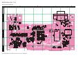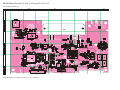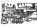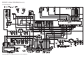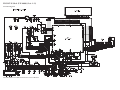
1
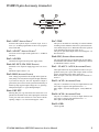
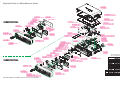
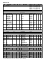
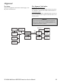
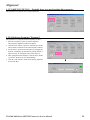
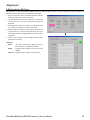
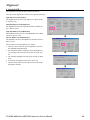
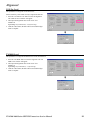
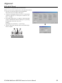
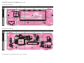
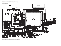
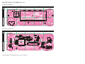
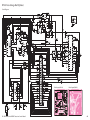
Vertex Standard LMR, Inc. UHF FM Transceiver 4-8-8 Nakameguro, Meguro-Ku, Tokyo 153-8644, Japan VX-4500 Series VX-4600 Series ©2013 Vertex Standard LMR, Inc. EC093U90G Service Manual VX-4500 Series VX-4600 Series Introduction This manual provides the technical information necessary for servicing the VX-4500/-4600 Series Mobile Transceiver. Servicing this equipment requires expertise in handing surface-mount chip components. Attempts by non-qualified persons to service this equipment may result in permanent damage not covered by the warranty, and may be illegal in some countries. Two PCB layout diagrams are provided for each double-sided board in this transceiver. Each side of the board is referred to by the type of the majority of components installed on that side (“Side A” or “Side B”). In most cases one side has only chip components (surface-mount devices), and the other has either a mixture of both chip and leaded components (trimmers, coils, electrolytic capacitors, ICs, etc.), or leaded components only. As described in the pages to follow, the advanced microprocessor design of the VX-4500/-4600 allows a complete alignment of this transceiver to be performed without opening the case of the radio; all adjustments can be performed from the personal computer, using with the Vertex Standard FIF-12 USB Programming Interface and CE115 Software. While we believe the information in this manual to be correct, Vertex Standard assumes no liability for damage that may occur as a result of typographical or other errors that may be present. Your cooperation in pointing out any inconsistencies in the technical information would be appreciated. Important Note The VX-4500/-4600 was assembled using Pb (lead) free solder, based on the RoHS specification. Only lead-free solder (Alloy Composition: Sn-3.0Ag-0.5Cu) should be used for repairs performed on this apparatus. The solder stated above utilizes the alloy composition required for compliance with the lead-free specification, and any solder with the above alloy composition may be used. Contents Specifications ................................................................. 2 DSUB 15-pin Accessory Connector ............................. 3 Exploded View & Miscellaneous Parts ........................ 4 Block Diagram ............................................................... 5 Parts List ........................................................................ 6 Circuit Description ........................................................ 7 Alignment ....................................................................... 9 Installation of Option .................................................. 23 Board Units (Schematics & Layouts) MAIN Unit ............................................................... 24 FRONT-A Unit (VX-4500) ..................................... 36 FRONT-B Unit (VX-4600) ..................................... 40 Optional Units (Schematics & Layouts) DVS-8 Voice Storage Unit ...................................... 44 VX-4500/-4600 Series UHF FM Transceiver Service Manual 1 Specifications General Frequency Ranges: Number of Channels: Power Supply Voltage: Channel Spacing: Pll Steps: Current Consumption (@13.6 V): Operating Temperature Range: Frequency Stability: Antenna Impedance: Case Size (W x H x D): Weight (Approx.): 450 - 520 MHz (512 MHz: USA only) (TYP D) /400 - 470 MHz (TYP A) 8 channels (VX-4500 Series) 512 channels with 32 group (VX-4600 Series) 13.6 V ± 20 % 12.5/20/25 kHz 5/6.25 kHz 11 A (TX: 45 W)/6 A (TX: 25 W) 2.5A (RX) 200 mA (RX: SQL Closed) –22 °F to +140 °F (–30 °C to +60 °C) ±2.5 ppm (–22 °F to +140 °C [–30 °C to +60 °C]) 50 ohms 6.5” x 1.8” x 6.1” inch (165 x 45 x 155 mm) (W/O knob) 2.8 lbs (1.25 kg) Receiver: measured by TIA/EIA-603 Circuit Type: Intermediate Frequency: Sensitivity (12 dB SINAD): Adjacent Channel Selectivity: Hum & Noise: Intermodulation: Spurious & Image Rejection: Audio Output: Double-conversion Superheterodyne 1st: 67.65 MHz, 2nd: 450 kHz 0.25 µV 70 dB (12.5 kHz) 80 dB (25 kHz) 40 dB (12.5 kHz) 45 dB (25 kHz) 75 dB 80 dB Internal: 4 W @32 Ohms, 5% THD External: 12 W @4 Ohms, 5% THD Transmitter: measured by TIA/EIA-603 Modulation Type: Power Output: Emission Type: Maximum Deviation: FM Hum & Noise: Audio Distortion: Conducted Spurious Emission: Variable Reactance 45/25/12.5/5 W 16K0F3E, 11K0F3E ±2.5 kHz (12.5 kHz) ±5 kHz (25 kHz) 40 dB (12.5 kHz) 45 dB (25 kHz) < 3 % (@1 kHz) 70 dB below Carrier Receiver: measured by EN 300 086 Circuit Type: Intermediate Frequency: Sensitivity (20 dB SINAD): Adjacent Channel Selectivity: Hum & Noise: Intermodulation: Spurious & Image Rejection: Audio Output: Double-conversion Superheterodyne 1st: 67.65 MHz, 2nd: 450 kHz –5 dBµ/–2 dBµ (25 kHz/12.5 kHz) 70 dB (12.5 kHz) 75 dB (25 kHz) 40 dB (12.5 kHz) 45 dB (25 kHz) 70 dB 80 dB Internal: 4 W @20 Ohms, 5% THD External: 12 W @4 Ohms, 5% THD Transmitter: measured by EN 300 086 Modulation Type: Power Output: Emission Type: Maximum Deviation: FM Hum & Noise: Audio Distortion: Conducted Spurious Emission: Variable Reactance 25/12.5/5/1W 16K0F3E, 11K0F3E ±2.5 kHz (12.5 kHz) ±5 kHz (25 kHz) 40 dB (12.5 kHz) 45 dB (25 kHz) < 3 % (@1 kHz) < –36 dBm@<= 1 GHz, –30 dBm>@1 GHz Specifications subject to change without notice or obligation. VX-4500/-4600 Series UHF FM Transceiver Service Manual 2 DSUB 15-pin Accessory Connector Pin 1: AF IN (ANALOG INPUT) External Microphone Input. Nominal input level is 4 mV (or –10 dBm; programmed via the CE115 programmer) at 600-ohm. Pin 2: AF OUT (ANALOG OUTPUT) Low-level receiver output. Peak signal level is –10 dBm at 600-ohm. Pin 3: AF GND Ground for all logic levels and power supply return. Pin 4: DC OUT (13.6 V DC OUTPUT) Switched 13.6V output for supplying power to an accessory. Maximum output current is 1 A. Pin 5: RSSI (ANALOG OUTPUT) A DC voltage proportional to the strength of the signal currently being received (Receiver Signal Strength Indicator) is provided on this pin. This low impedance output is gererated by the receiver IF sub-system and bufferd by an internal op-amp. Typical output voltages are 1 V (@No Signal Input) through 2.5 V (@50 dB Signal Input). Pin 6: EXT PTT Shorting this port to ground causes the transceiver to be placed in the Transmit mode, while opening the connection to this port returns the transceiver to the Receive mode. Opening voltage is 5 V, closed current approx. 5 mA. Pin 7: TRX This port is intended for controlling an external TX/RX switching circuit. When the transceiver is placed in the Receiver mode, this port is 5 V. When the transceiver is placed in the Transmit mode, this port reduce to 0 V. This port is open drain output which can sink approx. 50 mA when active. Pin 8: ING (IGNITION SENSE FEATURE) The VX-4500/-4600 may be automatically be switched to the STND-BY mode when the vehicle’s ignition key is turned on. Maximum current is 20 mA. Pin 9 - 12: ACC1 - ACC4 (ACCESSORY PORT) These port features can be programmed via the CE115 programmer. Each port is open drain output which can sink approx. 50 mA when active. Max. output 16 V. When the input is selected, it becomes active between 2 V and 16 V. Pin 13: ACC5 (ACCESSORY PORT) The port 5 is available to set only for Output function, and active logic is opposite side against the Port 1 ~ 4. Max. output 5 V, closed current approx. 1 mA (CMOS output). Pin 14: ACC6 (ACCESSORY PORT) The port 6 is available to set only for Input function, and active logic is opposite side against the Port 1 ~ 4. Max. input 5 V (CMOS input). Pin 15: GND Chassis ground VX-4500/-4600 Series UHF FM Transceiver Service Manual 3 Exploded View & Miscellaneous Parts Non-designated parts are available only as part of a designated assembly. VX-4500/-4600 Series UHF FM Transceiver Service Manual 4 Block Diagram VX-4500/-4600 Series UHF FM Transceiver Service Manual 5 Parts List REF DESCRIPTION VALUE V/W TOL. MFR'S DESIG PCB with Components MAIN UNIT FRONT-A UNIT FRONT-B UNIT VXSTD P/N VERS. CS2093701 CS2093702 CS2093703 CS2093704 CS2093705 CS2093706 CB5266001 CB5267001 CH:8, CH:512, CH:8, CH:512, CH:8, CH:512, CH:8 CH:512 RA124930A RA124940A RA123450B RA123420B RA1234300 RA123460A RA1245900 RA124700A RA1234400 RA1261500 RA1244600 RA124470A RA1288200 RA1244800 RA0786900 RA1292600 RA124680A RA1246900 RA1254600 RA0997300 U03308002 U24308001 U24306001 U71002001 CH:512 CH:8 LOT SIDE LAY ADR POW:45, POW:45, POW:45, POW:45, POW:25, POW:25, TYP D TYP D TYP A TYP A TYP A TYP A Mechanical Parts FRONT PANEL ASSY FRONT PANEL ASSY CHASSIS TOP COVER PACKING PAD SHIELD CASE COVER VOLUME KNOB RUBBER KNOB PACKING PAD SP HOLDER LCD HOLDER LIGHT GUIDE REFLECTOR SHEET INTER CONNECTOR SPONGE RUBBER REFLECTOR SHEET HOLDER LIGHT GUIDE SHEET LED FILTER SEMS SCREW BIND HEAD TAPTITE-B BIND HEAD TAPTITE-B SPRING LOCK WASHER SPEAKER CONNECTOR CD1001 CF1001 CF1002 CF1003 F 1001 F 1002 Q 1001 Q 1003 Q 1013 Q 1013 Q 1013 Q 1042 Q 1044 X 1001 X 1002 XF1001 CERAMIC DISC CERAMIC FILTER CERAMIC FILTER CERAMIC FILTER CHIP FUSE CHIP FUSE IC IC IC IC IC FET FET XTAL TCXO XTAL FILTER (8CH) (COVER) (PANEL) (LCD) (093) (LCD) (SUB) (LED) (LED) (LED) (8CH) ASM3X8NI M3X8 M3X6 SW2.6 20-ohm 1.25A 1.25A 32.768kHz 16.8MHz Electrical Parts 5015134H02 (AC093U) MAIN UNIT Electrical Parts JTBM450CX24-A LTM450GW-A LTM450EW-A LTM450GW-A FCC16 132ABTP FCC16 132ABTP NJM7808DL1A-TE1 TDA1519CTH RA60H4452M1 RA55H4047M RA30H4047M1-101 2SK880GR(TE85R.F) 3LN01S-TL 4809995L18 32.768KHZ TTS14VSB-A5 16.8MHZ MFT67P 67.650MHZ CH:512 CH:512 CH:512 CH:512 CH:512 CH:512 CH:8 CH:8 CH:8 CH:8 M4090203 P1091412A H7901530A H3900573A H3900574A H3900573A Q0000109 Q0000109 G1093802 G1093778 G1094520 G1094344 G1094555 G3808807G G3070330 H0103407 H9501150 H1102471 B A A A A A A B A A A B B A A A b4 H4 G4 H4 B1 C5 C3 g3 C1 C1 C1 d4 g2 A4 F4 G4 RA129670C RA129670C J60800312 B B A e1 a1 B1 G6090215 RA129670C RA129670C G3211327R G1094350 G9090120 J60800312 A B B B B B A C1 e1 a1 c1 d2 c1 B1 45 W, D 45 W, A 25 W, A FRONT-A UNIT (VX-4500) Electrical Parts J 2004 LEAF SPRING J 2005 LEAF SPRING VR2001 POT. DS3001 J 3004 J 3005 Q 3001 Q 3003 TH3001 VR3001 LCD LEAF SPRING LEAF SPRING TRANSISTOR IC THERMISTOR POT. RK09L1140 20KB FRONT-B UNIT (VX-4600) Electrical Parts GTG4795SK01 2SB1132 T100 R HA178L09UA-TL-E ERTJ0EV473J RK09L1140C33 20KB VX-4500/-4600 Series UHF FM Transceiver Service Manual 6 Circuit Description 1. Circuit Configuration by Frequency The receiver is a double-conversion superheterodyne with a first intermediate frequency (IF) of 67.65 MHz and a second IF of 450 kHz. Incoming signal from the antenna is mixed with the local signal from the VCO/PLL to produce the first IF of 67.65 MHz. This is then mixed with the 67.2 MHz second local oscillator output to produce the 450 kHz second IF. This is detected to give the demodulated signal. The transmit signal frequency is generated by the PLL VCO and modulated by the signal from the microphone. It is then amplified and sent to the antenna. 2. Receiver System 2-1. Front-end RF amplifier Incoming RF signal from the antenna is delivered to the RF Unit and passes through the Low-pass filter. Undesired frequencies are removed by the varactor diode tuned band-pass filter consisting of diodes D1013 & D1015 (both RKV500KJ) and Coils L1015 & L1018, and capacitors C1017, C1116, C1118, C1130, C1117, C1135, C1137, C1139, C1151, and C1156. The passed signal is amplified by Q1021 (2SC3356) and moreover cuts animage frequency with the tuned band pass filter consisting of Coils L1025, & L1028, and capacitors C1173, C1181, C1182, C1183, C1188, C1197, C1198, C1205, & C1212. The filtered RF signal is then delivered to the first Mixer. 2-2. First Mixer The 1st mixer consists of Q1040 (AK1220). Buffered output from the VCO is amplified by Q1026 (2SC5226) to provide a pure first local signal between 382.35 and 444.35 MHz for injection to the first mixer. The output IF signal is sent to the crystal filter. The IF signal then passes through monolithic crystal filter XF1001 (± 5.5 kHz BW) to strip away all but the desired signal. 2-3. IF Amplifier The first IF signal is amplified by Q1049 (2SC5226). The amplified first IF signal is applied to FM IF subsystem IC Q1054 (NJM2591V) which contains the second mixer, second local oscillator, limiter amplifier, noise amplifier, and S-meter amplifier. The signal from reference oscillator X1002 is multiplied 3 times in Q1054 (NJM2591V). It is mixed with the first IF signal and becomes the second IF signal of 450 kHz. The second IF then passes through the ceramic filter CF1002 (for wide channels) or CF1001 and CF1003 (for narrow channels) to strip away unwanted mixer products and remove amplitude variations in the 450 kHz IF before detection of the speech by the ceramic discriminator CD1001. 2-4. Audio amplifier Detected signal from Q1054 (NJM2591V) is delivered to Q1010 (FQ0801) pin 28 and is output by Q1010 (FQ0801) pin 17 through the band pass filter. When the optional unit is installed, Q1010 (FQ0801) is made “OFF” and the AF signal from Q1010 (FQ0801) pin 21 goes to the optional unit and returns to Q1010 (FQ0801) pin 20 from the optional unit. When the optional unit is not installed, Q1010 (FQ0801) is made “ON” the AF signal goes through Q1010 (FQ0801) pin 20/21. The signal is stored in the AF volume via AF mute and the deemphasis inside Q1010 (FQ0801). The AF volume is controlling Q1010 (FQ0801) by the CPU. After that, itrnters AF power amplifire Q1003 (TDA1519CTH) after passing AF volume. The output of Q1003 (TDA1519CTH) drives a speaker (it chooses the external SP or internal SP in J1001). 2-5. Squelch Circuit There are 16 levels of squelch setting from 0 to 15. The level 0 means open squelch. The level 1 means the threshold setting Level and level 15 means tight squelch. From 1 to 14 is established in the middle of threshold and tight. The bigger figure is nearer the tight setting. The level 16 becomes setting of carrier squelch. 2-5-1. Noise Squelch The noise squelch circuit is composed of the band pass filter of Q1054 (NJM2591V), noise amplifier Q1060 (2SC4617), and noise detector D1048, D1052 (both DA221). When a carrier isn’t received, the noise ingredient which goes out of the demodulator Q1054 (NJM2591V) is amplified in Q1060 (2SC4617) through the band pass filter Q1054 (NJM2591V), is detected to DC voltage with D1048 and D1052 (both DA221), and is inputted to pin 15 the A/D port of the Q1041 (LC88F52H0A) CPU. When a carrier is received, the DC voltage becomes “LOW” because the noise is compressed. When the detected voltage to CPU is “HIGH”, the CPU stops AF output with Q1010 (FQ0801) “OFF”. When the detected voltage is low, the CPU makes Q1010 (FQ0801) “ON” and the AF signal is output. 2-5-2. Carrier Squelch Pin 14 (A/D port) of Q1047 (NJM2904V) CPU detects RSSI voltage output from pin 12 of Q1054 (NJM2591V), and controls AF output. The RSSI output voltage changes according to the signal strength of carrier. The stronger signal causes the RSSI voltage to be higher voltage. The process of the AF signal control is the same as Noise Squelch. The shipping data is adjusted 3 dB higher than squelch tight sensitivity. VX-4500/-4600 Series UHF FM Transceiver Service Manual 7 Circuit Description 3. Transmitter System 3-1. Mic Amplifier The AF signal from microphone jack J2001 (VX-4500) or J3001 (VX-4600) is amplified with microphone amplifier in Q1010 (FQ0801), is amplified a second time after microphone selection switch Q1010 (FQ0801), and passes through microphone gain volume in Q1010 (FQ0801). The control from the CPU passes output and it passes a pre-emphasis circuit. When an option unit is installed, the AF signal from Q1010 (FQ0801) pin 38 goes through the option unit, and returns to Q1010 (FQ0801) pin 39. When an option unit isn't installed, Q1010 (FQ0801) is inputted to the pre-emphasis circuit. The signal passes the limiter and splatter filter of Q1010 (FQ0801), and is adjusted by maximum deviation adjustment volume. The adjusted low frequency signal ingredient is amplified by Q1047 (NJM2904V), added modulation terminal of TCXO (X1002), the FM modulation is made by reference oscillator. The high frequency signal ingredient is amplified, and adjusted the level by volume Q1010 (FQ0801) to make frequency balance between low frequency. After that, it is made FM modulation to transmit carrier by the modulator D1026 (HVC300A) of VCO. 3-2. Drive and Final amplifier The modulated signal from the VCO Q1034 (2SK508) is buffered by Q1026 (2SC5226) and amplified by Q1017 (2SC3357). The low-level transmit signal is then applied to the Power Module Q1013 (RA60H4452M1: for 50 W, RA30H4047M1: for 25 W) for final amplification up to 50 or 25 watts watts output power. The transmit signal is then lowpass filtered to suppress away harmonic spurious radiation before delivery to the antenna. 3-3. Automatic Transmit Power Control The output power of Power Module is detected by CM coupler, it is detected by D1005 & D1008 (both HSM88AS) and is input to comparator Q1048 (NJM12902V). The comparator compares two different voltages and makes output power stable by controlling the bias voltage of the Power Module. There are 4 levels of output power (Hi, Lo3, Lo2, and Lo1) it is switched by the Voltage of Q1010 (FQ0801) pin 44. 4. PLL Frequency Synthesizer The frequency synthesizer consists of PLL IC Q1043 (AK1541), VCO, TCXO (X1002), and buffer amplifier. The output frequency from TCXO is 16.8 MHz and the tolerance is ± 2.5 ppm (in the temperature range –22 °F to +140 °F [–30 °C to +60 °C]). 4-1. VCO While the radio is receiving, the RX oscillator Q1034 (2SK508) in VCO generates a programmed frequency between 382.35 and 444.35 MHz as 1st local signal. While the radio is transmitting, the TX oscillator Q1036 (2SK508) in VCO generates a frequency between 450 and 512 MHz. The output from the oscillator is amplified by buffer amplifier Q1029 (2SC5226) and becomes output of VCO. The output from the VCO is divided, one is amplified by Q1039 (2SC5226) and feed back to pin 17 of the PLL IC Q1043 (AK1541). It is amplified about the RF signal Q1029 (2SC5226) which was made by VCO. RF changes with the carrier signal of the transmitter and the mixer local signal of the receiver with D1020 (DAN222). 4-2. VCV CNTL Tuning voltage (VCV) of the VCO is expanding the lock range of VCO by controlling of the varactor diode at the voltage and the control voltage from PLL IC Q1043 (AK1541). As for the control voltage adjustment by the varactor diode, it controls the negative voltage to make with Q1025 (TPS60303) with the D/A converter inside Q1010 (FQ0801) and Q1037 (NJM2125F), it has the anode potential of the varactor diode variably 4-3. PLL The PLL IC Q1043 (AK1541) consists of reference divider, main divider, phase detector, charge pumps and delta-sigma fractional accumulator. The reference frequency from TCXO is inputted to pin 10 of PLL IC Q1043 (AK1541) and is divided by reference divider. This IC is decimal point dividing PLL IC Q1043 (AK1541) and the dividing ratio becomes 1/8 of usual PLL frequency step. Therefore, the output of the reference divider is 8 times the frequency of the channel step. For example when the channel stepping is 5 kHz, the output of reference divider becomes 40 kHz. On the other hand, inputted feed back signal to pin 1 of PLL IC Q1043 (AK1541) from VCO is divided with the dividing ratio which becomes the same frequency as the output of reference divider. These two signals are compared by the phase detector, and the phase difference pulse is generated. The phase difference pulse and the pulse from fractional accumulator pass through the charge pumps and LPF. It becomes the DC voltage (VCV) to control the VCO. The oscillation frequency of VCO is locked by the control of this DC voltage. The PLL serial data from CPU Q1041 (LC88F52H0A) is sent with three lines of SDO (pin 20), SCK (pin 22) and PSTB (pin 45). The lock condition of PLL is output from the UL (pin 18) terminal and UL becomes “H” at the time of the lock condition and becomes “L” at the time of the unlocked condition. The CPU Q1041 (LC88F52H0A) always watches over the UL condition, and when it becomes “L” unlocked condition, the CPU Q1041 (LC88F52H0A) prohibits transmitting and receiving. VX-4500/-4600 Series UHF FM Transceiver Service Manual 8 Alignment Introduction Required Test Equipment The VX-4500/-4600 series has been aligned at the factory for the specified performance across the entire frequency range specified. Realignment should therefore not be necessary except in the event of a component failure. All component replacement and service should be performed only by an authorized Vertex Standard representative, or the warranty policy may be voided. The following procedures cover the sometimes critical and tedious adjustments that are not normally required once the transceiver has left the factory. However, if damage occurs and some parts are replaced, realignment may be required. If a sudden problem occurs during normal operation, it is likely due to component failure; realignment should not be done until after the faulty component has been replaced. We recommend that servicing be performed only by authorized Vertex Standard service technicians who are experienced with the circuitry and fully equipped for repair and alignment. Therefore, if a fault is suspected, contact the dealer from whom the transceiver was purchased for instructions regarding repair. Authorized Vertex Standard service technicians realign all circuits and make complete performance checks to ensure compliance with factory specifications after replacing any faulty components. Those who do undertake any of the following alignments are cautioned to proceed at their own risk. Problems caused by unauthorized attempts at realignment are not covered by the warranty policy. Also, Vertex Standard must reserve the right to change circuits and alignment procedures in the interest of improved performance, without notifying owners. Under no circumstances should any alignment be attempted unless the normal function and operation of the transceiver are clearly understood, the cause of the malfunction has been clearly pinpointed and any faulty components replaced, and the need for realignment determined to be absolutely necessary. The following test equipment (and thorough familiarity with its correct use) is necessary for complete realignment. Correction of problems caused by misalignment resulting from use of improper test equipment is not covered under the warranty policy. While most steps do not require all of the equipment listed, the interactions of some adjustments may require that more complex adjustments be performed afterwards. Do not attempt to perform only a single step unless it is clearly isolated electrically from all other steps. Have all test equipment ready before beginning, and follow all of the steps in a section in the order presented. Radio Tester with calibrated output level at 1 GHz In-line Wattmeter with 5% accuracy at 1 GHz 50-ohm, 50-W RF Dummy Load Regulated DC Power Supply (standard 13.6V DC, 15A) Frequency Counter: ±0.2 ppm accuracy at 1 GHz AF Signal Generator AC Voltmeter DC Voltmeter UHF Sampling Coupler IBM® PC/compatible Computer with Microsoft® Windows® 2000, XP, Vista or Windows7 Vertex Standard CE115 PC Programming Software Vertex Standard FIF-12 USB Programming Interface and CT-104A, CT-106, or CT-171 PC Programming Cable Vertex FRB-6 Tuning Interface Box and CT-159 Connection Cable Alignment Preparation & Precautions A 50-ohm RF Dummy load and in-line wattmeter must be connected to the main antenna jack in all procedures that call for transmission, except where specified otherwise. Correct alignment is not possible with an antenna. Beacuse of the BTL (Bridged Trans Less) Amplifier circuit used in the VX-4500/-4600, do not connect eather side of the speaker leads to chassis “ground”. After completing one step, read the following step to determine whether the same test equipment will be required. If not, remove the test equipment (except dummy load and wattmeter, if connected) before proceeding. Correct alignment requires that the ambient temperature be the same as that of the transceiver and test equipment, and that this temperature be held constant between 20 °C and 30 °C (68 °F ~ 86 °F). When the transceiver is brought into the shop from hot or cold air, it should be allowed time to come to room temperature before alignment. Whenever possible, alignments should be made with oscillator shields and circuit boards firmly affixed in place. Also, the test equipment must be thoroughly warmed up before beginning. Note: Signal levels in dB referred to in this procedure are based on 0 dBµ EMF = 1.0 µV. VX-4500/-4600 Series UHF FM Transceiver Service Manual 9 Alignment Test Setup The Alignment Tool Outline Setup the test equipment as shown below, and then apply 13.6V DC power to the transceiver. Installation of the alignment tool Install the CE115 (PC Programming Software) to your PC. “Alignment“ function in the “Radio“ menu tab of CE115. Action of the switches When the transceiver is in the “Alignment mode,“ the action of the PTT and all PF KEYS are ignored. All of the action is controlled by the PC. Caution! Please never turn off the power supply during alignment. If the power supply is turned off during alignment, the alignment data will be corrupted. 50-ohm Dummy Load SP/LOAD Switch: LOAD LOAD Switch: 4W RF Signal Generator SINAD Meter CT-159 SP OUT B Inline Wattmeter Deviation Meter Sampling Coupler ANT MIC & EXT SP AF Signal FRB-6 VX-4500/-4600 D-Sub 15-pin MIC IN Generator Connector DC INPUT CLONE Port CT-104A, CT-106, or CT-171 Power Supply 13.6 VDC FIF-12 Computer (CE115) Frequency Counter VX-4500/-4600 Series UHF FM Transceiver Service Manual 10 Alignment Alignment Mode The Alignment mode allows you to align the entire radio. The value of each parameter can be changed to the desired value by use of the “” / “” and up/down arrow keys, along with direct number input and dragging of the PC mouse. To enter the Alignment Mode, select “Alignment” in the main “Radio” menu. It will start to “Upload” the alignment data from the radio to the PC. Pressing the “OK” button will then “Download” the alignment data to the radio and exit the Alignment Mode. Note: when all items are to be aligned, it is strongly recommended to align them according to the following sequence. Detailed information for each step may be found in the “Help” file within CE115 (PC Programming Software). 1. VCO (Please do not adjust it) 2. PLL Reference Frequency (Frequency) 3. RX Sensitivity (RX Tune) 4. Squelch (SQL/RSSI) 5. TX Power <High/Low3/Low2/Low1> 6. Maximum Deviation <Wide/Narrow> Please adjust the following items when needed. H Modulation Balance <Wide/Narrow> H H H H H H H CTCSS Deviation <Wide/Narrow> DCS Deviation <Wide/Narrow> DTMF Alignment Seq Tone VOX ON Level TX MSK Ext AF Out Unit During alignment, you may select the value among dBµV,µV (EMF or PD), or dBm. When performing the “RX Tune” and “SQL” alignment, the RF level shows this unit according to this setting. « VX-4500/-4600 Series UHF FM Transceiver Service Manual 11 Alignment 1. VCO (RX VCO/TX VCO) - Normally there is no need to adjust this parameter This parameter is to align the VCO Voltage adjustment. 2. PLL Reference Frequency (Frequency) This parameter is to align the reference frequency for PLL. VX-4500/-4600 Series UHF FM Transceiver Service Manual « 1. Press the “Frequency” button to start the alignment. The Frequency Alignment window will appear. 2. Click the “PTT” button or press the “SPACE” bar, and the radio will start to transmit on the center frequency channel. 3. Set the value to get the desired frequency by dragging the slide bar, clicking the up-down button, pressing the left or right arrow key, or entering the value in the entry box. 4. After getting the desired frequency click the “PTT” button or press the “SPACE” bar to stop transmitting. 5. Click the “OK” button to finish the frequency alignment and save the data. 12 Alignment 3. RX Sensitivity (RX Tune) This parameter is to align the RX BPF (Band Pass Filter) for Receive (RX) sensitivity. The PLL Reference Frequency (Frequency) alignment must be done before this alignment is performed. « 1. Press the “RX Tune” button to start the alignment. The RX Sensitivity Alignment window will appear. 2. Click the left mouse button on the slide bar or press the Up / Down arrow keys, to switch to the desired channel for alignment. 3. Set the Signal Generator according to the indication at the top of the screen (Setting Your SG as followings). 4. Drag the slide bar, click the up-down buttons, press the left or right arrow key, or enter the value in the entry box to get the best RX sensitivity (Highest RSSI value) on the selected channel. 5. Click the “OK” button to finish the RX Sensitivity alignment and save the data. ADJ Type Basic: “Low-edge / band center / high-edge“ and select the channel for alignment (Default). Single: Alignment value changes only on the selected channel. All Freq: Alignment value changes on all channels. VX-4500/-4600 Series UHF FM Transceiver Service Manual 13 Alignment 4. Squelch (SQL) This parameter is to align the SQL (Squelch) Sensitivity. There are several alignments as follows in the Squelch Sensitivity. Tight SQL Level (TI NSQ W/N) The Alignment for the Noise SQL Tight level at Wide (5k/4k) or Narrow (2.5k). Threshold SQL Level (TH NSQ W/N) The Alignment for the Noise SQL Threshold level at Wide (5k/ 4k) or Narrow (2.5k). « Tight SQL RSSI Level (TI RSSI W/N) The Alignment for the “level 14” of the RSSI SQL level at Wide (5k/4k) or Narrow (2.5k). TX Save RSSI Level (TX SAVE W/N) The Alignment for the TX Save RSSI level at Wide (5k/4k) or Narrow (2.5k). « VX-4500/-4600 Series UHF FM Transceiver Service Manual « The procedure for all the alignments is as follows. 1. Click the “Start” button to open the alignment window in the SQL/RSSI Alignment menu. 2. The Alignment window will appear, Set the Signal Generator according to the indication, then click the “Start” button. 3. The automatic alignment will start to get the SQL or RSSI level. 4. It will show the alignment result in the “New” box. 5. Click the “OK” button, then the data will be saved and the alignment is finished. 14 Alignment 5. TX Power This parameter is to align the “Power High”, “Power Low3”, “Power Low2” or “Power Low1” for the selected channel. « 1. Press the “TX Pwr(H / L3 / L2 / L1)” button to start the alignment. The TX Power Alignment window will appear. 2. Click the left mouse button on the slide bar or press the Up / Down arrow key, to select the desired channel. 3. Click the “PTT” button or press the “SPACE” bar at the desired channel, then the radio starts to transmit on the selected channel. 4. Set the value to get desired output power on the Power Meter by dragging the slide bar, clicking the up-down button, pressing the left or right arrow key, or entering the value in the entry box on the selected channel. 5. After getting the desired output power click the “PTT” button or press the “SPACE” bar to stop transmitting. 6. Click the “OK” button to finish the TX Power alignment and save the data. ADJ Type Basic: “Low-edge / band center / high-edge“ and select the channel for alignment (Default). Single: Alignment value changes only on the selected channel. All Freq: Alignment value changes on all channels. VX-4500/-4600 Series UHF FM Transceiver Service Manual 15 Alignment 6. Maximum Deviation <Wide> / <Narrow> This parameter is to align the “Maximum Deviation” (Wide/Narrow). « 1. Press the “Max Dev (W/N)” button to start the alignment. 2. The Max Deviation alignment window will appear. 3. Set the AF Signal Generator output level to –24 dBm at 1 kHz tone (Sine Wave). 4. Select the desired channel by following method: Clicking the left mouse button on the slide bar of the desired channel Pressing the Up / Down arrow key of the desired channel 5. Click the “PTT” button or press the “SPACE” bar, the radio starts to transmit on the selected channel. 6. Set the value to get desired deviation (Wide: 4.2kHz, Narrow: 2.1kHz) on the deviation meter by following method: Dragging the slide bar Clicking the up-down button Pressing the Left / Right arrow key Entering the value in the “Data” box on the selected channel 7. After getting the desired deviation click the “PTT” button or press the “SPACE” bar to stop transmitting. 8. Click the “OK” button to finish the Max Deviation alignment and save the data. ADJ Type Basic: “Low-edge / band center / high-edge“ and select the channel for alignment (Default). Single: Alignment value changes only on the selected channel. All Freq: Alignment value changes on all channels. VX-4500/-4600 Series UHF FM Transceiver Service Manual 16 Alignment Please adjust the following items when needed. Modulation Balance <Wide> / <Narrow> (This Alignment is difficult.) This parameter is to align the “Modulation Balance” (Wide/Narrow). « 1. Press the “Mod Bal (W/N)” button to start the alignment. 2. The Modulation Balance Alignment window will appear. 3. Connect the AF Signal Generator to pin 1 of the D-SUB connector on the rear panel of the transceiver. Then set the AF Signal Generator output level to –24 dBm at 3 kHz tone (Sine Wave). 4. Set the “Data” box value to “160” on the desired channel by following method: Dragging the slide bar of the desired channel Pressing the Up / Down arrow key of the desired channel Entering the value directly in the “Data” box on the selected channel 5. Click the “PTT” button or press the “SPACE” bar the radio starts to transmit on the selected channel. 6. Write down the measured deviation level. 7. Change the AF Signal Generator frequency to 40 Hz tone (Sine Wave, –24 dBm). 8. Set the value to get “deviation of step 6” by following method: Dragging the slide bar of the desired channel Pressing the Up / Down arrow key of the desired channel Entering the value directly in the “Data” box on the selected channel 9. After setting the deviation level click the “PTT” button or press the “SPACE” bar to stop transmitting. 10. Click the “OK” button to finish the Modulation Balance alignment and save the data. ADJ Type Basic: “Low-edge / band center / high-edge“ and select the channel for alignment (Default). Single: Alignment value changes only on the selected channel. All Freq: Alignment value changes on all channels. VX-4500/-4600 Series UHF FM Transceiver Service Manual 17 Alignment CTCSS Deviation <Wide> / <Narrow> This parameter is to align CTCSS Deviation of the selected channel. « 1. Press the “CTC Dev (W/N)” button to start the alignment. The CTCSS Deviation Alignment window will appear. 2. Click the left mouse button on the slide bar or press the Up / Down arrow key, to select the desired channel. 3. Click the “PTT” button or press the “SPACE” bar the radio starts to transmit with CTCSS tone on the selected channel. 4. Set the value to get desired deviation on the deviation meter by dragging the slide bar, clicking the up-down button, pressing the left or right arrow key, or entering the value in the entry box on the selected channel. 5. After getting the desired deviation (Wide: 0.6 kHz, Narrow: 0.3 kHz) click the “PTT” button or press the “SPACE” bar to stop transmitting. 6. Click the “OK” button to finish the CTCSS Deviation alignment and save the data. ADJ Type Basic: “Low-edge / band center / high-edge“ and select the channel for alignment (Default). Single: Alignment value changes only on the selected channel. All Freq: Alignment value changes on all channels. VX-4500/-4600 Series UHF FM Transceiver Service Manual 18 Alignment DCS Deviation <Wide> / <Narrow> This parameter is to align “DCS Deviation” of the selected channel. « 1. Press the “DCS Dev (W/N)” button to start the alignment. The DCS Deviation Alignment window will appear. 2. Click the left mouse button on the slide bar or press the Up / Down arrow key, to select the desired channel. 3. Click the “PTT” button or press the “SPACE” bar the radio starts to transmit with DCS Code on the selected channel. 4. Set the value to get desired deviation (Wide: 0.6 kHz, Narrow: 0.3 kHz) on the deviation meter by dragging the slide bar, clicking the up-down button, pressing the left or right arrow key, or entering the value in the entry box on the selected channel. 5. After getting the desired deviation click the “PTT” button or press the “SPACE” bar to stop transmitting. 6. Click the “OK” button to finish the DCS Deviation alignment and save the data. ADJ Type Basic: “Low-edge / band center / high-edge“ and select the channel for alignment (Default). Single: Alignment value changes only on the selected channel. All Freq: Alignment value changes on all channels. VX-4500/-4600 Series UHF FM Transceiver Service Manual 19 Alignment DTMF Deviation This parameter is to align “DTMF Deviation”. « 1. Press the “DTMF” button to start the alignment. The DTMF Alignment window will appear. 2. Click the “PTT” button or press the “SPACE” bar the radio starts to transmit on the Center frequency channel. 3. Set the value to get desired deviation (3.0 kHz) on the deviation meter by dragging the slide bar, clicking the up-down button, pressing the left or right arrow key, or entering the value in the entry box. 4. After getting the desired deviation click the “PTT” button or press the “SPACE” bar to stop transmitting.. 5. Click the “OK” button to finish the DTMF Deviation alignment and save the data. Sequential Tone Deviation This parameter is to align “Sequential Tone Deviation”. VX-4500/-4600 Series UHF FM Transceiver Service Manual « 1. Press the “Seq Tone” button to start the alignment. The Sequential Tone Deviation Alignment window will appear. 2. Click the “PTT” button or press the “SPACE” bar the radio starts to transmit on the Center frequency channel. 3. Set the value to get desired deviation (3.0 kHz) on the deviation meter by dragging the slide bar, clicking the up-down button, pressing the left or right arrow key, or entering the value in the entry box. 4. After getting the desired deviation click the “PTT” button or press the “SPACE” bar to stop transmitting. 5. Click the “OK” button to finish the Sequential Tone Deviation alignment and save the data. 20 Alignment VOX On Level This parameter is to align the “VOX On Level”. Set the Sensitivity of the VOX circuitry's input audio detector. 1. Press the “VOX ON Level” button to start the alignment. The VOX ON Level window will appear. 2. Then input the alignment value in the “New” box. Default: 80 Input Range: 0 (Level Down) ~ 255 (Level Up) 3. Click the “OK” button, the data will be saved and the alignment is complete. « TX MSK Level This parameter is to align the modulation level of the ANI function. 1. Press the “TX MSK” button to start the alignment. The TX MSK Level window will appear. 2. Then input the alignment value in the “New” box. Default: 10 Input Range: 0 (Level Down) ~ 15 (Level Up) 3. Click the “OK” button, the data will be saved and the alignment is complete. « VX-4500/-4600 Series UHF FM Transceiver Service Manual 21 Alignment EXT AF OUT Level This parameter is to align the “EXT AF OUT Level”. Set the Low-level receiver output of pin 2 of the D-SUB Connector. « 1. Press the “Ext AF Out” button to start the alignment. The Ext AF Out Level window will appear. 2. Connect the AF Signal Generator to pin 1 of the D-SUB connector (GND: pin 3). Then inject a 1 kHz tone / SinWave / +40 dBu. 3. Set the Peak signal level to –10 dBm ±0.7 dB at 600-ohm on pin 2 of the D-SUB connector (GND: pin 3) by entering the alignment value in the “New” box. Default: 7 Input Range: 0 (Level Down) ~ 15 (Level Up) 4. Click the “OK” button, the data will be saved and the alignment is complete. D-SUB Connector Pin Out VX-4500/-4600 Series UHF FM Transceiver Service Manual 22 Installation of Option The DVS-8 is a Voice Storage Unit which allows you to record and play back incoming receiver audio. The DVS-8 is is easily programmed the configulations using a Vertex Standard CE115 programmer with an IBM PC-compatible computer. 1. Disconnect the DC power cable. 2. Referring to Figure 1, grasp the Top Case Cover with both hands, Lift up the Top Case Cover to remove while sprend both side of the Top Case Cover. 3. Referring to Figure 2, remove the Shield Case Cover. 4. Referring to Figure 3, locate the empty connector for the Optional Unit, connect the Optional Unit here. 5. Replace the Shield Case Cover, then replace the Top Case Cover. Installation is now complete. Figure 1 Figure 2 Figure 3 VX-4500/-4600 Series UHF FM Transceiver Service Manual 23 MAIN Unit (Lot. 1~2) Circuit Diagram VX-4500/-4600 Series UHF FM Transceiver Service Manual 24 MAIN Unit (Lot. 1~2) Parts Layout (Side A) A B C D E F G H 1 2 3 4 5 VX-4500/-4600 Series UHF FM Transceiver Service Manual 25 MAIN Unit (Lot. 1~2) Parts Layout (Side B) a b c d e f g h 1 2 3 4 5 VX-4500/-4600 Series UHF FM Transceiver Service Manual 26 MAIN Unit (Version A: Lot. 3, Version D: Lot. 3~5) Circuit Diagram VX-4500/-4600 Series UHF FM Transceiver Service Manual 27 MAIN Unit (Version A: Lot. 3, Version D: Lot. 3~5) Parts Layout (Side A) A B C D E F G H 1 2 3 4 5 VX-4500/-4600 Series UHF FM Transceiver Service Manual 28 MAIN Unit (Version A: Lot. 3, Version D: Lot. 3~5) Parts Layout (Side B) a b c d e f g h 1 2 3 4 5 VX-4500/-4600 Series UHF FM Transceiver Service Manual 29 MAIN Unit (Version A: Lot. 4~10, Version D: Lot. 6~10) Circuit Diagram VX-4500/-4600 Series UHF FM Transceiver Service Manual 30 MAIN Unit (Version A: Lot. 4~10, Version D: Lot. 6~10) Parts Layout (Side A) A B C D E F G H 1 2 3 4 5 VX-4500/-4600 Series UHF FM Transceiver Service Manual 31 MAIN Unit (Version A: Lot. 4~10, Version D: Lot. 6~10) Parts Layout (Side B) a b c d e f g h 1 2 3 4 5 VX-4500/-4600 Series UHF FM Transceiver Service Manual 32 MAIN Unit (Lot. 11~) Circuit Diagram VX-4500/-4600 Series UHF FM Transceiver Service Manual 33 MAIN Unit (Lot. 11~) Parts Layout (Side A) A B C D E F G H 1 2 3 4 5 VX-4500/-4600 Series UHF FM Transceiver Service Manual 34 MAIN Unit (Lot. 11~) Parts Layout (Side B) a b c d e f g h 1 2 3 4 5 VX-4500/-4600 Series UHF FM Transceiver Service Manual 35 FRONT-A Unit (VX-4500) (Lot. 1~3) Circuit Diagram VX-4500/-4600 Series UHF FM Transceiver Service Manual 36 FRONT-A Unit (VX-4500) (Lot. 1~3) Parts Layout (Side A) A B C D E b c d e 1 2 Parts Layout (Side B) a 1 2 VX-4500/-4600 Series UHF FM Transceiver Service Manual 37 FRONT-A Unit (VX-4500) (Lot. 4~) Circuit Diagram VX-4500/-4600 Series UHF FM Transceiver Service Manual 38 FRONT-A Unit (VX-4500) (Lot. 4~) Parts Layout (Side A) A B C D E b c d e 1 2 Parts Layout (Side B) a 1 2 VX-4500/-4600 Series UHF FM Transceiver Service Manual 39 FRONT-B Unit (VX-4600) (Lot. 1~3) Circuit Diagram VX-4500/-4600 Series UHF FM Transceiver Service Manual 40 FRONT-B Unit (VX-4600) (Lot. 1~3) Parts Layout (Side A) A B C D E b c d e 1 2 Parts Layout (Side B) a 1 2 VX-4500/-4600 Series UHF FM Transceiver Service Manual 41 FRONT-B Unit (VX-4600) (Lot. 4~) Circuit Diagram VX-4500/-4600 Series UHF FM Transceiver Service Manual 42 FRONT-B Unit (VX-4600) (Lot. 4~) Parts Layout (Side A) A B C D E b c d e 1 2 Parts Layout (Side B) a 1 2 VX-4500/-4600 Series UHF FM Transceiver Service Manual 43 DVS-8 Voice Storage Unit (Option) Circuit Diagram Parts Layout (Side A) VX-4500/-4600 Series UHF FM Transceiver Service Manual Parts Layout (Side B) 44 Copyright 2013 Vertex Standard LMR, Inc. All rights reserved No portion of this manual may be reproduced without the permission of Vertex Standard LMR, Inc. VX-4500/-4600 Series UHF FM Transceiver Service Manual 24