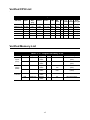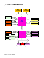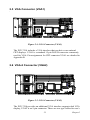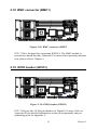
1
PCE-7210
Dual Socket 604 Intel® Xeon® / LV Xeon®
Processor Card with PCI Express / IPMI /
VGA/ Dual Gigabit LAN / FSB 800MHz
User Manual
Copyright Notice
This document is copyrighted, 2006, by Advantech Co., Ltd. All rights
are reserved. Advantech Co., Ltd. reserves the right to make improvements to the products described in this manual at any time without notice.
No part of this manual may be reproduced, copied, translated or transmitted in any form or by any means without the prior written permission of
Advantech Co., Ltd. Information provided in this manual is intended to
be accurate and reliable. However, Advantech Co., Ltd. assumes no
responsibility for its use, nor for any infringements upon the rights of
third parties which may result from its use.
Acknowledgements
• PICMG™ and the PICMG™ logos are trademarks of the PCI Industrial
Computers Manufacturers Group.
• All other product names or trademarks are properties of their respective
owners.
Certifications
• CE
• FCC Class A
PCE-7210 User Manual
Part No. 2002721000
1st Edition
Printed in Taiwan
June, 2006
ii
A Message to the Customer
Advantech customer services
Each and every Advantech product is built to the most exacting specifications to ensure reliable performance in the harsh and
demanding conditions typical of industrial environments. Whether your
new Advantech equipment is destined for the laboratory or the factory
floor, you can be assured that your product will provide the reliability and
ease of operation for which the name Advantech has come to be known.
Your satisfaction is our primary concern. Here is a guide to
Advantech’s customer services. To ensure you get the full benefit of our
services, please follow the instructions below carefully.
Technical support
We want you to get the maximum performance from your products. So if
you run into technical difficulties, we are here to help. For the most frequently asked questions, you can easily find answers in your product documentation. These answers are normally a lot more detailed than the ones
we can give over the phone.
So please consult this manual first. If you still cannot find the answer,
gather all the information or questions that apply to your problem, and
with the product close at hand, call your dealer. Our dealers are well
trained and ready to give you the support you need to get the most from
your Advantech products. In fact, most problems reported are minor and
are able to be easily solved over the phone.
In addition, free technical support is available from Advantech engineers
every business day. We are always ready to give advice on application
requirements or specific information on the installation and operation of
any of our products.
iii
Product warranty
Advantech warrants to you, the original purchaser, that each of its products will be free from defects in materials and workmanship for two years
from the date of purchase.
This warranty does not apply to any products which have been repaired or
altered by persons other than repair personnel authorized by Advantech,
or which have been subject to misuse, abuse, accident or improper installation. Advantech assumes no liability under the terms of this warranty as
a consequence of such events.
If an Advantech product is defective, it will be repaired or replaced at no
charge during the warranty period. For out-of-warranty repairs, you will
be billed according to the cost of replacement materials, service time and
freight. Please consult your dealer for more details.
If you think you have a defective product, follow these steps:
1.
Collect all the information about the problem encountered. (For
example, type of PC, CPU speed, Advantech products used, other
hardware and software used, etc.) Note anything abnormal and list
any on-screen messages you get when the problem occurs.
2.
Call your dealer and describe the problem. Please have your manual, product, and any helpful information readily available.
3.
If your product is diagnosed as defective, obtain an RMA (return
material authorization) number from your dealer. This allows us to
process your return more quickly.
4.
Carefully pack the defective product, a fully-completed Repair and
Replacement Order Card and a photocopy proof of purchase date
(such as your sales receipt) in a shippable container. A product
returned without proof of the purchase date is not eligible for warranty service.
5.
Write the RMA number visibly on the outside of the package and
ship it prepaid to your dealer.
Before you begin installing your single board computer, please make sure
that the following materials have been shipped:
If any of these items are missing or damaged, contact your distributor or
sales representative immediately.
PCE-7210 User Manual
iv
We have carefully inspected the PCE-7210 mechanically and
electrically before shipment. It should be free of marks and scratches and
in perfect working order upon receipt.
As you unpack the PCE-7210, check it for signs of shipping damage. (For
example, damaged box, scratches, dents, etc.) If it is damaged or it fails to
meet the specifications, notify our service department or your local sales
representative immediately. Also notify the carrier. Retain the shipping
carton and packing material for inspection by the carrier. After inspection, we will make arrangements to repair or replace the unit.
v
Initial Inspection
Before you begin installing your single board computer, please make sure
that the following materials have been shipped:
1 PCE-7210 Dual Intel® Xeon® / LV Xeon® processor-based single
board computer
1 PCE-7210 Startup Manual
1 CD with driver utility and manual (in PDF format)
1 FDD cable
P/N: 1700340640
2 Ultra ATA 66/100 HDD cables
P/N: 1701400452
2 Serial ATA HDD data cable
P/N: 1700071000
2 Serial ATA HDD power cable
P/N: 1703150102
1 Printer (parallel) port & COM port cable kit
P/N: 1701260305
1 Dual COM port cable kit
P/N: 1701092300
1 Y cable for PS/2 keyboard and PS/2 mouse
P/N: 1700060202
2 CPU cooler
P/N: 1750000282
1 VGA cable
P/N: 1700000259
1 Video Cable (S / Composite terminal)
P/N: 1700000784
Warranty card
If any of these items are missing or damaged, contact your distributor or
sales representative immediately.
We have carefully inspected the PCE-7210 mechanically and electrically
before shipment. It should be free of marks and scratches and in perfect
working order upon receipt.
As you unpack the PCE-7210, check it for signs of shipping damage. (For
example, damaged box, scratches, dents, etc.) If it is damaged or it fails to
meet the specifications, notify our service department or your local sales
representative immediately. Also notify the carrier. Retain the shipping
carton and packing material for inspection by the carrier. After inspection, we will make arrangements to repair or replace the unit.
PCE-7210 User Manual
vi
Verified CPU List
Table 1.1: Verified CPU List
CPU Freq.
Spec.
Core
Stepping
XEON 3.6 G
SL7ZC
N0
110W
1.4V max
800
90nm
Y
2MB
NA
604 pin
XEON 3.2 G
SL7ZE
N0
110W
1.4V max
800
90nm
Y
2MB
NA
604 pin
XEON 3.0 G
SL7ZF
N0
110W
1.4V max
800
90nm
Y
2MB
NA
604 pin
XEON 2.8 G
SL7ZG
N0
110W
1.4V max
800
90nm
Y
2MB
NA
604 pin
XEON 3.6 G
SL7PH
E0
103W
1.4V max
800
90nm
Y
1MB
NA
604 pin
XEON 3.0 G
SL7TC
E0
103W
1.4V max
800
90nm
Y
1MB
NA
604 pin
Thermal
Vcore
FSB
Mfg.
Tech
HT
L2
L3
Packcache cache age Type
Verified Memory List
Table 1.2: Verified Memory List
Brand
Apacer
(RoHS)
Unigen
(RoHS)
Size
Speed
Type
ECC
Part Number
Memory
512MB
DDR2 400
Register
DDR2
Y
78.91G57.421
ELPIDA E5108AE-5C-E
(64x8)
1GB
DDR2 400
Register
DDR2
Y
78.01G57.420
ELPIDA E5108AE-5C-E
(64x8)
1GB
DDR2 400
Register
DDR2
Y
UG12T7200L8DR5AC
ELPIDA E5108AG-5C-E
(64x8)
2GB
DDR2 400
Register
DDR2
Y
UG25T7200L4DR5AW
ELPIDA E5104AE-5C-E
(128x4)
512MB
DDR2 400
Register
DDR2
Y
NA
SEC K4T51043QC
2GB
DDR2 400
Register
DDR2
Y
NA
SEC K4T51043QC
Trancend
vii
Certification and Safety Instructions
This device complies with the requirements in part 15 of the FCC rules: Operation is subject to the following two conditions:
1. This device may not cause harmful interference, and
2. This device must accept any interference received, including interference that may
cause undesired operation
This equipment has been tested and found to comply with the limits for a Class A digital
device, pursuant to Part 15 of the FCC Rules. These limits are designed to provide reasonable protection against harmful interference when the equipment is operated in a
commercial environment. This equipment generates, uses, and can radiate radio frequency energy and, if not installed and used in accordance with the instruction manual,
may cause harmful interference to radio communications. Operation of this device in a
residential area is likely to cause harmful interference in which case the user will be
required to correct the interference at his/her own expense. The user is advised that any
equipment changes or modifications not expressly approved by the party responsible for
compliance would void the compliance to FCC regulations and therefore, the user's
authority to operate the equipment.
CAUTION!!
There is a danger of a new battery exploding if it is incorrectly installed. Do not
attempt to recharge, force open, or heat the battery. Replace the battery only with
the same or equivalent type recommended by the manufacturer. Discard used batteries according to the manufacturer’s instructions.
PCE-7210 User Manual
viii
Contents
Chapter
1 Hardware Configuration .................................2
1.1
1.2
1.3
Introduction ....................................................................... 2
Features ............................................................................. 4
Specifications .................................................................... 5
1.3.1
1.3.2
1.3.3
1.3.4
1.3.5
1.3.6
1.3.7
1.4
System............................................................................. 5
Memory........................................................................... 5
Input/Output.................................................................... 5
VGA interface................................................................. 6
Ethernet LAN.................................................................. 6
Industrial features ........................................................... 6
Mechanical and environmental specifications................ 6
Jumpers and Connectors.................................................... 7
Table 1.1:Jumper descriptions ........................................ 7
Table 1.2:Connector descriptions ................................... 7
1.5
Board Layout: Jumper and Connector Locations.............. 9
1.6
PCE-7210 Block Diagram.............................................. 10
1.7
1.8
Safety Precautions .......................................................... 11
Jumper Settings ............................................................... 12
Figure 1.1:Jumper and Connector locations ................... 9
Figure 1.2:Block Diagram ............................................ 10
1.8.1
1.8.2
1.8.3
1.9
How to set jumpers ....................................................... 12
CMOS clear (CMOS1) ................................................. 12
Table 1.3:CMOS (CMOS1).......................................... 12
Watchdog timer output (JWDT1) ................................. 13
Table 1.4:Watchdog timer output (JWDT1)................. 13
System Memory .............................................................. 14
Figure 1.3:PCE-7210 DIMM location .......................... 14
Table 1.5:Memory Configuration ................................. 15
1.10
1.11
1.12
Memory Installation Procedures ..................................... 15
Processor Installation ...................................................... 16
CPU Cooler Installation .................................................. 17
Figure 1.4:CPU Cooler Installation .............................. 17
Chapter
2 Connecting Peripherals .................................20
2.1
2.2
Introduction ..................................................................... 20
1st & 2nd IDE Connectors (IDE1, IDE2) ....................... 20
2.3
Floppy Drive Connector (FDD1) .................................... 21
2.4
Parallel Port (LPT1) ........................................................ 22
Figure 2.1: PCE-7210 IDE1 and IDE2 location ........... 20
Figure 2.2: PCE-7210 FDD1 location .......................... 21
ix
Figure 2.3: PCE-7210 LPT1 location ........................... 22
2.5
VGA Connector (VGA1) ................................................ 23
2.6
VGA-2 Connector (VGA2)............................................. 23
2.7
DVI connector (DVI1) .................................................... 24
2.8
Serial Ports (COM1, COM3, COM4) ............................. 25
2.9
PS/2 Keyboard/Mouse Connector (KBMS1).................. 26
2.10
External Keyboard Connector (KBMS2)........................ 26
2.11
CPU Fan Connectors (CPUFAN1, CPUFAN2).............. 27
2.12
Front Panel Connectors (JFP1, JFP2, JFP3) .................. 27
Figure 2.4:VGA Connector (VGA1) ............................ 23
Figure 2.5:VGA Connector (VGA2) ............................ 23
Figure 2.6:DVI connector (DVI1) ................................ 24
Figure 2.7:Serial Ports (COM1, COM3, COM4) ......... 25
Figure 2.8:PS/2 Keyboard/Mouse Connector (KBMS1) ..... 26
Figure 2.9: External Keyboard Connector (KBMS2)... 26
Figure 2.10:CPU Fan Connectors (CPUFAN1, CPUFAN2) 27
2.12.1
2.12.2
2.12.3
2.12.4
2.12.5
2.12.6
2.13
Figure 2.11:Front Panel Connectors (JFP1, JFP2, JFP3) .... 27
Figure 2.12:Detail (JFP1, JFP2, JFP3) ......................... 28
ATX soft power switch (JFP1 / PWR_SW) ................. 28
2.12.2 Reset (JFP1 / RESET)........................................ 28
HDD LED (JFP2 / HDDLED)...................................... 28
SM Bus Connector (JFP2 / SNMP) .............................. 28
External speaker (JFP2 / SPEAKER) ........................... 28
Power LED and keyboard lock connector (JFP3 /
PWR_LED&KEY LOCK) ........................................... 29
Table 2.1:ATX power supply LED status (No support for
AT power)..................................................... 29
HW Monitor Alarm (JOBS1).......................................... 30
Figure 2.13:HW Monitor Alarm (JOBS1).................... 30
Table 2.2:Hardware Monitor Alarm setting ................. 30
2.14
Dual Giga LAN RJ45 connector (LAN12) ..................... 31
2.15
AC'97 Link connector (AC97) ........................................ 31
2.16
Serial ATA interface (SATA1, SATA2)......................... 32
2.17
LAN1 and LAN2 LED connector (LANLED1) ............. 32
2.18
BMC connector (BMC1)................................................. 33
2.19
GPIO header (GPIO1)..................................................... 33
Figure 2.14:Dual Giga LAN RJ45 connector (LAN12) 31
Figure 2.15:AC'97 Link connector (AC97) .................. 31
Figure 2.16:Serial ATA interface (SATA1, SATA2)... 32
Figure 2.17:LAN1 and LAN2 LED connector (LANLED1)32
Figure 2.18: BMC connector (BMC133
Figure 2.19:GPIO header (GPIO1)............................... 33
PCE-7210 User Manual
x
Chapter
3 Award BIOS Setup.........................................36
3.1
Introduction ..................................................................... 36
3.1.1
CMOS RAM Auto-backup and Restore ....................... 36
3.2
Entering Setup ................................................................. 37
3.3
Standard CMOS Setup .................................................... 37
Figure 3.1:Award BIOS Setup initial screen ................ 37
Figure 3.2:Standard CMOS features screen ................. 37
Figure 3.3:Standard CMOS features IDE Channel screen... 38
3.4
Advanced BIOS Features ................................................ 39
3.4.1
3.4.2
3.4.3
3.4.4
3.4.5
3.4.6
3.4.7
3.4.8
3.4.9
3.4.10
3.4.11
3.4.12
3.4.13
3.4.14
3.4.15
3.4.16
3.4.17
3.4.18
3.4.19
3.4.20
3.4.21
3.4.22
3.5
Advanced Chipset Features............................................. 43
3.5.1
3.5.2
3.5.3
3.5.4
3.5.5
3.5.6
3.5.7
3.6
Figure 3.4:Advanced BIOS features screen - 1 ............ 39
Figure 3.5:Advanced BIOS features screen - 2 ............ 39
Hard Disk Boot Priority................................................ 40
Virus Warning............................................................... 40
CPU L1 & L2, L3 Cache .............................................. 40
Hyper-Threading Technology....................................... 40
Quick Power On Self Test ............................................ 40
First/Second/Third Boot Device ................................... 40
Boot Other Device ........................................................ 40
Swap Floppy Drive ....................................................... 40
Boot Up Floppy Seek.................................................... 40
Boot Up NumLock Status............................................. 41
Gate A20 Option........................................................... 41
Typematic Rate Setting................................................. 41
Typematic Rate (Chars/Sec) ......................................... 41
Typematic Delay (msec)............................................... 41
Security Option ............................................................. 41
APIC Mode (Advanced Programmable Interrupt Controller) 41
MPS Version Control For OS....................................... 42
Console Redirection...................................................... 42
Baud Rate...................................................................... 42
Agent Connect via ........................................................ 42
Agent wait time (sec).................................................... 42
Agent after boot ............................................................ 42
Figure 3.6: Advanced Chipset features screen.............. 43
System BIOS Cacheable............................................... 43
Video Bios Cacheable................................................... 43
Memory Hole At 15M-16M ......................................... 44
Delay Prior to Thermal ................................................. 44
MCH Compliance Mode............................................... 44
Memory RAS Feature................................................... 44
Init Display first ............................................................ 44
Integrated Peripherals...................................................... 45
Figure 3.7:Integrated peripherals.................................. 45
Figure 3.8:On-Chip IDE Device................................... 45
xi
3.6.1
3.6.2
3.6.3
3.6.4
3.6.5
3.6.6
3.6.7
3.6.8
3.6.9
3.6.10
3.6.11
3.6.12
3.6.13
3.6.14
3.6.15
3.6.16
3.6.17
3.6.18
3.6.19
3.6.20
3.6.21
3.6.22
3.6.23
3.6.24
3.6.25
3.6.26
3.7
IDE HDD Block Mode ................................................. 46
On-Chip IDE Device .................................................... 46
SATA Mode.................................................................. 46
On-Chip Serial ATA..................................................... 46
Serial ATA Port0/Port1 Mode ...................................... 46
Figure 3.9:Onbaord Device........................................... 46
USB Controller ............................................................. 47
USB 2.0 Controller ....................................................... 47
USB Keyboard Support ................................................ 47
AC97 Audio.................................................................. 47
GPIO Control................................................................ 47
Figure 3.10:Super IO Device ........................................ 47
Onboard FDC Controller .............................................. 47
Onboard Serial Port 1 ................................................... 48
Onboard Serial Port 2 ................................................... 48
UART Mode Select ...................................................... 48
RxD, TxD Active.......................................................... 48
IR Transmission Delay ................................................. 48
UR2 Duplex Mode........................................................ 48
Use IR Pins ................................................................... 48
Onboard Parallel Port.................................................... 48
Parallel Port Mode ........................................................ 48
EPP Mode Select .......................................................... 48
ECP Mode Use DMA ................................................... 48
Onboard Serial Port 3 ................................................... 49
Onboard Serial Port 3 use ............................................. 49
Onboard Serial Port 4 ................................................... 49
Onboard Serial Port 4 use ............................................. 49
Power Management Setup............................................... 49
3.7.1
3.7.2
3.7.3
3.7.4
3.7.5
3.7.6
3.7.7
3.7.8
3.7.9
3.7.10
3.7.11
3.7.12
3.7.13
3.7.14
PCE-7210 User Manual
Figure 3.11:Power management setup screen-1 ........... 49
Figure 3.12:Power management setup screen-2 ........... 50
Power Supply Type....................................................... 50
ACPI function ............................................................... 50
Power Management ...................................................... 50
Video Off Method......................................................... 51
Video Off In Suspend ................................................... 51
Suspend Type................................................................ 51
Modem Use IRQ........................................................... 51
Suspend Mode............................................................... 51
HDD Power Down........................................................ 51
Soft-Off by PWR-BTTN .............................................. 51
CPU THRM-Throttling................................................. 51
PowerOn by LAN ......................................................... 51
PowerOn by Modem..................................................... 51
PowerOn by Alarm ....................................................... 51
xii
3.7.15
3.7.16
3.7.17
3.7.18
3.8
PnP/PCI Configuration Setup.......................................... 52
3.8.1
3.8.2
3.8.3
3.8.4
3.8.5
3.9
Primary IDE 0 (1) and Secondary IDE 0 (1). ............... 51
FDD, COM, LPT PORT ............................................... 52
PCI PIRQ [A-D]# ......................................................... 52
PWRON After PWR-FAIL........................................... 52
Figure 3.13:PnP/PCI configurations screen.................. 52
Reset Configuration Data.............................................. 52
Resource Controlled By................................................ 53
IRQ Resources .............................................................. 53
PCI/VGA Palette Snoop ............................................... 53
Maximum Payload Size ................................................ 53
PC Health Status.............................................................. 54
Figure 3.14:PC Health Status Screen............................ 54
CPU Warning Temperature .......................................... 54
Current System Temperature ........................................ 54
Current CPU1/CPU2 Temperature ............................... 54
CPU1/CPU2 FAN Speed .............................................. 54
Vcore1/ Vcore2, +3.3V, +5V, +12V, VBAT(V),
5VSB(V)54
3.9.6 Shutdown Temperature................................................. 54
3.9.1
3.9.2
3.9.3
3.9.4
3.9.5
3.10
Frequency Control........................................................... 55
Figure 3.15:Frequency Control screen.......................... 55
3.10.1 Spread Spectrum ........................................................... 55
3.11
Load Setup Defaults ........................................................ 56
3.12
Set Password ................................................................... 57
3.13
Save & Exit Setup ........................................................... 58
3.14
Exit Without Saving ........................................................ 58
Figure 3.16: Load Setup Defaults screen...................... 56
Figure 3.17: Set Password screen ................................. 57
Figure 3.18:Save & Exit Setup screen .......................... 58
Figure 3.19: Exit Without Saving screen...................... 58
Chapter
4 Chipset Software Install Utility.....................60
4.1
4.2
4.3
Chapter
Before you begin ............................................................. 60
Introduction ..................................................................... 60
Windows XP Driver Setup.............................................. 61
5 VGA Setup ......................................................66
5.1
5.2
5.3
Introduction ..................................................................... 66
Windows XP Driver Setup.............................................. 66
Microsoft® Windows Server™ 2003 & Windows Server
2003 x64 Driver Setup.................................................... 70
xiii
Chapter
6 LAN Configuration ........................................74
6.1
6.2
Chapter
7 Onboard Security Setup ................................78
7.1
7.2
7.3
Chapter
Introduction ..................................................................... 74
Win XP Driver Setup ...................................................... 74
Introduction ..................................................................... 78
Windows XP Driver Setup.............................................. 78
Using the OBS Hardware Doctor Utility ........................ 81
8 SATA RAID Setup .........................................84
8.1
8.2
8.3
Introduction ..................................................................... 84
Windows XP Driver Setup.............................................. 85
Utility for SATA RAID................................................... 88
Table 9.1:Supported IPMI commands .......................... 90
Table 9.2:OEM Commands list .................................... 94
Appendix A
Programming the Watchdog Timer ............96
A.1
Watchdog Timer.............................................................. 96
A.1.1
A.1.2
A.1.3
A.1.4
Watchdog timer overview............................................. 96
Reset/ Interrupt selection .............................................. 96
Programming the Watchdog Timer .............................. 96
Table A.1:Watchdog Timer Registers .......................... 98
Example Program ......................................................... 99
Appendix B I/O Pin Assignments.....................................106
B.1
IDE Hard Drive Connector (IDE1, IDE2) .................... 106
B.2
Floppy Drive Connector (FDD1) .................................. 107
B.3
Parallel Port Connector (LPT1)..................................... 108
B.4
VGA Connector (VGA1) .............................................. 109
B.5
VGA-2 Connector (VGA2)........................................... 109
B.6
DVI Connector (DVI1) ................................................. 110
B.7
RS-232 Serial Port (COM1,COM3,COM4).................. 111
B.8
PS/2 Keyboard/Mouse Connector (KBMS1)................ 112
B.9
External Keyboard Connector (KBMS2)...................... 112
Table B.1:IDE hard drive connector (IDE1, IDE2).... 106
Table B.2:Floppy drive connector (FDD1)................. 107
Table B.3:Parallel port connector (LPT1) .................. 108
Table B.4:VGA connector (VGA1)............................ 109
Table B.5:VGA-2 Connector (VGA2)........................ 109
Table B.6:DVI Connector (DVI1) .............................. 110
Table B.7:RS-232 serial port (COM1,COM3,COM4) 111
Table B.8:PS/2 keyboard/mouse connector (KBMS1)...... 112
PCE-7210 User Manual
xiv
Table B.9:External keyboard connector (KBMS2) .... 112
B.10
CPU Fan Power Connector (CPUFAN1,CPUFAN2) ... 113
Table B.10:CPU Fan Power Connector
(CPUFAN1,CPUFAN2) ........................... 113
B.11
Power LED and Keyboard Lock Connector
(JFP3 / PWR_LED & KEY LOCK) ............................. 113
Table B.11:Power LED and Keyboard Lock Connector
(JFP3 / PWR_LED & KEY LOCK)........ 113
B.12
External Speaker Connector (JFP2 / SPEAKER) ......... 114
B.13
Reset Connector (JFP1 / RESET) ................................. 114
B.14
HDD LED (JFP2 / HDDLED) ...................................... 115
B.15
ATX Soft Power Switch (JFP1 / PWR_SW) ................ 115
B.16
AC'97 Link connector (AC97) ..................................... 116
B.17
SM Bus Connector (JFP2 / SNMP)............................... 116
B.18
LAN1 and LAN2 LED connector (LANLED1) ........... 117
Table B.12:External Speaker Connector (JFP2 / SPEAKER) 114
Table B.13:Reset connector (JFP1 / RESET)............. 114
Table B.14:HDD LED (JFP2 / HDDLED)................. 115
Table B.15:ATX soft power switch (JFP1 / PWR_SW) ... 115
Table B.16:AC'97 Link connector (AC97)................. 116
Table B.17:SM bus onnector (JFP2 / SNMP)............. 116
Table B.18:LAN1 and LAN2 LED connector
(LANLED1)............................................. 117
B.19
GPIO header (GPIO1)................................................... 118
B.20
System I/O Ports............................................................ 119
B.21
DMA Channel Assignments.......................................... 120
B.22
Interrupt Assignments ................................................... 121
B.23
1st MB Memory Map.................................................... 121
B.24
PCI Bus Map ................................................................. 122
Table B.19:GPIO header (GPIO1).............................. 118
Table B.20:System I/O ports ...................................... 119
Table B.21:DMA channel assignments ...................... 120
Table B.22:Interrupt assignments ............................... 121
Table B.23:1st MB memory map ............................... 121
Table B.24:PCI bus map............................................. 122
Appendix C Programming GPIO & Watchdog Timer ..124
C.1
Supported GPIO Register.............................................. 124
C.1.1
C.1.2
GPIO Registers ........................................................... 124
GPIO Example program-1 .......................................... 125
xv
CHAPTER
1
Hardware Configuration
1
Chapter 1 Hardware Configuration
1.1 Introduction
The PCE-7210 is designed with the Intel® E7520 chipset and 6300ESB
(I/O controller) to support sever grade Intel® Dual Xeon® / LV Xeon®
(FSB 800) Processor. It follows the PICMG 1.3 specification and is the
best solution for high computing performance and wide I/O bandwidth
demand applications.
Besides supports Dual Intel® Xeon® / LV Xeon® CPUs Intel® E7520
also provides three PCIe x8 Links which I/O bandwidth is up to 12 GB/s.
With this feature PCE-7210 provide two x8 Links and one x4 Link to the
PICMG 1.3 backplane, it offers up to 10 GB/s bandwidth for the backplane. It allows the backplane configure to variant expansion I/O slot
such as PCI-express slots thru the PCIe to PCIe Switch Chips or PCI-X
slots by PCIe to PCI-X Bridge chips which eliminates the I/O traffic bottleneck between I/O boards and CPU board. The other one PCIe x4 Link
is linked to Broadcom BCM5715C dual ports Gigabit LAN chip. With
this chip, PCE-7210 may provide high throughputs for heavy loading networking environment.
PCE-7210 provides 4 DIMMs which may support dual channel DDR2400 ECC Registered RAM up to 8GB. DDR2 is double bandwidth than
the DDR RAM between memory and North Bridge. It provides same
bandwidth between CPU, North Bridge and memory which optimize the
performance for memory demanding applications. ECC Registered RAM
is for memory error detection and correction of any number of bit failures
which may provide reliable environment for industrial applications.
An optional small form factor mezzanine card provides a fully fledged
IPMI 2.0 interface with LAN and serial port support for out-of-band management (including serial console redirection over LAN).
PCE-7210 uses the ATI-7000M Graphic chip. It integrates 16M on chip
graphic memory and 2D/3D Accelerator, supports dual VGA display and
one DVI interfaces. It is enough for most graphic demand in the server
grade applications.
PCE-7210 provides two Serial ATA ports (up to 150MB/s) which support
Software RAID 0 or 1 functions. Customer may set a higher reliability
storage application without extra cost.
In addition, the PCE-7210 also provides most of the popular I/O interfaces such as four USB2.0 ports, two ATA-100 EIDE ports, AC'97 audio
PCE-7210 User Manual
2
interface, three RS-232 ports, one enhanced parallel port and floppy disk
interface.
PCE-7210 retains a legacy PCI-X 32-bit /66 MHz bus from the CPU
board to the Backplane. Don't need PCI-Express to PCI-X bridge chip for
lower the system cost. Good for the application only needs few legacy
PCI Bus.
PCE-7210 is designed with reliability considerations to suit industrial
environments. A specially designed heat-sink is attached to the main
chips to keep them cool and to extend the operating temperature to 60
degree Celsius. The CMOS data backup and restore function protects the
BIOS setup data from loss due to battery failure. A 256-level watchdog
timer prevents the system from hanging up if a program cannot be executed normally. A remote management port allows users to monitor the
system health status and control the system remotely through standard
SNMP/HTTP protocol when used with Advantech's ACMM-1000 and
SNMP-1000 Intelligent System Manager.
3
1.2 Features
1.
Compliance with PICMG 1.3
2.
Support single/dual socket 604 Intel® Xeon® / LV Xeon® FSB
800Mhz processors
3.
Support Dual Channel DDR2 400 ECC Registered SDRAM up to
8GB
4.
Two PCI Express X 8 and One X4 to backplane
5.
PCI-X 32bits / 66 MHz bus to backplane
6.
Broadcom® BCM 5715C Dual Gigabit Ethernet Chip via PCI
Express X4 port
7.
Onboard ATI® Radeon® 7000-M with 16MB frame buffer memory
8.
Onboard IPMI module(Optional)
9.
2 SATA HDDs Support S/W SATA RAID 0,1
10.
4 USB 2.0 ports to Back plane
11.
Remote management with SNMP-1000-B1 modules
12.
CMOS automatic back and prevent accidental data loss of BIOS
setup
PCE-7210 User Manual
4
1.3 Specifications
1.3.1 System
• CPU: Dual Intel® 800 Mhz Xeon® / LV Xeon® processors
• L2 Cache: CPU built-in 1MB / 2MB L2 cache
• BIOS: Award Flash BIOS (4Mb Flash Memory)
• System Chipset: Intel® E7520 + 6300ESB
• SATA/EIDE hard disk drive interface: Supports up to two independent Serial ATA hard drives (up to 150MB/s) with software RAID 0 or
1 functions as well as two IDE hard disk drives, or four enhanced IDE
devices. Supports PIO mode 4 (16.67 MB/s data transfer rate) and
ATA 33/66/100 (33/66/100MB/s data transfer rate.)
• Floppy disk drive interface: Supports up to two floppy disk drives, 5¼
(360 KB and 1.2 MB) and/or 3½ (720 KB, 1.44 MB). BIOS enabled/
disabled.
1.3.2 Memory
• RAM: Up to 8 GB in four 240-pin DIMM sockets. Supports Dualchannel DDR2 400 MHz (ECC Registered DIMM).
1.3.3 Input/Output
• Bus interface: PICMG 1.3 SHB Express compliant bus interface
• PCI Express Bus: Two x8 & One x4 to backplane
• PCI Bus: 32bit / 66MHz PCI-X to backplane
• Enhanced parallel port: Configurable to LPT1, LPT2, LPT3, or disabled.
Standard DB-25 female connector provided. Supports EPP/SPP/ECP
• Serial ports: Three RS-232 ports with 16C550 UARTs (or compatible)
with 16-byte FIFO buffer. Supports speeds up to 115.2 Kbps. Ports can
be individually configured to COM1, COM3, COM4 or disabled
• Keyboard and PS/2 mouse connector: One 6-pin mini-DIN connector is
located on the mounting bracket for easy connection to a keyboard or PS/2
mouse. An on board keyboard pin header connector is also available
• AC'97 Audio: PCE-7210 can provide audio function with the optional
audio extension module PCA-AUDIO-00A1
• USB ports: PCE-7210 supports up to four USB 2.0 ports with transmission
rates up to 480Mbps; these ports are linked to the backplane base on PICMG
1.3 specification. Only the Backplane supports USB port link can offer this
function
5
1.3.4 VGA interface
• Controller: ATI RADEON 7000-M
• Display memory: 16MB frame buffer memory on chip
• Resolution:
VGA 1: 2048x1536 at 60Hz; 15 pin CRT connector x1
VGA 2: 2048x1536 at 60Hz; Alternative with TV-out, S-video
signal by pin header
DVI connector: 1600 x 1200 at 60Hz; connect to a special DVI
cable via pin header
1.3.5 Ethernet LAN
• Supports dual10/100/1000Base-T Ethernet networking
• Controller: Broadcom BCM5715C
1.3.6 Industrial features
• Watchdog timer: Can generate a system reset. The watchdog timer is
programmable, with each unit equal to one second or one minute (255
levels). You can find programming detail in Appendix A
1.3.7 Mechanical and environmental specifications
• Operating temperature: 0° ~ 60° C (32° ~ 140° F, depending on CPU)
• Storage temperature: -20°~ 70° C (-4° ~ 158° F)
• Humidity: 20 ~ 95% non-condensing
• Power supply voltage: +5 V, + 12V, 3.3V, +5VSBY
• Power consumption:
• CPU Intel® Xeon® 3.2GHz/2M/800/110W *2
MEMORY DDR2 2GB *4
Test program, Intel Max power 100% + BurnIn test 4.0
+12V
20.5 A
+5V
3.28 A
+3.3V
11.51 A
+5VSB
0.42 A
-12V
0.01 A
-5V
0.01 A
• Board size: 338 x 122 mm (13.3 x 4.8 inch)
• Board weight: 0.5 kg (1.2 lb)
PCE-7210 User Manual
6
1.4 Jumpers and Connectors
Connectors on the PCE-7210 single board computer link it to external
devices such as hard disk drives and a keyboard. In addition, the board has a
number of jumpers used to configure your system for your application.
Below, Table 1.1 and Table 1.2 list the jumper and connector functions.
Later sections in this chapter give instructions on setting jumpers. Chapter 2 gives instructions for connecting external devices to your single
board computer.
Table 1.1: Jumper descriptions
Label
Function
CMOS1
CMOS Clear
JWDT1
Watchdog timer output option
Table 1.2: Connector descriptions
Label
Function
IDE1
Primary IDE connector
IDE2
Secondary IDE connector
FDD1
Floppy drive connector
LPT1
Parallel port
VGA1
VGA connector
VGA2
VGA-2 connector
DVI1
DVI connector
COM1
Serial port:COM1 ( 9-pin connector)
COM3
Serial port:COM3 ( 9-pin connector)
COM4
Serial port:COM4 ( 9-pin connector)
KBMS1
PS/2 keyboard and mouse connector
KBMS2
External keyboard/mouse connector
JIR1
Reserved
CPUFAN1
CPU1 FAN connector
CPUFAN2
CPU2 FAN connector
JFP1
Power and Reset Button connector
7
Table 1.2: Connector descriptions
Label
Function
JFP2
HDD LED / SNMP(SM bus) / Speaker connector
JFP3
Power LED and keyboard lock connector
JOBS1
HW Monitor Alarm
Close: Enable OBS Alarm
Open: Disable OBS Alarm
LAN12
Dual Giga LAN RJ45 connector with Transformer
AC97
AC'97 Link connector
SATA1
Serial ATA1
SATA2
Serial ATA2
LANLED1
LAN1 and LAN2 LED connector
BMC1
BMC connector
GPIO1
GPIO header
EXPCI1
HIROSA Extended PCI connector (Optional)
PCE-7210 User Manual
8
1.5 Board Layout: Jumper and Connector Locations
CPU1
CPU2
HDDLED
PWR_SW
SNMP
RESET
SPEAKER
PWR_LED&KEY LOCK
SATA1
EXPCI1
DVI1
AC97
LANLED1
COM1
CMOS1
LPT1
FDD1
LAN12
VGA1
KBMS1
JOBS1
COM4 COM3 IDE2 IDE1
BMC1
GPIO1
KBMS2
JIR1
VGA2
JWDT1
9
DIMMB2
DIMMA2
DIMMB1
DIMMA1
SATA2
CPUFAN2
JFP2
JFP1
JFP3
CPUFAN1
Figure 1.1:Jumper and Connector locations
1.6 PCE-7210 Block Diagram
Xeon
Processor 1
Xeon
Processor 0
800 MHz FSB
G-LAN1 & 2 :
Broadcom
BCM5715C
PCI-E x4
PCI-E
Channel A
x8
DDR II 400
Intel
E7520
PCI-E x4
Connector A
DDR II 400
PCI-E x8
Channel B
DDR II 400
DDR II 400
8-bit HI 1.5
PCI-E x8
Connector D
32bit/66 MHz
PCI-X Bus
6300 ESB
VGA 1
VGA 2
TV
266 MB/Sec
Connector B
ATi Radeon
7000M
32bit/33
MHz
DMA 33/66/100
2 ATA 100 ports
150MB/s
2 SATA ports
USB 2.0/1.1
4 USB Ports
AC-97
Audio Codec
PCI Bus
TMDS
LPC Bus
BIOS
IPMI
I/F
Super IO
Winbond
W83627HF
Figure 1.2: Block Diagram
PCE-7210 User Manual
10
1.7 Safety Precautions
Warning!
Always completely disconnect the power cord
from your chassis whenever you work with the
hardware. Do not make connections while the
power is on. Sensitive electronic components
can be damaged by sudden power surges. Only
experienced electronics personnel should open
the PC chassis.
Caution!
Always ground yourself to remove any static
charge before touching the single board computer. Modern electronic devices are very sensitive to static electric charges. As a safety
precaution, use a grounding wrist strap at all
times. Place all electronic components on a
static-dissipative surface or in a static-shielded
bag when they are not in the chassis.
Caution!
The computer is provided with a battery-powered Real-time Clock circuit. There is a danger
of explosion if battery is incorrectly replaced.
Replace only with same or equivalent type recommended by the manufacturer. Discard used
batteries according to manufacturer's instructions.
Notice:
Before install your PCE-7210 into a chassis,
make sure that all components on both sides of
the CPU card do not touch any metal parts,
especially the chassis wall and add-on card at
the adjacent slot.
11
1.8 Jumper Settings
This section provides instructions on how to configure your single board
computer by setting the jumpers. It also includes the single board computer's default settings and your options for each jumper.
1.8.1 How to set jumpers
You can configure your single board computer to match the needs of your
application by setting the jumpers. A jumper is a metal bridge that closes
an electrical circuit. It consists of two metal pins and a small metal clip
(often protected by a plastic cover) that slides over the pins to connect
them. To “close” (or turn ON) a jumper, you connect the pins with the
clip. To “open” (or turn OFF) a jumper, you remove the clip. Sometimes
a jumper consists of a set of three pins, labeled 1, 2, and 3. In this case
you connect either pins 1 and 2, or 2 and 3. A pair of needle-nose pliers
may be useful when setting jumpers.
1.8.2 CMOS clear (CMOS1)
The PCE-7210 single board computer contains a jumper that can erase
CMOS data and reset the system BIOS information. Normally this
jumper should be set with pins 1-2 closed. If you want to reset the CMOS
data, set CMOS1 to 2-3 closed for just a few seconds, and then move the
jumper back to 1-2 closed. This procedure will reset the CMOS to its
default setting.
Table 1.3: CMOS (CMOS1)
Function
Jumper Setting
* Keep CMOS data
Clear CMOS data
* default setting
PCE-7210 User Manual
12
1
2
3
1
2
3
1 - 2 closed
2 - 3 short
1.8.3 Watchdog timer output (JWDT1)
The PCE-7210 contains a watchdog timer that will reset the CPU in the
event the CPU stops processing. This feature means the PCE-7210 will
recover from a software failure or an EMI problem. The JWDT1 jumper
settings control the outcome of what the computer will do in the event the
watchdog timer is tripped.
Table 1.4: Watchdog timer output (JWDT1)
Function
Jumper Setting
Reserved
* Reset
* default setting
13
1
2
3
1
2
3
1 - 2 closed
2 - 3 short
1.9 System Memory
The PCE-7210 has four sockets for 240-pin dual inline memory modules
(DIMMs) in two separated memory channels. It can operate with single
channel or dual channel modules. We recommend using dual channel
mode to provide optimized performance. All these sockets use ECC registered DDR2-400 SDRAM. They are available in capacities of 256, 512,
1024 and 2048 MB. The maximum memory size is up to 8GB.
Notice:
Owing to limitation of the Intel® E7520 chipset,
the RAM module must be configured as the
Table 1-5.
DIMMB2
DIMMA2
DIMMB1
DIMMA1
Figure 1.3: PCE-7210 DIMM location
PCE-7210 User Manual
14
Table 1.5: Memory Configuration
Quantity of
Memory modules
Location
(DIMM No.)
Memory
Type
Channel
Type
One module
Either A2 or B2
Non-Limited
Single
Two modules
(A1+A2) or
(B1+B2)
Non-Limited
Single
Two modules
Only A2 + B2
Same Type
Dual
Three modules
Not Recommend
--
--
Four modules
(A2+B2) and
(A1+B1)
A2=B2 and
A1=B1
Dual
1.10 Memory Installation Procedures
To install DIMMs, first make sure the two handles of the DIMM socket
are in the "open" position. i.e. The handles lean outward. Slowly slide the
DIMM module along the plastic guides on both ends of the socket. Then
press the DIMM module right down into the socket, until you hear a
click. This is when the two handles have automatically locked the memory module into the correct position of the DIMM socket. To remove the
memory module, just push both handles outward, and the memory module will be ejected by the mechanism in the socket.
15
1.11 Processor Installation
The CPU on the board must have a fan and heat sink attached, to prevent
overheating.
Notice:
Owing to limitation of the Intel® E7520 chipset when
you only use single CPU on the PCE-7210, the CPU
have to be located on the CPU1 socket. Otherwise
the system can not boot up normally.
Warning:
Without a fan or heat sink, the CPU will over-heat
and cause damage to both the CPU and the single
board computer. To install a CPU, first turn off your
system and remove its cover.
1.
Make sure the socket 604 lever is in the upright position. To raise
the lever, pull it out to the side a little and raise it as far as it will go.
2.
Place the CPU in the empty socket. Follow the instructions that
came with the CPU. If you have no instructions, complete the following procedure. Carefully align the CPU so it is parallel to the
socket and the notches on the corners of the CPU correspond with
the notches on the inside of the socket. Gently slide the CPU in. It
should insert easily. If it does not insert easily, pull the lever up a
little bit more.
3.
Press the lever down. The plate will slide forward. You will feel
some resistance as the pressure starts to secure the CPU in the
socket. This is normal and will not damage the CPU. When the
CPU is installed, the lever should snap into place at the side of the
socket.
4.
PCE-7210 accessory includes two CPU heat sink, please follow the
installation guide in the heat sink Box to install it properly.CP
Notice:
The PCE-7210 only supports the Intel® Xeon® processor with 800 MHz system made with 0.09 micrometer process technology.
PCE-7210 User Manual
16
1.12 CPU Cooler Installation
Please ensure that the CPU cooler included with the PCE-7210 is
installed as follows:
Figure 1.4: CPU Cooler Installation
17
CHAPTER
2
Connecting Peripherals
19
Chapter 2
Chapter 2 Connecting Peripherals
2.1 Introduction
You can access most of the connectors from the top of the board while it
is installed in the chassis. If you have a number of cards installed or have
a packed chassis, you may need to partially remove the card to make all
the connections.
2.2 1st & 2nd IDE Connectors (IDE1, IDE2)
IDE2 IDE1
Figure 2.1: PCE-7210 IDE1 and IDE2 location
You can attach up to four IDE (Integrated Drive Electronics) drives to the
PCE-7210's built-in controller. The primary (IDE1) and secondary
(IDE2) connectors can each accommodate two drives.
Wire number 1 on the cable is red or blue and the other wires are gray.
Connect one end to connector IDE1 or IDE2 on the single board computer. Make sure that the red/blue wire corresponds to pin 1 on the connector (in the upper right hand corner). See Chapter 1 for help finding the
connector.
Unlike floppy drives, IDE hard drives can connect in either position on
the cable. If you install two drives to a single connector, you will need to
set one as the master and the other as the slave. You do this by setting the
jumpers on the drives. If you use just one drive per connector, you should
set each drive as the master. See the documentation that came with your
drive for more information.
PCE-7210 User Manual
20
Connect the first hard drive to the other end of the cable. Wire 1 on the
cable should also connect to pin 1 on the hard drive connector, which is
labeled on the drive circuit board. Check the documentation that came
with the drive for more information.
Connect the second hard drive to the remaining connector (IDE1 or
IDE2), in the same way as described above.
2.3 Floppy Drive Connector (FDD1)
FDD1
Figure 2.2: PCE-7210 FDD1 location
You can attach up to two floppy disk drives to the PCE-7210's on board
controller. You can use 3.5" (720 KB, 1.44 MB) drives.
The single board computer comes with a 34-pin daisy-chain drive connector cable. On one end of the cable is a 34-pin flat-cable connector. On
the other end are two sets of 34-pin flat-cable connector (usually used for
3.5" drives). The set on the end (after the twist in the cable) connects to
the A: floppy drive. The set in the middle connects to the B: floppy drive.
21
Chapter 2
2.4 Parallel Port (LPT1)
LPT1
Figure 2.3: PCE-7210 LPT1 location
The parallel port is normally used to connect the single board computer to
a printer. The PCE-7210 includes an onboard parallel port, accessed
through a 26-pin flat-cable connector, LPT1. The card comes with an
adapter cable which lets you use a traditional DB-25 connector. The cable
has a 26-pin connector on one end and a DB-25 connector on the other,
mounted on a retaining bracket. The bracket installs at the end of an
empty slot in your chassis, giving you access to the connector.
The parallel port is designated as LPT1, and can be disabled or changed
to LPT2 or LPT3 in the system BIOS setup.
To install the bracket, find an empty slot in your chassis. Unscrew the
plate that covers the end of the slot. Screw in the bracket in place of the
plate. Next, attach the flat-cable connector to LPT1 on the CPU card.
Wire 1 of the cable is red or blue, and the other wires are gray. Make sure
that wire 1 corresponds to pin 1 of LPT1. Pin 1 is on the upper right side
of LPT1.
PCE-7210 User Manual
22
2.5 VGA Connector (VGA1)
VGA1
Figure 2.4: VGA Connector (VGA1)
The PCE-7210 includes a VGA interface that can drive conventional
CRT displays. VGA1 is a standard 15-pin D-SUB connector commonly
used for VGA. Pin assignments for CRT connector VGA1 are detailed in
Appendix B.
VGA2
2.6 VGA-2 Connector (VGA2)
Figure 2.5: VGA Connector (VGA2)
The PCE-7210 provides an additional VGA interface supports dual VGA
display, VGA2 is an 9 pin connector. There are two type cables for user's
23
Chapter 2
different application. User can choose 15-pin to 9-pin D-Sub VGA cable
(p/n: 1700000259) for providing VGA connector or choose Video Cable
(p/n: 1700000784) for providing S or AV terminal. Please be aware of S
and AV terminal can not use at the same time, it will cause unstable situation.
2.7 DVI connector (DVI1)
DVI1
Figure 2.6: DVI connector (DVI1)
The PCE-7210 provides a DVI interface that supports DVI display. The
user can choose 26-pin to 20-pin DVI cable (p/n: 1700000821) for providing DVI connector. Pin assignments for DVI connector DVI1 are
detailed in Appendix B.
PCE-7210 User Manual
24
2.8 Serial Ports (COM1, COM3, COM4)
COM4 COM3
COM1
Figure 2.7:Serial Ports (COM1, COM3, COM4)
The PCE-7210 offers three serial ports COM1, COM3 and COM4. These
ports can connect to serial devices, such as a mouse or to a communications network.
The IRQ and address ranges for all ports are fixed. However, if you want
to disable the port or change these parameters later, you can do this in the
system BIOS setup.
Different devices implement the RS-232 standard in different ways. If
you are having problems with a serial device, be sure to check the pin
assignments for the connector.
25
Chapter 2
2.9 PS/2 Keyboard/Mouse Connector (KBMS1)
KBMS1
Figure 2.8: PS/2 Keyboard/Mouse Connector (KBMS1)
One 6-pin mini-DIN connectors (KBMS1) on the card mounting bracket
provide connection to a PS/2 keyboard or a PS/2 mouse, respectively.
KBMS1 can also be connected to an adapter cable (P/N: 1700060202) for
connecting to both a PS/2 keyboard and a PS/2 mouse.
2.10 External Keyboard Connector (KBMS2)
KBMS2
Figure 2.9: External Keyboard Connector (KBMS2)
In addition to the PS/2 mouse/keyboard connector on the PCE-7210's
rear plate, there is also an extra onboard external keyboard connector.
This gives system integrators greater design flexibility.
PCE-7210 User Manual
26
CPUFAN1
2.11 CPU Fan Connectors (CPUFAN1, CPUFAN2)
CPUFAN2
Figure 2.10: CPU Fan Connectors (CPUFAN1, CPUFAN2)
If a fan is used, this connector supports cooling fans of 12V/1A (12W) or
less.
2.12 Front Panel Connectors (JFP1, JFP2, JFP3)
PWR_SW
RESET
HDDLED
SNMP
SPEAKER
PWR_LED&KEY LOCK
JFP1
JFP2
JFP3
Figure 2.11: Front Panel Connectors (JFP1, JFP2, JFP3)
There are several external switches to monitor and control the PCE-7210.
27
Chapter 2
PWR_SW
RESET
HDDLED
SNMP
JFP1
JFP2
SPEAKER
PWR_LED&KEY LOCK
JFP3
Figure 2.12: Detail (JFP1, JFP2, JFP3)
2.12.1 ATX soft power switch (JFP1 / PWR_SW)
If your computer case is equipped with an ATX power supply, you should
connect the power on/off button on your computer case to (JFP1 /
PWR_SW). This connection enables you to turn your computer on and
off.
2.12.2 2.12.2 Reset (JFP1 / RESET)
Many computer cases offer the convenience of a reset button. Connect the
wire for the reset button.
2.12.3 HDD LED (JFP2 / HDDLED)
You can connect an LED to connector (JFP2 / HDDLED) to indicate
when the HDD is active.
2.12.4 SM Bus Connector (JFP2 / SNMP)
This connector is reserved for Advantech's SNMP-1000 HTTP/SNMP
Remote System Manager. The SNMP-1000 allows users to monitor the
internal voltages, temperature and fans from a remote computer through
an Ethernet network.
(JFP2 / SNMP) can be connected to CN19 of SNMP-1000. Please be
careful about the pin assignments, pin 1 must be connected to pin 1 and
pin 2 to pin 2 on both ends of cable.
2.12.5 External speaker (JFP2 / SPEAKER)
(JFP2 / SPEAKER) is a 4-pin connector for an external speaker. If there
is no external speaker, the PCE-7210 provides an onboard buzzer as an
alternative. To enable the buzzer, set pins 3-4 as closed.
PCE-7210 User Manual
28
2.12.6 Power LED and keyboard lock connector (JFP3 /
PWR_LED&KEY LOCK)
(JFP3 / PWR_LED&KEY LOCK) is a 5-pin connector for the power on
LED and Key Lock function. Refer to Appendix B for detailed information on the pin assignments. The Power LED cable should be connected
to pin 1-3. The key lock button cable should be connected to pin 4-5.
There are 3 modes for the power supply connection. The first is "ATX
power mode", system is on/off by a tentative power button. The second is
"AT Power Mode", system is on/off by the switch of the Power supply.
The third is another "AT Power Mode" which is using the front panel
power switch. The power LED status is indicated as following table:
Table 2.1: ATX power supply LED status (No support for AT power)
Power mode
LED (ATX Power
mode) (On/off by
LED (AT Power
mode) (On/off by
LED (AT Power
mode) (On/off by
tentative button)
switch of Power
supply)
front panel Switch)
PSON1 (On Backplane Jumper setting)
2-3 pin closed
1-2 pin closed
Connect 1-2 pin
cable with switch
System On
On
On
On
Fast flashes
Fast flashes
Off
Off
System Suspend Fast flashes
System Off
Slow flashes
29
Chapter 2
2.13 HW Monitor Alarm (JOBS1)
JOBS1
Figure 2.13: HW Monitor Alarm (JOBS1)
(JOBS1) is a 2-pin connector for setting enable/disable alarm while the
On Board security event acts.
Table 2.2: Hardware Monitor Alarm setting
Pin setting
Function
Close
Enable OBS alarm
open
Disable OBS alarm
PCE-7210 User Manual
30
2.14 Dual Giga LAN RJ45 connector (LAN12)
LAN12
Figure 2.14: Dual Giga LAN RJ45 connector (LAN12)
PCE-7210 uses the Broadcom BCM5715C dual ports Gigabit LAN chip
is linked to PCIe x4 Link. With this chip PCE-7210 may provide high
throughputs for heavy loading networking environment. It provides two
RJ-45 connectors in the rear side and is convenient for most industrial
applications.
2.15 AC'97 Link connector (AC97)
AC97
Figure 2.15: AC'97 Link connector (AC97)
The PCE-7210 provides AC'97 audio through PCA-AUDIO-00A1
module from Advantech.
31
Chapter 2
2.16 Serial ATA interface (SATA1, SATA2)
SATA2 SATA1
Figure 2.16: Serial ATA interface (SATA1, SATA2)
In addition to the two EIDE interfaces (up to four devices), the PCE-7210
features a high performance serial ATA interface (up to 150MB/s) which
eases cabling to hard drives with thin and long cables. These two port can
be configured as RAID 0 and RAID 1 applications.
2.17 LAN1 and LAN2 LED connector (LANLED1)
LANLED1
Figure 2.17: LAN1 and LAN2 LED connector (LANLED1)
PCE-7210 provides an external LAN LED Pin header for connecting to
the front side of the chassis. With this convenient design users may know
whether the LAN port is acting or not easily. Refer to Appendix B for
detailed information on the pin assignments.
PCE-7210 User Manual
32
2.18 BMC connector (BMC1)
BMC1
Figure 2.18: BMC connector (BMC1
PCE-7210 is designed for supporting IPMI 2.0. The BMC module is
mounted on board thru this connector. For more detail operating information, please refer to Chapter 9.
2.19 GPIO header (GPIO1)
GPIO1
Figure 2.19: GPIO header (GPIO1)
PCE-7210 provides 14-Pins pin header for Digital I/O usage. Refer to
Appendix B for detailed information on the pin assignments and programming guide in Appendix C.
33
Chapter 2
CHAPTER
3
Award BIOS Setup
35
Chapter 3
Chapter 3 Award BIOS Setup
3.1 Introduction
Award’s BIOS ROM has a built-in setup program that allows users to
modify the basic system configuration. This type of information is stored
in battery backed-up memory (CMOS RAM) so that it retains the setup
information when the power is turned off.
3.1.1 CMOS RAM Auto-backup and Restore
The CMOS RAM is powered by an onboard button cell battery. When
you finish BIOS setup, the data in CMOS RAM will be automatically
backed up to Flash ROM. If operation in harsh industrial environments
causes a soft error, BIOS will recheck the data in CMOS RAM and automatically restore the original data in Flash ROM to CMOS RAM for
booting.
Note:
If you intend to change the CMOS setting without restoring the previous backup, you have to
click on "DEL" within two seconds of the
"CMOS checksum error..." display screen message appearing. Then enter the "Setup" screen
to modify the data. If the "CMOS checksum
error..."message appears again and again,
please check to see if you need to replace the
battery in your system.
PCE-7210 User Manual
36
3.2 Entering Setup
Turn on the computer and press <Del> to enter the BIOS setup.
Figure 3.1: Award BIOS Setup initial screen
3.3 Standard CMOS Setup
Choose the "Standard CMOS Features" option from the "Initial Setup
Screen" menu, and the screen below will be displayed. This menu allows
users to configure system components such as date, time, hard disk drive,
floppy drive, display, and memory. Use the arrow keys to highlight the
item and then use the <PgUp> or <PgDn> keys to select the value you
want for each item.
Figure 3.2: Standard CMOS features screen
37
Chapter 3
IDE Channel 0 Master/Slave IDE Channel 1 Master/Slave: Press PgUp/
<+> or PgDn/<-> to select Manual, None, Auto type. Note that the specifications of your drive must match with the drive table. The hard disk will
not work properly if you enter improper information for this category. If
your hard disk drive type is not matched or listed, you can use Manual to
define your own drive type manually. If you select Manual, the system
will prompt for related information for the following items. Enter the
information directly from the keyboard. This information should be provided in the documentation from your hard disk vendor or the system
manufacturer.
Figure 3.3: Standard CMOS features IDE Channel screen
PCE-7210 User Manual
38
3.4 Advanced BIOS Features
The "Advanced BIOS Features" screen appears when choosing the
"Advanced BIOS Features" item from the "Initial Setup Screen" menu. It
allows the user to configure the PCE-7210 according to his particular
requirements. Below are some major items that are provided in the
Advanced BIOS Features screen. A quick booting function is provided
for your convenience. Simply enable the Quick Booting item to save
yourself valuable time.
Figure 3.4: Advanced BIOS features screen - 1
Figure 3.5: Advanced BIOS features screen - 2
39
Chapter 3
3.4.1 Hard Disk Boot Priority
Select hard disk boot device priority.
3.4.2 Virus Warning
During and after the system boot, any attempt to write to the boot sector
or partition table of the hard disk drive will halt the system. If this happens, a warning message will be displayed. You can run the anti-virus
program to locate the problem. If Virus Warning is disabled, no warning
message will appear if anything attempts to access the boot sector or hard
disk partition. The commands are "Enabled" or "Disabled".
3.4.3 CPU L1 & L2, L3 Cache
Enabling this feature speeds up memory access. The commands are
"Enabled" or "Disabled".
3.4.4 Hyper-Threading Technology
While using CPU with Hyper-Threading technology, you can select
"Enabled" to enable Hyper Threading Technology in OS which supports
Hyper-Threading Technology or select "Disabled" for other OS which do
not support HT technology.
3.4.5 Quick Power On Self Test
Allows the system to skip certain tests while booting. This will decrease
the time needed to boot the system.
3.4.6 First/Second/Third Boot Device
The BIOS tries to load the OS with the devices in the sequence selected.
Choices are: "Floppy", "LS120", "Hard Disk", "CDROM", "ZIP100",
"USB-FDD", "USB-ZIP", "USB-CDROM", "LAN1", "LAN2" and "Disabled".
3.4.7 Boot Other Device
Selectable items is "Enabled" or "Disabled". When choose "Enabled";
while the upper (3.4.6) selected items can not boot up normally. The system will try to boot from other devices which list in the selection table in
the upper items.
3.4.8 Swap Floppy Drive
If the system has two floppy drives, choose "Enabled" to assign physical
drive B to logical drive A and vice-versa. The commands are "Enabled"
or "Disabled".
3.4.9 Boot Up Floppy Seek
Selection of the command "Disabled" will pass the Floppy disk driver
during the boot up procedure and it will speed the boot up. Selection of
"Enabled" searches disk drives during boot up.
PCE-7210 User Manual
40
3.4.10 Boot Up NumLock Status
This feature selects the "power on" state for NumLock. The commands
are "Off" or "On".
3.4.11 Gate A20 Option
"Normal":
A pin in the keyboard controller controls GateA20.
"Fast" (Default): Lets chipset control GateA20.
3.4.12 Typematic Rate Setting
The typematic rate is the rate key strokes repeat as determined by the keyboard controller. The commands are "Enabled" or "Disabled". Enabling
allows the typematic rate and delay to be selected.
3.4.13 Typematic Rate (Chars/Sec)
While Typematic Rate Setting is "Enabled", BIOS accepts the following
input values (characters/second) for typematic rate: 6, 8, 10, 12, 15, 20,
24, 30.
3.4.14 Typematic Delay (msec)
Typematic delay is the time interval between the appearances of two consecutive characters, when holding down a key. The input values for this
category are: 250, 500, 750, 1000 (msec).
3.4.15 Security Option
Select whether the password is required every time the system boots or
only when you enter setup.
"System" The system will not boot and access to Setup will be denied if
the correct password is not entered at the prompt.
"Setup" The system will boot, but access to Setup will be denied if the
correct password is not entered at the prompt.
Note:
To disable security, select "PASSWORD SETTING" in the main menu. At this point, you will
be asked to enter a password. Simply press
<Enter> to disable security. When security is
disabled, the system will boot, and you can
enter Setup freely.
3.4.16 APIC Mode (Advanced Programmable Interrupt
Controller)
This setting allows you to enable the APIC mode; the choice is "Disabled" or "Enabled".
41
Chapter 3
3.4.17 MPS Version Control For OS
This feature is only applicable to multiprocessor motherboard as it specifies the version of the Multi-Processor Specification (MPS) that the
motherboard will use. MPS 1.1 was the original specification. MPS version 1.4 adds extended configuration tables for improved support of multiple PCI bus configurations and greater expandability in the future.. The
selections are "1.1" or "1.4."
3.4.18 Console Redirection
When choose "Enable" users may configure BIOS SETUP and monitor
POST via COM1 while during system power on, the host system must
connect to the system with serial line before power on system.
The default is "Disable".
3.4.19 Baud Rate
This is to set the COM1 baud rate when using the Console Redirection
function.
3.4.20 Agent Connect via
Please keep the default setting.
3.4.21 Agent wait time(sec)
This is for setting the waiting time that local system waits for Host system
response. The selection is "3", "6", "12", "18" second.
3.4.22 Agent after boot
When choose "enable" the host system still can monitor local system after
local system entering "DOS" environment.
PCE-7210 User Manual
42
3.5 Advanced Chipset Features
The Advanced Chipset Features Setup option is used to change the values
in the chipset registers. These registers control most of the system options
in the computer.
By choosing the "Advanced Chipset Features" option from the "Initial
Setup Screen" menu, the screen below will be displayed. This sample
screen contains the manufacturer's default values for the PCE-7210, as
shown in Figure 3-6:
Figure 3.6: Advanced Chipset features screen
Note:
DRAM default timings have been carefully chosen and should ONLY be changed if data is
being lost. Please first contact technical support.
3.5.1 System BIOS Cacheable
Selecting Enabled allows caching of the system BIOS ROM at F0000hFFFFFh, resulting in better system performance. However, if any program writes to this memory area, a system error may occur. The Choices:
"Enabled", "Disabled".
3.5.2 Video Bios Cacheable
Selecting Enabled allows caching of the video BIOS, resulting in better
system performance. However, if any program writes to this memory
area, a system error may occur. The Choices: "Enabled", "Disabled".
43
Chapter 3
3.5.3 Memory Hole At 15M-16M
Enabling this feature reserves 15 MB to 16 MB memory address space
for ISA expansion cards that specifically require this setting. This makes
memory from 15 MB and up unavailable to the system. Expansion cards
can only access memory up to 16 MB. The default setting is "Disabled".
3.5.4 Delay Prior to Thermal
Select the period if user wants to lower the CPU speed when CPU temperature is too high. The choice: "4 Min", "8 Min", "16 Min" and
"32Min".
3.5.5 MCH Compliance Mode
This feature allows you to enable the PCI-Express Compliance mode.
3.5.6 Memory RAS Feature
This feature allow enable the special feature of DIMM sparing or memory mirroring. "Memory mirroring" allows for two copies of all data in
memory subsystem to be maintained. "DIMM sparing" allow for one
DIMM per channel to be held in reserve and brought on-line if another
DIMM in the channel becomes defective.
3.5.7 Init Display first
Choose the first display interface to initiate while booting. The choices
are "PCI Slot and Onboard/AGP".
PCE-7210 User Manual
44
3.6 Integrated Peripherals
The "Integrated Peripherals" screen appears when choosing the "Integrated Peripherals" item from the "Initial Setup Screen" menu. It allows
the user to configure the PCE-7210 on board device according to his particular requirements.
Figure 3.7: Integrated peripherals
There are three sub screen of the "Integrated Peripherals" screen, users
may choose each one for setting the relevant device.
Figure 3.8: On-Chip IDE Device
45
Chapter 3
3.6.1 IDE HDD Block Mode
Block mode is also called block transfer, multiple commands, or multiple
sectors read/write. If your IDE hard drive supports block mode (most new
drives do), select Enabled for automatic detection of the optimal number
of block read/writes per sector the drive can support. The settings are:
Enabled (Default), Disabled.
3.6.2 On-Chip IDE Device
IDE Primary (Secondary) Master/Slave PIO/UDMA Mode (Auto) Each channel
(Primary and Secondary) has both a master and a slave, making four IDE devices
possible. Because each IDE device may have a different Mode timing (0, 1, 2, 3,
4), it is necessary for these to be independent. The default setting "Auto" will
allow auto detection to ensure optimal performance.
3.6.3 SATA Mode
There are two options (IDE and RAID). The default is IDE.
3.6.4 On-Chip Serial ATA
Choose the status of serial ATA, the default setting is "Auto" which let system to
arrange all parallel and serial ATA resource automatically. The "Disabled" will
disable SATA controller. The "Combined Mode" will combine PATA and SATA,
and max of 2 IDE drives in each channel. The "Enhanced Mode" will enable both
SATA and PATA, and max of 6 IDE drives is supported. The "SATA Only"
means SATA is operating in legacy mode.
3.6.5 Serial ATA Port0/Port1 Mode
Select the mode for SATA port0 and SATA port1. The choices are "Primary Master", "Primary Slave", "Secondary Master", "Secondary Slave",
"SATA0 Master" and "SATA1 Master".
Figure 3.9: Onbaord Device
PCE-7210 User Manual
46
3.6.6 USB Controller
Select Enabled if your system contains a Universal Serial Bus (USB) controller and you have USB peripherals. The choices: "Enabled", "Disabled".
3.6.7 USB 2.0 Controller
This entry is to disable/enable the USB 2.0 controller only. The BIOS
itself may/may not have high speed USB support. If the BIOS has high
speed USB support built in, the support will automatically turn on when a
high speed device is attached. The choices are "Enabled" or "Disabled."
3.6.8 USB Keyboard Support
Select Enabled if you use USB KB/Mouse in DOS mode. Default is "Disabled".
3.6.9 AC97 Audio
Select Disable if you do not want to use AC'97 audio. Option is "Auto","
Disabled."
3.6.10 GPIO Control
The selection is "Enable" or "Disable". When users want to use the GPIO
function, it should set as "Enable"
Figure 3.10: Super IO Device
3.6.11 Onboard FDC Controller
When enabled, this field allows you to connect your floppy disk drives to
the onboard floppy disk drive connector instead of a separate controller
card. If you want to use a different controller card to connect the floppy
disk drives, set this field to Disabled.
47
Chapter 3
3.6.12 Onboard Serial Port 1
The settings are "3F8/IRQ4", "2F8/IRQ3", "3E8/IRQ4", "2E8/ IRQ3"
and "Disabled" for the on-board serial connector.
3.6.13 Onboard Serial Port 2
The settings are "3F8/IRQ4", "2F8/IRQ3", "3E8/IRQ4", "2E8/ IRQ3"
and "Disabled" for the on-board serial connector.
3.6.14 UART Mode Select
This item allows you to select UART mode. The choices: "IrDA",
"ASKIR", "Normal".
3.6.15 RxD, TxD Active
This item allows you to determine the active of RxD, TxD. The Choices:
"Hi, Hi," "Lo, Lo," "Lo, Hi," "Hi, Lo".
3.6.16 IR Transmission Delay
This item allows you to enable/disable IR transmission delay. The
choices: "Enabled", "Disabled".
3.6.17 UR2 Duplex Mode
This item allows you to select the IR half/full duplex function. The
choices: "Half", "Full".
3.6.18 Use IR Pins
The Choice: "RxD2, TxD2", "IR-Rx2Tx2".
3.6.19 Onboard Parallel Port
This field sets the address of the on-board parallel port connector. You
can select either "378/IRQ7", "278/IRQ5", "3BC/IRQ7", or "Disabled". If
you install an I/O card with a parallel port, make sure there is no conflict
in the address assignments. The single board computer can support up to
three parallel ports, as long as there are no conflicts for each port.
3.6.20 Parallel Port Mode
This field allows you to set the operation mode of the parallel port. The
setting "Normal" allows normal speed operation, but in one direction
only. "EPP" allows bidirectional parallel port operation at maximum
speed. "ECP" allows the parallel port to operate in bi-directional mode
and at a speed faster than the maximum data transfer rate. "ECP + EPP"
allows normal speed operation in a two-way mode.
3.6.21 EPP Mode Select
This field allows you to select EPP port type 1.7 or 1.9. The choices:
"EPP1.9", "EPP1.7".
3.6.22 ECP Mode Use DMA
PCE-7210 User Manual
48
This selection is available only if you select .ECP. or .ECP + EPP. In the
Parallel Port Mode field. In ECP Mode Use DMA, you can select DMA
channel 1, or DMA channel 3. Leave this field on the default setting.
3.6.23 Onboard Serial Port 3
The settings are "3F8", "2F8 ", "3E8 ", "2E8 "and "Disabled" for the onboard serial port3.
3.6.24 Onboard Serial Port 3 use
The settings are "IRQ5", "IRQ10" for the on-board serial port3.
3.6.25 Onboard Serial Port 4
The settings are "3F8", "2F8 ", "3E8 ", "2E8 "and "Disabled" for the onboard serial port4.
3.6.26 Onboard Serial Port 4 use
The settings are "IRQ5", "IRQ10" for the on-board serial port4.
3.7 Power Management Setup
The Power Management Setup allows you to configure you system to
most effectively save energy while operating in a manner consistent with
your own style of computer use.
Figure 3.11: Power management setup screen-1
49
Chapter 3
Figure 3.12: Power management setup screen-2
3.7.1 Power Supply Type
PCE-7210 can support both "ATX" and "AT" power supply. Customers
can choose the PSU type through this selection. The choices are:
"ATX","AT". While selecting "AT", the ACPI function will disable automatically.
3.7.2 ACPI function
The choices are: "Enabled", "Disabled".
3.7.3 Power Management
This category allows you to select the type (or degree) of power saving
and is directly related to the following modes:
1. HDD Power Down
2. Suspend Mode
There are three selections for Power Management, and they have fixed
mode settings.
Min Saving
Minimum power management., Suspend Mode = 1 hr.,
and HDD Power Down = 15 min.
Max Saving
Maximum power management., Suspend Mode = 1 min.,
and HDD Power Down = 1 min.
User Defined
(Default)
Allows you to set each mode individually. When not disabled, each of the ranges are from 1 min. to 1 hr. except
for HDD Power Down which ranges from 1 min. to 15
min, and disabled.
PCE-7210 User Manual
50
3.7.4 Video Off Method
Use this to select the method to turn off the video. The choices are :
"Blank Screen", "V/H SYNC+ Blank", "DPMS".
3.7.5 Video Off In Suspend
When the system is in suspend mode, the video will turn off. The choices
are "No" and "Yes".
3.7.6 Suspend Type
The choices are : "Stop Grant", "PwrOn Suspend".
3.7.7 Modem Use IRQ
This determines the IRQ that the MODEM can use.The choices are: "3",
"4", "5", "7", "9", "10", "11", "NA".
3.7.8 Suspend Mode
Please refer to 3.7.3
3.7.9 HDD Power Down
Please refer to 3.7.3
3.7.10 Soft-Off by PWR-BTTN
If you choose "Instant-Off", then pushing the ATX soft power switch button once will switch the system to "system off" power mode. You can
choose "Delay 4 sec". If you do, then pushing the button for more than 4
seconds will turn off the system, whereas pushing the button momentarily
(for less than 4 seconds) will switch the system to "suspend" mode.
3.7.11 CPU THRM-Throttling
This field allows you to select the CPU THRM-Throttling rate. The
choices: "75.0%", "50.0%", and "25.0%".
3.7.12 PowerOn by LAN
This item allows you to power on the system by LAN. The choices:
"Enabled", "Disabled".
3.7.13 PowerOn by Modem
To enabled or disable the function to power on the system via Modem
from the remote host. The Choice: "Enabled", "Disabled".
3.7.14 PowerOn by Alarm
When choose "Enabled" system will auto power on as below time.
Date (of month) Alarm: date of every month.
Time (hh:mm:ss) Alarm: time of the date
3.7.15 Primary IDE 0 (1) and Secondary IDE 0 (1).
51
Chapter 3
When Enabled, the system will resume from suspend mode if Primary
IDE 0 (1) or Secondary IDE 0 (1) is active. The choice: "Enabled", "Disabled".
3.7.16 FDD, COM, LPT PORT
When Enabled, the system will resume from suspend mode if FDD, COM
port, or LPT port is active. The choice: "Enabled", "Disabled".
3.7.17 PCI PIRQ [A-D]#
When Enabled, the system will resume from suspend mode if interrupt
occurs. The choice: "Enabled", "Disabled".
3.7.18 PWRON After PWR-FAIL
This option allows you to set the system so that it reboots after a power
failure. Select Former-Sts to reboot the system with its former settings.
3.8 PnP/PCI Configuration Setup
Figure 3.13: PnP/PCI configurations screen
3.8.1 Reset Configuration Data
Normally, you leave this field Disabled. Select Enabled to reset Extended
System Configuration Data (ESCD) when you exit Setup if you have
installed a new add-on and the system reconfiguration has caused such a
serious conflict that the operating system can not boot. The settings are:
Enabled and Disabled (Default).
PCE-7210 User Manual
52
3.8.2 Resource Controlled By
The Award Plug and Play BIOS has the capacity to automatically configure all the boot and Plug and Play compatible devices. However, this
capability means absolutely nothing unless you are using a Plug and Play
operating system such as Windows® 95/98. If you set this field to "manual," choose specific resources by going into each of the sub menus that
follow this field (a sub menu is preceded by a "Y"). The settings are: Auto
(ESCD) (Default), Manual.
3.8.3 IRQ Resources
When resources are controlled manually, assign each system interrupt a
type, depending on the type of device using the interrupt.
3.8.4 PCI/VGA Palette Snoop
The VGA "palette" is the set of colors that are in use by the video card
when it is in 256-color mode. Since there are thousands of colors and only
256 can be used in that mode, a palette containing the current colors is
used. Some special VGA cards, high-end hardware MPEG decoders etc.
need to be able to look at the video card's VGA palette to determine what
colors are currently in use. Enabling this feature turns on this palette
"snoop". Leave this field at Disabled. The settings are Enabled, Disabled
(Default).
3.8.5 Maximum Payload Size
This feature allows setting maximum TLP (Transaction Layer Packet)
payload size for the device. The default is 4096.
53
Chapter 3
3.9 PC Health Status
This section shows the Status of the CPU, Fan, and gives a warning for
overall system status. This is only available if there is a hardware monitor
on board.
Figure 3.14: PC Health Status Screen
3.9.1 CPU Warning Temperature
This item will prevent the CPU from overheating. The choices are: "Disabled," "50C/122F," "53C/127F," "56C/133F," "60C/140F," "63C/145F,"
"66C/151F," and "70C/158F".
3.9.2 Current System Temperature
This shows you the current temperature of system.
3.9.3 Current CPU1/CPU2 Temperature
This shows you the current CPU temperature.
3.9.4 CPU1/CPU2 FAN Speed
This shows you the current CPU FAN operating speed.
3.9.5 Vcore1/ Vcore2, +3.3V, +5V, +12V, VBAT(V),
5VSB(V)
This shows you the voltage of Vcore1/ Vcore2, +3.3V, +5V, +12V,
VBAT(V) and 5VSB(V).
3.9.6 Shutdown Temperature
The system will shut down automatically when the CPU temperature is
over the selected setting. This function can prevent CPU damage caused
by overheating. It only works under the ACPI power mode.
PCE-7210 User Manual
54
3.10 Frequency Control
Figure 3.15: Frequency Control screen
3.10.1 Spread Spectrum
Use this function to tune the PCI clock frequency. Setting this option to
Disabled will limit the clock signal spread, increase the consistency of the
frequency, but increase the EMI. Setting this option to Enabled will
decrease the EMI.
To enable/disable the spread spectrum. The choices are: "Disabled,"
"-0.40%," "- 0.50%," "- 0.60%," and "- 1.00%".
55
Chapter 3
3.11 Load Setup Defaults
Figure 3.16: Load Setup Defaults screen
When you press <Enter> on this item, you get a confirmation dialog box
with a message similar to:
• Load setup Defaults (Y/N) ? N
Pressing 'Y' loads the default values that are factory settings for optimal
performance system operations.
PCE-7210 User Manual
56
3.12 Set Password
Figure 3.17: Set Password screen
To change, confirm, or disable the password, choose the "Set Password"
option from the Setup main menu and press Enter. The password can be
at most 8 characters long. Remember, to enable this feature. You must
first select the Security Option in the Advance BIOS FEATURES
SETUP to be either "Setup" or "System." Pressing Enter again without
typing any characters can disable the password setting function.
57
Chapter 3
3.13 Save & Exit Setup
Figure 3.18: Save & Exit Setup screen
If you select this and press <Enter>, the values entered in the setup utilities will be recorded in the CMOS memory of the chipset. The microprocessor will check this every time you turn your system on and compare
this to what it finds as it checks the system. This record is required for the
system to operate.
3.14 Exit Without Saving
Figure 3.19: Exit Without Saving screen
Selecting this option and pressing the Enter key lets you exit the Setup
program without recording any new values or changing old ones.
PCE-7210 User Manual
58
CHAPTER
4
Chipset Software
Installation Utility
59
Chapter 4
Chapter 4 Chipset Software Install Utility
4.1 Before you begin
To facilitate the installation of the enhanced display device drivers and
utility software, you should read the instructions in this chapter carefully
before you attempt installation. The device drivers for the PCE-7210
board are located on the software installation CD. The auto-run function
of the driver CD will guide and link you to the utilities and device drivers
under a Windows system. .
Note:
The files on the software installation CD are compressed. Do not attempt to install the drivers by copying the files manually. You must use the supplied
SETUP program to install the drivers.
Note:
The Auto-Run function only can run under the 32-bit
Microsoft Windows OS. If it can't run under your system, please set up the driver manually.
Before you begin, it is important to note that most display drivers need to
have the relevant software application already installed in the system
prior to installing the enhanced display drivers. In addition, many of the
installation procedures assume that you are familiar with both the relevant software applications and operating system commands. Review the
relevant operating system commands and the pertinent sections of your
application software’s user’s manual before performing the installation.
4.2 Introduction
The Intel® Chipset Software Installation (CSI) installs Windows* INF
files to the target system. These files outline to the operating system how
to configure the Intel® chipset components in order to ensure that the following features function properly:
• Core PCI and ISA PnP services.
• PCIe support.
• IDE Ultra ATA 100/66/33 and Serial ATA interface support.
PCE-7210 User Manual
60
• USB 1.1/2.0 support
• Identification of Intel® chipset components in the Device Manager.
• Integrates superior video features. These include filtered sealing of 720
pixel DVD content, and MPEG-2 motion compensation for software
DVD
Note:
This utility is used for the following versions of
Windows system, and it has to be installed
before installing all the other drivers:
Microsoft Windows* Server 2003 with Service Pack 1
Microsoft Windows Server 2003 x64 Edition*
Microsoft Windows XP Professional x64 Edition
Microsoft Windows XP with Service Pack 2
Microsoft Windows 2000 with Service Pack 4
4.3 Windows XP Driver Setup
1.
Insert the driver CD into your system's CD-ROM drive. In a few
seconds, the software installation main menu appears.
61
Chapter 4
2.
Select the PCE-7210 for entering the following screen. Move the
mouse cursor over the "Install" button under the "CSI UTILITY"
heading, a message pops up telling you to install the CSI utility
before other device drivers, as shown in the following figure. Click
on this button. Taking Windows XP as example.
3.
Click "Next" when you see the following message.
PCE-7210 User Manual
62
4.
Click "Yes" when you see the following message.
5.
Click "Next" when you see the following message.
63
Chapter 4
6.
When the following message appears, click "Finish" to complete
the installation and restart Windows.
PCE-7210 User Manual
64
CHAPTER
5
VGA Setup
65
Chapter 5
Chapter 5 VGA Setup
5.1 Introduction
• The PCE-7210 has VGA onboard; you need to install the VGA driver
to enable the function.
• The on-board ATI RADEON 7000-M graphic accelerator including
16MB frames buffer memory on chip. It provides dual VGA display
and supports DVI interface for panel display.
5.2 Windows XP Driver Setup
Note:
Before installing this driver, make sure the CSI
utility has been installed in your system. See
Chapter 4 for information on installing the CSI
utility
Note:
While install the VGA driver, please select the
proper version for the OS that you are using
manually. The Driver path is: \\02-VGA_driver.
Note:
ATI recommends Windows XP Service Pack 2
or higher to be installed.
Note:
You must have Microsoft .NET Framework
installed prior to downloading and installing the
Catalyst Control Center:
The Driver Path is: \\02-VGA_driver\Framework.
PCE-7210 User Manual
66
1.
Insert the driver CD into your system's CD-ROM drive and choose
the directory \\02-VGA_driver\Framework. Double click the "dotnetfx.exe" for installing the Microsoft .NET Framework. Click
"Yes" when you see the following message.
2.
Choose "I agree" and Click "Install" when you see the following
message.
3.
Click "OK" when you see the following message.
67
Chapter 5
4.
Choose the directory \\02-VGA_driver. Then select the proper version for the OS that you are using. The following installation procedure is for Windows XP. For other operating systems, please
follow the on-screen installation guide. Double click the "6-2_xp2k_dd_ccc_wdm_enu_30152.exe". Click the"Install" button when
you see the following message.
5.
Click "Next" when you see the following message.
PCE-7210 User Manual
68
6.
Click "Yes" when you see the following message.
7.
Click "Express Recommend" when you see the following message.
69
Chapter 5
8.
Click "Finish" when you see the following message.
5.3 Microsoft® Windows Server™ 2003 & Windows
Server 2003 x64 Driver Setup
Note:
1.
Before you install the driver for Microsoft® Windows Server™ 2003 & Windows Server 2003
x64, you need to set the display property by
following these steps.
Right click the desk top screen and choose the “Properties”.
PCE-7210 User Manual
70
2.
Choose the “Setting” tag.
3.
Choose the “Advanced” icon.
71
Chapter 5
4.
Choose the “Troubleshoot” tag.
5.
Move the “Hardware Acceleration” to full.
6.
Go to the directory: \\02-VGA_driver\Windows_2003_XP_x64
and run setup.exe; then, follow the setting procedure to ensure the
driver can be installed successfully.
PCE-7210 User Manual
72
CHAPTER
6
LAN Configuration
73
Chapter 6
Chapter 6 LAN Configuration
6.1 Introduction
The PCE-7210 designed with Broadcom BCM5715C which is a 10/100/
1000BASE-T dual-port LAN controller for high performance server
application. It provides a single x4 PCI express host interface and two
integrated Gigabit Ethernet Controllers which may provide higher Thruput than the chips interface with PCI bus.
6.2 Win XP Driver Setup
1.
Insert the driver CD into your system's CD-ROM drive and choose
the directory \\03-LAN_driver\B57BCMCD905. Double click the
"Launch.exe" and the following screen will show up.
2.
Click "DRIVER INSTALLER" then you will see following message. And click "Next".
PCE-7210 User Manual
74
3.
Choose "I accept the terms in the license agreement" and then click
"Next" when you see the following message.
4.
Click "Install" when you see the following message. Then the
driver installation procedure will be run automatically.
5.
Click "Finish" when you see the following message.
75
Chapter 6
After installing the driver, you may choose to install the S/W utility for
this LAN chip. You may choose the "Users Guide" for more detail information about the LAN function.
PCE-7210 User Manual
76
CHAPTER
7
Onboard Security Setup
77
Chapter 7
Chapter 7 Onboard Security Setup
7.1 Introduction
The PCE-7210's hardware monitor is designed with Winbond
W83627HF. Onboard security (OBS) functions monitor key hardware.
They help you maintain your system's stability and durability. The PCE7210 can monitor 5 sets of system positive voltages, 2 sets of system negative voltages, CPU cooling fan speed, and CPU temperature. The positive system voltage sets which can be monitored include:
• CPU core voltage: 1.3 V ~ 3.3 V, according to Intel specifications.
• Transmission voltage from CPU to chipset: typically 1.8 V.
• Chipset voltage: typically 3.3 V.
• Main voltage: +5 V, +12 V.
The negative system voltage sets which can be monitored include:
• Main voltage: -5 V, -12 V.
7.2 Windows XP Driver Setup
1. Insert the driver CD into your system’s CD-ROM drive and choose
the PCE-7210 for seeing the following screen. Then click the install
button of the OBS driver.:
PCE-7210 User Manual
78
2. Click "Next" when you see the following message.
3. Click "Next" when you see the following message.
4. Click "Next" when you see the following message.
79
Chapter 7
5. Click "Finish" when you see the following message.
6. Click "Yes" if you want to create a short cut for the hardware doctor.
7. Click "Yes" to restart your system after the OBS utility installed finish.
PCE-7210 User Manual
80
7.3 Using the OBS Hardware Doctor Utility
After completing the setup, all the OBS functions are permanently
enabled. When a monitored reading exceeds safe limits, a warning message will be displayed and an error beep tone will activate to attract your
attention.
OBS Hardware Doctor will show an icon on the right side of the bottom
window bar. This icon is the "Terminate and Stay Resident" (TSR) icon.
It will permanently remain in the bottom window bar, and will activate
warning signals when triggered by the onboard security system.
You can view or change values for various OBS settings by running this
utility:
1.
From the desktop of Windows, click on "Start" and select "Programs", select "Winbond HWDoctor" and click "HWDOCTOR".
2.
It is recommended that you load the default values for all the OBS
settings. However, if desired, you can establish new conditions for
voltage, fan speed, and temperature.
81
Chapter 7
CHAPTER
8
SATA RAID Setup
83
Chapter 8
Chapter 8 SATA RAID Setup
8.1 Introduction
To support demanding disk I/O, Intel 6300ESB chipset integrates two
Serial ATA controllers with software RAID 0 and 1 capability. RAID 0
stripping increases the storage performance and is designed to speed up
data transfer rates for disk-intensive applications. RAID 1 mirroring protects valuable data that might be lost in the event of a hard drive failure.
Note:
Operating system support list: Microsoft Windows 2000, Windows Server 2003, Windows
XP; Linux: Red Hat Advanced Server 2.1 and
3.0, SuSE SLES 8.0 and 8.2, SuSE 9.0, United
Linux 1.0, Miracle Linux 2.1
Note:
Device drivers and utility software require
around 20 MB disk space
PCE-7210 User Manual
84
8.2 Windows XP Driver Setup
Note:
The following installation guide is only the basic
procedure for S/W SATA RAID driver, if you
want to know more detail information, please
check the User Guide in the driver CD.
Path: \\04SATA_RAID_driver\user’s guide
1.
Before you install the SATA RAID driver under, the BIOS has to
be set accordantly. Integrated peripherals =>OnChip IDE
Device=>SATA Mode=> RAID
2.
After booting up to Windows XP, Go to the Desk Top screen and
right click “My Computer”. Choose “manage”.
85
Chapter 8
3.
Double Click “Device manager” and you will see the device with
question mark.
4.
Right Click “RAID Controller” which with question mark. And
choose update driver.
PCE-7210 User Manual
86
5.
Choose “No, not this time” and click “Next”.
6.
Choose “Install from a list or specific location (advanced)” and
click “Next”.
7.
Choose “Include this location in the search” and click “Browse”.
87
Chapter 8
8.
Find the right path for the Driver “ex: \\04SATA_RAID_driver\Windows_32bit_driver\WIN32” and click
“OK”. The driver will install automatically.
9.
Click “Finish” when you see the following message.
8.3 Utility for SATA RAID
There is a basic storage management utility attached in this driver CD.
Path: \\04-SATA_RAID_driver\Adaptec Embedded SATA HostRAID\utility-ASM_BE\ASM 4494\ASM 4494\books. If you want to use
this utility, please read the user guide in folder "books".
PCE-7210 User Manual
88
CHAPTER
9
IPMI
89
Chapter 9
Chapter 9 IPMI
9.1 IPMI introduction
This product fully supports Intelligent Platform Management Interface
2.0 (IPMI 2.0) and PICMG1.3R1.0 specifications. It uses a micro-controller (Hitachi H8/2167) to run an IPMI firmware.
9.2 Definitions
• BMC - (Baseboard Management Controller) This is the common abbreviation for an IPMI Baseboard Management Controller
• IPMB – (Intelligent Platform Management Bus) Protocol defined for
passing IPMI messages over a public I2C bus.
• IPMI - (Intelligent Platform Management Interface) A standardized
system management interface. Please refer to the IPMI Specification
for more detail.
• IPMIv2.0 – Specifically version 2.0 of IPMI
9.3 IPMI function list
The following standard IPMI commands will be supported. The 5th column (Mandatory / Optional) is the record to distinguish the command is
mandatory or optional based on the definitions of Intel IPMI specification
(Intelligent Platform Management Interface Specification v2.0, revision
1.0, Intel Hewlett-Packard NEC Dell).
Table 9.1: Supported IPMI commands
IPMI Device Global Commands
Get Device Id
Cold Reset
Get Self Test Results
Manufacturing Test On
Set ACPI Power State
Get ACPI Power State
Get Device GUID
PCE-7210 User Manual
NetFn
Cmd
App
App
App
App
App
App
App
0x01
0x02
0x04
0x05
0x06
0x07
0x08
90
Mandatory /
Optional
M
O
M
O
O
O
O
BMC Device and
Messaging Commands
NetFn
Cmd
Mandatory /
Optional
Set BMC Global Enables
App
0x2e
M
Get BMC Global Enables
App
0x2f
M
Clear Message Flags
App
0x30
M
Get Message Flags
App
0x31
M
Enable Message Channel
Receive
App
0x32
O
Get Message
App
0x33
M
Send Message
App
0x34
M
Read Event Message Buffer
App
0x35
O
Get System GUID
App
0x37
O
Get Channel Authentication
Capabilities
App
0x38
O
Get Session Challenge
App
0x39
O
Activate Session
App
0x3a
O
Set Session Privilege Level
App
0x3b
O
Close Session
App
0x3c
O
Get Session Information
App
0x3d
O
Get AuthCode
App
0x3f
O
Set Channel Access
App
0x40
O
Get Channel Access
App
0x41
O
Get Channel Info
App
0x42
O
Set User Access
App
0x43
O
Get User Access
App
0x44
O
Set User Name
App
0x45
O
Get User Name
App
0x46
O
Set User Password
App
0x47
O
Master Write-Read
App
0x52
M
BMC Watchdog Timer
Commands
NetFn
Cmd
Mandatory /
Optional
Reset Watchdog Timer
App
0x22
M
Set Watchdog Timer
App
0x24
M
Get Watchdog Timer
App
0x25
M
Chassis Device
Commands
NetFn
Cmd
Mandatory /
Optional
Get Chassis Capabilities
Chassis
0x00
M
Get Chassis Status
Chassis
0x01
M
Chassis Control
Chassis
0x02
M
Chassis Identify
Chassis
0x04
O
Set Chassis Capabilities
Chassis
0x05
O
91
Chapter 9
Get System Restart Cause
Chassis
0x07
O
Set System Boot Options
Chassis
0x08
O
Get System Boot Options
Chassis
0x09
O
Set Front Panel Button Enables
Chassis
0x0a
O
Set Power Cycle Interval
Chassis
0x0b
O
Event Commands
NetFn
Cmd
Mandatory /
Optional
Set Event Receiver
S/E
0x00
M
Get Event Receiver
S/E
0x01
M
Platform Event
S/E
0x02
M
PEF and Alerting
Commands
NetFn
Cmd
Mandatory /
Optional
Get PEF Capabilities
S/E
0x10
M
Arm PEF Postpone Timer
S/E
0x11
M
Set PEF Configuration
Parameters
S/E
0x12
M
Get PEF Configuration
Parameters
S/E
0x13
M
Set Last Processed Event ID
S/E
0x14
M
Get Last Processed Event ID
S/E
0x15
M
Alert Immediate
S/E
0x16
O
PET acknowledge
S/E
0x17
O
SEL Device Commands
NetFn
Cmd
Mandatory /
Optional
Get SEL Info
Storage
0x40
M
Reserve SEL
Storage
0x42
O
Get SEL Entry
Storage
0x43
M
Add SEL Entry
Storage
0x44
M
Clear SEL
Storage
0x47
M
Get SEL Time
Storage
0x48
M
Set SEL Time
Storage
0x49
M
SDR Device Commands
NetFn
Cmd
Mandatory /
Optional
Get SDR Repository Info
Storage
0x20
M
Reserve SDR Repository
Storage
0x22
M
Get SDR
Storage
0x23
M
Get SDR Repository Time
Storage
0x28
M
Set SDR Repository Time
Storage
0x29
M
Run Initialization Agent
Storage
0x2c
O
PCE-7210 User Manual
92
FRU Device Commands
NetFn
Cmd
Mandatory /
Optional
Get FRU Inventory Area Info
Storage
0x10
M
Read FRU Inventory Data
Storage
0x11
M
Write FRU Inventory Data
Storage
0x12
M
Sensor Device
Commands
NetFn
Cmd
Mandatory /
Optional
Set Sensor Hysteresis
S/E
0x24
O
Get Sensor Hysteresis
S/E
0x25
O
Set Sensor Threshold
S/E
0x26
O
Get Sensor Threshold
S/E
0x27
O
Set Sensor Event Enable
S/E
0x28
O
Get Sensor Event Enable
S/E
0x29
O
Re-arm Sensor Events
S/E
0x2a
O
Get Sensor Event Status
S/E
0x2b
O
Get Sensor Reading
S/E
0x2d
M
LAN Device Commands
NetFn
Cmd
Mandatory /
Optional
Set LAN Configuration Parameters
Transport
0x01
M
Get LAN Configuration Parameters
Transport
0x02
M
Serial/Modem Device
Commands
NetFn
Cmd
Mandatory /
Optional
Set Serial/Modem Configuration Parameters
Transport
0x10
M
Get Serial/Modem Configuration Parameters
Transport
0x11
M
Set Serial/Modem Mux
Transport
0x12
M
Note: Network function (NetFn) is a field that identifies the functional
class of the message. The Network Function clusters IPMI commands
into different sets. You can refer the IPMI spec of network function
codes for more information.
Note: These command codes follow the IPMI spec.
Note: Mandatory and Optional command are define in IPMI spec. If
you want to know more detail, please refer to IPMI spec.
93
Chapter 9
9.4 IPMI OEM command lists
In addition to the above list of IPMI commands, the following OEM commands will be supported.
Table 9.2: OEM Commands list
Net Function = 0x2E, LUN = 0
Code Command Request, Response Data
Description
05h
Set System
GUID
Request:
Byte 1:16 – System GUID
Response:
Byte 1 — Completion code.
This command is
used to set the
system GUID.
The GUID can be
retrieved using a
standard IPMI
command.
0Dh
Reset to
Defaults
Request:
Reset module ID
Byte 1[7:0]
1 = OEM module
2 = LAN module
3 = User Info module
4 = Serial module
5 = SOL module
6 = PEF module
7 = Firewall module
8 = System Information
0xFF = all modules
Byte 2:4
Reserved.
Response:
Byte 1
Status of Reset to Default. If fail,
this value indicate the last fail
module and the reset process
stops.
[7:0]
0 = success
1 = fail in OEM module
2 = fail in LAN module
3 = fail in User Info module
4 = fail in Serial module
5 = fail in SOL module
6 = fail in PEF module
7 = fail in Firewall module
8 = fail in System Information
This command
resets the BMC
configuration to
default values.
PCE-7210 User Manual
94
Appendix
A
Programming the
Watchdog Timer
95
Appendix A
Appendix A Programming the Watchdog Timer
A.1 Watchdog Timer
The PCE-7210's watchdog timer can be used to monitor system software
operation and take corrective action if the software fails to function after
the programmed period. This section describes the operation of the
watchdog timer and how to program it.
A.1.1 Watchdog timer overview
The watchdog timer is built into the super I/O controller W83627HF. It
provides the following functions for user programming:
• Can be enabled and disabled by user's program.
• Timer can be set from 1 to 255 seconds or 1 to 255 minutes.
• Generates an interrupt or resets signal if the software fails to reset the
timer after time-out.
A.1.2 Reset/ Interrupt selection
The JWDT1 jumper is used to select reset in the event the watchdog timer
is tripped. See Chapter 1 for detailed jumper settings.
Note:
The interrupt output of the watchdog timer is a low
level signal. It will be held low until the watchdog timer
is reset.
A.1.3 Programming the Watchdog Timer
The I/O port address of the watchdog timer is 2E(hex) and 2F(hex).
2E (hex) is the address port. 2F(hex) is the data port.
You must first assign the address of register by writing address value
into address port 2E(hex), then write/read data to/from the assigned
register through data port 2F (hex).
PCE-7210 User Manual
96
Unlock W83627HF
Select register of
watchdog timer
Enable the function of
the watchdog timer
Use the function of
the watchdog timer
Lock W83627HF
97
Appendix A
Table A.1: Watchdog Timer Registers
Address of register (2E)
Attribute
Read/Write
Value (2F) and
description
87 (hex)
-----
Write this address to I/O
address port 2E (hex) twice
to unlock theW83627HF
07 (hex)
write
Write 08 (hex) to select register of watchdog timer.
30 (hex)
write
Write 01 (hex) to enable
the function of the watchdog timer. Disabled is set
as default.
F5 (hex)
write
Set seconds or minutes as
units for the timer.
write
0: stop timer [default]
01~FF (hex): The amount
of the count, in seconds or
minutes, depends on the
value set in register F5
(hex). This number decides
how long the watchdog
timer waits for strobe
before generating an interrupt or reset signal. Writing
a new value to this register
can reset the timer to count
with the new value.
Write 0 to bit 3: set second as counting unit.
[default]
Write 1 to bit 3: set
minute as counting unit
F6 (hex)
PCE-7210 User Manual
98
F7 (hex)
read/write
Bit 6: Write 1 to enable keyboard to reset the timer, 0
to disable.[default]
Bit 5: Write 1 to generate a
timeout signal immediately
and automatically return to
0. [default=0]
Bit 4: Read status of watchdog timer, 1 means timer is
""time out""."
AA (hex)
-----
Write this address to I/O
port 2E (hex) to lock the
watchdog timer.2
A.1.4 Example Program
1.
Enable watchdog timer and set 10 sec. as timeout interval
;----------------------------------------------------------Mov dx,2eh
; Unlock W83627HF
Mov al,87h
Out dx,al
Out dx,al
;----------------------------------------------------------Mov al,07h
; Select registers of watchdog timer
Out dx,al
Inc
dx
Mov al,08h
Out dx,al
;----------------------------------------------------------Dec dx
; Enable the function of watchdog timer
Mov al,30h
Out dx,al
Inc
dx
Mov al,01h
99
Appendix A
Out dx,al
;----------------------------------------------------------Dec dx
; Set second as counting unit
Mov al,0f5h
Out dx,al
Inc
dx
In
al,dx
And al,not 08h
Out dx,al
;----------------------------------------------------------Dec dx
; Set timeout interval as 10 seconds and start counting
Mov al,0f6h
Out dx,al
Inc
dx
Mov al,10
Out dx,al
;----------------------------------------------------------Dec dx
; lock W83627HF
Mov al,0aah
Out dx,al
2.
Enable watchdog timer and set 5 minutes as timeout interval
;----------------------------------------------------------Mov dx,2eh
; unlock W83627H
Mov al,87h
Out dx,al
Out dx,al
;----------------------------------------------------------Mov al,07h
; Select registers of watchdog timer
Out dx,al
Inc
dx
Mov al,08h
PCE-7210 User Manual
100
Out dx,al
;----------------------------------------------------------Dec dx
; Enable the function of watchdog timer
Mov al,30h
Out dx,al
Inc
dx
Mov al,01h
Out dx,al
;----------------------------------------------------------Dec dx
; Set minute as counting unit
Mov al,0f5h
Out dx,al
Inc
dx
In
al,dx
Or al,08h
Out dx,al
;----------------------------------------------------------Dec dx
; Set timeout interval as 5 minutes and start counting
Mov al,0f6h
Out dx,al
Inc
dx
Mov al,5
Out dx,al
;----------------------------------------------------------Dec dx
; lock W83627HF
Mov al,0aah
Out dx,al
3.
Enable watchdog timer to be reset by mouse
;----------------------------------------------------------Mov dx,2eh
; unlock W83627H
Mov al,87h
101
Appendix A
Out dx,al
Out dx,al
;----------------------------------------------------------Mov al,07h
; Select registers of watchdog timer
Out dx,al
Inc
dx
Mov al,08h
Out dx,al
;----------------------------------------------------------Dec dx
; Enable the function of watchdog timer
Mov al,30h
Out dx,al
Inc
dx
Mov al,01h
Out dx,al
;----------------------------------------------------------Dec dx
; Enable watchdog timer to be reset by mouse
Mov al,0f7h
Out dx,al
Inc
dx
In
al,dx
Or al,80h
Out dx,al
;----------------------------------------------------------Dec dx
; lock W83627HF
Mov al,0aah
Out dx,al
4.
Enable watchdog timer to be reset by keyboard
;----------------------------------------------------------Mov dx,2eh
; unlock W83627H
Mov al,87h
PCE-7210 User Manual
102
Out dx,al
Out dx,al
;----------------------------------------------------------Mov al,07h
; Select registers of watchdog timer
Out dx,al
Inc
dx
Mov al,08h
Out dx,al
;----------------------------------------------------------Dec dx
; Enable the function of watchdog timer
Mov al,30h
Out dx,al
Inc
dx
Mov al,01h
Out dx,al
;----------------------------------------------------------Dec dx
; Enable watchdog timer to be strobed reset by keyboard
Mov al,0f7h
Out dx,al
Inc
dx
In
al,dx
Or al,40h
Out dx,al
;----------------------------------------------------------Dec dx
; lock W83627HF
Mov al,0aah
Out dx,al
5.
Generate a time-out signal without timer counting
;----------------------------------------------------------Mov dx,2eh
; unlock W83627H
Mov al,87h
103
Appendix A
Out dx,al
Out dx,al
;----------------------------------------------------------Mov al,07h
; Select registers of watchdog timer
Out dx,al
Inc
dx
Mov al,08h
Out dx,al
;----------------------------------------------------------Dec dx
; Enable the function of watchdog timer
Mov al,30h
Out dx,al
Inc
dx
Mov al,01h
Out dx,al
;----------------------------------------------------------Dec dx
; Generate a time-out signal
Mov al,0f7h
Out dx,al
Inc
dx
In
al,dx
;Write 1 to bit 5 of F7 register
Or al,20h
Out dx,al
;----------------------------------------------------------Dec dx
; lock W83627HF
Mov al,0aah
Out dx,al
PCE-7210 User Manual
104
Appendix
B
I/O Pin Assignments
105
Appendix B
Appendix B I/O Pin Assignments
B.1 IDE Hard Drive Connector (IDE1, IDE2)
Table B.1: IDE hard drive connector (IDE1, IDE2)
Pin
Signal
Pin
Signal
1
IDE RESET*
2
GND
3
DATA 7
4
DATA 8
5
DATA 6
6
DATA 9
7
DATA 5
8
DATA 10
9
DATA 4
10
DATA 11
11
DATA 3
12
DATA 12
13
DATA 2
14
DATA 13
15
DATA 1
16
DATA 14
17
DATA 0
18
DATA 15
19
SIGNAL GND
20
N/C
21
DISK DMA REQUEST
22
GND
23
IO WRITE
24
GND
25
IO READ
26
GND
27
IO CHANNEL READY
28
CSEL
29
HDACKO*
30
GND
31
IRQ14
32
IDSC16-
33
ADDR 1
34
PDIAG
35
ADDR 0
36
ADDR 2
37
HARD DISK SELECT 0* 38
HARD DISK SELECT 1*
39
IDE ACTIVE*
GND
40
* low active
PCE-7210 User Manual
106
B.2 Floppy Drive Connector (FDD1)
33 31
3 1
34 32
4 2
Table B.2: Floppy drive connector (FDD1)
Pin
Signal
Pin
Signal
1
GND
2
FDHDIN*
3
GND
4
N/C
5
N/C
6
FDEDIN*
7
GND
8
INDEX*
9
GND
10
MOTOR 0*
11
GND
12
DRIVE SELECT 1*
13
GND
14
DRIVE SELECT 0*
15
GND
16
MOTOR 1*
17
GND
18
DIRECTION*
19
GND
20
STEP*
21
GND
22
WRITE DATA*
23
GND
24
WRITE GATE*
25
GND
26
TRACK 0*
27
GND
28
WRITE PROTECT*
29
GND
30
READ DATA*
31
GND
32
HEAD SELECT*
33
GND
34
DISK CHANGE*
* low active
107
Appendix B
B.3 Parallel Port Connector (LPT1)
13 12
2 1
26 25
15 14
Table B.3: Parallel port connector (LPT1)
Pin
Signal
Pin
Signal
1
STROBE*
14
AUTOFD*
2
D0
15
ERR
3
D1
16
INIT*
4
D2
17
SLCTINI*
5
D3
18
GND
6
D4
19
GND
7
D5
20
GND
8
D6
21
GND
9
D7
22
GND
10
ACK*
23
GND
11
BUSY
24
GND
12
PE
25
GND
13
SLCT
26
N/C
* low active
PCE-7210 User Manual
108
B.4 VGA Connector (VGA1)
5
1
10
6
15
11
Table B.4: VGA connector (VGA1)
Pin
Signal
Pin
Signal
1
RED
9
VCC
2
GREEN
10
GND
3
BLUE
11
N/C
4
N/C
12
SDT
5
GND
13
H-SYNC
6
GND
14
V-SYNC
7
GND
15
SCK
B.5 VGA-2 Connector (VGA2)
9
5
4
3 2
1
Table B.5: VGA-2 Connector (VGA2)
Pin
Signal
1
CRT2_R1
2
CRT2_G1
3
CRT2_B1
4
GND
5
D2_HS1OUT
6
D2_VS1OUT
7
DDC3_SDAOUT
8
DDC3_SCLOUT
9
VCC_VGA03
109
Appendix B
B.6 DVI Connector (DVI1)
Table B.6: DVI Connector (DVI1)
Pin
Signal
Pin
Signal
1
#TMDS1_0
11
GND
2
AGP_5V_TMDS2
12
DDC3_SDAOUT
3
TMDS1_0
13
#TMDS1_2
4
GND
14
#TMDS1_2
5
GND
15
TMDS1_2
6
TMDS1_CK
16
ATI_12C_DAT
7
#TMDS1_1
17
AGP_5V_TMDS2
8
GND
18
ATI_12C_CLK
9
#TMDS1_1
19
CPIS_ENA_BL
10
DDC3_SCLOUT
20
CPIS_VDD_VCL
PCE-7210 User Manual
110
B.7 RS-232 Serial Port (COM1,COM3,COM4)
9 7 5 3 1
8 6 4 2
Table B.7: RS-232 serial port (COM1,COM3,COM4)
Pin
Signal
1
DCD
2
RXD
3
TXD
4
DTR
5
GND
6
DSR
7
RTS
8
CTS
9
RI
10
N/A
111
Appendix B
B.8 PS/2 Keyboard/Mouse Connector (KBMS1)
6
5
4
3
2
1
Table B.8: PS/2 keyboard/mouse connector (KBMS1)
Pin
Signal
1
KB DATA
2
MS DATA
3
GND
4
VCC
5
KB CLOCK
6
MS CLOCK
B.9 External Keyboard Connector (KBMS2)
6
5
4
3
2
1
Table B.9: External keyboard connector (KBMS2)
Pin
Signal
1
KBCLK
2
KBDAT
3
MSDAT
4
GND
5
MSVCC
6
MSCLK
PCE-7210 User Manual
112
B.10 CPU Fan Power Connector (CPUFAN1,CPUFAN2)
1
Table B.10: CPU Fan Power Connector (CPUFAN1,CPUFAN2)
Pin
Signal
1
GND
2
+12V
3
Detect
B.11 Power LED and Keyboard Lock Connector
(JFP3 / PWR_LED & KEY LOCK)
Table B.11: Power LED and Keyboard Lock Connector
(JFP3 / PWR_LED & KEY LOCK)
Pin
Function
1
LED power (+5 V)
2
NC
3
GND
4
KEYLOCK#
5
GND
113
Appendix B
B.12 External Speaker Connector (JFP2 / SPEAKER)
Table B.12: External Speaker Connector (JFP2 / SPEAKER)
Pin
Function
1
SPK+
2
NC
3
SPK_IN
4
SPK-
B.13 Reset Connector (JFP1 / RESET)
Table B.13: Reset connector (JFP1 / RESET)
Pin
Signal
1
RESET #
2
GND
PCE-7210 User Manual
114
B.14 HDD LED (JFP2 / HDDLED)
Table B.14: HDD LED (JFP2 / HDDLED)
Pin
Signal
1
IDE LED+
2
IDE LED-
B.15 ATX Soft Power Switch (JFP1 / PWR_SW)
Table B.15: ATX soft power switch (JFP1 / PWR_SW)
Pin
Signal
1
5VSB
2
PWR-BTN
115
Appendix B
B.16 AC'97 Link connector (AC97)
Table B.16: AC'97 Link connector (AC97)
1 VCC
2 GND
3 Sync
4 BITCLK
5 SDOUT
6 SDIN0
7 SDIN1
8 AC-RST
9 +12V
10 GND
11 GND
12 N/C
B.17 SM Bus Connector (JFP2 / SNMP)
Table B.17: SM bus onnector (JFP2 / SNMP)
Pin
Signal
1
SMB_DATA
2
SMB_CLK
PCE-7210 User Manual
116
B.18 LAN1 and LAN2 LED connector (LANLED1)
1
3
5
7
9
2
4
6
8
Table B.18: LAN1 and LAN2 LED connector (LANLED1)
Pin
Signal
1
#LAN1_ACT
2
V33_AUX
3
#LAN1_LINK1000
4
#LAN1_LINK100
5
V33_AUX
6
#LAN2_ACT
7
V33_AUX
8
#LAN2_LINK1000
9
#LAN2_LINK100
117
Appendix B
B.19 GPIO header (GPIO1)
1
3
5
7
9
11
13
2
4
6
8
10
12
14
Table B.19: GPIO header (GPIO1)
Pin
Signal
1
GPIO_1
2
GPIO_5
3
VCC_GPIO
4
GND
5
GPIO_2
6
GPIO_6
7
GND
8
GND
9
GPIO_3
10
GPIO_7
11
GND
12
GND
13
GPIO_4
14
GPIO_8
PCE-7210 User Manual
118
B.20 System I/O Ports
Table B.20: System I/O ports
Addr. range (Hex)
Device
000-01F
DMA controller
020-021
Interrupt controller 1, master
022-023
Chipset address
040-05F
8254 timer
060-06F
8042 (keyboard controller)
070-07F
Real-time clock, non-maskable interrupt (NMI)
mask
080-09F
DMA page register
0A0-0BF
Interrupt controller 2
0C0-0DF
DMA controller
0F0
Clear math co-processor
0F1
Reset math co-processor
0F8-0FF
Math co-processor
1F0-1F8
Fixed disk
200-207
Game I/O
278-27F
Parallel printer port 2 (LPT3)
290-297
On-board hardware monitor
2F8-2FF
Serial port 2
300-31F
Prototype card
360-36F
Reserved
378-37F
Parallel printer port 1 (LPT2)
380-38F
SDLC, bisynchronous 2
3A0-3AF
Bisynchronous 1
3B0-3BF
Monochrome display and printer adapter (LPT1)
3C0-3CF
Reserved
3D0-3DF
Color/graphics monitor adapter
3F0-3F7
Diskette controller
3F8-3FF
Serial port 1
119
Appendix B
B.21 DMA Channel Assignments
Table B.21: DMA channel assignments
Channel
Function
0
Available
1
Available
2
Floppy disk (8-bit transfer)
3
Available
4
Cascade for DMA controller 1
5
Available
6
Available
7
Available
PCE-7210 User Manual
120
B.22 Interrupt Assignments
Table B.22: Interrupt assignments
Priority
Interrupt#
Interrupt source
1
NMI
Parity error detected
2
IRQ0
Interval timer
3
IRQ1
Keyboard
-
IRQ2
Interrupt from controller 2 (cascade)
4
IRQ8
Real-time clock
5
IRQ9
Cascaded to INT 0A (IRQ 2)
6
IRQ10
Available
7
IRQ11
Available
8
IRQ12
PS/2 mouse
9
IRQ13
INT from co-processor
10
IRQ14
Primary IDE Channel
11
IRQ15
Secondary IDE Channel
12
IRQ3
Serial communication port 2
13
IRQ4
Serial communication port 1
14
IRQ5
Parallel port 2
15
IRQ6
Diskette controller (FDC)
16
IRQ7
Parallel port 1 (print port)
B.23 1st MB Memory Map
Table B.23: 1st MB memory map
Addr. range (Hex)
Device
E0000h - FFFFFh
BIOS
CC000h - DFFFFh
Unused
C0000h - CBFFFh
VGA BIOS
A0000h - BFFFFh
Video Memory
00000h - 9FFFFh
Base memory
121
Appendix B
B.24 PCI Bus Map
Table B.24: PCI bus map
Function Signals
IDSEL
INT# pin
GNT
REQ
SCSI
AD19
INT B,C
GNT B
REQ B
PCI slot 1
AD31
INT D, A, B, C
GNT A
REQ A
PCI slot 2
AD30
INT C, D, A, B
GNT B
REQ B
PCI slot 3
AD29
INT B,C,D,A
GNT C
REQ C
PCI slot 4
AD28
INT A, B, C, D
GNT D
REQ D
PCE-7210 User Manual
122
Appendix
C
Programming the
GPIO and Watchdog
Timer
123
Appendix C
Appendix C Programming GPIO &
Watchdog Timer
C.1 Supported GPIO Register
Bellow are detailed description of the GPIO addresses and programming
sample.
C.1.1 GPIO Registers
CRF0 (GP10-GP17 I/O selection register. Default 0xFF)
When set to a '1', respective GPIO port is programmed as an input port.
When set to a '0', respective GPIO port is programmed as an output port.
CRF1 (GP10-GP17 data register. Default 0x00)
If a port is programmed to be an output port, then its respective bit can be
read/written.
If a port is programmed to be an input port, then its respective bit can
only be read.
CRF2 (GP10-GP17 inversion register. Default 0x00)
When set to a '1', the incoming/outgoing port value is inverted.
When set to a '0', the incoming/outgoing port value is the same as in data
register.
Extended Function Index Registers (EFIRs)
The EFIRs are write-only registers with port address 2Eh or 4Eh on PC/
AT systems.
Extended Function Data Registers(EFDRs)
the EFDRs are read/write registers with port address 2Fh or 4Fh on PC/
AT systems.
PCE-7210 User Manual
124
C.1.2 GPIO Example program-1
-----------------------------------------------Enter the extended function mode, interruptible double-write
-----------------------------------------------MOV DX,4EH
MOV AL,87H
OUT DX,AL
OUT DX,AL
--------------------------------------------------------------Configurate logical device 7(GP10~GP17), configuration register
CRF0,CRF1,CRF2
--------------------------------------------------------------MOV DX,4EH
MOV AL,07H ; point to Logical Device Number Reg.
OUT DX,AL
MOV DX,4FH
MOV AL,07H ; select logical device 7
OUT DX,AL ;
MOV DX,4EH
MOV AL,F0
OUT DX,AL
MOV DX,4FH
MOV AL,00H ; 01:Input 00:output for GP10~GP17
OUT DX,AL
MOV DX,4EH
MOV AL,F2H ;
OUT DX,AL
MOV DX,4FH
MOV AL,00H
;Set GPIO is normal not inverter
OUT DX,AL;
MOV DX,4EH
MOV AL,F1H
125
Appendix C
OUT DX,AL
MOV DX,4FH
MOV AL,??H ; Put the output value into AL
OUT DX,AL
-----------------------------------------Exit extended function mode |
-----------------------------------------MOV DX,4EH
MOV AL,AAH
OUT DX,AL
PCE-7210 User Manual
126