1
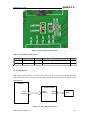
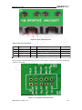
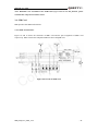
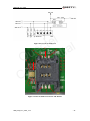
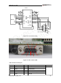
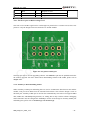
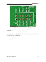
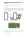
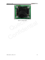
M80 EVB User Guide
M80
Quectel Cellular Engine
EVB User Guide
M80_EVB_User_Guide_V1.2
M80_EVB_User_Guide_V1.2
-0-
M80 EVB User Guide
Document Title
M80 EVB User Guide
Version
1.2
Date
2012-05-29
Status
Released
Document Control ID
M80_EVB_User_Guide_V1.2
l
e
t
l
c
a
e
i
t
u
n
Q ide
f
n
o
C
General Notes
Quectel offers this information as a service to its customers, to support application and
engineering efforts that use the products designed by Quectel. The information provided is
based upon requirements specifically provided for Quectel by the customers. Quectel has not
undertaken any independent search for additional relevant information, including any
information that may be in the customer’s possession. Furthermore, system validation of this
product designed by Quectel within a larger electronic system remains the responsibility of
the customer or the customer’s system integrator. All specifications supplied herein are
subject to change.
Copyright
This document contains proprietary technical information which is the property of Quectel
Limited. The copying of this document, distribution to others, and communication of the
contents thereof, are forbidden without express authority. Offenders are liable to the payment
of damages. All rights are reserved in the event of a patent grant or registration of a utility
model or design. All specification supplied herein are subject to change without notice at any
time.
Copyright © Quectel Wireless Solutions Co., Ltd. 2012
M80_EVB_User_Guide_V1.2
-1-
M80 EVB User Guide
Contents
Contents ............................................................................................................................................ 2
Table Index........................................................................................................................................ 4
Figure Index ...................................................................................................................................... 5
0. Revision history ............................................................................................................................ 7
1. Introduction ................................................................................................................................... 8
1.0. Related documents .............................................................................................................. 8
1.1. Safety precautions ............................................................................................................... 8
2. EVB kit ....................................................................................................................................... 10
2.1. EVB top and bottom view ................................................................................................. 10
2.2. EVB Accessories ............................................................................................................... 11
3. Application.................................................................................................................................. 12
3.1. Power................................................................................................................................. 12
3.1.1. LDO ......................................................................................................................... 12
3.1.2. Test point ................................................................................................................. 13
3.2. Charging ............................................................................................................................ 14
3.3. Audio ................................................................................................................................. 15
3.3.1. Handset .................................................................................................................... 15
3.3.2. Earphone.................................................................................................................. 17
3.3.3. Loud speaker ........................................................................................................... 18
3.3.4. PCM interface.......................................................................................................... 19
3.4. SIM Card ........................................................................................................................... 21
3.4.1. SIM1 card interface ................................................................................................. 21
3.4.2. SIM2 card interface ................................................................................................. 22
3.5. Antenna ............................................................................................................................. 24
3.6. Communication ................................................................................................................. 25
3.6.1. Main UART............................................................................................................. 25
3.6.2. Auxiliary UART and Debug UART ........................................................................ 27
3.6.3. USB ......................................................................................................................... 29
3.7. SD card .............................................................................................................................. 31
3.8. Camera .............................................................................................................................. 34
3.8.1. Analog camera ......................................................................................................... 34
3.8.2. Digital camera ......................................................................................................... 36
3.9. Switches and buttons ......................................................................................................... 38
3.10. LED indicator .................................................................................................................. 39
3.11. LCD ................................................................................................................................. 39
3.13. Keyboard ......................................................................................................................... 40
3.14. ADC ................................................................................................................................ 40
4. EVB accessories assembly .......................................................................................................... 42
5. Illustration ................................................................................................................................... 43
5.1. Turn on the module ........................................................................................................... 43
5.2. Turn off the module ........................................................................................................... 43
l
e
t
l
c
a
e
i
t
u
n
Q ide
f
n
o
C
M80_EVB_User_Guide_V1.2
-2-
M80 EVB User Guide
5.3. Emergency off ................................................................................................................... 43
5.4. Communicate with the module.......................................................................................... 43
5.4.1. UART ...................................................................................................................... 43
5.4.2. Auxiliary UART ...................................................................................................... 44
5.5. Firmware upgrade ............................................................................................................. 44
5.5.1. Main UART............................................................................................................. 44
5.6. Charging ............................................................................................................................ 44
5.6.1. Ghost mode.............................................................................................................. 44
5.6.2 Charging mode ......................................................................................................... 45
l
e
t
l
c
a
e
i
t
u
n
Q ide
f
n
o
C
M80_EVB_User_Guide_V1.2
-3-
M80 EVB User Guide
Table Index
TABLE 1: RELATED DOCUMENTS ..................................................................................................... 8
TABLE 2: PIN OF ADAPTER INTERFACE ........................................................................................ 12
TABLE 3: PINS OF AIN2/AOUT2 ........................................................................................................ 16
TABLE 4: PINS OF AIN1/AOUT1 ........................................................................................................ 17
TABLE 5: TEST POINTS OF LOUD SPEAKER ................................................................................. 19
TABLE 6: PINS OF PCM CHANNEL .................................................................................................. 20
l
e
t
l
c
a
e
i
t
u
n
Q ide
f
n
o
C
TABLE 7: PINS OF SIM CARD INTERFACE ..................................................................................... 22
TABLE 8: PINS OF SIM2 CARD INTERFACE ................................................................................... 24
TABLE 9: PINS OF SIM IC INTERFACE ............................................................................................ 24
TABLE 10: PINS OF SERIAL PORT .................................................................................................... 26
TABLE 11: PINS OF AUXILIARY UART ............................................................................................ 28
TABLE 12: PINS OF DEBUG UART ................................................................................................... 28
TABLE 13: PINS OF SERIAL PORT .................................................................................................... 31
TABLE 14: PINS OF MICRO SD CARD SOCKET ............................................................................. 32
TABLE 15: CONTACT PINS OF DIGITAL CAMERA ........................................................................ 37
TABLE 16: SWITCHES AND BUTTONS ............................................................................................ 38
TABLE 17: LED INDICATOR .............................................................................................................. 39
M80_EVB_User_Guide_V1.2
-4-
M80 EVB User Guide
Figure Index
FIGURE 1: EVB TOP VIEW ................................................................................................................. 10
FIGURE 2: EVB BOTTOM VIEW ....................................................................................................... 10
FIGURE 3: ACCESSORIES INTRODUCTION ................................................................................... 11
FIGURE 4: ADAPTER INTERFACE .................................................................................................... 12
FIGURE 5: LDO CIRCUIT ................................................................................................................... 13
FIGURE 6: TEST POINT OF VBAT ..................................................................................................... 13
l
e
t
l
c
a
e
i
t
u
n
Q ide
f
n
o
C
FIGURE 7: CHARGING CIRCUIT ....................................................................................................... 14
FIGURE 8: CHARGING PART ............................................................................................................. 15
FIGURE 9: BLOCK DIAGRAM OF AIN1/AOUT1&AIN2/AOUT2 ................................................... 16
FIGURE 10: PINS OF AIN1/AOUT1&AIN2/AOUT2 .......................................................................... 16
FIGURE 11: CONNECTION BETWEEN HANDSET AND RJ11 ....................................................... 17
FIGURE 12: EARPHONE CIRCUIT .................................................................................................... 18
FIGURE 13: EARPHONE INTERFACE ............................................................................................... 18
FIGURE 14: TEST POINTS OF LOUD SPEAKER ............................................................................. 19
FIGURE 15: BLOCK DIAGRAM OF PCM.......................................................................................... 19
FIGURE 16: PINS OF PCM INTERFACE ............................................................................................ 20
FIGURE 17: TEST POINTS OF PCM INTERFACE ............................................................................ 20
FIGURE 18: CIRCUIT OF SIM1 CARD............................................................................................... 21
FIGURE 19: PINS OF SIM1 CARD CASSETTE ................................................................................. 22
FIGURE 20: CIRCUIT OF SIM2 CARD............................................................................................... 23
FIGURE 21: PINS OF SIM2 CARD CASSETTE AND SIM IC ........................................................... 23
FIGURE 22: ANTENNA CIRCUIT ....................................................................................................... 24
FIGURE 23: ANTENNA INTERFACE ................................................................................................. 25
FIGURE 24: LEVEL MATCH CIRCUIT .............................................................................................. 26
FIGURE 25: PINS OF MAIN UART ..................................................................................................... 26
FIGURE 26: TEST POINTS OF MAIN PORT ...................................................................................... 27
FIGURE 27: AUXILIARY UART PORT AND DEBUG PORT ............................................................ 28
FIGURE 28: TEST POINTS OF AUXILIARY AND DEBUG PORT ................................................... 29
FIGURE 29: CONNECTION OF UPGRADING SOFTWARE ............................................................ 30
FIGURE 30: USB INTERFACE ............................................................................................................ 30
FIGURE 31: MICRO SD CARD CIRCUIT .......................................................................................... 31
FIGURE 32: PINS OF MICRO SD SOCKET ....................................................................................... 32
FIGURE 33: TEST POINTS OF SD CARD .......................................................................................... 33
FIGURE 34: BLOCK DIAGRAM OF ANALOG CAMERA ............................................................... 34
FIGURE 35: TEST POINTS OF ANALOG CAMERA ......................................................................... 34
FIGURE 36: ANALOG CAMERA ........................................................................................................ 35
FIGURE 37: CONNECTION OF DIGITAL CAMERA ........................................................................ 36
FIGURE 38: CONTACT PINS OF DIGITAL CAMERA ...................................................................... 36
FIGURE 39: BOARD OF DIGITAL CAMERA .................................................................................... 37
FIGURE 40: SWITCHES AND BUTTONS .......................................................................................... 38
FIGURE 41: LED INDICATOR ............................................................................................................ 39
M80_EVB_User_Guide_V1.2
-5-
M80 EVB User Guide
FIGURE 42: TEST POINTS OF LCD ................................................................................................... 40
FIGURE 43: TEST POINTS OF KEYBOARD ..................................................................................... 40
FIGURE 44: CIRCUIT OF ADC ........................................................................................................... 41
FIGURE 45: TEST POINTS OF ADC ................................................................................................... 41
FIGURE 46: EVB AND ACCESSORIES EQUIPMENT ...................................................................... 42
l
e
t
l
c
a
e
i
t
u
n
Q ide
f
n
o
C
M80_EVB_User_Guide_V1.2
-6-
M80 EVB User Guide
0. Revision history
Revision
Date
Author
Description of change
1.0
2012-02-10
Ray XU
Initial
1.1
2012-03-23
Ray XU
Optimized some pictures.
1.2
2012-05-29
Ray XU
Corrected the errors in Section 3.6.2.
l
e
t
l
c
a
e
i
t
u
n
Q ide
f
n
o
C
M80_EVB_User_Guide_V1.2
-7-
M80 EVB User Guide
1. Introduction
This document defines and specifies the usage of M80 EVB. Customers can get useful information
about M80 EVB from this document.
1.0. Related documents
Table 1: Related documents
l
e
t
l
c
a
e
i
t
u
n
Q ide
f
n
o
C
SN
Document name
Remark
[1]
M80_ATC
M80 AT commands sets
[2]
GSM_UART_AN
GSM UART application notes
[3]
M80_HD
M80 Hardware design
[4]
Firmware_Upgrade_Tool_Lite_GS2_
UGD
Firmware upgrade tool lite GS2 user guide
[5]
GSM_DUAL_UART_AN
GSM Dual UART application notes
[6]
PCM_AN
PCM application notes
[7]
M80_Charging_AN
M80 charging application notes
1.1. Safety precautions
The following safety precautions must be observed during all phases of the operation, such as
usage, service or repair of any cellular terminal or mobile incorporating M80 module.
Manufacturers of the cellular terminal are advised to convey the following safety information to
users and operating personnel and to incorporate these guidelines into all manuals supplied with
the product. If not so, Quectel does not take on any liability for customer failure to comply with
these precautions.
When in a hospital or other health care facility, observe the restrictions on the use
of mobile. Switch the cellular terminal or mobile off. Medical equipment may be
sensitive to RF energy interference.
Switch off the cellular terminal or mobile before boarding an aircraft. Make sure
it switched off. The operation of wireless appliances in an aircraft is forbidden to
prevent interference with communication systems. Forget to think much of these
instructions may influence the flight safety or offend against local legal action, or
both.
M80_EVB_User_Guide_V1.2
-8-
M80 EVB User Guide
Do not operate the cellular terminal or mobile in the presence of flammable gas
or fume. Switch off the cellular terminal when you are near petrol station, fuel
depot, chemical plant or where blasting operations are in progress. Operation of
any electrical equipment in potentially explosive atmosphere can constitute a
safety hazard.
Your cellular terminal or mobile receives and transmits radio frequency energy
while switched on. RF interference can occur if it is used close to TV set, radio,
computer or other electric equipment.
l
e
t
l
c
a
e
i
t
u
n
Q ide
f
n
o
C
Road safety comes first! Do not use a hand-held cellular terminal or mobile
while driving a vehicle, unless it is securely mounted in a holder for hands-free
operation. Before making a call with a hand-held terminal or mobile, park the
vehicle.
GSM cellular terminals or mobiles operate using radio frequency signal and
cellular network. Because of this, the connection cannot be guaranteed in all
conditions, for example no mobile fee or an invalid SIM card. While you are in
this condition and need emergent help, please remember using emergency call.
In order to make or receive calls, the cellular terminal or mobile must be
switched on and in a service area with adequate cellular signal strength.
Some networks do not allow for emergency call if certain network services or
phone features are in use (e.g. lock functions, fixed dialing etc.). You may have
to deactivate those features before you can make an emergency call.
Also, some networks require that a valid SIM card be properly inserted in
cellular terminal or mobile.
M80_EVB_User_Guide_V1.2
-9-
M80 EVB User Guide
2. EVB kit
2.1. EVB top and bottom view
L
l
e
t
l
c
a
e
i
t
u
n
Q ide
f
n
o
C
A
F
H
Figure 1: EVB top view
E
K
D
M
B
C
Figure 2: EVB bottom view
M80_EVB_User_Guide_V1.2
- 10 -
M80 EVB User Guide
A: SIM1 card cassette
B: Main UART port
C: Debug UART port
D: Auxiliary UART port
E: GSM RF connector
F: Camera interface
H: M80 module
K: SIM2 card cassette
L: Charging part
M: SD card cassette
l
e
t
l
c
a
e
i
t
u
n
Q ide
f
n
o
C
2.2. EVB Accessories
H
G
D
A
B
E
F
C
Figure 3: Accessories introduction
A: USB to UART converter cable
B: USB cable
C: Earphone
D: 5V DC adapter
E: Bolts and nuts for fixing module and EVB
F: Antenna
G: RF cable
H: Driver C
M80_EVB_User_Guide_V1.2
- 11 -
M80 EVB User Guide
3. Application
3.1. Power
l
e
t
l
c
a
e
i
t
u
n
Q ide
f
n
o
C
GND
1
Figure 4: Adapter interface
Table 2: Pin of adapter interface
Pin
1
Signal
I/O
Adapter input
I
Description
5V/2A DC source input
3.1.1. LDO
M80 EVB uses LDO to supply power for the module. The schematic of the LDO is shown as
below. In order to measure the VBAT voltage, adjust VBAT which is fed from the customer
device, or test module, M80 EVB reserves a test point.
M80_EVB_User_Guide_V1.2
- 12 -
M80 EVB User Guide
l
e
t
l
c
a
e
i
t
u
n
Q ide
f
n
o
C
Figure 5: LDO circuit
3.1.2. Test point
Test points of VBAT
Figure 6: Test point of VBAT
M80_EVB_User_Guide_V1.2
- 13 -
M80 EVB User Guide
3.2. Charging
Charging circuit has been illustrated in M80 EVB board. The components involving charging
function have been assembled. The charging circuit is shown as below. For more information
about charging, Please refer to document [7].
l
e
t
l
c
a
e
i
t
u
n
Q ide
f
n
o
C
Figure 7: Charging circuit
M80_EVB_User_Guide_V1.2
- 14 -
M80 EVB User Guide
Battery contact pins
l
e
t
l
c
a
e
i
t
u
n
Q ide
f
n
o
C
Figure 8: Charging part
3.3. Audio
Five patterns of audio have been designed in M80 EVB for the customer choice. There are
AIN1/AOUT1, AIN2/AOUT2, earphone, loudspeaker and PCM interface. In this chapter, we will
introduce these audios in details.
3.3.1. Handset
AIN1/AOUT1, AIN2/AOUT2 are designed in the handset. The block diagram of AIN1/AOUT1
and AIN2/AOUT2 is shown as below and some details are concealed. If you want to get more
information, please refer to document [3].
M80_EVB_User_Guide_V1.2
- 15 -
M80 EVB User Guide
Module
RJ11
AIN1/AOUT1
RJ11
AIN2/AOUT2
l
e
t
l
c
a
e
i
t
u
n
Q ide
f
n
o
C
Figure 9: Block diagram of AIN1/AOUT1&AIN2/AOUT2
The RJ11 interface is shown as below. The pins of RJ11 are shown in the following table.
1_4
1_3
1_2 1_1
2_4
2_3 2_2
2_1
Figure 10: Pins of AIN1/AOUT1&AIN2/AOUT2
Table 3: Pins of AIN2/AOUT2
Pin
Signal
I/O
Description
2_1
MIC2N
I
Negative microphone input
2_2
AGND
M80_EVB_User_Guide_V1.2
Note
AGND of audio circuits
- 16 -
M80 EVB User Guide
2_3
SPK2P
O
Positive receiver output
2_4
MIC2P
I
Positive microphone input
Table 4: Pins of AIN1/AOUT1
Pin
Signal
I/O
1_1
MIC1N
I
Negative microphone input
1_2
SPK1N
O
Negative receiver output
1_3
SPK1P
O
Positive receiver output
1_4
Description
Note
l
e
t
l
c
a
e
i
t
u
n
Q ide
f
n
o
C
MIC1P
I
Positive microphone input
The handset which suits for the M80 EVB is different from the common handset and Quectel does
not provide this handset. The following picture illustrates a connection between RJ11 and the
handset. Customer can refer to the following picture to make a handset which suits for the M80
EVB.
Handset
RJ11
3
2
SPKP
SPKN
Mic
4
1
+
MICP
33pF
MICN
10pF
-
Figure 11: Connection between handset and RJ11
3.3.2. Earphone
AIN2/AOUT2 can be also designed as earphone. The schematic is shown as below. ADC0 and
EINT are used for earphone detection, ADC0 and EINT can be selected from the module.
M80_EVB_User_Guide_V1.2
- 17 -
M80 EVB User Guide
l
e
t
l
c
a
e
i
t
u
n
Q ide
f
n
o
C
Figure 12: Earphone circuit
Figure 13: Earphone interface
3.3.3. Loud speaker
M80 module has embedded a class AB amplifier. It can drive up to 800mW speaker. In this case,
the customer can get good audio performance and eliminate an amplifier simultaneously. The test
points are shown as below.
M80_EVB_User_Guide_V1.2
- 18 -
M80 EVB User Guide
1
l
e
t
l
c
a
e
i
t
u
n
Q ide
f
n
o
C
2
Figure 14: Test points of loud speaker
Table 5: Test points of loud speaker
Pin
1
2
Signal
I/O
Description
LOUDSPKN
O
Negative loud speaker output
LOUDSPKP
O
Positive loud speaker output
Note
3.3.4. PCM interface
M80 supports PCM interface. An audio codec, W681360, is used in the EVB board. The audio
codec transforms between analog signal and digital signal. For more information, please refer to
document [6].
Module
Audio codec
PCM
interface
PCM
interface
Analog
audio
RJ11
Figure 15: Block diagram of PCM
M80_EVB_User_Guide_V1.2
- 19 -
M80 EVB User Guide
l
e
t
l
c
a
e
i
t
u
n
Q ide
f
n
o
C
4
3
2
1
Figure 16: Pins of PCM interface
Table 6: Pins of PCM channel
Pin
1
2
3
4
Signal
I/O
Description
MICN
I
Negative microphone input
SPKN
O
Negative receiver output
SPKP
O
Positive receiver output
MICP
I
Positive microphone input
Note
The test points of PCM interface have been reserved as below. Customer can measure PCM signal
using these test points.
Figure 17: Test points of PCM interface
M80_EVB_User_Guide_V1.2
- 20 -
M80 EVB User Guide
Note: W681360 is not assembled in the EVB board. If you want to use this function, please
assemble this component located at U301.
3.4. SIM Card
M80 provides dual SIM card interface.
3.4.1. SIM1 card interface
l
e
t
l
c
a
e
i
t
u
n
Q ide
f
n
o
C
Figure 18 and 19 shows the schematic of SIM1 card and the pins assignment of SIM1 card
respectively. SIM1 cassette has adopted an EINT to detect the SIM card.
Figure 18: Circuit of SIM1 card
M80_EVB_User_Guide_V1.2
- 21 -
M80 EVB User Guide
3
7
2
1
l
e
t
l
c
a
e
i
t
u
n
Q ide
f
n
o
C
8
6
4
5
Figure 19: Pins of SIM1 card cassette
Table 7: Pins of SIM card interface
Pin
1
2
3
4
5
6
Signal
I/O
GND
GND
VPP
Not connected
SIM1_DATA
I/O
SIM1 card data I/O
SIM1_CLK
O
SIM1 card clock
SIM1_RST
O
SIM1 card reset
SIM1_VDD
O
SIM1 power
Note
Pulled down to GND with external
circuit. When the SIM card is
inserted, pin 7 is connected to pin 8.
7
8
Description
SIM1_PRESENCE
I
SIM1 Card detect
3.4.2. SIM2 card interface
In order to be compatible with further application, M80 reserves an SIM IC and SIM2 cassette in
the EVB board. The schematic of SIM IC is same as SIM2 card. The SIM2 card interface does not
support SIM card detection. The following picture shows the schematic and test points.
M80_EVB_User_Guide_V1.2
- 22 -
M80 EVB User Guide
l
e
t
l
c
a
e
i
t
u
n
Q ide
f
n
o
C
Figure 20: Circuit of SIM2 card
5
6
4
8 7 5 6
1
2 3
4
1
2
3
Figure 21: Pins of SIM2 card cassette and SIM IC
M80_EVB_User_Guide_V1.2
- 23 -
M80 EVB User Guide
Table 8: Pins of SIM2 card interface
Pin
Signal
I/O
Description
1
GND
Ground
2
VPP
Not connected
3
SIM2_DATA
I/O
SIM2 card data I/O
4
SIM2_CLK
O
SIM2 card clock
5
SIM2_RST
O
SIM2 card reset
6
SIM2_VDD
O
SIM2 card power
Note
l
e
t
l
c
a
e
i
t
u
n
Q ide
f
n
o
C
Table 9: Pins of SIM IC interface
Pin
1
2
3
4
5
6
7
8
Signal
I/O
GND
SIM2_DATA
Description
Note
Ground
I/O
SIM2 card data I/O
NC
Not connected
NC
Not connected
NC
Not connected
SIM2_CLK
O
SIM2 card clock
SIM2_RST
O
SIM2 card reset
SIM2_VDD
O
SIM2 card power
3.5. Antenna
In order to be compatible with different antenna connectors, M80 EVB reserves two antenna ports
for the customer’s choice. The circuit and antenna connector are shown as below.
Figure 22: Antenna circuit
M80_EVB_User_Guide_V1.2
- 24 -
M80 EVB User Guide
J101
PAD101
l
e
t
l
c
a
e
i
t
u
n
Q ide
f
n
o
C
Figure 23: Antenna interface
3.6. Communication
M80 provides multi type communication ports, such as main UART, Auxiliary UART, Debug
UART and USB port.
3.6.1. Main UART
When using main UART port communicates data between PC and the module, a RS_232 level
shifter must be inserted between them, since this UART port do not support the RS_232 level,
while supports the CMOS level only. The following picture is the reference design of RS-232
level shifter. The main UART can be used for AT command, GPRS data, CSD FAX, etc.
Multiplexing function is supported on the main UART Port as well. For the design circuit of main
Port, please refer to document [2]. For more details about communication with UART, please
refer to chapter 5.4.1.
M80_EVB_User_Guide_V1.2
- 25 -
M80 EVB User Guide
SP3238
28
25
1
3
DCD
TXD
CTS
RI
GND
MODULE
V+
C1-
GND
C2+
VCC
C2-
V-
24
23
22
19
T1IN
T2IN
T3IN
T4IN
17
T5IN
16
21
20
18
RXD
DTR
RTS
C1+
27
2
3V
4
GND
10
6
7
5
12
T4OUT
T2OUT
T3OUT
T1OUT
T5OUT
/R1OUT
R1OUT
R2OUT
R3OUT
GND
26
8
9
11
R1IN
R2IN
R3IN
l
e
t
l
c
a
e
i
t
u
n
Q ide
f
n
o
C
3V
13
ONLINE
15
/STATUS
14
/SHUTDOWN
6
7
8
9
1
2
3
4
5
TO PC serial port
GND
Figure 24: Level match circuit
7
1
2
8
3
9
4
5
Figure 25: Pins of main UART
Table 10: Pins of Serial port
Pin
Signal
I/O
Description
1
DCD
O
Data carrier detection
2
TXD
O
Transmit data
3
RXD
I
Receive data
4
DTR
I
Data terminal ready
5
GND
M80_EVB_User_Guide_V1.2
Note
Ground
- 26 -
M80 EVB User Guide
7
RTS
I
Request to send
8
CTS
O
Clear to send
9
RI
O
Ring indicator
Note: The above pins are RS232 voltage level.
The TTL level of UART signal can be test through test points below. Customer can use these test
points to verify the design between customer device and the module.
l
e
t
l
c
a
e
i
t
u
n
Q ide
f
n
o
C
Figure 26: Test points of main port
The main port can be used for upgrading software. The PWRKEY pin must be pulled down before
the software upgrade. For more details about downloading software with UART, please refer to
chapter 5.5.1.
3.6.2. Auxiliary UART and Debug UART
When Auxiliary UART port and Debug Port are used to communicate data between PC and the
module, a RS_232 level shifter must be inserted between them. The reference design is same as
the main port. Auxiliary UART port is used for AT command only since it does not support GPRS
data, CSD FAX, and Multiplexing function, etc. Debug Port is only used for software debugging
and its baud rate must be configured as 460800bps. For the circuit design of Auxiliary UART port
and Debug Port, please refer to document [3] and document [5].
M80_EVB_User_Guide_V1.2
- 27 -
M80 EVB User Guide
1_2
1_3
1_5
2_2
2_3
2_5
l
e
t
l
c
a
e
i
t
u
n
Q ide
f
n
o
C
Figure 27: Auxiliary UART port and Debug Port
Table 11: Pins of Auxiliary UART
Pin
1_2
1_3
1_5
Signal
I/O
Description
TXD_AUX
O
Transmit data
RXD_AUX
I
Receive data
GND
Note
Ground
Note: The above pins are RS232 voltage level.
Table 12: Pins of debug UART
Pin
2_2
2_3
2_5
Signal
I/O
DBG_TXD
O
Transmit data
DBG_RXD
I
Receive data
GND
Description
Note
Ground
Note: The above pins are RS232 voltage level.
The TTL level of UART signal can be test through the test points below. Customer can use these
test points to verify the design between customer device and the module.
M80_EVB_User_Guide_V1.2
- 28 -
M80 EVB User Guide
l
e
t
l
c
a
e
i
t
u
n
Q ide
f
n
o
C
Figure 28: Test points of Auxiliary and Debug port
3.6.3. USB
USB interface supports downloading software and should cooperate with DOWNLOAD pin. The
following picture is the example of connection. For more details about downloading software with
USB cable, please refer to chapter 5.5.2.
M80_EVB_User_Guide_V1.2
- 29 -
M80 EVB User Guide
Module (DCE)
IO Connector
USB_DM
USB_DM
USB_DP
USB_DP
GND
GND
DOWNLOAD
l
e
t
l
c
a
e
i
t
u
n
Q ide
f
n
o
C
PWRKEY
Figure 29: Connection of upgrading software
4
3
1
2
Figure 30: USB interface
M80_EVB_User_Guide_V1.2
- 30 -
M80 EVB User Guide
Table 13: Pins of Serial port
Pin
Signal
I/O
Description
1
VUSB
I
USB power
2
USB_DM
I/O
USB data negative
3
USB_DP
I/O
USB data positive
4
GND
Note
Ground
3.7. SD card
l
e
t
l
c
a
e
i
t
u
n
Q ide
f
n
o
C
The module provides SD card interface, whose maximum capacity is up to 32GB. M80 EVB
reserves an SD card socket in the board. The pin definition and reference design are shown as
below.
Figure 31: Micro SD card circuit
M80_EVB_User_Guide_V1.2
- 31 -
M80 EVB User Guide
1
2
3
4
5
6
l
e
t
l
c
a
e
i
t
u
n
Q ide
f
n
o
C
7
8
Figure 32: Pins of micro SD socket
Table 14: Pins of micro SD card socket
Pin
1
2
3
4
5
6
7
8
Signal
I/O
Description
DATA2
I/O
Data output/ input signal line of SD card
DATA3
I/O
Data output / input signal line of SD card
CMD
O
Command signal of SD card output
VDD
CLK
Power of SD card
O
GND
Clock signal of SD card output
Ground
DATA0
I/O
Data output/input signal line of SD card
DATA1
I/O
Data output/input signal line of SD card
M80_EVB_User_Guide_V1.2
Note
- 32 -
M80 EVB User Guide
SD_CLK
l
e
t
l
c
a
e
i
t
u
n
Q ide
f
n
o
C
SD_CMD
SD_DATA0
Figure 33: Test points of SD card
M80_EVB_User_Guide_V1.2
- 33 -
M80 EVB User Guide
3.8. Camera
M80 EVB provides two types of camera interface: analog camera and digital camera.
3.8.1. Analog camera
M80 EVB provides analog camera function. The analog camera of the M80 EVB should employ
an AK8856 IC which converts the analog video to digital video, also should add a boost converter
when there is no 12V voltage in the board. The following picture is the block diagram. For more
information about the detail design circuit, please refer to EVB circuit involving this part. The test
point of analog camera is shown as below.
l
e
t
l
c
a
e
i
t
u
n
Q ide
f
n
o
C
AK8856
Module
39R
Data Bus
Video input
33nF
39R
+12V
Control Signal
DC input
27MHz
Ground
Boost
Figure 34: Block diagram of analog camera
Contact pins
Figure 35: Test points of analog camera
The following picture is the sample of analog camera. Customer can connect the analog camera to
EVB through contact pins. For more details about the analog camera, please contact the vendor of
the analog camera or Quectel.
M80_EVB_User_Guide_V1.2
- 34 -
M80 EVB User Guide
l
e
t
l
c
a
e
i
t
u
n
Q ide
f
n
o
C
Figure 36: Analog camera
M80_EVB_User_Guide_V1.2
- 35 -
M80 EVB User Guide
3.8.2. Digital camera
M80 EVB provides parallel digital camera interface. The maximum supported pixel is 0.3M.
VDD_EXT
10K
Module
10K
Camera
module
D[0:1]
l
e
t
l
c
a
e
i
t
u
n
Q ide
f
n
o
C
CS_D[0:7]
D[2:9]
CS_SCL
SCL
CS_SDA
SDA
CS_HSYNC
HSYNC
CS_VSYNC
CS_PXICLK
VSYNC
PXICLK
CS_ECLK
ECLK
CS_RESET
RESET
CS_PWDN
PWDN
Figure 37: Connection of digital camera
1_11
1_20
1_10
2_11
1_1
2_20
2_10
2_1
Figure 38: Contact pins of digital camera
M80_EVB_User_Guide_V1.2
- 36 -
M80 EVB User Guide
Table 15: Contact pins of digital camera
Pin
Signal
Pin
Signal
1_1
VCAMA
2_1
NC
1_2
NC
2_2
NC
1_3
SD_DATA0
2_3
CAM_SDA
1_4
SD_CMD
2_4
CAM_SCL
1_5
SD_CLK
2_5
CAM_PCLK
1_6
NC
2_6
CAM_HSYNC
1_7
GND
2_7
CAM_DATA6
GND
2_8
CAM_DATA4
VBAT
2_9
CAM_DATA2
VBAT
2_10
CAM_DATA0
VBAT
2_11
CAM_DATA1
VBAT
2_12
CAM_DATA3
GND
2_13
CAM_DATA5
GND
2_14
CAM_DATA7
NC
2_15
CAM_VSYNC
NC
2_16
CAM_RST
NC
2_17
CAM_PWDN
NC
2_18
CAM_MCLK
NC
2_19
NC
VCAMD
2_20
NC
1_8
1_9
1_10
1_11
1_12
1_13
1_14
1_15
1_16
1_17
1_18
1_19
1_20
l
e
t
l
c
a
e
i
t
u
n
Q ide
f
n
o
C
To cooperate with the digital camera in M80 EVB board, M33-EVB-TE-V1.01 board should be
added. The following board is the sample. M33-EVB-TE-V1.01 board supplies abundant
connectors for different camera sensors. For more details, please contact Quectel.
Figure 39: Board of digital camera
M80_EVB_User_Guide_V1.2
- 37 -
M80 EVB User Guide
3.9. Switches and buttons
S1
S2
S3 S4
K1
K2
l
e
t
l
c
a
e
i
t
u
n
Q ide
f
n
o
C
Figure 40: Switches and buttons
Table 16: Switches and buttons
Part
S1
S2
S3
S4
K1
K2
Name
I/O
Description
VBAT
I
Control power supply via adaptor
VCHG
I
Control charging if module has
charging function
DOWNLOAD
I
Pulled to “ON” when downloading
firmware via USB
PWRKEY
I
Pulled to “ON” when downloading
firmware via UART or USB
PWRKEY
I
Turn on/off the module
EMERG_OFF
I
Emergency button for shutting down
the module
M80_EVB_User_Guide_V1.2
Note
- 38 -
M80 EVB User Guide
3.10. LED indicator
l
e
t
l
c
a
e
i
t
u
n
Q ide
f
n
o
C
L2
L3
L4
L1
Figure 41: LED indicator
Table 17: LED indicator
Part
L1
L2
L3
L4
Name
I/O
Description
VBAT ON/OFF indicator
O
Bright: VBAT ON
Extinct: VBAT OFF
GSM_NET status
indicator
O
Blinking at a certain frequency
according to various GSM network
status
Module status indicator
O
Indicate module’s operating status
Note
RESERVED
3.11. LCD
M80 provides serial LCD interface including both four lines mode and three lines mode. The
maximum resolution is up to 240 x 320. The EVB board reserves the test points for the
measurement of signal.
M80_EVB_User_Guide_V1.2
- 39 -
M80 EVB User Guide
l
e
t
l
c
a
e
i
t
u
n
Q ide
f
n
o
C
Figure 42: Test points of LCD
3.13. Keyboard
M80 provide s 5*5 matrix keyboard. The following figure shows the test points.
Figure 43: Test points of keyboard
3.14. ADC
M80 provides two ADC channel. The test points and circuit are shown as below.
M80_EVB_User_Guide_V1.2
- 40 -
M80 EVB User Guide
l
e
t
l
c
a
e
i
t
u
n
Q ide
f
n
o
C
Figure 44: Circuit of ADC
ADC0
ADC1
Figure 45: Test points of ADC
M80_EVB_User_Guide_V1.2
- 41 -
M80 EVB User Guide
4. EVB accessories assembly
Generally, the EVB and its accessories are equipped as below.
l
e
t
l
c
a
e
i
t
u
n
Q ide
f
n
o
C
Figure 46: EVB and accessories equipment
M80_EVB_User_Guide_V1.2
- 42 -
M80 EVB User Guide
5. Illustration
5.1. Turn on the module
1.
2.
3.
4.
Insert the plug of the 5V power adapter.
Switch S1 to ON state, Switch S2 to OFF state, Switch S3 to OFF state, and Switch S4 to
OFF state. The LED L1 on the EVB will be bright.
Press the K1 button (PWRKEY) for about 1 second. The LED L4 will be light and indicates
the module is in the working mode. When L4 is bright, the module begins running. Otherwise,
please check the circuit.
The LED L2 will be blinking at a certain frequency. The GSM working status of the module
can be judged by this LED.
l
e
t
l
c
a
e
i
t
u
n
Q ide
f
n
o
C
Please refer to document [3] for the detailed network status indication.
5.2. Turn off the module
Press the PWRKEY button for about 1 second, the module will be turned off.
5.3. Emergency off
Press the EMERG_OFF button for more than 0.2 seconds, the module will be shut down
immediately. After that, the module can be restarted by pressing the PWRKEY button. Please note
that this operation is harmful to the whole module system and should only be done in emergency
such as failing to turn off the module through the PWRKEY button.
5.4. Communicate with the module
5.4.1. UART
1. Insert the plug of the 5V power adapter.
2. Connect PC and EVB correctly with USB to UART cable.
3. Open the HyperTerminal (AT command window) on PC. The location of the HyperTerminal
in windows XP is: START →program →accessory →communication →HyperTerminal.
Set appropriate Baud Rate (such as 115200 bps) and COM number which can be checked by
the Device Manager on PC.
4. Connect an antenna to M80-EVB with an RF cable.
5. Insert SIM card into the SIM1 card socket.
M80_EVB_User_Guide_V1.2
- 43 -
M80 EVB User Guide
6.
Insert earphone or handset into audio interface.
For Power On operation, please refer to chapter5.1.
After waiting for 2~3 seconds, customer should first input “AT” or “at” string once or more
until receiving “OK” from the module in the HyperTerminal. The module is set to
autobauding mode in default configuration. This operation is to synchronize the baud rate
between the computer and the module.
8. Input AT command and the module will execute its corresponding function.
7.
Customer can refer to document [1] for the details of AT commands. For instance, when inputting
“ATD112;” an emergency call is established.
l
e
t
l
c
a
e
i
t
u
n
Q ide
f
n
o
C
5.4.2. Auxiliary UART
Quectel module provides two UART ports for achieving Dual UART.
“AT+QEAUART=1” which is sent via main UART is used to enable Auxiliary UART. Please
restart the module after executing the command. For more details, please refer to document [1].
5.5. Firmware upgrade
5.5.1. Main UART
1.
2.
3.
4.
5.
Insert the plug of the 5V power adapter.
Connect PC and EVB correctly with USB to UART cable.
Start the Firmware Upgrade Tool in the PC and choose right COM port.
Press the START button in the Firmware Upgrade Tool.
Switch the S4 and S1 in the EVB to ON state
After these steps, the firmware refreshing process will be proceeding. For more details, please
refer to document [4].
5.6. Charging
The battery can be charged in both ghost mode and charging mode. About the difference between
them, you can refer to the document [7].
5.6.1. Ghost mode
1.
2.
3.
Connect the battery to the battery contact pin.
Insert the plug of the 5V power adapter.
Switch S1 to OFF state, Switch S2 to ON state, Switch S3 to OFF state, and Switch S4 to
M80_EVB_User_Guide_V1.2
- 44 -
M80 EVB User Guide
4.
OFF state.
Monitor the VBAT voltage and charging state via “AT+CBC”.
5.6.2 Charging mode
1.
2.
3.
4.
5.
6.
Connect the battery to the battery contact pin.
Insert the plug of the 5V power adapter.
Switch S1 to ON state, Switch S2 to OFF state, Switch S3 to OFF state, and Switch S4 to
OFF state. The LED L1 on the EVB will be bright.
Press the K1 button (PWRKEY) for about 1 second. The LED L4 will be light and indicates
the module is in the working mode. When L4 is bright, the module begins running.
Switch S2 to ON state to start the module.
Monitor the VBAT voltage and charging state via “AT+CBC”.
l
e
t
l
c
a
e
i
t
u
n
Q ide
f
n
o
C
M80_EVB_User_Guide_V1.2
- 45 -
Shanghai Quectel Wireless Solutions Co., Ltd.
Room 501, Building 13, No.99 Tianzhou Road, Shanghai, China 200233
Tel: +86 21 5108-6236
Mail: [email protected]