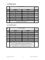
1
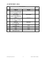
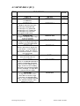
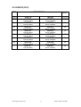
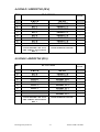
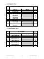
ELAN DIGITAL SYSTEMS LTD.
LITTLE PARK FARM ROAD,
SEGENSWORTH WEST,
FAREHAM,
HANTS. PO15 5SJ.
TEL: (44) (0)1489 579799
FAX: (44) (0)1489 577516
e-mail: [email protected]
website: www.pccard.co.uk
AD125 PC-CARD USER’S GUIDE
ALSO COVERS AD135, AD126, AD136, AD132, AD121, AD131
AND “MF2xx” SERIES CARDS
REVISION HISTORY
ISSUE
PAGES
DATE
NOTES
1
2
50
50
30.10.96
06.03.97
3
4
5
50
50
48
06.06.97
17.06.97
26.01.98
6
50
15.07.98
7
43
23.07.98
8
45
04.01.99
FIRST ISSUE
CORRECTION TO SAMPLE RATE
CALCULATIONS
REDUCED LOAD LIMIT ON +/-15V
ADDED AD132
SIMPLIFY PCCARDGO TEXT & ADD
NOTE ABOUT PRE-RUN IN
SECTION 3.5.3
ADD AD121/131 & SEC 1.1. ALSO
SOME MINOR SPEC CHANGES IN
5.2.
REMOVED SOFTWARE SECTION
TO PCCARDGO.DOC
MF SERIES CARDS
Elan Digital Systems Ltd.
1
AD125 USER’S GUIDE
CONTENTS
1. OVERVIEW..................................................................................................4
1.1 MODEL NAMING CONVENTIONS......................................................................................... 5
2. ABOUT THE AD125 ....................................................................................6
2.1 QUICK THEORY OF SUCCESSIVE APPROXIMATION CONVERTERS ........................ 6
2.2 NOISE............................................................................................................................................ 6
2.3 POSSIBLE SOURCES OF MEASUREMENT ERROR........................................................... 8
2.4 D to A Converters ......................................................................................................................... 9
3. CONTROLLING THE AD125.....................................................................10
3.1 ACQUISITION MODES............................................................................................................ 10
3.1.1 BURST MODE...................................................................................................................... 10
3.1.2 FIFO MODE.......................................................................................................................... 11
3.1.3 SINGLE-SHOT MODE......................................................................................................... 11
3.2 A to D OUTPUT FORMAT / GAIN SETTING ....................................................................... 12
3.3 AD125 BUFFER ADDRESSING............................................................................................... 14
3.3.1 BUFFER DATA ORDER...................................................................................................... 14
3.3.2 CONTROLLING THE SRAM POINTERS .......................................................................... 14
3.3.3 PRE-TRIGGER DEPTH ....................................................................................................... 15
3.3.4 READING THE SRAM DATA ............................................................................................ 16
3.4 TRIGGERING ............................................................................................................................ 17
3.4.1 THRESHOLD........................................................................................................................ 17
3.4.2 TRIGGER MODES ............................................................................................................... 18
3.4.3 ENABLING TRIGGER......................................................................................................... 19
3.5 OTHER FEATURES.................................................................................................................. 20
3.5.1 SAMPLE RATE .................................................................................................................... 20
3.5.2 INPUT MUX CONTROL ..................................................................................................... 21
3.5.3 SLEEP MODE....................................................................................................................... 23
3.5.4 INTERRUPTS ....................................................................................................................... 23
3.5.5 CONFIG OPTION REGISTER............................................................................................. 25
3.5.6 DIGITAL IO.......................................................................................................................... 26
3.6 DAC PROGRAMMING ............................................................................................................ 27
4. AD125 REGISTER INTERFACE ...............................................................29
4.0 SETUP REG 1 (IR 0).................................................................................................................. 31
4.1 SETUP REG 2 (IR 1).................................................................................................................. 32
4.2 IODATA (IR 2) ........................................................................................................................... 33
4.3 IODIR (IR 3) ............................................................................................................................... 34
4.4 DIVLO / ADDRCTLO (IR 4) .................................................................................................... 35
Elan Digital Systems Ltd.
2
AD125 USER’S GUIDE
4.5 DIVHI / ADDRCTHI (IR 5)....................................................................................................... 35
4.6 MUXSEQ (IR 6).......................................................................................................................... 36
4.7 TRIGTHRESH (IR 7) ................................................................................................................ 36
4.8 CTLEN (IR 9) ............................................................................................................................. 37
4.9 DECR (IR D) ............................................................................................................................... 37
4.10 DECW (IR E) ............................................................................................................................ 38
4.11 CLRCT (IR F)........................................................................................................................... 38
5. HARDWARE SPECIFICATION..................................................................39
5.1 PINOUT....................................................................................................................................... 39
5.2 ANALOGUE ............................................................................................................................... 40
5.2.1 CALIBRATION DATA ........................................................................................................ 41
5.3 DIGITAL ..................................................................................................................................... 43
5.4 POWER CONSUMPTION........................................................................................................ 43
5.5 MECHANICAL .......................................................................................................................... 43
5.6 ENVIRONMENTAL .................................................................................................................. 43
6. SOFTWARE...............................................................................................44
6.1 UNIVERSAL DRIVER .............................................................................................................. 44
6.2 C SOURCE CODE ..................................................................................................................... 44
7. OPERATIONAL PRECAUTIONS .............................................................45
Disclaimer
This document has been carefully prepared and checked. No responsibility can be
assumed for inaccuracies. Elan reserves the right to make changes without prior notice
to any products herein to improve functionality, reliability or other design aspects.
Elan does not assume any liability out of the use of any product described herein;
neither does it convey any licence under its patent rights not the rights of others. Elan
products are not authorised for use as components in life support services or systems.
Elan should be informed of any such intended use to determine suitability of the
products.
Source code supplied with Elan PC-Cards is provided “as-is” with no warranty, express
or implied, as to its quality or fitness for a particular purpose. Elan assume no liability
for any direct or indirect losses arising from use of the supplied code.
Copyright © 1996,1997,1998 Elan Digital Systems Ltd.
Elan Digital Systems Ltd.
3
AD125 USER’S GUIDE
1. OVERVIEW
Before using the AD125, take some time to read the section
“OPERATIONAL PRECAUTIONS”.
The AD125 card is a general purpose Analogue Data Acquisition
card with the following features:
• 12-bit 0.5MSPS A to D converter (0.625MSPS FOR AD1x6)
(0.25MSPS FOR AD132, 0.1MSPS FOR AD121/131)
• 16 single ended / 8 differential fault protected analogue inputs (8
single ended / 4 differential for AD12x)
• 2x12-bit D to A converters on MF series
• Bipolar and Unipolar input ranges
• 20 different input range settings including +/-10V
• 8 digital I/O lines for AD series or 4 I/O lines for MF series
• 32K x 8 SRAM sample buffer (16K samples)
• Programmable conversion clock divider
• Three modes: BURST, FIFO, SINGLE-SHOT.
• Digital trigger threshold for BURST mode
• Programmable pre-trigger depth
This guide aims to familiarise you with the way that the AD125
works and so will help you to maximise its performance in your
application.
The AD125 is capable of high speed and high accuracy
measurements and can be used as part of a complete data acquisition
and control system. Its applications are limitless. All that is needed
is appropriate control and/or analysis software. Elan provides a
royalty free “kernel” of source code that can be used as a starting
point for your software design. By expanding and enhancing the
code provided, you will be able to gain a significant “time to
market” advantage.
Elan will be happy to quote for either customisation of the AD125 if
its exact specifications do not quite meet your needs, or to create
complete application software. We can also create drivers for 3rd
party “virtual instrument” software e.g. Signal Center or Keithley
Testpoint.
Elan Digital Systems Ltd.
4
AD125 USER’S GUIDE
1.1 MODEL NAMING CONVENTIONS
The AD125 “family” of cards follows these naming conventions:
“AD1[X][Y]” for A to D cards
“MF2[X][Y]” for Multi-function A to D and D to A cards
[X]
[Y]
“2” ⇒ 8 single ended channels
“3” ⇒ 16 single ended channels
“1” ⇒ 100KSPS max sample rate
“2” ⇒ 250KSPS max sample rate
“5” ⇒ 500KSPS max sample rate
“6” ⇒ 625KSPS max sample rate
Elan Digital Systems Ltd.
5
AD125 USER’S GUIDE
2. ABOUT THE AD125
2.1 QUICK THEORY OF SUCCESSIVE APPROXIMATION
CONVERTERS
The type of converter used in the AD125 approximates the analogue
level being applied to its input using a D to A converter and a
comparator. The converter starts in “track” mode where it is
following the input voltage and applying it to a track and hold
amplifier. Once the converter is told to perform a conversion, it
holds the current input voltage level on a capacitor while it
approximates its value.
The converter uses a clock to break the approximation process down
into 12 steps, one per bit. Each step attempts to approximate the
held input voltage to one more “bit” of resolution. The logic in the
A to D makes the most significant bit decision first as this is the
most “coarse” level, i.e. is the signal positive or negative.
Subsequent decisions are then made on the difference between the
output of the internal D to A converter and the held input value: if
the comparison is “greater” then the bit is set, if “less” the bit is
cleared. After 12 clocks the complete word is ready to be read out of
the converter.
2.2 NOISE
Noise in an A to D converter system will degrade the “effective
resolution” of the conversion. The noise can be power supply noise,
thermal noise, pick-up noise etc. All contribute to the degradation.
The Effective Number Of Bits for a converter expresses a measure
of the noise level relative to the input signal level.
The ENOB of a converter is expressed as:
ENOB = (SNR(dB) - 1.76) / 6.02
So, the better the signal to noise ratio the higher the effective
resolution. Be warned however, that this computation is based on
RMS noise. Taking individual samples from the AD125 will reveal
Elan Digital Systems Ltd.
6
AD125 USER’S GUIDE
that the noise is Gaussian in distribution and is subject to the usual
statistical spread in its peaks and troughs from moment to moment.
So the converter output looks noisy, or at least more noisy than you
might expect. Normally this is not a problem but occasionally some
kind of post-processing of the data samples will be required in
software. This may mean a simple averaging process over say 10 or
more samples, or could be a properly designed digital filter. This
will depend on the exact application. Bear in mind that this
averaging could reduce the bandwidth of the data you are acquiring
and will increase the settling time needed for step-input changes.
The AD125 inevitably introduces several extra sources of noise:
•
•
•
•
The voltage references
The internal power rails
Ground noise
Noise from the front-end analogue circuits.
The power rails used inside the AD125 are designed to help
minimise power rail feedthrough.
All of these noise sources will act to degrade the ENOB attainable.
Post processing the data using a digital filter will help to improve the
effective resolution by reducing random noise.
Elan Digital Systems Ltd.
7
AD125 USER’S GUIDE
2.3 POSSIBLE SOURCES OF MEASUREMENT ERROR
The following is a list of possible error sources that should be
considered when taking measurements with the AD125:
1. The offset voltage of the A to D device and the front end
electronics will mean that an input voltage of 0V will not produce
an output code of 000000000000b. Software could be used to
correct for zero-point offset errors by using one of the analogue
inputs to the AD125 and tying it to AGND. Switch to this channel
and measure its level to obtain the code for bipolar zero. A set of
factory calibration constants is held on the card and can be
accessed by software to compensate for this error is required.
2. Gain errors in the A to D device and the front end electronics will
cause full scale “end-point” errors. In other words the A to D
output code may reach 011111111111b before or after the input
gets to nominal full positive scale and similarly the code may
reach 100000000000b before or after the input voltage gets to
nominal negative full scale. A set of factory calibration constants
is held on the card and can be accessed by software to compensate
for this error is required.
3. Avoid ground loops. These can be caused when the source’s -ve
side is connected via the AD125 cable to AGND and to the shield
on the AD125’s connector. This shield is connected to the PC’s
chassis and so to “earth”( via the gold ESD strips on each side of
the card). The source’s -ve side (unless floating) will be the local
GND and if this too is connected “earth” then if there is any
difference between the two “earth” potentials current will flow in
the AGND wire between the source and the AD125 causing offset
voltages (due to I x R losses) (the current will return through the
mains wiring). Avoid such loops by not connecting the AD125
connector shield to any other terminal (the AD125 already
internally links the shield to the PC’s “earth”). You may also get
problems if you simply connect the shield to “earth” at the source
end; again differences in local “earth” potential will cause currents
to flow in the shield.
4. Avoid long connections to the AD125’s analogue inputs.
5. Keep AGND and GND separate. Any digital switching currents
that are allowed to share the same return path as analogue signals
will result in induced voltage noise. AGND and GND are linked
Elan Digital Systems Ltd.
8
AD125 USER’S GUIDE
inside the AD125 at a “star-point”. All digital front-end circuits
use a separate ground trace to the front-end analogue circuits to
reduce such switching noise problems on the card itself. The
AGND/GND link occurs at the PCMCIA 68-way connector.
6. If using the inputs in differential mode, do not forget to keep the
common mode signal within the common mode range of the
AD125s inputs. The “best” you can achieve is to ensure that the side is very close to the card’s AGND level. This will give you
the maximum amount of “headroom” for the + signal. You can
arrange this (without making a direct connection) using an
external resistor of say 10K to “pull” the - side close to AGND.
2.4 D to A Converters
The two D to A converters on the MF series of cards can be set
individually to output a 12-bit resolution voltage. Each DAC drives
off card through a 10O series resistor and has a nominal range of 0 to
2.5V. Additionally, the output of each DAC is amplified and offset
so that a secondary nominal range of -10V to +10V is available.
These two amplifiers also drive off card through 10O series resistors.
This means that there is a total of four output pins for the two DACs.
Elan Digital Systems Ltd.
9
AD125 USER’S GUIDE
3. CONTROLLING THE AD125
3.1 ACQUISITION MODES
In all modes, the AD125 performs its conversions in around 2.0µs
(1.66µs for the AD1x6).
The conversion rate is software
programmable and is achieved by “spreading-out” the conversions
using the PACER clock.
3.1.1 BURST MODE
This is the mode intended for transient capture or vibration analysis.
Summary:
The AD125 is set up with trigger threshold and edge. The READ
and WRITE POINTERS are put into a known starting state. The
pre-trigger depth is configured. The system is set into RUN mode
but with trigger disabled. The AD125 starts taking samples. After
some elapsed time, software sets ENTRIG to on to “arm” the system.
The AD125 will then wait until the incoming sample data meets the
trigger requirements. The buffer is circular so all the time that the
card is waiting for trigger samples are being stored away into
SRAM.
When triggered, the READ POINTER freezes.
Conversions continue until the WRITE POINTER equals the READ
POINTER. Then the system halts and generates an interrupt. The
PC reads out the sample data from the SRAM for display /
processing.
The maximum sample rate in this mode is 500KSPS (or 600KSPS
for the AD1x6). This gives a buffer fill time of 32.768ms.
The slowest sample rate is 305SPS giving a buffer fill time of 53.7s.
Elan Digital Systems Ltd.
10
AD125 USER’S GUIDE
3.1.2 FIFO MODE
This is the mode intended for streaming data into the PC at high
speed.
Summary:
The AD125 takes continuous conversions in this mode. There is no
triggering. As soon as software sets RUN to on, the SRAM starts to
fill. The PC must empty the SRAM at a rate at least equal to the rate
at which it is being filled. An interrupt can be generated at 1/4 or
1/2 full to instruct the PC to fetch the correct amount of data from
the buffer. The throughput in this mode is PC speed dependent. If
an overrun occurs, i.e. the WRITE POINTER catches the READ
POINTER up, the AD125 will come out of RUN mode
automatically.
With well written Assembler/C software, 300KSPS should be
possible but the speed depends heavily on what happens to the data
once it is in the PC i.e. displayed / written to disk etc.
The “REP INSW” PC Assembler codes are essential to get high
speed.
3.1.3 SINGLE-SHOT MODE
This is the mode intended for streaming data into the PC at very low
rates.
Summary:
The AD125 takes single conversions in this mode. There is no
triggering. As soon as software sets RUN to on, a single conversion
occurs. The PC reads the sample out. The card automatically clears
the RUN state ready for the PC to set the next conversion in
progress. The time between conversions is totally controlled by the
PC. Remember to pre-clear the READ & WRITE POINTERS (and
do not try to set any pre-trigger) prior to commanding a single
conversion (this ensures that the process stops immediately after one
conversion rather than filling the whole SRAM buffer).
Elan Digital Systems Ltd.
11
AD125 USER’S GUIDE
3.2 A to D OUTPUT FORMAT / GAIN SETTING
The AD125 produces 2’s complement 12 bit output codes when in
Bipolar mode and “true binary” 12 bit codes when in Unipolar
mode. Table 3.2-1 summarises the codes.
THEORETICAL
INPUT LEVEL
(F.S. = FULL SCALE)
F.S.
F.S. - 1LSB
....
0 + 2LSB
0 +1LSB
0
0 - 1LSB
0 - 2LSB
....
-F.S. + 1LSB
-F.S.
AD125 OUTPUT CODE
BIPOLAR
UNIPOLAR
BINARY
HEX
BINARY
HEX
011111111111 7FF 111111111111 FFF
011111111110 7FE 111111111110 FFE
....
....
....
....
000000000010 002 000000000010 002
000000000001 001 000000000001 001
000000000000 000 000000000000 000
111111111111 FFF
111111111110 FFE
....
....
100000000001 801
100000000000 800
Remember that the size of the LSB step changes depending on the
input range selected and whether you are operating in Unipolar or
Bipolar mode.
Elan Digital Systems Ltd.
12
AD125 USER’S GUIDE
20 different input ranges can be achieved with the AD125. The gain
is programmed using the top four bits of SETUP REG 1 (GS0..3).
The following table summarises the gains and input ranges
available:
GAIN
GS0..3
4
2
4/3
1
4/5
2/3
4/7
1/2
4/9
2/5
4/11
1/3
4/13
2/7
4/15
1/4
0h
1h
2h
3h
4h
5h
6h
7h
8h
9h
Ah
Bh
Ch
Dh
Eh
Fh
Elan Digital Systems Ltd.
AD125 INPUT VOLTAGE RANGE (volts)
BIPOLAR
UNIPOLAR
± 0.625
0 → 1.25
± 1.25
0 → 2.5
± 1.875
0 → 3.75
± 2.5
0 → 5.0
± 3.125
0 → 6.25
± 3.75
0 → 7.5
± 4.375
0 → 8.75
± 5.0
0 → 10.0
± 5.625
± 6.25
± 6.875
± 7.5
± 8.125
± 8.75
± 9.375
± 10.0
13
AD125 USER’S GUIDE
3.3 AD125 BUFFER ADDRESSING
3.3.1 BUFFER DATA ORDER
The AD125 always writes its A to D conversion samples into the
SRAM buffer. They can be read out directly by the PC software. 2
bytes of data get written to the SRAM for every conversion “event”.
The buffer is organised as follows:
Pointer Address Decreasing →
7FFF
7FFE
7FFD
Sample
Sample
Sample
n
n
n+1
low byte
high byte
low byte
7FFC
Sample
n+1
high byte
7FFB
Sample
n+2
low byte
7FFA
etc etc...
The counters that control the SRAM addressing are 15-bit down
counters that address bytes. When cleared they are set to 7FFFh.
Each read by the PC of a byte of data decrements the READ
POINTER by one. Each conversion event decrements the WRITE
POINTER by two.
3.3.2 CONTROLLING THE SRAM POINTERS
The READ and WRITE pointers are 15 bits in length. They can also
be programmed to be 8,9,10,11,12,13 or 14 bits long if a “shorter”
buffer length is required. To achieve this, write to the CTLEN port
with a 7 bit value. The bits in this byte, referred to as the BUFFLEN
byte, are used to set the buffer length in the following way:
00h→8 bit
01h→9 bit
03h→10 bit
07h→11 bit
0Fh→12 bit
1Fh→13 bit
3Fh→14 bit
7Fh→15 bit
Note: The power up state of the CTLEN port is 00h
To decrement the READ POINTER by one, do a write access to the
DECR port with don’t care data.
Elan Digital Systems Ltd.
14
AD125 USER’S GUIDE
To decrement the WRITE POINTER by TWO, do a write access to
the DECW port with don’t care data. Remember that in FIFO mode,
you may get an IREQ when changing the WRITE POINTER
through a half or quarter count (just as you would if the AD125
passed these points whilst running at full speed...use the SELCTRD
bit to block interrupts whilst manipulating the WRITE POINTER if
this is a problem...see section on interrupts).
To clear all system counters to 7FFFh do the following:
1. Write access to CLRCT port with don’t care data. This will clear
the bottom 8-bits ONLY (it will also pre-load the MUXSEQ
counter...see section on INPUT MUX CONTROL)
2. With software, remember the value of the BUFFLEN byte (note
that the CTLEN port is WRITE ONLY), write to the CTLEN port
with 00h, then with BUFFLEN byte. This will clear the upper 7bits of the counters.
3. If in FIFO mode: pulse the SELCTRD bit in SETUP REG 2 to 01-0 to clear the possible artificial IREQ event caused by the
internal counter outputs changing state.
The READ and WRITE POINTERS can be read via port 4 and 5
(low byte high byte respectively). Bit 6 of SETUP REG 2 controls
whether the READ or WRITE pointer is readable: 0→READ
POINTER, 1→WRITE POINTER. Do not read either pointer
while the AD125 is running or samples will be stored in the wrong
order in SRAM. Note that this bit is dual purpose and also serves to
clear IREQ events (without having to read the SRAM).
3.3.3 PRE-TRIGGER DEPTH
Before performing a BURST acquisition the WRITE POINTER
must be pre-decremented at least once by software (i.e. 2 bytes).
This will give a pre-trigger depth of 1 conversion. To make the pretrigger depth greater simply pre-decrement the WRITE POINTER
extra times, each write to the DECW port will give one conversion
more pre-trigger. So to set 200 conversions for the pre-trigger
depth, pre-clear the pointers (3.3.2) and then write 200 times to the
DECW port (don’t care data).
Elan Digital Systems Ltd.
15
AD125 USER’S GUIDE
Remember that you must control the RUN and ENTRIG bits
correctly to ensure that the pre-trigger buffer actually holds valid
conversion data: the AD125 could trigger before conversion results
have been written into the whole pre-trigger area of SRAM. The
rule is to set the AD125 into RUN mode but with ENTRIG off, in
software wait a minimum of (t x n) seconds before enabling trigger
(t is the sample period, n is the pre-trigger depth in conversions).
3.3.4 READING THE SRAM DATA
SRAM data is accessed via a single IO port at IOBASE+2. Each
read by the PC will fetch data and decrement the READ POINTER.
If the AD125 has halted after a BURST acquisition then the READ
POINTER must be “released” temporarily to read out the A to D
data. This is achieved by setting SINGLE mode (Bit 7 in SETUP
REG 2). Be sure to return this bit to zero before attempting to do
further BURST acquisitions.
SRAM data can be read as bytes or words. If reading bytes, read
two bytes to make a 16-bit value; the data is stored in the bottom 12
bits. If reading words, read 1 word to get a 16-bit value. The word
wide transfer will be broken into 2 byte wide transfers automatically
by the HOST PC. Pseudo word access throughput is faster than byte
access throughput. The HOST PCMCIA controller should be
configured with an 8-bit wide IO window running from IOBASE to
IOBASE+3 (NOT +2 else word-to-byte conversions may not work
correctly).
Note that the top 4 bits of the SRAM data hold the MUXSEQ count
of the conversion...see section on INPUT MUX CONTROL.
Elan Digital Systems Ltd.
16
AD125 USER’S GUIDE
3.4 TRIGGERING
3.4.1 THRESHOLD
The AD125 uses an 8-bit 2’s complement OR “true binary” trigger
threshold value. This is compared against the top 8-bits of the 12bits of A to D data to decide when to trigger the card. The value
loaded into the threshold register MUST be appropriate to the
conversion mode selected: 2’s complement for Bipolar, “true binary”
for Unipolar.
In C/C++ or PASCAL the threshold is calculated as a SHORT INT
in the following way:
Bipolar mode:
TRIGBYTE = ROUND(128*(Vtrig/Vfs)); /*Vfs = full scale input voltage */
Unipolar mode:
TRIGBYTE = ROUND(256*(Vtrig/Vfs)); /*Vfs = full scale input voltage */
Remember that the value loaded into the trigger threshold register
varies depending on the full scale input range selected via GS0..3.
When a trigger event occurs while ENTRIG is low in SETUP REG
1, the READ POINTER is frozen but the WRITE POINTER
continues to run. Once the READ and WRITE POINTER are equal
(i.e. the buffer is full) the AD125 halts and sets the RUN bit in
SETUP REG 1. This can be polled in software to see when the card
has halted. If enabled via the HOST, this will also cause an
interrupt. Software can also check the TRIGGER STATUS via Bit 5
of SETUP REG 1: a 1 indicates TRIGGERED.
Triggering is only used in BURST mode.
Elan Digital Systems Ltd.
17
AD125 USER’S GUIDE
3.4.2 TRIGGER MODES
There are various configurations of trigger on the AD125, they are
summarised below:
+ET
-ET
>
<
TREDGE=1 LVL=0
TRIGGER WHEN
I/P TRANSITIONS
FROM BELOW
Vtrig TO ABOVE
Vtrig
TREDGE=0 LVL=0
TRIGGER WHEN
I/P TRANSITIONS
FROM ABOVE
Vtrig TO BELOW
Vtrig
TREDGE=1 LVL=1
TRIGGER
WHENEVER I/P IS
ABOVE Vtrig
TREDGE=0 LVL=1
TRIGGER
WHENEVER I/P IS
BELOW Vtrig
The modes are programmed via SETUP REG 2.
The AD125 can also be trigged externally via the nTRIGGER edge
connector signal. The signal is pulled up by 10K to Vcc inside the
card. Pulse the line low for a minimum of one sample period to
ensure the triggering is effective. This may mean external pulse
stretching is required for some applications.
Elan Digital Systems Ltd.
18
AD125 USER’S GUIDE
3.4.3 ENABLING TRIGGER
The AD125 will not trigger unless Bit 1 of SETUP REG 1 is low.
This allows software to “arm” the AD125 only when it is
appropriate to do so i.e. after some start up condition or when the
user has signalled that the system should arm ready to capture an
event.
Elan Digital Systems Ltd.
19
AD125 USER’S GUIDE
3.5 OTHER FEATURES
3.5.1 SAMPLE RATE
The SAMPLE RATE is programmed via a 14-bit divider, accessed
as an 8-bit register (DIVLO) and a 6-bit register (DIVHI). The clock
divider runs at 5MHz. Additionally, there is an extra control bit that
allows subtraction of a ¼ clock period from the divider. This is
located in SETUP REG 1 BIT-2 and is called “nTIMING”. The
purpose of this bit is to allow additional frequencies to be obtained
e.g. 571.4KSPS (at the top end).
The calculation for the two data bytes is given by:
nTIMING bit SET:
DIVHI = (round(1/(FSample*200E-9))-2) >> 8);
DIVLO =(round(1/(FSample*200E-9))-2) & 255);
( so FSample = 1/(200E-9 * (DIVHI:DIVLO + 2)) )
nTIMING bit RESET:
DIVHI = (round(1/(FSample*200E-9))-1.75) >> 8);
DIVLO =(round(1/(FSample*200E-9))-1.75) & 255);
( so FSample = 1/(200E-9 * (DIVHI:DIVLO + 1.75)) )
Where FSample is in Hz.
This gives:
FSample min = 305.1Hz (count=0x3FFF)
FSample max = 250KSPS (count=0x12 nTIMING=1 AD132)
500KSPS (count=0x08 nTIMING=1)
or 625KSPS (count=0x06 nTIMING=1 AD1x6 only)
For the AD1x5 and AD1x6 the input bandwidth of the card is
restricted to around 250KHz to aid with anti-aliasing requirements.
For the AD132 it is limited to around 120KHz. If slower sample
rates are used and signals greater than the Nyquist rate are present in
the input signal, some form of off card low-pass filtering may be
required. This filtering can be as simple as placing resistance in line
with the input signal. When adding series resistance, don’t forget
that you will also tend to degrade the card’s accuracy and induce
offset errors due to bias currents etc
Elan Digital Systems Ltd.
20
AD125 USER’S GUIDE
3.5.2 INPUT MUX CONTROL
There are 8 input channels to the AD12x and 16 to the AD13x. The
channels can be used either in single ended mode i.e. number of
input channels equals 8 (AD12x) or 16 (AD13x) OR they can be set
to work in true differential mode giving 4 channels (AD12x) or 8
channels (AD13x). Refer to the pinout table for details of which
channels are “differential pairs”.
The channels are multiplexed by fault protected muxes at the “front
end” of the card. The muxes are controlled by a 4-bit address
generated by an up counter. The MUXSEQ register controls the
counting “span” of the counter. The register is 8-bits wide and is
organised as 2 x 4-bit addresses. The mux counter is pre-loaded
with bits0..3 of the MUXSEQ register (start address) and counts up
to bits4..7 (end address). It then wraps back to the starting address
again. Before starting conversions the mux counter MUST be preloaded with the start address from the MUXSEQ register by setting
the SELCTRD bit in SUR2 and then writing don’t care data to the
CLRCT port (remember... i) that this will undo any setup for pretrigger that you may have made so the order of events is important
ii) to set SELCTRD low again iii) that setting SELCTRD to a 1 will
clear any pending interrupt). After each conversion, the mux
counter is incremented by one. The MUXSEQ register does not
change during conversions; it is provides permanent storage of the
start and end addresses.
The bit significance of the 4 bit counter changes depending whether
the card is in single ended or differential mode. In single ended
mode all four bits are used to cycle through the input channels in the
order in which they are numbered i.e. A1, A2, A3 etc. In differential
mode, the MSB of the counter is not used. When loading the
MUXSEQ register and operating in differential mode be sure to set
both bit3 and bit7 to zero (i.e. the MSBs of the start and end
addresses). In differential mode the 3 bit count value is used to
cycle channels in pairs i.e. A1&A5, A2&A6, A3&A7 etc.
Elan Digital Systems Ltd.
21
AD125 USER’S GUIDE
The following examples should clarify this:
MUXSEQ REGISTER
CHANNEL SEQUENCE
HEX
SINGLE ENDED
DIFFERENTIAL
00
A1,A1,A1,A1....
55
A6,A6,A6,A6....
AA
FF
64
A11,A11,A11....
A16,A16,A16....
A5,A6,A7,A5,A6,A7....
1B
A12,A13,A14,A15,A16
,A1,A2,A12,A13,A14,
A15,A16....
A16,A1,A16,A1,A16,A
1,A16....
A9,A10,A11,A12,A13,
A14,A15,A16,A1,A2,A
9,A10,A11...
(A1- A5), (A1-A5), (A1A5)....
(A10-A14), (A10-A14),
(A10-A14)....
INVALID
INVALID
(A9-A13), (A10-A14), (A11A15), (A9-A13), (A10A14)....
INVALID
0F
18
INVALID
INVALID
When the AD125 stores the conversion data into the SRAM it also
saves the mux counter value for the conversion in the top four bits of
the 16-bit data word. This provides a useful way of keeping track of
which samples came from which input channel.
The MUX address changes approximately 100ns after the track and
hold enters hold mode for the current conversion.
When the AD125 is running at the maximum sample rate there is
1.9µs available for the MUX and analogue inputs to settle before the
next conversion occurs. To keep 12-bit resolution when scanning
input channels at a high rate requires some careful thought with
regard to the magnitude of the difference in voltage between
successive channels. Large voltage differences causes large step
changes in the analog circuits which take longer to settle to ½LSB
accuracy. If this situation cannot be avoided but full channel scan
rate is required then be prepared to loose some accuracy in the last
few bits of the 12 bit conversion result.
Elan Digital Systems Ltd.
22
AD125 USER’S GUIDE
3.5.3 SLEEP MODE
The AD125 can be put into a low power SLEEP mode. This
effectively shuts down the internal DC-DC converters, oscillator and
AtoD converter. The analogue part of the card will not function in
this mode. When enabling the card i.e. coming out of SLEEP mode,
allow at least 2 seconds for the power to stabilise before taking any
measurements.
The card powers up in SLEEP mode and enters SLEEP mode after a
hard or soft reset. Bit 3 of SETUP REG 1 controls the SLEEP state:
1→POWER ON, 0→GO TO SLEEP.
Important:
Note that after powering up the card and bringing the card out of
sleep, the RUN state should be set to active then back to inactive.
This allows internal clock generation to stabilise prior to taking any
ADC readings. Failure to do this can show as a “bad” first sample
from the ADC directly after power-up.
3.5.4 INTERRUPTS
The AD125 can generate interrupts if the HOST enables the PCCard IREQ signal to a PC interrupt channel. Using interrupts is a
convenient and efficient means of keeping track of what the card is
doing. Interrupts work differently depending on which mode the
card is in:
MODE
BURST
FIFO
SINGLE
Elan Digital Systems Ltd.
CAUSE
WHEN CARD HALTS AFTER THE BUFFER HAS FILLED
PROGRESS AS BUFFER FILLS. USE SETUP REG 2 BITS
0 AND 1 TO SELECT: 0-INTERRUPT ONLY WHEN
BUFFER FULL (NO USE FOR CONTINUOUS DATA
STREAMING), 1-INTERRUPT EVERY TIME THE
BUFFER IS HALF FULL, 2-INTERRUPT EVERY TIME
THE BUFFER IS QUARTER FULL, 3-INTERRUPT
EVERY CONVERSION.
IGNORE ANY INTERRUPTS THAT MAY OCCUR IN
THIS MODE
23
AD125 USER’S GUIDE
To actually use interrupts the HOST controller will have to be
configured to route the IREQ signal to one of the PC’s interrupt
channels.
Note that all conditions that cause an interrupt can also be polled for
in software; that is, you do not have to use interrupts. This is
because the state of the internal Flip-Flop that latches the interrupt
state can be read via IODIR REGISTER Bit 4: 0→INTERRUPT
PENDING, 1→NO INTERRUPT.
The interrupt from the AD125 is latched. It must be cleared before
another interrupt can be generated. To clear it read from the SRAM
buffer. It can also be cleared by a soft or hard reset or by pulsing the
SELCTRD bit in SETUP REG 2 low-high-low. Note that leaving
the SELCTRD bit high will block ALL IREQ events AND will stop
the MUXSEQ counter from counting (this signal is used as the
control to pre-load the MUXSEQ counter from the MUXSEQ
register). Using the CLRCT port to reset the internal counters may
cause an artificial IREQ event when in FIFO mode. Use the
SELCTRD bit to clear this.
Elan Digital Systems Ltd.
24
AD125 USER’S GUIDE
3.5.5 CONFIG OPTION REGISTER
The AD125 uses the Config Option Register or COR to enable a
particular mode. The COR is at 400h in attribute space and is 8-bits
wide read/write. It is organised as follows:
BIT0
BIT1
BIT2
BIT3
BIT4
BIT5
BIT6
BIT7
Config value LSB
.
.
.
.
Config value MSB
Not used
Apply internal RESET when set
The config values (6 bit) are as follows:
COR Config value
0
1
5
Elan Digital Systems Ltd.
MODE
DISABLE CARD
BURST
FIFO
25
AD125 USER’S GUIDE
3.5.6 DIGITAL IO
There are 8 digital IO lines which can be used for general control /
monitoring.
The bottom 4 bits of the IODIR register are used to configure the
IOPINs as inputs or outputs. The grouping is as follows:
BIT0
BIT1
BIT2
BIT3
DIRECTION OF IOPIN1
DIRECTION OF IOPIN2
DIRECTION OF IOPIN3&4
DIRECTION OF IOPIN5,6,7&8.
Setting a bit high enables the pin/group of pins as outputs. The data to
/ from the pins is read via the IODATA register as an 8-bit byte and
logically the bit position in the byte corresponds to the particular
IOPIN that is addressed i.e. Bit 4 ⇔ IOPIN4.
Please read the section on Operational Precautions for tips on how
to protect the digital IO pins if they are to be subjected to active
power while the AD125 itself is unpowered.
Elan Digital Systems Ltd.
26
AD125 USER’S GUIDE
3.6 DAC PROGRAMMING
The DACs on the MF series are loaded serially using the upper four
digital I/O lines (which are no longer accessible on the MF series).
The following code fragment shows how to set DAC codes up:
void EXPORTFUNCTION DLL_SetDtoACodes(unsigned char skt,unsigned short code1, unsigned
short code2)
{
//pass in either code as 0xFFFF to load
previous DAC code
unsigned char d,dout,bit,cmds[100],cmdct=0;
//Note: if there are two threads altering the DIO pins at the same time and this
routine
//is interrupted by the other and alters the state of the bottom 4 DIOs then this
routine
//will revert them back to their states as read by the following line of code...
d = DLL_ReadIOPins(skt) & (unsigned char)0x0f;
//leave lower 4 DIOs alone
//A semaphore scheme to interlock accesses could be added if this is a problem.
if (code1 == 0xffff)
code1 = DtoACode[0][skt];
if (code2 == 0xffff)
code2 = DtoACode[1][skt];
DtoACode[0][skt] = code1;
DtoACode[1][skt] = code2;
//use last code if ffff passed in
//record the state for DtoA1
//record the state for DtoA2
code1 <<= 1;
//require 3 bit opcode + 12 bit data + 1 stop bit so move data +
opcode one place left
code2 <<= 1;
//to make the stop bit
//For speed this routine "compiles" a list of byte wide Digital IO data and blats
its in
//one go using a block write.
cmds[cmdct++] = d;
//set nCS low
for(bit=0;bit<16;bit++)
{
cmds[cmdct++] = dout = d | (unsigned char)((code1 & (unsigned short)0x8000) >>
11) | (unsigned char)((code2 & (unsigned short)0x8000) >> 10);
cmds[cmdct++] = dout | (unsigned char)0x40; //set clk high
code1 <<= 1; //next bits, NB msbit goes out first
code2 <<= 1;
}
cmds[cmdct++] = dout; //set clk low after last bit
if (DtoAWFGMode[skt] == INACTIVE)
cmds[cmdct++] = dout | (unsigned char)0x80;
leave it
//low so that pacer can
//set nCS high to update DACs, or
//return it high automatically
when in WFG
//mode
ByteWriteIOPort(io_win[skt],IODATA);
//send the index for the digital IO
data
BlockWriteIOPort((unsigned short)(io_win[skt]+1),1,cmds,cmdct); //then blat the
data bytes
//in a burst
}
One extra feature for the two DACs is their ability to be updated in
synchronism with an ADC event. After shifting in the DAC codes it
is usual to return the “nCS” line to the DACs high to affect the
update (the line is common to both). However, if this line is left low
and “waveform generation mode” is selected the “nCS” line will be
returned high automatically the next time the ADC section of the
card generates an interrupt. This can be used to “pace” the DAC
Elan Digital Systems Ltd.
27
AD125 USER’S GUIDE
updates at a low rate. Due to the high overhead involved with
loading DAC codes, DAC update rates of a few Hz can be realised.
By setting the interrupt configuration of the FIFO run mode of the
card this interrupt can occur i) every sample ii) every quarter buffer
(i.e. every 4096/Fsample seconds) iii) every half buffer (i.e. every
8192/Fsample seconds). Remember that the FIFO still needs to be
emptied correctly for this to keep running even if you are only
interested in updating DACs (otherwise the FIFO will overflow).
Elan Digital Systems Ltd.
28
AD125 USER’S GUIDE
4. AD125 REGISTER INTERFACE
The AD125 decodes the incoming PCMCIA interface. It maps the
CIS EPROM to 0-3FF,800-BFF etc. in attribute space. The range
400-7FF is occupied by the PCMCIA config option register inside
the AD125 (it repeats every byte). Both the CIS and COR are
always active.
The COR is used as a master enable, as defined by PCMCIA 2.01.
That is, when a valid config is written in bits0..5 the card's I/O
interface may function. Until this has happened, the card's I/O
interface is disabled. A config value of 0 will disable the card (NB
this is the state after a reset). Valid CONFIG values are 01d or 02d or
05d. See the section on the COR for details of the various modes.
Bit7 of the COR acts as a soft reset when set (the reset does not
clear bit7 but a subsequent write to the config register to return bit 7
to zero should not attempt to load data into bits 6..0 of the register as
they will still clear. This should be done as a separate write
operation.)
All AD125 functions are accessed via three I/O ports (starting at
IOBASE as mapped by the host controller). The AD125 decodes A0
and A1, giving an Index Register (IR) at IOBASE+0, a Data
Register (DR) at IOBASE+1 and the SRAM data port at
IOBASE+2&3. The IR is 8-bits wide and is write only. The IR
selects which internal register is to be read/written via the DR (cf
82365 PCIC). The DR is also 8-bits wide. It is the job of the host
socket controller to map the IR, DR and SRAM data registers into
the system’s IO space starting at IOBASE and ending at IOBASE+3.
Elan Digital Systems Ltd.
29
AD125 USER’S GUIDE
The following table shows the indexes of the various registers in the
AD125 (all are 8-bits unless stated):
IR
0
1
2
3
4
5
6
7
8
9
A
B
C
D
E
F
DR write
SETUP REG 1 (8-BIT)
SETUP REG 2
IODATA
IODIR (4-BIT)
DIVLO
DIVHI (6-BIT)
MUXSEQ
TRIGTHRESH
N/U
CTLEN
N/U
N/U
N/U
DECR
DECW
CLRCT
DR read
SETUP REG 1 (8-BIT)
SETUP REG 2
IODATA
IODIR(6-BIT)
ADDRCTLO
ADDRCTHI
N/U
N/U
SETUP REG 1 (8-BIT)
SETUP REG 2
IODATA
IODIR(6-BIT)
ADDRCTLO
ADDRCTHI
N/U
N/U
Port Index Allocations in the AD125
NOTE
1. All signals with an ‘n’ prefix are active low in this document.
2. All BINARY values are shown with MSBit LEFTMOST.
Elan Digital Systems Ltd.
30
AD125 USER’S GUIDE
4.0 SETUP REG 1 (IR 0)
BIT
0
RESET
STATE
FUNCTION
WRITE
nRUN
READ
nRUN
1
nENTRIG
1
nTIMING
1
nSLEEP
0
GS0
0
GS1
GS2
GS3
0
0
0
Set low to start the AD125 taking
conversions or to start a SINGLE
conversion.
1
nENTRIG
Set low to enable triggering i.e.
ARM the AD125 (BURST mode
only).
2
nTIMING
Set low to enable a ¼ clock period
subtraction from the PACER
divider.
3
nSLEEP
Set low to put AD125 into low
power SLEEP mode.
4
GS0
LSB of gain set code
5
6
7
GS1
GS2
GS3
MSB of gain set code
Elan Digital Systems Ltd.
31
AD125 USER’S GUIDE
4.1 SETUP REG 2 (IR 1)
BIT
0
RESET
STATE
FUNCTION
WRITE
IBITSEL0
READ
IBITSEL0
0
IBITSEL1
0
BIPOLAR
0
SINGLEEND
0
TREDGE
0
LVL
0
SELCTRD
0
SINGLE
0
See IBITSEL1.
1
IBITSEL1
MSBit of 2-bit interrupt select:
00: Interrupt when buffer full
01: Interrupt every ½buffer full
10: Interrupt every ¼ buffer full
11: Interrupt every conversion
Only applies in FIFO mode.
2
BIPOLAR
Set high to use Bipolar input ranges,
set low for Unipolar
3
SINGLEEND
Set high to use Single Ended input
channels, set low for Differential
4
TREDGE
Selects +ET when set high in nonlevel mode or > when set high in
level mode. Selects -ET when set
low in non-level mode or < when set
low in level mode.
5
LVL
Select level mode when set.
6
SELCTRD
Set low to read READ POINTER or
high to read WRITE POINTER.
Also used to clear IREQs when set
high. Set 0-1-0 to clear an IREQ.
Also used to pre-load the MUXSEQ
counter when high...see Input Mux
Control section for details.
7
SINGLE
Set high when in FIFO mode to
allow nRUN to invoke a single
conversion. Set high in BURST
mode to “release” READ POINTER
after AD125 has halted to allow
SRAM to be read out.
Elan Digital Systems Ltd.
32
AD125 USER’S GUIDE
4.2 IODATA (IR 2)
BIT
0
1
2
3
4
5
6
7
RESET
STATE
FUNCTION
WRITE
IOPIN0
READ
IOPIN0
Control IOPIN0
Status of IOPIN0
0
IOPIN1
IOPIN1
Control IOPIN1
Status of IOPIN1
0
IOPIN2
IOPIN2
Control IOPIN2
Status of IOPIN2
0
IOPIN3
IOPIN3
Control IOPIN3
Status of IOPIN3
0
IOPIN4
IOPIN4
Control IOPIN4
Status of IOPIN4
0
IOPIN5
IOPIN5
Control IOPIN5
Status of IOPIN5
0
IOPIN6
IOPIN6
Control IOPIN6
Status of IOPIN6
0
IOPIN7
IOPIN7
Control IOPIN7
Status of IOPIN7
Elan Digital Systems Ltd.
33
0
AD125 USER’S GUIDE
4.3 IODIR (IR 3)
BIT
0
RESET
STATE
FUNCTION
WRITE
IOPIN0DIR
READ
IOPIN0DIR
0
IOPIN1DIR
0
IOPIN2&3DIR
0
IOPIN4,5,6,7DIR
or
WFGEN
0
nIREQ
0
Set high to enable as OUTPUT
1
IOPIN1DIR
Set high to enable as OUTPUT
2
IOPIN2&3DIR
Set high to enable as OUTPUTS
3
IOPIN4,5,6,7DIR
Set high to enable as OUTPUTS.
On MF series the upper four IOs
are always outputs and this bit
changes function to become
WFGEN
which enables DAC waveform
generation mode when high.
4
Low when an interrupt request is
pending.
5
TRIGGERED
High when AD125 has detected a
trigger event whilst running and
ARMed.
6
7
Elan Digital Systems Ltd.
34
AD125 USER’S GUIDE
4.4 DIVLO / ADDRCTLO (IR 4)
BIT
0
1
2
3
4
5
6
7
RESET
STATE
FUNCTION
WRITE
DIV0
DIV1
DIV2
DIV3
DIV4
DIV5
DIV6
DIV7
READ
ADDRCT0
ADDRCT1
ADDRCT2
ADDRCT3
ADDRCT4
ADDRCT5
ADDRCT6
ADDRCT7
LOW 8-BIT WORD OF 14-BIT
CLOCK DIVIDER. SEE ALSO
THE “TIMING” BIT IN SETUP
REG 1.
LOW 8-BIT WORD OF 16-BIT
READ OR WRITE POINTER.
-
4.5 DIVHI / ADDRCTHI (IR 5)
BIT
0
1
2
3
4
5
6
7
RESET
STATE
FUNCTION
WRITE
DIV8
DIV9
DIV10
DIV11
DIV12
DIV13
READ
ADDRCT8
ADDRCT9
ADDRCT10
ADDRCT11
ADDRCT12
ADDRCT13
ADDRCT14
ADDRCT15
HIGH 6-BIT WORD OF 14-BIT
CLOCK DIVIDER. SEE ALSO
THE “TIMING” BIT IN SETUP
REG 1.
HIGH 8-BIT WORD OF 16-BIT
READ OR WRITE POINTER.
Elan Digital Systems Ltd.
35
-
AD125 USER’S GUIDE
4.6 MUXSEQ (IR 6)
BIT
0
RESET
STATE
FUNCTION
WRITE
MUXSEQ0
READ
0
(start address LSB)
1
2
3
MUXSEQ1
MUXSEQ2
MUXSEQ3
0
0
0
(start address MSB)
4
MUXSEQ4
0
(end address LSB)
5
6
7
MUXSEQ5
MUXSEQ6
MUXSEQ7
0
0
0
(end address MSB)
8-BIT VALUE USED TO
CONTROL INPUT MUX
SEQUENCING.
4.7 TRIGTHRESH (IR 7)
BIT
0
1
2
3
4
5
6
7
RESET
STATE
FUNCTION
WRITE
TRIGTHRESH0
TRIGTHRESH1
TRIGTHRESH2
TRIGTHRESH3
TRIGTHRESH4
TRIGTHRESH5
TRIGTHRESH6
TRIGTHRESH7
READ
0
0
0
0
0
0
0
0
8-BIT TRIGGER THRESHOLD
VALUE.
Elan Digital Systems Ltd.
36
AD125 USER’S GUIDE
4.8 CTLEN (IR 9)
BIT
0
1
2
3
4
5
6
7
RESET
STATE
FUNCTION
WRITE
CTLEN0
CTLEN1
CTLEN2
CTLEN3
CTLEN4
CTLEN5
CTLEN6
READ
0
0
0
0
0
0
0
0
7-BIT VALUE TO CONTROL
ACTIVE LENGTH OF READ AND
WRITE POINTERS. ALSO USED
TO FORCE A PARTIAL RESET
OF BOTH READ AND WRITE
POINTERS. BIT-MAPPED: 0x7F
SETS 15-BIT, 0x3F-14, 0x1F-13,
0x0F-12, 0x07-11, 0x03-10, 0x01-9,
0x00-8-BIT. MUST BE 15-BIT
FOR FIFO MODE.
4.9 DECR (IR D)
BIT
0
1
2
3
4
5
6
7
RESET
STATE
FUNCTION
WRITE
X
X
X
X
X
X
X
X
READ
X
X
X
X
X
X
X
X
-
ANY READ OR WRITE ACCESS TO THIS PORT WILL DECREMENT
THE READ POINTER BY ONE.
Elan Digital Systems Ltd.
37
AD125 USER’S GUIDE
4.10 DECW (IR E)
BIT
0
1
2
3
4
5
6
7
RESET
STATE
FUNCTION
WRITE
X
X
X
X
X
X
X
X
READ
X
X
X
X
X
X
X
X
-
ANY READ OR WRITE ACCESS TO THIS PORT WILL DECREMENT
THE WRITE POINTER BY TWO.
4.11 CLRCT (IR F)
BIT
0
1
2
3
4
5
6
7
RESET
STATE
FUNCTION
WRITE
X
X
X
X
X
X
X
X
READ
X
X
X
X
X
X
X
X
-
ANY READ OR WRITE ACCESS TO THIS PORT WILL SET THE
READ & WRITE POINTERS TO 0x7FFF AND WILL PRE_LOAD THE
MUX COUNTER WITH THE MUXSEQ START ADDRESS. NB:
CLEARING THE COUNTERS IN FIFO MODE MAY CAUSE AN
ARTIFICIAL IREQ EVENT. USE THE SELCTRD BIT TO CLEAR THE
IREQ FLIP-FLOP AFTER CLEARING THE COUNTERS.
Elan Digital Systems Ltd.
38
AD125 USER’S GUIDE
5. HARDWARE SPECIFICATION
5.1 PINOUT
MATING CONNECTOR TYPE: HIROSE NX30TA-32PAA + NX-32TA-CV1 + NX-32T-BS
PIN
1
2
3
4
5
6
7
8
9
10
11
12
13
14
15
16
17
18
19
20
21
22
23
24
25
26
27
28
29
30
31
NAME
A1
A5
A2
A6
A3
A7
A4
A8
A9 (AD135/6 ONLY)
A13 (AD135/6 ONLY)
A10 (AD135/6 ONLY)
A14 (AD135/6 ONLY)
A11 (AD135/6 ONLY)
A15 (AD135/6 ONLY)
A12 (AD135/6 ONLY)
A16 (AD135/6 ONLY)
AGND
GND
IOPIN0
IOPIN1
IOPIN2
IOPIN3
IOPIN4/DAC1 0→
→2.5V
IOPIN5/DAC1 ±10V
IOPIN6/DAC2 0→
→2.5V
IOPIN7/DAC2 ±10V
Vcc (100mA MAX)
+15V (1mA MAX)
-15V (1mA MAX)
GND
nTRIGGER
32
GND
FUNCTION
ANALOG CH 1 (CH 1 + IN DIFFERENTIAL MODE)
ANALOG CH 5 (CH 1 - IN DIFFERENTIAL MODE)
ANALOG CH 2 (CH 2 + IN DIFFERENTIAL MODE)
ANALOG CH 6 (CH 2 - IN DIFFERENTIAL MODE)
ANALOG CH 3 (CH 3 + IN DIFFERENTIAL MODE)
ANALOG CH 7 (CH 3 - IN DIFFERENTIAL MODE)
ANALOG CH 4 (CH 4 + IN DIFFERENTIAL MODE)
ANALOG CH 8 (CH 4 - IN DIFFERENTIAL MODE)
ANALOG CH 9 (CH 5 + IN DIFFERENTIAL MODE)
ANALOG CH 13 (CH 5 - IN DIFFERENTIAL MODE)
ANALOG CH 10 (CH 6 + IN DIFFERENTIAL MODE)
ANALOG CH 14 (CH 6 - IN DIFFERENTIAL MODE)
ANALOG CH 11 (CH 7 + IN DIFFERENTIAL MODE)
ANALOG CH 15 (CH 7 - IN DIFFERENTIAL MODE)
ANALOG CH 12 (CH 8 + IN DIFFERENTIAL MODE)
ANALOG CH 16 (CH 8 - IN DIFFERENTIAL MODE)
ANALOG GROUND REFERENCE LEVEL
DIGITAL / POWER GROUND
DIGITAL IOPIN 0
DIGITAL IOPIN 1
DIGITAL IOPIN 2
DIGITAL IOPIN 3
DIGITAL IOPIN 4 (AD) or DAC1 0→+2.5V OUTPUT (MF)
DIGITAL IOPIN 5 (AD) or DAC1 -10V→+10V OUTPUT (MF)
DIGITAL IOPIN 6 (AD) or DAC2 0→+2.5V OUTPUT (MF)
DIGITAL IOPIN 7 (AD) or DAC2 -10V→+10V OUTPUT (MF)
Vcc PASSED THROUGH FROM HOST PC
+15V NOMINAL
-15V NOMINAL
DIGITAL GROUND
EXTERNAL ACTIVE LOW TRIGGER INPUT. PULLED UP
BY 10K TO Vcc INSIDE CARD.
DIGITAL GROUND
T O P OF C A R D
P IN 32
Elan Digital Systems Ltd.
P IN 1
39
AD125 USER’S GUIDE
5.2 ANALOGUE
• ALL PARAMETERS @ 25°C (UNLESS STATED)
• “S/W” DENOTES SOFTWARE CONFIGURABLE
• SPECIFICATIONS LISTED FOR AD1xx ALSO APPLY TO MF2xx EQUIVALENT
AD125, AD126, AD121
INPUT CHANNELS:
8 SINGLE ENDED OR 4 DIFFERENTIAL (S/W)
AD135, AD136, AD132, AD131
INPUT CHANNELS:
16 SINGLE ENDED OR 8 DIFFERENTIAL (S/W)
INPUT RANGES:
GAIN ACCURACY:
UNIPOLAR: 0 to 1.25V, 2.5V, 3.75V, 5.0V, 6.25V,
7.5V, 8.75V, 10.0V (S/W)
BIPOLAR: +/-0.625V, 1.25V, 1.875V, 2.5V, 3.125V,
3.75V, 4.375V, 5.0V, 5.625V, 6.25V, 6.875V, 7.5V,
8.125V, 8.75V, 9.375V, 10.0V (S/W)
UNIPOLAR/BIPOLAR IS S/W CONFIGURABLE
1% NOMINAL ACCURACY, 55ppm/oC DRIFT
RESOLUTION:
12 BITS (11.2 AT NYQUIST)
SAMPLE RATES:
FROM 305SPS TO 500KSPS (AD125 & AD135) OR
625KSPS (AD126 & AD136) OR 250KSP (AD132) OR
100KSPS (AD121/131) (PROGRAMMABLE)
IN SINGLE SHOT MODE SAMPLE RATES BELOW
305SPS ARE POSSIBLE.
CHANNEL SCAN RATE
(AD1x5 AD1x6):
i) 500KSPS “BEST” CASE (SMALL SIGNAL
VARIATIONS CHANNEL TO CHANNEL, 5 LSB
SETTLING ALLOWANCE)
ii) 350KSPS “MID” CASE (LARGE SIGNAL
VARIATIONS CHANNEL TO CHANNEL, 5 LSB
SETTLING ALLOWANCE)
iii) 250KSPS WORST CASE (LARGE SIGNAL
VARIATIONS CHANNEL TO CHANNEL, 1/2 LSB
SETTLING ALLOWANCE)
REF CLOCK:
10MHz ± 0.5% INITIAL TOLERANCE
AtoD DNL:
AtoD INL:
±1.0 LSB TYP
±1.0 LSB TYP
REFERENCE TEMPCO:
±45ppm/°C MAX
INPUT PROTECTION:
±35V WITH CARD POWERED OR UNPOWERED
AD1x5, AD1x6
INPUT IMPEDANCE:
> 10Meg ohms FOR Fin < 250KHz (SINGLE ENDED)
Elan Digital Systems Ltd.
40
AD125 USER’S GUIDE
AD1x1, AD1x2
INPUT IMPEDANCE:
≈ (4000 + 109 / Fin) Ω (SINGLE ENDED)
! Avoid significant source impedance if you are
digitising AC components with relatively high
frequencies. To avoid attenuation > 1LSB the source
impedance should be 4096 times less than the above
calculated value. The frequency dependent nature of the
input impedance can be used to affect extra anti-aliasing
by deliberately adding source impedance to your signal
and so attenuating higher frequencies. At DC the input
impedance is >10Meg.
INPUT BANDWIDTH:
AD1x5, AD1x6 : 250KHz TYP +/- 20%
AD1x2 : 120KHz TYP +/-20%
AD1x1 : 50KHz TYP +/-20%
ANTI-ALIASING:
OUT OF BAND ROLL-OFF APPROX 60dB/DECADE
FOR AD1x5 AND AD1x6 OR 40dB/DECADE FOR
AD132 AND AD1x1.
DACS:
TWO LOW SPEED 12-BIT DACS ON MF SERIES
CARDS
EACH DAC OUTPUTS 0→2.5V AND -10V→+10V
0→2.5V RANGE ±0.5%, -10V→+10V ±0.9%
10O TYP.
<100us WITH 30pF LOAD TO 1LSB
1mA MAX EACH OUTPUT
DAC RANGES:
ACCURACY:
DAC O/P IMPEDANCE:
DAC SETTLING TIME:
DAC DRIVE:
ADC CALIBRATION:
ON-CARD FACTORY CALIBRATION
COEFFICIENTS FOR MAIN GAIN RANGES CAN BE
USED BY APPLICATION SOFTWARE TO
CORRECT OFFSET AND GAIN ERRORS IN ADC
AND FRONT END.
5.2.1 CALIBRATION DATA
There are 18 calibration data values stored in the card’s E². You can
access
these
using
PCCARDGO
function
call
ReadAttributeMemory( ) and a string search technique. These
values can be used to make a first order correction to zero and full
scale errors for the 5 most commonly used gain settings
(0.25,0.5,1.0,2.0,4.0). Other gain ranges can be approximated from
these 5 as they are derived using the same circuitry.
Explanation of symbols:
Elan Digital Systems Ltd.
41
AD125 USER’S GUIDE
“<ZxxxU>”Zero point at gain xxx in Unipolar Mode
“<FxxxU>”
Full scale point at gain xxx in Unipolar Mode
“<ZxxxB>”
Zero point at gain xxx in Bipolar Mode
“<FxxxB>” Full scale point at gain xxx in Bipolar Mode
Zero point is defined in two ways :
i) for Unipolar mode it is the voltage applied to the card that causes the
ADC reading to be +½LSB±¼LSB when averaged over 1000 readings.
ii) for Bipolar mode it is the voltage applied to the card that causes the
ADC reading to be 0±¼LSB when averaged over 1000 readings.
Full scale point is defined as :
The voltage applied to the card that causes the ADC reading to be
F.S.-(½LSB±¼LSB) when averaged over 1000 readings where F.S. is
0x7ffh (i.e. maximum ADC output code).
The voltage coefficients are stored as ASCII floating point strings which
always occupy 9 characters e.g. “<F100B>+2.498000”. The gain range
is storred as 3 ASCII digits e.g. “050”=0.50, “200”=2.00 etc.
Elan Digital Systems Ltd.
42
AD125 USER’S GUIDE
5.3 DIGITAL
ALL PARAMETERS @ 25°C
SAMPLE BUFFER:
ACQUISITION MODES:
FIFO THROUGHPUT:
32768 x 8 BITS (16K SAMPLES)
BURST, FIFO, SINGLE SHOT
> 500KSPS (PC SPEED DEPENDENT)
DIGITAL I/O CHANS:
DIGITAL I/O DRIVE:
I/O CONFIGURATIONS:
8 CHANNELS (AD) OR 4 (MF) BIT-MAPPED, PROG
AS I/P OR O/P
4mA TYP TO TTL LEVELS. CMOS DRIVERS
OUTPUT ENABLE GROUPS 1,1,2,4 (AD) OR 1,1,2
(MF) IOPINS WIDE GIVING ANY NUMBER OF
INs OR OUTs
TRIGGERING:
EDGE:
ENABLE:
PRE-TRIGGER:
PROGRAMMABLE 8-BIT THRESHOLD
+ET, -ET, >, <
SOFTWARE CAN ARM SYSTEM DURING RUN
FROM 1 TO 16383 CONVERSIONS (BURST MODE)
MUX SEQUENCING:
FLEXIBLE MUX ADDRESSES CYCLED
AUTOMATICALLY EACH CONVERSION. ALSO
ALLOWS CONTINUOUS SAMPLING OF ANY ONE
CHANNEL.
INTERRUPTS:
BURST MODE IREQ SIGNALS HALT.
FIFO MODE IREQ GIVES BUFFER FILL STATE
5.4 POWER CONSUMPTION
ALL PARAMETERS @ 25°C
Vcc CURRENT:
Vpp CURRENT:
ACTIVE MODE
200mA avg +/-20%.
SLEEP MODE
20mA typ.
ZERO (NOT USED)
5.5 MECHANICAL
MASS:
FORM FACTOR:
30g
TYPE II PC-CARD
5.6 ENVIRONMENTAL
HUMIDITY:
TEMP:
Elan Digital Systems Ltd.
<80% NON-CONDENSING
0-50°C AMBIENT
43
AD125 USER’S GUIDE
6. SOFTWARE
6.1 UNIVERSAL DRIVER
The PCCARDGO “universal driver” is used to act as a surrogate
Card Services client for an end user application. This device driver
simplifies greatly the enumeration process and configuration
management task for your application.
The driver is supplied on the diskette provided.
Please refer to PCCARDGO.DOC for further information.
6.2 C SOURCE CODE
On the diskette provided are several .C and .H files that provide a
convenient starting point for you to create your own application.
The files are located in a directory with the same name as this card.
Elan Digital Systems Ltd.
44
AD125 USER’S GUIDE
7. OPERATIONAL PRECAUTIONS
Unless otherwise stated, all voltage levels are referenced to the AD125’s DIGITAL GROUND PIN.
• Don’t leave active signals connected to the digital IOPINS that are
capable of sourcing more than a few mA whilst the AD125 itself is
unpowered. This could lead to “reverse powering” the card via its
inputs which can cause latch-up and destruction of internal cmos
devices. If there is a possibility of this condition occurring, you are
advised to connect series resistors between your drivers and the
AD125’s inputs to affect current limiting (typ 4k7). Remember that
this will slow the edges of the digital signals.
• Don’t draw excessive current from Vcc, +15V or -15V. The limit is
shown in the pinout table. Doing so will adversely effect the
AD125’s performance and could cause damage.
• Avoid connecting “analogue ground” and “digital ground” together.
Inside the AD125, a connection between these two is made at a
single “star point” to help reduce digital ground noise coupling into
the analogue sections. If you can, keep the two returns separate in a
similar fashion on your equipment.
• The 32 way IO connector is quite delicate. Don’t stress it unduly.
• Don’t apply analogue signals to the An inputs which are greater than
35v. Levels above this will damage the AD125 card.
• Don’t apply digital inputs to the AD125 that are greater than (system
Vcc + 0.5v) where “system Vcc” is the level provided on the
AD125’s Vcc output pin. Doing so will damage the AD125.
Likewise, don’t apply levels that are less than -0.5v to the digital
inputs.
• Don’t short circuit any of the AD125’s outputs to ground or to other
outputs. This will damage the AD125.
• Ensure that the card’s main 5v power input on the pcmcia 68 way
connector does not exceed 7.0v as this will damage internal devices.
This is normally not a factor that the user of a “standard” pcmcia slot
needs to consider. However, under fault conditions or an embedded
design this condition may need to be given some thought to avoid
damaging the AD125.
Elan Digital Systems Ltd.
45
AD125 USER’S GUIDE