1
SERVICE MANUAL
TV -50/90/120
Data Display Monitor
5-017-1035
REV. A
Electronic
Display
Division
BALL ELECTRONIC DISPLAY DIVISION
Nov., 1977
P.o. BOX 43376 • ST. PAUL. MINNESOTA 55164 • TELEPHONE: (6121786·8900 • TWX: 910·563·3552
IM1035
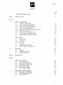
CONTENTS
Page
PART I
ILLUSTRATIONS AND TABLES
iii
OPERATING DATA
1
Section
GENERAL INFORMATION
1.1
General Description
1.2
Electrical Specifications
1.2.1 Input Data Specifications
1.2.2 Data Display Specifications
1.2.3 Display Specifications
1.2.4 Geometric Distortion Specifications
1.2.5 Power Requirements
1.3
Mechanical Specifications
1.4
Environmental Specifications
1.5
Human Factors Specifications
1-3
1-3
1-4
1-4
1-4
1-7
2.
INSTALLATION
2.1
Mechanical
2.2
Electrical
2.2.1 DC Input
2.2.2 AC Input
2.3
Location
2.4
Grounding Techniques
2.5
Input Signal Lead Routing
2-1
2-1
2-1
2-1
2-1
2-1
2-1
2-3
3.
OPERATION
3.1
General
3.2
Brightness Adjust
3.3
Contrast Adjust
3-1
3-1
3-1
3-1
SERVICE DATA
4
1.
PART II
1-1
1-1
1-1
1-1
Section
4
THEORY
4.1
4.2
4.3
4.3.1
4.3.2
4.4
OF OPERATION
Video Amplifier
Vertical Deflection
Horizontal Deflection
Low Level Stages
High Level Stages
Low Voltage Supply
5
ADJUSTMENT AND MAINTENANCE
5.1
Horizontal Adjustments
5.2
Vertical Adjustments
5.3
Focus Adjust
\ 4-1
4-1
4-1
4-2
4-2
4-2
4-5
5-1
5-1
5-1
5-1
i
IMI035
CONTENTS (Cont.)
Page
Section
ADJUSTMENT AND ~~INTENANCE
5.4
Centering
5.5
Troubleshooting Guide
5.6
Raster Shifting
5-1
5-1
5-1
5-2
6
SERVICE DATA
General
6.1
Ordering Parts
6.2
Returning Parts
6.3
Waveforms
6.4
Board Assembly Part Number
6.5
6-1
6-1
6-1
6-1
6-2
6-2
7
SUPPLEMENT
7.1
General
7-1
7-1
ILLUSTRATIONS
Page
Figure
1-1
1-2
2-2
4-1
5-1
6-1
6-2
6-3
6-4
G-5
6-6
6-7
6-8
Synchronization and Blanking Generator Waveform
TV 50, 90, 120 a Tilt with Bonded Panel Dimensions
Interface Connections
Horizontal Drive Processing and Timing Chart
Schematic for Raster Shifting
TV 50 Schematic
TV 50 Parts List, Waveforms and Component Layout
TV 90/120 12V Schematic
TV 90/120 12V Parts List, Waveforms and Component
Layout
TV 90/120 15V Schematic
TV 90/120 15V Parts List, Waveforms and Component
Layout
TV 90/120 AC Schematic
TV 90/120 AC Parts List, Waveforms and Component
Layout
1-2
1-6
2-2
4-3
5-3
6-3
6-4
6-5
6-6
6-7
6-8
6-9
6-10
TABLES
Page
Table
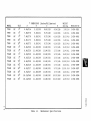
1-1
ii
Mechanical Specifications
1-5
IMI035
PART 1
OPERATING DATA
This section of the service manual provides data
concerning the specification, installation and
operation of the TV 50, 90, and 120 Data Display
Monitor.
1
IM1035
Section 1
GENERAL INFORMATION
1.1
GENERAL DESCRIPTION
The TV 50, 90 and 120 series monitor is a raster scan display designed specifically for data terminals. They are designed for high quality display of alphanumeric dot characters.
The data monitor accepts video, horizontal drive and vertical drive as separate
TTL level signals, eliminating stripping circuits in the data display unit as
well as mixing circuits in the external logic interface.
The 100% solid state silicon circuitry of the PWA provides cool operation and
high reliability. The electronic package.has been miniaturized for compatibility with small volume requirements.
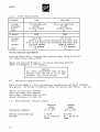
1.2
1.2.1
ELECTRICAL SPECIFICATIONS
Input Data Specification
PWB Edge Input Connector:
Viking
Ampheno1
Cinch
BBRC No.
Video Input Amplitude
Low
High
Video Pulse Width
-
2VKlOS/1-2
225-21031-101
250-10-30-170
1-039-0119
0.0 + 0.4 - 0.0 volts
4.0 ± 1.5 volts
50ns or greater
Vertical Drive Rate
49 to 61 Hz
Horizontal Drive Rate
15,250 to 16,250 Hz
Rise and Fall Times
Video
Vertical
Horizontal
Input Signal Format
Refer to figure 1-1
1.2.2
Less than 20ns
Less than lOOns
Less than SOns
Data Display Specifications
Input Impedance:
Video Input (Class A)
Vertical Drive Input
Horizontal Drive Input
Min Shunt
Resistance
Max Shunt
Capacitance
4k
1.2k
5l0n
40-60pF
40pF
40pF
1-1
IMl035
lO T040J.lS~
FF~TRA~CE
~----------------H
HORIZONTAL
7ps
DRIVE]-tl
VIDEO
t2
~I
l__________
- - - -.....[HIGH:+4±1.5V
,
i-
-
1
LOW:
O+O.4V
-O.OV
t2+7
-r~-B-L-A-N-KI-N-G----
H
~HIGH
UNBLANK .......:--IOJ.ls--t~
....-._t---VIDEO PULSE---~
...
MINIMUM
INFORMATION
LOW
~
"""E--TR--ACE-'-- V - - - - . . t · 1
I
VERT'CAL1600 ~
~
DRIVE
~s 50JlsMIN.
1.4msMAX.
f,HIGH
'--________
~
LOW
t5
V IDEO
-r.
UNBLANK
----e-L-A-N-K-I-N-G--- V
-HIGH
...~--- 850J,Js - __;..~..~~-VIDEO PULSE--+
MINIMUM
INFORMATION
LOW
NOTES:
I. HORIZONTAL RETRACE IS INITIATED AT t2
2. VERTICAL RETRACE
IS INITIATED AT
ts
(I.S TO 7.0,,1 AFTER
WITHOUT
t"
DEPENDING
ON SETTING
OF AI03).
DELAY.
3. H=PERIOD OF ONE LINE: 63.S}!1 ~3% •
4. V= PERIOD OF ONE FIELD: 16.4ml MIN. TO 20.4ms MAX.
5. VIDEO PULSE WIDTH SHOULD BE SOns
MIN.
TABLE I. t3 Vstl TIMING FOR CENTERED HORIZONTAL
VIDEO AS FUNCTION
OF H. BLANKING WIDTH.
HORIZONTAL
VIDEO
BLANKING
WIDTH
10,,1
. LEAD / LAG
-5.S TO
O~II
'c.
ts
Vs
TIMING FOR CENTERED VERTICAL
VIDEO AS FUNCTION OF V BLANKING WIDTH.
VERT ICAl VIO£O BLANKING
WIDTH
LEAD / LAG
ISOp.
t s - t6
IUpl
Ilpi
-4.5 TO
hll
tOOPI
ISOpl
14pI
- 3.S T.O 2,,1
1000pi
100pi
16pI
18pI
-1.S TO 3pI
-I.S TO 4pI
1l00pi
1400pI
SOOPI
400pI
20pI
-O.S
Figure 1-1
1-2
TABLE 2.
~
TO 5pI
Synchronization and Blanking Generator Waveform
IM103s
Video Amplifier:
Bandwidth
Rise and Fall Time
(10 to 90% amplitude)
Storage Time
12 MHz - 3db (Class A mode)
Less than 3sns (linear mode)
lsns max (linear mode)
Retrace Time:
Vertical
Horizontal
1.2.3
60Dl1s
71Js
Display Specifications
CRT Display (without bonded panel) Horizontal Resolution @ 15,750 Hz
Nominal Diagonal
Measurement
Inches/mm
Phosphor
5/127
9/229
12/305
12/305
P4
P4
P4
P39
*Reso1ution (TV lines)
Center
650
800
900
900
@
@
@
@
60
40
40
20
Corner
fL**
fL
fL
fL
550
650
750
750
@
@
@
@
60
40
40
20
fL**
fL
fL
fL
*Resolution is measured in accordance with EIA RS-37sA except burst modulation is adjusted for 100% and burst frequency is then increased to the point where resolution of
the lines is just discernible.
**Set reference black to visual cutoff with brightness control and reference white to the indicated fL with contrast
control.
1.2.4
Geometric Distortion
Specif~cations
On-Axis Scan Non-Linearities - No picture elements displaced from true position
by more than 2% of active raster height. Measurement made using "EIA Linearity
Chart" in accordance with RS-37sA.
If measured on a field of characters, the character height and width are within
10% of that for any adjacent character and within 20% of that for any character
on screen
Perimeter Non-Rectangularity - The perimeter of a full field of characters
approaches an ideal rectangle of 4 by 3 aspect ratio to within ±l.s% of the
rectangle height.
1-3
IM1035
1.2.5
Power Requirements
120V
AC Models
Voltage:
Frequency:
Power:
Fuse:
Current:
Fu~e:
220 or 240 VRMS ±10%
49-6lHz
24 Watts Nominal
2A
105-130 VRMS ±10%
49-6lHz
24 Watts Nominal
2A
DC Models
Voltage:
Ripple:
220V/240V
l2VDC
15VDC
15± 0.2 VDC
l2±0.2 VDC
100 mV p-p for refresh synchronous with power freq.
10 mV p-p for refresh non-synchronous with power freq.
750 rnA DC nominal
900rnA DC nominal
1.0 A DC maximum
1.5 A DC maximum
2A
2A
MATING CONNECTORS REQUIREMENTS
Power (AC models only): 4-contact male connector shell (Mo1ex 03-06-1041)
with female contact (Molex 4529T).
Signal (and power for DC models): 10-contact board edge connector
(Refer to paragraph 1.2.1 for details.)
WARNING
ANY POWER TRANSFORMER MUST BE WELL
REMOVED FROM CRT AND/OR BE OF LOW
EXTERNAL FLUX FIELD DESIGN
1.3
MECHANICAL SPECIFICATIONS
Table 1-1 and figure 1-2 lists the mechanical specifications for the TV 50/90/120
Data monitor. For further information, contact our General Sales Offices. They are:
Addison, Illinois (312) 279-7400
Ocean, New Jersey (201) 922-2800
Santa Clara, California (408) 244-1474
Upland, California (714) 985-7110
1.4
ENVIRONMENTAL SPECIFICATIONS
OPERATING
RANGE
-40°C to 65°C
Temperature (Ambient)
Humidity (Non-Condensing)
Altitude
1-4
STORAGE
RANGE
5 to 80%
Up to 10,000 ft/
3048m
5 to 90%
. Up to 30,000 ft/
9144m
*
MODEL
I
~
V1
TILT
A
DIMENSIONS (Inches/Millimeters)
B
c:
D
WEIGHT
Lbs/kg
OUTLINE NO
TV50
DC
OU
4.56/116
5.12/130
8.62/219
4.56/116
3.0/1.4
2-030-0319
TV90
DC
0°
7.00/178
9.50/241
9.75/248
6.16/156
6.8/3.1
2-030-0401
TV90
AC
0°
7.00/178
9.50/241
9.75/248
6.16/156
10.1/4.6
2-030-0401
TV90
DC
10°
6.90.175
9.50/241
9.75/248
6.16/156
6.8/3.1
2-030-0401
TV90
AC
10°
6.90/175
9.50/241
9.75/248
6.16/156
10.1/4.6
2-030-0401
TV120
DC
0°
9.06/230
11.40/289
11.84/301
5.75/146
11.0/5.0
2-030-0400
TV120
AC
0°
9.06/230
11.40/289
11.84/301
5.75/146
13.4/6.1
2-030-0400
TV120
DC
5°
9.03/229
11.40/289
11.84/301
5.75/146
11.0/5.0
2-030-0398
TV120
AC
5°
9.03/229
11.40/289
11.84/301
5.75/146
13.4/6.1
2-030-0398
TV120
DC
1
~
7 °
9.00/229
11.40/289
11.84/301
5.75/146
11.01/5.0
2-030-0399
TV120
AC
7 1~ °
9.00/229
11.40/289
11.84/301
5.75/146
13.4/6.1
2-030-0399
TV120
DC
10°
8.92/227
11.40/289
11.84/301
5.75/146
11.01.5.0
2-030-0397
TV120
AC
10°
8.92/227
11.40/289
11.84/301
5.75/146
13.4/6.1
2-030-0397
TV120
DC
15°
10.25/260
11.40/289
11.88/302
10.25/260
10.5/4.8
2-030-0396
TV120
AC
15°
10.25/260
11.40/289
11.88/302
10.25/260
12.9/5.9
2-030-0396
L-________________________________________________________________________________~
Table 1-1
Mechanical Specifications
..
IM103S
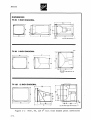
DIMENSIONS
TV-50 5 INCH DIAGONAL
n
y
""(
]
A
j
~
I
I
I
=--..
;1:
~
B
--..-
TV-90
,..
\
6·32 THO MTG HOLES (4)
~
9 INCH DIAGONAL
---- C
------41
.188 X .500 REND MTG SLOT (4)'
5 X 13
TV-120
12 INCH DIAGONAL
IT
.....
I
Zi4
A
_-_- _=
~~~:::'-=--B-
_-=
J
--':~
_::.L.......
t------
Figure 1-2
C
----f(
...
6·32 THO MTG HOLES THRU PLATE (4)
TVSO, 90, 120 00 tilt with bonded panel dimensions
IM1035
1.5
HUMAN FACTORS SPECIFICATION
X-Ray Radiation
The TV 50, 90 and 120 Data monitor complies with the Federal Regulation for
Radiation Control as required by the Radiation Control for Health and Safety
Act of 1968, and as implemented by Title 21, Subchapter J of the Code of Federal
Regulation.
These regulations place certain requirements upon manufacturers of products
which can emit x-rays under some conditions of operation or failure. This includes CRT data display monitors.
Label Visibility
Certification of compliance with radiation regulations is shown by a label
attached to each monitor. The user is responsible for labeling his product in
a similar fashion or in making the DHEW label easily visible from the outside
of the enclosure. The regulations state that "This (certification) information
shall be provided in the form of a tag or label permanently affixed or inscribed
on such product so as to be legible and readily accessible to view when the product is fully assembled for use ... " Each monitor is supplied with an extra
label attached to the face of the CRT. The user will remove this label and use
it as stated above.
Power Requirements
The Data monitor is designed to operate and meet radiation requirements when
operated within the respective AC or DC input power specifications. Radiation
testing is performed at the maximum specified input voltage for AC powered monitors or at 130 VAC for those nominally powered at 110-120 VAC, 60 Hz.
DC powered monitors have an additional requirement because the DC source is
usually regulated and subject to failure of the series pass element. This can
result in an appreciable increase in the anode voltage and consequent emission
of x-rays. This is not a problem for monitors equipped with over voltage protection. For monitors not so equipped, it is necessary for the buyer to ensure
that the normal adjustment of his regulator does not exceed the maximum level
specified for the particular monitor. Furthermore, he shall ensure that the
maximum available voltage from the supply cannot exceed 1.33 times nominal monitor input when the supply has a single failure such as to cause the highest
possible output voltage.
User Operating Controls
The only external control required for operation of the TV 50, 90, and 120 display unit is the contrast control. This control is a carbon composition variable resistor, 500n±20%; ~ watt.
The brightness control is mounted on the printed wIrIng board and is an internal adjustment by the user. An option is available where this control is removed from the board and a remote brightness control supplied by the user is
utilized. The remote brightness control is a carbon composition variable resistor,
100kn±20%; ~ watt.
1-7
IMl035
Section 2
INSTALLATION
-..J
2.1
MECHANICAL
The TV 50 data monitor has four 6-32 clinch nuts for mounting the unit. The
TV 120, 0°, 5°, 7~0 and 10° monitors have four 6-32 clinch nuts on the frame
for installation purposes. The TV 120, 15° monitor uses three 6-32 clinch nuts
for mounting. The TV 90 data monitor has four .188X.sOO radius end slots for
installation. Refer to figure 1-2
2.2
2.2.1
ELECTRICAL
DC Input
The TV 50/90/120 DC models can be operated from either a 12 VDC or IS VDC source.
Refer to section 1.2.5 for details. The DC input power is applied through the
10 pin edge connector.
2.2.2
AC Input
The TV 90/120 AC models have their own self contained AC power supply. This
supply can operate either on 120 VAC or 220/240 VAC depending on which plug of
the jumper plug assembly P2 is inserted into the power supply module.
The power transformer is wired to operate on either 120 VAC or 220/240 VAC
SO/60Hz. To operate the power supply on 120 VAC, take the connector shell of
P2 marked with 120 and insert it in to J2. Conversely, to operate at 220/240 VAC
insert the connector shell of P2 marked with 240 into J2.
AC power is supplied to the unit via Jl. Jl is a 4 contact female connector
shell (Molex #03-06-2041) with male contacts (Molex #45295)
2.3
Location
The TV 50/90/120 models shall not be located in an area that restricts air flow
around the unit nor shall it be placed near any heat generating sources, since
this may cause the unit to overheat.
2.4
GROUNDING TECHINIQUES
The method of interconnecting and grounding the equipment is a function· of the
signal frequency. Optimum grounding depends largely on the system in which the
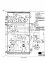
equipment is used. The following grounding technique is recommended when installing the monitor. Refer to figure 2-1 for interface connections.
The horizontal, CRT arc and video/vertical board circuit grounds are terminated
at JlOl. The horizontal ground (JlOl-1) and CRT arc ground (JlOl-5) is connected
together by a jumper wire on the board and they are connected to the frame by a
wire from EllO.
2-1
T2A BRN
T2A
WHT-~iZJ
~1+--T2B
BLK
T2B YEL --t1~
(5)11H--T2B BLU
T2B
ORN--t1~
(7)11H--T2B
RED
L
IBfthL
VERT
CHOKE
I YEL
VERT
L2A
CHOKE
VERT
4
L2A
DEFL
COIL
102
VERT
PiN J
DEFL
COIL
PIN 4
QI08
JI03-----",
P.S. GND
-{i
+15VDC FROM A2
5--ARC
2
TO 12.6VAC OF T I
TO 12.6VAC OF TI
4--}
OPTIONAL EXTERNAL
BRIGHTNESS CONTROL
8 - - VIDEO INPUT
7--(OPTIONAL} 12VII5V DC INPUT
3--
6--HORIZ DRIVE
I --HORIZONTAL GRD
2--N
I
N
Figure 2-1
Interface Connections
IMl035
A connection to system ground must be made at both JlOl-l and JlOl-lO. When the
frame is an integral part of system ground, one of three possible ground configurations can be used.
1.
When a good electrical ground connection cannot be made between the
monitor frame and system ground, then JlOl-l and JlOl-lO is wired
separately to the system ground.
2.
When a good ground connection can be made between the monitor frame and
system ground, then JlOl-lO is wired to the system ground and JlOl-l is
left open.
3.
When the ground connection between the monitor frame and the system
ground is acceptable and it is desired to omit the wire from JlOl-lO,
then add a jumper wire to the board to connect JlOl-5 and JlOl-lO together. JlOl-5 is then wired to the system ground. The monitor is
normally supplied without the jumper wire from JlOl-5 to JIOl-lO to
prevent horizontal circuit ground currents from flowing in the video
ground circuit.
In cases of severe arc related problems, the jumper between JlOI-1 and JlOl-5
can be removed and JlOI-5 or EllO can be connected separately to the frame or
CRT aquadag ground. JIOl-l or El02 must then be connected either to the frame
or system ground.
To isolate the frame from system ground, JlOI-1 and JlOI-IO should be wired
separately to system ground. Add another wire to JlOI-l and connect it and JlOl-5
to the frame (aquadag ground) through a capacitor. The frame cannot be completely
isolated, since an AC connection between the signal ground and frame must be
maintained to assume a complete circuit for the CRT aquadag capacity.
When the video is routed in by a long cabling, shielded cable should be used.
To avoid a ground loop, only one end of the shield should be grounded.
2.5
INPUT SIGNAL LEAD ROUTING
The input signal leads probably will carry high frequency signals and should be
given the following considerations:
A.
To minimize distributed capacity and capacitive pickup of nearby radiated
fields, route the video leads separately and away from all other wiring.
B.
Make the lead length as short as possible, consistent with the packaging
requirements.
C.
Ideally, the video line should meet the requirements of a terminated
coaxial system; i.e., the video line should exhibit a constant impedance
from source load.
2-3
IMl03S
Section 3
OPERATION
3.1
GENERAL
After power, video and drive signals have been applied to the monitor, the contrast and brightness controls may be adjusted to provide the optimum display.
3.2
BRIGHTNESS ADJUST
The monitor is used to display alphanumeric information. The video polarity is
usually white characters on a black background. The brightness control should
then be adjusted for visual cutoff of the raster. A maximum contrast ratio can
now be obtained when video is applied.
3.3
CONTRAST ADJUST
The video amplifier is designed to operate linearly from +.65 to +2.5 V signal
input. The contrast control should be adjusted to the point where defocusing
sets in and then backed down slightly. This occurs at a lS-20V p-p video swing
at the CRT cathode for the TV90/l20, and at a l2-lSV p-p swing for the TVSO.
In no case should contrast be adjusted to cause saturation of QlOl, as this impairs the pulse response of the video amplifier.
3-1
IM1035
PART II
SERVICE DATA
Section 4 through 6 and the supplement are for
qualified service personnel.
The TV 50, 90, 120 has no end user serviceable
parts inside. Refer service to qualified service
personnel.
4
IMI035
Section 4
THEORY OF OPERATION
4.1
VIDEO AMPLIFIER
The video amplifier consists of QlOl and its associated circuitry. The incoming
video signal is applied to the monitor through JlOl-8 and RlOl to the base of
QlOl.
Transistor QlOl has a nominal gain of 15, and operates as a class B amplifier.
QlOl remains cutoff until a DC coupled, positive-going signal arrives at its
base and turns it on. Rl03 provides series feedback which makes the terminal
to terminal voltage gain relatively independent of transistor parameters and
temperature variations. RI02 and CIOI provide emitter peaking to extend the
bandwidth to 12~1Hz.
.
The negative going signal at the collector of QIOI is direct coupled to the
CRT cathode. The class B biasing of QIOI allows a large video output signal
to modulate the CRT's cathode and results in a maximum available contrast
ratio.
The overall brightness at the screen of the CRT is also determined by the negative potential at its grid which is varied by the brightness control:
4.2
VERTICAL DEFLECTION
QI02 is a thyristor used as programmable unijunction and together with its external circuitry forms a relaxation oscillator operating at a vertical rate.
The sawtooth forming network consists of AIOI, Cl03 and Cl04. These capacitors
charge exponentially until the voltage at the anode of Ql02 exceeds its gate
voltage at which time QI02 becomes essentially a closed switch, allowing a
rapid discharge through LIOI. The rate of charge or frequency is adjustable by
AIOI. The oscillator is synchronized by a negative pulse coupled to its gate
from the vertical drive pulse applied externally at JIOI-9.
A divider network internal to AIOI sets the free running frequency by establishing a reference voltage at the gate. This programs the firing of QI02 and
amounts to resistive selection of the intrinsic standoff ratio. The frequency
is controlled by passive components only. CRIOI provides temperature compensation for Ql02 while controlling the gate impedance to allow easy turn on
and off of QI02. LIOI forms a tuned circuit with Cl03 and Cl04 during conduction
of QI02 which provides a stable control on the drop-out time of QI02 to assist
in maintaining interlace. Ql03 collector to base forward diode clamping action
prevents the voltage from swinging too far negative during this flywheel action.
The sawtooth at the anode of Ql02 is direct coupled to the base of Ql03. This
stage functions as a darlington pair emitter follower driver for the output stage
QI04. It presents an extremely high impedance in shunt with AlOI and prevents
the Beta dependent input impedance of QI04 from affecting the frequency of the
4-1
IMl03S
sawtooth forming network.
Linearity control of the sawtooth is accomplished by coupling the output at
Ql03 emitter resistively back into the junction of Cl03 and Cl04. This provides integration of the sawtooth and inserts a parabolic component. The
slope change rate of the sawtooth at Ql03 output is controlled by the setting
of Al02. The output at Ql03 is coupled into a resistive divider ..
Height control RllO varies the amplitude of the sawtooth voltage applied to the
base of Ql04 and controls the vertical raster size on the CRT. CIOS is used
to limit the amplitude of the flyback pulse at Ql04 collector.
The vertical output stage Ql04 uses an NPN power transistor operating as a
class AB amplifier. The output is capacitively coupled to the yoke. Ll provides a DC connection to B+ for Ql04; it has a high impedance compared to the
yoke inductance which causes most of the sawtooth current of Ql04 to appear in
the yoke. Rl14 prevents oscillations by providing damping across the vertical
yoke coils.
4.3
4.3.1
HORIZONTAL DEFLECTION
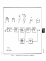
Low Level Stages (Figure 4-1)
The purpose of QlOS and Ql06 is basically to process the incoming horizontal
drive signal into a form suitable to drive the output stage Q108. The duty cycle
of Q108 becomes essentially independent of the amplitude and pulse width of the
drive pulse. This is a necessary condition to assure stability and reliability
in the output stage. In adddition, these stages provide a horizontal video
centering adjustment by delaying retrace with respect to the horizontal drive
pulse.
The drive pulse is presented to Q10S via J10l-6. The base circuit of QlOS includes a clamp and a differentiator which makes Q10S output insensitive to drive
pulse amplitude and width changes. The only requirement is that pulse amplitude
be of 2.S volts minimum and pulse width should be lO-40~s. QlOS together with
Ql06 functions as a monostab1e multivibrator with Ql07 being a slave that provides a positive feedback. Specifically, when Q10S is turned on by the drive
pulse, it discharges Cl12 at a rate determined by the setting of Al03. When
Cl12 is discharged to 2.7S volts, Q106 turns off. This change of state turns
Ql07 on and the base drive to Ql06 from R128 is shunted thru Ql07. QI06/Q107
remains in this state for nominally 2S~s until Cl12 recharges through Al03 to
8.2S volts. At this time, Q106 is biased on again by the current through Al03.
The mu1tivibrator is now in a state that Q106 is on and Q10S/Q107 is off. It
will remain in this state until the next drive pulse occurs or power is turned
off. Cl12 is the only timing capacitor in the circuit and has two time constants
associated with it. Primarily, the charge path between pin 1 and pin 3 of Al03
determines the on time of Q107 while the discharge path through the video centering control and QlOS determines the delay between application of the drive pulse
and start of retrace (turn on of Ql07).
4.3.2
High Level Stages
These stages consist of Ql07 driving the output stage, Ql08 and its associated
4-2
I
I
18 Id
l
I
I
I
Id Z
I
n
10 - 40
n
DIFFERENT IATOR
CII3
RI25
I
I
I
I Id
I d, I I
I
,
I d2 I
I
I
,+'
I:
if ~
t, I
t,
fl
HORIZ
DRIVE
I :
8
"sec
8-dl~:
I
+II
fl
ONE-SHOT
TRIGGER
0105
dl+d Z
VARIABLE
DELAY
AI03 PIN 1-3
CII2
d2+ 8
A
IJ :
t,+d l
dl
VARIABLE
DELAY
AI03 PIN 2-3
CIIZ
d2+ 8
25
t::J
~,
25 ~.
f l+ d l
f,+ d l
ONE-SHOT
OUTPUT
0106
ONE-SHOT
SLAVE
0107
POSITIVE
FEEDBACK
RIZ8
d I : 0.5-6.0)1 lec
dZ : 17" sec
d.+ d Z • 17.5-23,. sec
Figure 4-1
Horizontal Drive Processing and Timing Chart
TO
0108
IMl035
.,
""~,:,,
circuitry thru TlOl. Ql07 is an inverting slave of QI06 and is driven alternately into saturation and cutoff as are all stages in the horizontal circuit.
Ql07 output is transformer coupled to the output stage with phasing of TlOl
chosen such that Ql08 turns off when Ql07 turns on. This allows Ql08 to turn off
quickly, thus minimizing dissipation. A careful review will show that Ql08
turns off at a variable delay time after receipt of the drive pulse. This
action causes retrace to begin.
During conduction of the driver transistor, energy is stored in the coupling
transformer. The polarity at the secondary is then phased to keep Ql08 cut off.
As soon as the primary current of TlOl is interrupted due to the base signal driving
Ql07 into cut off, the secondary voltage changes polarity. Ql08 now saturates
due to the forward base current flow. This gradually decreases at a rate determined by the transformer inductance and circuit resistance. However the base
current is sufficient to keep Ql08 in saturation until the next polarity change
of TlOl.
The horizontal output stage has two main functions: 1) to supply the deflection
coil with the correct horizontal scanning currents: 2) to develop high voltage
for the CRT anode and DC voltage for the CRT bias, focus and accelerating grids
as well as the DC voltage for the video output stage.
(
Ql08 acts as a switch which is turned on or off by the rectangular waveform on
the base. When it is turned on, the supply voltage plus the charge on C123
causes deflection current to increase in a linear manner and moves the beam from
near the center of the screen to the right side. At this time, the transistor
is turned off by a polarity change of TlOl which causes the output circuit to
oscillate. A high reactive voltage in the form of a half cycle negative voltage
pulse is developed by the deflection coil inductance and the primary of T2.
The peak magnetic energy which was stored in the deflection coil during scan
time is not transferred to Cl22 and the deflection coil distributed capacity.
During this cycle, the beam is returned to the center of the screen.
The charged capacitances now discharge into the deflection coil and induce a
current in a direction opposite to the current of the previous part of the cycle.
The magnetic field thus created around the coil moves the ·scanning beam to the
left of the screen.
After slightly less than half a cycle, the decreasing voltage across Cl22 biases
the damper diode CRIll into conduction and prevents the flyback pulse from further oscillation. The magnetic energy that was stored in the deflection coil
from the discharge of the distributed capacity is now released to provide sweep
for the left half of scan and to charge Cl23 through the rectifying action of
the damper diode. The beam is now at the center of the screen. The cycle will
repeat as soon as the base of QI08 becomes positive with respect to its emitter.
e123 serves to block DC current from the deflection coil and to provide "S"
shaping of the current waveform. "S" shaping compensates for stretching at the
left and right sides of the picture tube because the curvature of the CRT face
and the deflected beam do not follow the same arc.
LI03 is an adjustable width control placed in a series with the horizontal de-
4-4
IM1035
flection coils. The variable inductance allows a greater or lesser amount of deflection current to flow through the horizontal yoke and varies the width of the
horizontal scan.
Linearity control is provided by modifying the deflection coil voltage. During
retrace, an auxi11iary winding on the f1yback transformer supplies a pulse which
charges Cl19 through rectifier diode CRl12 and L102. This voltage is then applied
in series with the deflection coil when the damper diode turns on at the start
of trace. The voltage is sawtooth shaped and has the effect of decreasing the
deflection coil current as a function of the sawtooth shape. This compensates
for the stretch normally found on the left side of the screen due to the deflection coil and system RL time constant. Linearity is optimized by adjustment of
L102 which acts as an impedance to the pulse from T2.
The negative f1yback pulse developed during horizontal retrace time is rectified
by CR110 and filtered by C117. This produces approximately -130 VDC which is
coupled through the brightness control Rl17 to G1 of the CRT.
This same pulse is transformer-coupled to the secondary of T2 where it is
rectified by CR2, CRl13 and CR114 to produce rectified voltage of approximately
l2KV, 400V and 32V respectively. l2KV is the anode voltage for the CRT, while
32V is used for the video output stage, and the 400V source is used for G2 and
G4 voltages for the CRT.
4.4
LOW VOLTAGE SUPPLY
The TV 90/120 models are available with an internal power supply. This supply
utilizes an integrated circuit voltage regulator which supplies 15VDC±2.5% to
J103-1. It also supplies 12.6 VAC to J103-3 and 4 for the CRT filament.
The l20VAC primary voltage (220/240V optional) is stepped down at the secondary
of T1 where it is rectified by CRI and filtered by CI. A2 functions as a series
regulator to drop the rectified voltage down to l5V at pin 2. The regulator
maintains a constant output voltage (within 2.5%) with changes in line voltage
load.or temperature. It is capable of supplying 1.5 amps and features internal
current limiting, thermal shutdown and safe over-voltage protection. A
hermetically sealed TO-3 case is used for high reliability and low thermal resistance.
If a short circuit is present at the output, the current limiting feature of A2
will cause the output current to fold back to safe levels. The fast limiting
action of A2 is very effective in protecting transistors from abnormal loads.
The resistor Rl, is used to reduce the power dissipation in A2.
4-5
IMl035
Section 5
ADJUSTMENT AND MAINTENANCE
5.1
HORIZONTAL ADJUSTMENTS
With a crosshatch signal applied, adjust video centering control, Al03 to center
the video within the raster horizontally. Adjust Ll02 for best horizontal linearity. Do not adjust Ll02 core out farther than necessary as this causes excessive power to be consumed.
Adjust Ll03 for desired width.
5.2
VERTICAL ADJUSTMENTS
With the crosshatch signal applied, adjust vertical hold control AlOl to lock in
the picture.
Adjust vertical linearity control Al02 for best overall linearity. This control
affects the vertical frequency slightly and might require a readjustment of the
hold control. Adjust vertical height control RllO for desired height.
5.3
FOCUS ADJUST
Adjust focus control R122 for best overall focus of the picture. Usually the
center and corners of the screen do not focus at the same setting and a compromise
must be made.
5.4
CENTERING ADJUST
If the raster is not properly centered, it may be repositioned by rotating the
ring magnets behind the deflection yoke. The ring magnets should not be used to
offset the raster from its nominal center position because this degrades the
focus and resolution of the display and may cause neck shadow.
If the picture is tilted, rotate the entire yoke.
5.5
TROUBLESHOOTING GUIDE
Symptom
Possible Remedy
1.
Screen is dark
Check l5V bus, Ql08, Ql07, CR2, CRl13
2.
Loss of Video
CRl14, QlOl
3.
Power consumption is
too high
Check horizontal drive waveform;
adjust horizontal linearity coil;
Ql07, Ql08
5-1
IMl035
4.
5.6
Low voltage bus
incorrect (for units
with a low voltage
supply)
AI, A2
NOTE: Low voltage supply will indicate
low or "0" volts if an abnormal
load is evident on the 15 volt
line.
RASTER SHIFTING
The extra cost factory option of inserting Rl13 or R1l5 makes possible a
raster shift either down or up by allowing a fixed DC current to flow in
deflection coil. This option precludes the need for using the centering
for non-standard centering which would result in disturbance of geometry
focus.
1.
Raster pull down (Refer to figure 5-1)
Add Rl13 from J102-4 to ground in holes provided.
for desired amount of pull down.
2.
fixed
the
rings
and
Value to be selected
Raster pull up (Refer to figure 5-1)
Replace C106 with a jumper wire. Remove jumper wire from J102-3 and J102-1
and replace with C107, 470uf, 10v, electrolytic. Add Rl15 from J102-3 to
ground in holes provided. Value of Rl15 to be selected for desired amount
of pull up.
5-2
TO JI02-2
•
IMI035
CI06
TO JI02-4
QI04
MJE3055
JO JI02-1
RII4
TO JI02-3
1.5K
1/2W
TP5
RII3
--
--
--
RASTER PULL DOWN
TO JI02-2
. . - - - - -.......------~TO JI02-4
---~TO
JI02-1
"----.........___----JTO J 102-3
--
-Figure 5-1
RASTER PULL UP
--
Schematic for Raster Shifting
5-3
IMl035
Section 6
SERVICE DATA
6.1
GENERAL
This section contains the replaceable electrical parts list, schematic, PWB
component layout and waveforms for servicing of the TV SO, 90, 120 data monitor.
If a part you have ordered has been replaced with a new part or an improved part,
our customer service representative will contact you concerning any change in the
part.
Change information concerning the TV S0, 90, 120 units is located at the rear of
the manual in the supplement section.
6.2
ORDERING PARTS
Most parts contained in the monitor are available commercially from electronic
parts outlets. When it is necessary to order spare or replacement parts from
BBRC, Electronic Display Division (E.D. DIV.), include the part description,
part number, model and serial number data of the monitor as listed on the serial
number plate and, if applicable, the schematic reference number listed in the
parts list. Orders for these parts should be sent to:
"
Ball Electronic Display Division
P.O. Box 43376
St. Paul, Minnesota 55164
For rapid service:
6.3
Telephone area (612) 786-8900
or
TWX area (910) 563-3552
RETURNING PARTS
When the monitor requires service or repair in accordance with the enclosed
warranty, return the unit or part to:
Ball Electronic Display Division
4501 Ball Road N.E.
Circle Pines, Minnesota 55014
ATTN: Customer Service
Telephone area (612) 786-8900
TWX area (910) 563-3552
6-1
IMl035
Unnecessary delays may be avoided when parts are returned to Electronic Display'
Division using the follo~ing procedures:
(1)
Package the unit or part in accordance with the method of shipment.
Enclose a list of the material being returned and the reason for
returning it.
(2)
Send the unit or part, transportation prepaid, to the address stipulated for returning parts.
All equipment and parts described in the warranty will be replaced, provided
E.D. DIV's examination discloses that the defects are within the limits of the
warranty. If damages or defects are not within the limits of the warranty, the
customer will be notified of the extent of repairs required and the cost. The
unit will be repaired and returned upon agreement.
6.4
WAVEFORMS
The waveforms on the component layout were taken with 1.5 V peak to peak crosshatch signal applied to the monitor. These waveforms can be used as a check
point to localize problems to a specific circuit area. The waveform photographs
indicate the actual peak amplitude for each test point. The TV 50 is the only
exception, the peak to peak amplitude is specified for TP9, TP12, TP13 and TP14.
6.5
BOARD ASSEMBLY
The board assembly part number has a,p-002-XXXX prefix. The last four digits of
the part number is found under the "use on 6-002" column in the parts list. The
last four digits of the board assembly part number is stamped on the component
side of the board near JlOl.
6-2
1M 1035
r.£IllRAl :I01E$:
LI
&
Ufo
&
VIllT
U;lllSS OTlllRHIS[ SPECIFIEO
1. ALL RESISTORS I/~W. 5%. VALUES III OII11S.
2. ALL CAPACITOR VALUES IN IlICROFARADS. FOR CAPACITOR TYPES. SEE NOTE '9.
0 DENOTES JIUI PC CARD E06E COIlIIECTOR.
~. ~>-DENOTES WIINrCTIOlI TO OfF BOARD WPIPON[NlS
5. R[FERElI(E DESIGNATION NOT USlD: Rlll. RlJ5
LAST REFEREIitE OESIG~ATION USED: R13~. C12~
PROTECTIVE ARC GAPS ARE AN INTEGRAL PART OF PRINTED WIRE BOARD.
~ THE PW8 CIRCUIT GROUNDS ARE BROtIGIIT OUT SEPARATELY TO PINS 1. 5 AND 10
OF JIOl. PWB (IRCUIT GROU~DS FOR PINS 1 AND 5 OF JIOl ARE CONNECTED TOGETHER BY A JUIV'lR WIRE ON THE BOARD AND ARE WNNECTED TO CHASSIS GROUHD
VIA A WIRE FROM EllO.
THE DATA DISPLAY um IS COHNECT£D TO THE SYSTEII GROUND THROUGH PINS 1
AND 10 OF JIO!. FOR NOH-STANDARD GROUNDING TECIINIIIIIES REFER TO SECTlOil
2 Of THE SERV ICl IlANUAl
DENOTES HEATSIIIK
9.
DIPPED PliCA
D • CERA/HC DISC.
M • IIYLAR
I'A • El£CTROLYTIC AXiAl
[R • ELECTROLYTIC RADIAL
p • POlYPROPYLENE
&.
<®.
i
TIJ~~QOU~; U:;;~~:;ST ;~'~oHtlilE~ro ~;;;'y COM~ttT;SItIl.c 'j'~
'N
.
• +vc~o I~ T"IS MONnOR. TI4£ C_IIICAL 'COkPONENTS fIlAr "fFen .
: .j(-RAllIAlltlN ~'E D~ ..<)tfO
11<8 s .... Ol!O ~.EAS ON 114£ SCH!HATIC.
\"':COIIPONfNT$ IN THE $HADro AIIEA AIlE TO II REPLACED ONLY WITH
. tl>D DI v . AP,.ROveD CO""O"~NTS.
Li ,i::.m£r.s~~~r !~U~~ c~~~~sO:~~~~rc:!o::~~s
ncfsslvl~:~.AOI.TltlN.•.
& 1D'
......
.~
. .........
.________________________________________________
. .-f)l.:.!L;;;;;;-..J
.
.,.--....- - - -.......- - -...- ....- -.....- - - - - -....- ....- - - - -.........- .....- - - - -.........
_IZONTM._
6·3
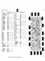
Figure 6-1 TV50 Schematic
r:. ~AYt
•
,,'
PARTS LIST TV50
REF
SYI!
DESCRIPTIOII
BBRC
PART NUMBER
AlOl
AlO2
Al03
RES TRIll. 6OK. VERT HOLD
RES TRIll. 20K. VERT LIN
RES TRIll. 2.5K. VIDEO CENTER
1-011-8006
1-011-8005
1-011-8001
CAPACITOR. FIXED. uF UNLESS HOTED
CI01
CI02
CI03
CI011
ClOS
ClO6
CI07
CIOB
C109
CllO
cm
Cll2
cm
ClI4
C115
C116
C117
C118
C119
Cl20
C121
C122
Cl23
C124
l00pFi51, 500V, 011
.OO5t2011 l00v, CD
.22ilOll l00v, IIY
.22tlOll l00v, IIY
.68, SOY, E
470, lOY, E
HOT USED
25, 25V, E
.01t2011 1000v, CD
.02t201, 1000v, CD
.01t201, l000V, CD
.0022t101, 63OY, IIY
.0047tl011 63OY, IIY
.02±20%, l00v, CD
I, SOY. E
50, soy, E
.0II7t10%. 2SOY, IIY
220J 25V, E
IOtl0%. l00v, IIY
.02t201, 500v, CO
501 soy, E
.022tlOI. 2SOY, PP
10-25V, E
10. 25V, E
1-012-0300
10-U-75OB
1-012-2277
1-012-2277
1-012-22611
1-012-2158
H510
1H3605
1N3605
IN3605
IN3605
IH3605
IN3605
1N3605
HOT USED
IN3605
IH3280/8599
30S3
3OS3
1"3280/8599
1"3605
1-021-01124
1-021-01110
1-021-01110
1-021-01110
1-021-01110
1-021-01110
1-021-()/jl0
1-021-01110
2A-125V, PICO
1-028-0247
1-0U-1380
1-0l2-2m
1-012-2217
1-012-2214
1-012-2254
1-012-2279
10-12-7209
1-012-2189
1-0U-2157
1-012-2240
1-012-2159
1-012-2255
1-012-0780
1-012-2157
1-012-2297
1-0U-2273
1-012-2273
DIODE
CRl
CRI01
CRI02
CRI03
CR1011
CR105
CRI06
tR107
CRI08
tR109
CRUO
CRm
CRIU
CRm
CRl14
1-021-(11110
1-021-0403
1-021-0458
1-021-01158
1-021-01103
1-021-01110
FUSE
FlOl
CONNECTORS
JI02
JI03
JI011
CONNECTOR, q PIN I1ALE
NOT USED
CONNECTOR, 7 PIN I1ALE
1-039-0146
1-039-0145
USED 011 6-0020689 0732
IMI035
REF
SYI!
DESCRIPTION
BBRC
PART NUMBER
U
L2
LlOl
Ll02
U03
VERTICAL CHOKE
DEFLECTION. TV50
560uH
LINEARITY
IIIDTH
6-003-0529
1-023-0231
1-016-0302
1-016-0328
1-016-0303
USED ON 6-0020698 0732
2N5830
2116027
""S-A65
t1JE3055
2N4m
2N4124
/'I'S-U05
BIJII07
~
>
0
iIlu
TRANSISTOR
0101
0102
0103
01011
0105
0106
0107
Q10B
X
X
X
X
X
1-015-1172
1-015-1157
1-015-1186
1-015-U56
1-015-1139
1-015-1139
1-015-1159
1-015-1210
~c\l~
><1
eg
~
RESISTOR, FIXED, CARBON, i51, 11411 UNLESS NOTED
R101
R102
R103
R1011
RI0S
R106
RI07
RIOB
RI09
R110
Rlll
Rll2
Rm
R114
R115
R116
Rll7
R118
R119
R~
R121
R122
R123
R124
R125
RU6
R127
R128
R129
RHO
Rm
Rm
Rm
Rl34
RH5
47
100
47
220J 11211
8201 11211
470
360
lOOK
180
VARI 250t201. CO VERT HGT
12. 11211
IS, 11211
NOT USED
1.5K, 11211
NOT USED
62K
VARJ l00Kt2011 CO BRT ADJ
30K, 11211
9.1K
8.211
lOOK
VAR, 2.5IIt2OI, CO FOC ADJ
HOT USED
510
lK
20K
3.3K
15K
2.4K
82±10%, 311, IfIf
3J 11211
1. 2±l01J 211. IfIf
6.8K
HOT USED
HOT USED
1-0U-2274
70-16-0623
1-011-5435
1-011-2305
70-16-0912
70-16-OB25
70-16-01()/j
1-011-5566
70-16-0511
70-16-0102
70-16-0203
70-16-0332
70-16-0153
70-16-0242
1-011-2375
1-011-2478
1-011-1395
70-16-0682
NOT USED
HIGII VOLTAGE
HORIZ DRIVER
I~
~~
~
Jg
r
>
~->
>"
i!:
0
>
~~
0
ill
~!~
~
TRANSFORl1ER
T1
T2
nOI
>
70-16-01170
70-16-0101
70-16-01170
1-011-2254
1-011-2268
70-16-0471
70-16-0361
70-16-01011
1-011-2252
70-89-0251
1-011-2224
1-011-2226
;:111
0--
~
6-003-0587
1-017-5402
IIISCELLANEOUS
CRT SOCKET
1-022-01127
I
I
~
Figure 6-2 TV50 Parts List, Waveform, and Component Layout
i!:q.
~ ~~
~~g
$~
I
5
I
li
I
~
6-4
1M 1035
(;lNlRAl :IOTES:
LI
&
LI"
&.
/1:.
VEtlT
IINU:SS OTIII.RWI$[ SP[ClfIf.D
ALL RfSISTORS )I~W. ',:. VALULS I~ OII1'1S.
ALL CAPACITOR VALUES I~ MICROfARADS. FOR CAPACITOR TYPES, SEE IIlTE 19.
DUWOlfS JIOI PC CARD EI)(,E CONNECTOR.
~. ~>-DENOII.~ CONNECTION TO OFf BOARD COI\POfl[NTS.
5. REfERENCE DESIG~ATlONS NOT USED: Rill. RIl5
LAST REFERENCE UESIGNAT lOtI USED: Rm. CI24
PROTECTIVE ARC GAPS ARE AN IlHEGRAl PART Of PRINTED WIRE BOARD.
THE PWB CIRCUIT GROUNDS ARE BROUGHT OUT SEPARATELY TO PINS I. 5 AND 10 OF
JIO!. PWB CIRCUIT GROUllDS FOR PINS I AND S Of JIOI ARE CONNECTED TOGEIIIER BY A JUMPER WIRE ON THE BOARD AND ARE CDNNECT£D TO CHASSIS GROUND
VIA A WIRE FRDM EIlO.
THE DATA DISPLAY UNIT IS CONNECTED TO TilE SYSTEM GROUND THROUGH PINS I
MiD 10 Of JIOI. fOR !CO~-STANDARD GROUNDING TECHNIQUES REFER TO SECTION
2 OF THE SERV ICE IIANlIAL.
I.
2.
&-.
9.
11
Il£NOTES HEATSINK
DIPPED "ICA
CD - CERAMIC DISC.
- MYLAR
II.'K~
[[[(fR0l YT IC AXIAL
£ - EllCTROlYTIC RADIAL
PP - POLYPROPYLENE
P3 AND H ARE USED ONLY (II THE TVX90 AND TVX120
""'"":t ,.
·""Y,(":·:)--"
$A'~T" /lUST"
Pltoooer
111311011,..
!2V
ftK~n$jye
.01
....--------................----........----..
@
~&"Yr~~"--,-~--~--~--"~------~----~--~------------~~~--------~--~~~--------"~~:~~~
~
6-5
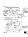
Figure 6-3 TV 90/120, 12V, Schematic
_tI ""Y
·,·t.
:,:·'v")!(~"\ll
COMPONENt IS
'Rt~
',"
~~;.~~fE~~5m~
r!:Uf~t c~~~~~so:m~A~c~;:;$T:V '::"'E I:
X-R401"tION.
CRII4
ClIO
&~------
'/:""r:" "y ,>'·t'· •.•.."':,""
COflUOII_eo
T>II! CRitICAL (O/'<'OIoII"T$ TAAT A"~Cf
X-RADIAl ION Altt OaNOTeD 1>1 TME SHADED AREM ON tHe SCI'!lIArt(,
COM'ONEIITS IN n,t $HADeD ARfA ARe TO Be REPLACED ONLY WITH
EO\) QIV; APPROVED COI1PO>1e>ll$.
Pl4CI!O ,,. THIS IIOHITQR.
Clltl3
400V
~ll£lS.
-•
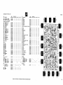
PARTS LIST TV 90/120, 12V
REF
SYII
DESCRIPTION
BBRC
PART HUl!BER
AlOl
Al02
Al03
RES TRill, 6OK, VERT HOlD
RES TRill, 20K, VERT LIN
RES TRill, 2.5K, VIDEO CENTER
1-0ll-8006
1-011-8005
1-011-8001
CAPACITOR, FIXED, uF UNLESS NOTED
C101 l00PFt51, 500v, 011
CI02 .0051201J 100v, CD
C103 .22t10IJ 100v, flY
C104 .22t10IJ 100v, flY
Cl05 .68J SOY, E
CI06 470J lOv, E
CI07 NOT USED
ClOB 25J 25y, E
CI09 .01t20IJ 1000v, CD
CllO .02t20IJ l000v, CD
C111 .01t201J 1000v, CD
C112 .0022dOIJ 63Ov, flY
Cll3 .0047t101J 63Ov. flY
CWI .02t201J l00v, CD
C115 IJ SOY. E
C116 SOJ SOv. E
Cll7 .047±lOlJ 2SOv, IIY
CU8 220; 25v, E
Cl19 lOt101J l00v, IIY
C120 .021201J 500v. CD
C121 SOJ SOv, E
C122 .033±lOlJ 25OV, AY
C123 10J 2Sv. E
Cl24 10J 25v, E
DIODE
CR1
11510
tRI01 IN3605
CRI02 IN3605
CRI03 IN3605
CR104 IH3605
CR10S 1N3605
CR106 1N3605
CR107 lH3605
tRl08
CRI09 lH3605
CRllO 1"3280/8599
CRill 3OS3
CR1l2 3OS3
CRIB 1N328018599
CRU4 IN3605
FUSE
flOl
2A-125v, PlCO
om
0731 0735
1-012-0300
10-12-7508
1-012-2277
1-012-2277
1-012-2264
1-012-2158
1-012-1380
1-012-2214
1-012-2217
1-012-2214
1-012-2254
1-012-2279
10-12-1209
1-012-2189
1-012-2157
1-012-2240
1-012-2159
1-012-2255
1-012-0780
1-012-2157
1-012-2298
1-012-2273
1-012-2273
REF
SYII
DESCRIPT ION
TRANSISTOR
0101 2NS830
0102 2N6027
0103 IIPS-A6S
0104 IIJE3055
0105 2N4124
0106 2"4124
0107 ""S-U05
0108 BU407
X
X
X
X
X
X
X
X
X
X
X
X
X
X
X
X
X
X
X
X
X
X
X
X
X
X
X
X
X
X
X
X
X
X
X
X
X
X
X
X
X
X
X
X
X
X
X
X
X
X
X
X
X
X
X
X
X
X
X
X
X
X
X
X
X
X
X
X
X
X
X
X
X
X
X
X
X
X
X
X
X
X
X
X
X
X
X
X
X
X
X
X
X
X
X
X
X
X
X
X
X
X
X
X
X
X
X
X
X
X
X
X
X
X
X
RIOI
Rl02
RI03
RI04
RI05
RI06
R107
RIOB
RlO9
R110
Rill
R112
RIB
R114
RI15
R116
47
100
47
220J 11211
820J 11211
470
360
lOOK
ISO
VARJ 250t201J co VERT HGT
12J 11211
12J 11211
NOT USED
I.5K1 11211
NOT USED
62K
VARJ 1001<%201J CO BRT ADJ
10K; 11211
9.1K
8.211
lOOK
VAR: 2.5/11:201, CD FOC ADJ
NOT USED
510
lK
20K
3.3K
15K
2.4K
56tlOlJ 3M, W
1.2J 11211
.4ldOlJ 211, W
6.8K
1.8151J 211
NOT USED
1-021-0410
1-021-0403
1-021-0458
1-021-0458
1-021-0403
1-021-0410
1-028-02_7
TRANSFORIIER
1-039-0146
T1
T2
1-021-0112_
1-02HIIIlO
1-021-(11110
1-021-0410
1-021-0410
1-021-0410
1-021-0410
1-021-0410
6-003-05n
1-023-0239
1-023-0240
UOI
ll02
U03
1-016-0302
1-016-0328
1-016-0323
1-039-0145
1-034-0323
1-034-0300
IMI035
BBRC
PART NUI1BER
9
USED ON 6-0020698 0686 0697 0710 0733 0731 0735
1-015-1172
1-015-1157
1-015-1186
1-015-1156
1-015-1139
1-015-1139
1-015-1159
1-01S-1210
~
RESISTOR, FIXED, CARBON, 151J 1/411 UNLESS NOTED
X
RI17
Rll8
Rll9
R120
R121
R122
R123
Rl24
R125
R126
RU7
Rl28
Rl29
RHO
RHl
RH2
RH3
Rl34
COIINECTORS
JI02 CONNECTOR. " PIli IW.E
J103 NOT USED
J1011 CDHNECTOR. 7 PIli IlALE
P3
CDHNECTOR, 1 PIN FEIIALE
JJ
CONNECTOR. 1 PIN IlALE
COIL
U
VERTl CAl CHOKE
L2
DEFLECTION, TV 120
OR DEFLECTION, TV 90
560uH
LINEARITY
WIDTH
USED ON 6-002
0698 0686 0697 0710
X
X
X
X.
X
X
X
X
X
X
X
Rl35
OR
OR
OR
flOl
NOT USED
HIGH VOLTAGE,
HIGH VOLTAGE,
HIGH VOlTAGE,
HIGH VOLTAGE,
HORIZ DRIVER
TV90
TV90nRll
TVl20
TVX120
70-16-0470
70-16-0101
70-16-0470
1-011-2254
1-011-2268
70-16-0471
70-16-0361
70-16-0104
1-011-2252
70-89-02S1
1-011-2224
1-011-2224
X
X
X
X
X
X
X
X
X
X
X
X
X
X
X
X
X
X
X
X
X
X
X
X
X
X
X
X
x
x
X
X
X
X
X
X
X
x
X
X
X
X
X
X
X
X
X
X
X
X
X
X
X
X
X
X
X
X
X
X
X
X
X
X
X
X
X
X
X
X
X
X
X
X
X
X
X
X
X
X
X
X
X
X
J8
..
G._>
~~
~
1-011-2274
70-16-0623
1-011-S435
1-011-2305
70-16-0912
70-16-0825
70-16-0104
1-011-5566
70-16-0511
70-16-0102
70-16-0203
70-16-0332
70-16-0153
70-16-0242
70-16-2521
1-011-2520
1-011-1394
70-16-0682
1-0ll-2417
6-003-06OS
6-003-0S71
6-003-0599
6-003-0586
1-017-S402
X
X
X
X
X
X
X
X
X
X
X
X
X
X
X
X
X
X
X
X
X
X
X
X
X
X
X
X
X
X
X
X
X
X
X
X
X
X
x
X
x
X
X
X
~
..~~~
~~
~
KISCELl.AIIEOUS
CRT SOCKET
1-022-0427
-18
a:->
>-~~
~
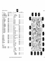
Figure 64 TV 90/120, 12V Parts List, Waveform and Component Layout
6-6
'~ . ~
..
1M 1035
GEIiERAL IIOTlS:
trHL[S~
OTIIERYIS[ SP[(IF IlD
1. ALL IIESISTORS lIQW. 51. VALUES IN ~tIIS.
2. ALL CAPAClTO!I VALUES IN PlICROFARADS. FOR CAPACITOR TYPES. SEE IIITE
n DENOTES JIOI PI: CARO EDGE CONNECTOR.
"woe
8>.
4.
)
r.
DENOTES CO:lNlCTIOH TO OFF BOARD COII'OHENTS.
5. REFERENCE DESIGNATIONS lilT USED: RlB. RllS
LAST REFERENCE DESIGNATION USED: Rm. Cill
PROTECTIVE ARC GAPS AN INTEGRAL PART OF TIE PRINTED MIRE BOARD.
/}}, THE PWB CIRCUIT GROUNDS ARE BROUGHT OUT SEPARATElY TO PINS L 5 AND II
OF JI01. PIID CIRCUIl GROUNDS FOR PINS I AND 5 OF JIOI ARE CONIIECT18
GET HER BY A JlJ1PlR WIRE ON TIE BOARD AND ARE CONNECTED TO CHASSIS GROI
VIA A WIRE FROf'I EllO.
&1
THE DATA DISPLAY UNIT IS COIIHfCTED TO THE SYSTEPI GROUND THROUGH PINS
AND 10 OF JI01. FOR 1liii-STANDARD GROUIIIlING TECHNIQUES REFER TO SECTII
2 OF THE SERVICE IlANUAL.
it
DlNOTES HEATSINK
9'1-
DIPPED "ICA
CO - CERMIC
DISC.
II.S.V
~·
6-7
..
__ ____________________________________________
__
__L."____" ____" __-J__________
__________
__ ________
& . . . ..m
...
ar~=-~
~~
~~~
-J~~
~~
~
Figure 6-5 TV 90/120. lSV Schematic
-J~~~~~
A
- "YLAR
E - ElECTROLYTIC AXIAL
E • fUClROLYTI( RADIAL
p . POLYPtIOPYl1lIE
P3 AND Jl ARE USED OIIlY 0fI TIE M90
AND
Ml20 PllDElS.
PARTS LIST TV 90/120, ISV
SYII
OESCRI PTION
BBRC
PART NllllBER
A101
A102
A103
RES TRIPI. 6OK, VERT OOLD
RES TRIPI. 20K, VERT LIN
RES TR I". 2. 5K. VIDEO CENTER
1-011-8006
1-011-8005
1-011-SOO1
REF
USED ON 6-0020695 0688 om 0728 0730
X
X
X
X
X
X
X
X
X
CAPACITOR. FIXED, uF UNLESS HOTED
100PFt51. 500v, Df't
.OO5t201) 100V. CD
.22t101) 10OV. IIY
.22t101) 100v. IIY
.68) SOV. E
470) 10V, E
HOT USED
25; 2SV, E
.01t201; l000v, CD
.02t201; l000v. CD
.01t201; 1000v. CD
.022tIOl, 63OV. IIY
.00II7tl0S; 63OV, IIY
.02t20%, 100v. CD
I; 50V, E
so; soy, E
.047tlO1; 25OV. IIY
220; 25V, E
lOtlO1; 100v. IIY
.02t20%; 500v, CD
so; 5OV. E
.022tl01; 25OV. PP
lOt10%; l00v, IIY
NOT USED
C101
C102
CI03
C1011
ClOS
CI06
CI07
CI08
CI09
CllO
Clll
Cl12
Cll3
Cll4
Cll5
Cll6
C117
Cll8
em
Cl20
Cl2l
C122
C123
e124
1-012-0300
10-12-7508
1-012-2277
1-012-2277
1-012-2264
1-012-2158
H510
1"3605
1"36OS
IN360S
1"3605
1"36OS
1"3605
IN3605
iIOT USED
1"3605
1"3280/B599
3OS3
30S3
1"3280/B599
IN3605
1-012-1380
1-012-2m
1-012-2217
1-012-2214
1-012-225q
1-012-2279
10-12-7209
1-012-2189
1-012-2157
1-012-2240
1-012-2159
1-012-2255
1-012-0780
1-012-2157
1-012-2297
1-012-2255
1-021-0424
1-021-0410
1-021-0410
1-021-01110
1-021-0410
1-021-0410
1-021-0410
1-012-()l1l0
1-021-0410
1-021-01103
1-021-0458
1-021-01158
1-021-0403
1-021-0410
om
X
X
X
REF
SYII
DESCRIPTION
TRANSISTOR
0101
11102
11103
111011
0105
0106
11107
1I1OS
2"5830
2"6027
f'tPS-A65
IIJE3055
2Nqm
2Nqm
f'tPS-U05
BU407
X
X
X
X
X
~
X
RI01
RI02
R103
RI04
R105
R106
R108
R109
RllO
Rlll
R112
Rll3
Rm
R115
RU6
R117
RI18
R119
R120
RI21
R122\
R123
R124
R125
R126
R127
R128
R129
mo
Rl3l
R132
R133
Rl34
2A-12SV, PICO
FlOI
CONNECTORS
CONNECTOR,
HOT USED
CONNECTOR.
CO:l.'lECTOR.
CONNECTOR.
JI02
J103
J1011
P3
J3
Q PIN IW.E
7 PIN PlALE
1 PIN FEf'tALE
1 PI HIIAlE
1-015-1172
1-015-1157
1-015-1186
1-015-1156
1-015-1139
1-015-1139
1-015-1159
1-015-1210
~
USED Otl 6-0020695 0688 om 0728 0730 0734
X
X
X
X
x
x
~
~
' X
q7
100
q1
220; 11211
820; 11211
lI70
lOOK
300, 11211
YARI 250t201; CO VERT HGT
12; 11211
15, 11211
NOT USED
1I5K 11211
NOT USED
62K
YAR) 100K:t20%; co BRT ADJ
3OK; 11211
9.1K
8.2f't
lOOK
YAR; 2. 511t20%. CO FOC ADJ
16; 11211
510
lK
HOT USED
3.3K
15K
3K
82dO%, 311. l1li
3; 112M, co
1.2tlOI; 211. l1li
6.8K
NOT USED
70-16-0470
70-16-0101
70-16-0470
1-011-225q
1-011-2268
70-16-0471
70-16-0104
1-011-2257
70-89-0251
1-011-2224
1-011-2226
X
X
X
X
X
X
X
X
X
X
X
1-0U 22711
70-16-0623
1-011-5q35
1-011-2305
70-16-0912
70-16-OS25
70-16-0104
1-G11-5566
1-011-2227
70-16-0511
70-16-0102
70-16-0332
70-16-0153
70-16-0302
1-011-2375
1-011-2Q78
1-011-1395
70-16-0682
TRANSISTOR
n
T2
fUSE
BBRC
PART NUPIBER
RESISTOR, FIXED. CARBON. tSS) 114M UNLESS NOTED
DIODE
CRI
CRI01
CRI02
CR103
CRI04
CR10S
CRIOO
tRlO7
CRIOS
CRI09
CRHO
CRlll
CRll2
CRll3
CRUll
-
IMI035
'1'1
OR
OR
OR
1-028-02Q7
NOT USED
H[6H VOlTAGE
HIGH VOlTAGE
HIGH VOLTAGE
HIGH VOLTAGE
HORIZ DRIVER
1-039-0146
n01
1.039-01ij5
1-034-0323
1-034-0300
"I SCEllANEOUS
CRT SOCKET
TY90/15Y
TY120/1SV
TY120
TYX120
6-003-0602
6-003-0530
6-003-0587
6-003-0604
1-017-5q02
1-022-0427
COIL
U
L2
OR
LIOI
U02
U03
VERTI CAL CHOKE
DEFLECTION TY90
DEFLECT ION TYX 1201TY120
560uH
lINEARITY
WIDTH
6-003-0529
1-023-0237
1-023-0231
1-016-0302
1-016-0328
1-016-0323
Figue-e 6-6 TV 90/120, lSV Parts List, Waveform and Component Layout
6-8
IMI035
GENERAL
1I0T~'S:
IJNLESS QIIIERWTSE SPECifiED
). ALL RESISTORS !I~W, 5~, VALUfS I" OII11S.
2. ALL CAPACITOR VALUlS Iii MICROFARADS. FOR CAPACITOR TYPES, SEE IIITE 19.
0 DfNOTES J101 PC C.~RD EOGE CONNECTOR.
~. -n-DENOTES CONNECIIO~ TO OFF BOARD COI1POH£NTS.
5. REfERE1ICE DESIGNATIONS NOT USED: RlB, RllS. R126
LAST R~FEREHCE DESIGNATION USED: Rm, C123
PROTECT IVE ARC GAPS ARE All INTEGRAL PART OF PRINTED VIRE BOARD.
TN[ PHB CIRCUIT GRou.~DS ARE BROOGHT OUT SEPARATElY TO PINS 1. S AIIII 10 OF
J10). PWB CIRCUIT GROUNDS FOR PINS 1 AND S OF JI01 ARE CONNECTED TOGETH£R BY A JIJII'ER VIRE ON THE BOARD AIID ARE CONNECTED TO CHASS IS GROUIIO
VIA A VIRE fROll EllO ••
TN[ DATA DISPlAY UHIT IS COWCTED TO TI£ SYSTEII GROUItD THR0U6H PINS 1
AND 10 OF JI0l. fOR NON-STAIIDARIl GROUIIOJlIG TECHNIQUES R£FER TO SECTlOII
2 OF THE SERV ICE IIAIIUAL.
DEIllTES HEATS INK
9. ~. DIPP£D "ICA
@. CERMIC DISC
IffLAR
@. ELECTROlYTIC AXIAL
@. ELECTROLYTIC RADiAl
POL YPROPYLE~E
&
&.
fA
£
®.
....
illIG
-
®.
",.
,
;~~'i :~~~::::;;~\~~~~~-:U~~:~~;:f~:~J,Y
ntIS _!TeA. fHl t_lnCAL eo_rrts .
..
.:~,~:;, C~~
flEet
Alit O£N(lT(I) IN \'It!! $""*1> AU,,$ 011 TOlf. Jltl<J~flt,
":::":_:~ :~: ~::e ARE H>.~ RE'LACfo 0!ti.1 IIIi'll
"
'.. ~ I<OtIlA~ef~__c'~
'IjAt ~~!~~, ~~'~'~;~
~: : ~::~ .:. '.>f:t:t':::i~· .~~:.:~"@
o ••
CRII5
400V
IN521011_
CRII4
6-9
Figure TC 90/120, AC Schematic
SYl'I
DESCRIPTION
BBRC
PART NlI1mER
Al
A2
AlOl
AlO2
Al03
INT CIRCUIT lAS-l515
BRIDGE RECTIFIER
RES TRIPI, 6OK, VERT OOLD
RES TRIPI, 20K, VERT LIN
RES TRIPI. 2.SK. VIDEO CENTER
1-025-0122
1-021-0413
1-011-8006
1-011-8OOS
1-011-8001
REF
USED ON 6-0020696 0654 0714 0729
3300) SOY. E
100J 2SV, E
1OOPft51. SOOV, DPI
.005t201; 100v, CD
.22t10%) 10OY, ltV
.221101) 100v. ltV
.68) SOV. E
470J lOV, E
NOT USED
25) 2SV. E
.01120%) 1000v, CD
.02t201J 1000v, CD
.01t20%J 1000v. CD
.0022tlOI) 630V. ltV
.0047t101; 630V. ltV
.021201) 100v. CD
1) SOY. E
SO) SOY. E
.047tlO'l) 25OV. flY
220) 2SV. E
10tl0%J l00v. flY
.02120%) 500V. CD
SO) SOY. E
.022tlOII 25OV. PP
IOt1011 l00v. ltV
NOT USED
OR
LIOI
LI02
LI03
H510
IN3605
1N3605
1H3605
1N3605
1N3605
1N3605
1N3605
NOT USED
1N3605
1N3280/8599
30S3
30S3
1N3280/8599
1H3605
1-021-0424
1-021-0410
1-021-0410
1-021-0410
1-021-0410
1-021-0410
1-021-0410
1-021-0410
1-021-0410
1-021-0403
1-021-0458
1-021-0458
1-021-0403
1-021-0410
FUSE
FlOl
NOT USED
CONNECTORS
JI02
J103
JI04
CONNECTOR. 4 PIN PlALE
CONNECTOR. 4 PJH PlALE
CONiIECTOR. 7 PIN PlALE
1-039-0146
1-039-0146
1-039-0145
IMI035
PART NUMBER
USED ON 6-0020696 0654 0714 0729
VERTICAL CHOI([
DEFlECTION, TV 120/AC
DEFLECTION, TV 90/AC
560uH
LINEARITY
WIDTH
6-003-0529
1-023-0231
1-023-0237
1-016-0302
1-016-0328
1-016-0303
~
~
TRANSISTOR
X
X
X
X
X
X
X
X
X
X
X
X
X
X
X
X
X
X
X
X
X
X
X
X
X
X
X
X
X
X
X
X
X
X
X
X
X
X
X
X
X
X
X
X
X
X
X
X
X
X
X
X
X
X
X
X
X
X
X
X
X
X
X
X
DIODE
CR
CR101
CR102
CR103
CRI04
CR105
CRIOG
CR107
CR108
CR109
CR110
CRlll
CRll2
CRIn
CRIll!
DESCRIPTION
LI
l2
1-012-2286
1-012-2076
1-012-0300
10-12-7508
1-012-2277
1-012-2277
1-012-22611
1-012-2158
1-012-1380
1-012-2214
1-012-2217
1-012-2m
1-012-2254
1-012-2279
10-12-7209
1-012-2189
1-012-2157
1-012-2240
1-012-21S9
1-012-2255
1-012-0780
1-012-2157
1-012-2297
1-012-2255
REF
SYI!
COIL
CAPACITOR, FIXED, uF UNLESS NOTED
Cl
C2
ClOl
C102
C103
C104
C105
C106
C107
CI08
C109
CUO
C111
Cll2
Cll3
CU4
C115
e116
e117
Cl18
C119
C120
Cl2l
C122
C123
C124
III
'I'
PARTS LIST, TV 90/120 AC
1.
0101
0102
0103
0104
0105
0106
0107
0108
2NS830
2N6027
HPS-A65
1IJE30SS
2N4124
2N4124
II'S-UOS
BU407
1-015-1172
1-015-1157
1-015-1186
1-015-1156
1-015-1139
1-015-1139
1-015-1159
1-015-1210
RESISTOR. FIXED. CARBON. 151) 1/411 UNLESS NOTED
R101
R102
RI03
R104
R105
R106
R107
RI08
RI09
R110
Rlll
Rll2
Rm
R114
Rm
R1l6
Rll7
R118
R1l9
R120
R121
R122
R12l
Rm
R125
R126
R127
RU8
R129
R130
Rm
Rm
Rl33
Rl34
Rl35
47
100
47
220) 11211
820) 11211
470
360
lOOK
300J 1/2\1
VARJ 25Ot20'l) CO VERT HGT
121 11211
151 11211
NOT USED
l.SKI 11211
70-16-0470
70-16-0lOl
70-16-0470
1-011-2254
1-011-2268
70-16-0471
70-16-0361
70-16-0104
1-011-22S7
70-89-02S1
1-011-2224
1-011-2226
i~~~
~
1-011-2274
HOT USED
62K
VARI 100Kt2011 CO BRT ADJ
30KI 112W
9.1K
8.2"
lOOK
VARJ 2. 5Plt201. CO FOC ADJ
NOT USED
510
1K
HOT USED
3.3K
30K
3K
82tl01 311. WI!
31 11211, CO
1.21101J 211. WI!
6.8K
NOT USED
HOT USED
10-16-0623
1-011-5435
H11-230S
70-16-0912
70-16-082S
70-16-0104
1-011-5566
70-16-0511
70-16-0102
70-16-0332
70-16-0303
70-16-0302
1-011-2375
1-011-2478
1-011-1395
70-16-0682
>
0
!r~~
>-f:
I~
c~~
..
~
TRANSFORltER
nOl
POWER
HIGH VOLTAGE
HIGH VOLTAGE
HORIZ DRIVER
6-003-0569
6-003-0530
6-003-0602
1-017-5402
VR101
ZENER. 1H759A.· 12V
78-15-0759
Tl
T2
OR
In SCELlANEOUS
CRT SOCKET
ASSY POWER SUPPLY
ASSY JUMPER PLUG
SOCKET TRANS ISTOR
1-022-0427
6-003-0570
6-004-0749
1-022-0433
Figure 6-8 TV 90/120 AC Parts List, Waveform and Component Layout
6~IO
IM1035
Section 7
SUPPLEMENT
7.1
GENERAL
We are continually striving to provide you with a service manual that represents
the units you have ordered. Because of printing and shipping requirements we
can't get these changes immediately in to the printed manuals. This section
will contain change information concerning the TV 50, 90, 120 data display models.
Each change supplement section will identify the mode1(s) affected by revision
level of the final assembly.
Section 1 through 6 represents the TV 50, TV 90 and TV 120 at the B reV1Slon
level. The revision level of your unit can be identified by the revision
letter following the unit model number on the serial number tag. The high
voltage transformer assembly, PWB assembly, power supply module and frame
assembly are also identified with a revision level. The revision level is noted
after the last four digits of the board assembly part number which is stamped
on the board.
/
7-1
INSTALLATION AND OPERATING MANUAL
MALFUNCTION
REPORT
Dear Customer:
We are trying to manufacture the most reliable product possible. You would do us a great courtesy
by completing this form should you experience any failures.
1.
Type Unit _ _ _ _ _ _ _ _ _ _ _ _ _ _ _ _ _ Serial No. _ _ _ _ _ _ _ __
~odule
(ifapplicable) _ _ _ _ _ _ _ _ _ _ _ _ _ _ _ _ _ _ _ _ _~
2.
Part failed (Name and Number} _ _ _ _ _ _ _ _ _ _ _ _ _ _ _ _ _ _ _ _ __
3.
Cause of failure (if readily available} _ _ _ _ _ _ _ _ _ _ _ _ _ _ _ _ _ _ __
4.
Approximate hours/days of operation to failure _ _ _ _ _ _ _ _ _ _ _ _ _ _ __
5.
Failure occurred during:
'\...
Final Inspection
6.
Customer Installation
Field Use
Personal Comment:
Customer _ _ _ _ _ _ _ _ _ _ _ _ _ _ __
Address _ _ _ _ _ _ _ _ _ _ _ _ _ _ __
Signed __- - - - - - - - - - - - - - - Date _________________
~~
Ball Electronic Display Division
P.O. Box 43376
St. Paul, Minnesota 55164
Telephone 612-786-8900 TWX 910-563-3552
LOST OR DAMAGED EQUIPMENT
The goods described on your Packing Slip have been received by the Transportation Company complete and in good condition. If any of the goods called for on this Packing Slip are short or damaged,
you must file a claim WITH THE TRANSPORTATION COMPANY FOR THE AMOUNT OF THE
DAMAGE AND/OR LOSS.
IF LOSS OR DAMAGE IS EVIDENT AT TIME OF DELIVERY:
If any of the good called for on th is Packing SI ip are short or damaged at the time of
delivery, ACCEPT THEM, but only if the Freight Agent makes a damaged or short
notation on your Freight Bill or Express Receipt and signs it.
IF DAMAGE OR LOSS IS CONCEALED AND DISCOVERED AT A LATER DATE:
If any concealed loss or damage is discovered, notify your local Freight Agent or Express Agent AT ONCE and request him to make an inspection. This is absolutely
necessary. Unless you do this, the Transportation Company will not consider any
claim for loss or damage valid. If the agent refuses to make an inspection, you
should draw up an affidavit to the effect that you notified him on a certain date and
that he failed to make the necessary inspecV-on.
After you have ascertained the extent of the loss or damage, ORDER THE REPLACEMENT
PARTS OF COMPLETE NEW UNITS FROM THE FACTORY. We will ship to you and bill you for
the cost. This new invoice will then be a part of your claim for reimbursement from the Transportation Company. This, together with other papers, will properly support your claim.
Remember, it is extremely important that you do not give the Transportation Company a clear receipt if damage or shortages are evident upon delivery. It is equally important that you call for an
inspection if the loss or damage is discovered later. DO NOT, UNDER ANY CIRCUMSTANCES,
ORDER THE TRANSPORTATION COMPANY TO RETURN SHIPMENT TO OUR FACTORY
OR REFUSE SHIPMENT UNTIL WE HAVE AUTHORIZED SUCH RETURN.
IMPORTANT
EQUIPMENT RETURN TO BALL ELECTRONIC DISPLAY DIVISION
1.
Receive return authorization from the plant unless the unit was sent to you upon evaluation
or rental.
2.
Return prepaid.
3.
Be sure a declared value equal to the price of the unit is shown on the bill of lading, express
receipt, or air freight bill, whichever is applicable. This would cover claim for shipping damage on return.
WARRANTY
Ball Electronic Display Division certifies that each monitor will be free from defective materials
and workmanship for one year from date of shipment to the original customer. The only exception will be the receiving tubes and solid state devices (transistors, diodes, etc.). Receiving tubes
will carry a 90 day warranty, and the picture tube will have the standard one year warranty. With
solid state devices, we will reflect the manufacturers' warranty.
Ball Electronic Display Division agrees to correct any of the above defects when the monitor is
returned to the factory prepaid. Written authorization must be obtained and confirmed in writing
by the Customer Service Department before returning the monitor to the factory.
Under this warranty, Ball Electronic Display Division will provide the necessary components required
by the customer to correct the monitor in the field. The components will be shipped, prepaid, on a
billing memo which will be cancelled upon receipt of the defective components at the factory. When
ordering components for repair or replacement, the model number and serial number must be included on the customer request.
This warranty is invalid if the monitor is subject to mis-use, abuse, neglect, accident, improper installation or application, alteration or negligence in use, storage, transportation or handling and
where the serial number has been removed, defaced or changed.