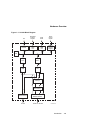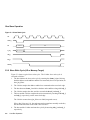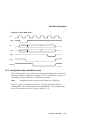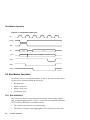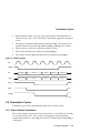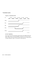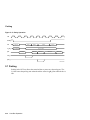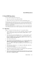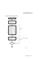
1
DIGITAL Semiconductor 21140A PCI Fast Ethernet LAN Controller Hardware Reference Manual Order Number: EC–QN7NF–TE Revision/Update Information: This is a revised document. It supersedes the DIGITAL Semiconductor 21140A PCI Fast Ethernet LAN Controller Hardware Reference Manual, EC–QN7NE–TE. Digital Equipment Corporation Maynard, Massachusetts http://www.digital.com/semiconductor Important Notice As of May 17, 1998, Digital Equipment Corporation’s StrongARM, PCI Bridge, and Networking component businesses, along with the chip fabrication facility in Hudson, Massachusetts, were acquired by Intel Corporation and transferred to Intel Massachusetts, Inc. As a result of this transaction, certain references to web sites, telephone numbers, and fax numbers have changed in the documentation. This information will be updated in the next version of this manual. Copies of documents that have an ordering number and are referenced in this document, or other Intel literature may be obtained by calling 1-800-332-2717 or by visiting Intel’s website for developers at: http://developer.intel.com The Intel Massachusetts Customer Technology Center continues to service your StrongARM Product, Bridge Product, and Network Product technical inquiries. Please use the following information lines for support: For documentation and general information: Intel Massachusetts Information Line United States: Outside United States: Electronic mail address: 1–800–332–2717 1–303-675-2148 [email protected] For technical support: Intel Massachusetts Customer Technology Center Phone (U.S. and international): Fax: Electronic mail address: 1–978–568–7474 1–978–568–6698 [email protected] March 1998 While DIGITAL believes the information included in this publication is correct as of the date of publication, it is subject to change without notice. Please read the Support, Products, and Documentation section in this document to determine how to obtain current product update and errata information. Digital Equipment Corporation makes no representations that the use of its products in the manner described in this publication will not infringe on existing or future patent rights, nor do the descriptions contained in this publication imply the granting of licenses to make, use, or sell equipment or software in accordance with the description. ©Digital Equipment Corporation 1998. All rights reserved. Printed in U.S.A. DIGITAL, DIGITAL Semiconductor, DNA, and the DIGITAL logo are trademarks of Digital Equipment Corporation. DIGITAL Semiconductor is a Digital Equipment Corporation business. IEEE is a registered trademark of The Institute of Electrical and Electronics Engineers, Inc. MicroWire is a registered trademark of BankAmerica Corporation. All other trademarks and registered trademarks are the property of their respective owners. Contents Preface 1 Introduction 1.1 1.1.1 1.2 2 1–1 1–2 1–3 Signal Descriptions 2.1 2.2 3 General Description . . . . . . . . . . . . . . . . . . . . . . . . . . . . . . . . . . . . . . . . . . . . . . . 21140A Features . . . . . . . . . . . . . . . . . . . . . . . . . . . . . . . . . . . . . . . . . . . . . . Hardware Overview . . . . . . . . . . . . . . . . . . . . . . . . . . . . . . . . . . . . . . . . . . . . . . . 21140A Pinout . . . . . . . . . . . . . . . . . . . . . . . . . . . . . . . . . . . . . . . . . . . . . . . . . . . Signal Descriptions . . . . . . . . . . . . . . . . . . . . . . . . . . . . . . . . . . . . . . . . . . . . . . . . 2–1 2–3 Registers 3.1 Configuration Operation . . . . . . . . . . . . . . . . . . . . . . . . . . . . . . . . . . . . . . . . . . . . 3.1.1 Configuration Register Mapping . . . . . . . . . . . . . . . . . . . . . . . . . . . . . . . . . . 3.1.2 Configuration Registers . . . . . . . . . . . . . . . . . . . . . . . . . . . . . . . . . . . . . . . . . 3.1.2.1 Configuration ID Register (CFID–Offset 00H) . . . . . . . . . . . . . . . . . . . . 3.1.2.2 Command and Status Configuration Register (CFCS–Offset 04H) . . . . 3.1.2.3 Configuration Revision Register (CFRV–Offset 08H). . . . . . . . . . . . . . . 3.1.2.4 Configuration Latency Timer Register (CFLT–Offset 0CH) . . . . . . . . . . 3.1.2.5 Configuration Base I/O Address Register (CBIO—Offset 10H) . . . . . . . 3.1.2.6 Configuration Base Memory Address Register (CBMA–Offset 14H) . . . 3.1.2.7 Subsystem ID Register (SSID–Offset 2CH) . . . . . . . . . . . . . . . . . . . . . . 3.1.2.8 Expansion ROM Base Address Register (CBER–Offset 30H) . . . . . . . . 3.1.2.9 Configuration Interrupt Register (CFIT–Offset 3CH) . . . . . . . . . . . . . . . 3.1.2.10 Configuration Device and Driver Area Register (CFDD–Offset 40H) . . 3.2 CSR Operation . . . . . . . . . . . . . . . . . . . . . . . . . . . . . . . . . . . . . . . . . . . . . . . . . . . 3.2.1 Control and Status Register Mapping . . . . . . . . . . . . . . . . . . . . . . . . . . . . . . 3.2.2 Host CSRs . . . . . . . . . . . . . . . . . . . . . . . . . . . . . . . . . . . . . . . . . . . . . . . . . . . 3–1 3–2 3–2 3–2 3–3 3–6 3–8 3–10 3–11 3–12 3–13 3–14 3–15 3–17 3–17 3–18 iii 3.2.2.1 3.2.2.2 3.2.2.3 3.2.2.4 3.2.2.5 3.2.2.6 3.2.2.7 3.2.2.8 3.2.2.9 3.2.2.10 3.2.2.11 3.2.2.12 3.2.2.13 4 Bus Mode Register (CSR0–Offset 00H). . . . . . . . . . . . . . . . . . . . . . . . . Transmit Poll Demand Register (CSR1–Offset 08H) . . . . . . . . . . . . . . . Receive Poll Demand Register (CSR2–Offset 10H) . . . . . . . . . . . . . . . Descriptor List Address Registers (CSR3–Offset 18H and CSR4–Offset 20H) . . . . . . . . . . . . . . . . . . . . . . . . . . . . . . . . . . . . . . . . . Status Register (CSR5–Offset 28H) . . . . . . . . . . . . . . . . . . . . . . . . . . . . Operation Mode Register (CSR6–Offset 30H) . . . . . . . . . . . . . . . . . . . . Interrupt Enable Register (CSR7–Offset 38H) . . . . . . . . . . . . . . . . . . . . Missed Frames and Overflow Counter (CSR8–Offset 40H) . . . . . . . . . . Boot ROM, Serial ROM, and MII Management Register (CSR9–Offset 48H) . . . . . . . . . . . . . . . . . . . . . . . . . . . . . . . . . . . . . . . . Boot ROM Programming Address Register (CSR10–Offset 50H) . . . . . General-Purpose Timer Register (CSR11–Offset 58H) . . . . . . . . . . . . . General-Purpose Port Register (CSR12–Offset 60H) . . . . . . . . . . . . . . Watchdog Timer Register (CSR1–Offset 78H). . . . . . . . . . . . . . . . . . . . 3–24 3–26 3–31 3–40 3–44 3–46 3–48 3–49 3–50 3–52 Host Communication 4.1 Data Communication . . . . . . . . . . . . . . . . . . . . . . . . . . . . . . . . . . . . . . . . . . . . . . 4.2 Descriptor Lists and Data Buffers . . . . . . . . . . . . . . . . . . . . . . . . . . . . . . . . . . . . . 4.2.1 Receive Descriptors. . . . . . . . . . . . . . . . . . . . . . . . . . . . . . . . . . . . . . . . . . . . 4.2.1.1 Receive Descriptor 0 (RDES0) . . . . . . . . . . . . . . . . . . . . . . . . . . . . . . . . 4.2.1.2 Receive Descriptor 1 (RDES1) . . . . . . . . . . . . . . . . . . . . . . . . . . . . . . . . 4.2.1.3 Receive Descriptor 2 (RDES2) . . . . . . . . . . . . . . . . . . . . . . . . . . . . . . . . 4.2.1.4 Receive Descriptor 3 (RDES3) . . . . . . . . . . . . . . . . . . . . . . . . . . . . . . . . 4.2.1.5 Receive Descriptor Status Validity . . . . . . . . . . . . . . . . . . . . . . . . . . . . . 4.2.2 Transmit Descriptors . . . . . . . . . . . . . . . . . . . . . . . . . . . . . . . . . . . . . . . . . . . 4.2.2.1 Transmit Descriptor 0 (TDES0) . . . . . . . . . . . . . . . . . . . . . . . . . . . . . . . 4.2.2.2 Transmit Descriptor 1 (TDES1) . . . . . . . . . . . . . . . . . . . . . . . . . . . . . . . 4.2.2.3 Transmit Descriptor 2 (TDES2) . . . . . . . . . . . . . . . . . . . . . . . . . . . . . . . 4.2.2.4 Transmit Descriptor 3 (TDES3) . . . . . . . . . . . . . . . . . . . . . . . . . . . . . . . 4.2.2.5 Transmit Descriptor Status Validity . . . . . . . . . . . . . . . . . . . . . . . . . . . . 4.2.3 Setup Frame . . . . . . . . . . . . . . . . . . . . . . . . . . . . . . . . . . . . . . . . . . . . . . . . . 4.2.3.1 First Setup Frame. . . . . . . . . . . . . . . . . . . . . . . . . . . . . . . . . . . . . . . . . . 4.2.3.2 Subsequent Setup Frames . . . . . . . . . . . . . . . . . . . . . . . . . . . . . . . . . . . 4.2.3.3 Perfect Filtering Setup Frame Buffer . . . . . . . . . . . . . . . . . . . . . . . . . . . 4.2.3.4 Imperfect Filtering Setup Frame Buffer . . . . . . . . . . . . . . . . . . . . . . . . . 4.3 Functional Description . . . . . . . . . . . . . . . . . . . . . . . . . . . . . . . . . . . . . . . . . . . . . 4.3.1 Reset Commands . . . . . . . . . . . . . . . . . . . . . . . . . . . . . . . . . . . . . . . . . . . . . 4.3.2 Arbitration Scheme . . . . . . . . . . . . . . . . . . . . . . . . . . . . . . . . . . . . . . . . . . . . 4.3.3 Interrupts . . . . . . . . . . . . . . . . . . . . . . . . . . . . . . . . . . . . . . . . . . . . . . . . . . . . 4.3.4 Startup Procedure . . . . . . . . . . . . . . . . . . . . . . . . . . . . . . . . . . . . . . . . . . . . . 4.3.5 Receive Process . . . . . . . . . . . . . . . . . . . . . . . . . . . . . . . . . . . . . . . . . . . . . . 4.3.5.1 Descriptor Acquisition . . . . . . . . . . . . . . . . . . . . . . . . . . . . . . . . . . . . . . . 4.3.5.2 Frame Processing . . . . . . . . . . . . . . . . . . . . . . . . . . . . . . . . . . . . . . . . . iv 3–18 3–22 3–23 4–1 4–1 4–3 4–3 4–8 4–9 4–10 4–10 4–12 4–13 4–16 4–18 4–19 4–19 4–20 4–21 4–21 4–21 4–24 4–30 4–30 4–31 4–33 4–34 4–35 4–35 4–35 4.3.5.3 4.3.5.4 4.3.6 4.3.6.1 4.3.6.2 4.3.6.3 5 Receive Process Suspended . . . . . . . . . . . . . . . . . . . . . . . . . . . . . . . . . Receive Process State Transitions. . . . . . . . . . . . . . . . . . . . . . . . . . . . . Transmit Process . . . . . . . . . . . . . . . . . . . . . . . . . . . . . . . . . . . . . . . . . . . . . . Frame Processing . . . . . . . . . . . . . . . . . . . . . . . . . . . . . . . . . . . . . . . . . Transmit Polling Suspended. . . . . . . . . . . . . . . . . . . . . . . . . . . . . . . . . . Transmit Process State Transitions . . . . . . . . . . . . . . . . . . . . . . . . . . . . Host Bus Operation 5.1 Overview . . . . . . . . . . . . . . . . . . . . . . . . . . . . . . . . . . . . . . . . . . . . . . . . . . . . . . . . 5.2 Bus Commands . . . . . . . . . . . . . . . . . . . . . . . . . . . . . . . . . . . . . . . . . . . . . . . . . . 5.3 Bus Slave Operation . . . . . . . . . . . . . . . . . . . . . . . . . . . . . . . . . . . . . . . . . . . . . . . 5.3.1 Slave Read Cycle (I/O or Memory Target). . . . . . . . . . . . . . . . . . . . . . . . . . . 5.3.2 Slave Write Cycle (I/O or Memory Target). . . . . . . . . . . . . . . . . . . . . . . . . . . 5.3.3 Configuration Read and Write Cycles . . . . . . . . . . . . . . . . . . . . . . . . . . . . . . 5.4 Bus Master Operation . . . . . . . . . . . . . . . . . . . . . . . . . . . . . . . . . . . . . . . . . . . . . . 5.4.1 Bus Arbitration . . . . . . . . . . . . . . . . . . . . . . . . . . . . . . . . . . . . . . . . . . . . . . . . 5.4.2 Memory Read Cycle . . . . . . . . . . . . . . . . . . . . . . . . . . . . . . . . . . . . . . . . . . . 5.4.3 Memory Write Cycle . . . . . . . . . . . . . . . . . . . . . . . . . . . . . . . . . . . . . . . . . . . 5.5 Termination Cycles . . . . . . . . . . . . . . . . . . . . . . . . . . . . . . . . . . . . . . . . . . . . . . . . 5.5.1 Slave-Initiated Termination . . . . . . . . . . . . . . . . . . . . . . . . . . . . . . . . . . . . . . 5.5.2 Master-Initiated Termination . . . . . . . . . . . . . . . . . . . . . . . . . . . . . . . . . . . . . 5.5.2.1 21140A-Initiated Termination . . . . . . . . . . . . . . . . . . . . . . . . . . . . . . . . . 5.5.2.1.1 Normal Completion . . . . . . . . . . . . . . . . . . . . . . . . . . . . . . . . . . . . . 5.5.2.1.2 Timeout . . . . . . . . . . . . . . . . . . . . . . . . . . . . . . . . . . . . . . . . . . . . . . 5.5.2.1.3 Master Abort . . . . . . . . . . . . . . . . . . . . . . . . . . . . . . . . . . . . . . . . . . 5.5.2.2 Memory-Controller-Initiated Termination . . . . . . . . . . . . . . . . . . . . . . . . 5.5.2.2.1 Target Abort . . . . . . . . . . . . . . . . . . . . . . . . . . . . . . . . . . . . . . . . . . 5.5.2.2.2 Target Disconnect Termination . . . . . . . . . . . . . . . . . . . . . . . . . . . . 5.5.2.2.3 Target Retry . . . . . . . . . . . . . . . . . . . . . . . . . . . . . . . . . . . . . . . . . . 5.6 Parity. . . . . . . . . . . . . . . . . . . . . . . . . . . . . . . . . . . . . . . . . . . . . . . . . . . . . . . . . . . 5.7 Parking . . . . . . . . . . . . . . . . . . . . . . . . . . . . . . . . . . . . . . . . . . . . . . . . . . . . . . . . . 6 4–36 4–36 4–37 4–37 4–38 4–39 5–1 5–2 5–2 5–3 5–4 5–5 5–6 5–6 5–7 5–8 5–9 5–9 5–10 5–11 5–11 5–11 5–11 5–12 5–12 5–13 5–14 5–15 5–16 Network Interface Operation 6.1 MII/SYM Port. . . . . . . . . . . . . . . . . . . . . . . . . . . . . . . . . . . . . . . . . . . . . . . . . . . . . 6.1.1 100BASE-T Terminology . . . . . . . . . . . . . . . . . . . . . . . . . . . . . . . . . . . . . . . . 6.1.2 Interface Description . . . . . . . . . . . . . . . . . . . . . . . . . . . . . . . . . . . . . . . . . . . 6.1.2.1 Signal Standards . . . . . . . . . . . . . . . . . . . . . . . . . . . . . . . . . . . . . . . . . . 6.1.2.2 Operating Modes . . . . . . . . . . . . . . . . . . . . . . . . . . . . . . . . . . . . . . . . . . 6.2 Serial Port . . . . . . . . . . . . . . . . . . . . . . . . . . . . . . . . . . . . . . . . . . . . . . . . . . . . . . . 6.3 Media Access Control Operation . . . . . . . . . . . . . . . . . . . . . . . . . . . . . . . . . . . . . 6.3.1 MAC Frame Format . . . . . . . . . . . . . . . . . . . . . . . . . . . . . . . . . . . . . . . . . . . . 6.3.1.1 Ethernet and IEEE 802.3 Frames. . . . . . . . . . . . . . . . . . . . . . . . . . . . . . 6–1 6–1 6–2 6–3 6–4 6–6 6–6 6–7 6–8 v 6.3.1.2 Ethernet Frame Format Description . . . . . . . . . . . . . . . . . . . . . . . . . . . . 6.3.2 Ethernet Reception Addressing . . . . . . . . . . . . . . . . . . . . . . . . . . . . . . . . . . . 6.3.3 Detailed Transmit Operation . . . . . . . . . . . . . . . . . . . . . . . . . . . . . . . . . . . . . 6.3.3.1 Transmit Initiation . . . . . . . . . . . . . . . . . . . . . . . . . . . . . . . . . . . . . . . . . . 6.3.3.2 Frame Encapsulation . . . . . . . . . . . . . . . . . . . . . . . . . . . . . . . . . . . . . . . 6.3.3.3 Initial Deferral . . . . . . . . . . . . . . . . . . . . . . . . . . . . . . . . . . . . . . . . . . . . . 6.3.3.4 Collision . . . . . . . . . . . . . . . . . . . . . . . . . . . . . . . . . . . . . . . . . . . . . . . . . 6.3.3.5 Terminating Transmission . . . . . . . . . . . . . . . . . . . . . . . . . . . . . . . . . . . 6.3.3.6 Transmit Parameter Values . . . . . . . . . . . . . . . . . . . . . . . . . . . . . . . . . . 6.3.4 Detailed Receive Operation . . . . . . . . . . . . . . . . . . . . . . . . . . . . . . . . . . . . . . 6.3.4.1 Receive Initiation . . . . . . . . . . . . . . . . . . . . . . . . . . . . . . . . . . . . . . . . . . 6.3.4.2 Preamble Processing . . . . . . . . . . . . . . . . . . . . . . . . . . . . . . . . . . . . . . . 6.3.4.2.1 MII or Serial Mode Preambles . . . . . . . . . . . . . . . . . . . . . . . . . . . . . 6.3.4.2.2 100BASE-TX or 100BASE-FX Mode Preambles . . . . . . . . . . . . . . 6.3.4.3 Address Matching. . . . . . . . . . . . . . . . . . . . . . . . . . . . . . . . . . . . . . . . . . 6.3.4.4 Frame Decapsulation . . . . . . . . . . . . . . . . . . . . . . . . . . . . . . . . . . . . . . . 6.3.4.5 Terminating Reception . . . . . . . . . . . . . . . . . . . . . . . . . . . . . . . . . . . . . . 6.3.4.6 Frame Reception Status. . . . . . . . . . . . . . . . . . . . . . . . . . . . . . . . . . . . . 6.4 Loopback Operations . . . . . . . . . . . . . . . . . . . . . . . . . . . . . . . . . . . . . . . . . . . . . . 6.4.1 Internal Loopback Mode . . . . . . . . . . . . . . . . . . . . . . . . . . . . . . . . . . . . . . . . 6.4.2 External Loopback Mode . . . . . . . . . . . . . . . . . . . . . . . . . . . . . . . . . . . . . . . . 6.5 Full-Duplex Operation . . . . . . . . . . . . . . . . . . . . . . . . . . . . . . . . . . . . . . . . . . . . . . 6.6 Capture Effect–A Value-Added Feature . . . . . . . . . . . . . . . . . . . . . . . . . . . . . . . . 6.6.1 What Is Capture Effect?. . . . . . . . . . . . . . . . . . . . . . . . . . . . . . . . . . . . . . . . . 6.6.2 Resolving Capture Effect . . . . . . . . . . . . . . . . . . . . . . . . . . . . . . . . . . . . . . . . 6.6.3 Enhanced Resolution for Capture Effect . . . . . . . . . . . . . . . . . . . . . . . . . . . . 6.7 Power-Saving Modes . . . . . . . . . . . . . . . . . . . . . . . . . . . . . . . . . . . . . . . . . . . . . . 6.7.1 Sleep Power-Saving Mode . . . . . . . . . . . . . . . . . . . . . . . . . . . . . . . . . . . . . . 6.7.2 Snooze Power-Saving Mode . . . . . . . . . . . . . . . . . . . . . . . . . . . . . . . . . . . . . 6.8 Jabber and Watchdog Timers . . . . . . . . . . . . . . . . . . . . . . . . . . . . . . . . . . . . . . . . 7 External Ports 7.1 7.2 7.3 7.3.1 7.3.2 7.3.3 7.4 7.4.1 7.4.2 7.5 7.6 7.7 vi 6–8 6–10 6–11 6–11 6–12 6–12 6–13 6–14 6–14 6–15 6–15 6–15 6–15 6–16 6–17 6–17 6–17 6–18 6–19 6–19 6–19 6–19 6–20 6–20 6–22 6–22 6–22 6–23 6–23 6–24 Overview . . . . . . . . . . . . . . . . . . . . . . . . . . . . . . . . . . . . . . . . . . . . . . . . . . . . . . . . Boot ROM and Serial ROM Connection . . . . . . . . . . . . . . . . . . . . . . . . . . . . . . . . Boot ROM Operations. . . . . . . . . . . . . . . . . . . . . . . . . . . . . . . . . . . . . . . . . . . . . . Byte Read . . . . . . . . . . . . . . . . . . . . . . . . . . . . . . . . . . . . . . . . . . . . . . . . . . . Byte Write . . . . . . . . . . . . . . . . . . . . . . . . . . . . . . . . . . . . . . . . . . . . . . . . . . . Dword Read . . . . . . . . . . . . . . . . . . . . . . . . . . . . . . . . . . . . . . . . . . . . . . . . . . Serial ROM Operations . . . . . . . . . . . . . . . . . . . . . . . . . . . . . . . . . . . . . . . . . . . . . Read Operation . . . . . . . . . . . . . . . . . . . . . . . . . . . . . . . . . . . . . . . . . . . . . . . Write Operation . . . . . . . . . . . . . . . . . . . . . . . . . . . . . . . . . . . . . . . . . . . . . . . External Register Operation . . . . . . . . . . . . . . . . . . . . . . . . . . . . . . . . . . . . . . . . . General-Purpose Port Register (CSR12) . . . . . . . . . . . . . . . . . . . . . . . . . . . . . . . LED Support . . . . . . . . . . . . . . . . . . . . . . . . . . . . . . . . . . . . . . . . . . . . . . . . . . . . . 7–1 7–1 7–3 7–3 7–4 7–5 7–6 7–7 7–10 7–13 7–14 7–14 A Joint Test Action Group—Test Logic A.1 A.2 A.2.1 A.2.2 A.2.3 A.2.4 General Description . . . . . . . . . . . . . . . . . . . . . . . . . . . . . . . . . . . . . . . . . . . . . . . Registers . . . . . . . . . . . . . . . . . . . . . . . . . . . . . . . . . . . . . . . . . . . . . . . . . . . . . . . . Instruction Register . . . . . . . . . . . . . . . . . . . . . . . . . . . . . . . . . . . . . . . . . . . . Bypass Register. . . . . . . . . . . . . . . . . . . . . . . . . . . . . . . . . . . . . . . . . . . . . . . Boundary-Scan Register . . . . . . . . . . . . . . . . . . . . . . . . . . . . . . . . . . . . . . . . Test Access Port Controller . . . . . . . . . . . . . . . . . . . . . . . . . . . . . . . . . . . . . . B DNA CSMA/CD Counters and Events Support C Hash C Routine D Support, Products, and Documentation A–1 A–2 A–2 A–3 A–4 A–4 Index vii Examples 4–1 Perfect Filtering Buffer ......................................................................................... 4–23 4–2 Imperfect Filtering Buffer .................................................................................... 4–26 viii Figures 1–1 2–1 3–1 3–2 3–3 3–4 3–5 3–6 3–7 3–8 3–9 3–10 3–11 3–12 3–13 3–14 3–15 3–16 3–17 3–18 3–19 3–20 3–21 3–22 3–23 3–24 4–1 4–2 4–3 4–4 4–5 4–6 4–7 4–8 4–9 4–10 4–11 4–12 4–13 4–14 5–1 5–2 5–3 5–4 21140A Block Diagram . . . . . . . . . . . . . . . . . . . . . . . . . . . . . . . . . . . . . . . . . . . . . 21140A Pinout Diagram (Top View) . . . . . . . . . . . . . . . . . . . . . . . . . . . . . . . . . . . CFID Configuration ID Register . . . . . . . . . . . . . . . . . . . . . . . . . . . . . . . . . . . . . . CFCS Command and Status Configuration Register . . . . . . . . . . . . . . . . . . . . . . CFRV Configuration Revision Register. . . . . . . . . . . . . . . . . . . . . . . . . . . . . . . . . CFLT Configuration Latency Timer Register. . . . . . . . . . . . . . . . . . . . . . . . . . . . . CBIO Configuration Base I/O Address Register . . . . . . . . . . . . . . . . . . . . . . . . . . CBMA Configuration Base Memory Address Register . . . . . . . . . . . . . . . . . . . . . SSID Subsystem ID Register . . . . . . . . . . . . . . . . . . . . . . . . . . . . . . . . . . . . . . . . CBER Expansion ROM Base Address Register . . . . . . . . . . . . . . . . . . . . . . . . . . CFIT Configuration Interrupt Register . . . . . . . . . . . . . . . . . . . . . . . . . . . . . . . . . . CFDD Configuration Driver Area Register . . . . . . . . . . . . . . . . . . . . . . . . . . . . . . CSR0 Bus Mode Register . . . . . . . . . . . . . . . . . . . . . . . . . . . . . . . . . . . . . . . . . . . CSR1 Transmit Poll Demand Register . . . . . . . . . . . . . . . . . . . . . . . . . . . . . . . . . CSR2 Receive Poll Demand Register . . . . . . . . . . . . . . . . . . . . . . . . . . . . . . . . . CSR3 Receive List Base Address Register . . . . . . . . . . . . . . . . . . . . . . . . . . . . . CSR4 Transmit List Base Address Register . . . . . . . . . . . . . . . . . . . . . . . . . . . . . CSR5 Status Register. . . . . . . . . . . . . . . . . . . . . . . . . . . . . . . . . . . . . . . . . . . . . . CSR6 Operating Mode Register . . . . . . . . . . . . . . . . . . . . . . . . . . . . . . . . . . . . . . CSR7 Interrupt Enable Register . . . . . . . . . . . . . . . . . . . . . . . . . . . . . . . . . . . . . . CSR8 Missed Frames and Overflow Counter . . . . . . . . . . . . . . . . . . . . . . . . . . . . CSR9 Boot ROM, Serial ROM, and MII Management Register . . . . . . . . . . . . . . CSR10 Boot ROM Programming Address Register . . . . . . . . . . . . . . . . . . . . . . . CSR11 General-Purpose Timer Register . . . . . . . . . . . . . . . . . . . . . . . . . . . . . . . CSR12 General-Purpose Port Register . . . . . . . . . . . . . . . . . . . . . . . . . . . . . . . . CSR15 Watchdog Timer Register. . . . . . . . . . . . . . . . . . . . . . . . . . . . . . . . . . . . . Descriptor Ring and Chain Structure Examples . . . . . . . . . . . . . . . . . . . . . . . . . . Receive Descriptor Format . . . . . . . . . . . . . . . . . . . . . . . . . . . . . . . . . . . . . . . . . . RDES0 Receive Descriptor 0 . . . . . . . . . . . . . . . . . . . . . . . . . . . . . . . . . . . . . . . . RDES1 Receive Descriptor 1 . . . . . . . . . . . . . . . . . . . . . . . . . . . . . . . . . . . . . . . . RDES2 Receive Descriptor 2 . . . . . . . . . . . . . . . . . . . . . . . . . . . . . . . . . . . . . . . . RDES3 Receive Descriptor 3 . . . . . . . . . . . . . . . . . . . . . . . . . . . . . . . . . . . . . . . . Transmit Descriptor Format . . . . . . . . . . . . . . . . . . . . . . . . . . . . . . . . . . . . . . . . . TDES0 Transmit Descriptor 0 . . . . . . . . . . . . . . . . . . . . . . . . . . . . . . . . . . . . . . . . TDES1 Transmit Descriptor 1 . . . . . . . . . . . . . . . . . . . . . . . . . . . . . . . . . . . . . . . . TDES2 Transmit Descriptor 2 . . . . . . . . . . . . . . . . . . . . . . . . . . . . . . . . . . . . . . . . TDES3 Transmit Descriptor 3 . . . . . . . . . . . . . . . . . . . . . . . . . . . . . . . . . . . . . . . . Perfect Filtering Setup Frame Buffer Format . . . . . . . . . . . . . . . . . . . . . . . . . . . . Imperfect Filtering . . . . . . . . . . . . . . . . . . . . . . . . . . . . . . . . . . . . . . . . . . . . . . . . . Imperfect Filtering Setup Frame Format . . . . . . . . . . . . . . . . . . . . . . . . . . . . . . . . Slave Read Cycle . . . . . . . . . . . . . . . . . . . . . . . . . . . . . . . . . . . . . . . . . . . . . . . . . Slave Write Cycle . . . . . . . . . . . . . . . . . . . . . . . . . . . . . . . . . . . . . . . . . . . . . . . . . Configuration Read Cycle . . . . . . . . . . . . . . . . . . . . . . . . . . . . . . . . . . . . . . . . . . . Bus Arbitration . . . . . . . . . . . . . . . . . . . . . . . . . . . . . . . . . . . . . . . . . . . . . . . . . . . 1–5 2–2 3–2 3–4 3–7 3–8 3–10 3–11 3–12 3–13 3–14 3–15 3–18 3–22 3–23 3–24 3–25 3–26 3–32 3–41 3–45 3–46 3–49 3–50 3–51 3–52 4–2 4–3 4–4 4–8 4–9 4–10 4–12 4–13 4–16 4–19 4–19 4–22 4–24 4–25 5–4 5–5 5–6 5–7 ix 5–5 5–6 5–7 5–8 5–9 5–10 5–11 5–12 5–13 6–1 6–2 7–1 7–2 7–3 7–4 7–5 7–6 7–7 7–8 7–9 7–10 x Memory Read Cycle . . . . . . . . . . . . . . . . . . . . . . . . . . . . . . . . . . . . . . . . . . . . . . . Memory Write . . . . . . . . . . . . . . . . . . . . . . . . . . . . . . . . . . . . . . . . . . . . . . . . . . . . 21140A-Initiated Retry Cycle . . . . . . . . . . . . . . . . . . . . . . . . . . . . . . . . . . . . . . . . Normal Completion . . . . . . . . . . . . . . . . . . . . . . . . . . . . . . . . . . . . . . . . . . . . . . . . Master Abort . . . . . . . . . . . . . . . . . . . . . . . . . . . . . . . . . . . . . . . . . . . . . . . . . . . . . Target Abort . . . . . . . . . . . . . . . . . . . . . . . . . . . . . . . . . . . . . . . . . . . . . . . . . . . . . Target Disconnect . . . . . . . . . . . . . . . . . . . . . . . . . . . . . . . . . . . . . . . . . . . . . . . . . Target Retry . . . . . . . . . . . . . . . . . . . . . . . . . . . . . . . . . . . . . . . . . . . . . . . . . . . . . Parity Operation . . . . . . . . . . . . . . . . . . . . . . . . . . . . . . . . . . . . . . . . . . . . . . . . . . Ethernet Frame Format. . . . . . . . . . . . . . . . . . . . . . . . . . . . . . . . . . . . . . . . . . . . . Preamble Recognition Sequence in SRL Mode . . . . . . . . . . . . . . . . . . . . . . . . . . Boot ROM, Serial ROM, and External Register Connection . . . . . . . . . . . . . . . . . Boot ROM Byte Read Cycle . . . . . . . . . . . . . . . . . . . . . . . . . . . . . . . . . . . . . . . . . Boot ROM Byte Write Cycle . . . . . . . . . . . . . . . . . . . . . . . . . . . . . . . . . . . . . . . . . Boot ROM Dword Read Cycle . . . . . . . . . . . . . . . . . . . . . . . . . . . . . . . . . . . . . . . Read Cycle (Page 1 of 2) . . . . . . . . . . . . . . . . . . . . . . . . . . . . . . . . . . . . . . . . . . . Read Cycle (Page 2 of 2) . . . . . . . . . . . . . . . . . . . . . . . . . . . . . . . . . . . . . . . . . . . Read Operation. . . . . . . . . . . . . . . . . . . . . . . . . . . . . . . . . . . . . . . . . . . . . . . . . . . Write Cycle (Page 1 of 2) . . . . . . . . . . . . . . . . . . . . . . . . . . . . . . . . . . . . . . . . . . . Write Cycle (Page 2 of 2) . . . . . . . . . . . . . . . . . . . . . . . . . . . . . . . . . . . . . . . . . . . Write Operation . . . . . . . . . . . . . . . . . . . . . . . . . . . . . . . . . . . . . . . . . . . . . . . . . . . 5–8 5–9 5–10 5–11 5–12 5–13 5–14 5–15 5–16 6–8 6–16 7–2 7–4 7–5 7–6 7–8 7–9 7–10 7–11 7–12 7–13 Tables 2–1 3–1 3–2 3–3 3–4 3–5 3–6 3–7 3–8 3–9 3–10 3–11 3–12 3–13 3–14 3–15 3–16 3–17 3–18 3–19 3–20 3–21 3–22 3–23 3–24 3–25 3–26 3–27 3–28 3–29 3–30 3–31 3–32 3–33 3–34 3–35 3–36 3–37 3–38 3–39 3–40 3–41 3–42 3–43 Functional Description of 21140A Signals . . . . . . . . . . . . . . . . . . . . . . . . . . . . . . Configuration Registers Mapping . . . . . . . . . . . . . . . . . . . . . . . . . . . . . . . . . . . . . CFID Configuration ID Register Description . . . . . . . . . . . . . . . . . . . . . . . . . . . . . CFID Access Rules. . . . . . . . . . . . . . . . . . . . . . . . . . . . . . . . . . . . . . . . . . . . . . . . CFCS Command and Status Configuration Register Description. . . . . . . . . . . . . CFSC Access Rules . . . . . . . . . . . . . . . . . . . . . . . . . . . . . . . . . . . . . . . . . . . . . . . CFRV Configuration Revision Register Description . . . . . . . . . . . . . . . . . . . . . . . 21140A Revision and Step Number . . . . . . . . . . . . . . . . . . . . . . . . . . . . . . . . . . . CFRV Access Rules . . . . . . . . . . . . . . . . . . . . . . . . . . . . . . . . . . . . . . . . . . . . . . . CFLT Configuration Latency Timer Register Description . . . . . . . . . . . . . . . . . . . CFLT Access Rules . . . . . . . . . . . . . . . . . . . . . . . . . . . . . . . . . . . . . . . . . . . . . . . CBIO Configuration Base I/O Address Register Description . . . . . . . . . . . . . . . . CBIO Access Rules . . . . . . . . . . . . . . . . . . . . . . . . . . . . . . . . . . . . . . . . . . . . . . . CBMA Configuration Base Memory Address Register Description. . . . . . . . . . . . CBMA Access Rules . . . . . . . . . . . . . . . . . . . . . . . . . . . . . . . . . . . . . . . . . . . . . . . SSID Subsystem ID Register Description . . . . . . . . . . . . . . . . . . . . . . . . . . . . . . . SSID Access Rules. . . . . . . . . . . . . . . . . . . . . . . . . . . . . . . . . . . . . . . . . . . . . . . . CBER Expansion ROM Base Address Register Description . . . . . . . . . . . . . . . . CBER Access Rules . . . . . . . . . . . . . . . . . . . . . . . . . . . . . . . . . . . . . . . . . . . . . . . CFIT Configuration Interrupt Register Description . . . . . . . . . . . . . . . . . . . . . . . . CFIT Access Rules . . . . . . . . . . . . . . . . . . . . . . . . . . . . . . . . . . . . . . . . . . . . . . . . CFDD Configuration Driver Area Register Description . . . . . . . . . . . . . . . . . . . . . CFDD Access Rules . . . . . . . . . . . . . . . . . . . . . . . . . . . . . . . . . . . . . . . . . . . . . . . CSR Mapping . . . . . . . . . . . . . . . . . . . . . . . . . . . . . . . . . . . . . . . . . . . . . . . . . . . . CSR0 Bus Mode Register Description . . . . . . . . . . . . . . . . . . . . . . . . . . . . . . . . . Transmit Automatic Polling Intervals. . . . . . . . . . . . . . . . . . . . . . . . . . . . . . . . . . . CSR0 Access Rules . . . . . . . . . . . . . . . . . . . . . . . . . . . . . . . . . . . . . . . . . . . . . . . Cache Alignment Bits . . . . . . . . . . . . . . . . . . . . . . . . . . . . . . . . . . . . . . . . . . . . . . CSR1 Transmit Poll Demand Register Description . . . . . . . . . . . . . . . . . . . . . . . CSR1 Access Rules . . . . . . . . . . . . . . . . . . . . . . . . . . . . . . . . . . . . . . . . . . . . . . . CSR2 Receive Poll Demand Register Description. . . . . . . . . . . . . . . . . . . . . . . . CSR2 Access Rules . . . . . . . . . . . . . . . . . . . . . . . . . . . . . . . . . . . . . . . . . . . . . . . CSR3 Receive List Base Address Register Description . . . . . . . . . . . . . . . . . . . . CSR3 Access Rules . . . . . . . . . . . . . . . . . . . . . . . . . . . . . . . . . . . . . . . . . . . . . . . CSR4 Transmit List Base Address Register Description . . . . . . . . . . . . . . . . . . . CSR4 Access Rules . . . . . . . . . . . . . . . . . . . . . . . . . . . . . . . . . . . . . . . . . . . . . . . CSR5 Status Register Description . . . . . . . . . . . . . . . . . . . . . . . . . . . . . . . . . . . . Fatal Bus Error Bits. . . . . . . . . . . . . . . . . . . . . . . . . . . . . . . . . . . . . . . . . . . . . . . . Transmit Process State. . . . . . . . . . . . . . . . . . . . . . . . . . . . . . . . . . . . . . . . . . . . . Receive Process State . . . . . . . . . . . . . . . . . . . . . . . . . . . . . . . . . . . . . . . . . . . . . CSR5 Access Rules . . . . . . . . . . . . . . . . . . . . . . . . . . . . . . . . . . . . . . . . . . . . . . . CSR6 Operating Mode Register Description . . . . . . . . . . . . . . . . . . . . . . . . . . . . Transmit Threshold . . . . . . . . . . . . . . . . . . . . . . . . . . . . . . . . . . . . . . . . . . . . . . . . Port and Data Rate Selection . . . . . . . . . . . . . . . . . . . . . . . . . . . . . . . . . . . . . . . . 2–4 3–2 3–3 3–3 3–4 3–6 3–7 3–7 3–8 3–9 3–9 3–10 3–10 3–11 3–11 3–12 3–12 3–13 3–13 3–14 3–15 3–16 3–16 3–17 3–19 3–21 3–22 3–22 3–23 3–23 3–23 3–24 3–24 3–25 3–25 3–25 3–27 3–29 3–30 3–30 3–31 3–33 3–38 3–38 xi 3–44 3–45 3–46 3–47 3–48 3–49 3–50 3–51 3–52 3–53 3–54 3–55 3–56 3–57 3–58 3–59 3–60 4–1 4–2 4–3 4–4 4–5 4–6 4–7 4–8 4–9 4–10 4–11 4–12 4–13 4–14 5–1 6–1 6–2 6–3 6–4 6–5 6–6 6–7 6–8 7–1 A–1 A–2 B–1 xii Loopback Operation . . . . . . . . . . . . . . . . . . . . . . . . . . . . . . . . . . . . . . . . . . . . . . . Filtering Mode . . . . . . . . . . . . . . . . . . . . . . . . . . . . . . . . . . . . . . . . . . . . . . . . . . . . CSR6 Access Rules . . . . . . . . . . . . . . . . . . . . . . . . . . . . . . . . . . . . . . . . . . . . . . . CSR7 Interrupt Enable Register Description. . . . . . . . . . . . . . . . . . . . . . . . . . . . . CSR7 Access Rules . . . . . . . . . . . . . . . . . . . . . . . . . . . . . . . . . . . . . . . . . . . . . . . CSR8 Missed Frames and Overflow Counter Description . . . . . . . . . . . . . . . . . . CSR8 Access Rules . . . . . . . . . . . . . . . . . . . . . . . . . . . . . . . . . . . . . . . . . . . . . . . CSR9 Boot ROM, Serial ROM, and MII Management RegisterDescription . . . . . CSR9 Access Rules . . . . . . . . . . . . . . . . . . . . . . . . . . . . . . . . . . . . . . . . . . . . . . . CSR10 Boot ROM Programming Address Description . . . . . . . . . . . . . . . . . . . . . CSR10 Access Rules . . . . . . . . . . . . . . . . . . . . . . . . . . . . . . . . . . . . . . . . . . . . . . CSR11 General-Purpose Timer Register Description. . . . . . . . . . . . . . . . . . . . . . CSR11 Access Rules . . . . . . . . . . . . . . . . . . . . . . . . . . . . . . . . . . . . . . . . . . . . . . CSR12 General-Purpose Port Register Description . . . . . . . . . . . . . . . . . . . . . . . CSR12 Access Rules . . . . . . . . . . . . . . . . . . . . . . . . . . . . . . . . . . . . . . . . . . . . . . CSR15 Watchdog Timer Register Description . . . . . . . . . . . . . . . . . . . . . . . . . . . CSR15 Access Rules . . . . . . . . . . . . . . . . . . . . . . . . . . . . . . . . . . . . . . . . . . . . . . RDES0 Receive Descriptor 0 Description. . . . . . . . . . . . . . . . . . . . . . . . . . . . . . . RDES1 Receive Descriptor 1 Description. . . . . . . . . . . . . . . . . . . . . . . . . . . . . . . RDES2 Receive Descriptor 2 Description. . . . . . . . . . . . . . . . . . . . . . . . . . . . . . . RDES3 Receive Descriptor 3 Description. . . . . . . . . . . . . . . . . . . . . . . . . . . . . . . Receive Descriptor Status Validity . . . . . . . . . . . . . . . . . . . . . . . . . . . . . . . . . . . . TDES0 Transmit Descriptor 0 Description . . . . . . . . . . . . . . . . . . . . . . . . . . . . . . TDES1 Transmit Descriptor 1 Description . . . . . . . . . . . . . . . . . . . . . . . . . . . . . . Filtering Type . . . . . . . . . . . . . . . . . . . . . . . . . . . . . . . . . . . . . . . . . . . . . . . . . . . . TDES2 Transmit Descriptor 2 Description . . . . . . . . . . . . . . . . . . . . . . . . . . . . . . TDES3 Transmit Descriptor 3 Description . . . . . . . . . . . . . . . . . . . . . . . . . . . . . . Transmit Descriptor Status Validity . . . . . . . . . . . . . . . . . . . . . . . . . . . . . . . . . . . . Arbitration Scheme . . . . . . . . . . . . . . . . . . . . . . . . . . . . . . . . . . . . . . . . . . . . . . . . Receive Process State Transitions . . . . . . . . . . . . . . . . . . . . . . . . . . . . . . . . . . . . Transmit Process State Transitions . . . . . . . . . . . . . . . . . . . . . . . . . . . . . . . . . . . Bus Commands . . . . . . . . . . . . . . . . . . . . . . . . . . . . . . . . . . . . . . . . . . . . . . . . . . IEEE 802.3 and MII/SYM Signals . . . . . . . . . . . . . . . . . . . . . . . . . . . . . . . . . . . . . Ethernet Frame Format. . . . . . . . . . . . . . . . . . . . . . . . . . . . . . . . . . . . . . . . . . . . . Frame Format . . . . . . . . . . . . . . . . . . . . . . . . . . . . . . . . . . . . . . . . . . . . . . . . . . . . Ethernet Receive Address Groups . . . . . . . . . . . . . . . . . . . . . . . . . . . . . . . . . . . . Transmit Parameter Values . . . . . . . . . . . . . . . . . . . . . . . . . . . . . . . . . . . . . . . . . Destination Address Bit 1 . . . . . . . . . . . . . . . . . . . . . . . . . . . . . . . . . . . . . . . . . . . Capture-Effect Sequence . . . . . . . . . . . . . . . . . . . . . . . . . . . . . . . . . . . . . . . . . . . 2–0 Backoff Algorithm . . . . . . . . . . . . . . . . . . . . . . . . . . . . . . . . . . . . . . . . . . . . . . LED Connection . . . . . . . . . . . . . . . . . . . . . . . . . . . . . . . . . . . . . . . . . . . . . . . . . . JTAG Test Logic Connection Requirements. . . . . . . . . . . . . . . . . . . . . . . . . . . . . Instruction Register . . . . . . . . . . . . . . . . . . . . . . . . . . . . . . . . . . . . . . . . . . . . . . . . CSMA/CD Counters . . . . . . . . . . . . . . . . . . . . . . . . . . . . . . . . . . . . . . . . . . . . . . . 3–39 3–39 3–40 3–42 3–44 3–45 3–45 3–46 3–48 3–49 3–49 3–50 3–50 3–51 3–52 3–53 3–54 4–5 4–9 4–10 4–10 4–11 4–14 4–16 4–18 4–19 4–19 4–20 4–32 4–36 4–39 5–2 6–3 6–8 6–9 6–10 6–14 6–17 6–21 6–22 7–14 A–1 A–3 B–1 Preface Purpose and Audience The DIGITAL Semiconductor 21140A PCI Fast Ethernet LAN Controller Hardware Reference Manual describes the operation of the DIGITAL Semiconductor 21140A PCI Fast Ethernet LAN Controller (also referred to as the 21140A). This manual is for designers who use the 21140A. Manual Organization This manual contains seven chapters, four appendixes, and an index. • Chapter 1, Introduction, includes a general description of the 21140A. It also provides an overview of the 21140A hardware components. • Chapter 2, Signal Descriptions, provides the physical layout of the 21140A and describes each of the input and output signals. • Chapter 3, Registers, provides a complete bit description of the 21140A control and status registers (CSRs) and the configuration registers. • Chapter 4, Host Communication, describes how the 21140A communicates with the host by using descriptor lists and data buffers. It also describes the transmit and receive processes. • Chapter 5, Host Bus Operation, provides a description of the read, write, and termination cycles. • Chapter 6, Network Interface Operation, describes the MII/SYM port and serial port interfaces. It includes a complete description of media access control (MAC) operations. It also provides detailed transmitting and receiving operation information. xiii • Chapter 7, External Ports, describes the interface and operation of the MicroWire serial ROM, the boot ROM, the general-purpose port, and the network activity LEDs. • Appendix A, Joint Test Action Group—Test Logic, provides descriptions of the testing, the observing, and the modifying of circuit activity during normal operation. • Appendix B, DNA CSMA/CD Counters and Events Support, describes features that support the driver in implementing and reporting the specified counters and events. • Appendix C, Hash C Routine, provides an example of a C routine that generates a hash index for a given Ethernet address. • Appendix D, Support, Products, and Documentation, contains technical support and ordering information. Document Conventions The values 1, 0, and X are used in some tables. X signifies a don’t care (1 or 0) state, which can be determined by the system designer. xiv 1 Introduction This chapter provides a general description of the 21140A and its features. The chapter also includes an overview of the 21140A hardware components. 1.1 General Description The 21140A is a fast Ethernet LAN controller for both 100-Mb/s and 10-Mb/s data rates, which provides a direct interface to the peripheral component interconnect (PCI) local bus. The 21140A interfaces to the host processor by using onchip control and status registers (CSRs) and a shared host memory area, set up mainly during initialization. This minimizes processor involvement in the 21140A operation during normal reception and transmission. Large FIFOs allow the 21140A to efficiently operate in systems with longer latency periods. Bus traffic is also minimized by filtering out received runt frames and by automatically retransmitting collided frames without a repeated fetch from the host memory. The 21140A provides two network ports: a 10-Mb/s port and a 10/100-Mb/s port. The 10-Mb/s port provides a conventional 7-wire interface for the existing 10-Mb/s front-end decoder (ENDEC). The 10/100-Mb/s port can be programmed to support various levels of interconnect. It can be programmed to support either full media-independent interface (MII) functionality or 100BASE-X physical coding sublayer (PCS), which includes 4B/5B encoder/decoder, framer, and scrambler/descrambler. The 21140A can sustain transmission or reception of minimal-sized back-to-back packets at full line speed with an interpacket gap (IPG) of 9.6 µs for 10 Mb/s and 0.96 µs for 100 Mb/s. The 21140A has several additional features that are not available on the 21140, yet it remains pin and software compatible with the 21140. Introduction 1–1 General Description 1.1.1 21140A Features All 21140A devices have the following features: • 1–2 Offers a single-chip Fast Ethernet controller for PCI local bus: – Provides a glueless connection to the PCI bus – Supports two network ports: 10 Mb/s and 10/100 Mb/s • Provides a standard 10/100-Mb/s MII supporting CAT3 unshielded twisted-pair (UTP), CAT5 UTP, shielded twisted-pair (STP) and fiber cables • Contains onchip scrambler and PCS for CAT5 to significantly reduce cost of 100BASE-T solutions • Supports full-duplex operation on both 10-Mb/s and 10/100-Mb/s ports • Provides external and internal loopback capability on both ports • Contains a variety of flexible address filtering modes (including perfect, hash tables, inverse perfect, and promiscuous): – 16 perfect addresses (normal or inverse filtering) – 512 hash-filtered addresses – 512 hash-filtered multicast addresses and one perfect address – Pass all multicast – Promiscuous – Pass all incoming packets with a status report • Offers a unique, patented solution to Ethernet capture-effect problem • Contains large independent receive and transmit FIFOs; no additional onboard memory required • Includes a powerful onchip direct memory access (DMA) with programmable burst size providing for low CPU utilization • Implements unique, patent-pending intelligent arbitration between DMA channels preventing underflow or overflow • Supports PCI clock frequency from dc to 33 MHz; network operational with PCI clock from 20 MHz to 33 MHz • Supports an unlimited PCI burst • Supports PCI read multiple commands Introduction Hardware Overview • Supports early interrupts on transmit and receive for improved performance • Implements low-power management with two power-saving modes (sleep or snooze) • Supports both PCI 5.0-V and 3.3-V signaling environments • Supports either big or little endian byte ordering for buffers and descriptors • Contains 8-bit, general-purpose, programmable register and corresponding I/O pins • Provides LED support for various network activity indications • Provides MicroWire interface for serial ROM (1K and 4K EEPROM) • Provides an upgradable boot ROM interface of up to 256KB • Supports automatic loading of sub-system vendor ID and sub-system ID from the serial ROM to the configuration register • Implements JTAG-compatible test-access port with boundary-scan pins • Supports IEEE 802.3, ANSI 8802-3, and Ethernet standards • Implements low-power, 3.3-V complementary metal-oxide semiconductor (CMOS) process technology • Supports PCI write and invalidate, and read line commands 1.2 Hardware Overview The following list describes the 21140A hardware components, and Figure 1–1 shows a block diagram of the 21140A: • PCI interface—Includes all interface functions to the PCI bus; handles all interconnect control signals; and executes PCI DMA and I/O transactions. • DMA—Contains dual receive and transmit controller; handles data transfers between CPU memory and onchip memory. • FIFOs—Contains two FIFOs for receive and transmit; supports automatic packet deletion on receive (runt packets or after a collision) and packet retransmission after a collision on transmit. Introduction 1–3 Hardware Overview • TxM—Handles all CSMA/CD1 MAC2 transmit operations, and transfers data from transmit FIFO to the ENDEC for transmission. • RxM—Handles all CSMA/CD receive operations, and transfers the data from the ENDEC to the receive FIFO. • Physical coding sublayer—Implements the encoding and decoding sublayer of the 100BASE-TX (CAT5) specification, including the squelch. • Scrambler/descrambler—Implements the twisted-pair physical layer medium dependent (TP-PMD) scrambler/descrambler scheme. • General-purpose register—Enables software to use for input or output functions. • Serial interface—Provides a 7-wire conventional interface to the Ethernet ENDEC components. • MII/SYM interface—Provides a full MII signal interface and a direct interface to the 10/100-Mb/s ENDEC for CAT5. • Serial ROM port—Provides a direct interface to the MicroWire ROM for storage of the Ethernet address and system parameters. • Boot ROM port—Provides an interface to perform read and write operations to the boot ROM; supports accesses to bytes or longwords (32-bit). Also provides the ability to connect an external 8-bit register to the boot ROM port. 1Carrier-sense 2 multiple access with collision detection Media access control 1–4 Introduction Hardware Overview Figure 1–1 21140A Block Diagram PCI PCI Interface Boot ROM/ External Register Serial ROM Board Control Signals Boot ROM Port Serial ROM Port GeneralPurpose Register 32 32 32 8 DMA 32 32 Rx FIFO Tx FIFO 16 16 RxM 1 TxM 4 4 Physical Coding Sublayer 4 1 4 Scrambler/ Descrambler Serial Interface MII/SYM Interface 10 Mb/s 10 Mb/s or 100 Mb/s LJ-05042.AI4 Introduction 1–5 2 Signal Descriptions This chapter provides the 21140A pinout, and a functional description of each of the signals. 2.1 21140A Pinout The 21140A is housed in the 144-pin PQFP. Figure 2–1 shows the 21140A pinout. Signal Descriptions 2–1 21140A Pinout tdo tdi tms tck srl_txen srl_tclk srl_txd srl_rclk srl_rxen srl_rxd srl_clsn mii/srl sym_txd<4> mii/sym_txd<3> mii/sym_txd<2> vdd vss mii/sym_txd<1> mii/sym_txd<0> mii/sym_txen sym_link mii/sym_tclk rcv_match vdd vss sym_rxd<4> mii/sym_rxd<3> mii/sym_rxd<2> mii/sym_rxd<1> mii/sym_rxd<0> mii/sym_rclk mii_crs mii_clsn mii_dv mii_err sd Figure 2–1 21140A Pinout Diagram (Top View) 1 1 1 1 1 1 1 1 1 1 1 1 1 1 1 1 1 1 1 1 1 1 1 1 1 1 1 1 1 1 1 1 1 1 1 1 4 4 4 4 4 3 3 3 3 3 3 3 3 3 3 2 2 2 2 2 2 2 2 2 2 1 1 1 1 1 1 1 1 1 1 0 4 3 2 1 0 9 8 7 6 5 4 3 2 1 0 9 8 7 6 5 4 3 2 1 0 9 8 7 6 5 4 3 2 1 0 9 int_l rst_l vdd vss pci_clk vdd gnt_l req_l vss ad<31> ad<30> vss ad<29> ad<28> vss ad<27> ad<26> vdd ad<25> ad<24> c_be_l<3> idsel vss ad<23> ad<22> ad<21> ad<20> vdd ad<19> ad<18> vdd vss vss ad<17> ad<16> vss 1 2 3 4 5 6 7 8 9 10 11 12 13 14 15 16 17 18 19 20 21 22 23 24 25 26 27 28 29 30 31 32 33 34 35 36 21140A 108 107 106 105 104 103 102 101 100 99 98 97 96 95 94 93 92 91 90 89 88 87 86 85 84 83 82 81 80 79 78 77 76 75 74 73 vss vdd mii_mdc mii_mdio nc br_a<1> br_a<0> br_ce_l br_ad<7> br_ad<6> vdd vss br_ad<5> br_ad<4> br_ad<3> br_ad<2> br_ad<1> br_ad<0> vss gep<7> gep<6> gep<5> gep<4> vdd vss gep<3> gep<2> gep<1> gep<0> sr_cs sr_ck sr_di sr_do vdd vss vdd_clamp vss c_be_l<2> frame_l irdy_l trdy_l devsel_l stop_l vdd perr_l serr_l par c_be_l<1> vss ad<15> ad<14> ad<13> vss ad<12> ad<11> vdd ad<10> ad<9> vss ad<8> c_be_l<0> ad<7> ad<6> vss ad<5> ad<4> vdd ad<3> ad<2> vss ad<1> ad<0> 3 3 3 4 4 4 4 4 4 4 4 4 4 5 5 5 5 5 5 5 5 5 5 6 6 6 6 6 6 6 6 6 6 7 7 7 7 8 9 0 1 2 3 4 5 6 7 8 9 0 1 2 3 4 5 6 7 8 9 0 1 2 3 4 5 6 7 8 9 0 1 2 LJ-04479.AI4 2–2 Signal Descriptions Signal Descriptions 2.2 Signal Descriptions Table 2–1 provides a functional description of each of the 21140A signals. The following terms describe the 21140A pinout: • Address phase Address and appropriate bus commands are driven during this cycle. • Data phase Data and the appropriate byte enable codes are driven during this cycle. • _l All pin names with the _l suffix are asserted low. • The following pins have an internal pull-up resistor: br_ce_l sr_do tdi tms • The sr_cs pin has an internal pull-down resistor. The following abbreviations are used in Table 2–1. I = Input O = Output I/O = Input/output O/D = Open drain P = Power Signal Descriptions 2–3 Signal Descriptions Table 2–1 Functional Description of 21140A Signals 2–4 Pin Number (Sheet 1 of 9) Signal Type ad<31:0> I/O See 32-bit PCI address and data lines. Address and Figure 2–1. data bits are multiplexed on the same pins. During the first clock cycle of a transaction, the address bits contain a physical address (32 bits). During subsequent clock cycles, these same lines contain data (32 bits). A 21140A bus transaction consists of an address phase followed by one or more data phases. The 21140A supports both read and write bursts (in master operation only). Little and big endian byte ordering can be used. br_a<0> O 102 Boot ROM address line bit 0. In a 256KB configuration, this pin also carries in two consecutive address cycles, boot ROM address bits 16 and 17. br_a<1> O 103 Boot ROM address line bit 1. This pin also latches the boot ROM address and control lines by the two external latches. br_ad<7:0> I/O See Boot ROM address and data multiplexed lines Figure 2–1. bits 7 through 0. In the first of two consecutive address cycles, these lines contain the boot ROM address bits 7 through 2, oe_l and we_l; followed by boot ROM address bits 15 through 8 in the second cycle. During the data cycle, bits 7 through 0 contain data. During operation with the external register, these lines are used to carry data bits 7 through 0 to and from the external register. br_ce_l O 101 Signal Descriptions Description Boot ROM or external register chip enable. Signal Descriptions Table 2–1 Functional Description of 21140A Signals Signal Type c_be_l<3:0> I/O Pin Number (Sheet 2 of 9) Description See Bits 0 through 3 of the bus command and byte Figure 2–1. enable lines. Bus command and byte enable are multiplexed on the same PCI pins. During the address phase of the transaction, these 4 bits provide the bus command. During the data phase, these 4 bits provide the byte enable. The byte enable determines which byte lines carry valid data. For example, bit 0 applies to byte 0, and bit 3 applies to bit 3. devsel_l I/O 42 Device select is asserted by the target of the current bus access. When the 21140A is the initiator of the current bus access, it expects the target to assert devsel_l within 5 bus cycles, confirming the access. If the target does not assert devsel_l within the required bus cycles, the 21140A aborts the cycle. To meet the timing requirements, the 21140A asserts this signal in a medium speed (within 2 bus cycles). frame_l I/O 39 The signal frame_l is driven by the 21140A (bus master) to indicate the beginning and duration of an access. Signal frame_l asserts to indicate the beginning of a bus transaction. While frame_l is asserted, data transfers continue. Signal frame_l deasserts to indicate that the next data phase is the final data phase transaction. gep<7:0> I/O See General-purpose pins can be used by software Figure 2–1. as either status pins or control pins. These pins can be configured by software to perform either input or output functions. gnt_l I 7 Bus grant asserts to indicate to the 21140A that access to the bus is granted. idsel I 22 Initialization device select asserts to indicate that the host is issuing a configuration cycle to the 21140A. Signal Descriptions 2–5 Signal Descriptions Table 2–1 Functional Description of 21140A Signals Signal Type Pin Number int_l O/D 1 (Sheet 3 of 9) Description Interrupt request asserts when one of the appropriate bits of CSR5 sets and causes an interrupt, provided that the corresponding mask bit in CSR7 is not asserted. Interrupt request deasserts by writing a 1 into the appropriate CSR5 bit. If more than one interrupt bit is asserted in CSR5 and the host does not clear all input bits, the 21140A deasserts int_l for one cycle to support edge-triggered systems. This pin must be pulled up by an external resistor. irdy_l I/O 40 Initiator ready indicates the bus master’s ability to complete the current data phase of the transaction. A data phase is completed on any rising edge of the clock when both irdy_l and target ready trdy_l are asserted. Wait cycles are inserted until both irdy_l and trdy_l are asserted together. When the 21140A is the bus master, irdy_l is asserted during write operations to indicate that valid data is present on the 32-bit ad lines. During read operations, the 21140A asserts irdy_l to indicate that it is ready to accept data. 2–6 mii_clsn I 112 Collision detected is asserted when detected by an external physical layer protocol (PHY) device. mii_crs I 113 Carrier sense is asserted by the PHY when the media is active. mii_dv I 111 Data valid is asserted by an external PHY when receive data is present on the mii/sym_rxd lines and is deasserted at the end of the packet. This signal should be synchronized with the mii/sym_rclk signal. Signal Descriptions Signal Descriptions Table 2–1 Functional Description of 21140A Signals (Sheet 4 of 9) Signal Type Pin Number mii_err I 110 Receive error asserts when a data decoding error is detected by an external PHY device. This signal is synchronized to mii/sym_rclk and can be asserted for a minimum of one receive clock. When asserted during a packet reception, it sets the cyclic redundancy check (CRC) error bit in the receive descriptor (RDES0). mii_mdc O 106 MII management data clock is sourced by the 21140A to the PHY devices as a timing reference for the transfer of information on the mii_mdio signal. mii_mdio I/O 105 MII management data input/output transfers control information and status between the PHY and the 21140A. mii/srl O 133 Indicates the selected port: SRL or MII/SYM. When asserted, the MII/SYM port is active. When deasserted, the SRL port is active. mii/sym_rclk I 114 Supports either the 25-MHz or 2.5-MHz receive clock. This clock is recovered by the PHY. Description mii/sym_rxd<3:0> I See Four parallel receive data lines when MII mode Figure 2–1. is selected. This data is driven by an external PHY that attached the media and should be synchronized with the mii/sym_rclk signal. mii/sym_tclk 123 I mii/sym_txd<3:0> O Supports the 25-MHz or 2.5-MHz transmit clock supplied by the external physical layer medium dependent (PMD) device. This clock should always be active. See Four parallel transmit data lines. This data is Figure 2–1. synchronized to the assertion of the mii/sym_tclk signal and is latched by the external PHY on the rising edge of the mii/sym_tclk signal. Signal Descriptions 2–7 Signal Descriptions Table 2–1 Functional Description of 21140A Signals (Sheet 5 of 9) Signal Type Pin Number mii_txen O 125 Transmit enable signals that the transmit is active to an external PHY device. In PCS mode CSR6<23>, this signal reflects the transmit activity of the MAC sublayer. nc O 104 No connection. par I/O 47 Parity is calculated by the 21140A as an even parity bit for the 32-bit ad and 4-bit c_be_l lines. Description During address and data phases, parity is calculated on all the ad and c_be_l lines whether or not any of these lines carry meaningful information. pci_clk I 5 The clock provides the timing for the 21140A related PCI bus transactions. All the bus signals are sampled on the rising edge of pci_clk. The clock frequency range is between 25 MHz and 33 MHz. perr_l I/O 45 Parity error asserts when a data parity error is detected. When the 21140A is the bus master and a parity error is detected, the 21140A asserts both CSR5 bit 13 (system error) and CFCS bit 24 (Data Parity Report). Next, it completes the current data burst transaction, and then stops operation. After the host clears the system error, the 21140A continues its operation. The 21140A asserts perr_l when a data parity error is detected in either master-read or slavewrite operations. This pin must be pulled up by an external resistor. rcv_match 2–8 Signal Descriptions O 122 Receive match indication is asserted when a received packet has passed address recognition. Signal Descriptions Table 2–1 Functional Description of 21140A Signals (Sheet 6 of 9) Signal Type Pin Number req_l O 8 Bus request is asserted by the 21140A to indicate to the bus arbiter that it wants to use the bus. rst_l I 2 Resets the 21140A to its initial state. This signal must be asserted for at least 10 active PCI clock cycles. When in the reset state, all PCI output pins are put into tristate and all PCI open drain (O/D) signals are floated. sd I 109 Signal detect indication supplied by an external physical layer medium dependent (PMD) device. serr_l O/D 46 If an address parity error is detected while CFCS bit 8 (serr_l enable) is enabled, the 21140A asserts both serr_l (system error) and CFCS bit 30 (signal system error). Description When an address parity error is detected, system error asserts two clock cycles after the failing address. This pin must be pulled up by an external resistor. sr_ck O 78 Serial ROM clock signal. sr_cs O 79 Serial ROM chip-select signal. sr_di O 77 Serial ROM data-in signal. sr_do I 76 Serial ROM data-out signal. srl_clsn I 134 Collision detect signals a collision occurrence on the Ethernet cable to the 21140A. It may be asserted and deasserted asynchronously by the external ENDEC to the receive clock. srl_rclk I 137 Receive clock carries the recovered receive clock supplied by an external ENDEC. During idle periods, srl_rclk may be inactive. Signal Descriptions 2–9 Signal Descriptions Table 2–1 Functional Description of 21140A Signals (Sheet 7 of 9) Signal Type Pin Number srl_rxd I 135 Receive data carries the input receive data from the external ENDEC. The incoming data should be synchronous with the srl_rclk signal. srl_rxen I 136 Receive enable signals activity on the Ethernet cable to the 21140A. It is asserted when receive data is present on the Ethernet cable and deasserted at the end of a frame. It may be asserted and deasserted asynchronously to the receive clock (srl_rclk) by the external ENDEC. srl_tclk I 139 Transmit clock carries the transmit clock supplied by an external ENDEC. This clock must always be active (even during reset). srl_txd O 138 Transmit data carries the serial output data from the 21140A. This data is synchronized to the srl_tclk signal. srl_txen O 140 Transmit enable signals an external ENDEC that the 21140A transmit is in progress. stop_l I/O 43 Stop indicator indicates that the current target is requesting the bus master to stop the current transaction. Description The 21140A responds to the assertion of stop_l when it is the bus master, either to disconnect, retry, or abort. 2–10 sym_link O 124 Indicates that the descrambler is locked to the input data signal. sym_rxd<4> I 119 Receive data together with the four receive lines mii/sym_rxd<3:0> provide five parallel lines of data in symbol form for use in PCS mode (100BASE-T, CSR6<23>). This data is driven by an external PMD device and should be synchronized to the mii/sym_rclk signal. Signal Descriptions Signal Descriptions Table 2–1 Functional Description of 21140A Signals (Sheet 8 of 9) Signal Type Pin Number sym_txd<4> O 132 Transmit data together with the four transmit lines mii/sym_txd<3:0> provide five parallel lines of data in symbol form for use in PCS mode (100BASE-T, CSR6<23>). This data is synchronized on the rising of the sym_tclk signal. tck I 141 JTAG clock shifts state information and test data into and out of the 21140A during JTAG test operations. This pin should not be left unconnected. tdi I 143 JTAG data-in pin is used to serially shift test data and instructions into the 21140A during JTAG test operations. tdo O 144 JTAG data-out pin is used to serially shift test data and instructions out of the 21140A during JTAG test operations. tms I 142 JTAG test mode select controls the state operation of JTAG testing in the 21140A. trdy_l I/O 41 Target ready indicates the target agent’s ability to complete the current data phase of the transaction. Description A data phase is completed on any clock when both trdy_l and irdy_l are asserted. Wait cycles are inserted until both irdy_l and trdy_l are asserted together. When the 21140A is the bus master, target ready is asserted by the bus slave on the read operation, indicating that valid data is present on the ad lines. During a write cycle, it indicates that the target is prepared to accept data. Signal Descriptions 2–11 Signal Descriptions Table 2–1 Functional Description of 21140A Signals 2–12 Pin Number Signal Type vdd P See A 3.3-V supply input voltage. Figure 2–1. vdd_clamp P 73 vss P See Ground pins. Figure 2–1. Signal Descriptions (Sheet 9 of 9) Description A 5-V reference for a 5-V signaling environment and a 3.3-V reference for a 3.3-V signaling environment. 3 Registers This chapter describes the configuration registers, and the command and status registers (CSRs) of the 21140A. The 21140A uses 10 configuration registers for initialization and configuration, and 16 CSRs (CSR0 through CSR15) for host communication. Configuration registers are used to identify and query the 21140A. The CSRs, which are mapped in the host I/O or memory address space, are used for initialization, pointers, commands, and status reporting. Note: All shaded bits in the figures in this chapter are reserved and should be written by the driver as zero. 3.1 Configuration Operation The 21140A enables a full software-driven initialization and configuration. This permits the software to identify and query the 21140A. The 21140A treats configuration space write operations to registers that are reserved as no-ops. That is, the access completes normally on the bus and the data is discarded. Read accesses, to reserved or unimplemented registers, complete normally and a data value of 0 is returned. Software reset CSR0<0> has no effect on the configuration registers. Hardware reset sets the configuration registers to their default values. The 21140A supports byte, word, and longword accesses to configuration registers. Registers 3–1 Configuration Operation 3.1.1 Configuration Register Mapping Table 3–1 lists the definitions and addresses for the configuration registers. Table 3–1 Configuration Registers Mapping Configuration Register Identifier I/O Address Offset Identification CFID 00H Command and status CFCS 04H Revision CFRV 08H Latency timer CFLT 0CH Base I/O address CBIO 10H Base memory address CBMA 14H Reserved — 18H–28H Subsystem ID SSID 2CH Expansion ROM base address CBER 30H Reserved — 34H–38H Interrupt CFIT 3CH Device and driver area CFDD 40H 3.1.2 Configuration Registers The 21140A implements 10 configuration registers. These registers are described in the following subsections. 3.1.2.1 Configuration ID Register (CFID–Offset 00H) The CFID register identifies the 21140A. Figure 3–1 shows the CFID register bit fields and Table 3–2 describes the bit fields. Figure 3–1 CFID Configuration ID Register 31 30 29 28 27 26 25 24 23 22 21 20 19 18 17 16 15 14 13 12 11 10 9 8 7 6 5 4 3 2 1 0 Device ID Vendor ID LJ-04696.AI4 3–2 Registers Configuration Operation Table 3–2 CFID Configuration ID Register Description Field Description 31:16 Device ID Provides the unique 21140A ID number (0009H). 15:0 Vendor ID Specifies the manufacturer of the 21140A (1011H). Table 3–3 lists the access rules for the CFID register. Table 3–3 CFID Access Rules Category Description Value after hardware reset 00091011H Read access rules — Write access rules Writing has no effect. 3.1.2.2 Command and Status Configuration Register (CFCS–Offset 04H) The CFCS register is divided into two sections: a command register (CFCS<15:0>) and a status register (CFCS<31:16>). The command register provides control of the 21140A’s ability to generate and respond to PCI cycles. Writing 0 to this register, the 21140A logically disconnects from the PCI bus for all accesses except configuration accesses. The status register records status information for the PCI bus-related events. The CFCS status bits do not clear when read. Writing 1 to these bits clears them; writing 0 has no effect. Figure 3–2 shows the CFCS bit fields and Table 3–4 describes the bit fields. Registers 3–3 Configuration Operation Figure 3–2 CFCS Command and Status Configuration Register 31 30 29 28 26 25 24 23 22 9 8 6 5 4 3 2 1 0 Detected Parity Error Signal System Error Received Master Abort Received Target Abort Device Select Timing Data Parity Report Fast Back-to-Back System Error Enable Parity Error Response Memory Write and Invalidate Enable Master Operation Memory Space Access I/O Space Access LJ03932B.AI4 Table 3–4 CFCS Command and Status Configuration Register Description (Sheet 1 of 3) Field Bit Type Description 31 Status Detected Parity Error When set, indicates that the 21140A detected a parity error, even if parity error handling is disabled in parity error response (CFCS<6>). 30 Status Signal System Error When set, indicates that the 21140A asserted the system error (serr_l) pin. 29 Status Received Master Abort When set, indicates that the 21140A terminated a master transaction with master abort. 28 Status Received Target Abort When set, indicates that the 21140A master transaction was terminated due to a target abort. 3–4 Registers Configuration Operation Table 3–4 CFCS Command and Status Configuration Register Description (Sheet 2 of 3) Field Bit Type Description 26:25 Status Device Select Timing Indicates the timing of the assertion of device select (devsel_l). These bits are fixed at 01, which indicates a medium assertion of devsel_l. 24 Status Data Parity Report This bit sets when the following conditions are met: • The 21140A asserts parity error (perr_l) or it senses the assertion of perr_l by another device. • The 21140A operates as a bus master for the operation that caused the error. • Parity error response (CFCS<6>) is set. 23 Status Fast Back-to-Back Always set by the 21140A. This indicates that the 21140A is capable of accepting fast back-to-back transactions that are not sent to the same bus device. 8 Command System Error Enable When set, the 21140A asserts system error (serr_l) when it detects a parity error on the address phase (ad<31:0> and c_be_l<3:0>). 6 Command Parity Error Response When set, the 21140A asserts system error (CSR5<13>) after a parity error detection. When reset, any detected parity error is ignored and the 21140A continues normal operation. Parity checking is disabled after reset. 4 Command Memory Write and Invalidate Enable When set, the 21140A may generate the Memory Write and Invalidate command. When reset, the 21140A may not generate the Memory Write and Invalidate command. Registers 3–5 Configuration Operation Table 3–4 CFCS Command and Status Configuration Register Description (Sheet 3 of 3) Field Bit Type Description 2 Command Master Operation When set, the 21140A is capable of acting as a bus master. When reset, the 21140A capability to generate PCI accesses is disabled. For normal 21140A operation, this bit must be set. 1 Command Memory Space Access When set, the 21140A responds to memory space accesses. When reset, the 21140A does not respond to memory space accesses. 0 Command I/O Space Access When set, the 21140A responds to I/O space accesses. When reset, the 21140A does not respond to I/O space accesses. Table 3–5 lists the access rules for the CFCS register. Table 3–5 CFSC Access Rules Category Description Value after hardware reset 02800000H Read access rules — Write access rules — 3.1.2.3 Configuration Revision Register (CFRV–Offset 08H) The CFRV register contains the 21140A revision number. Figure 3–3 shows the CFRV bit fields and Table 3–6 describes the bit fields. 3–6 Registers Configuration Operation Figure 3–3 CFRV Configuration Revision Register 31 30 29 28 27 26 25 24 23 22 21 20 19 18 17 16 15 8 7 6 5 4 3 2 1 0 Base Class Subclass Revision Number Step Number LJ03992B.AI4 Table 3–6 CFRV Configuration Revision Register Description Field Description 31:24 Base Class Indicates the network controller and is equal to 2H. 23:16 Subclass Indicates the fast Ethernet controller and is equal to 0H. 7:4 Revision Number Indicates the 21140A revision number. 3:0 Step Number Indicates the 21140A step number within the current revision. Table 3–7 lists the revision and step numbers for each variant of the device. Table 3–7 21140A Revision and Step Number Device Revision Number Step Number 21140–AD 2 1 21140–AE 2 2 21140–AF 2 2 Registers 3–7 Configuration Operation Table 3–8 lists the access rules for the CFRV register. Table 3–8 CFRV Access Rules Category Description Value after reset 02000020H Read access rules — Write access rules Writing has no effect. 3.1.2.4 Configuration Latency Timer Register (CFLT–Offset 0CH) This register configures the cache line size field and the 21140A latency timer. Figure 3–4 shows the CFLT bit field and Table 3–9 describes the bit field. Figure 3–4 CFLT Configuration Latency Timer Register 31 30 29 28 27 26 25 24 23 22 21 20 19 18 17 16 15 14 13 12 11 10 9 8 7 6 5 4 3 2 1 0 Configuration Latency Timer Cache Line Size LJ-05019.AI4 3–8 Registers Configuration Operation Table 3–9 CFLT Configuration Latency Timer Register Description Field Description 15:8 Configuration Latency Timer Specifies, in units of PCI bus clocks, the value of the latency timer of the 21140A. When the 21140A asserts frame_l, it enables its latency timer to count. If the 21140A deasserts frame_l prior to count expiration, the content of the latency timer is ignored. Otherwise, after the count expires, the 21140A initiates transaction termination as soon as its gnt_l is deasserted. 7:0 Cache Line Size Specifies, in units of 32-bit words, the system cache line size. The 21140A supports cache line sizes of 8, 16, and 32 longwords. If an attempt is made to write an unsupported value to this register, the 21140A behaves as if a value of zero was written. The driver should use the value of the cache line size to program the cache alignment bits (CSR0<15:14>). The 21140A uses the cache alignment bits for PCI commands that are cache oriented, such as memory-read-line, memory-read-multiple and memory-write-andinvalidate. Table 3–10 lists the access rules for the CFLT register. Table 3–10 CFLT Access Rules Category Description Value after hardware reset 0H Read access rules — Write access rules — Registers 3–9 Configuration Operation 3.1.2.5 Configuration Base I/O Address Register (CBIO—Offset 10H) The CBIO register specifies the base I/O address for accessing the 21140A CSRs (CSR0–15). For example, if the CBIO register is programmed to 1000H, the I/O address of CSR15 is equal to CBIO + CSR15-offset for a value of 1078H (Table 3–23). This register must be initialized prior to accessing any CSR with I/O access. Figure 3–5 shows the CBIO bit fields and Table 3–11 describes the bit fields. Figure 3–5 CBIO Configuration Base I/O Address Register 31 30 29 28 27 26 25 24 23 22 21 20 19 18 17 16 15 14 13 12 11 10 9 8 7 6 1 0 Configuration Base I/O Address I/O Space Indicator LJ03987A.AI4 Table 3–11 CBIO Configuration Base I/O Address Register Description Field Description 31:7 Configuration Base I/O Address Defines the address assignment mapping of 21140A CSRs. 6:1 This field value is 0 when read. 0 I/O Space Indicator Determines that the register maps into the I/O space. The value in this field is 1. This is a read-only field. Table 3–12 lists the access rules for the CBIO register. Table 3–12 CBIO Access Rules 3–10 Category Description Value after hardware reset Undefined Read access rules — Write access rules — Registers Configuration Operation 3.1.2.6 Configuration Base Memory Address Register (CBMA–Offset 14H) The CBMA register specifies the base memory address for memory accesses to the 21140A CSRs (CSR0–15). This register must be initialized prior to accessing any CSR with memory access. Figure 3–6 shows the CBMA bit fields and Table 3–13 describes the bit fields. Figure 3–6 CBMA Configuration Base Memory Address Register 31 30 29 28 27 26 25 24 23 22 21 20 19 18 17 16 15 14 13 12 11 10 9 1 0 Configuration Base Memory Address Memory Space Indicator LJ-04734.AI4 Table 3–13 CBMA Configuration Base Memory Address Register Description Field Description 31:7 Configuration Base Memory Address Defines the address assignment mapping of the 21140A CSRs. 6:1 This field value is 0 when read. 0 Memory Space Indicator Determines that the register maps into the memory space. The value in this field is 0. This is a read-only field. Table 3–14 lists the access rules for the CBMA register. Table 3–14 CBMA Access Rules Category Description Value after hardware reset Undefined Read access rules — Write access rules — Registers 3–11 Configuration Operation 3.1.2.7 Subsystem ID Register (SSID–Offset 2CH) The SSID register is a read-only 32-bit register that is loaded from the serial ROM immediately following a hardware reset. For a PCI frequency of 30 MHz, the SSID register requires a loading period of 1.23 ms. If the host attempts to access the SSID before the completion of the loading period, the 21140A responds with a retry termination on the PCI bus. The value is 0 if the serial ROM data integrity check fails. Figure 3–7 shows the SSID bit fields and Table 3–15 describes the bit fields. Figure 3–7 SSID Subsystem ID Register 31 16 15 0 Subsystem ID Subsystem Vendor ID LJ-04499.AI4 Table 3–15 SSID Subsystem ID Register Description Field Description 31:16 Subsystem ID Indicates a 16-bit field containing the subsystem ID. 15:0 Subsystem Vendor ID Indicates a 16-bit field containing the subsystem vendor ID. Table 3–16 lists the access rules for the SSID register. Table 3–16 SSID Access Rules 3–12 Category Description Value after hardware reset Read from serial ROM. Read access rules — Write access rules — Registers Configuration Operation 3.1.2.8 Expansion ROM Base Address Register (CBER–Offset 30H) The CBER register specifies the base address and provides information about the expansion ROM size. This register must be initialized prior to accessing the expansion ROM. Figure 3–8 shows the CBER bit fields and Table 3–17 describes the bit fields. Figure 3–8 CBER Expansion ROM Base Address Register 31 30 29 28 27 26 25 24 23 22 21 20 19 18 17 16 15 14 13 12 11 10 9 1 0 Expansion ROM Base Address Expansion ROM Enable Bit LJ03971A.AI4 Table 3–17 CBER Expansion ROM Base Address Register Description Field Description 31:10 Expansion ROM Base Address Defines the address assignment mapping of the expansion ROM. It also provides information about the expansion ROM size. CBER<17:10> are hardwired to 0, indicating that the expansion ROM size is up to 256KB. 9:1 This field value is 0 when read. 0 Expansion ROM Enable Bit The 21140A responds to its expansion ROM accesses only if the memory space access bit CFCS<1> and the expansion ROM enable bit are both set to 1. Table 3–18 lists the access rules for the CBER register. Table 3–18 CBER Access Rules Category Description Value after hardware reset XXXX0000H Read access rules — Write access rules — Registers 3–13 Configuration Operation 3.1.2.9 Configuration Interrupt Register (CFIT–Offset 3CH) The CFIT register is divided into two sections: the interrupt line and the interrupt pin. CFIT configures both the system’s interrupt line and the 21140A interrupt pin connection. Figure 3–9 shows the CFIT bit fields and Table 3–19 describes the bit fields. Figure 3–9 CFIT Configuration Interrupt Register 31 30 29 28 27 26 25 24 23 22 21 20 19 18 17 16 15 14 13 12 11 10 9 8 7 6 5 4 3 2 1 0 MAX_LAT MIN_GNT Interrupt Pin Interrupt Line LJ-04701.AI4 Table 3–19 CFIT Configuration Interrupt Register Description Field Description 31:24 MAX_LAT This field indicates how often the device needs to gain access to the PCI bus. Time unit is equal to 0.25 µs, assuming a PCI clock rate of 33 MHz. 23:16 MIN_GNT This field indicates the burst period length the device needs. Time unit is equal to 0.25 µs, assuming a PCI clock rate of 33 MHz. 15:8 Interrupt Pin Indicates which interrupt pin the 21140A uses. The 21140A uses INTA# and the read value is 01H. 7:0 Interrupt Line Provides interrupt line routing information.The basic input/output system (BIOS) writes the routing information into this field when it initializes and configures the system. The value in this field indicates which input of the system interrupt controller is connected to the 21140A’s interrupt pin. The driver can use this information to determine priority and vector information. Values in this field are system architecture specific. 3–14 Registers Configuration Operation Table 3–20 lists the access rules for the CFIT register. Table 3–20 CFIT Access Rules Category Description Value after hardware reset 281401XXH Read access rules — Write access rules — 3.1.2.10 Configuration Device and Driver Area Register (CFDD–Offset 40H) The CFDD register can be used to store driver-specific information during initialization. Figure 3–10 shows the CFDD bit field and Table 3–21 describes the bit field. Figure 3–10 CFDD Configuration Driver Area Register 31 30 29 16 15 14 13 12 11 10 9 8 7 0 Sleep Mode Snooze Mode Driver Special Use LJ03986A.AI4 Registers 3–15 Configuration Operation Table 3–21 CFDD Configuration Driver Area Register Description Field Description 31 Sleep Mode When set, the 21140A enters sleep mode and most of its clocks are disconnected. While in sleep mode, the 21140A can only be accessed through its configuration space. The 21140A exits from this mode upon hardware reset. When this bit is reset, a permanent exit from this mode is accomplished. Note that this bit should not be asserted together with bit 30 (snooze mode) in this register. 30 Snooze Mode When this bit is set, the following conditions exist. The 21140A enters snooze mode and most of its clocks are disconnected. The 21140A temporarily exits from snooze mode to normal operation mode upon sensing network activity, transmission start, or when it is being accessed by the host. When the activity is completed, the 21140A reenters snooze mode. When this bit is reset, a permanent exit from this mode is accomplished. Note that this bit should not be asserted together with bit 31 (sleep mode) in this register. 15:8 Driver Special Use Specifies read and write fields for the driver’s special use. Table 3–22 lists the access rules for the CFDD register. Table 3–22 CFDD Access Rules 3–16 Category Description Value after hardware reset 0000XX00H Read access rules — Write access rules — Registers CSR Operation 3.2 CSR Operation The 21140A CSRs are located in the host I/O or memory address space. The CSRs are quadword aligned, 32 bits long, and must be accessed using longword instructions with quadword-aligned addresses only. Note: • • Please note the following conditions: All shaded bits in the figures in this chapter are reserved and should be written with 0; failing to do this could cause incompatibility problems with a future release. Reserved bits are UNPREDICTABLE on read access. Retries on second data transactions occur in response to burst accesses. CSRs are physically located in the chip. The host uses a single instruction to access a CSR. 3.2.1 Control and Status Register Mapping Table 3–23 lists the definitions and addresses for the CSR registers. Table 3–23 CSR Mapping (Sheet 1 of 2) Register Meaning Offset from CSR Base Address (CBIO and CBMA) CSR0 Bus mode 00H CSR1 Transmit poll demand 08H CSR2 Receive poll demand 10H CSR3 Receive list base address 18H CSR4 Transmit list base address 20H CSR5 Status 28H CSR6 Operation mode 30H CSR7 Interrupt enable 38H CSR8 Missed frames and overflow counter 40H CSR9 Boot ROM, serial ROM, and MII management 48H CSR10 Boot ROM programming address 50H Registers 3–17 CSR Operation Table 3–23 CSR Mapping (Sheet 2 of 2) Register Meaning Offset from CSR Base Address (CBIO and CBMA) CSR11 General-purpose timer 58H CSR12 General-purpose port 60H CSR13 Reserved 68H CSR14 Reserved 70H CSR15 Watchdog timer 78H Note: Writing to CSR14 may cause UNPREDICTABLE behavior. 3.2.2 Host CSRs The 21140A implements 16 CSRs (CSR0 through CSR15), which can be accessed by the host. Two of these registers (CSR13 and CSR14) are reserved. 3.2.2.1 Bus Mode Register (CSR0–Offset 00H) Figure 3–11 shows the CSR0 bit fields and Table 3–24 describes the bit fields. CSR0 establishes the bus operating modes. Figure 3–11 CSR0 Bus Mode Register 31 24 23 22 21 20 19 18 17 16 15 14 13 12 11 10 9 8 7 6 5 4 3 2 1 0 WIE - Write and Invalidate Enable RLE - Read Line Enable RME - Read Multiple Enable DBO - Descriptor Byte Ordering Mode TAP - Transmit Automatic Polling CAL - Cache Alignment PBL - Programmable Burst Length BLE - Big/Little Endian DSL - Descriptor Skip Length BAR - Bus Arbitration SWR - Software Reset LJ-05020.AI4 3–18 Registers CSR Operation Table 3–24 CSR0 Bus Mode Register Description (Sheet 1 of 3) Field Description 24 WIE—Write and Invalidate Enable When set, the 21140A supports the memory-write-and-invalidate command on the PCI bus. The 21140A uses the memory-write-and-invalidate command while writing full cache lines. While writing partial cache lines, the 21140A uses the memory-write command. Descriptors are also written using the memory-write command. When this field is reset, the memory-write command is used for write access. 23 RLE—Read Line Enable When set, the 21140A supports the memory-read-line command on the PCI bus. Read access instructions that reach the cache-line boundary use the memory-readline command. Read access instructions that do not reach the cache-line boundary use the memory-read command. This field operates in conjunction with the read multiple enable (CSR0<21>) field. 21 RME—Read Multiple Enable When set, the 21140A supports the memory-read-multiple command on the PCI bus. The 21140A uses the memory-read-multiple command on bursts of more than two longwords. Descriptors are always read using the memory-read command. Note: If the memory buffer is not cache aligned, the 21140A uses a memory-read command (or memory-read-line command if enabled through CSR0<23>) to read up to the cache line boundary. The 21140A then uses a memory-read-multiple command to read an integer number of cache lines. If the read access does not reach the cache line boundary, then only the memory-read command is used. 20 DBO—Descriptor Byte Ordering Mode When set, the 21140A operates in big endian ordering mode for descriptors only. When reset, the 21140A operates in little endian mode. 19:17 TAP—Transmit Automatic Polling When set and the value 21140A is in a suspended state because a transmit buffer is unavailable, the 21140A performs a transmit automatic poll demand (Table 3–25). This field is not active in snooze mode. Registers 3–19 CSR Operation Table 3–24 CSR0 Bus Mode Register Description (Sheet 2 of 3) Field Description 15:14 CAL—Cache Alignment Programmable address boundaries for data burst stop (Table 3–27). If the buffer is not aligned, the 21140A executes the first transfer up to the address boundary. Then, all transfers are aligned to the specified boundary. These bits must be initialized after reset. Note: 13:8 When read line enable (CSR0<23>) is set, this field should be equal to the system cache line size (CFLT<7:0>). When write and invalidate enable (CSR0<24>) is set and read line enable (CSR0<23>) is reset, the cache alignment field should be equal to or a multiple of the system cache line size. PBL—Programmable Burst Length Indicates the maximum number of longwords to be transferred in one DMA transaction. If reset, the 21140A is limited only by the amount of data stored in the receive FIFO (at least 16 longwords), or by the amount of free space in the transmit FIFO (at least 16 longwords) before issuing a bus request. The PBL can be programmed with permissible values 0, 1, 2, 4, 8, 16, or 32. After reset, the PBL default value is 0. Note: 7 When read line enable (CSR0<23>) or write and invalidate enable (CSR0<24>) are set, the programmable burst length (CSR0<13:8>) should be greater than or equal to the system cache line size (CFLT<7:0>). BLE—Big/Little Endian When set, the 21140A operates in big endian mode. When reset, the 21140A operates in little endian mode. Big endian is applicable only for data buffers. For example, the byte order in little endian of a data buffer is 12345678H, with each digit representing a nibble. In big endian, the byte orientation is 78563412H. 3–20 Registers CSR Operation Table 3–24 CSR0 Bus Mode Register Description (Sheet 3 of 3) Field Description 6:2 DSL—Descriptor Skip Length Specifies the number of longwords to skip between two unchained descriptors. 1 BAR—Bus Arbitration Selects the internal bus arbitration between the receive and transmit processes. When set, a round-robin arbitration scheme is applied resulting in equal sharing between processes. When reset, the receive process has priority over the transmit process, unless the 21140A is currently transmitting (Section 4.3.2). 0 SWR—Software Reset When set, the 21140A resets all internal hardware with the exception of the configuration area; it does not change the port select setting CSR6<18>. Table 3–25 defines the transmit automatic polling bits and lists the automatic polling intervals for MII 10/100-Mb/s and SRL modes. Table 3–25 Transmit Automatic Polling Intervals CSR0<19:17> SRL Polling Intervals 10Mb MII 100Mb MII 000 TAP Disabled TAP Disabled TAP Disabled 001 200 µs 800 µs 8 µs 010 800 µs 3.2 ms 320 µs 011 1.6 ms 6.4 ms 640 µs 100 12.8 µs 51.2 µs 5.12 µs 101 25.6 µs 102.4 µs 10.24 µs 110 51.2 µs 204.8 µs 20.48 µs 111 102.4 µs 409.6 µs 40.96 µs Registers 3–21 CSR Operation Table 3–26 lists the CSR0 read and write access rules. Table 3–26 CSR0 Access Rules Category Description Value after reset FE000000H1 Read access rules — Write access rules To write, the transmit and receive processes must be stopped. If one or both of the processes is not stopped, the result is UNPREDICTABLE. 1 This value is FE800000 for the 21140–AD. Table 3–27 defines the cache address alignment bits. Table 3–27 Cache Alignment Bits CSR0<15:14> Address Alignment 00 No cache alignment 01 8-longword boundary alignment 10 16-longword boundary alignment 11 32-longword boundary alignment 3.2.2.2 Transmit Poll Demand Register (CSR1–Offset 08H) Figure 3–12 shows the CSR1 bit field and Table 3–28 describes the bit field. Figure 3–12 CSR1 Transmit Poll Demand Register 31 30 29 28 27 26 25 24 23 22 21 20 19 18 17 16 15 14 13 12 11 10 9 8 7 6 5 4 3 2 1 0 Transmit Poll Demand LJ-04704.AI4 3–22 Registers CSR Operation Table 3–28 CSR1 Transmit Poll Demand Register Description Field Description 31:0 TPD—Transmit Poll Demand (Write Only) When written with any value, the 21140A checks for frames to be transmitted. If no descriptor is available, the transmit process returns to the suspended state and CSR5<2> is not asserted. If the descriptor is available, the transmit process resumes. Table 3–29 lists the CSR1 read and write access rules. Table 3–29 CSR1 Access Rules Category Description Value after reset FFFFFFFFH Read access rules — Write access rules Effective only if the transmit process is in the suspended state. 3.2.2.3 Receive Poll Demand Register (CSR2–Offset 10H) Figure 3–13 shows the CSR2 bit field and Table 3–30 describes the bit field. Figure 3–13 CSR2 Receive Poll Demand Register 31 30 29 28 27 26 25 24 23 22 21 20 19 18 17 16 15 14 13 12 11 10 9 8 7 6 5 4 3 2 1 0 Receive Poll Demand LJ-04705.AI4 Table 3–30 CSR2 Receive Poll Demand Register Description Field Description 31:0 RPD—Receive Poll Demand (Write Only) When written with any value, the 21140A checks for receive descriptors to be acquired. If no descriptor is available, the receive process returns to the suspended state and CSR5<7> is not asserted. If the descriptor is available, the receive process resumes. Registers 3–23 CSR Operation Table 3–31 lists the access rules for CSR2. Table 3–31 CSR2 Access Rules Category Description Value after reset FFFFFFFFH Read access rules — Write access rules Effective only if the receive process is in the suspended state. 3.2.2.4 Descriptor List Address Registers (CSR3–Offset 18H and CSR4–Offset 20H) The CSR3 descriptor list address register is used for receive buffer descriptors and the CSR4 descriptor list address register is used for transmit buffer descriptors. In both cases, the registers are used to point the 21140A to the start of the appropriate descriptor list. Figure 3–14 shows the CSR3 bit field and Table 3–32 describes the bit field. Note : The descriptor lists reside in physical memory space and must be longword aligned. The 21140A behaves UNPREDICTABLY when the lists are not longword aligned. Writing to either CSR3 or CSR4 is permitted only when its respective process is in the stopped state. When stopped, the CSR3 and CSR4 registers must be written before the respective START command is given (Section 3.2.2.6). Figure 3–14 CSR3 Receive List Base Address Register 31 30 29 28 27 26 25 24 23 22 21 20 19 18 17 16 15 14 13 12 11 10 9 8 7 6 5 4 3 2 1 0 Start of Receive List LJ-04693.AI4 Table 3–32 CSR3 Receive List Base Address Register Description 3–24 Field Description 31:2 Start of Receive List 1:0 Must be 00 for longword alignment. Registers CSR Operation Table 3–33 lists the access rules for CSR3. Table 3–33 CSR3 Access Rules Category Description Value after reset UNPREDICTABLE Read access rules — Write access rules Receive process stopped. Figure 3–15 shows the CSR4 bit field and Table 3–34 describes the bit field. Figure 3–15 CSR4 Transmit List Base Address Register 31 30 29 28 27 26 25 24 23 22 21 20 19 18 17 16 15 14 13 12 11 10 9 8 7 6 5 4 3 2 1 0 Start of Transmit List LJ-04694.AI5 Table 3–34 CSR4 Transmit List Base Address Register Description Field Description 31:2 Start of Transmit List 1:0 Must be 00 for longword alignment. Table 3–35 lists the access rules for CSR4. Table 3–35 CSR4 Access Rules Category Description Value after reset UNPREDICTABLE Read access rules — Write access rules Transmit process stopped Registers 3–25 CSR Operation 3.2.2.5 Status Register (CSR5–Offset 28H) The status register CSR5 contains all the status bits that the 21140A reports to the host. CSR5 is usually read by the driver during interrupt service routine or polling. Most of the fields in this register cause the host to be interrupted. CSR5 bits are not cleared when read. Writing 1 to these bits clears them; writing 0 has no effect. Each field can be masked (Section 3.2.2.7). Figure 3–16 shows the CSR5 bit fields and Table 3–36 describes the bit fields. Figure 3–16 CSR5 Status Register 31 26 25 24 23 22 21 20 19 18 17 16 15 14 13 11 10 9 8 7 6 5 3 2 1 0 EB - Error Bits TS - Transmission Process State RS - Receive Process State NIS - Normal Interrupt Summary AIS - Abnormal Interrupt Summary ERI - Early Receive Interrupt FBE - Fatal Bus Error GTE - General-Purpose Timer Expired ETI - Early Transmit Interrupt RWT - Receive Watchdog Timeout RPS - Receive Process Stopped RU - Receive Buffer Unavailable RI - Receive Interrupt UNF - Transmit Underflow TJT - Transmit Jabber Timeout TU - Transmit Buffer Unavailable TPS - Transmit Process Stopped TI - Transmit Interrupt LJ-05021.AI4 3–26 Registers CSR Operation Table 3–36 CSR5 Status Register Description (Sheet 1 of 3) Field Description 25:23 EB—Error Bits (Read Only) Indicates the type of error that caused bus error. Valid only when fatal bus error CSR5<13> is set (Table 3–37). This field does not generate an interrupt. 22:20 TS—Transmission Process State (Read Only) Indicates the state of the transmit process (Table 3–38). This field does not generate an interrupt. 19:17 RS—Receive Process State (Read Only) Indicates the state of the receive process (Table 3–39). This field does not generate an interrupt. 16 NIS—Normal Interrupt Summary Normal interrupt summary bit. Its value is the logical OR of: CSR5<0>—Transmit interrupt CSR5<2>—Transmit buffer unavailable CSR5<6>—Receive interrupt CSR5<11>—General-purpose timer expired CSR5<14>—Early Receive Interrupt Only unmasked bits affect the normal interrupt summary CSR5<16> bit. 15 AIS—Abnormal Interrupt Summary CSR5<1>—Transmit process stopped CSR5<3>—Transmit jabber timeout CSR5<5>—Transmit underflow CSR5<7>—Receive buffer unavailable CSR5<8>—Receive process stopped CSR5<9>—Receive watchdog timeout CSR5<10>—Early transmit interrupt Only unmasked bits affect the abnormal interrupt summary CSR5<15> bit. Registers 3–27 CSR Operation Table 3–36 CSR5 Status Register Description (Sheet 2 of 3) Field Description 14 ERI—Early Receive Interrupt Indicates that the 21140A had filled the first data buffer of the packet. Receive interrupt CSR5<6> automatically clears this bit. 13 FBE—Fatal Bus Error Indicates that a bus error occurred (Table 3–37). When this bit is set, the 21140A disables all its bus accesses. 11 GTE—General-Purpose Timer Expired Indicates that the general-purpose timer (CSR11) counter has expired. This timer is mainly used by the software driver. 10 ETI—Early Transmit Interrupt Indicates that the packet to be transmitted was fully transferred into the chip’s internal transmit FIFOs. Transmit interrupt (CSR5<0> automatically clears this bit. 9 RWT—Receive Watchdog Timeout This bit reflects the line status and indicates that the receive watchdog timer has expired while another node is still active on the network. In case of overflow, the long packets may not be received. 8 RPS—Receive Process Stopped Asserts when the receive process enters the stopped state. 7 RU—Receive Buffer Unavailable Indicates that the next descriptor in the receive list is owned by the host and cannot be acquired by the 21140A. The reception process is suspended. To resume processing receive descriptors, the host should change the ownership of the descriptor and may issue a receive poll demand command. If no receive poll demand is issued, the reception process resumes when the next recognized incoming frame is received. After the first assertion, CSR5<7> is not asserted for any subsequent not owned receive descriptors fetches. CSR5<7> asserts only when the previous receive descriptor was owned by the 21140A. 6 RI—Receive Interrupt Indicates the completion of a frame receptions. Specific frame status information has been posted in the descriptor. The reception process remains in the running state. 5 UNF—Transmit Underflow Indicates that the transmit FIFO had an underflow condition during the packet transmission. The transmit process is placed in the suspended state and underflow error TDES0<1> is set. 3–28 Registers CSR Operation Table 3–36 CSR5 Status Register Description (Sheet 3 of 3) Field Description 3 TJT—Transmit Jabber Timeout Indicates that the transmit jabber timer expired, meaning that the 21140A transmitter had been excessively active. The transmission process is aborted and placed in the stopped state. This event causes the transmit jabber timeout TDES0<14> flag to assert. 2 TU—Transmit Buffer Unavailable Indicates that the next descriptor on the transmit list is owned by the host and cannot be acquired by the 21140A. The transmission process is suspended. Table 4–14 explains the transmit process state transitions. To resume processing transmit descriptors, the host should change the ownership bit of the descriptor and then issue a transmit poll demand command, unless transmit automatic polling (Table 3–25) is enabled. 1 TPS—Transmit Process Stopped Asserts when the transmit process enters the stopped state. 0 TI—Transmit Interrupt Indicates that a frame transmission was completed, while TDES1<31> is asserted in the first descriptor of the frame. Table 3–37 lists the bit codes for the fatal bus error bits. Table 3–37 Fatal Bus Error Bits CSR5<25:23> Error Type 000 Parity error1 001 Master abort 010 Target abort 011 Reserved 1xx Reserved 1 The only way to recover from a parity error is by setting software reset (CSR0<0>=1). Registers 3–29 CSR Operation Table 3–38 lists the bit codes for the transmit process state. Table 3–38 Transmit Process State CSR5<22:20> Process State 000 Stopped—RESET command or transmit jabber expired 001 Running—Fetching transmit descriptor 010 Running—Waiting for end of transmission 011 Running—Reading buffer from memory and queuing the data into the transmit FIFO 100 Reserved 101 Running—Setup packet 110 Suspended—Transmit FIFO underflow, or an unavailable transmit descriptor 111 Running—Closing transmit descriptor Table 3–39 lists the bit codes for the receive process state. Table 3–39 Receive Process State 3–30 CSR5<19:17> Process State 000 Stopped—RESET or STOP RECEIVE command 001 Running—Fetching receive descriptor 010 Running—Checking for end of receive packet before prefetch of next descriptor 011 Running—Waiting for receive packet 100 Suspended—Unavailable receive buffer 101 Running—Closing receive descriptor 110 Running—Flushing the current frame from the receive FIFO because of unavailable receive buffer 111 Running—Queuing the receive frame from the receive FIFO into the receive buffer Registers CSR Operation Table 3–40 lists the access rules for CSR5. Table 3–40 CSR5 Access Rules Category Description Value after reset FC000000H Read access rules — Write access rules CSR5 bits 0 through 16 are cleared by writing 1. Writing 0 to these bits has no effect. Writing to CSR5 bits 17 through 25 has no effect. 3.2.2.6 Operation Mode Register (CSR6–Offset 30H) CSR6 establishes the receive and transmit operating modes and commands. CSR6 should be the last CSR to be written as part of initialization. Figure 3–17 shows the CSR6 bit fields and Table 3–41 describes the bit fields. Registers 3–31 CSR Operation Figure 3–17 CSR6 Operating Mode Register 31 30 25 24 23 22 21 20 19 18 17 16 15 14 13 12 11 10 9 8 7 6 5 4 3 2 1 0 1 SC - Special Capture Effect Enable RA - Receive All SCR - Scrambler Mode PCS - PCS Function TTM - Transmit Threshold Mode SF - Store and Forward HBD - Heartbeat Disable PS - Port Select CA - Capture Effect Enable TR - Threshold Control Bits ST - Start/Stop Transmission Command FC - Force Collision Mode OM - Operating Mode FD - Full-Duplex Mode PM - Pass All Multicast PR - Promiscuous Mode SB - Start/Stop Backoff Counter IF - Inverse Filtering PB - Pass Bad Frames HO - Hash-Only Filtering Mode SR - Start/Stop Receive HP - Hash/Perfect Receive Filtering Mode LJ-05022.AI4 3–32 Registers CSR Operation Table 3–41 CSR6 Operating Mode Register Description (Sheet 1 of 5) Field Description 31 SC—Special Capture Effect Enable When set, enables the enhanced resolution of capture effect on the network (Section 6.6). DIGITAL recommends that this bit be set together with CSR6<17>. When clear, the 21140A disables the enhanced resolution of capture effect on the network. 30 RA—Receive All When set, all incoming packets will be received, regardless of the destination address. The address match is checked according to Table 3–45, and is reported in RDSE0<30>. 25 MBO—Must Be One This bit should always be programmed to one. 24 SCR—Scrambler Mode When set, the scrambler function is active and the MII/SYM port transmits and receives scrambled symbols. Changing this bit during operation may cause unpredictable behavior. 23 PCS—PCS Function When set, the PCS functions are active and the MII/SYM port operates in symbol mode. All MII/SYM port control signals are generated internally. When reset, the PCS functions are not active, and the MII/SYM port operates in MII mode. Changing this bit during operation may cause unpredictable behavior. 22 TTM—Transmit Threshold Mode Selects the transmit FIFO threshold to be either 10 Mb/s or 100 Mb/s (Table 3–42). When set, the threshold is 10 Mb/s. When reset, the threshold is 100 Mb/s. The transmit process must be in the stopped state to change this bit. 21 SF—Store and Forward When set, transmission starts when a full packet resides in the FIFO. When this occurs, the threshold values specified in CSR6<15:14> are ignored. The transmit process must be in the stopped state to change this bit. Registers 3–33 CSR Operation Table 3–41 CSR6 Operating Mode Register Description (Sheet 2 of 5) Field Description 19 HBD—Heartbeat Disable When set, the heartbeat signal quality (SQE) generator function is disabled. This bit should be set in MII/SYM 100-Mb/s mode. In MII 10-Mb/s mode, this bit should be set according to the configuration of the PHY device. 18 PS—Port Select When reset, the SRL port is selected. When set, the MII/SYM port is selected (Table 3–43). During a hardware reset, this bit automatically resets. A software reset does not affect this bit. After this bit state is changed, a software reset should be performed and both the transmit and receive processes should be initialized. 17 CA—Capture Effect Enable When set, enables the resolution of the capture effect on the network (Section 6.6). When reset, the 21140A disables the resolution of the capture effect on the network. 15:14 TR—Threshold Control Bits Controls the selected threshold level for the 21140A transmit FIFO. Four threshold levels are allowed (Table 3–42). The threshold value has a direct impact on the 21140A bus arbitration scheme (Section 4.3.2). Transmission starts when the frame size within the transmit FIFO is larger than the threshold. In addition, full frames with a length less than the threshold are also transmitted. The transmit process must be in the stopped state to change these bits (CSR6<15:14>). 3–34 Registers CSR Operation Table 3–41 CSR6 Operating Mode Register Description (Sheet 3 of 5) Field Description 13 ST—Start/Stop Transmission Command When set, the transmission process is placed in the running state, and the 21140A checks the transmit list at the current position for a frame to be transmitted. Descriptor acquisition is attempted either from the current position in the list, which is the transmit list base address set by CSR4, or from the position retained when the transmit process was previously stopped. If the current descriptor is not owned by the 21140A, the transmission process enters the suspended state and transmit buffer unavailable CSR5<2> is set. The start transmission command is effective only when the transmission process is stopped. If the command is issued before setting CSR4, the 21140A will behave UNPREDICTABLY. When reset, the transmission process is placed in the stopped state after completing the transmission of the current frame. The next descriptor position in the transmit list is saved, and becomes the current position when transmission is restarted. The stop transmission command is effective only when the transmission process is in either the running or suspended state (Table 4–14). 12 FC—Force Collision Mode Allows the collision logic to be tested. Meaningful only in internal loopback mode. When set, a collision is forced during the next transmission attempt. This results in 16 transmission attempts with excessive collision reported in the transmit descriptor (TDES0<8>). 11:10 OM—Operating Mode Selects the 21140A loopback operation modes (Table 3–44). 9 FD—Full-Duplex Mode When set, the 21140A operates in a full-duplex mode (Section 6.5). The 21140A can transmit and receive simultaneously. Setting the 21140A to operate in full-duplex mode is allowed only if the transmit and receive processes are in the stopped state, and start/stop receive (CSR6<1>) and start/stop transmission commands (CSR6<13>) are both set to 0. While in full-duplex mode: heartbeat check is disabled, heartbeat fail TDES0<7> should be ignored, and internal loopback is not allowed. Registers 3–35 CSR Operation Table 3–41 CSR6 Operating Mode Register Description (Sheet 4 of 5) Field Description 7 PM—Pass All Multicast When set, indicates that all the incoming frames with a multicast destination address (first bit in the destination address field is 1) are received. Incoming frames with physical address destinations are filtered according to the CSR6<0> bit. 6 PR—Promiscuous Mode When set, indicates that any incoming valid frame is received, regardless of its destination address. After reset, the 21140A wakes up in promiscuous mode. 5 SB—Start/Stop Backoff Counter When set, indicates that the internal backoff counter stops counting when any carrier activity is detected. The 21140A backoff counter resumes when the carrier drops. The earliest the 21140Astarts its transmission after carrier deassertion is 9.6 µs for 10-Mb/s data rate or 0.96 µs for 100-Mb/s data rate. When reset, the internal backoff counter is not affected by the carrier activity. 4 IF—Inverse Filtering (Read Only) When set, the 21140A operates in an inverse filtering mode. This is valid only during perfect filtering mode (Table 3–45 and Table 4–8). 3 PB—Pass Bad Frames When set, the 21140A operates in pass bad frame mode. All incoming frames that passed the address filtering are received, including runt frames, collided fragments, or truncated frames caused by FIFO overflow. If any received bad frames are required, promiscuous mode (CSR6<6>) should be set to 1. 3–36 Registers CSR Operation Table 3–41 CSR6 Operating Mode Register Description (Sheet 5 of 5) Field Description 2 HO—Hash-Only Filtering Mode (Read Only) When set, the 21140A operates in an imperfect address filtering mode for both physical and multicast addresses (Table 4–8). 1 SR—Start/Stop Receive When set, the receive process is placed in the running state. The 21140A attempts to acquire a descriptor from the receive list and processes incoming frames. Descriptor acquisition is attempted from the current position in the list, which is the address set by CSR3 or the position retained when the receive process was previously stopped. If no descriptor is owned by the 21140A, the receive process enters the suspended state and receive buffer unavailable (CSR5<7>) sets. The start reception command is effective only when the reception process has stopped. If the command was issued before setting CSR3, the 21140A behaves UNPREDICTABLY. When cleared, the receive process enters the stopped state after completing the reception of the current frame. The next descriptor position in the receive list is saved, and becomes the current position after the receive process is restarted. The stop reception command is effective only when the receive process is in running or suspended state (Table 4–13). 0 HP—Hash/Perfect Receive Filtering Mode (Read Only) When reset, the 21140A does a perfect address filter of incoming frames according to the addresses specified in the setup frame (Table 4–8). When set, the 21140A does imperfect address filtering of multicast incoming frames according to the hash table specified in the setup frame. If CSR6<2> is set, then physical addresses are imperfect address filtered too. If CSR6<2> is reset, physical addresses are perfect address filtered, according to a single physical address, as specified in the setup frame. Registers 3–37 CSR Operation Table 3–42 lists the threshold values in bytes. Table 3–42 Transmit Threshold CSR6<21> CSR6<15:14> CSR6<18> = 0 CSR6<22> = X CSR6<18> = 1 CSR6<22> = 1 CSR6<22> = 1 CSR6<22> = 0 0 00 72 72 128 0 01 96 96 256 0 10 128 128 512 0 11 160 160 1024 1 XX Store and forward Store and forward Store and forward Table 3–43 lists the port and data rate selection. Table 3–43 Port and Data Rate Selection CSR6<18> CSR6<22> CSR6<23> CSR6<24> Active Port Data Rate 0 0 X X SRL 10 Mb/s Conventional 10-Mb/s ENDEC interface 1 1 0 0 MII/SYM 10 Mb/s 1 0 0 0 MII/SYM 100 Mb/s MII with transmit FIFO thresholds appropriate for 100 Mb/s 1 0 1 0 MII/SYM 100 Mb/s PCS function for 100BASE-TX 1 0 1 1 MII/SYM 100 Mb/s PCS and scrambler functions for 100BASE-TX 3–38 Registers Function MII with transmit FIFO thresholds appropriate for 10 Mb/s CSR Operation Table 3–44 selects the 21140A loopback operation modes. Table 3–44 Loopback Operation CSR6<11:10> Operation Mode 00 Normal 011 Internal loopback 10 External loopback 1 Internal loopback is performed on the serial and MII/SYM ports. If enabled by CSR6, it also tests the PCS functions (CSR6<23>) and the scrambler function (CSR6<24>). Note that when internal loopback is performed on the SYM port, symbols appear on the network. When internal loopback is performed on the MII port, the mii_txen signal is disabled. Table 3–45 lists the codes to determine the filtering mode. Table 3–45 Filtering Mode CSR6<7> CSR6<6> CSR6<4> CSR6<2> CSR6<0> Filtering Mode 0 0 0 0 0 16 perfect filtering 0 0 0 0 1 512-bit hash + 1 perfect filtering 0 0 0 1 1 512-bit hash for multicast and physical addresses 0 0 1 0 0 Inverse filtering X 1 0 0 X Promiscuous 0 1 0 1 1 Promiscuous 1 0 0 0 X Pass all multicast 1 0 0 1 1 Pass all multicast Note: When CSR6<30> is set (receive all mode), this table is used to generate the address match status reported in RDES0<30>. Table 3–46 describes the only conditions that permit change to a field when modifying values to CSR6. Registers 3–39 CSR Operation Table 3–46 CSR6 Access Rules Category Description Value after reset 32000040H Read access rules — Write access rules * CSR6<22> Receive and transmit processes stopped * CSR6<21> Receive and transmit processes stopped * CSR6<17> Receive and transmit processes stopped * CSR6<16> Receive and transmit processes stopped * CSR6<15:14> Transmit process stopped * CSR6<12> Receive and transmit processes stopped * CSR6<11:10> Receive and transmit processes stopped * CSR6<9> Receive and transmit processes stopped * CSR6<8> Transmit process stopped * CSR6<5> Receive and transmit processes stopped * CSR6<3> Receive process stopped * Start_Transmit CSR6<13>=1 CSR4 initialized * Stop_Transmit CSR6<13>=0 Transmit running or suspended * Start_Receive CSR6<1>=1 CSR3 initialized * Stop_Receive CSR6<1>=0 Receive running or suspended 3.2.2.7 Interrupt Enable Register (CSR7–Offset 38H) The interrupt enable register (CSR7) enables the interrupts reported by CSR5 (Section 3.2.2.5). Setting a bit to 1 enables a corresponding interrupt. After a hardware or software reset, all interrupts are disabled. Figure 3–18 shows the CSR7 bit fields and Table 3–47 describes the bit fields. 3–40 Registers CSR Operation Figure 3–18 CSR7 Interrupt Enable Register 31 17 16 15 14 13 11 10 9 8 7 6 5 3 2 1 0 NI - Normal Interrupt Summary Enable AI - Abnormal Interrupt Summary Enable ERE - Early Receive Enable FBE - Fatal Bus Error Enable GPT - General-Purpose Timer Enable ETE - Early Transmit Interrupt Enable RW - Receive Watchdog Timeout Enable RS - Receive Stopped Enable RU - Receive Buffer Unavailable Enable RI - Receive Interrupt Enable UN - Underflow Interrupt Enable TJ - Transmit Jabber Timeout Enable TU - Transmit Buffer Unavailable Enable TS - Transmit Stopped Enable TI - Transmit Interrupt Enable LJ-05023.AI4 Registers 3–41 CSR Operation Table 3–47 CSR7 Interrupt Enable Register Description Field Description 16 NI—Normal Interrupt Summary Enable When set, normal interrupt is enabled. (Sheet 1 of 3) When reset, no normal interrupt is enabled. This bit (CSR7<16>) enables the following bits: CSR5<0>—Transmit interrupt CSR5<2>—Transmit buffer unavailable CSR5<6>—Receive interrupt CSR5<11>—General-purpose timer expired CSR5<14>—Early Receive Interrupt 15 AI—Abnormal Interrupt Summary Enable When set, abnormal interrupt is enabled. When reset, no abnormal interrupt is enabled. This bit (CSR7<15>) enables the following bits: CSR5<0>—Transmit process stopped CSR5<3>—Transmit jabber timeout CSR5<7>—Receive buffer unavailable CSR5<8>—Receive process stopped CSR5<9>—Receive watchdog timeout CSR5<10>—Early transmit interrupt CSR5<13>—Fatal bus error 14 ERE—Early Receive Enable When set together with normal interrupt summary enable (CSR7<16>) and early receive interrupt (CSR5<14>), the interrupt is enabled. When reset and early receive interrupt (CSR5<14>) is set, the interrupt is disabled. 3–42 Registers CSR Operation Table 3–47 CSR7 Interrupt Enable Register Description (Sheet 2 of 3) Field Description 13 FBE—Fatal Bus Error Enable When set together with abnormal interrupt summary enable (CSR7<15>) and fatal bus error (CSR5<13>), the interrupt is enabled When reset and fatal bus error (CSR5<13>) is set, the interrupt is disabled. 11 GPT—General-Purpose Timer Enable When set together with normal interrupt summary enable (CSR7<16>) and generalpurpose timer expired (CSR5<11>, the interrupt is enabled. When reset and general-purpose timer expired CSR5<11> is set, the interrupt is disabled. 10 ETE—Early Transmit Interrupt Enable When set together with abnormal interrupt summary enable (CSR7<15>) and early transmit interrupt (CSR5<10>), the interrupt is enabled. When reset and early transmit interrupt (CSR5<10>) is set, the interrupt is disabled. 9 RW—Receive Watchdog Timeout Enable When set together with abnormal interrupt summary enable (CSR7<15>) and receive watchdog timeout (CSR5<9>), the interrupt is enabled. When reset and receive watchdog timeout (CSR5<9> is set, the interrupt is disabled. 8 RS—Receive Stopped Enable When set together with abnormal interrupt summary enable (CSR7<15>) and receive stopped (CSR5<8>), the interrupt is enabled. When reset and receive stopped (CSR5<8>) is set, the interrupt is disabled. 7 RU—Receive Buffer Unavailable Enable When set together with abnormal interrupt summary enable (CSR7<15>) and receive buffer unavailable (CSR5<7>), the interrupt is enabled. When reset and receive buffer unavailable (CSR5<7>) is set, the interrupt is disabled. 6 RI—Receive Interrupt Enable When set together with normal interrupt summary enable (CSR7<16>) and receive interrupt bit (CSR5<6>), the interrupt is enabled. When reset and receive interrupt (CSR5<6>) is set, the interrupt is disabled. Registers 3–43 CSR Operation Table 3–47 CSR7 Interrupt Enable Register Description (Sheet 3 of 3) Field Description 5 UN—Underflow Interrupt Enable When set together with abnormal interrupt summary enable (CSR7<15>) and transmit underflow (CSR5<5>), the interrupt is enabled. When reset and transmit underflow (CSR5<5>) is set, the interrupt is disabled. 3 TJ—Transmit Jabber Timeout Enable When set together with abnormal interrupt summary enable (CSR7<15>) and transmit jabber timeout (CSR5<3>), the interrupt is enabled. When reset and transmit jabber timeout (CSR5<3> is set, the interrupt is disabled. 2 TU—Transmit Buffer Unavailable Enable When set together with normal interrupt summary enable (CSR7<16>) and transmit buffer unavailable (CSR5<2>), the interrupt is enabled. When reset and transmit buffer unavailable (CSR5<2>) is set, the interrupt is disabled. 1 TS—Transmit Stopped Enable When set together with abnormal interrupt summary enable (CSR7<15>) and transmission stopped (CSR5<1>), the interrupt is enabled. When reset and transmission stopped (CSR5<1>) is set, the interrupt is disabled. 0 TI—Transmit Interrupt Enable When set together with normal interrupt summary enable (CSR7<16>) and transmit interrupt (CSR5<0>), the interrupt is enabled. When reset and transmit interrupt (CSR5<0>) is set, the interrupt is disabled. Table 3–48 lists the access rules for CSR7. Table 3–48 CSR7 Access Rules Category Description Value after reset FFFE0000H Read access rules — Write access rules — 3.2.2.8 Missed Frames and Overflow Counter (CSR8–Offset 40H) Figure 3–19 shows the CSR8 bit fields and Table 3–49 describes the bit fields. 3–44 Registers CSR Operation Figure 3–19 CSR8 Missed Frames and Overflow Counter 31 30 29 28 27 26 25 24 23 22 21 20 19 18 17 16 15 14 13 12 11 10 9 8 7 6 5 4 3 2 1 0 OCO - Overflow Counter Overflow FOC - FIFO Overflow Counter MFO - Missed Frame Overflow MFC - Missed Frame Counter LJ-05024.AI4 Table 3–49 CSR8 Missed Frames and Overflow Counter Description Field Description 28 OCO—Overflow Counter Overflow (Read Only) Sets when the overflow counter overflows; resets when CSR8 is read. 27:17 FOC—FIFO Overflow Counter (Read Only) Indicates the number of frames discarded because of overflow. The counter clears when read. Packets longer than 4KB are not counted. 16 MFO—Missed Frame Overflow (Read Only) Sets when the missed frame counter overflows; resets when CSR8 is read. 15:0 MFC—Missed Frame Counter (Read Only) Indicates the number of frames discarded because no host receive descriptors were available. The counter clears when read. Table 3–50 lists the access rules for CSR8. Table 3–50 CSR8 Access Rules Category Description Value after reset E0000000H Read access rules — Write access rules Not possible Registers 3–45 CSR Operation 3.2.2.9 Boot ROM, Serial ROM, and MII Management Register (CSR9–Offset 48H) This register provides an interface to the boot ROM, serial ROM, and MII management. It selects the device and contains both the commands and data to be read from and stored in the boot ROM and serial ROM. The MII management selects an operation mode for reading and writing the MII. Figure 3–20 shows the boot ROM, serial ROM, and MII management register and Table 3–51 describes the register bit fields. Figure 3–20 CSR9 Boot ROM, Serial ROM, and MII Management Register 31 20 19 18 17 16 15 14 13 12 11 10 7 6 5 4 3 2 1 0 MDI - MII Management Data_In MII - MII Management Operation Mode MDO - MII Management Write Data MDC - MII Management Clock RD - ROM Read Operation WR - ROM Write Operation BR - Boot ROM Select SR - Serial ROM Select REG - External Register Select DATA - Boot ROM Data or Serial ROM Control LJ-04484.AI4 Table 3–51 CSR9 Boot ROM, Serial ROM, and MII Management Register (Sheet 1 of 3) Description 3–46 Field Description 19 MDI—MII Management Data_In Used by the 21140A to read data from the PHY through signal pin mii_mdio. 18 MII—MII Management Operation Mode Defines the operational mode of the PHY. When set, the PHY is in a read operation mode. When reset, the PHY is in a write operation mode. 17 MDO—MII Management Write Data Specifies the value of the data that the 21140A writes to the PHY through signal pin mii_mdio. Registers CSR Operation Table 3–51 CSR9 Boot ROM, Serial ROM, and MII Management Register (Sheet 2 of 3) Description Field Description 16 MDC—MII Management Clock MII management data clock (mii_mdc) is an output signal to the PHY. It is used as a timing reference. 14 RD—ROM Read Operation Read control bit. When set together with CSR9<12>, CSR9<11>, or CSR9<10>, the 21140A performs read cycles from the selected target (boot ROM, the serial ROM, or the external register). Setting this bit together with CSR9<13> will cause UNPREDICTABLE behavior. 13 WR—ROM Write Operation Write control bit. When set together with CSR9<12>, CSR9<11>, or CSR9<10>, the 21140A performs write cycles from the selected target (boot ROM, the serial ROM, or the external register). Setting this bit together with CSR9<14> will cause UNPREDICTABLE behavior. 12 BR—Boot ROM Select When set, the 21140A selects the boot ROM. Select only one of bits CSR9<12>, CSR9<11>, or CSR9<10>. Registers 3–47 CSR Operation Table 3–51 CSR9 Boot ROM, Serial ROM, and MII Management Register Description (Sheet 3 of 3) Field Description 11 SR—Serial ROM Select When set, the 21140A selects the serial ROM. Select only one of bits CSR9<12>, CSR9<11>, or CSR9<10>. 10 REG—External Register Select When set, the 21140A selects an external register (Section 7.5). Select only one of bits CSR9<12>, CSR9<11>, or CSR9<10>. 7:0 DATA—Boot ROM Data or Serial ROM Control If the boot ROM is selected, (CSR9<12> is set), this field contains the data to be read from and written to the boot ROM. If the serial ROM is selected, CSR9<3:0> bits are connected to the serial ROM control pins as follows: Bit3, Data Out—This pin serially shifts the read data from the serial ROM device to the 21140A. Bit 2, Data In—This pin serially shifts the write data from the 21140A to the serial ROM device. Bit 1, Serial ROM Clock—This pin provides a serial clock output to the serial ROM. Bit 0, Serial ROM Chip Select—This pin provides a serial ROM chip select to the serial ROM. Table 3–52 lists the access rules for CSR9. Table 3–52 CSR9 Access Rules Category Description Value after reset FFF483FFH Read access rules — Write access rules — 3.2.2.10 Boot ROM Programming Address Register (CSR10–Offset 50H) The boot ROM programming address register (CSR10) contains the 18-bit boot ROM address. 3–48 Registers CSR Operation Figure 3–21 shows the CSR10 bit field and Table 3–53 describes the bit field. Figure 3–21 CSR10 Boot ROM Programming Address Register 31 18 17 16 15 14 13 12 11 10 9 8 7 6 5 4 3 2 1 0 Boot ROM Address LJ03973A.AI4 Table 3–53 CSR10 Boot ROM Programming Address Description Field Description 17:0 Boot ROM Address Contains a pointer to the boot ROM. Table 3–54 lists the access rules for CSR10. Table 3–54 CSR10 Access Rules Category Description Value after reset UNPREDICTABLE Read access rules — Write access rules — 3.2.2.11 General-Purpose Timer Register (CSR11–Offset 58H) This register contains a 16-bit general-purpose timer. It is used mainly by the software driver for timing functions not supplied by the operating system. After this timer is loaded, it starts counting down. The expiration of the timer causes an interrupt in CSR5<11>. If the timer expires while the CON bit is set, the timer will automatically reload itself with the last value loaded. The value that is read by the host in this register is the current count value. The timer is not active in snooze mode. The read accuracy of the timer is ±1 bit. The timer operation is based on the existing serial clock. The cycle time of the timer depends on the port that is selected. Registers 3–49 CSR Operation Figure 3–22 shows the CSR11 bit fields and Table 3–55 describes the bit fields. Figure 3–22 CSR11 General-Purpose Timer Register 31 17 16 15 14 13 12 11 10 9 8 7 6 5 4 3 2 1 0 CON - Continuous Mode Timer Value LJ03930B.AI4 Table 3–55 CSR11 General-Purpose Timer Register Description Field Description 16 CON—Continuous Mode When set, the general-purpose timer is in continuous operating mode. When reset, the general-purpose timer is in one-shot operating mode. 15:0 Timer Value Contains the number of iterations of the general-purpose timer. Each iteration duration is: 10-Mb/s port is 204.8 µs. 100-Mb/s MII is 81.92 µs. 10-Mb/s MII is 819.2 µs. Table 3–56 lists the access rules for CSR11. Table 3–56 CSR11 Access Rules Category Description Value after reset FFFE0000H Read access rules — Write access rules — 3.2.2.12 General-Purpose Port Register (CSR12–Offset 60H) The 21140A has an 8-pin general-purpose port that is controlled by CSR12. Figure 3–23 shows the CSR12 bit fields and Table 3–57 describes the bit fields. 3–50 Registers CSR Operation Figure 3–23 CSR12 General-Purpose Port Register 31 30 29 28 27 26 25 24 23 22 21 20 19 18 17 16 15 14 13 12 11 10 9 8 7 6 5 4 3 2 1 0 GPC - General-Purpose Control MD - General-Purpose Mode and Data LJ-04706.AI4 Table 3–57 CSR12 General-Purpose Port Register Description Field Description 8 GPC—General-Purpose Control Determines whether accessing CSR12<7:0> affects either the direction of each pin (input or output) or the data of each pin (1 or 0). The interaction of this bit and CSR12<7:0> is described in the following field. 7:0 MD—General-Purpose Mode and Data When CSR12<8> is set, the value that is written by the host to CSR12<7:0> sets the direction of each pin to be either an input pin or an output pin. For example, if CSR12<1> is 1, then gep<1> is an output pin. If CSR12<1> is 0, then gep<1> is an input pin. When a hardware reset is initiated, all gep pins become input pins. When CSR12<8> is reset, any host write access to CSR12<7:0> sets values on the pins that are configured as output pins. For example, if CSR12<1> is 1 (and is defined as an output pin), then gep<1> is 1. If CSR12<1> is 0 (and is defined as an output pin), then gep<1> is 0. Any host read access to CSR12<7:0> reflects the input values on any pins designated as input pins and output values on any pins designated as output pins. The application of the general-purpose pins in board design should be correlated with the way the port driver software is using it. Note: Refer to the 21140A application notes for the details regarding a particular application. Registers 3–51 CSR Operation Table 3–58 lists the access rules for CSR12. Table 3–58 CSR12 Access Rules Category Description Value after reset FFFFFEXXH Read access rules — Write access rules — 3.2.2.13 Watchdog Timer Register (CSR1–Offset 78H) Figure 3–24 shows the CSR15 bit fields and Table 3–59 describes the bit fields. This register is mainly used for diagnostic purposes. Figure 3–24 CSR15 Watchdog Timer Register 31 6 5 4 2 1 0 RWR - Receive Watchdog Release RWD - Receive Watchdog Disable JCK - Jabber Clock HUJ - Host Unjab JBD - Jabber Disable LJ-05033 .AI4 3–52 Registers CSR Operation Table 3–59 CSR15 Watchdog Timer Register Description Field Description 5 RWR—Receive Watchdog Release Defines the time interval no carrier from receive watchdog expiration until reenabling the receive channel. When set, the receive watchdog is released 40- to 48-bit-times from the last carrier deassertion. When reset, the receive watchdog is released 16- to 24-bit-times from the last carrier deassertion. 4 RWD—Receive Watchdog Disable When set, the receive watchdog counter is disabled. When reset, receive carriers longer than 2560 bytes are guaranteed to cause the watchdog counter to time out. Packets shorter han 2048 bytes are guaranteed to pass. 2 JCK—Jabber Clock When set, transmission is cut off after a range of 2048 bytes to 2560 bytes is transmitted. When reset, transmission for the 10-Mb/s port is cut off after a range of 26 ms to 33 ms. When reset, transmission for the 100-Mb/s port is cut off after a range of 2.6 ms to 3.3 ms. 1 HUJ—Host Unjab Defines the time interval between transmit jabber expiration until reenabling of the transmit channel. When set, the transmit channel is released immediately after the jabber expiration. When reset, the transmit jabber is released 365 ms to 420 ms after jabber expiration for the 10-Mb/s port. When reset, the transmit jabber is released 36.5 ms to 42 ms after jabber expiration for the 100-Mb/s port. 0 JBD—Jabber Disable When set, the transmit jabber function is disabled. Registers 3–53 CSR Operation Table 3–60 lists the access rules for CSR15. Table 3–60 CSR15 Access Rules 3–54 Category Description Value after reset FFFFFEC8H Read access rules — Write access rules — Registers 4 Host Communication This chapter describes descriptor lists and data buffers, which are collectively called the host communication area, that manage the actions and status related to buffer management. Commands and signals that control the functional operation of the 21140A are also described. 4.1 Data Communication The 21140A and the driver communicate through two data structures: • Control and status registers (CSRs), described in Chapter 3 • Descriptor lists and data buffers, described in this chapter 4.2 Descriptor Lists and Data Buffers The 21140A transfers received data frames to the receive buffers in host memory and transmits data from the transmit buffers in host memory. Descriptors that reside in the host memory act as pointers to these buffers. There are two descriptor lists, one for receive and one for transmit. The base address of each list is written into CSR3 and CSR4, respectively. A descriptor list is forward linked (either implicitly or explicitly). The last descriptor may point back to the first entry to create a ring structure. Explicit chaining of descriptors is accomplished by setting the second address chained in both the receive and transmit descriptors (RDES1<24> and TDES1<24>). The descriptor lists reside in the host physical memory address space. Each descriptor can point to a maximum of two buffers. This enables two buffers to be used, physically addressed, and not contiguous in memory (Figure 4–1). Host Communication 4–1 Descriptor Lists and Data Buffers A data buffer consists of either an entire frame or part of a frame, but it cannot exceed a single frame. Buffers contain only data; buffer status is maintained in the descriptor. Data chaining refers to frames that span multiple data buffers. Data chaining can be enabled or disabled. Data buffers reside in host physical memory space. Figure 4–1 Descriptor Ring and Chain Structure Examples Ring Structure Buffer 1 Descriptor 0 Buffer 2 Buffer 1 Descriptor 1 Buffer 2 Buffer 1 Descriptor n Buffer 2 Chain Structure Buffer 1 Descriptor 0 Buffer 1 Descriptor 1 Next Descriptor LJ-04096.AI4 4–2 Host Communication Descriptor Lists and Data Buffers 4.2.1 Receive Descriptors Figure 4–2 shows the receive descriptor format. Note: Descriptors and receive buffers addresses must be longword aligned. Providing two buffers, two byte-count buffers, and two address pointers in each descriptor enables the adapter port to be compatible with various types of memory-management schemes. Figure 4–2 Receive Descriptor Format 31 RDES0 RDES1 0 O W N Control Bits Status Byte-Count Buffer 2 RDES2 Buffer Address 1 RDES3 Buffer Address 2 Byte-Count Buffer 1 MLO10318.AI4 4.2.1.1 Receive Descriptor 0 (RDES0) RDES0 contains the received frame status, the frame length, and the descriptor ownership information. Figure 4–3 shows the RDES0 bit fields and Table 4–1 describes the bit fields. Host Communication 4–3 Descriptor Lists and Data Buffers Figure 4–3 RDES0 Receive Descriptor 0 31 30 29 28 27 26 25 24 23 22 21 20 19 18 17 16 15 14 13 12 11 10 9 8 7 6 5 4 3 2 1 0 OWN - Own Bit FF - Filtering Fail FL - Frame Length ES - Error Summary DE - Descriptor Error DT - Data Type RF - Runt Frame MF - Muticast Frame FS - First Descriptor LS - Last Descriptor TL - Frame Too Long CS - Collision Seen FT - Frame Type RW - Receive Watchdog RE - Report on MII Error DB - Dribbling Bit CE - CRC Error ZER - Zero LJ-04485.AI4 4–4 Host Communication Descriptor Lists and Data Buffers Table 4–1 RDES0 Receive Descriptor 0 Description (Sheet 1 of 4) Field Description 31 OWN—Own Bit When set, indicates that the descriptor is owned by the 21140A. When reset, indicates that the descriptor is owned by the host. The 21140A clears this bit either when it completes the frame reception or when the buffers that are associated with this descriptor are full. 30 FF—Filtering Fail When set, this indicates that the frame failed the address recognition filtering. This bit can be set only when receive all (CSR6<30>) is set. Otherwise, this bit is reset. 29:16 FL—Frame Length Indicates the length, in bytes, of the received frame, including the cyclic redundancy check (CRC). This field is valid only when last descriptor (RDES0<8>) is set and descriptor error (RDES0<14>) is reset. 15 ES—Error Summary Indicates the logical OR of the following RDES0 bits: RDES0<1>—CRC error RDES0<6>—Collision seen RDES0<11>—Runt frame RDES0<14>—Descriptor error This bit is valid only when last descriptor (RDES0<8>) is set. 14 DE—Descriptor Error When set, indicates a frame truncation caused by a frame that does not fit within the current descriptor buffers, and that the 21140A does not own the next descriptor. The frame is truncated. This bit is valid only when last descriptor (RDES)<8>) is set. Host Communication 4–5 Descriptor Lists and Data Buffers Table 4–1 RDES0 Receive Descriptor 0 Description Field Description 13:12 DT—Data Type Indicates the type of frame the buffer contains: (Sheet 2 of 4) 00—Serial received frame. 01—Internal loopback frame. 10—External loopback frame or serial received frame. The 21140A does not differentiate between loopback and serial received frames; therefore, this information is global and reflects only the operating mode (CSR6<11:10>). 11—Reserved. This field is valid only when last descriptor (RDES0<8>) is set. 11 RF—Runt Frame When set, indicates that this frame was damaged by a collision or premature termination before the collision window had passed. Runt frames are passed on to the host only if the pass bad frames bit (CSR6<3>) is set. This bit is valid only when last descriptor (RDES0<8>) is set and overflow (RDES0<0>) is reset. 10 MF—Multicast Frame When set, indicates that this frame has a multicast address. This bit is valid only when last descriptor (RDES0<8>) is set. 9 FS—First Descriptor When set, indicates that this descriptor contains the first buffer of a frame. If the buffer size of the first buffer is 0, the second buffer contains the beginning of the frame. If the buffer size of the second is also 0, the second descriptor contains the beginning of the frame. 8 4–6 LS—Last Descriptor When set, indicates that the buffers pointed to by this descriptor are the last buffers of the frame. Host Communication Descriptor Lists and Data Buffers Table 4–1 RDES0 Receive Descriptor 0 Description (Sheet 3 of 4) Field Description 7 TL—Frame Too Long When set, indicates that the frame length exceeds the maximum Ethernet-specified size of 1518 bytes. This bit is valid only when last descriptor (RDES0<8>) is set. Note: 6 Frame too long is only a frame length indication and does not cause any frame truncation. CS—Collision Seen When set, indicates that the frame was damaged by a collision that occurred after the 64 bytes following the start frame delimiter (SFD). This is a late collision. This bit is valid only when last descriptor (RDES0<8>) is set. 5 FT—Frame Type When set, indicates that the frame is an Ethernet-type frame (frame length field is greater than 1500 bytes). When clear, indicates that the frame is an IEEE 802.3 frame. This bit is not valid for runt frames of less than 14 bytes. This bit is valid only when last descriptor (RDES0<8>) is set. 4 RW—Receive Watchdog When set, indicates that the receive watchdog timer expired while receiving the current packet with length greater than 2048 bytes through 2560 bytes. Receive watchdog timeout (CSR5<9>) is set. When RDES0<4> is set, the frame length field in RDES0<30:16> is not valid. This bit is valid only when last descriptor (RDES0<8>) is set. 3 RE—Report on MII Error When set, indicates that a receive error in the physical layer was reported during the frame reception. Host Communication 4–7 Descriptor Lists and Data Buffers Table 4–1 RDES0 Receive Descriptor 0 Description (Sheet 4 of 4) Field Description 2 DB—Dribbling Bit When set, indicates that the frame contained a noninteger multiple of 8 bits. This error is reported only if the number of dribbling bits in the last byte is 4 in MII/SYM operating mode, or at least 3 in 10-Mb/s serial operating mode. This bit is not valid if either collision seen (RDES0<6>) or runt frame (RDES0<11>) is set. If set, and the CRC error (RDES0<1> is reset, then the packet is valid. This bit is valid only when last descriptor (RDES0<8>) is set. 1 CE—CRC Error When set, indicates that a cyclic redundancy check (CRC) error occurred on the received frame. This bit is also set when the mii_err pin is asserted during the reception of a receive packet even though the CRC may be correct. This bit is valid only when last descriptor (RDES0<8>) is set. 0 ZER—Zero This bit is always zero for a packet with a legal length. 4.2.1.2 Receive Descriptor 1 (RDES1) Figure 4–4 shows the RDES1 bit fields and Table 4–2 describes the bit fields. Figure 4–4 RDES1 Receive Descriptor 1 31 30 29 28 27 26 25 24 23 22 21 20 19 18 17 16 15 14 13 12 11 10 9 8 7 6 5 4 3 2 1 0 RER - Receive End of Ring RCH - Second Address Chained RBS2 - Buffer 2 Size RBS1 - Buffer 1 Size LJ-04698.AI4 4–8 Host Communication Descriptor Lists and Data Buffers Table 4–2 RDES1 Receive Descriptor 1 Description Field Description 25 RER—Receive End of Ring When set, indicates that the descriptor list reached its final descriptor. The 21140A returns to the base address of the list (Section 3.2.2.4), creating a descriptor ring. 24 RCH—Second Address Chained When set, indicates that the second address in the descriptor is the next descriptor address, rather than the second buffer address. RDES1<25> takes precedence over RDES1<24>. 21:11 RBS2—Buffer 2 Size Indicates the size, in bytes, of the second data buffer. If this field is 0, the 21140A ignores this buffer and fetches the next descriptor. The buffer size must be a multiple of 4. This field is not valid if RDES1<24> is set. 10:0 RBS1—Buffer 1 Size Indicates the size, in bytes, of the first data buffer. If this field is 0, the 21140A ignores this buffer and uses buffer 2. The buffer size must be a multiple of 4. 4.2.1.3 Receive Descriptor 2 (RDES2) Figure 4–5 shows the RDES2 bit field and Table 4–3 describes the bit field. Figure 4–5 RDES2 Receive Descriptor 2 31 30 29 28 27 26 25 24 23 22 21 20 19 18 17 16 15 14 13 12 11 10 9 8 7 6 5 4 3 2 1 0 Buffer Address 1 LJ-04702.AI4 Host Communication 4–9 Descriptor Lists and Data Buffers Table 4–3 RDES2 Receive Descriptor 2 Description Field Description 31:0 Buffer Address 1 Indicates the physical address of buffer 1. The buffer must be longword aligned (RDES2<1:0> = 00). 4.2.1.4 Receive Descriptor 3 (RDES3) Figure 4–6 shows the RDES3 bit field and Table 4–4 describes the bit field. Figure 4–6 RDES3 Receive Descriptor 3 31 30 29 28 27 26 25 24 23 22 21 20 19 18 17 16 15 14 13 12 11 10 9 8 7 6 5 4 3 2 1 0 Buffer Address 2 LJ-04703.AI4 Table 4–4 RDES3 Receive Descriptor 3 Description Field Description 31:0 Buffer Address 2 Indicates the physical address of buffer 2. The buffer must be longword aligned (RDES3<1:0> = 00). 4.2.1.5 Receive Descriptor Status Validity Table 4–5 lists the validity of the receive descriptor status bits in relation to the reception completion status. 4–10 Host Communication Descriptor Lists and Data Buffers Table 4–5 Receive Descriptor Status Validity Receive Status Report CE RE (ES, DE, DT, FS, LS, FL, OF) Reception Status RF CS FT FF DB Overflow 0 0 V V NV NV V V Collision after 512 bits 0 V V V V V V V Runt frame V V V V V V V V Runt frame less than 14 bytes V V NV NV V V V V Watchdog timeout 0 V V V NV V V NV List of table abbreviations RF—Runt frame (RDES0<11>) CS—Collision seen (RDES0<6>) FT—Frame type (RDES0<5>) FF—Filtering Fail (RDES0<30>) DB—Dribbling bit (RDES0<2>) CE—CRC error (RDES0<1>) RE—Report on MII Error (RDES0<3>) ES—Error summary (RDES0<15>) DE—Descriptor error (RDES0<14>) DT—Data type (RDES0<13:12>) FS—First descriptor (RDES0<9>) LS—Last descriptor (RDES0<8>) FL—Frame length (RDES0<30:16>) OF—Overflow (RDES0<0>) V—Valid NV—Not valid Host Communication 4–11 Descriptor Lists and Data Buffers 4.2.2 Transmit Descriptors Figure 4–7 shows the Transmit descriptor format. Note: Descriptor addresses must be longword aligned. Providing two buffers, two byte-count buffers, and two address pointers in each descriptor enables the adapter port to be compatible with various types of memory-management schemes. Figure 4–7 Transmit Descriptor Format 31 TDES0 TDES1 0 O W N Control Bits Status Byte-Count Buffer 2 TDES2 Buffer Address 1 TDES3 Buffer Address 2 Byte-Count Buffer 1 MLO10322.AI4 4–12 Host Communication Descriptor Lists and Data Buffers 4.2.2.1 Transmit Descriptor 0 (TDES0) TDES0 contains transmitted frame status and descriptor ownership information. Figure 4–8 shows the TDES0 bit fields and Table 4–6 describes the bit fields. Figure 4–8 TDES0 Transmit Descriptor 0 31 30 16 15 14 11 10 9 8 7 6 5 4 3 2 1 0 OWN - Own Bit ES - Error Summary TO - Transmit Jabber Timeout LO - Loss of Carrier NC - No Carrier LC - Late Collision EC - Excessive Collisions HF - Heartbeat Fail CC - Collision Count LF - Link Fail Report UF - Underflow Error DE - Deferred LJ-04486.AI4 Host Communication 4–13 Descriptor Lists and Data Buffers Table 4–6 TDES0 Transmit Descriptor 0 Description (Sheet 1 of 2) Field Description 31 OWN—Own Bit When set, indicates that the descriptor is owned by the 21140A. When cleared, indicates that the descriptor is owned by the host. The 21140A clears this bit either when it completes the frame transmission or when the buffers allocated in the descriptor are empty. The ownership bit of the first descriptor of the frame should be set after all subsequent descriptors belonging to the same frame have been set. This avoids a possible race condition between the 21140A fetching a descriptor and the driver setting an ownership bit. 15 ES—Error Summary Indicates the logical OR of the following bits: TDES0<1>—Underflow error TDES0<8>—Excessive collisions TDES0<9>—Late collision TDES0<10>—No carrier TDES0<11>—Loss of carrier TDES0<14>—Transmit jabber timeout 14 TO—Transmit Jabber Timeout When set, indicates that the transmit jabber timer timed out and that the 21140A transmitter was still active. The transmit jabber timeout interrupt CSR5<3> is set. The transmission process is aborted and placed in the STOPPED state. When TDES0<14> is set, any heartbeat fail indication (TDES0<7>) is not valid. 11 LO—Loss of Carrier When set, indicates loss of carrier during transmission. Not valid in internal loopback mode (CSR6<11:10>=01). 10 NC—No Carrier When set, indicates that the carrier signal from the transceiver was not present during transmission. Not valid in internal loopback mode (CSR6<11:10>=01). 4–14 Host Communication Descriptor Lists and Data Buffers Table 4–6 TDES0 Transmit Descriptor 0 Description (Sheet 2 of 2) Field Description 9 LC—Late Collision When set, indicates that the frame transmission was aborted due to collision occurring after the collision window of 64 bytes. Not valid if underflow error (TDES0<1>) is set. 8 EC—Excessive Collisions When set, indicates that the transmission was aborted after 16 successive collisions while attempting to transmit the current frame. 7 HF—Heartbeat Fail This bit is effective only in 10-Mb/s operating mode.When set, this bit indicates a heartbeat collision check failure (the transceiver failed to return a collision pulse as a check after the transmission). For transceivers that do not support heartbeat collision check, heartbeat fail is set but is not valid. This bit is not valid if underflow error (TDES0<1>) is set. 6:3 CC—Collision Count This 4-bit counter indicates the number of collisions that occurred before the frame was transmitted. Not valid when the excessive collisions bit (TDES0<8>) is also set. 2 LF—Link Fail Report When set, indicates that the link test failed before the frame was transmitted through the symbol port. This bit is valid only while using the symbol mode. (CSR6<23> is set.) 1 UF—Underflow Error When set, indicates that the transmitter aborted the message because data arrived late from memory. Underflow error indicates that the 21140A encountered an empty transmit FIFO while transmitting a frame. The transmission process enters the suspended state and sets both transmit underflow (CSR5<5>) and transmit interrupt (CSR5<0>). 0 DE—Deferred When set, indicates that the 21140A had to defer while ready to transmit a frame because the carrier was asserted. Host Communication 4–15 Descriptor Lists and Data Buffers 4.2.2.2 Transmit Descriptor 1 (TDES1) Figure 4–9 shows the TDES1 bit fields and Table 4–7 describes the bit fields. Figure 4–9 TDES1 Transmit Descriptor 1 31 30 29 28 27 26 25 24 23 22 21 20 19 18 17 16 15 14 13 12 11 10 9 8 7 6 5 4 3 2 1 0 IC - Interrupt on Completion LS - Last Segment FS - First Segment FT1 - Filtering Type SET - Setup Packet AC - Add CRC Disable TER - Transmit End of Ring TCH - Second Address Chained DPD - Disabled Padding FT0 - Filtering Type TBS2 - Buffer 2 Size TBS1 - Buffer 1 Size LJ-04699.AI4 Table 4–7 TDES1 Transmit Descriptor 1 Description (Sheet 1 of 2) Field Description 31 IC—Interrupt on Completion When set, the 21140A sets transmit interrupt (CSR5<0>) after the present frame has been transmitted. It is valid only when last segment (TDES1<30>) is set or when it is a setup packet. 30 LS—Last Segment When set, indicates that the buffer contains the last segment of a frame. 29 FS—First Segment When set, indicates that the buffer contains the first segment of a frame. 28 FT1—Filtering Type Table 4–8 lists the filtering types. 4–16 Host Communication Descriptor Lists and Data Buffers Table 4–7 TDES1 Transmit Descriptor 1 Description (Sheet 2 of 2) Field Description 27 SET—Setup Packet When set, indicates that the current descriptor is a setup frame descriptor (Section 4.2.3). 26 AC—Add CRC Disable When set, the 21140A does not append the cyclic redundancy check (CRC) to the end of the transmitted frame. This field is valid only when first segment (TDES1<29>) is set. 25 TER—Transmit End of Ring When set, indicates that the descriptor pointer has reached its final descriptor. The 21140A returns to the root address of the list (Section 3.2.2.4). This creates a descriptor ring. 24 TCH—Second Address Chained When set, indicates that the second address in the descriptor is the next descriptor address, rather than the second buffer address. Transmit end of ring (TDES1<25>) takes precedence over second address chained (TDES1<24>). 23 DPD—Disabled Padding When set, the 21140A does not automatically add a padding field, to a packet shorter than 64 bytes. When reset, the 21140A automatically adds a padding field and also a CRC field to a packet shorter than 64 bytes. The CRC field is added despite the state of the add CRC disable (TDES1<26>) flag. 22 FT0—Filtering Type Table 4–8 lists the filtering types. 21:11 TBS2—Buffer 2 Size Indicates the size, in bytes, of the second data buffer. If this field is 0, the 21140A ignores this buffer and fetches the next descriptor. This field is not valid if second address chained (TDES1<24>) is set. 10:0 TBS1—Buffer 1 Size Indicates the size, in bytes, of the first data buffer. If this field is 0, the 21140A ignores this buffer and uses buffer 2. Host Communication 4–17 Descriptor Lists and Data Buffers Table 4–8 lists the filtering types and Table 3–45 provides additional information on filtering. Table 4–8 Filtering Type FT1 FT0 Description 0 0 Perfect Filtering The 21140A interprets the descriptor buffer as a setup perfect table of 16 addresses, and sets the 21140A filtering mode to perfect filtering. This field is valid only when setup packet (TDES1<27>) is set. 0 1 Hash Filtering The 21140A interprets the descriptor buffer as a setup hash table of 512-bit-plus-one perfect address. If an incoming receive packet destination address is a multicast address, the 21140A executes an imperfect address filtering compared with the hash table. However, if the incoming receive packet destination address is a physical address, the 21140A executes a perfect filtering compared with the perfect address. This field is valid only when setup packet (TDES1<27>) is set. 1 0 Inverse Filtering The 21140A interprets the descriptor buffer as a setup perfect table of 16 addresses and sets the 21140A filtering mode to inverse filtering. The 21140A receives the incoming frames with destination addresses not matching the perfect addresses and rejects the frames with destination addresses matching one of the perfect addresses. This field is valid only when setup packet (TDES1<27>) is set. 1 1 Hash-Only Filtering The 21140A interprets the descriptor buffer as a setup 512-bit hash table. If an incoming receive packet destination address is multicast or physical, the 21140A executes an imperfect address filtering against the hash table. This field is valid only when setup packet (TDES1<217>) is set. 4.2.2.3 Transmit Descriptor 2 (TDES2) Figure 4–10 shows the TDES2 bit field and Table 4–9 describes the bit field. 4–18 Host Communication Descriptor Lists and Data Buffers Figure 4–10 TDES2 Transmit Descriptor 2 31 30 29 28 27 26 25 24 23 22 21 20 19 18 17 16 15 14 13 12 11 10 9 8 7 6 5 4 3 2 1 0 Buffer Address 1 LJ-04702.AI4 Table 4–9 TDES2 Transmit Descriptor 2 Description Field Description 31:0 Buffer Address 1 Physical address of buffer 1. There are no limitations on the buffer address alignment. 4.2.2.4 Transmit Descriptor 3 (TDES3) Figure 4–11 shows the TDES3 bit field and Table 4–10 describes the bit field. Figure 4–11 TDES3 Transmit Descriptor 3 31 30 29 28 27 26 25 24 23 22 21 20 19 18 17 16 15 14 13 12 11 10 9 8 7 6 5 4 3 2 1 0 Buffer Address 2 LJ-04703.AI4 Table 4–10 TDES3 Transmit Descriptor 3 Description Field Description 31:0 Buffer Address 2 Physical address of buffer 2. There are no limitations on the buffer address alignment. 4.2.2.5 Transmit Descriptor Status Validity Table 4–11 lists the validity of the transmit descriptor status bits during transmission completion status. Host Communication 4–19 Descriptor Lists and Data Buffers Table 4–11 Transmit Descriptor Status Validity Transmission Status LO NC LC Transmit Status Report EC HF CC (ES,TO, UF, DE) Underflow V V V V V V V Excessive collisions V V V V V NV V Watchdog timeout NV V NV NV NV V V Internal loopback NV NV V NV V V V List of table abbreviations LO—Loss of carrier (TDES0<11>) NC—No carrier (TDES0<10>) LC—Late collision (TDES0<9>) EC—Excessive collisions (TDES0<8>) HF—Heartbeat fail (TDES0<7>) CC—Collision count (TDES0<6:3>) ES—Error summary (TDES0<15>) TO—Transmit jabber timeout (TDES0<14>) UF—Underflow error (TDES0<1>) DE—Deferred (TDES0<0>) V—Valid NV—Not valid 4.2.3 Setup Frame A setup frame defines the 21140A Ethernet addresses that are used to filter all incoming frames. The setup frame is never transmitted on the Ethernet wire nor is it looped back to the receive list. When processing the setup frame, the receiver logic temporarily disengages from the Ethernet wire. The setup frame size must be exactly 192 bytes. Note: The setup frame must be allocated in a single buffer that is longword aligned. First segment (TDES1<29>) and last segment (TDES1<30>) must both be 0. When the setup frame load is completed, the 21140A closes the setup frame descriptor by clearing its ownership bit and setting all other bits to 1. 4–20 Host Communication Descriptor Lists and Data Buffers 4.2.3.1 First Setup Frame A setup frame must be processed before the reception process is started, except when it operates in promiscuous filtering mode. 4.2.3.2 Subsequent Setup Frames Subsequent setup frames may be queued to the 21140A despite the reception process state. To ensure correct setup frame processing, these packets may be queued at the beginning of the transmit descriptor’s ring or following a descriptor with a zero-length buffer. For the descriptor with a zero-length buffer, it should contain the following information: TDES0<31> = 1 (Adapter-owned descriptor) TDES1<30> = 0 (Last segment bit 0) TDES1<29> = 0 (First segment bit 0) TDES1<21:11> = 0 (Transmit buffer 2 empty) TDES1<10:0> = 0 (Transmit buffer 1 empty) Setup packet (TDES1<27>) may also be set. If so, the address filtering bits (TDES1<22> and TDES1<28>) should be the same as in the previous packet. For setup frame processing, the transmission process must be running. The setup frame is processed after all preceding frames have been transmitted and the current frame reception, if any, is completed. The setup frame does not affect the reception process state, but during setup frame processing, the 21140A is disengaged from the Ethernet wire. 4.2.3.3 Perfect Filtering Setup Frame Buffer This section describes how the 21140A interprets a setup frame buffer in perfect filtering mode (CSR6<0> = 0). The 21140A can store 16 destination addresses (full 48-bit Ethernet addresses). The 21140A compares the addresses of any incoming frame to these addresses, and also tests the status of the inverse filtering (CSR6<4>). It rejects addresses that: • Do not match if not inverse filtering (CSR6<4> = 0). • Match if inverse filtering (CSR6<4> = 1). The setup frame must always supply all 16 addresses. Any mix of physical and multicast addresses can be used. Unused addresses should duplicate one of the valid addresses. Host Communication 4–21 Descriptor Lists and Data Buffers Figure 4–12 shows the perfect filtering setup frame buffer format of the addresses. Figure 4–12 Perfect Filtering Setup Frame Buffer Format 31 16 15 0 <3:0> XXXXXXXXXXXXXXXXXXXX Physical Address 00 (Bytes <1:0>) <7:4> XXXXXXXXXXXXXXXXXXXX Physical Address 00 (Bytes <3:2>) <11:8> XXXXXXXXXXXXXXXXXXXX Physical Address 00 (Bytes <5:4>) XXXXXXXXXXXXXXXXXXXX XXXXXXXXXXXXXXXXXXXX XXXXXXXXXXXXXXXXXXXX XXXXXXXXXXXXXXXXXXXX XXXXXXXXXXXXXXXXXXXX XXXXXXXXXXXXXXXXXXXX Physical Address 01 Physical Address 01 Physical Address 01 Physical Address 02 Physical Address 02 Physical Address 02 Physical Address 03 XXXXXXXXXXXXXXXXXXXX XXXXXXXXXXXXXXXXXXXX XXXXXXXXXXXXXXXXXXXX Physical Address 14 Physical Address 14 Physical Address 14 <183:180> XXXXXXXXXXXXXXXXXXXX Physical Address 15 (Bytes <1:0>) <187:184> XXXXXXXXXXXXXXXXXXXX Physical Address 15 (Bytes <3:2>) <191:188> XXXXXXXXXXXXXXXXXXXX Physical Address 15 (Bytes <5:4>) XXXXXX = Don't care LJ-04684.A14 The low-order bit of the low-order bytes is the multicast bit of the address. 4–22 Host Communication Descriptor Lists and Data Buffers Example 4–1 shows a perfect filtering setup buffer (fragment). Example 4–1 Perfect Filtering Buffer Ethernet addresses to be filtered: è A8-09-65-12-34-76 09-BC-87-DE-03-15 . . . Setup frame buffer fragment while in little endian byte ordering: xxx09A8 xxxx1265 xxxBC09 xxxDE87 xxxx1503 . . . Setup frame buffer fragment while in big endian byte ordering: A809xxxx 6512xxxx 3476xxxx 09BCxxxx 87DExxxx 0315xxxx . . . è Displays two Ethernet addresses written according to the Ethernet specification for address display. Displays two addresses as they would appear in the buffer in little endian format. Displays two addresses as they would appear in the buffer in big endian format. Host Communication 4–23 Descriptor Lists and Data Buffers 4.2.3.4 Imperfect Filtering Setup Frame Buffer This section describes how the 21140A interprets a setup frame buffer in imperfect filtering mode (CSR6<0>) is set. Figure 4–13 shows imperfect filtering. Figure 4–13 Imperfect Filtering 47 IG 0 Destination Address 31 9 8 0 32-Bit CRC 512-Bit Hash Table 1 Physical Address LJ-04726.AI4 The 21140A can store 512 bits serving as hash bucket heads, and one physical 48-bit Ethernet address. Incoming frames with multicast destination addresses are subjected to imperfect filtering. Frames with physical destination addresses are checked against the single physical address. For any incoming frame with a multicast destination address, the 21140A applies the standard Ethernet cyclic redundancy check (CRC) function to the first 6 bytes containing the destination address, then it uses the most significant 9 bits of the result as a bit index into the table. If the indexed bit is set, the frame is accepted. If the bit is cleared, the frame is rejected. (Appendix C provides an example of a hash index for a given Ethernet address.) This filtering mode is called imperfect because multicast frames not addressed to this station may slip through, but it still decreases the number of frames that the host can receive. Figure 4–14 shows the format for the hash table and the physical address. 4–24 Host Communication Descriptor Lists and Data Buffers Figure 4–14 Imperfect Filtering Setup Frame Format 31 <3:0> <7:4> 16 15 XXXXXXXXXXXXXXXXXXXXX XXXXXXXXXXXXXXXXXXXXX XXXXXXXXXXXXXXXXXXXXX 0 Hash Filter (Bytes <1:0>) Hash Filter (Bytes <3:2>) Hash Filter (Bytes <5:4>) Hash Filter XXXXXXXXXXXXXXXXXXXXX Hash Filter (Bytes <61:60>) Hash Filter <127:124> XXXXXXXXXXXXXXXXXXXXX <131:128> XXXXXXXXXXXXXXXXXXXXXXXXXXXXXXXXXXXXXXXXX (Bytes <63:62>) XXXXXXXXXXXXXXXXXXXXXXXXXXXXXXXXXXXXXXXXX Physical Address <159:156> XXXXXXXXXXXXXXXXXXXXX <163:160> XXXXXXXXXXXXXXXXXXXXX <167:164> XXXXXXXXXXXXXXXXXXXXX <171:168> XXXXXXXXXXXXXXXXXXXXXXXXXXXXXXXXXXXXXXXXX Physical Address Physical Address XXXXXXXXXXXXXXXXXXXXXXXXXXXXXXXXXXXXXXXXX XXXXXXXXXXXXXXXXXXXXXXXXXXXXXXXXXXXXXXXXX <191:188> XXXXXXXXXXXXXXXXXXXXXXXXXXXXXXXXXXXXXXXXX XXXXXX = Don't care LJ-04685.AI4 Bits are sequentially numbered from right to left and down the hash table. For example, if the CRC (destination address) <8:0> = 33, the 21140A examines bit 1 in the fourth longword. Host Communication 4–25 Descriptor Lists and Data Buffers Example 4–2 shows an imperfect filtering setup frame buffer. Example 4–2 Imperfect Filtering Buffer Ethernet addresses to be filtered: è 25-00-25-00-27-00 A3-C5-62-3F-25-87 D9-C2-C0-99-0B-82 7D-48-4D-FD-CC-0A E7-C1-96-36-89-DD 61-CC-28-55-D3-C7 6B-46-0A-55-2D-7E A8-12-34-35-76-08 Setup frame buffer while in little endian byte ordering: xxxx0000 xxxx0000 xxxx0000 xxxx1000 xxxx0000 xxxx0000 xxxx0000 xxxx0000 xxxx0000 xxxx0000 xxxx0000 xxxx4000 xxxx0080 xxxx0000 xxxx0000 xxxx0010 xxxx0000 xxxx0000 xxxx0000 4–26 Host Communication Descriptor Lists and Data Buffers Example 4–2 (Cont.) Imperfect Filtering Buffer xxxx1000 xxxx0000 xxxx0000 xxxx0000 xxxx0000 xxxx0000 xxxx0000 xxxx0000 xxxx0001 xxxx0000 xxxx0000 xxxx0000 xxxx0040 xxxxxxxx xxxxxxxx xxxxxxxx xxxxxxxx xxxxxxxx xxxxxxxx xxxxxxxx xxxx12A8 xxxx3534 xxxx0876 xxxxxxxx xxxxxxxx xxxxxxxx xxxxxxxx xxxxxxxx xxxxxxxx xxxxxxxx Host Communication 4–27 Descriptor Lists and Data Buffers Example 4–2 (Cont.) Imperfect Filtering Buffer xxxxxxxx Setup frame buffer while in big endian byte ordering: 0000xxxx 0000xxxx 0000xxxx 0010xxxx 0000xxxx 0000xxxx 0000xxxx 0000xxxx 0000xxxx 0000xxxx 0000xxxx 0040xxxx 8000xxxx 0000xxxx 0000xxxx 1000xxxx 0000xxxx 0000xxxx 0000xxxx 0010xxxx 0000xxxx 0000xxxx 0000xxxx 0000xxxx 0000xxxx 0000xxxx 0000xxxx 0100xxxx 0000xxxx 4–28 Host Communication Descriptor Lists and Data Buffers Example 4–2 (Cont.) Imperfect Filtering Buffer 0000xxxx 0000xxxx 4000xxxx xxxxxxxx xxxxxxxx xxxxxxxx xxxxxxxx xxxxxxxx xxxxxxxx xxxxxxxx ò A812xxxx 3435xxxx 7608xxxx xxxxxxxx xxxxxxxx xxxxxxxx xxxxxxxx xxxxxxxx xxxxxxxx xxxxxxxx xxxxxxxx è Displays Ethernet multicast addresses written according to the Ethernet specification for address display. Displays an Ethernet physical address. Displays the first part of an imperfect filter setup frame buffer, in little endian byte ordering, with set bits for the multicast addresses as in è. Displays the second part of the buffer with the physical address as in , in little endian byte ordering. Host Communication 4–29 Functional Description Displays the first part of an imperfect filter setup frame buffer, in big endian byte ordering, with set bits for the multicast addresses as in è. ò Displays the second part of the buffer with the physical address as in , in big endian byte ordering. 4.3 Functional Description This section describes the reset commands, interrupt handling, and startup. It also describes the transmit and receive processes. The functional operation of the 21140A is controlled by the driver interface located in the host communication area. The driver interface activity is controlled by control and status registers (CSRs), descriptor lists, and data buffers. Descriptor lists and data buffers, collectively referred to as the host communication area, reside in host memory. These data structures process the actions and status related to buffer management. The 21140A transfers frame data to and from the receive and transmit buffers in host memory. Descriptors resident in the host memory point to these buffers. 4.3.1 Reset Commands The following two commands are available to reset the 21140A hardware and software: • Assert rst_l, to initiate a hardware reset. • Assert CSR0<0>, to initiate a software reset. For a proper reset operation, both clocks (pci_clk, and, depending on the operation mode, either mii/sym_tclk or srl_tclk) should operate normally. For both the hardware and software reset commands, the 21140A aborts all processing and starts the reset sequence. The 21140A initializes all internal states and registers. Note: No internal states are retained, no descriptors are owned, and all the host-visible registers are set to the reset values. However, a software reset command has no effect on the configuration registers. The 21140A does not explicitly disown any owned descriptor; descriptor-owned bits can be left in a state indicating 21140A ownership. Section 4.2.1.1 and Section 4.2.2.1 provide a detailed description of own bits. 4–30 Host Communication Functional Description After either a hardware or software reset command, the first bus transaction to the 21140A should not be initiated for at least 50 PCI clock cycles. When the reset sequence completes, the 21140A can accept host commands. The receive and transmit processes are placed in the stopped state (Table 4–13 and Table 4–14). It is permissible to issue successive reset commands (hardware or software). 4.3.2 Arbitration Scheme The arbitration scheme is used by the 21140A to grant precedence to the receive process instead of the transmit process (CSR0<1>). Table 4–12 lists a description of the arbitration scheme. The technical expressions used in this table are described in the following list: • • Txreq—Specifies a DMA request for the transmit process to: – Fetch descriptor. – Close descriptor. – Process setup packet. – Transfer data from the host buffer to the transmit FIFO when there is sufficient space in the FIFO for a full data burst. Rxreq—Specifies a DMA request for the receive process to: – Fetch descriptor. – Close descriptor. – Transfer data from the receive FIFO to the host buffer when the FIFO contains either sufficient data for a full data burst or the end of a packet. • TxEN—Specifies that the 21140A is currently transmitting. • RxF<thrx—Specifies that the amount of free bytes left in the receive FIFO is less than an internal threshold. • TxF<thtx—Specifies that the amount of bytes in the transmit FIFO is less than an internal threshold. Host Communication 4–31 Functional Description Table 4–12 Arbitration Scheme Txreq Rxreq TxEN RxF<thrx TxF<thtx Chosen Process 0 0 0 — — — 0 0 1 — — — 0 1 0 — — Receive process 0 1 1 — — Receive process 1 0 0 — — Transmit process 1 0 1 — — Transmit process 1 1 0 — — Receive process 1 1 1 0 0 Transmit process 1 1 1 0 1 Transmit process 1 1 1 1 0 Receive process 1 1 1 1 1 Transmit process 1 1 True only while working in half-duplex mode. In full-duplex mode, a round-robin arbitration scheme is applied. In addition to the arbitration scheme listed in Table 4–12, two other factors must be considered: 4–32 • The transmit process obtains a window for one burst between two consecutive receive packets. • The receive process obtains a window for one burst between two consecutive transmit packets. Host Communication Functional Description 4.3.3 Interrupts Interrupts can be generated as a result of various events. CSR5 contains all the status bits that might cause an interrupt. The following list contains the events that cause interrupts: CSR5<0>—Transmit interrupt CSR5<1>—Transmit process stopped CSR5<2>—Transmit buffer unavailable CSR5<3>—Transmit jabber timeout CSR5<5>—Transmit underflow CSR5<6>—Receive interrupt CSR5<7>—Receive buffer unavailable CSR5<8>—Receive process stopped CSR5<9>—Receive watchdog timeout CSR5<10>—Early transmit interrupt CSR5<11>—General-purpose timer expired CSR5<13>—Fatal bus error CSR5<14>—Early receive interrupt Interrupt bits are cleared by writing a 1 to the bit position. This enables additional interrupts from the same source. Interrupts are not queued, and if the interrupting event recurs before the driver has responded to it, no additional interrupts are generated. For example, receive interrupt (CSR5<6>) indicates that one or more received frames were delivered to host memory. The driver must scan all descriptors, from the last recorded position to the first one owned by the 21140A. An interrupt is generated only once for simultaneous, multiple interrupting events. The driver must scan CSR5 for the interrupt cause or causes. The interrupt is not generated again, unless a new interrupting event occurs after the driver has cleared the appropriate CSR5 bits. For example, transmit interrupt (CSR5<0>) and receive interrupt (CSR5<6>) are set simultaneously. The host acknowledges the interrupt, and the driver begins executing by reading CSR5. Next, receive buffer unavailable (CSR5<7>) is set. The driver writes back its copy of CSR5, clearing transmit interrupt and receive interrupt. The interrupt line is deasserted for one cycle and then asserted again with receive buffer unavailable. Host Communication 4–33 Functional Description 4.3.4 Startup Procedure The following sequence of checks and commands must be performed by the driver to prepare the 21140A for operation: 1. Wait 50 PCI clock cycles for the 21140A to complete its reset sequence. 2. Update configuration registers (Section 3.1): a. Read the configuration ID and revision registers to identify the 21140A and its revision. b. Write the configuration interrupt register (if interrupt mapping is necessary). c. Write the configuration base address registers to map the 21140A I/O or memory address space into the appropriate processor address space. d. Write the configuration command register. e. Write the configuration latency counter to match the system latency guidelines. 3. Write CSR0 to set global host bus operating parameters (Section 3.2.2.1). 4. Write CSR7 to mask unnecessary (depending on the particular application) interrupt causes. 5. The driver must create the transmit and receive descriptor lists. Then, it writes to both CSR3 and CSR4, providing the 21140A with the starting address of each list (Section 3.2.2.4). The first descriptor on the transmit list may contain a setup frame (Section 4.2.3). Caution: If address filtering (either perfect or imperfect) is desired, the receive process should only be started after the setup frame has been processed (Section 4.2.3). 6. Write CSR6 (Section 3.2.2.6) to set global serial parameters and start both the receive and transmit processes. The receive and transmit processes enter the running state and attempt to acquire descriptors from the respective descriptor lists. Then the receive and transmit processes begin processing incoming and outgoing frames. The receive and transmit processes are independent of each other and can be started and stopped separately. 4–34 Host Communication Functional Description 4.3.5 Receive Process While in the running state, the receive process polls the receive descriptor list, attempting to acquire free descriptors. Incoming frames are processed and placed in acquired descriptors’ data buffers. Status information is written to receive descriptor 0. 4.3.5.1 Descriptor Acquisition The 21140A always attempts to acquire an extra descriptor in anticipation of incoming frames. Descriptor acquisition is attempted if any of the following conditions are satisfied: • When start/stop receive (CSR6<1>) sets immediately after being placed in the running state. • When the 21140A begins writing frame data to a data buffer pointed to by the current descriptor, and the buffer ends before the frame ends. • When the 21140A completes the reception of a frame, and the current receive descriptor has been closed. • When the receive process is suspended because of a host-owned buffer (RDES0<31>=0), and a new frame is received. • When receive poll demand is issued (Section 3.2.2.3). 4.3.5.2 Frame Processing As incoming frames arrive, the 21140A recovers the incoming data and clock pulses, and then sends them to the receive engine. The receive engine strips the preamble bits and stores the frame data in the receive FIFO. Concurrently, the receive section performs address filtering depending on the results of inverse filtering (CSR6<6), hash/perfect receive filtering mode (CSR6<0>), and hash-only receive filtering mode (CSR6<2>), and also its internal filtering table. If the frame fails the address filtering, it is ignored and purged from the FIFO. Frames that are shorter than 64 bytes, because of collision or premature termination, are also ignored and purged from the FIFO (unless pass bad frames bit CSR6<3> is set). After 64 bytes have been received, the 21140A requests the PCI bus to begin transferring the frame data to the buffer pointed to by the current descriptor. While waiting for the PCI bus, the 21140A continues to receive and store the data in the FIFO. After receiving the PCI bus, the 21140A sets first descriptor (RDES0<9>), to delimit the frame. Then, the descriptors are released when the OWN (RDES0<31>) Host Communication 4–35 Functional Description bit is reset to 0 either as the data buffers fill up or as the last segment of a frame is transferred to a buffer. If a frame is contained in a single descriptor, both last descriptor (RDES0<8>) and first descriptor (RDES0<9>) are set. The 21140A fetches the next descriptor, sets last descriptor (RDES0<8>) and releases the RDES0 status bits in the last frame descriptor. Then the 21140A sets receive interrupt (CSR5<6>). The same process repeats unless the 21140A encounters a descriptor flagged as being owned by the host. If this occurs, the receive process sets receive buffer unavailable (CSR5<7>) and then enters the suspended state. The position in the receive list is retained. 4.3.5.3 Receive Process Suspended If a receive frame arrives while the receive process is suspended, the 21140A refetches the current descriptor from the host memory. If the descriptor is presently owned by the 21140A, the receive process reenters the running state and starts the frame reception. If the descriptor is still owned by the host, the 21140A discards the current frame in the receive FIFO, and increments the missed frames counter (CSR8<15:0). If more than one frame is stored in the receive FIFO, this process is repeated. 4.3.5.4 Receive Process State Transitions Table 4–13 lists the receive process state transitions and the resulting actions. Table 4–13 Receive Process State Transitions From State Event Stopped Start receive command. Running Receive polling begins from last list position or from the list head, if this is the first start receive command issued, or if the receive descriptor list address (CSR3) was modified by the driver. Running The 21140A attempts to Suspended acquire a descriptor owned by the host. Receive buffer unavailable (CSR5<7>) sets when the last acquired descriptor buffer is consumed. The position in the list is retained. Running Stop receive command. Stopped Receive process is stopped after the current frame, if any, is completely transferred to data buffers. Receive process stopped (CSR5<8>) sets. The position in the list is retained. 4–36 Host Communication To State (Sheet 1 of 2) Action Functional Description Table 4–13 Receive Process State Transitions (Sheet 2 of 2) From State Event To State Action Running Memory or host bus parity error encountered. Running The 21140A operation is stopped and fatal bus error (CSR5<13>) sets. The 21140A remains in the running state. A software reset must be issued to release the 21140A. Running Reset command. Stopped Receive capability is cut off. Suspended Receive poll demand or Running incoming frame and available descriptor. Receive polling resumes from last list position. Suspended Stop receive command. Stopped Receive process stopped (CSR5<8>) sets. Suspended Reset command. None. Stopped 4.3.6 Transmit Process While in the running state, the transmit process polls the transmit descriptor list for frames requiring transmission. After polling starts, it continues in either sequential descriptor ring order or chained order. When it completes frame transmission, status information is written into transmit descriptor 0 (TDES0). If the 21140A detects a descriptor flagged as owned by the host, or if an error condition occurs, the transmit process is suspended and both transmit buffer unavailable (CSR5<2>) and normal interrupt summary (CSR5<16>) are set. Transmit interrupt (CSR5<0>) is set after completing transmission of a frame that has interrupt on completion (TDES1<31>) set in its last descriptor. When this occurs, the transmission process continues to run. While in the running state, the transmit process can simultaneously acquire two frames. As the transmit process completes copying the first frame, it immediately polls the transmit descriptor list for the second frame. If the second frame is valid, the transmit process copies the frame before writing the status information of the first frame. 4.3.6.1 Frame Processing Frames can be data-chained and span several buffers. Frames must be delimited by the first descriptor (TDES1<29>) and the last descriptor (TDES1<30>), respectively. Host Communication 4–37 Functional Description As the transmit process starts execution, the first descriptor must have TDES1<29> set. When this occurs, frame data transfers from the host buffer to the internal FIFO. Concurrently, if the current frame has the last descriptor TDES1<30> clear, the transmit process attempts to acquire the next descriptor. The transmit process expects this descriptor to have TDES1<29> clear. If TDES1<30> is clear, it indicates an intermediary buffer. If TDES1<30> is set, it indicates the last buffer of the frame. After the last buffer of the frame has been transmitted, the 21140A writes back the final status information to the transmit descriptor 0 (TDES0) word of the descriptor that has the last segment set in transmit descriptor 1 (TDES1<30>). At this time, if interrupt on completion (TDES1<31>) was set, the transmit interrupt (CSR5<0>) is set, the next descriptor is fetched, and the process repeats. Actual frame transmission begins after the internal FIFO has reached either a programmable threshold CSR6<15:14> (Table 3–42), or a full frame is contained in the FIFO. Descriptors are released (OWN bit TDES0<31> clears) when the 21140A completes the packet transmission. 4.3.6.2 Transmit Polling Suspended Transmit polling can be suspended by either of the following conditions: • The 21140A detects a descriptor owned by the host (TDES0<31>=0). To resume, the driver must give descriptor ownership to the 21140A and then issue a poll demand command. • A frame transmission is aborted when a locally induced error is detected. The appropriate transmit descriptor 0 (TDES0) bit is set. If either of the previous two conditions occur, both abnormal interrupt summary (CSR5<15>) and transmit interrupt (CSR5<0>) are set, and the information is written to transmit descriptor 0, causing the suspension. In both of the cases previously described, the position in the transmit list is retained. The retained position is that of the descriptor following the last descriptor closed (set to host ownership) by the 21140A. Note: 4–38 The 21140A does not automatically poll the transmit descriptor list. The driver must explicitly issue a transmit poll demand command after rectifying the cause of the suspension, unless the transmit automatic polling (CSR0<19:17>) field is non-zero. However, even if transmit automatic polling (CSR0<19:17>) is non-zero, the 21140A does not automatically poll the descriptors list if the suspension was the result of an underflow. Host Communication Functional Description 4.3.6.3 Transmit Process State Transitions Table 4–14 lists the transmit process state transitions and the resulting actions. Table 4–14 Transmit Process State Transitions (Sheet 1 of 2) From State Event To State Action Stopped Running Transmit polling begins from one of the following positions: Start transmit command. • The last list position. • The head of the list, if this is the first start command issued after CSR4 was initialized or modified. Running The 21140A attempts acquisition of a descriptor owned by the host. Suspended Transmit buffer unavailable (CSR5<2>) is set. Running Frame transmission aborts because a locally induced underflow error (TDES0<1>) is detected (Section 4.2.2.1). Suspended The following bits are set: TDES0<1>—Underflow error CSR5<5>—Transmit underflow CSR5<15>—Abnormal interrupt summary Running Stop transmit command. Stopped Running Frame transmission aborts Stopped because a transmit jabber timeout (TDES0<14>) was detected (Section 4.2.2.1). Transmit process is stopped after the current frame, if any, is transmitted. The following bits are set: TDES0<14>—Transmit jabber time out CSR5<1>—Transmit process stopped CSR5<3>—Transmit jabber time out CSR5<15>—Abnormal interrupt summary Host Communication 4–39 Functional Description Table 4–14 Transmit Process State Transitions (Sheet 2 of 2) From State Event To State Action Running Parity error detected by memory or host bus. Running Transmission is cut off and fatal bus error (CSR5<13) is set. The 21140A remains in the running state. If a software reset occurs, normal operation continues. Running Reset command. Stopped Transmission is cut off. If CSR4 was not changed, the position in the list is retained. If CSR4 was changed, the next descriptor address is fetched from the header list (CSR4) when the poll demand command is issued. Transmit process stopped (CSR5<1>) is set. Suspended Transmit poll demand command issued. Running Transmit polling resumes from the last list position. Suspended Stop transmit command. Stopped Transmit process stopped (CSR5<1>) is set. Suspended Reset command. Stopped None. 4–40 Host Communication 5 Host Bus Operation This chapter describes the commands and operations of read and write cycles for a bus slave and a bus master. It also explains the initiation of termination cycles by the bus master or bus slave. 5.1 Overview The peripheral component interconnect (PCI) is the physical interconnection used between highly integrated peripheral controller components and the host system. The 21140A uses the PCI bus to communicate with the host CPU and memory. The 21140A is directly compatible with revisions 2.0 and 2.1 of the PCI Local Bus Specification. The 21140A supports a subset of the PCI-bus cycles (transactions). When communicating with the host, the 21140A operates as a bus slave; when communicating with the memory, as a bus master. All signals are sampled on the rising edge of the clock. Each signal has a setup and hold aperture with respect to the rising clock edge. Refer to the DIGITAL Semiconductor 21140A PCI Fast Ethernet LAN Controller Data Sheet for detailed timing information. Table 5–1 lists the codes for bus commands. Note: The term clock cycle, as used in this chapter, refers to the PCI bus clock period specification. Host Bus Operation 5–1 Bus Commands 5.2 Bus Commands Table 5–1 lists the bus commands. Table 5–1 Bus Commands c_be_l<3:0> Command Type of Support 0000 Interrupt acknowledge Not supported 0001 Special cycle Not supported 0010 I/O read Supported as target 0011 I/O write Supported as target 0100 Reserved — 0101 Reserved — 0110 Memory read Supported as initiator and target 0111 Memory write Supported as initiator and target 1000 Reserved — 1001 Reserved — 1010 Configuration read Supported as target 1011 Configuration write Supported as target 1100 Memory read multiple Supported as initiator and target1 1101 Dual-address cycle Not supported 1110 Memory read line Supported as initiator and target 1111 Memory write and invalidate Supported as initiator and target 1 Initiator support for this command is controlled by CSR0<21>. 5.3 Bus Slave Operation All host accesses to CSRs and configuration registers in the 21140A are executed with the 21140A acting as the slave. The bus slave operations include the following: 5–2 • I/O read • I/O write Host Bus Operation Bus Slave Operation • Configuration read • Configuration write • Memory read • Memory write • Memory read/write (includes memory write and invalidate, memory read line, and memory read multiple) Note: The 21140A does not support the following bus transactions: • Interrupt acknowledge • Special cycle • Dual-address cycle If the 21140A is targeted for a burst I/O or memory operation, it responds with a retry on the second data transaction. 5.3.1 Slave Read Cycle (I/O or Memory Target) Figure 5–1 shows a typical slave read cycle. The 21140A I/O read cycle is executed as follows: 1. The host initiates the slave read cycle by asserting the frame_l signal, driving the address on the ad lines and driving the bus command (slave read operation) on the c_be_l lines. 2. The 21140A samples the address and the bus command on the next clock edge. 3. The host deasserts frame_l signal and asserts irdy_l signal. 4. The 21140A asserts devsel_l, and, at the next cycle, drives the data on the ad lines. 5. The read transaction completes when both irdy_l and trdy_l are asserted by the host and the 21140A, respectively, on the same clock edge. The 21140A assumes that c_be_l lines are 0000 (longword access). If the c_be_l lines are 1111, the ad bus read is 00000000H with correct parity. 6. The host and the 21140A terminates the cycle by deasserting irdy_l and trdy_l, respectively. Host Bus Operation 5–3 Bus Slave Operation Figure 5–1 Slave Read Cycle clk 1 2 3 4 5 6 7 frame_l ad Address c_be_l Bus Command Data be_I trdy_l irdy_l devsel_l LJ-04741.AI4 5.3.2 Slave Write Cycle (I/O or Memory Target) Figure 5–2 shows a typical slave write cycle. The 21140A slave write cycle is executed as follows: 1. The host initiates the slave write cycle by asserting the frame_l signal, driving both the address on the ad lines and the bus command (slave write operation) on the c_be_l lines. 2. The 21140A samples the address and the bus command on the next clock edge. 3. The host deasserts frame_l and drives the data on the ad lines along with irdy_l. 4. The 21140A samples the data, and also asserts both devsel_l and trdy_l. 5. The host and the 21140A complete the write transaction by asserting both irdy_l and trdy_l, respectively, on the same clock edge. The 21140A assumes that c_be_l lines are 0000 (longword access). If the c_be_l lines are 1111, the write transaction completes normally on the bus, but the write transaction to the CSR is not executed. 6. The host and the 21140A terminate the cycle by deasserting irdy_l and trdy_l, respectively. 5–4 Host Bus Operation Bus Slave Operation Figure 5–2 Slave Write Cycle clk 1 2 3 4 5 6 frame_l ad c_be_l Address Data Bus Command be_I trdy_l irdy_l devsel_l LJ-04742.AI4 5.3.3 Configuration Read and Write Cycles The 21140A provides a way for software to analyze and configure the system before defining any address assignments or mapping. The 21140A provides 256 bytes of configuration registers. Section 3.1 describes these registers. Note: Configuration space accesses provide support for c_be_l lines. Figure 5–3 shows a configuration read cycle. The host selects the 21140A by asserting idsel. The 21140A responds by asserting devsel_l. The remainder of the read cycle is similar to the slave read cycle (Section 5.3.1). Host Bus Operation 5–5 Bus Master Operation Figure 5–3 Configuration Read Cycle clk 1 2 3 4 5 6 frame_l idsel ad Address c_be_l Bus Command Data be_I trdy_l irdy_l devsel_l LJ-04743.AI4 5.4 Bus Master Operation All memory accesses are completed with the 21140A as the master on the PCI bus. The bus master operations include the following: • Bus arbitration • Memory read cycle • Memory write cycle • Termination cycles 5.4.1 Bus Arbitration The 21140A uses the PCI central arbitration mechanism with its unique request (req_l) and grant (gnt_l) signals. Figure 5–4 shows the bus arbitration mechanism. The 21140A bus arbitration is executed as follows: 1. The 21140A requests the bus by asserting req_l. 2. The arbiter, in response, asserts gnt_l (gnt_l can be deasserted on any clock). 5–6 Host Bus Operation Bus Master Operation 3. The 21140A ensures that its gnt_l is asserted on the clock edge that it wants to drive frame_l. (If gnt_l is deasserted, the 21140A does not proceed.) 4. The 21140A deasserts req_l on the cycle that it asserts frame_l. Figure 5–4 Bus Arbitration clk 1 2 3 4 5 6 7 req_l gnt_l frame_l ad Address Data Data LJ-04740.AI4 The 21140A uses gnt_l according to the following rules: • If gnt_l is deasserted together with the assertion of frame_l, the 21140A continues its bus transaction. • If gnt_l is asserted while frame_l remains deasserted, the arbiter can deassert gnt_l at any time. The 21140A does not assert frame_l until it is granted again. 5.4.2 Memory Read Cycle Figure 5–5 shows the memory read cycle. The memory read cycle is executed as follows: 1. The 21140A initiates the memory read cycle by asserting frame_l signal. It also drives the address on the ad lines and the appropriate bus command (read operation) on the c_be_l lines. 2. The memory controller samples the address and the bus command on the next clock edge. 3. The 21140A asserts irdy_l until the end of the read transaction. 4. During the data transfer cycles, c_be_l indicates which byte lines are involved in each cycle. The 21140A drives 0000 on the c_be_l lines (longword access). Host Bus Operation 5–7 Bus Master Operation 5. The memory controller drives the data on the ad lines and asserts trdy_l. 6. The 21140A samples the data on each rising clock edge when both irdy_l and trdy_l are asserted. 7. The previous two steps can be repeated a number of times. 8. The cycle is terminated when frame_l is deasserted by the 21140A. 9. Signal irdy_l is deasserted by the 21140A and trdy_l is deasserted by the memory controller. Figure 5–5 Memory Read Cycle clk 1 2 3 4 5 6 7 8 frame_l ad Address c_be_l Data-1 Data-2 Data-3 Data-4 Bus Command trdy_l irdy_l devsel_l LJ-04727.AI4 5.4.3 Memory Write Cycle Figure 5–6 shows the memory write cycle. The memory write cycle is executed as follows: 1. The 21140A initiates the memory write cycle by asserting frame_l. It also drives both the address on the ad lines and the write operation bus command on the c_be_l lines. 2. The 21140A asserts irdy_l until the end of the transaction and drives the data on the ad lines. 3. The memory controller samples the address and the bus command on the next clock edge and asserts devsel_l. 5–8 Host Bus Operation Termination Cycles 4. During the data transfer cycles, the c_be_l lines indicate which byte lines are involved in each cycle. The 21140A drives 0000 on the c_be_l lines (longword access). 5. The memory controller samples the data and asserts trdy_l. Each data cycle is completed on the rising clock edge when both irdy_l and trdy_l are asserted. 6. The previous two steps can be repeated a number of times. 7. The 21140A terminates the cycle by deasserting frame_l. 8. The 21140A deasserts irdy_l and the memory controller deasserts trdy_l. Figure 5–6 Memory Write clk 1 2 3 4 5 6 7 frame_l ad c_be_l Address Data-1 Data-2 Data-3 Data-4 Bus Command be_l-1 be_l-2 be_l-3 be_l-4 trdy_l irdy_l devsel_l LJ-04728.AI4 5.5 Termination Cycles Termination cycles can be initiated during either slave or master cycles. 5.5.1 Slave-Initiated Termination The 21140A initiates termination in slave mode when it is accessed by the host with I/O or memory burst cycles. The 21140A asserts stop_l to request the host to terminate the transaction. After stop_l is asserted, it remains asserted until frame_l is deasserted. Host Bus Operation 5–9 Termination Cycles Figure 5–7 shows the retried device (the host) releasing the bus. The host retries the last data transaction after acquiring the bus in a different arbitration. Figure 5–7 21140A-Initiated Retry Cycle clk 1 2 3 4 5 6 7 frame_l ad Address Data Data irdy_l trdy_l stop_l devsel_l LJ-04729.AI4 5.5.2 Master-Initiated Termination A master-initiated termination can occur when the 21140A operates as a master device on the PCI bus. Terminations can be issued by either the 21140A or the memory controller. Terminations by the 21140A include the following: Normal completion Timeout Master abort Memory-controller terminations (target) include the following: Target abort Target disconnect Target retry 5–10 Host Bus Operation Termination Cycles 5.5.2.1 21140A-Initiated Termination A 21140A-initiated termination occurs when frame_l is deasserted and irdy_l is asserted. This indicates to the memory controller that the final data phase is in progress. The final data transfer occurs when both irdy_l and trdy_l assert. The transaction completes when both frame_l and irdy_l deassert. This is an idle bus condition. 5.5.2.1.1 Normal Completion Figure 5–8 shows a normal completion cycle termination. This indicates that the 21140A successfully completed its intended transaction. Figure 5–8 Normal Completion clk 1 2 3 4 gnt_l frame_l irdy_l trdy_l LJ-04730.AI4 5.5.2.1.2 Timeout A timeout cycle termination occurs when the gnt_l line has been deasserted by the arbiter and the 21140A internal latency timer has expired. However, the intended transaction has not completed. A maximum of two additional data phases are permitted and then the 21140A performs a normal transaction completion. 5.5.2.1.3 Master Abort If the target does not assert devsel_l within five cycles from the assertion of frame_l, the 21140A performs a normal completion. It then releases the bus and asserts both master abort (CFCS<29>) and fatal bus error (CSR5<13>). Figure 5–9 shows the 21140A master abort termination. Host Bus Operation 5–11 Termination Cycles Figure 5–9 Master Abort clk 1 2 3 4 5 6 7 frame_l Remains Deasserted devsel_l irdy_l LJ-04735.AI4 5.5.2.2 Memory-Controller-Initiated Termination The memory controller or target can initiate certain terminations when the 21140A is the bus master. 5.5.2.2.1 Target Abort The 21140A aborts the bus transaction when the target asserts stop_l and deasserts devsel_l. This indicates that the target wants the transaction to be aborted. The 21140A releases the bus and asserts both received target abort (CFCS<28>) and fatal bus error (CSR5<15>). Figure 5–10 shows the 21140A target abort. 5–12 Host Bus Operation Termination Cycles Figure 5–10 Target Abort clk 1 2 3 4 5 frame_l irdy_l trdy_l stop_l devsel_l LJ-04731.AI4 5.5.2.2.2 Target Disconnect Termination The 21140A terminates the bus transaction when the target asserts stop_l, which remains asserted until frame_l is deasserted. The 21140A releases the bus. Then, it retries at least the last data transaction after regaining the bus in another arbitration. Figure 5–11 shows the 21140A target disconnect. Host Bus Operation 5–13 Termination Cycles Figure 5–11 Target Disconnect clk 1 2 3 4 5 frame_l irdy_l trdy_l stop_l devsel_l LJ-04732.AI4 5.5.2.2.3 Target Retry The 21140A retries the bus transaction when the target asserts stop_l and deasserts trdy_l; stop_l remains asserted until frame_l is deasserted. The 21140A releases the bus. Then, it retries at least the last two data transactions after regaining the bus in another arbitration. Figure 5–12 shows the 21140A target retry. 5–14 Host Bus Operation Parity Figure 5–12 Target Retry clk 1 2 3 4 5 frame_l irdy_l trdy_l stop_l devsel_l LJ-04097.AI4 5.6 Parity The 21140A supports parity generation on all address, data, and command bits. Parity is always checked and generated on the 32-bit address and data bus (ad) as well as on the four command (c_be_l) lines. The 21140A always transfers stable values (1 or 0) on all the ad and c_be_l lines. If a data parity error is detected or perr_l is asserted when the 21140A is a bus master, the 21140A asserts Data Parity Report (CFCS<24>) and Fatal Bus Error (CSR5<13>). Figure 5–13 shows an example of parity generation on a memory write burst transaction. Note that valid parity is generated one cycle after the address and data segments were generated on the bus. One cycle after the assertion of the address parity, serr_l is asserted for one cycle because of an address parity error during slave operation. One cycle after the assertion of the data parity, perr_l is asserted because of a parity data error in either slave write or master read operations. Host Bus Operation 5–15 Parking Figure 5–13 Parity Operation clk 1 2 3 4 5 6 7 8 9 frame_l ad Address c_be_l Data-1 Data-2 Data-4 be_l = '0000' Bus Command par Data-3 Add parity Data-1 par Data-2 par Data-3 par Data-4 par serr_l perr_l LJ-04736.AI4 5.7 Parking Parking in the PCI bus allows the central arbiter to pause any selected agent. The 21140A enters the parking state when the arbiter asserts its gnt_l line while the bus is idle. 5–16 Host Bus Operation 6 Network Interface Operation This chapter describes the operation of the MII/SYM port and the serial (also referred to as SRL) port. It also describes media access control (MAC), loopback, and full-duplex operations. 6.1 MII/SYM Port This section provides a description of the 100BASE-T terminology, the interface, the signals used, and the operating modes. 6.1.1 100BASE-T Terminology This subsection provides a description of the 100BASE-T terminology used for the MII/SYM port. The following is a list of these terms: • Media-independent interface (MII) is defined between the media access control (MAC) sublayer and the physical layer protocol (PHY) layer. • Physical coding sublayer (PCS) is a sublayer within the PHY defined by 100BASE-T. The PCS implements the higher level functions of the PHY. • 100BASE-T is a generic term that refers to all members in the IEEE 802.3 family of 100-Mb/s carrier-sense multiple access with collision detection (CSMA/CD) standards. • 100BASE-T4 is the standard IEEE 802.3 for 100-Mb/s, using unshielded twisted-pair (UTP) category 3 (CAT3) cables. The PHY requires four pairs. • 100BASE-X refers to all members of the IEEE 802.3 family contained in the 100-Mb/s CSMA/CD standard. It implements a specific physical medium attachment (PMA) and PCS. Members of this family include 100BASE-TX and 100BASE-FX. Network Interface Operation 6–1 MII/SYM Port • 100BASE-TX refers to the IEEE 802.3 PHY layer, which includes the 100BASE-X PCS and PMA together with the physical layer medium dependent (PMD). It uses UTP category 5 (CAT5) cables and STP cables. • 100BASE-FX refers to the IEEE 802.3 PHY layer, which includes the 100BASE-X PCS and PMA together with the PMD. It uses multimode fiber. 6.1.2 Interface Description The MII port is an IEEE 802.3 compliant interface that provides a simple, inexpensive, and easily implemented interconnection between the MAC sublayer and the PHY layer. It also interconnects the PHY layer devices and station management (STA) entities. This interface has the following characteristics: 6–2 • Supports both 100-Mb/s and 10-Mb/s data rates • Contains data and delimiters that are synchronous to clock references • Provides independent, 4-bit-wide transmit and receive data paths • Uses TTL signal levels, compatible with common CMOS application-specific integrated circuit (ASIC) processes • Provides a simple management interface • Provides capability to drive a limited length of shielded cable Network Interface Operation MII/SYM Port 6.1.2.1 Signal Standards Table 6–1 provides the standards that reference the MII/SYM port signal names with the appropriate IEEE 802.3 signal names. Table 6–1 IEEE 802.3 and MII/SYM Signals (Sheet 1 of 2) MII/SYM Signals IEEE 802.3 Signals Purpose mii_clsn COL Collision detect is asserted by the PHY layer when it detects a collision on the medium. It remains asserted while this condition persists. For the 10-Mb/s implementation, collision is derived from the signal quality error of the PMA. For the 100-Mb/s implementation, collision is defined for each PHY layer separately. mii_crs CRS Carrier sense is asserted by the PHY layer when either the transmit or receive medium is active (not idle). mii_dv RX_DV Receive data valid is asserted by the PHY layer when the first received preamble nibble is driven over the MII and remains asserted for the remainder of the frame. mii_err RX_ERR Receive error is asserted by the PHY layer to indicate either a coding error or any other type of error that the MAC cannot detect was received. This error was detected on the frame currently being received and transferred over the MII. mii_mdc MDC Management data clock is the clock reference for the mii_mdio signal. mii_mdio MDIO Management data input/output is used to transfer control signals between the PHY layer and STA entity. The 21140A is capable of initiating the transfer of control signals between the 21140A and the PHY device. mii/sym_rclk RX_CLK Receive clock synchronizes all receive signals. mii/sym_rxd<3:0> RXD<3:0> These lines provide receive data. Network Interface Operation 6–3 MII/SYM Port Table 6–1 IEEE 802.3 and MII/SYM Signals (Sheet 2 of 2) MII/SYM Signals IEEE 802.3 Signals Purpose mii/sym_tclk TX_CLK Transmit clock synchronizes all transmit signals. mii/sym_txd<3:0> TXD<3:0> These lines provide transmit data. mii_txen TX_EN Transmit enable is asserted by the MAC sublayer when the first transmit preamble nibble is driven over the MII and remains asserted for the remainder of the frame. Note: The remaining three signals are activated when the MII/SYM port uses either the 100BASE-TX or 100BASE-FX applications. mii_sd — Signal detect indication is supplied by an external PMD device. sym_rxd<4> — This line is used for receive data. sym_txd<4> — This line is used for transmit data. 6.1.2.2 Operating Modes The 21140A implements the MII/SYM port signals (Table 6–1) to support the following operating modes: 6–4 • MII 100-Mb/s mode—The 21140A implements the MII with a data rate of 100 Mb/s and both the receive clock mii/sym_rclk and the transmit clock mii/sym_tclk operate at 25 MHz. In this mode, the 21140A can be used with any device that implements the 100BASE-T PHY layer (for example, 100BASE-TX, 100BASE-FX, or 100BASE-T4) and an MII. • MII 10-Mb/s mode—The 21140A implements the MII with a data rate of 10 Mb/s and both the receive clock mii/sym_rclk and the transmit clock mii/sym_tclk operate at 2.5 MHz. In this mode, the 21140A can be used with any device that implements the 10-Mb/s PHY layer and an MII. • 100BASE-TX mode—The 21140A implements certain functions of the PCS for STP PMD and UTP CAT5 PMD. The receive symbols are 5 bits wide and are transferred over the mii/sym_rxd<3:0> and sym_rxd<4> lines. The transmit symbols are also 5 bits wide and are transferred over the mii/sym_txd<3:0> and sym_txd<4> lines. Network Interface Operation MII/SYM Port These functions include the following: – 4-bit and 5-bit decoding and encoding – Start-of-stream delimiter (SSD) and end-of-stream delimiter (ESD) detection and generation – Bit alignment – Carrier detect – Collision detect – Symbol error detection – Scrambling and descrambling – Link timer This mode enables a direct interface with existing fiber distributed data interface (FDDI) TP-PMD devices that implement the physical functions. • 100BASE-FX mode—The 21140A implements certain functions of the PCS sublayer for multimode fiber. The receive symbols are 5 bits wide and are transferred over the mii/sym_rxd<3:0> and sym_rxd<4> lines. The transmit symbols are also 5 bits wide and are transferred over the mii/sym_txd<3:0> and sym_txd<4> lines. These functions include the following: – 4-bit and 5-bit decoding and encoding – SSD and ESD detection and generation – Bit alignment – Carrier detect – Collision detect – Symbol error detection – Link timer This mode enables a direct interface with existing FDDI TP-PMD devices that implement the physical functions. Note: The SSD detection logic compares the incoming data to JK and not to IJK (this complies with IEEE 802.3, draft number 2). Network Interface Operation 6–5 Serial Port 6.2 Serial Port The serial port consists of seven signals that provide a conventional interface to the existing 10-Mb/s Ethernet ENDEC components. 6.3 Media Access Control Operation The 21140A supports a full implementation of the MAC sublayer of IEEE 802.3. It can operate in half-duplex mode, full-duplex mode, and loopback mode. Transmission In half-duplex mode, the 21140A checks the line condition before starting to transmit. If the condition is clear to transmit (for example, the line is idle for an IPG time duration and the PMA link status is okay), the 21140A starts transmitting. Transmit enable (mii/sym_txen) asserts and data is being transferred. Depending on the operating mode selected, the data is transferred either through the MII/SYM port or the serial port interface. During transmission, the 21140A monitors the line condition. If a collision is detected, the 21140A continues to transmit for a predetermined time as specified in IEEE 802.3 (for example, jam), and then it stops the transmission. The 21140A then implements the truncated binary backoff algorithm as defined in IEEE 802.3. Depending on the operating mode, a collision is defined as follows: • In serial mode, the signal srl_clsn asserts. • In MII mode, the signal mii/sym_clsn asserts. • In either 100BASE-TX or 100BASE-FX modes, the receive input is active while the 21140A transmits. If the 21140A fails to transmit a frame due to collisions after 16 attempts, the 21140A reports an excessive collision and stops transmitting the frame. In full-duplex mode, the 21140A starts transmitting a frame provided that IPG duration time has elapsed since its previous transmission. There is no collision in full-duplex mode, so the transmission is guaranteed to end successfully. Reception In both half-duplex and full-duplex modes, the 21140A monitors the line for a new frame transmission. When a frame is detected, the 21140A starts to assemble the frame. 6–6 Network Interface Operation Media Access Control Operation Depending on the 21140A operating mode, a new frame transmission is defined as follows: • In serial mode, receive enable (srl_rxen) asserts. • In MII mode, both data valid (mii_dv) and carrier sense (mii_crs) assert. • In either 100BASE-TX or 100BASE-FX modes, the receive input becomes active. While the frame is being assembled, the 21140A continues to monitor the line condition. The reception ends with an error if the frame is not a valid Ethernet or IEEE 802.3 MAC frame (Section 6.3.1), or if one of the following conditions occur: • The 21140A is operating in an MII mode and receive error (mii_err) asserts during a frame reception. • The 21140A is operating in either 100BASE-TX or 100BASE-FX mode and one of the following conditions occur: – An invalid symbol is detected. – The frame does not start with the symbol J followed by the symbol K. – The frame does not end with the symbol T followed by the symbol R. – Between the JK and TR symbols, the frame contains any symbol that does not belong to the data code groups defined in IEEE 802.3, clause 24. 6.3.1 MAC Frame Format The 21140A handles both IEEE 802.3 and Ethernet MAC frames. While operating in either the 100BASE-FX mode or 100BASE-TX mode, the 21140A encapsulates the frames it transmits according to the IEEE 802.3, clause 24. Receive frames are encapsulated according to the IEEE 802.3, clause 24. The changes between a MAC frame (Section 6.3.1.1) and the encapsulation used when operating either in 100BASE-TX or 100BASE-FX mode are listed as follows: 1. The first byte of the preamble in the MAC frame is replaced with the JK symbol pair. 2. After the frame check sequence (FCS) byte of the MAC frame, the TR symbol pair is inserted. Network Interface Operation 6–7 Media Access Control Operation 6.3.1.1 Ethernet and IEEE 802.3 Frames Ethernet is the generic name for the network type. An Ethernet frame has a minimum length of 64 bytes and a maximum length of 1518 bytes, exclusive of the preamble and the SFD. An Ethernet frame format consists of the following: Preamble Start frame delimiter (SFD) Two address fields Type or length field Data field Frame check sequence (CRC value) 6.3.1.2 Ethernet Frame Format Description Figure 6–1 shows the Ethernet frame format and Table 6–2 describes the byte fields. Figure 6–1 Ethernet Frame Format Preamble SFD Destination Adress Source Address Type/ Length Data CRC (7) (1) (6) (6) (2) (46...1500) (4) Numbers in parentheses indicate field length in bytes. LJ-04098.AI4 Table 6–2 Ethernet Frame Format (Sheet 1 of 2) Field Description Preamble A 7-byte field of 56 alternating 1s and 0s, beginning with a 0. SFD—Start frame delimiter A 1-byte field that contains the value 10101011; the most significant bit is transmitted and received first. Destination address A 6-byte field that contains either a specific station address, the broadcast address, or a multicast (logical) address where this frame is directed. Source address A 6-byte field that contains the specific station address where this frame originated. 6–8 Network Interface Operation Media Access Control Operation Table 6–2 Ethernet Frame Format (Sheet 2 of 2) Field Description Type/length A 2-byte field that indicates whether the frame is in IEEE 802.3 format or Ethernet format (Table 6–3.) A field greater than 1500 is interpreted as a type field, which defines the type of protocol of the frame. A field smaller than or equal to 1500 (05-DC) is interpreted as a length field, which indicates the number of data bytes in the frame. Data A data field consists of 46 to 1500 bytes of information that is fully transparent because any arbitrary sequence of bits can occur. A data field shorter than 46 bytes, which is specified by the length field, is allowed. Unless padding is disabled (TDES1<23>), it is added by the 21140A when transmitting to fill the data field up to 46 bytes. CRC A frame check sequence is a 32-bit cyclic redundancy check (CRC) value that is computed as a function of the destination address field, source address field, type field, and data field. The FCS is appended to each transmitted frame, and is used at reception to determine if the received frame is valid. Table 6–3 lists the possible values for the frame format. The values are expressed in hexadecimal notation and the 2-byte field is displayed with a hyphen separating the 2 bytes. The byte on the left of the hyphen is the most significant byte and is transmitted first. Table 6–3 Frame Format Frame Format Length or Type Hexadecimal Value IEEE 802.3 Length field 00-00 to 05-DC Ethernet Type field 05-DD to FF-FF The CRC polynomial, as specified in the Ethernet specification, is as follows: FCS(X) = X31 + X26 X23 + X22 + X16 + X12 + X11 + X10 + X8 + X7 + X5 + X4 + X2 + X1 + 1 The 32 bits of the CRC value are placed in the FCS field so that the X31 term is the right-most bit of the first octet, and the X0 term is the left-most bit of the last octet. The bits of the CRC are thus transmitted in the order X31, X30,..., X1, X0. Network Interface Operation 6–9 Media Access Control Operation 6.3.2 Ethernet Reception Addressing The 21140A can be set up to recognize any one of the Ethernet receive address groups described in Table 6–4. Each group is separate and distinct from the other groups. Table 6–4 Ethernet Receive Address Groups Group Description 1 16-address perfect filtering (Sheet 1 of 2) The 21140A provides support for the perfect filtering of up to 16 Ethernet physical or multicast addresses. Any mix of addresses can be used for this perfect filter function of the 21140A. The 16 addresses are issued in setup frames to the 21140A. 2 One physical address, unlimited multicast addresses imperfect filtering The 21140A provides support for one, single physical address to be perfectly filtered with an unlimited number of multicast addresses to be imperfectly filtered. This case supports the needs of applications that require one, single physical address to be filtered as the station address, while enabling reception of more than 16 multicast addresses, without suffering the overhead of pass-all-multicast mode. The single physical address, for perfect filtering, and a 512-bit mask, for imperfect filtering using a hash algorithm, are issued in a setup frame to the 21140A. When hash hits are detected, the 21140A delivers the received frame (Section 4.2.3). 3 Unlimited physical addresses, unlimited multicast addresses imperfect filtering The 21140A provides support for unlimited physical addresses to be imperfectly filtered with an unlimited number of multicast addresses to be imperfectly filtered as well. This case supports applications that require more than one physical address to be filtered as the station address, while enabling the reception of more than 16 multicast addresses, without suffering the overhead of pass-all-multicast mode. A 512-bit mask, for imperfect filtering using a hash algorithm, is issued in a setup frame to the 21140A. When hash hits are detected, the 21140A delivers the received frame (Section 4.2.3). 6–10 Network Interface Operation Media Access Control Operation Table 6–4 Ethernet Receive Address Groups Group Description 4 Promiscuous Ethernet reception (Sheet 2 of 2) The 21140A provides support for reception of all frames on the network regardless of their destination. This function is controlled by a CSR bit. This group is typically used for network monitoring. 5 16-address perfect filtering and reception of all multicast Ethernet addresses. This group augments the receive address Group 1 and also receives all frames on the Ethernet with a multicast address. 6 16-address inverse filtering. In this mode, the 21140A applies the reverse filter of Group 1. The 21140A provides support for the rejection of up to 16 Ethernet physical or multicast addresses. Any mix of addresses may be used for this filter function of the 21140A. The 16 addresses are issued in setup frames to the 21140A. 6.3.3 Detailed Transmit Operation This section describes the transmit operation in detail, as supported by the 21140A. This description includes the specific control register definitions, setup frame definitions, and a mechanism used by the host processor software to manipulate the transmit list (that is, the descriptors and buffers that can be found in Section 4.2). 6.3.3.1 Transmit Initiation The host CPU initiates a transmit by storing the entire information content of the frame to be transmitted in one or more buffers in memory. The host processor software prepares a companion transmit descriptor, also in host memory, for the transmit buffer and signals the 21140A to take it. After the 21140A has been notified of this transmit list, the 21140A starts to move the data bytes from the host memory to the internal transmit FIFO. When the transmit FIFO is adequately filled to the programmed threshold level, or when there is a full frame buffered into the transmit FIFO, the 21140A begins to encapsulate the frame. The threshold level can be programmed with various quantities (Table 3–42). The lower threshold is for low bus latency systems and the high threshold is for high bus latency systems. Network Interface Operation 6–11 Media Access Control Operation The transmit encapsulation is performed by the transmit state machine, which delays the actual transmission of the data onto the network until the network has been idle for a minimum interpacket gap (IPG) time. 6.3.3.2 Frame Encapsulation The transmit data frame encapsulation stream consists of appending the 56 preamble bits together with the SFD to the basic frame beginning and the FCS (for example, CRC), to the basic frame end. The basic frame read from the host memory includes the destination address field, the source address field, the type/length field, and the data field. If the data field length is less than 46 bytes, and padding (TDES1<23>) is enabled, the 21140A pads the basic frame with the pattern 00 for up to 46 bytes before appending the FCS field to the end. While operating either in 100BASE-FX mode or 100BASE-TX mode, the 21140A encapsulates the frames it transmits according to IEEE 802.3, clause 24 and the receive frame is encapsulated as defined in IEEE 802.3, clause 24. The changes between a MAC frame (Section 6.3.1) and the encapsulation used when operating either in 100BASE-TX or 100BASE-FX modes are listed as follows: 1. The first byte of the preamble in the MAC frame is replaced with the JK symbol pair. 2. After the FCS byte of the MAC frame, the TR symbol pair is inserted. 6.3.3.3 Initial Deferral The 21140A constantly monitors the line and can initiate a transmission any time the host CPU requests it. Actual transmission of the data onto the network occurs only if the network has been idle for a 96-bit time period, and any backoff time requirements have been satisfied. The IPG time is divided into two parts: IPS1 and IPS2. 1. IPS1 time (60-bit time): the 21140A monitors the network for an idle state. If a carrier is sensed on the serial line during this time, the 21140A defers and waits until the line is idle again before restarting the IPS1 time count. 2. IPS2 time (36-bit time): the 21140A continues to count time even though a carrier has been sensed on the network, and thus forces collisions on the network. This enables all network stations to have access to the serial line. 6–12 Network Interface Operation Media Access Control Operation 6.3.3.4 Collision A collision occurs when concurrent transmissions from two or more Ethernet nodes take place. Depending on the mode of operation, the 21140A detects a collision event in one of the following ways: • In serial mode, when srl_clsn asserts. • In MII mode, when mii/sym_clsn asserts. • In either 100BASE-TX or 100BASE-FX mode, when the receive input is active while the 21140A transmits. When the 21140A detects a collision while transmitting, it halts the transmission of the data, and instead, transmits a jam pattern consisting of hexadecimal AAAAAAAA. At the end of the jam transmission, the 21140A begins the backoff wait period. If the collision was detected during the preamble transmission, the jam pattern is transmitted after completing the preamble (if the 21140A is in 100BASE-FX or 100BASE-TX operating modes, this includes the JK symbol pair). This results in a minimum 96-bit fragment. The 21140A scheduling of retransmission is determined by a controlled randomization process called truncated binary exponential backoff. The delay is an integer multiple of slot times. The number of slot times of delay before the nth retransmission attempt is chosen as a uniformly distributed random integer r in the range: 0 ≥ r < 2k k = min (n, N) and N = 10 When 16 attempts have been made at transmission and all have been terminated by a collision, the 21140A sets an error status bit in the descriptor (TDES0<8>) and, if enabled, issues a normal transmit termination (CSR5<0>) interrupt to the host. Note: The jam pattern is a fixed pattern that is not compared with the actual frame CRC. This has the very low probability (0.532) of having a jam pattern equal to the CRC. Network Interface Operation 6–13 Media Access Control Operation 6.3.3.5 Terminating Transmission A specific frame transmission is terminated by any of the following conditions: • Normal—The frame has been transmitted successfully. When the last byte is serialized, the pad and CRC are optionally appended and transmitted, thus concluding frame transmission. • Underflow—Transmit data is not ready when needed for transmission. The underflow status bits (TDES0<1> and (CSR5<5>) are set, and the packet is terminated on the network with a bad CRC. • Excessive collisions—If a collision occurs for the 15th consecutive retransmission attempt of the same frame, TDES0<8> is set. • Jabber timer expired—If the timer expires (TDES0<14> sets) while transmission continues, the programmed interval transmission is cut off. • Memory error—This generic error indicates either a host bus timeout or a host memory error. • Late collision—If a collision occurs after the collision window (transmitting at least 64 bytes), transmission is cut off and TDES0<9> sets. At the completion of every frame transmission, status information about the frame is written into the transmit descriptor. Status information is written into CSR5 if an error occurs during the operation of the transmit machine itself. If a normal interrupt summary (CSR7<16>) is enabled, the 21140A issues a normal transmit termination interrupt (CSR5<0>) to the host. 6.3.3.6 Transmit Parameter Values Table 6–5 lists the transmit parameter values for both the 10-Mb/s and 100-Mb/s serial bit rates. Table 6–5 Transmit Parameter Values 6–14 (Sheet 1 of 2) Parameter Condition Value Defer time IPS1+IPS2=96-bit time period — IPS1 — 60-bit time period IPS2 — 36-bit time period Slot time interval — 512-bit time period Network acquisition time — 512-bit time period Network Interface Operation Media Access Control Operation Table 6–5 Transmit Parameter Values (Sheet 2 of 2) Parameter Condition Value Transmission attempts — 16 Backoff limit — 10 Jabber timer Default 16000- to 20000-bit time period Jabber timer Programmable range 26000- to 32000-bit time period 6.3.4 Detailed Receive Operation This section describes the detailed receive operation as supported by the 21140A. This description includes the specific control register definitions, setup frame definitions, and a mechanism used by the host processor software to manipulate the receive list (that is, the descriptors and buffers that can be found in Section 4.2). 6.3.4.1 Receive Initiation The 21140A continuously monitors the network when reception is enabled. When activity is recognized, it starts to process the incoming data. Depending on the mode of operation, the 21140A detects activity in one of the following ways: • In serial mode, when srl_rxen asserts. • In MII mode, when both mii_dv and mii_crs assert. • In either 100BASE-TX or 100BASE-FX mode, when the receive input is active. After detecting receive activity on the line, the 21140A starts to process the preamble bytes based on the mode of operation. 6.3.4.2 Preamble Processing Preamble processing varies depending on the 21140A operating mode. The next two subsections describe how this processing is handled. 6.3.4.2.1 MII or Serial Mode Preambles In either MII or serial mode, the preamble, as defined by Ethernet, can be up to 64 bits (8 bytes) long. Network Interface Operation 6–15 Media Access Control Operation The 21140A allows any arbitrary preamble length. However, depending on the mode, there is a minimum preamble length. • In MII/SYM mode, at least 8 bits are required to recognize a preamble. • In SRL mode, at least 16 bits are required to recognize a preamble. • While in snooze mode, at least 20 bits are required to recognize a preamble for both MII/SYM and SRL modes. Recognition occurs as follows: • In MII/SYM mode, the 21140A checks for the start frame delimiter (SFD) byte content of 10101011. • In SRL mode: 1. The first 8 preamble bits are ignored. 2. The 21140A checks for the start frame delimiter (SFD) byte content of 10101011. While checking for SFD, if the 21140A receives a 11 (before receiving 14 bits in SRL mode or 6 bits in MII mode) or a 00 (everywhere), the reception of the current frame is aborted. The frame is not received, and the 21140A waits until the network activity stops (Section 6.3.4.1) before monitoring the network activity for a new preamble. Figure 6–2 shows the preamble recognition sequence bit fields. Figure 6–2 Preamble Recognition Sequence in SRL Mode Preamble Frame X X 1 0 1 0 1 0 1 0 1 0 1 0 1 0 1 0 1 0 1 0 1 1 X X X X Neglected SFD MLO10296.AI4 6.3.4.2.2 100BASE-TX or 100BASE-FX Mode Preambles When operating in either 100BASE-TX or 100BASE-FX mode, the 21140A expects the frame to start with the symbol pair JK followed by the preamble, as specified in Section 6.3.4.2.1. If a JK symbol pair is not detected, the reception of the current frame is aborted (not received), and the 21140A waits until the network activity stops before monitoring the network activity for a new preamble. 6–16 Network Interface Operation Media Access Control Operation 6.3.4.3 Address Matching Ethernet addresses consist of two 6-byte fields: one field for the destination address and one for the source address. The first bit of the destination address signifies whether it is a physical address or a multicast address (Table 6–6). Table 6–6 Destination Address Bit 1 Bit 1 Address 0 Station address (physical) 1 Multicast address The 21140A filters the frame based on the Ethernet receive address group (Section 6.3.2) filtering mode that has been enabled. If the frame address passes the filter, the 21140A removes the preamble and delivers the frame to the host processor memory. If, however, the address does not pass the filter when the mismatch is recognized, the 21140A terminates its reception. In this case, no data is sent to the host memory nor is any receive buffer consumed. If receive all CSR6<30>) is set, the 21140A receives all incoming packets, regardless of the destination address. The address recognition status is posted in filtering fail (RDES0<30>). 6.3.4.4 Frame Decapsulation The 21140A checks the CRC bytes of all received frames before releasing them to the host processor. When operating in either 100BASE-TX or 100BASE-FX mode, the 21140A also checks that the frame ends with the TR symbol pair: if not, the 21140A reports an FCS error in the packet reception status. 6.3.4.5 Terminating Reception Reception of a specific frame is terminated when any of the following conditions occur: • Normal termination—The network activity (Section 6.3.4.1) stops for the various operating modes. • Overflow—The receive DMA cannot empty the receive FIFO into host processor memory as rapidly as it is filled, and an error occurs as frame data is lost. The overflow status bit (RDES0<0>) is set. • Watchdog timer expired—If the timer expires (CSR5<9> and RDES0<4> both set) while reception is still in process, and reception is cut off. Network Interface Operation 6–17 Media Access Control Operation • Collision—If a late collision occurs after the reception of 64 bytes of the packet, the collision seen status bit RDES0<6> is set. 6.3.4.6 Frame Reception Status When reception terminates, the 21140A determines the status of the received frame and loads it into the receive status word in the buffer descriptor. An interrupt is issued if enabled. The 21140A may report the following conditions at the end of frame reception: 6–18 • Overflow—The 21140A receive FIFO overflowed. • CRC error—The 32-bit CRC transmitted with the frame did not match the CRC calculated upon reception. The CRC check is always executed and is independent of any other errors. In addition, the 21140A reports a CRC error in any of the following cases: – The mii_err signal asserts during frame reception over the MII when operating in one of the MII operating modes. – The 21140A is operating in either the 100BASE-TX or 100BASE-FX mode and one of the following occur: – An invalid symbol is received in the middle of the frame. – The frame does not end with the symbol T followed by the symbol R. • Dribbling bits error—This indicates the frame did not end on a byte boundary. The 21140A signals a dribbling bits error only if the number of dribbling bits in the last byte is 4 in MII/SYM operating mode, or at least 3 in 10-Mb/s serial operating mode. Only whole bytes are run through the CRC check. This means that although up to 7 dribbling bits may have occurred and a framing error was signaled, the frame might nevertheless have been received correctly. • Alignment error—A CRC error and a dribbling bit error occur together. This means that the frame did not contain an integral number of bytes and the CRC check failed. • Frame too short (runt frame)—A frame containing less than 64 bytes was received (including CRC). Reception of runt frames is optionally selectable. The 21140A defaults to inhibit reception of runts. • Frame too long—A frame containing more than 1500 bytes was received. Reception of frames too long completes with an error indication. Network Interface Operation Loopback Operations • Collision seen—A frame collision occurred after the 64 bytes following the start frame delimiter (SFD) were received. Reception of such frames is completed and an error bit is set in the descriptor. • Descriptor error—An error was found in one of the receive descriptors, which disabled the correct reception of an incoming frame. 6.4 Loopback Operations The 21140A supports two loopback modes: internal loopback and external loopback. The default value of the loopback data rate is 10 Mb/s. When the MII/SYM port is enabled, the loopback data rate is 10/100 Mb/s. 6.4.1 Internal Loopback Mode Internal loopback mode is normally used to verify that the internal logic operations function correctly. Internal loopback mode is enabled according to CSR6<11:10>. Internal loopback mode includes all the internal functions. In loopback mode, the 21140A disengages from the Ethernet wire. 6.4.2 External Loopback Mode External loopback mode is normally used to verify that the logic operations up to the Ethernet wire function correctly. External loopback mode is enabled according to CSR6<11:10>. 6.5 Full-Duplex Operation The 21140A activates the transmit and receive processes simultaneously. It also supports receive back-to-back packets with an interpacket gap (IPG) of 96-bit times in parallel with transmit back-to-back packets with an IPG of 96-bit times. The 21140A implements a programmable full-duplex operating mode (CSR6<9>) bit that commands the MAC to ignore both the carrier and the collision detect signal. The driver must take the following actions to enter full-duplex operation. 1. Stop the receive and transmit processes by writing 0 to CSR6<1> and CSR6<13> fields, respectively. The driver must wait for any previously scheduled frame activity to cease by polling the transmit process state (<22:20>) and receive process state (<19:17>) fields in CSR5. Network Interface Operation 6–19 Capture Effect–A Value-Added Feature 2. Prepare appropriate transmit and receive descriptor lists in host memory. These lists can use the existing lists at the point of suspension, or can create new lists that must be identified to the 21140A by referencing the receive list base address in CSR3 and the transmit list base address in CSR4. 3. Set full-duplex mode (CSR6<9>). 4. Place the transmit and receive processes in the running state by using the start commands. 5. Resume normal processing. Execute any 21140A interrupts. 6.6 Capture Effect–A Value-Added Feature As a value-added feature, the 21140A provides a complete solution to an unsolved Ethernet and IEEE 802.3 problem referred to as capture effect. This solution is not part of the IEEE 802.3 standard. A device implementing this feature deviates from the IEEE 802.3 standard backoff algorithm. Therefore, this feature is optional and can be enabled or disabled using the CSR6<17> control bit. 6.6.1 What Is Capture Effect? Consider two stations on the line, station A and station B. Each station has a significant amount of data ready to transmit. Each station is able to satisfy the minimum IPG rules (both from transmit-to-transmit and from receive-to-transmit operations). The following steps show how station A captures the line (Table 6–7): 1. Station A (with data A1) and station B (with data B1) both attempt to transmit simultaneously within a slot time of 51.2 µs. Each station has an initial collision count set to 0. 2. The stations experience a collision. Both stations increment their collision count to 1. 3. Each station picks a backoff time value that is uniformly distributed from 0 to (2n)–1 slots. In this example, station B selects a backoff of 1 (a 50% probability), and station A selects a backoff of 0. 4. Station A successfully transmits its A1 data packet. Station B waits for data A1 to be transmitted before attempting to retransmit data B1. 5. Collision count at station B remains at 1, while collision count at station A is reset to 0. 6–20 Network Interface Operation Capture Effect–A Value-Added Feature 6. If station A has another packet (data A2) ready to transmit while station B still wants to transmit its packet (data B1), the stations both contend for the line again. 7. If these stations collide, the backoff value available for station A is 0 or 1 slots. The backoff value available for station B is 0, 1, 2, or 3 slots because the collision count is now at 2 (station A’s collision count is at 1). Station A is more likely to succeed and transmit data A2, while data B1 from station B begins the deferral of completing its backoff interval. 8. It is possible, with this type of behavior between stations, that in the 2-node Ethernet, a station can capture the channel for an unfair amount of time. One station can transmit a significant number of packets back to back, while the other station continues to backoff further and further. 9. This process could continue until station B reaches the maximum number of collisions, 16, while attempting to transmit data B1. At this time, station B would access the line and transmit data B1. Note: If station A completes the transmitting of a stream of packets during this type of capture, and station B is still in backoff, potentially for a long time, the line is idle for this period of time. Table 6–7 Capture-Effect Sequence Station A Line Station B Collision Count A B Transmit packet A1 Collision Transmit packet B1 0 0 Backoff 0, 1 — Backoff 0, 1 1 1 Transmit packet A1 Packet A1 Backoff 0 1 Transmit packet A2 Collision Transmit packet B1 0 1 Backoff 0, 1 — Backoff 0, 1, 2, 3 1 2 Transmit packet A2 Packet A2 Backoff 0 2 Transmit packet A3 Collision Transmit packet B1 0 2 Backoff 0,1 — Backoff 0, 1, 2, ... 7 1 3 Network Interface Operation 6–21 Power-Saving Modes 6.6.2 Resolving Capture Effect The 21140A generally resolves the capture effect by having the station use, after a successful transmission of a frame by a station, a 2–0 backoff algorithm on the next transmit frame. If the station senses a frame on the network before it attempts to transmit the next frame, regardless of whether the sensed frame destination address matches the station’s source address, the station returns to use the standard truncated binary exponential backoff algorithm (Section 6.3.3.4). When the station executes the 2–0 backoff algorithm, it always waits for a 2-slot period on the first collision, and for a 0-slot period on the second collision. For retransmission attempts greater than 2, it uses the standard truncated, binary exponential backoff algorithm. Table 6–8 summarizes the 2–0 backoff algorithm. Table 6–8 2–0 Backoff Algorithm Retransmission Attempts Backoff Period (Number of Slot Times) n=1 Backoff = 2 slots n=2 Backoff = 0 slots n = 3 to 15 Backoff = 0 ≤ r < 2k k = min (n, N) and N = 10 r = uniformly distributed random integer 6.6.3 Enhanced Resolution for Capture Effect The 21140A offers an enhanced resolution for capture effect. The enhancement is made by incorporating a stopped backoff algorithm (with the 2-0 backoff algorithm) to reduce collision while maintaining the key properties of the 2-0 backoff algorithm. When the enhanced resolution for the capture effect bit is set (CSR6<31>), the 21140A activates the stopped backoff algorithm as follows: in a back-to-back transmit, while in backoff after the first collision (n=1, where n is the retransmission attempts), the 21140A stops its backoff timer for the duration when the channel is busy. It continues its backoff timer when the channel is idle. For any other collision cases, the backoff timer is not stopped. 6.7 Power-Saving Modes The 21140A incorporates two different power-saving modes: sleep mode and snooze mode. The following subsections describe these power-saving modes. 6–22 Network Interface Operation Power-Saving Modes 6.7.1 Sleep Power-Saving Mode Sleep mode can be activated when the 21140A is not being used (for example, not connected to the network) and it is important to reduce its power dissipation. While in sleep mode, most of the circuitries are disabled. This includes the DMA machine, FIFOs, RxM, TxM, and the general-purpose timer. The PCI section is not affected and access to the 21140A configuration registers remains possible. Access to the 21140A CSRs is not allowed. To enter sleep mode, the driver must take the following actions: 1. Stop the receive and transmit processes by writing 0 to the CSR6<1> and CSR6<13> fields, respectively. The driver must wait for any previously scheduled frame activity to cease. This is done by polling the transmit process state (CSR5<22:20>) and the receive process state (CSR5<19:17>). 2. Set the CFDD<31> bit. To exit sleep mode, the driver must take the following actions: 1. Clear CFDD<31>. 2. Wait 10 ms. 3. Start the receive and transmit processes by writing 1 to the CSR6<1> and CSR6<13> fields respectively. 6.7.2 Snooze Power-Saving Mode Snooze mode is a dynamic power-saving mode. When the snooze mode bit (CFDD<30>) is set, the 21140A reduces its power dissipation unless one or more of the following conditions is true: • PCI slave or master access is conducted • Transmit process is in the running state • Receive process is in the running state but not waiting for a packet • Receive FIFO is not empty • MAC receive engine is not idle • Carrier is sensed • Link pass or link fail interrupt occurred Network Interface Operation 6–23 Jabber and Watchdog Timers When none of these conditions is true, the 21140A disables all its internal circuitries except for the PCI interface (not including the Manchester decoder that uses the 100-MHz phases). The 21140A automatically and immediately reenables all its circuitries when at least one of the following occurs: • PCI slave access is conducted • Carrier is sensed • Link pass or link fail interrupt occurred This results in the 21140A dynamically getting into and out of low-power mode, and overall power dissipation is reduced. To activate snooze mode, the driver should set CFDD<30>, which is the snooze mode bit. To stop snooze mode, the driver should clear CFDD<30>. Note: Snooze mode disrupts the general-purpose timer and the automatic poll demand functions and should not be used in this mode. While in snooze mode, at least 20 bits are required to recognize a preamble for both MII/SYM and RL modes. 6.8 Jabber and Watchdog Timers The jabber timer monitors the time of each packet transmission. The watchdog timer monitors the time of each packet reception. If a single packet transmission or reception exceeds a programmable value (Section 3.2.2.13), the jabber and watchdog circuitry automatically disables both the transmit and receive path. The transmit jabber timer provides the jabber function by cutting off transmission and asserting the collision signal to the MAC. The packet descriptor closes with both transmit jabber timeout (TDES0<14>) and late collision (TDES0<9>) setting if the jabber timer expires on a transmit packet. 6–24 Network Interface Operation 7 External Ports This chapter describes the interface and operation of the boot ROM, the MicroWire serial ROM, the general purpose port, and the network activity LEDs. This chapter also describes how to connect an external register to the boot ROM port. 7.1 Overview The 21140A provides a boot ROM interface that may be optionally used on the adapter. The boot ROM (expansion ROM) contains a code that can be executed for device-specific initialization and, possibly, a system boot function. During machine boot, the BIOS looks for bootable devices by searching a specific signature (55AA). Once found, the BIOS copies the code from the boot ROM to a shadow RAM in the host memory and executes the code from the RAM. The boot ROM interface supports: • 5-V or 12-V flash memory for code upgrade • 120-ns EEPROM or faster • Up to 256KB address space The 21140A provides a software-controlled, serial port interface suitable for MicroWire and other common serial ROM devices. The serial ROM contains the IEEE address and, optionally, other system parameters. 7.2 Boot ROM and Serial ROM Connection Figure 7–1 shows the connection of a 256KB boot ROM and the serial ROM. The two 9-bit edge trigger latches are used to latch the boot ROM addresses <17:2> and the oe_l and we_l control signals. External Ports 7–1 Boot ROM and Serial ROM Connection Figure 7–1 Boot ROM, Serial ROM, and External Register Connection External Register Logic 21140A br_ad<7:0> data<7:0> EEPROM/Flash in<8> in<7:0> LE out<8> out<7:0> Latch add<15:8> add<16> in<8> in<7:0> LE Latch out<8> out<7:2> <1> <0> we_l oe_l add<7:2> br_a<1> br_a<0> add<17> add<1> add<0> br_ce_l ce_l sr_do sr_ck sr_di sr_cs dout sk din cs Serial EEPROM LJ03979B.AI4 7–2 External Ports Boot ROM Operations 7.3 Boot ROM Operations Access to the boot ROM is done in two ways: • Byte access (read/write) using CSR9 and CSR10. • Dword (32-bit) read access from the PCI expansion ROM address space. The following sections describe these accesses. For each, the boot ROM must be set to the desired mode (read or write) prior to the actual access for the read or write transaction. For additional information about how this is done, refer to the specific ROM device documentation. Any mixture between byte access and Dword access is allowed, providing that byte access followed by Dword access will be separated by at least 15 PCI clock cycles. 7.3.1 Byte Read Figure 7–2 shows the 21140A byte read cycle. It is executed as follows: 1. The host initiates a byte read cycle to the boot ROM by writing the boot ROM offset to CSR10 and by setting a read command in CSR9 (CSR9<14>) and CSR9<12> = 1. 2. The 21140A drives the boot ROM address bits <7:2> and the signals oe_l and we_l on the br_ad lines, drives address bit 17 on the br_a<0> line, and sets br_a<1>. Signal br_a<1> is used as a latch_enable to latch the address, oe_l, and we_l in the upper edge trigger latch. 3. The 21140A clears br_a<1>. 4. The 21140A drives the boot ROM address bits <15:8> on the br_ad lines, drives address bit 16 on the br_a<0> line, and sets br_a<1>. Address bits <16:8> are latched in the upper edge trigger latch while the previous address bits (17, <7:2>) and the control signals (oe_l and we_l) are latched in the lower edge trigger latch. 5. The 21140A drives address bits <1:0> on br_a<1> and br_a<0> respectively and asserts the br_ce_l pin. 6. In response, the boot ROM drives the data on the br_ad lines. 7. The 21140A terminates the byte read cycle by sampling the data, by placing it in CSR9<7:0>, and by deasserting the br_ce_l signal. 8. The driver can read the data from CSR9 after at least 20 PCI clock cycles passed since this CSR was previously written. Note that the results of trying to read the data earlier are UNPREDICTABLE. External Ports 7–3 Boot ROM Operations Figure 7–2 Boot ROM Byte Read Cycle br_ad<7:0> Address<7:2> oe_l we_l Address<15:8> br_a<1> br_a<0> Data Address 1 Address 17 Address 16 Address 0 br_ce_l LJ-03975.AI4 7.3.2 Byte Write Before performing a write operation, all the boot ROM entries must be 1. This is achieved by using the erase command. Figure 7–3 shows the 21140A byte write cycle. It is executed as follows: 1. The host initiates a byte write cycle to the boot ROM by writing the boot ROM offset to CSR10, setting a write command in CSR9 (CSR9<13> and CSR9<12> = 1), and by writing the data to CSR9<7:0>. 2. The 21140A drives the boot ROM address bits <7:2> and the signals oe_l and we_l on the br_ad lines, drives address bit 17 on the br_a<0> line, and sets br_a<1>. Signal br_a<1> is used as a latch_enable to latch the address, oe_l, and we_l in the upper edge trigger latch. 3. The 21140A clears br_a<1>. 4. The 21140A drives the boot ROM address bits <15:8> on the br_ad lines, drives address bit 16 on the br_a<0> line, and sets br_a<1>. Address bits <16:8> are latched in the upper edge trigger latch while the previous address bits (<17>, <7:2>) and the control signals (oe_l and we_l) are latched in the lower edge trigger latch. 5. The 21140A drives address bits <1:0> on br_a<1> and br_a<0> respectively, drives the data on the br_ad lines, and asserts the br_ce_l pin. 6. The boot ROM samples the data. 7. The 21140A terminates the byte write cycle by deasserting the br_ce_l signal. 7–4 External Ports Boot ROM Operations Figure 7–3 Boot ROM Byte Write Cycle br_ad<7:0> Address<7:2> oe_l we_l Address<15:8> br_a<1> br_a<0> Data Address 1 Address 17 Address 16 Address 0 br_ce_l LJ-03976.AI4 7.3.3 Dword Read Figure 7–4 shows the Dword read cycle. The host initiates a Dword read cycle by executing a typical read cycle to the expansion ROM address space. The ad lines contain the expansion ROM address (base address and offset). Prior to the assertion of the trdy_l signal, the 21140A takes the following steps: 1. The 21140A drives the boot ROM address bits <7:2> and the control signals oe_l and we_l on the br_ad lines, drives address bit 17 on the br_a<0> line, and sets br_a<1>. Signal br_a<1> is used as a latch_enable to latch the address, oe_l, and we_l in the upper edge trigger latch. 2. The 21140A clears br_a<1>. 3. The 21140A drives the boot ROM address bits <15:8> on the br_ad lines, drives address bit 16 on the br_ad<0> line, and sets br_a<1>. Address bits <16:8> are latched in the upper edge trigger latch while the previous address bits (17, <7:2>) and the control signals oe_l and we_l are latched in the lower edge trigger latch. 4. The 21140A remains br_a<1> high, drives br_a<0> to high, and asserts the br_ce_l pin. 5. In response, the boot ROM drives the data on the br_ad lines (byte 3). 6. The 21140A samples the data (byte 3). 7. The 21140A remains br_a<1> high, drives br_a<0> to low, and asserts the br_ce_l pin. 8. In response, the boot ROM drives the data on the br_ad lines (byte 2). External Ports 7–5 Serial ROM Operations 9. The 21140A samples the data (byte 2). 10. The 21140A drives br_a<1> to low, drives br_a<0> high, and asserts the br_ce_l pin. 11. In response, the boot ROM drives the data on the br_ad lines (byte 1). 12. The 21140A samples the data (byte 1). 13. The 21140A remains br_a<1> low, drives br_a<0> to low, and asserts the br_ce_l pin. 14. In response, the boot ROM drives the data on the br_ad lines (byte 0). 15. The 21140A samples the data and deasserts the br_ce_l signal. 16. The 21140A assembles the 4 bytes, drives the data on the ad lines, and asserts trdy_l. Figure 7–4 Boot ROM Dword Read Cycle br_ad<7:0> Address<7:2> oe_l we_l Address<15:8> Data Byte 3 br_a<1:0> = 11 Data Byte 2 br_a<1:0> = 10 Data Byte 1 Data Byte 0 br_a<1:0> = 01 br_a<1:0> = 00 br_a<1> br_a<0> Address 17 Address 16 br_ce_l LJ-03977.AI4 7.4 Serial ROM Operations There are four serial ROM interface pins (Table 3–51): Serial ROM data out (CSR9<3>) Serial ROM data in (CSR9<2>) Serial ROM serial clock (CSR9<1>) Serial ROM chip select (CSR9<0>) All EEPROM access sequences and timing are handled by software. Serial ROM operations include the following: read and write. In addition, the erase EEPROM operation is also supported and is handled similarly to the read and write operations. 7–6 External Ports Serial ROM Operations 7.4.1 Read Operation Read operations consist of three phases: 1. Command phase—3 bits (binary code of 110) 2. Address phase—6 bits for 256-bit to 1Kb ROMs, 8 bits for 2Kb to 4Kb ROMs. 3. Data phase—16 bits Figure 7–5 and Figure 7–6 show a typical read cycle that describes the action steps that need to be taken by the driver to execute a read cycle. The timing (for example, 30 ns, 50 ns, and so on) specifies the minimum time that the driver must wait before advancing to the next action. During both the address phase in Figure 7–5 and the data phase in Figure 7–6, 1 bit is handled during each phase cycle. Therefore, the address phase should be repeated 6 or 8 times depending on the address length and the data phase should be repeated 16 times. Note that the value DX is the current data bit. External Ports 7–7 Serial ROM Operations Figure 7–5 Read Cycle (Page 1 of 2) 1. Write CSR9<2:0> = 000#2 30 ns 2. Write CSR9<2:0> = 001#2 50 ns 3. Write CSR9<2:0> = 011#2 250 ns 4. Write CSR9<2:0> = 001#2 100 ns 5. Write CSR9<2:0> = 101#2 150 ns 6. Write CSR9<2:0> = 111#2 250 ns 7. Write CSR9<2:0> = 101#2 250 ns 8. Write CSR9<2:0> = 111#2 250 ns 9. Write CSR9<2:0> = 101#2 100 ns 10. Write CSR9<2:0> = 001#2 150 ns 11. Write CSR9<2:0> = 011#2 250 ns 12. Write CSR9<2:0> = 001#2 100 ns 13. Write CSR9<2:0> = X01#2 150 ns 14. Write CSR9<2:0> = X11#2 250 ns 15. Write CSR9<2:0> = X01#2 100 ns Command X = Current Address Bit Address No X = A0? Yes Wait 150 ns A LJ-04049.AI4 7–8 External Ports Serial ROM Operations Figure 7–6 Read Cycle (Page 2 of 2) A 16. Write CSR9<2:0> = 011#2 100 ns 17. Read CSR9<3> = DX 150 ns 18. Write CSR9<2:0> = 001#2 250 ns DX = Current Data Bit Data No DX = D0 ? Yes 19. Write CSR9<2:0> = 000#2 Wait 100 ns Until Ready End LJ-04050.AI4 External Ports 7–9 Serial ROM Operations Figure 7–7 shows the read operation timing of the address and data. Figure 7–7 Read Operation Cs Sk Din 1 1 0 Dout A5/ A7 A0 0 D15 D0 LJ-03994.AI4 7.4.2 Write Operation Write operations consist of three phases: 1. Command phase — 3 bits (binary code of 101) 2. Address phase — 6 bits for 256-bit to 1Kb ROMs, 8 bits for 2Kb to 4Kb ROMs. 3. Data phase — 16 bits Figure 7–8 and Figure 7–9 show a typical write cycle that describes the action steps that need to be taken by the driver to execute a write cycle. The timing (for example, 30 ns, 50 ns, and so on) specifies the minimum time that the driver must wait before advancing to the next action. During both the address phase in Figure 7–8 and the data phase in Figure 7–9, 1 bit is handled during each phase cycle. Therefore, the address phase should be repeated 6 or 8 times depending on the address length and the data phase should be repeated 16 times. 7–10 External Ports Serial ROM Operations Figure 7–8 Write Cycle (Page 1 of 2) 1. Write CSR9<2:0> = 000#2 30 ns 2. Write CSR9<2:0> = 001#2 50 ns 3. Write CSR9<2:0> = 011#2 250 ns 4. Write CSR9<2:0> = 001#2 100 ns 5. Write CSR9<2:0> = 101#2 150 ns 6. Write CSR9<2:0> = 111#2 250 ns 7. Write CSR9<2:0> = 101#2 100 ns 8. Write CSR9<2:0> = 001#2 150 ns 9. Write CSR9<2:0> = 011#2 250 ns 10. Write CSR9<2:0> = 001#2 100 ns 11. Write CSR9<2:0> = 101#2 150 ns 12. Write CSR9<2:0> = 111#2 250 ns 13. Write CSR9<2:0> = 101#2 100 ns 14. Write CSR9<2:0> = X01#2 150 ns 15. Write CSR9<2:0> = X11#2 250 ns 16. Write CSR9<2:0> = X01#2 100 ns Command X = Current Address Bit Address No X = A0? Yes A LJ-04052.AI4 External Ports 7–11 Serial ROM Operations Figure 7–9 Write Cycle (Page 2 of 2) A 17. Write CSR9<2:0> = DX01#2 150 ns 18. Write CSR9<2:0> = DX11#2 250 ns 19. Write CSR9<2:0> = DX01#2 100 ns DX = Current Data Bit Data No DX = D0? Yes 20. Write CSR9<2:0> = 000#2 250 ns 21. Write CSR9<2:0> = 001#2 250 ns 22. Read CSR9<3> Wait 1 ms CSR9<3> = 1? Busy No Yes 23. Write CSR9<2:0> = 000#2 End LJ-04053.AI4 7–12 External Ports External Register Operation Figure 7–10 shows the write operation timing of the address and data. The time period indicated by twp is the actual write cycle time. Figure 7–10 Write Operation Cs Sk Din 1 0 1 A5/ A7 A0 D15 D0 Busy Dout Ready Twp LJ-03993.AI4 7.5 External Register Operation The 21140A provides the ability to connect an external 8-bit register to the boot ROM port. Figure 7–1 illustrates the signals for this connection. Note: CSR10 must be 0 before any external register access is done. To read from the external register, the driver should set the read command (CSR9<14>) and select the external register (CSR9<10>=1). The 21140A performs the same steps as described in Section 7.3.1. The only differences are that now the 21140A drives 1 on both the we_l and oe_l boot ROM inputs and drives 0 on br_a<0>. This, together with the assertion of br_ce_l, performs the actual read operation. The data is sampled by the 21140A and is placed in CSR9<7:0>. To write to the external register, the driver should set the write command (CSR<13>), select the external register (CSR9<10>=1), and write the data to CSR9<7:0>. The 21140A performs the same steps as described in Section 7.3.2. The only differences are that now the 21140A drives 1 on both the we_l and oe_l boot ROM inputs and drives 1 on br_a<0>. This, together with the assertion of br_ce_l, performs the actual write operation. External Ports 7–13 General-Purpose Port Register (CSR12) 7.6 General-Purpose Port Register (CSR12) The 21140A has an 8-pin general-purpose port that can read from or write to pins on external devices. This port is controlled by CSR12 and must be customized for each application. See Section 3.2.2.12 for more information about CSR12. 7.7 LED Support The 21140A supports two network event LEDs. Table 7–1 describes the LEDs and pin connections. Table 7–1 LED Connection 7–14 Signal Pin Number Description rcv_match 122 Receive address match sym_link 124 SYM port link External Ports A Joint Test Action Group—Test Logic This appendix describes the joint test action group (JTAG) test logic and the associated registers (instruction, bypass, and boundary scan). A.1 General Description JTAG test logic supports testing, observing, and modifying circuit activity during the components normal operation. As a PCI device, the 21140A supports the IEEE standard 1149.1 Test Access Port and Boundary Scan Architecture. The IEEE 1149.1 standard specifies the rules and permissions that govern the design of the 21140A JTAG test logic support. Inclusion of JTAG test logic allows boundary scan to be used to test both the device and the board where it is installed. The JTAG test logic consists of the following four signals to serially interface within the 21140A (Table 2–1): tck — JTAG clock tdi — Test data and instructions in tdo — Test data and instructions out tms — Test mode select Table A–1 describes the connection requirements for each variant of the device. Table A–1 JTAG Test Logic Connection Requirements Device Pins tdi and tms Pin tck 21140–AD Can be left unconnected Should be connected to ground 21140–AE Can be left unconnected Should be connected to ground 21140–AF Can be left unconnected Should be connected to ground Note: The tdo signal should remain unconnected. Joint Test Action Group—Test Logic A–1 Registers These test pins operate in the same electrical environment as the 21140A PCI I/O buffers. The system vendor is responsible for the design and operation of the 1149.1 serial chains (rings) required in the system. Typically, an 1149.1 ring is created by connecting one device’s tdo pin to another device’s tdi pin to create a serial chain of devices. In this application, the 21140A receives the same tck and tms signals as the other devices. The entire 1149.1 ring is connected to either a motherboard test connector for test purposes or to a resident 1149.1 controller. Note: To understand the description of the 21140A JTAG test logic in this section, the system designer should be familiar with the IEEE 1149.1 standard. A.2 Registers In JTAG test logic design, three registers are implemented through the 21140A pads: Instruction register Bypass register Boundary-scan register A.2.1 Instruction Register The 21140A JTAG test logic instruction register is a 3-bit (IR<2:0>) scan-type register that is used to direct the JTAG machine to the appropriate operating JTAG mode (Table A–2). Its contents are interpreted as test instructions. The test instructions select the boundary-scan registers for serial transfer of test data by using the tdi and tdo pins. These instructions also control the operation of the selected test features. A–2 Joint Test Action Group—Test Logic Registers . Table A–2 Instruction Register IR<2> IR<1> IR<0> Description 0 0 0 EXTEST mode (mandatory instruction) allows testing of the 21140A board-level interconnections. Test data is shifted into the boundary-scan register of the 21140A and then is transferred in parallel to the output pins. 0 0 1 Sample-preload mode (mandatory instruction) allows the 21140A JTAG boundary-scan register to be initialized prior to selecting other instructions such as EXTEST. It is also possible to capture data at system pins while the system is running, and to shift that data out for examination. 0 1 0 Reserved. 0 1 1 Reserved. 1 0 0 Reserved. 1 0 1 Tristate mode (optional instruction) allows the 21140A to enter power-saving mode. When this occurs, the PCI and serial ROM port pads are tristated. The MII and SRL ports continue to operate normally without any power reduction. 1 1 0 Continuity mode (optional instruction) allows the 21140A continuity test while in production. 1 1 1 Bypass mode (mandatory instruction) allows the test features on the 21140A JTAG test logic to be bypassed. This instruction selects the bypass register to be connected between tdi and tdo. When the bypass mode is selected, the operation of the test logic has no effect on the operation of the system logic. Bypass mode is selected automatically when power is applied. A.2.2 Bypass Register The bypass register is a 1-bit shift register that provides a single-bit serial connection between the tdi and tdo signals when either no other test data register in the 21140A JTAG test logic registers is selected, or the test logic in the 21140A JTAG is bypassed. When power is applied, JTAG test logic resets and then is set to bypass mode. Joint Test Action Group—Test Logic A–3 Registers A.2.3 Boundary-Scan Register The JTAG boundary-scan register consists of cells located at the PCI and serial ROM pads. This register provides the ability to perform board-level interconnection tests. It also provides additional control and observation of the 21140A pins during the testing phases. For example, the 21140A boundary-scan register can observe the output enable control signals of the I/O pads: ad_oe, cbe_oe, and so on. When these signals are programmed to be 1 during EXTEST mode, data is applied to the output from the selected boundary-scan cells. The following listing contains the order of the boundary-scan register pads: -> tdi -> int_l -> rst_l -> pci_clk -> gnt_l -> req_l -> idsel -> irdy_oe -> devsel_l -> serr_l -> c_be_l<0> -> inter0 -> inter5 -> inter10 -> ad_oe -> ad<23:16> -> irdy_l -> stop_oe -> par_oe -> ad<7:0> -> inter1 -> inter6 -> br_a<0> -> ad<31:24> -> c_be_l<2> -> trdy_oe -> stop_l -> par -> sr_do -> inter2 -> inter9 -> br_a<1> -> cbe_oe -> frame_oe -> trdy_l -> perr_oe -> c_be_l<1> -> sr_di -> inter3 -> inter7 -> tdo -> c_be_l<3> -> frame_l -> devsel_oe -> perr_l -> ad<15:8> -> sr_ck -> inter4 -> inter8 — Note: Inter0 through Inter10 are internal cells only and are not pads cells. These internal cells are listed with the boundary-scan pads only for determining proper sequencing while scanning. A.2.4 Test Access Port Controller The test access port (TAP) controller interprets IEEE P1149.1 protocols received on the tms pin. The TAP controller generates clocks and control signals to control the operation of the test logic. The TAP controller consists of a state machine and control dispatch logic. The 21140A fully implements the TAP state machine as described in the IEEE P1149.1 standard. A–4 Joint Test Action Group—Test Logic B DNA CSMA/CD Counters and Events Support This appendix describes the 21140A features that support the driver when implementing and reporting the specified counters and events.1 CSMA/CD2 specified events can be reported by the driver based on these features. Table B–1 lists the counters and features. Table B–1 CSMA/CD Counters (Sheet 1 of 3) Counter 21140A Feature Time since creation counter Supported by the host driver. Bytes received Driver must add the frame length (RDES0<29:16>) fields of all successfully received frames. Bytes sent Driver must add the buffer 1 sizeTDES1<10:0>) and buffer 2 size (TDES1<21:11>) fields of all successfully transmitted buffers. Frames received Driver must count the successfully received frames in the receive descriptor list. Frames sent Driver must count the successfully transmitted frames in the transmit descriptor list. Multicast bytes received Driver must add the frame length (RDES0<29:16>) fields of all successfully received frames with multicast frame (RDES0<10>) set. Multicast frames received Driver must count the successfully received frames with multicast frame (RDES<10>) set. Frames sent, initially deferred Driver must count the successfully transmitted frames when deferred (TDES0<0>) is set. Frames sent, single collision Driver must count the successfully transmitted frames when the collision count (TDES0<6:3>) is equal to 1. DNA CSMA/CD Counters and Events Support B–1 Table B–1 CSMA/CD Counters (Sheet 2 of 3) Counter 21140A Feature Frames sent, multiple collisions Driver must count the successfully transmitted frames when the collision count (TDES0<6:3>) is greater than 1. Send failure, excessive collisions Driver must count the transmit descriptors when the excessive collisions (TDES0<8>) bit is set. Send failure, carrier check failed Driver must count the transmit descriptors when both late collision (TDES0<9>) and loss of carrier (TDES0<11>) are set. Send failure, short circuit There were two successive transmit descriptors when the no_carrier flag (TDES0<10>) is set. This indicates a short circuit. Send failure, open circuit There were two successive transmit descriptors when the excessive_collisions flag (TDES0<8>) is set. This indicates an open circuit. Send failure, remote failure to defer Flagged as a late collision (TDES0<9>) in the transmit descriptors. Receive failure, block check error Driver must count the receive descriptors when CRC error (RDES0<1>) is set and dribbling bit (RDES0<2>) is cleared. Receive failure, framing error Driver must count the receive descriptors when both CRC error (RDES0<1>) and dribbling bit (RDES0<2>) are set. Receive failure, frame too long Driver must count the receive descriptors when frame too long (RDES0<7>) is set. Unrecognized frame destination Not applicable. B–2 Data overrun Driver must count the receive descriptors when (RDES0<0>) is set. System buffer unavailable Reported in the missed frame counter CSR8<15:0> (Section 3.1.2.8). User buffer unavailable Maintained by the driver. DNA CSMA/CD Counters and Events Support Table B–1 CSMA/CD Counters (Sheet 3 of 3) Counter 21140A Feature Collision detect check failed Driver must count the transmit descriptors when heartbeat fail (TDES0<7>) is set. 1 As specified in the DNA Maintenance Operations (MOP) Functional Specification, Version T.4.0.0, 28 January 1988. 2 Carrier-sense multiple access with collision detection. DNA CSMA/CD Counters and Events Support B–3 C Hash C Routine This appendix provides examples of a C routine that generates the hash index for a given Ethernet address. The bit position in the hash table is taken from the CRC32 checksum derived from the first 6 bytes. There are two C routines that follow: the first is for the little endian architecture and the second is for big endian architecture. 1. Little endian architecture Hash C routine. #define CRC32_POLY #define HASH_BITS 0xEDB88320UL 9 /* CRC-32 Poly -- Little Endian*/ /* Number of bits in hash */ unsigned crc32_mchash ( unsigned char *mca) { u_int idx, bit, data, crc = 0xFFFFFFFFUL; for (idx = 0; idx < 6; idx++) for (data = *mca++, bit = 0; bit < 8; bit++, data >>=1) crc = (crc >> 1) ^ (((crc ^ data) & 1) ? CRC32_POLY : 0); return crc & ((1 << HASH_BITS) - 1) /* return low bits for hash */ } Hash C Routine C–1 2. Big endian architecture Hash C routine. #include <stdio> unsigned HashIndex (char *Address); main (int argc, char *argv[]) { int Index; char m[6]; if (argc < 2) { printf(“usage: hash xx-xx-xx-xx-xx-xx\n”); return; } sscanf (argv[1],“%2X-%2X-%2X-%2X-%2X-%2X”, &m[0], &m[1], &m[2], &m[3], &m[4], &m[5]); Index = HashIndex(&m[0]); printf (“hash_index = %d byte: %d Index,Index/8,Index%8); } unsigned HashIndex (char *Address) { unsigned Crc = 0xffffffff; unsigned const POLY 0x04c11db6 unsigned Msb; int BytesLength = 6; unsigned char CurrentByte; unsigned Index; C–2 Hash C Routine bit: %d\n”, int Bit; int Shift; for (BytesLength=0; BytesLength<6; BytesLength++) { CurrentByte = Address[BytesLength]; for (Bit=0; Bit<8 ; Bit++) { Msb = Crc >> 31; Crc <<= 1; if ( Msb ^ (CurrentByte & 1)) { Crc ^= POLY; Crc |= 0x00000001; } CurrentByte >>= 1; } } /* the hash index is given by the upper 9 bits of the CRC * taken in decreasing order of significance * index<0> = crc<31> * index<1> = crc<30> * ... * index<9> = crc<23> */ for (Index=0, Bit=23, Shift=8; Shift >= 0; Bit++, Shift--) { Index |= ( ( (Crc>>Bit) & 1 ) << Shift ); Hash C Routine C–3 } return Index; } C–4 Hash C Routine D Support, Products, and Documentation To view current product update and errata revision information, visit the DIGITAL Semiconductor World Wide Web Internet site. You can also visit this website for technical support, a DIGITAL Semiconductor Product Catalog, or help deciding which documentation best meets your needs: http://www.digital.com/semiconductor You can also contact the DIGITAL Semiconductor Information Line or the DIGITAL Semiconductor Customer Technology Center for support. For documentation and general information: DIGITAL Semiconductor Information Line United States and Canada: 1–800–332–2717 Outside North America: 1–510–490–4753 Electronic mail address: [email protected] For technical support, product updates, and errata documentation: DIGITAL Semiconductor Customer Technology Center Phone (U.S. and international): 1–978–568–7474 Fax: 1–978–568–6698 Electronic mail address: [email protected] Support, Products, and Documentation D–1 DIGITAL Semiconductor Products To order the DIGITAL Semiconductor 21140A PCI Fast Ethernet LAN Controller and Evaluation Boards, contact your local distributor. The following tables list some of the semiconductor products available from DIGITAL Semiconductor. Note: The following products and order numbers might have been revised. For the latest versions, contact your local distributor. Chips Order Number DIGITAL Semiconductor 21140A PCI Fast Ethernet LAN Controller 21140–AF DIGITAL Semiconductor 21143 PCI/CardBus 10/100-Mb/s Ethernet LAN Controller (MQFP package) 21143–PD DIGITAL Semiconductor 21143 PCI/CardBus 10/100-Mb/s Ethernet LAN Controller (LQFP package) 21143–TD Evaluation board kits include an evaluation board, and can include a complete design kit, an installation kit, or an accessories kit. Evaluation Board Kits Order Number DIGITAL Semiconductor 21143 CardBus Evaluation Board Kit 21A43–02 DIGITAL Semiconductor 21143 PCI Evaluation Board Kit 21A43–04 DIGITAL Semiconductor 21140A 10/100BASE–TX Evaluation Board 21A40–TX Kit D–2 Support, Products, and Documentation DIGITAL Semiconductor Documentation The following table lists some of the available DIGITAL Semiconductor documentation. To determine which documents apply to a particular device part number, visit the DIGITAL Semiconductor Documentation Library on DIGITAL Semiconductor’s World Wide Web Internet site at: http://ftp.digital.com/pub/digital/info/semiconductor/literature/dsc-library.html Title Order Number DIGITAL Semiconductor 21140A PCI Fast Ethernet LAN Controller Data Sheet EC–QN7PF–TE DIGITAL Semiconductor 21140A PCI Fast Ethernet LAN Controller Product Brief EC–QN7MB–TE DIGITAL Semiconductor 21143 PCI/CardBus 10/100-Mb/s Ethernet LAN Controller Data Sheet EC–QWC3F–TE DIGITAL Semiconductor 21143 PCI/CardBus 10/100-Mb/s Ethernet LAN Controller Hardware Reference Manual EC–QWC4F–TE DIGITAL Semiconductor 21143 PCI/CardBus 10/100-Mb/s Ethernet LAN Controller Product Brief EC–QWC2B–TE Power Management in DIGITAL Semiconductor Ethernet LAN Controllers: An Application Note EC–R96DA–TE CardBus Guidelines for DIGITAL Semiconductor Ethernet Controllers: An Application Note EC–QZ1XB–TE Third–Party Documentation You can order the following third-party documentation directly from the vendor. Title Vendor PCI Local Bus Specification, Revision 2.1 PCI Multimedia Design Guide, Revision 1.0 PCI System Design Guide PCI-to-PCI Bridge Architecture Specification, Revision 1.0 PCI BIOS Specification, Revision 2.1 PCI Special Interest Group U.S. 1–800–433–5177 International 1–503–797–4207 Fax 1–503–234–6762 Support, Products, and Documentation D–3 Index Numerics 100BASE-FX implementation, 100BASE-T definition, 6–1 100BASE-T4 implementation, 100BASE-TX implementation, 100BASE-X implementation, 6–2 6–1 6–2 6–1 A Alignment error description, 6–18 Arbitration bus, 3–21 scheme, 4–32 timing, 5–6 B Block diagram, 1–5 Boot ROM byte read, 7–3 byte write, 7–4 Dword read, 7–5 interface, 3–46 overview, 7–1 pointer, 3–49 select, 3–47 Boot ROM programming address register See CSR10 Boot ROM, serial ROM, and MII management register See CSR9 Bus commands, 5–2 error bits, 3–29 runt frames, 1–1 unsupported transactions, 5–3 Bus master, 5–1 enabling, 3–6 operations, 5–6 Bus mode register See CSR0 Bus slave, 5–1 operations, 5–2 Byte ordering big endian, 3–20 little endian, 3–20 Index–1 C Capture effect 2-0 backoff algorithm, 6–22 definition, 6–20 enable, 3–34 example, 6–20 resolution, 6–22 sequence, 6–21 special enable, 3–33 Carrier-sense multiple access with collision detection See CSMA/CD CBER, 3–13 mapping, 3–13 ROM enable bit, 3–13 CBIO, 3–10 address, 3–10 CBMA, 3–11 address, 3–11 CFCS, 3–3 to 3–6 CFDD, 3–15 to 3–16 CFID, 3–2 to 3–3 CFIT, 3–14 to 3–15 CFLT, 3–8 to 3–9 CFRV, 3–6 to 3–8 Command and status configuration register See CFCS Configuration base I/O address register See CBIO Configuration base memory address register See CBMA Configuration driver area register See CFDD Configuration ID register See CFID Configuration interrupt register See CFIT Configuration latency timer register See CFLT Index–2 Configuration registers mapping, 3–2 purpose, 3–1 Configuration revision register See CFRV Control and status registers See CSRs CRC error, 6–18 See also Frame check sequence CSMA/CD counters, B–1 CSR0, 3–18 to 3–22 CSR1, 3–22 to 3–23 CSR10, 3–48 to 3–49 CSR11, 3–49 to 3–50 expired, 3–28 value, 3–50 CSR12, 3–51 to 3–52 8-pin implementation, 3–50, 7–14 CSR13 reserved, 3–18 CSR14 reserved, 3–18 CSR15, 3–52 to 3–54 CSR2, 3–23 to 3–24 CSR3, 3–24 to 3–25 CSR4, 3–24 to 3–25 CSR5, 3–26 to 3–31 CSR6, 3–31 to 3–40 CSR7, 3–40 to 3–44 CSR8, 3–45 CSR9, 3–46 to 3–48 CSRs access to, 3–17 mapping, 3–17 Cyclic redundancy check See CRC D F Data communications, 4–1 Fast transactions back-to-back, 3–5 FIFO purpose, 1–3 Frame check sequence computation, 6–9 Frame format description, 6–8 Frame too long description, 6–18 Full-duplex mode, 3–35 Descriptor error, 6–19 list addresses, 3–24 missed frame counter, 3–44 skip length, 3–21 Descriptor list address registers See CSR3 and CSR4 Destination address bit 1, 6–17 Device select timing, 3–5 DMA data transfers, 1–3 programmable burst length, 3–20 Documentation, D–3 Dribbling bit, 4–8, 6–18 E Encoder/decoder See ENDEC ENDEC front-end decoder, 1–1 Error system, 3–4 Ethernet frame format, 6–8 imperfect filtering, 6–10 inverse filtering, 6–11 perfect filtering, 6–10 promiscuous reception, 6–11 receive addresses, 6–10 Expansion ROM base address register See CBER External register operation, 7–13 select, 3–48 Full-duplex operations, 6–19 G General-purpose port register See CSR12 General-purpose timer register See CSR11 H Hash C Routine examples, C–1 Heartbeat collision pulse fail, 4–15 Host communication data buffers, 4–2 descriptor lists, 4–1 descriptor ring and chain, 4–2 receive descriptor format, 4–3 transmit descriptor format, 4–12 I I/O space access to, 3–6 ID device, 3–3 manufacturer, 3–3 IEEE 802.3 signals, 6–2 Index–3 Interpacket gap See IPG Interrupt enable register See CSR7 Interrupts abnormal, 3–27 early receive, 3–28 early receive enable, 3–42 enabling, 3–40 list, 4–33 multiple events, 4–33 normal, 3–27 pin definition, 3–14 IPG IPS1 duration, 6–12 IPS2 duration, 6–12 J Jabber timer interval, 3–53 purpose of, 6–24 Joint test action group See JTAG JTAG description, A–1 instruction register, A–3 registers, A–2 boundary scan, A–4 bypass, A–3 instruction, A–2 L Latency timer count, 3–9 LED connection, 7–14 Link fail test fail, 4–15 Loopback modes, 6–19 external, 6–19 internal, 6–19 Loopback operation mode, 3–39 Index–4 M MAC, 6–6 to 6–15 reception, 6–6 transmission, 6–6 Media access control See MAC Media-independent interface See MII Memory controller terminations, 5–10 Memory space access to, 3–4, 3–6 Memory write and invalidate command, 3–5 enable, 3–5 MII characteristics, 6–2 error, 4–7 location, 6–1 management, 3–46 MII/SYM operating modes , 6–4 port, 6–1 port select, 3–34 signals, 6–3 Missed frame counter register See CSR8 Modes descriptor byte ordering, 3–19 filtering, 3–39 force collision, 3–35 imperfect address filtering, 3–37 inverse filtering, 3–36 pass bad frames, 3–36 promiscuous, 3–36 sleep, 3–16 snooze, 3–16 symbol, 3–33 N Network events LEDs, 7–14 O R Operation mode register See CSR6 RDES0, 4–3 to 4–8 RDES1, 4–8 to 4–9 RDES2, 4–9 to 4–10 P RDES3, 4–10 Packets IPG, 6–19 Parity disable checking, 3–5 error, 5–15 detection, 3–4 generation, 5–15 software reset, 3–29 status, 3–5 Parking, 5–16 PCI interface functions, 1–3 purpose, 5–1 PCS implementation, 6–1 support features, 1–1 Peripheral component interconnect See PCI PHY layer timing, 2–7 Physical coding sublayer See PCS Physical layer medium dependent See PMD Physical medium attachment See PMA Pinout diagram, 2–2 PMA, 6–1 PMD, 6–2 Port data rate, 3–38 Power-saving modes, 6–22 sleep, 3–16 snooze, 3–16 Preamble recognition sequence, 6–16 Read cycle configuration, 5–5 memory, 5–7 slave, 5–3 Receive all packets, 3–33 buffer 1 address , 4–10 buffer 2 address , 4–10 data buffer 1 byte size, 4–9 data buffer 2 byte size, 4–9 data type, 4–6 descriptor status validity, 4–11 DMA conditions, 4–31 end of ring, 4–9 error summary, 4–5 first descriptor, 4–6 frame length, 4–5 frame too long, 4–7 frame type, 4–7 last descriptor, 4–6 multicast frame, 4–6 OWN bit, 4–5 process state, 3–30 second address chained, 4–9 start of list, 3–24 Receive descriptor 0 See RDES0 Receive descriptor 1 See RDES1 Receive descriptor 2 See RDES2 Receive descriptor 3 See RDES3 Receive descriptors , 4–3 to 4–10 See also specific receive descriptor entries Receive poll demand register See CSR2 Index–5 Receive process, 4–35 to 4–37 buffer unavailable, 3–28 descriptor acquisition, 4–35 frame processing, 4–35 start, stop, 3–37 state transitions, 4–36 when suspended, 4–36 window, 4–32 Receiving operation, 6–15 to 6–19 address matching, 6–17 frame conditions, 6–18 frame decapsulation, 6–17 initiation, 6–15 preamble processing, 6–15 terminating, 6–17 Registers, 3–1 to 3–54 See also specific register entries Reset hardware, 4–30 software, 4–30 Runt frame size, 6–18 RxM receive path, 1–4 SRL port, 3–34, 6–1 SSID, 3–12 subsystem ID, 3–12 subsystem vendor ID, 3–12 Startup procedure, 4–34 Status CSR5, 3–26 Status register See CSR5 STP, 1–1, 6–2 Subsystem ID register See SSID System error enabling, 3–5 T Target disconnect termination, 5–13 Target retry data transaction, 5–14 TDES0, 4–13 to 4–15 S TDES1, 4–16 to 4–18 Serial port See SRL port Serial ROM connection, 7–1 interface, 3–46 overview, 7–1 read operation, 7–7 select, 3–47 write operation, 7–10 Setup frame imperfect filtering format, 4–24 perfect filtering format, 4–22 size, 4–20 Shielded twisted-pair See STP Signal pins, 2–4 TDES3, 4–19 Sleep mode, 3–16, 6–23 Snooze mode, 3–16, 6–23 Index–6 TDES2, 4–18 to 4–19 Terminations, 5–10 master abort, 3–4 target abort, 3–4 Third-party documentation, D–3 Transmit automatic polling, 3–21 buffer 1 address, 4–19 buffer 2 address, 4–19 collision counter, 4–15 CRC disable, 4–17 data buffer 1 byte size, 4–17 data buffer 2 byte size, 4–17 defer, 4–15 descriptor status validity, 4–20 DMA conditions, 4–31 end of ring, 4–17 error summary, 4–14 filtering types, 4–18 first segment, 4–16 interrupt on completion, 4–16 last segment, 4–16 OWN bit, 4–14 padding disable, 4–17 process state, 3–30 second address chained, 4–17 start of list, 3–25 threshold, 3–38 Transmit descriptor 0 See TDES0 Transmit descriptor 1 See TDES1 Transmit descriptor 2 See TDES2 Transmit descriptor 3 See TDES3 Transmit descriptors, 4–12 to 4–20 See also specific transmit descriptor entries Transmit jabber timer timeout, 3–29 Transmit poll demand register See CSR1 Transmit process, 4–37 to 4–40 buffer unavailable, 3–29 frame processing, 4–37 polling suspended, 4–38 state transitions, 4–39 window, 4–32 Transmit threshold 10 Mb/s or 100 Mb/s, 3–33 Transmitting operation, 6–11 to 6–15 collision, 6–13 initial deferral, 6–12 initiation, 6–11 parameters, 6–14 termination, 6–14 TxM transmit path, 1–4 W Watchdog timer line status, 3–28 purpose of, 6–24 receive, 4–7 receive disable, 3–53 receive release, 3–53 Watchdog timer register See CSR15 Write cycle memory, 5–8 slave, 5–4 Index–7