1
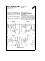
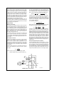
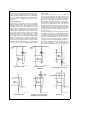
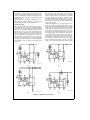
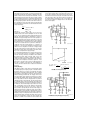
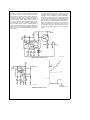
LM2907,LM2917
AN-162 LM2907 Tachometer/Speed Switch Building Block Applications
Literature Number: SNAA088
INTRODUCTION
Frequency to voltage converters are available in a number
of forms from a number of sources, but invariably require
significant additional components before they can be put to
use in a given situation. The LM2907, LM2917 series of
devices was developed to overcome these objections. Both
input and output interface circuitry is included on chip so
that a minimum number of additional components is required to complete the function. In keeping with the systems
building block concept, these devices provide an output
voltage which is proportional to input frequency and provide
zero output at zero frequency. In addition, the input may be
referred to ground. The devices are designed to operate
National Semiconductor
Application Note 162
June 1976
from a single supply voltage, which makes them particularly
suitable for battery operation.
PART 1ÐGENERAL OPERATION PRINCIPLES
Circuit Description
Referring to Figure 1, the family of devices all include three
basic components: an input amplifier with built-in hysteresis;
a charge pump frequency to voltage converter; and a versatile op amp/comparator with an uncommitted output transistor. LM2917 incorporates an active zener regulator on-chip.
LM2907 deletes this option. Both versions are obtainable in
14-pin and in 8-pin dual-in-line molded packages, and to
special order in other packages.
LM2907N-8
LM2917N-8
TL/H/7451 – 1
LM2907N
TL/H/7451 – 2
LM2917N
TL/H/7451 – 4
C1995 National Semiconductor Corporation
TL/H/7451
RRD-B30M115/Printed in U. S. A.
AN-162
TL/H/7451 – 3
FIGURE 1. Block Diagrams
LM2907 Tachometer/Speed Switch Building Block Applications
LM2907 Tachometer/Speed
Switch Building Block
Applications
required to return the capacitor on pin 2 to the high level
voltage is duplicated and used to charge the capacitor connected to pin 3. Thus in one cycle of input the capacitor on
pin 3 gets charged twice with a charge of CV.
Input Hysteresis Amplifier
The equivalent schematic diagram is shown in Figure 2. Q1
through Q11 comprise the input hysteresis amplifier. Q1
through Q4 comprise an input differential amplifier which, by
virtue of PNP level shifting, enables the circuit to operate
with signals referenced to ground. Q7, Q8, D4, and D5 comprise an active load with positive feedback. This load behaves as a bi-stable flip-flop which may be set or reset depending upon the currents supplied from Q2 and Q3. Consider the situation where Q2 and Q3 are conducting equally,
i.e. the input differential voltage is zero. Assuming Q7 to be
conducting, it will be noted that the current from Q3 will be
drawn by Q7 and Q8 will be in the ‘‘OFF’’ state. This allows
the current from Q2 to drive Q7 in parallel with D4 and a
small resistor. D4 and Q7 are identical geometry devices, so
that the resistor causes Q7 to be biased at a higher level
than D4. Thus Q7 will be able to conduct more current than
Q3 provides. In order to reverse the state of Q7 and Q8, it
will be necessary to reduce the current from Q2 below that
provided by Q3 by an amount which is established by R1. It
can be shown that this requires a differential input to Q1 and
Q4, of approximately 15mV. Since the circuit is symmetrical,
the threshold voltage to reverse the state is 15 mV in the
other direction. Thus the input amplifier has built-in hysteresis at g 15 mV. This provides clean switching where noise
may be present on the input signal, and allows total rejection of noise below this amplitude where there is no input
signal.
Thus the total charge pumped into the capacitor on pin 3
per cycle is:
Q e 2 CV
(2)
Now, since V e VCC/2
then
Q e CVCC
(3)
A resistor connected between pin 3 and ground causes a
discharge of the capacitor on pin 3, where the total charge
drained per cycle of input signal is equal to:
V3 # T
R
where V3 e the average voltage on pin 3
T e period of input signal
R e resistor connected to pin 3
In equilibrium Q e Q1
V3 # T
i.e., CVCC e
R
Q1 e
RC
T
or
V3 e VCC # R # C # f
where f e input frequency
and
CV
I
(5)
(6)
Op Amp/Comparator
Again referring to Figure 2, the op amp/comparator includes
Q35 through Q45. A PNP input stage again provides input
common-mode voltages down to zero, and if pin 8 is connected to VCC and the output taken from pin 5, the circuit
behaves as a conventional, unity-gain-compensated operational amplifier. However, by allowing alternate connections
of Q45 the circuit may be used as a comparator in which
loads to either VCC or ground may be switched. Q45 is capable of sinking 50 mA. Input bias current is typically 50 nA,
and voltage gain is typically 200 V/mV. Unity gain slew rate
is 0.2 V/ms. When operated as a comparator Q45 emitter
will switch at the slew rate, or the collector of Q45 will
switch at that rate multiplied by the voltage gain of Q45,
which is user selectable.
Charge Pump
The charge pump is composed of Q12 through Q32. R4, R5,
and R6 provide reference voltages equal to 1/4 and 3/4 of
supply voltage to Q12 and Q13. When Q10 turns ‘‘ON’’ or
‘‘OFF,’’ the base voltage at Q16 changes by an amount
equal to the voltage across R5, that is 1/2 VCC. A capacitor
connected between Pin 2 and ground is either charged by
Q21 or discharged by Q22 until its voltage matches that on
the base of Q16. When the voltage on Q16 base goes low,
Q16 turns ‘‘ON,’’ which results in Q18 and Q26 turning on,
which causes the current, sourced by Q19 and Q20, to be
shunted to ground. Thus Q21 is unable to charge pin 2.
Meanwhile, Q27 and Q30 are turned off permitting the
200 mA sourced by Q28 and Q29 to enter the emitters of
Q31 and Q32 respectively. The current from Q31 is mirrored
by Q22 through Q24 resulting in a 200 mA discharge current
through pin 2. The external capacitor on pin 2 is thus discharged at a constant rate until it reaches the new base
voltage on Q16. The time taken for this discharge to occur is
given by:
te
V3 e VCC #
(4)
Active Zener Regulator
The optional active zener regulator is also shown in Figure
2. D8 provides the voltage reference in conjunction with
Q33. As the supply voltage rises, D8 conducts and the base
voltage on Q33 starts to rise. When Q33 has sufficient base
voltage to be turned ‘‘ON,’’ it in turn causes Q34 to conduct
current from the power source. This reduces the current
available for D8 and the negative feedback loop is thereby
completed. The reference voltage is therefore the zener
voltage on D8 plus the emitter base voltage of Q33. This
results in a low temperature coefficient voltage.
(1)
where
C e capacitor on pin 2
V e change in voltage on Q16 base
I e current in Q22
During this time, Q32 sources an identical current into pin 3.
A capacitor connected to pin 3 will thus be charged by the
same current for the same amount of time as pin 2. When
the base voltage on Q16 goes high, Q18 and Q26 are
turned off while Q27 and Q30 are turned ‘‘ON.’’ In these
conditions, Q21 and Q25 provide the currents to charge the
capacitors on pins 2 and 3 respectively. Thus the charge
Input Levels and Protection
In 8-pin versions of the LM2907, LM2917, the non-inverting
input of the op amp/comparator is connected to the output
of the charge pump. Also, one input to the input hysteresis
amplifier is connected to ground. The other input (pin 1) is
then protected from transients by, first a 10kX series resis-
2
3
*Note: This connection made on LM2907-8 and LM2917-8 only.
Note: Pin numbers refer to 14-pin package.
**Note: This connection made on LM2917 and LM2917-8 only.
FIGURE 2. Equivalent Schematic Diagram
TL/H/7451 – 5
tor, R3 (Figure 2) which is located in a floating isolation
pocket, and secondly by clamp diode D1. Since the voltage
swing on the base of Q1 is thus restricted, the only restriction on the allowable voltage on pin 1 is the breakdown
voltage of the 10 kX resistor. This allows input swings to
g 28V. In 14-pin versions the link to D1 is opened in order to
allow the base of Q1 to be biased at some higher voltage.
Q5 clamps the negative swing on the base of Q1 to about
300 mV. This prevents substrate injection in the region of
Q1 which might otherwise cause false switching or erroneous discharge of one of the timing capacitors.
The differential input options (LM2907-14, LM2917-14), give
the user the option of setting his own input switching level
and still having the hysteresis around that level for excellent
noise rejection in any application.
Second, if R1 is too large, it can become a significant fraction of the output impedance at pin 3 which degrades linearity. Finally, ripple voltage must be considered, and the size
of C2 is affected by R1. An expression that describes the
ripple content on pin 3 for a single R1, C2 combination is:
VCC C1
VRIPPLE e
#
2
C2
#1
V
b CC
# fIN # C1
I2
J p-p
It appears R1 can be chosen independent of ripple, however response time, or the time it takes VOUT to stabilize at a
new frequency increases as the size of C2 increases, so a
compromise between ripple, response time, and linearity
must be cosen carefully. R1 should be selected according
to the following relationship:
C is selected according to:
V3 Full Scale
R1 # VCC # fFULL SCALE
Next decide on the maximum ripple which can be accepted
and plug into the following equation to determine C2:
C1 e
HOW TO USE IT
Basic f to V Converter
The operation of the LM2907, LM2917 series is best understood by observing the basic converter shown in Figure 3. In
this configuration, a frequency signal is applied to the input
of the charge pump at pin 1. The voltage appearing at pin 2
will swing between two values which are approximately 1/4
(VCC) b VBE and 3/4 (VCC) b VBE. The voltage at pin 3 will
have a value equal to VCC # fIN # C1 # R1 # K, where K is
the gain constant (normally 1.0).
The emitter output (pin 4) is connected to the inverting input
of the op amp so that pin 4 will follow pin 3 and provide a
low impedance output voltage proportional to input frequency. The linearity of this voltage is typically better than 0.3%
of full scale.
#
J
VCC
C1
V3
C2 e
1b
#
2
VRIPPLE
R1I2
The kind of capacitor used for timing capacitor C1 will determine the accuracy of the unit over the temperature range.
Figure 15 illustrates the tachometer output as a function of
temperature for the two devices. Note that the LM2907 operating from a fixed external supply has a negative temperature coefficient which enables the device to be used with
capacitors which have a positive temperature coefficient
and thus obtain overall stabililty. In the case of the LM2917
the internal zener supply voltage has a positive coefficient
which causes the overall tachometer output to have a very
low temperature coefficient and requires that the capacitor
temperature coefficient be balanced by the temperature coefficient of R1.
Choosing R1, C1 and C2
There are some limitations on the choice of R1, C1 and C2
(Figure 3) which should be considered for optimum performance. C1 also provides internal compensation for the
charge pump and should be kept larger than 100 pF. Smaller values can cause an error current on R1, especially at
low temperatures. Three considerations must be met when
choosing R1.
First, the output current at pin 3 is internally fixed and therefore V3 max, divided by R1, must be less than or equal to
this value.
Using Zener Regulated Options (LM2917)
For those applications where an output voltage or current
must be obtained independently of the supply voltage variations, the LM2917 is offered. The reference typically has an
11X source resistance. In choosing a dropping resistor from
the unregulated supply to the device note that the tachometer and op amp circuitry alone require about 3 mA at the
voltage level provided by the zener. At low supply voltages,
V3 max
.
. . R1 t
I3MIN
where V3 max is the full scale output voltage required
13MIN is determined from the data sheet (150 mA)
TL/H/7451 – 6
FIGURE 3. Basic f to V Converter
4
there must be some current flowing in the resistor above the
3 mA circuit current to operate the regulator. As an example, if the raw supply varies from 9V to 16V, a resistance of
470X will minimize these zener voltage variations to 160
mV. If the resistor goes under 400X or over 600X the zener
variation quickly rises above 200 mV for the same input variation. Take care also that the power dissipation of the IC is
not exceeded at higher supply voltages. Figure 4 shows
suitable dropping resistor values.
Input Interface Circuits
The ground referenced input capability of the LM2907-8 allows direct coupling to transformer inputs, or variable reluctance pickups. Figure 5(a) illustrates this connection. In
many cases, the frequency signal must be obtained from
another circuit whose output may not go below ground. This
may be remedied by using ac coupling to the input of the
LM2907 as illustrated in Figure 5(b). This approach is very
suitable for use with phototransistors for optical pickups.
Noisy signal sources may be coupled as shown in Figure
5(c). The signal is bandpass filtered. This can be used, for
example, for tachometers operating from breakerpoints on a
conventional Kettering ignition system. Remember that the
minimum input signal required by the LM2907 is only 30
mVp-p, but this signal must be able to swing at least 15 mV
on either side of the inverting input. The maximum signal
which can be applied to the LM2907 input, is g 28V. The
input bias current is a typically 100 nA. A path to ground
must be provided for this current through the source or by
other means as illustrated. With 14-pin package versions of
LM2907, LM2917, it is possible to bias the inverting input to
the tachometer as illustrated in Figure 5(d). This enables the
circuit to operate with input signals that do not go to ground,
but are referenced at higher voltages. Alternatively, this
method increases the noise immunity where large signal
TL/H/7451 – 7
FIGURE 4. Zener Regular Bias Resistor Range
TL/H/7451–8
TL/H/7451 – 9
(a) Ground Referenced Inputs
(b) AC Coupled Input
TL/H/7451 – 11
TL/H/7451 – 10
(c) Bandpass Filtered Input
Reduces Noise
TL/H/7451 – 12
(d) Above Ground Sensing
(e) High Common-Mode Rejection Input Circuit
FIGURE 5. Tachometer Input Configurations
5
placed in series with the output to protect the LED and the
output transistor.
levels are available but large noise signals on ground are
also present. To take full advantage of the common-mode
rejection of the input differential stage, a balanced bias configuration must be provided. One such circuit is illustrated in
Figure 5(e). With this arrangement, the effective commonmode rejection may be virtually infinite, owing to the input
hysteresis.
This circuit has no hysteresis in it, i.e., the turn ‘‘ON’’ and
turn ‘‘OFF’’ speed voltages are essentially equal. In cases
where speed may be fluctuating at a high rate and a flashing
LED would be objectionable, it is possible to incorporate
hysteresis so that the switch-on speed is above the switchoff speed by a controlled amount. Such a configuration is
illustrated in Figure 6(b). Figure 6(c) shows how a grounded
load can also be switched by the circuit. In this case, the
current limiting resistor is placed in the collector of the power transistor. The base current of the output transistor (Q45)
is limited by a 5 kX base resistor (see Figure 2 ). This raises
the output resistance so that the output swing will be reduced at full load.
The op amp/comparator is internally compensated for unity
gain feedback configurations as in Figure 6(d). By directly
connecting the emitter output to the non-inverting input, the
op amp may be operated as a voltage follower. Note that a
load resistor is required externally. The op amp can also be
operated, of course, as an amplifier, integrator, active filter,
or in any other normal operational amplifier configuration.
One unique configuration which is not available with standard operational amplifiers, is shown in Figure 6(e). Here
the collector of the output transistor is used to drive a load
Output Configurations
LM2907, LM2917 series devices incorporate an unusually
flexible op amp/comparator device on-chip for interfacing
with a wide variety of loads. This flexibility results from the
availability of both the collector and emitter of the output
transistor which is capable of driving up to 50 mA of load
current. When the non-inverting input is higher than the inverting input, this output transistor is turned ‘‘ON’’. It may be
used to drive loads to either the positive or the negative
supply with the emitter or collector respectively connected
to the other supply. For example, Figure 6(a), a simple
speed switch can be constructed in which the speed signal
derived from the frequency to voltage converter is compared to a reference derived simply by a resistive divider
from the power supply. When the speed signal exceeds the
reference, the output transistor turns on the light emitting
diode in the load. A small current limiting resistor should be
TL/H/7451–13
(a) Switching an LED
TL/H/7451 – 14
(b) Adding Hysteresis
to LED Switch
TL/H/7451–16
(d) Voltage Follower
TL/H/7451 – 15
(c) Switching a Grounded Load
TL/H/7451 – 17
(e) Voltage to Current Converter
FIGURE 6. Output Configurations
6
TL/H/7451 – 18
(f) Integrator
Figure 7 illustrates methods for protecting against these and
other transients. Figure 7(a) shows a typical situation in
which the power supply to the LM2907 can be provided
through a dropping resistor and regulated by an external
zener diode Z1, but the output drive is required to operate
from the full available supply voltage. In this case, a separate protection zener Z2 must be provided if the voltage on
the power line is expected to exceed the maximum rated
voltage of the LM2907.
In Figure 7(b) and Figure 7(c), the output transistor is required only to drive a simple resistive load and no secondary protection circuits are required. (Note that the dropping
resistor to the zener also has to supply current to the output
circuit). With the foregoing circuits, reverse supply protection is supplied by the forward biased zener diode. This device should be a low forward resistance unit in order to limit
the maximum reverse voltage applied to the integrated circuit. Excessive reverse voltage on the IC can cause high
currents to be conducted by the substrate diodes with consequent danger of permanent damage. Up to 1V negative
can generally be tolerated. Versions with internal zeners
may be self-protecting depending on the size of dropping
resistor used. In applications where large negative voltage
with a current which is proportional to the input voltage. In
other words, the circuit is operating as a voltage to current
converter. This is ideal for driving remote signal sensors and
moving coil galvanometers. Figure 6(f) shows how an active
integrator can be used to provide an output which falls with
increasing speed.
These are the basic configurations obtainable with the op
amp/comparator. Further combinations can be seen in the
applications shown in Part II of this application note.
Transient Protection
Many application areas use unregulated power supplies
which tend to expose the electronics to potentially damaging transients on the power supply line. This is particularly
true in the case of automotive applications where two such
transients are common.1 First is the load dump transient.
This occurs when a dead battery is being charged at a high
current and the battery cable comes loose, so that the current in the alternator inductance produces a positive transient on the line in the order of 60V to 120V. The second
transient is called field decay. This occurs when the ignition
is turned ‘‘OFF’’ and the energy stored in the field winding
of the alternator causes a negative 75V transient on the
ignition line.
TL/H/7451 – 20
TL/H/7451 – 19
(a)
(b)
TL/H/7451 – 22
TL/H/7451 – 21
(c)
(d)
FIGURE 7. Transient Protection Schemes
7
The concept of building blocks requires that a function be
performed in the same way as it can be mathematically defined. In other words, a frequency to voltage converter will
provide an output voltage proportional to frequency which is
independent of the input voltage or other input parameters,
except the frequency. In the same way, the output voltage
will be zero when the input frequency is zero. These features are built into the LM2907.
Applications for the device range from simple speed switch
for anti-pollution control device functions in automobiles, to
motor speed controls in industrial applications. The applications circuits which follow are designed to illustrate some of
the capabilities of the LM2907. In most cases, alternative
input or output configurations can be mixed and matched at
will and other variations can be determined from the description in Part I of this application note. For complete
specifications, refer to the data sheet.
transients may be anticipated, a blocking diode may be connected in the power supply line to the IC as illustrated in
Figure 7(d). During these negative transients, the diode D1
will be reverse biased and prevent reverse currents flowing
in the IC. If these transients are short and the capacitor C1
is large enough, then the power to the IC can be sustained.
This is useful to prevent change of state or change of
charge in in systems connected to it.
Temperature Ranges and Packaging Considerations
The LM2907, LM2917 series devices are specified for operation over the temperature range b40§ C to a 85§ C.
The devices are normally packaged in molded epoxy, dualin-line packages. Other temperature ranges and other packages are availabe to special order. For reliability requirements beyond those of normal commercial application
where the cost of military qualification is not bearable, other
programs are available such as B a .
Speed Switches
Perhaps the most natural application of the LM2907 is in
interfacing with magnetic pickups, such as the one illustrated in Figure 8 to perform speed switching functions. As an
example, New York taxies are required to change the intensity of the warning horn above and below 45 mph. Other
examples include an over-speed warning, where a driver
may set the desired maximum speed and have an audible
PART IIÐAPPLICATIONS
INTRODUCTION
The LM 2907, LM2917 series devices were designed not
only to perform the basic frequency to voltage function required in many systems, but also to provide the input and
output interface so often needed, so that low cost implementations of complete functions are available.
TL/H/7451 – 23
FIGURE 8. Typical Magnetic Pickup
TL/H/7451 – 25
TL/H/7451–24
FIGURE 10. RC Selection Chart
FIGURE 9. Simple Speed Switch Load is Energized
1
when fIN l
2C1R1
8
the output current is conducted along the supply line so that
a local current sensing device in the supply line can be used
to get a direct reading of the frequency at the remote location where the electronics may also be situated. The small
zero speed offset due to the device quiescent current may
be compensated by offsetting the zero on the display device. This also permits one display device to be shared between several inputs.
or visual warning of speeds in excess of that level. Many
anti-pollution devices included on several recent automobile
models have included a speed switch to disable the vacuum
advance function until a certain speed is attained2. A circuit
which will perform these kind of functions is shown in Figure
9. A typical magnetic pickup for automotive applications will
provide a thousand pulses per mile so that at 60 mph the
incoming frequency will be 16.6 Hz. If the reference level on
the comparator is set by two equal resistors R1 and R2 then
the desired value of C1 and R1 can be determined from the
simple relationship:
VCC
e VCC # C1 # R1 # f.
2
or
C1R1f e 0.5
and hence
C1R1 e 0.03
From the RC selection chart in Figure 10 we can choose
suitable values for R1 and C1. Examples are 100 kX and
0.3 mF. The circuit will then switch at approximately 60 mph
with the stated input frequency relationship to speed. To
determine the ripple voltage refer back to the equation for
ripple voltage (under ‘‘Choosing R1, C1 and C2’’). From this
we can determine that there will be about 10 mV of ripple at
the switching level. To prevent this from causing chattering
of the load a certain amount of hysteresis is added by including R3. This will provide typically 1% of supply as a
hysteresis or 1.2 mph in the example. Note that since the
reference to the comparator is a function of supply voltage
as is the output from the charge pump there is no need to
regulate the power supply. The frequency at which switching occurs is independent of supply voltage.
In some industrial applications it is useful to have an indication of past speed excesses, for example in notifying the
need for checking of bearings. The LM2907 can be made to
latch until the power supply is turned ‘‘OFF’’ in the case
where the frequency exceeds a certain limit, by simply connecting the output transistor emitter back to the non-inverting input of the comparator as shown in Figure 11. It can
also serve to shut off a tape recorder or editing machine at
the end of a rewind cycle. When the speed suddenly increases, the device will sense the condition and shut down
the motor.
TL/H/7451 – 26
TL/H/7451 – 27
VO e FINV a R1 C1
SETPOINT e V a
Analog Displays
The LM2907, LM2917 series devices are particularly useful
for analog display of frequency inputs. In situations where
the display device is a moving coil instrument the advantages of the uncommitted output transistor can be realized
by providing a current drive to the meter. This avoids temperature tracking problems with the varying meter resistance and enables high resistance instruments to be driven
accurately with relatively large voltages as illustrated in Figure 12. The LM2917 version is employed here to provide a
regulated current to the instrument. The onboard 7.6V zener
is compatible with car and boat batteries and enables the
moving coil instrument to employ the full battery voltage for
its deflection. This enables high torque meters to be used.
This is particularly useful in high vibration environments
such as boats and motorcycles. In the case of boats, the
most common speed pickup for the knot meter employs a
rotating propeller driving a magnetic pickup device. Meteorologists employ a large number of anemometers for measuring wind velocities and these are frequently coupled by a
magnetic pickup. In examples like these, where there is frequently a large distance between the display device and the
sensor, the configuration of Figure 13 can be usefully employed to cut down on the number of wires needed. Here
RB
RD a RA
(
Latchup occurs when
1
RB
FIN e
RA a RB R1 C1
Independent of V a !
FIGURE 11. Overspeed Latch
TL/H/7451 – 28
FIGURE 12. Analog Display of Frequency
9
Automotive Tachometer
Not all inputs are derived from variable reluctance magnetic
pickups; for example, in spark ignition engines the tachometer is generally driven from the spark coil. An interface circuit for this situation is shown in Figure 14. This tachometer
can be set up for any number of cylinders by linking the
appropriate timing resistor as illustrated. A 500X trim resistor can be used to set up final calibration. A protection circuit composed of a 10X resistor and a zener diode is also
shown as a safety precaution against the transients which
are to be found in automobiles.
Motor Speed Controls
DC motors with or without brushes can be purchased with
ac tachometer outputs already provided by the manufacturer3. With these motors in combination with the
TL/H/7451–29
TL/H/7451 – 32
FIGURE 15. Normalized Tachometer
Output vs. Temperature
TL/H/7451–30
FIGURE 13. Two Wire Remote Speed Sensor
TL/H/7451 – 31
FIGURE 14. Gasoline Engine Tachometer
10
the non-inverting input. As speed increases, the charge
pump puts charge into capacitor C2 and causes the output
VOUT to fall in proportion to speed. The output current of the
op amp transistor is used to provide an analog drive to the
motor. Thus as the motor speed approaches the reference
level, the current is proportionately reduced to the motor so
that the motor gradually comes up to speed and is maintained without operating the motor in a switching mode. This
is particularly useful in situations where the electrical noise
generated by the switching mode operation is objectionable.
This circuit has one primary disadvantage in that it has poor
load regulation. A third configuration is shown in Figure 18.
This employs an LM2907-8 acting as a shunt mode regulator. It also features an LED to indicate when the device is in
regulation.
LM2907, a very low cost speed control can be constructed.
In Figure 16 the most simple version is illustrated where the
tachometer drives the non-inverting input of the comparator
up towards the preset reference level. When that level is
reached, the output is turned off and the power is removed
from the motor. As the motor slows down, the voltage from
the charge pump output falls and power is restored. Thus
speed is maintained by operating the motor in a switching
mode. Hysteresis can be provided to control the rate of
switching. An alternative approach which gives proportional
control is shown in Figure 17. Here the charge pump integrator is shown in a feedback connection around the operational amplifier. The output voltage for zero speed is equal
to the reference voltage set up on the potentiometer on
TL/H/7451 – 33
FIGURE 16. Motor Speed Control
TL/H/7451 – 34
FIGURE 17. Motor Speed Control with Proportional Drive
11
The output of the tachometer is proportional to the product
of supply voltage, input frequency, a capacitor and a resistor. Any one of these may be used as the input variable or
they may be used in combination to produce multiplication.
An example of a capacitive transducer is illustrated in Figure
20, where a fixed input frequency is employed either from
the 60 Hz line as a convenient source or from a stable oscillator. The capacitor is a variable element mechanically coupled to the system whose position is to be sensed. The
output is proportional to the capacitance value, which can
be arranged to have any desired relationship to the mechanical input by suitable shaping of the capacitor electrodes.
Position Sensing
In addition to their use to complete tachometer feedback
loops, used in position transducer circuits, the LM2907,
LM2917 devices can also be used as position transducers.
For example, the timing resistor can be removed from pin 3
so that the output current produces a staircase instead of a
fixed dc level. If the magnetic pickup senses passing notches or items, a staircase signal is generated which can then
be compared with a reference to initiate a switching action
when a specified count is reached. For example, Figure 19
shows a circuit which will count up a hundred input pulses
and then switch on the output stage. Examples of this application can be found in automated packaging operations or
in line printers.
TL/H/7451 – 35
FIGURE 18. Motor Speed Control
TL/H/7451–36
TL/H/7451 – 37
FIGURE 19. Staircase Counter
12
TL/H/7451 – 38
FIGURE 20. Capacitive Transducer
The linearity of voltage controlled oscillators can be improved by employing the LM2907 as a feedback control element converting the frequency back to voltage and comparing with the input voltage. This can often be a lower cost
solution to linearizing the VCO than by working directly on
the VCO itself in the open loop mode. The arrangement is
illustrated in Figure 22.
Analog Systems Building Block
The LM2907, LM2917 series characterize systems building
block applications by the feature that the output from the
device is proportional only to externally programmed inputs.
Any or all of these inputs may be controlled inputs to provide the desired output. For example, in Figure 20 the capacitance transducer can be operated as a multiplier. In
flow measurement indicators, the input frequency can be a
variable depending on the flow rate, such as a signal generated from a paddle wheel, propeller or vortex sensor4. The
capacitor can be an indication of orifice size or aperture
size, such as in a throttle body. The product of these two will
indicate volume flow. A thermistor could be added to R1 to
convert the volume flow to mass flow. So a combination of
these inputs, including control voltage on the supply, can be
used to provide complex multiplicative analog functions with
independent control of the variables.
Phase-locked loops (PLL) are popular today now that low
cost monolithic implementations are available off the shelf.
One of their limitations is the narrow capture range and
hold-in range. The LM2907 can be employed as a PLL helper. The configuration is shown in Figure 21. The LM2907
here serves the function of a frequency-to-voltage converter
which puts the VCO initially at approximately the right frequency to match the input frequency. The phase detector is
then used to close the gap between VCO and input frequency by exerting a control on the summing point. In this way,
given proper tracking between the frequency-to-voltage
converter and the VCO, (which is a voltage-to-frequency
converter), a wide-range phase loop can be developed.
TL/H/7451 – 40
FIGURE 22. Feedback Controlled VCO
Digital Interface
A growing proportion of the complex control systems today
are being controlled by microprocessors and other digital
devices. Frequently they require inputs to indicate position
or time from some mechanical input. The LM2907 can be
used to provide zero crossing datum to a digital system using the circuits illustrated in Figure 23. At each zero crossing
of the input signal the charge pump changes the state of
capacitor C1 and provides a one-shot pulse into the zener
diode at pin 3. The width of this pulse is controlled by the
internal current of pin 2 and the size of capacitor C1 as well
as by the supply voltage. Since a pulse is generated by each
zero crossing of the input signal we call this a ‘‘two-shot’’
instead of a ‘‘one-shot’’ device and this can be used for
doubling the frequency that is presented to the microprocessor control system. If frequency doubling is not required
and a square wave output is preferred, the circuit of Figure
24 can be employed. In this case, the output swing is the
same as the swing on pin 2 which is a swing of half supply
voltage starting at 1 VBE below one quarter of supply and
going to 1 VBE below three-quarters of supply. This can be
increased up to the full output swing capability by reducing
or removing the negative feedback around the op amp.
TL/H/7451 – 39
FIGURE 21. Phase-Locked Loop Helper
Added f to V Greatly Increases Capture and Hold Range
13
The staircase generator shown in Figure 19 can be used as
an A-D converter. A suitable configuration is shown in Figure 25. To start a convert cycle the processor generates a
reset pulse to discharge the integrating capacitor C2. Each
complete clock cycle generates a charge and discharge cycle on C1. This results in two steps per cycle being added to
C2. As the voltage on C2 increases, clock pulses are re-
turned to the processor. When the voltage on C2 steps
above the analog input voltage the data line is clamped and
C2 ceases to charge. The processor, by counting the number of clock pulses received after the reset pulse, is thus
loaded with a digital measure of the input voltage. By making C2/C1 e 1024 an 8-bit A-D is obtained.
TL/H/7451 – 42
VCC C1
c
Pulse width e
2
I2
Input can be g 20 mV to g 28V
TL/H/7451 – 41
Output frequency equal twice input frequency.
VCC C1
c
Pulse width e
2
I2
Pulse height e VZENER
FIGURE 23. ‘‘Two-Shot’’ Zero Crossing Detector
TL/H/7451 – 44
TL/H/7451 – 43
FIGURE 24. Zero Crossing Detector and Line Drivers
TL/H/7451 – 46
TL/H/7451 – 45
FIGURE 25. A-D Converter
14
amp/comparator is connected with negative feedback with
a diode in the loop so that the amplifier can only pull down
on the load and not pull up. In this way, the outputs from the
two devices can be joined together and the output will be
the lower of the two input speeds. In Figure 27 the output
emitter of the onboard op amp provides the pullup required
to provide a select-high situation where the output is equal
to the higher of two speeds. The select average circuit in
Figure 28 saves components by allowing the two charge
pumps to operate into a single RC network. One of the amplifiers is needed then to buffer the output and provide a low
impedance output which is the average of the two input frequencies. The second amplifier is available for other applications.
Anti-Skid Circuit Functions
Motor Vehicle Standards 121 place certain stopping requirements on heavy vehicles which require the use of electronic
anti-skid control devices.5 These devices generally use variable reluctance magnetic pickup sensors on the wheels to
provide inputs to a control module. One of the questions
which the systems designer must answer is whether to use
the average from each of the two wheels on a given axle or
to use the lower of the two speeds or to use the higher of
the two speeds. Each of the three functions can be generated by a single pair of LM2907-8 as illustrated in Figures 26–
28. In Figure 26 the input frequency from each wheel sensor
is converted to a voltage in the normal manner. The op
TL/H/7451 – 47
VOUT is proportional to the lower of the
two input wheel speeds
TL/H/7451 – 48
FIGURE 26. ‘‘Select-Low’’ Circuit
15
TL/H/7451 – 49
VOUT is proportional to the higher of the
two input wheel speeds
TL/H/7451 – 50
FIGURE 27. ‘‘Select-High’’ Circuit
TL/H/7451 – 51
FIGURE 28. ‘‘Select-Average’’ Circuit
16
Transmission and Clutch Control Functions
CONCLUSION
Electric clutches can be added to automotive transmissions
to eliminate the 6% slip which typically occurs during cruise
and which results in a 6% loss in fuel economy. These devices could be operated by a pair of LM2907’s as illustrated
in Figure 29. Magnetic pickups are connected to input and
output shafts of the transmission respectively and provide
frequency inputs f1 and f 2 to the circuit. Frequency, f2, being the output shaft speed, is also a measure of vehicle road
speed. Thus the LM2907-8 No. 2 provides a voltage proportional to road speed at pin 3. This is buffered by the op amp
in LM2907-8 No. 1 to provide a speed output VOUT1 on pin
4. The input shaft provides charge pulses at the rate of 2f1
into the inverting node of op amp 2. This node has the integrating network R1, C3 going back to the output of the op
amp so that the charge pulses are integrated and provide
an inverted output voltage proportional to the input speed.
Thus the output VOUT2 is proportional to the difference between the two input frequencies. With these two signalsÐ
the road speed and the difference between road speed and
input shaft speedÐit is possible to develop a number of
control functions including the electronic clutch and a complete electronic transmission control. (In the configuration
shown, it is not possible for VOUT2 to go below zero so that
there is a limitation to the output swing in this direction. This
may be overcome by returning R3 to a negative bias supply
instead of to ground.)
The applications presented in this note indicate that the
LM2907, LM2917 series devices offer a wide variety of uses
ranging from very simple low cost frequency to voltage conversion to complex systems building blocks. It is hoped that
the ideas contained here have given suggestions which may
help provide new solutions to old problems. Additional applications ideas are included in the data sheet, which should
be referred to for all specifications and characteristics.
REFERENCES
1. Sociey of Automotive Engineers: Preliminary Recommended Environmental Practices for Electronic Equipment Design. October 1974.
2. See for example: Pollution Control Installers HandbookÐ
California Bureau of Automotive Repair No. BAR H-001 õ
5.5.4 NOX control systems.
3. TRW Globe Motors, 2275 Stanley Avenue, Dayton, Ohio
45404.
4. S.A.E. Paper Ý760018 Air Flow Measurement for Engine
ControlÐRobert D. Joy.
5. Code of Federal Regulations. Title 49 Transportation;
Chapter VÐNational Highway Traffic Safety Administration, Dept. of Transportation; Part 571ÐFederal Motor
Vehicle Safety Standards; Standard No. 121.
VOUT1 e VCC C2 R2 f2
VOUT2 e VCC (C2 R2 f2 b C1 R1 f1)
TL/H/7451 – 52
FIGURE 29. Transmission or Clutch Control Functions
17
LM2907 Tachometer/Speed Switch Building Block Applications
LIFE SUPPORT POLICY
NATIONAL’S PRODUCTS ARE NOT AUTHORIZED FOR USE AS CRITICAL COMPONENTS IN LIFE SUPPORT
DEVICES OR SYSTEMS WITHOUT THE EXPRESS WRITTEN APPROVAL OF THE PRESIDENT OF NATIONAL
SEMICONDUCTOR CORPORATION. As used herein:
AN-162
1. Life support devices or systems are devices or
systems which, (a) are intended for surgical implant
into the body, or (b) support or sustain life, and whose
failure to perform, when properly used in accordance
with instructions for use provided in the labeling, can
be reasonably expected to result in a significant injury
to the user.
National Semiconductor
Corporation
1111 West Bardin Road
Arlington, TX 76017
Tel: 1(800) 272-9959
Fax: 1(800) 737-7018
2. A critical component is any component of a life
support device or system whose failure to perform can
be reasonably expected to cause the failure of the life
support device or system, or to affect its safety or
effectiveness.
National Semiconductor
Europe
Fax: (a49) 0-180-530 85 86
Email: cnjwge @ tevm2.nsc.com
Deutsch Tel: (a49) 0-180-530 85 85
English Tel: (a49) 0-180-532 78 32
Fran3ais Tel: (a49) 0-180-532 93 58
Italiano Tel: (a49) 0-180-534 16 80
National Semiconductor
Hong Kong Ltd.
13th Floor, Straight Block,
Ocean Centre, 5 Canton Rd.
Tsimshatsui, Kowloon
Hong Kong
Tel: (852) 2737-1600
Fax: (852) 2736-9960
National Semiconductor
Japan Ltd.
Tel: 81-043-299-2309
Fax: 81-043-299-2408
National does not assume any responsibility for use of any circuitry described, no circuit patent licenses are implied and National reserves the right at any time without notice to change said circuitry and specifications.
IMPORTANT NOTICE
Texas Instruments Incorporated and its subsidiaries (TI) reserve the right to make corrections, modifications, enhancements, improvements,
and other changes to its products and services at any time and to discontinue any product or service without notice. Customers should
obtain the latest relevant information before placing orders and should verify that such information is current and complete. All products are
sold subject to TI’s terms and conditions of sale supplied at the time of order acknowledgment.
TI warrants performance of its hardware products to the specifications applicable at the time of sale in accordance with TI’s standard
warranty. Testing and other quality control techniques are used to the extent TI deems necessary to support this warranty. Except where
mandated by government requirements, testing of all parameters of each product is not necessarily performed.
TI assumes no liability for applications assistance or customer product design. Customers are responsible for their products and
applications using TI components. To minimize the risks associated with customer products and applications, customers should provide
adequate design and operating safeguards.
TI does not warrant or represent that any license, either express or implied, is granted under any TI patent right, copyright, mask work right,
or other TI intellectual property right relating to any combination, machine, or process in which TI products or services are used. Information
published by TI regarding third-party products or services does not constitute a license from TI to use such products or services or a
warranty or endorsement thereof. Use of such information may require a license from a third party under the patents or other intellectual
property of the third party, or a license from TI under the patents or other intellectual property of TI.
Reproduction of TI information in TI data books or data sheets is permissible only if reproduction is without alteration and is accompanied
by all associated warranties, conditions, limitations, and notices. Reproduction of this information with alteration is an unfair and deceptive
business practice. TI is not responsible or liable for such altered documentation. Information of third parties may be subject to additional
restrictions.
Resale of TI products or services with statements different from or beyond the parameters stated by TI for that product or service voids all
express and any implied warranties for the associated TI product or service and is an unfair and deceptive business practice. TI is not
responsible or liable for any such statements.
TI products are not authorized for use in safety-critical applications (such as life support) where a failure of the TI product would reasonably
be expected to cause severe personal injury or death, unless officers of the parties have executed an agreement specifically governing
such use. Buyers represent that they have all necessary expertise in the safety and regulatory ramifications of their applications, and
acknowledge and agree that they are solely responsible for all legal, regulatory and safety-related requirements concerning their products
and any use of TI products in such safety-critical applications, notwithstanding any applications-related information or support that may be
provided by TI. Further, Buyers must fully indemnify TI and its representatives against any damages arising out of the use of TI products in
such safety-critical applications.
TI products are neither designed nor intended for use in military/aerospace applications or environments unless the TI products are
specifically designated by TI as military-grade or "enhanced plastic." Only products designated by TI as military-grade meet military
specifications. Buyers acknowledge and agree that any such use of TI products which TI has not designated as military-grade is solely at
the Buyer's risk, and that they are solely responsible for compliance with all legal and regulatory requirements in connection with such use.
TI products are neither designed nor intended for use in automotive applications or environments unless the specific TI products are
designated by TI as compliant with ISO/TS 16949 requirements. Buyers acknowledge and agree that, if they use any non-designated
products in automotive applications, TI will not be responsible for any failure to meet such requirements.
Following are URLs where you can obtain information on other Texas Instruments products and application solutions:
Products
Applications
Audio
www.ti.com/audio
Communications and Telecom www.ti.com/communications
Amplifiers
amplifier.ti.com
Computers and Peripherals
www.ti.com/computers
Data Converters
dataconverter.ti.com
Consumer Electronics
www.ti.com/consumer-apps
DLP® Products
www.dlp.com
Energy and Lighting
www.ti.com/energy
DSP
dsp.ti.com
Industrial
www.ti.com/industrial
Clocks and Timers
www.ti.com/clocks
Medical
www.ti.com/medical
Interface
interface.ti.com
Security
www.ti.com/security
Logic
logic.ti.com
Space, Avionics and Defense
www.ti.com/space-avionics-defense
Power Mgmt
power.ti.com
Transportation and Automotive www.ti.com/automotive
Microcontrollers
microcontroller.ti.com
Video and Imaging
RFID
www.ti-rfid.com
OMAP Mobile Processors
www.ti.com/omap
Wireless Connectivity
www.ti.com/wirelessconnectivity
TI E2E Community Home Page
www.ti.com/video
e2e.ti.com
Mailing Address: Texas Instruments, Post Office Box 655303, Dallas, Texas 75265
Copyright © 2011, Texas Instruments Incorporated