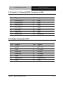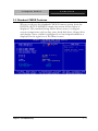
1
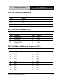
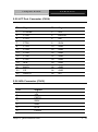
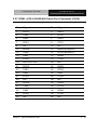
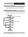
PCM-8500
Socket 478 based Pentium ® 4
/ Pentium ® 4 Processor-M
/ Celeron® Processors
Compact Board
With LCD, Ethernet, USB &
PCMCIA / Mini PCI
PCM-8500 Rev. A Manual
Oct. 2003
Compact Board
PCM -8 5 0 0
Copyright Notice
This document is copyrighted, 2003. All rights are reserved. The original
manufacturer reserves the right to make improvements to the products
described in this manual at any time without notice.
No part of this manual may be reproduced, copied, translated, or transmitted
in any form or by any means without the prior written permission of the
original manufacturer. Information provided in this manual is intended to be
accurate and reliable. However, the original manufacturer assumes no
responsibility for its use, or for any infringements upon the rights of third
parties that may result from its use.
The material in this document is for product information only and is subject
to change without notice. While reasonable efforts have been made in the
preparation of this document to assure its accuracy, AAEON assumes no
liabilities resulting from errors or omissions in this document, or from the
use of the information contained herein.
AAEON reserves the right to make changes in the product design without
notice to its users.
i
Compact Board
PCM -8 5 0 0
Acknowledgments
All other product s’name or trademarks are properties of their respective
owners.
l
Award is a trademark of Award Software International, Inc.
l
CompactFlash™ is a trademark of the Compact Flash Association.
l
Intel® , Pentium® 4 /4 Processor-M and Celeron® are trademarks of
Intel® Corporation.
l
Microsoft Windows® is a registered trademark of Microsoft Corp.
l
ITE is a trademark of Integrated Technology Express, Inc.
l
IBM, PC/AT, PS/2, and VGA are trademarks of International Business
Machines Corporation.
ii
Compact Board
PCM -8 5 0 0
Packing List
Before you begin installing your card, please make sure that the
following materials have been shipped:
•
1 PCM-8500 Compact Board
•
1 Quick Installation Guide
•
1 CD-ROM for manual (in PDF format) and drivers
•
1 Jumper Cap
If any of these items should be missing or damaged, please contact your
distributor or sales representative immediately.
iii
Compact Board
PCM -8 5 0 0
Contents
Chapter 1 General Information
1.1 Introduction ..................................................................................1-2
1.2 Features .........................................................................................1-4
1.3 Specifications ................................................................................1-5
Chapter 2 Quick Installation Guide
2.1 Safety Precautions ........................................................................2-2
2.2 Location of Connectors and Jumpers ........................................2-3
2.3 Mechanical Drawing.....................................................................2-5
2.4 List of Jumpers .............................................................................2-7
2.5 List of Connectors ........................................................................2-8
2.6 Setting Jumpers.............................................................................2-9
2.7 Clear CMOS (JP1) ........................................................................2-10
2.8 Audio Out Select (JP2) ................................................................2-10
2.9 COM2 Ring/+5V/+12V Selection (JP3)...............................2-10
2.10 COM2 RS-232/422/485 Select (JP4&JP5) ............................2-11
2.11 ATX Power simulate AT Power (JP6).....................................2-11
2.12 LCD Voltage Selection (JP7) ....................................................2-11
2.13 IDE Connector (CN1)...............................................................2-12
2.14 CompactFlash Connector (CN2) .............................................2-13
2.15 USB1 Connector (CN3) ............................................................2-14
2.16 USB2 Connector (CN4) ............................................................2-14
2.17 USB3 Connector (CN5) ............................................................2-14
iv
Compact Board
PCM -8 5 0 0
2.18 Audio 5.1 Channel/SPDIF Connector (CN6)........................2-15
2.19 Audio Connector (CN7)............................................................2-15
2.20 Fan Connector (CN8&CN24) .................................................2-16
2.21 LAN LED Connector (CN10) .................................................2-16
2.22 10/100Base-TX Ethernet Connector (CN10) ........................2-16
2.23 Option PME Connector (CN12)..............................................2-17
2.24 Floppy Connector (CN13) ........................................................2-17
2.25 LPT Port Connector (CN14) ....................................................2-18
2.26 IrDA Connector (CN15) ...........................................................2-18
2.27 COM1~4 RS-232/422/485 Serial Port Connector (CN16)..2-19
2.28 PS2 Keyboard/Mouse Connector (CN17)..............................2-20
2.29 Digital I/O-2 Connector (CN18) .............................................2-21
2.30 Digital I/O-1 Connector (CN26) .............................................2-22
2.31 TV Out Connector (CN19).......................................................2-23
2.32 Channel1 LVDS Connector (CN20)........................................2-23
2.33 Channel2 LVDS Connector (CN21)........................................2-24
2.34 VGA Display Connector (CN22).............................................2-24
2.35 Front Panel (CN25) ...................................................................2-25
2.36 ATX Power Connector (CN27) ...............................................2-25
2.27 ATX Power 12V Connector (CN28) .......................................2-25
Chapter 3 Award BIOS Setup
3.1 System Test and Initialization. ....................................................3-2
3.2 Award BIOS Setup.......................................................................3-3
3.3 Standard CMOS Features ............................................................3-6
3.4 Advanced BIOS Features ............................................................3-7
v
Compact Board
PCM -8 5 0 0
3.5 Advanced Chipset Features .........................................................3-8
3.6 Integrated Peripherals ..................................................................3-9
3.7 Power management Setup...........................................................3-10
3.8 PnP/PCI configuration ...............................................................3-11
3.9 PC Health Status...........................................................................3-12
3.10Frequency/Voltage control ........................................................3-13
3.11Load Fail-Safe Defaults ..............................................................3-14
3.12Load Optimized Defaults...........................................................3-14
3.13Set Supervisor/User Password ..................................................3-14
3.14Save&Exit Setup.........................................................................3-15
3.15Exit without saving......................................................................3-15
Chapter 4 Driver Installation
4.1 Installation 1..................................................................................4-3
4.2 Installation 2..................................................................................4-5
Appendix A Programming the WatchDog Timer
A.1 Watchdog timer ...................................................................... A-2
A.2 Configuring sequence description ........................................ A-2
A.3 ITE8712 Watchdog timer initial program ........................... A-5
vi
Compact Board
PCM -8 5 0 0
1
Chapter
General
Information
Chapter 1 General Information
1- 1
Compact Board
PCM -8 5 0 0
1.1 Introduction
PCM-8500 is first Pentium® 4 industrial board in AAEON Compact
Board product line. It features a PGA478 socket that can
accommodate Pentium® 4 / Pentium® 4 Processors-M and
Celeron® Processor, supporting FSB up to 400/533MHz.
Best performance for multimedia solution
AAEON's PCM-8500 also supports DDR DRAM up to 1GB, 4X
AGP, and 6 channels audio output. It can provide the strong
multimedia functions. Therefore PCM-8500 can be broadly
implemented in several markets, such as Point of sale, point of
information (Kiosk), and gaming markets.
Multi-Function Pentium4 Platform
If you are looking for powerful multi-media applications,
PCM-8500 is the one. PCM-8500 successfully integrates VGA,
Audio and Ethernet function into 5.75” size board; meanwhile
it also supports 6 USB2.0, mini PCI, and PCMCIA (optional
item) slots. PCM-8500 promises you the greatest expansion
possibilities with the most cost-effective expansion standards,
PCMCIA or Mini PCI. With numerous off-the-shelf
PCMCIA/Mini PCI modules, you get easy access to solutions
ranging from IEEE 1394, Modem, Storage, Sound Card, SCSI
card, Audio/Video capture card, Wireless LAN module, to
Chapter 1 Ge neral Information
1 -2
Compact Board
PCM -8 5 0 0
Bluetooth module. Especially for customers whom application
is various or changing, PCM-8500 reserves more than enough
flexibility for future expansion.
More
PCM-8500 provides more CPU options for different applications.
You can choose Pentium® 4 processor up to 3.06G for high
performance application or choose Pentium® 4 processor-M for
thermal concerned operative environment. Low-cost Socket 478
Celeron processors are also supported by PCM-8500 for
cost-intensive projects. Most of all Pentium® 4 Level processors are
suitable for PCM-8500. Talking about the display signal transmission,
PCM-8500 integrated 48-bit dual channel LVDS interface onboard,
which allows long distance display signal transmission. Besides LCD
supports, PCM-8500 also allows customer to show different contents
on CRT and LCD at same time. It meets multi-display demand at
most cost-efficient way.
Chapter 1 Ge neral Information
1 -3
Compact Board
PCM -8 5 0 0
1.2 Features
•
Support Intel Socket 478 Pentium® 4 / 4 Processor-M /
Celeron Processors
•
Support Intel Hyper-Threading Technology
•
Support 266/333MHz DDR SDRAM
•
High Speed AGP 4X for VGA display
•
Support 48bit Dual Channel LVDS
•
Support TV-Out Function
•
Integrated AC-97 5.1 3D Audio
•
One 10/100Base-T Fast Ethernet
•
Support CompactFlash memory storage
•
Six USB 2.0 Ports
•
Digital I/O ( 8 in, 8 out as Default, up to 16 in or 16 out )
Chapter 1 Ge neral Information
1 -4
Compact Board
PCM -8 5 0 0
1.3 Specifications
System
l
CPU
Intel Socket 478 Pentium® 4 /
4 Processor-M /
Celeron® Processor,
Hyper-Threading Technology
supported ( Standard Cooler
Supported )
l
Memory
184pin DIMM ×1, Support DDR
266/333MHz up to 1GB
l
Chipset
Intel ® i845GV / ICH4 + ITE
8712 ×2
l
BIOS
Award 512 KB FLASH BIOS
l
Audio
l
SSD
One Type II CompactFlash Card
l
Watchdog timer
Generate a system reset
l
DMA
7DMA channels ( 8237 equivalent)
l
Interrupt
15 interrupt levels ( 8259 equivalent)
l
Ethernet
Intel 82562 10/100 PHY chip
l
Expansion Interface
PCI slot ×1, Mini PCI slot ×1,
ALC 650 Codec 6 Channel, AC97
PCMCIA Type II ×2. (Optional)
l
H/W status monitoring
Power supply voltages and
temperatures monitoring functions
Chapter 1 Ge neral Information
1 -5
Compact Board
PCM -8 5 0 0
Battery
Lithium battery for data retention
l
Display
l
Memory size
Share Memory, Dynamically Adjusts
by OS.
l
Resolution
Up to 1600 X 1200 for CRT
Up to 1280 X 1024 for TFT
l
LCD Interface
Up to 48-bit Dual Channel LVDS
TFT LCD ( Chrontel 7017 )
l
TV Out
Support NTSC/PAL standard
1024 ×768 ( Chrontel 7017 )
l
Dual Display
Simultaneous Scan: CRT + LCD
Dual View: CRT + LCD
I/O
l
MIO
1 ×EIDE (Ultra DMA100),
1 ×FDD,
1 ×K/B,
1 ×Mouse,
1 ×RS-232/422/485,
3×RS-232,
1 ×LPT,
Chapter 1 Ge neral Information
1 -6
Compact Board
PCM -8 5 0 0
1 ×CRT
l
Digital I/O port
Support 8 in, 8 out as default, up to
16 in or 16 out.
l
IR interface
l
Ethernet
l
Audio
Support one IrDA Tx/Rx header
1 ×RJ45 Connector
Mic in, Line in, Line out / Speak
out, CD Audio in, With special
connector for 5.1 channel audio
l
USB
USB 2.0 ×3sets.
Total 6 ports
l
TV-Out
Chapter 1 Ge neral Information
Support S-terminal and RCA type
1 -7
Compact Board
PCM -8 5 0 0
2
Chapter
Notice:
The Quick Installation Guide is derived from
Chapter 2 of user manual. For other chapters
and further installation instructions, please
refer to the user manual CD -ROM that came
with the product.
Quick
Installation
Guide
Attention:
1. There are two different models of PCM-8500 for
supporting Desktop or Mobile type of Pentium® 4
Processors, please make sure appropriated
processor is installed on PCM-8500 before your
turn on the power.
2. The setting of " Advanced Chipset Features \
Speed Step Mode (Pentium® 4 Mobile) " in BIOS
should be disabled when desktop version
Pentium® 4 or Celeron® are adopted, otherwise
the system cannot boot. Clear CMOS will be
required to rescue your PC from this situation.
For Mobile Pentium® 4, this item can be disabled
or enabled to get the best performance or
maximum power saving of the processor.
Part No. 2007850011 Printed in Taiwan Oct. 2003
Chapter 2 Quick Installation Guide
2 -1
Compact Board
PCM -8 5 0 0
2.1 Safety Precautions
Always completely disconnect the power cord from
your board whenever you are working on it. Do not
make connections while the power is on, because a
sudden rush of power can damage sensitive
electronic components.
Always ground yourself to remove any static charge
before touching the board. Modern electronic
devices are very sensitive to static electric charges.
Use a grounding wrist strap at all times. Place all
electronic components on a static-dissipative
surface or in a static-shielded bag when they are not
in the chassis
Chapter 2 Quick Installation Guide
2 -2
Compact Board
PCM -8 5 0 0
2.2 Location of Connectors and Jumpers
Component Side
82559
Chapter 2 Quick Installation Guide
2 -3
Compact Board
PCM -8 5 0 0
Solder Side
Chapter 2 Quick Installation Guide
2 -4
Compact Board
PCM -8 5 0 0
2.3 Mechanical Drawing
Component Side
82559
Chapter 2 Quick Installation Guide
2 -5
Compact Board
PCM -8 5 0 0
Solder Side
Chapter 2 Quick Installation Guide
2 -6
Compact Board
PCM -8 5 0 0
2.4 List of Jumpers
The board has a number of jumpers that allow you to configure your
system to suit your application.
The table below shows the function of each of the board's jumpers:
Jumpers
Label
Function
JP1
Clear RTC
JP2
Audio Out Select
JP3
COM2 Ring/+5V/+12V Selection
JP4
COM2 RS-232/422/485 Selection
JP5
COM2 RS-232/422/485 Selection
JP6
ATX Power simulate AT Power
JP7
LCD Voltage Selection
Chapter 2 Quick Installation Guide
2 -7
Compact Board
PCM -8 5 0 0
2.5 List of Connectors
The board has a number of connectors that allow you to configure
your system to suit your application. The table below shows the
function of each board's connectors:
Connectors
Label
Function
CN1
EIDE HDD Connector
CN2
CompactFlash Connector / CompactFlash Socket
CN3/CN4/CN5
USB1/2/3 Connector
CN6
Audio 5.1 Channel / SPDIF Connector
CN7
Audio Connector
CN8,CN24
Fan Connector
CN9
PCMCIA Slot
CN10
LAN LED Connector
CN11
RJ-45 Connector
CN12
Option PME Connector
CN13
Floppy Connector
CN14
LPT Port Connector
CN15
IrDA Connector
CN16
RS-232 Serial Port (COM1~COM4) Connector
CN17
CN18,CN26
PS2 Keyboard/Mouse Connector
Digital I/O 16bit Connector
CN19
TV Out Connector
CN20
Channel1 LVDS Connector
CN21
Channel2 LVDS Connector
CN22
VGA Display Connector
CN23
MINI PCI SLOT
CN25
Front Panel
CN27
ATX Power Connector
CN28
ATX Power 12V Connector
Chapter 2 Quick Installation Guide
2 -8
Compact Board
PCM -8 5 0 0
2.6 Setting Jumpers
You configure your card to match the needs of your application by
setting jumpers. A jumper is the simplest kind of electric switch. It
consists of two metal pins and a small metal clip (often protected by
a plastic cover) that slides over the pins to connect them. To “close”
a jumper you connect the pins with the clip.
To “open” a jumper you remove the clip. Sometimes a jumper will
have three pins, labeled 1, 2 and 3. In this case you would connect
either pins 1 and 2 or 2 and 3.
3
1 2
Open
Closed
Closed 2-3
A pair of needle-nose pliers may be helpful when working with
jumpers.
If you have any doubts about the best hardware configuration for
your application, contact your local distributor or sales representative
before you make any change.
Generally, you simply need a standard cable to make most
connections.
Chapter 2 Quick Installation Guide
2 -9
Compact Board
PCM -8 5 0 0
2.7 Clear CMOS (JP1)
Warning:
To avoid damaging the computer, always turn off the power supply before setting
“ Clear CMOS. ” Before turning on the power supply, set the jumper back to
“Normal.”
JP1
Function
1-2
Active (Default)
2-3
Clear
2.8 Audio Out Select (JP2)
JP2
Function
1-3, 2-4
W/O Amplifier (Default)
3-5, 4-6
W/ Amplifier
2.9 COM2 Ring/+5V/+12V Selection (JP3)
JP3
Function
1-2
+12V
3-4
+5V
5-6
Ring (Default)
Chapter 2 Quick Installation Guide
2 - 10
Compact Board
PCM -8 5 0 0
2.10 COM2 RS-232/422/485 Select (JP4&JP5)
JP4
JP5
Function
1-2, 4-5, 7-8, 10-11
1-2
RS-232 (Default)
2-3, 5-6, 8-9, 11-12
3-4
RS-422
2-3, 5-6, 8-9, 11-12
5-6
RS-485
2.11 ATX Power simulate AT Power (JP6)
JP6
Function
1-2 ON
ATX Power Simulate AT Power
1-2 OFF
ATX Standard (Default)
2.12 LCD Voltage Selection (JP7)
JP7
Function
1-2
+5V
2-3
+3.3V (Default)
Chapter 2 Quick Installation Guide
2 - 11
Compact Board
PCM -8 5 0 0
2.13 IDE Connector (CN1)
Pin
Signal
Pin
Signal
1
IDE RESET
2
GND
3
DATA7
4
DATA8
5
DATA6
6
DATA9
7
DATA5
8
DATA10
9
DATA4
10
DATA11
11
DATA3
12
DATA12
13
DATA2
14
DATA13
15
DATA1
16
DATA14
17
DATA0
18
DATA15
19
GND
20
N.C
21
REQ
22
GND
23
IO WRITE
24
GND
25
IO READ
26
GND
27
IO READY
28
GND
29
DACK
30
GND
31
IRQ14
32
N.C
33
ADDR1
34
UDMA DETECT
35
ADDR0
36
ADDR2
37
CS#1
38
CS#3
39
LED
40
GND
Chapter 2 Quick Installation Guide
2 - 12
Compact Board
PCM -8 5 0 0
2.14 CompactFlash Connector (CN2)
Pin
Signal
Pin
Signal
1
GND
26
GND
2
DATA3
27
DATA11
3
DATA4
28
DATA12
4
DATA5
29
DATA13
5
DATA6
30
DATA14
6
DATA7
31
DATA15
7
CS#1
32
CS#3
8
GND
33
GND
9
GND
34
IO READ
10
GND
35
IO WRITE
11
GND
36
+5V
12
GND
37
IRQ15
13
+5V
38
+5V
14
GND
39
CSEL
15
GND
40
N.C
16
GND
41
IDE RESET
17
GND
42
IO READY
18
ADDR2
43
N.C
19
ADDR1
44
+5V
20
ADDR0
45
DASP
21
DATA0
46
DIAG
Chapter 2 Quick Installation Guide
2 - 13
Compact Board
PCM -8 5 0 0
2.15 USB1 Connector (CN3)
Pin
Signal
Pin
Signal
1
+5V
2
GND
3
USBD0-
4
GND
5
USBD0+
6
USBD1+
7
GND
8
USBD1-
9
GND
10
+5V
2.16 USB2 Connector (CN4)
Pin
Signal
Pin
Signal
1
+5V
2
GND
3
USBD2-
4
GND
5
USBD2+
6
USBD3+
7
GND
8
USBD3-
9
GND
10
+5V
2.17 USB3 Connector (CN5)
Pin
Signal
Pin
Signal
1
+5V
2
GND
3
USBD4-
4
GND
5
USBD4+
6
USBD5+
7
GND
8
USBD5-
9
GND
10
+5V
Chapter 2 Quick Installation Guide
2 - 14
Compact Board
PCM -8 5 0 0
2.18 Audio 5.1 Channel/SPDIF Connector (CN6)
Pin
Signal
Pin
Signal
1
Front-OUT-R
2
GND
3
Front-OUT-L
4
GND
5
Surr-OUT-R
6
GND
7
Surr-OUT-L
8
GND
9
LFE-OUT
10
GND
11
CNE-OUT
12
GND
13
SPDIF-OUT
14
SPDIF-IN
2.19 Audio Connector (CN7)
Pin
Signal
Pin
Signa l
1
MIC IN
2
MIC VCC
3
GND
4
CD-GND
5
LINE-IN L
6
CD-IN L
7
LINE-IN R
8
CD-GND
9
GND
10
CD-IN R
11
LINE-OUT L
12
LINE-OUT R
13
GND
14
GND
Chapter 2 Quick Installation Guide
2 - 15
Compact Board
PCM -8 5 0 0
2.20 Fan Connector (CN8&CN24)
Pin
Signal
1
GND
2
+5V
3
FAN SPEED SENSE
2.21 LAN LED Connector (CN10)
Pin
Signal
Pin
Signal
1
Active LED
2
+3.3V
3
Link LED
4
+3.3V
5
Speed LED
6
+3.3V
2.22 10/100Base -Tx Ethernet Connector (CN11)
Pin
Signal
Pin
Sign a l
1
TX+
9
N.C
2
TX-
10
N.C
3
RX+
11
GND
4
N.C
12
GND
5
N.C
13
N.C
6
RX-
14
N.C
7
N.C
15
N.C
8
N.C
16
N.C
Chapter 2 Quick Installation Guide
2 - 16
Compact Board
PCM -8 5 0 0
2.23 Option PME Connector (CN12)
Pin
Signal
Pin
Signal
1
+5VSB
2
GND
3
#PME
4
SMB_DATA
5
SMB_CLK
2.24 Floppy Connector (CN13)
Pin
Signal
Pin
Signal
1
GND
2
REDWC
3
GND
4
N.C
5
GND
6
DS1
7
GND
8
INDEX
9
GND
10
MOTOR A
11
GND
12
DRIVE SELECT B
13
GND
14
DRIVE SELECT A
15
GND
16
MOTOR B
17
GND
18
DIR
19
GND
20
STEP
21
GND
22
WRITE DATA
23
GND
24
WRITE GATE
25
GND
26
TRACK
27
GND
28
WRITE PROTECT
29
GND
30
READ DATA
31
GND
32
SIDE1
33
GND
34
DISK CHANGE
Chapter 2 Quick Installation Guide
2 - 17
Compact Board
PCM -8 5 0 0
2.25 LPT Port Connector (CN14)
Pin
Signal
Pin
Signal
1
STROBE
2
AFD
3
PTD0
4
ERROR
5
PTD1
6
INIT
7
PTD2
8
SLIN
9
PTD3
10
GND
11
PTD4
12
GND
13
PTD5
14
GND
15
PTD6
16
GND
17
PTD7
18
GND
19
ACK
20
GND
21
BUSY
22
GND
23
PE
24
GND
25
SELECT
26
N.C
2.26 IrDA Connector (CN15)
Pin
Signal
1
+5V
2
CIRTX
3
IRRX
4
GND
5
IRTX
6
CIRRX
Chapter 2 Quick Installation Guide
2 - 18
Compact Board
PCM -8 5 0 0
2.27 COM1~4 RS-232/422/485 Serial Port Connector (CN16)
Pin
Signal
Pin
Signal
1
DCD1
2
RXD1
3
TXD1
4
DTR1
5
GND
6
DSR1
7
RTS1
8
CTS1
9
RI1
10
N.C
11
DCD2
12
RXD2 (422RXD+)
13
TXD2
14
DTR2 (422RXD-)
15
GND
16
DSR2
17
RTS2
18
CTS2
19
RI2/+5V/+12V
20
N.C
21
DCD3
22
RXD3
23
TXD3
24
DTR3
25
GND
26
DSR
27
RTS3
28
CTS3
29
RI3
30
N.C
31
DCD4
32
RXD4
33
TXD4
34
DTR4
35
GND
36
DSR4
37
RTS4
38
CTS4
39
RI4
40
N.C
Chapter 2 Quick Installation Guide
2 - 19
Compact Board
PCM -8 5 0 0
2.28 PS2 Keyboard/Mouse Connector (CN17)
Pin
Signal
1
KB_DATA
2
KB_CLK
3
GND
4
+5V
5
MS_DATA
6
MS_CLK
Chapter 2 Quick Installation Guide
2 - 20
Compact Board
PCM -8 5 0 0
2.29 Digital I/O-2 Connector (CN18)
This connector offers 4-pair of digital I/O functions and address is
841H. The pin definitions are illustrated below: Please refer to Page
3-10 for digital I/O BIOS setting.
Pin
Signal
1
Digital-IN/ OUT
2
Digital-IN/OUT
3
Digital-IN/ OUT
4
Digital-IN/ OUT
5
Digital-IN/ OUT
6
Digital-IN/ OUT
7
Digital-IN/ OUT
8
Digital-IN/ OUT
9
+5V
10
GND
The pin definitions and registers mapping are illustrated below:
Address: 841H
4 in / 4 out
Pin1
Pin2
Pin3
Pin4
Pin5
Pin6
Pin7
Pin8
GPI 27
GPI 26
GPI 25
GPI 24
GPO 23
GPO 22
GPO 21
GPO 20
Bit 7
Bit 6
Bit 5
Bit 4
Bit 3
Bit 2
Bit 1
Bit 0
Pin1
Pin2
Pin3
Pin4
Pin5
Pin6
Pin7
Pin8
GPI 27
GPI 26
GPI 25
GPI 24
GPI 23
GPI 22
GPI 21
GPI 20
Bit 7
Bit 6
Bit 5
Bit 4
Bit 3
Bit 2
Bit 1
Bit 0
8 in
8 out
Pin1
Pin2
Pin3
Pin4
Pin5
Pin6
Pin7
Pin8
GPO 27
GPO 26
GPO 25
GPO 24
GPO 23
GPO 22
GPO 21
GPO 20
Bit 7
Bit 6
Bit 5
Bit 4
Bit 3
Bit 2
Bit 1
Bit 0
Chapter 2 Quick Installation Guide
2 - 21
Compact Board
PCM -8 5 0 0
2.30 Digital I/O-1 Connector (CN26)
This connector offers 4-pair of digital I/O functions and address is
801H. The pin definitions are illustrated below: Please refer to Page
3-10 for digital I/O BIOS setting.
Pin
Signal
1
Digital-IN/ OUT
2
Digital-IN/ OUT
3
Digital-IN/ OUT
4
Digital-IN/ OUT
5
Digital-IN/ OUT
6
Digital-IN/ OUT
7
Digital-IN/ OUT
8
Digital-IN/ OUT
9
+5V
10
GND
The pin definitions and registers mapping are illustrated below:
Address: 801H
4 in/ 4 out
Pin1
Pin2
Pin3
Pin4
Pin5
Pin6
Pin7
Pin8
GPI 27
GPI 26
GPI 25
GPI 24
GPO 23
GPO 22
GPO 21
GPO 20
Bit 7
Bit 6
Bit 5
Bit 4
Bit 3
Bit 2
Bit 1
Bit 0
Pin1
Pin2
Pin3
Pin4
Pin5
Pin6
Pin7
Pin8
GPI 27
GPI 26
GPI 25
GPI 24
GPI 23
GPI 22
GPI 21
GPI 20
Bit 7
Bit 6
Bit 5
Bit 4
Bit 3
Bit 2
Bit 1
Bit 0
8 in
8 out
Pin1
Pin2
Pin3
Pin4
Pin5
Pin6
Pin7
Pin8
GPO 27
GPO
26
GPO 25
GPO 24
GPO 23
GPO 22
GPO 21
GPO 20
Bit 7
Bit 6
Bit 5
Bit 4
Bit 3
Bit 2
Bit 1
Bit 0
Chapter 2 Quick Installation Guide
2 - 22
Compact Board
PCM -8 5 0 0
2.31 TV Out Connector (CN19)
Pin
Signal
Pin
Signal
1
Y
2
CVBS
3
GND
4
GND
5
C
6
N.C
7
GND
8
N.C
2.32 Channel1 LVDS Connector (CN20)
Pin
Signal
Pin
Signal
1
LVDS_TX1+
2
LVDS_TX1-
3
GND
4
GND
5
LVDS_TXCLK+
6
LVDS_TXCLK-
7
GND
8
PPVCC
9
PPVCC
10
PPVCC
11
LVDS_TX2+
12
LVDS_TX2-
13
GND
14
GND
15
LVDS_TX0+
16
LVDS_TX0-
17
LVDS_TX3+
18
LVDS_TX3-
19
ENBKL
20
N.C
Chapter 2 Quick Installation Guide
2 - 23
Compact Board
PCM -8 5 0 0
2.33 Channel2 LVDS Connector (CN21)
Pin
Signal
Pin
Signal
1
LVDS_TX1+
2
LVDS_TX1-
3
GND
4
GND
5
LVDS_TXCLK+
6
LVDS_TXCLK-
7
GND
8
PPVCC
9
PPVCC
10
PPVCC
11
LVDS_TX2+
12
LVDS_TX2-
13
GND
14
GND
15
LVDS_TX0+
16
LVDS_TX0-
17
LVDS_TX3+
18
LVDS_TX3-
2.34 VGA Display Connector (CN22)
Pin
Signal
Pin
Signal
1
Red
9
GND
2
VCC
10
HSYNC
3
Green
11
GND
4
GND
12
VSYNC
5
Blue
13
GND
6
N.C
14
SCL
7
N.C
15
GND
8
SDA
16
N.C
Chapter 2 Quick Installation Guide
2 - 24
Compact Board
PCM -8 5 0 0
2.35 Front Panel (CN25)
Pin
Signal
Pin
Signal
1
Power On Button (-)
2
Power On Button (+)
3
IDE LED (-)
4
IDE LED (+)
5
BUZZER (-)
6
+5V
7
EXTSMI (-)
8
EXTSMI (+)
9
Reset Switch (-)
10
Reset Switch (+)
2.36 ATX Power Connector (CN27)
Pin
Signal
Pin
Signal
1
+3.3V
11
+3.3V
2
+3.3V
12
-12V
3
GND
13
GND
4
+5V
14
PS_ON
5
GND
15
GND
6
+5V
16
GND
7
GND
17
GND
8
POWER OK
18
-5V
9
+5VSB
19
+5V
10
+12V
20
+5V
2.37 ATX Power 12V Connector (CN28)
Pin
Signal
Pin
Signal
1
GND
2
GND
3
+12V
4
+12V
Chapter 2 Quick Installation Guide
2 - 25
Compact Board
PCM -8500
3
Chapter
Award
BIOS Setup
Chapter 3 Award BIOS Setup
3-1
Compact Board
PCM -8500
3.1 System test and initialization
These routines test and initialize board hardware. If the routines
encounter an error during the tests, you will either hear a few short
beeps or see an error message on the screen. There are two kinds of
errors: fatal and non-fatal. The system can usually continue the boot
up sequence with non-fatal errors. Non-fatal error messages usually
appear on the screen along with the following instructions:
Press <F1> to RESUME
Write down the message and press the F1 key to continue the boot
up sequence.
System configuration verification
These routines check the current system configuration against the
values stored in the CMOS memory. If they do not match, the
program outputs an error message. You will then need to run the
BIOS setup program to set the configuration information in
memory.
There are three situations in which you will need to change the
CMOS settings:
1.
You are starting your system for the first time
2.
You have changed the hardware attached to your system
3.
The CMOS memory has lost power and the configuration
information has been erased.
The PCM-8500 CMOS memory has an integral lithium battery
backup for data retention. However, you will need to replace the
complete unit when it finally runs down.
Chapter3 Award BIOS Setup
3-2
Compact Board
PCM -8500
3.2 Award BIOS Setup
Awards BIOS ROM has a built-in Setup program that allows users to
modify the basic system configuration. This type of information is
stored in battery-backed CMOS RAM so that it retains the Setup
information when the power is turned off.
Entering setup
Power on the computer and press <Del> immediately. This will
allow you to enter Setup.
Standard CMOS Features
Use this menu for basic system configuration. (Date, time, IDE, etc.)
Advanced BIOS Features
Use this menu to set the advanced features available on your system.
Advanced Chipset Features
Chapter3 Award BIOS Setup
3-3
Compact Board
PCM -8500
Use this menu to change the values in the chipset registers and
optimize your system performance.
Integrated Peripherals
Use this menu to specify your settings for integrated peripherals.
(Primary slave, secondary slave, keyboard, mouse etc.)
Power Management Setup
Use this menu to specify your settings for power management.
(HDD power down, power on by ring, KB wake up, etc.)
PnP/PCI Configurations
This entry appears if your system supports PnP/PCI.
PC Health Status
This menu allows you to set the shutdown temperature for your
system.
Frequency/Voltage Control
Use this menu to specify your settings for frequency/ voltage
control.
Load Fail-Safe Defaults
Use this menu to load the BIOS default values for the
minimal/stable performance for your system to operate.
Load Optimized Defaults
Use this menu to load the BIOS default values that are factory
settings for optimal performance system operations. While AWARD
has designated the custom BIOS to maximize performance, the
factory has the right to change these defaults to meet their needs.
Set Supervisor/User Password
Chapter3 Award BIOS Setup
3-4
Compact Board
PCM -8500
Use this menu to set Supervisor/User Passwords.
Save and Exit Setup
Save CMOS value changes to CMOS and exit setup.
Exit Without Saving
Abandon all CMOS value changes and exit setup.
Chapter3 Award BIOS Setup
3-5
Compact Board
PCM -8500
3.3 Standard CMOS Features
When you choose the Standard CMOS Features option from the
INITIAL SETUP SCREEN menu, the screen shown below is
displayed. This standard Setup Menu allows users to configure
system components such as date, time, hard disk drive, floppy drive
and display. Once a field is highlighted, on-line help information is
displayed in the right box of the Menu screen.
Chapter3 Award BIOS Setup
3-6
Compact Board
PCM -8500
3.4 Advanced BIOS Features
By choosing the Advanced BIOS Features option from the INITIAL
SETUP SCREEN menu, the screen below is displayed. This sample
screen contains the manufacturer’s default values for the PCM-8500
Chapter3 Award BIOS Setup
3-7
Compact Board
PCM -8500
3.5 Advanced Chipset Features
By choosing the Advanced Chipset Features option from the
INITIAL SETUP SCREEN menu, the screen below is displayed.
This sample screen contains the manufacturer’s default values for the
PCM-8500.
Attention:
1. There are two different models of PCM-8500 for supporting
Desktop or Mobile type of P4 Processors, please make sure
appropriated processor is installed on PCM-8500 before your turn on
the power.
2. The setting of " Advanced Chipset Features \ Speed Step Mode
(P4 Mobile) " in BIOS should be disable when desktop version
Pentium 4 or Celeron are adopted, otherwise the system cannot
boot. Clear CMOS will be required to rescue your PC from this
situation. For Mobile Pentium 4, this item can be disable or enable
to get the best performance or maximum power saving of the
processor.
Chapter3 Award BIOS Setup
3-8
Compact Board
PCM -8500
3.6 Integrated Peripherals
By choosing the Integrated Peripherals from the INITIAL SETUP
SCREEN menu, the screen below is displayed. This sample screen
contains the manufacturer’s default values for the PCM-8500.
Chapter3 Award BIOS Setup
3-9
Compact Board
PCM -8500
3.7 Power management Setup
By choosing the Power Management Setup from the INITIAL
SETUP SCREEN menu, the screen below is displayed. This sample
screen contains the manufacturer’s default values for the PCM-8500.
Chapter3 Award BIOS Setup
3 - 10
Compact Board
PCM -8500
3.8 PnP/PCI configuration
By choosing the PnP/PCI configurations from the Initial Setup
Screen menu, the screen below is displayed. This sample screen
contains the manufacturer’s default values for the PCM-8500.
Chapter3 Award BIOS Setup
3 - 11
Compact Board
PCM -8500
3.9 PC Health Status
By choosing the PC Health Status from the Initial Setup Screen
menu, the screen below is displayed. This sample screen contains the
manufacturer’s default values for the PCM-8500.
Chapter3 Award BIOS Setup
3 - 12
Compact Board
PCM -8500
3.10 Frequency/Voltage control
By choosing the Frequency/Voltage Control from the Initial Setup
Screen menu, the screen below is displayed. This sample screen
contains the manufacturer’s default values for the PCM-8500.
Chapter3 Award BIOS Setup
3 - 13
Compact Board
PCM -8500
3.11 Load Fail-Safe Defaults
When you press <Enter> on this item you get a confirmation dialog
box with a message similar to:
Load Fail-Safe Default (Y/N)?
Pressing "Y" loads the BIOS default values for the most stable,
minimal performance system operations.
3.12 Load Optimized Defaults
When you press <Enter> on this item you get a confirmation dialog
box with a message similar to:
Load Optimized Defaults (Y/N)?
Pressing "Y" loads the default values that are manufacturer’s settings
for optimal performance system operations.
3.13 Set Supervisor/User Password
You can set either SUPERVISOR or USER PASSWORD, or both of
them. The difference between the two is that the supervisor password
allows unrestricted access to enter and change the options of the setup
menus, while the user password only allows entry to the program, but
not modify options.
To abort the process at any time, press Esc.
In the Security Option item in the BIOS Features Setup screen, select
System or Setup:
System
Enter a password each time the system boots and whenever you enter Setup.
Setup
Enter a password whenever you enter Setup.
Chapter3 Award BIOS Setup
3 - 14
Compact Board
PCM -8500
NOTE: To clear the password, simply press Enter when asked to enter a
password. Then the password function is disabled.
3.14 Save & Exit Setup
If you select this option and press <Enter>, the values entered in the
setup utilities will be recorded in the chipset’s CMOS memory. The
microprocessor will check this every time you turn on your system and
compare this to what it finds as it checks the system. This record is
required for the system to operate.
3.15 Exit without saving
Selecting this option and pressing <Enter> allows you to exit the
Setup program without recording any new value or changing old one.
Chapter3 Award BIOS Setup
3 - 15
Compact Board
PCM -8 5 0 0
4
Chapter
Driver
Installation
Chapter 4 Driver Installation
4-1
Compact Board
PCM -8 5 0 0
The PCM-8500 comes with a CD-ROM which contains most of
drivers and utilities of your needs.
There are several installation ways depending on the driver package
under different Operating System application.
If you utilize Windows NT series OS, you are strongly recommended
to download the latest version Windows NT Service Pack from
Microsoft website and install it before installing any driver.
Please follow the sequence below to install the drivers:
Step 1 – Install INF Driver
Step 2 – Install VGA Driver
Step 3 – Install IAA Driver
Step 4 – Install LAN Driver
Step 5 – Install Audio Driver
USB 2.0 Drivers are available for download using Windows Update
for both Windows XP and Windows 2000. For additional
information regarding USB 2.0 support in Windows XP and
Windows 2000, please visit www.microsoft.com/hwdev/usb/.
For installation procedures of each driver, you may refer to section
4.1-4.2
Chapter4 Drivers Installation
4 -2
Compact Board
PCM -8 5 0 0
4.1 Installation 1:
Applicable for Windows 2000/XP/9x/ME/NT 4.0
1.
Insert the PCM-8500 CD-ROM into the CD-ROM Drive.
2.
From the CD-ROM, select the desired component Driver folder,
and then select the desired Operation System folder to double
click on the Setup.exe icon. A driver installation screen will
appear.
Notice:
1.
Take VGA driver installation under Windows 98 for
example, choose the corresponding folder depending
on your OS
2.
When installing the VGA driver under Windows 98, the
system will ask you to reboot the computer. During the
installation process, it will appear the pop up window
as following.
3.
Please press ok and it will appear the pop up window
as following.
Chapter4 Drivers Installation
4 -3
Compact Board
4.
PCM -8 5 0 0
Please change the path to the installation folder and
search for the two files named as ikch8xx.cat and
isb8xx.cat.
3.
A driver installation screen will appear, please follow the
onscreen instructions to install the driver in sequence and click
on the Next button.
(Notice: In some cases the system will ask you to insert
Windows 98 CD ROM and key in its path. Then click on
the OK button to key in path.)
4.
Click on the Finish button to finish installation process. And
allow the system to reboot.
Chapter4 Drivers Installation
4 -4
Compact Board
PCM -8 5 0 0
4.2 Installation 2:
Applicable for Windows NT 4.0
1.
Insert the PCM-8500 CD ROM into the CD-ROM Drive.
2.
Start system with Windows NT 4.0 installed.
IMPORTANT: When the "Please select the operating system
to start..." message is displayed, select "Windows NT
Workstation Version 4.00 [VGA mode]".
3.
From Start, select the Settings group and then click on the
Control Panel icon.
4.
In the Control Panel, select the desired device and click on the
icon.
5.
Follow the step-by-step instruction and click on OK button.
6.
Click on the Have Disk... button.
7.
Key in CD-ROM path and specify component drivers, then click
on the OK button.
8.
From the list of displayed devices, select your desired device.
9.
If a message appears stating the driver is already installed on the
system, and asks if you want to use the current or new drivers, be
sure to select the New button.
10. If prompted for the driver diskette a second time, click on the
Continue button.
(Notice: In some cases the system will ask you to insert
Windows NT CD ROM. Follow its instructions to complete
the setup procedures.)
11. When the message “The drivers were successfully installed”
is displayed, click on the OK button.
12. Reboot the system.
Chapter4 Drivers Installation
4 -5
Compact Board
PCM -8 5 0 0
A
Appendix
Programming the
Watchdog Timer
Appendix A Programming the Watchdog Timer
A-1
Compact Board
PCM -8 5 0 0
A.1 Watchdog timer of PCM-8500
PCM-8500 utilizes ITE 8712 chipset as its watchdog timer controller.
Here are the procedures below to complete its configuration and the
AAEON intial watchdog timer program is also attached based on
which you can develop customized program to fit your application.
A.2 Configuring sequence description
After the hardware reset or power-on reset, the ITE 8712 enters the
normal mode with all logical devices disabled except KBC. The initial
state (enable bit ) of this logical device (KBC) is determined by the
state of pin 121 (DTR1#) at the falling edge of the system reset
during power-on reset.
Hardware Reset
Any other I/O transition cycle
Wait for key string
I/O write to 2Eh
N
Is the data “87h”?
Y
Any other I/O transition cycle
Check Pass key
I/O write to 2Eh
N
Next Data?
Y
N
Last Data?
Y
MB PnP Mode
Appendix A Programming the Watchdog Timer
A-2
Compact Board
PCM -8 5 0 0
There are three steps to complete the configuration setup:
1.
Enter the MB PnP Mode;
2. Modify the data of configuration registers;
3. Exit the MB PnP Mode.
Undesired result may occur if the MB PnP Mode is not exited
normally.
(1) Enter the MB PnP Mode
To enter the MB PnP Mode, four special I/O write operations are to
be performed during Wait for Key state. To ensure the initial state of
the key-check logic, it is necessary to perform four write operations
to the Special Address port (2EH). Two different enter keys are
provided to select configuration ports (2Eh/2Fh) of the next step.
87h, 01h, 55h, 55h:
Address Port
Data Port
2Eh
2Fh
(2) Modify the Data of the Registers
All configuration registers can be accessed after entering the MB PnP
Mode. Before accessing a selected register, the content of Index 07h
must be changed to the LDN to which the register belongs, except
some Global registers.
(3) Exit the MB PnP Mode
Set bit 1 of the configure control register (Index=02h) to 1 to exit
the MB PnP Mode.
WatchDog Timer Configuration Registers
LDN Index R/W Reset Configuration Register or Action
N/A Configure Control
All
02H
W
07H
71H
R/W 00H
WatchDog Timer Control Register
07H
72H
R/W 00H
WatchDog Timer Configuration Register
07H
73H
R/W 00H
WatchDog Timer Time-out Value
Register
Appendix A Programming the Watchdog Timer
A-3
Compact Board
PCM -8 5 0 0
Register
Configure Control (Index=02h)
This register is write only. Its values are not sticky; that is to say, a
hardware reset will automatically clear the bits, and does not require
the software to clear them.
Bit
Description
7-2
Reserved
1
Returns to the Wait for Key state. This bit is used when the
configuration sequence is completed
0
Resets all logical devices and restores configuration registers
to their power-on states.
WatchDog Timer Control Register (Index=71h, Default=00h)
Bit
Description
7
WDT is reset upon a CIR interrupt
6
WDT is reset upon a KBC (mouse) interrupt
5
WDT is reset upon a KBC (keyboard) interrupt
4
WDT is reset upon a read or a write to the Game Port base
address
3-2
Reserved
1
Force Time-out. This bit is self-clearing
0
WDT Status
1: WDT value reaches 0.
0: WDT value is not 0
WatchDog Timer Configuration Register (Index=72h,
Default=00h)
Bit
Description
Appendix A Programming the Watchdog Timer
A-4
Compact Board
7
PCM -8 5 0 0
WDT Time-out value select
1: Second
0: Minute
6
WDT output through KRST (pulse) enable
5-4
Reserved
3-0
Select the interrupt levelNote for WDT
WatchDog Timer Time-out Value Register (Index=73h,
Default=00h)
Bit
Description
7-0
WDT Time-out value 7-0
A.3 ITE8712 WatchDog timer initial program
MODEL SMALL
.CODE
Main:
CALL
Enter_Configuration_mode
CALL
Check_Chip
mov
cl, 7
call
Set_Logic_Device
;time setting
mov cl, 10 ; 10 Sec
dec
al
Watch_Dog_Setting:
;Timer setting
Appendix A Programming the Watchdog Timer
A-5
Compact Board
PCM -8 5 0 0
mov al, cl
mov cl, 73h
call
Superio_Set_Reg
;Clear by keyboard or mouse interrupt
mov al, 0f0h
mov cl, 71h
call
Superio_Set_Reg
;unit is second.
mov al, 0C0H
mov cl, 72h
call
Superio_Set_Reg
; game port enable
mov cl, 9
call
Set_Logic_Device
Initial_OK:
CALL
Exit_Configuration_mode
MOV AH,4Ch
INT
21h
Enter_Configuration_Mode PROC NEAR
Appendix A Programming the Watchdog Timer
A-6
Compact Board
MOV
PCM -8 5 0 0
SI,WORD PTR CS:[Offset Cfg_Port]
MOV
DX,02Eh
MOV
CX,04h
Init_1:
MOV
OUT
INC
LOOP
AL,BYTE PTR CS:[SI]
DX,AL
SI
Init_1
RET
Enter_Configuration_Mode ENDP
Exit_Configuration_Mode PROC NEAR
MOV
AX,0202h
CALL
Write_Configuration_Data
RET
Exit_Configuration_Mode ENDP
Check_Chip PROC NEAR
MOV
AL,20h
CALL
Read_Configuration_Data
CMP
AL,87h
JNE
Not_Initial
Appendix A Programming the Watchdog Timer
A-7
Compact Board
MOV
AL,21h
CALL
Read_Configuration_Data
CMP
AL,12h
JNE
PCM -8 5 0 0
Not_Initial
Need_Initial:
STC
RET
Not_Initial:
CLC
RET
Check_Chip ENDP
Read_Configuration_Data PROC NEAR
MOV
OUT
MOV
IN
DX,WORD PTR CS:[Cfg_Port+04h]
DX,AL
DX,WORD PTR CS:[Cfg_Port+06h]
AL,DX
RET
Read_Configuration_Data ENDP
Write_Configuration_Data PROC NEAR
MOV
DX,WORD PTR CS:[Cfg_Port+04h]
OUT
DX,AL
Appendix A Programming the Watchdog Timer
A-8
Compact Board
XCHG
PCM -8 5 0 0
AL,AH
MOV
DX,WORD PTR CS:[Cfg_Port+06h]
OUT
DX,AL
RET
Write_Configuration_Data ENDP
Superio_Set_Reg proc
push
MOV
near
ax
DX,WORD PTR CS:[Cfg_Port+04h]
mov
al,cl
out
dx,al
pop
ax
inc
dx
out
dx,al
ret
Superio_Set_Reg endp
Set_Logic_Device
push
ax
push
cx
xchg
al,cl
mov
cl,07h
call
proc
near
Superio_Set_Reg
pop
cx
pop
ax
ret
Appendix A Programming the Watchdog Timer
A-9
Compact Board
Set_Logic_Device
PCM -8 5 0 0
endp
;Select 02Eh->Index Port, 02Fh->Data Port
Cfg_Port DB 087h,001h,055h,055h
DW 02Eh,02Fh
END
Main
Note: Interrupt level mapping
0Fh-Dh: not valid
0Ch: IRQ12
.
.
.
03h: IRQ3
02h: not valid
01h: IRQ1
00h: no interrupt selected
Appendix A Programming the Watchdog Timer
A-10