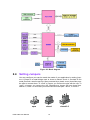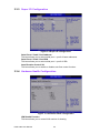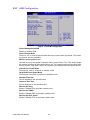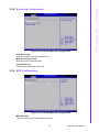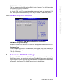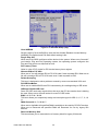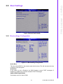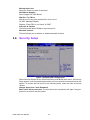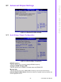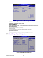
1
User Manual PCM-3362 PC/104-plus SBC with Intel® Atom™ N450, VGA, LCD, LAN, USB2.0, SATA, and on-board flash Copyright The documentation and the software included with this product are copyrighted 2009 by Advantech Co., Ltd. All rights are reserved. Advantech Co., Ltd. reserves the right to make improvements in the products described in this manual at any time without notice. No part of this manual may be reproduced, copied, translated or transmitted in any form or by any means without the prior written permission of Advantech Co., Ltd. Information provided in this manual is intended to be accurate and reliable. However, Advantech Co., Ltd. assumes no responsibility for its use, nor for any infringements of the rights of third parties, which may result from its use. Acknowledgements AMI is a trademark of American Megatrends, Inc. IBM, PC/AT, PS/2 and VGA are trademarks of International Business Machines Corporation. Atom, Pentium, Celeron, and MMX are registered trademarks of Intel Corporation. Microsoft Windows® is a registered trademark of Microsoft Corp. RTL is a trademark of Realtek Semi-Conductor Co., Ltd. ESS is a trademark of ESS Technology, Inc. UMC is a trademark of United Microelectronics Corporation. SMI is a trademark of Silicon Motion, Inc. Creative is a trademark of Creative Technology LTD. All other product names or trademarks are properties of their respective owners. For more information on this and other Advantech products, please visit our websites at: http://www.advantech.com http://www.advantech.com/eplatform For technical support and service, please visit our support website at: http://www.advantech.com/support This manual is for the PCM-3362. PCM-3362 User Manual Part No. 2006336210 Edition 1 Printed in China Dec. 2009 ii Packing List Before you begin installing your card, please make sure that the following materials have been shipped: 1 x PCM-3362 SBC 1 x SATA data cable (p/n: 1700071000) 1 x SATA power cable (p/n: 1703150102) 1 x Keyboard/Mouse cable (p/n: 1703060053) 1 x Y cable for KB/MS extension (p/n: 1700060202) 1 x Ethernet RJ-45 Conn. conversion cable (p/n: 1700017863) 1 x VGA cable (p/n: 1700000898) 1 x USB cable (bracket type with two USB ports) (p/n: 1703100260) 1 x RS-422/485 COM cable (p/n: 1703040157) 1 x RS-232 COM cable (p/n: 1701200220) 1 x ATX Power cable (p/n: 1700002332) 1 x AT Power cable (p/n: 1700003491) 1 x Startup manual 1 x CD-ROM (Manual, Driver, Utility) If any of these items are missing or damaged, contact your distributor or sales representative immediately. Model No.List Description PCM-3362N-S6A1E Intel Atom N450 PC/104-Plus SBC, VGA, LVDS, LAN, USB,SATA and on-board flash Optional Accessory 1 x heatspreader (p/n:1960047106T001) Additional Information and Assistance 1. 2. Visit the Advantech web site at www.advantech.com where you can find the latest information about the product. Contact your distributor, sales representative, or Advantech's customer service center for technical support if you need additional assistance. Please have the following information ready before you call: Product name and serial number Description of your peripheral attachments Description of your software (operating system, version, application software, etc.) A complete description of the problem The exact wording of any error messages Declaration of Conformity This device complies with the requirements in part 15 of the FCC rules: Operation is subject to the following two conditions: 1. This device may not cause harmful interference, and iii PCM-3362 User Manual 2. This device must accept any interference received, including interference that may cause undesired operation FCC Class A This equipment has been tested and found to comply with the limits for a Class A digital device, pursuant to part 15 of the FCC Rules. These limits are designed to provide reasonable protection against harmful interference when the equipment is operated in a commercial environment. This equipment generates, uses, and can radiate radio frequency energy and, if not installed and used in accordance with the instruction manual, may cause harmful interference to radio communications. Opera- thin of this equipment in a residential area is likely to cause harmful interference in which case the user will be required to correct the interference at his own expense. Caution! There is a danger of a new battery exploding if it is incorrectly installed. Do not attempt to recharge, force open, or heat the battery. Replace the battery only with the same or equivalent type recommended by the manflatterer. Discard used batteries according to the manufacturer's instructions. PCM-3362 User Manual iv Contents Chapter 1 General Information ............................1 1.1 1.2 1.3 Introduction ............................................................................................... 2 Features .................................................................................................... 2 Specifications ............................................................................................ 2 1.3.1 Standard PC/104-plus Biscuit SBC Functions .............................. 2 1.3.2 VGA/LVDS Interface ..................................................................... 3 1.3.3 Ethernet Interface ......................................................................... 3 1.3.4 OS support.................................................................................... 3 1.3.5 Mechanical and Environmental..................................................... 3 Board layout: dimensions.......................................................................... 4 Figure 1.1 Board layout: Dimensions (Component Side) ............ 4 Figure 1.2 Board layout: Dimensions (Solder Side)..................... 5 1.4 Chapter 2 Hardware Installation ..........................7 2.1 Jumpers .................................................................................................... 8 Table 2.1: Jumpers...................................................................... 8 Connectors................................................................................................ 8 Table 2.2: Connectors ................................................................. 8 Locating Connectors & block diagram ...................................................... 9 Figure 2.1 Connectors (component side) .................................... 9 Figure 2.2 Connectors (solder side) ............................................ 9 Figure 2.3 Block diagram........................................................... 10 Setting Jumpers ...................................................................................... 10 2.4.1 Clear CMOS (JP1) ...................................................................... 11 Table 2.3: Clear CMOS (JP1).................................................... 11 2.4.2 LVDS Panel Power Select (JP2)................................................. 11 Table 2.4: LVDS Panel Power Select (JP2) .............................. 11 2.4.3 COM3 RS422/RS485 Select (JP3) ............................................. 12 Table 2.5: COM3 RS422/RS485 Select (JP3)........................... 12 2.4.4 PCI I/O Voltage Select (JP4) ...................................................... 12 Table 2.6: PCI I/O Voltage Select (JP4) .................................... 12 Installing SODIMMs ................................................................................ 12 Flash ....................................................................................................... 12 High Definition Audio Interface (CN1) ..................................................... 13 VGA/LCD interface connections ............................................................. 13 2.8.1 CRT display connector (CN8) ..................................................... 13 2.8.2 LVDS connector (CN6) ............................................................... 13 2.8.3 Panel Inverter Power (CN7)........................................................ 13 USB connectors (CN9 & CN10) .............................................................. 13 Front Panel Connector (CN12) ............................................................... 13 Buzzer Connector (CN13)....................................................................... 14 SATA Connector (CN15)......................................................................... 14 COM port connector (CN16 & CN17)...................................................... 14 2.13.1 Serial Port RS-422/485 (CN17) .................................................. 14 Giga LAN Connector (CN18) .................................................................. 14 2.14.1 LAN LED Connector (CN19)....................................................... 14 Keyboard and PS/2 mouse connector (CN20)........................................ 14 GPIO Connector (CN21) ......................................................................... 15 ATX Power in connector (CN23)............................................................. 15 Power Connectors (CN24) ...................................................................... 15 I2C Bus connector (CN25) ...................................................................... 15 -12 V & -5 V power connector (CN26) ................................................... 15 Watchdog timer configuration ................................................................. 15 2.2 2.3 2.4 2.5 2.6 2.7 2.8 2.9 2.10 2.11 2.12 2.13 2.14 2.15 2.16 2.17 2.18 2.19 2.20 2.21 v PCM-3362 User Manual Chapter 3 3.1 3.2 3.3 3.4 3.5 3.6 3.7 3.8 PCM-3362 User Manual AMI BIOS Setup................................. 17 Figure 3.1 Setup program initial screen..................................... 18 Entering Setup ........................................................................................ 18 Main Setup.............................................................................................. 18 Figure 3.2 Main setup screen .................................................... 19 3.2.1 System time / System date ......................................................... 19 Advanced BIOS Features Setup............................................................. 19 Figure 3.3 Advanced BIOS features setup screen .................... 20 3.3.1 CPU Configuration...................................................................... 20 Figure 3.4 CPU Configuration Setting ....................................... 20 3.3.2 IDE Configuration ....................................................................... 21 Figure 3.5 IDE Configuration ..................................................... 21 3.3.3 Super I/O Configuration .............................................................. 22 Figure 3.6 Super I/O Configuration............................................ 22 3.3.4 Hardware Health Configuration .................................................. 22 Figure 3.7 Hardware health configuration ................................. 22 3.3.5 ACPI Settings ............................................................................. 23 Figure 3.8 ACPI Settings ........................................................... 23 Figure 3.9 General ACPI Configuration..................................... 23 Figure 3.10Advanced ACPI Configuration.................................. 24 Figure 3.11Chipset ACPI Configuration ..................................... 24 3.3.6 AHCI Configuration..................................................................... 25 Figure 3.12Advanced ACPI Configuration.................................. 25 3.3.7 APM Configuration...................................................................... 26 Figure 3.13APM Configuration ................................................... 26 3.3.8 Event Log Configuration ............................................................. 27 Figure 3.14South Bridge ACPI Configuration............................. 27 3.3.9 MPS Configuration...................................................................... 27 Figure 3.15South Bridge ACPI Configuration............................. 27 3.3.10 Smbios Configuration ................................................................. 28 Figure 3.16South Bridge ACPI Configuration............................. 28 3.3.11 USB Configuration ...................................................................... 28 Figure 3.17South Bridge ACPI Configuration............................. 28 Figure 3.18USB Mass storage Device Configuration ................. 29 Advanced PCI/PnP Settings ................................................................... 29 Figure 3.19PCI/PNP Setup (top) ................................................ 30 Boot Settings........................................................................................... 31 Figure 3.20Boot Setup Utility...................................................... 31 3.5.1 Boot settings Configuration......................................................... 31 Figure 3.21Boot Setting Configuration ....................................... 31 Security Setup......................................................................................... 32 Figure 3.22Password Configuration ........................................... 32 Advanced Chipset Settings..................................................................... 33 Figure 3.23Advanced Chipset Settings ...................................... 33 3.7.1 North Bridge Chipset Configuration ............................................ 33 Figure 3.24North Bridge Configuration....................................... 33 Figure 3.25Video function configuration ..................................... 34 3.7.2 South Bridge Chipset Configuration ........................................... 34 Figure 3.26South Bridge Configuration ...................................... 34 Exit Option .............................................................................................. 35 Figure 3.27Exit Option................................................................ 35 3.8.1 Save Changes and Exit .............................................................. 35 3.8.2 Discard Changes and Exit .......................................................... 36 3.8.3 Load Optimal Defaults ................................................................ 36 3.8.4 Load Fail-Safe Defaults .............................................................. 36 vi Chapter 4 Software Introduction & Installation ....37 4.1 4.2 S/W Introduction...................................................................................... 38 Driver Installation .................................................................................... 38 4.2.1 Windows XP professional ........................................................... 38 4.2.2 Other OS..................................................................................... 38 Value-Added Software Services ............................................................. 38 4.3.1 SUSI Introduction........................................................................ 38 4.3.2 Software APIs ............................................................................. 39 4.3.3 SUSI Utilities ............................................................................... 40 4.3.4 SUSI Installation ......................................................................... 40 4.3.5 SUSI Sample Programs.............................................................. 42 4.3 Chapter 5 Chipset Software Installation Utility.....49 5.1 5.2 5.3 Before You Begin .................................................................................... 50 Introduction ............................................................................................. 50 Windows XP/Vista/Win7 Driver Setup..................................................... 50 6 Integrated Graphic Device Setup .....51 6.1 6.2 Introduction ............................................................................................. 52 Windows XP/ Vista /Win7 Driver Setup................................................... 52 7 LAN Configuration.............................53 7.1 7.2 7.3 Introduction ............................................................................................. 54 Installation ............................................................................................... 54 Windows XP/ Vista /Win7 Driver Setup................................................... 54 Appendix A Pin Assignments ...............................55 A.1 Jumper and Connector Tables................................................................ 56 Appendix B System Assignments ........................65 B.1 System I/O Ports ..................................................................................... 66 Table B.1: System I/O ports....................................................... 66 1st MB Memory Map ............................................................................... 66 Table B.2: 1st MB memory map ................................................ 66 DMA channel assignments ..................................................................... 66 Table B.3: DMA channel assignments....................................... 66 Interrupt assignments.............................................................................. 67 Table B.4: Interrupt assignments ............................................... 67 Chapter Chapter B.2 B.3 B.4 Appendix C Mechanical Drawings ........................69 C.1 Board Mechanical Drawings ................................................................... 70 Figure C.1 PCM-3362 Mechanical Drawing (Component Side). 70 Figure C.2 PCM-3362 Mechanical Drawing (Solder Side) ......... 71 Heatsink Mechanical Drawings ............................................................... 72 Figure C.3 PCM-3362N Heatsink Mechanical Drawing ............. 72 Figure C.4 PCM-3362Z/Z2 Heatsink Mech Dwg, wide temp...... 72 Optional Heat spreader Mechanical Drawings........................................ 73 Figure C.5 PCM-3362 optional Heatspreader Mech Drawing .... 73 C.2 C.3 vii PCM-3362 User Manual Appendix D Watchdog Timer and GPIO sample code.................................................... 75 D.1 D.2 Watchdog Timer sample code ................................................................ 76 GPIO sample code.................................................................................. 77 PCM-3362 User Manual viii Chapter 1 1 General Information This chapter gives background information on the PCM-3362. Sections include: Introduction Features Specifications Board layout and dimensions 1.1 Introduction The PCM-3362 is a fanless, low power, small size (96X90mm), performance PC/104plus SBC (Single Board Computer) geared to satisfy the needs for various industrial computing equipment. PCM-3362 is ideal for communication, environment monitoring, factory automation, military, and medical applications that require flat panel support using digital displays with LVDS interfaces and single Ethernet ports. For those who want superior performance for various low-power embedded applications, PCM-3362 uses an Intel® Atom™ N450 processor, supporting DDRII 667 SDRAM up to 2GB. PCM-3362 has an integrated graphic core of Intel® Embedded Gen3.5+ graphic technology with 224 MB shared memory. This feature makes PCM-3362 is capable of handling complex and intense 2D/3D graphic processing, its VGA and LVDS dual video outputs also make it suitable for applications requiring dual display or digital panel display capabilities. PCM-3362 offers convenient connector layout, easy assembly, multiple I/Os, and includes a single 10/100/1000 Mbps Ethernet, four USB (Universal Serial Bus) 2.0, one SATA2 interface, 8-bit general purpose Input/Output, two RS-232 serial ports and one RS-422/485 serial port for easy system expansibility. PC/104-plus self-stacking rugged mechanical architecture and extended temperature operation makes it ideal for outdoor applications in the military and transportation fields. Supported operating systems include Windows 7, Windows XP, XP Embedded, Windows CE, and Linux. PCM-3362 also offers drivers and APIs for application development including I2C, GPIO, watchdog timer, hardware monitor, panel backlight on/off, and brightness control. 1.2 Features IIntel® Atom™ N450 Processor Supports DDR2 667 memory Supports 18-bit LVDS LCD interface Supports 1 X SATA2 interface Supports 2GB on-board flash Supports 1 x 10/100/1000 Mbps Fast Ethernet Supports four USB2.0 ports Supports two serial RS-232 ports (COM1/2), one RS-422/485 port(COM3) PC/104-plus expansion interface 1.3 Specifications 1.3.1 Standard PC/104-plus Biscuit SBC Functions CPU: Intel® Atom™ N450 processor, up to 1.67 GHz System Memory: supports Double Data Rate (DDR) DDR2 667 SDRAM up to 2GB Note! PCM-3362 cannot support DDR2 533 SDRAM. PCM-3362 User Manual 2 1.3.2 VGA/LVDS Interface Controller: Integrated graphic core of Embedded Gen3.5+ technology VRAM: 224 MB shared system memory Output Interfaces: – VGA: Supports up to SXGA 1400 x 1060 @ 60Hz – LVDS: Singe channel 18-bit LVDS up to WXGA 1366 x 768 – Dual Display: CRT + LVDS, support extended mode and clone mode 1.3.3 Ethernet Interface Supports Single 10/100/1000 Mbps Ethernet networking Controller: Intel® 82567V 1.3.4 OS support This board supports Win7,Win XP, Win CE and Win XPe. For further information about OS support in your PCM-3362, visit the following Advantech web resource: www.advantech.com or please contact your technical support center. 1.3.5 Mechanical and Environmental Dimensions: 96 x 90 mm (3.8" x 3.5") Mechanical Drawing (dxf file) is available. Power Supply Type: AT/ATX Power Requirement: +5 V ± 5%, +12 V ± 5% (Optional), (5 V only, 12 V optional for PC104 add on card and LCD inverter) Power Consumption: (Intel® Atom™ N450, 1GB DDRII 667) – Power on Load: +5 V @ 2.28 A, +12 V @ 5mA – Max load: +5 V @ 2.37 A, +12 V @ 7mA – Idle mode: +5 V @ 2 A, +12 V @ 5mA Power Consumption Conditions: – Test software: Maxpower + 3DMark 2005 3 PCM-3362 User Manual General Information 2nd Cache Memory: 512 KB on the processor System Chipset: Intel® ICH8M BIOS: AMI 16Mbit Flash BIOS Watchdog timer: 255 levels timer interval Expansion Interface: PC/104-Plus (ISA and PCI bus) Battery: Lithium 3V/210 mAH Power management: ACPI supported Serial ATA: One Serial ATA2 interface, Speed up to 300MB/s Flash: On board 2GB flash (IDE interface) Serial ports: Two serial RS-232 ports (COM1/2), one RS-422/485 port(COM3) Keyboard/mouse connector: Supports one standard PC/AT keyboard and a PS/2 mouse USB: Four USB 2.0 ports compliant universal serial bus ports GPIO: 8 bit general purpose Input/Output High Definition Audio: PCM-3362 can provide audio function with the optional audio extension module PCA-AUDIO-HDA1E and specific audio cable. Chapter 1 – Power on - Boot: Measure the maximum current value of between system power on and boot-up to O.S. – Max. load: Measure the maximum current value which system under maximum load (CPU: Top speed, RAM &Graphic: Full loading) – Idle mode: Measure the current value when system in windows mode and without running any program Operating temperature: 0 ~ 60°C (32 ~ 140°F) (operation humidity: 40°C @ 85% RH Non-Condensing) Weight: 0.85 kg (reference weight of total package) 1.4 Board layout: dimensions Figure 1.1 Board layout: Dimensions (Component Side) PCM-3362 User Manual 4 Chapter 1 General Information Figure 1.2 Board layout: Dimensions (Solder Side) 5 PCM-3362 User Manual PCM-3362 User Manual 6 Chapter 2 2 Hardware Installation This chapter explains the setup procedures of the PCM-3362 hardware, including instructions on setting jumpers and connecting peripherals, switches and indicators. Be sure to read all safety precautions before you begin the installation procedure. 2.1 Jumpers The PCM-3362 has a number of jumpers that allow you to configure your system to suit your application. The table below lists the functions of the various jumpers. Table 2.1: Jumpers JP1 CLEAR CMOS JP2 LVDS Panel Power Select JP3 COM3 RS422/RS485 Select JP4 PCI I/O Voltage Select 2.2 Connectors Onboard connectors link the PCM-3362 to external devices such as hard disk drives, a keyboard, or floppy drives. The table below lists the function of each of the board's connectors. Table 2.2: Connectors Label Function CN1 HD Audio Connector CN4 SO-DIMM Connector CN6 LVDS Connected CN7 Panel Inverter Connector CN8 VGA Connector CN9 USB Port0/1 Connector CN10 USB Port2/3 Connector CN12 Front panel Connector CN13 Buzzer Connector CN15 SATA Connector CN16 COM1~COM2 Connector CN17 RS422/485 Connector CN18 LAN Connector CN19 LAN LED Connector CN20 PS2 Keyboard/Mouse Connector CN21 GPIO Connector CN23 ATX Power In Connector CN24 Power In Connector CN25 I2C BUS connector CN26 -12 V & -5 V power connector P1 PC104-plus Connector BH1 RTC Battery Connector PCM-3362 User Manual 8 Chapter 2 2.3 Locating Connectors & block diagram Hardware Installation Figure 2.1 Connectors (component side) Figure 2.2 Connectors (solder side) 9 PCM-3362 User Manual Figure 2.3 Block diagram 2.4 Setting Jumpers You may configure your card to match the needs of your application by setting jumpers. A jumper is a metal bridge used to close an electric circuit. It consists of two metal pins and a small metal clip (often protected by a plastic cover) that slides over the pins to connect them. To “close” a jumper, you connect the pins with the clip. To “open” a jumper, you remove the clip. Sometimes a jumper will have three pins, labeled 1, 2 and 3. In this case you would connect either pins 1 and 2, or 2 and 3. RSHQ PCM-3362 User Manual FORVHG 10 FORVHG Open Closed Closed 2-3 2.4.1 Clear CMOS (JP1) The PCM-3362 single board computer contains a jumper that can erase CMOS data and reset the system BIOS information. Normally this jumper should be set with pins 1-2 closed. If you want to reset the CMOS data, set CMOS1 to 2-3 closed for just a few seconds, and then move the jumper back to 1-2 closed. This procedure will reset the CMOS to its default setting. Warning! To avoid damaging the computer, always turn off the power supply before clearing CMOS. Table 2.3: Clear CMOS (JP1) Setting Function 1-2 Normal (default) 2-3 Clear CMOS 2.4.2 LVDS Panel Power Select (JP2) Table 2.4: LVDS Panel Power Select (JP2) Setting Function 1-2 5V 2-3 3.3 V (default) 11 PCM-3362 User Manual Hardware Installation A pair of needle-nose pliers may be helpful when working with jumpers. If you have any doubts about the best hardware configuration for your application, contact your local distributor or sales representative before you make any changes. Generally, you simply need a standard cable to make most connections. Chapter 2 The jumper settings are schematically depicted in this manual as follows: 2.4.3 COM3 RS422/RS485 Select (JP3) Table 2.5: COM3 RS422/RS485 Select (JP3) Setting Function 1-2 RS-485 (default) 2-3 RS-422 2.4.4 PCI I/O Voltage Select (JP4) The PCI Host board will always determine the PCI signaling level on the bus by setting all VI/O pins to either 3.3 V or 5 V. If VI/0 is set to 3.3 V, then the system will use 3.3 V I/O signaling, likewise, if VI/O is set to 5 V, then the system will use 5 V I/O signaling. Some PCI host modules may only allow one of the options, while others may provide a jumper to allow the user to select the signaling level. Once the signaling level is selected, the remaining boards in the system must use that signaling level. Table 2.6: PCI I/O Voltage Select (JP4) Setting Function 1-2 5 V (default) 2-3 3.3 V 2.5 Installing SODIMMs The procedures for installing SODIMMs are described below. Please follow these steps carefully. You can install SDRAM memory modules using 200-pin SODIMMs (Small Outline Dual In-line Memory Modules). 1. Ensure that all power supplies to the system are switched off. 2. Tilt the SODIMM card just above the board and slide it into the housing card slot. 3. Push the module into the socket until the module gently snaps in. There should only be a slight insertion force to engage the module into the contacts. Make sure that the module and the housing are aligned and locked in place. 2.6 Flash The board provides onboard NAND Flash memory to replace CF socket. NANDriveTM integrated circuits (IC) are high-performance, fully-integrated, embedded flash solid state drives. They combine an integrated ATA Controller in a multi-chip package. These products are ideal for industrial grade solid state mass storage applications offering new and expanded functionality while enabling cost effective designs. PCM-3362 User Manual 12 2.7 High Definition Audio Interface (CN1) 2.8 VGA/LCD interface connections The PCM-3362’s VGA interface can drive conventional CRT displays and is capable of driving a wide range of LVDS flat panel displays. The board has two connectors to support these displays: one for standard CRT VGA monitors, one for LVDS type LCD panels. 2.8.1 CRT display connector (CN8) CN8 is a 12-pin, dual-inline header used for conventional CRT displays. A simple one-to-one adapter can be used to match CN8 to a standard 15-pin D-SUB connector commonly used for VGA. Users can drive a standard progressive scan analog monitor with pixel resolution up to SXGA 1400 x 1060 @ 60Hz. Pin assignments for CRT display connector CN8 are detailed in Appendix A. 2.8.2 LVDS connector (CN6) The PCM-3362 uses the Intel Atom N450 that supports single -channel 18-bit LVDS panel up to WXGA 1366 x 768 UXGA panel resolution. 2.8.3 Panel Inverter Power (CN7) The LCD inverter is connected to CN7 via a 5-pin connector to provide +5 V/+12 V power to the LCD display. JP2 provides inverter voltage selection function, closing Pin 1, 2 is for 5 V power input inverter; closing Pin 2, 3 is for 3.3 V power input inverter. 2.9 USB connectors (CN9 & CN10) The board provides up to four USB (Universal Serial Bus) ports using Plug and Play. The USB interfaces comply with High Speed USB specification Rev. 2.0 which supports 480 Mbps transfer rate, and are fuse protected. The USB interface is accessed through two 5 x 2-pin pin header connectors. You will need an adapter cable if you use a standard USB connector. The adapter cable has a 5 x 2-pin connector on one end and a USB connector on the other. The USB interfaces can be disabled in the system BIOS setup. 2.10 Front Panel Connector (CN12) You may want to install external switches to monitor and control the PCM-3362. These features are optional: install them only if you need them. Power Button(Pin1 & Pin2) PCM-3362 supports power on/off button. 13 PCM-3362 User Manual Hardware Installation The PCM-3362 provides high definition audio interface. It can support high definition audio stereo by customized audio module that has codec onboard or by Advantech’s PCA-AUDIO-HDA1E module through specific cable. Chapter 2 PCM-3362 supports 2GB industrial grade NAND NANDriveTM IC and up to 4GB for option. Flash endurance is about 100 Million write cycles. Data Retention is about 10 Years. PCM-3362’s NANDriveTM IC supports up to Ultra DMA Mode-4 and endures in wide temperature range of -40°C to +85°C for industrial operation. Reset (Pin3 & Pin4) If you install a reset switch, it should be an open single pole switch. Momentarily pressing the switch will activate a reset. POWER LED (Pin5 & Pin6) POWER LED indicator would light when the power is on. HDD LED (Pin7 & Pin8) The HDD LED indicator for hard disk access is an active low signal. 2.11 Buzzer Connector (CN13) PCM-3362 provides one buzzer connector to connect buzzer for alert function. Buzzer, Advantech’s P/N:1750005282, can be selected to install on board. 2.12 SATA Connector (CN15) In addition to on board 2GB flash, PCM-3362 features one high performance serial ATA interfaces (up to 300 MB/s) that eases cabling to hard drives with thin and long cables while your application need more large storage capacity. 2.13 COM port connector (CN16 & CN17) The board provides three serial ports: two serial RS-232 ports in one 20 pin connector (CN16:COM1/2), and one serial port RS422/485 in 4 pin connector(CN17: COM3). It provides connections for serial devices or a communication network. You can find the pin assignments for the COM port connector in Appendix. 2.13.1 Serial Port RS-422/485 (CN17) COM3 (CN17) can be configured to operate in RS-422 or RS-485 mode by JP3. 2.14 Giga LAN Connector (CN18) PCM-3362 uses the Intel? 82567V Gigabit LAN chips are linked to dedicated PCIe x1 lanes. PCM-3362 provide high throughputs for heavy loading networking environment. LAN connections are made via two internal 10-pin box header. 2.14.1 LAN LED Connector (CN19) PCM-3362 provides an external LAN LED Pin header for connecting to the front side of the chassis. With this convenient design users may know whether the LAN port is acting or not easily. Refer to Appendix for detailed information on the pin assignments. 2.15 Keyboard and PS/2 mouse connector (CN20) The board provides a keyboard connector that supports both a keyboard and a PS/2 style mouse. In most cases, especially in embedded applications, a keyboard is not used. If the keyboard is not present, the standard PC/AT BIOS will report an error or fail during power-on self-test (POST) after a reset. The PCM 3362's BIOS standard setup menu allows you to select "All, But Keyboard" under the "Halt On" selection. This allows no-keyboard operation in embedded system applications, without the system halting under POST. PCM-3362 User Manual 14 The board supports 8-bit GPIO through GPIO connector. The 8 digital inputs and outputs can be programmed to read or control devices, with each input or output defined. 2.17 ATX Power in connector (CN23) Caution! Important Make sure that the ATX power supply can take at least a 10mA load on the 5 V standby lead (5VSB). If not, you may have difficulty powering on your system. 2.18 Power Connectors (CN24) Supplies main power +5 V to the PCM-3362, and to devices that require +12 V. 2.19 I2C Bus connector (CN25) PCM-3362 provides I2C Bus connector for customer connection to I2C protocol embedded device. Advantech also provide I2C API allowing a developer to interface with an embedded system environment and transfer serial messages using the I2C protocols, allowing multiple simultaneous device control. 2.20 -12 V & -5 V power connector (CN26) The PCM-3362 is equipped with a Negative Power Input connector providing -12 V & -5 V power if your applications happen to need it. 2.21 Watchdog timer configuration An onboard watchdog timer reduces the chance of disruptions which EMP (electro magnetic pulse) interference can cause. This is an invaluable protective device for standalone or unmanned applications. Setup involves one jumper and running the control software (refer to Appendix). 15 PCM-3362 User Manual Hardware Installation The PCM-3362 can support an advanced soft power switch function, if an ATX power supply is used. please follow below instruction to enable ATX functions. 1. Plug ATX power cable (1700002332) into CN24. 2. Connect the 3-pin plug of this power cable to CN23 (ATX Power in connector). 3. Connect the power on/off button cable of the chassis to CN12 (front panel connector) pin1-2. Chapter 2 2.16 GPIO Connector (CN21) PCM-3362 User Manual 16 Chapter 3 AMI BIOS Setup 3 AMIBIOS has been integrated into many motherboards for over a decade. With the AMIBIOS Setup program, you can modify BIOS settings and control the various system features. This chapter describes the basic navigation of the PCM-3362 BIOS setup screens. Figure 3.1 Setup program initial screen AMI’s BIOS ROM has a built-in Setup program that allows users to modify the basic system configuration. This information is stored in battery-backed CMOS so it retains the Setup information when the power is turned off. 3.1 Entering Setup Turn on the computer and check for the “patch” code. If there is a number assigned to the patch code, it means that the BIOS supports your CPU. If there is no number assigned to the patch code, please contact an Advantech application engineer to obtain an up-to-date patch code file. This will ensure that your CPU’s system status is valid. After ensuring that you have a number assigned to the patch code, press <DEL> and you will immediately be allowed to enter Setup. 3.2 Main Setup When you first enter the BIOS Setup Utility, you will encounter the Main setup screen. You can always return to the Main setup screen by selecting the Main tab. There are two Main Setup options. They are described in this section. The Main BIOS Setup screen is shown below. PCM-3362 User Manual 18 Chapter 3 3.2.1 System time / System date Use this option to change the system time and date. Highlight System Time or System Date using the <Arrow> keys. Enter new values through the keyboard. Press the <Tab> key or the <Arrow> keys to move between fields. The date must be entered in MM/DD/YY format. The time must be entered in HH:MM:SS format. 3.3 Advanced BIOS Features Setup Select the Advanced tab from the PCM-3362 setup screen to enter the Advanced BIOS Setup screen. You can select any of the items in the left frame of the screen, such as CPU Configuration, to go to the sub menu for that item. You can display an Advanced BIOS Setup option by highlighting it using the <Arrow> keys. All Advanced BIOS Setup options are described in this section. The Advanced BIOS Setup screens is shown below. The sub menus are described on the following pages. 19 PCM-3362 User Manual AMI BIOS Setup Figure 3.2 Main setup screen The Main BIOS setup screen has two main frames. The left frame displays all the options that can be configured. Grayed-out options cannot be configured; options in blue can. The right frame displays the key legend. Above the key legend is an area reserved for a text message. When an option is selected in the left frame, it is highlighted in white. Often a text message will accompany it. Figure 3.3 Advanced BIOS features setup screen 3.3.1 CPU Configuration Figure 3.4 CPU Configuration Setting Max CPUID Value Limit This item allows you to limit CPUID maximum value. Execute-Disable Bit Capability This item allows you to enable or disable the No-Execution page protection technology. Hyper Threading Technology This item allows you to enable or disable Intel® Hyper Threading technology. Intel® SpeedStepTM tech When set to disabled, the CPU runs at its default speed, when set to enabled, the CPU speed is controlled by the operating system. PCM-3362 User Manual 20 3.3.2 IDE Configuration Chapter 3 Intel® C-STATE tech This item allows the CPU to save more power under idle mode. Enhanced C-States CPU idle set to enhanced C-States, disabled by Intel® C-STATE tech item. AMI BIOS Setup Figure 3.5 IDE Configuration ATA/IDE Configuration This item allows you to select Disabled / Compatible / Enhanced. Legacy IDE Channels When set to Enhanced mode you can select IDE or AHCI mode. When select Compatible mode you can select SATA only / SATA pri, PATA sec or PATA only. Primary/Secondary/Third IDE Master BIOS auto detects the presence of IDE device, and displays the status of auto detection of IDE device. Type: Select the type of SATA driver.[Not Installed][Auto][CD/DVD][ARMD] LBA/Large Mode: Enables or Disables the LBA mode. Block (Multi-Sector Transfer): Enables or disables data multi-sectors transfers. PIO Mode: Select the PIO mode. DMA Mode: Select the DMA mode. S.M.A.R.T.: Select the smart monitoring, analysis, and reporting technology. 32Bit Data Transfer: Enables or disables 32-bit data transfer. Hard Disk Write Protect Disable/Enable device write protection. This will be effective only if device is accessed through BIOS. IDE Detect Time Out (Sec) This item allows you to select the time out value for detecting ATA/ATAPI device(s). 21 PCM-3362 User Manual 3.3.3 Super I/O Configuration Figure 3.6 Super I/O Configuration Serial Port1 / Port2 / Port3 address This item allows you to select serial port1 ~ port3 of base addresses. Serial Port1 / Port2 / Port3 IRQ This item allows you to select serial port1 ~ port3 of IRQ. Auto Direction Control Sel This item allows you to enable or disable auto flow control function. 3.3.4 Hardware Health Configuration Figure 3.7 Hardware health configuration H/W Health Function This item allows you to control H/W monitor of showing. PCM-3362 User Manual 22 Chapter 3 Temperature & Voltage show CPU/System Temperature Vcore / +3.3Vin / +5Vin / +12Vin / VBAT 3.3.5 ACPI Settings AMI BIOS Setup Figure 3.8 ACPI Settings 3.3.5.1 General ACPI Configuration Figure 3.9 General ACPI Configuration Suspend mode Select the ACPI state used for system suspend. Report Video on S3 Resume This item allows you to invoke VA BIOS POST on S3/STR resume. 23 PCM-3362 User Manual 3.3.5.2 Advanced ACPI Configuration Figure 3.10 Advanced ACPI Configuration ACPI Version Features This item allows you to enable RSDP pointers to 64-bit fixed system description tables. ACPI APIC support Include APIC table pointer to RSDT pointer list. AMI OEMB table Include OEMB table pointer to R(x)SDT pointer lists. Headless mode Enable / Disable Headless operation mode through ACPI. 3.3.5.3 Chipset ACPI Configuration Figure 3.11 Chipset ACPI Configuration PCM-3362 User Manual 24 Chapter 3 Energy Lake Feature Allows you to configure Intel's Energy Lake power management technology. APIC ACPI SCI IRQ Enable/Disable APIC ACPI SCI IRQ. USB Device Wakeup From S3/S4 Enable/Disable USB Device Wakeup from S3/S4. High Performance Event Timer Enable/Disable High performance Event timer. AMI BIOS Setup 3.3.6 AHCI Configuration Figure 3.12 Advanced ACPI Configuration AHCI Ports0 While entering setup, BIOS auto detects the presence of IDE devices. This displays the status of auto detection of IDE device. 25 PCM-3362 User Manual 3.3.7 APM Configuration Figure 3.13 APM Configuration Power Management/APM Enable or disable APM. Power Button Mode Power on, off, or enter suspend mode when the power button is pressed. The following options are also available. Restore on AC power Loss Use this to set up the system response after a power failure. The "Off" setting keeps the system powered off after power failure, the "On" setting boots up the system after failure, and the "Last State" returns the system to the status just before power failure. Video Power Down Mode Power down video in suspend or standby mode. Hard Disk Power Down Mode Power down Hard Disk in suspend or standby mode. Standby Time Out Go into standby in the specified time. Suspend Time Out Go into Suspend in the specified time. Resume On Ring Enable / Disable RI to generate a wake event. Resume On PME# Enable / Disable PME to generate a wake event. Resume On RTC Alarm Enable / Disable RTC to generate a wake event. PCM-3362 User Manual 26 Chapter 3 3.3.8 Event Log Configuration View Event Log View all unread events on the event Log. Mark all events as read Mark all unread events as read. Clear Event Log Discard all events in the event Log. 3.3.9 MPS Configuration Figure 3.15 South Bridge ACPI Configuration MPS Revision This item allows you to select MPS reversion. 27 PCM-3362 User Manual AMI BIOS Setup Figure 3.14 South Bridge ACPI Configuration 3.3.10 Smbios Configuration Figure 3.16 South Bridge ACPI Configuration Smbios Smi Support SMBIOS SMI wrapper support for PnP function 50h-54h. 3.3.11 USB Configuration Figure 3.17 South Bridge ACPI Configuration Legacy USB Support Enables support for legacy USB. Auto option disables legacy support if no USB devices are connected. USB 2.0 Controller Mode This item allows you to select HiSpeed(480Mbps) or FullSpeed (12Mpbs). PCM-3362 User Manual 28 3.3.11.1 USB Mass Storage Device Configuration Chapter 3 BIOS EHCI Hand-Off This is a workaround for OSes without EHCI hand-off support. The EHCI ownership change should claim by EHCI driver. Hotplug USB FDD Support A dummy FDD device is created that will be associated with the hotplugged FDD later. Auto option creates this dummy device only if there is no USB FDD present. AMI BIOS Setup Figure 3.18 USB Mass storage Device Configuration USB Mass Storage Reset Delay Number of sends POST wait for the USB mass storage device after start unit command. Emulation Type If Auto, USB devices less than 530MB will be emulated as Floppy and remaining as hard drive. Force FDD option can be used to force a FDD formatted drive to boot as FDD (Ex. ZIP drive). 3.4 Advanced PCI/PnP Settings Select the PCI/PnP tab from the PCM-3362 setup screen to enter the Plug and Play BIOS Setup screen. You can display a Plug and Play BIOS Setup option by highlighting it using the <Arrow> keys. All Plug and Play BIOS Setup options are described in this section. The Plug and Play BIOS Setup screen is shown below. 29 PCM-3362 User Manual Figure 3.19 PCI/PNP Setup (top) Clear NVRAM Set this value to force the BIOS to clear the Non-Volatile Random Access Memory (NVRAM).The Optimal and Fail-Safe default setting is No. Plug & Play O/S When set to No, BIOS configures all the device in the system. When set to Yes and if you install a Plug and Play operating system, the operating system configures the Plug and Play device not required for boot. PCI Latency Timer Value in units of PCI clocks for PCI device latency timer register. Allocate IRQ to PCI VGA When set to Yes will assigns IRQ to PCI VGA card if card requests IRQ. When set to No will not assign IRQ to PCI VGA card even if card requests an IRQ. Palette Snooping This item is designed to solve problems caused by some non-standard VGA card. PCI IDE BusMaster When set to enabled BIOS uses PCI busmastering for reading/writing to IDE drives. OffBoard PCI/ISA IDE Card Some PCI IDE cards may require this to be set to the PCI slot number that is holding the card. When set to Auto will works for most PCI IDE cards. IRQ3 / 4 / 5 / 7 / 9 / 10 /11 This item allows you respectively assign an interruptive type for IRQ-3, 4, 5, 7, 9, 10, 11. DMA Channel0 / 1 / 3 / 5 / 6 / 7 When set to Available will specified DMA is available to be used by PCI/PnP devices. When set to Reserved will specified DMA will Reserved for use by legacy ISA devices. Reserved Memory Size This item allows you to reserved size of memory block for legacy ISA device. PCM-3362 User Manual 30 Chapter 3 3.5 Boot Settings AMI BIOS Setup Figure 3.20 Boot Setup Utility 3.5.1 Boot settings Configuration Figure 3.21 Boot Setting Configuration Quick Boot This item allows BIOS to skip certain tests while booting. This will decrease the time needed to boot the system. Quiet Boot If this option is set to Disabled, the BIOS displays normal POST messages. If Enabled, an OEM Logo is shown instead of POST messages. AddOn ROM Display Mode Set display mode for option ROM. 31 PCM-3362 User Manual Bootup Num-Lock Select the Power-on state for Numlock. PS/2 Mouse Support Select support for PS/2 Mouse. Wait For ‘F1’ If Error Wait for the F1 key to be pressed if an error occurs. Hit ‘DEL’ Message Display Displays “Press DEL to run Setup” in POST. Interrupt 19 Capture This item allows option ROMs to trap interrupt 19. Bootsafe function This item allows you to enables or disables bootsafe function. 3.6 Security Setup Figure 3.22 Password Configuration Select Security Setup from the PCM-3362 Setup main BIOS setup menu. All Security Setup options, such as password protection and virus protection are described in this section. To access the sub menu for the following items, select the item and press <Enter>: Change Supervisor / User Password Boot sector Virus protection: The boot sector virus protection will warn if any program tries to write to the boot sector. PCM-3362 User Manual 32 Chapter 3 3.7 Advanced Chipset Settings 3.7.1 North Bridge Chipset Configuration Figure 3.24 North Bridge Configuration DRAM Frequency This item allows you to manually changed DRAM frequency. Configure DRAM Timing by SPD This item allows you to enables or disables detect by DRAM SPD. Memory Hole This item allows you to free 15MB-16MB of memory size for some ISA devices. Internal Graphics Mode Select: Select the amount of system memory used by the Internal graphics device. 33 PCM-3362 User Manual AMI BIOS Setup Figure 3.23 Advanced Chipset Settings Figure 3.25 Video function configuration DVMT Mode Select Displays the active system memory mode. DVMT/FIXED Memory Specify the amount of DVMT / FIXED system memory to allocate for video memory. Boot Display Device Select boot display device at post stage. Flat Panel Type This item allows you to select which panel resolution you wants. Spread Spectrum Clock This item allows you to enables or disables spread spectrum clock. 3.7.2 South Bridge Chipset Configuration Figure 3.26 South Bridge Configuration PCM-3362 User Manual 34 Chapter 3 USB Functions Disabled, 2 USB Ports, or 4 USB Ports. USB 2.0 Controller Enables or disables the USB 2.0 controller. GbE controller Enables or disables the GbE controller. GbE LAN Boot Enables or disables GbE LAN boot. GbE Wake Up From S5 Enables or disables GbE LAN wake up from S5 function. HDA Controller Enables or disables the HDA controller. SMBUS Controller Enables or disables the SMBUS controller. SLP_S4# Min. Assertion Width This item allows you to set a delay of sorts. AMI BIOS Setup 3.8 Exit Option Figure 3.27 Exit Option 3.8.1 Save Changes and Exit When you have completed system configuration, select this option to save your changes, exit BIOS setup and reboot the computer so the new system configuration parameters can take effect. 1. Select Exit Saving Changes from the Exit menu and press <Enter>. The following message appears: Save Configuration Changes and Exit Now? [Ok] [Cancel] 2. Select Ok or cancel. 35 PCM-3362 User Manual 3.8.2 Discard Changes and Exit Select this option to quit Setup without making any permanent changes to the system configuration. 1. Select Exit Discarding Changes from the Exit menu and press <Enter>. The following message appears: Discard Changes and Exit Setup Now? [Ok] [Cancel] 2. Select Ok to discard changes and exit. Discard Changes 3. Select Discard Changes from the Exit menu and press <Enter>. 3.8.3 Load Optimal Defaults The PCM-3362 automatically configures all setup items to optimal settings when you select this option. Optimal Defaults are designed for maximum system performance, but may not work best for all computer applications. In particular, do not use the Optimal Defaults if your computer is experiencing system configuration problems. Select Load Optimal Defaults from the Exit menu and press <Enter>. 3.8.4 Load Fail-Safe Defaults The PCM-3362 automatically configures all setup options to fail-safe settings when you select this option. Fail-Safe Defaults are designed for maximum system stability, but not maximum performance. Select Fail-Safe Defaults if your computer is experiencing system configuration problems. 1. Select Load Fail-Safe Defaults from the Exit menu and press <Enter>. The following message appears: Load Fail-Safe Defaults? [OK] [Cancel] 2. Select OK to load Fail-Safe defaults. PCM-3362 User Manual 36 Chapter 4 4 Software Introduction & Installation 4.1 S/W Introduction The mission of Advantech Embedded Software Services is to "Enhance quality of life with Advantech platforms and Microsoft Windows® embedded technology." We enable Windows® Embedded software products on Advantech platforms to more effectively support the embedded computing community. Customers are freed from the hassle of dealing with multiple vendors (Hardware suppliers, System integrators, Embedded OS distributor) for projects. Our goal is to make Windows® Embedded Software solutions easily and widely available to the embedded computing community. 4.2 Driver Installation 4.2.1 Windows XP professional To install the drivers for Windows XP Professional, insert the CD into the CD-Rom, it will auto-detect the hardware platform and then pop up with the “Embedded Computing Install Wizard” box; just select the drivers that you want to install then click “Install All Selected Drivers”. Follow the Driver Setup Wizard instructions; click "Next" to complete the installation. 4.2.2 Other OS To install the drivers for Other Windows OS or Linux, please browse the CD to run the setup file under each chipset folder on the CD-ROM. 4.3 Value-Added Software Services 4.3.1 SUSI Introduction To make hardware easier and convenient to access for programmers, Advantech has released a suite of API (Application Programming Interface) in the form of a program library. The program Library is called Secured and Unified Smart Interface or SUSI for short. In modern operating systems, user space applications cannot access hardware directly. Drivers are required to access hardware. User space applications access hardware through drivers. Different operating systems usually define different interface for drivers. This means that user space applications call different functions for hardware access in different operating systems. To provide a uniform interface for accessing hardware, an abstraction layer is built on top of the drivers and SUSI is such an abstraction layer. SUSI provides a uniform API for application programmers to access the hardware functions in different Operating Systems and on different Advantech hardware platforms. Application programmers can invoke the functions exported by SUSI instead of calling the drivers directly. The benefit of using SUSI is portability. The same set of API is defined for different Advantech hardware platforms. Also, the same set of API is implemented in different Operating Systems including Windows XP and Windows CE. This user’s manual describes some sample programs and the API in SUSI. The hardware functions currently supported by SUSI can be grouped into a few categories including Watchdog, I2C, SMBus, GPIO, and VGA control. Each category of API in SUSI is briefly described below. PCM-3362 User Manual 38 PCM-3362 supports software APIs including GPIO, I2C, backlight on/off, Brightness control, watchdog, Hardware Monitor, and Power Saving. 4.3.2.1 The GPIO API General Purpose Input/Output is a flexible parallel interface that allows a variety of custom connections. It allows users to monitor the level of signal input or set the output status to switch on/off a device. Our API also provides Programmable GPIO, which allows developers to dynamically set the GPIO input or output status. I2C is a bi-directional two-wire bus that was developed by Philips for use in their televisions in the 1980s and nowadays is used in various types of embedded systems. The strict timing requirements defined in the I2C protocol has been taken care of by SUSI. Instead of asking application programmers to figure out the strict timing requirements in the I2C protocol, the I2C API in SUSI can be used to control I2C devices by invoking other function calls. SUSI provides a consistent programming interface for different Advantech boards. That means user programs using SUSI are portable among different Advantech boards as long as the boards and SUSI provide the required functionalities. Overall product development times can be greatly reduced using SUSI. 4.3.2.3 The Display Control API There are two kinds of VGA control APIs, backlight on/off control and brightness control. Backlight on/off control allows a developer to turn on or off the backlight, and to control brightness smoothly. 1. Brightness Control – The Brightness Control API allows a developer to interface with an embedded device to easily control brightness. 2. Backlight Control – The Backlight API allows a developer to control the backlight (screen) on/off in an embedded device. 4.3.2.4 The Watchdog API A watchdog timer (abbreviated as WDT) is a hardware device which triggers an action, e.g. rebooting the system, if the system does not reset the timer within a specific period of time. The WDT API in SUSI provides developers with functions such as starting the timer, resetting the timer, and setting the timeout value if the hardware requires customized timeout values. 4.3.2.5 The Hardware Monitor API The hardware monitor (abbreviated as HWM) is a system health supervision capability achieved by placing certain I/O chips along with sensors for inspecting the target of interests for certain condition indexes, such as fan speed, temperature and voltage etc. However, due to the inaccuracy among many commercially available hardware monitoring chips, Advantech has developed a unique scheme for hardware monitoring achieved by using a dedicated micro-processor with algorithms specifically designed for providing accurate, real-time and reliable data content; helping protect your system in a more reliable manner. 4.3.2.6 The Power Saving API 1. CPU Speed 39 PCM-3362 User Manual Software Introduction & Installation 4.3.2.2 The I2C API Chapter 4 4.3.2 Software APIs 2. – Make use of Intel SpeedStep technology to reduce power consumption. The system will automatically adjust the CPU Speed depending on system loading. System Throttling – Refers to a series of methods for reducing power consumption in computers by lowering the clock frequency. APIs allow the user to lower the clock from 87.5% to 12.5%. 4.3.3 SUSI Utilities PCM-3362 supports software Utility including Embedded Security ID, Monitoring utility, eSOS. 4.3.3.1 Embedded Security ID The embedded application is the most important property of a system integrator. It contains valuable intellectual property, design knowledge and innovation, but it is easily copied! The Embedded Security ID utility provides reliable security functions for customers to secure their application data within embedded BIOS. 4.3.3.2 Monitoring utility The Monitoring utility allows the customer to monitor system health, including voltage, CPU and system temperature and fan speed. These items are important to a device; if critical errors happen and are not solved immediately, permanent damage may be caused. 4.3.3.3 eSOS The eSOS is a small OS stored in BIOS ROM. It will boot up in case of a main OS crash. It will diagnose the hardware status, and then send an e-mail to a designated administrator. The eSOS also provides remote connection: Telnet server and FTP server, allowing the administrator to rescue the system. Note! eSOS Utility support on PCM-3362 is required to have BIOS modification. 4.3.4 SUSI Installation SUSI supports many different operating systems. Each subsection below describes how to install SUSI and related software on a specific operating system. Please refer to the subsection matching your operating system. 4.3.4.1 Windows XP In windows XP, you can install the library, drivers and demo programs onto the platform easily using the installation tool--The SUSI Library Installer. After the installer has executed, the SUSI Library and related files for Windows XP can be found in the target installation directory. The files are listed in the following table. Directory Contents \Library Susi.lib Library for developing the applications on Windows XP. Susi.dll Dynamic library for SUSI on Windows XP. PCM-3362 User Manual 40 SusiDemo.EXE Demo program on Windows XP. Susi.dll Dynamic library for SUSI on Windows XP. \Demo\SRC Source code of the demo program on Windows XP. The following section illustrates the installation process. The version of the SUSI Library Installer shown on each screen shot below depends on your own particular version. 1. Extract Susi.zip. 2. Double-click the "Setup.exe" file. The installer searches for a previous installation of the SUSI Library. If it locates one, a screen shot opens asking whether you want to modify, repair or remove the software. If a previous version is located, please see the section of [Maintenance Setup]. If it is not located, the following screen shot opens. Click Next. 4.3.4.2 Windows CE In windows CE, there are three ways to install the SUSI Library, you can install it manually or use Advantech CE-Builder to install the library or just copy the programs and the library onto a compact flash card. Express Installation: You can use Advantech CE-Builder to load the library into the image. First, you click the My Component tab. In this tab, you click Add New Category button to add a new category, e.g. the SUSI Library. Then you can add a new file in this category, and upload the SUSI.dll for this category. After these steps, you can select the SUSI Library category you created for every project. Manual Installation: You can add the SUSI Library into the image by editing any bib file. First you open project.bib in the platform builder. Add this line to the MODULES section of project.bib Susi.dll $(_FLATRELEASEDIR)\Susi.dll NK SH If you want to run the window-based demo, add following line: SusiTest.exe $(_FLATRELEASEDIR)\SusiTest.exe If you want to run the console-based demo, add following lines: Watchdog.exe $(_FLATRELEASEDIR)\Watchdog.exe NK S GPIO.exe $(_FLATRELEASEDIR)\GPIO.exe NK S SMBUS.exe $(_FLATRELEASEDIR)\SMBUS.exe NK S Place the three files into any files directory. Build your new Windows CE operating system. 41 PCM-3362 User Manual Software Introduction & Installation Note! Chapter 4 \Demo 4.3.5 SUSI Sample Programs Sample Programs The sample programs demonstrate how to incorporate SUSI into your program. There are sample programs for two categories of operating system, i.e. Windows XP and Windows CE. The sample programs run in graphics mode in Windows XP and Windows CE. The sample programs are described in the subsections below. Windows Graphics Mode There are sample programs of Windows in graphics mode for two categories of operating system, i.e. Windows CE and Windows XP. Each demo application contains an executable file SusiDemo.exe, a shared library Susi.dll and source code within the release package. The files of Windows CE and Windows XP are not compatible with each other. SusiDemo.exe is an executable file and it requires the shared library, Susi.dll, to demonstrate the SUSI functions. The source code of SusiDemo.exe also has two versions, i.e. Windows CE and Windows XP, and must be compiled under Microsoft Visual C++ 6.0 on Windows XP or under Microsoft Embedded Visual C++ 4.0 on Windows CE. Developers must add the header file Susi.h and library Susi.lib to their own projects when they want to develop something with SUSI. SusiDemo.exe The SusiDemo.exe test application is an application which uses all functions of the SUSI Library. It has five major function blocks: Watchdog, GPIO, SMBus, I2C and VGA control. The following screen shot appears when you execute SusiDemo.exe. You can click function tabs to select test functions respectively. Some function tabs will not show on the test application if your platform does not support such functions. For a complete support list, please refer to Appendix A. We describe the steps to test all functions of this application. GPIO PCM-3362 User Manual 42 Chapter 4 Test Read Multiple Input Pin – Click the radio button- Multiple-Pins. – Key in the pin number from ‘0x01’ to ‘0x0F’ to read the value of the input pin. The pin numbers are ordered bitwise, i.e. bit 0 stands for GPIO 0, bit 1 stands for GPIO 1, etc. For example, if you want to read pin 0, 1, and 3, the pin numbers should be ‘0x0B’. – Click READ GPIO DATA button and the statuses of the GPIO pins will be displayed in (R/W) Result field. Test Write Single Output Pin – Click the radio button- Single-Pin. – Key in the pin numbers you want to write. Pin numbers start from '0'. – Key in the value either '0' or '1' in (R/W) Result field to write the output pin you chose above step. – Click the WRITE GPIO DATA button to write the GPIO output pin. Test Write Multiple Output Pins – Click the radio button- Multiple-Pins. – Key in the pin number from ‘0x01’ to ‘0x0F’ to choose the multiple pin numbers to write the value of the output pin. The pin numbers are ordered bitwise, i.e. bit 0 stands for GPIO 0, bit 1 stands for GPIO 1, etc. For example, if you want to write pin 0, 1, and 3, the pin numbers should be ‘0x0B’. – Key in the value in (R/W) Result field from ‘0x01’ to ‘0x0F’ to write the value of the output pin. The pin numbers are ordered bitwise, i.e. bit 0 stands for GPIO 0, bit 1 stands for GPIO 1, etc. For example, if you want to set pin 0 43 PCM-3362 User Manual Software Introduction & Installation When the application is executed, it will display GPIO information in the GPIO INFORMATION group box. It displays the number of input pins and output pins. You can click the radio button to choose to test either the single pin function or multiple pin functions. The GPIO pin assignments of the supported platforms are located in Appendix B. Test Read Single Input Pin – Click the radio button- Single-Pin. – Key in the pin number to read the value of the input pin. The Pin number starts from '0'. – Click the READ GPIO DATA button and the status of the GPIO pin will be displayed in (R/W) Result field. and 1 high, 3 to low, the pin number should be ‘0x0B/, and then you should key in the value ‘0x0A’ to write. – Click the WRITE GPIO DATA button to write the GPIO output pins. I2 C When the application is executed, you can read or write a byte of data through I2C devices. All data must be read or written in hexadecimal system. Read a byte – Key in the slave device address in Slave address field. – Key in the register offset in Register Offset field. – Click the READ A BYTE button and then a byte of data from the device will be shown on the Result field. Write a byte – Key in the slave device address in Slave address field. – Key in the register offset in Register Offset field. – Key in the desirous of data in Result field to write to the device. – Click the WRITE A BYTE button and then the data will be written to the device through I2C. SMBus When the application has executed, you can click the radio button to choose to test each access mode, i.e. Access a byte, Access multiple bytes and Access a word. All data must be read or written in hexadecimal except the numbers for radio button: Access multiple bytes mode must be written in decimal. You can test the functionalities of the watchdog as follows: Read a byte PCM-3362 User Manual 44 Click the radio button- Access a byte. Key in the slave device address in the Slave address field. Key in the register offset in the Register Offset field. Click the READ SMBus DATA button and a byte of data from the device will be shown on the Result field. Write a byte – Click the radio button- Access a byte. – Key in the slave device address in Slave address field. – Key in the register offset in Register Offset field. – Key the desired data in the Result field to write to the device. – Click the WRITE SMBus DATA button and then the data will be written to the device through SMBus. Read a word – Click the radio button- Access a word. – Key in the slave device address in the Slave address field. – Key in the register offset in the Register Offset field. – Click the READ SMBus DATA button and then a word of data from the device will be shown on the Result field. Write a word – Click the radio button- Access a word. – Key in the slave device address in the Slave address field. – Key in the register offset in the Register Offset field. – Key in the desired data, such as 0x1234, in the Result field to write to the device. – Click the WRITE SMBus DATA button and the data will be written to the device through the SMBus. Read Multiple bytes – Click the radio button- Access multiple bytes. – Key in the slave device address in the Slave address field. – Key in the register offset in the Register Offset field. – Key in the desired number of bytes, such as 3, in the right side field of radio button- Access multiple bytes. The number must be written in decimal. – Click the READ SMBus DATA button and then all data from the device will be divided from each other by commas and be shown in the Result field. Write Multiple bytes – Click the radio button- Access multiple bytes. – Key in the slave device address in the Slave address field. – Key in the register offset in the Register Offset field. – Key in the desired number of bytes, such as 3, in the right side field of the radio button- Access multiple bytes. The number must be written in decimal. – Key in all the desired data in the Result field in hexadecimal format, divided by commas, for example, 0x50,0x60,0x7A. – Click the WRITE SMBus DATA button and all of the data will be written to the device through the SMBus. 45 PCM-3362 User Manual Software Introduction & Installation Chapter 4 – – – – Display Control When the application is executed, it will display two blocks of VGA control functions. The application can turn on or turn off the screen shot freely, and it also can tune the brightness of the panels if your platform is being supported. You can test the functionalities of VGA control as follows: Screen on/off control – Click the radio button ON or push the key F11 to turn on the panel screen. – Click the radio button OFF or push the key F12 to turn off the panel screen. – The display chip of your platform must be in the support list in Appendix A, or this function cannot work. Brightness control – Move the slider in increments, using either the mouse or the direction keys, or click the UP button to increase the brightness. – Move the slider in decrements, using either the mouse or the direction keys, or click the DOWN button to decrease the brightness. Watchdog When the application is executed, it will display watchdog information in the WATCHDOG INFORMATION group box. It displays max timeout, min timeout, and timeout steps in milliseconds. For example, a 1~255 seconds watchdog will has 255000 max timeout, 1000 min timeout, and 1000 timeout steps. You can test the functionality of the watchdog as follows: PCM-3362 User Manual 46 Set the timeout value 3000 (3 sec.) in the SET TIMEOUT field and set the delay value 2000 (2 sec.) in the SET DELAY field, then click the START button. The Timeout Countdown field will countdown the watchdog timer and display 5000 (5 sec.). Before the timer counts down to zero, you can reset the timer by clicking the REFRESH button. After you click this button, the Timeout Countdown field will display the value of the SET TIMEOUT field. If you want to stop the watchdog timer, you just click the STOP button. CL When the Monitor application is executed by clicking the button, hardware monitoring data values will be displayed. If certain data values are not supported by the platform, the correspondent data field will be grayed-out with a value of 0. For More detail PCM-3362 software API user manual, please contact your dealer or Advantech AE. We also include these manuals in this CD. 47 PCM-3362 User Manual Software Introduction & Installation Hardware Monitor Chapter 4 PCM-3362 User Manual 48 Chapter 5 Chipset Software Installation Utility 5 5.1 Before You Begin To facilitate the installation of the enhanced display drivers and utility software, read the instructions in this chapter carefully. The drivers for the PCM-3362 are located on the software installation CD. The driver in the folder of the driver CD will guide and link you to the utilities and drivers under a Windows system. Updates are provided via Service Packs from Microsoft*. Note! The files on the software installation CD are compressed. Do not attempt to install the drivers by copying the files manually. You must use the supplied SETUP program to install the drivers. Before you begin, it is important to note that most display drivers need to have the relevant software application already installed in the system prior to installing the enhanced display drivers. In addition, many of the installation procedures assume that you are familiar with both the relevant software applications and operating system commands. Review the relevant operating system commands and the pertinent sections of your application software’s user manual before performing the installation. 5.2 Introduction The Intel® Chipset Software Installation (CSI) utility installs the Windows INF files that outline to the operating system how the chipset components will be configured. This is needed for the proper functioning of the following features: Core PCI PnP services Serial ATA interface support USB 1.1/2.0 support (USB 2.0 driver needs to be installed separately for Win98) Identification of Intel® chipset components in the Device Manager Integrates superior video features. These include filtered sealing of 720 pixel DVD content, and MPEG-2 motion compensation for software DVD 5.3 Windows XP/Vista/Win7 Driver Setup Insert the driver CD into your system’s CD-ROM drive. You can see the driver folder items. Navigate to the "PCM-3362\01_chipset folder, and find folders including Win XP, Vista, and Win 7 and choose which of OS you would like to install, and click "infinst_autol.exe" to complete the installation of the driver. Note! Wrong driver installation may cause unexpected system instability. PCM-3362 User Manual 50 Chapter 6 6 Integrated Graphic Device Setup 6.1 Introduction To benefit from the Intel® Atom N450 integrated graphics controller, you need to install the graphic driver. 6.2 Windows XP/ Vista /Win7 Driver Setup Note! 1. 2. 3. 4. 5. Before installing this driver, make sure the chipset driver has been installed in your system. See Chapter 5 for information on installing the chipset driver. Insert the driver CD into your system’s CD-ROM drive. You can see the driver folder items. Navigate to the "PCM-3362\02_ Graphic folder, and find folders including Win XP, Vista, and Win 7 and choose which of OS you would like to install. Locate and highlight the "igxp32.INF" (if 32-bit) or "igxp64.INF" (if 64-bit).Click on the "Open" button. Click on the "OK" button. A window listing all of the available display types should open. Select the display adapter that your system contains and then click on the "Next" button. Click on the "Next" button. The operating system will install the driver. Click on the "Finish" button when done. Click on the "Close" button and then click on the "Yes" button to reboot. The driver should now be loaded. PCM-3362 User Manual 52 Chapter 7 7 LAN Configuration 7.1 Introduction The PCM-3362 has Gigabit Ethernet LAN via dedicated PCI Express x 1 lanes (Intel 82567V), that offer bandwidth of up to 500 MB/sec, eliminating the bottleneck of network data flow and incorporating Gigabit Ethernet to operate at 1000Mbps. 7.2 Installation Note! Before installing this driver, make sure the chipset driver has been installed in your system. See Chapter 5 for information on installing the chipset driver. The PCM-3362s Intel 82567V Gigabit controller supports all major network operating systems. However, the installation procedure varies with different operating systems. Please find and use the section that provides the driver setup procedure for the operating system you are using. 7.3 Windows XP/ Vista /Win7 Driver Setup Insert the driver CD into your system’s CD-ROM drive. You can see the driver folder items. Navigate to the "PCM-3362\03 LAN” folder and click autorun program to complete the installation of the driver. PCM-3362 User Manual 54 Appendix A A Pin Assignments This appendix contains information of a detailed or specialized nature. Sections include: Jumper and Connector Tables A.1 Jumper and Connector Tables JP1 CLEAR CMOS Part Number 1653003101 Footprint JH3X1V-2M Description PIN HEADER 3*1P 180D(M) 2.0mm DIP SQUARE W/O Pb Setting Function (1-2) NORMAL (Default) (2-3) CLEAR CMOS JP2 LVDS PANEL POWER Select Part Number 1653003101 Footprint JH3X1V-2M Description PIN HEADER 3*1P 180D(M) 2.0mm DIP SQUARE W/O Pb Setting Function (1-2) 5V for +VLVDS_PANEL POWER Select (2-3) 3.3V for +VLVDS_PANEL POWER Select (Default) JP3 COM3 RS422/RS485 Select Part Number 1653003101 Footprint JH3X1V-2M Description PIN HEADER 3*1P 180D(M) 2.0mm DIP SQUARE W/O Pb Setting Function (1-2) RS485 (default) (2-3) RS422 JP4 PCI I/O Voltage Select PCM-3362 User Manual 56 1653002101 Footprint JH2X1V-2M Description PIN HEADER 2*1P 180D(M)SQUARE 2.0mm DIP W/O Pb Setting Function (1-2) 5V for PCI I/O Voltage Select (default) (2-3) 3.3V for PCI I/O Voltage Select CN1 HD Audio Connector Part Number 1653008101 Footprint JH8X1V-2M Description PIN HEADER 8*1P 180D(M) 2.0mm DIP 209-1*8GS Pin Pin Name Signal Type Signal Level 1 +V5 PWR +5 V 2 GND 3 AZ_BITCLK CLK 4 AZ_SYNC I/O 5 AZ_RST# I/O 6 AZ_SDIN0 IN 7 AZ_SDOUT OUT 8 +V12 PWR +12 V CN4 DDR2 SO-DIMM Part Number 1651000087 Footprint DDR-SODIMM-STD65 Description SKT DIMM 200P DDR2 H=6.5mm STD SMD WO/Pb 1 3 17 19 2 4 18 20 CN6 LVDS Connector Part Number 1653910261 Footprint SPH10X2 Description *CONN. SMD 10*2P 180D(M)DF13-20DP-1.25V(91) HRS Pin Pin Name 1 GND 2 GND 3 LVDS0_z_D0+ 4 N/C 5 LVDS0_z_D0- 6 N/C 7 LVDS0_z_D1+ 57 Signal Type Signal Level OUT LVDS OUT LVDS OUT LVDS PCM-3362 User Manual Appendix A Pin Assignments Part Number 8 N/C 9 LVDS0_z_D1- 10 N/C OUT LVDS OUT LVDS OUT LVDS 11 LVDS0_z_D2+ 12 N/C 13 LVDS0_z_D2- 14 N/C 15 LVDS0_z_CLK+ OUT LVDS 16 N/C 17 LVDS0_z_CLK- OUT LVDS 18 N/C 19 +V_LCD PWR +5 V/+3.3 V 20 +V_LCD PWR +5 V/+3.3 V 1 5 CN7 Internal LCD Backlight Part Number 1655305020 Footprint WHL5V-2M Description WAFER BOX 2.0mm 5P 180D(M) W/LOCK Pin Pin Name Signal Type Signal Level 1 +V12_INVERTER PWR +12V 2 GND GND 3 LVDS0_ENABKL OUT +3.3V 4 LVDS0_VBR OUT +3.3V 5 +V5_INVERTER PWR +5V CN8 VGA Connector Part Number 1655912120 Footprint WB12P-S1.25mm Description Wafer Box 1.25mm 12P 90D(M) SMD 85204-12001 Pin Pin Name Signal Type 1 GND GND 2 VGA_z_R OUT +5 V 3 VGA_z_G OUT +5 V 4 VGA_z_B OUT +5 V 5 GND GND 6 +V5_CRT PWR +5 V 7 VGA_z_DDAT OUT +5 V 8 VGA_z_DCLK OUT +5 V 9 GND GND 10 VGA_z_HS OUT +5 V 11 VGA_z_VS OUT +5 V 12 GND GND PCM-3362 User Manual 58 Signal Level 1 6 8 10 3 5 7 9 CN9 USB0/1 Part Number 1653003718 Footprint PH5x2P-SR2.00 Description PIN HEADER 5*2P 2.00mm 90D(M) NO.10 SMD Pin Pin Name Signal Type Signal Level 1 +V5_USB0 PWR +5 V 2 +V5_USB0 PWR +5 V 3 USB0_z_P- I/O 4 USB1_z_P- I/O 5 USB0_z_P+ I/O 6 USB1_z_P+ I/O 7 GND 8 GND 9 GND 2 4 1 6 8 10 3 5 7 9 CN10 USB2/3 Part Number 1653003718 Footprint PH5x2P-SR2.00 Description PIN HEADER 5*2P 2.00mm 90D(M) NO.10 SMD Pin Pin Name Signal Type Signal Level 1 +V5_USB0 PWR +5 V 2 +V5_USB0 PWR +5 V 3 USB2_z_P- I/O 4 USB3_z_P- I/O 5 USB2_z_P+ I/O 6 USB3_z_P+ I/O 7 GND 8 GND 9 GND 59 PCM-3362 User Manual Appendix A Pin Assignments 2 4 CN12 Front panel Connector Part Number 1653008101 Footprint JH8X1V-2M Description PIN HEADER 8*1P 180D(M) 2.0mm DIP 209-1*8GS Pin Pin Name Signal Type Signal Level 1 PSIN# IN +3.3 V 2 GND 3 RESET 4 GND 5 PWR_LED 6 GND 7 +V3.3 PWR 8 HD_LED OUT CN13 Buzzer Connector Part Number 1653002101 Footprint HD_2x1P_79_D Description PIN HEADER 2*1P 180D(M)SQUARE 2.0mm DIP W/O Pb Pin Pin Name Signal Type Signal Level 1 +V3.3 PWR +3.3 V 2 SB_z_SPKR OUT IN OUT CN15 SATA1 connector Part Number 1654000128 Footprint SATA-LD11071S02 Description Serial ATA 7P 90D(M) SMD 15u Reverse +3.3 V Pin Pin Name Signal Type 1 GND GND 2 SATA0_TX+ I/O Analog 3 SATA0_TX- I/O Analog 4 GND GND 5 SATA0_RX- I/O Analog 6 SATA0_RX+ I/O Analog 7 GND GND PCM-3362 User Manual 60 Signal Level 18 20 1 3 17 19 CN16 COM1~COM2 Connector Part Number 1653003720 Footprint HD_10x2P_79_RA Description PIN HEADER 10*2P 2.00mm 90D(M) SMD 21N22050-20J1 Pin Pin Name Signal Type Signal Level 1 COM0_DCD# IN +5 V 2 COM0_DSR# IN +5 V 3 COM0_RXD IN +5 V 4 COM0_RTS# I/O +5 V 5 COM0_TXD OUT +5 V 6 COM0_CTS# IN +5 V 7 COM0_DTR# I/O +5 V 8 COM0_RI# IN +5 V 9 GND 10 GND 11 COM1_DCD# IN +5 V 12 COM1_DSR# IN +5 V 13 COM1_RXD IN +5 V 14 COM1_RTS# I/O +5 V 15 COM1_TXD OUT +5 V 16 COM1_CTS# IN +5 V 17 COM1_DTR# I/O +5 V 18 COM1_RI# IN +5 V 19 GND 20 GND 1 2 3 4 CN17 RS422/485 Connector Part Number 1655304120 Footprint WHL4H-2M_A Description WAFER BOX 2.0mm 4P 90D(M) DIP W/LOCK Pin Pin Name Signal Type Signal Level 1 RS422_RXD- I/O +5 V 2 RS422_RXD+ I/O +5 V 3 RS485_422_TXD+ I/O +5 V 4 RS485_422_TXD- I/O +5 V 61 PCM-3362 User Manual Appendix A Pin Assignments 2 4 2 4 1 6 8 10 3 5 7 9 CN18 LAN Connector Part Number 1653003719 Footprint HD_5x2P_79_RA_21N22050 Description PIN HEADER 5*2P 2.00mm 90D(M) SMD 21N22050-10J10 Pin Pin Name Signal Type A1 GNDT GND A2 GNDT GND A3 LAN1_M3+ I/O Analog A4 LAN1_M3- I/O Analog A5 LAN1_M2+ I/O Analog A6 LAN1_M2+ I/O Analog A7 LAN1_M1+ I/O Analog A8 LAN1_M1+ I/O Analog Signal Level A9 LAN1_M0+ I/O Analog A10 LAN1_M0+ I/O Analog CN19 LAN LED Connector Part Number 1653004101 Footprint HD_4x1P_79_D Description PIN HEADER 4*1P 180D(M) 2.0mm DIP WO/Pb Pin Pin Name Signal Type Signal Level 1 +V3.3_LAN1 PWR +3.3V 2 LAN1_ACT# OUT 3 LAN1_1000# OUT 4 LAN1_100# OUT CN20 PS2 Keyboard/Mouse Connector Part Number 1655306020 Footprint WHL6V-2M Description WAFER BOX 2.0mm 6P 180D(M) W/LOCK Pin Pin Name Signal Type Signal Level 1 KB_z_CLK# I/O +5 V 2 KB_z_DAT# I/O +5 V 3 MS_z_CLK# I/O +5 V 4 GND 5 +V5_KB PWR +5 V 6 MS_z_DAT# I/O +5 V PCM-3362 User Manual 62 GPIO Connector Part Number 1653010102 Footprint JH10X1V-2M Description PIN HEADER 10*1P 180D(M) DIP P=2.0mm Pin Pin Name Signal Type Signal Level 1 +V5_GPIO PWR +5 V 2 DIO_IO0 I/O +5 V 3 DIO_IO1 I/O +5 V 4 DIO_IO2 I/O +5 V 5 DIO_IO3 I/O +5 V 6 DIO_IO4 I/O +5 V 7 DIO_IO5 I/O +5 V 8 DIO_IO6 I/O +5 V 9 DIO_IO7 I/O +5 V 10 GND CN23 ATX Power In Connector Part Number 1655303020 Footprint WHL3V-2M Description WAFER BOX 2.0mm 3P 180D w/LOCK Pin Pin Name Signal Type Signal Level 1 +V5_SB PWR +5 V 2 GND 3 PWR_PSON# IN CN24 Power In Connector Part Number 1655308120 Footprint WHL8H-2M Description Wafer Box 2.0mm 8P 90D Male W/Lock Pin Pin Name Signal Type Signal Level 1 +V5_ATX PWR +5 V 2 +V5_ATX PWR +5 V 3 +V5_ATX PWR +5 V 4 GND 5 GND 6 GND 7 GND 8 +V12 PWR +12 V 63 PCM-3362 User Manual Appendix A Pin Assignments CN21 1 2 3 4 CN25 I2C BUS connector Part Number 1653004101 Footprint HD_4x1P_79_D Description PIN HEADER 4*1P 180D(M) 2.0mm DIP WO/Pb Pin Pin Name 1 GND Signal Type Signal Level 2 I2 C_DAT I/O 3 I2 C_CLK I/O 4 +V5_I2C PWR +5V CN26 -12V & -5V power connector Part Number 1653003101 Footprint HD_3x1P_79_D Description PIN HEADER 3*1P 180D(M) 2.0mm DIP SQUARE W/O Pb Pin Pin Name Signal Type Signal Level 1 -V5 PWR -5 V PWR -12 V 2 GND 3 -V12 PCM-3362 User Manual 64 Appendix B B System Assignments This appendix contains information of a detailed nature. Sections include: System I/O ports 1st MB memory map DMA channel assignments Interrupt assignments B.1 System I/O Ports Table B.1: System I/O ports Addr. range (Hex) Device 000-01F DMA controller 020-021 Interrupt controller 1, master 040-05F 8254 timer 060-06F 8042 (keyboard controller) 070-071 Real-time clock, non-maskable interrupt (NMI) mask 87-8A DMA page register 0A0-0A1 Interrupt controller 2 0C0-0DF DMA controller 1F0-1F8 Fixed disk 278-27F Reserved (Parallel port 2,LTP3) 2E8-2EF Reserved (Series port 4) 2F8-2FF Serial port 2 378-37F Parallel printer port 1 (LPT 2) 3B0-3BF Monochrome display and printer adapter (LPT1) 3D0-3DF Color/graphics monitor adapter 3E8-3EF Series port 3 3F0-3F7 Diskette controller 3F8-3FF Serial port 1 * PNP audio I/O map range from 220 ~ 250H (16 bytes) MPU-401 select from 300 ~ 330H (2 bytes) B.2 1st MB Memory Map Table B.2: 1st MB memory map Addr. range (Hex) Device F0000h - FFFFFh System ROM *CC000h - EFFFFh Unused (reserved for Ethernet ROM) C0000h - CBFFFh Expansion ROM (for VGA BIOS) B8000h - BFFFFh CGA/EGA/VGA text B0000h - B7FFFh Unused A0000h - AFFFFh EGA/VGA graphics 00000h - 9FFFFh Base memory * If Ethernet boot ROM is disabled (Ethernet ROM occupies about 16 KB) * E0000 - EFFFF is reserved for BIOS POST B.3 DMA channel assignments Table B.3: DMA channel assignments Channel Function 0 Available PCM-3362 User Manual 66 Appendix B System Assignments Table B.3: DMA channel assignments 1 Available (audio) 2 Floppy disk (8-bit transfer) 3 Available (parallel port) 4 Cascade for DMA controller 1 5 Available 6 Available 7 Available * Audio DMA select 1, 3, or 5 ** Parallel port DMA select 1 (LPT2) or 3 (LPT1) B.4 Interrupt assignments Table B.4: Interrupt assignments Interrupt# Interrupt source IRQ 0 Interval timer IRQ 1 Keyboard IRQ 2 Interrupt from controller 2 (cascade) IRQ 3 COM2 IRQ 4 COM1 IRQ 5 Reserved (COM4) IRQ 6 FDD IRQ 7 LPT1 IRQ 8 RTC IRQ 9 Reserved (audio) IRQ 10 Reserved (COM3) IRQ 11 Reserved IRQ 12 PS/2 mouse IRQ 13 INT from co-processor IRQ 14 Primary IDE IRQ 15 Reserved 67 PCM-3362 User Manual PCM-3362 User Manual 68 Appendix C C Mechanical Drawings C.1 Board Mechanical Drawings Figure C.1 PCM-3362 Mechanical Drawing (Component Side) PCM-3362 User Manual 70 Appendix C Mechanical Drawings Figure C.2 PCM-3362 Mechanical Drawing (Solder Side) 71 PCM-3362 User Manual C.2 Heatsink Mechanical Drawings Figure C.3 PCM-3362N Heatsink Mechanical Drawing Figure C.4 PCM-3362Z/Z2 Heatsink Mechanical Drawing for wide temperature version PCM-3362 User Manual 72 Figure C.5 PCM-3362 optional Heatspreader Mechanical Drawing 73 PCM-3362 User Manual Appendix C Mechanical Drawings C.3 Optional Heat spreader Mechanical Drawings PCM-3362 User Manual 74 Appendix D D Watchdog Timer and GPIO sample code D.1 Watchdog Timer sample code ;The SCH3114 Runtime base I/O address is A00h ;Setting WatchDog time value location at offset 66h ;If set value "0", it is mean disable WatchDog function. Superio_GPIO_Port = A00h mov dx,Superio_GPIO_Port + 66h mov al,00h out dx,al .model small .486p .stack 256 .data SCH3114_IO EQU A00h .code org 100h .STARTup ;==================================================== ;90H ;enable WDT function bit [0]=01h ;==================================================== mov dx,SCH3114_IO + 90h mov al,01h out dx,al ;==================================================== ;65H ;bit [1:0]=Reserved ;bit [6:2]Reserve=00000 ;bit [7] WDT time-out Value Units Select ;Minutes=0 (default) Seconds=1 ;==================================================== mov dx,SCH3114_IO + 65h ; mov al,080h out dx,al ;==================================================== ;66H ;WDT timer time-out value ;bit[7:0]=0~255 ;==================================================== mov dx,SCH3114_IO + 66h mov al,01h out dx,al ;==================================================== ;bit[0] status bit R/W ;WD timeout occurred =1 ;WD timer counting = 0 ;==================================================== mov dx,SCH3114_IO + 68h mov al,01h out dx,al .exit PCM-3362 User Manual 76 D.2 GPIO sample code ;=============================================================== ; Get Number of GPIO group ; one group mean 8 gpio pins (one GPIO Chip) ; Input: ; ax=5E87h ; bh=00h ; output: ; ax=5E78 ;function success, other value means function fail ; cl= n group of gpio mov ax,5E87h mov bh,00h INT15 ; You will get cl=01 in 8 bit GPIO product, cl = 02 in 16 bit GPIO product ;=============================================================== ;=============================================================== ; Get GPIO Config ; Input: ; ax=5E87h ; bh=01h ; cl= n ; n means which group of GPIO you want to get ; output: ; ax=5E78 ;function success, other value means function fail ; bl= the n group of gpio config ; bit 0 = gpio 0 , 0 => output pin; 1 => input pin ; bit 1 = gpio 1 , 0 => output pin; 1 => input pin ; ..... ; bit 7 = gpio 7 , 0 => output pin; 1 => input pin mov ax,5E87h mov bh,01h mov cl,01h INT15 ; You will get GPIO default setting from bl ;=============================================================== ;=============================================================== ; Set GPIO Config ; Input: ; ax=5E87h ; bh=02h 77 PCM-3362 User Manual Appendix D Watchdog Timer and GPIO sample code END ; cl= n ; n means which group of GPIO you want to set ; bl= the n group of gpio config ; bit 0 = gpio 0 , 0 => output pin; 1 => input pin ; bit 1 = gpio 1 , 0 => output pin; 1 => input pin ; ..... ; bit 7 = gpio 7 , 0 => output pin; 1 => input pin ; output: ; ax=5E78 ;function success, other value means function fail mov ax,5E87h mov bx,02AAh mov cl,01 INT15 ; Set GPIO 0,2,4,6 as output, GPI 1,3,5,7 as input ;=============================================================== ;=============================================================== ; Get GPIO status ; Input: ; ax=5E87h ; bh=03h ; cl= n ; n means which group of GPIO you want to get ; output: ; ax=5E78 ;function success, other value means function fail ; bl= the n group of gpio status ; bit 0 = gpio 0 , 0 => Low; 1 => High ; bit 1 = gpio 1 , 0 => Low; 1 => High ; ..... ; bit 7 = gpio 7 , 0 => Low; 1 => High mov ax,5E87h mov bh,03h mov cl,01h INT15 ; You will get GPIO value from bl ;=============================================================== ;=============================================================== ; Set GPIO status ; Input: ; ax=5E87h ; bh=04h ; cl= n ; n means which group of GPIO you want to set ; bl= the n group of gpio status ; bit 0 = gpio 0 , 0 => Low; 1 => High PCM-3362 User Manual 78 mov ax,5E87h mov bx,0400h mov cl,01 INT15 ; Set GPIO 0,2,4,6 Output Low ;=============================================================== 79 PCM-3362 User Manual Appendix D Watchdog Timer and GPIO sample code ; bit 1 = gpio 1 , 0 => Low; 1 => High ; ..... ; bit 7 = gpio 7 , 0 => Low; 1 => High ; output: ; ax=5E78 ;function success, other value means function fail www.advantech.com Please verify specifications before quoting. This guide is intended for reference purposes only. All product specifications are subject to change without notice. No part of this publication may be reproduced in any form or by any means, electronic, photocopying, recording or otherwise, without prior written permission of the publisher. All brand and product names are trademarks or registered trademarks of their respective companies. © Advantech Co., Ltd. 2009