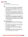
1
cPCI-6965 Series
6U CompactPCI Single Board Computer with
Intel® Core™2 Duo, Celeron® M Processor
User’s Manual
Manual Rev.
2.00
Revision Date:
April 27, 2009
Part No:
50-15068-1000
Advance Technologies; Automate the World.
Revision History
Revision
Release Date
2.00
2009/04/27
Description of Change(s)
Initial Release
cPCI-6965
Preface
Copyright 2009 ADLINK Technology Inc.
This document contains proprietary information protected by copyright. All rights are reserved. No part of this manual may be reproduced by any mechanical, electronic, or other means in any form
without prior written permission of the manufacturer.
Disclaimer
The information in this document is subject to change without prior
notice in order to improve reliability, design, and function and does
not represent a commitment on the part of the manufacturer.
In no event will the manufacturer be liable for direct, indirect, special, incidental, or consequential damages arising out of the use or
inability to use the product or documentation, even if advised of
the possibility of such damages.
Environmental Responsibility
ADLINK is committed to fulfill its social responsibility to global
environmental preservation through compliance with the European Union's Restriction of Hazardous Substances (RoHS) directive and Waste Electrical and Electronic Equipment (WEEE)
directive. Environmental protection is a top priority for ADLINK.
We have enforced measures to ensure that our products, manufacturing processes, components, and raw materials have as little
impact on the environment as possible. When products are at their
end of life, our customers are encouraged to dispose of them in
accordance with the product disposal and/or recovery programs
prescribed by their nation or company.
Trademarks
Product names mentioned herein are used for identification purposes only and may be trademarks and/or registered trademarks
of their respective companies.
Preface
iii
Using this Manual
Audience and Scope
The cPCI-6965 User’s Manual is intended for hardware
technicians and systems operators with knowledge of installing,
configuring and operating industrial grade CompactPCI modules.
Manual Organization
This manual is organized as follows:
Chapter 1, Overview: Introduces the cPCI-6965, its features,
block diagrams, and package contents.
Chapter 2, Specifications: Presents detailed specification
information, and power consumption, and technical drawings.
Chapter 3, Functional Description: Describes the cPCI-6965’s
main functions.
Chapter 4, Board Interfaces: Describes the cPCI-6965 board
interfaces, pin definitions, and jumper settings.
Chapter 5, Getting Started: Describes the installation instructions
of the cPCI-6965.
Chapter 6, Driver Installation: Describes the driver installation
procedures.
Chapter 7, Utilities: Describes the Watchdog Timer and Preboot
Execution Environment functions.
Chapter 8, BIOS Setup Utility: Describes the AMIBIOS®8 BIOS
setup utility.
Important Safety Instructions: Presents safety instructions all
users must follow for the proper setup, installation and usage of
equipment and/or software.
Getting Service: Contact information for ADLINK’s worldwide
offices.
iv
Preface
cPCI-6965
Conventions
Take note of the following conventions used throughout this
manual to make sure that users perform certain tasks and
instructions properly.
Additional information, aids, and tips that help users perform
tasks.
NOTE:
CAUTION:
WARNING:
Preface
Information to prevent minor physical injury, component damage, data loss, and/or program corruption when trying to complete a task.
Information to prevent serious physical injury, component
damage, data loss, and/or program corruption when trying to
complete a specific task.
v
This page intentionally left blank.
vi
Preface
cPCI-6965
Table of Contents
Revision History...................................................................... ii
Preface .................................................................................... iii
List of Tables........................................................................... v
List of Figures ....................................................................... vii
1 Overview ............................................................................. 1
1.1
Introduction .......................................................................... 1
1.2
Features............................................................................... 2
1.3
Block Diagram ..................................................................... 3
1.4
Product List.......................................................................... 4
SBC ................................................................................ 4
Rear Transition Module .................................................. 4
1.5
Package Contents ............................................................... 5
CPU module ................................................................... 5
Rear Transition Module .................................................. 5
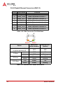
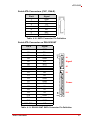
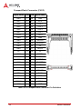
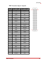
2 Specifications ..................................................................... 7
2.1
cPCI-6965 SBC Specifications ............................................ 7
2.2
cPCI-R6000-965(D) & cPCI-R6000(D)-L
Specifications .......................................................... 10
2.3
I/O Connectivity Table ....................................................... 11
2.4
Power Requirements ......................................................... 13
Power Consumption ..................................................... 14
3 Functional Description .................................................... 15
Intel® Core™2 Duo Processor T7500 .......................... 16
Intel® Celeron® Processor 550 .................................... 17
3.1
Chipset............................................................................... 18
Intel® GME965 Memory Controller Hub ....................... 18
Intel® ICH8 Mobile I/O Controller Hub ......................... 19
Table of Contents
i
3.2
DVI ..................................................................................... 20
3.3
Super I/O ........................................................................... 20
3.4
Battery ............................................................................... 20
3.5
PMC Site............................................................................ 20
3.6
Onboard USB Flash........................................................... 21
4 Board Interfaces................................................................ 23
4.1
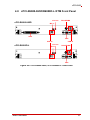
cPCI-6965 SBC Board Layout ........................................... 23
4.2
cPCI-6965 SBC Assembly Layout ..................................... 24
4.3
cPCI-6965 SBC Assembly Layout ..................................... 25
4.4
cPCI-6965, cPCI-6965D SBC Front Panel ........................ 26
System LEDs ................................................................ 27
4.5
cPCI-R6000-965/R6000-L RTM Board Layout ................. 28
4.6
cPCI-R6000-965/R6000-L RTM Front Panel ..................... 29
4.7
cPCI-R6000-965D/6000D-L RTM Board Layout................ 30
4.8
cPCI-R6000-965D/R6000D-L RTM Front Panel................ 31
4.9
Connector Pin Assignments............................................... 32
4.10 Switch and Jumper Settings .............................................. 45
5 Getting Started .................................................................. 49
5.1
CPU and Heatsink ............................................................. 49
5.2
Memory Module Installation ............................................... 50
Installing the Memory Modules ..................................... 50
5.3
CompactFlash Card Installation......................................... 51
5.4
Hard Drive Installation........................................................ 52
5.5
PCI Mezzanine Card (PMC) Installation ............................ 55
5.6
USB Flash Disk Module Installation................................... 59
5.7
Installing the cPCI-6965 to the Chassis ............................. 60
5.8
RTM Installation ................................................................. 61
6 Driver Installation.............................................................. 63
ii
6.1
Chipset Drivers .................................................................. 63
6.2
SCSI Driver ........................................................................ 64
Table of Contents
cPCI-6965
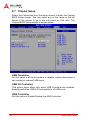
7 Utilities .............................................................................. 65
7.1
Watchdog Timer ................................................................ 65
Using the Watchdog in an Application .......................... 65
Sample Code ................................................................ 66
7.2
Preboot Execution Environment (PXE).............................. 69
8 BIOS Setup Utility............................................................. 71
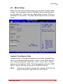
8.1
Starting the BIOS............................................................... 71
Setup Menu .................................................................. 72
Navigation ..................................................................... 72
Hotkey Descriptions ...................................................... 73
8.2
Main Setup......................................................................... 75
System Time/System Date ........................................... 75
8.3
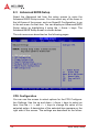
Advanced BIOS Setup....................................................... 76
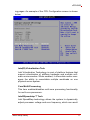
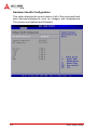
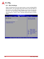
CPU Configuration ........................................................ 76
IDE Configuration ......................................................... 78
Floppy Configuration ..................................................... 79
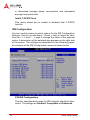
Super IO Configuration ................................................. 80
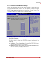
Hardware Health Configuration .................................... 82
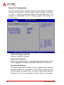
Remote Access Configuration ...................................... 83
USB Configuration ........................................................ 85
8.4
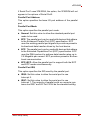
Advanced PCI/PnP Settings .............................................. 87
8.5
Boot Settings ..................................................................... 88
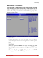
Boot Settings Configuration .......................................... 89
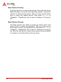
Boot Device Priority ...................................................... 90
Boot Device Groups ...................................................... 90
8.6
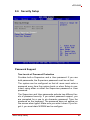
Security Setup ................................................................... 91
Password Support ........................................................ 91
Supervisor Password .................................................... 92
User Password ............................................................. 92
Change Supervisor Password ...................................... 92
Change User Password ................................................ 92
Table of Contents
iii
Clear User Password .................................................... 92
Change Supervisor Password ...................................... 92
Change User Password ................................................ 93
8.7
Chipset Setup .................................................................... 94
USB Functions .............................................................. 94
USB 2.0 Controller ........................................................ 94
HDA Controller .............................................................. 94
Onboard LAN BIOS Init ................................................ 95
8.8
Exit Menu ........................................................................... 96
Save Changes and Exit ................................................ 96
Discard Changes and Exit ............................................ 96
Discard Changes .......................................................... 97
Load Optimal Defaults .................................................. 97
Load Failsafe Defaults .................................................. 97
Important Safety Instructions............................................... 99
Getting Service .................................................................... 101
iv
Table of Contents
cPCI-6965
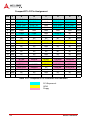
List of Tables
Table
Table
Table
Table
Table
Table
Table
Table
Table
Table
Table
Table
Table
Table
Table
Table
Table
Table
Table
Table
Table
Table
Table
Table
Table
Table
2-1:
2-2:
2-3:
2-4:
2-5:
2-6:
4-1:
4-2:
4-3:
4-4:
4-5:
4-6:
4-7:
4-8:
4-9:
4-10:
4-11:
4-12:
4-13:
4-14:
4-15:
4-16:
4-17:
4-18:
4-19:
4-20:
List of Tables
SBC I/O Connectivity ..............................................
RTM (4HP) I/O Connectivity ...................................
RTM (8HP) I/O Connectivity ...................................
CompactPCI input voltage characteristics ..............
Power consumption of Intel® Core™2 Duo T7500
Power consumption of Intel® Celeron® 550 ..........
cPCI-6965 Front Panel System LED Descriptions .
USB Connector Pin Definition ................................
PS/2 Keyboard/Mouse Connector Pin Definition ....
DVI-D Connector Pin Definition ..............................
DVI-D Connector Pin Definition ..............................
COM1-2 Serial Port Connector Pin Definition ........
Parallel Port Connector Pin Definition ....................
GbE Connector Pin Definitions ...............................
Ethernet LED Status Definitions .............................
SATA Connector Pin Definition ..............................
DB-6910SAT SATA Connector Pin Definition ........
CompactFlash Connector Pin Definition .................
PMC Connector Pin Definition ................................
CompactPCI J1 Connector Pin Definition ...............
CompactPCI J2 Connector Pin Definition ...............
CompactPCI J3 Connector Pin Definition ...............
CompactPCI J5 Connector Pin Definition ...............
COM1 Mode Switch Settings ..................................
COM2 Mode Switch Settings ..................................
PMC V(I/O) Select Jumper Settings .......................
11
12
12
13
14
14
27
32
32
33
34
34
35
36
36
37
37
38
40
41
42
43
44
45
46
47
v
This page intentionally left blank.
vi
List of Tables
cPCI-6965
List of Figures
Figure 1-1:
Figure 3-1:
Figure 4-1:
Figure 4-2:
Figure 4-3:
Figure 4-4:
Figure 4-5:
Figure 4-6:
Figure 4-7:
Figure 4-8:
List of Figures
cPCI-6965 Series Block Diagram .............................. 3
USB Flash Disk Mechanical Layout ........................ 21
cPCI-6965 Board Layout ......................................... 23
cPCI-6965 SBC Assembly Layout........................... 24
cPCI-6965D SBC Assembly Layout ........................ 25
cPCI-6965 Series Front Panel Layout ..................... 26
cPCI-R6000-965, cPCI-R6000-L Board Layout....... 28
cPCI-R6000-965, cPCI-R6000-L Front Panel ......... 29
cPCI-R6000-965D, cPCI-R6000D-L Board Layout . 30
cPCI-R6000-965D, cPCI-R6000D-L Front Panel .... 31
vii
This page intentionally left blank.
viii
List of Figures
cPCI-6965
1
Overview
1.1 Introduction
The cPCI-6965 Series is a highly integrated 6U CompactPCI SBC
in single slot (4HP) or dual slot (8HP) width form factor. It has been
designed to support the Intel® Core™ 2 Duo and Celeron® M processors in 478-pin Micro-FCPGA. The cPCI-6965 is based on the
Mobile Intel® GME965 Express chipset which offers outstanding
graphics and I/O bandwidth, asset management capabilities, storage speed and reliability.
The cPCI-6965 supports dual-channel non-ECC 533/667 MHz
DDR2 memory with a maximum capacity of up to 4GB, 533/800
MHz Front-Side Bus (FSB), and Mobile Intel® Graphics Media
Accelerator X3100 (Intel® GMA X3100). The integrated graphics
support dual independent displays through two DVI outputs on the
front panel.
The cPCI-6965 offers versatile I/O ports such as two Gigabit
Ethernet ports, two RS-232/422/485/485+ selectable serial ports,
four USB 2.0 ports, PS/2 Keyboard/Mouse, and parallel port on
the front panel. Additional I/O can be routed to available Rear
Transition Modules (RTM), including USB, VGA, SCSI, Floppy
port, Mic-in, Line-out, and SATA. The board also supports one
32-bit/33MHz CompactPCI interface and a PMC expansion slot.
Storage features of the cPCI-6965 include a pin header and
mounting space for an onboard USB NAND flash module, two
Serial ATA interfaces with mounting space for a 2.5” HDD, and
CompactFlash socket.
Overview
1
1.2 Features
2
X
6U CompactPCI SBC in 4HP or 8HP width form factor
X
Single Core™ 2 Duo 2.2GHz processor, 4MB L2 cache
X
Front Side Bus 800MHz
X
Mobile Intel® GME965 Memory Controller Hub and ICH8M
I/O Hub
X
Dual Channel DDR2 unbuffered non-ECC SDRAM at
667MHz
X
Two stacked SO-DIMM sockets for maximum up to 4GB
memory
X
32-bit/33MHz CompactPCI Interface based on PCI specifications
X
One DVI-I and one DVI-D port on front panel
X
Supports VGA+DVI or DVI+DVI dual independent displays
X
Two PCI-Express® Gigabit Ethernet egress ports
X
One EIDE CompactFlash socket
X
Space for USB NAND flash module for storage option
X
One SATA port for 2.5” HDD direct mounting and one 7-pin
signal SATA port for external HDD
X
Optional Rear Transition Module
Overview
cPCI-6965
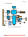
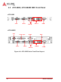
1.3 Block Diagram
Intel®
Core 2 Duo
Processor
533/667/800MHz FSB
F
R
O
N
T
DVI-D
DVI-I
SDVO-A
Sil1362
SDVO-B
Sil1362
Dual Channel 533/667MHz
Intel®
GME965
DDR2 SO-DIMM
DDR2 SO-DIMM
RGB
P
A
N
E
L
J3
DMI (x2/x4)
IDE
GbE 1
®
Intel
82573L
PCIE x1
CF
USB 5
Flash module
Intel®
GbE 2
Intel®
82573L
header
PMC
PCIE x1
ICH8M-DO
SPI
USB 1/2/3/4
SATA 1
COM x2
Parallel
PCI 32b/33M
SATA 2
LPC
PCI
2050B
PCIEx4
J1
BIOS
2.5” HDD
SATA 3, HD Audio, 5x USB, SMBus
SIO
IT8712F
J2
PCI 32b/33M
J3
J5
PS/2 KB/MS
FDD
J5
J3
Figure 1-1: cPCI-6965 Series Block Diagram
Overview
3
1.4 Product List
Products included in the cPCI-6965 Series include:
SBC
X
cPCI-6965: 4HP (single-slot) width 6U CompactPCI featuring Core™2 Duo or Celeron® processor; 512MB, 1GB,
2GB or 4GB memory by SO-DIMM; CompactFlash slot,
2xSATA ports, and 4xUSB, 2xGbE, DVI-D, DVI-I, COM and
J3, J5 connectors
X
cPCI-6965D: 8HP (dual-slot) width 6U CompactPCI featuring Core™2 Duo or Celeron® processor; 512MB, 1GB,
2GB or 4GB memory by SO-DIMM; CompactFlash slot, and
4x USB, 2x GbE, DVI-D, DVI-I, 2xCOM, printer port and J3,
J5 connectors. A DB-6965PMC riser card is included to provide a PMC slot.
X
cPCI-6965DZ: 8HP (dual-slot) width 6U CompactPCI featuring Core™2 Duo or Celeron® processor; 512MB, 1GB,
2GB or 4GB memory by SO-DIMM; CompactFlash slot, and
4x USB, 2x GbE, DVI-D, DVI-I, 2xCOM, printer port without
J3, J5 connectors. A DB-6965PMC riser card is included
to provide a PMC slot.
Rear Transition Module
4
X
cPCI-R6000-965: 4HP width Rear Transition Module for
cPCI-6965 SBCs with 2x USB, VGA, SCSI, Floppy, SATA
port
X
cPCI-R6000-965D: 8HP width Rear Transition Module for
cPCI-6965 SBCs with 4x USB, VGA, SCSI, Floppy, SATA ,
Mic-in, Line-out, PS/2 KB/MS port
X
cPCI-R6000-L: 4HP width Rear Transition Module for
cPCI-6965 SBCs with 2x USB, VGA, Floppy, SATA port
(without SCSI)
X
cPCI-R6000D-L: 8HP width Rear Transition Module for
cPCI-6965 SBCs with 4x USB, VGA, Floppy, SATA , Mic-in,
Line-out, PS/2 KB/MS port (without SCSI)
Overview
cPCI-6965
1.5 Package Contents
The cPCI-6965 is packaged with the following components. If any
of the items on the contents list are missing or damaged, retain the
shipping carton and packing material and contact the dealer for
inspection. Please obtain authorization before returning any product to ADLINK. The packing contents of the cPCI-6965 Series are
non-standard configurations and may vary depending on customer
requests.
CPU module
X
The cPCI-6965 Series CPU Module
Z
CPU, RAM will differ depending on options selected
Z
Thermal module is assembled on the board
X
Y-cable for PS/2 combo port (8HP version only)
X
DVI to VGA adapter
X
2.5” HDD accessory pack, including DB-6910SAT adapter
and screws, standoffs
X
USB NAND flash module screw pack
X
PMC accessory pack, including DB-6965PMC adapter and
screws, standoffs (8HP version only)
X
ADLINK All-in-One CD
X
User’s manual
Rear Transition Module
X
The cPCI-R6000-965, cPCI-R6000-965D, cPCI-R6000-L,
or cPCI-R6000D-L
X
Y-cable for PS/2 combo port (cPCI-R6000-965D,
cPCI-R6000D-L only)
X
DVI-to-VGA adapter
X
68-pin SCSI cable (cPCI-R6000-965, cPCI-R6000-965D
only)
The contents of non-standard cPCI-6965 configurations may
vary depending on the customer’s requirements.
NOTE:
Overview
5
CAUTION:
6
This product must be protected from static discharge and physical shock. Never remove any of the components except at a
static-free workstation. Use the anti-static bag shipped with the
product when putting the board on a surface. Wear an
anti-static wrist strap properly grounded on one of the system's
ESD ground jacks when installing or servicing system components.
Overview
cPCI-6965
2
Specifications
2.1 cPCI-6965 SBC Specifications
CompactPCI
Standard
PICMG® 2.0 CompactPCI® Rev. 3.0
PICMG® 2.1 Hot Swap specification Rev.2.0
Standard 6U CompactPCI®
Board size: 233.23 mm x 160mm
Mechanical
Single-slot (4HP, 20.32mm) or dual-slot (8HP, 40.64mm)
width
CompactPCI® connectors with J1, J2, J4, J5 for
cPCI-6965, cPCI-6965D
CompactPCI® connectors with J1, J2 for cPCI-6965DZ
µFC-PGA Intel® Core™2 Duo 2.2GHz (T7500),
4MB L2 cache, FSB 800MHz
Processor
µFC-PGA Intel® Celeron® 2.0GHz (550), 1MB L2 cache,
FSB 533MHz
Passive heatsink
Chipset
IIntel GME965 Memory Controller Hub (MCH)
Intel ICH8M I/O Controller Hub (ICH)
Memory
Dual channel DDR2-667 un-buffer non-ECC memory
Two SO-DIMM sockets (stacked type)
Maximum 4GB capacity
CompactPCI Bus
PMC
PCI 32bit/ 33MHz; 3.3V, 5V universal V(I/O)
Supports operation in system slot only
One PCI 32bit/ 33MHz PMC, 3.3V, 5V universal V(I/O)
Ethernet
Two PCI-Express x1 Intel® 82573L GbE controllers
Two egress 10/100/1000BASE-T ports
Graphics
GMA X3100 integrated in GME965 GMCH
Shared system memory up to 384 MB
Two DVI ports on front panel: one DVI-I (digital + analog),
one DVI-D (digital only)
Analog signal with up to 32-bit, 2048x1536 resolution @75Hz
Serial Ports
Specifications
Up to two 16C550 compatible DB-9 serial ports from
Super I/O IT8712F
Both ports support RS232/422/485/485+ by switch
selection
7
2.5” SATA HDD direct connector onboard
Storage
Interfaces
7-pin SATA port on board
CompactFlash Type II socket onboard
USB NAND Flash module option
BIOS
AMI® Core 8 16Mbit SPI flash memory
cPCI-6965 (4HP)
4x USB 2.0 ports
2x 10/100/1000BASE-T Ethernet ports
DVI-I port (digital and analog)
DVI-D port (digital only)
DB-9 serial port
cPCI-6965D (8HP)
Front Panel I/O
Supported OS
Microsoft Windows Vista
Microsoft Windows XP Professional
Fedora 7 (requires Intel IEGD driver to support dual
independent displays - contact ADLINK)
Fedora 10
Contact ADLINK for other OS support
Operating
Temperature1
0°C to 55°C with forced air flow
Storage
temperature
Humidity
Shock
Vibration2
Compliance
8
4x USB 2.0 ports
2x 10/100/1000BASE-T Ethernet ports
DVI-I port (digital and analog)
DVI-D port (digital only)
2x DB-9 serial ports
PS/2 Keyboard Mouse Combo port
Parallel port
PMC faceplate
-40°C to 85°C
20% to 90% @60°C non-condensing
15G peak-to-peak, 11ms duration, non-operating
Operating: 1.88G rms. 5 to 500Hz, each axis (without HDD)
CE, FCC Class A
Specifications
cPCI-6965
Notes:
1. ADLINK-certified thermal design. The thermal performance is
dependent on the chassis cooling design. Forced airflow with
16CFM is required. Temperature limit of optional mass storage
devices may affect the thermal specification.
2. The hard drive limits the operational vibration. When application requires higher specification for anti-vibration, it is recommended to use flash disk such as CF or USB flash disk
module.
Specifications are subject to change without prior notice.
NOTE:
Specifications
9
2.2 cPCI-R6000-965(D) & cPCI-R6000(D)-L
Specifications
Standard 6U CompactPCI® rear I/O
Mechanical
Board size: 233.23 mm x 80mm
Single-slot (4HP, 20.32mm) or dual-slot (8HP, 40.64mm) width
CompactPCI® connectors with rJ3 and rJ5
cPCI-R6000-965 (4HP)
2x USB 2.0 ports
VGA port (via DVI dongle)
External 68-pin SCSI connector
cPCI-R6000-L (4HP)
2x USB 2.0 ports
VGA port (via DVI dongle)
cPCI-R6000-965D (8HP)
Rear Panel I/O
4x USB 2.0 ports
VGA port (via DVI dongle)
PS/2 Keyboard Mouse port
External 68-pin SCSI connector
Mic-in, Line out
cPCI-R6000D-L (8HP)
4x USB 2.0 ports
VGA port (via DVI dongle)
PS/2 Keyboard Mouse port
Mic-in, Line out
cPCI-R6000-965, cPCI-R6000-965D
Onboard
Peripherals
Floppy port
7-pin SATA port
Internal 68-pin SCSI connector
cPCI-R6000-L, cPCI-R6000D-L
Floppy port
7-pin SATA port
cPCI-R6000-965, cPCI-R6000-965D
SCSI
LSI® Logic LSI53C1020 PCI-X Ultra320 SCSI Controller
Integrated RAID on PCI-X 64-bit/133MHz bus
320MB per second data transfer rate
Supports RAID 1 (mirroring)
10
Specifications
cPCI-6965
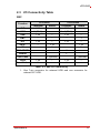
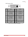
2.3 I/O Connectivity Table
SBC
Function
cPCI-6965
cPCI-6965D
Faceplate
Board
--
GbE
Y x2
COM
Y (DB-9)
Faceplate
Board
Y x2
--
Y x2 (DB-9)
USB
Y x4
--
Y x4
--
PMC
--
--
--
Y
Y x2
DVI
Y x2
--
SATA1
--
Y x2
CF
--
Y
--
Y
PS/2 KB/MS
--
--
Y
--
Parallel
-Y x2
Y
USB Flash
Y (optional)
Y (optional)
LEDs
Y x4
--
Y x4
--
Reset Button
Y
--
Y
--
Table 2-1: SBC I/O Connectivity
1. One 7-pin connector for external HDD and one connector for
onboard 2.5” HDD.
Specifications
11
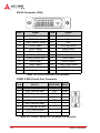
RTM (4HP)
Function
cPCI-R6000-965
cPCI-R6000-L
Faceplate
Board
Faceplate
Board
USB
Y x2
--
Y x2
--
VGA
Y
--
Y
--
SATA
--
Y (7-pin)
--
Y (7-pin)
SCSI
Y
Y
--
--
Floppy
--
Y
--
Y
Table 2-2: RTM (4HP) I/O Connectivity
RTM (8HP)
Function
cPCI-R6000-965D
cPCI-R6000D-L
Faceplate
Board
Faceplate
Board
USB
Y x4
--
Y x4
--
VGA
Y
--
Y
--
SATA
--
Y (7-pin)
--
Y (7-pin)
PS/2 KB/MS
Y
--
Y
--
Mic/Line-out
Y
--
Y
--
SCSI
Y
Y
--
--
Floppy
--
Y
--
Y
Table 2-3: RTM (8HP) I/O Connectivity
12
Specifications
cPCI-6965
2.4 Power Requirements
In order to guarantee a stable functionality of the system, it is recommended to provide more power than the system requires. An
industrial power supply unit should be able to provide at least
twice as much power as the entire system requires of each
voltage. An ATX power supply unit should be able to provide at
least three times as much power as the entire system requires.
The tolerance of the voltage lines described in the CompactPCI
specification (PICMG 2.0 R3.0) is +5%/ -3% for 5, 3.3 V and ±5%
for ±12V. This specification is for power delivered to each slot and
it includes both the power supply and the backplane tolerance.
Voltage
Nominal
Value
Tolerance
Max. Ripple
(P - P)
5V
+5.0 VDC
+5% / -3%
50 mV
3.3V
+3.3 VDC
+5% / -3%
50 mV
+12V
+12 VDC
+5% / -5%
240 mV
-12V
-12 VDC
+5% / -5%
240 mV
V I/O (PCI I/O
Buffer Voltage)
+3.3 VDC or
+5 VDC
+5% / -3%
50 mV
GND
Table 2-4: CompactPCI Input Voltage Characteristics
Specifications
13
Power Consumption
The following tables provide information on the power consumption of the cPCI-6965 Series when using the Intel® Core 2 Duo
T7500 or Celeron 550 processor with 2x 2GB SO-DIMM and
onboard 60GB SATA hard drive. The systems were tested in Idle
Mode and Full Loading Mode under Windows XP. The cPCI-6965
is powered by single 5V power rail.
Intel® Core™2 Duo T7500
OS/Mode
Current 5V Total Power
DOS/Idle mode
5.712 A
28.56 W
Linux/Idle mode
3.411 A
17.055 W
Windows XP/
Idle mode
3.490 A
17.45 W
Windows® XP/
CPU 100% Usage
9.416 A
47.08 W
Table 2-5: Intel® Core™2 Duo T7500 Power Consumption
Intel® Celeron® 550
OS/Mode
Current 5V Total Power
DOS/Idle mode
5.860 A
27.93 W
Linux/Idle mode
4.200 A
21.00 W
Windows XP/
Idle mode
4.278 A
21.39 W
Windows® XP/
CPU 100% Usage
6.534 A
32.67 W
Table 2-6: Intel® Celeron® 550 Power Consumption
14
Specifications
cPCI-6965
3
Functional Description
The following sections describe the cPCI-6965 Series features
and functions.
The following table lists the processors supported by the
cPCI-6965 Series and their power ratings.
Features
Clock
L2 cache
FSB
Maximum Power (TDP1)
Tjunction_MAX
2
Intel® Core™2 Duo T7500
Intel® Celeron® 550
2.2 GHz
2.0 GHz
4MB
1MB
800MHz
533MHz
35W
27W
100°C
100°C
Notes:
1. The highest expected sustainable power while running known
power intensive applications. TDP is not the maximum power
that the processor can dissipate.
2. The maximum supported operating temperature.
Functional Description
15
Intel® Core™2 Duo Processor T7500
The Intel® Core™2 Duo T7500 processor is a high-performance,
low-power processor based on the Intel® Core™ microarchitecture and 65-nm process technology. The Intel Core 2 Duo processor supports the Mobile Intel® 965 Express Chipset and Intel®
82801HBM ICH8M Controller Hub Based Systems.
The following list outlines the key features of this processor:
16
X
Dual core processor for mobile applications with enhanced
performance
X
Intel architecture with Intel® Wide Dynamic Execution
X
L1 Cache to Cache (C2C) transfer
X
On-die, primary 32-KB instruction cache and 32-KB
write-back data cache in each core
X
On-die, up to 4-MB second level shared cache with
advanced transfer cache architecture
X
Streaming SIMD Extensions 2 (SSE2), Streaming SIMD
Extensions 3 (SSE3) and Supplemental Streaming SIMD
Extensions 3 (SSSE3)
X
800-MHz Source-Synchronous Front Side Bus (FSB)
X
Advanced power management features including Enhanced Intel
SpeedStep® Technology and Dynamic FSB frequency switching.
X
Intel Enhanced Deeper Sleep state with P_LVL5 I/O support
X
Digital Thermal Sensor (DTS)
X
Intel® 64 Technology
X
Enhanced Intel® Virtualization Technology
X
Intel® Dynamic Acceleration Technology
X
Enhanced Multi Threaded Thermal Management (EMTTM)
X
Execute Disable Bit support for enhanced security
Functional Description
cPCI-6965
Intel® Celeron® Processor 550
The following list provides some of the key features of this processor:
X
Single core
X
On-die, primary 32-KB instruction cache and 32-KB
write-back data cache
X
On-die, 1-MB second level shared cache with advanced
transfer cache architecture
X
533-MHz source-synchronous front side bus (FSB)
X
Supports Intel® architecture with dynamic execution
X
Data prefetch logic
X
Micro-FCPGA packaging technology
X
MMX™ technology, Streaming SIMD Extensions (SSE),
Streaming SIMD Extensions 2 (SSE2), Streaming SIMD
Extensions 3 (SSE3), and Supplemental Streaming SIMD
Extensions 3 (SSSE 3)
X
Digital Thermal Sensor (DTS)
X
Execute Disable Bit support for enhanced security
X
Intel® 64 architecture (formerly Intel® EM64T)
X
Architectural and performance enhancements of the Core
microarchitecture
Functional Description
17
3.1 Chipset
The cPCI-6965 Series incorporates the Mobile Intel® GME965
Memory Controller Hub (MCH) and ICH8 Mobile (ICH8M) I/O Controller Hub.
Intel® GME965 Memory Controller Hub
The following outlines the key features of GME965 MCH.
Processor Support
X
Intel® Core™2 Duo Mobile Processor for Mobile Intel 965
Express Chipset Family
X
533 MHz and 800 MHz FSB support
X
Intel® Dynamic Front Side Bus Frequency Switching
X
36-bit interface to addressing, allowing the CPU to access
the entire 64GB of the (G)MCH memory address space.
System Memory Support
X
Supports dual-channel DDR2 SDRAM
X
One SO-DIMM connector or module per channel
X
Maximum 4GB memory supported
X
64-bit side per channel
X
Support for DDR2 at 667MHz and 533 MHz
X
256-Mb, 512-Mb, and 1-Gb memory technologies supported
X
Support for x8 and x16 devices
X
No support for ECC
Direct Management Interface
18
X
Chip-to-chip interface between (G)MCH and 82801
GMB/GHM
X
Configurable as x2 or x4 DMI lanes
X
2-GB/s (1-GB/s each direction) point-to-point interface to
Intel® 82801 GBM/GHM
X
32-bit downstream address
Functional Description
cPCI-6965
Integrated Graphics
X
Mobile Intel® Graphics Media Accelerator X3100 (Mobile®
Intel® GMA X3100)
X
Supports a QXGA maximum resolution of 2048x1536 at
60Hz, 32-bpp reduced blanking timing (driver limited)
X
Supports Analog TV-Out, LVDS, Analog CRT and SDVO
(the cPCI-6965 implements analog CRT and SDVO only)
X
Intel® Smart 2D Display Technology (Intel® S2DDT)
X
Video Capture via x1 concurrent PCI Express port
X
Dynamic Video Memory Technology (DVMT 4.0; 384 Maximum)
X
Microsoft DirectX 9
X
SGI OpenGL 1.5
X
Display Hot Plug support
X
Two SDVO ports supported (the cPCI-6965D is designed
with a DVI 1.0 port for External Digital Monitor)
Intel® ICH8 Mobile I/O Controller Hub
The ICH8M provides extensive I/O support. Functions and capabilities include:
X
Provides 6 PCI Expressx1 ports, supporting the PCI
Express Base Specification, Revision 1.1. Each Root Port
supports 2.5GB/s bandwidth in each direction. The
cPCI-6965 utilizes two PCI Expressx1 ports for two Gigabit
Ethernet controllers and routes two PCI Express x1 ports to
board-to-board connector and J2 connector for expansion
capability
X
Enhanced DMA controller, interrupt controller, and timer functions
X
Integrated Serial ATA host controller with independent DMA
operation on three ports
X
Integrated IDE controller supports Ultra ATA100/66/33
X
System Management Bus (SMBus) Specification, Version
2.0 with additional support for I2C devices
X
Supports Intel® Matrix Storage technology
X
PCI Local Bus Specification, Revision 2.3 support for
33MHz PCI operations
Functional Description
19
3.2 DVI
The Silicon Image SDVO PanelLink Transmitter Sil1362 is
designed into the cPCI-6965 to convert the SDVO signal to a DVI
interface. The Sil1362A is fully compliant with Intel SDVO 1.0 and
DVI 1.0.
3.3 Super I/O
The ITE IT8712F Super I/O is on a Low Pin Count interface supporting PS/2 keyboard/mouse; two 16550-compatible serial ports;
floppy drive interface; hardware monitor function to monitor CPU
voltage, CPU temperature, power supply voltages and system
temperature; and Watch Dog Timer with time resolution from minimum 1 second to maximum 255 minutes.
3.4 Battery
The cPCI-6965 is provided with a 3.0V coin cell lithium battery for
the Real Time Clock (RTC). The battery socket is equipped on the
daughter board DB-6965BAT. The lithium battery must be
replaced with an identical battery or a battery type recommended
by the manufacturer. A Panasonic CR2032 is equipped on board
by default.
3.5 PMC Site
The cPCI-6965 series supports a PMC site for front panel I/O
expansion. The PMC site provides a 32bit/33MHz PCI bus link
from the Intel® ICH8M I/O Hub. The PMC site supports +3.3V and
5V signaling.
20
Functional Description
cPCI-6965
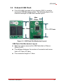
3.6 Onboard USB Flash
X
The cPCI-6965 provides a 9-pin header (CN7) to install a
horizontal USB flash disk module. The following figure illustrates an example of USB flash module layout.
Max.
29mm
Max. 39mm
27.3 ~ 27.9 mm
Figure 3-1: USB Flash Disk Mechanical Layout
USB Flash Disk Mechanical Layout
X
Maximum space reserved for USB flash disk is 39mm x
29mm (LxW)
X
The distance between the centers of connector and screw
hole is 27.3mm~27.9mm
X
The connector height is 7.4mm
Functional Description
21
This page intentionally left blank.
22
Functional Description
cPCI-6965
4
Board Interfaces
This chapter illustrates the board layout, connector pin
assignments, and jumper settings to familiarize users with the
cPCI-6965 Series.
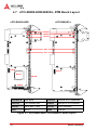
4.1 cPCI-6965 SBC Board Layout
CN10-12
CN9
CN15
CN4
CN6
CN2
CN3
CN8
CN1
U16
U19
CN13
U10
U4
U18
U21
CN14
CN7
CN5
JN1
JN2
J1
SODIMM
J2
J3
J5
U10
CPU socket
CN3/5
7-pin SATA connector
U4
North Bridge Intel® GME965
CN8/15
Serial ports
U18
South Bridge Intel® ICH8M
CN7
DB-6965L2 connector
U16/19
GbE Controller Intel® 82573L CN9~12
USB ports
U21
Super I/O
CN13
CF socket
CN1
PS/2 connector
CN14
DB-6910SAT connector
CN2/4
DVI connectors
JN1/2
DB-6965PMC connector
CN3
Printer port
J1/2/3/5
CompactPCI connectors
CN6
Dual RJ-45 GbE ports
SODIMM
Stacked SO-DIMM sockets
Figure 4-1: cPCI-6965 Board Layout
Board Interfaces
23
4.2 cPCI-6965 SBC Assembly Layout
This section describes the final assembly layout of cPCI-6965 (4HP).
Heatsink
2.5” SATA HDD
USB flash disk
DB-6910SAT
DDR2 SODIMM
modules
Figure 4-2: cPCI-6965 SBC Assembly Layout
24
Board Interfaces
cPCI-6965
4.3 cPCI-6965 SBC Assembly Layout
This section describes the final assembly layout of cPCI-6965D
(8HP). The dual-slot width cPCI-6965D is comprised of the cPCI6965 single-slot main board and the DB-6965PMC riser card (Upper1
and Upper2 are the PMC connectors).
CF
Card
Heatsink
USB flash disk
Upper1
DB-6965PMC
Upper2
Figure 4-3: cPCI-6965D SBC Assembly Layout
Board Interfaces
25
4.4 cPCI-6965, cPCI-6965D SBC Front Panel
cPCI-6965
DVI-I
DVI-D
GbE 1/2
USB x4
COM2
cPCI-6965D
PS/2
Printer port
DVI-I
COM1
DVI-D
PMC
USB x4
GbE 1/2
COM2
Figure 4-4: cPCI-6965 Series Front Panel Layout
26
Board Interfaces
cPCI-6965
System LEDs
HD
PW
LED
Color
Power
(PW)
Green
General
Purpose
(GP)
Blue
WDT
(WDT)
Amber
HDD
(HD)
Red
WDT
GP
RST
Condition
Indication
OFF
System is off
ON
System is on
OFF
Reserved for user definition
OFF
No Watchdog event
ON
Watchdog event alert
OFF
No read/write access to HDD
ON
HDD is installed
Blink
Data read/write in process
Table 4-1: cPCI-6965 Front Panel System LED Descriptions
Board Interfaces
27
4.5 cPCI-R6000-965/R6000-L RTM Board Layout
cPCI-R6000-965
cPCI-R6000-L
rJ5
rJ5
CNY1-R
CNY1-R
U26-R
CN16-R
CN15-R
CN16-R
CN15-R
rJ3
rJ3
CN14-R
CN1-R
CN14-R
CN1-R
U31-R
CN12-R
CN5-R
U26-R
PCI-E to PCI bridge
CN12-R
External SCSI connector
U31-R
SCSI controller
CN15/16-R USB ports
CN1-R
SATA port (7-pin)
CNY1-R
DVI to VGA adapter
CN5-R
Internal SCSI connector
CN14-R
DB-R6000L2 connector(1)
rJ3-J5
CompactPCI Connectors
Figure 4-5: cPCI-R6000-965, cPCI-R6000-L Board Layout
Note(1): Used for cPCI-R6000-965D and cPCI-R6000D-L RTM (8HP) only –
shown here for clarity.
28
Board Interfaces
cPCI-6965
4.6 cPCI-R6000-965/R6000-L RTM Front Panel
cPCI-R6000-965
SCSI
USB x2
VGA
cPCI-R6000-L
Figure 4-6: cPCI-R6000-965, cPCI-R6000-L Front Panel
Board Interfaces
29
4.7 cPCI-R6000-965D/6000D-L RTM Board Layout
cPCI-R6000-965D
cPCI-R6000D-L
CN19-R
CN18-R
CN11-R
PH2
PH1
CN1-R
CN1-R
U31-R
CN12-R
CN5-R
ʳʳʳʳ
CN18/19-R
USB ports
CN12-R
External SCSI connector
CN11-R
PS/2 KB/MS port
CN5-R
Internal SCSI connector
CN1-R
SATA port (7-pin)
U31-R
SCSI controller
PH1
Mic-in
PH2
Line-out
Figure 4-7: cPCI-R6000-965D, cPCI-R6000D-L Board Layout
30
Board Interfaces
cPCI-6965
4.8 cPCI-R6000-965D/R6000D-L RTM Front Panel
cPCI-R6000-965D
Line-out
Mic-in
PS/2 KB/MS
SCSI
VGA
USB x2
cPCI-R6000D-L
Line-out
Mic-in
USB x2
PS/2 KB/MS
VGA
Figure 4-8: cPCI-R6000-965D, cPCI-R6000D-L Front Panel
Board Interfaces
31
4.9 Connector Pin Assignments
USB Connectors (CN9-12)
Pin # Signal Name
1
Vcc
2
UV0-
3
UV0+
4
GND
Table 4-2: USB Connector Pin Definition
PS/2 Keyboard/Mouse Connector
Pin #
Signal
Function
1
KBDATA
Keyboard Data
2
MSDATA
Mouse Data
3
GND
Ground
4
+5V
Power
5
KBCLK
Keyboard Clock
6
MSCLK
Mouse Clock
Table 4-3: PS/2 Keyboard/Mouse Connector Pin Definition
32
Board Interfaces
cPCI-6965
DVI-I Connector (CN2)
Pin #
Signal
Pin #
Signal
1
TMDS Data2-
16
Hot Plug Detect
2
TMDS Data2+
17
TMDS Data0-
3
TMDS Data2/4 Shield
18
TMDSData0+
4
TMDS Data4-
19
TMDS Data0/5 Shield
5
TMDS Data4+
20
TMDS Data5-
6
DDC Clock [SCL]
21
TMDS Data5+
7
DDC Data [SDA]
22
TMDS Clock Shield
8
Analog vertical sync
23
TMDS Clock +
9
TMDS Data1-
24
TMDS Clock -
10
TMDS Data1+
C1
Analog Red
11
TMDS Data1/3 Shield
C2
Analog Green
12
TMDS Data3-
C3
Analog Blue
13
TMDS Data3+
C4
Analog Horizontal Sync
14
+5 V Power
C5
Analog GND Return
15
GND
Table 4-4: DVI-D Connector Pin Definition
Board Interfaces
33
DVI-D Connector (CN4)
Pin #
Signal
Pin #
Signal
1
TMDS Data2-
13
TMDS Data3+
2
TMDS Data2+
14
+5 V Power
3
TMDS Data2/4 Shield
15
GND
4
TMDS Data4-
16
Hot Plug Detect
5
TMDS Data4+
17
TMDS Data0-
6
DDC Clock [SCL]
18
TMDSData0+
7
DDC Data [SDA]
19
TMDS Data0/5 Shield
8
Analog vertical sync
20
TMDS Data5-
9
TMDS Data1-
21
TMDS Data5+
10
TMDS Data1+
22
TMDS Clock Shield
11
TMDS Data1/3 Shield
23
TMDS Clock +
12
TMDS Data3-
24
TMDS Clock -
Table 4-5: DVI-D Connector Pin Definition
COM1-2 DB-9 Serial Port Connector
Pin #
RS-232
1
DCD, Data carrier detect
RS422/485+ RS485
TXD-
Data-
2
RXD, Receive data
TXD+
Data+
3
TXD, Transmit data
RXD+
--
4
DTR, Data terminal ready
RXD
--
5
IsoGND, Isolated ground
GND
GND
6
DSR, Data set ready
--
--
7
RTS, Request to send
--
--
8
CTS, Clear to send
--
--
9
RI, Ring indicator
--
--
Table 4-6: COM1-2 Serial Port Connector Pin Definition
34
Board Interfaces
cPCI-6965
Parallel Port
Pin #
Signal Name
Pin # Signal Name
1
STROBE
14
AUTO FEED
2
DATA0
15
ERROR
3
DATA1
16
INIT
4
DATA2
17
SELECT IN
5
DATA3
18
GND
6
DATA4
19
GND
7
DATA5
20
GND
8
DATA6
21
GND
9
DATA7
22
GND
10
ACKNOWLEDGE
23
GND
11
BUSY
24
GND
12
PAPER EMPTY
25
GND
13
SELECT
Table 4-7: Parallel Port Connector Pin Definition
Board Interfaces
35
RJ-45 Gigabit Ethernet Connectors (GbE1-2)
Pin # Signal Name
Function
1
LANB_TX0P
Media Dependent Interface 1+
2
LANB_TX0N
Media Dependent Interface 1-
3
LANB_TX1P
Media Dependent Interface 2+
4
LANB_TX1N
Media Dependent Interface 2-
5
LANB_TX2P
Media Dependent Interface 3+
6
LANB_TX2N
Media Dependent Interface 3-
7
LANB_TX3P
Media Dependent Interface 4+
8
LANB_TX3N
Media Dependent Interface 4-
Table 4-8: GbE Connector Pin Definitions
1
8
Status
Speed LED
(Green/Amber)
Activity LED
(Amber)
Network link is not established
or system powered off
OFF
OFF
OFF
ON
Active
OFF
Blinking
Link
Green
ON
Active
Green
Blinking
Link
Amber
ON
Active
Amber
Blinking
10 Mbps
100 Mbps
1000 Mbps
Link
Table 4-9: Ethernet LED Status Definitions
36
Board Interfaces
cPCI-6965
Serial ATA Connectors (CN7, CN4-R)
Pin #
Signal
1
2
3
4
5
6
7
GND
TX+
TXGND
RXRX+
GND
1
7
Table 4-10: SATA Connector Pin Definition
Serial ATA Connector on DB-6910SAT
Pin #
Signal
S1
GND
S2
TX+
S3
TX-
S4
GND
S1
S5
RX-
Signal
S6
RX+
S7
GND
P1
NC
P2
NC
P3
NC
P4
GND
P5
GND
P6
GND
P7
5V
P8
5V
P9
5V
P10
GND
P11
Reserved
P12
GND
P13~P15
NC
S7
P1
Power
P15
Table 4-11: DB-6910SAT SATA Connector Pin Definition
Board Interfaces
37
CompactFlash Connector (CN13)
Signal Name Pin# Pin# Signal Name
GND
1
26
GND
DD3
2
27
DD11
DD4
3
28
DD12
DD5
4
29
DD13
DD6
5
30
DD14
DD7
6
31
DD15
CS1J
7
32
CS3J
GND
8
33
GND
GND
9
34
SDIORJ
GND
10
35
SDIOWJ
GND
11
36
5V
GND
12
37
IRQ15
5V
13
38
5V
GND
14
39
PCSEL
GND
15
40
NC
GND
16
41
BRSTDRVJ
GND
17
42
SDIORDY
DA2
18
43
NC
DA1
19
44
SDACKJ
DA0
20
45
IDEACTJ
DD0
21
46
DIAG
DD1
22
47
DD8
DD2
23
48
DD9
IOIS16J
24
49
DD10
GND
25
50
GND
Table 4-12: CompactFlash Connector Pin Definition
38
Board Interfaces
cPCI-6965
PMC Connector (Upper1, Upper2)
Pin#
Upper1 Signal
Upper2 Signal
1
PMC_TCK
+12V
2
-12V
TRST#
3
GND
TMS
4
INTA#
NC
5
INTB#
TDI
6
INTC#
GND
7
MOD1#
GND
8
+5V
NC
9
INTD#
NC
10
NC
NC
11
GND
MODE2#
12
+3V3
+3.3V
13
CLK33
RST2#
14
GND
MODE3#
15
GND
+3.3V
16
GNT3#
MOD4#
17
REQ3#
PME#
18
+5V
GND
19
VIO
AD30
20
AD31
AD29
21
AD28
GND
22
AD27
AD26
23
AD25
AD24
24
GND
+3.3V
25
GND
IDSEL
26
CBE3#
AD23
27
AD22
+3.3V
28
AD21
AD20
29
AD19
AD18
30
+5V
GND
31
VIO
AD16
32
AD17
CBE2#
33
FRAME#
GND
Board Interfaces
39
Pin#
Upper1 Signal
Upper2 Signal
34
GND
NC
35
GND
TRDY#
36
IRDY#
+3.3V
37
DEVSEL#
GND
38
+5V
STOP#
39
PCIXCAP
PERR#
40
LOCK-L
GND
41
NC
+3.3V
42
NC
SERR#
43
PAR
CBE1#
44
GND
GND
45
VIO
AD14
46
AD15
AD13
47
AD12
M66EN
48
AD11
AD10
49
AD9
AD8
50
+5V
+3.3V
51
GND
AD7
52
CBE0#
NC
53
AD6
+3.3
54
AD5
NC
55
AD4
NC
56
GND
GND
57
VIO
NC
58
AD3
NC
59
AD2
GND
60
AD1
NC
61
AD0
ACK64#
62
+5V
+3.3V
63
GND
GND
64
REQ64#
NC
Table 4-13: PMC Connector Pin Definition
40
Board Interfaces
cPCI-6965
CompactPCI J1 Connector Pin Assignment
Pin
Z
A
B
C
D
E
F
1
GND
+5V
NC
TRST#
NC
+5V
GND
2
GND
TCK#
+5V
TMS#
NC
TDI#
GND
3
GND
IRQA#
IRQB#
IRQC#
+5V
IRQD#
GND
4
GND
+5V_IPMB
HEALTHY#
VIO
NC
NC
GND
5
GND
NC
NC
RESET#
GND
GNT0#
GND
6
GND
REQ0#
GND
NC
CLK0
AD31
GND
7
GND
AD30
AD29
AD28
GND
AD27
GND
8
GND
AD26
GND
VIO
AD25
AD24
GND
9
GND
CBE3#
NC
AD23
GND
AD22
GND
10
GND
AD21
GND
NC
AD20
AD19
GND
11
GND
AD18
AD17
AD16
GND
CBE2#
GND
GND
NC
FRAME#
IRDY#
NC
TRDY#
GND
16
GND
DEVSEL#
PCIXCAP
VIO
STOP#
LOCK#
GND
17
GND
NC
IPMB_CLK
IPMB_DAT
GND
PERR#
GND
18
GND
SERR#
GND
NC
PAR
CBE1#
GND
19
GND
NC
AD15
AD14
GND
AD13
GND
20
GND
AD12
GND
VIO
AD11
AD10
GND
21
GND
NC
AD9
AD8
M66EN
CBE0#
GND
22
GND
AD7
GND
NC
AD6
AD5
GND
23
GND
NC
AD4
AD3
+5V
AD2
GND
24
GND
AD1
+5V
VIO
AD0
ACK64#
GND
25
GND
+5V
REQ64#
ENUM#
NC
+5V
GND
12-14
15
Key
Table 4-14: CompactPCI J1 Connector Pin Definition
Board Interfaces
41
CompactPCI J2 Connector Pin Assignment
Pin
Z
A
B
C
D
E
F
1
GND
CLK1
GND
REQ1#
GNT1#
REQ2#
GND
2
GND
CLK2
CLK3
SYSEN#
CGNT2#
REQ3#
GND
3
GND
CLK4
GND
GNT3#
REQ4#
GNT4#
GND
4
GND
VIO
NC
Pull up
GND
Pull up
GND
5
GND
Pull up
GND
VIO
Pull up
Pull up
GND
6
GND
Pull up
Pull up
Pull up
GND
Pull up
GND
7
GND
Pull up
GND
VIO
Pull up
Pull up
GND
8
GND
Pull up
Pull up
Pull up
GND
Pull up
GND
9
GND
Pull up
GND
VIO
Pull up
Pull up
GND
10
GND
Pull up
Pull up
Pull up
GND
Pull up
GND
11
GND
Pull up
GND
VIO
Pull up
Pull up
GND
12
GND
Pull up
Pull up
Pull up
VIO
Pull up
GND
13
GND
Pull up
GND
VIO
Pull up
Pull up
GND
14
GND
Pull up
Pull up
Pull up
GND
Pull up
GND
15
GND
NC
GND
FAL#
REQ5#
GNT5#
GND
16
GND
NC
NC
DEG#
GND
NC
GND
17
GND
NC
GNC
J2_RST#
REQ6#
GNT6#
GND
18
GND
NC
NC
NC
GND
NC
GND
19
GND
GND
GND
NC
NC
NC
GND
20
GND
CLK5
GND
NC
GND
NC
GND
21
GND
CLK6
GND
NC
NC
NC
GND
22
GND
GA4
GA3
GA2
GA1
GA0
GND
Table 4-15: CompactPCI J2 Connector Pin Definition
42
Board Interfaces
cPCI-6965
CompactPCI J3 Pin Assignment
Pin Z
A
B
1 GND
HDA_RST-L
HDA_SYNC
C
D
2 GND
HAD_SDIN1
HAD_SDIN2
HAD_SDIN3
NC
NC
GND
3 GND
PS2-KBD
PS2-KBC
NC
PS2-MSD
PS2-MSC
GND
HDA_BIT_CLK HDA_SDOUT
E
F
HAD_SDIN0 GND
4 GND
SATA-T2P
SATA-T2N
GND
NC
NC
GND
5 GND
GND
GND
NC
GND
GND
GND
6 GND
SATA-R2P
SATA-R2N
GND
NC
NC
GND
7 GND
NC
NC
NC
I2C_CLK
I2C_DAT
GND
8 GND
NC
NC
NC
NC
NC
GND
9 GND
NC
NC
RGB-BLUE
RGB-RED
10 GND
USB-OC#
11 GND
USB-P8
USB-N8
GND
USB-P9
USB-N9
GND
12 GND
USB-P6
USB-N6
GND
USB-P7
USB-N7
GND
13 GND
NC
NC
GND
USB-P5
USB-N5
GND
14 GND
NC
USB-OC5#
USB-OC6#
USB-OC7#
USB-OC8#
GND
15 GND
NC
NC
GND
NC
NC
GND
16 GND
NC
NC
GND
NC
NC
GND
17 GND
NC
NC
GND
NC
NC
GND
RGB-DDCCLK RGB-DDCDAT RGB-HSYNC
RGB-GREEN GND
RGB-VSYNC GND
18 GND
NC
NC
GND
NC
NC
GND
19 GND
+5V
+5V
+12V
+5V
+5V
GND
Table 4-16: CompactPCI J3 Connector Pin Definition
High Definition Audio
PS/2 Keyboard/Mouse
Serial ATA
RGB
USB port
I2C
Board Interfaces
43
CompactPCI J5 Pin Assignment
Pin
Z
A
B
C
D
E
F
1
GND
PCIE-TX0+
PCIE-TX0-
GND
PCIE-RX0+
PCIE-RX0-
GND
2
GND
PCIE-TX1+
PCIE-TX1-
GND
PCIE-RX1+
PCIE-RX1-
GND
3
GND
PCIE-TX2+
PCIE-TX2-
GND
PCIE-RX2+
PCIE-RX2-
GND
4
GND
PCIE-TX3+
PCIE-TX3-
GND
PCIE-RX3+
PCIERX3-
GND
5
GND
GND
GND
GND
GND
GND
GND
6
GND
CLK0+
CLK0-
GND
RESET#
NC
GND
7
GND
NC
NC
NC
NC
NC
GND
8
GND
NC
NC
NC
NC
NC
GND
9
GND
GPIO0
GPIO1
GPIO2
GPIO3
GPIO4
GND
10
GND
NC
NC
GND
NC
NC
GND
11
GND
NC
NC
GND
NC
NC
GND
12
GND
NC
NC
NC
NC
NC
GND
13
GND
NC
NC
NC
NC
NC
GND
14
GND
NC
NC
GND
NC
NC
GND
15
GND
NC
NC
NC
NC
NC
GND
16
GND
MTR0#
INDEX#
GPIO6
FDEDIN#
DENSEL#
GND
17
GND
DIR#
NC
GPIO7
DSEL0#
NC
GND
18
GND
TRK0#
WGATE#
GPIO9
WDATA#
STEP#
GND
19
GND
DSKCHG#
HDSEL#
NC
RDATA#
WRPORT#
GND
20
GND
NC
NC
GND
NC
NC
GND
21
GND
NC
NC
GND
NC
NC
GND
22
GND
NC
NC
NC
NC
NC
GND
Table 4-17: CompactPCI J5 Connector Pin Definition
PCI-Express x4
GPIO
Floppy
44
Board Interfaces
cPCI-6965
4.10 Switch and Jumper Settings
COM1 Mode Selection Switches (SW1~SW4)
This is switch is to select COM1 to be RS-232 full modem or
RS-422, RS-485, RS-485+ half Duplex mode. RS-232 full
modem is set by default.
RS-232
Full Modem
RS-422
Half Duplex
RS-485
Half Duplex
RS-485+
Half Duplex
Location
SW1
SW2
SW3
SW4
1
OFF
ON
ON
ON
2
OFF
OFF
OFF
OFF
3
OFF
OFF
ON
ON
4
OFF
OFF
OFF
OFF
1
ON
OFF
OFF
OFF
2
ON
ON
ON
ON
3
OFF
OFF
OFF
OFF
4
OFF
OFF
ON
ON
1
ON
OFF
OFF
OFF
2
ON
OFF
ON
ON
3
OFF
ON
OFF
OFF
4
OFF
OFF
ON
ON
1
OFF
OFF
OFF
OFF
2
OFF
OFF
ON
ON
3
ON
OFF
OFF
OFF
4
ON
ON
ON
ON
Table 4-18: COM1 Mode Switch Settings
Board Interfaces
45
COM2 Mode Selection Switches (SW5~SW8)
This is switch is to select COM2 to be RS-232 full modem or
RS-422, RS-485, RS-485+ half Duplex mode. RS-232 full
modem is set by default.
RS-232
Full Modem
RS-422
Half Duplex
RS-485
Half Duplex
RS-485+
Half Duplex
Location
SW5
SW6
SW7
SW8
1
OFF
ON
ON
ON
2
OFF
OFF
OFF
OFF
3
OFF
ON
OFF
ON
4
OFF
OFF
OFF
OFF
1
ON
OFF
OFF
OFF
2
ON
ON
ON
ON
3
OFF
OFF
OFF
OFF
4
OFF
ON
OFF
ON
1
ON
OFF
OFF
OFF
2
ON
ON
OFF
ON
3
OFF
OFF
ON
OFF
4
OFF
ON
OFF
ON
1
OFF
OFF
OFF
OFF
2
OFF
ON
OFF
ON
3
ON
OFF
OFF
OFF
4
ON
ON
ON
ON
Table 4-19: COM2 Mode Switch Settings
46
Board Interfaces
cPCI-6965
Clear CMOS Switch (SW9)
The cPCI-6965 series comes with a Clear CMOS switch to
reset the CMOS values to default. Press the Switch SW9
located near the J1 connector to clear the CMOS.
PMC V(I/O) Select Jumper (JPX1)
JPX1 is a three pin jumper for +3.3V or 5V PMC VIO signaling
selection.
Status
JPX1
5V
3.3V (Default)
Table 4-20: PMC V(I/O) Select Jumper Settings
Pin 1 of JPX1 is indicated by the thicker line printed on the
PCB.
NOTE:
Board Interfaces
47
This page intentionally left blank.
48
Board Interfaces
cPCI-6965
5
Getting Started
This chapter describes the installation of the following components
to the cPCI-6965 and rear transition modules:
X
Memory module
X
CompactFlash card
X
2.5” SATA hard drive
X
PMC module
X
USB Flash Disk module
X
cPCI-6965 CPU module installation to chassis
X
RTM installation to chassis
5.1 CPU and Heatsink
The cPCI-6965 Series comes with CPU and heatsink pre-installed.
Uninstalling the heatsink is not recommended. If it is necessary to
do so, please check that the thermal pad is not damaged before you
re-install the heatsink to the board. Contact ADLINK to obtain the
appropriate thermal pad for the cPCI-6965 or for any other assistance.
Getting Started
49
5.2 Memory Module Installation
The cPCI-6965 Series supports DDR2-667 unbuffered non-ECC
memory modules via two stacked-type SO-DIMM sockets. The
SO-DIMM modules have a 200-pin footprint and are notched to
facilitate correct installation in the SO-DIMM sockets. At lease one
memory module will be pre-installed in the lower socket.
Installing the Memory Modules
Align the notch in the memory module with the key on the
SO-DIMM slot. Press down on the module until is it is properly
seated in the socket.
50
Getting Started
cPCI-6965
5.3 CompactFlash Card Installation
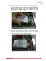
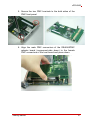
1. Remove the card retaining bracket from board by removing
the two screws as shown.
2. Insert the CF card into the CF slot, then replace the card
retaining bracket to prevent the CF card from sliding out
of the slot.
Getting Started
51
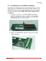
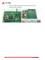
5.4 Hard Drive Installation
The cPCI-6965 Series provides space to install a slim type 2.5”
Serial-ATA hard drive and comes with the required installation
hardware. The HDD adapter kit includes screws, standoffs and
SATA adapter board (DB-6910SAT).
1. Attach the four standoffs provided with the HDD adapter
kit onto the SATA hard drive as shown below.
2. Attach the DB-6910SAT adapter board to the hard drive
connectors.
52
Getting Started
cPCI-6965
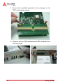
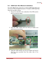
3. Position the hard drive assembly on the cPCI-6965 so
that the standoffs on the hard drive align with the screw
holes on the board, and the connector on the
DB-6910SAT adapter board is aligned with the
board-to-board connector (CN14).
4. Press the DB-6910SAT adapter to the board-to-board
connector until it is properly seated. Secure the adapter
to the board with the two screws provided.
Getting Started
53
5. Secure the hard drive with four screws from the board’s
solder side.
CAUTION:
54
When removing the hard drive, be careful to grasp the adapter
board and lift upwards in a vertical motion to disconnect it from
the board-to-board connector. This will avoid damaging the
adapter board and connectors.
Getting Started
cPCI-6965
5.5 PCI Mezzanine Card (PMC) Installation
The PMC slot is designed to support 3.3V and 5V V(I/O), and the
default setting is 3.3V. Before you install the PMC module on the
cPCI-6965, please make sure that the PMC V(I/O) jumper JPX1
has been correctly set (see “PMC V(I/O) Select Jumper (JPX1)”
on page 47).
1. There is a 3.3V key on the DB-6965PMC by default, if
the PMC module you wish to install is 5V signaling,
please switch the key to the 5V location and set the PMC
V(I/O) jumper JPX1 to the 5V setting.
2. Attach the DB-6965PMC adapter board onto the PMC
module as shown.
Getting Started
55
3. Secure the standoffs provided in the package to the
PMC assembly as shown.
4. Remove the two PMC brackets and PMC faceplate from
the front panel.
56
Getting Started
cPCI-6965
5. Secure the two PMC brackets to the both sides of the
PMC front panel.
6. Align the male PMC connectors of the DB-6965PMC
adapter board (component-side down) to the female
PMC connectors of the host board and press down.
Getting Started
57
7. Secure the PMC assembly to the host board with the six
screws provided as shown.
58
Getting Started
cPCI-6965
5.6 USB Flash Disk Module Installation
The cPCI-6965 Series supports an onboard USB Flash Disk module via the CN5 pin header connector. To install a USB Flash Disk,
follow the procedure below.
1. Secure the standoff to the underside of the USB module
with the screw provided.
2. Align the USB module with the CN5 pin header and
mounting hole as shown.
3. Insert the USB module onto the pin header and secure
with the screw provided from the solder side of the
cPCI-6965.
Getting Started
59
5.7 Installing the cPCI-6965 to the Chassis
The cPCI-6965 may be installed in a system or peripheral slot of a
6U CompactPCI chassis. These instructions are for reference
only. Refer to the user guide that comes with the chassis for more
information.
1. Be sure to select the correct slot depending on the operational purpose of the module. The system power may
now be powered on or off.
2. Remove the blank face cover from the selected slot, if
necessary.
3. Press down on the release catches of the cPCI-6965
ejector handles.
4. Remove the black plastic caps securing the mounting screws to the front panel.
5. Align the module’s top and bottom edges to the chassis
card guides, and then carefully slide the module into the
chassis. A slight resistance may be felt when inserting
the module. If the resistance it too strong, check if there
are bent pins on the backplane or if the board’s connector pins are not properly aligned with connectors on the
backplane. Then push the board until it is completely
flush with the chassis.
6. Push the ejector handles outwards to secure the module
in place, and then fasten the screws on the module front
panel.
7. Connect the cables and peripherals to the board, and
then turn the chassis on if necessary.
60
Getting Started
cPCI-6965
5.8 RTM Installation
The installation and removal procedures for a RTM are the same
as those for CompactPCI boards. Because they are shorter than
front boards, pay careful attention when inserting or removing
RTMs.
Refer to previous sections for peripheral connectivity of all I/O
ports on the RTM. When installing the cPCI-6965 Series and
related RTMs, make sure the RTM is the correct matching model.
NOTE:
You must install the correct RTM to enable functions (I/O interfaces) on the rear panel. Installation of non-compatible RTMs
may damage the system board and/or other RTMs.
Getting Started
61
This page intentionally left blank.
62
Getting Started
cPCI-6965
6
Driver Installation
6.1 Chipset Drivers
The cPCI-6965 drivers are available from the ADLINK All-In-One
CD at X:\cPCI\cPCI-6965\, or from the ADLINK website
(http://www.adlinktech.com). The following describes the driver
installation procedures for Windows® XP.
1. Install the Windows operating system before installing
any driver. Most standard I/O device drivers are installed
during Windows installation.
2. Install the chipset driver by running the program
...\Chipset\infinst_autol[9.0.0.1008].exe.
3. Install the VGA driver and utilities by running the program
...\Graphics\Windows XP Professional\win2k_xp1434.exe.
4. Install the LAN drivers by running the program
...\LAN\Windows XP Professional\PRO2KXP[13.0].exe.
5. Install the SCSI driver for RTM cPCI-R6000-965(D) if
required. Refer to “SCSI Driver” on page 64.
We recommend using the chipset, VGA, and LAN drivers provided
on the ADLINK All-in-One CD or downloaded from the ADLINK
website to ensure compatibility. Contact ADLINK to get support for
Linux and VxWorks BSP drivers.
Driver Installation
63
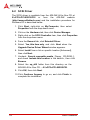
6.2 SCSI Driver
The SCSI driver is available from the ADLINK All-In-One CD at
X:cPCI\cPCI-6920\SCSI or from the ADLINK website
(http://www.adlinktech.com) and the installation procedure for
Windows XP is described below.
1. Click Start, right-click on My Computer, then select
Properties from the drop-down menu.
2. Click on the Hardware tab, then click Device Manager.
3. Right-click on the SCSI Controller item, then click Properties
from the drop-down menu.
4. From the General tab, click Reinstall Driver.
5. Select Yes, this time only and click Next when the
Upgrade Device Driver Wizard window appears.
6. Select Install from a list on specific location [Advanced],
then click Next.
7. Uncheck Search removable media [floppy, CD-ROM...],
and check Include this location in the search:, then click
Browse.
8. Select the xp_x86 folder from this directory on the
ADLINK All-In-One CD: …X:\cPCI\cPCI-6920\SCSI.
9. Click OK, then click Next.
10.Click Continue Anyway to go on, and click Finish to
complete the installation.
64
Driver Installation
cPCI-6965
7
Utilities
7.1 Watchdog Timer
This section describes the operation of the cPCI-6965’s watchdog
timer (WDT). The primary function of the WDT is to monitor the
cPCI-6965's operation and to reset the system if a software application fails to function as programmed. The following WDT functions may be controlled using a software application:
X
enabling and disabling
X
reloading timeout value
The cPCI-6965 custom WDT circuit is implemented using the
internal IO of the ITE SuperIO IT8712F which is at 2Eh of LPC.
The basic functions of the WDT include:
X
Starting the timer countdown
X
Enabling or disabling WDT
X
Enabling or disabling WDT countdown LED ON
X
Reloading the timeout value to keep the watchdog from timing
out
X
Setting the range of the timeout period from 1 to 15300 seconds
X
Sending a RESET signal to the system when the watchdog
times out
Using the Watchdog in an Application
The following section describes using the WDT functions in an
application. The WDT reset function is explained in the previous
section. This can be controlled through the registers in the
cPCI-6965's SuperIO.
An application using the reset feature enables the watchdog function, sets the count-down period, and reloads the timeout value
periodically to keep it from resetting the system. If the timer countdown value is not reloaded, the watchdog resets the system hardware after its counter reaches zero.
For a detailed programming sample, refer to the sample code provided on the ADLINK All-In-One CD. You can find it in the following
directory: X:\cPCI\cPCI-6965\WDT.
Utilities
65
Sample Code
The sample program written in C shown below offers an interactive
way to test the Watchdog Timer under DOS.
#include<stdio.h>
#include<dos.h>
static unsigned int IT8712_ioPort = 0x2e;
void Enter_IT8712_Config(unsigned int flag)
{
if(flag) IT8712_ioPort = 0x4e;
else IT8712_ioPort = 0x2e;
switch(IT8712_ioPort)
{
case 0x2E: //Address port = 0x2E, enter keys =
0x87, 0x01, 0x55, 0x55
outportb(0x2E, 0x87);
outportb(0x2E, 0x01);
outportb(0x2E, 0x55);
outportb(0x2E, 0x55);
break;
case 0x4E: //Address port = 0x4E, enter keys =
0x87, 0x01, 0x55, 0xAA
outportb(0x4E, 0x87);
outportb(0x4E, 0x01);
outportb(0x4E, 0x55);
outportb(0x4E, 0xAA);
break;
default:
break;
}
}
void Exit_IT8712_Config(unsigned int flag)
{
if(flag) IT8712_ioPort = 0x4e;
outportb(IT8712_ioPort, 0x02);
outportb(IT8712_ioPort+1, 0x02);
}
66
Utilities
cPCI-6965
void Get_IT8712_ID(unsigned int &ID1, unsigned int &ID2)
{
outportb(IT8712_ioPort, 0x20);
ID1 = inportb(IT8712_ioPort+1);
outportb(IT8712_ioPort, 0x21);
ID2 = inportb(IT8712_ioPort+1);
}
void IT8712_WDTRun(unsigned int count_value)
{
unsigned int tempCount, registerValue;
outportb(IT8712_ioPort, 0x07);
outportb(IT8712_ioPort+1, 0x07);// Device 7
if(count_value >= 60)
{
outportb(IT8712_ioPort, 0x72);
registerValue = inportb(IT8712_ioPort+1);
registerValue &= 0x7f;
registerValue |= 0x40; //enable WDT output
through KBRST
outportb(IT8712_ioPort+1, registerValue); //
set WDT count is minute
tempCount = count_value / 60;
if((count_value%60) > 30)
tempCount++;
if(tempCount > 255)
tempCount = 255;
printf("WDT timeout in %d minutes.\n",
tempCount);
}
else
{
outportb(IT8712_ioPort, 0x72);
registerValue = inportb(IT8712_ioPort+1);
registerValue |= 0x80;
tempCount = count_value;
if(tempCount != 0)
{
Utilities
67
printf("WDT timeout in %d seconds.\n",
tempCount);
registerValue |= 0x40; //Enable WDT
output through KBRST
}
else
{
printf("WDT is Disabled.\n");
registerValue &= 0xbf; //Disable WDT
output through KBRST
}
outportb(IT8712_ioPort+1, registerValue); //
set WDT count is second
}
outportb(IT8712_ioPort, 0x71);
registerValue = inportb(IT8712_ioPort + 1);
registerValue |= 0x60;// set Mouse & Keyboard
interrupt Enable
outportb(IT8712_ioPort+1, registerValue);
outportb(IT8712_ioPort, 0x73);
outportb(IT8712_ioPort+1, tempCount);
68
Utilities
cPCI-6965
7.2 Preboot Execution Environment (PXE)
The cPCI-6965 series supports the Intel® Preboot Execution Environment (PXE) that is capable of booting up or executing an OS
installation through an Ethernet ports. To use PXE, there must be
a DHCP server on the network with one or more servers running
PXE and MTFTP services. It could be a Windows® 2003 server
running DHCP, PXE, and MTFTP services or a dedicated DHCP
server with one or more additional servers running PXE and
MTFTP services.
To build a network environment with PXE support:
1. Setup a DHCP server with PXE tag configuration
2. Install the PXE and MTFTP services
3. Make a boot image file on the PXE server (i.e. the boot server)
4. Enable the PXE boot function on the client computer
Utilities
69
This page intentionally left blank.
70
Utilities
cPCI-6965
8
BIOS Setup Utility
The following chapter describes basic navigation for the
AMIBIOS®8 BIOS setup utility.
8.1 Starting the BIOS
To enter the setup screen, follow these steps:
1. Power on the motherboard
2. Press the < Delete > key on your keyboard when you
see the following text prompt:
< Press DEL to run Setup >
3. After you press the < Delete > key, the main BIOS setup
menu displays. You can access the other setup screens
from the main BIOS setup menu, such as Chipset and
Power menus.
Note:
In most cases, the < Delete > key is used to invoke the setup
screen. There are several cases that use other keys, such as
< F1 >, < F2 >, and so on.
BIOS Setup Utility
71
Setup Menu
The main BIOS setup menu is the first screen that you can navigate. Each main BIOS setup menu option is described in this
user’s guide.
The Main BIOS setup menu screen has two main frames. The left
frame displays all the options that can be configured. “Grayed”
options cannot be configured, “Blue” options can be.
The right frame displays the key legend. Above the key legend is
an area reserved for a text message. When an option is selected
in the left frame, it is highlighted in white. Often a text message will
accompany it.
Navigation
The BIOS setup/utility uses a key-based navigation system called
hot keys. Most of the BIOS setup utility hot keys can be used at
any time during the setup navigation process.
72
BIOS Setup Utility
cPCI-6965
These keys include < F1 >, < F10 >, < Enter >, < ESC >, < Arrow >
keys, and so on. .
Note:
There is a hot key legend located in the right frame on most
setup screens.
The < F8 > key on your keyboard is the Fail-Safe key. It is not displayed on the key legend by default. To set the Fail-Safe settings
of the BIOS, press the < F8 > key on your keyboard. It is located
on the upper row of a standard 101 keyboard. The Fail-Safe settings allow the motherboard to boot up with the least amount of
options set. This can lessen the probability of conflicting settings.
Hotkey Descriptions
F1
The < F1 > key allows you to display the General Help
screen.
Press the < F1 > key to open the General Help screen.
BIOS Setup Utility
73
F10
The < F10 > key allows you to save any changes you have
made and exit Setup. Press the < F10 > key to save your
changes. The following screen will appear:
Press the < Enter > key to save the configuration and exit.
You can also use the < Arrow > key to select Cancel and
then press the < Enter > key to abort this function and return
to the previous screen.
ESC
The < Esc > key allows you to discard any changes you have
made and exit the Setup. Press the < Esc > key to exit the
setup without saving your changes. The following screen will
appear:
Press the < Enter > key to discard changes and exit. You can
also use the < Arrow > key to select Cancel and then press
the < Enter > key to abort this function and return to the previous screen.
Enter
74
The < Enter > key allows you to display or change the setup
option listed for a particular setup item. The < Enter > key
can also allow you to display the setup sub-screens.
BIOS Setup Utility
cPCI-6965
8.2 Main Setup
When you first enter the Setup Utility, you will enter the Main setup
screen. You can always return to the Main setup screen by selecting the Main tab. There are two Main Setup options. They are
described in this section. The Main BIOS Setup screen is shown
below.
System Time/System Date
Use this option to change the system time and date. Highlight System Time or System Date using the < Arrow > keys. Enter new values using the keyboard. Press the < Tab > key or the < Arrow >
keys to move between fields. The date must be entered in MM/
DD/YY format. The time is entered in HH:MM:SS format.
Note:
The time is in 24-hour format. For example, 5:30 A.M. appears as 05:30:00, and 5:30 P.M. as 17:30:00.
BIOS Setup Utility
75
8.3 Advanced BIOS Setup
Select the Advanced tab from the setup screen to enter the
Advanced BIOS Setup screen. You can select any of the items in
the left frame of the screen, such as SuperIO Configuration, to go
to the sub menu for that item. You can display an Advanced BIOS
Setup option by highlighting it using the < Arrow > keys. The
Advanced BIOS Setup screen is shown below.
The sub menus are described on the following pages.
CPU Configuration
You can use this screen to select options for the CPU Configuration Settings. Use the up and down < Arrow > keys to select an
item. Use the < + > and < - > keys to change the value of the
selected option. A description of the selected item appears on the
right side of the screen. The settings are described on the follow-
76
BIOS Setup Utility
cPCI-6965
ing pages. An example of the CPU Configuration screen is shown
below.
Intel(R) Virtualization Tech
Intel Virtualization Technology is a set of platform features that
support virtualization of platform hardware and multiple software environmentss. When enabled, it offers data center managers the ability to consolidate multiple workloads on one
physical server system.
Core Multi-Processing
This item enables/disables multi-core processing functionality
for multi-core processors.
Intel®Speedstep™ Tech
Intel SpeedStep technology allows the system to dynamically
adjust processor voltage and core frequency, which can result
BIOS Setup Utility
77
in decreased average power consumption and decreased
average heat production.
Intel® C-STATE Tech
This option allows you to enable or disabled Intel C-STATE
function.
IDE Configuration
You can use this screen to select options for the IDE Configuration
Settings. Use the up and down < Arrow > keys to select an item.
Use the < + > and < - > keys to change the value of the selected
option. A description of the selected item appears on the right side
of the screen. The settings are described on the following pages.
An example of the IDE Configuration screen is shown below.
ATA/IDE Configuration
This item specifies which mode the IDE channels should be initialized in. The settings are Disabled, Compatible and Enhanced.
78
BIOS Setup Utility
cPCI-6965
Legacy IDE Channels
When running in Compatible mode, SATA channels can be
configured as a legacy IDE channels. Use this option to elect
the location of the IDE channel.
IDE Master/Slave
Select one of the hard disk drives to configure it. Press
< Enter > to access its sub menu.
Floppy Configuration
You can use this screen to specify options for the Floppy Configuration Settings. Use the up and down < Arrow > keys to select an
item. Use the < + > and < - > keys to change the value of the
selected option. The settings are described on the following
pages. The screen is shown below.
Options: Disabled, 360 KB 5 ¼”, 1.2 MB 5 ¼”, 720 KB 3 ½”,
1.44 MB 3 ½”, 2.88 MB 3 ½”.
BIOS Setup Utility
79
Super IO Configuration
You can use this screen to select options for the Super IO settings.
Use the up and down < Arrow > keys to select an item. Use the <
+ > and < - > keys to change the value of the selected option. The
settings are described on the following pages. The screen is
shown below.
Onboard Floppy Controller
Options: Disabled, Enabled
Serial Port1 Address
Select an address and a corresponding interrupt for Serial
Port1. Options: 3F8/IRQ4, 3E8/IRQ4, 2F8/IRQ3, 2E8/IRQ3.
Serial Port2 Address
This option specifies the base I/O port address and Interrupt
Request address of Serial Port2. The settings of Serial Port2
are the same as Serial Port1. However, the setting used by
Serial Port1 will not be available for Serial Port2. For example,
80
BIOS Setup Utility
cPCI-6965
if Serial Port1 uses 3F8/IRQ4, the option, the 3F8/IRQ4 will not
appear in the options of Serial Port2.
Parallel Port Address
This option specifies the base I/O port address of the parallel
port.
Parallel Port Mode
This option specifies the parallel port mode.
X
Normal: Set this value to allow the standard parallel port
mode to be used.
X
EPP: The parallel port can be used with devices that adhere
to the Enhanced Parallel Port (EPP) specification. EPP
uses the existing parallel port signals to provide asymmetric
bi-directional data transfer driven by the host device.
X
ECP: The parallel port can be used with devices that adhere
to the Extended Capabilities Port (ECP) specification. ECP
uses the DMA protocol to achieve data transfer rates up to
2.5 Megabits per second. ECP provides symmetric Bi-directional communication.
X
EPP+ECP: Allow the parallel port to support both the ECP
and EPP modes simultaneously.
Parallel Port IRQ
This option specifies the IRQ used by the parallel port.
X
IRQ5: Set this value to allow the serial port to use
Interrupt 5.
X
IRQ7: Set this value to allow the serial port to use
Interrupt 7. The majority of parallel ports on computer systems use IRQ7 and I/O Port 378H as the standard setting.
BIOS Setup Utility
81
Hardware Health Configuration
This option displays the current status of all of the monitored hardware devices/components such as voltages and temperatures.
The options are Enabled and Disabled.
82
BIOS Setup Utility
cPCI-6965
Remote Access Configuration
Remote access configuration provides the settings to allow remote
access by another computer to get POST messages and send
commands through serial port access.
Remote Access
Select this option to Enable or Disable the BIOS remote access
feature.
NOTE:
Enabling Remote Access requires a dedicated serial port connection.
Once both serial ports are configured to disabled, you should set this
value to Disabled or it may cause abnormal boot.
Serial Port Number
Select the serial port you want to use for the remote access
interface. You can set the value for this option to COM1 or
COM2.
BIOS Setup Utility
83
.
NOTE:
If you have changed the resource assignment of the serial ports in
Advanced> SuperIO Configuration, you must Save Changes and
Exit, reboot the system, and enter the setup menu again in order to
see those changes reflected in the available Remote Access options.
Serial Port Mode
Select the baud rate you want the serial port to use for console
redirection. The options are 115200 8,n,1; 57600 8,n,1;
19200 8,n,1; and 09600 8,n,1.
Flow Control
Set this option to select Flow Control for console redirection.
The settings for this value are None, Hardware, or Software.
Redirection After BIOS POST
This option allows you to set Redirection configuration after
BIOS POST. The settings for this value are Disabled, Boot
Loader, or Always.
X
Disabled: Set this value to turn off the redirection after POST
X
Boot Loader: Set this value to allow the redirection to be
active during POST and Boot Loader.
X
Always: Set this value to allow the redirection to be always
active.
Terminal Type
This option is used to select either VT100/VT-UTF8 or ANSI
terminal type. The settings for this value are ANSI, VT100, or
VT-UTF8.
VT-UTF8 Combo Key Support
This option enables VT-UTF8 Combination Key Support for
ANSI/VT100 terminals. The settings for this value are Enabled
or Disabled.
Sredir Memory Display Delay
This option gives the delay in seconds to display memory information. The options for this value are No Delay, Delay 1 Sec,
Delay 2 Sec, or Delay 4 Sec.
84
BIOS Setup Utility
cPCI-6965
USB Configuration
You can use this screen to select options for the USB Configuration. Use the up and down < Arrow > keys to select an item. Use
the < + > and < - > keys to change the value of the selected
option. The settings are described on the following pages. The
screen is shown below.
Legacy USB Support
Legacy USB Support refers to USB mouse and keyboard support. Normally if this option is not enabled, any attached USB
mouse or USB keyboard will not become available until a USB
compatible operating system is fully booted with all USB drivers loaded. When this option is enabled, any attached USB
mouse or USB keyboard can control the system even when
there are no USB drivers loaded on the system. Set this value
to enable or disable the Legacy USB Support.
X
Disabled: Set this value to prevent the use of any USB
device in DOS or during system boot.
BIOS Setup Utility
85
X
Enabled: Set this value to allow the use of USB devices
during boot and while using DOS.
X
Auto: This option auto detects USB Keyboards or Mice and
if found, allows them to be utilized during boot and while
using DOS.
USB 2.0 Controller Mode
The USB 2.0 Controller Mode configures the data rate of the
USB port. The options are FullSpeed (12 Mbps) and HiSpeed
(480 Mbps).
USB Mass Storage Device Configuration
This is a submenu for configuring the USB Mass Storage Class
Devices when BIOS finds they are in use on USB ports. Emulation Type can be set according to the type of attached USB
mass storage device(s). If set to Auto, USB devices less than
530MB will be emulated as Floppy and those greater than
530MB will remain as hard drive. The Forced FDD option can
be used to force a hard disk type drive (such as a Zip drive) to
boot as FDD.
86
BIOS Setup Utility
cPCI-6965
8.4 Advanced PCI/PnP Settings
Select the PCI/PnP tab from the setup screen to enter the Plug
and Play BIOS Setup screen. You can display a Plug and Play
BIOS Setup option by highlighting it using the < Arrow > keys. The
Plug and Play BIOS Setup screen is shown below.
IRQ/DMA Channel
Set this value to allow the IRQ/DMA channel settings to be
modified.
X
Available: This setting allows the specified IRQ/DMA channel to be used by a PCI/PnP device.
X
Reserved: This setting allows the specified IRQ/DMA channel to be used by a legacy ISA device.
BIOS Setup Utility
87
8.5 Boot Settings
Select the Boot tab from the setup screen to enter the Boot BIOS
Setup screen. You can select any of the items in the left frame of
the screen, such as Boot Device Priority, to go to the sub menu for
that item. You can display a Boot BIOS Setup option by highlighting it using the < Arrow > keys. The Boot Settings screen is shown
below:
88
BIOS Setup Utility
cPCI-6965
Boot Settings Configuration
Use this screen to select options for the Boot Settings Configuration. Use the up and down <Arrow> keys to select an item. Use the
<Plus> and <Minus> keys to change the value of the selected
option. The settings are described on the following pages. The
screen is shown below.
Quick Boot
Enabling this setting will cause the BIOS power-on self test
routine to skip some of its tests during bootup for faster system
boot.
Quiet Boot
When this feature is enabled, the BIOS will display the OEM
logo during the boot-up sequence, hiding normal POST messages.
When it is disabled, the BIOS will display the normal POST
messages, instead of the OEM logo.
BIOS Setup Utility
89
Boot Device Priority
The items allow you to set the sequence of boot devices where
BIOS attempts to load the disk operating system. First press
<Enter> to enter the sub-menu. Then you may use the arrow
keys to select the desired device, then press <+>, <-> or
<PageUp>, <PageDown> key to move it up/down in the priority
list.
Boot Device Groups
The Boot devices are listed in groups by device type. First
press <Enter> to enter the sub-menu. Then you may use the
arrow keys to select the desired device, then press <+>, <-> or
<PageUp>, <PageDown> key to move it up/down in the priority
list. Only the first device in each device group will be available
for selection in the Boot Device Priority option.
90
BIOS Setup Utility
cPCI-6965
8.6 Security Setup
Password Support
Two Levels of Password Protection
Provides both a Supervisor and a User password. If you use
both passwords, the Supervisor password must be set first.
The system can be configured so that all users must enter a
password every time the system boots or when Setup is executed, using either or either the Supervisor password or User
password.
The Supervisor and User passwords activate two different levels of password security. If you select password support, you
are prompted for a one to six character password. Type the
password on the keyboard. The password does not appear on
the screen when typed. Make sure you write it down. If you forget it, you must drain NVRAM and re-configure.
BIOS Setup Utility
91
Remember the Password
Keep a record of the new password when the password is
changed. If you forget the password, you must erase the system configuration information in NVRAM.
To access the sub menu for the following items, select the item
and press < Enter >:
X
Change Supervisor Password
X
Change User Password
X
Clear User Password
Supervisor Password
Indicates whether a supervisor password has been set.
User Password
Indicates whether a user password has been set.
Change Supervisor Password
Select this option and press < Enter > to access the sub menu.
You can use the sub menu to change the supervisor password.
Change User Password
Select this option and press < Enter > to access the sub menu.
You can use the sub menu to change the user password.
Clear User Password
Select this option and press < Enter > to access the sub menu.
You can use the sub menu to clear the user password.
Change Supervisor Password
Select Change Supervisor Password from the Security Setup
menu and press < Enter >.
Enter New Password:
Type the password and press < Enter >. The screen does not display the characters entered. Retype the password as prompted
92
BIOS Setup Utility
cPCI-6965
and press < Enter >. If the password confirmation is incorrect, an
error message appears. The password is stored in NVRAM after
completes.
Change User Password
Select Change User Password from the Security Setup menu and
press < Enter >.
Enter New Password:
Type the password and press < Enter >. The screen does not display the characters entered. Retype the password as prompted
and press < Enter >. If the password confirmation is incorrect, an
error message appears. The password is stored in NVRAM after
completes.
BIOS Setup Utility
93
8.7 Chipset Setup
Select the Chipset tab from the setup screen to enter the Chipset
BIOS Setup screen. You can select any of the items in the left
frame of the screen to go to the sub menu for that item. The
Chipset BIOS Setup screen is shown below.
USB Functions
Set this value to allow the system to disable, enable, and select a
set number of onboard USB ports.
USB 2.0 Controller
This option takes effect only when USB Functions are enabled.
Enabling will allow USB 2.0 functionality to all USB ports.
HDA Controller
Set this value to Enable/Disable the HDA Controller.
94
BIOS Setup Utility
cPCI-6965
Onboard LAN BIOS Init
Set this value to enable/disable the invoking of onboard LAN’s
PXE ROM. Disabling can shorten the POST time by not initializing
LAN PXE ROM. Enable it if boot from LAN is needed.
BIOS Setup Utility
95
8.8 Exit Menu
Select the Exit tab from the setup screen to enter the Exit BIOS
Setup screen. You can display an Exit BIOS Setup option by highlighting it using the < Arrow > keys. The Exit BIOS Setup screen is
shown below.
Save Changes and Exit
When you have completed the system configuration changes,
select this option to leave Setup and reboot the computer so the
new system configuration parameters can take effect.
Save Configuration Changes and Exit Now?
[Ok] [Cancel]
appears in the window. Select Ok to save changes and exit.
Discard Changes and Exit
Select this option to quit Setup without making any permanent
changes to the system configuration.
96
BIOS Setup Utility
cPCI-6965
Discard Changes and Exit Setup Now?
[Ok] [Cancel]
appears in the window. Select Ok to discard changes and exit.
Discard Changes
Select Discard Changes from the Exit menu and press < Enter >.
Select Ok to discard changes.
Load Optimal Defaults
Automatically sets all Setup options to a complete set of default
settings when you select this option. The Optimal settings are
designed for maximum system performance, but may not work
best for all computer applications. In particular, do not use the
Optimal Setup options if your computer is experiencing system
configuration problems.
Select Load Optimal Defaults from the Exit menu and press
< Enter >.
Select Ok to load optimal defaults.
Load Failsafe Defaults
Automatically sets all Setup options to a complete set of default
settings when you select this option. The Failsafe settings are
designed for maximum system stability, but not maximum performance. Select the FailSafe Setup options if your computer is
experiencing system configuration problems.
Select Load Fail-Safe Defaults from the Exit menu and press
< Enter >.
Load FailSafe Defaults?
[Ok] [Cancel]
appears in the window. Select Ok to load FailSafe defaults.
BIOS Setup Utility
97
This page intentionally left blank.
98
BIOS Setup Utility
cPCI-6965
Important Safety Instructions
Please read and follow all instructions marked on the product and
in the documentation before operating the system. Retain all
safety and operating instructions for future use.
X
Please read these safety instructions carefully.
X
Please keep this User’s Manual for future reference.
X
The equipment should be operated within the recommended operating temperature.
X
The equipment should be operated only from the type of
power source indicated on the rating label. Make sure the
voltage of the power source is correct when connecting the
equipment to the power outlet.
X
If the user’s equipment has a voltage selector switch, make
sure that the switch is set to the proper position for the area.
The voltage selector switch is set at the factory to the correct voltage.
X
For pluggable equipment, ensure they are installed near a
socket-outlet that is easily accessible.
X
Secure the power cord to prevent unnecessary accidents.
Do not place anything over the power cord.
X
If the equipment will not be in use for long periods of time,
disconnect the equipment from mains to avoid being damaged by transient overvoltage.
X
All cautions and warnings on the equipment should be
noted.
X
Please keep this equipment away from humidity.
X
Do not use this equipment near water or a heat source.
X
Place this equipment on a reliable surface when installing.
A drop or fall could cause injury.
X
Never pour any liquid into the opening, this could cause fire
or electrical shock.
Important Safety Instructions
99
X
Openings in the case are provided for ventilation. Do not
block or cover these openings. Make sure there is adequate
space around the system for ventilation when setting up the
work area. Never insert objects of any kind into the ventilation openings.
X
To avoid electrical shock, always unplug all power and
modem cables from the wall outlets before removing covers.
X
Lithium Battery provided (real time clock battery)
“CAUTION - Risk of explosion if battery is replaced by
an incorrect type. Dispose used batteries as instructed
in the instructions”
X
X
100
The equipment should be checked by service personnel if
one of the following situation arises:
Z
The power cord or plug is damaged.
Z
Liquid has penetrated the equipment.
Z
The equipment has been exposed to moisture.
Z
The equipment is not functioning or does not function
according to the user’s manual.
Z
The equipment has been dropped and damaged.
Z
If the equipment has obvious sign of breakage.
Never open the equipment. For safety reasons, the equipment should only be opened by qualified service personnel.
Important Safety Instructions
cPCI-6965
Getting Service
Contact us should you require any service or assistance.
ADLINK Technology Inc.
Address: 9F, No.166 Jian Yi Road, Chungho City,
Taipei County 235, Taiwan
קᗼխࡉؑ৬ԫሁ 166 ᇆ 9 ᑔ
Tel:
+886-2-8226-5877
Fax:
+886-2-8226-5717
Email:
[email protected]
Ampro ADLINK Technology Inc.
Address: 5215 Hellyer Avenue, #110, San Jose, CA 95138, USA
Tel:
+1-408-360-0200
Toll Free: +1-800-966-5200 (USA only)
Fax:
+1-408-360-0222
Email:
[email protected]
ADLINK Technology Beijing
Address: ࣫ҀᏖ⍋⎔ऎϞഄϰ䏃 1 োⲜ߯ࡼॺ E ᑻ 801 ᅸ
(100085)
Rm. 801, Power Creative E, No. 1, B/D
Shang Di East Rd., Beijing 100085, China
Tel:
+86-10-5885-8666
Fax:
+86-10-5885-8625
Email:
[email protected]
ADLINK Technology Shanghai
Address: Ϟ⍋Ꮦⓩ⊇⋒催⾥ᡔᓔথऎ䩺∳䏃 333 ো 39 ᐶ 4 ሖ
(200233)
Tel:
+86-21-6495-5210
Fax:
+86-21-5450-0414
Email:
[email protected]
ADLINK Technology Shenzhen
Address: ⏅ഇᏖफቅऎ⾥ᡔುफऎ催ᮄफϗ䘧᭄ᄫᡔᴃು
A1 ᷟ 2 ὐ C ऎ (518057)
2F, C Block, Bld. A1, Cyber-Tech Zone,
Gao Xin Ave. Sec 7, High-Tech Industrial Park S.,
Shenzhen, 518054 China
Tel:
+86-755-2643-4858
Fax:
+86-755-2664-6353
Email:
[email protected]
Getting Service
101
ADLINK Technology Inc. (German Liaison Office)
Address: Nord Carree 3, 40477 Duesseldorf, Germany
Tel:
+49-211-495-5552
Fax:
+49-211-495-5557
Email:
[email protected]
ADLINK (French Liaison Office)
Address: 15 rue Emile Baudot, 91300 MASSY Cedex, France
Tel:
+33 (0) 1 60 12 35 66
Fax:
+33 (0) 1 60 12 35 66
Email:
[email protected]
ADLINK Technology Japan Corporation
Address: 151-0072 ᧲੩ㇺᷦ⼱ᐈ䊱⼱㩷
1-1-2 ᦺᣣ↢ᐈ䊱⼱䊎䊦 8F
Asahiseimei Hatagaya Bldg. 8F
1-1-2 Hatagaya, Shibuya-ku, Tokyo 151-0072, Japan
Tel:
+81-3-4455-3722
Fax:
+81-3-5333-6040
Email:
[email protected]
ADLINK Technology Inc. (Korean Liaison Office)
Address: 昢殾柢 儛單割 嚂笊壟 60-12 壟昷捒娯 4 猻 402 笾
No.402, Dongsung B/D, 60-12, Nonhyeon-Dong
Gangnam-gu, Seoul, 135-010, Korea.
Tel:
+82-2-2057-0565
Fax:
+82-2-2057-0563
Email:
[email protected]
ADLINK Technology Singapore Pte Ltd.
Address: 84 Genting Lane #07-02A, Cityneon Design Centre,
Singapore 349584
Tel:
+65-6844-2261
Fax:
+65-6844-2263
Email:
[email protected]
ADLINK Technology Singapore Pte Ltd. (Indian Liaison Office)
Address: No. 1357, "Anupama", Sri Aurobindo Marg, 9th Cross,
JP Nagar Phase I, Bangalore - 560078, India
Tel:
+91-80-65605817
Fax:
+91-80-22443548
Email:
[email protected]
102
Getting Service