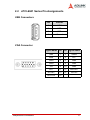
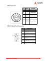
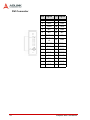
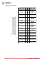
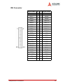
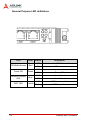
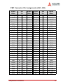
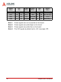
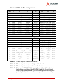
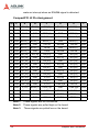
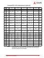
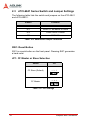
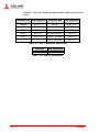
1
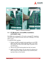
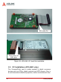
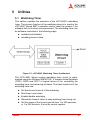
cPCI-6841 Series
6U CompactPCI Pentium M
Single Board Computers
User’s Manual
Manual Rev.
2.00
Revision Date:
July 19, 2005
Part No:
50-15048-1000
Advance Technologies; Automate the World.
Copyright 2005 ADLINK TECHNOLOGY INC.
All Rights Reserved.
The information in this document is subject to change without prior
notice in order to improve reliability, design, and function and does
not represent a commitment on the part of the manufacturer.
In no event will the manufacturer be liable for direct, indirect, special, incidental, or consequential damages arising out of the use or
inability to use the product or documentation, even if advised of
the possibility of such damages.
This document contains proprietary information protected by copyright. All rights are reserved. No part of this manual may be reproduced by any mechanical, electronic, or other means in any form
without prior written permission of the manufacturer.
Trademarks
Product names mentioned herein are used for identification purposes only and may be trademarks and/or registered trademarks
of their respective companies.
Getting Service from ADLINK
Customer Satisfaction is top priority for ADLINK Technology Inc.
Please contact us should you require any service or assistance.
ADLINK TECHNOLOGY INC.
Web Site:
http://www.adlinktech.com
Sales & Service:
[email protected]
TEL:
+886-2-82265877
FAX:
+886-2-82265717
Address:
9F, No. 166, Jian Yi Road, Chungho City,
Taipei, 235 Taiwan
Please email or FAX this completed service form for prompt and
satisfactory service.
Company Information
Company/Organization
Contact Person
E-mail Address
Address
Country
TEL
FAX:
Web Site
Product Information
Product Model
Environment
OS:
M/B:
Chipset:
CPU:
Bios:
Please give a detailed description of the problem(s):
Table of Contents
List of Tables.......................................................................... iii
List of Figures ......................................................................... v
1 Introduction ........................................................................ 1
1.1
1.2
1.3
1.4
1.5
Main Functions .................................................................... 3
CPU Support ................................................................... 3
CompactPCI Bus Interface ............................................. 3
PCI Mezzanine Card (PMC) Interface ............................ 3
IDE and CompactFlash Interfaces .................................. 3
Gigabit Ethernet Ports .................................................... 4
Universal Serial Bus (USB) ............................................. 4
Serial I/O ......................................................................... 4
Keyboard/Mouse Controller ............................................ 4
FDD Interface ................................................................. 4
Watchdog Timer ............................................................. 5
Hardware Monitoring ...................................................... 5
Operating System Support ............................................. 5
Features............................................................................... 6
Product List.......................................................................... 7
Specifications....................................................................... 8
cPCI-6841 SBC Specifications ....................................... 8
I/O Connectivity ............................................................ 11
Unpacking Checklist .......................................................... 12
2 Jumpers and Connectors ................................................ 13
2.1
2.2
cPCI-6841 Series Mechanical Drawings ........................... 14
cPCI-6841 Series Pin Assignments................................... 17
USB Connectors ........................................................... 17
VGA Connector ............................................................. 17
Ethernet (RJ-45) Connector .......................................... 18
PS2 Connector ............................................................. 19
RS-232 Serial Port Connector ..................................... 19
...................................................................................... 19
DVI Connector .............................................................. 20
CompactFlash Connector ............................................. 21
Floppy Connector ......................................................... 22
IDE Connector .............................................................. 23
Table of Contents
i
2.3
General Purpose LED definitions ................................. 24
PMC Connector Pin Assignments (JN1, JN2) .............. 25
CompactPCI J1 Pin Assignment .................................. 27
CompactPCI J2 Pin Assignment ................................... 28
CompactPCI J3 Pin Assignment (optional) ................... 29
cPCI-6841 Series Switch and Jumper Settings ................. 30
SW1: Reset Button ....................................................... 30
JP1: CF Master or Slave Selection .............................. 30
JP3: PMC VIO Selection .............................................. 31
3 Getting Started .................................................................. 33
3.1
3.2
3.3
3.4
3.5
3.6
CPU and Heatsink ............................................................. 33
CPU Installation ............................................................ 33
Heatsink Installation ...................................................... 35
Memory Module Installation ............................................... 36
PCI Mezzanine Card (PMC) Installation
(cPCI-6841 only)...................................................... 37
HDD Installation on Main Board......................................... 39
CF Installation (cPCI-6841 only) ........................................ 40
Main Board Installation ..................................................... 41
4 Windows Driver Installation............................................. 43
4.1
4.2
4.3
Chipset Drivers Installation ................................................ 44
VGA Driver Installation....................................................... 44
LAN Driver Installation ....................................................... 45
5 Utilities ............................................................................... 47
5.1
5.2
5.3
Watchdog Timer................................................................. 47
Using the Watchdog in an Application ............................... 48
Intel Preboot Execution Environment (PXE) ...................... 49
Appendix ................................................................................ 51
Serial Console User’s Guide.............................................. 51
1. Introduction ............................................................... 51
2. Equipment Needed ................................................... 51
3. Seting up the Server ................................................. 52
4. How to Use the Serial Console ................................. 53
Warranty Policy ..................................................................... 65
ii
Table of Contents
List of Tables
Table
Table
Table
Table
Table
Table
Table
Table
Table
Table
1-1:
1-2:
2-1:
2-2:
2-3:
2-4:
2-5:
3-1:
6-1:
6-2:
List of Tables
Power Ratings ........................................................
I/O Connectivity Table ............................................
Ethernet LED Status ...............................................
Switch and Jumper Functions ................................
JP1 Settings ...........................................................
JP2 Settings ...........................................................
JP3 Settings ...........................................................
DDR SDRAM Memory Capacity .............................
Key Translation Sequences ....................................
Special Commands ................................................
10
11
18
30
30
31
31
36
64
64
iii
iv
List of Tables
List of Figures
Figure 1-1:
Figure 2-1:
Figure 2-2:
Figure 2-3:
Figure 3-1:
Figure 3-2:
Figure 3-3:
Figure 3-4:
Figure 3-5:
Figure 3-6:
Figure 3-7:
Figure 5-1:
Figure 6-1:
List of Figures
cPCI-6841 Block Diagram ......................................... 2
cPCI-6841 Top View................................................ 14
cPCI-6841 and cPCI-6841-2 Front View ................. 15
cPCI-6841-2 Top View ............................................ 16
CPU Installation....................................................... 34
Heatsink Installation ................................................ 35
Memory Installation ................................................. 37
PMC Installation 1 ................................................... 38
PMC Installation 2 ................................................... 39
cPCI-6841 2.5” Hard Disk Installation ..................... 40
CompactFLASH Card Installation............................ 41
cPCI-6841 Watchdog Timer Architecture ................ 47
Null Modem Connection .......................................... 52
v
1
Introduction
The cPCI-6841 is a 6U CompactPCI single board computer based
on the Intel® Pentium® M processor and 855GME/ICH4 chipset.
The Pentium® M processor’s operating frequency ranges from
1.3GHz up to 2.0GHz and it comes with 1MB/2MB L2 cache in an
FC-mPGA package. The combination of the longevity of the Intel®
855GME/ICH4 chipset and low power consumption of the Pentium® M CPU make the cPCI-6841 the ideal solution for embedded applications.
The 855GME supports a 400MHz FSB and DDR333 memory up
to 2GB via two SODIMM sockets. An integrated 32-bit 3D graphic
controller provides analog VGA or DVI output.
The low power consumption ICH4 southbridge provides a 33MHz
PCI bus with highly integrated I/O features, including one USB 2.0
port and two E-IDE channels. The ICH4’s PCI bus is connected to
one PMC site, two 82541GI Gigabit Ethernet (GbE) controllers,
and a TI PCI-2050 PCI to PCI bridge. The 32-bit/33 MHz PMC site
provides high expansion capability and flexibility for various applications.
The cPCI-6841 is equipped with two Gigabit Ethernet (GbE) ports.
Two GbE ports use the 82541GI GbE controllers on the 33MHz
PCI bus to achieve the full communication bandwidth between the
LAN and CPU. These two ports are connected to the front panel.
Please refer to the following block diagram for the cPCI-6841
architecture.
Introduction
1
Figure 1-1: cPCI-6841 Block Diagram
2
Introduction
1.1 Main Functions
The following sections explain the main functions of the cPCI-6841.
CPU Support
The cPCI-6841 SBC is designed for the Intel® Pentium® M and
Celeron® M Processors. The standard cPCI-6841 SBC comes
with CPU socket which can be installed with µFC-PGA2 package
CPU, with the following options:
X
Pentium® M 1.4GHz, 1.6GHz, 1.7GHz, 1.8GHz, and 2.0GHz
X
Celeron® M 1.3GHz
The Low Voltage (LV) or Ultra Low Voltage (ULV) version of the
Pentium® M or Celeron® M Processors, which are in µFCBGA2
packages, can also be mounted on the cPCI-6841 SBC. However,
µFCBGA2 CPU support is reserved for OEM programs only. The
possible CPU options include:
X
LV Pentium® M 1.1GHz, 1.2GHz, 1.3GHz
X
ULV Celeron® M 600MHz
CompactPCI Bus Interface
The TI Technology PCI-2050 is a universal PCI to PCI bridge and
is used to implement the system slot on the cPCI-6841. The cPCI6841 CompactPCI bus supports 32-bit/33 MHz PCI.
PCI Mezzanine Card (PMC) Interface
The cPCI-6841 supports one PMC slot at 32-bit/33 MHz PCI,
providing expansion capability and flexibility for varieties of
applications.
IDE and CompactFlash Interfaces
The cPCI-6841 supports dual Ultra ATA100 IDE channels. Primary IDE is implemented on the cPCI-6841 and Secondary IDE is
routed to the backplane via the J3 connector. A 44-pin connector
for 2.5 inch IDE drives is reserved on the Primary IDE interface.
Introduction
3
Gigabit Ethernet Ports
The cPCI-6841 has two 10/100/1000Mbps Ethernet (GbE) ports.
Every port is assigned a unique static MAC Address. Two onboard
Intel® 82541GI Gigabit Ethernet controllers provide two Ethernet
ports and are implemented on a 32-bit/33 MHz PCI bus. The
82541GI supports IEEE 802.3x compliant flow control and IEEE
802.3ab compliant 10/100/1000 Mbps auto-negotiation. Two RJ45 connectors for these two LAN ports are located on the front
panel for system management or service requirements.
Universal Serial Bus (USB)
The cPCI-6841 provides one USB 2.0 port on the front panel for
use as an interface to versatile peripherals such as keyboard,
mouse, printer, USB flash disk, etc.
Serial I/O
One serial port is supported by the Winbond W83627HF Super I/O
on the cPCI-6841 and is accessed via a DB-9 connector on the
front panel. This port will be configured as Data Terminal Equipment (DTE). BIOS will initialize the serial port as COM1 with ISA I/
O base addresses of 3F8h and with a default setting of COM1
assigned to IRQ4.
Keyboard/Mouse Controller
The cPCI-6841 uses the Winbond W83627HF Super I/O to implement the keyboard/mouse controller. The controller is fully 8042
compatible. The cPCI-6841 provides a proprietary combo PS2
connector on the front panel (a cable is included).
FDD Interface
The cPCI-6841 uses the Winbond W83627HF Super I/O to implement the Floppy interface. Signals are available at the FDD connector.
4
Introduction
Watchdog Timer
The cPCI-6841 implements a watchdog timer (WDT) using the
Winbond W83627HF Super I/O. The programmable I/O port is on
address 2E, and the timer can be set for 1 to 255 seconds or 1 to
255 minutes. Easy-programming libraries for DOS and Windows
95/98/NT are included.
Hardware Monitoring
The cPCI-6841 uses the Winbond W83627HF Super I/O to detect
system voltages and temperatures. When it detects that the voltages or temperatures out of the safety range, it will instruct the
southbridge ICH4 to send the signals out halting the system in
order to protect the CPU board.
Operating System Support
The cPCI-6841 is compatible with Microsoft® Windows 2000, Windows 2003 Server, Windows XP, Red Hat Linux 9 and VxWorks
5.5. The device drivers for Windows are included on the ADLINK
CD. For Linux support and VxWork BSP, please contact ADLINK.
Introduction
5
1.2 Features
6
X
Low power consumption, supports Intel® Pentium® M and
Celeron® M CPUs from 1.3GHz up to 2.0GHz
X
Low power consumption Intel® 855GME and ICH4 embedded chipset, provides longevity for OEM
X
Compliant with PICMG 2.0, R3.0
X
32-bit/33 MHz CompactPCI interface based on PCI specifications
X
One 32-bit/33 MHz PMC site
X
Two 200-Pin DDR SODIMM sockets support up to 2GB
DDR333 SDRAM
X
Provides both IDE and FDD interfaces for storage devices.
X
Full feature I/O ports, including VGA, KB, MS, USB 2.0,
COM port, two GbEs, and optional DVI or PMC
Introduction
1.3 Product List
The cPCI-6841 series products include the following SBCs:
SBC
X
cPCI-6841: Pentium® M SBC with PMC slot
X
cPCI-6841-2: Pentium® M SBC with DVI output
Introduction
7
1.4 Specifications
cPCI-6841 SBC Specifications
CompactPCI Compliancy
X
PICMG 2.0 CompactPCI Rev. 3.0
Form Factor
X
Standard 6U CompactPCI (board size: 233.35mm x
160mm)
X
Single slot width (4TE or 4HP, 20.32mm)
CPU/Cache
X
Single Intel® Pentium® M 1.4GHz, 1.6GHz, 1.7GHz,
1.8GHz, 2.0GHz or Celeron® M 1.3GHz Processors with
µFC-PGA package
X
1MB or 2MB on die L2 cache, 400MHz FSB
Chipset
X
Intel® 855GME Graphics Memory Controller Hub (GMCH)
X
Intel® 82801DB I/O Hub (ICH4)
Host Memory
X
Two 200-pin DDR SODIMM sockets, 2GB maximum
X
Supports DDR333 SDRAM
BIOS
X
Phoenix/Award Plug and Play BIOS with 4Mb Flash ROM
X
BIOS write protection, provides anti-virus capability
X
Bootable from USB storage devices including USB-Floppy,
USB-ZIP, USB-CD-ROM, and USB-HDD.
X
Onboard Ethernet ports can be disabled via BIOS setting
X
Optional customized OEM splash image / power on screen
Note:
8
Due to BIOS segment limitations, enabling the remote console function may occupy the same memory space as other
ROM mapping add-on or boot-up devices such as Pre-boot
Agent of Ethernet Boot ROM, SCSI Boot ROM, or add-on
EIDE Boot ROM. It is recommended that only one ROMmapping add-on or boot-up device be enabled when enabling the remote console function.
Introduction
CompactPCI Bus Controller
X
TI PCI-2050 PCI-to-PCI bridge
X
PCI Rev 2.2 compliant
X
Supports 32-bit/33 MHz
Graphics
X
Integrated into 855GME Graphics Memory Controller Hub
X
Shared memory, up to 32MB
X
Dual channel display
X
Front panel DVI connector is available on cPCI-6841-2 only
Gigabit Ethernet
X
Two 10/100/1000bps Gigabit Ethernet ports
X
GbE ports are implemented through Intel® 82541GI Ethernet controllers, based on 32-bit/33 MHz PCI bus, RJ-45
connectors on the front panel
Onboard Peripherals
X
Integrated into Intel® 82801DB (ICH4) southbridge
X
Bus master IDE controller supports two ultra ATA-100 interfaces
X
Z
Primary IDE is on SBC with 44-pin IDE connector and a
CF slot. A 2.5 inch IDE HDD can be mounted.
Z
Secondary IDE port is routed to J3
USB Rev. 2.0 compliant port
Z
USB connectors are on the front panel
Z
USB ports support 0.5A@5V for peripherals with individual over-current protection
X
RS-232 serial port. COM is on the front panel with DB-9
type connector
X
PS2 keyboard / mouse connector on the front panel
Front Panel LED Indicators and Reset Button
X
Four LEDs on the front panel, including storage access LED
(RED), Power LED (green), General Purpose LED (blue),
and Watchdog Timer LED (yellow).
X
Flush tact switch for system reset.
Introduction
9
Real -Time Clock and Nonvolatile Memory
X
Built into Intel® 82801DB southbridge RTC
X
Battery-backed memory is used for BIOS configuration
X
Separate 3V coin cell CR2032 battery used for RTC and
nonvolatile memory
Environment
(1)
X Operating temperature: 0 to 45°C
X
Storage temperature: -40 to 80°C
X
Humidity: 5% to 95% non-condensed
Shock: 15G peak-to-peak, 11ms duration, non-operation
X Vibration:(2)
X
Z
Non-operation: 1.88Grms, 5-500Hz, each axis
Z
Operation: 0.5Grms, 5-500Hz, each axis, with 2.5” HDD
Safety Certificates and Tests
X
CE, FCC Class A
X
All plastic material, PCB and Battery used are all UL-94V0
certified
X
Designed for NEBS 3.0 requirements
Note 1: Certified with ADLINK thermal design. The thermal performance is dependent on the chassis cooling design. Forced
air-cooling with 50 CFM is required. Temperature limit of optional mass storage devices can impact the thermal specification.
Note 2: Operational vibration is limited by the 2.5 inches HDD. When
application requires higher definition for anti-vibration, we
recommend using Flash disk or CompactFlash.
Power Requirements
Configuration
Single Pentium® M 1.6GHz 512MB RAM,
40GB HDD
+5V
+3.3V +12V
-12V
Total
10.1A 2.28A 0.25A 20mA
61W
Table 1-1: Power Ratings
Note:
10
Power consumption measured under Windows 2000 SP4,
executing KPOWER and Burn-In-Test.
Introduction
I/O Connectivity
cPCI-6841
cPCI-6841-2
Function
Faceplate
On
Board
Faceplate
On
Board
COM
Y (DB-9)
---
Y (DB-9)
---
VGA
Y (DB-15)
---
Y (DB-15)
---
PS2
Y (Combo)
---
Y (Combo)
---
---
Y
---
USB2.0
Y
LAN x 2
Y (RJ-45)
CF
---
Y (IDE 1)
---
Y (IDE 1)
DVI
---
---
Y
---
PMC
Y
Y (32-bit/33
MHz)
---
---
IDE 1
---
Y (44-pin)
---
Y (44-pin)
FDD
---
Y (34-pin)
---
Y (34-pin)
LEDs
Y
---
Y
---
Reset Button
Y
---
Y
---
Y (RJ-45)
Table 1-2: I/O Connectivity Table
Introduction
11
1.5 Unpacking Checklist
Check the shipping carton for any damage. If the shipping carton
and contents are damaged, notify the dealer for a replacement.
Retain the shipping carton and packing materials for inspection by
the dealer. Obtain authorization before returning any product to
ADLINK.
Check that the following items are included in the package, if there
are any items missing, please contact your dealer.
SBC:
X
The cPCI-6841 or cPCI-6841-2 SBC (May be equipped with
different specifications of CPU, RAM, and HDD)
X
This User’s Manual
X
ADLINK All-in-One CD
X
Y Cable for Keyboard and Mouse
Note:
The packaging of OEM versions with non-standard
configuration, functionality, or package may vary
according to different configuration requests.
CAUTION: The boards must be protected from static discharge
and physical shock. Never remove any of the socketed
parts except at a static-free workstation. Use the antistatic bag shipped with the product to handle the
board. Wear a grounded wrist strap when servicing
12
Introduction
2
Jumpers and Connectors
This chapter illustrates the board layout, connector pin assignments, and jumper setings. Users should be familiar with the products before use. The following sections are included:
X
cPCI-6841 and cPCI-6841-2 board outline
X
cPCI-6841 and cPCI-6841-2 connectors pin assignments
X
cPCI-6841 and cPCI-6841-2 jumper settings
Jumpers and Connectors
13
2.1 cPCI-6841 Series Mechanical Drawings
Figure 2-1: cPCI-6841 Top View
14
Jumpers and Connectors
cPCI-6841-2
cPCI-6841
Figure 2-2: cPCI-6841 and cPCI-6841-2 Front View
Jumpers and Connectors
15
Figure 2-3: cPCI-6841-2 Top View
16
Jumpers and Connectors
2.2 cPCI-6841 Series Pin Assignments
USB Connectors
PIN
SIGNAL
1
VCC
2
USB-
3
USB+
4
Ground
VGA Connector
Signal Name Pin Pin Signal Name
Jumpers and Connectors
Red
1
2
Green
Blue
3
4
N.C.
GND
5
6
GND
GND
7
8
GND
+5V
9
10
GND
N.C.
11
12
DDCDAT
HSYNC
13
14
VSYNC
DDCCLK
15
17
Ethernet (RJ-45) Connector
Pin # Signal Name
1
Function
LAN_TDP1
Transmit Data1 +
2
LAN_TDN1
Transmit Data1 -
3
LAN_RDP2
Receive Data2 +
4
LAN_RDP3
Receive Data3 +
5
LAN_RDN3
Receive Data3 -
6
LAN_RDN2
Receive Data2 +
7
LAN_TDP4
Transmit Data4 +
8
LAN_TDN4
Transmit Data4 -
Status
Left LED
(Yellow or Amber)
Right LED
(Amber)
Network link is not established
OFF
OFF
OFF
Amber
Active
OFF
Blinking Amber
Link
Yellow
Amber
Active
Yellow
Blinking Amber
Link
Amber
Amber
Active
Amber
Blinking Amber
10 Mbps
(10 BaseT)
100 Mbps
(100 BaseTX)
1000 Mbps
(1000 BaseT)
Link
Table 2-1: Ethernet LED Status
18
Jumpers and Connectors
PS2 Connector
Pin
Signal
Function
1
KBDATA Keyboard Data
2
MSDAT
A
Mouse Data
3
GND
Ground
4
+5V
Power
5
KBCLK
Keyboard Clock
6
MSCLK
Mouse Clock
RS-232 Serial Port Connector
Jumpers and Connectors
Pin
Signal Name
1
DCD, Data carrier detect
2
RXD, Receive data
3
TXD, Transmit data
4
DTR, Data terminal ready
5
GND, Ground
6
DSR, Data set ready
7
RTS, Request to send
8
CTS, Clear to send
9
RI, Ring in
19
DVI Connector
20
Pin
Signal
Pin Signal
1
TX2-
16
2
TX2+
17
TX0-
3
GND
18
TX0+
4
NC
19
GND
5
NC
20
NC
6
I2CCLK
21
NC
7
I2CDAT
A
22
GND
8
VSYNC
23
TXC+
HTPLG
9
TX1-
24
TXC-
10
TX1+
25
RED
11
GND
26 GREEN
12
NC
27
13
NC
28 HSYNC
14
+5V
29
GND
15
GND
30
GND
BLUE
Jumpers and Connectors
CompactFlash Connector
Signal Name Pin Pin Signal Name
Jumpers and Connectors
GND
1
26
GND
SDD3
2
27
SDD11
SDD4
3
28
SDD12
SDD5
4
29
SDD13
SDD6
5
30
SDD14
SDD7
6
31
SDD15
SDCS#1
7
32
SDCS#3
GND
8
33
GND
GND
9
34
SDIOR#
GND
10
35
SDIOW#
GND
11
36
+5V
GND
12
37
IDEIRQ15
+5V
13
38
+5V
GND
14
39
PCSEL
GND
15
40
NC
GND
16
41
SIDERST#
GND
17
42
SIORDY
SDA2
18
43
NC
SDA1
19
44
SDDACK#
SDA0
20
45
IDEACT#
SDD0
21
46
S66DECT
SDD1
22
47
SDD8
SDD2
23
48
SDD9
IOIS16#
24
49
SDD10
GND
25
50
GND
21
Floppy Connector
Signal Name Pin Pin Signal Name
22
GND
1
2
Extended
Density
GND
3
4
NC
NC
5
6
Data Rate
GND
7
8
Index
GND
9
10
Motor A
Select
GND
11
12
Drive B
Select
GND
13
14
Drive A
Select
GND
15
16
Motor B
Select
GND
17
18
Step Direction
GND
19
20
Step Pulse
GND
21
22
Write Data
GND
23
24
Write Gate
GND
25
26
Track 0
GND
27
28
Write Protect
GND
29
30
Read Data
GND
31
32
Side 1
GND
33
34
Disk Change
Jumpers and Connectors
IDE Connector
Signal Name Pin Pin Signal Name
Jumpers and Connectors
BRSTDRVJ
1
2
GND
DDP7
3
4
DDP8
DDP6
5
6
DDP9
DDP5
7
8
DDP10
DDP4
9
10
DDP11
DDP3
11
12
DDP12
DDP2
13
14
DDP13
DDP1
15
16
DDP14
DDP0
17
18
DDP15
GND
19
20
NC
PDDREQ
21
22
GND
PDIOWJ
23
24
GND
PDIORJ
25
26
GND
PIORDY
27
28
PCSEL
PDDACKJ
29
30
GND
IRQ14
31
32
NC
DAP1
33
34
DIAG
DAP0
35
36
DAP2
CS1P
37
38
CS3PJ
IDEACTPJ
39
40
GND
+5V
41
42
+5V
GND
43
44
NC
23
General Purpose LED definitions
LED
Color
IDE Media Access
Red
Power OK
Green
General Purpose
LED
Blue
WDT LED
Yellow
24
Status
Description
OFF
IDE idle
ON
IDE access
OFF
System is not power-on or power failed
ON
Power ON
OFF
User defined
ON
User defined
OFF
WDT is not enabled
Blinking
WDT is enabled
Jumpers and Connectors
PMC Connector Pin Assignments (JN1, JN2)
Signal
Name
JN1
Pin
Signal
Name
Signal
Name
JN2
Pin
Signal
Name
TCK(3)
1
2
-12V
+12V
1
2
TRST#(3)
GND
3
4
INTA#
TMS(2)
3
4
TDO(1)
INTB#
5
6
INTC#
TDI(2)
5
6
GND
BM1(1)
7
8
+5V
GND
7
8
N/C
INTD#
9
10
N/C
N/C
9
10
N/C
GND
11
12
+3.3V
BM2(2)
11
12
+3.3V
CLKP1
13
14
GND
RST#
13
14
BM3(3)
GND
15
16
GNT0#
+3.3V
15
16
BM4(3)
REQ0#
17
18
+5V
PME#
17
18
GND
VIO(4)
19
20
AD31
AD30
19
20
AD29
AD28
21
22
AD27
GND
21
22
AD26
AD25
23
24
GND
AD24
23
24
+3.3V
GND
25
26
CBE3#
IDSEL
25
26
AD23
AD22
27
28
AD21
+3.3V
27
28
AD20
AD19
29
30
+5V
AD18
29
30
GND
VIO(4)
31
32
AD17
AD16
31
32
CBE2#
P1FRAME#
33
34
GND
GND
33
34
IDSL_B(1)
GND
35
36
IRDY#
TRDY#
35
36
+3.3V
DEVSL
37
38
+5V
GND
37
38
STOP#
GND
39
40
LOCK#
PERR#
39
40
GND
N/C
41
42
N/C
+3.3V
41
42
SERR#
PAR
43
44
GND
CBE1#
43
44
GND
VIO(4)
45
46
AD15
AD14
45
46
AD13
AD12
47
48
AD11
M66EN
47
48
AD10
AD9
49
50
+5V
AD8
49
50
+3.3V
GND
51
52
CBE0#
AD7
51
52
REQ_B#(1)
AD6
53
54
AD5
+3.3V
53
54
GNT_B#(1)
AD4
55
56
GND
N/C
55
56
GND
Jumpers and Connectors
25
Signal
Name
JN1
Pin
Signal
Name
Signal
Name
JN2
Pin
Signal
Name
VIO(4)
57
58
AD3
N/C
57
58
EREADY(1)
AD2
59
60
AD1
GND
59
60
RSTOUT#(1)
AD0
61
62
+5V
ACK64#
61
62
+3.3V
GND
63
64
REQ64#
GND
63
64
Monarch#(1)
Note 1: These signals are not connected on the board.
Note 2: These signals are pulled high on the board.
Note 3: These signals are pulled low on the board.
Note 4: The VIO signals by default set to +5V via jumper JP3.
26
Jumpers and Connectors
CompactPCI J1 Pin Assignment
Pin
Z
A
B
C
D
E
F
25
GND
+5V
REQ64#
ENUM#(4)
+3.3V
+5V
GND
24
GND
AD [1]
+5V
V (I/O)
AD [0]
23
GND
+3.3V
AD [4]
AD [3]
+5V
AD [2]
GND
22
GND
AD [7]
GND
+3.3V
AD [6]
AD [5]
GND
21
GND
+3.3V
AD [9]
AD [8]
M66EN C/BE [0]# GND
20
GND
AD [12]
GND
V (I/O)
AD [11]
AD [10]
GND
19
GND
+3.3V
AD [15]
AD [14]
GND
AD [13]
GND
18
GND
SERR#
GND
+3.3V
PAR
17
GND
+3.3V
IPMB_SCL
IPMB_SDA
GND
16
GND
DEVSEL#
GND
V (I/O)
STOP#
LOCK#
GND
15
GND
+3.3V
FRAME#
IRDY#
BDSEL
TRDY#
GND
12-14
11
ACK64# GND
C/BE [1]# GND
PERR#
GND
Key
GND
AD [18]
AD [17]
AD [16]
GND
C/BE [2]# GND
10
GND
AD [21]
GND
+3.3V
AD [20]
AD [19]
GND
9
GND
C/BE[3]#
IDSE
AD [23]
GND
AD [22]
GND
8
GND
AD [26]
GND
V (I/O)
AD[25]
AD [24]
GND
7
GND
AD [30]
AD [29]
AD [28]
GND
AD [27]
GND
6
GND
REQ#
GND
5
GND Reserved(1) Reserved(1)
4
GND IPMB_PWR
3
GND
INTA#
2
GND
TCK(3)
1
GND
+5V
+3.3V
CLK
AD [31]
GND
PCIRST#
GND
GNT#
GND
HEALTHY#
V (I/O)
INTP(1)
INTS
GND
INTB#
INTC#
+5V
INTD#
GND
+5V
TMS(2)
TDO(1)
TDI(2)
GND
-12V
TRST#(3)
+12V
+5V
GND
Note 1: These signals are not connected.
Note 2: These signals are pulled high on the board.
Note 3: These signals are pulled low on the board.
Note 4: To support PICMG 2.1 hotswap for peripheral boards, the
backplane should bus the ENUM# signal of all peripheral
slots to the system board. The ENUM# signal is continuously
polled by the system board’s hotswap firmware and will gen-
Jumpers and Connectors
27
erate an interrupt when an ENUM# signal is detected.
CompactPCI J2 Pin Assignment
Pin
Z
A
B
22 GND
GA4(2)
GA3(2)
GA2(2)
GA1(2)
GA0(2)
GND
21 GND
CLK6
GND
BRSV(1)
BRSV(1)
BRSV(1)
GND
20 GND
CLK5
GND
BRSV(1)
GND
BRSV(1)
GND
19 GND
GND
GND
18 GND BRSV(1) BRSV(1)
C
D
E
F
ICMBSDA(1) ICMBSCL(1) ICMBALR(1) GND
BRSV(1)
GND
BRSV(1)
GND
PRST#
REQ6#
GNT6#
GND
16 GND BRSV(1) BRSV(1)
DEG#
GND
BRSV(1)
GND
15 GND BRSV(1)
GND
FAL#
REQ5#
GNT5#
GND
17 GND BRSV(1)
GND
14 GND
AD [35]
AD [34]
AD [33]
GND
AD [32]
GND
13 GND
AD [38]
GND
V (I/O)
AD [37]
AD [36]
GND
12 GND
AD [42]
AD [41]
AD [40]
GND
AD [39]
GND
11 GND
AD [45]
GND
V (I/O)
AD [44]
AD [43]
GND
10 GND
AD [49]
AD [48]
AD [47]
GND
AD [46]
GND
9
GND
AD [52]
GND
V (I/O)
AD [51]
AD [50]
GND
8
GND
AD [56]
AD [55]
AD [54]
GND
AD [53]
GND
7
GND
AD [59]
GND
V (I/O)
AD [58]
AD [57]
GND
6
GND
AD [63]
AD [62]
AD [61]
GND
AD [60]
GND
5
GND C/BE [5]#
GND
V (I/O)
C/BE [4]#
PAR 64
GND
4
GND
V (I/O)
BRSV(1)
C/BE [7]#
GND
C/BE [6]#
GND
3
GND
CLK4
GND
GNT3#
REQ#4
GNT4#
GND
2
GND
CLK2
CLK3
SYSEN#
GNT2#
REQ3#
GND
1
GND
CLK1
GND
REQ1#
GNT1#
REQ2#
GND
Note 1: These signals are not connected.
Note 2: These signals are pulled high on the board.
Note 3:
28
These signals are pulled low on the board.
Jumpers and Connectors
CompactPCI J3 Pin Assignment (optional)
Pin
Z
A
B
C
D
E
F
19 GND
PCIRST-L
NC
SIDE_IORDY
NC
18 GND
SIDE_DACTL
NC
SIDE_CS-L3 SIDE_CS-L1
17 GND
SIDE_D15
SIDE_D14
SIDE_D13
SIDE_D12
16 GND
SIDE_D11
SIDE_D10
SIDE_D9
SIDE_D8
SIDE_DAC
GND
K-L
15 GND
SIDE_A0
SIDE_A1
NC
SIDE_A2
SIDE_DRE
GND
Q
14 GND
SIDE_D7
SIDE_D6
SIDE_D5
SIDE_D4
SIDE_IOWGND
L
13 GND
SIDE_D3
SIDE_D2
SIDE_D1
SIDE_D0
SIDE_IORGND
L
12 GND
FDD_DS0-L
FDD_DRATE
FDD_INDEX- FDD_DATA
FDD_MTR0-L
GND
0
L
-L
11 GND
FDD_DS1-L
FDD_DSKCH
FDD_DENSE FDD_RDAT
FDD_MTR-L
GND
G-L
L-L
E-L
10 GND
FDD_WP-L
FDD_HDSEL
FDD_STEP
FDD_DIR-L FDD_TRKO-L
GND
-L
-L
IDEIRQ15 GND
SIDE_66DE
GND
CT
NC
GND
9
GND FDD_GATE-L
NC
NC
NC
NC
GND
8
GND
NC
NC
NC
NC
NC
GND
7
GND
NC
NC
NC
NC
NC
GND
6
GND
NC
NC
NC
NC
NC
GND
5
GND
NC
MSDATA
NC
KBDATA
NC
GND
4
GND
NC
MSCLK
NC
KBCLK
NC
GND
3
GND
NC
NC
NC
NC
NC
GND
2
GND
NC
NC
NC
NC
NC
GND
1
GND
NC
NC
NC
NC
NC
GND
Note:
J3 is reserved for OEM versions. With ADLINK’s customized
backplanes, the secondary IDE and FDD ports can be connected to devices in the chassis.
Jumpers and Connectors
29
2.3 cPCI-6841 Series Switch and Jumper Settings
The following table lists the switch and jumpers on the cPCI-6841
and cPCI-6841V.
Switch
Function
SW1
Reset
JP1
Select CF as Master or Slave
JP2
Clear CMOS Content
JP3
PMC VIO
Table 2-2: Switch and Jumper Functions
SW1: Reset Button
SW1 is a push-button on the front panel. Pressing SW1 generates
a hard reset.
JP1: CF Master or Slave Selection
Status
JP1
CF Slave (Default)
1 2 3
CF Master
1 2 3
Table 2-3: JP1 Settings
30
Jumpers and Connectors
JP2: Clear CMOS
Status
JP3
Normal operation (Default)
1 2 3
Clear CMOS
1 2 3
Table 2-4: JP2 Settings
The CMOS RAM stores the real time clock (RTC) information,
BIOS configuration, and default BIOS setting. The CMOS is powered by a button cell battery when the system is powered off.
Please use the following procedure to erase the CMOS RAM data:
1. Remove the SBC from the system
2. Short pins 2 and 3 of JP2, then reinstall the jumper to its
normal default location
3. Insert the SBC back into the chassis.
JP3: PMC VIO Selection
Status
JP1
PMC VIO is set to 5V
(Default)
1 2 3
PMC VIO is set to 3.3V
1 2 3
Table 2-5: JP3 Settings
Jumpers and Connectors
31
32
Jumpers and Connectors
3
Getting Started
This chapter explains how to install necessary components on the
cPCI-6841 and cPCI-6841-2 including:
X
CPU and heat sink
X
Memory module installation
X
HDD installation
X
PMC installation (cPCI-6841 only)
X
CF card installation
X
Main board installation
3.1 CPU and Heatsink
The cPCI-6841 and cPCI-6841-2 support the Intel® Pentium® M
processor. The heat sink is necessary to help with CPU heat dissipation. Please follow the procedures below to install the CPU and
heat sink. (If the CPU and heat sink are already installed, you may
skip this section.)
CPU Installation
Fully turn the CPU locking screw counter-clockwise as far as it will
go as shown in Figure 3-1: CPU Installation below. Carefully
place the CPU into the CPU socket. Be sure to align the gold triangle on the corner of the chip with the triangular marking in the corner of the socket. Press down gently on the chip to ensure that it is
securely in place, and then fully turn the CPU locking screw clockwise as far as it will go to lock the CPU into position. Peel the
mylar film from the white side of the thermal pad included with the
heatsink kit and place it on the CPU as shown (pink side up). Then
remove the film protecting the top side of the the thermal pad.
Getting Started
33
Figure 3-1: CPU Installation
34
Getting Started
Heatsink Installation
Remove the film protecting the thermal pads on the heatsink as
shown in Figure 3-2: Heatsink Installation below. Place the
heatsink on the CPU and northbride, ensuring that the thermal
pads make proper contact with the board components. Secure
using the 6 spring-loaded screws provided
Figure 3-2: Heatsink Installation
Getting Started
35
3.2 Memory Module Installation
The cPCI-6841 Series SBC provides two 200-pin SODIMM sockets for DDR-SDRAM with a maximum memory capacity of 2GB. If
memory modules are pre-installed when the package is received,
this section may be skipped.
The GMCH system memory controller directly supports the following:
X
One channel of DDR SDRAM memory
X
DDR SDRAM devices with densities of 128-Mb, 256-Mb,
and 512-Mb technology
X
Up to 2GB (512-Mb technology) using high density devices
with two DIMMs
System
Memory
Capacity
System Memory
Capacity with Stacked
Memory
16
256MB
-
256Mb
16
512MB
-
512Mb
16
1GB
-
128Mb
8
256MB
512MB
256Mb
8
512MB
1GB
512Mb
8
1GB
2GB
Technology Width
128Mb
Table 3-1: DDR SDRAM Memory Capacity
To install the memory modules, align the notch in the memory
module with the key on the DIMM slot and follow the procedure
shown in Figure 3-3 below. When installing memory, ensure that
each DIMM module is firmly seated in its socket and does not
interfere with any components.
36
Getting Started
Figure 3-3: Memory Installation
3.3 PCI Mezzanine Card (PMC) Installation
(cPCI-6841 only)
The PMC slot is designed for 5V and/or universal PCI interfaces.
The PMC site is keyed to prevent users from installing a 3.3V only
PMC module.
To install the PMC modules:
1. Prepare an ESD protected area including an anti-ESD
table and ESD strap. Attach the ESD strap to your wrist
and connect the end of the ESD strap to ground of the
anti-ESD table.
2. Remove the PMC blanking plate from the front panel.
3. Install the PMC module onto the board by aligning the
PMC sockets and voltage selection keys and then pushing down firmly on the module.
Getting Started
37
4. Screw the four PMC mounting bolts to the main board
from the bottom side of the SBC to secure the PMC
module in place.
Figure 3-4: PMC Installation 1
38
Getting Started
Figure 3-5: PMC Installation 2
3.4 HDD Installation on Main Board
A slim-type 2.5-inch HDD can be mounted on the cPCI-6841 or
cPCI-6841-2. If a HDD is pre-installed, this section may be
skipped.
1. Screw the provided standoffs onto the HDD and attach
the included 44-pin IDE cable.
2. Place the HDD onto the board as shown and connect the
IDE cable to the socket. Tighten the four screws from the
bottom side of the main board to secure the HDD in to
place.
3. Press the IDE cable into the shape shown to avoid interference when inserting and removing the board.
Please refer to the illustrations shown below to install your 2.5”
hard disk.
Getting Started
39
Figure 3-6: cPCI-6841 2.5” Hard Disk Installation
3.5 CF Installation (cPCI-6841 only)
The CompactFlash card is widely applied in digital consumer
devices such as PDAs, digital cameras and MP3 players. Due to
its anti-shock/anti-vibration properties, better environmental toler-
40
Getting Started
ance, low power consumption, small form factor, and high reliability characteristics, it has been widely accepted in mission critical
embedded applications.
To install the CF card, insert it into the socket located under the
HDD as shown.
Figure 3-7: CompactFLASH Card Installation
3.6
Main Board Installation
Use the following procedure to install the cPCI-6841/cPCI-6841-2
main board into a CompactPCI chassis.
1. Refer to the relevant chassis user manual for pre-preparation of the chassis before installing the main board.
Users need to assign a slot to the board. Be sure to
select the correct slot (system or peripheral) depending
Getting Started
41
on the operational purpose of the board. The chassis
power may now be turned on.
2. Remove the blank face panel from the slot.
3. Align the top and bottom edges of the board with the
card guides on the chassis then slide the board into the
chassis until resistance is felt. If the system power is on,
the green LED (power status) will light up.
4. Move the upper and lower ejectors in an inward direction
simultaneously. Note that a slight resistance will be felt
while inserting the board. If this resistance is more than
normal, check to ensure that there are no pins bent on
the backplane and that the board’s connector pins are
aligned properly with the connectors on the backplane.
5. Secure the two screws hidden behind the upper and
lower ejector; connect the necessary cables to the
board.
42
Getting Started
4
Windows Driver Installation
The following sections show the driver installation procedures for
Windows 2000, Windows XP or Windows Server 2003. When
installing the Windows drivers, we recommend the following steps:
1. Fully install the Windows properly before installing any
driver. Most of the standard I/O devices’ driver will be
installed during the standard Windows installation.
2. Install the chipset driver.
3. Install the graphic driver and utilities.
4. Install the LAN drivers.
It is recommended that the chipset, graphic, and LAN drivers provided on the ADLINK All-in-One CD be used to ensure compatibility. Please contact ADLINK for support for Linux drivers and
VxWorks BSP.
Windows Driver Installation
43
4.1 Chipset Drivers Installation
1. Ensure your Windows operating system is fully installed
and running prior to executing the “Intel Chipset Software Installation Utility”.
2. Close any running applications.
3. The files are stored in an integrated application setup
program. This program is designed for Windows 2000,
XP and Windows Server 2003.
4. Locate the directory X:\cPCI\cPCI-6841\Chipset on the
ADLINK All-in-One CD, and then run “infinst_enu.exe”.
5. Click 'Next' on the Welcome screen to read and agree to
the license agreement. Click Yes if you agree to continue. NOTE: If you click No, the program will terminate.
6. Click ‘Next’ on the Readme Information screen to install
INF files.
7. Click “Finish” to restart the system when prompted to do
so.
8. Follow the screen instructions and use the default settings to complete the setup when Windows 2000/XP/
Windows Server 2003 re-starts.
4.2 VGA Driver Installation
1. Boot Windows 2000/XP/Windows Server 2003.
2. The driver is included on the ADLINK All-in-One CD.
Run the file win2k_xp142.exe under the following directory: X:\cPCI\cPCI-6841\VGA.
3. Click ‘Next’ on the Welcome screen. Select ‘Typical’ on
the setup type screen and click Next’.
4. Use the default program folders on the Select Program
Folder screen. Click ‘Next’ to install driver.
5. Finally, click 'Finish' to restart.
44
Windows Driver Installation
4.3 LAN Driver Installation
1. Boot Windows 2000/XP/Windows Server 2003.
2. Run the pro2kxp.exe under the following directory:
X:\cPCI\cPCI-6841\LAN.
3. Read the license agreement. Click 'I accept the terms in
the license agreement’ if you agree to continue.
4. At the Location to Save Files prompt, click Next to save
the files in the specified folder.
5. To install Intel® PRO Network Connections, click Install
Software to install drivers and Intel PROSet.
Windows Driver Installation
45
46
Windows Driver Installation
5
Utilities
5.1 Watchdog Timer
This section explains the operation of the cPCI-6841’s watchdog
timer. The primary function of the watchdog timer is to monitor the
cPCI-6841 Series SBC’s operation and to reset the system if the
software fails to function as programmed. The watchdog timer can
be software controlled in the following ways:
X
enabled and disabled
X
reloading timeout value
Figure 5-1: cPCI-6841 Watchdog Timer Architecture
The CPCI-6841 Series custom watchdog timer circuit is implemented using the Winbond W83627HF. It contains three Registers
(CRF5, CRF6 and CRF7 of logical device 8) for controlling the
watchdog timer and retrieving its status. The basic functions of the
watchdog timer are:
X
Set the timeout interval of the watchdog
X
Start timer count down
X
Enable/disable watchdog
X
Reload the timeout value to keep watchog from timing out
X
Set the range of the timeout period from 1 to 255 seconds,
or 1 to 255 minutes. It is set by control register.
Utilities
47
Once the watchdog has timed out, it will cause a RESET signal to
be sent to the system.
5.2 Using the Watchdog in an Application
The following section is provided to assist you in learning how to
use the watchdog in an application. The watchdog’s Reset function is as explained above. It can be controlled through the registers of the Super I/O on the cPCI-6841.
An application using the Reset feature enables the watchdog function, sets the count-down period of the timer, and reloads the timeout value periodically to keep it from resetting the system. If the
count-down value of the timer is not reloaded, the watchdog will
reset the system hardware after the counter reaches to zero.
For a detailed programming sample, please refer to the sample
code provide with the CD-ROM located at
X:\cPCI\cPCI-6841\WDT\WDT.CPP
48
Utilities
5.3 Intel Preboot Execution Environment (PXE)
The cPCI-6841 series supports Intel® Preboot Execution Environment (PXE), which provides the capability to boot up or execute an
OS installation through an Ethernet connection. There should be a
DHCP server in the network with one or more servers running
PXE and MTFTP services. It could be a Windows NT or Windows
2000 server running DHCP, PXE and MTFTP service or a dedicated DHCP server with one or more additional servers running
PXE and MTFTP service. This section describes the major items
required for building a network environment with PXE support.
1. Setup a DHCP server with PXE tag configuration
2. Install the PXE and MTFTP services
3. Make boot image file on PXE server (that is the boot
server)
4. Enable the PXE boot function on the client
For further details, please refer to pdkrel30.pdf under the directory
X:\Utility\PXE_PDK.
Utilities
49
50
Utilities
Appendix
Serial Console User’s Guide
1. Introduction
Most industrial implementations do not use a monitor or a keyboard to interface between the user and the computer, instead
connecting through a network or direct cable. ADLINK provides a
function for users to obtain Power-On Self Test (POST) messages
and execute commands using serial-port access. This function is
provided by Phoenix Technologies Ltd. (a.k.a. Award BIOS) and is
integrated into the BIOS of ADLINK’s CPU boards.OS) and integrated into the BIOS of ADLINK’s CPU boards.
Note:
Serial Console is a character-based terminal application. It
supports either VT100 or ANSI terminals. It does not support
graphics or graphical user interfaces. Serial Console is referred to as Award Preboot Agent by Phoenix Technologies
Ltd.
2. Equipment Needed
To use Serial Console, the following items are required:.
X
A server with the Award Preboot Agent BIOS
X
A client with a VT100 or ANSI terminal utility or application
X
A direct connection cable
The client obtains POST information from the server through a
direct connection cable. The server must have Award Preboot
Agent BIOS to support Serial Console. The required setup is
explained below.
To support Serial Console, a VT100 or ANSI compatibility terminal
utility or application is required. It needs to be executed on the client to receive data from the server. In this guide, Microsoft’s
HyperTerminal application, which is included with Windows, will
be used as the terminal console. Detailed settings are described
below in Section 5.4.
A null-modem cable is used as to connect the server and client
serial ports. Pin routing of a null-modem connection is as shown:
Appendix
51
Figure 6-1: Null Modem Connection
3. Seting up the Server
The server used in this guide is a CPU board where the Award
Preboot Agent is integrated into the BIOS. Use the BIOS setup
utility to setup the Serial Console. When you turn on the computer,
the Award BIOS is immediately activated. Pressing the <Del> key
allows you to enter the BIOS setup utility. Serial Console setup
items are found in the “Advanced BIOS Features” (Award Modular
6.0) or “BIOS FEATURES SETUP” (Award Modular 4.51) page.
They are listed as follows:
Console Redirection
This field allows you to enable or disable the Serial Console
function. If Enabled is selected, you must make sure that the
null modem cable connecting the two computers and the character-based terminal application are prepared.
Baud Rate
This is an important field that determines the communication
rate between the client and server. Baud rate selections are
9600, 19200, 38400, 57600 and 115200.
Note:
52
Baud rate settings between client and server must be the
same. If they are different, the error message “Award Preboot Agent Installation Failed” will be displayed when the
BIOS attempts to make a connection between server and client.
Appendix
Agent Connect Via
This field is un-selectable. Only one connection mode is supported: NULL. NULL means the connection cable is of null
modem type.
Agent wait time (min)
This option selects the amount of time (in minutes) to wait for a
successful connection. If the selected time elapses, the Serial
console times out and will not be supported by the server.
Agent after boot
This field enables or disables accepting text-based applications
(such as DOS) after the POST. If disabled, it will not send any
messages to client computers after booting to the OS. If
enabled, the user may execute commands from the client.
A boot message will be displayed after the BIOS attempts to
establish a connection between server and client:
X
“Award Preboot Agent Installation Successful”
When this message is displayed, POST messages are sent to
the client and indicates that Serial Console mode has been
successfully initiated.
X
“Award Preboot Agent Installation Failed”
If this message is shown, there is an issue with the connection.
To resolve this issue check the Serial Console configuration of
the server as described above, and ensure that the settings of
the terminal application of the client are configured accordingly.
4. How to Use the Serial Console
HyperTerminal is a console utility included with Microsoft Windows
operating systems, such as Windows 98, NT, 2000. Other console
utilities can also be used to achieve remote control functionality.
Note:
The HyperTerminal version used to illustrate these instructions is that of Windows 98 SE.
Appendix
53
If your system does not have HyperTerminal installed, please use
[Add/Remove Program Properties] in Control Panel to add it.
54
Appendix
Make sure that HyperTerminal is checked.
Appendix
55
Select HyperTerminal.
56
Appendix
Run Hypertrm by double-clicking on the icon.
Appendix
57
When executing HyperTerminal for the first time, you will be asked
to install a modem before running HyperTerminal. Select “No”.
Then, you will be asked to enter some configuration settings for
your local area.
After configuring the basic settings, HyperTerminal will need to
build a connection node. Enter a name you want to use and
choose an icon.
58
Appendix
Once you build a connection node, select the serial port that will
be used to connect to the server.
Appendix
59
On the properties page of the chosen serial port, the Bits per second setting must be the same as the baud rate setting of the
server.
Before using HyperTerminal to connect to the server, some properties of the console must first be set. Select File --> Properties.
60
Appendix
Check that the Telnet terminal mode is set to ANSI and select
ASCII Setup.
Appendix
61
To echo the data that the client sends, select all items on the
ASCII Setup page.
After HyperTerminal is setup and the connection cable is ready,
power on the server. POST messages from server will be sent to
the HyperTerminal Console as follows.
62
Appendix
After the server computer boots into the OS, execute commands
through the HyperTerminal console as shown.
Note:
Some keys, (i.e. DEL, ESC, Page Up, Page Down, Up Arrow, Down Arrow, Left Arrow, Right Arrow) may not be recognized by the server BIOS through the HyperTerminal
Appendix
63
console. Use the following sequences to perform such actions:
Function Key Key Sequence
HOME
ESC [ 1 ~
Function Key
Key Sequence
PG UP
ESC [ 5 ~
INS
ESC [ 2 ~
PG DOWN
ESC [ 6 ~
DEL
ESC [ 3 ~
UP ARROW
ESC [ A
END
ESC [ 4 ~
DOWN ARROW
ESC [ B
ESC
ESC ESC
RIGHT ARROW
ESC [ C
LEFT ARROW
ESC [ D
Table 6-1: Key Translation Sequences
Function
Key Sequence
Reboot system
ESC C
Table 6-2: Special Commands
64
Appendix
Warranty Policy
Thank you for choosing ADLINK. To understand your rights and
enjoy all the after-sales services we offer, please read the following carefully.
1. Before using ADLINK’s products please read the user manual and follow the instructions exactly. When sending in
damaged products for repair, please attach an RMA application form which can be downloaded from: http://
rma.adlinktech.com/policy/.
2. All ADLINK products come with a two-year guarantee:
X
The warranty period starts from the product’s shipment
date from ADLINK’s factory.
X
Peripherals and third-party products not manufactured
by ADLINK will be covered by the original manufacturers' warranty.
X
For products containing storage devices (hard drives,
flash cards, etc.), please back up your data before sending them for repair. ADLINK is not responsible for loss of
data.
X
Please ensure the use of properly licensed software with
our systems. ADLINK does not condone the use of
pirated software and will not service systems using such
software. ADLINK will not be held legally responsible for
products shipped with unlicensed software installed by
the user.
X
For general repairs, please do not include peripheral
accessories. If peripherals need to be included, be certain to specify which items you sent on the RMA Request
& Confirmation Form. ADLINK is not responsible for
items not listed on the RMA Request & Confirmation
Form.
Warranty Policy
65
3. Our repair service is not covered by ADLINK's two-year
guarantee in the following situations:
X
Damage caused by not following instructions in the
user's manual.
X
Damage caused by carelessness on the user's part during product transportation.
X
Damage caused by fire, earthquakes, floods, lightening,
pollution, other acts of God, and/or incorrect usage of
voltage transformers.
X
Damage caused by unsuitable storage environments
(i.e. high temperatures, high humidity, or volatile chemicals).
X
Damage caused by leakage of battery fluid during or
after change of batteries by customer/user.
X
Damage from improper repair by unauthorized technicians.
X
Products with altered and/or damaged serial numbers
are not entitled to our service.
X
Other categories not protected under our warranty.
4. Customers are responsible for shipping costs to transport
damaged products to our company or sales office.
5. To ensure the speed and quality of product repair, please
download an RMA application form from our company website: http://rma.adlinktech.com/policy. Damaged products
with attached RMA forms receive priority.
If you have any further questions, please email our FAE staff:
[email protected].
66
Warranty Policy