1
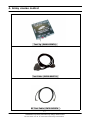
GSM TELEPHONE
SGH-E870
GSM TELEPHONE
CONTENTS
1.
Safety Precautions
2.
Specification
3.
Product Function
4.
Array course control
5.
Exploded View and Parts List
6.
Disassembly and Assembly
instructions
7.
MAIN Electrical Parts List
8.
Block Diagrams
9.
PCB Diagrams
10.
Flow Chart of Troubleshooting
11.
Reference data
Contents
1. Safety Precautions
1-1. Repair Precaution ...........................................................................1-1
1-2. ESD(Electrostatically Sensitive Devices) Precaution ...........................1-2
2. Specification
2-1. GSM General Specification ..............................................................2-1
2-2. GMSK TX Power Level ....................................................................2-2
2-3. EDGE TX Power Level ....................................................................2-3
3. Product Function
4. Array course control
Software Downloading
4-1. Downloading Binary Files ................................................................4-2
4-2. Pre-requsite for Downloading ..........................................................4-2
4-3. S/W Downloader Program ...............................................................4-3
5. Exploded View and Parts List
5-1. Cellular phone Exploded View .........................................................5-1
5-2. Cellular phone Part list ...................................................................5-2
6. Disassembly and Assembly instructions
6-1. Assembly .....................................................................................6-1
6-2. Disassembly ..................................................................................6-3
6-3. KIT Assembly ................................................................................6-5
7. MAIN Electrical Parts List
8. Block Diagrams
9. PCB Diagrams
10. Flow Chart of Troubleshooting
10-1. Baseband
10-1-1. Power ON ..............................................................................10-1
Contents
10-1-2.
10-1-3.
10-1-4.
10-1-5.
10-1-6.
10-1-7.
10-2. RF
10-2-1.
10-2-2.
10-2-3.
10-2-4.
10-2-5.
Initial ....................................................................................10-4
Sim Part ...............................................................................10-6
Microphone Part .....................................................................10-8
Speaker Part ........................................................................10-10
Camera Part ........................................................................10-12
Mp3 Display Part ..................................................................10-14
EGSM RX .............................................................................10-16
DCS RX ...............................................................................10-17
PCS RX ...............................................................................10-18
EGSM TX .............................................................................10-19
DCS & PCS TX .....................................................................10-20
11. Reference data
1. Safety Precautions
1-1. Repair Precaution
● Repair in Shield Box, during detailed tuning.
Take specially care of tuning or test,
because specipicty of cellular phone is sensitive for surrounding interference(RF noise).
● Be careful to use a kind of magnetic object or tool,
because performance of parts is damaged by the influence of manetic force.
● Surely use a standard screwdriver when you disassemble this product,
otherwise screw will be worn away.
● Use a thicken twisted wire when you measure level.
A thicken twisted wire has low resistance, therefore error of measurement is few.
● Repair after separate Test Pack and Set because for short danger (for example an
overcurrent and furious flames of parts etc) when you repair board in condition of
connecting Test Pack and tuning on.
● Take specially care of soldering, because Land of PCB is small and weak in heat.
● Surely tune on/off while using AC power plug, because a repair of battery charger is
dangerous when tuning ON/OFF PBA and Connector after disassembing charger.
● Don't use as you pleases after change other material than replacement registered on SEC
System.
Otherwise engineer in charge isn't charged with problem that you don't keep this rules.
1-1
SAMSUNG Proprietary-Contents may change without notice
This Document can not be used without Samsung's authorization
Safety Precautions
1-2. ESD(Electrostatically Sensitive Devices) Precaution
Several semiconductor may be damaged easilly by static electricity. Such parts are called by
ESD(Electrostatically Sensitive Devices), for example IC,BGA chip etc. Read Precaution below.
You can prevent from ESD damage by static electricity.
● Remove static electricity remained your body before you touch semiconductor or parts with
semiconductor. There are ways that you touch an earthed place or wear static electricity
prevention string on wrist.
● Use earthed soldering steel when you connect or disconnect ESD.
● Use soldering removing tool to break static electricity. , otherwise ESD will be damaged by
static electricity.
● Don't unpack until you set up ESD on product. Because most of ESD are packed by box
and aluminum plate to have conductive power,they are prevented from static electricity.
● You must maintain electric contact between ESD and place due to be set up until ESD is
connected completely to the proper place or a circuit board.
1-2
SAMSUNG Proprietary-Contents may change without notice
This Document can not be used without Samsung's authorization
2. Specification
2-1. GSM General Specification
GSM 900
DCS1800
PCS1900
F r e q . Ba n d [ M Hz ]
Uplink/ Downlink
88 0~9 15
92 5~9 60
1710~1785
1805~1880
1850~1910
1930~1990
AR FC N range
0~12 4
& 9 75 ~10 23
512~885
512~810
T x /Rx s pacing
45 M Hz
95 M Hz
80 M Hz
G P RS
270.833 Kbp s
3.692 us
270.833 Kbp s
3.692 us
270.833 Kbp s
3.692 us
EDGE
812.5 K bp s
3.692 us
812.5 K bp s
3.692 us
812.5 K bp s
3.692 us
576.9 u s
4.615 ms
576.9 u s
4.615 ms
576.9 u s
4.615 ms
G P RS
0.3 GM S K
0.3 GM S K
0.3 G MS K
EDGE
8 P SK
8 P SK
8 P SK
G P RS
33 dBm~5 dBm
30 dBm~0 dBm
30 dBm~0 dBm
ED G E
27~5 dBm
26~0 dBm
26~0 dBm
G P RS
5 pcl~19 pcl
0 pcl~15 pcl
0 pcl~15 pcl
EDGE
8~ 19(clas s E 2)
2~15(class E2)
2~15(class E2)
Sens itivity
-102 dBm
-100 dBm
-102 dBm
T DM A Mu x
8
8
8
Cell Radius
35 Km
2 Km
2 Km
M od . Bit
rate/
Bit P eriod
T i m e Slo t
Period/Frame Per iod
Modu lation
M S P o w er
P o wer
Leve l
2-1
Specification
2-2. GMSK TX power Level
TX Power
control
level
GSM900
TX Power
control
level
DCS1800
TX Power
control
level
PCS1900
5
33±2 dBm
0
30±2 dBm
0
30±2 dBm
6
31±3 dBm
1
28±3 dBm
1
28±3 dBm
7
29±3 dBm
2
26±3 dBm
2
26±3 dBm
8
27±3 dBm
3
24±3 dBm
3
24±3 dBm
9
25±3 dBm
4
22±3 dBm
4
22±3 dBm
10
23±3 dBm
5
20±3 dBm
5
20±3 dBm
11
21±3 dBm
6
18±3 dBm
6
18±3 dBm
12
19±3 dBm
7
16±3 dBm
7
16±3 dBm
13
17±3 dBm
8
14±3 dBm
8
14±3 dBm
14
15±3 dBm
9
12±4 dBm
9
12±4 dBm
15
13±3 dBm
10
10±4 dBm
10
10±4 dBm
16
11±5 dBm
11
8±4 dBm
11
8±4 dBm
17
9±5 dBm
12
6±4 dBm
12
6±4 dBm
18
7±5 dBm
13
4±4 dBm
13
4±4 dBm
19
5±5 dBm
14
2±5 dBm
14
2±5 dBm
15
0±5 dBm
15
0±5 dBm
2-2
Specification
2-3. EDGE TX Power Level
TX Power
control
level
GSM850
TX Power
control
level
DCS1800
TX Power
control
level
PCS1900
8
27±3 dBm
2
26±3 dBm
2
26±3 dBm
9
25±3 dBm
3
24±3 dBm
3
24±3 dBm
10
23±3 dBm
4
22±3 dBm
4
22±3 dBm
11
21±3 dBm
5
20±3 dBm
5
20±3 dBm
12
19±3 dBm
6
18±3 dBm
6
18±3 dBm
13
17±3 dBm
7
16±3 dBm
7
16±3 dBm
14
15±3 dBm
8
14±3 dBm
8
14±3 dBm
15
13±3 dBm
9
12±4 dBm
9
12±4 dBm
16
11±5 dBm
10
10±4 dBm
10
10±4 dBm
17
9±5 dBm
11
8±4 dBm
11
8±4 dBm
18
7±5 dBm
12
6±4 dBm
12
6±4 dBm
19
5±5 dBm
13
4±4 dBm
13
4±4 dBm
14
2±5 dBm
14
2±5 dBm
15
0±5 dBm
15
0±5 dBm
2-3
3. Product Function
Main Function
-Camera and camcorder
Use the camera module on your phone to take a photo or record a video.
-Music player
Play music files using your phone as a music player.
-Web browser
Access the wireless web to get up-to-the-minute information and a wide variety of
media content.
-Image editor
Crop, resize, rotate, and decorate your photos.
-Voice commands
Experience a new level of voice command capability that allows for easy hands-free
use. You can select menus, control camera settings, as well as make phone calls without
any key presses.
-Bluetooth
Transfer media files and personal data and connect to other devices using free, wireless
Bluetooth technology.
-Photo printing
Print your photos to preserve your best moments forever.
-Multimedia Message Service (MMS)
Send and receive MMS messages with a combinagion of text, image, video, and audio.
-E-mail
Send and receive e-mails with image, video, and audio attachments.
-Get personal with photo/video caller ID
See who's calling you when their very own photo or video displays.
-Phone to TV
View photos and video clips captured with the phone on your TV screen.
-Java
Enjoy Java™-based embedded games and download new games.
3-1
SAMSUNG Proprietary-Contents may change without notice
This Document can not be used without Samsung's authorization
4. Array course control
Test Jig (GH80-03307A)
Test Cable (GH39-00127A)
RF Test Cable (GH39-00397A )
4-1
SAMSUNG Proprietary-Contents may change without notice
This Document can not be used without Samsung's authorization
Array course control
Software Downloading
4-1. Downloading Binary Files
• Two binary files for downloading E870.
– E870XXYY.s3 : Main source code binary.
– E870XXYY.cts : Default Contents binary.
4-2. Pre-requsite for Downloading
• Downloader Program(OptiFlash.exe)
• E870 Mobile Phone
• Data Cable
• Binary files
• CTS files
4-2
SAMSUNG Proprietary-Contents may change without notice
This Document can not be used without Samsung's authorization
Array course control
4-3. S/W Downloader Program
1. Load the binary download programby executing the “OptiFlash.exe”
2. Select the “Options” -> “Settings” -> “Generic” ->
“Specify hardware platform”.
Choose hardware platform for the downloader file setting.
Set the everything else as the default values which are shown below
4-3
SAMSUNG Proprietary-Contents may change without notice
This Document can not be used without Samsung's authorization
Array course control
3. Select the COM port when the download cable is connected
Up to 64 ports are supported. Additionally you can select the maximum
transfer speed OptiFlash will use to communicate with the phone. However,
OptiFlash will use a slower speed if either the PC’s or the phone’s serial
hardware is incapable of handling the selected speed
4-4
SAMSUNG Proprietary-Contents may change without notice
This Document can not be used without Samsung's authorization
Array course control
4. Select the“Flash&Verify” -> “Browse”
Set the directory path and choose the latest s/w binary, for example
“E870XXYY.s3”,for the downloader binary setting.
In case of E870 the reserved regions are not a necessity.
(It is defined in platform.def file)
4-5
SAMSUNG Proprietary-Contents may change without notice
This Document can not be used without Samsung's authorization
Array course control
5. Select the“Default Contents” -> “Browse”
Set the directory path and choose the CTS file, for example
“E870XXYY.cts”,for the downloader binary setting.
Function of Flash option
S-Record only : download binary only
S-Record with Contens : download binary with default contents
Contents only : download default contents
4-6
SAMSUNG Proprietary-Contents may change without notice
This Document can not be used without Samsung's authorization
Array course control
6. Click “OK” button then press “Flash”.
(Before pressing ‘Flash’ button, push the button ‘*’and ‘END’ at the same
time. Then press ‘Flash’.)
Downloader will upload the binary file as below for the downloading.
7. When downloading is finished successfully, there is a “All is well”
message. 8. After finishing downloading, Certain memory resets should be done to
guarantee the normal performance.
9. Confirm the downloaded version name and etc. :
*#5002*8376263#
Full Reset : *2767*3855#
4-7
SAMSUNG Proprietary-Contents may change without notice
This Document can not be used without Samsung's authorization
5. Exploded View and Parts List
5-1. Cellular phone Exploded View
QCW01
QWD04
QHI01
QCK01
QFU01
QCH05
QFR01
QME03
QVO01
QSC14
QFB02
QRF03
QCA01
QKP01
QMP01
QME01
QAN05
QFB05
QLC01
QSP01
QMO01
QMI03
QFL01
QMI01
QCR05
QSC01
QCR12
QAN02
QRE01
QBA01
QCR05
QRF01
QBA00
5-1
SAMSUNG Proprietary-Contents may change without notice
This Document can not be used without Samsung's authorization
QMW01
Exploded View and Parts List
5-2. Cellular phone Parts list
Design LOC
Discription
SEC CODE
QAN02
INTENNA-SGHE870
GH42-00720A
QAN05
MEC-INTENNA CONTACT
GH75-08168A
QBA00
ASSY-COVER-BATTERY
GH98-01110A
QBA01
INNER BATTERY PACK-800MAH,BLK,
GH43-01850A
QCA01
UNIT-CAMERA
GH59-02696A
QCR05
SCREW-MACHINE
6001-001478
QCR12
SCREW-MACHINE
6001-001530
QCW01
PMO-COVER CAMERA WINDOW
GH72-27823A
QFB02
MEC-FLASH BRACKET
GH75-08830A
QFB05
MEC-BRACKET SIM
GH75-08832A
QFU01
MEC-FOLDER UPPER
GH75-08827A
QKP01
MEC-KEYPAD MAIN(SER/WS)
GH75-09168A
QLC01
MEA-LCD MODULE KIT
GH97-05621A
QME01
UNIT-METAL DOME
GH59-02688A
QME03
UNIT-CON TO CON ASS'Y
GH59-02705A
QMI01
MICROPHONE-ASSY-5.25MM
GH30-00177C
QMI03
RMO-MIC HOLDER
GH73-06697A
QMO01
MOTOR DC-SGHZ130
GH31-00155G
QMP01
PBA MAIN-SGHE870
GH92-02475A
QMW01
MEC-COVER MAIN WINDOW
GH75-08833A
QRE01
MEC-COVER REAR
GH75-08831A
QRF01
MPR-RF SHEET
GH74-19987A
QSC01
RMO-FOLDER SCREW COVER
GH73-05771A
QSC14
MPR-TAPE FRONT HOLE
GH74-19983A
QSP01
SPEAKER
3001-001864
QWD04
PMO-COVER DUAL WINDOW
GH72-27822A
MEC-FOLDER LOWER
GH75-08828A
MEC-HINGE
GH75-09605A
MEC-COVER FRONT
GH75-08829A
QCH05
PMO-T FLASH COVER
GH72-26489A
QCK01
MEC-CAMERA KEY
GH75-08835A
QRF03
PMO-EAR COVER
GH72-26490A
QVO01
MEC-VOLUME KEY
GH75-08836A
QFL01
QHI01
QFR01
5-2
SAMSUNG Proprietary-Contents may change without notice
This Document can not be used without Samsung's authorization
Exploded View and Parts List
Discription
SEC CODE
BAG PE
6902-000297
CBF INTERFACE-DATA LINK CABLE
GH39-00444B
ADAPTOR-SGHD800 TA(EU)
GH44-01060B
S/W CD-SAMSUNG PC STUDIO
GH46-00225A
UNIT-EARPHONE
GH59-02499B
LABEL(P)-WATER SOAK
GH68-02026A
LABEL(P)-WATER SOAK
GH68-02026A
MANUAL-WARRANTY CARD
GH68-02623A
MANUAL-SFC
GH68-04336A
LABEL(P)-BARCODE RUSSIA
GH68-08494A
LABEL(R)-MAIN (SER)
GH68-09068B
MANUAL USERS-EU RUSSIAN
GH68-09119A
CUSHION-CASE TA2 MA2
GH69-03580A
BOX(P)-UNIT MAIN (SER)
GH69-03583B
RMO-SUB LCD RUBBER A
GH73-06699A
RMO-SUB LCD RUBBER B
GH73-06700A
RMO-LCD CENTER RUBBER
GH73-06701A
RMO-SPEAK RUBBER
GH73-06707A
MPR-BOHO VINYL LCD CONN
GH74-15350A
MPR-BOHO VINYL DUAL WIN
GH74-17800A
MPR-BOHO VINYL DUAL WIN
GH74-17800A
MPR-CUSHION DUAL
GH74-19870A
MPR-LCD FPCB GASKET
GH74-19873A
MPR-PCB GASKET
GH74-19988A
MPR-TAPE EL CON
GH74-19989A
MPR-TAPE CAM GASKET LCD
GH74-20636A
MPR-VINYL BOHO UPPER OUT
GH74-21780A
MPR-VINYL BOHO MAIN WINDOW
GH74-21781A
MPR-TAPE EL SHEET LABEL A
GH74-21835A
MPR-TAPE EL SHEET LABEL B
GH74-21836A
MPR-TAPE HOLE IC
GH74-21837A
MPR-TAPE MIC FPCB
GH74-21838A
MPR-SPEAK CENTER GASKET
GH74-21840A
MPR-TAPE SPEAK WIRE MASKING
GH74-21841A
MPR-VINYL BOHO REAR
GH74-23610A
MEC-HANGER ROPE
GH75-00223T
5-3
SAMSUNG Proprietary-Contents may change without notice
This Document can not be used without Samsung's authorization
6. Disassembly and Assembly instructions
6-1. Assembly
1
2
WIRE
arrangement
CAMERA SAFE
ARRIVAL POSITION
SPEAK CENTER
GASKET
LCD FPCB GASKET
1. Insert LCD F-PCB at FOLDER LOWER.
2. Safe arrival in turn CAMERA / FLASH BRACKET.
3. Attach in turn SPEAK CENTER GASKET or LCD
FPCB GASKET at LCD(SUB LCD).
※ caution
1. When safe arrival the FLASH BRACKET,
Take care.
2. Perfectly safe arrival CAMERA or FLASH
BRACKET.
insulated
TAPE
1. Safe arrival in turn MOTOR / SPEAK.
2. Attach an insulate TAPE at SPEAK BONDING
left portion.
※ caution
1. Arrive safe MOTOR WIRE after twist four or five
times.
2. Arrange the wire, Do not jump out.
3
4
SCREW CAP
FOLDER
UPPER
①
②
LOWER SCREW
contract.
③
1. SCREW the LOWER . (2 POINT)
2. Insert to the SCREW CAP.
1.Assemble FOLDER UPPER.
※ caution
※ caution
1. Check SCREW CAP condition.
1. Do not damage , when combinate the FOLDER
2. Press SCREW CAP by cotton bud, to do not take
UPPER.
off assembly.
6-1
SAMSUNG Proprietary-Contents may change without notice
This Document can not be used without Samsung's authorization
Disassembly and Assembly instructions
5
6
②
①
Insert to LCD
FPCB
③
SIM FPCB
Insert
HINGE
1. Put the PBA.
2. Assemble LCD CONNECTOR.
※ caution
1.
2.
3.
4.
SIM
BRACKET
Assemble the SIM CONNECTOR.
Put the SIM BRACKET.
Remove the paper at SIM BRACKET.
Assemble SIM FPCB at SIM BRACKET.
※ caution
1. Connect SIM CONNECTOR perfectly.
2. Fix into HOLE, when put the SIM BRACKET.
3. Check to come off the SIM FPCB at SIM
BRACKET.
1. Do not damage to put the PBA.
2. Connect LCD CONNECTOR perfectly.
3. NO dust should be inside.
6-2
SAMSUNG Proprietary-Contents may change without notice
This Document can not be used without Samsung's authorization
Disassembly and Assembly instructions
6-2. Disassembly
1
2
Diassembly FOLLDER
SIM
ASSAY
ANT
CONTACT
SIM
CONNECTOR
SIM BRACKET
fixed SCREW
1. Loose the fixed screw at sim braket.
2. Separate the sim Assay at B'D.
1. Loose the four screws at the rear cover.
3. Disconnect the LCD connector at B'D.
2. Open the rear cover from bottom-side hook.
※ caution
※ caution
1. Do not scratch at rear cover & front.
2. Do not come off SIM BRACKET EMI metalization.
1. Handle with care SIM F-PCB & LCD F-PCB.
3
4
REMOVAL JIG
FRONT HOLE TAPE
AFTER
1
SEPERATING
REMOVE SCREW
CAP/SCREW
HINGE TAPE
2
1. Insert the removal JIG at HINGE HOLE.
2. Seperate front & hinge after opening the left
front, Drawing out LCD FPCB to front hole gap.
1. Seperate the PBA at front.
2. Take off KEYPAD.
3. Remove the screw cap by tweezers.
4. Taking to pieces screw of folder lower.
3. Remove the FRONT HOLE TAPE/ HINGE TAPE.
(2 POINT)
※ caution
※ caution
1. Do not damage the hinge hole by removal JIG.
1. Do not scratch at rear cover & front.
2. When separate the front & folder, Check NO
2. Handle the PBA scratch or crack with care.
bending.
6-3
SAMSUNG Proprietary-Contents may change without notice
This Document can not be used without Samsung's authorization
Disassembly and Assembly instructions
5
6
CAMERA
3
1
5
2
4
1
2
1. In turn MOTOR/SPEAKER/CAMERA/FLASH
1. Open a groove of FOLDER UPPER of the right
top portion by JIG, separating folder upper.
※ caution
BRACKET/
LCD F-PCB, separate to folder lower.
1. Do not scratch at folder upper & lower.
2. Seperate the LCD at folder lower.
※ caution
2. Handle the hook of FOLDER UPPER / LOWER
1. Do not damage when removed CAMERA or
with care.
FLASH BRACKET. 2. Take care of LCD F-PCB.
7
SEPERATING REAR
INTENNA
1. Seperate the INTENNA at REAR.
※ caution
1. Do not scratch.
2. Don't be stained a fingerprint at INTENNA
PATTERN.
6-4
SAMSUNG Proprietary-Contents may change without notice
This Document can not be used without Samsung's authorization
Disassembly and Assembly instructions
6-3. KIT Assembly
2
1
SPEAK RUBBER
LCD CENTER RUBBER
1. Check the LCD MODULE apperance
condition.
2. Check the LCD CONNECTOR condition.
SUB LCD RUBBER A
SUB LCD RUBBER B
1. Attach to SPEAK RUBBER / LCD CENTER
RUBBER.
2. Attach to SUB LCD RUBBER A / B.
※ caution
1. Do not touch front side of LCD
(fingerprint)
2. Do not scratch LCD F-PCB by tweezers
when attach the PORON.
※ caution
1. Do not touch front side of the LCD.
(fingerprint)
3
1. Check the extraneous matter condition.
※ caution
1. Do not touch front side of the LCD.
(fingerprint)
6-5
SAMSUNG Proprietary-Contents may change without notice
This Document can not be used without Samsung's authorization
7. MAIN Electrical Parts List
SEC CODE
Design LOC
4202-001105
ANT101
2203-000386
Discription
STATUS
ANTENNA-CHIP
SA
C101
C-CER,CHIP
SA
2203-006194
C103
C-CER,CHIP
SA
2203-006194
C104
C-CER,CHIP
SA
2203-006194
C105
C-CER,CHIP
SA
2203-006562
C106
C-CER,CHIP
SA
2203-006305
C107
C-CER,CHIP
SA
2203-005682
C108
C-CER,CHIP
SA
2203-006194
C109
C-CER,CHIP
SA
2203-006423
C110
C-CER,CHIP
SA
2203-006423
C111
C-CER,CHIP
SA
2203-005736
C112
C-CER,CHIP
SA
2203-006423
C113
C-CER,CHIP
SA
2203-006194
C114
C-CER,CHIP
SA
2203-006194
C115
C-CER,CHIP
SA
2203-001124
C116
C-CER,CHIP
SA
2203-000585
C117
C-CER,CHIP
SA
2203-006423
C118
C-CER,CHIP
SA
2203-005806
C119
C-CER,CHIP
SA
2203-006423
C120
C-CER,CHIP
SA
2203-006194
C121
C-CER,CHIP
SA
2203-003019
C122
C-CER,CHIP
SNA
2203-006305
C123
C-CER,CHIP
SA
2203-005682
C124
C-CER,CHIP
SA
2203-001437
C127
C-CER,CHIP
SA
2203-006194
C128
C-CER,CHIP
SA
2203-000854
C129
C-CER,CHIP
SA
2203-000725
C130
C-CER,CHIP
SA
2203-006847
C131
C-CER,CHIP
SA
2203-006847
C132
C-CER,CHIP
SA
2203-006123
C133
C-CER,CHIP
SA
2203-006194
C135
C-CER,CHIP
SA
2203-000233
C136
C-CER,CHIP
SA
2203-006194
C137
C-CER,CHIP
SA
2203-006194
C138
C-CER,CHIP
SA
2203-006361
C139
C-CER,CHIP
SA
2203-000254
C140
C-CER,CHIP
SA
7-1
SAMSUNG Proprietary-Contents may change without notice
This Document can not be used without Samsung's authorization
Main Electrical Parts List
SEC CODE
Design LOC
Discription
2203-000254
C141
C-CER,CHIP
SA
2203-006048
C142
C-CER,CHIP
SA
2203-006562
C143
C-CER,CHIP
SA
2203-000311
C144
C-CER,CHIP
SA
2203-006048
C145
C-CER,CHIP
SA
2203-006562
C148
C-CER,CHIP
SA
2203-006562
C149
C-CER,CHIP
SA
2203-006194
C152
C-CER,CHIP
SA
2203-006194
C201
C-CER,CHIP
SA
2203-006194
C202
C-CER,CHIP
SA
2203-006423
C203
C-CER,CHIP
SA
2203-006423
C204
C-CER,CHIP
SA
2203-006423
C205
C-CER,CHIP
SA
2203-006194
C206
C-CER,CHIP
SA
2203-006423
C207
C-CER,CHIP
SA
2203-006194
C208
C-CER,CHIP
SA
2203-006423
C209
C-CER,CHIP
SA
2203-002709
C210
C-CER,CHIP
SNA
2203-002709
C211
C-CER,CHIP
SNA
2203-006423
C213
C-CER,CHIP
SA
2203-005729
C214
C-CER,CHIP
SA
2203-005729
C215
C-CER,CHIP
SA
2203-006423
C216
C-CER,CHIP
SA
2203-006194
C217
C-CER,CHIP
SA
2203-006194
C301
C-CER,CHIP
SA
2203-002709
C302
C-CER,CHIP
SNA
2203-000254
C303
C-CER,CHIP
SA
2203-006423
C304
C-CER,CHIP
SA
2203-006562
C305
C-CER,CHIP
SA
2203-006048
C306
C-CER,CHIP
SA
2203-000812
C307
C-CER,CHIP
SA
2203-000812
C308
C-CER,CHIP
SA
2203-000812
C309
C-CER,CHIP
SA
2203-006324
C310
C-CER,CHIP
SA
2203-001153
C311
C-CER,CHIP
SA
2203-000254
C312
C-CER,CHIP
SA
2203-006048
C313
C-CER,CHIP
SA
7-2
SAMSUNG Proprietary-Contents may change without notice
This Document can not be used without Samsung's authorization
STATUS
Main Electrical Parts List
SEC CODE
Design LOC
Discription
2203-006562
C314
C-CER,CHIP
SA
2203-006562
C315
C-CER,CHIP
SA
2203-006562
C316
C-CER,CHIP
SA
2203-006562
C317
C-CER,CHIP
SA
2203-006562
C318
C-CER,CHIP
SA
2203-006562
C319
C-CER,CHIP
SA
2203-000233
C320
C-CER,CHIP
SA
2203-005344
C321
C-CER,CHIP
SA
2203-001405
C322
C-CER,CHIP
SA
2203-000254
C323
C-CER,CHIP
SA
2203-006257
C324
C-CER,CHIP
SA
2203-006562
C325
C-CER,CHIP
SA
2203-002709
C326
C-CER,CHIP
SNA
2203-006423
C327
C-CER,CHIP
SA
2203-006562
C328
C-CER,CHIP
SA
2203-006048
C329
C-CER,CHIP
SA
2203-006423
C330
C-CER,CHIP
SA
2203-006825
C331
C-CER,CHIP
SA
2203-006825
C332
C-CER,CHIP
SA
2404-001381
C333
C-TA,CHIP
SA
2404-001381
C334
C-TA,CHIP
SA
2203-006562
C335
C-CER,CHIP
SA
2203-006562
C336
C-CER,CHIP
SA
2203-006562
C337
C-CER,CHIP
SA
2203-006562
C338
C-CER,CHIP
SA
2203-006562
C401
C-CER,CHIP
SA
2203-006562
C402
C-CER,CHIP
SA
2203-002709
C403
C-CER,CHIP
SNA
2203-006562
C404
C-CER,CHIP
SA
2203-002709
C405
C-CER,CHIP
SNA
2203-006562
C406
C-CER,CHIP
SA
2203-006562
C407
C-CER,CHIP
SA
2203-006562
C408
C-CER,CHIP
SA
2203-006562
C409
C-CER,CHIP
SA
2203-002982
C410
C-CER,CHIP
SNA
2203-002982
C411
C-CER,CHIP
SNA
2203-000854
C413
C-CER,CHIP
SA
7-3
SAMSUNG Proprietary-Contents may change without notice
This Document can not be used without Samsung's authorization
STATUS
Main Electrical Parts List
SEC CODE
Design LOC
Discription
2203-002982
C414
C-CER,CHIP
SNA
2203-002982
C415
C-CER,CHIP
SNA
2203-000854
C417
C-CER,CHIP
SA
2203-006324
C418
C-CER,CHIP
SA
2203-006562
C419
C-CER,CHIP
SA
2203-000278
C420
C-CER,CHIP
SA
2203-000278
C421
C-CER,CHIP
SA
2404-001352
C422
C-TA,CHIP
SA
2203-006257
C423
C-CER,CHIP
SA
2203-006562
C424
C-CER,CHIP
SA
2203-002709
C425
C-CER,CHIP
SNA
2203-002709
C426
C-CER,CHIP
SNA
2203-006626
C427
C-CER,CHIP
SA
2203-005682
C428
C-CER,CHIP
SA
2203-000812
C429
C-CER,CHIP
SA
2203-001259
C430
C-CER,CHIP
SA
2203-006626
C431
C-CER,CHIP
SA
2203-005682
C432
C-CER,CHIP
SA
2203-000812
C433
C-CER,CHIP
SA
2203-006423
C434
C-CER,CHIP
SA
2404-001381
C435
C-TA,CHIP
SA
2203-006260
C436
C-CER,CHIP
SA
2203-006260
C437
C-CER,CHIP
SA
2203-006562
C438
C-CER,CHIP
SA
2203-006423
C439
C-CER,CHIP
SA
2203-000654
C440
C-CER,CHIP
SA
2203-001405
C441
C-CER,CHIP
SA
2404-001339
C442
C-TA,CHIP
SA
2203-006423
C443
C-CER,CHIP
SA
2203-006257
C444
C-CER,CHIP
SA
2203-006257
C445
C-CER,CHIP
SA
2203-006048
C446
C-CER,CHIP
SA
2203-005819
C448
C-CER,CHIP
SA
2203-000438
C449
C-CER,CHIP
SA
2203-006562
C450
C-CER,CHIP
SA
2203-006562
C451
C-CER,CHIP
SA
2203-006324
C452
C-CER,CHIP
SA
7-4
SAMSUNG Proprietary-Contents may change without notice
This Document can not be used without Samsung's authorization
STATUS
Main Electrical Parts List
SEC CODE
Design LOC
Discription
2203-006423
C453
C-CER,CHIP
SA
2203-006423
C454
C-CER,CHIP
SA
2203-006379
C455
C-CER,CHIP
SA
2203-005682
C456
C-CER,CHIP
SA
2203-006562
C457
C-CER,CHIP
SA
2203-006048
C458
C-CER,CHIP
SA
2404-001381
C501
C-TA,CHIP
SA
2203-006257
C502
C-CER,CHIP
SA
2203-006423
C518
C-CER,CHIP
SA
2203-006423
C519
C-CER,CHIP
SA
2203-006562
C520
C-CER,CHIP
SA
2203-006562
C521
C-CER,CHIP
SA
2203-000254
C522
C-CER,CHIP
SA
2203-006562
C523
C-CER,CHIP
SA
2404-001406
C524
C-TA,CHIP
SA
2404-001411
C525
C-TA,CHIP
SA
2404-001411
C526
C-TA,CHIP
SA
2404-001352
C527
C-TA,CHIP
SA
2203-006562
C528
C-CER,CHIP
SA
2203-005682
C529
C-CER,CHIP
SA
2203-006626
C530
C-CER,CHIP
SA
2203-006423
C531
C-CER,CHIP
SA
2203-006423
C532
C-CER,CHIP
SA
2203-006423
C533
C-CER,CHIP
SA
2203-006562
C534
C-CER,CHIP
SA
2203-000854
C535
C-CER,CHIP
SA
2203-000854
C536
C-CER,CHIP
SA
2203-006562
C537
C-CER,CHIP
SA
2203-002709
C538
C-CER,CHIP
SNA
2203-005344
C539
C-CER,CHIP
SA
2203-006562
C540
C-CER,CHIP
SA
2203-006562
C541
C-CER,CHIP
SA
2203-006048
C542
C-CER,CHIP
SA
2203-005736
C543
C-CER,CHIP
SA
2203-000854
C544
C-CER,CHIP
SA
2203-000854
C545
C-CER,CHIP
SA
2203-006562
C546
C-CER,CHIP
SA
7-5
SAMSUNG Proprietary-Contents may change without notice
This Document can not be used without Samsung's authorization
STATUS
Main Electrical Parts List
SEC CODE
Design LOC
Discription
3705-001358
CN101
CONNECTOR-COAXIAL
SA
3711-005550
CN302
HEADER-BOARD TO BOARD
SA
3711-006138
CN504
HEADER-BATTERY
SA
3710-002306
CN506
SOCKET-INTERFACE
SA
3708-001956
CN507
CONNECTOR-FPC/FFC/PIC
SA
3301-001342
F201
BEAD-SMD
SA
2901-001256
F301
FILTER-EMI SMD
SA
2901-001320
F501
FILTER-EMI/ESD
SA
2901-001320
F502
FILTER-EMI/ESD
SA
2901-001320
F503
FILTER-EMI/ESD
SA
2901-001320
F504
FILTER-EMI/ESD
SA
2901-001320
F505
FILTER-EMI/ESD
SA
2901-001317
F506
FILTER-EMI SMD
SA
2901-001317
F507
FILTER-EMI SMD
SA
GH71-05666A
L101
NPR-ANTENNA CONTACT
SNA
GH71-05666A
L102
NPR-ANTENNA CONTACT
SNA
2703-001752
L103
INDUCTOR-SMD
SA
2703-002870
L105
INDUCTOR-SMD
SA
2703-002176
L106
INDUCTOR-SMD
SA
2703-002176
L107
INDUCTOR-SMD
SA
2703-002597
L108
INDUCTOR-SMD
SA
2703-001722
L109
INDUCTOR-SMD
SA
3301-001342
L201
BEAD-SMD
SA
2703-002931
L300
INDUCTOR-SMD
SA
2703-001229
L301
INDUCTOR-SMD
SA
2703-002734
L302
INDUCTOR-SMD
SA
3301-001534
L401
BEAD-SMD
SA
3301-001342
L402
BEAD-SMD
SA
4302-001158
M301
BATTERY-LI(2ND)
SA
2809-001295
OSC101
OSCILLATOR-VCTCXO
SA
2801-004373
OSC200
CRYSTAL-SMD
SA
2801-004340
OSC401
CRYSTAL-SMD
SA
2703-001178
R101
INDUCTOR-SMD
SA
2007-008531
R102
R-CHIP
SA
2007-008516
R103
R-CHIP
SA
2007-008045
R104
R-CHIP
SA
2007-000982
R105
R-CHIP
SA
7-6
SAMSUNG Proprietary-Contents may change without notice
This Document can not be used without Samsung's authorization
STATUS
Main Electrical Parts List
SEC CODE
Design LOC
Discription
2007-008049
R106
R-CHIP
SA
2007-008587
R107
R-CHIP
SA
2007-008045
R108
R-CHIP
SA
2007-009223
R109
R-CHIP
SA
2007-000138
R110
R-CHIP
SA
2007-007095
R111
R-CHIP
SA
2007-007134
R112
R-CHIP
SA
2007-009199
R113
R-CHIP
SA
2007-008483
R114
R-CHIP
SA
2007-007142
R115
R-CHIP
SA
2007-000171
R116
R-CHIP
SA
2007-000157
R117
R-CHIP
SA
2007-000171
R118
R-CHIP
SA
2007-009111
R119
R-CHIP
SA
2007-008516
R201
R-CHIP
SA
2007-000162
R202
R-CHIP
SA
2007-008483
R204
R-CHIP
SA
2007-008055
R205
R-CHIP
SA
2007-008055
R206
R-CHIP
SA
2007-008542
R207
R-CHIP
SA
2007-008055
R209
R-CHIP
SA
2007-008542
R211
R-CHIP
SA
2007-000159
R302
R-CHIP
SA
2007-003013
R303
R-CHIP
SA
2007-008516
R307
R-CHIP
SA
2007-008045
R308
R-CHIP
SA
2007-000775
R309
R-CHIP
SA
2007-000143
R310
R-CHIP
SA
2007-000982
R311
R-CHIP
SA
2007-008483
R314
R-CHIP
SA
2007-008478
R315
R-CHIP
SA
2007-009115
R316
R-CHIP
SA
2007-009115
R317
R-CHIP
SA
2007-008542
R318
R-CHIP
SA
2007-000171
R319
R-CHIP
SA
2007-000831
R320
R-CHIP
SA
2007-007311
R403
R-CHIP
SA
7-7
SAMSUNG Proprietary-Contents may change without notice
This Document can not be used without Samsung's authorization
STATUS
Main Electrical Parts List
SEC CODE
Design LOC
Discription
2007-000171
R404
R-CHIP
SA
2007-008672
R405
R-CHIP
SA
2007-007311
R406
R-CHIP
SA
2007-008542
R407
R-CHIP
SA
2007-008542
R408
R-CHIP
SA
2007-007311
R409
R-CHIP
SA
2007-007311
R410
R-CHIP
SA
2007-000171
R411
R-CHIP
SA
2007-008672
R412
R-CHIP
SA
2007-000170
R414
R-CHIP
SA
2007-008544
R415
R-CHIP
SA
2007-000152
R418
R-CHIP
SA
2007-008478
R420
R-CHIP
SA
2007-008478
R421
R-CHIP
SA
2007-000141
R422
R-CHIP
SA
2007-000141
R423
R-CHIP
SA
2007-007588
R424
R-CHIP
SA
2007-007142
R425
R-CHIP
SA
2007-001306
R426
R-CHIP
SA
2007-007009
R427
R-CHIP
SA
2007-007741
R428
R-CHIP
SA
2007-008808
R429
R-CHIP
SA
2007-007741
R430
R-CHIP
SA
2007-008808
R431
R-CHIP
SA
2007-008210
R432
R-CHIP
SA
2007-008210
R433
R-CHIP
SA
2007-008531
R434
R-CHIP
SA
2007-007798
R435
R-CHIP
SA
2007-007798
R436
R-CHIP
SA
2007-007334
R437
R-CHIP
SA
2007-000775
R438
R-CHIP
SA
2007-000775
R439
R-CHIP
SA
2007-008419
R444
R-CHIP
SA
2007-001325
R445
R-CHIP
SA
2007-008419
R446
R-CHIP
SA
2007-008483
R447
R-CHIP
SA
2007-008516
R448
R-CHIP
SA
7-8
SAMSUNG Proprietary-Contents may change without notice
This Document can not be used without Samsung's authorization
STATUS
Main Electrical Parts List
SEC CODE
Design LOC
Discription
2007-008483
R449
R-CHIP
SA
2007-008420
R450
R-CHIP
SA
2007-008542
R451
R-CHIP
SA
2007-008542
R453
R-CHIP
SA
2007-000142
R505
R-CHIP
SNA
2007-000157
R506
R-CHIP
SA
2007-000162
R507
R-CHIP
SA
2007-008486
R509
R-CHIP
SA
2007-008483
R510
R-CHIP
SA
2007-008483
R511
R-CHIP
SA
2007-008483
R512
R-CHIP
SA
2007-008542
R513
R-CHIP
SA
2007-008544
R514
R-CHIP
SA
2007-001290
R515
R-CHIP
SA
2007-001290
R516
R-CHIP
SA
2007-008478
R517
R-CHIP
SA
2007-009157
R518
R-CHIP
SA
2007-000140
R520
R-CHIP
SA
2007-007741
R521
R-CHIP
SA
2007-000140
R522
R-CHIP
SA
2007-007741
R523
R-CHIP
SA
2007-009157
R524
R-CHIP
SA
2007-008478
R525
R-CHIP
SA
2007-007588
R526
R-CHIP
SA
2007-000157
R528
R-CHIP
SA
2007-000162
R529
R-CHIP
SA
2007-007741
R530
R-CHIP
SA
2007-007741
R531
R-CHIP
SA
2007-000831
R532
R-CHIP
SA
2007-000140
R533
R-CHIP
SA
2007-000140
R534
R-CHIP
SA
2007-001290
R544
R-CHIP
SA
2007-001290
R545
R-CHIP
SA
2007-001339
R546
R-CHIP
SA
2007-008055
R547
R-CHIP
SA
2007-008419
R548
R-CHIP
SA
2007-000690
R549
R-CHIP
SA
7-9
SAMSUNG Proprietary-Contents may change without notice
This Document can not be used without Samsung's authorization
STATUS
Main Electrical Parts List
SEC CODE
Design LOC
Discription
2007-001339
R550
R-CHIP
SA
2007-008786
R551
R-CHIP
SA
3404-001152
SW1
SWITCH-TACT
SA
3404-001152
SW2
SWITCH-TACT
SA
3404-001152
SW3
SWITCH-TACT
SA
1404-001165
TH301
THERMISTOR-NTC
SA
2911-000021
U100
DUPLEXER-FEM
SA
1001-001336
U102
IC-ANALOG SWITCH
SA
4709-001374
U103
BLUETOOTH MODULE
SA
1203-003432
U104
IC-POSI.FIXED REG.
SA
0801-002958
U105
IC-CMOS LOGIC
SA
1205-002821
U106
IC-TRANSCEIVER
SA
GH09-00038A
U201
IC MICOM
SA
1108-000024
U202
IC-MCP
SA
1009-001023
U203
IC-HALL EFFECT S/W
SA
1003-001716
U301
IC-EL DRIVER
SA
1203-003565
U302
IC-POWER SUPERVISOR
SA
1205-002272
U303
IC-TRANSCEIVER
SA
1203-003612
U304
IC-DC/DC CONVERTER
SA
1203-003428
U305
IC-DC/DC CONVERTER
SA
1203-003523
U306
IC-POSI.FIXED REG.
SA
1203-003432
U307
IC-POSI.FIXED REG.
SA
1203-003737
U308
IC-POSI.FIXED REG.
SA
1203-003737
U402
IC-POSI.FIXED REG.
SA
1205-002834
U403
IC-CODEC
SA
1201-002147
U404
IC-VIDEO AMP
SA
1204-002138
U405
IC-MELODY
SA
1205-002681
U406
IC-CODEC
SA
1203-003523
U407
IC-POSI.FIXED REG.
SA
1001-001306
U408
IC-ANALOG MULTIPLEX
SA
1203-003789
U500
IC-POWER SUPERVISOR
SA
1203-003109
U501
IC-BATTERY
SA
0406-001200
U502
DIODE-TVS
SA
1001-001231
U503
IC-ANALOG SWITCH
SA
3711-005933
U504
HEADER-BOARD TO BOARD
SA
3709-001344
U505
CONNECTOR-CARD EDGE
SA
0801-002958
U506
IC-CMOS LOGIC
SA
7-10
SAMSUNG Proprietary-Contents may change without notice
This Document can not be used without Samsung's authorization
STATUS
Main Electrical Parts List
SEC CODE
Design LOC
Discription
0801-002529
U507
IC-CMOS LOGIC
SA
1201-002294
U508
IC-POWER AMP
SA
1405-001082
V201
VARISTOR
SA
1405-001082
V301
VARISTOR
SA
1405-001082
V302
VARISTOR
SA
1405-001082
V303
VARISTOR
SA
1405-001082
V304
VARISTOR
SA
1405-001082
V305
VARISTOR
SA
1405-001082
V306
VARISTOR
SA
1405-001082
V307
VARISTOR
SA
1405-001082
V308
VARISTOR
SA
1405-001082
V309
VARISTOR
SA
1405-001082
V310
VARISTOR
SA
1405-001082
V311
VARISTOR
SA
1405-001082
V312
VARISTOR
SA
1405-001082
V400
VARISTOR
SA
1405-001082
V401
VARISTOR
SA
1405-001082
V500
VARISTOR
SA
2203-006260
V507
C-CER,CHIP
SA
0403-001511
ZD302
DIODE-ZENER
SA
0406-001190
ZD500
DIODE-TVS
SA
0406-001190
ZD501
DIODE-TVS
SA
0403-001547
ZD502
DIODE-ZENER
SA
0403-001427
ZD503
DIODE-ZENER
SA
0406-001150
ZD504
DIODE-TVS
SA
0406-001201
ZD505
DIODE-TVS
SA
0406-001201
ZD506
DIODE-TVS
SA
7-11
SAMSUNG Proprietary-Contents may change without notice
This Document can not be used without Samsung's authorization
STATUS
8. Block Diagrams
8-1. RF Solution Block Diagram
8-1
SAMSUNG Proprietary-Contents may change without notice
This Document can not be used without Samsung's authorization
9. PCB Diagrams
U307
U306
SW3
U508
U504
F507 F506
SW1
CN101
U100
SW2
F505 F504 F502 F503 F501
CN302
V507
U4 0 3
U106
U406
G2
G3
OSC401
U503
U402
U507
U405
ZD505
ZD500
ZD501
V202
U501
U500
U5 0 2
U506
CN506
U404
U407
OSC101
U505
U105
ZD503
U202
M301
TH301
U408
V311
V312
ZD504
V201
U302
U301
U303
U305
F201
U102
U103
CN507
U104
ZD302 U308
U304
OSC200
U201
F301
TP303
MIC401
CN504
G1
ANT101
V500C522
G4
ZD502
9-1
SAMSUNG Proprietary-Contents may change without notice
This Document can not be used without Samsung's authorization
U203
PCB Diagrams
STO
UP
I
RIGHT
LEFT
MENU
PWR
DOWN
SEND
CLEAR
H_GPIO9
2
5
6
8
9
3
1
4
7
H_GPIO8
T_NINT
T_OCS
T_A(1)
T_D(1)
T_OEN
TP201
SHARP
*
0
TP301
TP302 DAICK
DAIDO DAIDI
V400
T_DSP_IO
V306
V307
V301
V305
V304
V303
V302
V309
V310
V308
V401
DAIRN
9-2
SAMSUNG Proprietary-Contents may change without notice
This Document can not be used without Samsung's authorization
10. Flow Chart of Troubleshooting
10-1.Baseband
10-1-1. Power ON
'Power ON' Does not work
Check the current consumption
Current consumption
NO
Down load again
≥100mA ?
YES
Check the V bat. voltage
NO
Voltage ≥ 3.3V ?
Charge the Battery
YES
Check the pins of U302
NO
C315 ≥ 1.8V ?
Check U302 and C315
YES
C317 and C318 = 2.8V?
NO
YES
NO
C319=1.5V?
Check U302 and C319
YES
Check the clock signal
NO
at pin #3 of OSC101
Check the clock generation
circuit (OSC101, U105 pin#4)
Freq.=13MHz,Vrms ≥300mV
YES
Check the Initial operation
END
10-1
SAMSUNG Proprietary-Contents may change without notice
This Document can not be used without Samsung's authorization
Flow Chart of Troubleshooting
R102
VRF_2.8V
C103
OSC101
R103
AFC
C104
1
4
VCONVCC
2
GND OUT 3
R104
CLK13M_RF
C105
VRF_2.8V
C113
U105
C119
1 NC
VCC 6
2A
NC 5
3 GND
R107
C123
R108
Y4
C124
CLK13M_HPE
CLK13M_CSP
R109
C128
10-2
SAMSUNG Proprietary-Contents may change without notice
This Document can not be used without Samsung's authorization
CLK13M_YMU
Flow Chart of Troubleshooting
DSP_DB(15)
DSP_DB(14)
DSP_DB(13)
DSP_DB(12)
DSP_DB(11)
DSP_DB(10)
DSP_DB(9)
DSP_DB(8)
DSP_DB(7)
DSP_DB(6)
DSP_DB(5)
DSP_DB(4)
DSP_DB(3)
DSP_DB(2)
DSP_DB(1)
DSP_DB(0)
DSP_AB(8)
DSP_AB(7)
DSP_AB(6)
DSP_AB(5)
DSP_AB(4)
DSP_AB(3)
DSP_AB(2)
DSP_AB(1)
DSP_AB(0)
T_DSP_IO
E6
C5
F5
E5
A4
G6
B3
A3
D2
D3
E3
E2
F3
F2
F1
F4
G4
G3
H5
J6
J5
K3
K2
K1
K5
K7
M1
M2
N2
N1
L5
P1
K6
L3
L2
R3
OCTL0
OCTL1
OCTL2
OCTL3
OCTL4
OCTL5
OCTL6
OCTL7
DB15
DB14
DB13
DB12
DB11
DB10
DB9
DB8
DB7
DB6
DB5
DB4
DB3
DB2
DB1
DB0
AB8
AB7
AB6
AB5
AB4
AB3
AB2
AB1
AB0
I|O
RWN
RESETN_CSP
VCCD_2.9V
VBAT
C310
VSIM
SIMCLK
SIMRST
SIMDATA
SIM_IO
SIM_RST
SIM_CLK
C314
VCCB_2.9V
VBAT
C316
VLDO_1.8V VCCA_2.9V
C315
VRF_2.8V
C318
C320
C321
VCCB_2.9V
C319
VLDO_1.5V
VCCD_2.9V
C317
TH301
R309
VRTC_1.5V
R303
M301
SAMSUNG Proprietary-Contents may change without notice
VCCD_1.8V
C302
N9
R10
P10
J11
K11
K14
DCS_TX_EN
GSM_TX_EN
TP301
VCCB_2.9V
R307
10K
BP_VF
RTCALARM
This Document can not be used without Samsung's authorization
VCCA_2.9V
C301
UP_CLK
UP_RST
UP_IO
SIM_IO
SIM_RST
SIM_CLK
K12
H11
G12
G13
F13
F15
C12
A14
C9
D10
B10
B11
A12
B12
A13
J12
G11
F14
TP302
R308
UP_CS
UP_SCLK
UP_SDO
UP_SDI
ICHRG
R310
10-3
VRF_2.8V
C303
VSIM
VRTC
LED2_DRV
LED1_DRV
RING_DRV
VIB_DRV
VLDO_7
VLDO_6
VL5S_B
VL5S_A
VLDO_5
VL4S_B
VL4S_A
VLDO_4
VLDO_3
VLDO_2
VLDO_1
VACC
K8
L8
N7
M7
VDD34 C11
VDD12 J13
CSN_PSC
SCLK_PSC
SDO_PSC
SDI_PSC
E14
E13
E11
F12
D14
C322
VBAT
INTRQ
PWR_KEEP
RST
1
2
EAR_ADC
U302
VEXT
VBAT
CH_BDRV
CH_ISEN
CH_RES
ADC_AUX2
D15
ADC_AUX1 E10
VREF A10
CREF E9
RTC_ALMN H10
R313
C323
DSP_DB(0:15)
DSP_IO
DSP_RWN
R306
SERLE1
SERLE2
SERDA
SERCK
N4 RTC_CL K
D1 XOENA Q
R6 MC
P5 A DC_A UX4
P3 DINTR
DSP_INT
PWR_SW2
PWR_SW1N
PSW1_B UF
RESET_O
MODE
PWR_K EEP
INTRQ
VIB _RNG_EN
C14
C15
L7
K9
N10
M9
L 10
L9
J IG_ON
PWR_ON
PSW1_B UF
B1
A2
C1
C2
C328
R311
C304
B4
C4
P13
L 11
F6
A6
M10
N11
P6
R2
K4
G5
J4
N5
N6
M3
J3
F11
K 15
B 15
E8
B 13
C10
DA I CK
DA I RN
DA IDI
DA I DO
TX_EN
CHIP_EN
SX_EN
PAC_EN
RX_EN
SERLE
SERDAT
SERCLK
RTX_IP
RTX_IN
RTX_QP
RTX_QN
A OUTA P
A OUTA N
A OUTB P
A OUTB N
MICINP
MICINN
MICOUTP
MICOUTN
A UXINP
A UXINN
A UXOUTP
A UXOUTN
VXVCM
VREGP
VREGN
DA ICK
DA IRN
DA IDI
DA IDO
P11
N12
R12
P12
N14
M14
N15
P15
M15
L 14
K 13
L 13
R13
M13
R14
R4
P4
L6
M6
A O U TA P
A OUTA N
A O U TB P
A OUTB N
MICINP
MICINN
MICOUTP
MICOUTN
A UXINP
A UXINN
A UXOUTP
A UXOUTN
RA REF2
RA REF1
RXTXIP
RXTXIN
RXTXQP
RXTXQN
B5
B6
D7
D6
C7
C6
C326
GND_OCTL
VDD_OCTL
GNDV
VDDV
GNDB
VDDB
GNDD
VDDD
VSS4
VSS3
VSS2
VSS1
VDD_IO2
VDD_IO1
VDD3
VDD2
VDD1
GND_HCUR
GND_PSC2
GND_PSC1
GNDQ
VDD67
VDD5
CL K 32K
XOENA Q
CL K 13M_CSP
NC6 2
NC5 1
GNDS17 K 10
GNDS16 J 10
GNDS15 J 9
GNDS14 J 8
GNDS13 J 7
GNDS12 H9
GNDS11 H8
GNDS10 H7
GNDS9 H6
GNDS8 G10
GNDS7 G9
GNDS6 G8
GNDS5 G7
GNDS4 F10
GNDS3 F9
GNDS2 F8
GNDS1 F7
A UX_A DC3 D13
D9 A FC
E7 TXP
A FC
VA PC
DSP_AB(0:8)
FLASH_RESET
V31 2
Flow Chart of Troubleshooting
10-1-2. Initial
Initial Failure
NO
The voltage at the C315=1.8V?
The voltage at the C318=2.8V?
Check the U302
(If it has some problem,
it has to be replaced.)
YES
NO
The voltage at the V201
"Low --> High" ?
Check the U302
(If it has some problem,
it has to be replaced.)
YES
NO
There is 32.768KHz wave
form at the C214, C215 ?
Check the U201
YES
The voltage is 2.8V
NO
at the C316,C317,C318 ?
Check the U302
YES
NO
LCD Display OK ?
Check the LCD part
YES
NO
Sound operation OK ?
Check the Audio part
YES
END
10-4
SAMSUNG Proprietary-Contents may change without notice
This Document can not be used without Samsung's authorization
Flow Chart of Troubleshooting
HP_CORE_1.57V
HP_CORE_1.57V
C202
C203
C204
C205
C206
C207
VRTC_1.5V
C208
C209
F201
C201
VCCD_1.8V
SIMCLK
SIMDATA
SIMRST
F18
F17
R11
T11
M1 2
M1 1
M1 0
M9
M8
L8
L7
K8
J 12
H12
H11
H10
H9
H8
G9
G8
A 18
A2
V13
V7
N18
M2
H18
G2
B 13
B8
W1 8
W8
U12
U5
U1
T18
P1
L 16
L4
F1
D18
D9
C14
C1
B 16
B 12
B6
B4
G1 8
W1 2
G1 5
W1 4
R12
PIO38_MCI_CL K
PIO08_MCI_CMD
PIO21_MCI_DA T0
PIO22_MCI_DA T1
PIO23_MCI_DA T2
PIO24_MCI_DA T3
PIO39_MCI_CMD_EN
PIO40_MCI_DA T_EN
PIO43_MCI_DA T0_EN
X1RTC
X2RTC
RTCA L A RMN
OSC32OUT
PIO19_PWRK EEP
PIO20_SYSCL K REQ
PWM1_PIO46
PIO10
PIO25
PIO26
PIO27
PIO28
PIO32
K EYBRD11
H2
DSP_TMS
DSP_TDO
DSP_TDI
DSP_TCK
T12
V14
U14
N12
N11
V12
N15
N16
M17
M18
T15
W6
V6
P11
N10
N9
N8
P9
P8
R9
T9
T8
U8
V8
R8
T7
R7
T6
U6
R6
N6
V4
T5
U4
V3
W3
W2
V1
V16
T14
U15
T17
T13
L5
M4
K12
P12
P16
P18
P17
M19
M16
J16
R14
U18
TP201
FLASH_EN
SPK_SEL
PCM_SYNC
PCM_IN
PCM_OUT
PCM_CLK
DSP_DB(15)
DSP_DB(14)
DSP_DB(13)
DSP_DB(12)
DSP_DB(11)
DSP_DB(10)
DSP_DB(9)
DSP_DB(8)
DSP_DB(7)
DSP_DB(6)
DSP_DB(5)
DSP_DB(4)
DSP_DB(3)
DSP_DB(2)
DSP_DB(1)
DSP_DB(0)
USB_SUSP
USB_DET
VIB_EN
USB_VPO
USB_VMO
USB_OEN
USB_DATA
OSC200
C214
C215
SDS_TXD
SDS_RXD
KEY_COL(0:4)
MCI_DAT0_EN
KEY_COL(0)
KEY_COL(1)
KEY_COL(2)
KEY_COL(3)
KEY_COL(4)
MCI_CMD_EN
MCI_DAT0
MCI_CMD
MCI_CLK
PSW1_BUF
KEY_ROW(0:4)
KEY_ROW(0)
KEY_ROW(1)
KEY_ROW(2)
KEY_ROW(3)
KEY_ROW(4)
DSP_AB(0:8)
R207
CARD_INS
R208
NAND_INT
HALL_SENSOR
LCDC_INT
YMU_IRQ
JACK_IN
INTRQ
M_HOLD
USB_CON
AK_EN
XOENAQ
PWR_KEEP
CLK32K
RTCALARM
BT_EN
BT_RTS
BT_RXD
BT_TXD
BT_CTS
BRIGHTNESS
MOT_EN
SLCD_BL_EN
DSP_DB(0:15)
DSP_AB(8)
DSP_AB(7)
DSP_AB(6)
DSP_AB(5)
DSP_AB(4)
DSP_AB(3)
DSP_AB(2)
DSP_AB(1)
DSP_AB(0)
CP_TDO
CP_TDI
CP_TCK
CP_TMS
CHG_OFF
EAR_SWITCH
CHG_DET
EAR_SEL
AMP_EN
MIC_SEL
KEY_EL_ON
UP_SCLK
UP_SDO
UP_SDI
UP_CS
DSP_INT
DSP_IO
DSP_RWN
R206
J 15
J 13
K 13
L 12
L 13
L 15
L 14
M14
N14
H19
F19
H17
G16
P15
P19
G5
V17
V19
U16
U19
W17
R13
SIMCLK
LCDC_CS
YMU_CS
LOWER_BYTE
UPPER_BYTE
K EYBRD5_PSW1_B UF
RAM_CS
K EYB RD6
K EYB RD7
K EYB RD8
K EYB RD9
K EYB RD10
ONENAND_CS
H6
CP_WEN
CP_OEN
T_FLASH_ON
FLASH_RESET
ROM1_CS
TDO
TDI
TCK
CKO_IACK
IOBIT1_PIO06
IOBIT0_PIO05
SPFS1_PIO15
SPTXD1_I2SD_PIO16
SPRXD1_PIO17
SPCLK1_PIO18
INT0
IO
RWN
D_D15
D_D14
D_D13
D_D12
D_D11
D_D10
D_D9
D_D8
D_D7
D_D6
D_D5
D_D4
D_D3
D_D2
D_D1
D_D0
D_A8
D_A7
D_A6
D_A5
D_A4
D_A3
D_A2
D_A1
D_A0
TEST3
TEST2
TEST1
CPTSTSTOP_CKO
ATDO_PWM2
ATDI_RTS1
ATCK_CTS1
ATMS_PIO45
PIO31_IRQ6
PIO00_IRQ5
IRQ4
IRQ3
IRQ2
IRQ1
PIO47
PIO34
PIO33
U201
H4
H1
H3
G6
G4
D(0)
D(1)
D(2)
D(3)
D(4)
D(5)
D(6)
D(7)
D(8)
D(9)
D(10)
D(11)
D(12)
D(13)
D(14)
D(15)
A_A0
A_A1
A_A2
A_A3
A_A4
A_A5
A_A6
A_A7
A_A8
A_A9
A_A10
A_A11
A_A12
A_A13
A_A14
A_A15
A_A16
A_A17
A_A18
A_A19
A_A20
A_A21
A_A22
A_A23
A_A24
PIO35_A_A25_BOOTSEL
A_D0
A_D1
A_D2
A_D3
A_D4
A_D5
A_D6
A_D7
A_D8
A_D9
A_D10
A_D11
A_D12
A_D13
A_D14
A_D15
A_WEN
A_OEN
PIO30_WAITN
FLASHRSTN
A_CS0N
A_CS1N
A_CS2N
A_CS3N
A_CS4N
A_CS5N
A_CS6N
A_CS7N
A_BE0N
A_BE1N
P4
T2
P5
B 19
C19
C18
D17
E16
F16
E17
R3
R4
U2
T3
P3
P2
N4
N2
M3
M1
M6
N5
R16
R17
K7
L6
J7
J6
J5
J4
J8
D(0:15)
VSSA _U
VDDA _U
VSSA _D
VDDA _D
VSS18
VSS17
VSS16
VSS15
VSS14
VSS13
VSS12
VSS11
VSS10
VSS9
VSS8
VSS7
VSS6
VSS5
VSS4
VSS3
VSS2
VSS1
VDD_CORE8
VDD_CORE7
VDD_CORE6
VDD_CORE5
VDD_CORE4
VDD_CORE3
VDD_CORE2
VDD_CORE1
VDD_IO_1P8_18
VDD_IO_1P8_17
VDD_IO_1P8_16
VDD_IO_1P8_15
VDD_IO_1P8_14
VDD_IO_1P8_13
VDD_IO_1P8_12
VDD_IO_1P8_11
VDD_IO_1P8_10
VDD_IO_1P8_9
VDD_IO_1P8_8
VDD_IO_1P8_7
VDD_IO_1P8_6
VDD_IO_1P8_5
VDD_IO_1P8_4
VDD_IO_1P8_3
VDD_IO_1P8_2
VDD_IO_1P8_1
VRTC
CK I
RESTN
TMS
TRSTN
B7
C8
D8
A6
C6
C5
D7
E7
C4
C2
A3
B3
B1
D6
D5
D3
E8
F8
E6
D2
E4
E3
F5
F4
F3
F2
A8
E9
F9
G10
G11
F11
E11
G12
D11
E12
C12
A12
F12
D12
E13
D13
D14
B14
E14
H14
A14
C15
G14
J14
D15
C16
F15
B17
H16
A17
A(0)
A(1)
A(2)
A(3)
A(4)
A(5)
A(6)
A(7)
A(8)
A(9)
A(10)
A(11)
A(12)
A(13)
A(14)
A(15)
A(16)
A(17)
A(18)
A(19)
A(20)
A(21)
A(22)
A(23)
A(24)
SIMIO
PIO14_SIMRST
PIO07_USB _SUSP
PIO09_USB _VPI
PIO11_USB _VMI
PIO12_USB _VPO
PIO13_USB _VMO
PIO36_USB _OEN
PIO37_USB _DA TA
SPCL K 0
SPRXD0
SPTXD0_I2SD
SPFS0
RIO_PIO01
DSR0_PIO02
DTR0_PIO03
RTS0_PIO04
TX0
RX0_IRQ28
CTS0_PIO29
DCD0_PIO44
PIO41_IRDA TX
PIO42_IRDA RX
TX1
RX1_IRQ28
K EYB RD0
K EYB RD1
K EYB RD2
K EYB RD3
K EYB RD4
A(0:24)
NC2 2
NC1 1
CLK13M_HPE
TR_RST
10-5
SAMSUNG Proprietary-Contents may change without notice
This Document can not be used without Samsung's authorization
Flow Chart of Troubleshooting
10-1-3. Sim Part
"Insert SIM" is displayed on the LCD
The voltage is 2.8V
NO
at the pin #3 of CN302?
Check the U302
YES
Check the SIM Card
END
10-6
SAMSUNG Proprietary-Contents may change without notice
This Document can not be used without Samsung's authorization
Flow Chart of Troubleshooting
CN302
1
3
5
7
9
1
2
3
4
5
6
7
8
9 10
NC NC
11 12
C309
C308
C307
C306
C305
SIM_CLK
SIM_RST
SIM_IO
VSIM
10-7
SAMSUNG Proprietary-Contents may change without notice
This Document can not be used without Samsung's authorization
2
4
6
8
10
Flow Chart of Troubleshooting
10-1-4. Microphone Part
Micro-phone does not work
NO
Is the assembled status of
Microphone O.K?
Reassemble the microphone
YES
Check the DC bias voltage on
Mic path.
NO
The voltage of C422 is
about 2.2V±10%?
Solder the microphone again
or Replace
C422,C423,R415,R420,R421
YES
NO
Is microphone OK?
Check U302
YES
END
10-8
SAMSUNG Proprietary-Contents may change without notice
This Document can not be used without Samsung's authorization
Flow Chart of Troubleshooting
VCCA_2.9V
R415
C422
C423
R420
R421
MAIN_MIC+
MICINP
MICOUTP
C428
R429
R428
C427
C431
R430
MAIN_MIC-
MICINN
MICOUTN
C432
R431
10-9
SAMSUNG Proprietary-Contents may change without notice
This Document can not be used without Samsung's authorization
Flow Chart of Troubleshooting
10-1-5. Speaker Part
There is no sound from speaker
NO
Is the terminal of speaker O.K?
Replace the speaker
YES
NO
Are there any signal
at the pin #5, 7 of U504?
Check the LCD module
& Replace U504
YES
The type of sound from
the speaker is Melody?
YES
Are there any signal
at the pin #1,5 of U408?
NO
NO
Are there any signal
at the pin #3,15 of U408?
NO
YES
YES
Pin #2 of U408
is Low?
NO
Check
U405,
U302,
U201
NO
Pin #4 of U201
is High?
YES
YES
Pin 8 of U303
is High?
YES
Check U303
NO
Check U302
END
10-10
SAMSUNG Proprietary-Contents may change without notice
This Document can not be used without Samsung's authorization
Flow Chart of Troubleshooting
L 402
VBAT
C401
MP3+
SP+
AOUTBP
ROUT
EAR_R
AOUTBP
R404
R405
LOUT
EAR_L
AOUTBN
5
6
V+
4S2
SPK_SEL
D3
3S1
7
C413
12
D4
11
4S1
10
3-4IN
9
3S2
U408
2S2
EAR_SEL
1S1
21NC
22NC
1
1S2
2
1-2IN
3
2S1
4
D2
GND
C412
15 14 13
D1
GND
17 16
8
MP3SPAOUTBN
R411
R412
C416
C417
10-11
SAMSUNG Proprietary-Contents may change without notice
This Document can not be used without Samsung's authorization
Flow Chart of Troubleshooting
10-1-6. Camera Part
Camera function does not work
NO
Check the connect U504?
Connect the U504
YES
NO
Pin #5 of U305= 1.8V?
Check the U305&L301
YES
YES
Pin #4 of U306 = 2.8V?
NO
Pin #1 of U306 = High?
YES
Pin#3 of OSC401 is 27MHz?
NO
Replace OSC401
and check U201
YES
Is that clock signal at the
NO
pin #36 of U504?
YES
Pin#26 of U504 is High?
NO
Check
U403
END
10-12
SAMSUNG Proprietary-Contents may change without notice
This Document can not be used without Samsung's authorization
NO
Check
U201
Flow Chart of Troubleshooting
VCCD_1.8V
VCCD_2.9V
VCAM_2.8V
OSC401
LCDC_CS
A(18)
CP_OEN
CP_WEN
A(8)
LCDC_INT
M_HOLD
R414
HOT GND1
2
C14
C13
Y(0:7)
C421
VCAM_2.8V
R423
R422
C1
E4
D2
D1
E5
E2
E1
F4
A2
A1
A3
D4
C2
B2
B1
CAM_HSYNC
CAM_VSYNC
CAM_RST
P_CLK
C_SDA
C_SCK
N13
N12
L9
N14
P14
L7
K7
D_MSCK
D_BCK
D_LRCK
D_SDOUT
D_SDIN
C456
B7
A7
D6
B5
A5
E6
TV_3.3V
A12
B11
A11
D9
C408
C407
C409
C405
C404
XIN
XOUT
C_D0
C_D1
C_D2
C_D3
C_D4
C_D5
C_D6
C_D7
C_HS
C_VS
C_RST
C_PCLK
C_MCLK
C_SDA
C_SCK
U403
D_MSCK
D_BCK
D_LRCK
D_SDATAOUT
D_SDATAIN
D_SDA
D_SCK
SD_D0_SCLK
SD_D1_SCMD
SD_D2_SD_0
SD_D3_SD_1
SD_D4_SD_2
SD_D5_SD_3
SIN0
SOUT0
XCTS0
XRTS0
TMS
TRST
TDI
RTCK
TCK
TDO
S_SCK
S_SSN
S_MOSI
S_MISO
T_OUT
T_VRO
T_VREF
GPIO1_D0
GPIO1_D1
GPIO1_D2
GPIO1_D3
GPIO1_D4
GPIO1_D5
GPIO1_D6
GPIO1_D7
GPIO2_D8
GPIO2_D9
GPIO2_D10
GPIO2_D11
GPIO2_D12
GPIO2_D13
GPIO2_D14
GPIO2_D15
STROBE
TESTMODE
C_PWDN
M_RESET_N
LCD_D(0)
LCD_D(1)
LCD_D(2)
LCD_D(3)
LCD_D(4)
LCD_D(5)
LCD_D(6)
LCD_D(7)
LCD_D(8)
LCD_D(9)
LCD_D(10)
LCD_D(11)
LCD_D(12)
LCD_D(13)
LCD_D(14)
LCD_D(15)
MLCD_CS
SLCD_CS
LCD_WEN
LCD_ADS
H1
H2
K8
K9
K11
K13
K14
J14
TV_3.3V
L8
M13
L11
M14
TV_3.3V
R418
U404
J13
H13
H14
P6
P7
N7
N8
P8
N9
N10
P9
N11
P11
L14
K10
B8
A8
G2
G1
B4
P12
F2
B12
C424
1 +IN
P_MODE
TV_EN
VCAM_EN
2 GND
3
R424
R425
C426
R426
H_GPIO8
H_GPIO9
FLASH_RST
J 11
J 10
B 14
A6
B3
B9
F1
G5
L5
L 13
1
2
M_CLK
R450
USB_DP
USB_DM
LCD_D(0:15)
P5
N4
P2
P1
N2
N3
N1
M2
M1
L4
L2
L1
K1
K5
K4
J5
J4
K2
J1
P4
P3
N5
J2
N6
C406
C420
Y(0)
Y(1)
Y(2)
Y(3)
Y(4)
Y(5)
Y(6)
Y(7)
L_DA0
L_DA1
L_DA2
L_DA3
L_DA4
L_DA5
L_DA6
L_DA7
L_DA8
L_DA9
L_DA10
L_DA11
L_DA12
L_DA13
L_DA14
L_DA15
L_DA16
L_DA17
L_CS_N
LS_CS_N
L_WR_N
L_RD_N
L_ADS
L_PCLK
M_SA0
M_SA1
M_SA2
M_SD0
M_SD1
M_SD2
M_SD3
M_SD4
M_SD5
M_SD6
M_SD7
M_SD8
M_SD9
M_SD10
M_SD11
M_SD12
M_SD13
M_SD14
M_SD15
M_CS_N
MS_CS_N
M_RD_N
M_WR_N
M_ADS
M_INTR
M_HOLD
A VDDTV
A VSSTV
VSSPL L
VSSQ
VSS
VSS
VSS
VSS
VSS
VSS
NC
NC
D(0)
D(1)
D(2)
D(3)
D(4)
D(5)
D(6)
D(7)
D(8)
D(9)
D(10)
D(11)
D(12)
D(13)
D(14)
D(15)
4
3
GND2 HOT
1
D14
E9
B10
H10
H11
G14
G13
F14
G10
F13
G11
F10
F11
E13
E14
E10
E8
E11
D13
A10
D11
A14
A13
D7
E7
D10
A(1)
A(2)
D[0:15]
VDDI
VDDI
VDDI
VDDC
VDDC
VDDC
VDDC
VDDPL L
VDDS
VDDL CD
VDDA C
VDDSD
VDDUSB
VDDSPI
VDDG1
A9
F5
L6
A4
D8
G4
K6
B 13
D5
H5
P13
B6
H4
L 10
P10
C403
C402
L 401
VCCD_1.8V VCAM_2.8V
10-13
SAMSUNG Proprietary-Contents may change without notice
This Document can not be used without Samsung's authorization
SAG
C425
V+ 6
ENABLE
OUU
5
TV_EN
4
TVOUT
R427
Flow Chart of Troubleshooting
10-1-7. Mp3 Display Part
There is no MP3 sound from Earphone
YES
Are there any signal
at the pin #4,6 of CN506?
Replace the Earphone
NO
YES
Are there any signal
at the pin #4,16 of U408?
Check C525, C526
and the pin #1 ,4 of ZD500
NO
YES
Are there any signal
at the pin #3,15 of U408?
Pin #2 of U408
is Low?
NO
NO
Check
U201
YES
Are there any signal
at the C444, 445?
YES
Check
C444, 445
Pin 14 of U408
is 3.3V?
NO
YES
Check
U408
NO
The voltage of C435
is 3.3V?
NO
Pin 4 of U407
is High?
YES
NO
Check the U303
Check U302
END
Check the CN506
Check the U201
END
10-14
SAMSUNG Proprietary-Contents may change without notice
This Document can not be used without Samsung's authorization
YES
Check
U407
Flow Chart of Troubleshooting
VCCD_1.8V
YMU_R
C521
YMU_L
C523
R529
100K
AUXIOP
AUXION
EAR_R
EAR_L
EAR_SWITCH
JACK_IN
EAR_ADC
T_OPT
SDS_RXD
R515
C525
R516
C526
VCCD_2.9V
R547
100K
USB_5V VBAT
R546
CN506
1
2
3
4
5
6
7
8
9
10
11
12
180K
R548
R533
R520
13
14
15
16
17
18
19
20
21
22
23
24
R522
JIG_ON_IF
USB_D+
USB_D-
4
6
4
5
6
C536
C538
C537
ZD501
ZD504
1
7
2
8
3
ZD503
ZD505
1
7
2
8
3
C540
C539
R526
C535
5
TA_VEXT
ZD500
10-15
SAMSUNG Proprietary-Contents may change without notice
This Document can not be used without Samsung's authorization
1
2
3
4
5
6
7
8
9
10
11
12
13
14
15
16
17
18
19
20
NC
NC
NC
NC
NC
NC
NC
NC
25
26
27
28
Flow Chart of Troubleshooting
10-2.RF
10-2-1. EGSM RX
Continuous RX ON
RF Input : 62 CH
AMP : -50dBm
NO
NORMAL CONDITION
Catch the channel ?
Check soldered status of
R101, C102, L104
YES
NO
F100 Check
Pin #6 ≥ -65dBm ?
CN101, C101
Resoer or Change
YES
NO
F100 Check
Pin #15 ≥ -65dBm ?
F100 Resolder or Change
YES
NO
U106 Check
Pin#42 ≥ -65dBm ?
Check soldered status of
L108
YES
U106 Check
Pin#15,16,23,27,31
=Clean 2.8V?
NO
C109, 110, 111, 112, U302
Check or resolder
YES
U106 Check
Pin#28,29,30,54=100mV?
NO
YES
U106 Check
Pin #17 : 13MHz ?
Vpp : 1.1V?
NO
R104 = 13MHz ?
Vpp = 1.2V?
NO
YES
YES
U106
Change or resolder
C105, R104
resolder
Check U302
10-16
SAMSUNG Proprietary-Contents may change without notice
This Document can not be used without Samsung's authorization
NO
R102 = 1.5V ?
YES
OSC101
Change or resolder
Flow Chart of Troubleshooting
10-2-2. DCS RX
Continuous RX ON
RF Input : 660 CH
AMP : -50dBm
NO
NORMAL CONDITION
Catch the channel ?
Check soldered status of
R101, C102, L104
YES
NO
F100 Check
Pin #6 ≥ -65dBm ?
U508, C101
Resolder or Change
YES
NO
F100 Check
Pin #13 ≥ -65dBm ?
F100 Resolder or Change
YES
NO
U106 Check
Pin#43 ≥ -65dBm ?
Check soldered status of
L107, C126
YES
U106 Check
Pin#15,16,23,27,31
=Clean 2.8V?
NO
C110, 111, 118, 121, U302
Check or resolder
YES
U106 Check
Pin#28,29,30,54=100mV?
NO
YES
NO
U106 Check
Pin #17 : 13MHz ?
Vpp : 1.1V?
NO
YES
R104 = 13MHz ?
Vpp : 1.2V?
NO
YES
U106
Change or resolder
C105, R104
resolder
Check U302
10-17
SAMSUNG Proprietary-Contents may change without notice
This Document can not be used without Samsung's authorization
R102 = 1.5V ?
YES
OSC101
Change or resolder
Flow Chart of Troubleshooting
10-2-3. PCS RX
Continuous RX ON
RF Input : 660 CH
AMP : -50dBm
NO
NORMAL CONDITION
Catch the channel ?
Check soldered status of
R101, C102, L104
YES
NO
F100 Check
Pin #6 ≥ -65dBm ?
C101, CN101
Resolder or Change
YES
NO
F100 Check
Pin #11 ≥ -65dBm ?
F100 Resolder or Change
YES
NO
U106 Check
Pin#1 ≥ -65dBm ?
Check soldered status of
L106, C125
YES
U106 Check
Pin#15,16,23,27,31
=Clean 2.8V?
NO
C110, 111, 118, 121, U302
Check or resolder
YES
U106 Check
Pin#28,29,30,54=100mV?
NO
YES
U106 Check
Pin #17 : 13MHz ?
Vpp : 1.1V?
NO
R104 = 13MHz ?
Vpp : 1.2V?
YES
Check U302
NO
YES
U106
Change or resolder
C105, R104
resolder
10-18
SAMSUNG Proprietary-Contents may change without notice
This Document can not be used without Samsung's authorization
NO
R102 = 1.5V ?
YES
OSC101
Change or resolder
Flow Chart of Troubleshooting
10-2-4. EGSM TX
NO
F100 Pin#6
About 2~3 dBm?
NO
F100
Pin#4 = High?
U302
Check & Change
YES
YES
F100, C101
Check & Change
Level of
F100 Pin#2 is
4~5dBm ?
NO
Continuous TX ON condition
TX Power Code : 500 code Applied
CH : 62
RBW : 100KHz
VBW : 100KHz
SPAN : 10MHz
REF. Level : 10dBm
ATT. : 20dB
YES
F100
Check & Change
NO
C139
= 3.7V?
Check the
Battery Block
YES
Level of U508
Pin #30 is
1.2V?
NO
Check
U302 TXP OK ?
YES
YES
NO
U302
Check & Change
YES
U508 pin#15
About -5 dBm?
NO
NO
U508 pin#45
High ?
Check U302
YES
Change U508
U106 Check
Pin#15,16,23,27,31
≥ 2.8V ?
NO
C110, 111, 118, 121, U302
Check or resolder
YES
U106 Check
Pin #17 : 13MHz ?
Vpp : 1.1V?
YES
NO
U106 Pin
#4, = 1.7V?
NO
R104 = 13MHz ?
Vpp : 1.2V?
NO
R102 = 1.5V ?
YES
C105, R104
resolder
YES
OSC101
Change or resolder
YES
Check U302
Change U508
10-19
SAMSUNG Proprietary-Contents may change without notice
This Document can not be used without Samsung's authorization
NO
Flow Chart of Troubleshooting
10-2-5. DCS & PCS TX
F100 Pin#6
About 2~3 dBm?
NO
U302
Check & Change
YES
YES
CN101, C101
Check & Change
NO
F100
Pin#16 = High?
Level of
F100 Pin#7 is
4~5dBm ?
NO
Continuous TX ON condition
TX Power Code : 500 code Applied
CH : 62
RBW : 100KHz
VBW : 100KHz
SPAN : 10MHz
REF. Level : 10dBm
ATT. : 20dB
YES
F100
Check & Change
NO
C139
= 3.7V?
Check the
Battery Block
YES
Level of U508
Pin #30 is
1.2V?
NO
Check
U302 TXP OK ?
YES
YES
NO
U302
Check & Change
YES
U508 pin#19
About -5 dBm?
NO
U508 pin#45
High ?
NO
Check U302
YES
Change U508
U106 Check
Pin#15,16,23,27,31
≥ 2.8V ?
NO
C110, 111, 118, 121, U302
Check or resolder
YES
U106 Check
Pin #17 : 13MHz ?
Vpp : 1.1V?
YES
NO
U106 Pin
#4, = 1.7V?
NO
R104 = 13MHz ?
Vpp : 1.2V?
NO
R102 = 1.5V ?
YES
C105, R104
resolder
YES
OSC101
Change or resolder
YES
Check U302
Change U508
10-20
SAMSUNG Proprietary-Contents may change without notice
This Document can not be used without Samsung's authorization
NO
Flow Chart of Troubleshooting
C101
L103
VCCB_2.9V
VRF_2.8V VCCD_2.9V
U100
VRF_2.8V
2
17
16
4
GSM_OUT
DPCS_OUT
DCS_TX_EN
GSM_TX_EN
L105
6
ANT
PCSRX 11
DCSRX 13
15
EGSMRX
G
G
G
G
G
G
G
G
G
G
G
G
G
G
G
G
C106
EGSM_TX
DPCSTX
VC2
VC1
C107
R105
C109
R106
C116
C117
C114
L107
15
VCCD
31
38
19
VCC_FP
VCC_FN
VCC_B B
VCC_DRV
7
16
VCC_L NA
32
39
VCC_L O
26
27
VCC2_MIX_B B
CLK
BS2
SYN_REF
SX_EN
CAP_QCAP_Q+
RX_Q-
CAP_I-
RX_Q+
CAP_I+
RX_IRX_I+
BANDSEL
RX_EN
26MHZ_PAD
1
43
42
6
IF_REFIF_REF+
LO
IF_OUTIF_OUT+
5
41
2
3
22
SERLE
SERDAT
51
13
21
SERCLK
CHIP_EN
57
10
48
C131
9
8
56
11
C132
BAND_SEL
LPF_ADJ
LO-
NC
GND
LO+
14
R112
CLK_BUFF_OUT
U106
TX_900_OUT
55
52
R113
L108
47
12
53
TX_1800_OUT
NC
RX_EN
DATA
GND
36
TX_CPO
GND
54
LE
49
30
EDGE_IF+
TX_EN
64
29
EDGE_IF-
TX_I-
GND
28
C133
TX_Q+
TX_I+
63
50
EDGE_LO
GND
17
CLK13M_RF
SX_EN
EDGE_REF+
62
33
EDGE_REFTX_TUNE
GND
34
UHF_BYP
TX_Q-
61
C130
VCC_UHF
23
40
VCC_TX_VCO
VDD
37
LNA1800
LNA900
GND
4
45
58
LNA1900
UHF_CPO
GND
35
46
RTX_QN
RTX_QP
RTX_IN
RTX_IP
TX_EN
UHF_TUNE
GND
R110
XTAL_TUNE
60
24
44
18
59
25
DCS74945_OUT
1 3 5 7 8 910121418192021222324
FEM5440TSC
L106
20
C129
C108
C112
C120
C152 C121 C118
R111
C111
C115
C122
C127
C110
GSM74945_OUT
R119
10-21
SAMSUNG Proprietary-Contents may change without notice
This Document can not be used without Samsung's authorization
C125
C126
Flow Chart of Troubleshooting
VRF_2.8V
IF_REF+
IF_REF-
VRF_2.8V
C135
VBAT
C137
C138
R115
C141
C139
VAPC
C144
C140
48
49
50
GND29
U508
DCS_IN
2
3
4
5
6
7
8
9
GND12
GND10
GND11
GND9
GND8
GND7
GND6
GND5
GND4
GND3
52 GND30
53
GSM_IN
54
GND31
55
GND32
56
GND33
57
GND
1
V_IF2
VA PC
IF_IN+
NC
IF_IN-
VB A T
GND18
GND19
GND20
GND21
GND22
VPC
GND23
GND28
GND2
GSM74945_OUT
51
VCCA
GND27
VCCB
DCS74945_OUT
BANDSEL
SERCLK
SERLE
SERDAT
IF_OUTIF_OUT+
L109
LO
R116
C146
DPCS_OUT
C147
GSM_OUT
47
CLK 28
27
LE
26
DATA
25
IF_OUT24
IF_OUT+
23
V_IF1
22
LO_IN
21
V_RF
20
GND17
19
DCS_OUT
18
GND16
17
GND15
16
GND14
PAC_EN
GND13
46
GND26
GND1
BAND_SEL
45
GND25
44
PAC_EN
GND24
43 42 41 40 39 38 37 36 35 34 33 32 31 30 29
10 11 12 13 14 15
R118
GSM_OUT
C150
10-22
SAMSUNG Proprietary-Contents may change without notice
This Document can not be used without Samsung's authorization
C151
11. Reference data
11-1. Reference Abbreviate
AAC: Advanced Audio Coding.
AVC : Advanced Video Coding.
BER : Bit Error Rate
BPSK: Binary Phase Shift Keying
CA : Conditional Access
CDM : Code Division Multiplexing
C/I : Carrier to Interference
DMB : Digital Multimedia Broadcasting
EN : European Standard
ES : Elementary Stream
ETSI: European Telecommunications Standards Institute
MPEG: Moving Picture Experts Group
PN : Pseudo-random Noise
PS : Pilot Symbol
QPSK: Quadrature Phase Shift Keying
RS : Reed-Solomon
SI : Service Information
TDM : Time Division Multiplexing
TS : Transport Stream
11-1
SAMSUNG Proprietary-Contents may change without notice
This Document can not be used without Samsung's authorization
This Service Manual is a property of Samsung Electronics Co.,Ltd.
Any unauthorized use of Manual can be punished under applicable
International and/or domestic law.
ⓒ Samsung Electronics Co.,Ltd.
Code No.: GH68-08890A
2006. 05. Rev.1.0