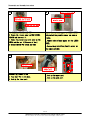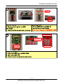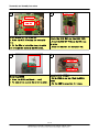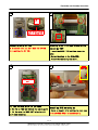
1
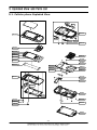
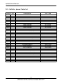
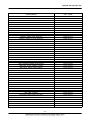
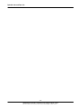
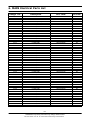
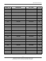
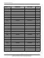
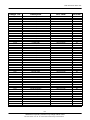
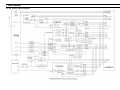
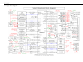
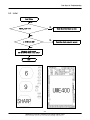
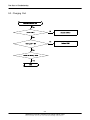
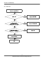
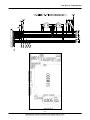
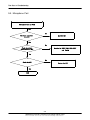
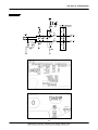
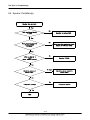
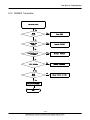
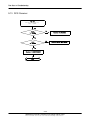
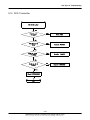
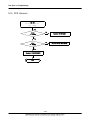
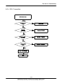
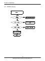
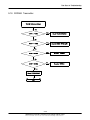
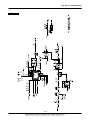
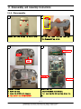
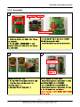
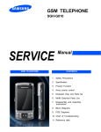
UMTS TELEPHONE
SGH-Z400
UMTS TELEPHONE
CONTENTS
1.
Safety Precautions
2.
Specification
3.
Product Function
4.
Array course control
5.
Exploded View and Parts List
6.
MAIN Electrical Parts List
7.
Block Diagrams
8.
PCB Diagrams
9.
Flow Chart of Troubleshooting
10.
Reference data
11.
Disassembly and Assembly
Instructions
목 차
1. Safety Precautions
1-1. Repair Precaution...........................................................................1-1
1-2. ESD(Electrostatically Sensitive Devices) Precaution...........................1-2
2. Specification
2-1. GSM General Specification..............................................................2-1
2-2. GSM Tx Power Class......................................................................2-2
3. Product Function
4. Array course control
4-1. Downloading Binary Files................................................................4-2
4-2. Pre-requsite for Downloading..........................................................4-2
4-3. S/W Downloader Program...............................................................4-3
5. Exploded View and Parts List
5-1. Cellular phone Exploded View.........................................................5-1
5-2. Cellular phone Parts list.................................................................5-2
6. MAIN Electrical Parts List
7. Block Diagrams
7-1. RF Solution Block Diagram.............................................................7-1
7-2. Logic Block Diagram......................................................................7-2
8. PCB Diagrams
목 차
9. Flow Chart of Troubleshooting
9-1. Power On.....................................................................................9-1
9-2. Initial............................................................................................9-3
9-3. Charging Part................................................................................9-4
9-4. Sim Part.......................................................................................9-6
9-5. Microphone Part.............................................................................9-8
9-6. Speaker Part(Melody)..................................................................9-10
9-7. Key Data Input...........................................................................9-12
9-8. Earphone Part.............................................................................9-13
9-9. LCD Part....................................................................................9-15
9-10. Camera part.............................................................................9-17
9-11. GSM900 Receiver......................................................................9-18
9-12. GSM900 Transmitter...................................................................9-19
9-13. DCS Receiver............................................................................9-20
9-14. DCS Transmitter........................................................................9-21
9-15. PCS Receiver............................................................................9-22
9-16. PCS Transmitter........................................................................9-23
9-17. WCDMA Receiver.......................................................................9-24
9-18. WCDMA Transmitter...................................................................9-25
10. Reference data
10-1. Reference Abbreviate..................................................................10-1
11. Disassembly and Assembly Instructions
11-1. Disassemby...............................................................................11-1
11-2. Assembly..................................................................................11-5
1. Safety Precautions
1-1. Repair Precaution
● Repair in Shield Box, during detailed tuning.
Take specially care of tuning or test,
because specificity of cellular phone is sensitive for surrounding interference(RF noise).
● Be careful to use a kind of magnetic object or tool,
because performance of parts is damaged by the influence of magnetic force.
● Surely use a standard screwdriver when you disassemble this product,
otherwise screw will be worn away.
● Use a thicken twisted wire when you measure level.
A thicken twisted wire has low resistance, therefore error of measurement is few.
● Repair after separate Test Pack and Set because for short danger (for example an
overcurrent and furious flames of parts etc) when you repair board in condition of
connecting Test Pack and tuning on.
● Take specially care of soldering, because Land of PCB is small and weak in heat.
● Surely tune on/off while using AC power plug, because a repair of battery charger is
dangerous when tuning ON/OFF PBA and Connector after disassembling charger.
● Don't use as you pleases after change other material than replacement registered on SEC System.
Otherwise engineer in charge isn't charged with problem that you don't keep this rules.
1-1
SAMSUNG Proprietary-Contents may change without notice
This Document can not be used without Samsung's authorization
Safety Precautions
1-2. ESD(Electrostatically Sensitive Devices) Precaution
Several semiconductor may be damaged easily by static electricity. Such parts are called by ESD
(Electrostatically Sensitive Devices), for example IC,BGA chip etc. Read Precaution below.
You can prevent from ESD damage by static electricity.
● Remove static electricity remained your body before you touch semiconductor or parts with
semiconductor. There are ways that you touch an earthed place or wear static electricity
prevention string on wrist.
● Use earthed soldering steel when you connect or disconnect ESD.
● Use soldering removing tool to break static electricity. , otherwise ESD will be damaged by
static electricity.
● Don't unpack until you set up ESD on product. Because most of ESD are packed by box and aluminum
plate to have conductive power,they are prevented from static electricity.
● You must maintain electric contact between ESD and place due to be set up until ESD is connected
completely to the proper place or a circuit board.
1-2
SAMSUNG Proprietary-Contents may change without notice
This Document can not be used without Samsung's authorization
2. Specification
2-1. GSM General Specification
EG SM9 00
DCS1800
PCS1900
W-CDMA
Fr eq.
Band[MHz]
Uplin k/Down link
8 90~915
9 35~960
17 10~178 5
18 05~188 0
18 50~191 0
19 30~199 0
192 0~1980
211 0~2170
ARF CN ra nge
0~ 124 &
97 5~1023
5 12~885
5 12~810
UL:96 12~988 8
DL:105 62~108 38
T x/Rx spacing
45MHz
95MHz
80MHz
1 90MHz
Mo d. Bit r ate/
Bit Period
270 .833kb ps
3 .692u s
270 .833kb ps
3 .692u s
270 .833kb ps
3 .692u s
3.8 4Mcps
Ti me Slo t
Pe rio d/Fr am e
Per iod
5 76.9u s
4. 615ms
5 76.9u s
4. 615ms
5 76.9u s
4. 615ms
Fr ame len gth : 10ms
Modula tion
0 .3G M SK
0 .3G MSK
0 .3G M SK
Q PS K
HQPSK
MS Power
33d Bm~5dBm
30d Bm~0dBm
30d Bm~0dBm
24 dBm ~ - 50dBm
Powe r Class
4
(max +33dBm)
1
(max +30dBm)
1
(max +30dBm)
3
(max + 24dBm)
Se nsitivity
-10 2dBm
-10 0dBm
-10 0dBm
- 106. 7dBm/ BW
TDMA Mu x
8
8
8
Cell Radiu s
35Km
2Km
2Km
2-1
SAMSUNG Proprietary-Contents may change without notice
This Document can not be used without Samsung's authorization
2Km
Specification
2-2. GSM TX power class
TX Power
control level
GSM900
TX Power
DCS1800
control level
TX Power
control level
PCS1800
5
33±2 dBm
0
30±3 dBm
0
30±3 dBm
6
31±2 dBm
1
28±3 dBm
1
28±3 dBm
7
29±2 dBm
2
26±3 dBm
2
26±3 dBm
8
27±2 dBm
3
24±3 dBm
3
24±3 dBm
9
25±2 dBm
4
22±3 dBm
4
22±3 dBm
10
23±2 dBm
5
20±3 dBm
5
20±3 dBm
11
21±2 dBm
6
18±3 dBm
6
18±3 dBm
12
19±2 dBm
7
16±3 dBm
7
16±3 dBm
13
17±2 dBm
8
14±3 dBm
8
14±3 dBm
14
15±2 dBm
9
12±4 dBm
9
12±4 dBm
15
13±2 dBm
10
10±4 dBm
10
10±4 dBm
16
11±3 dBm
11
8±4dBm
11
8±4dBm
17
9±3dBm
12
6±4 dBm
12
6±4 dBm
18
7±3 dBm
13
4±4 dBm
13
4±4 dBm
19
5±3 dBm
14
2±5 dBm
14
2±5 dBm
15
0±5 dBm
15
0±5 dBm
2-2
SAMSUNG Proprietary-Contents may change without notice
This Document can not be used without Samsung's authorization
3. Product Function
Main Function
▪ GPRS Class 10
▪ EGPRS Class E2
▪ GSM 900MHz & DCS1800MHz & 1900MHz & WCDMA FDD1
▪ Triple Vocoder (HR, FR, EFR)
▪ Slide type
▪ Built-in Digital Camera (2 Mega CMOS Sensor)
▪ AMLCD (262K TFT colors)
▪ Sending Photo & Video by MMS or E-Mail
▪ Downloadable Game via JAVA
▪ 64 Polyphonic Ring Tone
▪ WAP 2.0 Browser (Including xHTML/WCSS MP, w/HTTP)
▪ Video Telephony
▪ External Memory Card Socket(T-flash)
3-1
SAMSUNG Proprietary-Contents may change without notice
This Document can not be used without Samsung's authorization
Product Function
3-2
SAMSUNG Proprietary-Contents may change without notice
This Document can not be used without Samsung's authorization
4. Array course control
1.
2.
3.
4.
5.
6.
1
2
3
4
5
6
JIG: Download, Trace, Calibration, etc
RF test cable: RF test
Test cable: JIG to phone
TA (Travel Adaptor)
Data Link Cable : USB cable
Serial cable: PC to JIG
4-1
SAMSUNG Proprietary-Contents may change without notice
This Document can not be used without Samsung's authorization
Array course control
Software Downloading
4-1. Downloading Binary Files
• Four binary files for downloading Z400.
– amss.bin : Modem binary for communication function
& Mocha binary for user interface and various application
– Rsrc_Z400_.rc1: Files need for each application
– Rsrc2_Z400.rc2 : Power on/off animation
– FactoryFs_Z400_.ffs : Default file system to be put into in initial production
4-2. Pre-requsite for Downloading
• Downloader Program(FastMultiLoader V3.22.exe)
• SGH-Z400 Mobile Phone
• USB Data Link Cable
• Binary files
4-2
SAMSUNG Proprietary-Contents may change without notice
This Document can not be used without Samsung's authorization
Array course control
4-3. S/W Downloader Program
1. Boot the Z400 by pressing ‘Power ON key’ + ‘Number 9 key’ at the same timeIf you do properly, you can see the following message on sub LCD “SGH-Z400
DOWNLOAD”
2. Load the binary download program by executing the “FastMultiLoader
V3.22.exe”. And then Check the SMP6275.
3. Select the check box what you want to download.
4-3
SAMSUNG Proprietary-Contents may change without notice
This Document can not be used without Samsung's authorization
Array course control
4. Select the binary file what you want to download
* Up to eight ports are supported.
5. Now press the button ‘DownLoad’.
6. When downloading is complete, UE reboot automatically.
- If there is difference in FactoryFs.bin, UE will format file system
automatically.
4-4
SAMSUNG Proprietary-Contents may change without notice
This Document can not be used without Samsung's authorization
5. Exploded View and Parts List
5-1. Cellular phone Exploded View
QCK01
QRF03
QFR01
QFU01
QVO01
QRF09
QMI03
QCR32
QKP02
QCA03
QSP01
QCA01
QLC01
QKP01
QCR24
QME02
QCA02
QPC01
QMO01
QVK01
QME01
QAN05
QMP01
QFL01
QCR32
QAN02
QCA05
QRE01
QHI01
QCR21
QCR20
QSC01
QRF01
QSC02
QBA01
5-1
SAMSUNG Proprietary-Contents may change without notice
This Document can not be used without Samsung's authorization
Exploded view and Parts List
5-2. Cellular phone Parts list
Design LOC
QAN02
QAN05
QBA01
QCA01
QCA02
QCA03
QCR20
QCR21
QCR24
QCR32
QCR32
QKP01
QKP02
QLC01
QME01
QME02
QMO01
QMP01
QPC01
QRE01
QRF01
QSC01
QSC02
QSP01
QVK01
QFL01
QFU01
QFR01
QHI01
QCA05
QVO01
QRF09
QCK01
QRF03
QMI03
Description
SEC Code
INTENNA-SGHZ400
ASSY MEC-INTENNA CONTACT
BATTERY-950MAH,MIRROR SILVER,E
UNIT-CAMERA MODULE(VGA
UNIT-CAMERA KEY
UNIT-CAMERA
SCREW-MACHINE
SCREW-MACHINE
SCREW-MACHINE
SCREW-MACHINE
SCREW-MACHINE
MEC-KEYPAD MAIN(EU/SIL)
MEC-KEYPAD SUB(EU/SIL)
LCD-MODULE MAIN
UNIT-MAIN KEY FPCB
UNIT-EL KEY PBA
MOTOR DC-SGHZ400
PBA MAIN-SGH-Z400(V)
MEA-SLIDE FPCB KIT
ASSY ACCE-REAR(VODA)
MPR-TAPE RF COVER
ICT-COVER SCREW L
ICT-COVER SCREW R
MICRO SPEAKER
UNIT-VOLUME KEY
MEC-CASE SLIDE LOWER
ASSY MEC-HINGE MODULE
ASSY-DECO-CAMERA(VODA)
ASSY ACCE-SLIDE UPPER(VODA)
ASSY CASE-FRONT(VODA)
PMO-VOLUME KEY
PMO-COVER SD
PMO-CAMERA VT KEY
PMO-COVER EAR IF V2
RMO-RUBBER MIC HOLDER
GH42-00870A
GH75-08168A
GH43-02444B
GH59-03103A
GH59-02990A
GH59-03132A
6001-001429
6001-001507
6001-001892
6001-001700
6001-001700
GH75-09305B
GH75-09304B
GH07-00866A
GH59-02976A
GH59-02997A
GH31-00252A
GH92-02727A
GH97-06071A
GH98-00994B
GH74-24453B
GH70-01106A
GH70-01107A
3001-001950
GH59-02989A
GH75-09179B
GH75-09303B
GH98-00995A
GH98-00993B
GH98-00992B
GH72-28959A
GH72-28961B
GH72-29360A
GH72-30221B
GH73-06837A
5-2
SAMSUNG Proprietary-Contents may change without notice
This Document can not be used without Samsung's authorization
Exploded view and Parts List
Description
SEC Code
IC-MEMORY CARD
CONNECTOR-ADAPTOR
BAG PE
BAG ZIPPER
CBF INTERFACE-DATA LINK CABLE
ADAPTOR-SGHD800 TA(UK)
S/W CD-Z400V SAMSUNG PC STUDIO
UNIT-EARPHONE
LABEL(P)-WATER SOAK
LABEL(P)-WATER SOAK
MANUAL USERS-VODA ENGLISH
MANUAL USERS-VD QSG ENGLISH
LABEL(R)-MAIN(EU)
CUSHION-CASE(EU)
BOX-UNIT(VODA)
NDC-BRACKET CAMERA
NDC-BRACKET VOLUME
MPR-MAIN SHIELD TAPE
MPR-LCD PCB GASKET
MPR-BOHO VINYL LCD CONN
MPR-TAPE PBA A
MPR-BOHO VINYL KEY PAD
MPR-CUSHION LCD SCREW SHIELD L
MPR-CUSHION LCD SCREW SHIELD R
MPR-CUSHION PORON MAIN BOARD
MPR-VINYL BOHO CAMERA DUMMY
MPR-VINYL BOHO MAIN CAMERA
MPR-VINYL BOHO MAIN CAMERA LEN
MPR-VINYL BOHO SUB KEY
MPR-TAPE KEY INSULATION
MPR-TAPE CAMERA INSULATION
MPR-TAPE SUB CON INSULATION
MPR-TAPE FILTER INSULATION
MPR-TAPE B TO B BASE
MPR-TAPE B TO B BASE
MPR-TAPE LOWER SCREW CAP L
MPR-TAPE LOWER SCREW CAP R
MPR-TAPE LCD EMI
MPR-TAPE SUB CON BASE
MPR-TAPE CAMERA
MPR-VINYL BOHO MAIN WIN OUT
MPR-VINYL BOHO MAIN WIN OUT
MPR-TAPE EMI BD EL1
MPR-TAPE EMI BD EL2
MPR-TAPE INSULATION BD EL1
MPR-VINYL BOHO MAIN WINDOW
AS-IC-MCP UMTS
1109-001335
3719-001319
6902-000634
6902-000683
GH39-00444B
GH44-01131B
GH46-00238A
GH59-02499B
GH68-02026A
GH68-02026A
GH68-09727A
GH68-09741A
GH68-09930B
GH69-03844A
GH69-03886B
GH71-06382A
GH71-06383A
GH74-10829A
GH74-15077A
GH74-15350A
GH74-16066A
GH74-17373A
GH74-23396A
GH74-23397A
GH74-23399A
GH74-23408A
GH74-23409A
GH74-23410A
GH74-23413A
GH74-23414A
GH74-23417A
GH74-23418A
GH74-23420A
GH74-23430A
GH74-23430A
GH74-23433A
GH74-23434A
GH74-23526A
GH74-23594A
GH74-23595A
GH74-24255A
GH74-24255A
GH74-24615A
GH74-24616A
GH74-24617A
GH74-24962A
GH81-04519A
5-3
SAMSUNG Proprietary-Contents may change without notice
This Document can not be used without Samsung's authorization
Exploded view and Parts List
5-4
SAMSUNG Proprietary-Contents may change without notice
This Document can not be used without Samsung's authorization
6. MAIN Electrical Parts List
Design LOC
Description
SEC Code
STATUS
AN300
ANT100
ANT102
BAT50
BTC401
C100
C101
C102
C103
C104
C105
C107
C108
C109
C110
C111
C112
C113
C114
C115
C116
C117
C118
C119
C120
C121
C122
C123
C124
C125
C126
C127
C130
C133
C135
C137
C138
C139
C140
C141
C142
C143
C144
C145
C146
C147
C149
C150
C151
C152
C153
C154
C155
ANTENNA-CHIP
NPR-ANTENNA CONTACT
NPR-ANTENNA CONTACT
BATTERY-LI(2ND)
HEADER-BATTERY
C-CER,CHIP
C-CER,CHIP
C-CER,CHIP
C-CER,CHIP
C-CER,CHIP
C-CER,CHIP
C-CER,CHIP
C-CER,CHIP
C-CER,CHIP
C-CER,CHIP
C-CER,CHIP
C-CER,CHIP
C-CER,CHIP
C-CER,CHIP
C-CER,CHIP
C-CER,CHIP
C-CER,CHIP
C-CER,CHIP
C-CER,CHIP
C-CER,CHIP
C-CER,CHIP
C-CER,CHIP
C-CER,CHIP
C-CER,CHIP
C-CER,CHIP
C-CER,CHIP
C-CER,CHIP
C-CER,CHIP
C-CER,CHIP
C-CER,CHIP
C-CER,CHIP
C-CER,CHIP
C-CER,CHIP
C-CER,CHIP
C-CER,CHIP
C-CER,CHIP
C-CER,CHIP
C-CER,CHIP
C-CER,CHIP
C-CER,CHIP
C-CER,CHIP
C-CER,CHIP
C-CER,CHIP
C-CER,CHIP
C-CER,CHIP
C-CER,CHIP
C-CER,CHIP
C-CER,CHIP
4202-001132
GH71-04302A
GH71-04302A
4302-001130
3711-005880
2203-002982
2203-001124
2203-005808
2203-005806
2203-005682
2203-002668
2203-005808
2203-005719
2203-006423
2203-005682
2203-005682
2203-006423
2203-006423
2203-005682
2203-005682
2203-006423
2203-006379
2203-005682
2203-006423
2203-005806
2203-005682
2203-005808
2203-006556
2203-005682
2203-006556
2203-005808
2203-006423
2203-000725
2203-000836
2203-006423
2203-006423
2203-005682
2203-000438
2203-005719
2203-006838
2203-005682
2203-006208
2203-006423
2203-006379
2203-006379
2203-005729
2203-006048
2203-006305
2203-005729
2203-005732
2203-000311
2203-002443
2203-001153
SA
SA
SA
SA
SA
SNA
SA
SA
SA
SA
SA
SA
SA
SA
SA
SA
SA
SA
SA
SA
SA
SA
SA
SA
SA
SA
SA
SA
SA
SA
SA
SA
SA
SA
SA
SA
SA
SA
SA
SA
SA
SA
SA
SA
SA
SA
SA
SA
SA
SA
SA
SA
SA
6-1
SAMSUNG Proprietary-Contents may change without notice
This Document can not be used without Samsung's authorization
Main Electrical Parts List
Design LOC
Description
SEC Code
STATUS
C156
C157
C158
C159
C160
C162
C163
C164
C165
C166
C168
C170
C200
C201
C202
C203
C204
C206
C207
C210
C212
C213
C214
C217
C219
C220
C221
C222
C223
C224
C225
C231
C232
C233
C234
C235
C236
C237
C239
C240
C242
C244
C245
C246
C247
C248
C250
C251
C252
C253
C300
C301
C302
C-CER,CHIP
C-CER,CHIP
C-CER,CHIP
C-CER,CHIP
C-CER,CHIP
C-CER,CHIP
C-CER,CHIP
C-CER,CHIP
C-CER,CHIP
C-CER,CHIP
INDUCTOR-SMD
C-CER,CHIP
C-CER,CHIP
C-CER,CHIP
C-CER,CHIP
C-CER,CHIP
C-CER,CHIP
C-CER,CHIP
C-CER,CHIP
C-CER,CHIP
C-CER,CHIP
C-CER,CHIP
C-CER,CHIP
C-CER,CHIP
C-CER,CHIP
C-CER,CHIP
C-CER,CHIP
C-CER,CHIP
C-CER,CHIP
C-CER,CHIP
C-CER,CHIP
C-CER,CHIP
C-CER,CHIP
C-CER,CHIP
C-CER,CHIP
C-CER,CHIP
C-CER,CHIP
C-CER,CHIP
C-CER,CHIP
C-CER,CHIP
C-CER,CHIP
C-CER,CHIP
C-CER,CHIP
C-CER,CHIP
C-CER,CHIP
C-CER,CHIP
C-CER,CHIP
C-CER,CHIP
C-CER,CHIP
C-CER,CHIP
C-CER,CHIP
C-CER,CHIP
C-CER,CHIP
2203-005344
2203-001033
2203-005719
2203-006123
2203-005736
2203-005682
2203-005719
2203-005682
2203-005683
2203-005719
2703-001722
2203-006375
2203-005736
2203-006194
2203-005736
2203-006194
2203-006838
2203-005729
2203-005729
2203-005288
2203-006305
2203-006423
2203-006305
2203-006194
2203-005808
2203-006423
2203-005806
2203-006194
2203-005736
2203-006423
2203-005806
2203-005806
2203-005682
2203-006556
2203-005736
2203-006423
2203-006423
2203-006305
2203-006846
2203-006846
2203-005736
2203-006120
2203-005736
2203-005806
2203-000330
2203-000386
2203-006423
2203-000330
2203-000330
2203-005719
2203-005725
2203-005725
2203-006668
SA
SA
SA
SA
SA
SA
SA
SA
SA
SA
SA
SNA
SA
SA
SA
SA
SA
SA
SA
SA
SA
SA
SA
SA
SA
SA
SA
SA
SA
SA
SA
SA
SA
SA
SA
SA
SA
SA
SNA
SNA
SA
SA
SA
SA
SA
SA
SA
SA
SA
SA
SA
SA
SA
6-2
SAMSUNG Proprietary-Contents may change without notice
This Document can not be used without Samsung's authorization
Main Electrical Parts List
Design LOC
Description
SEC Code
STATUS
C303
C304
C305
C306
C307
C308
C309
C310
C311
C312
C314
C315
C316
C317
C318
C319
C320
C321
C322
C323
C324
C325
C326
C327
C328
C329
C330
C331
C332
C333
C334
C335
C336
C337
C338
C339
C340
C341
C342
C343
C344
C345
C346
C347
C348
C349
C350
C351
C354
C355
C356
C357
C358
C-CER,CHIP
C-CER,CHIP
C-CER,CHIP
C-CER,CHIP
C-CER,CHIP
C-CER,CHIP
C-CER,CHIP
C-CER,CHIP
C-CER,CHIP
C-CER,CHIP
C-CER,CHIP
C-CER,CHIP
C-CER,CHIP
C-CER,CHIP
C-CER,CHIP
C-CER,CHIP
C-CER,CHIP
C-CER,CHIP
C-CER,CHIP
C-CER,CHIP
C-CER,CHIP
C-CER,CHIP
C-CER,CHIP
C-CER,CHIP
C-CER,CHIP
C-CER,CHIP
C-CER,CHIP
C-CER,CHIP
C-CER,CHIP
C-CER,CHIP
C-CER,CHIP
C-CER,CHIP
C-CER,CHIP
C-CER,CHIP
C-CER,CHIP
C-CER,CHIP
C-CER,CHIP
C-CER,CHIP
C-CER,CHIP
C-CER,CHIP
C-CER,CHIP
C-CER,CHIP
C-CER,CHIP
C-CER,CHIP
C-CER,CHIP
C-CER,CHIP
C-CER,CHIP
C-CER,CHIP
C-CER,CHIP
C-CER,CHIP
C-CER,CHIP
C-CER,CHIP
C-CER,CHIP
2203-005725
2203-006194
2203-006047
2203-006423
2203-006423
2203-006838
2203-006838
2203-006838
2203-006423
2203-005717
2203-005482
2203-006562
2203-006257
2203-005682
2203-000233
2203-006194
2203-006194
2203-006825
2203-005806
2203-005806
2203-005806
2203-005806
2203-005806
2203-006194
2203-006194
2203-006194
2203-006194
2203-006194
2203-006194
2203-006194
2203-006423
2203-006091
2203-006423
2203-006423
2203-006423
2203-006091
2203-005806
2203-005806
2203-005806
2203-005806
2203-005806
2203-005806
2203-005806
2203-005806
2203-006194
2203-006194
2203-006194
2203-006194
2203-006423
2203-006194
2203-005806
2203-005806
2203-006194
SA
SA
SA
SA
SA
SA
SA
SA
SA
SA
SA
SA
SA
SA
SA
SA
SA
SA
SA
SA
SA
SA
SA
SA
SA
SA
SA
SA
SA
SA
SA
SA
SA
SA
SA
SA
SA
SA
SA
SA
SA
SA
SA
SA
SA
SA
SA
SA
SA
SA
SA
SA
SA
6-3
SAMSUNG Proprietary-Contents may change without notice
This Document can not be used without Samsung's authorization
Main Electrical Parts List
Design LOC
Description
SEC Code
STATUS
C359
C360
C361
C362
C363
C364
C365
C366
C367
C368
C369
C370
C371
C372
C373
C374
C375
C376
C377
C378
C379
C380
C381
C382
C383
C384
C385
C386
C387
C388
C400
C401
C402
C403
C404
C405
C406
C407
C408
C409
C410
C411
C412
C413
C414
C415
C417
C418
C420
C422
C423
C424
C425
C-CER,CHIP
C-CER,CHIP
C-CER,CHIP
C-CER,CHIP
C-CER,CHIP
C-CER,CHIP
C-CER,CHIP
C-CER,CHIP
C-CER,CHIP
C-CER,CHIP
C-CER,CHIP
C-CER,CHIP
C-CER,CHIP
C-CER,CHIP
C-CER,CHIP
C-CER,CHIP
C-CER,CHIP
C-CER,CHIP
C-CER,CHIP
C-CER,CHIP
C-CER,CHIP
C-CER,CHIP
C-CER,CHIP
C-CER,CHIP
C-CER,CHIP
C-CER,CHIP
C-CER,CHIP
C-CER,CHIP
C-CER,CHIP
C-CER,CHIP
C-CER,CHIP
C-CER,CHIP
C-CER,CHIP
C-CER,CHIP
C-CER,CHIP
C-CER,CHIP
C-CER,CHIP
C-CER,CHIP
C-CER,CHIP
C-CER,CHIP
C-CER,CHIP
C-CER,CHIP
C-CER,CHIP
C-CER,CHIP
C-CER,CHIP
C-CER,CHIP
C-CER,CHIP
C-CER,CHIP
C-CER,CHIP
C-CER,CHIP
C-CER,CHIP
C-CER,CHIP
C-CER,CHIP
2203-006423
2203-006194
2203-006194
2203-006194
2203-006194
2203-006423
2203-006423
2203-006423
2203-006423
2203-006423
2203-006423
2203-006194
2203-006194
2203-006194
2203-006825
2203-006423
2203-006423
2203-006423
2203-006423
2203-006423
2203-005682
2203-005682
2203-006423
2203-006562
2203-005789
2203-006423
2203-005682
2203-005719
2203-005719
2203-005719
2203-005806
2203-006194
2203-006423
2203-006423
2203-006423
2203-006562
2203-005719
2203-005719
2203-006838
2203-005806
2203-006194
2203-006423
2203-006423
2203-006423
2203-000254
2203-006423
2203-005682
2203-006562
2203-006423
2203-006423
2203-005719
2203-005719
2203-006423
SA
SA
SA
SA
SA
SA
SA
SA
SA
SA
SA
SA
SA
SA
SA
SA
SA
SA
SA
SA
SA
SA
SA
SA
SA
SA
SA
SA
SA
SA
SA
SA
SA
SA
SA
SA
SA
SA
SA
SA
SA
SA
SA
SA
SA
SA
SA
SA
SA
SA
SA
SA
SA
6-4
SAMSUNG Proprietary-Contents may change without notice
This Document can not be used without Samsung's authorization
Main Electrical Parts List
Design LOC
Description
SEC Code
STATUS
C426
C427
C500
C501
C502
C503
C504
C505
C507
C508
C509
C510
C511
C512
C513
C514
C515
C516
C517
C518
C519
C520
C521
C522
C523
C524
C525
C526
C527
C528
C529
C530
C531
C532
C534
C535
C536
C537
C538
C539
C540
C541
C542
C543
C544
C545
C548
C551
C554
C555
C556
C557
C558
C-CER,CHIP
C-CER,CHIP
C-CER,CHIP
C-CER,CHIP
C-CER,CHIP
C-CER,CHIP
C-CER,CHIP
C-CER,CHIP
C-CER,CHIP
C-CER,CHIP
C-CER,CHIP
C-CER,CHIP
C-CER,CHIP
C-CER,CHIP
C-CER,CHIP
C-CER,CHIP
C-CER,CHIP
C-CER,CHIP
C-CER,CHIP
C-CER,CHIP
C-CER,CHIP
C-CER,CHIP
C-CER,CHIP
C-CER,CHIP
C-CER,CHIP
C-CER,CHIP
C-CER,CHIP
C-CER,CHIP
C-CER,CHIP
C-CER,CHIP
C-CER,CHIP
C-CER,CHIP
C-CER,CHIP
C-CER,CHIP
C-CER,CHIP
C-CER,CHIP
C-CER,CHIP
C-CER,CHIP
C-CER,CHIP
C-CER,CHIP
C-CER,CHIP
C-CER,CHIP
C-CER,CHIP
C-CER,CHIP
C-CER,CHIP
C-CER,CHIP
C-CER,CHIP
C-CER,CHIP
C-CER,CHIP
C-CER,CHIP
C-CER,CHIP
C-CER,CHIP
C-CER,CHIP
2203-005682
2203-005682
2203-006423
2203-006324
2203-006208
2203-006423
2203-005736
2203-005731
2203-005736
2203-005731
2203-006423
2203-006423
2203-006423
2203-006562
2203-006208
2203-006208
2203-006838
2203-006305
2203-006562
2203-006208
2203-006838
2203-006305
2203-006838
2203-006838
2203-006305
2203-006562
2203-006305
2203-006562
2203-006305
2203-005806
2203-005806
2203-006423
2203-006208
2203-006838
2203-006423
2203-006423
2203-006423
2203-006423
2203-006838
2203-006838
2203-006208
2203-005806
2203-005806
2203-005806
2203-006423
2203-006423
2203-006562
2203-006562
2203-006562
2203-005482
2203-005682
2203-005682
2203-005682
SA
SA
SA
SA
SA
SA
SA
SA
SA
SA
SA
SA
SA
SA
SA
SA
SA
SA
SA
SA
SA
SA
SA
SA
SA
SA
SA
SA
SA
SA
SA
SA
SA
SA
SA
SA
SA
SA
SA
SA
SA
SA
SA
SA
SA
SA
SA
SA
SA
SA
SA
SA
SA
6-5
SAMSUNG Proprietary-Contents may change without notice
This Document can not be used without Samsung's authorization
Main Electrical Parts List
Design LOC
Description
SEC Code
STATUS
C559
C560
C563
C564
C565
C566
C567
C600
C601
C602
C603
C604
C605
C606
C607
C608
C609
C610
C611
C612
C613
C615
C616
C619
C620
C621
C622
C623
C624
C625
C626
C628
C629
C630
C631
C632
C633
C634
C635
C636
C637
C638
C639
C640
C642
C643
C645
C646
C647
C649
C650
C651
C653
C-CER,CHIP
C-CER,CHIP
C-CER,CHIP
C-CER,CHIP
C-CER,CHIP
C-CER,CHIP
C-CER,CHIP
C-CER,CHIP
C-CER,CHIP
C-CER,CHIP
C-CER,CHIP
C-CER,CHIP
C-CER,CHIP
C-CER,CHIP
C-CER,CHIP
C-CER,CHIP
C-CER,CHIP
C-CER,CHIP
C-CER,CHIP
C-CER,CHIP
C-CER,CHIP
C-CER,CHIP
C-CER,CHIP
C-CER,CHIP
C-CER,CHIP
C-CER,CHIP
C-CER,CHIP
C-CER,CHIP
C-CER,CHIP
C-CER,CHIP
C-CER,CHIP
C-CER,CHIP
C-CER,CHIP
C-CER,CHIP
C-CER,CHIP
C-CER,CHIP
C-CER,CHIP
C-CER,CHIP
C-CER,CHIP
C-CER,CHIP
C-CER,CHIP
C-CER,CHIP
C-CER,CHIP
C-CER,CHIP
C-CER,CHIP
C-CER,CHIP
C-CER,CHIP
C-CER,CHIP
C-CER,CHIP
C-CER,CHIP
C-CER,CHIP
C-CER,CHIP
C-CER,CHIP
2203-005682
2203-005682
2203-005736
2203-006562
2203-006562
2203-005719
2203-006257
2203-005779
2203-005682
2203-006423
2203-006423
2203-005779
2203-005682
2203-005719
2203-005719
2203-005682
2203-005779
2203-005719
2203-005719
2203-005719
2203-005719
2203-006648
2203-006648
2203-005779
2203-005729
2203-006305
2203-006305
2203-005729
2203-006648
2203-006648
2203-005719
2203-005719
2203-005719
2203-005719
2203-005779
2203-005682
2203-006348
2203-005682
2203-005779
2203-006423
2203-006423
2203-006423
2203-006208
2203-006208
2203-006423
2203-006423
2203-006562
2203-006423
2203-005344
2203-006423
2203-006423
2203-005344
2203-006423
SA
SA
SA
SA
SA
SA
SA
SA
SA
SA
SA
SA
SA
SA
SA
SA
SA
SA
SA
SA
SA
SA
SA
SA
SA
SA
SA
SA
SA
SA
SA
SA
SA
SA
SA
SA
SA
SA
SA
SA
SA
SA
SA
SA
SA
SA
SA
SA
SA
SA
SA
SA
SA
6-6
SAMSUNG Proprietary-Contents may change without notice
This Document can not be used without Samsung's authorization
Main Electrical Parts List
Design LOC
Description
SEC Code
STATUS
C654
C655
C656
C657
C658
C659
C660
C661
C700
C701
C703
C704
C705
C706
C707
C708
C709
C710
C711
C712
C713
C714
C715
C716
C717
D500
D501
D502
DUF201
F100
F101
F102
F200
F202
F400
F700
F701
F702
F703
F704
F705
F706
F707
F708
F709
F710
F711
IFC400
L102
L103
L104
L105
L106
C-CER,CHIP
C-CER,CHIP
C-CER,CHIP
C-CER,CHIP
C-CER,CHIP
C-CER,CHIP
C-CER,CHIP
C-CER,CHIP
C-CER,CHIP
C-CER,CHIP
C-CER,CHIP
C-CER,CHIP
C-CER,CHIP
C-CER,CHIP
C-CER,CHIP
C-CER,CHIP
C-CER,CHIP
C-CER,CHIP
C-CER,CHIP
C-CER,CHIP
C-CER,CHIP
C-CER,CHIP
C-CER,CHIP
C-CER,CHIP
C-CER,CHIP
DIODE-ZENER
DIODE-ARRAY
DIODE-ARRAY
DUPLEXER-SAW
FILTER-SAW
FILTER-SAW
FILTER-SAW
FILTER-SAW
FILTER-SAW
FILTER-EMI SMD
FILTER-EMI/ESD
FILTER-EMI/ESD
FILTER-EMI/ESD
FILTER-EMI/ESD
FILTER-EMI/ESD
FILTER-EMI/ESD
FILTER-EMI/ESD
FILTER-EMI/ESD
FILTER-EMI/ESD
FILTER-EMI/ESD
FILTER-EMI/ESD
FILTER-EMI/ESD
SOCKET-INTERFACE
INDUCTOR-SMD
BEAD-SMD
INDUCTOR-SMD
BEAD-SMD
INDUCTOR-SMD
2203-006668
2203-005736
2203-000654
2203-005344
2203-006562
2203-005731
2203-005731
2203-005719
2203-006257
2203-006562
2203-005682
2203-006423
2203-005682
2203-006838
2203-006423
2203-005682
2203-006423
2203-002982
2203-001153
2203-006562
2203-005719
2203-005719
2203-005719
2203-005742
2203-005742
0403-001547
0407-001002
0407-001002
2910-000018
2904-001628
2904-001634
2904-001635
2904-001658
2904-001623
2901-001254
2901-001326
2901-001353
2901-001326
2901-001353
2901-001326
2901-001326
2901-001326
2901-001326
2901-001326
2901-001353
2901-001353
2901-001353
3710-002306
2703-003004
3301-001756
2703-002903
3301-001756
2703-002900
SA
SA
SA
SA
SA
SA
SA
SA
SA
SA
SA
SA
SA
SA
SA
SA
SA
SNA
SA
SA
SA
SA
SA
SA
SA
SA
SA
SA
SA
SA
SA
SA
SA
SA
SA
SA
SA
SA
SA
SA
SA
SA
SA
SA
SA
SA
SA
SA
SA
SA
SA
SA
SA
6-7
SAMSUNG Proprietary-Contents may change without notice
This Document can not be used without Samsung's authorization
Main Electrical Parts List
Design LOC
Description
SEC Code
STATUS
L107
L108
L109
L110
L111
L112
L113
L114
L115
L116
L117
L118
L119
L120
L121
L123
L124
L125
L128
L129
L130
L131
L200
L206
L207
L208
L210
L211
L212
L214
L215
L218
L219
L300
L400
L500
L501
L502
L503
L506
L507
L600
L601
L700
L701
L702
L703
MIC60
MIS200
OSC300
OSC500
PAM100
PAM201
INDUCTOR-SMD
INDUCTOR-SMD
INDUCTOR-SMD
INDUCTOR-SMD
INDUCTOR-SMD
INDUCTOR-SMD
INDUCTOR-SMD
BEAD-SMD
INDUCTOR-SMD
INDUCTOR-SMD
INDUCTOR-SMD
INDUCTOR-SMD
BEAD-SMD
BEAD-SMD
INDUCTOR-SMD
BEAD-SMD
INDUCTOR-SMD
INDUCTOR-SMD
INDUCTOR-SMD
INDUCTOR-SMD
INDUCTOR-SMD
INDUCTOR-SMD
INDUCTOR-SMD
INDUCTOR-SMD
INDUCTOR-SMD
INDUCTOR-SMD
INDUCTOR-SMD
INDUCTOR-SMD
INDUCTOR-SMD
INDUCTOR-SMD
INDUCTOR-SMD
INDUCTOR-SMD
INDUCTOR-SMD
BEAD-SMD
BEAD-SMD
BEAD-SMD
BEAD-SMD
INDUCTOR-SMD
INDUCTOR-SMD
INDUCTOR-SMD
INDUCTOR-SMD
BEAD-SMD
BEAD-SMD
BEAD-SMD
BEAD-SMD
BEAD-SMD
INDUCTOR-SMD
MICROPHONE-ASSY-SMD MIC
FREQ-ISOLATOR
RESONATOR-CERAMIC
CRYSTAL-SMD
IC-POWER AMP
IC-POWER AMP
2703-002903
2703-002906
2703-002907
2703-002906
2703-002794
2703-002903
2703-002794
3301-001756
2703-002819
2703-002819
2703-002819
2703-002819
3301-001756
3301-001756
2703-002207
3301-001756
2703-001747
2703-001728
2703-002901
2703-002901
2703-002901
2703-001726
2703-002369
2703-002313
2703-003004
2703-002906
2703-003004
2703-003004
2703-002267
2703-002612
2703-003004
2703-002906
2703-002198
3301-001534
3301-001534
3301-001534
3301-001534
2703-002872
2703-002872
2703-002989
2703-002989
3301-001756
3301-001756
3301-001534
3301-001534
3301-001534
2703-002850
GH30-00265A
4709-001408
2802-001182
2801-004339
1201-002288
1201-002325
SA
SA
SNA
SA
SNA
SA
SNA
SA
SA
SA
SA
SA
SA
SA
SA
SA
SA
SA
SNA
SNA
SNA
SA
SA
SA
SA
SA
SA
SA
SA
SA
SA
SA
SA
SA
SA
SA
SA
SA
SA
SA
SA
SA
SA
SA
SA
SA
SA
SA
SNA
SA
SA
SA
SA
6-8
SAMSUNG Proprietary-Contents may change without notice
This Document can not be used without Samsung's authorization
Main Electrical Parts List
Design LOC
Description
SEC Code
STATUS
Q501
R100
R102
R103
R104
R105
R106
R107
R108
R109
R110
R111
R112
R113
R114
R115
R116
R117
R118
R119
R120
R121
R122
R123
R128
R200
R201
R202
R203
R205
R206
R301
R302
R303
R306
R308
R309
R310
R314
R315
R316
R317
R318
R320
R321
R322
R323
R324
R325
R326
R327
R328
R329
TR-DIGITAL
R-CHIP
R-CHIP
R-CHIP
R-CHIP
R-CHIP
R-CHIP
R-CHIP
R-CHIP
R-CHIP
R-CHIP
R-CHIP
R-CHIP
R-CHIP
R-CHIP
R-CHIP
R-CHIP
R-CHIP
R-CHIP
R-CHIP
R-CHIP
R-CHIP
R-CHIP
R-CHIP
R-CHIP
R-CHIP
R-CHIP
R-CHIP
R-CHIP
R-CHIP
R-CHIP
R-CHIP
R-CHIP
R-CHIP
R-CHIP
R-CHIP
R-CHIP
R-CHIP
R-CHIP
R-CHIP
R-CHIP
R-CHIP
R-CHIP
R-CHIP
R-CHIP
R-CHIP
R-CHIP
R-CHIP
R-CHIP
R-CHIP
R-CHIP
R-CHIP
R-CHIP
0504-000168
2007-007491
2007-007136
2007-008045
2007-007136
2007-008419
2007-008531
2007-008531
2007-007798
2007-007316
2007-000145
2007-007798
2007-008045
2007-008785
2007-009201
2007-008579
2007-008579
2007-008045
2007-008581
2007-008581
2007-000138
2007-008806
2007-008588
2007-001292
2007-008531
2007-008542
2007-007318
2007-001217
2007-008045
2007-008045
2007-007491
2007-008516
2007-008049
2007-008419
2007-008516
2007-008516
2007-008055
2007-009171
2007-007318
2007-007314
2007-007135
2007-000148
2007-001339
2007-001339
2007-000148
2007-009171
2007-009171
2007-009171
2007-009171
2007-008516
2007-008516
2007-008055
2007-008516
SA
SA
SA
SA
SA
SA
SA
SA
SA
SA
SA
SA
SA
SNA
SA
SA
SA
SA
SNA
SNA
SA
SA
SA
SA
SA
SA
SA
SA
SA
SA
SA
SA
SA
SA
SA
SA
SA
SA
SA
SA
SA
SA
SA
SA
SA
SA
SA
SA
SA
SA
SA
SA
SA
6-9
SAMSUNG Proprietary-Contents may change without notice
This Document can not be used without Samsung's authorization
Main Electrical Parts List
Design LOC
Description
SEC Code
STATUS
R330
R331
R332
R335
R336
R337
R401
R403
R404
R405
R406
R407
R408
R409
R410
R412
R413
R414
R415
R416
R418
R419
R420
R421
R501
R502
R503
R504
R505
R506
R507
R510
R511
R512
R513
R514
R517
R518
R519
R600
R601
R602
R603
R604
R605
R606
R607
R608
R609
R612
R613
R614
R615
R-CHIP
R-CHIP
R-CHIP
R-CHIP
R-CHIP
R-CHIP
R-CHIP
R-CHIP
R-CHIP
R-CHIP
R-CHIP
R-CHIP
R-CHIP
R-CHIP
R-CHIP
R-CHIP
R-CHIP
R-CHIP
R-CHIP
R-CHIP
R-CHIP
R-CHIP
R-CHIP
R-CHIP
R-CHIP
R-CHIP
R-CHIP
R-CHIP
R-CHIP
R-CHIP
R-CHIP
R-CHIP
R-CHIP
R-CHIP
R-CHIP
R-CHIP
R-CHIP
R-CHIP
R-CHIP
R-CHIP
R-CHIP
R-CHIP
R-CHIP
R-CHIP
R-CHIP
R-CHIP
R-CHIP
R-CHIP
R-CHIP
R-CHIP
R-CHIP
R-CHIP
R-CHIP
2007-008516
2007-008516
2007-009171
2007-008542
2007-008798
2007-008055
2007-008516
2007-008542
2007-008542
2007-009170
2007-008542
2007-008542
2007-008542
2007-008542
2007-008548
2007-009170
2007-009111
2007-009111
2007-008542
2007-000171
2007-008419
2007-008542
2007-008419
2007-008516
2007-000148
2007-008483
2007-000171
2007-008806
2007-007468
2007-008055
2007-000165
2007-008486
2007-007589
2007-007528
2007-009212
2007-000171
2007-007132
2007-000147
2007-008486
2007-009212
2007-009212
2007-008548
2007-008548
2007-008548
2007-008548
2007-009212
2007-009212
2007-003001
2007-003001
2007-007132
2007-007308
2007-007313
2007-007308
SA
SA
SA
SA
SNA
SA
SA
SA
SA
SA
SA
SA
SA
SA
SA
SA
SA
SA
SA
SA
SA
SA
SA
SA
SA
SA
SA
SA
SA
SA
SA
SA
SA
SA
SA
SA
SA
SA
SA
SA
SA
SA
SA
SA
SA
SA
SA
SA
SA
SA
SA
SA
SA
6-10
SAMSUNG Proprietary-Contents may change without notice
This Document can not be used without Samsung's authorization
Main Electrical Parts List
Design LOC
Description
SEC Code
STATUS
R616
R617
R618
R619
R700
R701
R702
R703
RFS10
SIM300
SLC700
TA148
TA300
TA301
TA302
TA400
TA401
TA402
TA500
TA501
TA600
TA601
TA602
TA603
TA604
TCX201
TH300
TR200
U100
U102
U200
U202
U300
U301
U303
U304
U305
U306
U401
U402
U403
U404
U500
U501
U502
U503
U504
U600
U601
U602
U700
U701
UCP300
R-CHIP
R-CHIP
R-CHIP
R-CHIP
R-CHIP
R-CHIP
R-CHIP
R-CHIP
CONNECTOR-COAXIAL
CONNECTOR-CARD EDGE
CONNECTOR-FPC/FFC/PIC
C-TA,CHIP
C-TA,CHIP
C-TA,CHIP
C-TA,CHIP
C-TA,CHIP
C-TA,CHIP
C-TA,CHIP
C-TA,CHIP
C-TA,CHIP
C-TA,CHIP
C-TA,CHIP
C-TA,CHIP
C-TA,CHIP
C-TA,CHIP
OSCILLATOR-VCTCXO
THERMISTOR-NTC
TR-DIGITAL
IC-SWITCH
IC-TRANSCEIVER
IC-DETECTOR
IC-RECEIVER
IC-CMOS LOGIC
IC-POSI.FIXED REG.
IC-SWITCH
IC-SWITCH
BLUETOOTH MODULE
DIODE-ARRAY
IC-ANALOG MULTIPLEX
IC-ANALOG MULTIPLEX
IC-ANALOG SWITCH
IC-HALL EFFECT S/W
IC-POWER SUPERVISOR
IC-VOL. DETECTOR
IC-ANALOG SWITCH
IC-POSI.FIXED REG.
IC-BATTERY
IC-ANALOG SWITCH
IC-MELODY
IC-CMOS LOGIC
IC-POSI.FIXED REG.
IC-EL DRIVER
IC-MODEM
2007-000159
2007-007132
2007-008786
2007-008786
2007-008055
2007-008542
2007-000159
2007-000690
3705-001358
3709-001453
3708-002194
2404-001411
2404-001402
2404-001339
2404-001339
2404-001268
2404-001268
2404-001411
2404-001381
2404-001381
2404-001402
2404-001402
2404-001422
2404-001422
2404-001381
2809-001280
1404-001224
0504-001151
1205-002724
1205-002645
1209-001577
1205-002781
0801-003076
1203-003737
1205-002784
1205-002784
4709-001398
0407-001038
1001-001349
1001-001349
1001-001265
1009-001020
1203-004102
1203-004045
1001-001231
1203-003737
1203-003823
1001-001261
1204-002587
0801-003076
1203-003787
1003-001716
1205-002790
SA
SA
SA
SA
SA
SA
SA
SA
SA
SA
SA
SA
SA
SA
SA
SA
SA
SA
SA
SA
SA
SA
SA
SA
SA
SA
SA
SA
SA
SA
SA
SA
SA
SA
SA
SA
SA
SA
SA
SA
SA
SA
SA
SA
SA
SA
SA
SA
SA
SA
SA
SA
SA
6-11
SAMSUNG Proprietary-Contents may change without notice
This Document can not be used without Samsung's authorization
Main Electrical Parts List
Design LOC
Description
SEC Code
STATUS
UME400
VCO100
ZD300
ZD301
ZD400
ZD401
ZD402
ZD403
ZD404
ZD600
ZD700
ZD701
ZD702
ZD703
ZD704
IC-MCP
OSCILLATOR-VCO
DIODE-TVS
DIODE-TVS
DIODE-ZENER
DIODE-TVS
DIODE-TVS
VARISTOR
DIODE-ZENER
DIODE-TVS
DIODE-ZENER
DIODE-TVS
DIODE-TVS
DIODE-TVS
DIODE-TVS
1108-000041
2806-001380
0406-001215
0406-001215
0403-001547
0406-001215
0406-001215
1405-001082
0403-001427
0406-001215
0403-001511
0406-001215
0406-001215
0406-001215
0406-001215
SA
SA
SA
SA
SA
SA
SA
SA
SA
SA
SA
SA
SA
SA
SA
6-12
SAMSUNG Proprietary-Contents may change without notice
This Document can not be used without Samsung's authorization
7. Block Diagrams
7-1. RF Solution Block Diagram
7-1
SAMSUNG Proprietary-Contents may change without notice
This Document can not be used without Samsung's authorization
Block Diagrams
7-2. Logic Block Diagram
7-2
SAMSUNG Proprietary-Contents may change without notice
This Document can not be used without Samsung's authorization
8. PCB Diagrams
Top
8-1
PCB Diagrams
Bottom
8-2
9. Flow Chart of Troubleshooting
9-1. Power On
' Power On ' does not work
Yes
No
Check the Battery Voltage
is more than 3.4V
Change the Battery
Yes
No
U500 PIN57(PS_HOLD)
= 2.6V?
Check the PMU related to PS_HOLD
Yes
No
Check the Clock at
OSC500=32.768KHZ
Resolder OSC500
Yes
No
L501(VREG_MSMC) =1.375V?
Check the PMIC
Yes
L500(VREG_MSME) = 1.8V?
No
C531(VREG_MSMP) = 2.6V?
Check the PMIC
C518(VREG_MSMA) = 2.6V?
C526(VREG_TCXO) = 2.8V?
Yes
No
Check for the clock at
C507= 19.2 MHz
Check the clock generation circuit
(TCX201)
Yes
Check the initial operation
Yes
END
9-1
SAMSUNG Proprietary-Contents may change without notice
This Document can not be used without Samsung's authorization
Flow Chart of Troubleshooting
Power On
9-2
SAMSUNG Proprietary-Contents may change without notice
This Document can not be used without Samsung's authorization
Flow Chart of Troubleshooting
9-2. Initial
Initial Failure
Yes
No
RESET_JTAG ="H"?
Check the circuit related to reset
Yes
No
Is TP400~410 OK?
Check the circuit related to momory
Yes
Check the circuit around
LCD & SLC700 (Short or not solder)
END
9-3
SAMSUNG Proprietary-Contents may change without notice
This Document can not be used without Samsung's authorization
Flow Chart of Troubleshooting
9-3. Charging Part
Abnormal charging part
Yes
No
C417 = 5V ?
Resolder IFC400
Yes
No
Replace U504
U504 pin5 = "H"?
Yes
Check the Battery & TA
Yes
END
9-4
SAMSUNG Proprietary-Contents may change without notice
This Document can not be used without Samsung's authorization
Flow Chart of Troubleshooting
Charging
9-5
SAMSUNG Proprietary-Contents may change without notice
This Document can not be used without Samsung's authorization
Flow Chart of Troubleshooting
9-4. SIM Part
Phone can't access SIM Card
Yes
No
R337 = "H"?
Check the SIM POWER
Yes
No
After Power ON,
Check SIMCLK Signal on
SIM300 pin15 in a few second
Check the 32.768 kHz OSC
Yes
No
After SIM card insert,
SIM300 pin 13 = "H(SIM_RST)"?
Replace PBA
Yes
Check the SIM Card
Yes
END
9-6
SAMSUNG Proprietary-Contents may change without notice
This Document can not be used without Samsung's authorization
Flow Chart of Troubleshooting
9-7
SAMSUNG Proprietary-Contents may change without notice
This Document can not be used without Samsung's authorization
Flow Chart of Troubleshooting
9-5. Microphone Part
Microphone does not work
Yes
No
Check the connection
from MIC
Resolder MIC
Yes
No
Check the circuit
from UCP300 to MIC
Resolder the R600, R603, R604, R607
and TA600
Yes
No
Check the MIC
Replace the MIC
OK
END
9-8
SAMSUNG Proprietary-Contents may change without notice
This Document can not be used without Samsung's authorization
Flow Chart of Troubleshooting
Microphone
9-9
SAMSUNG Proprietary-Contents may change without notice
This Document can not be used without Samsung's authorization
Flow Chart of Troubleshooting
9-6. Speaker Part(Melody))
Speaker does not work
Yes
No
U601 pin G8 and pin H1
= 2.7V?
Resolder or replace U601
Yes
No
Check the Clock signal at
Pin G5 of U601
(19.2MHz)
Check the clock generation circuit
(related to U601 and U602)
Yes
No
U708 pin C6, B6 ≒
1.8V?
(When UCP300 operate)
Resolder UCP300
Yes
Check the signals of
speaker input
No signal
Check the circuit related to
melody signal
OK
No
Is Speaker working?
Change the Speaker
Yes
END
9-10
SAMSUNG Proprietary-Contents may change without notice
This Document can not be used without Samsung's authorization
Flow Chart of Troubleshooting
Speaker
9-11
SAMSUNG Proprietary-Contents may change without notice
This Document can not be used without Samsung's authorization
Flow Chart of Troubleshooting
9-7. Key Data Input
Check Initial Operation
Yes
No
When one of the keys is
pushed,
is it displayed on LCD?
Check the Dome sheet
Yes
No
When one of the keys is
pushed,
KBIO signal is OK?
Replace the PBA
Yes
END
9-12
SAMSUNG Proprietary-Contents may change without notice
This Document can not be used without Samsung's authorization
Flow Chart of Troubleshooting
9-8. Earphone Part
Receiver does not work
Yes
No
Check UCP300
TP408 "L"?
Yes
No
Resolder U601
U601 pin C7, C8 ≥ 1V?
Yes
No
Resolder IFC400
IFC400 pin 5, 7 short?
Yes
No
Replace the Receiver and check UCP300
Is Receiver working?
Yes
END
9-13
SAMSUNG Proprietary-Contents may change without notice
This Document can not be used without Samsung's authorization
Flow Chart of Troubleshooting
9-14
SAMSUNG Proprietary-Contents may change without notice
This Document can not be used without Samsung's authorization
Flow Chart of Troubleshooting
9-9. LCD Part
LCD does not work
Yes
No
Is BACKLIGHT set
AlwaysON in the Menu?
Set BACKLIGHT on AlwaysON
Yes
Pin 25
No
Check UCP300
(LCD_RESET) at SLC700 is
"High" ?
Yes
Replace the LCD Module
END
9-15
SAMSUNG Proprietary-Contents may change without notice
This Document can not be used without Samsung's authorization
Flow Chart of Troubleshooting
9-16
SAMSUNG Proprietary-Contents may change without notice
This Document can not be used without Samsung's authorization
Flow Chart of Troubleshooting
9-10. Camera part
"Camera" function does not work
Yes
No
Check the Camera
connector on LCD module
Connect the camera module
Yes
No
SLC700pin 27, 29 =
3.6~4.2V?
Check U304
Yes
No
SLC700pin 55 = "H"?
Check F711 and SLC700
Yes
No
SLC700 Pin 47 = "H"?
Check F710 and SLC700
Yes
Is there another problem?
Yes
Replace the camera
module
END
9-17
SAMSUNG Proprietary-Contents may change without notice
This Document can not be used without Samsung's authorization
Flow Chart of Troubleshooting
9-11. GSM900 Receiver
RX ON
RF input : CH center freq
Amp : -50dBm
Yes
C108
≥ -65dBm
No
Resolder RFS100
Yes
C158
≥ -65dBm
No
Resolder U100
Yes
L106
≥ -70dBm
No
Resolder F100
Yes
U102 pin
11,12,13,14
≥ 500mV
No
Resolder U102
or Check pins related to U102
Yes
Check U102
END
9-18
SAMSUNG Proprietary-Contents may change without notice
This Document can not be used without Samsung's authorization
Flow Chart of Troubleshooting
9-12. GSM900 Transmitter
TX ON (5 Level)
Yes
R123
≥2.5V
Yes
Cheak PMIC
No
VCO100 pin1
≥2dBm
Yes
Resolder VCO100
No
U100(ASM) pin13
<= 20dBm
Yes
Resolder PAM100
No
C108 ≥25dBm
No
Replace U100(ASM)
Yes
R120
≥0.2V
No
Check VCO100 & U102
Yes
Check UCP300(MSM)
END
9-19
SAMSUNG Proprietary-Contents may change without notice
This Document can not be used without Samsung's authorization
Flow Chart of Troubleshooting
9-13. DCS Receiver
RX ON
RF input : CH center freq
Amp : -50dBm
Yes
C163
≥ -60dBm
No
Resolder U100(ASM)
Yes
L109
≥ -65dBm
No
Resolder F101 (DCS SAW)
Yes
Resolder U102(RTR6250)
END
9-20
SAMSUNG Proprietary-Contents may change without notice
This Document can not be used without Samsung's authorization
Flow Chart of Troubleshooting
9-14. DCS Transmitter
TX ON (0 Level)
Yes
VCO100 pin7
≥ 2.5V
Yes
Cheak PMIC
No
VCO100 pin5 ≥
2dBm
Yes
Resolder VCO100
No
PAM100 pin15
≥ 15dBm
Yes
Resolder PAM100
No
U100 pin 22 ≥
20dBm
No
Replace U100(ASM)
Yes
Check UCP300(MSM)
END
9-21
SAMSUNG Proprietary-Contents may change without notice
This Document can not be used without Samsung's authorization
Flow Chart of Troubleshooting
9-15. PCS Receiver
RX ON
RF input : CH center freq
Amp : -50dBm
Yes
C166
≥ -60dBm
No
Resolder U100(ASM)
Yes
L112
≥ -65dBm
No
Resolder F102 (PCS SAW)
Yes
Resolder U100(RTR6250)
END
9-22
SAMSUNG Proprietary-Contents may change without notice
This Document can not be used without Samsung's authorization
Flow Chart of Troubleshooting
9-16. PCS Transmitter
TX ON (0 Level)
Yes
VCO100 pin7
≥ 1V
Yes
Cheak PMIC
No
VCO100
pin7≥2dBm
Yes
Resolder VCO100
No
PAM100 pin15
≥15dBm
Yes
Resolder PAM100
No
U100 pin 22≥
20dBm
No
Replace U100(ASM)
Yes
Check UCP300MSM)
END
9-23
SAMSUNG Proprietary-Contents may change without notice
This Document can not be used without Samsung's authorization
Flow Chart of Troubleshooting
9-17. WCDMA Receiver
RX ON
Yes
C205
≥ -65dBm
Yes
Cheak and resolder DUF201
No
C247 ≥ -55dBm
Yes
Cheak and resolder U202
(LNA)
No
C239 >= -60dBm
Yes
Resolder
F202 (SAW)
No
Replace U202 (RFR6250)
END
9-24
SAMSUNG Proprietary-Contents may change without notice
This Document can not be used without Samsung's authorization
Flow Chart of Troubleshooting
9-18. WCDMA Transmitter
TX ON (PDM for 23dBm)
Yes
C206 ≥ -5dBm
Yes
Cheak U102 (RTR6250)
No
C207 ≥ -5dBm
Yes
Resolder F200 (WTX SAW)
No
L200 ≥ 20dBm
Yes
Resolder PAM201
No
C248 ≥ 20dBm
No
Resolder DUF201
Yes
Check UCP300(MSM)
END
9-25
SAMSUNG Proprietary-Contents may change without notice
This Document can not be used without Samsung's authorization
Flow Chart of Troubleshooting
GSM Part
9-26
SAMSUNG Proprietary-Contents may change without notice
This Document can not be used without Samsung's authorization
Flow Chart of Troubleshooting
WCDMA Part
9-27
SAMSUNG Proprietary-Contents may change without notice
This Document can not be used without Samsung's authorization
Flow Chart of Troubleshooting
9-28
SAMSUNG Proprietary-Contents may change without notice
This Document can not be used without Samsung's authorization
10. Reference data
10-1. Reference Abbreviate
AAC: Advanced Audio Coding.
AVC : Advanced Video Coding.
BER : Bit Error Rate
BPSK: Binary Phase Shift Keying
CA : Conditional Access
CDM : Code Division Multiplexing
C/I : Carrier to Interference
DMB : Digital Multimedia Broadcasting
EN : European Standard
ES : Elementary Stream
ETSI: European Telecommunications Standards Institute
MPEG: Moving Picture Experts Group
PN : Pseudo-random Noise
PS : Pilot Symbol
QPSK: Quadrature Phase Shift Keying
RS : Reed-Solomon
SI : Service Information
TDM : Time Division Multiplexing
TS : Transport Stream
10-1
SAMSUNG Proprietary-Contents may change without notice
This Document can not be used without Samsung's authorization
Reference data
10-2
SAMSUNG Proprietary-Contents may change without notice
This Document can not be used without Samsung's authorization
11. Disassembly and Assembly Instructions
11-1. Disassembly
1
2
Remove the five screws in red circles.
Open the rear case from the lower part
with disassembling stick.
4
3
MOTOR
SCREW
INTENNA
HOOK
PBA HOOK
PBA HOOK
Remove INTENNA
Detach the PBA
1. Remove the scew.
1. Remove the MOTOR with tweezers.
2. Remove the NTENNA with tweezers.
2. Pull back the PBA HOOK and then detach the
※ Take note of the INTENNA PATTERN
PBA.
11-1
SAMSUNG Proprietary-Contents may change without notice
This Document can not be used without Samsung's authorization
Disassembly and Assembly Instructions
5
6
INSULATING
TAPE
Remove two
soldering sopts
Remove the MAIN KEY PAD
Remove the LCD F-PCB soldering spots
1. Remove the insulating tapes.
2. Remove two soldering spots with soldering
station.
8
7
Remove SIDE
KEY soldering
spots
LCD CONNECTOR
BRACKET SCREW
Disassemble the SIDE KEY
Open the LCD Connector locker and then
remove the F-PCB
1. Remove the SIDE KEY soldering spots with
(Note that there is a BASE TAPE on the back of F
-PCB)
soldering station.
2. Remove the bracket screws and then remove the
SIDE KEY.
11-2
SAMSUNG Proprietary-Contents may change without notice
This Document can not be used without Samsung's authorization
Disassembly and Assembly Instructions
9
10
Remove soldering point
Remove EL SHEET
1. Remove insulating and conductive tapes in red
rectangles.
2. Remove soldering spots and then remove the EL
SHEET.
Remove the MOTOR
1. Remove the yellow glue.
2. Remove the soldering spots and then remove the
MOTOR.
11
Remove FRONT SCREW
Remove SCREW CAP
Remove LOWER SCREW
Remove FRONT SCREW
Remove LOWER SCREW
1. Remove the 4 screws and then remove the FRONT 1. Remove the screw caps with tweezers(Take note
case.
of SCRATCH)
2. Remove the LOWER 4 screws.
11-3
SAMSUNG Proprietary-Contents may change without notice
This Document can not be used without Samsung's authorization
Disassembly and Assembly Instructions
13
12
Remove the F-PCB
Remove the LOWER part
1. Open the hook of lower cover with
disassembling stick.
※ Take note of SCRATCH.
1. Remove the insulating tape
2. Pull back the connector locker and then remove
F-PCB(Take notice that there is a BASE tape in the
back of F-PCB)
15
14
2MEGA CAMERA
VGA CAMERA
Remove the INSULATING TAPE
KEY PCB HOOK
Remove the INSULATING TAPE
Remove the SUB KEY
Remove the CAMERA,SPEAKER
1. Remove the insulating tape and then remove
1. Remove the insulating tape.
KEY PCB.
2. Open the lockers of camera connectors and then
2. Remove the SUB KEY PAD
remove the camera modules.
11-4
SAMSUNG Proprietary-Contents may change without notice
This Document can not be used without Samsung's authorization
Disassembly and Assembly Instructions
11-2. Assembly
1
2MEGA CAMERA
VGA CAMERA
Attach INSULATION TAPE
LCD MODULE Assembling
3. Attach the insulating tape on the connector.
1. Attach the conductive, PORON, BASE TAPE on
4. Put the SUB KEY PCB to the end of the GUIDE
the each point.
LINE and then close the locker.
2. Put the CAMERA, SPEAKER MODULE to each
5. Attach the insulating tape on the connector.
connector.(Close the locker after you confirm
the GUIDE LINE)
2
3
Remove protective
plastic cover
KEY PAD
GUIDE PIN
Assembling SLIDE F-PCB
Put LCD MODULE to Front case
1. Put the F-PCB to the end of the GUIDE LINE
1. Remove the protective plastic cover on slide
2. Close the locker and then attach the
upper(CAMERA WINDOW, MAIN LCD WINDOW)
insulating tape on it.
2. Put the SUB KEY PAD along the GUIDE PIN
3. Bend the F-PCB and then press it.
3. Remove the protective plastic cover and then
put the LCD module from the LCD part.
※ Brush away dust in MAIN WINDOW, CAMERA WINDOW
with air spray.
11-5
SAMSUNG Proprietary-Contents may change without notice
This Document can not be used without Samsung's authorization
Disassembly and Assembly Instructions
4
5
Remove release paper
Remove the release paper
Remove protective
and then put it here
plastic cover
Check SUB KEY HOOK
Put CAMERA,SPEAKER,SUB KEY
1. Remove the release paper on MEGA CAMERA,
SPEAKER and then put it.
2. Remove the protective plastic cover on VGA
CAMERA and then put it(Take note of dust)
3. Connect SUB KEY PCB (Check the HOOK)
Remove the release paper on LOWER COVER
and protective plastic cover on camera
window.
1. Remove the release paper on the LOWER
COVER.
2. Remove the protective plastic cover on
the camera window.
6
②
PASS the F-PCB
③
Hook up the
lower part
Assembling LOWER slide
1. Pass the F-PCB to the hole.
2. Hook up the lower part.
3. Hook up the upper part.
4. Hook up the side part.
11-6
SAMSUNG Proprietary-Contents may change without notice
This Document can not be used without Samsung's authorization
①
Disassembly and Assembly Instructions
7
GUIDE PIN
EAR COVER
Screw up 4 point
1. Screw up the 4 point in LOWER
Assembling FRONT
(6001-001429)
2. Screw up the 4 point(6001-001700)
1. Put the FRONT COVER along GUIDE PIN
2. Attach the SCREW CAPs with double stick tape. ※ Take note of breakaway of the EARPHONE COVER.
8
Insulating tape
EL SHEET
Soldering point
EL SHEET
Conductive TAPE
GUIDE HOLE
Attach the EL SHEET
1. Attach the EL SHEET along the GUIDE PIN HOLE
2. Solder the EL SHEET F-PCB
3. Attach the insulating tape and the conductive tape
11-7
SAMSUNG Proprietary-Contents may change without notice
This Document can not be used without Samsung's authorization
Disassembly and Assembly Instructions
10
9
BASE TAPE
BRK GUIDE PIN
Soldering
SIDE KEY
RRK SCREW
Soldering SIDE KEY and attach BRK
1. Solder the SIDE KEYs along the each guide
hole.
2. Put the BRKs to both sides along the guide
pin hole and then screw up the BRK screws.
Attach the SIDE KEY and the BASE TAPE
1. Attach the SIDE KEY FPCBs on the BRK along
the guide.
2. Attach the BASE TAPE for the SLIDE F-PCB.
12
11
SCREW
INTENNA HOOK
Assemble REAR INTENNA
Soldering MOTOR
1. Solder the MOTOR pad.(Check +,- mark)
2. Put some yellow glue on the soldering point.
1. Put the INTENNA to rear case. (Check the HOOK for
intenna)
2. Put the SCREW to screw hole for intenna.
11-8
SAMSUNG Proprietary-Contents may change without notice
This Document can not be used without Samsung's authorization
Disassembly and Assembly Instructions
13
14
X
Take note of being
bent of the KEY PAD
Assembling MAIN KEY PAD
※ Be careful that you don't bend the KEY PAD
Soldering SLIDE F-PCB and attaching the
insulating TAPE
while putting the KEY PAD.
1. Insert the SLIDE F-PCB and then close the
locker.
2. Solder two wings on the Slide FPCB.
3. Attach the insulating tape on it.
15
16
②
Check locking
①
part
Put the PBA and MOTOR to the case.
1. Put PBA to FRONT ASS'Y(Check the locking part)
2. Put the motor to FRONT ASS'Y after turn it
half round clockwise.
③
Assembling REAR screwing up
1. Screw up 5 point after putting the rear case.
※ The EARPHONE COVER is seceded easily.
11-9
SAMSUNG Proprietary-Contents may change without notice
This Document can not be used without Samsung's authorization
Disassembly and Assembly Instructions
11-10
SAMSUNG Proprietary-Contents may change without notice
This Document can not be used without Samsung's authorization
This Service Manual is a property of Samsung Electronics Co.,Ltd.
Any unauthorized use of Manual can be punished under applicable
International and/or domestic law.
ⓒ Samsung Electronics Co.,Ltd.
Code No.: GH68-11920A
2006. 07. Rev.1.0