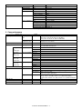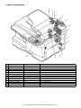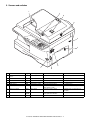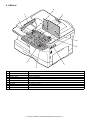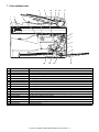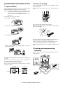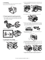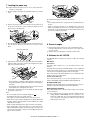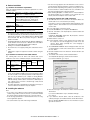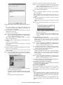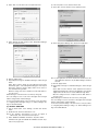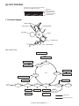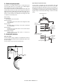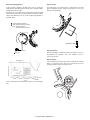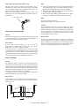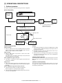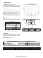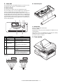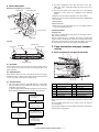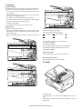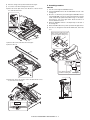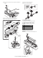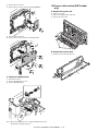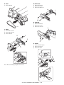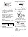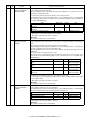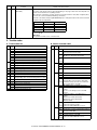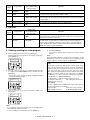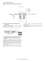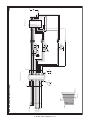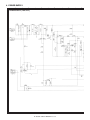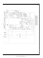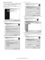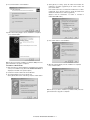
1
SERVICE MANUAL
CODE : 00ZAL1651CS1E
DIGITAL MULTIFUNCTIONAL
SYSTEM
(AL-1651CS)
MODEL
AL-1651CS
CONTENTS
[ 1 ] GENERAL . . . . . . . . . . . . . . . . . . . . . . . . . . . . . . . . . . . . . . . . . . . 1 - 1
[ 2 ] SPECIFICATIONS. . . . . . . . . . . . . . . . . . . . . . . . . . . . . . . . . . . . . 2 - 1
[ 3 ] CONSUMABLE PARTS. . . . . . . . . . . . . . . . . . . . . . . . . . . . . . . . . 3 - 1
[ 4 ] EXTERNAL VIEWS AND INTERNAL STRUCTURES . . . . . . . . . 4 - 1
[ 5 ] UNPACKING AND INSTALLATION . . . . . . . . . . . . . . . . . . . . . . . 5 - 1
[ 6 ] COPY PROCESS . . . . . . . . . . . . . . . . . . . . . . . . . . . . . . . . . . . . . 6 - 1
[ 7 ] OPERATIONAL DESCRIPTIONS . . . . . . . . . . . . . . . . . . . . . . . . . 7 - 1
[ 8 ] DISASSEMBLY AND ASSEMBLY . . . . . . . . . . . . . . . . . . . . . . . . 8 - 1
[ 9 ] ADJUSTMENTS . . . . . . . . . . . . . . . . . . . . . . . . . . . . . . . . . . . . . . 9 - 1
[10] TEST COMMAND, TROUBLE CODES. . . . . . . . . . . . . . . . . . . . 10 - 1
[11] USER PROGRAMS. . . . . . . . . . . . . . . . . . . . . . . . . . . . . . . . . . . 11 - 1
[12] ELECTRICAL SECTION . . . . . . . . . . . . . . . . . . . . . . . . . . . . . . . 12 - 1
[13] CIRCUIT DIAGRAM . . . . . . . . . . . . . . . . . . . . . . . . . . . . . . . . . . 13 - 1
[14] FIRMWARE DOWNLOAD PROCEDURES. . . . . . . . . . . . . . . . . 14 - 1
Parts marked with “ ” are important for maintaining the safety of the machine. Be sure to replace these parts
with the replacement parts specified to maintain the safety and performance of the machine.
SHARP CORPORATION
This document has been published to be used
for after sales service only.
The contents are subject to change without notice.
CAUTION
This product is a class 1 laser product that complies with 21CFR 1040 of the CDRH standard and
IEC825. This means that this machine does not produce hazardous laser radiation. The use of controls,
adjustments or performance of procedures other than those specified herein may result in hazardous
radiation exposure.
This laser radiation is not a danger to the skin, but when an exact focusing of the laser beam is achieved
on the eye’s retina, there is the danger of spot damage to the retina.
The following cautions must be observed to avoid exposure of the laser beam to your eyes at the time of
servicing.
1) When a problem in the laser optical unit has occurred, the whole optical unit must be exchanged as a
unit, not as individual parts.
2) Do not look into the machine with the main switch turned on after removing the developer unit, toner
cartridge, and drum cartridge.
3) Do not look into the laser beam exposure slit of the laser optical unit with the connector connected
when removing and installing the optical system.
4) The middle frame contains the safety interlock switch.
Do not defeat the safety interlock by inserting wedges or other items into the switch slot.
CAUTION
INVISIBLE LASER RADIATION,
WHEN OPEN AND INTERLOCKS DEFEATED.
AVOID EXPOSURE TO BEAM.
VORSICHT
UNSICHTBARE LASERSTRAHLUNG,
WENN ABDECKUNG GEÖFFNET UND
SICHERHEITSVERRIEGELUNG ÜBERBRÜCKT.
NICHT DEM STRAHL AUSSETZEN.
LASER WAVE – LENGTH : 770 ~ 795nm
Pulse times : 11.82µs/7mm
Out put power : 0.15mW ± 0.01mW
VARO !
AVATTAESSA JA SUOJALUKITUS
OHITETTAESSA OLET ALTTIINA
NÄKYMÄTTÖMÄLLE LASERSÄTEILYLLE ÄLÄ
KATSO SÄTEESEEN.
ADVARSEL
USYNLIG LASERSTRÅLNING VED ÅBNING, NÅR
SIKKERHEDSBRYDERE ER UDE AF
FUNKTION. UNDGÅ UDSAETTELSE FOR
STRÅLNING.
VARNING !
OSYNLIG LASERSTRÅLNING NÄR DENNA DEL
ÄR ÖPPNAD OCH SPÄRREN ÄR URKOPPLAD.
BETRAKTA EJ STRÅLEN. – STRÅLEN ÄR
FARLIG.
At the production line, the output power
of the scanner unit is adjusted to 0.57
MILLI-WATT PLUS 20 PCTS and is
maintained constant by the operation of
the Automatic Power Control (APC).
Even if the APC circuit fails in operation
for some reason, the maximum output
power will only be 15 MILLI-WATT 0.1
MICRO-SEC. Giving and accessible
emission level of 42 MICRO-WATT
which is still-less than the limit of
CLASS-1 laser product.
Caution
This product contains a low power laser
device. To ensure continued safety do not
remove any cover or attempt to gain access
to the inside of the product. Refer all
servicing to qualified personnel.
VAROITUS! LAITTEEN KÄYTTÄMINEN MUULLA
KUIN TÄSSÄ KÄYTTÖOHJEESSA MAINITULLA
TAVALLA SAATTAA ALTISTAA KÄYTTÄJÄN
TURVALLISUUSLUOKAN 1 YLITTÄVÄLLE
NÄKYMÄTTÖMÄLLE LASERSÄTEILYLLE.
VARNING - OM APPARATEN ANVÄNDS PÅ ANNAT
SÄTT ÄN I DENNA BRUKSANVISNING
SPECIFICERATS, KAN ANVÄNDAREN UTSÄTTAS
FÖR OSYNLIG LASERSTRÅLNING, SOM
ÖVERSKRIDER GRÄNSEN FÖR LASERKLASS 1.
The foregoing is applicable only to the 220V
model, 230V model and 240V model.
LUOKAN 1 LASERLAITE
KLASS 1 LASER APPARAT
CONTENTS
[1]
1.
2.
[2]
2-1
2-1
2-2
2-3
2-3
2-3
Supply system table . . . . . . . . . . . . . . . . . . . . . . . . . . . . . . . . . . . . . . . . . . . 3-1
Environmental . . . . . . . . . . . . . . . . . . . . . . . . . . . . . . . . . . . . . . . . . . . . . . . 3-1
Production control number(lot No.) identification . . . . . . . . . . . . . . . . . . . . . 3-2
EXTERNAL VIEWS AND INTERNAL STRUCTURES
1.
2.
3.
4.
5.
6.
7.
[5]
Basic Specifications . . . . . . . . . . . . . . . . . . . . . . . . . . . . . . . . . . . . . . . . . . .
Operation specifications . . . . . . . . . . . . . . . . . . . . . . . . . . . . . . . . . . . . . . . .
Copy performance . . . . . . . . . . . . . . . . . . . . . . . . . . . . . . . . . . . . . . . . . . . .
SPLC (JBIG GDI) printer . . . . . . . . . . . . . . . . . . . . . . . . . . . . . . . . . . . . . . .
Scan function . . . . . . . . . . . . . . . . . . . . . . . . . . . . . . . . . . . . . . . . . . . . . . . .
RSPF . . . . . . . . . . . . . . . . . . . . . . . . . . . . . . . . . . . . . . . . . . . . . . . . . . . . . .
CONSUMABLE PARTS
1.
2.
3.
[4]
6.
Major functions . . . . . . . . . . . . . . . . . . . . . . . . . . . . . . . . . . . . . . . . . . . . . . . 1-1
Note for servicing and handling . . . . . . . . . . . . . . . . . . . . . . . . . . . . . . . . . . 1-1
SPECIFICATIONS
1.
2.
3.
4.
5.
6.
[3]
C. Assembly procedure . . . . . . . . . . . . . . . . . . . . . . . . . . . . . . . . . . . . . . .8-12
Manual paper feed section. . . . . . . . . . . . . . . . . . . . . . . . . . . . . . . . . . . . . .8-12
A. List. . . . . . . . . . . . . . . . . . . . . . . . . . . . . . . . . . . . . . . . . . . . . . . . . . . . .8-12
B. Disassembly procedure. . . . . . . . . . . . . . . . . . . . . . . . . . . . . . . . . . . . .8-12
C. Assembly procedure . . . . . . . . . . . . . . . . . . . . . . . . . . . . . . . . . . . . . . .8-14
D. Pressure plate holder attachment . . . . . . . . . . . . . . . . . . . . . . . . . . . . .8-14
7. Rear frame section. . . . . . . . . . . . . . . . . . . . . . . . . . . . . . . . . . . . . . . . . . . .8-14
A. List. . . . . . . . . . . . . . . . . . . . . . . . . . . . . . . . . . . . . . . . . . . . . . . . . . . . .8-14
B. Disassembly procedure. . . . . . . . . . . . . . . . . . . . . . . . . . . . . . . . . . . . .8-14
C. Assembly procedure . . . . . . . . . . . . . . . . . . . . . . . . . . . . . . . . . . . . . . .8-15
8. Power section . . . . . . . . . . . . . . . . . . . . . . . . . . . . . . . . . . . . . . . . . . . . . . .8-15
A. List. . . . . . . . . . . . . . . . . . . . . . . . . . . . . . . . . . . . . . . . . . . . . . . . . . . . .8-15
B. Disassembly procedure. . . . . . . . . . . . . . . . . . . . . . . . . . . . . . . . . . . . .8-15
C. Assembly procedure . . . . . . . . . . . . . . . . . . . . . . . . . . . . . . . . . . . . . . .8-15
9. Duplex motor section (RSPF model only) . . . . . . . . . . . . . . . . . . . . . . . . . .8-15
A. Remove the rear cabinet. . . . . . . . . . . . . . . . . . . . . . . . . . . . . . . . . . . .8-15
B. Remove the main PWB. . . . . . . . . . . . . . . . . . . . . . . . . . . . . . . . . . . . .8-15
C. Remove the Duplex motor. . . . . . . . . . . . . . . . . . . . . . . . . . . . . . . . . . .8-16
10. Reverse roller section (RSPF model only) . . . . . . . . . . . . . . . . . . . . . . . . .8-16
A. Remove the reverse unit. . . . . . . . . . . . . . . . . . . . . . . . . . . . . . . . . . . .8-16
B. Remove the reverse roller. . . . . . . . . . . . . . . . . . . . . . . . . . . . . . . . . . .8-16
11. RSPF section (RSPF model only) . . . . . . . . . . . . . . . . . . . . . . . . . . . . . . . .8-17
A. RSPF. . . . . . . . . . . . . . . . . . . . . . . . . . . . . . . . . . . . . . . . . . . . . . . . . . .8-17
B. Intermediate tray . . . . . . . . . . . . . . . . . . . . . . . . . . . . . . . . . . . . . . . . . .8-17
C. Upper cover. . . . . . . . . . . . . . . . . . . . . . . . . . . . . . . . . . . . . . . . . . . . . .8-17
D. Pickup unit. . . . . . . . . . . . . . . . . . . . . . . . . . . . . . . . . . . . . . . . . . . . . . .8-17
E. Upper cover of the pickup unit. . . . . . . . . . . . . . . . . . . . . . . . . . . . . . . .8-18
F. Sensor PWB . . . . . . . . . . . . . . . . . . . . . . . . . . . . . . . . . . . . . . . . . . . . .8-18
G. Pickup solenoid . . . . . . . . . . . . . . . . . . . . . . . . . . . . . . . . . . . . . . . . . . .8-18
H. Clutch . . . . . . . . . . . . . . . . . . . . . . . . . . . . . . . . . . . . . . . . . . . . . . . . . .8-18
I. Manual paper feed roller, pickup roller . . . . . . . . . . . . . . . . . . . . . . . . .8-19
J. Transport unit removal . . . . . . . . . . . . . . . . . . . . . . . . . . . . . . . . . . . . .8-19
K. Belt 1 . . . . . . . . . . . . . . . . . . . . . . . . . . . . . . . . . . . . . . . . . . . . . . . . . . .8-20
L. Belt 2 . . . . . . . . . . . . . . . . . . . . . . . . . . . . . . . . . . . . . . . . . . . . . . . . . . .8-20
M. SPF motor . . . . . . . . . . . . . . . . . . . . . . . . . . . . . . . . . . . . . . . . . . . . . . .8-20
N. Solenoid . . . . . . . . . . . . . . . . . . . . . . . . . . . . . . . . . . . . . . . . . . . . . . . .8-20
O. Clutch . . . . . . . . . . . . . . . . . . . . . . . . . . . . . . . . . . . . . . . . . . . . . . . . . .8-20
P. Paper supply roller . . . . . . . . . . . . . . . . . . . . . . . . . . . . . . . . . . . . . . . .8-21
Q. Paper entry sensor . . . . . . . . . . . . . . . . . . . . . . . . . . . . . . . . . . . . . . . .8-21
R. Transport roller 1. . . . . . . . . . . . . . . . . . . . . . . . . . . . . . . . . . . . . . . . . .8-21
S. Paper exit roller . . . . . . . . . . . . . . . . . . . . . . . . . . . . . . . . . . . . . . . . . . .8-22
T. Solenoid . . . . . . . . . . . . . . . . . . . . . . . . . . . . . . . . . . . . . . . . . . . . . . . .8-23
GENERAL
Appearance . . . . . . . . . . . . . . . . . . . . . . . . . . . . . . . . . . . . . . . . . . . . . . . . .
Internal . . . . . . . . . . . . . . . . . . . . . . . . . . . . . . . . . . . . . . . . . . . . . . . . . . . . .
Operation panel . . . . . . . . . . . . . . . . . . . . . . . . . . . . . . . . . . . . . . . . . . . . . .
Motors and solenoids . . . . . . . . . . . . . . . . . . . . . . . . . . . . . . . . . . . . . . . . . .
Sensors and switches . . . . . . . . . . . . . . . . . . . . . . . . . . . . . . . . . . . . . . . . .
PWB unit . . . . . . . . . . . . . . . . . . . . . . . . . . . . . . . . . . . . . . . . . . . . . . . . . . .
Cross sectional view. . . . . . . . . . . . . . . . . . . . . . . . . . . . . . . . . . . . . . . . . . .
4-1
4-1
4-2
4-3
4-4
4-5
4-6
UNPACKING AND INSTALLATION
1.
2.
3.
4.
5.
6.
7.
8.
9.
Copier installation. . . . . . . . . . . . . . . . . . . . . . . . . . . . . . . . . . . . . . . . . . . . . 5-1
Cautions on handling . . . . . . . . . . . . . . . . . . . . . . . . . . . . . . . . . . . . . . . . . . 5-1
Checking packed components and accessories . . . . . . . . . . . . . . . . . . . . . 5-1
Unpacking . . . . . . . . . . . . . . . . . . . . . . . . . . . . . . . . . . . . . . . . . . . . . . . . . . 5-2
Removing protective packing materials . . . . . . . . . . . . . . . . . . . . . . . . . . . . 5-2
Installing the TD cartridge . . . . . . . . . . . . . . . . . . . . . . . . . . . . . . . . . . . . . . 5-2
Loading the paper tray . . . . . . . . . . . . . . . . . . . . . . . . . . . . . . . . . . . . . . . . . 5-3
Power to copier . . . . . . . . . . . . . . . . . . . . . . . . . . . . . . . . . . . . . . . . . . . . . . 5-3
Software for AL-1651CS . . . . . . . . . . . . . . . . . . . . . . . . . . . . . . . . . . . . . . . 5-3
A. Before installation . . . . . . . . . . . . . . . . . . . . . . . . . . . . . . . . . . . . . . . . . 5-4
B. Installing the software . . . . . . . . . . . . . . . . . . . . . . . . . . . . . . . . . . . . . . 5-4
C. Setting up button manager . . . . . . . . . . . . . . . . . . . . . . . . . . . . . . . . . . 5-8
10. Interface . . . . . . . . . . . . . . . . . . . . . . . . . . . . . . . . . . . . . . . . . . . . . . . . . . . 5-10
A. USB . . . . . . . . . . . . . . . . . . . . . . . . . . . . . . . . . . . . . . . . . . . . . . . . . . . 5-10
B. RJ45 . . . . . . . . . . . . . . . . . . . . . . . . . . . . . . . . . . . . . . . . . . . . . . . . . . 5-10
11. Moving . . . . . . . . . . . . . . . . . . . . . . . . . . . . . . . . . . . . . . . . . . . . . . . . . . . . 5-10
[6]
COPY PROCESS
1.
2.
3.
[7]
OPERATIONAL DESCRIPTIONS
1.
2.
3.
4.
5.
6.
7.
8.
9.
[8]
Functional diagram. . . . . . . . . . . . . . . . . . . . . . . . . . . . . . . . . . . . . . . . . . . . 6-1
Outline of print process . . . . . . . . . . . . . . . . . . . . . . . . . . . . . . . . . . . . . . . . 6-2
Actual print process . . . . . . . . . . . . . . . . . . . . . . . . . . . . . . . . . . . . . . . . . . . 6-2
Outline of operation . . . . . . . . . . . . . . . . . . . . . . . . . . . . . . . . . . . . . . . . . . .
Scanner section . . . . . . . . . . . . . . . . . . . . . . . . . . . . . . . . . . . . . . . . . . . . . .
A. Scanner unit. . . . . . . . . . . . . . . . . . . . . . . . . . . . . . . . . . . . . . . . . . . . . .
B. Optical system . . . . . . . . . . . . . . . . . . . . . . . . . . . . . . . . . . . . . . . . . . . .
C. Drive system . . . . . . . . . . . . . . . . . . . . . . . . . . . . . . . . . . . . . . . . . . . . .
Laser unit . . . . . . . . . . . . . . . . . . . . . . . . . . . . . . . . . . . . . . . . . . . . . . . . . . .
A. Basic structure . . . . . . . . . . . . . . . . . . . . . . . . . . . . . . . . . . . . . . . . . . . .
B. Laser beam path . . . . . . . . . . . . . . . . . . . . . . . . . . . . . . . . . . . . . . . . . .
C. Composition. . . . . . . . . . . . . . . . . . . . . . . . . . . . . . . . . . . . . . . . . . . . . .
Fuser section . . . . . . . . . . . . . . . . . . . . . . . . . . . . . . . . . . . . . . . . . . . . . . . .
A. General description . . . . . . . . . . . . . . . . . . . . . . . . . . . . . . . . . . . . . . . .
Paper feed section and paper transport section. . . . . . . . . . . . . . . . . . . . . .
A. Paper transport path and general operations . . . . . . . . . . . . . . . . . . . .
Process unit new drum detection mechanism . . . . . . . . . . . . . . . . . . . . . . .
RSPF section . . . . . . . . . . . . . . . . . . . . . . . . . . . . . . . . . . . . . . . . . . . . . . . .
A. Outline . . . . . . . . . . . . . . . . . . . . . . . . . . . . . . . . . . . . . . . . . . . . . . . . . .
B. Document transport path and basic composition. . . . . . . . . . . . . . . . . .
C. Operational descriptions . . . . . . . . . . . . . . . . . . . . . . . . . . . . . . . . . . . .
D. Cases where a document jam is caused . . . . . . . . . . . . . . . . . . . . . . . .
E. RSPF (SPF) open/close detection (book document detection) . . . . . . .
D-D (Duplex to Duplex) mode paper/document transport (Duplex model). .
A. Initial state . . . . . . . . . . . . . . . . . . . . . . . . . . . . . . . . . . . . . . . . . . . . . . .
B. Front copy . . . . . . . . . . . . . . . . . . . . . . . . . . . . . . . . . . . . . . . . . . . . . . .
C. Back copy . . . . . . . . . . . . . . . . . . . . . . . . . . . . . . . . . . . . . . . . . . . . . . .
Shifter . . . . . . . . . . . . . . . . . . . . . . . . . . . . . . . . . . . . . . . . . . . . . . . . . . . . . .
7-1
7-2
7-2
7-2
7-2
7-3
7-3
7-3
7-3
7-3
7-4
7-4
7-4
7-7
7-7
7-7
7-7
7-8
7-8
7-8
7-8
7-8
7-8
7-9
7-9
[9]
ADJUSTMENTS
1.
2.
3.
4.
5.
6.
7.
[10] TEST COMMAND, TROUBLE CODES
1.
2.
3.
4.
5.
2.
3.
4.
5.
High voltage section . . . . . . . . . . . . . . . . . . . . . . . . . . . . . . . . . . . . . . . . . . .
A. List . . . . . . . . . . . . . . . . . . . . . . . . . . . . . . . . . . . . . . . . . . . . . . . . . . . . .
B. Disassembly procedure . . . . . . . . . . . . . . . . . . . . . . . . . . . . . . . . . . . . .
C. Assembly procedure . . . . . . . . . . . . . . . . . . . . . . . . . . . . . . . . . . . . . . .
D. Charger wire cleaning . . . . . . . . . . . . . . . . . . . . . . . . . . . . . . . . . . . . . .
E. Charger wire replacement . . . . . . . . . . . . . . . . . . . . . . . . . . . . . . . . . . .
Operation panel section . . . . . . . . . . . . . . . . . . . . . . . . . . . . . . . . . . . . . . . .
A. List . . . . . . . . . . . . . . . . . . . . . . . . . . . . . . . . . . . . . . . . . . . . . . . . . . . . .
B. Disassembly procedure . . . . . . . . . . . . . . . . . . . . . . . . . . . . . . . . . . . . .
C. Assembly procedure . . . . . . . . . . . . . . . . . . . . . . . . . . . . . . . . . . . . . . .
Optical section . . . . . . . . . . . . . . . . . . . . . . . . . . . . . . . . . . . . . . . . . . . . . . .
A. List . . . . . . . . . . . . . . . . . . . . . . . . . . . . . . . . . . . . . . . . . . . . . . . . . . . . .
B. Disassembly procedure . . . . . . . . . . . . . . . . . . . . . . . . . . . . . . . . . . . . .
C. Assembly procedure . . . . . . . . . . . . . . . . . . . . . . . . . . . . . . . . . . . . . . .
Fusing section . . . . . . . . . . . . . . . . . . . . . . . . . . . . . . . . . . . . . . . . . . . . . . .
A. List . . . . . . . . . . . . . . . . . . . . . . . . . . . . . . . . . . . . . . . . . . . . . . . . . . . . .
B. Disassembly procedure . . . . . . . . . . . . . . . . . . . . . . . . . . . . . . . . . . . . .
C. Assembly procedure . . . . . . . . . . . . . . . . . . . . . . . . . . . . . . . . . . . . . . .
Tray paper feed/transport section . . . . . . . . . . . . . . . . . . . . . . . . . . . . . . . .
A. List . . . . . . . . . . . . . . . . . . . . . . . . . . . . . . . . . . . . . . . . . . . . . . . . . . . . .
B. Disassembly procedure . . . . . . . . . . . . . . . . . . . . . . . . . . . . . . . . . . . . .
8-1
8-1
8-1
8-1
8-1
8-2
8-2
8-2
8-2
8-3
8-3
8-3
8-3
8-4
8-5
8-5
8-5
8-7
8-7
8-7
8-7
Entering the test command mode . . . . . . . . . . . . . . . . . . . . . . . . . . . . . . . .10-1
Key rule . . . . . . . . . . . . . . . . . . . . . . . . . . . . . . . . . . . . . . . . . . . . . . . . . . . .10-1
List of test commands . . . . . . . . . . . . . . . . . . . . . . . . . . . . . . . . . . . . . . . . .10-1
Descriptions of various test commands . . . . . . . . . . . . . . . . . . . . . . . . . . . .10-2
Trouble codes . . . . . . . . . . . . . . . . . . . . . . . . . . . . . . . . . . . . . . . . . . . . . .10-27
A. Trouble codes list . . . . . . . . . . . . . . . . . . . . . . . . . . . . . . . . . . . . . . . .10-27
B. Details of trouble codes. . . . . . . . . . . . . . . . . . . . . . . . . . . . . . . . . . . .10-27
[11] USER PROGRAM
1.
DISASSEMBLY AND ASSEMBLY
1.
Optical section . . . . . . . . . . . . . . . . . . . . . . . . . . . . . . . . . . . . . . . . . . . . . . . .9-1
A. Copy magnification ratio adjustment . . . . . . . . . . . . . . . . . . . . . . . . . . . .9-1
B. Image position adjustment . . . . . . . . . . . . . . . . . . . . . . . . . . . . . . . . . . .9-2
Copy density adjustment . . . . . . . . . . . . . . . . . . . . . . . . . . . . . . . . . . . . . . . .9-3
A. Copy density adjustment timing . . . . . . . . . . . . . . . . . . . . . . . . . . . . . . .9-3
B. Note for copy density adjustment . . . . . . . . . . . . . . . . . . . . . . . . . . . . . .9-3
C. Necessary tool for copy density adjustment . . . . . . . . . . . . . . . . . . . . . .9-4
D. Features of copy density adjustment. . . . . . . . . . . . . . . . . . . . . . . . . . . .9-4
E. Copy density adjustment procedure . . . . . . . . . . . . . . . . . . . . . . . . . . . .9-4
High voltage adjustment . . . . . . . . . . . . . . . . . . . . . . . . . . . . . . . . . . . . . . . .9-5
A. Main charger (Grid bias) . . . . . . . . . . . . . . . . . . . . . . . . . . . . . . . . . . . . .9-5
B. DV bias check . . . . . . . . . . . . . . . . . . . . . . . . . . . . . . . . . . . . . . . . . . . . .9-5
Duplex adjustment . . . . . . . . . . . . . . . . . . . . . . . . . . . . . . . . . . . . . . . . . . . . .9-5
A. Adjusting the paper reverse position in memory for duplex copying . . . .9-5
B. Adjusting trailing edge void in duplex copy mode . . . . . . . . . . . . . . . . . .9-6
SPF (RSPF) scan position automatic adjustment . . . . . . . . . . . . . . . . . . . . .9-7
RSPF (SPF) mode sub scanning direction magnification ratio adjustment . .9-7
Automatic black level correction . . . . . . . . . . . . . . . . . . . . . . . . . . . . . . . . . .9-8
2.
User programs . . . . . . . . . . . . . . . . . . . . . . . . . . . . . . . . . . . . . . . . . . . . . . .11-1
A. Copy mode . . . . . . . . . . . . . . . . . . . . . . . . . . . . . . . . . . . . . . . . . . . . . .11-1
B. Print mode . . . . . . . . . . . . . . . . . . . . . . . . . . . . . . . . . . . . . . . . . . . . . . .11-2
Selecting a setting for a user program . . . . . . . . . . . . . . . . . . . . . . . . . . . . .11-2
[12] ELECTRICAL SECTION
1.
2.
Block diagram . . . . . . . . . . . . . . . . . . . . . . . . . . . . . . . . . . . . . . . . . . . . . . .12-1
A. Overall block diagram . . . . . . . . . . . . . . . . . . . . . . . . . . . . . . . . . . . . . .12-1
Circuit descriptions. . . . . . . . . . . . . . . . . . . . . . . . . . . . . . . . . . . . . . . . . . . .12-2
A. Main PWB (MCU) . . . . . . . . . . . . . . . . . . . . . . . . . . . . . . . . . . . . . . . . .12-2
B. DC power circuit . . . . . . . . . . . . . . . . . . . . . . . . . . . . . . . . . . . . . . . . .12-11
[13] CIRCUIT DIAGRAM
1.
2.
3.
4.
5.
MCU PWB . . . . . . . . . . . . . . . . . . . . . . . . . . . . . . . . . . . . . . . . . . . . . . . . . .13-1
OPERATION PWB. . . . . . . . . . . . . . . . . . . . . . . . . . . . . . . . . . . . . . . . . . .13-26
NIC PWB . . . . . . . . . . . . . . . . . . . . . . . . . . . . . . . . . . . . . . . . . . . . . . . . . .13-29
POWER SUPPLY . . . . . . . . . . . . . . . . . . . . . . . . . . . . . . . . . . . . . . . . . . .13-33
ACTUAL WIRING DIAGRAM. . . . . . . . . . . . . . . . . . . . . . . . . . . . . . . . . . .13-35
[14] FIRMWARE DOWNLOAD PROCEDURES
1.
2.
3.
4.
5.
Download procedures . . . . . . . . . . . . . . . . . . . . . . . . . . . . . . . . . . . . . . . . .14-1
Version acquisition procedures . . . . . . . . . . . . . . . . . . . . . . . . . . . . . . . . . .14-2
EEPROM data acquisition procedure . . . . . . . . . . . . . . . . . . . . . . . . . . . . .14-3
Serial number setting . . . . . . . . . . . . . . . . . . . . . . . . . . . . . . . . . . . . . . . . . .14-4
Installing procedures . . . . . . . . . . . . . . . . . . . . . . . . . . . . . . . . . . . . . . . . . .14-4
[1] GENERAL
1. Major functions
Configurations
Item CPM /
Color
Sharp IEEE
SB/ 2
GDI
PPM
USB
SPF R-SPF Scanner
SPLC E-SORT Duplex Shifter FAX
desk 1284
MB Tray
printer
(push)
Model
LT A4
AL-1651CS
16 15 MB
✕
✕
❍
❍
✕
❍
❍
❍
❍
✕
❍
✕
RJ45
❍
❍
(2.0) print only
External
NIC
✕
Descriptions of items
CPM:
Copy speed (Copies Per Minute)
SB/MB:
SB = Manual feed single bypass, MB = Manual feed multi bypass
2 tray:
Second cassette unit
SPF:
Original feed unit
R-SPF:
Duplex original feed unit
Color scanner:
Color scanner function
GDI printer:
GDI printer function with USB
SPLC:
SPLC printer function
E-SORT:
Electrical sort
Duplex:
Auto duplex copy function
Shifter:
Job separator function
FAX:
FAX function
Sharpdesk:
Scanner utilities
IEEE1284:
Interface port (parallel)
USB:
Interface port (USB)
RJ45:
Interface port (Network)
External NIC:
Interface port (Network)
Descriptions of table
❍: Standard provision
✕: No function or no option available
Opt: Option
(AL-1651CS)
2. Note for servicing and handling
When the main unit power is repeatedly turned OFF/ON rapidly (for about 1sec), the IC (OA982) on the MCU PWB may malfunction to cause an error
(E1-00 Communication error), which does not boot the machine. In case of this error, the blank display is kept for several tens seconds and then "E100" is displayed on the panel display.
<Countermeasure>
Turn off the power and keep it for more than 10sec. Then turn on the power.
When the machine is booted.: There is no problem in the MCU PWB.
When the machine is not booted.: The MCU PWB trouble
AL-1651CS GENERAL 1 - 1
[2] SPECIFICATIONS
1. Basic Specifications
Item
Type
Copy system
Segment (class)
Copier dimensions
Weight (Approximately)
Desktop
Dry, electrostatic
Digital personal copier
20.4" (W) x 19.8" (D) x 15.0" (H) (518mm (W) x 503mm (D) x 380mm (H))
44.1 lbs. (20kg)
Not includes toner cartridge
2. Operation specifications
Section, item
Paper feed Paper feed system
section
AB system
Tray paper feed
section
Multi bypass paper
feed section
Inch system
Tray paper feed
section
Multi bypass paper
feed section
Details
Paper size
Paper weight
Paper feed capacity
Kinds
Remark
Paper size
Paper weight
Paper feed capacity
Kinds
Remark
Paper size
Paper weight
Paper feed capacity
Kinds
Remark
Paper size
Paper weight
Paper feed capacity
Kinds
Paper exit section
Originals
Optical
section
Scanning section
Writing section
Image forming
Remark
Exit way
Capacity of output tray
Original set
Max. original size
Original kinds
Original size detection
Scanning system
CCD sensor
Resolution
Lighting lamp
Type
Voltage
Power consumption
Output data
Writing system
Laser unit
Resolution
Photoconductor
type
Life
Charger
Charging system
Transfer system
Separation system
Developing
Developing system
Cleaning
Cleaning system
1 tray (250 sheets) + multi bypass (50 sheets)
A4, B5, A5, 16K (Landscape)
56 - 80g/m2 (15 - 21 lbs.)
250 sheets
Standard paper, specified paper, recycled paper
User adjustment of front paper guide available
A4, B5, A5, B6, A6 (Post card), 16K (Landscape)
52 - 128g/m2 (14 - 34.5 lbs.)
50 sheets
Standard paper, specified paper, recycled paper, envelope,
OHP, Label (Single copy)
User adjustment of side paper guide available
8-1/2" x 14", 8-1/2 x 11", 8-1/2" x 5-1/2" (Landscape)
15 - 21 lbs.
250 sheets
Standard paper, specified paper, recycled paper
User adjustment of front paper guide available
8-1/2" x 14", 8-1/2 x 11", 8-1/2" x 5-1/2", 3-1/2" x 5-1/2"
(Landscape)
14 - 34.5 lbs.
50 sheets
Standard paper, specified paper, recycled paper, OHP, Label,
Envelop (Single copy)
User adjustment of side paper guide available
Face down
200 sheets
Center Registration (left edge)
A4 (8-1/2" x 14")
sheet, book
None
3 CCDs (RGB) sensor scanning by lighting white lamp
600 dpi
CCFL
560Vrms
2.8W
R, G, B 1 or 8 bits/pixel / A/D 16bit
Writing to OPC drum by the semiconductor laser
600 dpi
OPC (30ø)
18k
Saw -tooth charging with a grid, / (-) scorotron discharge
(+) DC scorotron system
(-) DC scorotron system
Dry, 2-component magnetic brush development system
Counter blade system (Counter to rotation)
AL-1651CS SPECIFICATIONS 2 - 1
Section, item
Fusing system
Upper heat roller
Lower heat roller
Heater lamp
Fusing section
Electrical section
Power source
Power consumption
Details
type
type
type
Voltage
Power consumption
Voltage
Frequency
Rated current
Max.
Average (during copying)
Average (stand-by)
Pre-heat mode
Auto power shut-off mode
Heat roller system
Teflon roller
Silicon rubber roller
Halogen lamp
120V
800W
120V
60Hz
8A
Less than 1000W
350 Wh/H *1)
80Wh/H *1)
25Wh/H *1)
8.8Wh/H *1)
*1) May fluctuate due to environmental conditions and the input voltage.
3. Copy performance
Section, item
Copy magnification
Manual steps (text, photo)
Copy speed
AB system
A4
(Landscape)
AB system
B5
(Landscape)
Inch system
8-1/2" x 14"
(Landscape)
Inch system
8-1/2" x 11"
(Landscape)
Max. continuous copy quantity
Void
Warm-up time
Power save mode reset time
Paper jam recovery time
Details
Fixed magnification
ratios
4 Reduction + 3 Enlargement
(AB system : 25, 50, 70, 86, 100, 141, 200, 400%)
(Inch system : 25, 50, 64, 78, 100, 129, 200, 400%)
Zooming
OC: 25 - 400%, RSPF 50 - 200%
magnification ratios
(376 steps in 1% increments)
5 steps
First copy time
Tray paper feed 9.6 sec. (Pre-heat mode:25 sec. / Auto power-shut-off mode : 40 sec.)
A4 or Letter/100%/Auto Exposure
Copy speed (CPM) Same size
15
Enlargement
15
Reduction
15
Copy speed (CPM) Same size
15
Enlargement
15
Reduction
15
Copy speed (CPM) Same size
12
Enlargement
12
Reduction
12
Copy speed (CPM) Same size
16
Enlargement
16
Reduction
16
99
Void area
leading edge
1 - 4mm
Trailing edge
4mm or less, 6mm or less (Duplex copying/both image)
Side void area 0.5mm or more (per side)
4.5mm or less (total of both sides)
Image loss
leading edge
Same size: 3.0mm or less (OC) / 4.0mm or less (SPF/R-SPF/Duplex)
Enlarge: 1.5mm or less (OC) / 3.0mm or less (SPF/R-SPF/Duplex)
Reduction (50%): 6.0mm or less (OC) / 8.0mm or less (SPF/R-SPF/Duplex)
0 sec.
0 sec.
0 sec.
AL-1651CS SPECIFICATIONS 2 - 2
4. SPLC (JBIG GDI) printer
Print speed
First print time
Duplex
ROPM
CPU
Memory
Interface
Network
Emulation
MIB support
Resolution
Supported OS
WHQL support
Application
Max. 15ppm (A4 / with ROPM) / 16ppm (Letter / with ROPM)
9.6 sec. (without data transfer time)
Yes
Yes
None
Share the memory with E-SORT function
RJ45 (10 base) / USB 2.0
Internal NIC
SPLC (JBIG GDI)
No
600dpi *1
Win 95 / 98 / Me / NT 4.0 / 2000 / XP
Yes *2
Status window
*1: Engine Resolution
*2: Running change
5. Scan function
Type
Scanning system
Light source
Resolution
Originals
Output data
Scan range
Scan speed
Protocol
Support file format
Interface
Scanner utility
Scan key/lamp
Duplex scan
Supported OS
Void area
WHQL supported
Flat Bed Color Scanner
Document glass/RSPF
3 CCDs (RGB) sensor scanning by lighting white lamp (2 pcs of CCFL)
Optical: 600 x 1200dpi
Setting range: 50 - 9600dpi (Preview resolution is fixed at 75dpi)
Sheet type / Book type
R, G, B 1 or 8 bits/pixel / A/D 16bit
OC / RSPF: 8.5" (297mm) (L) x 14" (431mm) (W)
Original position: Platen: Left center / SPF: Right center
OC / SPF: Max. 2.88ms/line (Color/Gray scale), Max. 0.96 ms/line (B & W)
TWAIN / WIA (Only XP) / STI
RAW / JPEG
USB2.0
Button Manager / Sharpdesk
Yes
No
Win 98 / Me / 2000 / XP
No (User settable by PC)
Yes *1
*1: Running change
6. RSPF
Original capacity
Original size
Original replacement speed
Job speed (Tray1,Landscape)
Single copy
Multi copy
Original placement
Original weight
Mixed feeding
Original which cannot
30 sheets (52 to 90g/m2) (14 to 23.9 lbs.)
A4 to A5/10" x 14" to 5-1/2" x 8-1/2"
12CPM (A4/8-1/2" x 11"Landscape)
S to S
12CPM
S to D
5.6CPM
D to S
5.5CPM
D to D
5.2CPM
S to S
16CPM
D to S
16CPM
Face up
52 to 90g/m2(14 - 23.9lbs.)
No
Thermal papers, originals with punch holes for files, be used folded paper, transparent originals
such as OHP films, stapled or clip used originals with cover up liquid used, Originals with tape
sealed, originals with high level frictional coefficient such as photos or catalogs.
AL-1651CS SPECIFICATIONS 2 - 3
[3] CONSUMABLE PARTS
1. Supply system table
Common to all destinations
No.
Name
1 Develop cartridge (Black) x 1
(Except Europe)
2 Drum cartridge
Content
Toner/developer cartridge x 1
(Toner: Net weight 124g) (Developer: Net weight 190g)
Drum cartridge
Life
4K
(5% document)
18K
Product name
AL-110TD
Package
5
AL-100DR
5
2. Environmental
The environmental conditions for assuring the copy quality and the machine operations are as follows:
(1) Normal operating condition
(4) Supply storage condition
Temperature:20 - 25°C
Humidity:65 ± 5%RH
Humidity (RH)
90%
(2) Acceptable operating condition
Humidity (RH)
85%
60%
20%
–5˚C
20%
10˚C
30˚C
35˚C
30˚C
40˚C
(3) Optical condition
Humidity (RH)
90%
60%
15%
–25˚C
AL-1651CS CONSUMABLE PARTS 3 - 1
45˚C
3. Production control number(lot No.) identification
<Developing cartridge>
Production month
Production day
Destination code
(Dealer, distributor, OEM, etc.)
Production place
(SOCC: Fixed to B.)
End digit of year
Version No.
*
Destination
Division
EX Destination
Option Destination
Production control
label attachment position
No.
A same pack
G
B same pack
H
A
P
B
Q
<Drum cartridge>
The label on the drum cartridge shows the date of production.
(SOCC production)
Production month
Production day
Destination code
(Dealer, distributor, OEM, etc.)
Production place
Production control
label attachment position(*1)
(SOCC: Fixed to B.)
End digit of year
Version No.
*1 The production control label is not attached to the cartridge of a
China product.
<JAPAN production>
Ver.A
9
1
1
0001
X
Production month
(1 - 9 = Jan. - Sep. 0 = Oct. X = Nov. Y = Dec.)
Serial number of month
Fixed to 1.
Pack division
(See table below)
End digit of year
Version No.
Division
No.
Ex production
1
Option
2
Same pack
3
AL-1651CS CONSUMABLE PARTS 3 - 2
[4] EXTERNAL VIEWS AND INTERNAL STRUCTURES
1. Appearance
RSPF
9
10
11
Interface
19
13
12
20
1
2
5
6
7
3
4
14
15
8
17
1
4
7
10
13
16
19
Document glass
Paper tray
Bypass tray paper guides
Original guides
Exit area
Power switch
USB port
2
5
8
11
14
17
20
Operation panel
Side cover
Bypass tray
Document feeder cover
Paper output tray
Handles
LAN port
21
16
17
18
3
6
9
12
15
18
21
Front cover
Side cover open button
Reversing tray
Document feeder tray
Paper output tray extension
Power cord
Paper holding arm
2. Internal
TD cartridge
Drum cartridge
1
2
3
4
5
1
4
Side cover
Charger cleaner
2
5
Fusing unit release lever
Front cover
3
Transfer charger
AL-1651CS EXTERNAL VIEWS AND INTERNAL STRUCTURES 4 - 1
3. Operation panel
1
2
3
4
5
AL-1651CS
Display
READY TO COPY.
100% 8.5x11
18
1
3
5
7
19
6 7
0
20
12 13 14
15
16 17
21
[MODE SELECT] key / Mode indicators
Press this key to select the mode. The indicator of the selected mode
lights (copy, printer, scanner).
2
Numeric keys
Use these to enter the number of copies and other numerical
settings.
The keys can also be used to select items in function setting menus.
Power save indicator
This lights up when the power save function is activated.
Error indicator
4
This lights steadily or blinks when a paper misfeed or other error
occurs.
9
8 9 10 11
Tray location indicator
Indicates the selected paper tray. The indicator blinks when the
tray is out of paper or is not closed.
11 [2-SIDED COPY] key
Use to copy both sides of an original.
13 [
] key (
), [
] key (
), [ENTER] key
Press the [
] key (
) or [
] key (
) to select an item in a
function setting menu.
Press the [ENTER] key to enter a selection.
15 [COPY RATIO] key
Press to select an enlargement or reduction ratio.
To select a preset ratio setting, press the [COPY RATIO] key
and select the desired preset ratio. To select a ratio that is not
preset, press the [COPY RATIO] key, select the preset ratio that
is closest to the desired ratio, and then press the [
] key ( )
or [
] key ( ) to increase or decrease the ratio in increments
of 1%.
Display
This shows messages indicating the machine status and any
problems that occur, as well as user programs and function
setting menus.
[CLEAR] key (
)
Use this to clear the set number of copies, as well as cancel a job
that is in progress. When a setting menu appears, use this key to
move back to the previous menu level.
6
8
RSPF indicator
This lights up when an original is placed in the RSPF.
[TRAY SELECT] key (
)
Use to select the paper tray that has the desired paper for copying.
10 [MENU] key
Press this key to select the paper size for copying, to configure a
user program or to display the total count.
12 [E-SORT/SP.FUN] key
Press to select the sort function, 2 in 1 copy function, or margin
shift function.
14 [EXPOSURE] key
Use to switch from auto exposure adjustment to text mode or
photo mode.
16 [START] key (
) / Ready indicator
The ready indicator lights up when copying or scanning is possible.
To begin copying, press the [START] key (
).
The [START] key ( ) is also pressed to return to normal
operation from auto power shut-off mode.
17 [CLEAR ALL] key (
)
18 Shows the current copy ratio.
This returns all functions to the default settings. When pressed in a
setting menu, this returns the settings and display to the initial state.
20 Shows the number of copies that has been entered with the
19 Shows the selected paper size.
numeric keys.
21 A checkmark "
" appears when the exposure has been
changed, or when two-sided copying, sort, 2 IN 1, or margin shift
is selected.
AL-1651CS EXTERNAL VIEWS AND INTERNAL STRUCTURES 4 - 2
4. Motors and solenoids
9
12
2
8
11
10
4
1
5
13
6
7
3
No.
1
2
3
4
5
6
7
8
9
10
11
12
13
Part name
Main motor
Scanner motor
Toner motor
Cooling fan motor
Resist roller solenoid
Paper feed solenoid
Multi paper feed solenoid
SPF motor
Duplex motor
Original feed solenoid
SPF paper feed solenoid
SPF gate solenoid
Shifter motor
Control signal
MM
MRMT
TM
VFM
RRS
CPFS1
MPFS
SPFM
DMT
SPUS
SPFS
SGS
SFTM
Function / Operation
Drives the copier.
Drives the optical mirror base (scanner unit).
Supplies toner.
Cools the optical section.
Resist roller rotation control solenoid
Cassette Paper feed solenoid 1
Multi manual pages feed solenoid
Drives the single pass feeder
Devices the duplex paper transport section
Original pick up solenoid
Original feed solenoid
Controls the document reverse gate.
Drives the shifter.
AL-1651CS EXTERNAL VIEWS AND INTERNAL STRUCTURES 4 - 3
5. Sensors and switches
1
2
8
9
3
4
5
7
6
No.
Name
1 Scanner unit home position
sensor
2 POD sensor
3 PPD2 sensor
4 Cassette detection switch
5 PPD1 sensor
6 Door switch
Signal
MHPS
Type
Transmission sensor
Function
Scanner unit home position detection
Output
"H" at home position
POD
PPD2
CED1
PPD1
DSW
Transmission sensor
Transmission sensor
Micro-switch
Transmission sensor
Micro-switch
Paper exit detection
Paper transport detection 2
Cassette installation detection
Paper transport detection 1
Door open/close detection
(safety switch for 24V)
New drum detection switch
"H" at paper pass
"L" at paper pass
"H" at cassette insertion
"L" at paper pass
1 or 0V of 24V at door open
7
Drum reset switch
DRST
Micro-switch
8
SPF sensor
Transmission sensor
9
SPPD sensor
SPID/
SD SW
SPPD
Transmission sensor
Paper entry detection
Cover open/close detection
Paper transport detection
Instantaneously "H" at insertion of
new drum
"L" at paper pass
"L" at paper pass
AL-1651CS EXTERNAL VIEWS AND INTERNAL STRUCTURES 4 - 4
6. PWB unit
9
5
2
1
8
6
4
7
3
No.
1
2
3
4
5
6
7
8
9
Name
Exposure lamp inverter PWB
Main PWB (MCU)
Operation PWB
Power PWB
CCD sensor PWB
LSU motor PWB
TCS PWB
LSU PWB
NIC PWB
Function
Exposure lamp (CCFL) control
Copier control
Operation input/display
AC power input, DC voltage control, High voltage control
For image scanning
For polygon motor drive (In the LSU)
For toner sensor control
For laser control (In the LSU)
10 BASE-T Network I/F
AL-1651CS EXTERNAL VIEWS AND INTERNAL STRUCTURES 4 - 5
7. Cross sectional view
3
1
2
5
18
15
16
17
4
6
7
8
9
10
14
No.
1
2
3
4
5
6
7
8
9
10
11
12
13
14
15
16
17
18
Part name
Scanner unit
Exposure lamp
LSU (Laser unit)
Paper exit roller
Main charger
Heat roller
Pressure roller
Drum
Transfer unit
Pickup roller
Manual paper feed tray
Manual paper feed roller
PS roller unit
Paper feed roller
Pickup roller
Separation roller
PS roller
Paper exit roller
13
12
11
Function and operation
Illuminates the original with the copy lamp and passes the reflected light to the lens unit(CCD).
Exposure lamp (CCFL) Illuminates original
Converts the original image signal into laser beams and writes onto the drum.
Roller for paper exit
Provides negative charges evenly to the drum surface.
Fuses toner on the paper. (Teflon roller)
Fuses toner on the paper. (Silicon rubber roller)
Forms images.
Transfers images onto the drum.
Picks up the manual feed paper. (In multi feed only)
Tray for manual feed paper
Transport the paper from the manual paper feed port.
Takes synchronization between the lead edge and the rear edge of the paper.
Picks up a sheet of paper from the cassette.
Picks up documents.
Separates documents to feed properly.
Feeds documents to the scanning section.
Discharges documents.
AL-1651CS EXTERNAL VIEWS AND INTERNAL STRUCTURES 4 - 6
[5] UNPACKING AND INSTALLATION
2. Cautions on handling
1. Copier installation
Be careful in handling the copier as follows to maintain the performance of this copier.
Improper installation may damage the copier. Please note the following
during initial installation and whenever the copier is moved.
Do not drop the copier, subject it to shock or strike it against any
object.
Caution: If the copier is moved from a cool place to a warm place, condensation may form inside the copier. Operation in this condition will cause poor copy quality and malfunctions.
Leave the copier at room temperature for at least 2 hours
before use.
Do not install your copier in areas that are:
• damp, humid, or very dusty
Do not expose the drum cartridge to direct sunlight.
Doing so will damage the surface (green portion) of the drum cartridge,
causing poor print quality.
• exposed to direct sunlight
• poorly ventilated
Store spare supplies such as drum cartridges and TD cartridges in a
dark place without removing from the package before use.
If they are exposed to direct sunlight, poor print quality may result.
Do not touch the surface (green portion) of the drum cartridge.
• subject to extreme temperature or humidity changes, e.g., near an
air conditioner or heater.
Doing so will damage the surface of the cartridge, causing poor print
quality.
3. Checking packed components and
accessories
Open the carton and check if the following components and accessories are included.
The copier should be installed near an accessible power outlet for easy
connection.
Be sure to connect the power cord only to a power outlet that meets
the specified voltage and current requirements.
Operation manual
Also make certain the outlet is properly grounded.
Be sure to allow the required space around the machine for servicing
and proper ventilation.
8" (20cm)
Software CD-ROM
8"(20cm)
Drum cartridge
(installed in machine)
4"
(10cm)
4"
(10cm)
TD cartridge
AL-1651CS UNPACKING AND INSTALLATION 5 - 1
4. Unpacking
Be sure to hold the handles on both sides of the machine to unpack the
machine and carry it to the installation location.
2) Remove the CAUTION tape from the front cover and remove the
two protective pins from the fusing machine by pulling the strings
upward one at a time.
Protective pins
CAUTION tape
3) Press gently on both sides of the front cover to open the cover.
5. Removing protective packing materials
1) Remove all pieces of tape shown in the illustration below and then
open the RSPF and remove the protective materials. Take out the
bag containing the TD cartridge.
4) Remove the TD cartridge from the bag. Remove the protective
paper. Hold the cartridge on both sides and shake it horizontally
four or five times. Hold the tab of the protective cover and pull the
tab to your side to remove the cover.
4 or 5 times
2) Release the scan head locking switch.
Grasp here and turn in
the direction of the arrow.
5) While pushing the lock release button, gently insert the TD cartridge until it locks into place.
Lock release button
Lock
Unlock
6. Installing the TD cartridge
1) Open the bypass tray, and then open the side cover.
6) Close the front cover and then the side cover by pressing the round
projections near the side cover open button.
Note: When closing the covers, be sure to close the front cover
securely and then close the side cover. If the covers are closed
in the wrong order, the covers may be damaged.
7) Ensure that the power switch of the machine is in the OFF position.
Plug the other end of the power cord into the nearest outlet.
AL-1651CS UNPACKING AND INSTALLATION 5 - 2
7. Loading the paper tray
Note: Make sure that the paper is not torn, is free of dust, and has no
wrinkles or curled edges.
1) Raise the handle of the paper tray and pull the paper tray out until it
stops.
6) Gently push the paper tray back into the machine.
Note:
2) Remove the pressure plate lock. Rotate the pressure plate lock in
the direction of the arrow to remove it while pressing down on the
pressure plate of the paper tray.
3) Store the pressure plate lock which has been removed in step 2. To
store the pressure plate lock, rotate the lock to secure it as shown
below.
Pressure plate lock
• If you loaded a different size of paper than was loaded previously in
the tray.
• When not using the machine for an extended period, remove all
paper from the paper tray and store it in a dry place. If paper is left in
the machine for an extended period, the paper will absorb moisture
from the air, resulting in paper jams.
8. Power to copier
1) Ensure that the power switch of the copier is in the OFF position.
Insert the attached power cord into the power cord socket at the
rear of the copier.
2) Plug the other end of the power cord into the nearest outlet.
9. Software for AL-1651CS
The CD-ROM that accompanies the machine contains the following
software:
4) Squeeze the lock lever of the front guide and slide the front guide to
match the width of the paper, and move the left guide to the appropriate slot as marked on the tray.
MFP driver
Printer driver
The printer driver enables you to use the printer function of the
machine.
The printer driver includes the Print Status Window. This is a utility that
monitors the machine and informs you of the printing status, the name
of the document currently being printed, and error messages.
Front
guide
Left
guide
• The front guide is a slide-type guide. Grasp the locking knob on
the guide and slide the guide to the indicator line of the paper to
be loaded.
• The left guide is an insert-type guide. Remove it and then insert it
at the indicator line of the paper to be loaded.
5) Fan the paper and insert it into the tray. Make sure that the edges
go under the corner hooks.
Note:
• Do not load paper above the maximum height line (
Exceeding the line will cause a paper misfeed.
).
• If the paper is not fanned, double-feeds or misfeeds may occur.
• Make sure the stack of paper is straight before loading it. When adding paper, take the remaining paper out and combine it into a single
stack with the new paper.
Please note that the Print Status Window does not operate when the
machine is used as a network printer.
Scanner driver (USB only)
The scanner driver allows you to use the scanning function of the
machine with TWAIN-compliant and WIA-compliant applications.
Sharpdesk (USB only)
Sharpdesk is an integrated software environment that makes it easy to
manage documents and image files, and launch applications.
Button Manager (USB only)
Button Manager allows you to use the scanner menus on the machine
to scan a document.
Note: The scanning feature can only be used with computers that are
running Windows 98/Me/2000/XP and are connected to the
machine by a USB cable. If you are running Windows 95/NT 4.0
or are connected to the machine by a LAN connection, only the
printer function can be used.
• Make sure that all the paper in the stack is the same size and type.
• When loading paper, ensure that there is no space between the
paper and the guide, and make sure that the guide is not set too narrow and causes the paper to bend. Incorrect loading will cause the
paper to skew or misfeed.
AL-1651CS UNPACKING AND INSTALLATION 5 - 3
A. Before installation
(1) Hardware and software requirements
Check the following hardware and software requirements in order to
install the software.
Computer type IBM PC/AT or compatible computer equipped with a
USB2.0*1/1.1*2 or 10Base-T LAN port
Operating
system*3 *4
Windows 95, Windows 98, Windows Me, Windows
NT Workstation 4.0 (ServicePack 5 or later)*5,
Windows 2000 Professional*5, Windows XP
Professional*5, Windows XP Home Edition*5
Display
800 x 600 dots (SVGA) display with 256 colors (or
better)
Hard disk free
space
150MB or more
*1 The machine's USB port will transfer data at the speed specified by
the USB 2.0 (Hi-Speed) only if the Microsoft USB 2.0 driver is preinstalled in the computer, or if the USB 2.0 driver for Windows 2000
Professional/XP that Microsoft provides through its "Windows
Update" is installed.
Compatible with Windows 98, Windows Me, Windows 2000 Professional, Windows XP Professional or Windows XP Home Edition
preinstalled model standardly equipped with a USB port.
*3 Printing is not available in MS-DOS mode.
*4 The machine does not support printing from a Macintosh environment.
*5 Administrator's rights are required to install the software using the
installer.
(2) Installation environment and usable software
The following table shows the drivers and software that can be
installed for each version of Windows and port connection method.
Cable
USB
*1
LAN
Operating system
• When installing Sharpdesk, a minimal version of Internet Explorer
5.01 will be installed on your computer if your computer does not
currently have Internet Explorer version 4.01 or later.
(1) Using the machine with a USB connection
1) The USB cable must not be connected to the machine. Make sure
that the cable is not connected before proceeding.
If the cable is connected, a Plug and Play window will appear. If this
happens, click the "Cancel" button to close the window and disconnect the cable.
Note: The cable will be connected in step 15.
Other hardware An environment on which any of the operating
requirements
systems listed above can fully operate
*2
• If an error message appears, follow the instructions on the screen to
solve the problem. After the problem is solved, the installation procedure will continue. Depending on the problem, you may have to click
the "Cancel" button to exit the installer. In this case, reinstall the software from the beginning after solving the problem.
2) Insert the CD-ROM into your computer's CD-ROM drive.
3) Click the "start" button, click "My Computer", and then double-click
the CD-ROM icon.
In Windows 98/Me/2000, double-click "My Computer", and then
double-click the CD-ROM icon.
4) Double-click the "setup" icon.
Note: If the language selection screen appears after you double click
the "setup" icon, select the language that you wish to use and
click the "Next" button. (Normally the correct language is
selected automatically.)
5) The "SOFTWARE LICENCE" window will appear. Make sure that
you understand the contents of the software licence, and then click
the "Yes" button.
6) Read the "Readme First" in the "Welcome" window and then click
the "Next" button.
7) To install all of the software, click the "Standard" button.
To install particular packages, click the "Custom" button.
If you selected "Custom", go to step 9.
MFP Driver
Button
Sharpdesk
Printer Scanner
Manager
driver
driver
Windows 98/Me/
2000/XP
Available
Windows 95/98/Me/ *2
NT 4.0/2000/XP
Available
Not Available
*1 Windows 98/Me does not support USB 2.0. A USB 2.0 connection
can be used in Windows 98/Me, however, the performance will be
the same as USB 1.1. The print speed based on USB 2.0 specifications can only be attained if your computer is running Windows
2000/XP, you are using a cable that supports USB 2.0 (USB 1.1 or
USB 2.0 certified), and the cable is connected to a USB 2.0 port on
your computer. If the connection is made through a hub, the hub
must support USB 2.0.
*2 The printer driver that is installed will vary depending on the type of
connection between the machine and your computer.
B. Installing the software
Note:
• If you need to use a different connection method after installing the
software using a USB or network connection, you must first uninstall
the software and then install it using the new connection method.
• In the following explanations it is assumed that the mouse is configured for right hand operation.
• The scanner feature only works when using a USB cable.
8) Read the message in the "Welcome" window and then click the
"Next" button.
If you selected "Standard" in step 7, installation will begin.
Go to step 14.
9) If you clicked the "Custom" button, select the checkboxes of the
software packages to be installed and then click the "Next" button.
Click the "Display README" button to show information on packages that are selected.
AL-1651CS UNPACKING AND INSTALLATION 5 - 4
14) When the "Finish" screen appears, click the "Close" button.
Caution: If you are running Windows 2000/XP and a warning message
appears regarding the Windows logo test or digital signature,
be sure to click "Continue Anyway" or "Yes".
A message will appear instructing you to connect the machine to
your computer. Click the OK button.
Note:
• If this is a "Standard" installation, the "Finish" screen will appear
after several minutes.
• After the installation, a message prompting you to restart your computer may appear. In this case, click the "Yes" button to restart your
computer.
15) Make sure that the power of the machine is turned on, and then
connect the USB cable.
Windows will detect the machine and a Plug and Play screen will
appear.
Caution: If the following message appears on your computer screen,
close it.
10) Check the packages on the screen, and then click the "Start" button.
The software packages to be installed will be displayed on the
screen. If an incorrect package is displayed, click the "Back" button and select the correct packages.
11) The files required for installation of the MFP driver are copied (if
"MFP Driver" was selected).
A window regarding "HI-SPEED USB Device" will then
appear. Close the window.
Follow the on-screen instructions.
Caution: If you are running Windows 2000/XP and a warning message
appears regarding the Windows logo test or digital signature,
be sure to click "Continue Anyway" or "Yes".
When "The installation of the SHARP software is complete"
appears, click the "OK" button.
12) Begin the installation of Button Manager (if "Button Manager" was
selected).
Follow the on-screen instructions.
Click the "Finish" button when the message informs you that setup
is successful.
The Sharpdesk installer will start.
13) Begin the installation of Sharpdesk (if "Sharpdesk" was selected).
Follow the on-screen instructions.
Click the "Finish" button when the message informs you that
Setup is complete.
Caution: In Windows 98/Me/2000, if the following screen appears,
click the "Skip" button or the "Continue" button as appropriate
to continue the Sharpdesk installation.
This message appears when the machine's USB 2.0 mode is
not set to "HI-SPEED". For information on switching the USB
2.0 mode.
16) Begin installation of the scanner driver.
"SHARP AL-XXXXCS" will appear in the "Found New Hardware
Wizard" dialog box. Select "Install the software automatically
(Recommended)" and click the "Next" button. Follow the onscreen instructions.
Caution: If you are running Windows 2000/XP and a warning message
appears regarding the Windows logo test or digital signature,
be sure to click "Continue Anyway" or "Yes".
Note: A "USB 2.0 Composite Device" installation window may appear
prior to this procedure. In this case, follow the instructions in the
window to install the USB 2.0 Composite Device.
17) Begin installation of the printer driver.
"SHARP AL-XXXXCS" will appear in the "Found New Hardware
Wizard" dialog box. Select "Install the software automatically
(Recommended)" and click the "Next" button. Follow the onscreen instructions.
Caution: If you are running Windows 2000/XP and a warning message
appears regarding the Windows logo test or digital signature,
be sure to click "Continue Anyway" or "Yes".
18) Follow the instructions in the Plug and Play screen that appears in
your version of Windows to begin the installation.
This completes the installation of the software.
• If you installed Button Manager, set up Button Manager as explained
in "SETTING UP BUTTON MANAGER".
(2) Connecting a USB cable
Follow the procedure below to connect the machine to your computer.
If "Skip" is selected, the Sharpdesk installation will continue
without installing Sharpdesk Imaging.
If "Continue" is selected, Sharpdesk Imaging will be installed.
If Imaging for Windows is installed on your computer, Sharpdesk
Imaging will overwrite Imaging for Windows.
A USB cable for connecting the machine to your computer is not
included with the machine. Please purchase the appropriate cable for
your computer.
Caution:
• USB is available with a PC/AT compatible computer that was originally equipped with USB and had Windows 98, Windows Me, Windows 2000 Professional, Windows XP Professional or Windows XP
Home Edition preinstalled.
• Do not connect the USB cable before installing the MFP driver. The
USB cable should be connected during installation of the MFP
driver.
AL-1651CS UNPACKING AND INSTALLATION 5 - 5
Note:
• If the machine will be connected using a USB 2.0 port of your computer, please purchase a USB cable that supports USB 2.0.
6) The "SOFTWARE LICENCE" window will appear. Make sure that
you understand the contents of the software licence, and then click
the "Yes" button.
• The machine's USB port will transfer data at the speed specified by
the USB 2.0 (Hi-Speed) only if the Microsoft USB 2.0 driver is preinstalled in the computer, or if the USB 2.0 driver for Windows 2000
Professional/XP that Microsoft provides through its "Windows
Update" Web page is installed.
7) Read the "Readme First" in the "Welcome" window and then click
the "Next" button.
• To obtain the fastest USB 2.0 data transfer speed, "USB2.0 MODE
SWITCH" in the machine's user programs must be set to "HISPEED". For more information, see "USER PROGRAMS".
Set the IP Address
• Use the machine's "HI-SPEED" mode only when using a computer
that is running Windows 2000/XP.
8) Click the "Set the IP Address" button.
Note: To set the IP address of the machine, follow the steps below. If
the machine is already connected to the network and its IP
address has been set, go to "LPR (TCP/IP) direct printing".
This setting is only required once when using the machine on a network.
• Even when the Microsoft USB 2.0 driver is used, it may not be possible to obtain full USB 2.0 speed if a PC card supporting USB 2.0 is
used. To obtain the latest driver (which may enable a higher speed),
contact the manufacturer of your PC card.
• Connection is also possible using a USB 1.1 port on your computer.
However, the specifications will be USB 1.1 specifications (FullSpeed).
1) Insert the cable into the USB port on the machine.
2) Insert the other end of the cable into your computer's USB port.
(3) Using the machine as a network printer
Note:
• Interface cables for connecting the machine to your computer are
not included with the machine. Please purchase the appropriate
cable for your computer.
9) The printer or printers connected to the network will be detected.
Click the printer to be configured (the machine) and click the "Next"
button.
• If you intend to use the machine as a scanner, it must be connected
to your computer with a USB interface cable. The scanner function
cannot be used if the machine is connected with a LAN cable.
• To install the software using a network connection in Windows 95,
Internet Explorer version 4.01 or later must be installed on your computer. If this is not installed, double-click "My Computer" and then
double-click the CD-ROM icon. Double-click the "le501" folder, the
"EN" folder, and then "ie5setup.exe".
1) Insert the LAN cable into the LAN port on the machine.
Use a network cable that is shielded.
Note:
• The "Ethernet Address" is indicated on the left side of the machine
near the LAN port.
2) Turn on the machine.
3) Insert the CD-ROM into your computer's CD-ROM drive.
4) Click the "start" button, click "My Computer", and then double-click
the CD-ROM icon.
• If the machine is used on a different network after the IP address is
set, the machine will not be recognized. Enter the Ethernet Address
and click the "Initialize" button to initialize the IP address. Follow the
on-screen instructions to click the "OK" button and then the "Search"
button.
In Windows 95/98/Me/NT 4.0/2000, double-click "My Computer",
and then double-click the CD-ROM icon.
5) Double-click the "setup" icon.
Note: If the language selection screen appears after you double click
the "setup" icon, select the language that you wish to use and
click the "Next" button. (Normally the correct language is
selected automatically.)
AL-1651CS UNPACKING AND INSTALLATION 5 - 6
10) Enter the IP address, subnet mask, and default gateway.
10) Select "LPR (TCP/IP) direct printing" and click the "Next" button.
The settings in the above window are examples.
Be sure to ask your network administrator for the correct IP
address, subnet mask, and default gateway to be entered.
11) The printer or printers connected to the network will be detected.
Click the printer to be configured (the machine) and click the
"Next" button.
Note: When "Get IP Address Automatically" is selected, the IP
address may at times change automatically. This will prevent
printing. In this event, select "Assign IP Address" and enter the
IP address.
11) Click the "Next" button.
12) Click the "Yes" button.
Go to step 11.
Note: If the machine's IP address cannot be found, make sure the
machine is powered on, make sure the network cable is
connected correctly, and then click the "Search" button.
12) In the window for setting the destination print port name, make
sure that ":lp" appears at the end of the IP address and click the
"Next" button.
LPR (TCP/IP) direct printing
After step 1-7.
8) Click the "Printer Driver" button.
If you have not set the IP Address, click the "Set the IP Address"
button in first and go to step 8 on "Connecting a USB cable".
Note: Any name can be entered in "Printer Port Name" (maximum of
38 characters).
13) A window appears to let you check your entries. Make sure that
the entries are correct and then click the "Finish" button.
If any of the entries are incorrect, click the "Back" button to return
to the appropriate window and correct the entry.
9) Read the message in the "Welcome" window and then click the
"Next" button.
AL-1651CS UNPACKING AND INSTALLATION 5 - 7
14) When the model selection window appears, select the model
name of your machine and click the "Next" button.
7) Select "Shared Printer" and click the "Next" button.
For the model name of your machine, see the operation panel on
the machine.
Note: A Welcome window may appear before this step. Read the
message in the "Welcome" window and then click the "Next"
button.
15) Select whether or not you wish the printer to be your default
printer and click the "Next" button.
Caution: If you are running Windows 2000/XP and a warning message
appears regarding the Windows logo test or digital signature,
be sure to click "Continue Anyway" or "Yes".
16) When "This installation of the SHARP software is complete"
appears, click the "OK" button.
17) When the "Finish" screen appears, click the "Close" button.
Note: After the installation, a message prompting you to restart your
computer may appear. In this case, click the "Yes" button to
restart your computer.
This completes the installation of the software.
8) For the port to be used, select the machine set as a shared printer,
and click the "Next" button.
You can also click the "Add Network Port" button and select the
printer to be shared (the machine) by browsing the network in the
window that appears.
(4) Sharing the printer using windows networking
If the machine will be used as a shared printer on a network, follow
these steps to install the printer driver in the client computer.
Note: To configure the appropriate settings in the print server, see the
operation manual or help file of your operating system.
1) Insert the CD-ROM into your computer's CD-ROM drive.
2) Click the "start" button, click "My Computer", and then double-click
the CD-ROM icon.
In Windows 95/98/Me/NT 4.0/2000, double-click "My Computer",
and then double-click the CD-ROM icon.
3) Double-click the "setup" icon.
Note: If the language selection screen appears after you double click
the "setup" icon, select the language that you wish to use and
click the "Next" button. (Normally the correct language is
selected automatically.)
4) The "SOFTWARE LICENCE" window will appear. Make sure that
you understand the contents of the software licence, and then click
the "Yes" button.
5) Click the "Printer Driver" button.
Note: If the shared printer does not appear in the list, check the
settings in the printer server.
9) When the model selection window appears, select model name of
your machine and click the "Next" button.
For the model name of your machine, see the operation panel on
the machine.
10) Follow the on-screen instructions.
11) When the "Finish" screen appears, click the "Close" button.
Note: After the installation, a message prompting you to restart your
computer may appear. In this case, click the "Yes" button to
restart your computer.
This completes the installation of the software.
C. Setting up button manager
Button Manager is a software program that works with the scanner
driver to enable scanning from the machine.
To scan using the machine, Button Manager must be linked with the
scan menu on the machine. Follow the steps below to link Button Manager to scanner events.
(1) Windows XP
1) Click the "start" button, click "Control Panel", click "Printers and
Other Hardware", and then click "Scanners and Cameras".
2) Click the "SHARP AL-XXXXCS" icon and select "Properties" from
the "File" menu.
3) In the "Properties" screen, click the "Events" tab.
6) Read the message in the "Welcome" window and then click the
"Next" button.
AL-1651CS UNPACKING AND INSTALLATION 5 - 8
4) Select "SC1:" from the "Select an event" pull-down menu.
4) In the "Properties" screen, click the "Events" tab.
5) Select "SC1:" from the "Scanner events" pull-down menu.
5) Select "Start this program" and then select "Sharp Button Manager
B" from the pull-down menu.
6) Click the "Apply" button.
7) Repeat Steps 4 through 6 to link Button Manager to "SC2:" through
"SC6:".
Select "SC2:" from the "Select an event" pull-down menu. Select
"Start this program", select "Sharp Button Manager B" from the pulldown menu, and then click the "Apply" button. Do the same for
each ScanMenu through "SC6:".
When the settings have been completed, click the "OK" button to
close the screen.
Button Manager is now linked to the scan menu (1 through 6).
The scan settings for each of scan menu 1 through 6 can be changed
with the setting window of Button Manager.
For the factory default settings of the scan menu. For the procedures
for configuring Button Manager settings, see "Button Manager Settings" in the Online Manual.
(2) Windows 98/Me/2000
6) Select "Sharp Button Manager B" in "Send to this application".
Note: If other applications are shown, deselect the checkboxes for the
other applications and leave only the Button Manager checkbox
selected.
7) Click the "Apply" button.
8) Repeat Steps 5 through 7 to link Button Manager to "SC2:" through
"SC6:".
Select "SC2:" from the "Scanner events" pull-down menu. Select
"Sharp Button Manager B" in "Send to this application" and click the
"Apply" button. Do the same for each ScanMenu through "SC6:".
When the settings have been completed, click the "OK" button to
close the screen.
Button Manager is now linked to the scan menu (1 through 6).
The scan settings for each of scan menus 1 through 6 can be changed
with the setting window of Button Manager.
For the factory default settings of the scan menu. For the procedures
for configuring Button Manager settings, see "Button Manager Settings" in the Online Manual.
1) click the "Start" button, select "Settings", and then click "Control
Panel".
2) Double-click the "Scanners and Cameras" icon.
Note: If the "Scanners and Cameras" icon does not appear in
Windows Me, click "view all Control Panel options".
3) Select "SHARP AL-XXXXCS" and click the "Properties" button.
In Windows Me, right click "SHARP AL-XXXXCS" and click "Properties" in the pop-up menu.
AL-1651CS UNPACKING AND INSTALLATION 5 - 9
10. Interface
B. RJ45
RJ-45 connector pin arrangement
A. USB
1
8
Connector
4-pin ACON UBR23-4K2200
Type-B connector
Cable
Shielded twisted pair cable
(2 m (6 feet) Max.: high-speed transmission equivalent)
Pin configuration
The pin numbers and signal names are listed in the following table.
Pin No.
1
2
3
4
Signal name
+5V
-DATA
+DATA
GND
2
1
3
4
Pin No.
1
2
3
6
4, 5, 7, 8
Signal name
TD+
TD–
RD+
RD–
Not used.
11. Moving
Moving instructions
When moving the unit, follow the procedure below.
Note: When moving this unit, be sure to remove the TD cartridge in
advance.
1) Turn the power switch off and remove the power cord from the outlet.
2) Open the side cover and front cover, in that order. Remove the TD
cartridge and close the front cover and side cover, in that order.
To open and close the side cover and front cover, and to remove
the TD cartridge.
3) Raise the handle of the paper tray and pull the paper tray out until it
stops.
4) Push the center of the pressure plate down until it locks in place
and lock the plate using the pressure plate lock which has been
stored in the front of the paper tray.
5) Push the paper tray back into the unit.
6) Lock the scan head locking switch.
Note: When shipping the unit, the scan head locking switch must be
locked to prevent shipping damage.
7) Close the multi-bypass tray and the paper output tray extension,
and attach the packing materials and tape which were removed
during installation of the unit.
8) Pack the unit into the carton.
AL-1651CS UNPACKING AND INSTALLATION 5 - 10
LAN adapter RJ-45 connector
Send output +
Send output Receive input +
Receive input Not used.
[6] COPY PROCESS
An OPC drum is used for the photoconductor.
(Structure of the OPC drum layers)
OPC layer
(20 microns thick)
Pigment layer (0.2
to 0.3 microns thick)
Aluminum drum
1. Functional diagram
Main charger
Laser beam
Cleaning blade
MG roller
Drum
Transfer unit
Resist roller
(Basic operation cycle)
Semiconductor laser
Focus correction lens
Main high voltage unit
Exposure
Charge
Saw tooth
Toner
Drum
Developing
Cleaning
Developer
Cleaning blade
PS roller
Waste toner box
To face
down tray
Paper release
Fusing
Separation
Transfer
Heat roller
Electrode
Transfer charger
Heater lamp
Transfer high
voltage unit
Synchronization
with drum
Manual feed
Cassette
paper feed
Print process
Paper transport route
AL-1651CS COPY PROCESS 6 - 1
2. Outline of print process
Step-2: Exposure (laser beam, lens)
This printer is a non-impact printer that uses a semiconductor laser
and electrostatic print process. This printer uses an OPC (Organic
Photo Conductor) for its photoconductive material.
First, voltage from the main corona unit charges the drum surface and
a latent image is formed on the drum surface using a laser beam. This
latent image forms a visible image on the drum surface when toner is
applied. The toner image is then transferred onto the print paper by the
transfer corona and fused on the print paper in the fusing section with
a combination of heat and pressure.
Step-1: Charge
Step-2: Exposure
* Latent image is formed on the drum.
Step-3: Developing
Latent image formed on the drum is then changed into visible
image with toner.
Step-4: Transfer
The visible image (toner image) on the drum is transferred
onto the print paper.
Step-5: Cleaning
Residual toner on the drum surface is removed and collected
by the cleaning blade.
Step-6: Optical discharge
Residual charge on the drum surface is removed, by
semiconductor laser beam.
3. Actual print process
A Laser beam is generated from the semiconductor laser and
controlled by the print pattern signal. The laser writes onto the OPC
drum surface through the polygon mirrors and lens. The resistance of
the OPC layer decreases for an area exposed by the laser beam
(corresponding to the print pattern signal). The beam neutralizes the
negative charge. An electrostatic latent image is formed on the drum
surface.
Semiconductor laser
Exposure
(semiconductor laser)
OPC layer
Pigment
layer
Aluminum
drum
Drum surface charge
after the exposure
Step-1: DC charge
A uniform negative charge is applied over the OPC drum surface by
the main charging unit. Stable potential is maintained by means of the
Scorotron charger.
Positive charges are generated in the aluminum layer.
About
DC5.5KV
( 580V/ 400V)
AL-1651CS COPY PROCESS 6 - 2
Non-image area
Image area
OPC layer
Pigment
layer
Aluminum
layer
Step-3: Developing (DC bias)
Step-4: Transfer
A bias potential is applied to the MG roller in the two component
magnetic brush developing method, and the toner is charged negative
through friction with the carrier.
Non-image area of the drum surface charged with negative potential
repel the toner, whereas the laser exposed portions where no negative
charges exist, attract the toner. As a result, a visible image appears on
the drum surface.
The visible image on the drum surface is transferred onto the print
paper by applying a positive charge from the transfer corona to the
backside of the print paper.
:Carrier (Magnetized particle)
:Toner (Charge negative by friction)
(N) (S) Permanent magnet
(provided in three locations)
N
S
N
About DC 5.2kV
DC
400V 8V
MG roller
Step-5: Separation
Since the print paper is charged positively by the transfer corona, it is
discharged by the separation corona. The separation corona is
connected to ground.
Step-6: Cleaning
Toner remaining on the drum is removed and collected by the cleaning
blade. It is transported to the waste toner collecting section in the
cleaning unit by the waste toner transport roller.
Toner is attracted over the shadowed area because of the developing
bias.
AL-1651CS COPY PROCESS 6 - 3
Step-7: Optical discharge (Semiconductor laser)
Start
Before the drum rotation is stopped, the semiconductor laser is
radiated onto the drum to reduce the electrical resistance in the OPC
layer and eliminate residual charge, providing a uniform state to the
drum surface for the next page to be printed.
When the electrical resistance is reduced, positive charges on the
aluminum layer are moved and neutralized with negative charges on
the OPC layer.
1) Because the grid potential is at a low level, the drum potential is at
about -400V. (Carrier may not be attracted though the carrier is
pulled towards the drum by the electrostatic force of -400V.
2) Developing bias (-400V) is applied when the photoconductor
potential is switched from LOW to HIGH.
3) Once developing bias (-400V) is applied and the photo conductor
potential rises to HIGH, toner will not be attracted to the drum.
Semiconductor laser
Stop
The reverse sequence takes place.
Retaining developing bias at an abnormal occurrence
Function
The developing bias will be lost if the power supply was removed
during print process. In this event, the drum potential slightly abates
and the carrier makes deposits on the drum because of strong static
power. To prevent this, the machine incorporates a function to retain
the developing bias for a certain period and decrease the voltage
gradually against possible power loss.
Charge by the Scorotron charger
Function
The Scorotron charger functions to maintain uniform surface potential
on the drum at all times, It control the surface potential regardless of
the charge characteristics of the photoconductor.
Basic function
A screen grid is placed between the saw tooth and the
photoconductor. A stable voltage is added to the screen grid to
maintain the corona current on the photoconductor.
As the photoconductor is charged by the saw tooth from the main
corona unit, the surface potential increases. This increases the current
flowing through the screen grid. When the photoconductor potential
nears the grid potential, the current turns to flow to the grid so that the
photoconductor potential can be maintained at a stable level.
Basic function
Normally, the developing bias voltage is retained for a certain time
before the drum comes to a complete stop if the machine should stop
before completing the normal print cycle. The developing bias can be
added before resuming the operation after an abnormal interruption.
Therefore, carrier will not make a deposit on the drum surface.
Process controlling
Function
The print pattern signal is converted into an invisible image by the
semiconductor laser using negative to positive (reversible) developing
method. Therefore, if the developing bias is added before the drum is
charged, toner is attracted onto the drum. If the developing bias is not
added when the drum is charged, the carrier is attracted to the drum
because of the strong electrostatic force of the drum.
To avoid this, the process is controlled by adjusting the drum potential
and the grid potential of the Scorotron charger.
Basic function
Voltage added to the screen grid can be selected, high and low. To
make it easily understood, the figure below shows voltage transition at
the developer unit.
START
STOP
0
Print potential
Toner attract
potential
Developing bias
2)
3)
1)
Low
4)
Drum potential
High
Time
AL-1651CS COPY PROCESS 6 - 4
[7] OPERATIONAL DESCRIPTIONS
1. Outline of operation
The outline of operation is described referring to the basic configuration.
(Basic configuration)
Scanner section
Operation
section
CCD
Printer/
Scanner I/F
MCU (Main control/image process section)
PC
USB or Network
Note: The scanner function is effective
only by USB connection.
Network is for print only.
LSU (Laser unit)
Laser diode, Polygon mirror lens
Laser beam
Paper exit
Process section
Fusing section
Printer section
Paper transport section
Cassette paper
feed section
Manual paper
feed section
(Outline of copy operation)
Printing
Setting conditions
7) Electrostatic latent images are formed on the OPC drum according
to the laser beams, and the latent images are developed to be visible images(toner images).
1) Set copy conditions such as the copy quantity and the copy density
with the operation section, and press the COPY button. The information on copy conditions is sent to the MCU.
Image scanning
8) Meanwhile the paper is fed to the image transfer section in synchronization with the image lead edge.
2) When the COPY button is pressed, the scanner section starts
scanning of images.
The light from the copy lamp is reflected by the document and
passed through the lens to the CCD.
9) After the transfer of toner images onto the paper, the toner images
are fused to the paper by the fusing section. The copied paper is
discharged onto the exit tray.
Photo signal/Electric signal conversion
3) The image is converted into electrical signals by the CCD circuit
and passed to the MCU.
The print data sent from the PC are passed through the I/F and the
MCU to the LSU. The procedures after that are the same as above 5)
and later.
Image process
(Outline of scanner operation)
4) The document image signal sent from the CCD circuit is processed
under the revised conditions and sent to the LSU (laser unit) as
print data.
The scan data are passed through the MCU and the I/F to the PC
according to the conditions requested by the PC or set by the operations with the operation panel.
(Outline of printer operation)
Electric signal/Photo signal (laser beam) conversion
5) The LSU emits laser beams according to the print data.
(Electrical signals are converted into photo signals.)
6) The laser beams are radiated through the polygon mirror and various lenses to the OPC drum.
AL-1651CS OPERATIONAL DESCRIPTIONS 7 - 1
2. Scanner section
A. Scanner unit
The scanner unit in the digital copier scans images.
It is composed of the optical unit and the drive unit. The optical unit
performs scanning in the main scan direction with the light receiving
elements (color CCD). The drive unit performs scanning in the sub
scanning direction by moving the optical unit.
B. Optical system
Two white lamps are used as the light source.
Light radiated from the light source is applied to the document on the
document table. The reflected light from the document is reflected 5
times by No. 1 - No. 3 mirrors and passed through the reduction lens to
form images on the light-receiving surface of 3-line CCD.
The light-receiving surface of the color CCD is provided with 3 line
scanning sections for RGB. Separate images scanned in each color
section are overlapped to complete color scanning. (When PC scanning)
(Spectrum characteristics of the color CCD)
The resolution is 600dpi.
1
When copying, only the green component is used to print with the
printer.
8
9
10
8
9
The color component for printing can be switched to red or blue by the
service test command.
6
MBVM26W25W260NLH/G
6.00E-01
Intensity of UV
5.00E-01
Lamp : MBVM26W25W260NLH/G
Lamp current : 5mA
Temp. : 25 degree
4.00E-01
7
2
3
3.00E-01
4
5
2.00E-01
(Optical unit)
1.00E-01
0.00E+00
0
200
400
Wave length (nm)
600
800
1
4
7
Table glass
Mirror 1
CCD PWB
2
5
8
Optical unit
Mirror 2
Lamp
3
6
9
Lens
Mirror 3
Reflector
(Spectrum characteristics of the lamp)
C. Drive system
The drive system is composed of the scanner motor, the pulley gear,
the idle pulley, the idle gear, the belt 473, the belt 190, and the shaft.
The motor rotation is converted into reciprocated movements of the
belt 473 through the idle gear, the pulley gear, the belt 190, and the
idle pulley to drive the optical unit.
1
7
3
1
4
7
4
Scanner motor
Belt 473
Shaft
6
2
2
5
8
8
Pulley gear
Belt 190
Idle gear
AL-1651CS OPERATIONAL DESCRIPTIONS 7 - 2
5
3
6
9
Idle pulley
Optical unit
3
3. Laser unit
B. Laser beam path
The image data sent from the MCU (image process circuit) is sent to
the LSU (laser unit), where it is converted into laser beams.
A. Basic structure
The LSU unit is the writing section of the digital optical system.
The semiconductor laser is used as the light source, and images are
formed on the OPC drum by the polygon mirror and fθ lens, etc.
The laser beams are passed through the collimator lens, the cylindrical
lens, the polygon mirror, the fθ lens, and the mirror to form images on
the OPC drum in the main scanning direction. The laser emitting PWB
is provided with the APC (auto power control) in order to eliminate fluctuations in the laser power. The BD PWB works for measurement of
the laser writing start point.
4
3
2
1
C. Composition
Effective scanning width: 216mm (max.)
Resolution: 600dpi
Beam diameter: 75um in the main scanning direction, 80um in the sub
scanning direction
Image surface power: 0.17 ±0.01mW (Laser wavelength 770 - 795nm)
6
No
1
2
3
Component
Semiconductor laser
Collimator lens
CY lens
4
Polygon mirror,
polygon motor
5
BD (Mirror, lens,
PWB)
fθ lens
6
Polygon motor section: Brushless motor 31,180rpm
No. of mirror surfaces: 4 surfaces
5
Function
Generates laser beams.
Converges laser beams in parallel.
Converges laser beams onto the
polygon mirror surface.
Reflects laser beams at a constant
rpm.
(A four-surfaces polygon mirror is
used.)
Detects start timing of laser scanning.
4. Fuser section
Converges laser beams at a spot on
the drum.
Makes the laser scanning speeds at
both ends of the drum same as each
other. (Refer to the figure below.)
Makes the laser scanning speeds at both ends of the drum same as
each other.
a≠b≠c
a
b
d=e=f
c
d
e
f
f θ LENS
AL-1651CS OPERATIONAL DESCRIPTIONS 7 - 3
A. General description
2) The surface temperature of the upper heat roller is set to 165 190°C. The surface temperature during the power save mode is
set to 100°C.
General block diagram (cross section)
Thermal fuse
Separator pawl
PPD2
3) The self-check function comes active when one of the following
malfunctions occurs, and an "H" is displayed on the multicopy
window.
a. When the heat roller surface temperature rises above 240°C.
b. When the heat roller surface temperature drops below 100°C during
the copy cycle.
c. Open thermistor
d. Open thermal fuse
e. When the heat roller temperature does not reach 190°C within 27
second after supplying the power.
Thermistor
Pressure roller
(4) Fusing resistor
Fusing resistor
Heat roller
This model is provided with a fusing resistor in the fusing section to
improve transfer efficiency.
Since the upper heat roller is conductive, when using copy paper that
contains moisture and the distance between the transfer unit and the
fusing unit is short, the transfer current may find a path to ground via
the copy paper, the upper heat roller and the discharging brush.
Paper guide
Top view
Heat roller
Thermal fuse
Thermistor
Heater lamp
5. Paper feed section and paper transport
section
A. Paper transport path and general operations
4
3
5
Separator pawl
2
1
(1) Heat roller
A Teflon roller is used for the heat roller and a silicone rubber roller is
used for the lower heat roller for better toner fusing performance and
paper separation.
6
7
8
9
10
(2) Separator pawl
Three separator pawls are used on the upper heat roller. The separator pawls are Teflon coated to reduce friction with the roller and prevent
a smear on the paper caused by the separator pawl.
14 13 12
11
(3) Thermal control
1) The heater lamp, thermistor, main PWB, DC power supply PWB,
and triac within the power supply unit are used to control the
temperature in the fuser unit.
To prevent against abnormally high temperature in the fuser unit, a
thermal breaker and thermal fuse are used for safety purposes.
Heated by the heater
lamp. (950W)
Safety device
(thermal breaker, thermal
fuse)
Triac (in the
power supply unit)
The surface temperature
of the upper heat roller is
sensed by the thermistor.
1
Scanner unit
8
Drum
2
Copy lamp
9
Transfer unit
3
LSU (Laser unit)
10 Pickup roller
4
Paper exit roller
11 Manual paper feed tray
5
Main charger
12 Manual paper feed roller
6
Heat roller
13 PS roller unit
7
Pressure roller
14 Paper feed roller
Paper feed is made in two ways; the tray paper feed and the manual
paper feed. The tray is of universal-type, and has the capacity of 250
sheets.
The front loading system allows you to install or remove the tray from
the front cabinet.
The general descriptions on the tray paper feed and the manual paper
feed operation are given below.
Level of the thermistor is
controlled by the main PWB.
With the signal from the
main PWB, the triac is
controlled on and off.
(power supply PWB)
AL-1651CS OPERATIONAL DESCRIPTIONS 7 - 4
(1) Cassette paper feed operation
1) The figure below shows the positions of the pick-up roller, the
paper feed clutch sleeve, and the paper feed latch in the initial
state without pressing the COPY button after lighting the ready
lamp.
The paper feed latch is in contact with the projection of the clutch
sleeve.
5) At this time, the paper is fed passed the paper entry detection
switch (PPD1), and detected by it. After about 0.15 sec from
detection of paper by PPD1, the tray paper feed solenoid (PFS)
turns on so that the clutch sleeve projection comes into contact
with the paper feed latch to stop the pick-up roller. Then the pickup roller rotates for about 0.15 sec so that the lead edge of the
paper is evenly pressed on the resist roller, preventing against
skew feeding.
2) When the COPY button is pressed, the main drive motor starts
rotating to drive each drive gear.
The pick-up drive gear also is driven at that time. Since, however,
the paper feed latch is in contact with the projection of the clutch
sleeve, rotation of the drive gear is not transmitted to the pick-up
roller, which does not rotate therefore.
PFS
OFF
PFS
ON
OFF
6) To release the resist roller, the tray paper feed solenoid and the
resist solenoid are turned on by the paper start signal to disengage
the resist start latch from the clutch sleeve, transmitting rotation of
the resist drive gear to the resist roller shaft. Thus the paper is
transported by the resist roller.
7) After the resist roller starts rotating, the paper is passed through
the pre-transfer guide to the transfer section. Images are
transferred on the paper, which is separated from the OPC drum
by the drum curve and the separation section.
PFS
OFF
OFF
OFF
RRS
3) After about 0.1 sec from when the main motor start rotating, the
tray paper feed solenoid (PFS) turns on for a moment.
This disengages the paper feed latch from the projection of the
clutch sleeve, transmitting rotation of the pick-up drive gear to the
paper feed roller shaft, rotating the pick-up roller to feed the paper.
PFS
RRS
RRS
ON
RRS
OFF
8) The paper separated from the drum is passed through the fusing
paper guide, the heat roller (fusing section), POD (paper out
detector) to the copy tray.
4) After more than half rotation of the pick-up roller, the paper feed
latch is brought in contact with a notch on the clutch sleeve,
stopping rotation of the pick-up roller.
AL-1651CS OPERATIONAL DESCRIPTIONS 7 - 5
(2) Manual multi paper feed operation
1) Before paper feed operation, the manual paper feed solenoid
(MPFS) is turned OFF as shown in the figure below.
C
3) When pawl C of the manual paper feed clutch sleeve is engaged
with the manual feed latch, the manual feed stopper falls and the
manual take-up roller rises. At that time, the manual paper feed
roller is rotating.
A
A
C
OFF
MPFS
ON
MPFS
2) When the PRINT button is pressed, the manual paper feed
solenoid (MPFS) turns on to disengage the manual paper feed
latch.
A from the manual paper feed clutch sleeve A, rotating the manual
paper feed roller and the manual take-up roller. At the same time,
the manual paper feed stopper opens and the manual take-up
roller is pressed to the surface of the paper to start paper feeding.
4) The lead edge of the transported paper is pressed on the resist
roller by the transport roller. Then the paper is stopped temporarily
to allow synchronization with the lead edge of the image on the
OPC drum.
From this point, the operation is the same as the paper feed
operation from the tray. (Refer to A-5 - 8.)
5) The solenoid turns off to close the gate and return to the initial
state.
C
A
A
C
ON
MPFS
OFF
MPFS
AL-1651CS OPERATIONAL DESCRIPTIONS 7 - 6
(3) Conditions of occurrence of paper misfeed
a. When the power is turned on:
PPD or POD is ON when the power is turned on.
b. Copy operation
a
PPD1 jam
b
PPD2 jam
c
POD jam
2) When the detection gear 38T turns one rotation, there is no gear
any more and it stops.
The latch section of the 38T gear is latched and fixed with the
projection of the process cover.
PPD1 does not turn off within 4 sec after turning
on the resist roller.
PPD2 is off immediately after turning on the
resist roller.
PPD2 does not turn off within 1.2 sec after
turning off the resist roller.
POD does not turn on within 2.9 sec after turning
on the resist roller.
POD does not turn off within 1.5 sec - 2.7 sec
after turning off PPD2.
Gear notch
6. Process unit new drum detection
mechanism
Gear pawl
1) When the power is turned on, the detection gear 38T is rotated in
the arrow direction by the detection gear 20T to push the microswitch (process detection switch) installed to the machine sensor
cover, making a judgement as a new drum.
Projection
Gear notch
Gear 20T
Gear 38T
Projection
Gear pawl
7. RSPF section
Process detection switch
A. Outline
The RSPF (Reverse Single Path Feeder) is installed to the AL-1651CS
as a standard provision, and it automatically copies up to 30 sheets of
documents of a same size. (Only one set of copies)
B. Document transport path and basic composition
12
3 1 4 5
13 10 11
1
3
5
7
9
11
13
Pickup roller
Set detection ACT
Document feed roller
Paper entry sensor
Transport follower roller
Paper exit follower roller
Switch gate
AL-1651CS OPERATIONAL DESCRIPTIONS 7 - 7
2
4
6
8
10
12
2
6 7
8 9
Sheet of document for paper feed
Paper stopper
Separation sheet
PS roller D
Paper exit roller
Document tray
8. D-D (Duplex to Duplex) mode paper/
document transport (Duplex model)
C. Operational descriptions
Time chart (Tray feed)
Document set
SPID ON
A. Initial state
Set duplex documents on the document tray.
Document set sensor
Set paper on the cassette. (In the duplex mode, the manual feed tray
cannot be selected.)
Document feed unit lamp ON
PSW ON
B. Front copy
Copy start
Document transport:
MIRM rotation
(Copier side)
MM rotation
Main motor rotation
The scanner is shifted
to the exposure position.
(SPF side)
SPF motor rotation
SPFM rotation
The document feed roller feeds the document from the paper feed
roller to the PS roller.
• The document is exposed in the exposure section, and sent to the
document exit section
• by the transport/paper exit roller.
CPFS ON
Paper feed
Document feed
SPUS ON
• R-SPF gate solenoid ON
• The document is sent to the intermediate tray.
(but not discharged completely.)
PPD ON
Synchronization
RRC ON
Document transport sensor
SPPD ON
Paper transport
Document transport
(Transfer)
(Exposure)
(Fusing)
(Document exit)
• The document is stopped once, then switchback operation is
performed.
(To the back copy)
Paper transport:
The document is passed through the paper feed roller and the PS
roller by the paper feed roller
POD ON
and the images on the front surface are transferred.
• The paper is passed through the fusing section and the lower side of
the gate section to the paper exit tray side, (but not discharged
completely.)
(Paper exit)
In the zooming mode, the magnification ratio in the sub
scanning direction (paper transport direction) is adjusted
by changing the document transport speed.
• It is stopped once and switchback operation is performed.
(To the back copy)
PSW
MIRR M
SPF M
CL
SPUS
SPPD
625msec
756msec
SCANST
752msec
MAIN M
CPFS1
RRS
PPD1
PPD2
POD
D. Cases where a document jam is caused
1) When SPPD is ON (document remaining) when the power is
turned on.
2) When SPPD is not turned ON within about 1.5 sec (at 100% copy)
after starting the document feed operation.
3) When SPPD is not turned on within about 4.7 sec (at 100% copy)
after turning on SPPD.
4) When the SPF document jam release door or the OC cover is
opened during document transport (SPF motor rotating).
E. RSPF (SPF) open/close detection (book
document detection)
RSPF (SPF) open/close detection (book document) detection is performed by detecting the interval between the reference lines on the
white Mylar attached to the paper exit guide (document scanning section) by the scanner (CCD) and detecting the varied quantity.
B
A
(Floating)
(White Mylar)
Reference line
(CCD)
Reference line
B
A
A - B = Varied quantity of pixels
(pixel)
AL-1651CS OPERATIONAL DESCRIPTIONS 7 - 8
C. Back copy
Document transport:
By switchback operation, the document is sent through the PS roller to
the exposure section, where the back of the document is exposed.
• It is sent to the document exit section by the transport roller and the
paper exit roller.
• R-SPF gate solenoid ON. The document is sent to the intermediate
tray, (but not discharged completely.)
• It is stopped once and switchback operation is performed.
• It is sent through the PS roller and the exposure section (without
exposure operation) to the document exit section.
• R-SPF gate solenoid OFF
• The document is discharged to the document exit tray.
Paper transport:
Switchback operation is performed.
• The paper is sent through the upper side of the gate section and the
duplex transport section, and the PS roller, and the images on the
back are transferred.
• It is sent through the fusing section and discharged to the paper exit
tray.
Switchback operation is made after back copying in order to discharge
documents according to the setting.
Set document Documents after discharge,
1
2
3
4
with empty feed
4
3
2
1
without empty feed
3
4
1
2
There are following job modes as well as D-D mode.
S - S (Simplex to Simplex)
S - D (Simplex to Duplex),
Rotation copy mode (The back images are rotated 180°C.)
S - D (Simplex to Duplex), Copy mode without rotation
D - S (Duplex to Simplex)
Rotation copy mode:
The front and the back are in upside down each other.
Copy mode without rotation:
The front and the back are not in upside down.
9. Shifter
Shift width: 2.5cm
The offset function by the shifter is turned ON/OFF by the user program.
According to the setting, offset operation is performed for every job.
(Default: ON)
AL-1651CS OPERATIONAL DESCRIPTIONS 7 - 9
[8] DISASSEMBLY AND ASSEMBLY
2) Push up the lock pawls (2 positions) of the side cover, and remove
the transfer charger.
Lock pawl rear
Before disassembly, be sure to disconnect the power cord for
safety.
1. Do not disconnect or connect the connector and the harness during the machine is powered. Especially be careful
not to disconnect or connect the harness between the MCU
PWB and the LSU (MCU PWB: CN20) during the machine is
powered. (If it is disconnected or connected during the
machine is powered, the IC inside the LSU will be
destroyed.)
1)
2. To disconnect the harness after turning on the power, be
sure to turn off the power and wait for at least 10 sec before
disconnection. (Note that a voltage still remains immediately after turning off the power.)
The disassembly and assembly procedures are described for the following sections:
1. High voltage section
2. Operation panel section
3. Optical section
2)
4. Fusing section
5. Tray paper feed/transport section
6. Manual paper feed section
Transfer
charger
7. Rear frame section
8. Power section
1)
9. Duplex motor section
10. Reverse roller section
11. RSPF section
1. High voltage section
Lock pawl rear
A. List
No.
Part name Ref.
1 Transfer charger unit
2 Charger wire
C. Assembly procedure
For assembly, reverse the disassembly procedure.
D. Charger wire cleaning
B. Disassembly procedure
1) Press the side cover open/close button and open the side cover.
1) Remove the charger cleaner from the manual paper feed unit.
1)
1)
2)
AL-1651CS DISASSEMBLY AND ASSEMBLY 8 - 1
2) Set the charger cleaner to the transfer unit, and move it reciprocally a few times in the direction of the arrow shown in the figure
below.
A. List
No.
Part name Ref.
1 Operation panel unit
2 Operation PWB
4)
3)
2. Operation panel section
B. Disassembly procedure
1) Open the side door, and Open the front cover.
2)
1)
1)
2)
2) Remove the screws (4 pcs.), the harness, and the operation panel
unit.
E. Charger wire replacement
1) Remove the TC cover and remove the screw.
1)
2) Remove the spring and remove the charger wire.
3) Install a new charger wire by reversing the procedures (1) and (2).
At that time, be careful of the following items.
• The rest of the charger wire must be within 1.5mm. Refer to Fig.1
• The spring hook section (charger wire winding section) must be in
the range of the projection section.
1)
• Be careful not to twist the charger wire.
3)
3)
1)
2)
Charger wire
1)
1)
2)
1)
1mm
Protrusion
1.5mm
Fig.1
AL-1651CS DISASSEMBLY AND ASSEMBLY 8 - 2
2) Remove the connector and the clamp, and remove the RSPF unit.
3) Remove four screws, and remove the operation cabinet.
4) Remove four screws, and remove the operation PWB.
1)
2)
1)
3)
1)
3)
4)
1)
4)
3)
2)
1)
3) Remove the four screws, remove the operation unit, and disconnect the connector.
Note that there are 9 pawls
4) Remove the right cabinet.
C. Assembly procedure
5) Remove the left cabinet.
For assembly, reverse the disassembly procedure
6) Remove the screw, and remove the rear cover.
7) Remove the table glass.
3. Optical section
A. List
NO.
Part name Ref.
1 Copy lamp unit
2 Copy lamp
3 Lens unit
6)
1)
7)
5)
8)
B. Disassembly procedure
1)
1) Remove four screws, and remove the rear cabinet and the rear
cabinet cover.
3)
1)
1)
1)
2)
2)
1)
2)
1)
1)
AL-1651CS DISASSEMBLY AND ASSEMBLY 8 - 3
4)
8) Move the carriage to the position indicated on the figure.
C. Assembly procedure
9) Loosen the screw which is fixing the tension plate.
CCD core
10) Move the tension plate in the arrow direction to release the tension, and remove the belt.
1) Pass the core through the CCD-MCU harness.
2) Insert the CCD-MCU harness into the CCD PWB connector of the
carriage unit.
3) Move the core which was passed through the CCD-MCU harness
near the CCD PWB connector as shown in the figure below, and fix
it with a filament tape (19mm wide, 40mm long). For the attachment reference, refer to the figure below. Clean and remove oil
from the attachment section.
3)
2)
4)
4) Attach the CCD-MCU harness to the duplex tape on the back of
the carriage unit.
5) Attach the PWB holder to the position specified in the figure below.
6) Pass the core through the FFC and the PWB holder, and fix the
core.
1)
Note: Attach the FCC to the base
plate securely with duplex tape
to prevent against coming loose.
11) Remove the screw, and remove the rod stopper.
12) Remove the rod.
3)
2)
1)
13) Lift the rear side of the carriage, remove the belt and the connector, and remove the carriage.
4)
1)
2)
3)
AL-1651CS DISASSEMBLY AND ASSEMBLY 8 - 4
Note: Attach the FCC to
fit with the marking line.
Marking line.
4. Fusing section
4) Remove the screw and remove the U-turn guide.
A. List
No.
1
2
3
4
5
Part name Ref.
Thermistor
PPD2 sensor
Heater lamp
Pressure roller
Heat roller
1)
2)
B. Disassembly procedure
1) Remove the connectors (3 pcs.) of the rear cabinet.
2) Open the side cover, remove two screws, and remove the fusing
unit.
Pressure roller section disassembly
5) Remove the three screws, remove the fusing cover lower on the
right side, and open the heat roller section.
2)
3)
4)
1)
6)
5)
1)
3)
2)
5)
6)
6) Remove the screw and remove the PPD2 sensor.
2)
1)
3) Cut the binding band, remove the screw, and remove the thermistor.
1)
2)
PPD2 sensor
2)
Thermistor
3)
AL-1651CS DISASSEMBLY AND ASSEMBLY 8 - 5
7) Remove the plate spring on the right and remove the heater lamp.
10) Remove the pressure release levers on the right and the left sides.
1)
1)
1)
2)
11) Remove the pressure roller, the pressure bearing, and the spring.
Note: Apply grease to the sections specified with an asterisk (*).
Grease: “JFE552” UKOG-0235FCZZ
Heater lamp
Pressure roller
8) Remove the spring and remove the separation pawls (3 pcs.).
1)
3)
3)
2)
1)
2)
2)
3)
Heat roller disassembly
(Continued from procedure (4).)
5) Remove screws, remove the fusing cover, and open the heat roller
section.
1)
3)
9) Remove the E-ring and remove the reverse gate.
3)
2)
1)
1)
2)
2)
AL-1651CS DISASSEMBLY AND ASSEMBLY 8 - 6
3)
6) Remove the C-ring and the fusing bearing, and remove the heat
roller.
5. Tray paper feed/transport section
A. List
1)
2)
3)
No.
1
2
3
4
5
Heat roller
Part name Ref.
Paper holding arm
PPD1 sensor PWB
LSU unit
Intermediate frame unit
Paper feed roller
B. Disassembly procedure
1) Remove the paper holding arm.
Remove the arm holder from the main unit, and remove the holder
from the arm.
1)
7) Remove the parts from the heat roller.
2)
Note: Apply grease to the sections specified with ∗1.
Grease: “JFE552” UKOG-0235FCZZ
2)
1
1
3)
2)
3)
2
4)
1)
Apply grease "GU-2" (UKOG-0255FCZZ)
to the fusing gear surface ∗2.
8) Remove two screws and remove the thermo unit.
2) Remove the two screws, and remove the hinge guide R.
3) Remove the fan duct and disconnect the connector. (2 positions)
4) Remove the six screws, and remove the scanner unit.
1)
5)
5)
6)
3)
5)
5)
5)
1)
2)
2)
4)
3)
4)
1)
5)
C. Assembly procedure
For assembly, reverse the disassembly procedure.
AL-1651CS DISASSEMBLY AND ASSEMBLY 8 - 7
5) Disconnect the connector from the MCU PWB.
9) Disengage the pawl, and remove the roller knob.
6) Disengage the pawls (2 positions), and remove the sensor PWB.
10) Disengage the pawl, and shift the pulley and the bearing.
3)
2)
3)
1)
4)
2)
11) Remove the paper exit roller, and remove the belt, the pulley, and
the bearing.
1)
2)
1)
7) Remove the screw, and open the upper paper guide.
1)
1)
2)
12) Disconnect the connectors.
13) Remove the three screws, and remove the MCU PWB.
1)
3)
8) Remove the roller, and remove the belt.
2)
2)
2)
2)
1)
1)
1)
AL-1651CS DISASSEMBLY AND ASSEMBLY 8 - 8
14) Remove two screws and remove the toner motor.
17) Remove the five screws and the grounding wire, and remove the
main drive unit.
2)
1)
2)
1)
1)
1)
1)
15) Remove the three screws, and remove the DUP motor unit and the
belt.
CAUTION:Attach the gears securely
18) Remove the parts as shown below, and remove the pressure
release solenoid and the paper feed solenoid.
1)
2)
3)
3)
1)
16) Remove the harness guide.
4)
2)
1)
1)
4)
2)
AL-1651CS DISASSEMBLY AND ASSEMBLY 8 - 9
3)
19) Remove each pawl, and remove the paper exit tray.
22) Remove the four screws, and remove the lower paper guide unit.
[Note for installation]
Fit the lower paper guide hole (a) with the shifter gear hole (b) so
that the black resin (c) of the shifter unit can be checked.
3)
c b
a
1)
1)
1)
1)
2)
1)
4)
2)
20) Remove two screws and remove the fusing connector.
21) Remove five screws and the connector, and lift the intermediate
frame unit to remove.
3)
23) Disengage the pawl, and remove the pulley.
3)
24) Shift and remove the shifter unit.
3)
3)
3)
4)
2)
4)
3)
1)
25) Remove the screw, and remove the grounding plate and the gear.
2)
26) Remove the E-ring, the gear, and the bearing, and remove the
shifter roller.
1)
2)
1)
2)
3)
AL-1651CS DISASSEMBLY AND ASSEMBLY 8 - 10
27) Put the lower paper guide unit upside down, remove the two
screws, and remove the shifter motor.
29) Remove the screw and the E-ring, and remove the PS semi-circular earth plate and the PS roller unit.
30) Remove the E-ring and remove the spring clutch from the PS roller
unit.
1)
5)
2)
4)
PS roller unit
Use grease of
Floil FG40H
only to apply to
this section.
4)
PS semi-circular
PS
semi-circuler
earth
plate
earth plate
28) Remove the four screws, and remove the LSU.
1)
1)
2)
1)
1)
3)
2)
31) Remove three screws and remove the TC front paper guide.
1)
2)
Note: When assembling, turn it to the right and attach.
AL-1651CS DISASSEMBLY AND ASSEMBLY 8 - 11
32) Remove the screw and the connector, and remove the PPD1 sensor PWB.
35) Remove the semi-circular roller unit.
36) Remove the semi-circular rubber.
2)
1)
1)
1)
2)
33) Remove two E-rings and remove the paper feed roller.
34) Remove three E-rings and remove the clutch unit.
C. Assembly procedure
Back
5)
For assembly, reverse the disassembly procedure.
6. Manual paper feed section
A. List
Clutch unit
4)
Paper feed
roller
No.
1
2
3
4
Part name Ref.
Manual transport roller
Cassette detection switch
PPD1 sensor PWB
Side door detection unit
B. Disassembly procedure
Multi unit
4)
1) Remove the screw and remove the multi upper cover.
3)
1)
Front
1)
2)
2)
AL-1651CS DISASSEMBLY AND ASSEMBLY 8 - 12
2) Remove the screw and remove the side door detection unit.
4) Remove two screws and remove the multi feed bracket unit from
the multi paper feed upper frame.
2)
2)
1)
1)
Back
1)
Wire treatment
2)
3) Remove three screws and remove the multi paper feed upper
frame.
1)
5) Remove three E-rings and remove the manual paper feed roller
B9.
1)
1)
1)
1)
2)
3)
L O CK
T O
K
AL-1651CS DISASSEMBLY AND ASSEMBLY 8 - 13
2)
D. Pressure plate holder attachment
6) Remove the pick-up roller.
1) Attach the pressure plate holder so that the resin section is not
covered with the seal M1-N.
Seal M1-N
1)
Pressure plate
holder
Attachment
reference
2)
7) Cut the binding band and remove the multi paper feed solenoid.
1)
Attachment
reference
7. Rear frame section
A. List
Multi paper feed
solenoid
3)
2)
No.
Part name Ref.
1 Mirror motor
2 Main motor
3 Exhaust fan motor
B. Disassembly procedure
1) Remove four screws, and remove the rear cabinet and the rear
cabinet cover.
1)
1)
2)
C. Assembly procedure
For assembly, reverse the disassembly procedure.
2)
1)
AL-1651CS DISASSEMBLY AND ASSEMBLY 8 - 14
1)
8. Power section
2) Disconnect the connector.
3) Remove two screws, and remove the scanner motor.
A. List
No.
Part name Ref.
1 Power PWB
1)
B. Disassembly procedure
1) Disconnect each connector.
3)
2) Remove the screw, and remove the earth line.
3) Remove two screws, and remove the power PWB unit.
4)
2)
1)
1)
4) Remove two screws and one harness, and remove the main
motor.
1)
1)
2)
1)
3)
5)
4)
C. Assembly procedure
3)
For assembly, reverse the disassembly procedure.
1)
9. Duplex motor section (RSPF model only)
A. Remove the rear cabinet.
1) Remove four screws.
2)
5) Remove two screws and one connector, and remove the exhaust
fan motor.
Note: Be careful of the installing directions of the fan.
Attach it so that the blowing direction faces outside.
2) Remove the rear cabinet.
B. Remove the main PWB.
1) Disconnect the connector.
2) Remove the two screws, and remove the NIC PWB.
1)
3)
2)
3)
1)
2)
Blowing direction
C. Assembly procedure
For assembly, reverse the disassembly procedure.
AL-1651CS DISASSEMBLY AND ASSEMBLY 8 - 15
2)
10. Reverse roller section (RSPF model
only)
3) Disconnect the connector.
4) Remove the two screws, and remove the NIC PWB unit.
A. Remove the reverse unit.
1) Remove four screws
2)
2) Remove the spring, and the earth wire
3) Remove the reverse unit.
3)
3)
1)
2)
2
5) Disconnect the connectors.
6) Remove the five screws, and remove the MCU PWB.
2)
1)
3
1
B. Remove the reverse roller.
1) Bend the reverse roller and remove it.
2)
3)
1)
2)
2)
1)
2)
1
C. Remove the Duplex motor.
1) Remove two screws.
2) Remove the Duplex motor cover.
3) Remove the Duplex motor.
1
3
1
2
Note: When reassembling, be sure to engage the Duplex motor gear
with the belt on the main body side.
AL-1651CS DISASSEMBLY AND ASSEMBLY 8 - 16
11. RSPF section (RSPF model only)
C. Upper cover
1) Remove four screws from the bottom of the main body.
A. RSPF
2) Remove the upper cover.
(1) Remove the rear cabinet.
2
1) Remove four screws.
2) Remove the rear cabinet.
(2) Remove the RSPF.
1) Remove the connector and the cable.
2) Remove the RSPF.
1
1
1
D. Pickup unit
1) Remove the belt, the paper feed frame spring, and two harnesses.
2
2) Remove the pickup unit.
1
1
B. Intermediate tray
1)
Remove the intermediate tray.
1
1
2
1
1
Note: When reassembling, be careful of the hole position for the paper
feed frame spring.
AL-1651CS DISASSEMBLY AND ASSEMBLY 8 - 17
E. Upper cover of the pickup unit.
G. Pickup solenoid
1) Remove two screws from the bottom of the pickup unit.
1) Remove two screws.
2) Remove the upper cover.
2) Remove the pickup solenoid.
2
2
1
A
1
1
F. Sensor PWB
1) Remove two screws.
2) Remove the sensor PWB.
3) Remove the harness.
1
Note: When reassembling, hang the iron core on the solenoid arm.
1
3
H. Clutch
(1) Remove the clutch unit.
1) Remove the E-ring.
2) Remove the pulley and the bush.
2
3) Slide the bush in the arrow direction.
4) Lift the clutch pawl.
5) Remove the clutch unit.
2
1
5
3
AL-1651CS DISASSEMBLY AND ASSEMBLY 8 - 18
4
(2) Remove the clutch
(2) Remove the Manual paper feed roller, pickup roller.
1) Remove the E-ring.
1) Remove the parts.
2) Remove the parts.
2) Remove the manual paper feed roller.
3) Remove the pickup roller.
4) Remove the parts.
1
4
3
1
1
2
2
1
I. Manual paper feed roller, pickup roller
(1) Remove the pickup unit.
J. Transport unit removal
1) Lift the paper stopper.
1) Disconnect the connector, and cut the binding band.
2) Slide the take-up roller unit.
2) Remove two screws, and remove the document tray unit.
3) Slide the bushing in the arrow direction.
3) Remove five screws, and remove the transport unit.
4) Remove the take-up roller.
A
1
2
1
5
5
3
2
4
5
5
4
3
3
Note: When reassembling, hang the convex portion of the roller unit
on the solenoid arm.
AL-1651CS DISASSEMBLY AND ASSEMBLY 8 - 19
6
K. Belt 1
M. SPF motor
1) Remove the belt.
1) Remove the harness.
2) Remove two screws.
3) Remove the SPF motor.
3
1
2
N. Solenoid
1) Remove the harness.
2) Remove two screws.
3) Remove the solenoid.
1
3
L. Belt 2
1) Remove three screws.
2) Remove the drive unit.
3) Remove the belt.
1
1
2
1
2
O. Clutch
1) Cut the band with nippers.
2) Remove the harness.
3
3) Remove the clutch.
3
Note: When reassembling, hang the belt on the boss.
2
1
1
AL-1651CS DISASSEMBLY AND ASSEMBLY 8 - 20
P. Paper supply roller
Q. Paper entry sensor
(1) Remove the parts.
1) Loosen the screw.
1) Remove the two screws.
2) Open the paper exit paper guide.
2) Remove the parts.
3) Remove the paper entry sensor.
4) Remove the harness.
1
1
2
4
3
(2) Remove the paper supply roller.
1) Loosen the screw.
2) Open the paper exit paper guide.
3) Remove the parts.
1
4) Remove the paper supply roller.
2
R. Transport roller 1.
(1) Remove the parts.
1) Remove the parts.
1
2
1
3
1
1
4
3
AL-1651CS DISASSEMBLY AND ASSEMBLY 8 - 21
(2) Remove the parts.
S. Paper exit roller
1) Loosen the screw.
(1) Remove the parts.
2) Open the paper exit paper guide.
1) Remove two screws.
3) Remove the parts.
2) Remove the parts.
1
2
3
1
(2) Remove the paper feed paper guide upper.
1) Remove two screws.
2) Remove the paper feed paper guide upper.
1
2
2
(3) Remove the transport roller.
1) Remove the paper exit paper guide.
2) Remove the transport roller.
2
1
1
AL-1651CS DISASSEMBLY AND ASSEMBLY 8 - 22
(3) Remove the paper exit roller.
(2) Remove the solenoid.
1) Remove the parts.
1) Remove the screw.
2) Remove the paper exit roller.
2) Remove the solenoid.
1
2
1
1
2
T. Solenoid
(1) Remove the reverse gate
1) Remove the ring
2) Remove the reverse gate
1
2
Note: When reassembling, be careful of the groove and the hole
positions of the spring.
Note: When reassembling, hang 2) on the solenoid.
AL-1651CS DISASSEMBLY AND ASSEMBLY 8 - 23
[9] ADJUSTMENTS
5) Calculate the main scanning direction magnification ratio.
Main scanning direction magnification ratio
1. Optical section
=
Copy image dimensions
Original dimension
X 100 (%)
A. Copy magnification ratio adjustment
The copy magnification ratio must be adjusted in the main scanning
direction and in the sub scanning direction. To adjust, use TC 48-01.
(When a 100mm scale is used as the original.)
Original (Scale)
HARDENED
STAINLESS
mm
1/2mm
JAPAN
10
20
100
110
120
130
140
150
(1) Outline
Shizuoka
The main scanning (front/rear) direction magnification ratio adjustment
is made manually.
The adjustment is made by manual key operations. (The zoom data
register set value is changed for adjustment.)
HARDENED
STAINLESS
Paper feed
direction
mm
1/2mm
JAPAN
10
20
100
110
120
130
140
150
Shizuoka
Reference
The magnification ratio in the sub scanning direction is adjusted by
changing the carriage (scanner) scanning speed.
Comparison point
Copy
110
(2) Main scanning/sub scanning direction magnification
ratio adjustment
6) Check that the copy magnification ratio is within the specified
range. If it is not within the specified range, perform the following
procedures.
a. Cases when the adjustment is required
1) When the main PWB is replaced.
2) When the EEPROM in the main PWB is replaced.
7) Execute TC 48-01 to select the main scanning direction copy
magnification ratio adjustment mode.
To select the adjustment mode, use the [←/→] key.
3) When "U2" trouble occurs.
4) When repairing or replacing the optical section.
b. Necessary tools
Mode
• Scale
c. Main scanning direction adjustment procedure
1) Set the scale vertically on the document table. (Use a long scale
for precise adjustment.)
Main scan direction
magnification ratio
OC mode sub scan
direction magnification ratio
Display
item
F-R
Default
value
50
PRINT mode lamp
SCAN
50
SCAN mode lamp
LED
8) Enter the new set value of main scanning direction copy
magnification ratio with the copy quantity set key, and press the
[START] key.
9) Change the set value and repeat the adjustment until the ratio is
within the specified range.
When the set value is changed by 1, the magnification ratio is
changed by 0.1%.
d. Sub scanning direction adjustment procedure
1) Set the scale on the document table as shown below. (Use a long
scale for precise adjustment.)
2) Set the copy magnification ratio to 100%.
3) Make a copy on A4 or 81/2" x 11" paper.
4) Measure the length of the copied scale image.
AL-1651CS ADJUSTMENTS 9 - 1
2) Set the copy magnification ratio to 100%.
Mode
3) Make a copy on A4 or 81/2" x 11" paper.
Print center offset
(Main cassette paper
feed)
(*) Print center offset
(2nd cassette paper
feed)
Print center offset
(Manual paper feed)
2nd print center
offset (Main cassette
paper feed)
4) Measure the length of the copied scale image.
5) Calculate the sub scanning direction copy magnification ratio
using the formula below.
Copy image dimensions
Original dimension
=
X 100 (%)
110
20
100
110
120
130
140
150
Shizuoka
Paper feed
direction
HARDDENCD
STAINLESS
mm
1/2mm
JAPAN
10
20
100
110
120
130
140
50
COPY mode lamp
2nd cassette lamp
MFT
50
SIDE2
50
COPY mode lamp
Manual feed lamp
PRINT mode lamp
Main cassette lamp
50-10
(*): Support for the installation models. For non-installation models,
skip.
JAPAN
10
TRAY2
TC
The modes can be selected by pressing [←/→] key.
Original (Scale)
HARDDENCD
STAINLESS
mm
1/2mm
Display
Default
LED
item
TRAY1
50
COPY mode lamp
Main cassette lamp
150
* In the 2nd print center offset adjustment, print is made forcibly as
1to2/Long Edge from OC regardless of duplex setting.
(1) Lead edge adjustment
Shizuoka
Reference
Comparison point
1) Set a scale to the center of the paper lead edge guide as shown
below, and cover it with B4 or 8 1/2" x 14" paper.
Copy
6) Check that the actual copy magnification ratio is within the
specified range. (100 ± 1.0%).
If it is not within the specified range, perform the following
procedures.
7) Execute TC 48-01 to select the sub scanning direction copy
magnification ratio adjustment mode.
To select the adjustment mode, use the [←/→] key. (SCAN mode
lamp ON)
8) Enter the new set value of sub scanning direction copy
magnification ratio with the copy quantity set key, and press the
[START] key.
Repeat procedures 1) - 8) until the sub scanning direction actual copy
magnification ratio in 100% copying is within the specified range.
When the set value is changed by 1, the magnification ration is
changed by 0.1%.
B. Image position adjustment
The employed test commands and the contents are as follows:
Mode
Print start position
(Main cassette paper
feed)
(*) Print start position
(2nd cassette paper
feed)
Print start position
(Manual paper feed)
Image lead edge void
amount
Image scan start
position
Image rear edge void
amount
Display
Default
LED
item
TRAY1
50
COPY mode lamp
Main cassette
lamp
TRAY2
50
COPY mode lamp
2nd cassette lamp
2) Execute TC 50 - 01
TC
MFT
50
DEN-A
50
COPY mode lamp
Manual feed lamp 50-01
PRINT mode lamp
RRC-A
50
SCAN mode lamp
DEN-B
50
COPY mode lamp
PRINT mode lamp
SCAN mode lamp
3) Set the print start position (A: COPY mode lamp ON), the lead
edge void amount (B: PRINT mode lamp ON), the scan start position (C: SCAN mode lamp) to zero, and make a copy of the scale
at 100%.
4) Measure the image loss (Rmm) of the scale.
Set C = 10 x R (mm). (Example: Set to 40.)
When the value of C is increased by 10, the image loss is
decreased by 1mm. (Default: 50)
5) Measure the distance (Hmm) from the paper lead edge to the
image print start position.
Set A = 10 x H (mm). (Example: Set to 50.)
When the value of A is increased by 10, the image lead edge is
moved to the paper lead edge by 1mm. (Default: 50).
6) Set the lead edge void amount to B = 50 (2.5mm). (Default: 50)
When the value of B is increased by 10, the void is extended by
about 0.1mm. (For 25 or less, however, the void amount is
regarded as 0.)
* The SFP adjustment is made by adjusting the SPF image scan start
position after OC adjustment.
AL-1651CS ADJUSTMENTS 9 - 2
(Example)
Document guide
Distance from the paper lead edge
to the image lead edge, H = 5mm
Image loss, R = 4mm
5mm
10mm
2) Execute TC 50-10 to select the print center offset (cassette paper
feed) adjustment mode.
The set adjustment value is displayed on the copy quantity display.
3) Make a copy and check that the copied center line is properly
positioned.
The standard value is 0 ±2mm from the paper center.
(2) Image rear edge void amount adjustment
1) Set a scale to the rear edge section of A4 or 11" x 8 1/2" paper size
as shown in the figure below, and cover it with B4 or 8 1/2" x 14"
paper.
2.0mm or less
(Copy A)
Copy image
B4 or 8 1/2″ × 14″ paper
Shift
A4 size rear edge
Copy paper
folding line
2.0mm or less
(Copy B)
Copy image
Shift
Copy paper
folding line
(Paper feed direction)
2) Execute TC 50 - 01 to select the image rear edge void amount
adjustment mode.
The set adjustment value is displayed on the copy quantity display.
3) Make a copy and measure the void amount of image rear edge.
Void amount (Standard value: 2 3mm)
4) If the measured value is out of the specified range, change the set
value and repeat the adjustment procedure.
When the set value is increased by 1, the copy image is shifted by
0.1mm toward the rear frame.
• For the manual paper feed, change the manual paper feed
adjustment mode and perform the similar procedures.
• Since the document center offset is automatically adjusted by the
CCD which scan the reference lines (F/R) on the back of document
guide, there is no need to adjust manually.
Scale image
2. Copy density adjustment
Paper rear edge
A. Copy density adjustment timing
The copy density adjustment must be performed in the following cases:
• When maintenance is performed.
4) If the measurement value is out of the specified range, change the
set value and repeat the adjustment procedure.
The default value is 50.
• When the developing bias/grid bias voltage is adjusted.
(3) Center offset adjustment
• When the optical section is disassembled.
1) Set the self-made test chart for the center position adjustment so
that its center line is aligned with the center mark of the document
guide.
• When the OPC drum is replaced.
• Test chart for the center position adjustment.
Draw a line at the center of A4 or 8 1/2" x 11" paper in the paper
transport direction.
• When the memory trouble (U2) occurs.
• When the optical section is cleaned.
• When a part in the optical section is replaced.
• When the main control PWB is replaced.
• When the EEPROM on the main control PWB is replaced.
B. Note for copy density adjustment
1) Arrangement before execution of the copy density adjustment
• Clean the optical section.
• Clean or replace the charger wire.
• Check that the voltage at the high voltage section and the
developing bias voltage are in the specified range.
AL-1651CS ADJUSTMENTS 9 - 3
C. Necessary tool for copy density adjustment
(2) Perform the adjustment in each mode.
• One of the following test charts:
UKOG-0162FCZZ, UKOG-0089CSZZ, KODAK GRAY SCALE
1) Execute TC 46-01 (300dpi). To adjust in 600dpi, execute TC 4602.
• B4 (14" x 8 1/2") white paper
2) Select the mode to be adjusted with the exposure mode select key.
Set the exposure level to 3 (center) for all adjustment. (Except for
the auto mode.)
• The user program AE setting should be "3."
1
2
3
4
5
6
7
8
9
10
W
TEXT
(1) Exposure mode, level display
| | | | |
Test chart comparison table
UKOG0162FCZZ
DENSITY
No.
1
UKOG0089CSZZ
DENSITY
No.
0.1
(2) Mode select key
2
3
4
5
6
7
8
9
10
W
Adjustment
mode
Display
item
Sharp gray chart
adjustment level
LED
Auto mode
AE
COPY mode lamp
"3" is slightly
copied.
Text mode
TEXT
PRINT mode lamp
"3" is slightly
copied.
Photo mode
PHOTO SCAN mode lamp
"3" is slightly
copied.
D. Features of copy density adjustment
Text T/S mode
TSTXT
For the copy density adjustment, the image data shift function provided
in the image process LSI is used.
PRINT mode lamp
SCAN mode lamp
"3" is slightly
copied.
Auto T/S mode
TSAE
COPY mode lamp
SCAN mode lamp
"3" is slightly
copied.
KODAK
GRAY
SCALE
0.2
1
0.3
2
0.5 1.9
3
4
19
0
A
List of the adjustment modes
Auto Mode
Manual Mode
Photo Mode
Manual T/S
mode
T/S Auto mode
Brightness 1 step only
Brightness 5 steps. Adjustment of only the center
brightness is made.
Brightness 5 steps. Adjustment of only the center
brightness is made.
Brightness 5 steps. Adjustment of only the center
brightness is made.
Brightness 1 step only
3) Make a copy.
Check the adjustment level (shown in the above table) of the
exposure test chart (Sharp Gray Scale).
Sharp Gray Scale adjustment level
Non toner
save mode
1
2
3
4
5
6
7
8
9
10
W
6
7
8
9
10
W
Slightly copied.
E. Copy density adjustment procedure
Not copied.
The copy density can be adjusted in 300dpi or in 600dpi.
Main code
46
Sub code
01
02
Resolution for copy density adjustment
300dpi
600dpi
Toner save
mode
1
2
For selection of modes, use the copy mode select key.
3
4
5
Slightly copied.
(1) Test chart (UKOG-0162FCZZ) setting
Not copied.
1) Place the test chart so that its edge is aligned with the A4 (Letter)
reference line on the document table. Then place a A4 (14" x
8 1/2") white paper on the test chart and close the document cover.
(When too bright): Decrease the value displayed on the copy quantity
display.
(When too dark):
Increase the value displayed on the copy quantity
display.
* The value can be set in the range of 1 - 99.
White paper
Test chart
AL-1651CS ADJUSTMENTS 9 - 4
3. High voltage adjustment
4. Duplex adjustment
A. Main charger (Grid bias)
A. Adjusting the paper reverse position in memory
for duplex copying
Note:
• Use a digital multi meter with internal resistance of 10MΩ or more
measurement.
• After adjusting the grid LOW output, adjust the HIGH output. Do not
reverse the sequence.
Procedures
1) Set the digital multi meter range to DC700V.
2) Set the positive side of the test rod to the connector CN11-3
(GRID) of high voltage section of the power PWB and set the
negative side to the frame ground (power frame).
3) Execute TC 8-02. (The main charger output is supplied for 30 sec
in the grid voltage HIGH output mode.)
4) Adjust the control volume (VRG1) so that the output voltage is 580
±12V.
This step adjusts the front surface printing (odd-number pages of a
document set) in the S-D mode copying and the leading edge position
of an image on even-number pages in the D-S mode.
That is, it covers the adjustment of the second surface printing mode
(image loss at the front edge of an image) in which image data is once
stored in memory.
The image data is read, starting from its front end in the document
delivery direction (Reference direction of document setting in the OC
mode)and stored in memory.
This stored image data is printed starting at the printing start position,
in the order of last-stored data to the first-stored data.
In other words, the front edge image loss of the image can be adjusted
by changing the document read end position.
(Adjustment procedure)
1) Preparing test chart (Draw a scale at the rear end of one side of a
sheet of A4 white paper or letter paper)
5 10
VRG1
2) Set the test chart so that the scale is positioned as shown below, in
the S-D mode and the D-S mode.
Scale (S-D mode)
Scale (D-S mode)
B. DV bias check
Note: • A digital multi meter with internal resistance of 1GΩ must be
use for correct check.
• The adjustment volume is locked, and no adjustment can be
made.
Procedures
3) Execute test command 50-18.
1) Set the digital multi meter range to DC500V.
2) Set the positive side of the test rod to the connector CN-10-1 (DV
BIAS) and set the negative side to the frame ground (power
frame).
3) Execute TC 25-01 to output the developing bias for 30sec, and
check that the output is –400±8V.
Mode
OC memory reverse
output position
SPF memory reverse
output position
Display
item
OC
Default
SPF
LED
50
COPY mode lamp
50
PRINT mode lamp
Select the SPF memory reverse output position, and press
[START] key to make a copy.
VRDV
Adjust the setting so that the front edge image loss is less than 4.0
mm in the R-SPF mode.
An increase of 1 in setting represents an increase of 0.1 mm in
image loss.
Front edge of paper
The front edge of the
scale on test chart
less than 4 mm
AL-1651CS ADJUSTMENTS 9 - 5
Void area
5 10
2) Set the test chart on the document glass as shown below.
Document guide
The trailing edge has a scale
2nd printing surface where scale is printed (lower side)
Table glass
B. Adjusting trailing edge void in duplex copy mode
This is the adjustment of the first surface printing mode (rear end void)
in duplex copying.
In a duplex copying operation, the paper is delivered starting from the
rear end of the first printing surface. It is therefore necessary to make a
void area at the rear end on the first printing surface to prevent paper
jam at the fusing part.
3) Execute test command 50-19 to turn on the PRINT mode lamp and
make the printing mode in OC-D mode.
Make a copy of the test chart to check the void area of the scale on
the image.
Void position to be check
There are two adjustment modes:
1) Image cut rear end void quantity (R-SPF) 50-19 (SCAN mode
lamp)
The size (length) of a document read from the R-SPF is detected,
the image at the trailing edge of the first printing surface is cut to
make a void area. (The adjustment of void quantity at the time
when the cassette paper size is not recognized.)
Paper
2) Paper trailing edge void quantity 50-19 (PRINT mode lamp)
This adjustment is made when the cassette paper size is
recognized. The trailing edge void quantity can be adjusted by
changing the trailing edge image laser OFF timing.
The paper void quantity should be first adjusted before the image cut
trailing edge void quantity (R-SPF) is adjusted.
The adjustment modes can be selected by pressing [←/→] key.
(Adjustment range; 1 – 99)
Enter the adjustment value and press [START] key to save the set
value and make a copy. (The paper information is cleared for every
copy.)
When the set value is increased by 1, the void amount is increased by
about 0.1mm.
Mode
Paper rear edge void
amount
Print start position (Duplex
back surface)
Display
item
DEN-B
Default
LED
50
PRINT mode lamp
50
SCAN mode lamp
RRC-D
The trailing edge void on the first printing surface
is shown above.
Adjust the setting so that the void area is 4 - 5 mm. An increase in 1 of
setting represents 0.1 mm in void area.
(2) Image cut trailing edge void quantity (R-SPF)
1) Set the test chart so that the scale is positioned as shown below.
Scale (D-D mode)
* The initial value of duplex setting is 2to2.
(Adjustment procedure)
2) Execute test command 50-19 to turn on the SCAN mode lamp(on
the operation panel) and make the printing mode in the D-D mode.
(1) Paper trailing edge void quantity
1) Preparing test chart (Draw a scale at the rear end of one side of a
sheet of A/4 white paper or letter paper)
3) Remove and reinsert the cassette.
Note: Make sure to carry out this step before making a copy during
this adjustment.
4) Make a copy and check the void area of the scale on the image.
Adjust the setting so that the void area is 2 - 4 mm. An increase of
1 in setting represents an increase of 0.1 mm in void area.
l Void position to be checked
AL-1651CS ADJUSTMENTS 9 - 6
5. SPF (RSPF) scan position automatic
adjustment
The size of the black chart (UKOG-0011QSZZ) is 297 x 420. Divide it
into four for use.
Place a black chart so that it covers the SPF scan glass and the OC
glass together, and close the OC cover.
When test command 53-08 is executed, the current adjustment value
is displayed as the initial display.
* Default is 1. Adjustment range is 1 – 99. Adjustment unit 1 = about
0.127mm
* If the values are kept as the default values, SPF scan is not performed properly. The front area of the proper scan position may be
scanned.
In case of AUTO, press [START] key, and the mirror unit scans from
the home position to the SPF scan position with the adjustment value
displayed. The SPF glass cover edge position is calculated from the
difference between the SPFG glass cover edge and the OC side
document glass CCD output level. If the adjustment is normal, the
adjusted value is displayed. If abnormal, the error LED lights up with
the current set value displayed.
6. RSPF (SPF) mode sub scanning direction
magnification ratio adjustment
Note: Before performing this adjustment, be sure to check that the OC
mode adjustment in copying has been completed.
1) Put a scale on the original table as shown below, and make a
normal copy (100%) on the front and the back surfaces to make a
test chart.
During the error LED is lighted, when [START] key is pressed again,
execution is performed again.
Mode
SPF scan position auto
adjustment
SPF scan position manual
adjustment
Display
item
AUTO
MANU
Default
LED
1
COPY mode lamp
1
PRINT mode lamp
Operation
The operation is similar to test command 46-01. (In MANUAL)
OK/ERR display in AUTO
<When OK>
53-08 SPF AUTO
AUTO 100% **
<When ERR>
OK
53-08 SPF AUTO
AUTO 100% **
Note: Since the printed copy is used as a test chart, put the scale in
paralled with the edge lines.
2) Set the test chart on the RSPF and make a duplex copy (D-D or DS) in the normal ratio (100%).
ERR
3) Compare the scale image and the actual image.
If necessary, perform the following adjustment procedures.
4) Execute TC 48-05.
5) The current front surface sub scanning direction magnification ratio
correction value is displayed in two digits on the display section.
To select SIDE1 and SIDE2, use [←/→] keys.
6) Enter the set value and press the start key.
When adjusting the RSPF, use [2-SIDED COPY] key to select
single/duplex after entering the one page print mode, performing 2page single copy.
Mode
Sub scan magnification ratio
adjustment on the surface of SPF/
RSPF document
Sub scan magnification ratio
adjustment on the surface of
RSPF document
Display
item
SIDE1
SIDE2
Default
LED
50
COPY
mode lamp
50
PRINT
mode lamp
* When there is no document in SPF, copy is inhibited.
<Adjustment specification>
6cm or more is required.
* Use a black chart (UKOG-0011QSZZ) or prepare a chart as shown
below.
Chart size: 300 x 100, prepared with cutting sheet No. 791 (Black) or
an equivalent one.
Adjustment
mode
Sub scanning
direction
magnification
ratio (SPF/RSPF
mode)
Reason: To prevent erroneous detection by disturbing light of a
fluorescent lamp, etc.
AL-1651CS ADJUSTMENTS 9 - 7
Spec value
TC
Set value
At normal:
±1.0%
48-5
Add 1:
0.1% increase
Reduce 1: 0.1%
decrease
Setting
range
1 – 99
7. Automatic black level correction
a. Cases when the adjustment is required
1) When the main PWB is replaced.
2) When the EEPROM in the main PWB is replaced.
3) When "U2" trouble occurs.
4) When repairing or replacing the optical section.
b. Adjustment procedure
Used to acquire the black level target value used for the black level
adjustment of white balance.
When test command 63-02 is executed, the current correction value is
displayed in 3 digits of 12bit hexadecimal number.
Place the gray gradation chart (UKOG-0162FCZZ) used as the
correction document so that the density 10 (black side) comes on the
left side and that the chart is upside down at the center of the plate left
center.
10
Chart back surface
When [ENTER/START] key is pressed, the mirror base unit scans the
chart and calculates the correction value.
After completion of correction, the corrected value is displayed on the
LCD.
* Default: 0
* If the value is set to the default, operation is made with 0x60.
c. Operation
1) Initial display
63-02 BLACK LEVEL
0
2) [ENTER/START] Correction start
63-02 BLACK LEVEL
EXECUTING...
<During canceling - When C/CA is pressed->
After canceling, the machine goes into the sub code entry standby
mode.
THE JOB IS BEING
CANCELED.
3) After execution
63-02 BLACK LEVEL
*** OK
3) In case of an error
63-02 BLACK LEVEL
*** ERR
AL-1651CS ADJUSTMENTS 9 - 8
[10] TEST COMMAND, TROUBLE CODES
1. Entering the test command mode
To enter the serviceman test command mode, press the keys as
follows:
[#] key → [*] key → [C] key → [*] key
To cancel the test command mode, press the [CA] key.
2. Key rule
[10KEY]:
Entry of MAIN CODE/SUB CODE
Selection of an item
Setup of an adjustment value in case of test commands for adjustment
[←/→]:
Selection of MAIN CODE/SUB CODE
Selection of an item
[ENTER/START]: Settlement
<In case of test commands for print>
[ENTER]:
Settlement (Without print)
[START]:
Settlement/Print
[C]:
(Interrupting operation check) Returns to the upper hierarchy.
[ENTER] After pressing: Settles the item and returns to the upper hierarchy.
[ENTER] Before pressing: Without settling the item, returns to the upper hierarchy.
In case of test command of operation check, terminates the operations.
[CA]:
Exits from the test command mode.
For a test command of adjustment, the display returns to the initial display (00-00).
3. List of test commands
Main
code
1
2
Sub
code
01
02
06
01
02
03
06
08
09
10
3
5
03
01
02
03
6
01
02
7
01
06
08
8
01
02
03
06
Contents
Mirror scan (SCAN CHK)
Mirror home position sensor (MHPS) status display
(MHP-SENSOR)
Mirror scan aging (SCAN AGING)
Single Paper Feeder (SPF) aging (SPF AGING)
SPF sensor status display (SPF SENSOR)
SPF motor operation check (SPF MOTOR CHK)
RSPF resist clutch operation check (RSPF RES.CHK)
SPF paper feed solenoid operation check (SPF SPUS
CHK)
RSPF reverse solenoid operation check (RSPF SPFS
CHK)
RSPF paper exit gate solenoid operation check
(RSPF SGS CHK)
Shifter operation check (SHIFTER CHK)
Operation panel display check (LCD/LED CHK)
Fusing lamp, cooling fan operation check (HT LAMP
CHK)
Copy lamp ON check
(C-LAMP CHK)
Paper feed solenoid (CPFS1, CPFS2, MPFS)
operation check (PSOL CHK)
Resist roller solenoid (RRS) operation check (RES.R
SOL CHK)
Check of warm-up display and aging with JAM (WUP/AGING)
Interval aging (INTERVAL AGING)
Shift to copy with warm-up display (Shift to equivalent
to CA key) (W-UP C-MODE)
Developing bias output (DVLP BIAS SET.)
Main charger output (Grid HIGH) (MHV(H) SET.)
Main charger output (Grid LOW) (MHV(L) SET.)
Transfer charger output (THV SET.)
Main
code
9
Sub
code
01
02
10
14
16
22
00
00
00
04
05
08
12
14
16
17
18
19
21
22
01
04
05
07
08
09
13
14
15
01
10
24
25
Contents
Duplex motor normal rotation check (DPLX ROT.)
Duplex motor reverse rotation check (DPLX
ROT.REV.)
Toner motor operation (TONER MOTOR)
Cancel of trouble other than U2 (TRBL CANC.)
U2 trouble cancel (U2 TRBL CANC.)
JAM total counter display (JAM TTL CNT)
Total counter display (TTL CNT)
SPF counter display (SPF CNT)
Drum counter display (DRUM CNT)
ROM version display (ROM VER.)
Duplex counter display (DPLX CNT)
Copy counter display (COPIES CNT)
Printer counter display (PRT.CNT)
Scanner mode counter display (S-MODE CNT)
Scanner counter display (SCAN CNT)
SPF JAM counter display (S JAM CNT)
JAM total counter clear (JAM TTL CLR.)
SPF counter clear (SPF CLR.)
Duplex counter clear (DPLX CLR.)
Drum counter clear (DRUM CLR.)
Copy counter clear (COPIES CLR.)
Printer counter clear (PRT.CLR.)
Scanner counter clear (SCAN CLR.)
SPF JAM total counter clear (S JAM TTL CLR.)
Scanner mode counter clear (S-MODE CLR.)
Main motor operation check (MAIN MOTOR CHK)
Polygon motor operation check (LSU CHK)
AL-1651CS TEST COMMAND, TROUBLE CODES 10 - 1
Main
code
26
Sub
code
01
02
03
04
06
07
20
30
38
39
40
42
43
62
64
30
41
43
01
06
01
04
05
09
11
14
Contents
Manual feed setting (BYPASS)
(R)SPF setting (SPF/RSPF)
Second cassette setting (2ND TRAY)
Main unit duplex setting (DPLX)
Destination setting (DESTINATION)
Machine conditions check (CPM)
Rear edge void setting (END EDGE)
CE mark support control ON/OFF (CE MARK)
Cancel of stop at drum life over (DRUM LIFE END)
Memory capacity check (MEM.CHK)
Polygon motor OFF time setting (Time required from
completion of printing to turning OFF the motor) (LSU
MOTOR OFF)
Transfer ON/OFF timing control setting (TC ON
TIMING)
Side void amount setting (SIDE VOID)
Energy-save mode copy lamp setting (C-LAMP E-S)
Heater control setting in scanner mode (S-MODE
HEATER)
Paper sensor status display (P-SENSOR)
OC cover float detection level (OC FLOAT LEVEL)
Fusing temperature setting (Normal copy) (FU TEMP)
Fusing temperature setting in multi coy (FU TEMP
MULTI)
Fusing temperature setting in duplex copy (FU TEMP
DPLX)
Postcard size paper fusing control setting (FU CTR PCARD) (Japan model only)
Postcard size paper fusing temperature setting (FU
TEMP P-CARD) (Japan model only)
Fusing start temperature setting (FU TEMP START)
Main
code
46
Sub
code
01
02
18
19
20
29
30
31
32
48
01
05
49
50
01
01
06
10
12
18
19
51
53
61
63
64
02
08
03
01
02
01
Contents
Copy density adjustment (300dpi) (EXP.LEVEL 300)
Copy density adjustment (600dpi) (EXP.LEVEL 600)
Image contrast adjustment (300dpi) (GAMMA 300)
Exposure mode setting (AE MODE)
SPF exposure correction (EXP.LEVEL SPF)
Image contrast adjustment (600dpi) (GAMMA 600)
AE limit adjustment (AE LIMIT)
Image sharpness adjustment (SHARPNESS)
Copier color reproduction setting (COLOR
REAPPEAR)
Mains can/sub scan direction magnification ratio
(COPY MAG.)
SPF/RSPF mode sub scan direction magnification
ratio in copying (SPF/RSPF MAG.)
Download mode (DOWNLOAD MODE)
Lead edge image position (LEAD EDGE)
Copy lead edge position adjustment (SPF/RSPF)
(SPF/RSPF EDGE)
Print center offset adjustment (PRT.OFF-CENTER)
Document feed off-center adjustment (ORG.OFFCENTER)
Memory reverse position adjustment in duplex copy
(DPLX REVERSE)
Duplex copy rear edge void adjustment (DPLX END
EDGE)
Resist amount adjustment (RESIST ADJ.)
SPF scan position automatic adjustment (SPF AUTO)
HSYNC output check (LSU CHK)
Shading check (SHADING CHK)
Black level automatic correction (BLACK LEVEL)
Self print (1by2 mode) (SELF PRT.)
4. Descriptions of various test commands
Main
code
1
Sub
code
01
Contents
Mirror scan (SCAN CHK)
Details of function/operation
[Function]
When [ENTER/START] key is pressed, the home position is checked and the mirror base performs
full scan at the speed of the set magnification ratio.
During operation, the set magnification ratio is displayed.
The mirror home position sensor status is displayed with the “COPY mode lamp”. (When the mirror is
in the home position, the lamp lights up.)
During operation, the copy lamp lights up.
When [C] key is pressed, if the operation is on the way, it is terminated and the machine goes to the
sub code entry standby mode.
[Operation]
1) Initial display
01-01 SCAN CHK
- 100% +
2) [ZOOM]
01-01 SCAN CHK
- 78% +
02
Mirror home position sensor
(MHPS) status display
(MHP-SENSOR)
2) [←]
01-01 SCAN CHK
- 99% +
3) [ENTER/START]
01-01 SCAN CHK
EXECUTING... -
78% +
2) [→]
01-01 SCAN CHK
- 101% +
[Function]
Monitors the mirror home position sensor, and makes the "COPY mode lamp" turn on during the sensor ON status.
[Operation]
1) Initial display
01-02 MHP-SENSOR
EXECUTING...
AL-1651CS TEST COMMAND, TROUBLE CODES 10 - 2
Main
code
1
Sub
code
06
Contents
Mirror scan aging (SCAN
AGING)
Details of function/operation
[Function]
When [ENTER/START] key is pressed, the mirror base performs full scan at the speed of the set
magnification ratio.
During operation, the set magnification ratio is displayed.
After 3sec, the mirror base performs full scan again.
∗ When [ENTER/START] key is pressed once, the ready lamp remains OFF.
The mirror home position sensor status is displayed on the "COPY mode lamp." (The lamp is ON
when the mirror is in the home position.)
During aging, the copy lamp is ON.
2
01
Single Paper Feeder (SPF)
aging (SPF AGING)
[Operation]
The operation is similar to test command 1-01.
[Function]
When [ENTER/START] key is pressed, the set magnification ratio is acquired and single-face document transport is performed in the case of SPF or duplex document transport in the case of R-SPF.
However, the operating conditions don't matter and the operation is not stopped even in case of a
jam. Also the magnification ratio is displayed on the LCD.
02
SPF sensor status display
(SPF SENSOR)
[Operation]
The operation is similar to test command 1-01.
[Function]
The ON/OFF status of the SPF sensors can be checked with the LCD.
When a sensor is ON, the sensor name is displayed on the LCD.
Sensor
Document set sensor
SPF document transport sensor
SPF paper feed cover open/close sensor
Display item
SPID
SPPD
SDSW
[Operation]
1) Initial display
02-02 SPF SENSOR
03
06
SPF motor operation check
(SPF MOTOR CHK)
RSPF resist clutch operation
check (RSPF RES.CHK)
2) When the sensor is ON:
02-02 SPF SENSOR
SPID SPPD SDSW
[Function]
When [ENTER/START] key is pressed, the motor rotates for 10sec at the speed corresponding to the
set magnification ratio.
[Operation]
The operation is similar to test command 1-01.
[Function]
When [ENTER/START] key is pressed, the RSPF resist clutch (SRRC) repeats ON for 500ms and
OFF for 500ms 20 times.
[Operation]
1) Initial display
02-06 RSPF RES.CHK
EXECUTING...
08
SPF paper feed solenoid
operation check (SPF SPUS
CHK)
[Function]
The SPF paper feed solenoid (SPUS) repeats ON for 500ms and OFF for 500ms 20 times by the use
of the solenoid drive control Bios.
[Operation]
1) Initial display
02-08 SPF SPUS CHK
EXECUTING...
09
RSPF reverse solenoid
operation check (RSPF
SPFS CHK)
[Function]
The SPF reverse solenoid (SPFS) repeats ON for 500ms and OFF for 500ms 20 times by the use of
the solenoid drive control Bios.
[Operation]
1) Initial display
02-09 RSPF SPFS CHK
EXECUTING...
AL-1651CS TEST COMMAND, TROUBLE CODES 10 - 3
Main
code
2
Sub
code
10
Contents
RSPF paper exit gate
solenoid operation check
(RSPF SGS CHK)
Details of function/operation
[Function]
The SPF paper exit gate solenoid (SGS) repeats ON for 500ms and OFF for 500ms 20 times by the
use of the solenoid drive control Bios.
[Operation]
1) Initial display
02-10 RSPF SGS CHK
EXECUTING...
3
03
Shifter operation check
(SHIFTER CHK)
[Function]
The shifter is moved back and forth in four reciprocations.
[Operation]
1) Initial display
03-03 SHIFTER CHK
EXECUTING...
5
01
Operation panel display
check (LCD/LED CHK)
[Function]
<LED check mode (All ON/Individual ON)>
When [ENTER/START] key is pressed, all the LCD's on the operation panel are turned ON (all pixels
ON).
After 5sec of ON, the machine goes into the sub code entry standby mode.
When [MODE SWITCH] key is pressed under the all ON state, the mode is shifted to the individual
ON mode, where the LED's are turned on one by one from the left upper end to the left lower side
then from the right upper side to the right lower side. (All the pixels of LCD are lighted simultaneously.)
After lighting all the LCD's sequentially, all the LCD's are lighted simultaneously. After 5sec from lighting all the LCD's simultaneously, the machine goes into the sub code entry standby mode. (Cycle of
individual ON mode: ON 300ms, OFF 20ms)
When [C] key is pressed in the LED check mode, the machine goes into the sub code entry standby
mode.
When [START] key is pressed, the machine goes into the key input check mode.
<Key input check mode>
When the machine goes into the key input check mode, the LCD displays 0.
Every time when a key on the operation panel is pressed, the entry number is added on the LCD and
displayed.
Once a key is pressed, it is not recounted.
When [START] key is pressed, counting is made and the machine goes into the LED ON check mode
(LED all ON status) after 3sec.
When [C] key is pressed for the first time, it is counted. When it is pressed for the second time, the
machine goes into the sub code entry mode.
When [CA] key is pressed for the first time, it is counted. When it is pressed for the second time, the
machine goes out from the test command mode.
(Note in the key input check mode)
• Be sure to press [START] key at the last. (If it is pressed on the way, the machine goes into the LED
ON check mode.) (LED all ON status)
• Multi key input is ignored.
[Operation]
<LED check mode (All ON/Individual ON)>
1) Initial display
■■■■■■■■■■■■■■■■■■■■■
■■■■■■■■■■■■■■■■■■■■■
2) When [MODE SWITCH] key is pressed, the machine goes into the individual ON mode.
<Key input check mode>
1) Initial display
2) [ENTER/START]
05-01 LCD/LED CHK.
05-01 LCD/LED CHK.
0
AL-1651CS TEST COMMAND, TROUBLE CODES 10 - 4
**
Main
code
5
Sub
code
02
Contents
Fusing lamp, cooling fan
operation check (HT LAMP
CHK)
Details of function/operation
[Function]
When [ENTER/START] key is pressed, the fusing lamp repeats ON for 500ms and OFF for 500ms 5
times. During this period, the cooling fan motor rotates. The motor should be rotated at a high (normal) speed.
[Operation]
1) Initial display
05-02 HT LAMP CHK
EXECUTING...
03
Copy lamp ON check
(C-LAMP CHK)
[Function]
When [ENTER/START] key is pressed, the copy lamp turns ON for 5sec.
[Operation]
1) Initial display
05-03 C-LAMP CHK
EXECUTING...
6
01
Paper feed solenoid
(CPFS1, CPFS2, MPFS)
operation check (PSOL
CHK)
[Function]
When [ENTER/START] key is pressed, the selected paper feed solenoid repeats ON for 500ms and
OF for 500ms 20times.
When [←/→/10KEY] is pressed, the paper feed solenoid setting is switched.
Code number
0
1
2
Setting
CPFS1
CPFS2
MPFS
Remark
Operation is possible only when No. 2 cassette is installed.
[Operation]
2) [←/10KEY]
1) Initial display
06-01 PSOL CHK
0:CPFS1
06-01 PSOL CHK
2:MPFS
2) [→/10KEY]
3) [ENTER/START]
06-01 PSOL CHK
1:CPFS2
06-01 PSOL CHK
EXECUTING...
4) Returns to the initial display.
02
Resist roller solenoid (RRS)
operation check (RES.R
SOL CHK)
[Function]
When [ENTER/START] key is pressed, the resist solenoid repeats ON for 500ms and OFF for 500ms
20 times.
[Operation]
1) Initial display
06-02 RES.R SOL CHK
EXECUTING...
7
01
Check of warm-up display
and aging with JAM (W-UP/
AGING)
[Function]
Copying is repeated to make the set quantity of copies.
When the test command is executed, warm-up is started and warm-up time is added for every second
from 0 and displayed.
When warm-up is completed, addition is stopped. When [CA] key is pressed, the ready lamp lights up.
After that, enter the copy quantity with [10KEY] and press [ENTER/START] key to repeat copying of
the set quantity (interval 0sec).
To cancel the test command, turn off the power or execute a test command which causes hardware
reset.
[Operation]
1) Initial display
2) After 10sec
07-01 W-UP/AGING
07-01 W-UP/AGING
0
AL-1651CS TEST COMMAND, TROUBLE CODES 10 - 5
10
Main
code
7
Sub
code
06
Contents
Interval aging (INTERVAL
AGING)
Details of function/operation
[Function]
Copying is repeated to make the set quantity of copies.
When the test command is executed, warm-up is performed and the ready lamp is lighted.
Enter the copy quantity with the [10KEY] and press [ENTER/START] key, and copying is executed to
make the set quantity of copies, and the ready state is kept for 3sec, and copying is executed again to
make the set quantity of copies. These operations are repeated.
To cancel the test command, turn off the power or execute a test command which executes hardware
reset.
[Operation]
1) Initial display (Basic display of copy)
READY TO COPY
100%
A4
08
Shift to copy with warm-up
display (Shift to equivalent to
CA key) (W-UP C-MODE)
0
[Function]
Enter the test command code, and warm-up is started and warm-up time is counted for every second
from 0 and displayed.
When [CA] key is pressed during counting up, "0" is displayed on the display and counting is stopped.
However, warm-up is continued.
After completion of warm-up, counting is terminated. (The aging function is removed from test command 7-01.)
[Operation]
1) Initial display
2) After 10sec
07-08 W-UP C-MODE
07-08 W-UP C-MODE
0
8
01
Developing bias output
(DVLP BIAS SET.)
10
[Function]
When [ENTER/START] key is pressed, the developing bias signal is turned ON for 30sec.
When, however, an actual output value is measured, use test command 25-01.
After completion of this process, the machine goes into the sub code entry standby mode.
[Operation]
1) Initial display
08-01 DVLP BIAS SET.
EXECUTING...
02
Main charger output (Grid
HIGH) (MHV(H) SET.)
[Function]
When [ENTER/START] key is pressed, the main charger is outputted for 30sec in the grid voltage
HIGH move.
After completion of this process, the machine goes into the sub code entry standby mode.
[Operation]
1) Initial display
08-02 MHV(H) SET.
EXECUTING...
03
Main charger output (Grid
LOW) (MHV(L) SET.)
[Function]
When [ENTER/START] key is pressed, the main charger is outputted for 30sec in the grid voltage
LOW move.
After completion of this process, the machine goes into the sub code entry standby mode.
[Operation]
1) Initial display
08-03 MHV(L) SET.
EXECUTING...
06
Transfer charger output
(THV SET.)
[Function]
When [ENTER/START] key is pressed, the transfer charger is outputted for 30sec.
After completion of this process, the machine goes into the sub code entry standby mode.
[Operation]
1) Initial display
08-03 THV SET.
EXECUTING...
AL-1651CS TEST COMMAND, TROUBLE CODES 10 - 6
Main
code
9
Sub
code
01
Contents
Details of function/operation
Duplex motor normal
rotation check (DPLX ROT.)
[Function]
Use the duplex motor Bios to drive the duplex motor in the normal direction (paper exit direction) for
30sec.
After completion of this process, the machine goes into the sub code entry standby mode.
[Operation]
1) Initial display
09-01 DPLX ROT.
EXECUTING...
02
Duplex motor reverse
rotation check (DPLX
ROT.REV.)
[Function]
Use the duplex motor Bios to drive the duplex motor in the reverse direction for 30sec.
After completion of this process, the machine goes into the sub code entry standby mode.
[Operation]
1) Initial display
09-02 DPLX ROT.REV.
EXECUTING...
10
00
Toner motor operation
(TONER MOTOR)
[Function]
When [ENTER/START] key is pressed, the toner motor is rotated for 30sec.
After completion of this process, the machine goes into the main code entry standby mode.
[Operation]
1) Initial display
10-00 TONER MOTOR
EXECUTING...
14
00
Cancel of trouble other than
U2 (TRBL CANC.)
[Function]
Used to cancel troubles other than U2.
∗ Cancel troubles such as H trouble which writes data into EEPROM, and perform hardware reset.
[Operation]
1) Initial display
14-00 TRBL CANC.
CLEARED
16
00
U2 trouble cancel (U2 TRBL
CANC.)
[Function]
Used to cancel U2 trouble.
When [ENTER/START] key is pressed, check sum of the total counter in the EEPROM is rewritten
and hardware reset is made.
[Operation]
1) Initial display
16-00 U2 TRBL CANC.
CLEARED
22
04
JAM total counter display
(JAM TTL CNT)
[Function]
The JAM total counter is displayed.
[Operation]
1) Initial display
22-04 JAM TTL CNT
***,***
05
Total counter display (TTL
CNT)
[Function]
The total counter value is displayed.
[Operation]
1) Initial display
22-05 TTL CNT
***,***
08
SPF counter display (SPF
CNT)
[Function]
The SPF counter is displayed.
[Operation]
1) Initial display
22-08 SPF CNT
***,***
AL-1651CS TEST COMMAND, TROUBLE CODES 10 - 7
Main
code
22
Sub
code
12
Contents
Drum counter display
(DRUM CNT)
Details of function/operation
[Function]
The drum counter is displayed.
[Operation]
1) Initial display
22-12 DRUM CNT
***,***
14
ROM version display (ROM
VER.)
[Function]
The P-ROM version is displayed.
Press [←/→/10KEY] to switch the display version.
Code number
0
1
2
3
Version
Main unit Program
IMC Program
FAX Program
LCD DATA
Display item
MAIN PROG.
IMC PROG.
FAX PROG.
LCD DATA
[Operation]
2) [→/10KEY]
1) Initial display
22-14 ROM VER.
MAIN PROG.
00.00
22-14 ROM VER.
IMC PROG.
00.00
2) [←/10KEY]
22-14 ROM VER.
LCD DATA
00.00
16
Duplex counter display
(DPLX CNT)
[Function]
The duplex counter is displayed.
[Operation]
1) Initial display
22-16 DPLX CNT
***,***
17
Copy counter display
(COPIES CNT)
[Function]
The copy counter is displayed.
[Operation]
1) Initial display
22-17 COPIES CNT
***,***
18
Printer counter display
(PRT.CNT)
[Function]
The printer counter is displayed.
[Operation]
1) Initial display
22-18 PRT.CNT
***,***
19
Scanner mode counter
display (S-MODE CNT)
[Function]
The scanner mode counter is displayed.
[Operation]
1) Initial display
22-19 S-MODE CNT
***,***
21
Scanner counter display
(SCAN CNT)
[Function]
The scanner counter is displayed.
[Operation]
1) Initial display
22-21 SCAN CNT
***,***
AL-1651CS TEST COMMAND, TROUBLE CODES 10 - 8
Main
code
22
Sub
code
22
Contents
SPF JAM counter display (S
JAM CNT)
Details of function/operation
[Function]
The SPF JAM counter is displayed.
[Operation]
1) Initial display
22-22 S JAM CNT
***,***
24
01
JAM total counter clear (JAM
TTL CLR.)
[Function]
When [ENTER/START] key is pressed, the JAM total counter is cleared to 0 and "000,000" is displayed on the LCD.
[Operation]
1) Initial display
24-01 JAM TTL CLR.
CLEARED
000,000
04
SPF counter clear (SPF
CLR.)
[Function]
When [ENTER/START] key is pressed, the SPF counter value is cleared to 0 and "000,000" is displayed on the LCD.
[Operation]
1) Initial display
24-04 SPF CLR.
CLEARED
000,000
05
Duplex counter clear (DPLX
CLR.)
[Function]
When [ENTER/START] key is pressed, the duplex counter value is cleared to 0, and "000,000" is displayed on the LCD.
[Operation]
1) Initial display
24-05 DPLX CLR.
CLEARED
000,000
07
Drum counter clear (DRUM
CLR.)
[Function]
When [ENTER/START] key is pressed, the drum counter value is cleared to 0, and "000,000" is displayed on the LCD.
[Operation]
1) Initial display
24-07 DRUM CLR.
CLEARED
000,000
08
Copy counter clear (COPIES
CLR.)
[Function]
When [ENTER/START] key is pressed, the copy counter value is cleared to 0, and "000,000" is displayed on the LCD.
[Operation]
1) Initial display
24-08 COPIES CLR.
CLEARED
000,000
09
Printer counter clear
(PRT.CLR.)
[Function]
When [ENTER/START] key is pressed, the printer counter value is cleared to 0, and "000,000" is displayed on the LCD.
[Operation]
1) Initial display
24-09 PRT.CLR.
CLEARED
000,000
13
Scanner counter clear
(SCAN CLR.)
[Function]
When [ENTER/START] key is pressed, the scanner counter value is cleared to 0, and "000,000" is
displayed on the LCD.
[Operation]
1) Initial display
24-13 SCAN CLR.
CLEARED
000,000
AL-1651CS TEST COMMAND, TROUBLE CODES 10 - 9
Main
code
24
Sub
code
14
Contents
Details of function/operation
SPF JAM total counter clear
(S JAM TTL CLR.)
[Function]
When [ENTER/START] key is pressed, the SPF JAM total counter value is cleared to 0, and
"000,000" is displayed on the LCD.
[Operation]
1) Initial display
24-14 S JAM TTL CLR.
CLEARED
000,000
15
Scanner mode counter clear
(S-MODE CLR.)
[Function]
When [ENTER/START] key is pressed, the scanner mode counter value is cleared to 0, and
"000,000" is displayed on the LCD.
[Operation]
1) Initial display
24-15 S-MODE CLR.
CLEARED
000,000
25
01
Main motor operation check
(MAIN MOTOR CHK)
[Function]
When [ENTER/START] key is pressed, the main motor (and the duplex motor in the case of a duplex
model) is operated for 30sec.
To reduce toner consumption, if the developing unit is installed, the developing bias, the main
charger, and the grid are also outputted.
In this case, laser discharge is required when stopping the motor, the polygon motor is also operated
at the same time. Check for installation of the developing unit. If it is not installed, the high voltage
above is not outputted and only the motor is rotated.
To check the developing bias, install the developing unit.
After completion of 30sec operation, the machine goes into the sub code entry standby mode.
[Operation]
1) Initial display
25-01 MAIN MOTOR CHK
EXECUTING...
10
Polygon motor operation
check (LSU CHK)
[Function]
When [ENTER/START] key is pressed, the Bios is called to rotate the polygon motor for 30sec.
After completion of 30sec operation, the operation is turned off with the Bios and the machine goes
into the sub code entry standby mode.
[Operation]
1) Initial display
25-10 LSU CHK
EXECUTING...
26
01
Manual feed setting
(BYPASS)
[Function]
When the test command is executed, the current set bypass is displayed.
Enter the code number corresponding to the bypass and press [ENTER/START] key to save the setting.
Code number
0
1
Bypass
Single bypass
Multi bypass
Display item
SINGLE
MULTI
∗ For single bypass, there is no schedule for production.
02
(R)SPF setting (SPF/RSPF)
[Operation]
The operation is similar to test command 21-01.
[Function]
When this test command is executed, the current set SPF is displayed. Enter the code number corresponding to the desired SPF and press [ENTER/START] key to save the setting.
Code number
0
1
2
SPF
SPF NO
SPF YES
RSPF YES
Display item
SPF OFF
SPF ON
RSPF ON
[Operation]
The operation is similar to test command 21-01.
AL-1651CS TEST COMMAND, TROUBLE CODES 10 - 10
Main
code
26
Sub
code
03
Contents
Second cassette setting
(2ND TRAY)
Details of function/operation
[Function]
When this test command is executed, the current set second cassette is displayed. Enter the code
number corresponding to the desired second cassette and press [ENTER/START] key to save the
setting.
Code number
0
1
04
Main unit duplex setting
(DPLX)
Destination setting
(DESTINATION)
Display item
OFF
ON
[Operation]
The operation is similar to test command 21-01.
[Function]
When this test command is executed, the current set duplex is displayed. Enter the code number corresponding to the desired duplex and press [ENTER/START] key to save the setting.
Code number
0
1
06
Second cassette
Second cassette NO
Second cassette YES
Duplex
Duplex NO
Duplex YES
Display item
OFF
ON
[Operation]
The operation is similar to test command 21-01.
[Function]
When this test command is executed, the current set destination is displayed. Enter the code number
corresponding to the desired destination and press [ENTER/START] key to save the setting.
Code number
0
1
2
3
Destination
Inch series
EX Japan AB series
Japan AB series
China (EX Japan AB series + China paper support)
Display item
INCH
AB
–
CHINA
∗ For Japan AB series, there is no schedule for production.
07
Machine conditions check
(CPM)
[Operation]
The operation is similar to test command 21-01.
[Function]
When this test command is executed, the current machine setting is displayed.
CPM
10 CPM
12 CPM
13 CPM
14 CPM
15 CPM
16 CPM
Coy quantity
10
12
13
14
15
16
Remark
[Operation]
1) The machine setting is displayed.
26-07 CPM
10 CPM
20
Rear edge void setting (END
EDGE)
[Function]
When this test command is executed, the current set rear edge void is displayed. Enter the code number corresponding to the desired rear edge void and press [ENTER/START] key to save the setting.
Code number
0
1
Setting
Rear edge void NO
Rear edge void YES
Display item
OFF
ON
[Operation]
The operation is similar to test command 21-01.
AL-1651CS TEST COMMAND, TROUBLE CODES 10 - 11
Remark
Default
Main
code
26
Sub
code
30
Contents
Details of function/operation
CE mark support control ON/
OFF (CE MARK)
[Function]
When this test command is executed, the current set CE mark support control is displayed. Enter the
code number corresponding to the desired CE mark support control and press [ENTER/START] key
to save the setting.
Code number
0
1
38
Cancel of stop at drum life
over (DRUM LIFE END)
Setting
CE mark support control OFF
CE mark support control ON
Memory capacity check
(MEM.CHK)
Remark
Default (100V series)
[Operation]
The operation is similar to test command 21-01.
[Function]
When this test command is executed, the current setting is displayed. Enter the code number corresponding to the desired setting and press [ENTER/START] key to save the setting.
Code number
0
1
39
Display item
OFF
ON
Setting
Stop at drum life over
Cancel of stop at drum life over
Display item
STOP
NONSTOP
Remark
Default
[Operation]
The operation is similar to test command 21-01.
[Function]
When the test command is executed, the currently installed SDRAM of the main unit is displayed.
Code number
8
Setting
8 MBYTE
Remark
[Operation]
1) Memory capacity display
26-39 MEM.CHK
8 MBYTE
40
42
Polygon motor OFF time
setting (Time required from
completion of printing to
turning OFF the motor) (LSU
MOTOR OFF)
Transfer ON/OFF timing
control setting (TC ON
TIMING)
[Function]
When this test command is executed, the current setting is displayed. Enter the code number corresponding to the desired setting and press [ENTER/START] key to save the setting.
Code number
0
1
2
3
Setting
0sec
30sec
60sec
90sec
Display item
0 SEC.
30 SEC.
60 SEC.
90 SEC.
Remark
Default
[Operation]
The operation is similar to test command 21-01.
[Function]
When this test command is executed, the currently set value of the transfer ON timing is displayed
(initial display), and the set value is saved. (Setting range: 0 – 9, Default: 5)
Code
0
1
2
3
4
5
6
7
8
9
Setting
0 msec
40 msec
–30 msec
–20 msec
–10 msec
0 msec
+10 msec
+20 msec
+30 msec
+40 msec
Remark
Default
∗ The default “5” of transfer ON timing is “330ms passed from PS release.”
∗ When set to “0,” it is the same as setting to “5.”
[Operation]
The operation is similar to test command 21-01.
AL-1651CS TEST COMMAND, TROUBLE CODES 10 - 12
Main
code
26
Sub
code
43
Contents
Side void amount setting
(SIDE VOID)
Details of function/operation
[Function]
When this test command is executed, the currently set code of the side void quantity is displayed (initial display), and the set data are saved. (Setting range: 0 – 10, Default: 4 (= One side 2.0mm))
9
Code
0
1
2
3
4
5
6
7
8
9
10
Setting
0 mm
0.5 mm
1.0 mm
1.5 mm
2.0 mm
2.5 mm
3.0 mm
3.5 mm
4.0 mm
4.5 mm
5.5 mm
Remark
4
Default
∗ When the adjustment value is increased by 1, the side void is changed as follows:
Side void adjustment: The side void is increased by 0.5mm. (The side void of “Set value x 0.5mm”
is made.)
[Operation]
2) [→/10KEY]
1) Initial display
26-43 SIDE VOID
4( 0-10)
3) [ENTER/START]
26-43 SIDE VOID
5( 0-10)
26-43 SIDE VOID
5( 0-10)
2) [←/10KEY]
26-43 SIDE VOID
3( 0-10)
62
Energy-save mode copy
lamp setting (C-LAMP E-S)
[Function]
Used to set half-ON /OFF of the copy lamp in the pre-heat mode.
When this test command is executed, the current set code number is displayed. Enter the desired
code number and press [ENTER/START] key to save the setting.
Code number
0
1
64
Heater control setting in
scanner mode (S-MODE
HEATER)
01
Paper sensor status display
(P-SENSOR)
Display item
OFF
ON
Remark
Default
[Operation]
The operation is similar to test command 21-01.
[Function]
When this test command is executed, the code number of the current heater control setting is displayed. Enter the code number corresponding to the desired heater control setting and press
[ENTER/START] key to save the setting.
Code number
0
1
30
Setting
Copy lamp OFF
Copy lamp half-ON
Heater control setting
Heater control OFF
Heater control ON
Display item
OFF
ON
Remark
Default (Only for Europe)
Default (Only for other than Europe)
[Operation]
The operation is similar to test command 21-01.
[Function]
The paper sensor status is displayed on the LCD.
Sensor
Paper exit sensor
No. 1 tray paper width sensor
No. 2 tray paper width sensor
Paper entry sensor
Duplex sensor
No. 2 tray paper feed sensor
New drum cartridge sensor
Display item
POD
PD1
PD2
PPD1
PPD2
PPD3
DRST
Remark
∗ Since the manual paper feed sensor is a single bypass sensor, its status is not displayed.
[Operation]
1) Initial display
30-01 P-SENSOR
2) When sensor ON
30-01 POD PD1 PD2
PPD1 PPD2 PPD3 DRST
AL-1651CS TEST COMMAND, TROUBLE CODES 10 - 13
Main
code
41
Sub
code
06
Contents
OC cover float detection
level (OC FLOAT LEVEL)
Details of function/operation
[Function]
When this test command is executed, the current set value is displayed. When [ENTER/START] key
is pressed, the mirror base unit moves to the SPF scan position to acquire the OC cover float detection level.
When the mirror base unit returns to the home position, the acquired value is displayed.
If the detection level is not acquired, ERR display is made. (Default: 0)
Note that, this test command must be executed with the OC cover closed.
∗ If the value is 0, float detection is not performed in normal jobs.
[Operation]
1) Initial display
41-06 OC FLOAT LEVEL
0
2) [ENTER/START]
41-06 OC FLOAT LEVEL
EXECUTING...
<Canceling - when C/CA key is pressed->
After canceling, the machine goes into the sub code entry
standby mode.
THE JOB IS BEING
CANCELED.
3) When the level is acquired:
41-06 OC FLOAT LEVEL
**** OK
3) When the level is not acquired:
41-06 OC FLOAT LEVEL
**** ERR
43
01
Fusing temperature setting
(Normal copy) (FU TEMP)
[Function]
When this test command is executed, the current set code number is displayed. Press [←/→/10KEY]
key to change the setting and press [ENTER/START] key to save the setting into the EERPOM. The
machine goes into the sub code entry standby mode.
Code
0
1
2
3
4
5
6
7
8
04
Fusing temperature setting
in multi coy (FU TEMP
MULTI)
Set temperature (°C)
160
165
170
175
180
185
190
195
200
Remark
Default
[Operation]
The operation is similar to test command 21-01.
[Function]
For 20th sheet or later in multi copy, the fusing temperature is automatically changed from the temperature set with test command 43-1 to the temperature set with this test command.
When this test command is executed, the current set code number is displayed. Enter the code number and press [ENTER/START] key to change the setting.
Code
0
1
2
3
4
5
Set temperature (°C)
155
160
165
170
175
180
Remark
Default
[Operation]
The operation is similar to test command 21-01.
AL-1651CS TEST COMMAND, TROUBLE CODES 10 - 14
Main
code
43
Sub
code
05
Contents
Fusing temperature setting
in duplex copy (FU TEMP
DPLX)
Details of function/operation
[Function]
In the case of duplex copy, the shift temperature set with this test command is applied to the fusing
temperature.
When this test command is executed, the current set code number is displayed.
Enter the desired code number and press [ENTER/START] key to save the setting.
Code
0
1
2
3
4
5
6
7
8
9
09
Postcard size paper fusing
control setting (FU CTR PCARD) (Japan model only)
Shift temperature (°C)
±0
-8
-6
-4
-2
±0
+2
+4
+6
+8
Remark
Default
[Operation]
The operation is similar to test command 21-01.
[Function]
When this test command is executed, the current set code number is displayed.
Enter the desired code number and press [ENTER/START] key to save the setting.
Code
0
1
Shift temperature (°C)
Cancel
Setting
Display item
OFF
ON
Remark
Default
∗ Setting" is default for Japan. However, there is no schedule for production of the Japan model.
11
Postcard size paper fusing
temperature setting (FU
TEMP P-CARD) (Japan
model only)
[Operation]
The operation is similar to test command 21-01.
[Function]
When this test command is executed, the current set code number is displayed.
When [←/→/10KEY] key is pressed, setting is changed. When [ENTER/START] key is pressed, setting is written into the EEPROM. The machine goes into the sub code entry standby mode.
Code
0
1
2
3
4
5
6
7
8
Shift temperature (°C)
160
165
170
175
180
185
190
195
200
Remark
Default
∗ Applied only to the Japan model. However, there is no schedule to produce the Japan model. Set-
ting is reflected only when ON with test command 43-09.
[Operation]
The operation is similar to test command 21-01.
AL-1651CS TEST COMMAND, TROUBLE CODES 10 - 15
Main
code
43
Sub
code
14
Contents
Fusing start temperature
setting (FU TEMP START)
Details of function/operation
[Function]
When this test command is started, the currently set code number is displayed.
Press [←/→/10KEY] to switch the setting, and press [ENTER/START] key to save it to the EEPROM.
The machine goes to the sub code entry standby mode.
Code
0
1
2
3
4
5
6
7
8
46
01
Copy density adjustment
(300dpi) (EXP.LEVEL 300)
Set temperature (°C)
160
165
170
175
180
185
190
195
200
Remark
Default
[Operation]
The operation is similar to test command 21-01.
[Function]
Copy density is set for each mode.
When this test command is executed, the current se value is displayed in 2 digits (Default: 50).
Change the set value and press [START] key to make a copy under the set value.
When the set value is increased, the copy becomes darker. When the set value is decreased, the
copy becomes lighter.
In this case, only Exp.3 copy is made. When, however, the setting is made to make darker copy,
Exp.1 and Exp.5 copies also become darker. When made to lighter copy, Exp1. and Exp.5 copies
become lighter, too.
Press [←/→] key to switch the mode. The set value of the selected mode is displayed on the LCD.
(Adjustment value: 1 – 99)
The setting procedure of the magnification ratio is the same as that to copy operation.
Mode
AE mode (300dpi)
TEXT mode (300dpi)
PHOTO mode
TS mode (TEXT)(300dpi)
TS mode (AE)(300dpi)
Display item
AE
TEXT
PHOTO
TSTXT
Default
50
50
50
50
TSAE
50
LED
COPY mode lamp
PRINT mode lamp
SCAN mode lamp
PRINT mode lamp
SCAN mode lamp
COPY mode lamp
SCAN mode lamp
[Operation]
1) Initial display
46-01 EXP.LEVEL 300
AE
100% 50( 0-99)
2) [←] Mode selection
46-01 EXP.LEVEL 300
TSAE 100% 50( 0-99)
2) [→] Mode selection
46-01 EXP.LEVEL 300
TEXT 100% 50( 0-99)
3) [10KEY] Value entry
46-01 EXP.LEVEL 300
AE
100% 62( 0-99)
4) [START] Fixing and printing value (No
change on the LCD)
∗ Print is started in the set mode.
46-01 EXP.LEVEL 300
AE
100% 62( 0-99)
4) To fix the set value without printing, press
[Enter] key.
46-01 EXP.LEVEL 300
AE
100% 62( 0-99)
∗ To cancel manual feed paper empty MSG,
press any key.
∗ When performing the AE mode exposure
adjustment, place the test chart on the document table so that the center area of 10cm is
not covered.
AL-1651CS TEST COMMAND, TROUBLE CODES 10 - 16
Main
code
46
Sub
code
02
Contents
Copy density adjustment
(600dpi) (EXP.LEVEL 600)
Details of function/operation
[Function]
Copy density is set for each mode.
When this test command is executed, the current se value is displayed in 2 digits (Default: 50).
Change the set value and press [START] key to make a copy under the set value.
When the set value is increased, the copy becomes darker. When the set value is decreased, the
copy becomes lighter.
In this case, only Exp.3 copy is made. When, however, the setting is made to make darker copy,
Exp.1 and Exp.5 copies also become darker. When made to lighter copy, Exp1. and Exp.5 copies
become lighter, too.
Press [←/→] key to switch the mode. The set value of the selected mode is displayed on the LCD.
(Adjustment value: 1 – 99)
Mode
AE mode (600dpi)
TEXT mode (600dpi)
PHOTO mode
TS mode (TEXT) (600dpi)
TS mode (AE) (600dpi)
18
Image contrast adjustment
(300dpi) (GAMMA 300)
Display item
AE
TEXT
PHOTO
TSTXT
TSAE
Default
50
50
50
50
50
LED
COPY mode lamp
PRINT mode lamp
SCAN mode lamp
PRINT mode lampSCAN mode lamp
COPY mode lampSCAN mode lamp
[Operation]
The operation is similar to test command 46-01.
[Function]
Contrast is set for each mode.
When this test command is executed, the current se value is displayed in 2 digits (Default: 50).
Change the set value and press [START] key to make a copy under the set value.
When the set value is increased, the contrast becomes higher. When the set value is decreased, the
contrast becomes lower.
In this case, only Exp.3 copy is made. When, however, the setting is made to make higher contrast,
Exp.1 and Exp.5 copies also become in higher contrast. When made to a lower contrast, Exp1. and
Exp.5 copies become lower contrast, too.
Press [←/→] key to switch the mode. The set value of the selected mode is displayed on the LCD.
(Adjustment value: 1 – 99)
Mode
AE mode (300dpi)
TEXT mode (300dpi)
PHOTO mode
TS mode (TEXT) (300dpi)
TS mode (AE) (300dpi)
Display item
AE
TEXT
PHOTO
TSTXT
Default
50
50
50
50
TSAE
50
∗ No density display on LCD.
[Operation]
The operation is similar to test command 46-01.
AL-1651CS TEST COMMAND, TROUBLE CODES 10 - 17
LED
COPY mode lamp
PRINT mode lamp
SCAN mode lamp
PRINT mode lamp
SCAN mode lamp
COPY mode lamp
SCAN mode lamp
Main
code
46
Sub
code
19
Contents
Exposure mode setting (AE
MODE)
Details of function/operation
[Function]
<γ table setting>
When this test command is executed, the code number of the current set gamma table is displayed.
(Default: Japan -1/Ex Japan -2)
Enter the code number corresponding to the desired gamma table, and press [←/→] key to change
the mode and write into the EEPROM.
<AE operation mode>
When setting the γ table, press [→] key to change to the AE operation mode, and the current set code
number of the AE operation mode is displayed. (Default: 0)
Enter the code number corresponding to the desired AE operation mode and press [←/→] key to
change the mode and write into the EEPROM.
<PHOTO image process setting>
When [→] key is pressed in AE operation mode setting, the mode is changed to the PHOTO image
process setting and the code number of the current set PHOTO image process setting is displayed.
(Default: 0)
Enter the code number corresponding to the desired PHOTO image process setting and press [←/→]
key to change the mode and write into the EEPROM.
Mode
Display item
γ
GAMMA
AE
AE
PHOTO
PHOTO
Code number
1
2
0
1
1
2
Setting content
Image quality priority mode
Toner consumption priority mode
Lead edge stop
Real time process
Error diffusion process
Dither process
Remark
Japan default
EX Japan default
Default
Default
[Operation]
2) [→] Mode selection
1) Initial display
<γ table setting>
46-19 AE MODE
GAMMA
2( 1-2)
3) [10KEY] Value input
46-19 AE MODE
AE
0( 0-1)
2) [←] Mode selection
46-19 AE MODE
PHOTO
1( 1-2)
20
SPF exposure correction
(EXP.LEVEL SPF)
46-19 AE MODE
AE
1( 0-1)
4) [ENTER/START] Save the
set value. The machine
goes to the sub code entry
standby mode.
[Function]
Used to adjust the exposure correction amount in the SPF mode. The adjustment is made by adjusting Vref voltage variation for the OC mode.
When this test command is executed, the current set value is displayed in 2 digits (Default: 50).
Change the set value and press [START] key to save the setting and make a copy.
When the set value is increased, copy becomes darker. When the set value is decreased, copy
becomes lighter. (Adjustment range: 1 – 99)
Mode
SPF
Display item
SPF
Default
50
[Operation]
The operation is similar to test command 46-01.
AL-1651CS TEST COMMAND, TROUBLE CODES 10 - 18
Remark
Main
code
46
Sub
code
29
Contents
Image contrast adjustment
(600dpi) (GAMMA 600)
Details of function/operation
[Function]
Contrast is set for each mode.
When this test command is executed, the current se value is displayed in 2 digits (Default: 50).
Change the set value and press [START] key to make a copy under the set value.
When the set value is increased, the contrast becomes higher. When the set value is decreased, the
contrast becomes lower.
In this case, only Exp.3 copy is made. When, however, the setting is made to make higher contrast,
Exp.1 and Exp.5 copies also become in higher contrast. When made to a lower contrast, Exp1. and
Exp.5 copies become lower contrast, too.
Press [←/→] key to switch the mode. The set value of the selected mode is displayed on the LCD.
(Adjustment value: 1 – 99)
Mode
AE mode (600dpi)
TEXT mode (600dpi)
PHOTO mode
TS mode (TEXT)(600dpi)
Display item
AE
TEXT
PHOTO
TSTXT
Default
50
50
50
50
TSAE
50
TS mode (AE)(600dpi)
LED
COPY mode lamp
PRINT mode lamp
SCAN mode lamp
PRINT mode lamp
SCAN mode lamp
COPY mode lamp
SCAN mode lamp
∗ No density display on LCD.
30
AE limit adjustment (AE
LIMIT)
[Operation]
The operation is similar to test command 46-01.
[Function]
Used to set the limit value in AE and AE (toner save).
Change the setting and press [ENTER/START] key to write the setting into the EEPROM. The
machine goes into the sub code entry standby mode.
By pressing [←/→] key, setting is changed. (Setting range: 0 – 31, Default: 0)
Mode
Limit value for AE
Limit value for AE (toner save)
Display item
AE
TSAE
Remark
<Remark>
When test command 26-06 (Destination setting) or test command 46-19 Auto Exposure mode is
changed, the setting of this test command is also changed to the default in connection.
31
Image sharpness
adjustment (SHARPNESS)
[Operation]
The operation is similar to test command 46-19.
[Function]
Used to adjust sharpening/blurring of image in each mode.
Image quality
Blurring
Standard
Sharpening
Setting No
0
1
2
Remark
Default
When this test command is executed, warm-up and shading are performed and the current set value
is displayed. (Default: 1)
Change the set value and press [START] key to make a copy under the set conditions.
To change the mode, press [←/→] key. The code number of the selected mode is dip0slayed on the
LCD.
Mode
AE mode
TEXT mode
PHOTO mode
TS mode (TEXT)
TS mode (AE)
Display item
AE
TEXT
PHOTO
TSTXT
Default setting
1
1
1
1
TSAE
1
LED
COPY mode lamp
PRINT mode lamp
SCAN mode lamp
PRINT mode lamp
SCAN mode lamp
COPY mode lamp
SCAN mode lamp
[Operation]
The operation is similar to test command 46-01.
AL-1651CS TEST COMMAND, TROUBLE CODES 10 - 19
Main
code
46
Sub
code
32
Contents
Copier color reproduction
setting (COLOR
REAPPEAR)
Details of function/operation
[Function]
Used to set color reproduction in each mode. Colors easy to be copied and colors difficult to be copied
can be switched.
Set value
0
1
2
Colors easy to be copied
Purple, Blue, Red
Water blue, Green, Blue
Yellow, Red, Green
Colors difficult to be copied
Yellow, Green, Water blue
Purple, Red, Yellow
Blue, Water blue, Purple
∗ This setting has virtually no effect on black-and-white documents.
When this test command is executed, warm-up and shading are performed and the current set value
is displayed. (Default: 0)
Press [START] key to make a copy under the set conditions . At that time, color components are
changed for used in copying.
To change the mode, press [←/→] key. The code number of the selected mode is dip0slayed on the
LCD.
Specification component
Green
Red
Blue
Mode
AE mode (including TS)
TEXT mode (including TS)
PHOTO mode
48
01
Main scan/sub scan
direction magnification ratio
(COPY MAG.)
Setting No
0
1
2
Display item
AE
TEXT
PHOTO
SPF/RSPF mode sub scan
direction magnification ratio
in copying (SPF/RSPF
MAG.)
Default setting
0
0
0
LED
COPY mode lamp
PRINT mode lamp
SCAN mode lamp
[Operation]
The operation is similar to test command 46-01.
[Function]
Used to adjust the magnification ratio in the main scan (front/rear) direction and sub scan direction.
Enter the adjustment value with [10KEY]. Press [START] key to save the set value and make a copy.
(When the adjustment value is increased by 1, the magnification ratio is increased by 0.1%.)
The adjustment mode can be changed by pressing [←/→] key. (Adjustment range: 1 – 99, Default: 50)
Mode
Main scan direction magnification ratio
OC mode sub scan direction
magnification ratio
05
Remark
Default
Display item
F-R
SCAN
Default value
50
50
LED
PRINT mode lamp
SCAN mode lamp
[Operation]
The operation is similar to test command 46-01.
[Function]
Used to display the current SPF/RSPF mode sub scan direction magnification ratio on the LCD.
When [START] key is pressed, the entered data is acquired and saved into the EEPROM, and a copy
is made. (When the set value is increased by 1, the magnification ratio is increased by 0.1%.)
(Adjustment range: 1 – 99, Default: 50)
When adjusting the RSPF, use [2-SIDED COPY] key to select single/duplex after entering the one
page print mode, performing 2-page single copy.
For printing, regardless of the density mode and the density level,
Density mode = MANUAL
Density level = 3
Mode
Sub scan magnification ratio adjustment on the
surface of SPF/RSPF document
Sub scan magnification ratio adjustment on the
surface of RSPF document
Display item
SIDE1
Default
50
LED
COPY mode lamp
SIDE2
50
PRINT mode lamp
∗ When there is no document in SPF, copy is inhibited.
[Operation]
The operation is similar to test command 46-01.
AL-1651CS TEST COMMAND, TROUBLE CODES 10 - 20
Main
code
49
Sub
code
01
Contents
Download mode
(DOWNLOAD MODE)
Details of function/operation
[Function]
When this test command is executed, "DLOWNLOAD MODE" is displayed on the LCD and the
machine goes into the program writing mode from PC to Flash ROM.
Use the writing tool on the PC and write the program.
During writing, the display shows as follows:
After completion of download, turn OFF/ON the power to reset.
Status
Download data receiving
Loader function transfer
Date delete start
Data write (Boot section)
Data write (Program section)
Data write (EEPROM)
Data write (LCD)
During SUM CHECK
During BOOT SUM CHECK
During EEPROM SUM CHECK
Download complete
Display item
RECEIVING
LOADER COPYING
FLASH ERASE
BOOT WRITING
PROGRAM WRITING
E2PROM WRITING
LCD DATE WRITING
FLASH ROM SUM CHECK
BOOT SUM CHECK
EEPROM SUM CHECK
DOWNLOAD COMPLETE!
In case of an error in download, the following message is displayed on the LCD.
Error status
PC data receiving
Loader function transfer
FLASH ROM delete
Boot section FLASH ROM write
Program section FLASH ROM write
Loader section SUM CHECK
Boot section SUM CHECK
Program section SUM CHECK
E2PROM SUM CHECK
E2PROM write
E2PROM read Verify
E2PROM collating Verify
Boot section lens check
Program section lens check
E2PROM lens check
Total data size check
IMC communication error
IMC FRASH ROM write
LCD section lens check
LCD section FLASH ROM write
LCD section SUM CHECK
Display item
E-01 PC TRANS
E-02 LOADER COPY
E-03 FLASH ERASE
E-04 BOOT WRITE
E-05 PROGRAM WRITE
E-06 LOADER SUM
E-07 BOOT SUM
E-08 PROGRAM SUM
E-09 E2PROM SUM
E-10 E2PROM WRITE
E-11 E2PROM READ
E-12 E2PROM COLLATE
E-13 BOOT LENGTH
E-14 PROGRAM LENGTH
E-15 E2PROM LENGTH
E-16 DATE SIZE
E-17 IMC TRANS
E-18 IMC FLASH WRITE
E-19 LCD DATE LENGTH
E-20 LCD DATE WRITE
E-21 LCD DATE SUM
To enter the download mode, there is a method to use key operations as well as to use a test command. With the power OFF, press and hold [CA] + [←], turn on the power.
[Operation]
1) Initial display
DOWNLOAD MODE
AL-1651CS TEST COMMAND, TROUBLE CODES 10 - 21
Main
code
50
Sub
code
01
Contents
Lead edge image position
(LEAD EDGE)
Details of function/operation
[Function]
Used to adjust the copy image position and the lead edge void amount on copy paper. The adjustment is made by adjusting the image scan start position at 100% and the print start position (resist
roller ON timing). When this test command is executed, the current set value is displayed in 2 digits.
(Center value: 50)
When [←/→] key is pressed, the setting mode and the display are changed.
Enter the adjustment value and press [START] key to save the set value and make a copy.
When the adjustment is made by the main cassette paper feed, the adjustment values of all the paper
feed ports become the same. (When the set value is increased by 1, shift is made by 0.1mm.)
Mode
Print start position (Main cassette
paper feed)
(*) Print start position (2nd
cassette paper feed)
Print start position (Manual paper
feed)
Image lead edge void amount
Image scan start position
Image rear edge void amount
Display item
TRAY1
Default
50
TRAY2
50
MFT
50
DEN-A
RRC-A
DEN-B
50
50
50
LED
COPY mode lamp
Main cassette lamp
COPY mode lamp
2nd cassette lamp
COPY mode lamp
Manual feed lamp
PRINT mode lamp
SCAN mode lamp
COPY mode lamp
PRINT mode lamp
SCAN mode lamp
(*): Support for the installation models. For non-installation models, skip.
[Adjustment procedure]
1) Set the print start position (A: COPY mode lamp ON), the lead edge void amount (B: PRINT mode
lamp ON), the scan start position (C: SCAN mode lamp) to zero, and make a copy of the scale at
100%.
2) Measure the image loss (Rmm) of the scale.
Set C = 10 x R (mm). (Example: Set to 40.)
When the value of C is increased by 10, the image loss is decreased by 1mm. (Default: 50)
3) Measure the distance (Hmm) from the paper lead edge to the image print start position.
Set A = 10 x H (mm). (Example: Set to 50.)
When the value of A is increased by 10, the image lead edge is moved to the paper lead edge by
1mm. (Default: 50).
4) Set the lead edge void amount to B = 50 (2.5mm). (Default: 50)
When the value of B is increased by 10, the void is extended by about 0.1mm. (For 25 or less,
however, the void amount is regarded as 0.)
∗ The SFP adjustment is made by adjusting the SPF image scan start position after OC adjustment.
∗ When paper is discharged, the shifter is operated.
(Example)
Distance from the paper lead edge
to the image lead edge, H = 5mm
Image loss, R = 4mm
5mm
10mm
[Operation]
The operation is similar to test command 46-01.
AL-1651CS TEST COMMAND, TROUBLE CODES 10 - 22
Main
code
50
Sub
code
06
Contents
Copy lead edge position
adjustment (SPF/RSPF)
(SPF/RSPF EDGE)
Details of function/operation
[Function]
Used to adjust the SPF copy lead edge.
When the adjustment value of the document scan position adjustment is increased by 1, the scan
start timing is advanced by 0.1mm.
The print result is shifted to the opposite direction of the scan start position.
The adjustment mode can be changed by pressing [←/→] key. (Adjustment range: 1 – 99, Default:50)
When scanning a back surface of document, the mode must be changed to operate the RSPF by
pressing [2-SIDED COPY] key.
Mode
Front surface document scan position
adjustment
Back surface document scan position
adjustment
Rear edge void adjustment (SPF)
Display item
SIDE1
Default
50
LED
COPY mode lamp
SIDE2
50
PRINT mode lamp
END
50
SCAN mode lamp
∗ When there is no document in the SPF, copy is inhibited.
∗ When paper is discharged, the shifter is operated.
10
Print center offset
adjustment (PRT.OFFCENTER)
[Operation]
The operation is similar to test command 46-01.
[Function]
Used to adjust the center offset position of copy images on copy paper and that in scanning document.
When this test command is executed, the current set value is displayed.
Enter the adjustment value and press [START] key to save the setting and make a copy. (When the
set value is changed by 1, the center is shifted by 0.1mm.)
When the adjustment value is increased, the center is shifted to right. When decreased, the center is
shifted to left.
The modes can be selected by pressing [←/→] key.
When the set value is changed largely, the area outside the shading area may be scanned to cause
black streaks on the edges. When the RSPF is used, select the mode for use of the RSPF by [2SIDED COPY] key.
Mode
Print center offset (Main cassette paper
feed)
(*) Print center offset (2nd cassette paper
feed)
Print center offset (Manual paper feed)
Display item
TRAY1
Default
50
TRAY2
50
MFT
50
SIDE2
50
2nd print center offset (Main cassette
paper feed)
LED
COPY mode lamp
Main cassette lamp
COPY mode lamp
2nd cassette lamp
COPY mode lamp
Manual feed lamp
PRINT mode lamp
Main cassette lamp
(*) : Support for the installation models. For non-installation models, skip.
∗ In the 2nd print center offset adjustment, print is made forcibly as 1to2/Short Edge from OC regard-
less of duplex setting.
∗ When paper is discharged, the shifter is operated.
12
Document feed off-center
adjustment (ORG.OFFCENTER)
[Operation]
The operation is similar to test command 46-01.
[Function]
Used to adjust document scan off-center adjustment.
The adjustment modes can be selected by pressing [←/→] key. (Adjustment range: 1 – 99, Default:50)
When the adjustment value is increased, the print result is shifted to left.
Mode
Platen document scan
SPF document front scan
RSPF document back scan
Display item
OC
SPF
RSPF
∗ When paper is discharged, the shifter is operated.
[Operation]
The operation is similar to test command 46-01.
AL-1651CS TEST COMMAND, TROUBLE CODES 10 - 23
Default
50
50
50
LED
COPY mode lamp
PRINT mode lamp
SCAN mode lamp
Main
code
50
Sub
code
18
Contents
Memory reverse position
adjustment in duplex copy
(DPLX REVERSE)
Details of function/operation
[Function]
When this test command is executed, the current set correction value is displayed.
Enter the correction value and press [START] key to save the entered correction value. (Correction
value range; 1 – 99, Default: 50)
For S-D mode front surface print and print of even paged in D-S mode, reverse memory copy operation is performed from the rear edge of documents.
When, therefore, the print position adjustment of output images is required, adjust as follows:
In the reverse memory coping, when the document scan is made in the arrow direction, the output
image is printed from the rear edge of scan image,
When, therefore, the print lead edge is shifted, set the reference chart so that the reference position is
on the rear edge, and use this test command to adjust the set value so that the print lead edge is
matched.
Since printing is made from the image data most lately stored in memory to the lead edge data from
the print start position, the image lead edge adjustment is made by changing the end data position
stored in memory by the set value of this test command.
Since it is performed by changing the scan end position, the image position adjustment is made by
changing the scan end position and the end data stored in memory.
Mode
OC memory reverse output position
SPF memory reverse output position
Display item
OC
SPF
Default
50
50
LED
COPY mode lamp
PRINT mode lamp
Document transport direction
Print lead edge
Lead edge void (1)
Print start position
Document transport direction
Scan lead edge
Scan end position
(Default: Scan cut by void (1))
Scan direction
Rear edge void
Print rear edge
Scan rear edge
∗ The initial value of duplex setting is: 1to2/Long Edge
∗ When paper is discharged, the shifter is operated.
19
Duplex copy rear edge void
adjustment (DPLX END
EDGE)
[Operation]
The operation is similar to test command 46-01.
[Function]
Used to adjust the rear edge void amount in duplex copy.
When this test command is executed, the current set value is displayed in 2 digits. (Center value: 50.
However, Set value 50 = Set value 0)
When the correction value is set to 0, write 50.
The adjustment modes can be selected by pressing [←/→] key. (Adjustment range; 1 – 99)
Enter the adjustment value and press [START] key to save the set value and make a copy. (The
paper information is cleared for every copy.)
When the set value is increased by 1, the void amount is increased by about 0.1mm.
Mode
Paper rear edge void amount
Print start position (Duplex back surface)
Display item
DEN-B
RRC-D
∗ The initial value of duplex setting is 2to2.
∗ When paper is discharged, the shifter is operated.
[Operation]
The operation is similar to test command 46-01.
AL-1651CS TEST COMMAND, TROUBLE CODES 10 - 24
Default
50
50
LED
PRINT mode lamp
SCAN mode lamp
Main
code
51
Sub
code
02
Contents
Resist amount adjustment
(RESIST ADJ.)
Details of function/operation
[Function]
Used to adjust the contact pressure of the main unit resist roller and the RSPF resist roller onto paper.
When this test command is executed, the current set value is displayed.
The adjustment modes can be selected by pressing [←/→] key.
Enter the adjustment value with [10KEY] and press [START] key to save the set value and make a
copy.
Mode
Main cassette paper fed
Display item
TRAY1
Default
50
TRAY2
50
MFT
50
RSPF document paper feed
(Front surface)
SIDE1
50
RSPF document paper feed
(Back surface)
Duplex back surface
SIDE2
50
DUP-2
50
(*) 2nd cassette paper feed
Manual paper feed
LED
COPY mode lamp
Main cassette lamp
COPY mode lamp
2nd cassette lamp
COPY mode lamp
Manual feed lamp
COPY mode lamp
PRINT mode lamp
SCAN mode lamp
COPY mode lamp
PRINT mode lamp
PRINT mode lamp
SCAN mode lamp
(*): Support for the installation models. For non-installation models, skip.
53
08
SPF scan position automatic
adjustment (SPF AUTO)
[Operation]
The operation is similar to test command 46-01.
[Function]
Place a black chart so that it covers the SPF scan glass and the OC glass together, and close the OC
cover.
When this test command is executed, the current adjustment value is displayed as the initial display.
∗ Default is 1. Adjustment range is 1 – 99. Adjustment unit 1 = about 0.127mm
∗ If the values are kept as the default values, SPF scan is not performed properly. The front area of
the proper scan position may be scanned.
In case of AUTO, press [START] key, and the mirror unit scans from the home position to the SPF
scan position with the adjustment value displayed. The SPF glass cover edge position is calculated
from the difference between the SPFG glass cover edge and the OC side document glass CCD output level. If the adjustment is normal, the adjusted value is displayed. If abnormal, the error LED lights
up with the current set value displayed.
During the error LED is lighted, when [START] key is pressed again, execution is performed again.
Mode
SPF scan position auto adjustment
SPF scan position manual adjustment
Display item
AUTO
MANU
Default
1
1
LED
COPY mode lamp
PRINT mode lamp
[Operation]
The operation is similar to test command 46-01. (In MANUAL)
OK/ERR display in AUTO
<When OK>
53-08 SPF AUTO
AUTO 100% **
61
03
HSYNC output check (LSU
CHK)
<When ERR>
OK
53-08 SPF AUTO
AUTO 100% **
ERR
[Function]
When [ENTER/START] key is pressed, HSYNC is performed and the polygon motor is rotated for
30sec.
At that time, the COPY mode lamp is lighted for 100msec every time when HSYNC is detected.
[Operation]
1) Initial display
61-03 LSU CHK
EXECUTING...
AL-1651CS TEST COMMAND, TROUBLE CODES 10 - 25
Main
code
63
Sub
code
01
Contents
Shading check (SHADING
CHK)
Details of function/operation
[Function]
Used to display the detection level of white plate for shading.
When [ENTER/START] key is pressed, the mirror base unit moves to the white plate for shading and
the copy lamp is lighted.
When the light quantity is stabilized, revision is made for every second, and the level of one pixel at
the center of CCD which is not corrected is detected and the value is displayed in decimal values on
the LCD. (3 digits)
[Operation]
1) Initial display
63-01 SHADING CHK
EXECUTING...
000
02
Black level automatic
correction (BLACK LEVEL)
[Function]
Used to acquire the black level target value used for the black level adjustment of white balance.
When this test command is executed, the current correction value is displayed in 3 digits of 12bit
hexadecimal number.
Place the gray gradation chart (UKOG-0162FCZZ) used as the correction document so that the density 10 (black side) comes on the left side and that the chart is upside down at the center of the plate
left center.
10
Chart back surface
When [ENTER/START] key is pressed, the mirror base unit scans the chart and calculates the correction value.
After completion of correction, the corrected value is displayed on the LCD.
∗ Default: 0
∗ If the value is set to the default, operation is made with 0x60.
[Operation]
1) Initial display
63-02 BLACK LEVEL
0
2) [ENTER/START] Correction start
63-02 BLACK LEVEL
EXECUTING...
<During canceling - When C/CA is pressed->
After canceling, the machine goes into the sub code entry
standby mode.
THE JOB IS BEING
CANCELED.
3) After execution
63-02 BLACK LEVEL
*** OK
3) In case of an error
63-02 BLACK LEVEL
*** ERR
AL-1651CS TEST COMMAND, TROUBLE CODES 10 - 26
Main
code
64
Sub
code
01
Contents
Self print (1by2 mode)
(SELF PRT.)
Details of function/operation
[Function]
The status of the optical section is ignored and printing of one page is made. Also when the print command is received from the host, printing is made.
When this test command is executed, warm-up is performed and the ready lamp is lighted. (Since,
however, the scanner is disabled, initializing is not made.)
Enter the code number and press [ENTER/START] key to start paper feed from the selected cassette
and print in the selected pattern.
Code number
0
1
2
3
Pattern
1by2
Grid pattern
White paper
Black background
Display item
1 BY 2
CHECK
WHITE
BLACK
∗ For 4 – 99, flip.
[Operation]
The operation is similar to test command 21-01.
5. Trouble codes
A. Trouble codes list
B. Details of trouble codes
Main Sub
Details of trouble
code code
E1
00 IMC communication trouble
10 IMC trouble
13 IMC flash ROM error
16 IMC DIMM memory read/write check error
81 IMC communication interface error (parity)
82 IMC communication interface error (Overrun)
84 IMC communication interface error (Framing)
E7
02 LSU trouble
10 Shading trouble (Black correction)
11 Shading trouble (White correction)
16 Abnormal laser output
F5
02 Copy lamp lighting abnormality
H2
00 Thermistor open
H3
00 Heat roller high temperature detection
H4
00 Heat roller low temperature detection
L1
00 Feeding is not completed within the specified time after
starting feeding. (The scan head locking switch is locked)
L3
00 Scanner return trouble
L4
01 Main motor lock detection
L6
10 Polygon motor lock detection
U2
04 EEPROM read/write error (Serial communication error)
11 Counter check sum error (EEPROM)
U9
99 Operation panel language error
Main Sub
Details of trouble
code code
E1
00 Content IMC communication trouble
Detail
An abnormality occurs in communication
between the CPU and the IMC.
Cause IMC – CPU signal line abnormality
IMC Memory defect/data abnormality
Check Replace the MCU PWB with new one.
and
remedy
10 Content IMC trouble
Detail
An abnormality occurs in the IMC.
Cause USB chip error/CODEC error on the IMC.
Check Replace the MCU PWB with a new one.
and
remedy
13 Content IMC flash ROM error
Detail
An abnormality occurs in the IMC flash ROM.
Cause IMC abnormality
Check Replace the MCU PWB with a new one.
and
If downloading of the program is abnormally
remedy terminated, it may cause an error. Download
the program again to avoid this.
16 Content IMC DIMM memory read/write check error
Detail
An installation error occurs in the IMC memory
module.
An error occurs during access to the IMC
memory.
Cause Improper installation of the IMC memory
module.
IMC memory module abnormality
IMC memory contact abnormality
IMC abnormality.
Check Check installation of the memory module.
and
Replace the memory module.
remedy Replace the MCU PWB with a new one.
81 Content IMC communication interface error (parity)
Detail
A parity error occurs in communication between
the CPU and the IMC.
Cause IMC memory defect/data abnormality
Check Check the memory of the IMC.
and
Replace the MCU PWB with new one.
remedy
AL-1651CS TEST COMMAND, TROUBLE CODES 10 - 27
Main Sub
Details of trouble
code code
E1
82 Content IMC communication interface error (Overrun)
Detail
An overrun error occurs in communication
between the CPU and the IMC.
Cause IMC memory defect/data abnormality.
Check Check the memory of the IMC.
and
Replace the MCU PWB with new one.
remedy
84 Content IMC communication interface error (Framing)
Detail
A framing error occurs in communication
between the CPU and the IMC.
Cause IMC memory defect/data abnormality.
Check Check the memory of the IMC.
and
remedy
E7
02 Content LSU trouble
Detail
The BD signal from the LSU cannot be detected
in a certain cycle. (Always OFF or always ON)
Cause LSU connector or LSU harness defect or
disconnection
Polygon motor rotation abnormality
Laser beams are not generated.
MCU PWB abnormality.
Check Check connection of the LSU connector.
and
Execute TC 61-03 to check the LSU operations.
remedy Check that the polygon motor rotates normally.
Check that the laser emitting diode generates
laser beams.
Replace the LSU unit.
Replace the MCU PWB.
10 Content Shading trouble (Black correction)
Detail
The CCD black scan level is abnormal when the
shading.
Cause Improper connection of the CCD unit flat cable
CCD unit abnormality
MCU PWB abnormality
Check Check connection of the CCD unit flat cable.
Check the CCD unit.
and
remedy
11 Content Shading trouble (White correction)
Detail
The CCD white scan level is abnormal when the
shading.
Cause Improper connection of the CCD unit flat cable
Dirt on the mirror, the lens, and the reference
white plate
Copy lamp lighting abnormality
CCD unit abnormality
MCU PWB abnormality
(When occurred in the SPF scan position.)
Improper installation of the mirror unit
Check Clean the mirror, lens, and the reference white
and
plate.
remedy Check the light quantity and lighting status of
the copy lamp (TC 05-03).
Check the MCU PWB.
16 Content Abnormal laser output
Detail
When the laser output is stopped, HSYNC is
detected.
Cause Laser abnormality
MCU PWB abnormality.
Check Check the laser emitting diode operation.
and
Replace the MCU PWB.
remedy
Main Sub
Details of trouble
code code
F5
02 Content Copy lamp lighting abnormality
Detail
The copy lamp does not turn on.
Cause Copy lamp abnormality
Copy lamp harness abnormality
CCD PWB harness abnormality.
Check Use TC 5-3 to check the copy lamp operations.
and
When the copy lamp lights up.
remedy Check the harness and the connector between
the CCD unit and the MCU PWB.
When the copy lamp does not light up.
Check the harness and the connector between
the copy lamp unit and the MCU PWB.
Replace the copy lamp unit.
Replace the MCU PWB.
H2
00 Content Thermistor open
Detail
The thermistor is open.
The fusing unit is not installed.
Cause Thermistor abnormality
Control PWB abnormality
Fusing section connector disconnection
The fusing unit is not installed.
Check Check the harness and the connector between
and
the thermistor and the PWB.
remedy Use TC 14 to clear the self diagnostic display.
H3
00 Content Heat roller high temperature detection
Detail
The fusing temperature exceeds 240°C.
Cause Thermistor abnormality
Control PWB abnormality
Fusing section connector disconnection.
Check Use TC 5-02 to check the heater lamp blinking
and
operation.
remedy When the lamp blinks normally.
Check the thermistor and its harness.
Check the thermistor input circuit on the control
PWB.
When the lamp keeps ON.
Check the power PWB and the lamp control
circuit on the MCU PWB.
Use TC 14 to clear the self diagnostic display.
H4
00 Content Heat roller low temperature detection
Detail
The fusing temperature does not reach 185°C
within 27 sec of turning on the power, or the
fusing temperature keeps at 140°C.
Cause Thermistor abnormality
Heater lamp abnormality
Thermostat abnormality
Control PWB abnormality
Check Use TC 5-02 to check the heater lamp blinking
operation.
and
remedy When the lamp blinks normally.
Check the thermistor and its harness.
Check the thermistor input circuit on the control
PWB.
When the lamp does not light up.
Check for disconnection of the heater lamp and
the thermostat. Check the interlock switch.
Check the power PWB and the lamp control
circuit on the MCU PWB.
Use TC 14 to clear the self diagnostic display.
AL-1651CS TEST COMMAND, TROUBLE CODES 10 - 28
Main Sub
Details of trouble
code code
L1
00 Content Feeding is not completed within the specified
time after starting feeding. (The scan head
locking switch is locked)
Detail
The white area and the black marking on the
shading plate are used to obtain the difference
in the CCD level values for judgment of lock.
When the difference in the levels of which and
black is small, it is judged that the black mark
could not be scanned by lock and the trouble
code “L1” is displayed.
Cause The scan head is locked by the lock switch.
Mirror unit abnormality
The scanner wire is disconnected.
The origin detection sensor abnormality
Mirror motor harness abnormality
Check Check to confirm that the scan head lock switch
and
is released.
remedy Use TC 1-1 to check the mirror reciprocating
operations.
When the mirror does not feed.
Check for disconnection of the scanner wire.
Check the harness and the connector between
the mirror motor and the MCU PWB.
Replace the mirror unit.
Replace the MCU PWB.
When the mirror does feed.
Use TC 1-2 to check the mirror home position
sensor.
L3
00 Content Scanner return trouble
Detail
When the mirror base is returned for the
specified time (6 sec) in mirror initializing after
turning on the power, the mirror home position
sensor (MHPS) does not turn ON. Or when the
mirror base is returned for the specified time
(about 6 sec) after start of copy return, the
mirror home position sensor (MHPS) does not
turn ON.
Cause Mirror unit abnormality
Scanner wire disconnection
Origin detection sensor abnormality
Mirror motor harness abnormality
Check Use TC 1-1 to check the mirror reciprocating
and
operations.
remedy When the mirror does not return.
Check for disconnection of the scanner wire.
Check the harness and the connector between
the mirror motor and the MCU PWB.
Replace the mirror unit.
Replace the MCU PWB.
When the mirror does feed.
Use TC 1-2 to check the mirror home position
sensor.
L4
01 Content Main motor lock detection
Detail
When the main motor encoder pulse is not
detected for 100 msec.
Cause Main motor unit abnormality
Improper connection or disconnection the main
motor and the harness.
MCU PWB abnormality
Check Use TC 25-01 to check the main motor
and
operations.
remedy Check connection of the main motor harness/
connector.
Replace the main motor.
Replace the MCU PWB.
Main Sub
Details of trouble
code code
L6
10 Content Polygon motor lock detection
Detail
The lock signal (specified rpm signal) does not
return within a certain time (about 20 sec) from
starting the polygon motor rotation.
Cause Polygon motor unit abnormality
Improper connection or disconnection of the
polygon motor and the harness.
MCU PWB abnormality
Check Use TC 61-1 to check the polygon motor
and
operations.
remedy Check connection of the polygon motor
harness/connector.
Replace the polygon motor.
Replace the MCU PWB.
U2
04 Content EEPROM read/write error (Serial
communication error)
Detail
EEPROM access process error
Cause EEPROM abnormality
Check Check that the EEPROM is properly set.
and
Use TC 16 to cancel the trouble.
remedy Replace the MCU PWB.
11 Content Counter check sum error (EEPROM)
Detail
Check sum error of the counter area in the
EEPROM
Cause EEPROM abnormality
Check Check that the EEPROM is properly set.
and
Use TC 16 to cancel the trouble.
remedy Replace the MCU PWB.
U9
99 Content Operation panel language error
Detail
There is no language file.
The language file is destroyed.
Cause Language file abnormality
MCU PWB abnormality
Check MCU firmware download
and
Replace the MCU PWB.
remedy
AL-1651CS TEST COMMAND, TROUBLE CODES 10 - 29
[11] USER PROGRAM
The user settings consist of the following items.
1. User programs
A. Copy mode
Program
number
Program name
Setting codes
(factory default setting
appears in bold)
1: 10 SEC.
2: 30 SEC.
3: 60 SEC.
4: 90 SEC.
5: 120 SEC.
6: OFF
1: 30 SEC.
2: 1 MIN.
3: 5 MIN.
4: 30 MIN.
5: 60 MIN.
6: 120 MIN.
7: 240 MIN.
1: ON
2: OFF
1: 5 MIN.
2: 30 MIN.
3: 60 MIN.
4: 120 MIN.
5: 240 MIN.
1
AUTO CLEAR
2
PREHEAT MODE
3
AUTO SHUT-OFF
4
AUTO SHUT-OFF
TIME
5
STREAM FEEDING
1: ON
2: OFF
6
LAYOUT IN 2IN1
7
OFFSET
FUNCTION
ROTATE ORIG.
IMAGE
1: PATTERN 1
2: PATTERN 2
1: ON
2: OFF
1: ON
2: OFF
AE/TEXT
RESOLUTION
2-SIDED COPY
MODE
1: 300dpi
2: 600dpi
1: HI-SPEED
2: NORMAL
11
MARGIN WIDTH
12
MEM. FOR
PRINTER
13
AUTO KEY REPEAT
1: 1/4"
2: 1/2"
3: 3/4"
4: 1"
1: 30%
2: 40%
3: 50%
4: 60%
5: 70%
1: ON
2: OFF
14
KEY PRESS TIME
15
KEY TOUCH
SOUND
8
9
10
1: NORMAL
2: 0.5 SEC.
3: 1.0 SEC.
4: 1.5 SEC.
5: 2.0 SEC.
1: LOW
2: HIGH
3: OFF
Explanation
• Auto clear time automatically returns the copy settings to the initial settings if no
keys are pressed for a preset period of time following the end of a copy job.
• This program is used to select the period of time. Auto clear time can also be
disabled.
• This function automatically switches the machine to a low power consumption
state if the set duration of time elapses without the machine being used when the
power is on. The power save indicator lights up, however, the keys on the
operation panel can be used. Normal operation automatically resumes when a key
on the operation panel is pressed, an original is placed, a print job is received.
• Use this setting to enable or disable auto power shut-off mode.
• This function automatically switches the machine to a state that consumes even
less power than preheat mode if the set duration of time elapses without the
machine being used when the power is on. All lights except the power save
indicator go off. To resume normal operation, press the [START] key. Normal
operation also resumes automatically when a print job is received or scanning is
begun from a computer. While in auto power shut-off mode, no keys (except the
[START] key) can be used.
• When copying using the RSPF, while "SET ORIGINALS FOR STREAM
FEEDING." appears in the display after an original has been scanned (about 5
seconds), a subsequent original can be placed and automatically fed into the
machine.
• Use this setting to select the layout pattern when two original pages are copied
onto a single sheet of paper (see page 35 for the layout patterns).
• When enabled, this function offsets the position in the paper output tray of sets of
copies during sort copy or copy job, and print jobs when using the printer function.
• When two-sided copying is performed, this function rotates the image on the back
of the original. This is convenient when binding the copies at the top (tablet
binding).
• The copy resolution in auto and text mode is normally 300 dpi. If high-quality
copies are preferred, use this setting to change the resolution to 600 dpi.
• If the memory fills up when two-sided copying is performed, "NORMAL" can be
selected to make copying possible. However, "NORMAL" results in a slower
copying speed. Normally "HI-SPEED" is selected to enable fast two-sided
copying.
• Use this setting to set the margin width.
• Use this to change the proportion of machine memory used for printer mode.
• Use this setting to select whether or not holding down a key causes repeated input
of the key. For keys that normally cause a set value to increase when held down
(for example, holding down the [<] key [v] or [>] key [^]), this program can be used
to have the set value not change when the key is held down.
• Use this setting to select how long a key must be pressed for the input to be
accepted. By selecting a longer time, you can prevent settings from being
changed by the accidental pressing of a key.
• This sets the volume of beep signals.
AL-1651CS USER PROGRAM 11 - 1
Program
number
16
Program name
18
SOUND AT
DEFAULT
TONER SAVE
MODE
AE LEVEL ADJUST
19
20
LANGUAGE
RESET FACTORY
17
Setting codes
(factory default setting
appears in bold)
1: ON
2: OFF
1: ON
2: OFF
1: SPF/RSPF
2: DOCUMENT GLASS
1: AMERICAN ENGLISH
1: Yes
2: No
Explanation
• Use this to sound a beep when a base setting is selected.
• This mode reduces toner usage by about 10% when copying. Toner save mode is
effective when the exposure mode is AUTO or TEXT.
• This is used to adjust the exposure level.
• The automatic exposure level can be adjusted separately for the document glass
and the RSPF.
This is used to set the language used in the display.
This is used to return all settings to the factory default settings.
B. Print mode
Program
number
Program name
1
FORCED OUTPUT
2
USB 2.0 MODE
SWITCH *1
Setting codes
(factory default setting
appears in bold)
1: ON
2: OFF
1: FULL-SPEED
2: HI-SPEED
Explanation
When this function is enabled, printing in printer mode will automatically continue
using a different size of paper if the specified size of paper runs out in all trays. This
feature does not function in copy mode.
This sets the USB 2.0 data transfer speed. To obtain the fastest speed when using
the USB 2.0 port, first verify that your computer meets the system requirements
(operating system and driver), and then use this program to change the USB 2.0
mode to "Hi-Speed". Note that the setting should not be changed while running a
TWAIN driver. (For the system requirements.)
*1: The scanning speed increases when the USB 2.0 mode is set to "HI-SPEED", however, the printing speed does not increase considerably.
2. Selecting a setting for a user program
1) Press the [MENU] key and then press the [ENTER] key.
In printer mode, the user programs are accessed by simply pressing the [MENU] key.
MAIN MENU
1:USER PROGRAM
4) Press the [ENTER] key.
Your selection appears briefly and then the previous screen
appears.
NOTE:
When "AE LEVEL ADJUST" is selected in the user programs and the
[ENTER] key is pressed, the automatic exposure adjustment screen
appears. Adjust the exposure and press the [ENTER] key.
Audible signals (key entry beep, invalid key beep, base setting
beep)
2) Press the [<] key [v] or [>] key [^] to select the item that you wish
to configure in the USER PROGRAM items, and then press the
[ENTER] key.
• You can also select a program by directly entering the program
number with the numeric keys.
The machine sounds three different types of beep signals: a key
entry beep that sounds when a valid key is pressed, an invalid key
beep that sounds when an invalid key is pressed, and a base setting
beep that sounds when a setting is the same as the base setting
(base settings are explained below). The base setting beep is initially
disabled. If you wish to enable the base setting beep, see "SOUND
AT DEFAULT". If you wish to change the volume of the beep signals
or disable them, see "KEY TOUCH SOUND".
The beep patterns of each type of beep signal are as follows:
Key entry beep: One beep
Base setting beep: Three beeps
Invalid key beep: Two beeps
Base settings
USER PROGRAM
2:PREHEAT MODE
3) Press the [<] key [v] or [>] key [^] to change the setting of the
selected item.
The base settings are preset standard selections for each copy setting. The base settings are as follows:
Copy ratio: 100%
Paper feed location: Paper tray
Light and Dark level: center
AUTO/TEXT/PHOTO: AUTO
PREHEAT MODE
1:30 SEC.
NOTE:
• If you mistakenly select the wrong item, press the [CLEAR] key [C]
and repeat the procedure from step 2.
• To cancel a setting for a user program, press the [MENU] key.
AL-1651CS USER PROGRAM 11 - 2
AL-1651CS ELECTRICAL SECTION 12 - 1
Fan Motor (1speed)
Shifter Motor
DuplexMotor
FlashROM
SRAM
1Mbit
256kbit
FPGA
Ether Chip
RTL8019AS
NIC PCBA
(Internal)
CPU
uPD703100
RJ45
(N/W
connec
tor)
AL Model Only
MCU-PWB
Reg
Driver
Driver
16Mbyte
SDRAM
A5V
MainMotor
Scanner CLK(48MHz)
Printer CLK(16.1511MHz)
CCD Driver
R
G
B
12V
AFE(AD9826)
A
C
G
D
C
S
/MMD
5V
CCD
(uPD8861)
12V
/MMRDY
CCD PWB
Toner Motor
Driver
8bits(MSB/LSB)
Mirror Motor
Driver
(296pin)
KRONOS ASIC
16bits
AD
3.3V
HC151
M
P
X
3.3V
D[15…0]
A[19…1]
Polygon
Motor
LCX574
I2C Bus
2Kbyte
EEPROM
EEPROM
(CRUM)
OP-CLK
OP-LATCH
OP-DATA
POWER SUPPLY
AC Code
PSW
OA982
4Mb
or 8Mb
or 16Mb
Flash ROM
8bit
LCD
(2 x 20)
START KEY
HC238
(3 to 8 decode) 8bit
HC151
PSL LED
OPE PWB
SDRAM
256Mbx1
LCD E
LCD RS
LCD R/W(TBD)
LCD DB7-4
KEYSCAN1-3
SELIN1,2,3
KEYIN
PSL
TC, GRID, MC, BIAS
HVU
CPU CLK(19.6608MHz)
SSCG
/POFF,HL,PR
FW
3.3V,5VEN,5V,24V
PMCLK
8Mbit
CPU
H8S/2321
(19.6608MHz)
System Reset
8
8
UART
SPF Motor
Driver
Image BUS(PI-Bus)
Image BUS(PO-Bus)
Reset IC
3.3V
HOME
POSITION
SENSOR
1Mbit
SRAM
Flash ROM
MHPS
LSU
LASER
PWM
DC-DC
0 - 24V
Lamp
Inverter
CCFL x 2
PMD
Carriage Unit
Buzzer
KEY Matrix
Copier 24pcs
LED Driver
12MHz
LED
Copier 11 pcs
16.1511MHz
ISP1581
SDOD
SPOD
Interlock SW
Cassette detector X 2
Drum Initial detector
PPD1
POD
MFD
PPD2
Note: Energy-saving 1W correspondence)
I/O
INTERRUPT
SPPD
Sensor/SW
(Electronic detector/SW/Sensor)
(Counter) MCNT
(SPF UNIT) SGS, SRRC, SPUS SPPS
MPFS,RRS,CPFS1
Mechanical Load
[12] ELECTRICAL SECTION
1. Block diagram
A. Overall block diagram
USB2.0
High-speed
2. Circuit descriptions
A. Main PWB (MCU)
(1) General
The MCU PWB is composed of:
• CPU peripheral section which performs mechanical sequence
control, U/I, and each function job management.
The CPU connects with the ASIC and memory by use of the system
bus and performs jog management and sequence control of the
whole engine.
• Image process ASIC which performs image process, CCD control,
LSU control, and print control.
• OA982 peripheral section which performs E-Sort and FAX control.
(The AL-1651CS has no FAX function.)
The OA982 performs image data input/output with the ASIC,
SDRAM memory management, and communication with USB2.0
devices.
• I/F section for USB2.0 and IEEE1284 control. (For the AL series,
IEEE1284 is not available.)
• Motor control circuit
• Mechanical load, sensor I/O circuit
It performs control and management of the process, the transport
loads, the fusing, the optical, and the operation panel sections for executing a series of copy/print/scan operations.
(2) CPU signal table (H8S/2321)
PIN
No.
1
2
3
4
5
6
7
8
9
10
11
12
13
14
15
16
17
18
19
20
21
22
23
24
25
26
27
28
29
30
/CS1
/CS0
GND
GND
Vcc
A0
A1
A2
A3
GND
A4
A5
A6
A7
A8
A9
A10
A11
GND
A12
A13
A14
A15
A16
A17
A18
A19
GND
A20
PSW
31
SPPD
32
CCD_TG
33
MHPS
34
/CPUSYNC
35
36
GND
GND
Signal code
Input/
Output
Output
Output
Output
Output
Output
Output
Output
Output
Output
Output
Output
Output
Output
Output
Output
Output
Output
Output
Output
Output
Output
Output
Interruption
level input
Interruption
level input
Interruption
level input
Interruption
level input
Interruption
level input
Operating
SRAM chip select
Flash ROM chip select
DGND
DGND
CPU3.3V
Address bus
Address bus
Address bus
Address bus
DGND
Address bus
Address bus
Address bus
Address bus
Address bus
Address bus
Address bus
Address bus
DGND
Address bus
Address bus
Address bus
Address bus
Address bus
Address bus
Address bus
Address bus
DGND
Pull-Up
Print SW
SPF paper sensor
CCD horizontal sync signal
Mirror Home Position
Horizontal sync (ASIC)
DGND
DGND
PIN
No.
37
FW
38
ARB_INT
39
40
41
42
43
44
45
46
47
48
49
50
51
52
53
54
55
56
57
58
59
60
61
62
63
64
65
66
67
68
69
70
71
72
73
74
75
76
77
78
79
80
81
82
83
84
85
86
87
88
89
90
91
92
93
94
95
96
97
98
99
100
101
102
103
104
Vcc
D0
D1
D2
D3
GND
D4
D5
D6
D7
D8
D9
D10
D11
GND
D12
D13
D14
D15
Vcc
POFF
TxD1
SDA
SCL
LCDRS
LCDE
GND
CS4 (FAX)
GND
GND
RY/BY
LCDDB4
LCDDB5
BZR
LCDDB7
LCDDB6
Reset OUT1
DMT0
DMT1
DMT2
DMT3
WDTOVF
/RES
NMI
STBY
Vcc
XTAL
EXTAL
GND
CPUCLK
Vcc
PRINTST
/RD
/HWR
/LWR
SELIN3
SELIN2
SELIN1
ESSTS
ESCMD
GND
GND
ESSRDY
ESCRDY
AVcc
Vref
Signal code
AL-1651CS ELECTRICAL SECTION 12 - 2
Input/
Output
Interruption
level input
Interruption
level input
Data I/O
Data I/O
Data I/O
Data I/O
Data I/O
Data I/O
Data I/O
Data I/O
Data I/O
Data I/O
Data I/O
Data I/O
Data I/O
Data I/O
Data I/O
Data I/O
Output
Output
Output
Output
Output
Output
Input
Output
Output
Output
Output
Output
Output
Output
Output
Output
Output
Output
Input
Output
Output
Input
Output
Output
Output
Output
Output
Output
Output
Output
Output
Output
Input
Input
Output
Operating
Zero cross signal
ASIC interruption
CPU3.3V
Data bus
Data bus
Data bus
Data bus
DGND
Data bus
Data bus
Data bus
Data bus
Data bus
Data bus
Data bus
Data bus
DGND
Data bus
Data bus
Data bus
Data bus
CPU3.3V
Shut off control
For debug
EEPROM Data bus
EEPROM clock
LCD control
LCD control
DGND
Chip select (FAX)
DGND
DGND
Flash Busy signal
LCD control
LCD control
Buzzer signal
LCD control
LCD control
Reset signal
Duplex Motor signal
Duplex Motor signal
Duplex Motor signal
Duplex Motor signal
NC Pull-Up
Reset
NC Pull-Up
NC Pull-Up
CPU3.3V
Clock
Clock
DGND
NC
CPU3.3V
Print start signal
Read signal
Write signal (High address)
Write signal (Low address)
HC151 select signal
HC151 select signal
HC151 select signal
E-sort control
E-sort control
DGND
DGND
E-sort control
E-sort control
CPU3.3V
CPU3.3V
PIN
No.
105
106
107
108
109
110
111
112
113
114
115
116
117
118
119
120
121
122
123
124
125
126
127
128
Signal code
RTH
ESPAGE
SIN1
SIN2
SIN3
KEY IN
MSUST1
Avss
GND
/SCANSP
/SCANST
/TRANSST
PMCLK
SPMT3
SPMT2
SPMT1
SPMT0
GND
GND
Vcc
PSL
/CS3
/CS2
Input/
Output
Analog
input
Input
Input
Input
Input
Input
Input
Output
Output
Output
Output
Output
Output
Output
Output
Output
Output
Output
Operating
Fusing thermistor
E-sort control
HC151 select detection
HC151 select detection
HC151 select detection
Pull up
NC
NC
DGND
DGND
Scan STOP signal
Scan START signal
ASIC transfer signal
Polygon clock
SPF motor signal
SPF motor signal
SPF motor signal
SPF motor signal
DGND
DGND
CPU3.3V
Power save LED control
Chip select signal
ASIC chip select
(3) Image process ASIC (HG73C114HF)
a. General
The ASIC is composed of the three blocks: the image process block,
the print control block, and the I/F block.
Image process section
According to the operation mode set by the register set value, the
image data from the CCD PWB are placed under shading, AE process, input gamma process, area separation, filter process, resolution conversion, zoom process, output gamma process, and binary
coding.
Print control section
During copying, image-processed data are outputted to the LSU at
the timing of LSU writing.
I/F section
This section performs DRUM control as image data buffer, image
data send/receive with the OA982, and data send/receive with the
IEEE1284 I/F.
nCS2
PORT1OUT[15..0]
nRD
I/O PORT
nLWR
A[9..1]
CPU BUS
I/F
OPE-LATCH
D[15..0]
LED Driver
Control
nRESET
JTAG
PORT2OUT[10..0]
TONER MOTOR
Control
to SDRAM
64Mb or 128Mb
(Op.400MByte)
OPE-DATA
OPE-CLK
TMCLK,TMEN
TM,TM-
to OPU-PWB
to TONNER MOTOR DRIVER
CCD-RS,CCD-CK1,CCD-CK2
to CCD(SCAN UNIT)
CCD-CP,CCD-SHR
bsmp,vsmp,mclk,OEB
afesen,afesck,afesdi
to AFE(SCAN UNIT)
AFE-DB[7..0]
to USB I/F
to IEEE1284 I/F
MIRCNT,MTR-Y1,MTR-PH-1,MTR-I01,MTR-I11,MTR-I21
MTR-Y2,MTR-PH-2,MTR-I02,MTR-I12,MTR-I22
to MIRROR MOTOR DRIVER
SYNC
to LSU-PWB
LD
to CCFL(Scan UNIT)
LEND
CL
CPUSYNC
AL-1651CS ELECTRICAL SECTION 12 - 3
d. ASIC (Signal table)
PIN
No.
1
2
3
4
5
6
7
8
9
10
11
cpudata7
cpudata6
cpudata5
cpudata4
VCC_AC
cpudata3
cpudata2
cpudata1
cpudata0
GND_AC
mircnt
IN/OUT
IN/OUT
IN/OUT
IN/OUT
Power
IN/OUT
IN/OUT
IN/OUT
IN/OUT
Power
OUT
CPU
CPU
CPU
CPU
CPU data bus
CPU data bus
CPU data bus
CPU data bus
CPU
CPU
CPU
CPU
CPU data bus
CPU data bus
CPU data bus
CPU data bus
Buffer IC
12
13
14
15
16
17
18
19
20
21
cpusync
mem_intr
arb_intr
VCC_core
cpu_ad8
cpu_ad7
cpu_ad6
cpu_ad5
GND_core
ram_clk_in
OUT
CPU
OUT
Power
IN
IN
IN
IN
Power
IN
CPU
SPF scanner select
signal
CPU SYNC signal
Not used
INTR signal
CPU
CPU
CPU
CPU
CPU address bus
CPU address bus
CPU address bus
CPU address bus
ASIC
22
23
24
25
26
27
28
29
30
31
32
cpu_ad4
cpu_ad3
cpu_ad2
cpu_ad1
cpu_ad0
xcpucs
sfclk
GND_core
xcpuwr
xcpurd
nrst
IN
IN
IN
IN
IN
IN
IN
Power
IN
IN
IN
SDRAM clock on the
board
CPU address bus
CPU address bus
CPU address bus
CPU address bus
CPU address bus
CS signal
Clock
33
34
35
36
37
38
39
40
41
42
43
44
VCC_core
pfclk2
clock_sw
GND_core
pfclk1_xout
pfclk1
VSSPLL2
VDDPLL2
VSS2
VDDI2
tm2_15m
xsync
Power
IN
IN
Power
OUT
IN
45
46
47
48
49
GND_AC
xld
xlend
VCC_AC
mmd
Power
OUT
OUT
Power
OUT
50
51
pmd
tc
OUT
OUT
I/O
Tr array IC
52
gridl
OUT
Tr array IC
Signal Name
IN/OUT Connected to
IN
CPU
CPU
CPU
CPU
CPU
CPU
Oscillator
CPU
CPU
SYSTEM
RESET
Description
CPU write signal
CPU read signal
SYSTEM RESET
Not used
Pull up
X-tal units
X-tal units
LSU
VIDEO clock
VIDEO clock
Pull up
Pull up
Pull up
Pull up
Pull up
Horizontal sync
signal from LSU
(/SYNC)
LSU
LSU
Laser drive signal
Laser APC signal
Tr array IC
Main motor control
signal. "H": Main
motor ON
Polygon motor drive
Transfer charger
control signal. "H":ON
Main charger grid
control signal. "H": L
output
PIN
Signal Name
No.
53 mc
OUT
Tr array IC
54
55
56
bias
NC
vfmcnt
OUT
OUT
OUT
I/O
I/O
Tr array IC
57
58
VCC_core
vfm
Power
OUT
Tr array IC
59
60
61
62
/FPOFF
GND_core
DEV DIR
spfclh
OUT
Power
OUT
OUT
I/O
Tr array IC
63
spfrsol
OUT
Tr array IC
64
spfgsol
OUT
Tr array IC
65
spfpsol
OUT
Tr array IC
66
67
VCC_core
bias
Power
OUT
Tr array IC
68
lden
OUT
Tr array IC
69
70
71
72
73
GND_AC
MRPS1
MRPS2
MRPS3
CPFS1
Power
OUT
OUT
OUT
OUT
I/O
I/O
I/O
I/O
SPF current control
SPF current control
SPF current control
1st cassette pick up
solenoid
74
75
VCC_AC
CPFS2
Power
OUT
I/O
76
77
pr
hl
OUT
OUT
I/O
Tr array IC
2nd cassette pick up
solenoid
Power relay control
Heater lamp control
signal. "H":ON
78
79
80
GND_core
MPFS
miron
Power
OUT
OUT
I/O
Buffer IC
81
82
83
84
85
86
87
spfon
KEYSC1
KEYSC2
KEYSC3
IMC ready
VCC_core
tmx
OUT
OUT
OUT
OUT
OUT
Power
OUT
Buffer IC
88
tm
OUT
Buffer IC
89
op_data
OUT
Tr array IC
90
ope_latch
OUT
Tr array IC
91
GND_AC
Power
AL-1651CS ELECTRICAL SECTION 12 - 4
IN/OUT Connected to
I/O
Buffer IC
I/O
I/O
I/O
I/O
Description
Main charger control
signal. "H": ON
HV bias drive
Not used
Ventilation fan
rotation speed control
signal. "H": High
speed, "L": Low
speed
Ventilation fan control
signal. "H": Fan ON
FAX poff signal
CRUM bus control
SPF/RSPF resist
roller clutch control
signal "H":ON
SPF/RSPF document
feed solenoid control
signal "H":ON
SPF/RSPF gate
solenoid control
signal "H":ON
SPF/RSPF document
transport solenoid
control signal "H":ON
DV bias control
signal. "H":ON
Laser circuit control
signal. "H": Laser
circuit ON
Multi-bypass solenoid
SPF scanner select
signal
SPF ON signal
Key sense control
Key sense control
Key sense control
IMC control
Toner motor control
signal
Toner motor control
signal
Operation circuit data
signal
Operation circuit latch
signal. Data take-in at
"L"
PIN
Signal Name IN/OUT Connected to
Description
No.
92 op_clk
OUT
Tr array IC
Operation circuit
clock signal
93 VCC_AC
Power
94 scanstop
IN
CPU
Scan stop signal
95 testpin0
IN
TEST
TEST
96 testmode_on IN
TEST
TEST
97 ie1284_stb
IN
I/F board
/STB signal
connector
(IEEE1284
communication port)
98 ie1284_autofd IN
I/F board
/AUTOFD signal
connector
(IEEE1284
communication port)
99 VCC_core
Power
100 ie1284_slctin IN
I/F board
/SLCTIN signal
connector
(IEEE1284
communication port)
101 ie1284_init
IN
I/F board
/INIT signal
connector
(IEEE1284
communication port)
102 ie1284_slct
OUT
I/F board
SLCT signal
connector
(IEEE1284
communication port)
103 GND_core
Power
104 ie1284_pe
OUT
I/F board
PE signal (IEEE1284
connector
communication port)
105 ie1284_busy
OUT
I/F board
BUSY signal
connector
(IEEE1284
communication port)
106 ie1284_ack
OUT
I/F board
/ACK signal
connector
(IEEE1284
communication port)
107 ie1284_fault
OUT
I/F board
/FAULT signal
connector
(IEEE1284
communication port)
108 VCC_core
Power
109 ie1284_rev
OUT
I/F board
/REV signal
connector
(IEEE1284
communication port)
110 ie1284_parad7 IN/OUT I/F board
DATA bus (IEEE1284
connector
communication port)
111 ie1284_parad6 IN/OUT I/F board
DATA bus (IEEE1284
connector
communication port)
112 ie1284_parad5 IN/OUT I/F board
DATA bus (IEEE1284
connector
communication port)
113 ie1284_parad4 IN/OUT I/F board
DATA bus (IEEE1284
connector
communication port)
114 ie1284_parad3 IN/OUT I/F board
DATA bus (IEEE1284
connector
communication port)
115 ie1284_parad2 IN/OUT I/F board
DATA bus (IEEE1284
connector
communication port)
116 VCC_AC
Power
117 ie1284_parad1 IN/OUT I/F board
DATA bus (IEEE1284
connector
communication port)
118 ie1284_parad0 IN/OUT I/F board
DATA bus (IEEE1284
connector
communication port)
119 suspend
OUT
I/F board
SUSPEND signal
connector
(USB communication
port)
120 GND_AC
Power
121 oen
OUT
I/F board
OEN signal (USB
connector
communication port)
122 vmout
OUT
I/F board
VMOUT signal (USB
connector
communication port)
123 vpout
OUT
I/F board
VPOUT signal (USB
connector
communication port)
124 GND_core
Power
PIN
Signal Name
No.
125 vmin
IN
126 vpin
IN
127 rcv
IN
128
129
130
131
IN
IN
IN
IN
scanst
printst
receptst
transst
IN/OUT Connected to
132 VCC_core
133 dci_dat7
Power
IN
134 dci_dat6
IN
135 dci_dat5
IN
136 dci_dat4
IN
137 dci_dat3
IN
138 dci_dat2
IN
139 dci_dat1
IN
140 dci_dat0
IN
141 GND_core
142 out_dc_req
Power
IN
143 in_dc_req
IN
144 GND_AC
145 out_dc_ack
Power
OUT
146 out_dc_wt
OUT
147 VCC_AC
148 in_dc_ack
Power
OUT
149 in_dc_cs
OUT
150 dco_dat7
OUT
151 dco_dat6
OUT
152 dco_dat5
OUT
153 dco_dat4
OUT
154 dco_dat3
OUT
155 VCC_AC
156 dco_dat2
Power
OUT
157 dco_dat1
OUT
158 dco_dat0
OUT
159
160
161
162
163
164
hsync
GND_core
out_req
in_ack
in_cs
GND_AC
AL-1651CS ELECTRICAL SECTION 12 - 5
Description
I/F board
connector
I/F board
connector
I/F board
connector
CPU
Start signal
Start signal
CPU
VMIN signal (USB
communication port)
VPIN signal (USB
communication port)
RCV signal (USB
communication port)
Scan start signal
Start signal
Start signal
Data transfer start
signal
E-SORT
(OA982)
E-SORT
(OA982)
E-SORT
(OA982)
E-SORT
(OA982)
E-SORT
(OA982)
E-SORT
(OA982)
E-SORT
(OA982)
E-SORT
(OA982)
E-SORT data bus
E-SORT
(OA982)
E-SORT
(OA982)
E-SORT control
signal
E-SORTcontrol signal
E-SORT
(OA982)
E-SORT
(OA982)
E-SORT control
signal
E-SORT control
signal
E-SORT
(OA982)
E-SORT
(OA982)
E-SORT
(OA982)
E-SORT
(OA982)
E-SORT
(OA982)
E-SORT
(OA982)
E-SORT
(OA982)
E-SORTcontrol signal
E-SORT
(OA982)
E-SORT
(OA982)
E-SORT
(OA982)
FAX
E-SORT data bus
E-SORT data bus
E-SORT data bus
E-SORT data bus
E-SORT data bus
E-SORT data bus
E-SORT data bus
E-SORT data bus
E-SORTcontrol signal
E-SORT data bus
E-SORT data bus
E-SORT data bus
E-SORT data bus
E-SORT data bus
E-SORT data bus
E-SORT data bus
FAX
Power
Not used
Not used
Not used
Power
PIN
No.
165
166
167
168
169
170
171
172
173
174
175
176
177
178
179
180
181
182
183
184
185
186
187
188
189
190
191
192
193
194
195
196
197
198
199
200
201
202
203
204
205
206
207
208
209
210
211
212
213
214
215
216
217
218
219
220
221
222
Signal Name
IN/OUT Connected to
mdat00
mdat01
mdat02
mdat03
VCC_core
mdat04
mdat05
mdat06
GND_core
mdat07
mdat08
mdat09
VCC_AC
mdat10
mdat11
mdat12
VCC_core
mdat13
mdat14
mdat15
GND_AC
pcl_s_print
fax_s_print
es_s_print
out_ack
out_cs
in_req
VCC_core
TCK
TMS
TRSTA
TDI
TDO
GND_core
afp_vsmp
ccd_tg
ccdrs
afp_bsmp
ccdcp
afe_sdata
ccd_ph2
ccd_ph1
afp_afesen
GND_core
afp_adcclk
VCC_core
afp_afesck
GND_AC
afp_data7
afp_data6
afp_data5
afp_data4
afp_data3
afp_data2
afp_data1
afp_data0
VCC_AC
cl
Power
OUT
OUT
OUT
OUT
OUT
IN
OUT
OUT
OUT
Power
OUT
Power
OUT
Power
IN
IN
IN
IN
IN
IN
IN
IN
Power
OUT
223 GND_core
224 mtr_y3
Power
OUT
I/O
225 mtr_y2
OUT
Tr array IC
Description
Not used
Not used
Not used
Not used
PIN
Signal Name
No.
226 mtr_y1
OUT
Tr array IC
Carriage motor
current control signal
227 VCC_core
228 mtr_phase2
Power
OUT
Motor driver
229 mtr_i02
OUT
Motor driver
230 mtr_i12
OUT
Motor driver
231 mtr_i22
OUT
Motor driver
232 mtr_phase1
OUT
Motor driver
233 mtr_i01
OUT
Motor driver
234 mtr_i11
OUT
Motor driver
235 mtr_i21
OUT
Motor driver
Carriage motor
control signal
Carriage motor
control signal
Carriage motor
control signal
Carriage motor
control signal
Carriage motor
control signal
Carriage motor
control signal
Carriage motor
control signal
Carriage motor
control signal
236 GND_AC
237 ram_mad3
Power
OUT
SDRAM
238 ram_mad2
OUT
SDRAM
239 GND_core
240 ram_mad1
Power
OUT
SDRAM
241 ram_mad0
OUT
SDRAM
242 ram_mad10
OUT
SDRAM
243 VCC_core
244 ram_banks1
Power
OUT
SDRAM
245 ram_banks0
OUT
SDRAM
246 xram_cs
OUT
247 xram_ras
OUT
SDRAM
248 xram_cas
OUT
SDRAM
249 VCC_AC
250 xram_wde
Power
OUT
SDRAM
251 ram_dqm0
OUT
SDRAM
252 GND_AC
253 ram_data7
Power
IN/OUT SDRAM
IN/OUT Connected to
Power
Not used
Not used
Not used
Power
Not used
Not used
Not used
Power
Not used
Not used
Not used
Power
Not used
Not used
Not used
Power
Not used
Not used
Not used
Not used
Not used
Not used
Power
JTAG
JTAG
JTAG
JTAG
JTAG
Not used
Not used
Not used
Not used
Not used
CCD PWB
CCD PWB
CCD PWB
CCD PWB
CCD PWB
CCD PWB
CCD PWB
CCD PWB
CCD PWB
AFE control signal
CCD control signal
CCD control signal
AFE control signal
CCD control signal
AD's serial data
CCD control signal
CCD control signal
AFE control signal
CCD PWB
AFE control signal
CCD PWB
AFE control signal
CCD PWB
CCD PWB
CCD PWB
CCD PWB
CCD PWB
CCD PWB
CCD PWB
CCD PWB
Image scan data
Image scan data
Image scan data
Image scan data
Image scan data
Image scan data
Image scan data
Image scan data
Logic IC
Copy lamp control
signal
Carriage motor
current control signal
Carriage motor
current control signal
AL-1651CS ELECTRICAL SECTION 12 - 6
Description
SDRAM (Image
process page
memory) address bus
SDRAM (Image
process page
memory) address bus
SDRAM (Image
process page
memory) address bus
SDRAM (Image
process page
memory) address bus
SDRAM (Image
process page
memory) address bus
SDRAM (Image
process page
memory) BANK
signal
SDRAM (Image
process page
memory) BANK
signal
SDRAM (Image
process page
memory) CS signal
SDRAM (Image
process page
memory) RAS signal
SDRAM (Image
process page
memory) CAS signal
SDRAM (Image
process page
memory) WDE signal
SDRAM (Image
process page
memory) DQM signal
SDRAM (Image
process page
memory) data bus
IN/OUT SDRAM
262 GND_AC
263 ram_data15
Power
IN/OUT SDRAM
264 ram_data14
IN/OUT SDRAM
265 VCC_AC
266 ram_data13
Power
IN/OUT SDRAM
267 ram_data12
IN/OUT SDRAM
268 ram_data11
IN/OUT SDRAM
269 ram_data10
270 ram_data9
271 ram_data8
IN/OUT SDRAM
IN/OUT SDRAM
IN/OUT SDRAM
Power
OUT
SDRAM
274 ram_cke
OUT
SDRAM
275
276
277
278
Power
GND_AC
ram_clk_out
GND_core
ram_mad12
SDRAM (Image
process page
memory) data bus
SDRAM (Image
process page
memory) data bus
SDRAM (Image
process page
memory) data bus
SDRAM (Image
process page
memory) data bus
SDRAM (Image
process page
memory) data bus
SDRAM (Image
process page
memory) data bus
Power
OUT
SDRAM
286 ram_mad5
OUT
SDRAM
287 ram_mad4
OUT
SDRAM
288
289
290
291
292
293
294
295
296
Power
IN/OUT
IN/OUT
IN/OUT
IN/OUT
IN/OUT
IN/OUT
IN/OUT
IN/OUT
CPU
CPU
CPU
CPU
CPU
CPU
CPU
CPU
GND_AC
cpudata15
cpudata14
cpudata13
cpudata12
cpudata11
cpudata10
cpudata9
cpudata8
SDRAM
SDRAM's clock
SDRAM
279 ram_mad11
OUT
SDRAM
280 ram_mad9
OUT
SDRAM
SDRAM (Image
process page
memory) address bus
SDRAM (Image
process page
memory) address bus
SDRAM (Image
process page
memory) address bus
CPU data bus
CPU data bus
CPU data bus
CPU data bus
CPU data bus
CPU data bus
CPU data bus
CPU data bus
This circuit detects ON/OFF of the power source, and controls start/
stop of each circuit. The voltage of 3.3V in the MCU PWB is detected
by the reset IC to generate the reset signal.
When the power voltage reaches the specified level, each circuit is
operated, but stopped before the power voltage falls below the specified level in order to protect against malfunction of the circuit. The
CPU/Flash ROM is reset by the power reset circuit, and system reset
of ASIC, OA982, FAX, and NIC is generated from the CPU (generalpurpose port output).
Reset IC
VCC3
VCC3
R18
11kF
R20
R19
3.3kJ
IC4
1
NC
2
IN
3
NC
4
GND
NC
VCC
OUT
Cd
10kF
8
7
6
5
/RESET0
C22
0.1u
M51957BFP
SDRAM (Image
process page
memory) DQM signal
SDRAM (Image
process page
memory) CKE signal
Power
OUT
SDRAM (Image
process page
memory) address bus
SDRAM (Image
process page
memory) address bus
SDRAM (Image
process page
memory) address bus
(4) Reset circuit
2
272 VCC_core
273 ram_dqm1
SDRAM (Image
process page
memory) data bus
SDRAM (Image
process page
memory) data bus
284 VCC_AC
285 ram_mad6
SDRAM (Image
process page
memory) address bus
SDRAM (Image
process page
memory) address bus
1
261 ram_data0
SDRAM
Description
2
IN/OUT SDRAM
OUT
AL-1651CS ELECTRICAL SECTION 12 - 7
1
IN/OUT SDRAM
SDRAM (Image
process page
memory) data bus
SDRAM (Image
process page
memory) data bus
SDRAM (Image
process page
memory) data bus
SDRAM (Image
process page
memory) data bus
283 ram_mad7
C23
OPEN
2
260 ram_data1
Power
IN/OUT SDRAM
SDRAM
1
259 ram_data2
IN/OUT SDRAM
Power
OUT
IN/OUT Connected to
2
257 GND_core
258 ram_data3
IN/OUT SDRAM
SDRAM (Image
process page
memory) data bus
SDRAM (Image
process page
memory) data bus
SDRAM (Image
process page
memory) data bus
PIN
Signal Name
No.
281 VCC_core
282 ram_mad8
1
256 ram_data4
IN/OUT SDRAM
Description
2
255 ram_data5
IN/OUT Connected to
1
PIN
Signal Name
No.
254 ram_data6
(2-C4)
(5) Heater lamp control circuit
a. Outline
The CPU converts the inputted analog voltage into a digital value. The
digital conversion value and the set value of the test command are
compared to control ON/OFF of the heater lamp according to the level,
controlling the heat roller surface temperature to be the fixed level.
12V
1
3 +
1
FTH (5-B2)
12V
C110
0.1u
2
R71
4.3kF
1
MA700
4
1
1
2 -
2
R70
10kF
2
R69
1kJ
IC22A
KIA393F
2
2
2
2
8
R68
7.5kF
D1
1
VCC3
1
R67
1MF
1
R66
1kF
1
VCC3
2
The heater lamp control circuit detects the heat roller surface temperature, and converts the temperature into a voltage. The converted voltage is inputted to the CPU.
VCC3
VCC3
D3
D2
1
1
12V
3
3
2
2
8
KDS226
3 +
(11-C1) RTH_IN
KDS226
IC24A
KIA358F
1
1
R81
300J
2
1
R82
100J
RTH (1-A3)
2
12V
4
C111
22000p
1
8
THOPEN (4-A4)
R87
240J
1
R85
10kF
2
1
7
6 -
3
R86
240J
5 +
2
1
1 2
2
4
(11-B2)
(6-A1)
(6-A1)
(6-A1)
(11-B2)
2
PMCLK_A
MRPS_1
MRPS_2
MRPS_3
/LDEN
1
16
15
14
13
12
11
10
9
R84
10kJ
C114
22000p
2
1C
2C
3C
4C
5C
6C
7C
NC
1
1B
2B
3B
4B
5B
6B
7B
G
1
1
2
3
4
5
6
7
8
IC22B
KIA393F
2
1
PMCLK
MRPS1
MRPS2
MRPS3
LDEN
HL
FTH
0.1u
5V
R83
1.2kF
IC26
(1-A2)
(2-C1)
(2-D1)
(2-D1)
(2-C1)
(2-D1)
(5-E3)
12V
C113
2
2
VCC3
1SS355
Q2
KRA119S
C112
0.1u
INT5V
D4
1
1
2 -
2
2
KID65503F
HLOUT (10-B3)
[High temperature protection circuit in case of CPU hung up
(uncontrollable)]
For IC22 3Pin (reference voltage), +3.3V is divided by the resistor. The
thermistor terminal voltage is inputted to IC22 2Pin. When, therefore,
the voltage at 2Pin falls below the voltage at 3Pin, IC22 1Pin becomes
"H" and the HL signal is pulled to the GND level, suppressing generation of the lighting signal of the heater lamp. (IC22 output 1Pin is normally Low.)
[When the heat roller surface temperature is lower than the set
level]
a. When the thermistor terminal voltage is higher than the set level,
the output signal HL from ASIC becomes HIGH level.
b. This HL signal becomes the HLOUT signal through IC26, and is
inputted to the photo triac coupler in the power PWB. When, therefore, the HL signal is HIGH, the internal triac turns on.
[When the thermistor is open]
The voltage at IC22 6Pin becomes higher than the voltage at 5Pin, and
the 7Pin output THOPEN becomes LOW. This is inputted to the CPU
to display the trouble code H2.
(6) Driver circuit (Clutch, solenoid)
Since a load cannot be directly driven by each load signal from the
CPU or the ASIC, each load is driven through the driver IC (transistor
array).
A large drive current (load current) is ordained from a small input current (ASIC output current).
When the driver input voltage (base resistor input) is HIGH, the transistor turns ON to flow a current through the load, operating the load.
+24V
c. When the internal triac turns on, the heater lamp lights up.
[When the heat roller surface temperature is higher than the set
level]
a. When the thermistor terminal voltage falls below the set level, the
output signal HL from ASIC becomes LOW level.
ASIC/CPU
OUT PUT
b. The HL signal becomes LOW, the power PWB photo triac coupler
turns OFF, and the heater lamp turns OFF.
AL-1651CS ELECTRICAL SECTION 12 - 8
LOAD
LOAD
(7) Toner motor control circuit
The IC32 is the motor drive IC, which generates pseudo-AC waveforms by the pulse signal from the ASIC to drive the toner supply
motor.
Tonner Motor Driver
1
+
C129
2
1
24V
0.1u/50V
2
C128
10u/35V
IC32
1
1
2
2
1
2
3
4
7
10
11
12
13
2
R113
47kJ
2
R112
47kJ
19
20
18
21
R106
1kJ
1
1
(4-D3) (TM)
(4-D3) (TM_)
R105
1kJ
PGND
PGND
Vcc
VM
PSAVE
Rin
OUT1
Fin
OUT2
VREF
RNF
GND
NC
FIN
NC
NC
NC
NC
NC
NC
NC
NC
NC
NC
NC
NC
NC
NC
17
16
9
5
TMB_O (11-A1)
TMA_O (11-A1)
6
8
FIN
25
24
23
22
15
14
BA6920FP
PGND
(8) Main motor control circuit/ LSU (Polygon motor)
control circuit
through the driver IC27 to the control circuit in the main motor/LSU,
rotating each motor.
The motors are driven by the MMD (main motor) signal and the PMD
(polygon motor) signal from the ASIC.
When the motor RPM reaches the specified level, the MMLD signal
(main) and the PMLD signal (LSU) become LOW. The CPU detects it
to start process control.
The MMD signal and the PMD signal are turned HIGH and sent
5V
1
2
3
4
5
6
7
8
1B
2B
3B
4B
5B
6B
7B
G
1C
2C
3C
4C
5C
6C
7C
NC
16
15
14
13
12
11
10
9
/MMD
MMref0
MMref1
MMref2
/POFF
/PMD
(11-A4)
(6-A3)
(6-A3)
(6-A3)
(10-B4)
(11-B2)
R88
10kJ
Q3
KRC106S
3
2
(2-C1)
MMD
(2-A3) MM_Y1
(2-A3) MM_Y2
(2-C1) MM_Y3
(1-D3) POFF
(2-C1)
PMD
(2-C1) /LEND
1
IC27
SHOLD (11-B2)
2
1
KID65503F
(9) Mirror motor control circuit, SPF motor control circuit,
Duplex motor control circuit, Shifter motor control
circuit.
Stepping motors are employed for the mirror motor, the SPF motor,
and the duplex motor. The driver for IC29 (for the mirror motor) is the
bipolar drive constant current drive IC. The drive for IC31 (for the SPF)
is the uni-polar drive constant current drive IC. The drive for IC28 (for
the duplex) and IC30 (for the shifter) is the constant current drive IC.
Each motor is driven in W1-2 phase excitement, 1-2 phase excitement,
or 2-phase excitement.
The mirror motor/SPF motor related to image scan are driven by a constant current, and each motor current is switched in each magnification
ratio.
AL-1651CS ELECTRICAL SECTION 12 - 9
Scanner Motor Driver
(10-D2)
(10-D2)
(10-D2)
(10-D2)
OUT_AOUT_A+
OUT_B+
OUT_B-
24VM
5V
R89
R90
1
PGND
2
(2-A3)
MM_BI0
(2-A3)
MM_BI1
(2-A3) MM_PH_B
1
1
R93
1kJ
24
23
22
21
20
19
18
17
16
15
14
13
VS
SENSE 1
COMP 1
OUT 1B
I01
GND
GND
I11
PHASE 1
VREF 1
RC 1
VSS
MM_AI0
1
L6219DS or AMM56219
R94
30kJ
R95
30kJ
C118
820p
2
1
2
PGND
PGND
PGND
PGND
1
2
2
2
MMref0
MMref1
MMref2
C121
0.1u
2
(5-C1)
(5-C1)
(5-C1)
PGND
5V
C119
0.1u
R98
510J
2
2
2
1
1
1
R97
1kJ
1
C115
820p
(2-A3)
MM_AI1
(2-A3)
MM_PH_A (2-A3)
2
2
C117
820p
OUT 1A
OUT 2A
SENSE 2
COMP 2
OUT 2B
GND
GND
I02
I12
PHASE 2
VREF 2
RC 2
2
1
2
3
4
5
6
7
8
9
10
11
12
C116
820p
5V
R96
2kJ
2
0.68J
1W
R91
1.5kJ
IC29
2
1
R92
1.5kJ
1
1
0.68J
1W
1
2
1
1
PGND
PGND
SPF Motor Driver
C125 2200p
1
1
R99
2
2
7.5kJ
R100 7.5kJ
1
1
C126
2
2
2200p
C127 OPEN
1
PGND
2
2
2
23
20
25
3
24
19
12
18
2
2200p
PGND
2
2W
R115
1kJ
2
OPEN
CrA
CrB
VsA
RsA
VrefA
VrefB
RsB
VsB
Vmm
OUT /A
OUT A
OUT /B
OUT B
In /A
In A
In /B
In B
PG
PG
22
1
4
14
11
SPMT_2
SPMT_0
SPMT_3
SPMT_1
(11-E1)
(11-D1)
(11-D1)
(11-E1)
15
28
C136
OPEN
MTD1361/F
2
2
PGND
1
C137
26
27
17
16
2200p
1
1
R114 1J
C135
1
1
2
R111 2.4kJ
2
1
0.1u
1
MRPS_1
MRPS_2
MRPS_3
C134
2
1
2
R110
100J
2
R109
1.2kJ
2
2
(5-C2)
(5-C2)
(5-C2)
1
1
1
R108
620J
R107
300J
2
24VM
OPEN
IC31
R104 2.4kJ
1
C130
C132
1
1
R101
1kJ
2W
2
R103 1J
R102
750J
2
1
1
1
5V
PGND
PGND
(4-D3)
(4-D3)
(4-D3)
(4-D3)
(SPFMT2)
(SPFMT0)
(SPFMT3)
(SPFMT1)
Duplex Motor Driver
Shifter Motor Driver
IC28
(1-D3)
(1-D3)
(1-D3)
(1-D3)
3
4
5
6
10
11
12
13
14
15
DMT0
DMT1
DMT2
DMT3
17
18
I1
NC
NC
I2
NC
I3
NC
NC
I4
NC
GND
GND
O1
O2
O3
O4
2
7
9
16
IC30
/DMT0
(11-B3)
/DMT1
(11-B3)
(4-B2) SFTMT0
/DMT2
(11-B3)
(4-B2) SFTMT1
/DMT3
(11-B3)
(4-B2) SFTMT2
24VDup
(4-B2) SFTMT3
COM
COM
TD62064AF
1
8
D5
R338 1
0J
2
R339 1
0J
R340 1
0J
2
R341 1
0J
2
2
3
4
5
6
10
11
12
13
14
15
17
18
MTZ J22B
I1
NC
NC
I2
NC
I3
NC
NC
I4
NC
GND
GND
O1
O2
O3
O4
2
7
9
16
PGND
AL-1651CS ELECTRICAL SECTION 12 - 10
/SFTMT1 (11-A1)
/SFTMT2 (11-A1)
/SFTMT3 (11-A1)
24VSFT
COM
COM
1
8
TD62064AF
PGND
/SFTMT0 (11-A1)
D6
MTZ J22B
(10) NIC PWB
(12) Carriage Unit
The NIC PWB is used to realize 10Base-T network functions (print
only). It is provided with the CPU, the Ether chip, FPGA, memory, and
the RJ45LAN connector. Data are converted into IEEE1284 parallel
data and sent to the MCU PWB, realizing network functions.
a. Outline
(11) OPE PWB
b. CCD PWB
a. Outline
The color image sensor uPD8861 (5400 pixels x 3 lines) is used as the
CCD on the CCD PWB to scan images in the resolution of 600dpi/US
letter size in the main scanning direction.
The operation circuit is composed of the LCD control circuit, the key
matrix circuit, the display matrix circuit, and the buzzer circuit, realizing
the U/I functions.
b. LCD control circuit
The character LCD (COG) in 2 lines and 16 digits is used. The display
data are sent from the MCU (CPU) to LCD internal registers, controlling the LCD.
c. Key matrix circuit
The SEL signal is sent from the CPU of MCU to the matrix selector IC
(multiplexer) in the operation circuit. The signal detects OFF/ON of the
key, and is sent to the CPU as serial data.
d. LED matrix circuit
The display is controlled by inputting the serial data signal, the clock
signal, and the latch signal from ASIC to the LED driver in the operation circuit.
In the LED driver, data are set to the register (8bit) and latched to control the IC output port, performing matrix-driving of ON/OFF of the LED.
The carriage unit is provided with the CCD PWB, the inverter PWB, the
lamps, etc. A document is radiated, and image data read by the CCD
are A/D converted to be sent to the ASIC.
Image data scanned by the CCD are inputted to AFE (AD9826), where
they are A/D-converted to output digital data. The output digital data
are sent to the MCU PWB and to the ASIC. The ASIC performs image
process with the digital data.
c. Lamp inverter PWB
The transformer is controlled by the lamp control signal from the MCU
PWB to turn ON/OFF the cool cathode ray tube by the transformer output.
B. DC power circuit
The DC power circuit directly rectifies the AC power and performs
switching-conversion with the DC/DC converter circuit, and rectifies
and smoothes again to generate a DC voltage.
The constant voltage control circuit is of +5VEN. +24V and +12V are of
the non-control system by winding from the +5VEN winding. As shown
in fig (1), +24V, +12V, and +5V are provided with the ON/OFF function
by external signals. +3.3V is outputted from +5VEN to the regulator IC.
Refer to the block diagram, fig (1).
Rush current
prevention circuit
Rectifying/
smoothing
circuit
Noise filter
circuit
Inverter circuit
(Ringing choke converter system)
Rectifying/
smoothing circuit
(Semiconductor switch)
+12V regulator IC
(with ON/OFF function)
Rectifying/
smoothing circuit
(Semiconductor switch)
Overcurrent
protection circuit
Control
circuit
Constant-voltage
detection circuit
+3.3V
regulator IC
fig (1) Block diagram
(1) Noise filter circuit
The filter circuit is composed of L and C. It reduces common noises
and normal mode noises generated from the AC line.
(2) Rush current prevention circuit and rectifying/
smoothing circuit
The common noise means that generated in each line for GND. Its
noise component is delivered through C002, C003, and C022 to GND.
The normal noise means that overlapped in the AC line or the output
line. It is attenuated by C023, C001, L002, C004, and L003. Refer to fig
(2).
fig (3) Rush current prevention, rectifying/smoothing circuit
fig (2) Noise filter circuit
AL-1651CS ELECTRICAL SECTION 12 - 11
Since the AC power is directly rectified, if there were not this rush current prevention resistor (TH001), an extremely large rush current
would flow due to a charging current flowing through the smoothing
capacitor C006 when turning on the power.
To prevent against this, the rush current prevention resistor TH001 is
provided between the rectifying diode D003 and the smoothing diode
C006, suppressing a rush current.
Q001
VDS waveform
The rectifying/smoothing circuit rectifies a 60Hz AC voltage with the
rectifying circuit, and smoothes it with the smoothing capacitor C006.
(3) Inverter and control circuit (Ringing choke converter
system)
Q001
ID waveform
ID
Np
Secondary output side
D706 D113
ID waveform
Nc
Fig. (5) Ringing choke converter operation waveforms
Ns
When Q001 turns off, energy accumulated in the transformer (T001)
flows a current of waveform C in the path indicated with dotted line as
shown in the figure above through D101 and D113 and dissipates to
the secondary output side. When this energy is exhausted, the current
flowing through D101 and D113 turns off. However, the NS winding has
a slight remaining energy, which generates a voltage in the base winding NC and turns on Q001 again to repeat switching operation, supplying a high frequency power to the secondary side.
(4) Overcurrent protection circuit (Primary side)
The ON period extension due to an increased output load is detected,
and the OFF period of Q001 is extended by the control circuit, and
energy accumulated in the primary winding of the transformer T001 is
reduced, providing protection against an overcurrent. Refer to Fig. (4).
(5) Rectifying/smoothing circuit (+5V)
Fig. (4) Inverter and control circuit
When the power is supplied to this circuit, the DC voltage, Vref, supplied by the rectifying/smoothing circuit is applied through R006 and
R007 to FET (Q001), turning on Q001.
When Q001 is turned on, the drain current, ID, flows as the waveform B
in Fig. (5) to apply VDC to the main winding, NP, on the primary side.
At the same time, a voltage is generated in NC winding and applied
through R005 and C008b to the gate of Q001. As a result, Q001 is
turned on rapidly.
At the same time with this, C009 is charged through D001, R001, and
D012. When the potential of C009 reaches 0.7V (= VBE of Q002), Q002
turns on to turn off Q001.
fig (6) Rectifying/smoothing circuit
The high frequency pulse generated by the inverter circuit is
decreased by the converter transformer, rectified by the high frequency
diode D113, and smoothed by C107 and C108.
Voltage waveform
Voltage waveform
fig (7) +5V rectifying/smoothing circuit voltage waveform
AL-1651CS ELECTRICAL SECTION 12 - 12
[13] CIRCUIT DIAGRAM
1. MCU PWB
A
B
MCU PWB (CPU section)
VCC3
Spreading Range :
+/- 1.25%
1
C1
*6
IC1
0J
OPEN
C3(*5)
22pF
15pF
C1(*6)
22pF
15pF
C2
0.1u
R2
8
Xin
VDD
7
SR0
Xout
6
MODOUT FS0
5
SSon
Vss
1
2
3
4
*2
2
1
R3
P2010/PLL701-01
R4
R6
0J
R5
0J
*1
2
1
X1
HC-49U/S
19.6608MHz
2
1
*3
2
C3
1
*4
2
C4
1
*5
R7
2
2
*R2,R3,C1, and C3 are temtative
(2-E3) /PRINTST
(13-B2) (3-A2) (2-C1)
/RD
(3-A2) (4-A2)
/HWR
(2-C1)
/LWR
R8 1
R9 1
R10 1
2 33J
2 33J
2 100J
SELIN3
SELIN2
SELIN1
(8-A3)
ESS_TS
(8-A3)
ES_CMD
(8-A2) /ESS_RDY
(8-A2) /ESC_RDY
CPUCLK(NC)
(4-C2)
(4-C2)
(4-C2)
/PRINTST
RD
HWR
LWR
1
12p
/RESET1
2
ESS_TS
ES_CMD
/ESS_RDY
/ESC_RDY
/WDTOVF
R2(*2)
VCC3
2
OPEN
1
680J
22J
1
1
OPEN
R7(*4)
2
R3(*1)
1
0J
/STBY
NMI
NOT mounted
OPEN
1
4
mounted
R4(*3)
2
When IC1 is,
2
R1
OPEN
VCC3
(SIN1)
(SIN2)
(SIN3)
(4-D4) (KEYIN)
C386
OPEN 1
MSU_ST1
SPFMT3
SPFMT2
SPFMT1
SPFMT0
PSL
5
6
7
8
C381
22pF
1
C382 2
OPEN
2
1
C383
OPEN
1
C384 2
OPEN
2
1
/CS3
/CS2
/CS1
/CS0
2
R337
1 33J
2
/SCANSP
/SCANST
/TRANSST
(2-D2)
/SCANSP
(2-E3)
/SCANST
(2-E3)
/TRANSST
(5-B2)
PMCLK
(4-C2)
SPFMT3
(4-C3) SPFMT2/MIRCNT
(4-C3)
SPFMT1
(4-C3)
SPFMT0
(4-C3)
2
BR110
4
3
2
1
102
101
100
99
98
97
96
95
94
93
92
91
90
89
88
87
86
85
84
83
82
81
80
79
78
77
76
75
74
73
72
71
70
69
68
67
66
65
/CS3#
/CS2#
/CS1#
/CS0#
BR20
33J
8
7
6
5
VCC3
8
7
6
5
A0
A1
A2
A3
1
R21
1
33J
2
C25
47p
2
2
R22
10kJ
1
1
RESETOUT1
A
1
2
3
4
(2-D1) (8-A1) (9-B2)
A12
A13
A14
A15
A16
A17
A18
A19
/ASIC_RST
C23
OPEN
2
2
(2-C4)
1
2
3
4
C22
0.1u
M51957BFP
2
10kF
/RESET0
A4
A5
A6
A7
A8
A9
A10
A11
2
NC
VCC
OUT
Cd
1
R20
R19
3.3kJ
IC4
1
NC
2
IN
3
NC
4
GND
1
1
2
R18
11kF
BR24
33J
8
7
6
5
1
BR23
33J
8
7
6
5
1
1
2
3
4
1
2
3
4
VCC3
1
2
C24
0.1u
B
AL-1651CS CIRCUIT DIAGRAM 13 - 1
P3
P3
P3
P3
P3
P3
P
P
P
P
P
P
33J
Reset IC
VCC3
HD6412321VF25(H8S/2321)
1
2
3
4
(13-B2)
AVcc
Vref
P40/AN0
P41/AN1
P42/AN2
P43/AN3
P44/AN4
P45/AN5
P46/AN6/DA0
P47/AN7/DA1
AVss
Vss
P17/PO15/TIOCB2/TCLKD
P16/PO14/TIOCA2
P15/PO13/TIOCB1/TCLKC
P14/PO12/TIOCA1
P13/PO11/TIOCD0/TCLKB
P12/PO10/TIOCC0/TCLKA
P11/PO9/TIOCB0/DACK1
P10/PO8/TIOCA0/DACK0
MD0
MD1
MD2
PG0/ CAS
PG1/ CS3
PG2/ CS2
BR22
33J
8
7
6
5
(4-D4)
(4-D4)
(4-D4)
(8-A2) /ES_PAGE
103
104
105
106
107
108
109
110
111
112
113
114
115
116
117
118
119
120
121
122
123
124
125
126
127
128
BR21
33J
8
7
6
5
RTH
P53/ADTRG
P52/SCK2
Vss
Vss
P51/RxD2
P50/TxD2
PF0/BREQ
PF1/BACK
PF2/LCAS/ WAIT/BREQO
PF3/LWR
PF4/HWR
PF4/RD
PF6/AS
VCC
PF7/0
Vss
EXTAL
XTAL
VCC
STBY
NMI
RES
WDTOVF
P20/PO0/TIOCA3
P21/PO1/YICOB3
P22/PO2/TIOCC3
P23/PO3/TIOCD3
P24/PO4/TIOCA4
P25/PO5/TIOCB4
P26/PO6/TIOCA5
P27/PO7/TIOCB5
P63/TEND1
P62/DREQ1
P61/TEND0/CS5
Vss
Vss
P60/DREQ0/CS4
Vss
(5-E3)
PG3/ CS1
PG4/ CS0
Vss
NC
VCC
PC0/A0
PC1/A1
PC2/A2
PC3/A3
Vss
PC4/A4
PC5/A5
PC6/A6
PC7/A7
PB0/A8
PB1/A9
PB2/A10
PB3/A11
Vss
PB4/A12
PB5/A13
PB6/A14
PB7/A15
PA0/A16
PA1/A17
PA2/A18
PA3/A19
Vss
PA4/A20/IRQ4
PA5/A21/IRQ5
PA6/A22/IRQ6
PA7/A23/IRQ7
P67/CS7P/ IRQ3
P66/CS6P/ IRQ2
Vss
Vss
P65/ IRQ1
P64/ IRQ0
2 10kJ
1 R13
IC2
1
2
3
4
5
6
7
8
9
10
11
12
13
14
15
16
17
18
19
20
21
22
23
24
25
26
27
28
29
30
31
32
33
34
35
36
37
38
1 10kJ
2 10kJ
2 R11
1 R12
3
C
D
E
1/14
100p
C6
2
100p
2
8
7
6
5
1
2
3
4
D15
D14
D13
D12
RY/BY
/CS4#
1
2
3
4
/ESC_RDY
/ESS_RDY
ES_CMD
ESS_TS
1
2
3
4
DMT0
DMT1
DMT2
DMT3
1
2
3
4
/PRINTST
10kJ
10kJ
BR6
BR7
8
7
6
5
D11
D10
D9
D8
1
2
3
4
8
7
6
5
D7
D6
D5
D4
1
2
3
4
D3
D2
D1
D0
1
2
3
4
RY/BY
2 R331
33J
1
1
2
3
4
8
7
6
5
CCD_TG
(SPPD)
(PSW)
A20
1
2
3
4
8
7
6
5
CPUCLK(NC)
RD
HWR
LWR
4
3
2
1
BR11
5
6
7
8
10kJ
10kJ
POFF
TxD1
SDA
SCL
4
3
2
1
BR12
5
6
7
8
10kJ
BR13
2
CPU3.3
8
7
6
5
10kJ
BR10
10kJ
8
7
6
5
BR9
10kJ
8
7
6
5
/TRANSST
/SCANST
/SCANSP
1
2
3
4
8
7
6
5
3
65
10kJ
64
63
62
61
60
59
58
57
56
55
54
53
52
51
50
49
48
47
46
45
44
43
42
41
40
39
4
3
2
1
LCDE (4-C1)
LCDRS (4-C1)
SCL
SDA
TXD1
POFF
1
2
3
4
1
2
3
4
8 BR14
7 33J
6
5
TxD1
POFF
1
2
3
4
8 BR16
7 33J
6
5
D11
D10
D9
D8
D7
D6
D5
D4
1
2
3
4
8 BR19
7 33J
6
5
D3
D2
D1
D0
8 BR17
7 33J
6
5
BR15
5
6
7
8
10kJ
(SIN1)
(SIN2)
(SIN3)
(KEYIN)
(11-B2)
(5-B1)
D15
D14
D13
D12
4
3
2
1
BR18
5
6
7
8
10kJ
D[15..0] (2-A1) (3-A1)
38
(4-A2)
(13-C2)
H8S/2321
Serial EE-PROM
(2-B1)
(4-D4) (8-A2)
(2-B1)
(14-C3)
(2-A4) (14-D3)
(7-E1)
(7-E1)
VCC3
1
C7
0.1u
IC3
SCL
SDA
1
R15
2
1kJ
1
R16
2
1kJ
E0
E1
E2
VSS
R14
10kJ
1
2
3
4
2
8
VCC
7
WC
6
SCL
5
SDA
1
ARB_INT
(FW)
CPU_SYNC
mt_at_home
CCD_TG
(SPPD)
(PSW)
VCC3
2
ARB_INT
(FW)
CPU_SYNC
MT_HOME
CCD_TG
(SPPD)
(PSW)
A20
2
1
VCC3
24WC02
R17
OPEN
2
SCL (4-A1)
SDA1 (4-B1)
A[19..0] (2-A1) (3-A3)
VCC3
L1
ZJSR5101-223
CPU3.3
AL-1651CS CIRCUIT DIAGRAM 13 - 2
2
1
0.1u
C8
10u/16V
+
1
2
1
C14
2
0.1u
0.1u
1
2
C13
1
0.1u
1
2
C12
C11
2
0.1u
D
0.1u
1
1
2
2
C9
C
3
1
C10
P64/ IRQ0
Vss
SPFMT3
SPFMT2
SPFMT1
SPFMT0
P35/SCK1
P34/SCK0
P33/RxD1
P32/RxD0
P31/TxD1
P30/TxD0
VCC
PD7/D15
PD6/D14
PD5/D13
PD4/D12
Vss
PD3/D11
PD2/D10
PD1/D9
PD0/D8
PE7/D7
PE6/D6
PE5/D5
PE4/D4
Vss
PE3/D3
PE2/D2
PE1/D1
PE0/D0
VCC
4
10kJ
C385
OPEN
1
/CS4#
(4-C1)
(4-C1)
(4-C3)
(4-C1)
(4-C1)
(3-B2)
(13-B2)
ARB_INT
(FW)
CPU_SYNC
mt_at_home
BR8
BR2
LCDDB6
LCDDB7
BZR
LCDDB5
LCDDB4
RY/BY
/CS4
8
7
6
5
10kJ
10kJ
(6-D4)
(6-D4)
(6-D4)
(6-D4)
8
7
6
5
BR3
10kJ
DMT0
DMT1
DMT2
DMT3
1
2
3
4
10kJ
BR94
DMT0
DMT1
DMT2
DMT3
RESETOUT1
/CS0#
/CS1#
/CS2#
/CS3#
8
7
6
5
1
1
C5
BR5
BR4
BR1
1
2
3
4
/STBY
NMI
/WDTOVF
VCC3
E
A
B
C
MCU PWB (ASIC section)
R24
CCD_TG
BSAMP
(14-D3)
CCD_CP
(14-A2)
AFE_SDI
R26
(14-D3)
CCD_PHI2
(14-D3)
CCD_PHI1
(14-A2)
AFE_SEN
(14-A2)
(14-A2)
ADCLK
AFE_SCK
(14-A3)
R27
1
33J
2
1
33J
2
1
33J
2
1
33J
2
1
33J
2
1
33J
2
BR25
/PCLPRO
/FAXPRO
/OUTACK
/INREQ
R30
R31
8
AFE_DB7
7
AFE_DB6
6
AFE_DB5
5 10kJ AFE_DB4
1
2
3
BR31 4
8
AFE_DB3
7
AFE_DB2
6
AFE_DB1
5 10kJ AFE_DB0
10kJ
2
1
47p
C53
47p
2
2
C52
1
47p
2
C51
1
47p
2
2
C50
1
47p
1
2
C49
1
47p
C54
47p
AFE_DB7
AFE_DB6
AFE_DB5
AFE_DB4
AFE_DB3
AFE_DB2
AFE_DB1
AFE_DB0
(14-A4)
BR27
33J
BR30
33J
1
2
3
4
8
7
6
5
1
2
3
4
8
7
6
5
JTG_TDO
JTG_TDI
1
2
3
BR29 4
C48
1
47p
1
C47
1
VCC3
2
AFE_DB[7..0]
R32
4
3
2
1
BR93
AFE_SDI
R29
JTG_TCK
JTG_TMS
JTG_TDI
JTG_TDO
(3-B2)
(14-A2)
R25
/RESET0 (1-B1)
CCD_RS
33J
2
33J
2
4
3
2
1
R2
2
/OUTCS
10K
/INREQ
/OUTCS
/OUTACK
/ESPRD
/FAXPRO
/PCLPRO
(14-D3)
1
1
2
4
R23
VSAMP
JTG_TMS
JTG_TCK
(14-A2)
(1-D2),(14-D3)
CL
AFE_SDI
VCC3
BR33
1
2
3
4
3
10kJ
R33 1
R34 1
(3-E1)
8
7
6
5
MM_BI0
MM_BI1
MM_BI2
MM_AI0
(5-B1)
(5-B1)
(5-B1)
MM_Y3
MM_Y2
MM_Y1
2 10kJ
2 10kJ
MM_AI1
MM_AI2
(6-B3)
(6-B3)
(6-B3)
MM_PH_B
MM_BI0
MM_BI1
(6-B3)
(6-B3)
(6-B3)
MM_PH_A
MM_AI0
MM_AI1
MAD[12..0]
MAD3
MAD2
MAD1
MAD0
MAD10
(3-E3)
1
2
3
BR41 4
8
7
6
5
33J
(3-D2)
(3-D2)
(3-D2)
(3-D2)
/SDRAS
/SDCAS
/SDWDE
DQM0
1
2
3
BR43 4
8
7
6
5
33J
RAMDB7
RAMDB6
RAMDB5
RAMDB4
1
2
3
BR45 4
8
7
6
5
33J
RAMDB3
RAMDB2
RAMDB1
RAMDB0
1
2
3
BR49 4
8
7
6
5
33J
RAMDB15
RAMDB14
RAMDB13
RAMDB12
1
2
3
BR52 4
8
7
6
5
33J
RAMDB11
RAMDB10
RAMDB9
RAMDB8
1
2
3
BR56 4
8
7
6
5
33J
1
2
3
BR60 4
8
7
6
5
82J
MAD12
MAD11
MAD9
MAD8
1
2
3
BR62 4
8
7
6
5
33J
MAD7
MAD6
MAD5
MAD4
1
2
3
BR63 4
8
7
6
5
33J
10kJ
BR53
RAMDB7
RAMDB6
RAMDB5
RAMDB4
8
7
6
5
RAMDB3
RAMDB2
RAMDB1
RAMDB0
10kJ
1
2
3
4
BR57
10kJ
1
2
3
4
BR61
8
7
6
5
RAMDB15
RAMDB14
RAMDB13
RAMDB12
8
7
6
5
RAMDB11
RAMDB10
RAMDB9
RAMDB8
10kJ
1
2
3
4
(3-E2)
(3-E2)
DQM1
SDCKE
(3-E2)
SDCLK
IC5
L3
X2
VCC
OUTPUT
1
5
C67
0.1u
1
N.C.
GND
4
R43 2
SFCLK48
33J
1
1
2
2
2
1
8
C66
22000p
3
C68
12p
2
1
1
2
3
4
5
6
7
8
9
10
11
12
13
14
15
16
17
18
19
20
21
22
23
24
25
26
27
28
29
30
31
32
33
34
35
36
37
38
39
40
41
42
43
44
45
46
47
48
49
50
ZJSR5101-223
ASIC
HG73C138HFV
CPU_DATA7
CPU_DATA6
CPU_DATA5
CPU_DATA4
VCC(AC)
CPU_DATA3
CPU_DATA2
CPU_DATA1
CPU_DATA0
GND(AC)
MIRCNT
/CPUSYNC
MEM_INT
ARB_INT
VCC(CORE)
CPU_AD8
CPU_AD7
CPU_AD6
CPU_AD5
GND(CORE)
RAM_CLK_IN
CPU_AD4
CPU_AD3
CPU_AD2
CPU_AD1
CPU_AD0
/CPUCS
SFCLK48
GND(CORE)
/CPUWR
/CPURD
/RESET
VCC(CORE)
PFCLK
CLKSW
GND(CORE)
PFCLKOUT
PFCLKIN
GND(PLL)
VCC(PLL)
GND(PLL)
VCC(PLL)
TM2_15M
/SYNC
GND(AC)
/VIDEO
/LEND
VCC(AC)
OUTP00A
OUTP01A
VCC3
GND(CORE)
MM_Y3
MM_Y2
MM_Y1
VCC(CORE)
MM_PH_B
MM_BI0
MM_BI1
MM_BI2
MM_PH_A
MM_AI0
MM_AI1
MM_AI2
GND(AC)
RAM_MAD3
RAM_MAD2
GND(CORE)
RAM_MAD1
RAM_MAD0
RAM_MAD10
VCC(CORE)
RAM_BANKS1
RAM_BANKS0
RAM_CS
RAM_RAS
RAM_CAS
VCC(AC)
RAM_WDE
RAM_DQM0
GND(AC)
RAM_DATA7
RAM_DATA6
RAM_DATA5
RAM_DATA4
GND(CORE)
RAM_DATA3
RAM_DATA2
RAM_DATA1
RAM_DATA0
GND(AC)
RAM_DATA15
RAM_DATA14
VCC(CORE)
RAM_DATA13
RAM_DATA12
RAM_DATA11
RAM_DATA10
RAM_DATA9
RAM_DATA8
VCC(CORE)
RAM_DQM1
RAM_CKE
GND(AC)
RAM_CLK_OUT
GND(CORE)
RAM_MAD12
RAM_MAD11
RAM_MAD9
VCC(CORE)
RAM_MAD8
RAM_MAD7
VCC(AC)
RAM_MAD6
RAM_MAD5
RAM_MAD4
GND(AC)
CPUDATA15
CPUDATA14
CPUDATA13
CPUDATA12
CPUDATA11
CPUDATA10
CPUDATA9
CPUDATA8
B
AL-1651CS CIRCUIT DIAGRAM 13 - 3
MMD
PMD
C
(5-B1)
(5-B1)
(
)
PFCLKOUT
PFCLKIN
PFCLK
CLKSW
SFCLK48
RAM_CLK_OUT
A5
A4
A3
A2
A1
SYNC#
VIDEO#
/LEND
1
12p
A
A9
A8
A7
A6
A[19..0]
(4-C1)
(5-B1)
PFCLKOUT
0J
/LWR
(1-B3)
/RD
(13-B2) (3-A2) (1-B3)
(/ASIC_RST)
(8-A1) (1-B1)
(9-B2)
2
D[15..0]
(1-C1)
(3-A3)
/CS2
PFCLKIN
(1-A2)
1
2
1
R45
2
(13-C2) (4-A2)
(3-A1) (1-D2)
ARB_INT
1
X3
C70
0J
MIRCNT
CPU_SYNC
2
R44
(1-D2)
HC-49U/S (16.1511MHz)
1
(4-C3)
(1-D2)
12p
2
D15
D14
D13
D12
D11
D10
D9
D8
C69
D3
D2
D1
D0
1
MEM_INT
OSC-31
48MHz
D7
D6
D5
D4
2
8
7
6
5
33J
BANK1
BANK0
/SDCS
RAMDB[15..0]
1
2
3
4
8
7
6
5
(3-D2)
(3-D2)
(3-D2)
VCC3
BR48
1
2
3
BR39 4
223
224
225
226
227
228
229
230
231
232
233
234
235
236
237
238
239
240
241
242
243
244
245
246
247
248
249
250
251
252
253
254
255
256
257
258
259
260
261
262
263
264
265
266
267
268
269
270
271
272
273
274
275
276
277
278
279
280
281
282
283
284
285
286
287
288
289
290
291
292
293
294
295
296
CLPWM
VCC(AC)
AFE_DB0
AFE_DB1
AFE_DB2
AFE_DB3
AFE_DB4
AFE_DB5
AFE_DB6
AFE_DB7
GND(AC)
AFESCK
VCC(CORE)
ADCLK
GND(CORE)
AFE_SEN
CCD_PH1
CCD_PH2
AFE_SDI
CCD_CP
BSAMP
CCD_RS
CCD_TG
VSAMP
GND(CORE)
TD0
TDI
TRSK
TMS
TCK
VCC(CORE)
/INREQ
/OUTCS
/OUTACK
/ESPRD
/FAXPRD
/PCLPRD
GND(AC)
MDAT15
MDAT14
MDAT13
VCC(CORE)
MDAT12
MDAT11
MDAT10
VCC(AC)
MDAT09
MDAT08
MDAT07
GND(CORE)
222
221
220
219
218
217
216
215
214
213
212
211
210
209
208
207
206
205
204
203
202
201
200
199
198
197
196
195
194
193
192
191
190
189
188
187
186
185
184
183
182
181
180
179
178
177
176
175
174
173
IC5
C
C
D
E
2/14
VCC3
VCC3
L2
ZJSR5101-102TA
10KJ
2
1
0.1u
1
0.1u
1
0.1u
1
0.1u
1
0.1u
1
0.1u
1
0.1u
1
2
C35
2
C34
2
C33
2
C32
2
C31
2
C30
2
C29
2
C28
2
0.1u
1
0.1u
1
0.1u
1
0.1u
1
0.1u
1
C41
2
C42
2
C43
2
C44
2
C45
2
0.1u
1
0.1u
1
C40
2
C46
2
0.1u
1
C39
2
33J
0.1u
1
0.1u
1
0.1u
1
0.1u
1
0.1u
1
0.1u
1
C60
2
C61
2
C62
2
C63
2
C64
2
0.1u
0.1u
1
C59
2
(8-A2)
0.1u
1
/H_SYNC
0.1u
1
33J
C58
2
PIDATA4
PIDATA5
PIDATA6
PIDATA7
C57
2
1
2
3
4
PIDATA0
PIDATA1
PIDATA2
PIDATA3
0.1u
1
1
10KJ
8
7
6
5
BR26
8
7
6
5
BR28
47u/16V
4
0.1u
1
1
2
3
4
R28
+
(8-A4)
C38
2
PIDATA[7..0]
C37
2
5
6
7
8
2
0.1u
1
0.1u
1
C26
2
10KJ
4
3
2
1
C27
2
C36
0.1u
1
BR93
3
1
0.1u
1
5
6
7
8
C55
2
4
3
2
1
G3.3V
C56
2
BR25
1
2
3
4
33J
33J
/POREQ
(8-A2)
/PIWR
/PIACK
/POACK
/PIREQ
(8-A4)
(8-A4)
(8-A2)
(8-A4)
PODATA[7..0]
PODATA0
PODATA1
PODATA2
PODATA3
PODATA4
PODATA5
PODATA6
PODATA7
3
(8-A2)
2
VCC3
R35
R310
2
10J
1
/PR_LINE
(8-A2)
R311
2
10J
1
/SC_LINE
(8-A2)
/TRANSST
(1-A2)
/PRINTST
/SCANST
(1-B3)
(1-A2)
1
10kJ
RCV
VPIN
VMIN
8
7
6
5
BR44
33J
8
7
6
5
BR47
33J
8
7
6
/REV
5
/FAULT
BR51
33J
8
/ACK
7
BUSY
6
PE
5
SLCT
BR55
33J
8
/INIT
7
/SLCTIN
6
/AUTOFD
5
/STB
BR58
33J
VCC3
(4-C3)
OP_CLK
(4-C3)
OP_LATCH
OP_DATA
TM
TM_
(4-C3)
(4-C3)
(4-C2)
(4-C2)
PARAD[7..0]
/ACK
BUSY
PE
SLCT
/INIT
/SLCTIN
/AUTOFD
/STB
(12-A3)
(12-A3)
(12-A3)
(12-A3)
VCC3
(5-B2)
(5-B3)
(5-B3)
10kJ
PODATA4
PODATA5
PODATA6
PODATA7
BR40
1
2
3
4
8
7
6
5
2
8
7
6
5
VCC3
R39
OPEN
2
R38
OPEN
BR46
1
2
3
4
10kJ
BR50
1
2
3
4
10kJ
PARAD0
PARAD1
PARAD2
PARAD3
BR54
1
2
3
4
10kJ
PARAD4
PARAD5
PARAD6
PARAD7
BR59
1
2
3
4
10kJ
/INIT
/SLCTIN
/AUTOFD
/STB
RCV
VPIN
VMIN
1
PFCLK
R41
10kJ
R40
OPEN
2
HL
PR
CPFS2
BR37
1
2
3
4
10kJ
PODATA0
PODATA1
PODATA2
PODATA3
VCC3
R37
10kJ
2
(8-A2)
/IMC_READY
(4-C2)
KEYSC3
(4-C2)
KEYSC2
(4-C2)
KEYSC1
(4-C2)
SPFON
(4-C2)
MIRON
(5-B3)
MPFS
(12-A3)
(12-A3)
(12-A3)
(12-A3)
(12-A3)
1
/SCANSP
(12-A3)
(12-A3)
8
7
6
5
1
1
2
3
4
/REV
/FAULT
2
1
2
3
4
BR35
1
2
3
4
10kJ
MEM_INT
CLKSW
/POREQ
/PIREQ
1
1
2
3
4
PARAD2
PARAD3
PARAD4
PARAD5
PARAD6
PARAD7
R42
10kJ
8
7
6
5
8
7
6
5
2
1
2
3
4
VCC3
PARAD0
PARAD1
1
1
2
3
4
1
148
147
146
145
144
143
142
141
140
139
138
137
136
135
134
133
132
131
130
129
128
127
126
125
124
123
122
121
120
119
118
117
116
115
114
113
112
111
110
109
108
107
106
105
104
103
102
101
100
99
98
97
96
95
94
93
92
91
90
89
88
87
86
85
84
83
82
81
80
79
78
77
76
75
8
7
6
5
BR32
8
7
6
5
BR34
47
48
49
50
51
52
53
54
55
56
57
58
59
60
61
62
63
64
65
66
67
68
69
70
71
72
73
74
/LEND
VCC(AC)
OUTP00A
OUTP01A
OUTP02A
OUTP03A
OUTP04A
OUTP05A
OUTP06A
OUTP15A
VCC(CORE)
OUTP07A
OUTP08A
GND(CORE)
OUTP09A
OUTP10A
OUTP11A
OUTP12A
OUTP13A
VCC(CORE)
OUTP14A
OUTP00B
GND(AC)
OUTP01B
OUTP02B
OUTP03B
OUTP04B
VCC(AC)
/POREQ
VCC(AC)
/PIWT
/PIACK
GND(AC)
/POACK
/PIREQ
GND(CORE)
PODATA0
PODATA1
PODATA2
PODATA3
PODATA4
PODATA5
PODATA6
PODATA7
VCC(CORE)
/TRANSST
/RECEPTST
/PRINTST
/SCANST
RCV
VPIN
VMIN
GND(CORE)
VPOUT
VMOUT
OEN
GND(AC)
SUSPEND
IE1284_PARAD0
IE1284_PARAD1
VCC(AC)
IE1284_PARAD2
IE1284_PARAD3
IE1284_PARAD4
IE1284_PARAD5
IE1284_PARAD6
IE1284_PARAD7
IE1284_REV
VCC(CORE)
IE1284_FAULT
IE1284_ACK
IE1284_BUSY
IE1284_PE
GND(CORE)
IE1284_SLCT
IE1284_INIT
IE1284_SLCTIN
VCC(CORE)
IE1284_AUTOFD
IE1284_STB
TSP_MODE
TSO0
/SCANSP
VCC(AC)
OPE_CLK
GND(AC)
OPE_LATCH
OPE_DATA
TM
/TM
VCC(CORE)
OUTP14B
OUTP13B
OUTP12B
OUTP11B
OUTP10B
OUTP09B
OUTP08B
GND(CORE)
OUTP07B
OUTP06B
OUTP05B
1
2
3
4
2
MDAT09
MDAT08
MDAT07
GND(CORE)
MDAT06
MDAT05
MDAT04
VCC(CORE)
MDAT03
MDAT02
MDAT01
MDAT00
GND(AC)
/INCS
/INACK
/OUTREQ
GND(CORE)
/HSYNC
PIDATA0
PIDATA1
PIDATA2
VCC(AC)
PIDATA3
PIDATA4
PIDATA5
PIDATA6
PIDATA7
/POCS
176
175
174
173
172
171
170
169
168
167
166
165
164
163
162
161
160
159
158
157
156
155
154
153
152
151
150
149
C65
2
1
G3.3V
8
7
6
5
8
7
6
5
1
R46
SYNC#
2
(/SYNC)
(4-D4)
10J
2
RRS
LDEN
MRPS1
MRPS2
MRPS3
CPFS1
(5-B3)
(5-B2)
C71
47p
(5-B2)
(5-B2)
(5-B2)
(5-B3)
DEVDIR
SPFS
SRRC
SGS
SPUS
(4-A1)
VFMCNT
VFM
/FPOFF
(5-B3)
C
(5-B3)
MMD
PMD
TC
GRIDL
MC
BIAS
/LEND
(5-B1)
(5-B1)
(5-B1)
(5-B4)
(5-B4)
(5-B4)
(5-B4)
1
1
D
AL-1651CS CIRCUIT DIAGRAM 13 - 4
E
A
B
MCU PWB (Memory section)
4
(1-C1)
A[19..0]
(2-A1)
3
IC8
(1-D3)
/CS1
/RD
/HWR
CS1Z
RDZ
HWRZ
5
28
12
CS1
OE
WE
GND
GND
9
25
IS63LV1024L-12J-TR
(15-C2)
(4-A2)
(2-A1)
(1-D2)
C73
0.1u
C74
0.1u
A17
A1
1
R51
0J
1
R48
RY/BY
2
0J
OPEN
2
(1-A2)
(1-B3)
(1-B3)
A19
A18
A8
A7
A6
A5
A4
A3
A2
OPEN
8
24
1
VDD
VDD
2
(15-B2) (2-C1)
HWRZ
/RESET0
VCC3
1
VCC3
IC7
1
2
3
4
5
6
7
8
9
10
11
12
13
14
15
16
17
18
19
20
21
22
23
24
A16
A15
A14
A13
A12
A11
A10
A9
D8
D9
D10
D11
D12
D13
D14
D15
R53
2
6
7
10
11
22
23
26
27
R52
2
I/O0
I/O1
I/O2
I/O3
I/O4
I/O5
I/O6
I/O7
1
A0
A1
A2
A3
A4
A5
A6
A7
A8
A9
A10
A11
A12
A13
A14
A15
A16
1
1
2
3
4
13
14
15
16
17
18
19
20
21
29
30
31
32
2
A0
A1
A2
A3
A4
A5
A6
A7
A8
A9
A10
A11
A12
A13
A14
A15
A16
R49
10kJ
2
2
R47
10kJ
1
VCC3
A15
A14
A13
A12
A11
A10
A9
A8
NC
NC
WE
RP
VPP
WP
RY/BY
NC
A17
A7
A6
A5
A4
A3
A2
A1
A16
BYTE
GND
DQ15
DQ7
DQ14
DQ6
DQ13
DQ5
DQ12
DQ4
VCC
DQ11
DQ3
DQ10
DQ2
DQ9
DQ1
DQ8
DQ0
OE
GND
CE
A0
48
47
46
45
44
43
42
41
40
39
38
37
36
35
34
33
32
31
30
29
28
27
26
25
Flash ROM
D[15..0]
Flash ROM
IC7
R51
1
A
B
AL-1651CS CIRCUIT DIAGRAM 13 - 5
LH28F400BVE-BL85
OPEN
C
D
E
3/14
4
(2-A2)
RAMDB[15..0]
3
VCC3
VCC3
IC6
1
2
3
4
5
6
7
8
9
10
11
12
13
14
15
16
17
18
19
20
21
22
23
24
25
26
27
VCC3
RAMDB0
1
RAMDB1
RAMDB2
R49
10kJ
2
48
47
46
45
44
43
42
41
40
39
38
37
36
35
34
33
32
31
30
29
28
27
26
25
RAMDB3
RAMDB4
RAMDB5
RAMDB6
A17
RAMDB7
D15
D7
D14
D6
D13
D5
D12
D4
D11
D3
D10
D2
D9
D1
D8
D0
(2-A2)
(2-A2)
(2-A2)
(2-A2)
(2-A3)
(2-A3)
(2-A3)
DQM0
/SDWDE
/SDCAS
/SDRAS
/SDCS
BANK0
BANK1
MAD10
MAD0
MAD1
MAD2
MAD3
54
53
52
51
50
49
48
47
46
45
44
43
42
41
40
39
38
37
36
35
34
33
32
31
30
29
28
RAMDB15
RAMDB14
RAMDB13
RAMDB12
RAMDB11
RAMDB10
RAMDB9
RAMDB8
DQM1
SDCLK
SDCKE
(2-A2)
(2-A2)
(2-A2)
R50
1
0J
2
MAD12
MAD11
MAD9
MAD8
MAD7
MAD6
MAD5
MAD4
SDRAM (16bit x 4bank)
RDZ
/CS0
VSS
DQ15
VSSQ
DQ14
DQ13
VCCQ
DQ12
DQ11
VSSQ
DQ10
DQ9
VCCQ
DQ8
VSS
NC
UDQM
CLK
CLKE
NC
A11
A9
A8
A7
A6
A5
A4
VSS
VCC
DQ0
VCCQ
DQ1
DQ2
VSSQ
DQ3
DQ4
VCCQ
DQ5
DQ6
VSSQ
DQ7
VCC
LDQM
WE
CAS
RAS
CS
BA0
BA1
A10
A0
A1
A2
A3
VCC
(1-A2)
2
A1
1
1
2
C81
0.1u
C82
0.1u
2
1
C80
0.1u
2
C79
0.1u
2
C78
0.1u
2
C77
0.1u
2
2
2
C76
0.1u
1
1
1
C75
0.1u
1
1
VCC3
MAD[12..0]
(2-A3)
IC6
BL85
LH28F800BJE-PBTL90
0J
SDRAM
128Mb(2Mx16bitx4bank)
Vendor/Type
MT48LC8M16A2TG-75(Micron)
HY57V281620HCT(Hyndai)
K4S281632E-TC75(Samsung)
W981216BH-75(Winbond)
1
64Mb(1Mx16bitx4bank)
C
HY57V641620HGT-P(Hyndai)
MT48LC4M16A2TG-75(Micron)
K4S641632F-TC75(Samsung)
K4S641632E-TC1H(Samsung)
W986416DH-7(Winbond)
D
AL-1651CS CIRCUIT DIAGRAM 13 - 6
E
A
B
C
MCU PWB (Driver section 1)
Digital Input Multiplexer
5V
5V/3.3V
IC9
R56
1
5
Y
A
B
C
G
8
GND
2
SIN1 (4-C4)
10J
6
W
C83
1
11
10
9
7
16
VCC
0.1u
2
(10-E3) (4-E2) (SELIN1)
(10-E3) (4-E2) (SELIN2)
(10-E3) (4-E2) (SELIN3)
4
D0
D1
D2
D3
D4
D5
D6
D7
1
4
3
2
1
15
14
13
12
2
(7-E2)
(PPD1)
(7-E4)
(POD)
(7-E3)
(MFD)
(7-E1)
(CED1)
(7-E3)
(TCS)
(7-E4) (PMRDY)
(7-E3)
DVS1
(7-E1)
(DRST)
(10-C4) KEYIN
SIN1
SIN2
SIN3
SPFS
SRRC
SGS
SPUS
C84
33p
74HC151
5V
IC11
16
VCC3
R57
1
5
Y
SIN2 (4-C4)
2
(2-D2) OP_CLK
(2-D2) OP_DATA
(2-D2) OP_LATCH
PSL
(1-A2)
33p
FW
BZR
/ASIC_RST
R317
1
(1-D3)
5V
5V
10kJ
2
R59
10kJ
W
6
1
2
SIN3 (4-C4)
3
10J
C90
0.1u
1
5
2
R60
Y
C91
2
A
B
C
G
16
VCC
1
11
10
9
7
D0
D1
D2
D3
D4
D5
D6
D7
2
4
3
2
1
15
14
13
12
(SDSW)
(SPID)
(SB4D)
(SDOD)
(PD1)
(PD2)
1
IC13
(7-E4)
(7-E4)
(7-E4)
(11-D3)
(7-E4)
(7-E4)
R315
1
C88
10kJ
2
1
0.1u
47pF
1
8
GND
C87
74HC151
3
3
C389
2
A
B
C
G
R55
10kJ
10J
6
W
2
1
VCC
2
11
10
9
7
D0
D1
D2
D3
D4
D5
D6
D7
1
4
3
2
1
15
14
13
12
(PPD2)
(PPD3)
THOPEN
(CED2)
DSWS
(MMLD)
2
(7-E2)
(7-E4)
(5-E2)
(7-E1)
(7-C4)
(7-E3)
33p
8
GND
(4-C3)
MIRCNT
74HC151
(1-A2)
SPFMT0
(1-A2)
SPFMT1
(1-A2) SPFMT2/MIRCNT
(1-A2)
SPFMT3
(2-D1)
MIRON
(2-D1)
SPFON
4
3
2
1
Extension Digital Output Port
BR68
10kJ
VCC3
(15-C2) (3-A1) (2-A1) (1-D2) D[15..0]
11
1
10
NC7S32M5X
(1-B3)
(1-B3)
(1-B3)
(2-D1)
(2-D1)
(2-D1)
(2-D2)
(2-D2)
MCNT
C94
R344 1
33J 1
R346 1
33J
SELIN1
SELIN2
SELIN3
KEYSC1
KEYSC2
KEYSC3
TM
TM_
2
2 R345
2 33J
0.1u
74LCX574
1
C390
2
C391
EN5V
R336
10kJ
IC18
(1-D3)
(1-D3)
(1-D3)
(1-D3)
(1-D3)
(1-D3)
3
C103
0.1u
LCDDB7
LCDDB6
LCDDB5
LCDDB4
LCDE
LCDRS
/RESET0
R347
0J
R349
0J
R308
10kJ
1
3.3V
5V
EN5V
2
IC20
1
1
1
1
2
2 R348
2 0J
2 R350
0J
/RESET#
1
2
TC7SBD385AFU
3.3V
R309
10kJ
OPEN
(SDA1)
1
GND
5V
2
OPEN
OE
5
OPEN
4
B
1
DEVDIR
A
1
(2-C1)
1
C393
2
C394
2
C395
2
C396
Vcc
SDA1
1
2
3.3V
2
1
VCC3
1
(1-E2)
4
SCL
1
EN5V
C109
(SCL1) (11-D3)
2
NC7ST08M5X
2
0.1u
For CRUM Model Only
A
B
AL-1651CS CIRCUIT DIAGRAM 13 - 7
OPEN
3
(3-A2) (1-B3) /HWR
CLK
OC
GND
(6-D3)
(6-D3)
(6-D3)
(6-D3)
33 F
4
2
SFTMT0
SFTMT1
SFTMT2
SFTMT3
33pF
IC17
1
(1-A2) /CS3
20
19
18
17
16
15
14
13
12
VCC
Q1
Q2
Q3
Q4
Q5
Q6
Q7
Q8
1
5
2
0.1u
D1
D2
D3
D4
D5
D6
D7
D8
2
1
2
C93
2
3
4
5
6
7
8
9
1
D8
D9
D10
D11
D12
D13
D14
D15
VCC3
5
6
7
8
IC15
VCC3
C
C
D
E
4/14
5V
VCC3
V/3.3V
VCC3
1
3.3V
R54
10kJ
3.3V
1
74LCX244
C86
0.1u
VCC3
20
18
16
14
12
9
7
5
3
33J
8
7
6
5
R342 2
100J
1
C85
47p
Y1
A2
Y2
GND
5
6
(/SYNC)
4
2
1
2
3
A1
C379
0.1u
(2-E1)
4
C89
0.1u
(OP_CLK)
(OP_DATA)
(OP_LATCH)
(PSL)
(10-E3)
(10-E3)
(10-E3)
(10-E4)
(FW)
(BZR)
(/ASIC_RST)
(10-E3)
5V
C388
OPEN
2
74LCX244
1
1
2
VCC
1Y1
1Y2
1Y3
1Y4
2Y1
2Y2
2Y3
2Y4
Vcc
1
(11-B2) /SYNC
3.3V
BR88
1
2
3
4
2
R58
1
R315
1
1
1A1
1A2
1A3
1A4
2A1
2A2
2A3
2A4
1G
2G
GND
IC45
NC7WZ17
IC12
2
4
6
8
11
13
15
17
1
19
10
(1-A3)
1
(KEYIN)
(SIN1)
(SIN2)
(SIN3)
SPFS#
SRRC#
SGS#
SPUS#
2
20
18
16
14
12
9
7
5
3
2
1A1
1A2
1A3
1A4
2A1
2A2
2A3
2A4
1G
2G
GND
VCC
1Y1
1Y2
1Y3
1Y4
2Y1
2Y2
2Y3
2Y4
2
IC10
2
4
6
8
11
13
15
17
1
19
10
10kJ
2
10kJ
2
IC107
3
1
4
(2-C1) VIDEO#
3.3V
2
3.3V
VCC3
1
R61
2
100J
/VIDEO (11-A2)
NC7ST08M5X
5V
IC14
1
20
18
16
14
12
9
7
5
3
C380
0.1u
2
VCC
1Y1
1Y2
1Y3
1Y4
2Y1
2Y2
2Y3
2Y4
(SPFMT0)
(SPFMT1)
(SPFMT2)
(SPFMT3)
(6-B1)
(6-B1)
(6-B1)
(6-B1)
4
3
2
1
1
1A1
1A2
1A3
1A4
2A1
2A2
2A3
2A4
1G
2G
GND
2
2
4
6
8
11
13
15
17
1
19
10
C92
0.1u
BR67
10kJ
5
6
7
8
74LCX244
5V
3.3V
5V
IC16
1A1
1A2
1A3
1A4
2A1
2A2
2A3
2A4
1G
2G
GND
(SELIN1)
(SELIN2)
(SELIN3)
(KEYSC1)
(KEYSC2)
(KEYSC3)
(TM)
(TM_)
(4-A4) (10-E3)
(4-A4) (10-E3)
(4-A4) (10-E3)
(10-E3)
(10-E3)
(10-E3)
(6-D2)
(6-D2)
(LCDDB7)
(LCDDB6)
(LCDDB5)
(LCDDB4)
(LCDE)
(LCDRS)
(10-E3)
(10-E3)
(10-E3)
(10-E3)
(10-E3)
(10-E3)
2
0.1u
1
33pF
2
4
6
8
11
13
15
17
1
19
10
20
18
16
14
12
9
7
5
3
C390
2
C391
2
C392
2
C95
74VHCT244
2
1
33pF
1
1
33pF
2
2 R345
2 33J
VCC
1Y1
1Y2
1Y3
1Y4
2Y1
2Y2
2Y3
2Y4
VCC3
3.3V
2 1kJ
2 33J
/RESET#
/RESET1
1
OPEN
1
0.01uF
1
C378
2
C104
2
C394
2
C395
2
C396
2
74LCX244
C
R323 1
R324 1
C377
2
1A1
1A2
1A3
1A4
2A1
2A2
2A3
2A4
1G
2G
GND
20
18
16
14
12
9
7
5
3
0.1u
1
OPEN
2
4
6
8
11
13
15
17
1
19
10
VCC
1Y1
1Y2
1Y3
1Y4
2Y1
2Y2
2Y3
2Y4
1
OPEN
1
1
OPEN
IC19
D
AL-1651CS CIRCUIT DIAGRAM 13 - 8
E
A
B
C
MCU PWB (Driver section 2)
24V
BR107
4
8
7
6
5
R325 1
1.5kJ
R343 1
1.5kJ
2
MC
(2-C1)
(2-C1) BIAS
TC
(2-C1)
(2-C1) GRIDL
MCNT
CPFS2
1.5kJ
1
2
3
4
IC21
1
2
3
4
5
6
7
8
2
1B
2B
3B
4B
5B
6B
7B
E
1C
2C
3C
4C
5C
6C
7C
COM
16
15
14
13
12
11
10
9
/MC
/BIAS
/TC
/GRIDL
/MCNT
(10
(10
(10
(10
/CPFS2
KID65001AF
PGND
24V
(2-D1)
(2-D1)
(2-C1)
BR108
1
2
3
4
CPFS1
MPFS
RRS
1
2
3
4
VFM
(2-C1)
VFMCNT
(2-C1)
PR
(2-D1)
3
BR109
1.5kJ
8
7
6
5
IC23
1
2
3
4
5
6
7
8
8
7
6
5
1.5kJ
1B
2B
3B
4B
5B
6B
7B
E
1C
2C
3C
4C
5C
6C
7C
COM
16
15
14
13
12
11
10
9
/CPFS1
/MPFS
/RRS
/VFMCNT
/PR
KID65001AF
PGND
24V
IC25
SPFS#
SPUS#
SGS#
SRRC#
3
4
5
6
10
11
12
13
14
15
I1
NC
NC
I2
NC
I3
NC
NC
I4
NC
17
18
GND
GND
O1
O2
O3
O4
COM
COM
2
/SPFS (11-E1)
7
/SPUS (11-E1)
9
/SGS
16
/SRRC (11-E1)
IC26
(11-E1)
(1-A2)
(2-C1)
(2-D1)
(2-D1)
(2-C1)
(2-D1)
(5-E3)
1
8
PMCLK
MRPS1
MRPS2
MRPS3
LDEN
HL
FTH
1
2
3
4
5
6
7
8
1B
2B
3B
4B
5B
6B
7B
G
1C
2C
3C
4C
5C
6C
7C
NC
16
15
14
13
12
11
10
9
PMCLK_A
MRPS_1
MRPS_2
MRPS_3
/LDEN
16
15
14
13
12
11
10
9
/MMD
MMref0
MMref1
MMref2
/POFF
/PMD
KID65503F
TD62064AF
PGND
2
For SPF/DSPF Model Only
IC27
(2-C1)
MMD
(2-A3) MM_Y1
(2-A3) MM_Y2
(2-C1) MM_Y3
(1-D3) POFF
(2-C1)
PMD
(2-C1) /LEND
1
2
3
4
5
6
7
8
1B
2B
3B
4B
5B
6B
7B
G
1C
2C
3C
4C
5C
6C
7C
NC
(11
(6-A
(6-A
(6-A
(10
(11
KID65503F
1
A
B
AL-1651CS CIRCUIT DIAGRAM 13 - 9
C
C
D
E
5/14
4
C
AS
C
RIDL
CNT
(10-B4)
(10-A4)
(10-B4)
(10-A4)
PFS2
12V
1
3 +
1
FTH (5-B2)
1
C110
2
R71
4.3kF
12V
4
1
MA700
0.1u
2
24V
1
2 -
2
2
R70
10kF
R69
1kJ
IC22A
KIA393F
2
2
2
2
8
R68
7.5kF
D1
1
VCC3
1
R67
1MF
1
R66
1kF
1
VCC3
R73
1
(11-B3)
2
VCC3
VCC3
47kJ
R78
1
1
12V
3
3
2
2
VFMOUT
(11-A3)
8
2
KDS226
3 +
(11-C1) RTH_IN
1SS355
1
1
4
2
3
RTH (1-A3)
2
1
8
2
2
5 +
0.1u
5V
1
1 2
12V
R83
1.2kF
IC22B
KIA393F
R84
10kJ
7
THOPEN (4-A4)
1
4
R87
240J
C114
22000p
2
2
2
1
R85
10kF
1
6 -
3
1
C112
2
VCC3
1SS355
C113
2
1
D4
R86
240J
R82
100J
1
1
1
12V
INT5V
(11-B2)
(6-A1)
(6-A1)
(6-A1)
(11-B2)
1
0.1u
PGND
MCLK_A
RPS_1
RPS_2
RPS_3
DEN
2
2 C111
22000p
Q2
KRA119S
R81
300J
2
D40
KDS226
IC24A
KIA358F
1
1
2
/VFMCNT (11-A3) 4.7kJ
/PR
(10-A3) 1/4W
D3
D2
Q1
KTA1505S
2
/CPFS1
/MPFS
/RRS
HLOUT (10-B3)
12V
8
2
5 +
IC24B
KIA358F
7
4
6 -
(11-A4)
(6-A3)
(6-A3)
(6-A3)
(10-B4)
(11-B2)
R88
10kJ
Q3
KRC106S
3
SHOLD (11-B2)
2
1
MD
Mref0
Mref1
Mref2
OFF
MD
2
1
5V
1
C
D
AL-1651CS CIRCUIT DIAGRAM 13 - 10
E
A
B
C
MCU PWB (Driver section 3)
4
Scanner Motor Driver
(10-D2)
(10-D2)
(10-D2)
(10-D2)
OUT_AOUT_A+
OUT_B+
OUT_B-
24VM
5V
R89
R90
1
C116
820p
(2-A3)
MM_BI0
(2-A3)
MM_BI1
(2-A3) MM_PH_B
1
5V
1
R93
1kJ
VS
SENSE 1
COMP 1
OUT 1B
I01
GND
GND
I11
PHASE 1
VREF 1
RC 1
VSS
24
23
22
21
20
19
18
17
16
15
14
13
MM_AI0
1
L6219DS or AMM56219
R94
30kJ
R95
30kJ
C118
820p
2
C119
0.1u
PGND
CP2
0603FA1.5A
1
MMref0
MMref1
MMref2
C121
0.1u
24VM
2
(5-C1)
(5-C1)
(5-C1)
PGND
PGND
PGND
2
2
3
2
2
R98
510J
PGND
5V
1
R97
1kJ
2
2
2
1
1
1
R96
2kJ
1
C115
820p
(2-A3)
(2-A3)
MM_AI1
MM_PH_A (2-A3)
2
2
C117
820p
OUT 1A
OUT 2A
SENSE 2
COMP 2
OUT 2B
GND
GND
I02
I12
PHASE 2
VREF 2
RC 2
2
1
IC29
1
2
3
4
5
6
7
8
9
10
11
12
0.68J
1W
R91
1.5kJ
1
PGND
2
R92
1.5kJ
2
1
2
1
2
0.68J
1W
1
1
2
1
PGND
1
C12
0.1u/50
C123
0.1u/50V
2
PGND
SPF Motor Driver
C125 2200p
1
1
R99
2
2
7.5kJ
R100 7.5kJ
1
1
C126
2
2
2200p
C127 OPEN
2
1
PGND
2
2
2
2
2200p
1
R114 1J
PGND
2
2W
C135
R115
1kJ
2
OPEN
CrA
CrB
VsA
RsA
VrefA
VrefB
RsB
VsB
In /A
In A
In /B
In B
Vmm
OUT /A
OUT A
OUT /B
OUT B
PG
PG
22
1
4
14
11
SPMT_2
SPMT_0
SPMT_3
SPMT_1
(11-E1)
(11-D1)
(11-D1)
(11-E1)
15
28
C136
OPEN
MTD1361/F
2
2
PGND
1
C137
26
27
17
16
2200p
1
1
2
R111 2.4kJ
1
1
0.1u
2
C134
2
1
R110
100J
2
1
2
R109
1.2kJ
23
20
25
3
24
19
12
18
1
MRPS_1
MRPS_2
MRPS_3
2
2
(5-C2)
(5-C2)
(5-C2)
1
1
R108
620J
R107
300J
2
24VM
OPEN
IC31
R104 2.4kJ
1
C130
C132
1
1
R101
1kJ
2W
2
R103 1J
R102
750J
2
1
1
1
5V
PGND
PGND
(4-D3)
(4-D3)
(4-D3)
(4-D3)
(SPFMT2)
(SPFMT0)
(SPFMT3)
(SPFMT1)
1
A
B
AL-1651CS CIRCUIT DIAGRAM 13 - 11
C
C
D
E
6/14
Duplex Motor Driver
4
IC28
(1-D3)
DMT0
(1-D3)
DMT1
(1-D3)
(1-D3)
3
4
5
6
10
11
12
13
14
15
DMT2
DMT3
O1
I1
NC
NC
I2
NC
I3
NC
NC
I4
NC
17
18
O2
O3
O4
2
7
9
16
/DMT0
(11-B3)
/DMT1
(11-B3)
/DMT2
(11-B3)
/DMT3
(11-B3)
24VDup
GND
GND
COM
COM
D5
1
8
MTZ J22B
TD62064AF
PGND
Shifter Motor Driver
24V
IC30
CP1
0603FA1.5A
1
2
(4-B2) SFTMT0
(4-B2) SFTMT1
24VDup
(4-B2) SFTMT2
+
1
1
1
CP3
0603FA1.5A
1
2
24VSFT
C122
47u/35V
2
(4-B2) SFTMT3
2
R339 1
0J
R340 1
0J
2
R341 1
0J
2
3
4
5
6
10
11
12
13
14
15
2
17
18
2
2
C124
0.1u/50V
R338 1
0J
I1
NC
NC
I2
NC
I3
NC
NC
I4
NC
GND
GND
O1
O2
O3
O4
2
7
9
16
/SFTMT0 (11-A1)
/SFTMT1 (11-A1)
3
/SFTMT2 (11-A1)
/SFTMT3 (11-A1)
24VSFT
COM
COM
D6
1
8
MTZ J22B
TD62064AF
PGND
PGND
Tonner Motor Driver
24V
2
1
C129
2
1
+
0.1u/50V
2
C128
10u/35V
IC32
1
1
(4-D3) (TM)
(4-D3) (TM_)
R105
1kJ
R106
1kJ
2
R113
47kJ
2
R112
47kJ
1
1
(11-E1)
(11-D1)
(11-D1)
(11-E1)
PGND
2
2
19
20
18
21
1
2
3
4
7
10
11
12
13
Vcc
PSAVE
VM
Rin
OUT1
Fin
OUT2
VREF
RNF
NC
GND
FIN
NC
NC
NC
NC
NC
NC
NC
NC
NC
NC
NC
NC
NC
NC
PGND
17
16
9
5
TMB_O (11-A1)
TMA_O (11-A1)
6
8
FIN
25
24
23
22
15
14
BA6920FP
PGND
1
C
D
AL-1651CS CIRCUIT DIAGRAM 13 - 12
E
A
B
C
MCU PWB (Noise filter/Pull-up section)
4
VCC3
C145
1
C144
1
C143
1
C142
1
C141
1
C140
1
C139
1
C138
1
1
5V
D11
C146
OPEN
2
OPEN
2
OPEN
2
OPEN
2
0.1µF
2
0.1µF
2
OPEN
2
2
2
1
0.1µF
3
OPEN
(11
(11
(11
(11
(11
(11
2
C155
D12
1SS355
OPEN
1
R132
20kJ
1
2
DSWS
2
1
C164
(4-A3)
R133
20kJ
R134
2.7kJ
2
OPEN
C165
0.1u
2
OPEN
1
C163
2
OPEN
1
C162
2
0.1µF
1
C161
2
0.1µF
1
C160
2
OPEN
1
C159
2
OPEN
1
C158
2
OPEN
1
1
C157
2
OPEN
2
2
1
1
C156
(11
(11
2
1
OPEN
1
C154
2
OPEN
1
C153
2
OPEN
1
C152
2
OPEN
1
C151
2
OPEN
1
C150
2
OPEN
1
C149
2
OPEN
1
C148
2
OPEN
1
C147
2
2
1
KDS226
C181
1
C180
1
C179
1
C178
1
C177
1
C176
1
C175
1
1
1
INT24V
C174
C182
OPEN
2
0.22J
2W
24V1(DSWS)
D17
1SS355
1
2
R136
1kJ
2W
3
(9-A3)
2
1
1
0.1µF
2
0.1µF
2
0.1µF
2
0.1µF
2
0.1µF
2
0.1µF
2
0.1µF
2
2
2
R135
0.1µF
PGND
PGND
(11
(11
(11
(11
D20
1SS355
INT24V
24V
2
1
R145
100J
C184
1
IC33
2W
2
1
IN
1
0.1u/50V
GND
1
1
2
C183
47u/35V
2
+
OUT
INT5V
3
C190
2
1
+
C189
PGND
KIA7805
0.1u
L5
ZJSR5101-223
3.3VIN
VCC3
3
2
2
C193
+
C192
22u/16V
0.1u
C194
0.1u
2
C191
47u/25V
2
+
1
2
1
(10-B4)
1
1
12VIN
L6
ZJSR5101-223
12V
3
1
(10-A4)
1
2
2
2
2
47u/35V
(11
(11
(11
(10
1
C197
C198
0.1u
2
2
22u/16V
2
2
+
C196
0.1u
22u/16V
1
1
1
+
C195
(11
(11
(10
EN5V
5V
1
A
B
AL-1651CS CIRCUIT DIAGRAM 13 - 13
C
D
E
7/14
5V
D9
(11-D1)
(11-E1)
(11-E1)
(11-D2)
(11-B1)
(11-D2)
R118
10kJ
R119
4.7kJ
R120
10kJ
R121
10kJ
1
1
1
1
1
1
1
R117
10kJ
R122
39kJ
R123
10kJ
2
2
KDS226
2
KDS226
R116
10kJ
2
KDS226
2
2
KDS226
3
2
2
2
4
1
3
2
2
D10
1
3
2
D8
1
3
1
D7
1
R124
R125
R126
R127
R128
R129
SDSW
SPID
SB4D
PPD3
PD1
PD2
(11-C2)
POD
(11-A2) PMRDY
1
1
1
1
1
1
R130 1
R131 1
2
2
2
2
2
2
1kJ
1kJ
1kJ
1kJ
1kJ
1kJ
2 1kJ
2 1kJ
5V
(SDSW)
(SPID)
(SB4D)
(PPD3)
(PD1)
(PD2)
(4-A3)
(11-E1)
(4-A3)
(4-A4)
(4-A3)
(4-A3)
(POD)
(PMRDY)
(4-A4)
(4-A4)
C171
C172
1
C170
1
C169
1
C168
1
1
1
C167
1000p
1000p
1000p
1000p
C173
1000p
2
1000p
2
2
KDS226
1000p
2
2
KDS226
1000p
2
2
3
2
3
2
3
KDS226
C166
1
2
3
2
1
D16
1
2
D15
1
1
D13
D14
1
KDS226
5V
3
D18
D19
1
2
R137
10kJ
1
R139
39kJ
R140
10kJ
2
2
2
2
R141
R142 1
R143 1
R144 1
1
1kJ
21kJ
21kJ
21kJ
2
(4-A4)
(4-A4)
(4-A4)
(4-A3)
DVS1
(TCS)
(MFD)
(MMLD)
D21
C187
1
C186
1
C185
1
5V
C188
D22
2
3
2
3
1000p
1000p
1000p
2
1000p
1
2
1
2
DVSEL
TCS
MFD
MMLD
R138
10kJ
KDS226
1
(11-C3)
(11-C3)
(11-C1)
(11-A4)
1
3
2
KDS226
1
1
1
3
2
KDS226
KDS226
2
5V
VCC3
D25
1
1
1
1
3
R150
7.5kJ
R151
10kJ
2
R152
3.3kJ
2
2
2
R153
R154
R155
R156
1
1
1
1
R157 1
R158 1
R159 1
2
2
2
2
1kJ
1kJ
1kJ
1kJ
2 1kJ
2 1kJ
2 1kJ
C203
1
C202
1
1
C201
2
(4-A4)
(4-A4)
(1-D2)
(1-D2)
(CED1)
(CED2)
(DRST)
(4-A4)
(4-A3)
(4-A4)
1000p
1000p
1
C204
3
1000p
2
1000p
2
3
1000p
2
3
KDS226
C200
(PPD1)
(PPD2)
(SPPD)
(PSW)
D29
1000p
1
2
C199
D28
1
2
D27
1
VCC3
1
5V
2
CED1
CED2
DRST
2
2
(11-B4)
(11-D2)
(10-E4)
R149
7.5kJ
KDS226
1
PPD1
PPD2
SPPD
PSW
R148
7.5kJ
KDS226
2
(11-C2)
(11-C1)
(11-D1)
(10-E4)
R147
39kJ
R146
39kJ
2
KDS226
2
2
KDS226
1
1
3
2
2
D26
1
3
1
D24
1
3
1
D23
1
2
KDS226
KDS226
1
D
AL-1651CS CIRCUIT DIAGRAM 13 - 14
E
A
B
C
MCU PWB (IMC2 section 1/2)
IC37
175
176
VSS_IO
VSS_IO
VSS_IO
VSS_IO
VSS_IO
VSS_IO
VSS_IO
VSS_IO
VSS_IO
VSS_IO
VSS_IO
VSS_IO
VSS_IO
VSS_IO
VSS_IO
VSS_IO
USB_DM
USB_DP
VCC3
(1-B1)
2
2
2
2
2
1 10KJ
1 10KJ
1 10KJ
1 10KJ
1 10KJ
(2-C1)
(9-B2)
TDO
TCK
TMS
TDI
TRST_L
(/ASIC_RST)
TDO
TCK
TMS
TDI
TRST_L
VCC3
C300
12P
1
2 OPEN
2 OPEN
R235 1
R236 1
2 4.7KJ
2 4.7KJ
R237
1
2
112
113
114
116
117
118
172
177
5
4
X4
16.1511MHz
1
1
R233 1
R234 1
TDO
TCK
TMS
TDI
TRST_L
0J
2
RESET_L
TDO
TCK
TMS
TDI
TRST_L
A
2
C293
0.1U
C294
0.1U
C295
0.1U
1
1
2
1
2
1
2
C288
0.1U
C287
0.1U
C296
0.1U
C297
0.1U
TEST_MODE0
TEST_MODE1
VSS_CORE
VSS_CORE
VSS_CORE
VSS_CORE
VSS_CORE
VSS_CORE
VSS_CORE
VSS_CORE
XIN
XOUT
17
35
69
87
121
139
173
191
XIN
XOUT
OA-982
(8-A3)
C306
12P
1
C292
0.1U
C286
0.1U
C278
0.1U
CLK_EXT
CLK_EXT
2
R244
R243
R242
R241
R240
10
27
41
54
64
76
86
98
108
123
136
150
164
179
193
206
C285
0.1U
C284
0.1U
C277
0.1U
C276
0.1U
1
33J
PODATA[7..0]
C283
0.1U
C275
0.1U
2
BR38
(2-E3)
33J
VDD_CORE
VDD_CORE
VDD_CORE
VDD_CORE
VDD_CORE
VDD_CORE
VDD_CORE
VDD_CORE
C274
0.1U
2
BR36
C273
0.1U
OA3.3V
18
36
70
88
122
140
174
192
1
10KJ
1
8
7
6
5
8
7
6
5
1
2
3
4
1
2
3
4
PO_LINE_SYNC/ANA_SCLK
PO_PAGE_SYNC/ANA_NCS
PO_REQ/ANA_SD0
PO_ACK/PDATA0/PDS0
PO_DONE/PDATA2/PDS2
PO_WR/PDATA1/PDS1
PO_DATA7/LHEAT/PAS_M
PO_DATA6/LCTRL/CFIRE2
PO_DATA5/AGATE/CFIRE1
PO_DATA4/ACLK/MFIRE2
PO_DATA3/PENABLE/MFIRE1
PO_DATA2/PLOAD
PO_DATA1/PCLK
PO_DATA0/PDATA3/PAS_C
2
PODATA7
PODATA6
PODATA5
PODATA4
PODATA3
PODATA2
PODATA1
PODATA0
37
38
39
40
42
43
44
45
47
48
49
50
51
52
GP_A0
GP_A1
GP_A2/DC_CHY1
GP_A3/DC_CHX1
GP_A4/DC_PWM1
GP_A5/DC_CHY0
GP_A6/DC_CHX0
GP_A7/DC_PWM0
3
20
25
33
46
59
71
81
93
103
115
130
144
158
171
184
200
1
/POREQ
/POACK
OA3.3V
VDD_IO
VDD_IO
VDD_IO
VDD_IO
VDD_IO
VDD_IO
VDD_IO
VDD_IO
VDD_IO
VDD_IO
VDD_IO
VDD_IO
VDD_IO
VDD_IO
VDD_IO
VDD_IO
VDD_IO
GP_D0/ADC_A0
GP_D1/ADC_A1
GP_D2/ADC_A2
GP_D3/ADC_CLK
GP_D4/ADC_DATA
GP_D5/ADC_NCS
2
(2-D3)
(2-D3)
/FPOFF
PLLSS_VSSA
C263
1U
1
/H_SYNC
C262
0.01U
148
2
R320
2
(2-D4)
149
1
1
/FPOFF
/SC_LINE
INT_USBD
/PR_LINE
/FPOFF
PLLSS_VDDA
C260
1U
2
10kJ
2
2
(2-E3)
(9-B2)
(2-E3)
R232
C259
0.01U
6
1
1
2
1
C267
NC
24
26
28
29
30
31
32
34
/IMC_READY
MDM_IRQ
SUSPEND
1
1
7
2
(2-D2)
(13-C3)
(9-D3)
7.5kF
PLLCS_VDDA
1
R231
R225
R226
SDRAM_CKE
2
2
USBVBUS
15
16
19
21
22
23
/ES_PAGE
/ESC_RDY
/ESS_RDY
WAKEUP
SDRAM_BANK0
SDRAM_BANK1
1
MODEM_IN
(1-A3)
(1-B3)
(1-B3)
(9-D3)
33JX4
2
(FW)
DT_ACKB
DT_REQB
SD
SDRA
SDRA
OA3.3V
PLLCS_VSSA
GP_B0/USART0_TX
GP_B1/USART0_RX
GP_B2/USART0_CK
GP_B3/ANA_SD1
GP_B4/DT_ACKB
GP_B5/DT_REQB
GP_B6/DT_ACKA
GP_B7/DT_REQA
33JX4
1
1
2
8
9
11
12
13
14
ES_CMD
ESS_TS
GP_C0/PB_ADDR0
GP_C1/PB_ADDR1
GP_C2/PB_ADDR2
GP_C3/PB_ADDR3
GP_C4/PB_ADDR4
GP_C5/PB_ADDR5
GP_C6/PB_ADDR6
GP_C7/PB_ADDR7
33JX4
2
(1-D2)
(9-B2)
(9-B2)
199
201
202
203
204
205
207
208
_SDRAM_CS0_L
SDRAM_ADDR0
SDRAM_ADDR1
SDRAM_ADDR2
SDRAM_ADDR3
SDRAM_ADDR4
SDRAM_ADDR5
SDRAM_ADDR6
SDRAM_ADDR7
SDRAM_ADDR8
SDRAM_ADDR9
SDRAM_ADDR10
SDRAM_ADDR11
SDRAM_ADDR12
33JX4
1
(1-B3)
(1-B3)
8 33JX4
7
6
5
8 33JX4
7
6
5
33J
33J
33J
2
BR78
1
2
3
4
1
2
3
4
2
2
2
1
BR77
1
1
1
2
PB_ADDR0
PB_ADDR1
PB_ADDR2
PB_ADDR3
PB_ADDR4
PB_ADDR5
PB_ADDR6
PB_ADDR7
R333
R334
R335
1
PB_ADDR[7:0]
BR114
84
83
79
78
33J
33J
2
PB_NWE
PB_NOE
SDRAM_CLK
SDRAM_CKE
2
2
1
PB_NCS3
PB_NAE0
(13-C3)
(13-C3)
SDRAM_BANK0
SDRAM_BANK1
1
8
7
6
5
8
7
6
5
8
7
6
5
8
7
6
5
_SDRAM_DQMA0
_SDRAM_DQMB0
_SDRAM_DQMA1
_SDRAM_DQMB1
33JX4
1
2
(9-A2)
(13-C3)
(9-B2)
(9-B2)
REG_A9/PB_NCS1
REG_A8/PB_NCS2
REG_AD7/PB_DATA7
REG_AD6/PB_DATA6
REG_AD5/PB_DATA5
REG_AD4/PB_DATA4
REG_AD3/PB_DATA3
REG_AD2/PB_DATA2
REG_AD1/PB_DATA1
REG_AD0/PB_DATA0
REG_ADDR_VALID/PB_NCS0
REG_RD_L/PB_NCS3
REG_WR_L/PB_NAE0
REG_CS_L/PB_NAE1
REG_RDY/PB_NWE
INTERRUPT_L/PB_NOE
BR113
150JX4
R218
1
(13-C4)
(9-A2)
8 33JX4
7
6
5
8 33JX4
7
6
5
BR112
150JX4
R332
1
2
3
4
1
2
3
4
1
2
3
4
1
2
3
4
BR111
2
(9-B3)
BR75
1
2
3
4
1
2
3
4
100
99
97
96
95
94
92
91
90
89
85
82
80
8
7
6
5
150JX4
_SDRAM_DATA0
_SDRAM_DATA1
_SDRAM_DATA2
_SDRAM_DATA3
_SDRAM_DATA4
_SDRAM_DATA5
_SDRAM_DATA6
_SDRAM_DATA7
_SDRAM_DATA8
_SDRAM_DATA9
_SDRAM_DATA10
_SDRAM_DATA11
_SDRAM_DATA12
_SDRAM_DATA13
_SDRAM_DATA14
_SDRAM_DATA15
1
3
BR74
111
110
101
1
2
3
4
150JX4
2
PB_DATA7
PB_DATA6
PB_DATA5
PB_DATA4
PB_DATA3
PB_DATA2
PB_DATA1
PB_DATA0
BASE_CLK/GP_PWM1
CLK_EXT/GP_PWM2
MAIN_CLK/GP_PWM0
SDRAM_CS0_L
8
7
6
5
8
7
6
5
8
7
6
5
8
7
6
5
1
PB_DATA[7:0]
178
180
181
182
183
185
186
187
188
189
190
194
195
196
197
198
SDRAM_ADDR0
SDRAM_ADDR1
SDRAM_ADDR2
SDRAM_ADDR3
SDRAM_ADDR4
SDRAM_ADDR5
SDRAM_ADDR6
SDRAM_ADDR7
SDRAM_ADDR8
SDRAM_ADDR9
SDRAM_ADDR10
SDRAM_ADDR11
SDRAM_ADDR12
104
102
77
75
BR73
1
2
3
4
1
2
3
4
1
2
3
4
1
2
3
4
2
(13-C4)
PB_NCS1
SDRAM_WE_L
SDRAM_CAS_L
SDRAM_RAS_L
SDRAM_DQMA0
SDRAM_DQMB0
SDRAM_DQMA1
SDRAM_DQMB1
1
(9-B3)
CLK_EXT
(13-C3)
SDRAM_CS0_L
SDRAM_CS1A_L
SDRAM_CS1B_L
ROM_CS_L
109
107
106
105
2
(9-B3)
(8-C1)
168
169
170
SDRAM_DQMA0
SDRAM_DQMB0
SDRAM_DQMA1
SDRAM_DQMB1
PP_HIDRIVE/USART1_RX
PP_DRIVE/USART1_TX
PP_NINIT
PP_NFAULT
PP_NSELECTIN
PP_NAUTOFD
PP_SELECT
PP_PERROR
PP_BUSY
PP_NACK
PP_DATA7
PP_DATA6
PP_DATA5
PP_DATA4
PP_DATA3
PP_DATA2
PP_DATA1/USART1_CK
PP_DATA0
PP_NSTROBE
BR72
1
143
145
146
147
151
152
153
154
155
156
157
159
160
161
162
163
165
166
167
RY_BY
BR71
2
OA_RX
OA_TX
BR70
1
4
BR69
2
PIDATA7
PIDATA6
PIDATA5
PIDATA4
PIDATA3
PIDATA2
PIDATA1
PIDATA0
SDRAM_DATA0
SDRAM_DATA1
SDRAM_DATA2
SDRAM_DATA3
SDRAM_DATA4
SDRAM_DATA5
SDRAM_DATA6
SDRAM_DATA7
SDRAM_DATA8
SDRAM_DATA9
SDRAM_DATA10
SDRAM_DATA11
SDRAM_DATA12
SDRAM_DATA13
SDRAM_DATA14
SDRAM_DATA15
1
/PIACK
/PIREQ
74
73
72
68
67
66
65
63
62
61
60
58
57
56
55
53
2
(2-D3)
(2-D3)
SDRAM_DATA0
SDRAM_DATA1
SDRAM_DATA2
SDRAM_DATA3
SDRAM_DATA4
SDRAM_DATA5
SDRAM_DATA6
SDRAM_DATA7
SDRAM_DATA8
SDRAM_DATA9
SDRAM_DATA10
SDRAM_DATA11
SDRAM_DATA12
SDRAM_DATA13
SDRAM_DATA14
SDRAM_DATA15
1
PIDATA[7..0]
/PIWR
PI_LINE_SYNC/GP_D6
PI_TR_TGEN
PI_TGEN6
PI_TGEN5
PI_TGEN4
PI_TGEN3
PI_TGEN2
PI_TGEN1
PI_TGEN0
PI_DATA7
PI_DATA6
PI_DATA5
PI_DATA4
PI_DATA3
PI_DATA2
PI_DATA1
PI_DATA0
2
(2-D4)
(2-D3)
119
120
124
125
126
127
128
129
131
132
133
134
135
137
138
141
142
B
AL-1651CS CIRCUIT DIAGRAM 13 - 15
C
C
D
E
8/14
M_DATA0
_DATA1
_DATA2
_DATA3
_DATA4
_DATA5
_DATA6
_DATA7
_DATA8
_DATA9
_DATA10
_DATA11
_DATA12
_DATA13
_DATA14
_DATA15
(8-E4)
(8-E3)
(8-C3)
(8-D3)
(8-C3)
_DQMA0
_DQMB0
_DQMA1
_DQMB1
(8-C4)
(8-E4)
(8-D2)
(8-E4)
(8-D2)
_SDRAM_DATA[15:0]
(8-E3)
M_CS0_L
_SDRAM_DATA[15:0]
IC38
SDRAM_ADDR1
SDRAM_ADDR2
SDRAM_ADDR3
SDRAM_ADDR4
SDRAM_ADDR5
SDRAM_ADDR6
SDRAM_ADDR7
SDRAM_ADDR8
SDRAM_ADDR9
SDRAM_ADDR10
SDRAM_ADDR11
SDRAM_BANK[1:0]
SDRAM_ADDR12
SDRAM_BANK0
SDRAM_BANK1
SDRAM_WE_L
SDRAM_CAS_L
SDRAM_RAS_L
_SDRAM_DQMB0
_SDRAM_DQMB1 R330 1
2 0J
VCC3
_SDRAM_DATA8 R327 1
2 0J
_SDRAM_DATA9 R328 1
2 0J
25
24
23
22
21
20
19
18
8
7
6
5
4
3
2
1
48
17
16
9
10
A0
A1
A2
A3
A4
A5
A6
A7
A8
A9
A10
A11
A12
A13
A14
A15
A16
A17
A18
A19
A20
_SDRAM_DQMA1
_SDRAM_DQMA0
ROM_CS_L
11
28
26
WE
OE
CE
RY_BY
15
RY/BYRY/
47
14
12
BYTE
WP/ACC
RESET
IO0
IO1
IO2
IO3
IO4
IO5
IO6
IO7
IO8
IO9
IO10
IO11
IO12
IO13
IO14
IO15/A-1
29
31
33
35
38
40
42
44
30
32
34
36
39
41
43
45
VCCW
13
VCC
37
GND
GND
46
27
(8-C4)
(8-D4)
(8-E3)
(8-C3)
(8-D3)
(8-D4)
_SDRAM_DATA0
_SDRAM_DATA1
_SDRAM_DATA2
_SDRAM_DATA3
_SDRAM_DATA4
_SDRAM_DATA5
_SDRAM_DATA6
_SDRAM_DATA7
4
SDRAM_ADDR[12:0]
VCC3
R217
SDRAM_ADDR0
0J
1
ROM_CS_L
SDRAM_ADDR[12:0]
2
(8-D4)
1
_SDRAM_DATA[15:0]
(8-D3)
(8-D4)
10kJ
1
(8-E4)
/RESET0
2
VCC3
C256
NM
1
R329
SDRAM_ADDR[12:0]
C257
0.1U
2
2
SDRAM_WE_L
SDRAM_CAS_L
SDRAM_RAS_L
Flash ROM
Flash ROM
SDRAM_BANK[1:0]
25
26
1
1
33J
4.7KJ
2
2
(8-D4)
(8-D2)
_SDRAM_CLK
_SDRAM_CLK
_SDRAM_CKE
Model
(8-D1)
Vendor/Type
E-Sort Model
4Mbit
LH28F400BVE-BL85
R327/R328/R330 ; OPEN
FAX Model
(US)
8Mbit
LH28F800BJE-PBTL90
R327/R328/R330 ; OPEN
FAX Model
(except US)
16Mbit
LH28F160BJE-BTL90
R327/R328/R330 ; 0J
(8-D2)
3
IC39
VCC3
_SDRAM_CS0_L
SDRAM_WE_L
SDRAM_CAS_L
SDRAM_RAS_L
19
16
17
18
CS
WE
CAS
RAS
_SDRAM_CLK
_SDRAM_CKE
38
37
CLK
CKE
_SDRAM_DQMA0
_SDRAM_DQMA1
15
39
LDQM
UDQM
DQ0
DQ1
DQ2
DQ3
DQ4
DQ5
DQ6
DQ7
DQ8
DQ9
DQ10
DQ11
DQ12
DQ13
DQ14
DQ15
2
4
5
7
8
10
11
13
42
44
45
47
48
50
51
53
VDDQ
VDDQ
VDDQ
VDDQ
49
43
9
3
VDD
VDD
VDD
27
14
1
VSSQ
VSSQ
VSSQ
VSSQ
52
46
12
6
VSS
VSS
VSS
54
41
28
_SDRAM_DATA[15:0]
_SDRAM_DATA0
_SDRAM_DATA1
_SDRAM_DATA2
_SDRAM_DATA3
_SDRAM_DATA4
_SDRAM_DATA5
_SDRAM_DATA6
_SDRAM_DATA7
_SDRAM_DATA8
_SDRAM_DATA9
_SDRAM_DATA10
_SDRAM_DATA11
_SDRAM_DATA12
_SDRAM_DATA13
_SDRAM_DATA14
_SDRAM_DATA15
(8-C4)
(8-D4)
(8-E4)
VCC3
C268
0.1U
1
VCC3
C270
0.1U
C269
0.1U
C271
0.1U
2
OA3.3V
_SDRAM_CLK
A0
A1
A2
A3
A4
A5
A6
A7
A8
A9
A10
A11
A12
BA0
BA1
1
(8-C3)
23
24
25
26
29
30
31
32
33
34
22
35
36
20
21
2
SDRAM_BANK[1:0]
(8-D4)
SDRAM_ADDR0
SDRAM_ADDR1
SDRAM_ADDR2
SDRAM_ADDR3
SDRAM_ADDR4
SDRAM_ADDR5
SDRAM_ADDR6
SDRAM_ADDR7
SDRAM_ADDR8
SDRAM_ADDR9
SDRAM_ADDR10
SDRAM_ADDR11
SDRAM_ADDR12
SDRAM_BANK0
SDRAM_BANK1
1
(8-C3)
SDRAM_ADDR[12:0]
2
(8-D4)
1
(8-E4)
2
(8-C3)
1
1
C334
0.1U
2
C289
0.1U
_SDRAM_CS0_L
1
2
C290
0.1U
2
2
N.C
C333
0.1U
K4S561632D
1
1
40
C288
0.1U
C332
0.1U
2
C272
47U/16V
2
2
2
3
+
2
C281
0.1U
C280
0.1U
2
C279
0.1U
2
1
1
1
1
1
C278
0.1U
1
L10
ZJSR5101-102TA
_SDRAM_DATA0
_SDRAM_DATA1
_SDRAM_DATA2
_SDRAM_DATA3
_SDRAM_DATA4
_SDRAM_DATA5
_SDRAM_DATA6
_SDRAM_DATA7
_SDRAM_DATA8
_SDRAM_DATA9
_SDRAM_DATA10
_SDRAM_DATA11
_SDRAM_DATA12
_SDRAM_DATA13
_SDRAM_DATA14
_SDRAM_DATA15
C299
0.1U
2
C298
0.1U
2
C297
0.1U
1
1
VCC3
BR115
BR116
BR117
BR118
1
2
3
4
1
2
3
4
1
2
3
4
1
2
3
4
8
7
6
5
8
7
6
5
8
7
6
5
8
7
6
5
C264
NM
10kJX4
2
C265
47pF
10kJX4
_SDRAM_CKE
1
2
10kJX4
10kJX4
1
1
T
2
R238
4.7KJ
C
D
AL-1651CS CIRCUIT DIAGRAM 13 - 16
E
A
B
MCU PWB (IMC2 USB2.0 section 2/2)
4
VCC3
C314
0.01U
C316
0.01U
C315
0.01U
C317
0.01U
C319
0.01U
C318
0.01U
VCC3
VCC3
GND
+
C320
C323
0.1U
C325
0.1U
C324
0.1U
C326
0.1U
C327
0.1U
C328
0.1U
10U/16V
GND
30
31
32
33
34
35
38
39
PB_DATA0
PB_DATA1
PB_DATA2
PB_DATA3
PB_DATA4
PB_DATA5
PB_DATA6
PB_DATA7
(13-C4)
PB_DATA[7:0]
(9-B3)
C338
0.1U
(13-C4)
PB_ADDR[7:0]
C339
0.1U
PB_ADDR0
PB_ADDR1
PB_ADDR2
PB_ADDR3
PB_ADDR4
PB_ADDR5
PB_ADDR6
PB_ADDR7
VCC3
GND
IC42
(8-A3)
PB_NCS3
40
41
44
45
46
47
48
49
50
51
52
53
54
55
56
57
PB_DATA0
PB_DATA1
PB_DATA2
PB_DATA3
PB_DATA4
PB_DATA5
PB_DATA6
PB_DATA7
VCC3
(1-B1)
1
(2-C1)
10
(8-A2) /ASIC_RST
25
28
12
13
26
27
4
(8-A3)
(13-C3)
PB_NAE0
2
NC7S08M5X
(13-C3)
(13-C3)
(8-A2)
(8-A2)
(8-A2)
(8-A3)
(8-A3)
INT_USBD
DT_REQB
DT_ACKB
PB_NOE
PB_NWE
PB_NOE
PB_NWE
GND
11
29
VCC3
DATA0
DATA1
DATA2
DATA3
DATA4
DATA5
DATA6
DATA7
DATA8
DATA9
DATA10
DATA11
DATA12
DATA13
DATA14
DATA15
/RESET
/CS
INT
DREQ
DACK
/RD
/WR
EOT
ALE
2
IC43
2
ISP1581
4
R303
R304
1
NM
0J
NC7S04M5X
AGND
(9-B3)
3
23
(8-A3)
AD0
AD1
AD2
AD3
AD4
AD5
AD6
AD7
VCC(3.3)
VCC(3.3)
PB_DATA[7:0]
VCC(5.0)
VCC(5.0)
VCC(5.0)
VCC(5.0)
(13-C4)
DGND
DGND
DGND
DGND
(9-B3)
1
36
42
61
(8-A3)
24
58
IC41
3
2
37
43
64
GND
R305
NM
GND
GND
GND
MLF1608-J
L12
1
GND
A
B
AL-1651CS CIRCUIT DIAGRAM 13 - 17
AG
AG
C
D
E
9/14
4
C321
0.1U
+ C322
10U/16V
VCC3
GND
DIOR
DIOW
MODE0
MODE1
BUS_CONF
/CS1
/CS0
INTRQ
READY
DA2
WAKEUP
SUSPEND
10KJ
10KJ
10KJ
NC
10KJ
R280
R281
R282
R284
R287
VCC(3.3)
VCC(3.3)
24
58
AG
14
15
20
9
19
3
PB_NOE
PB_NWE
17
18
16
22
21
62
63
R283
R285
10KJ
10KJ
R286
R288
10KJ
NC
WAKEUP
SUSPEND
R289
10KJ
C329
XTAL1
XTAL2
60
(8-A2)
(8-A2)
R290
10KJ
10P
Y1
GND
12MHz
59
GND
GND
(8-A2)
USBVBUS
L14
Vreg(3.3)
C330
4
10P
BLM21PG600SN1
R293
1.5KJ
RPU
AGND
DGND
DD+
RREF
GND
CN33
7
4
3
1
2
1
2
3
4
5
5
6
L15
8
DLW21SN900SQ2
+5V
-D
+D
GND
SHIELD
UBR23(ACON)
R301
NM
C331
0.01U
2
USB2.0 DEV1
3
23
R302
12KF
L16
BLM21PG600SN1
M
FGND_UD2
AG
AG
AGND_UD2
FG
AGND_UD2
MLF1608-J
L13
1
GND
FGND_UD1
FG
C
D
AL-1651CS CIRCUIT DIAGRAM 13 - 18
E
A
B
C
MCU PWB (Connector section 1)
To Power unit
4
INT5V
INT24V
CN1
C208
1
3
5
7
9
11
13
15
17
19
21
23
2
4
6
8
10
12
14
16
18
20
22
24
2
4
6
8
10
12
14
16
18
20
22
24
/TC
/MC
(5-C4)
(5-C4)
3.3VIN
(7-B2)
/POFF
24V
(5-C1)
(7-A2)
HLOUT
(5-D2)
B24B-PHDSS-B
0.1u/50V
2
C207
0.1u/50V
1
EN5V
5V
12VIN
FW
/PR
1
(7-A2)
(4-C4)
(5-C3)
/BIAS
/GRIDL
2
(5-C4)
(5-C4)
1
3
5
7
9
11
13
15
17
19
21
23
PGND
PGND
3
2
1
A
B
AL-1651CS CIRCUIT DIAGRAM 13 - 19
C
C
D
E
10/14
To Operational PWB
4
EN5V
5V
VCC3
5V
CN2
28
27
26
25
24
23
22
21
20
19
18
17
16
15
14
13
12
11
10
9
8
7
6
5
4
3
2
1
D30
1
1
R160
10kJ
3
2
KDS226
DRST
PSW
2
1000p
1
C211
2
2
1000p
1000p
1
(PSL)
(OP_CLK)
(OP_LATCH)
(OP_DATA)
(SELIN1)
(SELIN2)
(SELIN3)
(LCDDB7)
(LCDDB6)
(LCDDB5)
(LCDDB4)
(LCDE)
(LCDRS)
(BZR)
(KEYSC1)
(KEYSC2)
(KEYSC3)
C210
2
C205
1000p
1
KEYIN
1kJ
2
C209
2
(4-C4)
1
1
R162
28
27
26
25
24
23
22
21
20
19
18
17
16
15
14
13
12
11
10
9
8
7
6
5
4
3
2
1
28FE-BT-VK-N
3
To Mirror motor
2
CN4
(6-A4)
(6-A4)
(6-A4)
(6-A4)
OUT_A+
OUT_B+
OUT_AOUT_B-
1
1
2
2
3
3
4
4
B4B-PH-K-R
1
C
D
AL-1651CS CIRCUIT DIAGRAM 13 - 20
E
1
2
3
VFMOUT
TMA_O
TMB_O
(6-E3) /SFTMT0
(6-E3) /SFTMT1
(6-E3) /SFTMT2
(6-E3) /SFTMT3
(6-E2)
(6-E2)
(7-C4) PMRDY
(4-E1) /VIDEO
(7-B3) 24V1(DSWS)
(5-C3) /VFMCNT
(5-C3)
1000p
C217
1
3
5
7
9
11
13
15
17
2
4
6
8
10
12
14
16
18
2
4
6
8
10
12
14
16
18
1000p
A
24VSFT
PGND
1
2
3
4
5
1
2
24V
PGND
To Shifter motor
2
1
KDS226
D38
1
R181
3
2
1kJ
5V
(5-D1)
(5-C2)
(4-C4)
PMCLK_A (5-C2)
(5-C1)
/PMD
SHOLD
/LDEN
/SYNC
To Interlock switch
B2P-VH-R
1 1
2 2
CN15
B4B-PH-K-S
To Toner motor
B5B-PH-K-S
1
2
3
4
5
CN27
B2P-VH
1
2
CN23
24V
CN11
1
2 1
3 2
4 3
4
To Fan motor
To Main motor
08FE-BT-VK-N
8
7
6
5
4
3
2
1
PGND
8
7
6
5
4
3
2
1
INT5V
B18B-PHDSS-B
1
3
5
7
9
11
13
15
17
CN20
PGND
C220
1000p
C218
To LSU
1000p
C219
1
2
(5-C1) /MMD
(7-C3) MMLD
1
2
CN6
B
/DMT0
/DMT1
/DMT2
/DMT3
VCC3
(7-C4)PD1
TRST_L
TMS
TDO
TDI
TCK
/RESET0
OA_TX
OA_RX
1
2
3
4
5
6
7
8
9
10
1
2
3
4
1
2
3
4
5
6
7
8
9
10
CN40
B4B-PH-K-S
1
2
3
4
CN17
(For debug)
To Paper detect
B3B-PH-K-S
1
2 1
3 2
3
To Duplex motor
B05B-XASK-1
1
2
3
4
5
solenoid
10FLS-SM1-TB
CN25
VCC3
5V
1
2
3
4
5
CN13
B3B-PH-K-S
24VDup
OA982 JTAG & Serial
(1-D3) TxD1
CN10
To Cassette paper
To Cassette detect
B3B-PH-K-M
1
2
3
1
2 1
3 2
3
1
2
3
24V
CPU Serial
Not mounted
(6-E4)
(6-E4)
(6-E4)
(6-E4)
(5-C3) /CPFS1
(7-C1) CED1
CN7
C
(7-C3)
(5-C3)
PPD2
MFD
/MPFS
(5-D3) RTH_IN
(7-C2)
(7-C4) POD
(7-C2) PPD1
(5-C3) /RRS
TCS
(7-C3)
(7-C3) DVSEL
C
R187
390J
1/4W
5V
1
3
5
7
9
1
2
3
4
1
3
5
7
9
CN9
2
4
6
8
10
EN5V
B4B-PH-K-R
1
2
3
4
CN5
2
4
6
8
10
R172
10J
5V
5V
5V
24V
CN12
CN16
CN19
CN22
To Paper out detect
To HL unit
To Multi unit
B5B-PH-K-R
1
2
3
4
5
CN26
B5B-PH-K-S
1
2 1
3 2
4 3
5 4
5
R185
390J
1/4W
300J
2
2
300J
To Paper pass detect
B3B-PH-K-S
1
2 1
3 2
3
R180
390J
1/4W
1
2
3
4
5
solenoid
To Resist roller
B3B-PH-K-R
1 1
2 2
3 3
D36
KDS120
R175
1
1
R176
D35
KDS121
with CRUM
To DV Unit
For CRUM Model Only
B3B-PH-K-E
1
2 1
3 2
3
R179
390J
1/4W
24V
B10B-PHDSS-B
24V
24V
1
2
INT24V
B
2
1
4
1
2
1
2
3
3
MCU PWB (Connector section 2)
0.1u/50V
1
0.1u/50V
1
2
C222
2
C223
1
2
1
2
1
2
1
2
R173
10kJ
EN5V
1
2
A
1
2
D
(SDA1) (4-A1)
(SCL1) (4-B1)
D
(7-C2) SPPD
(7-C4) SDSW
(6-C2) SPMT_0
(6-C2) SPMT_3
R186
150J
1/4W
1
2
AL-1651CS CIRCUIT DIAGRAM 13 - 21
5V
24
22
20
18
16
14
12
10
8
6
4
2
CN24
23
21
19
17
15
13
11
9
7
5
3
1
23
21
19
17
15
13
11
9
7
5
3
1
B24B-PHDSS-B
24
22
20
18
16
14
12
10
8
6
4
2
24VM
For SPF/DSPF Model Only
24V
To SPF unit
E
E
SB4D
SPID
SPMT_2
SPMT_1
/SGS
/SRRC
/SPFS
/SPUS
(7-C4)
(7-C4)
(6-C2)
(6-C2)
(5-B2)
(5-B2)
(5-B2)
(5-B2)
11/14
1
2
3
4
2
3
4
A
(4-A3) (SDOD)
1
R178
1kJ
KDS226
D37
2
1
1000p
C221
R177
4.7kJ
5V
R318
150J
1/4W
B3B-PH-K-S
3
2
1
CN8
5V
3
2
1
For SPF/DSPF Model Only
2
3
To Cover open detect
/MCNT
24V
To Mechanical COUNTER
B3B-PH-K-S
3
2
1
CN14
3
2
1
B
B
PPD3
PD2
CED2
(7-C4)
(7-C1)
/CPFS2
(7-C4)
(5-C3)
C
C
PGND
1
3
5
7
9
11
13
2
4
6
8
10
12
14
2
4
6
8
10
12
14
B14B-PHDSS-B
1
3
5
7
9
11
13
CN18
To 2nd. cassette
1000p
1
C226
2
MCU PWB (Connector section 3)
1
2
1000p
1
1000p
1
C227
2
C228
2
A
1
2
1
2
AL-1651CS CIRCUIT DIAGRAM 13 - 22
24V 5V
D
D
11/14
2
3
4
AL-1651CS CIRCUIT DIAGRAM 13 - 23
1
2
3
4
/ACK
BUSY
PE
SLCT
/FAULT
(2-D2)
A
(/ASIC_RST)
/REV
(2-D2)
/STB
(2-D2) /AUTOFD
(2-D2) /SLCTIN
(2-D2)
/INIT
(2-D2)
(2-D2)
(2-D2)
(2-D2)
(2-D2)
(2-E2) PARAD[7..0]
24
23
22
21
20
19
18
17
16
15
14
13
12
11
10
9
8
7
6
5
4
3
2
1
To NIC PWB
VCC3 EN5V
R319
0J
PARAD0
PARAD1
PARAD2
PARAD3
PARAD4
PARAD5
PARAD6
PARAD7
/ACK
BUSY
PE
SLCT
/FAULT
/STB
/AUTOFD
/SLCTIN
/INIT
/REV
R326
OPEN
/REV
/STB
/AUTOFD
/SLCTIN
/INIT
/ACK
BUSY
PE
SLCT
/FAULT
PARAD0
PARAD1
PARAD2
PARAD3
PARAD4
PARAD5
PARAD6
PARAD7
24FMN-BTK-A
24
23
22
21
20
19
18
17
16
15
14
13
12
11
10
9
8
7
6
5
4
3
2
1
CN39
0.1u
0.1u
B
C243
VCC3
10kJ
10
15
1
48
19
24
20
21
22
23
2
3
4
5
6
17
16
14
13
12
11
9
8
7
18
GND
GND
PLH
HLHin
C14
C15
C16
C17
Y9
Y10
Y11
Y12
Y13
B8
B7
B6
B5
B4
B3
B2
B1
74LVX161284
GND
GND
HD
DIR
PLHin
HLH
A14
A15
A16
A17
A9
A10
A11
A12
A13
A8
A7
A6
A5
A4
A3
A2
A1
Vcc-cable
Vcc-cable
IC34
Vcc
Vcc
34
39
30
25
29
28
27
26
47
46
45
44
43
32
33
35
36
37
38
40
41
31
42
0.1u
EN5V
10kJ
0.1u
C245
EN5V
C244
R200
5V
IEEE1284 Driver/Receiver
10kJ
3.3V
B
C242
R198
R197
VCC3
MCU PWB (IEEE1284Interface section)
A
C
C
100p 330p 100p 100p
C246 C247 C248 C249
100p 100p 100p 100p 100p
C237 C238 C239 C240 C241
100p 100p 100p 100p 100p 100p 100p 100p
C229 C230 C231 C232 C233 C234 C235 C236
R209
BR92
1
2
3
4
R204
BR91
1
2
3
4
BR89 1
2
3
4
1
BR90 2
3
4
22J
22J
10kJ
22J
8
7
6
5
22J
22J
8
7
6
5
8
7
6
5
8
7
6
5
D
D
1
2
3
4
5
6
7
8
9
10
11
12
13
14
15
16
17
18
F.G
/D STB
Data 0
Data 1
Data 2
Data 3
Data 4
Data 5
Data 6
Data 7
/ACK
BUSY
PE
SLCT
/AUTO FD
NC
SG
FG
PLHOUT
CN28
19
20
21
22
23
24
25
26
27
28
29
30
31
32
33
34
35
36
IEEE1284_CN
D-GND
D-GND
D-GND
D-GND
D-GND
D-GND
D-GND
D-GND
D-GND
D-GND
D-GND
D-GND
/INIT
/FAULT
D-GND
NC
HLHIN
/SLCT IN
IEEE1284 Connector
Shield
R196
E
3.3KJ
11EQS06
D39
EN5V
12/14
E
1
2
1
2
3
4
1
2
3
4
A
(4-A3)
(1-B3) (2-C1) (3-A2)
(1-D3)
(1-A3)
MODEM_IN
/RD
/CS4
MSU_ST1
VCC3
MSU_ST1
R306
10kJ
PB_DATA[7:0]
B
(1-D2) (2-A1) (3-A1) (4-A2) D[15..0]
MDM_IRQ
PB_ADDR[7:0]
PB_NCS1
(8-A3)
PB_NAE0
(9-A2) (8-A3)
PB_NWE
(9-B2) (8-A3)
PB_NOE
(9-B2) (8-A3)
(4-D3) (/ASIC_RST)
MDM_IRQ
(8-A2)
(8-A3) (9-B3)
(8-A3) (9-B3) (9-B3)
MCU PWB (Modem I/F Connector)
1
2
D7
D6
D5
D4
D3
D2
D1
D0
24V
PB_ADDR7
PB_ADDR6
PB_ADDR5
PB_ADDR4
PB_ADDR3
PB_ADDR2
PB_ADDR1
PB_ADDR0
PGND
EN5V VCC3
PB_DATA7
PB_DATA6
PB_DATA5
PB_DATA4
PB_DATA3
PB_DATA2
PB_DATA1
PB_DATA0
20
19
18
17
16
15
14
13
12
11
10
9
8
7
6
5
4
3
2
1
26
25
24
23
22
21
20
19
18
17
16
15
14
13
12
11
10
9
8
7
6
5
4
3
2
1
20FE-BT-VK-N
20
19
18
17
16
15
14
13
12
11
10
9
8
7
6
5
4
3
2
1
CN38
26FE-BT-VK-N
26
25
24
23
22
21
20
19
18
17
16
15
14
13
12
11
10
9
8
7
6
5
4
3
2
1
CN37
C
To Modem PWB
To Modem PWB
C
D7
D6
D5
D4
D3
D2
D1
D0
MSU_ST1
PB_DATA7
PB_DATA6
PB_DATA5
PB_DATA4
PB_DATA3
PB_DATA2
PB_DATA1
PB_DATA0
MDM_IRQ
D
1 C363
OPEN
2
B
2
1 C369
OPEN
1 C370
OPEN
2
2
1 C368
OPEN
2
2
2
1 C359
OPEN
2
1 C360
OPEN
1 C361
OPEN
2
1 C362
OPEN
1 C371
OPEN
A
D
2
1 C372
OPEN
2
1 C365
OPEN
1 C364
OPEN
2
2
1 C373
OPEN
2
1 C374
OPEN
1 C366
OPEN
2
1 C375
OPEN
2
1 C367
OPEN
2
1 C376
OPEN
2
AL-1651CS CIRCUIT DIAGRAM 13 - 24
13/14
1
2
3
4
AL-1651CS CIRCUIT DIAGRAM 13 - 25
1
2
3
(2-A4) CL
A
1
R169
15kJ
C216 33p
1
2
2
R170
56kJ
C213
47u/35V
+
24V
1
2
R166
10kJ
1
2
4
Q4
KTB1151 Y
Copy Lamp Inverter
MCU PWB (Scanner I/F section)
R168
5.6kJ
1/4W
PGND
Q5
KTC3198
2
1
D33
11EQS06
TWKA-221K
L9
220uH
B
1
B
2
A
1
2
+
47u/35V
C214
1
2
1
2
0.1u/50V
C215
1
2
R167
15kJ
1
2
CP4
0603FA1.5A
VCL
C
(1-D2) mt_at_home
C
1
R165
1kJ
2
VCC3
1000p
C212
R164
10kJ
1
2
1
2
2
1
KDS226
D32
3
(2-A4)
D
AFE_DB[7..0]
AFE_SCK
ADCLK
(2-A4) CCD_PHI1
(2-A4) CCD_PHI2
(2-A4) CCD_CP
(2-A4) CCD_RS
(1-D2) (2-A4) CCD_TG
D
VCL
AFE_DB0
AFE_DB2
AFE_DB4
AFE_DB6
PGND
12V
32
30
28
26
24
22
20
18
16
14
12
10
8
6
4
2
31
29
27
25
23
21
19
17
15
13
11
9
7
5
3
1
31
29
27
25
23
21
19
17
15
13
11
9
7
5
3
1
AFE_DB0
AFE_DB1
AFE_DB2
AFE_DB3
AFE_DB4
AFE_DB5
AFE_DB6
AFE_DB7
FF4-32-S15D5
32
30
28
26
24
22
20
18
16
14
12
10
8
6
4
2
CN3
To Scanner unit
PGND
EN5V
E
VCL
VSAMP
AFE_SDI
BSAMP
AFE_SEN
AFE_DB5
AFE_DB7
AFE_DB1
AFE_DB3
14/14
E
1
2
3
4
AL-1651CS CIRCUIT DIAGRAM 13 - 26
1
2
3
OP-LATCH
OP-DATA
OP-CLK
A
Open
C308
1
2
KRC106S
Q302
R324
0J
1
3
3
R323
10KJ
3.3V
R325
0J
1
Q304
KRA225S
3
R303
3
B
R326
0J
Q305
KRA225S
2
2
Q303
KRA225S
R304
100J
R302
0.1u
C322
3.3V
100J
100J
5
16
1
4
5V
6
LED305
2CAS
1CAS
ALM
SPON
LED306
LED307
SCAN
FAX
LED308
LED302
LED301
COPY
LED304
C
/OUT0
VCC
7
/OUT1
1000p 1000p open
C305 C306 C307
2
S-IN
8
/OUT2
4
CLOCK
3
2
OPERATION PWB (LED/LCD Section)
9
/OUT3
/LATCH
10
/OUT4
13
/ENABLE
11
/OUT5
R305
0J
R327
820J
R306
OPEN
14
S-OUT
12
/OUT6
15
/OUT7
GND
R-EXT
TB62725AF
IC304
READY
LED310
MB
LED309
PRINT
LED303
C
=(1.15/820)x14.9=20.9mA
Iout=(1.15/Rext)x14.9 [A]
open
C323
1
B
DATA1
LED_V3
LCDDB[7..4]
LED_V2
LED_V1
LCDDB4
LCDDB5
LCDDB6
LCDDB7
D
PSL
LCDE
D
R333
2
LCDRS
KRC106S
Q301
100J
R328
10kJ
R332
R331
R330
R329
R334
1
LCDE#
LCDDB4#
LCDDB5#
LCDDB6#
LCDDB7#
LCDRS#
3
LCDDB7#
LCDDB6#
LCDDB5#
LCDDB4#
LCDE#
LCDRS#
100J
100J
100J
100J
100J
560J
R335
3.3V
R301
470J
1/3
Pin Holes x 10
GPM181C0
GND
V5
VDD
RS
R/W
E
DB4
DB5
DB6
DB7
IC301
PML
E
LED311
0.1u
E
To LCD
10
9
8
7
6
5
4
3
2
1
C333
5VEN
C332
100p
C327
100p
C328
100p
C329
100p
C330
100p
C331
100p
A
1
2
3
4
2. OPERATION PWB
AL-1651CS CIRCUIT DIAGRAM 13 - 27
1
2
3
4
2
KRC106S
47pF
C315
A
Open Open Open
C311 C310 C309
KEYIN
Open Open Open
C318 C319 C320
SELIN3
SELIN2
SELIN1
KEYSC1
KEYSC2
KEYSC3
BZR
Q306
R317
R316
R315
R318
R338
R337
R336
3
0.1u
PSW
5V
0.1u
C312
C321
1kJ
1kJ
1kJ
33J
1kJ
1kJ
1kJ
R339
2
5V
10kJ
PS1720P02
1
BZ301
5
6
6
4
5
1
2
3
Y0
Y1
Y2
Y3
Y4
Y5
Y6
Y7
Open
C304
74HC151
Y
W
IC302
A
B
C
G
D0
D1
D2
D3
D4
D5
D6
D7
74HC238
G1
G2A
G2B
A
B
C
IC303
5VEN
11
10
9
7
4
3
2
1
15
14
13
12
15
14
13
12
11
10
9
7
PSW
KEY310
OPERATION PWB (KEY / Buzzer Section)
A
1
B
B
R314
R313
R312
R311
R307
R308
R309
R310
100J
100J
100J
100J
100J
100J
100J
100J
1SS133
D303
1SS133
D302
1SS133
D301
R342
2kJ
C337
C335
Open
Open
C
2kJ
R341
F-KEYIN1
NM5K
NM3K
F-KEYSC1
F-KEYSC2
F-KEYSC3
KEY319
NM2K
CLK
KEY324
KEY323
NM6K
KEY320
KEY325
CAK
KEY321
C
Open
C334
2kJ
R340
F-KEYIN2
NM9K
KEY317
NM4K
KEY318
NM1K
KEY322
Open
C313
2kJ
R319
F-KEYIN3
NM0K
KEY308
SHPK
KEY309
NM8K
KEY316
Open
C314
2kJ
R320
F-KEYIN4
ASTK
KEY307
NM7K
KEY315
MAGK
KEY306
D
D
Open
C316
2kJ
R321
F-KEYIN5
EXMODK
KEY305
UPK
KEY313
ENTK
KEY314
Open
C317
2kJ
R322
F-KEYIN6
ESTK
KEY304
MENUK
KEY311
DWK
KEY312
Open
C336
2kJ
R343
F-KEYIN7
DUPK
KEY303
CASK
KEY302
MODK
KEY301
E
E
F-KEYIN8
2/3
1
2
3
4
AL-1651CS CIRCUIT DIAGRAM 13 - 28
LCDE
LCDRS
BZR
KEYSC1
KEYSC2
KEYSC3
B
LCDDB[7..4]
0.1u
C325
47uF/16v
C301
0.1u
C326
Close to CN1
C
18FE-ST-VK-N
1
2
3
4
5
6
7
8
9
10
11
12
13
14
15
16
17
18
CN301
To FAX Key PWB
F-KEYIN7
F-KEYIN6
F-KEYIN5
F-KEYIN4
F-KEYIN3
F-KEYIN2
F-KEYIN1
F-KEYIN8
F-KEYSC3
F-KEYSC2
F-KEYSC1
LED_V3
LED_V2
LED_V1
DATA1
D
DRST
S3B-PH-K-S
1
2
3
CN303
To Drum Initial Detector
E
E
3/3
3
4
1
LCDDB7
LCDDB6
LCDDB5
LCDDB4
PSW
KEYIN
PSL
OP-CLK
OP-LATCH
OP-DATA
SELIN1
SELIN2
SELIN3
47uF/16v
C302
5VEN
D
1
A
0.1u
47uF/16v
DRST
C324
C303
5V
C
2
28FE-ST-VK-N
1
2
3
4
5
6
7
8
9
10
11
12
13
14
15
16
17
18
19
20
21
22
23
24
25
26
27
28
CN302
3.3V
To MCU PWB
B
2
3
4
OPERATION PWB (Connector Section)
A
3. NIC PWB
A
B
C
NIC PWB (CONTROL SECTION)
VCC3
1
C29
OPEN
2
1
R11
OPEN
IC9
R14
VCC3
2
2
1
N.C.
4
GND
P2010/PLL701-01
R12
OPEN
2
2
R16
OPEN
X2
X2
X1
X1
OPEN
2
1
2
C30
R13
OPEN
1
OPEN
R17
OSC-31
40MHz
1
X2
HC-49U/S
40.0000MHz
1
C28
OPEN
X1
1
2
1
X1
C14
12p
2
1
1
R8 2
33J
1
5
VCC OUTPUT
R15
OPEN
2
1
1
8
C13
0.1u
Xin 1
VDD
SR0
Xout 2
MODOUT FS0 3
SSon
Vss 4
2
3
1
C12
22000p
4
1
X1
ZJSR5101-223
2
L2
2
8
7
6
5
2
VCC3
OPEN
2
1
C31
2
IC5
CLKOUT
1
X1
L3
X2
1
2
MMZ2012Y121 (OPEN)
(/RESET)
C36
OPEN
X1
X2
64
63
80
X1
X2
CLKOUT
(/RESET)
71
/RESET
66
67
68
69
70
CKSEL
MODE0
MODE1
MODE2
MODE3
37
38
39
40
41
42
43
44
NMI
P21
TXD0
RXD0
/SCK0
TXD1
RXD1
/SCK1
5V
2
3
TP1
P21
TXD0
RXD0
P21
1
RXD0
TP2
1
RXD1
RXD1
/DREQ3
/DREQ2
/DREQ1
/DREQ0 R24
1
TI0
TCLR0
/DREQ3
/DREQ2
/DREQ1
/DREQ0
TI0
TCLR0
/DACK0
TI1
/TCLR1
/DACK0
TI1
/TCLR1
5V
1kJ
2
820J
2
0J
2
R25
1
R26
1
0J
2
0J
2
TO1
TO1
R21
1
R22
1
/TCLR1
/DREQ0
TI2
TCLR2
TI2
TCLR2
2
R9 2
10kJ
1
BR10
10kJ
1
2
3
4
8
7
6
5
RXD0
TI2
TCLR2
/NWAIT
RXD0
TI2
TCLR2
/NWAIT
BR11
10kJ
1
2
3
4
8
7
6
5
/REFRQ
/HLDRQ
NICRST
TO1
/REFRQ
/HLDRQ
NICRST
TO1
INTP33
INTP32
/LK_LED
NICINT
TI3
TCLR3
/NWAIT
/REFRQ
/HLDRQ
INTP33
INTP32
/LK_LED
R27
NICINT
1
TI3
TCLR3
0J
2
/NWAIT
/REFRQ
/HLDRQ
BR14
10kJ
1
2
3
4
8
7
6
5
INTP32
INTP33
RXD1
P21
INTP32
INTP33
RXD1
P21
BR15
/RD
/WR
/CSPRN
/CSROM
/RD
/WR
/CSPRN
/CSROM
BR18
10kJ
1
2
3
4
1
2
3
4
8
7
6
5
BR19
8 TCLR3
7 TI3
6 NICINT
5 /LK_LED
TCLR3
TI3
NICINT
LK_LED
/CSNIC
/CSRAM
/IOWR
/CSNIC
/CSRAM
/IOWR
4
3
2
1
5
6
7
8
33J
33J
1
2
3
4
5
6
7
8
INTP103/DMARQ3
INTP102/DMARQ2
INTP101/DMARQ1
INTP100/DMARQ0
TI10/PP03
TCLR10/P02
TO101/P01
TO100/P00
10
11
12
13
14
15
16
17
INTP113/DMAAK3
INTP112/DMAAK2
INTP111/DMAAK1
INTP110/DMAAK0
TI11/P13
TCLR11/P12
TO111/P11
TO110/P10
18
19
20
21
22
23
24
25
INTP123/TC3
INTP122/TC2
INTP121/TC1
INTP120/TC0
TI12/P103
TCLR12/P102
TO121/P101
TO120/P100
46
47
48
49
50
51
52
53
INTP133
INTP132
INTP131
INTP130
TI13
TCLR13
TO131
TO130
81
82
84
85
86
87
88
89
90
91
/WAIT
/REFRQ
/HLDRQ
/HLDAK
/OE
/BCYST
/WE
/RD
/UWR
/LWR
99
98
97
96
95
94
93
92
/CS0
/CS1
/CS2
/CS3
/CS4/IOWR
/CS5/IORD
/CS6
/CS7
BR20
10kJ
1
2
3
4
8
7
6
5
JP
/DREQ3
/DREQ2
/DREQ1
JP
/DREQ3
/DREQ2
/DREQ1
9
83
117
135
65
35
36
BR21
10kJ
1
1
2
3
4
8
7
6
5
TI0
TCLR0
/DACK0
TI1
101
102
103
104
105
106
107
108
109
110
111
112
113
114
115
116
118
119
120
121
122
123
124
125
P57/D15
P56/D14
P55/D13
P54/D12
P53/D11
P52/D10
P51/D09
P50/D08
127
128
129
130
131
132
133
134
D07
D06
D05
D04
D03
D02
D01
D00
136
137
138
139
140
141
142
143
BR8
P117
P116
P115
P114
P113
P112
P111
P110
54
55
56
57
58
59
60
61
NICRST
BR2
BR3
BR4
BR5
8
7
6
5
4
3
2
1
4
3
2
1
4
3
2
1
4
3
2
1
5
6
7
8
5
6
7
8
5
6
7
8
5
6
7
8
A17
A16
33J A15
A14
A13
A12
33J A11
A10
A9
A8
33J A7
A6
A5
A4
33J A3
A2
A1
A0
A17 1
5V
BR6
10kJ
D7
D6
D5
D4
D3
D2
D1
D0
5
6
7
8
5
6
7
8
4
3
2
1
4
3
2
1
BR7
10kJ
BR9
4
3
2
1
4
3
2
1
5
6
7
8
5
6
7
8
33J
33J
D7
D6
D5
D4
D3
D2
D1
D0
NICRST
P127
P126
P125
P124
P123
P122
P121
P120
ST_LED
/DMAEN
/A_STB
DIR
/S_STB
/AFEED
/IT
/SELIN
P77
P76
P75
P74
P73
P72
P71
P70
26
27
28
29
30
31
32
33
P77
P76
P75
/PACK
PBSY
PERR
SLCT
/FLT
P77
P76
P75
/PACK
PBSY
PERR
SLCT
/FLT
A0
A1
A2
A3
A4
A5
A6
A7
A8
A9
A10
A11
A12
A13
A14
VCC3
/PACK
P75
P76
P77
1
2
3
4
/FLT
SLCT
PERR
PBSY
1
2
3
4
/S_STB
DIR
/A_STB
/DMAEN
/S_STB
DIR
/A_STB
/DMAEN
1
2
3
4
/SELIN
/IT
/AFEED
ST_LED
/SELIN
/IT
/AFEED
ST_LED
1
2
3
4
/PACK
P75
P76
P77
ST_LED
/DMAEN
/A_STB
DIR
/S_STB
/AFEED
/IT
/SELIN
/FLT
SLCT
PERR
PBSY
BR13
10kJ
BR17
10kJ
8
7
6
5
8
7
6
5
5V
BR12
10kJ
8
7
6
5
BR16
10kJ
8
7
6
5
VCC3
CPU3.3
45
144
62
IC8
5V
HVDD
HVDD
AVDD
100
126
34
TI0
TCLR0
/DACK0
TI1
/AFEED
/AFEED
/AFEED3
/IT
/AFEED3
/IT
1
2
3
4
5
6
7
A0
/O0
A1
/O1
A2
/O2
GND
VCC
A3
/O3
A4
/O4
A5
/O5
14
13
12
11
10
9
8
74VHC14
UPD703100GJ-33-8EU
A
A0
A1
A2
A3
A4
A5
A6
A7
A8
A9
A10
A11
A12
A13
A14
A15
A16
33J
1
2
3
4
72
73
74
75
76
77
78
79
VDD
VDD
CVDD
VSS
VSS
VSS
VSS
CVSS
AVSS
AVREF
BR1
A23
A22
A21
A20
A19
A18
A17
A16
A15
A14
A13
A12
A11
A10
A09
A08
A07
A06
A05
A04
A03
A02
A01
A00
1
0J
2
R23 2
1
1
OPEN
B
AL-1651CS CIRCUIT DIAGRAM 13 - 29
C
C
D
E
1/2
VCC3
CPU3.3
VCC3
L4
ZJSR5101-102TA
1
4
C27
0.1U
2
C26
0.1U
2
C25
0.1U
2
2
C24
0.1U
1
1
1
1
1
C20
10U/16V
2
2
+
C23
0.1U
2
C22
0.1U
C21
0.1U
C19
10U/16V
2
1
+
2
1
2
1
3
1
A[17:0]
D[7:0]
IC4
A0
A1
A2
A3
A4
A5
A6
A7
A8
A9
A10
A11
A12
A13
A14
A15
A16
NC
NC
D00
D01
D02
D03
D04
D05
D06
D07
/CE
/WE
/OE
VCC
D0
D1
D2
D3
D4
D5
D6
D7
21
22
23
25
26
27
28
29
30
7
32
/CSROM
/WR
/RD
5V
VSS
P[7:0]
24
C15
0.1U
IC6
/DMAEN
/A_STB
/S_STB
DIR
/PACK
PBSY
DIR3
IC7
BR26
10
9
8
7
6
5
4
3
25
24
21
23
2
26
1
IO0
IO1
IO2
IO3
IO4
IO5
IO6
IO7
11
12
13
15
16
17
18
19
/CS1
/WE
/OE
20
27
22
/DMAEN
/A_STB
/S_STB
DIR
/PACK
PBSY
DIR3
43
44
1
38
10
8
6
I/O
I/O
I/O
I/O
I/O
I/O
I/O
I/O
8
7
6
5
5
6
7
8
BR27
/CSRAM
/WR
/RD
D0
D1
D2
D3
D4
D5
D6
D7
(/RESET)
CLKOUT
TO1
/RD
/WR
/CSPRN
/DACK0
/IOWR
33J
/CSRAM
/WR
/RD
(/RESET)
CLKOUT
TO1
/RD
/WR
/CSPRN
/DACK0
/IOWR
39
37
40
2
3
5
42
7
22
12
13
14
15
18
19
20
21
34
35
VCCINT
VCCINT
VCCIO
VCCIO
9
17
29
41
GNDINT
GNDINT
GNDIO
GNDIO
GNDIO
GNDIO
36
16
4
24
11
30
I/O
I/O
I/O
IN
I/O
I/O
I/O
33J
1
2
3
4
4
3
2
1
I/O
I/O
I/O
I/O
I/O
I/O
I/O
I/O
I/O
I/O
I/O
IN
IN
IN
I/O
I/O
I/O
I/O
I/O
/STB
P7
P6
P5
P4
P3
P2
P1
P0
/TCLR1
/DREQ0
/STB
/TCLR1
/DREQ0
VCC3
2
EPM3032ATC44-10
5V
VCC
28
VSS
14
1
A0
A1
A2
A3
A4
A5
A6
A7
A8
A9
A10
A11
A12
A13
A14
33
32
31
28
27
26
25
23
D0
D1
D2
D3
D4
D5
D6
D7
SST39SF010-70-WH
0
1
2
3
4
5
6
7
8
9
10
11
12
13
14
3
/CSROM
/WR
/RD
8
2
R10
2
OPEN
A17 1
20
19
18
17
16
15
14
13
3
2
31
1
12
4
5
11
10
9
6
1
0
1
2
3
4
5
6
7
8
9
10
11
12
13
14
15
16
2
C16
0.1U
IS16C256AH-12
C18
0.1U
2
1
VCC3
C
/SELIN3
/SELIN
/SELIN3
/SELIN
/IT3
/IT3
1
D
AL-1651CS CIRCUIT DIAGRAM 13 - 30
E
A
B
C
NIC PWB (ETHERNET SECTION)
A[17:0]
IC1
D[7:0]
4
A0
A1
A2
A3
A4
5
7
8
9
10
11
12
13
15
16
18
19
20
21
22
23
24
25
26
27
5V
BA14
BA15
BA16
BA17
BA18
BA19
BA20
BA21
SA0
SA1
SA2
SA3
SA4
SA5
SA6
SA7
SA8
SA9
SA10
SA11
SA12
SA13
SA14
SA15
SA16
SA17
SA18
SA19
BD0
BD1
BD2
BD3
BD4
BD5
BD6
BD7
BCSB
EECS
AUI
BR24
D0
D1
D2
D3
D4
D5
D6
D7
0J
8
7
6
5
8
7
6
5
1
2
3
4
1
2
3
4
3
36
37
38
39
40
41
42
43
95
94
93
92
91
90
88
87
BR25 0J
NICINT
4
3
2
1
100
99
98
97
/CSNIC
/NWAIT
/CSNIC
/NWAIT
/RD
/WR
NICRST
/RD
/WR
NICRST
34
35
96
29
30
33
31
32
5V
LEDBNC
LED0
LED1
LED2
INT0
INT1
INT2
INT3
INT4
INT5
INT6
INT7
85
84
82
81
80
79
78
77
EESK
EEDI
EEDO
75
76
EECS
IC2
1
2
3
4
CS
SK
DI
DO
IS93C
64
54
53
56
55
49
48
59
58
45
46
60
61
62
63
X1
X2
50
51
JP
65
/LK_LED
LK_LED
CLKOUT
JP
JP
ET5V
VDD
VDD
VDD
VDD
VDD
VDD
AEN
IOCHRDY
IOCS16B
IORB
IOWB
RSTDRV
SMEMRB
SMEMWB
GND
GND
GND
GND
GND
GND
6
17
47
57
70
89
14
28
44
52
83
86
1
R5
27kJ
2
NICINT
CD+
CDRX+
RXTX+
TXTPIN+
TPINTPOUT+
TPOUT-
SD0
SD1
SD2
SD3
SD4
SD5
SD6
SD7
SD8
SD9
SD10
SD11
SD12
SD13
SD14
SD15
74
73
72
71
69
68
67
66
RTL8019AS
2
5V
ET5V
L1
ZJSR5101-102TA
1
B
AL-1651CS CIRCUIT DIAGRAM 13 - 31
C10
0.1U
C11
0.1U
2
C9
0.1U
1
1
1
1
C8
0.1U
2
2
2
2
A
C7
0.1U
2
C6
0.1U
C5
10U/16V
2
1
+
2
1
1
1
3
C
C
D
E
2/2
4
5V
VCC
NC
NC
GND
8
7
6
5
C1
0.1U
2
CS
SK
DI
DO
1
IC2
IS93C46-3GR
5V
J1
L6
8
1
TPOUT+ TPTX+
5 CT
TPTX- 6
3 TPOUT- TPTXC 7
/LK_LED
R1
820J
1
2
3
CON12
2
2
1
1
C3
0.01U
/LK_LED
C35
0.01U
10BASE-T
1
2
R2
200J
C34
0.01U
2
2
C2
0.01U
TLA-3M103LF
1
TPRXC 10
TPRX+ 9
TPRX- 11
1
16 TPIN+
12 CT
14 TPIN-
10
9
1
2
3
4
5
6
7
8
12
11
5V
R3
820J
1
2
IC3
1
R29
100J
2
2
C4
0.1U
4
1
ST_LED
1
NC7S04M5X
2
ST_LED
R4
OPEN
1
VCC3
2
5V
CN1
P[7:0]
/RESET
R6
24
23
22
21
20
19
18
17
16
15
14
13
12
11
10
9
8
7
6
5
4
3
2
1
0J
P0
P1
P2
P3
P4
P5
P6
P7
/PACK
PBSY
PERR
SLCT
/FLT
/STB
/AFEED3
/SELIN3
/IT3
DIR3
/PACK
PBSY
PERR
SLCT
/FLT
/STB
/AFEED3
/SELIN3
/IT3
DIR3
R7
OPEN
24
23
22
21
20
19
18
17
16
15
14
13
12
11
10
9
8
7
6
5
4
3
2
1
To MCU PWB
2
24FMN-SSTK-A
5V
R28
OPEN
IC45
2
1
3
A1
A2
Y1
Y2
5
4
C37
OPEN
GND
(/RESET)
6
2
1
1
2
Vcc
/RESET
C38
0.1u
1
NC7WZ17
C
D
AL-1651CS CIRCUIT DIAGRAM 13 - 32
E
4. POWER SUPPLY
1
2
3
4
5
6
3
4
5
6
POWER SUPPLY (120V/127V)
A
B
C
D
E
F
G
H
1
2
AL-1651CS CIRCUIT DIAGRAM 13 - 33
6
7
8
9
10
11
12
1/1
A
B
C
D
E
F
G
H
6
7
8
9
AL-1651CS CIRCUIT DIAGRAM 13 - 34
10
11
12
AL-1651CS CIRCUIT DIAGRAM 13 - 35
PD1
CED1
MM
1
2
MPFS
PD1
D-GND
PPD1
CED1
D-GND
1
2
DSW
CPFS1
AL-1661CS(FAX MODEL)ONLY
BR
GY
BR
GY
RD
RD
PK
GY
PK
PL
GY
BR
GY
BL
PK
PL
GY
RD
CN26
24V
/MPFS
LEDMFD
MFD
D-GND
CN25
PD1
D-GND
CN16
LEDPPD1
PPD1
D-GND
CN15
1 24V
2 24V1(DSWS)
1
2
3
4
5
1
2
1
2
3
CN7
1 CED1
2 D-GND
CN10
24V
/CPFS1
1
2
BL
PK
PL
GY
RD
CN12
24V
/RRS
1
2
3
4
5
1
2
PMCLK-A
PMRDY
/PMD
P-GND
24V
RRS
1
2
5
6
7
8
PM
TM
24V
24V
/MM
MMLD
GND
GND
Shifter
Motor
LSU
PK
GY
OR
GY
PL
PK
GY
LB
CN23
TMA-O
TMB-O
CN19
LEDPOD
POD
D-GND
1
2
1
2
3
CN13
24V
/DMT0
/DMT1
/DMT2
/DMT3
1
2
3
4
5
CN6
INT24V
INT24V
/MM
MMLD
P-GND
P-GND
PK
LB
GY
CN11
VFM
/VFMCNT
P-GND
1
3
4
8
7
4
3
2
1
OR
GY
PL
PK
GY
LB
PK
GY
PL
GY
1
2
3
4
5
CN27
24V
/SFTMT0
/SFTMT1
/SFTMT2
/SFTMT3
6
1
3
2
5
4
8
7
1
2
CN22
LEDPPD2
PPD2
D-GND
RTH-IN
AN-GND
1
2
3
4
5
5V1(DSWS)
D-GND
/VIDEO
S/H
D-GND
/LDEN
/H SYNC
D-GND
RTH
AN-GND
1
2
1
2
3
PK
BL
GY
PL
GY
CN20
INT5V
D-GND
/VIDEO
SHOLD
D-GND
/LDEN
NC
/SYNC
D-GND
D-GND
P-GND
PMCLK-A
PMRDY
/PMD
P-GND
24V
H
S
Y
N
C
LEDPPD2
PPD2
D-GND
1
2
3
PK
BL
GY
2
3
5
6
7
8
9
10
11
12
13
14
15
16
17
18
POD
Duplex
Motor
VFM
RTH
PPD2
PK
BL
GY
MCU
PWB
1
2
5
6
7
8
9
10
11
12
13
14
15
16
17
18
19
20
21
22
23
24
CN1(2/2)
D-GND
P-GND
D-GND
3.3VIN
EN5V
3.3VIN
5V
/POFF
12VIN
24V
FW
24V
/PR
HLOUT
P-GND
P-GND
1
3
5
7
CN1(1/2)
INT5V
INT24V
/BIAS
/TC
/GRIDL
/MC
CN5
24V
TCS
DVSEL
D-GND
32
31
30
29
28
27
26
25
24
23
22
21
20
19
18
17
16
15
14
13
12
11
10
9
8
7
6
5
4
3
2
1
1
2
3
4
CN4
OUT_A+
OUT_B+
OUT_AOUT_B-
CN3
(AFE_DB0)
(AFE_DB1)
(AFE_DB2)
(AFE_DB3)
(AFE_DB4)
D-GND
(AFE_DB6)
(AFE_DB5)
MHPS
(AFE_DB7)
(AFE_SCK)
D-GND
(ADCLK)
(AFE_SEN)
CCD_PHI1
D-GND
CCD_PHI2
(AFE_SDI)
CCD-CP
(BSAMP)
CCD-RS
D-GND
CCD-TG
(VSAMP)
D-GND
EN5V
12V
12V
VCL
VCL
P-GND
P-GND
1
2
3
4
5
6
7
8
9
10
11
12
13
14
15
16
17
18
19
20
21
22
23
24
25
26
27
28
CN2
D-GND
KEYSC3
KEYSC2
KEYSC1
BZR
LCDRS
LCDE
LCDDB4
LCDDB5
LCDDB6
LCDDB7
SELIN3
SELIN2
SELIN1
OP-DATA
OP-LATCH
OP-CLK
PSL
KEYIN
PSW
DRST
D-GND
5VEN
D-GND
5V
D-GND
VCC3
D-GND
GY
GY
GY
BL
OR
BL
OR
BR
PL
RD
PK
RD
PK
PL
GY
GY
OR
RD
YE
BR
LB
PK
RD
PL
BR
GY
RD
GY
GY
GY
BL
OR
BL
OR
BR
PL
RD
PK
RD
PK
PL
GY
GY
OR
RD
YE
BR
LB
PK
RD
GY
CN1
D-GND
KEYSC3
KEYSC2
KEYSC1
BZR
LCDRS
LCDE
LCDDB4
LCDDB5
LCDDB6
LCDDB7
SELIN3
SELIN2
SELIN1
OP-DATA
OP-LATCH
OP-CLK
PSL
KEYIN
PSW
DRST
D-GND
5VEN
D-GND
5V
D-GND
VCC3
D-GND
1
2
5
6
7
8
CN101
D-GND
P-GND
D-GND
3.3VIN
EN5V
3.3VIN
5V
/POFF
12VIN
24V
FW
24V
/PR
HLOUT
P-GND
P-GND
CN10
BIAS
F-GND
CN6
INT5V
INT24V
/BIAS
/TC
/GRIDL
/MC
CN1
(AFE_DB0)
(AFE_DB1)
(AFE_DB2)
(AFE_DB3)
(AFE_DB4)
D-GND
(AFE_DB6)
(AFE_DB5)
MHPS
(AFE_DB7)
(AFE_SCK)
D-GND
(ADCLK)
(AFE_SEN)
CCD_PHI1
D-GND
CCD_PHI2
(AFE_SDI)
CCD-CP
(BSAMP)
CCD-RS
D-GND
CCD-TG
(VSAMP)
D-GND
EN5V
12V
12V
VCL
VCL
P-GND
P-GND
1
2
3
4
5
6
7
8
9
10
11
12
13
14
15
16
1
2
3
4
5
6
7
8
9
10
11
12
13
14
15
16
17
18
19
20
21
22
23
24
25
26
27
28
29
30
31
32
Scanner
Motor
28
27
26
25
24
23
22
21
20
19
18
17
16
15
14
13
12
11
10
9
8
7
6
5
4
3
2
1
MC
1
2
BC
TC
BR
GY
POWER
SUPPLY
PWB
RD
WH
WH
RD
RD
CN001
L
N
CN001
CN002
HLL
HLN
L
N
1
2
1
4
2
3
DRST
D-GND
POWER
SUPPLY
PWB
CN002
HLL
HLN
CARRIAGE UN
HVT PWB
CN9
1
3
1
2
3
4
5
6
7
8
9
10
11
12
13
14
15
16
17
18
CN11 GRID
MCFB
CCD
PWB
VCL
P-GND
OP
PWB
CN2
D-GND
D-GND
F-KEYIN7
F-KEYIN6
F-KEYIN5
F-KEYIN4
F-KEYIN3
F-KEYIN2
F-KEYIN1
F-KEYIN8
F-KEYSC3
F-KEYSC2
F-KEYSC1
LED_V3
LED_V2
LED_V1
DATA1
D-GND
CN3
DRST
D-GND
CN1
D-GND
D-GND
F-KEYIN7
F-KEYIN6
F-KEYIN5
F-KEYIN4
F-KEYIN3
F-KEYIN2
F-KEYIN1
F-KEYIN8
F-KEYSC3
F-KEYSC2
F-KEYSC1
LED_V3
LED_V2
LED_V1
DATA1
D-GND
1
2
6
5
8
1
2
1
2
120V
ONLY
HLL
HLN
1
2
6
5
8
INLET
200V EX
ONLY
HLL
HLN
24V
TCS
DVSEL
D-GND
BIAS
YE GR
BK
WH
BK
WH
INVERTER
PWB
BK
WH
FAX OP PWB
1
2
BK
BK
1
2
CL
CL
WH
TCS
HL
DV
un
HL
THERMOSTAT
WH
THERMOSTAT
WH
WH
WH
WH
AL-1661CS(FAX MODEL)ONLY
18
17
16
15
14
13
12
11
10
9
8
7
6
5
4
3
2
1
DRST
5. ACTUAL WIRING DIAGRAM
(1) MCU SECTION (1/3)
PWB
MCU
CN24
D-GND
3
6
SDSW
5
SPID
7
SB4B
8
5V
11
24V
12
/SPUS
D-GND
1
2
SPPD
LEDSPPD 4
SPMT-1
19
SPMT-3
20
SPMT-2
21
SPMT-0
22
24Vmir
23
24Vmir
24
24V
13
/SPFS
14
24V
15
/SRRC
16
24V
17
/SGS
18
OR
OR
RD
BR
GY
BR
PK
PL
PK
BL
BR
RD
RD
RD
PK
RD
PL
RD
BL
AL-1651CS CIRCUIT DIAGRAM 13 - 36
RD
BL
RD
PL
RD
PK
RD
BR
GY
PL
BL
GY
PL
BL
1
2
1
2
1
2
1
2
1
2
3
4
5
24V
/SGS
24V
/SRRC
24V
/SPFS
24V
/SPUS
D-GND
SDSW
SPID
SB4B
5V
2
1
2
1
2
1
2
1
5
4
3
2
1
OR
GY
PL
BL
D-SPF UNIT
PL
PK
BL
BR
RD
RD
GY
BR
PK
5
4
3
2
1
3
1
6
4
2
5
SGS
SRRC
SPFS
SPMT-1
SPMT-3
SPMT-2
SPMT-0
24Vmir
24Vmir
SPPD
SPUS
D-GND
SDSW
SPID
SB4B
5V
SPMT
PWB
SENSOR
(2) D-SPF SECTION (2/3)
Personal Computer(USB PORT)
NETWORK
TO
NIC PWB
CN1
D-GND
DIR3
/IT3
/SELIN3
/AFEED3
/STB
/FLT
SLCT
PERR
PBSY
/PACK
P7
P6
P5
P4
P3
P2
P1
P0
/RESET
VCC3
5V
5V
D-GND
1
2
3
4
5
6
7
8
9
10
11
12
13
14
15
16
17
18
19
20
21
22
23
24
CN16
D-GND
DIR3
/IT3
/SELIN3
/AFEED3
/STB
/FLT
SLCT
PERR
PBSY
/PACK
P7
P6
P5
P4
P3
P2
P1
P0
/RESET
VCC3
5V
5V
D-GND
CN33
5V USB
DATA DATA +
D-GND
1
2
3
4
5
6
7
8
9
10
11
12
13
14
15
16
17
18
19
20
21
22
23
24
AL-1651CS CIRCUIT DIAGRAM 13 - 37
1
2
3
4
PWB
MCU
1
2
3
4
5
6
7
8
9
10
11
12
13
14
15
16
17
18
19
20
21
22
23
24
25
26
1
2
3
4
5
6
7
8
9
10
11
12
13
14
15
16
17
18
19
20
CN37
D-GND
MDM_IRQ
(/FAX_RST)
PB_MOE
PB_NWE
PB_NAE0
PB_NCS1
D-GND
PB_ADDR0
PB_ADDR1
PB_ADDR2
PB_ADDR3
PB_ADDR4
PB_ADDR5
PB_ADDR6
PB_ADDR7
D-GND
PB_DATA0
PB_DATA1
PB_DATA2
PB_DATA3
PB_DATA4
PB_DATA5
PB_DATA6
PB_DATA7
D-GND
CN38
D-GND
MSU_ST1
/CS4
/RD
MODEM_IN
D0
D1
D2
D3
D4
D5
D6
D7
P-GND
24V
D-GND
EN5V
VCC3
VCC3
D-GND
20
19
18
17
16
15
14
13
12
11
10
9
8
7
6
5
4
3
2
1
26
25
24
23
22
21
20
19
18
17
16
15
14
13
12
11
10
9
8
7
6
5
4
3
2
1
CN1
D-GND
MSU_ST1
/CS4
/RD
MODEM_IN
D0
D1
D2
D3
D4
D5
D6
D7
P-GND
24V
D-GND
EN5V
VCC3
VCC3
D-GND
CN2
D-GND
MDM_IRQ
(/FAX_RST)
PB_MOE
PB_NWE
PB_NAE0
PB_NCS1
D-GND
PB_ADDR0
PB_ADDR1
PB_ADDR2
PB_ADDR3
PB_ADDR4
PB_ADDR5
PB_ADDR6
PB_ADDR7
D-GND
PB_DATA0
PB_DATA1
PB_DATA2
PB_DATA3
PB_DATA4
PB_DATA5
PB_DATA6
PB_DATA7
D-GND
PWB
FAX
CN10
VOUT1
VOUT2
1
2
AL-1661CS(FAX MODEL)ONLY
TO TEL
SPEAKER
(3) NIC & FAX SECTION (3/3)
[14] FIRMWARE DOWNLOAD PROCEDURES
[Preparation]
The maintenance tool can be operated on Windows XP/2000/Me/
98SE.
5) PC side: When the integration maintenance program is boosted
and "The copier is not turned on." is displayed at the bottom of display, select "File" → "Reconnect" on the menu bar.
A USB port is required for the PC.
Copy the following files in a same folder.
• MaintenanceTool.exe (← Tool program)
• MaintenanceTool.fmt
• MaintenanceTool.ini
• Drivers/2KXp/Jaguar2.inf
• Drivers/Win9xME/Jaguar2.inf
• Drivers/Win9xME/usbscan.sys
• Download file (extension .dwl)
To execute the maintenance tool, the driver for the maintenance tool
must be installed.
For installation procedures, refer to 5. Installing procedures.
In addition, a number must be initialy assigned to the PC before the
maintenance tool can download files into the copier.
Please Refer to section 4. Serial number setting procedures.
To download files, refer to "Download file making procedures."
When making a folder for the maintenance tool in the PC, do not put a
long folder name in the absolute path.
6) PC side: Check that trees are displayed in the "Special (MCU/
IMC2/Facsimile)" folder in the integration maintenance program. (If
trees are not displayed, check that the USB connector is connected, and select "Reconnect" in procedure 5) again.)
[Example]
Erroneous case: c:\Jaguar2 Download Tool
Proper case:
c:\Jaguar2\Downtool
1. Download procedures
1) Main unit side: Press and hold [CA] key and [LEFT(V)] key
together, and turn on the power simultaneously. (Check that
"DOWNLOAD MODE" is displayed on the LCD of the operation
panel.)
2) Connect machine and the PC with a USB cable.
3) PC side: Boost "Mainetenance.exe" and select "JAGUAR2" in the
Select Model menu.
7) PC side: Double-click "Special (MCU/IMC2/Facsimile)" in the main
tree to develop its sub trees, and double-click "Download DWL
Data Area" in the sub trees.
4) PC side: Check that the "test command list" tree is displayed on the
integration maintenance program.
AL-1651CS ELECTRICAL SECTION 14 - 1
8) PC side: Specify the download file (*****.dwl) to be used.
Note: When another machine is connected, connect the USB cable
again and select "File" → "Reconnect" on the menu bar of the
integration maintenance program. Repeat the above procedures
from 5).
9) PC side: When a download file is specified, downloading is performed automatically.
∗ Inhibition during download (Important)
On specifying a download file, "FLASH ERASE" is displayed on the
LCD of machine.
10) PC side: When download is completed, the following message is
displayed.
Completion message: "Download completed."
If download is failed, the next download may not be executed. Use
great care not to execute the following items during download.
• Never turn off the machine.
• Never disconnect the download cable (USB cable).
2. Version acquisition procedures
1) Main unit side: Press and hold "CA" key and "LEFT(V)" key, and
turn on the power simultaneously. (Check that "DOWNLOAD
MODE" is displayed on the operation panel of the main unit.)
2) Connect the machine and the PC with a USB cable.
3) PC side: Boost "Mainetenance.exe" and select "JAGUAR2" in the
"Select Model" menu.
Note: Since, however, the machine enters the download data write
state, do not turn OFF the power of the machine at this moment.
11) Main unit side: Wait until "DOWNLOAD COMPLETE!" is displayed
on the LCD of the operation panel. When "DOWNLOAD COMPLETE!" is displayed, download is completed.
Turn OFF the power of the machine, and disconnect the USB
cable.
4) PC side: Check that the "test command list" tree on the integration
maintenance program.
5) PC side: Boot the integration maintenance program. If "The copier
is not turned on." is displayed, select "File" → "Reconnect" on the
menu bar.
12) Terminate the integration maintenance program, and turn ON the
machine again.
Download is completed with the above procedures.
AL-1651CS ELECTRICAL SECTION 14 - 2
6) PC side: Check that trees are displayed on "Special (MCU/IMC2/
Facsimile" in the integration maintenance program. (If trees are not
displayed, check that the USB cable is connected and select
"Reconnect" again in procedure 5).
3. EEPROM data acquisition procedure
EEPROM data is acquired to the PC. Use this procedure as data maintenance of EEPROM.
1) Main unit side: Press and hold [CA] key and [LEFT(V)] key, and turn
on the power simultaneously. (Check that "DOWNLOAD MODE" is
displayed on the operation panel of the main unit.)
2) Connect the machine and the PC with a USB cable.
3) PC side: Boot "Mainetenance.exe" and select "JUGUAR2" in the
"Select Model" menu.
7) PC side: Double-click "Special (MCU/IMC2/Facsimile)" in the main
tree items to develop its sub trees. Select "Get Version" in the sub
trees.
4) PC side: Check that "test command list" tree is displayed in the integration maintenance program.
5) PC side: Boot the integration maintenance program. If "The copier
is not turned on." is displayed on the lower side of the display,
select "File" → "Reconnect" on the menu bar.
8) Check that the following display is shown.
6) PC side: Check that trees are displayed on "Special (MCU/IMC2/
Facsimile" in the integration maintenance program. (If trees are not
displayed, check that the USB cable is connected and select
"Reconnect" again in procedure 5).
With the above procedures, version acquisition is completed.
• The display of "**.**" means its version is not downloaded. The
downloaded versions are displayed in a version number as shown in
"MCU Boot Version: 00.08."
Note: For models without FAX, the facsimile data version is not downloaded and always displayed as "**.**."
AL-1651CS ELECTRICAL SECTION 14 - 3
7) PC side: Double-click "Special (MCU/IMC2/Facsimile)" to develop
its sub trees, and select "Upload EEP-ROM Data Area" in the sub
trees.
2) Select "Option" → "Serial Number Setting" on the menu bar.
3) Enter optional values to "Product Code" and "ID Code" on the menu
box.
8) PC side: Enter a desired file name, and select "Save."
Product Code (P): Enter number (0 – 99)
Enter the product code of “3.”
ID Code(I):
9) PC side: When upload is completed, the complete message is displayed.
With the above procedure, the EEPROM data acquisition is completed.
Data acquired by the EEPROM data acquisition procedure are saved
in a file with extension of .eep.
Enter number (0 – 99)
Assign an individual code to each PC uses
“MaintenanceTool.exe.”
After completion setting, press [OK] key.
4) The PC number (serial number) has been assigned.
5. Installing procedures
4. Serial number setting
<USB integration maintenance program installation>
The serial number is set to the PC which is used for downloading. Setting is required once only, and there is no need to set again when
rebooting the program.
1) PC side: Boot "Mainetenance.exe" and select "JUGARD2" in the
"Select Model" menu.
(Only to set the serial number, the PC should not be connected to
the machine.)
Driver installation is made on plug-and-play.
<Installation on Windows XP>
1) Main unit side: Press and hold [CA] key and [LEFT(V)] key, and turn
on the power simultaneously. (Check that "DOWNLOAD MODE" is
displayed on the LCD of the operation panel.
2) Connect the machine and the PC with a USB cable.
AL-1651CS ELECTRICAL SECTION 14 - 4
3) The following display is shown.
Select [Install from a list or specific location] and press <Next> button.
4) Select [Include this location in the search;]. If the search location is
not the folder which includes the maintenance tool driver
(Jaguar2.inf), select <Browse>. If the search location is the folder
which includes the maintenance tool driver, press <Next> button to
go to procedure 7).
6) Check the path to the folder which includes the maintenance tool
driver (Jaguar2.inf), and press <Next> button.
7) When the following display is shown, press [Continue Anyway] button.
8) When the following display is shown, installation is completed.
Press <Finish> button.
5) Select the folder which includes the maintenance tool driver
(Jaguar2s.inf) and press <OK> button.
(Suppose that the driver is included in C:\Drivers\2kXp folder.)
With the above procedures, installation (on Windows XP) of the integration maintenance program is completed.
AL-1651CS ELECTRICAL SECTION 14 - 5
<Installation on Windows 2000>
6) Press <Browse> button.
1) Main unit side: Press and hold [CA] key and [LEFT(V)] key, and turn
on the power simultaneously. (Check that "DOWNLOAD MODE" is
displayed on the LCD of the operation panel.)
2) Connect the machine and the PC with a USB cable.
3) Check that the Found New Hardware Wizard is displayed, and
press <Next> button.
7) Specify the folder which includes the maintenance tool driver
(Jaguar2.inf), and press <Open> button.
4) Select [Search for a suitable driver for my device] and press <Next>
button.
8) Check that the path to the folder which includes the maintenance
tool driver (jaguar2.inf) is displayed, and press <OK> button.
(Suppose that the maintenance tool driver is included in C:\Drivers\2kXp folder.)
5) Select [Specify a location] and press <Next> button.
AL-1651CS ELECTRICAL SECTION 14 - 6
9) Press <Next> button to start installation.
4) Select [Specify a location], specify the folder which includes the
maintenance tool driver (Jaguar2.inf) as the search location, and
press <Next> button.
If the search location does not include the maintenance tool driver
(Jaguar2.inf), press <Browse> button to specify the folder which
includes the maintenance tool driver (Jaguar2.inf).
(Suppose that the maintenance tool driver is included in
C:\Driver\Win9xME folder.)
10) When the following display is shown, installation is completed.
Press <Finish> button.
5) Press <Next> button to start installation.
With the above procedures, installation (on Windows 2000) of the integration maintenance program is completed.
<Installation on Windows Me>
6) When the following display is shown, installation is completed.
Press <Finish> button.
1) Main unit side: Press and hold [CA] key and [LEFT(V)] key, and turn
on the power simultaneously. (Check that "DOWNLOAD MODE" is
displayed on the LCD of the operation panel.)
2) Connect the machine and the PC with a USB cable.
3) The following display is shown on the PC side.
Select [Specify the location of the driver], and press <Next> button.
With the above procedures, installation (on Windows ME) of the integration maintenance program is completed.
AL-1651CS ELECTRICAL SECTION 14 - 7
LEAD-FREE SOLDER
The PWB’s of this model employs lead-free solder. The “LF” marks indicated on the PWB’s and the Service Manual mean “Lead-Free” solder.
The alphabet following the LF mark shows the kind of lead-free solder.
Example:
<Solder composition code of lead-free solder>
Lead-Free
5mm
Solder composition
code (Refer to the
table at the right.)
a
Solder composition
Solder composition code
Sn-Ag-Cu
a
Sn-Ag-Bi
Sn-Ag-Bi-Cu
b
Sn-Zn-Bi
z
Sn-In-Ag-Bi
i
Sn-Cu-Ni
n
Sn-Ag-Sb
s
Bi-Sn-Ag-P
Bi-Sn-Ag
p
(1) NOTE FOR THE USE OF LEAD-FREE SOLDER THREAD
When repairing a lead-free solder PWB, use lead-free solder thread.
Never use conventional lead solder thread, which may cause a breakdown or an accident.
Since the melting point of lead-free solder thread is about 40°C higher than that of conventional lead solder thread, the use of the exclusive-use
soldering iron is recommendable.
(2) NOTE FOR SOLDERING WORK
Since the melting point of lead-free solder is about 220°C, which is about 40°C higher than that of conventional lead solder, and its soldering capacity is
inferior to conventional one, it is apt to keep the soldering iron in contact with the PWB for longer time. This may cause land separation or may exceed
the heat-resistive temperature of components. Use enough care to separate the soldering iron from the PWB when completion of soldering is
confirmed.
Since lead-free solder includes a greater quantity of tin, the iron tip may corrode easily. Turn ON/OFF the soldering iron power frequently.
If different-kind solder remains on the soldering iron tip, it is melted together with lead-free solder. To avoid this, clean the soldering iron tip after
completion of soldering work.
If the soldering iron tip is discolored black during soldering work, clean and file the tip with steel wool or a fine filer.
CAUTION FOR BATTERY REPLACEMENT
(Danish)
ADVARSEL !
Lithiumbatteri – Eksplosionsfare ved fejlagtig håndtering.
Udskiftning må kun ske med batteri
af samme fabrikat og type.
Levér det brugte batteri tilbage til leverandoren.
(English)
Caution !
Danger of explosion if battery is incorrectly replaced.
Replace only with the same or equivalent type
recommended by the manufacturer.
Dispose of used batteries according to manufacturer’s instructions.
(Finnish)
VAROITUS
Paristo voi räjähtää, jos se on virheellisesti asennettu.
Vaihda paristo ainoastaan laitevalmistajan suosittelemaan
tyyppiin. Hävitä käytetty paristo valmistajan ohjeiden
mukaisesti.
(French)
ATTENTION
Il y a danger d’explosion s’ il y a remplacement incorrect
de la batterie. Remplacer uniquement avec une batterie du
même type ou d’un type équivalent recommandé par
le constructeur.
Mettre au rebut les batteries usagées conformément aux
instructions du fabricant.
(Swedish)
VARNING
Explosionsfara vid felaktigt batteribyte.
Använd samma batterityp eller en ekvivalent
typ som rekommenderas av apparattillverkaren.
Kassera använt batteri enligt fabrikantens
instruktion.
(German)
Achtung
Explosionsgefahr bei Verwendung inkorrekter Batterien.
Als Ersatzbatterien dürfen nur Batterien vom gleichen Typ oder
vom Hersteller empfohlene Batterien verwendet werden.
Entsorgung der gebrauchten Batterien nur nach den vom
Hersteller angegebenen Anweisungen.
CAUTION FOR BATTERY DISPOSAL
(For USA, CANADA)
"BATTERY DISPOSAL"
THIS PRODUCT CONTAINS A LITHIUM PRIMARY
(MANGANESS DIOXIDE) MEMORY BACK-UP BATTERY
THAT MUST BE DISPOSED OF PROPERLY. REMOVE THE
BATTERY FROM THE PRODUCT AND CONTACT YOUR
LOCAL ENVIRONMENTAL AGENCIES FOR INFORMATION
ON RECYCLING AND DISPOSAL OPTIONS.
"TRAITEMENT DES PILES USAGÉES"
CE PRODUIT CONTIENT UNE PILE DE SAUVEGARDE DE
MÉMOIRE LITHIUM PRIMAIRE (DIOXYDE DE MANGANÈSE)
QUI DOIT ÊTRE TRAITÉE CORRECTEMENT. ENLEVEZ LA
PILE DU PRODUIT ET PRENEZ CONTACT AVEC VOTRE
AGENCE ENVIRONNEMENTALE LOCALE POUR DES
INFORMATIONS SUR LES MÉTHODES DE RECYCLAGE ET
DE TRAITEMENT.
All rights reserved.
Printed in Japan.
No part of this publication may be reproduced,
stored in a retrieval system, or transmitted,
in any form or by any means,
electronic; mechanical; photocopying; recording or otherwise
without prior written permission of the publisher.
Trademark acknowledgements
• Microsoft® Windows® operating system is a trademark or copyright of Microsoft
Corporation in the U.S.A. and other countries.
• Windows® 95, Windows® 98, Windows® Me, Windows NT® 4.0, Windows® 2000,
and Windows® XP are trademarks or copyrights of Microsoft Corporation in the
U.S.A. and other countries.
• IBM and PC/AT are trademarks of International Business Machines Corporation.
• Acrobat® Reader Copyright® 1987- 2002 Adobe Systems Incorporated. All rights
reserved. Adobe, the Adobe logo, Acrobat, and the Acrobat logo are trademarks of
Adobe Systems Incorporated.
• All other trademarks and copyrights are the property of their respective owners.
SHARP CORPORATION
Digital Document System Group
Products Quality Assurance Department
Yamatokoriyama, Nara 639-1186, Japan
2003 September Printed in Japan