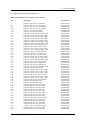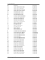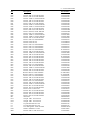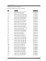
1
Eclipse Series
RF Technology
[email protected]
February 2005
PA501Amplifier
Operation and Maintenance Manual
This manual is produced by RF Technology Pty Ltd
10/8 Leighton Place, Hornsby NSW 2077 Australia
Copyright © 1997 RF Technology
CONTENTS
CONTENTS
Contents
1
Operating Instructions
1.1 Installation
1.1.1
Sub-rack Wiring Guidelines
1.2 Front Panel Indicators
1.3 Internal Adjustments
1.4 Amplifier I/O Connections
1.4.1
RF Input
1.4.2
RF Output
1.4.3
25 Pin Connector
4
4
4
5
5
6
6
6
6
2
Circuit Description
2.1 Block Overview
2.2 RF Amplifiers
2.3 Directional Coupler
2.4 Low Pass Filter
2.5 Power Control Circuits
2.6 RF Output Indicator
2.7 Over Temperature Protection
6
6
7
7
7
8
8
8
3
Field Alignment Procedures
3.1 Output Power Level
3.2 Tuning Procedure
9
9
9
4
Specifications
4.1 Description
4.2 Physical Configuration
4.3 Front Panel Indicators and Test Points
4.3.1
Indicators
4.3.2
Test Points
4.4 Electrical Specifications
4.4.1
Power Requirements
4.4.2
Frequency Range
4.5 Antenna Impedance
4.6 Output Power
4.6.1
Transmit Duty Cycle
4.7 Spurious and Harmonics
4.8 Heatsink Temperature
4.9 ALC Output
4.10 Connectors
4.10.1
RF Input
4.10.2
RF Output
4.10.3
25-Pin Connector
RF Technology
10
10
11
11
11
11
11
11
12
12
12
12
12
12
12
13
13
13
13
Page 2
CONTENTS
CONTENTS
A
Engineering Diagrams
A.1
Block Diagram
A.2
Circuit Diagrams
A.3
Component Overlay Diagrams
14
14
14
14
B
PA501 Factory Alignment and Test
B.1
Equipment Required
B.2
Procedure
B.3
Checking Mismatched Loads
18
C
Parts List
C.1
PA501 Parts List for PCB-30/9137/xxxx
C.2
PA501 Parts List for PCB-30/9151/xxxx
RF Technology PA501
22
25
Page 3
1 OPERATING INSTRUCTIONS
WARNING
Changes or modifications not expressly approved by
RF Technology could void your authority to operate
this equipment. Specifications may vary from those
given in this document in accordance with
requirements of local authorities. RF Technology
equipment is subject to continual improvement and
RF Technology reserves the right to change
performance and specification without further notice.
1
Operating Instructions
The PA501 is part of the Eclipse range of modular base station equipment. It is a
broadband power amplifier capable of continuously delivering 100 Watts of power in
the 400-512MHz frequency range. It is designed to complement the T500 transmitter,
and mounts in a standard Eclipse sub-rack.
1.1 Installation
There are no front panel controls requiring adjustment on the PA501. In normal
circumstances no alignment or setup is required. If mounted in a sub-rack that has not
previously been wired for a power amplifier, the rack connector must be wired
according to the guidelines in section 1.1.1 below.
1.1.1
Sub-rack Wiring Guidelines
When installing an Eclipse Power Amplifier in an Eclipse sub-rack, observe the
following guidelines for sub-rack installation:
•
The sub-rack power supply must be capable of delivering the full cur rent
requirements for all modules fitted in the sub-rack, typically 30 Amperes at 13.0
Volts for a complete repeater.
•
Owing to the high current drain, power supply lines should be cabled to the power
amplifier separately and using heavy gauge wire to minimise voltage drop and
interference with the power supply to other modules in the rack.
•
The ALC line from the power amplifier must be connected to the ALC input of the
exciter. If this connection is not correctly made, no control of the output power
level will be
possible. This can result in excessive RF output power, and
consequent breach of licensing authority regulations, or possible overload of the
unit.
With an Eclipse T500, join pin 8 on the exciter and the amplifier.
RF Technology PA501
Page 4
1
OPERATING INSTRUCTIONS
1.2 Front Panel Indictaors
1.2 Front Panel Indicators
PWR LED The power (PWR) LED shows that the dc supply is connected to the
transmitter.
RFO LED The RF output (RFO) LED indicates that the amplifier is being driven
and that the forward output power is above a preset level. This preset indication
level is generally set 1 - 3 dB below the preset output power level.
TEMP LED
The temperature (TEMP) LED indicates (illuminates) should the
amplifier's internal temperature become too high.
The RF power is
automatically reduced by 6-10 dB if the internal temperature rises above safe
limits and the cooling fans run continuously until the temperature drops.
1.3 Internal Adjustments (Rev 05/9151)
All internal adjustments are factory set and should not need to be changed under normal
conditions. A possible exception to this is the RF output power level which may need
to be changed to comply with local licensing requirements. The low forward power
warning circuit should be set at the same time as the forward power level. The controls
are described below, and the recommended procedure for carrying out the alignment is
set out in section 3.1.
WARNING
Ensure that the power setting complies with the
requirements of your licensing authority. Failure to do
so may result in penalties being imposed by the
licensing authority.
Output Power
The output power is set by VR136. This is nominally set to 100
Watts (+50dBm), but may be set to any value between 40 and 125 Watts
depending upon local regulations in the destination country, and the model of
power amplifier. VR136 determines the threshold affecting the ALC voltage that
is fed back to the transmitter module to regulate RF output power.
RF Level Detector The forward RF power threshold associated with the RFO LED on
the amplifier front panel is set by VR143. This is nominally set at half to threequarters of the preset output power, 50 - 90 Watts.
RF Technology PA501
Page 5
2 CIRCUIT DESCRIPTION
1.4 Amplifier I/O Connections
The PA501 has three connectors on the rear panel.
1.4.1
RF Input
The RF drive is delivered via a BNC connector. The absolute maximum power that
should be applied to this connector is 17 Watts.
1.4.2
RF Output
The RF output signal is available from an N-type connector.
Pins
1, 2, 3, 4, 5, 14, 15, 16, 17
9, 10, 11, 12, 13, 22, 23, 24, 25
8
Function
Positive supply
Ground (negative supply)
ALC output
Table 1: Pin connections for the 25 pin “D” connector on the rear panel
Note: The amplifier is capable of delivering as much as 120 Watts continuously.
In certain conditions1 an RF power of 180 Watts or more can be available via this
connector. This power level can cause burns like any 180w power source.
Appropriate care should be taken when working on the PA501 to avoid making or
breaking connections when the amplifier is operating, and to avoid RF burns
through close proximity to live connections, etc.
1.4.3
25 Pin Connector
The 25-pin “D” connector provides connection to ground and dc power, and from the
automatic level control (ALC) circuit. The pin connections are given in table 1.
2
Circuit Description
The following descriptions should be read as an aid to understanding the block and
schematic diagrams shown in figures 1 and 2.
2.1 Block Overview
The PA501 is comprised of two stages of RF amplification, a directional coupler
sensing forward and reverse power flow, an output low-pass filter and sundry associated
control and monitoring circuitry. The second RF amplifier employs two transistors
operating in parallel, a power splitter following the first RF
____________________
1
Excessive powers may be available, for example, in the event of a failure of the ALC loop,
such as may arise if the ALC feedback connection is broken.
RF Technology PA501
Page 6
2
CIRCUIT DESCRIPTION
2.2 Power Splitter / Combiners
amplifier stage, and is followed by a lumped/distributed network that performs both
impedance matching and power combining ahead of the output filter.
The PA501 design is very broad band and will not usually require adjustment once it
has left the factory unless components are changed or the equipment is required to move
frequency from one extreme end of the band to the other.
While it is often possible to achieve an adjustment that provides higher efficiency or
higher output power at one particular frequency, such adjustment will almost certainly
compromise operation in other parts of the band. Such adjustment is not recommended
and voids the warranty. Owing to the risk of severe RF burns the PA501 should not be
operated with its protective covers removed except by qualified personnel.
2.2 RF Amplifiers (Rev 05/9151)
The input to the PA501 is connected to the first RF amplifier stage, based around Q3,
by a matching network consisting of C43/44, etc. Q3 has a gain of 7-8dB, raising the
power level to about 35 Watts.
The main RF power amplification is provided by two single, class-C, transistor
amplifiers centered around Q1 and Q2. Each amplifier contributes half the output
power. The input and output impedances of the transistors are matched, and the power
split before the second stage, and combined after it, by broad band matching networks
employing both lumped and distributed (microstrip) components.
Variable capacitors are used in the input network to optimize the input match across the
desired frequency range, between the two RF stages, and in the output network to
optimize the output efficiency.
The dc supply is fed to the three RF power transistors through resistors to allow the
collector current of each to be measured at the front panel test socket.
2.3 Directional Coupler
The forward and reverse power components are measured through a coupled line
directional coupler. The output of the coupled line is frequency compensated and
impedence matched by R100, R101, R102 and R103 before being detected by D101 and
D101.
The dc output of the detectors is proportional to the forward and reflected RF power.
2.4 Low Pass Filter
A low pass filter consisting of L1 - 4 reduces the harmonic components to less than
-70dBc. The filter uses a comb ination of lumped elements and printed components to
obtain the required harmonic attenuation.
RF Technology PA501
Page 7
2.5 Power Control Circuits (Rev 05/9151)
The forward and reverse voltages from the directional coupler are amplified and
inverted by Q103 and Q101. The amplified voltages are compared to preset reference
levels and the comparison signals are combined in a logical fashion by Q109 and Q108
and used to produce the ALC signal. VR137 sets the maximum permitted reverse
power level.
The ALC signal is filtered and supplied to the rear panel system connector for
connection to the ALC control input of an exciter such as the model T500.
Equipment Type
Power Supply
RF Source
RF Load / Attenuator
RF Power Meter
Key Specifications
13.8Vdc, (<25A for 120W)
15 Watt source, 450-512MHz, e.g. T500
30 dB Attenuator, 50Ω, 150W, SWR<1.2:1
eg. HP437B or calibrated detector and voltmeter
Table 2: Standard test equipment for the PA501 Power Amplifier
2.6 RF Output Indicator
The forward power voltage is compared with the pre-set dc reference voltage from
VR136 by Q106, Q107. The output of Q113 is used to turn on the RFO LED. The
forward power voltage is buffered to Q116 to turn on the fans via Q6.
VR143 is normally set so that the RFO LED comes ON when output power is 1 - 3db
below the nominal power output level.
2.7 Over Temperature Protection
Thermistor RT144 is mounted to the case of output transistor Q1. If the transistor case
temperature rises above 90 Celsius (about 194o F) the resistance of RT144 increases
and Q117 is turned ON.
This causes the TEMP LED and the fans to come on and also reduces the dc output
voltage of the ALC signal via Q109. The input power will then be reduced by the
transmitter ALC circuits and the output transistor is kept within safe operating limits.
RF Technology PA501
Page 8
3
3
Field Alignment Procedures
3.1 Output Power Level
Field Alignment Procedures (Rev 05/9151)
Section 3.1 below describes how to adjust the PA501 amplifier for a particular output
power level. Section 3.2 broadly describes how to align the PA501 matching circuits.
This second procedure should not be necessary except after repair of a damaged unit,
and requires specialised equipment. It should not be undertaken without appropriate
tools and equipment.
3.1 Output Power Level
1. Set the unit up on a bench with the standard test equipment listed in table 2.
2. Set VR136 and VR137 both fully counter-clockwise.
3. Set the exciter to the desired operating frequency.
4. Adjust VR136 to set the output power on the meter to the level at which you want
the RFO LED to indicate (allowing for load attenuation). Note that the meter should
be calibrated to read the power at the connector of the power amplifier, not at the
end of any cables or attenuators.
5. Adjust VR137 until the RFO LED just goes out.
6. Adjust VR136 for the desired output power.
3.2 Tuning Procedure
Adjustment of the matching circuits is carried out with the aim of:
• ensuring that the specified power of 100 Watts is available2
• balancing the load reasonably equally between the power transistors, and
• obtaining acceptable efficiency in the power transistors.
Note that the factory alignment procedure is complicated, but allows a given unit to
operate across a full 450-512MHz band, without further adjustment. Alignment without
appropriate equipment can leave the amplifier unstable or otherwise unable to meet
specification.
The procedure calls for detection of the output power while sweeping the test frequency,
preferably by means of a calibrated network analyser or spectrum analyser. If this is not
possible, a rough approximation may be possible by observing the output of the unit’s
own ALC detector circuit with a swept stimulus.
____________________
2
At some frequencies a continuous power level of 120W is possible.
RF Technology PA501
Page 9
4 SPECIFICATIONS
4.1 Description
1. Set the unit up on a bench with the test equipment as given in table 3
2. Disable the ALC loop
3. Connect the output of the 15 Watt source directly to the annenuator, bypassing the
PA501 amplifier.
4. If you are using a network analyser, carry out calibration according to the
instruments instructions so as to obtain a 0 dB display from about 425MHz to
525MHz. Set the sweep time to no less than 0.2s, and the stimulus power to +42
dBm (15W). If you are using a swept source etc., store the response of the test
arrangement into a reference memory of the ’scope.
5. Connect the PA501 back in the circuit, and apply power.
6. The amplifier should have a gain of 10 dB across the frequency band, the collector
currents of Q1/Q2 should be within 20% of each other, and less than 10A each, at
each frequency in the sweep. The power delivered should exceed 125W across the
whole band.
7. Adjust the variable capacitors to achieve the above conditions. Beware achieving
higher gain across a narrow band. Also note that perfo rmance will change a little
when the lid is bolted down.
8. Reconnect the ALC loop. Check that the power levelling is working to within a dB
using a sweep speed of about 20MHz/second.
Power Supply
RF Source
RF Load
RF Power Meter
Dc Power Monitor
13.8V dc (<25A)
15 Watt swept source, 450-512MHz e.g., Network Analyser,
Spectrum Analyser and tracking generator, or sweep
generator and RF amplifier
Attenuator, 50Ω, 150W, SWR<1.2:1
e.g. Network Analyser, Spectrum Analyser, or HP532D
calibrated detector and digital storage scope
Q1/Q2 collector current
Table 3: Swept-frequency test equipment and conditions for the PA501
Power Amplifier.
4
Specifications
4.1 Description
The PA501 power amplifier is designed for use with the T500 series transmitters to
provide 120 Watts of RF output. Output power is regulated by connecting the ALC
output to the ALC input of the T500. The drive from the transmitter module is then
automatically adjusted to maintain the required output.
RF Technology PA501
Page 10
4
SPECIFICATIONS
4.5 Antenna Impedance
The regulated power level can be preset over a wide guaranteed range from 25 to 120
Watts or more, depending on the available driver power.
Sensing circuits are provided to protect the output transistors from excessive
temperature. If the heat sink temperature rises to 90C, the input drive will be reduced to
prevent damage.
4.2 Physical Configuration
The power amplifier is designed to fit in an RF Technology sub-rack within a 19" rack
frame. The installed height is 4 Rack Units (RU), or 178mm, and the depth is 350mm.
The amplifier is 158.75 mm or five Eclipse units wide. The amplifier uses an extruded
aluminium heat sink with vertical fins and fan-assisted air circulation. Heatsink
temperature rise is typically 30C.
4.3 Front Panel Indicators and Test Points
4.3.1
Indicators
Power:
Green LED
RF Power:
Yellow LED
Over Temperature:
Red LED
4.3.2
Test Points
Forward Power: Voltage to ground, 0 - 5V, uncalibrated
Reverse Power: Voltage to ground, 0 - 5V, uncalibrated
Collector Currents: Voltage to positive supply, across 22mΩ, ±10%
4.4 Electrical Specifications
4.4.1
Power Requirements
Operating Voltage: 10.5 - 16 Volts, with reduced output power below 12.5V
Current Drain: 25 Amperes maximum (20 typical) at 120 Watts and 13.5 Volts,
100mA maximum standby
Polarity: Negative Ground
RF Technology PA501
Page 11
4.4.2 Frequency Range
4.4.2
Model
PA501A
PA501B
4 SPECIFICATIONS
Frequency Range
Frequency Range
400-450MHz
450-512MHz
4.5 Antenna Impedance
Nominal load impedance is 50Ω SWR 1.5:1 or better. The PA501 will operate with a
VSWR of 2:1 at all phase angles. The forward power will reduce as reverse power rises
above acceptable limits, typically at an SWR of about 2.5:1.
4.6 Output Power
Nominally 100 Watts, preset adjustable from 25 to 120, typically 125 Watts maximum.
Gain is >8.5dB.
4.6.1
Transmit Duty Cycle
The transmitter is rated for 100% duty cycle (continuous operation) at 100W output for
air temperature below 40C. Derate linearly above 40C to 50% at 60C. At 125W output,
limit to 80% duty cycle or 2 minutes operation at 40C, derate to 40% at 60C.
4.7 Spurious and Harmonics
70dBc minimum at any harmonic of the transmit frequency.
4.8 Heatsink Temperature
The heatsink temperature can rise to 80C without affecting operation, except for
derating based on air-temperature as noted in section 4.6.1 above. Shutdown will occur
at heatsink temperatures exceeding approximately 90C.
4.9 ALC Output
The ALC is intended for connection to the T500. It supplies a voltage which decreases
with increasing power or temperature. Voltages below 6V should reduce drive power,
at a rate of approximately 6 dB/Volt, with voltages below 1V producing a minimum of
25 dB attenuation.
RF Technology PA501
Page 12
4 SPECIFICATIONS
4.10 Connectors
4.10.1
RF Input
The RF drive is delivered via a BNC connector. The maximum power that should be
applied to this connector is 17 Watts.
4.10.2
RF Output
The RF output signal is available from an N-type connector.
4.10.3
25-Pin Connector
A 25-pin, “D” connector provides connection to ground and dc power, and from the
automatic level control (ALC) circuit. The pin connections are given in table 1.
RF Technology PA501
Page 13
A ENGINEERING DIAGRAMS
A Engineering Diagrams
Where engineering diagrams are sufficiently complicated, large scale versions are
included as inserts or fold-outs elsewhere in the manual for reading convenience. If
inserts are missing or damaged, the information is identical to that presented in figures
embedded in the text.
A.1 Block Diagram
Figure 1 shows the block signal flow diagram of the PA501 amplifier.
A.2 Circuit Diagrams
Figure 2 shows the detailed circuit diagram of the PA501 amplifier with component
desiquators and values.
A.3 Component Overlay Diagrams
Figure 3 shows the PCB overlay guide of the PA501 amplifier with component
positions.
RF Technology PA501
Page 14
A
B
C
D
1
1
5-15W
INPUT
J2
BNC
R.F.DET.
FWD.PWR.
FAN
OVER TEMP.
RT1
90 DEG.C.
REF.
REG.
U5
+13.8 Vdc
Q7
FAN CONTROL
2
DRIVER
AMPLIFIER
Q3
U3D,Q5
RF OUTPUT
INDICATOR
U3C,Q6,Q8
t
U3B
SET
RFO
THRESHOLD
+8.0 V.REF.
Q9
OVER TEMP. DETECTOR
+8.0 V.REF.
2
3
Q1
Q2
RV2
+8.0 V.REF.
4
4
REV.PWR.
U2D
DIRECTIONAL
COUPLER
D1-D3
FWD.& REV.
POWER CONTROL
U2A
RV1
+8.0 V.REF.
SET MAX
REVERSE
POWER
ALC AMP
U3A
SET
FORWARD
POWER
OUTPUT
AMPLIFIER
Q4
OVER TEMP.
POWER CONTROL
ALC OUT
3
U2C
FWD. & REV.
DETECTOR AMPS.
U2B
50-125W
OUTPUT
J1
6
5
Date:
File:
Orcad B
Size
6
Sheet 2of
Drawn By:
PA501 Block Schematic
17-Mar-1998
D:\JBS\..\BLOCK.SCH
Number
2
05/9137 R6
JBS after RGM
Revision
600 MHz LPF
L1-L4 Title
R.F.TECHNOLOGY PTY. LTD.
17 / 8 Leighton Place, Hornsby, SYDNEY
5
A
B
C
D
A
B
C
D
1
1
1
6
2
7
3
8
4
9
5
+13.8
1
14
2
15
3
16
4
17
5
18
6
19
7
20
8
21
9
22
10
23
11
24
12
25
13
0V
A.L .C.
+13.8
CONNE CT OR DB 25
P5
-
0V
I cA
I cB
RF.DE T .
OV E R T E MP.
FWD.PWR.
RE V .PWR.
+
CONNE CT OR DB 9
J6
PW R
D1
AL C
D2
L E D PCB A SSY 11/9106
+
100
R 41
-
2
T E MP
D3
2
+
-
16
15
14
13
12
11
10
9
8
7
6
5
4
3
2
1
J5
J3
J2
J1
P4
16
15
14
13
12
11
10
9
8
7
6
5
4
3
2
1
3
3
Date:
File:
3
Revision
OU T PU T
J2
N Type
I NPU T
J1
B NC
4
Sheet 3of 3
JB S after R H M
Drawn B y:
9151 (U H F A MPL I F I E R )
3-Aug-1998
D:\RFT _MasterFiles\..\9151-block.sch
Number
R F T E CH NOL OGY PT Y . L T D.
10/8L eighton PL ace, H OR NSB Y , 2077, A ustr alia
Orcad A
Size
T itle
P3
P2
P1
A MPL I F I E R PCB A SSY 11/9151
4
A
B
C
D
B.1 Equipment Required
B PA501 FACTORY ALIGNMENT AND TEST
B. PA501 Factory Alignment and Test (Rev 30/9137)
B.1 Equipment Required
•
Spectrum Analyser and tracking generator (eg Tektronix 492 with TR503)
•
150W, 50Ω Attenuator/load, 40dB attenuation
•
Calibrated test Load with 5db return loss
•
Calibrated test Load with 8dB return loss
•
13.8 Volt, 30A power supply
•
Rhode & Schwarz SMG 1GHz GPIB-programmable RF generator
•
15W 450-520MHz driving amplifier (minimum 13W at 515MHz)
•
Directional Power meter
•
HP437B GPIB-programmable Power Meter
•
PC with PwrView test Software, GPIB cables, etc.
•
Spectrol long insulated alignment tool
•
Various 50Ω connection cables, adapters, etc.
B.2 Procedure
1.
Adjust the DC power supply to 14 Volts (no load). Adjust the SMG generator for
output off (Level OFF), centre frequency to 500MHz (RF 500 MHz), address 28
(IEC-addr, 2, 8, Enter). Connect the generator output to sweep amplifier input.
Connect DC supply to sweep amplifier and the device under test (DUT). Connect
the Sweep Amplifier to the Directional Power Meter, and the Directional Power
Meter to the DUT input. Connect the 40dB attenuating load to the output. Set up
and zero the HP437B power meter. The meter should be set for an operating
frequency of 0.5GHz and a cal factor as indicated on the sensor head, typically
98.5%. Fix it to range 5, offset 40dB (1kW range). connect the Power meter to
the load.
Set the RFO pot for maximum output (RV2 to CW), REVPWR to Max (RV1
fully CW), and C12 and C35 to middle position, C43 and C44 to about 1/4 of
range, and C11 near to the max (down) position.
RF Technology PA501
Page 18
A ENGINEERING DIAGRAMS
2.
Record serial number, etc., on the rest report sheet.
3.
Inspect the module. Check the disposition of flying cables (clear of RF power
compone nts).
4.
Switch the Generator output level to 3dBm (LEVEL 3 dBm/enter). Adjust C43,
44, 11, 12, 35 for output power of at least 100W on the power meter. Switch off
the generator (LEVEL OFF). The purpose of this step is simply to get the
adjustments approximately correct before moving to the swept alignment stage.
5.
Remove the power meter and connect the spectrum analyser to the output of the
attenuator. Remove the SMG and connect the tracking generator. Set the
tracking generator output to 0dBm.
Set the S.A. to a centre frequency of
485MHz and 10MHz/division. Set the reference level to 10dBm, and adjust the
display for 2dB/div. Check that spectrum analyser “time/div” and “Res. Bw” are
set to automatic. Adjust C43, C44, C11, C12 and C35 for flat response, as high as
possible on the display (i.e. remove small notches in the trace). There should be
less than 1 division of ripple for 3 divisions either side of the centre, preferably
3.5 to 4 divisions. Disconnect the tracking generator and the S.A.
6.
With the equipment set up as it was for the measurement of power at 500MHz,
and the generator output enabled, adjust the supply voltage to obtain 13.5 ± 0.25V
dc on the inside connections of the 25-pin D-shell power connector.
7.
With the equipment still set up for the measurement of power at 500MHz, using
the HP power meter and the R&S generator, start the PwrView program. (You
may use the command script ViewPA501, or the direct command “pwrview 450e6
512e6”.) You should see a simple ASCII screen with two columns of numbers at
the left, and an array of characters forming a horizontal bar graph across the rest
of the screen. The graph will refresh about every 3 seconds.
The display will have a horizontal row of characters for each frequency. At left,
the frequency and power in MHz and Watts is printed, followed by groups of
symbols. The symbol changes for power less that 100W, more than 100W but
less than 120W, and more than 120W. With 15W drive, the power may well
exceed 150W for all frequencies between 450MHz and 512MHz. Satisfactory
performance consists of power above 125W at the required operating frequency,
above 120W from 450-512MHz.
When met, this can be recorded by printing one screen of data. This is
conveniently achieved using the PrintPA501 script (batch file). Record the DUT
serial number on the printout, and attach this to the test report sheets.
8.
Set the RF generator to the frequency at which the greatest power was recorded in
the PwrView test. Switch the generator on, reconfirm the RF power level.
Measure and record the supply current, which should be below 30A.
9.
Adjust the FWDPWR pot (RV2) to obtain the desired output power, or an output
power of 120W if this is not specified, at the intended operating frequency, or
500MHz if this is not known. (ie.120W at 500MHz is the default alignment
RF Technology PA501
Page 19
A ENGINEERING DIAGRAMS
point). Measure and record the supply current, which should be below 25A
(typically 21A). Measure and record the voltage drop across the collector current
sense resistors (R21, R52, R53). The calculated supply current to Q2 and Q3
should be within 1A of each other.
10.
Measure the input RF (driving) power level. the forward power level should be
less than 14W. The reflected power level should be less than 1/5 of the forward
power. Measure and record the forward and reverse power voltages.
11.
Continuing at the operating frequency (or 500MHz if not specified), connect the
directional power meter to the output of the DUT. Connect the output from the
directional power meter to a load providing an SWR of 2.0:1 (or -8dB return loss).
Observe the forward power from the DUT to the load. Adjust the REVPWR pot
(RV1) until the amplifier output just starts to reduce, and return the pot until the
output returns to the set level. Attach the “5dB return loss” load (SWR of 3.5:1),
and see that the amplifier output falls.
12.
Replace the normal attenuator/load, and reconnect the power meter, or use the
directional power meter if preferred. Reduce the FWDPWR pot (RV2) to obtain
an output power of 2/3 the set level (nominally 80 Watts). Adjust the RFO pot to
just extinguish the front panel RFO LED, and then return it slightly until the LED
just comes back on. Reset the FWDPWR pot (RV2) to obtain the nominal 100
Watt output level.
13.
Reconnect the spectrum analyser to the attenuating load, but continue to use the
SMG generator rather than the tracking generator as the source. If the DUT is to
be used with a specific transmitter in a specific customer arrangement, substitute
the exciter for the generator and 15W sweep amplifier at this time.
Set the SA to centre frequency equal to the operating frequency, and span to
100kHz/division. Check for sidebands on the carrier.
14.
Reconnect the Power Meter to the attenuating load. Reduce the supply voltage
and observe the output power. As the voltage falls, the current drawn should
increase. Record the voltage and current level at which the output power falls
below 100W (or the desired set level, if different).
15.
Set the generator to 450MHz. (Minimum operating frequency). Measure the
input RF (driving) power level. The forward power level should be less than
14W. The reflected power level should be less than 1/5 of the forward power.
Measure and record the forward and reverse power voltages.
16.
Set the generator to 512MHz. (Maximum operating frequency). Measure the
input RF (driving) power level. The forward power level should be less than
14W. The reflected power level should be less than 1/5 of the forward power.
Measure and record the forward and reverse power voltages.
This concludes the alignment and test procedure.
RF Technology PA501
Page 20
B PA501 FACTORY ALIGNMENT AND TEST
B3 Checking Mismatched Loads
B3 Checking Mismatched Loads
The correct operation of the calibrated mismatch loads may be checked using the
equipment available for other tests. Place the Directional Power Meter between the
driving amplifier and the load to be tested. Adjust the generator to 500MHz, output on.
Measure the forward and reverse powers. The return loss is calculated at
RL = 10 log (PR/PF).
RF Technology PA501
Page 21
C PA501 PARTS LIST
C - PA501 Parts List for PCB - 30/9137/xxxx
Main PCB Assembly Parts, (common to all variants)
Ref.
Description
Part Number
C1
C8
C9
C10
C11
C12
C13
C14
C15
C16
C17
C18
C19
C20
C21
C23
C24
C25
C26
C27
C28
C29
C30
C31
C32
C33
C34
C35
C36
C37
C38
C39
C40
C41
C42
C43
C44
C45
C46
C47
C48
C49
C50
C51
C52
C53
C54
C55
C56
C57
C58
C59
C60
Capacitor 10N 10% 63V X7R 1206
Capacitor 10N 10% 63V X7R 1206
Capacitor 12P 5% 63V NPO SM1206
Capacitor 12P 5% 63V NPO SM1206
Capacitor Trim 14P JOH 15E85
Capacitor Trim 14P JOH 15E85
Capacitor Ceramic 220P 20%100V 100B
Capacitor Ceramic 33P 2% 500V 100B
Capacitor Ceramic 39P 2% 500V 100B
Capacitor Ceramic 33P 2% 500V 100B
Capacitor Ceramic 33P 2% 500V 100B
Capacitor Ceramic 220P 20%100V 100B
Capacitor Ceramic 220P 20%100V 100B
Capacitor 1N0 5% 63V NPO SM1206
Capacitor 100N 10% 63V X7R 1206
Capacitor Ceramic 39P 2% 500V 100B
Capacitor Ceramic 220P 20%100V 100B
Capacitor 1N0 5% 63V NPO SM1206
Capacitor 100N 10% 63V X7R 1206
Capacitor 6.8U 20% 25V SOLID AL
Capacitor Ceramic 33P 2% 500V 100B
Capacitor Ceramic 33P 2% 500V 100B
Capacitor Ceramic 220P 20%100V 100B
Capacitor 1N0 5% 63V NPO SM1206
Capacitor 100N 10% 63V X7R 1206
Capacitor 6.8U 20% 25V SOLID AL
Capacitor Ceramic 220P 20%100V 100B
Capacitor Trim 14P JOH 15E85
Capacitor Ceramic 33P 2% 500V 100B
Capacitor Ceramic 33P 2% 500V 100B
Capacitor Ceramic 33P 2% 500V 100B
Capacitor 56P 5% 63V NPO SM1206
Capacitor Ceramic 27P 2% 500V 100B
Capacitor Ceramic 27P 2% 500V 100B
Capacitor 56P 5% 63V NPO SM1206
Capacitor Trim 2-9P HI Temp
Capacitor Trim 2-9P HI Temp
Capacitor 100P 5% 63V NPO 1206
Capacitor 100P 5% 63V NPO 1206
Capacitor 100P 5% 63V NPO 1206
Capacitor 100P 5% 63V NPO 1206
Capacitor 100P 5% 63V NPO 1206
Capacitor 100P 5% 63V NPO 1206
Capacitor 100P 5% 63V NPO 1206
Capacitor 100P 5% 63V NPO 1206
Capacitor Ceramic 4N7 10% 63V X7R
Capacitor 100N 10% 63V X7R 1206
Capacitor 100P 5% 63V NPO 1206
Capacitor 10N 10% 63V X7R 1206
Capacitor 100P 5% 63V NPO 1206
Capacitor 1N0 5% 63V NPO SM1206
Capacitor 100P 5% 63V NPO 1206
Capacitor 100P 5% 63V NPO 1206
46/3310/010N
46/3310/010N
46/3300/012P
46/3300/012P
49/3004/014P
49/3004/014P
46/3100/220P
46/3102/033P
46/3102/039P
46/3102/033P
46/3102/033P
46/3100/220P
46/3100/220P
46/3300/01N0
46/3310/100N
46/3102/039P
46/3100/220P
46/3300/01N0
46/3310/100N
41/2225/06U8
46/3102/033P
46/3102/033P
46/3100/220P
46/3300/01N0
46/3310/100N
41/2225/06U8
46/3100/220P
49/3004/014P
46/3102/033P
46/3102/033P
46/3102/033P
46/3300/056P
46/3102/027P
46/3102/027P
46/3300/056P
49/3001/010P
49/3001/010P
46/3300/100P
46/3300/100P
46/3300/100P
46/3300/100P
46/3300/100P
46/3300/100P
46/3300/100P
46/3300/100P
46/3310/04N7
46/3310/100N
46/3300/100P
46/3310/010N
46/3300/100P
46/3300/01N0
46/3300/100P
46/3300/100P
RF Technology PA501
Page 22
C PA501 PARTS LIST
Ref.
Description
Part Number
C61
C62
C63
C64
C65
C201
D1
D2
D3
D4
D5
J3
J4
JP1
L1
L2
L3
L4
L5
L6
L7
L8
L9
L10
L11
L12
L13
L14
L15
P1
P2
Q1
Q2
Q3
Q4
Q5
Q6
Q7
Q8
Q9
R9
R10
R11
R21
R26
R27
R28
R29
R30
R31
R32
R33
R34
R35
R36
R37
R38
R39
Capacitor 100P 5% 63V NPO 1206
Capacitor 100P 5% 63V NPO 1206
Capacitor 10U 35V RAD Electro
Capacitor 100N 10% 63V X7R 1206
Capacitor 10N 10% 63V X7R 1206
Capacitor 100N 10% 50V X7R RD.2
Diode Shottkey BAT17 SOT23
Diode Shottkey BAT17 SOT23
Diode Shottkey BAT17 SOT23
Diode Dual GP BAV99 SOT23
Diode Dual GP BAV99 SOT23
2.8mm QC TAB Vertical PCB Mount
2.8mm QC TAB Vertical PCB Mount
Connector 16WAY Shroud Header
Inductor Hair Pin 10mmIDx13.5L
Inductor Hair Pin 10mmIDx14.5L
Inductor Hair Pin 10mmIDx14.5L
Inductor Hair Pin 10mmIDx13.5L
Inductor 220N 10% Choke SM1008
Inductor 11T UHF Collector
Ferrite Bead 3x4x1 4S2
Inductor 11T UHF Collector
Ferrite Bead 3x4x1 4S2
Inductor 11T UHF Collector
Ferrite Bead 3x4x1 4S2
Inductor 1uH Axial
Inductor 1uH Axial
Inductor Moulded 9.5 Turn
Inductor Moulded 9.5 Turn
6.35mm QC TAB Vertical PCB Mount
6.35mm QC TAB Vertical PCB Mount
Transistor NPN RF Power MRF658
Transis tor NPN RF Power MRF658
Transistor NPN 50W RF MRF650
Transistor NPN MMBT3904 SOT23
Transistor NPN MMBT3904 SOT23
Transis tor PNP TIP32
Transistor NPN MMBT3904 SOT23
Transistor NPN MMBT3904 SOT23
Transistor NPN MMBT3904 SOT23
Resistor 22K 5% 0.25W SM1206
Resistor 1K0 5% 0.25W SM1206
Resistor 100 5% 0.25W SM1206
Resistor 0.022 4W 5%
Resistor 680 5% 0.25W SM1206
Resistor 100 5% 0.25W SM1206
Resistor 100 5% 0.25W SM1206
Resistor 100K 5% 0.25W SM1206
Resistor 10 5% 0.25W Axial
Resistor 10 5% 0.25W Axial
Resistor 10 5% 0.25W Axial
Resistor 4R7 5% 0.25W Axial
Resistor 4R7 5% 0.25W Axial
Resistor 10K 5% 0.25W SM1206
Resistor 22K 5% 0.25W SM1206
Resistor 10K 5% 0.25W SM1206
Resistor 330K 5% 0.25W SM1206
Resistor 10K 5% 0.25W SM1206
46/3300/100P
46/3300/100P
41/2001/010U
46/ 3310/100N
46/3310/010N
46/2001/100N
21/3030/0017
21/ 3030/0017
21/3030/0017
21/3010/AV99
21/3010/AV99
35/0028/0001
35/0028/0001
35/2502/0016
37/3001/13D5
37/3001/14D5
37/3001/14D5
37/3001/13D5
37/3320/220N
37/1401/0011
37/1022/0001
37/1401/0011
37/1022/0001
37/1401/0011
37/1022/0001
37/2021/001U
37/2021/001U
37/2021/0009
37/2021/0009
35/0635/0001
35/0635/0001
27/3020/MRF658
27/3020/MRF658
27/3020/MRF650
27/3020/3904
27/3020/3904
27/2010/TP32
27/3020/3904
27/3020/3904
27/3020/3904
51/3380/022K
51/3380/01K0
51/3380/0100
51/1350/R022
51/3380/0680
51/3380/0100
51/3380/0100
51/3380/100K
51/1040/0010
51/1040/0010
51/1040/0010
51/1040/04R7
51/1040/04R7
51/3380/010K
51/3380/022K
51/3380/010K
51/3380/330K
51/3380/010K
RF Technology PA501
Page 23
C PA501 PARTS LIST
Ref.
R36
R37
R38
R39
R40
R41
R42
R43
R44
R45
R46
R47
R48
R49
R50
R51
R52
R53
R54
R55
R56
R57
R58
R59
R60
R61
R62
R63
R64
R65
R66
R67
R68
R69
R70
R71
R72
R73
R74
R75
R76
R77
R78
R79
R80
R81
R82
R83
R84
R85
RT1
RV1
RV2
RV3
U2
U3
U5
L201
R201
Description
Resistor 22K 5% 0.25W SM1206
Resistor 10K 5% 0.25W SM1206
Resistor 330K 5% 0.25W SM1206
Resistor 10K 5% 0.25W SM1206
Resistor 22K 5% 0.25W SM1206
Resistor 10K 5% 0.25W SM1206
Resistor 470K 5% 0.25W SM1206
Resistor 470K 5% 0.25W SM1206
Resistor 33K 5% 0.25W SM1206
Resistor 1M0 5% 0.25W SM1206
Resistor 1M0 5% 0.25W SM1206
Resistor 100 5% 0.25W SM1206
Resistor 100K 5% 0.25W SM1206
Resistor 100K 5% 0.25W SM1206
Resistor 47K 5% 0.25W SM1206
Resistor 100 5% 0.25W SM1206
Resistor 0.022 4W 5%
Resistor 0.022 4W 5%
Resistor 100 5% 0.25W SM1206
Resistor 100 5% 0.25W SM1206
Resistor 100 5% 0.25W SM1206
Resistor 100 5% 0.25W SM1206
Resistor 10K 5% 0.25W SM1206
Resistor 100K 5% 0.25W SM1206
Resistor 10K 5% 0.25W SM1206
Resistor 47K 5% 0.25W SM1206
Resistor 2K2 5% 0.25W SM1206
Resistor 47K 5% 0.25W SM1206
Resistor 10K 5% 0.25W SM1206
Resistor 10K 5% 0.25W SM1206
Resistor 270 5% 0.25W SM1206
Resistor 10K 5% 0.25W SM1206
Resistor 100K 5% 0.25W SM1206
Resistor 33K 5% 0.25W SM1206
Resistor 47K 5% 0.25W SM1206
Resistor 1K0 5% 0.25W SM1206
Resistor 10K 5% 0.25W SM1206
Resistor 270 5% 0.25W SM1206
Resistor 10K 5% 0.25W SM1206
Resistor 10K 5% 0.25W SM1206
Resistor 270 5% 0.25W SM1206
Resistor 10K 5% 0.25W SM1206
Resistor 470K 5% 0.25W SM1206
Resistor 4K7 5% 0.25W SM1206
Resistor 1K0 5% 0.25W SM1206
Resistor 270 5% 2W Axial
Resistor 4K7 5% 0.25W SM1206
Resistor 22K 5% 0.25W SM1206
Resistor 1K0 5% 0.25W SM1206
Resistor 1R0 5% 0.25W SM1206
Thermistor
Trimpot 10K 1 Turn Vertical
Trimpot 10K 1 Turn Vertical
Trimpot 10K 1 Turn Vertical
IC Quad OP AMP TLC274
IC Quad OP AMP TLC274
IC Volt Regulator 78L08 TO92M
Inductor Moulded 9.5 Turn
Resistor 68R 5% 2W Axial Lead
RF Technology PA501
Part Number
51/3380/022K
51/3380/010K
51/3380/330K
51/3380/010K
51/3380/022K
51/3380/010K
51/3380/470K
51/3380/470K
51/3380/033K
51/3380/01M0
51/3380/01M0
51/3380/0100
51/3380/100K
51/3380/100K
51/3380/047K
51/3380/0100
51/1350/R022
51/1350/R022
51/3380/0100
51/3380/0100
51/3380/0100
51/3380/0100
51/3380/010K
51/3380/100K
51/3380/010K
51/ 3380/047K
51/3380/02K2
51/3380/047K
51/3380/010K
51/3380/010K
51/3380/0270
51/3380/010K
51/3380/100K
51/3380/033K
51/3380/047K
51/3380/01K0
51/3380/010K
51/3380/0270
51/3380/010K
51/3380/010K
51/3380/0270
51/3380/010K
51/3380/470K
51/3380/04K7
51/3380/01K0
51/1052/0270
51/3380/04K7
51/3380/022K
51/3380/01K0
51/3380/01R0
54/0400/0080
53/1020/010K
53/1020/010K
53/1020/010K
25/2050/274C
25/2050/274C
25/2040/78L08
37/2021/0009
51/1052/0068
Page 24
C PA501 PARTS LIST
PA501 Parts List for PCB – 30/9151/xxxx
Main PCB Assembly Parts, (common to all variants)
Ref.
C1
C11
C12
C13
C15
C18
C19
C20
C21
C22
C24
C25
C26
C27
C29
C30
C31
C32
C33
C34
C35
C38
C39
C41
C42
C43
C44
C58
C63
C64
C65
C80
C81
C82
C83
C90
C91
C92
C93
C100
C101
C102
C103
C104
C105
C106
C107
C108
C109
C110
C111
C112
C113
Description
Capacitor 1N0 5% 63V NPO SM1206
Capacitor Trim 14P JOH 15E85
Capacitor Trim 14P JOH 15E85
Capacitor Ceramic 220P 20%100V 100B
Capacitor Ceramic 11P 2% 500V 100B
Capacitor Ceramic 220P 20%100V 100B
Capacitor Ceramic 220P 20%100V 100B
Capacitor 1N0 5% 63V NPO SM1206
Capacitor 100N 10% 63V X7R 1206
Capacitor 6.8U 20% 25V SOLID AL
Capacitor Ceramic 220P 20%100V 100B
Capacitor 1N0 5% 63V NPO SM1206
Capacitor 100N 10% 63V X7R 1206
Capacitor 6.8U 20% 25V SOLID AL
Capacitor Ceramic 33P 2% 500V 100B
Capacitor Ceramic 220P 20%100V 100B
Capacitor 1N0 5% 63V NPO SM1206
Capacitor 100N 10% 63V X7R 1206
Capacitor 6.8U 20% 25V SOLID AL
Capacitor Ceramic 220P 20%100V 100B
Capacitor Trim 14P JOH 15E85
Capacitor Ceramic 11P 2% 500V 100B
Capacitor 56P 5% 63V NPO SM1206
Capacitor Ceramic 27P 2% 500V 100B
Capacitor 56P 5% 63V NPO SM1206
Capacitor Trim 2-10P HI Temp
Capacitor Trim 2-10P HI Temp
Capacitor 1N0 5% 63V NPO SM1206
Capacitor 10U 35V RAD Electro
Capacitor 100N 10% 63V X7R 1206
Capacitor 1N0 5% 63V NPO SM1206
Capacitor Ceramic 11P 2% 500V 100B
Capacitor Ceramic 11P 2% 500V 100B
Capacitor Ceramic 11P 2% 500V 100B
Capacitor Ceramic 11P 2% 500V 100B
Capacitor Ceramic 11P 2% 500V 100B
Capacitor Ceramic 11P 2% 500V 100B
Capacitor Ceramic 11P 2% 500V 100B
Capacitor Ceramic 11P 2% 500V 100B
Capacitor 3P3 5% 63V NPO 1206
Capacitor 3P3 5% 63V NPO 1206
Capacitor 220P 5% 63V NPO 1206
Capacitor 220P 5% 63V NPO 1206
Capacitor 27P 5% 63V NPO SM1206
Capacitor 27P 5% 63V NPO SM1206
Capacitor 47P 5% 63V NPO SM1206
Capacitor 47P 5% 63V NPO SM1206
Capacitor 47P 5% 63V NPO SM1206
Capacitor 100P 5% 63V NPO 1206
Capacitor 27P 5% 63V NPO SM1206
Capacitor 27P 5% 63V NPO SM1206
Capacitor 27P 5% 63V NPO SM1206
Capacitor 100P 5% 63V NPO 1206
RF Technology PA501
Part Number
46/3300/01N0
49/3004/014P
49/3004/014P
46/3100/220P
46/3102/011P
46/3100/220P
46/3100/220P
46/3300/01N0
46/3310/100N
41/2225/06U8
46/3100/220P
46/3300/01N0
46/3310/100N
41/2225/06U8
46/3102/033P
46/3100/220P
46/3300/01N0
46/3310/100N
41/2225/06U8
46/3100/220P
49/3004/014P
46/3102/011P
46/3300/056P
46/3102/027P
46/3300/056P
49/3001/010P
49/3001/010P
46/3300/01N0
41/2001/010U
46/3310/100N
46/3300/01N0
46/3102/011P
46/3102/011P
46/3102/011P
46/3102/011P
46/3102/011P
46/3102/011P
46/3102/011P
46/3102/011P
46/3300/03P3
46/3300/03P3
46/3300/220P
46/3300/220P
46/3300/027P
46/3300/027P
46/3300/047P
46/3300/047P
46/3300/047P
46/3300/100P
46/3300/027P
46/3300/027P
46/3300/027P
46/3300/100P
Page 25
C PA501 (PCB 30/9151/xxxx) PARTS LIST
Ref.
Description
C115
D100
D101
D102
D103
J3
J4
JP1
L1
L2
L3
L4
L6
L7
L8
L9
L10
L11
L12
L13
L14
L15
L100
P1
P2
Q1
Q2
Q3
Q6
Q100
Q101
Q102
Q103
Q104
Q105
Q106
Q107
Q108
Q109
Q111
Q112
Q113
Q114
Q115
Q116
Q117
R21
R26
R29
R30
R31
R32
R33
R34
R43
R52
R53
R54
R55
R56
R57
Capacitor 1N0 5% 63V NPO SM1206
Diode Shottkey BAT17 SOT23
Diode Shottkey BAT17 SOT23
Diode Dual GP BAV99 SOT23
Diode Dual GP BAV99 SOT23
2.8mm QC TAB Vertical PCB Mount
2.8mm QC TAB Vertical PCB Mount
Connector 16WAY Shroud Header
Inductor Hair Pin 10mmIDx13.5L
Inductor Hair Pin 10mmIDx14.5L
Inductor Hair Pin 10mmIDx14.5L
Inductor Hair Pin 10mmIDx13.5L
Inductor 11T UHF Collector
Ferrite Bead 3x4x1 4S2
Inductor 11T UHF Collector
Ferrite Bead 3x4x1 4S2
Inductor 11T UHF Collector
Ferrite Bead 3x4x1 4S2
Inductor 1uH Axial
Inductor 1uH Axial
Inductor Moulded 9.5 Turn
Inductor Moulded 9.5 Turn
Inductor 220N 10% Choke SM1008
6.35mm QC TAB Vertical PCB Mount
6.35mm QC TAB Vertical PCB Mount
Transistor NPN RF Power MRF658
Transistor NPN RF Power MRF658
Transistor NPN 50W RF MRF650
Transistor PNP TIP32
Transistor NPN MMBT3904 SOT23
Transistor NPN MMBT3904 SOT23
Transistor NPN MMBT3904 SOT23
Transistor NPN MMBT3904 SOT23
Transistor NPN MMBT3906 SOT23
Transistor NPN MMBT3906 SOT23
Transistor NPN MMBT3906 SOT23
Transistor NPN MMBT3906 SOT23
Transistor NPN MMBT3904 SOT23
Transistor NPN MMBT3904 SOT23
Transistor NPN MMBT3904 SOT23
Transistor NPN MMBT3906 SOT23
Transistor NPN MMBT3906 SOT23
Transistor NPN MMBT3906 SOT23
Transis tor NPN MMBT3904 SOT23
Transistor NPN MMBT3904 SOT23
Transistor NPN MMBT3904 SOT23
Resistor 0.022 4W 5%
Resistor 680 5% 0.25W SM1206
Resistor 100K 5% 0.25W SM1206
Resistor 10 5% 0.25W Axial
Resistor 10 5% 0.25W Axial
Resistor 10 5% 0.25W Axial
Resistor 4R7 5% 0.25W Axial
Resistor 4R7 5% 0.25W Axial
Resistor 470R 5% 0.25W SM1206
Resistor 0.022 4W 5%
Resistor 0.022 4W 5%
Resistor 100R 5% 0.25W SM1206
Resistor 100R 5% 0.25W SM1206
Resistor 100R 5% 0.25W SM1206
Resistor 100R 5% 0.25W SM1206
RF Technology PA501
Part Number
46/3300/01N0
21/3030/0017
21/3030/0017
21/3010/AV99
21/ 3010/AV99
35/0028/0001
35/0028/0001
35/2502/0016
37/3001/13D5
37/3001/14D5
37/3001/14D5
37/3001/13D5
37/1401/0011
37/1022/0001
37/1401/0011
37/1022/0001
37/1401/0011
37/1022/0001
37/2021/001U
37/2021/001U
37/2021/0009
37/2021/0009
37/3320/220N
35/0635/0001
35/0635/0001
27/3020/MRF658
27/3020/MRF658
27/3020/MRF650
27/2010/TP32
27/3020/3904
27/3020/3904
27/3020/3904
27/3020/3904
27/3010/3906
27/3010/3906
27/3010/3906
27/3010/3906
27/3020/3904
27/3020/3904
27/3020/3904
27/3010/3906
27/3010/3906
27/3010/3906
27/3020/3904
27/3020/3904
27/3020/3904
51/1350/R022
51/3380/0680
51/3380/100K
51/1040/0010
51/1040/0010
51/1040/0010
51/1040/04R7
51/1040/04R7
51/3380/0470
51/1350/R022
51/1350/R022
51/3380/0100
51/3380/0100
51/3380/0100
51/3380/0100
Page 26
C PA501(PCB 30/9151/xxxx) PARTS LIST
Ref.
R66
R73
R76
R80
R81
R85
R100
R101
R102
R103
R104
R105
R107
R108
R109
R110
R111
R112
R113
R114
R115
R116
R117
R118
R120
R121
R122
R123
R124
R125
R126
R127
R128
R129
R130
R131
R132
R133
R134
R136
R137
R138
R139
R141
R142
R145
R146
R147
R148
R150
R151
R152
R153
R154
R156
R157
R158
R159
RT1
Description
Resistor 470R 5% 0.25W SM1206
Resistor 10R 5% 0.25W SM1206
Resistor 270 5% 0.25W SM1206
Resistor 1K0 5% 0.25W SM1206
Resistor 270 5% 2W Axial
Resistor 1R0 5% 0.25W SM1206
Resistor 120R 5% 0.25W SM1206
Resistor 120R 5% 0.25W SM1206
Resistor 470R 5% 0.25W SM1206
Resistor 470R 5% 0.25W SM1206
Resistor 470R 5% 0.25W SM1206
Resistor 470R 5% 0.25W SM1206
Resistor 3K9 5% 0.25W SM1206
Resistor 1K5 5% 0.25W SM1206
Resistor 150R 5% 0.25W SM1206
Resistor 1K0 5% 0.25W SM1206
Resistor 1K0 5% 0.25W SM1206
Resistor 470R 5% 0.25W SM1206
Resistor 3K9 5% 0.25W SM1206
Resistor 22K 5% 0.25W SM1206
Resistor 1K5 5% 0.25W SM1206
Resistor 150R 5% 0.25W SM1206
Resistor 1K0 5% 0.25W SM1206
Resistor 1K0 5% 0.25W SM1206
Resistor 10K 5% 0.25W SM1206
Resistor 470R 5% 0.25W SM1206
Resistor 10K 5% 0.25W SM1206
Resistor 22K 5% 0.25W SM1206
Resistor 2K2 5% 0.25W SM1206
Resistor 10K 5% 0.25W SM1206
Resistor 22K 5% 0.25W SM1206
Resistor 22K 5% 0.25W SM1206
Resistor 22K 5% 0.25W SM1206
Resistor 2K2 5% 0.25W SM1206
Resistor 3K3 5% 0.25W SM1206
Resistor 22K 5% 0.25W SM1206
Resistor 10K 5% 0.25W SM1206
Resistor 100R 5% 0.25W SM1206
Resistor 100R 5% 0.25W SM1206
Resistor 100R 5% 0.25W SM1206
Resistor 10K 5% 0.25W SM1206
Resistor 560R 5% 0.25W SM1206
Resistor 47R 5% 0.25W SM1206
Resistor 10K 5% 0.25W SM1206
Resistor 2K2 5% 0.25W SM1206
Resistor 10K 5% 0.25W SM1206
Resistor 10K 5% 0.25W SM1206
Resistor 10R 5% 0.25W SM1206
Resistor 22K 5% 0.25W SM1206
Resistor 10K 5% 0.25W SM1206
Resistor 22K 5% 0.25W SM1206
Resistor 10K 5% 0.25W SM1206
Resistor 100R 5% 0.25W SM1206
Resistor 100R 5% 0.25W SM1206
Resistor 10K 5% 0.25W SM1206
Resistor 10K 5% 0.25W SM1206
Resistor 10R 5% 0.25W SM1206
Resistor 100R 5% 0.25W SM1206
Thermistor
RF Technology PA501
Part Number
51/3380/0470
51/3380/0010
51/3380/0270
51/3380/01K0
51/1052/0270
51/3380/01R0
51/3380/0120
51/3380/0120
51/3380/0470
51/3380/0470
51/3380/0470
51/3380/0470
51/3380/03K9
51/3380/01K5
51/3380/0150
51/3380/01K0
51/3380/01K0
51/3380/0470
51/3380/03K9
51/3380/022K
51/3380/01K5
51/3380/0150
51/3380/01K0
51/3380/01K0
51/3380/010K
51/3380/0470
51/3380/010K
51/3380/022K
51/3380/02K2
51/3380/010K
51/3380/022K
51/3380/022K
51/3380/022K
51/3380/02K2
51/3380/03K3
51/3380/022K
51/3380/010K
51/3380/0100
51/3380/0100
51/3380/0100
51/3380/010K
51/3380/0560
51/3380/0047
51/3380/010K
51/3380/02K2
51/3380/010K
51/3380/010K
51/3380/0010
51/3380/022K
51/3380/010K
51/3380/022K
51/3380/010K
51/3380/0100
51/3380/0100
51/3380/010K
51/3380/010K
51/3380/0010
51/3380/0100
54/0400/0080
Page 27
C PA501 (PCB 30/9151/xxxx)PARTS LIST
Ref.
Description
Part Number
VR136
VR137
VR143
U5
Trimpot 10K 1 Turn Vertical
Trimpot 10K 1 Turn Vertical
Trimpot 10K 1 Turn Vertical
IC Volt Regulator 78L08 TO92M
53/1020/010K
53/1020/010K
53/1020/010K
25/2040/78L08
Parts Specific to PA501A (XXX – XXXMHz)
C14
C23
C16
C17
C28
C36
C37
C29A
C40
C41A
C116
Capacitor Ceramic 22P 2% 500V 100B
Capacitor Ceramic 22P 2% 500V 100B
Capacitor Ceramic 39P 2% 500V 100B
Capacitor Ceramic 39P 2% 500V 100B
Capacitor Ceramic 27P 2% 500V 100B
Capacitor Ceramic 39P 2% 500V 100B
Capacitor Ceramic 39P 2% 500V 100B
Capacitor Ceramic 27P 2% 500V 100B
Capacitor Ceramic 39P 2% 500V 100B
Capacitor Ceramic 27P 2% 500V 100B
Capacitor, Electrolytic 10U 35V
46/3102/022P
46/3102/022P
46/3102/039P
46/3102/039P
46/3102/027P
46/3102/039P
46/3102/039P
46/3102/027P
46/3102/039P
46/3102/027P
41/2001/010U
Parts Specific to PA501B (XXX – XXXMHz)
C14
C23
C16
C17
C28
C36
C37
C40
Capacitor Ceramic 11P 2% 500V 100B
Capacitor Ceramic 11P 2% 500V 100B
Capacitor Ceramic 33P 2% 500V 100B
Capacitor Ceramic 33P 2% 500V 100B
Capacitor Ceramic 33P 2% 500V 100B
Capacitor Cera mic 33P 2% 500V 100B
Capacitor Ceramic 33P 2% 500V 100B
Capacitor Ceramic 27P 2% 500V 100B
46/3102/011P
46/3102/011P
46/3102/033P
46/3102/033P
46/3102/033P
46/3102/033P
46/3102/033P
46/3102/027P
(end PA501 for PCB-30/9151/xxxx Partslists)
RF Technology PA501
Page 28
1
2
3
4
5
6
+8.0
+13.6B
R56
IC B
R53
0R022
C56
10N
+13.6C
R49
100K
OVER TEMP.
R51
+
100
C57
100P
U3A
TLC274
+13.8
-
3
R11
2
100
TLC274
U2A
11
P2
+8.0
4
J3
1
R50
47K
R68
100K
C54
D5
BAV99
0
4K7
10
0
+13.8
R54
+13.6C
#L201
L11
C31
1N0
+
C30
220P
+
33K
R84
1K
R39
9
10
C50
100P
R40
22K
C51
100P
R41
10K
C41
*
C35
14P
C29
*
+13.6B
D1
BAT17
C38
C23 C92 C93
*
*
*
*
C13
220P
C22
6U8
C18
220P
L7
*
C101
C20
1N0
+
C21
100N
R34
4.7
L13
1U0
C45
R30
10
C28
*
C40
*
DIRECTIONAL COUPLER
C90 C91
*
*
#C201
100N
L12
1U0
A
*
C17
* COMPONENT VALUES
#R201
68
C19
220P
C14
C15
C16
C17
C23
C28
C29
C36
C37
C38
C40
C41
11P
11P
33P
33P
11P
33P
33P
33P
33P
11P
27P
27P
C80-C83 C90-C92
11P
11P
C101
C46
100P
100P
C9
C10
12P
12P
R27
100
L5
220N
C11
D2
BAT17
L2
L3
J1
50-125W
OUTPUT
L6
#C201
100N
C83
*
A
*
C16
# PART OF SUB-ASSEMBLY 11/9138/0001
C82
C15 C14 C80 C81
*
*
*
*
*
NONE
Title
Date:
File:
3
L4
LOW PASS FILTER
R29
100K
RF TECHNOLOGY PTY. LTD.
UNIT 17, 8 LEIGHTON PLACE, HORNSBY, N.S.W. 2077
Size
2
C49
100P
R28
100
L1
14P
C12
14P
D3
BAT17
Orcad C
1
10K
L8
Q1
MRF658
400-450MHz
-
C
B
Q3
MRF650
L14
C24
220P
C37
*
C34
220P
#L201
PA501A
R42
470K
8
68
C39 R33
L15 56P 4.7
68
C44
10P
C42
56P
450-512 HMz
U2C
TLC274
R69
C36
*
#C201
100N
#R201
PA501B
Q4
MMBT3904
Q2
MRF658
L10
#L201
C25
1N0
C26
100N #R201
C32
100N
FREQUENCY RANGE
C48 10K
100P
L9
+
R32
10
MODEL
R37
R31
10
+13.6A
C43
10P
10K
+8.0
C65
10N
C27
6U8
INPUT
J2
C52
100P
C47
100P
R83
22K
2K2
FWD.PWR.
100
C33
6U8
C55
100P
13
R38
330K
R35
6
R36
22K
C1
10N
R62
13
SET RFO
RV3
10K
+13.8
B
D
R75
10K
DC LED
IC A
IC B
RF DET.
OVER TEMP.
FWD.PWR.
REV.PWR.
IC C
-
270
R26
680
-
12
+
10K
+8.0
12
+
14
U2D
TLC274
14
RF LED
RF LED
U3D
TLC274
REV.PWR.
0
JP1
R72
R10
1K
+8.0
R45 1M0
0
Q5
MMBT3904
R73
-
5
+
33K
RV2
10K
R71
1K0
R77
10K
U2B
TLC274
R44
C61
100P
SET FWD.
POWER
9
R78
C62
100P
R74
10K
C53
4N7
470K
TEMP. LED
RT1
+8.0
R43
470K
0
GND
8
+
C64
100N
2
R79
Q8
MMBT3904
R70
47K
U3C
TLC274
+13.8
16
15
14
13
12
11
10
9
8
7
6
5
4
3
2
1
t
C60
100P
R9
22K
RV1
10K
2
100N
0
J4
FAN
1
-
C63
10U
C
+8.0
VO
R60
10K
SET REV.
POWER
3
+
R46 1M0
D4
BAV99
+8.0
R81
270 1W
R67
10K
7
Q6
TIP32
VI
6
R65
10K
C8
10N
1
R80
1K0
+
R66
270
-
R85
1R0
LM78L08P
U5
5
+8.0
100
3
U3B
TLC274
R63
47K
-
C59
100P
R57
IC C
+13.8
10K
TEMP. LED
R47
100
100
TP3
R48
100K
+8.0
+
7
0
R21
0R022
R58
10K
47K
R64
R76
270
R59
100K
0
TP2
Q7
MMBT3904
0
100
R61
+13.8
R82
4K7
IC A
C58
1N0
D
Q9
MMBT3904
R55
0
+13.6A
0
TP1
R52
0R022
0
TP4
4
+13.8
11
P1
4
5
Number
30/9137 (PA501 Mk I)
Revision
22-Oct-2002
Sheet 1of 2
D:\Protel Files\Work Files\UHF_Manual.ddb
Drawn By: JBS
6
3
1
2
TP4
+13.8
TP1
R52
0R022
P1
3
4
5
6
8
7
+13.6A
R55
IC A
C58
1N0
+13.8
100
TP2
R21
0R022
+8V
R85
1R0
R56
IC B
D
R80
1K0
100
TP3
C100
10N
IC C
J4
100
270
R81
270 1W
R150
10k
R146
10k
R66
C112
470
27p
R158
10
RT144
B59901/D90
OVERTEMP
FAN
Q115
MMBT3904
Q116
MMBT3904
P2
R151
22k
Q114
MMBT3906
VR143
10k
R145
10k
TEMP.LED
R57
13.8
R138
560
R141
10k
MMBT3904
Q117
R76
+13.6C
R156
10k
MMBT3906
Q113
Q112
MMBT3906
Q6
TIP32
R53
0R022
R157
10k
R147
10
+13.6B
R148
22k
R137
10k
SET RFO
R142
2k2
*
D
R73
10
R139
47
R152
10k
RF LED
+8V
R132
10k
3
+8.0
C117
1nF
GND
+
Q109
MMBT3904
J3 (ALC)
C64
100N
C116
10U
R136
100
+
C106
47p
22k
R127
22k
R128
22k
REV
PWR
R129
2k2
C109
100P
C108
47p
C
Q104
MMBT3906
VR137
10k
VR136
10k
FWD
PWR
R134
100
Place C117 as close to J3 as possible
MMBT3906
Q105
Q106
MMBT3906
R131
1
VO
2
C63
10U
VI
Q107
MMBT3906
R120
10k
R125
10k
Q111
MMBT3904
LM78L08P
+13.8
R130
3k3
R126
22k
R123
22k
R124
2k2
C113
100P
R121
470
R122
10k
C
+13.8
Assy #30/9106
Assy #12/0004
D1
JP1F
RED
D2
YELLOW
D3
GREEN
JP1M
16
15
14
13
12
11
10
9
8
7
6
5
4
3
2
1
1
6
2
7
3
8
4
9
5
R159
Q108
MMBT3904
+13.8
16
15
14
13
12
11
10
9
8
7
6
5
4
3
2
1
TEMP. LED
C107
47p
R116
150
R133
100
DC LED
D103
BAV99
R153
100
R118
1k
C111
27p
C65
1N
R31
10
+13.8
R106
22k
R117
1k
+13.6A
L9
MMBT3904
Q101 D102
BAV99
C102
220P
C103
220P
V REV
R110
1k
R111
1k
C104
27P
R104
470
Q102
MMBT3904
R143
470
R154
100
R105
470
C105
27P
100
100
R109
150
R108
1500
R107
3900
R112
470
R54
J3
DB9
C115
1N
R113
3900
Vfwd
IC A
IC B
RF DET.
OVER TEMP.
FWD.PWR.
REV.PWR.
IC C
R114
22k
MMBT3904
Q103
R26
680
RF LED
R115
1500
C1
1N
C110
27p
Q100
MMBT3904
Ribbon Cable
C27
6U8
C25
1N0
+
C26
100N
R32
10
#L201
+13.6C
C24
220P
L8
C90
*
#C201
100N
#R201
C101
3P3
C91
*
68
L11
DIRECTIONAL COUPLER
Q2
MRF658
B
C33
6U8
C31
1N0
+
C30
220P
L10
#R201
INPUT
J2
#L201
C44
2-10P
35mm *
3mm
L15
#C201
100N
C37
*
R33
4.7
C38
C23
*
*
6mm
20mm
C34
220P
34mm
C93
*
L12
1U0
R101
120
C13
220P
85mm
Q3
MRF650
C35
14P
L13
1U0
C42
56P
C41
*
C18
220P
+13.6B
L7
C29
*
C22
6U8
C20
1N0
+
C21
100N
R34
4.7
#R201
C19
220P
L6
L1
L2
L3
L4
J1
50-125W
OUTPUT
50mm
C12
2-14P
LOW PASS FILTER
R29
100K
34mm
#C201
100N
C83
*
68
#L201
C11
2-14P
32mm
C40
*
L100
220N
32mm
R30
10
C28
*
L14
B
R102
470
R100
120
C92
*
32mm
68
6mm
C43
2-10P
C39
56P
D101
BAT17
R103
470
C36
*
C32
100N
D100
BAT17
C100
3P3
Q1
MRF658
* COMPONENT VALUES GIVEN IN TABLE BELOW. TL LENGTHS ARE FOR B MODEL
C17
*
A
MODEL
FREQUENCY RANGE
C14
C15
C16
C17
C23
C28
C29
C36
C37
C38
C40
C41
C80-C83 C90-C93
PCB
*
C16
# PART OF SUB-ASSEMBLY 11/9138/0001
C15 C14
*
*
C80
*
C81
*
C82
*
A
3
2
Rev No.
PA501B
450-512 HMz
11P
11P
33P
33P
11P
33P
PA501A
400-450MHz
22P
11P
39P
39P
22P
27P
33P
33//27P
33P
33P
11P
27P
39P
39P
11P
39P
27P
27//27P
11P
11P
30/9151/B001
11P
11P
30/9151/A001
0170
0128
0116
ECO No.
Add C117, also add details of DB9 pinout(Assy 12/0004)
Update the component value in PA501A(400-450MHz) table
Errors found in values of R147 and R157
Description of Change
Title 125W AMPLIFIER, UHF 450-520 MHZ
Size:
A3
Number:
Print Date: 10-Feb-2005
05/9151 R2
16:50:24
Rev. Release Date: 18/04/2000
Revision:
Sheet 1
of
1
Originator: David Lecomte
3
RF Technology Pty Ltd
Unit 10, 8 Leighton Place
Hornsby, NSW 2077
Australia
File: C:\Documents and Settings\Guang\Desktop\9151-PA501Mk2.DDB - Documents\9151-PA501Mk2.sch
1
2
3
4
5
6
7
8