1
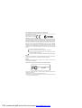
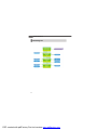
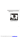
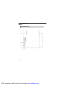
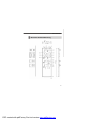
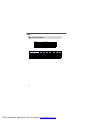
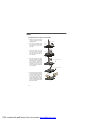
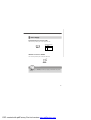
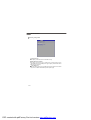
AM-690E
MS-9826 (V1.X) Mainboard
G52-98261X1
i
PDF created with pdfFactory Pro trial version www.pdffactory.com
Copyright Notice
Th e material in this d ocument is the in tellectual p rop erty of MICRO-STAR
INTERNATIONAL. We take every care in the preparation of this document, but no
guarantee is given as to the correctness of its contents. Our products are under
continual improvement and we reserve the right to make changes without notice.
Trademarks
All trademarks are the properties of their respective owners.
Intel® and Pentium® are registered trademarks of Intel Corporation.
AMD, Athlon™, Athlon™ XP, Thoroughbred™, and Duron™ are registered trademarks of AMD Corporation.
NVIDIA, the NVIDIA logo, DualNet, and nForce are registered trademarks or trademarks of NVIDIA Corporation in the United States and/or other countries.
PS/2 and OS ®/2 are registered trademarks of International Business Machines
Corporation.
Windows® 98/2000/NT/XP/Vista are registered trademarks of Microsoft Corporation.
Netware® is a registered trademark of Novell, Inc.
Award® is a registered trademark of Phoenix Technologies Ltd.
AMI® is a registered trademark of American Megatrends Inc.
Revision History
Revision
V1.0
Revision History
First release
Date
July 2008
Technical Support
If a problem arises with your system and no solution can be obtained from the user’s
manual, please contact your place of purchase or local distributor. Alternatively,
please try the following help resources for further guidance.
Visit th e MSI web site at http://global.msi.com.tw/index.php?
func=service for FAQ, technical guide, BIOS updates, driver updates, and
other information.
Contact our technical staff at http://ocss.msi.com.tw.
ii
PDF created with pdfFactory Pro trial version www.pdffactory.com
Safety Instructions
1.
Always read the safety instructions carefully.
2.
Keep this User’s Manual for future reference.
3.
Keep this equipment away from humidity.
4.
Lay this equipment on a reliable flat surface before setting it up.
5.
The openings on the enclosure are for air convection hence protects the equipment from overheating. DO NOT COVER THE OPENINGS.
6.
Make sure the voltage of the power source and adjust properly 110/220V before connecting the equipment to the power inlet.
7.
Place the power cord such a way that people can not step on it. Do not place
anything over the power cord.
8.
Always Unplug the Power Cord before inserting any add-on card or module.
9.
All cautions and warnings on the equipment should be noted.
10. Never pour any liquid into the opening that could damage or cause electrical
shock.
11. If any of the following situations arises, get the equipment checked by service
personnel:
The power cord or plug is damaged.
Liquid has penetrated into the equipment.
The equipment has been exposed to moisture.
The equipment does not work well or you can not get it work according to
User’s Manual.
The equipment has dropped and damaged.
The equipment has obvious sign of breakage.
12. DO NOT LEAVE THIS EQUIPMENT IN AN ENVIRONMENT UNCONDITIONED, STORAGE TEMPERATURE ABOVE 600 C (1400F), IT MAY DAMAGE THE EQUIPMENT.
CAUTION: Danger of explosion if battery is incorrectly replaced.
Replace only with the same or equivalent type recommended by the
manufacturer.
iii
PDF created with pdfFactory Pro trial version www.pdffactory.com
FCC-B Radio Frequency Interference Statement
Th is eq u ip men t h as been
tested and found to comply
with the limits for a Class B
digital device, pursuant to Part
15 of the FCC Rules. These limits are designed to provide reasonable protection
against harmful interference in a residential installation. This equipment generates,
uses and can radiate radio frequency energy and, if not installed and used in accordance with the instructions, may cause harmful interference to radio communications.
However, there is no guarantee that interference will not occur in a particular
installation. If this equipment does cause harmful interference to radio or television
reception, which can be determined by turning the equipment off and on, the user is
encouraged to try to correct the interference by one or more of the measures listed
bel ow.
Reorient or relocate the receiving antenna.
Increase the separation between the equipment and receiver.
Connect the equipment into an outlet on a circuit different from that to
which the receiver is connected.
Consult the dealer or an experienced radio/television technician for help.
Notice 1
The changes or modifications not expressly approved by the party responsible for
compliance could void the user’s authority to operate the equipment.
Notice 2
Shielded interface cables and A.C. power cord, if any, must be used in order to
comply with the emission limits.
VOIR LA NOTICE D’INSTALLATION AVANT DE RACCORDER AU RESEAU.
Micro-Star International
MS-9826
This device complies with Part 15 of the FCC Rules. Operation is subject to the
following two conditions:
(1) this device may not cause harmful interference, and
(2) this device must accept any interference received, including interference that
may cause undesired operation.
iv
PDF created with pdfFactory Pro trial version www.pdffactory.com
WEEE (Waste Electrical and Electronic Equipment) Statement
v
PDF created with pdfFactory Pro trial version www.pdffactory.com
vi
PDF created with pdfFactory Pro trial version www.pdffactory.com
vii
PDF created with pdfFactory Pro trial version www.pdffactory.com
CONTENTS
Copyright Notice .................................................................................................... ii
Trademarks ............................................................................................................ ii
Revision History .................................................................................................... ii
Technical Support ................................................................................................. ii
Safety Instructions ................................................................................................ iii
FCC-B Radio Frequency Interference Statement ................................................... iv
WEEE (Waste Electrical and Electronic Equipment) Statement ................................ v
Chapter 1 Product Overview .......................................................................... 1-1
Mainboard Specifications ............................................................................. 1-2
Block Diagram ............................................................................................... 1-4
Mainboard Layout ........................................................................................ 1-5
Board Dimension .......................................................................................... 1-6
Back Panel & I/O Shield Drawing .................................................................. 1-7
Power Consumption .................................................................................... 1-8
Safety Compliance & MTBF .......................................................................... 1-9
Chapter 2 Hardware Setup ............................................................................. 2-1
Quick Components Guide ............................................................................. 2-2
CPU (Central Processing Unit) ...................................................................... 2-3
Memory ....................................................................................................... 2-6
Power Supply .............................................................................................. 2-7
Back Panel ................................................................................................... 2-8
Connector .................................................................................................... 2-9
Jumper ...................................................................................................... 2-13
Slot ............................................................................................................ 2-14
Chapter 3 BIOS Setup ...................................................................................... 3-1
Entering Setup ............................................................................................. 3-2
The Menu Bar .............................................................................................. 3-4
Main ............................................................................................................. 3-5
Advanced .................................................................................................... 3-6
PCIPnP ....................................................................................................... 3-16
Boot ........................................................................................................... 3-17
Security ..................................................................................................... 3-19
Chipset ...................................................................................................... 3-20
Power ........................................................................................................ 3-24
Exit ............................................................................................................ 3-25
Chapter 4 System Resources ....................................................................... 4-1
Watch Dog Timer Setting .............................................................................. 4-2
AMI POST Code ........................................................................................... 4-3
Resource List .............................................................................................. 4-6
viii
PDF created with pdfFactory Pro trial version www.pdffactory.com
Product Overview
Chapter 1
Product Overview
Thank you for choosing the AM-690E (MS-9826 v1.X)
Mini ITX mainboard from MSI.
Based on the innovative AMD® RS690E & SB600 controllers for optimal system efficiency, the AM-690E accommodates the latest AMD® Sempron, Athlon 64/64
X2 (Dual Core) processors in Socket AM2 and supports two DDR2 533/667/800 DIMM slots to provide the
maximum of 4GB memory capacity.
In the entry-level and mid-range market segment, the
AM-690E can provide a high-performance solution for
today’s front-end and general purpose workstation, as
well as in the future.
1-1
PDF created with pdfFactory Pro trial version www.pdffactory.com
MS-9826 Mainboard
Mainboard Specifications
Processor
- AMD Sempron, Athlon 64/64 X2 (Dual Core) processor in Socket AM2
- 4-pin CPU fan pinheader with Smart Fan Speed Control
FSB
- Hyper Transport supporting speed up to 1 GHz (2000MT/s)
Chipset
- Northbridge: AMD RS690E
- Southbridge: AMD SB600
M e mo ry
- Unbuffered ECC DDR2 533/667/800 SDRAM (4GB Max)
- 2 DDR2 DIMM slots (240pin / 1.8V)
LAN
- Supports Gigabit Ethernet by Marvell 88E8056
IDE
- 1 IDE port by AMD SB600
- Supports Ultra DMA 66/100/133 mode
- Supports PIO, Bus Master operation mode
SATA
- 2 SATA II ports by AMD SB600
- Supports storage and data transfers at up to 3Gb/s
Slot
- 1 32-bit/33MHz PCI slot
Connectors
Back Panel
- 2 RJ-45 Gigabit LAN jacks
- 4 USB 2.0 ports
- 1 serial port
- 1 D-Sub VGA connector
- 1 PS/2 keyboard port
- 1 PS/2 mouse port
1-2
PDF created with pdfFactory Pro trial version www.pdffactory.com
Product Overview
Onboard Connectors
- 1 SPI Flash ROM connector (for debugging)
- 1 chassis intrusion switch connector
- 1 SMBus connector
- 1 front panel connector
- 1 CPU fan connector
- 1 system fan connector
- 2 SATA connectors
Form Factor
- M ini ITX: 170mm x 170mm
Mounting
- 4 mounting ho les
Environmental
Storage Temperature
- Temperature: -20 oC ~ 80 o C
- Humidity: 0% RH ~ 95% RH
Operation Temperature
- Temperature: 0 oC ~ 60 o C
- Humidity: 0% RH ~ 85% RH
1-3
PDF created with pdfFactory Pro trial version www.pdffactory.com
MS-9826 Mainboard
Block Diagram
1-4
PDF created with pdfFactory Pro trial version www.pdffactory.com
Product Overview
Mainboard Layout
DIMM1
DIMM2
JP W 1
To p: LA N Jack
B ot tom: U SB Po rts
To p: LA N Jack
B ot tom: U SB Po rts
JS P I1
I DE B1
S ATA 2
AMD
SB 600
JC ASE1
Top: Mo use
B ot tom: Key boar d
A MD
RS 69 0E
JBAT1
BATT
+
Top:
S erial Por t
B ot tom:
V GA Po rt
S ATA 1
J1
H DP WR1
J FP1 CPUFAN 1 SYSFAN1
PCI1
AM-690E (MS-9826 v1.X) Mini ITX Mainboard
1-5
PDF created with pdfFactory Pro trial version www.pdffactory.com
MS-9826 Mainboard
Board Dimension
1-6
PDF created with pdfFactory Pro trial version www.pdffactory.com
Product Overview
Back Panel & I/O Shield Drawing
1-7
PDF created with pdfFactory Pro trial version www.pdffactory.com
MS-9826 Mainboard
Power Consumption
Component
CPU
DDR2
HDD
ODD
Description
AMD Athlon™ 64 x2 Dual Core 2G
1024MB DDR2 533 *2
Maxtor 80G
NEC DVD-Multi Record ND-4550A
12Vp
AMD ThermNow! Utility
12V
4.2
5V
0.81
3.3V
3.03
5VSB
1.08
0.032
-12V
W
0.028
79.33
Particle Fuly + VCD + Xcopy
3.07
1.01
4.66
1.07
0.039
0.02
76.226
3Dmark 2005
2.81
0.84
4.27
1.06
0.04
0.042
69.352
Idle
0.82
0.81
3.09
1.17
0.024
0.017
39.195
S3
0
0
0
0
0.512
0
2.56
1-8
PDF created with pdfFactory Pro trial version www.pdffactory.com
Product Overview
Safety Compliance & MTBF
Standard number
Certification
Title of standard
EN 55022:1998+A1:2000+A2:2003 Class B Product family standard
Limits for harmonic current
EN 6100-3-2:2000 Class D
emission
RFI
Limitation of voltage
EN 6100-3-3:1995+A1:2001
fluctuation and flicker in lowvoltage supply system
Immunity EN 55024:1998+A1:2001+A2:2003
Product family standard
CE
BSMI
CNS 13438 乙類(1997年版)
C-Tick
AS/NZS CISPR 22:2004
FCC CFR Title 47 Part 15 Subpart B: 2005 Class B
FCC
CISPR 22: 2005
VCCI
VCCI V-3:2004, Class B
VCCI V-4:2004, Class B
MTBF - Reliability Prediction
Calculation Model
Telcordia Issue 1
Operation
Temperature (°C)
40
Operation
Environment
Duty Cycle MTBF (hr.)
GB, GC - Ground
Benign,
4,892.341404
Controlled
204,401
1-9
PDF created with pdfFactory Pro trial version www.pdffactory.com
PDF created with pdfFactory Pro trial version www.pdffactory.com
Hardware Setup
Chapter 2
Hardware Setup
This chapter provides you with the information about
hardware setup procedures. While doing the installation,
be careful in holding the components and follow the
installation procedures. For some components, if you
install in the wrong orientation, the components will not
work properly.
Use a grounded wrist strap before handling computer
comp onen ts. Static el ectricity may damag e th e
components.
2-1
PDF created with pdfFactory Pro trial version www.pdffactory.com
MS-9826 Mainboard
Quick Components Guide
DIMM Slots, p.2-6
CPU, p.2-3
JPW1, p.2-7
SATA1~2, p.2-10
Back Panel
I/O, p.2-8
J1, p.2-12
HDPWR1,
p.2-7
IDEB1, p.2-9
JCASE1, p.2-9
SYSFAN1, p.2-11
JSPI1, p.2-12
PCI Slot, p.2-14
CPUFAN1, p.2-11
JFP1, p.2-11
JBAT1, p.2-13
2-2
PDF created with pdfFactory Pro trial version www.pdffactory.com
Hardware Setup
CPU (Central Processing Unit)
When you are installing the CPU, make sure the CPU has a heat sink and a
cooling fan attached on the top to prevent overheating. If you do not have the
heat sink and cooling fan, contact your dealer to purchase and install them before
turning on the computer.
Important
1. Overheating will seriously damage the CPU and system. Always make
sure the cooling fan can work properly to protect the CPU from overheating.
2. Make sure that you apply an even layer of heat sink paste (or thermal tape)
between the CPU and the heatsink to enhance heat dissipation.
3. While replacing the CPU, always turn off the power supply or unplug the
power supply’s power cord from the grounded outlet first to ensure the
safety of CPU.
2-3
PDF created with pdfFactory Pro trial version www.pdffactory.com
MS-9826 Mainboard
CPU Installation Procedures for Socket AM2
1. Please turn off the power and
unplug the power cord before
installing the CPU.
2. Pull the lever sideways away
from the socket. Make sure to
raise the lever up to a 90-degree angle.
3. Look for the gold arrow of the
CPU. The gold arrow shou ld
point as shown in the picture.
The CPU can only fit in the correct orientation.
4. If the CPU is correctly installed,
the pins should be completely
embedded into the socket and
can not be seen. Please note
that any violation of the correct
instal l ation p roced u res may
cause permanent damages to
your mainboard.
O pe n L eve r
Sli din g
Pl ate
90 de gr ee
Go ld arrow
C or rect CP U pla cem en t
G o ld ar row
O
Inc orre c t C PU p lac em ent
G ol d ar row
5. Press the CPU down firmly into
the socket and close the lever.
As the CPU is likely to move while
the lever is bein g closed, always close the lever with your
fingers pressing tightly on top of
the CPU to make sure the CPU is
properly and completely embedded into the socket.
Pre ss d ow n
th e C PU
2-4
PDF created with pdfFactory Pro trial version www.pdffactory.com
C los e
Le v er
Hardware Setup
Installing AMD Socket AM2 CPU Cooler Set
When you are installing the CPU, make sure the CPU has a heat sink and a
cooling fan attached on the top to prevent overheating. If you do not have the
heat sink and cooling fan, contact your dealer to purchase and install them before
turning on the computer.
Important
Mainboard photos shown in this section are for demonstration of the cooler
installation for Socket AM2 CPUs only. The appearance of your mainboard
may vary depending on the model you purchase.
1. Position the cooling set onto the retention mechanism. Hook one end
of the clip to hook first.
2. Then press down the other end of
the clip to fasten the cooling set on
the top of the retention mechanism.
Locate the Fix Lever and lift it up.
Fixed Lever
3. Fasten down the lever.
4. Attach the CPU Fan cable to the CPU
fan connector on the mainboard.
2-5
PDF created with pdfFactory Pro trial version www.pdffactory.com
MS-9826 Mainboard
Memory
These DIMM slots are intended for system memory modules.
DDR2
240-pin, 1.8V
64x2=128 pin
56x2=112 pin
Installing Memory Modules
1. Locate the DIMM slots on the mainboard. Flip open the retaining clip at each side
of the DIMM slot.
2. Align the notch on the DIMM with the key on the slot. Insert the DIMM vertically into
the DIMM slot. Then push it in until the golden finger on the DIMM is deeply inserted
in the DIMM slot. The retaining clip at each side of the DIMM slot will automatically
close if the DIMM is properly seated.
Important
You can barely see the golden finger if the DIMM is properly inserted in the
DIMM slot.
3. Manually check if the DIMM has been locked in place by the retaining clips at the
sides.
4. Follow the same procedures to install more DIMMs if necessary.
Volt
Notch
2-6
PDF created with pdfFactory Pro trial version www.pdffactory.com
Hardware Setup
Power Supply
System/CPU Power Connector: JPW1
This connector provides power to the system and CPU.
JPW 1 Pin Definition
1
3
PIN
SIGNAL
2
4
1
2
3
4
GND
GND
12V
12V
JPW1
HDD Power Connector: HDPWR1
The connector provides power to the hard disk drives.
+1 2V
GND
GND
VCC5
HDPWR1
Important
Power supply of 120watts (and above) is highly recommended for system
stability.
2-7
PDF created with pdfFactory Pro trial version www.pdffactory.com
MS-9826 Mainboard
Back Panel
LAN
USB Ports
Serial Port
LAN
USB Ports
VGA Port
M ouse
Keyboard
Mouse/Keyboard
The standard PS/2® mouse/keyboard DIN connector is for a PS/2® mouse/keyboard.
Serial Port
The serial port is a 16550A high speed communications port that sends/ receives 16
bytes FIFOs. You can attach a serial mouse or other serial devices directly to the
connector.
VGA Port
The DB15-pin female connector is provided for monitor.
USB Port
The USB (Universal Serial Bus) port is for attaching USB devices such as keyboard,
mouse, or other USB-compatible devices.
LAN
The standard RJ-45 LAN jack is for connection to the Local Area Network (LAN).
You can connect a network cable to it.
LED
Color
LED State
Off
Left
Green
On (steady state)
Activity Indicator
Link Indicator
Condition
LAN link is not established.
LAN link is established.
On (brighter & pulsing) The computer is communicating with another computer on the LAN.
Green
Off
10 Mbit/sec data rate is selected.
On
100 Mbit/sec data rate is selected.
Orange
On
1000 Mbit/sec data rate is selected.
Right
2-8
PDF created with pdfFactory Pro trial version www.pdffactory.com
Hardware Setup
Connector
Chassis Intrusion Connector: JCASE1
This connector connects to the chassis intrusion switch cable. If the chassis is
opened, the chassis intrusion mechanism will be activated. The system will record
this status and show a warning message on the screen. To clear the warning, you
must enter the BIOS utility and clear the record.
CINTRU
GND
1
2
JCASE1
IDE Connector: IDEB1
This connector supports IDE hard disk drives, optical disk drives and other IDE devices.
IDEB1
Important
If you install two IDE devices on the same cable, you must configure the drives
separately to master / slave mode by setting jumpers. Refer to IDE device’s
documentation supplied by the vendors for jumper setting instructions.
2-9
PDF created with pdfFactory Pro trial version www.pdffactory.com
MS-9826 Mainboard
Serial ATA II Connector: SATA1, SATA2
SATA1
SATA2
This connector is a high-speed Serial ATA II interface port. Each connector can
connect to one Serial ATA II device.
Important
Please do not fold the Serial ATA cable into 90-degree angle. Otherwise,
data loss may occur during transmission.
2-10
PDF created with pdfFactory Pro trial version www.pdffactory.com
Hardware Setup
Fan Power Connectors: CPUFAN1, SYSFAN1
GND
+1 2V
SENSOR
CONTROL
GND
+1 2V
SENSOR
The fan power connectors support system cooling fan with +12V. When connecting
the wire to the connectors, always note that the red wire is the positive and should
be connected to the +12V; the black wire is Ground and should be connected to GND.
If the mainboard has a System Hardware Monitor chipset onboard, you must use a
specially designed fan with speed sensor to take advantage of the CPU fan control.
CPUFAN1
SYSFAN1
Important
Please refer to the recommended CPU fans at AMD® official website or consult
the vendors for proper CPU cooling fan.
Front Panel Connector: JFP1
The mainboard provides one front panel connector for electrical connection to the
front panel switches and LEDs. The JFP1 is compliant with Intel® Front Panel I/O
Connectivity Design Guide.
+
-
Power Power
LED Switch
10
9
2
1
+
+
JFP1
HDD Reset
LED Switch
JFP1 Pin Definition
PIN
SIGNAL
DESCRIPTION
1
2
3
4
5
6
7
8
9
HD_LED +
FP PWR/SLP
HD_LED FP PWR/SLP
RST_SW PWR_SW +
RST_SW +
PWR_SW RSVD_DNU
Hard disk LED pull-up
MSG LED pull-up
Hard disk active LED
MSG LED pull-up
Reset Switch low reference pull-down to GND
Power Switch high reference pull-up
Reset Switch high reference pull-up
Power Switch low reference pull-down to GND
Reserved. Do not use.
2-11
PDF created with pdfFactory Pro trial version www.pdffactory.com
MS-9826 Mainboard
I2C Bus Connector: J1
The mainboard provides one I2C (also known as I2C) Bus connector for users to
connect System Management Bus (SMBus) interface.
Pin Definition
4
1
J1
Pin
Signal
1
VCC5F
2
SMBCLK
3
GND
4
SMBDATA
SPI Flash ROM Connector: JSPI1
This connector is used to flash SPI flash ROM.
JSPI1
2
1
10
9
Pin Definition
Pin
Description
Pin
Description
1
VCC3_SB
2
VCC3_SB
3
SPI_MISO_F
4
SPI_MOSI_F
5
SPI_CS0_F#
6
SPI_CLK_F
7
GND
8
GND
9
SPI_HOLD#
10
NC
2-12
PDF created with pdfFactory Pro trial version www.pdffactory.com
Hardware Setup
Jumper
Clear CMOS Jumper: JBAT1
There is a CMOS RAM onboard that has a power supply from external battery to keep
the data of system configuration. With the CMOS RAM, the system can automatically
boot OS every time it is turned on. If you want to clear the system configuration, set
this jumper to clear data.
1
1
1
3
JBAT1
Keep Data
3
Clear Data
Important
You can clear CMOS by shorting 1-2 pin while the system is off. Then return
to 2-3 pin position. Avoid clearing the CMOS while the system is on; it will
damage the mainboard.
2-13
PDF created with pdfFactory Pro trial version www.pdffactory.com
MS-9826 Mainboard
Slot
PCI (Peripheral Component Interconnect) Slot
The PCI slot supports LAN card, SCSI card, USB card, and other add-on cards that
comply with PCI specifications.
32-bit PCI Slot
PCI Interrupt Request Routing
The IRQ, acronym of interrupt request line and pronounced I-R-Q, are hardware lines
over which devices can send interrupt signals to the microprocessor. The PCI IRQ
pins are typically connected to the PCI bus pins as follows:
DEVICE
IDSEL
INT A
INTB
INTC
INTD
REQ# / GNT#
32-bit PCI Slot
AD18
E
F
G
H
REQ#0 / GNT#0
Important
When adding or removing expansion cards, make sure that you unplug the
power supply first. Meanwhile, read the documentation for the expansion card
to configure any necessary hardware or software settings for the expansion
card, such as jumpers, switches or BIOS configuration.
2-14
PDF created with pdfFactory Pro trial version www.pdffactory.com
BIOS Setup
Chapter 3
BIOS Setup
This chapter provides information on the BIOS Setup
program and allows you to configure the system for
optimum use.
You may need to run the Setup program when:
² An error message appears on the screen during the
system booting up, and requests you to run SETUP.
² You want to change the default settings for customized features.
3-1
PDF created with pdfFactory Pro trial version www.pdffactory.com
MS-9826 Mainboard
Entering Setup
Power on the computer and the system will start POST (Power On Self Test) process.
When the message below appears on the screen, press <Del> key to enter Setup.
Press Del to enter SETUP
If the message disappears before you respond and you still wish to enter Setup,
restart the system by turning it OFF and On or pressing the RESET button. You may
also restart the system by simultaneously pressing <Ctrl>, <Alt>, and <Delete> keys.
Important
1. The items under each BIOS category described in this chapter are under
continuous update for better system performance. Therefore, the description may be slightly different from the latest BIOS and should be held for
reference only.
2. Upon boot-up, the 1st line appearing after the memory count is the BIOS
version. It is usually in the format:
A9826KMS V1.0 071608 where:
1st digit refers to BIOS maker as A = AMI, W = AWARD, and P =
PHOENIX.
2nd - 5th digit refers to the model number.
6th digit refers to the chipset as I = Intel, N = nVidia, A = ATi , K=AMD
and V = VIA.
7th - 8th digit refers to the customer as MS = all standard customers.
V1.0 refers to the BIOS version.
071608 refers to the date this BIOS was released.
3-2
PDF created with pdfFactory Pro trial version www.pdffactory.com
BIOS Setup
Control Keys
<↑>
<↓>
<←>
<→>
<Enter>
<Esc>
<+/PU>
<-/PD>
<F6>
<F7>
<F10>
Move to the previous item
Move to the next item
Move to the item in the left hand
Move to the item in the right hand
Select the item
Jumps to the Exit menu or returns to the main menu from a
submenu
Increase the numeric value or make changes
Decrease the numeric value or make changes
Load Optimized Defaults
Load Fail-Safe Defaults
Save all the CMOS changes and exit
Getting Help
After entering the Setup menu, the first menu you will see is the Main Menu.
Main Menu
The main menu lists the setup functions you can make changes to. You can use the
arrow keys ( ↑↓ ) to select the item. The on-line description of the highlighted setup
function is displayed at the bottom of the screen.
Sub-Menu
If you find a right pointer symbol (as shown in the right view)
appears to the left of certain fields that means a sub-menu
can be launched from this field. A sub-menu contains additional options for a field parameter. You can use arrow keys ( ↑↓ ) to highlight the
field and press <Enter> to call up the sub-menu. Then you can use the control keys
to enter values and move from field to field within a sub-menu. If you want to return
to the main menu, just press the <Esc >.
General Help <F1>
The BIOS setup program provides a General Help screen. You can call up this screen
from any menu by simply pressing <F1>. The Help screen lists the appropriate keys
to use and the possible selections for the highlighted item. Press <Esc> to exit the
Help screen.
3-3
PDF created with pdfFactory Pro trial version www.pdffactory.com
MS-9826 Mainboard
The Menu Bar
Main
Use this menu for basic system configurations, such as time, date etc.
Advanced
Use this menu to set up the items of special enhanced features.
PCIPnP
This entry appears if your system supports PnP/PCI.
Boot
Use this menu to specify the priority of boot devices.
Security
Use this menu to set supervisor and user passwords.
Chipset
This menu controls the advanced features of the onboard Northbridge and Southbridge.
Power
Use this menu to specify your settings for power management.
Exit
This menu allows you to load the BIOS default values or factory default settings into
the BIOS and exit the BIOS setup utility with or without changes.
3-4
PDF created with pdfFactory Pro trial version www.pdffactory.com
BIOS Setup
Main
AMI BIOS, Processor, System Memory
These items show the firmware and hardware specifications of your system. Read
only.
System Time
The time format is <Hour> <Minute> <Second>.
System Date
The date format is <Day>, <Month> <Date> <Year>.
3-5
PDF created with pdfFactory Pro trial version www.pdffactory.com
MS-9826 Mainboard
Advanced
CPU Configuration
These items show the advanced specifications of your CPU. Read only.
3-6
PDF created with pdfFactory Pro trial version www.pdffactory.com
BIOS Setup
Microcode Update
The Microcode Update device is an interface between the operating system
and the CPU. Downloading a microcode reliability update helps the processor
work more reliably. The update is volatile. If it introduces any problems, a simple
reboot will revert back to the original microcode.
IDE Configuration
OnBoard PCI IDE Controller
This setting specifies the operation mode of the onboard IDE controller.
Primary/Third/Fourth IDE Master/Slave
3-7
PDF created with pdfFactory Pro trial version www.pdffactory.com
MS-9826 Mainboard
[Type]
Press PgUp/<+> or PgDn/<-> to select
[Manual], [None] or [Auto] type. Note that the
specifications of your drive must match with
the drive table. The hard disk will not work
properly if you enter improper information for
this category. If your hard disk drive type is
not matched or listed, you can use [Manual] to
define your own drive type manually.
[LBA/Large Mode]
Enabling LBA causes Logical Block Addressing to be used in place of Cylinders,
Heads and Sectors
[Block(Multi-Sector Transfer)] Any selection except Disabled determines
the number of sectors transferred per block
[PIO Mode]
Indicates the type of PIO (Programmed Input/
Output)
[DMA Mode]
Indicates the type of Ultra DMA
[S.M.A.R.T.]
This allows you to activate the S.M.A.R.T.
(Self-Monitoring Analysis & Reporting
Technology) capability for the hard disks. S.
M.A.R.T is a utility that monitors your disk sta
tus to predict hard disk failure. This gives you
an opportunity to move data from a hard disk
that is going to fail to a safe place before the
hard disk becomes offline.
[32 Bit Data Transfer]
Enables 32-bit communication between
CPU and IDE device
Super IO Configuration
3-8
PDF created with pdfFactory Pro trial version www.pdffactory.com
BIOS Setup
Serial Port1 Address
Select an address and a corresponding interrupt for the serial port.
Hardware Health Configuration
CPU Temperature, System Temperature, Vcore, AVCC, 3VCC, +5VIN,
+12VIN, VSB, VBAT
These items display the current status of all of the monitored hardware devices/components such as CPU voltage, temperatures and all fans’ speeds.
Smart Fan Configuration
3-9
PDF created with pdfFactory Pro trial version www.pdffactory.com
MS-9826 Mainboard
CPU FAN Type
This setting specifies the pin numbers of the CPU fan power connector.
CPUFAN Mode Setting
This setting controls the Smart Fan feature. Smart Fan is an excellent feature
which will adjust the CPU fan speed automatically depending on the current
CPU temperature to prevent your CPU from overheating.
CPUFAN PWM Control
This setting allows users to control the fan speed by changing the duty
cycle of the fan PWM (Pulse-Width Modulation) output.
ACPI Settings
3-10
PDF created with pdfFactory Pro trial version www.pdffactory.com
BIOS Setup
General ACPI Configuration
C1E Support
When the C1E Support (Enhanced Halt Powerdown State) is enabled, the
processor will transition to a lower core to bus ratio and lower voltage ID
driven by the processor to the voltage regulator before entering Halt
Powerdown State (C1). Not al l porcessors su p port Enh anced Hal t
Powerdown State (C1E).
Advanced ACPI Configuration
ACPI Version Features
This setting allows you to select the ACPI version.
3-11
PDF created with pdfFactory Pro trial version www.pdffactory.com
MS-9826 Mainboard
Event Log Configuration
View Event Log
Press [Enter] to view the contents of the DMI event log.
Mark All Events As Read
Press [Enter] and a screen pops up, asking users to confirm whether or not to
clear all DMI event logs immediately. Press [Y] and [Enter], the BIOS will clear all
DMI event logs right away.
Clear Event Log
When this setting is set to [Yes], the DMI event log will be cleared at next POST
stage. Then, the BIOS will automatically set this option to [No].
3-12
PDF created with pdfFactory Pro trial version www.pdffactory.com
BIOS Setup
MPS Configuration
MPS Revision
This field allows you to select which MPS (Multi-Processor Specification) version to be used for the operating system. You need to select the MPS version
supported by your operating system. To find out which version to use, consult
the vendor of your operating system.
3-13
PDF created with pdfFactory Pro trial version www.pdffactory.com
MS-9826 Mainboard
Smbios Configuration
Smbios Smi Support
SMBIOS SMI wrapper supports the PnP function: 50h-54h.
USB Configuration
Legacy USB Support
Set to [Enabled] if your need to use any USB device in the operating system that
does not support or have any USB driver installed, such as DOS and SCO Unix.
3-14
PDF created with pdfFactory Pro trial version www.pdffactory.com
BIOS Setup
Set to [Disabled] only if you want to use any USB device other than the USB
mouse.
USB 2.0 Controller mode
Use this field to select the USB 2.0 mode.
USB Mass Storage Device Configuration
Emulation Type
This setting enables you to set the type of device you want the USB mass
storage device to emulate.
3-15
PDF created with pdfFactory Pro trial version www.pdffactory.com
MS-9826 Mainboard
PCIPnP
Clear NVRAM
The ESCD (Extended System Configuration Data) NVRAM (Non-volatile Random Access Memory) is where the BIOS stores resource information for both PNP and nonPNP devices in a bit string format. Whent the item is set to Yes, the system will reset
ESCD NVRAM right after the system is booted up and then set the setting of the item
back to No automatically.
Plug and Play O/S
When set to [Yes], BIOS will only initialize the PnP cards used for booting (VGA, IDE,
SCSI). The rest of the cards will be initialized by the PnP operating system like
Windows 98, 2000 or ME. When set to [No], BIOS will initialize all the PnP cards.
Select Yes if the operating system is Plug & Play.
PCI Latency Timer
This item controls how long each PCI device can hold the bus before another takes
over. When set to higher values, every PCI device can conduct transactions for a
longer time and thus improve the effective PCI bandwidth. For better PCI performance,
you should set the item to higher values.
3-16
PDF created with pdfFactory Pro trial version www.pdffactory.com
BIOS Setup
Boot
Boot Settings Configuration
3-17
PDF created with pdfFactory Pro trial version www.pdffactory.com
MS-9826 Mainboard
Quick Boot
Enabling this setting will cause the BIOS power-on self test routine to skip some
of its tests during bootup for faster system boot.
Quiet Boot
This BIOS feature determines if the BIOS should hide the normal POST messages with the motherboard or system manufacturer's full-screen logo.
When it is enabled, the BIOS will display the full-screen logo during the boot-up
sequence, hiding normal POST messages.
When it is disabled, the BIOS will display the normal POST messages, instead of
the full-screen logo.
Please note that enabling this BIOS feature often adds 2-3 seconds of delay to
the booting sequence. This delay ensures that the logo is displayed for a
sufficient amount of time. Therefore, it is recommended that you disable this
BIOS feature for a faster boot-up time.
AddOn ROM Display Mode
This item is used to determine the display mode when an optional ROM is
initialized during POST. When set to [Force BIOS], the display mode used by AMI
BIOS is used. Select [Keep Current] if you want to use the display mode of
optional ROM.
Bootup Num-Lock
This setting is to set the Num Lock status when the system is powered on.
Setting to [On] will turn on the Num Lock key when the system is powered on.
Setting to [Off] will allow users to use the arrow keys on the numeric keypad.
PS/2 Mouse Support
Select [Enabled] if you need to use a PS/2-interfaced mouse in the operating
system.
Boot Device Priority, Removable Drives
The items allow you to set the sequence of boot devices/removable drives. First
press <Enter> to enter the sub-menu. Then you may use the arrow keys ( ↑↓ ) to
select the desired device, then press <+>, <-> or <PageUp>, <PageDown> key to
move it up/down in the priority list.
3-18
PDF created with pdfFactory Pro trial version www.pdffactory.com
BIOS Setup
Security
Supervisor Password / Change Supervisor Password
Supervisor Password controls access to the BIOS Setup utility. These settings allow
you to set or change the supervisor password.
User Password / Change User Password
User Password controls access to the system at boot. These settings allow you to
set or change the user password.
Boot Sector Virus Protection
This function protects the BIOS from accidental corruption by unauthorized users or
computer viruses. When enabled, the BIOS’ data cannot be changed when attempting to update the BIOS with a Flash utility. To successfully update the BIOS, you’ll
need to disable this Flash BIOS Protection function.
You should enable this function at all times. The only time when you need to disable
it is when you want to update the BIOS. After updating the BIOS, you should immediately re-enable it to protect it against viruses.
Chassis Intrusion
The field enables or disables the feature of recording the chassis intrusion status
and issuing a warning message if the chassis is once opened. To clear the warning
message, set the field to [Reset]. The setting of the field will automatically return to
[Enabled] later.
3-19
PDF created with pdfFactory Pro trial version www.pdffactory.com
MS-9826 Mainboard
Chipset
NorthBridge Configuration
These items show the DRAM timing. Read only.
3-20
PDF created with pdfFactory Pro trial version www.pdffactory.com
BIOS Setup
ECC Configuration
DRAM ECC Enable
This setting enables/disables ECC (Error Correction Code) checking, a method
of checking the integrity of data in DRAM. ECC provides more elaborate error
detection than parity; ECC can detect multiple-bit errors and can locate and
correct single-bit errors.
4-Bit ECC Mode
This setting enables/disables the 4-bit ECC mode.
DRAM Scrub Redirect
This setting enables/disables ECC Scrubber to correct errors detected in
DRAM during normal CPU requests (foreground scrubbing).
DRAM BG Scrub
The setting enables/disables DRAM background scrubbing.
L2 Cache BG Scrub
The L2 ECC Scrub option controls the time allotted for the L2 memory cache
to be corrected when in an idle state.
Data Cache BG Scrub
The Data Cache ECC Scrub option controls the time allotted for the L1 memory
cache to be corrected when in an idle state.
3-21
PDF created with pdfFactory Pro trial version www.pdffactory.com
MS-9826 Mainboard
South Bridge Configuration
USB 1.1 OCHI Controllers, USB 2.0 EHCI Controller
This settings allow you to enable/disable the onboard USB1.1/ 2.0 controller.
OnChip SATA Channel
This item is used to enable/disable the onboard SATA channel.
OnChip SATA Type
This setting specifies the operation mode of the SATA drives.
3-22
PDF created with pdfFactory Pro trial version www.pdffactory.com
BIOS Setup
Onboard Peripherals Configuration
Spread Spectrum
When the motherboard’s clock generator pulses, the extreme values (spikes)
of the pulses create EMI (Electromagnetic Interference). The Spread Spectrum
function reduces the EMI generated by modulating the pulses so that the spikes
of the pulses are reduced to flatter curves.
Important
1. If you do not have any EMI problem, leave the setting at [Disabled] for
optimal system stability and performance. But if you are plagued by EMI,
select the value of Spread Spectrum for EMI reduction.
2. The greater the Spread Spectrum value is, the greater the EMI is reduced,
and the system will become less stable. For the most suitable Spread
Spectrum value, please consult your local EMI regulation.
3. Remember to disable Spread Spectrum if you are overclocking because
even a slight jitter can introduce a temporary boost in clock speed which
may just cause your overclocked processor to lock up.
Onboard LAN Boot ROM
The setting enables/disables the initialization of the onboard LAN Boot ROM
during bootup. Selecting [Disabled] will speed up the boot process.
3-23
PDF created with pdfFactory Pro trial version www.pdffactory.com
MS-9826 Mainboard
Power
Power M anagement/APM
Setting to [Enabled] will activate an Adcanced Power Management (APM) device to
enhance Max Saving mode and stop CPU internal clock.
Restore on AC Power Loss
This setting specifies whether your system will reboot after a power failure or
interrupt occurs. Available settings are:
[Power Off]
Leaves the computer in the power off state.
[Power On]
Leaves the computer in the power on state.
[Last State]
Restores the system to the previous status before power
failure or interrupt occurred.
RTC Resume
When [Enabled], your can set the date and time at which the RTC (real-time clock)
alarm awakens the system from Suspend mode.
Watch Dog Function
This setting enables/disables the Watch Dog Timer.
Watch Dog Timer
This setting specifies the Watch Dog Timer time out value.
3-24
PDF created with pdfFactory Pro trial version www.pdffactory.com
BIOS Setup
Exit
Save Changes and Exit
Save changes to CMOS and exit the Setup Utility.
Discard Changes and Exit
Abandon all changes and exit the Setup Utility.
Discard Changes
Abandon all changes and continue with the Setup Utility.
Load Optimal Defaults
Use this menu to load the default values set by the mainboard manufacturer specifically for optimal performance of the mainboard.
Load Failsafe Defaults
Use this menu to load the default values set by the BIOS vendor for stable system
performance.
3-25
PDF created with pdfFactory Pro trial version www.pdffactory.com
PDF created with pdfFactory Pro trial version www.pdffactory.com
System Resources
Chapter 4
System Resources
This chapter provides information on the following
system resources:
1. Watch Dog Timer Setting (p.4-2);
2. AMI POST Code (p.4-3);
3. Resource List (p.4-6).
4-1
PDF created with pdfFactory Pro trial version www.pdffactory.com
MS-9826 Mainboard
Watch Dog Timer Setting
Software code
SIO_IDX equ 4EH
SIO_DTA equ 4FH
Timer equ 10; reset after 10 seconds
1. Enter configuration mode
mov dx,SIO_IDX
mov al,87h
out dx,al
out dx,al
2. Set to LDN 08
mov dx,SIO_IDX
mov al,07h
out dx,al
mov dx,SIO_DTA
mov al,08h
out dx,al
3. Set WatchDog Timer
mov dx,SIO_IDX
mov al,0f6h
out dx,al
mov dx,SIO_DTA
mov al,Timer
out dx,al
4. Exit configuration mode
mov dx,SIO_IDX
mov al,0AAh
out dx,al
4-2
PDF created with pdfFactory Pro trial version www.pdffactory.com
System Resources
AMI POST Code
Bootblock Initialization Code Checkpoinits
The Bootblock initialization code sets up the chipset, memory and other components
before system memory is available. The following table describes the type of checkpoints that may occur during the bootblock initialization portion of the BIOS:
Bootblock Initialization Code Checkpoint list
Checkpoint
Before D1
D1
DO
D2
D3
D4
D5
D6
D7
D8
D9
DA
Description
Early chipset initialization is done. Early super I/O initialization is done
including RTC and keyboard controller. NMI is disabled.
Perform keyboard controller BAT test. Check if waking up from power
management suspend state. Save power-on CPUID value in scratch
CMOS.
Go to flat mode with 4GB limit and GA20 enabled. Verify the bootblock
checksum.
Disable CACHE before memory detection. Execute full memory sizing
module. Verify that flat mode is enabled.
If memory sizing module not executed, start memory refresh and do
memory sizing in Bootblock code. Do additional chipset initialization.
Re-enable CACHE. Verify that flat mode is enabled.
Test base 512KB memory. Adjust policies and cache first 8MB. Set stack.
Bootblock code is copied from ROM to lower system memory and control is
given to it. BIOS now executes out of RAM.
Both key sequence and OEM specific method is checked to determine if
BIOS recovery is forced. Main BIOS checksum is tested. If BIOS recovery
is necessary, control flows to checkpoint E0.
Restore CPUID value back into register. The Bootblock- Runtime interface
module is moved to system memory and control is given to it. Determine
whether to execute serial flash
The Runtime module is uncompressed into memory. CPUID information is
stored in memory.
Store the Uncompressed pointer for future use in PMM. Copying Main
BIOS into memory. Leaves all RAM below 1MB Read-Write including E000
and F000 shadow areas but closing SMRAM.
Restore CPUID value back into register. Give control to BIOS POST
(ExecutePOSTKernel.) See POST Code Checkpoint list for more
information.
4-3
PDF created with pdfFactory Pro trial version www.pdffactory.com
MS-9826 Mainboard
Post Code Checkpoints
The POST code checkpoints are the largest set of checkpoints during the BIOS
preboot process. The following table describes the type of checkpoints that may
occur during the POST portion of the BIOS:
Checkpoint
Description
03
Disable NMI, Parity, video for EGA, and DMA controllers. Initialize BIOS,
POST, Runtime data area. Also initialize BIOS modules on POST entry
and GPNV area. Initialized CMOS as mentioned in the Kernel Variable
“Wcomsflags”.
Check CMOS diagnostic byte to determine if battery power is OK and
CMOS checksum is OK. Verify CMOS checksum manually by reading
storage area. If the CMOS checksum is bad, update CMOS with
power-on default values and clear passwords. Initialize status register A.
Initializes data variables that are based on CMOS setup questions.
Initializes both the 8259 compatible PICs in the system.
Initializes the interrupt controlling hardware (generally PIC) and interrupt
vector table.
Do R/W test to CH-2 count reg. Initialize CH-0 as system timer. Install the
POSTINT1Ch handler. Enable IRQ-0 in PIC for system timer interrupt.
Traps INT1Ch vector to “POSTINT1ChHandlerBlock”.
Initializes the CPU. The BAT test is being done on KBC.
Program the keyboard controller command byte is being done after Auto
detection of KB/MS using AMI KB-5.
Initializes the 8042 compatible Key Board Controller.
Detects the presence of PS/2 mouse.
Detects the presence of keyboard in KBC port.
Testing and initialization of different Input Devices. Also, update the
Kernel Variables.
Traps the INT09h vector, so that the POST INT09h handler gets control
for IRQ1. Uncompress all available language, BIOS logo, and Silent logo
modules.
Early POST initialization of chipset registers.
Uncompress and initialize any platform specific BIOS modules.
Initialize System Management Interrupt.
Initializes different devices through DIM.
Initializes different devices. Detects and initializes the video adapter
installed in the system that have optional ROMs.
Initializes all the output devices.
Allocate memory for ADM module and uncompress it. Give control to
ADM module for initialization. Initialize language and font modules for
ADM. Activate ADM module.
Initializes the silent boot module. Set the window for displaying test
information.
Displaying sign-on message, CPU information, setup key message, and
any OEM specific information.
04
05
06
08
0A
0B
0C
0E
13
24
30
2A
2C
2E
31
33
37
4-4
PDF created with pdfFactory Pro trial version www.pdffactory.com
System Resources
Checkpoint
Description
38
39
3A
3B
Initializes different devices through DIM.
Initializes DMAC-1 & DMAC-2.
Initializes RTC date/time.
Test for total memory installed in the system. Also, Check for DEL or ESC
keys to limit memory test. Display total memory in the system.
Mid POST initialization of chipset registers.
Detect different devices (Parallel ports, serial ports, and coprocessor in
CPU…etc.)successfully installed in the system and update the BDA,
EBDA…etc.
Programming the memory hole or any kind of implementation that needs
an adjustment in system RAM size if needed.
Updates CMOS memory size from memory found in memory test.
Allocates memory for Extended BIOS Data Area from base memory.
Initializes NUM-LOCK status and programs the KBD typematic rate.
Initialize Int-13 and prepare for IPL detection.
Initializes IPL devices controlled by BIOS and option ROMs.
Initializes remaining option ROMs.
Generate and write contents of ESCD in NVRam.
Log errors encountered during POST.
Display errors to the user and gets the user response for error.
Execute BIOS setup if needed / requested.
Late POST initialization for chipset registers.
Program the peripheral parameters. Enable / Disable NMI as selected.
Late POST initialization of system management interrupt.
Check boot password if installed.
Clean-up work needed before booting to OS.
Takes care of runtime image preparation for different BIOS modules Fill the
free area in F000h segment with 0FFh.
Initializes the Microsoft IRQ Routing Table. Prepares the runtime language
module. Disables the system configuration display if needed.
Initialize runtime language module.
Displays the system configuration screen if enabled. Initialize the CPU’s
before boot, which includes the programming of the MTRR’s.
Prepare CPU for OS boot including final MTRR values.
Wait for user input at config display if needed.
Uninstall POST INT1Ch vector and INT09h vector. Deinitializes the ADM
module.
Prepare BBS for 19 boot.
End of POST initialization of chipset registers.
Save system contest for ACPI.
Passes control to OS Loader (typically INT19h).
3C
40
50
52
60
75
78
7A
7C
84
85
87
8C
8E
90
A0
A1
A2
A4
A7
A8
A9
AA
AB
AC
B1
00
4-5
PDF created with pdfFactory Pro trial version www.pdffactory.com
MS-9826 Mainboard
Resource List
SB600 GPIO Config.
G PIO Pi n
GPIO0
GPIO1
GPIO2
GPIO3
GPIO4
GPIO5
GPIO6
GPIO7
GPIO8
GPIO9
GPIO10
GPIO11
GPIO12
GPIO13
GPIO14
GPIO[ 15..30 ]
GPIO31
GPIO32
GPIO33
GPIO34
GPIO35
GPIO36
GPIO37
GPIO38
GPIO39
GPIO40
GPIO41
GPIO42
GPIO43
GPIO44
GPIO45
GPIO46
GPIO47
GPIO48
GPIO49
GPIO50
GPIO51
GPIO52
GPIO[ 53..60 ]
GPIO61
GPIO62
GPIO63
GPIO64
GPIO65
GPIO66
GPIO67
GPIO68
GPIO69
GPIO70
GPIO71
GPIO72
GPIO73
Type
Multiplexed
Power
I/OD(3.3V)
I/O(3.3V)
I/O(3.3V)
I/O(3.3V)
I/O(3.3V)
I/O(3.3V)
I/OD(3.3V)
I/O(3.3V)
I/O(3.3V)
I/O(3.3V)
I/O(3.3V)
I/O(S5_3.3V)
I/O(S5_3.3V)
O(3.3V)
I/O(3.3V)
I/O(3.3V)
I/O(S5_3.3V)
I/O(S5_3.3V)
I/O(3.3V)
I/O(3.3V)
I/O(3.3V)
I/O(3.3V)
I/O(3.3V)
I/O(3.3V)
I/O(3.3V)
I/O(3.3V)
I/O(3.3V)
I/O(S5_3.3V)
I/O(S5_3.3V)
I/O(S5_3.3V)
I/O(S5_3.3V)
I/O(S5_3.3V)
I/O(S5_3.3V)
I/O(3.3V)
I/O(3.3V)
I/O(3.3V)
I/O(3.3V)
I/O(3.3V)
I/O(3.3V)
I/O(3.3V)
I/O(3.3V)
I/O(3.3V)
I/O(3.3V)
I/O(3.3V)
I/O(S5_3.3V)
OD(3.3V)
I/O(3.3V)
I/O(S5_3.3V)
I/O(3.3V)
I/O(3.3V)
I/O(3.3V)
I/O(3.3V)
NA
NA
NA
NA
NA
NA
NA
NA
NA
NA
NA
SPI_D O
SPI_DI
NA
NA
IDE_D [ 0..15 ]
SPI_HO LD#
SPI_CS#
IN TE#
IN TE#
IN TE#
IN TE#
NA
NA
AC_SDOUT
NA
NA
ACZ_SDIN0
NA
NA
NA
NA
SPI_CLK
NA
NA
NA
NA
NA
NA
NA
NA
NA
TALERT#
BM REQ#
NA
SATA_ACT#
NA
NA
NA
NA
NA
NA
M ain
M ain
M ain
M ain
M ain
M ain
M ain
M ain
M ain
M ain
M ain
Standby
Standby
M ain
M ain
M ain
Standby
Standby
M ain
M ain
M ain
M ain
M ain
M ain
M ain
M ain
M ain
Standby
Standby
Standby
Standby
Standby
Standby
M ain
M ain
M ain
M ain
M ain
M ain
M ain
M ain
M ain
M ain
M ain
Standby
M ain
M ain
VBA T
M ain
M ain
M ain
M ain
Function
NC
NC
NC
NC
NC
NC
NC
NC
NC
IDE Cable Dectec
NC
SPI_D O
SPI_D I
NC
NC
IDE_D [ 0..15 ]
SPI_H OLD#
SPI_CS#
INTE#
INTE#
INTE#
INTE#
NC
NC
A C_SDOUT#
NC
NC
A CZ_SD IN0#
NC
NC
NC
G PIO46
SPI_CLK
AMP_GAIN0
AMP_GAIN1
AMP_EN
NC
NC
NC
NC
NC
NC
TALERT#
BM REQ#
NC
SATA_ACT#
NC
NC
NC
NC
NC
NC
4-6
PDF created with pdfFactory Pro trial version www.pdffactory.com
System Resources
SB600 GPM Config.
GP M Pi n
Type
Multiplexed
Power
GPM#0
GPM#1
GPM#2
GPM#3
GPM#4
GPM#5
GPM#6
GPM#7
GPM#8
GPM#9
I/O(S5_3.3V)
I/O(S5_3.3V)
I/O(S5_3.3V)
I/O(S5_3.3V)
I/O(S5_3.3V)
I/O/OD(S5_3.3V)
I/O(S5_3.3V)
I/O(S5_3.3V)
I/O(S5_3.3V)
I/O(S5_3.3V)
USB_OC0#
USB_OC1#
NA
NA
NA
NA
NA
SYS_RESET#
NA
NA
Standby
Standby
Standby
Standby
Standby
Standby
Standby
Standby
Standby
Standby
Function
USB OverC urrent
USB OverC urrent
NC
NC
NC
WLAN _PWRON
GPM6#
SYS_RESET#
NC
NC
SB600 EXTEVENT & GEVENT Config.
GEVENT P in
Type
Multiplexed
Power
EXTEVENT0#
EXTEVENT1#
GEVENT2#
GEVENT3#
GEVENT4#
GEVENT5#
GEVENT6#
GEVENT7#
GEVENT8#
I/O(S5_3.3V)
I/O(3.3V)
I/O(S5_3.3V)
I/O(S5_3.3V)
I/O(S5_3.3V)
I/O(S5_3.3V)
I/O(S5_3.3V)
I/O(S5_3.3V)
I/O(S5_3.3V)
NA
NA
NA
LPC_PM E#
PCI_PM E#
NA
NA
NA
PCIE_WAKE#
Standby
M ain
Standby
Standby
Standby
Standby
Standby
Standby
Standby
Function
NC
NC
NC
LPC_PME#
PCI_PME#
NC
NC
NC
PCIE_WAKE#
4-7
PDF created with pdfFactory Pro trial version www.pdffactory.com
MS-9826 Mainboard
I/O Map
I/O Port
0000-000F
0020-0021
002E-002F
0040-0043
004E-004F
0060, 0064
0070-0073
0080-0090
0092
00A0-00A1
00B2-00B3
00C0-00DF
00F0-00FF
01F0-01F7
02F8-02FF
0376
0378-037F
03F6
03F8-03FF
0800-085F
0B00-0B0F
0CF8-0CFF
Description
DMA Controller 1
Interrupt Controller 1
SIO Port
System Timer
TPM Port
Keyboard Controller
RTC and CMOS
DMA Controller Page Registers
Port 92h
Interrupt Controller 2
APM register
DMA Controller 2
Numeric Data Processor
Primary IDE Controller
COM2
Secondary IDE Controller
LPT1
Primary IDE Controller
COM1
ACPI I/O space
SMBus I/O Space
PCI configuration Port
4-8
PDF created with pdfFactory Pro trial version www.pdffactory.com
System Resources
PCI Devices
PCI Device
Device
Ven. ID Dev. ID
ATi Host Bridge
1002
7910
ATi PCI-to-PCI Bridge
1002
7912
ATi PCI-to-PCI Bridge
1002
7914
ATi PCI-to-PCI Bridge
1002
7915
ATi PCI-to-PCI Bridge
1002
7916
ATi IDE Controller
1002
4380
ATi OHCI USB Controller
1002
4387
ATi OHCI USB Controller
1002
4388
ATi OHCI USB Controller
1002
4389
ATi OHCI USB Controller
1002
438A
ATi OHCI USB Controller
1002
438B
ATi Unknown Deivce
1002
4386
ATi SMBus
1002
4385
ATi IDE Controller
1002
438C
ATi Unknown Deivce
1002
4383
ATi ISA Bridge
1002
438D
ATi Subtractive Decode P2P Bridge 1002
4384
AMD Host Bridge
1022
1100
Bus#
00
00
00
00
00
00
00
00
00
00
00
00
00
00
00
00
00
00
Dev#
00
01
04
05
06
12
13
13
13
13
13
13
14
14
14
14
14
18
Func#
00
00
00
00
00
00
00
01
02
03
04
05
00
01
02
03
04
00
4-9
PDF created with pdfFactory Pro trial version www.pdffactory.com
MS-9826 Mainboard
SMBus Resource Allocation
SMBus Resource Allocation
Device
Address
Description
MS-6
0101 111X MSI ACPI Controller
DIMM Slot 1010 0000 SPD
ISA Interrupt Allocation
ISA Interrupt Allocation
IRQ
Description
IRQ0
System Timer
IRQ1
Keyboard Controller
IRQ2
Cascade Interrupt
IRQ3
COM2
IRQ4
COM1
IRQ5
PCI Device
IRQ6
PCI Device
IRQ7
LPT1
IRQ8
RTC
IRQ9
ACPI Controller Interrupt
IRQ10
PCI Device
IRQ11
PCI Device
IRQ12
PS/2 Mouse
IRQ13
Numeric Data Processor
IRQ14
Primary IDE Controller
IRQ15
Secondary IDE Controller
ISA DMA Channel Allocation
4-10
PDF created with pdfFactory Pro trial version www.pdffactory.com