1
(without price)
EX-Z1000
MAY. 2006
■ Refer to the page 18 after changing the main PCB.
INDEX
R
CONTENTS
SPECIFICATIONS ....................................................................................................................................... 1
BLOCK DIAGRAM ...................................................................................................................................... 5
TEST MODE ................................................................................................................................................ 6
PROGRAM VERSION UPGRADING .......................................................................................................... 7
1. To update the firmware version ..................................................................................................... 7
2. How to restore the firmware ........................................................................................................... 8
3. To install the firmware .................................................................................................................... 9
ADJ TOOL ................................................................................................................................................. 10
1. Preparation ..................................................................................................................................... 10
2. How to use ADJ Tool when replacing Lens unit ........................................................................ 12
3. How to use ADJ Tool when replacing MAIN PCB ...................................................................... 13
VCOM DC ADJUSTMENT ........................................................................................................................ 14
CURRENT CONSUMPTION ..................................................................................................................... 17
THE COUNTERMEASURE FOR "SYSTEM ERROR" ............................................................................. 17
RESETTING THE PLACE OF DESTINATION .......................................................................................... 18
DISASSEMBLY ......................................................................................................................................... 19
ASSEMBLY ............................................................................................................................................... 26
EXPLODED VIEW ..................................................................................................................................... 34
PARTS LIST .............................................................................................................................................. 35
PRINTED CIRCUIT BOARD ..................................................................................................................... 37
SCHEMATIC DIAGRAMS ......................................................................................................................... 39
SPECIFICATIONS
Image Files Format
Recording Media
Snapshots: JPEG (Exif Ver.2.2); DCF (Design Rule for Camera File system) 1.0 standard;
Movies:
DPOF compliant
Motion JPEG AVI format
Audio:
WAV
Built-in Memory 8.0 MB
SD Memory Card
MultiMediaCard
Approximate Memory Capacity and File sizes
• Snapshots
Image Size
(pixels)
10M
(3648 x 2736)
3:2
(3648 x 2432)
16:9
(3648 x 2048)
5M
(2560 x 1920)
3M
(2048 x 1536)
2M
(1600 x 1200)
VGA
(640 x 480)
(VGA)
Image Quality
Fine
Normal
Economy
Fine
Normal
Economy
Fine
Normal
Economy
Fine
Normal
Economy
Normal
Economy
Economy
Fine
Normal
Economy
Fine
Normal
Economy
Approximate
Image File Size
4.2 MB
2.8 MB
1.4 MB
3.8 MB
2.5 MB
1.25 MB
3.3 MB
2.2 MB
1.1 MB
2.8 MB
2.0 MB
1.0 MB
1.92 MB
1.28 MB
640 KB
1.17 MB
780 KB
390 KB
360 KB
240 KB
120 KB
Approximate Built-in
Memory (8.0MB) Capacity
1 Image
2 Images
5 Images
2 Images
3 Images
5 Images
2 Images
3 Images
6 Images
2 Images
3 Images
7 Images
4 Images
5 Images
11 Images
6 Images
9 Images
17 Images
20 Images
30 Images
57 Images
Approximate SD Memory
Card* (256MB) Capacity
56 Images
84 Images
162 Images
62 Images
93 Images
180 Images
71 Images
106 Images
203 Images
84 Images
116 Images
221 Images
121 Images
180 Images
348 Images
196 Images
286 Images
530 Images
625 Images
938 Images
1742 Images
• Movies
Image Size
(Pixels)
HQ
640 x 480
Normal
640 x 480
LP
320 x 240
Maximum
Recording
Time Per File
Until memory full
Until memory full
Until memory full
Approximate Data Rate
(Frame Rate)
10.2 Megabits/second
(25 frames/second)
6.1 Megabits/second
(25 frames/second)
2.45 Megabits/second
(12.5 frames/second)
Approximate Built-in
Memory (8.0MB)
Capacity
6 seconds
10 seconds
26 seconds
Approximate SD
Memory Card*
(256MB) Capacity
3 minutes,
16 seconds
5 minutes,
27 seconds
13 minutes,
35 seconds
* Number of image values are approximate and are provided for reference only.
* Based on Matsushita Electric Industrial Co., Ltd. products.
The number of images you can save depends on the type of memory card you are using.
* When using a memory card with a different capacity, calculate the number of images as a percentage of 256 MB.
—1—
Delete
Effective Pixels
Imaging Element
Lens/Focal Distance
Zoom
Focusing
Approximate Focus Range
(from lens surface)
Exposure Control
Shutter
Aperture Value
White Balance
Sensitivity
Self-timer
Built-in Flash
Recording
Approximate Audio
Recording Times
Monitor Screen
Viewfinder
Timekeeping Functions
World Time
Input/Output Terminals
USB
Microphone
Speaker
1 file; all files (with memory protection feature)
10.1 million
1/1.8 square pixel primary color CCD (Total pixels: 10.37 million)
F2.8 to 5.4/f=7.9 to 23.7 mm (Equivalent to 38 to 114 mm on a 35 mm film camera.)
Seven lenses in five groups, including aspherical lens.
3X optical zoom / 4X digital zoom (Image Size: 10M (3648 x 2736 pixels)) (12X total zoom)
Contrast Detection Auto Focus
Focus Modes: Auto Focus, Macro Focus, Pan Focus (movie recording only), Infinity Mode,
Manual Focus
AF Area:
Spot or Multi; with AF assist lamp
Auto Focus: 40 cm to ∞ (1.3' to ∞)
Macro Focus: 6 cm to 50 cm (2.4" to 19.7")
Infinity: ∞
Manual Focus: 6 cm to ∞ (2.4" to ∞)
Range is affected by optical zoom.
Metering: Multi-pattern, center weighted, and spot by imaging element
Exposure: Program AE
Exposure Compensation: –2EV to +2EV (in 1/3EV steps)
CCD shutter, mechanical shutter; snapshot (Auto): 1/4 to 1/2000 second
* The shutter speed range may be different for some BEST SHOT scenes and sensitivity settings.
F2.8/5.6* auto switching
* Brightness converted
* Using optical zoom causes the aperture value to change.
Auto, fixed (6 modes), manual
Snapshots (Standard): Auto, ISO 50, ISO 100, ISO 200, ISO 400
Snapshots (When “Anti Shake” setting is “Auto”): ISO 800 (maximum)
Snapshots (When BEST SHOT scene is “Anti Shake”): ISO 800 (maximum)
Snapshots (When BEST SHOT scene is “High Sensitivity”): ISO 3200 (maximum)
Movies: Auto
Trigger Times: 10 seconds, 2 seconds, Triple Self-timer
Flash Modes: Auto, Off, On, Red-eye reduction
Approximate Flash Range:
Flash Range: Wide Angle Optical Zoom: 0.1 to 3.6 meters (0.3' to 11.8')
Telephoto Optical Zoom: 0.4 to 1.9 meters (1.3' to 6.2')
• Flash Continuous Shutter
Wide Angle Optical Zoom: 0.6 to 2.1 meters (2.0' to 6.9')
Telephoto Optical Zoom: 0.4 to 1.1 meters (1.3' to 3.6')
* ISO Sensitivity: “Auto”
* Depends on zoom factor.
Snapshots (with audio); Macro; Self-timer; Continuous Shutter; BEST SHOT; movie (with audio);
audio (Voice Recording)
* Audio is monaural.
Audio Snapshot: 30 seconds per image
After Recording: 30 seconds per image
Voice Recording: 24 minutes (when using built-in memory)
2.8-inch TFT color LCD 230,400 (960 x 240) pixels
Monitor Screen
Built-in quartz digital clock
Date and Time: Recorded with image data
Auto Calendar: To 2049
162 cities in 32 time zones
City name, date, time, summer time
Cradle contact
USB 2.0 Full-Speed compatible
Monaural
Monaural
—2—
Power Supply
Power Requirements
Lithium ion rechargeable battery
(NP-40) x 1
Approximate Battery Life
All of the values provided below represent the approximate amount of time under normal temperature (23°C (73°F)) before the
camera turns off. These values are not guaranteed. Low temperatures shorten battery life.
Number of Shots (CIPA)*1
360 shots
Continuous Playback (Snapshots)*2
780 minutes
Continuous Movie Recording
195 minutes
Continuous Voice Recording*3
480 minutes
• Battery: NP-40 (Rated Capacity: 1300 mAh)
• Recording Medium: SD memory card
• Measurement Conditions
*1 Number of Shots (CIPA)
In accordance with CIPA standards
Normal temperature (23°C (73°F)), monitor on, zoom operation between full wide and full telephoto every 30 seconds,
during which two images are shot with flash; power turned off and back on every time 10 images are shot.
*2 Continuous Playback Time
Standard temperature (23°C (73°F)), one-image scroll approximately every 10 seconds
*3 Approximate continuous recording time
• The above values are based a new battery, starting from a full charge. Repeated charging shortens battery life.
• Frequency of flash, zoom, and Auto Focus usage, and the time the camera is on greatly affects recording time and number of
shots values.
Power Consumption
Dimensions
3.7 V DC; Approximately 3.6 W
92.0 (W) x 58.4 (H) x 22.4 (D) mm (3.6"(W) x 2.3"(H) x 0.9"(D))
(Excluding projections; 19.9 mm (0.8") at thinnest point)
Weight
Bundled Accessories
Approximately 139 g (4.9 oz) (excluding battery and bundled accessories)
Rechargeable Lithium Ion Battery (NP-40); USB Cradle (CA-33); Special AC Adaptor; USB Cable;
AV Cable; Strap; CD-ROM; Basic Reference
—3—
Rechargeable Lithium Ion Battery (NP-40)
Rated Voltage
3.7 V
Rated Capacitance
1300 mAh
Operating Temperature
Dimensions
0 to 40°C (32 to 104°F)
38.5 (W) x 38.0 (H) x 9.3 (D) mm (1.53"(W) x 1.50"(H) x 0.37"(D))
Weight
Approximately 34 g (1.2 oz)
USB Cradle (CA-33)
Input/Output Terminals
Camera contact; USB port; external power supply terminal (DC IN 5.3 V);
Power Consumption
AV terminal (AV OUT: NTSC/PAL standards)
5.3 V DC, Approximately 3.2 W
Dimensions
107 (W) x 17 (H) x 58 (D) mm (4.2"(W) x 0.7"(H) x 2.3"(D)) (Excluding projections)
Weight
Approximately 59 g (2.1 oz)
Special AC Adaptor (Inlet Type) (AD-C52G)
Input Power
100 to 240 V AC 50/60Hz 83 mA
Output Power
5.3 V DC 650 mA
Dimensions
50 (W) x 20 (H) x 70 (D) mm (2.0"(W) x 0.8"(H) x 2.8"(D))
(excluding projections, excluding cable)
Weight
Approximately 90 g (3.2 oz)
Special AC Adaptor (Plug-in Type) (AD-C52J)
Input Power
Output Power
100 to 240 V AC 50/60Hz 83 mA
5.3 V DC 650 mA
Dimensions
50 (W) x 18 (H) x 70 (D) mm (2.0"(W) x 0.7"(H) x 2.8"(D))
Weight
(excluding projections, excluding cable)
Approximately 90 g (3.2 oz)
Power Supply
• Use only the special NP-40 rechargeable lithium ion battery to power this camera. Use of any other type of battery is not
supported.
• This camera does not have a separate battery for the clock. The date and time settings of the camera are cleared whenever
power is totally cut off (from both the battery and USB cradle). Be sure to reconfigure these settings after power is interrupted.
LCD Panel
• The LCD panel is a product of the latest LCD manufacturing technology that provides a pixel yield of 99.99%. This means that
less than 0.01% of the total pixels are defective (they do not turn on or always remain turned on).
Lens
• You may sometimes notice some distortion in certain types of images, such as a slight bend in lines that should be straight. This
is due to the characteristics of lens, and does not indicate malfunction of the camera.
—4—
CCD
MN39850PAJ3L
1/1.8" 10M
Lens Unit
PENTAX 3X
23PIN
—5—
Connector
CCD-FPC 33PIN
VCC12C VEE6C
Vcc5-2
VEE6
Vcc3.3D
CDS+Vdr
AD9927BBCZRL
VCC12C VEE6C
VEE6C
MOTOR-BUS
MOTOR-dr
LV8054LP
VCC12C
Vcc3.3-1
VCC13
Motor FPC Connector
Vcc3.3D
LCDBUS
Connector
45PIN
SD Card
Connector
SDBUS
Vcc3.3D
48MHz
LSI-SiP
R8J30225EBGV
Vcc3.3D
D+/D-
LEFT
PLAY
Vcc1.2
Vcc1.8
Vcc3.3-1
Vcc3.3A
Vcc3.3D
EVcc3.3
Vcc5-1
Vcc5-2
VCC13
VEE6
BLLEDA
Vcc1-0
Vcc1-1
8bit-BUS
VIDEO IC
NJW1351RB1
Vcc3.3A
RIGHT
R-LED
G-LED
MIC
MONOOUT
Speaker
Vcc1-1
DC
JACK
USB
JACK
A/V
JACK
Connector
30PIN
Connector
30PIN
DC VCC
CRADLE
D+/D-
GND1
FU100
USBGND
AGND CHG
BAT+
MIC
Vcc1-0Vcc3.3D
WIDE
FU101
Back up Cap
VOUT
MONOOUT
POWER-BLOCK
VOUT
EVcc3.3
Connector
19PIN
TELE
SHUTTER POWER
Strobe Unit
STANLEY
Connector
21PIN
Strobe
EVcc3.3
LSI-SIP
EVcc3.3
8bit-Micom
UPD78F8011
KEYBUS
Connector
14PIN
DOWN
PLAY
UP
REC
32.769KHz
Vcc3.3A
BLLEDA Vcc5-2 Vcc3.3D
BS
MENU
DISP
AF-LED
AUDIO IC
AK4633VN
AV-BUS
Vcc3.3-1
Vcc1.2 Vcc1.8 Vcc3.3D Vcc3.3A
2.8" WIDE LCD
7-LED BL
LCD/BL UNIT
KEY-FPC
–
+
TH
–
+
BATTERY
Dynamic
Speaker
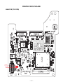
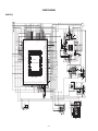
BLOCK DIAGRAM
TEST MODE
Note: Never perform the menu items unless otherwise instructed. Doing so may cause destruction of
the data inside, which will make the camera unusable.
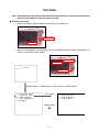
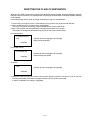
■ To boot the test mode
1. While firmly pressing down both [BS] and [UPPER], turn the power on.
[UPPER] button
[BS] button
2. After the version appears, press buttons in the order of [DOWN], [DOWN], [DISP] and [MENU] in 0.5
second. The diagnostic menu appears.
[MENU] button
[DISP] button
++ KX800 ++
Ve r 1 . 0 1
[DOWN] button
"DOWN" button -> "DOWN" button -> "DISP" button -> "MENU" button
1
2
3
4
5
:VERSION INFO
:USB TCC TEST
: R O M U P D AT E
: L A S T M E M O RY
: F O R M AT
"SET" button
"MENU" button
—6—
1
2
3
4
:USB
:USB
:USB
:USB
TCC ON
TCC OFF
STORAGE
SPEED
PROGRAM VERSION UPGRADING
1. To update the firmware version
1. Prepare the memory card which contains the firmware for EX-Z1000 in the root directory.
EX-Z1000.bin
2. Insert the above memory card into the camera, and set a fully charged battery in the camera.
3. Press the [power button] while holding [MENU] depressed. Keep holding [MENU] depressed until
“PROGRAM UPDATE” appears in the display.
• The following appears.
• The version of the firmware in the memory card appears at the bottom of the display.
PROGRAM UPDATE
YES
NO
NEW VERSION IS
VER 1.01
NOTE 1) When a wrong software is mistakenly used,
the message below appears. Update the
firmware again with the correct software.
FILE ERROR!
(As of May 2006)
NOTE 2) When only the version appears in the display
even though you are trying to operate the
camera, charge the battery to the fullest and
try again. The level of the battery indicator
should be highest in order to update the
firmware.
4. Align the white cursor to [YES] by [UPPER] and [DOWN], and then press [SET].
• “NOW LOADING” appears in the display and the update starts.
5. “COMPLETE” appears after the update finishes.
6. Remove the memory card after turning the power off once. Turn the power back on again while holding
[MENU] depressed, and check the version.
• “VER.1.01” appears.
VER 1.01
(As of May 2006)
7. If the version is correct, turn the power off.
8. Finally, check the operation by recording, playing back and deleting an image.
—7—
2. How to restore the firmware
1. Prepare the firmware restoration program and change its name as follows;
rom800_060512.lbn 씮 titan.bin
NOTE: This software and procedure automatically restores the firmware even if the firmware belongs
to a wrong model code. Make sure to use the correct software for the correct model.
2. Copy the above file to the root directory in the memory card.
3. Insert the memory card into the camera.
4. Set a fully charged battery in the camera.
NOTE: This software and procedure automatically restores the firmware even if the battery capacity of
the camera is low. Make sure to use a fully charged battery to prevent the danger of power
down during firmware restoration.
5. Turn the power on while pressing the [shutter release] button.
If the power does not turn on only by pressing the power button, insert the battery while holding the
[shutter release] button depressed.
• The LED next to the optical viewfinder changes from “green/red blinking”, “green blinking” to “green
steady”.
NOTE: This software and procedure automatically restores the firmware even if the firmware belongs
to a wrong model code. Make sure to use the correct software for the correct mode.
6. When the LED becomes “green steady”, the firmware restoration is finished.
Remove the battery and the memory card, and then turn the power off.
7. Turn the power on again while holding [BS] and [UPPER] depressed.
Check the model name and the program version (PR:) in the opening screen of the test menu.
++KX-800++
Ver 1.01
8. If the model name and the program version are correct, perform SYSTEM INITIAL to initialize the
system area.
“BS + UPPER + PW ON” 씮 “DOWN, DOWN, DISP, MENU” 씮 “3:ROM UPDATE” 씮 “5:SYSTEM
INITIAL”
NOTE: After SYSTEM INITIAL is performed, “SYSTEM ERROR” appears when the power is turned
on again.
9. Write the latest firmware. (Refer to page 6)
After the firmware is written, check the model name and the program version (PR:) in the opening
screen of the test menu.
10. Finally, start the camera normally to check the operation by recording, playing back and deleting an
image. Check also that the colors in the images are not too bright or two dark.
—8—
3. To install the firmware
Initially, firmware is not installed in the PCB supplied by the parts center.
Install the firmware into the PCB after replacing with a new one as shown in the procedures below.
Note: The camera does not operate (only LED becomes “green blinking”) if the firmware is not installed in
the PCB.
<Writing the restoration program 1>
1. Copy the following software to the root directly of the SD card.
Restoration software: rom800_060512.lbn
Firmware:
EX-Z1000.bin
2. Change the name as follows;
“rom800_060512.lbn” to “titan.bin”
3. Insert the SD card into the camera.
4. Insert the battery while holding the [shutter release] button depressed.
The LED next to the optical viewfinder changes from “green/red blinking”, “green blinking” to “green
steady”.
5. When the LED becomes “green steady”, remove the battery and turn the power off.
<System Initialize>
1. Boot the test mode.
2. Press [DOWN] twice and then press [DISP], [MENU].
3. Select “3: ROM UPDATE” and then press [SET].
4. Select “5: SYSTEM INITIALIZE” and then press [SET].
5. When the following message appears, press [SET].
SYSTEM INITIALIZE
START….
PUSH OK KEY?
6. The system initialize is executed. Turn off the power when “SUCCESS” appears.
* “SYSTEM ERROR” appears when the camera is turned off without system initialize.
<Writing the firmware>
1. Turn the power on while holding [MENU] depressed.
2. When “PROGRAM UPDATE” appears, select “YES” and then press [SET].
3. “NOW LOADING” appears while the firmware is updated.
4. When “COMPLETE” appears, the firmware update is complete.
5. Turn the power on and off to check if the camera normally functions. If there is no problem, the firmware
update is successful.
—9—
ADJ TOOL
■ Introduction
Make sure to perform the adjustment by the USB ADJ Tool “adj03SSAW.exe” when replacing the lens unit
or the PCB.
Here the necessary software, driver and setting are explained to use “adj03SSAW.exe”.
Note that the tool, drivers etc. are available only for Windows.
1. Preparation
1-1. Prepare the necessary software, driver and DLL file.
1) Prepare the following three files.
• Testmode driver
[testmode_driver] folder
uusbd.dll
uusbd.inf
uusbd.sys
* testmode_driver_2.0] is for Windows except Windows98.
* [testmode_driver] is for Windows98 only.
• ADJ tool, USB DLL and ADJ setting file
[adj03SSAW] folder
adj03SSAW.exe (ADJ tool itself)
uusbd.dll (USB DLL)
* .adt (ADJ setting file. Sorted by models)
2) Place the testmode driver in an appropriate place.
3) Place all of ADJ tool, USB DLL and ADJ setting file in the same folder.
1-2. Set the camera so that it recognizes the USB test mode.
1) Enter the test menu.
Turn the power on while pressing both [BS] and [UPPER].
Press [DOWN], [DOWN], [DISP] and [MENU].
2) Move the cursor to “2: USB TCC TEST” and press [SET].
3) Move the cursor to “1: USB TCC ON” and press [RIGHT], [RIGHT] and [SET].
4) USB TCC ON is now active. Turn the power off.
5) The test menu appears first when the camera power is turned on.
* When changing the USB TCC ON to OFF, set “2: USB TCC OFF” in the test menu.
1-3. Install the USB driver for the USB test mode in the computer.
(The following is an example using the Windows Me.)
1) Prepare the USB driver for the USB test mode.
2) Turn the camera power on which is set in the USB test mode as shown in 1-2 and let it enter the USB
test mode directly (the test menu appears right after the power is turned on).
3) Connect the camera in the above status to the computer by the USB cable.
4) The “Add new hardware” wizard appears.
5) Check “Designate the place for the driver (for users with sufficient knowledge)” and press “Next”.
6) Check “Search for the optimum driver for the device (recommended)”.
— 10 —
7) Check “Designate the place to search”, designate the place which contains “inf” file in the driver by
pressing “Reference” button, and then press “Next” button.
8) When “Universal USB Driver (VMEM manufacturer’s name)” appears upon message “Searching for
the driver file for the following devices”, press “Next” button.
9) The file copy starts.
(If a message “uusbd.inf cannot be found” appears during the file copy, designate the same place as
in the step 7).
10) Press “Complete” button.
11) Right-click “My computer”, select “property”, and then open “Device manager”.
If “Universal USB Driver (VMEM manufacturer’s name)”,“USB device for UUSBD” can be found, the
computer has successfully recognized the driver.
12) Installing the test driver into either one enables the other one to recognize it.
* How to uninstall the USB driver for the USB test mode
• Connect the camera to the computer while in the USB test mode so that the computer recognizes
the camera.
• Right-click “My computer”, select “Property” and open “Device manager”.
• Select “USB device for UUSBD” , and then “Universal USB Driver (VMEM manufacturer's name)”.
• Press “Delete” button to delete the driver.
• When using Windows98/98SE/Me, delete the following three files;
(NOTE! Do NOT delete “usbd.inf” and “usbd.sys”, whose names are much alike the following.)
C:windows / inf / uusbd.inf
C:windows / inf / other / KashiwanoUUSBD.inf
C:windows / system32 / drivers / uusbd.sys
• The driver has been successfully deleted.
1-4. Use the USB ADJ Tool
1) Prepare ADJ tool, USB DLL and ADJ setting file in the same folder.
2) Turn the camera power on which is set in the USB test mode and let it enter the USB test mode directly
(the test menu appears right after the power is turned on).
3) Boot “adj03SSAW.exe” and use it as follows;
• To read ADJ data from the camera
앶앸 Press “READ ($9)”.
There is no neto set the model by “FW Item Set”.
• To write ADJ data into the camera
앶앸 Press “WRITE ($8)”.
• To save ADJ data which is read
앶앸 Select “File” and “Save All ADJ”, and save it under an appropriate name.
• Open ADJ data which is saved
앶앸 1. Select the model by "FW Item Set", and then press "Load FW ->" button.
2. Select “File” and “Open”, and open the necessary file.
• Language” radio button can switch the language between Japanese and English in which the name
of the ADJ ITEM is displayed.
• “Radix” radio button can switch the data display between decimal and hexadecimal notations.
— 11 —
2. How to use ADJ Tool when replacing Lens unit
Make sure to perform the following procedure after replacing the lens.
A floppy disk with the lens data is bundled in the spare parts of the lens unit.
1 Enter the TEST mode.
1. Turn the power on while pressing both "BS" and "UP" buttons.
2. Press "DOWN" button, "DOWN" button, "DISP" button, and "MENU"
button while the program version is displayed.
3. Select "2.USB TCC TEST", and press "SET" button.
4. Select "1. USB TCC ON", and press "RIGHT" button, "RIGHT" button
and "SET" button.
5. Turn the power OFF.
2 Connect the camera to the computer by the USB cable.
3 Boot "adj03ssaw" .
4 Select the model name and click "Load FW " Key.
• EX-Z1000
5 Click "ADJ ALL READ", and display the data on the "adj03ssaw".
6 Find the No.1163, "LCD VCOM DC".
6
7 Write down this value(data).
8 Replace the Lens unit.
9 Perform the above 1 to 3.
4
0 Select the model name and click "Load FW " Key.
• EX-Z1000
A From "File/Open", open the bundled floppy disk, and transfer the data to
the "adj03ssaw".
A
B Find the No.1163,"LCD VCOM DC"
C Change the data to the former value.(Refer to 7).
D Click "WRITE" button of "ADJ ALL".
E After adjustment, change "1. USB TCC ON" to "2. USB TCC OFF".
D
— 12 —
3. How to use ADJ Tool when replacing MAIN PCB
Firmware is not installed in spare parts.
1 Enter the TEST mode.
1. Turn the power on while pressing both "BS" and "UP" buttons.
2. Press "DOWN" button, "DOWN" button, "DISP" button and "MENU"
button while the program version is displayed.
3. Select "2.USB TCC TEST", and press "SET" button.
4. Select "1. USB TCC ON", and press "RIGHT" button, "RIGHT" button
and "SET" button.
5. Turn the power OFF.
2 Connect the camera to the PC by the USB cable.
3 Boot "adj03ssaw".
4 Select the model name and click "Load FW " Key.
• EX-Z1000
5 Click "ADJ ALL READ", and display the data on the "adj03ssaw".
6 Save the data.
7 Replace the MAIN PCB.
8 Writing the Firmware.
Write the firmware into a spare part after replacing one.
NOTE: If a battery is inserted without the firmware, only LED
blinks green and the camera does not operate.
9 Perform the above 1 to 3.
0 Select the model name and click "Load FW " Key.
• EX-Z1000
A Open the file which is saved above, and display the data on the
"adj03ssaw".
B Click "WRITE" button of "ADJ ALL".
C After adjustment, change "1. USB TCC ON" to "2. USB TCC OFF".
6
5
4
A
B
— 13 —
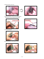
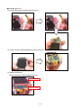
VCOM DC ADJUSTMENT
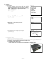
■ Purpose
Readjust the VCOM value to minimize the flicker of the LCD after replacing the LCD or the main PCB.
■ Necessary tools
1. Camera (Charge its battery fully)
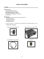
2. Photo diode (S2281-01) : See Fig 1.
3. Photo sensor amp (C2719) : See Fig 2.
4. BNC-BNC cable (E2573) x 2 : See Fig 3.
5. 9-volt alkaline battery (6LR61Y) x 2 : See Fig 4.
6. Oscilloscope
■ Preparation
1. The three tools can be obtained from the following global site.
Photo diode (S2281-01)
Photo sensor amp (C2719)
BNC-BNC cable (E2573)
www.hamamatsu.com/
2. 9-volt alkaline battery is a standard one, but can be obtained from the following global site as well.
www.panasonic.co.jp/global/
Fig1 Photo Diode (S2281-01)
Fig2 Photo Sensor Amp (C2719)
Fig3 BNC-BNC Cable (E2573)
Fig4 6LR61Y
— 14 —
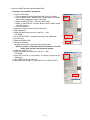
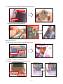
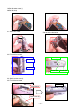
■ Procedure
1. Camera setting
a) Turn the power on while pressing “BS” and “UPPER”.
After pressing “DOWN” key twice, press “DISP” and “MENU”.
Select "2:USB TCC TEST", and press "SET" button.
Select "1:USB TCC ON", and press "RIGHT" button ,"RIGHT"
button and "SET" button.
Figure (a) appears.
Figure (a)
1: VERSION INFO
2: USB TCC TEST
3: ROM UPDATE
4: LAST MEMORY
5: FORMAT
6: HARD TEST
7: IMAGE TEST
8: ADJ TEST
9: TEST SCRIPT
b) Select “8 : ADJ_TEST” and then press SET.
(See Figure (b).)
Figure (b)
c) Next, select “2. LCD” and then press SET.
(See Figure (c).)
Figure (c)
d) Pressing SET causes the right figure to appear.
(See Figure (d).)
Figure (d)
1: ADJ STAT CLR
2: LCD
3: LENS
.
.
.
1:VCOM
.
.
.
OK
O K - > R e g i s t e rW ri t e
VCOM = 0xca
This value is an example and differs by products
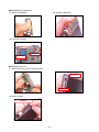
2. Connecting the TOOL
a) Place two 9-volt alkaline batteries in C2719.
b) Connect the output terminal of C2719 to the channel terminal of the oscilloscope by the BNC-BNCcable.
c) Connect the input terminal to the Photo Diode by the BNC cable.
d) Turn the oscilloscope and C2719 on.
* Pull the ON/OFF switch of C2719 this way and raise/lower it. (See below Figure.)
— 15 —
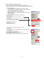
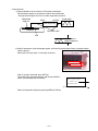
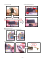
3. Measurement
a) Connect S2281-01 to the camera’s LCD monitor (see below).
AC Waveforms appear on the monitor screen of the oscilloscope.
* Change the Rf range of C2719 in case the range does not match.
Photo diode
S2281-01
INPUT
OUTPUT
Oscilloscope
Photo sensor amp
CAMERA
BNC-BNC cable
LCD
Minimize the
ripple components
b) After AC waveforms of the oscilloscope appear, minimize it by pressing the camera’s up/down buttons
(see the picture).
Make sure to visually check if it has been minimized.
[UPPER] button
[DOWN] button
After it has been minimized, press SET key.
The screen in the right figure appears and the new VCOM is
written (VCOM adjustment is finished.).
OK -> Register Write
VCOM = 0xca
ADJ DATA SET!
This value is only an example, and differs by products.
Return to the previous display by pressing MENU or PW key.
— 16 —
CURRENT CONSUMPTION
(1) Current consumption (DC in = 3.80 ± 0.1 [V])
• Make sure that current consumption is less than 230 mA in PLAY mode.
• Make sure that current consumption is less than 440 mA in REC mode.
• Make sure that current consumption is less than 300 µA when power is turned OFF.
(2) The battery indicator changes according to the voltages as follows.
• DC in = less than 3.70 ± 0.02 V:
(PLAY mode)
• DC in = less than 3.60 ± 0.02 V:
(PLAY mode)
(PLAY mode)
• DC in = less than 3.50 ± 0.02 V:
THE COUNTERMEASURE FOR "SYSTEM ERROR"
System error may occur when the battery is removed while data is written to the internal memory.
■ PROCEDURE
1. Initialize the system.
a) Enter the TEST mode.
b) Select "3:ROM UPDATE" and press SET button.
c) Next, select "5:SYSTEM INITIAL" and press SET button.
d) The following message appears.
SYSTEM INITIALIZE
START ...
PUSH OK KEY?
e) Press SET button and System is initialized.
"SUCCESS !" appears on the monitor.
2. Write firmware.
Refer to the "1. To update the firmware version" on page 7.
Write the firmware.
If the TEST mode boots automatically, change "USB TCC ON" to "USB TCC OFF".
Replace the Main PCB if the camera does not recover.
— 17 —
RESETTING THE PLACE OF DESTINATION
When the main PCB is replaced, the setting of the destination will be changed, therefore resetting is required.
However, when the firmware is changed or fixed, the setting of the destination will be held, therefore resetting
is not required.
Use the destination setting script to change the destination flag as instructed below.
1. Have an SD card ready that have a corresponding script (autorun.scp) under the root directory.
2. Insert the SD card in the camera and turn on the power.
The script is located at Qv/soft/Adj_soft/exz1000/Script in the service CD-ROM.
3. After a few seconds, one of the following messages will be shown in the screen.
The system will change the destination flag and turn off the camera automatically.
For North America
For North America
815
• Number of menu languages: 10 languages
• eBay scene compatible
Complete
For Europe and UK
For Europe_UK
• Number of menu languages: 10 languages
• Movie filming time limited
Complete
For others
else
• Number of menu languages: 10 languages
Complete
4. Remove the SD card from the camera and turn on the power to confirm if the camera is set as you wish
including the number of the menu languages and the scene of the best shot mode.
If there is no problem, the setting is completed.
— 18 —
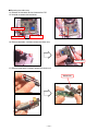
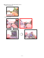
DISASSEMBLY
* Make sure to use correct screws when assembling since
there are several kinds of them.
It is a good idea to sort them as shown in the right when
disassembling.
1. Remove the battery.
■ Remove the case
2. Remove six screws.
Screw (S1)
Screw (S3)
Screw (S2)
Screw (S3)
Screw (S3)
— 19 —
Screw (S2)
3. Remove the rear case assy.
4. Remove the center case (A) and the power button.
Note: Make sure not to lose the power button.
Power button
Center case (A)
5. Remove the keypad.
Keypad
6. Remove the strap and the center case (B).
Strap
Center case (B)
— 20 —
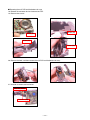
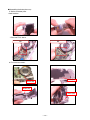
7. Remove two screws and then remove the front panel assy.
Screw (S1)
Screw (S2)
Note: Discharge the strobe condenser.
■ Removing the LCD
8. Remove two screws and then remove the clamp board.
Clamp board
Screw (S1)
Screw (S3)
9. Unsolder to remove two lead wires.
10. Release the connector lock and remove the FCP.
Lead wire (black)
Lead wire (red)
— 21 —
11. Remove the LCD.
* Fixed with double-sided tape.
Double-sided tape
Remove the LCD FPC that can be found under key FPC.
■ Removing the key FPC
12. Release the connector lock and remove the FCP.
13. Remove the key FPC.
Key FPC
— 22 —
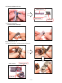
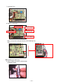
■ Removing the strobe assy
14. Release the connector lock and remove the FCP.
15. Unsolder to remove two lead wires.
Lead wire (red)
Lead wire (black)
Lead wire (gray)
16. Remove two hooks, and then remove the strobe assy.
Strobe assy
17. Remove three hooks, and then remove the shutter unit.
Shutter unit
— 23 —
■ Removing the mail PCB and the bottom sub assy
18. Release the connector lock and remove two FCP.
19. Remove four screws.
Screw (S4)
Screw (S3)
Screw (S1)
Screw (S3)
20. Remove the hook, and then remove the mail PCB and the bottom sub assy.
21. Unsolder to remove two lead wires.
Lead wire (black)
Lead wire (red)
— 24 —
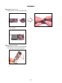
22. Remove the bottom sub assy.
Bottom sub assy
Connecter plate
Main PCB.
23. Remove the speaker.
* Fixed with double-sided tape.
■ Removing the lens unit.
24. Remove two hooks, and then remove the lens unit.
<hook location>
Buttery box assy
Lens unit
— 25 —
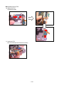
ASSEMBLY
■ Assembling the lens unit
1. Set the lens unit and fix it with three hooks.
<hook locations>
■ Assembling the speaker
2. Set the lens unit and fix it with three hooks.
* Pay attention to the lead wire positions.
— 26 —
■ Assembling the main PCB and the bottom sub assy
3. Set the connector plate.
Connector plate
4. Set the main PCB.
— 27 —
■ Assembling the buttery box assy
5. Set the connector plate.
<hook location>
* Place two FPCs above.
NG
NG
6. Fix it with four screws.
Screw (S4)
Screw (S3)
Screw (S1)
Screw (S3)
— 28 —
7. Insert two FPCs.
8. Solder five lead wires.
Lead wire (black)
Lead wire (red)
Lead wire (gray)
Lead wire (red)
Lead wire (black)
* Make sure to place to the right directions when soldering lead
wires.
■ Assembling the strobe assy
9. Set the strobe assy and fix it with the hook.
* Positioning guides.
— 29 —
■ Assembling the key FPC
10. Set the key FPC.
* Positioning guides
11. Insert one FPC.
* FPC should be placed under the lead wires.
— 30 —
■ Assembling the LCD
12. Lead the FPC through the buttery box clearance.
13. Fix the LCD with a double-sided tape and insert one FPC.
14. Solder tow lead wires.
* Wire the lead wires along the edge of the LCD.
Lead wire (red)
Lead wire (black)
— 31 —
■ Assembling the clump board
15. Set the clump board.
* Do not nip the lead wires.
16. Fix with two screws.
Screw (S1)
Screw (S3)
■ Assembling the case
17. Set the front case and fix it with two screws.
Screw (S1)
Screw (S2)
18. Set the keypad.
Keypad
— 32 —
19.Set the center case (B).
20.Set the strap.
21. Set the rear case.
* Do not nip the lead wires.
22. Fix it with five screws.
Screw (S3)
Screw (S2)
Screw (S3)
Screw (S3)
Screw (S2)
23. Set the power button.
24. Set the center case (A).
25. Fix it with one screw.
Screw (S1)
Power button
Center case (A)
— 33 —
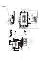
— 34 —
23
22
24
23
S3
S2
S1
13
6
32
S1
14
12
10
18
5
S3
8
S1
16
7
11
4
20
19
21
9
7
17
31
S1
15
3
30
26
29
S3
S2
28
27
S5
2
S3
S4
S3
2
1
S2
25
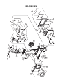
EXPLODED VIEW
PARTS LIST
N
N
N
N
N
N
N
N
N
N
N
N
N
N
N
N
N
N
N
N
N
N
N
N
N
N
N
N
N
N
N
N
N
N
Item
1
2
3
4
5
6
7
8
9
10
11
12
13
14
15
16
17
18
19
20
21
22
23
24
25
26
27
28
29
30
31
32
S1
S2
S3
S4
S5
Parts Code
10242103
10241458
10219347
10241438
10241439
10241441
10241440
10241467
10242108
10241452
10241447
10241456
10241455
10241960
10241962
10241454
10241451
10241491
10234007
10241464
10241463
10241958
10241472
10241471
10241959
10242106
10241475
10241448
10241465
10241466
10241453
10243984
10203893
10241435
10241436
10241461
10153233
FU100
FU101
10196218
10189324
N
*1
*2
*3
Parts Name
BOX ASSY/BATTERY
TAPE/LCD
SPRING/BATTERY
CASE/CENTER/A
CASE/CENTER/B
STRAP BOARD
TAPE
BUTTON/POWER
KEY
SHUT-SUB-ASSY
STROBE UNIT
CABLE/STROBE
CLAMP BOARD
PCB ASSY/MAIN
LENS UNIT
PLATE/CONNECTOR
CASE ASSY/BOTTOM
COVER/BATTERY
SPEAKER
NET/SPEAKER
TAPE/SPEAKER
PANEL ASSY/FRONT
TAPE/CAM RING
CAM RING
PANEL ASSY/REAR
KEY
TAPE/KEY
LCD UNIT
CABLE/LCD
CABLE/LCD
FPC/KEY
LABEL/RATING
SCREW
SCREW
SCREW
SCREW
SCREW
Specification
RJK509022*001V02
RJK508890-006V01
RJK507851-001V02
RJK509023-001V01
RJK509024-001V01
RJK508966-001V01
RJK508890-003V01
RJK508969-001V01
HKW1628-020010-S
RJK509020*001V01
XEST-K800-S
HKW1608-020010
RJK509031-001V01
RJK509021*001 TK
RJK509080*001 TK
RJK509011-001V01
RJK509019*001V01
RJK508959-001V01
YD-1352
RJK508879-001V01
RJK508880-001V01
RJK509014*001 TK
RJK508974-001V01
RJK508827-001V01
RJK509015*001 TK
HKW1618-020010-S
RJK508890-004V01
COM28T2856TLB
RJK508975-001V01
RJK508975-002V01
SB-CAS5-A
RJK509056-002V01
RJK502836-011V01
RJK509034-001V01
RJK509008-001V01
RJK508627-002V01
RJK506113-001V01
FUSE
FUSE
FCC10801ABPA
FCC10152ABPA
New parts
Floppy disk is bundled.
AC cord is not equipped.
Blade type AC cord is equipped.
— 35 —
QTY Price Code
1
2
1
1
1
1
2
1
1
1
1
1
1
1
1
1
1
1
1
1
1
1
4
1
1
1
2
1
1
1
1
1
4
3
6
1
2
1
1
R
Remark
C
X
C
C
C
C
C
C
C
C
C
X
X
A
A
*1
X
C
C
X
X
X
C
C
C
C
X
X
A
C Red
C Black
C
X
X
X
X
X
C
C
N
Item
N
N
-
N
N
Parts Code
Parts Name
ACCESSORIES
10243983
CD ROM
10242037
AV CABLE
10235765
USB CABLE
10210351
AC CORD
10210354
AC CORD
10210360
AC CORD
10210350
AC ADAPTOR
10211299
AC ADAPTOR
10242036
CRADLE
10242035
BATTERY/LI-ION
10187367
STRAP
N
*1
*2
*3
Specification
CK800DCA01R
AV-K800-BK15
UC-K815-BK10-MB
CBL-K835-AC-EU-06
CBL-K835-AC-UK-06
CBL-K835-AC-TW-06
AD-C52G-WW
AD-C52J-WW
R68-8209
MK11-2875
ST-K872-S
New parts
Floppy disk is bundled.
AC cord is not equipped.
Blade type AC cord is equipped.
— 36 —
QTY
1
1
1
1
1
1
1
1
1
1
1
Code
R
Remark
C
C
C
C EU type
C UK type
C Blade type
C
*2
C
*3
C
B
X
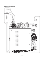
PRINTED CIRCUIT BOARD
MAIN PCB (TOP VIEW)
FU101
FU100
— 37 —
MAIN PCB (BOTTOM VIEW)
— 38 —
SCHEMATIC DIAGRAMS
VCC1.8
VCC3.3D
1005
CCD-BUS
CCD-BUS
L401
AG700
L400
AG700
1005
VCC1.2
VCC3.3A
MAIN PCB (1/3)
VCC1.8
USB/SD-BUS
VCC1.2
PW/KEY-BUS
TH
KIN4
D0
13 295 296 297 298
VSS_47
12 299 300 301 302
D4
PSRDY
0603
0603
R219
1k
R217
1005
C218
6.3V
35
37
31
34
36
J
K
L
M
IRIS1
124
IRIS0
0603
100k
ADPIN
0603
BATTEMP
PWCTL2
P06
P74/KR4
WATCH
P33/TI51/TO50/INTP4
P75/KR5
R229
26
SHUTSW
P31/INTP2
1k
25
0603
1005
3
VBUS
1
B0.1u
10V
2
0603
Q200
DTC144EM
C221
0603
100k
1005
100k
C219
B0.1u 10V
R222
P77/KR7
P72/KR2
24
P60/SCL0
P61/SDA0
P62
P123/XT1
P76/KR6
22
21
20
23
19
17
18
P63
EVDD
P124/XT2
REGC
VSS
VDD
16
15
12
14
EVSS
13
VDD_RTC
REQ_RTC
VDD_SUB
9
11
10
SUB_XT2
96
10V
1005
GND
1005
B1u
6.3V
C214
B0.1u
10V
1005
0603
C213
4
3
1k
31
P51
29
B0.1u
0
P406
ASEBRKAK
125
R225
R223
NC_4
0603
49
P25/ANI5
50
51
52
53
54
P130
AVREF
P26/ANI6
P22/ANI2
P23/ANI3
55
56
P20/ANI0
57
58
60
61
59
P02
P03
P27/ANI7
P24/ANI4
P21/ANI1
62
63
64
P04
P00/TI000
P30/INTP1
32
27
H
RESETB
EVCC3.3
R218
GND
2
1
270
HSD226
D200
P101/MTIA0
123
0603
AUDCLK
122
VSS_23
GND
121
D3
KIN3
0603
100k
R216
R214
65
66
P14/RXD6
P01/TI010/TO00
28
23
G
R221
1005
24
19
F
30
P100/MTIA1
126 125 124 123 12
300
301
B1u
C212
B2.2u 6.3V
1005
67
68
P43
P140/PCL/INTP6
P141/BUZ/INTP7
69
70
P41
IC2
71
100k
0.5
126
130 129 128 127 13
R8J30225EBGV
VCCX2_4
299
20
15
E
27
0603
IRIS2
128
127
298
16
11
R204
VCC_5
297
12
28
R213
IRIS3
129
D1
D
95
C211
130
VSS_24
ASEBRKAK#
296
7
C
C216
P102/MTIB1
8
4
3.3V
DSE#
138 137 136 135 15
134 133 132 131 14
HALFSHUT
C215
142 141 140 139 16
R228
P73/KR3
FOCUS0
P103/MTIB0
FVCC_2
11 303 304 305 306
122 121 120 119 11
10 307 308 309 310
118 117 116 115 10
VCC_4
120
D2
P07/INT7/MTDCPLS2/PLLFBCLK
302
119
AUDSYNC#
VCC3.3D
118
D7
VCCX1_4
304
CN801
30pin
ESA01P030S1-351-E0
117
P06/INT6/MTDCPLS1/PLLCLK3
6.3V
95 5
KIN4
R804
AG12
314
10 14
18 22 26
38 42 46 50 54 58
30 34
70
62 66
DM
92 4
74 78 82 94 93
106
D16
VSS_20
316
105
D15
3 334 335
6
9 13 17
2 336
5
8 12 16 20 24
25
21
29 33 37 41
45 49 53
57
65 69 73 77
61
81 85 91
90 3
80
89 2
4.7k
AUDAT2
DP
7
A
B
C
D
11 15 19
23 27 31
E
H UJ VK T L
F
G
43 47 51
35 39
M AN
P
59 63
55
R
67 71
Y
W
75 79
88 1
83 86
AA AB
AUDAT1
100
AG700
4
AV33
C AD AE
1005
2
9
CRDLSW
CHARGE
22
10
CHGCTL
DC
21
11
NC
DC
20
R820
270
VBUS
1608
CHGVCC
12
AGND
GND1
19
13
MONOOUT
GND1
18
14
AVDET
GND1
17
15
NC
GND1
16
99
VSS_50
DG12
323
C422
98
D22
VSS_18
D21
AUDAT0
324
97
325
SDDAT3
L804
SDCMD
L805
B0.1u
15pin
SCDA3A0800
1005
DC
L802
TO CRADLE
2
SDDAT0
L806
SDDAT1
L807
1005
HW680
SDDAT2
L808
1005
HW680
1005
P801
SDWP
0.8
D24
R406
93
F5.6k
P02/INT2/PLLCLK0_4
329
0603
CENDN
92
D23
USB-LED
94
REFIN
GND
C804
328
P04/INT4/PLLCLK1
DMINUS
D25
VOUT
(TOP VIEW)
VCCX2_6
327
KINTB
95
DPLUS
MONOOUT
DV12
VSS
4
VSS
5
VDD
6
VDD
7
SDCLK
8
VSS
9
SDDAT0
10
SDDAT1
11
SDDAT2
12
SDCD
13
VSS
14
SDWP
15
VSS
SDWP
1005
AVDET
D20
SDCMD
3
HW680
SDCD
10V
SDDAT3
2
HW680
1005
P802
ESD-GND
1
HW680
96
326
SD-CONNECTER
CN803
HW680
1005
L801
D17
322
1
GND
101
R822
1k
1
D18
23
1005
VSS_19
321
24
CHARGE
102
D19
320
AG700
84 87
L800
68 72 76
0603
319
56 60 64
52
25
CHARGE
BATTEMP
DPLUS
103
28 32 36 40 44 48
26
CHARGE
USBLED
8
SDCLK
AG33
3
27
USBVCC
VOUT
7
104
D14
318
VCC_12
USBGND
USBGND
6
0603
C800
B0.1u
10V
4 331 332 333
CHGCTL
DMINUS
107
VSS_49
USBGND
5
BATTEMP
108
D11
317
4
110
109
315
28
30
SHUTTER2
1005
111
AUDAT3
98 97 96
29
USBGND
USBGND
112
DG33
VSS_21
5 327 328 329 330 337
USBGND
D-
6.3V
B1u
113
P05/INT5/STLGTSIG2/PLLCLK2
D13
D12
313
D+
3
FG
2012
102 101 100 99 6
0603
106 105 104 103 7
6 323 324 325 326
AV12
VCCX2_5
312
1005
7 319 320 321 322
D8
R805
F22k
D9
USBGND
2
1005
EVCC3.3
L803
BD102
C423
114
310
311
1
VBUS
115
308
309
2
116
VBUS
VSS_22
B10u
110 109 108 107 8
D10
10k
114 113 112 111 9
8 315 316 317 318
DV33
VSS_48
307
0603
9 311 312 313 314
D5
306
R813
D6
305
D802
EDZTE5.6B
VCC_11
303
P03/INT3/PLLCLK0_8
R409
100k
SAMRES#
89
P44/MCLKOUT0
GND
0603
88
VSS_17
AVDET
87
0603
1005
0603
L250
1
AG700
130
47
3
2
84
VCC3.3D
2
G-LED
3
R-LED
4
KIN2
5
GND
6
KIN2
AFLED_C
P400
VCC3.3D
VCC3.3D
5
4
10V
1005
B0.1u
1
GND
P405
TDO
0.5
TMS
0.5
P404
P403
TCK
CN250
14pin
XF2U-1415-3A
Q801
EMH25
0603
P401
VCC3.3D
0.8
RESET
0.5
0
R403
RESETB
FOUT
WATCH
C418
1005
0.5
0.5
B0.1u 10V
P402
TDI
C415
MODE2:L
MODE1:H
MODE0:H
1005
TEST:L
C412
B0.1u 10V
VCC1.2
EVCC3.3
VCC5-2
SELFLED
P407
GND
VCC1.8
130
0603
R808
100k
R809
R408
R807
TDO
TRST#
0603
0.5
P409
TRST
47
P408
ASEMD0
0603
85
VSS_16
83
TMS
VSS_15
XIN
VDD_6
VDD_7
82
81
79
80
78
VSS_14
XOUT
VDD_5
VCCX1_3
77
76
75
TCK
VSS_13
VSS_12
VSS_11
TDI
73
74
72
71
70
RST#
VCC_3
RTCCLKIN
68
69
67
0.5
86
ASEMD0#
R806
P00/INT0/PLLCLK0_1
66
MODE1
65
63
MODE2
P01/INT1/PLLCLK0_2
64
60
TEST
VSS_10
P46/DREQ
P43/STDO
VDDQ_5
P42/STDI
58
59
57
55
56
VCCX1_2
53
54
RSTOUT#
P41/BICLK
52
VDDQ_4
51
50
CS1#
SACE#
48
49
CS0#
47
46
VSS_9
VCCX1_1
DQM3/WS3#
45
VSS_8
43
44
P40/LRCLK
VSS_7
SYSCLK
VCCX2_2
VCC_2
42
41
40
38
39
DQM2/WS2#
VSS_6
VCCX2_1
VCC_1
37
35
36
DQM1/WS1#
33
34
A18
DQM0/WS0#
VSS_5
31
30
32
VDDQ_3
A16/BA0
VDDQ_2
A17
28
27
29
A13/MA11
26
A15/BA1
A14/MA12
25
23
24
VDDQ_1
A11/MA9
A12/MA10
VDD_3
VSS_4
22
21
20
18
19
A9/MA7
A10/MA8
VSS_2
VSS_3
17
16
15
VDD_2
A8/MA6
VDD_1
VBGP
A7/MA5
13
14
12
10
11
A5/MA3
A6/MA4
7
8
9
D29
6
A3/MA1
VSS_1
VBGN
3
2
1
DUMMY
4
A2/MA0
337
5
D30
A4/MA2
VBB_CNTRL
D31
336
MODE0
D26
334
VDD_4
D27
333
90
62
D28
332
MRES#
61
VSS_51
331
335
91
P47/DACK#/MCLKOUT1
330
0.8
VCC1.2
GND
G-LED
R255
KIN1
6
AFLEDK
7
AFLEDA
8
BLLEDK
9
BLLEDA
10
R-LED
0603
LCD CONNECTOR
VCC3.3D
1
VCOM
3
D06
5
D04
7
D02
LDDAT7
D07
CHG
VCC3.3D
1
GND
3
GND
5
GND
7
GND
9
PWSW
CHG
IGBTGND
6
GND
5
POWER_SAVE
R450
IGBTGND
VOUT
75
IGBTGND
POWSW
0603
11
NC
13
NC
15
HALFSHUT
17
SHUTSW
HALFSHUT
GND
SHUTSW
19
KIN1
21
EVCC3.3
C605
B1u 6.3V
1005
C604
B1u 6.3V
1005
2
4
R600
6
10
0603
8
CENDN
10
VCC3.3D
12
VCC1-0
14
VCC1-0
16
VCC1-0
18
VCC1-0
20
C603
1608
B1u 6.3V
1005
6.3V
C452
C600
7
V-
4
CS
SCK
15
HSYNC
17
VSS
19
POCB
21
VSREF
23
VDD
25
CP1
27
CM2
29
VDD
2012
31
VVCOM
33
VSS
35
C3M
37
C4M
39
VDD3
41
C5P
43
C6P
45
VGL
VSYNC
14
CLK
16
VSS
18
VBC
20
COMDC
22
VDD2
24
CM1
26
C2P
28
COMOUT
30
VSS
32
VSS
34
R602
36
38
C5M
40
10k
0603
560k
C618
0603
B10u 6.3V
1608
C617
B10u
C3P
C4P
VGH
C601
GND
12
R601
10V
2012
C616
42
C6M
B2.2u 16V
FPC
DI
VSYNC
B2.2u 10V
C602
10
LCDCLK
1608
B4.7u 10V
TO ST-UNIT
BLON
LCDDI
HSYNC
8
CP2
3
LDDAT1
11
13
LCDSCK
CN800 21pin
046283021001868+
8
D00
9
LCDCS
B10u
L450
22u
GLF1608T220M
IGBTCNT
IC450
NJW1351RB1
VIN
1005
LDDAT3
6
D01
LDDAT0
1005
CP1
LDDAT5
4
D03
LDDAT2
VCC1-0
CENDN
C453
B1u 6.3V
2
D05
LDDAT4
44
B2.2u
16V
1608
C613
1608
5
C612
D600
B1u
RB521CS-30
16V
B1u
1608
C610
B2.2u
10V
1608
C608
B2.2u
10V
16V
1608
C611
B2.2u 10V
C609
B2.2u 10V
1608
1608
1608
FPC
GND
— 39 —
BLLEDA
BLLEDK
BLON
1005
CN600 45pin
046283045001868+
V+
1005
0603
1005
F22k
R252
C253
B0.1u 10V
0603
1005
F22k
R251
C252
B0.1u 10V
0603
C251
B0.1u 10V
1005
F22k
2
CH8p
50V
C417
1005
CH7p
50V
R250
MONOOUT
3
0603
1k
4
VIDEO
VOUT
AV-BUS
LDDAT6
2
EVCC3.3
TO KEY-FPC
GND
EVCC3.3
1
GND
14
FA238-48M-7/30
VCC3.3A
1608
GND
KIN3
13
X400
48MHz
1
R404
C416
AUDIO-BUS
AUDIO-BUS
0603
GND
C450
B10u 6.3V
11
12
KIN3
LCD-BUS
C451
B1u 6.3V
KIN1
100
C250
B0.1u 10V
MCKO
SDTO
SDTI
BICK
LRCK
R405
1M
VA_STBY
VCC1.8
IC400
14 291 292 293 294
P121/LDDAT0
5
2
B
Top View
1005
1005
131
15 287 288 289 290
16 283 284 285 286
PRE
P125/LDSTO/RXD3/ATGPLS1
3
1
A
96
1
0603
132
P107/MTFA0
294
295
2
PAS414HR-VE5R
VSS_46
293
CH5p 50V
B0.1u 10V
4.7k
134
133
291
292
R407
135
P120/LDDAT1
0603
100k
P106/MTFA1
FVCC_1
P124/LDCS/TXD3/ATGPLS3
R212
0603
R/B#
146 145 144 143 17
P111/MTFB0
VSS_45
AVREF0
PWCTL1
35
34
33
6.8k
150 149 148 147 18
17 279 280 281 282
1005
C202
C419
136
LDDAT2
289
290
NC_2
P32/INTP3
0603
18 275 276 277 278
CH8p 50V
137
288
LDDAT0
C201
138
VSS_25
287
38
1
P110/MTFB1
43
44
X200
32.768k
R205
1M
RS#
154 153 152 151 19
286
LCDDI
ZOOM0
2
158 157 156 155 20
19 271 272 273 274
45
32
REGC_RTC
139
20 267 268 269 270
40
39
/VDD_MAIN
0603
1005
P113/MTZA0
AN05
41
33
SUB_OUT2
C209
B0.1u 10V
Z_ENC_DET
140
AN04
285
LDDAT1
10V 1005
P112/MTZA1
LDDAT3
VCC_10
283
LCDCS
B0.1u
142
284
42
29
VDD_LVI
143
282
LDDAT2
30
25
94
144
162 161 160 159 21
66
P05
P121/X1
141
21 263 264 265 266
26
21
P122/X2
VCCX1_5
AN02
58
22
17
VCC1.2
281
62
18
13
VDD_MAIN
VCC3.3D
1005
70
14
9
93
R208
0
145
P114/MTZB1
P116/MTDPLS3
74
10
6
92
6.3V
1005
C421
146
22 260 261 262 250 246 242 238 234 230 226 222 218 214 210 206 202 198 194 190 186 182 166 165 164 163 22
78
93
95
91
B1u
147
23 258 259 253 249 245 241 237 233 229 225 221 217 213 209 205 201 197 193 189 185 181 178 169 168 167 23
90
92
P71/KR1
90
1005
C210
MT_RESET
148
AN03
89
91
94
P70/KR0
RESET
P40
B0.1u 10V
CHG
149
P115/MTZB0
VCC_9
1005
72
150
WP#
PWCTL4
CHGCTL
37
COMP_REF1
89
0603
0603
P52
COMP_IN2
88
100k
0603
100k
36
88
4
3
5
AVDD
87
R207
VSS_26
AN01
46
85
C205
VCC_6
LDDAT4
LDDAT3
0603
10V
1005
P20/TB10/TA07/SD1CMD
AN00
48
47
86
P24/TB14/TA03/SD1DAT2
Y AA AB AC AD AE
51
54
7
W
53
57
8
V
56
61
SDA_RTC
U
60
65
SUB_XT1
T
64
69
SCL_RTC
R
68
73
6
P
72
77
5
N
76
81
6.8k
M
80
87
0603
L
83
86
R215
K
85
SUB_OUT1
J
278
279
280
F160k
0603
P21/TB11/TA06/SD1CLK
277
10V
F75k
C203
B0.1u
100k
R226
38
IC1
H
40
P50
NC_1
G
7
6
4
F
49
50
NC_3
2
E
52
COMP_IN1
6.3V
D
55
59
63
67
39
1005
C
71
75
P53
84
B1u
B
24 257 255 252 248 244 240 236 232 228 224 220 216 212 208 204 200 196 192 188 184 180 177 175 171 170 24
276
C402
CDRSTB
VA_STBY
PWCTL5
R227
42
41
79
82
84
83
1005
10V
PSOUT
P15/TOH0
8
COMP_REF2
C208
B0.1u
PSIN
44
P17/TI50/TO50
PORT_IN
80
F_HOME_LED
C200
B0.1u 10V
A
25 256 254 251 247 243 239 235 231 227 223 219 215 211 207 203 199 195 191 187 183 179 176 174 173 172 25
P123/LDVD/MONACK3/SOF
VSS_44
B0.1u
79
PORT_OUT
R203
45
43
NC_5
151
272
46
P12/SO10
P16/TOH1/INTP5
AGND
152
LDDAT5
LENS_TH
10k
0603
1005
153
AVR
Z_HOME_DET
R206
PSCK
47
IC200
UPD78F8011
78
IC
0603
48
AVSS
P13/TXD6
P11/SI10/RXD0
VLC_RTC
1005
82
154
275
1005
P10/SCK10/TXD0
COMP_OUT2
81
R201
155
273
C220
B0.1u 10V
77
0603
VSS_27
P23/TB13/TA04/SD1DAT1
274
LDDAT4
10V
COMP_OUT1
76
P27/TB17/TA00/SD1CD
P22/TB12/TA05/SD1DAT0
LDDAT6
271
1005
F56k
B0.1u
P42
75
0603
C204
P26/TB16/TA01/SD1WP
P122/LDHD/MONACK4
VCCX2_3
C406
R202
1005
156
VSS_43
B1u 6.3V
R200
F160k
C207
B0.1u 10V
157
AIREF
1005
VSS_RTC
158
LDDAT7
C403
SELFLED
VCCX1_6
268
B0.1u 10V
R-LED
159
P25/TB15/TA02/SD1DAT3
267
F_HOME_DET
160
P12/TB02/TA15
270
LDDAT5
G-LED
161
P11/TB01/TA16
269
VSYNC
R211
D220k
MT_DATA
169
P133/TXD1
P17/TB07/TA10
162
VSS_28
P10/TB00/TA17
266
0603
1005
R210
D220k
CCLK
BL-PWM
170
MT_SCLK
171
173
174
175
172
VSS_29
P131/RXD0
P134/RXD1
P132/SCLK0
P135/SCLK1
C414
163
P15/TB05/TA12
AVSS_2
R401
F3.3k
AFLED_C
164
74
R209
100k
C206
B0.1u
10V
USB-LED
165
AVOUTB
HSYNC
P120/INTP0
166
265
LDDAT6
73
167
VDD_8
P14/TB04/TA13
264
LDDAT7
100k
CDSCK
176
178
177
P137/RXD2
P136/TXD2
P30/PSOUT
P140/SCLK2
179
180
182
183
181
VDDQ_6
VSS_30
P31/PSIN
P33/PSRST
P32/PSCK
184
185
186
DCKE
VDD_9
P34/PSRDY
VDDQ_7
187
188
190
189
VDDQ_8
VSS_31
191
P50/SD0CMD
P51/SD0CLK
192
194
195
196
197
193
VDDQ_9
VCC_7
198
VSS_32
VDDQ_10
P52/SD0DAT0
P53/SD0DAT1
P54/SD0DAT2
P55/SD0DAT3
199
200
201
VSS_33
VDD_10
202
203
204
206
207
208
209
210
211
212
213
214
215
205
VCCX1_7
P57/SD0CD
DCS0#
VSS_34
DCS1#
VCCX1_8
VSS_35
DWE#
RAS#
CAS#
SDCS0#
VSS_36
216
218
217
VSS_37
VDD_11
CDDAT8
CDDAT11
219
220
CDDAT9
221
222
VSS_38
CDDAT6
CDDAT10
223
CDDAT7
224
225
226
CDDAT4
VDDQ_12
VDDQ_11
227
CDDAT5
228
229
230
VSS_39
VDDQ_13
231
232
233
235
234
VCC_8
CDDAT2
CDDAT3
VSS_40
P145/CDDAT0
236
237
238
VSS_41
VCCX1_9
CDADCLK
P144/CDDAT1
239
240
241
242
VDD_12
243
263
VCCX1_10
P152/CDSHUT
P150/CDVD
P151/CDOFDC
244
245
246
VDD_13
VCCX1_11
247
248
249
AVSS_1
262
CDTI
168
P130/TXD0
P16/TB06/TA11
P13/TB03/TA14
3
AVOUT
261
0603
C217
B0.1u
10V
<CRDLSW>
1
AVCC_2
260
R400
F220
CDSVD
EVCC3.3
1005
MOTOR-BUS
VCC1.8
AVGB
VIDEO
250
MT_STB
258
259
P56/SD0WP/STLGTSIG2/SOF
1005
P126/LDSCLK/SCLK3/IRQOUT
AVGA
LDCLK
251
VSS_42
257
P154/STLGTSIG0
252
AVCC_1
256
1005
VDD_14
P155/STLGTSIG1
P37/ATGPLS0
255
C404
B1u 6.3V
C405
B1u 6.3V
P153/CDSHUTM
P147/CDHD
254
P35/ADTRG0/ATGTRG0/ATGPLS2
VCC3.3A
253
CDSHD
PDN
VCC1-1
SDCLK
SDCMD
SDDAT0
1005
SDDAT1
EVCC3.3
B0.1u 10V
SDWP
SDDAT2
SDDAT3
SDCD
1005
C413
B0.1u 10V
LCDSCK
LCDCLK
CDSCS
CDSDT
CDDAT8
CDDAT9
CDDAT11
CDDAT6
CDDAT7
CDDAT10
CDDAT4
CDDAT5
CDDAT2
CDDAT3
CDDAT0
OFDC1
CDDAT1
GND
ADCLK
2012
KIN1
B10u 6.3V
VCC1.2
KEY-BUS
KIN2
KINTB
POWSW
SHUTTER2
PSRSTB
FOUT
PSIN
PSCK
PSOUT
PSRDY
PSRSTB
C401
D10k
IGBTCNT
8BIT-BUS
CSN
2012
6.3V
C400
B10u
PWCTL0
PWCTL3
PW/KEY-BUS
VCC3.3D
FPC
LCD-BUS
MAIN PCB (2/3)
CDSCK
GPO3
C309
GPO7
12 100
NC1
91
95
98
83
87
79
70
72
75
SL
92
88
84
80
76
73
71
67
66
93
89
85
81
77
74
65
64
63
AVSS
9 104 105 106
94
90
86
82
78
62
61
60
59
OPOUT
LM
D1
109
8 107 108 109 110
V14
58
57
56
55
54
53
52
51
MPI
CDTI
40
D10
9
13
17
21
25
29
33
39
38
2 128
5
8
12
16
20
24
28
32
35
37
SUBCK
1
CSN
10uF
6.3V 2012
2
4
7
11
15
19
23
27
31
34
36
A
B
C
D
E
F
G
H
J
K
L
M
18
V1C
16
V1A
10
0
21
V2
19
V1B
17
V1S
15
GND
13
CCDOUT
11
6
RG
4
HL
2
H2
7
5
GND
3
D303
H1
1
1SS400G
HVSS2
C308
B10u
1005
FPC
4.3 mA
4 step = 17.2 mA / 1H
V1B
V1A
V3B
V3A
V5A
V5B
B1u
6.3V 1005
V3C
V5C
2.2
INNER LDO 1.8(V)
V1C
C311
1005
C307
B1u
6.3V
V2
V4
V6
R305
1005
@netLa
VCC3.3D
R504
IC500
0603
R505
0603
4
NJU7108KL1
10k
VEE6
VCC13
10k
R508
0603
L301
1
3
1
2
NC1
VIN
6
4
C330
B1u
C301
VOUT
2
3
VSS
IN-
IN+
0
VCC3.3D
B10u
10V
R502
25V
2012
NC2
VSS
NC3
5
D620k
D270k
6
R510
1005
R511
GND
0603
0
CGND
4
16V
XC6202PC02DR
1608
1005
B0.1u
25V
2012
C300
B4.7u
IC301
4
C502
Z_ENC_DET
VEE6C
10u
VOUT
VSS
VDD
4
5
R500
22k
0603
VCC12C
0603
1005
R501
4
1608
GLF1608T100M
0
R509
CGND
0603
0
VCC3.3D
GND
MOTOR-BUS
2
046296023210883+
CN500
Z_HOME_DET
LENS_TH
B0.1u
10V
C503
1005
PI(LED
TH
5
TH_EN
6
AF_MOTOR3
7
AF_MOTOR1
(A)
8
AF_MOTOR0
(/A)
9
AF_MOTOR2
(B)
)
)
)
C506
B0.1u
10V
1005
1005
C507
0603
(/B)
F_HOME_DET
10V
10
AF_HOME
11
AF_HOME_LED
AFPI(
12
VDD1
AFPI(
13
Shutter_+
(+)
14
Shutter_-
(-)
15
D+
(+)
D-
(-)
AFPI(
)
1005
21
OUT1
PGND1
OUT2
22
23
OUT3
OUT4
24
25
26
OUT9
VB1
27
28
29
30
VC
RF1
OUT10
20
)
IRIS
BI3
FOCUS
16
19
MT_STB
18
MT_SCLK
17
IRIS3
STB
33
SCLK
VB3
34
VCC
35
R515
16
36
15
LV8054LP
SGND
14
13
12
FOCUS0
11
MT_RESET
ZM_1
23
ZM_1
(+)
DC
(-)
OUT5
1005
1005
33k
B0.1u
10V
B0.1u
10V
GND
B
20k
C504
2
R514
1
C505
F_HOME_LED
1005
10
OUT6
PGND2
A
1005
F1
22
)
)
DC
3
2
/B
P500
ESD-MGND
/A
1005
R506
ZM_0
Q500
DTC144EM
GND
GND
21
)
ST
9
OUT7
8
OUT8
7
6
5
VB2
OUT11
4
RF2
3
2
1
BI1
OUT12
BO1
ZM_0
-----------------------------------------------------------------------------------Titan
LV8054
LensUnit
*Function*
Port
to_CPU
to_Lens
LensMaker
-----------------------------------------------------------------------------------23:VDD1
Zoom PR
276:Z_HOME_DET 22:ZM_HOME
Zoom PR
35:PI
21:ZM_HOME_LED Zoom PR
280:LENS_TH
20:TH
19:TH_EN
132:FOCUS0
12:CLK1 21:OUT1
18:AF_MOTOR3
Focus /B (Near
Far):H L L H
25:OUT4
17:AF_MOTOR1
Focus A (Near
Far):H H L L
24:OUT3
16:AF_MOTOR0
Focus /A (Near
Far):L L H H
22:OUT2
15:AF_MOTOR2
Focus B (Near
Far):L H H L
275:F_HOME_DET 14:AF_HOME
Focus PI
153:F_HOME_LED 13:AF_HOME_LED Focus PI
12:VDD1
Focus PI
129:IRIS3
17:IN62 2:OUT12
11:Shutter_+
Shutter (Open
Close):High
128:IRIS2
16:IN61 4:OUT11
10:Shutter_Shutter (Open
Close):Low
125:IRIS1
15:IN52 29:OUT10
9:D+
Iris
(Open
Close):High
124:IRIS0
14:IN51 27:OUT9
8:DIris
(Open
Close):Low
143:Z_ENC_DET
40:BO1
1:BI1
7:ZM_ENC_IN
Zoom PI
6:VDD1
Zoom PI
35:PI
5:ZM_ENC_LED
Zoom PI
140:ZOOM0
13:CLK2 9:OUT6
4:ZM_0
Zoom
(Wide
Tele):Low
6:OUT8
3:ZM_0
10:OUT5
2:ZM_1
Zoom
(Wide
Tele):High
7:OUT7
1:ZM_1
------------------------------------------------------------------------------------
CLK1
ZOOM
33k
R513
SHUT
40
R512
BI2
PI(
20
ZOOM0
CLK2/PWM
BO2
39
PI(
ZM_ENC_LED
IRIS0
IN51
VB4
38
PI(
VDD1
19
IRIS1
IN52
37
ZM_ENC_IN
18
240
IRIS2
IN61
PI
17
1005
IN62
IC501
)
MT_DATA
DATA
BO3
32
GND
1005
B10u
C501
PI(
ZM_HOME_LED
4
240
31
GND
PI(
ZM_HOME
3
F6.8k
R517
2012
10V
C500
B0.1u
1005
D500
RSB6.8CST2R
GND
2
VDD1
2
1005
330
R518
B0.1u
10V
VCC5-2
F0.68
VCC3.3D
R507
1005
1
R516
GND
GND
GND
— 40 —
VEE6C
9
VM2
6.3V 1608
CGND
0
32
31
H6
V1B
H5
H4
V1A
30
29
28
V2A
H3
V2B
27
25
24
26
HVDD1
23
22
V3A
V3B
HVSS1
21
H2
20
V5
H1
V4
18
17
16
19
LDOOUT
15
V6
14
V7
LDOIN
V8
SENSE
13
12
11
C306
10
9
V9
CPCLI
8
CP1P8
CPVSS
CPFCB
5
CP3P3
DRVSS
CPFCT
4
3
2
DRVDD
1005
VCC3.3-1
V1S
VEE6.0
CGND
R309
34
33
V2
V1B
GND
35
HVDD2
V4
V3B
GND
1005
36
H7
V5B
CCDOUT
25V 1005
2.2
23
V3B
V3R
GND
GND
R304
1005
25
V4
V6
V5L
VCC12
8
1005
R308
V5B
37
H8
DCLK
D13[MSB]
1005
V3A
27
VL2
VL1
128
L302
HW241
V3C
20
29
V3R
HL
127
1
C709
C708
B0.1u
10V 1005
1
126
GND
V5A
22
31
V5L
38
124
C303
B0.1u
VEE6C
40
RGVDD
39
D12
16V
R302
0
VCC12C
41
3
24
33
V6
VH2
123
VCC3.3-1
B0.01u
42
V10
V5C
12
C320
B0.1u
16V 1005
C318
RGVSS
VH1
26
14
1005
1005
44
122
C302
B0.1u
10V 1005
B1u
6.3V
46
VMM
CLIVDD
120
CDDAT11
25V
1005
43
41
D9
6.3V
0603
44
42
6
D11
B4700p 10k
45
30
3 126 127
125
C707 R703
10V
1608
46
43
121
V1S
CDDAT10
CDDAT9
B2.2u
1005
B0.1u
C705
C706
10V
B0.1u
6.3V
B22u
1005
2012
C701
C703
26
V3L
VCC12C
R301
F1k
RG
119
0.8
GND
22
V11
CDDAT7
6
5
PDN
VCOC
4
AVDD
AVSS
3
1
2
VCOM
CCLK
1
18
14
118
CDDAT8
7
0603
1005
20k
C700
V3L
C316
45
10
V5R
28
V1A
2012 6.3V
VLL
4 123 124 125
NC5
VSUB
30
V1C
2
TCVSS
5 119 120 121 122
116
117
8
MIC
0.8
1uF 6.3V
MICGND
P701
V12
D8
V3A
B22u
TCVDD
47
115
V3C
1005
48
47
D7
24
1
R701
MIC
P700
CDDAT5
9
SDTI
23
0603
CDDAT6
10
SDTO
BEEP
48
R300
F11k
1005
C305
CLO
49
50
16V
B0.1u
50
OPIN
49
6 115 116 117 118
V13
7
IC700
AK4633VN
22
1005
11
FCK
21
1uF 6.3V
0603
114
32
V5C
1005
BICK
SVDD
C702
AOUT
220
113
V3R
VM1
SVSS
20
R702
R700
2.2k
D5
V5L
CCDIN
IC300
AD9927
7 111 112 113 114
D6
6
14
15
16
17
18
12
V3L
V5A
C314
51
V15
2
SUBSW
0
DVDD
DVSS
MCKI
SPP
SPN
MCKO
1005
L700
AG700
19
V5R
1608
2
52
AVDD
110
R306
112
B0.1u
25V
CLI
D3
V5R
1608
VEE6C
ADCLK
6.3V
111
CDDAT3
1005 10V
53
CN300
C319
B1u
25V
B0.1u
54
C310
B10u
CDDAT4
C313
55
REFT
D4
D302
1SS400G
046296033210883+
C317
1608
C704
B0.1u
10V 1005
13
VCC3.3-1
108
D301
1SS400G
0603
10V
56
NC6
107
1005
57
BGSWEN
106
CDDAT1
R303
100k
B0.1u
58
96
97
D2
105
B0.1u
1005
AG700
1005
L702
L701
59
99
10 102 103
11 101
NC3
104
CDDAT2
C312
REFB
[LSB]D0
103
CDDAT0
CDSCS
60
68
69
102
1.8
AG700
2.5
VCC3.3-1
61
GPO5
NC2
101
1005
VCC12C
62
DECEN
100
C304
B0.1u
10V
1005 10V
SPN
P703
)
CDSDT
63
SDATA
DVDD
1.8(
0
R307
65
66
SCK
CCD_IN
64
99
2.5
OFDC1
10V
B0.1u
68
69
67
GPO6
IOVDD
GPO4
70
71
72
73
HD
GPO2
IOVSS
75
76
77
78
79
80
81
74
GPO1
XVVDD
VD
VDD1
NC13
SYNC
VSS1
83
84
85
86
82
VCC
NC12
RSTB
87
NC11
XSUBCNT
DVSS
98
NC4
SPP
P702
LDO1P8EN
VEE6C
VCC3.3A
LDO3P2EN
97
GPO8
6.3V
2
88
LDOVSS
C315
B10u
1
1608
90
91
92
93
94
95
96
89
V5V
NC9
VSS2
SD
NC8
NC7
VDD2
VCC12C
RB521S30
NC10
CSN
PDN
CCLK
CDTI
SDTI
SDTO
LRCK
BICK
MCKO
MONOOUT
2
D300
1005
2
AUDIO-BUS
1005
P303
GP03
VCC3.3-1
0.5
0.5
P304
GP04
CDSHD
CDRSTB
CDSVD
CCD-BUS
P300/301/302
MAIN PCB (3/3)
DC
FU101
3
VCC1-0
to STROBE
PWCTL2
PWCTL3
PW/KEY-BUS
FU101
1.5A
VCC1-1
D100
FCC10152ABPA
1005
C106
B0.022u
Q104
4
2
5
1
6
PWCTL5
1.5
1.5
2
Vout={(R113+R114)/R115}+1[V]
2.0
P102
MOTOR
AF_LED
)
TH
GND
P110
VCC3.3-1
0.8
1005
2
1005
DTC144EM
R112
0
LX
VSS
4
3
C111
B22u
1.8(
P101
VIN
CE/MODE VOUT
XC9225A33CMR
AFE
SPEAKER
6.3V
2.5
TH
Q102
RTL035N03
BAT+
VCC5-2
L110
6.3u
5
1
2012
R109
0
MTM261100
P100
CDRH4D28CNP-6R3NCT
IC110
3.3V
1
2012
Q103
0603
3
C110
B10u
4
0603
VCC5-1
1005
16V
5
3
R108
1M
3
2
F951A476MAAAQ2
F951A476MAAAQ2
1005
1005
R105 R104
F10k F390k
R106
F100k
FB
IC100
EXT
6
1
6
R107
100k
1
CUS01
1
XC6367B105MR
1
2
3
CE
VDD
GND
4
5
B10u
2012
6.3V B10u
2012
GRM21BB10J106ME01L
2
C103
2012
B10u
CHGVCC
5
GND
6.3V
3
C102
4
6.3V
Q101
MTM261100
C101
16V B0.1u
1005
C100
0603
2
R102
1k
1
1005
0603
R101
10
3
Q100
DTC123JM
2
NR4018T6R8M
FCC10801ABPA
R110
0
D101
VCC1-2
6.3V
L100
6.8u
FU100
0.8A
C105
10V47u
ADPIN
C104
10V47u
RSX101VA-30
1
2
GND
BAT2.0
GND
PAD
PWCTL5
GND
IC120
3.3V
VCC5-1
4
D190
MA2Z720
R141
0
R121
0
C120
3
S-1132B33-I6T2G
C121
EVCC3.3
1005
C141
B1u
R1100D331C-TR-F
C140
6.3V B1u
1005
GND
PWCTL5
300mV/15
= 20.0mA
GND
1005
4
3
ON/OFF NC
5
2
VSS_2
VSS_1
VIN
VOUT
LX
— 41 —
B1u
R180
1M
C176
C180
B0.022u
1005 16V
1005
R182
1
VEE6
3
B10u
2012
3216
10V
B10u
25V
C177
D30k
1005
VCC13
1005
3216
0603
R175
R176
1005
C175
CH56p
50V
D10k
1005
2
R173
10k
1
CDRH2D18LDNP6R8NCT
L171
6.8u
2012
C173
B10u
6.3V
B1u
6.3V
C172
1005
1005
R171
D10k 1005
C171
6.3V B0.33u
1005
C170
6.3V B0.33u
GND
0603
D170
RB551V-30
SI5513DC
GND
2
5
4
R181
1
3
6
4
1
3
0603
7
1
0603
2
2
Q171
NTE4151P
R179
470k
1
EXT1
EXT2
2
GND
VIN
3
9
8
RB551V-30
10
CE
VREFOUT
5
DTC1
0.8
VFB1
1005
6
C161
6.3V B1u
1005
B1u
6.3V
1005
VIN VOUT
VCC1-2
DTC2
4
3
BH18PB1WHFV-TR
VCC1.8
P160
VFB2
R161
0
GND
8
STBY SEL
2
7
IC170
R1280D002B
5
1
4
D171
1
R177
D75k
1005
4
Q170
IC160
1.8V
D1.5k
CDRH2D18LDNP100NCT
R174
0603
C174
B0.1u
L170
10u
GND
C160
1005
C131
B1u
PWCTL1
R172 47k
0603
C151
XC9225A12CDR
D4.7k
2012
C150
6.3V B10u
1005
3
B10u
VOUT
25V
VSS1
CE/MODE
GND
0.8
2
VSS2
4
0603
5
PWCTL4
VIDEO
AUDIO
VCC1.2
P150
VCC3.3A
0.8
TITAN ANALOG
1
VIN
PWCTL0
R151
0
P130
1005
6.3V
L150
10u
CDRH2D18LDNP100NCT
6
S-1132B33-I6T2G
6.3V
IC150
1.2V
BLLEDA
R131
0
1
6.3V B22u
2012
BLLEDK
C130
GND
1005
6
R178
6.3V
1005
C191
0603
B1u
BL-PWM
VCC3.3D
IC130
3.3V
R192
F20k
0
R132
TB62752AFUG(O.EL)
GND
1
PWCTL1
2
0603
0603
SW
R195
F15
R193
F18k
VIN
1608
16V
0603
4
3
C190
B2.2u
R190
100k
OVD GND
TITAN DIGITAL
SD
LENS
LED
Motor-Dr
STROBE IC
USB
LCD
GND
SHDN FB
2
VCC3.3D
0.8
C178
0603
VOUT
GND
VDD
2
P120
6.3V
R194
F5.1k
5
1
1
VOUT
1005
1005
IC140
3.3V
1608
C192
B1u
6
35V
LCD-BUS
IC190
2
VIN
6.3V B1u
1005
1
CDRH4D28CLDNP220NC
1
NC
VSS_2 VSS_1
6
6.3V B1u
1005
2
BLON
3
ON/OFF
5
L190
22u
Q172
DTC144EM
MAIN_003.sht
CASIO COMPUTER CO.,LTD.
Overseas Service Division
6-2, Hon-machi 1-Chome
Shibuya-ku, Tokyo 151-8543, Japan